JP2011134723A - 蒸着装置及びel素子の作製方法 - Google Patents
蒸着装置及びel素子の作製方法 Download PDFInfo
- Publication number
- JP2011134723A JP2011134723A JP2011060737A JP2011060737A JP2011134723A JP 2011134723 A JP2011134723 A JP 2011134723A JP 2011060737 A JP2011060737 A JP 2011060737A JP 2011060737 A JP2011060737 A JP 2011060737A JP 2011134723 A JP2011134723 A JP 2011134723A
- Authority
- JP
- Japan
- Prior art keywords
- layer
- electrode
- film
- vapor deposition
- chamber
- Prior art date
- Legal status (The legal status is an assumption and is not a legal conclusion. Google has not performed a legal analysis and makes no representation as to the accuracy of the status listed.)
- Withdrawn
Links
- 238000000034 method Methods 0.000 title claims abstract description 65
- 238000004519 manufacturing process Methods 0.000 title claims description 36
- 230000008021 deposition Effects 0.000 title description 45
- 239000000758 substrate Substances 0.000 claims description 130
- 238000007740 vapor deposition Methods 0.000 claims description 111
- 238000012546 transfer Methods 0.000 claims description 51
- 239000000463 material Substances 0.000 claims description 46
- 238000010438 heat treatment Methods 0.000 claims description 22
- 230000008569 process Effects 0.000 claims description 12
- 150000002894 organic compounds Chemical class 0.000 abstract description 77
- 239000004065 semiconductor Substances 0.000 abstract description 51
- 239000000872 buffer Substances 0.000 abstract description 50
- 229910052751 metal Inorganic materials 0.000 abstract description 33
- 239000002184 metal Substances 0.000 abstract description 33
- 239000011159 matrix material Substances 0.000 abstract description 19
- 239000010409 thin film Substances 0.000 abstract description 18
- 239000010410 layer Substances 0.000 description 255
- 239000010408 film Substances 0.000 description 230
- 230000015572 biosynthetic process Effects 0.000 description 52
- 238000000151 deposition Methods 0.000 description 44
- 239000012535 impurity Substances 0.000 description 21
- 239000012212 insulator Substances 0.000 description 21
- 229910010272 inorganic material Inorganic materials 0.000 description 18
- 238000001704 evaporation Methods 0.000 description 17
- 229910052718 tin Inorganic materials 0.000 description 16
- 239000011135 tin Substances 0.000 description 16
- 238000006243 chemical reaction Methods 0.000 description 15
- XUIMIQQOPSSXEZ-UHFFFAOYSA-N Silicon Chemical compound [Si] XUIMIQQOPSSXEZ-UHFFFAOYSA-N 0.000 description 14
- 230000008020 evaporation Effects 0.000 description 14
- 230000002829 reductive effect Effects 0.000 description 14
- 238000007789 sealing Methods 0.000 description 14
- 229910052710 silicon Inorganic materials 0.000 description 14
- 239000010703 silicon Substances 0.000 description 14
- 239000010936 titanium Substances 0.000 description 14
- 238000009434 installation Methods 0.000 description 13
- 239000011229 interlayer Substances 0.000 description 12
- 239000003566 sealing material Substances 0.000 description 12
- ATJFFYVFTNAWJD-UHFFFAOYSA-N Tin Chemical compound [Sn] ATJFFYVFTNAWJD-UHFFFAOYSA-N 0.000 description 11
- 239000000956 alloy Substances 0.000 description 11
- 230000007246 mechanism Effects 0.000 description 11
- 238000002347 injection Methods 0.000 description 9
- 239000007924 injection Substances 0.000 description 9
- 150000002484 inorganic compounds Chemical class 0.000 description 9
- 239000011147 inorganic material Substances 0.000 description 9
- 229910045601 alloy Inorganic materials 0.000 description 8
- 229910052782 aluminium Inorganic materials 0.000 description 8
- 229910000476 molybdenum oxide Inorganic materials 0.000 description 8
- IBHBKWKFFTZAHE-UHFFFAOYSA-N n-[4-[4-(n-naphthalen-1-ylanilino)phenyl]phenyl]-n-phenylnaphthalen-1-amine Chemical group C1=CC=CC=C1N(C=1C2=CC=CC=C2C=CC=1)C1=CC=C(C=2C=CC(=CC=2)N(C=2C=CC=CC=2)C=2C3=CC=CC=C3C=CC=2)C=C1 IBHBKWKFFTZAHE-UHFFFAOYSA-N 0.000 description 8
- PQQKPALAQIIWST-UHFFFAOYSA-N oxomolybdenum Chemical compound [Mo]=O PQQKPALAQIIWST-UHFFFAOYSA-N 0.000 description 8
- 239000002356 single layer Substances 0.000 description 8
- 229910052581 Si3N4 Inorganic materials 0.000 description 7
- PXHVJJICTQNCMI-UHFFFAOYSA-N nickel Substances [Ni] PXHVJJICTQNCMI-UHFFFAOYSA-N 0.000 description 7
- 238000012545 processing Methods 0.000 description 7
- HQVNEWCFYHHQES-UHFFFAOYSA-N silicon nitride Chemical compound N12[Si]34N5[Si]62N3[Si]51N64 HQVNEWCFYHHQES-UHFFFAOYSA-N 0.000 description 7
- NRTOMJZYCJJWKI-UHFFFAOYSA-N Titanium nitride Chemical compound [Ti]#N NRTOMJZYCJJWKI-UHFFFAOYSA-N 0.000 description 6
- 239000000853 adhesive Substances 0.000 description 6
- 230000001070 adhesive effect Effects 0.000 description 6
- 239000012298 atmosphere Substances 0.000 description 6
- 239000002131 composite material Substances 0.000 description 6
- 239000000975 dye Substances 0.000 description 6
- 230000000694 effects Effects 0.000 description 6
- 238000005530 etching Methods 0.000 description 6
- 230000005525 hole transport Effects 0.000 description 6
- 229910052738 indium Inorganic materials 0.000 description 6
- 229910044991 metal oxide Inorganic materials 0.000 description 6
- 150000004706 metal oxides Chemical class 0.000 description 6
- 229910052759 nickel Inorganic materials 0.000 description 6
- 229910052760 oxygen Inorganic materials 0.000 description 6
- 229910052698 phosphorus Inorganic materials 0.000 description 6
- 229920003227 poly(N-vinyl carbazole) Polymers 0.000 description 6
- 229910052721 tungsten Inorganic materials 0.000 description 6
- 229910052725 zinc Inorganic materials 0.000 description 6
- 239000011701 zinc Substances 0.000 description 6
- 229920001609 Poly(3,4-ethylenedioxythiophene) Polymers 0.000 description 5
- XAGFODPZIPBFFR-UHFFFAOYSA-N aluminium Chemical compound [Al] XAGFODPZIPBFFR-UHFFFAOYSA-N 0.000 description 5
- 229910052804 chromium Inorganic materials 0.000 description 5
- 239000011651 chromium Substances 0.000 description 5
- 238000004020 luminiscence type Methods 0.000 description 5
- 229910052757 nitrogen Inorganic materials 0.000 description 5
- 239000011368 organic material Substances 0.000 description 5
- 238000005268 plasma chemical vapour deposition Methods 0.000 description 5
- 229910052697 platinum Inorganic materials 0.000 description 5
- 229910052727 yttrium Inorganic materials 0.000 description 5
- XLOMVQKBTHCTTD-UHFFFAOYSA-N zinc oxide Inorganic materials [Zn]=O XLOMVQKBTHCTTD-UHFFFAOYSA-N 0.000 description 5
- SPDPTFAJSFKAMT-UHFFFAOYSA-N 1-n-[4-[4-(n-[4-(3-methyl-n-(3-methylphenyl)anilino)phenyl]anilino)phenyl]phenyl]-4-n,4-n-bis(3-methylphenyl)-1-n-phenylbenzene-1,4-diamine Chemical group CC1=CC=CC(N(C=2C=CC(=CC=2)N(C=2C=CC=CC=2)C=2C=CC(=CC=2)C=2C=CC(=CC=2)N(C=2C=CC=CC=2)C=2C=CC(=CC=2)N(C=2C=C(C)C=CC=2)C=2C=C(C)C=CC=2)C=2C=C(C)C=CC=2)=C1 SPDPTFAJSFKAMT-UHFFFAOYSA-N 0.000 description 4
- IJGRMHOSHXDMSA-UHFFFAOYSA-N Atomic nitrogen Chemical compound N#N IJGRMHOSHXDMSA-UHFFFAOYSA-N 0.000 description 4
- 229910015345 MOn Inorganic materials 0.000 description 4
- OAICVXFJPJFONN-UHFFFAOYSA-N Phosphorus Chemical compound [P] OAICVXFJPJFONN-UHFFFAOYSA-N 0.000 description 4
- VYPSYNLAJGMNEJ-UHFFFAOYSA-N Silicium dioxide Chemical compound O=[Si]=O VYPSYNLAJGMNEJ-UHFFFAOYSA-N 0.000 description 4
- 229910052796 boron Inorganic materials 0.000 description 4
- 238000010549 co-Evaporation Methods 0.000 description 4
- 150000001875 compounds Chemical class 0.000 description 4
- 238000002425 crystallisation Methods 0.000 description 4
- 230000005281 excited state Effects 0.000 description 4
- 239000007789 gas Substances 0.000 description 4
- 239000011521 glass Substances 0.000 description 4
- 238000011068 loading method Methods 0.000 description 4
- 230000003287 optical effect Effects 0.000 description 4
- 239000011574 phosphorus Substances 0.000 description 4
- 239000002861 polymer material Substances 0.000 description 4
- 230000001681 protective effect Effects 0.000 description 4
- 229910052814 silicon oxide Inorganic materials 0.000 description 4
- 229910052709 silver Inorganic materials 0.000 description 4
- 238000004544 sputter deposition Methods 0.000 description 4
- YLYPIBBGWLKELC-UHFFFAOYSA-N 4-(dicyanomethylene)-2-methyl-6-(4-(dimethylamino)styryl)-4H-pyran Chemical compound C1=CC(N(C)C)=CC=C1C=CC1=CC(=C(C#N)C#N)C=C(C)O1 YLYPIBBGWLKELC-UHFFFAOYSA-N 0.000 description 3
- ZOXJGFHDIHLPTG-UHFFFAOYSA-N Boron Chemical compound [B] ZOXJGFHDIHLPTG-UHFFFAOYSA-N 0.000 description 3
- OKTJSMMVPCPJKN-UHFFFAOYSA-N Carbon Chemical compound [C] OKTJSMMVPCPJKN-UHFFFAOYSA-N 0.000 description 3
- -1 MgAg Inorganic materials 0.000 description 3
- 229910017911 MgIn Inorganic materials 0.000 description 3
- 229910019794 NbN Inorganic materials 0.000 description 3
- 229910008484 TiSi Inorganic materials 0.000 description 3
- 229910008812 WSi Inorganic materials 0.000 description 3
- QVGXLLKOCUKJST-UHFFFAOYSA-N atomic oxygen Chemical compound [O] QVGXLLKOCUKJST-UHFFFAOYSA-N 0.000 description 3
- 229910052799 carbon Inorganic materials 0.000 description 3
- 238000000576 coating method Methods 0.000 description 3
- VBVAVBCYMYWNOU-UHFFFAOYSA-N coumarin 6 Chemical compound C1=CC=C2SC(C3=CC4=CC=C(C=C4OC3=O)N(CC)CC)=NC2=C1 VBVAVBCYMYWNOU-UHFFFAOYSA-N 0.000 description 3
- 230000005684 electric field Effects 0.000 description 3
- 238000000605 extraction Methods 0.000 description 3
- 239000000945 filler Substances 0.000 description 3
- 230000005283 ground state Effects 0.000 description 3
- 229910052739 hydrogen Inorganic materials 0.000 description 3
- 239000011261 inert gas Substances 0.000 description 3
- 230000001678 irradiating effect Effects 0.000 description 3
- 238000002156 mixing Methods 0.000 description 3
- 239000000203 mixture Substances 0.000 description 3
- QGLKJKCYBOYXKC-UHFFFAOYSA-N nonaoxidotritungsten Chemical compound O=[W]1(=O)O[W](=O)(=O)O[W](=O)(=O)O1 QGLKJKCYBOYXKC-UHFFFAOYSA-N 0.000 description 3
- 230000010355 oscillation Effects 0.000 description 3
- DYIZHKNUQPHNJY-UHFFFAOYSA-N oxorhenium Chemical compound [Re]=O DYIZHKNUQPHNJY-UHFFFAOYSA-N 0.000 description 3
- 239000001301 oxygen Substances 0.000 description 3
- 238000005192 partition Methods 0.000 description 3
- BASFCYQUMIYNBI-UHFFFAOYSA-N platinum Substances [Pt] BASFCYQUMIYNBI-UHFFFAOYSA-N 0.000 description 3
- 229920005989 resin Polymers 0.000 description 3
- 239000011347 resin Substances 0.000 description 3
- 229910003449 rhenium oxide Inorganic materials 0.000 description 3
- 238000000859 sublimation Methods 0.000 description 3
- 230000008022 sublimation Effects 0.000 description 3
- 239000000126 substance Substances 0.000 description 3
- 229910001930 tungsten oxide Inorganic materials 0.000 description 3
- 150000005072 1,3,4-oxadiazoles Chemical class 0.000 description 2
- VFUDMQLBKNMONU-UHFFFAOYSA-N 9-[4-(4-carbazol-9-ylphenyl)phenyl]carbazole Chemical compound C12=CC=CC=C2C2=CC=CC=C2N1C1=CC=C(C=2C=CC(=CC=2)N2C3=CC=CC=C3C3=CC=CC=C32)C=C1 VFUDMQLBKNMONU-UHFFFAOYSA-N 0.000 description 2
- 229910017073 AlLi Inorganic materials 0.000 description 2
- 229910018575 Al—Ti Inorganic materials 0.000 description 2
- KRHYYFGTRYWZRS-UHFFFAOYSA-N Fluorane Chemical compound F KRHYYFGTRYWZRS-UHFFFAOYSA-N 0.000 description 2
- 229910004166 TaN Inorganic materials 0.000 description 2
- AZWHFTKIBIQKCA-UHFFFAOYSA-N [Sn+2]=O.[O-2].[In+3] Chemical compound [Sn+2]=O.[O-2].[In+3] AZWHFTKIBIQKCA-UHFFFAOYSA-N 0.000 description 2
- 238000010521 absorption reaction Methods 0.000 description 2
- 230000004913 activation Effects 0.000 description 2
- 229910052785 arsenic Inorganic materials 0.000 description 2
- 239000011248 coating agent Substances 0.000 description 2
- 239000003086 colorant Substances 0.000 description 2
- PMHQVHHXPFUNSP-UHFFFAOYSA-M copper(1+);methylsulfanylmethane;bromide Chemical compound Br[Cu].CSC PMHQVHHXPFUNSP-UHFFFAOYSA-M 0.000 description 2
- 239000013078 crystal Substances 0.000 description 2
- 230000008025 crystallization Effects 0.000 description 2
- 239000002274 desiccant Substances 0.000 description 2
- 230000006866 deterioration Effects 0.000 description 2
- ZUOUZKKEUPVFJK-UHFFFAOYSA-N diphenyl Chemical compound C1=CC=CC=C1C1=CC=CC=C1 ZUOUZKKEUPVFJK-UHFFFAOYSA-N 0.000 description 2
- 230000005284 excitation Effects 0.000 description 2
- 238000003384 imaging method Methods 0.000 description 2
- 238000003475 lamination Methods 0.000 description 2
- 238000005224 laser annealing Methods 0.000 description 2
- 238000005499 laser crystallization Methods 0.000 description 2
- 239000004973 liquid crystal related substance Substances 0.000 description 2
- 239000011572 manganese Substances 0.000 description 2
- VOFUROIFQGPCGE-UHFFFAOYSA-N nile red Chemical compound C1=CC=C2C3=NC4=CC=C(N(CC)CC)C=C4OC3=CC(=O)C2=C1 VOFUROIFQGPCGE-UHFFFAOYSA-N 0.000 description 2
- 150000004767 nitrides Chemical class 0.000 description 2
- AHLBNYSZXLDEJQ-FWEHEUNISA-N orlistat Chemical compound CCCCCCCCCCC[C@H](OC(=O)[C@H](CC(C)C)NC=O)C[C@@H]1OC(=O)[C@H]1CCCCCC AHLBNYSZXLDEJQ-FWEHEUNISA-N 0.000 description 2
- 230000000737 periodic effect Effects 0.000 description 2
- 239000000049 pigment Substances 0.000 description 2
- 239000012495 reaction gas Substances 0.000 description 2
- 239000000565 sealant Substances 0.000 description 2
- 239000000243 solution Substances 0.000 description 2
- 239000002904 solvent Substances 0.000 description 2
- 238000004528 spin coating Methods 0.000 description 2
- 230000007480 spreading Effects 0.000 description 2
- 238000003892 spreading Methods 0.000 description 2
- XLYOFNOQVPJJNP-UHFFFAOYSA-N water Substances O XLYOFNOQVPJJNP-UHFFFAOYSA-N 0.000 description 2
- 239000011787 zinc oxide Substances 0.000 description 2
- QGKMIGUHVLGJBR-UHFFFAOYSA-M (4z)-1-(3-methylbutyl)-4-[[1-(3-methylbutyl)quinolin-1-ium-4-yl]methylidene]quinoline;iodide Chemical compound [I-].C12=CC=CC=C2N(CCC(C)C)C=CC1=CC1=CC=[N+](CCC(C)C)C2=CC=CC=C12 QGKMIGUHVLGJBR-UHFFFAOYSA-M 0.000 description 1
- KLCLIOISYBHYDZ-UHFFFAOYSA-N 1,4,4-triphenylbuta-1,3-dienylbenzene Chemical compound C=1C=CC=CC=1C(C=1C=CC=CC=1)=CC=C(C=1C=CC=CC=1)C1=CC=CC=C1 KLCLIOISYBHYDZ-UHFFFAOYSA-N 0.000 description 1
- AGBXYHCHUYARJY-UHFFFAOYSA-N 2-phenylethenesulfonic acid Chemical compound OS(=O)(=O)C=CC1=CC=CC=C1 AGBXYHCHUYARJY-UHFFFAOYSA-N 0.000 description 1
- OGGKVJMNFFSDEV-UHFFFAOYSA-N 3-methyl-n-[4-[4-(n-(3-methylphenyl)anilino)phenyl]phenyl]-n-phenylaniline Chemical group CC1=CC=CC(N(C=2C=CC=CC=2)C=2C=CC(=CC=2)C=2C=CC(=CC=2)N(C=2C=CC=CC=2)C=2C=C(C)C=CC=2)=C1 OGGKVJMNFFSDEV-UHFFFAOYSA-N 0.000 description 1
- SCZWJXTUYYSKGF-UHFFFAOYSA-N 5,12-dimethylquinolino[2,3-b]acridine-7,14-dione Chemical compound CN1C2=CC=CC=C2C(=O)C2=C1C=C1C(=O)C3=CC=CC=C3N(C)C1=C2 SCZWJXTUYYSKGF-UHFFFAOYSA-N 0.000 description 1
- 229910015999 BaAl Inorganic materials 0.000 description 1
- 229910052693 Europium Inorganic materials 0.000 description 1
- GYHNNYVSQQEPJS-UHFFFAOYSA-N Gallium Chemical compound [Ga] GYHNNYVSQQEPJS-UHFFFAOYSA-N 0.000 description 1
- PWHULOQIROXLJO-UHFFFAOYSA-N Manganese Chemical compound [Mn] PWHULOQIROXLJO-UHFFFAOYSA-N 0.000 description 1
- 229910000577 Silicon-germanium Inorganic materials 0.000 description 1
- 229910052771 Terbium Inorganic materials 0.000 description 1
- XBDYBAVJXHJMNQ-UHFFFAOYSA-N Tetrahydroanthracene Natural products C1=CC=C2C=C(CCCC3)C3=CC2=C1 XBDYBAVJXHJMNQ-UHFFFAOYSA-N 0.000 description 1
- YTPLMLYBLZKORZ-UHFFFAOYSA-N Thiophene Chemical compound C=1C=CSC=1 YTPLMLYBLZKORZ-UHFFFAOYSA-N 0.000 description 1
- 229910052775 Thulium Inorganic materials 0.000 description 1
- GWEVSGVZZGPLCZ-UHFFFAOYSA-N Titan oxide Chemical compound O=[Ti]=O GWEVSGVZZGPLCZ-UHFFFAOYSA-N 0.000 description 1
- RTAQQCXQSZGOHL-UHFFFAOYSA-N Titanium Chemical compound [Ti] RTAQQCXQSZGOHL-UHFFFAOYSA-N 0.000 description 1
- WGLPBDUCMAPZCE-UHFFFAOYSA-N Trioxochromium Chemical compound O=[Cr](=O)=O WGLPBDUCMAPZCE-UHFFFAOYSA-N 0.000 description 1
- 239000007983 Tris buffer Substances 0.000 description 1
- HCHKCACWOHOZIP-UHFFFAOYSA-N Zinc Chemical compound [Zn] HCHKCACWOHOZIP-UHFFFAOYSA-N 0.000 description 1
- 229910007541 Zn O Inorganic materials 0.000 description 1
- XHCLAFWTIXFWPH-UHFFFAOYSA-N [O-2].[O-2].[O-2].[O-2].[O-2].[V+5].[V+5] Chemical compound [O-2].[O-2].[O-2].[O-2].[O-2].[V+5].[V+5] XHCLAFWTIXFWPH-UHFFFAOYSA-N 0.000 description 1
- LEVVHYCKPQWKOP-UHFFFAOYSA-N [Si].[Ge] Chemical compound [Si].[Ge] LEVVHYCKPQWKOP-UHFFFAOYSA-N 0.000 description 1
- 238000005275 alloying Methods 0.000 description 1
- HSFWRNGVRCDJHI-UHFFFAOYSA-N alpha-acetylene Chemical class C#C HSFWRNGVRCDJHI-UHFFFAOYSA-N 0.000 description 1
- 229910021417 amorphous silicon Inorganic materials 0.000 description 1
- 238000000137 annealing Methods 0.000 description 1
- 239000007864 aqueous solution Substances 0.000 description 1
- 238000004380 ashing Methods 0.000 description 1
- 230000004888 barrier function Effects 0.000 description 1
- 235000010290 biphenyl Nutrition 0.000 description 1
- 239000004305 biphenyl Substances 0.000 description 1
- 230000000903 blocking effect Effects 0.000 description 1
- 239000005380 borophosphosilicate glass Substances 0.000 description 1
- 239000003054 catalyst Substances 0.000 description 1
- 239000003795 chemical substances by application Substances 0.000 description 1
- 229910000423 chromium oxide Inorganic materials 0.000 description 1
- 238000004140 cleaning Methods 0.000 description 1
- 229920001940 conductive polymer Polymers 0.000 description 1
- 238000007796 conventional method Methods 0.000 description 1
- 238000001816 cooling Methods 0.000 description 1
- 230000003247 decreasing effect Effects 0.000 description 1
- 238000007872 degassing Methods 0.000 description 1
- 238000010586 diagram Methods 0.000 description 1
- 229910003460 diamond Inorganic materials 0.000 description 1
- 239000010432 diamond Substances 0.000 description 1
- 238000009792 diffusion process Methods 0.000 description 1
- 239000002019 doping agent Substances 0.000 description 1
- 238000001312 dry etching Methods 0.000 description 1
- 239000000428 dust Substances 0.000 description 1
- 239000003822 epoxy resin Substances 0.000 description 1
- 230000001747 exhibiting effect Effects 0.000 description 1
- 229910052733 gallium Inorganic materials 0.000 description 1
- 229910000449 hafnium oxide Inorganic materials 0.000 description 1
- WIHZLLGSGQNAGK-UHFFFAOYSA-N hafnium(4+);oxygen(2-) Chemical compound [O-2].[O-2].[Hf+4] WIHZLLGSGQNAGK-UHFFFAOYSA-N 0.000 description 1
- 238000005984 hydrogenation reaction Methods 0.000 description 1
- 230000006872 improvement Effects 0.000 description 1
- APFVFJFRJDLVQX-UHFFFAOYSA-N indium atom Chemical compound [In] APFVFJFRJDLVQX-UHFFFAOYSA-N 0.000 description 1
- AMGQUBHHOARCQH-UHFFFAOYSA-N indium;oxotin Chemical compound [In].[Sn]=O AMGQUBHHOARCQH-UHFFFAOYSA-N 0.000 description 1
- 230000003993 interaction Effects 0.000 description 1
- 238000005339 levitation Methods 0.000 description 1
- 238000004518 low pressure chemical vapour deposition Methods 0.000 description 1
- 125000000040 m-tolyl group Chemical group [H]C1=C([H])C(*)=C([H])C(=C1[H])C([H])([H])[H] 0.000 description 1
- 238000012423 maintenance Methods 0.000 description 1
- AMWRITDGCCNYAT-UHFFFAOYSA-L manganese oxide Inorganic materials [Mn].O[Mn]=O.O[Mn]=O AMWRITDGCCNYAT-UHFFFAOYSA-L 0.000 description 1
- 229910021424 microcrystalline silicon Inorganic materials 0.000 description 1
- LBFXFIPIIMAZPK-UHFFFAOYSA-N n-[4-[4-(n-phenanthren-9-ylanilino)phenyl]phenyl]-n-phenylphenanthren-9-amine Chemical group C1=CC=CC=C1N(C=1C2=CC=CC=C2C2=CC=CC=C2C=1)C1=CC=C(C=2C=CC(=CC=2)N(C=2C=CC=CC=2)C=2C3=CC=CC=C3C3=CC=CC=C3C=2)C=C1 LBFXFIPIIMAZPK-UHFFFAOYSA-N 0.000 description 1
- 229910000484 niobium oxide Inorganic materials 0.000 description 1
- URLJKFSTXLNXLG-UHFFFAOYSA-N niobium(5+);oxygen(2-) Chemical compound [O-2].[O-2].[O-2].[O-2].[O-2].[Nb+5].[Nb+5] URLJKFSTXLNXLG-UHFFFAOYSA-N 0.000 description 1
- 239000003960 organic solvent Substances 0.000 description 1
- 230000001590 oxidative effect Effects 0.000 description 1
- BPUBBGLMJRNUCC-UHFFFAOYSA-N oxygen(2-);tantalum(5+) Chemical compound [O-2].[O-2].[O-2].[O-2].[O-2].[Ta+5].[Ta+5] BPUBBGLMJRNUCC-UHFFFAOYSA-N 0.000 description 1
- RVTZCBVAJQQJTK-UHFFFAOYSA-N oxygen(2-);zirconium(4+) Chemical compound [O-2].[O-2].[Zr+4] RVTZCBVAJQQJTK-UHFFFAOYSA-N 0.000 description 1
- 230000036961 partial effect Effects 0.000 description 1
- 238000000059 patterning Methods 0.000 description 1
- SLIUAWYAILUBJU-UHFFFAOYSA-N pentacene Chemical compound C1=CC=CC2=CC3=CC4=CC5=CC=CC=C5C=C4C=C3C=C21 SLIUAWYAILUBJU-UHFFFAOYSA-N 0.000 description 1
- 230000002093 peripheral effect Effects 0.000 description 1
- 125000000843 phenylene group Chemical class C1(=C(C=CC=C1)*)* 0.000 description 1
- IEQIEDJGQAUEQZ-UHFFFAOYSA-N phthalocyanine Chemical class N1C(N=C2C3=CC=CC=C3C(N=C3C4=CC=CC=C4C(=N4)N3)=N2)=C(C=CC=C2)C2=C1N=C1C2=CC=CC=C2C4=N1 IEQIEDJGQAUEQZ-UHFFFAOYSA-N 0.000 description 1
- 229920003023 plastic Polymers 0.000 description 1
- 239000004033 plastic Substances 0.000 description 1
- 229920001197 polyacetylene Chemical class 0.000 description 1
- 229910021420 polycrystalline silicon Inorganic materials 0.000 description 1
- 229920000647 polyepoxide Polymers 0.000 description 1
- 229920000642 polymer Polymers 0.000 description 1
- 229920000123 polythiophene Polymers 0.000 description 1
- 125000002924 primary amino group Chemical group [H]N([H])* 0.000 description 1
- 230000003252 repetitive effect Effects 0.000 description 1
- 238000012827 research and development Methods 0.000 description 1
- 230000004044 response Effects 0.000 description 1
- 230000002441 reversible effect Effects 0.000 description 1
- YYMBJDOZVAITBP-UHFFFAOYSA-N rubrene Chemical compound C1=CC=CC=C1C(C1=C(C=2C=CC=CC=2)C2=CC=CC=C2C(C=2C=CC=CC=2)=C11)=C(C=CC=C2)C2=C1C1=CC=CC=C1 YYMBJDOZVAITBP-UHFFFAOYSA-N 0.000 description 1
- 125000006850 spacer group Chemical group 0.000 description 1
- 239000007921 spray Substances 0.000 description 1
- 238000004381 surface treatment Methods 0.000 description 1
- 229910052715 tantalum Inorganic materials 0.000 description 1
- 229910001936 tantalum oxide Inorganic materials 0.000 description 1
- IFLREYGFSNHWGE-UHFFFAOYSA-N tetracene Chemical compound C1=CC=CC2=CC3=CC4=CC=CC=C4C=C3C=C21 IFLREYGFSNHWGE-UHFFFAOYSA-N 0.000 description 1
- XOLBLPGZBRYERU-UHFFFAOYSA-N tin dioxide Chemical compound O=[Sn]=O XOLBLPGZBRYERU-UHFFFAOYSA-N 0.000 description 1
- 229910001887 tin oxide Inorganic materials 0.000 description 1
- 229910052719 titanium Inorganic materials 0.000 description 1
- OGIDPMRJRNCKJF-UHFFFAOYSA-N titanium oxide Inorganic materials [Ti]=O OGIDPMRJRNCKJF-UHFFFAOYSA-N 0.000 description 1
- 238000002834 transmittance Methods 0.000 description 1
- TVIVIEFSHFOWTE-UHFFFAOYSA-K tri(quinolin-8-yloxy)alumane Chemical compound [Al+3].C1=CN=C2C([O-])=CC=CC2=C1.C1=CN=C2C([O-])=CC=CC2=C1.C1=CN=C2C([O-])=CC=CC2=C1 TVIVIEFSHFOWTE-UHFFFAOYSA-K 0.000 description 1
- 238000009281 ultraviolet germicidal irradiation Methods 0.000 description 1
- 229910001935 vanadium oxide Inorganic materials 0.000 description 1
- OYQCBJZGELKKPM-UHFFFAOYSA-N zinc indium(3+) oxygen(2-) Chemical compound [O-2].[Zn+2].[O-2].[In+3] OYQCBJZGELKKPM-UHFFFAOYSA-N 0.000 description 1
- YVTHLONGBIQYBO-UHFFFAOYSA-N zinc indium(3+) oxygen(2-) Chemical compound [O--].[Zn++].[In+3] YVTHLONGBIQYBO-UHFFFAOYSA-N 0.000 description 1
- 229910001928 zirconium oxide Inorganic materials 0.000 description 1
Images


Classifications
-
- H—ELECTRICITY
- H10—SEMICONDUCTOR DEVICES; ELECTRIC SOLID-STATE DEVICES NOT OTHERWISE PROVIDED FOR
- H10K—ORGANIC ELECTRIC SOLID-STATE DEVICES
- H10K59/00—Integrated devices, or assemblies of multiple devices, comprising at least one organic light-emitting element covered by group H10K50/00
- H10K59/10—OLED displays
- H10K59/12—Active-matrix OLED [AMOLED] displays
-
- H—ELECTRICITY
- H05—ELECTRIC TECHNIQUES NOT OTHERWISE PROVIDED FOR
- H05B—ELECTRIC HEATING; ELECTRIC LIGHT SOURCES NOT OTHERWISE PROVIDED FOR; CIRCUIT ARRANGEMENTS FOR ELECTRIC LIGHT SOURCES, IN GENERAL
- H05B33/00—Electroluminescent light sources
- H05B33/12—Light sources with substantially two-dimensional radiating surfaces
- H05B33/26—Light sources with substantially two-dimensional radiating surfaces characterised by the composition or arrangement of the conductive material used as an electrode
-
- H—ELECTRICITY
- H05—ELECTRIC TECHNIQUES NOT OTHERWISE PROVIDED FOR
- H05B—ELECTRIC HEATING; ELECTRIC LIGHT SOURCES NOT OTHERWISE PROVIDED FOR; CIRCUIT ARRANGEMENTS FOR ELECTRIC LIGHT SOURCES, IN GENERAL
- H05B33/00—Electroluminescent light sources
- H05B33/10—Apparatus or processes specially adapted to the manufacture of electroluminescent light sources
-
- H—ELECTRICITY
- H10—SEMICONDUCTOR DEVICES; ELECTRIC SOLID-STATE DEVICES NOT OTHERWISE PROVIDED FOR
- H10K—ORGANIC ELECTRIC SOLID-STATE DEVICES
- H10K50/00—Organic light-emitting devices
- H10K50/80—Constructional details
- H10K50/805—Electrodes
- H10K50/81—Anodes
-
- H—ELECTRICITY
- H10—SEMICONDUCTOR DEVICES; ELECTRIC SOLID-STATE DEVICES NOT OTHERWISE PROVIDED FOR
- H10K—ORGANIC ELECTRIC SOLID-STATE DEVICES
- H10K50/00—Organic light-emitting devices
- H10K50/80—Constructional details
- H10K50/805—Electrodes
- H10K50/81—Anodes
- H10K50/813—Anodes characterised by their shape
-
- H—ELECTRICITY
- H10—SEMICONDUCTOR DEVICES; ELECTRIC SOLID-STATE DEVICES NOT OTHERWISE PROVIDED FOR
- H10K—ORGANIC ELECTRIC SOLID-STATE DEVICES
- H10K50/00—Organic light-emitting devices
- H10K50/80—Constructional details
- H10K50/805—Electrodes
- H10K50/81—Anodes
- H10K50/818—Reflective anodes, e.g. ITO combined with thick metallic layers
-
- H—ELECTRICITY
- H10—SEMICONDUCTOR DEVICES; ELECTRIC SOLID-STATE DEVICES NOT OTHERWISE PROVIDED FOR
- H10K—ORGANIC ELECTRIC SOLID-STATE DEVICES
- H10K71/00—Manufacture or treatment specially adapted for the organic devices covered by this subclass
- H10K71/10—Deposition of organic active material
- H10K71/16—Deposition of organic active material using physical vapour deposition [PVD], e.g. vacuum deposition or sputtering
- H10K71/166—Deposition of organic active material using physical vapour deposition [PVD], e.g. vacuum deposition or sputtering using selective deposition, e.g. using a mask
-
- H—ELECTRICITY
- H10—SEMICONDUCTOR DEVICES; ELECTRIC SOLID-STATE DEVICES NOT OTHERWISE PROVIDED FOR
- H10K—ORGANIC ELECTRIC SOLID-STATE DEVICES
- H10K2102/00—Constructional details relating to the organic devices covered by this subclass
- H10K2102/301—Details of OLEDs
- H10K2102/302—Details of OLEDs of OLED structures
- H10K2102/3023—Direction of light emission
- H10K2102/3026—Top emission
-
- H—ELECTRICITY
- H10—SEMICONDUCTOR DEVICES; ELECTRIC SOLID-STATE DEVICES NOT OTHERWISE PROVIDED FOR
- H10K—ORGANIC ELECTRIC SOLID-STATE DEVICES
- H10K50/00—Organic light-emitting devices
- H10K50/10—OLEDs or polymer light-emitting diodes [PLED]
- H10K50/14—Carrier transporting layers
- H10K50/15—Hole transporting layers
- H10K50/155—Hole transporting layers comprising dopants
-
- H—ELECTRICITY
- H10—SEMICONDUCTOR DEVICES; ELECTRIC SOLID-STATE DEVICES NOT OTHERWISE PROVIDED FOR
- H10K—ORGANIC ELECTRIC SOLID-STATE DEVICES
- H10K59/00—Integrated devices, or assemblies of multiple devices, comprising at least one organic light-emitting element covered by group H10K50/00
- H10K59/10—OLED displays
- H10K59/12—Active-matrix OLED [AMOLED] displays
- H10K59/123—Connection of the pixel electrodes to the thin film transistors [TFT]
-
- H—ELECTRICITY
- H10—SEMICONDUCTOR DEVICES; ELECTRIC SOLID-STATE DEVICES NOT OTHERWISE PROVIDED FOR
- H10K—ORGANIC ELECTRIC SOLID-STATE DEVICES
- H10K59/00—Integrated devices, or assemblies of multiple devices, comprising at least one organic light-emitting element covered by group H10K50/00
- H10K59/30—Devices specially adapted for multicolour light emission
- H10K59/38—Devices specially adapted for multicolour light emission comprising colour filters or colour changing media [CCM]
-
- H—ELECTRICITY
- H10—SEMICONDUCTOR DEVICES; ELECTRIC SOLID-STATE DEVICES NOT OTHERWISE PROVIDED FOR
- H10K—ORGANIC ELECTRIC SOLID-STATE DEVICES
- H10K71/00—Manufacture or treatment specially adapted for the organic devices covered by this subclass
Abstract
造でき、且つ、低コストで歩留まりよく製造できる構造及び方法を提供する。
【解決手段】アクティブマトリクス型の発光装置の画素部に配置されるTFTの半導体層
に接して形成される金属電極、或いは電気的に接続される金属電極を積層構造とし、部分
的にエッチング加工する。そして、エッチング加工された金属電極を発光素子の第1の電
極とし、その上にバッファ層と、有機化合物を含む層と、第2の電極とを積層することを
特徴とする。
【選択図】図1
Description
けた素子に電界を加えることで、蛍光又は燐光が得られる発光素子を用いた発光装置及び
その作製方法に関する。また、有機化合物層などを形成する蒸着装置に関する。
いた発光素子は、次世代のフラットパネルディスプレイへの応用が期待されている。特に
、発光素子をマトリクス状に配置した表示装置は、従来の液晶表示装置と比較して、視野
角が広く視認性が優れる点に優位性があると考えられている。
り、陰極から注入された電子および陽極から注入された正孔が有機化合物層中の発光中心
で再結合して分子励起子を形成し、その分子励起子が基底状態に戻る際にエネルギーを放
出して発光するといわれている。励起状態には一重項励起と三重項励起が知られ、発光は
どちらの励起状態を経ても可能であると考えられている。
リクス駆動(単純マトリクス型)とアクティブマトリクス駆動(アクティブマトリクス型
)といった駆動方法を用いることが可能である。しかし、画素密度が増えた場合には、画
素(又は1ドット)毎にスイッチが設けられているアクティブマトリクス型の方が低電圧
駆動できるので有利であると考えられている。
、低分子系材料と高分子系(ポリマー系)材料とがそれぞれ研究されているが、低分子系
材料よりも取り扱いが容易で耐熱性の高い高分子系材料が注目されている。
に接続された電極が陽極として形成され、陽極上に有機化合物層が形成され、有機化合物
層上に陰極が形成される発光素子を有し、有機化合物層において生じた光を透明電極であ
る陽極からTFTの方へ取り出すという構造であった。
形成し、陽極上に有機化合物を含む層を形成し、有機化合物を含む層上に透明電極である
陰極を形成するという構造(以下、上面射出構造とよぶ)の発光素子を有するアクティブ
マトリクス型の発光装置を特許文献1、特許文献2、および特許文献3で提案している。
内で製造でき、且つ、低コストで歩留まりよく製造できる構造及び方法を提供する。また
、発光装置を作製するにあたり、効率よく蒸着できる蒸着装置も提供する。
に接して形成される金属電極、或いは電気的に接続される金属電極を積層構造とし、部分
的にエッチング加工する。そして、エッチング加工された金属電極を発光素子の第1の電
極とし、その上にバッファ層と、有機化合物を含む層と、第2の電極とを積層することを
特徴とする。
ことによって、第1の電極を形成するための成膜工程を削減できる。
ァ層と接する領域(即ち、発光領域)に金属膜の2層または単層が形成されていればよく
、TFTの半導体層に達するコンタクトホール領域に金属膜の3層または4層が形成され
ていればよい。本発明の第1の電極において、金属膜が3層または4層である領域が発光
領域を囲むような構造に限定されない。
差が形成されるが、その段差は、絶縁物(バンク、隔壁、障壁、土手などと呼ばれる)で
覆うものとする。なお、少なくとも絶縁物の上端部に曲率半径を有する曲面を持たせ、該
曲率半径は、0.2μm〜3μmとすることが好ましい。曲率を持たせることによって段
差被覆性を良好とし、後に形成する有機化合物を含む層などが極めて薄くとも成膜を可能
とする。
電極と第2の電極との間隔を広げることができ、金属電極の表面凹凸などを起因とする発
光素子の短絡も抑制することができる。
物との複合層であり、具体的には、金属酸化物と有機化合物とを含む複合層であることを
特徴としている。
(耐熱性の向上など)に加え、優れた導電性をも得ることができる。
ことができるため、発光素子形成プロセスにおけるゴミ等に起因する素子の短絡も抑制す
ることができ、歩留まりが向上する。
毎に発光効率が異なっている。発光装置の発光面全体として輝度のバランスをとるために
は、発光効率が悪い発光素子は過大な電流を流さなければならならず、そのために発光素
子の劣化が加速するという不具合があった。
を、それらの間に設けられた層の膜厚によりそれぞれ制御し、発光効率を高めることがで
きる。バッファ層の膜厚を調節することによって、各発光素子からの発光色がきれいに表
示された優れた映像を表示でき、低消費電力化された発光装置を実現することができる。
互いに電子的な相互作用を及ぼさない有機化合物と無機化合物とを単に混合したものでは
得られない効果である。
送)特性との両方を合わせ持っているため、有機化合物を含む層と、第2の電極との間に
もバッファ層を設けて、第1の電極、第1のバッファ層、有機化合物を含む層、第2のバ
ッファ層、第2の電極の順で積層してもよい。
体層に接して接続された第1の電極と、前記第1の電極の端部を覆う絶縁物と、前記第1
の電極上にバッファ層と、該バッファ層上に有機化合物を含む層と、該層上に第2の電極
とを有する発光素子であり、前記第1の電極は、第1領域と、該第1領域と積層数が異な
る第2領域と、前記第1領域と前記第2領域との境界線上に段差部とを有し、前記段差部
は前記絶縁物で覆われていることを特徴とする発光装置である。
電気的に接続された第1の電極と、前記第1の電極の端部を覆う絶縁物と、前記第1の電
極上にバッファ層と、該バッファ層上に有機化合物を含む層と、該層上に第2の電極とを
有する発光素子であり、前記第1の電極は、第1領域と、該第1領域と積層数が異なる第
2領域と、前記第1領域と前記第2領域との境界線上に段差部とを有し、前記段差部は前
記絶縁物で覆われていることを特徴の一つとする発光装置である。
膜トランジスタを有する駆動回路とを有しており、該駆動回路は、前記第2領域と同じ積
層の配線を有することを特徴の一つとしている。
ていることを特徴としている。また、バッファ層は、有機化合物と無機化合物とを含む複
合材料であり、前記無機化合物は、前記有機化合物に対して電子受容性を示す。バッファ
層は、有機化合物と無機化合物とを含む複合材料であり、前記無機化合物は、酸化チタン
、酸化ジルコニウム、酸化ハフニウム、酸化バナジウム、酸化ニオブ、酸化タンタル、酸
化クロム、酸化モリブデン、酸化タングステン、酸化マンガン、および酸化レニウムから
なる群より選ばれるいずれか一または複数である。バッファ層は、ホール輸送性を有する
有機化合物と、無機化合物とを含む複合材料である。
金属膜の積層数が4層の第2領域と、を有していることを特徴の一つとしている。或いは
、前記第1の電極は、金属膜の積層数が2層の第1領域と、金属膜の積層数が3層の第2
領域と、を有していることを特徴の一つとしている。或いは、前記第1の電極は、金属膜
単層の第1領域と、金属膜の積層数が2以上の第2領域と、を有していることを特徴の一
つとしている。積層数が少ないほうが、工程数を削減でき、半導体装置のトータルの作製
時間を短縮できる。
、Ag、Ni、W、WSiX、WNX、WSiXNY、Ta、TaNX、TaSiXNY
、NbN、MoN、Cr、Pt、Zn、Sn、In、またはMoから選ばれた元素、また
は前記元素を主成分とする合金材料もしくは化合物材料を主成分とする膜またはそれらの
積層膜を有することを特徴の一つとしている。
Al層)の第2領域とを有する構造とすると、成膜工程数が少なくなる。第1の電極がド
レイン領域に接する場合、Ti膜は、半導体(シリコン)との接触抵抗値が低く好ましい
。また、第2領域に積層される金属膜をAl膜とすると第1の電極を低抵抗な電極とする
ことができる。
の第2領域とを有する構造とすると、W膜とAl膜とのエッチングレートに差があるため
、エッチング加工がしやすい。
の面積は、前記第1領域の面積よりも小さいことを特徴の一つとしている。
一つとしている。
第1の電極と、該第1の電極上に有機化合物を含む層と、該有機化合物を含む層上に第2
の電極とを有する発光素子を複数有する発光装置の作製方法であり、
薄膜トランジスタの半導体層を形成する工程と、
前記薄膜トランジスタの半導体層を覆う絶縁膜を形成する工程と、
前記絶縁膜上に前記薄膜トランジスタの半導体層と接する金属層の積層からなる電極を形
成する工程と、
電極の積層の一部を除去して第1領域と、該第1領域より積層数が多い第2領域と、前記
第1領域と前記第2領域との境界線上に段差部とを形成する工程と、
前記第1の電極の段差部及び第2領域を覆う絶縁物を形成する工程と、
前記第1領域上に接してバッファ層を形成する工程と、
前記バッファ層上に有機化合物を含む層を形成する工程と、
該有機化合物を含む層上に、透光性を有する第2の電極を形成する工程と、を有すること
を特徴とする発光装置の作製方法である。
カラーの発光装置に限定されず、例えば、白色発光の発光素子を用い、カラーフィルタと
組み合わせてフルカラーの発光装置としてもよい。また、単色発光する発光素子を用い、
色変換層と組み合わせてフルカラーの発光装置としてもよい。また、4種類以上の発光素
子、例えば4種類(R、G、B、W)の発光素子を配置した画素部としてフルカラーの発
光装置としてもよい。
図7(A)または図7(B)に本発明の蒸着装置の一例を示す。この新規な蒸着装置を用
いて有機化合物を含む発光層や、Mnなどの発光中心を含むZnSなどの無機材料の発光
層を形成することができる。
ドが設けられており、開口部が複数設けられ、それらの開口部から蒸着材料が昇華する機
構となっている。蒸着シールドの下方には、基板の移動方向(搬送方向とも呼ぶ)とは垂
直な方向に移動可能な蒸着源を有している。また、蒸着シールドの幅Wbは、基板の幅W
aよりも広くさせて、蒸着膜の膜厚均一性を向上させている。
定され、加熱温度調節が可能な蒸着シールドと、該蒸着シールドの下方に蒸着源と、該蒸
着源を前記第1の方向と垂直な第2の方向に移動する移動手段と、を有し、
前記蒸着シールドは、基板の幅Waよりも広い矩形形状であり、蒸着シールドの上面に開
口部が複数設けられており、蒸着源から蒸発された蒸着材料は、蒸着シールドに設けられ
た複数の開口部を通過して基板に蒸着されることを特徴とする蒸着装置である。
置室を設けてもよい。また、図7(A)では蒸着源に2つのルツボを設置した例を示して
いるが特に限定されず、3つ以上のルツボを設置してもよいし、一つのルツボを設置して
もよい。また、蒸着源に設けた複数のルツボの蒸着中心が重なるように互いに傾けて共蒸
着を行ってもよい。
する基板上に、第1の電極と、該第1の電極上に有機化合物を含む層と、該有機化合物を
含む層上に第2の電極とを有する発光素子を複数有する発光装置の作製方法であり、成膜
室内で基板を移動させ、且つ、基板の移動方向と垂直な方向に蒸着源も移動させて第1の
電極上に有機化合物を含む層を形成することを特徴とする発光装置の作製方法である。
とができる。図7(A)に示す蒸着装置をインライン型の製造装置に連結する場合には、
室内部を減圧可能な搬送室と連結させる。一つの成膜室内に対して、1つの蒸着シールド
と1つの蒸着源を用いた場合には、所望の膜厚を得るため、基板を複数回、蒸着シールド
の開口部上方を通過させることが好ましい。
方向に2つの蒸着シールドを設け、それぞれに蒸着源を設けて同じ蒸着材料を連続的に成
膜してもよい。このような蒸着装置とすることで成膜速度を上げることができる。また、
蒸着源を移動させることで蒸着材料の膜厚のバラツキを低減させている。なお、2つの蒸
着シールド同士は平行に設けられ、十分な間隔を有している。また、図7(B)に示した
蒸着装置は、蒸着シールド上方を往復させなくとも所望の膜厚を得られるため、一方向に
基板を移動させることで複数のチャンバーを直列に並べて接続したインライン型の製造装
置に適用することが好ましい。図7(B)に示す蒸着装置は基板の搬送も兼ねることがで
きるため、図7(B)に示す蒸着装置をインライン型の製造装置に連結する場合には、室
内部を減圧可能な2つの処理室の間に連結させる。
、1つ目の蒸着源の2つのルツボに第1の有機化合物と無機化合物とを別々にセットし、
1つ目の蒸着源の上方に基板を通過させることで基板にバッファ層を蒸着する。次いで、
基板を移動させて2つ目の蒸着源のルツボに第2の有機化合物をセットし、2つ目の蒸着
源の上方に基板を通過させることでバッファ層上に発光層を蒸着することができる。
有する基板上に、第1の電極と、該第1の電極上に有機化合物を含む層と、該有機化合物
を含む層上に第2の電極とを有する発光素子を複数有する発光装置の作製方法であり、
薄膜トランジスタの半導体層を形成する工程と、
前記薄膜トランジスタの半導体層を覆う絶縁膜を形成する工程と、
前記絶縁膜上に前記薄膜トランジスタの半導体層と接する金属層の積層からなる電極を形
成する工程と、
電極の積層の一部を除去した第1領域と、該第1領域より積層数が多い第2領域と、前記
第1領域と前記第2領域との境界線上に段差部とを形成する工程と、
前記第1の電極の段差部及び第2領域を覆う絶縁物を形成する工程と、
成膜室内で基板を移動させ、且つ、基板の移動方向と垂直な方向に第1の蒸着源も移動さ
せて前記第1領域上に接してバッファ層を形成する工程と、
前記成膜室内で基板を移動させると同時に基板の移動方向と垂直な方向に第2の蒸着源も
移動させて前記バッファ層上に有機化合物を含む層を形成する工程と、
該有機化合物を含む層上に、透光性を有する第2の電極を形成する工程と、を有すること
を特徴とする発光装置の作製方法である。
ることによって製造工程を短縮することができる。
源(照明装置含む)を指す。また、発光装置にコネクター、例えばFPC(Flexib
le printed circuit)もしくはTAB(Tape Automate
d Bonding)テープもしくはTCP(Tape Carrier Packag
e)が取り付けられたモジュール、TABテープやTCPの先にプリント配線板が設けら
れたモジュール、または発光素子にCOG(Chip On Glass)方式によりI
C(集積回路)が直接実装されたモジュールも全て発光装置に含むものとする。
minescence)が得られる有機化合物や無機材料を含む層(以下、EL層と記す
)と、陽極と、陰極とを有する。
蛍光)と三重項励起状態から基底状態に戻る際の発光(リン光)とがあるが、本発明の製
造装置および成膜方法により作製される発光装置は、どちらの発光を用いた場合にも適用
可能である。
るが、EL層は通常、積層構造となっている。代表的には、「正孔輸送層、発光層、電子
輸送層」という積層構造が挙げられる。この構造は非常に発光効率が高く、現在、研究開
発が進められている発光装置は殆どこの構造を採用している。
造、または正孔注入層、正孔輸送層、発光層、電子輸送層、電子注入層の順に積層する構
造も良い。発光層に対して蛍光性色素等をドーピングしても良い。また、これらの層は、
全て低分子系の材料を用いて形成しても良いし、全て高分子系の材料を用いて形成しても
良い。なお、本明細書において、陰極と陽極との間に設けられる全ての層を総称してEL
層という。
子が高電界で加速され局在型の発光中心に衝突励起して発光する。無機材料の発光層とし
ては、ZnS、SrS、BaAl2S4などが挙げられる。また、発光中心としては、M
n、Tb、Tm、Euなどを無機材料の発光層に添加すればよい。無機材料を用いた発光
素子もRGBの発光色を得ることもできるが、発光素子からの発光をカラーフィルタに通
過させてフルカラーの表示を実現することもできる。
順次駆動方法や線順次駆動方法や面順次駆動方法などを用いればよい。代表的には、線順
次駆動方法とし、時分割階調駆動方法や面積階調駆動方法を適宜用いればよい。また、発
光装置のソース線に入力する映像信号は、アナログ信号であってもよいし、デジタル信号
であってもよく、適宜、映像信号に合わせて駆動回路などを設計すればよい。
各発光素子からの発光色がきれいに表示された優れた映像を表示でき、低消費電力化され
た発光装置を実現することができる。
は多くの異なる態様で実施することが可能であり、本発明の趣旨及びその範囲から逸脱す
ることなく、その形態及び詳細をさまざまに変更し得ることは当業者であれば容易に理解
される。従って、本実施の形態の記載内容に限定して解釈されるものではない。なお、以
下に示す図面において、同一部分又は同様な機能を有する部分には同一の符号を付し、そ
の繰り返しの説明は省略する。
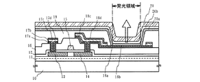
アクティブマトリクス型発光装置の断面図(1画素の一部)を図1に示す。
色、赤色、或いは緑色を発光する第2EL層20bに流れる電流を制御する素子であり、
13、14はソース領域またはドレイン領域である。基板10は、ガラス基板や、プラス
チック基板を用いることができ、絶縁膜を表面に有する半導体基板や金属基板も用いるこ
とができる。基板10上には下地絶縁膜11(ここでは、下層を窒化絶縁膜、上層を酸化
絶縁膜)が形成されており、ゲート電極15と半導体層との間には、ゲート絶縁膜12が
設けられている。また、16は無機材料、例えば、酸化珪素膜、窒化珪素膜、窒化酸化珪
素膜、窒化アルミニウム、または窒化酸化アルミニウムから選ばれる単層または積層から
なる層間絶縁膜である。また、ここでは図示しないが、一つの画素には、他にもTFT(
nチャネル型TFTまたはpチャネル型TFT)を一つ、または複数設けている。また、
ここでは、一つのチャネル形成領域を有するTFTを示したが、特に限定されず、複数の
チャネルを有するTFTとしてもよい。
第1の電極は、2層の領域からなる第1領域と、4層の領域からなる第2領域と、第1領
域と第2領域の境界線に段差を有する構造となっている。
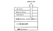
ムを主成分とする膜、18dとして窒化チタン膜として順に積層し、バッファ層20aに
接する窒化チタン膜(18bで示される第1の電極の1層)を陽極として機能させる。窒
化チタンはバッファ層20aと良好な接触抵抗が得られるため、好ましい。
造(合計4層)は、アルミニウムを主成分とする膜を含んでおり、低抵抗な配線とするこ
とができ、ソース配線なども同時に形成される。
00nm、第1の電極18cとしてAl−Ti=350nm、第1の電極18dとしてT
i=100nmとする場合、レジストマスクを形成してエッチングする。エッチング条件
は、ICPエッチング装置を用い、反応ガスとしてBCl3=60sccm、Cl2=2
0sccmを用い、1.9Paの圧力でコイル型の電極に450WのRF(13.56M
Hz)電力を投入し、基板側(試料ステージ)にも100WのRF(13.56MHz)
電力を投入してドライエッチングを行い、Al−Ti(第1の電極18c)がエッチング
されたところからさらに15秒のオーバーエッチングによってTiN(第1の電極18b
)を露出させる。
成する。絶縁物19は隣合う画素との境界に配置され、第1の電極の周縁を囲むように覆
っている。絶縁物19の厚さは、後の蒸着工程で接触する蒸着マスクと第1の電極との間
隔を確保するため重要であり、厚くすることが望ましい。本実施の形態においては、絶縁
物19の下方に4層構造の配線を設けることができるため、絶縁物19の最上面と第1の
電極との間隔を十分に確保することができる。
或いは陽極)である。透光性を有する導電膜(透光性導電膜とも呼ぶ)としては、ITO
(酸化インジウム酸化スズ合金)、酸化インジウム酸化亜鉛合金(In2O3―ZnO)
、酸化亜鉛(ZnO)、酸化珪素を含むインジウム錫酸化物(ITSO)、酸化スズ(S
nO2)等を用いることができる。また、第2の電極21は、可視光に対して透明であれ
ば特に限定されず、例えば、薄い金属層(代表的にはMgAg、MgIn、AlLiなど
の合金や、AgやAl)と透光性導電膜との積層としてもよい。
を指す。
層(バッファ層)20aと第2EL層20bの積層)を設けている。バッファ層20aは
、金属酸化物(酸化モリブデン、酸化タングステン、酸化レニウムなど)と有機化合物(
ホール輸送性を有する材料(例えば4,4’−ビス[N−(3−メチルフェニル)−N−
フェニルアミノ]ビフェニル(略称:TPD)、4,4’−ビス[N−(1−ナフチル)
−N−フェニルアミノ]ビフェニル(略称:α−NPD)、4,4’−ビス{N−[4−
(N,N−ジ−m−トリルアミノ)フェニル]−N−フェニルアミノ}ビフェニル(略称
:DNTPD)など))とを含む複合層である。また、第2EL層20bは、例えば、ト
リス(8−キノリノラト)アルミニウム(略称:Alq3)や、トリス(4−メチル−8
−キノリノラト)アルミニウム(略称:Almq3)や、α−NPDなどを用いることが
できる。また、第2EL層20bは、ドーパント材料を含ませてもよく、例えば、N,N
’−ジメチルキナクリドン(略称:DMQd)や、クマリン6や、ルブレンなどを用いる
ことができる。第1の電極と第2の電極の間に設けられる有機化合物を含む積層は、抵抗
加熱法などの蒸着法によって形成すればよい。
離を制御し、発光効率を高めることができる。バッファ層の膜厚を調節することによって
、各発光素子からの発光色がきれいに表示された優れた映像を表示でき、低消費電力化さ
れた発光装置を実現することができる。
よい。
成することが好ましい。この保護膜はスパッタ法(DC方式やRF方式)により得られる
窒化珪素または窒化酸化珪素を主成分とする絶縁膜、または炭素を主成分とする薄膜であ
る。
発明を適用することが可能であり、例えばボトムゲート型(逆スタガ型)TFTや順スタ
ガ型TFTに適用することが可能である。また、シングルゲート構造のTFTに限定され
ず、複数のチャネル形成領域を有するマルチゲート型TFT、例えばダブルゲート型TF
Tとしてもよい。
体膜、有機材料を主成分とする半導体膜、或いは金属酸化物を主成分とする半導体膜を用
いることができる。珪素を主成分とする半導体膜としては、非晶質半導体膜、結晶構造を
含む半導体膜、非晶質構造を含む化合物半導体膜などを用いることができ、具体的にはア
モルファスシリコン、微結晶シリコン、多結晶シリコンなどを用いることができる。また
、有機材料を主成分とする半導体膜としては、他の元素と組み合わせて一定量の炭素また
は炭素の同素体(ダイヤモンドを除く)からなる物質を主成分とする半導体膜を用いるこ
とができる。具体的には、ペンタセン、テトラセン、チオフェンオリゴマ誘導体、フェニ
レン誘導体、フタロシアニン化合物、ポリアセチレン誘導体、ポリチオフェン誘導体、シ
アニン色素等が挙げられる。また、金属酸化物を主成分とする半導体膜としては、酸化亜
鉛(ZnO)や亜鉛とガリウムとインジウムの酸化物(In−Ga−Zn−O)等を用い
ることができる。
A’で切断した断面図を図2(B)に示す。以下に、図を用いて発光装置の作製手順の一
例を説明する。
2Oを反応ガスとして成膜される酸化窒化シリコン膜を10〜200nm(好ましくは5
0〜100nm)形成する。ここでは、膜厚50nmの酸化窒化シリコン膜(組成比Si
=32%、O=27%、N=24%、H=17%)を形成する。次いで、下地絶縁膜の2
層目としては、プラズマCVD法を用い、SiH4及びN2Oを反応ガスとして成膜され
る酸化窒化シリコン膜を50〜200nm(好ましくは100〜150nm)の厚さに積
層形成する。ここでは、膜厚100nmの酸化窒化シリコン膜(組成比Si=32%、O
=59%、N=7%、H=2%)を形成する。ここでは下地絶縁膜31として2層構造を
用いるが、前記絶縁膜の単層膜または3層以上積層させた構造を用いても良い。
造を有する半導体膜を公知の手段(スパッタ法、LPCVD法、またはプラズマCVD法
等)により成膜した後、公知の結晶化処理(レーザー結晶化法、熱結晶化法、またはニッ
ケルなどの触媒を用いた熱結晶化法等)を行って得られた結晶質半導体膜を所望の形状に
パターニングして形成する。この半導体層の厚さは25〜80nm(好ましくは30〜6
0nm)の厚さで形成する。結晶質半導体膜の材料に限定はないが、好ましくはシリコン
またはシリコンゲルマニウム合金などで形成すると良い。
続発光型のエキシマレーザーやYAGレーザー、YVO4レーザーを用いることができる
。これらのレーザーを用いる場合には、レーザー発振器から放射されたレーザー光を光学
系で線状に集光し半導体膜に照射する方法を用いると良い。結晶化の条件は実施者が適宣
選択するものであるが、エキシマレーザーを用いる場合はパルス発振周波数30Hzとし
、レーザーエネルギー密度を100〜400mJ/cm2(代表的には200〜300m
J/cm2)とする。また、YAGレーザーを用いる場合にはその第2高調波を用いパル
ス発振周波数1〜10kHzとし、レーザーエネルギー密度を300〜600mJ/cm
2(代表的には350〜500mJ/cm2)とすると良い。そして幅100〜1000
μm、例えば400μmで線状に集光したレーザー光を基板全面に渡って照射し、この時
の線状レーザー光の重ね合わせ率(オーバーラップ率)を80〜98%として行えばよい
。
り返し周波数の高いパルスのレーザ光を非晶質構造を有する半導体膜に照射してレーザア
ニールを行って結晶質半導体膜を作製することもできる。なお、高強度とは、単位時間あ
たり単位面積あたりに高い尖頭出力を持つことを指しており、例えばレーザ光の尖頭出力
の範囲は、1GW/cm2〜1TW/cm2とする。波長が1μm程度の基本波は、半導
体薄膜に照射してもあまり吸収されず、吸収効率が低いが、パルス幅をピコ秒台、或いは
フェムト秒(10−15秒)台のパルスレーザから射出される基本波であれば、高強度の
レーザ光が得られ、非線形光学効果(多光子吸収)が生じ、半導体薄膜に吸収させること
ができる。非線形光学素子を用いず、且つ、高調波に変換しないため、15Wよりも大き
な出力、例えば40Wの出力を有するレーザ発振器をレーザアニール法に用いることが可
能となる。従って、一度の走査で形成される大粒径結晶の領域の幅を拡大することができ
るため、格段に生産性を向上させることができる。
絶縁膜33を形成する。ゲート絶縁膜33はプラズマCVD法またはスパッタ法を用い、
厚さを40〜150nmとしてシリコンを含む絶縁膜で形成する。本実施例では、プラズ
マCVD法により115nmの厚さで酸化窒化シリコン膜(組成比Si=32%、O=5
9%、N=7%、H=2%)で形成する。勿論、ゲート絶縁膜は酸化窒化シリコン膜に限
定されるものでなく、他のシリコンを含む絶縁膜を単層または積層構造として用いても良
い。
、ソース領域及びドレイン領域32を形成する。添加した後、不純物元素を活性化するた
めに加熱処理、強光の照射、またはレーザー光の照射を行う。また、活性化と同時にゲー
ト絶縁膜へのプラズマダメージやゲート絶縁膜と半導体層との界面へのプラズマダメージ
を回復することができる。特に、室温〜300℃の雰囲気中において、表面または裏面か
らYAGレーザーの第2高調波を照射して不純物元素を活性化させることは非常に有効で
ある。YAGレーザーはメンテナンスが少ないため好ましい活性化手段である。
ス、BPSG(ボロンとリンを添加したガラス)などを含む)からなる層間絶縁膜35を
形成し、水素化を行った後、ソース領域、またはドレイン領域に達するコンタクトホール
を形成する。次いで、ソース電極(配線34)、第1の電極(ドレイン電極)36a〜3
6dを形成してTFT(pチャネル型TFT)を完成させる。
えてn型不純物元素(P、As等)を用いることによってnチャネル型TFTを形成する
ことができることは言うまでもない。
l、Ag、Ni、W、WSiX、WNX、WSiXNY、Ta、TaNX、TaSiXN
Y、NbN、MoN、Cr、Pt、Zn、Sn、In、またはMoから選ばれた元素、ま
たは前記元素を主成分とする合金材料もしくは化合物材料を主成分とする膜またはそれら
の積層膜を総膜厚100nm〜800nmの範囲で用いればよい。
可能な材料、代表的にはチタンが好ましく、膜厚10〜100nmの範囲とすればよい。
また、第1の電極の第2層36bは、薄膜とした場合に仕事関数の大きい材料(TiN、
TaN、MoN、Pt、Cr、W、Ni、Zn、Sn)が好ましく、膜厚10〜100n
mの範囲とすればよい。なお、第2層36bは、第3層36cと第1層36aの合金化を
防ぐブロッキング層としても機能している。また、第4層36dは、第3層36cの酸化
防止、腐食防止、またはヒロック等の発生を防止する材料、代表的には窒化金属(TiN
、WNなど)が好ましく、膜厚20〜100nmの範囲とすればよい。
す構造とする。なお、図2(A)に第1領域と第2領域の境界線、即ち第3層36cの輪
郭を示す。
。なお、絶縁物37の輪郭を図2(A)に示す。
極39を形成する。
光素子を封止するためにシール材またはシート状接着材により封止基板(透明基板)を貼
り合わせる。なお、封止基板と発光素子との間隔を確保するために樹脂膜からなるスペー
サを設けても良い。そして、シール材の内側の空間には窒素等の不活性気体が充填されて
いる。なお、シール材としてはエポキシ樹脂を用いるのが好ましい。また、シール材はで
きるだけ水分や酸素を透過しない材料であることが望ましい。さらに、空間の内部に酸素
や水を吸収する効果をもつ物質(乾燥剤など)を含有させても良い。
断することができ、外部から水分や酸素といった有機化合物層の劣化を促す物質が侵入す
ることを防ぐことができる。従って、信頼性の高い発光装置を得ることができる。
本実施の形態では、実施の形態1と異なる構造の例を図3に示す。図3の構造は、第1
の電極がTFTの半導体層と接しているのではなく、電極を介して電気的にTFTの半導
体層と接している。また、第1の電極は、金属膜単層からなる第1領域と、3層からなる
第2領域と、第1領域と第2領域の間に段差を有する構造となっている。また、開口率を
向上させるために、コンタクトホール周辺のみを3層の第1領域とし、それ以外の領域を
第2領域としている。
結晶質半導体膜からなる半導体層、ゲート絶縁膜312を形成する。
電極となる電極338、337を形成する。次いで、レジストマスクを用いて、半導体に
p型を付与する不純物元素(Bなど)、ここではボロンを選択的に添加して、p型の高濃
度不純物領域313、314、331、332を形成する。次いで、LDD領域を形成す
るため、レジストマスクを除去したあと、新たにレジストマスクを形成して、半導体にn
型を付与する不純物元素(P、Asなど)、ここではリンを選択的に添加して低濃度不純
物領域を形成する。そして、レジストマスクを除去したあと、新たにレジストマスクを形
成して、半導体層に対してリンを選択的に添加して高濃度不純物領域333、334を形
成する。なお、1回しかリンが添加されていない低濃度不純物領域は、LDD領域335
、336となる。
の照射、またはレーザ光の照射を行う。
行う。その後、高濃度不純物領域に達するコンタクトホールを第1の層間絶縁膜316お
よびゲート絶縁膜に形成する。次いで、ソース電極またはドレイン電極となる電極317
、318、341〜344を形成して複数種類のTFT(pチャネル型TFT及びnチャ
ネル型TFT)を完成させる。
には、電極338をゲート電極とするnチャネル型TFTと、電極337をゲート電極と
するpチャネル型TFTが形成される。なお、駆動回路部のnチャネル型TFTは、チャ
ネル形成領域340を有し、駆動回路部のpチャネル型TFTは、チャネル形成領域33
9を有している。
、電極318、342、343に達するコンタクトホールを第2の層間絶縁膜309に形
成する。
膜は、Ti、TiN、TiSiXNY、Al、Ag、Ni、W、WSiX、WNX、WS
iXNY、Ta、TaNX、TaSiXNY、NbN、MoN、Cr、Pt、Zn、Sn
、In、またはMoから選ばれた元素、または前記元素を主成分とする合金材料もしくは
化合物材料を主成分とする膜またはそれらの積層膜を総膜厚100nm〜800nmの範
囲で用いればよい。
び第1の電極を形成する。接続電極と同時に引き回し配線も同じ積層構造で形成できるた
め、駆動回路部の占有面積を縮小することができる。
選択的にエッチングして、第1層308aのみで構成される第1領域と、第1層308a
、第2層308b、第3層308cの合計3層で構成される第2領域と、第1領域と第2
領域との境界線に段差を有する第1の電極を形成する。
る。
バッファ層であり、金属酸化物(酸化モリブデン、酸化タングステン、酸化レニウムなど
)と有機化合物(ホール輸送性を有する材料(例えば4,4’−ビス[N−(3−メチル
フェニル)−N−フェニルアミノ]ビフェニル(略称:TPD)、4,4’−ビス[N−
(1−ナフチル)−N−フェニルアミノ]ビフェニル(略称:α−NPD)、4,4’−
ビス{N−[4−(N,N−ジ−m−トリルアミノ)フェニル]−N−フェニルアミノ}
ビフェニル(略称:DNTPD)など))とを含む複合層である。また、320bは発光
層を含む単層または積層である。バッファ層320aの膜厚を調節することによって、第
1の電極と発光層との距離を制御し、発光効率を高めることができる。
或いはMgAg、MgIn、AlLiなどの合金、または周期表の1族もしくは2族に属
する元素とアルミニウムとを共蒸着法により形成した透光性を有する膜を用いればよい。
ここでは、第2の電極を通過させて発光させる上面射出型であるので、1nm〜20nm
程度の薄い金属層とする。第2の電極321は、発光を通過するのに十分な薄さであれば
よい。
を封止するためにシール材またはシート状接着材により封止基板(透明基板)を貼り合わ
せる。また、封止基板を貼りつける際には、不活性気体(希ガスまたは窒素)を含む雰囲
気下で行うことが好ましい。
また、1面取りの場合、予めカットされている対向基板を貼り合わせることによって、分
断工程を省略することもできる。この段階でELモジュールが完成する。
ールの上面図であり、図4(B)は、断面図の一部である。
と、画素部の各画素を駆動させる駆動回路部41a、41bと、EL層上に設けられる第
2の電極と引き出し配線とを接続する接続部43と、外部回路と接続するためにFPCを
貼り付ける端子部42が設けられている。
シール材49とによって密閉する。また、図4(B)は、図4(A)中における鎖線A−
A’で切断した場合の断面図である。
にストライプ配列、例えばR、G、Bの順で配置されている。また、発光素子の配置は限
定されず、デルタ配列、モザイク配列などとしてもよい。
ャップ保持材50が設けられ、且つ、シール材49によって封止基板48が貼りつけられ
ており、全ての発光素子は密閉されている。なお、シート状接着材44で発光素子を十分
に封止することができるのであれば、特にシール材49は設けなくともよい。また、シー
ト状接着材44で一対の基板間隔が十分に保たれるのであれば、特にギャップ保持材50
は設けなくともよい。
形成し、その凹部に乾燥剤を配置してもよい。
形成できるため、駆動回路部の占有面積を縮小して狭額縁化させることができる。また、
接続電極345a〜345cと同時に端子部42の端子電極も同じ積層構造で形成するこ
ともできる。
ここではフルカラー表示装置を作製するいくつかの方法を示す。具体的には、3つの発
光素子を用いる方法、白色発光素子とカラーフィルターとを組み合わせる方法、青色発光
素子と色変換層とを組み合わせる方法、白色発光素子と色変換層と、カラーフィルターと
を組み合わせる方法などが挙げられる。
素子と、緑色発光素子とを規則的に並べた1つの画素を画素部に配置することによって行
う。例えば発光色毎に開口位置が異なる蒸着マスクをR、G、Bで3種類用意してR、G
、Bの発光層の塗りわけを蒸着法で行えばよい。
、各発光素子からの発光色がきれいに表示された優れた映像を表示でき、低消費電力化さ
れた発光装置を実現することができる。
して、斜めモザイク配列、三角モザイク配列、RGBG四画素配列、もしくはRGBW四
画素配列などを用いることができる。
同じ色の着色層を発光素子に重なるように設ければよく、例えば、青色発光素子と重なる
位置に青色の着色層を設ければよい。
とよぶ)について図5(A)により説明する。
れた白色発光をカラーフィルターに通過させることで赤、緑、青の発光を得るという方式
である。
材料からなる発光層を用いる場合について説明する。この場合、発光層となる高分子材料
への色素ドーピングは溶液調整で行うことができ、複数の色素をドーピングする共蒸着を
行う蒸着法に比べて極めて容易に得ることができる。
なる陽極上に、正孔注入層として作用するポリ(エチレンジオキシチオフェン)/ポリ(
スチレンスルホン酸)水溶液(PEDOT/PSS)を全面に塗布、焼成した後、発光層
として作用する発光中心色素(1,1,4,4−テトラフェニル−1,3−ブタジエン(
TPB)、4−ジシアノメチレン−2−メチル−6−(p−ジメチルアミノ−スチリル)
−4H−ピラン(DCM1)、ナイルレッド、クマリン6など)ドープしたポリビニルカ
ルバゾール(PVK)溶液を全面に塗布、焼成した後、仕事関数の小さい金属(Li、M
g、Cs)を含む薄膜と、その上に積層した透明導電膜(ITO(酸化インジウム酸化ス
ズ合金)、酸化インジウム酸化亜鉛合金(In2O3―ZnO)、酸化亜鉛(ZnO)等
)との積層からなる陰極を形成する。なお、PEDOT/PSSは溶媒に水を用いており
、有機溶剤には溶けない。従って、PVKをその上から塗布する場合にも、再溶解する心
配はない。また、PEDOT/PSSとPVKは溶媒が異なるため、成膜室は同一のもの
を使用しないことが好ましい。
こともできる。例えば、ホール輸送性のポリビニルカルバゾール(PVK)に電子輸送性
の1,3,4−オキサジアゾール誘導体(PBD)を分散させてもよい。また、30wt
%のPBDを電子輸送剤として分散し、4種類の色素(TPB、クマリン6、DCM1、
ナイルレッド)を適当量分散することで白色発光が得られる。
陰極から注入された電子が有機化合物膜において再結合することにより、有機化合物膜に
おいて、白色発光が得られる。
物膜を適宜選択し、重ねて混色させることによって全体として白色発光を得ることも可能
である。
光以外を吸収する着色層(G)、青色発光以外を吸収する着色層(B)をそれぞれ設けた
カラーフィルタを形成することにより、発光素子からの白色発光をそれぞれ分離して、赤
色発光、緑色発光、青色発光として得ることができる。また、アクティブマトリクス型の
場合には、基板とカラーフィルターの間にTFTが形成される構造となる。
めモザイク配列、三角モザイク配列、RGBG四画素配列、もしくはRGBW四画素配列
などを用いることができる。
ジストを用いて形成される。白色発光とカラーフィルターを組み合わせれば、フルカラー
としての色再現性は十分確保することができる。
合物膜で形成されていることから、発光色ごとに有機化合物膜を塗り分けて形成する必要
がない。また、鏡面反射を防ぐ円偏光板も特に必要ないものとすることができる。
ることにより実現されるCCM法(color changing mediums)に
ついて図5(B)により説明する。
ぞれの色変換層で色変換を行う。具体的には色変換層で青色から赤色への変換(B色から
R色)、色変換層で青色から緑色への変換(B色からG色)、色変換層で青色からさらに
色純度のよい青色への変換(B色からB色)(なお、青色から青色への変換は行わなくて
も良い。)を行い、赤色、緑色及び青色の発光を得るというものである。CCM法の場合
にも、アクティブマトリクス型の場合には、基板と色変換層の間にTFTが形成される構
造となる。
防ぐ円偏光板も特に必要ないものとすることができる。
コントラストを低下させる問題があるので、図5(C)に示したようにカラーフィルター
を装着するなどしてコントラストを上げるようにすると良い。
ある。
図6に示す製造装置は、有機化合物を有する層の蒸着などを行うマルチチャンバーに封
止処理を行うチャンバーが一つのユニットとなっている例である。一つのユニットとする
ことで水分などの不純物の混入防止やスループット向上を図っている。
01、105、107、111と、第1成膜室106Eと、第2成膜室106Bと、第3
成膜室106Gと、第4成膜室106R、第5成膜室106Fと、その他の成膜室109
、110、112、113、132と、ベーク室123、マスクストック室124と、基
板ストック室130a、130bと、基板投入室120と、多段真空加熱室103とを有
する製造装置である。なお、搬送室104aには基板を搬送するための搬送機構が設けて
おり、他の搬送室も同様にそれぞれ搬送機構が設けてある。
、貼り合わせ室144と、シール形成室145と、前処理室146と、封止基板ロード室
117とを有する製造装置である。なお、チャンバーや処理室の間にはゲートが設けられ
ている。
板を図6に示す製造装置に搬入し、発光装置を作製する手順を示す。
の他の薄膜トランジスタ(スイッチング用TFTなど)が複数設けられている。
イズは、320mm×400mm、370mm×470mm、550mm×650mm、
600mm×720mm、680mm×880mm、1000mm×1200mm、11
00mm×1250mm、さらには1150mm×1300mmのような大面積基板でも
対応可能である。
た基板)は大気圧が保たれている搬送室118に搬送する。なお、搬送室118には基板
を搬送または反転するための搬送機構(搬送ロボットなど)が設けられている。
ある。搬送室118に設けられたロボットは、基板の表裏を反転させることができ、受渡
室101に反転させて搬入することができる。受渡室101は、真空排気処理室と連結さ
れており、真空排気して真空にすることもでき、真空排気した後、不活性ガスを導入して
大気圧にすることもできる。
プ、またはドライポンプが備えられている。これにより各室と連結された搬送室の到達真
空度を10−5〜10−6Paにすることが可能であり、さらにポンプ側および排気系か
らの不純物の逆拡散を制御することができる。
となく、受渡室101から搬送室102に基板を搬送する。
とが好ましく、基板を搬送室102から多段真空加熱室103に搬送し、上記基板に含ま
れる水分やその他のガスを徹底的に除去するために、脱気のためのアニールを真空(5×
10−3Torr(0.665Pa)以下、好ましくは10−4〜10−6Pa)で行う
。多段真空加熱室103では平板ヒータ(代表的にはシースヒータ)を用いて、複数の基
板を均一に加熱する。この平板ヒータは複数設置され、平板ヒータで基板を挟むように両
面から加熱することもでき、勿論、片面から加熱することもできる。特に、層間絶縁膜や
隔壁の材料として有機樹脂膜を用いた場合、有機樹脂材料によっては水分を吸着しやすく
、さらに脱ガスが発生する恐れがあるため、有機化合物を含む層を形成する前に100℃
〜250℃、好ましくは150℃〜200℃、例えば30分以上の加熱を行った後、30
分の自然冷却を行って吸着水分を除去する真空加熱を行うことは有効である。
どで高分子材料からなる正孔注入層を形成してもよい。正孔注入層を塗布法で形成した後
、蒸着法による成膜直前にベーク室123で大気圧加熱または真空加熱(100〜200
℃)を行うことが好ましい。
め、基板の端面や周縁部、端子部、陰極と下部配線との接続領域などは選択的に除去する
ことが好ましく、搬送室102に連結する前処理室を設け、前処理室でマスクを使用した
O2アッシングなどにより選択的に除去することが好ましい。
バッファ層を蒸着する。
N−フェニルアミノ]ビフェニル(略称:NPB)と酸化モリブデンとをそれぞれ別の抵
抗加熱式の蒸発源に収納し、真空に引かれた蒸着装置内に設置された第1の電極を有する
基板に対して蒸着する。蒸着時において、NPBは0.4nm/sの成膜レートで蒸着さ
せ、酸化モリブデンはNPBに対して1/4の量(重量比)を蒸発させる。この場合、モ
ル比では、NPB:酸化モリブデン=1:1となっている。金属酸化物と有機化合物とを
含む第1の複合層の膜厚は50nmとする。
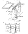
装置の機構を簡略に示す。
基板の搬送方向706a(図7(A)中の矢印の方向)に基板が搬送される。基板搬送手
段(搬送ロボットまたは搬送ローラー)により基板は搬送されて、蒸着シールド703a
の上方を通過する。蒸着シールド703aは開口部703bを有しており、蒸着源704
からの蒸着材料が開口部703bから昇華するようになっている。開口部703bから蒸
着材料の昇華方向706bを維持するために蒸着シールド703aは、蒸着シールド自体
には付着しないように加熱されている。また、蒸着シールドに接してヒーターが設けられ
ている。蒸着シールドの加熱温度はヒーターと接続しているコンピュータで制御しても良
い。
移動することが可能である。なお、蒸着源は移動させる代わりに、蒸着源の向きを変えて
蒸着される角度を変えても良い。蒸着方法は、抵抗加熱法を用いる。また、蒸着膜の膜厚
均一性を向上させるため、蒸着源が移動する範囲は基板の幅Waよりも広いことが望まし
い。また、蒸着シールドの幅Wbも基板の幅Waよりも広くすることが蒸着膜の膜厚均一
性を向上させる。
広がるため、蒸着源と重なる部分、即ち、同心円状に広がる中心部の膜厚が厚くなってし
まう恐れがある。本発明は、蒸着シールドによって同心円状に広がることを抑え、さらに
蒸着源を移動させることによって、蒸着膜の膜厚均一性を格段に向上させている。
楕円形としたが、開口部703bの形状や数は特に限定されない。開口部の形状を細長い
楕円形とすることで蒸着材料が開口を塞ぐことを防いでいる。
する設置室を設けてもよい。蒸着源にはルツボを加熱するヒーターが設けられている。設
置室は、成膜室内における蒸着源の移動方向の延長線上に設けることが好ましい。蒸着材
料を設置室で補給した後、成膜室と同じ真空度にし、設置室に設けられた膜厚モニタで安
定な蒸着速度まで加熱を行う。そしてゲートを開けて設置室から蒸着源を一方向に成膜室
へ移動させて、その方向を維持して成膜室内でも蒸着源を移動させることによって、基板
に対して蒸着を行う。このように設置室を配置することでスムーズな蒸着源の移動を可能
とする。また、一つの成膜室に複数の蒸着源と蒸着シールドを設けてもよい。複数の蒸着
源を設け、設置室を設けた場合の蒸着装置の上面図を図7(B)に示す。蒸着源の移動方
向705に設置室707を設置し、蒸着材料を補給する際には、蒸着源を設置室まで移動
させて補給を行えばよい。蒸着源が成膜室に固定されている場合には、蒸着源に蒸着材料
を補給するためには成膜室内を大気圧としなければならず、再度蒸着するためには成膜室
内を真空にするのに時間を要してしまう。設置室707を設ければ、成膜室700の真空
度を維持したまま、設置室内のみを大気圧と真空とに切り替えればよいため、短時間で蒸
着材料の補給が可能となる。
向と垂直方向に移動する2つ目の蒸着源708を設けてもよい。複数の蒸着源を一つの成
膜室に設けることによって、連続的な積層成膜が可能となる。ここでは一つの成膜室に2
つの蒸着源を設けた例を示したが、一つの成膜室にそれ以上の数の蒸着源を設けてもよい
。
となく、受渡室105から搬送室104aに基板を搬送する。
基板を適宜、搬送して、赤色の発光層、緑色の発光層、青色の発光層、電子輸送層(また
は電子注入層)となる低分子からなる有機化合物を含む層を適宜形成する。
示す蒸着装置とする。
青色の発光層としてCBP(4,4’−ビス(N−カルバゾリル)−ビフェニル)が添加
されたPPD(4,4’−ビス(N−(9−フェナントリル)−N−フェニルアミノ)ビ
フェニル)を膜厚30nmで蒸着する。
領域に赤色の発光層としてDCMが添加されたAlq3を膜厚40nmで成膜する。
領域に緑色の発光層としてDMQdが添加されたAlq3を膜厚40nmで成膜する。
具体的にはR、G、B)の発光を示す発光素子を形成することができる。
室に搬送する。大型基板を用いるとマスクが大面積化するため、マスクを固定するフレー
ムが大きくなり、枚数をたくさんストックするのが困難になるため、ここでは2つのマス
クストック室124を用意している。マスクストック室124で蒸着マスクのクリーニン
グを行ってもよい。また、蒸着の際にはマスクストック室が空くため、成膜後または処理
後の基板をストックすることも可能である。
ことなく、受渡室107から搬送室108に基板を搬送する。
、陰極を形成する。この陰極は、透明または半透明であることが好ましく、抵抗加熱を用
いた蒸着法により形成される金属膜(MgAg、MgIn、LiFなどの合金、または周
期表の1族もしくは2族に属する元素とアルミニウムとを共蒸着法により形成した膜、ま
たはこれらの積層膜)の薄膜(1nm〜20nm)、或いは上記金属膜の薄膜(1nm〜
20nm)と透明導電膜との積層を陰極とすることが好ましい。積層する場合、成膜室1
09に搬送し、スパッタ法を用いて透明導電膜を形成する。
膜からなる保護膜を形成して封止してもよい。ここでは、成膜室113内には、珪素から
なるターゲット、または酸化珪素からなるターゲット、または窒化珪素からなるターゲッ
トが備えられている。
室114に導入され、基板ストック室130a、130bで保管、もしくは受渡室141
に搬送する。搬送室114、基板ストック室130a、130b、受渡室141は減圧雰
囲気とすることが好ましい。
ト148によって、貼り合わせ室144に搬送される。
室117から導入した後、まず、減圧下で加熱して脱気を行う。その後、搬送室147に
設置された搬送ユニット148によって、UV照射機構を備えた前処理室146に搬送し
、紫外線照射による表面処理を行う。次いで、シール形成室145に搬送し、シール材の
形成を行う。シール形成室145にはディスペンス装置またはインクジェット装置が備え
られている。また、シール形成室145にはシール材を仮硬化するためにベークまたはU
V照射機構を備えてもよい。シール形成室145でシール材を仮硬化させた後、シール材
で囲まれた領域に充填材の滴下を行う。
わせる。上定盤または下定盤を上下動させることによって一対の基板を貼り合わせる。減
圧下で2枚の基板を貼り合わせる際、第2の基板に設けられた柱状または壁状の構造物が
基板間隔を精密に保ち続け、且つ、基板割れが生じないよう基板にかかる圧力を拡散する
重要な役割を果たしている。
材で囲まれた領域に充填材の滴下を行う機構としてもよい。
て定盤間の空間を密閉した後、下定盤に設けられた穴から真空ポンプで脱空させて定盤間
の空間を減圧することができるようにしてもよい。こうすると、処理室全体に比べて減圧
する空間の容積が小さいので短時間に減圧することができる。
ったままの貼り合わせた状態で光を照射してシール材を硬化させてもよい。
143に搬送する。硬化処理室143ではシール材の本硬化を光照射または加熱処理によ
って行う。
圧から大気圧に戻した後、貼り合わせた一対の基板を取り出す。こうして基板間隔を均一
に保つ封止工程が完了する。
合わせることができる。
ここでは、バッファ層と陽極との接触抵抗に関する実験結果と、光取り出し効率の計算
結果を説明する。
発光層、陰極を順に設け、2mm×2mmの発光面積を有する発光素子に6Vの電圧をか
け、電流値を測定したところ、0.313mAが得られた。このことから、TiN膜とバ
ッファ層との接触抵抗は良好である。また、この素子の輝度は、501cd/m2であっ
た。
、発光層、陰極を順に設け、同様に電流値を測定したところ、0.249mAが得られた
。このことから、Ti膜とバッファ層との接触抵抗も良好である。また、この素子の輝度
は、577cd/m2であった。
ところ、0.015mAが得られた。このことから、Al膜とバッファ層との接触抵抗は
、Ti膜やTiN膜に比べ、あまり良好でないと言える。また、この素子の輝度は、51
cd/m2であった。
効率を様々に変化させることができる。
各発光色でバッファ層の膜厚を最適化することで相対輝度を同じにすることができる。な
お、素子構成は図9として計算を行った。
合わせることができる。
本発明の半導体装置、及び電子機器として、ビデオカメラ、デジタルカメラ等のカメラ、
ゴーグル型ディスプレイ(ヘッドマウントディスプレイ)、ナビゲーションシステム、音
響再生装置(カーオーディオ、オーディオコンポ等)、パーソナルコンピュータ、ゲーム
機器、携帯情報端末(モバイルコンピュータ、携帯電話、携帯型ゲーム機又は電子書籍等
)、記録媒体を備えた画像再生装置(具体的にはDigital Versatile
Disc(DVD)等の記録媒体を再生し、その画像を表示しうるディスプレイを備えた
装置)などが挙げられる。それら電子機器の具体例を図10および図11に示す。
ー2104、シャッター2106等を含む。なお、図10(A)は表示部2102側から
の図であり、撮像部は示していない。本発明により、製造コストを低減したプロセスでデ
ジタルカメラが実現できる。
表示部2203、キーボード2204、外部接続ポート2205、ポインティングマウス
2206等を含む。本発明により、製造コストを低減したプロセスでノート型パーソナル
コンピュータを実現することができる。
あり、本体2401、筐体2402、表示部A2403、表示部B2404、記録媒体(
DVD等)読み込み部2405、操作キー2406、スピーカー部2407等を含む。表
示部A2403は主として画像情報を表示し、表示部B2404は主として文字情報を表
示する。なお、記録媒体を備えた画像再生装置には電子遊技機器(代表的には家庭用ゲー
ム機器)なども含まれる。本発明により、製造コストを低減したプロセスで画像再生装置
を実現することができる。
、スピーカー部1904、ビデオ入力端子1905などを含む。この表示装置は、他の実
施の形態で示した作製方法により形成した薄膜トランジスタをその表示部1903および
駆動回路に用いることにより作製される。なお、表示装置には液晶表示装置、発光装置な
どがあり、具体的にはコンピュータ用、テレビ受信用、広告表示用などの全ての情報表示
用表示装置が含まれる。本発明により、製造コストを低減したプロセスで表示装置、特に
22インチ〜50インチの大画面を有する大型の表示装置を実現することができる。
た本体(A)901と、表示パネル(A)908、表示パネル(B)909、スピーカ9
06などが備えられた本体(B)902とが、蝶番910で開閉可能に連結されている。
表示パネル(A)908と表示パネル(B)909は、回路基板907と共に本体(B)
902の筐体903の中に収納される。表示パネル(A)908及び表示パネル(B)9
09の画素部は筐体903に形成された開口窓から視認できように配置される。
応じて画素数などの仕様を適宜設定することができる。例えば、表示パネル(A)908
を主画面とし、表示パネル(B)909を副画面として組み合わせることができる。
を具備している。本発明により、製造コストを低減したプロセスで携帯情報端末を実現す
ることができる。
る。例えば、蝶番910の部位に撮像素子を組み込んで、カメラ付きの携帯電話機として
も良い。また、操作スイッチ904、表示パネル(A)908、表示パネル(B)909
を一つの筐体内に納め、内蔵させた構成としても、上記した作用効果を奏することができ
る。また、表示部を複数個そなえた情報表示端末に本実施の形態の構成を適用しても、同
様な効果を得ることができる。
は構成を用いて、様々な電子機器を完成させることができる。
時間内で製造でき、且つ、低コストで歩留まりよく製造できる。
11 下地絶縁膜
12 ゲート絶縁膜
13 ソース領域またはドレイン領域
14 ソース領域またはドレイン領域
15 ゲート電極
16 層間絶縁膜
17a〜17d 電源供給線
18a〜18d 第1の電極
19 絶縁物
20a 第1EL層(バッファ層)
20b 第2EL層(発光層を含む積層)
21 第2の電極
30 基板
31 下地絶縁膜
32 ソース領域及びドレイン領域
33 ゲート絶縁膜
34 配線
35 層間絶縁膜
36a〜36d 第1の電極
37 絶縁物
38a 有機化合物を含む積層
38b 有機化合物を含む積層
39 第2の電極
40 画素部
41a 駆動回路部
41b 駆動回路部
42 端子部
43 接続部
44 シート状接着材
48 封止基板
49 シール材
50 ギャップ保持材
101 受渡室
102 搬送室
103 多段真空加熱室
104a 搬送室
105 受渡室
106R 成膜室
106G 成膜室
106B 成膜室
106F 成膜室
106E 成膜室
107 受渡室
108 搬送室
109 成膜室
110 成膜室
111 受渡室
112 成膜室
113 成膜室
114 搬送室
117 封止基板ロード室
118 搬送室
119 取出室
120 基板投入室
123 ベーク室
124 マスクストック室
130a 基板ストック室
130b 基板ストック室
132 成膜室
141 受渡室
143 硬化処理室
144 貼り合わせ室
145 シール形成室
146 前処理室
147 搬送室
148 搬送ユニット
308a 第1層
308b 第2層
308c 第3層
309 第2の層間絶縁膜
310 絶縁表面を有する基板
311 下地絶縁膜
312 ゲート絶縁膜
313 p型の高濃度不純物領域
314 p型の高濃度不純物領域
315 電極
316 第1の層間絶縁膜
317 電極
318 電極
319 絶縁物
320a 有機化合物を含む積層
320b 有機化合物を含む積層
321 第2の電極
331 p型の高濃度不純物領域
332 p型の高濃度不純物領域
333 高濃度不純物領域
334 高濃度不純物領域
335 LDD領域
336 LDD領域
337 電極
338 電極
339 電極
340 チャネル形成領域
341 電極
342 電極
343 電極
344 電極
345a〜345c 接続電極
701 基板
702 蒸着マスク
703a 蒸着シールド
703b 開口部
704 蒸着源
705 蒸着源の移動方向
706a 基板の搬送方向
706b 昇華方向
707 設置室
708 蒸着源
709 蒸着シールド
900 携帯電話機
901 本体(A)
902 本体(B)
903 筐体
904 操作スイッチ
905 マイクロフォン
906 スピーカ
907 回路基板
908 表示パネル(A)
909 表示パネル(B)
910 蝶番
1901 筐体
1902 支持台
1903 表示部
1904 スピーカー部
1905 ビデオ入力端子
2101 本体
2102 表示部
2104 操作キー
2106 シャッター
2201 本体
2202 筐体
2203 表示部
2204 キーボード
2205 外部接続ポート
2206 ポインティングマウス
2401 本体
2402 筐体
2403 表示部A
2404 表示部B
2405 記録媒体読込部
2406 操作キー
2407 スピーカー部
Claims (3)
- 成膜室内に、基板を第1の方向に移動する手段と、成膜室内壁に固定され、加熱温度調節が可能な蒸着シールドと、該蒸着シールドの下方に蒸着源と、該蒸着源を前記第1の方向と垂直な第2の方向に移動する移動手段と、を有し、
前記蒸着シールドは、基板の幅よりも広い矩形形状であり、
蒸着シールドの上面に開口部が複数設けられており、
蒸着源から蒸発された蒸着材料は、蒸着シールドに設けられた複数の開口部を通過して基板に蒸着されることを特徴とする蒸着装置。
- 請求項1において、
前記蒸着装置はインライン型の製造装置の2つの処理室の間に連結していることを特徴とする蒸着装置。
- 請求項21において、
前記蒸着装置はマルチチャンバー型の製造装置の搬送室に連結していることを特徴とする蒸着装置。
Priority Applications (1)
| Application Number | Priority Date | Filing Date | Title |
|---|---|---|---|
| JP2011060737A JP2011134723A (ja) | 2005-02-18 | 2011-03-18 | 蒸着装置及びel素子の作製方法 |
Applications Claiming Priority (3)
| Application Number | Priority Date | Filing Date | Title |
|---|---|---|---|
| JP2005043102 | 2005-02-18 | ||
| JP2005043102 | 2005-02-18 | ||
| JP2011060737A JP2011134723A (ja) | 2005-02-18 | 2011-03-18 | 蒸着装置及びel素子の作製方法 |
Related Parent Applications (1)
| Application Number | Title | Priority Date | Filing Date |
|---|---|---|---|
| JP2006042623A Division JP5170964B2 (ja) | 2005-02-18 | 2006-02-20 | 発光装置の作製方法 |
Related Child Applications (2)
| Application Number | Title | Priority Date | Filing Date |
|---|---|---|---|
| JP2012228708A Division JP5604495B2 (ja) | 2005-02-18 | 2012-10-16 | 蒸着装置 |
| JP2013155678A Division JP5844776B2 (ja) | 2005-02-18 | 2013-07-26 | 装置 |
Publications (1)
| Publication Number | Publication Date |
|---|---|
| JP2011134723A true JP2011134723A (ja) | 2011-07-07 |
Family
ID=36911961
Family Applications (4)
| Application Number | Title | Priority Date | Filing Date |
|---|---|---|---|
| JP2011060737A Withdrawn JP2011134723A (ja) | 2005-02-18 | 2011-03-18 | 蒸着装置及びel素子の作製方法 |
| JP2012228708A Active JP5604495B2 (ja) | 2005-02-18 | 2012-10-16 | 蒸着装置 |
| JP2013155678A Expired - Fee Related JP5844776B2 (ja) | 2005-02-18 | 2013-07-26 | 装置 |
| JP2013260303A Expired - Fee Related JP5700872B2 (ja) | 2005-02-18 | 2013-12-17 | 発光装置 |
Family Applications After (3)
| Application Number | Title | Priority Date | Filing Date |
|---|---|---|---|
| JP2012228708A Active JP5604495B2 (ja) | 2005-02-18 | 2012-10-16 | 蒸着装置 |
| JP2013155678A Expired - Fee Related JP5844776B2 (ja) | 2005-02-18 | 2013-07-26 | 装置 |
| JP2013260303A Expired - Fee Related JP5700872B2 (ja) | 2005-02-18 | 2013-12-17 | 発光装置 |
Country Status (5)
| Country | Link |
|---|---|
| US (3) | US7948171B2 (ja) |
| JP (4) | JP2011134723A (ja) |
| KR (6) | KR101315197B1 (ja) |
| CN (2) | CN100585868C (ja) |
| TW (5) | TWI587741B (ja) |
Cited By (1)
| Publication number | Priority date | Publication date | Assignee | Title |
|---|---|---|---|---|
| WO2013111600A1 (ja) * | 2012-01-27 | 2013-08-01 | パナソニック株式会社 | 有機エレクトロルミネッセンス素子製造装置及び有機エレクトロルミネッセンス素子の製造方法 |
Families Citing this family (1844)
| Publication number | Priority date | Publication date | Assignee | Title |
|---|---|---|---|---|
| JP2006164708A (ja) | 2004-12-06 | 2006-06-22 | Semiconductor Energy Lab Co Ltd | 電子機器および発光装置 |
| TWI412138B (zh) * | 2005-01-28 | 2013-10-11 | Semiconductor Energy Lab | 半導體裝置,電子裝置,和半導體裝置的製造方法 |
| US7608531B2 (en) | 2005-01-28 | 2009-10-27 | Semiconductor Energy Laboratory Co., Ltd. | Semiconductor device, electronic device, and method of manufacturing semiconductor device |
| US7851989B2 (en) * | 2005-03-25 | 2010-12-14 | Semiconductor Energy Laboratory Co., Ltd. | Light emitting device |
| US8030643B2 (en) | 2005-03-28 | 2011-10-04 | Semiconductor Energy Laboratory Co., Ltd. | Memory device and manufacturing method the same |
| US7928938B2 (en) | 2005-04-19 | 2011-04-19 | Semiconductor Energy Laboratory Co., Ltd. | Semiconductor device including memory circuit, display device and electronic apparatus |
| US8629819B2 (en) | 2005-07-14 | 2014-01-14 | Semiconductor Energy Laboratory Co., Ltd. | Semiconductor device and driving method thereof |
| EP1758072A3 (en) * | 2005-08-24 | 2007-05-02 | Semiconductor Energy Laboratory Co., Ltd. | Display device and driving method thereof |
| EP1998374A3 (en) * | 2005-09-29 | 2012-01-18 | Semiconductor Energy Laboratory Co, Ltd. | Semiconductor device having oxide semiconductor layer and manufacturing method thereof |
| KR101397571B1 (ko) * | 2005-11-15 | 2014-05-22 | 가부시키가이샤 한도오따이 에네루기 켄큐쇼 | 반도체장치 및 그의 제조방법 |
| EP1843194A1 (en) | 2006-04-06 | 2007-10-10 | Semiconductor Energy Laboratory Co., Ltd. | Liquid crystal display device, semiconductor device, and electronic appliance |
| US20070290604A1 (en) * | 2006-06-16 | 2007-12-20 | Matsushita Electric Industrial Co., Ltd. | Organic electroluminescent device and method of producing the same |
| JP5116277B2 (ja) | 2006-09-29 | 2013-01-09 | 株式会社半導体エネルギー研究所 | 半導体装置、表示装置、液晶表示装置、表示モジュール及び電子機器 |
| TWI442368B (zh) | 2006-10-26 | 2014-06-21 | Semiconductor Energy Lab | 電子裝置,顯示裝置,和半導體裝置,以及其驅動方法 |
| US7646015B2 (en) * | 2006-10-31 | 2010-01-12 | Semiconductor Energy Laboratory Co., Ltd. | Manufacturing method of semiconductor device and semiconductor device |
| DE102007024153A1 (de) * | 2007-04-23 | 2008-10-30 | Osram Opto Semiconductors Gmbh | Elektrisches organisches Bauelement und Verfahren zu seiner Herstellung |
| JP5542296B2 (ja) | 2007-05-17 | 2014-07-09 | 株式会社半導体エネルギー研究所 | 液晶表示装置、表示モジュール及び電子機器 |
| JP5542297B2 (ja) | 2007-05-17 | 2014-07-09 | 株式会社半導体エネルギー研究所 | 液晶表示装置、表示モジュール及び電子機器 |
| JP4989309B2 (ja) | 2007-05-18 | 2012-08-01 | 株式会社半導体エネルギー研究所 | 液晶表示装置 |
| US8354674B2 (en) * | 2007-06-29 | 2013-01-15 | Semiconductor Energy Laboratory Co., Ltd. | Semiconductor device wherein a property of a first semiconductor layer is different from a property of a second semiconductor layer |
| WO2009014155A1 (en) | 2007-07-25 | 2009-01-29 | Semiconductor Energy Laboratory Co., Ltd. | Photoelectric conversion device and electronic device having the same |
| KR101383490B1 (ko) * | 2007-09-21 | 2014-04-08 | 엘지디스플레이 주식회사 | 전계발광소자 |
| JP5169195B2 (ja) * | 2007-12-14 | 2013-03-27 | セイコーエプソン株式会社 | 有機el装置、電子機器 |
| JP2009170200A (ja) * | 2008-01-15 | 2009-07-30 | Sony Corp | 表示装置の製造方法 |
| NO332409B1 (no) * | 2008-01-24 | 2012-09-17 | Well Technology As | Anordning og fremgangsmate for a isolere en seksjon av et bronnhull |
| CN101521219B (zh) * | 2008-02-28 | 2013-02-13 | 统宝光电股份有限公司 | 有机电激发光显示器及其制造方法 |
| US9041202B2 (en) | 2008-05-16 | 2015-05-26 | Semiconductor Energy Laboratory Co., Ltd. | Semiconductor device and manufacturing method of the same |
| KR101415794B1 (ko) * | 2008-06-12 | 2014-07-11 | 삼성디스플레이 주식회사 | 유기전계 발광 표시장치 및 그 제조방법 |
| US8314765B2 (en) | 2008-06-17 | 2012-11-20 | Semiconductor Energy Laboratory Co., Ltd. | Driver circuit, display device, and electronic device |
| KR20100001597A (ko) * | 2008-06-27 | 2010-01-06 | 삼성전자주식회사 | 표시 장치와 그 제조 방법 |
| KR102078248B1 (ko) | 2008-07-10 | 2020-02-17 | 가부시키가이샤 한도오따이 에네루기 켄큐쇼 | 발광장치 및 전자기기 |
| TWI500159B (zh) | 2008-07-31 | 2015-09-11 | Semiconductor Energy Lab | 半導體裝置和其製造方法 |
| TWI469354B (zh) | 2008-07-31 | 2015-01-11 | Semiconductor Energy Lab | 半導體裝置及其製造方法 |
| TWI622175B (zh) | 2008-07-31 | 2018-04-21 | 半導體能源研究所股份有限公司 | 半導體裝置 |
| US9666719B2 (en) | 2008-07-31 | 2017-05-30 | Semiconductor Energy Laboratory Co., Ltd. | Semiconductor device and manufacturing method thereof |
| US8945981B2 (en) | 2008-07-31 | 2015-02-03 | Semiconductor Energy Laboratory Co., Ltd. | Semiconductor device and manufacturing method thereof |
| JP5608347B2 (ja) | 2008-08-08 | 2014-10-15 | 株式会社半導体エネルギー研究所 | 半導体装置及び半導体装置の作製方法 |
| TWI508282B (zh) | 2008-08-08 | 2015-11-11 | Semiconductor Energy Lab | 半導體裝置及其製造方法 |
| JP5525778B2 (ja) * | 2008-08-08 | 2014-06-18 | 株式会社半導体エネルギー研究所 | 半導体装置 |
| TWI642113B (zh) | 2008-08-08 | 2018-11-21 | 半導體能源研究所股份有限公司 | 半導體裝置的製造方法 |
| JP5480554B2 (ja) | 2008-08-08 | 2014-04-23 | 株式会社半導体エネルギー研究所 | 半導体装置 |
| JP2010044894A (ja) * | 2008-08-11 | 2010-02-25 | Sony Corp | 表示装置 |
| US9082857B2 (en) * | 2008-09-01 | 2015-07-14 | Semiconductor Energy Laboratory Co., Ltd. | Semiconductor device comprising an oxide semiconductor layer |
| JP5627071B2 (ja) | 2008-09-01 | 2014-11-19 | 株式会社半導体エネルギー研究所 | 半導体装置の作製方法 |
| TWI606592B (zh) | 2008-09-01 | 2017-11-21 | 半導體能源研究所股份有限公司 | 半導體裝置的製造方法 |
| WO2010029859A1 (en) | 2008-09-12 | 2010-03-18 | Semiconductor Energy Laboratory Co., Ltd. | Semiconductor device and method for manufacturing the same |
| KR101722913B1 (ko) | 2008-09-12 | 2017-04-05 | 가부시키가이샤 한도오따이 에네루기 켄큐쇼 | 표시 장치 |
| KR101545460B1 (ko) * | 2008-09-12 | 2015-08-18 | 가부시키가이샤 한도오따이 에네루기 켄큐쇼 | 반도체 장치 및 그 생산 방법 |
| EP2327069A4 (en) | 2008-09-12 | 2013-03-20 | Semiconductor Energy Lab | DISPLAY DEVICE |
| KR101622981B1 (ko) * | 2008-09-19 | 2016-05-20 | 가부시키가이샤 한도오따이 에네루기 켄큐쇼 | 표시장치 및 그 제조방법 |
| KR20220110330A (ko) | 2008-09-19 | 2022-08-05 | 가부시키가이샤 한도오따이 에네루기 켄큐쇼 | 반도체 장치 |
| KR101507324B1 (ko) | 2008-09-19 | 2015-03-31 | 가부시키가이샤 한도오따이 에네루기 켄큐쇼 | 표시 장치 |
| KR101408715B1 (ko) * | 2008-09-19 | 2014-06-17 | 가부시키가이샤 한도오따이 에네루기 켄큐쇼 | 표시 장치 |
| KR102305881B1 (ko) * | 2008-09-19 | 2021-09-28 | 가부시키가이샤 한도오따이 에네루기 켄큐쇼 | 반도체장치 |
| WO2010038599A1 (en) * | 2008-10-01 | 2010-04-08 | Semiconductor Energy Laboratory Co., Ltd. | Semiconductor device |
| KR101579050B1 (ko) | 2008-10-03 | 2015-12-23 | 가부시키가이샤 한도오따이 에네루기 켄큐쇼 | 표시장치 |
| KR101273972B1 (ko) | 2008-10-03 | 2013-06-12 | 가부시키가이샤 한도오따이 에네루기 켄큐쇼 | 반도체장치 |
| EP2172977A1 (en) | 2008-10-03 | 2010-04-07 | Semiconductor Energy Laboratory Co., Ltd. | Display device |
| EP2172804B1 (en) | 2008-10-03 | 2016-05-11 | Semiconductor Energy Laboratory Co, Ltd. | Display device |
| CN101714546B (zh) * | 2008-10-03 | 2014-05-14 | 株式会社半导体能源研究所 | 显示装置及其制造方法 |
| CN101719493B (zh) * | 2008-10-08 | 2014-05-14 | 株式会社半导体能源研究所 | 显示装置 |
| JP5484853B2 (ja) * | 2008-10-10 | 2014-05-07 | 株式会社半導体エネルギー研究所 | 半導体装置の作製方法 |
| KR101799601B1 (ko) * | 2008-10-16 | 2017-11-20 | 가부시키가이샤 한도오따이 에네루기 켄큐쇼 | 발광 표시 장치 |
| JP5361651B2 (ja) | 2008-10-22 | 2013-12-04 | 株式会社半導体エネルギー研究所 | 半導体装置の作製方法 |
| EP2180518B1 (en) | 2008-10-24 | 2018-04-25 | Semiconductor Energy Laboratory Co, Ltd. | Method for manufacturing semiconductor device |
| WO2010047288A1 (en) | 2008-10-24 | 2010-04-29 | Semiconductor Energy Laboratory Co., Ltd. | Method for manufacturing semiconductordevice |
| CN102197490B (zh) | 2008-10-24 | 2013-11-06 | 株式会社半导体能源研究所 | 半导体器件和用于制造该半导体器件的方法 |
| US8741702B2 (en) | 2008-10-24 | 2014-06-03 | Semiconductor Energy Laboratory Co., Ltd. | Method for manufacturing semiconductor device |
| KR101667909B1 (ko) | 2008-10-24 | 2016-10-28 | 가부시키가이샤 한도오따이 에네루기 켄큐쇼 | 반도체장치의 제조방법 |
| US8106400B2 (en) | 2008-10-24 | 2012-01-31 | Semiconductor Energy Laboratory Co., Ltd. | Semiconductor device and method for manufacturing the same |
| JP5616012B2 (ja) | 2008-10-24 | 2014-10-29 | 株式会社半導体エネルギー研究所 | 半導体装置の作製方法 |
| JP5442234B2 (ja) | 2008-10-24 | 2014-03-12 | 株式会社半導体エネルギー研究所 | 半導体装置及び表示装置 |
| TWI659474B (zh) | 2008-10-31 | 2019-05-11 | 日商半導體能源研究所股份有限公司 | 半導體裝置及其製造方法 |
| KR101634411B1 (ko) * | 2008-10-31 | 2016-06-28 | 가부시키가이샤 한도오따이 에네루기 켄큐쇼 | 구동 회로, 표시 장치 및 전자 장치 |
| KR101603303B1 (ko) | 2008-10-31 | 2016-03-14 | 가부시키가이샤 한도오따이 에네루기 켄큐쇼 | 도전성 산질화물 및 도전성 산질화물막의 제작 방법 |
| KR101631454B1 (ko) * | 2008-10-31 | 2016-06-17 | 가부시키가이샤 한도오따이 에네루기 켄큐쇼 | 논리회로 |
| TWI535037B (zh) | 2008-11-07 | 2016-05-21 | 半導體能源研究所股份有限公司 | 半導體裝置和其製造方法 |
| TWI589006B (zh) | 2008-11-07 | 2017-06-21 | 半導體能源研究所股份有限公司 | 半導體裝置和其製造方法 |
| TWI467663B (zh) * | 2008-11-07 | 2015-01-01 | Semiconductor Energy Lab | 半導體裝置和該半導體裝置的製造方法 |
| KR20130138352A (ko) * | 2008-11-07 | 2013-12-18 | 가부시키가이샤 한도오따이 에네루기 켄큐쇼 | 반도체 장치 |
| EP2184783B1 (en) * | 2008-11-07 | 2012-10-03 | Semiconductor Energy Laboratory Co, Ltd. | Semiconductor device and method for manufacturing the same |
| CN101740631B (zh) * | 2008-11-07 | 2014-07-16 | 株式会社半导体能源研究所 | 半导体装置及该半导体装置的制造方法 |
| KR101432764B1 (ko) | 2008-11-13 | 2014-08-21 | 가부시키가이샤 한도오따이 에네루기 켄큐쇼 | 반도체장치의 제조방법 |
| TWI656645B (zh) | 2008-11-13 | 2019-04-11 | 日商半導體能源研究所股份有限公司 | 半導體裝置及其製造方法 |
| US8232947B2 (en) | 2008-11-14 | 2012-07-31 | Semiconductor Energy Laboratory Co., Ltd. | Liquid crystal display device |
| JP2010153365A (ja) * | 2008-11-19 | 2010-07-08 | Semiconductor Energy Lab Co Ltd | 発光素子、発光装置、電子機器及び照明装置 |
| JP2010153802A (ja) | 2008-11-20 | 2010-07-08 | Semiconductor Energy Lab Co Ltd | 半導体装置及び半導体装置の作製方法 |
| KR101671544B1 (ko) | 2008-11-21 | 2016-11-01 | 가부시키가이샤 한도오따이 에네루기 켄큐쇼 | 반도체 장치, 표시 장치 및 전자 기기 |
| TWI749283B (zh) | 2008-11-28 | 2021-12-11 | 日商半導體能源研究所股份有限公司 | 液晶顯示裝置 |
| TWI606593B (zh) | 2008-11-28 | 2017-11-21 | 半導體能源研究所股份有限公司 | 半導體裝置和其製造方法 |
| TWI585955B (zh) * | 2008-11-28 | 2017-06-01 | 半導體能源研究所股份有限公司 | 光感測器及顯示裝置 |
| KR101643204B1 (ko) * | 2008-12-01 | 2016-07-27 | 가부시키가이샤 한도오따이 에네루기 켄큐쇼 | 반도체 장치 및 그 제작 방법 |
| KR101348408B1 (ko) * | 2008-12-02 | 2014-01-07 | 엘지디스플레이 주식회사 | 상부발광 방식 유기전계 발광소자 및 이의 제조 방법 |
| JP2010156960A (ja) | 2008-12-03 | 2010-07-15 | Semiconductor Energy Lab Co Ltd | 液晶表示装置 |
| JP5491833B2 (ja) | 2008-12-05 | 2014-05-14 | 株式会社半導体エネルギー研究所 | 半導体装置 |
| JP5615540B2 (ja) * | 2008-12-19 | 2014-10-29 | 株式会社半導体エネルギー研究所 | 半導体装置の作製方法 |
| CN102257621B (zh) | 2008-12-19 | 2013-08-21 | 株式会社半导体能源研究所 | 晶体管的制造方法 |
| EP2515337B1 (en) * | 2008-12-24 | 2016-02-24 | Semiconductor Energy Laboratory Co., Ltd. | Driver circuit and semiconductor device |
| TWI476915B (zh) | 2008-12-25 | 2015-03-11 | Semiconductor Energy Lab | 半導體裝置及其製造方法 |
| US8114720B2 (en) * | 2008-12-25 | 2012-02-14 | Semiconductor Energy Laboratory Co., Ltd. | Semiconductor device and manufacturing method thereof |
| US8441007B2 (en) | 2008-12-25 | 2013-05-14 | Semiconductor Energy Laboratory Co., Ltd. | Display device and manufacturing method thereof |
| KR101719350B1 (ko) * | 2008-12-25 | 2017-03-23 | 가부시키가이샤 한도오따이 에네루기 켄큐쇼 | 반도체 장치 및 그 제작 방법 |
| JP5590877B2 (ja) * | 2008-12-26 | 2014-09-17 | 株式会社半導体エネルギー研究所 | 半導体装置 |
| TWI474408B (zh) * | 2008-12-26 | 2015-02-21 | Semiconductor Energy Lab | 半導體裝置及其製造方法 |
| KR101648927B1 (ko) * | 2009-01-16 | 2016-08-17 | 가부시키가이샤 한도오따이 에네루기 켄큐쇼 | 반도체 장치 및 그 제작 방법 |
| US8492756B2 (en) | 2009-01-23 | 2013-07-23 | Semiconductor Energy Laboratory Co., Ltd. | Semiconductor device and method for manufacturing the same |
| US8436350B2 (en) * | 2009-01-30 | 2013-05-07 | Semiconductor Energy Laboratory Co., Ltd. | Semiconductor device using an oxide semiconductor with a plurality of metal clusters |
| JP4863407B2 (ja) * | 2009-02-02 | 2012-01-25 | 株式会社日本製鋼所 | 半導体膜のレーザアニール方法 |
| US8367486B2 (en) | 2009-02-05 | 2013-02-05 | Semiconductor Energy Laboratory Co., Ltd. | Transistor and method for manufacturing the transistor |
| US8174021B2 (en) | 2009-02-06 | 2012-05-08 | Semiconductor Energy Laboratory Co., Ltd. | Semiconductor device and method of manufacturing the semiconductor device |
| US8749930B2 (en) * | 2009-02-09 | 2014-06-10 | Semiconductor Energy Laboratory Co., Ltd. | Protection circuit, semiconductor device, photoelectric conversion device, and electronic device |
| CN101840936B (zh) | 2009-02-13 | 2014-10-08 | 株式会社半导体能源研究所 | 包括晶体管的半导体装置及其制造方法 |
| US8247812B2 (en) * | 2009-02-13 | 2012-08-21 | Semiconductor Energy Laboratory Co., Ltd. | Transistor, semiconductor device including the transistor, and manufacturing method of the transistor and the semiconductor device |
| US8278657B2 (en) | 2009-02-13 | 2012-10-02 | Semiconductor Energy Laboratory Co., Ltd. | Transistor, semiconductor device including the transistor, and manufacturing method of the transistor and the semiconductor device |
| US8247276B2 (en) * | 2009-02-20 | 2012-08-21 | Semiconductor Energy Laboratory Co., Ltd. | Thin film transistor, method for manufacturing the same, and semiconductor device |
| US8841661B2 (en) * | 2009-02-25 | 2014-09-23 | Semiconductor Energy Laboratory Co., Ltd. | Staggered oxide semiconductor TFT semiconductor device and manufacturing method thereof |
| US8704216B2 (en) | 2009-02-27 | 2014-04-22 | Semiconductor Energy Laboratory Co., Ltd. | Semiconductor device and manufacturing method thereof |
| US8461582B2 (en) * | 2009-03-05 | 2013-06-11 | Semiconductor Energy Laboratory Co., Ltd. | Semiconductor device and method for manufacturing the same |
| US20100224880A1 (en) * | 2009-03-05 | 2010-09-09 | Semiconductor Energy Laboratory Co., Ltd. | Semiconductor device |
| US20100224878A1 (en) | 2009-03-05 | 2010-09-09 | Semiconductor Energy Laboratory Co., Ltd. | Semiconductor device |
| JP5504008B2 (ja) | 2009-03-06 | 2014-05-28 | 株式会社半導体エネルギー研究所 | 半導体装置 |
| KR101906751B1 (ko) * | 2009-03-12 | 2018-10-10 | 가부시키가이샤 한도오따이 에네루기 켄큐쇼 | 반도체 장치의 제작 방법 |
| TWI556323B (zh) * | 2009-03-13 | 2016-11-01 | 半導體能源研究所股份有限公司 | 半導體裝置及該半導體裝置的製造方法 |
| JP2010226059A (ja) * | 2009-03-25 | 2010-10-07 | Toshiba Corp | 有機電界発光素子 |
| US8450144B2 (en) * | 2009-03-26 | 2013-05-28 | Semiconductor Energy Laboratory Co., Ltd. | Semiconductor device and method for manufacturing the same |
| KR101752640B1 (ko) | 2009-03-27 | 2017-06-30 | 가부시키가이샤 한도오따이 에네루기 켄큐쇼 | 반도체장치 |
| KR101681884B1 (ko) | 2009-03-27 | 2016-12-05 | 가부시키가이샤 한도오따이 에네루기 켄큐쇼 | 반도체장치, 표시장치 및 전자기기 |
| TWI511288B (zh) | 2009-03-27 | 2015-12-01 | Semiconductor Energy Lab | 半導體裝置 |
| TWI485851B (zh) * | 2009-03-30 | 2015-05-21 | Semiconductor Energy Lab | 半導體裝置及其製造方法 |
| US8338226B2 (en) * | 2009-04-02 | 2012-12-25 | Semiconductor Energy Laboratory Co., Ltd. | Method for manufacturing semiconductor device |
| TWI489628B (zh) | 2009-04-02 | 2015-06-21 | Semiconductor Energy Lab | 半導體裝置和其製造方法 |
| US8441047B2 (en) | 2009-04-10 | 2013-05-14 | Semiconductor Energy Laboratory Co., Ltd. | Semiconductor device and method for manufacturing the same |
| TWI476917B (zh) | 2009-04-16 | 2015-03-11 | Semiconductor Energy Lab | 半導體裝置和其製造方法 |
| WO2010125986A1 (en) * | 2009-05-01 | 2010-11-04 | Semiconductor Energy Laboratory Co., Ltd. | Method for manufacturing semiconductor device |
| US20100279021A1 (en) * | 2009-05-04 | 2010-11-04 | Samsung Mobile Display Co., Ltd. | Apparatus for depositing organic material and depositing method thereof |
| JP5751762B2 (ja) | 2009-05-21 | 2015-07-22 | 株式会社半導体エネルギー研究所 | 半導体装置 |
| EP2256795B1 (en) | 2009-05-29 | 2014-11-19 | Semiconductor Energy Laboratory Co., Ltd. | Manufacturing method for oxide semiconductor device |
| JP5564331B2 (ja) * | 2009-05-29 | 2014-07-30 | 株式会社半導体エネルギー研究所 | 半導体装置の作製方法 |
| EP2256814B1 (en) * | 2009-05-29 | 2019-01-16 | Semiconductor Energy Laboratory Co, Ltd. | Oxide semiconductor device and method for manufacturing the same |
| KR101457837B1 (ko) * | 2009-06-30 | 2014-11-05 | 가부시키가이샤 한도오따이 에네루기 켄큐쇼 | 반도체 장치 제작 방법 |
| KR101644249B1 (ko) * | 2009-06-30 | 2016-07-29 | 가부시키가이샤 한도오따이 에네루기 켄큐쇼 | 반도체 장치 제조 방법 |
| KR101291395B1 (ko) | 2009-06-30 | 2013-07-30 | 가부시키가이샤 한도오따이 에네루기 켄큐쇼 | 반도체 장치 제조 방법 |
| KR102256492B1 (ko) * | 2009-06-30 | 2021-05-26 | 가부시키가이샤 한도오따이 에네루기 켄큐쇼 | 반도체 장치 제조 방법 |
| US20110000175A1 (en) * | 2009-07-01 | 2011-01-06 | Husqvarna Consumer Outdoor Products N.A. Inc. | Variable speed controller |
| WO2011001822A1 (en) * | 2009-07-03 | 2011-01-06 | Semiconductor Energy Laboratory Co., Ltd. | Method for manufacturing semiconductor device |
| KR101476817B1 (ko) | 2009-07-03 | 2014-12-26 | 가부시키가이샤 한도오따이 에네루기 켄큐쇼 | 트랜지스터를 갖는 표시 장치 및 그 제작 방법 |
| JP5663214B2 (ja) * | 2009-07-03 | 2015-02-04 | 株式会社半導体エネルギー研究所 | 半導体装置の作製方法 |
| KR101493662B1 (ko) | 2009-07-10 | 2015-02-13 | 가부시키가이샤 한도오따이 에네루기 켄큐쇼 | 반도체 장치, 전자 기기 및 표시 패널 |
| KR101935752B1 (ko) | 2009-07-10 | 2019-01-04 | 가부시키가이샤 한도오따이 에네루기 켄큐쇼 | 반도체 장치의 제작 방법 |
| KR101460868B1 (ko) | 2009-07-10 | 2014-11-11 | 가부시키가이샤 한도오따이 에네루기 켄큐쇼 | 반도체 장치 |
| WO2011007675A1 (en) * | 2009-07-17 | 2011-01-20 | Semiconductor Energy Laboratory Co., Ltd. | Semiconductor device and manufacturing method thereof |
| WO2011007677A1 (en) | 2009-07-17 | 2011-01-20 | Semiconductor Energy Laboratory Co., Ltd. | Semiconductor device and method for manufacturing the same |
| WO2011007682A1 (en) | 2009-07-17 | 2011-01-20 | Semiconductor Energy Laboratory Co., Ltd. | Method of manufacturing semiconductor device |
| KR101929726B1 (ko) | 2009-07-18 | 2018-12-14 | 가부시키가이샤 한도오따이 에네루기 켄큐쇼 | 반도체 장치 및 반도체 장치의 제조 방법 |
| WO2011010541A1 (en) | 2009-07-18 | 2011-01-27 | Semiconductor Energy Laboratory Co., Ltd. | Semiconductor device and method for manufacturing the same |
| WO2011010545A1 (en) * | 2009-07-18 | 2011-01-27 | Semiconductor Energy Laboratory Co., Ltd. | Semiconductor device and method for manufacturing the same |
| CN102576732B (zh) | 2009-07-18 | 2015-02-25 | 株式会社半导体能源研究所 | 半导体装置与用于制造半导体装置的方法 |
| WO2011010542A1 (en) * | 2009-07-23 | 2011-01-27 | Semiconductor Energy Laboratory Co., Ltd. | Semiconductor device and method for manufacturing the same |
| KR101785992B1 (ko) | 2009-07-24 | 2017-10-18 | 가부시키가이샤 한도오따이 에네루기 켄큐쇼 | 반도체 장치 |
| TWI495570B (zh) * | 2009-07-27 | 2015-08-11 | Memjet Technology Ltd | 具背側電連接之噴墨列印頭組件 |
| WO2011013523A1 (en) | 2009-07-31 | 2011-02-03 | Semiconductor Energy Laboratory Co., Ltd. | Semiconductor device and method for manufacturing the same |
| CN102473734B (zh) | 2009-07-31 | 2015-08-12 | 株式会社半导体能源研究所 | 半导体装置及其制造方法 |
| KR102386147B1 (ko) | 2009-07-31 | 2022-04-14 | 가부시키가이샤 한도오따이 에네루기 켄큐쇼 | 반도체 디바이스 및 그 형성 방법 |
| WO2011013502A1 (en) * | 2009-07-31 | 2011-02-03 | Semiconductor Energy Laboratory Co., Ltd. | Semiconductor device and manufacturing method thereof |
| KR102362616B1 (ko) | 2009-07-31 | 2022-02-15 | 가부시키가이샤 한도오따이 에네루기 켄큐쇼 | 표시 장치 |
| TWI596741B (zh) * | 2009-08-07 | 2017-08-21 | 半導體能源研究所股份有限公司 | 半導體裝置和其製造方法 |
| EP2284891B1 (en) * | 2009-08-07 | 2019-07-24 | Semiconductor Energy Laboratory Co, Ltd. | Semiconductor device and manufacturing method thereof |
| TWI604594B (zh) * | 2009-08-07 | 2017-11-01 | 半導體能源研究所股份有限公司 | 半導體裝置及包括該半導體裝置之電話、錶、和顯示裝置 |
| TWI529914B (zh) * | 2009-08-07 | 2016-04-11 | 半導體能源研究所股份有限公司 | 半導體裝置和其製造方法 |
| JP5642447B2 (ja) | 2009-08-07 | 2014-12-17 | 株式会社半導体エネルギー研究所 | 半導体装置 |
| TWI634642B (zh) | 2009-08-07 | 2018-09-01 | 半導體能源研究所股份有限公司 | 半導體裝置和其製造方法 |
| JP5663231B2 (ja) * | 2009-08-07 | 2015-02-04 | 株式会社半導体エネルギー研究所 | 発光装置 |
| US8115883B2 (en) | 2009-08-27 | 2012-02-14 | Semiconductor Energy Laboratory Co., Ltd. | Display device and method for manufacturing the same |
| WO2011027649A1 (en) * | 2009-09-02 | 2011-03-10 | Semiconductor Energy Laboratory Co., Ltd. | Semiconductor device including a transistor, and manufacturing method of semiconductor device |
| WO2011027656A1 (en) | 2009-09-04 | 2011-03-10 | Semiconductor Energy Laboratory Co., Ltd. | Transistor and display device |
| WO2011027676A1 (en) | 2009-09-04 | 2011-03-10 | Semiconductor Energy Laboratory Co., Ltd. | Semiconductor device and manufacturing method thereof |
| WO2011027701A1 (en) | 2009-09-04 | 2011-03-10 | Semiconductor Energy Laboratory Co., Ltd. | Light-emitting device and method for manufacturing the same |
| KR101791812B1 (ko) | 2009-09-04 | 2017-10-30 | 가부시키가이샤 한도오따이 에네루기 켄큐쇼 | 반도체 장치의 제작 방법 |
| KR101269812B1 (ko) | 2009-09-04 | 2013-05-30 | 가부시키가이샤 한도오따이 에네루기 켄큐쇼 | 반도체 장치, 표시 패널, 표시 모듈, 전자 기기 및 표시 장치 |
| WO2011027664A1 (en) * | 2009-09-04 | 2011-03-10 | Semiconductor Energy Laboratory Co., Ltd. | Liquid crystal display device and method for manufacturing the same |
| KR101746198B1 (ko) * | 2009-09-04 | 2017-06-12 | 가부시키가이샤 한도오따이 에네루기 켄큐쇼 | 표시장치 및 전자기기 |
| JP5700626B2 (ja) * | 2009-09-04 | 2015-04-15 | 株式会社半導体エネルギー研究所 | El表示装置 |
| KR102528026B1 (ko) | 2009-09-04 | 2023-05-03 | 가부시키가이샤 한도오따이 에네루기 켄큐쇼 | 발광 장치 및 발광 장치를 제작하기 위한 방법 |
| WO2011027702A1 (en) * | 2009-09-04 | 2011-03-10 | Semiconductor Energy Laboratory Co., Ltd. | Light-emitting device and method for manufacturing the same |
| KR101700470B1 (ko) * | 2009-09-16 | 2017-01-26 | 가부시키가이샤 한도오따이 에네루기 켄큐쇼 | 구동 회로, 구동 회로를 포함하는 표시 장치 및 표시 장치를 포함하는 전자 기기 |
| KR101470811B1 (ko) | 2009-09-16 | 2014-12-09 | 가부시키가이샤 한도오따이 에네루기 켄큐쇼 | 반도체 장치 |
| KR101709749B1 (ko) | 2009-09-16 | 2017-03-08 | 가부시키가이샤 한도오따이 에네루기 켄큐쇼 | 표시 장치의 구동 방법 및 표시 장치 |
| WO2011034012A1 (en) * | 2009-09-16 | 2011-03-24 | Semiconductor Energy Laboratory Co., Ltd. | Logic circuit, light emitting device, semiconductor device, and electronic device |
| EP3540772A1 (en) | 2009-09-16 | 2019-09-18 | Semiconductor Energy Laboratory Co., Ltd. | Transistor and display device |
| KR20170116246A (ko) * | 2009-09-16 | 2017-10-18 | 가부시키가이샤 한도오따이 에네루기 켄큐쇼 | 반도체 장치 및 그 제조 방법 |
| US9715845B2 (en) | 2009-09-16 | 2017-07-25 | Semiconductor Energy Laboratory Co., Ltd. | Semiconductor display device |
| KR102113064B1 (ko) | 2009-09-16 | 2020-05-20 | 가부시키가이샤 한도오따이 에네루기 켄큐쇼 | 발광 장치 및 이의 제조 방법 |
| WO2011037008A1 (en) * | 2009-09-24 | 2011-03-31 | Semiconductor Energy Laboratory Co., Ltd. | Method for manufacturing oxide semiconductor film and method for manufacturing semiconductor device |
| TWI512997B (zh) * | 2009-09-24 | 2015-12-11 | Semiconductor Energy Lab | 半導體裝置,電源電路,和半導體裝置的製造方法 |
| WO2011036987A1 (en) * | 2009-09-24 | 2011-03-31 | Semiconductor Energy Laboratory Co., Ltd. | Display device |
| KR102219095B1 (ko) * | 2009-09-24 | 2021-02-23 | 가부시키가이샤 한도오따이 에네루기 켄큐쇼 | 반도체 장치 및 그 제조 방법 |
| WO2011036981A1 (en) * | 2009-09-24 | 2011-03-31 | Semiconductor Energy Laboratory Co., Ltd. | Semiconductor device |
| EP2481089A4 (en) | 2009-09-24 | 2015-09-23 | Semiconductor Energy Lab | SEMICONDUCTOR DEVICE AND METHOD FOR MANUFACTURING THE SAME |
| CN105513644B (zh) | 2009-09-24 | 2019-10-15 | 株式会社半导体能源研究所 | 驱动器电路、包括驱动器电路的显示设备以及包括显示设备的电子电器 |
| KR101810383B1 (ko) * | 2009-09-24 | 2017-12-19 | 가부시키가이샤 한도오따이 에네루기 켄큐쇼 | 산화물 반도체막 및 반도체 장치 |
| CN104934483B (zh) | 2009-09-24 | 2018-08-10 | 株式会社半导体能源研究所 | 半导体元件及其制造方法 |
| CN102576608B (zh) * | 2009-09-30 | 2015-06-03 | 株式会社半导体能源研究所 | 氧化还原电容器以及其制造方法 |
| WO2011040213A1 (en) * | 2009-10-01 | 2011-04-07 | Semiconductor Energy Laboratory Co., Ltd. | Semiconductor device and method for manufacturing the same |
| WO2011043182A1 (en) | 2009-10-05 | 2011-04-14 | Semiconductor Energy Laboratory Co., Ltd. | Method for removing electricity and method for manufacturing semiconductor device |
| KR20120084751A (ko) * | 2009-10-05 | 2012-07-30 | 가부시키가이샤 한도오따이 에네루기 켄큐쇼 | 반도체 장치 및 그 제작 방법 |
| CN105185837B (zh) | 2009-10-08 | 2018-08-03 | 株式会社半导体能源研究所 | 半导体器件、显示装置和电子电器 |
| WO2011043176A1 (en) | 2009-10-08 | 2011-04-14 | Semiconductor Energy Laboratory Co., Ltd. | Oxide semiconductor layer and semiconductor device |
| CN103984176B (zh) * | 2009-10-09 | 2016-01-20 | 株式会社半导体能源研究所 | 液晶显示装置及包括该液晶显示装置的电子设备 |
| WO2011043170A1 (en) | 2009-10-09 | 2011-04-14 | Semiconductor Energy Laboratory Co., Ltd. | Semiconductor device and manufacturing method thereof |
| CN112242173A (zh) | 2009-10-09 | 2021-01-19 | 株式会社半导体能源研究所 | 半导体器件 |
| WO2011043206A1 (en) | 2009-10-09 | 2011-04-14 | Semiconductor Energy Laboratory Co., Ltd. | Semiconductor device |
| US9171640B2 (en) | 2009-10-09 | 2015-10-27 | Semiconductor Energy Laboratory Co., Ltd. | Shift register and display device |
| WO2011043218A1 (en) | 2009-10-09 | 2011-04-14 | Semiconductor Energy Laboratory Co., Ltd. | Semiconductor device and method for manufacturing the same |
| KR101778513B1 (ko) | 2009-10-09 | 2017-09-15 | 가부시키가이샤 한도오따이 에네루기 켄큐쇼 | 발광 표시 장치 및 이를 포함한 전자 기기 |
| WO2011043162A1 (en) * | 2009-10-09 | 2011-04-14 | Semiconductor Energy Laboratory Co., Ltd. | Semiconductor device and method for manufacturing the semiconductor device |
| WO2011043164A1 (en) * | 2009-10-09 | 2011-04-14 | Semiconductor Energy Laboratory Co., Ltd. | Semiconductor device and method for manufacturing the semiconductor device |
| EP2486595B1 (en) * | 2009-10-09 | 2019-10-23 | Semiconductor Energy Laboratory Co. Ltd. | Semiconductor device |
| WO2011043194A1 (en) | 2009-10-09 | 2011-04-14 | Semiconductor Energy Laboratory Co., Ltd. | Semiconductor device and method for manufacturing the same |
| KR101832698B1 (ko) * | 2009-10-14 | 2018-02-28 | 가부시키가이샤 한도오따이 에네루기 켄큐쇼 | 반도체 장치 및 그 제작 방법 |
| KR102290831B1 (ko) | 2009-10-16 | 2021-08-19 | 가부시키가이샤 한도오따이 에네루기 켄큐쇼 | 액정 표시 장치 및 이를 구비한 전자 장치 |
| KR101717460B1 (ko) * | 2009-10-16 | 2017-03-17 | 가부시키가이샤 한도오따이 에네루기 켄큐쇼 | 액정 표시 장치 및 액정 표시 장치를 포함한 전자 기기 |
| MY158956A (en) * | 2009-10-16 | 2016-11-30 | Semiconductor Energy Lab | Logic circuit and semiconductor device |
| KR102005736B1 (ko) | 2009-10-16 | 2019-07-31 | 가부시키가이샤 한도오따이 에네루기 켄큐쇼 | 반도체 장치의 제작 방법 |
| KR101772639B1 (ko) | 2009-10-16 | 2017-08-29 | 가부시키가이샤 한도오따이 에네루기 켄큐쇼 | 반도체 장치 |
| KR102377866B1 (ko) | 2009-10-21 | 2022-03-22 | 가부시키가이샤 한도오따이 에네루기 켄큐쇼 | 아날로그 회로 및 반도체 장치 |
| KR20170024130A (ko) | 2009-10-21 | 2017-03-06 | 가부시키가이샤 한도오따이 에네루기 켄큐쇼 | 반도체 장치 및 그 제조 방법 |
| KR101582636B1 (ko) | 2009-10-21 | 2016-01-07 | 가부시키가이샤 한도오따이 에네루기 켄큐쇼 | 표시 장치 및 표시 장치를 갖는 전자 기기 |
| KR20170143023A (ko) | 2009-10-21 | 2017-12-28 | 가부시키가이샤 한도오따이 에네루기 켄큐쇼 | 반도체 장치 제작방법 |
| WO2011048923A1 (en) | 2009-10-21 | 2011-04-28 | Semiconductor Energy Laboratory Co., Ltd. | E-book reader |
| WO2011049230A1 (en) | 2009-10-21 | 2011-04-28 | Semiconductor Energy Laboratory Co., Ltd. | Voltage regulator circuit |
| CN102598280B (zh) | 2009-10-21 | 2016-05-18 | 株式会社半导体能源研究所 | 液晶显示器件及包括该液晶显示器件的电子设备 |
| WO2011048968A1 (en) | 2009-10-21 | 2011-04-28 | Semiconductor Energy Laboratory Co., Ltd. | Semiconductor device |
| CN102598246B (zh) | 2009-10-29 | 2016-03-16 | 株式会社半导体能源研究所 | 半导体器件 |
| KR101829074B1 (ko) * | 2009-10-29 | 2018-02-13 | 가부시키가이샤 한도오따이 에네루기 켄큐쇼 | 반도체 장치 |
| WO2011052384A1 (en) * | 2009-10-30 | 2011-05-05 | Semiconductor Energy Laboratory Co., Ltd. | Semiconductor device and method for manufacturing the same |
| KR101499494B1 (ko) | 2009-10-30 | 2015-03-06 | 가부시키가이샤 한도오따이 에네루기 켄큐쇼 | 논리 회로 및 반도체 장치 |
| CN102576172B (zh) * | 2009-10-30 | 2016-01-27 | 株式会社半导体能源研究所 | 液晶显示设备、其驱动方法以及包括该液晶显示设备的电子电器 |
| WO2011052437A1 (en) | 2009-10-30 | 2011-05-05 | Semiconductor Energy Laboratory Co., Ltd. | Non-linear element, display device including non-linear element, and electronic device including display device |
| WO2011052410A1 (en) | 2009-10-30 | 2011-05-05 | Semiconductor Energy Laboratory Co., Ltd. | Power diode, rectifier, and semiconductor device including the same |
| WO2011052382A1 (en) | 2009-10-30 | 2011-05-05 | Semiconductor Energy Laboratory Co., Ltd. | Semiconductor device and method for manufacturing the same |
| CN102598249B (zh) * | 2009-10-30 | 2014-11-05 | 株式会社半导体能源研究所 | 半导体装置 |
| WO2011052366A1 (en) * | 2009-10-30 | 2011-05-05 | Semiconductor Energy Laboratory Co., Ltd. | Voltage regulator circuit |
| KR101752518B1 (ko) | 2009-10-30 | 2017-06-29 | 가부시키가이샤 한도오따이 에네루기 켄큐쇼 | 반도체 장치 |
| KR101796909B1 (ko) | 2009-10-30 | 2017-12-12 | 가부시키가이샤 한도오따이 에네루기 켄큐쇼 | 비선형 소자, 표시 장치, 및 전자 기기 |
| WO2011052411A1 (en) * | 2009-10-30 | 2011-05-05 | Semiconductor Energy Laboratory Co., Ltd. | Transistor |
| WO2011052409A1 (en) | 2009-10-30 | 2011-05-05 | Semiconductor Energy Laboratory Co., Ltd. | Transistor |
| CN102484471B (zh) * | 2009-10-30 | 2015-04-01 | 株式会社半导体能源研究所 | 驱动器电路、包括该驱动器电路的显示设备和包括该显示设备的电子设备 |
| KR102019239B1 (ko) | 2009-10-30 | 2019-09-06 | 가부시키가이샤 한도오따이 에네루기 켄큐쇼 | 반도체 장치 |
| US8404500B2 (en) | 2009-11-02 | 2013-03-26 | Semiconductor Energy Laboratory Co., Ltd. | Method for manufacturing light-emitting element, light-emitting element, light-emitting device, lighting device, and electronic appliance |
| CN102612741B (zh) | 2009-11-06 | 2014-11-12 | 株式会社半导体能源研究所 | 半导体装置 |
| KR101818265B1 (ko) * | 2009-11-06 | 2018-01-12 | 가부시키가이샤 한도오따이 에네루기 켄큐쇼 | 반도체 장치 |
| WO2011055625A1 (en) | 2009-11-06 | 2011-05-12 | Semiconductor Energy Laboratory Co., Ltd. | Semiconductor device and operating method thereof |
| CN102598269B (zh) | 2009-11-06 | 2015-04-01 | 株式会社半导体能源研究所 | 半导体器件 |
| CN105206676B (zh) | 2009-11-06 | 2019-12-10 | 株式会社半导体能源研究所 | 半导体装置及其制造方法 |
| JP5539846B2 (ja) | 2009-11-06 | 2014-07-02 | 株式会社半導体エネルギー研究所 | 評価方法、半導体装置の作製方法 |
| CN102598284B (zh) | 2009-11-06 | 2015-04-15 | 株式会社半导体能源研究所 | 半导体器件 |
| KR101861980B1 (ko) | 2009-11-06 | 2018-05-28 | 가부시키가이샤 한도오따이 에네루기 켄큐쇼 | 반도체 장치 |
| KR101727469B1 (ko) | 2009-11-06 | 2017-04-17 | 가부시키가이샤 한도오따이 에네루기 켄큐쇼 | 표시 장치 |
| KR101747158B1 (ko) | 2009-11-06 | 2017-06-14 | 가부시키가이샤 한도오따이 에네루기 켄큐쇼 | 반도체 장치를 제작하기 위한 방법 |
| WO2011055769A1 (en) * | 2009-11-06 | 2011-05-12 | Semiconductor Energy Laboratory Co., Ltd. | Method for manufacturing semiconductor element and semiconductor device, and deposition apparatus |
| WO2011055620A1 (en) | 2009-11-06 | 2011-05-12 | Semiconductor Energy Laboratory Co., Ltd. | Semiconductor device and manufacturing method thereof |
| KR20170076818A (ko) * | 2009-11-13 | 2017-07-04 | 가부시키가이샤 한도오따이 에네루기 켄큐쇼 | 스퍼터링 타겟 및 그 제작 방법 및 트랜지스터 |
| KR102138547B1 (ko) * | 2009-11-13 | 2020-07-28 | 가부시키가이샤 한도오따이 에네루기 켄큐쇼 | 반도체 장치 및 그 제작 방법 |
| KR101975741B1 (ko) | 2009-11-13 | 2019-05-09 | 가부시키가이샤 한도오따이 에네루기 켄큐쇼 | 타깃 재료의 포장 방법 및 타깃의 장착 방법 |
| WO2011058865A1 (en) * | 2009-11-13 | 2011-05-19 | Semiconductor Energy Laboratory Co., Ltd. | Semiconductor devi ce |
| WO2011058913A1 (en) | 2009-11-13 | 2011-05-19 | Semiconductor Energy Laboratory Co., Ltd. | Semiconductor device and manufacturing method thereof |
| KR101987790B1 (ko) | 2009-11-13 | 2019-06-11 | 가부시키가이샤 한도오따이 에네루기 켄큐쇼 | 표시 장치 및 이 표시 장치를 구비한 전자 기기 |
| WO2011058864A1 (en) * | 2009-11-13 | 2011-05-19 | Semiconductor Energy Laboratory Co., Ltd. | Device including nonvolatile memory element |
| KR101893332B1 (ko) | 2009-11-13 | 2018-08-31 | 가부시키가이샤 한도오따이 에네루기 켄큐쇼 | 반도체 장치 및 반도체 장치의 구동 방법 |
| KR20120094013A (ko) | 2009-11-13 | 2012-08-23 | 가부시키가이샤 한도오따이 에네루기 켄큐쇼 | 스퍼터링 타겟 및 그 제조방법, 및 트랜지스터 |
| WO2011058852A1 (en) * | 2009-11-13 | 2011-05-19 | Semiconductor Energy Laboratory Co., Ltd. | Semiconductor device |
| WO2011062029A1 (en) | 2009-11-18 | 2011-05-26 | Semiconductor Energy Laboratory Co., Ltd. | Memory device |
| WO2011062057A1 (en) | 2009-11-20 | 2011-05-26 | Semiconductor Energy Laboratory Co., Ltd. | Semiconductor device |
| WO2011062067A1 (en) * | 2009-11-20 | 2011-05-26 | Semiconductor Energy Laboratory Co., Ltd. | Semiconductor device |
| WO2011062042A1 (en) | 2009-11-20 | 2011-05-26 | Semiconductor Energy Laboratory Co., Ltd. | Semiconductor device |
| KR20220041239A (ko) * | 2009-11-20 | 2022-03-31 | 가부시키가이샤 한도오따이 에네루기 켄큐쇼 | 트랜지스터 |
| WO2011062075A1 (en) | 2009-11-20 | 2011-05-26 | Semiconductor Energy Laboratory Co., Ltd. | Nonvolatile latch circuit and logic circuit, and semiconductor device using the same |
| KR101800854B1 (ko) * | 2009-11-20 | 2017-11-23 | 가부시키가이샤 한도오따이 에네루기 켄큐쇼 | 트랜지스터 |
| KR101790365B1 (ko) * | 2009-11-20 | 2017-10-25 | 가부시키가이샤 한도오따이 에네루기 켄큐쇼 | 반도체 장치 |
| KR20180133548A (ko) | 2009-11-20 | 2018-12-14 | 가부시키가이샤 한도오따이 에네루기 켄큐쇼 | 반도체 장치 |
| JP5762723B2 (ja) | 2009-11-20 | 2015-08-12 | 株式会社半導体エネルギー研究所 | 変調回路及びそれを備えた半導体装置 |
| WO2011062043A1 (en) | 2009-11-20 | 2011-05-26 | Semiconductor Energy Laboratory Co., Ltd. | Method for manufacturing semiconductor device |
| WO2011065183A1 (en) * | 2009-11-24 | 2011-06-03 | Semiconductor Energy Laboratory Co., Ltd. | Semiconductor device including memory cell |
| KR101191645B1 (ko) * | 2009-11-25 | 2012-10-17 | 삼성디스플레이 주식회사 | 유기 발광 표시 장치 및 그 제조 방법 |
| WO2011065258A1 (en) * | 2009-11-27 | 2011-06-03 | Semiconductor Energy Laboratory Co., Ltd. | Semiconductor device |
| WO2011065209A1 (en) * | 2009-11-27 | 2011-06-03 | Semiconductor Energy Laboratory Co., Ltd. | Non-linear element, display device including non-linear element, and electronic device including display device |
| KR20180059577A (ko) * | 2009-11-27 | 2018-06-04 | 가부시키가이샤 한도오따이 에네루기 켄큐쇼 | 반도체 장치 |
| KR20190093705A (ko) * | 2009-11-27 | 2019-08-09 | 가부시키가이샤 한도오따이 에네루기 켄큐쇼 | 반도체 장치 및 반도체 장치의 제작방법 |
| CN105206514B (zh) | 2009-11-28 | 2018-04-10 | 株式会社半导体能源研究所 | 层叠的氧化物材料、半导体器件、以及用于制造该半导体器件的方法 |
| KR102089200B1 (ko) | 2009-11-28 | 2020-03-13 | 가부시키가이샤 한도오따이 에네루기 켄큐쇼 | 반도체 장치 및 그 제조 방법 |
| WO2011065210A1 (en) * | 2009-11-28 | 2011-06-03 | Semiconductor Energy Laboratory Co., Ltd. | Stacked oxide material, semiconductor device, and method for manufacturing the semiconductor device |
| KR101520024B1 (ko) | 2009-11-28 | 2015-05-14 | 가부시키가이샤 한도오따이 에네루기 켄큐쇼 | 반도체 장치 및 그 제작 방법 |
| WO2011065230A1 (en) | 2009-11-30 | 2011-06-03 | Semiconductor Energy Laboratory Co., Ltd. | Liquid crystal display device, method for driving the same, and electronic device including the same |
| KR101049003B1 (ko) * | 2009-12-01 | 2011-07-12 | 삼성모바일디스플레이주식회사 | 평판 표시 장치 및 그의 제조 방법 |
| JP5584103B2 (ja) | 2009-12-04 | 2014-09-03 | 株式会社半導体エネルギー研究所 | 半導体装置 |
| WO2011068037A1 (en) | 2009-12-04 | 2011-06-09 | Semiconductor Energy Laboratory Co., Ltd. | Semiconductor device and manufacturing method thereof |
| WO2011068021A1 (en) | 2009-12-04 | 2011-06-09 | Semiconductor Energy Laboratory Co., Ltd. | Display device |
| JP2011139052A (ja) | 2009-12-04 | 2011-07-14 | Semiconductor Energy Lab Co Ltd | 半導体記憶装置 |
| KR20120103676A (ko) * | 2009-12-04 | 2012-09-19 | 가부시키가이샤 한도오따이 에네루기 켄큐쇼 | 반도체 장치 |
| KR102462239B1 (ko) | 2009-12-04 | 2022-11-03 | 가부시키가이샤 한도오따이 에네루기 켄큐쇼 | 반도체 장치 |
| WO2011068066A1 (en) | 2009-12-04 | 2011-06-09 | Semiconductor Energy Laboratory Co., Ltd. | Semiconductor device and manufacturing method thereof |
| WO2011068028A1 (en) | 2009-12-04 | 2011-06-09 | Semiconductor Energy Laboratory Co., Ltd. | Semiconductor element, semiconductor device, and method for manufacturing the same |
| WO2011068022A1 (en) | 2009-12-04 | 2011-06-09 | Semiconductor Energy Laboratory Co., Ltd. | Semiconductor device |
| KR101963300B1 (ko) * | 2009-12-04 | 2019-03-28 | 가부시키가이샤 한도오따이 에네루기 켄큐쇼 | 표시 장치 |
| WO2011068106A1 (en) * | 2009-12-04 | 2011-06-09 | Semiconductor Energy Laboratory Co., Ltd. | Display device and electronic device including the same |
| WO2011068025A1 (en) | 2009-12-04 | 2011-06-09 | Semiconductor Energy Laboratory Co., Ltd. | Dc converter circuit and power supply circuit |
| EP2507822B1 (en) | 2009-12-04 | 2016-08-31 | Semiconductor Energy Laboratory Co. Ltd. | Manufacturing method of semiconductor device |
| KR20120106786A (ko) * | 2009-12-08 | 2012-09-26 | 가부시키가이샤 한도오따이 에네루기 켄큐쇼 | 반도체 장치 및 그 제작 방법 |
| WO2011070900A1 (en) | 2009-12-08 | 2011-06-16 | Semiconductor Energy Laboratory Co., Ltd. | Semiconductor device and manufacturing method thereof |
| KR101742777B1 (ko) | 2009-12-10 | 2017-06-01 | 가부시키가이샤 한도오따이 에네루기 켄큐쇼 | 표시 장치의 구동 방법 및 표시 장치 |
| KR101804589B1 (ko) | 2009-12-11 | 2018-01-10 | 가부시키가이샤 한도오따이 에네루기 켄큐쇼 | 반도체 장치 및 그 제조 방법 |
| CN104600105B (zh) | 2009-12-11 | 2018-05-08 | 株式会社半导体能源研究所 | 半导体装置 |
| KR20170116239A (ko) * | 2009-12-11 | 2017-10-18 | 가부시키가이샤 한도오따이 에네루기 켄큐쇼 | 전계 효과 트랜지스터 |
| KR101720072B1 (ko) | 2009-12-11 | 2017-03-27 | 가부시키가이샤 한도오따이 에네루기 켄큐쇼 | 불휘발성 래치 회로와 논리 회로, 및 이를 사용한 반도체 장치 |
| WO2011070929A1 (en) | 2009-12-11 | 2011-06-16 | Semiconductor Energy Laboratory Co., Ltd. | Semiconductor device and electronic device |
| JP5727204B2 (ja) | 2009-12-11 | 2015-06-03 | 株式会社半導体エネルギー研究所 | 半導体装置の作製方法 |
| WO2011074590A1 (en) | 2009-12-17 | 2011-06-23 | Semiconductor Energy Laboratory Co., Ltd. | Semiconductor device, measurement apparatus, and measurement method of relative permittivity |
| KR101867003B1 (ko) | 2009-12-18 | 2018-06-12 | 가부시키가이샤 한도오따이 에네루기 켄큐쇼 | 액정 표시 장치 및 전자 기기 |
| CN105655340B (zh) | 2009-12-18 | 2020-01-21 | 株式会社半导体能源研究所 | 半导体装置 |
| US9057758B2 (en) | 2009-12-18 | 2015-06-16 | Semiconductor Energy Laboratory Co., Ltd. | Method for measuring current, method for inspecting semiconductor device, semiconductor device, and test element group |
| KR101743620B1 (ko) * | 2009-12-18 | 2017-06-05 | 가부시키가이샤 한도오따이 에네루기 켄큐쇼 | 광 센서를 포함하는 표시 장치 및 그 구동 방법 |
| WO2011074408A1 (en) | 2009-12-18 | 2011-06-23 | Semiconductor Energy Laboratory Co., Ltd. | Non-volatile latch circuit and logic circuit, and semiconductor device using the same |
| WO2011074393A1 (en) | 2009-12-18 | 2011-06-23 | Semiconductor Energy Laboratory Co., Ltd. | Method for driving liquid crystal display device |
| CN102640207A (zh) | 2009-12-18 | 2012-08-15 | 株式会社半导体能源研究所 | 液晶显示装置及其驱动方法 |
| WO2011074409A1 (en) | 2009-12-18 | 2011-06-23 | Semiconductor Energy Laboratory Co., Ltd. | Method for manufacturing semiconductor device |
| WO2011074407A1 (en) | 2009-12-18 | 2011-06-23 | Semiconductor Energy Laboratory Co., Ltd. | Semiconductor device and method for manufacturing the same |
| CN102652396B (zh) | 2009-12-23 | 2015-12-16 | 株式会社半导体能源研究所 | 半导体装置 |
| KR20120101716A (ko) | 2009-12-24 | 2012-09-14 | 가부시키가이샤 한도오따이 에네루기 켄큐쇼 | 표시 장치 및 전자 기기 |
| WO2011077916A1 (en) | 2009-12-24 | 2011-06-30 | Semiconductor Energy Laboratory Co., Ltd. | Display device |
| WO2011077925A1 (en) * | 2009-12-25 | 2011-06-30 | Semiconductor Energy Laboratory Co., Ltd. | Method for driving liquid crystal display device |
| CN103985760B (zh) | 2009-12-25 | 2017-07-18 | 株式会社半导体能源研究所 | 半导体装置 |
| EP3550604A1 (en) | 2009-12-25 | 2019-10-09 | Semiconductor Energy Laboratory Co., Ltd. | Semiconductor device |
| CN105590646B (zh) | 2009-12-25 | 2019-01-08 | 株式会社半导体能源研究所 | 存储器装置、半导体器件和电子装置 |
| US8441009B2 (en) * | 2009-12-25 | 2013-05-14 | Semiconductor Energy Laboratory Co., Ltd. | Semiconductor device and manufacturing method thereof |
| KR20170142998A (ko) | 2009-12-25 | 2017-12-28 | 가부시키가이샤 한도오따이 에네루기 켄큐쇼 | 반도체 장치 제작 방법 |
| WO2011077978A1 (en) | 2009-12-25 | 2011-06-30 | Semiconductor Energy Laboratory Co., Ltd. | Method for manufacturing display device |
| KR101760537B1 (ko) | 2009-12-28 | 2017-07-21 | 가부시키가이샤 한도오따이 에네루기 켄큐쇼 | 반도체 장치 |
| KR101762316B1 (ko) | 2009-12-28 | 2017-07-27 | 가부시키가이샤 한도오따이 에네루기 켄큐쇼 | 반도체 장치 |
| KR102480794B1 (ko) | 2009-12-28 | 2022-12-22 | 가부시키가이샤 한도오따이 에네루기 켄큐쇼 | 기억 장치와 반도체 장치 |
| WO2011081041A1 (en) * | 2009-12-28 | 2011-07-07 | Semiconductor Energy Laboratory Co., Ltd. | Semiconductor device and method for manufacturing the semiconductor device |
| CN105353551A (zh) | 2009-12-28 | 2016-02-24 | 株式会社半导体能源研究所 | 液晶显示装置及电子设备 |
| CN102903758B (zh) | 2009-12-28 | 2015-06-03 | 株式会社半导体能源研究所 | 半导体装置 |
| KR101748763B1 (ko) * | 2010-01-15 | 2017-06-20 | 가부시키가이샤 한도오따이 에네루기 켄큐쇼 | 반도체 장치 및 전자 기기 |
| KR101798367B1 (ko) | 2010-01-15 | 2017-11-16 | 가부시키가이샤 한도오따이 에네루기 켄큐쇼 | 반도체 장치 |
| WO2011086846A1 (en) | 2010-01-15 | 2011-07-21 | Semiconductor Energy Laboratory Co., Ltd. | Semiconductor device |
| CN102725841B (zh) | 2010-01-15 | 2016-10-05 | 株式会社半导体能源研究所 | 半导体器件 |
| KR102471810B1 (ko) | 2010-01-15 | 2022-11-29 | 가부시키가이샤 한도오따이 에네루기 켄큐쇼 | 반도체 장치 및 이를 구동하는 방법 |
| US8780629B2 (en) * | 2010-01-15 | 2014-07-15 | Semiconductor Energy Laboratory Co., Ltd. | Semiconductor device and driving method thereof |
| KR101791279B1 (ko) * | 2010-01-15 | 2017-10-27 | 가부시키가이샤 한도오따이 에네루기 켄큐쇼 | 반도체 장치 |
| WO2011089832A1 (en) | 2010-01-20 | 2011-07-28 | Semiconductor Energy Laboratory Co., Ltd. | Method for driving display device and liquid crystal display device |
| US8415731B2 (en) * | 2010-01-20 | 2013-04-09 | Semiconductor Energy Laboratory Co., Ltd. | Semiconductor storage device with integrated capacitor and having transistor overlapping sections |
| KR101791829B1 (ko) | 2010-01-20 | 2017-10-31 | 가부시키가이샤 한도오따이 에네루기 켄큐쇼 | 휴대 전자 기기 |
| KR102208565B1 (ko) | 2010-01-20 | 2021-01-28 | 가부시키가이샤 한도오따이 에네루기 켄큐쇼 | 표시 장치 |
| WO2011089847A1 (en) | 2010-01-20 | 2011-07-28 | Semiconductor Energy Laboratory Co., Ltd. | Signal processing circuit and method for driving the same |
| CN102714023B (zh) * | 2010-01-20 | 2016-05-04 | 株式会社半导体能源研究所 | 液晶显示设备的驱动方法 |
| CN102713999B (zh) | 2010-01-20 | 2016-01-20 | 株式会社半导体能源研究所 | 电子设备和电子系统 |
| CN102714029B (zh) * | 2010-01-20 | 2016-03-23 | 株式会社半导体能源研究所 | 显示装置的显示方法 |
| US9984617B2 (en) | 2010-01-20 | 2018-05-29 | Semiconductor Energy Laboratory Co., Ltd. | Display device including light emitting element |
| MY160598A (en) | 2010-01-20 | 2017-03-15 | Semiconductor Energy Lab | Semiconductor device |
| WO2011089843A1 (en) | 2010-01-20 | 2011-07-28 | Semiconductor Energy Laboratory Co., Ltd. | Method for driving display device |
| KR101773641B1 (ko) | 2010-01-22 | 2017-09-12 | 가부시키가이샤 한도오따이 에네루기 켄큐쇼 | 반도체 장치 |
| KR101844085B1 (ko) * | 2010-01-22 | 2018-03-30 | 가부시키가이샤 한도오따이 에네루기 켄큐쇼 | 반도체 장치 |
| CN102714209B (zh) | 2010-01-22 | 2015-09-16 | 株式会社半导体能源研究所 | 半导体存储器件及其驱动方法 |
| KR101878224B1 (ko) | 2010-01-24 | 2018-07-16 | 가부시키가이샤 한도오따이 에네루기 켄큐쇼 | 표시 장치와 이의 제조 방법 |
| TWI525377B (zh) | 2010-01-24 | 2016-03-11 | 半導體能源研究所股份有限公司 | 顯示裝置 |
| KR101873730B1 (ko) | 2010-01-24 | 2018-07-04 | 가부시키가이샤 한도오따이 에네루기 켄큐쇼 | 표시 장치 |
| WO2011093151A1 (en) | 2010-01-29 | 2011-08-04 | Semiconductor Energy Laboratory Co., Ltd. | Semiconductor device and electronic device including the same |
| WO2011093150A1 (en) | 2010-01-29 | 2011-08-04 | Semiconductor Energy Laboratory Co., Ltd. | Semiconductor device |
| KR101800850B1 (ko) * | 2010-01-29 | 2017-11-23 | 가부시키가이샤 한도오따이 에네루기 켄큐쇼 | 반도체 기억 장치 |
| CN105405747B (zh) | 2010-02-05 | 2020-03-13 | 株式会社半导体能源研究所 | 半导体装置和制造半导体装置的方法 |
| US8436403B2 (en) | 2010-02-05 | 2013-05-07 | Semiconductor Energy Laboratory Co., Ltd. | Semiconductor device including transistor provided with sidewall and electronic appliance |
| WO2011096153A1 (en) | 2010-02-05 | 2011-08-11 | Semiconductor Energy Laboratory Co., Ltd. | Display device |
| WO2011096264A1 (en) | 2010-02-05 | 2011-08-11 | Semiconductor Energy Laboratory Co., Ltd. | Semiconductor device and method of driving semiconductor device |
| KR20230141883A (ko) | 2010-02-05 | 2023-10-10 | 가부시키가이샤 한도오따이 에네루기 켄큐쇼 | 반도체 장치, 및 반도체 장치의 제조 방법 |
| KR102094131B1 (ko) | 2010-02-05 | 2020-03-30 | 가부시키가이샤 한도오따이 에네루기 켄큐쇼 | 반도체 장치를 구동하는 방법 |
| US9391209B2 (en) | 2010-02-05 | 2016-07-12 | Semiconductor Energy Laboratory Co., Ltd. | Semiconductor device |
| KR101862823B1 (ko) * | 2010-02-05 | 2018-05-30 | 가부시키가이샤 한도오따이 에네루기 켄큐쇼 | 반도체 장치 및 반도체 장치의 구동 방법 |
| CN105590964B (zh) * | 2010-02-05 | 2019-01-04 | 株式会社半导体能源研究所 | 半导体装置 |
| WO2011096270A1 (en) | 2010-02-05 | 2011-08-11 | Semiconductor Energy Laboratory Co., Ltd. | Semiconductor device |
| WO2011096286A1 (en) | 2010-02-05 | 2011-08-11 | Semiconductor Energy Laboratory Co., Ltd. | Field effect transistor and semiconductor device |
| WO2011099342A1 (en) | 2010-02-10 | 2011-08-18 | Semiconductor Energy Laboratory Co., Ltd. | Field effect transistor |
| US8947337B2 (en) | 2010-02-11 | 2015-02-03 | Semiconductor Energy Laboratory Co., Ltd. | Display device |
| KR101814222B1 (ko) * | 2010-02-12 | 2018-01-02 | 가부시키가이샤 한도오따이 에네루기 켄큐쇼 | 액정 표시 장치 및 전자 장치 |
| KR101838130B1 (ko) | 2010-02-12 | 2018-03-13 | 가부시키가이샤 한도오따이 에네루기 켄큐쇼 | 반도체 장치 및 그 제작방법 |
| US8617920B2 (en) * | 2010-02-12 | 2013-12-31 | Semiconductor Energy Laboratory Co., Ltd. | Semiconductor device and manufacturing method thereof |
| EP2534679B1 (en) * | 2010-02-12 | 2021-06-16 | Semiconductor Energy Laboratory Co., Ltd. | Semiconductor device and driving method of the same |
| KR101830196B1 (ko) | 2010-02-12 | 2018-02-20 | 가부시키가이샤 한도오따이 에네루기 켄큐쇼 | 반도체 장치 및 그 구동 방법 |
| KR101817054B1 (ko) * | 2010-02-12 | 2018-01-11 | 가부시키가이샤 한도오따이 에네루기 켄큐쇼 | 반도체 장치 및 이를 포함한 표시 장치 |
| KR102129413B1 (ko) | 2010-02-12 | 2020-07-02 | 가부시키가이샤 한도오따이 에네루기 켄큐쇼 | 표시 장치 및 구동 방법 |
| KR101775180B1 (ko) | 2010-02-12 | 2017-09-05 | 가부시키가이샤 한도오따이 에네루기 켄큐쇼 | 반도체 장치 및 그 구동 방법 |
| CN102754209B (zh) | 2010-02-12 | 2015-11-25 | 株式会社半导体能源研究所 | 半导体装置及其驱动方法 |
| KR102586642B1 (ko) | 2010-02-18 | 2023-10-11 | 가부시키가이샤 한도오따이 에네루기 켄큐쇼 | 반도체 장치 |
| WO2011102233A1 (en) * | 2010-02-19 | 2011-08-25 | Semiconductor Energy Laboratory Co., Ltd. | Semiconductor device |
| KR102015762B1 (ko) * | 2010-02-19 | 2019-08-29 | 가부시키가이샤 한도오따이 에네루기 켄큐쇼 | 반도체 메모리 장치, 그 구동 방법, 및 반도체 장치 제작 방법 |
| KR101906151B1 (ko) | 2010-02-19 | 2018-10-11 | 가부시키가이샤 한도오따이 에네루기 켄큐쇼 | 트랜지스터 및 이를 이용한 표시 장치 |
| WO2011102190A1 (en) * | 2010-02-19 | 2011-08-25 | Semiconductor Energy Laboratory Co., Ltd. | Demodulation circuit and rfid tag including the demodulation circuit |
| WO2011102205A1 (en) * | 2010-02-19 | 2011-08-25 | Semiconductor Energy Laboratory Co., Ltd. | Semiconductor device |
| JP5740169B2 (ja) * | 2010-02-19 | 2015-06-24 | 株式会社半導体エネルギー研究所 | トランジスタの作製方法 |
| WO2011102501A1 (en) | 2010-02-19 | 2011-08-25 | Semiconductor Energy Laboratory Co., Ltd. | Display device and method for driving display device |
| WO2011102228A1 (en) | 2010-02-19 | 2011-08-25 | Semiconductor Energy Laboratory Co., Ltd. | Semiconductor device and driving method of semiconductor device |
| KR20120121931A (ko) * | 2010-02-19 | 2012-11-06 | 가부시키가이샤 한도오따이 에네루기 켄큐쇼 | 반도체 장치 및 그 제조 방법 |
| KR101832119B1 (ko) | 2010-02-19 | 2018-02-26 | 가부시키가이샤 한도오따이 에네루기 켄큐쇼 | 반도체 장치 |
| WO2011102248A1 (en) | 2010-02-19 | 2011-08-25 | Semiconductor Energy Laboratory Co., Ltd. | Liquid crystal display device and electronic device |
| CN102763332B (zh) * | 2010-02-23 | 2016-04-13 | 株式会社半导体能源研究所 | 显示装置、半导体装置以及它们的驱动方法 |
| KR101780841B1 (ko) | 2010-02-26 | 2017-09-21 | 가부시키가이샤 한도오따이 에네루기 켄큐쇼 | 반도체 장치 |
| KR20190000365A (ko) * | 2010-02-26 | 2019-01-02 | 가부시키가이샤 한도오따이 에네루기 켄큐쇼 | 반도체 장치를 제작하기 위한 방법 |
| KR101862811B1 (ko) * | 2010-02-26 | 2018-05-30 | 가부시키가이샤 한도오따이 에네루기 켄큐쇼 | 표시장치 및 표시장치의 구동 방법 |
| WO2011105310A1 (en) * | 2010-02-26 | 2011-09-01 | Semiconductor Energy Laboratory Co., Ltd. | Semiconductor device |
| KR20130009978A (ko) * | 2010-02-26 | 2013-01-24 | 가부시키가이샤 한도오따이 에네루기 켄큐쇼 | 반도체 소자의 제조 방법 및 성막 장치 |
| US9000438B2 (en) | 2010-02-26 | 2015-04-07 | Semiconductor Energy Laboratory Co., Ltd. | Semiconductor device and manufacturing method thereof |
| CN106340542A (zh) | 2010-02-26 | 2017-01-18 | 株式会社半导体能源研究所 | 制造半导体装置的方法 |
| KR20120120458A (ko) | 2010-02-26 | 2012-11-01 | 가부시키가이샤 한도오따이 에네루기 켄큐쇼 | 액정 표시 장치 |
| KR101803552B1 (ko) * | 2010-02-26 | 2017-11-30 | 가부시키가이샤 한도오따이 에네루기 켄큐쇼 | 표시 장치 및 이 표시 장치를 구비하는 전자 서적 |
| KR101807734B1 (ko) | 2010-03-02 | 2017-12-11 | 가부시키가이샤 한도오따이 에네루기 켄큐쇼 | 펄스 신호 출력 회로 및 시프트 레지스터 |
| KR101767037B1 (ko) | 2010-03-02 | 2017-08-10 | 가부시키가이샤 한도오따이 에네루기 켄큐쇼 | 승압 회로 및 승압 회로를 포함하는 rfid 태그 |
| KR101838628B1 (ko) | 2010-03-02 | 2018-03-14 | 가부시키가이샤 한도오따이 에네루기 켄큐쇼 | 펄스 신호 출력 회로 및 시프트 레지스터 |
| CN105245218B (zh) | 2010-03-02 | 2019-01-22 | 株式会社半导体能源研究所 | 脉冲信号输出电路和移位寄存器 |
| KR101932909B1 (ko) * | 2010-03-04 | 2018-12-27 | 가부시키가이샤 한도오따이 에네루기 켄큐쇼 | 반도체 메모리 장치 및 반도체 장치 |
| KR102114012B1 (ko) | 2010-03-05 | 2020-05-22 | 가부시키가이샤 한도오따이 에네루기 켄큐쇼 | 표시 장치 |
| WO2011108374A1 (en) * | 2010-03-05 | 2011-09-09 | Semiconductor Energy Laboratory Co., Ltd. | Semiconductor device and method for manufacturing semiconductor device |
| KR101878206B1 (ko) * | 2010-03-05 | 2018-07-16 | 가부시키가이샤 한도오따이 에네루기 켄큐쇼 | 산화물 반도체막의 제작 방법 및 트랜지스터의 제작 방법 |
| KR20130008037A (ko) * | 2010-03-05 | 2013-01-21 | 가부시키가이샤 한도오따이 에네루기 켄큐쇼 | 반도체 장치를 제작하는 방법 |
| EP2365417A3 (en) * | 2010-03-08 | 2015-04-29 | Semiconductor Energy Laboratory Co, Ltd. | Electronic device and electronic system |
| KR101784676B1 (ko) | 2010-03-08 | 2017-10-12 | 가부시키가이샤 한도오따이 에네루기 켄큐쇼 | 반도체 장치 및 그 제조방법 |
| KR20190018049A (ko) * | 2010-03-08 | 2019-02-20 | 가부시키가이샤 한도오따이 에네루기 켄큐쇼 | 반도체 장치 및 반도체 장치를 제작하는 방법 |
| KR101812467B1 (ko) * | 2010-03-08 | 2017-12-27 | 가부시키가이샤 한도오따이 에네루기 켄큐쇼 | 반도체 장치 |
| KR101791253B1 (ko) | 2010-03-08 | 2017-11-20 | 가부시키가이샤 한도오따이 에네루기 켄큐쇼 | 전자기기 및 전자 시스템 |
| KR101898297B1 (ko) | 2010-03-08 | 2018-09-12 | 가부시키가이샤 한도오따이 에네루기 켄큐쇼 | 반도체 장치 및 그 구동 방법 |
| DE112011100841B4 (de) * | 2010-03-08 | 2021-11-25 | Semiconductor Energy Laboratory Co., Ltd. | Halbleitervorrichtung und verfahren zur herstellung der halbleitervorrichtung |
| KR101840185B1 (ko) | 2010-03-12 | 2018-03-20 | 가부시키가이샤 한도오따이 에네루기 켄큐쇼 | 회로를 구동하는 방법 및 표시 장치를 구동하는 방법 |
| US8900362B2 (en) * | 2010-03-12 | 2014-12-02 | Semiconductor Energy Laboratory Co., Ltd. | Manufacturing method of gallium oxide single crystal |
| WO2011111507A1 (en) * | 2010-03-12 | 2011-09-15 | Semiconductor Energy Laboratory Co., Ltd. | Semiconductor device and method for manufacturing the same |
| KR101761558B1 (ko) * | 2010-03-12 | 2017-07-26 | 가부시키가이샤 한도오따이 에네루기 켄큐쇼 | 입력 회로를 구동하는 방법 및 입출력 장치를 구동하는 방법 |
| CN105304661B (zh) | 2010-03-12 | 2018-08-14 | 株式会社半导体能源研究所 | 半导体装置 |
| KR101770550B1 (ko) * | 2010-03-12 | 2017-08-23 | 가부시키가이샤 한도오따이 에네루기 켄큐쇼 | 표시 장치의 구동 방법 |
| WO2011114866A1 (en) | 2010-03-17 | 2011-09-22 | Semiconductor Energy Laboratory Co., Ltd. | Memory device and semiconductor device |
| WO2011114868A1 (en) | 2010-03-19 | 2011-09-22 | Semiconductor Energy Laboratory Co., Ltd. | Semiconductor device |
| WO2011114919A1 (en) | 2010-03-19 | 2011-09-22 | Semiconductor Energy Laboratory Co., Ltd. | Semiconductor device |
| WO2011114905A1 (en) | 2010-03-19 | 2011-09-22 | Semiconductor Energy Laboratory Co., Ltd. | Semiconductor memory device |
| KR102001820B1 (ko) * | 2010-03-19 | 2019-07-19 | 가부시키가이샤 한도오따이 에네루기 켄큐쇼 | 반도체 장치 및 반도체 장치 구동 방법 |
| US20110227082A1 (en) * | 2010-03-19 | 2011-09-22 | Semiconductor Energy Laboratory Co., Ltd. | Semiconductor device |
| WO2011118351A1 (en) * | 2010-03-25 | 2011-09-29 | Semiconductor Energy Laboratory Co., Ltd. | Semiconductor device |
| JP5731244B2 (ja) * | 2010-03-26 | 2015-06-10 | 株式会社半導体エネルギー研究所 | 半導体装置の作製方法 |
| CN102822979B (zh) * | 2010-03-26 | 2015-08-26 | 株式会社半导体能源研究所 | 半导体器件 |
| DE112011101069B4 (de) * | 2010-03-26 | 2018-05-03 | Semiconductor Energy Laboratory Co., Ltd. | Halbleitervorrichtung und Verfahren zur Herstellung der Halbleitervorrichtung |
| KR101921047B1 (ko) | 2010-03-26 | 2018-11-23 | 가부시키가이샤 한도오따이 에네루기 켄큐쇼 | 반도체 장치를 제작하는 방법 |
| WO2011118741A1 (en) | 2010-03-26 | 2011-09-29 | Semiconductor Energy Laboratory Co., Ltd. | Method for manufacturing semiconductor device |
| WO2011122280A1 (en) | 2010-03-31 | 2011-10-06 | Semiconductor Energy Laboratory Co., Ltd. | Semiconductor display device |
| WO2011122271A1 (en) | 2010-03-31 | 2011-10-06 | Semiconductor Energy Laboratory Co., Ltd. | Field-sequential display device |
| DE112011101152T5 (de) | 2010-03-31 | 2013-01-10 | Semiconductor Energy Laboratory Co.,Ltd. | Flüssigkristallanzeigeeinrichtung und Verfahren zu deren Ansteuerung |
| WO2011122299A1 (en) | 2010-03-31 | 2011-10-06 | Semiconductor Energy Laboratory Co., Ltd. | Driving method of liquid crystal display device |
| KR101761966B1 (ko) | 2010-03-31 | 2017-07-26 | 가부시키가이샤 한도오따이 에네루기 켄큐쇼 | 전력 공급 장치와 그 구동 방법 |
| CN102844872B (zh) | 2010-04-02 | 2016-08-24 | 株式会社半导体能源研究所 | 半导体装置 |
| US9147768B2 (en) | 2010-04-02 | 2015-09-29 | Semiconductor Energy Laboratory Co., Ltd. | Semiconductor device having an oxide semiconductor and a metal oxide film |
| WO2011122364A1 (en) | 2010-04-02 | 2011-10-06 | Semiconductor Energy Laboratory Co., Ltd. | Semiconductor device |
| US8884282B2 (en) | 2010-04-02 | 2014-11-11 | Semiconductor Energy Laboratory Co., Ltd. | Semiconductor device |
| US9190522B2 (en) | 2010-04-02 | 2015-11-17 | Semiconductor Energy Laboratory Co., Ltd. | Semiconductor device having an oxide semiconductor |
| US9196739B2 (en) | 2010-04-02 | 2015-11-24 | Semiconductor Energy Laboratory Co., Ltd. | Semiconductor device including oxide semiconductor film and metal oxide film |
| CN102918650B (zh) | 2010-04-07 | 2017-03-22 | 株式会社半导体能源研究所 | 晶体管 |
| WO2011125432A1 (en) | 2010-04-07 | 2011-10-13 | Semiconductor Energy Laboratory Co., Ltd. | Semiconductor memory device |
| KR101850926B1 (ko) | 2010-04-09 | 2018-04-20 | 가부시키가이샤 한도오따이 에네루기 켄큐쇼 | 반도체 장치 |
| WO2011125806A1 (en) | 2010-04-09 | 2011-10-13 | Semiconductor Energy Laboratory Co., Ltd. | Manufacturing method of semiconductor device |
| WO2011125456A1 (en) | 2010-04-09 | 2011-10-13 | Semiconductor Energy Laboratory Co., Ltd. | Semiconductor device |
| US8207025B2 (en) | 2010-04-09 | 2012-06-26 | Semiconductor Energy Laboratory Co., Ltd. | Manufacturing method of semiconductor device |
| KR101748901B1 (ko) | 2010-04-09 | 2017-06-19 | 가부시키가이샤 한도오따이 에네루기 켄큐쇼 | 액정 표시 장치 및 그 구동 방법 |
| US8653514B2 (en) | 2010-04-09 | 2014-02-18 | Semiconductor Energy Laboratory Co., Ltd. | Semiconductor device and method for manufacturing the same |
| KR101321833B1 (ko) | 2010-04-09 | 2013-10-23 | 가부시키가이샤 한도오따이 에네루기 켄큐쇼 | 산화물 반도체 메모리 장치 |
| US8854583B2 (en) | 2010-04-12 | 2014-10-07 | Semiconductor Energy Laboratory Co., Ltd. | Semiconductor device and liquid crystal display device |
| JP5744366B2 (ja) | 2010-04-12 | 2015-07-08 | 株式会社半導体エネルギー研究所 | 液晶表示装置 |
| WO2011129456A1 (en) | 2010-04-16 | 2011-10-20 | Semiconductor Energy Laboratory Co., Ltd. | Deposition method and method for manufacturing semiconductor device |
| JP2011237418A (ja) | 2010-04-16 | 2011-11-24 | Semiconductor Energy Lab Co Ltd | 電流測定方法、半導体装置の検査方法、半導体装置、および特性評価用回路 |
| KR20130061678A (ko) | 2010-04-16 | 2013-06-11 | 가부시키가이샤 한도오따이 에네루기 켄큐쇼 | 전원 회로 |
| WO2011129233A1 (en) | 2010-04-16 | 2011-10-20 | Semiconductor Energy Laboratory Co., Ltd. | Semiconductor device |
| US8692243B2 (en) | 2010-04-20 | 2014-04-08 | Semiconductor Energy Laboratory Co., Ltd. | Semiconductor device and method for manufacturing the same |
| WO2011132591A1 (en) | 2010-04-23 | 2011-10-27 | Semiconductor Energy Laboratory Co., Ltd. | Method for manufacturing semiconductor device |
| CN105390402B (zh) | 2010-04-23 | 2018-09-07 | 株式会社半导体能源研究所 | 半导体装置及半导体装置的制造方法 |
| KR101854421B1 (ko) | 2010-04-23 | 2018-05-03 | 가부시키가이샤 한도오따이 에네루기 켄큐쇼 | 반도체 장치의 제작 방법 |
| KR20130055607A (ko) | 2010-04-23 | 2013-05-28 | 가부시키가이샤 한도오따이 에네루기 켄큐쇼 | 반도체 장치의 제작 방법 |
| WO2011132556A1 (en) | 2010-04-23 | 2011-10-27 | Semiconductor Energy Laboratory Co., Ltd. | Method for manufacturing semiconductor device |
| US9537043B2 (en) | 2010-04-23 | 2017-01-03 | Semiconductor Energy Laboratory Co., Ltd. | Photoelectric conversion device and manufacturing method thereof |
| DE112011101396T5 (de) | 2010-04-23 | 2013-03-21 | Semiconductor Energy Laboratory Co., Ltd. | Anzeigevorrichtung und Treiberverfahren für dieselbe |
| KR101540039B1 (ko) | 2010-04-23 | 2015-07-28 | 가부시키가이샤 한도오따이 에네루기 켄큐쇼 | 반도체 장치의 제작 방법 |
| WO2011135999A1 (en) | 2010-04-27 | 2011-11-03 | Semiconductor Energy Laboratory Co., Ltd. | Semiconductor memory device |
| US8890555B2 (en) | 2010-04-28 | 2014-11-18 | Semiconductor Energy Laboratory Co., Ltd. | Method for measuring transistor |
| WO2011135987A1 (en) | 2010-04-28 | 2011-11-03 | Semiconductor Energy Laboratory Co., Ltd. | Method for manufacturing semiconductor device |
| US9349325B2 (en) | 2010-04-28 | 2016-05-24 | Semiconductor Energy Laboratory Co., Ltd. | Liquid crystal display device and electronic device |
| WO2011136018A1 (en) | 2010-04-28 | 2011-11-03 | Semiconductor Energy Laboratory Co., Ltd. | Liquid crystal display device and electronic appliance |
| KR20180082636A (ko) | 2010-04-28 | 2018-07-18 | 가부시키가이샤 한도오따이 에네루기 켄큐쇼 | 표시 장치 |
| US9697788B2 (en) | 2010-04-28 | 2017-07-04 | Semiconductor Energy Laboratory Co., Ltd. | Liquid crystal display device |
| US9478185B2 (en) | 2010-05-12 | 2016-10-25 | Semiconductor Energy Laboratory Co., Ltd. | Electro-optical display device and display method thereof |
| US9064473B2 (en) | 2010-05-12 | 2015-06-23 | Semiconductor Energy Laboratory Co., Ltd. | Electro-optical display device and display method thereof |
| JP5797449B2 (ja) | 2010-05-13 | 2015-10-21 | 株式会社半導体エネルギー研究所 | 半導体装置の評価方法 |
| TWI511236B (zh) | 2010-05-14 | 2015-12-01 | Semiconductor Energy Lab | 半導體裝置 |
| WO2011142371A1 (en) | 2010-05-14 | 2011-11-17 | Semiconductor Energy Laboratory Co., Ltd. | Semiconductor device |
| US8664658B2 (en) | 2010-05-14 | 2014-03-04 | Semiconductor Energy Laboratory Co., Ltd. | Semiconductor device |
| WO2011142467A1 (en) | 2010-05-14 | 2011-11-17 | Semiconductor Energy Laboratory Co., Ltd. | Method for manufacturing semiconductor device |
| US8416622B2 (en) | 2010-05-20 | 2013-04-09 | Semiconductor Energy Laboratory Co., Ltd. | Driving method of a semiconductor device with an inverted period having a negative potential applied to a gate of an oxide semiconductor transistor |
| US8588000B2 (en) | 2010-05-20 | 2013-11-19 | Semiconductor Energy Laboratory Co., Ltd. | Semiconductor memory device having a reading transistor with a back-gate electrode |
| US9496405B2 (en) | 2010-05-20 | 2016-11-15 | Semiconductor Energy Laboratory Co., Ltd. | Method for manufacturing semiconductor device including step of adding cation to oxide semiconductor layer |
| US9490368B2 (en) | 2010-05-20 | 2016-11-08 | Semiconductor Energy Laboratory Co., Ltd. | Semiconductor device and manufacturing method of the same |
| US8624239B2 (en) | 2010-05-20 | 2014-01-07 | Semiconductor Energy Laboratory Co., Ltd. | Semiconductor device |
| JP5714973B2 (ja) | 2010-05-21 | 2015-05-07 | 株式会社半導体エネルギー研究所 | 半導体装置 |
| WO2011145633A1 (en) | 2010-05-21 | 2011-11-24 | Semiconductor Energy Laboratory Co., Ltd. | Semiconductor device |
| KR101872927B1 (ko) | 2010-05-21 | 2018-06-29 | 가부시키가이샤 한도오따이 에네루기 켄큐쇼 | 반도체 장치 |
| CN102906980B (zh) | 2010-05-21 | 2015-08-19 | 株式会社半导体能源研究所 | 半导体装置及显示装置 |
| WO2011145468A1 (en) | 2010-05-21 | 2011-11-24 | Semiconductor Energy Laboratory Co., Ltd. | Memory device and semiconductor device |
| WO2011145484A1 (en) * | 2010-05-21 | 2011-11-24 | Semiconductor Energy Laboratory Co., Ltd. | Semiconductor device |
| WO2011145634A1 (en) | 2010-05-21 | 2011-11-24 | Semiconductor Energy Laboratory Co., Ltd. | Semiconductor device |
| CN102893403B (zh) | 2010-05-21 | 2016-08-03 | 株式会社半导体能源研究所 | 半导体装置及其制造方法 |
| WO2011145707A1 (en) | 2010-05-21 | 2011-11-24 | Semiconductor Energy Laboratory Co., Ltd. | Semiconductor device and display device |
| US8629438B2 (en) | 2010-05-21 | 2014-01-14 | Semiconductor Energy Laboratory Co., Ltd. | Semiconductor device and manufacturing method thereof |
| WO2011145537A1 (en) | 2010-05-21 | 2011-11-24 | Semiconductor Energy Laboratory Co., Ltd. | Liquid crystal display device |
| KR101808198B1 (ko) | 2010-05-21 | 2017-12-12 | 가부시키가이샤 한도오따이 에네루기 켄큐쇼 | 반도체 장치의 제작 방법 |
| JP5766012B2 (ja) | 2010-05-21 | 2015-08-19 | 株式会社半導体エネルギー研究所 | 液晶表示装置 |
| JP5852793B2 (ja) | 2010-05-21 | 2016-02-03 | 株式会社半導体エネルギー研究所 | 液晶表示装置の作製方法 |
| CN102906882B (zh) | 2010-05-21 | 2015-11-25 | 株式会社半导体能源研究所 | 半导体装置及其制造方法 |
| JP5749975B2 (ja) | 2010-05-28 | 2015-07-15 | 株式会社半導体エネルギー研究所 | 光検出装置、及び、タッチパネル |
| US8895375B2 (en) | 2010-06-01 | 2014-11-25 | Semiconductor Energy Laboratory Co., Ltd. | Field effect transistor and method for manufacturing the same |
| KR101894897B1 (ko) | 2010-06-04 | 2018-09-04 | 가부시키가이샤 한도오따이 에네루기 켄큐쇼 | 반도체 장치 |
| WO2011152286A1 (en) | 2010-06-04 | 2011-12-08 | Semiconductor Energy Laboratory Co., Ltd. | Semiconductor device |
| US8779433B2 (en) | 2010-06-04 | 2014-07-15 | Semiconductor Energy Laboratory Co., Ltd. | Semiconductor device |
| WO2011152254A1 (en) | 2010-06-04 | 2011-12-08 | Semiconductor Energy Laboratory Co., Ltd. | Semiconductor device |
| WO2011155295A1 (en) | 2010-06-10 | 2011-12-15 | Semiconductor Energy Laboratory Co., Ltd. | Dc/dc converter, power supply circuit, and semiconductor device |
| US8610180B2 (en) | 2010-06-11 | 2013-12-17 | Semiconductor Energy Laboratory Co., Ltd. | Gas sensor and method for manufacturing the gas sensor |
| WO2011155502A1 (en) | 2010-06-11 | 2011-12-15 | Semiconductor Energy Laboratory Co., Ltd. | Semiconductor device and method for manufacturing the same |
| WO2011155302A1 (en) | 2010-06-11 | 2011-12-15 | Semiconductor Energy Laboratory Co., Ltd. | Semiconductor device |
| JP5797471B2 (ja) | 2010-06-16 | 2015-10-21 | 株式会社半導体エネルギー研究所 | 入出力装置 |
| US9209314B2 (en) | 2010-06-16 | 2015-12-08 | Semiconductor Energy Laboratory Co., Ltd. | Field effect transistor |
| JP5823740B2 (ja) | 2010-06-16 | 2015-11-25 | 株式会社半導体エネルギー研究所 | 入出力装置 |
| KR101862808B1 (ko) | 2010-06-18 | 2018-05-30 | 가부시키가이샤 한도오따이 에네루기 켄큐쇼 | 반도체 장치 |
| US8552425B2 (en) | 2010-06-18 | 2013-10-08 | Semiconductor Energy Laboratory Co., Ltd. | Semiconductor device |
| WO2011158704A1 (en) | 2010-06-18 | 2011-12-22 | Semiconductor Energy Laboratory Co., Ltd. | Method for manufacturing semiconductor device |
| US8637802B2 (en) | 2010-06-18 | 2014-01-28 | Semiconductor Energy Laboratory Co., Ltd. | Photosensor, semiconductor device including photosensor, and light measurement method using photosensor |
| WO2011162147A1 (en) | 2010-06-23 | 2011-12-29 | Semiconductor Energy Laboratory Co., Ltd. | Semiconductor device |
| KR20120000499A (ko) | 2010-06-25 | 2012-01-02 | 가부시키가이샤 한도오따이 에네루기 켄큐쇼 | 트랜지스터 및 반도체 장치 |
| KR101746197B1 (ko) | 2010-06-25 | 2017-06-12 | 가부시키가이샤 한도오따이 에네루기 켄큐쇼 | 반도체 장치의 제작 방법 및 반도체 장치의 검사 방법 |
| WO2011162104A1 (en) | 2010-06-25 | 2011-12-29 | Semiconductor Energy Laboratory Co., Ltd. | Semiconductor device and method for driving the same |
| WO2012002236A1 (en) | 2010-06-29 | 2012-01-05 | Semiconductor Energy Laboratory Co., Ltd. | Wiring board, semiconductor device, and manufacturing methods thereof |
| WO2012002104A1 (en) | 2010-06-30 | 2012-01-05 | Semiconductor Energy Laboratory Co., Ltd. | Semiconductor device and manufacturing method thereof |
| US8441010B2 (en) | 2010-07-01 | 2013-05-14 | Semiconductor Energy Laboratory Co., Ltd. | Semiconductor device |
| JP5771079B2 (ja) | 2010-07-01 | 2015-08-26 | 株式会社半導体エネルギー研究所 | 撮像装置 |
| WO2012002040A1 (en) | 2010-07-01 | 2012-01-05 | Semiconductor Energy Laboratory Co., Ltd. | Driving method of liquid crystal display device |
| JP5792524B2 (ja) | 2010-07-02 | 2015-10-14 | 株式会社半導体エネルギー研究所 | 装置 |
| KR20130090405A (ko) | 2010-07-02 | 2013-08-13 | 가부시키가이샤 한도오따이 에네루기 켄큐쇼 | 액정 표시 장치 |
| US9336739B2 (en) | 2010-07-02 | 2016-05-10 | Semiconductor Energy Laboratory Co., Ltd. | Liquid crystal display device |
| US8642380B2 (en) | 2010-07-02 | 2014-02-04 | Semiconductor Energy Laboratory Co., Ltd. | Manufacturing method of semiconductor device |
| US8605059B2 (en) | 2010-07-02 | 2013-12-10 | Semiconductor Energy Laboratory Co., Ltd. | Input/output device and driving method thereof |
| US8766252B2 (en) | 2010-07-02 | 2014-07-01 | Semiconductor Energy Laboratory Co., Ltd. | Semiconductor device comprising an oxide semiconductor |
| KR101995851B1 (ko) | 2010-07-02 | 2019-07-03 | 가부시키가이샤 한도오따이 에네루기 켄큐쇼 | 반도체 장치 |
| TWI541782B (zh) | 2010-07-02 | 2016-07-11 | 半導體能源研究所股份有限公司 | 液晶顯示裝置 |
| WO2012002186A1 (en) | 2010-07-02 | 2012-01-05 | Semiconductor Energy Laboratory Co., Ltd. | Semiconductor device |
| KR101859361B1 (ko) | 2010-07-16 | 2018-05-21 | 가부시키가이샤 한도오따이 에네루기 켄큐쇼 | 반도체 장치 |
| KR101850567B1 (ko) | 2010-07-16 | 2018-04-19 | 가부시키가이샤 한도오따이 에네루기 켄큐쇼 | 반도체 장치 |
| US8785241B2 (en) | 2010-07-16 | 2014-07-22 | Semiconductor Energy Laboratory Co., Ltd. | Semiconductor device and manufacturing method thereof |
| WO2012008390A1 (en) | 2010-07-16 | 2012-01-19 | Semiconductor Energy Laboratory Co., Ltd. | Semiconductor device |
| JP5676949B2 (ja) * | 2010-07-21 | 2015-02-25 | キヤノン株式会社 | 有機el表示装置 |
| JP5917035B2 (ja) | 2010-07-26 | 2016-05-11 | 株式会社半導体エネルギー研究所 | 半導体装置 |
| KR102143469B1 (ko) | 2010-07-27 | 2020-08-11 | 가부시키가이샤 한도오따이 에네루기 켄큐쇼 | 반도체 장치 및 그 제작 방법 |
| CN102960069B (zh) * | 2010-07-27 | 2015-09-02 | 株式会社日本有机雷特显示器 | 有机el显示面板及其制造方法 |
| JP5735872B2 (ja) | 2010-07-27 | 2015-06-17 | 株式会社半導体エネルギー研究所 | 半導体装置 |
| TWI565001B (zh) | 2010-07-28 | 2017-01-01 | 半導體能源研究所股份有限公司 | 半導體裝置及半導體裝置的驅動方法 |
| JP5846789B2 (ja) | 2010-07-29 | 2016-01-20 | 株式会社半導体エネルギー研究所 | 半導体装置 |
| WO2012014786A1 (en) | 2010-07-30 | 2012-02-02 | Semiconductor Energy Laboratory Co., Ltd. | Semicondcutor device and manufacturing method thereof |
| US8537600B2 (en) | 2010-08-04 | 2013-09-17 | Semiconductor Energy Laboratory Co., Ltd. | Low off-state leakage current semiconductor memory device |
| KR101842181B1 (ko) | 2010-08-04 | 2018-03-26 | 가부시키가이샤 한도오따이 에네루기 켄큐쇼 | 반도체 장치 |
| US8928466B2 (en) | 2010-08-04 | 2015-01-06 | Semiconductor Energy Laboratory Co., Ltd. | Semiconductor device |
| JP5739257B2 (ja) | 2010-08-05 | 2015-06-24 | 株式会社半導体エネルギー研究所 | 半導体装置の作製方法 |
| KR102006586B1 (ko) | 2010-08-06 | 2019-08-01 | 가부시키가이샤 한도오따이 에네루기 켄큐쇼 | 반도체 장치 |
| TWI555128B (zh) | 2010-08-06 | 2016-10-21 | 半導體能源研究所股份有限公司 | 半導體裝置及半導體裝置的驅動方法 |
| KR101809105B1 (ko) | 2010-08-06 | 2017-12-14 | 가부시키가이샤 한도오따이 에네루기 켄큐쇼 | 반도체 집적 회로 |
| US8467232B2 (en) | 2010-08-06 | 2013-06-18 | Semiconductor Energy Laboratory Co., Ltd. | Semiconductor device |
| JP5743790B2 (ja) | 2010-08-06 | 2015-07-01 | 株式会社半導体エネルギー研究所 | 半導体装置 |
| TWI688047B (zh) | 2010-08-06 | 2020-03-11 | 半導體能源研究所股份有限公司 | 半導體裝置 |
| JP5832181B2 (ja) | 2010-08-06 | 2015-12-16 | 株式会社半導体エネルギー研究所 | 液晶表示装置 |
| US8582348B2 (en) | 2010-08-06 | 2013-11-12 | Semiconductor Energy Laboratory Co., Ltd. | Semiconductor device and method for driving semiconductor device |
| US8792284B2 (en) | 2010-08-06 | 2014-07-29 | Semiconductor Energy Laboratory Co., Ltd. | Oxide semiconductor memory device |
| US8467231B2 (en) | 2010-08-06 | 2013-06-18 | Semiconductor Energy Laboratory Co., Ltd. | Semiconductor device and driving method thereof |
| US8422272B2 (en) | 2010-08-06 | 2013-04-16 | Semiconductor Energy Laboratory Co., Ltd. | Semiconductor device and driving method thereof |
| JP5671418B2 (ja) | 2010-08-06 | 2015-02-18 | 株式会社半導体エネルギー研究所 | 半導体装置の駆動方法 |
| US8803164B2 (en) | 2010-08-06 | 2014-08-12 | Semiconductor Energy Laboratory Co., Ltd. | Solid-state image sensing device and semiconductor display device |
| TWI621184B (zh) | 2010-08-16 | 2018-04-11 | 半導體能源研究所股份有限公司 | 半導體裝置之製造方法 |
| US9343480B2 (en) | 2010-08-16 | 2016-05-17 | Semiconductor Energy Laboratory Co., Ltd. | Semiconductor device |
| US9129703B2 (en) | 2010-08-16 | 2015-09-08 | Semiconductor Energy Laboratory Co., Ltd. | Method for driving semiconductor memory device |
| JP5848912B2 (ja) | 2010-08-16 | 2016-01-27 | 株式会社半導体エネルギー研究所 | 液晶表示装置の制御回路、液晶表示装置、及び当該液晶表示装置を具備する電子機器 |
| TWI508294B (zh) | 2010-08-19 | 2015-11-11 | Semiconductor Energy Lab | 半導體裝置 |
| US8759820B2 (en) | 2010-08-20 | 2014-06-24 | Semiconductor Energy Laboratory Co., Ltd. | Semiconductor device |
| US8508276B2 (en) | 2010-08-25 | 2013-08-13 | Semiconductor Energy Laboratory Co., Ltd. | Semiconductor device including latch circuit |
| US8883555B2 (en) | 2010-08-25 | 2014-11-11 | Semiconductor Energy Laboratory Co., Ltd. | Electronic device, manufacturing method of electronic device, and sputtering target |
| US8685787B2 (en) | 2010-08-25 | 2014-04-01 | Semiconductor Energy Laboratory Co., Ltd. | Manufacturing method of semiconductor device |
| US9058047B2 (en) | 2010-08-26 | 2015-06-16 | Semiconductor Energy Laboratory Co., Ltd. | Semiconductor device |
| JP2013009285A (ja) | 2010-08-26 | 2013-01-10 | Semiconductor Energy Lab Co Ltd | 信号処理回路及びその駆動方法 |
| JP5727892B2 (ja) | 2010-08-26 | 2015-06-03 | 株式会社半導体エネルギー研究所 | 半導体装置 |
| US8603841B2 (en) | 2010-08-27 | 2013-12-10 | Semiconductor Energy Laboratory Co., Ltd. | Manufacturing methods of semiconductor device and light-emitting display device |
| JP5806043B2 (ja) | 2010-08-27 | 2015-11-10 | 株式会社半導体エネルギー研究所 | 半導体装置の作製方法 |
| CN106298794B (zh) | 2010-08-27 | 2019-07-30 | 株式会社半导体能源研究所 | 存储器件及半导体器件 |
| JP5674594B2 (ja) | 2010-08-27 | 2015-02-25 | 株式会社半導体エネルギー研究所 | 半導体装置及び半導体装置の駆動方法 |
| KR20120020073A (ko) | 2010-08-27 | 2012-03-07 | 가부시키가이샤 한도오따이 에네루기 켄큐쇼 | 반도체 장치의 설계 방법 |
| JP5763474B2 (ja) | 2010-08-27 | 2015-08-12 | 株式会社半導体エネルギー研究所 | 光センサ |
| US8450123B2 (en) | 2010-08-27 | 2013-05-28 | Semiconductor Energy Laboratory Co., Ltd. | Oxygen diffusion evaluation method of oxide film stacked body |
| US8593858B2 (en) | 2010-08-31 | 2013-11-26 | Semiconductor Energy Laboratory Co., Ltd. | Driving method of semiconductor device |
| US8634228B2 (en) | 2010-09-02 | 2014-01-21 | Semiconductor Energy Laboratory Co., Ltd. | Driving method of semiconductor device |
| US8575610B2 (en) | 2010-09-02 | 2013-11-05 | Semiconductor Energy Laboratory Co., Ltd. | Semiconductor device and method for driving the same |
| WO2012029612A1 (en) | 2010-09-03 | 2012-03-08 | Semiconductor Energy Laboratory Co., Ltd. | Sputtering target and method for manufacturing semiconductor device |
| WO2012029638A1 (en) | 2010-09-03 | 2012-03-08 | Semiconductor Energy Laboratory Co., Ltd. | Semiconductor device |
| WO2012029674A1 (en) | 2010-09-03 | 2012-03-08 | Semiconductor Energy Laboratory Co., Ltd. | Field effect transistor and method for manufacturing semiconductor device |
| US8728860B2 (en) | 2010-09-03 | 2014-05-20 | Semiconductor Energy Laboratory Co., Ltd. | Method for manufacturing semiconductor device |
| JP2012256819A (ja) | 2010-09-08 | 2012-12-27 | Semiconductor Energy Lab Co Ltd | 半導体装置 |
| US8487844B2 (en) | 2010-09-08 | 2013-07-16 | Semiconductor Energy Laboratory Co., Ltd. | EL display device and electronic device including the same |
| US8520426B2 (en) | 2010-09-08 | 2013-08-27 | Semiconductor Energy Laboratory Co., Ltd. | Method for driving semiconductor device |
| KR20120026970A (ko) | 2010-09-10 | 2012-03-20 | 가부시키가이샤 한도오따이 에네루기 켄큐쇼 | 반도체 장치 및 발광 장치 |
| KR101824125B1 (ko) | 2010-09-10 | 2018-02-01 | 가부시키가이샤 한도오따이 에네루기 켄큐쇼 | 표시 장치 |
| US8766253B2 (en) | 2010-09-10 | 2014-07-01 | Semiconductor Energy Laboratory Co., Ltd. | Semiconductor device |
| US8797487B2 (en) | 2010-09-10 | 2014-08-05 | Semiconductor Energy Laboratory Co., Ltd. | Transistor, liquid crystal display device, and manufacturing method thereof |
| US9142568B2 (en) | 2010-09-10 | 2015-09-22 | Semiconductor Energy Laboratory Co., Ltd. | Method for manufacturing light-emitting display device |
| US9546416B2 (en) | 2010-09-13 | 2017-01-17 | Semiconductor Energy Laboratory Co., Ltd. | Method of forming crystalline oxide semiconductor film |
| US9496743B2 (en) | 2010-09-13 | 2016-11-15 | Semiconductor Energy Laboratory Co., Ltd. | Power receiving device and wireless power feed system |
| JP2012256821A (ja) | 2010-09-13 | 2012-12-27 | Semiconductor Energy Lab Co Ltd | 記憶装置 |
| US8664097B2 (en) | 2010-09-13 | 2014-03-04 | Semiconductor Energy Laboratory Co., Ltd. | Manufacturing method of semiconductor device |
| US8558960B2 (en) | 2010-09-13 | 2013-10-15 | Semiconductor Energy Laboratory Co., Ltd. | Liquid crystal display device and method for manufacturing the same |
| US8592879B2 (en) | 2010-09-13 | 2013-11-26 | Semiconductor Energy Laboratory Co., Ltd. | Method for manufacturing semiconductor device |
| US8546161B2 (en) | 2010-09-13 | 2013-10-01 | Semiconductor Energy Laboratory Co., Ltd. | Manufacturing method of thin film transistor and liquid crystal display device |
| US8835917B2 (en) | 2010-09-13 | 2014-09-16 | Semiconductor Energy Laboratory Co., Ltd. | Semiconductor device, power diode, and rectifier |
| KR101952235B1 (ko) | 2010-09-13 | 2019-02-26 | 가부시키가이샤 한도오따이 에네루기 켄큐쇼 | 표시 장치 |
| US8871565B2 (en) | 2010-09-13 | 2014-10-28 | Semiconductor Energy Laboratory Co., Ltd. | Method for manufacturing semiconductor device |
| JP5827520B2 (ja) | 2010-09-13 | 2015-12-02 | 株式会社半導体エネルギー研究所 | 半導体記憶装置 |
| US8647919B2 (en) | 2010-09-13 | 2014-02-11 | Semiconductor Energy Laboratory Co., Ltd. | Light-emitting display device and method for manufacturing the same |
| TWI608486B (zh) | 2010-09-13 | 2017-12-11 | 半導體能源研究所股份有限公司 | 半導體裝置 |
| KR101932576B1 (ko) | 2010-09-13 | 2018-12-26 | 가부시키가이샤 한도오따이 에네루기 켄큐쇼 | 반도체 장치 및 그 제작 방법 |
| KR101872926B1 (ko) | 2010-09-13 | 2018-06-29 | 가부시키가이샤 한도오따이 에네루기 켄큐쇼 | 반도체 장치 |
| JP5815337B2 (ja) | 2010-09-13 | 2015-11-17 | 株式会社半導体エネルギー研究所 | 半導体装置 |
| TWI670711B (zh) | 2010-09-14 | 2019-09-01 | 日商半導體能源研究所股份有限公司 | 記憶體裝置和半導體裝置 |
| US9230994B2 (en) | 2010-09-15 | 2016-01-05 | Semiconductor Energy Laboratory Co., Ltd. | Liquid crystal display device |
| JP2012256012A (ja) | 2010-09-15 | 2012-12-27 | Semiconductor Energy Lab Co Ltd | 表示装置 |
| WO2012035975A1 (en) | 2010-09-15 | 2012-03-22 | Semiconductor Energy Laboratory Co., Ltd. | Liquid crystal display device and manufacturing method thereof |
| KR101426515B1 (ko) | 2010-09-15 | 2014-08-05 | 가부시키가이샤 한도오따이 에네루기 켄큐쇼 | 반도체 장치 및 표시 장치 |
| KR101856722B1 (ko) | 2010-09-22 | 2018-05-10 | 가부시키가이샤 한도오따이 에네루기 켄큐쇼 | 파워 절연 게이트형 전계 효과 트랜지스터 |
| US8767443B2 (en) | 2010-09-22 | 2014-07-01 | Semiconductor Energy Laboratory Co., Ltd. | Semiconductor memory device and method for inspecting the same |
| US8792260B2 (en) | 2010-09-27 | 2014-07-29 | Semiconductor Energy Laboratory Co., Ltd. | Rectifier circuit and semiconductor device using the same |
| US8859438B2 (en) | 2010-09-27 | 2014-10-14 | Sharp Kabushiki Kaisha | Vapor deposition method, vapor deposition device and organic EL display device |
| TWI574259B (zh) | 2010-09-29 | 2017-03-11 | 半導體能源研究所股份有限公司 | 半導體記憶體裝置和其驅動方法 |
| JP5595392B2 (ja) | 2010-09-29 | 2014-09-24 | パナソニック株式会社 | El表示パネル、el表示装置及びel表示パネルの製造方法 |
| TWI664631B (zh) | 2010-10-05 | 2019-07-01 | 日商半導體能源研究所股份有限公司 | 半導體記憶體裝置及其驅動方法 |
| TWI556317B (zh) | 2010-10-07 | 2016-11-01 | 半導體能源研究所股份有限公司 | 薄膜元件、半導體裝置以及它們的製造方法 |
| US8716646B2 (en) | 2010-10-08 | 2014-05-06 | Semiconductor Energy Laboratory Co., Ltd. | Photoelectric conversion device and method for operating the same |
| US8679986B2 (en) | 2010-10-14 | 2014-03-25 | Semiconductor Energy Laboratory Co., Ltd. | Method for manufacturing display device |
| US8546892B2 (en) | 2010-10-20 | 2013-10-01 | Semiconductor Energy Laboratory Co., Ltd. | Semiconductor device and method for manufacturing semiconductor device |
| US8803143B2 (en) | 2010-10-20 | 2014-08-12 | Semiconductor Energy Laboratory Co., Ltd. | Thin film transistor including buffer layers with high resistivity |
| TWI476931B (zh) * | 2010-10-21 | 2015-03-11 | Au Optronics Corp | 薄膜電晶體與具有此薄膜電晶體的畫素結構 |
| DE102010042727A1 (de) * | 2010-10-21 | 2012-05-10 | Ledon Oled Lighting Gmbh & Co. Kg | OLED-Modul |
| TWI543158B (zh) | 2010-10-25 | 2016-07-21 | 半導體能源研究所股份有限公司 | 半導體儲存裝置及其驅動方法 |
| JP5771505B2 (ja) | 2010-10-29 | 2015-09-02 | 株式会社半導体エネルギー研究所 | 受信回路 |
| KR101952456B1 (ko) | 2010-10-29 | 2019-02-26 | 가부시키가이샤 한도오따이 에네루기 켄큐쇼 | 기억 장치 |
| KR101924231B1 (ko) | 2010-10-29 | 2018-11-30 | 가부시키가이샤 한도오따이 에네루기 켄큐쇼 | 반도체 기억 장치 |
| US8871304B2 (en) | 2010-11-02 | 2014-10-28 | Ube Industries, Ltd. | (Amide amino alkane) metal compound, method of manufacturing metal-containing thin film using said metal compound |
| US8916866B2 (en) | 2010-11-03 | 2014-12-23 | Semiconductor Energy Laboratory Co., Ltd. | Semiconductor device |
| US8569754B2 (en) | 2010-11-05 | 2013-10-29 | Semiconductor Energy Laboratory Co., Ltd. | Semiconductor device and manufacturing method thereof |
| US8957468B2 (en) | 2010-11-05 | 2015-02-17 | Semiconductor Energy Laboratory Co., Ltd. | Variable capacitor and liquid crystal display device |
| US9087744B2 (en) | 2010-11-05 | 2015-07-21 | Semiconductor Energy Laboratory Co., Ltd. | Semiconductor device and method for driving transistor |
| WO2012060202A1 (en) | 2010-11-05 | 2012-05-10 | Semiconductor Energy Laboratory Co., Ltd. | Semiconductor device |
| JP6010291B2 (ja) | 2010-11-05 | 2016-10-19 | 株式会社半導体エネルギー研究所 | 表示装置の駆動方法 |
| TWI555205B (zh) | 2010-11-05 | 2016-10-21 | 半導體能源研究所股份有限公司 | 半導體裝置及半導體裝置的製造方法 |
| KR102130257B1 (ko) | 2010-11-05 | 2020-07-03 | 가부시키가이샤 한도오따이 에네루기 켄큐쇼 | 반도체 장치 |
| US8902637B2 (en) | 2010-11-08 | 2014-12-02 | Semiconductor Energy Laboratory Co., Ltd. | Semiconductor memory device comprising inverting amplifier circuit and driving method thereof |
| TWI535014B (zh) | 2010-11-11 | 2016-05-21 | 半導體能源研究所股份有限公司 | 半導體裝置及其製造方法 |
| TWI541981B (zh) | 2010-11-12 | 2016-07-11 | 半導體能源研究所股份有限公司 | 半導體裝置 |
| US8854865B2 (en) | 2010-11-24 | 2014-10-07 | Semiconductor Energy Laboratory Co., Ltd. | Semiconductor memory device |
| US8936965B2 (en) | 2010-11-26 | 2015-01-20 | Semiconductor Energy Laboratory Co., Ltd. | Semiconductor device and manufacturing method thereof |
| US8809852B2 (en) | 2010-11-30 | 2014-08-19 | Semiconductor Energy Laboratory Co., Ltd. | Semiconductor film, semiconductor element, semiconductor device, and method for manufacturing the same |
| US8823092B2 (en) | 2010-11-30 | 2014-09-02 | Semiconductor Energy Laboratory Co., Ltd. | Semiconductor device and manufacturing method thereof |
| US9103724B2 (en) | 2010-11-30 | 2015-08-11 | Semiconductor Energy Laboratory Co., Ltd. | Semiconductor device comprising photosensor comprising oxide semiconductor, method for driving the semiconductor device, method for driving the photosensor, and electronic device |
| US8629496B2 (en) | 2010-11-30 | 2014-01-14 | Semiconductor Energy Laboratory Co., Ltd. | Semiconductor device and method for manufacturing the same |
| US8816425B2 (en) | 2010-11-30 | 2014-08-26 | Semiconductor Energy Laboratory Co., Ltd. | Semiconductor device and method for manufacturing the same |
| TWI562379B (en) | 2010-11-30 | 2016-12-11 | Semiconductor Energy Lab Co Ltd | Semiconductor device and method for manufacturing semiconductor device |
| US8461630B2 (en) | 2010-12-01 | 2013-06-11 | Semiconductor Energy Laboratory Co., Ltd. | Semiconductor device and manufacturing method thereof |
| JP5908263B2 (ja) | 2010-12-03 | 2016-04-26 | 株式会社半導体エネルギー研究所 | Dc−dcコンバータ |
| TWI590249B (zh) | 2010-12-03 | 2017-07-01 | 半導體能源研究所股份有限公司 | 積體電路,其驅動方法,及半導體裝置 |
| KR101995082B1 (ko) | 2010-12-03 | 2019-07-02 | 가부시키가이샤 한도오따이 에네루기 켄큐쇼 | 산화물 반도체막 및 반도체 장치 |
| JP5856827B2 (ja) | 2010-12-09 | 2016-02-10 | 株式会社半導体エネルギー研究所 | 半導体装置 |
| TWI534905B (zh) | 2010-12-10 | 2016-05-21 | 半導體能源研究所股份有限公司 | 顯示裝置及顯示裝置之製造方法 |
| JP2012256020A (ja) | 2010-12-15 | 2012-12-27 | Semiconductor Energy Lab Co Ltd | 半導体装置及びその駆動方法 |
| US9202822B2 (en) | 2010-12-17 | 2015-12-01 | Semiconductor Energy Laboratory Co., Ltd. | Semiconductor device and manufacturing method thereof |
| US8730416B2 (en) | 2010-12-17 | 2014-05-20 | Semiconductor Energy Laboratory Co., Ltd. | Liquid crystal display device |
| US8894825B2 (en) | 2010-12-17 | 2014-11-25 | Semiconductor Energy Laboratory Co., Ltd. | Sputtering target, method for manufacturing the same, manufacturing semiconductor device |
| JP2012142562A (ja) | 2010-12-17 | 2012-07-26 | Semiconductor Energy Lab Co Ltd | 半導体記憶装置 |
| CN103238375B (zh) * | 2010-12-20 | 2016-04-27 | 夏普株式会社 | 蒸镀方法、蒸镀装置和有机el显示装置 |
| US9024317B2 (en) | 2010-12-24 | 2015-05-05 | Semiconductor Energy Laboratory Co., Ltd. | Semiconductor circuit, method for driving the same, storage device, register circuit, display device, and electronic device |
| JP5285187B2 (ja) | 2010-12-27 | 2013-09-11 | シャープ株式会社 | 蒸着装置及び蒸着方法 |
| JP5993141B2 (ja) | 2010-12-28 | 2016-09-14 | 株式会社半導体エネルギー研究所 | 記憶装置 |
| WO2012090974A1 (en) | 2010-12-28 | 2012-07-05 | Semiconductor Energy Laboratory Co., Ltd. | Semiconductor device and method for manufacturing the same |
| JP6030298B2 (ja) | 2010-12-28 | 2016-11-24 | 株式会社半導体エネルギー研究所 | 緩衝記憶装置及び信号処理回路 |
| US9048142B2 (en) | 2010-12-28 | 2015-06-02 | Semiconductor Energy Laboratory Co., Ltd. | Semiconductor device |
| US9443984B2 (en) | 2010-12-28 | 2016-09-13 | Semiconductor Energy Laboratory Co., Ltd. | Semiconductor device and manufacturing method thereof |
| JP5975635B2 (ja) | 2010-12-28 | 2016-08-23 | 株式会社半導体エネルギー研究所 | 半導体装置 |
| US8941112B2 (en) | 2010-12-28 | 2015-01-27 | Semiconductor Energy Laboratory Co., Ltd. | Semiconductor device and method for manufacturing the same |
| JP2012151453A (ja) | 2010-12-28 | 2012-08-09 | Semiconductor Energy Lab Co Ltd | 半導体装置および半導体装置の駆動方法 |
| JP5852874B2 (ja) | 2010-12-28 | 2016-02-03 | 株式会社半導体エネルギー研究所 | 半導体装置 |
| WO2012090799A1 (en) | 2010-12-28 | 2012-07-05 | Semiconductor Energy Laboratory Co., Ltd. | Semiconductor device and method for manufacturing the same |
| JP5864054B2 (ja) | 2010-12-28 | 2016-02-17 | 株式会社半導体エネルギー研究所 | 半導体装置 |
| US8735892B2 (en) | 2010-12-28 | 2014-05-27 | Semiconductor Energy Laboratory Co., Ltd. | Semiconductor device using oxide semiconductor |
| WO2012090973A1 (en) | 2010-12-28 | 2012-07-05 | Semiconductor Energy Laboratory Co., Ltd. | Semiconductor device and manufacturing method thereof |
| TWI525614B (zh) | 2011-01-05 | 2016-03-11 | 半導體能源研究所股份有限公司 | 儲存元件、儲存裝置、及信號處理電路 |
| US8536571B2 (en) | 2011-01-12 | 2013-09-17 | Semiconductor Energy Laboratory Co., Ltd. | Manufacturing method of semiconductor device |
| JP5982125B2 (ja) | 2011-01-12 | 2016-08-31 | 株式会社半導体エネルギー研究所 | 半導体装置の作製方法 |
| US8921948B2 (en) | 2011-01-12 | 2014-12-30 | Semiconductor Energy Laboratory Co., Ltd. | Semiconductor device and manufacturing method thereof |
| TWI535032B (zh) | 2011-01-12 | 2016-05-21 | 半導體能源研究所股份有限公司 | 半導體裝置的製造方法 |
| TWI570809B (zh) | 2011-01-12 | 2017-02-11 | 半導體能源研究所股份有限公司 | 半導體裝置及其製造方法 |
| US8575678B2 (en) | 2011-01-13 | 2013-11-05 | Semiconductor Energy Laboratory Co., Ltd. | Semiconductor memory device with floating gate |
| US8421071B2 (en) | 2011-01-13 | 2013-04-16 | Semiconductor Energy Laboratory Co., Ltd. | Memory device |
| KR102026718B1 (ko) | 2011-01-14 | 2019-09-30 | 가부시키가이샤 한도오따이 에네루기 켄큐쇼 | 기억장치, 반도체 장치, 검출 방법 |
| JP5859839B2 (ja) | 2011-01-14 | 2016-02-16 | 株式会社半導体エネルギー研究所 | 記憶素子の駆動方法、及び、記憶素子 |
| TWI492368B (zh) | 2011-01-14 | 2015-07-11 | Semiconductor Energy Lab | 半導體記憶裝置 |
| KR101942701B1 (ko) | 2011-01-20 | 2019-01-29 | 가부시키가이샤 한도오따이 에네루기 켄큐쇼 | 산화물 반도체 소자 및 반도체 장치 |
| TWI570920B (zh) | 2011-01-26 | 2017-02-11 | 半導體能源研究所股份有限公司 | 半導體裝置及其製造方法 |
| WO2012102182A1 (en) | 2011-01-26 | 2012-08-02 | Semiconductor Energy Laboratory Co., Ltd. | Semiconductor device |
| CN103348464B (zh) | 2011-01-26 | 2016-01-13 | 株式会社半导体能源研究所 | 半导体装置及其制造方法 |
| TWI552345B (zh) | 2011-01-26 | 2016-10-01 | 半導體能源研究所股份有限公司 | 半導體裝置及其製造方法 |
| JP5798933B2 (ja) | 2011-01-26 | 2015-10-21 | 株式会社半導体エネルギー研究所 | 信号処理回路 |
| TWI657580B (zh) | 2011-01-26 | 2019-04-21 | 日商半導體能源研究所股份有限公司 | 半導體裝置及其製造方法 |
| TWI564890B (zh) | 2011-01-26 | 2017-01-01 | 半導體能源研究所股份有限公司 | 記憶體裝置及半導體裝置 |
| TWI525619B (zh) | 2011-01-27 | 2016-03-11 | 半導體能源研究所股份有限公司 | 記憶體電路 |
| KR20130140824A (ko) | 2011-01-27 | 2013-12-24 | 가부시키가이샤 한도오따이 에네루기 켄큐쇼 | 반도체 장치 |
| US8634230B2 (en) | 2011-01-28 | 2014-01-21 | Semiconductor Energy Laboratory Co., Ltd. | Semiconductor device and method for driving the same |
| US9494829B2 (en) | 2011-01-28 | 2016-11-15 | Semiconductor Energy Laboratory Co., Ltd. | Semiconductor device and liquid crystal display device containing the same |
| WO2012102281A1 (en) * | 2011-01-28 | 2012-08-02 | Semiconductor Energy Laboratory Co., Ltd. | Semiconductor device |
| KR102111015B1 (ko) | 2011-01-28 | 2020-05-14 | 가부시키가이샤 한도오따이 에네루기 켄큐쇼 | 반도체 장치의 제작 방법 및 반도체 장치 |
| US8513773B2 (en) | 2011-02-02 | 2013-08-20 | Semiconductor Energy Laboratory Co., Ltd. | Capacitor and semiconductor device including dielectric and N-type semiconductor |
| US8780614B2 (en) | 2011-02-02 | 2014-07-15 | Semiconductor Energy Laboratory Co., Ltd. | Semiconductor memory device |
| US9799773B2 (en) | 2011-02-02 | 2017-10-24 | Semiconductor Energy Laboratory Co., Ltd. | Transistor and semiconductor device |
| TWI520273B (zh) | 2011-02-02 | 2016-02-01 | 半導體能源研究所股份有限公司 | 半導體儲存裝置 |
| US9431400B2 (en) | 2011-02-08 | 2016-08-30 | Semiconductor Energy Laboratory Co., Ltd. | Semiconductor memory device and method for manufacturing the same |
| US8787083B2 (en) | 2011-02-10 | 2014-07-22 | Semiconductor Energy Laboratory Co., Ltd. | Memory circuit |
| JP5969216B2 (ja) | 2011-02-11 | 2016-08-17 | 株式会社半導体エネルギー研究所 | 発光素子、表示装置、照明装置、及びこれらの作製方法 |
| US9167234B2 (en) | 2011-02-14 | 2015-10-20 | Semiconductor Energy Laboratory Co., Ltd. | Display device |
| KR101899880B1 (ko) | 2011-02-17 | 2018-09-18 | 가부시키가이샤 한도오따이 에네루기 켄큐쇼 | 프로그래머블 lsi |
| US8975680B2 (en) | 2011-02-17 | 2015-03-10 | Semiconductor Energy Laboratory Co., Ltd. | Semiconductor memory device and method manufacturing semiconductor memory device |
| US8643007B2 (en) | 2011-02-23 | 2014-02-04 | Semiconductor Energy Laboratory Co., Ltd. | Semiconductor device |
| US8709920B2 (en) | 2011-02-24 | 2014-04-29 | Semiconductor Energy Laboratory Co., Ltd. | Method for manufacturing semiconductor device |
| US9443455B2 (en) | 2011-02-25 | 2016-09-13 | Semiconductor Energy Laboratory Co., Ltd. | Display device having a plurality of pixels |
| US9691772B2 (en) | 2011-03-03 | 2017-06-27 | Semiconductor Energy Laboratory Co., Ltd. | Semiconductor memory device including memory cell which includes transistor and capacitor |
| JP5898527B2 (ja) | 2011-03-04 | 2016-04-06 | 株式会社半導体エネルギー研究所 | 半導体装置 |
| US9646829B2 (en) | 2011-03-04 | 2017-05-09 | Semiconductor Energy Laboratory Co., Ltd. | Manufacturing method of semiconductor device |
| US8785933B2 (en) | 2011-03-04 | 2014-07-22 | Semiconductor Energy Laboratory Co., Ltd. | Semiconductor device |
| US9023684B2 (en) | 2011-03-04 | 2015-05-05 | Semiconductor Energy Laboratory Co., Ltd. | Semiconductor device and manufacturing method thereof |
| US8659015B2 (en) | 2011-03-04 | 2014-02-25 | Semiconductor Energy Laboratory Co., Ltd. | Semiconductor device |
| US8841664B2 (en) | 2011-03-04 | 2014-09-23 | Semiconductor Energy Laboratory Co., Ltd. | Semiconductor device |
| US8659957B2 (en) | 2011-03-07 | 2014-02-25 | Semiconductor Energy Laboratory Co., Ltd. | Semiconductor device and method of driving semiconductor device |
| US9099437B2 (en) | 2011-03-08 | 2015-08-04 | Semiconductor Energy Laboratory Co., Ltd. | Semiconductor device |
| US8625085B2 (en) | 2011-03-08 | 2014-01-07 | Semiconductor Energy Laboratory Co., Ltd. | Defect evaluation method for semiconductor |
| JP5827145B2 (ja) | 2011-03-08 | 2015-12-02 | 株式会社半導体エネルギー研究所 | 信号処理回路 |
| US8541781B2 (en) | 2011-03-10 | 2013-09-24 | Semiconductor Energy Laboratory Co., Ltd. | Semiconductor device and method for manufacturing the same |
| WO2012121265A1 (en) | 2011-03-10 | 2012-09-13 | Semiconductor Energy Laboratory Co., Ltd. | Memory device and method for manufacturing the same |
| US8772849B2 (en) | 2011-03-10 | 2014-07-08 | Semiconductor Energy Laboratory Co., Ltd. | Semiconductor memory device |
| TWI541904B (zh) | 2011-03-11 | 2016-07-11 | 半導體能源研究所股份有限公司 | 半導體裝置的製造方法 |
| JP2012209543A (ja) | 2011-03-11 | 2012-10-25 | Semiconductor Energy Lab Co Ltd | 半導体装置 |
| US8760903B2 (en) | 2011-03-11 | 2014-06-24 | Semiconductor Energy Laboratory Co., Ltd. | Storage circuit |
| TWI521612B (zh) | 2011-03-11 | 2016-02-11 | 半導體能源研究所股份有限公司 | 半導體裝置的製造方法 |
| JP5902515B2 (ja) | 2011-03-14 | 2016-04-13 | 株式会社半導体エネルギー研究所 | 連続成膜装置及び連続成膜方法 |
| JP5933300B2 (ja) | 2011-03-16 | 2016-06-08 | 株式会社半導体エネルギー研究所 | 半導体装置 |
| JP5933897B2 (ja) | 2011-03-18 | 2016-06-15 | 株式会社半導体エネルギー研究所 | 半導体装置 |
| KR101900525B1 (ko) | 2011-03-18 | 2018-09-19 | 가부시키가이샤 한도오따이 에네루기 켄큐쇼 | 산화물 반도체막, 반도체 장치, 및 반도체 장치의 제작 방법 |
| US8859330B2 (en) | 2011-03-23 | 2014-10-14 | Semiconductor Energy Laboratory Co., Ltd. | Method for manufacturing semiconductor device |
| JP5839474B2 (ja) | 2011-03-24 | 2016-01-06 | 株式会社半導体エネルギー研究所 | 信号処理回路 |
| US8956944B2 (en) | 2011-03-25 | 2015-02-17 | Semiconductor Energy Laboratory Co., Ltd. | Semiconductor device and method for manufacturing the same |
| TWI545652B (zh) | 2011-03-25 | 2016-08-11 | 半導體能源研究所股份有限公司 | 半導體裝置及其製造方法 |
| US9219159B2 (en) | 2011-03-25 | 2015-12-22 | Semiconductor Energy Laboratory Co., Ltd. | Method for forming oxide semiconductor film and method for manufacturing semiconductor device |
| US8987728B2 (en) | 2011-03-25 | 2015-03-24 | Semiconductor Energy Laboratory Co., Ltd. | Semiconductor device and method of manufacturing semiconductor device |
| US9012904B2 (en) | 2011-03-25 | 2015-04-21 | Semiconductor Energy Laboratory Co., Ltd. | Semiconductor device and method for manufacturing the same |
| US8686416B2 (en) | 2011-03-25 | 2014-04-01 | Semiconductor Energy Laboratory Co., Ltd. | Oxide semiconductor film and semiconductor device |
| TWI597842B (zh) | 2011-03-25 | 2017-09-01 | 半導體能源研究所股份有限公司 | 場效電晶體及包含該場效電晶體之記憶體與半導體電路 |
| JP6053098B2 (ja) | 2011-03-28 | 2016-12-27 | 株式会社半導体エネルギー研究所 | 半導体装置 |
| US8927329B2 (en) | 2011-03-30 | 2015-01-06 | Semiconductor Energy Laboratory Co., Ltd. | Method for manufacturing oxide semiconductor device with improved electronic properties |
| JP5879165B2 (ja) | 2011-03-30 | 2016-03-08 | 株式会社半導体エネルギー研究所 | 半導体装置 |
| TWI567735B (zh) | 2011-03-31 | 2017-01-21 | 半導體能源研究所股份有限公司 | 記憶體電路,記憶體單元,及訊號處理電路 |
| US9082860B2 (en) | 2011-03-31 | 2015-07-14 | Semiconductor Energy Laboratory Co., Ltd. | Semiconductor device |
| US8686486B2 (en) | 2011-03-31 | 2014-04-01 | Semiconductor Energy Laboratory Co., Ltd. | Memory device |
| US8541266B2 (en) | 2011-04-01 | 2013-09-24 | Semiconductor Energy Laboratory Co., Ltd. | Method for manufacturing semiconductor device |
| JP5982147B2 (ja) | 2011-04-01 | 2016-08-31 | 株式会社半導体エネルギー研究所 | 発光装置 |
| US9960278B2 (en) | 2011-04-06 | 2018-05-01 | Yuhei Sato | Manufacturing method of semiconductor device |
| TWI567736B (zh) | 2011-04-08 | 2017-01-21 | 半導體能源研究所股份有限公司 | 記憶體元件及信號處理電路 |
| US9093538B2 (en) | 2011-04-08 | 2015-07-28 | Semiconductor Energy Laboratory Co., Ltd. | Semiconductor device and method for manufacturing the same |
| US8743590B2 (en) | 2011-04-08 | 2014-06-03 | Semiconductor Energy Laboratory Co., Ltd. | Memory device and semiconductor device using the same |
| US9012905B2 (en) | 2011-04-08 | 2015-04-21 | Semiconductor Energy Laboratory Co., Ltd. | Semiconductor device including transistor comprising oxide semiconductor and method for manufacturing the same |
| US9478668B2 (en) | 2011-04-13 | 2016-10-25 | Semiconductor Energy Laboratory Co., Ltd. | Oxide semiconductor film and semiconductor device |
| US8854867B2 (en) | 2011-04-13 | 2014-10-07 | Semiconductor Energy Laboratory Co., Ltd. | Memory device and driving method of the memory device |
| JP5883699B2 (ja) | 2011-04-13 | 2016-03-15 | 株式会社半導体エネルギー研究所 | プログラマブルlsi |
| US8878174B2 (en) | 2011-04-15 | 2014-11-04 | Semiconductor Energy Laboratory Co., Ltd. | Semiconductor element, memory circuit, integrated circuit, and driving method of the integrated circuit |
| US8779488B2 (en) | 2011-04-15 | 2014-07-15 | Semiconductor Energy Laboratory Co., Ltd. | Semiconductor memory device |
| JP5890234B2 (ja) | 2011-04-15 | 2016-03-22 | 株式会社半導体エネルギー研究所 | 半導体装置及びその駆動方法 |
| US8878270B2 (en) | 2011-04-15 | 2014-11-04 | Semiconductor Energy Laboratory Co., Ltd. | Semiconductor memory device |
| JP6001900B2 (ja) | 2011-04-21 | 2016-10-05 | 株式会社半導体エネルギー研究所 | 信号処理回路 |
| JP5946683B2 (ja) | 2011-04-22 | 2016-07-06 | 株式会社半導体エネルギー研究所 | 半導体装置 |
| US9331206B2 (en) | 2011-04-22 | 2016-05-03 | Semiconductor Energy Laboratory Co., Ltd. | Oxide material and semiconductor device |
| US8916868B2 (en) | 2011-04-22 | 2014-12-23 | Semiconductor Energy Laboratory Co., Ltd. | Semiconductor device and method for manufacturing semiconductor device |
| US8809854B2 (en) | 2011-04-22 | 2014-08-19 | Semiconductor Energy Laboratory Co., Ltd. | Semiconductor device |
| US8878288B2 (en) | 2011-04-22 | 2014-11-04 | Semiconductor Energy Laboratory Co., Ltd. | Semiconductor device |
| US10079053B2 (en) | 2011-04-22 | 2018-09-18 | Semiconductor Energy Laboratory Co., Ltd. | Memory element and memory device |
| US8941958B2 (en) | 2011-04-22 | 2015-01-27 | Semiconductor Energy Laboratory Co., Ltd. | Semiconductor device |
| US9006803B2 (en) | 2011-04-22 | 2015-04-14 | Semiconductor Energy Laboratory Co., Ltd. | Semiconductor device and method for manufacturing thereof |
| US8932913B2 (en) | 2011-04-22 | 2015-01-13 | Semiconductor Energy Laboratory Co., Ltd. | Manufacturing method of semiconductor device |
| CN102760697B (zh) | 2011-04-27 | 2016-08-03 | 株式会社半导体能源研究所 | 半导体装置的制造方法 |
| US8729545B2 (en) | 2011-04-28 | 2014-05-20 | Semiconductor Energy Laboratory Co., Ltd. | Semiconductor memory device |
| US9935622B2 (en) | 2011-04-28 | 2018-04-03 | Semiconductor Energy Laboratory Co., Ltd. | Comparator and semiconductor device including comparator |
| KR101919056B1 (ko) | 2011-04-28 | 2018-11-15 | 가부시키가이샤 한도오따이 에네루기 켄큐쇼 | 반도체 회로 |
| US8681533B2 (en) | 2011-04-28 | 2014-03-25 | Semiconductor Energy Laboratory Co., Ltd. | Memory circuit, signal processing circuit, and electronic device |
| US8446171B2 (en) | 2011-04-29 | 2013-05-21 | Semiconductor Energy Laboratory Co., Ltd. | Signal processing unit |
| US9111795B2 (en) | 2011-04-29 | 2015-08-18 | Semiconductor Energy Laboratory Co., Ltd. | Semiconductor device with capacitor connected to memory element through oxide semiconductor film |
| KR101963457B1 (ko) | 2011-04-29 | 2019-03-28 | 가부시키가이샤 한도오따이 에네루기 켄큐쇼 | 반도체 기억 장치 및 그 구동 방법 |
| US8785923B2 (en) | 2011-04-29 | 2014-07-22 | Semiconductor Energy Laboratory Co., Ltd. | Semiconductor device |
| US8848464B2 (en) | 2011-04-29 | 2014-09-30 | Semiconductor Energy Laboratory Co., Ltd. | Semiconductor device and method of driving semiconductor device |
| US9614094B2 (en) | 2011-04-29 | 2017-04-04 | Semiconductor Energy Laboratory Co., Ltd. | Semiconductor device including oxide semiconductor layer and method for driving the same |
| US8476927B2 (en) | 2011-04-29 | 2013-07-02 | Semiconductor Energy Laboratory Co., Ltd. | Programmable logic device |
| TWI525615B (zh) | 2011-04-29 | 2016-03-11 | 半導體能源研究所股份有限公司 | 半導體儲存裝置 |
| TWI671911B (zh) | 2011-05-05 | 2019-09-11 | 日商半導體能源研究所股份有限公司 | 半導體裝置及其製造方法 |
| US8809928B2 (en) | 2011-05-06 | 2014-08-19 | Semiconductor Energy Laboratory Co., Ltd. | Semiconductor device, memory device, and method for manufacturing the semiconductor device |
| US9117701B2 (en) | 2011-05-06 | 2015-08-25 | Semiconductor Energy Laboratory Co., Ltd. | Semiconductor device |
| WO2012153697A1 (en) | 2011-05-06 | 2012-11-15 | Semiconductor Energy Laboratory Co., Ltd. | Semiconductor memory device |
| US8709922B2 (en) | 2011-05-06 | 2014-04-29 | Semiconductor Energy Laboratory Co., Ltd. | Semiconductor device |
| WO2012153473A1 (en) | 2011-05-06 | 2012-11-15 | Semiconductor Energy Laboratory Co., Ltd. | Semiconductor device |
| TWI568181B (zh) | 2011-05-06 | 2017-01-21 | 半導體能源研究所股份有限公司 | 邏輯電路及半導體裝置 |
| US9443844B2 (en) | 2011-05-10 | 2016-09-13 | Semiconductor Energy Laboratory Co., Ltd. | Gain cell semiconductor memory device and driving method thereof |
| US8946066B2 (en) | 2011-05-11 | 2015-02-03 | Semiconductor Energy Laboratory Co., Ltd. | Method of manufacturing semiconductor device |
| TWI541978B (zh) | 2011-05-11 | 2016-07-11 | 半導體能源研究所股份有限公司 | 半導體裝置及半導體裝置之驅動方法 |
| US8847233B2 (en) | 2011-05-12 | 2014-09-30 | Semiconductor Energy Laboratory Co., Ltd. | Semiconductor device having a trenched insulating layer coated with an oxide semiconductor film |
| TWI557711B (zh) | 2011-05-12 | 2016-11-11 | 半導體能源研究所股份有限公司 | 顯示裝置的驅動方法 |
| SG11201503709SA (en) | 2011-05-13 | 2015-07-30 | Semiconductor Energy Lab | Semiconductor device |
| TWI536502B (zh) | 2011-05-13 | 2016-06-01 | 半導體能源研究所股份有限公司 | 記憶體電路及電子裝置 |
| US9466618B2 (en) | 2011-05-13 | 2016-10-11 | Semiconductor Energy Laboratory Co., Ltd. | Semiconductor device including two thin film transistors and method of manufacturing the same |
| KR101940570B1 (ko) | 2011-05-13 | 2019-01-21 | 가부시키가이샤 한도오따이 에네루기 켄큐쇼 | El 표시 장치 및 그 전자 기기 |
| US9093539B2 (en) | 2011-05-13 | 2015-07-28 | Semiconductor Energy Laboratory Co., Ltd. | Semiconductor device and method for manufacturing the same |
| JP5959296B2 (ja) | 2011-05-13 | 2016-08-02 | 株式会社半導体エネルギー研究所 | 半導体装置およびその製造方法 |
| JP6110075B2 (ja) | 2011-05-13 | 2017-04-05 | 株式会社半導体エネルギー研究所 | 表示装置 |
| WO2012157472A1 (en) | 2011-05-13 | 2012-11-22 | Semiconductor Energy Laboratory Co., Ltd. | Semiconductor device |
| JP6013773B2 (ja) | 2011-05-13 | 2016-10-25 | 株式会社半導体エネルギー研究所 | 半導体装置 |
| KR101921772B1 (ko) | 2011-05-13 | 2018-11-23 | 가부시키가이샤 한도오따이 에네루기 켄큐쇼 | 반도체 장치 |
| US9048788B2 (en) | 2011-05-13 | 2015-06-02 | Semiconductor Energy Laboratory Co., Ltd. | Semiconductor device comprising a photoelectric conversion portion |
| JP5886128B2 (ja) | 2011-05-13 | 2016-03-16 | 株式会社半導体エネルギー研究所 | 半導体装置 |
| KR101889383B1 (ko) | 2011-05-16 | 2018-08-17 | 가부시키가이샤 한도오따이 에네루기 켄큐쇼 | 프로그래머블 로직 디바이스 |
| TWI570891B (zh) | 2011-05-17 | 2017-02-11 | 半導體能源研究所股份有限公司 | 半導體裝置 |
| US9673823B2 (en) | 2011-05-18 | 2017-06-06 | Semiconductor Energy Laboratory Co., Ltd. | Semiconductor device and method of driving semiconductor device |
| TWI552150B (zh) | 2011-05-18 | 2016-10-01 | 半導體能源研究所股份有限公司 | 半導體儲存裝置 |
| US9117920B2 (en) | 2011-05-19 | 2015-08-25 | Semiconductor Energy Laboratory Co., Ltd. | Method for manufacturing semiconductor device using oxide semiconductor |
| US8581625B2 (en) | 2011-05-19 | 2013-11-12 | Semiconductor Energy Laboratory Co., Ltd. | Programmable logic device |
| KR102093909B1 (ko) | 2011-05-19 | 2020-03-26 | 가부시키가이샤 한도오따이 에네루기 켄큐쇼 | 회로 및 회로의 구동 방법 |
| US8837203B2 (en) | 2011-05-19 | 2014-09-16 | Semiconductor Energy Laboratory Co., Ltd. | Semiconductor device |
| KR101991735B1 (ko) | 2011-05-19 | 2019-06-21 | 가부시키가이샤 한도오따이 에네루기 켄큐쇼 | 반도체 집적 회로 |
| US8709889B2 (en) | 2011-05-19 | 2014-04-29 | Semiconductor Energy Laboratory Co., Ltd. | Semiconductor memory device and manufacturing method thereof |
| US8779799B2 (en) | 2011-05-19 | 2014-07-15 | Semiconductor Energy Laboratory Co., Ltd. | Logic circuit |
| KR102081792B1 (ko) | 2011-05-19 | 2020-02-26 | 가부시키가이샤 한도오따이 에네루기 켄큐쇼 | 연산회로 및 연산회로의 구동방법 |
| JP5820335B2 (ja) | 2011-05-20 | 2015-11-24 | 株式会社半導体エネルギー研究所 | 半導体装置 |
| KR101922397B1 (ko) | 2011-05-20 | 2018-11-28 | 가부시키가이샤 한도오따이 에네루기 켄큐쇼 | 반도체 장치 |
| JP6013680B2 (ja) | 2011-05-20 | 2016-10-25 | 株式会社半導体エネルギー研究所 | 半導体装置 |
| TWI501226B (zh) | 2011-05-20 | 2015-09-21 | Semiconductor Energy Lab | 記憶體裝置及驅動記憶體裝置的方法 |
| TWI614995B (zh) | 2011-05-20 | 2018-02-11 | 半導體能源研究所股份有限公司 | 鎖相迴路及使用此鎖相迴路之半導體裝置 |
| WO2012161059A1 (en) | 2011-05-20 | 2012-11-29 | Semiconductor Energy Laboratory Co., Ltd. | Semiconductor device and method for driving the same |
| JP5820336B2 (ja) | 2011-05-20 | 2015-11-24 | 株式会社半導体エネルギー研究所 | 半導体装置 |
| JP6091083B2 (ja) | 2011-05-20 | 2017-03-08 | 株式会社半導体エネルギー研究所 | 記憶装置 |
| US8508256B2 (en) | 2011-05-20 | 2013-08-13 | Semiconductor Energy Laboratory Co., Ltd. | Semiconductor integrated circuit |
| JP6030334B2 (ja) | 2011-05-20 | 2016-11-24 | 株式会社半導体エネルギー研究所 | 記憶装置 |
| TWI570730B (zh) | 2011-05-20 | 2017-02-11 | 半導體能源研究所股份有限公司 | 半導體裝置 |
| JP5947099B2 (ja) | 2011-05-20 | 2016-07-06 | 株式会社半導体エネルギー研究所 | 半導体装置 |
| JP5951351B2 (ja) | 2011-05-20 | 2016-07-13 | 株式会社半導体エネルギー研究所 | 加算器及び全加算器 |
| JP5892852B2 (ja) | 2011-05-20 | 2016-03-23 | 株式会社半導体エネルギー研究所 | プログラマブルロジックデバイス |
| TWI557739B (zh) | 2011-05-20 | 2016-11-11 | 半導體能源研究所股份有限公司 | 半導體積體電路 |
| JP5886496B2 (ja) | 2011-05-20 | 2016-03-16 | 株式会社半導体エネルギー研究所 | 半導体装置 |
| JP6013682B2 (ja) | 2011-05-20 | 2016-10-25 | 株式会社半導体エネルギー研究所 | 半導体装置の駆動方法 |
| TWI570719B (zh) | 2011-05-20 | 2017-02-11 | 半導體能源研究所股份有限公司 | 儲存裝置及信號處理電路 |
| JP6082189B2 (ja) | 2011-05-20 | 2017-02-15 | 株式会社半導体エネルギー研究所 | 記憶装置及び信号処理回路 |
| JP5936908B2 (ja) | 2011-05-20 | 2016-06-22 | 株式会社半導体エネルギー研究所 | パリティビット出力回路およびパリティチェック回路 |
| TWI559683B (zh) | 2011-05-20 | 2016-11-21 | 半導體能源研究所股份有限公司 | 半導體積體電路 |
| JP5754239B2 (ja) * | 2011-05-24 | 2015-07-29 | ソニー株式会社 | 半導体装置 |
| US20120298998A1 (en) * | 2011-05-25 | 2012-11-29 | Semiconductor Energy Laboratory Co., Ltd. | Method for forming oxide semiconductor film, semiconductor device, and method for manufacturing semiconductor device |
| US9171840B2 (en) | 2011-05-26 | 2015-10-27 | Semiconductor Energy Laboratory Co., Ltd. | Semiconductor device and manufacturing method thereof |
| WO2012161003A1 (en) | 2011-05-26 | 2012-11-29 | Semiconductor Energy Laboratory Co., Ltd. | Divider circuit and semiconductor device using the same |
| TWI534956B (zh) | 2011-05-27 | 2016-05-21 | 半導體能源研究所股份有限公司 | 調整電路及驅動調整電路之方法 |
| US8669781B2 (en) | 2011-05-31 | 2014-03-11 | Semiconductor Energy Laboratory Co., Ltd. | Semiconductor device |
| US9467047B2 (en) | 2011-05-31 | 2016-10-11 | Semiconductor Energy Laboratory Co., Ltd. | DC-DC converter, power source circuit, and semiconductor device |
| JP5912844B2 (ja) | 2011-05-31 | 2016-04-27 | 株式会社半導体エネルギー研究所 | プログラマブルロジックデバイス |
| KR20140003315A (ko) | 2011-06-08 | 2014-01-09 | 가부시키가이샤 한도오따이 에네루기 켄큐쇼 | 스퍼터링 타겟, 스퍼터링 타겟의 제조 방법 및 박막의 형성 방법 |
| JP5890251B2 (ja) | 2011-06-08 | 2016-03-22 | 株式会社半導体エネルギー研究所 | 通信方法 |
| JP2013016243A (ja) | 2011-06-09 | 2013-01-24 | Semiconductor Energy Lab Co Ltd | 記憶装置 |
| JP6009226B2 (ja) | 2011-06-10 | 2016-10-19 | 株式会社半導体エネルギー研究所 | 半導体装置の作製方法 |
| JP6005401B2 (ja) | 2011-06-10 | 2016-10-12 | 株式会社半導体エネルギー研究所 | 半導体装置の作製方法 |
| US8958263B2 (en) | 2011-06-10 | 2015-02-17 | Semiconductor Energy Laboratory Co., Ltd. | Semiconductor device |
| US8891285B2 (en) | 2011-06-10 | 2014-11-18 | Semiconductor Energy Laboratory Co., Ltd. | Semiconductor memory device |
| JP6104522B2 (ja) | 2011-06-10 | 2017-03-29 | 株式会社半導体エネルギー研究所 | 半導体装置 |
| US8804405B2 (en) | 2011-06-16 | 2014-08-12 | Semiconductor Energy Laboratory Co., Ltd. | Memory device and semiconductor device |
| TWI557910B (zh) | 2011-06-16 | 2016-11-11 | 半導體能源研究所股份有限公司 | 半導體裝置及其製造方法 |
| US9299852B2 (en) | 2011-06-16 | 2016-03-29 | Semiconductor Energy Laboratory Co., Ltd. | Semiconductor device and method for manufacturing the same |
| US9099885B2 (en) | 2011-06-17 | 2015-08-04 | Semiconductor Energy Laboratory Co., Ltd. | Wireless power feeding system |
| US8901554B2 (en) | 2011-06-17 | 2014-12-02 | Semiconductor Energy Laboratory Co., Ltd. | Semiconductor device including channel formation region including oxide semiconductor |
| KR102546888B1 (ko) | 2011-06-17 | 2023-06-26 | 가부시키가이샤 한도오따이 에네루기 켄큐쇼 | 액정 디스플레이 장치 |
| US9166055B2 (en) | 2011-06-17 | 2015-10-20 | Semiconductor Energy Laboratory Co., Ltd. | Semiconductor device and method for manufacturing the same |
| KR20130007426A (ko) | 2011-06-17 | 2013-01-18 | 가부시키가이샤 한도오따이 에네루기 켄큐쇼 | 반도체 장치 및 그 제작 방법 |
| US8673426B2 (en) | 2011-06-29 | 2014-03-18 | Semiconductor Energy Laboratory Co., Ltd. | Driver circuit, method of manufacturing the driver circuit, and display device including the driver circuit |
| US8878589B2 (en) | 2011-06-30 | 2014-11-04 | Semiconductor Energy Laboratory Co., Ltd. | Semiconductor device and driving method thereof |
| WO2013005380A1 (en) | 2011-07-01 | 2013-01-10 | Semiconductor Energy Laboratory Co., Ltd. | Semiconductor device and manufacturing method thereof |
| US9385238B2 (en) | 2011-07-08 | 2016-07-05 | Semiconductor Energy Laboratory Co., Ltd. | Transistor using oxide semiconductor |
| US9490241B2 (en) | 2011-07-08 | 2016-11-08 | Semiconductor Energy Laboratory Co., Ltd. | Semiconductor device comprising a first inverter and a second inverter |
| US8952377B2 (en) | 2011-07-08 | 2015-02-10 | Semiconductor Energy Laboratory Co., Ltd. | Semiconductor device and manufacturing method thereof |
| US9496138B2 (en) | 2011-07-08 | 2016-11-15 | Semiconductor Energy Laboratory Co., Ltd. | Method for manufacturing oxide semiconductor film, method for manufacturing semiconductor device, and semiconductor device |
| KR102014876B1 (ko) | 2011-07-08 | 2019-08-27 | 가부시키가이샤 한도오따이 에네루기 켄큐쇼 | 반도체 장치 및 반도체 장치의 제작 방법 |
| US8748886B2 (en) | 2011-07-08 | 2014-06-10 | Semiconductor Energy Laboratory Co., Ltd. | Semiconductor device and method for manufacturing semiconductor device |
| US9318506B2 (en) | 2011-07-08 | 2016-04-19 | Semiconductor Energy Laboratory Co., Ltd. | Semiconductor device and manufacturing method thereof |
| US9214474B2 (en) | 2011-07-08 | 2015-12-15 | Semiconductor Energy Laboratory Co., Ltd. | Semiconductor device and method for manufacturing semiconductor device |
| US8847220B2 (en) | 2011-07-15 | 2014-09-30 | Semiconductor Energy Laboratory Co., Ltd. | Semiconductor device |
| JP2013042117A (ja) | 2011-07-15 | 2013-02-28 | Semiconductor Energy Lab Co Ltd | 半導体装置 |
| US8836626B2 (en) | 2011-07-15 | 2014-09-16 | Semiconductor Energy Laboratory Co., Ltd. | Semiconductor device and method for driving the same |
| US9200952B2 (en) | 2011-07-15 | 2015-12-01 | Semiconductor Energy Laboratory Co., Ltd. | Semiconductor device comprising a photodetector and an analog arithmetic circuit |
| US8946812B2 (en) | 2011-07-21 | 2015-02-03 | Semiconductor Energy Laboratory Co., Ltd. | Semiconductor device and manufacturing method thereof |
| US8716073B2 (en) | 2011-07-22 | 2014-05-06 | Semiconductor Energy Laboratory Co., Ltd. | Method for processing oxide semiconductor film and method for manufacturing semiconductor device |
| JP6013685B2 (ja) | 2011-07-22 | 2016-10-25 | 株式会社半導体エネルギー研究所 | 半導体装置 |
| US9012993B2 (en) | 2011-07-22 | 2015-04-21 | Semiconductor Energy Laboratory Co., Ltd. | Semiconductor device |
| US8643008B2 (en) | 2011-07-22 | 2014-02-04 | Semiconductor Energy Laboratory Co., Ltd. | Semiconductor device |
| KR102449610B1 (ko) | 2011-07-22 | 2022-09-29 | 가부시키가이샤 한도오따이 에네루기 켄큐쇼 | 발광 장치 |
| US8994019B2 (en) | 2011-08-05 | 2015-03-31 | Semiconductor Energy Laboratory Co., Ltd. | Semiconductor device |
| US8718224B2 (en) | 2011-08-05 | 2014-05-06 | Semiconductor Energy Laboratory Co., Ltd. | Pulse signal output circuit and shift register |
| JP6006572B2 (ja) | 2011-08-18 | 2016-10-12 | 株式会社半導体エネルギー研究所 | 半導体装置 |
| TWI575494B (zh) | 2011-08-19 | 2017-03-21 | 半導體能源研究所股份有限公司 | 半導體裝置的驅動方法 |
| JP6128775B2 (ja) | 2011-08-19 | 2017-05-17 | 株式会社半導体エネルギー研究所 | 半導体装置 |
| JP6116149B2 (ja) | 2011-08-24 | 2017-04-19 | 株式会社半導体エネルギー研究所 | 半導体装置 |
| TWI659523B (zh) | 2011-08-29 | 2019-05-11 | 日商半導體能源研究所股份有限公司 | 半導體裝置 |
| KR101821167B1 (ko) * | 2011-08-30 | 2018-01-24 | 삼성디스플레이 주식회사 | 반사 구조를 갖는 전극을 포함하는 유기 발광 표시 장치 및 유기 발광 표시 장치의 제조 방법 |
| US9660092B2 (en) | 2011-08-31 | 2017-05-23 | Semiconductor Energy Laboratory Co., Ltd. | Oxide semiconductor thin film transistor including oxygen release layer |
| US9252279B2 (en) | 2011-08-31 | 2016-02-02 | Semiconductor Energy Laboratory Co., Ltd. | Semiconductor device and manufacturing method thereof |
| JP6016532B2 (ja) | 2011-09-07 | 2016-10-26 | 株式会社半導体エネルギー研究所 | 半導体装置 |
| JP6050054B2 (ja) | 2011-09-09 | 2016-12-21 | 株式会社半導体エネルギー研究所 | 半導体装置 |
| US8802493B2 (en) | 2011-09-13 | 2014-08-12 | Semiconductor Energy Laboratory Co., Ltd. | Manufacturing method of oxide semiconductor device |
| JP5825744B2 (ja) | 2011-09-15 | 2015-12-02 | 株式会社半導体エネルギー研究所 | パワー絶縁ゲート型電界効果トランジスタ |
| US8952379B2 (en) | 2011-09-16 | 2015-02-10 | Semiconductor Energy Laboratory Co., Ltd. | Semiconductor device |
| JP5832399B2 (ja) | 2011-09-16 | 2015-12-16 | 株式会社半導体エネルギー研究所 | 発光装置 |
| WO2013039126A1 (en) | 2011-09-16 | 2013-03-21 | Semiconductor Energy Laboratory Co., Ltd. | Semiconductor device |
| US9082663B2 (en) | 2011-09-16 | 2015-07-14 | Semiconductor Energy Laboratory Co., Ltd. | Semiconductor device and manufacturing method thereof |
| CN103022012B (zh) | 2011-09-21 | 2017-03-01 | 株式会社半导体能源研究所 | 半导体存储装置 |
| WO2013042562A1 (en) | 2011-09-22 | 2013-03-28 | Semiconductor Energy Laboratory Co., Ltd. | Semiconductor device |
| WO2013042643A1 (en) | 2011-09-22 | 2013-03-28 | Semiconductor Energy Laboratory Co., Ltd. | Photodetector and method for driving photodetector |
| US9431545B2 (en) | 2011-09-23 | 2016-08-30 | Semiconductor Energy Laboratory Co., Ltd. | Semiconductor device and method for manufacturing the same |
| US8841675B2 (en) | 2011-09-23 | 2014-09-23 | Semiconductor Energy Laboratory Co., Ltd. | Minute transistor |
| KR102108572B1 (ko) | 2011-09-26 | 2020-05-07 | 가부시키가이샤 한도오따이 에네루기 켄큐쇼 | 반도체 장치 및 반도체 장치의 제작 방법 |
| JP2013084333A (ja) | 2011-09-28 | 2013-05-09 | Semiconductor Energy Lab Co Ltd | シフトレジスタ回路 |
| TWI605590B (zh) | 2011-09-29 | 2017-11-11 | 半導體能源研究所股份有限公司 | 半導體裝置及其製造方法 |
| KR101506303B1 (ko) | 2011-09-29 | 2015-03-26 | 가부시키가이샤 한도오따이 에네루기 켄큐쇼 | 반도체 장치, 및 반도체 장치의 제작 방법 |
| DE112012007294B3 (de) | 2011-09-29 | 2019-05-29 | Semiconductor Energy Laboratory Co., Ltd. | Halbleitervorrichtung |
| CN103843145B (zh) | 2011-09-29 | 2017-03-29 | 株式会社半导体能源研究所 | 半导体装置 |
| US8982607B2 (en) | 2011-09-30 | 2015-03-17 | Semiconductor Energy Laboratory Co., Ltd. | Memory element and signal processing circuit |
| JP5806905B2 (ja) | 2011-09-30 | 2015-11-10 | 株式会社半導体エネルギー研究所 | 半導体装置 |
| US20130087784A1 (en) | 2011-10-05 | 2013-04-11 | Semiconductor Energy Laboratory Co., Ltd. | Semiconductor device and manufacturing method thereof |
| JP2013093561A (ja) | 2011-10-07 | 2013-05-16 | Semiconductor Energy Lab Co Ltd | 酸化物半導体膜及び半導体装置 |
| JP6022880B2 (ja) | 2011-10-07 | 2016-11-09 | 株式会社半導体エネルギー研究所 | 半導体装置及び半導体装置の作製方法 |
| US10014068B2 (en) | 2011-10-07 | 2018-07-03 | Semiconductor Energy Laboratory Co., Ltd. | Semiconductor device |
| US9287405B2 (en) | 2011-10-13 | 2016-03-15 | Semiconductor Energy Laboratory Co., Ltd. | Semiconductor device comprising oxide semiconductor |
| JP5912394B2 (ja) | 2011-10-13 | 2016-04-27 | 株式会社半導体エネルギー研究所 | 半導体装置 |
| US9018629B2 (en) | 2011-10-13 | 2015-04-28 | Semiconductor Energy Laboratory Co., Ltd. | Semiconductor device and method for manufacturing semiconductor device |
| US8637864B2 (en) | 2011-10-13 | 2014-01-28 | Semiconductor Energy Laboratory Co., Ltd. | Semiconductor device and method of manufacturing the same |
| JP6026839B2 (ja) | 2011-10-13 | 2016-11-16 | 株式会社半導体エネルギー研究所 | 半導体装置 |
| US9117916B2 (en) | 2011-10-13 | 2015-08-25 | Semiconductor Energy Laboratory Co., Ltd. | Semiconductor device comprising oxide semiconductor film |
| KR20130040706A (ko) | 2011-10-14 | 2013-04-24 | 가부시키가이샤 한도오따이 에네루기 켄큐쇼 | 반도체 장치 및 반도체 장치의 제작 방법 |
| KR20140074384A (ko) | 2011-10-14 | 2014-06-17 | 가부시키가이샤 한도오따이 에네루기 켄큐쇼 | 반도체 장치 |
| KR20130043063A (ko) | 2011-10-19 | 2013-04-29 | 가부시키가이샤 한도오따이 에네루기 켄큐쇼 | 반도체 장치 및 반도체 장치의 제작 방법 |
| TWI567985B (zh) | 2011-10-21 | 2017-01-21 | 半導體能源研究所股份有限公司 | 半導體裝置及其製造方法 |
| KR102067051B1 (ko) | 2011-10-24 | 2020-01-16 | 가부시키가이샤 한도오따이 에네루기 켄큐쇼 | 반도체 장치 및 반도체 장치의 제작 방법 |
| JP6226518B2 (ja) | 2011-10-24 | 2017-11-08 | 株式会社半導体エネルギー研究所 | 半導体装置 |
| KR101976212B1 (ko) | 2011-10-24 | 2019-05-07 | 가부시키가이샤 한도오따이 에네루기 켄큐쇼 | 반도체 장치 및 반도체 장치의 제작 방법 |
| KR20130046357A (ko) | 2011-10-27 | 2013-05-07 | 가부시키가이샤 한도오따이 에네루기 켄큐쇼 | 반도체 장치 |
| JP6082562B2 (ja) | 2011-10-27 | 2017-02-15 | 株式会社半導体エネルギー研究所 | 半導体装置 |
| WO2013061895A1 (en) | 2011-10-28 | 2013-05-02 | Semiconductor Energy Laboratory Co., Ltd. | Semiconductor device and manufacturing method thereof |
| US8604472B2 (en) | 2011-11-09 | 2013-12-10 | Semiconductor Energy Laboratory Co., Ltd. | Semiconductor device |
| JP5933895B2 (ja) | 2011-11-10 | 2016-06-15 | 株式会社半導体エネルギー研究所 | 半導体装置および半導体装置の作製方法 |
| WO2013069548A1 (en) | 2011-11-11 | 2013-05-16 | Semiconductor Energy Laboratory Co., Ltd. | Signal line driver circuit and liquid crystal display device |
| JP6076038B2 (ja) | 2011-11-11 | 2017-02-08 | 株式会社半導体エネルギー研究所 | 表示装置の作製方法 |
| US8796682B2 (en) | 2011-11-11 | 2014-08-05 | Semiconductor Energy Laboratory Co., Ltd. | Method for manufacturing a semiconductor device |
| US9082861B2 (en) | 2011-11-11 | 2015-07-14 | Semiconductor Energy Laboratory Co., Ltd. | Transistor with oxide semiconductor channel having protective layer |
| JP6122275B2 (ja) | 2011-11-11 | 2017-04-26 | 株式会社半導体エネルギー研究所 | 表示装置 |
| US8878177B2 (en) | 2011-11-11 | 2014-11-04 | Semiconductor Energy Laboratory Co., Ltd. | Semiconductor device and method for manufacturing semiconductor device |
| CN102394240B (zh) * | 2011-11-18 | 2013-07-03 | 贵州大学 | 一种tft-led彩色阵列显示基板及其制造方法 |
| KR20130055521A (ko) | 2011-11-18 | 2013-05-28 | 가부시키가이샤 한도오따이 에네루기 켄큐쇼 | 반도체 소자, 및 반도체 소자의 제작 방법, 및 반도체 소자를 포함하는 반도체 장치 |
| US8969130B2 (en) | 2011-11-18 | 2015-03-03 | Semiconductor Energy Laboratory Co., Ltd. | Insulating film, formation method thereof, semiconductor device, and manufacturing method thereof |
| US8951899B2 (en) | 2011-11-25 | 2015-02-10 | Semiconductor Energy Laboratory | Method for manufacturing semiconductor device |
| JP6059968B2 (ja) | 2011-11-25 | 2017-01-11 | 株式会社半導体エネルギー研究所 | 半導体装置、及び液晶表示装置 |
| US8962386B2 (en) | 2011-11-25 | 2015-02-24 | Semiconductor Energy Laboratory Co., Ltd. | Semiconductor device and method for manufacturing the same |
| JP6099368B2 (ja) | 2011-11-25 | 2017-03-22 | 株式会社半導体エネルギー研究所 | 記憶装置 |
| JP6125211B2 (ja) | 2011-11-25 | 2017-05-10 | 株式会社半導体エネルギー研究所 | 半導体装置の作製方法 |
| US9057126B2 (en) | 2011-11-29 | 2015-06-16 | Semiconductor Energy Laboratory Co., Ltd. | Method for manufacturing sputtering target and method for manufacturing semiconductor device |
| CN103137701B (zh) | 2011-11-30 | 2018-01-19 | 株式会社半导体能源研究所 | 晶体管及半导体装置 |
| US20130137232A1 (en) | 2011-11-30 | 2013-05-30 | Semiconductor Energy Laboratory Co., Ltd. | Method for forming oxide semiconductor film and method for manufacturing semiconductor device |
| TWI669760B (zh) | 2011-11-30 | 2019-08-21 | 日商半導體能源研究所股份有限公司 | 半導體裝置的製造方法 |
| US9076871B2 (en) | 2011-11-30 | 2015-07-07 | Semiconductor Energy Laboratory Co., Ltd. | Semiconductor device and method for manufacturing the same |
| TWI639150B (zh) | 2011-11-30 | 2018-10-21 | 日商半導體能源研究所股份有限公司 | 半導體顯示裝置 |
| KR102072244B1 (ko) | 2011-11-30 | 2020-01-31 | 가부시키가이샤 한도오따이 에네루기 켄큐쇼 | 반도체 장치 및 반도체 장치의 제작 방법 |
| US8981367B2 (en) | 2011-12-01 | 2015-03-17 | Semiconductor Energy Laboratory Co., Ltd. | Semiconductor device |
| TWI621183B (zh) | 2011-12-01 | 2018-04-11 | 半導體能源研究所股份有限公司 | 半導體裝置及半導體裝置的製造方法 |
| EP2786404A4 (en) | 2011-12-02 | 2015-07-15 | Semiconductor Energy Lab | SEMICONDUCTOR DEVICE AND METHOD FOR MANUFACTURING THE SAME |
| JP6050662B2 (ja) | 2011-12-02 | 2016-12-21 | 株式会社半導体エネルギー研究所 | 半導体装置及び半導体装置の作製方法 |
| JP2013137853A (ja) | 2011-12-02 | 2013-07-11 | Semiconductor Energy Lab Co Ltd | 記憶装置および記憶装置の駆動方法 |
| US9257422B2 (en) | 2011-12-06 | 2016-02-09 | Semiconductor Energy Laboratory Co., Ltd. | Signal processing circuit and method for driving signal processing circuit |
| US9076505B2 (en) | 2011-12-09 | 2015-07-07 | Semiconductor Energy Laboratory Co., Ltd. | Memory device |
| US10002968B2 (en) | 2011-12-14 | 2018-06-19 | Semiconductor Energy Laboratory Co., Ltd. | Semiconductor device and display device including the same |
| JP6105266B2 (ja) | 2011-12-15 | 2017-03-29 | 株式会社半導体エネルギー研究所 | 記憶装置 |
| KR102084274B1 (ko) | 2011-12-15 | 2020-03-03 | 가부시키가이샤 한도오따이 에네루기 켄큐쇼 | 반도체 장치 및 그 제작 방법 |
| US8785258B2 (en) | 2011-12-20 | 2014-07-22 | Semiconductor Energy Laboratory Co., Ltd. | Method for manufacturing semiconductor device |
| JP2013149953A (ja) | 2011-12-20 | 2013-08-01 | Semiconductor Energy Lab Co Ltd | 半導体装置及び半導体装置の作製方法 |
| US9055654B2 (en) | 2011-12-22 | 2015-06-09 | Semiconductor Energy Laboratory Co., Ltd. | Film formation apparatus and film formation method |
| US8907392B2 (en) | 2011-12-22 | 2014-12-09 | Semiconductor Energy Laboratory Co., Ltd. | Semiconductor memory device including stacked sub memory cells |
| JP2013130802A (ja) | 2011-12-22 | 2013-07-04 | Semiconductor Energy Lab Co Ltd | 半導体装置、画像表示装置、記憶装置、及び電子機器 |
| US8748240B2 (en) | 2011-12-22 | 2014-06-10 | Semiconductor Energy Laboratory Co., Ltd. | Method for manufacturing semiconductor device |
| TWI580189B (zh) | 2011-12-23 | 2017-04-21 | 半導體能源研究所股份有限公司 | 位準位移電路及半導體積體電路 |
| JP6053490B2 (ja) | 2011-12-23 | 2016-12-27 | 株式会社半導体エネルギー研究所 | 半導体装置の作製方法 |
| US8704221B2 (en) | 2011-12-23 | 2014-04-22 | Semiconductor Energy Laboratory Co., Ltd. | Semiconductor device |
| JP6012450B2 (ja) | 2011-12-23 | 2016-10-25 | 株式会社半導体エネルギー研究所 | 半導体装置の駆動方法 |
| JP6033071B2 (ja) | 2011-12-23 | 2016-11-30 | 株式会社半導体エネルギー研究所 | 半導体装置 |
| US8796683B2 (en) | 2011-12-23 | 2014-08-05 | Semiconductor Energy Laboratory Co., Ltd. | Semiconductor device |
| TWI569446B (zh) | 2011-12-23 | 2017-02-01 | 半導體能源研究所股份有限公司 | 半導體元件、半導體元件的製造方法、及包含半導體元件的半導體裝置 |
| WO2013094547A1 (en) | 2011-12-23 | 2013-06-27 | Semiconductor Energy Laboratory Co., Ltd. | Semiconductor device and method for manufacturing the same |
| WO2013099537A1 (en) | 2011-12-26 | 2013-07-04 | Semiconductor Energy Laboratory Co., Ltd. | Motion recognition device |
| KR102100425B1 (ko) | 2011-12-27 | 2020-04-13 | 가부시키가이샤 한도오따이 에네루기 켄큐쇼 | 반도체 장치 및 반도체 장치의 제작 방법 |
| TWI584383B (zh) | 2011-12-27 | 2017-05-21 | 半導體能源研究所股份有限公司 | 半導體裝置及其製造方法 |
| KR102103913B1 (ko) | 2012-01-10 | 2020-04-23 | 가부시키가이샤 한도오따이 에네루기 켄큐쇼 | 반도체 장치 및 반도체 장치의 제작 방법 |
| US8969867B2 (en) | 2012-01-18 | 2015-03-03 | Semiconductor Energy Laboratory Co., Ltd. | Semiconductor device |
| JP2013168926A (ja) | 2012-01-18 | 2013-08-29 | Semiconductor Energy Lab Co Ltd | 回路、センサ回路及びセンサ回路を用いた半導体装置 |
| US9040981B2 (en) | 2012-01-20 | 2015-05-26 | Semiconductor Energy Laboratory Co., Ltd. | Semiconductor device |
| US9099560B2 (en) | 2012-01-20 | 2015-08-04 | Semiconductor Energy Laboratory Co., Ltd. | Semiconductor device and manufacturing method thereof |
| WO2013111757A1 (en) | 2012-01-23 | 2013-08-01 | Semiconductor Energy Laboratory Co., Ltd. | Semiconductor device |
| US9653614B2 (en) | 2012-01-23 | 2017-05-16 | Semiconductor Energy Laboratory Co., Ltd. | Semiconductor device and method for manufacturing the same |
| KR102225396B1 (ko) | 2012-01-25 | 2021-03-09 | 가부시키가이샤 한도오따이 에네루기 켄큐쇼 | 반도체 장치 및 반도체 장치의 제작 방법 |
| JP6091905B2 (ja) | 2012-01-26 | 2017-03-08 | 株式会社半導体エネルギー研究所 | 半導体装置 |
| US8956912B2 (en) | 2012-01-26 | 2015-02-17 | Semiconductor Energy Laboratory Co., Ltd. | Method for manufacturing semiconductor device |
| US9419146B2 (en) | 2012-01-26 | 2016-08-16 | Semiconductor Energy Laboratory Co., Ltd. | Semiconductor device and method for manufacturing the same |
| US9006733B2 (en) | 2012-01-26 | 2015-04-14 | Semiconductor Energy Laboratory Co., Ltd. | Semiconductor device and method for manufacturing thereof |
| TWI642193B (zh) | 2012-01-26 | 2018-11-21 | 半導體能源研究所股份有限公司 | 半導體裝置及半導體裝置的製造方法 |
| TWI561951B (en) | 2012-01-30 | 2016-12-11 | Semiconductor Energy Lab Co Ltd | Power supply circuit |
| TWI562361B (en) | 2012-02-02 | 2016-12-11 | Semiconductor Energy Lab Co Ltd | Semiconductor device |
| US9196741B2 (en) | 2012-02-03 | 2015-11-24 | Semiconductor Energy Laboratory Co., Ltd. | Semiconductor device |
| KR102101167B1 (ko) | 2012-02-03 | 2020-04-16 | 가부시키가이샤 한도오따이 에네루기 켄큐쇼 | 반도체 장치 |
| US9362417B2 (en) | 2012-02-03 | 2016-06-07 | Semiconductor Energy Laboratory Co., Ltd. | Semiconductor device |
| US8916424B2 (en) | 2012-02-07 | 2014-12-23 | Semiconductor Energy Laboratory Co., Ltd. | Method for manufacturing semiconductor device |
| US9859114B2 (en) | 2012-02-08 | 2018-01-02 | Semiconductor Energy Laboratory Co., Ltd. | Oxide semiconductor device with an oxygen-controlling insulating layer |
| JP6125850B2 (ja) | 2012-02-09 | 2017-05-10 | 株式会社半導体エネルギー研究所 | 半導体装置及び半導体装置の作製方法 |
| US20130207111A1 (en) | 2012-02-09 | 2013-08-15 | Semiconductor Energy Laboratory Co., Ltd. | Semiconductor device, display device including semiconductor device, electronic device including semiconductor device, and method for manufacturing semiconductor device |
| US9112037B2 (en) | 2012-02-09 | 2015-08-18 | Semiconductor Energy Laboratory Co., Ltd. | Semiconductor device |
| JP5981157B2 (ja) | 2012-02-09 | 2016-08-31 | 株式会社半導体エネルギー研究所 | 半導体装置 |
| US8817516B2 (en) | 2012-02-17 | 2014-08-26 | Semiconductor Energy Laboratory Co., Ltd. | Memory circuit and semiconductor device |
| JP2014063557A (ja) | 2012-02-24 | 2014-04-10 | Semiconductor Energy Lab Co Ltd | 記憶装置及び半導体装置 |
| US20130221345A1 (en) | 2012-02-28 | 2013-08-29 | Semiconductor Energy Laboratory Co., Ltd. | Semiconductor device and method for manufacturing the same |
| US8988152B2 (en) | 2012-02-29 | 2015-03-24 | Semiconductor Energy Laboratory Co., Ltd. | Semiconductor device |
| US9312257B2 (en) | 2012-02-29 | 2016-04-12 | Semiconductor Energy Laboratory Co., Ltd. | Semiconductor device |
| JP6151530B2 (ja) | 2012-02-29 | 2017-06-21 | 株式会社半導体エネルギー研究所 | イメージセンサ、カメラ、及び監視システム |
| JP6220526B2 (ja) | 2012-02-29 | 2017-10-25 | 株式会社半導体エネルギー研究所 | 半導体装置の作製方法 |
| JP2013183001A (ja) | 2012-03-01 | 2013-09-12 | Semiconductor Energy Lab Co Ltd | 半導体装置 |
| US8975917B2 (en) | 2012-03-01 | 2015-03-10 | Semiconductor Energy Laboratory Co., Ltd. | Programmable logic device |
| JP6046514B2 (ja) | 2012-03-01 | 2016-12-14 | 株式会社半導体エネルギー研究所 | 半導体装置 |
| US9287370B2 (en) | 2012-03-02 | 2016-03-15 | Semiconductor Energy Laboratory Co., Ltd. | Memory device comprising a transistor including an oxide semiconductor and semiconductor device including the same |
| US9176571B2 (en) | 2012-03-02 | 2015-11-03 | Semiconductor Energy Laboratories Co., Ltd. | Microprocessor and method for driving microprocessor |
| US9735280B2 (en) | 2012-03-02 | 2017-08-15 | Semiconductor Energy Laboratory Co., Ltd. | Semiconductor device, method for manufacturing semiconductor device, and method for forming oxide film |
| US8754693B2 (en) | 2012-03-05 | 2014-06-17 | Semiconductor Energy Laboratory Co., Ltd. | Latch circuit and semiconductor device |
| JP6100559B2 (ja) | 2012-03-05 | 2017-03-22 | 株式会社半導体エネルギー研究所 | 半導体記憶装置 |
| US8995218B2 (en) | 2012-03-07 | 2015-03-31 | Semiconductor Energy Laboratory Co., Ltd. | Semiconductor device |
| US8981370B2 (en) | 2012-03-08 | 2015-03-17 | Semiconductor Energy Laboratory Co., Ltd. | Semiconductor device |
| WO2013133143A1 (en) | 2012-03-09 | 2013-09-12 | Semiconductor Energy Laboratory Co., Ltd. | Method for driving semiconductor device |
| CN106504697B (zh) | 2012-03-13 | 2019-11-26 | 株式会社半导体能源研究所 | 发光装置及其驱动方法 |
| US9058892B2 (en) | 2012-03-14 | 2015-06-16 | Semiconductor Energy Laboratory Co., Ltd. | Semiconductor device and shift register |
| KR102108248B1 (ko) | 2012-03-14 | 2020-05-07 | 가부시키가이샤 한도오따이 에네루기 켄큐쇼 | 산화물 반도체막, 트랜지스터, 및 반도체 장치 |
| US9117409B2 (en) | 2012-03-14 | 2015-08-25 | Semiconductor Energy Laboratory Co., Ltd. | Light-emitting display device with transistor and capacitor discharging gate of driving electrode and oxide semiconductor layer |
| JP6168795B2 (ja) | 2012-03-14 | 2017-07-26 | 株式会社半導体エネルギー研究所 | 半導体装置の作製方法 |
| US9541386B2 (en) | 2012-03-21 | 2017-01-10 | Semiconductor Energy Laboratory Co., Ltd. | Distance measurement device and distance measurement system |
| US9349849B2 (en) | 2012-03-28 | 2016-05-24 | Semiconductor Energy Laboratory Co., Ltd. | Semiconductor device and electronic device including the semiconductor device |
| JP6169376B2 (ja) | 2012-03-28 | 2017-07-26 | 株式会社半導体エネルギー研究所 | 電池管理ユニット、保護回路、蓄電装置 |
| US9324449B2 (en) | 2012-03-28 | 2016-04-26 | Semiconductor Energy Laboratory Co., Ltd. | Driver circuit, signal processing unit having the driver circuit, method for manufacturing the signal processing unit, and display device |
| JP6139187B2 (ja) | 2012-03-29 | 2017-05-31 | 株式会社半導体エネルギー研究所 | 半導体装置 |
| JP2013229013A (ja) | 2012-03-29 | 2013-11-07 | Semiconductor Energy Lab Co Ltd | アレイコントローラ及びストレージシステム |
| US9786793B2 (en) | 2012-03-29 | 2017-10-10 | Semiconductor Energy Laboratory Co., Ltd. | Semiconductor device comprising oxide semiconductor layer including regions with different concentrations of resistance-reducing elements |
| KR102044725B1 (ko) | 2012-03-29 | 2019-11-14 | 가부시키가이샤 한도오따이 에네루기 켄큐쇼 | 전원 제어 장치 |
| US8941113B2 (en) | 2012-03-30 | 2015-01-27 | Semiconductor Energy Laboratory Co., Ltd. | Semiconductor element, semiconductor device, and manufacturing method of semiconductor element |
| US8999773B2 (en) | 2012-04-05 | 2015-04-07 | Semiconductor Energy Laboratory Co., Ltd. | Processing method of stacked-layer film and manufacturing method of semiconductor device |
| US8947155B2 (en) | 2012-04-06 | 2015-02-03 | Semiconductor Energy Laboratory Co., Ltd. | Solid-state relay |
| US9793444B2 (en) | 2012-04-06 | 2017-10-17 | Semiconductor Energy Laboratory Co., Ltd. | Display device and electronic device |
| US8901556B2 (en) | 2012-04-06 | 2014-12-02 | Semiconductor Energy Laboratory Co., Ltd. | Insulating film, method for manufacturing semiconductor device, and semiconductor device |
| US9711110B2 (en) | 2012-04-06 | 2017-07-18 | Semiconductor Energy Laboratory Co., Ltd. | Display device comprising grayscale conversion portion and display portion |
| JP5975907B2 (ja) | 2012-04-11 | 2016-08-23 | 株式会社半導体エネルギー研究所 | 半導体装置 |
| JP2013236068A (ja) | 2012-04-12 | 2013-11-21 | Semiconductor Energy Lab Co Ltd | 半導体装置及び半導体装置の作製方法 |
| US9208849B2 (en) | 2012-04-12 | 2015-12-08 | Semiconductor Energy Laboratory Co., Ltd. | Semiconductor device and method for driving semiconductor device, and electronic device |
| JP6059566B2 (ja) | 2012-04-13 | 2017-01-11 | 株式会社半導体エネルギー研究所 | 半導体装置の作製方法 |
| JP6128906B2 (ja) | 2012-04-13 | 2017-05-17 | 株式会社半導体エネルギー研究所 | 半導体装置 |
| US9030232B2 (en) | 2012-04-13 | 2015-05-12 | Semiconductor Energy Laboratory Co., Ltd. | Isolator circuit and semiconductor device |
| KR20230004930A (ko) | 2012-04-13 | 2023-01-06 | 가부시키가이샤 한도오따이 에네루기 켄큐쇼 | 반도체 장치 |
| JP6143423B2 (ja) | 2012-04-16 | 2017-06-07 | 株式会社半導体エネルギー研究所 | 半導体装置の製造方法 |
| JP6001308B2 (ja) | 2012-04-17 | 2016-10-05 | 株式会社半導体エネルギー研究所 | 半導体装置 |
| JP6076612B2 (ja) | 2012-04-17 | 2017-02-08 | 株式会社半導体エネルギー研究所 | 半導体装置 |
| US9219164B2 (en) | 2012-04-20 | 2015-12-22 | Semiconductor Energy Laboratory Co., Ltd. | Semiconductor device with oxide semiconductor channel |
| US9029863B2 (en) | 2012-04-20 | 2015-05-12 | Semiconductor Energy Laboratory Co., Ltd. | Semiconductor device and method for manufacturing the same |
| US9236408B2 (en) | 2012-04-25 | 2016-01-12 | Semiconductor Energy Laboratory Co., Ltd. | Oxide semiconductor device including photodiode |
| US9230683B2 (en) | 2012-04-25 | 2016-01-05 | Semiconductor Energy Laboratory Co., Ltd. | Semiconductor device and driving method thereof |
| US9006024B2 (en) | 2012-04-25 | 2015-04-14 | Semiconductor Energy Laboratory Co., Ltd. | Method for manufacturing semiconductor device |
| US8860022B2 (en) | 2012-04-27 | 2014-10-14 | Semiconductor Energy Laboratory Co., Ltd. | Oxide semiconductor film and semiconductor device |
| JP6199583B2 (ja) | 2012-04-27 | 2017-09-20 | 株式会社半導体エネルギー研究所 | 半導体装置 |
| US9285848B2 (en) | 2012-04-27 | 2016-03-15 | Semiconductor Energy Laboratory Co., Ltd. | Power reception control device, power reception device, power transmission and reception system, and electronic device |
| US9331689B2 (en) | 2012-04-27 | 2016-05-03 | Semiconductor Energy Laboratory Co., Ltd. | Power supply circuit and semiconductor device including the same |
| JP6228381B2 (ja) | 2012-04-30 | 2017-11-08 | 株式会社半導体エネルギー研究所 | 半導体装置 |
| US9048323B2 (en) | 2012-04-30 | 2015-06-02 | Semiconductor Energy Laboratory Co., Ltd. | Semiconductor device |
| JP6100071B2 (ja) | 2012-04-30 | 2017-03-22 | 株式会社半導体エネルギー研究所 | 半導体装置の作製方法 |
| US9703704B2 (en) | 2012-05-01 | 2017-07-11 | Semiconductor Energy Laboratory Co., Ltd. | Semiconductor device |
| US9007090B2 (en) | 2012-05-01 | 2015-04-14 | Semiconductor Energy Laboratory Co., Ltd. | Method of driving semiconductor device |
| US8860023B2 (en) | 2012-05-01 | 2014-10-14 | Semiconductor Energy Laboratory Co., Ltd. | Semiconductor device |
| US9261943B2 (en) | 2012-05-02 | 2016-02-16 | Semiconductor Energy Laboratory Co., Ltd. | Semiconductor device and driving method thereof |
| US8866510B2 (en) | 2012-05-02 | 2014-10-21 | Semiconductor Energy Laboratory Co., Ltd. | Semiconductor device |
| KR102025722B1 (ko) | 2012-05-02 | 2019-09-26 | 가부시키가이샤 한도오따이 에네루기 켄큐쇼 | 온도 센서 회로, 및 온도 센서 회로를 사용한 반도체 장치 |
| JP6227890B2 (ja) | 2012-05-02 | 2017-11-08 | 株式会社半導体エネルギー研究所 | 信号処理回路および制御回路 |
| JP6243136B2 (ja) | 2012-05-02 | 2017-12-06 | 株式会社半導体エネルギー研究所 | スイッチングコンバータ |
| DE112013002281T5 (de) | 2012-05-02 | 2015-03-05 | Semiconductor Energy Laboratory Co., Ltd. | Programmierbare Logikvorrichtung |
| US9104395B2 (en) | 2012-05-02 | 2015-08-11 | Semiconductor Energy Laboratory Co., Ltd. | Processor and driving method thereof |
| KR20130125717A (ko) | 2012-05-09 | 2013-11-19 | 가부시키가이샤 한도오따이 에네루기 켄큐쇼 | 반도체 장치 및 그 구동 방법 |
| KR20230104756A (ko) | 2012-05-10 | 2023-07-10 | 가부시키가이샤 한도오따이 에네루기 켄큐쇼 | 반도체 장치 |
| KR20210109658A (ko) | 2012-05-10 | 2021-09-06 | 가부시키가이샤 한도오따이 에네루기 켄큐쇼 | 반도체 디바이스 |
| KR102069158B1 (ko) | 2012-05-10 | 2020-01-22 | 가부시키가이샤 한도오따이 에네루기 켄큐쇼 | 배선의 형성 방법, 반도체 장치, 및 반도체 장치의 제작 방법 |
| DE102013207324A1 (de) | 2012-05-11 | 2013-11-14 | Semiconductor Energy Laboratory Co., Ltd. | Halbleitervorrichtung und elektronisches Gerät |
| KR102087443B1 (ko) | 2012-05-11 | 2020-03-10 | 가부시키가이샤 한도오따이 에네루기 켄큐쇼 | 반도체 장치 및 그 구동 방법 |
| TWI670553B (zh) | 2012-05-16 | 2019-09-01 | 日商半導體能源研究所股份有限公司 | 半導體裝置及觸控面板 |
| US8929128B2 (en) | 2012-05-17 | 2015-01-06 | Semiconductor Energy Laboratory Co., Ltd. | Storage device and writing method of the same |
| US9817032B2 (en) | 2012-05-23 | 2017-11-14 | Semiconductor Energy Laboratory Co., Ltd. | Measurement device |
| JP6050721B2 (ja) | 2012-05-25 | 2016-12-21 | 株式会社半導体エネルギー研究所 | 半導体装置 |
| KR102164990B1 (ko) | 2012-05-25 | 2020-10-13 | 가부시키가이샤 한도오따이 에네루기 켄큐쇼 | 기억 소자의 구동 방법 |
| JP6250955B2 (ja) | 2012-05-25 | 2017-12-20 | 株式会社半導体エネルギー研究所 | 半導体装置の駆動方法 |
| JP2014003594A (ja) | 2012-05-25 | 2014-01-09 | Semiconductor Energy Lab Co Ltd | 半導体装置及びその駆動方法 |
| CN104321967B (zh) | 2012-05-25 | 2018-01-09 | 株式会社半导体能源研究所 | 可编程逻辑装置及半导体装置 |
| US9147706B2 (en) | 2012-05-29 | 2015-09-29 | Semiconductor Energy Laboratory Co., Ltd. | Semiconductor device having sensor circuit having amplifier circuit |
| JP6377317B2 (ja) | 2012-05-30 | 2018-08-22 | 株式会社半導体エネルギー研究所 | プログラマブルロジックデバイス |
| JP6158588B2 (ja) | 2012-05-31 | 2017-07-05 | 株式会社半導体エネルギー研究所 | 発光装置 |
| WO2013179922A1 (en) | 2012-05-31 | 2013-12-05 | Semiconductor Energy Laboratory Co., Ltd. | Semiconductor device and method for manufacturing the same |
| US8995607B2 (en) | 2012-05-31 | 2015-03-31 | Semiconductor Energy Laboratory Co., Ltd. | Pulse signal output circuit and shift register |
| US9048265B2 (en) | 2012-05-31 | 2015-06-02 | Semiconductor Energy Laboratory Co., Ltd. | Method for manufacturing semiconductor device comprising oxide semiconductor layer |
| JP6208469B2 (ja) | 2012-05-31 | 2017-10-04 | 株式会社半導体エネルギー研究所 | 半導体装置 |
| KR102071545B1 (ko) | 2012-05-31 | 2020-01-30 | 가부시키가이샤 한도오따이 에네루기 켄큐쇼 | 반도체 장치 |
| US9343120B2 (en) | 2012-06-01 | 2016-05-17 | Semiconductor Energy Laboratory Co., Ltd. | High speed processing unit with non-volatile register |
| US9135182B2 (en) | 2012-06-01 | 2015-09-15 | Semiconductor Energy Laboratory Co., Ltd. | Central processing unit and driving method thereof |
| US8872174B2 (en) | 2012-06-01 | 2014-10-28 | Semiconductor Energy Laboratory Co., Ltd. | Light-emitting device |
| KR20150023547A (ko) | 2012-06-01 | 2015-03-05 | 가부시키가이샤 한도오따이 에네루기 켄큐쇼 | 반도체 디바이스 및 경보 장치 |
| US9916793B2 (en) | 2012-06-01 | 2018-03-13 | Semiconductor Energy Laboratory Co., Ltd. | Semiconductor device and method of driving the same |
| KR102113160B1 (ko) * | 2012-06-15 | 2020-05-20 | 가부시키가이샤 한도오따이 에네루기 켄큐쇼 | 반도체 장치 |
| US8901557B2 (en) | 2012-06-15 | 2014-12-02 | Semiconductor Energy Laboratory Co., Ltd. | Semiconductor device |
| FR2992098A1 (fr) * | 2012-06-19 | 2013-12-20 | Commissariat Energie Atomique | Dispositif optoelectronique organique et son procede de fabrication. |
| US9059219B2 (en) | 2012-06-27 | 2015-06-16 | Semiconductor Energy Laboratory Co., Ltd. | Semiconductor device and method for manufacturing semiconductor device |
| KR102082794B1 (ko) | 2012-06-29 | 2020-02-28 | 가부시키가이샤 한도오따이 에네루기 켄큐쇼 | 표시 장치의 구동 방법, 및 표시 장치 |
| KR102161077B1 (ko) | 2012-06-29 | 2020-09-29 | 가부시키가이샤 한도오따이 에네루기 켄큐쇼 | 반도체 장치 |
| US9742378B2 (en) | 2012-06-29 | 2017-08-22 | Semiconductor Energy Laboratory Co., Ltd. | Pulse output circuit and semiconductor device |
| WO2014002920A1 (en) | 2012-06-29 | 2014-01-03 | Semiconductor Energy Laboratory Co., Ltd. | Semiconductor device |
| US8873308B2 (en) | 2012-06-29 | 2014-10-28 | Semiconductor Energy Laboratory Co., Ltd. | Signal processing circuit |
| KR102099445B1 (ko) | 2012-06-29 | 2020-04-09 | 가부시키가이샤 한도오따이 에네루기 켄큐쇼 | 반도체 장치 및 반도체 장치의 제작 방법 |
| US9054678B2 (en) | 2012-07-06 | 2015-06-09 | Semiconductor Energy Laboratory Co., Ltd. | Semiconductor device and driving method thereof |
| US9083327B2 (en) | 2012-07-06 | 2015-07-14 | Semiconductor Energy Laboratory Co., Ltd. | Semiconductor device and method of driving semiconductor device |
| JP6310194B2 (ja) | 2012-07-06 | 2018-04-11 | 株式会社半導体エネルギー研究所 | 半導体装置 |
| KR102099262B1 (ko) | 2012-07-11 | 2020-04-09 | 가부시키가이샤 한도오따이 에네루기 켄큐쇼 | 액정 표시 장치, 및 액정 표시 장치의 구동 방법 |
| JP2014032399A (ja) | 2012-07-13 | 2014-02-20 | Semiconductor Energy Lab Co Ltd | 液晶表示装置 |
| JP6006558B2 (ja) | 2012-07-17 | 2016-10-12 | 株式会社半導体エネルギー研究所 | 半導体装置及びその製造方法 |
| DE112013003606B4 (de) | 2012-07-20 | 2022-03-24 | Semiconductor Energy Laboratory Co., Ltd. | Anzeigevorrichtung |
| KR102078213B1 (ko) | 2012-07-20 | 2020-02-17 | 가부시키가이샤 한도오따이 에네루기 켄큐쇼 | 반도체 장치 및 반도체 장치의 제조 방법 |
| WO2014014039A1 (en) | 2012-07-20 | 2014-01-23 | Semiconductor Energy Laboratory Co., Ltd. | Display device and electronic device including the display device |
| JP6185311B2 (ja) | 2012-07-20 | 2017-08-23 | 株式会社半導体エネルギー研究所 | 電源制御回路、及び信号処理回路 |
| JP2014042004A (ja) | 2012-07-26 | 2014-03-06 | Semiconductor Energy Lab Co Ltd | 半導体装置及びその作製方法 |
| KR20140013931A (ko) | 2012-07-26 | 2014-02-05 | 가부시키가이샤 한도오따이 에네루기 켄큐쇼 | 액정 표시 장치 |
| JP6224931B2 (ja) | 2012-07-27 | 2017-11-01 | 株式会社半導体エネルギー研究所 | 半導体装置 |
| JP2014045175A (ja) | 2012-08-02 | 2014-03-13 | Semiconductor Energy Lab Co Ltd | 半導体装置 |
| JP6134598B2 (ja) | 2012-08-02 | 2017-05-24 | 株式会社半導体エネルギー研究所 | 半導体装置 |
| KR20150040873A (ko) | 2012-08-03 | 2015-04-15 | 가부시키가이샤 한도오따이 에네루기 켄큐쇼 | 반도체 장치 |
| SG10201700805WA (en) | 2012-08-03 | 2017-02-27 | Semiconductor Energy Lab Co Ltd | Oxide semiconductor stacked film and semiconductor device |
| US10557192B2 (en) | 2012-08-07 | 2020-02-11 | Semiconductor Energy Laboratory Co., Ltd. | Method for using sputtering target and method for forming oxide film |
| US9885108B2 (en) | 2012-08-07 | 2018-02-06 | Semiconductor Energy Laboratory Co., Ltd. | Method for forming sputtering target |
| WO2014024808A1 (en) | 2012-08-10 | 2014-02-13 | Semiconductor Energy Laboratory Co., Ltd. | Semiconductor device and manufacturing method thereof |
| US9929276B2 (en) | 2012-08-10 | 2018-03-27 | Semiconductor Energy Laboratory Co., Ltd. | Semiconductor device and method for manufacturing the same |
| KR102171650B1 (ko) | 2012-08-10 | 2020-10-29 | 가부시키가이샤 한도오따이 에네루기 켄큐쇼 | 반도체 장치 및 그 제작 방법 |
| JP2014199899A (ja) | 2012-08-10 | 2014-10-23 | 株式会社半導体エネルギー研究所 | 半導体装置 |
| JP2014057296A (ja) | 2012-08-10 | 2014-03-27 | Semiconductor Energy Lab Co Ltd | 半導体装置の駆動方法 |
| US8937307B2 (en) | 2012-08-10 | 2015-01-20 | Semiconductor Energy Laboratory Co., Ltd. | Semiconductor device |
| JP2014057298A (ja) | 2012-08-10 | 2014-03-27 | Semiconductor Energy Lab Co Ltd | 半導体装置の駆動方法 |
| TWI581404B (zh) | 2012-08-10 | 2017-05-01 | 半導體能源研究所股份有限公司 | 半導體裝置以及該半導體裝置的驅動方法 |
| JP6220597B2 (ja) | 2012-08-10 | 2017-10-25 | 株式会社半導体エネルギー研究所 | 半導体装置 |
| US9245958B2 (en) | 2012-08-10 | 2016-01-26 | Semiconductor Energy Laboratory Co., Ltd. | Semiconductor device and method for manufacturing the same |
| CN108305895B (zh) | 2012-08-10 | 2021-08-03 | 株式会社半导体能源研究所 | 半导体装置及其制造方法 |
| US8872120B2 (en) | 2012-08-23 | 2014-10-28 | Semiconductor Energy Laboratory Co., Ltd. | Imaging device and method for driving the same |
| KR102069683B1 (ko) | 2012-08-24 | 2020-01-23 | 가부시키가이샤 한도오따이 에네루기 켄큐쇼 | 방사선 검출 패널, 방사선 촬상 장치, 및 화상 진단 장치 |
| KR20140029202A (ko) | 2012-08-28 | 2014-03-10 | 가부시키가이샤 한도오따이 에네루기 켄큐쇼 | 표시 장치 |
| US9625764B2 (en) | 2012-08-28 | 2017-04-18 | Semiconductor Energy Laboratory Co., Ltd. | Display device and electronic device |
| KR102161078B1 (ko) | 2012-08-28 | 2020-09-29 | 가부시키가이샤 한도오따이 에네루기 켄큐쇼 | 표시 장치 및 그 제작 방법 |
| DE102013216824A1 (de) | 2012-08-28 | 2014-03-06 | Semiconductor Energy Laboratory Co., Ltd. | Halbleitervorrichtung |
| TWI657539B (zh) | 2012-08-31 | 2019-04-21 | 日商半導體能源研究所股份有限公司 | 半導體裝置 |
| US8947158B2 (en) | 2012-09-03 | 2015-02-03 | Semiconductor Energy Laboratory Co., Ltd. | Semiconductor device and electronic device |
| WO2014034820A1 (en) | 2012-09-03 | 2014-03-06 | Semiconductor Energy Laboratory Co., Ltd. | Microcontroller |
| DE102013217278B4 (de) | 2012-09-12 | 2017-03-30 | Semiconductor Energy Laboratory Co., Ltd. | Photodetektorschaltung, Bildgebungsvorrichtung und Verfahren zum Ansteuern einer Photodetektorschaltung |
| US8981372B2 (en) | 2012-09-13 | 2015-03-17 | Semiconductor Energy Laboratory Co., Ltd. | Display device and electronic appliance |
| US9018624B2 (en) | 2012-09-13 | 2015-04-28 | Semiconductor Energy Laboratory Co., Ltd. | Display device and electronic appliance |
| KR102400509B1 (ko) | 2012-09-13 | 2022-05-20 | 가부시키가이샤 한도오따이 에네루기 켄큐쇼 | 표시 장치 |
| TWI644437B (zh) | 2012-09-14 | 2018-12-11 | 半導體能源研究所股份有限公司 | 半導體裝置及其製造方法 |
| US8927985B2 (en) | 2012-09-20 | 2015-01-06 | Semiconductor Energy Laboratory Co., Ltd. | Semiconductor device |
| WO2014046222A1 (en) | 2012-09-24 | 2014-03-27 | Semiconductor Energy Laboratory Co., Ltd. | Display device |
| TWI627750B (zh) | 2012-09-24 | 2018-06-21 | 半導體能源研究所股份有限公司 | 半導體裝置 |
| JP6290576B2 (ja) | 2012-10-12 | 2018-03-07 | 株式会社半導体エネルギー研究所 | 液晶表示装置及びその駆動方法 |
| TWI681233B (zh) | 2012-10-12 | 2020-01-01 | 日商半導體能源研究所股份有限公司 | 液晶顯示裝置、觸控面板及液晶顯示裝置的製造方法 |
| JP6351947B2 (ja) | 2012-10-12 | 2018-07-04 | 株式会社半導体エネルギー研究所 | 液晶表示装置の作製方法 |
| KR102226090B1 (ko) | 2012-10-12 | 2021-03-09 | 가부시키가이샤 한도오따이 에네루기 켄큐쇼 | 반도체 장치의 제작 방법 및 반도체 장치의 제조 장치 |
| JP6021586B2 (ja) | 2012-10-17 | 2016-11-09 | 株式会社半導体エネルギー研究所 | 半導体装置 |
| KR102102589B1 (ko) | 2012-10-17 | 2020-04-22 | 가부시키가이샤 한도오따이 에네루기 켄큐쇼 | 프로그램 가능한 논리 장치 |
| KR102227591B1 (ko) | 2012-10-17 | 2021-03-15 | 가부시키가이샤 한도오따이 에네루기 켄큐쇼 | 반도체 장치 |
| WO2014061761A1 (en) | 2012-10-17 | 2014-04-24 | Semiconductor Energy Laboratory Co., Ltd. | Microcontroller and method for manufacturing the same |
| KR102094568B1 (ko) | 2012-10-17 | 2020-03-27 | 가부시키가이샤 한도오따이 에네루기 켄큐쇼 | 반도체 장치 및 그의 제작 방법 |
| US9166021B2 (en) | 2012-10-17 | 2015-10-20 | Semiconductor Energy Laboratory Co., Ltd. | Semiconductor device and method for manufacturing the same |
| JP2014082388A (ja) | 2012-10-17 | 2014-05-08 | Semiconductor Energy Lab Co Ltd | 半導体装置 |
| JP5951442B2 (ja) | 2012-10-17 | 2016-07-13 | 株式会社半導体エネルギー研究所 | 半導体装置 |
| TWI591966B (zh) | 2012-10-17 | 2017-07-11 | 半導體能源研究所股份有限公司 | 可編程邏輯裝置及可編程邏輯裝置的驅動方法 |
| JP6283191B2 (ja) | 2012-10-17 | 2018-02-21 | 株式会社半導体エネルギー研究所 | 半導体装置 |
| JP6059501B2 (ja) | 2012-10-17 | 2017-01-11 | 株式会社半導体エネルギー研究所 | 半導体装置の作製方法 |
| KR102220279B1 (ko) | 2012-10-19 | 2021-02-24 | 가부시키가이샤 한도오따이 에네루기 켄큐쇼 | 산화물 반도체막을 포함하는 다층막 및 반도체 장치의 제작 방법 |
| JP6204145B2 (ja) | 2012-10-23 | 2017-09-27 | 株式会社半導体エネルギー研究所 | 半導体装置 |
| TWI637517B (zh) | 2012-10-24 | 2018-10-01 | 半導體能源研究所股份有限公司 | 半導體裝置及其製造方法 |
| WO2014065301A1 (en) | 2012-10-24 | 2014-05-01 | Semiconductor Energy Laboratory Co., Ltd. | Semiconductor device |
| JP6300489B2 (ja) | 2012-10-24 | 2018-03-28 | 株式会社半導体エネルギー研究所 | 半導体装置の作製方法 |
| WO2014065343A1 (en) | 2012-10-24 | 2014-05-01 | Semiconductor Energy Laboratory Co., Ltd. | Semiconductor device |
| KR102279459B1 (ko) | 2012-10-24 | 2021-07-19 | 가부시키가이샤 한도오따이 에네루기 켄큐쇼 | 반도체 장치 및 그 제작 방법 |
| WO2014065389A1 (en) | 2012-10-25 | 2014-05-01 | Semiconductor Energy Laboratory Co., Ltd. | Central control system |
| JP6219562B2 (ja) | 2012-10-30 | 2017-10-25 | 株式会社半導体エネルギー研究所 | 表示装置及び電子機器 |
| WO2014073374A1 (en) | 2012-11-06 | 2014-05-15 | Semiconductor Energy Laboratory Co., Ltd. | Semiconductor device and driving method thereof |
| KR20230152795A (ko) | 2012-11-08 | 2023-11-03 | 가부시키가이샤 한도오따이 에네루기 켄큐쇼 | 디스플레이 장치 |
| TWI605593B (zh) | 2012-11-15 | 2017-11-11 | 半導體能源研究所股份有限公司 | 半導體裝置 |
| JP6220641B2 (ja) | 2012-11-15 | 2017-10-25 | 株式会社半導体エネルギー研究所 | 半導体装置 |
| TWI608616B (zh) | 2012-11-15 | 2017-12-11 | 半導體能源研究所股份有限公司 | 半導體裝置 |
| TWI661553B (zh) | 2012-11-16 | 2019-06-01 | 日商半導體能源研究所股份有限公司 | 半導體裝置 |
| TWI620323B (zh) | 2012-11-16 | 2018-04-01 | 半導體能源研究所股份有限公司 | 半導體裝置 |
| JP6317059B2 (ja) | 2012-11-16 | 2018-04-25 | 株式会社半導体エネルギー研究所 | 半導体装置及び表示装置 |
| JP6285150B2 (ja) | 2012-11-16 | 2018-02-28 | 株式会社半導体エネルギー研究所 | 半導体装置 |
| US9412764B2 (en) | 2012-11-28 | 2016-08-09 | Semiconductor Energy Laboratory Co., Ltd. | Semiconductor device, display device, and electronic device |
| TWI820614B (zh) | 2012-11-28 | 2023-11-01 | 日商半導體能源研究所股份有限公司 | 顯示裝置 |
| KR102148549B1 (ko) | 2012-11-28 | 2020-08-26 | 가부시키가이샤 한도오따이 에네루기 켄큐쇼 | 표시 장치 |
| US9263531B2 (en) | 2012-11-28 | 2016-02-16 | Semiconductor Energy Laboratory Co., Ltd. | Oxide semiconductor film, film formation method thereof, and semiconductor device |
| TWI627483B (zh) | 2012-11-28 | 2018-06-21 | 半導體能源研究所股份有限公司 | 顯示裝置及電視接收機 |
| KR102248765B1 (ko) | 2012-11-30 | 2021-05-04 | 가부시키가이샤 한도오따이 에네루기 켄큐쇼 | 반도체 장치 |
| US9153649B2 (en) | 2012-11-30 | 2015-10-06 | Semiconductor Energy Laboratory Co., Ltd. | Semiconductor device and method for evaluating semiconductor device |
| JP2014110294A (ja) * | 2012-11-30 | 2014-06-12 | Panasonic Corp | 真空加熱炉及び有機半導体素子の製造方法 |
| US9594281B2 (en) | 2012-11-30 | 2017-03-14 | Semiconductor Energy Laboratory Co., Ltd. | Liquid crystal display device |
| US9246011B2 (en) | 2012-11-30 | 2016-01-26 | Semiconductor Energy Laboratory Co., Ltd. | Semiconductor device |
| TWI624949B (zh) | 2012-11-30 | 2018-05-21 | 半導體能源研究所股份有限公司 | 半導體裝置 |
| JP2014130336A (ja) | 2012-11-30 | 2014-07-10 | Semiconductor Energy Lab Co Ltd | 表示装置 |
| JP6320009B2 (ja) | 2012-12-03 | 2018-05-09 | 株式会社半導体エネルギー研究所 | 半導体装置及びその作製方法 |
| JP2014135478A (ja) | 2012-12-03 | 2014-07-24 | Semiconductor Energy Lab Co Ltd | 半導体装置およびその作製方法 |
| KR102207028B1 (ko) | 2012-12-03 | 2021-01-22 | 가부시키가이샤 한도오따이 에네루기 켄큐쇼 | 반도체 장치 |
| KR102112364B1 (ko) | 2012-12-06 | 2020-05-18 | 가부시키가이샤 한도오따이 에네루기 켄큐쇼 | 반도체 장치 |
| US9577446B2 (en) | 2012-12-13 | 2017-02-21 | Semiconductor Energy Laboratory Co., Ltd. | Power storage system and power storage device storing data for the identifying power storage device |
| TWI611419B (zh) | 2012-12-24 | 2018-01-11 | 半導體能源研究所股份有限公司 | 可程式邏輯裝置及半導體裝置 |
| DE112013006219T5 (de) | 2012-12-25 | 2015-09-24 | Semiconductor Energy Laboratory Co., Ltd. | Halbleitervorrichtung und deren Herstellungsverfahren |
| KR102241249B1 (ko) | 2012-12-25 | 2021-04-15 | 가부시키가이샤 한도오따이 에네루기 켄큐쇼 | 저항 소자, 표시 장치, 및 전자기기 |
| KR20230121931A (ko) | 2012-12-25 | 2023-08-21 | 가부시키가이샤 한도오따이 에네루기 켄큐쇼 | 반도체 장치 |
| US9905585B2 (en) | 2012-12-25 | 2018-02-27 | Semiconductor Energy Laboratory Co., Ltd. | Semiconductor device comprising capacitor |
| US9437273B2 (en) | 2012-12-26 | 2016-09-06 | Semiconductor Energy Laboratory Co., Ltd. | Semiconductor device |
| KR102639256B1 (ko) | 2012-12-28 | 2024-02-21 | 가부시키가이샤 한도오따이 에네루기 켄큐쇼 | 반도체 장치, 및 반도체 장치의 제작 방법 |
| JP2014143410A (ja) | 2012-12-28 | 2014-08-07 | Semiconductor Energy Lab Co Ltd | 半導体装置およびその作製方法 |
| US9316695B2 (en) | 2012-12-28 | 2016-04-19 | Semiconductor Energy Laboratory Co., Ltd. | Semiconductor device |
| TWI607510B (zh) | 2012-12-28 | 2017-12-01 | 半導體能源研究所股份有限公司 | 半導體裝置及半導體裝置的製造方法 |
| JP6329762B2 (ja) | 2012-12-28 | 2018-05-23 | 株式会社半導体エネルギー研究所 | 半導体装置 |
| KR102370239B1 (ko) | 2012-12-28 | 2022-03-04 | 가부시키가이샤 한도오따이 에네루기 켄큐쇼 | 반도체 장치 |
| KR102109166B1 (ko) * | 2013-01-15 | 2020-05-12 | 삼성디스플레이 주식회사 | 박막 트랜지스터 및 이를 구비하는 표시 기판 |
| US9391096B2 (en) | 2013-01-18 | 2016-07-12 | Semiconductor Energy Laboratory Co., Ltd. | Semiconductor device and method for manufacturing the same |
| TWI614813B (zh) | 2013-01-21 | 2018-02-11 | 半導體能源研究所股份有限公司 | 半導體裝置的製造方法 |
| TWI619010B (zh) | 2013-01-24 | 2018-03-21 | 半導體能源研究所股份有限公司 | 半導體裝置 |
| JP6223198B2 (ja) | 2013-01-24 | 2017-11-01 | 株式会社半導体エネルギー研究所 | 半導体装置 |
| US9466725B2 (en) | 2013-01-24 | 2016-10-11 | Semiconductor Energy Laboratory Co., Ltd. | Semiconductor device and method for manufacturing the same |
| JP5807076B2 (ja) | 2013-01-24 | 2015-11-10 | 株式会社半導体エネルギー研究所 | 半導体装置 |
| US9190172B2 (en) | 2013-01-24 | 2015-11-17 | Semiconductor Energy Laboratory Co., Ltd. | Semiconductor device |
| TWI593025B (zh) | 2013-01-30 | 2017-07-21 | 半導體能源研究所股份有限公司 | 氧化物半導體層的處理方法 |
| US8981374B2 (en) | 2013-01-30 | 2015-03-17 | Semiconductor Energy Laboratory Co., Ltd. | Semiconductor device |
| US9076825B2 (en) | 2013-01-30 | 2015-07-07 | Semiconductor Energy Laboratory Co., Ltd. | Semiconductor device and method for manufacturing the semiconductor device |
| TWI618252B (zh) | 2013-02-12 | 2018-03-11 | 半導體能源研究所股份有限公司 | 半導體裝置 |
| KR102112367B1 (ko) | 2013-02-12 | 2020-05-18 | 가부시키가이샤 한도오따이 에네루기 켄큐쇼 | 반도체 장치 |
| US9231111B2 (en) | 2013-02-13 | 2016-01-05 | Semiconductor Energy Laboratory Co., Ltd. | Semiconductor device |
| US9190527B2 (en) | 2013-02-13 | 2015-11-17 | Semiconductor Energy Laboratory Co., Ltd. | Semiconductor device and manufacturing method of semiconductor device |
| US8952723B2 (en) | 2013-02-13 | 2015-02-10 | Semiconductor Energy Laboratory Co., Ltd. | Programmable logic device and semiconductor device |
| KR102125593B1 (ko) | 2013-02-13 | 2020-06-22 | 가부시키가이샤 한도오따이 에네루기 켄큐쇼 | 프로그래머블 로직 디바이스 및 반도체 장치 |
| US9318484B2 (en) | 2013-02-20 | 2016-04-19 | Semiconductor Energy Laboratory Co., Ltd. | Semiconductor device |
| TWI611566B (zh) | 2013-02-25 | 2018-01-11 | 半導體能源研究所股份有限公司 | 顯示裝置和電子裝置 |
| US9293544B2 (en) | 2013-02-26 | 2016-03-22 | Semiconductor Energy Laboratory Co., Ltd. | Semiconductor device having buried channel structure |
| US9373711B2 (en) | 2013-02-27 | 2016-06-21 | Semiconductor Energy Laboratory Co., Ltd. | Semiconductor device |
| TWI612321B (zh) | 2013-02-27 | 2018-01-21 | 半導體能源研究所股份有限公司 | 成像裝置 |
| TWI651839B (zh) | 2013-02-27 | 2019-02-21 | 半導體能源研究所股份有限公司 | 半導體裝置、驅動電路及顯示裝置 |
| JP2014195241A (ja) | 2013-02-28 | 2014-10-09 | Semiconductor Energy Lab Co Ltd | 半導体装置 |
| JP6141777B2 (ja) | 2013-02-28 | 2017-06-07 | 株式会社半導体エネルギー研究所 | 半導体装置の作製方法 |
| KR102238682B1 (ko) | 2013-02-28 | 2021-04-08 | 가부시키가이샤 한도오따이 에네루기 켄큐쇼 | 반도체 장치와 그 제작 방법 |
| JP2014195243A (ja) | 2013-02-28 | 2014-10-09 | Semiconductor Energy Lab Co Ltd | 半導体装置 |
| JP2014195060A (ja) | 2013-03-01 | 2014-10-09 | Semiconductor Energy Lab Co Ltd | センサ回路及びセンサ回路を用いた半導体装置 |
| JP6250883B2 (ja) | 2013-03-01 | 2017-12-20 | 株式会社半導体エネルギー研究所 | 半導体装置 |
| KR102153110B1 (ko) | 2013-03-06 | 2020-09-07 | 가부시키가이샤 한도오따이 에네루기 켄큐쇼 | 반도체막 및 반도체 장치 |
| US9269315B2 (en) | 2013-03-08 | 2016-02-23 | Semiconductor Energy Laboratory Co., Ltd. | Driving method of semiconductor device |
| US8947121B2 (en) | 2013-03-12 | 2015-02-03 | Semiconductor Energy Laboratory Co., Ltd. | Programmable logic device |
| TWI644433B (zh) | 2013-03-13 | 2018-12-11 | 半導體能源研究所股份有限公司 | 半導體裝置 |
| KR20150128820A (ko) | 2013-03-14 | 2015-11-18 | 가부시키가이샤 한도오따이 에네루기 켄큐쇼 | 반도체 장치의 구동 방법 및 반도체 장치 |
| JP6283237B2 (ja) | 2013-03-14 | 2018-02-21 | 株式会社半導体エネルギー研究所 | 半導体装置 |
| KR102290247B1 (ko) | 2013-03-14 | 2021-08-13 | 가부시키가이샤 한도오따이 에네루기 켄큐쇼 | 반도체 장치와 그 제작 방법 |
| JP2014199709A (ja) | 2013-03-14 | 2014-10-23 | 株式会社半導体エネルギー研究所 | 記憶装置、半導体装置 |
| US9294075B2 (en) | 2013-03-14 | 2016-03-22 | Semiconductor Energy Laboratory Co., Ltd. | Semiconductor device |
| WO2014142332A1 (en) | 2013-03-14 | 2014-09-18 | Semiconductor Energy Laboratory Co., Ltd. | Method for driving semiconductor device and semiconductor device |
| JP6298662B2 (ja) | 2013-03-14 | 2018-03-20 | 株式会社半導体エネルギー研究所 | 半導体装置 |
| TWI722545B (zh) | 2013-03-15 | 2021-03-21 | 日商半導體能源研究所股份有限公司 | 半導體裝置 |
| US9786350B2 (en) | 2013-03-18 | 2017-10-10 | Semiconductor Energy Laboratory Co., Ltd. | Memory device |
| US9153650B2 (en) | 2013-03-19 | 2015-10-06 | Semiconductor Energy Laboratory Co., Ltd. | Oxide semiconductor |
| US9577107B2 (en) | 2013-03-19 | 2017-02-21 | Semiconductor Energy Laboratory Co., Ltd. | Oxide semiconductor film and method for forming oxide semiconductor film |
| US9007092B2 (en) | 2013-03-22 | 2015-04-14 | Semiconductor Energy Laboratory Co., Ltd. | Semiconductor device |
| JP6093726B2 (ja) | 2013-03-22 | 2017-03-08 | 株式会社半導体エネルギー研究所 | 半導体装置 |
| JP6355374B2 (ja) | 2013-03-22 | 2018-07-11 | 株式会社半導体エネルギー研究所 | 半導体装置の作製方法 |
| JP6272713B2 (ja) | 2013-03-25 | 2018-01-31 | 株式会社半導体エネルギー研究所 | プログラマブルロジックデバイス及び半導体装置 |
| US10347769B2 (en) | 2013-03-25 | 2019-07-09 | Semiconductor Energy Laboratory Co., Ltd. | Thin film transistor with multi-layer source/drain electrodes |
| WO2014157019A1 (en) | 2013-03-25 | 2014-10-02 | Semiconductor Energy Laboratory Co., Ltd. | Semiconductor device |
| JP6316630B2 (ja) | 2013-03-26 | 2018-04-25 | 株式会社半導体エネルギー研究所 | 半導体装置 |
| JP6376788B2 (ja) | 2013-03-26 | 2018-08-22 | 株式会社半導体エネルギー研究所 | 半導体装置およびその作製方法 |
| JP6395409B2 (ja) | 2013-03-27 | 2018-09-26 | 株式会社半導体エネルギー研究所 | 半導体装置およびその作製方法 |
| JP2014209209A (ja) | 2013-03-28 | 2014-11-06 | 株式会社半導体エネルギー研究所 | 表示装置 |
| US9368636B2 (en) | 2013-04-01 | 2016-06-14 | Semiconductor Energy Laboratory Co., Ltd. | Method for manufacturing a semiconductor device comprising a plurality of oxide semiconductor layers |
| KR102127235B1 (ko) * | 2013-04-02 | 2020-06-29 | 엘지디스플레이 주식회사 | 디스플레이 장치의 박막 트랜지스터 기판과 이의 제조방법 |
| JP6300589B2 (ja) | 2013-04-04 | 2018-03-28 | 株式会社半導体エネルギー研究所 | 半導体装置の作製方法 |
| US9112460B2 (en) | 2013-04-05 | 2015-08-18 | Semiconductor Energy Laboratory Co., Ltd. | Signal processing device |
| JP6198434B2 (ja) | 2013-04-11 | 2017-09-20 | 株式会社半導体エネルギー研究所 | 表示装置及び電子機器 |
| JP6224338B2 (ja) | 2013-04-11 | 2017-11-01 | 株式会社半導体エネルギー研究所 | 半導体装置、表示装置及び半導体装置の作製方法 |
| JP6280794B2 (ja) | 2013-04-12 | 2018-02-14 | 株式会社半導体エネルギー研究所 | 半導体装置及びその駆動方法 |
| US10304859B2 (en) | 2013-04-12 | 2019-05-28 | Semiconductor Energy Laboratory Co., Ltd. | Semiconductor device having an oxide film on an oxide semiconductor film |
| TWI620324B (zh) | 2013-04-12 | 2018-04-01 | 半導體能源研究所股份有限公司 | 半導體裝置 |
| JP6456598B2 (ja) | 2013-04-19 | 2019-01-23 | 株式会社半導体エネルギー研究所 | 表示装置 |
| JP6333028B2 (ja) | 2013-04-19 | 2018-05-30 | 株式会社半導体エネルギー研究所 | 記憶装置及び半導体装置 |
| US9915848B2 (en) | 2013-04-19 | 2018-03-13 | Semiconductor Energy Laboratory Co., Ltd. | Display device and electronic device |
| WO2014175296A1 (en) | 2013-04-24 | 2014-10-30 | Semiconductor Energy Laboratory Co., Ltd. | Display device |
| US9893192B2 (en) | 2013-04-24 | 2018-02-13 | Semiconductor Energy Laboratory Co., Ltd. | Semiconductor device |
| JP6396671B2 (ja) | 2013-04-26 | 2018-09-26 | 株式会社半導体エネルギー研究所 | 半導体装置 |
| JP6401483B2 (ja) | 2013-04-26 | 2018-10-10 | 株式会社半導体エネルギー研究所 | 半導体装置の作製方法 |
| TWI644434B (zh) | 2013-04-29 | 2018-12-11 | 日商半導體能源研究所股份有限公司 | 半導體裝置及其製造方法 |
| TWI631711B (zh) | 2013-05-01 | 2018-08-01 | 半導體能源研究所股份有限公司 | 半導體裝置 |
| KR102222344B1 (ko) | 2013-05-02 | 2021-03-02 | 가부시키가이샤 한도오따이 에네루기 켄큐쇼 | 반도체 장치 |
| US9882058B2 (en) | 2013-05-03 | 2018-01-30 | Semiconductor Energy Laboratory Co., Ltd. | Semiconductor device |
| US9231002B2 (en) | 2013-05-03 | 2016-01-05 | Semiconductor Energy Laboratory Co., Ltd. | Display device and electronic device |
| CN105190902B (zh) | 2013-05-09 | 2019-01-29 | 株式会社半导体能源研究所 | 半导体装置及其制造方法 |
| US9704894B2 (en) | 2013-05-10 | 2017-07-11 | Semiconductor Energy Laboratory Co., Ltd. | Display device including pixel electrode including oxide |
| US9246476B2 (en) | 2013-05-10 | 2016-01-26 | Semiconductor Energy Laboratory Co., Ltd. | Driver circuit |
| TWI621337B (zh) | 2013-05-14 | 2018-04-11 | 半導體能源研究所股份有限公司 | 信號處理裝置 |
| TWI742574B (zh) | 2013-05-16 | 2021-10-11 | 日商半導體能源研究所股份有限公司 | 半導體裝置 |
| TWI679772B (zh) | 2013-05-16 | 2019-12-11 | 日商半導體能源研究所股份有限公司 | 半導體裝置 |
| TWI618058B (zh) | 2013-05-16 | 2018-03-11 | 半導體能源研究所股份有限公司 | 半導體裝置 |
| US9312392B2 (en) | 2013-05-16 | 2016-04-12 | Semiconductor Energy Laboratory Co., Ltd. | Semiconductor device |
| US10032872B2 (en) | 2013-05-17 | 2018-07-24 | Semiconductor Energy Laboratory Co., Ltd. | Semiconductor device, method for manufacturing the same, and apparatus for manufacturing semiconductor device |
| US9209795B2 (en) | 2013-05-17 | 2015-12-08 | Semiconductor Energy Laboratory Co., Ltd. | Signal processing device and measuring method |
| TWI638519B (zh) | 2013-05-17 | 2018-10-11 | 半導體能源研究所股份有限公司 | 可程式邏輯裝置及半導體裝置 |
| JP6298353B2 (ja) | 2013-05-17 | 2018-03-20 | 株式会社半導体エネルギー研究所 | 半導体装置 |
| US9754971B2 (en) | 2013-05-18 | 2017-09-05 | Semiconductor Energy Laboratory Co., Ltd. | Semiconductor device |
| KR102376226B1 (ko) | 2013-05-20 | 2022-03-17 | 가부시키가이샤 한도오따이 에네루기 켄큐쇼 | 반도체 장치 |
| US9293599B2 (en) | 2013-05-20 | 2016-03-22 | Semiconductor Energy Laboratory Co., Ltd. | Semiconductor device and method for manufacturing the same |
| US9343579B2 (en) | 2013-05-20 | 2016-05-17 | Semiconductor Energy Laboratory Co., Ltd. | Semiconductor device |
| TWI664731B (zh) | 2013-05-20 | 2019-07-01 | 半導體能源研究所股份有限公司 | 半導體裝置 |
| DE102014208859B4 (de) | 2013-05-20 | 2021-03-11 | Semiconductor Energy Laboratory Co., Ltd. | Halbleitervorrichtung |
| US9647125B2 (en) | 2013-05-20 | 2017-05-09 | Semiconductor Energy Laboratory Co., Ltd. | Semiconductor device and method for manufacturing the same |
| WO2014188982A1 (en) | 2013-05-20 | 2014-11-27 | Semiconductor Energy Laboratory Co., Ltd. | Semiconductor device |
| US10416504B2 (en) | 2013-05-21 | 2019-09-17 | Semiconductor Energy Laboratory Co., Ltd. | Liquid crystal display device |
| KR20160009626A (ko) | 2013-05-21 | 2016-01-26 | 가부시키가이샤 한도오따이 에네루기 켄큐쇼 | 산화물 반도체막 및 그 형성 방법 |
| KR102070951B1 (ko) * | 2013-05-23 | 2020-01-30 | 삼성디스플레이 주식회사 | 유기 발광 표시 장치 및 그 제조방법 |
| TWI624936B (zh) | 2013-06-05 | 2018-05-21 | 半導體能源研究所股份有限公司 | 顯示裝置 |
| US9806198B2 (en) | 2013-06-05 | 2017-10-31 | Semiconductor Energy Laboratory Co., Ltd. | Semiconductor device and method for manufacturing the same |
| JP6400336B2 (ja) | 2013-06-05 | 2018-10-03 | 株式会社半導体エネルギー研究所 | 半導体装置 |
| TWI687748B (zh) | 2013-06-05 | 2020-03-11 | 日商半導體能源研究所股份有限公司 | 顯示裝置及電子裝置 |
| JP6475424B2 (ja) | 2013-06-05 | 2019-02-27 | 株式会社半導体エネルギー研究所 | 半導体装置 |
| JP2015195327A (ja) | 2013-06-05 | 2015-11-05 | 株式会社半導体エネルギー研究所 | 半導体装置 |
| US9773915B2 (en) | 2013-06-11 | 2017-09-26 | Semiconductor Energy Laboratory Co., Ltd. | Semiconductor device and manufacturing method thereof |
| TWI641112B (zh) | 2013-06-13 | 2018-11-11 | 半導體能源研究所股份有限公司 | 半導體裝置 |
| JP6368155B2 (ja) | 2013-06-18 | 2018-08-01 | 株式会社半導体エネルギー研究所 | プログラマブルロジックデバイス |
| US9035301B2 (en) | 2013-06-19 | 2015-05-19 | Semiconductor Energy Laboratory Co., Ltd. | Imaging device |
| TWI652822B (zh) | 2013-06-19 | 2019-03-01 | 日商半導體能源研究所股份有限公司 | 氧化物半導體膜及其形成方法 |
| KR102257058B1 (ko) | 2013-06-21 | 2021-05-26 | 가부시키가이샤 한도오따이 에네루기 켄큐쇼 | 반도체 장치 |
| JP6357363B2 (ja) | 2013-06-26 | 2018-07-11 | 株式会社半導体エネルギー研究所 | 記憶装置 |
| KR102269460B1 (ko) | 2013-06-27 | 2021-06-28 | 가부시키가이샤 한도오따이 에네루기 켄큐쇼 | 반도체 장치 |
| JP2015012048A (ja) | 2013-06-27 | 2015-01-19 | 三菱電機株式会社 | アクティブマトリクス基板およびその製造方法 |
| JP6352070B2 (ja) | 2013-07-05 | 2018-07-04 | 株式会社半導体エネルギー研究所 | 半導体装置 |
| US9312349B2 (en) | 2013-07-08 | 2016-04-12 | Semiconductor Energy Laboratory Co., Ltd. | Semiconductor device and method for manufacturing semiconductor device |
| US9666697B2 (en) | 2013-07-08 | 2017-05-30 | Semiconductor Energy Laboratory Co., Ltd. | Semiconductor device and method for manufacturing semiconductor device including an electron trap layer |
| US20150008428A1 (en) | 2013-07-08 | 2015-01-08 | Semiconductor Energy Laboratory Co., Ltd. | Semiconductor device and method for manufacturing semiconductor device |
| TWI622053B (zh) | 2013-07-10 | 2018-04-21 | 半導體能源研究所股份有限公司 | 半導體裝置 |
| US9293480B2 (en) | 2013-07-10 | 2016-03-22 | Semiconductor Energy Laboratory Co., Ltd. | Semiconductor device and display device including the semiconductor device |
| US9818763B2 (en) | 2013-07-12 | 2017-11-14 | Semiconductor Energy Laboratory Co., Ltd. | Display device and method for manufacturing display device |
| JP6018607B2 (ja) | 2013-07-12 | 2016-11-02 | 株式会社半導体エネルギー研究所 | 半導体装置 |
| JP6322503B2 (ja) | 2013-07-16 | 2018-05-09 | 株式会社半導体エネルギー研究所 | 半導体装置 |
| JP6516978B2 (ja) | 2013-07-17 | 2019-05-22 | 株式会社半導体エネルギー研究所 | 半導体装置 |
| US9443592B2 (en) | 2013-07-18 | 2016-09-13 | Semiconductor Energy Laboratory Co., Ltd. | Semiconductor device and method for manufacturing semiconductor device |
| US9379138B2 (en) | 2013-07-19 | 2016-06-28 | Semiconductor Energy Laboratory Co., Ltd. | Imaging device with drive voltage dependent on external light intensity |
| US9395070B2 (en) | 2013-07-19 | 2016-07-19 | Semiconductor Energy Laboratory Co., Ltd. | Support of flexible component and light-emitting device |
| TWI608523B (zh) | 2013-07-19 | 2017-12-11 | 半導體能源研究所股份有限公司 | Oxide semiconductor film, method of manufacturing oxide semiconductor film, and semiconductor device |
| TWI632688B (zh) | 2013-07-25 | 2018-08-11 | 半導體能源研究所股份有限公司 | 半導體裝置以及半導體裝置的製造方法 |
| US10529740B2 (en) | 2013-07-25 | 2020-01-07 | Semiconductor Energy Laboratory Co., Ltd. | Semiconductor device including semiconductor layer and conductive layer |
| TWI636309B (zh) | 2013-07-25 | 2018-09-21 | 日商半導體能源研究所股份有限公司 | 液晶顯示裝置及電子裝置 |
| TWI641208B (zh) | 2013-07-26 | 2018-11-11 | 日商半導體能源研究所股份有限公司 | 直流對直流轉換器 |
| JP6410496B2 (ja) | 2013-07-31 | 2018-10-24 | 株式会社半導体エネルギー研究所 | マルチゲート構造のトランジスタ |
| JP6460592B2 (ja) | 2013-07-31 | 2019-01-30 | 株式会社半導体エネルギー研究所 | Dcdcコンバータ、及び半導体装置 |
| US9343288B2 (en) | 2013-07-31 | 2016-05-17 | Semiconductor Energy Laboratory Co., Ltd. | Semiconductor device |
| TWI635750B (zh) | 2013-08-02 | 2018-09-11 | 半導體能源研究所股份有限公司 | 攝像裝置以及其工作方法 |
| US9496330B2 (en) | 2013-08-02 | 2016-11-15 | Semiconductor Energy Laboratory Co., Ltd. | Oxide semiconductor film and semiconductor device |
| JP2015053477A (ja) | 2013-08-05 | 2015-03-19 | 株式会社半導体エネルギー研究所 | 半導体装置および半導体装置の作製方法 |
| JP6345023B2 (ja) | 2013-08-07 | 2018-06-20 | 株式会社半導体エネルギー研究所 | 半導体装置およびその作製方法 |
| US9601591B2 (en) | 2013-08-09 | 2017-03-21 | Semiconductor Energy Laboratory Co., Ltd. | Method for manufacturing semiconductor device |
| US9299855B2 (en) | 2013-08-09 | 2016-03-29 | Semiconductor Energy Laboratory Co., Ltd. | Semiconductor device having dual gate insulating layers |
| JP6329843B2 (ja) | 2013-08-19 | 2018-05-23 | 株式会社半導体エネルギー研究所 | 半導体装置 |
| US9374048B2 (en) | 2013-08-20 | 2016-06-21 | Semiconductor Energy Laboratory Co., Ltd. | Signal processing device, and driving method and program thereof |
| TWI663820B (zh) | 2013-08-21 | 2019-06-21 | 日商半導體能源研究所股份有限公司 | 電荷泵電路以及具備電荷泵電路的半導體裝置 |
| KR102232133B1 (ko) | 2013-08-22 | 2021-03-24 | 가부시키가이샤 한도오따이 에네루기 켄큐쇼 | 반도체 장치 |
| US9443987B2 (en) | 2013-08-23 | 2016-09-13 | Semiconductor Energy Laboratory Co., Ltd. | Semiconductor device |
| KR102244553B1 (ko) | 2013-08-23 | 2021-04-23 | 가부시키가이샤 한도오따이 에네루기 켄큐쇼 | 용량 소자 및 반도체 장치 |
| TWI708981B (zh) | 2013-08-28 | 2020-11-01 | 日商半導體能源研究所股份有限公司 | 顯示裝置 |
| US9552767B2 (en) | 2013-08-30 | 2017-01-24 | Semiconductor Energy Laboratory Co., Ltd. | Light-emitting device |
| JP6426402B2 (ja) | 2013-08-30 | 2018-11-21 | 株式会社半導体エネルギー研究所 | 表示装置 |
| US9590109B2 (en) | 2013-08-30 | 2017-03-07 | Semiconductor Energy Laboratory Co., Ltd. | Semiconductor device and method for manufacturing the same |
| WO2015030150A1 (en) | 2013-08-30 | 2015-03-05 | Semiconductor Energy Laboratory Co., Ltd. | Storage circuit and semiconductor device |
| US9360564B2 (en) | 2013-08-30 | 2016-06-07 | Semiconductor Energy Laboratory Co., Ltd. | Imaging device |
| US9449853B2 (en) | 2013-09-04 | 2016-09-20 | Semiconductor Energy Laboratory Co., Ltd. | Method for manufacturing semiconductor device comprising electron trap layer |
| JP6406926B2 (ja) | 2013-09-04 | 2018-10-17 | 株式会社半導体エネルギー研究所 | 半導体装置 |
| US10008513B2 (en) | 2013-09-05 | 2018-06-26 | Semiconductor Energy Laboratory Co., Ltd. | Semiconductor device |
| JP6345544B2 (ja) | 2013-09-05 | 2018-06-20 | 株式会社半導体エネルギー研究所 | 半導体装置の作製方法 |
| US9607991B2 (en) | 2013-09-05 | 2017-03-28 | Semiconductor Energy Laboratory Co., Ltd. | Semiconductor device |
| JP6401977B2 (ja) | 2013-09-06 | 2018-10-10 | 株式会社半導体エネルギー研究所 | 半導体装置 |
| KR102294507B1 (ko) | 2013-09-06 | 2021-08-30 | 가부시키가이샤 한도오따이 에네루기 켄큐쇼 | 반도체 장치 |
| US9590110B2 (en) | 2013-09-10 | 2017-03-07 | Semiconductor Energy Laboratory Co., Ltd. | Ultraviolet light sensor circuit |
| TWI640014B (zh) | 2013-09-11 | 2018-11-01 | 半導體能源研究所股份有限公司 | 記憶體裝置、半導體裝置及電子裝置 |
| US9269822B2 (en) | 2013-09-12 | 2016-02-23 | Semiconductor Energy Laboratory Co., Ltd. | Semiconductor device and method for manufacturing semiconductor device |
| US9893194B2 (en) | 2013-09-12 | 2018-02-13 | Semiconductor Energy Laboratory Co., Ltd. | Method for manufacturing semiconductor device |
| KR102197416B1 (ko) | 2013-09-13 | 2020-12-31 | 가부시키가이샤 한도오따이 에네루기 켄큐쇼 | 표시 장치 |
| JP6429540B2 (ja) | 2013-09-13 | 2018-11-28 | 株式会社半導体エネルギー研究所 | 半導体装置の作製方法 |
| JP2015079946A (ja) | 2013-09-13 | 2015-04-23 | 株式会社半導体エネルギー研究所 | 半導体装置の作製方法 |
| TWI646690B (zh) | 2013-09-13 | 2019-01-01 | 半導體能源研究所股份有限公司 | 半導體裝置及其製造方法 |
| US9461126B2 (en) | 2013-09-13 | 2016-10-04 | Semiconductor Energy Laboratory Co., Ltd. | Transistor, clocked inverter circuit, sequential circuit, and semiconductor device including sequential circuit |
| JP6467171B2 (ja) | 2013-09-17 | 2019-02-06 | 株式会社半導体エネルギー研究所 | 半導体装置 |
| US9269915B2 (en) | 2013-09-18 | 2016-02-23 | Semiconductor Energy Laboratory Co., Ltd. | Display device |
| US9859439B2 (en) | 2013-09-18 | 2018-01-02 | Semiconductor Energy Laboratory Co., Ltd. | Semiconductor device and method for manufacturing the same |
| TWI677989B (zh) | 2013-09-19 | 2019-11-21 | 日商半導體能源研究所股份有限公司 | 半導體裝置及其製造方法 |
| US9425217B2 (en) | 2013-09-23 | 2016-08-23 | Semiconductor Energy Laboratory Co., Ltd. | Semiconductor device |
| TWI678740B (zh) | 2013-09-23 | 2019-12-01 | 日商半導體能源研究所股份有限公司 | 半導體裝置 |
| JP6570817B2 (ja) | 2013-09-23 | 2019-09-04 | 株式会社半導体エネルギー研究所 | 半導体装置 |
| JP2015084418A (ja) | 2013-09-23 | 2015-04-30 | 株式会社半導体エネルギー研究所 | 半導体装置 |
| JP6383616B2 (ja) | 2013-09-25 | 2018-08-29 | 株式会社半導体エネルギー研究所 | 半導体装置 |
| KR102213515B1 (ko) | 2013-09-26 | 2021-02-08 | 가부시키가이샤 한도오따이 에네루기 켄큐쇼 | 스위치 회로, 반도체 장치, 및 시스템 |
| JP2015069806A (ja) * | 2013-09-27 | 2015-04-13 | 株式会社ジャパンディスプレイ | 有機エレクトロルミネッセンス表示装置の製造方法 |
| JP6392603B2 (ja) | 2013-09-27 | 2018-09-19 | 株式会社半導体エネルギー研究所 | 半導体装置 |
| JP6581765B2 (ja) | 2013-10-02 | 2019-09-25 | 株式会社半導体エネルギー研究所 | ブートストラップ回路、およびブートストラップ回路を有する半導体装置 |
| TWI457955B (zh) * | 2013-10-04 | 2014-10-21 | Univ Nat Kaohsiung 1St Univ Sc | Flexible packaging of flexible wireless systems |
| JP6386323B2 (ja) | 2013-10-04 | 2018-09-05 | 株式会社半導体エネルギー研究所 | 半導体装置 |
| TWI741298B (zh) | 2013-10-10 | 2021-10-01 | 日商半導體能源研究所股份有限公司 | 半導體裝置 |
| US9293592B2 (en) | 2013-10-11 | 2016-03-22 | Semiconductor Energy Laboratory Co., Ltd. | Semiconductor device and method for manufacturing semiconductor device |
| US9245593B2 (en) | 2013-10-16 | 2016-01-26 | Semiconductor Energy Laboratory Co., Ltd. | Method for driving arithmetic processing unit |
| TWI642170B (zh) | 2013-10-18 | 2018-11-21 | 半導體能源研究所股份有限公司 | 顯示裝置及電子裝置 |
| TWI621127B (zh) | 2013-10-18 | 2018-04-11 | 半導體能源研究所股份有限公司 | 運算處理裝置及其驅動方法 |
| JP2015109424A (ja) | 2013-10-22 | 2015-06-11 | 株式会社半導体エネルギー研究所 | 半導体装置、該半導体装置の作製方法、及び該半導体装置に用いるエッチング溶液 |
| DE102014220672A1 (de) | 2013-10-22 | 2015-05-07 | Semiconductor Energy Laboratory Co., Ltd. | Halbleitervorrichtung |
| JP2015179247A (ja) | 2013-10-22 | 2015-10-08 | 株式会社半導体エネルギー研究所 | 表示装置 |
| US9455349B2 (en) | 2013-10-22 | 2016-09-27 | Semiconductor Energy Laboratory Co., Ltd. | Oxide semiconductor thin film transistor with reduced impurity diffusion |
| KR102270823B1 (ko) | 2013-10-22 | 2021-06-30 | 가부시키가이샤 한도오따이 에네루기 켄큐쇼 | 반도체 장치와 그 제작 방법 |
| KR102244460B1 (ko) | 2013-10-22 | 2021-04-23 | 가부시키가이샤 한도오따이 에네루기 켄큐쇼 | 반도체 장치 |
| WO2015060203A1 (en) | 2013-10-22 | 2015-04-30 | Semiconductor Energy Laboratory Co., Ltd. | Display device |
| JP6625796B2 (ja) | 2013-10-25 | 2019-12-25 | 株式会社半導体エネルギー研究所 | 表示装置 |
| JP6457239B2 (ja) | 2013-10-31 | 2019-01-23 | 株式会社半導体エネルギー研究所 | 半導体装置 |
| US9590111B2 (en) | 2013-11-06 | 2017-03-07 | Semiconductor Energy Laboratory Co., Ltd. | Semiconductor device and display device including the semiconductor device |
| JP6478562B2 (ja) | 2013-11-07 | 2019-03-06 | 株式会社半導体エネルギー研究所 | 半導体装置 |
| JP6440457B2 (ja) | 2013-11-07 | 2018-12-19 | 株式会社半導体エネルギー研究所 | 半導体装置 |
| US9385054B2 (en) | 2013-11-08 | 2016-07-05 | Semiconductor Energy Laboratory Co., Ltd. | Data processing device and manufacturing method thereof |
| JP2015118724A (ja) | 2013-11-13 | 2015-06-25 | 株式会社半導体エネルギー研究所 | 半導体装置及び半導体装置の駆動方法 |
| JP6393590B2 (ja) | 2013-11-22 | 2018-09-19 | 株式会社半導体エネルギー研究所 | 半導体装置 |
| JP6426437B2 (ja) | 2013-11-22 | 2018-11-21 | 株式会社半導体エネルギー研究所 | 半導体装置 |
| JP6486660B2 (ja) | 2013-11-27 | 2019-03-20 | 株式会社半導体エネルギー研究所 | 表示装置 |
| JP2016001712A (ja) | 2013-11-29 | 2016-01-07 | 株式会社半導体エネルギー研究所 | 半導体装置の作製方法 |
| US9882014B2 (en) | 2013-11-29 | 2018-01-30 | Semiconductor Energy Laboratory Co., Ltd. | Semiconductor device and method for manufacturing the same |
| US20150155313A1 (en) | 2013-11-29 | 2015-06-04 | Semiconductor Energy Laboratory Co., Ltd. | Semiconductor device |
| WO2015083034A1 (en) | 2013-12-02 | 2015-06-11 | Semiconductor Energy Laboratory Co., Ltd. | Display device |
| US9601634B2 (en) | 2013-12-02 | 2017-03-21 | Semiconductor Energy Laboratory Co., Ltd. | Semiconductor device |
| KR102215364B1 (ko) | 2013-12-02 | 2021-02-10 | 가부시키가이샤 한도오따이 에네루기 켄큐쇼 | 표시 장치 및 그 제조방법 |
| US9991392B2 (en) | 2013-12-03 | 2018-06-05 | Semiconductor Energy Laboratory Co., Ltd. | Semiconductor device and manufacturing method thereof |
| JP2016027597A (ja) | 2013-12-06 | 2016-02-18 | 株式会社半導体エネルギー研究所 | 半導体装置 |
| US9627413B2 (en) | 2013-12-12 | 2017-04-18 | Semiconductor Energy Laboratory Co., Ltd. | Semiconductor device and display device |
| US9349751B2 (en) | 2013-12-12 | 2016-05-24 | Semiconductor Energy Laboratory Co., Ltd. | Semiconductor device |
| TWI642186B (zh) | 2013-12-18 | 2018-11-21 | 日商半導體能源研究所股份有限公司 | 半導體裝置 |
| TWI721409B (zh) | 2013-12-19 | 2021-03-11 | 日商半導體能源研究所股份有限公司 | 半導體裝置 |
| JP6444714B2 (ja) | 2013-12-20 | 2018-12-26 | 株式会社半導体エネルギー研究所 | 半導体装置の作製方法 |
| US9379192B2 (en) | 2013-12-20 | 2016-06-28 | Semiconductor Energy Laboratory Co., Ltd. | Semiconductor device |
| WO2015097586A1 (en) | 2013-12-25 | 2015-07-02 | Semiconductor Energy Laboratory Co., Ltd. | Semiconductor device |
| US9960280B2 (en) | 2013-12-26 | 2018-05-01 | Semiconductor Energy Laboratory Co., Ltd. | Semiconductor device |
| WO2015097596A1 (en) | 2013-12-26 | 2015-07-02 | Semiconductor Energy Laboratory Co., Ltd. | Semiconductor device |
| KR20220163502A (ko) * | 2013-12-26 | 2022-12-09 | 가부시키가이샤 한도오따이 에네루기 켄큐쇼 | 반도체 장치 |
| JP6402017B2 (ja) | 2013-12-26 | 2018-10-10 | 株式会社半導体エネルギー研究所 | 半導体装置 |
| TWI637484B (zh) | 2013-12-26 | 2018-10-01 | 日商半導體能源研究所股份有限公司 | 半導體裝置 |
| US9397149B2 (en) | 2013-12-27 | 2016-07-19 | Semiconductor Energy Laboratory Co., Ltd. | Semiconductor device |
| US9472678B2 (en) | 2013-12-27 | 2016-10-18 | Semiconductor Energy Laboratory Co., Ltd. | Semiconductor device |
| JP6506545B2 (ja) | 2013-12-27 | 2019-04-24 | 株式会社半導体エネルギー研究所 | 半導体装置 |
| KR102513764B1 (ko) | 2013-12-27 | 2023-03-24 | 가부시키가이샤 한도오따이 에네루기 켄큐쇼 | 발광 장치 |
| KR102529174B1 (ko) | 2013-12-27 | 2023-05-08 | 가부시키가이샤 한도오따이 에네루기 켄큐쇼 | 반도체 장치 |
| US9318618B2 (en) | 2013-12-27 | 2016-04-19 | Semiconductor Energy Laboratory Co., Ltd. | Semiconductor device |
| US9349418B2 (en) | 2013-12-27 | 2016-05-24 | Semiconductor Energy Laboratory Co., Ltd. | Semiconductor device and method for driving the same |
| JP6506961B2 (ja) | 2013-12-27 | 2019-04-24 | 株式会社半導体エネルギー研究所 | 液晶表示装置 |
| US9577110B2 (en) | 2013-12-27 | 2017-02-21 | Semiconductor Energy Laboratory Co., Ltd. | Semiconductor device including an oxide semiconductor and the display device including the semiconductor device |
| JP6444723B2 (ja) | 2014-01-09 | 2018-12-26 | 株式会社半導体エネルギー研究所 | 装置 |
| US9300292B2 (en) | 2014-01-10 | 2016-03-29 | Semiconductor Energy Laboratory Co., Ltd. | Circuit including transistor |
| US9401432B2 (en) | 2014-01-16 | 2016-07-26 | Semiconductor Energy Laboratory Co., Ltd. | Semiconductor device and electronic device |
| US9379713B2 (en) | 2014-01-17 | 2016-06-28 | Semiconductor Energy Laboratory Co., Ltd. | Data processing device and driving method thereof |
| EP3624175B1 (en) * | 2014-01-21 | 2021-12-22 | Kateeva, Inc. | Method for electronic device encapsulation |
| KR102306200B1 (ko) | 2014-01-24 | 2021-09-30 | 가부시키가이샤 한도오따이 에네루기 켄큐쇼 | 반도체 장치 |
| WO2015114476A1 (en) | 2014-01-28 | 2015-08-06 | Semiconductor Energy Laboratory Co., Ltd. | Semiconductor device |
| US9929044B2 (en) | 2014-01-30 | 2018-03-27 | Semiconductor Energy Laboratory Co., Ltd. | Method of manufacturing semiconductor device |
| US9443876B2 (en) | 2014-02-05 | 2016-09-13 | Semiconductor Energy Laboratory Co., Ltd. | Semiconductor device, display device including the semiconductor device, display module including the display device, and electronic device including the semiconductor device, the display device, and the display module |
| US9929279B2 (en) | 2014-02-05 | 2018-03-27 | Semiconductor Energy Laboratory Co., Ltd. | Semiconductor device and manufacturing method thereof |
| US9653487B2 (en) | 2014-02-05 | 2017-05-16 | Semiconductor Energy Laboratory Co., Ltd. | Semiconductor device, manufacturing method thereof, module, and electronic device |
| TWI665778B (zh) | 2014-02-05 | 2019-07-11 | 日商半導體能源研究所股份有限公司 | 半導體裝置、模組及電子裝置 |
| JP6473626B2 (ja) | 2014-02-06 | 2019-02-20 | 株式会社半導体エネルギー研究所 | 半導体装置 |
| TWI685116B (zh) | 2014-02-07 | 2020-02-11 | 日商半導體能源研究所股份有限公司 | 半導體裝置 |
| JP2015165226A (ja) | 2014-02-07 | 2015-09-17 | 株式会社半導体エネルギー研究所 | 装置 |
| US9479175B2 (en) | 2014-02-07 | 2016-10-25 | Semiconductor Energy Laboratory Co., Ltd. | Semiconductor device and electronic device |
| US10055232B2 (en) | 2014-02-07 | 2018-08-21 | Semiconductor Energy Laboratory Co., Ltd. | Semiconductor device comprising memory circuit |
| US9869716B2 (en) | 2014-02-07 | 2018-01-16 | Semiconductor Energy Laboratory Co., Ltd. | Device comprising programmable logic element |
| CN105960633B (zh) | 2014-02-07 | 2020-06-19 | 株式会社半导体能源研究所 | 半导体装置、装置及电子设备 |
| DE112015000739T5 (de) | 2014-02-11 | 2016-12-29 | Semiconductor Energy Laboratory Co., Ltd. | Anzeigevorrichtung und elektronisches Gerät |
| WO2015125042A1 (en) | 2014-02-19 | 2015-08-27 | Semiconductor Energy Laboratory Co., Ltd. | Oxide, semiconductor device, module, and electronic device |
| CN111524967A (zh) | 2014-02-21 | 2020-08-11 | 株式会社半导体能源研究所 | 半导体膜、晶体管、半导体装置、显示装置以及电子设备 |
| JP2015172991A (ja) | 2014-02-21 | 2015-10-01 | 株式会社半導体エネルギー研究所 | 半導体装置、電子部品、及び電子機器 |
| US9817040B2 (en) | 2014-02-21 | 2017-11-14 | Semiconductor Energy Laboratory Co., Ltd. | Measuring method of low off-state current of transistor |
| US9294096B2 (en) | 2014-02-28 | 2016-03-22 | Semiconductor Energy Laboratory Co., Ltd. | Semiconductor device |
| WO2015128774A1 (en) | 2014-02-28 | 2015-09-03 | Semiconductor Energy Laboratory Co., Ltd. | Semiconductor device and display device including the semiconductor device |
| US10074576B2 (en) | 2014-02-28 | 2018-09-11 | Semiconductor Energy Laboratory Co., Ltd. | Semiconductor memory device |
| US9564535B2 (en) | 2014-02-28 | 2017-02-07 | Semiconductor Energy Laboratory Co., Ltd. | Semiconductor device, display device including the semiconductor device, display module including the display device, and electronic appliance including the semiconductor device, the display device, and the display module |
| KR102329066B1 (ko) | 2014-02-28 | 2021-11-18 | 가부시키가이샤 한도오따이 에네루기 켄큐쇼 | 반도체 장치 및 그 구동 방법, 및 전자 기기 |
| KR20150104518A (ko) | 2014-03-05 | 2015-09-15 | 가부시키가이샤 한도오따이 에네루기 켄큐쇼 | 레벨 시프터 회로 |
| JP6474280B2 (ja) | 2014-03-05 | 2019-02-27 | 株式会社半導体エネルギー研究所 | 半導体装置 |
| US9537478B2 (en) | 2014-03-06 | 2017-01-03 | Semiconductor Energy Laboratory Co., Ltd. | Semiconductor device |
| US10096489B2 (en) | 2014-03-06 | 2018-10-09 | Semiconductor Energy Laboratory Co., Ltd. | Method for manufacturing semiconductor device |
| US9397637B2 (en) | 2014-03-06 | 2016-07-19 | Semiconductor Energy Laboratory Co., Ltd. | Voltage controlled oscillator, semiconductor device, and electronic device |
| JP6625328B2 (ja) | 2014-03-06 | 2019-12-25 | 株式会社半導体エネルギー研究所 | 半導体装置の駆動方法 |
| US9443872B2 (en) | 2014-03-07 | 2016-09-13 | Semiconductor Energy Laboratory Co., Ltd. | Semiconductor device |
| JP6585354B2 (ja) | 2014-03-07 | 2019-10-02 | 株式会社半導体エネルギー研究所 | 半導体装置 |
| KR102267237B1 (ko) | 2014-03-07 | 2021-06-18 | 가부시키가이샤 한도오따이 에네루기 켄큐쇼 | 반도체 장치 및 전자 기기 |
| US9711536B2 (en) | 2014-03-07 | 2017-07-18 | Semiconductor Energy Laboratory Co., Ltd. | Semiconductor device, electronic component, and electronic device |
| WO2015132697A1 (en) | 2014-03-07 | 2015-09-11 | Semiconductor Energy Laboratory Co., Ltd. | Semiconductor device |
| JP6442321B2 (ja) | 2014-03-07 | 2018-12-19 | 株式会社半導体エネルギー研究所 | 半導体装置及びその駆動方法、並びに電子機器 |
| US9419622B2 (en) | 2014-03-07 | 2016-08-16 | Semiconductor Energy Laboratory Co., Ltd. | Semiconductor device |
| JP6607681B2 (ja) | 2014-03-07 | 2019-11-20 | 株式会社半導体エネルギー研究所 | 半導体装置 |
| WO2015132694A1 (en) | 2014-03-07 | 2015-09-11 | Semiconductor Energy Laboratory Co., Ltd. | Touch sensor, touch panel, and manufacturing method of touch panel |
| KR20160132405A (ko) | 2014-03-12 | 2016-11-18 | 가부시키가이샤 한도오따이 에네루기 켄큐쇼 | 반도체 장치 |
| JP6677449B2 (ja) | 2014-03-13 | 2020-04-08 | 株式会社半導体エネルギー研究所 | 半導体装置の駆動方法 |
| US9640669B2 (en) | 2014-03-13 | 2017-05-02 | Semiconductor Energy Laboratory Co., Ltd. | Semiconductor device, display device including the semiconductor device, display module including the display device, and electronic appliance including the semiconductor device, the display device, and the display module |
| JP6541376B2 (ja) | 2014-03-13 | 2019-07-10 | 株式会社半導体エネルギー研究所 | プログラマブルロジックデバイスの動作方法 |
| JP6525421B2 (ja) | 2014-03-13 | 2019-06-05 | 株式会社半導体エネルギー研究所 | 半導体装置 |
| JP6560508B2 (ja) | 2014-03-13 | 2019-08-14 | 株式会社半導体エネルギー研究所 | 半導体装置 |
| WO2015136418A1 (en) | 2014-03-13 | 2015-09-17 | Semiconductor Energy Laboratory Co., Ltd. | Imaging device |
| US9324747B2 (en) | 2014-03-13 | 2016-04-26 | Semiconductor Energy Laboratory Co., Ltd. | Imaging device |
| US10361290B2 (en) | 2014-03-14 | 2019-07-23 | Semiconductor Energy Laboratory Co., Ltd. | Method for manufacturing semiconductor device comprising adding oxygen to buffer film and insulating film |
| US9887212B2 (en) | 2014-03-14 | 2018-02-06 | Semiconductor Energy Laboratory Co., Ltd. | Semiconductor device and electronic device |
| SG11201606647PA (en) | 2014-03-14 | 2016-09-29 | Semiconductor Energy Lab Co Ltd | Circuit system |
| JP2015188071A (ja) | 2014-03-14 | 2015-10-29 | 株式会社半導体エネルギー研究所 | 半導体装置 |
| US9299848B2 (en) | 2014-03-14 | 2016-03-29 | Semiconductor Energy Laboratory Co., Ltd. | Semiconductor device, RF tag, and electronic device |
| JP6509596B2 (ja) | 2014-03-18 | 2019-05-08 | 株式会社半導体エネルギー研究所 | 半導体装置 |
| SG11201606536XA (en) | 2014-03-18 | 2016-09-29 | Semiconductor Energy Lab Co Ltd | Semiconductor device and manufacturing method thereof |
| US9887291B2 (en) | 2014-03-19 | 2018-02-06 | Semiconductor Energy Laboratory Co., Ltd. | Semiconductor device, display device including the semiconductor device, display module including the display device, and electronic device including the semiconductor device, the display device, or the display module |
| US9842842B2 (en) | 2014-03-19 | 2017-12-12 | Semiconductor Energy Laboratory Co., Ltd. | Semiconductor memory device and semiconductor device and electronic device having the same |
| JP6495698B2 (ja) | 2014-03-20 | 2019-04-03 | 株式会社半導体エネルギー研究所 | 半導体装置、電子部品、及び電子機器 |
| TWI657488B (zh) | 2014-03-20 | 2019-04-21 | 日商半導體能源研究所股份有限公司 | 半導體裝置、具有該半導體裝置的顯示裝置、具有該顯示裝置的顯示模組以及具有該半導體裝置、該顯示裝置和該顯示模組的電子裝置 |
| CN106165106B (zh) | 2014-03-28 | 2020-09-15 | 株式会社半导体能源研究所 | 晶体管以及半导体装置 |
| JP6487738B2 (ja) | 2014-03-31 | 2019-03-20 | 株式会社半導体エネルギー研究所 | 半導体装置、電子部品 |
| TWI767772B (zh) | 2014-04-10 | 2022-06-11 | 日商半導體能源研究所股份有限公司 | 記憶體裝置及半導體裝置 |
| JP6635670B2 (ja) | 2014-04-11 | 2020-01-29 | 株式会社半導体エネルギー研究所 | 半導体装置 |
| JP6541398B2 (ja) | 2014-04-11 | 2019-07-10 | 株式会社半導体エネルギー研究所 | 半導体装置 |
| TWI646782B (zh) | 2014-04-11 | 2019-01-01 | 日商半導體能源研究所股份有限公司 | 保持電路、保持電路的驅動方法以及包括保持電路的半導體裝置 |
| US9674470B2 (en) | 2014-04-11 | 2017-06-06 | Semiconductor Energy Laboratory Co., Ltd. | Semiconductor device, method for driving semiconductor device, and method for driving electronic device |
| KR20160144492A (ko) | 2014-04-18 | 2016-12-16 | 가부시키가이샤 한도오따이 에네루기 켄큐쇼 | 반도체 장치 및 전자 장치 |
| CN106256017B (zh) | 2014-04-18 | 2020-02-07 | 株式会社半导体能源研究所 | 半导体装置、包括该半导体装置的显示装置 |
| KR102511325B1 (ko) | 2014-04-18 | 2023-03-20 | 가부시키가이샤 한도오따이 에네루기 켄큐쇼 | 표시 장치 및 그 동작 방법 |
| JP6613044B2 (ja) | 2014-04-22 | 2019-11-27 | 株式会社半導体エネルギー研究所 | 表示装置、表示モジュール、及び電子機器 |
| KR102380829B1 (ko) | 2014-04-23 | 2022-03-31 | 가부시키가이샤 한도오따이 에네루기 켄큐쇼 | 촬상 장치 |
| KR102330412B1 (ko) | 2014-04-25 | 2021-11-25 | 가부시키가이샤 한도오따이 에네루기 켄큐쇼 | 반도체 장치, 전자 부품, 및 전자 기기 |
| TWI643457B (zh) | 2014-04-25 | 2018-12-01 | 日商半導體能源研究所股份有限公司 | 半導體裝置 |
| JP6468686B2 (ja) | 2014-04-25 | 2019-02-13 | 株式会社半導体エネルギー研究所 | 入出力装置 |
| US9780226B2 (en) | 2014-04-25 | 2017-10-03 | Semiconductor Energy Laboratory Co., Ltd. | Semiconductor device and manufacturing method thereof |
| US10043913B2 (en) | 2014-04-30 | 2018-08-07 | Semiconductor Energy Laboratory Co., Ltd. | Semiconductor film, semiconductor device, display device, module, and electronic device |
| US10656799B2 (en) | 2014-05-02 | 2020-05-19 | Semiconductor Energy Laboratory Co., Ltd. | Display device and operation method thereof |
| TWI679624B (zh) | 2014-05-02 | 2019-12-11 | 日商半導體能源研究所股份有限公司 | 半導體裝置 |
| JP6537341B2 (ja) | 2014-05-07 | 2019-07-03 | 株式会社半導体エネルギー研究所 | 半導体装置 |
| KR102333604B1 (ko) | 2014-05-15 | 2021-11-30 | 가부시키가이샤 한도오따이 에네루기 켄큐쇼 | 반도체 장치, 이 반도체 장치를 포함하는 표시 장치 |
| JP2015233130A (ja) | 2014-05-16 | 2015-12-24 | 株式会社半導体エネルギー研究所 | 半導体基板および半導体装置の作製方法 |
| JP6612056B2 (ja) | 2014-05-16 | 2019-11-27 | 株式会社半導体エネルギー研究所 | 撮像装置、及び監視装置 |
| JP6580863B2 (ja) | 2014-05-22 | 2019-09-25 | 株式会社半導体エネルギー研究所 | 半導体装置、健康管理システム |
| JP6616102B2 (ja) | 2014-05-23 | 2019-12-04 | 株式会社半導体エネルギー研究所 | 記憶装置及び電子機器 |
| TWI672804B (zh) | 2014-05-23 | 2019-09-21 | 日商半導體能源研究所股份有限公司 | 半導體裝置的製造方法 |
| US10020403B2 (en) | 2014-05-27 | 2018-07-10 | Semiconductor Energy Laboratory Co., Ltd. | Semiconductor device |
| WO2015181679A1 (en) * | 2014-05-27 | 2015-12-03 | Semiconductor Energy Laboratory Co., Ltd. | Semiconductor device and method for manufacturing the same |
| US9874775B2 (en) | 2014-05-28 | 2018-01-23 | Semiconductor Energy Laboratory Co., Ltd. | Liquid crystal display device and electronic device |
| KR102354008B1 (ko) | 2014-05-29 | 2022-01-24 | 가부시키가이샤 한도오따이 에네루기 켄큐쇼 | 반도체 장치, 반도체 장치의 제작 방법 및 전자 기기 |
| JP6525722B2 (ja) | 2014-05-29 | 2019-06-05 | 株式会社半導体エネルギー研究所 | 記憶装置、電子部品、及び電子機器 |
| KR102418666B1 (ko) | 2014-05-29 | 2022-07-11 | 가부시키가이샤 한도오따이 에네루기 켄큐쇼 | 촬상 소자, 전자 기기, 촬상 소자의 구동 방법, 및 전자 기기의 구동 방법 |
| KR20150138026A (ko) | 2014-05-29 | 2015-12-09 | 가부시키가이샤 한도오따이 에네루기 켄큐쇼 | 반도체 장치 |
| JP6653129B2 (ja) | 2014-05-29 | 2020-02-26 | 株式会社半導体エネルギー研究所 | 記憶装置 |
| WO2015181997A1 (en) | 2014-05-30 | 2015-12-03 | Semiconductor Energy Laboratory Co., Ltd. | Semiconductor device and method for manufacturing the same |
| DE112014006711B4 (de) | 2014-05-30 | 2021-01-21 | Semiconductor Energy Laboratory Co., Ltd. | Halbleitervorrichtung, Herstellungsverfahren dafür und elektronische Vorrichtung |
| TWI663726B (zh) | 2014-05-30 | 2019-06-21 | Semiconductor Energy Laboratory Co., Ltd. | 半導體裝置、模組及電子裝置 |
| JP6537892B2 (ja) | 2014-05-30 | 2019-07-03 | 株式会社半導体エネルギー研究所 | 半導体装置、及び電子機器 |
| JP6538426B2 (ja) | 2014-05-30 | 2019-07-03 | 株式会社半導体エネルギー研究所 | 半導体装置及び電子機器 |
| TWI646658B (zh) | 2014-05-30 | 2019-01-01 | 日商半導體能源研究所股份有限公司 | 半導體裝置 |
| US9831238B2 (en) | 2014-05-30 | 2017-11-28 | Semiconductor Energy Laboratory Co., Ltd. | Semiconductor device including insulating film having opening portion and conductive film in the opening portion |
| KR102344782B1 (ko) | 2014-06-13 | 2021-12-28 | 가부시키가이샤 한도오따이 에네루기 켄큐쇼 | 입력 장치 및 입출력 장치 |
| JP2016015475A (ja) | 2014-06-13 | 2016-01-28 | 株式会社半導体エネルギー研究所 | 半導体装置、及び電子機器 |
| WO2015189731A1 (en) | 2014-06-13 | 2015-12-17 | Semiconductor Energy Laboratory Co., Ltd. | Semiconductor device and electronic device including the semiconductor device |
| TWI663733B (zh) | 2014-06-18 | 2019-06-21 | 日商半導體能源研究所股份有限公司 | 電晶體及半導體裝置 |
| KR20150146409A (ko) | 2014-06-20 | 2015-12-31 | 가부시키가이샤 한도오따이 에네루기 켄큐쇼 | 반도체 장치, 표시 장치, 입출력 장치, 및 전자 기기 |
| TWI666776B (zh) | 2014-06-20 | 2019-07-21 | 日商半導體能源研究所股份有限公司 | 半導體裝置以及包括該半導體裝置的顯示裝置 |
| US9722090B2 (en) | 2014-06-23 | 2017-08-01 | Semiconductor Energy Laboratory Co., Ltd. | Semiconductor device including first gate oxide semiconductor film, and second gate |
| JP6545541B2 (ja) | 2014-06-25 | 2019-07-17 | 株式会社半導体エネルギー研究所 | 撮像装置、監視装置、及び電子機器 |
| US10002971B2 (en) | 2014-07-03 | 2018-06-19 | Semiconductor Energy Laboratory Co., Ltd. | Semiconductor device and display device including the semiconductor device |
| US9647129B2 (en) | 2014-07-04 | 2017-05-09 | Semiconductor Energy Laboratory Co., Ltd. | Semiconductor device |
| US9461179B2 (en) | 2014-07-11 | 2016-10-04 | Semiconductor Energy Laboratory Co., Ltd. | Thin film transistor device (TFT) comprising stacked oxide semiconductor layers and having a surrounded channel structure |
| US9729809B2 (en) | 2014-07-11 | 2017-08-08 | Semiconductor Energy Laboratory Co., Ltd. | Semiconductor device and driving method of semiconductor device or electronic device |
| CN106537604B (zh) | 2014-07-15 | 2020-09-11 | 株式会社半导体能源研究所 | 半导体装置及其制造方法以及包括该半导体装置的显示装置 |
| KR102422059B1 (ko) | 2014-07-18 | 2022-07-15 | 가부시키가이샤 한도오따이 에네루기 켄큐쇼 | 반도체 장치, 촬상 장치, 및 전자 기기 |
| JP6581825B2 (ja) | 2014-07-18 | 2019-09-25 | 株式会社半導体エネルギー研究所 | 表示システム |
| US9312280B2 (en) | 2014-07-25 | 2016-04-12 | Semiconductor Energy Laboratory Co., Ltd. | Semiconductor device |
| KR102352633B1 (ko) | 2014-07-25 | 2022-01-17 | 가부시키가이샤 한도오따이 에네루기 켄큐쇼 | 발진 회로 및 그것을 포함하는 반도체 장치 |
| US10115830B2 (en) | 2014-07-29 | 2018-10-30 | Semiconductor Energy Laboratory Co., Ltd. | Semiconductor device, manufacturing method thereof, and electronic device |
| CN106537486B (zh) | 2014-07-31 | 2020-09-15 | 株式会社半导体能源研究所 | 显示装置及电子装置 |
| JP6555956B2 (ja) | 2014-07-31 | 2019-08-07 | 株式会社半導体エネルギー研究所 | 撮像装置、監視装置、及び電子機器 |
| US9705004B2 (en) | 2014-08-01 | 2017-07-11 | Semiconductor Energy Laboratory Co., Ltd. | Semiconductor device |
| JP6553444B2 (ja) | 2014-08-08 | 2019-07-31 | 株式会社半導体エネルギー研究所 | 半導体装置 |
| JP6652342B2 (ja) | 2014-08-08 | 2020-02-19 | 株式会社半導体エネルギー研究所 | 半導体装置 |
| KR102245497B1 (ko) * | 2014-08-08 | 2021-04-29 | 삼성디스플레이 주식회사 | 표시 기판 및 이의 제조 방법 |
| US9595955B2 (en) | 2014-08-08 | 2017-03-14 | Semiconductor Energy Laboratory Co., Ltd. | Semiconductor device including power storage elements and switches |
| US10147747B2 (en) | 2014-08-21 | 2018-12-04 | Semiconductor Energy Laboratory Co., Ltd. | Semiconductor device, manufacturing method thereof, and electronic device |
| US10032888B2 (en) | 2014-08-22 | 2018-07-24 | Semiconductor Energy Laboratory Co., Ltd. | Semiconductor device, method for manufacturing semiconductor device, and electronic appliance having semiconductor device |
| US10559667B2 (en) | 2014-08-25 | 2020-02-11 | Semiconductor Energy Laboratory Co., Ltd. | Semiconductor device and method for measuring current of semiconductor device |
| KR102388997B1 (ko) | 2014-08-29 | 2022-04-22 | 가부시키가이샤 한도오따이 에네루기 켄큐쇼 | 촬상 장치 및 전자 기기 |
| KR102441803B1 (ko) | 2014-09-02 | 2022-09-08 | 가부시키가이샤 한도오따이 에네루기 켄큐쇼 | 촬상 장치 및 전자 기기 |
| KR102329498B1 (ko) | 2014-09-04 | 2021-11-19 | 가부시키가이샤 한도오따이 에네루기 켄큐쇼 | 반도체 장치 |
| TW201614626A (en) | 2014-09-05 | 2016-04-16 | Semiconductor Energy Lab | Display device and electronic device |
| US9766517B2 (en) | 2014-09-05 | 2017-09-19 | Semiconductor Energy Laboratory Co., Ltd. | Display device and display module |
| JP6676316B2 (ja) | 2014-09-12 | 2020-04-08 | 株式会社半導体エネルギー研究所 | 半導体装置の作製方法 |
| US9722091B2 (en) | 2014-09-12 | 2017-08-01 | Semiconductor Energy Laboratory Co., Ltd. | Method for manufacturing semiconductor device |
| KR102513878B1 (ko) | 2014-09-19 | 2023-03-24 | 가부시키가이샤 한도오따이 에네루기 켄큐쇼 | 반도체 장치의 제작 방법 |
| KR20160034200A (ko) | 2014-09-19 | 2016-03-29 | 가부시키가이샤 한도오따이 에네루기 켄큐쇼 | 반도체 장치의 제작 방법 |
| US9401364B2 (en) | 2014-09-19 | 2016-07-26 | Semiconductor Energy Laboratory Co., Ltd. | Semiconductor device, electronic component, and electronic device |
| JP2016066788A (ja) | 2014-09-19 | 2016-04-28 | 株式会社半導体エネルギー研究所 | 半導体膜の評価方法および半導体装置の作製方法 |
| US10071904B2 (en) | 2014-09-25 | 2018-09-11 | Semiconductor Energy Laboratory Co., Ltd. | Semiconductor device, display module, and electronic device |
| JP2016111677A (ja) | 2014-09-26 | 2016-06-20 | 株式会社半導体エネルギー研究所 | 半導体装置、無線センサ、及び電子機器 |
| WO2016046685A1 (en) | 2014-09-26 | 2016-03-31 | Semiconductor Energy Laboratory Co., Ltd. | Imaging device |
| JP6633330B2 (ja) | 2014-09-26 | 2020-01-22 | 株式会社半導体エネルギー研究所 | 半導体装置 |
| US10170055B2 (en) | 2014-09-26 | 2019-01-01 | Semiconductor Energy Laboratory Co., Ltd. | Display device and driving method thereof |
| US9450581B2 (en) | 2014-09-30 | 2016-09-20 | Semiconductor Energy Laboratory Co., Ltd. | Logic circuit, semiconductor device, electronic component, and electronic device |
| WO2016055894A1 (en) | 2014-10-06 | 2016-04-14 | Semiconductor Energy Laboratory Co., Ltd. | Semiconductor device and electronic device |
| US9698170B2 (en) | 2014-10-07 | 2017-07-04 | Semiconductor Energy Laboratory Co., Ltd. | Semiconductor device, display module, and electronic device |
| KR20170069207A (ko) | 2014-10-10 | 2017-06-20 | 가부시키가이샤 한도오따이 에네루기 켄큐쇼 | 반도체 장치, 회로 기판, 및 전자 기기 |
| KR102433326B1 (ko) | 2014-10-10 | 2022-08-18 | 가부시키가이샤 한도오따이 에네루기 켄큐쇼 | 논리 회로, 처리 유닛, 전자 부품, 및 전자 기기 |
| US9991393B2 (en) | 2014-10-16 | 2018-06-05 | Semiconductor Energy Laboratory Co., Ltd. | Semiconductor device, module, and electronic device |
| JP6645793B2 (ja) | 2014-10-17 | 2020-02-14 | 株式会社半導体エネルギー研究所 | 半導体装置 |
| WO2016063159A1 (en) | 2014-10-20 | 2016-04-28 | Semiconductor Energy Laboratory Co., Ltd. | Semiconductor device and manufacturing method thereof, module, and electronic device |
| US10068927B2 (en) | 2014-10-23 | 2018-09-04 | Semiconductor Energy Laboratory Co., Ltd. | Semiconductor device, display module, and electronic device |
| JP6615565B2 (ja) | 2014-10-24 | 2019-12-04 | 株式会社半導体エネルギー研究所 | 半導体装置 |
| US9704704B2 (en) | 2014-10-28 | 2017-07-11 | Semiconductor Energy Laboratory Co., Ltd. | Semiconductor device and display device including the same |
| WO2016067144A1 (en) | 2014-10-28 | 2016-05-06 | Semiconductor Energy Laboratory Co., Ltd. | Display device, manufacturing method of display device, and electronic device |
| TWI652362B (zh) | 2014-10-28 | 2019-03-01 | 日商半導體能源研究所股份有限公司 | 氧化物及其製造方法 |
| JP6780927B2 (ja) | 2014-10-31 | 2020-11-04 | 株式会社半導体エネルギー研究所 | 半導体装置 |
| US10680017B2 (en) | 2014-11-07 | 2020-06-09 | Semiconductor Energy Laboratory Co., Ltd. | Light-emitting element including EL layer, electrode which has high reflectance and a high work function, display device, electronic device, and lighting device |
| US9548327B2 (en) | 2014-11-10 | 2017-01-17 | Semiconductor Energy Laboratory Co., Ltd. | Imaging device having a selenium containing photoelectric conversion layer |
| US9584707B2 (en) | 2014-11-10 | 2017-02-28 | Semiconductor Energy Laboratory Co., Ltd. | Imaging device and electronic device |
| US9438234B2 (en) | 2014-11-21 | 2016-09-06 | Semiconductor Energy Laboratory Co., Ltd. | Logic circuit and semiconductor device including logic circuit |
| TWI711165B (zh) | 2014-11-21 | 2020-11-21 | 日商半導體能源研究所股份有限公司 | 半導體裝置及電子裝置 |
| TW202236688A (zh) | 2014-11-21 | 2022-09-16 | 日商半導體能源研究所股份有限公司 | 半導體裝置 |
| JP6563313B2 (ja) | 2014-11-21 | 2019-08-21 | 株式会社半導体エネルギー研究所 | 半導体装置、及び電子機器 |
| DE112015005339T5 (de) | 2014-11-28 | 2017-08-17 | Semiconductor Energy Laboratory Co., Ltd. | Halbleitervorrichtung, Modul und elektronisches Gerät |
| JP6647841B2 (ja) | 2014-12-01 | 2020-02-14 | 株式会社半導体エネルギー研究所 | 酸化物の作製方法 |
| JP6667267B2 (ja) | 2014-12-08 | 2020-03-18 | 株式会社半導体エネルギー研究所 | 半導体装置 |
| US9768317B2 (en) | 2014-12-08 | 2017-09-19 | Semiconductor Energy Laboratory Co., Ltd. | Semiconductor device, manufacturing method of semiconductor device, and electronic device |
| CN113793872A (zh) | 2014-12-10 | 2021-12-14 | 株式会社半导体能源研究所 | 半导体装置及其制造方法 |
| JP6689062B2 (ja) | 2014-12-10 | 2020-04-28 | 株式会社半導体エネルギー研究所 | 半導体装置 |
| JP6833315B2 (ja) | 2014-12-10 | 2021-02-24 | 株式会社半導体エネルギー研究所 | 半導体装置、及び電子機器 |
| US9773832B2 (en) | 2014-12-10 | 2017-09-26 | Semiconductor Energy Laboratory Co., Ltd. | Semiconductor device and electronic device |
| WO2016092416A1 (en) | 2014-12-11 | 2016-06-16 | Semiconductor Energy Laboratory Co., Ltd. | Semiconductor device, memory device, and electronic device |
| JP2016116220A (ja) | 2014-12-16 | 2016-06-23 | 株式会社半導体エネルギー研究所 | 半導体装置、及び電子機器 |
| JP6676354B2 (ja) | 2014-12-16 | 2020-04-08 | 株式会社半導体エネルギー研究所 | 半導体装置 |
| TWI791952B (zh) | 2014-12-18 | 2023-02-11 | 日商半導體能源研究所股份有限公司 | 半導體裝置、感測裝置和電子裝置 |
| KR20170101233A (ko) | 2014-12-26 | 2017-09-05 | 가부시키가이샤 한도오따이 에네루기 켄큐쇼 | 스퍼터링용 타깃의 제작 방법 |
| US10396210B2 (en) | 2014-12-26 | 2019-08-27 | Semiconductor Energy Laboratory Co., Ltd. | Semiconductor device with stacked metal oxide and oxide semiconductor layers and display device including the semiconductor device |
| TWI686874B (zh) | 2014-12-26 | 2020-03-01 | 日商半導體能源研究所股份有限公司 | 半導體裝置、顯示裝置、顯示模組、電子裝置、氧化物及氧化物的製造方法 |
| KR20170098839A (ko) | 2014-12-29 | 2017-08-30 | 가부시키가이샤 한도오따이 에네루기 켄큐쇼 | 반도체 장치 및 반도체 장치를 가지는 표시 장치 |
| US10522693B2 (en) | 2015-01-16 | 2019-12-31 | Semiconductor Energy Laboratory Co., Ltd. | Memory device and electronic device |
| US9443564B2 (en) | 2015-01-26 | 2016-09-13 | Semiconductor Energy Laboratory Co., Ltd. | Semiconductor device, electronic component, and electronic device |
| US9954112B2 (en) | 2015-01-26 | 2018-04-24 | Semiconductor Energy Laboratory Co., Ltd. | Semiconductor device and manufacturing method thereof |
| JP6857447B2 (ja) | 2015-01-26 | 2021-04-14 | 株式会社半導体エネルギー研究所 | 半導体装置 |
| US9647132B2 (en) | 2015-01-30 | 2017-05-09 | Semiconductor Energy Laboratory Co., Ltd. | Semiconductor device and memory device |
| TWI792065B (zh) | 2015-01-30 | 2023-02-11 | 日商半導體能源研究所股份有限公司 | 成像裝置及電子裝置 |
| CN107207252B (zh) | 2015-02-02 | 2021-04-30 | 株式会社半导体能源研究所 | 氧化物及其制造方法 |
| WO2016125051A1 (en) | 2015-02-04 | 2016-08-11 | Semiconductor Energy Laboratory Co., Ltd. | Method for manufacturing semiconductor device |
| WO2016125044A1 (en) | 2015-02-06 | 2016-08-11 | Semiconductor Energy Laboratory Co., Ltd. | Device, manufacturing method thereof, and electronic device |
| US9660100B2 (en) | 2015-02-06 | 2017-05-23 | Semiconductor Energy Laboratory Co., Ltd. | Semiconductor device and method for manufacturing the same |
| US9954113B2 (en) | 2015-02-09 | 2018-04-24 | Semiconductor Energy Laboratory Co., Ltd. | Transistor including oxide semiconductor, semiconductor device including the transistor, and electronic device including the transistor |
| JP6717604B2 (ja) | 2015-02-09 | 2020-07-01 | 株式会社半導体エネルギー研究所 | 半導体装置、中央処理装置及び電子機器 |
| WO2016128859A1 (en) | 2015-02-11 | 2016-08-18 | Semiconductor Energy Laboratory Co., Ltd. | Semiconductor device and manufacturing method thereof |
| JP2016154225A (ja) | 2015-02-12 | 2016-08-25 | 株式会社半導体エネルギー研究所 | 半導体装置およびその作製方法 |
| US9818880B2 (en) | 2015-02-12 | 2017-11-14 | Semiconductor Energy Laboratory Co., Ltd. | Semiconductor device and display device including the semiconductor device |
| WO2016128854A1 (en) | 2015-02-12 | 2016-08-18 | Semiconductor Energy Laboratory Co., Ltd. | Oxide semiconductor film and semiconductor device |
| JP6758844B2 (ja) | 2015-02-13 | 2020-09-23 | 株式会社半導体エネルギー研究所 | 表示装置 |
| US9991394B2 (en) | 2015-02-20 | 2018-06-05 | Semiconductor Energy Laboratory Co., Ltd. | Semiconductor device and fabrication method thereof |
| US9489988B2 (en) | 2015-02-20 | 2016-11-08 | Semiconductor Energy Laboratory Co., Ltd. | Memory device |
| US10403646B2 (en) | 2015-02-20 | 2019-09-03 | Semiconductor Energy Laboratory Co., Ltd. | Semiconductor device and method for manufacturing the same |
| JP6711642B2 (ja) | 2015-02-25 | 2020-06-17 | 株式会社半導体エネルギー研究所 | 半導体装置 |
| JP6739185B2 (ja) | 2015-02-26 | 2020-08-12 | 株式会社半導体エネルギー研究所 | ストレージシステム、およびストレージ制御回路 |
| US9653613B2 (en) | 2015-02-27 | 2017-05-16 | Semiconductor Energy Laboratory Co., Ltd. | Semiconductor device and manufacturing method thereof |
| US9685560B2 (en) | 2015-03-02 | 2017-06-20 | Semiconductor Energy Laboratory Co., Ltd. | Transistor, method for manufacturing transistor, semiconductor device, and electronic device |
| CN107406966B (zh) | 2015-03-03 | 2020-11-20 | 株式会社半导体能源研究所 | 氧化物半导体膜、包括该氧化物半导体膜的半导体装置以及包括该半导体装置的显示装置 |
| DE112016001033T5 (de) | 2015-03-03 | 2017-12-21 | Semiconductor Energy Laboratory Co., Ltd. | Halbleitervorrichtung, Verfahren zum Herstellen derselben oder Anzeigevorrichtung mit derselben |
| TWI718125B (zh) | 2015-03-03 | 2021-02-11 | 日商半導體能源研究所股份有限公司 | 半導體裝置及其製造方法 |
| US9905700B2 (en) | 2015-03-13 | 2018-02-27 | Semiconductor Energy Laboratory Co., Ltd. | Semiconductor device or memory device and driving method thereof |
| US10008609B2 (en) | 2015-03-17 | 2018-06-26 | Semiconductor Energy Laboratory Co., Ltd. | Semiconductor device, method for manufacturing the same, or display device including the same |
| CN114546158A (zh) | 2015-03-17 | 2022-05-27 | 株式会社半导体能源研究所 | 触摸屏 |
| US9964799B2 (en) | 2015-03-17 | 2018-05-08 | Semiconductor Energy Laboratory Co., Ltd. | Display device, display module, and electronic device |
| US9882061B2 (en) | 2015-03-17 | 2018-01-30 | Semiconductor Energy Laboratory Co., Ltd. | Semiconductor device and manufacturing method thereof |
| US10134332B2 (en) | 2015-03-18 | 2018-11-20 | Semiconductor Energy Laboratory Co., Ltd. | Display device, electronic device, and driving method of display device |
| KR102582523B1 (ko) | 2015-03-19 | 2023-09-26 | 가부시키가이샤 한도오따이 에네루기 켄큐쇼 | 반도체 장치 및 전자 기기 |
| US10147823B2 (en) | 2015-03-19 | 2018-12-04 | Semiconductor Energy Laboratory Co., Ltd. | Semiconductor device |
| JP6662665B2 (ja) | 2015-03-19 | 2020-03-11 | 株式会社半導体エネルギー研究所 | 液晶表示装置及び該液晶表示装置を用いた電子機器 |
| US9842938B2 (en) | 2015-03-24 | 2017-12-12 | Semiconductor Energy Laboratory Co., Ltd. | Semiconductor device and display device including semiconductor device |
| US9634048B2 (en) | 2015-03-24 | 2017-04-25 | Semiconductor Energy Laboratory Co., Ltd. | Imaging device and electronic device |
| KR20160114511A (ko) | 2015-03-24 | 2016-10-05 | 가부시키가이샤 한도오따이 에네루기 켄큐쇼 | 반도체 장치의 제작 방법 |
| US10429704B2 (en) | 2015-03-26 | 2019-10-01 | Semiconductor Energy Laboratory Co., Ltd. | Display device, display module including the display device, and electronic device including the display device or the display module |
| US10096715B2 (en) | 2015-03-26 | 2018-10-09 | Semiconductor Energy Laboratory Co., Ltd. | Semiconductor device, method for manufacturing the same, and electronic device |
| TWI695513B (zh) | 2015-03-27 | 2020-06-01 | 日商半導體能源研究所股份有限公司 | 半導體裝置及電子裝置 |
| US9806200B2 (en) | 2015-03-27 | 2017-10-31 | Semiconductor Energy Laboratory Co., Ltd. | Semiconductor device |
| JP6736321B2 (ja) | 2015-03-27 | 2020-08-05 | 株式会社半導体エネルギー研究所 | 半導体装置の製造方法 |
| TWI695415B (zh) | 2015-03-30 | 2020-06-01 | 日商半導體能源研究所股份有限公司 | 半導體裝置的製造方法 |
| US9716852B2 (en) | 2015-04-03 | 2017-07-25 | Semiconductor Energy Laboratory Co., Ltd. | Broadcast system |
| US10389961B2 (en) | 2015-04-09 | 2019-08-20 | Semiconductor Energy Laboratory Co., Ltd. | Imaging device and electronic device |
| KR102440302B1 (ko) | 2015-04-13 | 2022-09-05 | 가부시키가이샤 한도오따이 에네루기 켄큐쇼 | 반도체 장치 및 그 제작 방법 |
| US10372274B2 (en) | 2015-04-13 | 2019-08-06 | Semiconductor Energy Laboratory Co., Ltd. | Semiconductor device and touch panel |
| US10460984B2 (en) | 2015-04-15 | 2019-10-29 | Semiconductor Energy Laboratory Co., Ltd. | Method for fabricating electrode and semiconductor device |
| US10056497B2 (en) | 2015-04-15 | 2018-08-21 | Semiconductor Energy Laboratory Co., Ltd. | Semiconductor device and manufacturing method thereof |
| JP2016206659A (ja) | 2015-04-16 | 2016-12-08 | 株式会社半導体エネルギー研究所 | 表示装置および電子機器、並びに表示装置の駆動方法 |
| US10192995B2 (en) | 2015-04-28 | 2019-01-29 | Semiconductor Energy Laboratory Co., Ltd. | Semiconductor device and manufacturing method thereof |
| US10002970B2 (en) | 2015-04-30 | 2018-06-19 | Semiconductor Energy Laboratory Co., Ltd. | Semiconductor device, manufacturing method of the same, or display device including the same |
| KR102549926B1 (ko) | 2015-05-04 | 2023-06-29 | 가부시키가이샤 한도오따이 에네루기 켄큐쇼 | 반도체 장치, 반도체 장치의 제작 방법, 및 전자기기 |
| US10671204B2 (en) | 2015-05-04 | 2020-06-02 | Semiconductor Energy Laboratory Co., Ltd. | Touch panel and data processor |
| JP6681780B2 (ja) | 2015-05-07 | 2020-04-15 | 株式会社半導体エネルギー研究所 | 表示システムおよび電子機器 |
| DE102016207737A1 (de) | 2015-05-11 | 2016-11-17 | Semiconductor Energy Laboratory Co., Ltd. | Halbleitervorrichtung, Verfahren zum Herstellen der Halbleitervorrichtung, Reifen und beweglicher Gegenstand |
| TWI693719B (zh) | 2015-05-11 | 2020-05-11 | 日商半導體能源研究所股份有限公司 | 半導體裝置的製造方法 |
| JP6935171B2 (ja) | 2015-05-14 | 2021-09-15 | 株式会社半導体エネルギー研究所 | 半導体装置 |
| US11728356B2 (en) | 2015-05-14 | 2023-08-15 | Semiconductor Energy Laboratory Co., Ltd. | Photoelectric conversion element and imaging device |
| US9627034B2 (en) | 2015-05-15 | 2017-04-18 | Semiconductor Energy Laboratory Co., Ltd. | Electronic device |
| KR102484903B1 (ko) * | 2015-05-22 | 2023-01-06 | 엘지디스플레이 주식회사 | 유기발광소자 및 그 제조방법 |
| CN114695562A (zh) | 2015-05-22 | 2022-07-01 | 株式会社半导体能源研究所 | 半导体装置以及包括该半导体装置的显示装置 |
| US9837547B2 (en) | 2015-05-22 | 2017-12-05 | Semiconductor Energy Laboratory Co., Ltd. | Semiconductor device comprising oxide conductor and display device including the semiconductor device |
| JP6773453B2 (ja) | 2015-05-26 | 2020-10-21 | 株式会社半導体エネルギー研究所 | 記憶装置及び電子機器 |
| KR102540372B1 (ko) * | 2015-05-28 | 2023-06-05 | 엘지디스플레이 주식회사 | 유기 발광 표시 장치 및 그 제조 방법 |
| US10139663B2 (en) | 2015-05-29 | 2018-11-27 | Semiconductor Energy Laboratory Co., Ltd. | Input/output device and electronic device |
| KR102553553B1 (ko) | 2015-06-12 | 2023-07-10 | 가부시키가이샤 한도오따이 에네루기 켄큐쇼 | 촬상 장치, 및 그 동작 방법 및 전자 기기 |
| DE112016002769T5 (de) | 2015-06-19 | 2018-03-29 | Semiconductor Energy Laboratory Co., Ltd. | Halbleitervorrichtung, Herstellungsverfahren dafür und elektronisches Gerät |
| US9860465B2 (en) | 2015-06-23 | 2018-01-02 | Semiconductor Energy Laboratory Co., Ltd. | Imaging device and electronic device |
| US9935633B2 (en) | 2015-06-30 | 2018-04-03 | Semiconductor Energy Laboratory Co., Ltd. | Logic circuit, semiconductor device, electronic component, and electronic device |
| US10290573B2 (en) | 2015-07-02 | 2019-05-14 | Semiconductor Energy Laboratory Co., Ltd. | Semiconductor device and electronic device |
| US9917209B2 (en) | 2015-07-03 | 2018-03-13 | Semiconductor Energy Laboratory Co., Ltd. | Manufacturing method of semiconductor device including step of forming trench over semiconductor |
| KR102548001B1 (ko) | 2015-07-08 | 2023-06-28 | 가부시키가이샤 한도오따이 에네루기 켄큐쇼 | 반도체 장치 및 그 제작 방법 |
| JP2017022377A (ja) | 2015-07-14 | 2017-01-26 | 株式会社半導体エネルギー研究所 | 半導体装置 |
| US10501003B2 (en) | 2015-07-17 | 2019-12-10 | Semiconductor Energy Laboratory Co., Ltd. | Semiconductor device, lighting device, and vehicle |
| US10985278B2 (en) | 2015-07-21 | 2021-04-20 | Semiconductor Energy Laboratory Co., Ltd. | Method for manufacturing semiconductor device |
| US10978489B2 (en) | 2015-07-24 | 2021-04-13 | Semiconductor Energy Laboratory Co., Ltd. | Semiconductor device, display panel, method for manufacturing semiconductor device, method for manufacturing display panel, and information processing device |
| US11189736B2 (en) | 2015-07-24 | 2021-11-30 | Semiconductor Energy Laboratory Co., Ltd. | Semiconductor device and manufacturing method thereof |
| US11024725B2 (en) | 2015-07-24 | 2021-06-01 | Semiconductor Energy Laboratory Co., Ltd. | Semiconductor device including metal oxide film |
| US10424671B2 (en) | 2015-07-29 | 2019-09-24 | Semiconductor Energy Laboratory Co., Ltd. | Semiconductor device, circuit board, and electronic device |
| US9825177B2 (en) | 2015-07-30 | 2017-11-21 | Semiconductor Energy Laboratory Co., Ltd. | Manufacturing method of a semiconductor device using multiple etching mask |
| US10019025B2 (en) | 2015-07-30 | 2018-07-10 | Semiconductor Energy Laboratory Co., Ltd. | Semiconductor device and electronic device |
| CN106409919A (zh) | 2015-07-30 | 2017-02-15 | 株式会社半导体能源研究所 | 半导体装置以及包括该半导体装置的显示装置 |
| US10585506B2 (en) | 2015-07-30 | 2020-03-10 | Semiconductor Energy Laboratory Co., Ltd. | Display device with high visibility regardless of illuminance of external light |
| JP6725357B2 (ja) | 2015-08-03 | 2020-07-15 | 株式会社半導体エネルギー研究所 | 半導体装置、半導体装置の作製方法 |
| US9876946B2 (en) | 2015-08-03 | 2018-01-23 | Semiconductor Energy Laboratory Co., Ltd. | Imaging device and electronic device |
| JP6791661B2 (ja) | 2015-08-07 | 2020-11-25 | 株式会社半導体エネルギー研究所 | 表示パネル |
| WO2017029576A1 (en) | 2015-08-19 | 2017-02-23 | Semiconductor Energy Laboratory Co., Ltd. | Manufacturing method of semiconductor device |
| US9786856B2 (en) * | 2015-08-20 | 2017-10-10 | Dpix, Llc | Method of manufacturing an image sensor device |
| US9666606B2 (en) | 2015-08-21 | 2017-05-30 | Semiconductor Energy Laboratory Co., Ltd. | Semiconductor device and electronic device |
| JP2017041877A (ja) | 2015-08-21 | 2017-02-23 | 株式会社半導体エネルギー研究所 | 半導体装置、電子部品、および電子機器 |
| US9773919B2 (en) | 2015-08-26 | 2017-09-26 | Semiconductor Energy Laboratory Co., Ltd. | Semiconductor device and manufacturing method thereof |
| WO2017037564A1 (en) | 2015-08-28 | 2017-03-09 | Semiconductor Energy Laboratory Co., Ltd. | Oxide semiconductor, transistor, and semiconductor device |
| JP2017050537A (ja) | 2015-08-31 | 2017-03-09 | 株式会社半導体エネルギー研究所 | 半導体装置 |
| US9412590B1 (en) | 2015-08-31 | 2016-08-09 | United Microelectronics Corp. | Manufacturing method of oxide semiconductor device |
| US9911756B2 (en) | 2015-08-31 | 2018-03-06 | Semiconductor Energy Laboratory Co., Ltd. | Semiconductor device including transistor and electronic device surrounded by layer having assigned band gap to prevent electrostatic discharge damage |
| JP6807683B2 (ja) | 2015-09-11 | 2021-01-06 | 株式会社半導体エネルギー研究所 | 入出力パネル |
| CN105161503B (zh) * | 2015-09-15 | 2018-07-10 | 深圳市华星光电技术有限公司 | 非晶硅半导体tft背板结构 |
| SG10201607278TA (en) | 2015-09-18 | 2017-04-27 | Semiconductor Energy Lab Co Ltd | Semiconductor device and electronic device |
| JP2017063420A (ja) | 2015-09-25 | 2017-03-30 | 株式会社半導体エネルギー研究所 | 半導体装置 |
| WO2017055967A1 (en) | 2015-09-30 | 2017-04-06 | Semiconductor Energy Laboratory Co., Ltd. | Semiconductor device and electronic device |
| WO2017064587A1 (en) | 2015-10-12 | 2017-04-20 | Semiconductor Energy Laboratory Co., Ltd. | Display panel, input/output device, data processor, and method for manufacturing display panel |
| WO2017064590A1 (en) | 2015-10-12 | 2017-04-20 | Semiconductor Energy Laboratory Co., Ltd. | Method for manufacturing semiconductor device |
| US9852926B2 (en) | 2015-10-20 | 2017-12-26 | Semiconductor Energy Laboratory Co., Ltd. | Manufacturing method for semiconductor device |
| WO2017068490A1 (en) | 2015-10-23 | 2017-04-27 | Semiconductor Energy Laboratory Co., Ltd. | Semiconductor device and electronic device |
| KR102084378B1 (ko) | 2015-10-23 | 2020-03-03 | 가부시키가이샤 한도오따이 에네루기 켄큐쇼 | 반도체 장치 및 전자 기기 |
| US10007161B2 (en) | 2015-10-26 | 2018-06-26 | Semiconductor Energy Laboratory Co., Ltd. | Display device |
| SG10201608814YA (en) | 2015-10-29 | 2017-05-30 | Semiconductor Energy Lab Co Ltd | Semiconductor device and method for manufacturing the semiconductor device |
| US9773787B2 (en) | 2015-11-03 | 2017-09-26 | Semiconductor Energy Laboratory Co., Ltd. | Semiconductor device, memory device, electronic device, or method for driving the semiconductor device |
| US9741400B2 (en) | 2015-11-05 | 2017-08-22 | Semiconductor Energy Laboratory Co., Ltd. | Semiconductor device, memory device, electronic device, and method for operating the semiconductor device |
| JP6796461B2 (ja) | 2015-11-18 | 2020-12-09 | 株式会社半導体エネルギー研究所 | 半導体装置、コンピュータ及び電子機器 |
| JP2018032839A (ja) | 2015-12-11 | 2018-03-01 | 株式会社半導体エネルギー研究所 | トランジスタ、回路、半導体装置、表示装置および電子機器 |
| US10868045B2 (en) | 2015-12-11 | 2020-12-15 | Semiconductor Energy Laboratory Co., Ltd. | Transistor, semiconductor device, and electronic device |
| JP2017112374A (ja) | 2015-12-16 | 2017-06-22 | 株式会社半導体エネルギー研究所 | トランジスタ、半導体装置、および電子機器 |
| US20170179199A1 (en) * | 2015-12-18 | 2017-06-22 | Dpix, Llc | Method of screen printing in manufacturing an image sensor device |
| CN108475491B (zh) | 2015-12-18 | 2021-04-20 | 株式会社半导体能源研究所 | 半导体装置以及包括该半导体装置的显示装置 |
| US10177142B2 (en) | 2015-12-25 | 2019-01-08 | Semiconductor Energy Laboratory Co., Ltd. | Circuit, logic circuit, processor, electronic component, and electronic device |
| CN113327948A (zh) | 2015-12-28 | 2021-08-31 | 株式会社半导体能源研究所 | 半导体装置、包括该半导体装置的显示装置 |
| WO2017115222A1 (en) | 2015-12-29 | 2017-07-06 | Semiconductor Energy Laboratory Co., Ltd. | Metal oxide film and semiconductor device |
| JP6851814B2 (ja) | 2015-12-29 | 2021-03-31 | 株式会社半導体エネルギー研究所 | トランジスタ |
| JP2017135698A (ja) | 2015-12-29 | 2017-08-03 | 株式会社半導体エネルギー研究所 | 半導体装置、コンピュータ及び電子機器 |
| US10580798B2 (en) | 2016-01-15 | 2020-03-03 | Semiconductor Energy Laboratory Co., Ltd. | Semiconductor device |
| KR20230062664A (ko) | 2016-01-18 | 2023-05-09 | 가부시키가이샤 한도오따이 에네루기 켄큐쇼 | 금속 산화물막, 반도체 장치, 및 표시 장치 |
| US9905657B2 (en) | 2016-01-20 | 2018-02-27 | Semiconductor Energy Laboratory Co., Ltd. | Semiconductor device and method for manufacturing semiconductor device |
| US9887010B2 (en) | 2016-01-21 | 2018-02-06 | Semiconductor Energy Laboratory Co., Ltd. | Semiconductor device, memory device, and driving method thereof |
| US10411013B2 (en) | 2016-01-22 | 2019-09-10 | Semiconductor Energy Laboratory Co., Ltd. | Semiconductor device and memory device |
| US9929217B2 (en) | 2016-01-27 | 2018-03-27 | Au Optronics Corporation | Array substrate of display and method of manufacturing the same |
| US10700212B2 (en) | 2016-01-28 | 2020-06-30 | Semiconductor Energy Laboratory Co., Ltd. | Semiconductor device, semiconductor wafer, module, electronic device, and manufacturing method thereof |
| US10115741B2 (en) | 2016-02-05 | 2018-10-30 | Semiconductor Energy Laboratory Co., Ltd. | Semiconductor device and electronic device |
| US10250247B2 (en) | 2016-02-10 | 2019-04-02 | Semiconductor Energy Laboratory Co., Ltd. | Semiconductor device, electronic component, and electronic device |
| JP6970511B2 (ja) | 2016-02-12 | 2021-11-24 | 株式会社半導体エネルギー研究所 | トランジスタ |
| CN114284364A (zh) | 2016-02-12 | 2022-04-05 | 株式会社半导体能源研究所 | 半导体装置以及包括该半导体装置的显示装置 |
| US9954003B2 (en) | 2016-02-17 | 2018-04-24 | Semiconductor Energy Laboratory Co., Ltd. | Semiconductor device and electronic device |
| US10263114B2 (en) | 2016-03-04 | 2019-04-16 | Semiconductor Energy Laboratory Co., Ltd. | Semiconductor device, method for manufacturing the same, or display device including the same |
| WO2017149413A1 (en) | 2016-03-04 | 2017-09-08 | Semiconductor Energy Laboratory Co., Ltd. | Semiconductor device and manufacturing method thereof |
| KR20180124874A (ko) | 2016-03-04 | 2018-11-21 | 가부시키가이샤 한도오따이 에네루기 켄큐쇼 | 반도체 장치, 그 제작 방법, 및 상기 반도체 장치를 포함하는 표시 장치 |
| JP6904730B2 (ja) | 2016-03-08 | 2021-07-21 | 株式会社半導体エネルギー研究所 | 撮像装置 |
| US9882064B2 (en) | 2016-03-10 | 2018-01-30 | Semiconductor Energy Laboratory Co., Ltd. | Transistor and electronic device |
| US10096720B2 (en) | 2016-03-25 | 2018-10-09 | Semiconductor Energy Laboratory Co., Ltd. | Transistor, semiconductor device, and electronic device |
| WO2017168283A1 (ja) | 2016-04-01 | 2017-10-05 | 株式会社半導体エネルギー研究所 | 複合酸化物半導体、当該複合酸化物半導体を用いた半導体装置、当該半導体装置を有する表示装置 |
| KR102651136B1 (ko) * | 2016-04-12 | 2024-03-25 | 삼성디스플레이 주식회사 | 유기 발광 표시 장치 및 그 제조 방법 |
| US10236875B2 (en) | 2016-04-15 | 2019-03-19 | Semiconductor Energy Laboratory Co., Ltd. | Semiconductor device and method for operating the semiconductor device |
| WO2017178923A1 (en) | 2016-04-15 | 2017-10-19 | Semiconductor Energy Laboratory Co., Ltd. | Semiconductor device, electronic component, and electronic device |
| WO2017199130A1 (en) | 2016-05-19 | 2017-11-23 | Semiconductor Energy Laboratory Co., Ltd. | Composite oxide semiconductor and transistor |
| WO2017208119A1 (en) | 2016-06-03 | 2017-12-07 | Semiconductor Energy Laboratory Co., Ltd. | Metal oxide and field-effect transistor |
| KR102330605B1 (ko) | 2016-06-22 | 2021-11-24 | 가부시키가이샤 한도오따이 에네루기 켄큐쇼 | 반도체 장치 |
| US9929215B2 (en) | 2016-07-12 | 2018-03-27 | Dpix, Llc | Method of optimizing an interface for processing of an organic semiconductor |
| KR102573690B1 (ko) * | 2016-09-30 | 2023-09-04 | 엘지디스플레이 주식회사 | 박막트랜지스터 어레이 기판 및 이를 포함하는 표시장치 |
| US10411003B2 (en) | 2016-10-14 | 2019-09-10 | Semiconductor Energy Laboratory Co., Ltd. | Semiconductor device and method for manufacturing the same |
| US10191345B2 (en) * | 2016-11-01 | 2019-01-29 | Innolux Corporation | Display device |
| KR102490188B1 (ko) | 2016-11-09 | 2023-01-18 | 가부시키가이샤 한도오따이 에네루기 켄큐쇼 | 표시 장치, 표시 모듈, 전자 기기, 및 표시 장치의 제작 방법 |
| CN106374056A (zh) * | 2016-11-28 | 2017-02-01 | 武汉华星光电技术有限公司 | Qled显示面板制造方法及qled显示器 |
| JP6986517B2 (ja) * | 2016-12-21 | 2021-12-22 | ソニーセミコンダクタソリューションズ株式会社 | 表示装置の製造方法 |
| CN106898706A (zh) * | 2017-02-24 | 2017-06-27 | 深圳市华星光电技术有限公司 | 发光二极管显示器及其制作方法 |
| KR102400426B1 (ko) * | 2017-07-24 | 2022-05-23 | 삼성디스플레이 주식회사 | 표시 장치 및 표시 장치의 제조 방법 |
| US10801101B2 (en) * | 2017-08-17 | 2020-10-13 | Wuhan China Star Optoelectronics Semiconductor Display Technology Co., Ltd. | Vapor evaporation source |
| JP6782211B2 (ja) * | 2017-09-08 | 2020-11-11 | 株式会社東芝 | 透明電極、それを用いた素子、および素子の製造方法 |
| WO2019145803A1 (ja) | 2018-01-24 | 2019-08-01 | 株式会社半導体エネルギー研究所 | 半導体装置、電子部品、及び電子機器 |
| KR102560100B1 (ko) * | 2018-03-08 | 2023-07-26 | 삼성디스플레이 주식회사 | 표시 장치 및 이의 제조 방법 |
| WO2019175704A1 (ja) | 2018-03-16 | 2019-09-19 | 株式会社半導体エネルギー研究所 | 電気モジュール、表示パネル、表示装置、入出力装置、情報処理装置、電気モジュールの作製方法 |
| CN108508643A (zh) * | 2018-04-03 | 2018-09-07 | 京东方科技集团股份有限公司 | 显示基板及其制造方法、显示装置 |
| CN108565360A (zh) * | 2018-04-10 | 2018-09-21 | 深圳市华星光电技术有限公司 | 一种oled显示装置及其制备方法 |
| KR20200080741A (ko) * | 2018-12-27 | 2020-07-07 | 엘지디스플레이 주식회사 | 표시장치 |
| KR20210009000A (ko) * | 2019-07-16 | 2021-01-26 | 삼성전자주식회사 | 반도체 장치 |
| US11296163B2 (en) * | 2020-05-27 | 2022-04-05 | Shenzhen China Star Optoelectronics Semiconductor Display Technology Co., Ltd. | OLED display panel and OLED display device |
| KR20220004891A (ko) * | 2020-07-03 | 2022-01-12 | 삼성디스플레이 주식회사 | 표시 장치 |
| JP7242626B2 (ja) * | 2020-12-10 | 2023-03-20 | キヤノントッキ株式会社 | 成膜装置 |
| US11756983B2 (en) | 2020-12-10 | 2023-09-12 | Massachusetts Institute Of Technology | Silicon nano light emitting diodes |
| KR20230140716A (ko) * | 2022-03-30 | 2023-10-10 | 엘지이노텍 주식회사 | 회로 기판, 반도체 패키지 및 이의 제조 방법 |
Citations (8)
| Publication number | Priority date | Publication date | Assignee | Title |
|---|---|---|---|---|
| JPS63115063U (ja) * | 1987-01-22 | 1988-07-25 | ||
| JPH0734221A (ja) * | 1993-07-20 | 1995-02-03 | Shin Etsu Chem Co Ltd | 薄膜形成方法 |
| JPH09291359A (ja) * | 1996-04-26 | 1997-11-11 | Olympus Optical Co Ltd | スパッタリング装置 |
| JP2002080961A (ja) * | 2000-06-22 | 2002-03-22 | Matsushita Electric Works Ltd | 真空蒸着装置及び真空蒸着方法 |
| JP2004014946A (ja) * | 2002-06-10 | 2004-01-15 | Toyota Industries Corp | 半導体装置の製造方法 |
| JP2004059982A (ja) * | 2002-07-26 | 2004-02-26 | Matsushita Electric Works Ltd | 真空蒸着方法 |
| JP2004307976A (ja) * | 2003-04-10 | 2004-11-04 | Semiconductor Energy Lab Co Ltd | マスク、容器、および製造装置 |
| JP2005029839A (ja) * | 2003-07-11 | 2005-02-03 | Ulvac Japan Ltd | 蒸発容器、蒸発源および真空蒸着方法 |
Family Cites Families (140)
| Publication number | Priority date | Publication date | Assignee | Title |
|---|---|---|---|---|
| US641933A (en) * | 1897-03-25 | 1900-01-23 | John M Fisher | Convertible hose-nozzle. |
| JPS60170972A (ja) | 1984-02-15 | 1985-09-04 | Sony Corp | 薄膜半導体装置 |
| JPH0719925B2 (ja) * | 1985-03-05 | 1995-03-06 | 株式会社東芝 | 導電性薄膜 |
| JPH0734221B2 (ja) | 1986-06-17 | 1995-04-12 | 株式会社テック | 光学読取装置 |
| JP3384055B2 (ja) | 1993-09-24 | 2003-03-10 | 株式会社ニコン | 真空薄膜形成装置 |
| US5786664A (en) | 1995-03-27 | 1998-07-28 | Youmin Liu | Double-sided electroluminescent device |
| US6462722B1 (en) | 1997-02-17 | 2002-10-08 | Seiko Epson Corporation | Current-driven light-emitting display apparatus and method of producing the same |
| CN101068025B (zh) * | 1997-08-21 | 2010-05-12 | 精工爱普生株式会社 | 显示装置 |
| JP3980159B2 (ja) | 1998-03-05 | 2007-09-26 | 株式会社半導体エネルギー研究所 | 半導体装置の作製方法 |
| JPH11307264A (ja) * | 1998-04-17 | 1999-11-05 | Matsushita Electric Ind Co Ltd | 有機電界発光素子 |
| JPH11307259A (ja) | 1998-04-23 | 1999-11-05 | Tdk Corp | 有機el素子 |
| JPH11339970A (ja) * | 1998-05-26 | 1999-12-10 | Tdk Corp | 有機el表示装置 |
| JP2000150861A (ja) | 1998-11-16 | 2000-05-30 | Tdk Corp | 酸化物薄膜 |
| JP2000330134A (ja) | 1999-03-16 | 2000-11-30 | Furontekku:Kk | 薄膜トランジスタ基板および液晶表示装置 |
| TW543206B (en) | 1999-06-28 | 2003-07-21 | Semiconductor Energy Lab | EL display device and electronic device |
| JP4472073B2 (ja) | 1999-09-03 | 2010-06-02 | 株式会社半導体エネルギー研究所 | 表示装置及びその作製方法 |
| TW516244B (en) | 1999-09-17 | 2003-01-01 | Semiconductor Energy Lab | EL display device and method for manufacturing the same |
| US6641933B1 (en) | 1999-09-24 | 2003-11-04 | Semiconductor Energy Laboratory Co., Ltd. | Light-emitting EL display device |
| JP4824848B2 (ja) * | 2000-02-29 | 2011-11-30 | 淳二 城戸 | 有機エレクトロルミネッセント素子、有機エレクトロルミネッセント素子群及びその発光スペクトルの特定方法 |
| TW474114B (en) | 1999-09-29 | 2002-01-21 | Junji Kido | Organic electroluminescent device, organic electroluminescent device assembly and method of controlling the emission spectrum in the device |
| TW468283B (en) | 1999-10-12 | 2001-12-11 | Semiconductor Energy Lab | EL display device and a method of manufacturing the same |
| US6384427B1 (en) | 1999-10-29 | 2002-05-07 | Semiconductor Energy Laboratory Co., Ltd. | Electronic device |
| JP4727029B2 (ja) | 1999-11-29 | 2011-07-20 | 株式会社半導体エネルギー研究所 | El表示装置、電気器具及びel表示装置用の半導体素子基板 |
| US6921588B2 (en) | 1999-12-15 | 2005-07-26 | Samsung Sdi Co., Ltd. | Organic electroluminescent device having high luminance efficiency |
| TW490714B (en) | 1999-12-27 | 2002-06-11 | Semiconductor Energy Lab | Film formation apparatus and method for forming a film |
| TWI252592B (en) | 2000-01-17 | 2006-04-01 | Semiconductor Energy Lab | EL display device |
| TW495812B (en) | 2000-03-06 | 2002-07-21 | Semiconductor Energy Lab | Thin film forming device, method of forming a thin film, and self-light-emitting device |
| TW484238B (en) | 2000-03-27 | 2002-04-21 | Semiconductor Energy Lab | Light emitting device and a method of manufacturing the same |
| JP4004709B2 (ja) | 2000-03-30 | 2007-11-07 | パイオニア株式会社 | 有機エレクトロルミネッセンス表示パネル及びその製造方法 |
| TW531901B (en) | 2000-04-27 | 2003-05-11 | Semiconductor Energy Lab | Light emitting device |
| US6515310B2 (en) | 2000-05-06 | 2003-02-04 | Semiconductor Energy Laboratory Co., Ltd. | Light-emitting device and electric apparatus |
| US6608449B2 (en) | 2000-05-08 | 2003-08-19 | Semiconductor Energy Laboratory Co., Ltd. | Luminescent apparatus and method of manufacturing the same |
| US6692845B2 (en) | 2000-05-12 | 2004-02-17 | Semiconductor Energy Laboratory Co., Ltd. | Light-emitting device |
| US7517551B2 (en) | 2000-05-12 | 2009-04-14 | Semiconductor Energy Laboratory Co., Ltd. | Method of manufacturing a light-emitting device |
| KR100623989B1 (ko) | 2000-05-23 | 2006-09-13 | 삼성전자주식회사 | 액정 표시 장치용 박막 트랜지스터 기판 및 그의 수리 방법 |
| ATE497028T1 (de) * | 2000-06-22 | 2011-02-15 | Panasonic Elec Works Co Ltd | Vorrichtung und verfahren zum vakuum-ausdampfen |
| US6956324B2 (en) | 2000-08-04 | 2005-10-18 | Semiconductor Energy Laboratory Co., Ltd. | Semiconductor device and manufacturing method therefor |
| US6605826B2 (en) | 2000-08-18 | 2003-08-12 | Semiconductor Energy Laboratory Co., Ltd. | Light-emitting device and display device |
| US6739931B2 (en) | 2000-09-18 | 2004-05-25 | Semiconductor Energy Laboratory Co., Ltd. | Display device and method of fabricating the display device |
| JP4954366B2 (ja) | 2000-11-28 | 2012-06-13 | 株式会社半導体エネルギー研究所 | 半導体装置の作製方法 |
| US20020139303A1 (en) | 2001-02-01 | 2002-10-03 | Shunpei Yamazaki | Deposition apparatus and deposition method |
| JP4101522B2 (ja) | 2001-02-01 | 2008-06-18 | 株式会社半導体エネルギー研究所 | 成膜装置及び成膜方法 |
| JP4906018B2 (ja) * | 2001-03-12 | 2012-03-28 | 株式会社半導体エネルギー研究所 | 成膜方法、発光装置の作製方法及び成膜装置 |
| JP4801278B2 (ja) | 2001-04-23 | 2011-10-26 | 株式会社半導体エネルギー研究所 | 発光装置及びその作製方法 |
| CN1404345A (zh) | 2001-08-31 | 2003-03-19 | 三洋电机株式会社 | 电激发光显示板的制造方法及蒸镀遮罩 |
| US6852997B2 (en) * | 2001-10-30 | 2005-02-08 | Semiconductor Energy Laboratory Co., Ltd. | Light emitting device |
| WO2003040441A1 (en) | 2001-11-05 | 2003-05-15 | Japan Science And Technology Agency | Natural superlattice homologous single crystal thin film, method for preparation thereof, and device using said single crystal thin film |
| JP4164562B2 (ja) | 2002-09-11 | 2008-10-15 | 独立行政法人科学技術振興機構 | ホモロガス薄膜を活性層として用いる透明薄膜電界効果型トランジスタ |
| SG114589A1 (en) | 2001-12-12 | 2005-09-28 | Semiconductor Energy Lab | Film formation apparatus and film formation method and cleaning method |
| JP4294305B2 (ja) | 2001-12-12 | 2009-07-08 | 株式会社半導体エネルギー研究所 | 成膜装置および成膜方法 |
| KR100474891B1 (ko) * | 2001-12-20 | 2005-03-08 | 엘지전자 주식회사 | 유기 el 디스플레이 소자 |
| JP4101511B2 (ja) | 2001-12-27 | 2008-06-18 | 株式会社半導体エネルギー研究所 | 発光装置及びその作製方法 |
| JP3754380B2 (ja) | 2002-02-06 | 2006-03-08 | 株式会社エイコー・エンジニアリング | 薄膜堆積用分子線源セルと薄膜堆積方法 |
| JP4083486B2 (ja) | 2002-02-21 | 2008-04-30 | 独立行政法人科学技術振興機構 | LnCuO(S,Se,Te)単結晶薄膜の製造方法 |
| JP4558277B2 (ja) * | 2002-02-22 | 2010-10-06 | 株式会社半導体エネルギー研究所 | 発光装置の作製方法 |
| TWI285515B (en) | 2002-02-22 | 2007-08-11 | Semiconductor Energy Lab | Light-emitting device and method of manufacturing the same, and method of operating manufacturing apparatus |
| SG113448A1 (en) | 2002-02-25 | 2005-08-29 | Semiconductor Energy Lab | Fabrication system and a fabrication method of a light emitting device |
| JP3877613B2 (ja) | 2002-03-05 | 2007-02-07 | 三洋電機株式会社 | 有機エレクトロルミネッセンス表示装置の製造方法 |
| CN1445821A (zh) | 2002-03-15 | 2003-10-01 | 三洋电机株式会社 | ZnO膜和ZnO半导体层的形成方法、半导体元件及其制造方法 |
| EP1369499A3 (en) | 2002-04-15 | 2004-10-20 | Semiconductor Energy Laboratory Co., Ltd. | Method of fabricating light-emitting device and apparatus for manufacturing light-emitting device |
| US7579771B2 (en) | 2002-04-23 | 2009-08-25 | Semiconductor Energy Laboratory Co., Ltd. | Light emitting device and method of manufacturing the same |
| JP4156431B2 (ja) | 2002-04-23 | 2008-09-24 | 株式会社半導体エネルギー研究所 | 発光装置およびその作製方法 |
| US7786496B2 (en) | 2002-04-24 | 2010-08-31 | Semiconductor Energy Laboratory Co., Ltd. | Semiconductor device and method of manufacturing same |
| JP2003317971A (ja) | 2002-04-26 | 2003-11-07 | Semiconductor Energy Lab Co Ltd | 発光装置およびその作製方法 |
| TWI336905B (en) | 2002-05-17 | 2011-02-01 | Semiconductor Energy Lab | Evaporation method, evaporation device and method of fabricating light emitting device |
| US20040035360A1 (en) | 2002-05-17 | 2004-02-26 | Semiconductor Energy Laboratory Co., Ltd. | Manufacturing apparatus |
| TWI255432B (en) * | 2002-06-03 | 2006-05-21 | Lg Philips Lcd Co Ltd | Active matrix organic electroluminescent display device and fabricating method thereof |
| JP4401688B2 (ja) | 2002-06-07 | 2010-01-20 | 株式会社半導体エネルギー研究所 | 発光装置およびその作製方法、並びに電子機器 |
| US7897979B2 (en) | 2002-06-07 | 2011-03-01 | Semiconductor Energy Laboratory Co., Ltd. | Light emitting device and manufacturing method thereof |
| US7105868B2 (en) | 2002-06-24 | 2006-09-12 | Cermet, Inc. | High-electron mobility transistor with zinc oxide |
| JP4216008B2 (ja) | 2002-06-27 | 2009-01-28 | 株式会社半導体エネルギー研究所 | 発光装置およびその作製方法、ならびに前記発光装置を有するビデオカメラ、デジタルカメラ、ゴーグル型ディスプレイ、カーナビゲーション、パーソナルコンピュータ、dvdプレーヤー、電子遊技機器、または携帯情報端末 |
| TWI277363B (en) | 2002-08-30 | 2007-03-21 | Semiconductor Energy Lab | Fabrication system, light-emitting device and fabricating method of organic compound-containing layer |
| TWI252706B (en) | 2002-09-05 | 2006-04-01 | Sanyo Electric Co | Manufacturing method of organic electroluminescent display device |
| JP2004103269A (ja) | 2002-09-05 | 2004-04-02 | Sanyo Electric Co Ltd | 有機el表示装置の製造方法 |
| WO2004026002A1 (en) | 2002-09-11 | 2004-03-25 | Semiconductor Energy Laboratory Co., Ltd. | Light-emitting apparatus and fabrication method of the same |
| JP2004127933A (ja) | 2002-09-11 | 2004-04-22 | Semiconductor Energy Lab Co Ltd | 発光装置およびその作製方法 |
| US20040054867A1 (en) * | 2002-09-13 | 2004-03-18 | Paulus Stravers | Translation lookaside buffer |
| JP4156891B2 (ja) | 2002-09-20 | 2008-09-24 | 株式会社アルバック | 薄膜形成装置 |
| JP2004149846A (ja) | 2002-10-30 | 2004-05-27 | Sony Corp | 蒸着装置および有機電界発光素子の製造装置 |
| JP2004169066A (ja) | 2002-11-18 | 2004-06-17 | Sony Corp | 蒸着装置 |
| JP4711595B2 (ja) | 2002-12-10 | 2011-06-29 | 株式会社半導体エネルギー研究所 | Elディスプレイ及び電子機器 |
| JP4519651B2 (ja) * | 2002-12-19 | 2010-08-04 | 株式会社半導体エネルギー研究所 | 発光装置及びその作製方法 |
| JP4373086B2 (ja) | 2002-12-27 | 2009-11-25 | 株式会社半導体エネルギー研究所 | 発光装置 |
| JP4373235B2 (ja) | 2003-02-14 | 2009-11-25 | 株式会社半導体エネルギー研究所 | 成膜装置及び成膜方法 |
| US7211461B2 (en) | 2003-02-14 | 2007-05-01 | Semiconductor Energy Laboratory Co., Ltd. | Manufacturing apparatus |
| JP4166105B2 (ja) | 2003-03-06 | 2008-10-15 | シャープ株式会社 | 半導体装置およびその製造方法 |
| DE10312646A1 (de) * | 2003-03-21 | 2004-10-07 | Fraunhofer-Gesellschaft zur Förderung der angewandten Forschung e.V. | Lichtemittierendes Bauelement mit anorganisch-organischer Konverterschicht |
| JP4493926B2 (ja) | 2003-04-25 | 2010-06-30 | 株式会社半導体エネルギー研究所 | 製造装置 |
| US7221095B2 (en) | 2003-06-16 | 2007-05-22 | Semiconductor Energy Laboratory Co., Ltd. | Light emitting device and method for fabricating light emitting device |
| JP4519532B2 (ja) | 2003-06-16 | 2010-08-04 | 株式会社半導体エネルギー研究所 | 発光装置及び発光装置を用いた電子機器 |
| TWI230462B (en) | 2003-09-15 | 2005-04-01 | Toppoly Optoelectronics Corp | Thin film transistor structure with self-aligned intra-gate |
| US7297977B2 (en) | 2004-03-12 | 2007-11-20 | Hewlett-Packard Development Company, L.P. | Semiconductor device |
| US7145174B2 (en) | 2004-03-12 | 2006-12-05 | Hewlett-Packard Development Company, Lp. | Semiconductor device |
| KR101078509B1 (ko) | 2004-03-12 | 2011-10-31 | 도꾸리쯔교세이호징 가가꾸 기쥬쯔 신꼬 기꼬 | 박막 트랜지스터의 제조 방법 |
| KR100953596B1 (ko) | 2004-11-10 | 2010-04-21 | 캐논 가부시끼가이샤 | 발광장치 |
| EP1815530B1 (en) | 2004-11-10 | 2021-02-17 | Canon Kabushiki Kaisha | Field effect transistor employing an amorphous oxide |
| US7829444B2 (en) | 2004-11-10 | 2010-11-09 | Canon Kabushiki Kaisha | Field effect transistor manufacturing method |
| US7453065B2 (en) | 2004-11-10 | 2008-11-18 | Canon Kabushiki Kaisha | Sensor and image pickup device |
| WO2006051993A2 (en) | 2004-11-10 | 2006-05-18 | Canon Kabushiki Kaisha | Amorphous oxide and field effect transistor |
| US7791072B2 (en) | 2004-11-10 | 2010-09-07 | Canon Kabushiki Kaisha | Display |
| US7863611B2 (en) | 2004-11-10 | 2011-01-04 | Canon Kabushiki Kaisha | Integrated circuits utilizing amorphous oxides |
| US8681077B2 (en) | 2005-03-18 | 2014-03-25 | Semiconductor Energy Laboratory Co., Ltd. | Semiconductor device, and display device, driving method and electronic apparatus thereof |
| US7544967B2 (en) | 2005-03-28 | 2009-06-09 | Massachusetts Institute Of Technology | Low voltage flexible organic/transparent transistor for selective gas sensing, photodetecting and CMOS device applications |
| US8300031B2 (en) | 2005-04-20 | 2012-10-30 | Semiconductor Energy Laboratory Co., Ltd. | Semiconductor device comprising transistor having gate and drain connected through a current-voltage conversion element |
| JP2006344849A (ja) | 2005-06-10 | 2006-12-21 | Casio Comput Co Ltd | 薄膜トランジスタ |
| US7402506B2 (en) | 2005-06-16 | 2008-07-22 | Eastman Kodak Company | Methods of making thin film transistors comprising zinc-oxide-based semiconductor materials and transistors made thereby |
| US7691666B2 (en) | 2005-06-16 | 2010-04-06 | Eastman Kodak Company | Methods of making thin film transistors comprising zinc-oxide-based semiconductor materials and transistors made thereby |
| US7507618B2 (en) | 2005-06-27 | 2009-03-24 | 3M Innovative Properties Company | Method for making electronic devices using metal oxide nanoparticles |
| KR100711890B1 (ko) | 2005-07-28 | 2007-04-25 | 삼성에스디아이 주식회사 | 유기 발광표시장치 및 그의 제조방법 |
| JP2007059128A (ja) | 2005-08-23 | 2007-03-08 | Canon Inc | 有機el表示装置およびその製造方法 |
| JP4850457B2 (ja) | 2005-09-06 | 2012-01-11 | キヤノン株式会社 | 薄膜トランジスタ及び薄膜ダイオード |
| JP4280736B2 (ja) | 2005-09-06 | 2009-06-17 | キヤノン株式会社 | 半導体素子 |
| JP2007073705A (ja) | 2005-09-06 | 2007-03-22 | Canon Inc | 酸化物半導体チャネル薄膜トランジスタおよびその製造方法 |
| JP5116225B2 (ja) | 2005-09-06 | 2013-01-09 | キヤノン株式会社 | 酸化物半導体デバイスの製造方法 |
| EP1998374A3 (en) | 2005-09-29 | 2012-01-18 | Semiconductor Energy Laboratory Co, Ltd. | Semiconductor device having oxide semiconductor layer and manufacturing method thereof |
| JP5037808B2 (ja) | 2005-10-20 | 2012-10-03 | キヤノン株式会社 | アモルファス酸化物を用いた電界効果型トランジスタ、及び該トランジスタを用いた表示装置 |
| KR101397571B1 (ko) | 2005-11-15 | 2014-05-22 | 가부시키가이샤 한도오따이 에네루기 켄큐쇼 | 반도체장치 및 그의 제조방법 |
| KR101229280B1 (ko) | 2005-12-28 | 2013-02-04 | 삼성디스플레이 주식회사 | 표시 기판과, 이의 제조 방법 및 이를 구비한 표시 패널 |
| US7867636B2 (en) | 2006-01-11 | 2011-01-11 | Murata Manufacturing Co., Ltd. | Transparent conductive film and method for manufacturing the same |
| JP4977478B2 (ja) | 2006-01-21 | 2012-07-18 | 三星電子株式会社 | ZnOフィルム及びこれを用いたTFTの製造方法 |
| US7576394B2 (en) | 2006-02-02 | 2009-08-18 | Kochi Industrial Promotion Center | Thin film transistor including low resistance conductive thin films and manufacturing method thereof |
| US7977169B2 (en) | 2006-02-15 | 2011-07-12 | Kochi Industrial Promotion Center | Semiconductor device including active layer made of zinc oxide with controlled orientations and manufacturing method thereof |
| KR20070101595A (ko) | 2006-04-11 | 2007-10-17 | 삼성전자주식회사 | ZnO TFT |
| US20070252928A1 (en) | 2006-04-28 | 2007-11-01 | Toppan Printing Co., Ltd. | Structure, transmission type liquid crystal display, reflection type display and manufacturing method thereof |
| JP5028033B2 (ja) | 2006-06-13 | 2012-09-19 | キヤノン株式会社 | 酸化物半導体膜のドライエッチング方法 |
| JP4999400B2 (ja) | 2006-08-09 | 2012-08-15 | キヤノン株式会社 | 酸化物半導体膜のドライエッチング方法 |
| JP4609797B2 (ja) | 2006-08-09 | 2011-01-12 | Nec液晶テクノロジー株式会社 | 薄膜デバイス及びその製造方法 |
| JP4332545B2 (ja) | 2006-09-15 | 2009-09-16 | キヤノン株式会社 | 電界効果型トランジスタ及びその製造方法 |
| JP5164357B2 (ja) | 2006-09-27 | 2013-03-21 | キヤノン株式会社 | 半導体装置及び半導体装置の製造方法 |
| JP4274219B2 (ja) | 2006-09-27 | 2009-06-03 | セイコーエプソン株式会社 | 電子デバイス、有機エレクトロルミネッセンス装置、有機薄膜半導体装置 |
| US7622371B2 (en) | 2006-10-10 | 2009-11-24 | Hewlett-Packard Development Company, L.P. | Fused nanocrystal thin film semiconductor and method |
| US7772021B2 (en) | 2006-11-29 | 2010-08-10 | Samsung Electronics Co., Ltd. | Flat panel displays comprising a thin-film transistor having a semiconductive oxide in its channel and methods of fabricating the same for use in flat panel displays |
| JP2008140684A (ja) | 2006-12-04 | 2008-06-19 | Toppan Printing Co Ltd | カラーelディスプレイおよびその製造方法 |
| KR101303578B1 (ko) | 2007-01-05 | 2013-09-09 | 삼성전자주식회사 | 박막 식각 방법 |
| US8207063B2 (en) | 2007-01-26 | 2012-06-26 | Eastman Kodak Company | Process for atomic layer deposition |
| KR100851215B1 (ko) | 2007-03-14 | 2008-08-07 | 삼성에스디아이 주식회사 | 박막 트랜지스터 및 이를 이용한 유기 전계 발광표시장치 |
| US7795613B2 (en) | 2007-04-17 | 2010-09-14 | Toppan Printing Co., Ltd. | Structure with transistor |
| KR101325053B1 (ko) | 2007-04-18 | 2013-11-05 | 삼성디스플레이 주식회사 | 박막 트랜지스터 기판 및 이의 제조 방법 |
| KR20080094300A (ko) | 2007-04-19 | 2008-10-23 | 삼성전자주식회사 | 박막 트랜지스터 및 그 제조 방법과 박막 트랜지스터를포함하는 평판 디스플레이 |
| KR101334181B1 (ko) | 2007-04-20 | 2013-11-28 | 삼성전자주식회사 | 선택적으로 결정화된 채널층을 갖는 박막 트랜지스터 및 그제조 방법 |
-
2006
- 2006-02-10 US US11/352,185 patent/US7948171B2/en not_active Expired - Fee Related
- 2006-02-15 TW TW100113448A patent/TWI587741B/zh not_active IP Right Cessation
- 2006-02-15 KR KR1020060014538A patent/KR101315197B1/ko active IP Right Grant
- 2006-02-15 TW TW099139971A patent/TWI581663B/zh not_active IP Right Cessation
- 2006-02-15 TW TW98104234A patent/TWI472264B/zh not_active IP Right Cessation
- 2006-02-15 TW TW100113447A patent/TWI554147B/zh not_active IP Right Cessation
- 2006-02-15 TW TW095105120A patent/TWI428052B/zh not_active IP Right Cessation
- 2006-02-17 CN CN200610009053A patent/CN100585868C/zh not_active Expired - Fee Related
- 2006-02-17 CN CN200810185584.9A patent/CN101499477B/zh active Active
-
2008
- 2008-12-10 US US12/331,679 patent/US8558453B2/en active Active
- 2008-12-11 KR KR1020080125925A patent/KR101152943B1/ko active IP Right Grant
-
2011
- 2011-03-18 JP JP2011060737A patent/JP2011134723A/ja not_active Withdrawn
- 2011-05-03 US US13/099,804 patent/US9093402B2/en not_active Expired - Fee Related
- 2011-09-23 KR KR1020110096458A patent/KR101152951B1/ko active IP Right Grant
- 2011-09-23 KR KR1020110096459A patent/KR101122623B1/ko not_active IP Right Cessation
-
2012
- 2012-08-28 KR KR1020120094491A patent/KR101303291B1/ko active IP Right Grant
- 2012-10-16 JP JP2012228708A patent/JP5604495B2/ja active Active
-
2013
- 2013-02-27 KR KR1020130021572A patent/KR101356096B1/ko active IP Right Grant
- 2013-07-26 JP JP2013155678A patent/JP5844776B2/ja not_active Expired - Fee Related
- 2013-12-17 JP JP2013260303A patent/JP5700872B2/ja not_active Expired - Fee Related
Patent Citations (8)
| Publication number | Priority date | Publication date | Assignee | Title |
|---|---|---|---|---|
| JPS63115063U (ja) * | 1987-01-22 | 1988-07-25 | ||
| JPH0734221A (ja) * | 1993-07-20 | 1995-02-03 | Shin Etsu Chem Co Ltd | 薄膜形成方法 |
| JPH09291359A (ja) * | 1996-04-26 | 1997-11-11 | Olympus Optical Co Ltd | スパッタリング装置 |
| JP2002080961A (ja) * | 2000-06-22 | 2002-03-22 | Matsushita Electric Works Ltd | 真空蒸着装置及び真空蒸着方法 |
| JP2004014946A (ja) * | 2002-06-10 | 2004-01-15 | Toyota Industries Corp | 半導体装置の製造方法 |
| JP2004059982A (ja) * | 2002-07-26 | 2004-02-26 | Matsushita Electric Works Ltd | 真空蒸着方法 |
| JP2004307976A (ja) * | 2003-04-10 | 2004-11-04 | Semiconductor Energy Lab Co Ltd | マスク、容器、および製造装置 |
| JP2005029839A (ja) * | 2003-07-11 | 2005-02-03 | Ulvac Japan Ltd | 蒸発容器、蒸発源および真空蒸着方法 |
Cited By (1)
| Publication number | Priority date | Publication date | Assignee | Title |
|---|---|---|---|---|
| WO2013111600A1 (ja) * | 2012-01-27 | 2013-08-01 | パナソニック株式会社 | 有機エレクトロルミネッセンス素子製造装置及び有機エレクトロルミネッセンス素子の製造方法 |
Also Published As
Similar Documents
| Publication | Publication Date | Title |
|---|---|---|
| JP5700872B2 (ja) | 発光装置 | |
| JP5170964B2 (ja) | 発光装置の作製方法 | |
| JP5577393B2 (ja) | 発光装置、モジュール、及び電子機器 | |
| US7038374B2 (en) | Light emitting device including plural carbon-based thin film layers | |
| JP2003257657A (ja) | 発光装置およびその作製方法、および製造装置 |
Legal Events
| Date | Code | Title | Description |
|---|---|---|---|
| A521 | Request for written amendment filed |
Free format text: JAPANESE INTERMEDIATE CODE: A523 Effective date: 20110331 |
|
| A621 | Written request for application examination |
Free format text: JAPANESE INTERMEDIATE CODE: A621 Effective date: 20110331 |
|
| A977 | Report on retrieval |
Free format text: JAPANESE INTERMEDIATE CODE: A971007 Effective date: 20120817 |
|
| A131 | Notification of reasons for refusal |
Free format text: JAPANESE INTERMEDIATE CODE: A131 Effective date: 20120828 |
|
| A521 | Request for written amendment filed |
Free format text: JAPANESE INTERMEDIATE CODE: A523 Effective date: 20121022 |
|
| A02 | Decision of refusal |
Free format text: JAPANESE INTERMEDIATE CODE: A02 Effective date: 20130514 |
|
| A521 | Request for written amendment filed |
Free format text: JAPANESE INTERMEDIATE CODE: A523 Effective date: 20130726 |
|
| A761 | Written withdrawal of application |
Free format text: JAPANESE INTERMEDIATE CODE: A761 Effective date: 20130730 |