US9391096B2 - Semiconductor device and method for manufacturing the same - Google Patents
Semiconductor device and method for manufacturing the same Download PDFInfo
- Publication number
- US9391096B2 US9391096B2 US14/154,483 US201414154483A US9391096B2 US 9391096 B2 US9391096 B2 US 9391096B2 US 201414154483 A US201414154483 A US 201414154483A US 9391096 B2 US9391096 B2 US 9391096B2
- Authority
- US
- United States
- Prior art keywords
- layer
- oxide
- oxide layer
- oxide semiconductor
- insulating film
- Prior art date
- Legal status (The legal status is an assumption and is not a legal conclusion. Google has not performed a legal analysis and makes no representation as to the accuracy of the status listed.)
- Active
Links
- 239000004065 semiconductor Substances 0.000 title claims abstract description 502
- 238000000034 method Methods 0.000 title claims description 85
- 238000004519 manufacturing process Methods 0.000 title claims description 32
- 229910052738 indium Inorganic materials 0.000 claims abstract description 24
- APFVFJFRJDLVQX-UHFFFAOYSA-N indium atom Chemical compound [In] APFVFJFRJDLVQX-UHFFFAOYSA-N 0.000 claims abstract description 24
- 239000000758 substrate Substances 0.000 claims description 156
- 239000001301 oxygen Substances 0.000 claims description 101
- 229910052760 oxygen Inorganic materials 0.000 claims description 101
- QVGXLLKOCUKJST-UHFFFAOYSA-N atomic oxygen Chemical compound [O] QVGXLLKOCUKJST-UHFFFAOYSA-N 0.000 claims description 99
- 238000010438 heat treatment Methods 0.000 claims description 99
- 239000011701 zinc Substances 0.000 claims description 34
- 229910052725 zinc Inorganic materials 0.000 claims description 21
- 229910052733 gallium Inorganic materials 0.000 claims description 18
- HCHKCACWOHOZIP-UHFFFAOYSA-N Zinc Chemical compound [Zn] HCHKCACWOHOZIP-UHFFFAOYSA-N 0.000 claims description 16
- GYHNNYVSQQEPJS-UHFFFAOYSA-N Gallium Chemical compound [Ga] GYHNNYVSQQEPJS-UHFFFAOYSA-N 0.000 claims description 12
- 238000005530 etching Methods 0.000 claims description 10
- 230000000903 blocking effect Effects 0.000 claims description 2
- 230000015572 biosynthetic process Effects 0.000 abstract description 57
- 239000010410 layer Substances 0.000 description 729
- 238000000151 deposition Methods 0.000 description 120
- 230000008021 deposition Effects 0.000 description 116
- 239000013078 crystal Substances 0.000 description 81
- 125000004429 atom Chemical group 0.000 description 64
- 239000002245 particle Substances 0.000 description 62
- 239000007789 gas Substances 0.000 description 56
- 239000012535 impurity Substances 0.000 description 56
- 230000001681 protective effect Effects 0.000 description 55
- 229910052581 Si3N4 Inorganic materials 0.000 description 49
- VYPSYNLAJGMNEJ-UHFFFAOYSA-N silicon dioxide Inorganic materials O=[Si]=O VYPSYNLAJGMNEJ-UHFFFAOYSA-N 0.000 description 49
- HQVNEWCFYHHQES-UHFFFAOYSA-N silicon nitride Chemical compound N12[Si]34N5[Si]62N3[Si]51N64 HQVNEWCFYHHQES-UHFFFAOYSA-N 0.000 description 49
- 229910052814 silicon oxide Inorganic materials 0.000 description 49
- 238000004544 sputter deposition Methods 0.000 description 42
- 239000000523 sample Substances 0.000 description 41
- 230000002829 reductive effect Effects 0.000 description 36
- XUIMIQQOPSSXEZ-UHFFFAOYSA-N Silicon Chemical compound [Si] XUIMIQQOPSSXEZ-UHFFFAOYSA-N 0.000 description 35
- 230000007547 defect Effects 0.000 description 35
- 229910052710 silicon Inorganic materials 0.000 description 33
- 239000010703 silicon Substances 0.000 description 33
- UFHFLCQGNIYNRP-UHFFFAOYSA-N Hydrogen Chemical compound [H][H] UFHFLCQGNIYNRP-UHFFFAOYSA-N 0.000 description 32
- 150000002500 ions Chemical class 0.000 description 32
- 239000001257 hydrogen Substances 0.000 description 30
- 229910052739 hydrogen Inorganic materials 0.000 description 30
- 239000003990 capacitor Substances 0.000 description 27
- XKRFYHLGVUSROY-UHFFFAOYSA-N Argon Chemical compound [Ar] XKRFYHLGVUSROY-UHFFFAOYSA-N 0.000 description 24
- 239000004973 liquid crystal related substance Substances 0.000 description 23
- IJGRMHOSHXDMSA-UHFFFAOYSA-N Atomic nitrogen Chemical compound N#N IJGRMHOSHXDMSA-UHFFFAOYSA-N 0.000 description 22
- 238000012546 transfer Methods 0.000 description 21
- 230000037230 mobility Effects 0.000 description 20
- 238000010586 diagram Methods 0.000 description 19
- 238000005259 measurement Methods 0.000 description 18
- 125000004430 oxygen atom Chemical group O* 0.000 description 16
- 238000002524 electron diffraction data Methods 0.000 description 15
- 230000006870 function Effects 0.000 description 14
- 238000010521 absorption reaction Methods 0.000 description 13
- 230000005669 field effect Effects 0.000 description 13
- 229910052751 metal Inorganic materials 0.000 description 13
- 229910052786 argon Inorganic materials 0.000 description 12
- 238000005229 chemical vapour deposition Methods 0.000 description 12
- 238000012360 testing method Methods 0.000 description 12
- RYGMFSIKBFXOCR-UHFFFAOYSA-N Copper Chemical compound [Cu] RYGMFSIKBFXOCR-UHFFFAOYSA-N 0.000 description 11
- MYMOFIZGZYHOMD-UHFFFAOYSA-N Dioxygen Chemical compound O=O MYMOFIZGZYHOMD-UHFFFAOYSA-N 0.000 description 11
- 229910052757 nitrogen Inorganic materials 0.000 description 11
- QGZKDVFQNNGYKY-UHFFFAOYSA-N Ammonia Chemical compound N QGZKDVFQNNGYKY-UHFFFAOYSA-N 0.000 description 10
- PXHVJJICTQNCMI-UHFFFAOYSA-N Nickel Chemical compound [Ni] PXHVJJICTQNCMI-UHFFFAOYSA-N 0.000 description 10
- 238000006243 chemical reaction Methods 0.000 description 10
- 229910052802 copper Inorganic materials 0.000 description 10
- 239000010949 copper Substances 0.000 description 10
- 230000006866 deterioration Effects 0.000 description 10
- 150000002431 hydrogen Chemical class 0.000 description 10
- MRELNEQAGSRDBK-UHFFFAOYSA-N lanthanum(3+);oxygen(2-) Chemical compound [O-2].[O-2].[O-2].[La+3].[La+3] MRELNEQAGSRDBK-UHFFFAOYSA-N 0.000 description 10
- PLDDOISOJJCEMH-UHFFFAOYSA-N neodymium(3+);oxygen(2-) Chemical compound [O-2].[O-2].[O-2].[Nd+3].[Nd+3] PLDDOISOJJCEMH-UHFFFAOYSA-N 0.000 description 10
- XLYOFNOQVPJJNP-UHFFFAOYSA-N water Substances O XLYOFNOQVPJJNP-UHFFFAOYSA-N 0.000 description 10
- 229910001868 water Inorganic materials 0.000 description 10
- 238000003917 TEM image Methods 0.000 description 9
- 229910001882 dioxygen Inorganic materials 0.000 description 9
- 239000011521 glass Substances 0.000 description 9
- TWNQGVIAIRXVLR-UHFFFAOYSA-N oxo(oxoalumanyloxy)alumane Chemical compound O=[Al]O[Al]=O TWNQGVIAIRXVLR-UHFFFAOYSA-N 0.000 description 9
- 230000009467 reduction Effects 0.000 description 9
- 239000002156 adsorbate Substances 0.000 description 8
- 238000004458 analytical method Methods 0.000 description 8
- 238000000231 atomic layer deposition Methods 0.000 description 8
- 230000008569 process Effects 0.000 description 8
- 238000004549 pulsed laser deposition Methods 0.000 description 8
- 238000001004 secondary ion mass spectrometry Methods 0.000 description 8
- 239000012212 insulator Substances 0.000 description 7
- XEEYBQQBJWHFJM-UHFFFAOYSA-N iron Substances [Fe] XEEYBQQBJWHFJM-UHFFFAOYSA-N 0.000 description 7
- 239000002184 metal Substances 0.000 description 7
- 238000001451 molecular beam epitaxy Methods 0.000 description 7
- 239000002356 single layer Substances 0.000 description 7
- OKTJSMMVPCPJKN-UHFFFAOYSA-N Carbon Chemical compound [C] OKTJSMMVPCPJKN-UHFFFAOYSA-N 0.000 description 6
- 238000004435 EPR spectroscopy Methods 0.000 description 6
- 229910052799 carbon Inorganic materials 0.000 description 6
- 150000001875 compounds Chemical class 0.000 description 6
- 230000003287 optical effect Effects 0.000 description 6
- 238000004151 rapid thermal annealing Methods 0.000 description 6
- 238000003776 cleavage reaction Methods 0.000 description 5
- 239000004020 conductor Substances 0.000 description 5
- 230000003247 decreasing effect Effects 0.000 description 5
- 238000010894 electron beam technology Methods 0.000 description 5
- 229910052732 germanium Inorganic materials 0.000 description 5
- GNPVGFCGXDBREM-UHFFFAOYSA-N germanium atom Chemical compound [Ge] GNPVGFCGXDBREM-UHFFFAOYSA-N 0.000 description 5
- YBMRDBCBODYGJE-UHFFFAOYSA-N germanium oxide Inorganic materials O=[Ge]=O YBMRDBCBODYGJE-UHFFFAOYSA-N 0.000 description 5
- 229910000449 hafnium oxide Inorganic materials 0.000 description 5
- WIHZLLGSGQNAGK-UHFFFAOYSA-N hafnium(4+);oxygen(2-) Chemical compound [O-2].[O-2].[Hf+4] WIHZLLGSGQNAGK-UHFFFAOYSA-N 0.000 description 5
- 229910052759 nickel Inorganic materials 0.000 description 5
- SIWVEOZUMHYXCS-UHFFFAOYSA-N oxo(oxoyttriooxy)yttrium Chemical compound O=[Y]O[Y]=O SIWVEOZUMHYXCS-UHFFFAOYSA-N 0.000 description 5
- PVADDRMAFCOOPC-UHFFFAOYSA-N oxogermanium Chemical compound [Ge]=O PVADDRMAFCOOPC-UHFFFAOYSA-N 0.000 description 5
- BPUBBGLMJRNUCC-UHFFFAOYSA-N oxygen(2-);tantalum(5+) Chemical compound [O-2].[O-2].[O-2].[O-2].[O-2].[Ta+5].[Ta+5] BPUBBGLMJRNUCC-UHFFFAOYSA-N 0.000 description 5
- RVTZCBVAJQQJTK-UHFFFAOYSA-N oxygen(2-);zirconium(4+) Chemical compound [O-2].[O-2].[Zr+4] RVTZCBVAJQQJTK-UHFFFAOYSA-N 0.000 description 5
- 230000036961 partial effect Effects 0.000 description 5
- 230000007017 scission Effects 0.000 description 5
- 239000000126 substance Substances 0.000 description 5
- 229910001936 tantalum oxide Inorganic materials 0.000 description 5
- -1 water) Chemical compound 0.000 description 5
- 229910001928 zirconium oxide Inorganic materials 0.000 description 5
- DGAQECJNVWCQMB-PUAWFVPOSA-M Ilexoside XXIX Chemical compound C[C@@H]1CC[C@@]2(CC[C@@]3(C(=CC[C@H]4[C@]3(CC[C@@H]5[C@@]4(CC[C@@H](C5(C)C)OS(=O)(=O)[O-])C)C)[C@@H]2[C@]1(C)O)C)C(=O)O[C@H]6[C@@H]([C@H]([C@@H]([C@H](O6)CO)O)O)O.[Na+] DGAQECJNVWCQMB-PUAWFVPOSA-M 0.000 description 4
- RTAQQCXQSZGOHL-UHFFFAOYSA-N Titanium Chemical compound [Ti] RTAQQCXQSZGOHL-UHFFFAOYSA-N 0.000 description 4
- 238000002441 X-ray diffraction Methods 0.000 description 4
- QCWXUUIWCKQGHC-UHFFFAOYSA-N Zirconium Chemical compound [Zr] QCWXUUIWCKQGHC-UHFFFAOYSA-N 0.000 description 4
- 229910052782 aluminium Inorganic materials 0.000 description 4
- XAGFODPZIPBFFR-UHFFFAOYSA-N aluminium Chemical group [Al] XAGFODPZIPBFFR-UHFFFAOYSA-N 0.000 description 4
- 229910021417 amorphous silicon Inorganic materials 0.000 description 4
- 230000007423 decrease Effects 0.000 description 4
- 238000003795 desorption Methods 0.000 description 4
- AJNVQOSZGJRYEI-UHFFFAOYSA-N digallium;oxygen(2-) Chemical compound [O-2].[O-2].[O-2].[Ga+3].[Ga+3] AJNVQOSZGJRYEI-UHFFFAOYSA-N 0.000 description 4
- KMHJKRGRIJONSV-UHFFFAOYSA-N dioxygen(.1+) Chemical compound [O+]=O KMHJKRGRIJONSV-UHFFFAOYSA-N 0.000 description 4
- 230000005684 electric field Effects 0.000 description 4
- 229910001195 gallium oxide Inorganic materials 0.000 description 4
- 239000011261 inert gas Substances 0.000 description 4
- 229910052742 iron Inorganic materials 0.000 description 4
- CPLXHLVBOLITMK-UHFFFAOYSA-N magnesium oxide Inorganic materials [Mg]=O CPLXHLVBOLITMK-UHFFFAOYSA-N 0.000 description 4
- 239000000395 magnesium oxide Substances 0.000 description 4
- AXZKOIWUVFPNLO-UHFFFAOYSA-N magnesium;oxygen(2-) Chemical compound [O-2].[Mg+2] AXZKOIWUVFPNLO-UHFFFAOYSA-N 0.000 description 4
- 239000000463 material Substances 0.000 description 4
- 230000007246 mechanism Effects 0.000 description 4
- 239000013081 microcrystal Substances 0.000 description 4
- 230000003647 oxidation Effects 0.000 description 4
- 238000007254 oxidation reaction Methods 0.000 description 4
- 238000012545 processing Methods 0.000 description 4
- 230000008929 regeneration Effects 0.000 description 4
- 238000011069 regeneration method Methods 0.000 description 4
- 229910052708 sodium Inorganic materials 0.000 description 4
- 239000011734 sodium Substances 0.000 description 4
- 229910052719 titanium Inorganic materials 0.000 description 4
- 239000010936 titanium Substances 0.000 description 4
- WFKWXMTUELFFGS-UHFFFAOYSA-N tungsten Chemical compound [W] WFKWXMTUELFFGS-UHFFFAOYSA-N 0.000 description 4
- 229910052721 tungsten Inorganic materials 0.000 description 4
- 239000010937 tungsten Substances 0.000 description 4
- 229910052727 yttrium Inorganic materials 0.000 description 4
- VWQVUPCCIRVNHF-UHFFFAOYSA-N yttrium atom Chemical group [Y] VWQVUPCCIRVNHF-UHFFFAOYSA-N 0.000 description 4
- 229910052726 zirconium Inorganic materials 0.000 description 4
- WHXSMMKQMYFTQS-UHFFFAOYSA-N Lithium Chemical compound [Li] WHXSMMKQMYFTQS-UHFFFAOYSA-N 0.000 description 3
- HBBGRARXTFLTSG-UHFFFAOYSA-N Lithium ion Chemical compound [Li+] HBBGRARXTFLTSG-UHFFFAOYSA-N 0.000 description 3
- OUUQCZGPVNCOIJ-UHFFFAOYSA-M Superoxide Chemical compound [O-][O] OUUQCZGPVNCOIJ-UHFFFAOYSA-M 0.000 description 3
- 239000000969 carrier Substances 0.000 description 3
- 238000004891 communication Methods 0.000 description 3
- 125000005843 halogen group Chemical group 0.000 description 3
- 230000006872 improvement Effects 0.000 description 3
- 230000000670 limiting effect Effects 0.000 description 3
- 229910052744 lithium Inorganic materials 0.000 description 3
- 229910001416 lithium ion Inorganic materials 0.000 description 3
- 239000002159 nanocrystal Substances 0.000 description 3
- 230000000737 periodic effect Effects 0.000 description 3
- 229910021420 polycrystalline silicon Inorganic materials 0.000 description 3
- 239000013074 reference sample Substances 0.000 description 3
- 230000003746 surface roughness Effects 0.000 description 3
- OYPRJOBELJOOCE-UHFFFAOYSA-N Calcium Chemical compound [Ca] OYPRJOBELJOOCE-UHFFFAOYSA-N 0.000 description 2
- CURLTUGMZLYLDI-UHFFFAOYSA-N Carbon dioxide Chemical compound O=C=O CURLTUGMZLYLDI-UHFFFAOYSA-N 0.000 description 2
- ZAMOUSCENKQFHK-UHFFFAOYSA-N Chlorine atom Chemical compound [Cl] ZAMOUSCENKQFHK-UHFFFAOYSA-N 0.000 description 2
- VYZAMTAEIAYCRO-UHFFFAOYSA-N Chromium Chemical compound [Cr] VYZAMTAEIAYCRO-UHFFFAOYSA-N 0.000 description 2
- 102100040844 Dual specificity protein kinase CLK2 Human genes 0.000 description 2
- PXGOKWXKJXAPGV-UHFFFAOYSA-N Fluorine Chemical compound FF PXGOKWXKJXAPGV-UHFFFAOYSA-N 0.000 description 2
- 101000749291 Homo sapiens Dual specificity protein kinase CLK2 Proteins 0.000 description 2
- ZOKXTWBITQBERF-UHFFFAOYSA-N Molybdenum Chemical compound [Mo] ZOKXTWBITQBERF-UHFFFAOYSA-N 0.000 description 2
- ZLMJMSJWJFRBEC-UHFFFAOYSA-N Potassium Chemical compound [K] ZLMJMSJWJFRBEC-UHFFFAOYSA-N 0.000 description 2
- KJTLSVCANCCWHF-UHFFFAOYSA-N Ruthenium Chemical compound [Ru] KJTLSVCANCCWHF-UHFFFAOYSA-N 0.000 description 2
- BQCADISMDOOEFD-UHFFFAOYSA-N Silver Chemical compound [Ag] BQCADISMDOOEFD-UHFFFAOYSA-N 0.000 description 2
- ATJFFYVFTNAWJD-UHFFFAOYSA-N Tin Chemical group [Sn] ATJFFYVFTNAWJD-UHFFFAOYSA-N 0.000 description 2
- 230000002159 abnormal effect Effects 0.000 description 2
- 230000001133 acceleration Effects 0.000 description 2
- 230000009471 action Effects 0.000 description 2
- 229910052784 alkaline earth metal Inorganic materials 0.000 description 2
- 238000005452 bending Methods 0.000 description 2
- 229910052791 calcium Inorganic materials 0.000 description 2
- 239000011575 calcium Substances 0.000 description 2
- 150000001768 cations Chemical class 0.000 description 2
- 230000008859 change Effects 0.000 description 2
- 229910052801 chlorine Inorganic materials 0.000 description 2
- 239000000460 chlorine Substances 0.000 description 2
- 229910052804 chromium Inorganic materials 0.000 description 2
- 239000011651 chromium Substances 0.000 description 2
- 229910017052 cobalt Inorganic materials 0.000 description 2
- 239000010941 cobalt Substances 0.000 description 2
- GUTLYIVDDKVIGB-UHFFFAOYSA-N cobalt atom Chemical compound [Co] GUTLYIVDDKVIGB-UHFFFAOYSA-N 0.000 description 2
- 238000001514 detection method Methods 0.000 description 2
- 238000009792 diffusion process Methods 0.000 description 2
- 230000002349 favourable effect Effects 0.000 description 2
- 229910052731 fluorine Inorganic materials 0.000 description 2
- 239000011737 fluorine Substances 0.000 description 2
- 229910052735 hafnium Inorganic materials 0.000 description 2
- VBJZVLUMGGDVMO-UHFFFAOYSA-N hafnium atom Chemical compound [Hf] VBJZVLUMGGDVMO-UHFFFAOYSA-N 0.000 description 2
- 239000000203 mixture Substances 0.000 description 2
- 229910052750 molybdenum Inorganic materials 0.000 description 2
- 239000011733 molybdenum Substances 0.000 description 2
- 230000001590 oxidative effect Effects 0.000 description 2
- 229910052696 pnictogen Inorganic materials 0.000 description 2
- 229910052700 potassium Inorganic materials 0.000 description 2
- 239000011591 potassium Substances 0.000 description 2
- 239000010453 quartz Substances 0.000 description 2
- 230000005855 radiation Effects 0.000 description 2
- 230000000717 retained effect Effects 0.000 description 2
- 229910052707 ruthenium Inorganic materials 0.000 description 2
- 238000005001 rutherford backscattering spectroscopy Methods 0.000 description 2
- 238000005204 segregation Methods 0.000 description 2
- 238000004904 shortening Methods 0.000 description 2
- 229910052709 silver Inorganic materials 0.000 description 2
- 239000004332 silver Substances 0.000 description 2
- 239000007787 solid Substances 0.000 description 2
- 125000006850 spacer group Chemical group 0.000 description 2
- 238000004611 spectroscopical analysis Methods 0.000 description 2
- 229910052712 strontium Inorganic materials 0.000 description 2
- CIOAGBVUUVVLOB-UHFFFAOYSA-N strontium atom Chemical compound [Sr] CIOAGBVUUVVLOB-UHFFFAOYSA-N 0.000 description 2
- 229910052715 tantalum Inorganic materials 0.000 description 2
- GUVRBAGPIYLISA-UHFFFAOYSA-N tantalum atom Chemical compound [Ta] GUVRBAGPIYLISA-UHFFFAOYSA-N 0.000 description 2
- 229910052718 tin Chemical group 0.000 description 2
- 229910052723 transition metal Inorganic materials 0.000 description 2
- 229910052724 xenon Inorganic materials 0.000 description 2
- FHNFHKCVQCLJFQ-UHFFFAOYSA-N xenon atom Chemical compound [Xe] FHNFHKCVQCLJFQ-UHFFFAOYSA-N 0.000 description 2
- 241001270131 Agaricus moelleri Species 0.000 description 1
- ZOXJGFHDIHLPTG-UHFFFAOYSA-N Boron Chemical compound [B] ZOXJGFHDIHLPTG-UHFFFAOYSA-N 0.000 description 1
- 102100040862 Dual specificity protein kinase CLK1 Human genes 0.000 description 1
- 101000749294 Homo sapiens Dual specificity protein kinase CLK1 Proteins 0.000 description 1
- OKKJLVBELUTLKV-UHFFFAOYSA-N Methanol Chemical compound OC OKKJLVBELUTLKV-UHFFFAOYSA-N 0.000 description 1
- OAICVXFJPJFONN-UHFFFAOYSA-N Phosphorus Chemical compound [P] OAICVXFJPJFONN-UHFFFAOYSA-N 0.000 description 1
- 241001591005 Siga Species 0.000 description 1
- 229910000577 Silicon-germanium Inorganic materials 0.000 description 1
- 229910007610 Zn—Sn Inorganic materials 0.000 description 1
- LEVVHYCKPQWKOP-UHFFFAOYSA-N [Si].[Ge] Chemical compound [Si].[Ge] LEVVHYCKPQWKOP-UHFFFAOYSA-N 0.000 description 1
- 238000009825 accumulation Methods 0.000 description 1
- 230000008901 benefit Effects 0.000 description 1
- 230000005540 biological transmission Effects 0.000 description 1
- 238000005422 blasting Methods 0.000 description 1
- 229910052796 boron Inorganic materials 0.000 description 1
- 229910052795 boron group element Inorganic materials 0.000 description 1
- 239000001569 carbon dioxide Substances 0.000 description 1
- 229910002092 carbon dioxide Inorganic materials 0.000 description 1
- 229910052800 carbon group element Inorganic materials 0.000 description 1
- 239000000919 ceramic Substances 0.000 description 1
- 238000000576 coating method Methods 0.000 description 1
- 238000002485 combustion reaction Methods 0.000 description 1
- 238000010276 construction Methods 0.000 description 1
- 238000002508 contact lithography Methods 0.000 description 1
- 238000002425 crystallisation Methods 0.000 description 1
- 230000008025 crystallization Effects 0.000 description 1
- 238000007599 discharging Methods 0.000 description 1
- 238000009826 distribution Methods 0.000 description 1
- 230000000694 effects Effects 0.000 description 1
- 238000011156 evaluation Methods 0.000 description 1
- QZQVBEXLDFYHSR-UHFFFAOYSA-N gallium(III) oxide Inorganic materials O=[Ga]O[Ga]=O QZQVBEXLDFYHSR-UHFFFAOYSA-N 0.000 description 1
- 229910052736 halogen Inorganic materials 0.000 description 1
- 150000002367 halogens Chemical class 0.000 description 1
- 229910001385 heavy metal Inorganic materials 0.000 description 1
- 239000001307 helium Substances 0.000 description 1
- 229910052734 helium Inorganic materials 0.000 description 1
- SWQJXJOGLNCZEY-UHFFFAOYSA-N helium atom Chemical compound [He] SWQJXJOGLNCZEY-UHFFFAOYSA-N 0.000 description 1
- 125000004435 hydrogen atom Chemical group [H]* 0.000 description 1
- 238000007654 immersion Methods 0.000 description 1
- PJXISJQVUVHSOJ-UHFFFAOYSA-N indium(III) oxide Inorganic materials [O-2].[O-2].[O-2].[In+3].[In+3] PJXISJQVUVHSOJ-UHFFFAOYSA-N 0.000 description 1
- 238000007641 inkjet printing Methods 0.000 description 1
- 238000009434 installation Methods 0.000 description 1
- 230000003993 interaction Effects 0.000 description 1
- 238000005468 ion implantation Methods 0.000 description 1
- 238000001659 ion-beam spectroscopy Methods 0.000 description 1
- 230000001788 irregular Effects 0.000 description 1
- 238000002955 isolation Methods 0.000 description 1
- 229910052743 krypton Inorganic materials 0.000 description 1
- DNNSSWSSYDEUBZ-UHFFFAOYSA-N krypton atom Chemical compound [Kr] DNNSSWSSYDEUBZ-UHFFFAOYSA-N 0.000 description 1
- 238000000608 laser ablation Methods 0.000 description 1
- 239000007788 liquid Substances 0.000 description 1
- 230000033001 locomotion Effects 0.000 description 1
- 238000012423 maintenance Methods 0.000 description 1
- 230000008018 melting Effects 0.000 description 1
- 238000002844 melting Methods 0.000 description 1
- QSHDDOUJBYECFT-UHFFFAOYSA-N mercury Chemical compound [Hg] QSHDDOUJBYECFT-UHFFFAOYSA-N 0.000 description 1
- 229910052753 mercury Inorganic materials 0.000 description 1
- 229910001507 metal halide Inorganic materials 0.000 description 1
- 150000005309 metal halides Chemical class 0.000 description 1
- 230000005012 migration Effects 0.000 description 1
- 238000013508 migration Methods 0.000 description 1
- 239000003595 mist Substances 0.000 description 1
- 229910021421 monocrystalline silicon Inorganic materials 0.000 description 1
- 229910052754 neon Inorganic materials 0.000 description 1
- GKAOGPIIYCISHV-UHFFFAOYSA-N neon atom Chemical compound [Ne] GKAOGPIIYCISHV-UHFFFAOYSA-N 0.000 description 1
- 230000003071 parasitic effect Effects 0.000 description 1
- 238000005192 partition Methods 0.000 description 1
- 239000008188 pellet Substances 0.000 description 1
- 230000002093 peripheral effect Effects 0.000 description 1
- 230000002085 persistent effect Effects 0.000 description 1
- 229910052698 phosphorus Inorganic materials 0.000 description 1
- 239000011574 phosphorus Substances 0.000 description 1
- 238000005268 plasma chemical vapour deposition Methods 0.000 description 1
- 238000009832 plasma treatment Methods 0.000 description 1
- 238000005498 polishing Methods 0.000 description 1
- 230000002441 reversible effect Effects 0.000 description 1
- 238000004439 roughness measurement Methods 0.000 description 1
- 229910052594 sapphire Inorganic materials 0.000 description 1
- 239000010980 sapphire Substances 0.000 description 1
- 238000007650 screen-printing Methods 0.000 description 1
- 238000007789 sealing Methods 0.000 description 1
- 238000000926 separation method Methods 0.000 description 1
- HBMJWWWQQXIZIP-UHFFFAOYSA-N silicon carbide Chemical compound [Si+]#[C-] HBMJWWWQQXIZIP-UHFFFAOYSA-N 0.000 description 1
- 229910010271 silicon carbide Inorganic materials 0.000 description 1
- 239000000779 smoke Substances 0.000 description 1
- 238000003980 solgel method Methods 0.000 description 1
- 238000001179 sorption measurement Methods 0.000 description 1
- 238000004528 spin coating Methods 0.000 description 1
- 239000007921 spray Substances 0.000 description 1
- 238000003860 storage Methods 0.000 description 1
- 239000002344 surface layer Substances 0.000 description 1
- 238000003786 synthesis reaction Methods 0.000 description 1
- 230000002194 synthesizing effect Effects 0.000 description 1
- MZLGASXMSKOWSE-UHFFFAOYSA-N tantalum nitride Chemical compound [Ta]#N MZLGASXMSKOWSE-UHFFFAOYSA-N 0.000 description 1
- 150000003624 transition metals Chemical class 0.000 description 1
Images


Classifications
-
- H—ELECTRICITY
- H01—ELECTRIC ELEMENTS
- H01L—SEMICONDUCTOR DEVICES NOT COVERED BY CLASS H10
- H01L27/00—Devices consisting of a plurality of semiconductor or other solid-state components formed in or on a common substrate
- H01L27/02—Devices consisting of a plurality of semiconductor or other solid-state components formed in or on a common substrate including semiconductor components specially adapted for rectifying, oscillating, amplifying or switching and having at least one potential-jump barrier or surface barrier; including integrated passive circuit elements with at least one potential-jump barrier or surface barrier
- H01L27/12—Devices consisting of a plurality of semiconductor or other solid-state components formed in or on a common substrate including semiconductor components specially adapted for rectifying, oscillating, amplifying or switching and having at least one potential-jump barrier or surface barrier; including integrated passive circuit elements with at least one potential-jump barrier or surface barrier the substrate being other than a semiconductor body, e.g. an insulating body
- H01L27/1214—Devices consisting of a plurality of semiconductor or other solid-state components formed in or on a common substrate including semiconductor components specially adapted for rectifying, oscillating, amplifying or switching and having at least one potential-jump barrier or surface barrier; including integrated passive circuit elements with at least one potential-jump barrier or surface barrier the substrate being other than a semiconductor body, e.g. an insulating body comprising a plurality of TFTs formed on a non-semiconducting substrate, e.g. driving circuits for AMLCDs
- H01L27/1222—Devices consisting of a plurality of semiconductor or other solid-state components formed in or on a common substrate including semiconductor components specially adapted for rectifying, oscillating, amplifying or switching and having at least one potential-jump barrier or surface barrier; including integrated passive circuit elements with at least one potential-jump barrier or surface barrier the substrate being other than a semiconductor body, e.g. an insulating body comprising a plurality of TFTs formed on a non-semiconducting substrate, e.g. driving circuits for AMLCDs with a particular composition, shape or crystalline structure of the active layer
- H01L27/1225—Devices consisting of a plurality of semiconductor or other solid-state components formed in or on a common substrate including semiconductor components specially adapted for rectifying, oscillating, amplifying or switching and having at least one potential-jump barrier or surface barrier; including integrated passive circuit elements with at least one potential-jump barrier or surface barrier the substrate being other than a semiconductor body, e.g. an insulating body comprising a plurality of TFTs formed on a non-semiconducting substrate, e.g. driving circuits for AMLCDs with a particular composition, shape or crystalline structure of the active layer with semiconductor materials not belonging to the group IV of the periodic table, e.g. InGaZnO
-
- H—ELECTRICITY
- H01—ELECTRIC ELEMENTS
- H01L—SEMICONDUCTOR DEVICES NOT COVERED BY CLASS H10
- H01L27/00—Devices consisting of a plurality of semiconductor or other solid-state components formed in or on a common substrate
- H01L27/02—Devices consisting of a plurality of semiconductor or other solid-state components formed in or on a common substrate including semiconductor components specially adapted for rectifying, oscillating, amplifying or switching and having at least one potential-jump barrier or surface barrier; including integrated passive circuit elements with at least one potential-jump barrier or surface barrier
- H01L27/12—Devices consisting of a plurality of semiconductor or other solid-state components formed in or on a common substrate including semiconductor components specially adapted for rectifying, oscillating, amplifying or switching and having at least one potential-jump barrier or surface barrier; including integrated passive circuit elements with at least one potential-jump barrier or surface barrier the substrate being other than a semiconductor body, e.g. an insulating body
- H01L27/1214—Devices consisting of a plurality of semiconductor or other solid-state components formed in or on a common substrate including semiconductor components specially adapted for rectifying, oscillating, amplifying or switching and having at least one potential-jump barrier or surface barrier; including integrated passive circuit elements with at least one potential-jump barrier or surface barrier the substrate being other than a semiconductor body, e.g. an insulating body comprising a plurality of TFTs formed on a non-semiconducting substrate, e.g. driving circuits for AMLCDs
- H01L27/1222—Devices consisting of a plurality of semiconductor or other solid-state components formed in or on a common substrate including semiconductor components specially adapted for rectifying, oscillating, amplifying or switching and having at least one potential-jump barrier or surface barrier; including integrated passive circuit elements with at least one potential-jump barrier or surface barrier the substrate being other than a semiconductor body, e.g. an insulating body comprising a plurality of TFTs formed on a non-semiconducting substrate, e.g. driving circuits for AMLCDs with a particular composition, shape or crystalline structure of the active layer
-
- H—ELECTRICITY
- H01—ELECTRIC ELEMENTS
- H01L—SEMICONDUCTOR DEVICES NOT COVERED BY CLASS H10
- H01L29/00—Semiconductor devices adapted for rectifying, amplifying, oscillating or switching, or capacitors or resistors with at least one potential-jump barrier or surface barrier, e.g. PN junction depletion layer or carrier concentration layer; Details of semiconductor bodies or of electrodes thereof ; Multistep manufacturing processes therefor
- H01L29/40—Electrodes ; Multistep manufacturing processes therefor
- H01L29/43—Electrodes ; Multistep manufacturing processes therefor characterised by the materials of which they are formed
- H01L29/49—Metal-insulator-semiconductor electrodes, e.g. gates of MOSFET
- H01L29/4908—Metal-insulator-semiconductor electrodes, e.g. gates of MOSFET for thin film semiconductor, e.g. gate of TFT
-
- H—ELECTRICITY
- H01—ELECTRIC ELEMENTS
- H01L—SEMICONDUCTOR DEVICES NOT COVERED BY CLASS H10
- H01L29/00—Semiconductor devices adapted for rectifying, amplifying, oscillating or switching, or capacitors or resistors with at least one potential-jump barrier or surface barrier, e.g. PN junction depletion layer or carrier concentration layer; Details of semiconductor bodies or of electrodes thereof ; Multistep manufacturing processes therefor
- H01L29/66—Types of semiconductor device ; Multistep manufacturing processes therefor
- H01L29/66007—Multistep manufacturing processes
- H01L29/66969—Multistep manufacturing processes of devices having semiconductor bodies not comprising group 14 or group 13/15 materials
-
- H—ELECTRICITY
- H01—ELECTRIC ELEMENTS
- H01L—SEMICONDUCTOR DEVICES NOT COVERED BY CLASS H10
- H01L29/00—Semiconductor devices adapted for rectifying, amplifying, oscillating or switching, or capacitors or resistors with at least one potential-jump barrier or surface barrier, e.g. PN junction depletion layer or carrier concentration layer; Details of semiconductor bodies or of electrodes thereof ; Multistep manufacturing processes therefor
- H01L29/66—Types of semiconductor device ; Multistep manufacturing processes therefor
- H01L29/68—Types of semiconductor device ; Multistep manufacturing processes therefor controllable by only the electric current supplied, or only the electric potential applied, to an electrode which does not carry the current to be rectified, amplified or switched
- H01L29/76—Unipolar devices, e.g. field effect transistors
- H01L29/772—Field effect transistors
- H01L29/78—Field effect transistors with field effect produced by an insulated gate
- H01L29/786—Thin film transistors, i.e. transistors with a channel being at least partly a thin film
- H01L29/78606—Thin film transistors, i.e. transistors with a channel being at least partly a thin film with supplementary region or layer in the thin film or in the insulated bulk substrate supporting it for controlling or increasing the safety of the device
- H01L29/78633—Thin film transistors, i.e. transistors with a channel being at least partly a thin film with supplementary region or layer in the thin film or in the insulated bulk substrate supporting it for controlling or increasing the safety of the device with a light shield
-
- H—ELECTRICITY
- H01—ELECTRIC ELEMENTS
- H01L—SEMICONDUCTOR DEVICES NOT COVERED BY CLASS H10
- H01L29/00—Semiconductor devices adapted for rectifying, amplifying, oscillating or switching, or capacitors or resistors with at least one potential-jump barrier or surface barrier, e.g. PN junction depletion layer or carrier concentration layer; Details of semiconductor bodies or of electrodes thereof ; Multistep manufacturing processes therefor
- H01L29/66—Types of semiconductor device ; Multistep manufacturing processes therefor
- H01L29/68—Types of semiconductor device ; Multistep manufacturing processes therefor controllable by only the electric current supplied, or only the electric potential applied, to an electrode which does not carry the current to be rectified, amplified or switched
- H01L29/76—Unipolar devices, e.g. field effect transistors
- H01L29/772—Field effect transistors
- H01L29/78—Field effect transistors with field effect produced by an insulated gate
- H01L29/786—Thin film transistors, i.e. transistors with a channel being at least partly a thin film
- H01L29/78645—Thin film transistors, i.e. transistors with a channel being at least partly a thin film with multiple gate
- H01L29/78648—Thin film transistors, i.e. transistors with a channel being at least partly a thin film with multiple gate arranged on opposing sides of the channel
-
- H—ELECTRICITY
- H01—ELECTRIC ELEMENTS
- H01L—SEMICONDUCTOR DEVICES NOT COVERED BY CLASS H10
- H01L29/00—Semiconductor devices adapted for rectifying, amplifying, oscillating or switching, or capacitors or resistors with at least one potential-jump barrier or surface barrier, e.g. PN junction depletion layer or carrier concentration layer; Details of semiconductor bodies or of electrodes thereof ; Multistep manufacturing processes therefor
- H01L29/66—Types of semiconductor device ; Multistep manufacturing processes therefor
- H01L29/68—Types of semiconductor device ; Multistep manufacturing processes therefor controllable by only the electric current supplied, or only the electric potential applied, to an electrode which does not carry the current to be rectified, amplified or switched
- H01L29/76—Unipolar devices, e.g. field effect transistors
- H01L29/772—Field effect transistors
- H01L29/78—Field effect transistors with field effect produced by an insulated gate
- H01L29/786—Thin film transistors, i.e. transistors with a channel being at least partly a thin film
- H01L29/7869—Thin film transistors, i.e. transistors with a channel being at least partly a thin film having a semiconductor body comprising an oxide semiconductor material, e.g. zinc oxide, copper aluminium oxide, cadmium stannate
-
- H—ELECTRICITY
- H01—ELECTRIC ELEMENTS
- H01L—SEMICONDUCTOR DEVICES NOT COVERED BY CLASS H10
- H01L29/00—Semiconductor devices adapted for rectifying, amplifying, oscillating or switching, or capacitors or resistors with at least one potential-jump barrier or surface barrier, e.g. PN junction depletion layer or carrier concentration layer; Details of semiconductor bodies or of electrodes thereof ; Multistep manufacturing processes therefor
- H01L29/66—Types of semiconductor device ; Multistep manufacturing processes therefor
- H01L29/68—Types of semiconductor device ; Multistep manufacturing processes therefor controllable by only the electric current supplied, or only the electric potential applied, to an electrode which does not carry the current to be rectified, amplified or switched
- H01L29/76—Unipolar devices, e.g. field effect transistors
- H01L29/772—Field effect transistors
- H01L29/78—Field effect transistors with field effect produced by an insulated gate
- H01L29/786—Thin film transistors, i.e. transistors with a channel being at least partly a thin film
- H01L29/78696—Thin film transistors, i.e. transistors with a channel being at least partly a thin film characterised by the structure of the channel, e.g. multichannel, transverse or longitudinal shape, length or width, doping structure, or the overlap or alignment between the channel and the gate, the source or the drain, or the contacting structure of the channel
Definitions
- the present invention relates to an object, a method, or a manufacturing method.
- the present invention relates to a process, a machine, manufacture, or a composition of matter.
- the present invention relates to, for example, a semiconductor layer, a semiconductor device, a display device, a liquid crystal display device, or a light-emitting device.
- the present invention relates to a method for manufacturing a semiconductor device, a display device, a liquid crystal display device, or a light-emitting device.
- the present invention relates to a driving method of a semiconductor device, a display device, a liquid crystal display device, or a light-emitting device.
- the present invention relates to a semiconductor device, a display device, or a light-emitting device each including a transistor, or a driving method thereof, for example. Further, the present invention relates to, for example, an electronic device including the semiconductor device, the display device, or the light-emitting device.
- a semiconductor device refers to any device that can function by utilizing semiconductor characteristics, and an electro-optical device, a semiconductor circuit, an electronic device, and the like are all included in the category of the semiconductor device.
- a technique for forming a transistor by using a semiconductor layer formed over a substrate having an insulating surface has attracted attention.
- the transistor is applied to a wide range of semiconductor devices such as an integrated circuit and a display device.
- a silicon layer is known as a semiconductor layer applicable to a transistor.
- an amorphous silicon layer or a polycrystalline silicon layer is used as a semiconductor layer in a transistor depends on the purpose.
- an amorphous silicon layer which can be formed using an established technique for forming a film over a large substrate, is preferably used.
- a polycrystalline silicon layer which can form a transistor having a high field-effect mobility, is preferably used.
- a method for forming a polycrystalline silicon layer high-temperature heat treatment or laser light treatment which is performed on an amorphous silicon layer has been known.
- an oxide semiconductor layer has attracted attention.
- a transistor which includes an amorphous oxide semiconductor layer containing indium, gallium, and zinc has been disclosed (see Patent Document 1).
- a transistor including three amorphous oxide semiconductor layers which are stacked has been disclosed (see Patent Document 2 and Patent Document 3).
- An oxide semiconductor layer can be formed by a sputtering method or the like, and thus can be used for a channel formation region of a transistor in a large display device.
- a transistor including an oxide semiconductor layer has a high field-effect mobility; therefore, a high-performance display device where driver circuits are formed over the same substrate can be formed.
- capital investment can be reduced because part of production equipment for a transistor including an amorphous silicon layer can be improved to be used for an oxide semiconductor layer.
- homologous compounds represented by InMO 3 (ZnO) m (M is Fe, Ga, or Al and m is a natural number) are known (see Non-Patent Document 1).
- a crystal where M is gallium (Ga) is sometimes referred to as “Kumizuka crystal” named after Dr. Noboru Kimizuka who succeeded in synthesizing the crystal for the first time.
- An object is to provide a highly reliable semiconductor device or the like.
- Another object is to provide a transistor or the like with a small influence of an interface state. Another object is to provide a transistor or the like having stable electrical characteristics. Another object is to provide a transistor or the like having low off-state current. Another object is to provide a transistor or the like having high field-effect mobility. Another object is to provide a transistor or the like with a small number of steps. Another object is to provide a transistor or the like with high yield. Another object is to provide a semiconductor device or the like including the transistor or the like. Another object is to provide a novel semiconductor device or the like.
- An embodiment of the present invention is a transistor with small deterioration due to electric charge captured by trap states, for example.
- Another embodiment of the present invention is a semiconductor device including the transistor.
- Another embodiment of the present invention is a transistor with a low density of trap states, for example.
- Another embodiment of the present invention is a semiconductor device including the transistor.
- Another embodiment of the present invention is a semiconductor device including, for example, a first oxide layer over an insulating film; an oxide semiconductor layer over the first oxide layer; a gate insulating film over the oxide semiconductor layer; and a gate electrode over the gate insulating film.
- the first oxide layer contains indium.
- the oxide semiconductor layer contains indium and includes a channel formation region.
- An interface state is formed at an interface between the first oxide layer and the insulating film. The distance from the interface to the channel formation region is 20 nm or more, preferably 30 nm or more, further preferably 40 nm or more, still further preferably 60 nm or more.
- Another embodiment of the present invention is a semiconductor device including, for example, a first oxide layer over an insulating film; an oxide semiconductor layer over the first oxide layer; a gate insulating film over the oxide semiconductor layer; and a gate electrode over the gate insulating film.
- the first oxide layer contains indium, gallium, and zinc.
- the oxide semiconductor layer contains indium, gallium, and zinc and includes a channel formation region.
- An interface state is formed at an interface between the first oxide layer and the insulating film. The distance from the interface to the channel formation region is 20 nm or more, preferably 30 nm or more, further preferably 40 nm or more, still further preferably 60 nm or more.
- Another embodiment of the present invention is a semiconductor device including, for example, a first oxide layer over an insulating film; an oxide semiconductor layer over the first oxide layer; a gate insulating film over the oxide semiconductor layer; and a gate electrode over the gate insulating film.
- the oxide semiconductor layer includes a channel formation region.
- An interface state is formed at an interface between the first oxide layer and the insulating film. The distance from the interface to the channel formation region is 20 nm or more, preferably 30 nm or more, further preferably 40 nm or more, still further preferably 60 nm or more.
- the semiconductor device of one embodiment of the present invention includes, for example, a second oxide layer containing one or more kinds of metal elements forming the oxide semiconductor layer, between the oxide semiconductor layer and the gate insulating film.
- the semiconductor device of one embodiment of the present invention includes, for example, a source electrode and a drain electrode between the oxide semiconductor layer and the second oxide layer.
- the oxide semiconductor layer includes a crystal part whose c-axis is aligned in a direction parallel to a vector normal to an interface between the oxide semiconductor layer and the first oxide layer.
- the first oxide layer includes a crystal part whose size is greater than or equal to 1 nm and less than or equal to 10 nm.
- the second oxide layer includes a crystal part whose size is greater than or equal to 1 nm and less than or equal to 10 nm.
- Another embodiment of the present invention is a method for manufacturing a semiconductor device including the steps of, for example, forming a first oxide layer over a first insulating film from which oxygen is released by heat treatment; forming an oxide semiconductor layer over the first oxide layer; forming a source electrode and a drain electrode over the oxide semiconductor layer; forming a second oxide layer so as to cover the first insulating film, the first oxide layer, the oxide semiconductor layer, the source electrode, and the drain electrode and then performing heat treatment; forming a second insulating film over the second oxide layer; forming a conductive film over the second insulating film; forming a gate electrode by etching part of the conductive film; forming a gate insulating film by etching part of the second insulating film; and forming a third oxide layer by etching part of the second oxide layer.
- Another embodiment of the present invention is a method for manufacturing a semiconductor device including the steps of, for example, forming a first oxide layer over a first insulating film from which oxygen is released by heat treatment; forming an oxide semiconductor layer over the first oxide layer; forming a second oxide layer so as to cover the first insulating film, the first oxide layer, and the oxide semiconductor layer and then performing heat treatment; forming a second insulating film over the second oxide layer; forming a conductive film over the second insulating film; forming a gate electrode by etching part of the conductive film; forming a gate insulating film by etching part of the second insulating film; and forming a third oxide layer by etching part of the second oxide layer.
- the gate insulating film is an insulating film from which oxygen is released by heat treatment.
- Any of the above methods further includes the steps of forming a third insulating film over the first insulating film, the first oxide layer, the oxide semiconductor layer, the source electrode, the drain electrode, the third oxide layer, the gate insulating film, and the gate electrode; and forming a fourth insulating film having a function of blocking oxygen over the third insulating film.
- a transistor with a small influence of an interface state can be provided.
- a transistor with stable electric characteristics can be provided.
- a transistor with low off-state current can be provided.
- a transistor having high field-effect mobility can be provided.
- a transistor fabrication with a small number of steps can be provided.
- a transistor fabrication with high yield can be provided.
- a semiconductor device including the transistor can be provided.
- a novel semiconductor device can be provided.
- FIG. 1A is a cross-sectional view of a transistor and FIG. 1B is an equivalent circuit diagram;
- FIGS. 2A and 2B are band structure diagrams
- FIGS. 3A to 3C are a top view and cross-sectional views illustrating an example of a transistor in accordance with one embodiment of the present invention.
- FIGS. 4A to 4C are each a cross-sectional view of a region near a source electrode and a drain electrode of a transistor in accordance with one embodiment of the present invention as an example;
- FIGS. 5A to 5D are cross-sectional views illustrating an example of a method for manufacturing a transistor in accordance with one embodiment of the present invention
- FIGS. 6A to 6D are cross-sectional views illustrating an example of a method for manufacturing a transistor in accordance with one embodiment of the present invention
- FIGS. 7A to 7C are a top view and cross-sectional views illustrating an example of a transistor in accordance with one embodiment of the present invention.
- FIGS. 8A to 8D are cross-sectional views illustrating an example of a method for manufacturing a transistor in accordance with one embodiment of the present invention.
- FIGS. 9A to 9D are cross-sectional views illustrating an example of a method for manufacturing a transistor in accordance with one embodiment of the present invention.
- FIGS. 10A to 10D are a top view and cross-sectional views illustrating an example of a transistor in accordance with one embodiment of the present invention.
- FIG. 11 is a band structure diagram of an oxide stack in accordance with one embodiment of the present invention.
- FIGS. 12A and 12B are nanobeam electron diffraction patterns of an oxide semiconductor
- FIG. 13 is a graph showing an absorption coefficient measured by CPM
- FIGS. 14A and 14B are schematic views illustrating a state in which sputtered particles are separated from a target and the sputtered particles reach a deposition surface
- FIGS. 15A and 15B are diagrams illustrating a crystal structure of a homologous compound represented by InGaO 3 (ZnO) m (m is a natural number) where m is 1;
- FIGS. 16 A 1 , 16 A 2 , 16 B 1 , 16 B 2 , 16 C 1 , and 16 C 2 are diagrams illustrating plasma discharge in a sputtering method using a DC source and an AC source;
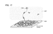
- FIG. 17 is a diagram illustrating a crystal structure of an oxide
- FIGS. 18A and 18B are each a top view illustrating an example of a deposition apparatus
- FIGS. 19A and 19B are each a cross-sectional view illustrating an example of a deposition chamber
- FIG. 20 is a diagram illustrating an example of a heat treatment chamber.
- FIG. 21 is a block diagram illustrating an example of a semiconductor device in accordance with one embodiment of the present invention.
- FIGS. 22A and 22B are a cross-sectional view and a circuit diagram illustrating an example of a semiconductor device in accordance with one embodiment of the present invention.
- FIGS. 23A to 23C are block diagrams illustrating an example of a CPU in accordance with one embodiment of the present invention.
- FIGS. 24A to 24C are diagrams illustrating examples of electronic appliances in accordance with one embodiment of the present invention.
- FIGS. 25A, 25B, and 25C are a circuit diagram, a top view, a cross-sectional view, respectively, illustrating an example of an EL display device in accordance with one embodiment of the present invention
- FIGS. 26A and 26B are a circuit diagram and a cross-sectional view, respectively, illustrating an example of a liquid crystal display device in accordance with one embodiment of the present invention
- FIGS. 27A and 27B each show the V g -I d characteristics of a transistor
- FIGS. 28A and 28B each show the V g -I d characteristics of a transistor
- FIGS. 29A and 29B each show the V g -I d characteristics of a transistor before and after a gate BT stress test.
- FIGS. 30A and 30B each show the V g -I d characteristics of a transistor before and after a gate BT stress test.
- drawings are schematic views of ideal examples, and the embodiments of the present invention are not limited to the shape or the value illustrated in the drawings.
- the following can be included: variation in shape due to a manufacturing technique; variation in shape due to an error; variation in signal, voltage, or current due to noise; variation in signal, voltage, or current due to a difference in timing; or the like.
- a voltage usually refers to a difference in electric potential (more simply referred to as potential) between a given potential and a reference potential (e.g., a source potential or a ground potential (GND)).
- a reference potential e.g., a source potential or a ground potential (GND)
- a voltage can be referred to as a potential and vice versa.
- the term when the shape of an object is described with use of a term such as “diameter”, “grain size (diameter)”, “dimension”, “size”, or “width”, the term can be regarded as the length of one side of a minimal cube where the object fits, or an equivalent circle diameter of a cross section of the object.
- the term “equivalent circle diameter of a cross section of the object” refers to the diameter of a perfect circle having the same area as that of the cross section of the object.
- a “semiconductor” includes characteristics of an “insulator” in some cases when the conductivity is sufficiently low, for example. Further, a “semiconductor” and an “insulator” cannot be strictly distinguished from each other in some cases because a border between the “semiconductor” and the “insulator” is not clear. Accordingly, a “semiconductor” in this specification can be called an “insulator” in some cases. Similarly, an “insulator” in this specification can be called a “semiconductor” in some cases.
- a “semiconductor” includes characteristics of a “conductor” in some cases when the conductivity is sufficiently high, for example. Further, a “semiconductor” and a “conductor” cannot be strictly distinguished from each other in some cases because a border between the “semiconductor” and the “conductor” is not clear. Accordingly, a “semiconductor” in this specification can be called a “conductor” in some cases. Similarly, a “conductor” in this specification can be called a “semiconductor” in some cases.
- an impurity in a semiconductor layer refers to, for example, elements other than the main components of a semiconductor layer.
- an impurity is contained, carrier traps may be formed in the semiconductor layer, the carrier mobility may be decreased, or the crystallinity may be decreased, for example.
- states are formed in the semiconductor layer, electrons or holes are generated from the states, whereby the carrier density may be increased or trap states may be formed, for example.
- examples of an impurity which changes the characteristics of the semiconductor layer include Group 1 elements, Group 2 elements, Group 14 elements, Group 15 elements, and transition metals other than the main components; specifically, there are hydrogen (including water), lithium, sodium, silicon, boron, phosphorus, carbon, and nitrogen, for example.
- examples of an impurity which changes the characteristics of the semiconductor layer include oxygen, Group 1 elements except hydrogen, Group 2 elements, Group 13 elements, and Group 15 elements.
- a deterioration model of the transistor In order to increase reliability of a transistor in which a channel is formed in an oxide semiconductor layer, for example, it is effective to construct a deterioration model of the transistor. By construction of the deterioration model, it is possible to highlight a cause of deterioration of the transistor, and thus a measure for improving reliability is made easily. Thus, a deterioration model of a transistor in which a channel is formed in an oxide semiconductor layer and has variation in electric characteristics is considered below.
- FIG. 1A is an example of a cross-sectional view of a transistor whose channel is formed in an oxide semiconductor layer.
- the transistor illustrated in FIG. 1A includes a gate electrode (bg); a gate insulating film (bg) over the gate electrode (bg); an oxide layer (I 1 ) over the gate insulating film (bg); an oxide semiconductor layer (S 2 ) over the oxide layer (I 1 ); a source electrode and a drain electrode over the oxide semiconductor layer (S 2 ); an oxide layer (I 3 ) over the oxide semiconductor layer (S 2 ), the source electrode, and the drain electrode; a gate insulating film (tg) over the oxide layer (I 3 ); and a gate electrode (tg) over the gate insulating film (tg).
- the transistor illustrated in FIG. 1A includes the gate electrode (bg) for easy understanding, but the deterioration model described below can be applied to a transistor without the gate electrode (bg).
- the gate insulating film (bg) serves as a base insulating film.
- the oxide layer (I 1 ) and the oxide layer (I 3 ) include, for example, at least one metal element, preferably at least two metal elements, further preferably at least three metal elements of metal elements contained in the oxide semiconductor layer (S 2 ).
- the gate insulating film (bg) does not include any of the metal elements contained in the oxide layer (I 1 ), for example.
- the gate insulating film (tg) does not include any of the metal elements contained in the oxide layer (I 3 ), for example.
- the interface between the gate insulating film (bg) and the oxide layer (I 1 ) is a bonding interface between different substances, so that the interface state density is high. Further, the interface between the gate insulating film (tg) and the oxide layer (I 3 ) is a bonding interface between different substances, so that the interface state density is high.
- the interface between the oxide layer (I 1 ) and the oxide semiconductor layer (S 2 ) is a bonding interface between the same types of substances, so that the interface state density is low. Further, the interface between the oxide layer (I 3 ) and the oxide semiconductor layer (S 2 ) is a bonding interface between the same types of substances, so that the interface state density is low.
- the interface state at the interface between the gate insulating film (bg) and the oxide layer (I 1 ) is assumed to be a charge trap.
- the interface state at the interface between the gate insulating film (tg) and the oxide layer (I 3 ) is assumed to be a charge trap.
- the charge might shift the threshold voltage of the transistor. A charge can be trapped in the trap state, resulting from an operation stress of the transistor.
- the charge trapped at the interface between the gate insulating film (bg) and the oxide layer (I 1 ) is referred to as Q ssb .
- the charge trapped at the interface between the gate insulating film (tg) and the oxide layer (I 3 ) is referred to as Q sst . It is verified below that Q ssb and Q sst shift the threshold voltage of the transistor.
- FIG. 1A illustrates the state where the gate electrode (bg) and the gate insulating film (bg) are provided, as an non-limiting example.
- the gate electrode (bg) a conductive layer, a semiconductor layer, or a semiconductor layer doped with an impurity (for example, a p-type semiconductor or an n-type semiconductor) may be provided.
- the gate electrode (bg) does not necessarily acts as a gate electrode.
- the gate insulating film (bg) does not necessarily act as a gate insulating film.
- FIG. 1B is an equivalent circuit of a stacked structure up to the gate electrode (tg) from the gate electrode (bg) in the transistor in FIG. 1A .
- the capacitance of the gate insulating film (bg) is referred to as C bg
- the capacitance of the oxide layer (I 1 ) is referred to as C I1
- the capacitance of the oxide semiconductor layer (S 2 ) is referred to as C S2
- the capacitance of the oxide layer (I 3 ) is referred to as C I3
- the capacitance of the gate insulating film (tg) is referred to as C tg .
- C tg the capacitance of the gate insulating film
- the stacked structure up to the gate electrode (tg) from the gate electrode (bg) in the transistor in FIG. 1A can be illustrated as an equivalent circuit having a capacitor where components between the gate electrode (bg) and the gate electrode (tg), i.e., the gate insulating film (bg), the oxide layer (I 1 ), the oxide semiconductor layer (S 2 ), the oxide layer (I 3 ), and the gate insulating film (tg) are connected in series.
- the potential of the gate electrode (bg) is V bg and the potential of the gate electrode (tg) is V tg .
- the potential of the interface between the gate insulating film (bg) and the oxide layer (I 1 ) is ⁇ ssb
- the potential of the interface between the oxide layer (I 1 ) and the oxide semiconductor layer (S 2 ) is ⁇ S2b
- the potential of the interface between the oxide semiconductor layer (S 2 ) and the oxide layer (I 3 ) is ⁇ S2t
- the potential of the interface between the oxide layer (I 3 ) and the gate insulating film (tg) is ⁇ sst .
- the gate insulating film (bg) has a charge ⁇ (Q ssb +Q I1 ) on the gate electrode (bg) side, and a charge Q ssb +Q I1 on the oxide layer (I 1 ) side.
- the oxide layer (I 1 ) has a charge ⁇ Q I1 on the gate insulating film (bg) side, and a charge Q I1 on the oxide semiconductor layer (S 2 ) side.
- the oxide semiconductor layer (S 2 ) has a charge ⁇ Q S2 on the oxide layer (I 1 ) side, and a charge Q S2 on the oxide layer (I 3 ) side.
- the oxide layer (I 3 ) has a charge ⁇ Q I3 on the oxide semiconductor layer (S 2 ) side, and has a charge Q I3 on the gate insulating film (tg) side.
- the gate insulating film (tg) has a charge Q sst ⁇ Q I3 on the oxide layer (I 3 ) side, and has a charge ⁇ (Q sst ⁇ Q I3 ) on the gate electrode (tg) side.
- oxide layer (I 1 ) and the oxide layer (I 3 ) are assumed to be insulators.
- the whole oxide semiconductor layer (S 2 ) is assumed to be depleted.
- t S2 is a thickness of the oxide semiconductor layer (S 2 )
- x represents a coordinate in the oxide semiconductor layer (S 2 ) along the thickness direction
- x 0 at the interface between the oxide layer (I 1 ) and the oxide semiconductor layer (S 2 )
- Poisson's equation in the oxide semiconductor layer (S 2 ) is expressed by an equation (8).
- e is an elementary charge
- N D is a donor density of the oxide semiconductor layer (S 2 )
- n is an electron density of the oxide semiconductor layer (S 2 )
- ⁇ S2 is a dielectric constant of the oxide semiconductor layer (S 2 ).
- Equation (9) is modified into an equation (10) and an equation (11) where E(x) is an electric field in a film-thickness direction and k 1 and k 2 are undetermined coefficients.
- V th V fbt - Q sst C tg - ( 1 C tg + 1 C I ⁇ ⁇ 1 + 1 C S ⁇ ⁇ 2 ) ⁇ C I ⁇ ⁇ 1 C bg + C I ⁇ ⁇ 1 ⁇ [ Q ssb + C bg ⁇ ( V bg - V fbb ) ] - ( 1 C tg + 1 C I ⁇ ⁇ 3 + 1 2 ⁇ ⁇ C I ⁇ ⁇ 3 ) ⁇ e ⁇ ⁇ N D ⁇ t S ⁇ ⁇ 2 ( 20 )
- Q ssb contributes less to ⁇ V th by increasing C I3 (for example, the thickness of the oxide layer (I 3 ) is reduced).
- Q ssb contributes less to ⁇ V th by increasing C S2 (for example, the thickness of the oxide semiconductor layer (S 2 ) is reduced).
- Q ssb contributes less to ⁇ V th by decreasing CI 1 (for example, the thickness of the oxide layer (I 1 ) is increased).
- C I3 , C S2 , and C I1 do not influence the contribution of Q sst to V th .
- Q sst contributes less to ⁇ V th .
- the channel of the transistor is formed in the oxide semiconductor layer (S 2 ).
- the oxide layer (I 1 ) and the oxide layer (I 3 ) have higher energy (Ec) at the bottom of the conduction band than that of the oxide semiconductor layer (S 2 ).
- the band structure at this time of the transistor is illustrated in FIGS. 2A and 2B .
- the potential at the interface state between the gate insulating film (bg) and the oxide layer (I 1 ) and the potential at the interface state between the gate insulating film (tg) and the oxide layer (I 3 ) are lower than the Fermi level.
- the potentials of the gate electrode (bg) and the gate electrode (tg) are 0V, electrons are trapped in the interface state between the oxide layer (I 1 ) and the gate insulating layer (bg) and in the interface state between the oxide layer (I 3 ) and the gate insulating layer (tg), and a charge Q ssb and a charge Q sst are accumulated (see FIG. 2A ).
- the potentials at the interfaces are higher than Fermi level (are closer to energy at the bottom of the conduction band) as compared to the transistor not including the oxide layer (I 1 ) and the oxide layer (I 3 ) in some cases.
- the potentials at the interface states are higher than the Fermi level, electrons are not trapped in the interface states and thus the charge Q ssb and the charge Q sst are not accumulated (see FIG. 2B ).
- the gate electrode (tg) or the like charges are trapped in the interface states in some cases. The trapped charge is eliminated in a short relaxation time, since the potentials at the interface states are close to energy at the bottom of the conduction band. Accordingly, each interface state hardly causes the shift in the threshold voltage of the transistor.
- the charge Q sst is not accumulated by formation of the oxide layer (I 3 ) in some cases.
- the reliability of the transistor is high because the cause of deterioration does not exist.
- a transistor whose channel is formed in an oxide semiconductor layer is described below.
- top-gate and top-contact transistor An example of a top-gate and top-contact transistor is described first.
- FIGS. 3A to 3C are a top view and cross-sectional views of the transistor.
- FIG. 3A is the top view of the transistor.
- FIG. 3B is the cross-sectional view taken along dashed-dotted line A 1 -A 2 in FIG. 3A .
- FIG. 3C is the cross-sectional view taken along dashed-dotted line A 3 -A 4 in FIG. 3A .
- the transistor illustrated in FIG. 3B includes a base insulating film 102 over a substrate 100 ; an oxide layer 106 a over the base insulating film 102 ; an oxide semiconductor layer 106 b over the oxide layer 106 a ; an oxide layer 106 c over the oxide semiconductor layer 106 b ; a source electrode 116 a and a drain electrode 116 b in contact with the oxide layer 106 c ; a gate insulating film 112 over the oxide layer 106 c , the source electrode 116 a , and the drain electrode 116 b ; and a gate electrode 104 over the gate insulating film 112 .
- a protective insulating film 108 is formed over the gate insulating film 112 and the gate electrode 104 , and a protective insulating film 118 is formed over the protective insulating film 108 .
- the transistor does not necessarily include the base insulating film 102 .
- the base insulating film 102 in the transistor illustrated in FIGS. 3A to 3C corresponds to, for example, the gate insulating film (bg) in the transistor illustrated in FIG. 1A .
- the transistor illustrated in FIGS. 3A to 3C may include, for example, the gate electrode (bg) in the transistor illustrated in FIG. 1A .
- the transistor illustrated in FIGS. 3A to 3C may include, for example, a back gate electrode that is opposite to the gate electrode 104 and is in contact with the bottom surface of the base insulating film 102 .
- the substrate 100 if the substrate 100 has a conductivity, the substrate 100 can correspond to the gate insulating film (bg) in the transistor illustrated in FIG.
- the conductive film can correspond to the gate insulating film (bg) in the transistor illustrated in FIG. 1A .
- Some of materials used for the conductive film serving as the source electrode 116 a and the drain electrode 116 b deprives parts of the oxide semiconductor layer 106 b and the oxide layer 106 c of oxygen or form a mixed layer, so that an n-type region (low-resistant region) might be formed in the oxide semiconductor layer 106 b and the oxide layer 106 c.
- the distance between the source electrode 116 a and the drain electrode 116 b in a region overlapping with the gate electrode 104 is called a channel length. Note that when the transistor includes an n-type region, the distance between the source region and the drain region in a region overlapping the gate electrode 104 may be called a channel length.
- a channel formation region refers to a region, which overlaps with the gate electrode 104 and is interposed between the source electrode 116 a and the drain electrode 116 b , in the oxide layer 106 a , the oxide semiconductor layer 106 b , and the oxide layer 106 c (see FIG. 3B ). Further, a channel refers to a main current path in the channel formation region.
- part of the oxide semiconductor layer 106 b is provided outside the gate electrode 104 .
- the oxide semiconductor layer 106 b may be provided inside the gate electrode 104 . This can suppress generation of carriers in the oxide semiconductor layer 106 b due to incident light from the gate electrode 104 side.
- the gate electrode 104 functions as a light-blocking film.
- the positions of the protective insulating film 118 and the protective insulating film 108 may be reversed.
- the protective insulating film 108 may be provided over the protective insulating film 118 .
- the oxide layer 106 a , the oxide semiconductor layer 106 b , and the oxide layer 106 c are described below.
- the oxide semiconductor layer 106 b is an oxide containing indium.
- An oxide can have a high carrier mobility (electron mobility) by containing indium, for example.
- the oxide semiconductor layer 106 b preferably includes an element M.
- the element M is aluminum, gallium, yttrium, or tin, for example.
- the element M is an element having a high bonding energy with oxygen, for example.
- the element M is an element that can increase the energy gap of the oxide, for example.
- the oxide semiconductor layer 106 b preferably contains zinc. When the oxide contains zinc, the oxide can be easily crystallized, for example. The energy at the top of the valence band of the oxide can be controlled with the atomic ratio of zinc, for example.
- the oxide semiconductor layer 106 b is not limited to the oxide containing indium.
- the oxide semiconductor layer 106 b may be, for example, a Zn—Sn oxide or a Ga—Sn oxide.
- the oxide layer 106 a is an oxide layer which includes one or more kinds of elements included in the oxide semiconductor layer 106 b other than oxygen. Further, since the oxide layer 106 a includes one or more kinds of elements included in the oxide semiconductor layer 106 b other than oxygen, an interface state is unlikely to be formed at the interface between the oxide semiconductor layer 106 b and the oxide layer 106 a.
- the oxide layer 106 c is an oxide layer which includes one or more kinds of elements included in the oxide semiconductor layer 106 b other than oxygen. Further, since the oxide layer 106 c includes one or more kinds of elements included in the oxide semiconductor layer 106 b other than oxygen, an interface state is unlikely to be formed at the interface between the oxide semiconductor layer 106 b and the oxide layer 106 c.
- the proportions of In and M when summation of In and M is assumed to be 100 atomic % is preferably as follows: the atomic percentage of In is less than 50 at. % and the atomic percentage of M is greater than or equal to 50 at. %; further preferably, the atomic percentage of In is less than 25 at. % and the atomic percentage of M is greater than or equal to 75 at. %.
- the proportions of In and M are preferably greater than or equal to 25 atomic % and less than 75 atomic %, respectively, and more preferably greater than or equal to 34 atomic % and less than 66 atomic %, respectively.
- the proportions of In and M when summation of In and M is assumed to be 100 atomic % is preferably as follows: the atomic percentage of In is less than 50 at. % and the atomic percentage of M is greater than or equal to 50 at.
- the oxide layer 106 c may be an oxide that is the same type as that of the oxide layer 106 a.
- the oxide layer 106 a and the oxide semiconductor layer 106 b there is a mixed region of the oxide layer 106 a and the oxide semiconductor layer 106 b between the oxide layer 106 a and the oxide semiconductor layer 106 b .
- the mixed region has a low density of interface states. For that reason, the stack where the oxide layer 106 a , the oxide semiconductor layer 106 b , and the oxide layer 106 c are stacked has a band structure where energy at each interface is changed continuously (continuous junction) (see FIG. 11 ).
- the energy at the bottom of the conduction band of the oxide layer 106 a is EcA
- the energy at the bottom of the conduction band of the oxide semiconductor layer 106 b is EcB
- the energy at the bottom of the conduction band of the oxide layer 106 c is EcC.
- the energy gap of the oxide semiconductor layer 106 b is greater than or equal to 2.5 eV and less than or equal to 4.2 eV, preferably greater than or equal to 2.8 eV and less than or equal to 3.8 eV, more preferably greater than or equal to 3 eV and less than or equal to 3.5 eV.
- the energy gap of the oxide layer 106 c is greater than or equal to 2.7 eV and less than or equal to 4.9 eV, preferably greater than or equal to 3 eV and less than or equal to 4.7 eV, more preferably greater than or equal to 3.2 eV and less than or equal to 4.4 eV.
- the energy gap of the oxide layer 106 a is greater than or equal to 2.7 eV and less than or equal to 4.9 eV, preferably greater than or equal to 3 eV and less than or equal to 4.7 eV, more preferably greater than or equal to 3.2 eV and less than or equal to 4.4 eV.
- an oxide with a wide energy gap is used for the oxide layer 106 c .
- the energy gap of the oxide layer 106 c is greater than or equal to 2.7 eV and less than or equal to 4.9 eV, preferably greater than or equal to 3 eV and less than or equal to 4.7 eV, more preferably greater than or equal to 3.2 eV and less than or equal to 4.4 eV.
- the oxide layer 106 a and the oxide layer 106 c are oxides having energy gaps wider than that of the oxide semiconductor layer 106 b.
- An oxide having a higher electron affinity than the oxide layer 106 a is used as the oxide semiconductor layer 106 b .
- the oxide semiconductor layer 106 b an oxide having higher electron affinity than the oxide layer 106 a by 0.07 eV or higher and 1.3 eV or lower, preferably 0.1 eV or higher and 0.7 eV or lower, more preferably 0.15 eV or higher and 0.4 eV or lower is used.
- the electron affinity refers to an energy gap between the vacuum level and the bottom of the conduction band.
- the oxide semiconductor layer 106 b is an oxide having a higher electron affinity than that of the oxide semiconductor layer 106 c .
- an oxide having a higher electron affinity than the oxide layer 106 c by 0.07 eV or higher and 1.3 eV, or lower, preferably 0.1 eV or higher 0.7 eV or lower, more preferably 0.15 eV or higher and 0.4 eV or lower is used.
- the thickness of the oxide layer 106 a is large, the thickness of the oxide semiconductor layer 106 b is small, and the thickness of the oxide layer 106 c is small.
- the thickness of the oxide layer 106 a is 20 nm or larger, preferably 30 nm or larger, further preferably 40 nm or larger, still further 60 nm or larger.
- the distance from the interface between the base insulating film 102 and the oxide layer 106 a to the oxide semiconductor layer 106 b where a channel is formed can be 20 nm or larger, preferably 30 nm or larger, further preferably 40 nm or larger, still further preferably 60 nm or larger.
- the thickness of the oxide layer 106 a is 200 nm or smaller, preferably 120 nm or smaller, further preferably 80 nm or smaller.
- the thickness of the oxide semiconductor layer 106 b is greater than or equal to 3 nm and less than or equal to 100 nm, preferably greater than or equal to 3 nm and less than or equal to 80 nm, more preferably greater than or equal to 3 nm and less than or equal to 50 nm.
- the oxide layer 106 c has a thickness of greater than or equal to 3 nm and less than or equal to 50 nm, preferably greater than or equal to 3 nm and less than or equal to 20 nm.
- the oxide layer 106 a is thicker than the oxide semiconductor layer 106 b
- the oxide semiconductor layer 106 b is thicker than the oxide layer 106 c.
- the oxide stack including three layers, the oxide layer 106 a , the oxide semiconductor layer 106 b , and the oxide layer 106 c has been described above, but one embodiment of the present invention is not limited to the oxide stack including three layers.
- an oxide stack including two layers, the oxide layer 106 a and the oxide semiconductor layer 106 b or an oxide stack including two layers, the oxide semiconductor layer 106 b and the oxide layer 106 c may be employed.
- an oxide stack having four or more layers including an oxide layer between the oxide layer 106 a and the oxide semiconductor layer 106 b may be provided.
- the oxide layer provided between the oxide layer 106 a and the oxide semiconductor layer 106 b is, for example, an oxide having an electron affinity that is equal to or higher than the electron affinity of the oxide layer 106 a and is equal to or lower than the electron affinity of the oxide semiconductor layer 106 b .
- an oxide stack having four or more layers including an oxide layer between the oxide layer 106 c and the oxide semiconductor layer 106 b may be provided for example.
- the oxide layer provided between the oxide layer 106 c and the oxide semiconductor layer 106 b is, for example, an oxide having an electron affinity that is equal to or higher than the electron affinity of the oxide layer 106 c and is equal to or lower than the electron affinity of the oxide semiconductor layer 106 b.
- targets containing indium are preferably used in order to prevent an increase in the number of particles.
- the conductivity of the target may be decreased.
- the element M include aluminum, gallium, yttrium, and tin.
- the conductivity of the target can be increased and DC discharge or AC discharge is facilitated; thus, deposition over a large substrate can be easily performed.
- semiconductor devices can be manufactured with improved productivity.
- the atomic ratio of In to M and Zn contained in the target is preferably 1:1:0.5, 1:1:1, 1:1:2, 1:3:1, 1:3:2, 1:3:4, 1:3:6, 1:6:2, 1:6:4, 1:6:6, 1:6:8, 1:6:10, 1:9:2, 1:9:4, 1:9:6, 1:9:8, or 1:9:10 for example.
- the atomic ratio of In to M and Zn contained in the target is preferably 3:1:1, 3:1:2, 3:1:4, 1:1:0.5, 1:1:1, or 1:1:2, for example.
- the atomic ratio of In to M and Zn contained in the target is preferably 1:1:0.5, 1:1:1, 1:1:2, 1:3:1, 1:3:2, 1:3:4, 1:3:6, 1:6:2, 1:6:4, 1:6:6, 1:6:8, 1:6:10, 1:9:2, 1:9:4, 1:9:6, 1:9:8, or 1:9:10, for example.
- the oxide layer 106 a , the oxide semiconductor layer 106 b and the oxide layer 106 c are formed by a sputtering method
- films having atomic ratios different from the atomic ratios of the targets used may be formed.
- the atomic ratio of zinc in a deposited film is smaller than the atomic ratio of the target in some cases.
- the film may have an atomic ratio of zinc of 40 atomic % to 90 atomic % of the atomic ratio of zinc in the target.
- the carrier density of the oxide semiconductor layer 106 b is set to lower than 1 ⁇ 10 17 /cm 3 , lower than 1 ⁇ 10 15 /cm 3 , or lower than 1 ⁇ 10 13 /cm 3 .
- a light element, a semimetal element, a metal element, and the like other than main components that is, elements having concentrations lower than 1 atomic %) serve as impurities.
- hydrogen, lithium, carbon, nitrogen, fluorine, sodium, silicon, chlorine, potassium, calcium, titanium, iron, nickel, copper, germanium, strontium, zirconium, and hafnium might be impurities in the oxide. Accordingly, the concentration of impurities in an adjacent layer is preferably reduced.
- an impurity state might be formed in the case where silicon is contained in the oxide.
- the concentration of silicon in a region between the oxide semiconductor layer 106 b and the oxide layer 106 a is set to lower than 1 ⁇ 10 19 atoms/cm 3 , preferably lower than 5 ⁇ 10 18 atoms/cm 3 , more preferably lower than 2 ⁇ 10 18 atoms/cm 3 .
- the concentration of silicon in a region between the oxide semiconductor layer 106 b and the oxide layer 106 c is set to lower than 1 ⁇ 10 19 atoms/cm 3 , preferably lower than 5 ⁇ 10 18 atoms/cm 3 , more preferably lower than 2 ⁇ 10 18 atoms/cm 3 .
- the concentration of hydrogen in the oxide semiconductor layer 106 b which is measured by secondary ion mass spectrometry (SIMS), is set to lower than or equal to 2 ⁇ 10 20 atoms/cm 3 , preferably lower than or equal to 5 ⁇ 10 19 atoms/cm 3 , more preferably lower than or equal to 1 ⁇ 10 19 atoms/cm 3 , still more preferably lower than or equal to 5 ⁇ 10 18 atoms/cm 3 .
- the concentration of nitrogen in the oxide semiconductor layer 106 b which is measured by SIMS, can be lower than 5 ⁇ 10 19 atoms/cm 3 , preferably lower than or equal to 5 ⁇ 10 18 atoms/cm 3 , more preferably lower than or equal to 1 ⁇ 10 18 atoms/cm 3 , still more preferably lower than or equal to 5 ⁇ 10 17 atoms/cm 3 .
- the concentrations of hydrogen and nitrogen in the oxide layer 106 a can be lower than or equal to 2 ⁇ 10 20 atoms/cm 3 , preferably lower than or equal to 5 ⁇ 10 19 atoms/cm 3 , more preferably lower than or equal to 1 ⁇ 10 19 atoms/cm 3 , still more preferably lower than or equal to 5 ⁇ 10 18 atoms/cm 3 .
- the concentration of nitrogen in the oxide layer 106 a which is measured by SIMS, can be lower than 5 ⁇ 10 19 atoms/cm 3 , preferably lower than or equal to 5 ⁇ 10 18 atoms/cm 3 , more preferably lower than or equal to 1 ⁇ 10 18 atoms/cm 3 , still more preferably lower than or equal to 5 ⁇ 10 17 atoms/cm 3 .
- the concentrations of hydrogen and nitrogen in the oxide layer 106 c which are measured by SIMS, is set to lower than or equal to 2 ⁇ 10 20 atoms/cm 3 , preferably lower than or equal to 5 ⁇ 10 19 atoms/cm 3 , more preferably lower than or equal to 1 ⁇ 10 19 atoms/cm 3 , still more preferably lower than or equal to 5 ⁇ 10 18 atoms/cm 3 .
- the concentration of nitrogen in the oxide layer 106 c is lower than 5 ⁇ 10 19 atoms/cm 3 , preferably lower than or equal to 5 ⁇ 10 18 atoms/cm 3 , more preferably lower than or equal to 1 ⁇ 10 18 atoms/cm 3 , still more preferably lower than or equal to 5 ⁇ 10 17 atoms/cm 3 .
- An oxide semiconductor which can be used for the oxide semiconductor layer 106 b and the like is described below.
- An oxide semiconductor may include a non-single-crystal, for example.
- the non-single-crystal is, for example, structured by at least one of c-axis aligned crystal (CAAC), polycrystal, microcrystal, and an amorphous part.
- CAAC c-axis aligned crystal
- An oxide semiconductor may include CAAC, for example.
- CAAC-OS c-axis aligned crystalline oxide semiconductor
- crystal parts in an image obtained with a transmission electron microscope (TEM) (hereinafter referred to as a TME image), for example, crystal parts can be found in the CAAC-OS in some cases.
- TEM transmission electron microscope
- crystal parts in the CAAC-OS each fit inside a cube whose one side is less than 100 nm, for example.
- a boundary between the amorphous part and the crystal part and a boundary between the crystal parts in the CAAC-OS is not clearly observed in some cases.
- a grain boundary in the CAAC-OS is not clearly observed in some cases.
- a clear grain boundary does not exist, for example, segregation of an impurity is unlikely to occur.
- CAAC-OS since a clear grain boundary does not exist, for example, high density of defect states is unlikely to occur.
- CAAC-OS since a clear grain boundary does not exist, for example, a reduction in electron mobility is unlikely to occur.
- the CAAC-OS includes a plurality of crystal parts.
- c-axes are aligned in a direction parallel to a normal vector of a surface where the CAAC-OS is formed or a normal vector of a surface of the CAAC-OS in some cases.
- XRD X-ray diffraction
- An electron diffraction pattern obtained with an electron beam having a beam diameter of 10 nm ⁇ or smaller, or 5 nm ⁇ or smaller, is called a nanobeam electron diffraction pattern.
- the CAAC-OS for example, among crystal parts, the directions of the a-axis and the b-axis of one crystal part are different from those of another crystal part, in some cases.
- the CAAC-OS for example, c-axes are aligned, and a-axes and/or b-axes are not macroscopically aligned, in some cases.
- FIG. 12A shows an example of a nanobeam electron diffraction pattern of a sample including CAAC-OS.
- the sample is cut in the direction perpendicular to a surface where the CAAC-OS is formed and the thickness thereof is reduced to about 40 nm. Further, an electron beam with a diameter of 1 nm enters from the direction perpendicular to the cut surface of the sample.
- FIG. 12A shows that spots are observed in the nanobeam electron diffraction pattern of the CAAC-OS.
- a c-axis is aligned in the direction parallel to a normal vector of a surface where the CAAC-OS is formed or a normal vector of a surface of the CAAC-OS.
- metal atoms are arranged in a triangular or hexagonal configuration when seen from the direction perpendicular to the a-b plane, and metal atoms are arranged in a layered manner or metal atoms and oxygen atoms are arranged in a layered manner when seen from the direction perpendicular to the c-axis.
- a term “perpendicular” includes a range from 80° to 100°, preferably from 85° to 95°.
- a term “parallel” includes a range from ⁇ 10° to 10°, preferably from ⁇ 5° to 5°.
- the directions of the c-axes may be different from each other depending on the shape of the CAAC-OS film (the cross-sectional shape of the surface where the CAAC-OS film is formed or the cross-sectional shape of the surface of the CAAC-OS film).
- the film deposition is accompanied with the formation of the crystal parts or followed by the formation of the crystal parts through crystallization treatment such as heat treatment.
- the c-axes of the crystal parts are aligned in the direction parallel to a normal vector of the surface where the CAAC-OS film is formed or a normal vector of the surface of the CAAC-OS film.
- the CAAC-OS could be obtained by reducing the impurity concentration, for example.
- the impurity means here an element other than the main components of the oxide semiconductor, such as hydrogen, carbon, silicon, or a transition metal element.
- an element such as silicon has a higher strength to bond with oxygen than that of a metal element included in the oxide semiconductor. Therefore, when the element takes oxygen away in the oxide semiconductor, the atomic arrangement in the oxide semiconductor is disrupted, whereby the crystallinity of the oxide semiconductor is lowered in some cases.
- the CAAC-OS is an oxide semiconductor with a low impurity concentration.
- the impurity included in the oxide semiconductor might serve as a carrier generation source.
- the CAAC-OS film distribution of crystal parts is not necessarily uniform.
- the proportion of crystal parts in the vicinity of the surface of the oxide semiconductor is higher than that in the vicinity of the surface where the oxide semiconductor is formed in some cases.
- the crystal part in a region into which the impurity is mixed becomes amorphous or microcrystalline in some cases.
- the CAAC-OS can be formed, for example, by reducing the density of defect states.
- oxygen vacancies for example form defect states.
- the oxygen vacancies form trap states or serve as carrier generation sources when hydrogen is trapped therein.
- the CAAC-OS is an oxide semiconductor having a low density of defect states.
- the CAAC-OS is an oxide semiconductor having few oxygen vacancies.
- the state in which impurity concentration is low and density of defect states is low (the number of oxygen vacancies is small) is referred to as “highly purified intrinsic” or “substantially highly purified intrinsic”.
- a highly purified intrinsic or substantially highly-purified intrinsic oxide semiconductor has few carrier generation sources, and thus has a low carrier density in some cases.
- a transistor including the oxide semiconductor in a channel formation region rarely has a negative threshold voltage (is rarely normally-on).
- a highly purified intrinsic or substantially highly purified intrinsic oxide semiconductor has a low density of defect states and accordingly has a low density of trap states in some cases.
- the transistor including the oxide semiconductor in the channel formation region has a small variation in electrical characteristics and high reliability in some cases. Charges trapped by the trap states in the oxide semiconductor take a long time to be released and may behave like fixed charges.
- the transistor which includes the oxide semiconductor having a high density of trap states in the channel formation region has unstable electrical characteristics in some cases.
- a transistor including the highly purified intrinsic or substantially highly purified intrinsic CAAC-OS has a small variation in the electrical characteristics due to irradiation with visible light or ultraviolet light.
- the CAAC-OS can be formed by a sputtering method using a DC power source, for example.
- the oxide semiconductor may include polycrystal, for example.
- an oxide semiconductor including polycrystal is referred to as a polycrystalline oxide semiconductor.
- a polycrystalline oxide semiconductor includes a plurality of crystal grains.
- a polycrystalline oxide semiconductor includes, for example, amorphous parts in some cases.
- a crystal grain in the polycrystalline oxide semiconductor is greater than or equal to 2 nm and less than or equal to 300 nm, greater than or equal to 3 nm and less than or equal to 100 nm, or greater than or equal to 5 nm and less than or equal to 50 nm in an image obtained with the TEM, for example.
- a boundary between an amorphous part and a crystal grain and a boundary between crystal grains can be found in the polycrystalline oxide semiconductor in some cases.
- a grain boundary can be found in the polycrystalline oxide semiconductor in some cases.
- the polycrystalline oxide semiconductor may include a plurality of crystal grains, and the alignment of crystals may be different in the plurality of crystal grains.
- a peak at 2 ⁇ of around 31 degrees which shows alignment or plural kinds of peaks showing alignment appears in some cases. Further, spots are observed in an electron diffraction pattern of the polycrystalline oxide semiconductor in some cases.
- the polycrystalline oxide semiconductor has high crystallinity and thus has high electron mobility in some cases. Accordingly, a transistor using the polycrystalline oxide semiconductor for a channel formation region has high field-effect mobility. Note that there are cases in which an impurity is segregated at the grain boundary between the crystals in the polycrystalline oxide semiconductor. Moreover, the grain boundary of the polycrystalline oxide semiconductor becomes a defect state. Since the grain boundary of the polycrystalline oxide semiconductor may serve as a carrier trap or a carrier generation source, a transistor using the polycrystalline oxide semiconductor for a channel formation region has larger variation in electrical characteristics and lower reliability than a transistor using a CAAC-OS for a channel formation region in some cases.
- the polycrystalline oxide semiconductor can be formed by high-temperature heat treatment or laser light treatment.
- the oxide semiconductor may include microcrystal, for example. Note that an oxide semiconductor including microcrystal is referred to as a microcrystalline oxide semiconductor.
- the size of a crystal part included in the microcrystalline oxide semiconductor is greater than or equal to 1 nm and less than or equal to 100 nm, or greater than or equal to 1 nm and less than or equal to 10 nm, for example.
- a microcrystal with a size greater than or equal to 1 nm and less than or equal to 10 nm is specifically referred to as nanocrystal (nc).
- An oxide semiconductor including nanocrystal is referred to as an nc-OS (nanocrystalline oxide semiconductor).
- nc-OS In a TEM image of the nc-OS, for example, a boundary between an amorphous part and a crystal part and a boundary between crystal parts cannot be found clearly in some cases.
- a clear grain boundary does not exist, for example, segregation of an impurity is unlikely to occur.
- a clear grain boundary does not exist, for example, high density of defect states is unlikely to occur.
- a clear grain boundary does not exist, for example, a reduction in electron mobility is unlikely to occur.
- nc-OS for example, a microscopic region (for example, a region with a size greater than or equal to 1 nm and less than or equal to 10 nm) has a periodic atomic order occasionally. Further, for example, in the nc-OS, crystal parts are not regularly-arranged. Thus, there is a case where periodic atomic order is not observed macroscopically or a case where long-range order in atomic arrangement is not observed. Accordingly, in some cases, the nc-OS cannot be distinguished from an amorphous oxide semiconductor, for example, depending on an analysis method.
- nc-OS When the nc-OS is analyzed by an out-of-plane method with an XRD apparatus using an X-ray having a beam diameter larger than that of a crystal part, a peak which shows alignment does not appear in some cases. Further, for example, a halo pattern is shown in some cases in an electron diffraction pattern of the nc-OS obtained by using an electron beam having a diameter larger than that of a crystal part (for example, a beam diameter of 20 nm ⁇ or more, or 50 nm ⁇ or more).
- spots are shown in some cases in a nanobeam electron diffraction pattern of the nc-OS obtained by using an electron beam having a diameter smaller than or equal to that of a crystal part (for example, a beam diameter of 10 nm ⁇ or less, or 5 nm ⁇ or less).
- a nanobeam electron diffraction pattern of the nc-OS for example, regions with high luminance in a circular pattern are shown in some cases.
- a plurality of spots are shown in the region in some cases.
- FIG. 12B shows an example of a nanobeam electron diffraction pattern of a sample including nc-OS.
- the sample is cut in the direction perpendicular to a surface where the nc-OS is formed and the thickness thereof is reduced to about 40 nm. Further, an electron beam with a diameter of 1 nm ⁇ enters from the direction perpendicular to the cut surface of the sample.
- FIG. 12B shows that in the nanobeam electron diffraction pattern of the nc-OS, regions with high luminance in a circular pattern are shown and a plurality of spots are shown in the region.
- the nc-OS Since the microscopic region in the nc-OS has a periodic atomic order occasionally, the nc-OS has lower density of defect states than the amorphous oxide semiconductor. Note that since crystal parts in the nc-OS are not regularly-arranged, the nc-OS has higher density of defect states than the CAAC-OS.
- the nc-OS has higher carrier density than the CAAC-OS in some cases.
- An oxide semiconductor with a high carrier density tends to have a high electron mobility. Therefore, a transistor using the nc-OS for a channel formation region has a high field-effect mobility in some cases.
- the nc-OS has higher density of defect states than the CAAC-OS and thus has higher density of trap states in some cases. Therefore, a transistor using the nc-OS for a channel formation region has larger variation in electrical characteristics and lower reliability than a transistor using the CAAC-OS for a channel formation region.
- the nc-OS can be obtained even when the amount of impurity contained therein is relatively large; thus, the nc-OS is sometimes preferably used depending on the application.
- the nc-OS may be formed by a deposition method such as a sputtering method using an AC power supply.
- the sputtering method using an AC power supply allows a film to be formed with high uniformity over a large substrate, so that a semiconductor device including a transistor using the nc-OS for a channel formation region can be manufactured with high productivity.
- An oxide semiconductor may include an amorphous part.
- an oxide semiconductor including an amorphous part is referred to as an amorphous oxide semiconductor.
- An amorphous oxide semiconductor for example, has disordered atomic arrangement and no crystal part.
- An amorphous oxide semiconductor for example, does not have a specific shape as in quartz and regularity in atomic arrangement.
- a peak which shows alignment does not appear in some cases.
- a halo pattern is observed in an electron diffraction pattern of the amorphous oxide semiconductor in some cases. In other cases, a halo pattern is observed instead of a spot in a nanobeam electron diffraction pattern of the amorphous oxide semiconductor.
- the amorphous oxide semiconductor can be formed in some cases, for example, by introducing a high-concentration impurity such as hydrogen.
- the amorphous oxide semiconductor is, for example, an oxide semiconductor containing a high-concentration impurity.
- an oxide semiconductor contains a high-concentration impurity
- a defect state such as an oxygen vacancy is formed in the oxide semiconductor in some cases.
- an amorphous oxide semiconductor with a high-concentration impurity has a high density of defect states.
- the amorphous oxide semiconductor has low crystallinity, the density of defect states of the amorphous oxide semiconductor is higher than that of the CAAC-OS or the nc-OS.
- the amorphous oxide semiconductor has a much higher carrier density than the nc-OS in some cases. Therefore, a transistor using the amorphous oxide semiconductor for a channel formation region tends to be normally on, and sometimes can be preferably used for a transistor which needs to have such electrical characteristics.
- the amorphous oxide semiconductor has a high density of defect states and thus has a high density of trap states in some cases. Therefore, a transistor using the amorphous oxide semiconductor for a channel formation region has larger variation in electrical characteristics and lower reliability than a transistor using the CAAC-OS or the nc-OS for a channel formation region in some cases.
- the amorphous oxide semiconductor can be formed by a deposition method in which a relatively large amount of impurity is contained, and thus can be easily obtained and preferably used depending on the application.
- the amorphous oxide semiconductor may be formed by a deposition method such as a spin coating method, a sol-gel method, an immersion method, a spray method, a screen printing method, a contact printing method, an ink-jet printing method, a roll coating method, or a mist CVD method.
- a semiconductor device including a transistor using the amorphous oxide semiconductor for a channel formation region can be manufactured with high productivity.
- the oxide semiconductor may be a mixed film including two or more of a CAAC-OS, a polycrystalline oxide semiconductor, a microcrystalline oxide semiconductor, and an amorphous oxide semiconductor.
- the mixed film includes two or more of an amorphous oxide semiconductor region, a microcrystalline oxide semiconductor region, a polycrystalline oxide semiconductor region, and a CAAC-OS region in some cases.
- the mixed film has a layered structure of two or more of an amorphous oxide semiconductor region, a microcrystalline oxide semiconductor region, a polycrystalline oxide semiconductor region, and a CAAC-OS region in some cases.
- An oxide semiconductor may include a single crystal, for example. Note that an oxide semiconductor including a single crystal is referred to as a single crystal oxide semiconductor.
- the single crystal oxide semiconductor has, for example, a low impurity concentration and a low density of defect states (a small number of oxygen vacancies), and thus has a low carrier density. Therefore, a transistor using the single crystal oxide semiconductor for a channel formation region is unlikely to be normally on. Further, the single crystal oxide semiconductor has a low density of defect states and thus has a low density of trap states in some cases. Therefore, a transistor using the single crystal oxide semiconductor for a channel formation region has a small variation in electrical characteristics and a high reliability in some cases.
- the oxide semiconductor has a high density if including few defects, for example.
- the oxide semiconductor has a high density if having a high crystallinity, for example.
- the oxide semiconductor has a high density if including a low-concentration impurity such as hydrogen.
- the density of a single crystal oxide semiconductor is higher than that of a CAAC-OS in some cases.
- the density of a CAAC-OS is higher than that of a microcrystalline oxide semiconductor in some cases.
- the density of a polycrystalline oxide semiconductor is higher than that of a microcrystalline oxide semiconductor in some cases.
- the density of a microcrystalline oxide semiconductor is higher than that of an amorphous oxide semiconductor in some cases.
- Localized states in the oxide semiconductor layer 106 b are described below. By reducing the density of localized states due to defect states of the oxide semiconductor layer 106 b , a transistor including the oxide semiconductor layer 106 b can have stable electric characteristics. The density of localized states in the oxide semiconductor layer 106 b can be measured by a constant photocurrent method (CPM).
- CPM constant photocurrent method
- the absorption coefficient due to the localized states in the oxide semiconductor layer 106 b measured by CPM is preferably lower than 1 ⁇ 10 ⁇ 3 cm ⁇ 1 , further preferably lower than 3 ⁇ 10 ⁇ 4 cm ⁇ 1 . Further, when the absorption coefficient due to the localized states in the oxide semiconductor layer 106 b measured by CPM is lower than 1 ⁇ 10 ⁇ 3 cm ⁇ 1 , preferably lower than 3 ⁇ 10 ⁇ 4 cm ⁇ 1 , the field-effect mobility of the transistor can be increased.
- the concentrations of elements forming a localized state such as hydrogen, lithium, carbon, nitrogen, fluorine, sodium, silicon, chlorine, potassium, calcium, titanium, iron, nickel, copper, germanium, strontium, zirconium, and hafnium in the oxide are lower than 2 ⁇ 10 19 atoms/cm 3 , preferably lower than 2 ⁇ 10 18 atoms/cm 3 , further preferably lower than 2 ⁇ 10 17 atoms/cm 3 .
- the density of state (DOS) of a sample where the oxide layer 106 a , the oxide semiconductor layer 106 b and the oxide layer 106 c are stacked over a substrate is evaluated by CPM.
- the oxide layer 106 c is formed by a sputtering method using an In—Ga—Zn oxide (the atomic ratio of In to Ga and Zn is 1:3:2) target. Note that the oxide layer 106 c is formed in such a manner that an argon gas at a flow rate of 30 sccm and an oxygen gas at a flow rate of 15 sccm are used as a film formation gas, the pressure is set to be 0.4 Pa, the substrate temperature is set to be 200° C., and a DC power of 0.5 kW is applied.
- the thicknesses of the oxide layer 106 a , the oxide semiconductor layer 106 b , and the oxide layer 106 c are set to 30 nm, 100 nm, and 30 nm, respectively for increasing the accuracy in the CPM measurement.
- the amount of light with which a surface of the sample between terminals is irradiated is adjusted so that a photocurrent value is kept constant in the state where voltage is applied between a first electrode and a second electrode provided in contact with the oxide semiconductor layer 106 b that is the sample, and then an absorption coefficient is derived from the amount of the irradiation light at each wavelength.
- the absorption coefficient of energy which corresponds to a level at which the defect exists is increased. The increase in the absorption coefficient is multiplied by a constant, whereby the DOS of the sample can be obtained.
- FIG. 13 shows results of fitting the absorption coefficient (dotted line) measured using a spectrophotometer and the absorption coefficient (solid line) measured by CPM in the range of energy higher than or equal to the energy gap of the oxide semiconductor layer 106 b .
- the Urbach energy obtained based on the absorption coefficient measured by CPM was 78.7 meV.
- the integral value of the absorption coefficient is calculated in such a manner that a background (thin dotted line) is subtracted from the absorption coefficient measured by CPM in FIG. 13 .
- the absorption coefficient due to DOS of this sample is found to be 2.02 ⁇ 10 ⁇ 4 cm ⁇ 1 .
- the base insulating film 102 illustrated in FIGS. 3A to 3C may be formed of a single layer or a stacked layer using an insulating film containing one or more of aluminum oxide, magnesium oxide, silicon oxide, silicon oxynitride, silicon nitride oxide, silicon nitride, gallium oxide, germanium oxide, yttrium oxide, zirconium oxide, lanthanum oxide, neodymium oxide, hafnium oxide, and tantalum oxide, for example.
- the base insulating film 102 is, for example, a multilayer film including a silicon nitride layer as a first layer and a silicon oxide layer as a second layer.
- the silicon oxide layer may be a silicon oxynitride layer.
- the silicon nitride layer may be a silicon nitride oxide layer.
- As the silicon oxide layer a silicon oxide layer whose defect density is low is preferably used. Specifically, a silicon oxide layer whose spin density attributed to a signal with a g factor of 2.001 in electron spin resonance (ESR) is lower than or equal to 3 ⁇ 10 17 spins/cm 3 , preferably lower than or equal to 5 ⁇ 10 16 spins/cm 3 is used.
- ESR electron spin resonance
- the silicon nitride layer a silicon nitride layer from which a hydrogen gas and an ammonia gas are less likely to be released is used.
- the amount of discharge of the hydrogen gas or the ammonia gas may be measured by thermal desorption spectroscopy (TDS).
- TDS thermal desorption spectroscopy
- the silicon nitride layer a silicon nitride layer which does not transmit or hardly transmits hydrogen, water, and oxygen is used.
- the base insulating film 102 may be, for example, a multilayer film including a silicon nitride layer as a first layer, a first silicon oxide layer as a second layer, and a second silicon oxide layer as a third layer.
- the first silicon oxide layer and/or the second silicon oxide layer may be a silicon oxynitride layer.
- the silicon nitride layer may be a silicon nitride oxide layer.
- As the first silicon oxide layer a silicon oxide layer whose defect density is low is preferably used.
- a silicon oxide layer whose spin density attributed to a signal with a g factor of 2.001 in ESR is lower than or equal to 3 ⁇ 10 17 spins/cm 3 , preferably lower than or equal to 5 ⁇ 10 16 spins/cm 3 is used.
- a silicon oxide layer having excess oxygen is used.
- the silicon nitride layer a silicon nitride layer from which a hydrogen gas and an ammonia gas are less likely to be released is used. Further, as the silicon nitride layer, a silicon nitride layer which does not transmit or hardly transmits hydrogen, water, and oxygen is used.
- the silicon oxide layer having excess oxygen means a silicon oxide layer from which oxygen can be released by heat treatment or the like.
- An insulating film having excess oxygen means an insulating film from which oxygen is released by heat treatment.
- the insulating film containing excess oxygen is capable of reducing oxygen vacancies in the oxide semiconductor layer 106 b .
- Such an oxygen vacancy forms defect states in the oxide semiconductor layer 106 b and some of the defect states serves as a trap state.
- hydrogen comes into the site of such an oxygen vacancy and forms an electron serving as a carrier.
- a film from which oxygen is released by heat treatment may release oxygen, the amount of which is higher than or equal to 1 ⁇ 10 18 atoms/cm 3 , higher than or equal to 1 ⁇ 10 19 atoms/cm 3 , or higher than or equal to 1 ⁇ 10 20 atoms/cm 3 in TDS analysis (converted into the number of oxygen atoms) in the range of a film surface temperature of from 100° C. to 700° C. or from 100° C. to 500° C.
- the total amount of released gas from a measurement sample in TDS analysis is proportional to the integral value of the ion intensity of the released gas. Then, comparison with a reference sample is made, whereby the total amount of released gas can be calculated.
- the number of released oxygen molecules (N O2 ) from the measurement sample can be calculated based on Equation (22) using the TDS results of a silicon wafer containing hydrogen at a predetermined density, which is a reference sample, and the TDS results of the measurement sample.
- N O2 the number of released oxygen molecules (N O2 ) from the measurement sample.
- all gases having a mass number of 32 which are obtained in the TDS analysis are assumed to originate from an oxygen molecule.
- a CH 3 OH gas, which is given as a gas having a mass number of 32, is not taken into consideration on the assumption that it is unlikely to be present.
- an oxygen molecule including an oxygen atom having a mass number of 17 or 18 which is an isotope of an oxygen atom is also not taken into consideration because the proportion of such a molecule in the natural world is minimal
- N O ⁇ ⁇ 2 N H ⁇ ⁇ 2 S H ⁇ ⁇ 2 ⁇ S O ⁇ ⁇ 2 ⁇ ⁇ ( 22 )
- the value N H2 is obtained by conversion of the amount of hydrogen molecules desorbed from the standard sample into densities.
- the value S H2 is the integral value of ion intensity in the case where the standard sample is subjected to the TDS analysis.
- the reference value of the standard sample is set to N H2 /S H2 .
- S O2 is the integral value of ion intensity when the measurement sample is analyzed by TDS.
- the value ⁇ is a coefficient affecting the ion intensity in the TDS analysis. Refer to Japanese Published Patent Application No. H6-275697 for details of Equation 22.
- the amount of released oxygen is measured with a thermal desorption spectroscopy apparatus produced by ESCO Ltd., EMD-WA1000S/W using a silicon wafer containing hydrogen atoms at 1 ⁇ 10 16 atoms/cm 2 as the reference sample.
- oxygen is partly detected as an oxygen atom.
- the ratio between oxygen molecules and oxygen atoms can be calculated from the ionization rate of the oxygen molecules. Note that since the above ⁇ includes the ionization rate of the oxygen molecules, the amount of the released oxygen atoms can also be estimated through the evaluation of the amount of the released oxygen molecules.
- N O2 is the amount of the released oxygen molecules.
- the amount of released oxygen in the case of being converted into oxygen atoms is twice the amount of the released oxygen molecules.
- a film from which oxygen is released by heat treatment may contain a peroxide radical.
- the spin density attributed to the peroxide radical is greater than or equal to 5 ⁇ 10 17 spins/cm 3 .
- the film containing a peroxide radical may have an asymmetric signal with a g factor of approximately 2.01 in ESR.
- the insulating film containing excess oxygen may be oxygen-excess silicon oxide (SiO X (X>2)).
- SiO X (X>2) oxygen-excess silicon oxide
- the number of oxygen atoms per unit volume is more than twice the number of silicon atoms per unit volume.
- the number of silicon atoms and the number of oxygen atoms per unit volume are measured by Rutherford backscattering spectrometry (RBS).
- the source electrode 116 a and the drain electrode 116 b may be formed using a single layer or a stacked layer of a conductive film containing one or more kinds of aluminum, titanium, chromium, cobalt, nickel, copper, yttrium, zirconium, molybdenum, ruthenium, silver, tantalum, and tungsten, for example.
- the source electrode 116 a and the drain electrode 116 b are each preferably a multilayer film including a layer containing copper.
- the source electrode 116 a and the drain electrode 116 b are each a multilayer film including a layer containing copper, whereby wiring resistance can be reduced in the case where a wiring is formed in the same layer as the source electrode 116 a and the drain electrode 116 b .
- the compositions of the source electrode 116 a and the drain electrode 116 b are either the same as or different from each other.
- the oxide semiconductor layer 106 b In the case where a multilayer film including a layer containing copper is used for the source electrode 116 a and the drain electrode 116 b , copper comes into the oxide semiconductor layer 106 b and thereby the carrier density of the oxide semiconductor layer 106 b may be increased. Alternatively, copper forms an impurity state in the oxide semiconductor layer 106 b and the impurity state serves as a charge trap in some cases. In this case, when the oxide layer 106 c can block copper, the increase in off-state current and the variation of the threshold voltage of the transistor due to the entry of copper into the oxide semiconductor layer 106 b can be inhibited.
- FIGS. 4A to 4C are cross-sectional views of the vicinities of the source electrode 116 a and the drain electrode 116 b of the transistor.
- the source electrode 116 a and the drain electrode 116 b may have any structure illustrated in FIGS. 4A to 4C .
- the top surface of the oxide layer 106 c is hollowed as a result of the formation of the source electrode 116 a and the drain electrode 116 b.
- FIG. 4A illustrates a structure where steps are formed in the source electrode 116 a and the drain electrode 116 b .
- N-type regions are formed in regions represented by dotted line in the oxide layer 106 c .
- the n-type regions are formed resulting from generation of oxygen vacancies in the oxide layer 106 c due to damages when the source electrode 116 a and the drain electrode 116 b are formed over the oxide layer 106 c or action of the conductive film serving as the source electrode 116 a and the drain electrode 116 b . Due to entry of hydrogen into the site of oxygen vacancies, an electron serving as a carrier may be generated.
- the n-type regions are formed down to the vicinity of the boundary between the oxide layer 106 c and the oxide semiconductor layer 106 b as a non-limiting example illustrated in FIG. 4A .
- the n-type regions may be formed in the oxide layer 106 c and the oxide semiconductor layer 106 b , or only in the oxide layer 106 c.
- a conductive layer 116 a 2 which is not easily oxidized and a conductive layer 116 a 1 provided over the conductive layer 116 a 2 are used as the source electrode 116 a
- a conductive layer 116 b 2 which is not easily oxidized and a conductive layer 116 b 1 provided over the conductive layer 116 b 2 are used as the drain electrode 116 b .
- the conductive layer which is not easily oxidized is unlikely to reduce the oxide layer 106 c .
- the source electrode 116 a and the drain electrode 116 b have a structure illustrated in FIG. 4B , the n-type regions are formed only in the oxide layer 106 c .
- the channel formation region is less likely to have n-type conductivity.
- the conductive layer 116 a 1 and the conductive layer 116 b 1 it is acceptable that the conductive layer 116 a 2 and the conductive layer 116 b 2 have low conductivity.
- the thicknesses of the conductive layer 116 a 2 and the conductive layer 116 b 2 can be small, which leads to easy microfabrication.
- the structure illustrated in FIG. 4B is favorable for a miniaturized transistor having a small channel length.
- the conductive layer 116 a 1 and the conductive layer 116 a 2 may be the same conductive layer.
- the conductive layer 116 b 1 and the conductive layer 116 b 2 may be the same conductive layer.
- a conductive layer 116 a 3 and a conductive layer 116 a 4 which is not easily oxidized and is provided over the conductive layer 116 a 3 are used as the source electrode 116 a
- a conductive layer 116 b 3 and a conductive layer 116 b 4 which is not easily oxidized and is provided over the conductive layer 116 b 3 are used as the drain electrode 116 b .
- the source electrode 116 a and the drain electrode 116 b have a structure illustrated in FIG.
- parts of the n-type regions formed in the oxide layer 106 c are formed down to the vicinity of the boundary between the oxide semiconductor layer 106 b and the oxide layer 106 c and a part of the n-type regions is formed in only the oxide layer 106 c .
- diffusion of oxygen vacancies in the channel length direction is small, so that the channel formation region is less likely to have n-type conductivity.
- the n-type regions are formed so as to reach the oxide semiconductor layer 106 b below the conductive layer 116 a 3 and the conductive layer 116 b 3 , the resistance between the source electrode 116 a and the drain electrode 116 b is small; as a result, the field-effect mobility of the transistor can be increased.
- the conductive layer 116 a 3 and the conductive layer 116 b 3 it is acceptable that the conductive layer 116 a 4 and the conductive layer 116 b 4 can have low conductivity.
- the thicknesses of the conductive layer 116 a 4 and the conductive layer 116 b 4 can be small, which leads to easy microfabrication.
- the structure illustrated in FIG. 4C is favorable for a miniaturized transistor having a small channel length.
- the conductive layer 116 a 3 and the conductive layer 116 a 4 may be the same conductive layer.
- the conductive layer 116 b 3 and the conductive layer 116 b 4 may be the same conductive layer.
- the gate insulating film 112 illustrated in FIGS. 3A to 3C may be formed using a single layer or a stacked layer of an insulating film containing one or more kinds of aluminum oxide, magnesium oxide, silicon oxide, silicon oxynitride, silicon nitride oxide, silicon nitride, gallium oxide, germanium oxide, yttrium oxide, zirconium oxide, lanthanum oxide, neodymium oxide, hafnium oxide, and tantalum oxide.
- the gate insulating film 112 may be, for example, a multilayer film including a silicon nitride layer as a first layer and a silicon oxide layer as a second layer.
- the silicon oxide layer may be a silicon oxynitride layer.
- the silicon nitride layer may be a silicon nitride oxide layer.
- As the silicon oxide layer a silicon oxide layer whose defect density is low is preferably used. Specifically, a silicon oxide layer whose spin density attributed to a signal with a g factor of 2.001 in electron spin resonance (ESR) is lower than or equal to 3 ⁇ 10 17 spins/cm 3 , preferably lower than or equal to 5 ⁇ 10 16 spins/cm 3 is used.
- silicon oxide layer a silicon oxide layer having excess oxygen is preferably used.
- silicon nitride layer a silicon nitride layer from which a hydrogen gas and an ammonia gas are less likely to be released is used. The amount of released hydrogen gas or ammonia gas may be measured by TDS.
- the gate insulating film 112 and the base insulating film 102 includes an insulating film containing excess oxygen, oxygen vacancies in the oxide semiconductor layer 106 b are reduced, so that the transistor can have stable electrical characteristics.
- the gate electrode 104 may be formed using a single layer or a stacked layer of a conductive film containing one or more kinds of aluminum, titanium, chromium, cobalt, nickel, copper, yttrium, zirconium, molybdenum, ruthenium, silver, tantalum, and tungsten, for example.
- the protective insulating film 108 may be formed using a single layer or a stacked layer of an insulating film containing one or more kinds of aluminum oxide, magnesium oxide, silicon oxide, silicon oxynitride, silicon nitride oxide, silicon nitride, gallium oxide, germanium oxide, yttrium oxide, zirconium oxide, lanthanum oxide, neodymium oxide, hafnium oxide, and tantalum oxide, for example.
- the protective insulating film 108 includes, for example, a silicon nitride layer.
- the silicon nitride layer may be a silicon nitride oxide layer.
- a silicon nitride layer from which a hydrogen gas and an ammonia gas are less likely to be released is preferred.
- the amount of released the hydrogen gas or the ammonia gas may be measured by TDS.
- a silicon nitride layer which does not transmit or hardly transmits hydrogen, water, and oxygen is preferably used as the silicon nitride layer.
- the protective insulating film 108 includes, for example, an aluminum oxide layer.
- an aluminum oxide layer from which a hydrogen gas is less likely to be released is preferred.
- the amount of released hydrogen gas may be measured by TDS.
- an aluminum oxide layer which does not transmit or hardly transmits hydrogen, water, and oxygen is preferably used.
- the protective insulating film 118 may be formed using a single layer or a stacked layer of an insulating film containing one or more kinds of silicon oxide, silicon oxynitride, germanium oxide, yttrium oxide, zirconium oxide, lanthanum oxide, neodymium oxide, hafnium oxide, and tantalum oxide, for example. Owing to the protective insulating film 118 , the protective insulating film 108 is not necessarily provided.
- the substrate 100 there is no particular limitation on the substrate 100 .
- a glass substrate, a ceramic substrate, a quartz substrate, or a sapphire substrate may be used as the substrate 100 .
- a single crystal semiconductor substrate or a polycrystalline semiconductor substrate made of silicon, silicon carbide, or the like, a compound semiconductor substrate made of silicon germanium or the like, a silicon-on-insulator (SOI) substrate, or the like may be used as the substrate 100 .
- SOI silicon-on-insulator
- any of these substrates provided with a semiconductor element may be used as the substrate 100 .
- a large glass substrate such as the fifth generation (1000 mm ⁇ 1200 mm or 1300 mm ⁇ 1500 mm); the sixth generation (1500 mm ⁇ 1800 mm); the seventh generation (1870 mm ⁇ 2200 mm); the eighth generation (2200 mm ⁇ 2500 mm); the ninth generation (2400 mm ⁇ 2800 mm); or the tenth generation (2880 mm ⁇ 3130 mm) as the substrate 100
- microfabrication is difficult in some cases due to the shrinkage of the substrate 100 , which is caused by heat treatment or the like in a manufacturing process of the semiconductor device. Therefore, in the case where the above-described large glass substrate is used as the substrate 100 , a substrate whose shrinkage due to heat treatment is as less as possible is preferably used.
- the substrate 100 it is possible to use a large glass substrate in which the amount of shrinkage by heat treatment for one hour at 400° C., preferably 450° C., more preferably 500° C. is less than or equal to 10 ppm, preferably less than or equal to 5 ppm, more preferably less than or equal to 3 ppm.
- a flexible substrate may be used as the substrate 100 .
- a method of providing a transistor over a flexible substrate there is a method in which a transistor is formed over a non-flexible substrate, and then the transistor is separated and transferred to the substrate 100 which is a flexible substrate.
- a separation layer is preferably provided between the non-flexible substrate and the transistor.
- FIGS. 5A to 5D and FIGS. 6A to 6D are cross-sectional views corresponding to FIG. 3B .
- the substrate 100 is prepared.
- the base insulating film 102 is formed.
- the base insulating film 102 can be deposited by a sputtering method, a chemical vapor deposition (CVD) method, a molecular beam epitaxy (MBE) method, an atomic layer deposition (ALD) method, or a pulsed laser deposition (PLD) method.
- CVD chemical vapor deposition
- MBE molecular beam epitaxy
- ALD atomic layer deposition
- PLD pulsed laser deposition
- the base insulating film 102 can be formed by a thermal oxidation method.
- the average surface roughness (Ra) of the base insulating film 102 is preferably 1 nm or less, further preferably 0.3 nm or less, still preferably 0.1 nm or less. Ra that is 1 nm or less can increase the crystallinity of the oxide semiconductor layer 106 b in some cases.
- the average surface roughness (Ra) is obtained by expanding, into three dimensions, arithmetic mean surface roughness that is defined by JIS B 0601:2001 (ISO4287:1997) so as to apply it to a curved surface. Ra can be expressed as an “average value of the absolute values of deviations from a reference surface to a designated surface” and is defined by Equation (23).
- Ra 1 S 0 ⁇ ⁇ y 1 y 2 ⁇ ⁇ x 1 x 2 ⁇ ⁇ f ⁇ ( x , y ) - Z 0 ⁇ ⁇ d x ⁇ d y ( 23 )
- the specific surface is a surface which is a target of roughness measurement, and is a quadrilateral region which is specified by four points represented by the coordinates (x 1 , y 1 , f(x 1 , y 1 )), (x 1 , y 2 , f(x 1 , y 2 )), (x 2 , y 1 , f(x 2 , y 1 )), and (x 2 , y 2 , f(x 2 , y 2 )).
- S 0 represents the area of a rectangle which is obtained by projecting the specific surface on the xy plane
- Z 0 represents the height of the reference surface (the average height of the specific surface).
- Ra can be measured using an atomic force microscope (AFM).
- oxygen ions may be added into the base insulating film 102 so that an insulating film containing excess oxygen can be formed.
- the addition of oxygen ions is preferably performed by an ion-implantation method at acceleration voltage of 2 kV to 100 kV and at a dose of 5 ⁇ 10 14 ions/cm 2 to 5 ⁇ 10 16 ions/cm 2 for example.
- the oxide layer 136 a , the oxide semiconductor layer 136 b , and the oxide layer 136 c are formed in this order (see FIG. 5A ).
- the oxide layer 136 a , the oxide semiconductor layer 136 b , and the oxide layer 136 c can be formed using any of oxides listed for the oxide layer 106 a , the oxide semiconductor layer 106 b , and the oxide layer 106 c .
- the oxide semiconductor layer 136 b and the oxide layer 136 c can be deposited by a sputtering method, a CVD method, an MBE method, an ALD method, or a PLD method.
- a model of sputtering formation of an oxide layer having crystallinity even over an amorphous surface, an amorphous insulating surface, or an amorphous oxide surface is described below.
- the formation method of the oxide layer described below can be applied to the formation methods of the oxide layer 136 a , the oxide semiconductor layer 136 b , and the oxide layer 136 c.
- FIG. 14A is a schematic diagram illustrating a state in which an ion 1001 collides with a target 1000 containing a polycrystalline oxide, a sputtered particle 1002 with crystallinity is separated from the target 1000 and deposited on an amorphous film 1004 , so that an oxide layer 1003 is formed.
- a crystal grain contained in the target has a cleavage plane 1005 parallel to the a-b plane of a crystal.
- the crystal grain contained in the target has a portion 1006 with a weak interatomic bond.
- the interatomic bond is broken in the cleavage plane 1005 and a particle having crystallinity that is cut into a round slice from the crystal grain contained in the target blasts off. Then, the particle blasting off the target is subjected to the plasma 1007 and the interatomic bond in the portion 1006 is broken, so that a plurality of sputtered particles 1002 are generated.
- the sputtering particle 1002 has a flat-plate like shape, for example.
- the term “flat-plate” has two planes that are parallel with each other (each plane can be said to be a flat-plate), for example.
- a flat-plate having two parallel planes that are hexagons (regular hexagons) with all the internal angles of 120° is referred to as a pellet.
- the sputtered particle 1002 that is pellet-like has an a-b plane parallel with the hexagonal plane, for example.
- the pellet-like sputtered particle 1002 has a c-axis direction of a crystal that is perpendicular to the plane of the hexagon, for example (see FIG. 14B ).
- the diameter of the hexagonal plane of the pellet-like sputtered particle 1002 is from 1 nm to 100 nm, from 1 nm to 30 nm, or from 1 nm to 10 nm.
- the shape of the sputtered particle 1002 is not limited to the flat-plate like shape in which parallel two planes are hexagonal in the model described below. The sputtered particle 1002 appears and disappears instantly. Therefore, it is extremely difficult to directly observe the sputtered particle 1002 itself. Based on the assumption that the sputtered particle 1002 has a flat-plate like shape having two parallel hexagonal planes, description is made below.
- the ion 1001 is, for example, a cation of oxygen. With use of an oxygen cation as the ion 1001 , plasma damage at deposition can be alleviated. In addition, the use of the ion 1001 having an oxygen cation can inhibit the crystallinity of the target from being decreased or being made into amorphous at the time of collision of the ion 1001 to the target, for example. Further, in some cases, the use of the ion 1001 having an oxygen cation can increase the crystallinity of the target at the time of collision of the ion 1001 to the target surface, for example. Note that the ion 1001 may have, for example, a cation of a rare gas (such as helium, neon, argon, krypton, or xenon).
- a rare gas such as helium, neon, argon, krypton, or xenon.
- FIG. 15A An example of a crystal contained in the target, in a homologous compound represented by InGaO 3 (ZnO) m (m is a natural number), the crystal structure when m is 1 is illustrated as viewed parallel with the a-b plane (see FIG. 15A ). Further, FIG. 15B illustrates an enlarged portion surrounded by a dashed line in FIG. 15A .
- ZnO Zinc Oxide
- a cleavage plane is a plane between a first layer and a second layer as illustrated in FIG. 15B .
- the first layer includes a gallium atom and/or zinc atom and an oxygen atom
- the second layer includes a gallium atom and/or zinc atom and an oxygen atom.
- oxygen atoms in the first layer and oxygen atoms in the second layer are close to each other (see surrounded portions in FIG. 15B ).
- the bonding between layers can be weakened by the oxygen atoms closer to each other.
- the cleavage plane is a plane parallel to an a-b plane.
- the separated sputtered particles 1002 be charged as illustrated in FIG. 14A .
- corner portions of the sputtered particles 1002 have charges with the same polarity because interaction between the sputtered particles occurs (the sputtered particles repel with each other) such that the shapes of the sputtered particles 1002 maintain.
- the sputtered particles 1002 may be positively charged.
- the sputtered particle 1002 can be charged positively by receiving a charge at collision of the ion 1001 , for example.
- the sputtered particle 1002 can be charged positively by being subjected to the plasma 1007 , for example.
- the ion 1001 which is an oxygen cation is preferably bonded to a side surface, a top surface, or a bottom surface of the sputtered particle 1002 , whereby the sputtered particle 1002 is positively charged.
- DC direct-current
- RF radio frequency
- AC alternating-current
- a direct current is applied between a target and a substrate, for example, as illustrated in FIG. 16 A 1 . Accordingly, the potential difference between the target and the substrate while a direct-current voltage is being applied is constant as illustrated in FIG. 16 B 1 .
- the sputtering method using a DC source can maintain persistent plasma discharge.
- the sputtered particle 1002 is being subjected to an electric field and thus a charge at the corner portion of the sputtered particle 1002 is not lost.
- the shape of the sputtered particle 1002 can be maintained by a charge held at the corner portion (FIG. 16 C 1 ).
- a cathode and an anode of adjacent targets are switched between Period A and Period B.
- a target ( 1 ) serves as a cathode and a target ( 2 ) serves as an anode.
- the target ( 1 ) serves as an anode and the target ( 2 ) serves as a cathode.
- the sum of Period A and Period B is about 20 microseconds to 50 microseconds, for example.
- Period A and Period B are switched alternately to discharge plasma.
- the sputtered particle 1002 is not subjected to an electric field instantly, and thus the charge at the corner portion may be lost. Thus, the shape of the sputtered particle 1002 may be broken by the loss of the charge at the corner portion (FIG. 16 C 2 ). Accordingly, the DC source is preferred to maintain the shape of the sputtered particle 1002 , as compared with the AC source.
- high temperatures e.g. 150° C. or higher
- the sputtered particle 1002 migrates to an area where no sputtered particle 1002 is deposited on an outer surface and bonds to the side of another sputtered particle 1002 , thereby being deposited. In this manner, the sputtered particles 1002 are spread with flat plate planes so as to be parallel with the deposition surface.
- the oxide layer 1003 formed in this manner has, for example, crystals with c-axes aligned in the direction perpendicular to the deposition surface (c-axis aligned crystal, CAAC).
- the oxide layer 1003 is, for example, an oxide layer having a uniform thickness and aligned orientations of crystals.
- the oxide layer formed in this manner has a high crystallinity even over an amorphous surface, an amorphous insulating surface, an amorphous oxide surface, or the like.
- the temperature is lower than 130° C., lower than 100° C., lower than 70° C. or at room temperatures (20° C. to 25° C.).
- the sputtered particle 1002 flutters down on the deposition surface randomly.
- the sputtered particle 1002 does not migrate and thus is deposited at random in areas including an area where another sputtered particle 1002 is deposited, for example.
- the thickness of the deposited oxide layer is not uniform and the orientation of crystals is irregular in some cases.
- the oxide layer deposited in this manner has a crystal part (nanocrystal) because the crystallinity of the sputtered particle 1002 has been maintained to some degree.
- the sputtered particle 1002 that is flying collides with another particle such as atom, molecule, ion, radical, or the like
- the crystal structure of the sputtered particle 1002 may be broken when the sputtered particle 1002 that is flying collides with another particle (the sputtered particle 1002 is re-sputtered).
- the flat-plate shape of the sputtered particle 1002 cannot be maintained to be broken into pieces (separated into atoms) in some cases.
- each atom separated from the sputtered particle 1002 is deposited on the deposition surface so that an amorphous oxide layer is formed in some cases.
- the oxide layer can be formed.
- the detail of a sputtering apparatus with which the oxide layer is formed is described below.
- first heat treatment is preferably formed.
- the first heat treatment is performed at a temperature higher than or equal to 250° C. and lower than or equal to 650° C., preferably higher than or equal to 300° C. and lower than or equal to 500° C.
- the first heat treatment is performed in an inert gas atmosphere or an atmosphere containing an oxidizing gas at 10 ppm or more, 1% or more, or 10% or more, or under reduced pressure.
- the first heat treatment may be performed under a reduced pressure.
- the first heat treatment may be performed in such a manner that heat treatment is performed in an inert gas atmosphere, and then another heat treatment is performed in an atmosphere containing an oxidizing gas at 10 ppm or more, 1% or more, or 10% or more in order to compensate desorbed oxygen.
- the crystallinity of the oxide semiconductor layer 136 b can be improved, and in addition, impurities such as hydrogen and water can be removed from the oxide insulating film 136 b .
- the density of defect states in the oxide semiconductor layer 106 b is reduced.
- the oxide layer 136 a , the oxide semiconductor layer 136 b , and the oxide layer 136 c are partly etched, so that an island-like oxide layer 106 a , an island-like oxide semiconductor layer 106 b , and an island-like oxide layer 106 c are formed (see FIG. 5B ).
- the conductive film 116 may be a conductive film selected from the conductive films listed for the source electrode 116 a and the drain electrode 116 b .
- the conductive film 116 can be deposited by a sputtering method, a CVD method, an MBE method, an ALD method, or a PLD method.
- n-type regions are formed in regions represented by broken lines in the oxide layer 106 a , the oxide semiconductor layer 106 b , and the oxide layer 106 c in some cases.
- the n-type regions are formed resulting from generation of oxygen vacancies in the oxide layer 106 c due to damages when the conductive film 116 is formed over the oxide layer 106 c or action of the conductive film 116 . For example, due to entry of hydrogen into the site of oxygen vacancies, an electron serving as a carrier is generated.
- the n-type regions are formed up to the vicinity of the boundary between the oxide layer 106 c and the oxide semiconductor layer 106 b as a non-limiting example illustrated in FIG. 4A .
- the n-type regions may be formed in the oxide layer 106 c and the oxide semiconductor layer 106 b , or only in the oxide layer 106 c (see FIG. 5C ).
- the conductive film 116 is partially etched so that the source electrode 116 a and the drain electrode 116 b are formed (see FIG. 5D ).
- second heat treatment is preferably performed.
- the second heat treatment is preferably performed under conditions selected from the conditions listed for the first heat treatment.
- the n-type region where the oxide layer 106 c is exposed can be turned into an i-type region (see FIG. 6A ). Therefore, in the oxide layer 106 c , the n-type regions can be formed only just under the source electrode 116 a and the drain electrode 116 b . Due to the n-type regions, the contact resistance between the oxide layer 106 c and the source electrode 116 a and the drain electrode 116 b can be reduced, so that the amount of on-state current of a transistor can be increased.
- the second heat treatment can serve as also the first heat treatment.
- the gate insulating film 112 is formed (see FIG. 6B ).
- the gate insulating film 112 may be formed by a sputtering method, a CVD method, an MBE method, an ALD method, or a PLD method.
- a conductive film to serve as the gate electrode 104 is formed.
- the conductive film to serve as the gate electrode 104 can be selected from the conductive films listed for the gate electrode 104 .
- the conductive film to serve as the gate electrode 104 may be formed by a sputtering method, a CVD method, an MBE method, an ALD method, or a PLD method.
- the conductive film to serve as the gate electrode 104 is partly etched to form the gate electrode 104 (see FIG. 6C ).
- the protective insulating film 108 is formed.
- the protective insulating film 108 may be formed by a sputtering method, a CVD method, an MBE method, an ALD method, or a PLD method.
- the protective insulating film 118 is formed (see FIG. 6D ).
- the protective insulating film 118 can be deposited by a sputtering method, a CVD method, an MBE method, an ALD method, or a PLD method.
- third heat treatment is preferably performed.
- the third heat treatment may be performed under any of the conditions listed for the first heat treatment or may be performed at temperature lower than the temperatures for the first heat treatment and the second heat treatment.
- the transistor illustrated in FIGS. 3A to 3C can be fabricated.
- the concentration of impurities contained in the oxide semiconductor layer 106 b is low, the electric characteristics of the transistor are stable. Moreover, the oxide semiconductor layer 106 b with high crystallinity has electric characteristics more stable than those of the oxide semiconductor layer 106 b with an amorphous structure.
- a deposition apparatus for forming the oxide semiconductor layer 106 b with low impurity concentration and high crystallinity is described below. The deposition apparatus described below can be used for formation of components other than transistors. With use of the deposition apparatus, the impurity concentrations of other components can be reduced.
- FIG. 18A is a top view of a multi-chamber deposition apparatus.
- the deposition apparatus includes an atmosphere-side substrate supply chamber 71 provided with three cassette ports 74 for holding substrates, a load lock chamber 72 a , an unload lock chamber 72 b , a transfer chamber 73 , a transfer chamber 73 a , a transfer chamber 73 b , a substrate heating chamber 75 , a deposition chamber 70 a , and a deposition chamber 70 b .
- the atmosphere-side substrate supply chamber 71 is connected to the load lock chamber 72 a and the unload lock chamber 72 b .
- the load lock chamber 72 a and the unload lock chamber 72 b are connected to the transfer chamber 73 through the transfer chamber 73 a and the transfer chamber 73 b , respectively.
- the substrate heating chamber 75 , the deposition chamber 70 a , and the deposition chamber 70 b are connected only to the transfer chamber 73 .
- Gate valves (GV) are provided for connecting portions between chambers so that each chamber except the atmosphere-side substrate supply chamber 71 can be independently kept under vacuum.
- the atmosphere-side substrate supply chamber 71 and the transfer chamber 73 each include one or more substrate transfer robots 76 , with which a substrate can be transferred.
- the substrate heating chamber 75 also serve as a plasma treatment chamber.
- the number of the transfer chambers, the number of the deposition chambers, the number of the load lock chambers, the number of the unload lock chambers, and the number of the substrate heating chambers are not limited to the above, and can be determined as appropriate depending on the space for placement or the process.
- FIG. 18B is a top view of a multi-chamber deposition apparatus having a structure different from that illustrated in FIG. 18A .
- the deposition apparatus includes an atmosphere-side substrate supply chamber 81 including cassette ports 84 , a load and unload lock chamber 82 , a transfer chamber 83 , a substrate heating chamber 85 , substrate transfer robots 86 , a deposition chamber 80 a , a deposition chamber 80 b , a deposition chamber 80 c , and a deposition chamber 80 d .
- the atmosphere-side substrate supply chamber 81 , the substrate heating chamber 85 , the deposition chamber 80 a , the deposition chamber 80 b , the deposition chamber 80 c , and the deposition chamber 80 d are connected to one another through the transfer chamber 83 .
- the deposition chamber 80 b includes a target 87 , an attachment protection plate 88 , and a substrate stage 90 , for example.
- a glass substrate 89 is set on the substrate stage 90 .
- the substrate stage 90 may include a substrate holding mechanism which holds the glass substrate 89 , a rear heater which heats the glass substrate 89 from the back surface, or the like.
- the attachment protection plate 88 can suppress deposition of a particle which is sputtered from the target 87 on a region where deposition is not needed.
- the deposition chamber 80 b illustrated in FIG. 19A is connected to a refiner 94 through a mass flow controller 97 .
- the refiner 94 and the mass flow controller 97 are provided in accordance with the number of kinds of gases, only one refiner 94 and one mass flow controller 97 are illustrated for simplicity.
- a gas introduced to the deposition chamber 80 b or the like a gas whose dew point is lower than or equal to ⁇ 80° C., preferably lower than or equal to ⁇ 100° C., more preferably lower than or equal to ⁇ 120° C. is used.
- a rare gas e.g., an argon gas
- moisture entering a film at the time of deposition can be reduced.
- a vacuum pump 96 may be, for example, a pump in which a dry pump and a mechanical booster pump are connected in series.
- the deposition chamber 80 b and the transfer chamber 83 are evacuated from atmospheric pressure to a low vacuum (about 0.1 Pa to 10 Pa) by the vacuum pump 96 , and then evacuated from the low vacuum to a high vacuum (1 ⁇ 10 ⁇ 7 Pa to 1 ⁇ 10 ⁇ 4 Pa) by a cryopump 95 a or 95 b after the valves are switched.
- the deposition chamber 80 b illustrated in FIG. 19B is connected to the transfer chamber 83 through the gate valve, and the transfer chamber 83 is connected to the load/unload lock chamber 82 through the gate valves.
- the deposition chamber 80 b in FIG. 19B is connected to the mass flow controller 97 through a gas heating system 98 , and the gas heating system 98 is connected to the refiner 94 through the mass flow controller 97 .
- a gas used in the deposition chamber 80 b can be heated to a temperature higher than or equal to 40° C. and lower than or equal to 400° C. or higher than or equal to 50° C. and lower than or equal to 200° C.
- the gas heating system 98 , the refiner 94 , and the mass flow controller 97 are provided in accordance with the number of kinds of gases, only one gas heating system 98 , one refiner 94 , and one mass flow controller 97 are provided for simplicity.
- the deposition chamber 80 b in FIG. 19B is connected to a turbo molecular pump 95 c and a vacuum pump 96 b each through a valve.
- a vacuum pump 96 a is provided for the turbo molecular pump 95 c through a valve.
- the vacuum pump 96 a and the vacuum pump 96 b can have structures similar to that of the vacuum pump 96 .
- the deposition chamber 80 b in FIG. 19B is provided with a cryotrap 99 .
- the turbo molecular pump 95 c is capable of stably evacuating a large-sized molecule (atom), needs low frequency of maintenance, and thus enables high productivity, whereas it has a low capability in evacuating hydrogen and water.
- the cryotrap 99 having a high capability in evacuating a molecule (atom) having a relatively high melting point, such as water is connected to the deposition chamber 80 b .
- the temperature of a refrigerator of the cryotrap 99 is set to be lower than or equal to 100 K, preferably lower than or equal to 80 K.
- the refrigerators preferably have different temperatures, in which case efficient evacuation can be performed.
- the temperatures of a first-stage refrigerator and a second-stage refrigerator may be set at 100 K or lower and 20 K or lower, respectively.
- the transfer chamber 83 in FIG. 19B is connected to the vacuum pump 96 b , a cryopump 95 d , and a cryopump 95 e each through a valve.
- evacuation cannot be performed while the cryopump is in regeneration; however, in the case of two or more cryopumps which are connected in parallel, even when one of the cryopumps is in regeneration, evacuation can be performed using any of the other cryopumps.
- regeneration of a cryopump refers to treatment for discharging molecules (atoms) entrapped in the cryopump. When molecules (or atoms) are entrapped too much in a cryopump, the evacuation capability of the cryopump is lowered; therefore, regeneration is performed regularly.
- the load/unload lock chamber 82 in FIG. 19B is connected to a cryopump 95 f and a vacuum pump 96 c each through a valve.
- the vacuum pump 96 c may have a structure similar to that of the vacuum pump 96 .
- a target-facing-type sputtering apparatus may be employed in the deposition chamber 80 b .
- a parallel-plate-type sputtering device or an ion beam sputtering apparatus may be provided in the deposition chamber 80 b.
- the substrate heating chamber 85 illustrated in FIG. 20 is connected to the transfer chamber 83 through a gate valve. Note that the transfer chamber 83 is connected to the load/unload lock chamber 82 through a gate valve.
- the substrate heating chamber 85 in FIG. 20 is connected to the refiner 94 through the mass flow controller 97 .
- the refiner 94 and the mass flow controller 97 are provided in accordance with the number of kinds of gases, only one refiner 94 and one mass flow controller 97 are illustrated for simplicity.
- the substrate heating chamber 85 is connected to the vacuum pump 96 b through a valve.
- the substrate heating chamber 85 includes a substrate stage 92 . At least one substrate is set on the substrate stage 92 , and a substrate stage on which a plurality of substrates can be set may be used as the substrate stage 92 .
- the substrate heating chamber 85 also includes a heating mechanism 93 .
- the heating mechanism 93 may be the one using a resistance heater for heating, for example. Alternatively, heat conduction or heat radiation from a medium such as a heated gas may be used as the heating mechanism.
- a rapid thermal annealing (RTA) apparatus such as a gas rapid thermal annealing (GRTA) apparatus or a lamp rapid thermal annealing (LRTA) apparatus can be used.
- RTA rapid thermal annealing
- GRTA gas rapid thermal annealing
- LRTA lamp rapid thermal annealing
- the LRTA apparatus is an apparatus for heating an object by radiation of light (an electromagnetic wave) emitted from a lamp such as a halogen lamp, a metal halide lamp, a xenon arc lamp, a carbon arc lamp, a high-pressure sodium lamp, or a high-pressure mercury lamp.
- a lamp such as a halogen lamp, a metal halide lamp, a xenon arc lamp, a carbon arc lamp, a high-pressure sodium lamp, or a high-pressure mercury lamp.
- heat treatment is performed using a high-temperature gas.
- An inert gas is used as a gas.
- the RTA apparatus enables heat treatment in a short time; thus, the amount of bending of the substrate caused by the heat treatment can be reduced. In particular, in a large glass substrate, bending may cause a reduction in yield of a semiconductor device even in a small amount. Accordingly, the RTA apparatus is preferably used for heat treatment at a high temperature such that a substrate
- each of the deposition chamber 80 b and the substrate heating chamber 85 is lower than or equal to 1 ⁇ 10 ⁇ 4 Pa, preferably lower than or equal to 3 ⁇ 10 ⁇ 5 Pa, further preferably lower than or equal to 1 ⁇ 10 ⁇ 5 Pa.
- the partial pressure of a gas molecule (atom) having a mass-to-charge ratio (m/z) of 18 is lower than or equal to 3 ⁇ 10 ⁇ 5 Pa, preferably lower than or equal to 1 ⁇ 10 ⁇ 5 Pa, further preferably lower than or equal to 3 ⁇ 10 ⁇ 6 Pa.
- the partial pressure of a gas molecule (atom) having a mass-to-charge ratio (m/z) of 28 is lower than or equal to 3 ⁇ 10 ⁇ 5 Pa, preferably lower than or equal to 1 ⁇ 10 ⁇ 5 Pa, further preferably lower than or equal to 3 ⁇ 10 ⁇ 6 Pa.
- the partial pressure of a gas molecule (atom) having a mass-to-charge ratio (m/z) of 44 is lower than or equal to 3 ⁇ 10 ⁇ 5 Pa, preferably lower than or equal to 1 ⁇ 10 ⁇ 5 Pa, further preferably lower than or equal to 3 ⁇ 10 ⁇ 6 Pa.
- the leakage rate is less than or equal to 3 ⁇ 10 ⁇ 6 Pa ⁇ m 3 /s, preferably less than or equal to 1 ⁇ 10 ⁇ 6 Pa ⁇ m 3 /s.
- the leakage rate of a gas molecule (atom) having a mass-to-charge ratio (m/z) of 18 is less than or equal to 1 ⁇ 10 ⁇ 7 Pa ⁇ m 3 /s, preferably less than or equal to 3 ⁇ 10 ⁇ 8 Pa ⁇ m 3 /s.
- the leakage rate of a gas molecule (atom) having a mass-to-charge ratio (m/z) of 28 is less than or equal to 1 ⁇ 10 ⁇ 5 Pa ⁇ m 3 /s, preferably less than or equal to 1 ⁇ 10 ⁇ 6 Pa ⁇ m 3 /s.
- the leakage rate of a gas molecule (atom) having a mass-to-charge ratio (m/z) of 44 is less than or equal to 3 ⁇ 10 ⁇ 6 Pa ⁇ m 3 /s, preferably less than or equal to 1 ⁇ 10 ⁇ 6 Pa ⁇ m 3 /s.
- the total pressure and the partial pressure in the vacuum chambers can be measured using a mass analyzer.
- a mass analyzer for example, Qulee CGM-051, a quadruple mass analyzer (also referred to as Q-mass) manufactured by ULVAC, Inc. may be used.
- a leakage rate can be derived from the total pressure and partial pressure measured using the mass analyzer.
- the leakage rate depends on external leakage and internal leakage.
- the external leakage refers to inflow of gas from the outside of a vacuum system through a minute hole, a sealing defect, or the like.
- the internal leakage is due to leakage through a partition, such as a valve, in a vacuum system or due to gas released from an internal member. Measures need to be taken from both aspects of external leakage and internal leakage in order that the leakage rate be lower than or equal to the above value.
- the adsorbate When an adsorbate is present in the deposition chamber, the adsorbate does not affect the pressure in the deposition chamber because it is adsorbed onto an inner wall or the like; however, the adsorbate causes gas to be released when the inside of the deposition chamber is evacuated. Therefore, it is important that the adsorbate present in the deposition chamber be desorbed as much as possible with the use of a pump having high evacuation capability. Note that the deposition chamber may be baked to promote desorption of the adsorbate.
- treatment for evacuating the inside of the deposition chamber is preferably performed a certain period of time after heated oxygen, a heated inert gas such as a heated rare gas, or the like is introduced to increase a pressure in the deposition chamber.
- a heated inert gas such as a heated rare gas, or the like is introduced to increase a pressure in the deposition chamber.
- the introduction of the heated gas can desorb the adsorbate in the deposition chamber, and the impurities present in the deposition chamber can be reduced.
- the rate of desorption of the adsorbate can be further increased also by dummy deposition.
- the dummy deposition refers to deposition on a dummy substrate by a sputtering method or the like, in which a film is formed on the dummy substrate and the inner wall of the deposition chamber so that impurities in the deposition chamber and an adsorbate on the inner wall of the deposition chamber are confined in the film.
- a substrate which releases a smaller amount of gas is preferably used, and for example, a substrate similar to the substrate 100 described later may be used.
- the concentration of impurities in a film to be formed later can be reduced.
- the dummy deposition may be performed at the same time as the baking of the deposition chamber.
- the oxide semiconductor layer 106 b is formed with the use of the above deposition apparatus, so that the entry of impurities into the oxide semiconductor layer 106 b can be suppressed. Further, a film in contact with the oxide semiconductor layer 106 b is formed with the use of the above deposition apparatus, so that the entry of impurities into the oxide semiconductor layer 106 b from the film in contact with the oxide semiconductor layer 106 b can be suppressed.
- the oxide layer 106 a is formed. As the heating temperature at the time of deposition increases, the concentration of impurities in the oxide layer 106 a decreases. Further, a substrate temperature at the time of deposition is higher than or equal to 150° C. and lower than or equal to 500° C., preferably higher than or equal to 170° C. and lower than or equal to 450° C., for example.
- the oxide layer 106 a is formed after the following steps: a substrate is transferred to the deposition chamber; a deposition gas is flown; and the deposition pressure is kept for longer than or equal to 10 seconds and shorter than or equal to 1000 seconds, preferably longer than or equal to 15 seconds and shorter than or equal to 720 seconds to be stabilized. The substrate is held for the above period of time in order to stabilize the pressure, whereby the amount of impurities entering the oxide layer 106 a at the time of the deposition can be reduced.
- a substrate temperature at the time of deposition is higher than or equal to 150° C. and lower than or equal to 500° C., preferably higher than or equal to 170° C. and lower than or equal to 450° C., for example.
- the oxide semiconductor layer 106 b is formed after the following steps: a substrate is transferred to the deposition chamber; a deposition gas is flown; and the deposition pressure is kept for longer than or equal to 10 seconds and shorter than or equal to 1000 seconds, preferably longer than or equal to 15 seconds and shorter than or equal to 720 seconds to be stabilized.
- the substrate is held for the above period of time in order to stabilize the pressure, whereby the amount of impurities entering the oxide semiconductor layer 106 b at the time of the deposition can be reduced.
- a substrate temperature at the time of deposition is higher than or equal to 150° C. and lower than or equal to 500° C., preferably higher than or equal to 170° C. and lower than or equal to 450° C., for example.
- the oxide layer 106 c is formed after the following steps: a substrate is transferred to the deposition chamber; a deposition gas is flown; and the deposition pressure is kept for longer than or equal to 10 seconds and shorter than or equal to 1000 seconds, preferably longer than or equal to 15 seconds and shorter than or equal to 720 seconds to be stabilized.
- the substrate is held for the above period of time in order to stabilize the pressure, whereby the amount of impurities entering the oxide layer 106 c at the time of the deposition can be reduced.
- the oxide layer 106 a , the oxide semiconductor layer 106 b , and the oxide layer 106 c are formed over a plurality of substrates, it is preferable that a rare gas, an oxygen gas, or the like be continuously supplied in a small amount even in a period during which the formation is not performed.
- the pressure of the deposition chamber can be kept high; thus, counter flow of impurities from the vacuum pump or the like can be reduced. Release of impurities from a pipe, another member, or the like can be suppressed. Accordingly, entry of impurities into the oxide layer 106 a , the oxide semiconductor layer 106 b , and the oxide layer 106 c can be reduced.
- the flow rate of argon is greater than or equal to 1 sccm and less than or equal to 500 sccm, preferably greater than or equal to 2 sccm and less than or equal to 200 sccm, further preferably greater than or equal to 5 sccm and less than or equal to 100 sccm.
- the heat treatment is performed in an inert atmosphere or an oxidation atmosphere.
- the heat treatment may be performed under a reduced pressure.
- the heat treatment can decrease the impurity concentration of the oxide layer 106 a , the oxide semiconductor layer 106 b , and the oxide layer 106 c.
- the heat treatment is preferably performed in such a manner that heat treatment is performed in an inert atmosphere, and then the atmosphere is switched to an oxidation atmosphere with the temperature maintained, and heat treatment is further performed.
- the heat treatment is performed in an inert atmosphere, the concentration of impurities in the oxide layer 106 a , the oxide semiconductor layer 106 b , and the oxide layer 106 c can be reduced; however, oxygen vacancies are caused at the same time in some cases.
- the heat treatment in an oxidation atmosphere the caused oxygen vacancies can be reduced.
- the concentration of hydrogen in each of the oxide layer 106 a , the oxide semiconductor layer 106 b , and the oxide layer 106 c that are obtained in this manner is set to be lower than or equal to 2 ⁇ 10 20 atoms/cm 3 , preferably lower than or equal to 5 ⁇ 10 19 atoms/cm 3 , further preferably lower than or equal to 1 ⁇ 10 19 atoms/cm 3 , still further preferably lower than or equal to 5 ⁇ 10 18 atoms/cm 3 .
- the concentration of carbon in each of the oxide layer 106 a , the oxide semiconductor layer 106 b , and the oxide layer 106 c which is measured by SIMS, is set to be lower than 5 ⁇ 10 19 atoms/cm 3 , preferably lower than or equal to 5 ⁇ 10 18 atoms/cm 3 , further preferably lower than or equal to 2 ⁇ 10 18 atoms/cm 3 , still further preferably lower than or equal to 5 ⁇ 10 17 atoms/cm 3 .
- the oxide layer 106 a , the oxide semiconductor layer 106 b , and the oxide layer 106 c are formed as described above, whereby the crystallinity of the oxide semiconductor layer 106 b can be improved, and the concentrations of impurities in the oxide layer 106 a , the oxide semiconductor layer 106 b , and the oxide layer 106 c and at the interface between the oxide layer 106 a and the oxide semiconductor layer 106 b and the interface between the oxide semiconductor layer 106 b and the oxide layer 106 c can be reduced.
- top-gate and top-contact transistor having a structure different from that of the transistor structure ( 1 ) is described as an example.
- FIGS. 7A to 7C are a top view and cross-sectional views of the transistor.
- FIG. 7A is a top view of the transistor.
- FIG. 7B is the cross-sectional view taken along dashed-dotted line B 1 -B 2 in FIG. 7A .
- FIG. 7C is the cross-sectional view taken along dashed-dotted line B 3 -B 4 in FIG. 7A .
- the transistor illustrated in FIG. 7B includes a base insulating film 202 over a substrate 200 , an oxide layer 206 a over the base insulating film 202 , an oxide semiconductor layer 206 b over the oxide layer 206 a , a source electrode 216 a and a drain electrode 216 b in contact with the oxide semiconductor layer 206 b , an oxide layer 206 c over the oxide semiconductor layer 206 b and the source electrode 216 a and the drain electrode 216 b , a gate insulating film 212 over the oxide layer 206 c , and a gate electrode 204 over the gate insulating film 212 .
- the transistor does not necessarily include the base insulating film 202 .
- the base insulating film 202 of the transistor illustrated in FIGS. 7A to 7C corresponds to the gate insulating film (bg) of the transistor in FIG. 1A .
- the transistor illustrated in FIGS. 7A to 7C may have, for example, the gate electrode (bg) of the transistor in FIG. 1A .
- the transistor illustrated in FIGS. 7A to 7C may have, for example, a back gate electrode that is opposite to the gate electrode 204 and in contact with the bottom surface of the base insulating film 202 .
- the substrate 200 when the substrate 200 has a conductivity, the substrate 200 can correspond to the gate insulating film (bg) of the transistor in FIG. 1A , for example.
- the conductive film when a conductive film of a wiring or the like is located below the base insulating film 202 , the conductive film can correspond to the gate insulating film (bg) of the transistor in FIG. 1A .
- the gate electrode 204 , the gate insulating film 212 , and the oxide layer 206 c have substantially the same top shape (shapes in the top view illustrated), but the present invention is not limited to the example.
- the oxide layer 206 c and/or the gate insulating film 212 may be provided outside the gate electrode 204 .
- a conductive film used for the source electrode 216 a and the drain electrode 216 b takes oxygen away from part of the oxide semiconductor layer 206 b or forms a mixed layer depending on its kind, which results in formation of n-type regions in the oxide semiconductor layer 206 b.
- the oxide semiconductor layer 206 b is provided outside the gate electrode 204 .
- the oxide semiconductor layer 206 b may be provided inside the gate electrode 204 .
- the gate electrode 204 functions as a light-blocking film.
- the positions of the protective insulating film 218 and the protective insulating film 208 may be reversed.
- the protective insulating film 218 may be provided over the protective insulating film 208 .
- the description of the oxide layer 106 a , the oxide semiconductor layer 106 b , and the oxide layer 106 c can be referred to for the description of the oxide layer 206 a , the oxide semiconductor layer 206 b , and the oxide layer 206 c .
- the description of the base insulating film 102 is referred to.
- the description of the source electrode 116 a and the drain electrode 116 b is referred to.
- the description of the gate insulating film 112 is referred to.
- the description of the gate electrode 104 is referred to.
- the description of the protective insulating film 218 is referred to.
- the description of the protective insulating film 208 is referred to.
- the description of the protective insulating film 108 is referred to.
- the substrate 200 the description of the substrate 100 is referred to.
- FIGS. 8A to 8D and FIGS. 9A to 9D are cross-sectional views corresponding to FIG. 7B .
- the substrate 200 is prepared.
- the base insulating film 202 is formed.
- the base insulating film 202 refer to the description of the method for forming the base insulating film 102 .
- the oxide layer 236 a and the oxide semiconductor layer 236 b are formed in this order (see FIG. 8A ).
- the description of the oxide layer 136 a and the oxide semiconductor layer 136 b is referred to.
- first heat treatment is preferably performed.
- the description of the manufacturing method of the transistor structure ( 1 ) is referred to.
- the oxide layer 236 a and the oxide semiconductor layer 236 b are partially etched to form the oxide layer 206 a and the oxide semiconductor layer 206 b that have an island-shape (see FIG. 8B ).
- a conductive film 216 is formed (see FIG. 8C ).
- the formation method of the conductive film 116 can be referred to for the formation method of the conductive film 216 .
- the conductive film 216 is partly etched to form the source electrode 216 a and the drain electrode 216 b.
- second heat treatment is preferably performed. Description made on the manufacturing method of the transistor structure ( 1 ) can be referred to for the second heat treatment.
- the n-type region in the oxide semiconductor layer 206 b that is exposed can be turned into an i-type region in some cases (see FIG. 8D ).
- an oxide semiconductor layer 236 c is formed (see FIG. 9A ).
- the description of the oxide layer 136 c is referred to.
- an insulating film 242 is formed.
- the description of the gate insulating film 112 is referred to.
- the insulating film 242 can be formed by a plasma CVD method, for example.
- a denser insulating film having a lower density of defects can be provided as a substrate temperature is higher.
- the insulating film 242 after being processed serves as the gate insulating film 212 , a transistor can have more stable electric characteristics, as the insulating film 242 is denser and has a lower density of defects.
- the base insulating film 202 contains excess oxygen, a transistor can have stable electric characteristics. However, by raising the substrate temperature when the base insulating film 202 is exposed, oxygen is released from the base insulating film 202 , so that excess oxygen is reduced.
- the base insulating film 202 is covered with the oxide layer 236 c at the time of formation of the insulating film 242 , oxygen can be prevented from being released from the base insulating film 202 . Therefore, the insulating film 242 can be dense and have a low density of defects, without reducing excess oxygen contained in the base insulating film 202 . For this reason, the reliability of the transistor can be improved.
- a conductive film 234 is formed (see FIG. 9B ).
- the description of the conductive film to be the gate electrode 104 is referred to.
- the oxide layer 236 c , the insulating film 242 , and the conductive film 234 are partially etched to form the oxide layer 206 c , the gate insulating film 212 , and the gate electrode 204 (see FIG. 9C ).
- the protective insulating film 218 is formed.
- the description of the protective insulating film 118 is referred to.
- the protective insulating film 208 is formed (see FIG. 9D ).
- the description of the protective insulating film 108 is referred to.
- third heat treatment is preferably performed.
- the description of the manufacturing method of the transistor structure ( 1 ) is referred to.
- the transistor illustrated in FIGS. 7A to 7C can be fabricated.
- FIGS. 10A to 10D are a top view and cross-sectional views of the transistor.
- FIG. 10A is a top view of the transistor.
- FIG. 10B is the cross-sectional view taken along dashed-dotted line C 1 -C 2 in FIG. 10A .
- FIG. 10C is the cross-sectional view taken along dashed-dotted line C 3 -C 4 in FIG. 10A .
- the transistor illustrated in FIG. 10B includes a gate electrode 304 over a substrate 300 , a gate insulating film 312 over the gate electrode 304 , an oxide layer 306 a over the gate insulating film 312 , an oxide semiconductor layer 306 b over the oxide layer 306 a , an oxide layer 306 c over the oxide semiconductor layer 306 b , and a source electrode 316 a and a drain electrode 316 b in contact with the oxide layer 306 c .
- the protective insulating film 318 of the transistor illustrated in FIGS. 10A to 10D corresponds to, for example, the gate insulating film (bg) of the transistor illustrated in FIG. 1A .
- the transistor illustrated in FIGS. 10A to 10D may have, for example, the gate electrode (bg) of the transistor in FIG. 1A .
- the transistor illustrated in FIGS. 10A to 10D may have, for example, a back gate electrode in contact with the top surface of the protective insulating film 318 , facing with the gate electrode 304 .
- the conductive film can correspond to the gate insulating film (bg) of the transistor in FIG. 1A .
- a conductive film used for the source electrode 316 a and the drain electrode 316 b takes oxygen away from part of the oxide semiconductor layer 306 b and the oxide layer 306 c or forms a mixed layer depending on its kind, which results in formation of n-type regions (low-resistance regions) in the oxide semiconductor layer 306 b and the oxide layer 306 c.
- the gate electrode 304 is provided such that the whole the oxide semiconductor layer 306 b is located inside the gate electrode 304 in the top view. With such a structure, when light irradiation is performed from the gate electrode 304 side, generation of carriers in the oxide semiconductor layer 306 b due to light can be suppressed. In other words, the gate electrode 304 functions as a light-blocking film. Note that the oxide semiconductor layer 306 b may be provided outside the gate electrode 304 .
- the descriptions of the oxide layer 106 c , the oxide semiconductor layer 106 b , and the oxide layer 106 a can be referred to for the oxide layer 306 a , the oxide semiconductor layer 306 b , and the oxide layer 306 c .
- the bottom-gate and top-contact transistor has a reverse stacked structure of the top-gate and top-contact transistor.
- the protective insulating film 318 may be formed to have a single-layer structure or a stacked-layer structure using an insulating film containing one or more of aluminum oxide, magnesium oxide, silicon oxide, silicon oxynitride, silicon nitride oxide, silicon nitride, gallium oxide, germanium oxide, yttrium oxide, zirconium oxide, lanthanum oxide, neodymium oxide, hafnium oxide, and tantalum oxide, for example.
- the protective insulating film 318 may be, for example, a multilayer film including a silicon oxide layer as a first layer and a silicon nitride layer as a second layer.
- the silicon oxide layer may be a silicon oxynitride layer.
- the silicon nitride layer may be a silicon nitride oxide layer.
- As the silicon oxide layer a silicon oxide layer whose defect density is low is preferably used. Specifically, a silicon oxide layer whose spin density attributed to a signal with a g factor of 2.001 in ESR is lower than or equal to 3 ⁇ 10 17 spins/cm 3 , preferably lower than or equal to 5 ⁇ 10 16 spins/cm 3 is used.
- the silicon nitride layer a silicon nitride layer from which a hydrogen gas and an ammonia gas are less likely to be released is used.
- the amount of released hydrogen gas or ammonia gas may be measured by TDS.
- a silicon nitride layer which does not transmit or hardly transmits hydrogen, water, and oxygen is used.
- the protective insulating film 318 may be, for example, a multilayer film including a first silicon oxide layer 318 a as a first layer, a second silicon oxide layer 318 b as a second layer, and a silicon nitride layer 318 c as a third layer (see FIG. 10D ).
- the first silicon oxide layer 318 a and/or the second silicon oxide layer 318 b may be a silicon oxynitride layer.
- the silicon nitride layer may be a silicon nitride oxide layer.
- a silicon oxide layer whose defect density is low is preferably used as the first silicon oxide layer 318 a .
- a silicon oxide layer whose spin density attributed to a signal with a g factor of 2.001 in ESR is lower than or equal to 3 ⁇ 10 17 spins/cm 3 , preferably lower than or equal to 5 ⁇ 10 16 spins/cm 3 is used.
- the second silicon oxide layer 318 b a silicon oxide layer containing excess oxygen is used.
- the silicon nitride layer 318 c a silicon nitride layer from which a hydrogen gas and an ammonia gas are less likely to be released is used.
- the silicon nitride layer 318 c a silicon nitride layer which does not transmit or hardly transmits hydrogen, water, and oxygen is used.
- the silicon oxide layer containing excess oxygen means a silicon oxide layer from which oxygen can be released by heat treatment or the like.
- An insulating film containing excess oxygen means an insulating film from which oxygen is released by heat treatment.
- the insulating film containing excess oxygen is capable of reducing oxygen vacancies in the oxide semiconductor layer 306 b .
- the oxygen vacancies form defect states in the oxide semiconductor layer 306 b , and some of the defect states become donor states.
- the transistor can have stable electrical characteristics.
- the description of the source electrode 116 a and the drain electrode 116 b is referred to.
- the description of the gate insulating film 312 is referred to.
- the description of the gate insulating film 112 is referred to.
- the description of the gate electrode 304 is referred to.
- the substrate 300 the description of the substrate 100 is referred to.
- the gate electrode 304 is formed over the substrate 300 .
- the gate insulating film 312 is formed over the gate electrode 304 .
- the oxide layer 306 a , the oxide semiconductor layer 306 b , and the oxide layer 306 c are formed over the gate insulating film 312 in this order.
- the source electrode 316 a and the drain electrode 316 b are formed over the oxide layer 306 c .
- the protective insulating film 318 is formed over the oxide layer 306 c , the source electrode 316 a , and the drain electrode 316 b .
- the transistor illustrated in FIGS. 10A to 10D may be manufactured.
- heat treatment may be performed at any of the following timings: after formation of the oxide layer 306 a , the oxide semiconductor layer 306 b , and the oxide layer 306 c ; after formation of the source electrode 316 a and the drain electrode 316 b ; after formation of the protective insulating film 318 ; and the like. Description made on the manufacturing method of the transistor structure ( 1 ) can be referred to for the conditions for the heat treatment.
- the transistor described above can be applied to microcomputers which are mounted on variety of electronic appliances.
- FIG. 21 and FIGS. 22A and 22B A structure and operation of a fire alarm that is an example of the electronic appliance using a microcomputer are described with reference to FIG. 21 and FIGS. 22A and 22B .
- a fire alarm in this specification refers to any device which raises an alarm over fire occurrence instantly, and for example, a residential fire alarm, an automatic fire alarm system, and a fire detector used for the automatic fire alarm system are included in its category.
- An alarm device illustrated in FIG. 21 includes at least a microcomputer 500 .
- the microcomputer 500 is provided in the alarm device.
- the microcomputer 500 includes a power gate controller 503 electrically connected to a high potential power supply line VDD, a power gate 504 electrically connected to the high potential power supply line VDD and the power gate controller 503 , a CPU (central processing unit) 505 electrically connected to the power gate 504 , and a sensor portion 509 electrically connected to the power gate 504 and the CPU 505 .
- the CPU 505 includes a volatile memory portion 506 and a nonvolatile memory portion 507 .
- the CPU 505 is electrically connected to a bus line 502 through an interface 508 .
- the interface 508 as well as the CPU 505 are electrically connected to the power gate 504 .
- an I 2 C bus can be used, for example.
- a light-emitting element 530 electrically connected to the power gate 504 through the interface 508 is provided in the alarm device.
- the light-emitting element 530 is preferably an element which emits light with high directivity, and for example, an organic EL element, an inorganic EL element, or an LED can be used.
- the power gate controller 503 includes a timer and controls the power gate 504 with the use of the timer.
- the power gate 504 allows or stops supply of power from the high potential power supply line VDD to the CPU 505 , the sensor portion 509 , and the interface 508 , in accordance with the control by the power gate controller 503 .
- a switching element such as a transistor can be given.
- the power gate controller 503 and the power gate 504 With the use of the power gate controller 503 and the power gate 504 , power is supplied to the sensor portion 509 , the CPU 505 , and the interface 508 in a period during which the amount of light is measured, and supply of power to the sensor portion 509 , the CPU 505 , and the interface 508 can be stopped during an interval between measurement periods.
- the alarm device operates in such a manner, whereby a reduction in power consumption of the alarm device can be achieved compared with that of the case where power is continuously supplied to the above structures.
- a transistor which has an extremely low off-state current and is used for the nonvolatile memory portion 507 , for example, the above transistor which includes an oxide semiconductor layer.
- a leakage current can be reduced when supply of power is stopped by the power gate 504 , so that a reduction in power consumption of the alarm device can be achieved.
- a direct-current power source 501 may be provided in the alarm device so that power is supplied from the direct-current power source 501 to the high potential power supply line VDD.
- An electrode of the direct-current power source 501 on a high potential side is electrically connected to the high potential power supply line VDD, and an electrode of the direct-current power source 501 on a low potential side is electrically connected to a low potential power supply line VSS.
- the low potential power supply line VSS is electrically connected to the microcomputer 500 .
- the high potential power supply line VDD is supplied with a high potential H.
- the low potential power supply line VSS is supplied with a low potential L, for example, a ground potential (GND).
- the direct-current power source 501 for example, a battery case including an electrode electrically connected to the high potential power supply line VDD, an electrode electrically connected to the low potential power supply line VSS, and a housing which can hold the battery is provided in a housing.
- the alarm device does not necessarily include the direct-current power source 501 and may have, for example, a structure in which power is supplied from an alternate-current power source provided outside the alarm device through a wiring.
- a secondary battery such as a lithium ion secondary battery (also called a lithium ion storage battery or a lithium ion battery) can be used. Further, a solar battery is preferably provided so that the secondary battery can be charged.
- a lithium ion secondary battery also called a lithium ion storage battery or a lithium ion battery
- a solar battery is preferably provided so that the secondary battery can be charged.
- the sensor portion 509 measures a physical quantity relating to an abnormal situation and transmits a measurement value to the CPU 505 .
- a physical quantity relating to an abnormal situation depends on the usage of the alarm device, and in an alarm device functioning as a fire alarm, a physical quantity relating to a fire is measured. Accordingly, the sensor portion 509 measures the amount of light as a physical quantity relating to a fire and senses smoke.
- the sensor portion 509 includes an optical sensor 511 electrically connected to the power gate 504 , an amplifier 512 electrically connected to the power gate 504 , and an AD converter 513 electrically connected to the power gate 504 and the CPU 505 .
- the light-emitting element 530 , the optical sensor 511 , the amplifier 512 , and the AD converter 513 operate when the power gate 504 allows supply of power to the sensor portion 509 .
- FIG. 22A illustrates part of the cross section of the alarm device.
- the cross section taken along A-B in the channel length direction and the cross section taken along C-D perpendicular to the channel length direction are illustrated.
- Element isolation regions 403 are formed in a p-type semiconductor substrate 401 , and a transistor 519 including a gate insulating film 407 , a gate electrode 409 , n-type impurity regions 411 a and 411 b , an insulating film 415 , and an insulating film 417 is formed.
- the transistor 519 is formed using a semiconductor such as single crystal silicon, so that the transistor 519 can operate at high speed. Accordingly, a volatile memory portion of a CPU that can achieve high-speed access can be formed.
- contact plugs 419 a and 419 b are formed in openings which are formed by partly etching the insulating films 415 and 417 , and an insulating film 421 having groove portions is formed over the insulating film 417 and the contact plugs 419 a and 419 b .
- Wirings 423 a and 423 b are formed in the groove portions of the insulating film 421 .
- An insulating film 420 is formed over the insulating film 421 and the wirings 423 a and 423 b by a sputtering method, a CVD method, or the like, and an insulating film 422 having a groove portion is formed over the insulating film 420 .
- An electrode 424 is formed in the groove portion of the insulating film 422 .
- the electrode 424 functions as a back gate electrode of a transistor 517 .
- the electrode 424 can control the threshold voltage of the transistor 517 .
- an insulating film 425 is formed over the insulating film 422 and the electrode 424 by a sputtering method, a CVD method, or the like.
- the transistor 517 and a photoelectric conversion element 514 are provided over the insulating film 425 .
- the transistor 517 includes an oxide layer 106 a , an oxide semiconductor layer 106 b , and an oxide layer 106 c ; a source electrode 116 a and a drain electrode 116 b ; a gate insulating film 112 ; a gate electrode 104 ; a protective insulating film 108 ; and a protective insulating film 118 .
- an insulating film 445 cover the photoelectric conversion element 514 and the transistor 517 , and a wiring 449 is formed over the insulating film 445 and so as to be in contact with the drain electrode 116 b .
- the wiring 449 electrically connects the drain electrode 116 b of the transistor 517 to the gate electrode 409 of the transistor 519 .
- FIG. 22B is a circuit diagram of a detection portion.
- the detection portion includes the optical sensor 511 , the amplifier 512 , and the AD converter 513 .
- the optical sensor 511 includes the photoelectric conversion element 514 , a capacitor 515 , a transistor 516 , the transistor 517 , a transistor 518 , and the transistor 519 .
- a photodiode can be used here, for example.
- One of terminals of the photoelectric conversion element 514 is electrically connected to the low potential power supply line VSS, and the other of the terminals thereof is electrically connected to one of the source electrode and the drain electrode of the transistor 517 .
- the gate electrode of the transistor 517 is supplied with an electric charge accumulation control signal Tx, and the other of the source electrode and the drain electrode thereof is electrically connected to one of a pair of electrodes of the capacitor 515 , one of a source electrode and a drain electrode of the transistor 516 , and the gate electrode of the transistor 519 (hereinafter the node is referred to as a node FD in some cases).
- the other of the pair of electrodes of the capacitor 515 is electrically connected to the low potential power supply line VSS.
- a gate electrode of the transistor 516 is supplied with a reset signal Res, and the other of the source electrode and the drain electrode thereof is electrically connected to the high potential power supply line VDD.
- One of a source electrode and a drain electrode of the transistor 519 is electrically connected to one of a source electrode and a drain electrode of the transistor 518 and the amplifier 512 .
- the other of the source electrode and the drain electrode of the transistor 519 is electrically connected to the high potential power supply line VDD.
- a gate electrode of the transistor 518 is supplied with a bias signal Bias, and the other of the source electrode and the drain electrode thereof is electrically connected to the low potential power supply line VSS.
- the capacitor 515 is not necessarily provided.
- a structure without the capacitor may be employed.
- the transistor having an extremely low off-state current is preferably used as each of the transistor 516 and the transistor 517 .
- the transistor having an extremely low off-state current the above transistor is preferably used. With such a structure, the potential of the node FD can be held for a long time.
- the photoelectric conversion element 514 is electrically connected to the transistor 517 and is provided over the insulating film 425 .
- the photoelectric conversion element 514 includes a semiconductor film 460 provided over the insulating film 425 , and the source electrode 116 a and an electrode 416 c which are in contact with a top surface of the semiconductor film 460 .
- the source electrode 116 a is an electrode functioning as the source electrode or the drain electrode of the transistor 517 and electrically connects the photoelectric conversion element 514 to the transistor 517 .
- the gate insulating film 112 Over the semiconductor film 460 , the source electrode 116 a , and the electrode 416 c , the gate insulating film 112 , the protective insulating film 108 , the protective insulating film 118 , and the insulating film 445 are provided. Further, a wiring 456 is provided over the insulating film 445 and is in contact with the electrode 416 c through an opening provided in the gate insulating film 112 , the protective insulating film 108 , the protective insulating film 118 , and the insulating film 445 .
- the electrode 416 c can be formed in steps similar to those of the source electrode 116 a and the drain electrode 116 b
- the wiring 456 can be formed in steps similar to those of the wiring 449 .
- the semiconductor film 460 a semiconductor film which can perform photoelectric conversion is provided, and for example, silicon or germanium can be used.
- the semiconductor film 460 functions as an optical sensor which senses visible light. Further, there is a difference, between silicon and germanium, in wavelengths of electromagnetic waves that can be absorbed.
- the semiconductor film 460 includes germanium, a sensor which mainly senses an infrared ray can be obtained.
- the sensor portion 509 including the optical sensor 511 can be incorporated into the microcomputer 500 , so that the number of components can be reduced and the size of the housing of the alarm device can be reduced.
- the CPU 505 in which a plurality of circuits including any of the above transistors are combined and mounted on one IC chip is used.
- FIGS. 23A to 23C are block diagrams illustrating a specific configuration of a CPU at least partly including any of the above transistors.
- the CPU illustrated in FIG. 23A includes an arithmetic logic unit (ALU) 1191 , an ALU controller 1192 , an instruction decoder 1193 , an interrupt controller 1194 , a timing controller 1195 , a register 1196 , a register controller 1197 , a bus interface 1198 , a rewritable ROM 1199 , and an ROM interface 1189 over a substrate 1190 .
- a semiconductor substrate, an SOI substrate, a glass substrate, or the like is used as the substrate 1190 .
- the ROM 1199 and the ROM interface 1189 may be provided over a separate chip.
- the CPU in FIG. 23A is just an example in which the configuration has been simplified, and an actual CPU may have various configurations depending on the application.
- An instruction that is input to the CPU through the bus interface 1198 is input to the instruction decoder 1193 and decoded therein, and then, input to the ALU controller 1192 , the interrupt controller 1194 , the register controller 1197 , and the timing controller 1195 .
- the ALU controller 1192 , the interrupt controller 1194 , the register controller 1197 , and the timing controller 1195 conduct various controls in accordance with the decoded instruction. Specifically, the ALU controller 1192 generates signals for controlling the operation of the ALU 1191 . While the CPU is executing a program, the interrupt controller 1194 judges an interrupt request from an external input/output device or a peripheral circuit on the basis of its priority or a mask state, and processes the request. The register controller 1197 generates an address of the register 1196 , and reads/writes data from/to the register 1196 in accordance with the state of the CPU.
- the timing controller 1195 generates signals for controlling operation timings of the ALU 1191 , the ALU controller 1192 , the instruction decoder 1193 , the interrupt controller 1194 , and the register controller 1197 .
- the timing controller 1195 includes an internal clock generator for generating an internal clock signal CLK 2 based on a reference clock signal CLK 1 , and supplies the internal clock signal CLK 2 to the above circuits.
- a memory cell is provided in the register 1196 .
- the memory cell of the register 1196 any of the above transistors can be used.
- the register controller 1197 selects operation of retaining data in the register 1196 in accordance with an instruction from the ALU 1191 . That is, the register controller 1197 selects whether data is retained by a flip-flop or by a capacitor in the memory cell included in the register 1196 . When data retaining by the flip-flop is selected, a power supply voltage is supplied to the memory cell in the register 1196 . When data retaining by the capacitor is selected, the data is rewritten in the capacitor, and supply of power supply voltage to the memory cell in the register 1196 can be stopped.
- the power supply can be stopped by a switching element provided between a memory cell group and a node to which a power supply potential VDD or a power supply potential VSS is supplied, as illustrated in FIG. 23B or FIG. 23C . Circuits illustrated in FIGS. 23B and 23C are described below.
- FIGS. 23B and 23C each illustrate a memory device in which any of the above transistors is used as a switching element which controls supply of a power supply potential to a memory cell.
- the memory device illustrated in FIG. 23B includes a switching element 1141 and a memory cell group 1143 including a plurality of memory cells 1142 .
- a switching element 1141 As each of the memory cells 1142 , any of the above transistors can be used.
- Each of the memory cells 1142 included in the memory cell group 1143 is supplied with the high-level power supply potential VDD via the switching element 1141 . Further, each of the memory cells 1142 included in the memory cell group 1143 is supplied with a potential of a signal IN and the low-level power supply potential VSS.
- any of the above transistors is used as the switching element 1141 , and the switching of the transistor is controlled by a signal SigA supplied to a gate electrode layer thereof.
- FIG. 23B illustrates the configuration in which the switching element 1141 includes only one transistor; however, one of embodiment of the present invention is not particularly limited to such configuration and the switching element 1141 may include a plurality of transistors.
- the switching element 1141 includes a plurality of transistors which function as switching elements, the plurality of transistors may be connected to each other in parallel, in series, or in combination of parallel connection and series connection.
- the switching element 1141 controls the supply of the high-level power supply potential VDD to each of the memory cells 1142 included in the memory cell group 1143 in FIG. 23B , the switching element 1141 may control the supply of the low-level power supply potential VSS.
- FIG. 23C an example of a memory device in which each of the memory cells 1142 included in the memory cell group 1143 is supplied with the low-level power supply potential VSS via the switching element 1141 is illustrated.
- the supply of the low-level power supply potential VSS to each of the memory cells 1142 included in the memory cell group 1143 can be controlled by the switching element 1141 .
- any of the above transistors can also be applied to an LSI such as a digital signal processor (DSP), a custom LSI, or a field programmable gate array (FPGA).
- DSP digital signal processor
- FPGA field programmable gate array
- a liquid crystal element also referred to as a liquid crystal display element
- a light-emitting element also referred to as a light-emitting display element
- the light-emitting element includes, in its category, an element whose luminance is controlled by current or voltage, specifically an inorganic electroluminescent (EL) element, an organic EL element, and the like.
- a display medium whose contrast is changed by an electric effect, such as electronic ink or an electrophoretic element, can be used as the display element.
- a display device including an EL element and a display device including a liquid crystal element are described below as examples of the display device.
- the display device described below includes in its category a panel in which a display element is sealed, and a module in which an IC such as a controller or the like is mounted on the panel.
- the display device described below refers to an image display device or a light source (including a lighting device).
- the display device includes any of the following modules: a module provided with a connector such as an FPC or TCP; a module in which a printed wiring board is provided at the end of TCP; and a module in which an integrated circuit (IC) is mounted directly on a display element by a COG method.
- a display device including an EL element also referred to as an EL display device.
- FIG. 25A is an example of the circuit diagram of a pixel of an EL display device.
- an active element e.g., a transistor or a diode
- a passive element e.g., a capacitor or a resistor
- the EL display device shown in FIG. 25A includes a switching element 743 , a transistor 741 , a capacitor 742 , and a light-emitting element 719 .
- FIG. 25A and the like each illustrate a circuit configuration example; thus, a transistor can be additionally provided.
- a transistor can be additionally provided in each node in FIG. 25A .
- the following structure can be used: only the transistor 741 is directly connected to the node C and the other transistors are not directly connected to the node C.
- a gate of the transistor 741 is electrically connected to one terminal of the switching element 743 and one terminal of the capacitor 742 .
- a source of the transistor 741 is electrically connected to the other terminal of the capacitor 742 and one terminal of the light-emitting element 719 .
- a power supply potential VDD is supplied to a drain of the transistor 741 .
- the other terminal of the switching element 743 is electrically connected to a signal line 744 .
- a constant potential is supplied to the other terminal of the light-emitting element 719 .
- the constant potential is a ground potential GND or a potential lower than the ground potential GND.
- the above transistor including the oxide semiconductor layer is used as the transistor 741 .
- the transistor has stable electrical characteristics. Accordingly, an EL display device having high display quality can be provided.
- the switch element 743 It is preferable to use a transistor as the switch element 743 .
- the transistor When the transistor is used as the switching element, the area of a pixel can be reduced, so that the EL display device can have high resolution.
- the above transistor including the oxide semiconductor layer may be used as the switching element 743 ; accordingly, the switching element 743 can be formed by the same process as the transistor 741 , which leads to an improvement in the productivity of the EL display device.
- FIG. 25B is a top view of the EL display device.
- the EL display device includes a substrate 300 , a substrate 700 , a seal material 734 , a driver circuit 735 , a driver circuit 736 , a pixel 737 , and an FPC 732 .
- the seal material 734 is provided between the substrate 300 and the substrate 700 so as to surround the pixel 737 , the driver circuit 735 , and the driver circuit 736 .
- the driver circuit 735 and/or the driver circuit 736 may be provided outside the seal material 734 .
- FIG. 25C is a cross-sectional view of the EL display device taken along dashed-dotted line M-N in FIG. 25B .
- the FPC 732 is connected to a wiring 733 a through a terminal 731 .
- the wiring 733 a is formed in the same layer as the gate electrode 304 .
- FIG. 25C illustrates the example in which the transistor 741 and the capacitor 742 are provided in the same plane.
- the capacitor 742 can be formed in the same planes as the gate electrode, the gate insulating film, and the source (drain) electrode of the transistor 741 .
- Such provision of the transistor 741 and the capacitor 742 in the same plane leads to shortening of the manufacturing process of the EL display device and an improvement of the productivity.
- FIG. 25C illustrates the example in which a transistor having a structure similar to that of the transistor illustrated in FIGS. 10A to 10D is applied to the transistor 741 .
- the transistor illustrated in FIGS. 10A to 10D is a transistor with a small shift in threshold voltage. Accordingly, the transistor is preferred for EL display devices where gray scales are varied even with the small shift of the threshold voltage.
- An insulating film 720 is provided over the transistor 741 and the capacitor 742 .
- an opening reaching the source electrode 316 a of the transistor 741 is provided in the insulating film 720 and the protective insulating film 318 .
- An electrode 781 is provided over the insulating film 720 .
- the electrode 781 is in contact with the source electrode 316 a of the transistor 741 though the opening provided in the insulating film 720 and the protective insulating film 318 .
- a bank 784 having an opening reaching the electrode 781 is provided.
- a light-emitting layer 782 in contact with the electrode 781 through the opening provided in the bank 784 is provided.
- An electrode 783 is provided over the light-emitting layer 782 .
- a region where the electrode 781 , the light-emitting layer 782 , and the electrode 783 overlap with one another serves as the light-emitting element 719 .
- a display device including a liquid crystal element also referred to as a liquid crystal display device.
- FIG. 26A is a circuit diagram illustrating a configuration example of the pixel of a liquid crystal display device.
- a pixel 750 shown in FIG. 26A includes a transistor 751 , a capacitor 752 , and an element (hereinafter also referred to as liquid crystal element) 753 in which a space between a pair of electrodes is filled with a liquid crystal.
- One of a source and a drain of the transistor 751 is electrically connected to a signal line 755 , and a gate of the transistor 751 is electrically connected to a scan line 754 .
- One electrode of the capacitor 752 is electrically connected to the other of the source and the drain of the transistor 751 , and the other electrode of the capacitor 752 is electrically connected to a wiring to which a common potential is supplied.
- One electrode of the liquid crystal element 753 is electrically connected to the other of the source and the drain of the transistor 751 , and the other electrode of the liquid crystal element 753 is electrically connected to a wiring to which a common potential is supplied.
- the common potential supplied to the wiring electrically connected to the other electrode of the capacitor 752 may be different from that supplied to the wiring electrically connected to the other electrode of the liquid crystal element 753 .
- the top view of the liquid crystal display device is similar to that of the EL display device.
- a cross-sectional view of the liquid crystal display device taken along dashed-dotted line M-N in FIG. 25B is illustrated in FIG. 26B .
- the FPC 732 is connected to the wiring 733 a through the terminal 731 .
- the wiring 733 a is formed in the same layer as the gate electrode 304 .
- FIG. 26B illustrates the example in which the transistor 751 and the capacitor 752 are provided in the same plane.
- the capacitor 752 can be formed in the same planes as the gate electrode, the gate insulating film, and the source (drain) electrode of the transistor 751 .
- Such provision of the transistor 751 and the capacitor 752 in the same plane leads to shortening of the manufacturing process of the liquid crystal display device and an improvement of the productivity.
- FIG. 26B illustrates the example in which a transistor having a structure similar to that of the transistor illustrated in FIGS. 10A to 10D is applied to the transistor 751 .
- the off-state current of the transistor 751 can be made extremely small. Therefore, charge stored in the capacitor 752 is unlikely to leak, so that the voltage applied to the liquid crystal element 753 can be maintained for a long period. Accordingly, the transistor 751 can be kept off during a period in which moving images with few motions or a still image are/is displayed, whereby power for the operation of the transistor 751 can be saved in that period; accordingly a liquid crystal display device with low power consumption can be provided.
- An insulating film 721 is provided over the transistor 751 and the capacitor 752 .
- an opening reaching the drain electrode 316 b of the transistor 751 is provided in the insulating film 721 and the protective insulating film 318 .
- An electrode 791 is provided over the insulating film 721 .
- the electrode 791 is in contact with the drain electrode 316 b of the transistor 751 though the opening provided in the insulating film 721 and the protective insulating film 318 .
- An insulating film 792 which functions as an alignment film is provided over the electrode 791 .
- a liquid crystal layer 793 is provided over the insulating film 792 .
- An insulating film 794 which functions as an alignment film is provided over the liquid crystal layer 793 .
- a spacer 795 is provided over the insulating film 794 .
- An electrode 796 is provided over the spacer 795 and the insulating film 794 .
- a substrate 797 is provided over the electrode 796 .
- a display portion 8002 is incorporated in a housing 8001 .
- the display portion 8002 displays an image and a speaker portion 8003 can output sound.
- the above display device can be used for the display portion 8002 .
- the television set 8000 may be provided with a receiver, a modem, and the like. With the receiver, the television set 8000 can receive general television broadcasting. Furthermore, when the television set 8000 is connected to a communication network by wired or wireless connection via the modem, one-way (from a transmitter to a receiver) or two-way (between a transmitter and a receiver, between receivers, or the like) data communication can be performed.
- the television set 8000 may include a memory or a CPU for performing information communication.
- the above memory or CPU can be used for the television set 8000 .
- an alarm device 8100 is a residential fire alarm, which includes a sensor portion and a microcomputer 8101 .
- the microcomputer 8101 includes a CPU in which any of the above transistors is used.
- an air conditioner which includes an indoor unit 8200 and an outdoor unit 8204 includes the CPU in which any of the above transistors is used.
- the indoor unit 8200 includes a housing 8201 , an air outlet 8202 , a CPU 8203 , and the like.
- the CPU 8203 is provided in the indoor unit 8200 in FIG. 24 A, the CPU 8203 may be provided in the outdoor unit 8204 .
- the CPU 8203 may be provided in both the indoor unit 8200 and the outdoor unit 8204 .
- an electric refrigerator-freezer 8300 includes the CPU in which any of the above transistors is used.
- the electric refrigerator-freezer 8300 includes a housing 8301 , a door for a refrigerator 8302 , a door for a freezer 8303 , a CPU 8304 , and the like.
- the CPU 8304 is provided in the housing 8301 .
- FIGS. 24B and 24C illustrate an example of an electric vehicle.
- An electric vehicle 9700 is equipped with a secondary battery 9701 .
- the output of the electric power of the secondary battery 9701 is adjusted by a control circuit 9702 and the electric power is supplied to a driving device 9703 .
- the control circuit 9702 is controlled by a processing unit 9704 including a ROM, a RAM, a CPU, or the like which is not illustrated.
- a processing unit 9704 including a ROM, a RAM, a CPU, or the like which is not illustrated.
- the driving device 9703 includes a DC motor or an AC motor either alone or in combination with an internal-combustion engine.
- the processing unit 9704 outputs a control signal to the control circuit 9702 on the basis of input data such as data of operation (e.g., acceleration, deceleration, or stop) by a driver or data during driving (e.g., data on an upgrade or a downgrade, or data on a load on a driving wheel) of the electric vehicle 9700 .
- the control circuit 9702 adjusts the electric energy supplied from the secondary battery 9701 in accordance with the control signal of the processing unit 9704 to control the output of the driving device 9703 .
- an inverter which converts direct current into alternate current is also incorporated.
- This embodiment shows an example of a basic principle. Thus, part of this embodiment can be freely combined with, applied to, or replaced with another part of this embodiment.
- a transistor of one embodiment of the present invention was fabricated, and electric characteristics and variation in the electric characteristics of the transistor were evaluated.
- Example Sample 1 and Example Sample 2 transistors each having a structure similar to the transistor structure ( 2 ) were fabricated.
- the description for FIGS. 7A to 7C , FIGS. 8A to 8D , and FIGS. 9A to 9D can be referred to for the details of Example Samples 1 and 2.
- Example Samples 1 and 2 a silicon wafer was used as the substrate 200 .
- the base insulating film 202 a multilayer film in which a 100-nm-thick silicon oxide film and a 300-nm-thick silicon oxynitride film containing excess oxygen were stacked was used.
- the source electrode 216 a and the drain electrode 216 b a 100-nm-thick tungsten film was used.
- the gate insulating film 212 a 20-nm-thick silicon oxynitride film was used.
- the gate electrode 204 a multilayer film in which a 30-nm-thick tantalum nitride film and a 135-nm-thick tungsten film are stacked was used.
- the protective insulating film 218 a 300-nm-thick silicon oxynitride film was used.
- the protective insulating film 208 a 50-nm-thick silicon nitride film was used.
- the oxide semiconductor layer 206 b As the oxide semiconductor layer 206 b , a 15-nm-thick In—Ga—Zn oxide film was used.
- the oxide semiconductor layer 206 b was formed by a sputtering method under the following conditions: a target whose atomic ratio of In to Ga and Zn is 1:1:1 was used; a direct-current (DC) power of 0.5 kW was supplied; an argon gas at a flow rate of 30 sccm and an oxygen gas at a flow rate of 15 sccm were used as a deposition gas; the pressure was 0.4 Pa; and the substrate temperature was 300° C.
- the oxide layer 206 c a 5-nm-thick In—Ga—Zn oxide film was used.
- the oxide layer 206 c was formed by a sputtering method under the following conditions: a target whose atomic ratio of In to Ga and Zn is 1:3:2 was used; a direct-current (DC) power of 0.5 kW was supplied; an argon gas at a flow rate of 30 sccm and an oxygen gas at a flow rate of 15 sccm were used as a deposition gas; the pressure was 0.4 Pa; and the substrate temperature was 200° C.
- Example Sample 1 a 20-nm-thick In—Ga—Zn oxide film was used as the oxide layer 206 a .
- the oxide layer 206 a was formed by a sputtering method under the following conditions: a target whose atomic ratio of In to Ga and Zn is 1:3:2 was used; a direct-current (DC) power of 0.5 kW was supplied; an argon gas at a flow rate of 30 sccm and an oxygen gas at a flow rate of 15 sccm were used as a deposition gas; the pressure was 0.4 Pa; and the substrate temperature was 200° C.
- Example Sample 2 a 40-nm-thick In—Ga—Zn oxide film was used as the oxide layer 206 a .
- the oxide layer 206 a was formed by a sputtering method under the following conditions: a target whose atomic ratio of In to Ga and Zn is 1:3:2 was used; a direct-current (DC) power of 0.5 kW was supplied; an argon gas at a flow rate of 30 sccm and an oxygen gas at a flow rate of 15 sccm were used as a deposition gas; the pressure was 0.4 Pa; and the substrate temperature was 200° C.
- Vg -I d characteristics Characteristics between the gate voltage (Vg) and the drain current (Id) (hereinafter V g -I d characteristics) of Example Samples 1 and 2 were measured.
- the measurement of the V g -I d characteristics was performed by measuring drain current (Id) when the drain voltage (Vd) was set to 0.1 V or 3 V and the gate voltage (Vg) was swept in the range of ⁇ 3 V to +3 V.
- the field-effect mobilities ( ⁇ FE ) of the transistors with the drain voltage (Vd) of 0.1 V are represented by the right axis of FIGS. 27A and 27B , FIGS. 28A and 28B , FIGS. 29A and 29B , and FIGS. 30A and 30B .
- FIGS. 27A and 27B 25 points of the V g -I d characteristics of Example Sample 1 are shown together.
- FIG. 27A shows the V g -I d characteristics of a transistor having a channel length (L) of 0.48 ⁇ m and a channel width of 1 ⁇ m.
- FIG. 27B shows the V g -I d characteristics of a transistor having a channel length (L) of 1.1 ⁇ m and a channel width (W) of 1 ⁇ m.
- FIGS. 28A and 28B 25 points of the V g -I d characteristics of Example Sample 2 are shown together.
- FIG. 28A shows the V g -I d characteristics of a transistor having a channel length (L) of 0.46 ⁇ m and a channel width (W) of 1 ⁇ m.
- FIG. 28B shows the V g -I d characteristics of a transistor having a channel length (L) of 1.1 ⁇ m and a channel width (W) of 1 ⁇ m.
- Example Samples 1 and 2 Average values of the electric characteristics of Example Samples 1 and 2 are shown in Table 1.
- the threshold voltage (Vth) refers to a gate voltage when a channel is formed (voltage between a source and a gate).
- the shift value (Shift) is defined as a gate voltage (Vg) at a point of intersection of an extrapolated tangent line having the highest inclination with a drain current (Id) of 1 ⁇ 10 ⁇ 12 A.
- the field-effect mobility ( ⁇ FE ) and the subthreshold swing value (S value) were calculated from the V g -I d characteristics at a drain voltage (V d ) of 0.1 V, and the threshold voltage (V th ) and the shift value (Shift) was calculated from the V g -I d characteristics at a drain voltage (V d ) of 3V.
- Example Sample 1 Example Sample 2 L [ ⁇ m] 0.48 1.1 0.46 1.1 ⁇ FE [cm 2 /Vs] 6.06 7.63 8.51 9.16 S value [mV/dec.] 112.0 119.6 79.9 84.4 Vth [V] 0.84 1.00 0.51 0.75 Shift [V] 0.07 0.26 ⁇ 0.10 0.15
- Example Sample 2 has higher field-effect mobility ( ⁇ FE ) and smaller subthreshold swing value (S value) than Example Sample 1, and thus is a transistor with extremely excellent electrical characteristics. Accordingly, it is found that as the oxide layer 206 a is thicker, a transistor can have better electrical characteristics.
- Example Samples 1 and 2 before and after a gate BT (Bias-Temperature) stress test were measured.
- the substrate temperature was set to 40° C. and the first measurement of the V g -I d characteristics was performed.
- the substrate temperature was set to 150° C.
- the gate voltage (V g ) was set to 3.3 V
- the drain voltage (V d ) was set to 0 V
- the transistors were kept in these conditions for an hour.
- the substrate temperature was set to 40° C. and the second measurement of the V g -I d characteristics was performed.
- the substrate temperature was set to 40° C. and the first measurement of the V g -I d characteristics was performed.
- the substrate temperature was set to 150° C.
- the gate voltage (V g ) was set to ⁇ 3.3 V
- the drain voltage (V d ) was set to 0 V
- the transistors were kept in these conditions for an hour.
- the substrate temperature was set to 40° C. and the second measurement of the V g -I d characteristics was performed.
- FIGS. 29A and 29B show the V g -I d characteristics of Example Sample 1 before and after the gate BT stress test.
- the right axis shows the field-effect mobility ( ⁇ FE ) of Example Sample 1 at the drain voltage (V d ) of 0.1 V.
- FIG. 29A shows the V g -I d characteristics of Example Sample 1 before and after the positive gate BT stress test.
- FIG. 29B shows the V g -I d characteristics of Example Sample 1 before and after the negative gate BT stress test. Note that the transistor has a channel length (L) of 0.48 ⁇ m and a channel width (W) of 1 ⁇ m, and the measurement of the V g -I d characteristics thereof was performed.
- V g -I d characteristics were performed by measuring drain current (I d ) when the drain voltage (V d ) was set to 0.1 V or 3 V and the gate voltage (V g ) was swept in the range of ⁇ 3 V to +3V.
- FIGS. 30A and 30B show the V g -I d characteristics of Example Sample 2 before and after the gate BT stress test.
- the right axis shows the field-effect mobility ( ⁇ FE ) of Example Sample 2 with the drain voltage (V d ) of 0.1 V.
- FIG. 30A shows the V g -I d characteristics of Example Sample 2 before and after the positive gate BT stress test.
- FIG. 30B shows the V g -I d characteristics of Example Sample 2 before and after the negative gate BT stress test. Note that the transistor has a channel length (L) of 0.46 ⁇ m and a channel width (W) of 1 ⁇ m, and the measurement of the V g -I d characteristics thereof was performed.
- V g -I d characteristics was performed by measuring drain current (I d ) when the drain voltage (V d ) was set to 0.1 V or 3 V and the gate voltage (V g ) was swept in the range of ⁇ 4 V to +4V.
- Table 2 shows changes in threshold voltage ( ⁇ Vth) and shift values ( ⁇ Shift) of Example Samples 1 and 2 between before and after the gate BT stress tests.
- Example Sample 2 has a smaller change in threshold voltage ( ⁇ Vth) than that of Example Sample 1, which has a relatively large change in threshold voltage ( ⁇ Vth) and thus is a transistor with extremely stable electrical characteristics. Accordingly, it is found that as the oxide layer 206 a is thicker, a transistor can have higher reliability.
- This example shows that a transistor of one embodiment of the present invention has excellent electric characteristics and high reliability.
Abstract
Description
- [Patent Document 1] Japanese Published Patent Application No. 2006-165528
- [Patent Document 2] Japanese Published Patent Application No. 2010-67954
- [Patent Document 3] Japanese Published Patent Application No. 2011-124360
- [Non-Patent Document 1] N. Kimizuka, M. Isobe, and M. Nakamura, “Syntheses and Single-Crystal Data of Homologous Compounds, In2O3(ZnO)m (m=3, 4, and 5), InGaO3(ZnO)3, and Ga2O3(ZnO)m (m=7, 8, 9, and 16) in the In2O3—ZnGa2O4—ZnO System”, J. Solid State Chem., 1995, Vol. 116, pp. 170-178
[Equation 1]
C tg└(V tg −V fbt)−φsst┘=−(Q sst −Q I3) (1)
[Equation 2]
C I3(φsst−φS2t)=Q I3 (2)
[Equation 3]
C S2(φS2t−φS2b)=Q S2 (3)
[Equation 4]
C I1(φS2b−φssb)=Q I1 (4)
[Equation 5]
C bg└φssb−(V bg V fbb)┘=Q ssb +Q I1 (5)
[Equation 14]
Q I3=∈S2 E(0) (14)
[Equation 15]
Q I1=∈S2 E(t S2) (15)
| TABLE 1 | |||
| |
Example Sample 2 | ||
| L [μm] | 0.48 | 1.1 | 0.46 | 1.1 |
| μFE [cm2/Vs] | 6.06 | 7.63 | 8.51 | 9.16 |
| S value [mV/dec.] | 112.0 | 119.6 | 79.9 | 84.4 |
| Vth [V] | 0.84 | 1.00 | 0.51 | 0.75 |
| Shift [V] | 0.07 | 0.26 | −0.10 | 0.15 |
| TABLE 2 | |||||
| |
|
||||
| Stress Voltage | +3.3 V | −3.3 V | +3.3 V | −3.3 V |
| ΔVth [V] | 0.17 | 0.31 | 0.11 | 0.04 |
| ΔShift [V] | 0.04 | 0.07 | −0.04 | 0.09 |
Claims (40)
Applications Claiming Priority (2)
| Application Number | Priority Date | Filing Date | Title |
|---|---|---|---|
| JP2013007894 | 2013-01-18 | ||
| JP2013-007894 | 2013-01-18 |
Publications (2)
| Publication Number | Publication Date |
|---|---|
| US20140203276A1 US20140203276A1 (en) | 2014-07-24 |
| US9391096B2 true US9391096B2 (en) | 2016-07-12 |
Family
ID=51207037
Family Applications (1)
| Application Number | Title | Priority Date | Filing Date |
|---|---|---|---|
| US14/154,483 Active US9391096B2 (en) | 2013-01-18 | 2014-01-14 | Semiconductor device and method for manufacturing the same |
Country Status (2)
| Country | Link |
|---|---|
| US (1) | US9391096B2 (en) |
| JP (2) | JP2014158018A (en) |
Cited By (7)
| Publication number | Priority date | Publication date | Assignee | Title |
|---|---|---|---|---|
| US20160260838A1 (en) * | 2015-03-06 | 2016-09-08 | Semiconductor Energy Laboratory Co., Ltd. | Semiconductor device and manufacturing method of the same |
| US9842941B2 (en) | 2013-09-13 | 2017-12-12 | Semiconductor Energy Laboratory Co., Ltd. | Semiconductor device and manufacturing method thereof |
| US9847431B2 (en) | 2014-05-30 | 2017-12-19 | Semiconductor Energy Laboratory Co., Ltd. | Semiconductor device, module, and electronic device |
| US9882059B2 (en) | 2013-12-19 | 2018-01-30 | Semiconductor Energy Laboratory Co., Ltd. | Semiconductor device |
| US10134914B2 (en) | 2016-03-11 | 2018-11-20 | Semiconductor Energy Laboratory Co., Ltd. | Semiconductor device, manufacturing method thereof, and display device including the semiconductor device |
| US10714633B2 (en) | 2015-12-15 | 2020-07-14 | Semiconductor Energy Laboratory Co., Ltd. | Semiconductor device and display device |
| US11380799B2 (en) | 2015-02-12 | 2022-07-05 | Semiconductor Energy Laboratory Co., Ltd. | Oxide semiconductor film and semiconductor device |
Families Citing this family (19)
| Publication number | Priority date | Publication date | Assignee | Title |
|---|---|---|---|---|
| US9190527B2 (en) | 2013-02-13 | 2015-11-17 | Semiconductor Energy Laboratory Co., Ltd. | Semiconductor device and manufacturing method of semiconductor device |
| US9153650B2 (en) | 2013-03-19 | 2015-10-06 | Semiconductor Energy Laboratory Co., Ltd. | Oxide semiconductor |
| US10304859B2 (en) * | 2013-04-12 | 2019-05-28 | Semiconductor Energy Laboratory Co., Ltd. | Semiconductor device having an oxide film on an oxide semiconductor film |
| TWI652822B (en) * | 2013-06-19 | 2019-03-01 | 日商半導體能源研究所股份有限公司 | Oxide semiconductor film and formation method thereof |
| TWI608523B (en) | 2013-07-19 | 2017-12-11 | 半導體能源研究所股份有限公司 | Oxide semiconductor film, method of manufacturing oxide semiconductor film, and semiconductor device |
| WO2015125042A1 (en) | 2014-02-19 | 2015-08-27 | Semiconductor Energy Laboratory Co., Ltd. | Oxide, semiconductor device, module, and electronic device |
| US9722090B2 (en) | 2014-06-23 | 2017-08-01 | Semiconductor Energy Laboratory Co., Ltd. | Semiconductor device including first gate oxide semiconductor film, and second gate |
| US9461179B2 (en) | 2014-07-11 | 2016-10-04 | Semiconductor Energy Laboratory Co., Ltd. | Thin film transistor device (TFT) comprising stacked oxide semiconductor layers and having a surrounded channel structure |
| CN104183194A (en) * | 2014-08-26 | 2014-12-03 | 珠海格力电器股份有限公司 | Domestic display device and air conditioner |
| JP6613116B2 (en) * | 2014-12-02 | 2019-11-27 | 株式会社半導体エネルギー研究所 | Semiconductor device and manufacturing method of semiconductor device |
| JP6647846B2 (en) * | 2014-12-08 | 2020-02-14 | 株式会社半導体エネルギー研究所 | Semiconductor device |
| JP6711642B2 (en) | 2015-02-25 | 2020-06-17 | 株式会社半導体エネルギー研究所 | Semiconductor device |
| JP2016225602A (en) * | 2015-03-17 | 2016-12-28 | 株式会社半導体エネルギー研究所 | Semiconductor device and method of manufacturing the same |
| KR20160114511A (en) | 2015-03-24 | 2016-10-05 | 가부시키가이샤 한도오따이 에네루기 켄큐쇼 | Method for manufacturing semiconductor device |
| US9806200B2 (en) | 2015-03-27 | 2017-10-31 | Semiconductor Energy Laboratory Co., Ltd. | Semiconductor device |
| US10290666B2 (en) | 2017-05-12 | 2019-05-14 | Shenzhen China Star Optoelectronics Semiconductor Display Technology Co., Ltd | Thin film transistor (TFT) array substrates and manufacturing methods thereof |
| CN107195634A (en) * | 2017-05-12 | 2017-09-22 | 深圳市华星光电技术有限公司 | A kind of tft array substrate and preparation method thereof |
| US20220320339A1 (en) * | 2019-06-21 | 2022-10-06 | Semiconductor Energy Laboratory Co., Ltd. | Metal oxide, formation method of metal oxide, semiconductor device, and manufacturing method of semiconductor device |
| WO2022176986A1 (en) * | 2021-02-22 | 2022-08-25 | 国立研究開発法人科学技術振興機構 | Thin film transistor, display device, electronic device and method for producing thin film transistor |
Citations (134)
| Publication number | Priority date | Publication date | Assignee | Title |
|---|---|---|---|---|
| JPS60198861A (en) | 1984-03-23 | 1985-10-08 | Fujitsu Ltd | Thin film transistor |
| JPS63210024A (en) | 1987-02-24 | 1988-08-31 | Natl Inst For Res In Inorg Mater | Compound having laminar structure of hexagonal crystal system expressed by ingazn5o8 and its production |
| JPS63210023A (en) | 1987-02-24 | 1988-08-31 | Natl Inst For Res In Inorg Mater | Compound having laminar structure of hexagonal crystal system expressed by ingazn4o7 and its production |
| JPS63210022A (en) | 1987-02-24 | 1988-08-31 | Natl Inst For Res In Inorg Mater | Compound having laminar structure of hexagonal crystal system expressed by ingazn3o6 and its production |
| JPS63215519A (en) | 1987-02-27 | 1988-09-08 | Natl Inst For Res In Inorg Mater | Chemical compound of ingazn6o9 with hexagonal system layer structure |
| JPS63239117A (en) | 1987-01-28 | 1988-10-05 | Natl Inst For Res In Inorg Mater | Compound having lamellar structure of hexagonal system expressed in ingazn2o5 and its production |
| JPS63265818A (en) | 1987-04-22 | 1988-11-02 | Natl Inst For Res In Inorg Mater | Compound having hexagonal laminar structure expressed by ingazn7o10 and its production |
| JPH05251705A (en) | 1992-03-04 | 1993-09-28 | Fuji Xerox Co Ltd | Thin-film transistor |
| JPH06275697A (en) | 1993-03-23 | 1994-09-30 | Denshi Kagaku Kk | Programmed temperature desorption gas analyzer |
| JPH08264794A (en) | 1995-03-27 | 1996-10-11 | Res Dev Corp Of Japan | Metal oxide semiconductor device forming a pn junction with a thin film transistor of metal oxide semiconductor of copper suboxide and manufacture thereof |
| US5731856A (en) | 1995-12-30 | 1998-03-24 | Samsung Electronics Co., Ltd. | Methods for forming liquid crystal displays including thin film transistors and gate pads having a particular structure |
| US5744864A (en) | 1995-08-03 | 1998-04-28 | U.S. Philips Corporation | Semiconductor device having a transparent switching element |
| JP2000044236A (en) | 1998-07-24 | 2000-02-15 | Hoya Corp | Article having transparent conductive oxide thin film and its production |
| JP2000150900A (en) | 1998-11-17 | 2000-05-30 | Japan Science & Technology Corp | Transistor and semiconductor device |
| US6294274B1 (en) | 1998-11-16 | 2001-09-25 | Tdk Corporation | Oxide thin film |
| US20010046027A1 (en) | 1999-09-03 | 2001-11-29 | Ya-Hsiang Tai | Liquid crystal display having stripe-shaped common electrodes formed above plate-shaped pixel electrodes |
| JP2002076356A (en) | 2000-09-01 | 2002-03-15 | Japan Science & Technology Corp | Semiconductor device |
| US20020056838A1 (en) | 2000-11-15 | 2002-05-16 | Matsushita Electric Industrial Co., Ltd. | Thin film transistor array, method of producing the same, and display panel using the same |
| US20020132454A1 (en) | 2001-03-19 | 2002-09-19 | Fuji Xerox Co., Ltd. | Method of forming crystalline semiconductor thin film on base substrate, lamination formed with crystalline semiconductor thin film and color filter |
| JP2002270617A (en) | 2001-12-28 | 2002-09-20 | Seiko Instruments Inc | Semiconductor device |
| JP2002289859A (en) | 2001-03-23 | 2002-10-04 | Minolta Co Ltd | Thin-film transistor |
| JP2003086808A (en) | 2001-09-10 | 2003-03-20 | Masashi Kawasaki | Thin film transistor and matrix display |
| JP2003086000A (en) | 2001-09-10 | 2003-03-20 | Sharp Corp | Semiconductor memory and its test method |
| US20030189401A1 (en) | 2002-03-26 | 2003-10-09 | International Manufacturing And Engineering Services Co., Ltd. | Organic electroluminescent device |
| US20030218222A1 (en) | 2002-05-21 | 2003-11-27 | The State Of Oregon Acting And Through The Oregon State Board Of Higher Education On Behalf Of | Transistor structures and methods for making the same |
| US20040038446A1 (en) | 2002-03-15 | 2004-02-26 | Sanyo Electric Co., Ltd.- | Method for forming ZnO film, method for forming ZnO semiconductor layer, method for fabricating semiconductor device, and semiconductor device |
| JP2004103957A (en) | 2002-09-11 | 2004-04-02 | Japan Science & Technology Corp | Transparent thin film field effect type transistor using homologous thin film as active layer |
| US20040127038A1 (en) | 2002-10-11 | 2004-07-01 | Carcia Peter Francis | Transparent oxide semiconductor thin film transistors |
| JP2004273732A (en) | 2003-03-07 | 2004-09-30 | Sharp Corp | Active matrix substrate and its producing process |
| JP2004273614A (en) | 2003-03-06 | 2004-09-30 | Sharp Corp | Semiconductor device and its fabricating process |
| WO2004114391A1 (en) | 2003-06-20 | 2004-12-29 | Sharp Kabushiki Kaisha | Semiconductor device, its manufacturing method, and electronic device |
| US20050017302A1 (en) | 2003-07-25 | 2005-01-27 | Randy Hoffman | Transistor including a deposited channel region having a doped portion |
| US20050199959A1 (en) | 2004-03-12 | 2005-09-15 | Chiang Hai Q. | Semiconductor device |
| US20060043377A1 (en) | 2004-03-12 | 2006-03-02 | Hewlett-Packard Development Company, L.P. | Semiconductor device |
| US20060091793A1 (en) | 2004-11-02 | 2006-05-04 | 3M Innovative Properties Company | Methods and displays utilizing integrated zinc oxide row and column drivers in conjunction with organic light emitting diodes |
| US20060108529A1 (en) | 2004-11-10 | 2006-05-25 | Canon Kabushiki Kaisha | Sensor and image pickup device |
| US20060108636A1 (en) | 2004-11-10 | 2006-05-25 | Canon Kabushiki Kaisha | Amorphous oxide and field effect transistor |
| US20060110867A1 (en) | 2004-11-10 | 2006-05-25 | Canon Kabushiki Kaisha | Field effect transistor manufacturing method |
| US20060113539A1 (en) | 2004-11-10 | 2006-06-01 | Canon Kabushiki Kaisha | Field effect transistor |
| US20060113565A1 (en) | 2004-11-10 | 2006-06-01 | Canon Kabushiki Kaisha | Electric elements and circuits utilizing amorphous oxides |
| US20060113549A1 (en) | 2004-11-10 | 2006-06-01 | Canon Kabushiki Kaisha | Light-emitting device |
| US20060113536A1 (en) | 2004-11-10 | 2006-06-01 | Canon Kabushiki Kaisha | Display |
| US7061014B2 (en) | 2001-11-05 | 2006-06-13 | Japan Science And Technology Agency | Natural-superlattice homologous single crystal thin film, method for preparation thereof, and device using said single crystal thin film |
| JP2006165528A (en) | 2004-11-10 | 2006-06-22 | Canon Inc | Image display |
| US20060169973A1 (en) | 2005-01-28 | 2006-08-03 | Semiconductor Energy Laboratory Co., Ltd. | Semiconductor device, electronic device, and method of manufacturing semiconductor device |
| US20060170111A1 (en) | 2005-01-28 | 2006-08-03 | Semiconductor Energy Laboratory Co., Ltd. | Semiconductor device, electronic device, and method of manufacturing semiconductor device |
| US20060197092A1 (en) | 2005-03-03 | 2006-09-07 | Randy Hoffman | System and method for forming conductive material on a substrate |
| US7105868B2 (en) | 2002-06-24 | 2006-09-12 | Cermet, Inc. | High-electron mobility transistor with zinc oxide |
| US20060208977A1 (en) | 2005-03-18 | 2006-09-21 | Semiconductor Energy Laboratory Co., Ltd. | Semiconductor device, and display device, driving method and electronic apparatus thereof |
| US20060228974A1 (en) | 2005-03-31 | 2006-10-12 | Theiss Steven D | Methods of making displays |
| US20060231882A1 (en) | 2005-03-28 | 2006-10-19 | Il-Doo Kim | Low voltage flexible organic/transparent transistor for selective gas sensing, photodetecting and CMOS device applications |
| US20060238135A1 (en) | 2005-04-20 | 2006-10-26 | Semiconductor Energy Laboratory Co., Ltd. | Semiconductor device and display device |
| US20060284171A1 (en) | 2005-06-16 | 2006-12-21 | Levy David H | Methods of making thin film transistors comprising zinc-oxide-based semiconductor materials and transistors made thereby |
| US20060284172A1 (en) | 2005-06-10 | 2006-12-21 | Casio Computer Co., Ltd. | Thin film transistor having oxide semiconductor layer and manufacturing method thereof |
| US20060292777A1 (en) | 2005-06-27 | 2006-12-28 | 3M Innovative Properties Company | Method for making electronic devices using metal oxide nanoparticles |
| US20070024187A1 (en) | 2005-07-28 | 2007-02-01 | Shin Hyun S | Organic light emitting display (OLED) and its method of fabrication |
| US20070046191A1 (en) | 2005-08-23 | 2007-03-01 | Canon Kabushiki Kaisha | Organic electroluminescent display device and manufacturing method thereof |
| US20070052025A1 (en) | 2005-09-06 | 2007-03-08 | Canon Kabushiki Kaisha | Oxide semiconductor thin film transistor and method of manufacturing the same |
| US20070054507A1 (en) | 2005-09-06 | 2007-03-08 | Canon Kabushiki Kaisha | Method of fabricating oxide semiconductor device |
| US20070072439A1 (en) | 2005-09-29 | 2007-03-29 | Semiconductor Energy Laboratory Co., Ltd. | Semiconductor device and manufacturing method thereof |
| JP2007096055A (en) | 2005-09-29 | 2007-04-12 | Semiconductor Energy Lab Co Ltd | Semiconductor device and method for manufacturing the same |
| US20070090365A1 (en) | 2005-10-20 | 2007-04-26 | Canon Kabushiki Kaisha | Field-effect transistor including transparent oxide and light-shielding member, and display utilizing the transistor |
| US7211825B2 (en) | 2004-06-14 | 2007-05-01 | Yi-Chi Shih | Indium oxide-based thin film transistors and circuits |
| JP2007123861A (en) | 2005-09-29 | 2007-05-17 | Semiconductor Energy Lab Co Ltd | Semiconductor device and its manufacturing method |
| US20070108446A1 (en) | 2005-11-15 | 2007-05-17 | Semiconductor Energy Laboratory Co., Ltd. | Semiconductor device and manufacturing method thereof |
| US20070152217A1 (en) | 2005-12-29 | 2007-07-05 | Chih-Ming Lai | Pixel structure of active matrix organic light-emitting diode and method for fabricating the same |
| US20070172591A1 (en) | 2006-01-21 | 2007-07-26 | Samsung Electronics Co., Ltd. | METHOD OF FABRICATING ZnO FILM AND THIN FILM TRANSISTOR ADOPTING THE ZnO FILM |
| US20070187760A1 (en) | 2006-02-02 | 2007-08-16 | Kochi Industrial Promotion Center | Thin film transistor including low resistance conductive thin films and manufacturing method thereof |
| US20070187678A1 (en) | 2006-02-15 | 2007-08-16 | Kochi Industrial Promotion Center | Semiconductor device including active layer made of zinc oxide with controlled orientations and manufacturing method thereof |
| US20070194379A1 (en) | 2004-03-12 | 2007-08-23 | Japan Science And Technology Agency | Amorphous Oxide And Thin Film Transistor |
| US20070252928A1 (en) | 2006-04-28 | 2007-11-01 | Toppan Printing Co., Ltd. | Structure, transmission type liquid crystal display, reflection type display and manufacturing method thereof |
| US7297977B2 (en) | 2004-03-12 | 2007-11-20 | Hewlett-Packard Development Company, L.P. | Semiconductor device |
| US20070272922A1 (en) | 2006-04-11 | 2007-11-29 | Samsung Electronics Co. Ltd. | ZnO thin film transistor and method of forming the same |
| US20070287296A1 (en) | 2006-06-13 | 2007-12-13 | Canon Kabushiki Kaisha | Dry etching method for oxide semiconductor film |
| US20080006877A1 (en) | 2004-09-17 | 2008-01-10 | Peter Mardilovich | Method of Forming a Solution Processed Device |
| US7323356B2 (en) | 2002-02-21 | 2008-01-29 | Japan Science And Technology Agency | LnCuO(S,Se,Te)monocrystalline thin film, its manufacturing method, and optical device or electronic device using the monocrystalline thin film |
| US20080038929A1 (en) | 2006-08-09 | 2008-02-14 | Canon Kabushiki Kaisha | Method of dry etching oxide semiconductor film |
| US20080038882A1 (en) | 2006-08-09 | 2008-02-14 | Kazushige Takechi | Thin-film device and method of fabricating the same |
| US20080050595A1 (en) | 2006-01-11 | 2008-02-28 | Murata Manufacturing Co., Ltd. | Transparent conductive film and method for manufacturing the same |
| US20080073653A1 (en) | 2006-09-27 | 2008-03-27 | Canon Kabushiki Kaisha | Semiconductor apparatus and method of manufacturing the same |
| US20080083950A1 (en) | 2006-10-10 | 2008-04-10 | Alfred I-Tsung Pan | Fused nanocrystal thin film semiconductor and method |
| US20080106191A1 (en) | 2006-09-27 | 2008-05-08 | Seiko Epson Corporation | Electronic device, organic electroluminescence device, and organic thin film semiconductor device |
| US20080129195A1 (en) | 2006-12-04 | 2008-06-05 | Toppan Printing Co., Ltd. | Color el display and method for producing the same |
| US20080128689A1 (en) | 2006-11-29 | 2008-06-05 | Je-Hun Lee | Flat panel displays comprising a thin-film transistor having a semiconductive oxide in its channel and methods of fabricating the same for use in flat panel displays |
| US7385224B2 (en) | 2004-09-02 | 2008-06-10 | Casio Computer Co., Ltd. | Thin film transistor having an etching protection film and manufacturing method thereof |
| US20080166834A1 (en) | 2007-01-05 | 2008-07-10 | Samsung Electronics Co., Ltd. | Thin film etching method |
| US7402506B2 (en) | 2005-06-16 | 2008-07-22 | Eastman Kodak Company | Methods of making thin film transistors comprising zinc-oxide-based semiconductor materials and transistors made thereby |
| US20080182358A1 (en) | 2007-01-26 | 2008-07-31 | Cowdery-Corvan Peter J | Process for atomic layer deposition |
| US7411209B2 (en) | 2006-09-15 | 2008-08-12 | Canon Kabushiki Kaisha | Field-effect transistor and method for manufacturing the same |
| US20080224133A1 (en) | 2007-03-14 | 2008-09-18 | Jin-Seong Park | Thin film transistor and organic light-emitting display device having the thin film transistor |
| US20080258139A1 (en) | 2007-04-17 | 2008-10-23 | Toppan Printing Co., Ltd. | Structure with transistor |
| US20080258143A1 (en) | 2007-04-18 | 2008-10-23 | Samsung Electronics Co., Ltd. | Thin film transitor substrate and method of manufacturing the same |
| US20080258140A1 (en) | 2007-04-20 | 2008-10-23 | Samsung Electronics Co., Ltd. | Thin film transistor including selectively crystallized channel layer and method of manufacturing the thin film transistor |
| US20080258141A1 (en) | 2007-04-19 | 2008-10-23 | Samsung Electronics Co., Ltd. | Thin film transistor, method of manufacturing the same, and flat panel display having the same |
| WO2008133345A1 (en) | 2007-04-25 | 2008-11-06 | Canon Kabushiki Kaisha | Oxynitride semiconductor |
| US7453087B2 (en) | 2005-09-06 | 2008-11-18 | Canon Kabushiki Kaisha | Thin-film transistor and thin-film diode having amorphous-oxide semiconductor layer |
| US20080296568A1 (en) | 2007-05-29 | 2008-12-04 | Samsung Electronics Co., Ltd | Thin film transistors and methods of manufacturing the same |
| US7501293B2 (en) | 2002-06-13 | 2009-03-10 | Murata Manufacturing Co., Ltd. | Semiconductor device in which zinc oxide is used as a semiconductor material and method for manufacturing the semiconductor device |
| US20090073325A1 (en) | 2005-01-21 | 2009-03-19 | Semiconductor Energy Laboratory Co., Ltd. | Semiconductor device and method for manufacturing the same, and electric device |
| US20090114910A1 (en) | 2005-09-06 | 2009-05-07 | Canon Kabushiki Kaisha | Semiconductor device |
| US20090134399A1 (en) | 2005-02-18 | 2009-05-28 | Semiconductor Energy Laboratory Co., Ltd. | Semiconductor Device and Method for Manufacturing the Same |
| US20090152541A1 (en) | 2005-02-03 | 2009-06-18 | Semiconductor Energy Laboratory Co., Ltd. | Electronic device, semiconductor device and manufacturing method thereof |
| US20090152506A1 (en) | 2007-12-17 | 2009-06-18 | Fujifilm Corporation | Process for producing oriented inorganic crystalline film, and semiconductor device using the oriented inorganic crystalline film |
| JP2009231613A (en) | 2008-03-24 | 2009-10-08 | Fujifilm Corp | Thin film field effect transistor and display unit |
| US20090321731A1 (en) | 2008-06-30 | 2009-12-31 | Samsung Mobile Display Co., Ltd. | Thin film transistor, method of manufacturing the same and flat panel display device having the same |
| JP2010016347A (en) | 2008-06-30 | 2010-01-21 | Samsung Mobile Display Co Ltd | Thin film transistor, method of manufacturing the same, and flat panel display device having thin film transistor |
| JP4415062B1 (en) | 2009-06-22 | 2010-02-17 | 富士フイルム株式会社 | THIN FILM TRANSISTOR AND METHOD FOR PRODUCING THIN FILM TRANSISTOR |
| US20100065844A1 (en) | 2008-09-18 | 2010-03-18 | Sony Corporation | Thin film transistor and method of manufacturing thin film transistor |
| JP2010067954A (en) | 2008-08-14 | 2010-03-25 | Fujifilm Corp | Thin film field effect transistor |
| JP2010073881A (en) | 2008-09-18 | 2010-04-02 | Fujifilm Corp | Thin-film field-effect transistor, and display device using the same |
| US20100092800A1 (en) | 2008-10-09 | 2010-04-15 | Canon Kabushiki Kaisha | Substrate for growing wurtzite type crystal and method for manufacturing the same and semiconductor device |
| US20100181565A1 (en) | 2009-01-16 | 2010-07-22 | Semiconductor Energy Laboratory Co., Ltd. | Semiconductor device and manufacturing method thereof |
| JP2010177431A (en) | 2009-01-29 | 2010-08-12 | Fujifilm Corp | Thin film transistor, method for manufacturing polycrystalline oxide semiconductor thin film, and method for manufacturing thin film transistor |
| US20100224871A1 (en) * | 2009-03-04 | 2010-09-09 | Sony Corporation | Thin film transistor, method of manufacturing the same, and display device |
| JP4571221B1 (en) | 2009-06-22 | 2010-10-27 | 富士フイルム株式会社 | IGZO-based oxide material and method for producing IGZO-based oxide material |
| US20100301329A1 (en) | 2009-05-29 | 2010-12-02 | Semiconductor Energy Laboratory Co., Ltd. | Semiconductor device and manufacturing method thereof |
| US20110090204A1 (en) | 2009-10-16 | 2011-04-21 | Semiconductor Energy Laboratory Co., Ltd. | Liquid crystal display device and electronic apparatus having the same |
| US20110140100A1 (en) * | 2009-12-10 | 2011-06-16 | Masahiro Takata | Thin-film transistor, method of producing the same, and devices provided with the same |
| US20110175080A1 (en) * | 2010-01-15 | 2011-07-21 | Samsung Electronics Co., Ltd. | Transistors, methods of manufacturing a transistor, and electronic devices including a transistor |
| US20110215328A1 (en) | 2010-03-04 | 2011-09-08 | Sony Corporation | Thin film transistor, method of manufacturing the thin film transistor, and display device |
| US20110240991A1 (en) | 2010-04-02 | 2011-10-06 | Semiconductor Energy Laboratory Co., Ltd. | Semiconductor device |
| US20110240987A1 (en) * | 2010-04-06 | 2011-10-06 | Samsung Electronics Co., Ltd. | Thin film transistor, and method of manufacturing the same |
| US20110240992A1 (en) * | 2010-04-02 | 2011-10-06 | Semiconductor Energy Laboratory Co., Ltd. | Semiconductor device |
| US8058645B2 (en) | 2008-04-03 | 2011-11-15 | Samsung Mobile Display Co., Ltd. | Thin film transistor, display device, including the same, and associated methods |
| JP2011243745A (en) | 2010-05-18 | 2011-12-01 | Fujifilm Corp | Method of manufacturing thin film transistor, thin film transistor, image sensor, x-ray sensor, and x-ray digital photographing device |
| US20120097942A1 (en) * | 2010-10-20 | 2012-04-26 | Semiconductor Energy Laboratory Co., Ltd. | Semiconductor device and method for manufacturing semiconductor device |
| US20120119205A1 (en) | 2009-12-28 | 2012-05-17 | Sony Corporation | Thin film transistor, display device, and electronic device |
| JP2012160679A (en) | 2011-02-03 | 2012-08-23 | Sony Corp | Thin-film transistor, display device, and electronic apparatus |
| US20120305913A1 (en) | 2009-12-28 | 2012-12-06 | Semiconductor Energy Laboratory Co., Ltd. | Method for manufacturing semiconductor device |
| US20130009209A1 (en) | 2011-07-08 | 2013-01-10 | Semiconductor Energy Laboratory Co., Ltd. | Semiconductor device and method for manufacturing semiconductor device |
| US8421083B2 (en) | 2009-07-31 | 2013-04-16 | Semiconductor Energy Laboratory Co., Ltd. | Semiconductor device with two oxide semiconductor layers and manufacturing method thereof |
| US20130270552A1 (en) | 2012-04-13 | 2013-10-17 | Semiconductor Energy Laboratory Co., Ltd. | Semiconductor device |
| US20130320334A1 (en) | 2012-05-31 | 2013-12-05 | Semiconductor Energy Laboratory Co., Ltd. | Semiconductor device |
| US20130320330A1 (en) | 2012-05-31 | 2013-12-05 | Semiconductor Energy Laboratory Co., Ltd. | Semiconductor device and method for manufacturing the same |
Family Cites Families (4)
| Publication number | Priority date | Publication date | Assignee | Title |
|---|---|---|---|---|
| CN105810752B (en) * | 2010-04-02 | 2019-11-19 | 株式会社半导体能源研究所 | Semiconductor device |
| KR102110496B1 (en) * | 2010-12-03 | 2020-05-13 | 가부시키가이샤 한도오따이 에네루기 켄큐쇼 | Oxide semiconductor film and semiconductor device |
| KR101680768B1 (en) * | 2010-12-10 | 2016-11-29 | 삼성전자주식회사 | Transistor and electronic device including the same |
| KR20140024866A (en) * | 2011-06-17 | 2014-03-03 | 가부시키가이샤 한도오따이 에네루기 켄큐쇼 | Semiconductor device and method for manufacturing the same |
-
2014
- 2014-01-14 US US14/154,483 patent/US9391096B2/en active Active
- 2014-01-16 JP JP2014005620A patent/JP2014158018A/en not_active Withdrawn
-
2018
- 2018-11-05 JP JP2018208018A patent/JP2019024123A/en not_active Withdrawn
Patent Citations (169)
| Publication number | Priority date | Publication date | Assignee | Title |
|---|---|---|---|---|
| JPS60198861A (en) | 1984-03-23 | 1985-10-08 | Fujitsu Ltd | Thin film transistor |
| JPS63239117A (en) | 1987-01-28 | 1988-10-05 | Natl Inst For Res In Inorg Mater | Compound having lamellar structure of hexagonal system expressed in ingazn2o5 and its production |
| JPS63210024A (en) | 1987-02-24 | 1988-08-31 | Natl Inst For Res In Inorg Mater | Compound having laminar structure of hexagonal crystal system expressed by ingazn5o8 and its production |
| JPS63210023A (en) | 1987-02-24 | 1988-08-31 | Natl Inst For Res In Inorg Mater | Compound having laminar structure of hexagonal crystal system expressed by ingazn4o7 and its production |
| JPS63210022A (en) | 1987-02-24 | 1988-08-31 | Natl Inst For Res In Inorg Mater | Compound having laminar structure of hexagonal crystal system expressed by ingazn3o6 and its production |
| JPS63215519A (en) | 1987-02-27 | 1988-09-08 | Natl Inst For Res In Inorg Mater | Chemical compound of ingazn6o9 with hexagonal system layer structure |
| JPS63265818A (en) | 1987-04-22 | 1988-11-02 | Natl Inst For Res In Inorg Mater | Compound having hexagonal laminar structure expressed by ingazn7o10 and its production |
| JPH05251705A (en) | 1992-03-04 | 1993-09-28 | Fuji Xerox Co Ltd | Thin-film transistor |
| JPH06275697A (en) | 1993-03-23 | 1994-09-30 | Denshi Kagaku Kk | Programmed temperature desorption gas analyzer |
| US5528032A (en) | 1993-03-23 | 1996-06-18 | Esco Ltd | Thermal desorption gas spectrometer |
| JPH08264794A (en) | 1995-03-27 | 1996-10-11 | Res Dev Corp Of Japan | Metal oxide semiconductor device forming a pn junction with a thin film transistor of metal oxide semiconductor of copper suboxide and manufacture thereof |
| US5744864A (en) | 1995-08-03 | 1998-04-28 | U.S. Philips Corporation | Semiconductor device having a transparent switching element |
| JPH11505377A (en) | 1995-08-03 | 1999-05-18 | フィリップス エレクトロニクス ネムローゼ フェンノートシャップ | Semiconductor device |
| US5731856A (en) | 1995-12-30 | 1998-03-24 | Samsung Electronics Co., Ltd. | Methods for forming liquid crystal displays including thin film transistors and gate pads having a particular structure |
| JP2000044236A (en) | 1998-07-24 | 2000-02-15 | Hoya Corp | Article having transparent conductive oxide thin film and its production |
| US6294274B1 (en) | 1998-11-16 | 2001-09-25 | Tdk Corporation | Oxide thin film |
| US7064346B2 (en) | 1998-11-17 | 2006-06-20 | Japan Science And Technology Agency | Transistor and semiconductor device |
| JP2000150900A (en) | 1998-11-17 | 2000-05-30 | Japan Science & Technology Corp | Transistor and semiconductor device |
| US6727522B1 (en) | 1998-11-17 | 2004-04-27 | Japan Science And Technology Corporation | Transistor and semiconductor device |
| US20010046027A1 (en) | 1999-09-03 | 2001-11-29 | Ya-Hsiang Tai | Liquid crystal display having stripe-shaped common electrodes formed above plate-shaped pixel electrodes |
| JP2002076356A (en) | 2000-09-01 | 2002-03-15 | Japan Science & Technology Corp | Semiconductor device |
| US20020056838A1 (en) | 2000-11-15 | 2002-05-16 | Matsushita Electric Industrial Co., Ltd. | Thin film transistor array, method of producing the same, and display panel using the same |
| US20020132454A1 (en) | 2001-03-19 | 2002-09-19 | Fuji Xerox Co., Ltd. | Method of forming crystalline semiconductor thin film on base substrate, lamination formed with crystalline semiconductor thin film and color filter |
| JP2002289859A (en) | 2001-03-23 | 2002-10-04 | Minolta Co Ltd | Thin-film transistor |
| JP2003086000A (en) | 2001-09-10 | 2003-03-20 | Sharp Corp | Semiconductor memory and its test method |
| US6563174B2 (en) | 2001-09-10 | 2003-05-13 | Sharp Kabushiki Kaisha | Thin film transistor and matrix display device |
| JP2003086808A (en) | 2001-09-10 | 2003-03-20 | Masashi Kawasaki | Thin film transistor and matrix display |
| US7061014B2 (en) | 2001-11-05 | 2006-06-13 | Japan Science And Technology Agency | Natural-superlattice homologous single crystal thin film, method for preparation thereof, and device using said single crystal thin film |
| JP2002270617A (en) | 2001-12-28 | 2002-09-20 | Seiko Instruments Inc | Semiconductor device |
| US7323356B2 (en) | 2002-02-21 | 2008-01-29 | Japan Science And Technology Agency | LnCuO(S,Se,Te)monocrystalline thin film, its manufacturing method, and optical device or electronic device using the monocrystalline thin film |
| US20040038446A1 (en) | 2002-03-15 | 2004-02-26 | Sanyo Electric Co., Ltd.- | Method for forming ZnO film, method for forming ZnO semiconductor layer, method for fabricating semiconductor device, and semiconductor device |
| US7049190B2 (en) | 2002-03-15 | 2006-05-23 | Sanyo Electric Co., Ltd. | Method for forming ZnO film, method for forming ZnO semiconductor layer, method for fabricating semiconductor device, and semiconductor device |
| US20030189401A1 (en) | 2002-03-26 | 2003-10-09 | International Manufacturing And Engineering Services Co., Ltd. | Organic electroluminescent device |
| US20030218222A1 (en) | 2002-05-21 | 2003-11-27 | The State Of Oregon Acting And Through The Oregon State Board Of Higher Education On Behalf Of | Transistor structures and methods for making the same |
| US7501293B2 (en) | 2002-06-13 | 2009-03-10 | Murata Manufacturing Co., Ltd. | Semiconductor device in which zinc oxide is used as a semiconductor material and method for manufacturing the semiconductor device |
| US7105868B2 (en) | 2002-06-24 | 2006-09-12 | Cermet, Inc. | High-electron mobility transistor with zinc oxide |
| JP2004103957A (en) | 2002-09-11 | 2004-04-02 | Japan Science & Technology Corp | Transparent thin film field effect type transistor using homologous thin film as active layer |
| US20060035452A1 (en) | 2002-10-11 | 2006-02-16 | Carcia Peter F | Transparent oxide semiconductor thin film transistor |
| US20040127038A1 (en) | 2002-10-11 | 2004-07-01 | Carcia Peter Francis | Transparent oxide semiconductor thin film transistors |
| JP2004273614A (en) | 2003-03-06 | 2004-09-30 | Sharp Corp | Semiconductor device and its fabricating process |
| JP2004273732A (en) | 2003-03-07 | 2004-09-30 | Sharp Corp | Active matrix substrate and its producing process |
| WO2004114391A1 (en) | 2003-06-20 | 2004-12-29 | Sharp Kabushiki Kaisha | Semiconductor device, its manufacturing method, and electronic device |
| US20060244107A1 (en) | 2003-06-20 | 2006-11-02 | Toshinori Sugihara | Semiconductor device, manufacturing method, and electronic device |
| US20050017302A1 (en) | 2003-07-25 | 2005-01-27 | Randy Hoffman | Transistor including a deposited channel region having a doped portion |
| US20090278122A1 (en) | 2004-03-12 | 2009-11-12 | Japan Science And Technology Agency | Amorphous oxide and thin film transistor |
| EP1737044B1 (en) | 2004-03-12 | 2014-12-10 | Japan Science and Technology Agency | Amorphous oxide and thin film transistor |
| US20070194379A1 (en) | 2004-03-12 | 2007-08-23 | Japan Science And Technology Agency | Amorphous Oxide And Thin Film Transistor |
| US7462862B2 (en) | 2004-03-12 | 2008-12-09 | Hewlett-Packard Development Company, L.P. | Transistor using an isovalent semiconductor oxide as the active channel layer |
| US20060043377A1 (en) | 2004-03-12 | 2006-03-02 | Hewlett-Packard Development Company, L.P. | Semiconductor device |
| US20050199959A1 (en) | 2004-03-12 | 2005-09-15 | Chiang Hai Q. | Semiconductor device |
| US20080254569A1 (en) * | 2004-03-12 | 2008-10-16 | Hoffman Randy L | Semiconductor Device |
| US7282782B2 (en) | 2004-03-12 | 2007-10-16 | Hewlett-Packard Development Company, L.P. | Combined binary oxide semiconductor device |
| EP2226847A2 (en) | 2004-03-12 | 2010-09-08 | Japan Science And Technology Agency | Amorphous oxide and thin film transistor |
| US7297977B2 (en) | 2004-03-12 | 2007-11-20 | Hewlett-Packard Development Company, L.P. | Semiconductor device |
| US20090280600A1 (en) | 2004-03-12 | 2009-11-12 | Japan Science And Technology Agency | Amorphous oxide and thin film transistor |
| US7211825B2 (en) | 2004-06-14 | 2007-05-01 | Yi-Chi Shih | Indium oxide-based thin film transistors and circuits |
| US7385224B2 (en) | 2004-09-02 | 2008-06-10 | Casio Computer Co., Ltd. | Thin film transistor having an etching protection film and manufacturing method thereof |
| US20080006877A1 (en) | 2004-09-17 | 2008-01-10 | Peter Mardilovich | Method of Forming a Solution Processed Device |
| US20060091793A1 (en) | 2004-11-02 | 2006-05-04 | 3M Innovative Properties Company | Methods and displays utilizing integrated zinc oxide row and column drivers in conjunction with organic light emitting diodes |
| US20060108636A1 (en) | 2004-11-10 | 2006-05-25 | Canon Kabushiki Kaisha | Amorphous oxide and field effect transistor |
| US7601984B2 (en) | 2004-11-10 | 2009-10-13 | Canon Kabushiki Kaisha | Field effect transistor with amorphous oxide active layer containing microcrystals and gate electrode opposed to active layer through gate insulator |
| US7791072B2 (en) | 2004-11-10 | 2010-09-07 | Canon Kabushiki Kaisha | Display |
| US20060110867A1 (en) | 2004-11-10 | 2006-05-25 | Canon Kabushiki Kaisha | Field effect transistor manufacturing method |
| US20060113565A1 (en) | 2004-11-10 | 2006-06-01 | Canon Kabushiki Kaisha | Electric elements and circuits utilizing amorphous oxides |
| US20060108529A1 (en) | 2004-11-10 | 2006-05-25 | Canon Kabushiki Kaisha | Sensor and image pickup device |
| US20060113539A1 (en) | 2004-11-10 | 2006-06-01 | Canon Kabushiki Kaisha | Field effect transistor |
| JP2006165528A (en) | 2004-11-10 | 2006-06-22 | Canon Inc | Image display |
| US7453065B2 (en) | 2004-11-10 | 2008-11-18 | Canon Kabushiki Kaisha | Sensor and image pickup device |
| US20060113549A1 (en) | 2004-11-10 | 2006-06-01 | Canon Kabushiki Kaisha | Light-emitting device |
| US20060113536A1 (en) | 2004-11-10 | 2006-06-01 | Canon Kabushiki Kaisha | Display |
| US20090073325A1 (en) | 2005-01-21 | 2009-03-19 | Semiconductor Energy Laboratory Co., Ltd. | Semiconductor device and method for manufacturing the same, and electric device |
| US20060169973A1 (en) | 2005-01-28 | 2006-08-03 | Semiconductor Energy Laboratory Co., Ltd. | Semiconductor device, electronic device, and method of manufacturing semiconductor device |
| US20060170111A1 (en) | 2005-01-28 | 2006-08-03 | Semiconductor Energy Laboratory Co., Ltd. | Semiconductor device, electronic device, and method of manufacturing semiconductor device |
| US20090152541A1 (en) | 2005-02-03 | 2009-06-18 | Semiconductor Energy Laboratory Co., Ltd. | Electronic device, semiconductor device and manufacturing method thereof |
| US20090134399A1 (en) | 2005-02-18 | 2009-05-28 | Semiconductor Energy Laboratory Co., Ltd. | Semiconductor Device and Method for Manufacturing the Same |
| US20060197092A1 (en) | 2005-03-03 | 2006-09-07 | Randy Hoffman | System and method for forming conductive material on a substrate |
| US20060208977A1 (en) | 2005-03-18 | 2006-09-21 | Semiconductor Energy Laboratory Co., Ltd. | Semiconductor device, and display device, driving method and electronic apparatus thereof |
| US20060231882A1 (en) | 2005-03-28 | 2006-10-19 | Il-Doo Kim | Low voltage flexible organic/transparent transistor for selective gas sensing, photodetecting and CMOS device applications |
| US20060228974A1 (en) | 2005-03-31 | 2006-10-12 | Theiss Steven D | Methods of making displays |
| US20060238135A1 (en) | 2005-04-20 | 2006-10-26 | Semiconductor Energy Laboratory Co., Ltd. | Semiconductor device and display device |
| US20060284172A1 (en) | 2005-06-10 | 2006-12-21 | Casio Computer Co., Ltd. | Thin film transistor having oxide semiconductor layer and manufacturing method thereof |
| US20060284171A1 (en) | 2005-06-16 | 2006-12-21 | Levy David H | Methods of making thin film transistors comprising zinc-oxide-based semiconductor materials and transistors made thereby |
| US7402506B2 (en) | 2005-06-16 | 2008-07-22 | Eastman Kodak Company | Methods of making thin film transistors comprising zinc-oxide-based semiconductor materials and transistors made thereby |
| US20060292777A1 (en) | 2005-06-27 | 2006-12-28 | 3M Innovative Properties Company | Method for making electronic devices using metal oxide nanoparticles |
| US20070024187A1 (en) | 2005-07-28 | 2007-02-01 | Shin Hyun S | Organic light emitting display (OLED) and its method of fabrication |
| US20070046191A1 (en) | 2005-08-23 | 2007-03-01 | Canon Kabushiki Kaisha | Organic electroluminescent display device and manufacturing method thereof |
| US20070052025A1 (en) | 2005-09-06 | 2007-03-08 | Canon Kabushiki Kaisha | Oxide semiconductor thin film transistor and method of manufacturing the same |
| US20070054507A1 (en) | 2005-09-06 | 2007-03-08 | Canon Kabushiki Kaisha | Method of fabricating oxide semiconductor device |
| US20090114910A1 (en) | 2005-09-06 | 2009-05-07 | Canon Kabushiki Kaisha | Semiconductor device |
| US7453087B2 (en) | 2005-09-06 | 2008-11-18 | Canon Kabushiki Kaisha | Thin-film transistor and thin-film diode having amorphous-oxide semiconductor layer |
| US7468304B2 (en) | 2005-09-06 | 2008-12-23 | Canon Kabushiki Kaisha | Method of fabricating oxide semiconductor device |
| JP2007123861A (en) | 2005-09-29 | 2007-05-17 | Semiconductor Energy Lab Co Ltd | Semiconductor device and its manufacturing method |
| US7732819B2 (en) | 2005-09-29 | 2010-06-08 | Semiconductor Energy Laboratory Co., Ltd. | Semiconductor device and manufacturing method thereof |
| US20070072439A1 (en) | 2005-09-29 | 2007-03-29 | Semiconductor Energy Laboratory Co., Ltd. | Semiconductor device and manufacturing method thereof |
| JP2007096055A (en) | 2005-09-29 | 2007-04-12 | Semiconductor Energy Lab Co Ltd | Semiconductor device and method for manufacturing the same |
| US7674650B2 (en) | 2005-09-29 | 2010-03-09 | Semiconductor Energy Laboratory Co., Ltd. | Semiconductor device and manufacturing method thereof |
| US20070090365A1 (en) | 2005-10-20 | 2007-04-26 | Canon Kabushiki Kaisha | Field-effect transistor including transparent oxide and light-shielding member, and display utilizing the transistor |
| US20070108446A1 (en) | 2005-11-15 | 2007-05-17 | Semiconductor Energy Laboratory Co., Ltd. | Semiconductor device and manufacturing method thereof |
| US20070152217A1 (en) | 2005-12-29 | 2007-07-05 | Chih-Ming Lai | Pixel structure of active matrix organic light-emitting diode and method for fabricating the same |
| US20090068773A1 (en) | 2005-12-29 | 2009-03-12 | Industrial Technology Research Institute | Method for fabricating pixel structure of active matrix organic light-emitting diode |
| US20080050595A1 (en) | 2006-01-11 | 2008-02-28 | Murata Manufacturing Co., Ltd. | Transparent conductive film and method for manufacturing the same |
| US20070172591A1 (en) | 2006-01-21 | 2007-07-26 | Samsung Electronics Co., Ltd. | METHOD OF FABRICATING ZnO FILM AND THIN FILM TRANSISTOR ADOPTING THE ZnO FILM |
| US20070187760A1 (en) | 2006-02-02 | 2007-08-16 | Kochi Industrial Promotion Center | Thin film transistor including low resistance conductive thin films and manufacturing method thereof |
| US20070187678A1 (en) | 2006-02-15 | 2007-08-16 | Kochi Industrial Promotion Center | Semiconductor device including active layer made of zinc oxide with controlled orientations and manufacturing method thereof |
| US20070272922A1 (en) | 2006-04-11 | 2007-11-29 | Samsung Electronics Co. Ltd. | ZnO thin film transistor and method of forming the same |
| US20070252928A1 (en) | 2006-04-28 | 2007-11-01 | Toppan Printing Co., Ltd. | Structure, transmission type liquid crystal display, reflection type display and manufacturing method thereof |
| US20070287296A1 (en) | 2006-06-13 | 2007-12-13 | Canon Kabushiki Kaisha | Dry etching method for oxide semiconductor film |
| US20080038882A1 (en) | 2006-08-09 | 2008-02-14 | Kazushige Takechi | Thin-film device and method of fabricating the same |
| US20080038929A1 (en) | 2006-08-09 | 2008-02-14 | Canon Kabushiki Kaisha | Method of dry etching oxide semiconductor film |
| US7411209B2 (en) | 2006-09-15 | 2008-08-12 | Canon Kabushiki Kaisha | Field-effect transistor and method for manufacturing the same |
| US20080106191A1 (en) | 2006-09-27 | 2008-05-08 | Seiko Epson Corporation | Electronic device, organic electroluminescence device, and organic thin film semiconductor device |
| US20080073653A1 (en) | 2006-09-27 | 2008-03-27 | Canon Kabushiki Kaisha | Semiconductor apparatus and method of manufacturing the same |
| US20080083950A1 (en) | 2006-10-10 | 2008-04-10 | Alfred I-Tsung Pan | Fused nanocrystal thin film semiconductor and method |
| US20080128689A1 (en) | 2006-11-29 | 2008-06-05 | Je-Hun Lee | Flat panel displays comprising a thin-film transistor having a semiconductive oxide in its channel and methods of fabricating the same for use in flat panel displays |
| US20080129195A1 (en) | 2006-12-04 | 2008-06-05 | Toppan Printing Co., Ltd. | Color el display and method for producing the same |
| US20080166834A1 (en) | 2007-01-05 | 2008-07-10 | Samsung Electronics Co., Ltd. | Thin film etching method |
| US20080182358A1 (en) | 2007-01-26 | 2008-07-31 | Cowdery-Corvan Peter J | Process for atomic layer deposition |
| US20080224133A1 (en) | 2007-03-14 | 2008-09-18 | Jin-Seong Park | Thin film transistor and organic light-emitting display device having the thin film transistor |
| US20080258139A1 (en) | 2007-04-17 | 2008-10-23 | Toppan Printing Co., Ltd. | Structure with transistor |
| US20080258143A1 (en) | 2007-04-18 | 2008-10-23 | Samsung Electronics Co., Ltd. | Thin film transitor substrate and method of manufacturing the same |
| US20080258141A1 (en) | 2007-04-19 | 2008-10-23 | Samsung Electronics Co., Ltd. | Thin film transistor, method of manufacturing the same, and flat panel display having the same |
| US20080258140A1 (en) | 2007-04-20 | 2008-10-23 | Samsung Electronics Co., Ltd. | Thin film transistor including selectively crystallized channel layer and method of manufacturing the thin film transistor |
| US20100109002A1 (en) | 2007-04-25 | 2010-05-06 | Canon Kabushiki Kaisha | Oxynitride semiconductor |
| US8274078B2 (en) | 2007-04-25 | 2012-09-25 | Canon Kabushiki Kaisha | Metal oxynitride semiconductor containing zinc |
| WO2008133345A1 (en) | 2007-04-25 | 2008-11-06 | Canon Kabushiki Kaisha | Oxynitride semiconductor |
| US20080296568A1 (en) | 2007-05-29 | 2008-12-04 | Samsung Electronics Co., Ltd | Thin film transistors and methods of manufacturing the same |
| US7923722B2 (en) | 2007-05-29 | 2011-04-12 | Samsung Electronics Co., Ltd. | Thin film transistors and methods of manufacturing the same |
| US8202365B2 (en) | 2007-12-17 | 2012-06-19 | Fujifilm Corporation | Process for producing oriented inorganic crystalline film, and semiconductor device using the oriented inorganic crystalline film |
| US20090152506A1 (en) | 2007-12-17 | 2009-06-18 | Fujifilm Corporation | Process for producing oriented inorganic crystalline film, and semiconductor device using the oriented inorganic crystalline film |
| JP2009231613A (en) | 2008-03-24 | 2009-10-08 | Fujifilm Corp | Thin film field effect transistor and display unit |
| US8188480B2 (en) | 2008-03-24 | 2012-05-29 | Fujifilm Corporation | Thin film field effect transistor and display |
| US8058645B2 (en) | 2008-04-03 | 2011-11-15 | Samsung Mobile Display Co., Ltd. | Thin film transistor, display device, including the same, and associated methods |
| US8148779B2 (en) | 2008-06-30 | 2012-04-03 | Samsung Mobile Display Co., Ltd. | Thin film transistor, method of manufacturing the same and flat panel display device having the same |
| US7994500B2 (en) | 2008-06-30 | 2011-08-09 | Samsung Mobile Display Co., Ltd. | Thin film transistor, method of manufacturing the same and flat panel display device having the same |
| JP2010016347A (en) | 2008-06-30 | 2010-01-21 | Samsung Mobile Display Co Ltd | Thin film transistor, method of manufacturing the same, and flat panel display device having thin film transistor |
| US20110193083A1 (en) | 2008-06-30 | 2011-08-11 | Samsung Mobile Display Co., Ltd. | Thin film transistor, method of manufacturing the same and flat panel display device having the same |
| US20090321731A1 (en) | 2008-06-30 | 2009-12-31 | Samsung Mobile Display Co., Ltd. | Thin film transistor, method of manufacturing the same and flat panel display device having the same |
| US20120153278A1 (en) | 2008-06-30 | 2012-06-21 | Samsung Mobile Display Co., Ltd. | Thin film transistor, method of manufacturing the same and flat panel display device having the same |
| JP2010067954A (en) | 2008-08-14 | 2010-03-25 | Fujifilm Corp | Thin film field effect transistor |
| US8203143B2 (en) | 2008-08-14 | 2012-06-19 | Fujifilm Corporation | Thin film field effect transistor |
| JP2010073881A (en) | 2008-09-18 | 2010-04-02 | Fujifilm Corp | Thin-film field-effect transistor, and display device using the same |
| US20100065844A1 (en) | 2008-09-18 | 2010-03-18 | Sony Corporation | Thin film transistor and method of manufacturing thin film transistor |
| US20100092800A1 (en) | 2008-10-09 | 2010-04-15 | Canon Kabushiki Kaisha | Substrate for growing wurtzite type crystal and method for manufacturing the same and semiconductor device |
| US20100181565A1 (en) | 2009-01-16 | 2010-07-22 | Semiconductor Energy Laboratory Co., Ltd. | Semiconductor device and manufacturing method thereof |
| JP2010177431A (en) | 2009-01-29 | 2010-08-12 | Fujifilm Corp | Thin film transistor, method for manufacturing polycrystalline oxide semiconductor thin film, and method for manufacturing thin film transistor |
| US20100224871A1 (en) * | 2009-03-04 | 2010-09-09 | Sony Corporation | Thin film transistor, method of manufacturing the same, and display device |
| US20100301329A1 (en) | 2009-05-29 | 2010-12-02 | Semiconductor Energy Laboratory Co., Ltd. | Semiconductor device and manufacturing method thereof |
| US20100320459A1 (en) | 2009-06-22 | 2010-12-23 | Fujifilm Corporation | Thin film transistor and method of producing thin film transistor |
| JP4415062B1 (en) | 2009-06-22 | 2010-02-17 | 富士フイルム株式会社 | THIN FILM TRANSISTOR AND METHOD FOR PRODUCING THIN FILM TRANSISTOR |
| JP4571221B1 (en) | 2009-06-22 | 2010-10-27 | 富士フイルム株式会社 | IGZO-based oxide material and method for producing IGZO-based oxide material |
| US20100320458A1 (en) | 2009-06-22 | 2010-12-23 | Fujifilm Corporation | Igzo-based oxide material and method of producing igzo-based oxide material |
| US8421083B2 (en) | 2009-07-31 | 2013-04-16 | Semiconductor Energy Laboratory Co., Ltd. | Semiconductor device with two oxide semiconductor layers and manufacturing method thereof |
| US20110090204A1 (en) | 2009-10-16 | 2011-04-21 | Semiconductor Energy Laboratory Co., Ltd. | Liquid crystal display device and electronic apparatus having the same |
| US20110140100A1 (en) * | 2009-12-10 | 2011-06-16 | Masahiro Takata | Thin-film transistor, method of producing the same, and devices provided with the same |
| JP2011124360A (en) | 2009-12-10 | 2011-06-23 | Fujifilm Corp | Thin-film transistor and method for manufacturing the same, and device including the same |
| US20120305913A1 (en) | 2009-12-28 | 2012-12-06 | Semiconductor Energy Laboratory Co., Ltd. | Method for manufacturing semiconductor device |
| US20120119205A1 (en) | 2009-12-28 | 2012-05-17 | Sony Corporation | Thin film transistor, display device, and electronic device |
| US20110175080A1 (en) * | 2010-01-15 | 2011-07-21 | Samsung Electronics Co., Ltd. | Transistors, methods of manufacturing a transistor, and electronic devices including a transistor |
| US20110215328A1 (en) | 2010-03-04 | 2011-09-08 | Sony Corporation | Thin film transistor, method of manufacturing the thin film transistor, and display device |
| US20110240991A1 (en) | 2010-04-02 | 2011-10-06 | Semiconductor Energy Laboratory Co., Ltd. | Semiconductor device |
| US20110240992A1 (en) * | 2010-04-02 | 2011-10-06 | Semiconductor Energy Laboratory Co., Ltd. | Semiconductor device |
| US20110240987A1 (en) * | 2010-04-06 | 2011-10-06 | Samsung Electronics Co., Ltd. | Thin film transistor, and method of manufacturing the same |
| JP2011243745A (en) | 2010-05-18 | 2011-12-01 | Fujifilm Corp | Method of manufacturing thin film transistor, thin film transistor, image sensor, x-ray sensor, and x-ray digital photographing device |
| US20120097942A1 (en) * | 2010-10-20 | 2012-04-26 | Semiconductor Energy Laboratory Co., Ltd. | Semiconductor device and method for manufacturing semiconductor device |
| JP2012160679A (en) | 2011-02-03 | 2012-08-23 | Sony Corp | Thin-film transistor, display device, and electronic apparatus |
| US20130009209A1 (en) | 2011-07-08 | 2013-01-10 | Semiconductor Energy Laboratory Co., Ltd. | Semiconductor device and method for manufacturing semiconductor device |
| US20130270552A1 (en) | 2012-04-13 | 2013-10-17 | Semiconductor Energy Laboratory Co., Ltd. | Semiconductor device |
| US20130320334A1 (en) | 2012-05-31 | 2013-12-05 | Semiconductor Energy Laboratory Co., Ltd. | Semiconductor device |
| US20130320330A1 (en) | 2012-05-31 | 2013-12-05 | Semiconductor Energy Laboratory Co., Ltd. | Semiconductor device and method for manufacturing the same |
Non-Patent Citations (72)
| Title |
|---|
| Asakuma.N. et al., "Crystallization and Reduction of SOL-GEL-Derived Zinc Oxide Films by Irradiation With Ultraviolet Lamp", Journal of SOL-GEL Science and Technology, 2003, vol. 26, pp. 181-184. |
| Asaoka.Y et al., "29.1,Polarizer-Free Reflective LCD Combined With Ultra Low-Power Driving Technology", SID Digest '09 : SID International Symposium Digest of Technical Papers, May 31, 2009, pp. 395-398. |
| Chern.H et al., "An Analytical Model for the Above-Threshold Characteristics of Polysilicon Thin-Film Transistors", IEEE Transactions on Electron Devices, Jul. 1, 1995, vol. 42, No. 7, pp. 1240-1246. |
| Cho.D et al., "21.2AL and SN-Doped Zinc Indium Oxide Thin Film Transistors for AMOLED Back-Plane", SID Digest '09 : SiD International Symposium Digest of Technical Papers, May 31, 2009, pp. 280-283. |
| Clark.S et al., "First Principles Methods Using CASTEP", Zeitschrift fur Kristallographie, 2005, vol. 220, pp. 567-570. |
| Coates.D et al., "Optical Studies of the Amorphous Liquid-Cholesteric Liquid Crystal Transition:The "Blue Phase"", Physics Letters, Sep. 10, 1973, vol. 45A, No. 2, pp. 115-116. |
| Costello.M et al., "Electron Microscopy of a Cholesteric Liquid Crystal and Its Blue Phase", Phys. Rev. A (Physical Review. A), May 1, 1984, vol. 29, No. 5, pp. 2957-2959. |
| Dembo.H et al., "RFCPUS on Glass and Plastic Substrates Fabricated by TFT Transfer Technology", IEDM 05: Technical Digest of International Electron Devices Meeting, Dec. 5, 2005, pp. 1067-1069. |
| Fortunato.E et al., "Wide-Bandgap High-Mobility ZnO Thin-Film Transistors Produced At Room Temperature", Appl. Phys. Lett. (Applied Physics Letters) , Sep. 27, 2004, vol. 65, No. 13, pp. 2541-2543. |
| Fung.T et al., "2-D Numerical Simulation of High Performance Amorphous In-Ga-Zn-O TFTs for Flat Panel Displays", AM-FPD '08 Digest of Technical Papers, Jul. 2, 2008, pp. 251-252, The Japan Society of Applied Physics. |
| Godo.H et al., "P-9:Numerical Analysis on Temperature Dependence of Characteristics of Amorphous In-Ga-Zn-Oxide TFT", SID Digest '09 : SID International Symposium Digest of Technical Papers, May 31, 2009, pp. 1110-1112. |
| Godo.H et al., "Temperature Dependence of Characteristics and Electronic Structure For Amorphous In-Ga-Zn-Oxide TFT", AM-FPD '09 Digest of Technical Papers, Jul. 1, 2009, pp. 41-44. |
| Hayashi.R et al., "42.1: Invited Paper: Improved Amorphous In-Ga-Zn-O TFTs", SID Digest '08 : SID International Symposium Digest of Technical Papers, May 20, 2008, vol. 39, pp. 621-624. |
| Hirao.T et al., "Novel Top-Gate Zinc Oxide Thin-Film Transistors (ZNO TFTS) for AMLCDS", Journal of the SID, 2007, vol. 15, No. 1, pp. 17-22. |
| Hosono.H et al., "Working hypothesis to explore novel wide band gap electrically conducting amorphous oxides and examples", J. Non-Cryst. Solids (Journal of Non-Crystalline Solids), 1996, vol. 198-200, pp.165-169. |
| Hosono.H, "68.3:Invited Paper:Transparent Amorphous Oxide Semiconductors for High Performance TFT", SID Digest '07 : SID International Symposium Digest of Technical Papers, 2007, vol. 38, pp. 1830-1833. |
| Hsieh.H et al., "P-29:Modeling of Amorphous Oxide Semiconductor Thin Film Transistors and Subgap Density of States", SID Digest '08 : SID International Symposium Digest of Technical Papers, May 20, 2008, vol. 39, pp. 1277-1280. |
| Ikeda.T et al., "Full-Functional System Liquid Crystal Display Using CG-Silicon Technology", SID Digest '04 : SID International Symposium Digest of Technical Papers, 2004, vol. 35, pp. 860-863. |
| Janotti.A et al., "Native Point Defects in ZnO", Phys. Rev. B (Physical Review. B), Oct. 4, 2007, vol. 76, No. 16, pp. 165202-1-165202-22. |
| Janotti.A et al., "Oxygen Vacancies In ZnO", Appl. Phys. Lett. (Applied Physics Letters) , 2005, vol.87, pp. 122102-1-122102-3. |
| Jeong.J et al., "3.1: Distinguished Paper: 12.1-Inch WXGA AMOLED Display Driven by Indium-Gallium-Zinc Oxide TFTs Array", SID Digest '08 : SID International Symposium Digest of Technical Papers, May 20, 2008, vol. 39, No. 1, pp. 1-4. |
| Jin.D et al., "65.2:Distinguished Paper:World-Largest (6.5'') Flexible Full Color Top Emission AMOLED Display on Plastic Film and Its Bending Properties", SID Digest '09 : SID International Symposium Digest of Technical Papers, May 31, 2009, pp. 983-985. |
| Jin.D et al., "65.2:Distinguished Paper:World-Largest (6.5″) Flexible Full Color Top Emission AMOLED Display on Plastic Film and Its Bending Properties", SID Digest '09 : SID International Symposium Digest of Technical Papers, May 31, 2009, pp. 983-985. |
| Kanno.H et al., "White Stacked Electrophosphorecent Organic Light-Emitting Devices Employing MOO3 as a Charge-Generation Layer", Adv, Mater. (Advanced Materials), 2006, vol. 18, No. 3, pp. 339-342. |
| Kikuchi.H et al., "39.1:Invited Paper:Optically Isotropic Nano-Structured Liquid Crystal Composites for Display Applications", SID Digest '09 : SID International Symposium Digest of Technical Papers, May 31, 2009, pp. 578-581. |
| Kikuchi.H et al., "62.2:Invited Paper:Fast Electro-Optical Switching in Polymer-Stabilized Liquid Crystalline Blue Phases for Display Application", SID Digest '07 : SID International Symposium Digest of Technical Papers, 2007, vol. 38, pp. 1737-1740. |
| Kikuchi.H et al., "Polymer-Stabilized Liquid Crystal Blue Phases", Nature Materials, Sep. 2, 2002, vol. 1, pp. 64-68. |
| Kim.S et al., "High-Performance oxide thin film transistors passivated by various gas plasmas", 214th ECS Meeting, 2008, No. 2317, ECS. |
| Kimizuka et al., "Syntheses and Single-Crystal Data of Homologous Compounds, In2O3(ZnO)m (m = 3, 4, and 5), InGaO3(ZnO)3, and Ga2O3(ZnO)m (m = 7, 8, 9, and 16) in the In2O3-ZnGa2O4-ZnO System", Journal of Solid State Chemistry, 1995, vol. 116, pp. 170-178. |
| Kimizuka.N. et al., "Spinel,YBFE2O4, and YB2FE3O7 Types of Structures for Compounds in the IN2O3 and SC2O3-A2O3-BO Systems [A; FE, GA, or AL; B: MG, MN, FE, NI, CU,or ZN] at Temperatures Over 1000°C", Journal of Solid State Chemistry, 1985, vol. 60, pp. 382-384. |
| Kitzerow.H et al., "Observation of Blue Phases in Chiral Networks", Liquid Crystals, 1993, vol. 14, No. 3, pp. 911-916. |
| Kurokawa.Y et al. "UHF RFCPUS on Flexible and Glass Substrates for Secure RFID Systems", Journal of Solid-State Circuits , 2008, vol. 43, No. 1, pp. 292-299. |
| Lany.S et al., "Dopability, Intrinsic Conductivity, and Nonstoichiometry of Transparent Conducting Oxides", Phys. Rev. Lett. (Physical Review Letters), Jan. 26, 2007, vol. 98, pp. 045501-1-045501-4. |
| Lee.H et al., "Current Status of, Challenges to, and Perspective View of AM-OLED ", IDW '06 : Proceedings of the 13th International Display Workshops, Dec. 7, 2006, pp. 663-666. |
| Lee.J et al., "World'S Largest (15-Inch) XGA AMLCD Panel Using IGZO Oxide TFT", SID Digest '08 : SID International Symposium Digest of Technical Papers, May 20, 2008, vol. 39, pp. 625-628. |
| Lee.M et al., "15.4:Excellent Performance of Indium-Oxide-Based Thin-Film Transistors by DC Sputtering", SID Digest '09 : SID International Symposium Digest of Technical Papers, May 31, 2009, pp. 191-193. |
| Li.C et al., "Modulated Structures of Homologous Compounds InMO3(ZnO)m (M=In,Ga; m=Integer) Described by Four-Dimensional Superspace Group", Journal of Solid State Chemistry, 1998, vol. 139, pp. 347-355. |
| Masuda.S et al., "Transparent thin film transistors using ZnO as an active channel layer and their electrical properties", J. Appl. Phys. (Journal of Applied Physics) , Feb. 1, 2003, vol. 93, No. 3, pp. 1624-1630. |
| Meiboom.S et al., "Theory of the Blue Phase of Cholesteric Liquid Crystals", Phys. Rev. Lett. (Physical Review Letters), May 4, 1981, vol. 46, No. 18, pp. 1216-1219. |
| Miyasaka.M, "SUFTLA Flexible Microelectronics on Their Way to Business", SID Digest '07 : SID International Symposium Digest of Technical Papers, 2007, vol. 38, pp. 1673-1676. |
| Mo.Y et al., "Amorphous Oxide TFT Backplanes for Large Size AMOLED Displays", IDW '08 : Proceedings of the 6th International Display Workshops, Dec. 3, 2008, pp. 581-584. |
| Nakamura.M et al., "The phase relations in the In2O3-Ga2ZnO4-ZnO system at 1350°C", Journal of Solid State Chemistry, Aug. 1, 1991, vol. 93, No. 2, pp. 298-315. |
| Nakamura.M, "Synthesis of Homologous Compound with New Long-Period Structure", NIRIM Newsletter, Mar. 1, 1995, vol. 150, pp. 1-4. |
| Nakayama et al., "17a-TL-8 Effect of GaO Layer on IGZO-TFT Channel," Extended Abstracts (The 57th Spring Meeting 2010), The Japan Society of Applied Physics and Related Societies, Mar. 17, 2010, pp. 21-008. |
| Nomura.K et al., "Amorphous Oxide Semiconductors for High-Performance Flexible Thin-Film Transistors", Jpn. J. Appl. Phys. (Japanese Journal of Applied Physics) , 2006, vol. 45, No. 5B, pp. 4303-4308. |
| Nomura.K et al., "Carrier transport in transparent oxide semiconductor with intrinsic structural randomness probed using single-crystalline InGaO3(ZnO)5 films", Appl. Phys. Lett. (Applied Physics Letters) , Sep. 13, 2004, vol. 85, No. 11, pp. 1993-1995. |
| Nomura.K et al., "Room-Temperature Fabrication of Transparent Flexible Thin-Film Transistors Using Amorphous Oxide Semiconductors", Nature, Nov. 25, 2004, vol. 432, pp. 488-492. |
| Nomura.K et al., "Thin-Film Transistor Fabricated in Single-Crystalline Transparent Oxide Semiconductor", Science, May 23, 2003, vol. 300, No. 5623, pp. 1269-1272. |
| Nowatari.H et al., "60.2. Intermediate Connector With Suppressed Voltage Loss for White Tandem OLEDS", SID Digest '09 : SID International Symposium Digest of Technical Papers, May 31, 2009, vol. 40, pp. 899-902. |
| Oba.F et al., "Defect energetics in ZnO: A hybrid Hartree-Fock density functional study", Phys. Rev. B (Physical Review. B), 2008, vol. 77, pp. 245202-1-245202-6. |
| Ohara.H et al., "21.3:4.0 IN. QVGA AMOLED Display Using In-Ga-Zn-Oxide TFTs With a Novel Passivation Layer", SID Digest '09 : SID International Symposium Digest of Technical Papers, May 31, 2009, pp. 284-287. |
| Ohara.H et al., "Amorphous In-Ga-Zn-Oxide TFTs with Suppressed Variation for 4.0 inch QVGA AMOLED Display", AM-FPD '09 Digest of Technical Papers, Jul. 1, 2009, pp. 227-230, The Japan Society of Applied Physics. |
| Ono et al., "Novel High Performance IGZO-TFT with High Mobility over 40 cm2/Vs and High Photostability Incorporated Oxygen Diffusion,", IDW '11 : Proceedings of the 18th International Display Workshops, Dec. 7, 2011, pp. 1689-1690. |
| Orita.M et al., "Amorphous transparent conductive oxide InGaO3(ZnO)m (m<4):a Zn4s conductor", Philosophical Magazine, 2001, vol. 81, No. 5, pp. 501-515. |
| Orita.M et al., "Mechanism of Electrical Conductivity of Transparent InGaZn04", Phys. Rev. B (Physical Review. B), Jan. 15, 2000, vol. 61, No. 3, pp. 1811-1816. |
| Orm et al., "Improving the Gate Stability of ZnO Thin-Film Transistors With Aluminum Oxide Dielectric Layers", J. Electrochem. Soc. (Journal of the Electrochemical Society), 2008, vol. 155, No. 12, pp. H1009-H1014. |
| Osada,T et al., "Development of Driver-Integrated Panel Using Amorphous In-Ga-Zn-Oxide TFT", AM-FPD '09 Digest of Technical Papers, Jul. 1, 2009, pp. 33-36. |
| Osada.T et al., "15.2: Development of Driver-Integrated Panel using Amorphous In-Ga-Zn-Oxide TFT", SID Digest '09 : SID International Symposium Digest of Technical Papers, May 31, 2009, pp. 184-187. |
| Park.J et al , "Dry etching of ZnO films and plasma-induced damage to optical properties", J. Vac. Sci. Technol. B (Journal of Vacuum Science & Technology B), Mar. 1, 2003, vol. 21, No. 2, pp. 800-803. |
| Park.J et al., "Amorphous Indium-Gallium-Zinc Oxide TFTs and Their Application for Large Size AMOLED", AM-FPD '08 Digest of Technical Papers, Jul. 2, 2008, pp. 275-278. |
| Park.J et al., "Electronic Transport Properties of Amorphous Indium-Gallium-Zinc Oxide Semiconductor Upon Exposure to Water", Appl. Phys. Lett. (Applied Physics Letters) , 2008, vol. 92, pp. 072104-1-072104-3. |
| Park.J et al., "High performance amorphous oxide thin film transistors with self-aligned top-gate structure", IEDM 09: Technical Digest of International Electron Devices Meeting, Dec. 7, 2009, pp. 191-194. |
| Park.J et al., "Improvements in the Device Characteristics of Amorphous Indium Gallium Zinc Oxide Thin-Film Transistors by AR Plasma Treatment", Appl. Phys. Lett. (Applied Physics Letters) , Jun. 26, 2007, vol. 90, No. 26, pp. 262106-1-262106-3. |
| Park.S et al., "Challenge to Future Displays: Transparent AM-OLED Driven by Peald Grown ZNO TFT", IMID '07 Digest, 2007, pp. 1249-1252. |
| Park.Sang-Hee et al., "42.3: Transparent ZnO Thin Film Transistor for the Application of High Aperture Ratio Bottom Emission AM-OLED Display", SID Digest '08 : SID International Symposium Digest of Technical Papers, May 20, 2008, vol. 39, pp. 629-632. |
| Prins.M et al., "A Ferroelectric Transparent Thin-Film Transistor", Appl. Phys. Lett (Applied Physics Letters) , Jun. 17, 1996, vol. 68, No. 25, pp. 3650-3652. |
| Sakata.J et al., "Development of 4.0-In. AMOLED Display With Driver Circuit Using Amorphous In-Ga-Zn-Oxide TFTs", IDW '09 : Proceedings of the 16th International Display Workshops, 2009, pp. 689-692. |
| Son.K et al., "42.4L: Late-News Paper: 4 Inch QVGA AMOLED Driven by the Threshold Voltage Controlled Amorphous GIZO (Ga2O3-In2O3-ZnO) TFT", SID Digest '08 : SID International Symposium Digest of Technical Papers, May 20, 2008, vol. 39, pp. 633-635. |
| Takahashi.M et al., "Theoretical Analysis of IGZO Transparent Amorphous Oxide Semiconductor", IDW '08 : Proceedings of the 15th International Display Workshops, Dec. 3, 2008, pp. 1637-1640. |
| Tsuda.K et al., "Ultra Low Power Consumption Technologies for Mobile TFT-LCDs ", IDW '02 : Proceedings of the 9th International Display Workshops, Dec. 4, 2002, pp. 295-298. |
| Ueno.K et al., "Field-Effect Transistor on SrTiO3 With Sputtered A1203 Gate Insulator", Appl. Phys. Lett. (Applied Physics Letters) , Sep. 1, 2003, vol. 83, No. 9, pp. 1755-1757. |
| Van de Walle.C, "Hydrogen as a Cause of Doping in Zinc Oxide", Phys. Rev. Lett. (Physical Review Letters), Jul. 31, 2000, vol. 85, No. 5, pp. 1012-1015. |
Cited By (14)
| Publication number | Priority date | Publication date | Assignee | Title |
|---|---|---|---|---|
| US9842941B2 (en) | 2013-09-13 | 2017-12-12 | Semiconductor Energy Laboratory Co., Ltd. | Semiconductor device and manufacturing method thereof |
| US10944014B2 (en) | 2013-12-19 | 2021-03-09 | Semiconductor Energy Laboratory Co., Ltd. | Semiconductor device |
| US9882059B2 (en) | 2013-12-19 | 2018-01-30 | Semiconductor Energy Laboratory Co., Ltd. | Semiconductor device |
| US10374097B2 (en) | 2013-12-19 | 2019-08-06 | Semiconductor Energy Laboratory Co., Ltd. | Semiconductor device |
| US9847431B2 (en) | 2014-05-30 | 2017-12-19 | Semiconductor Energy Laboratory Co., Ltd. | Semiconductor device, module, and electronic device |
| US11380799B2 (en) | 2015-02-12 | 2022-07-05 | Semiconductor Energy Laboratory Co., Ltd. | Oxide semiconductor film and semiconductor device |
| US11532755B2 (en) * | 2015-02-12 | 2022-12-20 | Semiconductor Energy Laboratory Co., Ltd. | Oxide semiconductor film and semiconductor device |
| US10727355B2 (en) * | 2015-03-06 | 2020-07-28 | Semiconductor Energy Laboratory Co., Ltd. | Semiconductor device and manufacturing method of the same |
| US20160260838A1 (en) * | 2015-03-06 | 2016-09-08 | Semiconductor Energy Laboratory Co., Ltd. | Semiconductor device and manufacturing method of the same |
| US10714633B2 (en) | 2015-12-15 | 2020-07-14 | Semiconductor Energy Laboratory Co., Ltd. | Semiconductor device and display device |
| US11764309B2 (en) | 2015-12-15 | 2023-09-19 | Semiconductor Energy Laboratory Co., Ltd. | Semiconductor device and display device |
| US10134914B2 (en) | 2016-03-11 | 2018-11-20 | Semiconductor Energy Laboratory Co., Ltd. | Semiconductor device, manufacturing method thereof, and display device including the semiconductor device |
| US10796903B2 (en) | 2016-03-11 | 2020-10-06 | Semiconductor Energy Laboratory Co., Ltd. | Semiconductor device, manufacturing method thereof, and display device including the semiconductor device |
| US11557612B2 (en) | 2016-03-11 | 2023-01-17 | Semiconductor Energy Laboratory Co., Ltd. | Semiconductor device, manufacturing method thereof, and display device including the semiconductor device |
Also Published As
| Publication number | Publication date |
|---|---|
| JP2019024123A (en) | 2019-02-14 |
| US20140203276A1 (en) | 2014-07-24 |
| JP2014158018A (en) | 2014-08-28 |
Similar Documents
| Publication | Publication Date | Title |
|---|---|---|
| US9391096B2 (en) | Semiconductor device and method for manufacturing the same | |
| US9306077B2 (en) | Method for processing oxide semiconductor layer | |
| US9412877B2 (en) | Semiconductor device | |
| US10916663B2 (en) | Oxide semiconductor film and semiconductor device | |
| US9711656B2 (en) | Semiconductor device | |
| US10014414B2 (en) | Semiconductor device and method for manufacturing the same | |
| US9647095B2 (en) | Semiconductor device and method for manufacturing the same |
Legal Events
| Date | Code | Title | Description |
|---|---|---|---|
| AS | Assignment |
Owner name: SEMICONDUCTOR ENERGY LABORATORY CO., LTD., JAPAN Free format text: ASSIGNMENT OF ASSIGNORS INTEREST;ASSIGNORS:YAMAZAKI, SHUNPEI;MATSUBAYASHI, DAISUKE;SUZAWA, HIDEOMI;AND OTHERS;SIGNING DATES FROM 20140128 TO 20140202;REEL/FRAME:032202/0221 |
|
| FEPP | Fee payment procedure |
Free format text: PAYOR NUMBER ASSIGNED (ORIGINAL EVENT CODE: ASPN); ENTITY STATUS OF PATENT OWNER: LARGE ENTITY |
|
| STCF | Information on status: patent grant |
Free format text: PATENTED CASE |
|
| MAFP | Maintenance fee payment |
Free format text: PAYMENT OF MAINTENANCE FEE, 4TH YEAR, LARGE ENTITY (ORIGINAL EVENT CODE: M1551); ENTITY STATUS OF PATENT OWNER: LARGE ENTITY Year of fee payment: 4 |
|
| MAFP | Maintenance fee payment |
Free format text: PAYMENT OF MAINTENANCE FEE, 8TH YEAR, LARGE ENTITY (ORIGINAL EVENT CODE: M1552); ENTITY STATUS OF PATENT OWNER: LARGE ENTITY Year of fee payment: 8 |