EP2455975B1 - Transistor à effet de champ avec oxyde amorphe - Google Patents
Transistor à effet de champ avec oxyde amorphe Download PDFInfo
- Publication number
- EP2455975B1 EP2455975B1 EP11009311.9A EP11009311A EP2455975B1 EP 2455975 B1 EP2455975 B1 EP 2455975B1 EP 11009311 A EP11009311 A EP 11009311A EP 2455975 B1 EP2455975 B1 EP 2455975B1
- Authority
- EP
- European Patent Office
- Prior art keywords
- film
- amorphous oxide
- amorphous
- electron
- tft
- Prior art date
- Legal status (The legal status is an assumption and is not a legal conclusion. Google has not performed a legal analysis and makes no representation as to the accuracy of the status listed.)
- Active
Links
- 230000005669 field effect Effects 0.000 title claims description 35
- 108091006149 Electron carriers Proteins 0.000 claims description 92
- 239000000203 mixture Substances 0.000 claims description 65
- 239000012212 insulator Substances 0.000 claims description 52
- 229910007541 Zn O Inorganic materials 0.000 claims description 51
- 229910052757 nitrogen Inorganic materials 0.000 claims description 12
- 229910019092 Mg-O Inorganic materials 0.000 claims description 10
- 229910019395 Mg—O Inorganic materials 0.000 claims description 10
- 229910052799 carbon Inorganic materials 0.000 claims description 6
- 229910052698 phosphorus Inorganic materials 0.000 claims description 6
- 229910052793 cadmium Inorganic materials 0.000 claims description 5
- 229910052802 copper Inorganic materials 0.000 claims description 5
- 229910052731 fluorine Inorganic materials 0.000 claims description 5
- 229910052744 lithium Inorganic materials 0.000 claims description 5
- 229910052748 manganese Inorganic materials 0.000 claims description 5
- 229910052759 nickel Inorganic materials 0.000 claims description 5
- 229910052763 palladium Inorganic materials 0.000 claims description 5
- 229910052708 sodium Inorganic materials 0.000 claims description 5
- 238000002441 X-ray diffraction Methods 0.000 claims description 4
- 238000004611 spectroscopical analysis Methods 0.000 claims description 2
- 125000001475 halogen functional group Chemical group 0.000 claims 1
- 239000010408 film Substances 0.000 description 324
- XLOMVQKBTHCTTD-UHFFFAOYSA-N Zinc monoxide Chemical compound [Zn]=O XLOMVQKBTHCTTD-UHFFFAOYSA-N 0.000 description 126
- 229910052760 oxygen Inorganic materials 0.000 description 123
- 239000001301 oxygen Substances 0.000 description 122
- QVGXLLKOCUKJST-UHFFFAOYSA-N atomic oxygen Chemical compound [O] QVGXLLKOCUKJST-UHFFFAOYSA-N 0.000 description 118
- 239000000758 substrate Substances 0.000 description 104
- 238000000034 method Methods 0.000 description 98
- 239000010409 thin film Substances 0.000 description 93
- 230000015572 biosynthetic process Effects 0.000 description 63
- 239000011787 zinc oxide Substances 0.000 description 63
- 230000008569 process Effects 0.000 description 41
- 239000011701 zinc Substances 0.000 description 40
- 239000012298 atmosphere Substances 0.000 description 39
- 239000011521 glass Substances 0.000 description 35
- 239000012535 impurity Substances 0.000 description 32
- 239000004065 semiconductor Substances 0.000 description 32
- 230000001965 increasing effect Effects 0.000 description 29
- 150000001875 compounds Chemical class 0.000 description 25
- LFQSCWFLJHTTHZ-UHFFFAOYSA-N Ethanol Chemical compound CCO LFQSCWFLJHTTHZ-UHFFFAOYSA-N 0.000 description 22
- 239000013078 crystal Substances 0.000 description 21
- 238000000151 deposition Methods 0.000 description 21
- 238000004544 sputter deposition Methods 0.000 description 21
- RUDFQVOCFDJEEF-UHFFFAOYSA-N yttrium(III) oxide Inorganic materials [O-2].[O-2].[O-2].[Y+3].[Y+3] RUDFQVOCFDJEEF-UHFFFAOYSA-N 0.000 description 21
- 239000000463 material Substances 0.000 description 19
- 239000013081 microcrystal Substances 0.000 description 19
- PJXISJQVUVHSOJ-UHFFFAOYSA-N indium(III) oxide Inorganic materials [O-2].[O-2].[O-2].[In+3].[In+3] PJXISJQVUVHSOJ-UHFFFAOYSA-N 0.000 description 18
- 239000007789 gas Substances 0.000 description 17
- PNEYBMLMFCGWSK-UHFFFAOYSA-N aluminium oxide Inorganic materials [O-2].[O-2].[O-2].[Al+3].[Al+3] PNEYBMLMFCGWSK-UHFFFAOYSA-N 0.000 description 16
- 229910052593 corundum Inorganic materials 0.000 description 16
- 230000007547 defect Effects 0.000 description 16
- CJNBYAVZURUTKZ-UHFFFAOYSA-N hafnium(IV) oxide Inorganic materials O=[Hf]=O CJNBYAVZURUTKZ-UHFFFAOYSA-N 0.000 description 16
- 229910001845 yogo sapphire Inorganic materials 0.000 description 16
- 239000008186 active pharmaceutical agent Substances 0.000 description 14
- 230000007423 decrease Effects 0.000 description 14
- PCHJSUWPFVWCPO-UHFFFAOYSA-N gold Chemical compound [Au] PCHJSUWPFVWCPO-UHFFFAOYSA-N 0.000 description 14
- 229910052737 gold Inorganic materials 0.000 description 14
- 239000010931 gold Substances 0.000 description 14
- 229920000139 polyethylene terephthalate Polymers 0.000 description 14
- 239000005020 polyethylene terephthalate Substances 0.000 description 14
- 238000000235 small-angle X-ray scattering Methods 0.000 description 14
- 238000007740 vapor deposition Methods 0.000 description 14
- CSCPPACGZOOCGX-UHFFFAOYSA-N Acetone Chemical compound CC(C)=O CSCPPACGZOOCGX-UHFFFAOYSA-N 0.000 description 12
- XKRFYHLGVUSROY-UHFFFAOYSA-N Argon Chemical compound [Ar] XKRFYHLGVUSROY-UHFFFAOYSA-N 0.000 description 12
- IJGRMHOSHXDMSA-UHFFFAOYSA-N Atomic nitrogen Chemical compound N#N IJGRMHOSHXDMSA-UHFFFAOYSA-N 0.000 description 12
- VYPSYNLAJGMNEJ-UHFFFAOYSA-N Silicium dioxide Chemical compound O=[Si]=O VYPSYNLAJGMNEJ-UHFFFAOYSA-N 0.000 description 12
- 239000000654 additive Substances 0.000 description 12
- 230000000996 additive effect Effects 0.000 description 12
- 150000002500 ions Chemical class 0.000 description 12
- 229910052751 metal Inorganic materials 0.000 description 12
- 238000000206 photolithography Methods 0.000 description 12
- 230000008859 change Effects 0.000 description 11
- 230000000052 comparative effect Effects 0.000 description 11
- 229910052738 indium Inorganic materials 0.000 description 11
- 238000002360 preparation method Methods 0.000 description 11
- 229920002799 BoPET Polymers 0.000 description 10
- 230000003247 decreasing effect Effects 0.000 description 10
- 229910052718 tin Inorganic materials 0.000 description 10
- 229910052725 zinc Inorganic materials 0.000 description 10
- 229910020923 Sn-O Inorganic materials 0.000 description 9
- 125000004429 atom Chemical group 0.000 description 9
- 239000002985 plastic film Substances 0.000 description 9
- 238000004458 analytical method Methods 0.000 description 8
- 238000009826 distribution Methods 0.000 description 8
- 239000012071 phase Substances 0.000 description 8
- 239000004033 plastic Substances 0.000 description 8
- 229920003023 plastic Polymers 0.000 description 8
- 229920006255 plastic film Polymers 0.000 description 8
- 239000010936 titanium Substances 0.000 description 8
- 238000010894 electron beam technology Methods 0.000 description 7
- 238000004519 manufacturing process Methods 0.000 description 7
- -1 polyethylene terephthalate Polymers 0.000 description 7
- 229910052786 argon Inorganic materials 0.000 description 6
- 238000001354 calcination Methods 0.000 description 6
- 239000003153 chemical reaction reagent Substances 0.000 description 6
- 229910052681 coesite Inorganic materials 0.000 description 6
- 239000004020 conductor Substances 0.000 description 6
- 229910052906 cristobalite Inorganic materials 0.000 description 6
- 230000008021 deposition Effects 0.000 description 6
- 238000011156 evaluation Methods 0.000 description 6
- 230000006698 induction Effects 0.000 description 6
- 239000002184 metal Substances 0.000 description 6
- 229920006395 saturated elastomer Polymers 0.000 description 6
- 229910052710 silicon Inorganic materials 0.000 description 6
- 239000000377 silicon dioxide Substances 0.000 description 6
- 238000005245 sintering Methods 0.000 description 6
- 229910052682 stishovite Inorganic materials 0.000 description 6
- XOLBLPGZBRYERU-UHFFFAOYSA-N tin dioxide Chemical compound O=[Sn]=O XOLBLPGZBRYERU-UHFFFAOYSA-N 0.000 description 6
- 229910052905 tridymite Inorganic materials 0.000 description 6
- 229910021642 ultra pure water Inorganic materials 0.000 description 6
- 239000012498 ultrapure water Substances 0.000 description 6
- 229910052720 vanadium Inorganic materials 0.000 description 6
- 229910052726 zirconium Inorganic materials 0.000 description 6
- 238000002156 mixing Methods 0.000 description 5
- 239000002904 solvent Substances 0.000 description 5
- 229910052733 gallium Inorganic materials 0.000 description 4
- QZQVBEXLDFYHSR-UHFFFAOYSA-N gallium(III) oxide Inorganic materials O=[Ga]O[Ga]=O QZQVBEXLDFYHSR-UHFFFAOYSA-N 0.000 description 4
- 229910052749 magnesium Inorganic materials 0.000 description 4
- 238000005259 measurement Methods 0.000 description 4
- 230000010355 oscillation Effects 0.000 description 4
- 229910052719 titanium Inorganic materials 0.000 description 4
- 239000012808 vapor phase Substances 0.000 description 4
- XUIMIQQOPSSXEZ-UHFFFAOYSA-N Silicon Chemical compound [Si] XUIMIQQOPSSXEZ-UHFFFAOYSA-N 0.000 description 3
- 238000000560 X-ray reflectometry Methods 0.000 description 3
- 229910052782 aluminium Inorganic materials 0.000 description 3
- 229910021417 amorphous silicon Inorganic materials 0.000 description 3
- 229910052796 boron Inorganic materials 0.000 description 3
- 239000000919 ceramic Substances 0.000 description 3
- 230000007812 deficiency Effects 0.000 description 3
- 238000005401 electroluminescence Methods 0.000 description 3
- 230000001747 exhibiting effect Effects 0.000 description 3
- 229910052732 germanium Inorganic materials 0.000 description 3
- 238000010438 heat treatment Methods 0.000 description 3
- 230000007246 mechanism Effects 0.000 description 3
- 235000019592 roughness Nutrition 0.000 description 3
- 239000010703 silicon Substances 0.000 description 3
- 239000000243 solution Substances 0.000 description 3
- 230000005355 Hall effect Effects 0.000 description 2
- 206010021143 Hypoxia Diseases 0.000 description 2
- 229910052765 Lutetium Inorganic materials 0.000 description 2
- 229910004014 SiF4 Inorganic materials 0.000 description 2
- 238000000862 absorption spectrum Methods 0.000 description 2
- 229910052784 alkaline earth metal Inorganic materials 0.000 description 2
- 230000005540 biological transmission Effects 0.000 description 2
- 229910052791 calcium Inorganic materials 0.000 description 2
- 239000002772 conduction electron Substances 0.000 description 2
- 238000013461 design Methods 0.000 description 2
- 230000002708 enhancing effect Effects 0.000 description 2
- 229910021480 group 4 element Inorganic materials 0.000 description 2
- 229910021478 group 5 element Inorganic materials 0.000 description 2
- 229910052736 halogen Inorganic materials 0.000 description 2
- 125000005843 halogen group Chemical group 0.000 description 2
- 150000002367 halogens Chemical class 0.000 description 2
- 238000011835 investigation Methods 0.000 description 2
- 230000031700 light absorption Effects 0.000 description 2
- 229910021645 metal ion Inorganic materials 0.000 description 2
- 150000002739 metals Chemical class 0.000 description 2
- 229910052758 niobium Inorganic materials 0.000 description 2
- 230000003287 optical effect Effects 0.000 description 2
- ABTOQLMXBSRXSM-UHFFFAOYSA-N silicon tetrafluoride Chemical compound F[Si](F)(F)F ABTOQLMXBSRXSM-UHFFFAOYSA-N 0.000 description 2
- 230000006641 stabilisation Effects 0.000 description 2
- 238000011105 stabilization Methods 0.000 description 2
- 238000006467 substitution reaction Methods 0.000 description 2
- 229910052715 tantalum Inorganic materials 0.000 description 2
- 229910052721 tungsten Inorganic materials 0.000 description 2
- 229910052727 yttrium Inorganic materials 0.000 description 2
- MYMOFIZGZYHOMD-UHFFFAOYSA-N Dioxygen Chemical compound O=O MYMOFIZGZYHOMD-UHFFFAOYSA-N 0.000 description 1
- 229910005226 Ga2O2 Inorganic materials 0.000 description 1
- 229910052774 Proactinium Inorganic materials 0.000 description 1
- CDBYLPFSWZWCQE-UHFFFAOYSA-L Sodium Carbonate Chemical compound [Na+].[Na+].[O-]C([O-])=O CDBYLPFSWZWCQE-UHFFFAOYSA-L 0.000 description 1
- RTAQQCXQSZGOHL-UHFFFAOYSA-N Titanium Chemical compound [Ti] RTAQQCXQSZGOHL-UHFFFAOYSA-N 0.000 description 1
- 239000007864 aqueous solution Substances 0.000 description 1
- 239000012300 argon atmosphere Substances 0.000 description 1
- 239000000969 carrier Substances 0.000 description 1
- 238000001816 cooling Methods 0.000 description 1
- 238000005137 deposition process Methods 0.000 description 1
- 238000011161 development Methods 0.000 description 1
- 230000018109 developmental process Effects 0.000 description 1
- 229910001882 dioxygen Inorganic materials 0.000 description 1
- 230000000694 effects Effects 0.000 description 1
- 238000000313 electron-beam-induced deposition Methods 0.000 description 1
- 238000013213 extrapolation Methods 0.000 description 1
- 229920002457 flexible plastic Polymers 0.000 description 1
- 229920006015 heat resistant resin Polymers 0.000 description 1
- 230000006872 improvement Effects 0.000 description 1
- 238000009413 insulation Methods 0.000 description 1
- 238000011031 large-scale manufacturing process Methods 0.000 description 1
- 239000004973 liquid crystal related substance Substances 0.000 description 1
- 238000001819 mass spectrum Methods 0.000 description 1
- 239000011159 matrix material Substances 0.000 description 1
- 229910021420 polycrystalline silicon Inorganic materials 0.000 description 1
- 238000002128 reflection high energy electron diffraction Methods 0.000 description 1
- 238000009877 rendering Methods 0.000 description 1
- 229920005989 resin Polymers 0.000 description 1
- 239000011347 resin Substances 0.000 description 1
- 238000001228 spectrum Methods 0.000 description 1
- 239000000126 substance Substances 0.000 description 1
- 239000013077 target material Substances 0.000 description 1
- 238000007725 thermal activation Methods 0.000 description 1
- YONPGGFAJWQGJC-UHFFFAOYSA-K titanium(iii) chloride Chemical compound Cl[Ti](Cl)Cl YONPGGFAJWQGJC-UHFFFAOYSA-K 0.000 description 1
- 238000009281 ultraviolet germicidal irradiation Methods 0.000 description 1
- 238000005019 vapor deposition process Methods 0.000 description 1
- XLYOFNOQVPJJNP-UHFFFAOYSA-N water Chemical compound O XLYOFNOQVPJJNP-UHFFFAOYSA-N 0.000 description 1
Images
Classifications
-
- H—ELECTRICITY
- H01—ELECTRIC ELEMENTS
- H01L—SEMICONDUCTOR DEVICES NOT COVERED BY CLASS H10
- H01L29/00—Semiconductor devices adapted for rectifying, amplifying, oscillating or switching, or capacitors or resistors with at least one potential-jump barrier or surface barrier, e.g. PN junction depletion layer or carrier concentration layer; Details of semiconductor bodies or of electrodes thereof ; Multistep manufacturing processes therefor
- H01L29/02—Semiconductor bodies ; Multistep manufacturing processes therefor
- H01L29/12—Semiconductor bodies ; Multistep manufacturing processes therefor characterised by the materials of which they are formed
- H01L29/26—Semiconductor bodies ; Multistep manufacturing processes therefor characterised by the materials of which they are formed including, apart from doping materials or other impurities, elements provided for in two or more of the groups H01L29/16, H01L29/18, H01L29/20, H01L29/22, H01L29/24, e.g. alloys
-
- H—ELECTRICITY
- H01—ELECTRIC ELEMENTS
- H01L—SEMICONDUCTOR DEVICES NOT COVERED BY CLASS H10
- H01L21/00—Processes or apparatus adapted for the manufacture or treatment of semiconductor or solid state devices or of parts thereof
- H01L21/02—Manufacture or treatment of semiconductor devices or of parts thereof
- H01L21/02104—Forming layers
- H01L21/02365—Forming inorganic semiconducting materials on a substrate
- H01L21/02367—Substrates
- H01L21/0237—Materials
- H01L21/02422—Non-crystalline insulating materials, e.g. glass, polymers
-
- H—ELECTRICITY
- H01—ELECTRIC ELEMENTS
- H01L—SEMICONDUCTOR DEVICES NOT COVERED BY CLASS H10
- H01L21/00—Processes or apparatus adapted for the manufacture or treatment of semiconductor or solid state devices or of parts thereof
- H01L21/02—Manufacture or treatment of semiconductor devices or of parts thereof
- H01L21/02104—Forming layers
- H01L21/02365—Forming inorganic semiconducting materials on a substrate
- H01L21/02518—Deposited layers
- H01L21/02521—Materials
- H01L21/02551—Group 12/16 materials
- H01L21/02554—Oxides
-
- H—ELECTRICITY
- H01—ELECTRIC ELEMENTS
- H01L—SEMICONDUCTOR DEVICES NOT COVERED BY CLASS H10
- H01L21/00—Processes or apparatus adapted for the manufacture or treatment of semiconductor or solid state devices or of parts thereof
- H01L21/02—Manufacture or treatment of semiconductor devices or of parts thereof
- H01L21/02104—Forming layers
- H01L21/02365—Forming inorganic semiconducting materials on a substrate
- H01L21/02518—Deposited layers
- H01L21/02521—Materials
- H01L21/02565—Oxide semiconducting materials not being Group 12/16 materials, e.g. ternary compounds
-
- H—ELECTRICITY
- H01—ELECTRIC ELEMENTS
- H01L—SEMICONDUCTOR DEVICES NOT COVERED BY CLASS H10
- H01L21/00—Processes or apparatus adapted for the manufacture or treatment of semiconductor or solid state devices or of parts thereof
- H01L21/02—Manufacture or treatment of semiconductor devices or of parts thereof
- H01L21/02104—Forming layers
- H01L21/02365—Forming inorganic semiconducting materials on a substrate
- H01L21/02518—Deposited layers
- H01L21/02587—Structure
- H01L21/0259—Microstructure
- H01L21/02592—Microstructure amorphous
-
- H—ELECTRICITY
- H01—ELECTRIC ELEMENTS
- H01L—SEMICONDUCTOR DEVICES NOT COVERED BY CLASS H10
- H01L21/00—Processes or apparatus adapted for the manufacture or treatment of semiconductor or solid state devices or of parts thereof
- H01L21/02—Manufacture or treatment of semiconductor devices or of parts thereof
- H01L21/02104—Forming layers
- H01L21/02365—Forming inorganic semiconducting materials on a substrate
- H01L21/02612—Formation types
- H01L21/02617—Deposition types
- H01L21/02631—Physical deposition at reduced pressure, e.g. MBE, sputtering, evaporation
-
- H—ELECTRICITY
- H01—ELECTRIC ELEMENTS
- H01L—SEMICONDUCTOR DEVICES NOT COVERED BY CLASS H10
- H01L21/00—Processes or apparatus adapted for the manufacture or treatment of semiconductor or solid state devices or of parts thereof
- H01L21/02—Manufacture or treatment of semiconductor devices or of parts thereof
- H01L21/04—Manufacture or treatment of semiconductor devices or of parts thereof the devices having at least one potential-jump barrier or surface barrier, e.g. PN junction, depletion layer or carrier concentration layer
- H01L21/34—Manufacture or treatment of semiconductor devices or of parts thereof the devices having at least one potential-jump barrier or surface barrier, e.g. PN junction, depletion layer or carrier concentration layer the devices having semiconductor bodies not provided for in groups H01L21/0405, H01L21/0445, H01L21/06, H01L21/16 and H01L21/18 with or without impurities, e.g. doping materials
- H01L21/42—Bombardment with radiation
- H01L21/423—Bombardment with radiation with high-energy radiation
- H01L21/428—Bombardment with radiation with high-energy radiation using electromagnetic radiation, e.g. laser radiation
-
- H—ELECTRICITY
- H01—ELECTRIC ELEMENTS
- H01L—SEMICONDUCTOR DEVICES NOT COVERED BY CLASS H10
- H01L27/00—Devices consisting of a plurality of semiconductor or other solid-state components formed in or on a common substrate
- H01L27/02—Devices consisting of a plurality of semiconductor or other solid-state components formed in or on a common substrate including semiconductor components specially adapted for rectifying, oscillating, amplifying or switching and having at least one potential-jump barrier or surface barrier; including integrated passive circuit elements with at least one potential-jump barrier or surface barrier
- H01L27/12—Devices consisting of a plurality of semiconductor or other solid-state components formed in or on a common substrate including semiconductor components specially adapted for rectifying, oscillating, amplifying or switching and having at least one potential-jump barrier or surface barrier; including integrated passive circuit elements with at least one potential-jump barrier or surface barrier the substrate being other than a semiconductor body, e.g. an insulating body
- H01L27/1214—Devices consisting of a plurality of semiconductor or other solid-state components formed in or on a common substrate including semiconductor components specially adapted for rectifying, oscillating, amplifying or switching and having at least one potential-jump barrier or surface barrier; including integrated passive circuit elements with at least one potential-jump barrier or surface barrier the substrate being other than a semiconductor body, e.g. an insulating body comprising a plurality of TFTs formed on a non-semiconducting substrate, e.g. driving circuits for AMLCDs
- H01L27/1222—Devices consisting of a plurality of semiconductor or other solid-state components formed in or on a common substrate including semiconductor components specially adapted for rectifying, oscillating, amplifying or switching and having at least one potential-jump barrier or surface barrier; including integrated passive circuit elements with at least one potential-jump barrier or surface barrier the substrate being other than a semiconductor body, e.g. an insulating body comprising a plurality of TFTs formed on a non-semiconducting substrate, e.g. driving circuits for AMLCDs with a particular composition, shape or crystalline structure of the active layer
- H01L27/1225—Devices consisting of a plurality of semiconductor or other solid-state components formed in or on a common substrate including semiconductor components specially adapted for rectifying, oscillating, amplifying or switching and having at least one potential-jump barrier or surface barrier; including integrated passive circuit elements with at least one potential-jump barrier or surface barrier the substrate being other than a semiconductor body, e.g. an insulating body comprising a plurality of TFTs formed on a non-semiconducting substrate, e.g. driving circuits for AMLCDs with a particular composition, shape or crystalline structure of the active layer with semiconductor materials not belonging to the group IV of the periodic table, e.g. InGaZnO
-
- H—ELECTRICITY
- H01—ELECTRIC ELEMENTS
- H01L—SEMICONDUCTOR DEVICES NOT COVERED BY CLASS H10
- H01L27/00—Devices consisting of a plurality of semiconductor or other solid-state components formed in or on a common substrate
- H01L27/02—Devices consisting of a plurality of semiconductor or other solid-state components formed in or on a common substrate including semiconductor components specially adapted for rectifying, oscillating, amplifying or switching and having at least one potential-jump barrier or surface barrier; including integrated passive circuit elements with at least one potential-jump barrier or surface barrier
- H01L27/12—Devices consisting of a plurality of semiconductor or other solid-state components formed in or on a common substrate including semiconductor components specially adapted for rectifying, oscillating, amplifying or switching and having at least one potential-jump barrier or surface barrier; including integrated passive circuit elements with at least one potential-jump barrier or surface barrier the substrate being other than a semiconductor body, e.g. an insulating body
- H01L27/1214—Devices consisting of a plurality of semiconductor or other solid-state components formed in or on a common substrate including semiconductor components specially adapted for rectifying, oscillating, amplifying or switching and having at least one potential-jump barrier or surface barrier; including integrated passive circuit elements with at least one potential-jump barrier or surface barrier the substrate being other than a semiconductor body, e.g. an insulating body comprising a plurality of TFTs formed on a non-semiconducting substrate, e.g. driving circuits for AMLCDs
- H01L27/124—Devices consisting of a plurality of semiconductor or other solid-state components formed in or on a common substrate including semiconductor components specially adapted for rectifying, oscillating, amplifying or switching and having at least one potential-jump barrier or surface barrier; including integrated passive circuit elements with at least one potential-jump barrier or surface barrier the substrate being other than a semiconductor body, e.g. an insulating body comprising a plurality of TFTs formed on a non-semiconducting substrate, e.g. driving circuits for AMLCDs with a particular composition, shape or layout of the wiring layers specially adapted to the circuit arrangement, e.g. scanning lines in LCD pixel circuits
-
- H—ELECTRICITY
- H01—ELECTRIC ELEMENTS
- H01L—SEMICONDUCTOR DEVICES NOT COVERED BY CLASS H10
- H01L29/00—Semiconductor devices adapted for rectifying, amplifying, oscillating or switching, or capacitors or resistors with at least one potential-jump barrier or surface barrier, e.g. PN junction depletion layer or carrier concentration layer; Details of semiconductor bodies or of electrodes thereof ; Multistep manufacturing processes therefor
- H01L29/02—Semiconductor bodies ; Multistep manufacturing processes therefor
- H01L29/06—Semiconductor bodies ; Multistep manufacturing processes therefor characterised by their shape; characterised by the shapes, relative sizes, or dispositions of the semiconductor regions ; characterised by the concentration or distribution of impurities within semiconductor regions
-
- H—ELECTRICITY
- H01—ELECTRIC ELEMENTS
- H01L—SEMICONDUCTOR DEVICES NOT COVERED BY CLASS H10
- H01L29/00—Semiconductor devices adapted for rectifying, amplifying, oscillating or switching, or capacitors or resistors with at least one potential-jump barrier or surface barrier, e.g. PN junction depletion layer or carrier concentration layer; Details of semiconductor bodies or of electrodes thereof ; Multistep manufacturing processes therefor
- H01L29/66—Types of semiconductor device ; Multistep manufacturing processes therefor
- H01L29/66007—Multistep manufacturing processes
- H01L29/66969—Multistep manufacturing processes of devices having semiconductor bodies not comprising group 14 or group 13/15 materials
-
- H—ELECTRICITY
- H01—ELECTRIC ELEMENTS
- H01L—SEMICONDUCTOR DEVICES NOT COVERED BY CLASS H10
- H01L29/00—Semiconductor devices adapted for rectifying, amplifying, oscillating or switching, or capacitors or resistors with at least one potential-jump barrier or surface barrier, e.g. PN junction depletion layer or carrier concentration layer; Details of semiconductor bodies or of electrodes thereof ; Multistep manufacturing processes therefor
- H01L29/66—Types of semiconductor device ; Multistep manufacturing processes therefor
- H01L29/68—Types of semiconductor device ; Multistep manufacturing processes therefor controllable by only the electric current supplied, or only the electric potential applied, to an electrode which does not carry the current to be rectified, amplified or switched
- H01L29/76—Unipolar devices, e.g. field effect transistors
- H01L29/772—Field effect transistors
- H01L29/78—Field effect transistors with field effect produced by an insulated gate
- H01L29/786—Thin film transistors, i.e. transistors with a channel being at least partly a thin film
- H01L29/7869—Thin film transistors, i.e. transistors with a channel being at least partly a thin film having a semiconductor body comprising an oxide semiconductor material, e.g. zinc oxide, copper aluminium oxide, cadmium stannate
- H01L29/78693—Thin film transistors, i.e. transistors with a channel being at least partly a thin film having a semiconductor body comprising an oxide semiconductor material, e.g. zinc oxide, copper aluminium oxide, cadmium stannate the semiconducting oxide being amorphous
-
- H—ELECTRICITY
- H01—ELECTRIC ELEMENTS
- H01L—SEMICONDUCTOR DEVICES NOT COVERED BY CLASS H10
- H01L29/00—Semiconductor devices adapted for rectifying, amplifying, oscillating or switching, or capacitors or resistors with at least one potential-jump barrier or surface barrier, e.g. PN junction depletion layer or carrier concentration layer; Details of semiconductor bodies or of electrodes thereof ; Multistep manufacturing processes therefor
- H01L29/66—Types of semiconductor device ; Multistep manufacturing processes therefor
- H01L29/68—Types of semiconductor device ; Multistep manufacturing processes therefor controllable by only the electric current supplied, or only the electric potential applied, to an electrode which does not carry the current to be rectified, amplified or switched
- H01L29/76—Unipolar devices, e.g. field effect transistors
- H01L29/772—Field effect transistors
- H01L29/78—Field effect transistors with field effect produced by an insulated gate
- H01L29/786—Thin film transistors, i.e. transistors with a channel being at least partly a thin film
- H01L29/78696—Thin film transistors, i.e. transistors with a channel being at least partly a thin film characterised by the structure of the channel, e.g. multichannel, transverse or longitudinal shape, length or width, doping structure, or the overlap or alignment between the channel and the gate, the source or the drain, or the contacting structure of the channel
Definitions
- the present invention relates to an amorphous oxide.
- the present invention also relates to a field effect transistor using an amorphous oxide.
- FPD flat panel display
- EL electroluminescence
- TFT field-effect thin film transistor
- TFTs using conventional oxide semiconductor thin films have not provided performances on the same level as of TFTs using silicon.
- the present invention relates to an amorphous oxide, and also, to a field effect transistor using the amorphous oxide.
- the present invention relates to an amorphous oxide for use in the active layer of a semiconductor device such as a thin film transistor (TFT) and serving as a suitable semiconductor.
- An object of the present invention is to provide a field effect transistor using said amorphous oxide.
- the amorphous oxide may be selected from the group consisting of an oxide containing In, Zn and Sn; an oxide containing In and Zn; an oxide containing In and Sn; and an oxide containing In.
- the amorphous oxide comprises In-Ga-Zn-O or In-Ga-Zn-Mg-O.
- the inventors of the present invention investigated the amorphous oxide film Zn x M y In z O (x+3y/2+3z/2) (M: at least one element of Al and Ga) mentioned in Japanese Patent Application Laid-Open No. 2000-044236 .
- This material contains electron carriers at a concentration not less than 1 ⁇ 10 18 /cm 3 , and is suitable as a simple transparent electrode.
- the oxide containing the electron carrier at a concentration of not less than 1x10 18 /cm 3 used in a channel layer of TFT cannot give a sufficient on-off ratio, and is not suitable for the normally-off TFT.
- a conventional amorphous oxide film cannot provide a film of a carrier concentration of less than 1 ⁇ 10 18 /cm 3 .
- the inventors of the present invention prepared a TFT by use of an amorphous oxide of a carrier concentration of less than 1 ⁇ 10 18 /cm 3 as an active layer of a field-effect transistor.
- the TFT was found to have desired properties and to be useful for an image display apparatus like a light emission apparatus.
- the inventors of the present invention investigated a material InGaO 3 (ZnO) m and the film forming conditions of this material, and found that the carrier concentration of this material can be controlled to be less than 1 ⁇ 10 18 /cm 3 by controlling the oxygen atmosphere conditions in the film formation.
- amorphous oxide as an active layer serving as e.g. a channel layer of TFT.
- use of the amorphous oxide is not limited to the case.
- the present invention relates to an amorphous oxide that is suitably used in the channel layer of a transistor, for example, a TFT.
- the present invention also provides a field effect transistor having excellent properties.
- the invention according to the first reference example relates to an amorphous oxide, wherein the amorphous oxide contains a 'microcrystal(s). Where a microcrystal(s) are contained or not in the amorphous oxide is determined by taking a TEM (transmission electron microscopic) photograph of a section of a formed amorphous oxide film.
- An amorphous oxide film used in the present invention comprises In-Ga-Zn-O and the composition of the amorphous oxide film in a crystalline state is represented by InGaO 3 (ZnO) m (m is a natural number of less than 6).
- Oxides represented by the term "amorphous oxide" in the specification has an electron carrier concentration is less than 10 18 /cm 3 or shows a tendency that the electron mobility increases as the electron carrier concentration increases, or and so forth. Although depending on the kind of use of a TFT, it is preferable to use the amorphous TFT for fabricating normally off type TFT.
- an amorphous oxide film used in the present invention comprises In-Ga-Zn-Mg-O and the composition of the amorphous oxide film in a crystalline state is represented by InGaO 3 (Zn 1-x Mg x O) m (m is a natural number of less than 6, 0 ⁇ x ⁇ 1). It is preferable that these amorphous oxide films have an electron mobility exceeding 1 cm 2 /V.sec.
- the present inventors found that use of such a film mentioned above as a channel layer makes it possible to form a flexible TFT having transistor characteristics: a gate current of less than 0.1 micro ampere when the TFT is off (normally-off) and an on/off ratio exceeding 1x10 3 , and being permeable to visible light.
- Such a transparent film is characterized in that the electron mobility increases with an increase of the number of conductive electrons.
- a substrate for forming the transparent film use can be made of a glass substrate, plastic substrate and plastic film.
- the transparent oxide film is used as the channel layer of a transistor, it is preferable to employ, as the gate insulator, one type of compound selected from the group consisting of Al 2 O 3 , Y 2 O 3 and HfO 2 or a mixed crystal compound containing at least two types selected from the group consisting of Al 2 O 3 , Y 2 O 3 and HfO 2 .
- the film transparent oxide film
- the film is formed in an atmosphere containing oxygen under light irradiation without adding impurity ions for enhancing electric resistance on purpose.
- a transparent amorphous oxide thin film which has a composition in a crystalline state represented by InGaO 3 (ZnO) m (m is a natural number of less than 6)
- ZnO InGaO 3
- m is a natural number of less than 6
- the amorphous state can be stably maintained to a temperature as high as 800°C or more if the value m is less than 6.
- the ratio of ZnO to InGaO 3 increases (that is, the composition of the film becomes closer to ZnO), the film comes to be easily crystallized
- the value m is less than 6 when the amorphous film is used as the channel layer of an amorphous TFT.
- the film is formed under light irradiation, microcrystals can be formed even though the value m is small.
- the film may be formed by a vapor-phase film formation method with a polycrystalline-sintered body having a composition of InGaO 3 (ZnO) m used as a target.
- a sputtering method and a pulse laser deposition method are suitable.
- the sputtering method is most preferable in view of large-scale production.
- the electron carrier concentration can be reduced to less than 1 ⁇ 10 18 /cm 3 .
- the substrate is not purposely heated and therefore maintained approximately at room temperature.
- the temperature of the plastic film is preferably maintained at less than 100°C.
- an amorphous oxide comprises In-Ga-Zn-O and formed by a pulse laser deposition method under light irradiation. More specifically, the reference example is directed to a transparent amorphous oxide thin film containing a microcrystal(s) represented by a crystalline state composition of InGaO 3 (ZnO) m (m is a natural number of less than 6). A normally-off transistor can be formed by use of such a thin film.
- the present reference example is directed to an amorphous oxide comprising In-Ga-Zn-O and formed by a sputtering method using argon gas under light irradiation. More specifically, the present invention is directed to a transparent amorphous oxide thin film containing a microcrystal(s) represented by a crystalline state composition, InGaO 3 (ZnO) m (m is a natural number of less than 6).
- a film can be obtained by a sputtering method using the apparatus shown in FIG. 8 in an atmosphere having a high oxygen partial pressure in excess of 1 ⁇ 10 12 Pa.
- the temperature of the substrate is not purposely heated and thus maintained approximately at room temperature.
- the substrate temperature is preferably maintained at less than 100°C. The number of electron carriers can be reduced by further increasing oxygen partial pressure.
- the present reference example is directed to an amorphous oxide comprising In-Ga-Zn-O prepared by a sputtering deposition method under light irradiation.
- a normally-off transistor having an on/off ratio exceeding 1 ⁇ 10 3 can be formed by using a transparent amorphous oxide thin film containing a microcrystal(s) represented by a crystalline state composition of InGaO 3 (ZnO) m (m is a natural number of less than 6).
- the electron mobility increases with an increase of the number of conductive electrons.
- An amorphous oxide usable in the present invention can be obtained by forming a thin film according to any one of FIGS. 1 to 5 under light irradiation.
- a film can be formed at an oxygen partial pressure, for example, within the predetermined range described later.
- the grain boundary interface of a microcrystal is covered with (surrounded by) an amorphous structure. Therefore, the grain boundary interface capable of trapping mobile electrons and holes does not virtually exist, unlike the polycrystalline state like zinc oxide.
- an amorphous thin film having high electron mobility can be obtained.
- the number of conductive electrons can be reduced without adding predetermined impurity ions. Since electrons are not scattered by the impurity ions, high electron mobility can be maintained.
- the microcrystals according to the present reference example are not limited to that having a composition represented by InGaO 3 (ZnO) m (m is a natural number of less than 6).
- the gate insulator is preferably formed of a mixed crystal compound containing at least two compounds selected from the group consisting of Al 2 O 3 , Y 2 O 3 and HfO 2 .
- a defect defect
- the electron mobility decreases and hysteresis as a transistor characteristic, takes place.
- the types of gate insulators differs, leak current greatly varies. For this reason, it is necessary to select a suitable gate insulator for the channel layer. If an Al 2 O 3 film is used (as the gate insulator), the leak current can be reduced.
- a gate insulator If an Y 2 O 3 film is used, the hysteresis can be reduced. If an HfO 2 film having a high dielectric constant is used, the electron mobility can be increased. Furthermore, if a mixed crystal of these compounds is used (as a gate insulator), leak current, it is possible to form a TFT having a small leak current and hysteresis, and large electron mobility. Since a gate insulator formation process and a channel layer formation process can be performed at room temperature, not only a stagger-structure TFT but also an inverse-stagger structure TFT may be formed.
- a TFT is a device having three terminals, namely, a gate terminal, source terminal and drain terminal.
- a semiconductor thin film formed on an insulating substrate such as ceramic, glass, or plastic substrate is used as a channel layer for migrating electrons and holes therethrough.
- the current flowing through the channel layer is controlled by applying a voltage to the gate terminal, thereby switching the current between the source terminal and the drain terminal. Since the TFT has such a switching function, it is an active device.
- microcrystals contained in an amorphous oxide may be formed by light irradiation (specifically, light irradiation by a halogen lamp or UV irradiation) as mentioned above and may be formed by other methods except for light irradiation.
- an amorphous oxide is characterized by a composition varying in a film-thickness direction.
- composition varying in a film-thickness direction means that the oxygen amount contained in an oxide changes in the film thickness direction and elements constituting an oxide changes in the middle (that is, the composition changes), and the contents of the elements constituting an oxide change.
- the amorphous oxide is used as the active layer (also called channel layer) of a field effect transistor, for example, the following constitution is preferable.
- the amorphous oxide layer is constituted such that the concentration of oxygen near the interface is set higher than the region away from the interface.
- the so-called channel of the transistor is formed within the amorphous oxide layer away from the interface.
- Such a constitution is preferable when the interface is a rough surface, because current leakage can be reduced.
- the active layer in case of using the above amorphous oxide as an active layer of the transistor, it is preferable to design the active layer so as to be comprised of the first region and the second region more adjacent to the gate insulator than the first region, the concentration of oxygen in the second region is greater than the that in the first region.
- the two regions are not necessary to be distinguishable at a boundary of them but may change their respective compositions gradually or step by step.
- the electron carrier concentration of the amorphous oxide is preferably less than 10 18 /cm 3 .
- a direction of the film formed on the substrate means any direction which is not in the direction in plane of the substrate, e.g. the direction perpendicular to the direction in plane of the substrate.
- the concentration of In or Zn contained in the region of the amorphous oxide layer (active layer) close to the interface is higher than the region away from the interface. In this case, the electron field-effect mobility can be enhanced.
- the active layer in case of using the above amorphous oxide as an active layer of the transistor, it is preferable to design the active layer so as to be comprised of the first region and the second region more adjacent to the gate insulator than the first region, the concentration of In or Zn in the second region is greater than the that in the first region.
- an oxide film comprises In-Ga-Zn-O and its composition changes in the film-thickness direction, and characterized in that the composition of a crystalline-state portion is represented by InGaO 3 (ZnO) m (m is a natural number of less than 6) and an electron carrier concentration is less than 1 ⁇ 10 18 /cm 3 .
- an oxide film according to this reference example is a transparent amorphous oxide film comprising In-Ga-Zn-Mg-O and characterized in that the composition changes in a film-thickness direction and the composition of a crystalline state portion is represented by InGaO 3 (Zn 1-x Mg x O) m (m is a natural number of less than 6, 0 ⁇ x ⁇ 1) and an electron carrier concentration is less than 1x10 18 /cm 3 . Note that, it is also preferable that these films have an electron mobility exceeding 1 cm 2 /V.sec.
- the channel layer When the aforementioned film is used as the channel layer, it is possible to obtain a flexible TFT having transistor characteristics: a gate current of less than 0.1 micro ampere when TFT is off (normally-off), an on/off ratio exceeding 1 ⁇ 10 4 , and being permeable to visible light.
- such a transparent film is characterized in that the electron mobility increases with an increase of the number of conductive electrons.
- a substrate for forming the transparent film use can be made of a glass substrate, plastic substrate or plastic film.
- the transparent oxide film is used as the channel layer of a transistor, it is preferable to employ one type of compound selected from the group consisting of Al 2 O 3 , Y 2 O 3 and HfO 2 or a mixed crystal compound containing at least two types of compounds selected from the group consisting of Al 2 O 3 , Y 2 O 3 and HfO 2 as the gate insulator.
- the film transparent oxide film
- the film is formed in an atmosphere containing oxygen without adding impurity ions for enhancing electric resistance on purpose.
- the present inventors found a specific feature of the semi-insulating amorphous oxide thin film. That is, the electron mobility increases with an increase of the number of conductive electrons. They formed a TFT using this film and found that the characteristics of the transistor, such as an on/off ratio, saturation current at a pinch-off state, and switching speed, further increase.
- the current between the drain and source terminals in the off time can be reduced to less than 10 micro ampere, preferably, less than 0.1 micro ampere.
- the saturation current after the pinch off can be increased to more than 10 micro ampere.
- an on/off ratio can be increased to more than 1x10 4 .
- the saturation current can be increased by the extent corresponding to an increase of electron mobility.
- almost all characteristics of the transistor such as an on/off ratio, saturation current, and switching rate, are increased and improved. Note that, in a general compound, when the number of electrons increases, collision between electrons takes place, with the result that the electron mobility decreases.
- the amorphous oxide according to the present invention can be used in a staggered (top gate) structure TFT in which the gate insulator and the gate terminal are sequentially formed in this order on the semiconductor channel layer and in an inverse staggered (bottom gate) structure TFT in which the gate insulator and the semiconductor channel layer are sequentially formed in this order on the gate terminal.
- a transparent amorphous oxide thin film whose crystalline portion has a composition represented by InGaO 3 (ZnO) m (m is a natural number of less than 6)
- ZnO InGaO 3
- m is a natural number of less than 6
- the amorphous state can be stably maintained to a temperature as high as 800°C or more.
- the ratio of ZnO to InGaO 3 increases (that is, the composition of the film becomes closer to ZnO), the film comes to be easily crystallized
- the value m is less than 6 when the amorphous film is used as the channel layer of an amorphous TFT.
- a thin film transistor employing the transparent film mentioned above preferably uses a gate insulator formed of a mixed crystal compound containing one type of compound selected from the group consisting of Al 2 O 3 , Y 2 O 3 and HfO 2 or a mixed crystal compound containing at least two types of compounds selected from the group consisting of Al 2 O 3 , Y 2 O 3 and HfO 2
- a defect deficiency
- the electron mobility decreases and hysteresis as a transistor characteristic, takes place.
- the types of gate insulators differs, leak current greatly varies. For this reason, it is necessary to select a suitable gate insulator for the channel layer.
- the leak current can be reduced. If an Y 2 O 3 film is used, the hysteresis can be reduced. If an HfO 2 film having a high dielectric constant is used, the electron mobility can be increased. Furthermore, if a mixed crystal of these compounds is used (as a gate insulator), leak current, it is possible to form a TFT having a small leak current and hysteresis, and large electron mobility. Since a gate insulator formation process and a channel layer formation process can be performed at room temperature, not only a stagger-structure TFT but also an inverse-stagger structure TFT may be formed.
- a TFT is a device having three terminals, namely, a gate terminal, source terminal and drain terminal.
- a semiconductor thin film formed on an insulating substrate such as ceramic, glass, or plastic substrate is used as a channel layer for migrating electrons and holes therethrough.
- the current flowing through the channel layer is controlled by applying a voltage to the gate terminal, thereby switching the current between the source terminal and the drain terminal. Since the TFT has such a switching function, it is an active device.
- the second reference example is directed to improvement of a composition in the film thickness direction of the transparent film, which serves as the active layer of a field effect transistor (FET), when the FET is formed using the transparent film.
- FET field effect transistor
- a composition is changed in the film-thickness direction by varying oxygen partial pressure in the film thickness direction, varying oscillation power of a pulse laser or an oscillation frequency, or varying the distance between a target and a substrate in the film thickness direction.
- a sputter deposition method a composition is changed in the film thickness direction by additionally sputtering a target, such as In 2 O 3 or ZnO.
- a target such as In 2 O 3 or ZnO.
- an amorphous oxide used in this embodiment is characterized in that the amorphous oxide contains at least one or plurality of types of elements selected from the group consisting of Li, Na, Mn, Ni, Pd, Cu, Cd, C, N, P, Ti, Ru, and F as an additive. Outside of the scope of the invention as claimed, the amorphous oxide may also contain at least one or plurality of types of elements selected from the group consisting of Zr, V, Ge, and Sn as an additive.
- Introduction of an additive into an amorphous oxide is attained by introducing the additive in a gas for use in a film formation apparatus or in the film formation apparatus, or in a target material that is used in the apparatus. As a matter of course, after a film is formed from an amorphous oxide without an additive, the additive may be introduced into the film as is described later in Comparative Examples.
- the electron carrier concentration of the amorphous oxide is preferably less than 10 18 /cm 3 .
- An amorphous oxide used in the present invention may include a transparent amorphous oxide comprising In-Ga-Zn-O and whose composition in a crystalline state is represented by InGaO 3 (ZnO) m (m is a natural number of less than 6) and include an oxide comprising In-Ga-Zn-Mg-O and whose composition in a crystalline state is represented by InGaO 3 (Zn 1-x Mg x O) m (m is a natural number of less than 6, 0 ⁇ x ⁇ 1).
- ZnO transparent amorphous oxide comprising In-Ga-Zn-O and whose composition in a crystalline state is represented by InGaO 3 (Zn 1-x Mg x O) m (m is a natural number of less than 6, 0 ⁇ x ⁇ 1).
- the electron carrier concentration can be reduced. Even though the electron carrier concentration is significantly reduced, it is possible to prevent the electron carrier mobility from decreasing, rendering the control of electron carrier concentration easy. As a result, when the transparent amorphous oxide film is employed as the channel layer of a TFT, the resultant TFT panel has a uniform characteristic even though the panel has a large area.
- these impurities can substitute for any one of In, Ga, Zn, O and serve as an acceptor and may decrease the electron carrier density, although the details of the mechanism are unknown.
- a general oxide semiconductor since the oxygen concentration cannot be appropriately controlled, a large number of oxygen deficiencies are produced. Furthermore, mostly in the case where deficiency are produced in the grain boundary due to a polycrystalline state, the electron carrier density cannot be controlled well even if impurities are introduced.
- a transparent amorphous oxide film used in the present invention has a few oxygen deficiencies and no grain boundary due to the amorphous state.
- the additive may be selected from the group consisting of Ti, Zr, V, Ru, Ge, Sn and F as mentioned below.
- the concentration of impurities required for obtaining a desired effect is about 0.1 to 3 atomic %, which is higher than that in a crystalline film formed of Si or the like. This is considered because the probability that impurity atoms enter effective sites for controlling valence electrons is lower in the amorphous state than on the crystalline state.
- a desired impurity is introduced into the target by an impurity introduction method.
- impurities such as C, N, and P, they can be introduced into a film by introducing a gas such as CH 4, NO and PH 3 together with oxygen to the atmosphere.
- a metallic element is introduced as an impurity
- the film is brought into contact with a solution or paste containing the metallic-element ion.
- a substrate such as a glass having a high heat resistance
- these metallic elements are previously contained in the substrate and then, the substrate is heated during or after the film formation, thereby diffusing the metallic elements into a transparent amorphous oxide film.
- soda glass can be used since it contains 10 to 20 atomic % of Na.
- FIG. 5 shows a typical structure of a TFT device.
- the portion that can effectively reduce the electron carrier density is that of a channel layer 2 sandwiched between a drain electrode 5 and a source electrode 6.
- the portion of the channel layer 2 in contact with the drain electrode 5 and the source electrode 6 has a high electron carrier density. This is because it can maintain good contact with the electrodes.
- the impurity concentration of this portion preferably low.
- Such a constitution can be attained by bringing the channel layer 2 into contact with a solution containing impurities after the drain electrode 5 and the source electrode 6 are formed and before a gate insulting film 3 is formed. In this manner, the impurities can be diffused with the drain electrode 5 and the source electrode 6 used as a mask.
- the portion of the channel layer 2 especially in contact with the substrate is not easily placed under the control of the gate electrode 4 for electron carrier density. Therefore, it is helpful if the electron carrier density of the portion is previously suppressed low, in order to increase the on/off ratio. Then, it is effective to increase the concentration of impurities particularly at the interface facing the substrate.
- Such a constitution can be attained by controlling the concentration of a gas such as CH 4 , NO and PH 3 to be introduced into the atmosphere, in such a manner that the gas is started to supply at an excessive concentration and gradually reduced in concentration.
- a gas such as CH 4 , NO and PH 3
- such a constitution can be attained by diffusing Na by heating the substrate at an appropriate temperature.
- At least one type or a plurality of types of elements selected from the group consisting of Ti, Zr, V, Ru, Ge, Sn, and F may be introduced into an amorphous oxide.
- the electron mobility can be increased to 1 cm 2 /V.sec or more, and further to 5 cm 2 /V.sec or more while keeping an electron carrier concentration of less than 1 ⁇ 10 18 /cm 3 .
- the transparent amorphous oxide film is used as the channel layer, it is possible to obtain a TFT having a high on/off ratio and a large saturation current during the pinch off time as well as a high switching speed.
- atomic % is a ratio of the atomic number of a constitutional element contained in an oxide. Note that when it sis difficult to measure the amount of oxygen, the aforementioned ranges may be defined by a ratio of the atomic numbers of constitutional elements except.for oxygen.
- a desired impurity is introduced into the target by a method of introducing an impurity. In the case of an impurity of F, it can be introduced into a film by introducing a gas such as SF 6 , SiF 4 , or CLF 3 together with oxygen to the atmosphere.
- a metallic element is introduced as the impurity, after a transparent amorphous oxide film is formed, the film is brought into contact with a solution or paste containing the metallic-element ion.
- FIG. 5 shows a typical structure of a TFT device.
- the portion in which especially high electron mobility is required is that of the channel layer 2 in contact with the gate insulator 3. Then, it is effective that the impurity concentration of the present invention is increased particularly in the interface in contact with the gate insulation film 3.
- a gas such as SF 6 , SiF 4 , and CLF 3 into an atmosphere during the channel layer formation time while increasing the concentration of the gas (starting from a lower level).
- atomic bonding structure can be appropriately formed by controlling the amount of oxygen (oxygen defect amount).
- the amount of oxygen in a transparent oxide film is controlled by forming a film in an atmosphere containing a predetermined amount of oxygen. It is also preferable that after an oxide film is formed, it is treated in an atmosphere containing oxygen, thereby controlling (decreasing or increasing) the oxygen defect amount.
- a film is treated in an atmosphere containing oxygen set at a temperature from 0 to 300°C (both inclusive), preferably from 25 to 250°C (both inclusive), further preferable 100 to 200°C (both inclusive).
- the lowermost electron carrier concentration varies depending upon the use of the obtained oxide film, more specifically, the type of device, circuit, and apparatus; however, for example, 1 ⁇ 10 14 /cm 3 or more is preferable.
- amorphous oxides applicable to Embodiment 1 and Reference Examples 1 and 2 will be described in detail below.
- the following conditions are added.
- light irradiation is added to the manufacturing conditions.
- means for changing a film composition are used as described in Comparative Examples.
- a gas and a target for adding impurities are used or, after the film formation, a predetermined method for adding impurities to amorphous oxide shown below may be employed.
- the electron carrier concentration in the amorphous oxide in the present invention is a value measured at a room temperature.
- the room temperature is a temperature in the range from 0°C to about 40°C, for example, 25°C.
- the electron carrier concentration in the amorphous oxide in the present invention need not be less than 10 18 /cm 3 throughout the entire range from 0 to 40°C. For example, the electron carrier concentration of less than 1 ⁇ 10 18 /cm 3 at a temperature of 25°C is acceptable.
- a normally-off TFT can be produced at a high yield.
- the description "less than 10 18 /cm 3" means --preferably less than 1 ⁇ 10 18 /cm 3 and more preferably less than 1.0 ⁇ 10 18 /cm 3 .
- the electron carrier concentration can be measured by measurement of a Hall Effect.
- the amorphous oxide in the present invention is an oxide which exhibits a halo pattern and no characteristic diffraction line in an X-ray diffraction spectrometry.
- the lower limit of the electron carrier concentration is, for example, 1 ⁇ 10 12 /cm 3 , but is not limited insofar as it is applicable as a channel layer of a TFT.
- the electron carrier concentration is adjusted by controlling the material, composition ratio, production conditions, and so forth of the amorphous oxide as in the Comparative Examples described later to be in the range, for instance, from 1 ⁇ 10 12 /cm 3 to 1 ⁇ 10 18 /cm 3 , preferably from 1 ⁇ 10 13 /cm 3 to 1 ⁇ 10 17 /cm 3 , more preferably from 1 ⁇ 10 15 /cm 3 to 1 ⁇ 10 16 /cm 3 .
- the amorphous oxide can be selected suitably from In oxides, In x Zn 1-x oxides (0.2 ⁇ x ⁇ 1), In x Sn 1-x oxides (0.8 ⁇ x ⁇ 1), and In x (Zn,Sn) 1-x oxides (0.15 ⁇ x ⁇ 1).
- the In x (Zn,Sn) 1-x oxide can also be represented by In x (Zn y Sn 1-y ) 1-x (0 ⁇ y ⁇ 1).
- the In contains neither Zn nor Sn, the In can be partly substituted by Ga: In x Ga 1-x oxide (0 ⁇ x ⁇ 1).
- One group of the aforementioned oxides used in the present invention are characteristically constituted of In-Ga-Zn-O, represented by InGaO 3 (ZnO) m (m: a natural number of less than 6) in a crystal state, and containing electron carriers at a concentration of less than 1 ⁇ 10 18 /cm 3 .
- the other group of the aforementioned oxides used in the present invention are characteristically constituted of In-Ga-Zn-Mg-O, represented by InGaO 3 (Zn 1-x Mg x O) m (m: a natural number of less than 6, and 0 ⁇ x ⁇ 1) in a crystal state, and containing electron carriers at a concentration of less than 1 ⁇ 10 18 /cm 3 .
- the film constituted of such an oxide is preferably designed to exhibit preferably an electron mobility of higher than 1 cm 2 /V.sec.
- a TFT By use of the above film as the channel layer, a TFT can be prepared which is normally-off with a gate current of less than 0.1 microampere in a transistor off-state, having an on-off ratio of higher than 1 ⁇ 10 3 , being transparent to visible light and flexible.
- the substrate for forming the transparent film includes glass plates, plastic plates, and plastic films.
- At least one of layers constituted of Al 2 O 3 , Y 2 O 3 or HfO 2 , or a mixed crystal compound thereof is useful as the gate insulator.
- the film is formed in an oxygen gas-containing atmosphere without intentional addition of an impurity for increasing the electric resistance to the amorphous oxide.
- the inventors of the present invention found that the amorphous thin films of semi-insulating oxides have characteristics that the electron mobility therein increases with increase in number of conduction electrons, and further found that a TFT prepared by use of the film is improved in transistor characteristics such as the on-off ratio, the saturation current in a pinch-off state, and the switching rate. Thus a normally-off type TFT can be produced by use of the amorphous oxide.
- the electron mobility can be made higher than 1 cm 2 /v.sec, preferably higher than 5 cm 2 /V.sec.
- the current between the drain terminal and the source terminal at an off-state (no gate voltage applied) can be controlled to be less than 10 microamperes, preferably less than more than 0.1 microamperes at the carrier concentration of lower than 1 ⁇ 10 18 /cm 3 , preferably lower than 1 ⁇ 10 16 /cm 3 .
- the saturation current after pinch-off can be raised to 10 microamperes or more and the on-off ratio can be raised to be higher than 1 ⁇ 10 3 for the electron mobility higher than 1 cm 2 /V.sec, preferably higher than 5 cm 2 /V.sec.
- the saturation current can be increased in correspondence with the increase of the electron mobility.
- the transistor characteristics can be improved, such as increase of the on-off ratio, increase of the saturation current, and increase of the switching rate.
- the increase of electrons decreases the electron mobility owing to collision between electrons.
- the structure of the aforementioned TFT may be a stagger (top gate) structure in which a gate insulator and a gate terminal are successively formed on a semiconductor channel layer, or a reversed stagger (bottom gate) structure in which a gate insulator and a semiconductor channel layer successively on a gate terminal.
- the amorphous oxide thin film having the composition InGaO 3 (ZnO) m (m: a natural number of less than 6) in a crystal state is stable up to a high temperature of 800°C or higher when m is less than 6, whereas with increase of m, namely with increase of the ratio of ZnO to InGaO 3 near to the composition of ZnO, the oxide tends to crystallize. Therefore, the value m of the oxide is preferably less than 6 for use as the channel layer of the amorphous TFT.
- the film formation is conducted preferably by a gas phase film formation process by use of a target of a polycrystalline sintered compact having a composition InGaO 3 (ZnO) m.
- a gas phase film formation process by use of a target of a polycrystalline sintered compact having a composition InGaO 3 (ZnO) m.
- sputtering, and pulse laser vapor deposition are suitable.
- the sputtering is particularly suitable for the mass-production.
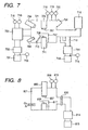
- the inventors of the present invention produced an In-Ga-Zn-O film by a pulse laser vapor deposition by use of the apparatus shown in Fig. 7 .
- the film-forming was carried out by using such a PLD film-forming apparatus as shown in Fig. 7 .
- the numerals indicate the followings: 701, an RP (rotary pump); 702, a TMP (turbo molecular pump); 703, a preliminary chamber; 704, an electron gun for RHEED; 705, a substrate-holding means for rotating and vertically moving the substrate; 706, a laser-introducing window; 707, a substrate; 708, a target; 709, a radical source; 710, a gas inlet; 711, a target-holding means for rotating and vertically moving the target; 712, a by-pass line; 713, a main line; 714, a TMP (turbo molecular pump); 715, an RP (rotary pump); 716, a titanium getter pump; 717, a shutter; 718, an IG (ion manometer); 719, a PG (Pirani gage); 720, a BG (baratron gage); and 721, a growth chamber.
- An In-Ga-Zn-O type amorphous oxide semiconductor thin film was deposited on an SiO 2 glass substrate (Corning Co.: 1737) by a pulse laser vapor deposition employing a KrF excimer laser.
- the substrate was washed ultrasonically for defatting with acetone, ethanol, and ultrapure water each for five minutes, and dried in the air at 100°C.
- the polycrystalline target was an InGaO 3 (ZnO) 4 sintered compact (size: 20 mm diameter, 5 mm thick), which had been prepared by wet-mixing In 2 O 3 , Ga 2 O 3 , and ZnO (each 4N reagent) as the source material (solvent: ethanol), calcining the mixture (1000°C, 2 hours), dry-crushing it, and sintering it (1550°C, 2 hours).
- the target had an electro conductivity of 90 S/cm.
- the film formation was conducted by controlling the final vacuum of the growth chamber to be 2 ⁇ 10 -6 Pa, and the oxygen partial pressure during the growth to be 6.5 Pa.
- the oxygen partial pressure in growth chamber 721 was 6.5 Pa
- the substrate temperature was 25°C.
- the distance between target 708 and film-holding substrate 707 was 30 mm, the power introduced through introduction window 716 was in the range of 1.5-3 mJ/cm 2 /pulse.
- the pulse width was 20 nsec, the repeating frequency was 10 Hz, and the irradiation spot size was 1 ⁇ 1 mm square. Under the above conditions, the film was formed at a rate of 7 nm/min.
- the resulting thin film was examined by small angle X-ray scattering method (SAXS) (thin film method, incidence angle: 0.5°): no clear diffraction peak was observed.
- SAXS small angle X-ray scattering method
- the mean square roughness (Rrms) was found to be about 0.5 nm, and the film thickness to be about 120 nm.
- XRF fluorescence X-ray spectrometric analysis
- the electric conductivity was less than about 1 ⁇ 10 -2 S/cm.
- the electron carrier concentration was estimated to be not more than 1 ⁇ 10 -16 /cm 3 .
- the electron mobility was estimated to be about 5 cm 2 /V.sec. From light absorption spectrum analysis, the optical band gap energy breadth of the resulting amorphous thin film was estimated to be about 3 eV.
- the obtained In-Ga-Zn-O type thin film is a transparent flat thin film having an amorphous phase of a composition near to a crystalline InGaO 3 (ZnO) 4 , having less oxygen defect, and having lower electric conductivity.
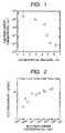
- Fig. 1 shows dependency of the electron carrier concentration in the formed transparent amorphous oxide thin film on the oxygen partial pressure for the film of a composition of InGaO 3 (ZnO) m (m: an integer less than 6) in an assumed crystalline state under the same film formation conditions as in the above Example.
- the electron carrier concentration could be lowered to less than 1 ⁇ 10 18 /cm 3 as shown in Fig. 1 .
- the substrate was kept nearly at room temperature without intentional heating.
- the substrate temperature is kept preferably at a temperature lower than 100°C.
- the higher oxygen partial pressure enables decrease of the electron carrier concentration.
- the thin InGaO 3 (ZnO) 4 film formed at the substrate temperature of 25°C and the oxygen partial pressure of 5 Pa had a lower electron carrier concentration of 1 ⁇ 10 16 /cm 3 .
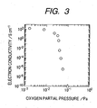
- the electron mobility was higher than 1 cm 2 /V.sec as shown in Fig. 2 .
- the film deposited by the pulse laser vapor deposition at an oxygen partial pressure of higher than 6.5 Pa as in this Example has a rough surface, being not suitable for a channel layer of the TFT.
- a normally-off type transistor can be constructed by using a transparent thin amorphous oxide represented by InGaO 3 (ZnO) m (m: a number less than 6) in a crystal state formed at an oxygen partial pressure of higher than 4.5 Pa, preferably higher than 5 Pa, but lower than 6.5 Pa by a pulse laser vapor deposition method in the above Example.
- ZnO InGaO 3
- the above obtained thin film exhibited an electron mobility higher than 1 cm 2 /V, and the on-off ratio could be made higher than 1 ⁇ 10 3 .
- the oxygen partial pressure is controlled in the range preferably from 4.5 Pa to 6.5 Pa.
- the oxygen partial pressure conditions, the constitution of the film formation apparatus, the kind and composition of the film-forming material should be controlled.
- a top-gate type MISFET element as shown in Fig. 5 was produced by forming an amorphous oxide with the aforementioned apparatus at an oxygen partial pressure of 6.5 Pa.
- a semi-insulating amorphous InGaO 3 (ZnO) 4 film of 120 nm thick was formed for use for channel layer 2 by the above method of formation of amorphous thin Ga-Ga-Zn-O film.
- an InGaO 3 (ZnO) 4 film having a higher electro, conductivity and a gold film were laminated respectively in a thickness of 30 nm by pulse laser deposition at an oxygen partial pressure of lower than 1 Pa in the chamber.
- drain terminal 5 and source terminal 6 were formed by photolithography and a lift-off method.
- a Y 2 O 3 film for gate insulator 3 was formed by an electron beam vapor deposition method (thickness: 90 nm, relative dielectric constant: about 15, leak current density: 1 ⁇ 10 -3 A/cm 3 at application of 0.5 MV/cm).
- a gold film was formed, and gate terminal 4 was formed by photolithography and lifting-off.
- Fig. 6 shows current-voltage characteristics of the MISFET element measured at room temperature.
- the channel is understood to be an n-type semiconductor from the increase of the drain current I DS with the increase of the drain voltage V DS .
- the on-off ratio of the transistor was higher than 1 ⁇ 10 3 . From the output characteristics, the field effect mobility was calculated to be about 7 cm 2 (Vs) -1 . Irradiation of visible light did not change the transistor characteristics of the produced element according to the same measurement.
- a thin film transistor can be produced which has a channel layer containing electron carriers at a lower concentration to achieve higher electric resistance and exhibiting a higher electron mobility.
- the above amorphous oxide has excellent characteristics that the electron mobility increases with the increase of the electron carrier concentration, and exhibits degenerate conduction.
- the thin film was formed on a glass substrate.
- a plastic plate or film is useful as the substrate since the film formation can be conducted at room temperature.
- the amorphous oxide obtained in this Example absorbs visible light only little to give transparent flexible TFT.
- Fig. 8 The SP process was conducted by use of the apparatus shown in Fig. 8 .
- the numerals indicates the followings: 807, a substrate for film formation; 808, a target; 805, a substrate-holding means equipped with a cooling mechanism; 814, a turbo molecular pump; 815, a rotary pump; 817, a shutter; 818, an ion manometer; 819, a Pirani gage; 821, a growth chamber; and 830, a gate valve.
- Substrate 807 for film formation was an SiO 2 glass substrate (Corning Co.: 1737) which had been washed ultrasonically for defatting with acetone, ethanol, and ultrapure water respectively for 5 minutes, and dried at 100°C in the air.
- the target was a polycrystalline sintered compact having a composition of InGaO 3 (ZnO) 4 (size: 20 nm diameter, 5 mm thick), which had been prepared by wet-mixing In 2 O 3 , Ga 2 O 3 , and ZnO (each 4N reagent) as the source material (solvent: ethanol), calcining the mixture (1000°C, 2 hours), dry-crushing it, and sintering (1550°C, 2 hours).
- Target 808 had an electro conductivity of 90 S/cm, being semi-insulating.
- the final vacuum degree of growth chamber 821 was 1 ⁇ 10 -4 Pa.
- the total pressure of the oxygen and argon gas was kept constant within the range of 4 to 0.1 ⁇ 10 -1 Pa.
- the partial pressure ratio of argon to oxygen was changed in the range of the oxygen partial pressure from 1 ⁇ 10 -3 to 2 ⁇ 10 -1 Pa.
- the substrate temperature was room temperature.
- the distance between target 808 and substrate 807 for film formation was 30 mm.
- the inputted electric power was RF 180 W, and the film forming rate was 10 nm/min.
- the resulting thin film was examined by small angle X-ray scattering method (SAXS) (thin film method, incidence angle: 0.5°): no clear diffraction peak was observed.
- SAXS small angle X-ray scattering method
- the obtained In-Ga-Zn-O type thin film was judged to be amorphous.
- the mean square roughness (Rrms) was found to be about 0.5 nm, and the film thickness to be about 120 nm.
- XRF fluorescence X-ray spectrometric analysis
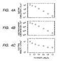
- Fig. 3 shows the result.
- the electric conductivity can be lowered to less than 10 S/cm by conducting the film formation in an atmosphere having an oxygen partial pressure higher then 3 ⁇ 10 -2 Pa.
- the electron carrier number could be decreased by increase of the oxygen partial pressure.
- the thin InGaO 3 (ZnO) 4 film formed at the substrate temperature of 25°C and the oxygen partial pressure or 1 ⁇ 10 -1 Pa had a lower electric conductivity of about 1 ⁇ 10 -10 S/cm. Further, the thin InGaO 3 (ZnO) 4 film formed at the oxygen partial pressure or 1 ⁇ 10 -1 Pa had an excessively high electric resistance, having the electric conductivity not measurable. With this film, although the electron mobility was not measurable, the electron mobility was estimated to be about 1 cm 2 /V.sec by extrapolation from the values of the films of high electron carrier concentration.
- a normally-off transistor having the on-off ratio of higher than 1 ⁇ 10 3 could be obtained by use of a transparent thin amorphous oxide film constituted of In-Ga-Zn-O represented in a crystal state by InGaO 3 (ZnO) m (m: a natural number of less than 6) produced by sputtering vapor deposition in an argon atmosphere containing oxygen at a partial pressure of higher than 3 ⁇ 10 -2 Pa, preferably higher than 5 ⁇ 10 -1 Pa.
- the film formation by sputtering is conducted in the oxygen partial pressure ranging from 3 ⁇ 10 -2 Pa to 5 ⁇ 10 -1 Pa.
- the electron mobility increases with increase in number of the conductive electrons.
- the oxygen defect can be decreased, and thereby the electron carrier concentration can be decreased.
- the electron mobility can be high, since no grain interface exists essentially in the amorphous state differently from polycrystalline state.
- a high-resistance amorphous film InGaO 3 (Zn 1-x Mg x O) m (m: an natural number less than 6; 0 ⁇ x ⁇ 1) can be obtained by using, as the target, polycrystalline InGaO 3 (Zn 1-x Mg x O) m even at an oxygen partial pressure less than 1 Pa.
- the electron carrier concentration lower than 1 ⁇ 10 16 /cm (resistance: about 1 ⁇ 10 -2 S/cm) can be achieved by pulse laser deposition in an atmosphere containing oxygen at a partial pressure of 0.8 Pa.
- the electron mobility is lower than that of the Mg-free film, but the decrease is slight: the electron mobility is about 5 cm 2 /V.sec at room temperature, being higher by about one digit than that of amorphous silicon.
- increase of the Mg content decreases both the electric conductivity and the electron mobility. Therefore, the content of the Mg ranges preferably from 20% to 85% (0.2 ⁇ x ⁇ 0.85).
- the gate insulator contains preferably a mixed crystal compound containing two or more of Al 2 O 3 , Y 2 O 3 , HfO 2 , and compounds thereof.
- the current leakage depends greatly on the kind of the gate insulator. Therefore the gate insulator should be selected to be suitable for the channel layer.
- the current leakage can be decreased by use of an Al 2 O 3 film, the hysteresis can be made smaller by use of a Y 2 O 3 film, and the electron' mobility can be increased by use of an HfO 2 film having a high dielectric constant.
- TFT can be formed which causes smaller current leakage, less hysteresis, and exhibiting a higher electron mobility. Since the gate insulator forming process and the channel layer forming process can be conducted at room temperature, the TFT can be formed in a stagger constitution or in a reversed stagger constitution.
- the TFT thus formed is a three-terminal element having a gate terminal, a source terminal, and a drain terminal.
- This TFT is formed by forming a semiconductor thin film on a insulating substrate of a ceramics, glass, or plastics as a channel layer for transport of electrons or holes, and serves as an active element having a function of controlling the current flowing through the channel layer by application of a voltage to the gate terminal, and switching the current between the source terminal and the drain terminal.
- the amount of the oxygen in the amorphous oxide film is controlled by controlling the oxygen concentration in the film-forming atmosphere. Otherwise the oxygen defect quantity can be controlled (decreased or increase) by post-treatment of the oxide film in an oxygen-containing atmosphere as a preferred embodiment.
- the temperature of the oxygen-containing atmosphere is controlled in the range from 0°C to 300°C, preferably from 25°C to 250°C, more preferably from 100°C to 200°C.
- a film may be formed in an oxygen-containing atmosphere and further post-treated in an oxygen-containing atmosphere. Otherwise the film is formed without control of the oxygen partial pressure and post-treatment is conducted in an oxygen-containing atmosphere, insofar as the intended electron carrier concentration (less than 1 ⁇ 10 18 /cm 3 ) can be achieved.
- the lower limit of the electron carrier concentration in the present invention is, for example, 1 ⁇ 10 14 /cm 3 , depending on the kind of the element, circuit, or device employing the produced oxide film.
- an amorphous oxide composed of at least one oxide of the elements of Zn, In, and Sn is useful for an amorphous oxide film of a low carrier concentration and high electron mobility.
- This amorphous oxide film was found to have a specific property that increase in number of conductive electrons therein increases the electron mobility.
- a normally-off type TFT can be produced which is excellent in transistor properties such as the on-off ratio, the saturation current in the pinch-off state, and the switching rate.
- the present invention also provides a field-effect transistor employing the above mentioned amorphous oxide or amorphous oxide film as the channel layer.
- a field-effect transistor is prepared which is employs an amorphous oxide film having an electron carrier concentration of less than 1 ⁇ 10 18 /cm 3 but more than 1 ⁇ 10 15 /cm 3 as the channel layer, and having a source terminal and a drain terminal, and a gate terminal with interposition of a gate insulator.
- a voltage of about 5 V is applied between the source and drain terminals without application of gate voltage, the electric current between the source and drain terminals is about 1 ⁇ 10 -7 amperes.
- the electron mobility in the oxide crystal becomes larger with increase of the overlap of the s-orbitals of the metal ions.
- the electron mobility is in the range from 0.1 to 200 cm 2 /V.sec.
- oxygen and metal ions are bonded by ionic bonds without orientation of the chemical bonds, having a random structure. Therefore in the oxide in an amorphous state, the electron mobility can be comparable to that in a crystal state.
- the electron mobility in the amorphous oxide of the present invention ranges from about 0.01 to 20 cm 2 /V. sec.
- the gate insulator is preferably formed from Al 2 O 3 , Y 2 O 3 , HfO 2 , or a mixed crystal compound containing two or more thereof.
- the current leakage depends greatly on the kind of the gate insulator. Therefore the gate insulator should be selected to be suitable for the channel layer.
- the current leakage can be decreased by use of an Al 2 O 3 film, the hysteresis can be made smaller by use of a Y 2 O 3 film, and the electron mobility can be increased by use of an HfO 2 film having a high dielectric constant.
- TFT can be formed which causes smaller current leakage, less hysteresis, and exhibiting a higher electron mobility. Since the gate insulator-forming process and the channel layer-forming process can be conducted at room temperature, the TFT can be formed in a stagger constitution or in a reversed stagger constitution.
- the In 2 O 3 oxide film can be formed through a gas-phase process, and addition of moisture in a partial pressure of about 0.1 Pa to the film-forming atmosphere makes the formed film amorphous.
- ZnO and SnO 2 respectively cannot readily be formed in an amorphous film state.
- In 2 O 3 is added in an amount of 20 atom%.
- In 2 O 3 is added in an amount of 90 atom%.
- gaseous nitrogen is introduced in a partial pressure of about 0.1 Pa in the film formation atmosphere.
- an element capable of forming a complex oxide selected from Group-2 elements M2 having an atomic number lower than Zn (Mg, and Ca), Group-3 elements M3 having an atomic number lower than In (B, Al, Ga, and Y), Group-4 elements M4 having an atomic number lower than Sn (Si, Ge, and Zr), Group-5 elements M5 (V, Nb, and Ta), and Lu, and W.
- the addition of the above element stabilizes the amorphous film at room temperature, and broadens the composition range for amorphous film formation.
- addition of B, Si, or Ge tending to form a covalent bond is effective for amorphous phase stabilization.
- Addition of a complex oxide constituted of ions having largely different ion radiuses is effective for amorphous phase stabilization.
- In should be contained more than about 20 atom%.
- addition of Mg in an amount equivalent to In enables formation of stable amorphous film in the composition range of In of not less than about 15 atom%.
- an amorphous oxide film of the electron carrier concentration ranging from 1 ⁇ 10 15 /cm 3 to 1 ⁇ 10 18 /cm 3 can be obtained by controlling the film forming atmosphere.
- An amorphous oxide film can be suitably formed by a vapor phase process such as a pulse laser vapor deposition process (PLD process), a sputtering process (SP process), and an electron-beam vapor deposition.
- a vapor phase process such as a pulse laser vapor deposition process (PLD process), a sputtering process (SP process), and an electron-beam vapor deposition.
- PLD process pulse laser vapor deposition process
- SP process sputtering process
- electron-beam vapor deposition electron-beam vapor deposition
- An In-Zn-Ga-O type amorphous oxide was deposited on a glass substrate (Corning Co.: 1737) by a PLD process employing a KrF excimer laser with a polycrystal sintered compact as the target having a composition of InGaO 3 (ZnO) or InGaO 3 (ZnO) 4.
- the substrate temperature was 25°C.
- SAXS small angle X-ray scattering method
- the mean square roughnesses (Rrms) of the thin films were found to be about 0.5 nm, and the film thicknesses to be about 120 nm.
- Amorphous oxide films were formed at various oxygen partial pressure of the film-forming atmosphere with the target having the composition of InGaO 3 (ZnO) 4.
- the formed amorphous oxide films were measured for the electron carrier concentration.
- Fig. 1 shows the results.
- the electron carrier concentration could be lowered to less than 1 ⁇ 10 18 /cm 3 as shown in Fig. 1 .
- the substrate was kept nearly at room temperature without intentional heating.
- the oxygen partial pressure of lower than 6.5 Pa the surfaces of the obtained amorphous oxide films were flat.
- the electron carrier concentration was 1 ⁇ 10 16 /cm 3
- the electro conductivity was 1 ⁇ 10 -2 S/cm
- the electron mobility therein was estimated to be about 5 cm 2 /V.sec.
- the optical band gap energy breadth of the formed amorphous oxide film was estimated to be about 3 eV.
- the higher oxygen partial pressure further lowered the electron carrier concentration.
- the electron carrier concentration was lowered to 8 ⁇ 10 15 /cm 3 (electroconductivity: about 8 ⁇ 10 -3 S/cm).
- the electron mobility in the film was estimated to be 1 cm 2 /V.sec or more.
- the PLD process at the oxygen partial pressure of 6.5 Pa or higher, the deposited film has a rough surface, being not suitable for use as the channel layer of the TFT.
- the In-Zn-Ga-O type amorphous oxide films were formed at various oxygen partial pressures in the film-forming atmosphere with the target constituted of a polycrystalline sintered compact having the composition of InGaO 3 (ZnO) 4 .
- the ersulting films were examined for the relation between the electron carrier concentration and the electron mobility.
- Fig. 2 shows the results.
- the electron mobility increased from about 3 cm 2 /V.sec to about 11 cm 2 /V.sec.
- the same tendency was observed with the amorphous oxide films obtained with the polycrystalline sintered InGaO 3 (ZnO) target.
- a film of InGaO 3 (Zn 1-x Mg x O) 4 (0 ⁇ x ⁇ 1) was formed on a glass substrate by a PLD process with an InGaO 3 (Zn 1-x Mg x O) 4 target (0 ⁇ x ⁇ 1).
- the apparatus employed was the one shown in Fig. 7 .
- An SiO 2 glass substrate (Corning Co.: 1737) was used as the substrate.
- the substrate was washed ultrasonically for defatting with acetone, ethanol, and ultrapure water each for five minutes, and dried in the air at 100°C.
- the target was prepared by wet-mixing source materials In 2 O 3 , Ga 2 O 3 , and ZnO (each 4N reagent) (solvent: ethanol), calcining the mixture (1000°C, 2 hours), dry-crushing it, and sintering it (1550°C, 2 hours).
- the final pressure in the growth chamber was 2 ⁇ 10 -6 Pa.
- the oxygen partial pressure during the growth was controlled at 0.8 Pa.
- the substrate temperature was room temperature (25°C).
- the distance between the target and the substrate for film formation was 30 mm.
- the KrF excimer laser was irradiated at a power of 1.5 mJ/cm 2 /pulse with the pulse width of 20 nsec, the repeating frequency of 10 Hz, and the irradiation spot size of 1x1 mm square.
- the film-forming rate was 7 nm/min.
- the oxygen partial pressure in the film-forming atmosphere was 0.8 Pa.
- the substrate temperature was 25°C.
- the resulting thin film was examined by small angle X-ray scattering method (SAXS) (thin film method, incidence angle: 0.5°): no clear diffraction peak was observed.
- SAXS small angle X-ray scattering method
- In-Zn-Ga-Mg-O type amorphous oxide films were formed at the oxygen partial pressure of 0.8 Pa in a film-forming atmosphere to investigate the dependency of the conductivity, the electron carrier concentration, and the electron mobility on the x-value.
- Figs. 4A, 4B, and 4C show the results.
- the electron carrier concentration was decreased to be less than 1 ⁇ 101 8 /cm 3 .
- the electron mobility was higher than 1 cm 2 /V.
- the electron carrier concentration less than 1 ⁇ 10 16 /cm 3 could be achieved in the film prepared by a pulse laser deposition process with the target in which 80 atom% of Zn is replaced by Mg andat the oxygen partial pressure of 0.8 Pa (electric resistance: about 1 ⁇ 10 -2 S.cm).
- the electron mobility is decreased in comparison with the Mg-free film, but the decrease is slight.
- the electron mobility in the films is about 5 cm 2 /V.sec, which is higher by about one digit than that of amorphous silicon.
- both the electric conductivity and the electron mobility in the film decrease with increase of the Mg content. Therefore, the Mg content in the film is preferably more than 20 atom% and less than 85 atom% (0.2 ⁇ x ⁇ 0.85), more preferably 0.5 ⁇ x ⁇ 0.85.
- An In 2 O 3 film was formed on a 200 ⁇ m-thick PET film by use of a target constituted of In 2 O 3 polycrystalline sintered compact by a PLD process employing a KrF excimer laser.
- the apparatus used is shown in Fig. 7 .
- the substrate for the film formation was an SiO 2 glass substrate (Corning Co.: 1737).
- the substrate was washed ultrasonically for defatting with acetone, ethanol, and ultrapure water each for five minutes, and dried in the air at 100°C.
- the target was an In 2 O 3 sintered compact (size: 20 mm diameter, 5 mm thick), which had been prepared by calcining the source material In 2 O 3 (4N reagent) (1000°C, 2 hours), dry-crushing it, and sintering it (1550°C, 2 hours).
- the final vacuum of the growth chamber was 2x 10 -6 Pa, the oxygen partial pressure during the growth was 5 Pa, and the substrate temperature was 25°C.
- the water vapor partial pressure was 0.1 Pa, and oxygen radicals were generated by the oxygen radical-generating assembly by application of 200W.
- the distance between the target and the film-holding substrate was 40 mm
- the power of the Krf excimer laser was 0.5 mJ/cm 2 /pulse
- the pulse width was 20 nsec
- the repeating frequency was 10 Hz
- the irradiation spot size was 1x1 mm square.
- the film-forming rate was of 3 nm/min.
- the resulting thin film was examined by small angle X-ray scattering method (SAXS) (thin film method, incidence angle: 0.5°): no clear diffraction peak was observed, which shows that the obtained In-O type oxide film was amorphous.
- SAXS small angle X-ray scattering method
- the electron carrier concentration was 5 ⁇ 10 17 /cm 3
- the electron mobility was about 7 cm 2 /V.sec.
- An In-Sn-O type oxide film was formed on a 200 ⁇ m-thick PET film by use of a target constituted of polycrystalline sintered compact of (In 0.9 Sn 0.1 )O 3.1 by a PLD process employing a KrF excimer laser.
- the apparatus used is shown in Fig. 7 .
- the substrate for the film formation was an SiO 2 glass substrate (Corning Co.: 1737).
- the substrate was washed ultrasonically for defatting with acetone, ethanol, and ultrapure water each for five minutes, and dried in the air at 100°C.
- the target was an In 2 O 3 -SnO 2 sintered compact (size: 20 mm diameter, 5 mm thick), which had been prepared by wet-mixing the source materials In 2 O 3 -SnO 2 . (4N reagents) (solvent: ethanol), calcining the mixture (1000°C, 2 hours), dry-crushing it, and sintering it (1550°C, 2 hours).
- the substrate was kept at room temperature.
- the oxygen partial pressure was 5 Pa.
- the nitrogen partial pressure was 0.1 Pa.
- Oxygen radicals were generated by the oxygen radical-generating assembly by application of 200W.
- the distance between the target and the film-holding substrate was 30 mm
- the power of the Krf excimer laser was 1.5 mJ/cm 2 /pulse
- the pulse width was 20 nsec
- the repeating frequency was 10 Hz
- the irradiation spot size was 1x1 mm square.
- the film-forming rate was of 6 nm/min.
- the resulting thin film was examined by small angle X-ray scattering method (SAXS) (thin film method, incidence angle: 0.5°): no clear diffraction peak was detected, which shows that the obtained In-Sn-O type oxide film is amorphous.
- SAXS small angle X-ray scattering method
- the electron carrier concentration was 8 ⁇ 10 17 /cm 3
- the electron mobility was about 5 cm 2 /V.sec.
- the film thickness was 100 nm.
- the substrate for the film was an SiO 2 glass substrate (Corning Co.:1737).
- the substrate was washed ultrasonically for defatting with acetone, ethanol, and ultrapure water each for five minutes, and dried in the air at 100°C.
- This target was prepared by wet-mixing the source materials In 2 O 3 -Ga 2 O 2 (4N reagents) (solvent: ethanol), calcining the mixture (1000°C, 2 hours), dry-crushing it, and sintering it (1550°C, 2 hours).
- the final pressure of the growth chamber was 2 ⁇ 10 -6 Pa.
- the oxygen partial pressure during the growth was 1 Pa.
- the substrate was at room temperature.
- the distance between the target and the film-holding substrate was 30 mm.
- the power of the Krf excimer laser was 1.5 mJ/cm 2 /pulse.
- the pulse width was 20 nsec.
- the repeating frequency was 10 Hz.
- the irradiation spot size was 1 ⁇ 1 mm square.
- the film-forming rate was of 6 nm/min.
- the substrate temperature was 25°C.
- the oxygen pressure was 1 Pa.
- the resulting film was examined by small angle X-ray scattering method (SAXS) (thin film method, incidence angle: 0.5°): no clear diffraction peak was detected, which shows that the obtained In-Ga-O type oxide film is amorphous.
- SAXS small angle X-ray scattering method
- the electron carrier concentration was 8 ⁇ 10 16 /cm 3
- the electron mobility was about 1 cm 2 /V.sec.
- a top gate type TFT element shown in Fig. 5 was prepared.
- an In-Ga-Zn-O type amorphous oxide film was prepared on glass substrate 1 by the aforementioned PLS apparatus with a target constituted of a polycrystalline sintered compact having a composition of InGaO 3 (ZnO) 4 at an oxygen partial pressure of 5 Pa.
- the formed In-Ga-Zn-O film had a thickness of 120 nm, and was used as channel layer 2.
- drain terminal 5 and source terminal 6 were formed by photolithography and a lift-off method.
- a Y 2 O 3 film as gate insulator 3 was formed by electron beam vapor deposition (thickness: 90 nm, relative dielectric constant: about 15, leakage current density: 1 ⁇ 10 -3 A/cm 2 under application of 0.5 MV/cm). Further thereon, a gold film was formed and therefrom gate terminal 4 was formed by photolithography and a lift-off method. The channel length was 50 ⁇ m, and the channel width was 200 ⁇ m.
- Fig. 6 shows current-voltage characteristics of the TFT element at room temperature. Drain current I DS increased with increase of drain voltage V DS , which shows that the channel is of an n-type conduction.
- the on-off ratio of the transistor was higher than 1 ⁇ 10 3 . From the output characteristics, the field effect mobility was calculated to be about 7 cm 2 (Vs). -1 in the saturation region. Irradiation of visible light did not change the transistor characteristics of the produced element according to the same measurement.
- the amorphous oxide of the electron carrier concentration lower than 1 ⁇ 10 18 /cm 3 is useful as a channel layer of a TFT.
- the electron carrier concentration is more preferably less than 1 ⁇ 10 17 /cm 3 , still more preferably less than 1 ⁇ 10 16 /cm 3 .
- a top gate type TFT element shown in Fig. 5 was prepared.
- an In-Ga-Zn-O type amorphous oxide film was prepared on polyethylene terephthalate (PET) film 1 by the aforementioned PLS apparatus with a target constituted of a polycrystalline sintered compact having a composition of InGaO 3 (ZnO) at an oxygen partial pressure of 5 Pa in the atmosphere.
- the formed film had a thickness of 12.0 nm, and was used as channel layer 2.
- drain terminal 5 and source terminal 6 were formed by photolithography and a lift-off method.
- gate insulator 3 was formed by an electron beam vapor deposition method. Further thereon, a gold film was formed and therefrom gate terminal 4 was formed by photolithography and a lift-off method. The channel length was 50 ⁇ m, and the channel width was 200 ⁇ m.
- Three TFTs of the above structure were prepared by using respectively one of the three kinds of gate insulators: Y 2 O 3 (140 nm thick), Al 2 O 3 (130 ⁇ m thick), and HfO 2 (140 ⁇ m thick).
- the TFT elements formed on a PET film had current-voltage characteristics similar to that shown in Fig. 6 at room temperature.
- Drain current I DS increased with increase of drain voltage V DS , which shows that the channel is of an n-type conduction. This is consistent with the fact that an amorphous In-Ga-Zn-O type semiconductor is of an n type.
- V G 10 V. This corresponds to carrier induction by gate bias in the insulator, the In-Ga-Zn-O type amorphous semiconductor oxide film.
- the on-off ratio of the transistor was higher than 1 ⁇ 10 3 . From the output characteristics, the field effect mobility was calculated to be about 7 cm 2 (V s ) -1 in the saturation region.
- the elements formed on the PET film were curved at a curvature radius of 30 mm, and in this state, transistor characteristics were measured. However the no change was observed in the transistor characteristics. Irradiation of visible light did not change the transistor characteristics.
- the TFT employing the Al 2 O 3 film as the gate insulator has also transistor characteristics similar to that shown in Fig. 6 .
- the on-off ratio of the transistor was higher than 1 ⁇ 10 2 . From the output characteristics, the field effect mobility was calculated to be about 2 cm 2 (Vs) -1 in the saturation region.
- the TFT employing the HfO 2 film as the gate insulator has also transistor characteristics similar to that shown in Fig. 6 .
- the on-off ratio of the transistor was higher than 1 ⁇ 10 2 . From the output characteristics, the field effect mobility was calculated to be about 10 cm 2 (Vs) -1 in the saturation region.
- a top gate type TFT element shown in Fig. 5 was prepared.
- an In 2 O 3 type amorphous oxide film was formed on polyethylene terephthalate (PET) film 1 by the PLD method as channel layer 2 in a thickness of 80 nm.
- drain terminal 5 and source terminal 6 were formed by photolithography and a lift-off method.
- gate terminal 4 was formed by photolithography and a lift-off method.
- drain current I DS increased with increase of drain voltage V DS , which shows that the channel is an n-type conductor. This is consistent with the fact that an amorphous In-O type amorphous oxide film is an n type conductor.
- the on-off ratio of the transistor was about 1 ⁇ 10 2 . From the output characteristics, the field effect mobility was calculated to be about 1 ⁇ 10 cm 2 (Vs) -1 in the saturation region.
- the TFT element formed on a glass substrate had similar characteristics.
- the elements formed on the PET film were curved in a curvature radius of 30 mm, and in this state, transistor characteristics were measured. No change was observed in the transistor characteristics.
- a top gate type TFT element shown in Fig. 5 was prepared.
- an In-Sn-O type amorphous oxide film was formed in a thickness of 100 nm as channel layer 2 on polyethylene terephthalate (PET) film 1 by the PLD method.
- drain terminal 5 and source terminal 6 were formed by photolithography and a lift-off method.
- gate terminal 4 was formed by photolithography and a lift-off method.
- drain current I DS increased with increase of drain voltage V DS , which shows that the channel is an n-type conductor. This is consistent with the fact that an amorphous In-Sn-O type amorphous oxide film is an n type conductor.
- the on-off ratio of the transistor was about 1 ⁇ 10 3 . From the output characteristics, the field effect mobility was calculated to be about 5 cm 2 (Vs) -1 in the saturation range.
- the TFT element formed on a glass substrate had similar characteristics.
- the elements formed on the PET film were curved at a curvature radius of 30 mm, and in this state, transistor characteristics were measured. No change was caused thereby in the transistor characteristics.
- a top gate type TFT element shown in Fig. 5 was prepared.
- an In-Ga-O type amorphous oxide film was formed in a thickness of 120 nm as channel layer 2 on polyethylene terephthalate (PET) film 1 by the PLD method shown in Example 6.
- drain terminal 5 and source terminal 6 were formed by photolithography and a lift-off method.
- gate terminal 4 was formed by photolithography and a lift-off method.
- drain current I DS increased with increase of drain voltage V DS , which shows that the channel is an n-type conductor. This is consistent with the fact that an amorphous In-Ga-O type amorphous oxide film is an n type conductor.
- the on-off ratio of the transistor was about 1 ⁇ 10 2 . From the output characteristics, the field effect mobility was calculated to be about 0.8 cm 2 (Vs) -1 in the saturation range.
- the TFT element formed on a glass substrate had similar characteristics.
- the elements formed on the PET film were curved at a curvature radius of 30 mm, and in this state, transistor characteristics were measured. No change was caused thereby in the transistor characteristics.
- the amorphous oxide of the electron carrier concentration of lower than 1 ⁇ 10 18 /cm 3 is useful as the channel layer of the TFT.
- the electron carrier concentration is more preferably not higher than 1 ⁇ 10 17 /cm 3 , still more preferably not higher than 1 ⁇ 10 16 /cm 3 .
- a film is prepared by using the apparatus shown in FIG. 7 .
- a pulse laser deposition method using KrF excimer laser is performed with a polycrystalline sintered body having a composition of InGaO 3 (ZnO) 4 as a target.
- a glass substrate 1737, manufactured by Corning Incorporated
- an In-Ga-Zn-O based amorphous oxide semiconductor thin film containing microcrystals is deposited.
- a substrate surface is irradiated with a halogen lamp (20mW/cm 2 ). The presence or absence of microcrystals is confirmed under TEM (transmission electron microscope) observation of a film section.
- a top-gate type MISFET device shown in FIG. 5 is manufactured.
- a semi-insulating amorphous InGaO 3 (ZnO) 4 film of 30 nm in thickness containing microcrystals and serving as a channel layer (2) is formed on the glass substrate (1) in accordance with the aforementioned method for preparing an amorphous In-Ga-Zn-O thin film containing microcrystals.
- InGaO 3 (ZnO) 4 film and a gold film large in electric conductivity, each having 30 nm thickness are stacked by a pulse laser deposition method while setting the oxygen partial pressure of a chamber at less than 1Pa.
- a drain terminal (5) and a source terminal (6) are formed by a photolithographic method and a lift-off method.
- an Y 2 O 3 film serving as a gate insulator (3) is formed by an electron beam deposition method (the obtained film has a thickness of 90 to 110 nm, a specific dielectric constant of about 15, leak current density of 1 ⁇ 10 -3 A/cm 2 when a current of 0.5 MV/cm is applied).
- a gold film is formed on the resultant construct, and then, a gate terminal (4) is formed by a photolithographic method and a lift-off method. In this manner, the field effect transistor is formed.
- the on/off ratio of the transistor exceeds 1 ⁇ 10 4 .
- an electron field-effect mobility of about 7.5 cm 2 (Vs) -1 was obtained in a saturation field.
- the device thus manufactured was irradiated with visible light and subjected to the same measurement. As a result, any change in the characteristics of a transistor was not observed.
- microcrystals In this reason, light irradiation is preferable. Although it varies depending upon the amount of microcrystals in an amorphous oxide film, the presence of microcrystals is generally confirmed if a peak is detected by X-ray diffraction.
- An In-Ga-Zn-O based amorphous oxide semiconductor thin film having a compositional distribution in the film thickness direction is deposited on a glass substrate (1737, manufactured by Corning Incorporated) by a pulse laser deposition method using KrF excimer laser with a polycrystalline sintered body having a composition of InGaO 3 (ZnO) 4 as a target.
- the film is deposited in a chamber having inner oxygen partial pressure within a predetermined range while increasing the distance between the target and the substrate up to 5 mm. As the distance increases, the amount of oxygen incorporated into the formed film increases. Note that the temperature of the substrate is set at 25°C.
- a composition may be changed by varying oxygen partial pressure in the film thickness direction, or alternatively, by changing an oscillation power or oscillation frequency of a pulse laser. In this manner, leak current can be reduced or the on/off ratio of a transistor can be increased, as well as electron field-effect mobility can be increased.
- the film is formed by a sputtering method using argon gas.
- targets (1) a polycrystalline sintered body having a composition of InGaO 3 (ZnO) 4 and (2) a zinc oxide sintered body are prepared.
- an amorphous In-Ga-Zn-O thin film having a compositional distribution in the film thickness direction is deposited on a glass substrate (1737, manufactured by Corning Incorporated).
- the film is formed by the sputtering method in an atmosphere having a predetermined oxygen partial pressure, first by using target (1), subsequently by using target (1) and target (2), simultaneously. In this manner, the amorphous In-Ga-Zn-O thin film having a compositional distribution in the film thickness direction can be prepared.
- the temperature of the substrate is set at 25°C.
- the In-Ga-Zn-O thin film having a compositional distribution in the film thickness direction may be prepared by the following manner.
- the composition is distributed in the film thickness direction by sputtering an In 2 O 3 target simultaneously or separately, or changing oxygen partial pressure in the film thickness direction, or alternatively, changing power supply in the film thickness direction for each target in a sputtering step.
- electron field-effect mobility is expected to increase as the amount of In 2 O 3 or ZnO increases.
- An In-Ga-Zn-O based amorphous oxide semiconductor thin film containing nitrogen as an impurity is deposited on a glass substrate of the same type as above by a pulse laser deposition method using KrF excimer laser with an InGaO 3 (ZnO) 4 , polycrystalline sintered body used as a target.
- the oxygen partial pressure within a chamber is set at, for example, 4 Pa
- the nitrogen partial pressure is set at 1 Pa
- the temperature of a substrate is set at 25°C.
- the compositional ratio of oxygen and nitrogen of the thin film is preferably about 50:1, as analyzed by a secondary ion mass spectrum (SIMS).
- An In-Ga-Zn-O based amorphous oxide semiconductor thin film is deposited on a glass substrate (1737, manufactured by Corning Incorporated) by a pulse laser deposition method using KrF excimer laser with a polycrystalline sintered body having a composition of InGaO 3 (ZnO) 4 used as a target.
- the resultant In-Ga-Zn-O based thin film is soaked in an aqueous solution of titanium trichloride kept at 80°C. Thereafter, the film is taken up and annealed at 300°C in the air. In this manner, Ti can be introduced as an impurity in the amorphous oxide.
- the Ti concentration of the thin film is analyzed from the surface to the bottom by SIMS, the Ti concentration of the outermost surface is about 0.5% and gradually decreases toward the bottom.
- An amorphous oxide as used in the present invention is applicable to the channel layer of a transistor.
- a transistor can be used as switching devices for LCDs and organic EL displays.
- the amorphous oxide may be applied on a flexible material such as a plastic film to form a semiconductor thin film.
- a semiconductor thin film can be widely used as panels of flexible displays, IC cards and ID tags.
Landscapes
- Engineering & Computer Science (AREA)
- Power Engineering (AREA)
- Microelectronics & Electronic Packaging (AREA)
- Physics & Mathematics (AREA)
- Condensed Matter Physics & Semiconductors (AREA)
- General Physics & Mathematics (AREA)
- Computer Hardware Design (AREA)
- Manufacturing & Machinery (AREA)
- Ceramic Engineering (AREA)
- Chemical & Material Sciences (AREA)
- Crystallography & Structural Chemistry (AREA)
- Toxicology (AREA)
- Electromagnetism (AREA)
- Optics & Photonics (AREA)
- Health & Medical Sciences (AREA)
- Materials Engineering (AREA)
- Thin Film Transistor (AREA)
- Liquid Crystal (AREA)
- Physical Deposition Of Substances That Are Components Of Semiconductor Devices (AREA)
- Dram (AREA)
- Physical Vapour Deposition (AREA)
Claims (5)
- Transistor à effet de champ ayant une couche active comprenant un film d'oxyde amorphe et une électrode de grille formée de manière à faire face à la couche active à travers un isolant de grille, le film d'oxyde amorphe ayant une concentration en porteurs d'électrons inférieure à 1018/cm3 à une température de 25°C, dans lequel le film d'oxyde amorphe comprend un oxyde amorphe comprenant In-Ga-Zn-O ou In-Ga-Zn-Mg-O, et dans lequel l'oxyde comprend un type d'élément ou une pluralité d'éléments choisis dans le groupe consistant en Li, Na, Mn, Ni, Pd, Cu, Cd, C, N et P.
- Transistor à effet de champ ayant une couche active comprenant un film d'oxyde amorphe et une électrode de grille formée de manière à faire face à la couche active à travers un isolant de grille, le film d'oxyde amorphe ayant une concentration en porteurs d'électrons inférieure à 1018/cm3 à une température de 25°C, dans lequel le film d'oxyde amorphe comprend un oxyde amorphe comprenant In-Ga-Zn-O ou In-Ga-Zn-Mg-O, et dans lequel l'oxyde comprend au moins un élément choisi dans le groupe consistant en Ti, Ru et F.
- Transistor à effet de champ suivant la revendication 1 ou 2, dans lequel la concentration en porteurs d'électrons est inférieure à 1017/cm3 à une température de 25°C.
- Transistor à effet de champ suivant l'une quelconque des revendications 1 à 3, dans lequel l'oxyde amorphe est un oxyde qui présente un motif de halo et qui ne présente aucune raie de diffraction caractéristique en spectrométrie de diffraction des rayons X.
- Transistor à effet de champ suivant l'une quelconque des revendications 1 à 4, dans lequel le film d'oxyde amorphe est obtenu en utilisant une cible ayant une composition InGaO3(ZnO)m ou InGaO3(Zn1-xMgxO) à l'état cristallin, dans laquelle m représente un nombre entier inférieur à 6 et x est supérieur à 0 et non supérieur à 1.
Applications Claiming Priority (2)
| Application Number | Priority Date | Filing Date | Title |
|---|---|---|---|
| JP2004326687 | 2004-11-10 | ||
| EP05806969.1A EP1812969B1 (fr) | 2004-11-10 | 2005-11-09 | Transistor a effet de champ comprenant un oxyde amorphe |
Related Parent Applications (3)
| Application Number | Title | Priority Date | Filing Date |
|---|---|---|---|
| EP05806969.1 Division | 2005-11-09 | ||
| EP05806969.1A Division EP1812969B1 (fr) | 2004-11-10 | 2005-11-09 | Transistor a effet de champ comprenant un oxyde amorphe |
| EP05806969.1A Division-Into EP1812969B1 (fr) | 2004-11-10 | 2005-11-09 | Transistor a effet de champ comprenant un oxyde amorphe |
Publications (3)
| Publication Number | Publication Date |
|---|---|
| EP2455975A2 EP2455975A2 (fr) | 2012-05-23 |
| EP2455975A3 EP2455975A3 (fr) | 2014-06-25 |
| EP2455975B1 true EP2455975B1 (fr) | 2015-10-28 |
Family
ID=35696016
Family Applications (4)
| Application Number | Title | Priority Date | Filing Date |
|---|---|---|---|
| EP05806969.1A Active EP1812969B1 (fr) | 2004-11-10 | 2005-11-09 | Transistor a effet de champ comprenant un oxyde amorphe |
| EP11009313.5A Active EP2453481B1 (fr) | 2004-11-10 | 2005-11-09 | Transistor à effet de champ avec oxyde amorphe |
| EP11009311.9A Active EP2455975B1 (fr) | 2004-11-10 | 2005-11-09 | Transistor à effet de champ avec oxyde amorphe |
| EP20110009312 Withdrawn EP2453480A2 (fr) | 2004-11-10 | 2005-11-09 | Oxyde amorphe et transistor à effet de champ |
Family Applications Before (2)
| Application Number | Title | Priority Date | Filing Date |
|---|---|---|---|
| EP05806969.1A Active EP1812969B1 (fr) | 2004-11-10 | 2005-11-09 | Transistor a effet de champ comprenant un oxyde amorphe |
| EP11009313.5A Active EP2453481B1 (fr) | 2004-11-10 | 2005-11-09 | Transistor à effet de champ avec oxyde amorphe |
Family Applications After (1)
| Application Number | Title | Priority Date | Filing Date |
|---|---|---|---|
| EP20110009312 Withdrawn EP2453480A2 (fr) | 2004-11-10 | 2005-11-09 | Oxyde amorphe et transistor à effet de champ |
Country Status (10)
| Country | Link |
|---|---|
| US (5) | US7601984B2 (fr) |
| EP (4) | EP1812969B1 (fr) |
| JP (3) | JP2011256108A (fr) |
| KR (2) | KR100998527B1 (fr) |
| CN (3) | CN102945857B (fr) |
| AU (2) | AU2005302962B2 (fr) |
| BR (1) | BRPI0517568B8 (fr) |
| CA (3) | CA2708335A1 (fr) |
| RU (3) | RU2402106C2 (fr) |
| WO (1) | WO2006051993A2 (fr) |
Cited By (15)
| Publication number | Priority date | Publication date | Assignee | Title |
|---|---|---|---|---|
| US9252288B2 (en) | 2008-11-20 | 2016-02-02 | Semiconductor Energy Laboratory Co., Ltd. | Semiconductor device and method for manufacturing the same |
| US9318654B2 (en) | 2009-10-09 | 2016-04-19 | Semiconductor Energy Laboratory Co., Ltd. | Light-emitting display device and electronic device including the same |
| US9324878B2 (en) | 2009-03-06 | 2016-04-26 | Semiconductor Energy Laboratory Co., Ltd. | Semiconductor device and method for manufacturing the same |
| US9324874B2 (en) | 2008-10-03 | 2016-04-26 | Semiconductor Energy Laboratory Co., Ltd. | Display device comprising an oxide semiconductor |
| US9343517B2 (en) | 2008-09-19 | 2016-05-17 | Semiconductor Energy Laboratory Co., Ltd. | Display device |
| US9397194B2 (en) | 2008-09-01 | 2016-07-19 | Semiconductor Energy Laboratory Co., Ltd. | Method for manufacturing semiconductor device with oxide semiconductor ohmic conatct layers |
| US9411208B2 (en) | 2009-12-04 | 2016-08-09 | Semiconductor Energy Laboratory Co., Ltd. | Display device |
| US9431427B2 (en) | 2009-02-06 | 2016-08-30 | Semiconductor Energy Laboratory Co., Ltd. | Semiconductor device comprising oxide semiconductor layer |
| US9437428B2 (en) | 2013-11-29 | 2016-09-06 | Semiconductor Energy Laboratory Co., Ltd. | Method of manufacturing a semiconductor device having an oxide semiconductor layer with increased hydrogen concentration |
| US9466728B2 (en) | 2011-12-01 | 2016-10-11 | Semiconductor Energy Laboratory Co., Ltd. | Semiconductor device and method for manufacturing the same |
| US9520288B2 (en) | 2009-09-24 | 2016-12-13 | Semiconductor Energy Laboratory Co., Ltd. | Semiconductor device including IGZO layer and manufacturing method thereof |
| US9559212B2 (en) | 2008-11-13 | 2017-01-31 | Semiconductor Energy Laboratory Co., Ltd. | Semiconductor device and method for manufacturing the same |
| US9570470B2 (en) | 2008-10-03 | 2017-02-14 | Semiconductor Energy Laboratory Co., Ltd. | Display device |
| US9576795B2 (en) | 2009-06-30 | 2017-02-21 | Semiconductor Energy Laboratory Co., Ltd. | Semiconductor device |
| US9589988B2 (en) | 2008-10-03 | 2017-03-07 | Semiconductor Energy Laboratory Co., Ltd. | Display device and method for manufacturing the same |
Families Citing this family (1920)
| Publication number | Priority date | Publication date | Assignee | Title |
|---|---|---|---|---|
| US7442629B2 (en) | 2004-09-24 | 2008-10-28 | President & Fellows Of Harvard College | Femtosecond laser-induced formation of submicrometer spikes on a semiconductor substrate |
| US7057256B2 (en) | 2001-05-25 | 2006-06-06 | President & Fellows Of Harvard College | Silicon-based visible and near-infrared optoelectric devices |
| US7829444B2 (en) | 2004-11-10 | 2010-11-09 | Canon Kabushiki Kaisha | Field effect transistor manufacturing method |
| US7791072B2 (en) | 2004-11-10 | 2010-09-07 | Canon Kabushiki Kaisha | Display |
| WO2006051994A2 (fr) | 2004-11-10 | 2006-05-18 | Canon Kabushiki Kaisha | Dispositif electroluminescent |
| US7863611B2 (en) | 2004-11-10 | 2011-01-04 | Canon Kabushiki Kaisha | Integrated circuits utilizing amorphous oxides |
| US7453065B2 (en) | 2004-11-10 | 2008-11-18 | Canon Kabushiki Kaisha | Sensor and image pickup device |
| BRPI0517560B8 (pt) | 2004-11-10 | 2018-12-11 | Canon Kk | transistor de efeito de campo |
| EP1812969B1 (fr) | 2004-11-10 | 2015-05-06 | Canon Kabushiki Kaisha | Transistor a effet de champ comprenant un oxyde amorphe |
| US7579224B2 (en) * | 2005-01-21 | 2009-08-25 | Semiconductor Energy Laboratory Co., Ltd. | Method for manufacturing a thin film semiconductor device |
| TWI472037B (zh) * | 2005-01-28 | 2015-02-01 | Semiconductor Energy Lab | 半導體裝置,電子裝置,和半導體裝置的製造方法 |
| TWI569441B (zh) | 2005-01-28 | 2017-02-01 | 半導體能源研究所股份有限公司 | 半導體裝置,電子裝置,和半導體裝置的製造方法 |
| US7858451B2 (en) * | 2005-02-03 | 2010-12-28 | Semiconductor Energy Laboratory Co., Ltd. | Electronic device, semiconductor device and manufacturing method thereof |
| US7948171B2 (en) * | 2005-02-18 | 2011-05-24 | Semiconductor Energy Laboratory Co., Ltd. | Light emitting device |
| US7928938B2 (en) * | 2005-04-19 | 2011-04-19 | Semiconductor Energy Laboratory Co., Ltd. | Semiconductor device including memory circuit, display device and electronic apparatus |
| US7710739B2 (en) * | 2005-04-28 | 2010-05-04 | Semiconductor Energy Laboratory Co., Ltd. | Semiconductor device and display device |
| CN102394049B (zh) | 2005-05-02 | 2015-04-15 | 株式会社半导体能源研究所 | 显示装置的驱动方法 |
| US8059109B2 (en) * | 2005-05-20 | 2011-11-15 | Semiconductor Energy Laboratory Co., Ltd. | Display device and electronic apparatus |
| EP1724751B1 (fr) * | 2005-05-20 | 2013-04-10 | Semiconductor Energy Laboratory Co., Ltd. | Dispositif d'affichage à cristaux liquides et appareil électronique |
| US8629819B2 (en) | 2005-07-14 | 2014-01-14 | Semiconductor Energy Laboratory Co., Ltd. | Semiconductor device and driving method thereof |
| EP1758072A3 (fr) * | 2005-08-24 | 2007-05-02 | Semiconductor Energy Laboratory Co., Ltd. | Dispositif d'affichage et son méthode de commande |
| WO2007034935A1 (fr) * | 2005-09-21 | 2007-03-29 | Semiconductor Energy Laboratory Co., Ltd. | Circuit de contrôle de redondance cyclique et dispositif à semi-conducteur muni de ce circuit |
| EP1770788A3 (fr) * | 2005-09-29 | 2011-09-21 | Semiconductor Energy Laboratory Co., Ltd. | Dispositif semi-conducteur à oxyde semi-conducteur et son procédé de fabrication |
| EP1935027B1 (fr) | 2005-10-14 | 2017-06-28 | Semiconductor Energy Laboratory Co., Ltd. | Dispositif a semi-conducteurs et son procede de fabrication |
| JP4560505B2 (ja) | 2005-11-08 | 2010-10-13 | キヤノン株式会社 | 電界効果型トランジスタ |
| KR101112655B1 (ko) * | 2005-11-15 | 2012-02-16 | 가부시키가이샤 한도오따이 에네루기 켄큐쇼 | 액티브 매트릭스 디스플레이 장치 및 텔레비전 수신기 |
| CN101309864B (zh) * | 2005-11-18 | 2012-06-27 | 出光兴产株式会社 | 半导体薄膜及其制造方法以及薄膜晶体管 |
| EP2924498A1 (fr) | 2006-04-06 | 2015-09-30 | Semiconductor Energy Laboratory Co, Ltd. | Dispositif d'affichage à cristaux liquides, dispositif semi-conducteur et dispositif électronique |
| KR101150142B1 (ko) * | 2006-04-06 | 2012-06-11 | 어플라이드 머티어리얼스, 인코포레이티드 | 대형 기판 상에 아연 산화물 투명 전도성 산화물의 반응성 스퍼터링 |
| KR100785038B1 (ko) * | 2006-04-17 | 2007-12-12 | 삼성전자주식회사 | 비정질 ZnO계 TFT |
| US7443202B2 (en) * | 2006-06-02 | 2008-10-28 | Semiconductor Energy Laboratory Co., Ltd. | Semiconductor device and electronic apparatus having the same |
| KR100746361B1 (ko) * | 2006-07-11 | 2007-08-06 | 삼성전기주식회사 | 인쇄회로기판 제조방법 |
| JP4609797B2 (ja) | 2006-08-09 | 2011-01-12 | Nec液晶テクノロジー株式会社 | 薄膜デバイス及びその製造方法 |
| JP5127183B2 (ja) * | 2006-08-23 | 2013-01-23 | キヤノン株式会社 | アモルファス酸化物半導体膜を用いた薄膜トランジスタの製造方法 |
| US7651896B2 (en) | 2006-08-30 | 2010-01-26 | Semiconductor Energy Laboratory Co., Ltd. | Method for manufacturing semiconductor device |
| JP5116277B2 (ja) | 2006-09-29 | 2013-01-09 | 株式会社半導体エネルギー研究所 | 半導体装置、表示装置、液晶表示装置、表示モジュール及び電子機器 |
| US7646015B2 (en) * | 2006-10-31 | 2010-01-12 | Semiconductor Energy Laboratory Co., Ltd. | Manufacturing method of semiconductor device and semiconductor device |
| WO2008072486A1 (fr) * | 2006-12-13 | 2008-06-19 | Idemitsu Kosan Co., Ltd. | Cible de sublimation et film semi-conducteur à base d'oxyde |
| WO2008097117A1 (fr) * | 2007-02-05 | 2008-08-14 | Universidade Nova De Lisboa | Dispositif semi-conducteur électronique à base de nickel cuivre et d'oxydes de type p et n de gallium-etain-zinc-cuivre-titanium, leurs applications et procédé de fabrication correspondant |
| KR101312259B1 (ko) * | 2007-02-09 | 2013-09-25 | 삼성전자주식회사 | 박막 트랜지스터 및 그 제조방법 |
| KR101509663B1 (ko) | 2007-02-16 | 2015-04-06 | 삼성전자주식회사 | 산화물 반도체층 형성 방법 및 이를 이용한 반도체 소자제조방법 |
| KR101410926B1 (ko) | 2007-02-16 | 2014-06-24 | 삼성전자주식회사 | 박막 트랜지스터 및 그 제조방법 |
| JP5121254B2 (ja) * | 2007-02-28 | 2013-01-16 | キヤノン株式会社 | 薄膜トランジスタおよび表示装置 |
| KR100858088B1 (ko) * | 2007-02-28 | 2008-09-10 | 삼성전자주식회사 | 박막 트랜지스터 및 그 제조 방법 |
| JP5466939B2 (ja) | 2007-03-23 | 2014-04-09 | 出光興産株式会社 | 半導体デバイス、多結晶半導体薄膜、多結晶半導体薄膜の製造方法、電界効果型トランジスタ、及び、電界効果型トランジスタの製造方法 |
| EP1976019B1 (fr) | 2007-03-29 | 2011-06-15 | Korea Advanced Institute of Science and Technology | Transistor à film mince comportant des oxydes de titane en tant que couche active et son procédé de fabrication |
| JP2008276211A (ja) * | 2007-04-05 | 2008-11-13 | Fujifilm Corp | 有機電界発光表示装置およびパターニング方法 |
| JP2008276212A (ja) * | 2007-04-05 | 2008-11-13 | Fujifilm Corp | 有機電界発光表示装置 |
| CN101632179B (zh) * | 2007-04-06 | 2012-05-30 | 夏普株式会社 | 半导体元件及其制造方法、以及包括该半导体元件的电子器件 |
| JP2009031742A (ja) * | 2007-04-10 | 2009-02-12 | Fujifilm Corp | 有機電界発光表示装置 |
| KR20080094300A (ko) * | 2007-04-19 | 2008-10-23 | 삼성전자주식회사 | 박막 트랜지스터 및 그 제조 방법과 박막 트랜지스터를포함하는 평판 디스플레이 |
| GB0707714D0 (en) * | 2007-04-20 | 2007-05-30 | Imp Innovations Ltd | Improved oxide-based field-effect transistors |
| KR101334181B1 (ko) * | 2007-04-20 | 2013-11-28 | 삼성전자주식회사 | 선택적으로 결정화된 채널층을 갖는 박막 트랜지스터 및 그제조 방법 |
| JP2008277326A (ja) | 2007-04-25 | 2008-11-13 | Canon Inc | アモルファス酸化物半導体、半導体デバイス及び薄膜トランジスタ |
| WO2008133345A1 (fr) * | 2007-04-25 | 2008-11-06 | Canon Kabushiki Kaisha | Semi-conducteur d'oxynitrure |
| US7927713B2 (en) | 2007-04-27 | 2011-04-19 | Applied Materials, Inc. | Thin film semiconductor material produced through reactive sputtering of zinc target using nitrogen gases |
| JP5522889B2 (ja) | 2007-05-11 | 2014-06-18 | 出光興産株式会社 | In−Ga−Zn−Sn系酸化物焼結体、及び物理成膜用ターゲット |
| JP5542297B2 (ja) | 2007-05-17 | 2014-07-09 | 株式会社半導体エネルギー研究所 | 液晶表示装置、表示モジュール及び電子機器 |
| JP5542296B2 (ja) | 2007-05-17 | 2014-07-09 | 株式会社半導体エネルギー研究所 | 液晶表示装置、表示モジュール及び電子機器 |
| JP4989309B2 (ja) | 2007-05-18 | 2012-08-01 | 株式会社半導体エネルギー研究所 | 液晶表示装置 |
| JP5241143B2 (ja) | 2007-05-30 | 2013-07-17 | キヤノン株式会社 | 電界効果型トランジスタ |
| KR101092483B1 (ko) * | 2007-05-31 | 2011-12-13 | 캐논 가부시끼가이샤 | 산화물 반도체를 사용한 박막트랜지스터의 제조 방법 |
| US7897482B2 (en) * | 2007-05-31 | 2011-03-01 | Semiconductor Energy Laboratory Co., Ltd. | Semiconductor device and manufacturing method thereof |
| US7935964B2 (en) * | 2007-06-19 | 2011-05-03 | Samsung Electronics Co., Ltd. | Oxide semiconductors and thin film transistors comprising the same |
| JP2010530634A (ja) | 2007-06-19 | 2010-09-09 | サムスン エレクトロニクス カンパニー リミテッド | 酸化物半導体及びそれを含む薄膜トランジスタ |
| US8354674B2 (en) * | 2007-06-29 | 2013-01-15 | Semiconductor Energy Laboratory Co., Ltd. | Semiconductor device wherein a property of a first semiconductor layer is different from a property of a second semiconductor layer |
| KR20090002841A (ko) * | 2007-07-04 | 2009-01-09 | 삼성전자주식회사 | 산화물 반도체, 이를 포함하는 박막 트랜지스터 및 그 제조방법 |
| WO2009014155A1 (fr) | 2007-07-25 | 2009-01-29 | Semiconductor Energy Laboratory Co., Ltd. | Dispositif de conversion photoélectrique et dispositif électronique comportant celui-ci |
| KR101536101B1 (ko) * | 2007-08-02 | 2015-07-13 | 어플라이드 머티어리얼스, 인코포레이티드 | 박막 반도체 물질들을 이용하는 박막 트랜지스터들 |
| JP5393058B2 (ja) * | 2007-09-05 | 2014-01-22 | キヤノン株式会社 | 電界効果型トランジスタ |
| JP4759598B2 (ja) | 2007-09-28 | 2011-08-31 | キヤノン株式会社 | 薄膜トランジスタ、その製造方法及びそれを用いた表示装置 |
| US8319214B2 (en) * | 2007-11-15 | 2012-11-27 | Fujifilm Corporation | Thin film field effect transistor with amorphous oxide active layer and display using the same |
| US7982216B2 (en) * | 2007-11-15 | 2011-07-19 | Fujifilm Corporation | Thin film field effect transistor with amorphous oxide active layer and display using the same |
| JP2009130209A (ja) * | 2007-11-26 | 2009-06-11 | Fujifilm Corp | 放射線撮像素子 |
| JP2010103451A (ja) * | 2007-11-26 | 2010-05-06 | Fujifilm Corp | 薄膜電界効果型トランジスタおよびそれを用いた電界発光装置 |
| JP5213421B2 (ja) | 2007-12-04 | 2013-06-19 | キヤノン株式会社 | 酸化物半導体薄膜トランジスタ |
| WO2009075161A1 (fr) * | 2007-12-12 | 2009-06-18 | Idemitsu Kosan Co., Ltd. | Couche mince semi-conductrice cristalline gravée, procédé de production de transistor à couches minces et transistor à effet de champ |
| US8384077B2 (en) * | 2007-12-13 | 2013-02-26 | Idemitsu Kosan Co., Ltd | Field effect transistor using oxide semicondutor and method for manufacturing the same |
| US8461583B2 (en) | 2007-12-25 | 2013-06-11 | Idemitsu Kosan Co., Ltd. | Oxide semiconductor field effect transistor and method for manufacturing the same |
| JP5213458B2 (ja) | 2008-01-08 | 2013-06-19 | キヤノン株式会社 | アモルファス酸化物及び電界効果型トランジスタ |
| NO332409B1 (no) * | 2008-01-24 | 2012-09-17 | Well Technology As | Anordning og fremgangsmate for a isolere en seksjon av et bronnhull |
| CN102017088B (zh) * | 2008-01-31 | 2013-08-07 | 哈佛大学校长及研究员协会 | 在经脉冲激光照射而掺杂的材料上构造平坦表面 |
| US8980066B2 (en) * | 2008-03-14 | 2015-03-17 | Applied Materials, Inc. | Thin film metal oxynitride semiconductors |
| WO2009117438A2 (fr) * | 2008-03-20 | 2009-09-24 | Applied Materials, Inc. | Procédé de fabrication de réseau de transistors à couches minces d’oxyde métalliques avec couche d’arrêt de gravure |
| JP2009267399A (ja) | 2008-04-04 | 2009-11-12 | Fujifilm Corp | 半導体装置,半導体装置の製造方法,表示装置及び表示装置の製造方法 |
| US8017045B2 (en) | 2008-04-16 | 2011-09-13 | Electronics And Telecommunications Research Institute | Composition for oxide semiconductor thin film and field effect transistor using the composition |
| KR100990217B1 (ko) * | 2008-04-16 | 2010-10-29 | 한국전자통신연구원 | 산화물 반도체 박막용 조성물, 이를 채용한 전계 효과트랜지스터 및 이의 제조방법 |
| KR101496148B1 (ko) | 2008-05-15 | 2015-02-27 | 삼성전자주식회사 | 반도체소자 및 그 제조방법 |
| US9041202B2 (en) | 2008-05-16 | 2015-05-26 | Semiconductor Energy Laboratory Co., Ltd. | Semiconductor device and manufacturing method of the same |
| US8377743B2 (en) * | 2008-05-21 | 2013-02-19 | Cbrite Inc. | Laser annealing of metal oxide semiconductor on temperature sensitive substrate formations |
| KR101468591B1 (ko) * | 2008-05-29 | 2014-12-04 | 삼성전자주식회사 | 산화물 반도체 및 이를 포함하는 박막 트랜지스터 |
| KR101224769B1 (ko) * | 2008-06-10 | 2013-01-21 | 제이엑스 닛코 닛세키 킨조쿠 가부시키가이샤 | 스퍼터링용 산화물 소결체 타겟 및 그 제조 방법 |
| US8314765B2 (en) | 2008-06-17 | 2012-11-20 | Semiconductor Energy Laboratory Co., Ltd. | Driver circuit, display device, and electronic device |
| US8258511B2 (en) * | 2008-07-02 | 2012-09-04 | Applied Materials, Inc. | Thin film transistors using multiple active channel layers |
| KR102040563B1 (ko) | 2008-07-10 | 2019-11-05 | 가부시키가이샤 한도오따이 에네루기 켄큐쇼 | 발광장치 및 전자기기 |
| TWI450399B (zh) | 2008-07-31 | 2014-08-21 | Semiconductor Energy Lab | 半導體裝置及其製造方法 |
| TWI500159B (zh) | 2008-07-31 | 2015-09-11 | Semiconductor Energy Lab | 半導體裝置和其製造方法 |
| TWI476921B (zh) | 2008-07-31 | 2015-03-11 | Semiconductor Energy Lab | 半導體裝置及其製造方法 |
| JP2010056541A (ja) | 2008-07-31 | 2010-03-11 | Semiconductor Energy Lab Co Ltd | 半導体装置およびその作製方法 |
| JP5616038B2 (ja) | 2008-07-31 | 2014-10-29 | 株式会社半導体エネルギー研究所 | 半導体装置の作製方法 |
| KR100975204B1 (ko) * | 2008-08-04 | 2010-08-10 | 삼성모바일디스플레이주식회사 | 박막 트랜지스터, 그의 제조 방법 및 박막 트랜지스터를구비하는 평판 표시 장치 |
| JP5525778B2 (ja) * | 2008-08-08 | 2014-06-18 | 株式会社半導体エネルギー研究所 | 半導体装置 |
| JP5480554B2 (ja) | 2008-08-08 | 2014-04-23 | 株式会社半導体エネルギー研究所 | 半導体装置 |
| TWI642113B (zh) | 2008-08-08 | 2018-11-21 | 半導體能源研究所股份有限公司 | 半導體裝置的製造方法 |
| TWI508282B (zh) | 2008-08-08 | 2015-11-11 | Semiconductor Energy Lab | 半導體裝置及其製造方法 |
| JP5608347B2 (ja) | 2008-08-08 | 2014-10-15 | 株式会社半導体エネルギー研究所 | 半導体装置及び半導体装置の作製方法 |
| JP2010050165A (ja) * | 2008-08-19 | 2010-03-04 | Sumitomo Chemical Co Ltd | 半導体装置、半導体装置の製造方法、トランジスタ基板、発光装置、および、表示装置 |
| JP5644071B2 (ja) | 2008-08-20 | 2014-12-24 | 株式会社リコー | 電界効果型トランジスタ、表示素子、画像表示装置及びシステム |
| TWI606592B (zh) | 2008-09-01 | 2017-11-21 | 半導體能源研究所股份有限公司 | 半導體裝置的製造方法 |
| JP5627071B2 (ja) | 2008-09-01 | 2014-11-19 | 株式会社半導体エネルギー研究所 | 半導体装置の作製方法 |
| KR101489652B1 (ko) * | 2008-09-02 | 2015-02-06 | 삼성디스플레이 주식회사 | 박막 트랜지스터 기판 및 이의 제조 방법 |
| WO2010029859A1 (fr) * | 2008-09-12 | 2010-03-18 | Semiconductor Energy Laboratory Co., Ltd. | Dispositif à semi-conducteurs et procédé de fabrication associé |
| WO2010029865A1 (fr) | 2008-09-12 | 2010-03-18 | Semiconductor Energy Laboratory Co., Ltd. | Dispositif d'affichage |
| KR101767864B1 (ko) * | 2008-09-12 | 2017-08-11 | 가부시키가이샤 한도오따이 에네루기 켄큐쇼 | 반도체 장치 및 그 생산 방법 |
| KR101657957B1 (ko) | 2008-09-12 | 2016-09-20 | 가부시키가이샤 한도오따이 에네루기 켄큐쇼 | 표시 장치 |
| EP2327070B1 (fr) * | 2008-09-19 | 2018-10-17 | Semiconductor Energy Laboratory Co, Ltd. | Dispositif d'affichage |
| CN102881696A (zh) | 2008-09-19 | 2013-01-16 | 株式会社半导体能源研究所 | 显示装置 |
| CN103545342B (zh) * | 2008-09-19 | 2018-01-26 | 株式会社半导体能源研究所 | 半导体装置 |
| KR101622981B1 (ko) * | 2008-09-19 | 2016-05-20 | 가부시키가이샤 한도오따이 에네루기 켄큐쇼 | 표시장치 및 그 제조방법 |
| KR101611643B1 (ko) * | 2008-10-01 | 2016-04-11 | 가부시키가이샤 한도오따이 에네루기 켄큐쇼 | 반도체 장치 |
| KR20110069831A (ko) * | 2008-10-03 | 2011-06-23 | 가부시키가이샤 한도오따이 에네루기 켄큐쇼 | 변조회로 및 그것을 갖는 반도체장치 |
| KR101961632B1 (ko) | 2008-10-03 | 2019-03-25 | 가부시키가이샤 한도오따이 에네루기 켄큐쇼 | 표시장치 |
| KR101652693B1 (ko) | 2008-10-03 | 2016-09-01 | 가부시키가이샤 한도오따이 에네루기 켄큐쇼 | 표시 장치 |
| JP5430113B2 (ja) * | 2008-10-08 | 2014-02-26 | キヤノン株式会社 | 電界効果型トランジスタ及びその製造方法 |
| CN101719493B (zh) | 2008-10-08 | 2014-05-14 | 株式会社半导体能源研究所 | 显示装置 |
| JP5484853B2 (ja) | 2008-10-10 | 2014-05-07 | 株式会社半導体エネルギー研究所 | 半導体装置の作製方法 |
| WO2010044478A1 (fr) * | 2008-10-16 | 2010-04-22 | Semiconductor Energy Laboratory Co., Ltd. | Dispositif d'affichage électroluminescent |
| JP5361651B2 (ja) | 2008-10-22 | 2013-12-04 | 株式会社半導体エネルギー研究所 | 半導体装置の作製方法 |
| US8106400B2 (en) | 2008-10-24 | 2012-01-31 | Semiconductor Energy Laboratory Co., Ltd. | Semiconductor device and method for manufacturing the same |
| EP2180518B1 (fr) | 2008-10-24 | 2018-04-25 | Semiconductor Energy Laboratory Co, Ltd. | Procédé de fabrication d'un dispositif semi-conducteur |
| WO2010047288A1 (fr) * | 2008-10-24 | 2010-04-29 | Semiconductor Energy Laboratory Co., Ltd. | Procédé de fabrication d’un dispositif semi-conducteur |
| US8741702B2 (en) | 2008-10-24 | 2014-06-03 | Semiconductor Energy Laboratory Co., Ltd. | Method for manufacturing semiconductor device |
| KR101259727B1 (ko) | 2008-10-24 | 2013-04-30 | 가부시키가이샤 한도오따이 에네루기 켄큐쇼 | 반도체 장치 |
| KR101667909B1 (ko) | 2008-10-24 | 2016-10-28 | 가부시키가이샤 한도오따이 에네루기 켄큐쇼 | 반도체장치의 제조방법 |
| JP5616012B2 (ja) * | 2008-10-24 | 2014-10-29 | 株式会社半導体エネルギー研究所 | 半導体装置の作製方法 |
| JP5442234B2 (ja) | 2008-10-24 | 2014-03-12 | 株式会社半導体エネルギー研究所 | 半導体装置及び表示装置 |
| KR101634411B1 (ko) * | 2008-10-31 | 2016-06-28 | 가부시키가이샤 한도오따이 에네루기 켄큐쇼 | 구동 회로, 표시 장치 및 전자 장치 |
| KR101603303B1 (ko) | 2008-10-31 | 2016-03-14 | 가부시키가이샤 한도오따이 에네루기 켄큐쇼 | 도전성 산질화물 및 도전성 산질화물막의 제작 방법 |
| KR101631454B1 (ko) | 2008-10-31 | 2016-06-17 | 가부시키가이샤 한도오따이 에네루기 켄큐쇼 | 논리회로 |
| TWI478356B (zh) | 2008-10-31 | 2015-03-21 | Semiconductor Energy Lab | 半導體裝置及其製造方法 |
| EP2184783B1 (fr) | 2008-11-07 | 2012-10-03 | Semiconductor Energy Laboratory Co, Ltd. | Dispositif semi-conducteur et son procédé de fabrication |
| KR101659703B1 (ko) | 2008-11-07 | 2016-09-26 | 가부시키가이샤 한도오따이 에네루기 켄큐쇼 | 반도체 장치 |
| TWI467663B (zh) | 2008-11-07 | 2015-01-01 | Semiconductor Energy Lab | 半導體裝置和該半導體裝置的製造方法 |
| TWI487104B (zh) | 2008-11-07 | 2015-06-01 | Semiconductor Energy Lab | 半導體裝置和其製造方法 |
| CN101740631B (zh) * | 2008-11-07 | 2014-07-16 | 株式会社半导体能源研究所 | 半导体装置及该半导体装置的制造方法 |
| TWI574423B (zh) | 2008-11-07 | 2017-03-11 | 半導體能源研究所股份有限公司 | 半導體裝置和其製造方法 |
| KR101432764B1 (ko) * | 2008-11-13 | 2014-08-21 | 가부시키가이샤 한도오따이 에네루기 켄큐쇼 | 반도체장치의 제조방법 |
| US8232947B2 (en) | 2008-11-14 | 2012-07-31 | Semiconductor Energy Laboratory Co., Ltd. | Liquid crystal display device |
| KR102359831B1 (ko) | 2008-11-21 | 2022-02-09 | 가부시키가이샤 한도오따이 에네루기 켄큐쇼 | 표시 장치 |
| TWI616707B (zh) | 2008-11-28 | 2018-03-01 | 半導體能源研究所股份有限公司 | 液晶顯示裝置 |
| TWI506795B (zh) | 2008-11-28 | 2015-11-01 | Semiconductor Energy Lab | 半導體裝置和其製造方法 |
| TWI585955B (zh) * | 2008-11-28 | 2017-06-01 | 半導體能源研究所股份有限公司 | 光感測器及顯示裝置 |
| KR101643204B1 (ko) * | 2008-12-01 | 2016-07-27 | 가부시키가이샤 한도오따이 에네루기 켄큐쇼 | 반도체 장치 및 그 제작 방법 |
| JP2010156960A (ja) | 2008-12-03 | 2010-07-15 | Semiconductor Energy Lab Co Ltd | 液晶表示装置 |
| JP5491833B2 (ja) | 2008-12-05 | 2014-05-14 | 株式会社半導体エネルギー研究所 | 半導体装置 |
| JP5538797B2 (ja) * | 2008-12-12 | 2014-07-02 | キヤノン株式会社 | 電界効果型トランジスタ及び表示装置 |
| JP5615540B2 (ja) * | 2008-12-19 | 2014-10-29 | 株式会社半導体エネルギー研究所 | 半導体装置の作製方法 |
| KR101642384B1 (ko) | 2008-12-19 | 2016-07-25 | 가부시키가이샤 한도오따이 에네루기 켄큐쇼 | 트랜지스터의 제작 방법 |
| EP2202802B1 (fr) | 2008-12-24 | 2012-09-26 | Semiconductor Energy Laboratory Co., Ltd. | Circuit de commande et dispositif semi-conducteur |
| KR101719350B1 (ko) * | 2008-12-25 | 2017-03-23 | 가부시키가이샤 한도오따이 에네루기 켄큐쇼 | 반도체 장치 및 그 제작 방법 |
| US8441007B2 (en) | 2008-12-25 | 2013-05-14 | Semiconductor Energy Laboratory Co., Ltd. | Display device and manufacturing method thereof |
| US8114720B2 (en) | 2008-12-25 | 2012-02-14 | Semiconductor Energy Laboratory Co., Ltd. | Semiconductor device and manufacturing method thereof |
| US8383470B2 (en) * | 2008-12-25 | 2013-02-26 | Semiconductor Energy Laboratory Co., Ltd. | Thin film transistor (TFT) having a protective layer and manufacturing method thereof |
| JP5590877B2 (ja) | 2008-12-26 | 2014-09-17 | 株式会社半導体エネルギー研究所 | 半導体装置 |
| TWI540647B (zh) * | 2008-12-26 | 2016-07-01 | 半導體能源研究所股份有限公司 | 半導體裝置及其製造方法 |
| KR101034686B1 (ko) * | 2009-01-12 | 2011-05-16 | 삼성모바일디스플레이주식회사 | 유기전계발광 표시 장치 및 그의 제조 방법 |
| KR101648927B1 (ko) * | 2009-01-16 | 2016-08-17 | 가부시키가이샤 한도오따이 에네루기 켄큐쇼 | 반도체 장치 및 그 제작 방법 |
| US8492756B2 (en) * | 2009-01-23 | 2013-07-23 | Semiconductor Energy Laboratory Co., Ltd. | Semiconductor device and method for manufacturing the same |
| US8436350B2 (en) * | 2009-01-30 | 2013-05-07 | Semiconductor Energy Laboratory Co., Ltd. | Semiconductor device using an oxide semiconductor with a plurality of metal clusters |
| US8367486B2 (en) | 2009-02-05 | 2013-02-05 | Semiconductor Energy Laboratory Co., Ltd. | Transistor and method for manufacturing the transistor |
| US8749930B2 (en) * | 2009-02-09 | 2014-06-10 | Semiconductor Energy Laboratory Co., Ltd. | Protection circuit, semiconductor device, photoelectric conversion device, and electronic device |
| US8247812B2 (en) * | 2009-02-13 | 2012-08-21 | Semiconductor Energy Laboratory Co., Ltd. | Transistor, semiconductor device including the transistor, and manufacturing method of the transistor and the semiconductor device |
| US8278657B2 (en) | 2009-02-13 | 2012-10-02 | Semiconductor Energy Laboratory Co., Ltd. | Transistor, semiconductor device including the transistor, and manufacturing method of the transistor and the semiconductor device |
| CN101840936B (zh) | 2009-02-13 | 2014-10-08 | 株式会社半导体能源研究所 | 包括晶体管的半导体装置及其制造方法 |
| US8247276B2 (en) | 2009-02-20 | 2012-08-21 | Semiconductor Energy Laboratory Co., Ltd. | Thin film transistor, method for manufacturing the same, and semiconductor device |
| US20100213458A1 (en) * | 2009-02-23 | 2010-08-26 | Micron Technology, Inc. | Rigid semiconductor memory having amorphous metal oxide semiconductor channels |
| US8841661B2 (en) * | 2009-02-25 | 2014-09-23 | Semiconductor Energy Laboratory Co., Ltd. | Staggered oxide semiconductor TFT semiconductor device and manufacturing method thereof |
| US8704216B2 (en) | 2009-02-27 | 2014-04-22 | Semiconductor Energy Laboratory Co., Ltd. | Semiconductor device and manufacturing method thereof |
| US8461582B2 (en) | 2009-03-05 | 2013-06-11 | Semiconductor Energy Laboratory Co., Ltd. | Semiconductor device and method for manufacturing the same |
| US20100224880A1 (en) * | 2009-03-05 | 2010-09-09 | Semiconductor Energy Laboratory Co., Ltd. | Semiconductor device |
| US20100224878A1 (en) | 2009-03-05 | 2010-09-09 | Semiconductor Energy Laboratory Co., Ltd. | Semiconductor device |
| KR101743164B1 (ko) * | 2009-03-12 | 2017-06-02 | 가부시키가이샤 한도오따이 에네루기 켄큐쇼 | 반도체 장치의 제작 방법 |
| TWI485781B (zh) * | 2009-03-13 | 2015-05-21 | Semiconductor Energy Lab | 半導體裝置及該半導體裝置的製造方法 |
| WO2010110571A2 (fr) * | 2009-03-23 | 2010-09-30 | Samsung Electronics Co., Ltd. | Oxyde semi-conducteur et transistor à couches minces le contenant |
| US8450144B2 (en) * | 2009-03-26 | 2013-05-28 | Semiconductor Energy Laboratory Co., Ltd. | Semiconductor device and method for manufacturing the same |
| KR101681884B1 (ko) | 2009-03-27 | 2016-12-05 | 가부시키가이샤 한도오따이 에네루기 켄큐쇼 | 반도체장치, 표시장치 및 전자기기 |
| TWI617029B (zh) | 2009-03-27 | 2018-03-01 | 半導體能源研究所股份有限公司 | 半導體裝置 |
| KR101752640B1 (ko) | 2009-03-27 | 2017-06-30 | 가부시키가이샤 한도오따이 에네루기 켄큐쇼 | 반도체장치 |
| TWI485851B (zh) * | 2009-03-30 | 2015-05-21 | Semiconductor Energy Lab | 半導體裝置及其製造方法 |
| US8338226B2 (en) * | 2009-04-02 | 2012-12-25 | Semiconductor Energy Laboratory Co., Ltd. | Method for manufacturing semiconductor device |
| TWI489628B (zh) * | 2009-04-02 | 2015-06-21 | Semiconductor Energy Lab | 半導體裝置和其製造方法 |
| US8441047B2 (en) | 2009-04-10 | 2013-05-14 | Semiconductor Energy Laboratory Co., Ltd. | Semiconductor device and method for manufacturing the same |
| TWI476917B (zh) | 2009-04-16 | 2015-03-11 | Semiconductor Energy Lab | 半導體裝置和其製造方法 |
| KR101690216B1 (ko) * | 2009-05-01 | 2016-12-27 | 가부시키가이샤 한도오따이 에네루기 켄큐쇼 | 반도체 장치의 제작 방법 |
| JP5751762B2 (ja) | 2009-05-21 | 2015-07-22 | 株式会社半導体エネルギー研究所 | 半導体装置 |
| JP5564331B2 (ja) * | 2009-05-29 | 2014-07-30 | 株式会社半導体エネルギー研究所 | 半導体装置の作製方法 |
| EP2256814B1 (fr) | 2009-05-29 | 2019-01-16 | Semiconductor Energy Laboratory Co, Ltd. | Dispositif semi-conducteur d'oxide et son procédé de fabrication |
| EP2256795B1 (fr) | 2009-05-29 | 2014-11-19 | Semiconductor Energy Laboratory Co., Ltd. | Procédé de fabrication d'un dispositif à semi-conducteurs d'oxyde |
| KR20120031026A (ko) | 2009-06-30 | 2012-03-29 | 가부시키가이샤 한도오따이 에네루기 켄큐쇼 | 반도체 장치 제조 방법 |
| KR102011616B1 (ko) | 2009-06-30 | 2019-08-16 | 가부시키가이샤 한도오따이 에네루기 켄큐쇼 | 반도체 장치 제조 방법 |
| KR20200031709A (ko) * | 2009-06-30 | 2020-03-24 | 가부시키가이샤 한도오따이 에네루기 켄큐쇼 | 반도체 장치 제조 방법 |
| US20110000175A1 (en) * | 2009-07-01 | 2011-01-06 | Husqvarna Consumer Outdoor Products N.A. Inc. | Variable speed controller |
| JP5663214B2 (ja) * | 2009-07-03 | 2015-02-04 | 株式会社半導体エネルギー研究所 | 半導体装置の作製方法 |
| KR101610606B1 (ko) | 2009-07-03 | 2016-04-07 | 가부시키가이샤 한도오따이 에네루기 켄큐쇼 | 반도체 장치의 제작 방법 |
| KR101476817B1 (ko) | 2009-07-03 | 2014-12-26 | 가부시키가이샤 한도오따이 에네루기 켄큐쇼 | 트랜지스터를 갖는 표시 장치 및 그 제작 방법 |
| KR101600887B1 (ko) * | 2009-07-06 | 2016-03-09 | 삼성디스플레이 주식회사 | 박막 트랜지스터 표시판 및 이의 제조 방법 |
| JP5640478B2 (ja) * | 2009-07-09 | 2014-12-17 | 株式会社リコー | 電界効果型トランジスタの製造方法及び電界効果型トランジスタ |
| KR101642620B1 (ko) | 2009-07-10 | 2016-07-25 | 가부시키가이샤 한도오따이 에네루기 켄큐쇼 | 반도체 장치 및 그 제조 방법 |
| KR20210131462A (ko) * | 2009-07-10 | 2021-11-02 | 가부시키가이샤 한도오따이 에네루기 켄큐쇼 | 액정 표시 장치의 제작 방법 |
| WO2011004755A1 (fr) | 2009-07-10 | 2011-01-13 | Semiconductor Energy Laboratory Co., Ltd. | Dispositif à semi-conducteur et procédé de fabrication associé |
| KR101739154B1 (ko) * | 2009-07-17 | 2017-05-23 | 가부시키가이샤 한도오따이 에네루기 켄큐쇼 | 반도체 장치 및 그 제조 방법 |
| WO2011007682A1 (fr) | 2009-07-17 | 2011-01-20 | Semiconductor Energy Laboratory Co., Ltd. | Procédé de fabrication de dispositif à semi-conducteur |
| WO2011007677A1 (fr) | 2009-07-17 | 2011-01-20 | Semiconductor Energy Laboratory Co., Ltd. | Dispositif à semi-conducteur et son procédé de fabrication |
| KR101414926B1 (ko) * | 2009-07-18 | 2014-07-04 | 가부시키가이샤 한도오따이 에네루기 켄큐쇼 | 반도체 장치 및 반도체 장치 제조 방법 |
| CN102473733B (zh) | 2009-07-18 | 2015-09-30 | 株式会社半导体能源研究所 | 半导体装置以及制造半导体装置的方法 |
| WO2011010545A1 (fr) | 2009-07-18 | 2011-01-27 | Semiconductor Energy Laboratory Co., Ltd. | Dispositif à semi-conducteurs et son procédé de fabrication |
| WO2011010541A1 (fr) | 2009-07-18 | 2011-01-27 | Semiconductor Energy Laboratory Co., Ltd. | Dispositif à semi-conducteurs et son procédé de fabrication |
| WO2011010542A1 (fr) * | 2009-07-23 | 2011-01-27 | Semiconductor Energy Laboratory Co., Ltd. | Dispositif à semi-conducteurs et son procédé de fabrication |
| KR101785992B1 (ko) | 2009-07-24 | 2017-10-18 | 가부시키가이샤 한도오따이 에네루기 켄큐쇼 | 반도체 장치 |
| WO2011013502A1 (fr) * | 2009-07-31 | 2011-02-03 | Semiconductor Energy Laboratory Co., Ltd. | Dispositif à semi-conducteur et son procédé de fabrication |
| WO2011013523A1 (fr) | 2009-07-31 | 2011-02-03 | Semiconductor Energy Laboratory Co., Ltd. | Dispositif semi-conducteur et procédé de fabrication de celui-ci |
| KR102251729B1 (ko) | 2009-07-31 | 2021-05-13 | 가부시키가이샤 한도오따이 에네루기 켄큐쇼 | 반도체 디바이스 및 그 형성 방법 |
| CN103489871B (zh) | 2009-07-31 | 2016-03-23 | 株式会社半导体能源研究所 | 半导体装置及其制造方法 |
| CN105097946B (zh) | 2009-07-31 | 2018-05-08 | 株式会社半导体能源研究所 | 半导体装置及其制造方法 |
| TWI596741B (zh) * | 2009-08-07 | 2017-08-21 | 半導體能源研究所股份有限公司 | 半導體裝置和其製造方法 |
| TWI559501B (zh) | 2009-08-07 | 2016-11-21 | 半導體能源研究所股份有限公司 | 半導體裝置和其製造方法 |
| TWI626731B (zh) | 2009-08-07 | 2018-06-11 | 半導體能源研究所股份有限公司 | 半導體裝置和其製造方法 |
| JP5642447B2 (ja) | 2009-08-07 | 2014-12-17 | 株式会社半導体エネルギー研究所 | 半導体装置 |
| TWI528527B (zh) | 2009-08-07 | 2016-04-01 | 半導體能源研究所股份有限公司 | 半導體裝置及半導體裝置之製造方法 |
| EP2284891B1 (fr) | 2009-08-07 | 2019-07-24 | Semiconductor Energy Laboratory Co, Ltd. | Dispositif de semi-conducteurs et son procédé de fabrication |
| JP5663231B2 (ja) * | 2009-08-07 | 2015-02-04 | 株式会社半導体エネルギー研究所 | 発光装置 |
| US8115883B2 (en) | 2009-08-27 | 2012-02-14 | Semiconductor Energy Laboratory Co., Ltd. | Display device and method for manufacturing the same |
| WO2011027649A1 (fr) * | 2009-09-02 | 2011-03-10 | Semiconductor Energy Laboratory Co., Ltd. | Dispositif semi-conducteur comprenant un transistor et procédé de fabrication du dispositif semi-conducteur |
| KR101746198B1 (ko) | 2009-09-04 | 2017-06-12 | 가부시키가이샤 한도오따이 에네루기 켄큐쇼 | 표시장치 및 전자기기 |
| WO2011027676A1 (fr) | 2009-09-04 | 2011-03-10 | Semiconductor Energy Laboratory Co., Ltd. | Dispositif à semi-conducteur et procédé de fabrication de celui-ci |
| CN103151387A (zh) | 2009-09-04 | 2013-06-12 | 株式会社半导体能源研究所 | 半导体器件及其制造方法 |
| WO2011027702A1 (fr) * | 2009-09-04 | 2011-03-10 | Semiconductor Energy Laboratory Co., Ltd. | Dispositif émetteur de lumière et procédé pour sa fabrication |
| KR101672072B1 (ko) | 2009-09-04 | 2016-11-02 | 가부시키가이샤 한도오따이 에네루기 켄큐쇼 | 반도체 장치의 제작 방법 |
| WO2011027664A1 (fr) * | 2009-09-04 | 2011-03-10 | Semiconductor Energy Laboratory Co., Ltd. | Ecran à cristaux liquides et procédé de fabrication associé |
| JP5700626B2 (ja) * | 2009-09-04 | 2015-04-15 | 株式会社半導体エネルギー研究所 | El表示装置 |
| WO2011027701A1 (fr) | 2009-09-04 | 2011-03-10 | Semiconductor Energy Laboratory Co., Ltd. | Dispositif électroluminescent et procédé de fabrication de celui-ci |
| KR101707433B1 (ko) | 2009-09-04 | 2017-02-16 | 가부시키가이샤 한도오따이 에네루기 켄큐쇼 | 발광 장치 및 발광 장치를 제작하기 위한 방법 |
| WO2011027656A1 (fr) * | 2009-09-04 | 2011-03-10 | Semiconductor Energy Laboratory Co., Ltd. | Transistor et dispositif d'affichage |
| KR101882887B1 (ko) | 2009-09-16 | 2018-07-27 | 가부시키가이샤 한도오따이 에네루기 켄큐쇼 | 발광 장치 및 이의 제조 방법 |
| EP3540772A1 (fr) | 2009-09-16 | 2019-09-18 | Semiconductor Energy Laboratory Co., Ltd. | Transistor et afficheur |
| KR101785745B1 (ko) * | 2009-09-16 | 2017-10-16 | 가부시키가이샤 한도오따이 에네루기 켄큐쇼 | 반도체 장치 및 그 제조 방법 |
| KR20210048590A (ko) * | 2009-09-16 | 2021-05-03 | 가부시키가이샤 한도오따이 에네루기 켄큐쇼 | 반도체 장치 |
| WO2011034012A1 (fr) * | 2009-09-16 | 2011-03-24 | Semiconductor Energy Laboratory Co., Ltd. | Circuit logique, dispositif électroluminescent, dispositif à semi-conducteurs et dispositif électronique |
| KR101700470B1 (ko) * | 2009-09-16 | 2017-01-26 | 가부시키가이샤 한도오따이 에네루기 켄큐쇼 | 구동 회로, 구동 회로를 포함하는 표시 장치 및 표시 장치를 포함하는 전자 기기 |
| WO2011033914A1 (fr) | 2009-09-16 | 2011-03-24 | Semiconductor Energy Laboratory Co., Ltd. | Procédé de commande d'un dispositif d'affichage et dispositif d'affichage |
| US9715845B2 (en) | 2009-09-16 | 2017-07-25 | Semiconductor Energy Laboratory Co., Ltd. | Semiconductor display device |
| TWI512997B (zh) | 2009-09-24 | 2015-12-11 | Semiconductor Energy Lab | 半導體裝置,電源電路,和半導體裝置的製造方法 |
| KR101809759B1 (ko) | 2009-09-24 | 2018-01-18 | 가부시키가이샤 한도오따이 에네루기 켄큐쇼 | 반도체 소자 및 그 제조 방법 |
| CN105513644B (zh) | 2009-09-24 | 2019-10-15 | 株式会社半导体能源研究所 | 驱动器电路、包括驱动器电路的显示设备以及包括显示设备的电子电器 |
| WO2011037213A1 (fr) | 2009-09-24 | 2011-03-31 | Semiconductor Energy Laboratory Co., Ltd. | Dispositif semi-conducteur et procédé de fabrication associé |
| WO2011037829A2 (fr) * | 2009-09-24 | 2011-03-31 | Applied Materials, Inc. | Procédés de fabrication de transistor en couches minces (tft) à base d'oxyde métallique ou d'oxynitrure métallique à l'aide d'un procédé par voie humide pour une gravure de métal source-drain |
| KR102321565B1 (ko) * | 2009-09-24 | 2021-11-05 | 가부시키가이샤 한도오따이 에네루기 켄큐쇼 | 산화물 반도체막 및 반도체 장치 |
| WO2011037008A1 (fr) | 2009-09-24 | 2011-03-31 | Semiconductor Energy Laboratory Co., Ltd. | Procédé de fabrication de film d'oxyde semi-conducteur et procédé de fabrication de dispositif semi-conducteur |
| KR101707260B1 (ko) * | 2009-09-24 | 2017-02-15 | 가부시키가이샤 한도오따이 에네루기 켄큐쇼 | 반도체 장치 |
| KR101740943B1 (ko) * | 2009-09-24 | 2017-06-15 | 가부시키가이샤 한도오따이 에네루기 켄큐쇼 | 표시 장치 |
| US8840763B2 (en) * | 2009-09-28 | 2014-09-23 | Applied Materials, Inc. | Methods for stable process in a reactive sputtering process using zinc or doped zinc target |
| JPWO2011039853A1 (ja) * | 2009-09-30 | 2013-02-21 | キヤノン株式会社 | 薄膜トランジスタ |
| WO2011040349A1 (fr) * | 2009-09-30 | 2011-04-07 | Semiconductor Energy Laboratory Co., Ltd. | Condensateur redox et son procédé de fabrication |
| WO2011040213A1 (fr) | 2009-10-01 | 2011-04-07 | Semiconductor Energy Laboratory Co., Ltd. | Dispositif à semi-conducteur et procédé de fabrication associé |
| KR20120084751A (ko) | 2009-10-05 | 2012-07-30 | 가부시키가이샤 한도오따이 에네루기 켄큐쇼 | 반도체 장치 및 그 제작 방법 |
| WO2011043182A1 (fr) | 2009-10-05 | 2011-04-14 | Semiconductor Energy Laboratory Co., Ltd. | Procédé d'élimination de l'électricité et procédé de fabrication de dispositif semi-conducteur |
| KR102246127B1 (ko) | 2009-10-08 | 2021-04-29 | 가부시키가이샤 한도오따이 에네루기 켄큐쇼 | 반도체 장치 |
| KR101877149B1 (ko) | 2009-10-08 | 2018-07-10 | 가부시키가이샤 한도오따이 에네루기 켄큐쇼 | 산화물 반도체층, 반도체 장치 및 그 제조 방법 |
| WO2011043206A1 (fr) | 2009-10-09 | 2011-04-14 | Semiconductor Energy Laboratory Co., Ltd. | Dispositif semi-conducteur |
| WO2011043164A1 (fr) * | 2009-10-09 | 2011-04-14 | Semiconductor Energy Laboratory Co., Ltd. | Dispositif à semi-conducteur et procédé pour fabriquer le dispositif à semi-conducteur |
| CN102598278B (zh) * | 2009-10-09 | 2015-04-08 | 株式会社半导体能源研究所 | 半导体器件 |
| WO2011043217A1 (fr) * | 2009-10-09 | 2011-04-14 | Semiconductor Energy Laboratory Co., Ltd. | Dispositif d'affichage à cristaux liquides et dispositif électronique en comportant |
| KR101949670B1 (ko) | 2009-10-09 | 2019-02-19 | 가부시키가이샤 한도오따이 에네루기 켄큐쇼 | 반도체 장치 |
| CN107180608B (zh) * | 2009-10-09 | 2020-10-02 | 株式会社半导体能源研究所 | 移位寄存器和显示装置以及其驱动方法 |
| WO2011043162A1 (fr) * | 2009-10-09 | 2011-04-14 | Semiconductor Energy Laboratory Co., Ltd. | Dispositif à semi-conducteur et procédé pour fabriquer le dispositif à semi-conducteur |
| KR101721285B1 (ko) | 2009-10-09 | 2017-03-29 | 가부시키가이샤 한도오따이 에네루기 켄큐쇼 | 시프트 레지스터 및 표시 장치 |
| WO2011043194A1 (fr) | 2009-10-09 | 2011-04-14 | Semiconductor Energy Laboratory Co., Ltd. | Dispositif à semi-conducteur et procédé pour fabriquer celui-ci |
| KR101820972B1 (ko) | 2009-10-09 | 2018-01-22 | 가부시키가이샤 한도오따이 에네루기 켄큐쇼 | 반도체 장치 및 그 제조 방법 |
| KR101779349B1 (ko) * | 2009-10-14 | 2017-09-18 | 가부시키가이샤 한도오따이 에네루기 켄큐쇼 | 반도체 장치 및 그 제작 방법 |
| CN102576738B (zh) | 2009-10-16 | 2015-06-03 | 株式会社半导体能源研究所 | 逻辑电路和半导体器件 |
| KR102462145B1 (ko) * | 2009-10-16 | 2022-11-03 | 가부시키가이샤 한도오따이 에네루기 켄큐쇼 | 액정 표시 장치 및 이를 구비한 전자 장치 |
| KR101772639B1 (ko) | 2009-10-16 | 2017-08-29 | 가부시키가이샤 한도오따이 에네루기 켄큐쇼 | 반도체 장치 |
| KR101943293B1 (ko) | 2009-10-16 | 2019-01-29 | 가부시키가이샤 한도오따이 에네루기 켄큐쇼 | 반도체 장치, 표시 장치 및 전자 장치 |
| KR101962603B1 (ko) | 2009-10-16 | 2019-03-28 | 가부시키가이샤 한도오따이 에네루기 켄큐쇼 | 액정 표시 장치 및 액정 표시 장치를 포함한 전자 기기 |
| CN103794612B (zh) * | 2009-10-21 | 2018-09-07 | 株式会社半导体能源研究所 | 半导体装置 |
| EP2491586B1 (fr) | 2009-10-21 | 2019-11-20 | Semiconductor Energy Laboratory Co. Ltd. | Dispositif semi-conducteur |
| KR101402294B1 (ko) | 2009-10-21 | 2014-06-02 | 가부시키가이샤 한도오따이 에네루기 켄큐쇼 | 반도체 장치 제작방법 |
| KR101801959B1 (ko) * | 2009-10-21 | 2017-11-27 | 가부시키가이샤 한도오따이 에네루기 켄큐쇼 | 액정 표시 장치 및 그 액정 표시 장치를 구비하는 전자기기 |
| WO2011048959A1 (fr) | 2009-10-21 | 2011-04-28 | Semiconductor Energy Laboratory Co., Ltd. | Dispositif à semi-conducteur et son procédé de fabrication |
| KR101293261B1 (ko) | 2009-10-21 | 2013-08-09 | 가부시키가이샤 한도오따이 에네루기 켄큐쇼 | 표시 장치 및 표시 장치를 갖는 전자 기기 |
| JP5730529B2 (ja) | 2009-10-21 | 2015-06-10 | 株式会社半導体エネルギー研究所 | 半導体装置 |
| WO2011048923A1 (fr) | 2009-10-21 | 2011-04-28 | Semiconductor Energy Laboratory Co., Ltd. | Lecteur de livres électroniques |
| KR102162746B1 (ko) | 2009-10-21 | 2020-10-07 | 가부시키가이샤 한도오따이 에네루기 켄큐쇼 | 아날로그 회로 및 반도체 장치 |
| KR101969279B1 (ko) | 2009-10-29 | 2019-04-15 | 가부시키가이샤 한도오따이 에네루기 켄큐쇼 | 반도체 장치 |
| SG10201910510UA (en) | 2009-10-29 | 2020-01-30 | Semiconductor Energy Lab | Semiconductor device |
| WO2011052437A1 (fr) | 2009-10-30 | 2011-05-05 | Semiconductor Energy Laboratory Co., Ltd. | Élément non linéaire, dispositif d'affichage comprenant un élément non linéaire, et dispositif électronique comprenant un dispositif d'affichage |
| EP2494597A4 (fr) | 2009-10-30 | 2015-03-18 | Semiconductor Energy Lab | Dispositif à semi-conducteurs |
| KR101712340B1 (ko) * | 2009-10-30 | 2017-03-06 | 가부시키가이샤 한도오따이 에네루기 켄큐쇼 | 구동 회로, 구동 회로를 포함하는 표시 장치, 및 표시 장치를 포함하는 전자 기기 |
| KR20120099657A (ko) | 2009-10-30 | 2012-09-11 | 가부시키가이샤 한도오따이 에네루기 켄큐쇼 | 트랜지스터 |
| EP2494601A4 (fr) * | 2009-10-30 | 2016-09-07 | Semiconductor Energy Lab | Dispositif à semi-conducteur et son procédé de fabrication |
| KR101837102B1 (ko) | 2009-10-30 | 2018-03-09 | 가부시키가이샤 한도오따이 에네루기 켄큐쇼 | 반도체 장치 |
| EP2494599B1 (fr) * | 2009-10-30 | 2020-10-07 | Semiconductor Energy Laboratory Co., Ltd. | Dispositif semi-conducteur |
| KR101751712B1 (ko) * | 2009-10-30 | 2017-06-28 | 가부시키가이샤 한도오따이 에네루기 켄큐쇼 | 전압 조정 회로 |
| CN102687400B (zh) | 2009-10-30 | 2016-08-24 | 株式会社半导体能源研究所 | 逻辑电路和半导体装置 |
| WO2011052411A1 (fr) | 2009-10-30 | 2011-05-05 | Semiconductor Energy Laboratory Co., Ltd. | Transistor |
| WO2011052413A1 (fr) | 2009-10-30 | 2011-05-05 | Semiconductor Energy Laboratory Co., Ltd. | Élément non linéaire, dispositif d'affichage, et dispositif électronique |
| KR101835155B1 (ko) * | 2009-10-30 | 2018-03-06 | 가부시키가이샤 한도오따이 에네루기 켄큐쇼 | 액정 표시 장치, 액정 표시 장치의 구동 방법 및 액정 표시 장치를 포함하는 전자 기기 |
| KR101740684B1 (ko) | 2009-10-30 | 2017-05-26 | 가부시키가이샤 한도오따이 에네루기 켄큐쇼 | 파워 다이오드, 정류기 및 그것을 가지는 반도체 장치 |
| WO2011052382A1 (fr) | 2009-10-30 | 2011-05-05 | Semiconductor Energy Laboratory Co., Ltd. | Dispositif à semi-conducteur et son procédé de fabrication |
| KR101930230B1 (ko) | 2009-11-06 | 2018-12-18 | 가부시키가이샤 한도오따이 에네루기 켄큐쇼 | 반도체 장치를 제작하기 위한 방법 |
| WO2011055769A1 (fr) * | 2009-11-06 | 2011-05-12 | Semiconductor Energy Laboratory Co., Ltd. | Procede de production d'un element semi-conducteur et d'un dispositif a semi-conducteur, et appareil de depot |
| CN104465318B (zh) | 2009-11-06 | 2018-04-24 | 株式会社半导体能源研究所 | 制造半导体器件的方法 |
| KR101753927B1 (ko) | 2009-11-06 | 2017-07-04 | 가부시키가이샤 한도오따이 에네루기 켄큐쇼 | 반도체 장치 |
| CN102612749B (zh) | 2009-11-06 | 2015-04-01 | 株式会社半导体能源研究所 | 半导体器件 |
| KR101763126B1 (ko) | 2009-11-06 | 2017-07-31 | 가부시키가이샤 한도오따이 에네루기 켄큐쇼 | 반도체 장치 및 그 제작 방법 |
| CN102598269B (zh) | 2009-11-06 | 2015-04-01 | 株式会社半导体能源研究所 | 半导体器件 |
| WO2011055638A1 (fr) | 2009-11-06 | 2011-05-12 | Semiconductor Energy Laboratory Co., Ltd. | Dispositif d'affichage |
| KR102128972B1 (ko) | 2009-11-06 | 2020-07-01 | 가부시키가이샤 한도오따이 에네루기 켄큐쇼 | 반도체 장치 및 반도체 장치의 제작 방법 |
| KR101605984B1 (ko) | 2009-11-06 | 2016-03-23 | 가부시키가이샤 한도오따이 에네루기 켄큐쇼 | 반도체 장치 |
| KR101818265B1 (ko) * | 2009-11-06 | 2018-01-12 | 가부시키가이샤 한도오따이 에네루기 켄큐쇼 | 반도체 장치 |
| JP5539846B2 (ja) | 2009-11-06 | 2014-07-02 | 株式会社半導体エネルギー研究所 | 評価方法、半導体装置の作製方法 |
| KR101652790B1 (ko) | 2009-11-09 | 2016-08-31 | 삼성전자주식회사 | 트랜지스터와 그 제조방법 및 트랜지스터를 포함하는 전자소자 |
| WO2011058852A1 (fr) | 2009-11-13 | 2011-05-19 | Semiconductor Energy Laboratory Co., Ltd. | Dispositif semi-conducteur |
| WO2011058867A1 (fr) * | 2009-11-13 | 2011-05-19 | Semiconductor Energy Laboratory Co., Ltd. | Cible de pulvérisation cathodique et procédé pour fabriquer celle-ci, et transistor |
| KR20230107711A (ko) | 2009-11-13 | 2023-07-17 | 가부시키가이샤 한도오따이 에네루기 켄큐쇼 | 표시 장치 및 이 표시 장치를 구비한 전자 기기 |
| KR101738996B1 (ko) * | 2009-11-13 | 2017-05-23 | 가부시키가이샤 한도오따이 에네루기 켄큐쇼 | 불휘발성 메모리 소자를 포함하는 장치 |
| WO2011058882A1 (fr) * | 2009-11-13 | 2011-05-19 | Semiconductor Energy Laboratory Co., Ltd. | Cible de pulvérisation cathodique et procédé pour fabriquer celle-ci, et transistor |
| KR101975741B1 (ko) * | 2009-11-13 | 2019-05-09 | 가부시키가이샤 한도오따이 에네루기 켄큐쇼 | 타깃 재료의 포장 방법 및 타깃의 장착 방법 |
| KR101751560B1 (ko) * | 2009-11-13 | 2017-06-27 | 가부시키가이샤 한도오따이 에네루기 켄큐쇼 | 반도체 장치 |
| KR101895561B1 (ko) | 2009-11-13 | 2018-09-07 | 가부시키가이샤 한도오따이 에네루기 켄큐쇼 | 반도체 장치 및 그 제작 방법 |
| WO2011058934A1 (fr) | 2009-11-13 | 2011-05-19 | Semiconductor Energy Laboratory Co., Ltd. | Dispositif à semi-conducteurs et son procédé d'entraînement |
| WO2011058913A1 (fr) | 2009-11-13 | 2011-05-19 | Semiconductor Energy Laboratory Co., Ltd. | Dispositif à semi-conducteurs et son procédé de fabrication |
| WO2011062029A1 (fr) | 2009-11-18 | 2011-05-26 | Semiconductor Energy Laboratory Co., Ltd. | Dispositif de mémoire |
| KR20120107079A (ko) | 2009-11-20 | 2012-09-28 | 가부시키가이샤 한도오따이 에네루기 켄큐쇼 | 박막 트랜지스터 |
| WO2011062041A1 (fr) * | 2009-11-20 | 2011-05-26 | Semiconductor Energy Laboratory Co., Ltd. | Transistor |
| WO2011062057A1 (fr) * | 2009-11-20 | 2011-05-26 | Semiconductor Energy Laboratory Co., Ltd. | Dispositif semiconducteur |
| CN102598266B (zh) * | 2009-11-20 | 2015-04-22 | 株式会社半导体能源研究所 | 半导体装置 |
| KR101829176B1 (ko) | 2009-11-20 | 2018-02-13 | 가부시키가이샤 한도오따이 에네루기 켄큐쇼 | 반도체 장치 |
| CN102668077B (zh) | 2009-11-20 | 2015-05-13 | 株式会社半导体能源研究所 | 非易失性锁存电路和逻辑电路,以及使用其的半导体器件 |
| KR20190124813A (ko) | 2009-11-20 | 2019-11-05 | 가부시키가이샤 한도오따이 에네루기 켄큐쇼 | 반도체 장치 |
| JP5762723B2 (ja) | 2009-11-20 | 2015-08-12 | 株式会社半導体エネルギー研究所 | 変調回路及びそれを備えた半導体装置 |
| KR101995704B1 (ko) | 2009-11-20 | 2019-07-03 | 가부시키가이샤 한도오따이 에네루기 켄큐쇼 | 반도체 장치의 제작 방법 |
| CN102668063B (zh) * | 2009-11-20 | 2015-02-18 | 株式会社半导体能源研究所 | 半导体装置 |
| WO2011065183A1 (fr) * | 2009-11-24 | 2011-06-03 | Semiconductor Energy Laboratory Co., Ltd. | Dispositif semi-conducteur comprenant une cellule de mémoire |
| KR101802406B1 (ko) | 2009-11-27 | 2017-11-28 | 가부시키가이샤 한도오따이 에네루기 켄큐쇼 | 반도체 장치 및 반도체 장치의 제작방법 |
| KR20120099450A (ko) * | 2009-11-27 | 2012-09-10 | 가부시키가이샤 한도오따이 에네루기 켄큐쇼 | 반도체 장치 |
| KR101911382B1 (ko) * | 2009-11-27 | 2018-10-24 | 가부시키가이샤 한도오따이 에네루기 켄큐쇼 | 반도체 장치 |
| WO2011065209A1 (fr) * | 2009-11-27 | 2011-06-03 | Semiconductor Energy Laboratory Co., Ltd. | Élément non linéaire, dispositif d'affichage comprenant un élément non linéaire et dispositif électronique comprenant un dispositif d'affichage |
| KR101803553B1 (ko) | 2009-11-28 | 2017-11-30 | 가부시키가이샤 한도오따이 에네루기 켄큐쇼 | 반도체 장치 및 그 제작 방법 |
| KR101825345B1 (ko) | 2009-11-28 | 2018-02-05 | 가부시키가이샤 한도오따이 에네루기 켄큐쇼 | 적층 산화물 재료, 반도체 장치 및 반도체 장치의 제작 방법 |
| WO2011065210A1 (fr) | 2009-11-28 | 2011-06-03 | Semiconductor Energy Laboratory Co., Ltd. | Matériau d'oxyde empilé, dispositif à semi-conducteurs et procédé pour fabriquer le dispositif à semi-conducteurs |
| KR101895080B1 (ko) | 2009-11-28 | 2018-10-04 | 가부시키가이샤 한도오따이 에네루기 켄큐쇼 | 반도체 장치 및 그 제조 방법 |
| EP2507787A4 (fr) | 2009-11-30 | 2013-07-17 | Semiconductor Energy Lab | Dispositif d'affichage à cristaux liquides, son procédé de commande, dispositif électronique le comprenant |
| WO2011068106A1 (fr) * | 2009-12-04 | 2011-06-09 | Semiconductor Energy Laboratory Co., Ltd. | Dispositif d'affichage et dispositif électronique comprenant ce dernier |
| WO2011068025A1 (fr) | 2009-12-04 | 2011-06-09 | Semiconductor Energy Laboratory Co., Ltd. | Circuit convertisseur continu et circuit d'alimentation électrique |
| KR20120107107A (ko) | 2009-12-04 | 2012-09-28 | 가부시키가이샤 한도오따이 에네루기 켄큐쇼 | 반도체 장치 |
| WO2011068028A1 (fr) * | 2009-12-04 | 2011-06-09 | Semiconductor Energy Laboratory Co., Ltd. | Élément semi-conducteur, dispositif à semi-conducteur et son procédé de fabrication |
| WO2011068037A1 (fr) | 2009-12-04 | 2011-06-09 | Semiconductor Energy Laboratory Co., Ltd. | Dispositif à semi-conducteur et son procédé de fabrication |
| KR101833198B1 (ko) | 2009-12-04 | 2018-03-02 | 가부시키가이샤 한도오따이 에네루기 켄큐쇼 | 표시 장치 및 이를 포함하는 전자 기기 |
| KR102250803B1 (ko) | 2009-12-04 | 2021-05-11 | 가부시키가이샤 한도오따이 에네루기 켄큐쇼 | 반도체 장치 |
| WO2011068016A1 (fr) * | 2009-12-04 | 2011-06-09 | Semiconductor Energy Laboratory Co., Ltd. | Dispositif semi-conducteur |
| WO2011068021A1 (fr) | 2009-12-04 | 2011-06-09 | Semiconductor Energy Laboratory Co., Ltd. | Dispositif d'affichage |
| WO2011068033A1 (fr) | 2009-12-04 | 2011-06-09 | Semiconductor Energy Laboratory Co., Ltd. | Dispositif à semi-conducteur et procédé de fabrication associé |
| JP2011139052A (ja) | 2009-12-04 | 2011-07-14 | Semiconductor Energy Lab Co Ltd | 半導体記憶装置 |
| JP5584103B2 (ja) * | 2009-12-04 | 2014-09-03 | 株式会社半導体エネルギー研究所 | 半導体装置 |
| WO2011070892A1 (fr) | 2009-12-08 | 2011-06-16 | Semiconductor Energy Laboratory Co., Ltd. | Dispositif à semi-conducteurs et son procédé de fabrication |
| KR101470303B1 (ko) * | 2009-12-08 | 2014-12-09 | 가부시키가이샤 한도오따이 에네루기 켄큐쇼 | 반도체 장치 |
| KR101742777B1 (ko) | 2009-12-10 | 2017-06-01 | 가부시키가이샤 한도오따이 에네루기 켄큐쇼 | 표시 장치의 구동 방법 및 표시 장치 |
| WO2011070887A1 (fr) | 2009-12-11 | 2011-06-16 | Semiconductor Energy Laboratory Co., Ltd. | Transistor à effet de champ |
| JP5727204B2 (ja) | 2009-12-11 | 2015-06-03 | 株式会社半導体エネルギー研究所 | 半導体装置の作製方法 |
| KR101777643B1 (ko) | 2009-12-11 | 2017-09-26 | 가부시키가이샤 한도오따이 에네루기 켄큐쇼 | 반도체 장치, 논리 회로, 및 cpu |
| WO2011070929A1 (fr) | 2009-12-11 | 2011-06-16 | Semiconductor Energy Laboratory Co., Ltd. | Dispositif à semi-conducteur et dispositif électronique |
| WO2011070901A1 (fr) | 2009-12-11 | 2011-06-16 | Semiconductor Energy Laboratory Co., Ltd. | Dispositif semi-conducteur et son procédé de fabrication |
| KR101770976B1 (ko) | 2009-12-11 | 2017-08-24 | 가부시키가이샤 한도오따이 에네루기 켄큐쇼 | 반도체 장치 |
| KR101035357B1 (ko) | 2009-12-15 | 2011-05-20 | 삼성모바일디스플레이주식회사 | 산화물 반도체 박막 트랜지스터, 그 제조방법 및 산화물 반도체 박막 트랜지스터를 구비한 유기전계 발광소자 |
| WO2011074590A1 (fr) | 2009-12-17 | 2011-06-23 | Semiconductor Energy Laboratory Co., Ltd. | Dispositif à semiconducteur, appareil de mesure et procédé de mesure de permittivité relative |
| KR101743620B1 (ko) | 2009-12-18 | 2017-06-05 | 가부시키가이샤 한도오따이 에네루기 켄큐쇼 | 광 센서를 포함하는 표시 장치 및 그 구동 방법 |
| CN104700890B (zh) * | 2009-12-18 | 2017-10-17 | 株式会社半导体能源研究所 | 非易失性锁存电路和逻辑电路以及使用它们的半导体器件 |
| EP2513893A4 (fr) | 2009-12-18 | 2016-09-07 | Semiconductor Energy Lab | Dispositif d'affichage à cristaux liquides et dispositif électronique |
| WO2011074379A1 (fr) | 2009-12-18 | 2011-06-23 | Semiconductor Energy Laboratory Co., Ltd. | Dispositif d'affichage à cristaux liquides et son procédé de pilotage |
| EP2513894B1 (fr) | 2009-12-18 | 2018-08-01 | Semiconductor Energy Laboratory Co., Ltd. | Procédé de pilotage d'un dispositif d'affichage à cristaux liquides |
| KR101913111B1 (ko) | 2009-12-18 | 2018-10-31 | 가부시키가이샤 한도오따이 에네루기 켄큐쇼 | 반도체 장치 |
| KR101830195B1 (ko) * | 2009-12-18 | 2018-02-20 | 가부시키가이샤 한도오따이 에네루기 켄큐쇼 | 반도체 장치와 그것의 제작 방법 |
| WO2011074409A1 (fr) | 2009-12-18 | 2011-06-23 | Semiconductor Energy Laboratory Co., Ltd. | Procédé de fabrication d'un dispositif à semi-conducteur |
| US9057758B2 (en) * | 2009-12-18 | 2015-06-16 | Semiconductor Energy Laboratory Co., Ltd. | Method for measuring current, method for inspecting semiconductor device, semiconductor device, and test element group |
| WO2011074407A1 (fr) * | 2009-12-18 | 2011-06-23 | Semiconductor Energy Laboratory Co., Ltd. | Dispositif à semi-conducteur et procédé de fabrication associé |
| CN102652396B (zh) | 2009-12-23 | 2015-12-16 | 株式会社半导体能源研究所 | 半导体装置 |
| WO2011077916A1 (fr) | 2009-12-24 | 2011-06-30 | Semiconductor Energy Laboratory Co., Ltd. | Dispositif d'affichage |
| WO2011077926A1 (fr) | 2009-12-24 | 2011-06-30 | Semiconductor Energy Laboratory Co., Ltd. | Dispositif d'affichage et dispositif électronique |
| US8441009B2 (en) * | 2009-12-25 | 2013-05-14 | Semiconductor Energy Laboratory Co., Ltd. | Semiconductor device and manufacturing method thereof |
| WO2011077978A1 (fr) | 2009-12-25 | 2011-06-30 | Semiconductor Energy Laboratory Co., Ltd. | Procédé de fabrication d'un dispositif d'affichage |
| CN104716139B (zh) | 2009-12-25 | 2018-03-30 | 株式会社半导体能源研究所 | 半导体装置 |
| WO2011077925A1 (fr) | 2009-12-25 | 2011-06-30 | Semiconductor Energy Laboratory Co., Ltd. | Procédé de commande d'un dispositif d'affichage à cristaux liquides |
| KR20170142998A (ko) * | 2009-12-25 | 2017-12-28 | 가부시키가이샤 한도오따이 에네루기 켄큐쇼 | 반도체 장치 제작 방법 |
| CN102656801B (zh) | 2009-12-25 | 2016-04-27 | 株式会社半导体能源研究所 | 存储器装置、半导体器件和电子装置 |
| WO2011077946A1 (fr) | 2009-12-25 | 2011-06-30 | Semiconductor Energy Laboratory Co., Ltd. | Dispositif à semi-conducteur |
| IN2012DN05057A (fr) | 2009-12-28 | 2015-10-09 | Semiconductor Energy Lab | |
| KR101842413B1 (ko) * | 2009-12-28 | 2018-03-26 | 가부시키가이샤 한도오따이 에네루기 켄큐쇼 | 반도체 장치 |
| KR101872678B1 (ko) | 2009-12-28 | 2018-07-02 | 가부시키가이샤 한도오따이 에네루기 켄큐쇼 | 액정 표시 장치 및 전자 기기 |
| WO2011080999A1 (fr) * | 2009-12-28 | 2011-07-07 | Semiconductor Energy Laboratory Co., Ltd. | Dispositif semi-conducteur |
| WO2011081041A1 (fr) | 2009-12-28 | 2011-07-07 | Semiconductor Energy Laboratory Co., Ltd. | Dispositif à semi-conducteurs et son procédé de fabrication |
| KR101436120B1 (ko) | 2009-12-28 | 2014-09-01 | 가부시키가이샤 한도오따이 에네루기 켄큐쇼 | 반도체 장치의 제작 방법 |
| WO2011086846A1 (fr) * | 2010-01-15 | 2011-07-21 | Semiconductor Energy Laboratory Co., Ltd. | Dispositif semiconducteur |
| WO2011086871A1 (fr) * | 2010-01-15 | 2011-07-21 | Semiconductor Energy Laboratory Co., Ltd. | Dispositif semiconducteur |
| KR101798367B1 (ko) | 2010-01-15 | 2017-11-16 | 가부시키가이샤 한도오따이 에네루기 켄큐쇼 | 반도체 장치 |
| US8780629B2 (en) | 2010-01-15 | 2014-07-15 | Semiconductor Energy Laboratory Co., Ltd. | Semiconductor device and driving method thereof |
| WO2011086848A1 (fr) | 2010-01-15 | 2011-07-21 | Semiconductor Energy Laboratory Co., Ltd. | Dispositif semiconducteur et procédé d'attaque de celui-ci |
| CN102696064B (zh) * | 2010-01-15 | 2015-11-25 | 株式会社半导体能源研究所 | 半导体装置和电子装置 |
| WO2011086812A1 (fr) * | 2010-01-15 | 2011-07-21 | Semiconductor Energy Laboratory Co., Ltd. | Dispositif semiconducteur |
| IN2012DN05920A (fr) | 2010-01-20 | 2015-09-18 | Semiconductor Energy Lab | |
| EP2526619B1 (fr) | 2010-01-20 | 2016-03-23 | Semiconductor Energy Laboratory Co. Ltd. | Circuit de traitement de signaux et son procédé de commande |
| KR101750126B1 (ko) * | 2010-01-20 | 2017-06-22 | 가부시키가이샤 한도오따이 에네루기 켄큐쇼 | 표시 장치의 구동 방법 및 액정 표시 장치 |
| WO2011089843A1 (fr) | 2010-01-20 | 2011-07-28 | Semiconductor Energy Laboratory Co., Ltd. | Procédé de pilotage de dispositif d'affichage |
| KR102395345B1 (ko) | 2010-01-20 | 2022-05-10 | 가부시키가이샤 한도오따이 에네루기 켄큐쇼 | 전자 기기 |
| WO2011090087A1 (fr) * | 2010-01-20 | 2011-07-28 | Semiconductor Energy Laboratory Co., Ltd. | Procédé d'affichage pour dispositif d'affichage |
| US8415731B2 (en) * | 2010-01-20 | 2013-04-09 | Semiconductor Energy Laboratory Co., Ltd. | Semiconductor storage device with integrated capacitor and having transistor overlapping sections |
| CN105761688B (zh) * | 2010-01-20 | 2019-01-01 | 株式会社半导体能源研究所 | 液晶显示设备的驱动方法 |
| KR102479269B1 (ko) | 2010-01-20 | 2022-12-20 | 가부시키가이샤 한도오따이 에네루기 켄큐쇼 | 표시 장치 및 휴대 전화기 |
| US9984617B2 (en) | 2010-01-20 | 2018-05-29 | Semiconductor Energy Laboratory Co., Ltd. | Display device including light emitting element |
| CN102713999B (zh) | 2010-01-20 | 2016-01-20 | 株式会社半导体能源研究所 | 电子设备和电子系统 |
| KR101829309B1 (ko) | 2010-01-22 | 2018-02-19 | 가부시키가이샤 한도오따이 에네루기 켄큐쇼 | 반도체 장치 |
| WO2011089852A1 (fr) | 2010-01-22 | 2011-07-28 | Semiconductor Energy Laboratory Co., Ltd. | Dispositif mémoire semi-conducteur et son procédé de commande |
| WO2011089846A1 (fr) * | 2010-01-22 | 2011-07-28 | Semiconductor Energy Laboratory Co., Ltd. | Dispositif semi-conducteur |
| TWI525377B (zh) | 2010-01-24 | 2016-03-11 | 半導體能源研究所股份有限公司 | 顯示裝置 |
| WO2011089853A1 (fr) | 2010-01-24 | 2011-07-28 | Semiconductor Energy Laboratory Co., Ltd. | Dispositif d'affichage |
| KR101805378B1 (ko) * | 2010-01-24 | 2017-12-06 | 가부시키가이샤 한도오따이 에네루기 켄큐쇼 | 표시 장치와 이의 제조 방법 |
| CN102714001B (zh) | 2010-01-29 | 2015-11-25 | 株式会社半导体能源研究所 | 半导体装置与包含半导体装置的电子装置 |
| WO2011093000A1 (fr) | 2010-01-29 | 2011-08-04 | Semiconductor Energy Laboratory Co., Ltd. | Procédé de pilotage de dispositif d'affichage à cristaux liquides |
| KR101299256B1 (ko) * | 2010-01-29 | 2013-08-22 | 가부시키가이샤 한도오따이 에네루기 켄큐쇼 | 반도체 기억 장치 |
| WO2011093150A1 (fr) | 2010-01-29 | 2011-08-04 | Semiconductor Energy Laboratory Co., Ltd. | Dispositif semi-conducteur |
| WO2011096286A1 (fr) | 2010-02-05 | 2011-08-11 | Semiconductor Energy Laboratory Co., Ltd. | Transistor à effet de champ et dispositif semi-conducteur |
| US8436403B2 (en) | 2010-02-05 | 2013-05-07 | Semiconductor Energy Laboratory Co., Ltd. | Semiconductor device including transistor provided with sidewall and electronic appliance |
| CN102687275B (zh) * | 2010-02-05 | 2016-01-27 | 株式会社半导体能源研究所 | 半导体装置 |
| CN102725842B (zh) | 2010-02-05 | 2014-12-03 | 株式会社半导体能源研究所 | 半导体器件 |
| KR102172343B1 (ko) | 2010-02-05 | 2020-10-30 | 가부시키가이샤 한도오따이 에네루기 켄큐쇼 | 반도체 장치, 및 반도체 장치의 제조 방법 |
| CN106847816A (zh) * | 2010-02-05 | 2017-06-13 | 株式会社半导体能源研究所 | 半导体装置 |
| WO2011096264A1 (fr) | 2010-02-05 | 2011-08-11 | Semiconductor Energy Laboratory Co., Ltd. | Dispositif à semi-conducteur et procédé destiné à commander un dispositif à semi-conducteur |
| US9391209B2 (en) | 2010-02-05 | 2016-07-12 | Semiconductor Energy Laboratory Co., Ltd. | Semiconductor device |
| KR102172360B1 (ko) | 2010-02-05 | 2020-10-30 | 가부시키가이샤 한도오따이 에네루기 켄큐쇼 | 반도체 장치 및 반도체 장치의 제조 방법 |
| WO2011096153A1 (fr) | 2010-02-05 | 2011-08-11 | Semiconductor Energy Laboratory Co., Ltd. | Dispositif d'affichage |
| WO2011096277A1 (fr) * | 2010-02-05 | 2011-08-11 | Semiconductor Energy Laboratory Co., Ltd. | Dispositif à semi-conducteur et procédé destiné à commander un dispositif à semi-conducteur |
| WO2011099342A1 (fr) | 2010-02-10 | 2011-08-18 | Semiconductor Energy Laboratory Co., Ltd. | Transistor à effet de champ |
| US8947337B2 (en) | 2010-02-11 | 2015-02-03 | Semiconductor Energy Laboratory Co., Ltd. | Display device |
| WO2011099343A1 (fr) | 2010-02-12 | 2011-08-18 | Semiconductor Energy Laboratory Co., Ltd. | Dispositif à semi-conducteur et procédé de commande associé |
| KR101924318B1 (ko) | 2010-02-12 | 2018-12-03 | 가부시키가이샤 한도오따이 에네루기 켄큐쇼 | 반도체 장치 및 그 구동 방법 |
| CN102763156B (zh) * | 2010-02-12 | 2015-11-25 | 株式会社半导体能源研究所 | 液晶显示装置和电子装置 |
| US8617920B2 (en) | 2010-02-12 | 2013-12-31 | Semiconductor Energy Laboratory Co., Ltd. | Semiconductor device and manufacturing method thereof |
| KR101817054B1 (ko) * | 2010-02-12 | 2018-01-11 | 가부시키가이샤 한도오따이 에네루기 켄큐쇼 | 반도체 장치 및 이를 포함한 표시 장치 |
| WO2011099359A1 (fr) | 2010-02-12 | 2011-08-18 | Semiconductor Energy Laboratory Co., Ltd. | Dispositif d'affichage et procédé de pilotage |
| WO2011099360A1 (fr) | 2010-02-12 | 2011-08-18 | Semiconductor Energy Laboratory Co., Ltd. | Dispositif à semi-conducteur et procédé d'excitation associé |
| KR101811204B1 (ko) | 2010-02-12 | 2017-12-22 | 가부시키가이샤 한도오따이 에네루기 켄큐쇼 | 반도체 장치 및 그 구동 방법 |
| WO2011099335A1 (fr) | 2010-02-12 | 2011-08-18 | Semiconductor Energy Laboratory Co., Ltd. | Dispositif semi-conducteur et son procédé de fabrication |
| JP5776192B2 (ja) | 2010-02-16 | 2015-09-09 | 株式会社リコー | 電界効果型トランジスタ、表示素子、画像表示装置及びシステム |
| KR101840617B1 (ko) | 2010-02-18 | 2018-03-20 | 가부시키가이샤 한도오따이 에네루기 켄큐쇼 | 표시 장치 및 전자 장치 |
| KR101820776B1 (ko) * | 2010-02-19 | 2018-01-22 | 가부시키가이샤 한도오따이 에네루기 켄큐쇼 | 반도체 장치 |
| US8928644B2 (en) * | 2010-02-19 | 2015-01-06 | Semiconductor Energy Laboratory Co., Ltd. | Display device and method for driving display device |
| CN102763202B (zh) * | 2010-02-19 | 2016-08-03 | 株式会社半导体能源研究所 | 半导体装置及其制造方法 |
| KR102015762B1 (ko) * | 2010-02-19 | 2019-08-29 | 가부시키가이샤 한도오따이 에네루기 켄큐쇼 | 반도체 메모리 장치, 그 구동 방법, 및 반도체 장치 제작 방법 |
| WO2011102248A1 (fr) * | 2010-02-19 | 2011-08-25 | Semiconductor Energy Laboratory Co., Ltd. | Dispositif d'affichage à cristaux liquides et dispositif électronique |
| JP5740169B2 (ja) * | 2010-02-19 | 2015-06-24 | 株式会社半導体エネルギー研究所 | トランジスタの作製方法 |
| WO2011102228A1 (fr) | 2010-02-19 | 2011-08-25 | Semiconductor Energy Laboratory Co., Ltd. | Dispositif semi-conducteur et procédé de commande d'un dispositif semi-conducteur |
| KR101780748B1 (ko) * | 2010-02-19 | 2017-09-21 | 가부시키가이샤 한도오따이 에네루기 켄큐쇼 | 복조회로 및 복조회로를 이용한 rfid 태그 |
| CN102754163B (zh) * | 2010-02-19 | 2015-11-25 | 株式会社半导体能源研究所 | 半导体器件 |
| WO2011102203A1 (fr) | 2010-02-19 | 2011-08-25 | Semiconductor Energy Laboratory Co., Ltd. | Transistor et écran utilisant ce dernier |
| WO2011102183A1 (fr) * | 2010-02-19 | 2011-08-25 | Semiconductor Energy Laboratory Co., Ltd. | Dispositif semi-conducteur |
| KR102318235B1 (ko) * | 2010-02-23 | 2021-10-28 | 가부시키가이샤 한도오따이 에네루기 켄큐쇼 | 반도체 장치 및 그 제조 방법 |
| KR20130009978A (ko) * | 2010-02-26 | 2013-01-24 | 가부시키가이샤 한도오따이 에네루기 켄큐쇼 | 반도체 소자의 제조 방법 및 성막 장치 |
| KR20130025871A (ko) | 2010-02-26 | 2013-03-12 | 가부시키가이샤 한도오따이 에네루기 켄큐쇼 | 반도체 장치를 제작하기 위한 방법 |
| WO2011105310A1 (fr) * | 2010-02-26 | 2011-09-01 | Semiconductor Energy Laboratory Co., Ltd. | Dispositif à semi-conducteur |
| KR101803552B1 (ko) * | 2010-02-26 | 2017-11-30 | 가부시키가이샤 한도오따이 에네루기 켄큐쇼 | 표시 장치 및 이 표시 장치를 구비하는 전자 서적 |
| KR102011259B1 (ko) | 2010-02-26 | 2019-08-16 | 가부시키가이샤 한도오따이 에네루기 켄큐쇼 | 반도체 장치 |
| WO2011105198A1 (fr) | 2010-02-26 | 2011-09-01 | Semiconductor Energy Laboratory Co., Ltd. | Dispositif à semi-conducteur |
| KR101950364B1 (ko) | 2010-02-26 | 2019-02-20 | 가부시키가이샤 한도오따이 에네루기 켄큐쇼 | 액정 표시 장치 |
| US9000438B2 (en) * | 2010-02-26 | 2015-04-07 | Semiconductor Energy Laboratory Co., Ltd. | Semiconductor device and manufacturing method thereof |
| KR101733765B1 (ko) * | 2010-02-26 | 2017-05-08 | 가부시키가이샤 한도오따이 에네루기 켄큐쇼 | 표시장치 및 표시장치의 구동 방법 |
| CN105245218B (zh) | 2010-03-02 | 2019-01-22 | 株式会社半导体能源研究所 | 脉冲信号输出电路和移位寄存器 |
| WO2011108367A1 (fr) | 2010-03-02 | 2011-09-09 | Semiconductor Energy Laboratory Co., Ltd. | Circuit d'amplification et étiquette rfid comprenant un circuit d'amplification |
| WO2011108345A1 (fr) * | 2010-03-02 | 2011-09-09 | Semiconductor Energy Laboratory Co., Ltd. | Circuit de sortie de signal par imuplsion et registre de décalage |
| DE112011100756B4 (de) | 2010-03-02 | 2016-09-15 | Semiconductor Energy Laboratory Co., Ltd. | Impulssignal-Ausgangsschaltung und Schieberegister |
| EP2543438B1 (fr) * | 2010-03-04 | 2017-05-03 | Panasonic Intellectual Property Management Co., Ltd. | Semi-conducteur optique, électrode semi-conductrice optique l'utilisant, cellule photoélectrochimique et système énergétique |
| WO2011108475A1 (fr) * | 2010-03-04 | 2011-09-09 | Semiconductor Energy Laboratory Co., Ltd. | Dispositif de mémoire à semi-conducteurs et dispositif à semi-conducteurs |
| WO2011108374A1 (fr) * | 2010-03-05 | 2011-09-09 | Semiconductor Energy Laboratory Co., Ltd. | Dispositif à semi-conducteur et procédé de fabrication de dispositif à semi-conducteur |
| WO2011108382A1 (fr) * | 2010-03-05 | 2011-09-09 | Semiconductor Energy Laboratory Co., Ltd. | Procédé de fabrication d'un dispositif à semi-conducteur |
| KR102268217B1 (ko) * | 2010-03-05 | 2021-06-24 | 가부시키가이샤 한도오따이 에네루기 켄큐쇼 | 표시 장치 |
| WO2011108346A1 (fr) * | 2010-03-05 | 2011-09-09 | Semiconductor Energy Laboratory Co., Ltd. | Procédé de production de film d'oxyde semi-conducteur et procédé de production de transistor |
| TW201732525A (zh) * | 2010-03-08 | 2017-09-16 | 半導體能源研究所股份有限公司 | 電子裝置及電子系統 |
| KR102220018B1 (ko) * | 2010-03-08 | 2021-02-26 | 가부시키가이샤 한도오따이 에네루기 켄큐쇼 | 반도체 장치 및 반도체 장치를 제작하는 방법 |
| WO2011111522A1 (fr) * | 2010-03-08 | 2011-09-15 | Semiconductor Energy Laboratory Co., Ltd. | Dispositif à semi-conducteur |
| KR101874784B1 (ko) | 2010-03-08 | 2018-07-06 | 가부시키가이샤 한도오따이 에네루기 켄큐쇼 | 반도체 장치 |
| KR101791253B1 (ko) | 2010-03-08 | 2017-11-20 | 가부시키가이샤 한도오따이 에네루기 켄큐쇼 | 전자기기 및 전자 시스템 |
| CN102782822B (zh) * | 2010-03-08 | 2016-06-01 | 株式会社半导体能源研究所 | 半导体装置及半导体装置的制造方法 |
| KR101898297B1 (ko) | 2010-03-08 | 2018-09-12 | 가부시키가이샤 한도오따이 에네루기 켄큐쇼 | 반도체 장치 및 그 구동 방법 |
| KR101823853B1 (ko) * | 2010-03-12 | 2018-02-01 | 가부시키가이샤 한도오따이 에네루기 켄큐쇼 | 반도체 장치 및 그 제작 방법 |
| KR101761558B1 (ko) * | 2010-03-12 | 2017-07-26 | 가부시키가이샤 한도오따이 에네루기 켄큐쇼 | 입력 회로를 구동하는 방법 및 입출력 장치를 구동하는 방법 |
| DE112011100886T5 (de) * | 2010-03-12 | 2012-12-27 | Semiconductor Energy Laboratory Co., Ltd. | Ansteuerverfahren für Anzeigeeinrichtung |
| WO2011111529A1 (fr) | 2010-03-12 | 2011-09-15 | Semiconductor Energy Laboratory Co., Ltd. | Dispositif à semi-conducteurs |
| WO2011111506A1 (fr) | 2010-03-12 | 2011-09-15 | Semiconductor Energy Laboratory Co., Ltd. | Procédés de pilotage de circuit et de dispositif d'affichage |
| US8900362B2 (en) * | 2010-03-12 | 2014-12-02 | Semiconductor Energy Laboratory Co., Ltd. | Manufacturing method of gallium oxide single crystal |
| WO2011114866A1 (fr) * | 2010-03-17 | 2011-09-22 | Semiconductor Energy Laboratory Co., Ltd. | Dispositif mémoire et dispositif semi-conducteur |
| US20110227082A1 (en) | 2010-03-19 | 2011-09-22 | Semiconductor Energy Laboratory Co., Ltd. | Semiconductor device |
| WO2011114868A1 (fr) | 2010-03-19 | 2011-09-22 | Semiconductor Energy Laboratory Co., Ltd. | Dispositif à semi-conducteur |
| WO2011114919A1 (fr) | 2010-03-19 | 2011-09-22 | Semiconductor Energy Laboratory Co., Ltd. | Dispositif à semi-conducteur |
| WO2011114905A1 (fr) | 2010-03-19 | 2011-09-22 | Semiconductor Energy Laboratory Co., Ltd. | Dispositif de mémoire à semi-conducteurs |
| WO2011114867A1 (fr) * | 2010-03-19 | 2011-09-22 | Semiconductor Energy Laboratory Co., Ltd. | Dispositif à semi-conducteur et procédé de commande de dispositif à semi-conducteur |
| WO2011118351A1 (fr) * | 2010-03-25 | 2011-09-29 | Semiconductor Energy Laboratory Co., Ltd. | Dispositif à semi-conducteur |
| KR101862539B1 (ko) * | 2010-03-26 | 2018-05-31 | 가부시키가이샤 한도오따이 에네루기 켄큐쇼 | 반도체 장치 |
| DE112011101069B4 (de) * | 2010-03-26 | 2018-05-03 | Semiconductor Energy Laboratory Co., Ltd. | Halbleitervorrichtung und Verfahren zur Herstellung der Halbleitervorrichtung |
| CN105304502B (zh) | 2010-03-26 | 2018-07-03 | 株式会社半导体能源研究所 | 半导体装置的制造方法 |
| JP5731244B2 (ja) * | 2010-03-26 | 2015-06-10 | 株式会社半導体エネルギー研究所 | 半導体装置の作製方法 |
| WO2011118741A1 (fr) * | 2010-03-26 | 2011-09-29 | Semiconductor Energy Laboratory Co., Ltd. | Procédé de fabrication d'un dispositif semi-conducteur |
| KR101814367B1 (ko) | 2010-03-31 | 2018-01-04 | 가부시키가이샤 한도오따이 에네루기 켄큐쇼 | 액정 표시 장치 및 그 구동 방법 |
| WO2011122280A1 (fr) | 2010-03-31 | 2011-10-06 | Semiconductor Energy Laboratory Co., Ltd. | Dispositif d'affichage à semi-conducteurs |
| WO2011122271A1 (fr) | 2010-03-31 | 2011-10-06 | Semiconductor Energy Laboratory Co., Ltd. | Dispositif d'affichage à séquence de trames |
| WO2011122299A1 (fr) | 2010-03-31 | 2011-10-06 | Semiconductor Energy Laboratory Co., Ltd. | Procédé de commande de dispositif d'affichage à cristaux liquides |
| WO2011122514A1 (fr) | 2010-03-31 | 2011-10-06 | Semiconductor Energy Laboratory Co., Ltd. | Dispositif d'alimentation électrique et procédé de commande pour celui-ci |
| US9196739B2 (en) | 2010-04-02 | 2015-11-24 | Semiconductor Energy Laboratory Co., Ltd. | Semiconductor device including oxide semiconductor film and metal oxide film |
| US9190522B2 (en) | 2010-04-02 | 2015-11-17 | Semiconductor Energy Laboratory Co., Ltd. | Semiconductor device having an oxide semiconductor |
| WO2011122364A1 (fr) | 2010-04-02 | 2011-10-06 | Semiconductor Energy Laboratory Co., Ltd. | Dispositif à semi-conducteurs |
| US9147768B2 (en) | 2010-04-02 | 2015-09-29 | Semiconductor Energy Laboratory Co., Ltd. | Semiconductor device having an oxide semiconductor and a metal oxide film |
| KR101977152B1 (ko) | 2010-04-02 | 2019-05-10 | 가부시키가이샤 한도오따이 에네루기 켄큐쇼 | 반도체 장치 |
| US8884282B2 (en) | 2010-04-02 | 2014-11-11 | Semiconductor Energy Laboratory Co., Ltd. | Semiconductor device |
| WO2011125432A1 (fr) | 2010-04-07 | 2011-10-13 | Semiconductor Energy Laboratory Co., Ltd. | Dispositif de mémoire à semi-conducteur |
| WO2011125453A1 (fr) | 2010-04-07 | 2011-10-13 | Semiconductor Energy Laboratory Co., Ltd. | Transistor |
| KR101803730B1 (ko) | 2010-04-09 | 2017-12-01 | 가부시키가이샤 한도오따이 에네루기 켄큐쇼 | 반도체 장치 |
| KR101321833B1 (ko) | 2010-04-09 | 2013-10-23 | 가부시키가이샤 한도오따이 에네루기 켄큐쇼 | 산화물 반도체 메모리 장치 |
| WO2011125456A1 (fr) | 2010-04-09 | 2011-10-13 | Semiconductor Energy Laboratory Co., Ltd. | Dispositif semi-conducteur |
| US8207025B2 (en) | 2010-04-09 | 2012-06-26 | Semiconductor Energy Laboratory Co., Ltd. | Manufacturing method of semiconductor device |
| US8653514B2 (en) | 2010-04-09 | 2014-02-18 | Semiconductor Energy Laboratory Co., Ltd. | Semiconductor device and method for manufacturing the same |
| WO2011125806A1 (fr) | 2010-04-09 | 2011-10-13 | Semiconductor Energy Laboratory Co., Ltd. | Procédé de fabrication d'un dispositif semi-conducteur |
| KR101748901B1 (ko) | 2010-04-09 | 2017-06-19 | 가부시키가이샤 한도오따이 에네루기 켄큐쇼 | 액정 표시 장치 및 그 구동 방법 |
| JP5744366B2 (ja) | 2010-04-12 | 2015-07-08 | 株式会社半導体エネルギー研究所 | 液晶表示装置 |
| US8854583B2 (en) | 2010-04-12 | 2014-10-07 | Semiconductor Energy Laboratory Co., Ltd. | Semiconductor device and liquid crystal display device |
| KR101881729B1 (ko) | 2010-04-16 | 2018-07-27 | 가부시키가이샤 한도오따이 에네루기 켄큐쇼 | 성막 방법 및 반도체 장치를 제작하기 위한 방법 |
| US8552712B2 (en) | 2010-04-16 | 2013-10-08 | Semiconductor Energy Laboratory Co., Ltd. | Current measurement method, inspection method of semiconductor device, semiconductor device, and test element group |
| WO2011129233A1 (fr) | 2010-04-16 | 2011-10-20 | Semiconductor Energy Laboratory Co., Ltd. | Dispositif semi-conducteur |
| KR20130061678A (ko) | 2010-04-16 | 2013-06-11 | 가부시키가이샤 한도오따이 에네루기 켄큐쇼 | 전원 회로 |
| US8692243B2 (en) | 2010-04-20 | 2014-04-08 | Semiconductor Energy Laboratory Co., Ltd. | Semiconductor device and method for manufacturing the same |
| US8692198B2 (en) | 2010-04-21 | 2014-04-08 | Sionyx, Inc. | Photosensitive imaging devices and associated methods |
| JPWO2011132418A1 (ja) * | 2010-04-22 | 2013-07-18 | 出光興産株式会社 | 成膜方法 |
| US9537043B2 (en) | 2010-04-23 | 2017-01-03 | Semiconductor Energy Laboratory Co., Ltd. | Photoelectric conversion device and manufacturing method thereof |
| CN106057907B (zh) | 2010-04-23 | 2019-10-22 | 株式会社半导体能源研究所 | 半导体装置的制造方法 |
| WO2011132591A1 (fr) | 2010-04-23 | 2011-10-27 | Semiconductor Energy Laboratory Co., Ltd. | Procédé de fabrication d'un dispositif semi-conducteur |
| CN102859705B (zh) | 2010-04-23 | 2015-12-09 | 株式会社半导体能源研究所 | 半导体装置及半导体装置的制造方法 |
| WO2011132555A1 (fr) | 2010-04-23 | 2011-10-27 | Semiconductor Energy Laboratory Co., Ltd. | Dispositif d'affichage et son procédé d'attaque |
| CN103367167B (zh) | 2010-04-23 | 2020-04-10 | 株式会社半导体能源研究所 | 半导体装置的制造方法 |
| CN103500709B (zh) | 2010-04-23 | 2015-09-23 | 株式会社半导体能源研究所 | 半导体装置的制造方法 |
| WO2011132625A1 (fr) | 2010-04-23 | 2011-10-27 | Semiconductor Energy Laboratory Co., Ltd. | Procédé de fabrication d'un dispositif semi-conducteur |
| WO2011135999A1 (fr) | 2010-04-27 | 2011-11-03 | Semiconductor Energy Laboratory Co., Ltd. | Dispositif de mémoire semi-conducteur |
| US9697788B2 (en) | 2010-04-28 | 2017-07-04 | Semiconductor Energy Laboratory Co., Ltd. | Liquid crystal display device |
| US9349325B2 (en) | 2010-04-28 | 2016-05-24 | Semiconductor Energy Laboratory Co., Ltd. | Liquid crystal display device and electronic device |
| WO2011136018A1 (fr) | 2010-04-28 | 2011-11-03 | Semiconductor Energy Laboratory Co., Ltd. | Dispositif d'affichage à cristaux liquides et appareil électronique |
| WO2011135987A1 (fr) | 2010-04-28 | 2011-11-03 | Semiconductor Energy Laboratory Co., Ltd. | Procédé de fabrication d'un dispositif à semi-conducteur |
| US8890555B2 (en) | 2010-04-28 | 2014-11-18 | Semiconductor Energy Laboratory Co., Ltd. | Method for measuring transistor |
| KR101879570B1 (ko) | 2010-04-28 | 2018-07-20 | 가부시키가이샤 한도오따이 에네루기 켄큐쇼 | 액정 표시 장치 및 그 제작 방법 |
| US9478185B2 (en) | 2010-05-12 | 2016-10-25 | Semiconductor Energy Laboratory Co., Ltd. | Electro-optical display device and display method thereof |
| US9064473B2 (en) | 2010-05-12 | 2015-06-23 | Semiconductor Energy Laboratory Co., Ltd. | Electro-optical display device and display method thereof |
| JP5797449B2 (ja) | 2010-05-13 | 2015-10-21 | 株式会社半導体エネルギー研究所 | 半導体装置の評価方法 |
| WO2011142371A1 (fr) | 2010-05-14 | 2011-11-17 | Semiconductor Energy Laboratory Co., Ltd. | Dispositif à semi-conducteurs |
| TWI511236B (zh) | 2010-05-14 | 2015-12-01 | Semiconductor Energy Lab | 半導體裝置 |
| US8664658B2 (en) | 2010-05-14 | 2014-03-04 | Semiconductor Energy Laboratory Co., Ltd. | Semiconductor device |
| KR101806271B1 (ko) | 2010-05-14 | 2017-12-07 | 가부시키가이샤 한도오따이 에네루기 켄큐쇼 | 반도체 장치의 제작 방법 |
| US9496405B2 (en) | 2010-05-20 | 2016-11-15 | Semiconductor Energy Laboratory Co., Ltd. | Method for manufacturing semiconductor device including step of adding cation to oxide semiconductor layer |
| US9490368B2 (en) | 2010-05-20 | 2016-11-08 | Semiconductor Energy Laboratory Co., Ltd. | Semiconductor device and manufacturing method of the same |
| US8624239B2 (en) | 2010-05-20 | 2014-01-07 | Semiconductor Energy Laboratory Co., Ltd. | Semiconductor device |
| WO2011145738A1 (fr) | 2010-05-20 | 2011-11-24 | Semiconductor Energy Laboratory Co., Ltd. | Dispositif à semi-conducteurs et procédé de commande d'un dispositif à semi-conducteurs |
| JP5923248B2 (ja) | 2010-05-20 | 2016-05-24 | 株式会社半導体エネルギー研究所 | 半導体装置 |
| WO2011145633A1 (fr) | 2010-05-21 | 2011-11-24 | Semiconductor Energy Laboratory Co., Ltd. | Dispositif à semiconducteur |
| US8906756B2 (en) | 2010-05-21 | 2014-12-09 | Semiconductor Energy Laboratory Co., Ltd. | Method for manufacturing semiconductor device |
| WO2011145706A1 (fr) | 2010-05-21 | 2011-11-24 | Semiconductor Energy Laboratory Co., Ltd. | Dispositif à semi-conducteur et dispositif d'affichage |
| WO2011145537A1 (fr) | 2010-05-21 | 2011-11-24 | Semiconductor Energy Laboratory Co., Ltd. | Dispositif d'affichage à cristaux liquides |
| JP5766012B2 (ja) | 2010-05-21 | 2015-08-19 | 株式会社半導体エネルギー研究所 | 液晶表示装置 |
| CN102906882B (zh) | 2010-05-21 | 2015-11-25 | 株式会社半导体能源研究所 | 半导体装置及其制造方法 |
| WO2011145634A1 (fr) | 2010-05-21 | 2011-11-24 | Semiconductor Energy Laboratory Co., Ltd. | Dispositif à semiconducteur |
| WO2011145468A1 (fr) | 2010-05-21 | 2011-11-24 | Semiconductor Energy Laboratory Co., Ltd. | Dispositif de mémoire et dispositif à semi-conducteur |
| US8629438B2 (en) | 2010-05-21 | 2014-01-14 | Semiconductor Energy Laboratory Co., Ltd. | Semiconductor device and manufacturing method thereof |
| WO2011145467A1 (fr) | 2010-05-21 | 2011-11-24 | Semiconductor Energy Laboratory Co., Ltd. | Dispositif à semi-conducteur |
| CN105957802A (zh) | 2010-05-21 | 2016-09-21 | 株式会社半导体能源研究所 | 半导体装置及其制造方法 |
| WO2011145484A1 (fr) | 2010-05-21 | 2011-11-24 | Semiconductor Energy Laboratory Co., Ltd. | Dispositif à semi-conducteurs |
| WO2011145707A1 (fr) | 2010-05-21 | 2011-11-24 | Semiconductor Energy Laboratory Co., Ltd. | Dispositif à semi-conducteur et dispositif d'affichage |
| JP5714973B2 (ja) | 2010-05-21 | 2015-05-07 | 株式会社半導体エネルギー研究所 | 半導体装置 |
| JP5852793B2 (ja) | 2010-05-21 | 2016-02-03 | 株式会社半導体エネルギー研究所 | 液晶表示装置の作製方法 |
| JP5749975B2 (ja) | 2010-05-28 | 2015-07-15 | 株式会社半導体エネルギー研究所 | 光検出装置、及び、タッチパネル |
| US8895375B2 (en) | 2010-06-01 | 2014-11-25 | Semiconductor Energy Laboratory Co., Ltd. | Field effect transistor and method for manufacturing the same |
| US8779433B2 (en) | 2010-06-04 | 2014-07-15 | Semiconductor Energy Laboratory Co., Ltd. | Semiconductor device |
| WO2011152254A1 (fr) | 2010-06-04 | 2011-12-08 | Semiconductor Energy Laboratory Co., Ltd. | Dispositif semi-conducteur |
| WO2011152286A1 (fr) | 2010-06-04 | 2011-12-08 | Semiconductor Energy Laboratory Co., Ltd. | Dispositif semi-conducteur |
| KR101894897B1 (ko) | 2010-06-04 | 2018-09-04 | 가부시키가이샤 한도오따이 에네루기 켄큐쇼 | 반도체 장치 |
| WO2011155295A1 (fr) | 2010-06-10 | 2011-12-15 | Semiconductor Energy Laboratory Co., Ltd. | Convertisseur continu-continu, circuit d'alimentation en énergie et dispositif à semi-conducteur |
| WO2011155302A1 (fr) | 2010-06-11 | 2011-12-15 | Semiconductor Energy Laboratory Co., Ltd. | Dispositif à semi-conducteur |
| CN102939659B (zh) | 2010-06-11 | 2016-08-17 | 株式会社半导体能源研究所 | 半导体器件及半导体器件的制造方法 |
| US8610180B2 (en) | 2010-06-11 | 2013-12-17 | Semiconductor Energy Laboratory Co., Ltd. | Gas sensor and method for manufacturing the gas sensor |
| US9209314B2 (en) | 2010-06-16 | 2015-12-08 | Semiconductor Energy Laboratory Co., Ltd. | Field effect transistor |
| JP5823740B2 (ja) | 2010-06-16 | 2015-11-25 | 株式会社半導体エネルギー研究所 | 入出力装置 |
| JP5797471B2 (ja) | 2010-06-16 | 2015-10-21 | 株式会社半導体エネルギー研究所 | 入出力装置 |
| KR101783352B1 (ko) | 2010-06-17 | 2017-10-10 | 삼성디스플레이 주식회사 | 평판 표시 장치 및 그 제조 방법 |
| US8552425B2 (en) | 2010-06-18 | 2013-10-08 | Semiconductor Energy Laboratory Co., Ltd. | Semiconductor device |
| WO2011158703A1 (fr) | 2010-06-18 | 2011-12-22 | Semiconductor Energy Laboratory Co., Ltd. | Dispositif semiconducteur |
| US8637802B2 (en) | 2010-06-18 | 2014-01-28 | Semiconductor Energy Laboratory Co., Ltd. | Photosensor, semiconductor device including photosensor, and light measurement method using photosensor |
| WO2011158704A1 (fr) | 2010-06-18 | 2011-12-22 | Semiconductor Energy Laboratory Co., Ltd. | Procédé de fabrication d'un dispositif semiconducteur |
| US20120146172A1 (en) | 2010-06-18 | 2012-06-14 | Sionyx, Inc. | High Speed Photosensitive Devices and Associated Methods |
| WO2011162147A1 (fr) | 2010-06-23 | 2011-12-29 | Semiconductor Energy Laboratory Co., Ltd. | Dispositif semi-conducteur |
| WO2011162104A1 (fr) | 2010-06-25 | 2011-12-29 | Semiconductor Energy Laboratory Co., Ltd. | Dispositif semi-conducteur et son procédé de commande |
| KR101746197B1 (ko) | 2010-06-25 | 2017-06-12 | 가부시키가이샤 한도오따이 에네루기 켄큐쇼 | 반도체 장치의 제작 방법 및 반도체 장치의 검사 방법 |
| KR20120000499A (ko) | 2010-06-25 | 2012-01-02 | 가부시키가이샤 한도오따이 에네루기 켄큐쇼 | 트랜지스터 및 반도체 장치 |
| US9437454B2 (en) | 2010-06-29 | 2016-09-06 | Semiconductor Energy Laboratory Co., Ltd. | Wiring board, semiconductor device, and manufacturing methods thereof |
| WO2012002104A1 (fr) | 2010-06-30 | 2012-01-05 | Semiconductor Energy Laboratory Co., Ltd. | Dispositif à semi-conducteurs et son procédé de fabrication |
| US8441010B2 (en) | 2010-07-01 | 2013-05-14 | Semiconductor Energy Laboratory Co., Ltd. | Semiconductor device |
| WO2012002040A1 (fr) | 2010-07-01 | 2012-01-05 | Semiconductor Energy Laboratory Co., Ltd. | Procédé de commande de dispositif d'affichage à cristaux liquides |
| US9473714B2 (en) | 2010-07-01 | 2016-10-18 | Semiconductor Energy Laboratory Co., Ltd. | Solid-state imaging device and semiconductor display device |
| WO2012002197A1 (fr) | 2010-07-02 | 2012-01-05 | Semiconductor Energy Laboratory Co., Ltd. | Dispositif d'affichage à cristaux liquides |
| WO2012002186A1 (fr) | 2010-07-02 | 2012-01-05 | Semiconductor Energy Laboratory Co., Ltd. | Dispositif semi-conducteur |
| US9336739B2 (en) | 2010-07-02 | 2016-05-10 | Semiconductor Energy Laboratory Co., Ltd. | Liquid crystal display device |
| US8605059B2 (en) | 2010-07-02 | 2013-12-10 | Semiconductor Energy Laboratory Co., Ltd. | Input/output device and driving method thereof |
| US8642380B2 (en) | 2010-07-02 | 2014-02-04 | Semiconductor Energy Laboratory Co., Ltd. | Manufacturing method of semiconductor device |
| US8895978B2 (en) * | 2010-07-02 | 2014-11-25 | Advanced Interconnect Materials, Llc | Semiconductor device |
| KR20130030295A (ko) | 2010-07-02 | 2013-03-26 | 가부시키가이샤 한도오따이 에네루기 켄큐쇼 | 반도체 장치 및 그 제작 방법 |
| CN107452630B (zh) | 2010-07-02 | 2020-11-27 | 株式会社半导体能源研究所 | 半导体装置 |
| TWI541782B (zh) | 2010-07-02 | 2016-07-11 | 半導體能源研究所股份有限公司 | 液晶顯示裝置 |
| JP5792524B2 (ja) | 2010-07-02 | 2015-10-14 | 株式会社半導体エネルギー研究所 | 装置 |
| US8513720B2 (en) | 2010-07-14 | 2013-08-20 | Sharp Laboratories Of America, Inc. | Metal oxide semiconductor thin film transistors |
| KR101859361B1 (ko) | 2010-07-16 | 2018-05-21 | 가부시키가이샤 한도오따이 에네루기 켄큐쇼 | 반도체 장치 |
| WO2012008390A1 (fr) | 2010-07-16 | 2012-01-19 | Semiconductor Energy Laboratory Co., Ltd. | Dispositif semi-conducteur |
| US8785241B2 (en) | 2010-07-16 | 2014-07-22 | Semiconductor Energy Laboratory Co., Ltd. | Semiconductor device and manufacturing method thereof |
| WO2012008304A1 (fr) | 2010-07-16 | 2012-01-19 | Semiconductor Energy Laboratory Co., Ltd. | Dispositif semi-conducteur |
| US8519387B2 (en) | 2010-07-26 | 2013-08-27 | Semiconductor Energy Laboratory Co., Ltd. | Semiconductor device and method for manufacturing |
| KR101885691B1 (ko) | 2010-07-27 | 2018-08-06 | 가부시키가이샤 한도오따이 에네루기 켄큐쇼 | 반도체 장치 및 그 제작 방법 |
| KR101853516B1 (ko) | 2010-07-27 | 2018-04-30 | 가부시키가이샤 한도오따이 에네루기 켄큐쇼 | 반도체 장치 |
| TWI565001B (zh) | 2010-07-28 | 2017-01-01 | 半導體能源研究所股份有限公司 | 半導體裝置及半導體裝置的驅動方法 |
| JP5846789B2 (ja) | 2010-07-29 | 2016-01-20 | 株式会社半導体エネルギー研究所 | 半導体装置 |
| WO2012014786A1 (fr) | 2010-07-30 | 2012-02-02 | Semiconductor Energy Laboratory Co., Ltd. | Dispositif semi-conducteur et procédé de fabrication de celui-ci |
| JP5718072B2 (ja) | 2010-07-30 | 2015-05-13 | 三星ディスプレイ株式會社Samsung Display Co.,Ltd. | 薄膜トランジスタの半導体層用酸化物およびスパッタリングターゲット、並びに薄膜トランジスタ |
| US8928466B2 (en) | 2010-08-04 | 2015-01-06 | Semiconductor Energy Laboratory Co., Ltd. | Semiconductor device |
| US8537600B2 (en) | 2010-08-04 | 2013-09-17 | Semiconductor Energy Laboratory Co., Ltd. | Low off-state leakage current semiconductor memory device |
| KR101842181B1 (ko) | 2010-08-04 | 2018-03-26 | 가부시키가이샤 한도오따이 에네루기 켄큐쇼 | 반도체 장치 |
| JP5739257B2 (ja) | 2010-08-05 | 2015-06-24 | 株式会社半導体エネルギー研究所 | 半導体装置の作製方法 |
| US8467231B2 (en) | 2010-08-06 | 2013-06-18 | Semiconductor Energy Laboratory Co., Ltd. | Semiconductor device and driving method thereof |
| JP5671418B2 (ja) | 2010-08-06 | 2015-02-18 | 株式会社半導体エネルギー研究所 | 半導体装置の駆動方法 |
| TWI555128B (zh) | 2010-08-06 | 2016-10-21 | 半導體能源研究所股份有限公司 | 半導體裝置及半導體裝置的驅動方法 |
| KR101925159B1 (ko) | 2010-08-06 | 2018-12-04 | 가부시키가이샤 한도오따이 에네루기 켄큐쇼 | 반도체 장치 |
| US8422272B2 (en) | 2010-08-06 | 2013-04-16 | Semiconductor Energy Laboratory Co., Ltd. | Semiconductor device and driving method thereof |
| KR101809105B1 (ko) | 2010-08-06 | 2017-12-14 | 가부시키가이샤 한도오따이 에네루기 켄큐쇼 | 반도체 집적 회로 |
| US8792284B2 (en) | 2010-08-06 | 2014-07-29 | Semiconductor Energy Laboratory Co., Ltd. | Oxide semiconductor memory device |
| JP5832181B2 (ja) | 2010-08-06 | 2015-12-16 | 株式会社半導体エネルギー研究所 | 液晶表示装置 |
| US8803164B2 (en) | 2010-08-06 | 2014-08-12 | Semiconductor Energy Laboratory Co., Ltd. | Solid-state image sensing device and semiconductor display device |
| US8582348B2 (en) | 2010-08-06 | 2013-11-12 | Semiconductor Energy Laboratory Co., Ltd. | Semiconductor device and method for driving semiconductor device |
| TWI688047B (zh) | 2010-08-06 | 2020-03-11 | 半導體能源研究所股份有限公司 | 半導體裝置 |
| JP5743790B2 (ja) | 2010-08-06 | 2015-07-01 | 株式会社半導体エネルギー研究所 | 半導体装置 |
| US8467232B2 (en) | 2010-08-06 | 2013-06-18 | Semiconductor Energy Laboratory Co., Ltd. | Semiconductor device |
| TWI587405B (zh) | 2010-08-16 | 2017-06-11 | 半導體能源研究所股份有限公司 | 半導體裝置之製造方法 |
| US9343480B2 (en) | 2010-08-16 | 2016-05-17 | Semiconductor Energy Laboratory Co., Ltd. | Semiconductor device |
| US9129703B2 (en) | 2010-08-16 | 2015-09-08 | Semiconductor Energy Laboratory Co., Ltd. | Method for driving semiconductor memory device |
| JP5848912B2 (ja) | 2010-08-16 | 2016-01-27 | 株式会社半導体エネルギー研究所 | 液晶表示装置の制御回路、液晶表示装置、及び当該液晶表示装置を具備する電子機器 |
| TWI508294B (zh) | 2010-08-19 | 2015-11-11 | Semiconductor Energy Lab | 半導體裝置 |
| US8759820B2 (en) | 2010-08-20 | 2014-06-24 | Semiconductor Energy Laboratory Co., Ltd. | Semiconductor device |
| US8883555B2 (en) | 2010-08-25 | 2014-11-11 | Semiconductor Energy Laboratory Co., Ltd. | Electronic device, manufacturing method of electronic device, and sputtering target |
| US8508276B2 (en) | 2010-08-25 | 2013-08-13 | Semiconductor Energy Laboratory Co., Ltd. | Semiconductor device including latch circuit |
| US8685787B2 (en) | 2010-08-25 | 2014-04-01 | Semiconductor Energy Laboratory Co., Ltd. | Manufacturing method of semiconductor device |
| US9058047B2 (en) | 2010-08-26 | 2015-06-16 | Semiconductor Energy Laboratory Co., Ltd. | Semiconductor device |
| JP2013009285A (ja) | 2010-08-26 | 2013-01-10 | Semiconductor Energy Lab Co Ltd | 信号処理回路及びその駆動方法 |
| JP5727892B2 (ja) | 2010-08-26 | 2015-06-03 | 株式会社半導体エネルギー研究所 | 半導体装置 |
| US8603841B2 (en) | 2010-08-27 | 2013-12-10 | Semiconductor Energy Laboratory Co., Ltd. | Manufacturing methods of semiconductor device and light-emitting display device |
| JP5674594B2 (ja) | 2010-08-27 | 2015-02-25 | 株式会社半導体エネルギー研究所 | 半導体装置及び半導体装置の駆動方法 |
| US8450123B2 (en) | 2010-08-27 | 2013-05-28 | Semiconductor Energy Laboratory Co., Ltd. | Oxygen diffusion evaluation method of oxide film stacked body |
| JP5864163B2 (ja) | 2010-08-27 | 2016-02-17 | 株式会社半導体エネルギー研究所 | 半導体装置の設計方法 |
| JP5806043B2 (ja) | 2010-08-27 | 2015-11-10 | 株式会社半導体エネルギー研究所 | 半導体装置の作製方法 |
| KR102334169B1 (ko) | 2010-08-27 | 2021-12-01 | 가부시키가이샤 한도오따이 에네루기 켄큐쇼 | 기억 장치, 반도체 장치 |
| JP5763474B2 (ja) | 2010-08-27 | 2015-08-12 | 株式会社半導体エネルギー研究所 | 光センサ |
| JP5702689B2 (ja) | 2010-08-31 | 2015-04-15 | 株式会社半導体エネルギー研究所 | 半導体装置の駆動方法、及び半導体装置 |
| US8575610B2 (en) | 2010-09-02 | 2013-11-05 | Semiconductor Energy Laboratory Co., Ltd. | Semiconductor device and method for driving the same |
| US8634228B2 (en) | 2010-09-02 | 2014-01-21 | Semiconductor Energy Laboratory Co., Ltd. | Driving method of semiconductor device |
| KR20180105252A (ko) | 2010-09-03 | 2018-09-27 | 가부시키가이샤 한도오따이 에네루기 켄큐쇼 | 전계 효과 트랜지스터 및 반도체 장치의 제조 방법 |
| WO2012029638A1 (fr) | 2010-09-03 | 2012-03-08 | Semiconductor Energy Laboratory Co., Ltd. | Dispositif semi-conducteur |
| KR20130099074A (ko) | 2010-09-03 | 2013-09-05 | 가부시키가이샤 한도오따이 에네루기 켄큐쇼 | 스퍼터링 타겟 및 반도체 장치의 제작 방법 |
| US8728860B2 (en) | 2010-09-03 | 2014-05-20 | Semiconductor Energy Laboratory Co., Ltd. | Method for manufacturing semiconductor device |
| JP5745369B2 (ja) | 2010-09-06 | 2015-07-08 | 株式会社半導体エネルギー研究所 | 電子機器 |
| US8520426B2 (en) | 2010-09-08 | 2013-08-27 | Semiconductor Energy Laboratory Co., Ltd. | Method for driving semiconductor device |
| JP2012256819A (ja) | 2010-09-08 | 2012-12-27 | Semiconductor Energy Lab Co Ltd | 半導体装置 |
| US8487844B2 (en) | 2010-09-08 | 2013-07-16 | Semiconductor Energy Laboratory Co., Ltd. | EL display device and electronic device including the same |
| KR20120026970A (ko) | 2010-09-10 | 2012-03-20 | 가부시키가이샤 한도오따이 에네루기 켄큐쇼 | 반도체 장치 및 발광 장치 |
| US8797487B2 (en) | 2010-09-10 | 2014-08-05 | Semiconductor Energy Laboratory Co., Ltd. | Transistor, liquid crystal display device, and manufacturing method thereof |
| US9142568B2 (en) | 2010-09-10 | 2015-09-22 | Semiconductor Energy Laboratory Co., Ltd. | Method for manufacturing light-emitting display device |
| US8766253B2 (en) | 2010-09-10 | 2014-07-01 | Semiconductor Energy Laboratory Co., Ltd. | Semiconductor device |
| KR101824125B1 (ko) | 2010-09-10 | 2018-02-01 | 가부시키가이샤 한도오따이 에네루기 켄큐쇼 | 표시 장치 |
| US8835917B2 (en) | 2010-09-13 | 2014-09-16 | Semiconductor Energy Laboratory Co., Ltd. | Semiconductor device, power diode, and rectifier |
| US8592879B2 (en) | 2010-09-13 | 2013-11-26 | Semiconductor Energy Laboratory Co., Ltd. | Method for manufacturing semiconductor device |
| KR101952235B1 (ko) | 2010-09-13 | 2019-02-26 | 가부시키가이샤 한도오따이 에네루기 켄큐쇼 | 표시 장치 |
| EP2534673B1 (fr) | 2010-09-13 | 2015-02-18 | Panasonic Corporation | Procédé pour la fabrication d'un semi-conducteur à oxyde métallique |
| TWI543166B (zh) | 2010-09-13 | 2016-07-21 | 半導體能源研究所股份有限公司 | 半導體裝置 |
| US8647919B2 (en) | 2010-09-13 | 2014-02-11 | Semiconductor Energy Laboratory Co., Ltd. | Light-emitting display device and method for manufacturing the same |
| JP5815337B2 (ja) | 2010-09-13 | 2015-11-17 | 株式会社半導体エネルギー研究所 | 半導体装置 |
| JP5827520B2 (ja) | 2010-09-13 | 2015-12-02 | 株式会社半導体エネルギー研究所 | 半導体記憶装置 |
| US9496743B2 (en) | 2010-09-13 | 2016-11-15 | Semiconductor Energy Laboratory Co., Ltd. | Power receiving device and wireless power feed system |
| KR101872926B1 (ko) | 2010-09-13 | 2018-06-29 | 가부시키가이샤 한도오따이 에네루기 켄큐쇼 | 반도체 장치 |
| US9546416B2 (en) | 2010-09-13 | 2017-01-17 | Semiconductor Energy Laboratory Co., Ltd. | Method of forming crystalline oxide semiconductor film |
| US8558960B2 (en) | 2010-09-13 | 2013-10-15 | Semiconductor Energy Laboratory Co., Ltd. | Liquid crystal display device and method for manufacturing the same |
| US8871565B2 (en) | 2010-09-13 | 2014-10-28 | Semiconductor Energy Laboratory Co., Ltd. | Method for manufacturing semiconductor device |
| US8546161B2 (en) | 2010-09-13 | 2013-10-01 | Semiconductor Energy Laboratory Co., Ltd. | Manufacturing method of thin film transistor and liquid crystal display device |
| KR101932576B1 (ko) | 2010-09-13 | 2018-12-26 | 가부시키가이샤 한도오따이 에네루기 켄큐쇼 | 반도체 장치 및 그 제작 방법 |
| US8664097B2 (en) | 2010-09-13 | 2014-03-04 | Semiconductor Energy Laboratory Co., Ltd. | Manufacturing method of semiconductor device |
| JP2012256821A (ja) | 2010-09-13 | 2012-12-27 | Semiconductor Energy Lab Co Ltd | 記憶装置 |
| TWI670711B (zh) | 2010-09-14 | 2019-09-01 | 日商半導體能源研究所股份有限公司 | 記憶體裝置和半導體裝置 |
| KR20140054465A (ko) | 2010-09-15 | 2014-05-08 | 가부시키가이샤 한도오따이 에네루기 켄큐쇼 | 반도체 장치 및 표시 장치 |
| US9230994B2 (en) | 2010-09-15 | 2016-01-05 | Semiconductor Energy Laboratory Co., Ltd. | Liquid crystal display device |
| WO2012035975A1 (fr) | 2010-09-15 | 2012-03-22 | Semiconductor Energy Laboratory Co., Ltd. | Dispositif d'affichage à cristaux liquides et son procédé de fabrication |
| JP2012256012A (ja) | 2010-09-15 | 2012-12-27 | Semiconductor Energy Lab Co Ltd | 表示装置 |
| KR101856722B1 (ko) | 2010-09-22 | 2018-05-10 | 가부시키가이샤 한도오따이 에네루기 켄큐쇼 | 파워 절연 게이트형 전계 효과 트랜지스터 |
| US8767443B2 (en) | 2010-09-22 | 2014-07-01 | Semiconductor Energy Laboratory Co., Ltd. | Semiconductor memory device and method for inspecting the same |
| US8792260B2 (en) | 2010-09-27 | 2014-07-29 | Semiconductor Energy Laboratory Co., Ltd. | Rectifier circuit and semiconductor device using the same |
| TWI574259B (zh) | 2010-09-29 | 2017-03-11 | 半導體能源研究所股份有限公司 | 半導體記憶體裝置和其驅動方法 |
| TWI664631B (zh) | 2010-10-05 | 2019-07-01 | 日商半導體能源研究所股份有限公司 | 半導體記憶體裝置及其驅動方法 |
| TWI556317B (zh) | 2010-10-07 | 2016-11-01 | 半導體能源研究所股份有限公司 | 薄膜元件、半導體裝置以及它們的製造方法 |
| US8716646B2 (en) | 2010-10-08 | 2014-05-06 | Semiconductor Energy Laboratory Co., Ltd. | Photoelectric conversion device and method for operating the same |
| US8679986B2 (en) | 2010-10-14 | 2014-03-25 | Semiconductor Energy Laboratory Co., Ltd. | Method for manufacturing display device |
| TWI565079B (zh) | 2010-10-20 | 2017-01-01 | 半導體能源研究所股份有限公司 | 半導體裝置及半導體裝置的製造方法 |
| US8803143B2 (en) | 2010-10-20 | 2014-08-12 | Semiconductor Energy Laboratory Co., Ltd. | Thin film transistor including buffer layers with high resistivity |
| TWI543158B (zh) | 2010-10-25 | 2016-07-21 | 半導體能源研究所股份有限公司 | 半導體儲存裝置及其驅動方法 |
| WO2012057296A1 (fr) | 2010-10-29 | 2012-05-03 | Semiconductor Energy Laboratory Co., Ltd. | Dispositif de stockage |
| JP5771505B2 (ja) | 2010-10-29 | 2015-09-02 | 株式会社半導体エネルギー研究所 | 受信回路 |
| KR101924231B1 (ko) | 2010-10-29 | 2018-11-30 | 가부시키가이샤 한도오따이 에네루기 켄큐쇼 | 반도체 기억 장치 |
| KR101924656B1 (ko) | 2010-11-02 | 2018-12-03 | 우베 고산 가부시키가이샤 | (아미드아미노알칸) 금속 화합물, 및 당해 금속 화합물을 사용한 금속 함유 박막의 제조 방법 |
| US8916866B2 (en) | 2010-11-03 | 2014-12-23 | Semiconductor Energy Laboratory Co., Ltd. | Semiconductor device |
| CN103201831B (zh) | 2010-11-05 | 2015-08-05 | 株式会社半导体能源研究所 | 半导体装置 |
| US8957468B2 (en) | 2010-11-05 | 2015-02-17 | Semiconductor Energy Laboratory Co., Ltd. | Variable capacitor and liquid crystal display device |
| WO2012060253A1 (fr) | 2010-11-05 | 2012-05-10 | Semiconductor Energy Laboratory Co., Ltd. | Dispositif à semi-conducteur |
| TWI555205B (zh) | 2010-11-05 | 2016-10-21 | 半導體能源研究所股份有限公司 | 半導體裝置及半導體裝置的製造方法 |
| US9087744B2 (en) | 2010-11-05 | 2015-07-21 | Semiconductor Energy Laboratory Co., Ltd. | Semiconductor device and method for driving transistor |
| US8569754B2 (en) | 2010-11-05 | 2013-10-29 | Semiconductor Energy Laboratory Co., Ltd. | Semiconductor device and manufacturing method thereof |
| JP6010291B2 (ja) | 2010-11-05 | 2016-10-19 | 株式会社半導体エネルギー研究所 | 表示装置の駆動方法 |
| US8902637B2 (en) | 2010-11-08 | 2014-12-02 | Semiconductor Energy Laboratory Co., Ltd. | Semiconductor memory device comprising inverting amplifier circuit and driving method thereof |
| TWI593115B (zh) | 2010-11-11 | 2017-07-21 | 半導體能源研究所股份有限公司 | 半導體裝置及其製造方法 |
| JP5770068B2 (ja) | 2010-11-12 | 2015-08-26 | 株式会社半導体エネルギー研究所 | 半導体装置 |
| US8854865B2 (en) | 2010-11-24 | 2014-10-07 | Semiconductor Energy Laboratory Co., Ltd. | Semiconductor memory device |
| US8936965B2 (en) | 2010-11-26 | 2015-01-20 | Semiconductor Energy Laboratory Co., Ltd. | Semiconductor device and manufacturing method thereof |
| US8823092B2 (en) | 2010-11-30 | 2014-09-02 | Semiconductor Energy Laboratory Co., Ltd. | Semiconductor device and manufacturing method thereof |
| TWI525818B (zh) | 2010-11-30 | 2016-03-11 | 半導體能源研究所股份有限公司 | 半導體裝置及半導體裝置之製造方法 |
| US8809852B2 (en) | 2010-11-30 | 2014-08-19 | Semiconductor Energy Laboratory Co., Ltd. | Semiconductor film, semiconductor element, semiconductor device, and method for manufacturing the same |
| US9103724B2 (en) | 2010-11-30 | 2015-08-11 | Semiconductor Energy Laboratory Co., Ltd. | Semiconductor device comprising photosensor comprising oxide semiconductor, method for driving the semiconductor device, method for driving the photosensor, and electronic device |
| US8629496B2 (en) | 2010-11-30 | 2014-01-14 | Semiconductor Energy Laboratory Co., Ltd. | Semiconductor device and method for manufacturing the same |
| US8816425B2 (en) | 2010-11-30 | 2014-08-26 | Semiconductor Energy Laboratory Co., Ltd. | Semiconductor device and method for manufacturing the same |
| US8461630B2 (en) | 2010-12-01 | 2013-06-11 | Semiconductor Energy Laboratory Co., Ltd. | Semiconductor device and manufacturing method thereof |
| JP5908263B2 (ja) | 2010-12-03 | 2016-04-26 | 株式会社半導体エネルギー研究所 | Dc−dcコンバータ |
| TWI632551B (zh) | 2010-12-03 | 2018-08-11 | 半導體能源研究所股份有限公司 | 積體電路,其驅動方法,及半導體裝置 |
| CN103339715B (zh) | 2010-12-03 | 2016-01-13 | 株式会社半导体能源研究所 | 氧化物半导体膜以及半导体装置 |
| US8957462B2 (en) | 2010-12-09 | 2015-02-17 | Semiconductor Energy Laboratory Co., Ltd. | Semiconductor device comprising an N-type transistor with an N-type semiconductor containing nitrogen as a gate |
| TWI534905B (zh) | 2010-12-10 | 2016-05-21 | 半導體能源研究所股份有限公司 | 顯示裝置及顯示裝置之製造方法 |
| JP2012256020A (ja) | 2010-12-15 | 2012-12-27 | Semiconductor Energy Lab Co Ltd | 半導体装置及びその駆動方法 |
| US9202822B2 (en) | 2010-12-17 | 2015-12-01 | Semiconductor Energy Laboratory Co., Ltd. | Semiconductor device and manufacturing method thereof |
| US8894825B2 (en) | 2010-12-17 | 2014-11-25 | Semiconductor Energy Laboratory Co., Ltd. | Sputtering target, method for manufacturing the same, manufacturing semiconductor device |
| US8730416B2 (en) | 2010-12-17 | 2014-05-20 | Semiconductor Energy Laboratory Co., Ltd. | Liquid crystal display device |
| JP2012142562A (ja) | 2010-12-17 | 2012-07-26 | Semiconductor Energy Lab Co Ltd | 半導体記憶装置 |
| US9024317B2 (en) | 2010-12-24 | 2015-05-05 | Semiconductor Energy Laboratory Co., Ltd. | Semiconductor circuit, method for driving the same, storage device, register circuit, display device, and electronic device |
| JP5864054B2 (ja) | 2010-12-28 | 2016-02-17 | 株式会社半導体エネルギー研究所 | 半導体装置 |
| US9048142B2 (en) | 2010-12-28 | 2015-06-02 | Semiconductor Energy Laboratory Co., Ltd. | Semiconductor device |
| JP2012151453A (ja) | 2010-12-28 | 2012-08-09 | Semiconductor Energy Lab Co Ltd | 半導体装置および半導体装置の駆動方法 |
| JP5993141B2 (ja) | 2010-12-28 | 2016-09-14 | 株式会社半導体エネルギー研究所 | 記憶装置 |
| US8941112B2 (en) | 2010-12-28 | 2015-01-27 | Semiconductor Energy Laboratory Co., Ltd. | Semiconductor device and method for manufacturing the same |
| JP5975635B2 (ja) | 2010-12-28 | 2016-08-23 | 株式会社半導体エネルギー研究所 | 半導体装置 |
| JP5973165B2 (ja) | 2010-12-28 | 2016-08-23 | 株式会社半導体エネルギー研究所 | 半導体装置 |
| JP6030298B2 (ja) | 2010-12-28 | 2016-11-24 | 株式会社半導体エネルギー研究所 | 緩衝記憶装置及び信号処理回路 |
| US9443984B2 (en) | 2010-12-28 | 2016-09-13 | Semiconductor Energy Laboratory Co., Ltd. | Semiconductor device and manufacturing method thereof |
| US8883556B2 (en) | 2010-12-28 | 2014-11-11 | Semiconductor Energy Laboratory Co., Ltd. | Semiconductor device and manufacturing method thereof |
| WO2012090799A1 (fr) | 2010-12-28 | 2012-07-05 | Semiconductor Energy Laboratory Co., Ltd. | Dispositif semi-conducteur et procédé de fabrication dudit dispositif |
| JP5852874B2 (ja) | 2010-12-28 | 2016-02-03 | 株式会社半導体エネルギー研究所 | 半導体装置 |
| JP5731369B2 (ja) | 2010-12-28 | 2015-06-10 | 株式会社半導体エネルギー研究所 | 半導体装置の作製方法 |
| TWI525614B (zh) | 2011-01-05 | 2016-03-11 | 半導體能源研究所股份有限公司 | 儲存元件、儲存裝置、及信號處理電路 |
| JP5977523B2 (ja) | 2011-01-12 | 2016-08-24 | 株式会社半導体エネルギー研究所 | トランジスタの作製方法 |
| TWI570809B (zh) | 2011-01-12 | 2017-02-11 | 半導體能源研究所股份有限公司 | 半導體裝置及其製造方法 |
| TWI535032B (zh) | 2011-01-12 | 2016-05-21 | 半導體能源研究所股份有限公司 | 半導體裝置的製造方法 |
| JP5982125B2 (ja) | 2011-01-12 | 2016-08-31 | 株式会社半導体エネルギー研究所 | 半導体装置の作製方法 |
| US8536571B2 (en) | 2011-01-12 | 2013-09-17 | Semiconductor Energy Laboratory Co., Ltd. | Manufacturing method of semiconductor device |
| US8575678B2 (en) | 2011-01-13 | 2013-11-05 | Semiconductor Energy Laboratory Co., Ltd. | Semiconductor memory device with floating gate |
| US8421071B2 (en) | 2011-01-13 | 2013-04-16 | Semiconductor Energy Laboratory Co., Ltd. | Memory device |
| JP5859839B2 (ja) | 2011-01-14 | 2016-02-16 | 株式会社半導体エネルギー研究所 | 記憶素子の駆動方法、及び、記憶素子 |
| KR102026718B1 (ko) | 2011-01-14 | 2019-09-30 | 가부시키가이샤 한도오따이 에네루기 켄큐쇼 | 기억장치, 반도체 장치, 검출 방법 |
| TWI572009B (zh) | 2011-01-14 | 2017-02-21 | 半導體能源研究所股份有限公司 | 半導體記憶裝置 |
| US8916867B2 (en) | 2011-01-20 | 2014-12-23 | Semiconductor Energy Laboratory Co., Ltd. | Oxide semiconductor element and semiconductor device |
| JP5798933B2 (ja) | 2011-01-26 | 2015-10-21 | 株式会社半導体エネルギー研究所 | 信号処理回路 |
| TWI602303B (zh) | 2011-01-26 | 2017-10-11 | 半導體能源研究所股份有限公司 | 半導體裝置及其製造方法 |
| TWI614747B (zh) | 2011-01-26 | 2018-02-11 | 半導體能源研究所股份有限公司 | 記憶體裝置及半導體裝置 |
| TWI787452B (zh) | 2011-01-26 | 2022-12-21 | 日商半導體能源研究所股份有限公司 | 半導體裝置及其製造方法 |
| WO2012102182A1 (fr) | 2011-01-26 | 2012-08-02 | Semiconductor Energy Laboratory Co., Ltd. | Dispositif semi-conducteur |
| WO2012102183A1 (fr) | 2011-01-26 | 2012-08-02 | Semiconductor Energy Laboratory Co., Ltd. | Dispositif semi-conducteur et procédé de fabrication de ce dernier |
| TWI570920B (zh) | 2011-01-26 | 2017-02-11 | 半導體能源研究所股份有限公司 | 半導體裝置及其製造方法 |
| KR20130140824A (ko) | 2011-01-27 | 2013-12-24 | 가부시키가이샤 한도오따이 에네루기 켄큐쇼 | 반도체 장치 |
| TWI525619B (zh) | 2011-01-27 | 2016-03-11 | 半導體能源研究所股份有限公司 | 記憶體電路 |
| US9494829B2 (en) | 2011-01-28 | 2016-11-15 | Semiconductor Energy Laboratory Co., Ltd. | Semiconductor device and liquid crystal display device containing the same |
| US8634230B2 (en) | 2011-01-28 | 2014-01-21 | Semiconductor Energy Laboratory Co., Ltd. | Semiconductor device and method for driving the same |
| WO2012102314A1 (fr) | 2011-01-28 | 2012-08-02 | Semiconductor Energy Laboratory Co., Ltd. | Procédé de fabrication d'un dispositif à semi-conducteurs, et dispositif à semi-conducteurs |
| KR101899375B1 (ko) | 2011-01-28 | 2018-09-17 | 가부시키가이샤 한도오따이 에네루기 켄큐쇼 | 반도체 장치 |
| US8780614B2 (en) | 2011-02-02 | 2014-07-15 | Semiconductor Energy Laboratory Co., Ltd. | Semiconductor memory device |
| US9799773B2 (en) | 2011-02-02 | 2017-10-24 | Semiconductor Energy Laboratory Co., Ltd. | Transistor and semiconductor device |
| TWI520273B (zh) | 2011-02-02 | 2016-02-01 | 半導體能源研究所股份有限公司 | 半導體儲存裝置 |
| US8513773B2 (en) | 2011-02-02 | 2013-08-20 | Semiconductor Energy Laboratory Co., Ltd. | Capacitor and semiconductor device including dielectric and N-type semiconductor |
| US9431400B2 (en) | 2011-02-08 | 2016-08-30 | Semiconductor Energy Laboratory Co., Ltd. | Semiconductor memory device and method for manufacturing the same |
| US8787083B2 (en) | 2011-02-10 | 2014-07-22 | Semiconductor Energy Laboratory Co., Ltd. | Memory circuit |
| TWI569041B (zh) | 2011-02-14 | 2017-02-01 | 半導體能源研究所股份有限公司 | 顯示裝置 |
| KR101899880B1 (ko) | 2011-02-17 | 2018-09-18 | 가부시키가이샤 한도오따이 에네루기 켄큐쇼 | 프로그래머블 lsi |
| US8975680B2 (en) | 2011-02-17 | 2015-03-10 | Semiconductor Energy Laboratory Co., Ltd. | Semiconductor memory device and method manufacturing semiconductor memory device |
| US8643007B2 (en) | 2011-02-23 | 2014-02-04 | Semiconductor Energy Laboratory Co., Ltd. | Semiconductor device |
| US8709920B2 (en) | 2011-02-24 | 2014-04-29 | Semiconductor Energy Laboratory Co., Ltd. | Method for manufacturing semiconductor device |
| US9443455B2 (en) | 2011-02-25 | 2016-09-13 | Semiconductor Energy Laboratory Co., Ltd. | Display device having a plurality of pixels |
| US9691772B2 (en) | 2011-03-03 | 2017-06-27 | Semiconductor Energy Laboratory Co., Ltd. | Semiconductor memory device including memory cell which includes transistor and capacitor |
| US8659015B2 (en) | 2011-03-04 | 2014-02-25 | Semiconductor Energy Laboratory Co., Ltd. | Semiconductor device |
| US9023684B2 (en) | 2011-03-04 | 2015-05-05 | Semiconductor Energy Laboratory Co., Ltd. | Semiconductor device and manufacturing method thereof |
| JP5898527B2 (ja) | 2011-03-04 | 2016-04-06 | 株式会社半導体エネルギー研究所 | 半導体装置 |
| US9646829B2 (en) | 2011-03-04 | 2017-05-09 | Semiconductor Energy Laboratory Co., Ltd. | Manufacturing method of semiconductor device |
| US8841664B2 (en) | 2011-03-04 | 2014-09-23 | Semiconductor Energy Laboratory Co., Ltd. | Semiconductor device |
| US8785933B2 (en) | 2011-03-04 | 2014-07-22 | Semiconductor Energy Laboratory Co., Ltd. | Semiconductor device |
| US8659957B2 (en) | 2011-03-07 | 2014-02-25 | Semiconductor Energy Laboratory Co., Ltd. | Semiconductor device and method of driving semiconductor device |
| JP5827145B2 (ja) | 2011-03-08 | 2015-12-02 | 株式会社半導体エネルギー研究所 | 信号処理回路 |
| US8625085B2 (en) | 2011-03-08 | 2014-01-07 | Semiconductor Energy Laboratory Co., Ltd. | Defect evaluation method for semiconductor |
| US9099437B2 (en) | 2011-03-08 | 2015-08-04 | Semiconductor Energy Laboratory Co., Ltd. | Semiconductor device |
| WO2012121265A1 (fr) | 2011-03-10 | 2012-09-13 | Semiconductor Energy Laboratory Co., Ltd. | Dispositif à mémoire et son procédé de fabrication |
| US8541781B2 (en) | 2011-03-10 | 2013-09-24 | Semiconductor Energy Laboratory Co., Ltd. | Semiconductor device and method for manufacturing the same |
| US8772849B2 (en) | 2011-03-10 | 2014-07-08 | Semiconductor Energy Laboratory Co., Ltd. | Semiconductor memory device |
| JP2012209543A (ja) | 2011-03-11 | 2012-10-25 | Semiconductor Energy Lab Co Ltd | 半導体装置 |
| TWI521612B (zh) | 2011-03-11 | 2016-02-11 | 半導體能源研究所股份有限公司 | 半導體裝置的製造方法 |
| US8760903B2 (en) | 2011-03-11 | 2014-06-24 | Semiconductor Energy Laboratory Co., Ltd. | Storage circuit |
| TWI602249B (zh) | 2011-03-11 | 2017-10-11 | 半導體能源研究所股份有限公司 | 半導體裝置的製造方法 |
| JP5933300B2 (ja) | 2011-03-16 | 2016-06-08 | 株式会社半導体エネルギー研究所 | 半導体装置 |
| KR101995682B1 (ko) | 2011-03-18 | 2019-07-02 | 가부시키가이샤 한도오따이 에네루기 켄큐쇼 | 산화물 반도체막, 반도체 장치, 및 반도체 장치의 제작 방법 |
| JP5933897B2 (ja) | 2011-03-18 | 2016-06-15 | 株式会社半導体エネルギー研究所 | 半導体装置 |
| US8859330B2 (en) | 2011-03-23 | 2014-10-14 | Semiconductor Energy Laboratory Co., Ltd. | Method for manufacturing semiconductor device |
| JP5839474B2 (ja) | 2011-03-24 | 2016-01-06 | 株式会社半導体エネルギー研究所 | 信号処理回路 |
| US8686416B2 (en) | 2011-03-25 | 2014-04-01 | Semiconductor Energy Laboratory Co., Ltd. | Oxide semiconductor film and semiconductor device |
| US8987728B2 (en) | 2011-03-25 | 2015-03-24 | Semiconductor Energy Laboratory Co., Ltd. | Semiconductor device and method of manufacturing semiconductor device |
| US8956944B2 (en) | 2011-03-25 | 2015-02-17 | Semiconductor Energy Laboratory Co., Ltd. | Semiconductor device and method for manufacturing the same |
| US9219159B2 (en) | 2011-03-25 | 2015-12-22 | Semiconductor Energy Laboratory Co., Ltd. | Method for forming oxide semiconductor film and method for manufacturing semiconductor device |
| TWI545652B (zh) | 2011-03-25 | 2016-08-11 | 半導體能源研究所股份有限公司 | 半導體裝置及其製造方法 |
| TWI538215B (zh) | 2011-03-25 | 2016-06-11 | 半導體能源研究所股份有限公司 | 場效電晶體及包含該場效電晶體之記憶體與半導體電路 |
| US9012904B2 (en) | 2011-03-25 | 2015-04-21 | Semiconductor Energy Laboratory Co., Ltd. | Semiconductor device and method for manufacturing the same |
| JP6053098B2 (ja) | 2011-03-28 | 2016-12-27 | 株式会社半導体エネルギー研究所 | 半導体装置 |
| US8927329B2 (en) | 2011-03-30 | 2015-01-06 | Semiconductor Energy Laboratory Co., Ltd. | Method for manufacturing oxide semiconductor device with improved electronic properties |
| JP5879165B2 (ja) | 2011-03-30 | 2016-03-08 | 株式会社半導体エネルギー研究所 | 半導体装置 |
| TWI567735B (zh) | 2011-03-31 | 2017-01-21 | 半導體能源研究所股份有限公司 | 記憶體電路,記憶體單元,及訊號處理電路 |
| US9082860B2 (en) | 2011-03-31 | 2015-07-14 | Semiconductor Energy Laboratory Co., Ltd. | Semiconductor device |
| US8686486B2 (en) | 2011-03-31 | 2014-04-01 | Semiconductor Energy Laboratory Co., Ltd. | Memory device |
| JP5982147B2 (ja) | 2011-04-01 | 2016-08-31 | 株式会社半導体エネルギー研究所 | 発光装置 |
| US8541266B2 (en) | 2011-04-01 | 2013-09-24 | Semiconductor Energy Laboratory Co., Ltd. | Method for manufacturing semiconductor device |
| US9960278B2 (en) | 2011-04-06 | 2018-05-01 | Yuhei Sato | Manufacturing method of semiconductor device |
| US9012905B2 (en) | 2011-04-08 | 2015-04-21 | Semiconductor Energy Laboratory Co., Ltd. | Semiconductor device including transistor comprising oxide semiconductor and method for manufacturing the same |
| TWI567736B (zh) | 2011-04-08 | 2017-01-21 | 半導體能源研究所股份有限公司 | 記憶體元件及信號處理電路 |
| US8743590B2 (en) | 2011-04-08 | 2014-06-03 | Semiconductor Energy Laboratory Co., Ltd. | Memory device and semiconductor device using the same |
| US9093538B2 (en) | 2011-04-08 | 2015-07-28 | Semiconductor Energy Laboratory Co., Ltd. | Semiconductor device and method for manufacturing the same |
| US8854867B2 (en) | 2011-04-13 | 2014-10-07 | Semiconductor Energy Laboratory Co., Ltd. | Memory device and driving method of the memory device |
| JP5883699B2 (ja) | 2011-04-13 | 2016-03-15 | 株式会社半導体エネルギー研究所 | プログラマブルlsi |
| US9478668B2 (en) | 2011-04-13 | 2016-10-25 | Semiconductor Energy Laboratory Co., Ltd. | Oxide semiconductor film and semiconductor device |
| JP6045176B2 (ja) | 2011-04-15 | 2016-12-14 | 株式会社半導体エネルギー研究所 | 半導体装置 |
| JP5890234B2 (ja) | 2011-04-15 | 2016-03-22 | 株式会社半導体エネルギー研究所 | 半導体装置及びその駆動方法 |
| US8878174B2 (en) | 2011-04-15 | 2014-11-04 | Semiconductor Energy Laboratory Co., Ltd. | Semiconductor element, memory circuit, integrated circuit, and driving method of the integrated circuit |
| US8779488B2 (en) | 2011-04-15 | 2014-07-15 | Semiconductor Energy Laboratory Co., Ltd. | Semiconductor memory device |
| JP6001900B2 (ja) | 2011-04-21 | 2016-10-05 | 株式会社半導体エネルギー研究所 | 信号処理回路 |
| US8941958B2 (en) | 2011-04-22 | 2015-01-27 | Semiconductor Energy Laboratory Co., Ltd. | Semiconductor device |
| US8932913B2 (en) | 2011-04-22 | 2015-01-13 | Semiconductor Energy Laboratory Co., Ltd. | Manufacturing method of semiconductor device |
| US10079053B2 (en) | 2011-04-22 | 2018-09-18 | Semiconductor Energy Laboratory Co., Ltd. | Memory element and memory device |
| US8916868B2 (en) | 2011-04-22 | 2014-12-23 | Semiconductor Energy Laboratory Co., Ltd. | Semiconductor device and method for manufacturing semiconductor device |
| JP5946683B2 (ja) | 2011-04-22 | 2016-07-06 | 株式会社半導体エネルギー研究所 | 半導体装置 |
| US8809854B2 (en) | 2011-04-22 | 2014-08-19 | Semiconductor Energy Laboratory Co., Ltd. | Semiconductor device |
| US8878288B2 (en) | 2011-04-22 | 2014-11-04 | Semiconductor Energy Laboratory Co., Ltd. | Semiconductor device |
| US9331206B2 (en) | 2011-04-22 | 2016-05-03 | Semiconductor Energy Laboratory Co., Ltd. | Oxide material and semiconductor device |
| US9006803B2 (en) | 2011-04-22 | 2015-04-14 | Semiconductor Energy Laboratory Co., Ltd. | Semiconductor device and method for manufacturing thereof |
| CN102760697B (zh) | 2011-04-27 | 2016-08-03 | 株式会社半导体能源研究所 | 半导体装置的制造方法 |
| US8729545B2 (en) | 2011-04-28 | 2014-05-20 | Semiconductor Energy Laboratory Co., Ltd. | Semiconductor memory device |
| US9935622B2 (en) | 2011-04-28 | 2018-04-03 | Semiconductor Energy Laboratory Co., Ltd. | Comparator and semiconductor device including comparator |
| US8681533B2 (en) | 2011-04-28 | 2014-03-25 | Semiconductor Energy Laboratory Co., Ltd. | Memory circuit, signal processing circuit, and electronic device |
| KR101919056B1 (ko) | 2011-04-28 | 2018-11-15 | 가부시키가이샤 한도오따이 에네루기 켄큐쇼 | 반도체 회로 |
| US8785923B2 (en) | 2011-04-29 | 2014-07-22 | Semiconductor Energy Laboratory Co., Ltd. | Semiconductor device |
| KR101963457B1 (ko) | 2011-04-29 | 2019-03-28 | 가부시키가이샤 한도오따이 에네루기 켄큐쇼 | 반도체 기억 장치 및 그 구동 방법 |
| TWI525615B (zh) | 2011-04-29 | 2016-03-11 | 半導體能源研究所股份有限公司 | 半導體儲存裝置 |
| US8446171B2 (en) | 2011-04-29 | 2013-05-21 | Semiconductor Energy Laboratory Co., Ltd. | Signal processing unit |
| US9614094B2 (en) | 2011-04-29 | 2017-04-04 | Semiconductor Energy Laboratory Co., Ltd. | Semiconductor device including oxide semiconductor layer and method for driving the same |
| US9111795B2 (en) | 2011-04-29 | 2015-08-18 | Semiconductor Energy Laboratory Co., Ltd. | Semiconductor device with capacitor connected to memory element through oxide semiconductor film |
| US8476927B2 (en) | 2011-04-29 | 2013-07-02 | Semiconductor Energy Laboratory Co., Ltd. | Programmable logic device |
| US8848464B2 (en) | 2011-04-29 | 2014-09-30 | Semiconductor Energy Laboratory Co., Ltd. | Semiconductor device and method of driving semiconductor device |
| TWI792087B (zh) | 2011-05-05 | 2023-02-11 | 日商半導體能源研究所股份有限公司 | 半導體裝置及其製造方法 |
| US8809928B2 (en) | 2011-05-06 | 2014-08-19 | Semiconductor Energy Laboratory Co., Ltd. | Semiconductor device, memory device, and method for manufacturing the semiconductor device |
| US9117701B2 (en) | 2011-05-06 | 2015-08-25 | Semiconductor Energy Laboratory Co., Ltd. | Semiconductor device |
| US8709922B2 (en) | 2011-05-06 | 2014-04-29 | Semiconductor Energy Laboratory Co., Ltd. | Semiconductor device |
| KR101874144B1 (ko) | 2011-05-06 | 2018-07-03 | 가부시키가이샤 한도오따이 에네루기 켄큐쇼 | 반도체 기억 장치 |
| TWI568181B (zh) | 2011-05-06 | 2017-01-21 | 半導體能源研究所股份有限公司 | 邏輯電路及半導體裝置 |
| WO2012153473A1 (fr) | 2011-05-06 | 2012-11-15 | Semiconductor Energy Laboratory Co., Ltd. | Dispositif à semi-conducteurs |
| US9443844B2 (en) | 2011-05-10 | 2016-09-13 | Semiconductor Energy Laboratory Co., Ltd. | Gain cell semiconductor memory device and driving method thereof |
| US8946066B2 (en) | 2011-05-11 | 2015-02-03 | Semiconductor Energy Laboratory Co., Ltd. | Method of manufacturing semiconductor device |
| TWI541978B (zh) | 2011-05-11 | 2016-07-11 | 半導體能源研究所股份有限公司 | 半導體裝置及半導體裝置之驅動方法 |
| US8847233B2 (en) | 2011-05-12 | 2014-09-30 | Semiconductor Energy Laboratory Co., Ltd. | Semiconductor device having a trenched insulating layer coated with an oxide semiconductor film |
| TWI557711B (zh) | 2011-05-12 | 2016-11-11 | 半導體能源研究所股份有限公司 | 顯示裝置的驅動方法 |
| JP6013773B2 (ja) | 2011-05-13 | 2016-10-25 | 株式会社半導体エネルギー研究所 | 半導体装置 |
| KR101957315B1 (ko) | 2011-05-13 | 2019-03-12 | 가부시키가이샤 한도오따이 에네루기 켄큐쇼 | 반도체 장치 |
| JP5886128B2 (ja) | 2011-05-13 | 2016-03-16 | 株式会社半導体エネルギー研究所 | 半導体装置 |
| JP5959296B2 (ja) | 2011-05-13 | 2016-08-02 | 株式会社半導体エネルギー研究所 | 半導体装置およびその製造方法 |
| JP6110075B2 (ja) | 2011-05-13 | 2017-04-05 | 株式会社半導体エネルギー研究所 | 表示装置 |
| TWI536502B (zh) | 2011-05-13 | 2016-06-01 | 半導體能源研究所股份有限公司 | 記憶體電路及電子裝置 |
| US9048788B2 (en) | 2011-05-13 | 2015-06-02 | Semiconductor Energy Laboratory Co., Ltd. | Semiconductor device comprising a photoelectric conversion portion |
| US9093539B2 (en) | 2011-05-13 | 2015-07-28 | Semiconductor Energy Laboratory Co., Ltd. | Semiconductor device and method for manufacturing the same |
| KR101921772B1 (ko) | 2011-05-13 | 2018-11-23 | 가부시키가이샤 한도오따이 에네루기 켄큐쇼 | 반도체 장치 |
| WO2012157472A1 (fr) | 2011-05-13 | 2012-11-22 | Semiconductor Energy Laboratory Co., Ltd. | Dispositif à semi-conducteur |
| JP6109489B2 (ja) | 2011-05-13 | 2017-04-05 | 株式会社半導体エネルギー研究所 | El表示装置 |
| KR101952570B1 (ko) | 2011-05-13 | 2019-02-27 | 가부시키가이샤 한도오따이 에네루기 켄큐쇼 | 반도체 장치 및 그 제작 방법 |
| WO2012157532A1 (fr) | 2011-05-16 | 2012-11-22 | Semiconductor Energy Laboratory Co., Ltd. | Dispositif logique programmable |
| TWI570891B (zh) | 2011-05-17 | 2017-02-11 | 半導體能源研究所股份有限公司 | 半導體裝置 |
| TWI552150B (zh) | 2011-05-18 | 2016-10-01 | 半導體能源研究所股份有限公司 | 半導體儲存裝置 |
| TWI571058B (zh) | 2011-05-18 | 2017-02-11 | 半導體能源研究所股份有限公司 | 半導體裝置與驅動半導體裝置之方法 |
| US8581625B2 (en) | 2011-05-19 | 2013-11-12 | Semiconductor Energy Laboratory Co., Ltd. | Programmable logic device |
| KR101991735B1 (ko) | 2011-05-19 | 2019-06-21 | 가부시키가이샤 한도오따이 에네루기 켄큐쇼 | 반도체 집적 회로 |
| KR102081792B1 (ko) | 2011-05-19 | 2020-02-26 | 가부시키가이샤 한도오따이 에네루기 켄큐쇼 | 연산회로 및 연산회로의 구동방법 |
| US8709889B2 (en) | 2011-05-19 | 2014-04-29 | Semiconductor Energy Laboratory Co., Ltd. | Semiconductor memory device and manufacturing method thereof |
| KR102093909B1 (ko) | 2011-05-19 | 2020-03-26 | 가부시키가이샤 한도오따이 에네루기 켄큐쇼 | 회로 및 회로의 구동 방법 |
| US9117920B2 (en) | 2011-05-19 | 2015-08-25 | Semiconductor Energy Laboratory Co., Ltd. | Method for manufacturing semiconductor device using oxide semiconductor |
| US8779799B2 (en) | 2011-05-19 | 2014-07-15 | Semiconductor Energy Laboratory Co., Ltd. | Logic circuit |
| US8837203B2 (en) | 2011-05-19 | 2014-09-16 | Semiconductor Energy Laboratory Co., Ltd. | Semiconductor device |
| JP5936908B2 (ja) | 2011-05-20 | 2016-06-22 | 株式会社半導体エネルギー研究所 | パリティビット出力回路およびパリティチェック回路 |
| TWI557739B (zh) | 2011-05-20 | 2016-11-11 | 半導體能源研究所股份有限公司 | 半導體積體電路 |
| TWI559683B (zh) | 2011-05-20 | 2016-11-21 | 半導體能源研究所股份有限公司 | 半導體積體電路 |
| TWI614995B (zh) | 2011-05-20 | 2018-02-11 | 半導體能源研究所股份有限公司 | 鎖相迴路及使用此鎖相迴路之半導體裝置 |
| US8508256B2 (en) | 2011-05-20 | 2013-08-13 | Semiconductor Energy Laboratory Co., Ltd. | Semiconductor integrated circuit |
| WO2012161059A1 (fr) | 2011-05-20 | 2012-11-29 | Semiconductor Energy Laboratory Co., Ltd. | Dispositif à semi-conducteurs et son procédé de pilotage |
| WO2012160963A1 (fr) | 2011-05-20 | 2012-11-29 | Semiconductor Energy Laboratory Co., Ltd. | Dispositif à semi-conducteur |
| JP6013680B2 (ja) | 2011-05-20 | 2016-10-25 | 株式会社半導体エネルギー研究所 | 半導体装置 |
| JP5886496B2 (ja) * | 2011-05-20 | 2016-03-16 | 株式会社半導体エネルギー研究所 | 半導体装置 |
| JP6091083B2 (ja) | 2011-05-20 | 2017-03-08 | 株式会社半導体エネルギー研究所 | 記憶装置 |
| JP5947099B2 (ja) | 2011-05-20 | 2016-07-06 | 株式会社半導体エネルギー研究所 | 半導体装置 |
| TWI616873B (zh) | 2011-05-20 | 2018-03-01 | 半導體能源研究所股份有限公司 | 儲存裝置及信號處理電路 |
| JP5892852B2 (ja) | 2011-05-20 | 2016-03-23 | 株式会社半導体エネルギー研究所 | プログラマブルロジックデバイス |
| JP6030334B2 (ja) | 2011-05-20 | 2016-11-24 | 株式会社半導体エネルギー研究所 | 記憶装置 |
| JP6013682B2 (ja) | 2011-05-20 | 2016-10-25 | 株式会社半導体エネルギー研究所 | 半導体装置の駆動方法 |
| JP5951351B2 (ja) | 2011-05-20 | 2016-07-13 | 株式会社半導体エネルギー研究所 | 加算器及び全加算器 |
| JP5820335B2 (ja) | 2011-05-20 | 2015-11-24 | 株式会社半導体エネルギー研究所 | 半導体装置 |
| TWI570730B (zh) | 2011-05-20 | 2017-02-11 | 半導體能源研究所股份有限公司 | 半導體裝置 |
| TWI501226B (zh) | 2011-05-20 | 2015-09-21 | Semiconductor Energy Lab | 記憶體裝置及驅動記憶體裝置的方法 |
| TWI573136B (zh) | 2011-05-20 | 2017-03-01 | 半導體能源研究所股份有限公司 | 儲存裝置及信號處理電路 |
| JP5820336B2 (ja) | 2011-05-20 | 2015-11-24 | 株式会社半導体エネルギー研究所 | 半導体装置 |
| US20120298998A1 (en) | 2011-05-25 | 2012-11-29 | Semiconductor Energy Laboratory Co., Ltd. | Method for forming oxide semiconductor film, semiconductor device, and method for manufacturing semiconductor device |
| KR101912971B1 (ko) | 2011-05-26 | 2018-10-29 | 가부시키가이샤 한도오따이 에네루기 켄큐쇼 | 분주 회로 및 분주 회로를 이용한 반도체 장치 |
| US9171840B2 (en) | 2011-05-26 | 2015-10-27 | Semiconductor Energy Laboratory Co., Ltd. | Semiconductor device and manufacturing method thereof |
| TWI534956B (zh) | 2011-05-27 | 2016-05-21 | 半導體能源研究所股份有限公司 | 調整電路及驅動調整電路之方法 |
| US8669781B2 (en) | 2011-05-31 | 2014-03-11 | Semiconductor Energy Laboratory Co., Ltd. | Semiconductor device |
| JP5912844B2 (ja) | 2011-05-31 | 2016-04-27 | 株式会社半導体エネルギー研究所 | プログラマブルロジックデバイス |
| US9467047B2 (en) | 2011-05-31 | 2016-10-11 | Semiconductor Energy Laboratory Co., Ltd. | DC-DC converter, power source circuit, and semiconductor device |
| KR20140003315A (ko) | 2011-06-08 | 2014-01-09 | 가부시키가이샤 한도오따이 에네루기 켄큐쇼 | 스퍼터링 타겟, 스퍼터링 타겟의 제조 방법 및 박막의 형성 방법 |
| JP5890251B2 (ja) | 2011-06-08 | 2016-03-22 | 株式会社半導体エネルギー研究所 | 通信方法 |
| US9496308B2 (en) | 2011-06-09 | 2016-11-15 | Sionyx, Llc | Process module for increasing the response of backside illuminated photosensitive imagers and associated methods |
| JP2013016243A (ja) | 2011-06-09 | 2013-01-24 | Semiconductor Energy Lab Co Ltd | 記憶装置 |
| US8891285B2 (en) | 2011-06-10 | 2014-11-18 | Semiconductor Energy Laboratory Co., Ltd. | Semiconductor memory device |
| JP6009226B2 (ja) | 2011-06-10 | 2016-10-19 | 株式会社半導体エネルギー研究所 | 半導体装置の作製方法 |
| JP6005401B2 (ja) | 2011-06-10 | 2016-10-12 | 株式会社半導体エネルギー研究所 | 半導体装置の作製方法 |
| JP6104522B2 (ja) | 2011-06-10 | 2017-03-29 | 株式会社半導体エネルギー研究所 | 半導体装置 |
| US8958263B2 (en) | 2011-06-10 | 2015-02-17 | Semiconductor Energy Laboratory Co., Ltd. | Semiconductor device |
| US9299852B2 (en) | 2011-06-16 | 2016-03-29 | Semiconductor Energy Laboratory Co., Ltd. | Semiconductor device and method for manufacturing the same |
| TWI557910B (zh) | 2011-06-16 | 2016-11-11 | 半導體能源研究所股份有限公司 | 半導體裝置及其製造方法 |
| US8804405B2 (en) | 2011-06-16 | 2014-08-12 | Semiconductor Energy Laboratory Co., Ltd. | Memory device and semiconductor device |
| KR20130007426A (ko) | 2011-06-17 | 2013-01-18 | 가부시키가이샤 한도오따이 에네루기 켄큐쇼 | 반도체 장치 및 그 제작 방법 |
| US9166055B2 (en) | 2011-06-17 | 2015-10-20 | Semiconductor Energy Laboratory Co., Ltd. | Semiconductor device and method for manufacturing the same |
| KR20190039345A (ko) | 2011-06-17 | 2019-04-10 | 가부시키가이샤 한도오따이 에네루기 켄큐쇼 | 반도체 장치 및 그의 제조 방법 |
| US9099885B2 (en) | 2011-06-17 | 2015-08-04 | Semiconductor Energy Laboratory Co., Ltd. | Wireless power feeding system |
| US8901554B2 (en) | 2011-06-17 | 2014-12-02 | Semiconductor Energy Laboratory Co., Ltd. | Semiconductor device including channel formation region including oxide semiconductor |
| US8673426B2 (en) | 2011-06-29 | 2014-03-18 | Semiconductor Energy Laboratory Co., Ltd. | Driver circuit, method of manufacturing the driver circuit, and display device including the driver circuit |
| US8878589B2 (en) | 2011-06-30 | 2014-11-04 | Semiconductor Energy Laboratory Co., Ltd. | Semiconductor device and driving method thereof |
| US9130044B2 (en) | 2011-07-01 | 2015-09-08 | Semiconductor Energy Laboratory Co., Ltd. | Semiconductor device and manufacturing method thereof |
| TWI565067B (zh) | 2011-07-08 | 2017-01-01 | 半導體能源研究所股份有限公司 | 半導體裝置及其製造方法 |
| US9496138B2 (en) | 2011-07-08 | 2016-11-15 | Semiconductor Energy Laboratory Co., Ltd. | Method for manufacturing oxide semiconductor film, method for manufacturing semiconductor device, and semiconductor device |
| US9385238B2 (en) | 2011-07-08 | 2016-07-05 | Semiconductor Energy Laboratory Co., Ltd. | Transistor using oxide semiconductor |
| US9490241B2 (en) | 2011-07-08 | 2016-11-08 | Semiconductor Energy Laboratory Co., Ltd. | Semiconductor device comprising a first inverter and a second inverter |
| US8952377B2 (en) | 2011-07-08 | 2015-02-10 | Semiconductor Energy Laboratory Co., Ltd. | Semiconductor device and manufacturing method thereof |
| US8748886B2 (en) | 2011-07-08 | 2014-06-10 | Semiconductor Energy Laboratory Co., Ltd. | Semiconductor device and method for manufacturing semiconductor device |
| US9214474B2 (en) | 2011-07-08 | 2015-12-15 | Semiconductor Energy Laboratory Co., Ltd. | Semiconductor device and method for manufacturing semiconductor device |
| KR102014876B1 (ko) | 2011-07-08 | 2019-08-27 | 가부시키가이샤 한도오따이 에네루기 켄큐쇼 | 반도체 장치 및 반도체 장치의 제작 방법 |
| EP2732402A2 (fr) | 2011-07-13 | 2014-05-21 | Sionyx, Inc. | Dispositifs de prise d'images biométriques et procédés associés |
| US8847220B2 (en) | 2011-07-15 | 2014-09-30 | Semiconductor Energy Laboratory Co., Ltd. | Semiconductor device |
| US9200952B2 (en) | 2011-07-15 | 2015-12-01 | Semiconductor Energy Laboratory Co., Ltd. | Semiconductor device comprising a photodetector and an analog arithmetic circuit |
| US8836626B2 (en) | 2011-07-15 | 2014-09-16 | Semiconductor Energy Laboratory Co., Ltd. | Semiconductor device and method for driving the same |
| JP2013042117A (ja) | 2011-07-15 | 2013-02-28 | Semiconductor Energy Lab Co Ltd | 半導体装置 |
| US8946812B2 (en) | 2011-07-21 | 2015-02-03 | Semiconductor Energy Laboratory Co., Ltd. | Semiconductor device and manufacturing method thereof |
| US9012993B2 (en) | 2011-07-22 | 2015-04-21 | Semiconductor Energy Laboratory Co., Ltd. | Semiconductor device |
| US8716073B2 (en) | 2011-07-22 | 2014-05-06 | Semiconductor Energy Laboratory Co., Ltd. | Method for processing oxide semiconductor film and method for manufacturing semiconductor device |
| DE112012003074T5 (de) | 2011-07-22 | 2014-04-10 | Semiconductor Energy Laboratory Co., Ltd. | Lichtemissionsvorrichtung |
| US8643008B2 (en) | 2011-07-22 | 2014-02-04 | Semiconductor Energy Laboratory Co., Ltd. | Semiconductor device |
| JP6013685B2 (ja) | 2011-07-22 | 2016-10-25 | 株式会社半導体エネルギー研究所 | 半導体装置 |
| US8718224B2 (en) | 2011-08-05 | 2014-05-06 | Semiconductor Energy Laboratory Co., Ltd. | Pulse signal output circuit and shift register |
| US8994019B2 (en) | 2011-08-05 | 2015-03-31 | Semiconductor Energy Laboratory Co., Ltd. | Semiconductor device |
| JP6006572B2 (ja) | 2011-08-18 | 2016-10-12 | 株式会社半導体エネルギー研究所 | 半導体装置 |
| JP6128775B2 (ja) | 2011-08-19 | 2017-05-17 | 株式会社半導体エネルギー研究所 | 半導体装置 |
| TWI575494B (zh) | 2011-08-19 | 2017-03-21 | 半導體能源研究所股份有限公司 | 半導體裝置的驅動方法 |
| JP6116149B2 (ja) | 2011-08-24 | 2017-04-19 | 株式会社半導体エネルギー研究所 | 半導体装置 |
| TWI637483B (zh) | 2011-08-29 | 2018-10-01 | 日商半導體能源研究所股份有限公司 | 半導體裝置 |
| US9660092B2 (en) | 2011-08-31 | 2017-05-23 | Semiconductor Energy Laboratory Co., Ltd. | Oxide semiconductor thin film transistor including oxygen release layer |
| US9252279B2 (en) | 2011-08-31 | 2016-02-02 | Semiconductor Energy Laboratory Co., Ltd. | Semiconductor device and manufacturing method thereof |
| CN102969362B (zh) * | 2011-09-01 | 2016-03-30 | 中国科学院微电子研究所 | 高稳定性非晶态金属氧化物tft器件 |
| JP6016532B2 (ja) | 2011-09-07 | 2016-10-26 | 株式会社半導体エネルギー研究所 | 半導体装置 |
| JP6050054B2 (ja) | 2011-09-09 | 2016-12-21 | 株式会社半導体エネルギー研究所 | 半導体装置 |
| US8802493B2 (en) | 2011-09-13 | 2014-08-12 | Semiconductor Energy Laboratory Co., Ltd. | Manufacturing method of oxide semiconductor device |
| JP5825744B2 (ja) | 2011-09-15 | 2015-12-02 | 株式会社半導体エネルギー研究所 | パワー絶縁ゲート型電界効果トランジスタ |
| US9082663B2 (en) | 2011-09-16 | 2015-07-14 | Semiconductor Energy Laboratory Co., Ltd. | Semiconductor device and manufacturing method thereof |
| WO2013039126A1 (fr) | 2011-09-16 | 2013-03-21 | Semiconductor Energy Laboratory Co., Ltd. | Dispositif à semiconducteur |
| JP5832399B2 (ja) | 2011-09-16 | 2015-12-16 | 株式会社半導体エネルギー研究所 | 発光装置 |
| US8952379B2 (en) | 2011-09-16 | 2015-02-10 | Semiconductor Energy Laboratory Co., Ltd. | Semiconductor device |
| CN103022012B (zh) | 2011-09-21 | 2017-03-01 | 株式会社半导体能源研究所 | 半导体存储装置 |
| KR101891650B1 (ko) | 2011-09-22 | 2018-08-27 | 삼성디스플레이 주식회사 | 산화물 반도체, 이를 포함하는 박막 트랜지스터, 및 박막 트랜지스터 표시판 |
| KR101976228B1 (ko) | 2011-09-22 | 2019-05-07 | 가부시키가이샤 한도오따이 에네루기 켄큐쇼 | 광 검출 장치 및 광 검출 장치의 구동 방법 |
| WO2013042562A1 (fr) | 2011-09-22 | 2013-03-28 | Semiconductor Energy Laboratory Co., Ltd. | Dispositif semi-conducteur |
| US9431545B2 (en) | 2011-09-23 | 2016-08-30 | Semiconductor Energy Laboratory Co., Ltd. | Semiconductor device and method for manufacturing the same |
| US8841675B2 (en) | 2011-09-23 | 2014-09-23 | Semiconductor Energy Laboratory Co., Ltd. | Minute transistor |
| KR102108572B1 (ko) | 2011-09-26 | 2020-05-07 | 가부시키가이샤 한도오따이 에네루기 켄큐쇼 | 반도체 장치 및 반도체 장치의 제작 방법 |
| JP2013084333A (ja) | 2011-09-28 | 2013-05-09 | Semiconductor Energy Lab Co Ltd | シフトレジスタ回路 |
| WO2013047631A1 (fr) | 2011-09-29 | 2013-04-04 | Semiconductor Energy Laboratory Co., Ltd. | Dispositif semi-conducteur |
| TWI605590B (zh) | 2011-09-29 | 2017-11-11 | 半導體能源研究所股份有限公司 | 半導體裝置及其製造方法 |
| KR101506303B1 (ko) | 2011-09-29 | 2015-03-26 | 가부시키가이샤 한도오따이 에네루기 켄큐쇼 | 반도체 장치, 및 반도체 장치의 제작 방법 |
| KR102304125B1 (ko) | 2011-09-29 | 2021-09-17 | 가부시키가이샤 한도오따이 에네루기 켄큐쇼 | 반도체 장치 |
| US8982607B2 (en) | 2011-09-30 | 2015-03-17 | Semiconductor Energy Laboratory Co., Ltd. | Memory element and signal processing circuit |
| JP5806905B2 (ja) | 2011-09-30 | 2015-11-10 | 株式会社半導体エネルギー研究所 | 半導体装置 |
| US20130087784A1 (en) | 2011-10-05 | 2013-04-11 | Semiconductor Energy Laboratory Co., Ltd. | Semiconductor device and manufacturing method thereof |
| US10014068B2 (en) | 2011-10-07 | 2018-07-03 | Semiconductor Energy Laboratory Co., Ltd. | Semiconductor device |
| KR20140071971A (ko) * | 2011-10-07 | 2014-06-12 | 스미토모덴키고교가부시키가이샤 | 절연막 및 그 제조 방법 |
| JP6022880B2 (ja) | 2011-10-07 | 2016-11-09 | 株式会社半導体エネルギー研究所 | 半導体装置及び半導体装置の作製方法 |
| JP2013093561A (ja) | 2011-10-07 | 2013-05-16 | Semiconductor Energy Lab Co Ltd | 酸化物半導体膜及び半導体装置 |
| US9117916B2 (en) | 2011-10-13 | 2015-08-25 | Semiconductor Energy Laboratory Co., Ltd. | Semiconductor device comprising oxide semiconductor film |
| US9018629B2 (en) | 2011-10-13 | 2015-04-28 | Semiconductor Energy Laboratory Co., Ltd. | Semiconductor device and method for manufacturing semiconductor device |
| JP5912394B2 (ja) | 2011-10-13 | 2016-04-27 | 株式会社半導体エネルギー研究所 | 半導体装置 |
| US8637864B2 (en) | 2011-10-13 | 2014-01-28 | Semiconductor Energy Laboratory Co., Ltd. | Semiconductor device and method of manufacturing the same |
| JP6026839B2 (ja) | 2011-10-13 | 2016-11-16 | 株式会社半導体エネルギー研究所 | 半導体装置 |
| US9287405B2 (en) | 2011-10-13 | 2016-03-15 | Semiconductor Energy Laboratory Co., Ltd. | Semiconductor device comprising oxide semiconductor |
| KR20130040706A (ko) | 2011-10-14 | 2013-04-24 | 가부시키가이샤 한도오따이 에네루기 켄큐쇼 | 반도체 장치 및 반도체 장치의 제작 방법 |
| KR20140074384A (ko) | 2011-10-14 | 2014-06-17 | 가부시키가이샤 한도오따이 에네루기 켄큐쇼 | 반도체 장치 |
| KR20130043063A (ko) | 2011-10-19 | 2013-04-29 | 가부시키가이샤 한도오따이 에네루기 켄큐쇼 | 반도체 장치 및 반도체 장치의 제작 방법 |
| KR20130042867A (ko) | 2011-10-19 | 2013-04-29 | 삼성디스플레이 주식회사 | 보호막 용액 조성물, 박막 트랜지스터 표시판 및 박막 트랜지스터 표시판 제조 방법 |
| TWI567985B (zh) | 2011-10-21 | 2017-01-21 | 半導體能源研究所股份有限公司 | 半導體裝置及其製造方法 |
| JP6226518B2 (ja) | 2011-10-24 | 2017-11-08 | 株式会社半導体エネルギー研究所 | 半導体装置 |
| KR101976212B1 (ko) | 2011-10-24 | 2019-05-07 | 가부시키가이샤 한도오따이 에네루기 켄큐쇼 | 반도체 장치 및 반도체 장치의 제작 방법 |
| JP6045285B2 (ja) | 2011-10-24 | 2016-12-14 | 株式会社半導体エネルギー研究所 | 半導体装置の作製方法 |
| JP6082562B2 (ja) | 2011-10-27 | 2017-02-15 | 株式会社半導体エネルギー研究所 | 半導体装置 |
| KR20130046357A (ko) | 2011-10-27 | 2013-05-07 | 가부시키가이샤 한도오따이 에네루기 켄큐쇼 | 반도체 장치 |
| WO2013061895A1 (fr) | 2011-10-28 | 2013-05-02 | Semiconductor Energy Laboratory Co., Ltd. | Dispositif à semiconducteur et procédé pour sa fabrication |
| KR20130049620A (ko) | 2011-11-04 | 2013-05-14 | 삼성디스플레이 주식회사 | 표시 장치 |
| US8604472B2 (en) | 2011-11-09 | 2013-12-10 | Semiconductor Energy Laboratory Co., Ltd. | Semiconductor device |
| JP5933895B2 (ja) | 2011-11-10 | 2016-06-15 | 株式会社半導体エネルギー研究所 | 半導体装置および半導体装置の作製方法 |
| KR101984739B1 (ko) | 2011-11-11 | 2019-05-31 | 가부시키가이샤 한도오따이 에네루기 켄큐쇼 | 신호선 구동 회로 및 액정 표시 장치 |
| US8878177B2 (en) | 2011-11-11 | 2014-11-04 | Semiconductor Energy Laboratory Co., Ltd. | Semiconductor device and method for manufacturing semiconductor device |
| JP6122275B2 (ja) | 2011-11-11 | 2017-04-26 | 株式会社半導体エネルギー研究所 | 表示装置 |
| US8796682B2 (en) | 2011-11-11 | 2014-08-05 | Semiconductor Energy Laboratory Co., Ltd. | Method for manufacturing a semiconductor device |
| US9082861B2 (en) | 2011-11-11 | 2015-07-14 | Semiconductor Energy Laboratory Co., Ltd. | Transistor with oxide semiconductor channel having protective layer |
| JP6076038B2 (ja) | 2011-11-11 | 2017-02-08 | 株式会社半導体エネルギー研究所 | 表示装置の作製方法 |
| US8969130B2 (en) | 2011-11-18 | 2015-03-03 | Semiconductor Energy Laboratory Co., Ltd. | Insulating film, formation method thereof, semiconductor device, and manufacturing method thereof |
| KR20130055521A (ko) | 2011-11-18 | 2013-05-28 | 가부시키가이샤 한도오따이 에네루기 켄큐쇼 | 반도체 소자, 및 반도체 소자의 제작 방법, 및 반도체 소자를 포함하는 반도체 장치 |
| US8951899B2 (en) | 2011-11-25 | 2015-02-10 | Semiconductor Energy Laboratory | Method for manufacturing semiconductor device |
| US8829528B2 (en) | 2011-11-25 | 2014-09-09 | Semiconductor Energy Laboratory Co., Ltd. | Semiconductor device including groove portion extending beyond pixel electrode |
| JP6099368B2 (ja) | 2011-11-25 | 2017-03-22 | 株式会社半導体エネルギー研究所 | 記憶装置 |
| JP6125211B2 (ja) | 2011-11-25 | 2017-05-10 | 株式会社半導体エネルギー研究所 | 半導体装置の作製方法 |
| US8962386B2 (en) | 2011-11-25 | 2015-02-24 | Semiconductor Energy Laboratory Co., Ltd. | Semiconductor device and method for manufacturing the same |
| US9057126B2 (en) | 2011-11-29 | 2015-06-16 | Semiconductor Energy Laboratory Co., Ltd. | Method for manufacturing sputtering target and method for manufacturing semiconductor device |
| US20130137232A1 (en) | 2011-11-30 | 2013-05-30 | Semiconductor Energy Laboratory Co., Ltd. | Method for forming oxide semiconductor film and method for manufacturing semiconductor device |
| TWI639150B (zh) | 2011-11-30 | 2018-10-21 | 日商半導體能源研究所股份有限公司 | 半導體顯示裝置 |
| KR102072244B1 (ko) | 2011-11-30 | 2020-01-31 | 가부시키가이샤 한도오따이 에네루기 켄큐쇼 | 반도체 장치 및 반도체 장치의 제작 방법 |
| US9076871B2 (en) | 2011-11-30 | 2015-07-07 | Semiconductor Energy Laboratory Co., Ltd. | Semiconductor device and method for manufacturing the same |
| CN103137701B (zh) | 2011-11-30 | 2018-01-19 | 株式会社半导体能源研究所 | 晶体管及半导体装置 |
| US8956929B2 (en) | 2011-11-30 | 2015-02-17 | Semiconductor Energy Laboratory Co., Ltd. | Method for manufacturing semiconductor device |
| US8981367B2 (en) | 2011-12-01 | 2015-03-17 | Semiconductor Energy Laboratory Co., Ltd. | Semiconductor device |
| JP6050662B2 (ja) | 2011-12-02 | 2016-12-21 | 株式会社半導体エネルギー研究所 | 半導体装置及び半導体装置の作製方法 |
| JP2013137853A (ja) | 2011-12-02 | 2013-07-11 | Semiconductor Energy Lab Co Ltd | 記憶装置および記憶装置の駆動方法 |
| EP2786404A4 (fr) | 2011-12-02 | 2015-07-15 | Semiconductor Energy Lab | Dispositif semi-conducteur et son procédé de fabrication |
| US9257422B2 (en) | 2011-12-06 | 2016-02-09 | Semiconductor Energy Laboratory Co., Ltd. | Signal processing circuit and method for driving signal processing circuit |
| US9076505B2 (en) | 2011-12-09 | 2015-07-07 | Semiconductor Energy Laboratory Co., Ltd. | Memory device |
| US10002968B2 (en) | 2011-12-14 | 2018-06-19 | Semiconductor Energy Laboratory Co., Ltd. | Semiconductor device and display device including the same |
| KR102084274B1 (ko) | 2011-12-15 | 2020-03-03 | 가부시키가이샤 한도오따이 에네루기 켄큐쇼 | 반도체 장치 및 그 제작 방법 |
| JP6105266B2 (ja) | 2011-12-15 | 2017-03-29 | 株式会社半導体エネルギー研究所 | 記憶装置 |
| JP2013149953A (ja) | 2011-12-20 | 2013-08-01 | Semiconductor Energy Lab Co Ltd | 半導体装置及び半導体装置の作製方法 |
| US8785258B2 (en) | 2011-12-20 | 2014-07-22 | Semiconductor Energy Laboratory Co., Ltd. | Method for manufacturing semiconductor device |
| US8907392B2 (en) | 2011-12-22 | 2014-12-09 | Semiconductor Energy Laboratory Co., Ltd. | Semiconductor memory device including stacked sub memory cells |
| US8748240B2 (en) | 2011-12-22 | 2014-06-10 | Semiconductor Energy Laboratory Co., Ltd. | Method for manufacturing semiconductor device |
| JP2013130802A (ja) | 2011-12-22 | 2013-07-04 | Semiconductor Energy Lab Co Ltd | 半導体装置、画像表示装置、記憶装置、及び電子機器 |
| US8704221B2 (en) | 2011-12-23 | 2014-04-22 | Semiconductor Energy Laboratory Co., Ltd. | Semiconductor device |
| JP6053490B2 (ja) | 2011-12-23 | 2016-12-27 | 株式会社半導体エネルギー研究所 | 半導体装置の作製方法 |
| JP6033071B2 (ja) | 2011-12-23 | 2016-11-30 | 株式会社半導体エネルギー研究所 | 半導体装置 |
| WO2013094547A1 (fr) | 2011-12-23 | 2013-06-27 | Semiconductor Energy Laboratory Co., Ltd. | Dispositif à semi-conducteurs et son procédé de fabrication |
| TWI569446B (zh) | 2011-12-23 | 2017-02-01 | 半導體能源研究所股份有限公司 | 半導體元件、半導體元件的製造方法、及包含半導體元件的半導體裝置 |
| TWI580189B (zh) | 2011-12-23 | 2017-04-21 | 半導體能源研究所股份有限公司 | 位準位移電路及半導體積體電路 |
| JP6012450B2 (ja) | 2011-12-23 | 2016-10-25 | 株式会社半導体エネルギー研究所 | 半導体装置の駆動方法 |
| TWI580047B (zh) | 2011-12-23 | 2017-04-21 | 半導體能源研究所股份有限公司 | 半導體裝置 |
| WO2013099537A1 (fr) | 2011-12-26 | 2013-07-04 | Semiconductor Energy Laboratory Co., Ltd. | Dispositif de reconnaissance de mouvement |
| TWI584383B (zh) | 2011-12-27 | 2017-05-21 | 半導體能源研究所股份有限公司 | 半導體裝置及其製造方法 |
| KR102100425B1 (ko) | 2011-12-27 | 2020-04-13 | 가부시키가이샤 한도오따이 에네루기 켄큐쇼 | 반도체 장치 및 반도체 장치의 제작 방법 |
| KR102103913B1 (ko) | 2012-01-10 | 2020-04-23 | 가부시키가이샤 한도오따이 에네루기 켄큐쇼 | 반도체 장치 및 반도체 장치의 제작 방법 |
| JP2013168926A (ja) | 2012-01-18 | 2013-08-29 | Semiconductor Energy Lab Co Ltd | 回路、センサ回路及びセンサ回路を用いた半導体装置 |
| US8969867B2 (en) | 2012-01-18 | 2015-03-03 | Semiconductor Energy Laboratory Co., Ltd. | Semiconductor device |
| US9040981B2 (en) | 2012-01-20 | 2015-05-26 | Semiconductor Energy Laboratory Co., Ltd. | Semiconductor device |
| US9099560B2 (en) | 2012-01-20 | 2015-08-04 | Semiconductor Energy Laboratory Co., Ltd. | Semiconductor device and manufacturing method thereof |
| US9653614B2 (en) | 2012-01-23 | 2017-05-16 | Semiconductor Energy Laboratory Co., Ltd. | Semiconductor device and method for manufacturing the same |
| KR102296696B1 (ko) | 2012-01-23 | 2021-09-02 | 가부시키가이샤 한도오따이 에네루기 켄큐쇼 | 반도체 장치 |
| KR102412138B1 (ko) | 2012-01-25 | 2022-06-22 | 가부시키가이샤 한도오따이 에네루기 켄큐쇼 | 반도체 장치 및 반도체 장치의 제작 방법 |
| JP6091905B2 (ja) | 2012-01-26 | 2017-03-08 | 株式会社半導体エネルギー研究所 | 半導体装置 |
| US9419146B2 (en) | 2012-01-26 | 2016-08-16 | Semiconductor Energy Laboratory Co., Ltd. | Semiconductor device and method for manufacturing the same |
| US9006733B2 (en) | 2012-01-26 | 2015-04-14 | Semiconductor Energy Laboratory Co., Ltd. | Semiconductor device and method for manufacturing thereof |
| TW201901972A (zh) | 2012-01-26 | 2019-01-01 | 日商半導體能源研究所股份有限公司 | 半導體裝置及半導體裝置的製造方法 |
| US8956912B2 (en) | 2012-01-26 | 2015-02-17 | Semiconductor Energy Laboratory Co., Ltd. | Method for manufacturing semiconductor device |
| TWI561951B (en) | 2012-01-30 | 2016-12-11 | Semiconductor Energy Lab Co Ltd | Power supply circuit |
| TWI604609B (zh) | 2012-02-02 | 2017-11-01 | 半導體能源研究所股份有限公司 | 半導體裝置 |
| US9196741B2 (en) | 2012-02-03 | 2015-11-24 | Semiconductor Energy Laboratory Co., Ltd. | Semiconductor device |
| US9362417B2 (en) | 2012-02-03 | 2016-06-07 | Semiconductor Energy Laboratory Co., Ltd. | Semiconductor device |
| KR102101167B1 (ko) | 2012-02-03 | 2020-04-16 | 가부시키가이샤 한도오따이 에네루기 켄큐쇼 | 반도체 장치 |
| US8916424B2 (en) | 2012-02-07 | 2014-12-23 | Semiconductor Energy Laboratory Co., Ltd. | Method for manufacturing semiconductor device |
| US9859114B2 (en) | 2012-02-08 | 2018-01-02 | Semiconductor Energy Laboratory Co., Ltd. | Oxide semiconductor device with an oxygen-controlling insulating layer |
| US20130207111A1 (en) | 2012-02-09 | 2013-08-15 | Semiconductor Energy Laboratory Co., Ltd. | Semiconductor device, display device including semiconductor device, electronic device including semiconductor device, and method for manufacturing semiconductor device |
| JP6125850B2 (ja) | 2012-02-09 | 2017-05-10 | 株式会社半導体エネルギー研究所 | 半導体装置及び半導体装置の作製方法 |
| JP5981157B2 (ja) | 2012-02-09 | 2016-08-31 | 株式会社半導体エネルギー研究所 | 半導体装置 |
| US9112037B2 (en) | 2012-02-09 | 2015-08-18 | Semiconductor Energy Laboratory Co., Ltd. | Semiconductor device |
| US8817516B2 (en) | 2012-02-17 | 2014-08-26 | Semiconductor Energy Laboratory Co., Ltd. | Memory circuit and semiconductor device |
| JP2014063557A (ja) | 2012-02-24 | 2014-04-10 | Semiconductor Energy Lab Co Ltd | 記憶装置及び半導体装置 |
| US20130221345A1 (en) | 2012-02-28 | 2013-08-29 | Semiconductor Energy Laboratory Co., Ltd. | Semiconductor device and method for manufacturing the same |
| US9312257B2 (en) | 2012-02-29 | 2016-04-12 | Semiconductor Energy Laboratory Co., Ltd. | Semiconductor device |
| JP6220526B2 (ja) | 2012-02-29 | 2017-10-25 | 株式会社半導体エネルギー研究所 | 半導体装置の作製方法 |
| JP6151530B2 (ja) | 2012-02-29 | 2017-06-21 | 株式会社半導体エネルギー研究所 | イメージセンサ、カメラ、及び監視システム |
| US8988152B2 (en) | 2012-02-29 | 2015-03-24 | Semiconductor Energy Laboratory Co., Ltd. | Semiconductor device |
| JP6046514B2 (ja) | 2012-03-01 | 2016-12-14 | 株式会社半導体エネルギー研究所 | 半導体装置 |
| US8975917B2 (en) | 2012-03-01 | 2015-03-10 | Semiconductor Energy Laboratory Co., Ltd. | Programmable logic device |
| JP2013183001A (ja) | 2012-03-01 | 2013-09-12 | Semiconductor Energy Lab Co Ltd | 半導体装置 |
| US9735280B2 (en) | 2012-03-02 | 2017-08-15 | Semiconductor Energy Laboratory Co., Ltd. | Semiconductor device, method for manufacturing semiconductor device, and method for forming oxide film |
| US9287370B2 (en) | 2012-03-02 | 2016-03-15 | Semiconductor Energy Laboratory Co., Ltd. | Memory device comprising a transistor including an oxide semiconductor and semiconductor device including the same |
| US9176571B2 (en) | 2012-03-02 | 2015-11-03 | Semiconductor Energy Laboratories Co., Ltd. | Microprocessor and method for driving microprocessor |
| US8754693B2 (en) | 2012-03-05 | 2014-06-17 | Semiconductor Energy Laboratory Co., Ltd. | Latch circuit and semiconductor device |
| JP6100559B2 (ja) | 2012-03-05 | 2017-03-22 | 株式会社半導体エネルギー研究所 | 半導体記憶装置 |
| US8995218B2 (en) | 2012-03-07 | 2015-03-31 | Semiconductor Energy Laboratory Co., Ltd. | Semiconductor device |
| US8981370B2 (en) | 2012-03-08 | 2015-03-17 | Semiconductor Energy Laboratory Co., Ltd. | Semiconductor device |
| CN104160295B (zh) | 2012-03-09 | 2017-09-15 | 株式会社半导体能源研究所 | 半导体装置的驱动方法 |
| KR20210078571A (ko) | 2012-03-13 | 2021-06-28 | 가부시키가이샤 한도오따이 에네루기 켄큐쇼 | 발광 장치 및 그 구동 방법 |
| JP6168795B2 (ja) | 2012-03-14 | 2017-07-26 | 株式会社半導体エネルギー研究所 | 半導体装置の作製方法 |
| US9117409B2 (en) | 2012-03-14 | 2015-08-25 | Semiconductor Energy Laboratory Co., Ltd. | Light-emitting display device with transistor and capacitor discharging gate of driving electrode and oxide semiconductor layer |
| US9058892B2 (en) | 2012-03-14 | 2015-06-16 | Semiconductor Energy Laboratory Co., Ltd. | Semiconductor device and shift register |
| KR102108248B1 (ko) | 2012-03-14 | 2020-05-07 | 가부시키가이샤 한도오따이 에네루기 켄큐쇼 | 산화물 반도체막, 트랜지스터, 및 반도체 장치 |
| US9541386B2 (en) | 2012-03-21 | 2017-01-10 | Semiconductor Energy Laboratory Co., Ltd. | Distance measurement device and distance measurement system |
| US9324449B2 (en) | 2012-03-28 | 2016-04-26 | Semiconductor Energy Laboratory Co., Ltd. | Driver circuit, signal processing unit having the driver circuit, method for manufacturing the signal processing unit, and display device |
| US9349849B2 (en) | 2012-03-28 | 2016-05-24 | Semiconductor Energy Laboratory Co., Ltd. | Semiconductor device and electronic device including the semiconductor device |
| JP6169376B2 (ja) | 2012-03-28 | 2017-07-26 | 株式会社半導体エネルギー研究所 | 電池管理ユニット、保護回路、蓄電装置 |
| WO2013146154A1 (fr) | 2012-03-29 | 2013-10-03 | Semiconductor Energy Laboratory Co., Ltd. | Dispositif de commande d'alimentation électrique |
| JP6139187B2 (ja) | 2012-03-29 | 2017-05-31 | 株式会社半導体エネルギー研究所 | 半導体装置 |
| US9786793B2 (en) | 2012-03-29 | 2017-10-10 | Semiconductor Energy Laboratory Co., Ltd. | Semiconductor device comprising oxide semiconductor layer including regions with different concentrations of resistance-reducing elements |
| JP2013229013A (ja) | 2012-03-29 | 2013-11-07 | Semiconductor Energy Lab Co Ltd | アレイコントローラ及びストレージシステム |
| US8941113B2 (en) | 2012-03-30 | 2015-01-27 | Semiconductor Energy Laboratory Co., Ltd. | Semiconductor element, semiconductor device, and manufacturing method of semiconductor element |
| KR20130111874A (ko) | 2012-04-02 | 2013-10-11 | 삼성디스플레이 주식회사 | 박막 트랜지스터, 이를 포함하는 박막 트랜지스터 표시판 및 표시 장치, 그리고 박막 트랜지스터의 제조 방법 |
| US9553201B2 (en) | 2012-04-02 | 2017-01-24 | Samsung Display Co., Ltd. | Thin film transistor, thin film transistor array panel, and manufacturing method of thin film transistor |
| US8999773B2 (en) | 2012-04-05 | 2015-04-07 | Semiconductor Energy Laboratory Co., Ltd. | Processing method of stacked-layer film and manufacturing method of semiconductor device |
| US9793444B2 (en) | 2012-04-06 | 2017-10-17 | Semiconductor Energy Laboratory Co., Ltd. | Display device and electronic device |
| US9711110B2 (en) | 2012-04-06 | 2017-07-18 | Semiconductor Energy Laboratory Co., Ltd. | Display device comprising grayscale conversion portion and display portion |
| US8901556B2 (en) | 2012-04-06 | 2014-12-02 | Semiconductor Energy Laboratory Co., Ltd. | Insulating film, method for manufacturing semiconductor device, and semiconductor device |
| JP2013232885A (ja) | 2012-04-06 | 2013-11-14 | Semiconductor Energy Lab Co Ltd | 半導体リレー |
| JP5975907B2 (ja) | 2012-04-11 | 2016-08-23 | 株式会社半導体エネルギー研究所 | 半導体装置 |
| US9208849B2 (en) | 2012-04-12 | 2015-12-08 | Semiconductor Energy Laboratory Co., Ltd. | Semiconductor device and method for driving semiconductor device, and electronic device |
| US9276121B2 (en) | 2012-04-12 | 2016-03-01 | Semiconductor Energy Laboratory Co., Ltd. | Semiconductor device and method for manufacturing the same |
| JP6059566B2 (ja) | 2012-04-13 | 2017-01-11 | 株式会社半導体エネルギー研究所 | 半導体装置の作製方法 |
| US9030232B2 (en) | 2012-04-13 | 2015-05-12 | Semiconductor Energy Laboratory Co., Ltd. | Isolator circuit and semiconductor device |
| KR20230004930A (ko) | 2012-04-13 | 2023-01-06 | 가부시키가이샤 한도오따이 에네루기 켄큐쇼 | 반도체 장치 |
| JP6128906B2 (ja) | 2012-04-13 | 2017-05-17 | 株式会社半導体エネルギー研究所 | 半導体装置 |
| JP6143423B2 (ja) | 2012-04-16 | 2017-06-07 | 株式会社半導体エネルギー研究所 | 半導体装置の製造方法 |
| DE102012206234A1 (de) | 2012-04-17 | 2013-10-17 | Evonik Industries Ag | Formulierungen enthaltend ammoniakalische Hydroxo-Zink-Verbindungen |
| JP6001308B2 (ja) | 2012-04-17 | 2016-10-05 | 株式会社半導体エネルギー研究所 | 半導体装置 |
| JP6076612B2 (ja) | 2012-04-17 | 2017-02-08 | 株式会社半導体エネルギー研究所 | 半導体装置 |
| US9219164B2 (en) | 2012-04-20 | 2015-12-22 | Semiconductor Energy Laboratory Co., Ltd. | Semiconductor device with oxide semiconductor channel |
| US9029863B2 (en) | 2012-04-20 | 2015-05-12 | Semiconductor Energy Laboratory Co., Ltd. | Semiconductor device and method for manufacturing the same |
| US9236408B2 (en) | 2012-04-25 | 2016-01-12 | Semiconductor Energy Laboratory Co., Ltd. | Oxide semiconductor device including photodiode |
| US9230683B2 (en) | 2012-04-25 | 2016-01-05 | Semiconductor Energy Laboratory Co., Ltd. | Semiconductor device and driving method thereof |
| US9006024B2 (en) | 2012-04-25 | 2015-04-14 | Semiconductor Energy Laboratory Co., Ltd. | Method for manufacturing semiconductor device |
| JP6199583B2 (ja) | 2012-04-27 | 2017-09-20 | 株式会社半導体エネルギー研究所 | 半導体装置 |
| US9331689B2 (en) | 2012-04-27 | 2016-05-03 | Semiconductor Energy Laboratory Co., Ltd. | Power supply circuit and semiconductor device including the same |
| US8860022B2 (en) | 2012-04-27 | 2014-10-14 | Semiconductor Energy Laboratory Co., Ltd. | Oxide semiconductor film and semiconductor device |
| US9285848B2 (en) | 2012-04-27 | 2016-03-15 | Semiconductor Energy Laboratory Co., Ltd. | Power reception control device, power reception device, power transmission and reception system, and electronic device |
| JP6100071B2 (ja) | 2012-04-30 | 2017-03-22 | 株式会社半導体エネルギー研究所 | 半導体装置の作製方法 |
| US9048323B2 (en) | 2012-04-30 | 2015-06-02 | Semiconductor Energy Laboratory Co., Ltd. | Semiconductor device |
| JP6228381B2 (ja) | 2012-04-30 | 2017-11-08 | 株式会社半導体エネルギー研究所 | 半導体装置 |
| US9703704B2 (en) | 2012-05-01 | 2017-07-11 | Semiconductor Energy Laboratory Co., Ltd. | Semiconductor device |
| JP6035195B2 (ja) | 2012-05-01 | 2016-11-30 | 株式会社半導体エネルギー研究所 | 半導体装置の作製方法 |
| US9007090B2 (en) | 2012-05-01 | 2015-04-14 | Semiconductor Energy Laboratory Co., Ltd. | Method of driving semiconductor device |
| JP6243136B2 (ja) | 2012-05-02 | 2017-12-06 | 株式会社半導体エネルギー研究所 | スイッチングコンバータ |
| JP6227890B2 (ja) | 2012-05-02 | 2017-11-08 | 株式会社半導体エネルギー研究所 | 信号処理回路および制御回路 |
| US9104395B2 (en) | 2012-05-02 | 2015-08-11 | Semiconductor Energy Laboratory Co., Ltd. | Processor and driving method thereof |
| CN104247268B (zh) | 2012-05-02 | 2016-10-12 | 株式会社半导体能源研究所 | 可编程逻辑器件 |
| KR102025722B1 (ko) | 2012-05-02 | 2019-09-26 | 가부시키가이샤 한도오따이 에네루기 켄큐쇼 | 온도 센서 회로, 및 온도 센서 회로를 사용한 반도체 장치 |
| US8866510B2 (en) | 2012-05-02 | 2014-10-21 | Semiconductor Energy Laboratory Co., Ltd. | Semiconductor device |
| JP2013250965A (ja) | 2012-05-02 | 2013-12-12 | Semiconductor Energy Lab Co Ltd | 半導体装置およびその駆動方法 |
| KR20130125717A (ko) | 2012-05-09 | 2013-11-19 | 가부시키가이샤 한도오따이 에네루기 켄큐쇼 | 반도체 장치 및 그 구동 방법 |
| WO2013168687A1 (fr) | 2012-05-10 | 2013-11-14 | Semiconductor Energy Laboratory Co., Ltd. | Dispositif à semiconducteur |
| KR102380379B1 (ko) | 2012-05-10 | 2022-04-01 | 가부시키가이샤 한도오따이 에네루기 켄큐쇼 | 반도체 장치 |
| KR102069158B1 (ko) | 2012-05-10 | 2020-01-22 | 가부시키가이샤 한도오따이 에네루기 켄큐쇼 | 배선의 형성 방법, 반도체 장치, 및 반도체 장치의 제작 방법 |
| KR102087443B1 (ko) | 2012-05-11 | 2020-03-10 | 가부시키가이샤 한도오따이 에네루기 켄큐쇼 | 반도체 장치 및 그 구동 방법 |
| DE102013207324A1 (de) | 2012-05-11 | 2013-11-14 | Semiconductor Energy Laboratory Co., Ltd. | Halbleitervorrichtung und elektronisches Gerät |
| JP5795551B2 (ja) * | 2012-05-14 | 2015-10-14 | 富士フイルム株式会社 | 電界効果型トランジスタの製造方法 |
| US8994891B2 (en) | 2012-05-16 | 2015-03-31 | Semiconductor Energy Laboratory Co., Ltd. | Semiconductor device and touch panel |
| US8929128B2 (en) | 2012-05-17 | 2015-01-06 | Semiconductor Energy Laboratory Co., Ltd. | Storage device and writing method of the same |
| KR20130129674A (ko) | 2012-05-21 | 2013-11-29 | 삼성디스플레이 주식회사 | 박막 트랜지스터 및 이를 포함하는 박막 트랜지스터 표시판 |
| US9817032B2 (en) | 2012-05-23 | 2017-11-14 | Semiconductor Energy Laboratory Co., Ltd. | Measurement device |
| JP2014003594A (ja) | 2012-05-25 | 2014-01-09 | Semiconductor Energy Lab Co Ltd | 半導体装置及びその駆動方法 |
| JP6050721B2 (ja) | 2012-05-25 | 2016-12-21 | 株式会社半導体エネルギー研究所 | 半導体装置 |
| KR102164990B1 (ko) | 2012-05-25 | 2020-10-13 | 가부시키가이샤 한도오따이 에네루기 켄큐쇼 | 기억 소자의 구동 방법 |
| JP6250955B2 (ja) | 2012-05-25 | 2017-12-20 | 株式会社半導体エネルギー研究所 | 半導体装置の駆動方法 |
| CN104321967B (zh) | 2012-05-25 | 2018-01-09 | 株式会社半导体能源研究所 | 可编程逻辑装置及半导体装置 |
| US9147706B2 (en) | 2012-05-29 | 2015-09-29 | Semiconductor Energy Laboratory Co., Ltd. | Semiconductor device having sensor circuit having amplifier circuit |
| JP6377317B2 (ja) | 2012-05-30 | 2018-08-22 | 株式会社半導体エネルギー研究所 | プログラマブルロジックデバイス |
| JP6158588B2 (ja) | 2012-05-31 | 2017-07-05 | 株式会社半導体エネルギー研究所 | 発光装置 |
| WO2013179922A1 (fr) | 2012-05-31 | 2013-12-05 | Semiconductor Energy Laboratory Co., Ltd. | Dispositif à semi-conducteur et son procédé de fabrication |
| US8995607B2 (en) | 2012-05-31 | 2015-03-31 | Semiconductor Energy Laboratory Co., Ltd. | Pulse signal output circuit and shift register |
| KR102071545B1 (ko) | 2012-05-31 | 2020-01-30 | 가부시키가이샤 한도오따이 에네루기 켄큐쇼 | 반도체 장치 |
| US9048265B2 (en) | 2012-05-31 | 2015-06-02 | Semiconductor Energy Laboratory Co., Ltd. | Method for manufacturing semiconductor device comprising oxide semiconductor layer |
| JP6208469B2 (ja) | 2012-05-31 | 2017-10-04 | 株式会社半導体エネルギー研究所 | 半導体装置 |
| US8872174B2 (en) | 2012-06-01 | 2014-10-28 | Semiconductor Energy Laboratory Co., Ltd. | Light-emitting device |
| JP6108960B2 (ja) | 2012-06-01 | 2017-04-05 | 株式会社半導体エネルギー研究所 | 半導体装置、処理装置 |
| KR20150023547A (ko) | 2012-06-01 | 2015-03-05 | 가부시키가이샤 한도오따이 에네루기 켄큐쇼 | 반도체 디바이스 및 경보 장치 |
| US9916793B2 (en) | 2012-06-01 | 2018-03-13 | Semiconductor Energy Laboratory Co., Ltd. | Semiconductor device and method of driving the same |
| US9135182B2 (en) | 2012-06-01 | 2015-09-15 | Semiconductor Energy Laboratory Co., Ltd. | Central processing unit and driving method thereof |
| KR20130137851A (ko) * | 2012-06-08 | 2013-12-18 | 삼성디스플레이 주식회사 | 산화물 반도체의 전구체 조성물, 산화물 반도체를 포함하는 박막 트랜지스터 기판, 그리고 산화물 반도체를 포함하는 박막 트랜지스터 기판의 제조 방법 |
| US8901557B2 (en) | 2012-06-15 | 2014-12-02 | Semiconductor Energy Laboratory Co., Ltd. | Semiconductor device |
| KR102113160B1 (ko) | 2012-06-15 | 2020-05-20 | 가부시키가이샤 한도오따이 에네루기 켄큐쇼 | 반도체 장치 |
| US9059219B2 (en) | 2012-06-27 | 2015-06-16 | Semiconductor Energy Laboratory Co., Ltd. | Semiconductor device and method for manufacturing semiconductor device |
| US9742378B2 (en) | 2012-06-29 | 2017-08-22 | Semiconductor Energy Laboratory Co., Ltd. | Pulse output circuit and semiconductor device |
| US8873308B2 (en) | 2012-06-29 | 2014-10-28 | Semiconductor Energy Laboratory Co., Ltd. | Signal processing circuit |
| KR102161077B1 (ko) | 2012-06-29 | 2020-09-29 | 가부시키가이샤 한도오따이 에네루기 켄큐쇼 | 반도체 장치 |
| KR102082794B1 (ko) | 2012-06-29 | 2020-02-28 | 가부시키가이샤 한도오따이 에네루기 켄큐쇼 | 표시 장치의 구동 방법, 및 표시 장치 |
| CN110581070B (zh) | 2012-06-29 | 2022-12-20 | 株式会社半导体能源研究所 | 半导体装置 |
| KR102099445B1 (ko) | 2012-06-29 | 2020-04-09 | 가부시키가이샤 한도오따이 에네루기 켄큐쇼 | 반도체 장치 및 반도체 장치의 제작 방법 |
| US9054678B2 (en) | 2012-07-06 | 2015-06-09 | Semiconductor Energy Laboratory Co., Ltd. | Semiconductor device and driving method thereof |
| US9083327B2 (en) | 2012-07-06 | 2015-07-14 | Semiconductor Energy Laboratory Co., Ltd. | Semiconductor device and method of driving semiconductor device |
| US9190525B2 (en) | 2012-07-06 | 2015-11-17 | Semiconductor Energy Laboratory Co., Ltd. | Semiconductor device including oxide semiconductor layer |
| KR102099262B1 (ko) | 2012-07-11 | 2020-04-09 | 가부시키가이샤 한도오따이 에네루기 켄큐쇼 | 액정 표시 장치, 및 액정 표시 장치의 구동 방법 |
| JP2014032399A (ja) | 2012-07-13 | 2014-02-20 | Semiconductor Energy Lab Co Ltd | 液晶表示装置 |
| JP6006558B2 (ja) | 2012-07-17 | 2016-10-12 | 株式会社半導体エネルギー研究所 | 半導体装置及びその製造方法 |
| JP6185311B2 (ja) | 2012-07-20 | 2017-08-23 | 株式会社半導体エネルギー研究所 | 電源制御回路、及び信号処理回路 |
| KR102644240B1 (ko) | 2012-07-20 | 2024-03-07 | 가부시키가이샤 한도오따이 에네루기 켄큐쇼 | 표시 장치 |
| KR102343715B1 (ko) | 2012-07-20 | 2021-12-27 | 가부시키가이샤 한도오따이 에네루기 켄큐쇼 | 반도체 장치 및 반도체 장치의 제조 방법 |
| KR102081468B1 (ko) | 2012-07-20 | 2020-02-25 | 가부시키가이샤 한도오따이 에네루기 켄큐쇼 | 표시 장치, 및 표시 장치를 포함하는 전자 장치 |
| KR102004398B1 (ko) | 2012-07-24 | 2019-07-29 | 삼성디스플레이 주식회사 | 표시 장치 및 그 제조 방법 |
| KR20140013931A (ko) | 2012-07-26 | 2014-02-05 | 가부시키가이샤 한도오따이 에네루기 켄큐쇼 | 액정 표시 장치 |
| JP2014042004A (ja) | 2012-07-26 | 2014-03-06 | Semiconductor Energy Lab Co Ltd | 半導体装置及びその作製方法 |
| JP6224931B2 (ja) | 2012-07-27 | 2017-11-01 | 株式会社半導体エネルギー研究所 | 半導体装置 |
| JP2014045175A (ja) | 2012-08-02 | 2014-03-13 | Semiconductor Energy Lab Co Ltd | 半導体装置 |
| JP6134598B2 (ja) | 2012-08-02 | 2017-05-24 | 株式会社半導体エネルギー研究所 | 半導体装置 |
| KR102243843B1 (ko) | 2012-08-03 | 2021-04-22 | 가부시키가이샤 한도오따이 에네루기 켄큐쇼 | 산화물 반도체 적층막 및 반도체 장치 |
| DE112013007566B3 (de) | 2012-08-03 | 2018-02-22 | Semiconductor Energy Laboratory Co., Ltd. | Halbleitervorrichtung |
| US10557192B2 (en) | 2012-08-07 | 2020-02-11 | Semiconductor Energy Laboratory Co., Ltd. | Method for using sputtering target and method for forming oxide film |
| US9885108B2 (en) | 2012-08-07 | 2018-02-06 | Semiconductor Energy Laboratory Co., Ltd. | Method for forming sputtering target |
| US9245958B2 (en) | 2012-08-10 | 2016-01-26 | Semiconductor Energy Laboratory Co., Ltd. | Semiconductor device and method for manufacturing the same |
| JP2014057296A (ja) | 2012-08-10 | 2014-03-27 | Semiconductor Energy Lab Co Ltd | 半導体装置の駆動方法 |
| US9929276B2 (en) | 2012-08-10 | 2018-03-27 | Semiconductor Energy Laboratory Co., Ltd. | Semiconductor device and method for manufacturing the same |
| KR102171650B1 (ko) | 2012-08-10 | 2020-10-29 | 가부시키가이샤 한도오따이 에네루기 켄큐쇼 | 반도체 장치 및 그 제작 방법 |
| US8937307B2 (en) | 2012-08-10 | 2015-01-20 | Semiconductor Energy Laboratory Co., Ltd. | Semiconductor device |
| JP2014057298A (ja) | 2012-08-10 | 2014-03-27 | Semiconductor Energy Lab Co Ltd | 半導体装置の駆動方法 |
| JP2014199899A (ja) | 2012-08-10 | 2014-10-23 | 株式会社半導体エネルギー研究所 | 半導体装置 |
| JP6220597B2 (ja) | 2012-08-10 | 2017-10-25 | 株式会社半導体エネルギー研究所 | 半導体装置 |
| TWI581404B (zh) | 2012-08-10 | 2017-05-01 | 半導體能源研究所股份有限公司 | 半導體裝置以及該半導體裝置的驅動方法 |
| CN108305895B (zh) | 2012-08-10 | 2021-08-03 | 株式会社半导体能源研究所 | 半导体装置及其制造方法 |
| WO2014024808A1 (fr) | 2012-08-10 | 2014-02-13 | Semiconductor Energy Laboratory Co., Ltd. | Dispositif à semi-conducteur et son procédé de fabrication |
| KR101466013B1 (ko) * | 2012-08-13 | 2014-11-27 | 한국표준과학연구원 | 비정질 산화물 반도체 층 및 이를 포함하는 박막 트랜지스터 |
| US8872120B2 (en) | 2012-08-23 | 2014-10-28 | Semiconductor Energy Laboratory Co., Ltd. | Imaging device and method for driving the same |
| KR102069683B1 (ko) | 2012-08-24 | 2020-01-23 | 가부시키가이샤 한도오따이 에네루기 켄큐쇼 | 방사선 검출 패널, 방사선 촬상 장치, 및 화상 진단 장치 |
| DE102013216824A1 (de) | 2012-08-28 | 2014-03-06 | Semiconductor Energy Laboratory Co., Ltd. | Halbleitervorrichtung |
| US9625764B2 (en) | 2012-08-28 | 2017-04-18 | Semiconductor Energy Laboratory Co., Ltd. | Display device and electronic device |
| KR20140029202A (ko) | 2012-08-28 | 2014-03-10 | 가부시키가이샤 한도오따이 에네루기 켄큐쇼 | 표시 장치 |
| KR102161078B1 (ko) | 2012-08-28 | 2020-09-29 | 가부시키가이샤 한도오따이 에네루기 켄큐쇼 | 표시 장치 및 그 제작 방법 |
| TWI575663B (zh) | 2012-08-31 | 2017-03-21 | 半導體能源研究所股份有限公司 | 半導體裝置 |
| SG11201504939RA (en) | 2012-09-03 | 2015-07-30 | Semiconductor Energy Lab | Microcontroller |
| US8947158B2 (en) | 2012-09-03 | 2015-02-03 | Semiconductor Energy Laboratory Co., Ltd. | Semiconductor device and electronic device |
| DE102013217278B4 (de) | 2012-09-12 | 2017-03-30 | Semiconductor Energy Laboratory Co., Ltd. | Photodetektorschaltung, Bildgebungsvorrichtung und Verfahren zum Ansteuern einer Photodetektorschaltung |
| US9018624B2 (en) | 2012-09-13 | 2015-04-28 | Semiconductor Energy Laboratory Co., Ltd. | Display device and electronic appliance |
| CN111477634B (zh) | 2012-09-13 | 2023-11-14 | 株式会社半导体能源研究所 | 半导体装置 |
| US8981372B2 (en) | 2012-09-13 | 2015-03-17 | Semiconductor Energy Laboratory Co., Ltd. | Display device and electronic appliance |
| TWI799011B (zh) | 2012-09-14 | 2023-04-11 | 日商半導體能源研究所股份有限公司 | 半導體裝置及其製造方法 |
| WO2014046480A1 (fr) | 2012-09-18 | 2014-03-27 | 주식회사 엘지화학 | Film conducteur transparent et procédé de préparation associé |
| US8927985B2 (en) | 2012-09-20 | 2015-01-06 | Semiconductor Energy Laboratory Co., Ltd. | Semiconductor device |
| WO2014046222A1 (fr) | 2012-09-24 | 2014-03-27 | Semiconductor Energy Laboratory Co., Ltd. | Dispositif d'affichage |
| TWI746200B (zh) | 2012-09-24 | 2021-11-11 | 日商半導體能源研究所股份有限公司 | 半導體裝置 |
| KR102226090B1 (ko) | 2012-10-12 | 2021-03-09 | 가부시키가이샤 한도오따이 에네루기 켄큐쇼 | 반도체 장치의 제작 방법 및 반도체 장치의 제조 장치 |
| JP6351947B2 (ja) | 2012-10-12 | 2018-07-04 | 株式会社半導体エネルギー研究所 | 液晶表示装置の作製方法 |
| TWI681233B (zh) | 2012-10-12 | 2020-01-01 | 日商半導體能源研究所股份有限公司 | 液晶顯示裝置、觸控面板及液晶顯示裝置的製造方法 |
| JP6290576B2 (ja) | 2012-10-12 | 2018-03-07 | 株式会社半導体エネルギー研究所 | 液晶表示装置及びその駆動方法 |
| US9166021B2 (en) | 2012-10-17 | 2015-10-20 | Semiconductor Energy Laboratory Co., Ltd. | Semiconductor device and method for manufacturing the same |
| JP6059501B2 (ja) | 2012-10-17 | 2017-01-11 | 株式会社半導体エネルギー研究所 | 半導体装置の作製方法 |
| JP6283191B2 (ja) | 2012-10-17 | 2018-02-21 | 株式会社半導体エネルギー研究所 | 半導体装置 |
| KR102102589B1 (ko) | 2012-10-17 | 2020-04-22 | 가부시키가이샤 한도오따이 에네루기 켄큐쇼 | 프로그램 가능한 논리 장치 |
| JP2014082388A (ja) | 2012-10-17 | 2014-05-08 | Semiconductor Energy Lab Co Ltd | 半導体装置 |
| WO2014061762A1 (fr) | 2012-10-17 | 2014-04-24 | Semiconductor Energy Laboratory Co., Ltd. | Dispositif à semi-conducteur et son procédé de fabrication |
| TWI591966B (zh) | 2012-10-17 | 2017-07-11 | 半導體能源研究所股份有限公司 | 可編程邏輯裝置及可編程邏輯裝置的驅動方法 |
| DE112013005029T5 (de) | 2012-10-17 | 2015-07-30 | Semiconductor Energy Laboratory Co., Ltd. | Mikrocontroller und Herstellungsverfahren dafür |
| JP5951442B2 (ja) | 2012-10-17 | 2016-07-13 | 株式会社半導体エネルギー研究所 | 半導体装置 |
| KR102227591B1 (ko) | 2012-10-17 | 2021-03-15 | 가부시키가이샤 한도오따이 에네루기 켄큐쇼 | 반도체 장치 |
| JP6021586B2 (ja) | 2012-10-17 | 2016-11-09 | 株式会社半導体エネルギー研究所 | 半導体装置 |
| KR102220279B1 (ko) | 2012-10-19 | 2021-02-24 | 가부시키가이샤 한도오따이 에네루기 켄큐쇼 | 산화물 반도체막을 포함하는 다층막 및 반도체 장치의 제작 방법 |
| JP6204145B2 (ja) | 2012-10-23 | 2017-09-27 | 株式会社半導体エネルギー研究所 | 半導体装置 |
| TWI637517B (zh) | 2012-10-24 | 2018-10-01 | 半導體能源研究所股份有限公司 | 半導體裝置及其製造方法 |
| KR102279459B1 (ko) | 2012-10-24 | 2021-07-19 | 가부시키가이샤 한도오따이 에네루기 켄큐쇼 | 반도체 장치 및 그 제작 방법 |
| WO2014065343A1 (fr) | 2012-10-24 | 2014-05-01 | Semiconductor Energy Laboratory Co., Ltd. | Dispositif à semi-conducteur |
| JP6300489B2 (ja) | 2012-10-24 | 2018-03-28 | 株式会社半導体エネルギー研究所 | 半導体装置の作製方法 |
| KR102130184B1 (ko) | 2012-10-24 | 2020-07-03 | 가부시키가이샤 한도오따이 에네루기 켄큐쇼 | 반도체 장치 |
| WO2014065389A1 (fr) | 2012-10-25 | 2014-05-01 | Semiconductor Energy Laboratory Co., Ltd. | Système de commande centrale |
| JP6219562B2 (ja) | 2012-10-30 | 2017-10-25 | 株式会社半導体エネルギー研究所 | 表示装置及び電子機器 |
| WO2014073374A1 (fr) | 2012-11-06 | 2014-05-15 | Semiconductor Energy Laboratory Co., Ltd. | Dispositif à semi-conducteurs et son procédé de commande |
| KR102072340B1 (ko) | 2012-11-08 | 2020-01-31 | 가부시키가이샤 한도오따이 에네루기 켄큐쇼 | 금속 산화물 막 및 금속 산화물 막의 형성 방법 |
| JP6220641B2 (ja) | 2012-11-15 | 2017-10-25 | 株式会社半導体エネルギー研究所 | 半導体装置 |
| TWI608616B (zh) | 2012-11-15 | 2017-12-11 | 半導體能源研究所股份有限公司 | 半導體裝置 |
| TWI605593B (zh) | 2012-11-15 | 2017-11-11 | 半導體能源研究所股份有限公司 | 半導體裝置 |
| TWI620323B (zh) | 2012-11-16 | 2018-04-01 | 半導體能源研究所股份有限公司 | 半導體裝置 |
| JP6285150B2 (ja) | 2012-11-16 | 2018-02-28 | 株式会社半導体エネルギー研究所 | 半導体装置 |
| JP6317059B2 (ja) | 2012-11-16 | 2018-04-25 | 株式会社半導体エネルギー研究所 | 半導体装置及び表示装置 |
| TWI600157B (zh) | 2012-11-16 | 2017-09-21 | 半導體能源研究所股份有限公司 | 半導體裝置 |
| TWI627483B (zh) | 2012-11-28 | 2018-06-21 | 半導體能源研究所股份有限公司 | 顯示裝置及電視接收機 |
| TWI757837B (zh) | 2012-11-28 | 2022-03-11 | 日商半導體能源研究所股份有限公司 | 顯示裝置 |
| US9263531B2 (en) | 2012-11-28 | 2016-02-16 | Semiconductor Energy Laboratory Co., Ltd. | Oxide semiconductor film, film formation method thereof, and semiconductor device |
| US9412764B2 (en) | 2012-11-28 | 2016-08-09 | Semiconductor Energy Laboratory Co., Ltd. | Semiconductor device, display device, and electronic device |
| WO2014084153A1 (fr) | 2012-11-28 | 2014-06-05 | Semiconductor Energy Laboratory Co., Ltd. | Dispositif d'affichage |
| US9153649B2 (en) | 2012-11-30 | 2015-10-06 | Semiconductor Energy Laboratory Co., Ltd. | Semiconductor device and method for evaluating semiconductor device |
| TWI624949B (zh) | 2012-11-30 | 2018-05-21 | 半導體能源研究所股份有限公司 | 半導體裝置 |
| KR102526635B1 (ko) | 2012-11-30 | 2023-04-26 | 가부시키가이샤 한도오따이 에네루기 켄큐쇼 | 반도체 장치 |
| EP2738815B1 (fr) * | 2012-11-30 | 2016-02-10 | Samsung Electronics Co., Ltd | Matériaux semi-conducteurs, transistors comprenant ceux-ci et dispositifs électroniques comprenant des transistors |
| US9246011B2 (en) | 2012-11-30 | 2016-01-26 | Semiconductor Energy Laboratory Co., Ltd. | Semiconductor device |
| JP2014130336A (ja) | 2012-11-30 | 2014-07-10 | Semiconductor Energy Lab Co Ltd | 表示装置 |
| US9594281B2 (en) | 2012-11-30 | 2017-03-14 | Semiconductor Energy Laboratory Co., Ltd. | Liquid crystal display device |
| US9349593B2 (en) | 2012-12-03 | 2016-05-24 | Semiconductor Energy Laboratory Co., Ltd. | Method for manufacturing semiconductor device |
| JP2014135478A (ja) | 2012-12-03 | 2014-07-24 | Semiconductor Energy Lab Co Ltd | 半導体装置およびその作製方法 |
| KR102207028B1 (ko) | 2012-12-03 | 2021-01-22 | 가부시키가이샤 한도오따이 에네루기 켄큐쇼 | 반도체 장치 |
| JP6254834B2 (ja) | 2012-12-06 | 2017-12-27 | 株式会社半導体エネルギー研究所 | 半導体装置 |
| US9577446B2 (en) | 2012-12-13 | 2017-02-21 | Semiconductor Energy Laboratory Co., Ltd. | Power storage system and power storage device storing data for the identifying power storage device |
| TWI611419B (zh) | 2012-12-24 | 2018-01-11 | 半導體能源研究所股份有限公司 | 可程式邏輯裝置及半導體裝置 |
| TW201426879A (zh) * | 2012-12-25 | 2014-07-01 | Hon Hai Prec Ind Co Ltd | 氧化物半導體製造方法及薄膜電晶體製造方法 |
| US9905585B2 (en) | 2012-12-25 | 2018-02-27 | Semiconductor Energy Laboratory Co., Ltd. | Semiconductor device comprising capacitor |
| KR20220145922A (ko) | 2012-12-25 | 2022-10-31 | 가부시키가이샤 한도오따이 에네루기 켄큐쇼 | 반도체 장치 |
| KR102241249B1 (ko) | 2012-12-25 | 2021-04-15 | 가부시키가이샤 한도오따이 에네루기 켄큐쇼 | 저항 소자, 표시 장치, 및 전자기기 |
| DE112013006219T5 (de) | 2012-12-25 | 2015-09-24 | Semiconductor Energy Laboratory Co., Ltd. | Halbleitervorrichtung und deren Herstellungsverfahren |
| US9437273B2 (en) | 2012-12-26 | 2016-09-06 | Semiconductor Energy Laboratory Co., Ltd. | Semiconductor device |
| JP6329762B2 (ja) | 2012-12-28 | 2018-05-23 | 株式会社半導体エネルギー研究所 | 半導体装置 |
| JP2014143410A (ja) | 2012-12-28 | 2014-08-07 | Semiconductor Energy Lab Co Ltd | 半導体装置およびその作製方法 |
| CN110137181A (zh) | 2012-12-28 | 2019-08-16 | 株式会社半导体能源研究所 | 半导体装置及半导体装置的制造方法 |
| US9316695B2 (en) | 2012-12-28 | 2016-04-19 | Semiconductor Energy Laboratory Co., Ltd. | Semiconductor device |
| KR102370239B1 (ko) | 2012-12-28 | 2022-03-04 | 가부시키가이샤 한도오따이 에네루기 켄큐쇼 | 반도체 장치 |
| TWI607510B (zh) | 2012-12-28 | 2017-12-01 | 半導體能源研究所股份有限公司 | 半導體裝置及半導體裝置的製造方法 |
| US9391096B2 (en) | 2013-01-18 | 2016-07-12 | Semiconductor Energy Laboratory Co., Ltd. | Semiconductor device and method for manufacturing the same |
| TWI614813B (zh) | 2013-01-21 | 2018-02-11 | 半導體能源研究所股份有限公司 | 半導體裝置的製造方法 |
| US9466725B2 (en) | 2013-01-24 | 2016-10-11 | Semiconductor Energy Laboratory Co., Ltd. | Semiconductor device and method for manufacturing the same |
| US9190172B2 (en) | 2013-01-24 | 2015-11-17 | Semiconductor Energy Laboratory Co., Ltd. | Semiconductor device |
| JP5807076B2 (ja) | 2013-01-24 | 2015-11-10 | 株式会社半導体エネルギー研究所 | 半導体装置 |
| JP6223198B2 (ja) | 2013-01-24 | 2017-11-01 | 株式会社半導体エネルギー研究所 | 半導体装置 |
| TWI619010B (zh) | 2013-01-24 | 2018-03-21 | 半導體能源研究所股份有限公司 | 半導體裝置 |
| US9076825B2 (en) | 2013-01-30 | 2015-07-07 | Semiconductor Energy Laboratory Co., Ltd. | Semiconductor device and method for manufacturing the semiconductor device |
| US9105658B2 (en) | 2013-01-30 | 2015-08-11 | Semiconductor Energy Laboratory Co., Ltd. | Method for processing oxide semiconductor layer |
| US8981374B2 (en) | 2013-01-30 | 2015-03-17 | Semiconductor Energy Laboratory Co., Ltd. | Semiconductor device |
| KR102112367B1 (ko) | 2013-02-12 | 2020-05-18 | 가부시키가이샤 한도오따이 에네루기 켄큐쇼 | 반도체 장치 |
| TWI618252B (zh) | 2013-02-12 | 2018-03-11 | 半導體能源研究所股份有限公司 | 半導體裝置 |
| US8952723B2 (en) | 2013-02-13 | 2015-02-10 | Semiconductor Energy Laboratory Co., Ltd. | Programmable logic device and semiconductor device |
| US9190527B2 (en) | 2013-02-13 | 2015-11-17 | Semiconductor Energy Laboratory Co., Ltd. | Semiconductor device and manufacturing method of semiconductor device |
| US9231111B2 (en) | 2013-02-13 | 2016-01-05 | Semiconductor Energy Laboratory Co., Ltd. | Semiconductor device |
| KR102125593B1 (ko) | 2013-02-13 | 2020-06-22 | 가부시키가이샤 한도오따이 에네루기 켄큐쇼 | 프로그래머블 로직 디바이스 및 반도체 장치 |
| US9318484B2 (en) | 2013-02-20 | 2016-04-19 | Semiconductor Energy Laboratory Co., Ltd. | Semiconductor device |
| TWI611566B (zh) | 2013-02-25 | 2018-01-11 | 半導體能源研究所股份有限公司 | 顯示裝置和電子裝置 |
| US9293544B2 (en) | 2013-02-26 | 2016-03-22 | Semiconductor Energy Laboratory Co., Ltd. | Semiconductor device having buried channel structure |
| TWI651839B (zh) | 2013-02-27 | 2019-02-21 | 半導體能源研究所股份有限公司 | 半導體裝置、驅動電路及顯示裝置 |
| TWI612321B (zh) | 2013-02-27 | 2018-01-21 | 半導體能源研究所股份有限公司 | 成像裝置 |
| US9373711B2 (en) | 2013-02-27 | 2016-06-21 | Semiconductor Energy Laboratory Co., Ltd. | Semiconductor device |
| JP2014195241A (ja) | 2013-02-28 | 2014-10-09 | Semiconductor Energy Lab Co Ltd | 半導体装置 |
| KR102238682B1 (ko) | 2013-02-28 | 2021-04-08 | 가부시키가이샤 한도오따이 에네루기 켄큐쇼 | 반도체 장치와 그 제작 방법 |
| JP6141777B2 (ja) | 2013-02-28 | 2017-06-07 | 株式会社半導体エネルギー研究所 | 半導体装置の作製方法 |
| JP2014195243A (ja) | 2013-02-28 | 2014-10-09 | Semiconductor Energy Lab Co Ltd | 半導体装置 |
| JP6250883B2 (ja) | 2013-03-01 | 2017-12-20 | 株式会社半導体エネルギー研究所 | 半導体装置 |
| JP2014195060A (ja) | 2013-03-01 | 2014-10-09 | Semiconductor Energy Lab Co Ltd | センサ回路及びセンサ回路を用いた半導体装置 |
| KR102153110B1 (ko) | 2013-03-06 | 2020-09-07 | 가부시키가이샤 한도오따이 에네루기 켄큐쇼 | 반도체막 및 반도체 장치 |
| US9269315B2 (en) | 2013-03-08 | 2016-02-23 | Semiconductor Energy Laboratory Co., Ltd. | Driving method of semiconductor device |
| US8947121B2 (en) | 2013-03-12 | 2015-02-03 | Semiconductor Energy Laboratory Co., Ltd. | Programmable logic device |
| TWI644433B (zh) | 2013-03-13 | 2018-12-11 | 半導體能源研究所股份有限公司 | 半導體裝置 |
| JP2014199709A (ja) | 2013-03-14 | 2014-10-23 | 株式会社半導体エネルギー研究所 | 記憶装置、半導体装置 |
| KR20150128820A (ko) | 2013-03-14 | 2015-11-18 | 가부시키가이샤 한도오따이 에네루기 켄큐쇼 | 반도체 장치의 구동 방법 및 반도체 장치 |
| JP2014199708A (ja) | 2013-03-14 | 2014-10-23 | 株式会社半導体エネルギー研究所 | 半導体装置の駆動方法 |
| US9294075B2 (en) | 2013-03-14 | 2016-03-22 | Semiconductor Energy Laboratory Co., Ltd. | Semiconductor device |
| KR102290247B1 (ko) | 2013-03-14 | 2021-08-13 | 가부시키가이샤 한도오따이 에네루기 켄큐쇼 | 반도체 장치와 그 제작 방법 |
| JP6283237B2 (ja) | 2013-03-14 | 2018-02-21 | 株式会社半導体エネルギー研究所 | 半導体装置 |
| JP6298662B2 (ja) | 2013-03-14 | 2018-03-20 | 株式会社半導体エネルギー研究所 | 半導体装置 |
| US9245650B2 (en) | 2013-03-15 | 2016-01-26 | Semiconductor Energy Laboratory Co., Ltd. | Semiconductor device |
| US9786350B2 (en) | 2013-03-18 | 2017-10-10 | Semiconductor Energy Laboratory Co., Ltd. | Memory device |
| US9153650B2 (en) | 2013-03-19 | 2015-10-06 | Semiconductor Energy Laboratory Co., Ltd. | Oxide semiconductor |
| US9577107B2 (en) | 2013-03-19 | 2017-02-21 | Semiconductor Energy Laboratory Co., Ltd. | Oxide semiconductor film and method for forming oxide semiconductor film |
| JP6093726B2 (ja) | 2013-03-22 | 2017-03-08 | 株式会社半導体エネルギー研究所 | 半導体装置 |
| JP6355374B2 (ja) | 2013-03-22 | 2018-07-11 | 株式会社半導体エネルギー研究所 | 半導体装置の作製方法 |
| US9007092B2 (en) | 2013-03-22 | 2015-04-14 | Semiconductor Energy Laboratory Co., Ltd. | Semiconductor device |
| US10347769B2 (en) | 2013-03-25 | 2019-07-09 | Semiconductor Energy Laboratory Co., Ltd. | Thin film transistor with multi-layer source/drain electrodes |
| JP6272713B2 (ja) | 2013-03-25 | 2018-01-31 | 株式会社半導体エネルギー研究所 | プログラマブルロジックデバイス及び半導体装置 |
| WO2014157019A1 (fr) | 2013-03-25 | 2014-10-02 | Semiconductor Energy Laboratory Co., Ltd. | Dispositif à semi-conducteurs |
| JP6316630B2 (ja) | 2013-03-26 | 2018-04-25 | 株式会社半導体エネルギー研究所 | 半導体装置 |
| JP6376788B2 (ja) | 2013-03-26 | 2018-08-22 | 株式会社半導体エネルギー研究所 | 半導体装置およびその作製方法 |
| JP6395409B2 (ja) | 2013-03-27 | 2018-09-26 | 株式会社半導体エネルギー研究所 | 半導体装置およびその作製方法 |
| JP2014209209A (ja) | 2013-03-28 | 2014-11-06 | 株式会社半導体エネルギー研究所 | 表示装置 |
| US9368636B2 (en) | 2013-04-01 | 2016-06-14 | Semiconductor Energy Laboratory Co., Ltd. | Method for manufacturing a semiconductor device comprising a plurality of oxide semiconductor layers |
| JP5581416B2 (ja) * | 2013-04-03 | 2014-08-27 | 出光興産株式会社 | 結晶酸化物半導体、及びそれを用いてなる薄膜トランジスタ |
| JP6300589B2 (ja) | 2013-04-04 | 2018-03-28 | 株式会社半導体エネルギー研究所 | 半導体装置の作製方法 |
| US9112460B2 (en) | 2013-04-05 | 2015-08-18 | Semiconductor Energy Laboratory Co., Ltd. | Signal processing device |
| JP6198434B2 (ja) | 2013-04-11 | 2017-09-20 | 株式会社半導体エネルギー研究所 | 表示装置及び電子機器 |
| JP6224338B2 (ja) | 2013-04-11 | 2017-11-01 | 株式会社半導体エネルギー研究所 | 半導体装置、表示装置及び半導体装置の作製方法 |
| US10304859B2 (en) | 2013-04-12 | 2019-05-28 | Semiconductor Energy Laboratory Co., Ltd. | Semiconductor device having an oxide film on an oxide semiconductor film |
| TWI620324B (zh) | 2013-04-12 | 2018-04-01 | 半導體能源研究所股份有限公司 | 半導體裝置 |
| JP6280794B2 (ja) | 2013-04-12 | 2018-02-14 | 株式会社半導体エネルギー研究所 | 半導体装置及びその駆動方法 |
| JP6333028B2 (ja) | 2013-04-19 | 2018-05-30 | 株式会社半導体エネルギー研究所 | 記憶装置及び半導体装置 |
| JP6456598B2 (ja) | 2013-04-19 | 2019-01-23 | 株式会社半導体エネルギー研究所 | 表示装置 |
| US9915848B2 (en) | 2013-04-19 | 2018-03-13 | Semiconductor Energy Laboratory Co., Ltd. | Display device and electronic device |
| TWI647559B (zh) | 2013-04-24 | 2019-01-11 | 日商半導體能源研究所股份有限公司 | 顯示裝置 |
| US9893192B2 (en) | 2013-04-24 | 2018-02-13 | Semiconductor Energy Laboratory Co., Ltd. | Semiconductor device |
| JP6396671B2 (ja) | 2013-04-26 | 2018-09-26 | 株式会社半導体エネルギー研究所 | 半導体装置 |
| JP6401483B2 (ja) | 2013-04-26 | 2018-10-10 | 株式会社半導体エネルギー研究所 | 半導体装置の作製方法 |
| TWI644434B (zh) | 2013-04-29 | 2018-12-11 | 日商半導體能源研究所股份有限公司 | 半導體裝置及其製造方法 |
| TWI631711B (zh) | 2013-05-01 | 2018-08-01 | 半導體能源研究所股份有限公司 | 半導體裝置 |
| KR102222344B1 (ko) | 2013-05-02 | 2021-03-02 | 가부시키가이샤 한도오따이 에네루기 켄큐쇼 | 반도체 장치 |
| US9882058B2 (en) | 2013-05-03 | 2018-01-30 | Semiconductor Energy Laboratory Co., Ltd. | Semiconductor device |
| US9231002B2 (en) | 2013-05-03 | 2016-01-05 | Semiconductor Energy Laboratory Co., Ltd. | Display device and electronic device |
| CN105190902B (zh) | 2013-05-09 | 2019-01-29 | 株式会社半导体能源研究所 | 半导体装置及其制造方法 |
| US9246476B2 (en) | 2013-05-10 | 2016-01-26 | Semiconductor Energy Laboratory Co., Ltd. | Driver circuit |
| US9704894B2 (en) | 2013-05-10 | 2017-07-11 | Semiconductor Energy Laboratory Co., Ltd. | Display device including pixel electrode including oxide |
| TWI621337B (zh) | 2013-05-14 | 2018-04-11 | 半導體能源研究所股份有限公司 | 信號處理裝置 |
| TWI618058B (zh) | 2013-05-16 | 2018-03-11 | 半導體能源研究所股份有限公司 | 半導體裝置 |
| TWI679772B (zh) | 2013-05-16 | 2019-12-11 | 日商半導體能源研究所股份有限公司 | 半導體裝置 |
| TWI802017B (zh) | 2013-05-16 | 2023-05-11 | 日商半導體能源研究所股份有限公司 | 半導體裝置 |
| US9312392B2 (en) | 2013-05-16 | 2016-04-12 | Semiconductor Energy Laboratory Co., Ltd. | Semiconductor device |
| JP6298353B2 (ja) | 2013-05-17 | 2018-03-20 | 株式会社半導体エネルギー研究所 | 半導体装置 |
| TWI638519B (zh) | 2013-05-17 | 2018-10-11 | 半導體能源研究所股份有限公司 | 可程式邏輯裝置及半導體裝置 |
| US10032872B2 (en) | 2013-05-17 | 2018-07-24 | Semiconductor Energy Laboratory Co., Ltd. | Semiconductor device, method for manufacturing the same, and apparatus for manufacturing semiconductor device |
| US9209795B2 (en) | 2013-05-17 | 2015-12-08 | Semiconductor Energy Laboratory Co., Ltd. | Signal processing device and measuring method |
| US9754971B2 (en) | 2013-05-18 | 2017-09-05 | Semiconductor Energy Laboratory Co., Ltd. | Semiconductor device |
| KR102376226B1 (ko) | 2013-05-20 | 2022-03-17 | 가부시키가이샤 한도오따이 에네루기 켄큐쇼 | 반도체 장치 |
| DE102014208859B4 (de) | 2013-05-20 | 2021-03-11 | Semiconductor Energy Laboratory Co., Ltd. | Halbleitervorrichtung |
| TWI664731B (zh) | 2013-05-20 | 2019-07-01 | 半導體能源研究所股份有限公司 | 半導體裝置 |
| US9293599B2 (en) | 2013-05-20 | 2016-03-22 | Semiconductor Energy Laboratory Co., Ltd. | Semiconductor device and method for manufacturing the same |
| KR102264971B1 (ko) | 2013-05-20 | 2021-06-16 | 가부시키가이샤 한도오따이 에네루기 켄큐쇼 | 반도체 장치 |
| US9343579B2 (en) | 2013-05-20 | 2016-05-17 | Semiconductor Energy Laboratory Co., Ltd. | Semiconductor device |
| US9647125B2 (en) | 2013-05-20 | 2017-05-09 | Semiconductor Energy Laboratory Co., Ltd. | Semiconductor device and method for manufacturing the same |
| KR20160009626A (ko) | 2013-05-21 | 2016-01-26 | 가부시키가이샤 한도오따이 에네루기 켄큐쇼 | 산화물 반도체막 및 그 형성 방법 |
| US10416504B2 (en) | 2013-05-21 | 2019-09-17 | Semiconductor Energy Laboratory Co., Ltd. | Liquid crystal display device |
| JP2015195327A (ja) | 2013-06-05 | 2015-11-05 | 株式会社半導体エネルギー研究所 | 半導体装置 |
| US9806198B2 (en) | 2013-06-05 | 2017-10-31 | Semiconductor Energy Laboratory Co., Ltd. | Semiconductor device and method for manufacturing the same |
| TWI687748B (zh) | 2013-06-05 | 2020-03-11 | 日商半導體能源研究所股份有限公司 | 顯示裝置及電子裝置 |
| JP6400336B2 (ja) | 2013-06-05 | 2018-10-03 | 株式会社半導体エネルギー研究所 | 半導体装置 |
| TWI624936B (zh) | 2013-06-05 | 2018-05-21 | 半導體能源研究所股份有限公司 | 顯示裝置 |
| JP6475424B2 (ja) | 2013-06-05 | 2019-02-27 | 株式会社半導体エネルギー研究所 | 半導体装置 |
| US9773915B2 (en) | 2013-06-11 | 2017-09-26 | Semiconductor Energy Laboratory Co., Ltd. | Semiconductor device and manufacturing method thereof |
| KR102282108B1 (ko) | 2013-06-13 | 2021-07-26 | 가부시키가이샤 한도오따이 에네루기 켄큐쇼 | 반도체 장치 |
| JP6368155B2 (ja) | 2013-06-18 | 2018-08-01 | 株式会社半導体エネルギー研究所 | プログラマブルロジックデバイス |
| TWI652822B (zh) | 2013-06-19 | 2019-03-01 | 日商半導體能源研究所股份有限公司 | 氧化物半導體膜及其形成方法 |
| US9035301B2 (en) | 2013-06-19 | 2015-05-19 | Semiconductor Energy Laboratory Co., Ltd. | Imaging device |
| TWI633650B (zh) | 2013-06-21 | 2018-08-21 | 半導體能源研究所股份有限公司 | 半導體裝置 |
| US9515094B2 (en) | 2013-06-26 | 2016-12-06 | Semiconductor Energy Laboratory Co., Ltd. | Storage device and semiconductor device |
| KR102522133B1 (ko) | 2013-06-27 | 2023-04-17 | 가부시키가이샤 한도오따이 에네루기 켄큐쇼 | 반도체 장치 |
| WO2014209421A1 (fr) | 2013-06-29 | 2014-12-31 | Sionyx, Inc. | Régions texturées formées de tranchées peu profondes et procédés associés. |
| JP6352070B2 (ja) | 2013-07-05 | 2018-07-04 | 株式会社半導体エネルギー研究所 | 半導体装置 |
| US9666697B2 (en) | 2013-07-08 | 2017-05-30 | Semiconductor Energy Laboratory Co., Ltd. | Semiconductor device and method for manufacturing semiconductor device including an electron trap layer |
| US9312349B2 (en) | 2013-07-08 | 2016-04-12 | Semiconductor Energy Laboratory Co., Ltd. | Semiconductor device and method for manufacturing semiconductor device |
| US20150008428A1 (en) | 2013-07-08 | 2015-01-08 | Semiconductor Energy Laboratory Co., Ltd. | Semiconductor device and method for manufacturing semiconductor device |
| TWI622053B (zh) | 2013-07-10 | 2018-04-21 | 半導體能源研究所股份有限公司 | 半導體裝置 |
| US9293480B2 (en) | 2013-07-10 | 2016-03-22 | Semiconductor Energy Laboratory Co., Ltd. | Semiconductor device and display device including the semiconductor device |
| US9006736B2 (en) | 2013-07-12 | 2015-04-14 | Semiconductor Energy Laboratory Co., Ltd. | Semiconductor device |
| US9818763B2 (en) | 2013-07-12 | 2017-11-14 | Semiconductor Energy Laboratory Co., Ltd. | Display device and method for manufacturing display device |
| JP6322503B2 (ja) | 2013-07-16 | 2018-05-09 | 株式会社半導体エネルギー研究所 | 半導体装置 |
| JP6516978B2 (ja) | 2013-07-17 | 2019-05-22 | 株式会社半導体エネルギー研究所 | 半導体装置 |
| TWI621130B (zh) | 2013-07-18 | 2018-04-11 | 半導體能源研究所股份有限公司 | 半導體裝置及用於製造半導體裝置之方法 |
| TWI608523B (zh) | 2013-07-19 | 2017-12-11 | 半導體能源研究所股份有限公司 | Oxide semiconductor film, method of manufacturing oxide semiconductor film, and semiconductor device |
| US9379138B2 (en) | 2013-07-19 | 2016-06-28 | Semiconductor Energy Laboratory Co., Ltd. | Imaging device with drive voltage dependent on external light intensity |
| US9395070B2 (en) | 2013-07-19 | 2016-07-19 | Semiconductor Energy Laboratory Co., Ltd. | Support of flexible component and light-emitting device |
| US10529740B2 (en) | 2013-07-25 | 2020-01-07 | Semiconductor Energy Laboratory Co., Ltd. | Semiconductor device including semiconductor layer and conductive layer |
| TWI636309B (zh) | 2013-07-25 | 2018-09-21 | 日商半導體能源研究所股份有限公司 | 液晶顯示裝置及電子裝置 |
| TWI632688B (zh) | 2013-07-25 | 2018-08-11 | 半導體能源研究所股份有限公司 | 半導體裝置以及半導體裝置的製造方法 |
| TWI641208B (zh) | 2013-07-26 | 2018-11-11 | 日商半導體能源研究所股份有限公司 | 直流對直流轉換器 |
| US9343288B2 (en) | 2013-07-31 | 2016-05-17 | Semiconductor Energy Laboratory Co., Ltd. | Semiconductor device |
| JP6460592B2 (ja) | 2013-07-31 | 2019-01-30 | 株式会社半導体エネルギー研究所 | Dcdcコンバータ、及び半導体装置 |
| JP6410496B2 (ja) | 2013-07-31 | 2018-10-24 | 株式会社半導体エネルギー研究所 | マルチゲート構造のトランジスタ |
| US9496330B2 (en) | 2013-08-02 | 2016-11-15 | Semiconductor Energy Laboratory Co., Ltd. | Oxide semiconductor film and semiconductor device |
| TWI635750B (zh) | 2013-08-02 | 2018-09-11 | 半導體能源研究所股份有限公司 | 攝像裝置以及其工作方法 |
| JP2015053477A (ja) | 2013-08-05 | 2015-03-19 | 株式会社半導体エネルギー研究所 | 半導体装置および半導体装置の作製方法 |
| JP6345023B2 (ja) | 2013-08-07 | 2018-06-20 | 株式会社半導体エネルギー研究所 | 半導体装置およびその作製方法 |
| US9299855B2 (en) | 2013-08-09 | 2016-03-29 | Semiconductor Energy Laboratory Co., Ltd. | Semiconductor device having dual gate insulating layers |
| US9601591B2 (en) | 2013-08-09 | 2017-03-21 | Semiconductor Energy Laboratory Co., Ltd. | Method for manufacturing semiconductor device |
| CN105453272B (zh) * | 2013-08-19 | 2020-08-21 | 出光兴产株式会社 | 氧化物半导体基板及肖特基势垒二极管元件 |
| JP6329843B2 (ja) | 2013-08-19 | 2018-05-23 | 株式会社半導体エネルギー研究所 | 半導体装置 |
| US9374048B2 (en) | 2013-08-20 | 2016-06-21 | Semiconductor Energy Laboratory Co., Ltd. | Signal processing device, and driving method and program thereof |
| TWI643435B (zh) | 2013-08-21 | 2018-12-01 | 日商半導體能源研究所股份有限公司 | 電荷泵電路以及具備電荷泵電路的半導體裝置 |
| KR102232133B1 (ko) | 2013-08-22 | 2021-03-24 | 가부시키가이샤 한도오따이 에네루기 켄큐쇼 | 반도체 장치 |
| US9443987B2 (en) | 2013-08-23 | 2016-09-13 | Semiconductor Energy Laboratory Co., Ltd. | Semiconductor device |
| KR102244553B1 (ko) | 2013-08-23 | 2021-04-23 | 가부시키가이샤 한도오따이 에네루기 켄큐쇼 | 용량 소자 및 반도체 장치 |
| TWI749810B (zh) | 2013-08-28 | 2021-12-11 | 日商半導體能源研究所股份有限公司 | 顯示裝置 |
| KR102205698B1 (ko) | 2013-08-29 | 2021-01-21 | 삼성전자주식회사 | 반도체막의 형성방법 및 반도체막을 포함하는 트랜지스터의 제조방법 |
| US9360564B2 (en) | 2013-08-30 | 2016-06-07 | Semiconductor Energy Laboratory Co., Ltd. | Imaging device |
| US9552767B2 (en) | 2013-08-30 | 2017-01-24 | Semiconductor Energy Laboratory Co., Ltd. | Light-emitting device |
| WO2015030150A1 (fr) | 2013-08-30 | 2015-03-05 | Semiconductor Energy Laboratory Co., Ltd. | Circuit de stockage et dispositif à semi-conducteurs |
| US9590109B2 (en) | 2013-08-30 | 2017-03-07 | Semiconductor Energy Laboratory Co., Ltd. | Semiconductor device and method for manufacturing the same |
| JP6426402B2 (ja) | 2013-08-30 | 2018-11-21 | 株式会社半導体エネルギー研究所 | 表示装置 |
| JP6406926B2 (ja) | 2013-09-04 | 2018-10-17 | 株式会社半導体エネルギー研究所 | 半導体装置 |
| US9449853B2 (en) | 2013-09-04 | 2016-09-20 | Semiconductor Energy Laboratory Co., Ltd. | Method for manufacturing semiconductor device comprising electron trap layer |
| US10008513B2 (en) | 2013-09-05 | 2018-06-26 | Semiconductor Energy Laboratory Co., Ltd. | Semiconductor device |
| JP6345544B2 (ja) | 2013-09-05 | 2018-06-20 | 株式会社半導体エネルギー研究所 | 半導体装置の作製方法 |
| US9607991B2 (en) | 2013-09-05 | 2017-03-28 | Semiconductor Energy Laboratory Co., Ltd. | Semiconductor device |
| KR102294507B1 (ko) | 2013-09-06 | 2021-08-30 | 가부시키가이샤 한도오따이 에네루기 켄큐쇼 | 반도체 장치 |
| JP6401977B2 (ja) | 2013-09-06 | 2018-10-10 | 株式会社半導体エネルギー研究所 | 半導体装置 |
| US9590110B2 (en) | 2013-09-10 | 2017-03-07 | Semiconductor Energy Laboratory Co., Ltd. | Ultraviolet light sensor circuit |
| TWI640014B (zh) | 2013-09-11 | 2018-11-01 | 半導體能源研究所股份有限公司 | 記憶體裝置、半導體裝置及電子裝置 |
| US9269822B2 (en) | 2013-09-12 | 2016-02-23 | Semiconductor Energy Laboratory Co., Ltd. | Semiconductor device and method for manufacturing semiconductor device |
| US9893194B2 (en) | 2013-09-12 | 2018-02-13 | Semiconductor Energy Laboratory Co., Ltd. | Method for manufacturing semiconductor device |
| US9461126B2 (en) | 2013-09-13 | 2016-10-04 | Semiconductor Energy Laboratory Co., Ltd. | Transistor, clocked inverter circuit, sequential circuit, and semiconductor device including sequential circuit |
| TWI646690B (zh) | 2013-09-13 | 2019-01-01 | 半導體能源研究所股份有限公司 | 半導體裝置及其製造方法 |
| KR102448479B1 (ko) | 2013-09-13 | 2022-09-27 | 가부시키가이샤 한도오따이 에네루기 켄큐쇼 | 표시 장치 |
| US9716003B2 (en) | 2013-09-13 | 2017-07-25 | Semiconductor Energy Laboratory Co., Ltd. | Method of manufacturing semiconductor device |
| US9805952B2 (en) | 2013-09-13 | 2017-10-31 | Semiconductor Energy Laboratory Co., Ltd. | Method for manufacturing semiconductor device |
| US9887297B2 (en) | 2013-09-17 | 2018-02-06 | Semiconductor Energy Laboratory Co., Ltd. | Semiconductor device comprising oxide semiconductor layer in which thickness of the oxide semiconductor layer is greater than or equal to width of the oxide semiconductor layer |
| US9269915B2 (en) | 2013-09-18 | 2016-02-23 | Semiconductor Energy Laboratory Co., Ltd. | Display device |
| US9859439B2 (en) | 2013-09-18 | 2018-01-02 | Semiconductor Energy Laboratory Co., Ltd. | Semiconductor device and method for manufacturing the same |
| TWI677989B (zh) | 2013-09-19 | 2019-11-21 | 日商半導體能源研究所股份有限公司 | 半導體裝置及其製造方法 |
| JP2015084418A (ja) | 2013-09-23 | 2015-04-30 | 株式会社半導体エネルギー研究所 | 半導体装置 |
| US9425217B2 (en) | 2013-09-23 | 2016-08-23 | Semiconductor Energy Laboratory Co., Ltd. | Semiconductor device |
| JP6570817B2 (ja) | 2013-09-23 | 2019-09-04 | 株式会社半導体エネルギー研究所 | 半導体装置 |
| US9397153B2 (en) | 2013-09-23 | 2016-07-19 | Semiconductor Energy Laboratory Co., Ltd. | Semiconductor device |
| JP6383616B2 (ja) | 2013-09-25 | 2018-08-29 | 株式会社半導体エネルギー研究所 | 半導体装置 |
| US9799774B2 (en) | 2013-09-26 | 2017-10-24 | Semiconductor Energy Laboratory Co., Ltd. | Switch circuit, semiconductor device, and system |
| JP6392603B2 (ja) | 2013-09-27 | 2018-09-19 | 株式会社半導体エネルギー研究所 | 半導体装置 |
| US20160204139A1 (en) * | 2013-09-30 | 2016-07-14 | Joled Inc. | Thin film transistor substrate and method for manufacturing same |
| JP6581765B2 (ja) | 2013-10-02 | 2019-09-25 | 株式会社半導体エネルギー研究所 | ブートストラップ回路、およびブートストラップ回路を有する半導体装置 |
| JP6386323B2 (ja) | 2013-10-04 | 2018-09-05 | 株式会社半導体エネルギー研究所 | 半導体装置 |
| TWI741298B (zh) | 2013-10-10 | 2021-10-01 | 日商半導體能源研究所股份有限公司 | 半導體裝置 |
| KR102183763B1 (ko) | 2013-10-11 | 2020-11-27 | 가부시키가이샤 한도오따이 에네루기 켄큐쇼 | 반도체 장치 및 반도체 장치의 제작 방법 |
| KR102275031B1 (ko) | 2013-10-16 | 2021-07-07 | 가부시키가이샤 한도오따이 에네루기 켄큐쇼 | 연산 처리 장치의 구동 방법 |
| TWI621127B (zh) | 2013-10-18 | 2018-04-11 | 半導體能源研究所股份有限公司 | 運算處理裝置及其驅動方法 |
| TWI642170B (zh) | 2013-10-18 | 2018-11-21 | 半導體能源研究所股份有限公司 | 顯示裝置及電子裝置 |
| JP2015109424A (ja) | 2013-10-22 | 2015-06-11 | 株式会社半導体エネルギー研究所 | 半導体装置、該半導体装置の作製方法、及び該半導体装置に用いるエッチング溶液 |
| WO2015060133A1 (fr) | 2013-10-22 | 2015-04-30 | Semiconductor Energy Laboratory Co., Ltd. | Dispositif semi-conducteur |
| US9455349B2 (en) | 2013-10-22 | 2016-09-27 | Semiconductor Energy Laboratory Co., Ltd. | Oxide semiconductor thin film transistor with reduced impurity diffusion |
| DE102014220672A1 (de) | 2013-10-22 | 2015-05-07 | Semiconductor Energy Laboratory Co., Ltd. | Halbleitervorrichtung |
| WO2015060203A1 (fr) | 2013-10-22 | 2015-04-30 | Semiconductor Energy Laboratory Co., Ltd. | Dispositif d'affichage |
| WO2015060318A1 (fr) | 2013-10-22 | 2015-04-30 | Semiconductor Energy Laboratory Co., Ltd. | Dispositif à semi-conducteurs et son procédé de fabrication |
| JP2015179247A (ja) | 2013-10-22 | 2015-10-08 | 株式会社半導体エネルギー研究所 | 表示装置 |
| US9583516B2 (en) | 2013-10-25 | 2017-02-28 | Semiconductor Energy Laboratory Co., Ltd. | Display device |
| JP6457239B2 (ja) | 2013-10-31 | 2019-01-23 | 株式会社半導体エネルギー研究所 | 半導体装置 |
| US9590111B2 (en) | 2013-11-06 | 2017-03-07 | Semiconductor Energy Laboratory Co., Ltd. | Semiconductor device and display device including the semiconductor device |
| JP6440457B2 (ja) | 2013-11-07 | 2018-12-19 | 株式会社半導体エネルギー研究所 | 半導体装置 |
| JP6478562B2 (ja) | 2013-11-07 | 2019-03-06 | 株式会社半導体エネルギー研究所 | 半導体装置 |
| US9385054B2 (en) | 2013-11-08 | 2016-07-05 | Semiconductor Energy Laboratory Co., Ltd. | Data processing device and manufacturing method thereof |
| JP2015118724A (ja) | 2013-11-13 | 2015-06-25 | 株式会社半導体エネルギー研究所 | 半導体装置及び半導体装置の駆動方法 |
| JP6426437B2 (ja) | 2013-11-22 | 2018-11-21 | 株式会社半導体エネルギー研究所 | 半導体装置 |
| JP6393590B2 (ja) | 2013-11-22 | 2018-09-19 | 株式会社半導体エネルギー研究所 | 半導体装置 |
| JP6486660B2 (ja) | 2013-11-27 | 2019-03-20 | 株式会社半導体エネルギー研究所 | 表示装置 |
| US20150155313A1 (en) | 2013-11-29 | 2015-06-04 | Semiconductor Energy Laboratory Co., Ltd. | Semiconductor device |
| US9882014B2 (en) | 2013-11-29 | 2018-01-30 | Semiconductor Energy Laboratory Co., Ltd. | Semiconductor device and method for manufacturing the same |
| KR102516162B1 (ko) | 2013-12-02 | 2023-03-29 | 가부시키가이샤 한도오따이 에네루기 켄큐쇼 | 표시 장치 및 그 제조방법 |
| US9601634B2 (en) | 2013-12-02 | 2017-03-21 | Semiconductor Energy Laboratory Co., Ltd. | Semiconductor device |
| CN105874524B (zh) | 2013-12-02 | 2019-05-28 | 株式会社半导体能源研究所 | 显示装置 |
| US9991392B2 (en) | 2013-12-03 | 2018-06-05 | Semiconductor Energy Laboratory Co., Ltd. | Semiconductor device and manufacturing method thereof |
| JP2016027597A (ja) | 2013-12-06 | 2016-02-18 | 株式会社半導体エネルギー研究所 | 半導体装置 |
| US9806098B2 (en) | 2013-12-10 | 2017-10-31 | Semiconductor Energy Laboratory Co., Ltd. | Light-emitting device |
| US9627413B2 (en) | 2013-12-12 | 2017-04-18 | Semiconductor Energy Laboratory Co., Ltd. | Semiconductor device and display device |
| US9349751B2 (en) | 2013-12-12 | 2016-05-24 | Semiconductor Energy Laboratory Co., Ltd. | Semiconductor device |
| TWI642186B (zh) | 2013-12-18 | 2018-11-21 | 日商半導體能源研究所股份有限公司 | 半導體裝置 |
| TWI721409B (zh) | 2013-12-19 | 2021-03-11 | 日商半導體能源研究所股份有限公司 | 半導體裝置 |
| US9379192B2 (en) | 2013-12-20 | 2016-06-28 | Semiconductor Energy Laboratory Co., Ltd. | Semiconductor device |
| JP6444714B2 (ja) | 2013-12-20 | 2018-12-26 | 株式会社半導体エネルギー研究所 | 半導体装置の作製方法 |
| KR102283814B1 (ko) | 2013-12-25 | 2021-07-29 | 가부시키가이샤 한도오따이 에네루기 켄큐쇼 | 반도체 장치 |
| TWI637484B (zh) | 2013-12-26 | 2018-10-01 | 日商半導體能源研究所股份有限公司 | 半導體裝置 |
| US9960280B2 (en) | 2013-12-26 | 2018-05-01 | Semiconductor Energy Laboratory Co., Ltd. | Semiconductor device |
| KR102472875B1 (ko) | 2013-12-26 | 2022-12-02 | 가부시키가이샤 한도오따이 에네루기 켄큐쇼 | 반도체 장치 |
| JP6402017B2 (ja) | 2013-12-26 | 2018-10-10 | 株式会社半導体エネルギー研究所 | 半導体装置 |
| WO2015097596A1 (fr) | 2013-12-26 | 2015-07-02 | Semiconductor Energy Laboratory Co., Ltd. | Dispositif à semi-conducteurs |
| US9397149B2 (en) | 2013-12-27 | 2016-07-19 | Semiconductor Energy Laboratory Co., Ltd. | Semiconductor device |
| KR20230065379A (ko) | 2013-12-27 | 2023-05-11 | 가부시키가이샤 한도오따이 에네루기 켄큐쇼 | 반도체 장치 |
| CN111129039B (zh) | 2013-12-27 | 2024-04-16 | 株式会社半导体能源研究所 | 发光装置 |
| JP6446258B2 (ja) | 2013-12-27 | 2018-12-26 | 株式会社半導体エネルギー研究所 | トランジスタ |
| US9349418B2 (en) | 2013-12-27 | 2016-05-24 | Semiconductor Energy Laboratory Co., Ltd. | Semiconductor device and method for driving the same |
| JP6506961B2 (ja) | 2013-12-27 | 2019-04-24 | 株式会社半導体エネルギー研究所 | 液晶表示装置 |
| US9577110B2 (en) | 2013-12-27 | 2017-02-21 | Semiconductor Energy Laboratory Co., Ltd. | Semiconductor device including an oxide semiconductor and the display device including the semiconductor device |
| JP6506545B2 (ja) | 2013-12-27 | 2019-04-24 | 株式会社半導体エネルギー研究所 | 半導体装置 |
| US9472678B2 (en) | 2013-12-27 | 2016-10-18 | Semiconductor Energy Laboratory Co., Ltd. | Semiconductor device |
| US9224599B2 (en) * | 2013-12-31 | 2015-12-29 | Industrial Technology Research Institute | P-type metal oxide semiconductor material and method for fabricating the same |
| JP6444723B2 (ja) | 2014-01-09 | 2018-12-26 | 株式会社半導体エネルギー研究所 | 装置 |
| US9300292B2 (en) | 2014-01-10 | 2016-03-29 | Semiconductor Energy Laboratory Co., Ltd. | Circuit including transistor |
| US9401432B2 (en) | 2014-01-16 | 2016-07-26 | Semiconductor Energy Laboratory Co., Ltd. | Semiconductor device and electronic device |
| US9379713B2 (en) | 2014-01-17 | 2016-06-28 | Semiconductor Energy Laboratory Co., Ltd. | Data processing device and driving method thereof |
| KR102306200B1 (ko) | 2014-01-24 | 2021-09-30 | 가부시키가이샤 한도오따이 에네루기 켄큐쇼 | 반도체 장치 |
| WO2015114476A1 (fr) | 2014-01-28 | 2015-08-06 | Semiconductor Energy Laboratory Co., Ltd. | Dispositif à semi-conducteurs |
| US9929044B2 (en) | 2014-01-30 | 2018-03-27 | Semiconductor Energy Laboratory Co., Ltd. | Method of manufacturing semiconductor device |
| TWI665778B (zh) | 2014-02-05 | 2019-07-11 | 日商半導體能源研究所股份有限公司 | 半導體裝置、模組及電子裝置 |
| US9443876B2 (en) | 2014-02-05 | 2016-09-13 | Semiconductor Energy Laboratory Co., Ltd. | Semiconductor device, display device including the semiconductor device, display module including the display device, and electronic device including the semiconductor device, the display device, and the display module |
| JP6523695B2 (ja) | 2014-02-05 | 2019-06-05 | 株式会社半導体エネルギー研究所 | 半導体装置 |
| US9929279B2 (en) | 2014-02-05 | 2018-03-27 | Semiconductor Energy Laboratory Co., Ltd. | Semiconductor device and manufacturing method thereof |
| JP6473626B2 (ja) | 2014-02-06 | 2019-02-20 | 株式会社半導体エネルギー研究所 | 半導体装置 |
| JP6534530B2 (ja) | 2014-02-07 | 2019-06-26 | 株式会社半導体エネルギー研究所 | 半導体装置 |
| US9869716B2 (en) | 2014-02-07 | 2018-01-16 | Semiconductor Energy Laboratory Co., Ltd. | Device comprising programmable logic element |
| TWI685116B (zh) | 2014-02-07 | 2020-02-11 | 日商半導體能源研究所股份有限公司 | 半導體裝置 |
| US10055232B2 (en) | 2014-02-07 | 2018-08-21 | Semiconductor Energy Laboratory Co., Ltd. | Semiconductor device comprising memory circuit |
| JP2015188062A (ja) | 2014-02-07 | 2015-10-29 | 株式会社半導体エネルギー研究所 | 半導体装置 |
| WO2015118436A1 (fr) | 2014-02-07 | 2015-08-13 | Semiconductor Energy Laboratory Co., Ltd. | Dispositif semi-conducteur, dispositif et dispositif électronique |
| JP2015165226A (ja) | 2014-02-07 | 2015-09-17 | 株式会社半導体エネルギー研究所 | 装置 |
| DE112015000739T5 (de) | 2014-02-11 | 2016-12-29 | Semiconductor Energy Laboratory Co., Ltd. | Anzeigevorrichtung und elektronisches Gerät |
| KR102317297B1 (ko) | 2014-02-19 | 2021-10-26 | 가부시키가이샤 한도오따이 에네루기 켄큐쇼 | 산화물, 반도체 장치, 모듈, 및 전자 장치 |
| TWI675004B (zh) | 2014-02-21 | 2019-10-21 | 日商半導體能源研究所股份有限公司 | 半導體膜、電晶體、半導體裝置、顯示裝置以及電子裝置 |
| JP2015172991A (ja) | 2014-02-21 | 2015-10-01 | 株式会社半導体エネルギー研究所 | 半導体装置、電子部品、及び電子機器 |
| US9817040B2 (en) | 2014-02-21 | 2017-11-14 | Semiconductor Energy Laboratory Co., Ltd. | Measuring method of low off-state current of transistor |
| US9294096B2 (en) | 2014-02-28 | 2016-03-22 | Semiconductor Energy Laboratory Co., Ltd. | Semiconductor device |
| JP6542542B2 (ja) | 2014-02-28 | 2019-07-10 | 株式会社半導体エネルギー研究所 | 半導体装置 |
| WO2015128774A1 (fr) | 2014-02-28 | 2015-09-03 | Semiconductor Energy Laboratory Co., Ltd. | Dispositif à semi-conducteur, dispositif d'affichage comprenant le dispositif à semi-conducteur, module d'affichage comprenant le dispositif d'affichage, et appareil électronique comprenant le dispositif à semi-conducteur, le dispositif d'affichage ou le module d'affichage |
| US10074576B2 (en) | 2014-02-28 | 2018-09-11 | Semiconductor Energy Laboratory Co., Ltd. | Semiconductor memory device |
| US9564535B2 (en) | 2014-02-28 | 2017-02-07 | Semiconductor Energy Laboratory Co., Ltd. | Semiconductor device, display device including the semiconductor device, display module including the display device, and electronic appliance including the semiconductor device, the display device, and the display module |
| JP6474280B2 (ja) | 2014-03-05 | 2019-02-27 | 株式会社半導体エネルギー研究所 | 半導体装置 |
| KR20150104518A (ko) | 2014-03-05 | 2015-09-15 | 가부시키가이샤 한도오따이 에네루기 켄큐쇼 | 레벨 시프터 회로 |
| US9397637B2 (en) | 2014-03-06 | 2016-07-19 | Semiconductor Energy Laboratory Co., Ltd. | Voltage controlled oscillator, semiconductor device, and electronic device |
| US9537478B2 (en) | 2014-03-06 | 2017-01-03 | Semiconductor Energy Laboratory Co., Ltd. | Semiconductor device |
| JP6625328B2 (ja) | 2014-03-06 | 2019-12-25 | 株式会社半導体エネルギー研究所 | 半導体装置の駆動方法 |
| US10096489B2 (en) | 2014-03-06 | 2018-10-09 | Semiconductor Energy Laboratory Co., Ltd. | Method for manufacturing semiconductor device |
| KR102267237B1 (ko) | 2014-03-07 | 2021-06-18 | 가부시키가이샤 한도오따이 에네루기 켄큐쇼 | 반도체 장치 및 전자 기기 |
| JP6607681B2 (ja) | 2014-03-07 | 2019-11-20 | 株式会社半導体エネルギー研究所 | 半導体装置 |
| WO2015132697A1 (fr) | 2014-03-07 | 2015-09-11 | Semiconductor Energy Laboratory Co., Ltd. | Dispositif à semi-conducteur |
| US9419622B2 (en) | 2014-03-07 | 2016-08-16 | Semiconductor Energy Laboratory Co., Ltd. | Semiconductor device |
| JP6545976B2 (ja) | 2014-03-07 | 2019-07-17 | 株式会社半導体エネルギー研究所 | 半導体装置 |
| WO2015132694A1 (fr) | 2014-03-07 | 2015-09-11 | Semiconductor Energy Laboratory Co., Ltd. | Capteur tactile, panneau tactile, et procédé de fabrication de panneau tactile |
| JP6585354B2 (ja) | 2014-03-07 | 2019-10-02 | 株式会社半導体エネルギー研究所 | 半導体装置 |
| US9711536B2 (en) | 2014-03-07 | 2017-07-18 | Semiconductor Energy Laboratory Co., Ltd. | Semiconductor device, electronic component, and electronic device |
| JP6442321B2 (ja) | 2014-03-07 | 2018-12-19 | 株式会社半導体エネルギー研究所 | 半導体装置及びその駆動方法、並びに電子機器 |
| WO2015136413A1 (fr) | 2014-03-12 | 2015-09-17 | Semiconductor Energy Laboratory Co., Ltd. | Dispositif à semi-conducteurs |
| US9640669B2 (en) | 2014-03-13 | 2017-05-02 | Semiconductor Energy Laboratory Co., Ltd. | Semiconductor device, display device including the semiconductor device, display module including the display device, and electronic appliance including the semiconductor device, the display device, and the display module |
| JP6525421B2 (ja) | 2014-03-13 | 2019-06-05 | 株式会社半導体エネルギー研究所 | 半導体装置 |
| JP6677449B2 (ja) | 2014-03-13 | 2020-04-08 | 株式会社半導体エネルギー研究所 | 半導体装置の駆動方法 |
| US9324747B2 (en) | 2014-03-13 | 2016-04-26 | Semiconductor Energy Laboratory Co., Ltd. | Imaging device |
| JP6560508B2 (ja) | 2014-03-13 | 2019-08-14 | 株式会社半導体エネルギー研究所 | 半導体装置 |
| JP6541376B2 (ja) | 2014-03-13 | 2019-07-10 | 株式会社半導体エネルギー研究所 | プログラマブルロジックデバイスの動作方法 |
| KR20230062676A (ko) | 2014-03-13 | 2023-05-09 | 가부시키가이샤 한도오따이 에네루기 켄큐쇼 | 촬상 장치 |
| JP2015188071A (ja) | 2014-03-14 | 2015-10-29 | 株式会社半導体エネルギー研究所 | 半導体装置 |
| JP6559444B2 (ja) | 2014-03-14 | 2019-08-14 | 株式会社半導体エネルギー研究所 | 半導体装置の作製方法 |
| KR102252213B1 (ko) | 2014-03-14 | 2021-05-14 | 가부시키가이샤 한도오따이 에네루기 켄큐쇼 | 회로 시스템 |
| US9887212B2 (en) | 2014-03-14 | 2018-02-06 | Semiconductor Energy Laboratory Co., Ltd. | Semiconductor device and electronic device |
| US9299848B2 (en) | 2014-03-14 | 2016-03-29 | Semiconductor Energy Laboratory Co., Ltd. | Semiconductor device, RF tag, and electronic device |
| KR20160132982A (ko) | 2014-03-18 | 2016-11-21 | 가부시키가이샤 한도오따이 에네루기 켄큐쇼 | 반도체 장치와 그 제작 방법 |
| JP6509596B2 (ja) | 2014-03-18 | 2019-05-08 | 株式会社半導体エネルギー研究所 | 半導体装置 |
| US9887291B2 (en) | 2014-03-19 | 2018-02-06 | Semiconductor Energy Laboratory Co., Ltd. | Semiconductor device, display device including the semiconductor device, display module including the display device, and electronic device including the semiconductor device, the display device, or the display module |
| US9842842B2 (en) | 2014-03-19 | 2017-12-12 | Semiconductor Energy Laboratory Co., Ltd. | Semiconductor memory device and semiconductor device and electronic device having the same |
| JP6495698B2 (ja) | 2014-03-20 | 2019-04-03 | 株式会社半導体エネルギー研究所 | 半導体装置、電子部品、及び電子機器 |
| TWI657488B (zh) | 2014-03-20 | 2019-04-21 | 日商半導體能源研究所股份有限公司 | 半導體裝置、具有該半導體裝置的顯示裝置、具有該顯示裝置的顯示模組以及具有該半導體裝置、該顯示裝置和該顯示模組的電子裝置 |
| KR102400212B1 (ko) | 2014-03-28 | 2022-05-23 | 가부시키가이샤 한도오따이 에네루기 켄큐쇼 | 트랜지스터 및 반도체 장치 |
| JP6487738B2 (ja) | 2014-03-31 | 2019-03-20 | 株式会社半導体エネルギー研究所 | 半導体装置、電子部品 |
| TWI695375B (zh) | 2014-04-10 | 2020-06-01 | 日商半導體能源研究所股份有限公司 | 記憶體裝置及半導體裝置 |
| TWI646782B (zh) | 2014-04-11 | 2019-01-01 | 日商半導體能源研究所股份有限公司 | 保持電路、保持電路的驅動方法以及包括保持電路的半導體裝置 |
| US9674470B2 (en) | 2014-04-11 | 2017-06-06 | Semiconductor Energy Laboratory Co., Ltd. | Semiconductor device, method for driving semiconductor device, and method for driving electronic device |
| JP6635670B2 (ja) | 2014-04-11 | 2020-01-29 | 株式会社半導体エネルギー研究所 | 半導体装置 |
| JP6541398B2 (ja) | 2014-04-11 | 2019-07-10 | 株式会社半導体エネルギー研究所 | 半導体装置 |
| KR102511325B1 (ko) | 2014-04-18 | 2023-03-20 | 가부시키가이샤 한도오따이 에네루기 켄큐쇼 | 표시 장치 및 그 동작 방법 |
| KR102318728B1 (ko) | 2014-04-18 | 2021-10-27 | 가부시키가이샤 한도오따이 에네루기 켄큐쇼 | 반도체 장치와 이를 가지는 표시 장치 |
| WO2015159179A1 (fr) | 2014-04-18 | 2015-10-22 | Semiconductor Energy Laboratory Co., Ltd. | Dispositif à semi-conducteurs et dispositif électronique |
| JP6613044B2 (ja) | 2014-04-22 | 2019-11-27 | 株式会社半導体エネルギー研究所 | 表示装置、表示モジュール、及び電子機器 |
| KR102380829B1 (ko) | 2014-04-23 | 2022-03-31 | 가부시키가이샤 한도오따이 에네루기 켄큐쇼 | 촬상 장치 |
| KR102330412B1 (ko) | 2014-04-25 | 2021-11-25 | 가부시키가이샤 한도오따이 에네루기 켄큐쇼 | 반도체 장치, 전자 부품, 및 전자 기기 |
| US9780226B2 (en) | 2014-04-25 | 2017-10-03 | Semiconductor Energy Laboratory Co., Ltd. | Semiconductor device and manufacturing method thereof |
| JP6468686B2 (ja) | 2014-04-25 | 2019-02-13 | 株式会社半導体エネルギー研究所 | 入出力装置 |
| TWI643457B (zh) | 2014-04-25 | 2018-12-01 | 日商半導體能源研究所股份有限公司 | 半導體裝置 |
| US10043913B2 (en) | 2014-04-30 | 2018-08-07 | Semiconductor Energy Laboratory Co., Ltd. | Semiconductor film, semiconductor device, display device, module, and electronic device |
| TWI655442B (zh) | 2014-05-02 | 2019-04-01 | 日商半導體能源研究所股份有限公司 | 輸入/輸出裝置 |
| TWI679624B (zh) | 2014-05-02 | 2019-12-11 | 日商半導體能源研究所股份有限公司 | 半導體裝置 |
| US10656799B2 (en) | 2014-05-02 | 2020-05-19 | Semiconductor Energy Laboratory Co., Ltd. | Display device and operation method thereof |
| JP6537341B2 (ja) | 2014-05-07 | 2019-07-03 | 株式会社半導体エネルギー研究所 | 半導体装置 |
| JP6653997B2 (ja) | 2014-05-09 | 2020-02-26 | 株式会社半導体エネルギー研究所 | 表示補正回路及び表示装置 |
| KR102333604B1 (ko) | 2014-05-15 | 2021-11-30 | 가부시키가이샤 한도오따이 에네루기 켄큐쇼 | 반도체 장치, 이 반도체 장치를 포함하는 표시 장치 |
| JP6612056B2 (ja) | 2014-05-16 | 2019-11-27 | 株式会社半導体エネルギー研究所 | 撮像装置、及び監視装置 |
| JP2015233130A (ja) | 2014-05-16 | 2015-12-24 | 株式会社半導体エネルギー研究所 | 半導体基板および半導体装置の作製方法 |
| JP6580863B2 (ja) | 2014-05-22 | 2019-09-25 | 株式会社半導体エネルギー研究所 | 半導体装置、健康管理システム |
| TWI672804B (zh) | 2014-05-23 | 2019-09-21 | 日商半導體能源研究所股份有限公司 | 半導體裝置的製造方法 |
| JP6616102B2 (ja) | 2014-05-23 | 2019-12-04 | 株式会社半導体エネルギー研究所 | 記憶装置及び電子機器 |
| WO2015181679A1 (fr) * | 2014-05-27 | 2015-12-03 | Semiconductor Energy Laboratory Co., Ltd. | Dispositif semi-conducteur et son procédé de fabrication |
| US10020403B2 (en) | 2014-05-27 | 2018-07-10 | Semiconductor Energy Laboratory Co., Ltd. | Semiconductor device |
| US9874775B2 (en) | 2014-05-28 | 2018-01-23 | Semiconductor Energy Laboratory Co., Ltd. | Liquid crystal display device and electronic device |
| KR102418666B1 (ko) | 2014-05-29 | 2022-07-11 | 가부시키가이샤 한도오따이 에네루기 켄큐쇼 | 촬상 소자, 전자 기기, 촬상 소자의 구동 방법, 및 전자 기기의 구동 방법 |
| KR20150138026A (ko) | 2014-05-29 | 2015-12-09 | 가부시키가이샤 한도오따이 에네루기 켄큐쇼 | 반도체 장치 |
| KR102354008B1 (ko) | 2014-05-29 | 2022-01-24 | 가부시키가이샤 한도오따이 에네루기 켄큐쇼 | 반도체 장치, 반도체 장치의 제작 방법 및 전자 기기 |
| JP6525722B2 (ja) | 2014-05-29 | 2019-06-05 | 株式会社半導体エネルギー研究所 | 記憶装置、電子部品、及び電子機器 |
| JP6653129B2 (ja) | 2014-05-29 | 2020-02-26 | 株式会社半導体エネルギー研究所 | 記憶装置 |
| TWI663726B (zh) | 2014-05-30 | 2019-06-21 | Semiconductor Energy Laboratory Co., Ltd. | 半導體裝置、模組及電子裝置 |
| JP6538426B2 (ja) | 2014-05-30 | 2019-07-03 | 株式会社半導体エネルギー研究所 | 半導体装置及び電子機器 |
| KR102582740B1 (ko) | 2014-05-30 | 2023-09-26 | 가부시키가이샤 한도오따이 에네루기 켄큐쇼 | 반도체 장치, 이의 제조 방법, 및 전자 장치 |
| JP6537892B2 (ja) | 2014-05-30 | 2019-07-03 | 株式会社半導体エネルギー研究所 | 半導体装置、及び電子機器 |
| US9831238B2 (en) | 2014-05-30 | 2017-11-28 | Semiconductor Energy Laboratory Co., Ltd. | Semiconductor device including insulating film having opening portion and conductive film in the opening portion |
| TWI669761B (zh) | 2014-05-30 | 2019-08-21 | 日商半導體能源研究所股份有限公司 | 半導體裝置、包括該半導體裝置的顯示裝置 |
| KR20170013240A (ko) | 2014-05-30 | 2017-02-06 | 가부시키가이샤 한도오따이 에네루기 켄큐쇼 | 반도체 장치 및 이를 제조하기 위한 방법 |
| TWI646658B (zh) | 2014-05-30 | 2019-01-01 | 日商半導體能源研究所股份有限公司 | 半導體裝置 |
| KR102344782B1 (ko) | 2014-06-13 | 2021-12-28 | 가부시키가이샤 한도오따이 에네루기 켄큐쇼 | 입력 장치 및 입출력 장치 |
| JP2016015475A (ja) | 2014-06-13 | 2016-01-28 | 株式会社半導体エネルギー研究所 | 半導体装置、及び電子機器 |
| WO2015189731A1 (fr) | 2014-06-13 | 2015-12-17 | Semiconductor Energy Laboratory Co., Ltd. | Dispositif à semi-conducteurs et dispositif électronique comprenant ledit dispositif à semi-conducteurs |
| TWI663733B (zh) | 2014-06-18 | 2019-06-21 | 日商半導體能源研究所股份有限公司 | 電晶體及半導體裝置 |
| KR20150146409A (ko) | 2014-06-20 | 2015-12-31 | 가부시키가이샤 한도오따이 에네루기 켄큐쇼 | 반도체 장치, 표시 장치, 입출력 장치, 및 전자 기기 |
| TWI666776B (zh) | 2014-06-20 | 2019-07-21 | 日商半導體能源研究所股份有限公司 | 半導體裝置以及包括該半導體裝置的顯示裝置 |
| US9722090B2 (en) | 2014-06-23 | 2017-08-01 | Semiconductor Energy Laboratory Co., Ltd. | Semiconductor device including first gate oxide semiconductor film, and second gate |
| JP6545541B2 (ja) | 2014-06-25 | 2019-07-17 | 株式会社半導体エネルギー研究所 | 撮像装置、監視装置、及び電子機器 |
| US10002971B2 (en) | 2014-07-03 | 2018-06-19 | Semiconductor Energy Laboratory Co., Ltd. | Semiconductor device and display device including the semiconductor device |
| US9647129B2 (en) | 2014-07-04 | 2017-05-09 | Semiconductor Energy Laboratory Co., Ltd. | Semiconductor device |
| US9729809B2 (en) | 2014-07-11 | 2017-08-08 | Semiconductor Energy Laboratory Co., Ltd. | Semiconductor device and driving method of semiconductor device or electronic device |
| JP6651714B2 (ja) * | 2014-07-11 | 2020-02-19 | 株式会社リコー | n型酸化物半導体製造用塗布液、電界効果型トランジスタ、表示素子、画像表示装置、及びシステム |
| US9461179B2 (en) | 2014-07-11 | 2016-10-04 | Semiconductor Energy Laboratory Co., Ltd. | Thin film transistor device (TFT) comprising stacked oxide semiconductor layers and having a surrounded channel structure |
| CN106537604B (zh) | 2014-07-15 | 2020-09-11 | 株式会社半导体能源研究所 | 半导体装置及其制造方法以及包括该半导体装置的显示装置 |
| KR102422059B1 (ko) | 2014-07-18 | 2022-07-15 | 가부시키가이샤 한도오따이 에네루기 켄큐쇼 | 반도체 장치, 촬상 장치, 및 전자 기기 |
| JP6581825B2 (ja) | 2014-07-18 | 2019-09-25 | 株式会社半導体エネルギー研究所 | 表示システム |
| US9312280B2 (en) | 2014-07-25 | 2016-04-12 | Semiconductor Energy Laboratory Co., Ltd. | Semiconductor device |
| WO2016012893A1 (fr) | 2014-07-25 | 2016-01-28 | Semiconductor Energy Laboratory Co., Ltd. | Circuit oscillateur et dispositif semi-conducteur le comprenant |
| JP6527416B2 (ja) | 2014-07-29 | 2019-06-05 | 株式会社半導体エネルギー研究所 | 半導体装置の作製方法 |
| CN106537486B (zh) | 2014-07-31 | 2020-09-15 | 株式会社半导体能源研究所 | 显示装置及电子装置 |
| JP6555956B2 (ja) | 2014-07-31 | 2019-08-07 | 株式会社半導体エネルギー研究所 | 撮像装置、監視装置、及び電子機器 |
| US9705004B2 (en) | 2014-08-01 | 2017-07-11 | Semiconductor Energy Laboratory Co., Ltd. | Semiconductor device |
| DE102014111140B4 (de) * | 2014-08-05 | 2019-08-14 | Infineon Technologies Austria Ag | Halbleitervorrichtung mit Feldeffektstrukturen mit verschiedenen Gatematerialien und Verfahren zur Herstellung davon |
| JP6739150B2 (ja) | 2014-08-08 | 2020-08-12 | 株式会社半導体エネルギー研究所 | 半導体装置、発振回路、位相同期回路及び電子機器 |
| JP6553444B2 (ja) | 2014-08-08 | 2019-07-31 | 株式会社半導体エネルギー研究所 | 半導体装置 |
| JP6652342B2 (ja) | 2014-08-08 | 2020-02-19 | 株式会社半導体エネルギー研究所 | 半導体装置 |
| US10147747B2 (en) | 2014-08-21 | 2018-12-04 | Semiconductor Energy Laboratory Co., Ltd. | Semiconductor device, manufacturing method thereof, and electronic device |
| US10032888B2 (en) | 2014-08-22 | 2018-07-24 | Semiconductor Energy Laboratory Co., Ltd. | Semiconductor device, method for manufacturing semiconductor device, and electronic appliance having semiconductor device |
| US10559667B2 (en) | 2014-08-25 | 2020-02-11 | Semiconductor Energy Laboratory Co., Ltd. | Semiconductor device and method for measuring current of semiconductor device |
| KR102388997B1 (ko) | 2014-08-29 | 2022-04-22 | 가부시키가이샤 한도오따이 에네루기 켄큐쇼 | 촬상 장치 및 전자 기기 |
| WO2016034983A1 (fr) | 2014-09-02 | 2016-03-10 | Semiconductor Energy Laboratory Co., Ltd. | Dispositif d'imagerie et dispositif électronique |
| KR102329498B1 (ko) | 2014-09-04 | 2021-11-19 | 가부시키가이샤 한도오따이 에네루기 켄큐쇼 | 반도체 장치 |
| TW201614626A (en) | 2014-09-05 | 2016-04-16 | Semiconductor Energy Lab | Display device and electronic device |
| US9766517B2 (en) | 2014-09-05 | 2017-09-19 | Semiconductor Energy Laboratory Co., Ltd. | Display device and display module |
| US9722091B2 (en) | 2014-09-12 | 2017-08-01 | Semiconductor Energy Laboratory Co., Ltd. | Method for manufacturing semiconductor device |
| JP6676316B2 (ja) | 2014-09-12 | 2020-04-08 | 株式会社半導体エネルギー研究所 | 半導体装置の作製方法 |
| US9401364B2 (en) | 2014-09-19 | 2016-07-26 | Semiconductor Energy Laboratory Co., Ltd. | Semiconductor device, electronic component, and electronic device |
| KR20160034200A (ko) | 2014-09-19 | 2016-03-29 | 가부시키가이샤 한도오따이 에네루기 켄큐쇼 | 반도체 장치의 제작 방법 |
| JP2016066788A (ja) | 2014-09-19 | 2016-04-28 | 株式会社半導体エネルギー研究所 | 半導体膜の評価方法および半導体装置の作製方法 |
| KR102513878B1 (ko) | 2014-09-19 | 2023-03-24 | 가부시키가이샤 한도오따이 에네루기 켄큐쇼 | 반도체 장치의 제작 방법 |
| US10071904B2 (en) | 2014-09-25 | 2018-09-11 | Semiconductor Energy Laboratory Co., Ltd. | Semiconductor device, display module, and electronic device |
| JP2016111677A (ja) | 2014-09-26 | 2016-06-20 | 株式会社半導体エネルギー研究所 | 半導体装置、無線センサ、及び電子機器 |
| WO2016046685A1 (fr) | 2014-09-26 | 2016-03-31 | Semiconductor Energy Laboratory Co., Ltd. | Dispositif d'imagerie |
| JP6633330B2 (ja) | 2014-09-26 | 2020-01-22 | 株式会社半導体エネルギー研究所 | 半導体装置 |
| US10170055B2 (en) | 2014-09-26 | 2019-01-01 | Semiconductor Energy Laboratory Co., Ltd. | Display device and driving method thereof |
| US9450581B2 (en) | 2014-09-30 | 2016-09-20 | Semiconductor Energy Laboratory Co., Ltd. | Logic circuit, semiconductor device, electronic component, and electronic device |
| WO2016055894A1 (fr) | 2014-10-06 | 2016-04-14 | Semiconductor Energy Laboratory Co., Ltd. | Dispositif à semi-conducteur et dispositif électronique |
| US9698170B2 (en) | 2014-10-07 | 2017-07-04 | Semiconductor Energy Laboratory Co., Ltd. | Semiconductor device, display module, and electronic device |
| KR102433326B1 (ko) | 2014-10-10 | 2022-08-18 | 가부시키가이샤 한도오따이 에네루기 켄큐쇼 | 논리 회로, 처리 유닛, 전자 부품, 및 전자 기기 |
| KR20170069207A (ko) | 2014-10-10 | 2017-06-20 | 가부시키가이샤 한도오따이 에네루기 켄큐쇼 | 반도체 장치, 회로 기판, 및 전자 기기 |
| US9991393B2 (en) | 2014-10-16 | 2018-06-05 | Semiconductor Energy Laboratory Co., Ltd. | Semiconductor device, module, and electronic device |
| JP6645793B2 (ja) | 2014-10-17 | 2020-02-14 | 株式会社半導体エネルギー研究所 | 半導体装置 |
| WO2016063159A1 (fr) | 2014-10-20 | 2016-04-28 | Semiconductor Energy Laboratory Co., Ltd. | Dispositif à semi-conducteur et son procédé de fabrication, module, et dispositif électronique |
| US10068927B2 (en) | 2014-10-23 | 2018-09-04 | Semiconductor Energy Laboratory Co., Ltd. | Semiconductor device, display module, and electronic device |
| JP6615565B2 (ja) | 2014-10-24 | 2019-12-04 | 株式会社半導体エネルギー研究所 | 半導体装置 |
| KR102439023B1 (ko) | 2014-10-28 | 2022-08-31 | 가부시키가이샤 한도오따이 에네루기 켄큐쇼 | 표시 장치, 표시 장치의 제작 방법, 및 전자 기기 |
| US9704704B2 (en) | 2014-10-28 | 2017-07-11 | Semiconductor Energy Laboratory Co., Ltd. | Semiconductor device and display device including the same |
| TWI652362B (zh) | 2014-10-28 | 2019-03-01 | 日商半導體能源研究所股份有限公司 | 氧化物及其製造方法 |
| US9793905B2 (en) | 2014-10-31 | 2017-10-17 | Semiconductor Energy Laboratory Co., Ltd. | Semiconductor device |
| US10680017B2 (en) | 2014-11-07 | 2020-06-09 | Semiconductor Energy Laboratory Co., Ltd. | Light-emitting element including EL layer, electrode which has high reflectance and a high work function, display device, electronic device, and lighting device |
| US9584707B2 (en) | 2014-11-10 | 2017-02-28 | Semiconductor Energy Laboratory Co., Ltd. | Imaging device and electronic device |
| US9548327B2 (en) | 2014-11-10 | 2017-01-17 | Semiconductor Energy Laboratory Co., Ltd. | Imaging device having a selenium containing photoelectric conversion layer |
| TWI711165B (zh) | 2014-11-21 | 2020-11-21 | 日商半導體能源研究所股份有限公司 | 半導體裝置及電子裝置 |
| TWI699897B (zh) | 2014-11-21 | 2020-07-21 | 日商半導體能源研究所股份有限公司 | 半導體裝置 |
| JP6563313B2 (ja) | 2014-11-21 | 2019-08-21 | 株式会社半導体エネルギー研究所 | 半導体装置、及び電子機器 |
| US9438234B2 (en) | 2014-11-21 | 2016-09-06 | Semiconductor Energy Laboratory Co., Ltd. | Logic circuit and semiconductor device including logic circuit |
| DE112015005339T5 (de) | 2014-11-28 | 2017-08-17 | Semiconductor Energy Laboratory Co., Ltd. | Halbleitervorrichtung, Modul und elektronisches Gerät |
| JP6647841B2 (ja) | 2014-12-01 | 2020-02-14 | 株式会社半導体エネルギー研究所 | 酸化物の作製方法 |
| JP6667267B2 (ja) | 2014-12-08 | 2020-03-18 | 株式会社半導体エネルギー研究所 | 半導体装置 |
| JP6647846B2 (ja) | 2014-12-08 | 2020-02-14 | 株式会社半導体エネルギー研究所 | 半導体装置 |
| JP6833315B2 (ja) | 2014-12-10 | 2021-02-24 | 株式会社半導体エネルギー研究所 | 半導体装置、及び電子機器 |
| US9773832B2 (en) | 2014-12-10 | 2017-09-26 | Semiconductor Energy Laboratory Co., Ltd. | Semiconductor device and electronic device |
| CN107004722A (zh) | 2014-12-10 | 2017-08-01 | 株式会社半导体能源研究所 | 半导体装置及其制造方法 |
| JP6689062B2 (ja) | 2014-12-10 | 2020-04-28 | 株式会社半導体エネルギー研究所 | 半導体装置 |
| WO2016092416A1 (fr) | 2014-12-11 | 2016-06-16 | Semiconductor Energy Laboratory Co., Ltd. | Dispositif à semi-conducteur, dispositif de mémoire, et dispositif électronique |
| JP2016116220A (ja) | 2014-12-16 | 2016-06-23 | 株式会社半導体エネルギー研究所 | 半導体装置、及び電子機器 |
| JP6676354B2 (ja) | 2014-12-16 | 2020-04-08 | 株式会社半導体エネルギー研究所 | 半導体装置 |
| TWI687657B (zh) | 2014-12-18 | 2020-03-11 | 日商半導體能源研究所股份有限公司 | 半導體裝置、感測裝置和電子裝置 |
| TWI686874B (zh) | 2014-12-26 | 2020-03-01 | 日商半導體能源研究所股份有限公司 | 半導體裝置、顯示裝置、顯示模組、電子裝置、氧化物及氧化物的製造方法 |
| KR20170101233A (ko) | 2014-12-26 | 2017-09-05 | 가부시키가이샤 한도오따이 에네루기 켄큐쇼 | 스퍼터링용 타깃의 제작 방법 |
| US10396210B2 (en) | 2014-12-26 | 2019-08-27 | Semiconductor Energy Laboratory Co., Ltd. | Semiconductor device with stacked metal oxide and oxide semiconductor layers and display device including the semiconductor device |
| CN107111985B (zh) | 2014-12-29 | 2020-09-18 | 株式会社半导体能源研究所 | 半导体装置以及包括该半导体装置的显示装置 |
| US10522693B2 (en) | 2015-01-16 | 2019-12-31 | Semiconductor Energy Laboratory Co., Ltd. | Memory device and electronic device |
| US9954112B2 (en) | 2015-01-26 | 2018-04-24 | Semiconductor Energy Laboratory Co., Ltd. | Semiconductor device and manufacturing method thereof |
| US9443564B2 (en) | 2015-01-26 | 2016-09-13 | Semiconductor Energy Laboratory Co., Ltd. | Semiconductor device, electronic component, and electronic device |
| US9812587B2 (en) | 2015-01-26 | 2017-11-07 | Semiconductor Energy Laboratory Co., Ltd. | Semiconductor device and manufacturing method thereof |
| TWI710124B (zh) | 2015-01-30 | 2020-11-11 | 日商半導體能源研究所股份有限公司 | 成像裝置及電子裝置 |
| US9647132B2 (en) | 2015-01-30 | 2017-05-09 | Semiconductor Energy Laboratory Co., Ltd. | Semiconductor device and memory device |
| KR20170109231A (ko) | 2015-02-02 | 2017-09-28 | 가부시키가이샤 한도오따이 에네루기 켄큐쇼 | 산화물 및 그 제작 방법 |
| KR20170109237A (ko) | 2015-02-04 | 2017-09-28 | 가부시키가이샤 한도오따이 에네루기 켄큐쇼 | 반도체 장치, 반도체 장치의 제조 방법, 또는 반도체 장치를 포함하는 표시 장치 |
| TWI683365B (zh) | 2015-02-06 | 2020-01-21 | 日商半導體能源研究所股份有限公司 | 裝置及其製造方法以及電子裝置 |
| US9660100B2 (en) | 2015-02-06 | 2017-05-23 | Semiconductor Energy Laboratory Co., Ltd. | Semiconductor device and method for manufacturing the same |
| JP6717604B2 (ja) | 2015-02-09 | 2020-07-01 | 株式会社半導体エネルギー研究所 | 半導体装置、中央処理装置及び電子機器 |
| JP6674269B2 (ja) | 2015-02-09 | 2020-04-01 | 株式会社半導体エネルギー研究所 | 半導体装置、及び半導体装置の作製方法 |
| WO2016128859A1 (fr) | 2015-02-11 | 2016-08-18 | Semiconductor Energy Laboratory Co., Ltd. | Dispositif à semi-conducteur et son procédé de fabrication |
| KR20230141954A (ko) | 2015-02-12 | 2023-10-10 | 가부시키가이샤 한도오따이 에네루기 켄큐쇼 | 산화물 반도체막 및 반도체 장치 |
| US9818880B2 (en) | 2015-02-12 | 2017-11-14 | Semiconductor Energy Laboratory Co., Ltd. | Semiconductor device and display device including the semiconductor device |
| JP2016154225A (ja) | 2015-02-12 | 2016-08-25 | 株式会社半導体エネルギー研究所 | 半導体装置およびその作製方法 |
| US10249644B2 (en) | 2015-02-13 | 2019-04-02 | Semiconductor Energy Laboratory Co., Ltd. | Semiconductor device and manufacturing method of the same |
| US9991394B2 (en) | 2015-02-20 | 2018-06-05 | Semiconductor Energy Laboratory Co., Ltd. | Semiconductor device and fabrication method thereof |
| US10403646B2 (en) | 2015-02-20 | 2019-09-03 | Semiconductor Energy Laboratory Co., Ltd. | Semiconductor device and method for manufacturing the same |
| US9489988B2 (en) | 2015-02-20 | 2016-11-08 | Semiconductor Energy Laboratory Co., Ltd. | Memory device |
| JP6711642B2 (ja) | 2015-02-25 | 2020-06-17 | 株式会社半導体エネルギー研究所 | 半導体装置 |
| JP6739185B2 (ja) | 2015-02-26 | 2020-08-12 | 株式会社半導体エネルギー研究所 | ストレージシステム、およびストレージ制御回路 |
| US9653613B2 (en) | 2015-02-27 | 2017-05-16 | Semiconductor Energy Laboratory Co., Ltd. | Semiconductor device and manufacturing method thereof |
| US9685560B2 (en) | 2015-03-02 | 2017-06-20 | Semiconductor Energy Laboratory Co., Ltd. | Transistor, method for manufacturing transistor, semiconductor device, and electronic device |
| KR102653836B1 (ko) * | 2015-03-03 | 2024-04-03 | 가부시키가이샤 한도오따이 에네루기 켄큐쇼 | 반도체 장치, 그 제작 방법, 또는 그를 포함하는 표시 장치 |
| KR102526654B1 (ko) | 2015-03-03 | 2023-04-26 | 가부시키가이샤 한도오따이 에네루기 켄큐쇼 | 산화물 반도체막, 상기 산화물 반도체막을 포함하는 반도체 장치, 및 상기 반도체 장치를 포함하는 표시 장치 |
| TWI718125B (zh) | 2015-03-03 | 2021-02-11 | 日商半導體能源研究所股份有限公司 | 半導體裝置及其製造方法 |
| US9905700B2 (en) | 2015-03-13 | 2018-02-27 | Semiconductor Energy Laboratory Co., Ltd. | Semiconductor device or memory device and driving method thereof |
| CN107430461B (zh) | 2015-03-17 | 2022-01-28 | 株式会社半导体能源研究所 | 触摸屏 |
| US10008609B2 (en) | 2015-03-17 | 2018-06-26 | Semiconductor Energy Laboratory Co., Ltd. | Semiconductor device, method for manufacturing the same, or display device including the same |
| US9964799B2 (en) | 2015-03-17 | 2018-05-08 | Semiconductor Energy Laboratory Co., Ltd. | Display device, display module, and electronic device |
| US9882061B2 (en) | 2015-03-17 | 2018-01-30 | Semiconductor Energy Laboratory Co., Ltd. | Semiconductor device and manufacturing method thereof |
| JP2016177280A (ja) | 2015-03-18 | 2016-10-06 | 株式会社半導体エネルギー研究所 | 表示装置および電子機器、並びに表示装置の駆動方法 |
| KR102582523B1 (ko) | 2015-03-19 | 2023-09-26 | 가부시키가이샤 한도오따이 에네루기 켄큐쇼 | 반도체 장치 및 전자 기기 |
| US10147823B2 (en) | 2015-03-19 | 2018-12-04 | Semiconductor Energy Laboratory Co., Ltd. | Semiconductor device |
| JP6662665B2 (ja) | 2015-03-19 | 2020-03-11 | 株式会社半導体エネルギー研究所 | 液晶表示装置及び該液晶表示装置を用いた電子機器 |
| US9842938B2 (en) | 2015-03-24 | 2017-12-12 | Semiconductor Energy Laboratory Co., Ltd. | Semiconductor device and display device including semiconductor device |
| US9634048B2 (en) | 2015-03-24 | 2017-04-25 | Semiconductor Energy Laboratory Co., Ltd. | Imaging device and electronic device |
| KR20160114511A (ko) | 2015-03-24 | 2016-10-05 | 가부시키가이샤 한도오따이 에네루기 켄큐쇼 | 반도체 장치의 제작 방법 |
| US10429704B2 (en) | 2015-03-26 | 2019-10-01 | Semiconductor Energy Laboratory Co., Ltd. | Display device, display module including the display device, and electronic device including the display device or the display module |
| US10096715B2 (en) | 2015-03-26 | 2018-10-09 | Semiconductor Energy Laboratory Co., Ltd. | Semiconductor device, method for manufacturing the same, and electronic device |
| TWI695513B (zh) | 2015-03-27 | 2020-06-01 | 日商半導體能源研究所股份有限公司 | 半導體裝置及電子裝置 |
| JP6736321B2 (ja) | 2015-03-27 | 2020-08-05 | 株式会社半導体エネルギー研究所 | 半導体装置の製造方法 |
| US9806200B2 (en) | 2015-03-27 | 2017-10-31 | Semiconductor Energy Laboratory Co., Ltd. | Semiconductor device |
| TWI777164B (zh) | 2015-03-30 | 2022-09-11 | 日商半導體能源研究所股份有限公司 | 半導體裝置的製造方法 |
| US9716852B2 (en) | 2015-04-03 | 2017-07-25 | Semiconductor Energy Laboratory Co., Ltd. | Broadcast system |
| US10389961B2 (en) | 2015-04-09 | 2019-08-20 | Semiconductor Energy Laboratory Co., Ltd. | Imaging device and electronic device |
| WO2016166628A1 (fr) | 2015-04-13 | 2016-10-20 | Semiconductor Energy Laboratory Co., Ltd. | Dispositif à semi-conducteurs et son procédé de fabrication |
| US10372274B2 (en) | 2015-04-13 | 2019-08-06 | Semiconductor Energy Laboratory Co., Ltd. | Semiconductor device and touch panel |
| US10056497B2 (en) | 2015-04-15 | 2018-08-21 | Semiconductor Energy Laboratory Co., Ltd. | Semiconductor device and manufacturing method thereof |
| US10460984B2 (en) | 2015-04-15 | 2019-10-29 | Semiconductor Energy Laboratory Co., Ltd. | Method for fabricating electrode and semiconductor device |
| US9916791B2 (en) | 2015-04-16 | 2018-03-13 | Semiconductor Energy Laboratory Co., Ltd. | Display device, electronic device, and method for driving display device |
| US10192995B2 (en) | 2015-04-28 | 2019-01-29 | Semiconductor Energy Laboratory Co., Ltd. | Semiconductor device and manufacturing method thereof |
| US10002970B2 (en) | 2015-04-30 | 2018-06-19 | Semiconductor Energy Laboratory Co., Ltd. | Semiconductor device, manufacturing method of the same, or display device including the same |
| US10671204B2 (en) | 2015-05-04 | 2020-06-02 | Semiconductor Energy Laboratory Co., Ltd. | Touch panel and data processor |
| KR102549926B1 (ko) | 2015-05-04 | 2023-06-29 | 가부시키가이샤 한도오따이 에네루기 켄큐쇼 | 반도체 장치, 반도체 장치의 제작 방법, 및 전자기기 |
| JP6681780B2 (ja) | 2015-05-07 | 2020-04-15 | 株式会社半導体エネルギー研究所 | 表示システムおよび電子機器 |
| DE102016207737A1 (de) | 2015-05-11 | 2016-11-17 | Semiconductor Energy Laboratory Co., Ltd. | Halbleitervorrichtung, Verfahren zum Herstellen der Halbleitervorrichtung, Reifen und beweglicher Gegenstand |
| TWI693719B (zh) | 2015-05-11 | 2020-05-11 | 日商半導體能源研究所股份有限公司 | 半導體裝置的製造方法 |
| US11728356B2 (en) | 2015-05-14 | 2023-08-15 | Semiconductor Energy Laboratory Co., Ltd. | Photoelectric conversion element and imaging device |
| JP6935171B2 (ja) | 2015-05-14 | 2021-09-15 | 株式会社半導体エネルギー研究所 | 半導体装置 |
| US9627034B2 (en) | 2015-05-15 | 2017-04-18 | Semiconductor Energy Laboratory Co., Ltd. | Electronic device |
| KR20240014632A (ko) | 2015-05-22 | 2024-02-01 | 가부시키가이샤 한도오따이 에네루기 켄큐쇼 | 반도체 장치, 및 상기 반도체 장치를 포함하는 표시 장치 |
| KR20160137843A (ko) * | 2015-05-22 | 2016-12-01 | 엘지디스플레이 주식회사 | 고신뢰성 금속 산화물 반도체 물질을 포함하는 박막 트랜지스터 기판 |
| US9837547B2 (en) | 2015-05-22 | 2017-12-05 | Semiconductor Energy Laboratory Co., Ltd. | Semiconductor device comprising oxide conductor and display device including the semiconductor device |
| JP2016225614A (ja) | 2015-05-26 | 2016-12-28 | 株式会社半導体エネルギー研究所 | 半導体装置 |
| JP6773453B2 (ja) | 2015-05-26 | 2020-10-21 | 株式会社半導体エネルギー研究所 | 記憶装置及び電子機器 |
| JP6832634B2 (ja) | 2015-05-29 | 2021-02-24 | 株式会社半導体エネルギー研究所 | 半導体装置 |
| US10139663B2 (en) | 2015-05-29 | 2018-11-27 | Semiconductor Energy Laboratory Co., Ltd. | Input/output device and electronic device |
| KR102553553B1 (ko) | 2015-06-12 | 2023-07-10 | 가부시키가이샤 한도오따이 에네루기 켄큐쇼 | 촬상 장치, 및 그 동작 방법 및 전자 기기 |
| KR102556718B1 (ko) | 2015-06-19 | 2023-07-17 | 가부시키가이샤 한도오따이 에네루기 켄큐쇼 | 반도체 장치, 그 제작 방법, 및 전자 기기 |
| US9860465B2 (en) | 2015-06-23 | 2018-01-02 | Semiconductor Energy Laboratory Co., Ltd. | Imaging device and electronic device |
| US9935633B2 (en) | 2015-06-30 | 2018-04-03 | Semiconductor Energy Laboratory Co., Ltd. | Logic circuit, semiconductor device, electronic component, and electronic device |
| US10290573B2 (en) | 2015-07-02 | 2019-05-14 | Semiconductor Energy Laboratory Co., Ltd. | Semiconductor device and electronic device |
| US9917209B2 (en) | 2015-07-03 | 2018-03-13 | Semiconductor Energy Laboratory Co., Ltd. | Manufacturing method of semiconductor device including step of forming trench over semiconductor |
| KR102548001B1 (ko) | 2015-07-08 | 2023-06-28 | 가부시키가이샤 한도오따이 에네루기 켄큐쇼 | 반도체 장치 및 그 제작 방법 |
| JP2017022377A (ja) | 2015-07-14 | 2017-01-26 | 株式会社半導体エネルギー研究所 | 半導体装置 |
| US10501003B2 (en) | 2015-07-17 | 2019-12-10 | Semiconductor Energy Laboratory Co., Ltd. | Semiconductor device, lighting device, and vehicle |
| US10985278B2 (en) | 2015-07-21 | 2021-04-20 | Semiconductor Energy Laboratory Co., Ltd. | Method for manufacturing semiconductor device |
| US11024725B2 (en) | 2015-07-24 | 2021-06-01 | Semiconductor Energy Laboratory Co., Ltd. | Semiconductor device including metal oxide film |
| US10978489B2 (en) | 2015-07-24 | 2021-04-13 | Semiconductor Energy Laboratory Co., Ltd. | Semiconductor device, display panel, method for manufacturing semiconductor device, method for manufacturing display panel, and information processing device |
| US11189736B2 (en) | 2015-07-24 | 2021-11-30 | Semiconductor Energy Laboratory Co., Ltd. | Semiconductor device and manufacturing method thereof |
| US10424671B2 (en) | 2015-07-29 | 2019-09-24 | Semiconductor Energy Laboratory Co., Ltd. | Semiconductor device, circuit board, and electronic device |
| CN106409919A (zh) | 2015-07-30 | 2017-02-15 | 株式会社半导体能源研究所 | 半导体装置以及包括该半导体装置的显示装置 |
| KR102513517B1 (ko) | 2015-07-30 | 2023-03-22 | 가부시키가이샤 한도오따이 에네루기 켄큐쇼 | 반도체 장치 및 전자 기기 |
| US9825177B2 (en) | 2015-07-30 | 2017-11-21 | Semiconductor Energy Laboratory Co., Ltd. | Manufacturing method of a semiconductor device using multiple etching mask |
| US10585506B2 (en) | 2015-07-30 | 2020-03-10 | Semiconductor Energy Laboratory Co., Ltd. | Display device with high visibility regardless of illuminance of external light |
| US9911861B2 (en) | 2015-08-03 | 2018-03-06 | Semiconductor Energy Laboratory Co., Ltd. | Semiconductor device, manufacturing method of the same, and electronic device |
| US9876946B2 (en) | 2015-08-03 | 2018-01-23 | Semiconductor Energy Laboratory Co., Ltd. | Imaging device and electronic device |
| CN105140238A (zh) * | 2015-08-05 | 2015-12-09 | 深圳市华星光电技术有限公司 | 阵列基板及其制作方法 |
| JP6791661B2 (ja) | 2015-08-07 | 2020-11-25 | 株式会社半導体エネルギー研究所 | 表示パネル |
| US9893202B2 (en) | 2015-08-19 | 2018-02-13 | Semiconductor Energy Laboratory Co., Ltd. | Manufacturing method of semiconductor device |
| US9666606B2 (en) | 2015-08-21 | 2017-05-30 | Semiconductor Energy Laboratory Co., Ltd. | Semiconductor device and electronic device |
| JP2017041877A (ja) | 2015-08-21 | 2017-02-23 | 株式会社半導体エネルギー研究所 | 半導体装置、電子部品、および電子機器 |
| US9773919B2 (en) | 2015-08-26 | 2017-09-26 | Semiconductor Energy Laboratory Co., Ltd. | Semiconductor device and manufacturing method thereof |
| WO2017037564A1 (fr) | 2015-08-28 | 2017-03-09 | Semiconductor Energy Laboratory Co., Ltd. | Semi-conducteur à oxyde, transistor, et dispositif à semi-conducteur |
| US9911756B2 (en) | 2015-08-31 | 2018-03-06 | Semiconductor Energy Laboratory Co., Ltd. | Semiconductor device including transistor and electronic device surrounded by layer having assigned band gap to prevent electrostatic discharge damage |
| JP2017050537A (ja) | 2015-08-31 | 2017-03-09 | 株式会社半導体エネルギー研究所 | 半導体装置 |
| JP6807683B2 (ja) | 2015-09-11 | 2021-01-06 | 株式会社半導体エネルギー研究所 | 入出力パネル |
| SG10201607278TA (en) | 2015-09-18 | 2017-04-27 | Semiconductor Energy Lab Co Ltd | Semiconductor device and electronic device |
| JP2017063420A (ja) | 2015-09-25 | 2017-03-30 | 株式会社半導体エネルギー研究所 | 半導体装置 |
| CN108140657A (zh) | 2015-09-30 | 2018-06-08 | 株式会社半导体能源研究所 | 半导体装置及电子设备 |
| WO2017064590A1 (fr) | 2015-10-12 | 2017-04-20 | Semiconductor Energy Laboratory Co., Ltd. | Procédé de fabrication de dispositif à semi-conducteur |
| JP6851166B2 (ja) | 2015-10-12 | 2021-03-31 | 株式会社半導体エネルギー研究所 | 半導体装置の作製方法 |
| WO2017064587A1 (fr) | 2015-10-12 | 2017-04-20 | Semiconductor Energy Laboratory Co., Ltd. | Panneau d'affichage, dispositif d'entrée/sortie, processeur de données et procédé de fabrication de panneau d'affichage |
| US9852926B2 (en) | 2015-10-20 | 2017-12-26 | Semiconductor Energy Laboratory Co., Ltd. | Manufacturing method for semiconductor device |
| JP2017102904A (ja) | 2015-10-23 | 2017-06-08 | 株式会社半導体エネルギー研究所 | 半導体装置および電子機器 |
| CN107077639A (zh) | 2015-10-23 | 2017-08-18 | 株式会社半导体能源研究所 | 半导体装置及电子设备 |
| US10007161B2 (en) | 2015-10-26 | 2018-06-26 | Semiconductor Energy Laboratory Co., Ltd. | Display device |
| SG10201608814YA (en) | 2015-10-29 | 2017-05-30 | Semiconductor Energy Lab Co Ltd | Semiconductor device and method for manufacturing the semiconductor device |
| US9773787B2 (en) | 2015-11-03 | 2017-09-26 | Semiconductor Energy Laboratory Co., Ltd. | Semiconductor device, memory device, electronic device, or method for driving the semiconductor device |
| US9741400B2 (en) | 2015-11-05 | 2017-08-22 | Semiconductor Energy Laboratory Co., Ltd. | Semiconductor device, memory device, electronic device, and method for operating the semiconductor device |
| US10312373B2 (en) * | 2015-11-17 | 2019-06-04 | Ricoh Company, Ltd. | Field-effect transistor (FET) having oxide insulating layer disposed on gate insulating film and between source and drain electrodes, and display element, display and system including said FET, and method of manufacturing said FET |
| JP6796461B2 (ja) | 2015-11-18 | 2020-12-09 | 株式会社半導体エネルギー研究所 | 半導体装置、コンピュータ及び電子機器 |
| WO2017085591A1 (fr) | 2015-11-20 | 2017-05-26 | 株式会社半導体エネルギー研究所 | Dispositif à semi-conducteurs, dispositif d'affichage mettant en oeuvre ce dispositif à semi-conducteurs et dispositif électronique mettant en oeuvre ce dispositif à semi-conducteurs |
| CN108292684B (zh) | 2015-11-20 | 2022-06-21 | 株式会社半导体能源研究所 | 半导体装置、该半导体装置的制造方法或包括该半导体装置的显示装置 |
| JP6607013B2 (ja) * | 2015-12-08 | 2019-11-20 | 株式会社リコー | 電界効果型トランジスタ、表示素子、画像表示装置、及びシステム |
| JP6887243B2 (ja) | 2015-12-11 | 2021-06-16 | 株式会社半導体エネルギー研究所 | トランジスタ、半導体装置、電子機器及び半導ウエハ |
| JP2018032839A (ja) | 2015-12-11 | 2018-03-01 | 株式会社半導体エネルギー研究所 | トランジスタ、回路、半導体装置、表示装置および電子機器 |
| US10050152B2 (en) | 2015-12-16 | 2018-08-14 | Semiconductor Energy Laboratory Co., Ltd. | Transistor, semiconductor device, and electronic device |
| WO2017103731A1 (fr) | 2015-12-18 | 2017-06-22 | Semiconductor Energy Laboratory Co., Ltd. | Dispositif à semi-conducteurs et dispositif d'affichage le comprenant |
| US10177142B2 (en) | 2015-12-25 | 2019-01-08 | Semiconductor Energy Laboratory Co., Ltd. | Circuit, logic circuit, processor, electronic component, and electronic device |
| US10083991B2 (en) | 2015-12-28 | 2018-09-25 | Semiconductor Energy Laboratory Co., Ltd. | Display device, display module, and electronic device |
| CN108475699B (zh) | 2015-12-28 | 2021-11-16 | 株式会社半导体能源研究所 | 半导体装置、包括该半导体装置的显示装置 |
| JP6851814B2 (ja) | 2015-12-29 | 2021-03-31 | 株式会社半導体エネルギー研究所 | トランジスタ |
| KR20180099725A (ko) | 2015-12-29 | 2018-09-05 | 가부시키가이샤 한도오따이 에네루기 켄큐쇼 | 금속 산화물막 및 반도체 장치 |
| JP2017135698A (ja) | 2015-12-29 | 2017-08-03 | 株式会社半導体エネルギー研究所 | 半導体装置、コンピュータ及び電子機器 |
| JP6827328B2 (ja) | 2016-01-15 | 2021-02-10 | 株式会社半導体エネルギー研究所 | 半導体装置及び電子機器 |
| WO2017125796A1 (fr) | 2016-01-18 | 2017-07-27 | 株式会社半導体エネルギー研究所 | Film d'oxyde métallique, dispositif à semi-conducteur et dispositif d'affichage |
| US9905657B2 (en) | 2016-01-20 | 2018-02-27 | Semiconductor Energy Laboratory Co., Ltd. | Semiconductor device and method for manufacturing semiconductor device |
| US9887010B2 (en) | 2016-01-21 | 2018-02-06 | Semiconductor Energy Laboratory Co., Ltd. | Semiconductor device, memory device, and driving method thereof |
| US10411013B2 (en) | 2016-01-22 | 2019-09-10 | Semiconductor Energy Laboratory Co., Ltd. | Semiconductor device and memory device |
| US10700212B2 (en) | 2016-01-28 | 2020-06-30 | Semiconductor Energy Laboratory Co., Ltd. | Semiconductor device, semiconductor wafer, module, electronic device, and manufacturing method thereof |
| US10115741B2 (en) | 2016-02-05 | 2018-10-30 | Semiconductor Energy Laboratory Co., Ltd. | Semiconductor device and electronic device |
| US10250247B2 (en) | 2016-02-10 | 2019-04-02 | Semiconductor Energy Laboratory Co., Ltd. | Semiconductor device, electronic component, and electronic device |
| WO2017137869A1 (fr) | 2016-02-12 | 2017-08-17 | Semiconductor Energy Laboratory Co., Ltd. | Dispositif à semi-conducteur et dispositif d'affichage le comprenant |
| JP6970511B2 (ja) | 2016-02-12 | 2021-11-24 | 株式会社半導体エネルギー研究所 | トランジスタ |
| US9954003B2 (en) | 2016-02-17 | 2018-04-24 | Semiconductor Energy Laboratory Co., Ltd. | Semiconductor device and electronic device |
| JP6429816B2 (ja) * | 2016-02-17 | 2018-11-28 | 三菱電機株式会社 | 薄膜トランジスタおよびその製造方法、薄膜トランジスタ基板、液晶表示装置 |
| KR20180116291A (ko) | 2016-02-18 | 2018-10-24 | 가부시키가이샤 한도오따이 에네루기 켄큐쇼 | 반도체 장치, 이의 제작 방법, 표시 장치, 및 전자 기기 |
| CN105742342B (zh) * | 2016-02-23 | 2019-06-04 | 华南理工大学 | 一种氧化物半导体薄膜及其低温溶液制备方法 |
| JP7130209B2 (ja) | 2016-03-02 | 2022-09-05 | 国立大学法人東京工業大学 | 酸化物半導体化合物の層、酸化物半導体化合物の層を備える半導体素子、および積層体 |
| WO2017149413A1 (fr) | 2016-03-04 | 2017-09-08 | Semiconductor Energy Laboratory Co., Ltd. | Dispositif à semi-conducteurs et son procédé de fabrication |
| KR20180124874A (ko) | 2016-03-04 | 2018-11-21 | 가부시키가이샤 한도오따이 에네루기 켄큐쇼 | 반도체 장치, 그 제작 방법, 및 상기 반도체 장치를 포함하는 표시 장치 |
| US10263114B2 (en) | 2016-03-04 | 2019-04-16 | Semiconductor Energy Laboratory Co., Ltd. | Semiconductor device, method for manufacturing the same, or display device including the same |
| JP6904730B2 (ja) | 2016-03-08 | 2021-07-21 | 株式会社半導体エネルギー研究所 | 撮像装置 |
| US9882064B2 (en) | 2016-03-10 | 2018-01-30 | Semiconductor Energy Laboratory Co., Ltd. | Transistor and electronic device |
| US10096720B2 (en) | 2016-03-25 | 2018-10-09 | Semiconductor Energy Laboratory Co., Ltd. | Transistor, semiconductor device, and electronic device |
| WO2017168283A1 (fr) | 2016-04-01 | 2017-10-05 | 株式会社半導体エネルギー研究所 | Semi-conducteur à oxyde composite, dispositif à semi-conducteur ayant ledit semi-conducteur à oxyde composite, et dispositif d'affichage comportant ledit dispositif à semi-conducteur |
| WO2017178923A1 (fr) | 2016-04-15 | 2017-10-19 | Semiconductor Energy Laboratory Co., Ltd. | Dispositif à semi-conducteur, composant électronique et dispositif électronique |
| US10236875B2 (en) | 2016-04-15 | 2019-03-19 | Semiconductor Energy Laboratory Co., Ltd. | Semiconductor device and method for operating the semiconductor device |
| WO2017199130A1 (fr) | 2016-05-19 | 2017-11-23 | Semiconductor Energy Laboratory Co., Ltd. | Semi-conducteur et transistor à oxyde composite |
| CN109196656B (zh) | 2016-06-03 | 2022-04-19 | 株式会社半导体能源研究所 | 金属氧化物及场效应晶体管 |
| RU167501U1 (ru) * | 2016-06-14 | 2017-01-10 | Федеральное государственное бюджетное образовательное учреждение высшего образования "Воронежский государственный технический университет" (ВГТУ) | Тонкопленочный прозрачный полевой транзистор |
| KR102330605B1 (ko) | 2016-06-22 | 2021-11-24 | 가부시키가이샤 한도오따이 에네루기 켄큐쇼 | 반도체 장치 |
| US10411003B2 (en) | 2016-10-14 | 2019-09-10 | Semiconductor Energy Laboratory Co., Ltd. | Semiconductor device and method for manufacturing the same |
| CN108109592B (zh) | 2016-11-25 | 2022-01-25 | 株式会社半导体能源研究所 | 显示装置及其工作方法 |
| WO2019025893A1 (fr) | 2017-07-31 | 2019-02-07 | 株式会社半導体エネルギー研究所 | Dispositif à semi-conducteur et procédé de fabrication d'un dispositif à semi-conducteur |
| JP6782211B2 (ja) * | 2017-09-08 | 2020-11-11 | 株式会社東芝 | 透明電極、それを用いた素子、および素子の製造方法 |
| JPWO2019106896A1 (ja) | 2017-11-28 | 2020-11-19 | Agc株式会社 | 薄膜トランジスタ |
| KR20200088335A (ko) | 2017-11-28 | 2020-07-22 | 에이지씨 가부시키가이샤 | 반도체 화합물, 반도체 화합물의 층을 갖는 반도체 소자, 적층체 및 타깃 |
| WO2019175704A1 (fr) | 2018-03-16 | 2019-09-19 | 株式会社半導体エネルギー研究所 | Module électrique, panneau d'affichage, dispositif d'affichage, dispositif d'entrée/sortie, dispositif de traitement d'informations et procédé de génération pour module électrique |
| JPWO2020012276A1 (ja) | 2018-07-09 | 2021-08-12 | 株式会社半導体エネルギー研究所 | 半導体装置 |
| US20220131010A1 (en) * | 2019-02-22 | 2022-04-28 | Semiconductor Energy Laboratory Co., Ltd. | Metal oxide and transistor including the metal oxide |
| CN116864510A (zh) * | 2019-03-19 | 2023-10-10 | 群创光电股份有限公司 | 具有晶体管元件的工作模块 |
| US11948945B2 (en) | 2019-05-31 | 2024-04-02 | Semiconductor Energy Laboratory Co., Ltd. | Semiconductor device and wireless communication device with the semiconductor device |
| KR20220012496A (ko) | 2020-07-22 | 2022-02-04 | 삼성디스플레이 주식회사 | 트랜지스터 및 이를 포함하는 표시 장치 |
| EP4117042A1 (fr) * | 2021-07-03 | 2023-01-11 | Imec VZW | Oxyde métallique mixte |
| WO2023096425A1 (fr) | 2021-11-26 | 2023-06-01 | 한국세라믹기술원 | Semi-conducteur à oxyde, son procédé de fabrication et dispositif semi-conducteur le comprenant |
| EP4286338A1 (fr) * | 2022-05-31 | 2023-12-06 | Imec VZW | Oxyde métallique mixte de magnésium et de zinc |
Family Cites Families (78)
| Publication number | Priority date | Publication date | Assignee | Title |
|---|---|---|---|---|
| JPH05251705A (ja) | 1992-03-04 | 1993-09-28 | Fuji Xerox Co Ltd | 薄膜トランジスタ |
| US5899709A (en) * | 1992-04-07 | 1999-05-04 | Semiconductor Energy Laboratory Co., Ltd. | Method for forming a semiconductor device using anodic oxidation |
| JP3073327B2 (ja) * | 1992-06-30 | 2000-08-07 | キヤノン株式会社 | 堆積膜形成方法 |
| JP3314509B2 (ja) * | 1994-02-04 | 2002-08-12 | 株式会社豊田中央研究所 | NOxガス検知半導体およびその製造方法 |
| US5986311A (en) * | 1997-05-19 | 1999-11-16 | Citizen Watch Company, Ltd. | Semiconductor device having recrystallized source/drain regions |
| US5656844A (en) * | 1995-07-27 | 1997-08-12 | Motorola, Inc. | Semiconductor-on-insulator transistor having a doping profile for fully-depleted operation |
| US5625199A (en) * | 1996-01-16 | 1997-04-29 | Lucent Technologies Inc. | Article comprising complementary circuit with inorganic n-channel and organic p-channel thin film transistors |
| US5959312A (en) * | 1996-09-27 | 1999-09-28 | Xerox Corporation | Sensor with doped microcrystalline silicon channel leads with bubble formation protection means |
| JP3191745B2 (ja) * | 1997-04-23 | 2001-07-23 | 日本電気株式会社 | 薄膜トランジスタ素子及びその製造方法 |
| US6303945B1 (en) * | 1998-03-16 | 2001-10-16 | Canon Kabushiki Kaisha | Semiconductor element having microcrystalline semiconductor material |
| JP4170454B2 (ja) | 1998-07-24 | 2008-10-22 | Hoya株式会社 | 透明導電性酸化物薄膜を有する物品及びその製造方法 |
| JP2000228516A (ja) * | 1999-02-08 | 2000-08-15 | Tdk Corp | 半導体積層薄膜、電子デバイスおよびダイオード |
| JP2000275663A (ja) * | 1999-03-26 | 2000-10-06 | Hitachi Ltd | 液晶表示装置とその製造方法 |
| US6225149B1 (en) * | 1999-05-03 | 2001-05-01 | Feng Yuan Gan | Methods to fabricate thin film transistors and circuits |
| JP2001015739A (ja) * | 1999-06-30 | 2001-01-19 | Nec Corp | ゲート絶縁膜とその製造方法 |
| US6472248B2 (en) * | 1999-07-04 | 2002-10-29 | Canon Kabushiki Kaisha | Microcrystalline series photovoltaic element and process for fabrication of same |
| US6998656B2 (en) * | 2003-02-07 | 2006-02-14 | Hewlett-Packard Development Company, L.P. | Transparent double-injection field-effect transistor |
| WO2002016679A1 (fr) | 2000-08-18 | 2002-02-28 | Tohoku Techno Arch Co., Ltd. | Matiere semi-conductrice polycristalline |
| JP4089858B2 (ja) * | 2000-09-01 | 2008-05-28 | 国立大学法人東北大学 | 半導体デバイス |
| JP2002110631A (ja) * | 2000-09-29 | 2002-04-12 | Toshiba Corp | 多層薄膜パターンの製造方法 |
| KR100390523B1 (ko) * | 2001-01-20 | 2003-07-04 | 주승기 | 실리콘 박막 결정화 방법 |
| KR100378259B1 (ko) * | 2001-01-20 | 2003-03-29 | 주승기 | 결정질 활성층을 포함하는 박막트랜지스터 제작 방법 및장치 |
| US6774010B2 (en) * | 2001-01-25 | 2004-08-10 | International Business Machines Corporation | Transferable device-containing layer for silicon-on-insulator applications |
| JP2002289859A (ja) * | 2001-03-23 | 2002-10-04 | Minolta Co Ltd | 薄膜トランジスタ |
| TW480735B (en) * | 2001-04-24 | 2002-03-21 | United Microelectronics Corp | Structure and manufacturing method of polysilicon thin film transistor |
| US20020167981A1 (en) * | 2001-05-09 | 2002-11-14 | Motorola, Inc. | Semiconductor device structure including an optically-active material, device formed using the structure, and method of forming the structure and device |
| JP2002371357A (ja) * | 2001-06-14 | 2002-12-26 | Canon Inc | シリコン系薄膜の形成方法、シリコン系薄膜及び半導体素子並びにシリコン系薄膜の形成装置 |
| US20030013319A1 (en) * | 2001-07-10 | 2003-01-16 | Motorola, Inc. | Semiconductor structure with selective doping and process for fabrication |
| US6646293B2 (en) * | 2001-07-18 | 2003-11-11 | Motorola, Inc. | Structure for fabricating high electron mobility transistors utilizing the formation of complaint substrates |
| US20030015756A1 (en) * | 2001-07-23 | 2003-01-23 | Motorola, Inc. | Semiconductor structure for integrated control of an active subcircuit and process for fabrication |
| JP4164562B2 (ja) * | 2002-09-11 | 2008-10-15 | 独立行政法人科学技術振興機構 | ホモロガス薄膜を活性層として用いる透明薄膜電界効果型トランジスタ |
| US7061014B2 (en) * | 2001-11-05 | 2006-06-13 | Japan Science And Technology Agency | Natural-superlattice homologous single crystal thin film, method for preparation thereof, and device using said single crystal thin film |
| JP2003195784A (ja) * | 2001-12-25 | 2003-07-09 | Hitachi Ltd | 表示装置及びその製造方法 |
| JP2003298062A (ja) | 2002-03-29 | 2003-10-17 | Sharp Corp | 薄膜トランジスタ及びその製造方法 |
| KR100519368B1 (ko) * | 2002-03-29 | 2005-10-07 | 엘지.필립스 엘시디 주식회사 | 액정표시소자 및 그 제조방법 |
| US7339187B2 (en) * | 2002-05-21 | 2008-03-04 | State Of Oregon Acting By And Through The Oregon State Board Of Higher Education On Behalf Of Oregon State University | Transistor structures |
| US7189992B2 (en) * | 2002-05-21 | 2007-03-13 | State Of Oregon Acting By And Through The Oregon State Board Of Higher Education On Behalf Of Oregon State University | Transistor structures having a transparent channel |
| CN100369267C (zh) | 2002-05-22 | 2008-02-13 | 夏普株式会社 | 半导体装置及采用其的显示装置 |
| JP4556407B2 (ja) * | 2002-10-04 | 2010-10-06 | 住友金属鉱山株式会社 | 酸化物透明電極膜とその製造方法、透明導電性基材、太陽電池および光検出素子 |
| US20060113546A1 (en) * | 2002-10-11 | 2006-06-01 | Chien-Min Sung | Diamond composite heat spreaders having low thermal mismatch stress and associated methods |
| US7067843B2 (en) * | 2002-10-11 | 2006-06-27 | E. I. Du Pont De Nemours And Company | Transparent oxide semiconductor thin film transistors |
| JP2004235180A (ja) * | 2003-01-28 | 2004-08-19 | Sanyo Electric Co Ltd | 半導体装置及びその製造方法 |
| JP2004311784A (ja) * | 2003-04-08 | 2004-11-04 | Fuji Xerox Co Ltd | 光検出装置、及びその実装方法 |
| KR100567386B1 (ko) * | 2003-04-30 | 2006-04-03 | 아이티엠 주식회사 | 투명 도전성 복합 박막 구조물 및 그 형성 방법 및 스퍼터링 장치 |
| US7262463B2 (en) * | 2003-07-25 | 2007-08-28 | Hewlett-Packard Development Company, L.P. | Transistor including a deposited channel region having a doped portion |
| US7145174B2 (en) | 2004-03-12 | 2006-12-05 | Hewlett-Packard Development Company, Lp. | Semiconductor device |
| CN102856390B (zh) * | 2004-03-12 | 2015-11-25 | 独立行政法人科学技术振兴机构 | 包含薄膜晶体管的lcd或有机el显示器的转换组件 |
| US7297977B2 (en) | 2004-03-12 | 2007-11-20 | Hewlett-Packard Development Company, L.P. | Semiconductor device |
| US7242039B2 (en) | 2004-03-12 | 2007-07-10 | Hewlett-Packard Development Company, L.P. | Semiconductor device |
| US7282782B2 (en) | 2004-03-12 | 2007-10-16 | Hewlett-Packard Development Company, L.P. | Combined binary oxide semiconductor device |
| US7250627B2 (en) | 2004-03-12 | 2007-07-31 | Hewlett-Packard Development Company, L.P. | Semiconductor device |
| US7642573B2 (en) | 2004-03-12 | 2010-01-05 | Hewlett-Packard Development Company, L.P. | Semiconductor device |
| US8314420B2 (en) | 2004-03-12 | 2012-11-20 | Hewlett-Packard Development Company, L.P. | Semiconductor device with multiple component oxide channel |
| US7622367B1 (en) * | 2004-06-04 | 2009-11-24 | The Board Of Trustees Of The University Of Illinois | Methods and devices for fabricating and assembling printable semiconductor elements |
| US7453065B2 (en) * | 2004-11-10 | 2008-11-18 | Canon Kabushiki Kaisha | Sensor and image pickup device |
| WO2006051994A2 (fr) * | 2004-11-10 | 2006-05-18 | Canon Kabushiki Kaisha | Dispositif electroluminescent |
| US7829444B2 (en) * | 2004-11-10 | 2010-11-09 | Canon Kabushiki Kaisha | Field effect transistor manufacturing method |
| BRPI0517560B8 (pt) * | 2004-11-10 | 2018-12-11 | Canon Kk | transistor de efeito de campo |
| EP1812969B1 (fr) * | 2004-11-10 | 2015-05-06 | Canon Kabushiki Kaisha | Transistor a effet de champ comprenant un oxyde amorphe |
| US7791072B2 (en) * | 2004-11-10 | 2010-09-07 | Canon Kabushiki Kaisha | Display |
| US7309895B2 (en) * | 2005-01-25 | 2007-12-18 | Hewlett-Packard Development Company, L.P. | Semiconductor device |
| JP4560502B2 (ja) * | 2005-09-06 | 2010-10-13 | キヤノン株式会社 | 電界効果型トランジスタ |
| JP5037808B2 (ja) * | 2005-10-20 | 2012-10-03 | キヤノン株式会社 | アモルファス酸化物を用いた電界効果型トランジスタ、及び該トランジスタを用いた表示装置 |
| JP4560505B2 (ja) * | 2005-11-08 | 2010-10-13 | キヤノン株式会社 | 電界効果型トランジスタ |
| JP2007250982A (ja) * | 2006-03-17 | 2007-09-27 | Canon Inc | 酸化物半導体を用いた薄膜トランジスタ及び表示装置 |
| JP5105842B2 (ja) * | 2006-12-05 | 2012-12-26 | キヤノン株式会社 | 酸化物半導体を用いた表示装置及びその製造方法 |
| JP5196870B2 (ja) * | 2007-05-23 | 2013-05-15 | キヤノン株式会社 | 酸化物半導体を用いた電子素子及びその製造方法 |
| JP4727684B2 (ja) * | 2007-03-27 | 2011-07-20 | 富士フイルム株式会社 | 薄膜電界効果型トランジスタおよびそれを用いた表示装置 |
| JP2009194351A (ja) * | 2007-04-27 | 2009-08-27 | Canon Inc | 薄膜トランジスタおよびその製造方法 |
| JP5294651B2 (ja) * | 2007-05-18 | 2013-09-18 | キヤノン株式会社 | インバータの作製方法及びインバータ |
| US7982216B2 (en) * | 2007-11-15 | 2011-07-19 | Fujifilm Corporation | Thin film field effect transistor with amorphous oxide active layer and display using the same |
| US8319214B2 (en) * | 2007-11-15 | 2012-11-27 | Fujifilm Corporation | Thin film field effect transistor with amorphous oxide active layer and display using the same |
| JP5219529B2 (ja) * | 2008-01-23 | 2013-06-26 | キヤノン株式会社 | 電界効果型トランジスタ及び、該電界効果型トランジスタを備えた表示装置 |
| JP5305696B2 (ja) * | 2008-03-06 | 2013-10-02 | キヤノン株式会社 | 半導体素子の処理方法 |
| JP5345456B2 (ja) * | 2008-08-14 | 2013-11-20 | 富士フイルム株式会社 | 薄膜電界効果型トランジスタ |
| KR101877149B1 (ko) * | 2009-10-08 | 2018-07-10 | 가부시키가이샤 한도오따이 에네루기 켄큐쇼 | 산화물 반도체층, 반도체 장치 및 그 제조 방법 |
| US8685787B2 (en) * | 2010-08-25 | 2014-04-01 | Semiconductor Energy Laboratory Co., Ltd. | Manufacturing method of semiconductor device |
| KR102084274B1 (ko) * | 2011-12-15 | 2020-03-03 | 가부시키가이샤 한도오따이 에네루기 켄큐쇼 | 반도체 장치 및 그 제작 방법 |
-
2005
- 2005-11-09 EP EP05806969.1A patent/EP1812969B1/fr active Active
- 2005-11-09 CN CN201210322291.7A patent/CN102945857B/zh active Active
- 2005-11-09 CA CA 2708335 patent/CA2708335A1/fr not_active Abandoned
- 2005-11-09 KR KR1020097015568A patent/KR100998527B1/ko active IP Right Grant
- 2005-11-09 RU RU2008143340A patent/RU2402106C2/ru active
- 2005-11-09 CN CN2005800382734A patent/CN101057339B/zh active Active
- 2005-11-09 RU RU2007121704A patent/RU2369940C2/ru active
- 2005-11-09 EP EP11009313.5A patent/EP2453481B1/fr active Active
- 2005-11-09 WO PCT/JP2005/020980 patent/WO2006051993A2/fr active Application Filing
- 2005-11-09 EP EP11009311.9A patent/EP2455975B1/fr active Active
- 2005-11-09 AU AU2005302962A patent/AU2005302962B2/en active Active
- 2005-11-09 CA CA002585190A patent/CA2585190A1/fr not_active Abandoned
- 2005-11-09 KR KR1020077012791A patent/KR100939998B1/ko active IP Right Grant
- 2005-11-09 US US11/269,600 patent/US7601984B2/en active Active
- 2005-11-09 RU RU2008143344A patent/RU2399989C2/ru active
- 2005-11-09 EP EP20110009312 patent/EP2453480A2/fr not_active Withdrawn
- 2005-11-09 CN CN201210322249.5A patent/CN102938420B/zh active Active
- 2005-11-09 CA CA 2708337 patent/CA2708337A1/fr not_active Abandoned
- 2005-11-09 BR BRPI0517568A patent/BRPI0517568B8/pt active IP Right Grant
-
2009
- 2009-01-29 AU AU2009200323A patent/AU2009200323B2/en active Active
- 2009-03-18 US US12/406,464 patent/US20090179199A1/en not_active Abandoned
-
2011
- 2011-07-15 JP JP2011156724A patent/JP2011256108A/ja active Pending
- 2011-07-15 JP JP2011156723A patent/JP5337849B2/ja active Active
-
2012
- 2012-07-02 JP JP2012148444A patent/JP5589030B2/ja active Active
-
2013
- 2013-06-20 US US13/923,009 patent/US9130049B2/en active Active
-
2015
- 2015-07-22 US US14/806,108 patent/US9583637B2/en active Active
-
2017
- 2017-01-10 US US15/402,646 patent/US10615287B2/en active Active
Cited By (16)
| Publication number | Priority date | Publication date | Assignee | Title |
|---|---|---|---|---|
| US9397194B2 (en) | 2008-09-01 | 2016-07-19 | Semiconductor Energy Laboratory Co., Ltd. | Method for manufacturing semiconductor device with oxide semiconductor ohmic conatct layers |
| US9343517B2 (en) | 2008-09-19 | 2016-05-17 | Semiconductor Energy Laboratory Co., Ltd. | Display device |
| US9589988B2 (en) | 2008-10-03 | 2017-03-07 | Semiconductor Energy Laboratory Co., Ltd. | Display device and method for manufacturing the same |
| US9570470B2 (en) | 2008-10-03 | 2017-02-14 | Semiconductor Energy Laboratory Co., Ltd. | Display device |
| US9324874B2 (en) | 2008-10-03 | 2016-04-26 | Semiconductor Energy Laboratory Co., Ltd. | Display device comprising an oxide semiconductor |
| US9559212B2 (en) | 2008-11-13 | 2017-01-31 | Semiconductor Energy Laboratory Co., Ltd. | Semiconductor device and method for manufacturing the same |
| US9252288B2 (en) | 2008-11-20 | 2016-02-02 | Semiconductor Energy Laboratory Co., Ltd. | Semiconductor device and method for manufacturing the same |
| US9431427B2 (en) | 2009-02-06 | 2016-08-30 | Semiconductor Energy Laboratory Co., Ltd. | Semiconductor device comprising oxide semiconductor layer |
| US9496414B2 (en) | 2009-03-06 | 2016-11-15 | Semiconductor Energy Laboratory Co., Ltd. | Semiconductor device and method for manufacturing the same |
| US9324878B2 (en) | 2009-03-06 | 2016-04-26 | Semiconductor Energy Laboratory Co., Ltd. | Semiconductor device and method for manufacturing the same |
| US9576795B2 (en) | 2009-06-30 | 2017-02-21 | Semiconductor Energy Laboratory Co., Ltd. | Semiconductor device |
| US9520288B2 (en) | 2009-09-24 | 2016-12-13 | Semiconductor Energy Laboratory Co., Ltd. | Semiconductor device including IGZO layer and manufacturing method thereof |
| US9318654B2 (en) | 2009-10-09 | 2016-04-19 | Semiconductor Energy Laboratory Co., Ltd. | Light-emitting display device and electronic device including the same |
| US9411208B2 (en) | 2009-12-04 | 2016-08-09 | Semiconductor Energy Laboratory Co., Ltd. | Display device |
| US9466728B2 (en) | 2011-12-01 | 2016-10-11 | Semiconductor Energy Laboratory Co., Ltd. | Semiconductor device and method for manufacturing the same |
| US9437428B2 (en) | 2013-11-29 | 2016-09-06 | Semiconductor Energy Laboratory Co., Ltd. | Method of manufacturing a semiconductor device having an oxide semiconductor layer with increased hydrogen concentration |
Also Published As
Similar Documents
| Publication | Publication Date | Title |
|---|---|---|
| US10615287B2 (en) | Amorphous oxide and field effect transistor | |
| EP1815530B1 (fr) | Transistor a effet de champ utilisant un oxyde amorphe | |
| JP5710041B2 (ja) | 液晶表示装置 | |
| JP5138163B2 (ja) | 電界効果型トランジスタ | |
| JP2007103918A (ja) | アモルファス酸化物膜をチャネル層に用いた電界効果型トランジスタ、アモルファス酸化物膜をチャネル層に用いた電界効果型トランジスタの製造方法及びアモルファス酸化物膜の製造方法 |
Legal Events
| Date | Code | Title | Description |
|---|---|---|---|
| PUAI | Public reference made under article 153(3) epc to a published international application that has entered the european phase |
Free format text: ORIGINAL CODE: 0009012 |
|
| AC | Divisional application: reference to earlier application |
Ref document number: 1812969 Country of ref document: EP Kind code of ref document: P |
|
| AK | Designated contracting states |
Kind code of ref document: A2 Designated state(s): AT BE BG CH CY CZ DE DK EE ES FI FR GB GR HU IE IS IT LI LT LU LV MC NL PL PT RO SE SI SK TR |
|
| RIN1 | Information on inventor provided before grant (corrected) |
Inventor name: NOMURA, KENJI Inventor name: HOSONO, HIDEO Inventor name: SANO, MASAFUMI Inventor name: KAMIYA, TOSHIO Inventor name: NAKAGAWA, KATSUMI |
|
| PUAL | Search report despatched |
Free format text: ORIGINAL CODE: 0009013 |
|
| AK | Designated contracting states |
Kind code of ref document: A3 Designated state(s): AT BE BG CH CY CZ DE DK EE ES FI FR GB GR HU IE IS IT LI LT LU LV MC NL PL PT RO SE SI SK TR |
|
| RIC1 | Information provided on ipc code assigned before grant |
Ipc: H01L 29/786 20060101AFI20140520BHEP Ipc: H01L 21/428 20060101ALI20140520BHEP Ipc: H01L 21/02 20060101ALI20140520BHEP Ipc: H01L 21/363 20060101ALI20140520BHEP |
|
| 17P | Request for examination filed |
Effective date: 20141010 |
|
| RBV | Designated contracting states (corrected) |
Designated state(s): AT BE BG CH CY CZ DE DK EE ES FI FR GB GR HU IE IS IT LI LT LU LV MC NL PL PT RO SE SI SK TR |
|
| REG | Reference to a national code |
Ref country code: DE Ref legal event code: R079 Ref document number: 602005047815 Country of ref document: DE Free format text: PREVIOUS MAIN CLASS: H01L0029786000 Ipc: H01L0029660000 |
|
| GRAP | Despatch of communication of intention to grant a patent |
Free format text: ORIGINAL CODE: EPIDOSNIGR1 |
|
| RIC1 | Information provided on ipc code assigned before grant |
Ipc: H01L 29/786 20060101ALI20150506BHEP Ipc: H01L 21/02 20060101ALI20150506BHEP Ipc: H01L 29/66 20060101AFI20150506BHEP Ipc: H01L 21/428 20060101ALI20150506BHEP |
|
| INTG | Intention to grant announced |
Effective date: 20150609 |
|
| GRAS | Grant fee paid |
Free format text: ORIGINAL CODE: EPIDOSNIGR3 |
|
| GRAA | (expected) grant |
Free format text: ORIGINAL CODE: 0009210 |
|
| AC | Divisional application: reference to earlier application |
Ref document number: 1812969 Country of ref document: EP Kind code of ref document: P |
|
| AK | Designated contracting states |
Kind code of ref document: B1 Designated state(s): AT BE BG CH CY CZ DE DK EE ES FI FR GB GR HU IE IS IT LI LT LU LV MC NL PL PT RO SE SI SK TR |
|
| REG | Reference to a national code |
Ref country code: GB Ref legal event code: FG4D |
|
| REG | Reference to a national code |
Ref country code: CH Ref legal event code: EP |
|
| REG | Reference to a national code |
Ref country code: AT Ref legal event code: REF Ref document number: 758355 Country of ref document: AT Kind code of ref document: T Effective date: 20151115 |
|
| REG | Reference to a national code |
Ref country code: IE Ref legal event code: FG4D |
|
| REG | Reference to a national code |
Ref country code: FR Ref legal event code: PLFP Year of fee payment: 11 |
|
| REG | Reference to a national code |
Ref country code: DE Ref legal event code: R096 Ref document number: 602005047815 Country of ref document: DE |
|
| REG | Reference to a national code |
Ref country code: LT Ref legal event code: MG4D |
|
| REG | Reference to a national code |
Ref country code: NL Ref legal event code: MP Effective date: 20151028 |
|
| REG | Reference to a national code |
Ref country code: AT Ref legal event code: MK05 Ref document number: 758355 Country of ref document: AT Kind code of ref document: T Effective date: 20151028 |
|
| PG25 | Lapsed in a contracting state [announced via postgrant information from national office to epo] |
Ref country code: ES Free format text: LAPSE BECAUSE OF FAILURE TO SUBMIT A TRANSLATION OF THE DESCRIPTION OR TO PAY THE FEE WITHIN THE PRESCRIBED TIME-LIMIT Effective date: 20151028 Ref country code: NL Free format text: LAPSE BECAUSE OF FAILURE TO SUBMIT A TRANSLATION OF THE DESCRIPTION OR TO PAY THE FEE WITHIN THE PRESCRIBED TIME-LIMIT Effective date: 20151028 Ref country code: IS Free format text: LAPSE BECAUSE OF FAILURE TO SUBMIT A TRANSLATION OF THE DESCRIPTION OR TO PAY THE FEE WITHIN THE PRESCRIBED TIME-LIMIT Effective date: 20160228 Ref country code: LT Free format text: LAPSE BECAUSE OF FAILURE TO SUBMIT A TRANSLATION OF THE DESCRIPTION OR TO PAY THE FEE WITHIN THE PRESCRIBED TIME-LIMIT Effective date: 20151028 Ref country code: IT Free format text: LAPSE BECAUSE OF FAILURE TO SUBMIT A TRANSLATION OF THE DESCRIPTION OR TO PAY THE FEE WITHIN THE PRESCRIBED TIME-LIMIT Effective date: 20151028 |
|
| PG25 | Lapsed in a contracting state [announced via postgrant information from national office to epo] |
Ref country code: PT Free format text: LAPSE BECAUSE OF FAILURE TO SUBMIT A TRANSLATION OF THE DESCRIPTION OR TO PAY THE FEE WITHIN THE PRESCRIBED TIME-LIMIT Effective date: 20160229 Ref country code: AT Free format text: LAPSE BECAUSE OF FAILURE TO SUBMIT A TRANSLATION OF THE DESCRIPTION OR TO PAY THE FEE WITHIN THE PRESCRIBED TIME-LIMIT Effective date: 20151028 Ref country code: BE Free format text: LAPSE BECAUSE OF NON-PAYMENT OF DUE FEES Effective date: 20151130 Ref country code: FI Free format text: LAPSE BECAUSE OF FAILURE TO SUBMIT A TRANSLATION OF THE DESCRIPTION OR TO PAY THE FEE WITHIN THE PRESCRIBED TIME-LIMIT Effective date: 20151028 Ref country code: PL Free format text: LAPSE BECAUSE OF FAILURE TO SUBMIT A TRANSLATION OF THE DESCRIPTION OR TO PAY THE FEE WITHIN THE PRESCRIBED TIME-LIMIT Effective date: 20151028 Ref country code: LV Free format text: LAPSE BECAUSE OF FAILURE TO SUBMIT A TRANSLATION OF THE DESCRIPTION OR TO PAY THE FEE WITHIN THE PRESCRIBED TIME-LIMIT Effective date: 20151028 Ref country code: GR Free format text: LAPSE BECAUSE OF FAILURE TO SUBMIT A TRANSLATION OF THE DESCRIPTION OR TO PAY THE FEE WITHIN THE PRESCRIBED TIME-LIMIT Effective date: 20160129 Ref country code: SE Free format text: LAPSE BECAUSE OF FAILURE TO SUBMIT A TRANSLATION OF THE DESCRIPTION OR TO PAY THE FEE WITHIN THE PRESCRIBED TIME-LIMIT Effective date: 20151028 |
|
| REG | Reference to a national code |
Ref country code: CH Ref legal event code: PL |
|
| PG25 | Lapsed in a contracting state [announced via postgrant information from national office to epo] |
Ref country code: LI Free format text: LAPSE BECAUSE OF NON-PAYMENT OF DUE FEES Effective date: 20151130 Ref country code: MC Free format text: LAPSE BECAUSE OF FAILURE TO SUBMIT A TRANSLATION OF THE DESCRIPTION OR TO PAY THE FEE WITHIN THE PRESCRIBED TIME-LIMIT Effective date: 20151028 Ref country code: CH Free format text: LAPSE BECAUSE OF NON-PAYMENT OF DUE FEES Effective date: 20151130 Ref country code: CZ Free format text: LAPSE BECAUSE OF FAILURE TO SUBMIT A TRANSLATION OF THE DESCRIPTION OR TO PAY THE FEE WITHIN THE PRESCRIBED TIME-LIMIT Effective date: 20151028 |
|
| REG | Reference to a national code |
Ref country code: DE Ref legal event code: R097 Ref document number: 602005047815 Country of ref document: DE |
|
| REG | Reference to a national code |
Ref country code: IE Ref legal event code: MM4A |
|
| PG25 | Lapsed in a contracting state [announced via postgrant information from national office to epo] |
Ref country code: DK Free format text: LAPSE BECAUSE OF FAILURE TO SUBMIT A TRANSLATION OF THE DESCRIPTION OR TO PAY THE FEE WITHIN THE PRESCRIBED TIME-LIMIT Effective date: 20151028 Ref country code: SK Free format text: LAPSE BECAUSE OF FAILURE TO SUBMIT A TRANSLATION OF THE DESCRIPTION OR TO PAY THE FEE WITHIN THE PRESCRIBED TIME-LIMIT Effective date: 20151028 Ref country code: EE Free format text: LAPSE BECAUSE OF FAILURE TO SUBMIT A TRANSLATION OF THE DESCRIPTION OR TO PAY THE FEE WITHIN THE PRESCRIBED TIME-LIMIT Effective date: 20151028 Ref country code: RO Free format text: LAPSE BECAUSE OF FAILURE TO SUBMIT A TRANSLATION OF THE DESCRIPTION OR TO PAY THE FEE WITHIN THE PRESCRIBED TIME-LIMIT Effective date: 20151028 |
|
| PLBE | No opposition filed within time limit |
Free format text: ORIGINAL CODE: 0009261 |
|
| STAA | Information on the status of an ep patent application or granted ep patent |
Free format text: STATUS: NO OPPOSITION FILED WITHIN TIME LIMIT |
|
| 26N | No opposition filed |
Effective date: 20160729 |
|
| REG | Reference to a national code |
Ref country code: FR Ref legal event code: PLFP Year of fee payment: 12 |
|
| PG25 | Lapsed in a contracting state [announced via postgrant information from national office to epo] |
Ref country code: IE Free format text: LAPSE BECAUSE OF NON-PAYMENT OF DUE FEES Effective date: 20151109 |
|
| PG25 | Lapsed in a contracting state [announced via postgrant information from national office to epo] |
Ref country code: SI Free format text: LAPSE BECAUSE OF FAILURE TO SUBMIT A TRANSLATION OF THE DESCRIPTION OR TO PAY THE FEE WITHIN THE PRESCRIBED TIME-LIMIT Effective date: 20151028 |
|
| PG25 | Lapsed in a contracting state [announced via postgrant information from national office to epo] |
Ref country code: BE Free format text: LAPSE BECAUSE OF FAILURE TO SUBMIT A TRANSLATION OF THE DESCRIPTION OR TO PAY THE FEE WITHIN THE PRESCRIBED TIME-LIMIT Effective date: 20151028 |
|
| PG25 | Lapsed in a contracting state [announced via postgrant information from national office to epo] |
Ref country code: HU Free format text: LAPSE BECAUSE OF FAILURE TO SUBMIT A TRANSLATION OF THE DESCRIPTION OR TO PAY THE FEE WITHIN THE PRESCRIBED TIME-LIMIT; INVALID AB INITIO Effective date: 20051109 Ref country code: BG Free format text: LAPSE BECAUSE OF FAILURE TO SUBMIT A TRANSLATION OF THE DESCRIPTION OR TO PAY THE FEE WITHIN THE PRESCRIBED TIME-LIMIT Effective date: 20151028 |
|
| PG25 | Lapsed in a contracting state [announced via postgrant information from national office to epo] |
Ref country code: CY Free format text: LAPSE BECAUSE OF FAILURE TO SUBMIT A TRANSLATION OF THE DESCRIPTION OR TO PAY THE FEE WITHIN THE PRESCRIBED TIME-LIMIT Effective date: 20151028 |
|
| PG25 | Lapsed in a contracting state [announced via postgrant information from national office to epo] |
Ref country code: TR Free format text: LAPSE BECAUSE OF FAILURE TO SUBMIT A TRANSLATION OF THE DESCRIPTION OR TO PAY THE FEE WITHIN THE PRESCRIBED TIME-LIMIT Effective date: 20151028 |
|
| REG | Reference to a national code |
Ref country code: FR Ref legal event code: PLFP Year of fee payment: 13 |
|
| PG25 | Lapsed in a contracting state [announced via postgrant information from national office to epo] |
Ref country code: LU Free format text: LAPSE BECAUSE OF NON-PAYMENT OF DUE FEES Effective date: 20151109 |
|
| REG | Reference to a national code |
Ref country code: FR Ref legal event code: PLFP Year of fee payment: 14 |
|
| PGFP | Annual fee paid to national office [announced via postgrant information from national office to epo] |
Ref country code: GB Payment date: 20231019 Year of fee payment: 19 |
|
| PGFP | Annual fee paid to national office [announced via postgrant information from national office to epo] |
Ref country code: FR Payment date: 20231019 Year of fee payment: 19 Ref country code: DE Payment date: 20231019 Year of fee payment: 19 |