JP5241143B2 - 電界効果型トランジスタ - Google Patents
電界効果型トランジスタ Download PDFInfo
- Publication number
- JP5241143B2 JP5241143B2 JP2007143431A JP2007143431A JP5241143B2 JP 5241143 B2 JP5241143 B2 JP 5241143B2 JP 2007143431 A JP2007143431 A JP 2007143431A JP 2007143431 A JP2007143431 A JP 2007143431A JP 5241143 B2 JP5241143 B2 JP 5241143B2
- Authority
- JP
- Japan
- Prior art keywords
- atomic
- film
- composition ratio
- tft
- atomic composition
- Prior art date
- Legal status (The legal status is an assumption and is not a legal conclusion. Google has not performed a legal analysis and makes no representation as to the accuracy of the status listed.)
- Expired - Fee Related
Links
Images


Classifications
-
- H—ELECTRICITY
- H10—SEMICONDUCTOR DEVICES; ELECTRIC SOLID-STATE DEVICES NOT OTHERWISE PROVIDED FOR
- H10D—INORGANIC ELECTRIC SEMICONDUCTOR DEVICES
- H10D30/00—Field-effect transistors [FET]
- H10D30/60—Insulated-gate field-effect transistors [IGFET]
- H10D30/67—Thin-film transistors [TFT]
- H10D30/674—Thin-film transistors [TFT] characterised by the active materials
- H10D30/6755—Oxide semiconductors, e.g. zinc oxide, copper aluminium oxide or cadmium stannate
-
- H—ELECTRICITY
- H10—SEMICONDUCTOR DEVICES; ELECTRIC SOLID-STATE DEVICES NOT OTHERWISE PROVIDED FOR
- H10D—INORGANIC ELECTRIC SEMICONDUCTOR DEVICES
- H10D62/00—Semiconductor bodies, or regions thereof, of devices having potential barriers
- H10D62/40—Crystalline structures
- H10D62/402—Amorphous materials
-
- H—ELECTRICITY
- H10—SEMICONDUCTOR DEVICES; ELECTRIC SOLID-STATE DEVICES NOT OTHERWISE PROVIDED FOR
- H10D—INORGANIC ELECTRIC SEMICONDUCTOR DEVICES
- H10D62/00—Semiconductor bodies, or regions thereof, of devices having potential barriers
- H10D62/80—Semiconductor bodies, or regions thereof, of devices having potential barriers characterised by the materials
- H10D62/875—Semiconductor bodies, or regions thereof, of devices having potential barriers characterised by the materials being semiconductor metal oxide, e.g. InGaZnO
Landscapes
- Thin Film Transistor (AREA)
- Dram (AREA)
Description
まず、トランジスタ動作特性の評価指標について説明する。
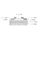
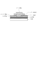
本発明に係わるTFT素子の第1実施例を図4を用いて説明する。
活性層を除いては上記実施例1と同様の構成とした。本比較例では活性層11として、N添加していないIn−Zn−O膜を形成した。なお、本比較例においても、活性層の材料の原子組成比率依存性を検討するために、成膜にコンビナトリアル法を用いている。
活性層を除いては上記実施例1と同様の構成とした。本比較例では活性層11として、N添加したIn−Zn−O膜を形成した。なお、本比較例においても、活性層の材料の原子組成比率依存性を検討するために、成膜にコンビナトリアル法を用いている。
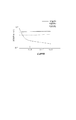
本実施例で得られたN添加In−Zn−O活性層について、光吸収スペクトルの解析を行ったところ、上記N添加酸化膜の禁制帯エネルギー幅はInの原子組成比率に依存して約2.7eVから2.9eVの範囲の値を示していた。比較例1のIn−Zn−O膜では禁制帯エネルギー幅が上記と同様に約2.7から2.9eVの範囲、一方比較例2の酸窒化物半導体では約2.3−2.4eVの値を示している。この結果、窒素の原子組成比率(N/(N+O))が大きくなるに従い、可視域での受光感度が増加してしまうことが分かった。
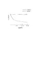
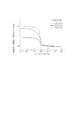
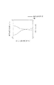
図6は、本実施例で作製したTFT素子を室温下で測定した時の、Vd=6VにおけるId−Vg特性(トランスファ特性)を示したものである。
本発明に係わるTFT素子の第2実施例を図4を用いて説明する。
活性層を除いては上記実施例1と同様の構成とした。本比較例では活性層11として、N添加していないIn−Zn−Ga−O膜を形成した。なお、本比較例においても、活性層の材料の原子組成比率依存性を検討するために、成膜にコンビナトリアル法を用いている。
本実施例で得られたN添加In−Zn−Ga−O活性層について、光吸収スペクトルの解析を行った。その結果、上記N添加酸化膜の禁制帯エネルギー幅は金属の原子組成比率に依存して約2.8eVから3.1eVの範囲の値を示していた。そして実施例1のN添加In−Zn−O膜よりも若干高い値、また比較例3のIn−Zn―Ga−O膜と同程度の値を示していた。
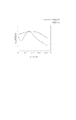
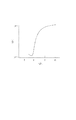
本実施例2において、最も良好なトランジスタ特性が得られたのは、Inの原子組成比率(In/(Zn+In))が約40原子%、全原子数に対するGaの原子組成比率が0.4原子%の時であった。この時、オン電流は比較的大きい値を示しており、Vg=10Vの時には、Id=4×10−4A程度の電流が流れていることがわかった。オフ電流はId=1×10−13A程度、しきい電圧は約2.3Vであり、実施例1と比べてオフ電流が低く、しきい電圧も大きいことが分かった。またこの時、TFTはノーマリーオフ特性を示していた。出力特性から電界効果移動度およびS値を算出したところ、それぞれ約14.4cm2/Vsおよび約0.3V/decと、実施例1で得られた値とほぼ同程度の良好な特性が得られた。上記結果は比較例3で作製したTFTにおいても同様に観測され、微量のGa添加によって、高い電界効果移動度を保ったまま、低いオフ電流やノーマリーオフ特性が実現されることが分かった。
12 ソース電極
13 ドレイン電極
14 ゲート絶縁膜
15 ゲート電極
16 密着層
Claims (4)
- 電界効果型トランジスタであって、
前記電界効果型トランジスタの活性層が、Inと、Znと、Nと、Oと、を含むアモルファス酸化物からなり、
前記アモルファス酸化物中の前記Nの含有原子濃度[N]の、前記含有原子濃度[N]と前記Oの含有原子濃度[O]との合計に対する原子組成比率が0.01原子%以上3原子%以下であることを特徴とする電界効果型トランジスタ。 - 前記アモルファス酸化物中の前記含有原子濃度[N]の、前記アモルファス酸化物中の前記Inの含有原子濃度[In]と前記アモルファス酸化物中の前記Znの含有原子濃度[Zn]との合計に対する原子組成比率が0.01原子%以上7原子%以下であることを特徴とする、請求項1に記載の電界効果型トランジスタ。
- 前記アモルファス酸化物中の前記Inの前記含有原子濃度[In]の、前記含有原子濃度[In]と前記アモルファス酸化物中の前記Znの含有原子濃度[Zn]との合計に対する原子組成比率が15原子%以上75原子%以下であることを特徴とする、請求項1又は2に記載の電界効果型トランジスタ。
- 前記アモルファス酸化物は、Gaをさらに含有し、前記アモルファス酸化物中の前記Gaの含有原子濃度[Ga]は、前記含有原子濃度[N]より低濃度であることを特徴とする請求項1乃至3のいずれか1項に記載の電界効果型トランジスタ。
Priority Applications (7)
| Application Number | Priority Date | Filing Date | Title |
|---|---|---|---|
| JP2007143431A JP5241143B2 (ja) | 2007-05-30 | 2007-05-30 | 電界効果型トランジスタ |
| US12/597,934 US8188467B2 (en) | 2007-05-30 | 2008-05-22 | Amorphous oxide and field effect transistor |
| EP08764821A EP2165368B1 (en) | 2007-05-30 | 2008-05-22 | Amorphous oxide and field effect transistor |
| CN2008800174542A CN101681922B (zh) | 2007-05-30 | 2008-05-22 | 无定形氧化物和场效应晶体管 |
| PCT/JP2008/059852 WO2008149754A1 (en) | 2007-05-30 | 2008-05-22 | Amorphous oxide and field effect transistor |
| KR1020097027135A KR101294113B1 (ko) | 2007-05-30 | 2008-05-22 | 아모퍼스 산화물 및 전계 효과형 트랜지스터 |
| TW097119728A TWI397183B (zh) | 2007-05-30 | 2008-05-28 | 非晶形氧化物與場效電晶體 |
Applications Claiming Priority (1)
| Application Number | Priority Date | Filing Date | Title |
|---|---|---|---|
| JP2007143431A JP5241143B2 (ja) | 2007-05-30 | 2007-05-30 | 電界効果型トランジスタ |
Publications (2)
| Publication Number | Publication Date |
|---|---|
| JP2008300518A JP2008300518A (ja) | 2008-12-11 |
| JP5241143B2 true JP5241143B2 (ja) | 2013-07-17 |
Family
ID=39590910
Family Applications (1)
| Application Number | Title | Priority Date | Filing Date |
|---|---|---|---|
| JP2007143431A Expired - Fee Related JP5241143B2 (ja) | 2007-05-30 | 2007-05-30 | 電界効果型トランジスタ |
Country Status (7)
| Country | Link |
|---|---|
| US (1) | US8188467B2 (ja) |
| EP (1) | EP2165368B1 (ja) |
| JP (1) | JP5241143B2 (ja) |
| KR (1) | KR101294113B1 (ja) |
| CN (1) | CN101681922B (ja) |
| TW (1) | TWI397183B (ja) |
| WO (1) | WO2008149754A1 (ja) |
Families Citing this family (44)
| Publication number | Priority date | Publication date | Assignee | Title |
|---|---|---|---|---|
| JP5222281B2 (ja) * | 2006-04-06 | 2013-06-26 | アプライド マテリアルズ インコーポレイテッド | ラージエリア基板への酸化亜鉛透明導電性酸化物の反応性スパッタリング |
| TWI434420B (zh) | 2007-08-02 | 2014-04-11 | Applied Materials Inc | 使用薄膜半導體材料的薄膜式電晶體 |
| US8980066B2 (en) * | 2008-03-14 | 2015-03-17 | Applied Materials, Inc. | Thin film metal oxynitride semiconductors |
| WO2009117438A2 (en) * | 2008-03-20 | 2009-09-24 | Applied Materials, Inc. | Process to make metal oxide thin film transistor array with etch stopping layer |
| JP5510767B2 (ja) * | 2008-06-19 | 2014-06-04 | 出光興産株式会社 | 薄膜トランジスタおよびその製造方法 |
| US8258511B2 (en) | 2008-07-02 | 2012-09-04 | Applied Materials, Inc. | Thin film transistors using multiple active channel layers |
| EP2202802B1 (en) * | 2008-12-24 | 2012-09-26 | Semiconductor Energy Laboratory Co., Ltd. | Driver circuit and semiconductor device |
| TWI474408B (zh) | 2008-12-26 | 2015-02-21 | 半導體能源研究所股份有限公司 | 半導體裝置及其製造方法 |
| CN101928560B (zh) * | 2009-06-18 | 2013-08-07 | 晶元光电股份有限公司 | 一种可由紫外光激发的蓝光荧光材料及其制备方法 |
| WO2011007677A1 (en) * | 2009-07-17 | 2011-01-20 | Semiconductor Energy Laboratory Co., Ltd. | Semiconductor device and method for manufacturing the same |
| KR102057221B1 (ko) * | 2009-09-16 | 2019-12-18 | 가부시키가이샤 한도오따이 에네루기 켄큐쇼 | 반도체 장치 및 그 제조 방법 |
| WO2011037829A2 (en) * | 2009-09-24 | 2011-03-31 | Applied Materials, Inc. | Methods of fabricating metal oxide or metal oxynitride tfts using wet process for source-drain metal etch |
| US8840763B2 (en) * | 2009-09-28 | 2014-09-23 | Applied Materials, Inc. | Methods for stable process in a reactive sputtering process using zinc or doped zinc target |
| KR101623619B1 (ko) * | 2009-10-08 | 2016-05-23 | 가부시키가이샤 한도오따이 에네루기 켄큐쇼 | 산화물 반도체층 및 반도체 장치 |
| KR101820972B1 (ko) | 2009-10-09 | 2018-01-22 | 가부시키가이샤 한도오따이 에네루기 켄큐쇼 | 반도체 장치 및 그 제조 방법 |
| KR101865546B1 (ko) * | 2009-10-16 | 2018-06-11 | 가부시키가이샤 한도오따이 에네루기 켄큐쇼 | 액정 표시 장치 및 액정 표시 장치를 포함한 전자 기기 |
| KR20120096463A (ko) | 2009-10-21 | 2012-08-30 | 가부시키가이샤 한도오따이 에네루기 켄큐쇼 | 표시 장치 및 표시 장치를 갖는 전자 기기 |
| WO2011052383A1 (en) | 2009-10-30 | 2011-05-05 | Semiconductor Energy Laboratory Co., Ltd. | Logic circuit and semiconductor device |
| KR20120094013A (ko) * | 2009-11-13 | 2012-08-23 | 가부시키가이샤 한도오따이 에네루기 켄큐쇼 | 스퍼터링 타겟 및 그 제조방법, 및 트랜지스터 |
| JP5596963B2 (ja) * | 2009-11-19 | 2014-09-24 | 出光興産株式会社 | スパッタリングターゲット及びそれを用いた薄膜トランジスタ |
| CN105206514B (zh) * | 2009-11-28 | 2018-04-10 | 株式会社半导体能源研究所 | 层叠的氧化物材料、半导体器件、以及用于制造该半导体器件的方法 |
| KR101840623B1 (ko) * | 2009-12-04 | 2018-03-21 | 가부시키가이샤 한도오따이 에네루기 켄큐쇼 | 표시 장치 및 이를 포함하는 전자 기기 |
| WO2011070901A1 (en) * | 2009-12-11 | 2011-06-16 | Semiconductor Energy Laboratory Co., Ltd. | Semiconductor device and manufacturing method thereof |
| JP5727204B2 (ja) * | 2009-12-11 | 2015-06-03 | 株式会社半導体エネルギー研究所 | 半導体装置の作製方法 |
| JP5185357B2 (ja) * | 2009-12-17 | 2013-04-17 | 株式会社半導体エネルギー研究所 | 半導体装置 |
| WO2011102183A1 (en) * | 2010-02-19 | 2011-08-25 | Semiconductor Energy Laboratory Co., Ltd. | Semiconductor device |
| WO2011108346A1 (en) * | 2010-03-05 | 2011-09-09 | Semiconductor Energy Laboratory Co., Ltd. | Manufacturing method of oxide semiconductor film and manufacturing method of transistor |
| EP2589085B1 (en) * | 2010-07-02 | 2019-02-20 | Hewlett-Packard Development Company, L.P. | Thin film transistors |
| US20120001179A1 (en) * | 2010-07-02 | 2012-01-05 | Semiconductor Energy Laboratory Co., Ltd. | Semiconductor device |
| DE112011102644B4 (de) | 2010-08-06 | 2019-12-05 | Semiconductor Energy Laboratory Co., Ltd. | Integrierte Halbleiterschaltung |
| JP5525380B2 (ja) * | 2010-08-25 | 2014-06-18 | 富士フイルム株式会社 | 酸化物半導体薄膜の製造方法および薄膜トランジスタの製造方法 |
| TWI555205B (zh) * | 2010-11-05 | 2016-10-21 | 半導體能源研究所股份有限公司 | 半導體裝置及半導體裝置的製造方法 |
| TWI654764B (zh) | 2010-11-11 | 2019-03-21 | Semiconductor Energy Laboratory Co., Ltd. | 半導體裝置及其製造方法 |
| JP5886491B2 (ja) * | 2010-11-12 | 2016-03-16 | 株式会社半導体エネルギー研究所 | 半導体装置の作製方法 |
| US8816425B2 (en) * | 2010-11-30 | 2014-08-26 | Semiconductor Energy Laboratory Co., Ltd. | Semiconductor device and method for manufacturing the same |
| TWI562379B (en) * | 2010-11-30 | 2016-12-11 | Semiconductor Energy Lab Co Ltd | Semiconductor device and method for manufacturing semiconductor device |
| US8883556B2 (en) * | 2010-12-28 | 2014-11-11 | Semiconductor Energy Laboratory Co., Ltd. | Semiconductor device and manufacturing method thereof |
| KR101878731B1 (ko) * | 2011-12-06 | 2018-07-17 | 삼성전자주식회사 | 트랜지스터와 그 제조방법 및 트랜지스터를 포함하는 전자소자 |
| KR20150025621A (ko) * | 2013-08-29 | 2015-03-11 | 삼성전자주식회사 | 트랜지스터와 그 제조방법 및 트랜지스터를 포함하는 전자소자 |
| CN104167448B (zh) * | 2014-08-05 | 2017-06-30 | 京东方科技集团股份有限公司 | 薄膜晶体管及其制备方法、阵列基板和显示装置 |
| KR102042782B1 (ko) * | 2017-03-15 | 2019-11-27 | 한화케미칼 주식회사 | 에멀젼, 에멀젼의 제조 방법 및 에멀젼을 이용한 코팅막 형성 방법 |
| WO2018211724A1 (ja) * | 2017-05-16 | 2018-11-22 | 住友電気工業株式会社 | 酸化物焼結体およびその製造方法、スパッタターゲット、酸化物半導体膜、ならびに半導体デバイスの製造方法 |
| US11581334B2 (en) | 2021-02-05 | 2023-02-14 | Taiwan Semiconductor Manufacturing Company, Ltd. | Cocktail layer over gate dielectric layer of FET FeRAM |
| KR102537632B1 (ko) * | 2021-09-17 | 2023-05-26 | 충북대학교 산학협력단 | 전류 어닐링 공정을 포함하는 전계효과 트랜지스터 제조 방법 |
Family Cites Families (8)
| Publication number | Priority date | Publication date | Assignee | Title |
|---|---|---|---|---|
| JPH0513404A (ja) * | 1991-07-03 | 1993-01-22 | Fujitsu Ltd | 半導体装置の製造方法 |
| JP3423896B2 (ja) * | 1999-03-25 | 2003-07-07 | 科学技術振興事業団 | 半導体デバイス |
| JP4089858B2 (ja) | 2000-09-01 | 2008-05-28 | 国立大学法人東北大学 | 半導体デバイス |
| KR101219038B1 (ko) * | 2004-10-26 | 2013-01-07 | 삼성디스플레이 주식회사 | 박막 트랜지스터 표시판 및 그 제조 방법 |
| RU2358354C2 (ru) | 2004-11-10 | 2009-06-10 | Кэнон Кабусики Кайся | Светоизлучающее устройство |
| CN102945857B (zh) | 2004-11-10 | 2015-06-03 | 佳能株式会社 | 无定形氧化物和场效应晶体管 |
| JP5376750B2 (ja) * | 2005-11-18 | 2013-12-25 | 出光興産株式会社 | 半導体薄膜、及びその製造方法、並びに薄膜トランジスタ、アクティブマトリックス駆動表示パネル |
| JP5016831B2 (ja) | 2006-03-17 | 2012-09-05 | キヤノン株式会社 | 酸化物半導体薄膜トランジスタを用いた発光素子及びこれを用いた画像表示装置 |
-
2007
- 2007-05-30 JP JP2007143431A patent/JP5241143B2/ja not_active Expired - Fee Related
-
2008
- 2008-05-22 WO PCT/JP2008/059852 patent/WO2008149754A1/en not_active Ceased
- 2008-05-22 EP EP08764821A patent/EP2165368B1/en not_active Not-in-force
- 2008-05-22 KR KR1020097027135A patent/KR101294113B1/ko not_active Expired - Fee Related
- 2008-05-22 CN CN2008800174542A patent/CN101681922B/zh not_active Expired - Fee Related
- 2008-05-22 US US12/597,934 patent/US8188467B2/en not_active Expired - Fee Related
- 2008-05-28 TW TW097119728A patent/TWI397183B/zh not_active IP Right Cessation
Also Published As
| Publication number | Publication date |
|---|---|
| TW200915576A (en) | 2009-04-01 |
| EP2165368B1 (en) | 2012-05-30 |
| CN101681922A (zh) | 2010-03-24 |
| CN101681922B (zh) | 2012-05-23 |
| JP2008300518A (ja) | 2008-12-11 |
| TWI397183B (zh) | 2013-05-21 |
| KR20100020488A (ko) | 2010-02-22 |
| US20100140611A1 (en) | 2010-06-10 |
| EP2165368A1 (en) | 2010-03-24 |
| US8188467B2 (en) | 2012-05-29 |
| WO2008149754A1 (en) | 2008-12-11 |
| KR101294113B1 (ko) | 2013-08-08 |
Similar Documents
| Publication | Publication Date | Title |
|---|---|---|
| JP5241143B2 (ja) | 電界効果型トランジスタ | |
| JP5213458B2 (ja) | アモルファス酸化物及び電界効果型トランジスタ | |
| JP5295170B2 (ja) | アモルファス酸化物膜をチャネル層に用いた電界効果型トランジスタの製造方法 | |
| JP4560502B2 (ja) | 電界効果型トランジスタ | |
| JP5213507B2 (ja) | 薄膜トランジスタ | |
| JP4981283B2 (ja) | アモルファス酸化物層を用いた薄膜トランジスタ | |
| EP1812969B1 (en) | Field effect transistor comprising an amorphous oxide | |
| JP5467728B2 (ja) | 薄膜電界効果型トランジスタおよびその製造方法 | |
| KR100973124B1 (ko) | 인듐과 아연을 포함하는 산화물 반도체 재료를 구비하는채널을 갖는 전계 효과 트랜지스터 | |
| JP5213429B2 (ja) | 電界効果型トランジスタ | |
| JP5258475B2 (ja) | 薄膜電界効果型トランジスタ | |
| JP2009081413A (ja) | 電界効果型トランジスタ | |
| JP2010016126A (ja) | 薄膜電界効果型トランジスタ、その製造方法、およびそれを用いた表示装置 | |
| Liu et al. | High-performance ZnO thin-film transistors fabricated at low temperature on glass substrates | |
| Kim et al. | New approach for passivation of Ga 2 O 3-In 2 O 3-ZnO thin film transistors | |
| Chang et al. | Amorphous Hafnium‐Indium‐Zinc Oxide Semiconductor Thin Film Transistors | |
| Chiu et al. | The effect of Zn/Sn Ratio on the Electrical Performance of Amorphous ZrZnSnO (ZZTO) Thin Film Transistors by RF Sputtering |
Legal Events
| Date | Code | Title | Description |
|---|---|---|---|
| RD04 | Notification of resignation of power of attorney |
Free format text: JAPANESE INTERMEDIATE CODE: A7424 Effective date: 20100201 |
|
| A621 | Written request for application examination |
Free format text: JAPANESE INTERMEDIATE CODE: A621 Effective date: 20100305 |
|
| RD01 | Notification of change of attorney |
Free format text: JAPANESE INTERMEDIATE CODE: A7421 Effective date: 20100630 |
|
| A131 | Notification of reasons for refusal |
Free format text: JAPANESE INTERMEDIATE CODE: A131 Effective date: 20120807 |
|
| A521 | Request for written amendment filed |
Free format text: JAPANESE INTERMEDIATE CODE: A523 Effective date: 20121005 |
|
| TRDD | Decision of grant or rejection written | ||
| A01 | Written decision to grant a patent or to grant a registration (utility model) |
Free format text: JAPANESE INTERMEDIATE CODE: A01 Effective date: 20130305 |
|
| A61 | First payment of annual fees (during grant procedure) |
Free format text: JAPANESE INTERMEDIATE CODE: A61 Effective date: 20130402 |
|
| FPAY | Renewal fee payment (event date is renewal date of database) |
Free format text: PAYMENT UNTIL: 20160412 Year of fee payment: 3 |
|
| R151 | Written notification of patent or utility model registration |
Ref document number: 5241143 Country of ref document: JP Free format text: JAPANESE INTERMEDIATE CODE: R151 |
|
| FPAY | Renewal fee payment (event date is renewal date of database) |
Free format text: PAYMENT UNTIL: 20160412 Year of fee payment: 3 |
|
| LAPS | Cancellation because of no payment of annual fees |