JP2010166069A - 半導体装置 - Google Patents
半導体装置 Download PDFInfo
- Publication number
- JP2010166069A JP2010166069A JP2010046235A JP2010046235A JP2010166069A JP 2010166069 A JP2010166069 A JP 2010166069A JP 2010046235 A JP2010046235 A JP 2010046235A JP 2010046235 A JP2010046235 A JP 2010046235A JP 2010166069 A JP2010166069 A JP 2010166069A
- Authority
- JP
- Japan
- Prior art keywords
- insulating film
- film
- opening
- semiconductor
- substrate
- Prior art date
- Legal status (The legal status is an assumption and is not a legal conclusion. Google has not performed a legal analysis and makes no representation as to the accuracy of the status listed.)
- Withdrawn
Links
- 239000004065 semiconductor Substances 0.000 title claims abstract description 133
- 238000000034 method Methods 0.000 claims abstract description 153
- 238000007599 discharging Methods 0.000 claims abstract description 7
- 239000000463 material Substances 0.000 claims description 73
- 230000015572 biosynthetic process Effects 0.000 claims description 38
- 239000011229 interlayer Substances 0.000 claims description 38
- 229910052710 silicon Inorganic materials 0.000 claims description 29
- XUIMIQQOPSSXEZ-UHFFFAOYSA-N Silicon Chemical compound [Si] XUIMIQQOPSSXEZ-UHFFFAOYSA-N 0.000 claims description 27
- 239000010703 silicon Substances 0.000 claims description 27
- VYPSYNLAJGMNEJ-UHFFFAOYSA-N Silicium dioxide Chemical compound O=[Si]=O VYPSYNLAJGMNEJ-UHFFFAOYSA-N 0.000 claims description 23
- 239000004020 conductor Substances 0.000 claims description 19
- 229910052581 Si3N4 Inorganic materials 0.000 claims description 17
- HQVNEWCFYHHQES-UHFFFAOYSA-N silicon nitride Chemical compound N12[Si]34N5[Si]62N3[Si]51N64 HQVNEWCFYHHQES-UHFFFAOYSA-N 0.000 claims description 17
- 229910052814 silicon oxide Inorganic materials 0.000 claims description 15
- 238000006243 chemical reaction Methods 0.000 claims description 9
- 239000000853 adhesive Substances 0.000 claims description 8
- 230000001070 adhesive effect Effects 0.000 claims description 8
- 229910044991 metal oxide Inorganic materials 0.000 claims description 7
- 150000004706 metal oxides Chemical class 0.000 claims description 7
- 229910052782 aluminium Inorganic materials 0.000 claims description 6
- 239000002904 solvent Substances 0.000 claims description 6
- XAGFODPZIPBFFR-UHFFFAOYSA-N aluminium Chemical compound [Al] XAGFODPZIPBFFR-UHFFFAOYSA-N 0.000 claims description 4
- 229910052738 indium Inorganic materials 0.000 claims description 4
- APFVFJFRJDLVQX-UHFFFAOYSA-N indium atom Chemical compound [In] APFVFJFRJDLVQX-UHFFFAOYSA-N 0.000 claims description 4
- 229910052719 titanium Inorganic materials 0.000 claims description 4
- 239000010936 titanium Substances 0.000 claims description 4
- 229910007541 Zn O Inorganic materials 0.000 claims description 3
- RTAQQCXQSZGOHL-UHFFFAOYSA-N Titanium Chemical compound [Ti] RTAQQCXQSZGOHL-UHFFFAOYSA-N 0.000 claims description 2
- 239000003990 capacitor Substances 0.000 claims description 2
- 230000008569 process Effects 0.000 abstract description 27
- 230000001678 irradiating effect Effects 0.000 abstract description 22
- 230000000994 depressogenic effect Effects 0.000 abstract description 2
- 239000010408 film Substances 0.000 description 334
- 239000010410 layer Substances 0.000 description 181
- 239000000758 substrate Substances 0.000 description 121
- 238000004519 manufacturing process Methods 0.000 description 56
- 230000003287 optical effect Effects 0.000 description 38
- 230000000149 penetrating effect Effects 0.000 description 38
- 239000002245 particle Substances 0.000 description 31
- 239000004973 liquid crystal related substance Substances 0.000 description 26
- 239000000203 mixture Substances 0.000 description 26
- 239000012535 impurity Substances 0.000 description 20
- 239000010409 thin film Substances 0.000 description 19
- 239000010949 copper Substances 0.000 description 18
- 238000010521 absorption reaction Methods 0.000 description 16
- 238000005530 etching Methods 0.000 description 16
- 239000011159 matrix material Substances 0.000 description 16
- 239000011521 glass Substances 0.000 description 13
- 229910052802 copper Inorganic materials 0.000 description 12
- RYGMFSIKBFXOCR-UHFFFAOYSA-N Copper Chemical compound [Cu] RYGMFSIKBFXOCR-UHFFFAOYSA-N 0.000 description 10
- 239000013078 crystal Substances 0.000 description 10
- 239000007789 gas Substances 0.000 description 10
- 238000010438 heat treatment Methods 0.000 description 10
- 238000000206 photolithography Methods 0.000 description 10
- 238000003672 processing method Methods 0.000 description 10
- 238000000576 coating method Methods 0.000 description 9
- 229910052751 metal Inorganic materials 0.000 description 9
- 239000002184 metal Substances 0.000 description 9
- 150000002894 organic compounds Chemical class 0.000 description 9
- 230000001681 protective effect Effects 0.000 description 9
- 238000004544 sputter deposition Methods 0.000 description 9
- 239000004642 Polyimide Substances 0.000 description 8
- -1 fluorine Aromatic ethers Chemical class 0.000 description 8
- 239000011368 organic material Substances 0.000 description 8
- 229920001721 polyimide Polymers 0.000 description 8
- 238000007639 printing Methods 0.000 description 8
- 229910052709 silver Inorganic materials 0.000 description 8
- OAICVXFJPJFONN-UHFFFAOYSA-N Phosphorus Chemical compound [P] OAICVXFJPJFONN-UHFFFAOYSA-N 0.000 description 7
- 230000006870 function Effects 0.000 description 7
- 239000010931 gold Substances 0.000 description 7
- 230000007246 mechanism Effects 0.000 description 7
- 239000002923 metal particle Substances 0.000 description 7
- 229920003023 plastic Polymers 0.000 description 7
- 239000004033 plastic Substances 0.000 description 7
- 239000004417 polycarbonate Substances 0.000 description 7
- 229920000515 polycarbonate Polymers 0.000 description 7
- 229920000642 polymer Polymers 0.000 description 7
- 229920005989 resin Polymers 0.000 description 7
- 239000011347 resin Substances 0.000 description 7
- 239000004332 silver Substances 0.000 description 7
- BQCADISMDOOEFD-UHFFFAOYSA-N Silver Chemical compound [Ag] BQCADISMDOOEFD-UHFFFAOYSA-N 0.000 description 6
- XLOMVQKBTHCTTD-UHFFFAOYSA-N Zinc monoxide Chemical compound [Zn]=O XLOMVQKBTHCTTD-UHFFFAOYSA-N 0.000 description 6
- 150000001875 compounds Chemical class 0.000 description 6
- 238000001312 dry etching Methods 0.000 description 6
- 239000011574 phosphorus Substances 0.000 description 6
- 229910052698 phosphorus Inorganic materials 0.000 description 6
- 239000011248 coating agent Substances 0.000 description 5
- 238000001514 detection method Methods 0.000 description 5
- 238000009826 distribution Methods 0.000 description 5
- 229910052737 gold Inorganic materials 0.000 description 5
- 230000010354 integration Effects 0.000 description 5
- 239000007788 liquid Substances 0.000 description 5
- 238000005498 polishing Methods 0.000 description 5
- 230000005236 sound signal Effects 0.000 description 5
- 125000006850 spacer group Chemical group 0.000 description 5
- 238000007740 vapor deposition Methods 0.000 description 5
- OKTJSMMVPCPJKN-UHFFFAOYSA-N Carbon Chemical compound [C] OKTJSMMVPCPJKN-UHFFFAOYSA-N 0.000 description 4
- NIXOWILDQLNWCW-UHFFFAOYSA-N acrylic acid group Chemical group C(C=C)(=O)O NIXOWILDQLNWCW-UHFFFAOYSA-N 0.000 description 4
- 238000005229 chemical vapour deposition Methods 0.000 description 4
- 239000000945 filler Substances 0.000 description 4
- PCHJSUWPFVWCPO-UHFFFAOYSA-N gold Chemical compound [Au] PCHJSUWPFVWCPO-UHFFFAOYSA-N 0.000 description 4
- 238000003384 imaging method Methods 0.000 description 4
- 238000002955 isolation Methods 0.000 description 4
- 239000003550 marker Substances 0.000 description 4
- 230000008018 melting Effects 0.000 description 4
- 238000002844 melting Methods 0.000 description 4
- 229910021421 monocrystalline silicon Inorganic materials 0.000 description 4
- 238000005192 partition Methods 0.000 description 4
- 238000000059 patterning Methods 0.000 description 4
- 229910021420 polycrystalline silicon Inorganic materials 0.000 description 4
- 235000012239 silicon dioxide Nutrition 0.000 description 4
- 238000005245 sintering Methods 0.000 description 4
- 239000000243 solution Substances 0.000 description 4
- 229910052721 tungsten Inorganic materials 0.000 description 4
- ZWEHNKRNPOVVGH-UHFFFAOYSA-N 2-Butanone Chemical compound CCC(C)=O ZWEHNKRNPOVVGH-UHFFFAOYSA-N 0.000 description 3
- ZOXJGFHDIHLPTG-UHFFFAOYSA-N Boron Chemical compound [B] ZOXJGFHDIHLPTG-UHFFFAOYSA-N 0.000 description 3
- RTZKZFJDLAIYFH-UHFFFAOYSA-N Diethyl ether Chemical compound CCOCC RTZKZFJDLAIYFH-UHFFFAOYSA-N 0.000 description 3
- XEKOWRVHYACXOJ-UHFFFAOYSA-N Ethyl acetate Chemical compound CCOC(C)=O XEKOWRVHYACXOJ-UHFFFAOYSA-N 0.000 description 3
- KFZMGEQAYNKOFK-UHFFFAOYSA-N Isopropanol Chemical compound CC(C)O KFZMGEQAYNKOFK-UHFFFAOYSA-N 0.000 description 3
- YTPLMLYBLZKORZ-UHFFFAOYSA-N Thiophene Chemical compound C=1C=CSC=1 YTPLMLYBLZKORZ-UHFFFAOYSA-N 0.000 description 3
- 230000004888 barrier function Effects 0.000 description 3
- 229910052796 boron Inorganic materials 0.000 description 3
- 229910052799 carbon Inorganic materials 0.000 description 3
- 239000000919 ceramic Substances 0.000 description 3
- 238000002425 crystallisation Methods 0.000 description 3
- 238000000151 deposition Methods 0.000 description 3
- 238000010586 diagram Methods 0.000 description 3
- KPUWHANPEXNPJT-UHFFFAOYSA-N disiloxane Chemical class [SiH3]O[SiH3] KPUWHANPEXNPJT-UHFFFAOYSA-N 0.000 description 3
- 238000001035 drying Methods 0.000 description 3
- 230000009977 dual effect Effects 0.000 description 3
- 238000009713 electroplating Methods 0.000 description 3
- 238000005516 engineering process Methods 0.000 description 3
- 235000013305 food Nutrition 0.000 description 3
- 239000011810 insulating material Substances 0.000 description 3
- 238000005468 ion implantation Methods 0.000 description 3
- 239000005001 laminate film Substances 0.000 description 3
- 239000002105 nanoparticle Substances 0.000 description 3
- PXHVJJICTQNCMI-UHFFFAOYSA-N nickel Substances [Ni] PXHVJJICTQNCMI-UHFFFAOYSA-N 0.000 description 3
- 238000004806 packaging method and process Methods 0.000 description 3
- SLIUAWYAILUBJU-UHFFFAOYSA-N pentacene Chemical compound C1=CC=CC2=CC3=CC4=CC5=CC=CC=C5C=C4C=C3C=C21 SLIUAWYAILUBJU-UHFFFAOYSA-N 0.000 description 3
- 238000005268 plasma chemical vapour deposition Methods 0.000 description 3
- 229920005591 polysilicon Polymers 0.000 description 3
- 230000009467 reduction Effects 0.000 description 3
- 238000007789 sealing Methods 0.000 description 3
- 239000003566 sealing material Substances 0.000 description 3
- 229910021332 silicide Inorganic materials 0.000 description 3
- FVBUAEGBCNSCDD-UHFFFAOYSA-N silicide(4-) Chemical compound [Si-4] FVBUAEGBCNSCDD-UHFFFAOYSA-N 0.000 description 3
- 239000000377 silicon dioxide Substances 0.000 description 3
- 239000002356 single layer Substances 0.000 description 3
- 239000000126 substance Substances 0.000 description 3
- 229920003002 synthetic resin Polymers 0.000 description 3
- 239000000057 synthetic resin Substances 0.000 description 3
- 238000001039 wet etching Methods 0.000 description 3
- 229910052725 zinc Inorganic materials 0.000 description 3
- 239000011701 zinc Substances 0.000 description 3
- QGKMIGUHVLGJBR-UHFFFAOYSA-M (4z)-1-(3-methylbutyl)-4-[[1-(3-methylbutyl)quinolin-1-ium-4-yl]methylidene]quinoline;iodide Chemical compound [I-].C12=CC=CC=C2N(CCC(C)C)C=CC1=CC1=CC=[N+](CCC(C)C)C2=CC=CC=C12 QGKMIGUHVLGJBR-UHFFFAOYSA-M 0.000 description 2
- CSCPPACGZOOCGX-UHFFFAOYSA-N Acetone Chemical compound CC(C)=O CSCPPACGZOOCGX-UHFFFAOYSA-N 0.000 description 2
- 239000004593 Epoxy Substances 0.000 description 2
- LFQSCWFLJHTTHZ-UHFFFAOYSA-N Ethanol Chemical compound CCO LFQSCWFLJHTTHZ-UHFFFAOYSA-N 0.000 description 2
- GYHNNYVSQQEPJS-UHFFFAOYSA-N Gallium Chemical compound [Ga] GYHNNYVSQQEPJS-UHFFFAOYSA-N 0.000 description 2
- XYFCBTPGUUZFHI-UHFFFAOYSA-N Phosphine Chemical compound P XYFCBTPGUUZFHI-UHFFFAOYSA-N 0.000 description 2
- 239000004696 Poly ether ether ketone Substances 0.000 description 2
- 239000004952 Polyamide Substances 0.000 description 2
- 239000004697 Polyetherimide Substances 0.000 description 2
- BLRPTPMANUNPDV-UHFFFAOYSA-N Silane Chemical compound [SiH4] BLRPTPMANUNPDV-UHFFFAOYSA-N 0.000 description 2
- 229910000577 Silicon-germanium Inorganic materials 0.000 description 2
- XBDYBAVJXHJMNQ-UHFFFAOYSA-N Tetrahydroanthracene Natural products C1=CC=C2C=C(CCCC3)C3=CC2=C1 XBDYBAVJXHJMNQ-UHFFFAOYSA-N 0.000 description 2
- HCHKCACWOHOZIP-UHFFFAOYSA-N Zinc Chemical compound [Zn] HCHKCACWOHOZIP-UHFFFAOYSA-N 0.000 description 2
- 239000012790 adhesive layer Substances 0.000 description 2
- 239000000956 alloy Substances 0.000 description 2
- HSFWRNGVRCDJHI-UHFFFAOYSA-N alpha-acetylene Chemical class C#C HSFWRNGVRCDJHI-UHFFFAOYSA-N 0.000 description 2
- 150000001408 amides Chemical class 0.000 description 2
- 229910021417 amorphous silicon Inorganic materials 0.000 description 2
- 239000012298 atmosphere Substances 0.000 description 2
- QVGXLLKOCUKJST-UHFFFAOYSA-N atomic oxygen Chemical compound [O] QVGXLLKOCUKJST-UHFFFAOYSA-N 0.000 description 2
- 230000018109 developmental process Effects 0.000 description 2
- 239000000975 dye Substances 0.000 description 2
- 239000003822 epoxy resin Substances 0.000 description 2
- 235000019441 ethanol Nutrition 0.000 description 2
- 238000001704 evaporation Methods 0.000 description 2
- 238000011049 filling Methods 0.000 description 2
- 238000010304 firing Methods 0.000 description 2
- 229910052733 gallium Inorganic materials 0.000 description 2
- 230000005525 hole transport Effects 0.000 description 2
- AMGQUBHHOARCQH-UHFFFAOYSA-N indium;oxotin Chemical compound [In].[Sn]=O AMGQUBHHOARCQH-UHFFFAOYSA-N 0.000 description 2
- 238000002347 injection Methods 0.000 description 2
- 239000007924 injection Substances 0.000 description 2
- 229910010272 inorganic material Inorganic materials 0.000 description 2
- 239000011147 inorganic material Substances 0.000 description 2
- 238000007689 inspection Methods 0.000 description 2
- 239000012212 insulator Substances 0.000 description 2
- 239000011344 liquid material Substances 0.000 description 2
- 238000004518 low pressure chemical vapour deposition Methods 0.000 description 2
- 229910052759 nickel Inorganic materials 0.000 description 2
- 230000003647 oxidation Effects 0.000 description 2
- 238000007254 oxidation reaction Methods 0.000 description 2
- 229910052760 oxygen Inorganic materials 0.000 description 2
- 239000001301 oxygen Substances 0.000 description 2
- 125000000843 phenylene group Chemical class C1(=C(C=CC=C1)*)* 0.000 description 2
- IEQIEDJGQAUEQZ-UHFFFAOYSA-N phthalocyanine Chemical class N1C(N=C2C3=CC=CC=C3C(N=C3C4=CC=CC=C4C(=N4)N3)=N2)=C(C=CC=C2)C2=C1N=C1C2=CC=CC=C2C4=N1 IEQIEDJGQAUEQZ-UHFFFAOYSA-N 0.000 description 2
- 229920002492 poly(sulfone) Polymers 0.000 description 2
- 229920001197 polyacetylene Chemical class 0.000 description 2
- 229920002647 polyamide Polymers 0.000 description 2
- 229920001230 polyarylate Polymers 0.000 description 2
- 229920000647 polyepoxide Polymers 0.000 description 2
- 229920000728 polyester Polymers 0.000 description 2
- 229920002530 polyetherether ketone Polymers 0.000 description 2
- 229920001601 polyetherimide Polymers 0.000 description 2
- 229920000139 polyethylene terephthalate Polymers 0.000 description 2
- 239000005020 polyethylene terephthalate Substances 0.000 description 2
- 229920000123 polythiophene Polymers 0.000 description 2
- 229910052594 sapphire Inorganic materials 0.000 description 2
- 239000010980 sapphire Substances 0.000 description 2
- 239000000565 sealant Substances 0.000 description 2
- 229910000077 silane Inorganic materials 0.000 description 2
- 239000005368 silicate glass Substances 0.000 description 2
- LIVNPJMFVYWSIS-UHFFFAOYSA-N silicon monoxide Chemical compound [Si-]#[O+] LIVNPJMFVYWSIS-UHFFFAOYSA-N 0.000 description 2
- 238000003860 storage Methods 0.000 description 2
- IFLREYGFSNHWGE-UHFFFAOYSA-N tetracene Chemical compound C1=CC=CC2=CC3=CC4=CC=CC=C4C=C3C=C21 IFLREYGFSNHWGE-UHFFFAOYSA-N 0.000 description 2
- 229920001187 thermosetting polymer Polymers 0.000 description 2
- 230000007704 transition Effects 0.000 description 2
- WFKWXMTUELFFGS-UHFFFAOYSA-N tungsten Chemical compound [W] WFKWXMTUELFFGS-UHFFFAOYSA-N 0.000 description 2
- 239000010937 tungsten Substances 0.000 description 2
- 239000002699 waste material Substances 0.000 description 2
- 239000011787 zinc oxide Substances 0.000 description 2
- VXNZUUAINFGPBY-UHFFFAOYSA-N 1-Butene Chemical compound CCC=C VXNZUUAINFGPBY-UHFFFAOYSA-N 0.000 description 1
- 239000004925 Acrylic resin Substances 0.000 description 1
- 229920000178 Acrylic resin Polymers 0.000 description 1
- DKPFZGUDAPQIHT-UHFFFAOYSA-N Butyl acetate Natural products CCCCOC(C)=O DKPFZGUDAPQIHT-UHFFFAOYSA-N 0.000 description 1
- 229910052691 Erbium Inorganic materials 0.000 description 1
- 229910001218 Gallium arsenide Inorganic materials 0.000 description 1
- JMASRVWKEDWRBT-UHFFFAOYSA-N Gallium nitride Chemical compound [Ga]#N JMASRVWKEDWRBT-UHFFFAOYSA-N 0.000 description 1
- 239000004640 Melamine resin Substances 0.000 description 1
- 229920000877 Melamine resin Polymers 0.000 description 1
- 241001465754 Metazoa Species 0.000 description 1
- 229910052779 Neodymium Inorganic materials 0.000 description 1
- 239000004677 Nylon Substances 0.000 description 1
- LFPIHDQZHBXSGD-UHFFFAOYSA-N P(=O)(=O)[B] Chemical compound P(=O)(=O)[B] LFPIHDQZHBXSGD-UHFFFAOYSA-N 0.000 description 1
- 229920012266 Poly(ether sulfone) PES Polymers 0.000 description 1
- 239000004743 Polypropylene Substances 0.000 description 1
- 229910004283 SiO 4 Inorganic materials 0.000 description 1
- 229910020177 SiOF Inorganic materials 0.000 description 1
- 229910006404 SnO 2 Inorganic materials 0.000 description 1
- BZHJMEDXRYGGRV-UHFFFAOYSA-N Vinyl chloride Chemical compound ClC=C BZHJMEDXRYGGRV-UHFFFAOYSA-N 0.000 description 1
- 229910052769 Ytterbium Inorganic materials 0.000 description 1
- GDFCWFBWQUEQIJ-UHFFFAOYSA-N [B].[P] Chemical compound [B].[P] GDFCWFBWQUEQIJ-UHFFFAOYSA-N 0.000 description 1
- LEVVHYCKPQWKOP-UHFFFAOYSA-N [Si].[Ge] Chemical compound [Si].[Ge] LEVVHYCKPQWKOP-UHFFFAOYSA-N 0.000 description 1
- FFEYZVDJHQUAKG-UHFFFAOYSA-N [W].[Gd].[K] Chemical compound [W].[Gd].[K] FFEYZVDJHQUAKG-UHFFFAOYSA-N 0.000 description 1
- 230000004913 activation Effects 0.000 description 1
- 150000001298 alcohols Chemical class 0.000 description 1
- 125000000217 alkyl group Chemical group 0.000 description 1
- 125000005376 alkyl siloxane group Chemical group 0.000 description 1
- 229910045601 alloy Inorganic materials 0.000 description 1
- 230000003321 amplification Effects 0.000 description 1
- 150000001491 aromatic compounds Chemical class 0.000 description 1
- 150000004945 aromatic hydrocarbons Chemical class 0.000 description 1
- 229910052785 arsenic Inorganic materials 0.000 description 1
- RQNWIZPPADIBDY-UHFFFAOYSA-N arsenic atom Chemical compound [As] RQNWIZPPADIBDY-UHFFFAOYSA-N 0.000 description 1
- 230000002238 attenuated effect Effects 0.000 description 1
- 229910052788 barium Inorganic materials 0.000 description 1
- 230000006399 behavior Effects 0.000 description 1
- UMIVXZPTRXBADB-UHFFFAOYSA-N benzocyclobutene Chemical compound C1=CC=C2CCC2=C1 UMIVXZPTRXBADB-UHFFFAOYSA-N 0.000 description 1
- YXTPWUNVHCYOSP-UHFFFAOYSA-N bis($l^{2}-silanylidene)molybdenum Chemical group [Si]=[Mo]=[Si] YXTPWUNVHCYOSP-UHFFFAOYSA-N 0.000 description 1
- IAQRGUVFOMOMEM-UHFFFAOYSA-N butene Natural products CC=CC IAQRGUVFOMOMEM-UHFFFAOYSA-N 0.000 description 1
- 229910052793 cadmium Inorganic materials 0.000 description 1
- 230000015556 catabolic process Effects 0.000 description 1
- 239000003054 catalyst Substances 0.000 description 1
- 230000003197 catalytic effect Effects 0.000 description 1
- 239000002800 charge carrier Substances 0.000 description 1
- 229910052804 chromium Inorganic materials 0.000 description 1
- 230000000295 complement effect Effects 0.000 description 1
- 238000011109 contamination Methods 0.000 description 1
- 229920001577 copolymer Polymers 0.000 description 1
- 230000008025 crystallization Effects 0.000 description 1
- 125000001995 cyclobutyl group Chemical class [H]C1([H])C([H])([H])C([H])(*)C1([H])[H] 0.000 description 1
- 230000007547 defect Effects 0.000 description 1
- 229910003460 diamond Inorganic materials 0.000 description 1
- 239000010432 diamond Substances 0.000 description 1
- 239000002270 dispersing agent Substances 0.000 description 1
- 239000002019 doping agent Substances 0.000 description 1
- 230000005684 electric field Effects 0.000 description 1
- 238000004070 electrodeposition Methods 0.000 description 1
- 238000007772 electroless plating Methods 0.000 description 1
- 150000002148 esters Chemical group 0.000 description 1
- 230000001747 exhibiting effect Effects 0.000 description 1
- 239000000835 fiber Substances 0.000 description 1
- 239000002657 fibrous material Substances 0.000 description 1
- 230000005669 field effect Effects 0.000 description 1
- 239000010419 fine particle Substances 0.000 description 1
- 239000012530 fluid Substances 0.000 description 1
- 239000011737 fluorine Substances 0.000 description 1
- 229910052731 fluorine Inorganic materials 0.000 description 1
- 229910000078 germane Inorganic materials 0.000 description 1
- 229910052732 germanium Inorganic materials 0.000 description 1
- 229910002804 graphite Inorganic materials 0.000 description 1
- 239000010439 graphite Substances 0.000 description 1
- FUZZWVXGSFPDMH-UHFFFAOYSA-M hexanoate Chemical compound CCCCCC([O-])=O FUZZWVXGSFPDMH-UHFFFAOYSA-M 0.000 description 1
- 229920001519 homopolymer Polymers 0.000 description 1
- 238000005984 hydrogenation reaction Methods 0.000 description 1
- 230000001771 impaired effect Effects 0.000 description 1
- 230000006872 improvement Effects 0.000 description 1
- 229910003437 indium oxide Inorganic materials 0.000 description 1
- PJXISJQVUVHSOJ-UHFFFAOYSA-N indium(iii) oxide Chemical compound [O-2].[O-2].[O-2].[In+3].[In+3] PJXISJQVUVHSOJ-UHFFFAOYSA-N 0.000 description 1
- 239000010954 inorganic particle Substances 0.000 description 1
- 150000002500 ions Chemical class 0.000 description 1
- 229910052741 iridium Inorganic materials 0.000 description 1
- 229910052742 iron Inorganic materials 0.000 description 1
- XEEYBQQBJWHFJM-UHFFFAOYSA-N iron Substances [Fe] XEEYBQQBJWHFJM-UHFFFAOYSA-N 0.000 description 1
- 238000005499 laser crystallization Methods 0.000 description 1
- 238000001459 lithography Methods 0.000 description 1
- 238000007726 management method Methods 0.000 description 1
- 239000007769 metal material Substances 0.000 description 1
- 229910052976 metal sulfide Inorganic materials 0.000 description 1
- 150000002739 metals Chemical class 0.000 description 1
- 229910021424 microcrystalline silicon Inorganic materials 0.000 description 1
- 229910052750 molybdenum Inorganic materials 0.000 description 1
- 229910021344 molybdenum silicide Inorganic materials 0.000 description 1
- DCZNSJVFOQPSRV-UHFFFAOYSA-N n,n-diphenyl-4-[4-(n-phenylanilino)phenyl]aniline Chemical compound C1=CC=CC=C1N(C=1C=CC(=CC=1)C=1C=CC(=CC=1)N(C=1C=CC=CC=1)C=1C=CC=CC=1)C1=CC=CC=C1 DCZNSJVFOQPSRV-UHFFFAOYSA-N 0.000 description 1
- 229920003986 novolac Polymers 0.000 description 1
- 238000003199 nucleic acid amplification method Methods 0.000 description 1
- 229920001778 nylon Polymers 0.000 description 1
- 238000007645 offset printing Methods 0.000 description 1
- 239000012788 optical film Substances 0.000 description 1
- 239000012860 organic pigment Substances 0.000 description 1
- 229920000620 organic polymer Polymers 0.000 description 1
- 239000003960 organic solvent Substances 0.000 description 1
- 150000003961 organosilicon compounds Chemical class 0.000 description 1
- WCPAKWJPBJAGKN-UHFFFAOYSA-N oxadiazole Chemical compound C1=CON=N1 WCPAKWJPBJAGKN-UHFFFAOYSA-N 0.000 description 1
- 230000001590 oxidative effect Effects 0.000 description 1
- 229910052763 palladium Inorganic materials 0.000 description 1
- KDLHZDBZIXYQEI-UHFFFAOYSA-N palladium Substances [Pd] KDLHZDBZIXYQEI-UHFFFAOYSA-N 0.000 description 1
- 230000003071 parasitic effect Effects 0.000 description 1
- 239000005011 phenolic resin Substances 0.000 description 1
- 229910000073 phosphorus hydride Inorganic materials 0.000 description 1
- 229920002120 photoresistant polymer Polymers 0.000 description 1
- 238000009832 plasma treatment Methods 0.000 description 1
- 238000007747 plating Methods 0.000 description 1
- 229910052697 platinum Inorganic materials 0.000 description 1
- BASFCYQUMIYNBI-UHFFFAOYSA-N platinum Substances [Pt] BASFCYQUMIYNBI-UHFFFAOYSA-N 0.000 description 1
- 229920000052 poly(p-xylylene) Polymers 0.000 description 1
- 229920001707 polybutylene terephthalate Polymers 0.000 description 1
- 239000011112 polyethylene naphthalate Substances 0.000 description 1
- 238000006116 polymerization reaction Methods 0.000 description 1
- 229920001155 polypropylene Polymers 0.000 description 1
- 229920001709 polysilazane Polymers 0.000 description 1
- 229920002620 polyvinyl fluoride Polymers 0.000 description 1
- 239000011241 protective layer Substances 0.000 description 1
- 238000005086 pumping Methods 0.000 description 1
- 239000010453 quartz Substances 0.000 description 1
- 230000007261 regionalization Effects 0.000 description 1
- 229910052703 rhodium Inorganic materials 0.000 description 1
- 238000007650 screen-printing Methods 0.000 description 1
- SBIBMFFZSBJNJF-UHFFFAOYSA-N selenium;zinc Chemical group [Se]=[Zn] SBIBMFFZSBJNJF-UHFFFAOYSA-N 0.000 description 1
- 239000010944 silver (metal) Substances 0.000 description 1
- 229910000679 solder Inorganic materials 0.000 description 1
- 238000000638 solvent extraction Methods 0.000 description 1
- 238000005507 spraying Methods 0.000 description 1
- 239000002344 surface layer Substances 0.000 description 1
- 229910052715 tantalum Inorganic materials 0.000 description 1
- GUVRBAGPIYLISA-UHFFFAOYSA-N tantalum atom Chemical compound [Ta] GUVRBAGPIYLISA-UHFFFAOYSA-N 0.000 description 1
- CXWXQJXEFPUFDZ-UHFFFAOYSA-N tetralin Chemical compound C1=CC=C2CCCCC2=C1 CXWXQJXEFPUFDZ-UHFFFAOYSA-N 0.000 description 1
- 238000002230 thermal chemical vapour deposition Methods 0.000 description 1
- 229920002803 thermoplastic polyurethane Polymers 0.000 description 1
- 229930192474 thiophene Natural products 0.000 description 1
- XOLBLPGZBRYERU-UHFFFAOYSA-N tin dioxide Chemical compound O=[Sn]=O XOLBLPGZBRYERU-UHFFFAOYSA-N 0.000 description 1
- 229910001887 tin oxide Inorganic materials 0.000 description 1
- 229910021341 titanium silicide Inorganic materials 0.000 description 1
- 239000002341 toxic gas Substances 0.000 description 1
- WQJQOUPTWCFRMM-UHFFFAOYSA-N tungsten disilicide Chemical compound [Si]#[W]#[Si] WQJQOUPTWCFRMM-UHFFFAOYSA-N 0.000 description 1
- 229910021342 tungsten silicide Inorganic materials 0.000 description 1
- 125000000391 vinyl group Chemical group [H]C([*])=C([H])[H] 0.000 description 1
- 229920002554 vinyl polymer Polymers 0.000 description 1
- 229910052726 zirconium Inorganic materials 0.000 description 1
Images


Classifications
-
- H—ELECTRICITY
- H01—ELECTRIC ELEMENTS
- H01L—SEMICONDUCTOR DEVICES NOT COVERED BY CLASS H10
- H01L23/00—Details of semiconductor or other solid state devices
- H01L23/52—Arrangements for conducting electric current within the device in operation from one component to another, i.e. interconnections, e.g. wires, lead frames
- H01L23/522—Arrangements for conducting electric current within the device in operation from one component to another, i.e. interconnections, e.g. wires, lead frames including external interconnections consisting of a multilayer structure of conductive and insulating layers inseparably formed on the semiconductor body
- H01L23/5226—Via connections in a multilevel interconnection structure
-
- H—ELECTRICITY
- H01—ELECTRIC ELEMENTS
- H01L—SEMICONDUCTOR DEVICES NOT COVERED BY CLASS H10
- H01L21/00—Processes or apparatus adapted for the manufacture or treatment of semiconductor or solid state devices or of parts thereof
- H01L21/02—Manufacture or treatment of semiconductor devices or of parts thereof
- H01L21/04—Manufacture or treatment of semiconductor devices or of parts thereof the devices having at least one potential-jump barrier or surface barrier, e.g. PN junction, depletion layer or carrier concentration layer
- H01L21/18—Manufacture or treatment of semiconductor devices or of parts thereof the devices having at least one potential-jump barrier or surface barrier, e.g. PN junction, depletion layer or carrier concentration layer the devices having semiconductor bodies comprising elements of Group IV of the Periodic System or AIIIBV compounds with or without impurities, e.g. doping materials
- H01L21/28—Manufacture of electrodes on semiconductor bodies using processes or apparatus not provided for in groups H01L21/20 - H01L21/268
- H01L21/283—Deposition of conductive or insulating materials for electrodes conducting electric current
- H01L21/288—Deposition of conductive or insulating materials for electrodes conducting electric current from a liquid, e.g. electrolytic deposition
-
- H—ELECTRICITY
- H01—ELECTRIC ELEMENTS
- H01L—SEMICONDUCTOR DEVICES NOT COVERED BY CLASS H10
- H01L21/00—Processes or apparatus adapted for the manufacture or treatment of semiconductor or solid state devices or of parts thereof
- H01L21/70—Manufacture or treatment of devices consisting of a plurality of solid state components formed in or on a common substrate or of parts thereof; Manufacture of integrated circuit devices or of parts thereof
- H01L21/71—Manufacture of specific parts of devices defined in group H01L21/70
- H01L21/768—Applying interconnections to be used for carrying current between separate components within a device comprising conductors and dielectrics
- H01L21/76801—Applying interconnections to be used for carrying current between separate components within a device comprising conductors and dielectrics characterised by the formation and the after-treatment of the dielectrics, e.g. smoothing
- H01L21/76802—Applying interconnections to be used for carrying current between separate components within a device comprising conductors and dielectrics characterised by the formation and the after-treatment of the dielectrics, e.g. smoothing by forming openings in dielectrics
- H01L21/76816—Aspects relating to the layout of the pattern or to the size of vias or trenches
-
- H—ELECTRICITY
- H01—ELECTRIC ELEMENTS
- H01L—SEMICONDUCTOR DEVICES NOT COVERED BY CLASS H10
- H01L21/00—Processes or apparatus adapted for the manufacture or treatment of semiconductor or solid state devices or of parts thereof
- H01L21/70—Manufacture or treatment of devices consisting of a plurality of solid state components formed in or on a common substrate or of parts thereof; Manufacture of integrated circuit devices or of parts thereof
- H01L21/71—Manufacture of specific parts of devices defined in group H01L21/70
- H01L21/768—Applying interconnections to be used for carrying current between separate components within a device comprising conductors and dielectrics
- H01L21/76838—Applying interconnections to be used for carrying current between separate components within a device comprising conductors and dielectrics characterised by the formation and the after-treatment of the conductors
- H01L21/76877—Filling of holes, grooves or trenches, e.g. vias, with conductive material
-
- H—ELECTRICITY
- H01—ELECTRIC ELEMENTS
- H01L—SEMICONDUCTOR DEVICES NOT COVERED BY CLASS H10
- H01L27/00—Devices consisting of a plurality of semiconductor or other solid-state components formed in or on a common substrate
- H01L27/02—Devices consisting of a plurality of semiconductor or other solid-state components formed in or on a common substrate including semiconductor components specially adapted for rectifying, oscillating, amplifying or switching and having at least one potential-jump barrier or surface barrier; including integrated passive circuit elements with at least one potential-jump barrier or surface barrier
- H01L27/12—Devices consisting of a plurality of semiconductor or other solid-state components formed in or on a common substrate including semiconductor components specially adapted for rectifying, oscillating, amplifying or switching and having at least one potential-jump barrier or surface barrier; including integrated passive circuit elements with at least one potential-jump barrier or surface barrier the substrate being other than a semiconductor body, e.g. an insulating body
- H01L27/1214—Devices consisting of a plurality of semiconductor or other solid-state components formed in or on a common substrate including semiconductor components specially adapted for rectifying, oscillating, amplifying or switching and having at least one potential-jump barrier or surface barrier; including integrated passive circuit elements with at least one potential-jump barrier or surface barrier the substrate being other than a semiconductor body, e.g. an insulating body comprising a plurality of TFTs formed on a non-semiconducting substrate, e.g. driving circuits for AMLCDs
- H01L27/124—Devices consisting of a plurality of semiconductor or other solid-state components formed in or on a common substrate including semiconductor components specially adapted for rectifying, oscillating, amplifying or switching and having at least one potential-jump barrier or surface barrier; including integrated passive circuit elements with at least one potential-jump barrier or surface barrier the substrate being other than a semiconductor body, e.g. an insulating body comprising a plurality of TFTs formed on a non-semiconducting substrate, e.g. driving circuits for AMLCDs with a particular composition, shape or layout of the wiring layers specially adapted to the circuit arrangement, e.g. scanning lines in LCD pixel circuits
-
- H—ELECTRICITY
- H01—ELECTRIC ELEMENTS
- H01L—SEMICONDUCTOR DEVICES NOT COVERED BY CLASS H10
- H01L27/00—Devices consisting of a plurality of semiconductor or other solid-state components formed in or on a common substrate
- H01L27/02—Devices consisting of a plurality of semiconductor or other solid-state components formed in or on a common substrate including semiconductor components specially adapted for rectifying, oscillating, amplifying or switching and having at least one potential-jump barrier or surface barrier; including integrated passive circuit elements with at least one potential-jump barrier or surface barrier
- H01L27/12—Devices consisting of a plurality of semiconductor or other solid-state components formed in or on a common substrate including semiconductor components specially adapted for rectifying, oscillating, amplifying or switching and having at least one potential-jump barrier or surface barrier; including integrated passive circuit elements with at least one potential-jump barrier or surface barrier the substrate being other than a semiconductor body, e.g. an insulating body
- H01L27/1214—Devices consisting of a plurality of semiconductor or other solid-state components formed in or on a common substrate including semiconductor components specially adapted for rectifying, oscillating, amplifying or switching and having at least one potential-jump barrier or surface barrier; including integrated passive circuit elements with at least one potential-jump barrier or surface barrier the substrate being other than a semiconductor body, e.g. an insulating body comprising a plurality of TFTs formed on a non-semiconducting substrate, e.g. driving circuits for AMLCDs
- H01L27/1259—Multistep manufacturing methods
- H01L27/127—Multistep manufacturing methods with a particular formation, treatment or patterning of the active layer specially adapted to the circuit arrangement
- H01L27/1274—Multistep manufacturing methods with a particular formation, treatment or patterning of the active layer specially adapted to the circuit arrangement using crystallisation of amorphous semiconductor or recrystallisation of crystalline semiconductor
- H01L27/1285—Multistep manufacturing methods with a particular formation, treatment or patterning of the active layer specially adapted to the circuit arrangement using crystallisation of amorphous semiconductor or recrystallisation of crystalline semiconductor using control of the annealing or irradiation parameters, e.g. using different scanning direction or intensity for different transistors
-
- H—ELECTRICITY
- H01—ELECTRIC ELEMENTS
- H01L—SEMICONDUCTOR DEVICES NOT COVERED BY CLASS H10
- H01L27/00—Devices consisting of a plurality of semiconductor or other solid-state components formed in or on a common substrate
- H01L27/02—Devices consisting of a plurality of semiconductor or other solid-state components formed in or on a common substrate including semiconductor components specially adapted for rectifying, oscillating, amplifying or switching and having at least one potential-jump barrier or surface barrier; including integrated passive circuit elements with at least one potential-jump barrier or surface barrier
- H01L27/12—Devices consisting of a plurality of semiconductor or other solid-state components formed in or on a common substrate including semiconductor components specially adapted for rectifying, oscillating, amplifying or switching and having at least one potential-jump barrier or surface barrier; including integrated passive circuit elements with at least one potential-jump barrier or surface barrier the substrate being other than a semiconductor body, e.g. an insulating body
- H01L27/1214—Devices consisting of a plurality of semiconductor or other solid-state components formed in or on a common substrate including semiconductor components specially adapted for rectifying, oscillating, amplifying or switching and having at least one potential-jump barrier or surface barrier; including integrated passive circuit elements with at least one potential-jump barrier or surface barrier the substrate being other than a semiconductor body, e.g. an insulating body comprising a plurality of TFTs formed on a non-semiconducting substrate, e.g. driving circuits for AMLCDs
- H01L27/1259—Multistep manufacturing methods
- H01L27/1292—Multistep manufacturing methods using liquid deposition, e.g. printing
-
- H—ELECTRICITY
- H01—ELECTRIC ELEMENTS
- H01L—SEMICONDUCTOR DEVICES NOT COVERED BY CLASS H10
- H01L29/00—Semiconductor devices adapted for rectifying, amplifying, oscillating or switching, or capacitors or resistors with at least one potential-jump barrier or surface barrier, e.g. PN junction depletion layer or carrier concentration layer; Details of semiconductor bodies or of electrodes thereof ; Multistep manufacturing processes therefor
- H01L29/40—Electrodes ; Multistep manufacturing processes therefor
- H01L29/41—Electrodes ; Multistep manufacturing processes therefor characterised by their shape, relative sizes or dispositions
- H01L29/417—Electrodes ; Multistep manufacturing processes therefor characterised by their shape, relative sizes or dispositions carrying the current to be rectified, amplified or switched
- H01L29/41725—Source or drain electrodes for field effect devices
- H01L29/41733—Source or drain electrodes for field effect devices for thin film transistors with insulated gate
-
- G—PHYSICS
- G02—OPTICS
- G02F—OPTICAL DEVICES OR ARRANGEMENTS FOR THE CONTROL OF LIGHT BY MODIFICATION OF THE OPTICAL PROPERTIES OF THE MEDIA OF THE ELEMENTS INVOLVED THEREIN; NON-LINEAR OPTICS; FREQUENCY-CHANGING OF LIGHT; OPTICAL LOGIC ELEMENTS; OPTICAL ANALOGUE/DIGITAL CONVERTERS
- G02F1/00—Devices or arrangements for the control of the intensity, colour, phase, polarisation or direction of light arriving from an independent light source, e.g. switching, gating or modulating; Non-linear optics
- G02F1/01—Devices or arrangements for the control of the intensity, colour, phase, polarisation or direction of light arriving from an independent light source, e.g. switching, gating or modulating; Non-linear optics for the control of the intensity, phase, polarisation or colour
- G02F1/13—Devices or arrangements for the control of the intensity, colour, phase, polarisation or direction of light arriving from an independent light source, e.g. switching, gating or modulating; Non-linear optics for the control of the intensity, phase, polarisation or colour based on liquid crystals, e.g. single liquid crystal display cells
- G02F1/133—Constructional arrangements; Operation of liquid crystal cells; Circuit arrangements
- G02F1/136—Liquid crystal cells structurally associated with a semi-conducting layer or substrate, e.g. cells forming part of an integrated circuit
- G02F1/1362—Active matrix addressed cells
- G02F1/136227—Through-hole connection of the pixel electrode to the active element through an insulation layer
-
- H—ELECTRICITY
- H01—ELECTRIC ELEMENTS
- H01L—SEMICONDUCTOR DEVICES NOT COVERED BY CLASS H10
- H01L23/00—Details of semiconductor or other solid state devices
- H01L23/48—Arrangements for conducting electric current to or from the solid state body in operation, e.g. leads, terminal arrangements ; Selection of materials therefor
- H01L23/488—Arrangements for conducting electric current to or from the solid state body in operation, e.g. leads, terminal arrangements ; Selection of materials therefor consisting of soldered or bonded constructions
- H01L23/498—Leads, i.e. metallisations or lead-frames on insulating substrates, e.g. chip carriers
- H01L23/49855—Leads, i.e. metallisations or lead-frames on insulating substrates, e.g. chip carriers for flat-cards, e.g. credit cards
-
- H—ELECTRICITY
- H01—ELECTRIC ELEMENTS
- H01L—SEMICONDUCTOR DEVICES NOT COVERED BY CLASS H10
- H01L2924/00—Indexing scheme for arrangements or methods for connecting or disconnecting semiconductor or solid-state bodies as covered by H01L24/00
- H01L2924/0001—Technical content checked by a classifier
- H01L2924/0002—Not covered by any one of groups H01L24/00, H01L24/00 and H01L2224/00
-
- H—ELECTRICITY
- H01—ELECTRIC ELEMENTS
- H01L—SEMICONDUCTOR DEVICES NOT COVERED BY CLASS H10
- H01L2924/00—Indexing scheme for arrangements or methods for connecting or disconnecting semiconductor or solid-state bodies as covered by H01L24/00
- H01L2924/10—Details of semiconductor or other solid state devices to be connected
- H01L2924/11—Device type
- H01L2924/12—Passive devices, e.g. 2 terminal devices
- H01L2924/1204—Optical Diode
- H01L2924/12044—OLED
Abstract
とする。また、開口径の比較的大きいコンタクトホールに液滴吐出技術やナノインプリン
ト技術を用いた場合、開口の形状に沿った配線となり、開口の部分は他の箇所より凹む形
状となりやすかった。
【解決手段】高強度、且つ、繰り返し周波数の高いパルスのレーザ光を透光性を有する絶
縁膜に照射して貫通した開口を形成する。大きな接触面積を有する1つの開口を形成する
のではなく、微小な接触面積を有する開口を複数設け、部分的な凹みを低減して配線の太
さを均一にし、且つ、接触抵抗も確保する。
【選択図】図1
Description
置およびその作製方法に関する。具体的には、本発明は電界効果トランジスタ(以下、F
ETという)で構成された回路を有する半導体装置に関する。例えば、大規模集積回路(
LSI)や、液晶表示パネルに代表される電気光学装置や、有機発光素子を有する発光表
示装置や、ラインセンサなどのセンサ装置や、SRAM、DRAMなどのメモリ装置を部
品として搭載した電子機器に関する。
置全般を指し、電気光学装置、半導体回路および電子機器は全て半導体装置である。
ほど段差が増大し、配線の加工が困難となっている。そこで、一般的に絶縁膜に形成され
た配線溝や孔等のような配線開口部内にダマシン法と称する配線形成技術によって、配線
材料を埋め込んでいる。
材料を塗布し、次にCMP(化学的機械研磨)法などで、全面研磨をすることである。こ
の際、金属配線の下方に、さらに下層の金属配線や半導体領域とのコンタクトを取るため
の孔を形成しておくことを含めたものをデュアルダマシン法と呼んでいる。デュアルダマ
シン法は、下層配線との接続孔と配線溝とを形成した後、配線材料を堆積し、CMP法に
より配線部分以外の配線材料を除去する工程などを含んでいる。
ている。電解めっき法では接続孔に銅(Cu)を完全に埋め込むため、めっき液や、印加
する電界を複雑に調整する必要がある。また、銅(Cu)はエッチャントやエッチングガ
スを用いたエッチングプロセスで加工することが困難であり、銅(Cu)の加工には研磨
を行うための特殊なCMP法が必要とされている。
くという問題があった。
FT)を用いたアクティブマトリクス基板製造工程においても、多層配線を形成する際に
おける配線の加工が困難となっている。近年、薄膜トランジスタはICや電気光学装置の
ような電子デバイスに広く応用され、特に画像表示装置のスイッチング素子として開発が
急がれている。なお、画像表示装置として、液晶表示装置が一般によく知られている。
型の液晶表示装置が多く用いられるようになっている。アクティブマトリクス型の液晶表
示装置においては、マトリクス状に配置された画素電極を駆動することによって、画面上
に表示パターンが形成される。詳しくは選択された画素電極と該画素電極に対応する対向
電極との間に電圧が印加されることによって、画素電極と対向電極との間に配置された液
晶層の光学変調が行われ、この光学変調が表示パターンとして観察者に認識される。
の大面積化とともに、生産性の向上や低コスト化の要求も高まっている。
れらの配線の間に設けられる層間絶縁膜にフォトリソグラフィ法を用いてコンタクトホー
ルを形成している。フォトリソグラフィ法を用いてコンタクトホールを形成する場合、レ
ジストマスクの形成(レジスト塗布、露光、現像)、選択的なエッチング、レジストマス
ク除去などの多くの工程が必要とされる。即ち、複数の配線を立体交差させるべく多層構
造とするため、コンタクトホールをあける必要があり、これが製造工程数の増加の原因の
一つとなっている。
るため、そのフォトマスクを製造する費用がかかり、製造コストの増大の原因の一つとな
っている。
や、大量の現像液が使用され、余分な材料の消費量が多い。
トエッチングとが知られている。一般的にはガスプラズマによるドライエッチングがテー
パー加工などのパターン形成に有利とされているが、ドライエッチング装置は高価で大が
かりな装置を必要とし、製造コストが高くなるという欠点がある。また、ガスプラズマに
よるダメージが半導体素子に与えられる恐れがある。従って、ドライエッチングはできる
限り少なく行うことが望ましい。
用でエッチャントを大量に使用するため、廃液処理が大変であり、製造コストの増大の原
因の一つとなっている。また、ウェットエッチングは、等方性エッチングであるため、比
較的径の小さいコンタクトホールを形成することは困難であり、回路の高集積化に不向き
であった。
レーザ加工技術が知られており、中でもYAGレーザ光(波長1.06μm)を用いたレ
ーザ加工法が知られている。YAGレーザ光を用いたレーザ加工法はスポット状のビーム
を被加工物に照射するとともに、ビームを加工方向に走査し、点の連続の鎖状に開溝を形
成するものである。
光性導電膜に照射し、開溝を形成する薄膜加工方法を特許文献1、特許文献2、及び特許
文献3に記載している。
課題とする。さらに、回路の高集積化をも実現する技術を提供することも課題とする。
すい。そこで、本発明は、簡便なプロセスで深さの異なる複数のコンタクトホールを実現
することができる技術を提供する。
ウェハー基板ではなくマザーガラス基板を用い、一枚のマザーガラス基板から複数のデバ
イスを切り出す多面取りがよく行われている。マザーガラス基板のサイズは、1990年
初頭における第1世代の300×400mmから、2000年には第4世代となり680
×880mm、若しくは730×920mmへと大型化して、一枚の基板から多数のデバ
イス、代表的には多数の表示パネルが生産できるように生産技術が進歩してきた。
成膜方法では、ターゲットが大きなサイズとなるにつれて高価となってくるため、大量生
産上、不利と考えられる。
課題とする。
に照射し、導電層に達する貫通した開口を形成することを特徴としている。レーザ光によ
り透光性を有する絶縁膜に貫通した開口を形成することによって、コンタクトホール形成
工程を簡便とすることができる。
や貫通した開口のサイズを適宜、決定することができる。従って、本発明により簡便なプ
ロセスで深さの異なる複数のコンタクトホールを実現できる。また、透光性を有する絶縁
膜は単層に限らず、2層以上の積層であってもコンタクトホール形成工程を簡便とするこ
とができる。
、且つ、繰り返し周波数の高いパルスのレーザ光を透光性を有する絶縁膜に照射して貫通
した開口を形成する。なお、本発明で用いるレーザの繰り返し周波数は10MHz以上と
することも特徴の一つである。
おり、本発明におけるレーザ光の尖頭出力の範囲は、1GW/cm2〜1TW/cm2と
する。
収効率が低いが、パルス幅をピコ秒台、或いはフェムト秒(10−15秒)台のパルスレ
ーザから射出される基本波であれば、高強度のレーザ光が得られ、非線形光学効果(多光
子吸収)が生じ、透光性を有する絶縁膜に吸収させて貫通した開口を形成することができ
る。
おける開口形状も適宜、決定することができる。例えば、透光性を有する絶縁膜表面にお
ける開口面積が導電層の露出面積よりも小さい開口を形成することができる。
布を示すため、被加工物の表面に垂直な面における開口形状はガウス分布に従った形にな
る。従って、従来のYAGレーザ光による加工方法では、表面における開口径が広がりや
すく、微小な開口径を有し、且つ、深さの深いコンタクトホール形成が困難である。また
、従来のYAGレーザ光による加工方法で使用されるパルス幅は、10−4秒〜10−2
秒である。
照射し、開溝を形成する従来の加工方法は、400μm以下の波長を有するレーザ光を吸
収する透光性導電膜を用いているため、透光性導電膜表面から開溝が形成される。この加
工方法においても表面にエネルギーが吸収されやすく、表面における開口径が広がりやす
い。
限定されず、様々な形成方法が可能である。例えば、レーザ光の焦点位置を導電層側から
表面に向けて移動させながらレーザ光を透光性を有する絶縁膜に照射した場合、透光性を
有する絶縁膜は、導電層側から表面に向けて貫通した開口が形成される。また、裏面、即
ち透光性を有する基板側から基板を通過させてレーザ光を照射して絶縁膜に開口を形成す
ることもできる。
(深さ方向)に縦方向の貫通した開口を形成した後、X方向またはY方向に横方向の穴を
形成して複雑な形状の開口を形成することも可能である。
はナノインプリント技術などの印刷技術を用いて、絶縁膜の開口と重なる位置に配線また
は電極を形成し、絶縁膜の開口を通じて導電層と電気的に接続させることも特徴の一つと
している。
持たせることができるため、曲がりくねった複雑な形状を有する開口であっても導電材料
を充填することができる。例えば、側壁が逆テーパ形状となっている穴にも導電材料を充
填することができる。また、液滴吐出技術を用いて滴下する導電材料の速度を利用して深
い開口や形状の複雑な開口に導電材料を充填することもできる。また、流動性を有する導
電材料を充填しやすい形状の開口を提供することも本発明の一つである。
導電材料に流動性を持たせて複雑な形状を有する開口に導電材料を充填することもできる
。
術やナノインプリント技術を用いた配線の形成を行った場合、コンタクトホールの形状に
沿った配線となり、コンタクトホールの配線部分は他の箇所より凹む形状となりやすかっ
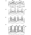
た。図19(A)〜図19(C)に従来のコンタクトホール形成の様子を示す。基板30
10上に下地絶縁膜3011が設けられ、その上に導電層3012が設けられている。図
19(A)には導電層3012上に絶縁膜3013が形成され、フォトリソグラフィ技術
によりレジストからなるマスク3014を形成し、エッチングして開口3016が形成さ
れている。そして、レジストマスク3014を除去して液滴吐出技術やナノインプリント
技術を用いた配線の形成を行うと図19(B)に示すような配線3017aが形成される
。図19(B)に示すように配線3017aは、コンタクトホールの形状に沿った配線と
なり、コンタクトホールの配線部分は他の箇所より凹んでしまう。さらに、焼成を行うと
、配線材料が流動性を持つため、図19(C)に示すように形状が変形し、配線3017
bになってしまう。従って、図19(C)中の矢印に示す材料の移動方向3018に移動
し、コンタクトホール付近の配線の太さが他の箇所に比べて細くなってしまう恐れがあっ
た。また、液滴吐出技術において、粘度の低く流動性を有する材料を用いた場合、焼成前
、即ち配線形成直後でも配線材料は低い所に移動しやすい。
、直径2μm以下、好ましくは直径3〜200nm程度の微小な接触面積を有する開口を
複数設け、部分的な凹みを低減して配線の太さを均一にし、且つ、接触抵抗も確保するこ
とも特徴の一つとしている。
と、複数の貫通した開口を有し、且つ前記第1の導電層を覆う絶縁膜と、前記複数の貫通
した開口を介して前記第1の導電層と接触する第2の導電層とを有し、前記第2の導電層
は、導電性粒子を含み、前記複数の貫通した開口と重なる第2の導電層の表面と、前記複
数の貫通した開口と重ならない第2の導電層の表面とが同一面に形成されていることを特
徴とする半導体装置である。なお、第2の導電層の幅Wと、1つの貫通した開口の径Dは
、2D<Wを満たす。第2の導電層の幅Wに対して1つの貫通した開口の径を小さくする
ことができるため、第2の導電層の幅を一定にすることができ、配線レイアウトを単純化
することができる。従来では、コンタクトホールを形成する領域の導電層の幅を部分的に
広くしてパターニングのズレが生じてもよいようにマージンを取っていることが多い。ま
た、1つの貫通した開口の径Dは、2D<Wを満たすように、配線幅に対して開口の径を
小さくすることで、開口位置の形成位置の多少のズレが生じても確実に電気的な接続を行
うことができる。
、該結晶が重なりあっていることを特徴の一つとしている。3〜7nmの金属粒子を含む
導電材料を液滴吐出法または印刷法で配線を形成し、焼成を行うと金属粒子が溶融して集
合して100nm程度の結晶となり、その結晶が三次元に不規則に重なりあって形成され
る。
している。少なくとも使用する金属粒子が表面における開口に入るように、金属粒子の径
(3〜7nm)より大きい開口とする。具体的には、本発明の貫通した開口の径は、3〜
2000nmであることを特徴としている。
、半導体層と、複数の貫通した開口を有し、且つ前記半導体層を覆う絶縁膜と、前記複数
の貫通した開口を介して前記半導体層と接触する導電層とを有し、前記導電層は、導電性
粒子を含み、前記複数の貫通した開口と重なる導電層の表面と、前記複数の貫通した開口
と重ならない導電層の表面とが同一面に形成されていることを特徴とする半導体装置であ
る。
面で切断した断面の径が部分毎に異なっていてもよい。例えば、絶縁膜上面における開口
径よりも絶縁膜下面における開口径が10倍以上であってもよく、絶縁膜上面における開
口径が金属粒子よりも大きければよい。また、貫通した開口の水平面で切断した断面は円
に限定されず、楕円形や矩形であってもよい。貫通した開口の水平面で切断した断面形状
が楕円である場合には短軸の長さが、3〜2000nmの範囲であればよい。また、貫通
した開口の水平面で切断した断面形状が矩形である場合には短辺の長さが、3〜2000
nmの範囲であればよい。
うに絶縁膜下面における開口径を一つの結晶と同じ、もしくは少し大きな径にしてもよい
。
発明の構成は、第1の導電層と、複数の貫通した開口を有し、且つ前記第1の導電層を覆
う絶縁膜と、前記複数の貫通した開口を介して前記第1の導電層と接触する第2の導電層
とを有し、前記第2の導電層は、導電性粒子を含み、前記複数の貫通した開口のうち、少
なくとも2つの貫通した開口は絶縁膜中で互いに繋がっていることを特徴とする半導体装
置である。
明の構成は、第1の導電層と、複数の貫通した開口を有し、且つ前記第1の導電層を覆う
絶縁膜と、前記複数の貫通した開口を介して前記第1の導電層と接触する第2の導電層と
を有し、前記第2の導電層は、導電性粒子を含み、前記複数の貫通した開口の断面形状は
、L字形、U字状、または弧を描いた形状であることを特徴とする半導体装置である。
中を水平方向に延びる通路を指している。例えば、本発明の貫通した開口の断面形状は、
L字形、U字状(図7(D)に一例を示す)、または弧を描いた形状(図5(B)に一例
を示す)なども含まれる。このような複雑な断面形状を有する開口であっても液滴吐出法
であれば、吐出する材料の粘度を調節することで導電材料を複雑な形状の開口内に充填す
ることができる。
こうすることで絶縁膜上面には微小な複数の開口が設けられ、絶縁膜の下面付近に設けら
れた横方向の穴(X方向またはY方向に延びる穴)によって複数の開口を連結させること
によって接触面積の増大が図れる。また、複数の縦穴(Z方向に延びる穴)を絶縁膜の下
面に沿った横穴(X方向またはY方向に延びる穴)で連結することによって、液滴吐出の
際、空気の逃げ道を設けることができ、気泡が開口内に残存することを防ぐことができる
。
少なくとも一つを含むことを特徴の一つとしている。例えば、本発明により、貫通した開
口を介して形成された多層配線を有する集積回路の高集積化を実現できる。具体的には、
本発明により、物品、商品、或いは人物の識別や管理を行うためのアンテナ及びメモリー
を有する集積回路、代表的には無線チップ(IDタグ、ICタグ、ICチップ、RF(R
adio Frequency)タグ、無線タグ、電子タグ、RFID(Radio F
requency Identification)ともよばれる))を完成させること
ができる。
、ビデオカメラ、デジタルカメラ、パーソナルコンピュータ、または携帯情報端末である
ことを特徴の一つとしている。例えば、本発明により、貫通した開口を介して形成された
多層配線を有する集積回路を簡便なプロセスで作製でき、その集積回路を備えた電子機器
を完成させることができる。
形成する工程と、前記第1の導電層上に絶縁膜を形成する工程と、前記絶縁膜に対して選
択的にレーザ光を照射して前記絶縁膜に複数の貫通した開口を形成する工程と、液滴吐出
法または印刷法により前記複数の貫通した開口を介して前記第1の導電層と接触する第2
の導電層を形成する工程と、を有することを特徴とする半導体装置の作製方法である。
複数の貫通した開口と重なる第2の導電層の表面と、前記複数の貫通した開口と重ならな
い第2の導電層の表面とを同一面にする加熱処理を含むことを特徴の一つとしている。
1の導電層上に絶縁膜を形成する工程と、前記絶縁膜に対して選択的にレーザ光を照射し
て前記絶縁膜に深さの異なる複数の貫通した開口を形成する工程と、液滴吐出法または印
刷法により前記複数の貫通した開口を充填する第2の導電層を形成する工程と、を有する
ことを特徴とする半導体装置の作製方法である。
1の導電層上に絶縁膜を形成する工程と、前記絶縁膜に対して選択的にレーザ光を照射し
て前記絶縁膜に深さの異なる複数の貫通した開口を形成する工程と、導電性粒子を有する
液状物質を液滴吐出法により前記複数の貫通した開口に対して吐出し、前記複数の貫通し
た開口を導電性粒子で充填して第2の導電層を形成する工程と、を有することを特徴とす
る半導体装置の作製方法である。
方向、またはZ方向にレーザ光の焦点を移動させて形成することを特徴の一つとしている
。
方法に関する各構成において、前記複数の貫通した開口の断面形状は、柱状、L字形、U
字状、または弧を描いた形状であることを特徴の一つとしている。
)を形成しておき、後で表層をエッチングや研磨により除去することによって、貫通した
開口を形成してもよい。
層上に絶縁膜を形成する工程と、前記絶縁膜に対して選択的にレーザ光を照射して前記絶
縁膜に前記第1の導電層に接し、且つ、閉じられた孔を形成する工程と、前記絶縁膜を薄
膜化処理を行うと同時に、前記閉じられた孔を貫通した開口とする工程と、液滴吐出法ま
たは印刷法により前記複数の貫通した開口を介して前記第1の導電層と接触する第2の導
電層を形成する工程と、を有することを特徴とする半導体装置の作製方法である。
nmであることを特徴の一つとしている。
であり、
その構成は、トランジスタを有する半導体装置の作製方法であり、半導体基板上に第1の
絶縁膜を形成する工程と、前記第1の絶縁膜上に第2の絶縁膜を形成する工程と、選択的
にレーザ光を照射して前記第2の絶縁膜に前記第1の絶縁膜に達する第1の貫通した開口
と、前記半導体基板に達する第2の貫通した開口とを形成する工程と、液滴吐出法により
前記第1の貫通した開口を介して前記第1の絶縁膜に接触するゲート電極と、前記第2の
貫通した開口を介して前記半導体基板に接する電極とを形成する工程と、を有することを
特徴とする半導体装置の作製方法である。
T)の作製方法も本発明の一つである。その構成は、薄膜トランジスタを有する半導体装
置の作製方法であり、
絶縁表面を有する基板上に半導体層を形成する工程と、前記半導体層を覆う第1の絶縁膜
を形成する工程と、第2の絶縁膜を形成する工程と、選択的にレーザ光を照射して前記第
2の絶縁膜に前記第1の絶縁膜に達する第1の貫通した開口と、前記半導体層に達する第
2の貫通した開口とを形成する工程と、液滴吐出法により前記第1の貫通した開口を介し
て前記第1の絶縁膜に接触するゲート電極と、前記第2の貫通した開口を介して前記半導
体層に接する電極とを形成する工程と、を有することを特徴とする半導体装置の作製方法
である。
である。
T)の作製方法も本発明の一つである。その構成は、薄膜トランジスタを有する半導体装
置の作製方法であり、
絶縁表面を有する基板上に第1の絶縁膜を形成する工程と、前記第1の絶縁膜上に半導体
層を形成する工程と、前記半導体層の上方に第2の絶縁膜を形成する工程と、選択的にレ
ーザ光を照射して前記第1の絶縁膜及び前記第2の絶縁膜に第1の貫通した開口と、前記
第2の絶縁膜に前記半導体層に達する第2の貫通した開口とを形成する工程と、液滴吐出
法により前記第1の貫通した開口を介してゲート電極と、前記第2の貫通した開口を介し
て前記半導体層に接する電極とを形成する工程とを有し、前記第1の貫通した開口の一部
は、前記半導体層の下方に形成され、前記第1の貫通した開口と前記半導体層との間に位
置する第1の絶縁膜は、ゲート絶縁膜であることを特徴とする半導体装置の作製方法であ
る。
側からのレーザ光の照射、または前記第2の絶縁膜側からのレーザ光の照射により形成す
ることを特徴の一つとしている。
、X方向またはY方向の開口とが繋がっていることを特徴の一つとしている。上記本発明
の作製方法は、先に第2の絶縁膜を形成した後に、レーザ光でトンネルのような開口を形
成し、その開口に導電材料を充填することによってゲート電極を形成する点が特徴である
。レーザ光により、深さ方向におけるゲート電極位置も自由に設定できるため、ゲート絶
縁膜の薄膜化も可能である。また、ゲート絶縁膜へのダメージを与えることなくゲート電
極を形成することができる。
00nmであることを特徴の一つとしている。
以上10ピコ秒以下で発振することを特徴の一つとしている。パルス幅を1フェムト秒以
上10ピコ秒以下の範囲とすることで、多光子吸収を引き起こすのに十分な高強度を得る
ことができる。パルス幅が10ピコ秒より長い数十ピコ秒のレーザビームでは多光子吸収
が生じない。また、前記レーザ光は、レーザの繰り返し周波数が10MHz以上のレーザ
発振器から射出した基本波であることを特徴の一つとしている。
とする半導体膜、或いは金属酸化物を主成分とする半導体膜を用いることができる。珪素
を主成分とする半導体膜としては、非晶質半導体膜、結晶構造を含む半導体膜、非晶質構
造を含む化合物半導体膜などを用いることができ、具体的にはアモルファスシリコン、微
結晶シリコン、多結晶シリコン、単結晶シリコンなどを用いることができる。また、有機
材料を主成分とする半導体膜としては、他の元素と組み合わせて一定量の炭素または炭素
の同素体(ダイヤモンドを除く)からなる物質を主成分とする半導体膜(室温(20℃)
で少なくとも10−3cm2/V・sの電荷キャリア移動度を示す材料、例えば、π電子
共役系の芳香族化合物、鎖式化合物、有機顔料、有機珪素化合物など)を用いることがで
きる。具体的には、ペンタセン、テトラセン、チオフェンオリゴマ誘導体、フェニレン誘
導体、フタロシアニン化合物、ポリアセチレン誘導体、ポリチオフェン誘導体、シアニン
色素等が挙げられる。また、金属酸化物を主成分とする半導体膜としては、酸化亜鉛(Z
nO)や亜鉛とガリウムとインジウムの酸化物(In−Ga−Zn−O)等を用いること
ができる。
など)を設けてもよい。
例えば、トップゲート型TFTや、ボトムゲート型(逆スタガ型)TFTや、順スタガ型
TFTを用いることが可能である。また、シングルゲート構造のトランジスタに限定され
ず、複数のチャネル形成領域を有するマルチゲート型トランジスタ、例えばダブルゲート
型トランジスタとしてもよい。
とができる。さらに、回路の高集積化をも実現することができる。
ることができる。
ため、素子や基板にダメージをほとんど与えることなくコンタクトホールの形成を行うこ
とができる。従って、熱やエッチング溶液によわい素子や、熱やエッチング溶液に弱いフ
ィルム基板を用いて半導体装置を作製することができる。
、本発明の趣旨及びその範囲から逸脱することなくその形態及び詳細を様々に変更し得る
ことは当業者であれば容易に理解される。従って、本発明は以下に示す実施の形態の記載
内容に限定して解釈されるものではない。なお、以下に説明する本発明の構成において、
同じものを指す符号は異なる図面間で共通して用いる。
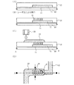
本実施の形態では、第1の導電層へのコンタクトホールの形成方法および該コンタクト
ホールを介して第1の導電層と電気的に接続する第2の導電層の形成方法について図1、
図2、図10、及び図11を用いて説明する。
12を形成する。次いで、第1の導電層12を覆う絶縁膜13を形成する。この段階の断
面図を図1(A)に示している。
いればよい。
ン膜などの絶縁膜から成る下地膜を形成する。ここでは下地膜として2層構造を用いた例
を示すが、前記絶縁膜の単層膜または2層以上積層させた構造を用いても良い。なお、特
に下地絶縁膜を形成しなくてもよい。
した後、フォトリソグラフィ技術を用いてパターニングを行う。なお、導電膜は、Ta、
W、Ti、Mo、Al、Cu、Siから選ばれた元素、または前記元素を主成分とする合
金材料若しくは化合物材料の単層、またはこれらの積層で形成する。ここではフォトリソ
グラフィ技術を用いて第1の導電層を形成した例を示すが、特に限定されず、第1の導電
層12は、液滴吐出法や印刷法や無電界メッキ法により形成してもよい。第1の導電層1
2は、後の開口工程で用いるレーザ光を反射してほとんど吸収しない材料を用いることが
好ましい。
よい。後の開口工程で用いるレーザ光を透過してほとんど吸収しない材料を用いることが
好ましい。
縁材料、例えば酸化シリコン膜、窒化シリコン膜または酸化窒化シリコン膜などの絶縁膜
を用いる。また、絶縁膜13として、塗布法によって得られるシリコン(Si)と酸素(
O)との結合で骨格構造が構成される絶縁膜を用いてもよい。また、絶縁膜13として、
二酸化珪素にリンを添加したPSG(リンシリケートガラス)、二酸化珪素にリン及びボ
ロンを添加したBPSG(ホウ素リンリシケートガラス)、二酸化珪素にフッ素を添加し
たSiOF、ポリイミド、ポリアリルエーテルやフッ素が添加されたポリフルオロアリエ
ーテルに代表される芳香族エーテル、芳香族炭化水素、BCB(Benzocyclob
utene)に代表されるシクロブタン誘導体などを用いることもできる。
れず、CVD法やスパッタ法で得られる無機絶縁膜であってもよい。絶縁膜13が平坦で
なくとも、本発明は、レーザ光を用いて複数の開口を形成することができる。
た後、乾燥、焼成を行って形成する。
6を複数形成する。ここでは、レーザ光として超短光パルスレーザから射出されるレーザ
光を用いる。透光性を有する材料に対して、超短光パルスレーザを集光することにより、
当該超短光パルスレーザが集光された位置たる集光点のみに多光子吸収を生じさせ、閉じ
られた孔を形成し、集光点を移動させて一つの貫通した開口を形成することが出来る。レ
ーザ光のパルス幅が10−4秒〜10−2秒では絶縁膜13に吸収されないが、非常に短
いパルス幅(ピコ秒台、或いはフェムト秒)のレーザ光を照射することによって多光子吸
収を生じさせて絶縁膜13に吸収させることができる。超短光パルスレーザによる開口の
作製方法について図2(A)及び図2(B)を用いて説明する。
るレーザ発振器を用いる。該超短光パルスレーザ発振器101として用いることができる
のは、サファイヤ、YAG、セラミックスYAG、セラミックスY2O3、KGW(ポタ
シウムガドリ二ウムタングステン)、Mg2SiO4、YLF、YVO4、GdVO4な
どの結晶に、Nd、Yb、Cr、Ti、Ho、Erなどのドーパントを添加したレーザな
どが挙げられる。超短光パルスレーザ発振器101から射出されたレーザ光をミラー10
2で反射した後、高い開口数の対物レンズ103により試料104、ここでは基板上に設
けられた絶縁膜13中にレーザ光を集光する(図2(A)参照。)。この結果、集光点近
傍において絶縁膜中に孔を形成することができる。また、XYZステージ105を用いて
集光点を移動させることにより、絶縁膜13に所望の開口を作製する。図2(B)に開口
形成の途中を示す断面図を示す。図2(B)において、貫通していない開口を孔17とし
て示している。
下で固体レーザから発振されたレーザビームを指す。なお、本発明におけるレーザ光の尖
頭出力の範囲は、1GW/cm2〜1TW/cm2とする。
通常のレーザでは、レーザ波長以下の加工は困難であるが、超短光パルスレーザを用いる
ことで微細加工、即ちレーザ波長以下の加工が可能となる。
材料、即ち超短光パルスレーザの波長の光を吸収しない材料、更に詳しくは超短光パルス
レーザの波長よりもエネルギーギャップの大きい材料を用いる必要がある。透光性を有す
る材料内部で超短光パルスレーザを集光することにより、当該超短光パルスレーザが集光
された位置たる集光点のみに多光子吸収を生じさせ、孔を形成することが出来る。なお、
多光子吸収とは、複数個の光子を同時に吸収して、光子のエネルギーの和に相当する固有
状態に遷移することである。該遷移により、吸収されない波長領域の光を吸収することが
可能であり、光エネルギー密度が十分に大きい集光点において、孔を形成することが出来
る。なお、ここで言う「同時」とは10−14秒以下の時間内に発生する2つの事象を意
味する。
ように、レーザビーム描画装置1001は、レーザビームを照射する際の各種制御を実行
するパーソナルコンピュータ1002(以下、PCと示す。)と、レーザビームを出力す
るレーザ発振器1003と、レーザ発振器1003の電源1004と、レーザビームを減
衰させるための光学系1005(NDフィルタ)と、レーザビームの強度を変調するため
の音響光学変調器1006(AOM)と、レーザビームの断面の拡大または縮小をするた
めのレンズ、光路の変更するためのミラー等で構成される光学系1007、Xステージ及
びYステージを有する基板移動機構1009と、PCから出力される制御データをデジタ
ルーアナログ変換するD/A変換部1010と、D/A変換部から出力されるアナログ電
圧に応じて音響光学変調器1006を制御するドライバ1011と、基板移動機構100
9を駆動するための駆動信号を出力するドライバ1012とを備えている。
ーザ発振器を用いる。
08が基板移動機構1009に装着されると、PC1002は図外のカメラによって、基
板に付されているマーカーの位置を検出する。次いで、PC1002は、検出したマーカ
ーの位置データと、予め入力されている描画パターンデータとに基づいて、基板移動機構
1009を移動させるための移動データを生成する。この後、PC1002が、ドライバ
1011を介して音響光学変調器1006の出力光量を制御することにより、レーザ発振
器1003から出力されたレーザビームは、光学系1005によって減衰された後、音響
光学変調器1006によって所定の光量になるように光量が制御される。
びビーム形を変化させ、レンズで集光した後、基板上の絶縁膜に該ビームを照射して、孔
を形成する。このとき、PC1002が生成した移動データに従い、基板移動機構100
9をZ方向に移動制御する。この結果、所定の場所にレーザビームが照射され、孔がZ方
向に連結されて柱状の開口形成が絶縁膜に行われる。基板移動機構1009をX方向及び
Y方向に移動制御すれば、絶縁膜に基板面と水平な方向に孔が形成される。
波長のレーザビームを照射することで、微細な径の開口を形成することができる。
たは線状(厳密には細長い長方形状)となるように光学系で加工することが可能である。
に限定されず、レーザビームをZ方向、X方向、Y方向に移動してレーザビームを照射す
ることができる。この場合、光学系1007にポリゴンミラーやガルバノミラー、音響光
学偏向器(Acoust−Optic Deflector;AOD)を用いることが好
ましい。
法を用いて吐出して、第2の導電層19を形成する(図1(C)参照。)。第2の導電層
19の形成は、液滴吐出手段18を用いて行う。液滴吐出手段18とは、組成物の吐出口
を有するノズルや、1つまたは複数のノズルを具備したヘッド等の液滴を吐出する手段を
有するものの総称とする。液滴吐出手段18が具備するノズルの径は、0.02〜100
μm(好適には30μm以下)に設定し、該ノズルから吐出される組成物の吐出量は0.
001pl〜100pl(好適には10pl以下)に設定する。吐出量は、ノズルの径の
大きさに比例して増加する。また、被処理物とノズルの吐出口との距離は、所望の箇所に
滴下するために、出来る限り近づけておくことが好ましく、好適には0.1〜3mm(好
適には1mm以下)程度に設定する。
導電性粒子とは、Ag、Au、Cu、Ni、Pt、Pd、Ir、Rh、W、Al等の金属
、Cd、Znの金属硫化物、Fe、Ti、Si、Ge、Zr、Baなどの酸化物、ハロゲ
ン化銀等の微粒子、または分散性ナノ粒子に相当する。但し、吐出口から吐出する組成物
は、比抵抗値を考慮して、金、銀、銅のいずれかの材料を溶媒に溶解または分散させたも
のを用いることが好適であり、より好適には、低抵抗な銀、銅を用いるとよい。但し、銀
、銅を用いる場合には、不純物対策のため、合わせてバリア膜を設けるとよい。溶媒は、
酢酸ブチル、酢酸エチル等のエステル類、イソプロピルアルコール、エチルアルコール等
のアルコール類、メチルエチルケトン、アセトン等の有機溶剤等を用いる。組成物の粘度
は50cp以下が好適であり、これは、乾燥が起こることを防止したり、吐出口から組成
物を円滑に吐出できるようにしたりするためである。また、組成物の表面張力は、40m
N/m以下が好適である。但し、用いる溶媒や、用途に合わせて、組成物の粘度等は適宜
調整するとよい。
パターンの作製のため、導電体の粒子の径はなるべく小さい方が好ましく、好適には粒径
0.1μm以下が好ましい。組成物は、電解法、アトマイズ法または湿式還元法等の公知
の方法で形成されるものであり、その粒子サイズは、約0.01〜10μmである。但し
、ガス中蒸発法で形成すると、分散剤で保護されたナノ粒子は約7nmと微細であり、ま
たこのナノ粒子は、被覆剤を用いて各粒子の表面を覆うと、溶剤中に凝集がなく、室温で
安定に分散し、液体とほぼ同じ挙動を示す。従って、被覆剤を用いることが好ましい。
のヘッド1105、1112は制御手段1107に接続され、それがコンピュータ111
0で制御することにより予めプログラミングされたパターンを描画することができる。描
画するタイミングは、例えば、基板1100上に形成されたマーカー1111を基準に行
えば良い。或いは、基板1100の縁を基準にして基準点を確定させても良い。これを電
荷結合素子(CCD)や相補型金属酸化物半導体(CMOS)を利用したイメージセンサ
などの撮像手段1104で検出し、画像処理手段1109にてデジタル信号に変換したも
のをコンピュータ1110で認識して制御信号を発生させて制御手段1107に送る。勿
論、基板1100上に形成されるべきパターンの情報は記憶媒体1108に格納されたも
のであり、この情報を基にして制御手段1107に制御信号を送り、液滴吐出手段110
3の個々のヘッド1105、1112を個別に制御することができる。吐出する材料は、
材料供給源1113、1114より配管を通してヘッド1105、1112に供給される
。図11では、液滴吐出手段1103の個々のヘッド1105、1112の並んだ距離が
基板の幅と一致しているが、液滴吐出手段1103の個々のヘッド1105、1112の
並んだ距離より大きな幅を持つ大型基板にも繰り返し走査することでパターンの形成可能
な液滴吐出装置である。その場合、ヘッド1105、1112は、基板上を矢印の方向に
自在に走査し、描画する領域を自由に設定することができ、同じパターンを一枚の基板に
複数描画することができる。
に、導電性粒子の溶融、焼結、及び癒着のいずれか一つまたは複数の反応を進行させる。
なお、図1(C)は、図1(D)中の鎖線A−Bで切断した断面図に相当する。
を介して第2の導電層19が第1の導電層12と電気的に接続されている。なお、開口の
個数は10個に限定されないことは言うまでもなく、また、開口の配置も特に限定されな
い。
に凹みが生じることを防いでいる。また、第2の導電層19の配線幅を均一にすることが
できる。なお、第2の導電層の幅Wと、1つの貫通した開口の径Dは、2D<Wを満たす
。
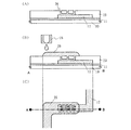
本実施の形態では、実施の形態1と開口の断面形状が異なる例を図3(A)、図3(B
)、図3(C)に示す。実施の形態1と異なる部分を詳細に説明し、図3において、図1
と同じ部分は同一の符号を用いることとする。
のではなく、図3に示すように複数の開口が絶縁膜中で繋がった構造の開口形状としても
よい。
の導電層12とを形成する。
らなる絶縁膜を形成した後、超短光パルスレーザ光を照射して貫通した開口26を有する
絶縁膜23を得る。絶縁膜に対して、超短光パルスレーザを集光することにより、当該超
短光パルスレーザが集光された位置たる集光点のみに多光子吸収を生じさせ、閉じられた
孔を形成し、集光点を移動させて一つの貫通した開口を形成することが出来る。レーザ光
のパルス幅が10−4秒〜10−2秒では絶縁膜23に吸収されないが、非常に短いパル
ス幅(ピコ秒台、或いはフェムト秒)のレーザ光を照射することによって多光子吸収を生
じさせて絶縁膜23に吸収させることができる。
簡単な説明のみとする。
焦点位置をZ方向、X方向またはY方向に移動することによって形成できる。
して、第2の導電層29を形成する(図3(B)参照。)。第2の導電層29の形成は、
液滴吐出手段28を用いて行う。
、開口内部の空気は、他の開口から押し出される。このように複数の開口が絶縁膜中で繋
がった構造とすることで、複雑な形状の開口内部に気泡が残ることなく導電性粒子を充填
することができる。
粒子の溶融、焼結、及び癒着のいずれか一つまたは複数の反応を進行させる。
残すことなく導電性粒子を充填させてもよい。
なお、図3(B)は、図3(C)中の鎖線A−Bで切断した断面図に相当する。
っており、合計2個の複雑な形状の開口と呼べる。また、実施の形態1と比較して、絶縁
表面に設けられた開口は少ないが、第1導電層と第2の導電層との接触面積は本実施の形
態のほうが大きい。なお、開口の個数は2個に限定されないことは言うまでもなく、また
、開口の配置も特に限定されない。
ペーサとなり、第2の導電層の表面に凹みが生じることを防いでいる。また、第2の導電
層29の配線幅を均一にすることができる。
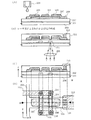
本実施の形態では、レーザ光とエッチングとを組み合わせて複数の開口を形成する例を図
4に説明する。実施の形態1と異なる部分を詳細に説明し、図4において、図1と同じ部
分は同一の符号を用いることとする。
なる絶縁膜を形成した後、超短光パルスレーザ光を照射して閉じている孔37を有する絶
縁膜33を得る。絶縁膜に対して、超短光パルスレーザを集光することにより、当該超短
光パルスレーザが集光された位置たる集光点のみに多光子吸収を生じさせ、閉じられた孔
を形成し、集光点を移動させて一つの貫通した開口を形成することが出来る。レーザ光の
パルス幅が10−4秒〜10−2秒では絶縁膜33に吸収されないが、非常に短いパルス
幅(ピコ秒台、或いはフェムト秒)のレーザ光を照射することによって多光子吸収を生じ
させて絶縁膜33に吸収させることができる。
簡単な説明のみとする。
ザ光を照射しながら焦点位置を移動することによって形成される。
エッチングによって、閉じている孔37の上方の絶縁膜を除去し、閉じている孔37を貫
通した開口36とすることができる。この段階で、貫通した複数の開口36を有する絶縁
膜34を得る。なお、図4(B)に示す点線は、エッチング前の絶縁膜表面を示している
。
法を用いて吐出して、第2の導電層39を形成する(図4(C)参照。)。第2の導電層
39の形成は、液滴吐出手段38を用いて行う。
粒子の溶融、焼結、及び癒着のいずれか一つまたは複数の反応を進行させる。
る。
本実施の形態では、実施の形態1と開口の断面形状が異なる例を図5(A)、図5(B)
、図5(C)に示す。実施の形態1と異なる部分を詳細に説明し、図5において、図1と
同じ部分は同一の符号を用いることとする。
の導電層12とを形成する。
ルスレーザ光を照射して貫通した開口46を有する絶縁膜43を得る。レーザ光のパルス
幅が10−4秒〜10−2秒では絶縁膜43に吸収されないが、非常に短いパルス幅(ピ
コ秒台、或いはフェムト秒)のレーザ光を照射することによって多光子吸収を生じさせて
絶縁膜43に吸収させることができる。
簡単な説明のみとする。
射しながら焦点位置をX方向またはY方向に移動した後、Z方向に移動させ、再びX方向
またはY方向に移動させることを繰り返すことによって形成できる。
る。
法を用いて吐出して、第2の導電層49を形成する(図5(B)参照。)。第2の導電層
49の形成は、液滴吐出手段48を用いて行う。本実施の形態において、開口の断面形状
は湾曲しているため、スムーズに導電性粒子を含む組成物を開口内部に充填できる。
粒子の溶融、焼結、及び癒着のいずれか一つまたは複数の反応を進行させる。
なお、図5(B)は、図5(C)中の鎖線A−Bで切断した断面図に相当する。また、図
5(C)において、楕円形状と、円形状との2種類の開口を形成した例を示している。即
ち、3つの楕円形状の開口と、1つの円形状の開口との合計4つの開口が形成されている
。このように、本発明は、レーザ光の焦点位置を自在に調節することにより複数種類の開
口を形成することができる。
面で第2の導電層49と電気的な導通を行うことができる。従って、第1の導電層12と
第2の導電層49とが重ならないように配置することができる。このような配置とするこ
とによって、第1導電層12と第2の導電層49との間に形成される寄生容量を低減でき
る。
わせることができる。
本実施の形態では、本発明のレーザ光による開口を用いてTFTを形成する例を図6に
示す。
る基板200としては、透光性を有する基板、例えばガラス基板、結晶化ガラス基板、も
しくはプラスチック基板を用いることができる。プラスチック基板としては、フィルム状
のプラスチック基板、例えば、ポリエチレンテレフタレート(PET)、ポリエーテルス
ルホン(PES)、ポリエチレンナフタレート(PEN)、ポリカーボネート(PC)、
ナイロン、ポリエーテルエーテルケトン(PEEK)、ポリスルホン(PSF)、ポリエ
ーテルイミド(PEI)、ポリアリレート(PAR)、ポリブチレンテレフタレート(P
BT)などのプラスチック基板が好ましい。また、耐熱性を有するプラスチック基板、例
えば直径数nmの無機粒子が有機ポリマーマトリックスに分散した材料をシート状に加工
したプラスチック基板を用いてもよい。
膜(SiOxNy)等の絶縁膜を用いる。代表的な一例は下地絶縁膜11として2層構造
から成り、SiH4、NH3、及びN2Oを反応ガスとして成膜される窒化酸化珪素膜を
50〜100nm、SiH4、及びN2Oを反応ガスとして成膜される酸化窒化珪素膜を
100〜150nmの厚さに積層形成する構造が採用される。また、下地絶縁膜201の
一層として膜厚10nm以下の窒化シリコン膜(SiN膜)、或いは酸化窒化珪素膜(S
iNxOy膜(X>Y))を用いることが好ましい。また、窒化酸化珪素膜、酸化窒化珪
素膜、窒化シリコン膜とを順次積層した3層構造を用いてもよい。ここでは下地絶縁膜2
01を形成した例を示したが、特に必要でなければ設ける必要はない。
ては、後の開口工程で用いるレーザ光の基本波を透過してほとんど吸収しない材料を用い
ることが好ましい。第1の絶縁膜202としては、酸化シリコン膜、窒化シリコン膜また
は酸化窒化シリコン膜などの絶縁膜を用いる。また、第1の絶縁膜202として、ポリシ
ラザンやシロキサンポリマーを含む溶液を塗布焼成して得られる膜、光硬化性有機樹脂膜
、熱硬化性有機樹脂膜などを用いてもよい。
スを用いて気相成長法やスパッタリング法や熱CVD法で作製されるアモルファス半導体
膜、或いは微結晶半導体膜で形成する。本実施の形態では、半導体膜として、アモルファ
スシリコン膜を用いた例を示す。また、半導体膜として、スパッタ法やPLD(Pals
e Laser Deposition)法で作製されるZnOや亜鉛ガリウムインジウ
ムの酸化物を用いてもよいが、その場合にはゲート絶縁膜をアルミニウムやチタンを含む
酸化物とすることが好ましい。また、半導体膜として塗布法や液滴吐出法や蒸着法で作製
されるペンタセン、テトラセン、チオフェンオリゴマ誘導体、フェニレン誘導体、フタロ
シアニン化合物、ポリアセチレン誘導体、ポリチオフェン誘導体、シアニン色素等などの
有機材料を用いてもよい。
はp型の不純物が添加されてn型またはp型の導電型を示す半導体膜を用いる。n型の半
導体膜は、シランガスとフォスフィンガスを用いたPCVD法で形成すれば良い。本実施
の形態では、導電性を有する半導体膜として、リンを含むシリコン膜を用いた例を示す。
なお、半導体膜としてペンタセンなどの有機材料を用いる場合は、導電性を有する半導体
膜に代えて電荷輸送層を用い、例えば正孔輸送層として機能するトリフェニルジアミン、
電子輸送層として機能するオキサジアゾールを用いればよい。
、導電性を有する半導体層206を得る。なお、公知のフォトリソ技術に代えて、液滴吐
出法や印刷法(凸版、平版、凹版、スクリーンなど)を用いてマスクを形成し、選択的に
エッチングを行ってもよい。
ングステン)、Al(アルミニウム)等)を含む組成物を選択的に吐出して、配線203
、204、209を形成する。図6(A)にはインクジェットヘッド208から導電性材
料を含む組成物を吐出している様子を示している。なお、配線203、204、209は
液滴吐出法により形成することに限定されず、例えば、スパッタ法を用いて金属膜を形成
し、マスクを形成し、選択的にエッチングを行って形成してもよい。
導体層の上部をエッチングして半導体層の一部を露出させる。半導体層の露出させた部分
はTFTのチャネル形成領域として機能する箇所である。
を形成する。保護膜としては、スパッタ法、またはPCVD法により得られる窒化珪素、
または窒化酸化珪素を主成分とする材料を用いる。本実施の形態では保護膜を形成した後
に水素化処理を行う。また、層間絶縁膜は、エポキシ樹脂、アクリル樹脂、フェノール樹
脂、ノボラック樹脂、メラミン樹脂、ウレタン樹脂等の樹脂材料を用いる。また、ベンゾ
シクロブテン、パリレン、フッ化アリレンエーテル、透過性を有するポリイミドなどの有
機材料、シロキサン系ポリマー等の重合によってできた化合物材料、水溶性ホモポリマー
と水溶性共重合体を含む組成物材料等を用いることができる。
複数の第1の開口210を形成する。また、チャネル形成領域にレーザ光が照射されるこ
とを防ぐために、基板の裏面側からも超短光パルスレーザ光の照射を行い、複数の第2の
開口212も形成する。図6(B)には、光学系205を通過した超短光パルスレーザ光
が第2の開口212を形成している断面図を示している。
されないが、非常に短いパルス幅(ピコ秒台、或いはフェムト秒)のレーザ光を照射する
ことによって多光子吸収を生じさせて保護膜を含む層間絶縁膜211に吸収させることが
できる。
簡単な説明のみとする。
2がゲート絶縁膜となる。従って、第2の開口212の形成によってゲート絶縁膜の膜厚
を自由に決定することができる。
組成物を液滴吐出法を用いて吐出して、各開口内部に導電性粒子を充填する。そして、焼
成を行うと導電性粒子が溶融して集合して100nm程度の結晶となり、ゲート電極、ゲ
ート配線214、215、および接続配線213を形成する(図6(C)参照。)。本実
施の形態においては、異なる層に配置されたゲート電極とゲート配線を同時、且つ、同一
材料で形成することが可能である。
を形成した後にゲート電極を形成するという工程順序が大きな特徴の一つである。
て、鎖線A−B断面が図6(C)の断面図と対応している。なお、対応する部位には同じ
符号を用いている。
ある。ゲート配線214、215は、Z方向(基板面に垂直な方向)に形成された第3の
開口216と、Y方向に形成された第2の開口212を介して電気的に接続されている。
なお、第3の開口216は、第1の開口または第2の開口の形成と同様にレーザ光を用い
て形成したものである。
3の開口216は、第1の開口210と深さが異なっている。また、接続配線213は第
1の開口210を介して配線209と電気的に接続されている。
第2の開口を先に形成してもよい。また、第3の開口は、第2の開口を形成する際にその
まま連続的にレーザ光の焦点位置を移動させて形成してもよい。
製することができる。また、接続配線213と重なる第1の電極、第1の端部を覆う隔壁
を形成し、第1の電極上に有機化合物を含む層と第2の電極を積層形成してアクティブマ
トリクス型の発光表示装置も作製することができる。
07を形成することができ、ゲート電極の形成のための開口を半導体層へダメージなく形
成することができる。従って、半導体層は塗布法で形成されることが可能であるため、有
機材料を半導体層に用いる場合に有効である。
較的少ないものとすることができる。
と自由に組み合わせることができる。
本実施の形態では、実施の形態5とは異なるTFTを形成する例を図7に示す。
基板300としては、透光性を有する基板、例えばガラス基板、結晶化ガラス基板、もし
くはプラスチック基板を用いることができる。後の工程でレーザ光を基板を通過させずに
開口を形成する場合にはセラミックス基板、半導体基板、金属基板等も用いることができ
る。
(SiOxNy)等の絶縁膜を用いる。
導体膜を公知の手段(スパッタ法、LPCVD法、またはプラズマCVD法等)により成
膜した後、公知の結晶化処理(レーザー結晶化法、熱結晶化法、またはニッケルなどの触
媒を用いた熱結晶化法等)を行って得られた結晶質半導体膜上にレジスト膜を形成した後
、レーザ光を走査して露光を行った第1のレジストマスクを用いて所望の形状にパターニ
ングして形成する。この半導体層の厚さは25〜80nm(好ましくは30〜70nm)
の厚さで形成する。結晶質半導体膜の材料に限定はないが、好ましくはシリコンまたはシ
リコンゲルマニウム(SiGe)合金などで形成すると良い。
する。ゲート絶縁膜303はプラズマCVD法またはスパッタ法または熱酸化法を用い、
厚さを1〜200nmとする。ゲート絶縁膜303としては、酸化シリコン膜、窒化シリ
コン膜または酸化窒化シリコン膜などの絶縁膜から成る膜を形成する。
行った第2のレジストマスクを形成する。第2のレジストマスクをマスクとし、イオンド
ーピング法またはイオン注入法を用いて、半導体層にp型またはn型を付与する不純物元
素を選択的に添加する。こうして、不純物元素が添加された領域は、不純物領域304、
306、307となる。また、第2のレジストマスクに覆われ、不純物元素が添加されな
かった領域302は、TFTのチャネル形成領域として機能する。
よび水素化を行う。
絶縁膜319としては、透光性を有する無機材料(酸化シリコン、窒化シリコン、酸化窒
化シリコンなど)、感光性または非感光性の有機材料(ポリイミド、アクリル、ポリアミ
ド、ポリイミドアミド、レジストまたはベンゾシクロブテン)、またはこれらの積層など
を用いる。また、層間絶縁膜319に用いる他の透光性を有する膜としては、塗布法によ
って得られるアルキル基を含むSiOx膜からなる絶縁膜、例えばシリカガラス、アルキ
ルシロキサンポリマー、アルキルシルセスキオキサンポリマー、水素化シルセスキオキサ
ンポリマー、水素化アルキルシルセスキオキサンポリマーなどを用いて形成された絶縁膜
を用いることができる。シロキサン系ポリマーの一例としては、東レ製塗布絶縁膜材料で
あるPSB−K1、PSB−K31や触媒化成製塗布絶縁膜材料であるZRS−5PHが
挙げられる。
膜303に形成する。複数の第1の開口309は、不純物領域304、307に達するよ
うに形成される。また、レーザ光を用いて複数の第2の開口310、311を層間絶縁膜
319に形成する。複数の第2の開口310、311は、不純物元素が添加されなかった
領域302と重なる位置に形成する。図7(B)には、第2の開口310を形成した後、
超短光パルスレーザ光の焦点位置を移動させて、光学系305を通過した超短光パルスレ
ーザ光が第1の開口309を形成している断面図を示している。
されないが、非常に短いパルス幅(ピコ秒台、或いはフェムト秒)のレーザ光を照射する
ことによって多光子吸収を生じさせて保護膜を含む層間絶縁膜319に吸収させることが
できる。
簡単な説明のみとする。
性粒子を含む組成物を液滴吐出法を用いて吐出して、各開口内部に導電性粒子を充填する
。そして、焼成を行うと導電性粒子が溶融して集合して100nm程度の結晶となり、ゲ
ート電極313、314、およびソース電極またはドレイン電極312、315を形成す
る(図7(C)参照。)。本実施の形態においては、異なる層に配置されたゲート電極と
ソース電極を同一材料で形成することが可能である。図7(C)にはインクジェットヘッ
ド308から導電性材料を含む組成物を吐出している様子を示している。
ネル形成領域を有するダブルゲート型のTFTである。本実施の形態において、層間絶縁
膜を形成した後にゲート電極を形成するという工程順序が大きな特徴の一つである。
おいて、鎖線C−Dを含む面で切断した断面図が図7(D)と対応している。なお、対応
する部位には同じ符号を用いている。
2の開口310の底部はゲート絶縁膜303に接している。
一配線となっている。
の液晶表示装置を作製することができる。
型の液晶表示装置の作製方法を示す。
て、絶縁膜316にコンタクトホールを形成し、ITOなどで画素電極317を形成する
。また、絶縁膜316上にITOなどで端子電極を形成する。
、液滴吐出法やスクリーン印刷法やオフセット印刷法を用いればよい。その後、配向膜3
20の表面にラビング処理を行う。
22を形成する。そして、閉パターンであるシール材(図示しない)を液滴吐出法により
画素部と重なる領域を囲むように形成する。ここでは液晶を滴下するため、閉パターンの
シール材を描画する例を示すが、開口部を有するシールパターンを設け、TFT基板を貼
りあわせた後に毛細管現象を用いて液晶を注入するディップ式(汲み上げ式)を用いても
よい。
。閉ループのシールパターン内に液晶を1回若しくは複数回滴下する。液晶321の配向
モードとしては、液晶分子の配列が光の入射から出射に向かって90°ツイスト配向した
TNモードを用いる場合が多い。TNモードの液晶表示装置を作製する場合には、基板の
ラビング方向が直交するように貼り合わせる。
を形成したり、シール材にフィラーを含ませることによって維持すればよい。上記柱状の
スペーサは、アクリル、ポリイミド、ポリイミドアミド、エポキシの少なくとも1つを主
成分とする有機樹脂材料、もしくは酸化珪素、窒化珪素、酸化窒化珪素のいずれか一種の
材料、或いはこれらの積層膜からなる無機材料であることを特徴としている。
。また、1面取りの場合、予めカットされている対向基板を貼り合わせることによって、
分断工程を省略することもできる。
上の工程で液晶モジュールが完成する。(図8)また、必要があればカラーフィルタなど
の光学フィルムを貼り付ける。透過型の液晶表示装置とする場合、偏光板は、アクティブ
マトリクス基板と対向基板の両方に貼り付ける。
作製することができる。
の作製方法を示す。ここではTFTをnチャネル型TFTとした例を示す。
て、絶縁膜316にコンタクトホールを形成し、第1の電極318を形成する。
の電極318としては、インジウム錫酸化物(ITO)、酸化珪素を含むインジウム錫酸
化物(ITSO)、酸化亜鉛(ZnO)、酸化スズ(SnO2)などを含む組成物からな
る所定のパターンを形成する。また、発光を第1の電極318で反射させる場合、Ag(
銀)、Au(金)、Cu(銅)、W(タングステン)、Al(アルミニウム)等の金属の
粒子を主成分とした組成物からなる所定のパターンを形成して第1の電極318を形成す
る。
)331は、珪素を含む材料、有機材料及び化合物材料を用いて形成する。また、多孔質
膜を用いても良い。但し、アクリル、ポリイミド等の感光性、非感光性の材料を用いて形
成すると、その側面は曲率半径が連続的に変化する形状となり、上層の薄膜が段切れせず
に形成されるため好ましい。
。有機化合物を含む層330は、積層構造であり、それぞれ蒸着法または塗布法を用いて
形成する。例えば、陰極上に電子輸送層(電子注入層)、発光層、正孔輸送層、正孔注入
層と順次積層する。
気下での加熱処理を行うとよい。蒸着法を用いる場合、予め、抵抗加熱により有機化合物
は気化されており、蒸着時にシャッターが開くことにより基板の方向へ飛散する。気化さ
れた有機化合物は、上方に飛散し、メタルマスクに設けられた開口部を通って基板に蒸着
される。また、フルカラー化するためには、発光色(R、G、B)ごとにマスクのアライ
メントを行えばよい。
い、カラーフィルターや色変換層を組み合わせることによりフルカラー表示を行うことが
できる。
2は光を透過する透明導電膜を用いて形成し、例えばITO、ITSOの他、酸化インジ
ウムに2〜20%の酸化亜鉛(ZnO)を混合した透明導電膜を用いる。発光素子は、有
機化合物を含む層330を第1の電極と第2の電極で挟んだ構成になっている。なお、第
1の電極及び第2の電極は仕事関数を考慮して材料を選択する必要があり、そして第1の
電極及び第2の電極は、画素構成によりいずれも陽極、又は陰極となりうる。
。なお、シール材で囲まれた領域には透明な充填材333を充填する。充填材333とし
ては、透光性を有している材料であれば特に限定されず、代表的には紫外線硬化または熱
硬化のエポキシ樹脂を用いればよい。
は実施の形態5と自由に組み合わせることができる。
こととする。
結晶シリコン基板または化合物半導体基板であり、代表的には、N型またはP型の単結晶
シリコン基板、GaAs基板、InP基板、GaN基板、SiC基板、サファイヤ基板、
又はZnSe基板である。
ウェルを、第2の素子形成領域にp型ウェルをそれぞれ選択的に形成する。
なるフィールド酸化膜503、504、505を形成する。フィールド酸化膜503、5
04、505は厚い熱酸化膜であり、公知のLOCOS法を用いて形成すればよい。なお
、素子分離法は、LOCOS法に限定されず、例えば素子分離領域はトレンチ分離法を用
いてトレンチ構造を有していてもよいし、LOCOS構造とトレンチ構造の組み合わせで
あってもよい。
する。ゲート絶縁膜は、CVD法を用いて形成してもよく、酸化窒化珪素膜や酸化珪素膜
や窒化珪素膜やそれらの積層膜を用いることができる。例えば、熱酸化により得られる膜
厚5nmの酸化珪素膜とCVD法で得られる膜厚10nm〜15nmの酸化窒化珪素膜の
積層膜を形成する。
およびドライエッチング技術に基づき積層膜をパターニングすることによってゲート絶縁
膜上にポリサイド構造を有するゲート電極506を形成する。ポリシリコン層は低抵抗化
するために予め、1021/cm3程度の濃度でリン(P)をドープしておいても良いし
、ポリシリコン層を形成した後で濃いn型不純物を拡散させても良い。また、シリサイド
層を形成する材料はモリブデンシリサイド(MoSix)、タングステンシリサイド(W
Six)、タンタルシリサイド(TaSix)、チタンシリサイド(TiSix)などを
適用することが可能であり、公知の方法に従い形成すれば良い。
絶縁膜508が形成される。
素からなる絶縁材料層を全面にCVD法にて堆積させ、かかる絶縁材料層をエッチバック
することによってサイドウォールを形成すればよい。
オン注入を行う。CMOSを製造する場合であるので、pチャネル型FETを形成すべき
第1の素子形成領域をレジスト材料で被覆し、n型不純物であるヒ素(As)やリン(P
)をシリコン基板に注入してソース領域514及びドレイン領域515を形成する。同時
に、サイドウォールを通過させてn型不純物が添加された低濃度不純物領域518、51
9を形成する。また、nチャネル型FETを形成すべき第2の素子形成領域をレジスト材
料で被覆し、p型不純物であるボロン(B)をシリコン基板に注入してソース領域516
及びドレイン領域517を形成する。また、同時に、サイドウォールを通過させてp型不
純物が添加された低濃度不純物領域520、521を形成する。
ン基板における結晶欠陥を回復するために、GRTA法やLRTA法などを用いて活性化
処理を行う(図12(A)参照)。
縁膜545は、プラズマCVD法や減圧CVD法を用いて酸化シリコン膜や酸化窒化シリ
コン膜などで100〜2000nmの厚さに形成する。さらにその上にリンガラス(PS
G)、あるいはボロンガラス(BSG)、もしくはリンボロンガラス(PBSG)の層間
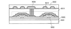
絶縁膜を積層してもよい。
る超短パルスレーザから射出されるレーザ光を照射して貫通した開口541〜544を形
成する。
組成物を吐出し、焼成して導電膜551〜554を形成する。本発明により、開口と重な
る箇所には凹みができず、導電膜551〜554の上面はほぼ同一面となっている。
2〜565の形成を行い、図12(D)に示すように多層配線を形成することができる。
導電膜551〜554の上面はほぼ同一面となっているため、第2の層間絶縁膜561を
貫通する開口の深さを一定とすることができる。
酸化絶縁膜の界面又は層内で剥離することが可能な処理を行うことによりMOSトランジ
スタを有する回路を剥離することができる。また、剥離したMOSトランジスタを有する
回路をフレキシブル基板に接着することにより、半導体装置の薄膜化が可能である。
タ等の様々な半導体装置に適用可能である。また、メモリ、ロジック回路等の回路にも適
用可能である。
積回路装置(無線ICタグ、RFID(無線認証、Radio Frequency I
dentification)とも呼ばれる)として用いることができる。
Cチップ1516を貼り付けたIDカードの例を図13に示す。アンテナとして機能する
導電層1517も液滴吐出法で形成することができる。また、アンテナとして機能する導
電層1517と接続する接続電極とのコンタクトホールの形成を本発明のレーザ光による
開口形成技術を用いて形成してもよい。このように、本発明のICチップ1516は、小
型、薄型、軽量であり、多種多様の用途が実現し、物品に貼り付けても、その物品のデザ
イン性を損なうことがない。
れず、曲面や様々な形状の物品に貼り付けることもできる。例えば、ICチップを紙幣、
硬貨、有価証券類、無記名債券類、証書類(運転免許証や住民票等)、包装用容器類(包
装紙やボトル等)、記録媒体(DVDソフトやビデオテープ等)、乗物類(自転車等)、
身の回り品(鞄や眼鏡等)、食品類、衣類、生活用品類等に設けて使用することができる
。
態5、または実施の形態6と自由に組み合わせることができる。
ュールについて、図14を用いて説明する。図14は表示パネル9501と、回路基板9
502を組み合わせたモジュールを示している。回路基板9502には、例えば、コント
ロール回路9504や信号分割回路9505などが形成されている。また、表示パネル9
501と回路基板9502とは、接続配線9503で接続されている。表示パネル950
1に実施の形態5または実施の形態6で示すような、液晶表示パネル、発光表示パネルを
適宜用いることができる。
駆動回路9507、選択された画素にビデオ信号を供給する信号線駆動回路9508を備
えている。画素部9506の構成は、実施の形態5または実施の形態6と同様である。ま
た、走査線駆動回路9507や信号線駆動回路9508は、公知の異方性導電接着剤、及
び異方性導電フィルムを用いた実装方法、COG方式、ワイヤボンディング方法、並びに
半田バンプを用いたリフロー処理等により、基板上にICチップで形成される走査線駆動
回路9507、信号線駆動回路9508を実装する。
態5、実施の形態6、または実施例1と自由に組み合わせることができる。
の例を示したが、これに限られるものではなく、DMD(Digital Microm
irror Device;デジタルマイクロミラーデバイス)、PDP(Plasma
Display Panel;プラズマディスプレイパネル)、FED(Field
Emission Display;フィールドエミッションディスプレイ)、電気泳動
表示装置(電子ペーパー)、エレクトロデポジション型画像表示装置等の表示モジュール
の開口形成および配線形成に、本発明を適宜適用することができる。
態5、実施の形態6と自由に組み合わせることができる。
(単にテレビ、又はテレビジョン受信機ともよぶ)が挙げられる。ここでは、テレビジョ
ン装置の具体例について、図15を参照して説明する。
置の斜視図を示す。上記実施例に示される液晶モジュールやELモジュールにより、液晶
レジビジョン装置やELテレビジョン装置を完成させることができる。
11は映像信号と音声信号を受信する。映像信号は、映像検波回路9512と、そこから
出力される信号を赤、緑、青の各色に対応した色信号に変換する映像信号処理回路951
3と、その映像信号をドライバICの入力仕様に変換するためのコントロール回路951
4により処理される。コントロール回路9514は、表示パネル9515の走査線駆動回
路9516と信号線駆動回路9517にそれぞれ信号が出力する。デジタル駆動する場合
には、信号線側に信号分割回路9518を設け、入力デジタル信号をm個に分割して供給
する構成としても良い。
その出力は音声信号処理回路9522を経てスピーカー9523に供給される。制御回路
9524は受信局(受信周波数)や音量の制御情報を入力部9525から受け、チューナ
9511や音声信号処理回路9522に信号を送出する。
置を完成させることができる。液晶モジュールやELモジュールに代表されるモジュール
により、表示画面9532が形成される。また、スピーカー9533、操作スイッチ95
34などが適宜備えられている。
ジョン装置のコストダウンを図ることが可能である。また、高精細な表示が可能なテレビ
ジョン装置を作製することが可能である。
鉄道の駅や空港などにおける情報表示盤や、街頭における広告表示盤など特に大面積の表
示媒体として様々な用途に適用することができる。
態5、実施の形態6と自由に組み合わせることができる。
ゴーグル型ディスプレイ(ヘッドマウントディスプレイ)、ナビゲーションシステム、音
響再生装置(カーオーディオ、オーディオコンポ等)、パーソナルコンピュータ、ゲーム
機器、携帯情報端末(モバイルコンピュータ、携帯電話、携帯型ゲーム機又は電子書籍等
)、記録媒体を備えた画像再生装置(具体的にはDigital Versatile
Disc(DVD)等の記録媒体を再生し、その画像を表示しうるディスプレイを備えた
装置)などが挙げられる。それら電子機器の具体例を図16に示す。
ー2104、シャッター2106等を含む。なお、図16(A)は表示部2102側から
の図であり、撮像部は示していない。本発明により、製造コストを低減したプロセスでデ
ジタルカメラが実現できる。
203、キーボード2204、外部接続ポート2205、ポインティングマウス2206
等を含む。本発明により、製造コストを低減したプロセスでパーソナルコンピュータを実
現することができる。
あり、本体2401、筐体2402、表示部A2403、表示部B2404、記録媒体(
DVD等)読み込み部2405、操作キー2406、スピーカー部2407等を含む。表
示部A2403は主として画像情報を表示し、表示部B2404は主として文字情報を表
示する。なお、記録媒体を備えた画像再生装置には家庭用ゲーム機器なども含まれる。本
発明により、製造コストを低減したプロセスで画像再生装置を実現することができる。
話として使用する状態を示す斜視図である。図16(D)において、使用者はキーボード
のように右手指で操作キー2706aを操作し、左手指で操作キー2706bを操作する
。本発明により、製造コストを低減したプロセスで携帯情報端末を実現することができる
。
702を持ち、音声入力部2704、音声出力部2705、操作キー2706c、アンテ
ナ2708等を使用する。
横表示する高画質な表示部2703aと、縦表示する表示部2703bとを備えている。
施の形態4、実施の形態5、実施の形態6、実施例1乃至4のいずれか一の作製方法また
は構成を用いて、様々な電子機器を完成させることができる。
する半導体装置を形成することができる。
を示したが、TFTを用いて無線チップを形成することもできる。
無線チップは、薄膜集積回路9303及びそれに接続されるアンテナ9304とで形成さ
れる。また、薄膜集積回路9303及びアンテナ9304は、カバー材9301、930
2により挟持される。薄膜集積回路9303は、接着剤を用いてカバー材に接着してもよ
い。図17においては、薄膜集積回路9303の一方が、接着剤9305を介してカバー
材9301に接着されている。
した後、公知の剥離工程により剥離してカバー材に設ける。また、薄膜集積回路9303
に用いられる半導体素子はこれに限定されない。例えば、TFTの他に、記憶素子、ダイ
オード、光電変換素子、抵抗素子、コイル、容量素子、インダクタなどを用いることがで
きる。
れ、層間絶縁膜9311を介してTFTに接続するアンテナ9304が形成される。また
、層間絶縁膜9311及びアンテナ9304上には、窒化珪素膜等からなるバリア膜93
12が形成されている。
燥焼成して形成する。液滴吐出法によりアンテナを形成することで、工程数の削減が可能
であり、それに伴うコスト削減が可能である。
ビニル、ポリフッ化ビニル、塩化ビニルなどからなる)、繊維質な材料からなる紙、基材
フィルム(ポリエステル、ポリアミド、無機蒸着フィルム、紙類等)と、接着性合成樹脂
フィルム(アクリル系合成樹脂、エポキシ系合成樹脂等)との積層フィルムなどを用いる
ことが好ましい。ラミネートフィルムは、熱圧着により、被処理体とラミネート処理が行
われるものであり、ラミネート処理を行う際には、ラミネートフィルムの最表面に設けら
れた接着層か、又は最外層に設けられた層(接着層ではない)を加熱処理によって溶かし
、加圧により接着する。
り、使用済み無線チップの焼却、又は裁断することが可能である。また、これらの材料を
用いた無線チップは、焼却しても有毒ガスを発生しないため、無公害である。
が、該カバー材9301の代わりに、物品に無線チップを貼付けて、使用しても良い。
硬貨、有価証券類、無記名債券類、証書類(運転免許証や住民票等、図18(A)参照)
、包装用容器類(包装紙やボトル等、図18(C)参照)、記録媒体(DVDソフトやビ
デオテープ等、図18(B)参照)、乗物類(自転車等、図18(D)参照)、身の回り
品(鞄や眼鏡等)、食品類、植物類、動物類、人体、衣類、生活用品類、電子機器等の商
品や荷物の荷札(図18(E)、図18(F)参照)等の物品に設けて使用することがで
きる。電子機器とは、液晶表示装置、EL表示装置、テレビジョン装置(単にテレビ、テ
レビ受像機、テレビジョン受像機とも呼ぶ)及び携帯電話等を指す。
えば、本なら紙に埋め込んだり、有機樹脂からなるパッケージなら当該有機樹脂に埋め込
んだりするとよい。紙幣、硬貨、有価証券類、無記名債券類、証書類等に無線チップを設
けることにより、偽造を防止することができる。また、包装用容器類、記録媒体、身の回
り品、食品類、衣類、生活用品類、電子機器等に無線チップを設けることにより、検品シ
ステムやレンタル店のシステムなどの効率化を図ることができる。本発明より形成するこ
とが可能な無線チップは、基板上に形成した薄膜集積回路を、公知の剥離工程により剥離
した後、カバー材に設けるため、小型、薄型、軽量であり、物品に実装しても、デザイン
性を損なうことがない。更には、可とう性を有するため、瓶やパイプなど曲面を有するも
のにも用いることが可能である。
することで、システムの高機能化を図ることができる。例えば、荷札に設けられる無線チ
ップに記録された情報を、ベルトコンベアの脇に設けられたリーダライタで読み取ること
で、流通過程及び配達先等の情報が読み出され、商品の検品や荷物の分配を簡単に行うこ
とができる。
態5、実施の形態6、または実施例1と自由に組み合わせることができる。
ため、材料液のロスおよび廃液量を低減できる。また、本発明は、大量生産上、大型の基
板に適している液滴吐出法を用いた製造プロセスを実現できる。
11,201,301,3011 下地絶縁膜
12 第1の導電層
13,23,33,34,43 絶縁膜
15,205,305,1005,1007 光学系
16、46 貫通した開口
17,37 閉じている孔
18,28,38,48 液滴吐出手段
19,29,39,49 第2の導電層
26,36,541,542,543,544 開口
101 超短光パルスレーザ発振器
102 ミラー
103 対物レンズ
104 試料
105 XYZステージ
200,300 絶縁表面を有する基板
202 第1の絶縁膜
203,204, 209 配線
206 導電性を有する半導体層
207 島状の半導体層
208,308 インクジェットヘッド
210,309 複数の第1の開口
211 保護膜を含む層間絶縁膜
212, 310,311 複数の第2の開口
213 接続配線
214,215 ゲート配線
216 第3の開口
302 不純物元素が添加されなかった領域
303 ゲート絶縁膜
304,306,307 不純物領域
312,315 ソース電極またはドレイン電極
313,314 ゲート電極
316 絶縁膜
317 画素電極
318 第1の電極
319 平坦性を有する層間絶縁膜
320,322 配向膜
321 液晶
323 対向基板
324 対向電極
330 有機化合物を含む層
331 隔壁
332 第2の電極
333 透明な充填材
334 封止基板
500 半導体基板
503,504,505 フィールド酸化膜
506 ゲート電極
508 ゲート絶縁膜
510,511,512,513 サイドウォール
514,516 ソース領域
515,517 ドレイン領域
518,519,520,521 低濃度不純物領域
545 第1の層間絶縁膜
551,552,553,554,562,563,564,565 導電膜
561 第2の層間絶縁膜
1001 レーザビーム描画装置
1002 パーソナルコンピュータ
1003 レーザ発振器
1004 電源
1006 音響光学変調器
1009 基板移動機構
1010 D/A変換部
1011,1012 ドライバ
1103 液滴吐出手段
1104 撮像手段
1105 ヘッド
1107 制御手段
1108 記憶媒体
1109 画像処理手段
1110 コンピュータ
1111 マーカー
1112 ヘッド
1113,1114 材料供給源
1516 ICチップ
1517 導電層
1518 カード状基板
2101,2201,2401,2701 本体
2102 表示部
2104,2406,2706a,2706b,2706c 操作キー
2106 シャッター
2202,2402,2702 筐体
2203,2703a,2703b 表示部
2204 キーボード
2205 外部接続ポート
2206 ポインティングマウス
2403 表示部A
2404 表示部B
2405 記録媒体読込部
2407 スピーカー部
2704 音声入力部
2705 音声出力部
2708,9304 アンテナ
3012 導電層
3013 絶縁膜
3014 マスク
3016 開口
3017a,3017b 配線
3018 材料の移動方向
9210 無線チップ
9301,9302 カバー材
9303 薄膜集積回路
9305 接着剤
9311 層間絶縁膜
9312 バリア膜
9501 表示パネル
9502 回路基板
9503 接続配線
9504 コントロール回路
9505 信号分割回路
9506 画素部
9507 走査線駆動回路
9508 信号線駆動回路
9511 チューナ
9512 映像検波増幅回路
9513 映像信号処理回路
9514 コントロール回路
9515 表示パネル
9516 走査線駆動回路
9517 信号線駆動回路
9518 信号分割回路
9521 音声検波回路
9522 音声信号処理回路
9523,9533 スピーカー
9524 制御回路
9525 入力部
9531 筐体
9532 表示画面
9534 操作スイッチ
Claims (12)
- トランジスタを有する集積回路と、
前記集積回路と電気的に接続されたアンテナと、を有し、
前記トランジスタは、ゲート電極と、ゲート絶縁膜と、チャネル形成領域を有する半導体膜と、を有し、
前記半導体膜は、金属酸化物を有し、
前記金属酸化物は、インジウムを有することを特徴とする半導体装置。 - トランジスタを有する集積回路と、
前記集積回路と電気的に接続されたアンテナと、を有し、
前記トランジスタは、ゲート電極と、ゲート絶縁膜と、チャネル形成領域を有する半導体膜と、を有し、
前記半導体膜は、In−Ga−Zn−Oを有することを特徴とする半導体装置。 - トランジスタを有する集積回路と、
前記トランジスタ上に設けられた層間絶縁膜と、
前記層間絶縁膜上に設けられ、前記集積回路と電気的に接続されたアンテナと、を有し、
前記トランジスタは、ゲート電極と、ゲート絶縁膜と、チャネル形成領域を有する半導体膜と、を有し、
前記半導体膜は、金属酸化物を有し、
前記金属酸化物は、インジウムを有することを特徴とする半導体装置。 - トランジスタを有する集積回路と、
前記トランジスタ上に設けられた層間絶縁膜と、
前記層間絶縁膜上に設けられ、前記集積回路と電気的に接続されたアンテナと、を有し、
前記トランジスタは、ゲート電極と、ゲート絶縁膜と、チャネル形成領域を有する半導体膜と、を有し、
前記半導体膜は、In−Ga−Zn−Oを有することを特徴とする半導体装置。 - 請求項1乃至請求項4のいずれか一項において、
前記トランジスタは、トップゲート型トランジスタ、ボトムゲート型トランジスタ、又は順スタガ型トランジスタであることを特徴とする半導体装置。 - 請求項1乃至請求項5のいずれか一項において、
前記集積回路は、記憶素子、ダイオード、光電変換素子、抵抗素子、コイル、容量素子、又はインダクタを有することを特徴とする半導体装置。 - 請求項1乃至請求項6のいずれか一項において、
第1のカバー材と第2のカバー材とを有し、
前記集積回路と前記アンテナは、前記第1のカバー材と前記第2のカバー材により挟持されていることを特徴とする半導体装置。 - 請求項7において、
接着剤を有し、
前記集積回路の一方の面は、前記接着剤を用いて前記第1のカバー材に接着されていることを特徴とする半導体装置。 - 請求項1乃至請求項8のいずれか一項において、
酸化シリコン膜、窒化シリコン膜、及び酸化窒化シリコン膜の少なくとも1つを有する絶縁膜を有し、
前記トランジスタは、前記絶縁膜と前記アンテナにより挟持されていることを特徴とする半導体装置。 - 請求項1乃至請求項9のいずれか一項において、
前記ゲート絶縁膜は、アルミニウムを含む酸化物を有することを特徴とする半導体装置。 - 請求項1乃至請求項10のいずれか一項において、
前記ゲート絶縁膜は、チタンを含む酸化物を有することを特徴とする半導体装置。 - 請求項1乃至請求項11のいずれか一項において、
前記アンテナは、導電物を含む溶媒を液滴吐出法を用いて吐出することによって設けることを特徴とする半導体装置。
Priority Applications (1)
| Application Number | Priority Date | Filing Date | Title |
|---|---|---|---|
| JP2010046235A JP2010166069A (ja) | 2005-01-21 | 2010-03-03 | 半導体装置 |
Applications Claiming Priority (2)
| Application Number | Priority Date | Filing Date | Title |
|---|---|---|---|
| JP2005014756 | 2005-01-21 | ||
| JP2010046235A JP2010166069A (ja) | 2005-01-21 | 2010-03-03 | 半導体装置 |
Related Parent Applications (1)
| Application Number | Title | Priority Date | Filing Date |
|---|---|---|---|
| JP2006012162A Division JP5094019B2 (ja) | 2005-01-21 | 2006-01-20 | 半導体装置の作製方法 |
Publications (2)
| Publication Number | Publication Date |
|---|---|
| JP2010166069A true JP2010166069A (ja) | 2010-07-29 |
| JP2010166069A5 JP2010166069A5 (ja) | 2012-07-12 |
Family
ID=36695934
Family Applications (2)
| Application Number | Title | Priority Date | Filing Date |
|---|---|---|---|
| JP2010046235A Withdrawn JP2010166069A (ja) | 2005-01-21 | 2010-03-03 | 半導体装置 |
| JP2012116246A Expired - Fee Related JP5463382B2 (ja) | 2005-01-21 | 2012-05-22 | 半導体装置及びその作製方法 |
Family Applications After (1)
| Application Number | Title | Priority Date | Filing Date |
|---|---|---|---|
| JP2012116246A Expired - Fee Related JP5463382B2 (ja) | 2005-01-21 | 2012-05-22 | 半導体装置及びその作製方法 |
Country Status (3)
| Country | Link |
|---|---|
| US (5) | US7579224B2 (ja) |
| JP (2) | JP2010166069A (ja) |
| CN (3) | CN100502040C (ja) |
Cited By (1)
| Publication number | Priority date | Publication date | Assignee | Title |
|---|---|---|---|---|
| JP2012053866A (ja) * | 2010-08-04 | 2012-03-15 | Semiconductor Energy Lab Co Ltd | 半導体装置 |
Families Citing this family (1841)
| Publication number | Priority date | Publication date | Assignee | Title |
|---|---|---|---|---|
| DE10260149A1 (de) * | 2002-12-20 | 2004-07-01 | BSH Bosch und Siemens Hausgeräte GmbH | Vorrichtung zur Bestimmung des Leitwertes von Wäsche, Wäschetrockner und Verfahren zur Verhinderung von Schichtbildung auf Elektroden |
| US7579224B2 (en) * | 2005-01-21 | 2009-08-25 | Semiconductor Energy Laboratory Co., Ltd. | Method for manufacturing a thin film semiconductor device |
| TWI569441B (zh) | 2005-01-28 | 2017-02-01 | 半導體能源研究所股份有限公司 | 半導體裝置,電子裝置,和半導體裝置的製造方法 |
| TWI472037B (zh) * | 2005-01-28 | 2015-02-01 | Semiconductor Energy Lab | 半導體裝置,電子裝置,和半導體裝置的製造方法 |
| US7858451B2 (en) * | 2005-02-03 | 2010-12-28 | Semiconductor Energy Laboratory Co., Ltd. | Electronic device, semiconductor device and manufacturing method thereof |
| US7928938B2 (en) | 2005-04-19 | 2011-04-19 | Semiconductor Energy Laboratory Co., Ltd. | Semiconductor device including memory circuit, display device and electronic apparatus |
| US8629819B2 (en) | 2005-07-14 | 2014-01-14 | Semiconductor Energy Laboratory Co., Ltd. | Semiconductor device and driving method thereof |
| EP1758072A3 (en) * | 2005-08-24 | 2007-05-02 | Semiconductor Energy Laboratory Co., Ltd. | Display device and driving method thereof |
| EP1995787A3 (en) * | 2005-09-29 | 2012-01-18 | Semiconductor Energy Laboratory Co, Ltd. | Semiconductor device having oxide semiconductor layer and manufacturing method therof |
| CN101707212B (zh) * | 2005-11-15 | 2012-07-11 | 株式会社半导体能源研究所 | 半导体器件及其制造方法 |
| EP1843194A1 (en) | 2006-04-06 | 2007-10-10 | Semiconductor Energy Laboratory Co., Ltd. | Liquid crystal display device, semiconductor device, and electronic appliance |
| US7943287B2 (en) * | 2006-07-28 | 2011-05-17 | Semiconductor Energy Laboratory Co., Ltd. | Method for manufacturing display device |
| US7994021B2 (en) | 2006-07-28 | 2011-08-09 | Semiconductor Energy Laboratory Co., Ltd. | Method of manufacturing semiconductor device |
| JP4969177B2 (ja) * | 2006-08-18 | 2012-07-04 | 株式会社半導体エネルギー研究所 | 半導体装置の作製方法 |
| US8563431B2 (en) * | 2006-08-25 | 2013-10-22 | Semiconductor Energy Laboratory Co., Ltd. | Method for manufacturing semiconductor device |
| US8148259B2 (en) * | 2006-08-30 | 2012-04-03 | Semiconductor Energy Laboratory Co., Ltd. | Method for manufacturing semiconductor device |
| JP4919738B2 (ja) * | 2006-08-31 | 2012-04-18 | 株式会社半導体エネルギー研究所 | 半導体装置の作製方法 |
| JP5116277B2 (ja) | 2006-09-29 | 2013-01-09 | 株式会社半導体エネルギー研究所 | 半導体装置、表示装置、液晶表示装置、表示モジュール及び電子機器 |
| US7782651B2 (en) | 2006-10-24 | 2010-08-24 | Semiconductor Energy Laboratory Co., Ltd. | Semiconductor device including storage device and method for driving the same |
| US7646015B2 (en) * | 2006-10-31 | 2010-01-12 | Semiconductor Energy Laboratory Co., Ltd. | Manufacturing method of semiconductor device and semiconductor device |
| JP2008130866A (ja) * | 2006-11-22 | 2008-06-05 | Seiko Epson Corp | 表面改質方法およびパターン形成方法 |
| JP5412034B2 (ja) | 2006-12-26 | 2014-02-12 | 株式会社半導体エネルギー研究所 | 半導体装置 |
| JP2008176009A (ja) * | 2007-01-18 | 2008-07-31 | Seiko Epson Corp | パターン形成方法 |
| JP5542296B2 (ja) | 2007-05-17 | 2014-07-09 | 株式会社半導体エネルギー研究所 | 液晶表示装置、表示モジュール及び電子機器 |
| JP5542297B2 (ja) | 2007-05-17 | 2014-07-09 | 株式会社半導体エネルギー研究所 | 液晶表示装置、表示モジュール及び電子機器 |
| US10231344B2 (en) | 2007-05-18 | 2019-03-12 | Applied Nanotech Holdings, Inc. | Metallic ink |
| JP4989309B2 (ja) | 2007-05-18 | 2012-08-01 | 株式会社半導体エネルギー研究所 | 液晶表示装置 |
| US7897482B2 (en) * | 2007-05-31 | 2011-03-01 | Semiconductor Energy Laboratory Co., Ltd. | Semiconductor device and manufacturing method thereof |
| JP2008311585A (ja) * | 2007-06-18 | 2008-12-25 | Elpida Memory Inc | 配線構造及び半導体装置、並びにそれらの製造方法 |
| US8354674B2 (en) * | 2007-06-29 | 2013-01-15 | Semiconductor Energy Laboratory Co., Ltd. | Semiconductor device wherein a property of a first semiconductor layer is different from a property of a second semiconductor layer |
| WO2009014155A1 (en) | 2007-07-25 | 2009-01-29 | Semiconductor Energy Laboratory Co., Ltd. | Photoelectric conversion device and electronic device having the same |
| KR20090028413A (ko) * | 2007-09-13 | 2009-03-18 | 가부시키가이샤 한도오따이 에네루기 켄큐쇼 | 발광장치 제작방법 및 증착용 기판 |
| TWI366059B (en) * | 2008-01-21 | 2012-06-11 | Prime View Int Co Ltd | Flexible electrophoretic display and method for manufacturing the same |
| NO332409B1 (no) * | 2008-01-24 | 2012-09-17 | Well Technology As | Anordning og fremgangsmate for a isolere en seksjon av et bronnhull |
| WO2009107548A1 (en) * | 2008-02-29 | 2009-09-03 | Semiconductor Energy Laboratory Co., Ltd. | Deposition method and manufacturing method of light-emitting device |
| KR20090095206A (ko) * | 2008-03-05 | 2009-09-09 | 삼성전자주식회사 | 박막 트랜지스터 기판, 이를 구비한 표시 장치 및 그 제조방법들 |
| US8182863B2 (en) | 2008-03-17 | 2012-05-22 | Semiconductor Energy Laboratory Co., Ltd. | Deposition method and manufacturing method of light-emitting device |
| US9730333B2 (en) | 2008-05-15 | 2017-08-08 | Applied Nanotech Holdings, Inc. | Photo-curing process for metallic inks |
| US9041202B2 (en) | 2008-05-16 | 2015-05-26 | Semiconductor Energy Laboratory Co., Ltd. | Semiconductor device and manufacturing method of the same |
| US8314765B2 (en) | 2008-06-17 | 2012-11-20 | Semiconductor Energy Laboratory Co., Ltd. | Driver circuit, display device, and electronic device |
| WO2010004944A1 (en) | 2008-07-10 | 2010-01-14 | Semiconductor Energy Laboratory Co., Ltd. | Light-emitting device and electronic device using the same |
| JP5616038B2 (ja) * | 2008-07-31 | 2014-10-29 | 株式会社半導体エネルギー研究所 | 半導体装置の作製方法 |
| US8945981B2 (en) | 2008-07-31 | 2015-02-03 | Semiconductor Energy Laboratory Co., Ltd. | Semiconductor device and manufacturing method thereof |
| TWI627757B (zh) | 2008-07-31 | 2018-06-21 | 半導體能源研究所股份有限公司 | 半導體裝置 |
| TWI491048B (zh) | 2008-07-31 | 2015-07-01 | Semiconductor Energy Lab | 半導體裝置 |
| TWI711182B (zh) * | 2008-07-31 | 2020-11-21 | 日商半導體能源研究所股份有限公司 | 半導體裝置及半導體裝置的製造方法 |
| JP5608347B2 (ja) | 2008-08-08 | 2014-10-15 | 株式会社半導体エネルギー研究所 | 半導体装置及び半導体装置の作製方法 |
| TWI518800B (zh) | 2008-08-08 | 2016-01-21 | 半導體能源研究所股份有限公司 | 半導體裝置的製造方法 |
| JP5525778B2 (ja) * | 2008-08-08 | 2014-06-18 | 株式会社半導体エネルギー研究所 | 半導体装置 |
| TWI508282B (zh) | 2008-08-08 | 2015-11-11 | Semiconductor Energy Lab | 半導體裝置及其製造方法 |
| JP5480554B2 (ja) | 2008-08-08 | 2014-04-23 | 株式会社半導体エネルギー研究所 | 半導体装置 |
| US9082857B2 (en) * | 2008-09-01 | 2015-07-14 | Semiconductor Energy Laboratory Co., Ltd. | Semiconductor device comprising an oxide semiconductor layer |
| JP5627071B2 (ja) | 2008-09-01 | 2014-11-19 | 株式会社半導体エネルギー研究所 | 半導体装置の作製方法 |
| US8021916B2 (en) * | 2008-09-01 | 2011-09-20 | Semiconductor Energy Laboratory Co., Ltd. | Method for manufacturing semiconductor device |
| KR101681483B1 (ko) * | 2008-09-12 | 2016-12-02 | 삼성디스플레이 주식회사 | 박막 트랜지스터 기판 및 그 제조 방법 |
| WO2010029866A1 (en) | 2008-09-12 | 2010-03-18 | Semiconductor Energy Laboratory Co., Ltd. | Display device |
| KR101772377B1 (ko) | 2008-09-12 | 2017-08-29 | 가부시키가이샤 한도오따이 에네루기 켄큐쇼 | 표시 장치 |
| KR101545460B1 (ko) * | 2008-09-12 | 2015-08-18 | 가부시키가이샤 한도오따이 에네루기 켄큐쇼 | 반도체 장치 및 그 생산 방법 |
| KR20160063402A (ko) * | 2008-09-12 | 2016-06-03 | 가부시키가이샤 한도오따이 에네루기 켄큐쇼 | 디스플레이 장치 |
| KR101273913B1 (ko) | 2008-09-19 | 2013-06-17 | 가부시키가이샤 한도오따이 에네루기 켄큐쇼 | 표시 장치 |
| KR101999970B1 (ko) | 2008-09-19 | 2019-07-15 | 가부시키가이샤 한도오따이 에네루기 켄큐쇼 | 반도체 장치 |
| KR101874327B1 (ko) * | 2008-09-19 | 2018-07-05 | 가부시키가이샤 한도오따이 에네루기 켄큐쇼 | 표시장치 |
| CN102160102B (zh) * | 2008-09-19 | 2013-11-06 | 株式会社半导体能源研究所 | 显示装置 |
| KR101670695B1 (ko) | 2008-09-19 | 2016-10-31 | 가부시키가이샤 한도오따이 에네루기 켄큐쇼 | 반도체장치 |
| KR101611643B1 (ko) | 2008-10-01 | 2016-04-11 | 가부시키가이샤 한도오따이 에네루기 켄큐쇼 | 반도체 장치 |
| WO2010038819A1 (en) * | 2008-10-03 | 2010-04-08 | Semiconductor Energy Laboratory Co., Ltd. | Display device |
| KR101659925B1 (ko) | 2008-10-03 | 2016-09-26 | 가부시키가이샤 한도오따이 에네루기 켄큐쇼 | 표시장치 |
| EP2172804B1 (en) | 2008-10-03 | 2016-05-11 | Semiconductor Energy Laboratory Co, Ltd. | Display device |
| WO2010038596A1 (en) * | 2008-10-03 | 2010-04-08 | Semiconductor Energy Laboratory Co., Ltd. | Modulation circuit and semiconductor device including the same |
| CN103928476A (zh) | 2008-10-03 | 2014-07-16 | 株式会社半导体能源研究所 | 显示装置及其制造方法 |
| EP2172977A1 (en) | 2008-10-03 | 2010-04-07 | Semiconductor Energy Laboratory Co., Ltd. | Display device |
| CN101719493B (zh) * | 2008-10-08 | 2014-05-14 | 株式会社半导体能源研究所 | 显示装置 |
| JP5484853B2 (ja) * | 2008-10-10 | 2014-05-07 | 株式会社半導体エネルギー研究所 | 半導体装置の作製方法 |
| WO2010044478A1 (en) * | 2008-10-16 | 2010-04-22 | Semiconductor Energy Laboratory Co., Ltd. | Light-emitting display device |
| JP2011003522A (ja) | 2008-10-16 | 2011-01-06 | Semiconductor Energy Lab Co Ltd | フレキシブル発光装置、電子機器及びフレキシブル発光装置の作製方法 |
| JP5361651B2 (ja) | 2008-10-22 | 2013-12-04 | 株式会社半導体エネルギー研究所 | 半導体装置の作製方法 |
| KR101667909B1 (ko) * | 2008-10-24 | 2016-10-28 | 가부시키가이샤 한도오따이 에네루기 켄큐쇼 | 반도체장치의 제조방법 |
| KR101310473B1 (ko) | 2008-10-24 | 2013-09-24 | 가부시키가이샤 한도오따이 에네루기 켄큐쇼 | 반도체 장치 |
| JP5616012B2 (ja) | 2008-10-24 | 2014-10-29 | 株式会社半導体エネルギー研究所 | 半導体装置の作製方法 |
| US8106400B2 (en) | 2008-10-24 | 2012-01-31 | Semiconductor Energy Laboratory Co., Ltd. | Semiconductor device and method for manufacturing the same |
| EP2180518B1 (en) | 2008-10-24 | 2018-04-25 | Semiconductor Energy Laboratory Co, Ltd. | Method for manufacturing semiconductor device |
| JP5442234B2 (ja) | 2008-10-24 | 2014-03-12 | 株式会社半導体エネルギー研究所 | 半導体装置及び表示装置 |
| US8741702B2 (en) | 2008-10-24 | 2014-06-03 | Semiconductor Energy Laboratory Co., Ltd. | Method for manufacturing semiconductor device |
| WO2010047288A1 (en) | 2008-10-24 | 2010-04-29 | Semiconductor Energy Laboratory Co., Ltd. | Method for manufacturing semiconductordevice |
| KR101603303B1 (ko) | 2008-10-31 | 2016-03-14 | 가부시키가이샤 한도오따이 에네루기 켄큐쇼 | 도전성 산질화물 및 도전성 산질화물막의 제작 방법 |
| TWI567829B (zh) | 2008-10-31 | 2017-01-21 | 半導體能源研究所股份有限公司 | 半導體裝置及其製造方法 |
| WO2010050419A1 (en) * | 2008-10-31 | 2010-05-06 | Semiconductor Energy Laboratory Co., Ltd. | Driver circuit and display device |
| KR101631454B1 (ko) | 2008-10-31 | 2016-06-17 | 가부시키가이샤 한도오따이 에네루기 켄큐쇼 | 논리회로 |
| TWI487104B (zh) | 2008-11-07 | 2015-06-01 | Semiconductor Energy Lab | 半導體裝置和其製造方法 |
| KR20110084523A (ko) * | 2008-11-07 | 2011-07-25 | 가부시키가이샤 한도오따이 에네루기 켄큐쇼 | 반도체 장치 |
| TWI467663B (zh) | 2008-11-07 | 2015-01-01 | Semiconductor Energy Lab | 半導體裝置和該半導體裝置的製造方法 |
| TW202115917A (zh) * | 2008-11-07 | 2021-04-16 | 日商半導體能源研究所股份有限公司 | 半導體裝置和其製造方法 |
| CN101740631B (zh) * | 2008-11-07 | 2014-07-16 | 株式会社半导体能源研究所 | 半导体装置及该半导体装置的制造方法 |
| EP2184783B1 (en) | 2008-11-07 | 2012-10-03 | Semiconductor Energy Laboratory Co, Ltd. | Semiconductor device and method for manufacturing the same |
| KR101432764B1 (ko) | 2008-11-13 | 2014-08-21 | 가부시키가이샤 한도오따이 에네루기 켄큐쇼 | 반도체장치의 제조방법 |
| TWI656645B (zh) * | 2008-11-13 | 2019-04-11 | 日商半導體能源研究所股份有限公司 | 半導體裝置及其製造方法 |
| US8232947B2 (en) | 2008-11-14 | 2012-07-31 | Semiconductor Energy Laboratory Co., Ltd. | Liquid crystal display device |
| JP2010153802A (ja) | 2008-11-20 | 2010-07-08 | Semiconductor Energy Lab Co Ltd | 半導体装置及び半導体装置の作製方法 |
| KR101671544B1 (ko) | 2008-11-21 | 2016-11-01 | 가부시키가이샤 한도오따이 에네루기 켄큐쇼 | 반도체 장치, 표시 장치 및 전자 기기 |
| TWI616707B (zh) | 2008-11-28 | 2018-03-01 | 半導體能源研究所股份有限公司 | 液晶顯示裝置 |
| TWI506795B (zh) | 2008-11-28 | 2015-11-01 | Semiconductor Energy Lab | 半導體裝置和其製造方法 |
| TWI585955B (zh) * | 2008-11-28 | 2017-06-01 | 半導體能源研究所股份有限公司 | 光感測器及顯示裝置 |
| WO2010064590A1 (en) * | 2008-12-01 | 2010-06-10 | Semiconductor Energy Laboratory Co., Ltd. | Semiconductor device and manufacturing method thereof |
| JP2010156960A (ja) | 2008-12-03 | 2010-07-15 | Semiconductor Energy Lab Co Ltd | 液晶表示装置 |
| JP5491833B2 (ja) | 2008-12-05 | 2014-05-14 | 株式会社半導体エネルギー研究所 | 半導体装置 |
| JP5615540B2 (ja) * | 2008-12-19 | 2014-10-29 | 株式会社半導体エネルギー研究所 | 半導体装置の作製方法 |
| CN103456794B (zh) * | 2008-12-19 | 2016-08-10 | 株式会社半导体能源研究所 | 晶体管的制造方法 |
| EP2515337B1 (en) * | 2008-12-24 | 2016-02-24 | Semiconductor Energy Laboratory Co., Ltd. | Driver circuit and semiconductor device |
| US8441007B2 (en) | 2008-12-25 | 2013-05-14 | Semiconductor Energy Laboratory Co., Ltd. | Display device and manufacturing method thereof |
| US8114720B2 (en) | 2008-12-25 | 2012-02-14 | Semiconductor Energy Laboratory Co., Ltd. | Semiconductor device and manufacturing method thereof |
| US8383470B2 (en) | 2008-12-25 | 2013-02-26 | Semiconductor Energy Laboratory Co., Ltd. | Thin film transistor (TFT) having a protective layer and manufacturing method thereof |
| KR101719350B1 (ko) * | 2008-12-25 | 2017-03-23 | 가부시키가이샤 한도오따이 에네루기 켄큐쇼 | 반도체 장치 및 그 제작 방법 |
| US8330156B2 (en) * | 2008-12-26 | 2012-12-11 | Semiconductor Energy Laboratory Co., Ltd. | Thin film transistor with a plurality of oxide clusters over the gate insulating layer |
| TWI475616B (zh) * | 2008-12-26 | 2015-03-01 | Semiconductor Energy Lab | 半導體裝置及其製造方法 |
| KR101648927B1 (ko) * | 2009-01-16 | 2016-08-17 | 가부시키가이샤 한도오따이 에네루기 켄큐쇼 | 반도체 장치 및 그 제작 방법 |
| US8492756B2 (en) * | 2009-01-23 | 2013-07-23 | Semiconductor Energy Laboratory Co., Ltd. | Semiconductor device and method for manufacturing the same |
| US8436350B2 (en) * | 2009-01-30 | 2013-05-07 | Semiconductor Energy Laboratory Co., Ltd. | Semiconductor device using an oxide semiconductor with a plurality of metal clusters |
| US8367486B2 (en) | 2009-02-05 | 2013-02-05 | Semiconductor Energy Laboratory Co., Ltd. | Transistor and method for manufacturing the transistor |
| US8174021B2 (en) | 2009-02-06 | 2012-05-08 | Semiconductor Energy Laboratory Co., Ltd. | Semiconductor device and method of manufacturing the semiconductor device |
| US8749930B2 (en) * | 2009-02-09 | 2014-06-10 | Semiconductor Energy Laboratory Co., Ltd. | Protection circuit, semiconductor device, photoelectric conversion device, and electronic device |
| US8278657B2 (en) | 2009-02-13 | 2012-10-02 | Semiconductor Energy Laboratory Co., Ltd. | Transistor, semiconductor device including the transistor, and manufacturing method of the transistor and the semiconductor device |
| US8247812B2 (en) * | 2009-02-13 | 2012-08-21 | Semiconductor Energy Laboratory Co., Ltd. | Transistor, semiconductor device including the transistor, and manufacturing method of the transistor and the semiconductor device |
| CN101840936B (zh) | 2009-02-13 | 2014-10-08 | 株式会社半导体能源研究所 | 包括晶体管的半导体装置及其制造方法 |
| US8247276B2 (en) | 2009-02-20 | 2012-08-21 | Semiconductor Energy Laboratory Co., Ltd. | Thin film transistor, method for manufacturing the same, and semiconductor device |
| US8841661B2 (en) * | 2009-02-25 | 2014-09-23 | Semiconductor Energy Laboratory Co., Ltd. | Staggered oxide semiconductor TFT semiconductor device and manufacturing method thereof |
| US8704216B2 (en) * | 2009-02-27 | 2014-04-22 | Semiconductor Energy Laboratory Co., Ltd. | Semiconductor device and manufacturing method thereof |
| US20100224878A1 (en) | 2009-03-05 | 2010-09-09 | Semiconductor Energy Laboratory Co., Ltd. | Semiconductor device |
| US20100224880A1 (en) * | 2009-03-05 | 2010-09-09 | Semiconductor Energy Laboratory Co., Ltd. | Semiconductor device |
| US8461582B2 (en) | 2009-03-05 | 2013-06-11 | Semiconductor Energy Laboratory Co., Ltd. | Semiconductor device and method for manufacturing the same |
| KR101671210B1 (ko) | 2009-03-06 | 2016-11-01 | 가부시키가이샤 한도오따이 에네루기 켄큐쇼 | 반도체 장치 및 반도체 장치의 제작 방법 |
| KR101906751B1 (ko) * | 2009-03-12 | 2018-10-10 | 가부시키가이샤 한도오따이 에네루기 켄큐쇼 | 반도체 장치의 제작 방법 |
| TWI556323B (zh) * | 2009-03-13 | 2016-11-01 | 半導體能源研究所股份有限公司 | 半導體裝置及該半導體裝置的製造方法 |
| US8450144B2 (en) * | 2009-03-26 | 2013-05-28 | Semiconductor Energy Laboratory Co., Ltd. | Semiconductor device and method for manufacturing the same |
| KR101681884B1 (ko) | 2009-03-27 | 2016-12-05 | 가부시키가이샤 한도오따이 에네루기 켄큐쇼 | 반도체장치, 표시장치 및 전자기기 |
| TWI492303B (zh) | 2009-03-27 | 2015-07-11 | Applied Nanotech Holdings Inc | 增進光及/或雷射燒結之緩衝層 |
| TWI529942B (zh) * | 2009-03-27 | 2016-04-11 | 半導體能源研究所股份有限公司 | 半導體裝置 |
| KR101752640B1 (ko) | 2009-03-27 | 2017-06-30 | 가부시키가이샤 한도오따이 에네루기 켄큐쇼 | 반도체장치 |
| US8927981B2 (en) * | 2009-03-30 | 2015-01-06 | Semiconductor Energy Laboratory Co., Ltd. | Semiconductor device and method for manufacturing the same |
| US8338226B2 (en) * | 2009-04-02 | 2012-12-25 | Semiconductor Energy Laboratory Co., Ltd. | Method for manufacturing semiconductor device |
| TWI489628B (zh) | 2009-04-02 | 2015-06-21 | Semiconductor Energy Lab | 半導體裝置和其製造方法 |
| JP5455753B2 (ja) * | 2009-04-06 | 2014-03-26 | 株式会社半導体エネルギー研究所 | Icカード |
| JP5615018B2 (ja) | 2009-04-10 | 2014-10-29 | 株式会社半導体エネルギー研究所 | 半導体装置および半導体装置の作製方法 |
| TWI535023B (zh) | 2009-04-16 | 2016-05-21 | 半導體能源研究所股份有限公司 | 半導體裝置和其製造方法 |
| KR101690216B1 (ko) * | 2009-05-01 | 2016-12-27 | 가부시키가이샤 한도오따이 에네루기 켄큐쇼 | 반도체 장치의 제작 방법 |
| JP5751762B2 (ja) | 2009-05-21 | 2015-07-22 | 株式会社半導体エネルギー研究所 | 半導体装置 |
| EP2256795B1 (en) * | 2009-05-29 | 2014-11-19 | Semiconductor Energy Laboratory Co., Ltd. | Manufacturing method for oxide semiconductor device |
| JP5564331B2 (ja) | 2009-05-29 | 2014-07-30 | 株式会社半導体エネルギー研究所 | 半導体装置の作製方法 |
| EP2256814B1 (en) * | 2009-05-29 | 2019-01-16 | Semiconductor Energy Laboratory Co, Ltd. | Oxide semiconductor device and method for manufacturing the same |
| US8456586B2 (en) * | 2009-06-11 | 2013-06-04 | Apple Inc. | Portable computer display structures |
| KR101291395B1 (ko) | 2009-06-30 | 2013-07-30 | 가부시키가이샤 한도오따이 에네루기 켄큐쇼 | 반도체 장치 제조 방법 |
| KR102501183B1 (ko) | 2009-06-30 | 2023-02-21 | 가부시키가이샤 한도오따이 에네루기 켄큐쇼 | 표시 장치 |
| KR101810699B1 (ko) | 2009-06-30 | 2018-01-25 | 가부시키가이샤 한도오따이 에네루기 켄큐쇼 | 반도체 장치 제작 방법 |
| KR101915421B1 (ko) | 2009-06-30 | 2018-11-05 | 가부시키가이샤 한도오따이 에네루기 켄큐쇼 | 반도체 장치 제조 방법 |
| US20110000175A1 (en) * | 2009-07-01 | 2011-01-06 | Husqvarna Consumer Outdoor Products N.A. Inc. | Variable speed controller |
| KR101476817B1 (ko) | 2009-07-03 | 2014-12-26 | 가부시키가이샤 한도오따이 에네루기 켄큐쇼 | 트랜지스터를 갖는 표시 장치 및 그 제작 방법 |
| JP5663214B2 (ja) * | 2009-07-03 | 2015-02-04 | 株式会社半導体エネルギー研究所 | 半導体装置の作製方法 |
| KR102228220B1 (ko) * | 2009-07-03 | 2021-03-17 | 가부시키가이샤 한도오따이 에네루기 켄큐쇼 | 반도체 장치의 제작 방법 |
| WO2011004723A1 (en) | 2009-07-10 | 2011-01-13 | Semiconductor Energy Laboratory Co., Ltd. | Semiconductor device and manufacturing method the same |
| SG177332A1 (en) | 2009-07-10 | 2012-02-28 | Semiconductor Energy Lab | Method for manufacturing semiconductor device |
| KR101857405B1 (ko) | 2009-07-10 | 2018-05-11 | 가부시키가이샤 한도오따이 에네루기 켄큐쇼 | 반도체 장치 및 그 제조 방법 |
| WO2011007677A1 (en) | 2009-07-17 | 2011-01-20 | Semiconductor Energy Laboratory Co., Ltd. | Semiconductor device and method for manufacturing the same |
| KR101739154B1 (ko) * | 2009-07-17 | 2017-05-23 | 가부시키가이샤 한도오따이 에네루기 켄큐쇼 | 반도체 장치 및 그 제조 방법 |
| WO2011007682A1 (en) | 2009-07-17 | 2011-01-20 | Semiconductor Energy Laboratory Co., Ltd. | Method of manufacturing semiconductor device |
| KR102181301B1 (ko) | 2009-07-18 | 2020-11-20 | 가부시키가이샤 한도오따이 에네루기 켄큐쇼 | 반도체 장치 및 반도체 장치 제조 방법 |
| WO2011010544A1 (en) * | 2009-07-18 | 2011-01-27 | Semiconductor Energy Laboratory Co., Ltd. | Semiconductor device and method for manufacturing semiconductor device |
| KR101782176B1 (ko) | 2009-07-18 | 2017-09-26 | 가부시키가이샤 한도오따이 에네루기 켄큐쇼 | 반도체 장치 및 반도체 장치의 제조 방법 |
| WO2011010545A1 (en) * | 2009-07-18 | 2011-01-27 | Semiconductor Energy Laboratory Co., Ltd. | Semiconductor device and method for manufacturing the same |
| WO2011010542A1 (en) * | 2009-07-23 | 2011-01-27 | Semiconductor Energy Laboratory Co., Ltd. | Semiconductor device and method for manufacturing the same |
| KR101904811B1 (ko) | 2009-07-24 | 2018-10-05 | 가부시키가이샤 한도오따이 에네루기 켄큐쇼 | 반도체 장치 |
| WO2011013523A1 (en) | 2009-07-31 | 2011-02-03 | Semiconductor Energy Laboratory Co., Ltd. | Semiconductor device and method for manufacturing the same |
| KR102386147B1 (ko) | 2009-07-31 | 2022-04-14 | 가부시키가이샤 한도오따이 에네루기 켄큐쇼 | 반도체 디바이스 및 그 형성 방법 |
| WO2011013502A1 (en) * | 2009-07-31 | 2011-02-03 | Semiconductor Energy Laboratory Co., Ltd. | Semiconductor device and manufacturing method thereof |
| KR101716918B1 (ko) | 2009-07-31 | 2017-03-15 | 가부시키가이샤 한도오따이 에네루기 켄큐쇼 | 반도체 장치 및 그 제작 방법 |
| CN102473734B (zh) * | 2009-07-31 | 2015-08-12 | 株式会社半导体能源研究所 | 半导体装置及其制造方法 |
| EP2284891B1 (en) | 2009-08-07 | 2019-07-24 | Semiconductor Energy Laboratory Co, Ltd. | Semiconductor device and manufacturing method thereof |
| TWI559501B (zh) | 2009-08-07 | 2016-11-21 | 半導體能源研究所股份有限公司 | 半導體裝置和其製造方法 |
| TWI596741B (zh) * | 2009-08-07 | 2017-08-21 | 半導體能源研究所股份有限公司 | 半導體裝置和其製造方法 |
| JP5663231B2 (ja) * | 2009-08-07 | 2015-02-04 | 株式会社半導体エネルギー研究所 | 発光装置 |
| TWI528527B (zh) * | 2009-08-07 | 2016-04-01 | 半導體能源研究所股份有限公司 | 半導體裝置及半導體裝置之製造方法 |
| TWI650848B (zh) * | 2009-08-07 | 2019-02-11 | 日商半導體能源研究所股份有限公司 | 半導體裝置和其製造方法 |
| JP5642447B2 (ja) | 2009-08-07 | 2014-12-17 | 株式会社半導体エネルギー研究所 | 半導体装置 |
| US8115883B2 (en) | 2009-08-27 | 2012-02-14 | Semiconductor Energy Laboratory Co., Ltd. | Display device and method for manufacturing the same |
| WO2011027649A1 (en) * | 2009-09-02 | 2011-03-10 | Semiconductor Energy Laboratory Co., Ltd. | Semiconductor device including a transistor, and manufacturing method of semiconductor device |
| WO2011027656A1 (en) | 2009-09-04 | 2011-03-10 | Semiconductor Energy Laboratory Co., Ltd. | Transistor and display device |
| WO2011027702A1 (en) * | 2009-09-04 | 2011-03-10 | Semiconductor Energy Laboratory Co., Ltd. | Light-emitting device and method for manufacturing the same |
| CN105810753A (zh) | 2009-09-04 | 2016-07-27 | 株式会社半导体能源研究所 | 半导体器件及其制造方法 |
| JP5700626B2 (ja) * | 2009-09-04 | 2015-04-15 | 株式会社半導体エネルギー研究所 | El表示装置 |
| CN104681447A (zh) * | 2009-09-04 | 2015-06-03 | 株式会社半导体能源研究所 | 半导体器件的制造方法 |
| WO2011027701A1 (en) | 2009-09-04 | 2011-03-10 | Semiconductor Energy Laboratory Co., Ltd. | Light-emitting device and method for manufacturing the same |
| WO2011027664A1 (en) * | 2009-09-04 | 2011-03-10 | Semiconductor Energy Laboratory Co., Ltd. | Liquid crystal display device and method for manufacturing the same |
| KR101988341B1 (ko) | 2009-09-04 | 2019-06-12 | 가부시키가이샤 한도오따이 에네루기 켄큐쇼 | 발광 장치 및 발광 장치를 제작하기 위한 방법 |
| WO2011027676A1 (en) | 2009-09-04 | 2011-03-10 | Semiconductor Energy Laboratory Co., Ltd. | Semiconductor device and manufacturing method thereof |
| KR101746198B1 (ko) | 2009-09-04 | 2017-06-12 | 가부시키가이샤 한도오따이 에네루기 켄큐쇼 | 표시장치 및 전자기기 |
| WO2011033909A1 (en) * | 2009-09-16 | 2011-03-24 | Semiconductor Energy Laboratory Co., Ltd. | Driver circuit, display device including the driver circuit, and electronic device including the display device |
| US9715845B2 (en) | 2009-09-16 | 2017-07-25 | Semiconductor Energy Laboratory Co., Ltd. | Semiconductor display device |
| KR102157249B1 (ko) * | 2009-09-16 | 2020-09-17 | 가부시키가이샤 한도오따이 에네루기 켄큐쇼 | 반도체 장치 및 그 제조 방법 |
| KR102480780B1 (ko) | 2009-09-16 | 2022-12-22 | 가부시키가이샤 한도오따이 에네루기 켄큐쇼 | 발광 장치 및 이의 제조 방법 |
| CN105428424A (zh) | 2009-09-16 | 2016-03-23 | 株式会社半导体能源研究所 | 晶体管及显示设备 |
| WO2011033914A1 (en) | 2009-09-16 | 2011-03-24 | Semiconductor Energy Laboratory Co., Ltd. | Driving method of display device and display device |
| WO2011034012A1 (en) * | 2009-09-16 | 2011-03-24 | Semiconductor Energy Laboratory Co., Ltd. | Logic circuit, light emitting device, semiconductor device, and electronic device |
| KR20230165355A (ko) | 2009-09-16 | 2023-12-05 | 가부시키가이샤 한도오따이 에네루기 켄큐쇼 | 표시 장치 |
| CN105513644B (zh) | 2009-09-24 | 2019-10-15 | 株式会社半导体能源研究所 | 驱动器电路、包括驱动器电路的显示设备以及包括显示设备的电子电器 |
| CN102576677B (zh) | 2009-09-24 | 2015-07-22 | 株式会社半导体能源研究所 | 半导体元件及其制造方法 |
| CN102549758B (zh) | 2009-09-24 | 2015-11-25 | 株式会社半导体能源研究所 | 半导体器件及其制造方法 |
| TWI512997B (zh) | 2009-09-24 | 2015-12-11 | Semiconductor Energy Lab | 半導體裝置,電源電路,和半導體裝置的製造方法 |
| KR102337631B1 (ko) | 2009-09-24 | 2021-12-10 | 가부시키가이샤 한도오따이 에네루기 켄큐쇼 | 반도체 장치 및 그 제조 방법 |
| WO2011037008A1 (en) | 2009-09-24 | 2011-03-31 | Semiconductor Energy Laboratory Co., Ltd. | Method for manufacturing oxide semiconductor film and method for manufacturing semiconductor device |
| WO2011036981A1 (en) | 2009-09-24 | 2011-03-31 | Semiconductor Energy Laboratory Co., Ltd. | Semiconductor device |
| WO2011036987A1 (en) | 2009-09-24 | 2011-03-31 | Semiconductor Energy Laboratory Co., Ltd. | Display device |
| KR102321565B1 (ko) | 2009-09-24 | 2021-11-05 | 가부시키가이샤 한도오따이 에네루기 켄큐쇼 | 산화물 반도체막 및 반도체 장치 |
| WO2011040349A1 (en) * | 2009-09-30 | 2011-04-07 | Semiconductor Energy Laboratory Co., Ltd. | Redox capacitor and manufacturing method thereof |
| KR101767035B1 (ko) * | 2009-10-01 | 2017-08-10 | 가부시키가이샤 한도오따이 에네루기 켄큐쇼 | 반도체 장치 및 그 제작 방법 |
| WO2011043182A1 (en) | 2009-10-05 | 2011-04-14 | Semiconductor Energy Laboratory Co., Ltd. | Method for removing electricity and method for manufacturing semiconductor device |
| WO2011043163A1 (en) * | 2009-10-05 | 2011-04-14 | Semiconductor Energy Laboratory Co., Ltd. | Semiconductor device and manufacturing method thereof |
| KR101877149B1 (ko) * | 2009-10-08 | 2018-07-10 | 가부시키가이샤 한도오따이 에네루기 켄큐쇼 | 산화물 반도체층, 반도체 장치 및 그 제조 방법 |
| KR20230154098A (ko) * | 2009-10-08 | 2023-11-07 | 가부시키가이샤 한도오따이 에네루기 켄큐쇼 | 표시 장치 |
| WO2011043206A1 (en) | 2009-10-09 | 2011-04-14 | Semiconductor Energy Laboratory Co., Ltd. | Semiconductor device |
| KR101778513B1 (ko) | 2009-10-09 | 2017-09-15 | 가부시키가이샤 한도오따이 에네루기 켄큐쇼 | 발광 표시 장치 및 이를 포함한 전자 기기 |
| KR101790704B1 (ko) | 2009-10-09 | 2017-11-20 | 가부시키가이샤 한도오따이 에네루기 켄큐쇼 | 시프트 레지스터 및 표시 장치 |
| CN103984176B (zh) * | 2009-10-09 | 2016-01-20 | 株式会社半导体能源研究所 | 液晶显示装置及包括该液晶显示装置的电子设备 |
| WO2011043218A1 (en) | 2009-10-09 | 2011-04-14 | Semiconductor Energy Laboratory Co., Ltd. | Semiconductor device and method for manufacturing the same |
| WO2011043164A1 (en) * | 2009-10-09 | 2011-04-14 | Semiconductor Energy Laboratory Co., Ltd. | Semiconductor device and method for manufacturing the semiconductor device |
| KR101820973B1 (ko) * | 2009-10-09 | 2018-01-22 | 가부시키가이샤 한도오따이 에네루기 켄큐쇼 | 반도체 장치 및 반도체 장치 제조 방법 |
| WO2011043194A1 (en) | 2009-10-09 | 2011-04-14 | Semiconductor Energy Laboratory Co., Ltd. | Semiconductor device and method for manufacturing the same |
| CN104733540B (zh) | 2009-10-09 | 2019-11-12 | 株式会社半导体能源研究所 | 半导体器件 |
| WO2011043215A1 (en) | 2009-10-09 | 2011-04-14 | Semiconductor Energy Laboratory Co., Ltd. | Shift register and display device and driving method thereof |
| CN102576737B (zh) | 2009-10-09 | 2015-10-21 | 株式会社半导体能源研究所 | 半导体器件及其制造方法 |
| KR101832698B1 (ko) * | 2009-10-14 | 2018-02-28 | 가부시키가이샤 한도오따이 에네루기 켄큐쇼 | 반도체 장치 및 그 제작 방법 |
| KR102462145B1 (ko) | 2009-10-16 | 2022-11-03 | 가부시키가이샤 한도오따이 에네루기 켄큐쇼 | 액정 표시 장치 및 이를 구비한 전자 장치 |
| WO2011046010A1 (en) | 2009-10-16 | 2011-04-21 | Semiconductor Energy Laboratory Co., Ltd. | Liquid crystal display device and electronic device including the liquid crystal display device |
| KR101772639B1 (ko) * | 2009-10-16 | 2017-08-29 | 가부시키가이샤 한도오따이 에네루기 켄큐쇼 | 반도체 장치 |
| KR101801538B1 (ko) | 2009-10-16 | 2017-11-27 | 가부시키가이샤 한도오따이 에네루기 켄큐쇼 | 논리 회로 및 반도체 장치 |
| CN113903796A (zh) | 2009-10-16 | 2022-01-07 | 株式会社半导体能源研究所 | 逻辑电路和半导体器件 |
| KR101847656B1 (ko) * | 2009-10-21 | 2018-05-24 | 가부시키가이샤 한도오따이 에네루기 켄큐쇼 | 반도체 장치 및 그 제조 방법 |
| KR101751908B1 (ko) | 2009-10-21 | 2017-06-28 | 가부시키가이샤 한도오따이 에네루기 켄큐쇼 | 전압 조정 회로 |
| KR101801959B1 (ko) * | 2009-10-21 | 2017-11-27 | 가부시키가이샤 한도오따이 에네루기 켄큐쇼 | 액정 표시 장치 및 그 액정 표시 장치를 구비하는 전자기기 |
| CN112447130A (zh) | 2009-10-21 | 2021-03-05 | 株式会社半导体能源研究所 | 显示装置和包括显示装置的电子设备 |
| WO2011048923A1 (en) | 2009-10-21 | 2011-04-28 | Semiconductor Energy Laboratory Co., Ltd. | E-book reader |
| KR101803554B1 (ko) | 2009-10-21 | 2017-11-30 | 가부시키가이샤 한도오따이 에네루기 켄큐쇼 | 반도체 장치 제작방법 |
| KR102023128B1 (ko) | 2009-10-21 | 2019-09-19 | 가부시키가이샤 한도오따이 에네루기 켄큐쇼 | 아날로그 회로 및 반도체 장치 |
| WO2011048968A1 (en) | 2009-10-21 | 2011-04-28 | Semiconductor Energy Laboratory Co., Ltd. | Semiconductor device |
| EP2494594B1 (en) | 2009-10-29 | 2020-02-19 | Semiconductor Energy Laboratory Co. Ltd. | Semiconductor device |
| SG10201910510UA (en) | 2009-10-29 | 2020-01-30 | Semiconductor Energy Lab | Semiconductor device |
| KR20120091243A (ko) * | 2009-10-30 | 2012-08-17 | 가부시키가이샤 한도오따이 에네루기 켄큐쇼 | 반도체 장치 |
| EP2494601A4 (en) * | 2009-10-30 | 2016-09-07 | Semiconductor Energy Lab | SEMICONDUCTOR COMPONENT AND MANUFACTURING METHOD THEREFOR |
| CN102598249B (zh) * | 2009-10-30 | 2014-11-05 | 株式会社半导体能源研究所 | 半导体装置 |
| MY163862A (en) | 2009-10-30 | 2017-10-31 | Semiconductor Energy Lab | Logic circuit and semiconductor device |
| WO2011052437A1 (en) | 2009-10-30 | 2011-05-05 | Semiconductor Energy Laboratory Co., Ltd. | Non-linear element, display device including non-linear element, and electronic device including display device |
| WO2011052413A1 (en) | 2009-10-30 | 2011-05-05 | Semiconductor Energy Laboratory Co., Ltd. | Non-linear element, display device, and electronic device |
| WO2011052366A1 (en) | 2009-10-30 | 2011-05-05 | Semiconductor Energy Laboratory Co., Ltd. | Voltage regulator circuit |
| WO2011052410A1 (en) * | 2009-10-30 | 2011-05-05 | Semiconductor Energy Laboratory Co., Ltd. | Power diode, rectifier, and semiconductor device including the same |
| WO2011052382A1 (en) * | 2009-10-30 | 2011-05-05 | Semiconductor Energy Laboratory Co., Ltd. | Semiconductor device and method for manufacturing the same |
| CN102668095B (zh) | 2009-10-30 | 2016-08-03 | 株式会社半导体能源研究所 | 晶体管 |
| KR101835155B1 (ko) * | 2009-10-30 | 2018-03-06 | 가부시키가이샤 한도오따이 에네루기 켄큐쇼 | 액정 표시 장치, 액정 표시 장치의 구동 방법 및 액정 표시 장치를 포함하는 전자 기기 |
| WO2011052411A1 (en) * | 2009-10-30 | 2011-05-05 | Semiconductor Energy Laboratory Co., Ltd. | Transistor |
| KR101752518B1 (ko) | 2009-10-30 | 2017-06-29 | 가부시키가이샤 한도오따이 에네루기 켄큐쇼 | 반도체 장치 |
| WO2011052368A1 (en) * | 2009-10-30 | 2011-05-05 | Semiconductor Energy Laboratory Co., Ltd. | Driver circuit, display device including the driver circuit, and electronic device including the display device |
| US8408780B2 (en) * | 2009-11-03 | 2013-04-02 | Apple Inc. | Portable computer housing with integral display |
| KR101727469B1 (ko) * | 2009-11-06 | 2017-04-17 | 가부시키가이샤 한도오따이 에네루기 켄큐쇼 | 표시 장치 |
| KR101876470B1 (ko) | 2009-11-06 | 2018-07-10 | 가부시키가이샤 한도오따이 에네루기 켄큐쇼 | 반도체 장치 |
| CN104485341A (zh) | 2009-11-06 | 2015-04-01 | 株式会社半导体能源研究所 | 半导体装置 |
| EP2497115A4 (en) | 2009-11-06 | 2015-09-02 | Semiconductor Energy Lab | SEMICONDUCTOR COMPONENT AND MANUFACTURING METHOD THEREFOR |
| KR101763126B1 (ko) | 2009-11-06 | 2017-07-31 | 가부시키가이샤 한도오따이 에네루기 켄큐쇼 | 반도체 장치 및 그 제작 방법 |
| WO2011055769A1 (en) * | 2009-11-06 | 2011-05-12 | Semiconductor Energy Laboratory Co., Ltd. | Method for manufacturing semiconductor element and semiconductor device, and deposition apparatus |
| KR101818265B1 (ko) * | 2009-11-06 | 2018-01-12 | 가부시키가이샤 한도오따이 에네루기 켄큐쇼 | 반도체 장치 |
| CN104600074A (zh) | 2009-11-06 | 2015-05-06 | 株式会社半导体能源研究所 | 半导体装置 |
| JP5539846B2 (ja) | 2009-11-06 | 2014-07-02 | 株式会社半導体エネルギー研究所 | 評価方法、半導体装置の作製方法 |
| WO2011055644A1 (en) | 2009-11-06 | 2011-05-12 | Semiconductor Energy Laboratory Co., Ltd. | Method for manufacturing semiconductor device |
| KR101952065B1 (ko) | 2009-11-06 | 2019-02-25 | 가부시키가이샤 한도오따이 에네루기 켄큐쇼 | 반도체 장치 및 그 동작 방법 |
| KR101861980B1 (ko) * | 2009-11-06 | 2018-05-28 | 가부시키가이샤 한도오따이 에네루기 켄큐쇼 | 반도체 장치 |
| US8743309B2 (en) | 2009-11-10 | 2014-06-03 | Apple Inc. | Methods for fabricating display structures |
| KR101721850B1 (ko) * | 2009-11-13 | 2017-03-31 | 가부시키가이샤 한도오따이 에네루기 켄큐쇼 | 반도체 장치 |
| KR20170076818A (ko) * | 2009-11-13 | 2017-07-04 | 가부시키가이샤 한도오따이 에네루기 켄큐쇼 | 스퍼터링 타겟 및 그 제작 방법 및 트랜지스터 |
| WO2011058864A1 (en) * | 2009-11-13 | 2011-05-19 | Semiconductor Energy Laboratory Co., Ltd. | Device including nonvolatile memory element |
| WO2011058913A1 (en) | 2009-11-13 | 2011-05-19 | Semiconductor Energy Laboratory Co., Ltd. | Semiconductor device and manufacturing method thereof |
| KR20180014255A (ko) | 2009-11-13 | 2018-02-07 | 가부시키가이샤 한도오따이 에네루기 켄큐쇼 | 표시 장치 및 이 표시 장치를 구비한 전자 기기 |
| CN102612714B (zh) | 2009-11-13 | 2016-06-29 | 株式会社半导体能源研究所 | 半导体器件及其驱动方法 |
| WO2011058882A1 (en) | 2009-11-13 | 2011-05-19 | Semiconductor Energy Laboratory Co., Ltd. | Sputtering target and manufacturing method thereof, and transistor |
| CN102668097B (zh) * | 2009-11-13 | 2015-08-12 | 株式会社半导体能源研究所 | 半导体器件及其制造方法 |
| KR101975741B1 (ko) | 2009-11-13 | 2019-05-09 | 가부시키가이샤 한도오따이 에네루기 켄큐쇼 | 타깃 재료의 포장 방법 및 타깃의 장착 방법 |
| KR102138547B1 (ko) * | 2009-11-13 | 2020-07-28 | 가부시키가이샤 한도오따이 에네루기 켄큐쇼 | 반도체 장치 및 그 제작 방법 |
| WO2011062029A1 (en) | 2009-11-18 | 2011-05-26 | Semiconductor Energy Laboratory Co., Ltd. | Memory device |
| EP2887395B1 (en) | 2009-11-20 | 2019-05-08 | Semiconductor Energy Laboratory Co., Ltd. | Nonvolatile latch circuit and logic circuit, and semiconductor device using the same |
| KR20190109597A (ko) | 2009-11-20 | 2019-09-25 | 가부시키가이샤 한도오따이 에네루기 켄큐쇼 | 트랜지스터 |
| JP5762723B2 (ja) | 2009-11-20 | 2015-08-12 | 株式会社半導体エネルギー研究所 | 変調回路及びそれを備えた半導体装置 |
| KR101995704B1 (ko) * | 2009-11-20 | 2019-07-03 | 가부시키가이샤 한도오따이 에네루기 켄큐쇼 | 반도체 장치의 제작 방법 |
| KR101829176B1 (ko) | 2009-11-20 | 2018-02-13 | 가부시키가이샤 한도오따이 에네루기 켄큐쇼 | 반도체 장치 |
| KR101790365B1 (ko) * | 2009-11-20 | 2017-10-25 | 가부시키가이샤 한도오따이 에네루기 켄큐쇼 | 반도체 장치 |
| WO2011062057A1 (en) | 2009-11-20 | 2011-05-26 | Semiconductor Energy Laboratory Co., Ltd. | Semiconductor device |
| KR20200096317A (ko) * | 2009-11-20 | 2020-08-11 | 가부시키가이샤 한도오따이 에네루기 켄큐쇼 | 반도체 장치 |
| KR101800854B1 (ko) * | 2009-11-20 | 2017-11-23 | 가부시키가이샤 한도오따이 에네루기 켄큐쇼 | 트랜지스터 |
| CN102598266B (zh) * | 2009-11-20 | 2015-04-22 | 株式会社半导体能源研究所 | 半导体装置 |
| KR101662359B1 (ko) * | 2009-11-24 | 2016-10-04 | 가부시키가이샤 한도오따이 에네루기 켄큐쇼 | 메모리 셀을 포함하는 반도체 장치 |
| KR101803254B1 (ko) * | 2009-11-27 | 2017-11-30 | 가부시키가이샤 한도오따이 에네루기 켄큐쇼 | 반도체 장치 |
| WO2011065209A1 (en) * | 2009-11-27 | 2011-06-03 | Semiconductor Energy Laboratory Co., Ltd. | Non-linear element, display device including non-linear element, and electronic device including display device |
| WO2011065198A1 (en) | 2009-11-27 | 2011-06-03 | Semiconductor Energy Laboratory Co., Ltd. | Semiconductor device |
| WO2011065208A1 (en) | 2009-11-27 | 2011-06-03 | Semiconductor Energy Laboratory Co., Ltd. | Semiconductor device and method for manufacturing the same |
| WO2011065244A1 (en) | 2009-11-28 | 2011-06-03 | Semiconductor Energy Laboratory Co., Ltd. | Semiconductor device and method for manufacturing the same |
| KR102068463B1 (ko) * | 2009-11-28 | 2020-01-22 | 가부시키가이샤 한도오따이 에네루기 켄큐쇼 | 적층 산화물 재료, 반도체 장치 및 반도체 장치의 제작 방법 |
| KR102089200B1 (ko) | 2009-11-28 | 2020-03-13 | 가부시키가이샤 한도오따이 에네루기 켄큐쇼 | 반도체 장치 및 그 제조 방법 |
| WO2011065210A1 (en) * | 2009-11-28 | 2011-06-03 | Semiconductor Energy Laboratory Co., Ltd. | Stacked oxide material, semiconductor device, and method for manufacturing the semiconductor device |
| CN102648490B (zh) * | 2009-11-30 | 2016-08-17 | 株式会社半导体能源研究所 | 液晶显示设备、用于驱动该液晶显示设备的方法、以及包括该液晶显示设备的电子设备 |
| KR20120099475A (ko) | 2009-12-04 | 2012-09-10 | 가부시키가이샤 한도오따이 에네루기 켄큐쇼 | 반도체 장치 및 그 제작 방법 |
| JP5584103B2 (ja) * | 2009-12-04 | 2014-09-03 | 株式会社半導体エネルギー研究所 | 半導体装置 |
| WO2011068028A1 (en) * | 2009-12-04 | 2011-06-09 | Semiconductor Energy Laboratory Co., Ltd. | Semiconductor element, semiconductor device, and method for manufacturing the same |
| WO2011068025A1 (en) | 2009-12-04 | 2011-06-09 | Semiconductor Energy Laboratory Co., Ltd. | Dc converter circuit and power supply circuit |
| WO2011068022A1 (en) * | 2009-12-04 | 2011-06-09 | Semiconductor Energy Laboratory Co., Ltd. | Semiconductor device |
| JP2011139052A (ja) * | 2009-12-04 | 2011-07-14 | Semiconductor Energy Lab Co Ltd | 半導体記憶装置 |
| WO2011068033A1 (en) | 2009-12-04 | 2011-06-09 | Semiconductor Energy Laboratory Co., Ltd. | Semiconductor device and manufacturing method thereof |
| KR102462239B1 (ko) | 2009-12-04 | 2022-11-03 | 가부시키가이샤 한도오따이 에네루기 켄큐쇼 | 반도체 장치 |
| WO2011068106A1 (en) * | 2009-12-04 | 2011-06-09 | Semiconductor Energy Laboratory Co., Ltd. | Display device and electronic device including the same |
| CN105609509A (zh) * | 2009-12-04 | 2016-05-25 | 株式会社半导体能源研究所 | 显示装置 |
| WO2011068021A1 (en) | 2009-12-04 | 2011-06-09 | Semiconductor Energy Laboratory Co., Ltd. | Display device |
| CN102640272B (zh) * | 2009-12-04 | 2015-05-20 | 株式会社半导体能源研究所 | 半导体装置及其制造方法 |
| WO2011068016A1 (en) * | 2009-12-04 | 2011-06-09 | Semiconductor Energy Laboratory Co., Ltd. | Semiconductor device |
| KR101511076B1 (ko) * | 2009-12-08 | 2015-04-10 | 가부시키가이샤 한도오따이 에네루기 켄큐쇼 | 반도체 장치 및 그 제작 방법 |
| KR101945171B1 (ko) * | 2009-12-08 | 2019-02-07 | 가부시키가이샤 한도오따이 에네루기 켄큐쇼 | 반도체 장치 |
| KR101742777B1 (ko) | 2009-12-10 | 2017-06-01 | 가부시키가이샤 한도오따이 에네루기 켄큐쇼 | 표시 장치의 구동 방법 및 표시 장치 |
| WO2011070929A1 (en) | 2009-12-11 | 2011-06-16 | Semiconductor Energy Laboratory Co., Ltd. | Semiconductor device and electronic device |
| JP5727204B2 (ja) | 2009-12-11 | 2015-06-03 | 株式会社半導体エネルギー研究所 | 半導体装置の作製方法 |
| CN104658598B (zh) | 2009-12-11 | 2017-08-11 | 株式会社半导体能源研究所 | 半导体器件、逻辑电路和cpu |
| WO2011070887A1 (en) | 2009-12-11 | 2011-06-16 | Semiconductor Energy Laboratory Co., Ltd. | Field effect transistor |
| KR101804589B1 (ko) | 2009-12-11 | 2018-01-10 | 가부시키가이샤 한도오따이 에네루기 켄큐쇼 | 반도체 장치 및 그 제조 방법 |
| WO2011070928A1 (en) * | 2009-12-11 | 2011-06-16 | Semiconductor Energy Laboratory Co., Ltd. | Semiconductor device |
| JP5185357B2 (ja) | 2009-12-17 | 2013-04-17 | 株式会社半導体エネルギー研究所 | 半導体装置 |
| CN102640207A (zh) * | 2009-12-18 | 2012-08-15 | 株式会社半导体能源研究所 | 液晶显示装置及其驱动方法 |
| KR102352590B1 (ko) * | 2009-12-18 | 2022-01-17 | 가부시키가이샤 한도오따이 에네루기 켄큐쇼 | 액정 표시 장치 및 전자 기기 |
| EP2513966B1 (en) | 2009-12-18 | 2020-09-16 | Semiconductor Energy Laboratory Co., Ltd. | Semiconductor device |
| WO2011074408A1 (en) * | 2009-12-18 | 2011-06-23 | Semiconductor Energy Laboratory Co., Ltd. | Non-volatile latch circuit and logic circuit, and semiconductor device using the same |
| WO2011074409A1 (en) | 2009-12-18 | 2011-06-23 | Semiconductor Energy Laboratory Co., Ltd. | Method for manufacturing semiconductor device |
| WO2011074407A1 (en) | 2009-12-18 | 2011-06-23 | Semiconductor Energy Laboratory Co., Ltd. | Semiconductor device and method for manufacturing the same |
| CN105390110B (zh) | 2009-12-18 | 2019-04-30 | 株式会社半导体能源研究所 | 显示设备及其驱动方法 |
| CN102725784B (zh) | 2009-12-18 | 2016-03-23 | 株式会社半导体能源研究所 | 具有光学传感器的显示设备及其驱动方法 |
| US9057758B2 (en) | 2009-12-18 | 2015-06-16 | Semiconductor Energy Laboratory Co., Ltd. | Method for measuring current, method for inspecting semiconductor device, semiconductor device, and test element group |
| WO2011077908A1 (en) * | 2009-12-23 | 2011-06-30 | Semiconductor Energy Laboratory Co., Ltd. | Semiconductor device |
| WO2011077916A1 (en) | 2009-12-24 | 2011-06-30 | Semiconductor Energy Laboratory Co., Ltd. | Display device |
| KR20120101716A (ko) | 2009-12-24 | 2012-09-14 | 가부시키가이샤 한도오따이 에네루기 켄큐쇼 | 표시 장치 및 전자 기기 |
| CN103985760B (zh) | 2009-12-25 | 2017-07-18 | 株式会社半导体能源研究所 | 半导体装置 |
| KR101613701B1 (ko) * | 2009-12-25 | 2016-04-19 | 가부시키가이샤 한도오따이 에네루기 켄큐쇼 | 액정 표시 장치의 구동 방법 |
| KR101777624B1 (ko) | 2009-12-25 | 2017-09-13 | 가부시키가이샤 한도오따이 에네루기 켄큐쇼 | 반도체 장치 |
| US8441009B2 (en) * | 2009-12-25 | 2013-05-14 | Semiconductor Energy Laboratory Co., Ltd. | Semiconductor device and manufacturing method thereof |
| SG10201408329SA (en) * | 2009-12-25 | 2015-02-27 | Semiconductor Energy Lab | Memory device, semiconductor device, and electronic device |
| WO2011077978A1 (en) | 2009-12-25 | 2011-06-30 | Semiconductor Energy Laboratory Co., Ltd. | Method for manufacturing display device |
| WO2011077966A1 (en) | 2009-12-25 | 2011-06-30 | Semiconductor Energy Laboratory Co., Ltd. | Semiconductor device and method for manufacturing the same |
| WO2011081041A1 (en) | 2009-12-28 | 2011-07-07 | Semiconductor Energy Laboratory Co., Ltd. | Semiconductor device and method for manufacturing the semiconductor device |
| CN102714184B (zh) * | 2009-12-28 | 2016-05-18 | 株式会社半导体能源研究所 | 半导体器件 |
| WO2011081010A1 (en) | 2009-12-28 | 2011-07-07 | Semiconductor Energy Laboratory Co., Ltd. | Liquid crystal display device and electronic device |
| KR101762316B1 (ko) * | 2009-12-28 | 2017-07-27 | 가부시키가이샤 한도오따이 에네루기 켄큐쇼 | 반도체 장치 |
| WO2011081009A1 (en) | 2009-12-28 | 2011-07-07 | Semiconductor Energy Laboratory Co., Ltd. | Method for manufacturing semiconductor device |
| KR102198144B1 (ko) * | 2009-12-28 | 2021-01-04 | 가부시키가이샤 한도오따이 에네루기 켄큐쇼 | 기억 장치와 반도체 장치 |
| WO2011086871A1 (en) * | 2010-01-15 | 2011-07-21 | Semiconductor Energy Laboratory Co., Ltd. | Semiconductor device |
| KR101698537B1 (ko) | 2010-01-15 | 2017-01-20 | 가부시키가이샤 한도오따이 에네루기 켄큐쇼 | 반도체 장치 |
| WO2011086837A1 (en) * | 2010-01-15 | 2011-07-21 | Semiconductor Energy Laboratory Co., Ltd. | Semiconductor device and electronic device |
| EP2524395A4 (en) | 2010-01-15 | 2014-06-18 | Semiconductor Energy Lab | SEMICONDUCTOR COMPONENT AND CONTROL METHOD THEREFOR |
| KR101848516B1 (ko) | 2010-01-15 | 2018-04-12 | 가부시키가이샤 한도오따이 에네루기 켄큐쇼 | 반도체 장치 |
| CN102714208B (zh) | 2010-01-15 | 2015-05-20 | 株式会社半导体能源研究所 | 半导体装置 |
| US8780629B2 (en) | 2010-01-15 | 2014-07-15 | Semiconductor Energy Laboratory Co., Ltd. | Semiconductor device and driving method thereof |
| WO2011089832A1 (en) | 2010-01-20 | 2011-07-28 | Semiconductor Energy Laboratory Co., Ltd. | Method for driving display device and liquid crystal display device |
| KR101861991B1 (ko) | 2010-01-20 | 2018-05-30 | 가부시키가이샤 한도오따이 에네루기 켄큐쇼 | 신호 처리 회로 및 신호 처리 회로를 구동하기 위한 방법 |
| CN102714023B (zh) * | 2010-01-20 | 2016-05-04 | 株式会社半导体能源研究所 | 液晶显示设备的驱动方法 |
| WO2011089833A1 (en) | 2010-01-20 | 2011-07-28 | Semiconductor Energy Laboratory Co., Ltd. | Display device |
| CN102713999B (zh) | 2010-01-20 | 2016-01-20 | 株式会社半导体能源研究所 | 电子设备和电子系统 |
| US8415731B2 (en) * | 2010-01-20 | 2013-04-09 | Semiconductor Energy Laboratory Co., Ltd. | Semiconductor storage device with integrated capacitor and having transistor overlapping sections |
| KR101791829B1 (ko) | 2010-01-20 | 2017-10-31 | 가부시키가이샤 한도오따이 에네루기 켄큐쇼 | 휴대 전자 기기 |
| US9984617B2 (en) | 2010-01-20 | 2018-05-29 | Semiconductor Energy Laboratory Co., Ltd. | Display device including light emitting element |
| IN2012DN05920A (ja) | 2010-01-20 | 2015-09-18 | Semiconductor Energy Lab | |
| WO2011090087A1 (en) * | 2010-01-20 | 2011-07-28 | Semiconductor Energy Laboratory Co., Ltd. | Display method of display device |
| KR101842860B1 (ko) | 2010-01-20 | 2018-03-28 | 가부시키가이샤 한도오따이 에네루기 켄큐쇼 | 표시 장치의 구동 방법 |
| KR101993584B1 (ko) * | 2010-01-22 | 2019-06-26 | 가부시키가이샤 한도오따이 에네루기 켄큐쇼 | 반도체 장치 |
| WO2011089852A1 (en) * | 2010-01-22 | 2011-07-28 | Semiconductor Energy Laboratory Co., Ltd. | Semiconductor memory device and driving method thereof |
| KR101773641B1 (ko) | 2010-01-22 | 2017-09-12 | 가부시키가이샤 한도오따이 에네루기 켄큐쇼 | 반도체 장치 |
| WO2011089844A1 (en) * | 2010-01-24 | 2011-07-28 | Semiconductor Energy Laboratory Co., Ltd. | Display device and manufacturing method thereof |
| TWI525377B (zh) | 2010-01-24 | 2016-03-11 | 半導體能源研究所股份有限公司 | 顯示裝置 |
| KR20200088506A (ko) | 2010-01-24 | 2020-07-22 | 가부시키가이샤 한도오따이 에네루기 켄큐쇼 | 표시 장치 |
| KR101800850B1 (ko) * | 2010-01-29 | 2017-11-23 | 가부시키가이샤 한도오따이 에네루기 켄큐쇼 | 반도체 기억 장치 |
| KR20120120330A (ko) | 2010-01-29 | 2012-11-01 | 가부시키가이샤 한도오따이 에네루기 켄큐쇼 | 반도체 장치 |
| WO2011093151A1 (en) * | 2010-01-29 | 2011-08-04 | Semiconductor Energy Laboratory Co., Ltd. | Semiconductor device and electronic device including the same |
| WO2011096153A1 (en) | 2010-02-05 | 2011-08-11 | Semiconductor Energy Laboratory Co., Ltd. | Display device |
| KR102581069B1 (ko) | 2010-02-05 | 2023-09-20 | 가부시키가이샤 한도오따이 에네루기 켄큐쇼 | 반도체 장치, 및 반도체 장치의 제조 방법 |
| US9391209B2 (en) | 2010-02-05 | 2016-07-12 | Semiconductor Energy Laboratory Co., Ltd. | Semiconductor device |
| WO2011096286A1 (en) | 2010-02-05 | 2011-08-11 | Semiconductor Energy Laboratory Co., Ltd. | Field effect transistor and semiconductor device |
| US8436403B2 (en) | 2010-02-05 | 2013-05-07 | Semiconductor Energy Laboratory Co., Ltd. | Semiconductor device including transistor provided with sidewall and electronic appliance |
| WO2011096270A1 (en) | 2010-02-05 | 2011-08-11 | Semiconductor Energy Laboratory Co., Ltd. | Semiconductor device |
| KR101921618B1 (ko) | 2010-02-05 | 2018-11-26 | 가부시키가이샤 한도오따이 에네루기 켄큐쇼 | 반도체 장치 및 반도체 장치의 구동 방법 |
| WO2011096277A1 (en) * | 2010-02-05 | 2011-08-11 | Semiconductor Energy Laboratory Co., Ltd. | Semiconductor device and method of driving semiconductor device |
| KR102094131B1 (ko) * | 2010-02-05 | 2020-03-30 | 가부시키가이샤 한도오따이 에네루기 켄큐쇼 | 반도체 장치를 구동하는 방법 |
| CN105590964B (zh) * | 2010-02-05 | 2019-01-04 | 株式会社半导体能源研究所 | 半导体装置 |
| KR102402342B1 (ko) | 2010-02-05 | 2022-05-30 | 가부시키가이샤 한도오따이 에네루기 켄큐쇼 | 반도체 장치 및 반도체 장치의 제조 방법 |
| WO2011099342A1 (en) | 2010-02-10 | 2011-08-18 | Semiconductor Energy Laboratory Co., Ltd. | Field effect transistor |
| US8947337B2 (en) | 2010-02-11 | 2015-02-03 | Semiconductor Energy Laboratory Co., Ltd. | Display device |
| CN102754209B (zh) * | 2010-02-12 | 2015-11-25 | 株式会社半导体能源研究所 | 半导体装置及其驱动方法 |
| CN102763156B (zh) * | 2010-02-12 | 2015-11-25 | 株式会社半导体能源研究所 | 液晶显示装置和电子装置 |
| KR101830196B1 (ko) | 2010-02-12 | 2018-02-20 | 가부시키가이샤 한도오따이 에네루기 켄큐쇼 | 반도체 장치 및 그 구동 방법 |
| WO2011099335A1 (en) | 2010-02-12 | 2011-08-18 | Semiconductor Energy Laboratory Co., Ltd. | Semiconductor device and method for manufacturing the same |
| US8617920B2 (en) * | 2010-02-12 | 2013-12-31 | Semiconductor Energy Laboratory Co., Ltd. | Semiconductor device and manufacturing method thereof |
| WO2011099368A1 (en) * | 2010-02-12 | 2011-08-18 | Semiconductor Energy Laboratory Co., Ltd. | Semiconductor device and display device including the same |
| WO2011099360A1 (en) | 2010-02-12 | 2011-08-18 | Semiconductor Energy Laboratory Co., Ltd. | Semiconductor device and method for driving the same |
| KR101811204B1 (ko) | 2010-02-12 | 2017-12-22 | 가부시키가이샤 한도오따이 에네루기 켄큐쇼 | 반도체 장치 및 그 구동 방법 |
| KR102197415B1 (ko) | 2010-02-12 | 2020-12-31 | 가부시키가이샤 한도오따이 에네루기 켄큐쇼 | 표시 장치 및 구동 방법 |
| KR102376342B1 (ko) | 2010-02-18 | 2022-03-18 | 가부시키가이샤 한도오따이 에네루기 켄큐쇼 | 표시 장치 및 전자 장치 |
| KR20120121931A (ko) * | 2010-02-19 | 2012-11-06 | 가부시키가이샤 한도오따이 에네루기 켄큐쇼 | 반도체 장치 및 그 제조 방법 |
| WO2011102501A1 (en) | 2010-02-19 | 2011-08-25 | Semiconductor Energy Laboratory Co., Ltd. | Display device and method for driving display device |
| JP5740169B2 (ja) * | 2010-02-19 | 2015-06-24 | 株式会社半導体エネルギー研究所 | トランジスタの作製方法 |
| KR101906151B1 (ko) | 2010-02-19 | 2018-10-11 | 가부시키가이샤 한도오따이 에네루기 켄큐쇼 | 트랜지스터 및 이를 이용한 표시 장치 |
| WO2011102233A1 (en) * | 2010-02-19 | 2011-08-25 | Semiconductor Energy Laboratory Co., Ltd. | Semiconductor device |
| KR101686089B1 (ko) | 2010-02-19 | 2016-12-28 | 가부시키가이샤 한도오따이 에네루기 켄큐쇼 | 반도체 장치 |
| KR102015762B1 (ko) * | 2010-02-19 | 2019-08-29 | 가부시키가이샤 한도오따이 에네루기 켄큐쇼 | 반도체 메모리 장치, 그 구동 방법, 및 반도체 장치 제작 방법 |
| KR101848684B1 (ko) * | 2010-02-19 | 2018-04-16 | 가부시키가이샤 한도오따이 에네루기 켄큐쇼 | 액정 표시 장치 및 전자 장치 |
| KR101832119B1 (ko) | 2010-02-19 | 2018-02-26 | 가부시키가이샤 한도오따이 에네루기 켄큐쇼 | 반도체 장치 |
| KR101780748B1 (ko) | 2010-02-19 | 2017-09-21 | 가부시키가이샤 한도오따이 에네루기 켄큐쇼 | 복조회로 및 복조회로를 이용한 rfid 태그 |
| CN102754162B (zh) | 2010-02-19 | 2015-12-09 | 株式会社半导体能源研究所 | 半导体器件及半导体器件的驱动方法 |
| KR20240035927A (ko) * | 2010-02-23 | 2024-03-18 | 가부시키가이샤 한도오따이 에네루기 켄큐쇼 | 반도체 장치 및 그 제조 방법 |
| WO2011105210A1 (en) | 2010-02-26 | 2011-09-01 | Semiconductor Energy Laboratory Co., Ltd. | Liquid crystal display device |
| WO2011105198A1 (en) | 2010-02-26 | 2011-09-01 | Semiconductor Energy Laboratory Co., Ltd. | Semiconductor device |
| US9000438B2 (en) | 2010-02-26 | 2015-04-07 | Semiconductor Energy Laboratory Co., Ltd. | Semiconductor device and manufacturing method thereof |
| WO2011105310A1 (en) | 2010-02-26 | 2011-09-01 | Semiconductor Energy Laboratory Co., Ltd. | Semiconductor device |
| WO2011105200A1 (en) * | 2010-02-26 | 2011-09-01 | Semiconductor Energy Laboratory Co., Ltd. | Display device and driving method thereof |
| KR101969291B1 (ko) | 2010-02-26 | 2019-04-17 | 가부시키가이샤 한도오따이 에네루기 켄큐쇼 | 반도체 장치 |
| CN102770903B (zh) * | 2010-02-26 | 2015-10-07 | 株式会社半导体能源研究所 | 显示装置及具备该显示装置的电子书阅读器 |
| WO2011105183A1 (en) * | 2010-02-26 | 2011-09-01 | Semiconductor Energy Laboratory Co., Ltd. | Method for manufacturing semiconductor element and deposition apparatus |
| KR20180001562A (ko) | 2010-02-26 | 2018-01-04 | 가부시키가이샤 한도오따이 에네루기 켄큐쇼 | 반도체 장치를 제작하기 위한 방법 |
| CN105553462B (zh) | 2010-03-02 | 2019-12-13 | 株式会社半导体能源研究所 | 脉冲信号输出电路和移位寄存器 |
| WO2011108345A1 (en) | 2010-03-02 | 2011-09-09 | Semiconductor Energy Laboratory Co., Ltd. | Pulse signal output circuit and shift register |
| CN105245218B (zh) | 2010-03-02 | 2019-01-22 | 株式会社半导体能源研究所 | 脉冲信号输出电路和移位寄存器 |
| KR101817926B1 (ko) | 2010-03-02 | 2018-01-12 | 가부시키가이샤 한도오따이 에네루기 켄큐쇼 | 승압 회로 및 승압 회로를 포함하는 rfid 태그 |
| WO2011108475A1 (en) * | 2010-03-04 | 2011-09-09 | Semiconductor Energy Laboratory Co., Ltd. | Semiconductor memory device and semiconductor device |
| KR20130008037A (ko) * | 2010-03-05 | 2013-01-21 | 가부시키가이샤 한도오따이 에네루기 켄큐쇼 | 반도체 장치를 제작하는 방법 |
| WO2011108381A1 (en) | 2010-03-05 | 2011-09-09 | Semiconductor Energy Laboratory Co., Ltd. | Semiconductor device and manufacturing method thereof |
| WO2011108346A1 (en) * | 2010-03-05 | 2011-09-09 | Semiconductor Energy Laboratory Co., Ltd. | Manufacturing method of oxide semiconductor film and manufacturing method of transistor |
| WO2011108374A1 (en) * | 2010-03-05 | 2011-09-09 | Semiconductor Energy Laboratory Co., Ltd. | Semiconductor device and method for manufacturing semiconductor device |
| WO2011111549A1 (en) | 2010-03-08 | 2011-09-15 | Semiconductor Energy Laboratory Co., Ltd. | Semiconductor device and manufacturing method thereof |
| DE112011100841B4 (de) * | 2010-03-08 | 2021-11-25 | Semiconductor Energy Laboratory Co., Ltd. | Halbleitervorrichtung und verfahren zur herstellung der halbleitervorrichtung |
| WO2011111504A1 (en) | 2010-03-08 | 2011-09-15 | Semiconductor Energy Laboratory Co., Ltd. | Electronic device and electronic system |
| KR101812467B1 (ko) * | 2010-03-08 | 2017-12-27 | 가부시키가이샤 한도오따이 에네루기 켄큐쇼 | 반도체 장치 |
| KR20180020327A (ko) | 2010-03-08 | 2018-02-27 | 가부시키가이샤 한도오따이 에네루기 켄큐쇼 | 반도체 장치 및 반도체 장치를 제작하는 방법 |
| TWI594173B (zh) * | 2010-03-08 | 2017-08-01 | 半導體能源研究所股份有限公司 | 電子裝置及電子系統 |
| WO2011111490A1 (en) | 2010-03-08 | 2011-09-15 | Semiconductor Energy Laboratory Co., Ltd. | Semiconductor device and driving method thereof |
| WO2011111508A1 (en) * | 2010-03-12 | 2011-09-15 | Semiconductor Energy Laboratory Co., Ltd. | Method for driving input circuit and method for driving input-output device |
| DE112011100886T5 (de) * | 2010-03-12 | 2012-12-27 | Semiconductor Energy Laboratory Co., Ltd. | Ansteuerverfahren für Anzeigeeinrichtung |
| WO2011111507A1 (en) * | 2010-03-12 | 2011-09-15 | Semiconductor Energy Laboratory Co., Ltd. | Semiconductor device and method for manufacturing the same |
| US8900362B2 (en) * | 2010-03-12 | 2014-12-02 | Semiconductor Energy Laboratory Co., Ltd. | Manufacturing method of gallium oxide single crystal |
| WO2011111529A1 (en) | 2010-03-12 | 2011-09-15 | Semiconductor Energy Laboratory Co., Ltd. | Semiconductor device |
| KR101840185B1 (ko) | 2010-03-12 | 2018-03-20 | 가부시키가이샤 한도오따이 에네루기 켄큐쇼 | 회로를 구동하는 방법 및 표시 장치를 구동하는 방법 |
| WO2011114866A1 (en) * | 2010-03-17 | 2011-09-22 | Semiconductor Energy Laboratory Co., Ltd. | Memory device and semiconductor device |
| CN102812547B (zh) * | 2010-03-19 | 2015-09-09 | 株式会社半导体能源研究所 | 半导体装置 |
| KR101840797B1 (ko) | 2010-03-19 | 2018-03-21 | 가부시키가이샤 한도오따이 에네루기 켄큐쇼 | 반도체 메모리 장치 |
| US20110227082A1 (en) | 2010-03-19 | 2011-09-22 | Semiconductor Energy Laboratory Co., Ltd. | Semiconductor device |
| WO2011114868A1 (en) | 2010-03-19 | 2011-09-22 | Semiconductor Energy Laboratory Co., Ltd. | Semiconductor device |
| WO2011114867A1 (en) * | 2010-03-19 | 2011-09-22 | Semiconductor Energy Laboratory Co., Ltd. | Semiconductor device and driving method of semiconductor device |
| WO2011118351A1 (en) * | 2010-03-25 | 2011-09-29 | Semiconductor Energy Laboratory Co., Ltd. | Semiconductor device |
| KR101435970B1 (ko) | 2010-03-26 | 2014-08-29 | 가부시키가이샤 한도오따이 에네루기 켄큐쇼 | 반도체 장치를 제작하는 방법 |
| CN102822979B (zh) * | 2010-03-26 | 2015-08-26 | 株式会社半导体能源研究所 | 半导体器件 |
| CN105789321B (zh) * | 2010-03-26 | 2019-08-20 | 株式会社半导体能源研究所 | 半导体装置的制造方法 |
| JP5731244B2 (ja) * | 2010-03-26 | 2015-06-10 | 株式会社半導体エネルギー研究所 | 半導体装置の作製方法 |
| WO2011118741A1 (en) | 2010-03-26 | 2011-09-29 | Semiconductor Energy Laboratory Co., Ltd. | Method for manufacturing semiconductor device |
| WO2011122514A1 (en) | 2010-03-31 | 2011-10-06 | Semiconductor Energy Laboratory Co., Ltd. | Power supply device and driving method thereof |
| KR20130069583A (ko) | 2010-03-31 | 2013-06-26 | 가부시키가이샤 한도오따이 에네루기 켄큐쇼 | 필드 시퀀셜 구동형 표시 장치 |
| WO2011122280A1 (en) | 2010-03-31 | 2011-10-06 | Semiconductor Energy Laboratory Co., Ltd. | Semiconductor display device |
| WO2011122312A1 (en) | 2010-03-31 | 2011-10-06 | Semiconductor Energy Laboratory Co., Ltd. | Liquid crystal display device and method for driving the same |
| WO2011122299A1 (en) | 2010-03-31 | 2011-10-06 | Semiconductor Energy Laboratory Co., Ltd. | Driving method of liquid crystal display device |
| US9147768B2 (en) | 2010-04-02 | 2015-09-29 | Semiconductor Energy Laboratory Co., Ltd. | Semiconductor device having an oxide semiconductor and a metal oxide film |
| US9190522B2 (en) | 2010-04-02 | 2015-11-17 | Semiconductor Energy Laboratory Co., Ltd. | Semiconductor device having an oxide semiconductor |
| US8884282B2 (en) | 2010-04-02 | 2014-11-11 | Semiconductor Energy Laboratory Co., Ltd. | Semiconductor device |
| US9196739B2 (en) | 2010-04-02 | 2015-11-24 | Semiconductor Energy Laboratory Co., Ltd. | Semiconductor device including oxide semiconductor film and metal oxide film |
| WO2011122363A1 (en) | 2010-04-02 | 2011-10-06 | Semiconductor Energy Laboratory Co., Ltd. | Semiconductor device |
| CN102834922B (zh) | 2010-04-02 | 2016-04-13 | 株式会社半导体能源研究所 | 半导体装置 |
| WO2011125453A1 (en) | 2010-04-07 | 2011-10-13 | Semiconductor Energy Laboratory Co., Ltd. | Transistor |
| KR101884031B1 (ko) | 2010-04-07 | 2018-07-31 | 가부시키가이샤 한도오따이 에네루기 켄큐쇼 | 반도체 기억 장치 |
| KR101465192B1 (ko) | 2010-04-09 | 2014-11-25 | 가부시키가이샤 한도오따이 에네루기 켄큐쇼 | 반도체 장치 |
| US8207025B2 (en) | 2010-04-09 | 2012-06-26 | Semiconductor Energy Laboratory Co., Ltd. | Manufacturing method of semiconductor device |
| US8653514B2 (en) | 2010-04-09 | 2014-02-18 | Semiconductor Energy Laboratory Co., Ltd. | Semiconductor device and method for manufacturing the same |
| WO2011125456A1 (en) | 2010-04-09 | 2011-10-13 | Semiconductor Energy Laboratory Co., Ltd. | Semiconductor device |
| KR101748901B1 (ko) | 2010-04-09 | 2017-06-19 | 가부시키가이샤 한도오따이 에네루기 켄큐쇼 | 액정 표시 장치 및 그 구동 방법 |
| WO2011125806A1 (en) | 2010-04-09 | 2011-10-13 | Semiconductor Energy Laboratory Co., Ltd. | Manufacturing method of semiconductor device |
| WO2011125455A1 (en) | 2010-04-09 | 2011-10-13 | Semiconductor Energy Laboratory Co., Ltd. | Oxide semiconductor memory device |
| JP5744366B2 (ja) | 2010-04-12 | 2015-07-08 | 株式会社半導体エネルギー研究所 | 液晶表示装置 |
| US8854583B2 (en) | 2010-04-12 | 2014-10-07 | Semiconductor Energy Laboratory Co., Ltd. | Semiconductor device and liquid crystal display device |
| CN102844847B (zh) | 2010-04-16 | 2015-09-23 | 株式会社半导体能源研究所 | 沉积方法及半导体装置的制造方法 |
| US8552712B2 (en) | 2010-04-16 | 2013-10-08 | Semiconductor Energy Laboratory Co., Ltd. | Current measurement method, inspection method of semiconductor device, semiconductor device, and test element group |
| WO2011129209A1 (en) | 2010-04-16 | 2011-10-20 | Semiconductor Energy Laboratory Co., Ltd. | Power source circuit |
| WO2011129233A1 (en) | 2010-04-16 | 2011-10-20 | Semiconductor Energy Laboratory Co., Ltd. | Semiconductor device |
| US8692243B2 (en) | 2010-04-20 | 2014-04-08 | Semiconductor Energy Laboratory Co., Ltd. | Semiconductor device and method for manufacturing the same |
| DE112011101395B4 (de) | 2010-04-23 | 2014-10-16 | Semiconductor Energy Laboratory Co., Ltd. | Verfahren zum Herstellen einer Halbleitervorrichtung |
| KR20180054919A (ko) | 2010-04-23 | 2018-05-24 | 가부시키가이샤 한도오따이 에네루기 켄큐쇼 | 반도체 장치의 제작 방법 |
| KR101887336B1 (ko) | 2010-04-23 | 2018-08-09 | 가부시키가이샤 한도오따이 에네루기 켄큐쇼 | 표시 장치 및 그 구동 방법 |
| WO2011132591A1 (en) | 2010-04-23 | 2011-10-27 | Semiconductor Energy Laboratory Co., Ltd. | Method for manufacturing semiconductor device |
| US9537043B2 (en) | 2010-04-23 | 2017-01-03 | Semiconductor Energy Laboratory Co., Ltd. | Photoelectric conversion device and manufacturing method thereof |
| KR101324760B1 (ko) | 2010-04-23 | 2013-11-05 | 가부시키가이샤 한도오따이 에네루기 켄큐쇼 | 반도체 장치의 제작 방법 |
| WO2011132548A1 (en) | 2010-04-23 | 2011-10-27 | Semiconductor Energy Laboratory Co., Ltd. | Semiconductor device and manufacturing method thereof |
| KR20130055607A (ko) | 2010-04-23 | 2013-05-28 | 가부시키가이샤 한도오따이 에네루기 켄큐쇼 | 반도체 장치의 제작 방법 |
| WO2011135999A1 (en) | 2010-04-27 | 2011-11-03 | Semiconductor Energy Laboratory Co., Ltd. | Semiconductor memory device |
| WO2011135988A1 (en) | 2010-04-28 | 2011-11-03 | Semiconductor Energy Laboratory Co., Ltd. | Semiconductor display device and driving method the same |
| US9697788B2 (en) | 2010-04-28 | 2017-07-04 | Semiconductor Energy Laboratory Co., Ltd. | Liquid crystal display device |
| WO2011135987A1 (en) | 2010-04-28 | 2011-11-03 | Semiconductor Energy Laboratory Co., Ltd. | Method for manufacturing semiconductor device |
| US9349325B2 (en) | 2010-04-28 | 2016-05-24 | Semiconductor Energy Laboratory Co., Ltd. | Liquid crystal display device and electronic device |
| WO2011136018A1 (en) | 2010-04-28 | 2011-11-03 | Semiconductor Energy Laboratory Co., Ltd. | Liquid crystal display device and electronic appliance |
| US8890555B2 (en) | 2010-04-28 | 2014-11-18 | Semiconductor Energy Laboratory Co., Ltd. | Method for measuring transistor |
| US9478185B2 (en) | 2010-05-12 | 2016-10-25 | Semiconductor Energy Laboratory Co., Ltd. | Electro-optical display device and display method thereof |
| US9064473B2 (en) | 2010-05-12 | 2015-06-23 | Semiconductor Energy Laboratory Co., Ltd. | Electro-optical display device and display method thereof |
| JP5797449B2 (ja) | 2010-05-13 | 2015-10-21 | 株式会社半導体エネルギー研究所 | 半導体装置の評価方法 |
| KR101806271B1 (ko) | 2010-05-14 | 2017-12-07 | 가부시키가이샤 한도오따이 에네루기 켄큐쇼 | 반도체 장치의 제작 방법 |
| WO2011142371A1 (en) | 2010-05-14 | 2011-11-17 | Semiconductor Energy Laboratory Co., Ltd. | Semiconductor device |
| TWI511236B (zh) | 2010-05-14 | 2015-12-01 | Semiconductor Energy Lab | 半導體裝置 |
| US8664658B2 (en) | 2010-05-14 | 2014-03-04 | Semiconductor Energy Laboratory Co., Ltd. | Semiconductor device |
| US9490368B2 (en) | 2010-05-20 | 2016-11-08 | Semiconductor Energy Laboratory Co., Ltd. | Semiconductor device and manufacturing method of the same |
| WO2011145738A1 (en) | 2010-05-20 | 2011-11-24 | Semiconductor Energy Laboratory Co., Ltd. | Semiconductor device and method for driving semiconductor device |
| US8624239B2 (en) | 2010-05-20 | 2014-01-07 | Semiconductor Energy Laboratory Co., Ltd. | Semiconductor device |
| US9496405B2 (en) | 2010-05-20 | 2016-11-15 | Semiconductor Energy Laboratory Co., Ltd. | Method for manufacturing semiconductor device including step of adding cation to oxide semiconductor layer |
| JP5923248B2 (ja) | 2010-05-20 | 2016-05-24 | 株式会社半導体エネルギー研究所 | 半導体装置 |
| JP5714973B2 (ja) | 2010-05-21 | 2015-05-07 | 株式会社半導体エネルギー研究所 | 半導体装置 |
| US8906756B2 (en) | 2010-05-21 | 2014-12-09 | Semiconductor Energy Laboratory Co., Ltd. | Method for manufacturing semiconductor device |
| CN102906980B (zh) | 2010-05-21 | 2015-08-19 | 株式会社半导体能源研究所 | 半导体装置及显示装置 |
| JP5852793B2 (ja) | 2010-05-21 | 2016-02-03 | 株式会社半導体エネルギー研究所 | 液晶表示装置の作製方法 |
| WO2011145633A1 (en) | 2010-05-21 | 2011-11-24 | Semiconductor Energy Laboratory Co., Ltd. | Semiconductor device |
| WO2011145537A1 (en) | 2010-05-21 | 2011-11-24 | Semiconductor Energy Laboratory Co., Ltd. | Liquid crystal display device |
| WO2011145634A1 (en) | 2010-05-21 | 2011-11-24 | Semiconductor Energy Laboratory Co., Ltd. | Semiconductor device |
| WO2011145632A1 (en) | 2010-05-21 | 2011-11-24 | Semiconductor Energy Laboratory Co., Ltd. | Semiconductor device and method of manufacturing the same |
| WO2011145468A1 (en) | 2010-05-21 | 2011-11-24 | Semiconductor Energy Laboratory Co., Ltd. | Memory device and semiconductor device |
| CN102893403B (zh) | 2010-05-21 | 2016-08-03 | 株式会社半导体能源研究所 | 半导体装置及其制造方法 |
| WO2011145707A1 (en) | 2010-05-21 | 2011-11-24 | Semiconductor Energy Laboratory Co., Ltd. | Semiconductor device and display device |
| JP5766012B2 (ja) | 2010-05-21 | 2015-08-19 | 株式会社半導体エネルギー研究所 | 液晶表示装置 |
| WO2011145467A1 (en) | 2010-05-21 | 2011-11-24 | Semiconductor Energy Laboratory Co., Ltd. | Semiconductor device |
| WO2011145484A1 (en) | 2010-05-21 | 2011-11-24 | Semiconductor Energy Laboratory Co., Ltd. | Semiconductor device |
| US8629438B2 (en) | 2010-05-21 | 2014-01-14 | Semiconductor Energy Laboratory Co., Ltd. | Semiconductor device and manufacturing method thereof |
| JP5749975B2 (ja) | 2010-05-28 | 2015-07-15 | 株式会社半導体エネルギー研究所 | 光検出装置、及び、タッチパネル |
| US8895375B2 (en) | 2010-06-01 | 2014-11-25 | Semiconductor Energy Laboratory Co., Ltd. | Field effect transistor and method for manufacturing the same |
| US8779433B2 (en) | 2010-06-04 | 2014-07-15 | Semiconductor Energy Laboratory Co., Ltd. | Semiconductor device |
| WO2011152286A1 (en) | 2010-06-04 | 2011-12-08 | Semiconductor Energy Laboratory Co., Ltd. | Semiconductor device |
| WO2011152254A1 (en) | 2010-06-04 | 2011-12-08 | Semiconductor Energy Laboratory Co., Ltd. | Semiconductor device |
| KR101894897B1 (ko) | 2010-06-04 | 2018-09-04 | 가부시키가이샤 한도오따이 에네루기 켄큐쇼 | 반도체 장치 |
| WO2011155295A1 (en) | 2010-06-10 | 2011-12-15 | Semiconductor Energy Laboratory Co., Ltd. | Dc/dc converter, power supply circuit, and semiconductor device |
| CN102939659B (zh) | 2010-06-11 | 2016-08-17 | 株式会社半导体能源研究所 | 半导体器件及半导体器件的制造方法 |
| US8610180B2 (en) | 2010-06-11 | 2013-12-17 | Semiconductor Energy Laboratory Co., Ltd. | Gas sensor and method for manufacturing the gas sensor |
| WO2011155302A1 (en) | 2010-06-11 | 2011-12-15 | Semiconductor Energy Laboratory Co., Ltd. | Semiconductor device |
| US9209314B2 (en) | 2010-06-16 | 2015-12-08 | Semiconductor Energy Laboratory Co., Ltd. | Field effect transistor |
| JP5797471B2 (ja) | 2010-06-16 | 2015-10-21 | 株式会社半導体エネルギー研究所 | 入出力装置 |
| JP5823740B2 (ja) | 2010-06-16 | 2015-11-25 | 株式会社半導体エネルギー研究所 | 入出力装置 |
| US8637802B2 (en) | 2010-06-18 | 2014-01-28 | Semiconductor Energy Laboratory Co., Ltd. | Photosensor, semiconductor device including photosensor, and light measurement method using photosensor |
| US8552425B2 (en) | 2010-06-18 | 2013-10-08 | Semiconductor Energy Laboratory Co., Ltd. | Semiconductor device |
| WO2011158704A1 (en) | 2010-06-18 | 2011-12-22 | Semiconductor Energy Laboratory Co., Ltd. | Method for manufacturing semiconductor device |
| KR101862808B1 (ko) | 2010-06-18 | 2018-05-30 | 가부시키가이샤 한도오따이 에네루기 켄큐쇼 | 반도체 장치 |
| WO2011162147A1 (en) | 2010-06-23 | 2011-12-29 | Semiconductor Energy Laboratory Co., Ltd. | Semiconductor device |
| KR101746197B1 (ko) | 2010-06-25 | 2017-06-12 | 가부시키가이샤 한도오따이 에네루기 켄큐쇼 | 반도체 장치의 제작 방법 및 반도체 장치의 검사 방법 |
| WO2011162104A1 (en) | 2010-06-25 | 2011-12-29 | Semiconductor Energy Laboratory Co., Ltd. | Semiconductor device and method for driving the same |
| KR20120000499A (ko) | 2010-06-25 | 2012-01-02 | 가부시키가이샤 한도오따이 에네루기 켄큐쇼 | 트랜지스터 및 반도체 장치 |
| WO2012002236A1 (en) | 2010-06-29 | 2012-01-05 | Semiconductor Energy Laboratory Co., Ltd. | Wiring board, semiconductor device, and manufacturing methods thereof |
| WO2012002104A1 (en) | 2010-06-30 | 2012-01-05 | Semiconductor Energy Laboratory Co., Ltd. | Semiconductor device and manufacturing method thereof |
| KR101350751B1 (ko) | 2010-07-01 | 2014-01-10 | 가부시키가이샤 한도오따이 에네루기 켄큐쇼 | 액정 표시 장치의 구동 방법 |
| US8441010B2 (en) | 2010-07-01 | 2013-05-14 | Semiconductor Energy Laboratory Co., Ltd. | Semiconductor device |
| US9473714B2 (en) | 2010-07-01 | 2016-10-18 | Semiconductor Energy Laboratory Co., Ltd. | Solid-state imaging device and semiconductor display device |
| US9336739B2 (en) | 2010-07-02 | 2016-05-10 | Semiconductor Energy Laboratory Co., Ltd. | Liquid crystal display device |
| CN107195686B (zh) | 2010-07-02 | 2021-02-09 | 株式会社半导体能源研究所 | 半导体装置 |
| TWI541782B (zh) | 2010-07-02 | 2016-07-11 | 半導體能源研究所股份有限公司 | 液晶顯示裝置 |
| JP5792524B2 (ja) | 2010-07-02 | 2015-10-14 | 株式会社半導体エネルギー研究所 | 装置 |
| WO2012002186A1 (en) | 2010-07-02 | 2012-01-05 | Semiconductor Energy Laboratory Co., Ltd. | Semiconductor device |
| US8642380B2 (en) | 2010-07-02 | 2014-02-04 | Semiconductor Energy Laboratory Co., Ltd. | Manufacturing method of semiconductor device |
| KR20130090405A (ko) | 2010-07-02 | 2013-08-13 | 가부시키가이샤 한도오따이 에네루기 켄큐쇼 | 액정 표시 장치 |
| KR20180135118A (ko) | 2010-07-02 | 2018-12-19 | 가부시키가이샤 한도오따이 에네루기 켄큐쇼 | 반도체 장치 및 그 제작 방법 |
| US8605059B2 (en) | 2010-07-02 | 2013-12-10 | Semiconductor Energy Laboratory Co., Ltd. | Input/output device and driving method thereof |
| CN103003934B (zh) | 2010-07-16 | 2015-07-01 | 株式会社半导体能源研究所 | 半导体器件 |
| KR101859361B1 (ko) | 2010-07-16 | 2018-05-21 | 가부시키가이샤 한도오따이 에네루기 켄큐쇼 | 반도체 장치 |
| US8785241B2 (en) | 2010-07-16 | 2014-07-22 | Semiconductor Energy Laboratory Co., Ltd. | Semiconductor device and manufacturing method thereof |
| WO2012008390A1 (en) | 2010-07-16 | 2012-01-19 | Semiconductor Energy Laboratory Co., Ltd. | Semiconductor device |
| JP5917035B2 (ja) | 2010-07-26 | 2016-05-11 | 株式会社半導体エネルギー研究所 | 半導体装置 |
| WO2012014790A1 (en) | 2010-07-27 | 2012-02-02 | Semiconductor Energy Laboratory Co., Ltd. | Semiconductor device |
| KR102143469B1 (ko) | 2010-07-27 | 2020-08-11 | 가부시키가이샤 한도오따이 에네루기 켄큐쇼 | 반도체 장치 및 그 제작 방법 |
| TWI565001B (zh) | 2010-07-28 | 2017-01-01 | 半導體能源研究所股份有限公司 | 半導體裝置及半導體裝置的驅動方法 |
| JP5846789B2 (ja) | 2010-07-29 | 2016-01-20 | 株式会社半導体エネルギー研究所 | 半導体装置 |
| KR101394540B1 (ko) * | 2010-07-29 | 2014-05-14 | 삼성디스플레이 주식회사 | 표시 장치 및 유기 발광 표시 장치 |
| WO2012014786A1 (en) | 2010-07-30 | 2012-02-02 | Semiconductor Energy Laboratory Co., Ltd. | Semicondcutor device and manufacturing method thereof |
| KR101842181B1 (ko) | 2010-08-04 | 2018-03-26 | 가부시키가이샤 한도오따이 에네루기 켄큐쇼 | 반도체 장치 |
| US8537600B2 (en) | 2010-08-04 | 2013-09-17 | Semiconductor Energy Laboratory Co., Ltd. | Low off-state leakage current semiconductor memory device |
| JP5739257B2 (ja) | 2010-08-05 | 2015-06-24 | 株式会社半導体エネルギー研究所 | 半導体装置の作製方法 |
| TWI688047B (zh) | 2010-08-06 | 2020-03-11 | 半導體能源研究所股份有限公司 | 半導體裝置 |
| WO2012017844A1 (en) | 2010-08-06 | 2012-02-09 | Semiconductor Energy Laboratory Co., Ltd. | Semiconductor device |
| TWI555128B (zh) | 2010-08-06 | 2016-10-21 | 半導體能源研究所股份有限公司 | 半導體裝置及半導體裝置的驅動方法 |
| JP5832181B2 (ja) | 2010-08-06 | 2015-12-16 | 株式会社半導体エネルギー研究所 | 液晶表示装置 |
| US8467231B2 (en) | 2010-08-06 | 2013-06-18 | Semiconductor Energy Laboratory Co., Ltd. | Semiconductor device and driving method thereof |
| US8422272B2 (en) | 2010-08-06 | 2013-04-16 | Semiconductor Energy Laboratory Co., Ltd. | Semiconductor device and driving method thereof |
| US8803164B2 (en) | 2010-08-06 | 2014-08-12 | Semiconductor Energy Laboratory Co., Ltd. | Solid-state image sensing device and semiconductor display device |
| DE112011102644B4 (de) | 2010-08-06 | 2019-12-05 | Semiconductor Energy Laboratory Co., Ltd. | Integrierte Halbleiterschaltung |
| JP5671418B2 (ja) | 2010-08-06 | 2015-02-18 | 株式会社半導体エネルギー研究所 | 半導体装置の駆動方法 |
| US8467232B2 (en) | 2010-08-06 | 2013-06-18 | Semiconductor Energy Laboratory Co., Ltd. | Semiconductor device |
| TWI524347B (zh) | 2010-08-06 | 2016-03-01 | 半導體能源研究所股份有限公司 | 半導體裝置及其驅動方法 |
| US8792284B2 (en) | 2010-08-06 | 2014-07-29 | Semiconductor Energy Laboratory Co., Ltd. | Oxide semiconductor memory device |
| JP5743790B2 (ja) | 2010-08-06 | 2015-07-01 | 株式会社半導体エネルギー研究所 | 半導体装置 |
| US9343480B2 (en) | 2010-08-16 | 2016-05-17 | Semiconductor Energy Laboratory Co., Ltd. | Semiconductor device |
| TWI559409B (zh) | 2010-08-16 | 2016-11-21 | 半導體能源研究所股份有限公司 | 半導體裝置之製造方法 |
| US9129703B2 (en) | 2010-08-16 | 2015-09-08 | Semiconductor Energy Laboratory Co., Ltd. | Method for driving semiconductor memory device |
| JP5848912B2 (ja) | 2010-08-16 | 2016-01-27 | 株式会社半導体エネルギー研究所 | 液晶表示装置の制御回路、液晶表示装置、及び当該液晶表示装置を具備する電子機器 |
| TWI508294B (zh) | 2010-08-19 | 2015-11-11 | Semiconductor Energy Lab | 半導體裝置 |
| US8759820B2 (en) | 2010-08-20 | 2014-06-24 | Semiconductor Energy Laboratory Co., Ltd. | Semiconductor device |
| US8685787B2 (en) | 2010-08-25 | 2014-04-01 | Semiconductor Energy Laboratory Co., Ltd. | Manufacturing method of semiconductor device |
| US8883555B2 (en) | 2010-08-25 | 2014-11-11 | Semiconductor Energy Laboratory Co., Ltd. | Electronic device, manufacturing method of electronic device, and sputtering target |
| US8508276B2 (en) | 2010-08-25 | 2013-08-13 | Semiconductor Energy Laboratory Co., Ltd. | Semiconductor device including latch circuit |
| US9058047B2 (en) | 2010-08-26 | 2015-06-16 | Semiconductor Energy Laboratory Co., Ltd. | Semiconductor device |
| JP5727892B2 (ja) | 2010-08-26 | 2015-06-03 | 株式会社半導体エネルギー研究所 | 半導体装置 |
| JP2013009285A (ja) | 2010-08-26 | 2013-01-10 | Semiconductor Energy Lab Co Ltd | 信号処理回路及びその駆動方法 |
| US8450123B2 (en) | 2010-08-27 | 2013-05-28 | Semiconductor Energy Laboratory Co., Ltd. | Oxygen diffusion evaluation method of oxide film stacked body |
| JP5806043B2 (ja) | 2010-08-27 | 2015-11-10 | 株式会社半導体エネルギー研究所 | 半導体装置の作製方法 |
| JP5674594B2 (ja) | 2010-08-27 | 2015-02-25 | 株式会社半導体エネルギー研究所 | 半導体装置及び半導体装置の駆動方法 |
| JP5763474B2 (ja) | 2010-08-27 | 2015-08-12 | 株式会社半導体エネルギー研究所 | 光センサ |
| KR20120020073A (ko) | 2010-08-27 | 2012-03-07 | 가부시키가이샤 한도오따이 에네루기 켄큐쇼 | 반도체 장치의 설계 방법 |
| US8603841B2 (en) | 2010-08-27 | 2013-12-10 | Semiconductor Energy Laboratory Co., Ltd. | Manufacturing methods of semiconductor device and light-emitting display device |
| DE112011102837B4 (de) | 2010-08-27 | 2021-03-11 | Semiconductor Energy Laboratory Co., Ltd. | Speichereinrichtung und Halbleitereinrichtung mit Doppelgate und Oxidhalbleiter |
| JP5702689B2 (ja) | 2010-08-31 | 2015-04-15 | 株式会社半導体エネルギー研究所 | 半導体装置の駆動方法、及び半導体装置 |
| US8575610B2 (en) | 2010-09-02 | 2013-11-05 | Semiconductor Energy Laboratory Co., Ltd. | Semiconductor device and method for driving the same |
| US8634228B2 (en) | 2010-09-02 | 2014-01-21 | Semiconductor Energy Laboratory Co., Ltd. | Driving method of semiconductor device |
| WO2012029638A1 (en) | 2010-09-03 | 2012-03-08 | Semiconductor Energy Laboratory Co., Ltd. | Semiconductor device |
| WO2012029612A1 (en) | 2010-09-03 | 2012-03-08 | Semiconductor Energy Laboratory Co., Ltd. | Sputtering target and method for manufacturing semiconductor device |
| US8728860B2 (en) | 2010-09-03 | 2014-05-20 | Semiconductor Energy Laboratory Co., Ltd. | Method for manufacturing semiconductor device |
| KR20180105252A (ko) | 2010-09-03 | 2018-09-27 | 가부시키가이샤 한도오따이 에네루기 켄큐쇼 | 전계 효과 트랜지스터 및 반도체 장치의 제조 방법 |
| JP2012256819A (ja) | 2010-09-08 | 2012-12-27 | Semiconductor Energy Lab Co Ltd | 半導体装置 |
| US8487844B2 (en) | 2010-09-08 | 2013-07-16 | Semiconductor Energy Laboratory Co., Ltd. | EL display device and electronic device including the same |
| US8520426B2 (en) | 2010-09-08 | 2013-08-27 | Semiconductor Energy Laboratory Co., Ltd. | Method for driving semiconductor device |
| US8797487B2 (en) | 2010-09-10 | 2014-08-05 | Semiconductor Energy Laboratory Co., Ltd. | Transistor, liquid crystal display device, and manufacturing method thereof |
| KR101824125B1 (ko) | 2010-09-10 | 2018-02-01 | 가부시키가이샤 한도오따이 에네루기 켄큐쇼 | 표시 장치 |
| KR20120026970A (ko) | 2010-09-10 | 2012-03-20 | 가부시키가이샤 한도오따이 에네루기 켄큐쇼 | 반도체 장치 및 발광 장치 |
| US8766253B2 (en) | 2010-09-10 | 2014-07-01 | Semiconductor Energy Laboratory Co., Ltd. | Semiconductor device |
| US9142568B2 (en) | 2010-09-10 | 2015-09-22 | Semiconductor Energy Laboratory Co., Ltd. | Method for manufacturing light-emitting display device |
| US9496743B2 (en) | 2010-09-13 | 2016-11-15 | Semiconductor Energy Laboratory Co., Ltd. | Power receiving device and wireless power feed system |
| US8558960B2 (en) | 2010-09-13 | 2013-10-15 | Semiconductor Energy Laboratory Co., Ltd. | Liquid crystal display device and method for manufacturing the same |
| US8592879B2 (en) | 2010-09-13 | 2013-11-26 | Semiconductor Energy Laboratory Co., Ltd. | Method for manufacturing semiconductor device |
| US8664097B2 (en) | 2010-09-13 | 2014-03-04 | Semiconductor Energy Laboratory Co., Ltd. | Manufacturing method of semiconductor device |
| US8546161B2 (en) | 2010-09-13 | 2013-10-01 | Semiconductor Energy Laboratory Co., Ltd. | Manufacturing method of thin film transistor and liquid crystal display device |
| KR101952235B1 (ko) | 2010-09-13 | 2019-02-26 | 가부시키가이샤 한도오따이 에네루기 켄큐쇼 | 표시 장치 |
| US8835917B2 (en) | 2010-09-13 | 2014-09-16 | Semiconductor Energy Laboratory Co., Ltd. | Semiconductor device, power diode, and rectifier |
| KR101932576B1 (ko) | 2010-09-13 | 2018-12-26 | 가부시키가이샤 한도오따이 에네루기 켄큐쇼 | 반도체 장치 및 그 제작 방법 |
| JP2012256821A (ja) | 2010-09-13 | 2012-12-27 | Semiconductor Energy Lab Co Ltd | 記憶装置 |
| TWI543166B (zh) | 2010-09-13 | 2016-07-21 | 半導體能源研究所股份有限公司 | 半導體裝置 |
| JP5815337B2 (ja) | 2010-09-13 | 2015-11-17 | 株式会社半導体エネルギー研究所 | 半導体装置 |
| US8871565B2 (en) | 2010-09-13 | 2014-10-28 | Semiconductor Energy Laboratory Co., Ltd. | Method for manufacturing semiconductor device |
| US9546416B2 (en) | 2010-09-13 | 2017-01-17 | Semiconductor Energy Laboratory Co., Ltd. | Method of forming crystalline oxide semiconductor film |
| JP5827520B2 (ja) | 2010-09-13 | 2015-12-02 | 株式会社半導体エネルギー研究所 | 半導体記憶装置 |
| KR101872926B1 (ko) | 2010-09-13 | 2018-06-29 | 가부시키가이샤 한도오따이 에네루기 켄큐쇼 | 반도체 장치 |
| US8647919B2 (en) | 2010-09-13 | 2014-02-11 | Semiconductor Energy Laboratory Co., Ltd. | Light-emitting display device and method for manufacturing the same |
| TWI539453B (zh) | 2010-09-14 | 2016-06-21 | 半導體能源研究所股份有限公司 | 記憶體裝置和半導體裝置 |
| JP2012256012A (ja) | 2010-09-15 | 2012-12-27 | Semiconductor Energy Lab Co Ltd | 表示装置 |
| US9230994B2 (en) | 2010-09-15 | 2016-01-05 | Semiconductor Energy Laboratory Co., Ltd. | Liquid crystal display device |
| KR20180124158A (ko) | 2010-09-15 | 2018-11-20 | 가부시키가이샤 한도오따이 에네루기 켄큐쇼 | 액정 표시 장치 및 그 제작 방법 |
| WO2012035984A1 (en) | 2010-09-15 | 2012-03-22 | Semiconductor Energy Laboratory Co., Ltd. | Semiconductor device and display device |
| US8767443B2 (en) | 2010-09-22 | 2014-07-01 | Semiconductor Energy Laboratory Co., Ltd. | Semiconductor memory device and method for inspecting the same |
| KR101856722B1 (ko) | 2010-09-22 | 2018-05-10 | 가부시키가이샤 한도오따이 에네루기 켄큐쇼 | 파워 절연 게이트형 전계 효과 트랜지스터 |
| US8792260B2 (en) | 2010-09-27 | 2014-07-29 | Semiconductor Energy Laboratory Co., Ltd. | Rectifier circuit and semiconductor device using the same |
| TWI574259B (zh) | 2010-09-29 | 2017-03-11 | 半導體能源研究所股份有限公司 | 半導體記憶體裝置和其驅動方法 |
| TWI664631B (zh) | 2010-10-05 | 2019-07-01 | 日商半導體能源研究所股份有限公司 | 半導體記憶體裝置及其驅動方法 |
| US9437743B2 (en) | 2010-10-07 | 2016-09-06 | Semiconductor Energy Laboratory Co., Ltd. | Thin film element, semiconductor device, and method for manufacturing the same |
| US8716646B2 (en) | 2010-10-08 | 2014-05-06 | Semiconductor Energy Laboratory Co., Ltd. | Photoelectric conversion device and method for operating the same |
| US8679986B2 (en) | 2010-10-14 | 2014-03-25 | Semiconductor Energy Laboratory Co., Ltd. | Method for manufacturing display device |
| US8803143B2 (en) | 2010-10-20 | 2014-08-12 | Semiconductor Energy Laboratory Co., Ltd. | Thin film transistor including buffer layers with high resistivity |
| TWI565079B (zh) | 2010-10-20 | 2017-01-01 | 半導體能源研究所股份有限公司 | 半導體裝置及半導體裝置的製造方法 |
| TWI543158B (zh) | 2010-10-25 | 2016-07-21 | 半導體能源研究所股份有限公司 | 半導體儲存裝置及其驅動方法 |
| US8467177B2 (en) | 2010-10-29 | 2013-06-18 | Apple Inc. | Displays with polarizer windows and opaque masking layers for electronic devices |
| JP5771505B2 (ja) | 2010-10-29 | 2015-09-02 | 株式会社半導体エネルギー研究所 | 受信回路 |
| KR101924231B1 (ko) | 2010-10-29 | 2018-11-30 | 가부시키가이샤 한도오따이 에네루기 켄큐쇼 | 반도체 기억 장치 |
| KR101952456B1 (ko) | 2010-10-29 | 2019-02-26 | 가부시키가이샤 한도오따이 에네루기 켄큐쇼 | 기억 장치 |
| US9143668B2 (en) | 2010-10-29 | 2015-09-22 | Apple Inc. | Camera lens structures and display structures for electronic devices |
| CN105503618A (zh) | 2010-11-02 | 2016-04-20 | 宇部兴产株式会社 | (酰胺氨基烷烃)金属化合物及使用所述金属化合物制备含金属的薄膜的方法 |
| US8916866B2 (en) | 2010-11-03 | 2014-12-23 | Semiconductor Energy Laboratory Co., Ltd. | Semiconductor device |
| US8569754B2 (en) | 2010-11-05 | 2013-10-29 | Semiconductor Energy Laboratory Co., Ltd. | Semiconductor device and manufacturing method thereof |
| WO2012060253A1 (en) | 2010-11-05 | 2012-05-10 | Semiconductor Energy Laboratory Co., Ltd. | Semiconductor device |
| TWI555205B (zh) | 2010-11-05 | 2016-10-21 | 半導體能源研究所股份有限公司 | 半導體裝置及半導體裝置的製造方法 |
| WO2012060202A1 (en) | 2010-11-05 | 2012-05-10 | Semiconductor Energy Laboratory Co., Ltd. | Semiconductor device |
| US8957468B2 (en) | 2010-11-05 | 2015-02-17 | Semiconductor Energy Laboratory Co., Ltd. | Variable capacitor and liquid crystal display device |
| JP6010291B2 (ja) | 2010-11-05 | 2016-10-19 | 株式会社半導体エネルギー研究所 | 表示装置の駆動方法 |
| US9087744B2 (en) | 2010-11-05 | 2015-07-21 | Semiconductor Energy Laboratory Co., Ltd. | Semiconductor device and method for driving transistor |
| US8902637B2 (en) | 2010-11-08 | 2014-12-02 | Semiconductor Energy Laboratory Co., Ltd. | Semiconductor memory device comprising inverting amplifier circuit and driving method thereof |
| TWI654764B (zh) | 2010-11-11 | 2019-03-21 | 日商半導體能源研究所股份有限公司 | 半導體裝置及其製造方法 |
| TWI541981B (zh) | 2010-11-12 | 2016-07-11 | 半導體能源研究所股份有限公司 | 半導體裝置 |
| US8854865B2 (en) | 2010-11-24 | 2014-10-07 | Semiconductor Energy Laboratory Co., Ltd. | Semiconductor memory device |
| US8936965B2 (en) | 2010-11-26 | 2015-01-20 | Semiconductor Energy Laboratory Co., Ltd. | Semiconductor device and manufacturing method thereof |
| US8629496B2 (en) | 2010-11-30 | 2014-01-14 | Semiconductor Energy Laboratory Co., Ltd. | Semiconductor device and method for manufacturing the same |
| US9103724B2 (en) | 2010-11-30 | 2015-08-11 | Semiconductor Energy Laboratory Co., Ltd. | Semiconductor device comprising photosensor comprising oxide semiconductor, method for driving the semiconductor device, method for driving the photosensor, and electronic device |
| US8816425B2 (en) | 2010-11-30 | 2014-08-26 | Semiconductor Energy Laboratory Co., Ltd. | Semiconductor device and method for manufacturing the same |
| US8809852B2 (en) | 2010-11-30 | 2014-08-19 | Semiconductor Energy Laboratory Co., Ltd. | Semiconductor film, semiconductor element, semiconductor device, and method for manufacturing the same |
| TWI525818B (zh) | 2010-11-30 | 2016-03-11 | 半導體能源研究所股份有限公司 | 半導體裝置及半導體裝置之製造方法 |
| US8823092B2 (en) | 2010-11-30 | 2014-09-02 | Semiconductor Energy Laboratory Co., Ltd. | Semiconductor device and manufacturing method thereof |
| US9034233B2 (en) * | 2010-11-30 | 2015-05-19 | Infineon Technologies Ag | Method of processing a substrate |
| US8461630B2 (en) | 2010-12-01 | 2013-06-11 | Semiconductor Energy Laboratory Co., Ltd. | Semiconductor device and manufacturing method thereof |
| JP5908263B2 (ja) | 2010-12-03 | 2016-04-26 | 株式会社半導体エネルギー研究所 | Dc−dcコンバータ |
| CN105336791B (zh) | 2010-12-03 | 2018-10-26 | 株式会社半导体能源研究所 | 氧化物半导体膜以及半导体装置 |
| TWI632551B (zh) | 2010-12-03 | 2018-08-11 | 半導體能源研究所股份有限公司 | 積體電路,其驅動方法,及半導體裝置 |
| JP5856827B2 (ja) | 2010-12-09 | 2016-02-10 | 株式会社半導体エネルギー研究所 | 半導体装置 |
| TWI534905B (zh) | 2010-12-10 | 2016-05-21 | 半導體能源研究所股份有限公司 | 顯示裝置及顯示裝置之製造方法 |
| JP2012256020A (ja) | 2010-12-15 | 2012-12-27 | Semiconductor Energy Lab Co Ltd | 半導体装置及びその駆動方法 |
| US8894825B2 (en) | 2010-12-17 | 2014-11-25 | Semiconductor Energy Laboratory Co., Ltd. | Sputtering target, method for manufacturing the same, manufacturing semiconductor device |
| US8730416B2 (en) | 2010-12-17 | 2014-05-20 | Semiconductor Energy Laboratory Co., Ltd. | Liquid crystal display device |
| US9202822B2 (en) | 2010-12-17 | 2015-12-01 | Semiconductor Energy Laboratory Co., Ltd. | Semiconductor device and manufacturing method thereof |
| JP2012142562A (ja) | 2010-12-17 | 2012-07-26 | Semiconductor Energy Lab Co Ltd | 半導体記憶装置 |
| US9024317B2 (en) | 2010-12-24 | 2015-05-05 | Semiconductor Energy Laboratory Co., Ltd. | Semiconductor circuit, method for driving the same, storage device, register circuit, display device, and electronic device |
| JP5864054B2 (ja) | 2010-12-28 | 2016-02-17 | 株式会社半導体エネルギー研究所 | 半導体装置 |
| US9443984B2 (en) | 2010-12-28 | 2016-09-13 | Semiconductor Energy Laboratory Co., Ltd. | Semiconductor device and manufacturing method thereof |
| JP5975635B2 (ja) | 2010-12-28 | 2016-08-23 | 株式会社半導体エネルギー研究所 | 半導体装置 |
| JP6030298B2 (ja) | 2010-12-28 | 2016-11-24 | 株式会社半導体エネルギー研究所 | 緩衝記憶装置及び信号処理回路 |
| US9048142B2 (en) | 2010-12-28 | 2015-06-02 | Semiconductor Energy Laboratory Co., Ltd. | Semiconductor device |
| JP5852874B2 (ja) | 2010-12-28 | 2016-02-03 | 株式会社半導体エネルギー研究所 | 半導体装置 |
| US8735892B2 (en) | 2010-12-28 | 2014-05-27 | Semiconductor Energy Laboratory Co., Ltd. | Semiconductor device using oxide semiconductor |
| JP5993141B2 (ja) | 2010-12-28 | 2016-09-14 | 株式会社半導体エネルギー研究所 | 記憶装置 |
| WO2012090973A1 (en) | 2010-12-28 | 2012-07-05 | Semiconductor Energy Laboratory Co., Ltd. | Semiconductor device and manufacturing method thereof |
| WO2012090799A1 (en) | 2010-12-28 | 2012-07-05 | Semiconductor Energy Laboratory Co., Ltd. | Semiconductor device and method for manufacturing the same |
| WO2012090974A1 (en) | 2010-12-28 | 2012-07-05 | Semiconductor Energy Laboratory Co., Ltd. | Semiconductor device and method for manufacturing the same |
| JP2012151453A (ja) | 2010-12-28 | 2012-08-09 | Semiconductor Energy Lab Co Ltd | 半導体装置および半導体装置の駆動方法 |
| JP5784479B2 (ja) | 2010-12-28 | 2015-09-24 | 株式会社半導体エネルギー研究所 | 半導体装置 |
| TWI525614B (zh) | 2011-01-05 | 2016-03-11 | 半導體能源研究所股份有限公司 | 儲存元件、儲存裝置、及信號處理電路 |
| JP5977523B2 (ja) | 2011-01-12 | 2016-08-24 | 株式会社半導体エネルギー研究所 | トランジスタの作製方法 |
| TWI570809B (zh) | 2011-01-12 | 2017-02-11 | 半導體能源研究所股份有限公司 | 半導體裝置及其製造方法 |
| TWI535032B (zh) | 2011-01-12 | 2016-05-21 | 半導體能源研究所股份有限公司 | 半導體裝置的製造方法 |
| US8536571B2 (en) | 2011-01-12 | 2013-09-17 | Semiconductor Energy Laboratory Co., Ltd. | Manufacturing method of semiconductor device |
| US8912080B2 (en) | 2011-01-12 | 2014-12-16 | Semiconductor Energy Laboratory Co., Ltd. | Manufacturing method of the semiconductor device |
| US8421071B2 (en) | 2011-01-13 | 2013-04-16 | Semiconductor Energy Laboratory Co., Ltd. | Memory device |
| US8575678B2 (en) | 2011-01-13 | 2013-11-05 | Semiconductor Energy Laboratory Co., Ltd. | Semiconductor memory device with floating gate |
| TWI657565B (zh) | 2011-01-14 | 2019-04-21 | 日商半導體能源研究所股份有限公司 | 半導體記憶裝置 |
| JP5859839B2 (ja) | 2011-01-14 | 2016-02-16 | 株式会社半導体エネルギー研究所 | 記憶素子の駆動方法、及び、記憶素子 |
| KR102026718B1 (ko) | 2011-01-14 | 2019-09-30 | 가부시키가이샤 한도오따이 에네루기 켄큐쇼 | 기억장치, 반도체 장치, 검출 방법 |
| KR101942701B1 (ko) | 2011-01-20 | 2019-01-29 | 가부시키가이샤 한도오따이 에네루기 켄큐쇼 | 산화물 반도체 소자 및 반도체 장치 |
| TWI564890B (zh) | 2011-01-26 | 2017-01-01 | 半導體能源研究所股份有限公司 | 記憶體裝置及半導體裝置 |
| TWI787452B (zh) | 2011-01-26 | 2022-12-21 | 日商半導體能源研究所股份有限公司 | 半導體裝置及其製造方法 |
| JP5798933B2 (ja) | 2011-01-26 | 2015-10-21 | 株式会社半導体エネルギー研究所 | 信号処理回路 |
| WO2012102182A1 (en) | 2011-01-26 | 2012-08-02 | Semiconductor Energy Laboratory Co., Ltd. | Semiconductor device |
| TWI570920B (zh) | 2011-01-26 | 2017-02-11 | 半導體能源研究所股份有限公司 | 半導體裝置及其製造方法 |
| CN103348464B (zh) | 2011-01-26 | 2016-01-13 | 株式会社半导体能源研究所 | 半导体装置及其制造方法 |
| TWI552345B (zh) | 2011-01-26 | 2016-10-01 | 半導體能源研究所股份有限公司 | 半導體裝置及其製造方法 |
| TWI525619B (zh) | 2011-01-27 | 2016-03-11 | 半導體能源研究所股份有限公司 | 記憶體電路 |
| KR20130140824A (ko) | 2011-01-27 | 2013-12-24 | 가부시키가이샤 한도오따이 에네루기 켄큐쇼 | 반도체 장치 |
| US9494829B2 (en) | 2011-01-28 | 2016-11-15 | Semiconductor Energy Laboratory Co., Ltd. | Semiconductor device and liquid crystal display device containing the same |
| KR101899375B1 (ko) | 2011-01-28 | 2018-09-17 | 가부시키가이샤 한도오따이 에네루기 켄큐쇼 | 반도체 장치 |
| CN102169552A (zh) * | 2011-01-28 | 2011-08-31 | 上海集成电路研发中心有限公司 | 射频识别标签及其制造方法 |
| WO2012102314A1 (en) | 2011-01-28 | 2012-08-02 | Semiconductor Energy Laboratory Co., Ltd. | Method for manufacturing semiconductor device and semiconductor device |
| US8634230B2 (en) | 2011-01-28 | 2014-01-21 | Semiconductor Energy Laboratory Co., Ltd. | Semiconductor device and method for driving the same |
| JP6000560B2 (ja) | 2011-02-02 | 2016-09-28 | 株式会社半導体エネルギー研究所 | 半導体メモリ装置 |
| US8513773B2 (en) | 2011-02-02 | 2013-08-20 | Semiconductor Energy Laboratory Co., Ltd. | Capacitor and semiconductor device including dielectric and N-type semiconductor |
| US9799773B2 (en) | 2011-02-02 | 2017-10-24 | Semiconductor Energy Laboratory Co., Ltd. | Transistor and semiconductor device |
| TWI520273B (zh) | 2011-02-02 | 2016-02-01 | 半導體能源研究所股份有限公司 | 半導體儲存裝置 |
| US9431400B2 (en) | 2011-02-08 | 2016-08-30 | Semiconductor Energy Laboratory Co., Ltd. | Semiconductor memory device and method for manufacturing the same |
| US8787083B2 (en) | 2011-02-10 | 2014-07-22 | Semiconductor Energy Laboratory Co., Ltd. | Memory circuit |
| TWI569041B (zh) | 2011-02-14 | 2017-02-01 | 半導體能源研究所股份有限公司 | 顯示裝置 |
| US8975680B2 (en) | 2011-02-17 | 2015-03-10 | Semiconductor Energy Laboratory Co., Ltd. | Semiconductor memory device and method manufacturing semiconductor memory device |
| KR101899880B1 (ko) | 2011-02-17 | 2018-09-18 | 가부시키가이샤 한도오따이 에네루기 켄큐쇼 | 프로그래머블 lsi |
| US8643007B2 (en) | 2011-02-23 | 2014-02-04 | Semiconductor Energy Laboratory Co., Ltd. | Semiconductor device |
| US8709920B2 (en) | 2011-02-24 | 2014-04-29 | Semiconductor Energy Laboratory Co., Ltd. | Method for manufacturing semiconductor device |
| US9443455B2 (en) | 2011-02-25 | 2016-09-13 | Semiconductor Energy Laboratory Co., Ltd. | Display device having a plurality of pixels |
| US9691772B2 (en) | 2011-03-03 | 2017-06-27 | Semiconductor Energy Laboratory Co., Ltd. | Semiconductor memory device including memory cell which includes transistor and capacitor |
| JP5898527B2 (ja) | 2011-03-04 | 2016-04-06 | 株式会社半導体エネルギー研究所 | 半導体装置 |
| US9023684B2 (en) | 2011-03-04 | 2015-05-05 | Semiconductor Energy Laboratory Co., Ltd. | Semiconductor device and manufacturing method thereof |
| US9646829B2 (en) | 2011-03-04 | 2017-05-09 | Semiconductor Energy Laboratory Co., Ltd. | Manufacturing method of semiconductor device |
| US8659015B2 (en) * | 2011-03-04 | 2014-02-25 | Semiconductor Energy Laboratory Co., Ltd. | Semiconductor device |
| US8785933B2 (en) | 2011-03-04 | 2014-07-22 | Semiconductor Energy Laboratory Co., Ltd. | Semiconductor device |
| US8841664B2 (en) | 2011-03-04 | 2014-09-23 | Semiconductor Energy Laboratory Co., Ltd. | Semiconductor device |
| US8659957B2 (en) | 2011-03-07 | 2014-02-25 | Semiconductor Energy Laboratory Co., Ltd. | Semiconductor device and method of driving semiconductor device |
| JP5827145B2 (ja) | 2011-03-08 | 2015-12-02 | 株式会社半導体エネルギー研究所 | 信号処理回路 |
| US9099437B2 (en) | 2011-03-08 | 2015-08-04 | Semiconductor Energy Laboratory Co., Ltd. | Semiconductor device |
| US8625085B2 (en) | 2011-03-08 | 2014-01-07 | Semiconductor Energy Laboratory Co., Ltd. | Defect evaluation method for semiconductor |
| JP2012189716A (ja) * | 2011-03-09 | 2012-10-04 | Japan Display East Co Ltd | 画像表示装置 |
| US8541781B2 (en) | 2011-03-10 | 2013-09-24 | Semiconductor Energy Laboratory Co., Ltd. | Semiconductor device and method for manufacturing the same |
| WO2012121265A1 (en) | 2011-03-10 | 2012-09-13 | Semiconductor Energy Laboratory Co., Ltd. | Memory device and method for manufacturing the same |
| US8772849B2 (en) | 2011-03-10 | 2014-07-08 | Semiconductor Energy Laboratory Co., Ltd. | Semiconductor memory device |
| JP2012209543A (ja) | 2011-03-11 | 2012-10-25 | Semiconductor Energy Lab Co Ltd | 半導体装置 |
| TWI521612B (zh) | 2011-03-11 | 2016-02-11 | 半導體能源研究所股份有限公司 | 半導體裝置的製造方法 |
| TWI624878B (zh) | 2011-03-11 | 2018-05-21 | 半導體能源研究所股份有限公司 | 半導體裝置的製造方法 |
| US8760903B2 (en) | 2011-03-11 | 2014-06-24 | Semiconductor Energy Laboratory Co., Ltd. | Storage circuit |
| JP5933300B2 (ja) | 2011-03-16 | 2016-06-08 | 株式会社半導体エネルギー研究所 | 半導体装置 |
| JP5933897B2 (ja) | 2011-03-18 | 2016-06-15 | 株式会社半導体エネルギー研究所 | 半導体装置 |
| KR101900525B1 (ko) | 2011-03-18 | 2018-09-19 | 가부시키가이샤 한도오따이 에네루기 켄큐쇼 | 산화물 반도체막, 반도체 장치, 및 반도체 장치의 제작 방법 |
| US8859330B2 (en) | 2011-03-23 | 2014-10-14 | Semiconductor Energy Laboratory Co., Ltd. | Method for manufacturing semiconductor device |
| JP5839474B2 (ja) | 2011-03-24 | 2016-01-06 | 株式会社半導体エネルギー研究所 | 信号処理回路 |
| TWI582999B (zh) | 2011-03-25 | 2017-05-11 | 半導體能源研究所股份有限公司 | 場效電晶體及包含該場效電晶體之記憶體與半導體電路 |
| US8686416B2 (en) | 2011-03-25 | 2014-04-01 | Semiconductor Energy Laboratory Co., Ltd. | Oxide semiconductor film and semiconductor device |
| US8987728B2 (en) | 2011-03-25 | 2015-03-24 | Semiconductor Energy Laboratory Co., Ltd. | Semiconductor device and method of manufacturing semiconductor device |
| US8956944B2 (en) | 2011-03-25 | 2015-02-17 | Semiconductor Energy Laboratory Co., Ltd. | Semiconductor device and method for manufacturing the same |
| US9219159B2 (en) | 2011-03-25 | 2015-12-22 | Semiconductor Energy Laboratory Co., Ltd. | Method for forming oxide semiconductor film and method for manufacturing semiconductor device |
| TWI545652B (zh) | 2011-03-25 | 2016-08-11 | 半導體能源研究所股份有限公司 | 半導體裝置及其製造方法 |
| US9012904B2 (en) | 2011-03-25 | 2015-04-21 | Semiconductor Energy Laboratory Co., Ltd. | Semiconductor device and method for manufacturing the same |
| JP6053098B2 (ja) | 2011-03-28 | 2016-12-27 | 株式会社半導体エネルギー研究所 | 半導体装置 |
| JP5879165B2 (ja) | 2011-03-30 | 2016-03-08 | 株式会社半導体エネルギー研究所 | 半導体装置 |
| US8927329B2 (en) | 2011-03-30 | 2015-01-06 | Semiconductor Energy Laboratory Co., Ltd. | Method for manufacturing oxide semiconductor device with improved electronic properties |
| TWI567735B (zh) | 2011-03-31 | 2017-01-21 | 半導體能源研究所股份有限公司 | 記憶體電路,記憶體單元,及訊號處理電路 |
| US8686486B2 (en) | 2011-03-31 | 2014-04-01 | Semiconductor Energy Laboratory Co., Ltd. | Memory device |
| US9082860B2 (en) | 2011-03-31 | 2015-07-14 | Semiconductor Energy Laboratory Co., Ltd. | Semiconductor device |
| US8541266B2 (en) | 2011-04-01 | 2013-09-24 | Semiconductor Energy Laboratory Co., Ltd. | Method for manufacturing semiconductor device |
| JP5982147B2 (ja) | 2011-04-01 | 2016-08-31 | 株式会社半導体エネルギー研究所 | 発光装置 |
| US9960278B2 (en) | 2011-04-06 | 2018-05-01 | Yuhei Sato | Manufacturing method of semiconductor device |
| US9093538B2 (en) | 2011-04-08 | 2015-07-28 | Semiconductor Energy Laboratory Co., Ltd. | Semiconductor device and method for manufacturing the same |
| US9142320B2 (en) | 2011-04-08 | 2015-09-22 | Semiconductor Energy Laboratory Co., Ltd. | Memory element and signal processing circuit |
| US9012905B2 (en) | 2011-04-08 | 2015-04-21 | Semiconductor Energy Laboratory Co., Ltd. | Semiconductor device including transistor comprising oxide semiconductor and method for manufacturing the same |
| JP2012256406A (ja) | 2011-04-08 | 2012-12-27 | Semiconductor Energy Lab Co Ltd | 記憶装置、及び当該記憶装置を用いた半導体装置 |
| JP5883699B2 (ja) | 2011-04-13 | 2016-03-15 | 株式会社半導体エネルギー研究所 | プログラマブルlsi |
| US9478668B2 (en) | 2011-04-13 | 2016-10-25 | Semiconductor Energy Laboratory Co., Ltd. | Oxide semiconductor film and semiconductor device |
| US8854867B2 (en) | 2011-04-13 | 2014-10-07 | Semiconductor Energy Laboratory Co., Ltd. | Memory device and driving method of the memory device |
| JP6045176B2 (ja) | 2011-04-15 | 2016-12-14 | 株式会社半導体エネルギー研究所 | 半導体装置 |
| US8878174B2 (en) | 2011-04-15 | 2014-11-04 | Semiconductor Energy Laboratory Co., Ltd. | Semiconductor element, memory circuit, integrated circuit, and driving method of the integrated circuit |
| JP5890234B2 (ja) | 2011-04-15 | 2016-03-22 | 株式会社半導体エネルギー研究所 | 半導体装置及びその駆動方法 |
| US8779488B2 (en) | 2011-04-15 | 2014-07-15 | Semiconductor Energy Laboratory Co., Ltd. | Semiconductor memory device |
| JP6001900B2 (ja) | 2011-04-21 | 2016-10-05 | 株式会社半導体エネルギー研究所 | 信号処理回路 |
| TWI548057B (zh) | 2011-04-22 | 2016-09-01 | 半導體能源研究所股份有限公司 | 半導體裝置 |
| US9331206B2 (en) | 2011-04-22 | 2016-05-03 | Semiconductor Energy Laboratory Co., Ltd. | Oxide material and semiconductor device |
| US8809854B2 (en) | 2011-04-22 | 2014-08-19 | Semiconductor Energy Laboratory Co., Ltd. | Semiconductor device |
| US8916868B2 (en) | 2011-04-22 | 2014-12-23 | Semiconductor Energy Laboratory Co., Ltd. | Semiconductor device and method for manufacturing semiconductor device |
| US8932913B2 (en) | 2011-04-22 | 2015-01-13 | Semiconductor Energy Laboratory Co., Ltd. | Manufacturing method of semiconductor device |
| US9006803B2 (en) | 2011-04-22 | 2015-04-14 | Semiconductor Energy Laboratory Co., Ltd. | Semiconductor device and method for manufacturing thereof |
| JP5946683B2 (ja) | 2011-04-22 | 2016-07-06 | 株式会社半導体エネルギー研究所 | 半導体装置 |
| US10079053B2 (en) | 2011-04-22 | 2018-09-18 | Semiconductor Energy Laboratory Co., Ltd. | Memory element and memory device |
| US8878288B2 (en) | 2011-04-22 | 2014-11-04 | Semiconductor Energy Laboratory Co., Ltd. | Semiconductor device |
| CN105931967B (zh) | 2011-04-27 | 2019-05-03 | 株式会社半导体能源研究所 | 半导体装置的制造方法 |
| US8729545B2 (en) | 2011-04-28 | 2014-05-20 | Semiconductor Energy Laboratory Co., Ltd. | Semiconductor memory device |
| US9935622B2 (en) | 2011-04-28 | 2018-04-03 | Semiconductor Energy Laboratory Co., Ltd. | Comparator and semiconductor device including comparator |
| US8681533B2 (en) | 2011-04-28 | 2014-03-25 | Semiconductor Energy Laboratory Co., Ltd. | Memory circuit, signal processing circuit, and electronic device |
| KR101919056B1 (ko) | 2011-04-28 | 2018-11-15 | 가부시키가이샤 한도오따이 에네루기 켄큐쇼 | 반도체 회로 |
| US8446171B2 (en) | 2011-04-29 | 2013-05-21 | Semiconductor Energy Laboratory Co., Ltd. | Signal processing unit |
| US9614094B2 (en) | 2011-04-29 | 2017-04-04 | Semiconductor Energy Laboratory Co., Ltd. | Semiconductor device including oxide semiconductor layer and method for driving the same |
| TWI525615B (zh) | 2011-04-29 | 2016-03-11 | 半導體能源研究所股份有限公司 | 半導體儲存裝置 |
| US8785923B2 (en) | 2011-04-29 | 2014-07-22 | Semiconductor Energy Laboratory Co., Ltd. | Semiconductor device |
| KR101963457B1 (ko) | 2011-04-29 | 2019-03-28 | 가부시키가이샤 한도오따이 에네루기 켄큐쇼 | 반도체 기억 장치 및 그 구동 방법 |
| US8848464B2 (en) | 2011-04-29 | 2014-09-30 | Semiconductor Energy Laboratory Co., Ltd. | Semiconductor device and method of driving semiconductor device |
| US8476927B2 (en) | 2011-04-29 | 2013-07-02 | Semiconductor Energy Laboratory Co., Ltd. | Programmable logic device |
| US9111795B2 (en) | 2011-04-29 | 2015-08-18 | Semiconductor Energy Laboratory Co., Ltd. | Semiconductor device with capacitor connected to memory element through oxide semiconductor film |
| TWI573277B (zh) | 2011-05-05 | 2017-03-01 | 半導體能源研究所股份有限公司 | 半導體裝置及其製造方法 |
| US8809928B2 (en) | 2011-05-06 | 2014-08-19 | Semiconductor Energy Laboratory Co., Ltd. | Semiconductor device, memory device, and method for manufacturing the semiconductor device |
| US8709922B2 (en) | 2011-05-06 | 2014-04-29 | Semiconductor Energy Laboratory Co., Ltd. | Semiconductor device |
| KR101874144B1 (ko) | 2011-05-06 | 2018-07-03 | 가부시키가이샤 한도오따이 에네루기 켄큐쇼 | 반도체 기억 장치 |
| US9117701B2 (en) | 2011-05-06 | 2015-08-25 | Semiconductor Energy Laboratory Co., Ltd. | Semiconductor device |
| TWI568181B (zh) | 2011-05-06 | 2017-01-21 | 半導體能源研究所股份有限公司 | 邏輯電路及半導體裝置 |
| WO2012153473A1 (en) | 2011-05-06 | 2012-11-15 | Semiconductor Energy Laboratory Co., Ltd. | Semiconductor device |
| US9443844B2 (en) | 2011-05-10 | 2016-09-13 | Semiconductor Energy Laboratory Co., Ltd. | Gain cell semiconductor memory device and driving method thereof |
| US8946066B2 (en) | 2011-05-11 | 2015-02-03 | Semiconductor Energy Laboratory Co., Ltd. | Method of manufacturing semiconductor device |
| TWI541978B (zh) | 2011-05-11 | 2016-07-11 | 半導體能源研究所股份有限公司 | 半導體裝置及半導體裝置之驅動方法 |
| TWI557711B (zh) | 2011-05-12 | 2016-11-11 | 半導體能源研究所股份有限公司 | 顯示裝置的驅動方法 |
| US8847233B2 (en) | 2011-05-12 | 2014-09-30 | Semiconductor Energy Laboratory Co., Ltd. | Semiconductor device having a trenched insulating layer coated with an oxide semiconductor film |
| US9093539B2 (en) | 2011-05-13 | 2015-07-28 | Semiconductor Energy Laboratory Co., Ltd. | Semiconductor device and method for manufacturing the same |
| US9048788B2 (en) | 2011-05-13 | 2015-06-02 | Semiconductor Energy Laboratory Co., Ltd. | Semiconductor device comprising a photoelectric conversion portion |
| WO2012157472A1 (en) | 2011-05-13 | 2012-11-22 | Semiconductor Energy Laboratory Co., Ltd. | Semiconductor device |
| KR101921772B1 (ko) | 2011-05-13 | 2018-11-23 | 가부시키가이샤 한도오따이 에네루기 켄큐쇼 | 반도체 장치 |
| US9954110B2 (en) | 2011-05-13 | 2018-04-24 | Semiconductor Energy Laboratory Co., Ltd. | EL display device and electronic device |
| JP6013773B2 (ja) | 2011-05-13 | 2016-10-25 | 株式会社半導体エネルギー研究所 | 半導体装置 |
| US9397222B2 (en) | 2011-05-13 | 2016-07-19 | Semiconductor Energy Laboratory Co., Ltd. | Display device and electronic device |
| JP5886128B2 (ja) | 2011-05-13 | 2016-03-16 | 株式会社半導体エネルギー研究所 | 半導体装置 |
| KR101952570B1 (ko) | 2011-05-13 | 2019-02-27 | 가부시키가이샤 한도오따이 에네루기 켄큐쇼 | 반도체 장치 및 그 제작 방법 |
| US9105749B2 (en) | 2011-05-13 | 2015-08-11 | Semiconductor Energy Laboratory Co., Ltd. | Semiconductor device and manufacturing method thereof |
| JP5886127B2 (ja) | 2011-05-13 | 2016-03-16 | 株式会社半導体エネルギー研究所 | 半導体装置 |
| TWI536502B (zh) | 2011-05-13 | 2016-06-01 | 半導體能源研究所股份有限公司 | 記憶體電路及電子裝置 |
| CN103534950B (zh) | 2011-05-16 | 2017-07-04 | 株式会社半导体能源研究所 | 可编程逻辑装置 |
| TWI570891B (zh) | 2011-05-17 | 2017-02-11 | 半導體能源研究所股份有限公司 | 半導體裝置 |
| TWI552150B (zh) | 2011-05-18 | 2016-10-01 | 半導體能源研究所股份有限公司 | 半導體儲存裝置 |
| TWI571058B (zh) | 2011-05-18 | 2017-02-11 | 半導體能源研究所股份有限公司 | 半導體裝置與驅動半導體裝置之方法 |
| US8581625B2 (en) | 2011-05-19 | 2013-11-12 | Semiconductor Energy Laboratory Co., Ltd. | Programmable logic device |
| KR102081792B1 (ko) | 2011-05-19 | 2020-02-26 | 가부시키가이샤 한도오따이 에네루기 켄큐쇼 | 연산회로 및 연산회로의 구동방법 |
| US8837203B2 (en) | 2011-05-19 | 2014-09-16 | Semiconductor Energy Laboratory Co., Ltd. | Semiconductor device |
| KR101991735B1 (ko) | 2011-05-19 | 2019-06-21 | 가부시키가이샤 한도오따이 에네루기 켄큐쇼 | 반도체 집적 회로 |
| KR102093909B1 (ko) | 2011-05-19 | 2020-03-26 | 가부시키가이샤 한도오따이 에네루기 켄큐쇼 | 회로 및 회로의 구동 방법 |
| US9117920B2 (en) | 2011-05-19 | 2015-08-25 | Semiconductor Energy Laboratory Co., Ltd. | Method for manufacturing semiconductor device using oxide semiconductor |
| US8779799B2 (en) | 2011-05-19 | 2014-07-15 | Semiconductor Energy Laboratory Co., Ltd. | Logic circuit |
| JP6014362B2 (ja) | 2011-05-19 | 2016-10-25 | 株式会社半導体エネルギー研究所 | 半導体装置の作製方法 |
| JP6030334B2 (ja) | 2011-05-20 | 2016-11-24 | 株式会社半導体エネルギー研究所 | 記憶装置 |
| WO2012161059A1 (en) | 2011-05-20 | 2012-11-29 | Semiconductor Energy Laboratory Co., Ltd. | Semiconductor device and method for driving the same |
| JP5886496B2 (ja) | 2011-05-20 | 2016-03-16 | 株式会社半導体エネルギー研究所 | 半導体装置 |
| JP5947099B2 (ja) | 2011-05-20 | 2016-07-06 | 株式会社半導体エネルギー研究所 | 半導体装置 |
| KR101922397B1 (ko) | 2011-05-20 | 2018-11-28 | 가부시키가이샤 한도오따이 에네루기 켄큐쇼 | 반도체 장치 |
| JP5820336B2 (ja) | 2011-05-20 | 2015-11-24 | 株式会社半導体エネルギー研究所 | 半導体装置 |
| TWI559683B (zh) | 2011-05-20 | 2016-11-21 | 半導體能源研究所股份有限公司 | 半導體積體電路 |
| JP5951351B2 (ja) | 2011-05-20 | 2016-07-13 | 株式会社半導体エネルギー研究所 | 加算器及び全加算器 |
| JP6091083B2 (ja) | 2011-05-20 | 2017-03-08 | 株式会社半導体エネルギー研究所 | 記憶装置 |
| JP5820335B2 (ja) | 2011-05-20 | 2015-11-24 | 株式会社半導体エネルギー研究所 | 半導体装置 |
| US8508256B2 (en) | 2011-05-20 | 2013-08-13 | Semiconductor Energy Laboratory Co., Ltd. | Semiconductor integrated circuit |
| TWI614995B (zh) | 2011-05-20 | 2018-02-11 | 半導體能源研究所股份有限公司 | 鎖相迴路及使用此鎖相迴路之半導體裝置 |
| TWI570730B (zh) | 2011-05-20 | 2017-02-11 | 半導體能源研究所股份有限公司 | 半導體裝置 |
| TWI501226B (zh) | 2011-05-20 | 2015-09-21 | Semiconductor Energy Lab | 記憶體裝置及驅動記憶體裝置的方法 |
| JP6013682B2 (ja) | 2011-05-20 | 2016-10-25 | 株式会社半導体エネルギー研究所 | 半導体装置の駆動方法 |
| JP6013680B2 (ja) | 2011-05-20 | 2016-10-25 | 株式会社半導体エネルギー研究所 | 半導体装置 |
| JP6082189B2 (ja) | 2011-05-20 | 2017-02-15 | 株式会社半導体エネルギー研究所 | 記憶装置及び信号処理回路 |
| TWI557739B (zh) | 2011-05-20 | 2016-11-11 | 半導體能源研究所股份有限公司 | 半導體積體電路 |
| JP5936908B2 (ja) | 2011-05-20 | 2016-06-22 | 株式会社半導体エネルギー研究所 | パリティビット出力回路およびパリティチェック回路 |
| JP5892852B2 (ja) | 2011-05-20 | 2016-03-23 | 株式会社半導体エネルギー研究所 | プログラマブルロジックデバイス |
| TWI616873B (zh) | 2011-05-20 | 2018-03-01 | 半導體能源研究所股份有限公司 | 儲存裝置及信號處理電路 |
| US20120298998A1 (en) | 2011-05-25 | 2012-11-29 | Semiconductor Energy Laboratory Co., Ltd. | Method for forming oxide semiconductor film, semiconductor device, and method for manufacturing semiconductor device |
| WO2012161003A1 (en) | 2011-05-26 | 2012-11-29 | Semiconductor Energy Laboratory Co., Ltd. | Divider circuit and semiconductor device using the same |
| US9171840B2 (en) | 2011-05-26 | 2015-10-27 | Semiconductor Energy Laboratory Co., Ltd. | Semiconductor device and manufacturing method thereof |
| TWI534956B (zh) | 2011-05-27 | 2016-05-21 | 半導體能源研究所股份有限公司 | 調整電路及驅動調整電路之方法 |
| US8669781B2 (en) | 2011-05-31 | 2014-03-11 | Semiconductor Energy Laboratory Co., Ltd. | Semiconductor device |
| JP5912844B2 (ja) | 2011-05-31 | 2016-04-27 | 株式会社半導体エネルギー研究所 | プログラマブルロジックデバイス |
| US9467047B2 (en) | 2011-05-31 | 2016-10-11 | Semiconductor Energy Laboratory Co., Ltd. | DC-DC converter, power source circuit, and semiconductor device |
| JP5890251B2 (ja) | 2011-06-08 | 2016-03-22 | 株式会社半導体エネルギー研究所 | 通信方法 |
| KR102492593B1 (ko) | 2011-06-08 | 2023-01-26 | 가부시키가이샤 한도오따이 에네루기 켄큐쇼 | 스퍼터링 타겟, 스퍼터링 타겟의 제조 방법 및 박막의 형성 방법 |
| JP2013016243A (ja) | 2011-06-09 | 2013-01-24 | Semiconductor Energy Lab Co Ltd | 記憶装置 |
| US8891285B2 (en) | 2011-06-10 | 2014-11-18 | Semiconductor Energy Laboratory Co., Ltd. | Semiconductor memory device |
| US8958263B2 (en) | 2011-06-10 | 2015-02-17 | Semiconductor Energy Laboratory Co., Ltd. | Semiconductor device |
| JP6009226B2 (ja) | 2011-06-10 | 2016-10-19 | 株式会社半導体エネルギー研究所 | 半導体装置の作製方法 |
| JP6005401B2 (ja) | 2011-06-10 | 2016-10-12 | 株式会社半導体エネルギー研究所 | 半導体装置の作製方法 |
| JP6104522B2 (ja) | 2011-06-10 | 2017-03-29 | 株式会社半導体エネルギー研究所 | 半導体装置 |
| US9299852B2 (en) | 2011-06-16 | 2016-03-29 | Semiconductor Energy Laboratory Co., Ltd. | Semiconductor device and method for manufacturing the same |
| US8804405B2 (en) | 2011-06-16 | 2014-08-12 | Semiconductor Energy Laboratory Co., Ltd. | Memory device and semiconductor device |
| TWI575751B (zh) | 2011-06-16 | 2017-03-21 | 半導體能源研究所股份有限公司 | 半導體裝置及其製造方法 |
| US8901554B2 (en) | 2011-06-17 | 2014-12-02 | Semiconductor Energy Laboratory Co., Ltd. | Semiconductor device including channel formation region including oxide semiconductor |
| KR102377750B1 (ko) | 2011-06-17 | 2022-03-23 | 가부시키가이샤 한도오따이 에네루기 켄큐쇼 | 액정 디스플레이 장치 |
| US9099885B2 (en) | 2011-06-17 | 2015-08-04 | Semiconductor Energy Laboratory Co., Ltd. | Wireless power feeding system |
| KR20130007426A (ko) | 2011-06-17 | 2013-01-18 | 가부시키가이샤 한도오따이 에네루기 켄큐쇼 | 반도체 장치 및 그 제작 방법 |
| US9166055B2 (en) | 2011-06-17 | 2015-10-20 | Semiconductor Energy Laboratory Co., Ltd. | Semiconductor device and method for manufacturing the same |
| US8673426B2 (en) | 2011-06-29 | 2014-03-18 | Semiconductor Energy Laboratory Co., Ltd. | Driver circuit, method of manufacturing the driver circuit, and display device including the driver circuit |
| US8878589B2 (en) | 2011-06-30 | 2014-11-04 | Semiconductor Energy Laboratory Co., Ltd. | Semiconductor device and driving method thereof |
| WO2013005380A1 (en) | 2011-07-01 | 2013-01-10 | Semiconductor Energy Laboratory Co., Ltd. | Semiconductor device and manufacturing method thereof |
| US9496138B2 (en) | 2011-07-08 | 2016-11-15 | Semiconductor Energy Laboratory Co., Ltd. | Method for manufacturing oxide semiconductor film, method for manufacturing semiconductor device, and semiconductor device |
| US9214474B2 (en) | 2011-07-08 | 2015-12-15 | Semiconductor Energy Laboratory Co., Ltd. | Semiconductor device and method for manufacturing semiconductor device |
| US9490241B2 (en) | 2011-07-08 | 2016-11-08 | Semiconductor Energy Laboratory Co., Ltd. | Semiconductor device comprising a first inverter and a second inverter |
| US9385238B2 (en) | 2011-07-08 | 2016-07-05 | Semiconductor Energy Laboratory Co., Ltd. | Transistor using oxide semiconductor |
| KR102014876B1 (ko) | 2011-07-08 | 2019-08-27 | 가부시키가이샤 한도오따이 에네루기 켄큐쇼 | 반도체 장치 및 반도체 장치의 제작 방법 |
| US9318506B2 (en) | 2011-07-08 | 2016-04-19 | Semiconductor Energy Laboratory Co., Ltd. | Semiconductor device and manufacturing method thereof |
| US8748886B2 (en) | 2011-07-08 | 2014-06-10 | Semiconductor Energy Laboratory Co., Ltd. | Semiconductor device and method for manufacturing semiconductor device |
| US8952377B2 (en) | 2011-07-08 | 2015-02-10 | Semiconductor Energy Laboratory Co., Ltd. | Semiconductor device and manufacturing method thereof |
| US9200952B2 (en) | 2011-07-15 | 2015-12-01 | Semiconductor Energy Laboratory Co., Ltd. | Semiconductor device comprising a photodetector and an analog arithmetic circuit |
| US8836626B2 (en) | 2011-07-15 | 2014-09-16 | Semiconductor Energy Laboratory Co., Ltd. | Semiconductor device and method for driving the same |
| JP2013042117A (ja) | 2011-07-15 | 2013-02-28 | Semiconductor Energy Lab Co Ltd | 半導体装置 |
| US8847220B2 (en) | 2011-07-15 | 2014-09-30 | Semiconductor Energy Laboratory Co., Ltd. | Semiconductor device |
| US8946812B2 (en) | 2011-07-21 | 2015-02-03 | Semiconductor Energy Laboratory Co., Ltd. | Semiconductor device and manufacturing method thereof |
| US8716073B2 (en) | 2011-07-22 | 2014-05-06 | Semiconductor Energy Laboratory Co., Ltd. | Method for processing oxide semiconductor film and method for manufacturing semiconductor device |
| KR102297329B1 (ko) | 2011-07-22 | 2021-09-01 | 가부시키가이샤 한도오따이 에네루기 켄큐쇼 | 발광 장치 |
| JP6013685B2 (ja) | 2011-07-22 | 2016-10-25 | 株式会社半導体エネルギー研究所 | 半導体装置 |
| US8643008B2 (en) | 2011-07-22 | 2014-02-04 | Semiconductor Energy Laboratory Co., Ltd. | Semiconductor device |
| US9012993B2 (en) | 2011-07-22 | 2015-04-21 | Semiconductor Energy Laboratory Co., Ltd. | Semiconductor device |
| US8994019B2 (en) | 2011-08-05 | 2015-03-31 | Semiconductor Energy Laboratory Co., Ltd. | Semiconductor device |
| US8718224B2 (en) | 2011-08-05 | 2014-05-06 | Semiconductor Energy Laboratory Co., Ltd. | Pulse signal output circuit and shift register |
| JP6006572B2 (ja) | 2011-08-18 | 2016-10-12 | 株式会社半導体エネルギー研究所 | 半導体装置 |
| TWI575494B (zh) | 2011-08-19 | 2017-03-21 | 半導體能源研究所股份有限公司 | 半導體裝置的驅動方法 |
| JP6128775B2 (ja) | 2011-08-19 | 2017-05-17 | 株式会社半導体エネルギー研究所 | 半導体装置 |
| JP6116149B2 (ja) | 2011-08-24 | 2017-04-19 | 株式会社半導体エネルギー研究所 | 半導体装置 |
| TWI573014B (zh) | 2011-08-29 | 2017-03-01 | 半導體能源研究所股份有限公司 | 半導體裝置 |
| US9252279B2 (en) | 2011-08-31 | 2016-02-02 | Semiconductor Energy Laboratory Co., Ltd. | Semiconductor device and manufacturing method thereof |
| US9660092B2 (en) | 2011-08-31 | 2017-05-23 | Semiconductor Energy Laboratory Co., Ltd. | Oxide semiconductor thin film transistor including oxygen release layer |
| JP6016532B2 (ja) | 2011-09-07 | 2016-10-26 | 株式会社半導体エネルギー研究所 | 半導体装置 |
| JP6050054B2 (ja) | 2011-09-09 | 2016-12-21 | 株式会社半導体エネルギー研究所 | 半導体装置 |
| US8802493B2 (en) | 2011-09-13 | 2014-08-12 | Semiconductor Energy Laboratory Co., Ltd. | Manufacturing method of oxide semiconductor device |
| JP5825744B2 (ja) | 2011-09-15 | 2015-12-02 | 株式会社半導体エネルギー研究所 | パワー絶縁ゲート型電界効果トランジスタ |
| US8952379B2 (en) | 2011-09-16 | 2015-02-10 | Semiconductor Energy Laboratory Co., Ltd. | Semiconductor device |
| WO2013039126A1 (en) | 2011-09-16 | 2013-03-21 | Semiconductor Energy Laboratory Co., Ltd. | Semiconductor device |
| JP5832399B2 (ja) | 2011-09-16 | 2015-12-16 | 株式会社半導体エネルギー研究所 | 発光装置 |
| US9082663B2 (en) | 2011-09-16 | 2015-07-14 | Semiconductor Energy Laboratory Co., Ltd. | Semiconductor device and manufacturing method thereof |
| CN103022012B (zh) | 2011-09-21 | 2017-03-01 | 株式会社半导体能源研究所 | 半导体存储装置 |
| WO2013042643A1 (en) | 2011-09-22 | 2013-03-28 | Semiconductor Energy Laboratory Co., Ltd. | Photodetector and method for driving photodetector |
| WO2013042562A1 (en) | 2011-09-22 | 2013-03-28 | Semiconductor Energy Laboratory Co., Ltd. | Semiconductor device |
| US9431545B2 (en) | 2011-09-23 | 2016-08-30 | Semiconductor Energy Laboratory Co., Ltd. | Semiconductor device and method for manufacturing the same |
| US8841675B2 (en) | 2011-09-23 | 2014-09-23 | Semiconductor Energy Laboratory Co., Ltd. | Minute transistor |
| KR102108572B1 (ko) | 2011-09-26 | 2020-05-07 | 가부시키가이샤 한도오따이 에네루기 켄큐쇼 | 반도체 장치 및 반도체 장치의 제작 방법 |
| JP2013084333A (ja) | 2011-09-28 | 2013-05-09 | Semiconductor Energy Lab Co Ltd | シフトレジスタ回路 |
| KR101506303B1 (ko) | 2011-09-29 | 2015-03-26 | 가부시키가이샤 한도오따이 에네루기 켄큐쇼 | 반도체 장치, 및 반도체 장치의 제작 방법 |
| US8716708B2 (en) | 2011-09-29 | 2014-05-06 | Semiconductor Energy Laboratory Co., Ltd. | Semiconductor device and method for manufacturing the same |
| SG11201505088UA (en) | 2011-09-29 | 2015-08-28 | Semiconductor Energy Lab | Semiconductor device |
| CN103843146B (zh) | 2011-09-29 | 2016-03-16 | 株式会社半导体能源研究所 | 半导体器件 |
| US8982607B2 (en) | 2011-09-30 | 2015-03-17 | Semiconductor Energy Laboratory Co., Ltd. | Memory element and signal processing circuit |
| JP5806905B2 (ja) | 2011-09-30 | 2015-11-10 | 株式会社半導体エネルギー研究所 | 半導体装置 |
| US20130087784A1 (en) | 2011-10-05 | 2013-04-11 | Semiconductor Energy Laboratory Co., Ltd. | Semiconductor device and manufacturing method thereof |
| JP2013093561A (ja) | 2011-10-07 | 2013-05-16 | Semiconductor Energy Lab Co Ltd | 酸化物半導体膜及び半導体装置 |
| US10014068B2 (en) | 2011-10-07 | 2018-07-03 | Semiconductor Energy Laboratory Co., Ltd. | Semiconductor device |
| JP6022880B2 (ja) | 2011-10-07 | 2016-11-09 | 株式会社半導体エネルギー研究所 | 半導体装置及び半導体装置の作製方法 |
| JP6026839B2 (ja) | 2011-10-13 | 2016-11-16 | 株式会社半導体エネルギー研究所 | 半導体装置 |
| JP5912394B2 (ja) | 2011-10-13 | 2016-04-27 | 株式会社半導体エネルギー研究所 | 半導体装置 |
| US9018629B2 (en) | 2011-10-13 | 2015-04-28 | Semiconductor Energy Laboratory Co., Ltd. | Semiconductor device and method for manufacturing semiconductor device |
| US8637864B2 (en) | 2011-10-13 | 2014-01-28 | Semiconductor Energy Laboratory Co., Ltd. | Semiconductor device and method of manufacturing the same |
| US9287405B2 (en) | 2011-10-13 | 2016-03-15 | Semiconductor Energy Laboratory Co., Ltd. | Semiconductor device comprising oxide semiconductor |
| US9117916B2 (en) | 2011-10-13 | 2015-08-25 | Semiconductor Energy Laboratory Co., Ltd. | Semiconductor device comprising oxide semiconductor film |
| KR20130040706A (ko) | 2011-10-14 | 2013-04-24 | 가부시키가이샤 한도오따이 에네루기 켄큐쇼 | 반도체 장치 및 반도체 장치의 제작 방법 |
| DE112012004307B4 (de) | 2011-10-14 | 2017-04-13 | Semiconductor Energy Laboratory Co., Ltd. | Halbleitervorrichtung |
| KR20130043063A (ko) | 2011-10-19 | 2013-04-29 | 가부시키가이샤 한도오따이 에네루기 켄큐쇼 | 반도체 장치 및 반도체 장치의 제작 방법 |
| TWI567985B (zh) | 2011-10-21 | 2017-01-21 | 半導體能源研究所股份有限公司 | 半導體裝置及其製造方法 |
| KR101976212B1 (ko) | 2011-10-24 | 2019-05-07 | 가부시키가이샤 한도오따이 에네루기 켄큐쇼 | 반도체 장치 및 반도체 장치의 제작 방법 |
| JP6226518B2 (ja) | 2011-10-24 | 2017-11-08 | 株式会社半導体エネルギー研究所 | 半導体装置 |
| JP6045285B2 (ja) | 2011-10-24 | 2016-12-14 | 株式会社半導体エネルギー研究所 | 半導体装置の作製方法 |
| JP6082562B2 (ja) | 2011-10-27 | 2017-02-15 | 株式会社半導体エネルギー研究所 | 半導体装置 |
| KR20130046357A (ko) | 2011-10-27 | 2013-05-07 | 가부시키가이샤 한도오따이 에네루기 켄큐쇼 | 반도체 장치 |
| KR20140086954A (ko) | 2011-10-28 | 2014-07-08 | 가부시키가이샤 한도오따이 에네루기 켄큐쇼 | 반도체 장치 및 그 제작 방법 |
| US8604472B2 (en) | 2011-11-09 | 2013-12-10 | Semiconductor Energy Laboratory Co., Ltd. | Semiconductor device |
| JP5933895B2 (ja) | 2011-11-10 | 2016-06-15 | 株式会社半導体エネルギー研究所 | 半導体装置および半導体装置の作製方法 |
| JP6076038B2 (ja) | 2011-11-11 | 2017-02-08 | 株式会社半導体エネルギー研究所 | 表示装置の作製方法 |
| US9082861B2 (en) | 2011-11-11 | 2015-07-14 | Semiconductor Energy Laboratory Co., Ltd. | Transistor with oxide semiconductor channel having protective layer |
| JP6122275B2 (ja) | 2011-11-11 | 2017-04-26 | 株式会社半導体エネルギー研究所 | 表示装置 |
| CN103918025B (zh) | 2011-11-11 | 2016-12-21 | 株式会社半导体能源研究所 | 信号线驱动电路以及液晶显示装置 |
| US8878177B2 (en) | 2011-11-11 | 2014-11-04 | Semiconductor Energy Laboratory Co., Ltd. | Semiconductor device and method for manufacturing semiconductor device |
| US8796682B2 (en) | 2011-11-11 | 2014-08-05 | Semiconductor Energy Laboratory Co., Ltd. | Method for manufacturing a semiconductor device |
| US8969130B2 (en) | 2011-11-18 | 2015-03-03 | Semiconductor Energy Laboratory Co., Ltd. | Insulating film, formation method thereof, semiconductor device, and manufacturing method thereof |
| KR20130055521A (ko) | 2011-11-18 | 2013-05-28 | 가부시키가이샤 한도오따이 에네루기 켄큐쇼 | 반도체 소자, 및 반도체 소자의 제작 방법, 및 반도체 소자를 포함하는 반도체 장치 |
| US8962386B2 (en) | 2011-11-25 | 2015-02-24 | Semiconductor Energy Laboratory Co., Ltd. | Semiconductor device and method for manufacturing the same |
| US8951899B2 (en) | 2011-11-25 | 2015-02-10 | Semiconductor Energy Laboratory | Method for manufacturing semiconductor device |
| JP6099368B2 (ja) | 2011-11-25 | 2017-03-22 | 株式会社半導体エネルギー研究所 | 記憶装置 |
| JP6125211B2 (ja) | 2011-11-25 | 2017-05-10 | 株式会社半導体エネルギー研究所 | 半導体装置の作製方法 |
| JP6059968B2 (ja) | 2011-11-25 | 2017-01-11 | 株式会社半導体エネルギー研究所 | 半導体装置、及び液晶表示装置 |
| US9057126B2 (en) | 2011-11-29 | 2015-06-16 | Semiconductor Energy Laboratory Co., Ltd. | Method for manufacturing sputtering target and method for manufacturing semiconductor device |
| TWI639150B (zh) | 2011-11-30 | 2018-10-21 | 日商半導體能源研究所股份有限公司 | 半導體顯示裝置 |
| KR102072244B1 (ko) | 2011-11-30 | 2020-01-31 | 가부시키가이샤 한도오따이 에네루기 켄큐쇼 | 반도체 장치 및 반도체 장치의 제작 방법 |
| JP6147992B2 (ja) | 2011-11-30 | 2017-06-14 | 株式会社半導体エネルギー研究所 | 半導体装置 |
| TWI556319B (zh) | 2011-11-30 | 2016-11-01 | 半導體能源研究所股份有限公司 | 半導體裝置的製造方法 |
| US20130137232A1 (en) | 2011-11-30 | 2013-05-30 | Semiconductor Energy Laboratory Co., Ltd. | Method for forming oxide semiconductor film and method for manufacturing semiconductor device |
| US9076871B2 (en) | 2011-11-30 | 2015-07-07 | Semiconductor Energy Laboratory Co., Ltd. | Semiconductor device and method for manufacturing the same |
| TWI621185B (zh) | 2011-12-01 | 2018-04-11 | 半導體能源研究所股份有限公司 | 半導體裝置及半導體裝置的製造方法 |
| US8981367B2 (en) | 2011-12-01 | 2015-03-17 | Semiconductor Energy Laboratory Co., Ltd. | Semiconductor device |
| JP6050662B2 (ja) | 2011-12-02 | 2016-12-21 | 株式会社半導体エネルギー研究所 | 半導体装置及び半導体装置の作製方法 |
| WO2013080900A1 (en) | 2011-12-02 | 2013-06-06 | Semiconductor Energy Laboratory Co., Ltd. | Semiconductor device and method for manufacturing the same |
| JP2013137853A (ja) | 2011-12-02 | 2013-07-11 | Semiconductor Energy Lab Co Ltd | 記憶装置および記憶装置の駆動方法 |
| US9257422B2 (en) | 2011-12-06 | 2016-02-09 | Semiconductor Energy Laboratory Co., Ltd. | Signal processing circuit and method for driving signal processing circuit |
| US9076505B2 (en) | 2011-12-09 | 2015-07-07 | Semiconductor Energy Laboratory Co., Ltd. | Memory device |
| US10002968B2 (en) | 2011-12-14 | 2018-06-19 | Semiconductor Energy Laboratory Co., Ltd. | Semiconductor device and display device including the same |
| JP6105266B2 (ja) | 2011-12-15 | 2017-03-29 | 株式会社半導体エネルギー研究所 | 記憶装置 |
| WO2013089115A1 (en) | 2011-12-15 | 2013-06-20 | Semiconductor Energy Laboratory Co., Ltd. | Semiconductor device and method for manufacturing the same |
| JP5409759B2 (ja) * | 2011-12-20 | 2014-02-05 | 株式会社半導体エネルギー研究所 | 半導体装置の作製方法 |
| US8785258B2 (en) | 2011-12-20 | 2014-07-22 | Semiconductor Energy Laboratory Co., Ltd. | Method for manufacturing semiconductor device |
| JP2013149953A (ja) | 2011-12-20 | 2013-08-01 | Semiconductor Energy Lab Co Ltd | 半導体装置及び半導体装置の作製方法 |
| US8748240B2 (en) | 2011-12-22 | 2014-06-10 | Semiconductor Energy Laboratory Co., Ltd. | Method for manufacturing semiconductor device |
| JP2013130802A (ja) | 2011-12-22 | 2013-07-04 | Semiconductor Energy Lab Co Ltd | 半導体装置、画像表示装置、記憶装置、及び電子機器 |
| US8907392B2 (en) | 2011-12-22 | 2014-12-09 | Semiconductor Energy Laboratory Co., Ltd. | Semiconductor memory device including stacked sub memory cells |
| WO2013094547A1 (en) | 2011-12-23 | 2013-06-27 | Semiconductor Energy Laboratory Co., Ltd. | Semiconductor device and method for manufacturing the same |
| JP6012450B2 (ja) | 2011-12-23 | 2016-10-25 | 株式会社半導体エネルギー研究所 | 半導体装置の駆動方法 |
| JP6053490B2 (ja) | 2011-12-23 | 2016-12-27 | 株式会社半導体エネルギー研究所 | 半導体装置の作製方法 |
| TWI580189B (zh) | 2011-12-23 | 2017-04-21 | 半導體能源研究所股份有限公司 | 位準位移電路及半導體積體電路 |
| US8704221B2 (en) | 2011-12-23 | 2014-04-22 | Semiconductor Energy Laboratory Co., Ltd. | Semiconductor device |
| TWI569446B (zh) | 2011-12-23 | 2017-02-01 | 半導體能源研究所股份有限公司 | 半導體元件、半導體元件的製造方法、及包含半導體元件的半導體裝置 |
| TWI580047B (zh) | 2011-12-23 | 2017-04-21 | 半導體能源研究所股份有限公司 | 半導體裝置 |
| JP6033071B2 (ja) | 2011-12-23 | 2016-11-30 | 株式会社半導体エネルギー研究所 | 半導体装置 |
| WO2013099537A1 (en) | 2011-12-26 | 2013-07-04 | Semiconductor Energy Laboratory Co., Ltd. | Motion recognition device |
| KR102100425B1 (ko) | 2011-12-27 | 2020-04-13 | 가부시키가이샤 한도오따이 에네루기 켄큐쇼 | 반도체 장치 및 반도체 장치의 제작 방법 |
| TWI584383B (zh) | 2011-12-27 | 2017-05-21 | 半導體能源研究所股份有限公司 | 半導體裝置及其製造方法 |
| KR102103913B1 (ko) | 2012-01-10 | 2020-04-23 | 가부시키가이샤 한도오따이 에네루기 켄큐쇼 | 반도체 장치 및 반도체 장치의 제작 방법 |
| US8969867B2 (en) | 2012-01-18 | 2015-03-03 | Semiconductor Energy Laboratory Co., Ltd. | Semiconductor device |
| JP2013168926A (ja) | 2012-01-18 | 2013-08-29 | Semiconductor Energy Lab Co Ltd | 回路、センサ回路及びセンサ回路を用いた半導体装置 |
| US9099560B2 (en) | 2012-01-20 | 2015-08-04 | Semiconductor Energy Laboratory Co., Ltd. | Semiconductor device and manufacturing method thereof |
| US9040981B2 (en) | 2012-01-20 | 2015-05-26 | Semiconductor Energy Laboratory Co., Ltd. | Semiconductor device |
| US9653614B2 (en) | 2012-01-23 | 2017-05-16 | Semiconductor Energy Laboratory Co., Ltd. | Semiconductor device and method for manufacturing the same |
| SG11201504940RA (en) | 2012-01-23 | 2015-07-30 | Semiconductor Energy Lab | Semiconductor device |
| KR102295888B1 (ko) | 2012-01-25 | 2021-08-31 | 가부시키가이샤 한도오따이 에네루기 켄큐쇼 | 반도체 장치 및 반도체 장치의 제작 방법 |
| US9419146B2 (en) | 2012-01-26 | 2016-08-16 | Semiconductor Energy Laboratory Co., Ltd. | Semiconductor device and method for manufacturing the same |
| TW201901972A (zh) | 2012-01-26 | 2019-01-01 | 日商半導體能源研究所股份有限公司 | 半導體裝置及半導體裝置的製造方法 |
| US9006733B2 (en) | 2012-01-26 | 2015-04-14 | Semiconductor Energy Laboratory Co., Ltd. | Semiconductor device and method for manufacturing thereof |
| JP6091905B2 (ja) | 2012-01-26 | 2017-03-08 | 株式会社半導体エネルギー研究所 | 半導体装置 |
| US8956912B2 (en) | 2012-01-26 | 2015-02-17 | Semiconductor Energy Laboratory Co., Ltd. | Method for manufacturing semiconductor device |
| TWI561951B (en) | 2012-01-30 | 2016-12-11 | Semiconductor Energy Lab Co Ltd | Power supply circuit |
| TWI604609B (zh) | 2012-02-02 | 2017-11-01 | 半導體能源研究所股份有限公司 | 半導體裝置 |
| US9196741B2 (en) | 2012-02-03 | 2015-11-24 | Semiconductor Energy Laboratory Co., Ltd. | Semiconductor device |
| KR102101167B1 (ko) | 2012-02-03 | 2020-04-16 | 가부시키가이샤 한도오따이 에네루기 켄큐쇼 | 반도체 장치 |
| US9362417B2 (en) | 2012-02-03 | 2016-06-07 | Semiconductor Energy Laboratory Co., Ltd. | Semiconductor device |
| US8916424B2 (en) | 2012-02-07 | 2014-12-23 | Semiconductor Energy Laboratory Co., Ltd. | Method for manufacturing semiconductor device |
| US9859114B2 (en) | 2012-02-08 | 2018-01-02 | Semiconductor Energy Laboratory Co., Ltd. | Oxide semiconductor device with an oxygen-controlling insulating layer |
| JP6175244B2 (ja) * | 2012-02-09 | 2017-08-02 | 株式会社半導体エネルギー研究所 | 半導体装置およびその作製方法 |
| US9112037B2 (en) | 2012-02-09 | 2015-08-18 | Semiconductor Energy Laboratory Co., Ltd. | Semiconductor device |
| JP6125850B2 (ja) | 2012-02-09 | 2017-05-10 | 株式会社半導体エネルギー研究所 | 半導体装置及び半導体装置の作製方法 |
| JP5981157B2 (ja) | 2012-02-09 | 2016-08-31 | 株式会社半導体エネルギー研究所 | 半導体装置 |
| US20130207111A1 (en) | 2012-02-09 | 2013-08-15 | Semiconductor Energy Laboratory Co., Ltd. | Semiconductor device, display device including semiconductor device, electronic device including semiconductor device, and method for manufacturing semiconductor device |
| US8817516B2 (en) | 2012-02-17 | 2014-08-26 | Semiconductor Energy Laboratory Co., Ltd. | Memory circuit and semiconductor device |
| JP2014063557A (ja) | 2012-02-24 | 2014-04-10 | Semiconductor Energy Lab Co Ltd | 記憶装置及び半導体装置 |
| US20130221345A1 (en) | 2012-02-28 | 2013-08-29 | Semiconductor Energy Laboratory Co., Ltd. | Semiconductor device and method for manufacturing the same |
| JP6151530B2 (ja) | 2012-02-29 | 2017-06-21 | 株式会社半導体エネルギー研究所 | イメージセンサ、カメラ、及び監視システム |
| US9553200B2 (en) | 2012-02-29 | 2017-01-24 | Semiconductor Energy Laboratory Co., Ltd. | Semiconductor device and method for manufacturing the same |
| US9312257B2 (en) | 2012-02-29 | 2016-04-12 | Semiconductor Energy Laboratory Co., Ltd. | Semiconductor device |
| US8988152B2 (en) | 2012-02-29 | 2015-03-24 | Semiconductor Energy Laboratory Co., Ltd. | Semiconductor device |
| JP2013183001A (ja) | 2012-03-01 | 2013-09-12 | Semiconductor Energy Lab Co Ltd | 半導体装置 |
| JP6046514B2 (ja) | 2012-03-01 | 2016-12-14 | 株式会社半導体エネルギー研究所 | 半導体装置 |
| US8975917B2 (en) | 2012-03-01 | 2015-03-10 | Semiconductor Energy Laboratory Co., Ltd. | Programmable logic device |
| US9735280B2 (en) | 2012-03-02 | 2017-08-15 | Semiconductor Energy Laboratory Co., Ltd. | Semiconductor device, method for manufacturing semiconductor device, and method for forming oxide film |
| US9287370B2 (en) | 2012-03-02 | 2016-03-15 | Semiconductor Energy Laboratory Co., Ltd. | Memory device comprising a transistor including an oxide semiconductor and semiconductor device including the same |
| US9176571B2 (en) | 2012-03-02 | 2015-11-03 | Semiconductor Energy Laboratories Co., Ltd. | Microprocessor and method for driving microprocessor |
| JP6041707B2 (ja) | 2012-03-05 | 2016-12-14 | 株式会社半導体エネルギー研究所 | ラッチ回路および半導体装置 |
| JP6100559B2 (ja) | 2012-03-05 | 2017-03-22 | 株式会社半導体エネルギー研究所 | 半導体記憶装置 |
| US8995218B2 (en) | 2012-03-07 | 2015-03-31 | Semiconductor Energy Laboratory Co., Ltd. | Semiconductor device |
| US8994152B2 (en) * | 2012-03-08 | 2015-03-31 | Polar Semiconductor, Llc | Metal shield for integrated circuits |
| US8981370B2 (en) | 2012-03-08 | 2015-03-17 | Semiconductor Energy Laboratory Co., Ltd. | Semiconductor device |
| CN107340509B (zh) | 2012-03-09 | 2020-04-14 | 株式会社半导体能源研究所 | 半导体装置的驱动方法 |
| CN106504697B (zh) | 2012-03-13 | 2019-11-26 | 株式会社半导体能源研究所 | 发光装置及其驱动方法 |
| US9058892B2 (en) | 2012-03-14 | 2015-06-16 | Semiconductor Energy Laboratory Co., Ltd. | Semiconductor device and shift register |
| JP6168795B2 (ja) | 2012-03-14 | 2017-07-26 | 株式会社半導体エネルギー研究所 | 半導体装置の作製方法 |
| KR102108248B1 (ko) | 2012-03-14 | 2020-05-07 | 가부시키가이샤 한도오따이 에네루기 켄큐쇼 | 산화물 반도체막, 트랜지스터, 및 반도체 장치 |
| US9117409B2 (en) | 2012-03-14 | 2015-08-25 | Semiconductor Energy Laboratory Co., Ltd. | Light-emitting display device with transistor and capacitor discharging gate of driving electrode and oxide semiconductor layer |
| US9541386B2 (en) | 2012-03-21 | 2017-01-10 | Semiconductor Energy Laboratory Co., Ltd. | Distance measurement device and distance measurement system |
| US9324449B2 (en) | 2012-03-28 | 2016-04-26 | Semiconductor Energy Laboratory Co., Ltd. | Driver circuit, signal processing unit having the driver circuit, method for manufacturing the signal processing unit, and display device |
| US9349849B2 (en) | 2012-03-28 | 2016-05-24 | Semiconductor Energy Laboratory Co., Ltd. | Semiconductor device and electronic device including the semiconductor device |
| JP6169376B2 (ja) | 2012-03-28 | 2017-07-26 | 株式会社半導体エネルギー研究所 | 電池管理ユニット、保護回路、蓄電装置 |
| JP6139187B2 (ja) | 2012-03-29 | 2017-05-31 | 株式会社半導体エネルギー研究所 | 半導体装置 |
| US9786793B2 (en) | 2012-03-29 | 2017-10-10 | Semiconductor Energy Laboratory Co., Ltd. | Semiconductor device comprising oxide semiconductor layer including regions with different concentrations of resistance-reducing elements |
| JP2013229013A (ja) | 2012-03-29 | 2013-11-07 | Semiconductor Energy Lab Co Ltd | アレイコントローラ及びストレージシステム |
| WO2013146154A1 (en) | 2012-03-29 | 2013-10-03 | Semiconductor Energy Laboratory Co., Ltd. | Power supply control device |
| US8941113B2 (en) | 2012-03-30 | 2015-01-27 | Semiconductor Energy Laboratory Co., Ltd. | Semiconductor element, semiconductor device, and manufacturing method of semiconductor element |
| US8999773B2 (en) | 2012-04-05 | 2015-04-07 | Semiconductor Energy Laboratory Co., Ltd. | Processing method of stacked-layer film and manufacturing method of semiconductor device |
| US9793444B2 (en) | 2012-04-06 | 2017-10-17 | Semiconductor Energy Laboratory Co., Ltd. | Display device and electronic device |
| US8901556B2 (en) | 2012-04-06 | 2014-12-02 | Semiconductor Energy Laboratory Co., Ltd. | Insulating film, method for manufacturing semiconductor device, and semiconductor device |
| US8947155B2 (en) | 2012-04-06 | 2015-02-03 | Semiconductor Energy Laboratory Co., Ltd. | Solid-state relay |
| US9711110B2 (en) | 2012-04-06 | 2017-07-18 | Semiconductor Energy Laboratory Co., Ltd. | Display device comprising grayscale conversion portion and display portion |
| JP5975907B2 (ja) | 2012-04-11 | 2016-08-23 | 株式会社半導体エネルギー研究所 | 半導体装置 |
| US9276121B2 (en) | 2012-04-12 | 2016-03-01 | Semiconductor Energy Laboratory Co., Ltd. | Semiconductor device and method for manufacturing the same |
| US9208849B2 (en) | 2012-04-12 | 2015-12-08 | Semiconductor Energy Laboratory Co., Ltd. | Semiconductor device and method for driving semiconductor device, and electronic device |
| US9030232B2 (en) | 2012-04-13 | 2015-05-12 | Semiconductor Energy Laboratory Co., Ltd. | Isolator circuit and semiconductor device |
| JP6059566B2 (ja) | 2012-04-13 | 2017-01-11 | 株式会社半導体エネルギー研究所 | 半導体装置の作製方法 |
| JP6128906B2 (ja) | 2012-04-13 | 2017-05-17 | 株式会社半導体エネルギー研究所 | 半導体装置 |
| WO2013154195A1 (en) | 2012-04-13 | 2013-10-17 | Semiconductor Energy Laboratory Co., Ltd. | Semiconductor device |
| JP6143423B2 (ja) | 2012-04-16 | 2017-06-07 | 株式会社半導体エネルギー研究所 | 半導体装置の製造方法 |
| JP6001308B2 (ja) | 2012-04-17 | 2016-10-05 | 株式会社半導体エネルギー研究所 | 半導体装置 |
| JP6076612B2 (ja) | 2012-04-17 | 2017-02-08 | 株式会社半導体エネルギー研究所 | 半導体装置 |
| US9219164B2 (en) | 2012-04-20 | 2015-12-22 | Semiconductor Energy Laboratory Co., Ltd. | Semiconductor device with oxide semiconductor channel |
| US9029863B2 (en) | 2012-04-20 | 2015-05-12 | Semiconductor Energy Laboratory Co., Ltd. | Semiconductor device and method for manufacturing the same |
| US9236408B2 (en) | 2012-04-25 | 2016-01-12 | Semiconductor Energy Laboratory Co., Ltd. | Oxide semiconductor device including photodiode |
| US9230683B2 (en) | 2012-04-25 | 2016-01-05 | Semiconductor Energy Laboratory Co., Ltd. | Semiconductor device and driving method thereof |
| US9006024B2 (en) | 2012-04-25 | 2015-04-14 | Semiconductor Energy Laboratory Co., Ltd. | Method for manufacturing semiconductor device |
| JP6199583B2 (ja) | 2012-04-27 | 2017-09-20 | 株式会社半導体エネルギー研究所 | 半導体装置 |
| US8860022B2 (en) | 2012-04-27 | 2014-10-14 | Semiconductor Energy Laboratory Co., Ltd. | Oxide semiconductor film and semiconductor device |
| US9285848B2 (en) | 2012-04-27 | 2016-03-15 | Semiconductor Energy Laboratory Co., Ltd. | Power reception control device, power reception device, power transmission and reception system, and electronic device |
| US9331689B2 (en) | 2012-04-27 | 2016-05-03 | Semiconductor Energy Laboratory Co., Ltd. | Power supply circuit and semiconductor device including the same |
| US9048323B2 (en) | 2012-04-30 | 2015-06-02 | Semiconductor Energy Laboratory Co., Ltd. | Semiconductor device |
| JP6100071B2 (ja) | 2012-04-30 | 2017-03-22 | 株式会社半導体エネルギー研究所 | 半導体装置の作製方法 |
| JP6228381B2 (ja) | 2012-04-30 | 2017-11-08 | 株式会社半導体エネルギー研究所 | 半導体装置 |
| US9007090B2 (en) | 2012-05-01 | 2015-04-14 | Semiconductor Energy Laboratory Co., Ltd. | Method of driving semiconductor device |
| US9703704B2 (en) | 2012-05-01 | 2017-07-11 | Semiconductor Energy Laboratory Co., Ltd. | Semiconductor device |
| US8860023B2 (en) | 2012-05-01 | 2014-10-14 | Semiconductor Energy Laboratory Co., Ltd. | Semiconductor device |
| DE112013002281T5 (de) | 2012-05-02 | 2015-03-05 | Semiconductor Energy Laboratory Co., Ltd. | Programmierbare Logikvorrichtung |
| KR102025722B1 (ko) | 2012-05-02 | 2019-09-26 | 가부시키가이샤 한도오따이 에네루기 켄큐쇼 | 온도 센서 회로, 및 온도 센서 회로를 사용한 반도체 장치 |
| JP6100076B2 (ja) | 2012-05-02 | 2017-03-22 | 株式会社半導体エネルギー研究所 | プロセッサ |
| JP6227890B2 (ja) | 2012-05-02 | 2017-11-08 | 株式会社半導体エネルギー研究所 | 信号処理回路および制御回路 |
| US9261943B2 (en) | 2012-05-02 | 2016-02-16 | Semiconductor Energy Laboratory Co., Ltd. | Semiconductor device and driving method thereof |
| US8866510B2 (en) | 2012-05-02 | 2014-10-21 | Semiconductor Energy Laboratory Co., Ltd. | Semiconductor device |
| JP6243136B2 (ja) | 2012-05-02 | 2017-12-06 | 株式会社半導体エネルギー研究所 | スイッチングコンバータ |
| KR20130125717A (ko) | 2012-05-09 | 2013-11-19 | 가부시키가이샤 한도오따이 에네루기 켄큐쇼 | 반도체 장치 및 그 구동 방법 |
| WO2013168624A1 (en) | 2012-05-10 | 2013-11-14 | Semiconductor Energy Laboratory Co., Ltd. | Semiconductor device |
| KR20210109658A (ko) | 2012-05-10 | 2021-09-06 | 가부시키가이샤 한도오따이 에네루기 켄큐쇼 | 반도체 디바이스 |
| KR102069158B1 (ko) | 2012-05-10 | 2020-01-22 | 가부시키가이샤 한도오따이 에네루기 켄큐쇼 | 배선의 형성 방법, 반도체 장치, 및 반도체 장치의 제작 방법 |
| DE102013022449B3 (de) | 2012-05-11 | 2019-11-07 | Semiconductor Energy Laboratory Co., Ltd. | Halbleitervorrichtung und elektronisches Gerät |
| KR102087443B1 (ko) | 2012-05-11 | 2020-03-10 | 가부시키가이샤 한도오따이 에네루기 켄큐쇼 | 반도체 장치 및 그 구동 방법 |
| US8994891B2 (en) | 2012-05-16 | 2015-03-31 | Semiconductor Energy Laboratory Co., Ltd. | Semiconductor device and touch panel |
| US8929128B2 (en) | 2012-05-17 | 2015-01-06 | Semiconductor Energy Laboratory Co., Ltd. | Storage device and writing method of the same |
| US9817032B2 (en) | 2012-05-23 | 2017-11-14 | Semiconductor Energy Laboratory Co., Ltd. | Measurement device |
| KR102059218B1 (ko) | 2012-05-25 | 2019-12-24 | 가부시키가이샤 한도오따이 에네루기 켄큐쇼 | 프로그래머블 로직 디바이스 및 반도체 장치 |
| JP2014003594A (ja) | 2012-05-25 | 2014-01-09 | Semiconductor Energy Lab Co Ltd | 半導体装置及びその駆動方法 |
| JP6050721B2 (ja) | 2012-05-25 | 2016-12-21 | 株式会社半導体エネルギー研究所 | 半導体装置 |
| JP6250955B2 (ja) | 2012-05-25 | 2017-12-20 | 株式会社半導体エネルギー研究所 | 半導体装置の駆動方法 |
| KR102164990B1 (ko) | 2012-05-25 | 2020-10-13 | 가부시키가이샤 한도오따이 에네루기 켄큐쇼 | 기억 소자의 구동 방법 |
| US9147706B2 (en) | 2012-05-29 | 2015-09-29 | Semiconductor Energy Laboratory Co., Ltd. | Semiconductor device having sensor circuit having amplifier circuit |
| JP6377317B2 (ja) | 2012-05-30 | 2018-08-22 | 株式会社半導体エネルギー研究所 | プログラマブルロジックデバイス |
| JP6158588B2 (ja) | 2012-05-31 | 2017-07-05 | 株式会社半導体エネルギー研究所 | 発光装置 |
| US8995607B2 (en) | 2012-05-31 | 2015-03-31 | Semiconductor Energy Laboratory Co., Ltd. | Pulse signal output circuit and shift register |
| US9048265B2 (en) | 2012-05-31 | 2015-06-02 | Semiconductor Energy Laboratory Co., Ltd. | Method for manufacturing semiconductor device comprising oxide semiconductor layer |
| KR102119914B1 (ko) | 2012-05-31 | 2020-06-05 | 가부시키가이샤 한도오따이 에네루기 켄큐쇼 | 반도체 장치 및 그 제작 방법 |
| US8785928B2 (en) | 2012-05-31 | 2014-07-22 | Semiconductor Energy Laboratory Co., Ltd. | Semiconductor device |
| CN104380473B (zh) | 2012-05-31 | 2017-10-13 | 株式会社半导体能源研究所 | 半导体装置 |
| US9135182B2 (en) | 2012-06-01 | 2015-09-15 | Semiconductor Energy Laboratory Co., Ltd. | Central processing unit and driving method thereof |
| US9916793B2 (en) | 2012-06-01 | 2018-03-13 | Semiconductor Energy Laboratory Co., Ltd. | Semiconductor device and method of driving the same |
| US8872174B2 (en) | 2012-06-01 | 2014-10-28 | Semiconductor Energy Laboratory Co., Ltd. | Light-emitting device |
| WO2013180016A1 (en) | 2012-06-01 | 2013-12-05 | Semiconductor Energy Laboratory Co., Ltd. | Semiconductor device and alarm device |
| US9343120B2 (en) | 2012-06-01 | 2016-05-17 | Semiconductor Energy Laboratory Co., Ltd. | High speed processing unit with non-volatile register |
| US8901557B2 (en) | 2012-06-15 | 2014-12-02 | Semiconductor Energy Laboratory Co., Ltd. | Semiconductor device |
| JP2014027263A (ja) | 2012-06-15 | 2014-02-06 | Semiconductor Energy Lab Co Ltd | 半導体装置およびその作製方法 |
| US9059219B2 (en) | 2012-06-27 | 2015-06-16 | Semiconductor Energy Laboratory Co., Ltd. | Semiconductor device and method for manufacturing semiconductor device |
| US8873308B2 (en) | 2012-06-29 | 2014-10-28 | Semiconductor Energy Laboratory Co., Ltd. | Signal processing circuit |
| TWI596778B (zh) | 2012-06-29 | 2017-08-21 | 半導體能源研究所股份有限公司 | 半導體裝置及半導體裝置的製造方法 |
| CN104380444A (zh) | 2012-06-29 | 2015-02-25 | 株式会社半导体能源研究所 | 半导体装置 |
| KR102082794B1 (ko) | 2012-06-29 | 2020-02-28 | 가부시키가이샤 한도오따이 에네루기 켄큐쇼 | 표시 장치의 구동 방법, 및 표시 장치 |
| KR102161077B1 (ko) | 2012-06-29 | 2020-09-29 | 가부시키가이샤 한도오따이 에네루기 켄큐쇼 | 반도체 장치 |
| US9742378B2 (en) | 2012-06-29 | 2017-08-22 | Semiconductor Energy Laboratory Co., Ltd. | Pulse output circuit and semiconductor device |
| US9190525B2 (en) | 2012-07-06 | 2015-11-17 | Semiconductor Energy Laboratory Co., Ltd. | Semiconductor device including oxide semiconductor layer |
| US9054678B2 (en) | 2012-07-06 | 2015-06-09 | Semiconductor Energy Laboratory Co., Ltd. | Semiconductor device and driving method thereof |
| US9083327B2 (en) | 2012-07-06 | 2015-07-14 | Semiconductor Energy Laboratory Co., Ltd. | Semiconductor device and method of driving semiconductor device |
| WO2014011578A1 (en) | 2012-07-09 | 2014-01-16 | Applied Nanotech Holdings, Inc. | Photosintering of micron-sized copper particles |
| KR102099262B1 (ko) | 2012-07-11 | 2020-04-09 | 가부시키가이샤 한도오따이 에네루기 켄큐쇼 | 액정 표시 장치, 및 액정 표시 장치의 구동 방법 |
| JP2014032399A (ja) | 2012-07-13 | 2014-02-20 | Semiconductor Energy Lab Co Ltd | 液晶表示装置 |
| JP6006558B2 (ja) | 2012-07-17 | 2016-10-12 | 株式会社半導体エネルギー研究所 | 半導体装置及びその製造方法 |
| CN104508548B (zh) | 2012-07-20 | 2017-11-07 | 株式会社半导体能源研究所 | 显示装置 |
| JP6185311B2 (ja) | 2012-07-20 | 2017-08-23 | 株式会社半導体エネルギー研究所 | 電源制御回路、及び信号処理回路 |
| CN104488016B (zh) | 2012-07-20 | 2018-08-10 | 株式会社半导体能源研究所 | 显示装置及具有该显示装置的电子设备 |
| KR102078213B1 (ko) | 2012-07-20 | 2020-02-17 | 가부시키가이샤 한도오따이 에네루기 켄큐쇼 | 반도체 장치 및 반도체 장치의 제조 방법 |
| JP2014042004A (ja) | 2012-07-26 | 2014-03-06 | Semiconductor Energy Lab Co Ltd | 半導体装置及びその作製方法 |
| KR20140013931A (ko) | 2012-07-26 | 2014-02-05 | 가부시키가이샤 한도오따이 에네루기 켄큐쇼 | 액정 표시 장치 |
| JP6224931B2 (ja) | 2012-07-27 | 2017-11-01 | 株式会社半導体エネルギー研究所 | 半導体装置 |
| KR102014169B1 (ko) * | 2012-07-30 | 2019-08-27 | 삼성디스플레이 주식회사 | 유기 발광 표시 장치 및 유기 발광 표시 장치 제조 방법 |
| JP6134598B2 (ja) | 2012-08-02 | 2017-05-24 | 株式会社半導体エネルギー研究所 | 半導体装置 |
| JP2014045175A (ja) | 2012-08-02 | 2014-03-13 | Semiconductor Energy Lab Co Ltd | 半導体装置 |
| WO2014021356A1 (en) | 2012-08-03 | 2014-02-06 | Semiconductor Energy Laboratory Co., Ltd. | Semiconductor device |
| SG11201505225TA (en) | 2012-08-03 | 2015-08-28 | Semiconductor Energy Lab | Oxide semiconductor stacked film and semiconductor device |
| US9885108B2 (en) | 2012-08-07 | 2018-02-06 | Semiconductor Energy Laboratory Co., Ltd. | Method for forming sputtering target |
| US10557192B2 (en) | 2012-08-07 | 2020-02-11 | Semiconductor Energy Laboratory Co., Ltd. | Method for using sputtering target and method for forming oxide film |
| KR102171650B1 (ko) | 2012-08-10 | 2020-10-29 | 가부시키가이샤 한도오따이 에네루기 켄큐쇼 | 반도체 장치 및 그 제작 방법 |
| TWI581404B (zh) | 2012-08-10 | 2017-05-01 | 半導體能源研究所股份有限公司 | 半導體裝置以及該半導體裝置的驅動方法 |
| CN104584229B (zh) | 2012-08-10 | 2018-05-15 | 株式会社半导体能源研究所 | 半导体装置及其制造方法 |
| US9929276B2 (en) | 2012-08-10 | 2018-03-27 | Semiconductor Energy Laboratory Co., Ltd. | Semiconductor device and method for manufacturing the same |
| JP2014057296A (ja) | 2012-08-10 | 2014-03-27 | Semiconductor Energy Lab Co Ltd | 半導体装置の駆動方法 |
| JP2014199899A (ja) | 2012-08-10 | 2014-10-23 | 株式会社半導体エネルギー研究所 | 半導体装置 |
| JP2014057298A (ja) | 2012-08-10 | 2014-03-27 | Semiconductor Energy Lab Co Ltd | 半導体装置の駆動方法 |
| US8937307B2 (en) | 2012-08-10 | 2015-01-20 | Semiconductor Energy Laboratory Co., Ltd. | Semiconductor device |
| JP6220597B2 (ja) | 2012-08-10 | 2017-10-25 | 株式会社半導体エネルギー研究所 | 半導体装置 |
| JP6211843B2 (ja) | 2012-08-10 | 2017-10-11 | 株式会社半導体エネルギー研究所 | 半導体装置 |
| US9245958B2 (en) | 2012-08-10 | 2016-01-26 | Semiconductor Energy Laboratory Co., Ltd. | Semiconductor device and method for manufacturing the same |
| US8872120B2 (en) | 2012-08-23 | 2014-10-28 | Semiconductor Energy Laboratory Co., Ltd. | Imaging device and method for driving the same |
| KR102069683B1 (ko) | 2012-08-24 | 2020-01-23 | 가부시키가이샤 한도오따이 에네루기 켄큐쇼 | 방사선 검출 패널, 방사선 촬상 장치, 및 화상 진단 장치 |
| KR20140029202A (ko) | 2012-08-28 | 2014-03-10 | 가부시키가이샤 한도오따이 에네루기 켄큐쇼 | 표시 장치 |
| DE102013216824A1 (de) | 2012-08-28 | 2014-03-06 | Semiconductor Energy Laboratory Co., Ltd. | Halbleitervorrichtung |
| US9625764B2 (en) | 2012-08-28 | 2017-04-18 | Semiconductor Energy Laboratory Co., Ltd. | Display device and electronic device |
| KR102161078B1 (ko) | 2012-08-28 | 2020-09-29 | 가부시키가이샤 한도오따이 에네루기 켄큐쇼 | 표시 장치 및 그 제작 방법 |
| TWI657539B (zh) | 2012-08-31 | 2019-04-21 | 日商半導體能源研究所股份有限公司 | 半導體裝置 |
| US8947158B2 (en) | 2012-09-03 | 2015-02-03 | Semiconductor Energy Laboratory Co., Ltd. | Semiconductor device and electronic device |
| SG11201504939RA (en) | 2012-09-03 | 2015-07-30 | Semiconductor Energy Lab | Microcontroller |
| DE102013217278B4 (de) | 2012-09-12 | 2017-03-30 | Semiconductor Energy Laboratory Co., Ltd. | Photodetektorschaltung, Bildgebungsvorrichtung und Verfahren zum Ansteuern einer Photodetektorschaltung |
| US8981372B2 (en) | 2012-09-13 | 2015-03-17 | Semiconductor Energy Laboratory Co., Ltd. | Display device and electronic appliance |
| CN111477634B (zh) | 2012-09-13 | 2023-11-14 | 株式会社半导体能源研究所 | 半导体装置 |
| US9018624B2 (en) | 2012-09-13 | 2015-04-28 | Semiconductor Energy Laboratory Co., Ltd. | Display device and electronic appliance |
| TWI595659B (zh) | 2012-09-14 | 2017-08-11 | 半導體能源研究所股份有限公司 | 半導體裝置及其製造方法 |
| US8927985B2 (en) | 2012-09-20 | 2015-01-06 | Semiconductor Energy Laboratory Co., Ltd. | Semiconductor device |
| WO2014046222A1 (en) | 2012-09-24 | 2014-03-27 | Semiconductor Energy Laboratory Co., Ltd. | Display device |
| TWI627750B (zh) | 2012-09-24 | 2018-06-21 | 半導體能源研究所股份有限公司 | 半導體裝置 |
| JP6290576B2 (ja) | 2012-10-12 | 2018-03-07 | 株式会社半導体エネルギー研究所 | 液晶表示装置及びその駆動方法 |
| TWI681233B (zh) | 2012-10-12 | 2020-01-01 | 日商半導體能源研究所股份有限公司 | 液晶顯示裝置、觸控面板及液晶顯示裝置的製造方法 |
| KR102226090B1 (ko) | 2012-10-12 | 2021-03-09 | 가부시키가이샤 한도오따이 에네루기 켄큐쇼 | 반도체 장치의 제작 방법 및 반도체 장치의 제조 장치 |
| JP6351947B2 (ja) | 2012-10-12 | 2018-07-04 | 株式会社半導体エネルギー研究所 | 液晶表示装置の作製方法 |
| KR102168987B1 (ko) | 2012-10-17 | 2020-10-22 | 가부시키가이샤 한도오따이 에네루기 켄큐쇼 | 마이크로컨트롤러 및 그 제조 방법 |
| WO2014061762A1 (en) | 2012-10-17 | 2014-04-24 | Semiconductor Energy Laboratory Co., Ltd. | Semiconductor device and method for manufacturing the same |
| JP6021586B2 (ja) | 2012-10-17 | 2016-11-09 | 株式会社半導体エネルギー研究所 | 半導体装置 |
| TWI591966B (zh) | 2012-10-17 | 2017-07-11 | 半導體能源研究所股份有限公司 | 可編程邏輯裝置及可編程邏輯裝置的驅動方法 |
| JP6059501B2 (ja) | 2012-10-17 | 2017-01-11 | 株式会社半導体エネルギー研究所 | 半導体装置の作製方法 |
| WO2014061567A1 (en) | 2012-10-17 | 2014-04-24 | Semiconductor Energy Laboratory Co., Ltd. | Programmable logic device |
| JP5951442B2 (ja) | 2012-10-17 | 2016-07-13 | 株式会社半導体エネルギー研究所 | 半導体装置 |
| KR102227591B1 (ko) | 2012-10-17 | 2021-03-15 | 가부시키가이샤 한도오따이 에네루기 켄큐쇼 | 반도체 장치 |
| JP2014082388A (ja) | 2012-10-17 | 2014-05-08 | Semiconductor Energy Lab Co Ltd | 半導体装置 |
| JP6283191B2 (ja) | 2012-10-17 | 2018-02-21 | 株式会社半導体エネルギー研究所 | 半導体装置 |
| US9166021B2 (en) | 2012-10-17 | 2015-10-20 | Semiconductor Energy Laboratory Co., Ltd. | Semiconductor device and method for manufacturing the same |
| KR102220279B1 (ko) | 2012-10-19 | 2021-02-24 | 가부시키가이샤 한도오따이 에네루기 켄큐쇼 | 산화물 반도체막을 포함하는 다층막 및 반도체 장치의 제작 방법 |
| JP6204145B2 (ja) | 2012-10-23 | 2017-09-27 | 株式会社半導体エネルギー研究所 | 半導体装置 |
| TWI637517B (zh) | 2012-10-24 | 2018-10-01 | 半導體能源研究所股份有限公司 | 半導體裝置及其製造方法 |
| JP6300489B2 (ja) | 2012-10-24 | 2018-03-28 | 株式会社半導体エネルギー研究所 | 半導体装置の作製方法 |
| KR102279459B1 (ko) | 2012-10-24 | 2021-07-19 | 가부시키가이샤 한도오따이 에네루기 켄큐쇼 | 반도체 장치 및 그 제작 방법 |
| WO2014065301A1 (en) | 2012-10-24 | 2014-05-01 | Semiconductor Energy Laboratory Co., Ltd. | Semiconductor device |
| WO2014065343A1 (en) | 2012-10-24 | 2014-05-01 | Semiconductor Energy Laboratory Co., Ltd. | Semiconductor device |
| WO2014065389A1 (en) | 2012-10-25 | 2014-05-01 | Semiconductor Energy Laboratory Co., Ltd. | Central control system |
| JP6219562B2 (ja) | 2012-10-30 | 2017-10-25 | 株式会社半導体エネルギー研究所 | 表示装置及び電子機器 |
| WO2014073374A1 (en) | 2012-11-06 | 2014-05-15 | Semiconductor Energy Laboratory Co., Ltd. | Semiconductor device and driving method thereof |
| KR20200011610A (ko) | 2012-11-08 | 2020-02-03 | 가부시키가이샤 한도오따이 에네루기 켄큐쇼 | 금속 산화물 막 및 금속 산화물 막의 형성 방법 |
| TWI608616B (zh) | 2012-11-15 | 2017-12-11 | 半導體能源研究所股份有限公司 | 半導體裝置 |
| JP6220641B2 (ja) | 2012-11-15 | 2017-10-25 | 株式会社半導体エネルギー研究所 | 半導体装置 |
| TWI605593B (zh) | 2012-11-15 | 2017-11-11 | 半導體能源研究所股份有限公司 | 半導體裝置 |
| TWI613813B (zh) | 2012-11-16 | 2018-02-01 | 半導體能源研究所股份有限公司 | 半導體裝置 |
| JP6285150B2 (ja) | 2012-11-16 | 2018-02-28 | 株式会社半導体エネルギー研究所 | 半導体装置 |
| JP6317059B2 (ja) | 2012-11-16 | 2018-04-25 | 株式会社半導体エネルギー研究所 | 半導体装置及び表示装置 |
| TWI620323B (zh) | 2012-11-16 | 2018-04-01 | 半導體能源研究所股份有限公司 | 半導體裝置 |
| WO2014084153A1 (en) | 2012-11-28 | 2014-06-05 | Semiconductor Energy Laboratory Co., Ltd. | Display device |
| TWI627483B (zh) | 2012-11-28 | 2018-06-21 | 半導體能源研究所股份有限公司 | 顯示裝置及電視接收機 |
| US9412764B2 (en) | 2012-11-28 | 2016-08-09 | Semiconductor Energy Laboratory Co., Ltd. | Semiconductor device, display device, and electronic device |
| US9263531B2 (en) | 2012-11-28 | 2016-02-16 | Semiconductor Energy Laboratory Co., Ltd. | Oxide semiconductor film, film formation method thereof, and semiconductor device |
| TWI757837B (zh) | 2012-11-28 | 2022-03-11 | 日商半導體能源研究所股份有限公司 | 顯示裝置 |
| US9153649B2 (en) * | 2012-11-30 | 2015-10-06 | Semiconductor Energy Laboratory Co., Ltd. | Semiconductor device and method for evaluating semiconductor device |
| TWI624949B (zh) | 2012-11-30 | 2018-05-21 | 半導體能源研究所股份有限公司 | 半導體裝置 |
| JP2014130336A (ja) | 2012-11-30 | 2014-07-10 | Semiconductor Energy Lab Co Ltd | 表示装置 |
| KR20230062659A (ko) | 2012-11-30 | 2023-05-09 | 가부시키가이샤 한도오따이 에네루기 켄큐쇼 | 반도체 장치 |
| US9246011B2 (en) | 2012-11-30 | 2016-01-26 | Semiconductor Energy Laboratory Co., Ltd. | Semiconductor device |
| US9594281B2 (en) | 2012-11-30 | 2017-03-14 | Semiconductor Energy Laboratory Co., Ltd. | Liquid crystal display device |
| US9406810B2 (en) | 2012-12-03 | 2016-08-02 | Semiconductor Energy Laboratory Co., Ltd. | Semiconductor device and manufacturing method thereof |
| JP6320009B2 (ja) | 2012-12-03 | 2018-05-09 | 株式会社半導体エネルギー研究所 | 半導体装置及びその作製方法 |
| KR102207028B1 (ko) | 2012-12-03 | 2021-01-22 | 가부시키가이샤 한도오따이 에네루기 켄큐쇼 | 반도체 장치 |
| JP6254834B2 (ja) | 2012-12-06 | 2017-12-27 | 株式会社半導体エネルギー研究所 | 半導体装置 |
| US9577446B2 (en) | 2012-12-13 | 2017-02-21 | Semiconductor Energy Laboratory Co., Ltd. | Power storage system and power storage device storing data for the identifying power storage device |
| TWI611419B (zh) | 2012-12-24 | 2018-01-11 | 半導體能源研究所股份有限公司 | 可程式邏輯裝置及半導體裝置 |
| US9905585B2 (en) | 2012-12-25 | 2018-02-27 | Semiconductor Energy Laboratory Co., Ltd. | Semiconductor device comprising capacitor |
| KR102241249B1 (ko) | 2012-12-25 | 2021-04-15 | 가부시키가이샤 한도오따이 에네루기 켄큐쇼 | 저항 소자, 표시 장치, 및 전자기기 |
| WO2014103901A1 (en) | 2012-12-25 | 2014-07-03 | Semiconductor Energy Laboratory Co., Ltd. | Semiconductor device and method for manufacturing the same |
| KR102459007B1 (ko) | 2012-12-25 | 2022-10-27 | 가부시키가이샤 한도오따이 에네루기 켄큐쇼 | 반도체 장치 |
| US9437273B2 (en) | 2012-12-26 | 2016-09-06 | Semiconductor Energy Laboratory Co., Ltd. | Semiconductor device |
| KR102211596B1 (ko) | 2012-12-28 | 2021-02-03 | 가부시키가이샤 한도오따이 에네루기 켄큐쇼 | 반도체 장치 |
| JP2014143410A (ja) | 2012-12-28 | 2014-08-07 | Semiconductor Energy Lab Co Ltd | 半導体装置およびその作製方法 |
| TWI607510B (zh) | 2012-12-28 | 2017-12-01 | 半導體能源研究所股份有限公司 | 半導體裝置及半導體裝置的製造方法 |
| JP6329762B2 (ja) | 2012-12-28 | 2018-05-23 | 株式会社半導体エネルギー研究所 | 半導体装置 |
| CN104904018B (zh) | 2012-12-28 | 2019-04-09 | 株式会社半导体能源研究所 | 半导体装置及半导体装置的制造方法 |
| US9316695B2 (en) | 2012-12-28 | 2016-04-19 | Semiconductor Energy Laboratory Co., Ltd. | Semiconductor device |
| US9391096B2 (en) | 2013-01-18 | 2016-07-12 | Semiconductor Energy Laboratory Co., Ltd. | Semiconductor device and method for manufacturing the same |
| TWI614813B (zh) | 2013-01-21 | 2018-02-11 | 半導體能源研究所股份有限公司 | 半導體裝置的製造方法 |
| US9466725B2 (en) | 2013-01-24 | 2016-10-11 | Semiconductor Energy Laboratory Co., Ltd. | Semiconductor device and method for manufacturing the same |
| JP5807076B2 (ja) | 2013-01-24 | 2015-11-10 | 株式会社半導体エネルギー研究所 | 半導体装置 |
| TWI619010B (zh) | 2013-01-24 | 2018-03-21 | 半導體能源研究所股份有限公司 | 半導體裝置 |
| JP6223198B2 (ja) | 2013-01-24 | 2017-11-01 | 株式会社半導体エネルギー研究所 | 半導体装置 |
| US9190172B2 (en) | 2013-01-24 | 2015-11-17 | Semiconductor Energy Laboratory Co., Ltd. | Semiconductor device |
| US9076825B2 (en) | 2013-01-30 | 2015-07-07 | Semiconductor Energy Laboratory Co., Ltd. | Semiconductor device and method for manufacturing the semiconductor device |
| US9105658B2 (en) | 2013-01-30 | 2015-08-11 | Semiconductor Energy Laboratory Co., Ltd. | Method for processing oxide semiconductor layer |
| US8981374B2 (en) | 2013-01-30 | 2015-03-17 | Semiconductor Energy Laboratory Co., Ltd. | Semiconductor device |
| TWI618252B (zh) | 2013-02-12 | 2018-03-11 | 半導體能源研究所股份有限公司 | 半導體裝置 |
| KR102112367B1 (ko) | 2013-02-12 | 2020-05-18 | 가부시키가이샤 한도오따이 에네루기 켄큐쇼 | 반도체 장치 |
| WO2014125979A1 (en) | 2013-02-13 | 2014-08-21 | Semiconductor Energy Laboratory Co., Ltd. | Programmable logic device and semiconductor device |
| US9190527B2 (en) | 2013-02-13 | 2015-11-17 | Semiconductor Energy Laboratory Co., Ltd. | Semiconductor device and manufacturing method of semiconductor device |
| US8952723B2 (en) | 2013-02-13 | 2015-02-10 | Semiconductor Energy Laboratory Co., Ltd. | Programmable logic device and semiconductor device |
| US9231111B2 (en) | 2013-02-13 | 2016-01-05 | Semiconductor Energy Laboratory Co., Ltd. | Semiconductor device |
| US9318484B2 (en) | 2013-02-20 | 2016-04-19 | Semiconductor Energy Laboratory Co., Ltd. | Semiconductor device |
| TWI611566B (zh) | 2013-02-25 | 2018-01-11 | 半導體能源研究所股份有限公司 | 顯示裝置和電子裝置 |
| US9293544B2 (en) | 2013-02-26 | 2016-03-22 | Semiconductor Energy Laboratory Co., Ltd. | Semiconductor device having buried channel structure |
| TWI611567B (zh) | 2013-02-27 | 2018-01-11 | 半導體能源研究所股份有限公司 | 半導體裝置、驅動電路及顯示裝置 |
| US9373711B2 (en) | 2013-02-27 | 2016-06-21 | Semiconductor Energy Laboratory Co., Ltd. | Semiconductor device |
| TWI612321B (zh) | 2013-02-27 | 2018-01-21 | 半導體能源研究所股份有限公司 | 成像裝置 |
| JP6141777B2 (ja) | 2013-02-28 | 2017-06-07 | 株式会社半導体エネルギー研究所 | 半導体装置の作製方法 |
| KR102238682B1 (ko) | 2013-02-28 | 2021-04-08 | 가부시키가이샤 한도오따이 에네루기 켄큐쇼 | 반도체 장치와 그 제작 방법 |
| JP2014195243A (ja) | 2013-02-28 | 2014-10-09 | Semiconductor Energy Lab Co Ltd | 半導体装置 |
| JP2014195241A (ja) | 2013-02-28 | 2014-10-09 | Semiconductor Energy Lab Co Ltd | 半導体装置 |
| JP6250883B2 (ja) | 2013-03-01 | 2017-12-20 | 株式会社半導体エネルギー研究所 | 半導体装置 |
| JP2014195060A (ja) | 2013-03-01 | 2014-10-09 | Semiconductor Energy Lab Co Ltd | センサ回路及びセンサ回路を用いた半導体装置 |
| KR102153110B1 (ko) | 2013-03-06 | 2020-09-07 | 가부시키가이샤 한도오따이 에네루기 켄큐쇼 | 반도체막 및 반도체 장치 |
| US9269315B2 (en) | 2013-03-08 | 2016-02-23 | Semiconductor Energy Laboratory Co., Ltd. | Driving method of semiconductor device |
| US8947121B2 (en) | 2013-03-12 | 2015-02-03 | Semiconductor Energy Laboratory Co., Ltd. | Programmable logic device |
| TWI644433B (zh) | 2013-03-13 | 2018-12-11 | 半導體能源研究所股份有限公司 | 半導體裝置 |
| US9294075B2 (en) | 2013-03-14 | 2016-03-22 | Semiconductor Energy Laboratory Co., Ltd. | Semiconductor device |
| JP6298662B2 (ja) | 2013-03-14 | 2018-03-20 | 株式会社半導体エネルギー研究所 | 半導体装置 |
| KR102290247B1 (ko) | 2013-03-14 | 2021-08-13 | 가부시키가이샤 한도오따이 에네루기 켄큐쇼 | 반도체 장치와 그 제작 방법 |
| JP6283237B2 (ja) | 2013-03-14 | 2018-02-21 | 株式会社半導体エネルギー研究所 | 半導体装置 |
| WO2014142332A1 (en) | 2013-03-14 | 2014-09-18 | Semiconductor Energy Laboratory Co., Ltd. | Method for driving semiconductor device and semiconductor device |
| WO2014142043A1 (en) | 2013-03-14 | 2014-09-18 | Semiconductor Energy Laboratory Co., Ltd. | Method for driving semiconductor device and semiconductor device |
| JP2014199709A (ja) | 2013-03-14 | 2014-10-23 | 株式会社半導体エネルギー研究所 | 記憶装置、半導体装置 |
| TWI677193B (zh) | 2013-03-15 | 2019-11-11 | 日商半導體能源研究所股份有限公司 | 半導體裝置 |
| US9786350B2 (en) | 2013-03-18 | 2017-10-10 | Semiconductor Energy Laboratory Co., Ltd. | Memory device |
| US9153650B2 (en) | 2013-03-19 | 2015-10-06 | Semiconductor Energy Laboratory Co., Ltd. | Oxide semiconductor |
| US9577107B2 (en) | 2013-03-19 | 2017-02-21 | Semiconductor Energy Laboratory Co., Ltd. | Oxide semiconductor film and method for forming oxide semiconductor film |
| JP6355374B2 (ja) | 2013-03-22 | 2018-07-11 | 株式会社半導体エネルギー研究所 | 半導体装置の作製方法 |
| JP6093726B2 (ja) | 2013-03-22 | 2017-03-08 | 株式会社半導体エネルギー研究所 | 半導体装置 |
| US9007092B2 (en) | 2013-03-22 | 2015-04-14 | Semiconductor Energy Laboratory Co., Ltd. | Semiconductor device |
| WO2014157019A1 (en) | 2013-03-25 | 2014-10-02 | Semiconductor Energy Laboratory Co., Ltd. | Semiconductor device |
| JP6272713B2 (ja) | 2013-03-25 | 2018-01-31 | 株式会社半導体エネルギー研究所 | プログラマブルロジックデバイス及び半導体装置 |
| US10347769B2 (en) | 2013-03-25 | 2019-07-09 | Semiconductor Energy Laboratory Co., Ltd. | Thin film transistor with multi-layer source/drain electrodes |
| JP6376788B2 (ja) | 2013-03-26 | 2018-08-22 | 株式会社半導体エネルギー研究所 | 半導体装置およびその作製方法 |
| JP6316630B2 (ja) | 2013-03-26 | 2018-04-25 | 株式会社半導体エネルギー研究所 | 半導体装置 |
| US9608122B2 (en) | 2013-03-27 | 2017-03-28 | Semiconductor Energy Laboratory Co., Ltd. | Semiconductor device and method for manufacturing the same |
| JP2014209209A (ja) | 2013-03-28 | 2014-11-06 | 株式会社半導体エネルギー研究所 | 表示装置 |
| US9368636B2 (en) | 2013-04-01 | 2016-06-14 | Semiconductor Energy Laboratory Co., Ltd. | Method for manufacturing a semiconductor device comprising a plurality of oxide semiconductor layers |
| JP6300589B2 (ja) | 2013-04-04 | 2018-03-28 | 株式会社半導体エネルギー研究所 | 半導体装置の作製方法 |
| US9112460B2 (en) | 2013-04-05 | 2015-08-18 | Semiconductor Energy Laboratory Co., Ltd. | Signal processing device |
| JP6198434B2 (ja) | 2013-04-11 | 2017-09-20 | 株式会社半導体エネルギー研究所 | 表示装置及び電子機器 |
| JP6224338B2 (ja) | 2013-04-11 | 2017-11-01 | 株式会社半導体エネルギー研究所 | 半導体装置、表示装置及び半導体装置の作製方法 |
| JP6280794B2 (ja) | 2013-04-12 | 2018-02-14 | 株式会社半導体エネルギー研究所 | 半導体装置及びその駆動方法 |
| TWI620324B (zh) | 2013-04-12 | 2018-04-01 | 半導體能源研究所股份有限公司 | 半導體裝置 |
| US10304859B2 (en) | 2013-04-12 | 2019-05-28 | Semiconductor Energy Laboratory Co., Ltd. | Semiconductor device having an oxide film on an oxide semiconductor film |
| JP6456598B2 (ja) | 2013-04-19 | 2019-01-23 | 株式会社半導体エネルギー研究所 | 表示装置 |
| US9915848B2 (en) | 2013-04-19 | 2018-03-13 | Semiconductor Energy Laboratory Co., Ltd. | Display device and electronic device |
| JP6333028B2 (ja) | 2013-04-19 | 2018-05-30 | 株式会社半導体エネルギー研究所 | 記憶装置及び半導体装置 |
| US9893192B2 (en) | 2013-04-24 | 2018-02-13 | Semiconductor Energy Laboratory Co., Ltd. | Semiconductor device |
| WO2014175296A1 (en) | 2013-04-24 | 2014-10-30 | Semiconductor Energy Laboratory Co., Ltd. | Display device |
| JP6401483B2 (ja) | 2013-04-26 | 2018-10-10 | 株式会社半導体エネルギー研究所 | 半導体装置の作製方法 |
| JP6396671B2 (ja) | 2013-04-26 | 2018-09-26 | 株式会社半導体エネルギー研究所 | 半導体装置 |
| TWI644434B (zh) | 2013-04-29 | 2018-12-11 | 日商半導體能源研究所股份有限公司 | 半導體裝置及其製造方法 |
| TWI631711B (zh) | 2013-05-01 | 2018-08-01 | 半導體能源研究所股份有限公司 | 半導體裝置 |
| KR102222344B1 (ko) | 2013-05-02 | 2021-03-02 | 가부시키가이샤 한도오따이 에네루기 켄큐쇼 | 반도체 장치 |
| US9882058B2 (en) | 2013-05-03 | 2018-01-30 | Semiconductor Energy Laboratory Co., Ltd. | Semiconductor device |
| US9231002B2 (en) | 2013-05-03 | 2016-01-05 | Semiconductor Energy Laboratory Co., Ltd. | Display device and electronic device |
| CN105190902B (zh) | 2013-05-09 | 2019-01-29 | 株式会社半导体能源研究所 | 半导体装置及其制造方法 |
| US9246476B2 (en) | 2013-05-10 | 2016-01-26 | Semiconductor Energy Laboratory Co., Ltd. | Driver circuit |
| US9704894B2 (en) | 2013-05-10 | 2017-07-11 | Semiconductor Energy Laboratory Co., Ltd. | Display device including pixel electrode including oxide |
| TWI621337B (zh) | 2013-05-14 | 2018-04-11 | 半導體能源研究所股份有限公司 | 信號處理裝置 |
| TWI809225B (zh) | 2013-05-16 | 2023-07-21 | 日商半導體能源研究所股份有限公司 | 半導體裝置 |
| TWI618058B (zh) | 2013-05-16 | 2018-03-11 | 半導體能源研究所股份有限公司 | 半導體裝置 |
| US9312392B2 (en) | 2013-05-16 | 2016-04-12 | Semiconductor Energy Laboratory Co., Ltd. | Semiconductor device |
| TWI742574B (zh) | 2013-05-16 | 2021-10-11 | 日商半導體能源研究所股份有限公司 | 半導體裝置 |
| JP6298353B2 (ja) | 2013-05-17 | 2018-03-20 | 株式会社半導体エネルギー研究所 | 半導体装置 |
| US10032872B2 (en) | 2013-05-17 | 2018-07-24 | Semiconductor Energy Laboratory Co., Ltd. | Semiconductor device, method for manufacturing the same, and apparatus for manufacturing semiconductor device |
| TWI638519B (zh) | 2013-05-17 | 2018-10-11 | 半導體能源研究所股份有限公司 | 可程式邏輯裝置及半導體裝置 |
| US9209795B2 (en) | 2013-05-17 | 2015-12-08 | Semiconductor Energy Laboratory Co., Ltd. | Signal processing device and measuring method |
| US9754971B2 (en) | 2013-05-18 | 2017-09-05 | Semiconductor Energy Laboratory Co., Ltd. | Semiconductor device |
| KR102657220B1 (ko) | 2013-05-20 | 2024-04-16 | 가부시키가이샤 한도오따이 에네루기 켄큐쇼 | 반도체 장치 |
| US9647125B2 (en) | 2013-05-20 | 2017-05-09 | Semiconductor Energy Laboratory Co., Ltd. | Semiconductor device and method for manufacturing the same |
| US9293599B2 (en) | 2013-05-20 | 2016-03-22 | Semiconductor Energy Laboratory Co., Ltd. | Semiconductor device and method for manufacturing the same |
| TWI664731B (zh) | 2013-05-20 | 2019-07-01 | 半導體能源研究所股份有限公司 | 半導體裝置 |
| DE102014208859B4 (de) | 2013-05-20 | 2021-03-11 | Semiconductor Energy Laboratory Co., Ltd. | Halbleitervorrichtung |
| SG10201601511RA (en) | 2013-05-20 | 2016-03-30 | Semiconductor Energy Lab | Semiconductor device |
| US9343579B2 (en) | 2013-05-20 | 2016-05-17 | Semiconductor Energy Laboratory Co., Ltd. | Semiconductor device |
| US10416504B2 (en) | 2013-05-21 | 2019-09-17 | Semiconductor Energy Laboratory Co., Ltd. | Liquid crystal display device |
| WO2014188983A1 (en) | 2013-05-21 | 2014-11-27 | Semiconductor Energy Laboratory Co., Ltd. | Oxide semiconductor film and formation method thereof |
| TWI624936B (zh) | 2013-06-05 | 2018-05-21 | 半導體能源研究所股份有限公司 | 顯示裝置 |
| JP6475424B2 (ja) | 2013-06-05 | 2019-02-27 | 株式会社半導体エネルギー研究所 | 半導体装置 |
| JP2015195327A (ja) | 2013-06-05 | 2015-11-05 | 株式会社半導体エネルギー研究所 | 半導体装置 |
| JP6374221B2 (ja) | 2013-06-05 | 2018-08-15 | 株式会社半導体エネルギー研究所 | 半導体装置 |
| TWI649606B (zh) | 2013-06-05 | 2019-02-01 | 日商半導體能源研究所股份有限公司 | 顯示裝置及電子裝置 |
| JP6400336B2 (ja) | 2013-06-05 | 2018-10-03 | 株式会社半導体エネルギー研究所 | 半導体装置 |
| US9773915B2 (en) | 2013-06-11 | 2017-09-26 | Semiconductor Energy Laboratory Co., Ltd. | Semiconductor device and manufacturing method thereof |
| KR102282108B1 (ko) | 2013-06-13 | 2021-07-26 | 가부시키가이샤 한도오따이 에네루기 켄큐쇼 | 반도체 장치 |
| JP6368155B2 (ja) | 2013-06-18 | 2018-08-01 | 株式会社半導体エネルギー研究所 | プログラマブルロジックデバイス |
| US9035301B2 (en) | 2013-06-19 | 2015-05-19 | Semiconductor Energy Laboratory Co., Ltd. | Imaging device |
| TWI652822B (zh) | 2013-06-19 | 2019-03-01 | 日商半導體能源研究所股份有限公司 | 氧化物半導體膜及其形成方法 |
| TWI633650B (zh) | 2013-06-21 | 2018-08-21 | 半導體能源研究所股份有限公司 | 半導體裝置 |
| US9515094B2 (en) | 2013-06-26 | 2016-12-06 | Semiconductor Energy Laboratory Co., Ltd. | Storage device and semiconductor device |
| KR20230053723A (ko) | 2013-06-27 | 2023-04-21 | 가부시키가이샤 한도오따이 에네루기 켄큐쇼 | 반도체 장치 |
| JP6352070B2 (ja) | 2013-07-05 | 2018-07-04 | 株式会社半導体エネルギー研究所 | 半導体装置 |
| US9312349B2 (en) | 2013-07-08 | 2016-04-12 | Semiconductor Energy Laboratory Co., Ltd. | Semiconductor device and method for manufacturing semiconductor device |
| US9666697B2 (en) | 2013-07-08 | 2017-05-30 | Semiconductor Energy Laboratory Co., Ltd. | Semiconductor device and method for manufacturing semiconductor device including an electron trap layer |
| US20150008428A1 (en) | 2013-07-08 | 2015-01-08 | Semiconductor Energy Laboratory Co., Ltd. | Semiconductor device and method for manufacturing semiconductor device |
| US9293480B2 (en) | 2013-07-10 | 2016-03-22 | Semiconductor Energy Laboratory Co., Ltd. | Semiconductor device and display device including the semiconductor device |
| US9424950B2 (en) | 2013-07-10 | 2016-08-23 | Semiconductor Energy Laboratory Co., Ltd. | Semiconductor device |
| US9006736B2 (en) | 2013-07-12 | 2015-04-14 | Semiconductor Energy Laboratory Co., Ltd. | Semiconductor device |
| JP6400961B2 (ja) | 2013-07-12 | 2018-10-03 | 株式会社半導体エネルギー研究所 | 表示装置 |
| JP6322503B2 (ja) | 2013-07-16 | 2018-05-09 | 株式会社半導体エネルギー研究所 | 半導体装置 |
| JP6516978B2 (ja) | 2013-07-17 | 2019-05-22 | 株式会社半導体エネルギー研究所 | 半導体装置 |
| TWI621130B (zh) | 2013-07-18 | 2018-04-11 | 半導體能源研究所股份有限公司 | 半導體裝置及用於製造半導體裝置之方法 |
| US9395070B2 (en) | 2013-07-19 | 2016-07-19 | Semiconductor Energy Laboratory Co., Ltd. | Support of flexible component and light-emitting device |
| TWI608523B (zh) | 2013-07-19 | 2017-12-11 | 半導體能源研究所股份有限公司 | Oxide semiconductor film, method of manufacturing oxide semiconductor film, and semiconductor device |
| US9379138B2 (en) | 2013-07-19 | 2016-06-28 | Semiconductor Energy Laboratory Co., Ltd. | Imaging device with drive voltage dependent on external light intensity |
| TWI632688B (zh) | 2013-07-25 | 2018-08-11 | 半導體能源研究所股份有限公司 | 半導體裝置以及半導體裝置的製造方法 |
| US10529740B2 (en) | 2013-07-25 | 2020-01-07 | Semiconductor Energy Laboratory Co., Ltd. | Semiconductor device including semiconductor layer and conductive layer |
| TWI636309B (zh) | 2013-07-25 | 2018-09-21 | 日商半導體能源研究所股份有限公司 | 液晶顯示裝置及電子裝置 |
| TWI641208B (zh) | 2013-07-26 | 2018-11-11 | 日商半導體能源研究所股份有限公司 | 直流對直流轉換器 |
| JP6410496B2 (ja) | 2013-07-31 | 2018-10-24 | 株式会社半導体エネルギー研究所 | マルチゲート構造のトランジスタ |
| JP6460592B2 (ja) | 2013-07-31 | 2019-01-30 | 株式会社半導体エネルギー研究所 | Dcdcコンバータ、及び半導体装置 |
| US9343288B2 (en) | 2013-07-31 | 2016-05-17 | Semiconductor Energy Laboratory Co., Ltd. | Semiconductor device |
| US9496330B2 (en) | 2013-08-02 | 2016-11-15 | Semiconductor Energy Laboratory Co., Ltd. | Oxide semiconductor film and semiconductor device |
| TWI635750B (zh) | 2013-08-02 | 2018-09-11 | 半導體能源研究所股份有限公司 | 攝像裝置以及其工作方法 |
| JP2015053477A (ja) | 2013-08-05 | 2015-03-19 | 株式会社半導体エネルギー研究所 | 半導体装置および半導体装置の作製方法 |
| JP6345023B2 (ja) | 2013-08-07 | 2018-06-20 | 株式会社半導体エネルギー研究所 | 半導体装置およびその作製方法 |
| US9299855B2 (en) | 2013-08-09 | 2016-03-29 | Semiconductor Energy Laboratory Co., Ltd. | Semiconductor device having dual gate insulating layers |
| US9601591B2 (en) | 2013-08-09 | 2017-03-21 | Semiconductor Energy Laboratory Co., Ltd. | Method for manufacturing semiconductor device |
| JP6329843B2 (ja) | 2013-08-19 | 2018-05-23 | 株式会社半導体エネルギー研究所 | 半導体装置 |
| US9374048B2 (en) | 2013-08-20 | 2016-06-21 | Semiconductor Energy Laboratory Co., Ltd. | Signal processing device, and driving method and program thereof |
| US9385592B2 (en) | 2013-08-21 | 2016-07-05 | Semiconductor Energy Laboratory Co., Ltd. | Charge pump circuit and semiconductor device including the same |
| KR102232133B1 (ko) | 2013-08-22 | 2021-03-24 | 가부시키가이샤 한도오따이 에네루기 켄큐쇼 | 반도체 장치 |
| US9443987B2 (en) | 2013-08-23 | 2016-09-13 | Semiconductor Energy Laboratory Co., Ltd. | Semiconductor device |
| KR102244553B1 (ko) | 2013-08-23 | 2021-04-23 | 가부시키가이샤 한도오따이 에네루기 켄큐쇼 | 용량 소자 및 반도체 장치 |
| TWI803081B (zh) | 2013-08-28 | 2023-05-21 | 日商半導體能源研究所股份有限公司 | 顯示裝置 |
| WO2015030150A1 (en) | 2013-08-30 | 2015-03-05 | Semiconductor Energy Laboratory Co., Ltd. | Storage circuit and semiconductor device |
| JP6426402B2 (ja) | 2013-08-30 | 2018-11-21 | 株式会社半導体エネルギー研究所 | 表示装置 |
| US9552767B2 (en) | 2013-08-30 | 2017-01-24 | Semiconductor Energy Laboratory Co., Ltd. | Light-emitting device |
| US9360564B2 (en) | 2013-08-30 | 2016-06-07 | Semiconductor Energy Laboratory Co., Ltd. | Imaging device |
| US9590109B2 (en) | 2013-08-30 | 2017-03-07 | Semiconductor Energy Laboratory Co., Ltd. | Semiconductor device and method for manufacturing the same |
| US9449853B2 (en) | 2013-09-04 | 2016-09-20 | Semiconductor Energy Laboratory Co., Ltd. | Method for manufacturing semiconductor device comprising electron trap layer |
| JP6406926B2 (ja) | 2013-09-04 | 2018-10-17 | 株式会社半導体エネルギー研究所 | 半導体装置 |
| US9607991B2 (en) | 2013-09-05 | 2017-03-28 | Semiconductor Energy Laboratory Co., Ltd. | Semiconductor device |
| JP6345544B2 (ja) | 2013-09-05 | 2018-06-20 | 株式会社半導体エネルギー研究所 | 半導体装置の作製方法 |
| US10008513B2 (en) | 2013-09-05 | 2018-06-26 | Semiconductor Energy Laboratory Co., Ltd. | Semiconductor device |
| JP6401977B2 (ja) | 2013-09-06 | 2018-10-10 | 株式会社半導体エネルギー研究所 | 半導体装置 |
| KR102294507B1 (ko) | 2013-09-06 | 2021-08-30 | 가부시키가이샤 한도오따이 에네루기 켄큐쇼 | 반도체 장치 |
| US9590110B2 (en) | 2013-09-10 | 2017-03-07 | Semiconductor Energy Laboratory Co., Ltd. | Ultraviolet light sensor circuit |
| TWI640014B (zh) | 2013-09-11 | 2018-11-01 | 半導體能源研究所股份有限公司 | 記憶體裝置、半導體裝置及電子裝置 |
| US9893194B2 (en) | 2013-09-12 | 2018-02-13 | Semiconductor Energy Laboratory Co., Ltd. | Method for manufacturing semiconductor device |
| US9269822B2 (en) | 2013-09-12 | 2016-02-23 | Semiconductor Energy Laboratory Co., Ltd. | Semiconductor device and method for manufacturing semiconductor device |
| TWI646690B (zh) | 2013-09-13 | 2019-01-01 | 半導體能源研究所股份有限公司 | 半導體裝置及其製造方法 |
| JP2015079946A (ja) | 2013-09-13 | 2015-04-23 | 株式会社半導体エネルギー研究所 | 半導体装置の作製方法 |
| KR102643577B1 (ko) | 2013-09-13 | 2024-03-04 | 가부시키가이샤 한도오따이 에네루기 켄큐쇼 | 표시 장치 |
| JP6429540B2 (ja) | 2013-09-13 | 2018-11-28 | 株式会社半導体エネルギー研究所 | 半導体装置の作製方法 |
| US9461126B2 (en) | 2013-09-13 | 2016-10-04 | Semiconductor Energy Laboratory Co., Ltd. | Transistor, clocked inverter circuit, sequential circuit, and semiconductor device including sequential circuit |
| JP6467171B2 (ja) | 2013-09-17 | 2019-02-06 | 株式会社半導体エネルギー研究所 | 半導体装置 |
| US9859439B2 (en) | 2013-09-18 | 2018-01-02 | Semiconductor Energy Laboratory Co., Ltd. | Semiconductor device and method for manufacturing the same |
| US9269915B2 (en) | 2013-09-18 | 2016-02-23 | Semiconductor Energy Laboratory Co., Ltd. | Display device |
| TWI677989B (zh) | 2013-09-19 | 2019-11-21 | 日商半導體能源研究所股份有限公司 | 半導體裝置及其製造方法 |
| JP6570817B2 (ja) | 2013-09-23 | 2019-09-04 | 株式会社半導体エネルギー研究所 | 半導体装置 |
| JP2015084418A (ja) | 2013-09-23 | 2015-04-30 | 株式会社半導体エネルギー研究所 | 半導体装置 |
| US9425217B2 (en) | 2013-09-23 | 2016-08-23 | Semiconductor Energy Laboratory Co., Ltd. | Semiconductor device |
| US9397153B2 (en) | 2013-09-23 | 2016-07-19 | Semiconductor Energy Laboratory Co., Ltd. | Semiconductor device |
| JP6383616B2 (ja) | 2013-09-25 | 2018-08-29 | 株式会社半導体エネルギー研究所 | 半導体装置 |
| KR102213515B1 (ko) | 2013-09-26 | 2021-02-08 | 가부시키가이샤 한도오따이 에네루기 켄큐쇼 | 스위치 회로, 반도체 장치, 및 시스템 |
| JP6392603B2 (ja) | 2013-09-27 | 2018-09-19 | 株式会社半導体エネルギー研究所 | 半導体装置 |
| JP6581765B2 (ja) | 2013-10-02 | 2019-09-25 | 株式会社半導体エネルギー研究所 | ブートストラップ回路、およびブートストラップ回路を有する半導体装置 |
| JP6386323B2 (ja) | 2013-10-04 | 2018-09-05 | 株式会社半導体エネルギー研究所 | 半導体装置 |
| TWI688102B (zh) | 2013-10-10 | 2020-03-11 | 日商半導體能源研究所股份有限公司 | 半導體裝置 |
| US9293592B2 (en) | 2013-10-11 | 2016-03-22 | Semiconductor Energy Laboratory Co., Ltd. | Semiconductor device and method for manufacturing semiconductor device |
| JP6591739B2 (ja) | 2013-10-16 | 2019-10-16 | 株式会社半導体エネルギー研究所 | 演算処理装置の駆動方法 |
| TWI621127B (zh) | 2013-10-18 | 2018-04-11 | 半導體能源研究所股份有限公司 | 運算處理裝置及其驅動方法 |
| TWI642170B (zh) | 2013-10-18 | 2018-11-21 | 半導體能源研究所股份有限公司 | 顯示裝置及電子裝置 |
| US9455349B2 (en) | 2013-10-22 | 2016-09-27 | Semiconductor Energy Laboratory Co., Ltd. | Oxide semiconductor thin film transistor with reduced impurity diffusion |
| KR20160074514A (ko) | 2013-10-22 | 2016-06-28 | 가부시키가이샤 한도오따이 에네루기 켄큐쇼 | 표시 장치 |
| CN105659369B (zh) | 2013-10-22 | 2019-10-22 | 株式会社半导体能源研究所 | 半导体装置及半导体装置的制造方法 |
| WO2015060133A1 (en) | 2013-10-22 | 2015-04-30 | Semiconductor Energy Laboratory Co., Ltd. | Semiconductor device |
| US9276128B2 (en) | 2013-10-22 | 2016-03-01 | Semiconductor Energy Laboratory Co., Ltd. | Semiconductor device, method for manufacturing the same, and etchant used for the same |
| DE102014220672A1 (de) | 2013-10-22 | 2015-05-07 | Semiconductor Energy Laboratory Co., Ltd. | Halbleitervorrichtung |
| JP2015179247A (ja) | 2013-10-22 | 2015-10-08 | 株式会社半導体エネルギー研究所 | 表示装置 |
| US9583516B2 (en) | 2013-10-25 | 2017-02-28 | Semiconductor Energy Laboratory Co., Ltd. | Display device |
| JP6457239B2 (ja) | 2013-10-31 | 2019-01-23 | 株式会社半導体エネルギー研究所 | 半導体装置 |
| US9590111B2 (en) | 2013-11-06 | 2017-03-07 | Semiconductor Energy Laboratory Co., Ltd. | Semiconductor device and display device including the semiconductor device |
| JP6478562B2 (ja) | 2013-11-07 | 2019-03-06 | 株式会社半導体エネルギー研究所 | 半導体装置 |
| JP6440457B2 (ja) | 2013-11-07 | 2018-12-19 | 株式会社半導体エネルギー研究所 | 半導体装置 |
| US9385054B2 (en) | 2013-11-08 | 2016-07-05 | Semiconductor Energy Laboratory Co., Ltd. | Data processing device and manufacturing method thereof |
| JP2015118724A (ja) | 2013-11-13 | 2015-06-25 | 株式会社半導体エネルギー研究所 | 半導体装置及び半導体装置の駆動方法 |
| JP6393590B2 (ja) | 2013-11-22 | 2018-09-19 | 株式会社半導体エネルギー研究所 | 半導体装置 |
| JP6426437B2 (ja) | 2013-11-22 | 2018-11-21 | 株式会社半導体エネルギー研究所 | 半導体装置 |
| JP6486660B2 (ja) | 2013-11-27 | 2019-03-20 | 株式会社半導体エネルギー研究所 | 表示装置 |
| US20150155313A1 (en) | 2013-11-29 | 2015-06-04 | Semiconductor Energy Laboratory Co., Ltd. | Semiconductor device |
| US9882014B2 (en) | 2013-11-29 | 2018-01-30 | Semiconductor Energy Laboratory Co., Ltd. | Semiconductor device and method for manufacturing the same |
| JP2016001712A (ja) | 2013-11-29 | 2016-01-07 | 株式会社半導体エネルギー研究所 | 半導体装置の作製方法 |
| JP6496132B2 (ja) | 2013-12-02 | 2019-04-03 | 株式会社半導体エネルギー研究所 | 半導体装置 |
| KR102411905B1 (ko) | 2013-12-02 | 2022-06-22 | 가부시키가이샤 한도오따이 에네루기 켄큐쇼 | 표시 장치 및 그 제조방법 |
| CN105874524B (zh) | 2013-12-02 | 2019-05-28 | 株式会社半导体能源研究所 | 显示装置 |
| US9991392B2 (en) | 2013-12-03 | 2018-06-05 | Semiconductor Energy Laboratory Co., Ltd. | Semiconductor device and manufacturing method thereof |
| JP2016027597A (ja) | 2013-12-06 | 2016-02-18 | 株式会社半導体エネルギー研究所 | 半導体装置 |
| US9349751B2 (en) | 2013-12-12 | 2016-05-24 | Semiconductor Energy Laboratory Co., Ltd. | Semiconductor device |
| JP6537264B2 (ja) | 2013-12-12 | 2019-07-03 | 株式会社半導体エネルギー研究所 | 半導体装置 |
| TWI642186B (zh) | 2013-12-18 | 2018-11-21 | 日商半導體能源研究所股份有限公司 | 半導體裝置 |
| TWI721409B (zh) | 2013-12-19 | 2021-03-11 | 日商半導體能源研究所股份有限公司 | 半導體裝置 |
| JP6444714B2 (ja) | 2013-12-20 | 2018-12-26 | 株式会社半導体エネルギー研究所 | 半導体装置の作製方法 |
| US9379192B2 (en) | 2013-12-20 | 2016-06-28 | Semiconductor Energy Laboratory Co., Ltd. | Semiconductor device |
| WO2015097586A1 (en) | 2013-12-25 | 2015-07-02 | Semiconductor Energy Laboratory Co., Ltd. | Semiconductor device |
| TWI637484B (zh) | 2013-12-26 | 2018-10-01 | 日商半導體能源研究所股份有限公司 | 半導體裝置 |
| US9960280B2 (en) | 2013-12-26 | 2018-05-01 | Semiconductor Energy Laboratory Co., Ltd. | Semiconductor device |
| WO2015097596A1 (en) | 2013-12-26 | 2015-07-02 | Semiconductor Energy Laboratory Co., Ltd. | Semiconductor device |
| JP6402017B2 (ja) | 2013-12-26 | 2018-10-10 | 株式会社半導体エネルギー研究所 | 半導体装置 |
| KR20160102295A (ko) | 2013-12-26 | 2016-08-29 | 가부시키가이샤 한도오따이 에네루기 켄큐쇼 | 반도체 장치 |
| DE112014006046T5 (de) | 2013-12-27 | 2016-09-15 | Semiconductor Energy Laboratory Co., Ltd. | Licht emittierende Vorrichtung |
| KR102320576B1 (ko) | 2013-12-27 | 2021-11-02 | 가부시키가이샤 한도오따이 에네루기 켄큐쇼 | 반도체 장치 |
| JP6446258B2 (ja) | 2013-12-27 | 2018-12-26 | 株式会社半導体エネルギー研究所 | トランジスタ |
| JP6506545B2 (ja) | 2013-12-27 | 2019-04-24 | 株式会社半導体エネルギー研究所 | 半導体装置 |
| JP6488124B2 (ja) | 2013-12-27 | 2019-03-20 | 株式会社半導体エネルギー研究所 | 半導体装置 |
| JP6506961B2 (ja) | 2013-12-27 | 2019-04-24 | 株式会社半導体エネルギー研究所 | 液晶表示装置 |
| US9349418B2 (en) | 2013-12-27 | 2016-05-24 | Semiconductor Energy Laboratory Co., Ltd. | Semiconductor device and method for driving the same |
| US9397149B2 (en) | 2013-12-27 | 2016-07-19 | Semiconductor Energy Laboratory Co., Ltd. | Semiconductor device |
| US9577110B2 (en) | 2013-12-27 | 2017-02-21 | Semiconductor Energy Laboratory Co., Ltd. | Semiconductor device including an oxide semiconductor and the display device including the semiconductor device |
| JP6444723B2 (ja) | 2014-01-09 | 2018-12-26 | 株式会社半導体エネルギー研究所 | 装置 |
| US9300292B2 (en) | 2014-01-10 | 2016-03-29 | Semiconductor Energy Laboratory Co., Ltd. | Circuit including transistor |
| US9401432B2 (en) | 2014-01-16 | 2016-07-26 | Semiconductor Energy Laboratory Co., Ltd. | Semiconductor device and electronic device |
| US9379713B2 (en) | 2014-01-17 | 2016-06-28 | Semiconductor Energy Laboratory Co., Ltd. | Data processing device and driving method thereof |
| KR102306200B1 (ko) | 2014-01-24 | 2021-09-30 | 가부시키가이샤 한도오따이 에네루기 켄큐쇼 | 반도체 장치 |
| WO2015114476A1 (en) | 2014-01-28 | 2015-08-06 | Semiconductor Energy Laboratory Co., Ltd. | Semiconductor device |
| US9929044B2 (en) | 2014-01-30 | 2018-03-27 | Semiconductor Energy Laboratory Co., Ltd. | Method of manufacturing semiconductor device |
| TWI665778B (zh) | 2014-02-05 | 2019-07-11 | 日商半導體能源研究所股份有限公司 | 半導體裝置、模組及電子裝置 |
| US9443876B2 (en) | 2014-02-05 | 2016-09-13 | Semiconductor Energy Laboratory Co., Ltd. | Semiconductor device, display device including the semiconductor device, display module including the display device, and electronic device including the semiconductor device, the display device, and the display module |
| JP6523695B2 (ja) | 2014-02-05 | 2019-06-05 | 株式会社半導体エネルギー研究所 | 半導体装置 |
| US9929279B2 (en) | 2014-02-05 | 2018-03-27 | Semiconductor Energy Laboratory Co., Ltd. | Semiconductor device and manufacturing method thereof |
| JP6473626B2 (ja) | 2014-02-06 | 2019-02-20 | 株式会社半導体エネルギー研究所 | 半導体装置 |
| JP2015165226A (ja) | 2014-02-07 | 2015-09-17 | 株式会社半導体エネルギー研究所 | 装置 |
| TWI685116B (zh) | 2014-02-07 | 2020-02-11 | 日商半導體能源研究所股份有限公司 | 半導體裝置 |
| US9479175B2 (en) | 2014-02-07 | 2016-10-25 | Semiconductor Energy Laboratory Co., Ltd. | Semiconductor device and electronic device |
| JP6545970B2 (ja) | 2014-02-07 | 2019-07-17 | 株式会社半導体エネルギー研究所 | 装置 |
| CN105960633B (zh) | 2014-02-07 | 2020-06-19 | 株式会社半导体能源研究所 | 半导体装置、装置及电子设备 |
| US10055232B2 (en) | 2014-02-07 | 2018-08-21 | Semiconductor Energy Laboratory Co., Ltd. | Semiconductor device comprising memory circuit |
| KR20220058668A (ko) | 2014-02-11 | 2022-05-09 | 가부시키가이샤 한도오따이 에네루기 켄큐쇼 | 표시 장치 및 전자 기기 |
| WO2015125042A1 (en) | 2014-02-19 | 2015-08-27 | Semiconductor Energy Laboratory Co., Ltd. | Oxide, semiconductor device, module, and electronic device |
| TWI702187B (zh) | 2014-02-21 | 2020-08-21 | 日商半導體能源研究所股份有限公司 | 半導體膜、電晶體、半導體裝置、顯示裝置以及電子裝置 |
| JP2015172991A (ja) | 2014-02-21 | 2015-10-01 | 株式会社半導体エネルギー研究所 | 半導体装置、電子部品、及び電子機器 |
| JP6506566B2 (ja) | 2014-02-21 | 2019-04-24 | 株式会社半導体エネルギー研究所 | 電流測定方法 |
| US9294096B2 (en) | 2014-02-28 | 2016-03-22 | Semiconductor Energy Laboratory Co., Ltd. | Semiconductor device |
| KR20160126991A (ko) | 2014-02-28 | 2016-11-02 | 가부시키가이샤 한도오따이 에네루기 켄큐쇼 | 반도체 장치 및 상기 반도체 장치를 포함하는 표시 장치 |
| JP6542542B2 (ja) | 2014-02-28 | 2019-07-10 | 株式会社半導体エネルギー研究所 | 半導体装置 |
| US10074576B2 (en) | 2014-02-28 | 2018-09-11 | Semiconductor Energy Laboratory Co., Ltd. | Semiconductor memory device |
| US9564535B2 (en) | 2014-02-28 | 2017-02-07 | Semiconductor Energy Laboratory Co., Ltd. | Semiconductor device, display device including the semiconductor device, display module including the display device, and electronic appliance including the semiconductor device, the display device, and the display module |
| JP6474280B2 (ja) | 2014-03-05 | 2019-02-27 | 株式会社半導体エネルギー研究所 | 半導体装置 |
| KR20150104518A (ko) | 2014-03-05 | 2015-09-15 | 가부시키가이샤 한도오따이 에네루기 켄큐쇼 | 레벨 시프터 회로 |
| JP6625328B2 (ja) | 2014-03-06 | 2019-12-25 | 株式会社半導体エネルギー研究所 | 半導体装置の駆動方法 |
| US10096489B2 (en) | 2014-03-06 | 2018-10-09 | Semiconductor Energy Laboratory Co., Ltd. | Method for manufacturing semiconductor device |
| US9397637B2 (en) | 2014-03-06 | 2016-07-19 | Semiconductor Energy Laboratory Co., Ltd. | Voltage controlled oscillator, semiconductor device, and electronic device |
| US9537478B2 (en) | 2014-03-06 | 2017-01-03 | Semiconductor Energy Laboratory Co., Ltd. | Semiconductor device |
| JP6607681B2 (ja) | 2014-03-07 | 2019-11-20 | 株式会社半導体エネルギー研究所 | 半導体装置 |
| JP6585354B2 (ja) | 2014-03-07 | 2019-10-02 | 株式会社半導体エネルギー研究所 | 半導体装置 |
| US9419622B2 (en) | 2014-03-07 | 2016-08-16 | Semiconductor Energy Laboratory Co., Ltd. | Semiconductor device |
| US9711536B2 (en) | 2014-03-07 | 2017-07-18 | Semiconductor Energy Laboratory Co., Ltd. | Semiconductor device, electronic component, and electronic device |
| JP6442321B2 (ja) | 2014-03-07 | 2018-12-19 | 株式会社半導体エネルギー研究所 | 半導体装置及びその駆動方法、並びに電子機器 |
| US9443872B2 (en) | 2014-03-07 | 2016-09-13 | Semiconductor Energy Laboratory Co., Ltd. | Semiconductor device |
| WO2015132694A1 (en) | 2014-03-07 | 2015-09-11 | Semiconductor Energy Laboratory Co., Ltd. | Touch sensor, touch panel, and manufacturing method of touch panel |
| WO2015132697A1 (en) | 2014-03-07 | 2015-09-11 | Semiconductor Energy Laboratory Co., Ltd. | Semiconductor device |
| KR102267237B1 (ko) | 2014-03-07 | 2021-06-18 | 가부시키가이샤 한도오따이 에네루기 켄큐쇼 | 반도체 장치 및 전자 기기 |
| KR20160132405A (ko) | 2014-03-12 | 2016-11-18 | 가부시키가이샤 한도오따이 에네루기 켄큐쇼 | 반도체 장치 |
| US9640669B2 (en) | 2014-03-13 | 2017-05-02 | Semiconductor Energy Laboratory Co., Ltd. | Semiconductor device, display device including the semiconductor device, display module including the display device, and electronic appliance including the semiconductor device, the display device, and the display module |
| JP6525421B2 (ja) | 2014-03-13 | 2019-06-05 | 株式会社半導体エネルギー研究所 | 半導体装置 |
| KR20230062676A (ko) | 2014-03-13 | 2023-05-09 | 가부시키가이샤 한도오따이 에네루기 켄큐쇼 | 촬상 장치 |
| JP6677449B2 (ja) | 2014-03-13 | 2020-04-08 | 株式会社半導体エネルギー研究所 | 半導体装置の駆動方法 |
| US9324747B2 (en) | 2014-03-13 | 2016-04-26 | Semiconductor Energy Laboratory Co., Ltd. | Imaging device |
| JP6541376B2 (ja) | 2014-03-13 | 2019-07-10 | 株式会社半導体エネルギー研究所 | プログラマブルロジックデバイスの動作方法 |
| JP6560508B2 (ja) | 2014-03-13 | 2019-08-14 | 株式会社半導体エネルギー研究所 | 半導体装置 |
| US9299848B2 (en) | 2014-03-14 | 2016-03-29 | Semiconductor Energy Laboratory Co., Ltd. | Semiconductor device, RF tag, and electronic device |
| JP6559444B2 (ja) | 2014-03-14 | 2019-08-14 | 株式会社半導体エネルギー研究所 | 半導体装置の作製方法 |
| US9887212B2 (en) | 2014-03-14 | 2018-02-06 | Semiconductor Energy Laboratory Co., Ltd. | Semiconductor device and electronic device |
| JP2015188071A (ja) | 2014-03-14 | 2015-10-29 | 株式会社半導体エネルギー研究所 | 半導体装置 |
| SG11201606647PA (en) | 2014-03-14 | 2016-09-29 | Semiconductor Energy Lab Co Ltd | Circuit system |
| SG11201606536XA (en) | 2014-03-18 | 2016-09-29 | Semiconductor Energy Lab Co Ltd | Semiconductor device and manufacturing method thereof |
| JP6509596B2 (ja) | 2014-03-18 | 2019-05-08 | 株式会社半導体エネルギー研究所 | 半導体装置 |
| US9842842B2 (en) | 2014-03-19 | 2017-12-12 | Semiconductor Energy Laboratory Co., Ltd. | Semiconductor memory device and semiconductor device and electronic device having the same |
| US9887291B2 (en) | 2014-03-19 | 2018-02-06 | Semiconductor Energy Laboratory Co., Ltd. | Semiconductor device, display device including the semiconductor device, display module including the display device, and electronic device including the semiconductor device, the display device, or the display module |
| TWI657488B (zh) | 2014-03-20 | 2019-04-21 | 日商半導體能源研究所股份有限公司 | 半導體裝置、具有該半導體裝置的顯示裝置、具有該顯示裝置的顯示模組以及具有該半導體裝置、該顯示裝置和該顯示模組的電子裝置 |
| KR102398965B1 (ko) | 2014-03-20 | 2022-05-17 | 가부시키가이샤 한도오따이 에네루기 켄큐쇼 | 반도체 장치, 전자 부품, 및 전자 기기 |
| US9564408B2 (en) * | 2014-03-28 | 2017-02-07 | Intel Corporation | Space transformer |
| WO2015145292A1 (en) | 2014-03-28 | 2015-10-01 | Semiconductor Energy Laboratory Co., Ltd. | Transistor and semiconductor device |
| JP6487738B2 (ja) | 2014-03-31 | 2019-03-20 | 株式会社半導体エネルギー研究所 | 半導体装置、電子部品 |
| TWI735206B (zh) | 2014-04-10 | 2021-08-01 | 日商半導體能源研究所股份有限公司 | 記憶體裝置及半導體裝置 |
| JP6541398B2 (ja) | 2014-04-11 | 2019-07-10 | 株式会社半導体エネルギー研究所 | 半導体装置 |
| TWI646782B (zh) | 2014-04-11 | 2019-01-01 | 日商半導體能源研究所股份有限公司 | 保持電路、保持電路的驅動方法以及包括保持電路的半導體裝置 |
| US9674470B2 (en) | 2014-04-11 | 2017-06-06 | Semiconductor Energy Laboratory Co., Ltd. | Semiconductor device, method for driving semiconductor device, and method for driving electronic device |
| JP6635670B2 (ja) | 2014-04-11 | 2020-01-29 | 株式会社半導体エネルギー研究所 | 半導体装置 |
| KR102511325B1 (ko) | 2014-04-18 | 2023-03-20 | 가부시키가이샤 한도오따이 에네루기 켄큐쇼 | 표시 장치 및 그 동작 방법 |
| WO2015159183A2 (en) | 2014-04-18 | 2015-10-22 | Semiconductor Energy Laboratory Co., Ltd. | Semiconductor device and display device having the same |
| DE112015001878B4 (de) | 2014-04-18 | 2021-09-09 | Semiconductor Energy Laboratory Co., Ltd. | Halbleitervorrichtung und elektronisches Gerät |
| JP6613044B2 (ja) | 2014-04-22 | 2019-11-27 | 株式会社半導体エネルギー研究所 | 表示装置、表示モジュール、及び電子機器 |
| KR102380829B1 (ko) | 2014-04-23 | 2022-03-31 | 가부시키가이샤 한도오따이 에네루기 켄큐쇼 | 촬상 장치 |
| JP6468686B2 (ja) | 2014-04-25 | 2019-02-13 | 株式会社半導体エネルギー研究所 | 入出力装置 |
| US9780226B2 (en) | 2014-04-25 | 2017-10-03 | Semiconductor Energy Laboratory Co., Ltd. | Semiconductor device and manufacturing method thereof |
| TWI643457B (zh) | 2014-04-25 | 2018-12-01 | 日商半導體能源研究所股份有限公司 | 半導體裝置 |
| KR102330412B1 (ko) | 2014-04-25 | 2021-11-25 | 가부시키가이샤 한도오따이 에네루기 켄큐쇼 | 반도체 장치, 전자 부품, 및 전자 기기 |
| US10043913B2 (en) | 2014-04-30 | 2018-08-07 | Semiconductor Energy Laboratory Co., Ltd. | Semiconductor film, semiconductor device, display device, module, and electronic device |
| TWI679624B (zh) | 2014-05-02 | 2019-12-11 | 日商半導體能源研究所股份有限公司 | 半導體裝置 |
| US10656799B2 (en) | 2014-05-02 | 2020-05-19 | Semiconductor Energy Laboratory Co., Ltd. | Display device and operation method thereof |
| JP6537341B2 (ja) | 2014-05-07 | 2019-07-03 | 株式会社半導体エネルギー研究所 | 半導体装置 |
| JP6653997B2 (ja) | 2014-05-09 | 2020-02-26 | 株式会社半導体エネルギー研究所 | 表示補正回路及び表示装置 |
| KR102333604B1 (ko) | 2014-05-15 | 2021-11-30 | 가부시키가이샤 한도오따이 에네루기 켄큐쇼 | 반도체 장치, 이 반도체 장치를 포함하는 표시 장치 |
| JP6612056B2 (ja) | 2014-05-16 | 2019-11-27 | 株式会社半導体エネルギー研究所 | 撮像装置、及び監視装置 |
| JP2015233130A (ja) | 2014-05-16 | 2015-12-24 | 株式会社半導体エネルギー研究所 | 半導体基板および半導体装置の作製方法 |
| JP6580863B2 (ja) | 2014-05-22 | 2019-09-25 | 株式会社半導体エネルギー研究所 | 半導体装置、健康管理システム |
| JP6616102B2 (ja) | 2014-05-23 | 2019-12-04 | 株式会社半導体エネルギー研究所 | 記憶装置及び電子機器 |
| TWI672804B (zh) | 2014-05-23 | 2019-09-21 | 日商半導體能源研究所股份有限公司 | 半導體裝置的製造方法 |
| US10020403B2 (en) | 2014-05-27 | 2018-07-10 | Semiconductor Energy Laboratory Co., Ltd. | Semiconductor device |
| US9874775B2 (en) | 2014-05-28 | 2018-01-23 | Semiconductor Energy Laboratory Co., Ltd. | Liquid crystal display device and electronic device |
| JP6615490B2 (ja) | 2014-05-29 | 2019-12-04 | 株式会社半導体エネルギー研究所 | 半導体装置及び電子機器 |
| KR20150138026A (ko) | 2014-05-29 | 2015-12-09 | 가부시키가이샤 한도오따이 에네루기 켄큐쇼 | 반도체 장치 |
| JP6653129B2 (ja) | 2014-05-29 | 2020-02-26 | 株式会社半導体エネルギー研究所 | 記憶装置 |
| KR102418666B1 (ko) | 2014-05-29 | 2022-07-11 | 가부시키가이샤 한도오따이 에네루기 켄큐쇼 | 촬상 소자, 전자 기기, 촬상 소자의 구동 방법, 및 전자 기기의 구동 방법 |
| JP6525722B2 (ja) | 2014-05-29 | 2019-06-05 | 株式会社半導体エネルギー研究所 | 記憶装置、電子部品、及び電子機器 |
| JP6538426B2 (ja) | 2014-05-30 | 2019-07-03 | 株式会社半導体エネルギー研究所 | 半導体装置及び電子機器 |
| WO2015181997A1 (en) | 2014-05-30 | 2015-12-03 | Semiconductor Energy Laboratory Co., Ltd. | Semiconductor device and method for manufacturing the same |
| JP6537892B2 (ja) | 2014-05-30 | 2019-07-03 | 株式会社半導体エネルギー研究所 | 半導体装置、及び電子機器 |
| TWI646658B (zh) | 2014-05-30 | 2019-01-01 | 日商半導體能源研究所股份有限公司 | 半導體裝置 |
| TWI663726B (zh) | 2014-05-30 | 2019-06-21 | Semiconductor Energy Laboratory Co., Ltd. | 半導體裝置、模組及電子裝置 |
| US9831238B2 (en) | 2014-05-30 | 2017-11-28 | Semiconductor Energy Laboratory Co., Ltd. | Semiconductor device including insulating film having opening portion and conductive film in the opening portion |
| WO2015182000A1 (en) | 2014-05-30 | 2015-12-03 | Semiconductor Energy Laboratory Co., Ltd. | Semiconductor device, manufacturing method thereof, and electronic device |
| KR102344782B1 (ko) | 2014-06-13 | 2021-12-28 | 가부시키가이샤 한도오따이 에네루기 켄큐쇼 | 입력 장치 및 입출력 장치 |
| KR102437450B1 (ko) | 2014-06-13 | 2022-08-30 | 가부시키가이샤 한도오따이 에네루기 켄큐쇼 | 반도체 장치, 및 반도체 장치를 포함하는 전자 기기 |
| JP2016015475A (ja) | 2014-06-13 | 2016-01-28 | 株式会社半導体エネルギー研究所 | 半導体装置、及び電子機器 |
| TWI663733B (zh) | 2014-06-18 | 2019-06-21 | 日商半導體能源研究所股份有限公司 | 電晶體及半導體裝置 |
| KR20150146409A (ko) | 2014-06-20 | 2015-12-31 | 가부시키가이샤 한도오따이 에네루기 켄큐쇼 | 반도체 장치, 표시 장치, 입출력 장치, 및 전자 기기 |
| TWI666776B (zh) | 2014-06-20 | 2019-07-21 | 日商半導體能源研究所股份有限公司 | 半導體裝置以及包括該半導體裝置的顯示裝置 |
| US9722090B2 (en) | 2014-06-23 | 2017-08-01 | Semiconductor Energy Laboratory Co., Ltd. | Semiconductor device including first gate oxide semiconductor film, and second gate |
| JP6545541B2 (ja) | 2014-06-25 | 2019-07-17 | 株式会社半導体エネルギー研究所 | 撮像装置、監視装置、及び電子機器 |
| CN104078759A (zh) * | 2014-06-27 | 2014-10-01 | 南通富士通微电子股份有限公司 | 射频识别天线的形成方法 |
| US10002971B2 (en) | 2014-07-03 | 2018-06-19 | Semiconductor Energy Laboratory Co., Ltd. | Semiconductor device and display device including the semiconductor device |
| US9647129B2 (en) | 2014-07-04 | 2017-05-09 | Semiconductor Energy Laboratory Co., Ltd. | Semiconductor device |
| US9461179B2 (en) | 2014-07-11 | 2016-10-04 | Semiconductor Energy Laboratory Co., Ltd. | Thin film transistor device (TFT) comprising stacked oxide semiconductor layers and having a surrounded channel structure |
| US9729809B2 (en) | 2014-07-11 | 2017-08-08 | Semiconductor Energy Laboratory Co., Ltd. | Semiconductor device and driving method of semiconductor device or electronic device |
| WO2016009310A1 (en) | 2014-07-15 | 2016-01-21 | Semiconductor Energy Laboratory Co., Ltd. | Semiconductor device, manufacturing method thereof, and display device including the semiconductor device |
| KR102422059B1 (ko) | 2014-07-18 | 2022-07-15 | 가부시키가이샤 한도오따이 에네루기 켄큐쇼 | 반도체 장치, 촬상 장치, 및 전자 기기 |
| JP6581825B2 (ja) | 2014-07-18 | 2019-09-25 | 株式会社半導体エネルギー研究所 | 表示システム |
| KR102352633B1 (ko) | 2014-07-25 | 2022-01-17 | 가부시키가이샤 한도오따이 에네루기 켄큐쇼 | 발진 회로 및 그것을 포함하는 반도체 장치 |
| US9312280B2 (en) | 2014-07-25 | 2016-04-12 | Semiconductor Energy Laboratory Co., Ltd. | Semiconductor device |
| US10115830B2 (en) | 2014-07-29 | 2018-10-30 | Semiconductor Energy Laboratory Co., Ltd. | Semiconductor device, manufacturing method thereof, and electronic device |
| KR102533396B1 (ko) | 2014-07-31 | 2023-05-26 | 가부시키가이샤 한도오따이 에네루기 켄큐쇼 | 표시 장치 및 전자 장치 |
| JP6555956B2 (ja) | 2014-07-31 | 2019-08-07 | 株式会社半導体エネルギー研究所 | 撮像装置、監視装置、及び電子機器 |
| US9705004B2 (en) | 2014-08-01 | 2017-07-11 | Semiconductor Energy Laboratory Co., Ltd. | Semiconductor device |
| US9373070B2 (en) * | 2014-08-04 | 2016-06-21 | Avery Dennison Corporation | Use of RFID chip as assembly facilitator |
| JP6739150B2 (ja) | 2014-08-08 | 2020-08-12 | 株式会社半導体エネルギー研究所 | 半導体装置、発振回路、位相同期回路及び電子機器 |
| JP6652342B2 (ja) | 2014-08-08 | 2020-02-19 | 株式会社半導体エネルギー研究所 | 半導体装置 |
| JP6553444B2 (ja) | 2014-08-08 | 2019-07-31 | 株式会社半導体エネルギー研究所 | 半導体装置 |
| US10147747B2 (en) | 2014-08-21 | 2018-12-04 | Semiconductor Energy Laboratory Co., Ltd. | Semiconductor device, manufacturing method thereof, and electronic device |
| US10032888B2 (en) | 2014-08-22 | 2018-07-24 | Semiconductor Energy Laboratory Co., Ltd. | Semiconductor device, method for manufacturing semiconductor device, and electronic appliance having semiconductor device |
| US10559667B2 (en) | 2014-08-25 | 2020-02-11 | Semiconductor Energy Laboratory Co., Ltd. | Semiconductor device and method for measuring current of semiconductor device |
| WO2016030801A1 (en) | 2014-08-29 | 2016-03-03 | Semiconductor Energy Laboratory Co., Ltd. | Imaging device and electronic device |
| KR102545592B1 (ko) | 2014-09-02 | 2023-06-21 | 가부시키가이샤 한도오따이 에네루기 켄큐쇼 | 촬상 장치 및 전자 기기 |
| KR102329498B1 (ko) | 2014-09-04 | 2021-11-19 | 가부시키가이샤 한도오따이 에네루기 켄큐쇼 | 반도체 장치 |
| US9766517B2 (en) | 2014-09-05 | 2017-09-19 | Semiconductor Energy Laboratory Co., Ltd. | Display device and display module |
| JP2016066065A (ja) | 2014-09-05 | 2016-04-28 | 株式会社半導体エネルギー研究所 | 表示装置、および電子機器 |
| US9722091B2 (en) | 2014-09-12 | 2017-08-01 | Semiconductor Energy Laboratory Co., Ltd. | Method for manufacturing semiconductor device |
| JP6676316B2 (ja) | 2014-09-12 | 2020-04-08 | 株式会社半導体エネルギー研究所 | 半導体装置の作製方法 |
| DE112015004272T5 (de) | 2014-09-19 | 2017-06-01 | Semiconductor Energy Laboratory Co., Ltd. | Herstellungsverfahren der Halbleitervorrichtung |
| JP2016066788A (ja) | 2014-09-19 | 2016-04-28 | 株式会社半導体エネルギー研究所 | 半導体膜の評価方法および半導体装置の作製方法 |
| KR20160034200A (ko) | 2014-09-19 | 2016-03-29 | 가부시키가이샤 한도오따이 에네루기 켄큐쇼 | 반도체 장치의 제작 방법 |
| US9401364B2 (en) | 2014-09-19 | 2016-07-26 | Semiconductor Energy Laboratory Co., Ltd. | Semiconductor device, electronic component, and electronic device |
| US10071904B2 (en) | 2014-09-25 | 2018-09-11 | Semiconductor Energy Laboratory Co., Ltd. | Semiconductor device, display module, and electronic device |
| WO2016046685A1 (en) | 2014-09-26 | 2016-03-31 | Semiconductor Energy Laboratory Co., Ltd. | Imaging device |
| JP6633330B2 (ja) | 2014-09-26 | 2020-01-22 | 株式会社半導体エネルギー研究所 | 半導体装置 |
| JP2016111677A (ja) | 2014-09-26 | 2016-06-20 | 株式会社半導体エネルギー研究所 | 半導体装置、無線センサ、及び電子機器 |
| US10170055B2 (en) | 2014-09-26 | 2019-01-01 | Semiconductor Energy Laboratory Co., Ltd. | Display device and driving method thereof |
| US9450581B2 (en) | 2014-09-30 | 2016-09-20 | Semiconductor Energy Laboratory Co., Ltd. | Logic circuit, semiconductor device, electronic component, and electronic device |
| WO2016055894A1 (en) | 2014-10-06 | 2016-04-14 | Semiconductor Energy Laboratory Co., Ltd. | Semiconductor device and electronic device |
| US9698170B2 (en) | 2014-10-07 | 2017-07-04 | Semiconductor Energy Laboratory Co., Ltd. | Semiconductor device, display module, and electronic device |
| KR20170069207A (ko) | 2014-10-10 | 2017-06-20 | 가부시키가이샤 한도오따이 에네루기 켄큐쇼 | 반도체 장치, 회로 기판, 및 전자 기기 |
| CN112671388A (zh) | 2014-10-10 | 2021-04-16 | 株式会社半导体能源研究所 | 逻辑电路、处理单元、电子构件以及电子设备 |
| US9991393B2 (en) | 2014-10-16 | 2018-06-05 | Semiconductor Energy Laboratory Co., Ltd. | Semiconductor device, module, and electronic device |
| JP6645793B2 (ja) | 2014-10-17 | 2020-02-14 | 株式会社半導体エネルギー研究所 | 半導体装置 |
| WO2016063159A1 (en) | 2014-10-20 | 2016-04-28 | Semiconductor Energy Laboratory Co., Ltd. | Semiconductor device and manufacturing method thereof, module, and electronic device |
| US10068927B2 (en) | 2014-10-23 | 2018-09-04 | Semiconductor Energy Laboratory Co., Ltd. | Semiconductor device, display module, and electronic device |
| JP6615565B2 (ja) | 2014-10-24 | 2019-12-04 | 株式会社半導体エネルギー研究所 | 半導体装置 |
| US9704704B2 (en) | 2014-10-28 | 2017-07-11 | Semiconductor Energy Laboratory Co., Ltd. | Semiconductor device and display device including the same |
| TWI652362B (zh) | 2014-10-28 | 2019-03-01 | 日商半導體能源研究所股份有限公司 | 氧化物及其製造方法 |
| CN113540130A (zh) | 2014-10-28 | 2021-10-22 | 株式会社半导体能源研究所 | 显示装置、显示装置的制造方法及电子设备 |
| US9793905B2 (en) | 2014-10-31 | 2017-10-17 | Semiconductor Energy Laboratory Co., Ltd. | Semiconductor device |
| US10680017B2 (en) | 2014-11-07 | 2020-06-09 | Semiconductor Energy Laboratory Co., Ltd. | Light-emitting element including EL layer, electrode which has high reflectance and a high work function, display device, electronic device, and lighting device |
| US9548327B2 (en) | 2014-11-10 | 2017-01-17 | Semiconductor Energy Laboratory Co., Ltd. | Imaging device having a selenium containing photoelectric conversion layer |
| US9584707B2 (en) | 2014-11-10 | 2017-02-28 | Semiconductor Energy Laboratory Co., Ltd. | Imaging device and electronic device |
| TWI766298B (zh) | 2014-11-21 | 2022-06-01 | 日商半導體能源研究所股份有限公司 | 半導體裝置 |
| JP6563313B2 (ja) | 2014-11-21 | 2019-08-21 | 株式会社半導体エネルギー研究所 | 半導体装置、及び電子機器 |
| TWI711165B (zh) | 2014-11-21 | 2020-11-21 | 日商半導體能源研究所股份有限公司 | 半導體裝置及電子裝置 |
| US9438234B2 (en) | 2014-11-21 | 2016-09-06 | Semiconductor Energy Laboratory Co., Ltd. | Logic circuit and semiconductor device including logic circuit |
| DE112015005339T5 (de) | 2014-11-28 | 2017-08-17 | Semiconductor Energy Laboratory Co., Ltd. | Halbleitervorrichtung, Modul und elektronisches Gerät |
| JP6647841B2 (ja) | 2014-12-01 | 2020-02-14 | 株式会社半導体エネルギー研究所 | 酸化物の作製方法 |
| JP6667267B2 (ja) | 2014-12-08 | 2020-03-18 | 株式会社半導体エネルギー研究所 | 半導体装置 |
| JP6647846B2 (ja) | 2014-12-08 | 2020-02-14 | 株式会社半導体エネルギー研究所 | 半導体装置 |
| CN113793872A (zh) | 2014-12-10 | 2021-12-14 | 株式会社半导体能源研究所 | 半导体装置及其制造方法 |
| JP6833315B2 (ja) | 2014-12-10 | 2021-02-24 | 株式会社半導体エネルギー研究所 | 半導体装置、及び電子機器 |
| JP6689062B2 (ja) | 2014-12-10 | 2020-04-28 | 株式会社半導体エネルギー研究所 | 半導体装置 |
| US9773832B2 (en) | 2014-12-10 | 2017-09-26 | Semiconductor Energy Laboratory Co., Ltd. | Semiconductor device and electronic device |
| WO2016092416A1 (en) | 2014-12-11 | 2016-06-16 | Semiconductor Energy Laboratory Co., Ltd. | Semiconductor device, memory device, and electronic device |
| JP2016116220A (ja) | 2014-12-16 | 2016-06-23 | 株式会社半導体エネルギー研究所 | 半導体装置、及び電子機器 |
| JP6676354B2 (ja) | 2014-12-16 | 2020-04-08 | 株式会社半導体エネルギー研究所 | 半導体装置 |
| KR102581808B1 (ko) | 2014-12-18 | 2023-09-21 | 가부시키가이샤 한도오따이 에네루기 켄큐쇼 | 반도체 장치, 센서 장치, 및 전자 기기 |
| TWI686874B (zh) | 2014-12-26 | 2020-03-01 | 日商半導體能源研究所股份有限公司 | 半導體裝置、顯示裝置、顯示模組、電子裝置、氧化物及氧化物的製造方法 |
| US10396210B2 (en) | 2014-12-26 | 2019-08-27 | Semiconductor Energy Laboratory Co., Ltd. | Semiconductor device with stacked metal oxide and oxide semiconductor layers and display device including the semiconductor device |
| KR20170101233A (ko) | 2014-12-26 | 2017-09-05 | 가부시키가이샤 한도오따이 에네루기 켄큐쇼 | 스퍼터링용 타깃의 제작 방법 |
| CN107111985B (zh) | 2014-12-29 | 2020-09-18 | 株式会社半导体能源研究所 | 半导体装置以及包括该半导体装置的显示装置 |
| US10522693B2 (en) | 2015-01-16 | 2019-12-31 | Semiconductor Energy Laboratory Co., Ltd. | Memory device and electronic device |
| JP6857447B2 (ja) | 2015-01-26 | 2021-04-14 | 株式会社半導体エネルギー研究所 | 半導体装置 |
| US9443564B2 (en) | 2015-01-26 | 2016-09-13 | Semiconductor Energy Laboratory Co., Ltd. | Semiconductor device, electronic component, and electronic device |
| US9954112B2 (en) | 2015-01-26 | 2018-04-24 | Semiconductor Energy Laboratory Co., Ltd. | Semiconductor device and manufacturing method thereof |
| KR102320382B1 (ko) * | 2015-01-28 | 2021-11-02 | 삼성디스플레이 주식회사 | 전자 장치 |
| KR101636453B1 (ko) * | 2015-01-29 | 2016-07-05 | 한림대학교 산학협력단 | 유기 박막 트랜지스터 및 그 제조 방법 |
| US9647132B2 (en) | 2015-01-30 | 2017-05-09 | Semiconductor Energy Laboratory Co., Ltd. | Semiconductor device and memory device |
| TWI710124B (zh) | 2015-01-30 | 2020-11-11 | 日商半導體能源研究所股份有限公司 | 成像裝置及電子裝置 |
| CN107207252B (zh) | 2015-02-02 | 2021-04-30 | 株式会社半导体能源研究所 | 氧化物及其制造方法 |
| KR20170109237A (ko) | 2015-02-04 | 2017-09-28 | 가부시키가이샤 한도오따이 에네루기 켄큐쇼 | 반도체 장치, 반도체 장치의 제조 방법, 또는 반도체 장치를 포함하는 표시 장치 |
| US9660100B2 (en) | 2015-02-06 | 2017-05-23 | Semiconductor Energy Laboratory Co., Ltd. | Semiconductor device and method for manufacturing the same |
| TWI732383B (zh) | 2015-02-06 | 2021-07-01 | 日商半導體能源研究所股份有限公司 | 裝置及其製造方法以及電子裝置 |
| US9954113B2 (en) | 2015-02-09 | 2018-04-24 | Semiconductor Energy Laboratory Co., Ltd. | Transistor including oxide semiconductor, semiconductor device including the transistor, and electronic device including the transistor |
| JP6717604B2 (ja) | 2015-02-09 | 2020-07-01 | 株式会社半導体エネルギー研究所 | 半導体装置、中央処理装置及び電子機器 |
| WO2016128859A1 (en) | 2015-02-11 | 2016-08-18 | Semiconductor Energy Laboratory Co., Ltd. | Semiconductor device and manufacturing method thereof |
| US10439068B2 (en) | 2015-02-12 | 2019-10-08 | Semiconductor Energy Laboratory Co., Ltd. | Oxide semiconductor film and semiconductor device |
| US9818880B2 (en) | 2015-02-12 | 2017-11-14 | Semiconductor Energy Laboratory Co., Ltd. | Semiconductor device and display device including the semiconductor device |
| JP2016154225A (ja) | 2015-02-12 | 2016-08-25 | 株式会社半導体エネルギー研究所 | 半導体装置およびその作製方法 |
| US10249644B2 (en) | 2015-02-13 | 2019-04-02 | Semiconductor Energy Laboratory Co., Ltd. | Semiconductor device and manufacturing method of the same |
| US9489988B2 (en) | 2015-02-20 | 2016-11-08 | Semiconductor Energy Laboratory Co., Ltd. | Memory device |
| US10403646B2 (en) | 2015-02-20 | 2019-09-03 | Semiconductor Energy Laboratory Co., Ltd. | Semiconductor device and method for manufacturing the same |
| US9991394B2 (en) | 2015-02-20 | 2018-06-05 | Semiconductor Energy Laboratory Co., Ltd. | Semiconductor device and fabrication method thereof |
| JP6711642B2 (ja) | 2015-02-25 | 2020-06-17 | 株式会社半導体エネルギー研究所 | 半導体装置 |
| JP6739185B2 (ja) | 2015-02-26 | 2020-08-12 | 株式会社半導体エネルギー研究所 | ストレージシステム、およびストレージ制御回路 |
| US9653613B2 (en) | 2015-02-27 | 2017-05-16 | Semiconductor Energy Laboratory Co., Ltd. | Semiconductor device and manufacturing method thereof |
| JP6744108B2 (ja) | 2015-03-02 | 2020-08-19 | 株式会社半導体エネルギー研究所 | トランジスタ、トランジスタの作製方法、半導体装置および電子機器 |
| WO2016139560A1 (en) | 2015-03-03 | 2016-09-09 | Semiconductor Energy Laboratory Co., Ltd. | Oxide semiconductor film, semiconductor device including the oxide semiconductor film, and display device including the semiconductor device |
| DE112016001033T5 (de) | 2015-03-03 | 2017-12-21 | Semiconductor Energy Laboratory Co., Ltd. | Halbleitervorrichtung, Verfahren zum Herstellen derselben oder Anzeigevorrichtung mit derselben |
| TWI718125B (zh) | 2015-03-03 | 2021-02-11 | 日商半導體能源研究所股份有限公司 | 半導體裝置及其製造方法 |
| JP6681117B2 (ja) | 2015-03-13 | 2020-04-15 | 株式会社半導体エネルギー研究所 | 半導体装置 |
| US9964799B2 (en) | 2015-03-17 | 2018-05-08 | Semiconductor Energy Laboratory Co., Ltd. | Display device, display module, and electronic device |
| JP2016225602A (ja) | 2015-03-17 | 2016-12-28 | 株式会社半導体エネルギー研究所 | 半導体装置およびその作製方法 |
| US10008609B2 (en) | 2015-03-17 | 2018-06-26 | Semiconductor Energy Laboratory Co., Ltd. | Semiconductor device, method for manufacturing the same, or display device including the same |
| WO2016147074A1 (en) | 2015-03-17 | 2016-09-22 | Semiconductor Energy Laboratory Co., Ltd. | Touch panel |
| JP2016177280A (ja) | 2015-03-18 | 2016-10-06 | 株式会社半導体エネルギー研究所 | 表示装置および電子機器、並びに表示装置の駆動方法 |
| JP6662665B2 (ja) | 2015-03-19 | 2020-03-11 | 株式会社半導体エネルギー研究所 | 液晶表示装置及び該液晶表示装置を用いた電子機器 |
| KR102582523B1 (ko) | 2015-03-19 | 2023-09-26 | 가부시키가이샤 한도오따이 에네루기 켄큐쇼 | 반도체 장치 및 전자 기기 |
| US10147823B2 (en) | 2015-03-19 | 2018-12-04 | Semiconductor Energy Laboratory Co., Ltd. | Semiconductor device |
| US9842938B2 (en) | 2015-03-24 | 2017-12-12 | Semiconductor Energy Laboratory Co., Ltd. | Semiconductor device and display device including semiconductor device |
| JP6688116B2 (ja) | 2015-03-24 | 2020-04-28 | 株式会社半導体エネルギー研究所 | 撮像装置および電子機器 |
| KR20160114511A (ko) | 2015-03-24 | 2016-10-05 | 가부시키가이샤 한도오따이 에네루기 켄큐쇼 | 반도체 장치의 제작 방법 |
| US10429704B2 (en) | 2015-03-26 | 2019-10-01 | Semiconductor Energy Laboratory Co., Ltd. | Display device, display module including the display device, and electronic device including the display device or the display module |
| US10096715B2 (en) | 2015-03-26 | 2018-10-09 | Semiconductor Energy Laboratory Co., Ltd. | Semiconductor device, method for manufacturing the same, and electronic device |
| US9806200B2 (en) | 2015-03-27 | 2017-10-31 | Semiconductor Energy Laboratory Co., Ltd. | Semiconductor device |
| TWI695513B (zh) | 2015-03-27 | 2020-06-01 | 日商半導體能源研究所股份有限公司 | 半導體裝置及電子裝置 |
| JP6736321B2 (ja) | 2015-03-27 | 2020-08-05 | 株式会社半導体エネルギー研究所 | 半導体装置の製造方法 |
| TWI695415B (zh) | 2015-03-30 | 2020-06-01 | 日商半導體能源研究所股份有限公司 | 半導體裝置的製造方法 |
| US9716852B2 (en) | 2015-04-03 | 2017-07-25 | Semiconductor Energy Laboratory Co., Ltd. | Broadcast system |
| US10389961B2 (en) | 2015-04-09 | 2019-08-20 | Semiconductor Energy Laboratory Co., Ltd. | Imaging device and electronic device |
| CN107710392B (zh) | 2015-04-13 | 2021-09-03 | 株式会社半导体能源研究所 | 半导体装置及其制造方法 |
| US10372274B2 (en) | 2015-04-13 | 2019-08-06 | Semiconductor Energy Laboratory Co., Ltd. | Semiconductor device and touch panel |
| US10460984B2 (en) | 2015-04-15 | 2019-10-29 | Semiconductor Energy Laboratory Co., Ltd. | Method for fabricating electrode and semiconductor device |
| US10056497B2 (en) | 2015-04-15 | 2018-08-21 | Semiconductor Energy Laboratory Co., Ltd. | Semiconductor device and manufacturing method thereof |
| JP2016206659A (ja) | 2015-04-16 | 2016-12-08 | 株式会社半導体エネルギー研究所 | 表示装置および電子機器、並びに表示装置の駆動方法 |
| US10192995B2 (en) | 2015-04-28 | 2019-01-29 | Semiconductor Energy Laboratory Co., Ltd. | Semiconductor device and manufacturing method thereof |
| US10002970B2 (en) | 2015-04-30 | 2018-06-19 | Semiconductor Energy Laboratory Co., Ltd. | Semiconductor device, manufacturing method of the same, or display device including the same |
| US10671204B2 (en) | 2015-05-04 | 2020-06-02 | Semiconductor Energy Laboratory Co., Ltd. | Touch panel and data processor |
| KR102549926B1 (ko) | 2015-05-04 | 2023-06-29 | 가부시키가이샤 한도오따이 에네루기 켄큐쇼 | 반도체 장치, 반도체 장치의 제작 방법, 및 전자기기 |
| JP6681780B2 (ja) | 2015-05-07 | 2020-04-15 | 株式会社半導体エネルギー研究所 | 表示システムおよび電子機器 |
| DE102016207737A1 (de) | 2015-05-11 | 2016-11-17 | Semiconductor Energy Laboratory Co., Ltd. | Halbleitervorrichtung, Verfahren zum Herstellen der Halbleitervorrichtung, Reifen und beweglicher Gegenstand |
| TWI693719B (zh) | 2015-05-11 | 2020-05-11 | 日商半導體能源研究所股份有限公司 | 半導體裝置的製造方法 |
| JP6935171B2 (ja) | 2015-05-14 | 2021-09-15 | 株式会社半導体エネルギー研究所 | 半導体装置 |
| US11728356B2 (en) | 2015-05-14 | 2023-08-15 | Semiconductor Energy Laboratory Co., Ltd. | Photoelectric conversion element and imaging device |
| US9627034B2 (en) | 2015-05-15 | 2017-04-18 | Semiconductor Energy Laboratory Co., Ltd. | Electronic device |
| JP6803682B2 (ja) | 2015-05-22 | 2020-12-23 | 株式会社半導体エネルギー研究所 | 半導体装置の作製方法 |
| US9837547B2 (en) | 2015-05-22 | 2017-12-05 | Semiconductor Energy Laboratory Co., Ltd. | Semiconductor device comprising oxide conductor and display device including the semiconductor device |
| JP6773453B2 (ja) | 2015-05-26 | 2020-10-21 | 株式会社半導体エネルギー研究所 | 記憶装置及び電子機器 |
| JP2016225614A (ja) | 2015-05-26 | 2016-12-28 | 株式会社半導体エネルギー研究所 | 半導体装置 |
| US10139663B2 (en) | 2015-05-29 | 2018-11-27 | Semiconductor Energy Laboratory Co., Ltd. | Input/output device and electronic device |
| KR102553553B1 (ko) | 2015-06-12 | 2023-07-10 | 가부시키가이샤 한도오따이 에네루기 켄큐쇼 | 촬상 장치, 및 그 동작 방법 및 전자 기기 |
| WO2016203354A1 (en) | 2015-06-19 | 2016-12-22 | Semiconductor Energy Laboratory Co., Ltd. | Semiconductor device, manufacturing method thereof, and electronic device |
| US9860465B2 (en) | 2015-06-23 | 2018-01-02 | Semiconductor Energy Laboratory Co., Ltd. | Imaging device and electronic device |
| US9935633B2 (en) | 2015-06-30 | 2018-04-03 | Semiconductor Energy Laboratory Co., Ltd. | Logic circuit, semiconductor device, electronic component, and electronic device |
| US10290573B2 (en) | 2015-07-02 | 2019-05-14 | Semiconductor Energy Laboratory Co., Ltd. | Semiconductor device and electronic device |
| US9917209B2 (en) | 2015-07-03 | 2018-03-13 | Semiconductor Energy Laboratory Co., Ltd. | Manufacturing method of semiconductor device including step of forming trench over semiconductor |
| KR102548001B1 (ko) | 2015-07-08 | 2023-06-28 | 가부시키가이샤 한도오따이 에네루기 켄큐쇼 | 반도체 장치 및 그 제작 방법 |
| JP2017022377A (ja) | 2015-07-14 | 2017-01-26 | 株式会社半導体エネルギー研究所 | 半導体装置 |
| US10501003B2 (en) | 2015-07-17 | 2019-12-10 | Semiconductor Energy Laboratory Co., Ltd. | Semiconductor device, lighting device, and vehicle |
| US10985278B2 (en) | 2015-07-21 | 2021-04-20 | Semiconductor Energy Laboratory Co., Ltd. | Method for manufacturing semiconductor device |
| US10978489B2 (en) | 2015-07-24 | 2021-04-13 | Semiconductor Energy Laboratory Co., Ltd. | Semiconductor device, display panel, method for manufacturing semiconductor device, method for manufacturing display panel, and information processing device |
| US11189736B2 (en) | 2015-07-24 | 2021-11-30 | Semiconductor Energy Laboratory Co., Ltd. | Semiconductor device and manufacturing method thereof |
| US11024725B2 (en) | 2015-07-24 | 2021-06-01 | Semiconductor Energy Laboratory Co., Ltd. | Semiconductor device including metal oxide film |
| US10424671B2 (en) | 2015-07-29 | 2019-09-24 | Semiconductor Energy Laboratory Co., Ltd. | Semiconductor device, circuit board, and electronic device |
| US10019025B2 (en) | 2015-07-30 | 2018-07-10 | Semiconductor Energy Laboratory Co., Ltd. | Semiconductor device and electronic device |
| US9825177B2 (en) | 2015-07-30 | 2017-11-21 | Semiconductor Energy Laboratory Co., Ltd. | Manufacturing method of a semiconductor device using multiple etching mask |
| US10585506B2 (en) | 2015-07-30 | 2020-03-10 | Semiconductor Energy Laboratory Co., Ltd. | Display device with high visibility regardless of illuminance of external light |
| CN106409919A (zh) | 2015-07-30 | 2017-02-15 | 株式会社半导体能源研究所 | 半导体装置以及包括该半导体装置的显示装置 |
| US9911861B2 (en) | 2015-08-03 | 2018-03-06 | Semiconductor Energy Laboratory Co., Ltd. | Semiconductor device, manufacturing method of the same, and electronic device |
| US9876946B2 (en) | 2015-08-03 | 2018-01-23 | Semiconductor Energy Laboratory Co., Ltd. | Imaging device and electronic device |
| JP6791661B2 (ja) | 2015-08-07 | 2020-11-25 | 株式会社半導体エネルギー研究所 | 表示パネル |
| US9893202B2 (en) | 2015-08-19 | 2018-02-13 | Semiconductor Energy Laboratory Co., Ltd. | Manufacturing method of semiconductor device |
| US9666606B2 (en) | 2015-08-21 | 2017-05-30 | Semiconductor Energy Laboratory Co., Ltd. | Semiconductor device and electronic device |
| JP2017041877A (ja) | 2015-08-21 | 2017-02-23 | 株式会社半導体エネルギー研究所 | 半導体装置、電子部品、および電子機器 |
| US9773919B2 (en) | 2015-08-26 | 2017-09-26 | Semiconductor Energy Laboratory Co., Ltd. | Semiconductor device and manufacturing method thereof |
| WO2017037564A1 (en) | 2015-08-28 | 2017-03-09 | Semiconductor Energy Laboratory Co., Ltd. | Oxide semiconductor, transistor, and semiconductor device |
| US9911756B2 (en) | 2015-08-31 | 2018-03-06 | Semiconductor Energy Laboratory Co., Ltd. | Semiconductor device including transistor and electronic device surrounded by layer having assigned band gap to prevent electrostatic discharge damage |
| JP2017050537A (ja) | 2015-08-31 | 2017-03-09 | 株式会社半導体エネルギー研究所 | 半導体装置 |
| JP6807683B2 (ja) | 2015-09-11 | 2021-01-06 | 株式会社半導体エネルギー研究所 | 入出力パネル |
| SG10201607278TA (en) | 2015-09-18 | 2017-04-27 | Semiconductor Energy Lab Co Ltd | Semiconductor device and electronic device |
| JP2017063420A (ja) | 2015-09-25 | 2017-03-30 | 株式会社半導体エネルギー研究所 | 半導体装置 |
| US9935143B2 (en) | 2015-09-30 | 2018-04-03 | Semiconductor Energy Laboratory Co., Ltd. | Semiconductor device and electronic device |
| WO2017064587A1 (en) | 2015-10-12 | 2017-04-20 | Semiconductor Energy Laboratory Co., Ltd. | Display panel, input/output device, data processor, and method for manufacturing display panel |
| WO2017064590A1 (en) | 2015-10-12 | 2017-04-20 | Semiconductor Energy Laboratory Co., Ltd. | Method for manufacturing semiconductor device |
| US9852926B2 (en) | 2015-10-20 | 2017-12-26 | Semiconductor Energy Laboratory Co., Ltd. | Manufacturing method for semiconductor device |
| KR20230169441A (ko) | 2015-10-23 | 2023-12-15 | 가부시키가이샤 한도오따이 에네루기 켄큐쇼 | 모듈 및 전자 기기 |
| JP2017102904A (ja) | 2015-10-23 | 2017-06-08 | 株式会社半導体エネルギー研究所 | 半導体装置および電子機器 |
| US10007161B2 (en) | 2015-10-26 | 2018-06-26 | Semiconductor Energy Laboratory Co., Ltd. | Display device |
| SG10201608814YA (en) | 2015-10-29 | 2017-05-30 | Semiconductor Energy Lab Co Ltd | Semiconductor device and method for manufacturing the semiconductor device |
| US9773787B2 (en) | 2015-11-03 | 2017-09-26 | Semiconductor Energy Laboratory Co., Ltd. | Semiconductor device, memory device, electronic device, or method for driving the semiconductor device |
| US9741400B2 (en) | 2015-11-05 | 2017-08-22 | Semiconductor Energy Laboratory Co., Ltd. | Semiconductor device, memory device, electronic device, and method for operating the semiconductor device |
| JP6796461B2 (ja) | 2015-11-18 | 2020-12-09 | 株式会社半導体エネルギー研究所 | 半導体装置、コンピュータ及び電子機器 |
| JP2018032839A (ja) | 2015-12-11 | 2018-03-01 | 株式会社半導体エネルギー研究所 | トランジスタ、回路、半導体装置、表示装置および電子機器 |
| JP6887243B2 (ja) | 2015-12-11 | 2021-06-16 | 株式会社半導体エネルギー研究所 | トランジスタ、半導体装置、電子機器及び半導ウエハ |
| US10050152B2 (en) | 2015-12-16 | 2018-08-14 | Semiconductor Energy Laboratory Co., Ltd. | Transistor, semiconductor device, and electronic device |
| CN108475491B (zh) | 2015-12-18 | 2021-04-20 | 株式会社半导体能源研究所 | 半导体装置以及包括该半导体装置的显示装置 |
| US10177142B2 (en) | 2015-12-25 | 2019-01-08 | Semiconductor Energy Laboratory Co., Ltd. | Circuit, logic circuit, processor, electronic component, and electronic device |
| CN113327948A (zh) | 2015-12-28 | 2021-08-31 | 株式会社半导体能源研究所 | 半导体装置、包括该半导体装置的显示装置 |
| JP2017135698A (ja) | 2015-12-29 | 2017-08-03 | 株式会社半導体エネルギー研究所 | 半導体装置、コンピュータ及び電子機器 |
| CN108473334B (zh) | 2015-12-29 | 2021-03-12 | 株式会社半导体能源研究所 | 金属氧化物膜以及半导体装置 |
| JP6851814B2 (ja) | 2015-12-29 | 2021-03-31 | 株式会社半導体エネルギー研究所 | トランジスタ |
| TWI619937B (zh) * | 2016-01-15 | 2018-04-01 | 奇美視像科技股份有限公司 | 以多光子激發技術檢查物體之方法以及量測物體之裝置 |
| US10580798B2 (en) | 2016-01-15 | 2020-03-03 | Semiconductor Energy Laboratory Co., Ltd. | Semiconductor device |
| US10865470B2 (en) | 2016-01-18 | 2020-12-15 | Semiconductor Energy Laboratory Co., Ltd. | Metal oxide film, semiconductor device, and display device |
| US9905657B2 (en) | 2016-01-20 | 2018-02-27 | Semiconductor Energy Laboratory Co., Ltd. | Semiconductor device and method for manufacturing semiconductor device |
| US9887010B2 (en) | 2016-01-21 | 2018-02-06 | Semiconductor Energy Laboratory Co., Ltd. | Semiconductor device, memory device, and driving method thereof |
| US10411013B2 (en) | 2016-01-22 | 2019-09-10 | Semiconductor Energy Laboratory Co., Ltd. | Semiconductor device and memory device |
| US10700212B2 (en) | 2016-01-28 | 2020-06-30 | Semiconductor Energy Laboratory Co., Ltd. | Semiconductor device, semiconductor wafer, module, electronic device, and manufacturing method thereof |
| US10115741B2 (en) | 2016-02-05 | 2018-10-30 | Semiconductor Energy Laboratory Co., Ltd. | Semiconductor device and electronic device |
| US10250247B2 (en) | 2016-02-10 | 2019-04-02 | Semiconductor Energy Laboratory Co., Ltd. | Semiconductor device, electronic component, and electronic device |
| CN109121438B (zh) | 2016-02-12 | 2022-02-18 | 株式会社半导体能源研究所 | 半导体装置以及包括该半导体装置的显示装置 |
| JP6970511B2 (ja) | 2016-02-12 | 2021-11-24 | 株式会社半導体エネルギー研究所 | トランジスタ |
| US9954003B2 (en) | 2016-02-17 | 2018-04-24 | Semiconductor Energy Laboratory Co., Ltd. | Semiconductor device and electronic device |
| WO2017149413A1 (en) | 2016-03-04 | 2017-09-08 | Semiconductor Energy Laboratory Co., Ltd. | Semiconductor device and manufacturing method thereof |
| US10263114B2 (en) | 2016-03-04 | 2019-04-16 | Semiconductor Energy Laboratory Co., Ltd. | Semiconductor device, method for manufacturing the same, or display device including the same |
| WO2017149428A1 (en) | 2016-03-04 | 2017-09-08 | Semiconductor Energy Laboratory Co., Ltd. | Semiconductor device, manufacturing method thereof, and display device including the semiconductor device |
| JP6904730B2 (ja) | 2016-03-08 | 2021-07-21 | 株式会社半導体エネルギー研究所 | 撮像装置 |
| US9882064B2 (en) | 2016-03-10 | 2018-01-30 | Semiconductor Energy Laboratory Co., Ltd. | Transistor and electronic device |
| US10096720B2 (en) | 2016-03-25 | 2018-10-09 | Semiconductor Energy Laboratory Co., Ltd. | Transistor, semiconductor device, and electronic device |
| JP6668455B2 (ja) | 2016-04-01 | 2020-03-18 | 株式会社半導体エネルギー研究所 | 酸化物半導体膜の作製方法 |
| US10236875B2 (en) | 2016-04-15 | 2019-03-19 | Semiconductor Energy Laboratory Co., Ltd. | Semiconductor device and method for operating the semiconductor device |
| KR102295315B1 (ko) | 2016-04-15 | 2021-08-30 | 가부시키가이샤 한도오따이 에네루기 켄큐쇼 | 반도체 장치, 전자 부품, 및 전자 기기 |
| KR102358829B1 (ko) | 2016-05-19 | 2022-02-07 | 가부시키가이샤 한도오따이 에네루기 켄큐쇼 | 복합 산화물 반도체 및 트랜지스터 |
| JP6266040B2 (ja) * | 2016-05-19 | 2018-01-24 | 株式会社ソディック | 積層造形装置 |
| CN114664949A (zh) | 2016-06-03 | 2022-06-24 | 株式会社半导体能源研究所 | 场效应晶体管 |
| KR102330605B1 (ko) | 2016-06-22 | 2021-11-24 | 가부시키가이샤 한도오따이 에네루기 켄큐쇼 | 반도체 장치 |
| CN106200180A (zh) * | 2016-09-09 | 2016-12-07 | 武汉华星光电技术有限公司 | 一种阵列基板静电释放防护装置及方法 |
| US10411003B2 (en) | 2016-10-14 | 2019-09-10 | Semiconductor Energy Laboratory Co., Ltd. | Semiconductor device and method for manufacturing the same |
| GB2580264B (en) * | 2017-08-22 | 2022-11-30 | Rockley Photonics Ltd | Optical modulator and method of fabricating an optical modulator |
| JP6782211B2 (ja) * | 2017-09-08 | 2020-11-11 | 株式会社東芝 | 透明電極、それを用いた素子、および素子の製造方法 |
| KR102605008B1 (ko) | 2018-01-24 | 2023-11-24 | 가부시키가이샤 한도오따이 에네루기 켄큐쇼 | 반도체 장치, 전자 부품, 및 전자 기기 |
| JP7293190B2 (ja) | 2018-03-16 | 2023-06-19 | 株式会社半導体エネルギー研究所 | 半導体装置 |
| US10748934B2 (en) * | 2018-08-28 | 2020-08-18 | Qualcomm Incorporated | Silicon on insulator with multiple semiconductor thicknesses using layer transfer |
| CN111106134B (zh) * | 2018-10-29 | 2023-08-08 | 夏普株式会社 | 有源矩阵基板以及具备其的x射线拍摄面板 |
| US11342256B2 (en) | 2019-01-24 | 2022-05-24 | Applied Materials, Inc. | Method of fine redistribution interconnect formation for advanced packaging applications |
| US20220208245A1 (en) * | 2019-04-26 | 2022-06-30 | Semiconductor Energy Laboratory Co., Ltd. | Semiconductor device and electronic device |
| IT201900006740A1 (it) | 2019-05-10 | 2020-11-10 | Applied Materials Inc | Procedimenti di strutturazione di substrati |
| IT201900006736A1 (it) | 2019-05-10 | 2020-11-10 | Applied Materials Inc | Procedimenti di fabbricazione di package |
| US11931855B2 (en) | 2019-06-17 | 2024-03-19 | Applied Materials, Inc. | Planarization methods for packaging substrates |
| JP6864875B2 (ja) | 2019-08-30 | 2021-04-28 | 日亜化学工業株式会社 | 発光モジュール及びその製造方法 |
| CN112648937B (zh) * | 2019-10-13 | 2023-01-06 | 中北大学 | 带有防转机构的孔检测装置与检测方法 |
| US11862546B2 (en) | 2019-11-27 | 2024-01-02 | Applied Materials, Inc. | Package core assembly and fabrication methods |
| US11637919B2 (en) | 2019-12-03 | 2023-04-25 | Apple Inc. | Handheld electronic device |
| US11503143B2 (en) | 2019-12-03 | 2022-11-15 | Apple Inc. | Handheld electronic device |
| US11257790B2 (en) | 2020-03-10 | 2022-02-22 | Applied Materials, Inc. | High connectivity device stacking |
| US11454884B2 (en) | 2020-04-15 | 2022-09-27 | Applied Materials, Inc. | Fluoropolymer stamp fabrication method |
| US11400545B2 (en) | 2020-05-11 | 2022-08-02 | Applied Materials, Inc. | Laser ablation for package fabrication |
| US11232951B1 (en) | 2020-07-14 | 2022-01-25 | Applied Materials, Inc. | Method and apparatus for laser drilling blind vias |
| US11676832B2 (en) | 2020-07-24 | 2023-06-13 | Applied Materials, Inc. | Laser ablation system for package fabrication |
| US11521937B2 (en) | 2020-11-16 | 2022-12-06 | Applied Materials, Inc. | Package structures with built-in EMI shielding |
| US11404318B2 (en) | 2020-11-20 | 2022-08-02 | Applied Materials, Inc. | Methods of forming through-silicon vias in substrates for advanced packaging |
| US11705365B2 (en) | 2021-05-18 | 2023-07-18 | Applied Materials, Inc. | Methods of micro-via formation for advanced packaging |
Citations (6)
| Publication number | Priority date | Publication date | Assignee | Title |
|---|---|---|---|---|
| JPH09312349A (ja) * | 1996-03-18 | 1997-12-02 | Sony Corp | 薄膜半導体装置およびicカードの製造方法 |
| JPH1148661A (ja) * | 1997-08-05 | 1999-02-23 | Hitachi Maxell Ltd | 非接触icカード及びその製造方法 |
| JP2003086808A (ja) * | 2001-09-10 | 2003-03-20 | Masashi Kawasaki | 薄膜トランジスタおよびマトリクス表示装置 |
| WO2004034449A2 (en) * | 2002-10-11 | 2004-04-22 | E.I. Du Pont De Nemours And Company | Transparent oxide semiconductor thin film transistors |
| JP2004206134A (ja) * | 1996-10-22 | 2004-07-22 | Seiko Epson Corp | 液晶パネル用基板、液晶パネル、及びそれを用いた電子機器並びに投写型表示装置 |
| JP2004282050A (ja) * | 2003-02-24 | 2004-10-07 | Semiconductor Energy Lab Co Ltd | 薄膜集積回路装置、icラベル、薄膜集積回路が搭載された容器、それらの作製方法、及び当該容器を有する商品の管理方法 |
Family Cites Families (107)
| Publication number | Priority date | Publication date | Assignee | Title |
|---|---|---|---|---|
| JPS59169154A (ja) | 1983-03-16 | 1984-09-25 | Fujitsu Ltd | 半導体装置の製造方法 |
| US4713518A (en) * | 1984-06-08 | 1987-12-15 | Semiconductor Energy Laboratory Co., Ltd. | Electronic device manufacturing methods |
| US6149988A (en) * | 1986-09-26 | 2000-11-21 | Semiconductor Energy Laboratory Co., Ltd. | Method and system of laser processing |
| US5708252A (en) * | 1986-09-26 | 1998-01-13 | Semiconductor Energy Laboratory Co., Ltd. | Excimer laser scanning system |
| JPS6384789A (ja) * | 1986-09-26 | 1988-04-15 | Semiconductor Energy Lab Co Ltd | 光加工方法 |
| EP0296707A1 (en) * | 1987-06-12 | 1988-12-28 | Hewlett-Packard Company | Incorporation of dielectric layers in a semiconductor |
| JP2616040B2 (ja) * | 1989-08-31 | 1997-06-04 | 松下電器産業株式会社 | 厚膜回路基板の製造方法 |
| JPH05160271A (ja) * | 1991-12-03 | 1993-06-25 | Mitsubishi Electric Corp | 半導体装置 |
| JP3450376B2 (ja) * | 1993-06-12 | 2003-09-22 | 株式会社半導体エネルギー研究所 | 半導体装置の作製方法 |
| US6310300B1 (en) * | 1996-11-08 | 2001-10-30 | International Business Machines Corporation | Fluorine-free barrier layer between conductor and insulator for degradation prevention |
| JP3361029B2 (ja) * | 1997-03-19 | 2003-01-07 | 株式会社東芝 | 表示装置 |
| JP4073533B2 (ja) * | 1998-02-09 | 2008-04-09 | 株式会社半導体エネルギー研究所 | 情報処理装置 |
| US5946567A (en) * | 1998-03-20 | 1999-08-31 | Taiwan Semiconductor Manufacturing Company, Ltd. | Method for making metal capacitors for deep submicrometer processes for semiconductor integrated circuits |
| US6046381A (en) * | 1998-04-30 | 2000-04-04 | The Regents Of The University Of California | Apolipoprotein E transgenic mice and assay methods |
| JP2000081638A (ja) * | 1998-09-04 | 2000-03-21 | Matsushita Electric Ind Co Ltd | 液晶表示装置およびその製造方法 |
| GB9821311D0 (en) * | 1998-10-02 | 1998-11-25 | Koninkl Philips Electronics Nv | Reflective liquid crystal display device |
| JP2000150861A (ja) * | 1998-11-16 | 2000-05-30 | Tdk Corp | 酸化物薄膜 |
| JP2000330134A (ja) * | 1999-03-16 | 2000-11-30 | Furontekku:Kk | 薄膜トランジスタ基板および液晶表示装置 |
| US6492118B1 (en) * | 1999-08-27 | 2002-12-10 | Matrix Technologies Corporation | Methods of immobilizing ligands on solid supports |
| US6399486B1 (en) * | 1999-11-22 | 2002-06-04 | Taiwan Semiconductor Manufacturing Company | Method of improved copper gap fill |
| JP3365554B2 (ja) * | 2000-02-07 | 2003-01-14 | キヤノン販売株式会社 | 半導体装置の製造方法 |
| US6882012B2 (en) * | 2000-02-28 | 2005-04-19 | Semiconductor Energy Laboratory Co., Ltd. | Semiconductor device and a method of manufacturing the same |
| US6309957B1 (en) * | 2000-04-03 | 2001-10-30 | Taiwan Semiconductor Maufacturing Company | Method of low-K/copper dual damascene |
| JP3868713B2 (ja) * | 2000-05-18 | 2007-01-17 | 独立行政法人科学技術振興機構 | 超短光パルスによりガラス中に作製した三次元光メモリー素子のデータの書き換え方法 |
| JP3645184B2 (ja) * | 2000-05-31 | 2005-05-11 | シャープ株式会社 | 液晶表示装置及びその欠陥修正方法 |
| JP3719939B2 (ja) * | 2000-06-02 | 2005-11-24 | シャープ株式会社 | アクティブマトリクス基板およびその製造方法ならびに表示装置および撮像装置 |
| US6376353B1 (en) * | 2000-07-03 | 2002-04-23 | Chartered Semiconductor Manufacturing Ltd. | Aluminum and copper bimetallic bond pad scheme for copper damascene interconnects |
| JP2002083691A (ja) * | 2000-09-06 | 2002-03-22 | Sharp Corp | アクティブマトリックス駆動型有機led表示装置及びその製造方法 |
| US6429118B1 (en) * | 2000-09-18 | 2002-08-06 | Taiwan Semiconductor Manufacturing Company | Elimination of electrochemical deposition copper line damage for damascene processing |
| JP4282219B2 (ja) * | 2000-11-28 | 2009-06-17 | 三洋電機株式会社 | 画素暗点化方法 |
| US6753249B1 (en) * | 2001-01-16 | 2004-06-22 | Taiwan Semiconductor Manufacturing Company | Multilayer interface in copper CMP for low K dielectric |
| US6495437B1 (en) * | 2001-02-09 | 2002-12-17 | Advanced Micro Devices, Inc. | Low temperature process to locally form high-k gate dielectrics |
| US6492708B2 (en) * | 2001-03-14 | 2002-12-10 | International Business Machines Corporation | Integrated coil inductors for IC devices |
| WO2003040441A1 (en) * | 2001-11-05 | 2003-05-15 | Japan Science And Technology Agency | Natural superlattice homologous single crystal thin film, method for preparation thereof, and device using said single crystal thin film |
| JP4083486B2 (ja) * | 2002-02-21 | 2008-04-30 | 独立行政法人科学技術振興機構 | LnCuO(S,Se,Te)単結晶薄膜の製造方法 |
| JP2003324201A (ja) * | 2002-02-26 | 2003-11-14 | Hitachi Ltd | 薄膜トランジスタ及びそれを用いた表示装置 |
| US6885146B2 (en) * | 2002-03-14 | 2005-04-26 | Semiconductor Energy Laboratory Co., Ltd. | Display device comprising substrates, contrast medium and barrier layers between contrast medium and each of substrates |
| US7049190B2 (en) * | 2002-03-15 | 2006-05-23 | Sanyo Electric Co., Ltd. | Method for forming ZnO film, method for forming ZnO semiconductor layer, method for fabricating semiconductor device, and semiconductor device |
| JP4042497B2 (ja) * | 2002-04-15 | 2008-02-06 | セイコーエプソン株式会社 | 導電膜パターンの形成方法、配線基板、電子デバイス、電子機器、並びに非接触型カード媒体 |
| JP3787839B2 (ja) * | 2002-04-22 | 2006-06-21 | セイコーエプソン株式会社 | デバイスの製造方法、デバイス及び電子機器 |
| US7105868B2 (en) * | 2002-06-24 | 2006-09-12 | Cermet, Inc. | High-electron mobility transistor with zinc oxide |
| JP3749884B2 (ja) * | 2002-08-28 | 2006-03-01 | 株式会社東芝 | 電子透かし埋め込み装置、電子透かし解析装置、電子透かし埋め込み方法、電子透かし解析方法及びプログラム |
| US7404990B2 (en) * | 2002-11-14 | 2008-07-29 | Air Products And Chemicals, Inc. | Non-thermal process for forming porous low dielectric constant films |
| EP1437683B1 (en) * | 2002-12-27 | 2017-03-08 | Semiconductor Energy Laboratory Co., Ltd. | IC card and booking account system using the IC card |
| US7041748B2 (en) * | 2003-01-08 | 2006-05-09 | International Business Machines Corporation | Patternable low dielectric constant materials and their use in ULSI interconnection |
| WO2004070810A1 (ja) * | 2003-02-05 | 2004-08-19 | Semiconductor Energy Laboratory Co., Ltd. | 表示装置の製造方法 |
| US7973313B2 (en) * | 2003-02-24 | 2011-07-05 | Semiconductor Energy Laboratory Co., Ltd. | Thin film integrated circuit device, IC label, container comprising the thin film integrated circuit, manufacturing method of the thin film integrated circuit device, manufacturing method of the container, and management method of product having the container |
| WO2004085609A2 (en) * | 2003-02-28 | 2004-10-07 | Brown University | Nanopores, methods for using same, methods for making same and methods for characterizing biomolecules using same |
| JP2004305990A (ja) | 2003-04-10 | 2004-11-04 | Seiko Epson Corp | パターン形成方法、パターン形成装置、導電膜配線、デバイスの製造方法、電気光学装置、並びに電子機器 |
| KR100510915B1 (ko) * | 2003-07-18 | 2005-08-26 | 매그나칩 반도체 유한회사 | 반도체 소자의 절연막 형성 방법 |
| TWI230462B (en) * | 2003-09-15 | 2005-04-01 | Toppoly Optoelectronics Corp | Thin film transistor structure with self-aligned intra-gate |
| JP4334308B2 (ja) * | 2003-09-24 | 2009-09-30 | オムロンレーザーフロント株式会社 | 配線修正装置 |
| TWI457835B (zh) * | 2004-02-04 | 2014-10-21 | Semiconductor Energy Lab | 攜帶薄膜積體電路的物品 |
| JP4194508B2 (ja) * | 2004-02-26 | 2008-12-10 | 三洋電機株式会社 | 半導体装置の製造方法 |
| US7242039B2 (en) * | 2004-03-12 | 2007-07-10 | Hewlett-Packard Development Company, L.P. | Semiconductor device |
| US7297977B2 (en) * | 2004-03-12 | 2007-11-20 | Hewlett-Packard Development Company, L.P. | Semiconductor device |
| KR101078509B1 (ko) * | 2004-03-12 | 2011-10-31 | 도꾸리쯔교세이호징 가가꾸 기쥬쯔 신꼬 기꼬 | 박막 트랜지스터의 제조 방법 |
| US7145174B2 (en) * | 2004-03-12 | 2006-12-05 | Hewlett-Packard Development Company, Lp. | Semiconductor device |
| JP2005327898A (ja) * | 2004-05-14 | 2005-11-24 | Fujitsu Ltd | 半導体装置及びその製造方法 |
| WO2006043690A1 (en) * | 2004-10-20 | 2006-04-27 | Semiconductor Energy Laboratory Co., Ltd. | Laser irradiation method, laser irradiation apparatus and method for manufacturing semiconductor device |
| CA2585071A1 (en) * | 2004-11-10 | 2006-05-18 | Canon Kabushiki Kaisha | Field effect transistor employing an amorphous oxide |
| US7791072B2 (en) * | 2004-11-10 | 2010-09-07 | Canon Kabushiki Kaisha | Display |
| US7453065B2 (en) * | 2004-11-10 | 2008-11-18 | Canon Kabushiki Kaisha | Sensor and image pickup device |
| WO2006051994A2 (en) * | 2004-11-10 | 2006-05-18 | Canon Kabushiki Kaisha | Light-emitting device |
| US7829444B2 (en) * | 2004-11-10 | 2010-11-09 | Canon Kabushiki Kaisha | Field effect transistor manufacturing method |
| US7863611B2 (en) * | 2004-11-10 | 2011-01-04 | Canon Kabushiki Kaisha | Integrated circuits utilizing amorphous oxides |
| CN102938420B (zh) * | 2004-11-10 | 2015-12-02 | 佳能株式会社 | 无定形氧化物和场效应晶体管 |
| US7732349B2 (en) * | 2004-11-30 | 2010-06-08 | Semiconductor Energy Laboratory Co., Ltd. | Manufacturing method of insulating film and semiconductor device |
| US7696625B2 (en) * | 2004-11-30 | 2010-04-13 | Semiconductor Energy Laboratory Co., Ltd. | Semiconductor device and method for manufacturing the same |
| US7985677B2 (en) * | 2004-11-30 | 2011-07-26 | Semiconductor Energy Laboratory Co., Ltd. | Method of manufacturing semiconductor device |
| US7579224B2 (en) * | 2005-01-21 | 2009-08-25 | Semiconductor Energy Laboratory Co., Ltd. | Method for manufacturing a thin film semiconductor device |
| US7858451B2 (en) * | 2005-02-03 | 2010-12-28 | Semiconductor Energy Laboratory Co., Ltd. | Electronic device, semiconductor device and manufacturing method thereof |
| US8681077B2 (en) * | 2005-03-18 | 2014-03-25 | Semiconductor Energy Laboratory Co., Ltd. | Semiconductor device, and display device, driving method and electronic apparatus thereof |
| WO2006105077A2 (en) * | 2005-03-28 | 2006-10-05 | Massachusetts Institute Of Technology | Low voltage thin film transistor with high-k dielectric material |
| US8300031B2 (en) * | 2005-04-20 | 2012-10-30 | Semiconductor Energy Laboratory Co., Ltd. | Semiconductor device comprising transistor having gate and drain connected through a current-voltage conversion element |
| US7199528B2 (en) * | 2005-04-21 | 2007-04-03 | Energy Conservation Technologies, Inc. | Control circuit for maintaining constant power in power factor corrected electronic ballasts and power supplies |
| US7402506B2 (en) * | 2005-06-16 | 2008-07-22 | Eastman Kodak Company | Methods of making thin film transistors comprising zinc-oxide-based semiconductor materials and transistors made thereby |
| KR100711890B1 (ko) * | 2005-07-28 | 2007-04-25 | 삼성에스디아이 주식회사 | 유기 발광표시장치 및 그의 제조방법 |
| JP2007059128A (ja) * | 2005-08-23 | 2007-03-08 | Canon Inc | 有機el表示装置およびその製造方法 |
| JP4850457B2 (ja) * | 2005-09-06 | 2012-01-11 | キヤノン株式会社 | 薄膜トランジスタ及び薄膜ダイオード |
| JP2007073705A (ja) * | 2005-09-06 | 2007-03-22 | Canon Inc | 酸化物半導体チャネル薄膜トランジスタおよびその製造方法 |
| JP4280736B2 (ja) * | 2005-09-06 | 2009-06-17 | キヤノン株式会社 | 半導体素子 |
| EP1995787A3 (en) * | 2005-09-29 | 2012-01-18 | Semiconductor Energy Laboratory Co, Ltd. | Semiconductor device having oxide semiconductor layer and manufacturing method therof |
| JP5037808B2 (ja) * | 2005-10-20 | 2012-10-03 | キヤノン株式会社 | アモルファス酸化物を用いた電界効果型トランジスタ、及び該トランジスタを用いた表示装置 |
| CN101707212B (zh) * | 2005-11-15 | 2012-07-11 | 株式会社半导体能源研究所 | 半导体器件及其制造方法 |
| KR101229280B1 (ko) * | 2005-12-28 | 2013-02-04 | 삼성디스플레이 주식회사 | 표시 기판과, 이의 제조 방법 및 이를 구비한 표시 패널 |
| US7867636B2 (en) * | 2006-01-11 | 2011-01-11 | Murata Manufacturing Co., Ltd. | Transparent conductive film and method for manufacturing the same |
| JP4977478B2 (ja) * | 2006-01-21 | 2012-07-18 | 三星電子株式会社 | ZnOフィルム及びこれを用いたTFTの製造方法 |
| US7576394B2 (en) * | 2006-02-02 | 2009-08-18 | Kochi Industrial Promotion Center | Thin film transistor including low resistance conductive thin films and manufacturing method thereof |
| US7977169B2 (en) * | 2006-02-15 | 2011-07-12 | Kochi Industrial Promotion Center | Semiconductor device including active layer made of zinc oxide with controlled orientations and manufacturing method thereof |
| KR20070101595A (ko) * | 2006-04-11 | 2007-10-17 | 삼성전자주식회사 | ZnO TFT |
| US20070252928A1 (en) * | 2006-04-28 | 2007-11-01 | Toppan Printing Co., Ltd. | Structure, transmission type liquid crystal display, reflection type display and manufacturing method thereof |
| JP4609797B2 (ja) * | 2006-08-09 | 2011-01-12 | Nec液晶テクノロジー株式会社 | 薄膜デバイス及びその製造方法 |
| JP4999400B2 (ja) * | 2006-08-09 | 2012-08-15 | キヤノン株式会社 | 酸化物半導体膜のドライエッチング方法 |
| JP4332545B2 (ja) * | 2006-09-15 | 2009-09-16 | キヤノン株式会社 | 電界効果型トランジスタ及びその製造方法 |
| JP5164357B2 (ja) * | 2006-09-27 | 2013-03-21 | キヤノン株式会社 | 半導体装置及び半導体装置の製造方法 |
| JP4274219B2 (ja) * | 2006-09-27 | 2009-06-03 | セイコーエプソン株式会社 | 電子デバイス、有機エレクトロルミネッセンス装置、有機薄膜半導体装置 |
| US7622371B2 (en) * | 2006-10-10 | 2009-11-24 | Hewlett-Packard Development Company, L.P. | Fused nanocrystal thin film semiconductor and method |
| US7772021B2 (en) * | 2006-11-29 | 2010-08-10 | Samsung Electronics Co., Ltd. | Flat panel displays comprising a thin-film transistor having a semiconductive oxide in its channel and methods of fabricating the same for use in flat panel displays |
| JP2008140684A (ja) * | 2006-12-04 | 2008-06-19 | Toppan Printing Co Ltd | カラーelディスプレイおよびその製造方法 |
| KR101303578B1 (ko) * | 2007-01-05 | 2013-09-09 | 삼성전자주식회사 | 박막 식각 방법 |
| US8207063B2 (en) * | 2007-01-26 | 2012-06-26 | Eastman Kodak Company | Process for atomic layer deposition |
| KR100851215B1 (ko) * | 2007-03-14 | 2008-08-07 | 삼성에스디아이 주식회사 | 박막 트랜지스터 및 이를 이용한 유기 전계 발광표시장치 |
| US7795613B2 (en) * | 2007-04-17 | 2010-09-14 | Toppan Printing Co., Ltd. | Structure with transistor |
| KR101325053B1 (ko) * | 2007-04-18 | 2013-11-05 | 삼성디스플레이 주식회사 | 박막 트랜지스터 기판 및 이의 제조 방법 |
| KR20080094300A (ko) * | 2007-04-19 | 2008-10-23 | 삼성전자주식회사 | 박막 트랜지스터 및 그 제조 방법과 박막 트랜지스터를포함하는 평판 디스플레이 |
| KR101334181B1 (ko) * | 2007-04-20 | 2013-11-28 | 삼성전자주식회사 | 선택적으로 결정화된 채널층을 갖는 박막 트랜지스터 및 그제조 방법 |
-
2006
- 2006-01-11 US US11/329,095 patent/US7579224B2/en not_active Expired - Fee Related
- 2006-01-20 CN CN200610006407.0A patent/CN100502040C/zh not_active Expired - Fee Related
- 2006-01-20 CN CN200810185259.2A patent/CN101436600B/zh active Active
- 2006-01-20 CN CN200810185260.5A patent/CN101442057B/zh active Active
-
2008
- 2008-11-11 US US12/268,558 patent/US20090073325A1/en not_active Abandoned
-
2009
- 2009-01-05 US US12/348,681 patent/US20090153762A1/en not_active Abandoned
-
2010
- 2010-03-03 JP JP2010046235A patent/JP2010166069A/ja not_active Withdrawn
- 2010-03-23 US US12/729,298 patent/US20100171117A1/en not_active Abandoned
-
2012
- 2012-02-03 US US13/365,498 patent/US20120126226A1/en not_active Abandoned
- 2012-05-22 JP JP2012116246A patent/JP5463382B2/ja not_active Expired - Fee Related
Patent Citations (6)
| Publication number | Priority date | Publication date | Assignee | Title |
|---|---|---|---|---|
| JPH09312349A (ja) * | 1996-03-18 | 1997-12-02 | Sony Corp | 薄膜半導体装置およびicカードの製造方法 |
| JP2004206134A (ja) * | 1996-10-22 | 2004-07-22 | Seiko Epson Corp | 液晶パネル用基板、液晶パネル、及びそれを用いた電子機器並びに投写型表示装置 |
| JPH1148661A (ja) * | 1997-08-05 | 1999-02-23 | Hitachi Maxell Ltd | 非接触icカード及びその製造方法 |
| JP2003086808A (ja) * | 2001-09-10 | 2003-03-20 | Masashi Kawasaki | 薄膜トランジスタおよびマトリクス表示装置 |
| WO2004034449A2 (en) * | 2002-10-11 | 2004-04-22 | E.I. Du Pont De Nemours And Company | Transparent oxide semiconductor thin film transistors |
| JP2004282050A (ja) * | 2003-02-24 | 2004-10-07 | Semiconductor Energy Lab Co Ltd | 薄膜集積回路装置、icラベル、薄膜集積回路が搭載された容器、それらの作製方法、及び当該容器を有する商品の管理方法 |
Non-Patent Citations (1)
| Title |
|---|
| JPN6012044679; Kenji Nomura et al.: '"Room-temperature fabrication of transparent flexible thin-film transistors using amorphous oxide se' Nature Vol.432, p.488-492, 20041125 * |
Cited By (1)
| Publication number | Priority date | Publication date | Assignee | Title |
|---|---|---|---|---|
| JP2012053866A (ja) * | 2010-08-04 | 2012-03-15 | Semiconductor Energy Lab Co Ltd | 半導体装置 |
Also Published As
| Publication number | Publication date |
|---|---|
| CN101442057B (zh) | 2012-09-05 |
| CN101442057A (zh) | 2009-05-27 |
| CN101436600A (zh) | 2009-05-20 |
| US20090073325A1 (en) | 2009-03-19 |
| CN101436600B (zh) | 2011-11-09 |
| US20120126226A1 (en) | 2012-05-24 |
| US20100171117A1 (en) | 2010-07-08 |
| US7579224B2 (en) | 2009-08-25 |
| US20090153762A1 (en) | 2009-06-18 |
| CN100502040C (zh) | 2009-06-17 |
| JP5463382B2 (ja) | 2014-04-09 |
| JP2012212888A (ja) | 2012-11-01 |
| CN1819268A (zh) | 2006-08-16 |
| US20060163743A1 (en) | 2006-07-27 |
Similar Documents
| Publication | Publication Date | Title |
|---|---|---|
| JP5463382B2 (ja) | 半導体装置及びその作製方法 | |
| JP5094019B2 (ja) | 半導体装置の作製方法 | |
| JP5688448B2 (ja) | 発光装置、モジュール、及び電子機器 | |
| US8324018B2 (en) | Semiconductor device, electronic device, and method of manufacturing semiconductor device | |
| JP5238132B2 (ja) | 半導体装置、モジュール、および電子機器 | |
| KR101207441B1 (ko) | 반도체장치의 제작 방법 | |
| US8158517B2 (en) | Method for manufacturing wiring substrate, thin film transistor, display device and television device | |
| JP5264132B2 (ja) | 半導体装置の作製方法 |
Legal Events
| Date | Code | Title | Description |
|---|---|---|---|
| A521 | Request for written amendment filed |
Free format text: JAPANESE INTERMEDIATE CODE: A523 Effective date: 20120522 |
|
| A977 | Report on retrieval |
Free format text: JAPANESE INTERMEDIATE CODE: A971007 Effective date: 20120801 |
|
| A131 | Notification of reasons for refusal |
Free format text: JAPANESE INTERMEDIATE CODE: A131 Effective date: 20120828 |
|
| A521 | Request for written amendment filed |
Free format text: JAPANESE INTERMEDIATE CODE: A523 Effective date: 20121002 |
|
| A02 | Decision of refusal |
Free format text: JAPANESE INTERMEDIATE CODE: A02 Effective date: 20121211 |
|
| A761 | Written withdrawal of application |
Free format text: JAPANESE INTERMEDIATE CODE: A761 Effective date: 20130123 |