US11862546B2 - Package core assembly and fabrication methods - Google Patents
Package core assembly and fabrication methods Download PDFInfo
- Publication number
- US11862546B2 US11862546B2 US16/698,680 US201916698680A US11862546B2 US 11862546 B2 US11862546 B2 US 11862546B2 US 201916698680 A US201916698680 A US 201916698680A US 11862546 B2 US11862546 B2 US 11862546B2
- Authority
- US
- United States
- Prior art keywords
- core substrate
- layer
- dielectric material
- core
- assembly
- Prior art date
- Legal status (The legal status is an assumption and is not a legal conclusion. Google has not performed a legal analysis and makes no representation as to the accuracy of the status listed.)
- Active, expires
Links
- 238000000034 method Methods 0.000 title claims abstract description 212
- 238000004519 manufacturing process Methods 0.000 title description 8
- 239000000758 substrate Substances 0.000 claims abstract description 104
- 239000004065 semiconductor Substances 0.000 claims abstract description 78
- 229910052710 silicon Inorganic materials 0.000 claims abstract description 26
- 239000010703 silicon Substances 0.000 claims abstract description 26
- 239000003822 epoxy resin Substances 0.000 claims description 49
- 229920000647 polyepoxide Polymers 0.000 claims description 49
- 239000003989 dielectric material Substances 0.000 claims description 33
- RYGMFSIKBFXOCR-UHFFFAOYSA-N Copper Chemical compound [Cu] RYGMFSIKBFXOCR-UHFFFAOYSA-N 0.000 claims description 22
- 229910052802 copper Inorganic materials 0.000 claims description 22
- 239000010949 copper Substances 0.000 claims description 22
- 239000000919 ceramic Substances 0.000 claims description 14
- 238000000608 laser ablation Methods 0.000 claims description 14
- VYPSYNLAJGMNEJ-UHFFFAOYSA-N Silicium dioxide Chemical compound O=[Si]=O VYPSYNLAJGMNEJ-UHFFFAOYSA-N 0.000 claims description 12
- 239000002245 particle Substances 0.000 claims description 12
- ZOKXTWBITQBERF-UHFFFAOYSA-N Molybdenum Chemical compound [Mo] ZOKXTWBITQBERF-UHFFFAOYSA-N 0.000 claims description 10
- 229910052750 molybdenum Inorganic materials 0.000 claims description 10
- 239000011733 molybdenum Substances 0.000 claims description 10
- 238000000151 deposition Methods 0.000 claims description 9
- ATJFFYVFTNAWJD-UHFFFAOYSA-N Tin Chemical compound [Sn] ATJFFYVFTNAWJD-UHFFFAOYSA-N 0.000 claims description 4
- XUIMIQQOPSSXEZ-UHFFFAOYSA-N Silicon Chemical compound [Si] XUIMIQQOPSSXEZ-UHFFFAOYSA-N 0.000 abstract description 33
- 238000000429 assembly Methods 0.000 abstract description 23
- 230000000712 assembly Effects 0.000 abstract description 23
- 238000000059 patterning Methods 0.000 abstract description 11
- 239000010410 layer Substances 0.000 description 248
- 230000008569 process Effects 0.000 description 152
- 239000000463 material Substances 0.000 description 51
- 230000001681 protective effect Effects 0.000 description 38
- 238000003475 lamination Methods 0.000 description 31
- 239000011241 protective layer Substances 0.000 description 19
- 229910000679 solder Inorganic materials 0.000 description 18
- 230000015572 biosynthetic process Effects 0.000 description 14
- 238000013036 cure process Methods 0.000 description 14
- 239000000945 filler Substances 0.000 description 14
- 239000011810 insulating material Substances 0.000 description 14
- 229920000139 polyethylene terephthalate Polymers 0.000 description 13
- 239000005020 polyethylene terephthalate Substances 0.000 description 13
- 238000011161 development Methods 0.000 description 11
- 238000010586 diagram Methods 0.000 description 11
- BQCADISMDOOEFD-UHFFFAOYSA-N Silver Chemical compound [Ag] BQCADISMDOOEFD-UHFFFAOYSA-N 0.000 description 9
- 229910052782 aluminium Inorganic materials 0.000 description 9
- XAGFODPZIPBFFR-UHFFFAOYSA-N aluminium Chemical compound [Al] XAGFODPZIPBFFR-UHFFFAOYSA-N 0.000 description 9
- PCHJSUWPFVWCPO-UHFFFAOYSA-N gold Chemical compound [Au] PCHJSUWPFVWCPO-UHFFFAOYSA-N 0.000 description 9
- 229910052737 gold Inorganic materials 0.000 description 9
- 239000010931 gold Substances 0.000 description 9
- 229910052709 silver Inorganic materials 0.000 description 9
- 239000004332 silver Substances 0.000 description 9
- 239000004020 conductor Substances 0.000 description 8
- 238000005530 etching Methods 0.000 description 8
- 229910052581 Si3N4 Inorganic materials 0.000 description 7
- 238000001035 drying Methods 0.000 description 7
- HQVNEWCFYHHQES-UHFFFAOYSA-N silicon nitride Chemical compound N12[Si]34N5[Si]62N3[Si]51N64 HQVNEWCFYHHQES-UHFFFAOYSA-N 0.000 description 7
- PXHVJJICTQNCMI-UHFFFAOYSA-N Nickel Chemical compound [Ni] PXHVJJICTQNCMI-UHFFFAOYSA-N 0.000 description 6
- KDLHZDBZIXYQEI-UHFFFAOYSA-N Palladium Chemical compound [Pd] KDLHZDBZIXYQEI-UHFFFAOYSA-N 0.000 description 6
- -1 cobalt nitride Chemical class 0.000 description 6
- AMWRITDGCCNYAT-UHFFFAOYSA-L hydroxy(oxo)manganese;manganese Chemical compound [Mn].O[Mn]=O.O[Mn]=O AMWRITDGCCNYAT-UHFFFAOYSA-L 0.000 description 6
- 230000003647 oxidation Effects 0.000 description 6
- 238000007254 oxidation reaction Methods 0.000 description 6
- WFKWXMTUELFFGS-UHFFFAOYSA-N tungsten Chemical compound [W] WFKWXMTUELFFGS-UHFFFAOYSA-N 0.000 description 6
- 229910052721 tungsten Inorganic materials 0.000 description 6
- 239000010937 tungsten Substances 0.000 description 6
- 238000000231 atomic layer deposition Methods 0.000 description 5
- 239000000969 carrier Substances 0.000 description 5
- 238000005229 chemical vapour deposition Methods 0.000 description 5
- 230000007547 defect Effects 0.000 description 5
- 230000009969 flowable effect Effects 0.000 description 5
- 238000002161 passivation Methods 0.000 description 5
- 238000005240 physical vapour deposition Methods 0.000 description 5
- 238000000623 plasma-assisted chemical vapour deposition Methods 0.000 description 5
- 150000003071 polychlorinated biphenyls Chemical group 0.000 description 5
- 229920000642 polymer Polymers 0.000 description 5
- 230000002829 reductive effect Effects 0.000 description 5
- 239000010936 titanium Substances 0.000 description 5
- 239000002318 adhesion promoter Substances 0.000 description 4
- CETPSERCERDGAM-UHFFFAOYSA-N ceric oxide Chemical compound O=[Ce]=O CETPSERCERDGAM-UHFFFAOYSA-N 0.000 description 4
- 229910000422 cerium(IV) oxide Inorganic materials 0.000 description 4
- 150000001875 compounds Chemical class 0.000 description 4
- 238000005137 deposition process Methods 0.000 description 4
- 239000011521 glass Substances 0.000 description 4
- FFUAGWLWBBFQJT-UHFFFAOYSA-N hexamethyldisilazane Chemical compound C[Si](C)(C)N[Si](C)(C)C FFUAGWLWBBFQJT-UHFFFAOYSA-N 0.000 description 4
- 230000010354 integration Effects 0.000 description 4
- 239000000395 magnesium oxide Substances 0.000 description 4
- CPLXHLVBOLITMK-UHFFFAOYSA-N magnesium oxide Inorganic materials [Mg]=O CPLXHLVBOLITMK-UHFFFAOYSA-N 0.000 description 4
- AXZKOIWUVFPNLO-UHFFFAOYSA-N magnesium;oxygen(2-) Chemical compound [O-2].[Mg+2] AXZKOIWUVFPNLO-UHFFFAOYSA-N 0.000 description 4
- TWNQGVIAIRXVLR-UHFFFAOYSA-N oxo(oxoalumanyloxy)alumane Chemical compound O=[Al]O[Al]=O TWNQGVIAIRXVLR-UHFFFAOYSA-N 0.000 description 4
- 239000011295 pitch Substances 0.000 description 4
- 239000002904 solvent Substances 0.000 description 4
- 125000006850 spacer group Chemical group 0.000 description 4
- 229910052882 wollastonite Inorganic materials 0.000 description 4
- 239000004593 Epoxy Substances 0.000 description 3
- OKKJLVBELUTLKV-UHFFFAOYSA-N Methanol Chemical compound OC OKKJLVBELUTLKV-UHFFFAOYSA-N 0.000 description 3
- 239000004642 Polyimide Substances 0.000 description 3
- RTAQQCXQSZGOHL-UHFFFAOYSA-N Titanium Chemical compound [Ti] RTAQQCXQSZGOHL-UHFFFAOYSA-N 0.000 description 3
- NRTOMJZYCJJWKI-UHFFFAOYSA-N Titanium nitride Chemical compound [Ti]#N NRTOMJZYCJJWKI-UHFFFAOYSA-N 0.000 description 3
- 230000004888 barrier function Effects 0.000 description 3
- 230000008901 benefit Effects 0.000 description 3
- UMIVXZPTRXBADB-UHFFFAOYSA-N benzocyclobutene Chemical compound C1=CC=C2CCC2=C1 UMIVXZPTRXBADB-UHFFFAOYSA-N 0.000 description 3
- 229910017052 cobalt Inorganic materials 0.000 description 3
- 239000010941 cobalt Substances 0.000 description 3
- 229910000428 cobalt oxide Inorganic materials 0.000 description 3
- IVMYJDGYRUAWML-UHFFFAOYSA-N cobalt(ii) oxide Chemical compound [Co]=O IVMYJDGYRUAWML-UHFFFAOYSA-N 0.000 description 3
- 230000008878 coupling Effects 0.000 description 3
- 238000010168 coupling process Methods 0.000 description 3
- 238000005859 coupling reaction Methods 0.000 description 3
- 230000003247 decreasing effect Effects 0.000 description 3
- 238000007772 electroless plating Methods 0.000 description 3
- 238000009713 electroplating Methods 0.000 description 3
- 238000007731 hot pressing Methods 0.000 description 3
- WPBNNNQJVZRUHP-UHFFFAOYSA-L manganese(2+);methyl n-[[2-(methoxycarbonylcarbamothioylamino)phenyl]carbamothioyl]carbamate;n-[2-(sulfidocarbothioylamino)ethyl]carbamodithioate Chemical compound [Mn+2].[S-]C(=S)NCCNC([S-])=S.COC(=O)NC(=S)NC1=CC=CC=C1NC(=S)NC(=O)OC WPBNNNQJVZRUHP-UHFFFAOYSA-L 0.000 description 3
- 238000010297 mechanical methods and process Methods 0.000 description 3
- 230000005226 mechanical processes and functions Effects 0.000 description 3
- 239000000203 mixture Substances 0.000 description 3
- 229910052759 nickel Inorganic materials 0.000 description 3
- 229910052763 palladium Inorganic materials 0.000 description 3
- 229920002577 polybenzoxazole Polymers 0.000 description 3
- 229920001721 polyimide Polymers 0.000 description 3
- 238000012545 processing Methods 0.000 description 3
- 235000012239 silicon dioxide Nutrition 0.000 description 3
- 229910052715 tantalum Inorganic materials 0.000 description 3
- GUVRBAGPIYLISA-UHFFFAOYSA-N tantalum atom Chemical compound [Ta] GUVRBAGPIYLISA-UHFFFAOYSA-N 0.000 description 3
- MZLGASXMSKOWSE-UHFFFAOYSA-N tantalum nitride Chemical compound [Ta]#N MZLGASXMSKOWSE-UHFFFAOYSA-N 0.000 description 3
- 229910052718 tin Inorganic materials 0.000 description 3
- 239000011135 tin Substances 0.000 description 3
- 229910052719 titanium Inorganic materials 0.000 description 3
- PIGFYZPCRLYGLF-UHFFFAOYSA-N Aluminum nitride Chemical compound [Al]#N PIGFYZPCRLYGLF-UHFFFAOYSA-N 0.000 description 2
- LTPBRCUWZOMYOC-UHFFFAOYSA-N Beryllium oxide Chemical compound O=[Be] LTPBRCUWZOMYOC-UHFFFAOYSA-N 0.000 description 2
- PZNSFCLAULLKQX-UHFFFAOYSA-N Boron nitride Chemical compound N#B PZNSFCLAULLKQX-UHFFFAOYSA-N 0.000 description 2
- 229910000577 Silicon-germanium Inorganic materials 0.000 description 2
- GWEVSGVZZGPLCZ-UHFFFAOYSA-N Titan oxide Chemical compound O=[Ti]=O GWEVSGVZZGPLCZ-UHFFFAOYSA-N 0.000 description 2
- XLOMVQKBTHCTTD-UHFFFAOYSA-N Zinc monoxide Chemical compound [Zn]=O XLOMVQKBTHCTTD-UHFFFAOYSA-N 0.000 description 2
- LEVVHYCKPQWKOP-UHFFFAOYSA-N [Si].[Ge] Chemical compound [Si].[Ge] LEVVHYCKPQWKOP-UHFFFAOYSA-N 0.000 description 2
- PNEYBMLMFCGWSK-UHFFFAOYSA-N aluminium oxide Inorganic materials [O-2].[O-2].[O-2].[Al+3].[Al+3] PNEYBMLMFCGWSK-UHFFFAOYSA-N 0.000 description 2
- 239000005388 borosilicate glass Substances 0.000 description 2
- IJTYDJRHNUQVSS-UHFFFAOYSA-N calcium copper oxygen(2-) titanium(4+) Chemical compound [O--].[O--].[O--].[O--].[Ca++].[Ti+4].[Cu++] IJTYDJRHNUQVSS-UHFFFAOYSA-N 0.000 description 2
- 229910010293 ceramic material Inorganic materials 0.000 description 2
- 238000005336 cracking Methods 0.000 description 2
- 229910021419 crystalline silicon Inorganic materials 0.000 description 2
- 238000004070 electrodeposition Methods 0.000 description 2
- 239000011152 fibreglass Substances 0.000 description 2
- 238000011049 filling Methods 0.000 description 2
- 238000001465 metallisation Methods 0.000 description 2
- 239000007800 oxidant agent Substances 0.000 description 2
- 230000001590 oxidative effect Effects 0.000 description 2
- 229920002120 photoresistant polymer Polymers 0.000 description 2
- 229910021420 polycrystalline silicon Inorganic materials 0.000 description 2
- 229920005591 polysilicon Polymers 0.000 description 2
- 229920001343 polytetrafluoroethylene Polymers 0.000 description 2
- 239000004810 polytetrafluoroethylene Substances 0.000 description 2
- LLHKCFNBLRBOGN-UHFFFAOYSA-N propylene glycol methyl ether acetate Chemical compound COCC(C)OC(C)=O LLHKCFNBLRBOGN-UHFFFAOYSA-N 0.000 description 2
- 239000010453 quartz Substances 0.000 description 2
- 230000005855 radiation Effects 0.000 description 2
- 229910052594 sapphire Inorganic materials 0.000 description 2
- 239000010980 sapphire Substances 0.000 description 2
- HBMJWWWQQXIZIP-UHFFFAOYSA-N silicon carbide Chemical compound [Si+]#[C-] HBMJWWWQQXIZIP-UHFFFAOYSA-N 0.000 description 2
- 229910052814 silicon oxide Inorganic materials 0.000 description 2
- 239000000126 substance Substances 0.000 description 2
- XLYOFNOQVPJJNP-UHFFFAOYSA-N water Chemical compound O XLYOFNOQVPJJNP-UHFFFAOYSA-N 0.000 description 2
- 239000010456 wollastonite Substances 0.000 description 2
- 229910052845 zircon Inorganic materials 0.000 description 2
- GFQYVLUOOAAOGM-UHFFFAOYSA-N zirconium(iv) silicate Chemical compound [Zr+4].[O-][Si]([O-])([O-])[O-] GFQYVLUOOAAOGM-UHFFFAOYSA-N 0.000 description 2
- 229910021592 Copper(II) chloride Inorganic materials 0.000 description 1
- MYMOFIZGZYHOMD-UHFFFAOYSA-N Dioxygen Chemical compound O=O MYMOFIZGZYHOMD-UHFFFAOYSA-N 0.000 description 1
- 238000003491 array Methods 0.000 description 1
- 238000013473 artificial intelligence Methods 0.000 description 1
- 239000011230 binding agent Substances 0.000 description 1
- 230000005540 biological transmission Effects 0.000 description 1
- 230000000903 blocking effect Effects 0.000 description 1
- 239000013590 bulk material Substances 0.000 description 1
- 239000003990 capacitor Substances 0.000 description 1
- 238000010382 chemical cross-linking Methods 0.000 description 1
- 238000006243 chemical reaction Methods 0.000 description 1
- 238000004140 cleaning Methods 0.000 description 1
- 238000004891 communication Methods 0.000 description 1
- 239000002131 composite material Substances 0.000 description 1
- 239000000356 contaminant Substances 0.000 description 1
- ORTQZVOHEJQUHG-UHFFFAOYSA-L copper(II) chloride Chemical compound Cl[Cu]Cl ORTQZVOHEJQUHG-UHFFFAOYSA-L 0.000 description 1
- MPTQRFCYZCXJFQ-UHFFFAOYSA-L copper(II) chloride dihydrate Chemical compound O.O.[Cl-].[Cl-].[Cu+2] MPTQRFCYZCXJFQ-UHFFFAOYSA-L 0.000 description 1
- 230000007797 corrosion Effects 0.000 description 1
- 238000005260 corrosion Methods 0.000 description 1
- 230000008021 deposition Effects 0.000 description 1
- 238000009792 diffusion process Methods 0.000 description 1
- 229910001882 dioxygen Inorganic materials 0.000 description 1
- 238000009826 distribution Methods 0.000 description 1
- 238000005553 drilling Methods 0.000 description 1
- 230000000694 effects Effects 0.000 description 1
- 238000005538 encapsulation Methods 0.000 description 1
- 238000005516 engineering process Methods 0.000 description 1
- 230000002708 enhancing effect Effects 0.000 description 1
- 229920006336 epoxy molding compound Polymers 0.000 description 1
- 239000004744 fabric Substances 0.000 description 1
- 239000000835 fiber Substances 0.000 description 1
- 230000006870 function Effects 0.000 description 1
- 239000007789 gas Substances 0.000 description 1
- 239000003365 glass fiber Substances 0.000 description 1
- 239000003292 glue Substances 0.000 description 1
- 238000009413 insulation Methods 0.000 description 1
- 238000002955 isolation Methods 0.000 description 1
- 238000003698 laser cutting Methods 0.000 description 1
- 230000000670 limiting effect Effects 0.000 description 1
- 229910052751 metal Inorganic materials 0.000 description 1
- 239000002184 metal Substances 0.000 description 1
- 239000007769 metal material Substances 0.000 description 1
- 238000000465 moulding Methods 0.000 description 1
- 238000004806 packaging method and process Methods 0.000 description 1
- 230000036961 partial effect Effects 0.000 description 1
- 238000005498 polishing Methods 0.000 description 1
- 238000007517 polishing process Methods 0.000 description 1
- 238000002360 preparation method Methods 0.000 description 1
- 230000001737 promoting effect Effects 0.000 description 1
- 239000000377 silicon dioxide Substances 0.000 description 1
- 238000005476 soldering Methods 0.000 description 1
- 230000006641 stabilisation Effects 0.000 description 1
- 238000011105 stabilization Methods 0.000 description 1
- 238000009279 wet oxidation reaction Methods 0.000 description 1
Images


Classifications
-
- H—ELECTRICITY
- H01—ELECTRIC ELEMENTS
- H01L—SEMICONDUCTOR DEVICES NOT COVERED BY CLASS H10
- H01L23/00—Details of semiconductor or other solid state devices
- H01L23/52—Arrangements for conducting electric current within the device in operation from one component to another, i.e. interconnections, e.g. wires, lead frames
- H01L23/538—Arrangements for conducting electric current within the device in operation from one component to another, i.e. interconnections, e.g. wires, lead frames the interconnection structure between a plurality of semiconductor chips being formed on, or in, insulating substrates
- H01L23/5383—Multilayer substrates
-
- H—ELECTRICITY
- H01—ELECTRIC ELEMENTS
- H01L—SEMICONDUCTOR DEVICES NOT COVERED BY CLASS H10
- H01L23/00—Details of semiconductor or other solid state devices
- H01L23/48—Arrangements for conducting electric current to or from the solid state body in operation, e.g. leads, terminal arrangements ; Selection of materials therefor
- H01L23/488—Arrangements for conducting electric current to or from the solid state body in operation, e.g. leads, terminal arrangements ; Selection of materials therefor consisting of soldered or bonded constructions
- H01L23/498—Leads, i.e. metallisations or lead-frames on insulating substrates, e.g. chip carriers
- H01L23/49838—Geometry or layout
-
- H—ELECTRICITY
- H01—ELECTRIC ELEMENTS
- H01L—SEMICONDUCTOR DEVICES NOT COVERED BY CLASS H10
- H01L21/00—Processes or apparatus adapted for the manufacture or treatment of semiconductor or solid state devices or of parts thereof
- H01L21/02—Manufacture or treatment of semiconductor devices or of parts thereof
- H01L21/04—Manufacture or treatment of semiconductor devices or of parts thereof the devices having at least one potential-jump barrier or surface barrier, e.g. PN junction, depletion layer or carrier concentration layer
- H01L21/48—Manufacture or treatment of parts, e.g. containers, prior to assembly of the devices, using processes not provided for in a single one of the subgroups H01L21/06 - H01L21/326
- H01L21/4814—Conductive parts
- H01L21/4846—Leads on or in insulating or insulated substrates, e.g. metallisation
- H01L21/486—Via connections through the substrate with or without pins
-
- H—ELECTRICITY
- H01—ELECTRIC ELEMENTS
- H01L—SEMICONDUCTOR DEVICES NOT COVERED BY CLASS H10
- H01L23/00—Details of semiconductor or other solid state devices
- H01L23/12—Mountings, e.g. non-detachable insulating substrates
- H01L23/14—Mountings, e.g. non-detachable insulating substrates characterised by the material or its electrical properties
- H01L23/147—Semiconductor insulating substrates
-
- H—ELECTRICITY
- H01—ELECTRIC ELEMENTS
- H01L—SEMICONDUCTOR DEVICES NOT COVERED BY CLASS H10
- H01L23/00—Details of semiconductor or other solid state devices
- H01L23/48—Arrangements for conducting electric current to or from the solid state body in operation, e.g. leads, terminal arrangements ; Selection of materials therefor
- H01L23/488—Arrangements for conducting electric current to or from the solid state body in operation, e.g. leads, terminal arrangements ; Selection of materials therefor consisting of soldered or bonded constructions
- H01L23/498—Leads, i.e. metallisations or lead-frames on insulating substrates, e.g. chip carriers
- H01L23/49811—Additional leads joined to the metallisation on the insulating substrate, e.g. pins, bumps, wires, flat leads
-
- H—ELECTRICITY
- H01—ELECTRIC ELEMENTS
- H01L—SEMICONDUCTOR DEVICES NOT COVERED BY CLASS H10
- H01L23/00—Details of semiconductor or other solid state devices
- H01L23/48—Arrangements for conducting electric current to or from the solid state body in operation, e.g. leads, terminal arrangements ; Selection of materials therefor
- H01L23/488—Arrangements for conducting electric current to or from the solid state body in operation, e.g. leads, terminal arrangements ; Selection of materials therefor consisting of soldered or bonded constructions
- H01L23/498—Leads, i.e. metallisations or lead-frames on insulating substrates, e.g. chip carriers
- H01L23/49827—Via connections through the substrates, e.g. pins going through the substrate, coaxial cables
-
- H—ELECTRICITY
- H01—ELECTRIC ELEMENTS
- H01L—SEMICONDUCTOR DEVICES NOT COVERED BY CLASS H10
- H01L23/00—Details of semiconductor or other solid state devices
- H01L23/48—Arrangements for conducting electric current to or from the solid state body in operation, e.g. leads, terminal arrangements ; Selection of materials therefor
- H01L23/488—Arrangements for conducting electric current to or from the solid state body in operation, e.g. leads, terminal arrangements ; Selection of materials therefor consisting of soldered or bonded constructions
- H01L23/498—Leads, i.e. metallisations or lead-frames on insulating substrates, e.g. chip carriers
- H01L23/49866—Leads, i.e. metallisations or lead-frames on insulating substrates, e.g. chip carriers characterised by the materials
-
- H—ELECTRICITY
- H01—ELECTRIC ELEMENTS
- H01L—SEMICONDUCTOR DEVICES NOT COVERED BY CLASS H10
- H01L23/00—Details of semiconductor or other solid state devices
- H01L23/52—Arrangements for conducting electric current within the device in operation from one component to another, i.e. interconnections, e.g. wires, lead frames
- H01L23/538—Arrangements for conducting electric current within the device in operation from one component to another, i.e. interconnections, e.g. wires, lead frames the interconnection structure between a plurality of semiconductor chips being formed on, or in, insulating substrates
- H01L23/5389—Arrangements for conducting electric current within the device in operation from one component to another, i.e. interconnections, e.g. wires, lead frames the interconnection structure between a plurality of semiconductor chips being formed on, or in, insulating substrates the chips being integrally enclosed by the interconnect and support structures
-
- H—ELECTRICITY
- H01—ELECTRIC ELEMENTS
- H01L—SEMICONDUCTOR DEVICES NOT COVERED BY CLASS H10
- H01L24/00—Arrangements for connecting or disconnecting semiconductor or solid-state bodies; Methods or apparatus related thereto
- H01L24/01—Means for bonding being attached to, or being formed on, the surface to be connected, e.g. chip-to-package, die-attach, "first-level" interconnects; Manufacturing methods related thereto
- H01L24/02—Bonding areas ; Manufacturing methods related thereto
-
- H—ELECTRICITY
- H01—ELECTRIC ELEMENTS
- H01L—SEMICONDUCTOR DEVICES NOT COVERED BY CLASS H10
- H01L2224/00—Indexing scheme for arrangements for connecting or disconnecting semiconductor or solid-state bodies and methods related thereto as covered by H01L24/00
- H01L2224/01—Means for bonding being attached to, or being formed on, the surface to be connected, e.g. chip-to-package, die-attach, "first-level" interconnects; Manufacturing methods related thereto
- H01L2224/02—Bonding areas; Manufacturing methods related thereto
- H01L2224/023—Redistribution layers [RDL] for bonding areas
- H01L2224/0233—Structure of the redistribution layers
- H01L2224/02331—Multilayer structure
-
- H—ELECTRICITY
- H01—ELECTRIC ELEMENTS
- H01L—SEMICONDUCTOR DEVICES NOT COVERED BY CLASS H10
- H01L2224/00—Indexing scheme for arrangements for connecting or disconnecting semiconductor or solid-state bodies and methods related thereto as covered by H01L24/00
- H01L2224/01—Means for bonding being attached to, or being formed on, the surface to be connected, e.g. chip-to-package, die-attach, "first-level" interconnects; Manufacturing methods related thereto
- H01L2224/02—Bonding areas; Manufacturing methods related thereto
- H01L2224/023—Redistribution layers [RDL] for bonding areas
- H01L2224/0239—Material of the redistribution layers
-
- H—ELECTRICITY
- H01—ELECTRIC ELEMENTS
- H01L—SEMICONDUCTOR DEVICES NOT COVERED BY CLASS H10
- H01L23/00—Details of semiconductor or other solid state devices
- H01L23/52—Arrangements for conducting electric current within the device in operation from one component to another, i.e. interconnections, e.g. wires, lead frames
- H01L23/538—Arrangements for conducting electric current within the device in operation from one component to another, i.e. interconnections, e.g. wires, lead frames the interconnection structure between a plurality of semiconductor chips being formed on, or in, insulating substrates
- H01L23/5385—Assembly of a plurality of insulating substrates
Definitions
- Embodiments of the present disclosure generally relate to electronic mounting structures and methods of forming the same. More specifically, embodiments described herein relate to semiconductor package and PCB assemblies and methods of forming the same.
- circuit chips have been fabricated on organic package substrates coupled to circuit boards (e.g. printed circuit boards (PCB's)) due to the ease of forming features and connections in the organic package substrates, as well as the relatively low package manufacturing costs associated with organic composites.
- PCB's printed circuit boards
- the utilization of organic package substrates and conventional interconnect PCB's becomes impractical due to limitations with material structuring resolution to sustain device scaling and associated performance requirements.
- 2.5D and 3D integrated circuits have been fabricated utilizing passive silicon interposers as redistribution layers to compensate for some of the limitations associated with organic package substrates.
- Silicon interposer utilization is driven by the potential for high-bandwidth density, lower-power chip-to-chip communication, and heterogeneous integration sought in advanced electronic mounting and packaging applications. Yet, the formation of features in silicon interposers, such as through-silicon vias (TSVs), is still difficult and costly. In particular, high costs are imposed by high-aspect-ratio silicon via etching, chemical mechanical planarization, and semiconductor back end of line (BEOL) interconnection.
- TSVs through-silicon vias
- BEOL semiconductor back end of line
- the present disclosure generally relates to electronic mounting structures and methods of forming the same.
- a semiconductor device assembly in one embodiment, includes a silicon core structure having a first surface opposing a second surface and a thickness less than about 1000 ⁇ m. One or more conductive interconnections are formed through the silicon core structure and protrude from the first surface and the second surface.
- the semiconductor device assembly further includes a first redistribution layer formed on the first surface and a second redistribution layer formed on the second surface. The first redistribution layer and the second redistribution layer each have one or more conductive contacts formed thereon.
- a semiconductor device assembly in one embodiment, includes a silicon core structure, a passivating layer, and a dielectric layer.
- the silicon core structure has a thickness less than about 1000 ⁇ m.
- the passivating layer surrounds the silicon core structure and includes a thermal oxide.
- the dielectric layer is formed on the passivating layer and includes an epoxy resin having silica particles disposed therein.
- a semiconductor device assembly in one embodiment, includes a silicon core structure, a passivating layer surrounding the silicon structure and including a thermal oxide, a dielectric layer surrounding the passivating layer and formed of an epoxy resin, and a redistribution layer formed on the dielectric layer.
- the redistribution layer further includes an adhesion layer formed on the dielectric layer and formed of molybdenum, a copper seed layer formed on the adhesion layer, and a copper layer formed on the copper seed layer.
- FIG. 1 A schematically illustrates a cross-sectional view of a semiconductor core assembly, according to an embodiment described herein.
- FIG. 1 B schematically illustrates a cross-sectional view of a semiconductor core assembly, according to an embodiment described herein.
- FIG. 2 is a flow diagram that illustrates a process for forming the semiconductor core assemblies of FIGS. 1 A and 1 B , according to an embodiment described herein.
- FIG. 3 is a flow diagram that illustrates of a process for structuring a substrate for a semiconductor core assembly, according to an embodiment described herein.
- FIGS. 4 A- 4 D schematically illustrate cross-sectional views of a substrate at different stages of the process depicted in FIG. 3 , according to an embodiment described herein.
- FIG. 5 is a flow diagram that illustrates a process for forming an insulating layer on a core structure for a semiconductor core assembly, according to an embodiment described herein.
- FIGS. 6 A- 6 I schematically illustrate cross-sectional views of a core structure at different stages of the process depicted in FIG. 5 , according to an embodiment described herein.
- FIG. 7 is a flow diagram that illustrates a process for forming an insulating layer on a core structure for a semiconductor core assembly, according to an embodiment described herein.
- FIGS. 8 A- 8 E schematically illustrate cross-sectional views of a core structure at different stages of the process depicted in FIG. 7 , according to an embodiment described herein.
- FIG. 9 is a flow diagram that illustrates a process for forming interconnections in a semiconductor core assembly, according to an embodiment described herein.
- FIGS. 10 A- 10 H schematically illustrate cross-sectional views of the semiconductor core assembly at different stages of the process depicted in FIG. 9 , according to an embodiment described herein.
- FIG. 11 is a flow diagram that illustrates a process for forming a redistribution layer on a semiconductor core assembly, according to an embodiment described herein.
- FIGS. 12 A- 12 L schematically illustrate cross-sectional views of the semiconductor core assembly at different stages of the process depicted in FIG. 11 , according to an embodiment described herein.
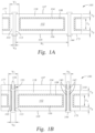
- FIG. 13 A schematically illustrates a cross-sectional view of a chip carrier structure including a semiconductor core assembly, according to an embodiment described herein.
- FIG. 13 B schematically illustrates a cross-sectional view of a PCB structure including a semiconductor core assembly, according to an embodiment described herein.
- FIG. 13 C schematically illustrates a cross-sectional view of a PCB structure including a semiconductor core assembly, according to an embodiment described herein.
- the present disclosure relates to semiconductor core assemblies and methods of forming the same.
- the semiconductor core assemblies described herein may be utilized to form semiconductor package assemblies, PCB assemblies, PCB spacer assemblies, chip carrier assemblies, intermediate carrier assemblies (e.g., for graphics cards), and the like.
- a silicon substrate core is structured by direct laser patterning. One or more conductive interconnections are formed in the substrate core and one or more redistribution layers are formed on surfaces thereof.
- the silicon substrate core may thereafter be utilized as a core structure for a semiconductor package, PCB, PCB spacer, chip carrier, intermediate carrier, or the like.
- the methods and apparatus disclosed herein include novel thin-form-factor semiconductor core structures intended to replace more conventional semiconductor package, PCB, and chip carrier structures utilizing glass fiber-filled epoxy frames.
- the scalability of current semiconductor packages, PCBs, spacers, and chip carriers is limited by the rigidity and lack of planarity of the materials typically utilized to form these various structures (e.g., epoxy molding compound, FR-4 and FR-5 grade woven fiberglass cloth with epoxy resin binders, and the like).
- the intrinsic properties of these materials cause difficulty in patterning and utilizing fine (e.g., micron scale) features formed therein.
- coefficient of thermal expansion (CTE) mismatch may occur between fiberglass frames, boards, molding compounds, and any chips disposed adjacent thereto. Therefore, current package, PCB, spacer, and carrier structures necessitate larger solder bumps with greater spacing to mitigate the effect of any warpage caused by CTE mismatch. Accordingly, conventional semiconductor package, PCB, spacer, and carrier frames are characterized by low through-structure electrical bandwidths, resulting in decreased overall power efficiency.
- the methods and apparatus disclosed herein provide semiconductor core structures that overcome many of the disadvantages associated with conventional semiconductor package, PCB, spacer, and carrier structures described above.
- FIGS. 1 A and 1 B illustrate cross-sectional views of a thin-form-factor semiconductor core assembly 100 according to some embodiments.
- the semiconductor core assembly 100 may be utilized for structural support and electrical interconnection of semiconductor packages mounted thereon.
- the semiconductor core assembly 100 may be utilized as a carrier structure for a surface-mounted device, such as a chip or graphics card.
- the semiconductor core assembly 100 generally includes a core structure 102 , an optional passivating layer 104 , and an insulating layer 118 .
- the core structure 102 includes a patterned (e.g., structured) substrate formed of any suitable substrate material.
- the core structure 102 includes a substrate formed from a III-V compound semiconductor material, silicon, crystalline silicon (e.g., Si ⁇ 100> or Si ⁇ 111>), silicon oxide, silicon germanium, doped or undoped silicon, doped or undoped polysilicon, silicon nitride, quartz, glass (e.g., borosilicate glass), sapphire, alumina, and/or ceramic materials.
- the core structure 102 includes a monocrystalline p-type or n-type silicon substrate.
- the core structure 102 includes a polycrystalline p-type or n-type silicon substrate.
- the core structure 102 includes a p-type or an n-type silicon solar substrate.
- the substrate utilized to form the core structure 102 may further have a polygonal or circular shape.
- the core structure 102 may include a substantially square silicon substrate having lateral dimensions between about 120 mm and about 180 mm, with or without chamfered edges.
- the core structure 102 may include a circular silicon-containing wafer having a diameter between about 20 mm and about 700 mm, such as between about 100 mm and about 50 mm, for example about 300 mm.
- the core structure 102 has a thickness T 1 between about 50 ⁇ m and about 1000 ⁇ m, such as a thickness T 1 between about 70 ⁇ m and about 800 ⁇ m.
- the core structure 102 has a thickness T 1 between about 80 ⁇ m and about 400 ⁇ m, such as a thickness T 1 between about 100 ⁇ m and about 200 ⁇ m.
- the core structure 102 has a thickness T 1 between about 70 ⁇ m and about 150 ⁇ m, such as a thickness T 1 between about 100 ⁇ m and about 130 ⁇ m.
- the core structure 102 has a thickness T 1 between about 700 ⁇ m and about 800 ⁇ m, such as a thickness T 1 between about 725 ⁇ m and about 775 ⁇ m.
- the core structure 102 further includes one or more holes or core vias 103 (hereinafter referred to as “core vias”) formed therein to enable conductive electrical interconnections to be routed through the core structure 102 .
- core vias 103 are substantially cylindrical in shape.
- the core vias 103 may be formed as singular and isolated core vias 103 through the core structure 102 or in one or more groupings or arrays.
- a minimum pitch Pi between each core via 103 is less than about 1000 ⁇ m, such as between about 25 ⁇ m and about 200 ⁇ m.
- the pitch Pi is between about 40 ⁇ m and about 150 ⁇ m.
- the one or more core vias 103 have a diameter V 1 less than about 500 ⁇ m, such as a diameter V 1 less than about 250 ⁇ m.
- the core vias 103 have a diameter V 1 between about 25 ⁇ m and about 100 ⁇ m, such as a diameter V 1 between about 30 ⁇ m and about 60 ⁇ m.
- the core vias 103 have a diameter V 1 of about 40 ⁇ m.
- the optional passivating layer 104 may be formed on one or more surfaces of the core structure 102 , including a first surface 106 , a second surface 108 , and one or more sidewalls of the core vias 103 .
- the passivating layer 104 is formed on substantially all exterior surfaces of the core structure 102 such that the passivating layer 104 substantially surrounds the core structure 102 .
- the passivating layer 104 provides a protective outer barrier for the core structure 102 against corrosion and other forms of damage.
- the passivating layer 104 is formed of an oxide film or layer, such as a thermal oxide layer.
- the passivating layer 104 has a thickness between about 100 nm and about 3 ⁇ m, such as a thickness between about 200 nm and about 2.5 ⁇ m. In one example, the passivating layer 104 has a thickness between about 300 nm and about 2 ⁇ m, such as a thickness of about 1.5 ⁇ m.
- the insulating layer 118 is formed on one or more surfaces of the core structure 102 or the passivating layer 104 and may substantially encase the passivating layer 104 and/or the core structure 102 . Thus, the insulating layer 118 may extend into the core vias 103 and coat the passivating layer 104 formed on the sidewalls thereof or directly coat the core structure 102 , thus defining the diameter V 2 as depicted in FIG. 1 A .
- the insulating layer 118 has a thickness T 2 from an outer surface of the core structure 102 or the passivating layer 104 to an adjacent outer surface of the insulating layer 118 (e.g., major surfaces 105 , 107 ) that is less than about 50 ⁇ m, such as a thickness T 2 less than about 20 ⁇ m.
- the insulating layer 118 has thickness T 2 between about 5 ⁇ m and about 10 ⁇ m.
- the insulating layer 118 is formed of polymer-based dielectric materials.
- the insulating layer 118 is formed from a flowable build-up material. Accordingly, although hereinafter referred to as an “insulating layer,” the insulating layer 118 may also be described as a dielectric layer.
- the insulating layer 118 is formed of an epoxy resin material having a ceramic filler, such as silica (SiO 2 ) particles.
- Ceramic fillers that may be utilized to form the insulating layer 118 include aluminum nitride (AlN), aluminum oxide (Al 2 O 3 ), silicon carbide (SiC), silicon nitride (Si 3 N 4 , Sr 2 Ce 2 Ti 5 O 16 , zirconium silicate (ZrSiO 4 ), wollastonite (CaSiO 3 ), beryllium oxide (BeO), cerium dioxide (CeO 2 ), boron nitride (BN), calcium copper titanium oxide (CaCu 3 Ti 4 O 12 ), magnesium oxide (MgO), titanium dioxide (TiO 2 ), zinc oxide (ZnO) and the like.
- AlN aluminum nitride
- Al 2 O 3 silicon carbide
- Si 3 N 4 silicon nitride
- ZrSiO 4 zirconium silicate
- wollastonite CaSiO 3
- BeO beryllium oxide
- CeO 2 cerium dioxide
- BN boron
- the ceramic fillers utilized to form the insulating layer 118 have particles ranging in size between about 40 nm and about 1.5 ⁇ m, such as between about 80 nm and about 1 ⁇ m.
- the ceramic fillers have particles ranging in size between about 200 nm and about 800 nm, such as between about 300 nm and about 600 nm.
- the ceramic fillers include particles having a size less than about 10% of the width or diameter of adjacent core vias 103 in the core structure 102 , such as a size less than about 5% of the width or diameter of the core vias 103 .
- through-assembly vias 113 are formed through the insulating layer 118 where the insulating layer 118 extends into the core vias 103 .
- the through-assembly vias 113 may be centrally formed within the core vias 103 having the insulating layer 118 disposed therein.
- the insulating layer 118 forms one or more sidewalls of the through-assembly vias 113 , wherein the through-assembly vias 113 have a diameter V 2 lesser than the diameter V 1 of the core vias 103 .
- the through-assembly vias 113 have a diameter V 2 less than about 100 ⁇ m, such as less than about 75 ⁇ m.
- the through-assembly vias 113 have a diameter V 2 less than about 50 ⁇ m, such as less than about 35 ⁇ m.
- the through-assembly vias 113 have a diameter of between about 25 ⁇ m and about 50 ⁇ m, such as a diameter of between about 35 ⁇ m and about 40 ⁇ m.
- the through-assembly vias 113 provide channels through which one or more electrical interconnections 144 are formed in the semiconductor core assembly 100 .
- the electrical interconnections 144 are formed through the entire thickness of the semiconductor core assembly 100 (i.e. from a first major surface 105 to a second major surface 107 of the semiconductor core assembly 100 ).
- the electrical interconnections 144 may have a longitudinal length corresponding to a total thickness of the semiconductor core assembly 100 between about 50 ⁇ m and about 1000 ⁇ m, such as a longitudinal length between about 200 ⁇ m and about 800 ⁇ m.
- the electrical interconnections 144 have a longitudinal length of between about 400 ⁇ m and about 600 ⁇ m, such as longitudinal length of about 500 ⁇ m.
- the electrical interconnections 144 are only formed through a portion of the thickness of the semiconductor core assembly 100 .
- the electrical interconnections 144 may protrude from a major surface of the semiconductor core assembly 100 , such as the major surfaces 105 , 107 as depicted in FIG. 1 A .
- the electrical interconnections 144 may be formed of any conductive materials used in the field of integrated circuits, circuit boards, chip carriers, and the like.
- the electrical interconnections 144 are formed of a metallic material, such as copper, aluminum, gold, nickel, silver, palladium, tin, or the like.
- the electrical interconnections 144 have a lateral thickness equal to the diameter V 2 of the through-assembly vias 113 in which they are formed.
- the semiconductor core assembly 100 further includes an adhesion layer 140 and/or a seed layer 142 formed thereon for electrical isolation of the electrical interconnections 144 .
- the adhesion layer 140 is formed on surfaces of the insulating layer 118 adjacent to the electrical interconnections 144 , including the sidewalls of the through-assembly vias 113 .
- the electrical interconnections 144 have a lateral thickness less than the diameter V 2 of the through-assembly vias 113 in which they are formed. In yet another embodiment, the electrical interconnections 144 only cover the surfaces of the sidewalls of the through-assembly vias 113 , and thus may have a hollow core therethrough.
- the adhesion layer 140 may be formed of any suitable materials, including but not limited to titanium, titanium nitride, tantalum, tantalum nitride, manganese, manganese oxide, molybdenum, cobalt oxide, cobalt nitride, and the like.
- the adhesion layer 140 has a thickness Bi between about 10 nm and about 300 nm, such as between about 50 nm and about 150 nm.
- the adhesion layer 140 has a thickness Bi between about 75 nm and about 125 nm, such as about 100 nm.
- the optional seed layer 142 comprises a conductive material, including but not limited to copper, tungsten, aluminum, silver, gold, or any other suitable materials or combinations thereof.
- the seed layer 142 may be formed on the adhesion layer 140 or directly on the sidewalls of the through-assembly vias 113 (e.g., on the insulating layer 118 without an adhesion layer therebetween).
- the seed layer 142 has a thickness between about 50 nm and about 500 nm, such as between about 100 nm and about 300 nm.
- the seed layer 142 has a thickness between about 150 nm and about 250 nm, such as about 200 nm.
- the semiconductor core assembly 100 further includes one or more redistribution layers 150 formed on a first side 175 and/or a second side 177 of the semiconductor core assembly 100 (the redistribution layer 150 is depicted as being formed on the second side 177 in FIG. 1 B ).
- the redistribution layer 150 is formed of substantially the same materials as the insulating layer 118 (e.g., polymer-based dielectric materials), and thus forms an extension thereof.
- the redistribution layer 150 is formed of a different material than the insulating layer 118 .
- the redistribution layer 150 may be formed of a photodefinable polyimide material, a non-photosensitive polyimide, polybenzoxazole (PBO), benzocyclobutene (BCB), silicon dioxide, and/or silicon nitride.
- the redistribution layer 150 is formed from a different inorganic dielectric material than the insulating layer 118 .
- the redistribution layer 150 has a thickness between about 5 ⁇ m and about 50 ⁇ m, such as a thickness between about 10 ⁇ m and about 40 ⁇ m.
- the redistribution layer 150 has a thickness between about 20 ⁇ m and about 30 ⁇ m, such as about 25 ⁇ m.
- the redistribution layer 150 may include one or more redistribution connections 154 formed through redistribution vias 153 for relocating contact points of the electrical interconnections 144 to desired locations on the surfaces of the semiconductor core assembly 100 , such as the major surfaces 105 , 107 .
- the redistribution layer 150 may further include one or more external electrical connections (not shown) formed on the major surfaces 105 , 107 , such as a ball grid array or solder balls.
- the redistribution vias 153 and the redistribution connections 154 have substantially similar or smaller lateral dimensions relative to the through-assembly vias 113 and the electrical interconnections 144 , respectively.
- the redistribution vias 153 have a diameter V 3 between about 2 ⁇ m and about 50 ⁇ m, such as a diameter V 3 between about 10 ⁇ m and about 40 ⁇ m, such as a diameter V 3 between about 20 ⁇ m and about 30 ⁇ m.
- the redistribution layer 150 may include the adhesion layer 140 and the seed layer 142 formed on surfaces adjacent to the redistribution connections 154 , including sidewalls of the redistribution vias 153 .
- FIG. 2 illustrates a flow diagram of a representative method 200 of forming a semiconductor core assembly.
- the method 200 has multiple operations 210 , 220 , 230 , and 240 . Each operation is described in greater detail with reference to FIGS. 3 - 12 L .
- the method may include one or more additional operations which are carried out before any of the defined operations, between two of the define operations, or after all the defined operations (except where the context excludes the possibility).
- the method 200 includes structuring a substrate to be utilized as a core structure (e.g., frame) at operation 210 , further described in greater detail with reference to FIGS. 3 and 4 A- 4 D .
- a core structure e.g., frame
- an insulating layer is formed on the core structure 102 , further described in greater detail with reference to FIGS. 5 , 6 A- 6 I, 7 , and 8 A- 8 E .
- one or more interconnections are formed through the core structure 102 and the insulating layer, further described in greater detail with reference to FIGS. 9 and 10 A- 10 H .
- a redistribution layer is formed on the insulating layer to relocate contact points of the interconnections to desired locations on a surface of an assembled core assembly and the core assembly is thereafter singulated.
- one or more additional redistribution layers may be formed in addition to the first redistribution layer, described in greater detail with reference to FIGS. 11 and 12 A- 12 L .
- FIG. 3 illustrates a flow diagram of a representative method 300 for structuring a substrate 400 to be utilized as a core structure.
- FIGS. 4 A- 4 D schematically illustrate cross-sectional views of a substrate 400 at various stages of the substrate structuring process 300 represented in FIG. 3 . Therefore, FIG. 3 and FIGS. 4 A- 4 D are herein described together for clarity.
- the substrate 400 is formed of any suitable substrate material including but not limited to a III-V compound semiconductor material, silicon, crystalline silicon (e.g., Si ⁇ 100> or Si ⁇ 111>), silicon oxide, silicon germanium, doped or undoped silicon, doped or undoped polysilicon, silicon nitride, quartz, glass material (e.g., borosilicate glass), sapphire, alumina, and/or ceramic material.
- the substrate 400 is a monocrystalline p-type or n-type silicon substrate.
- the substrate 400 is a multicrystalline p-type or n-type silicon substrate.
- the substrate 400 is a p-type or an n-type silicon solar substrate.
- the substrate 400 may further have a polygonal or circular shape.
- the substrate 400 may include a substantially square silicon substrate having lateral dimensions between about 140 mm and about 180 mm, with or without chamfered edges.
- the substrate 400 may include a circular silicon containing wafer having a diameter between about 20 mm and about 700 mm, such as between about 100 mm and about 500 mm, for example about 300 mm.
- embodiments and examples described herein are conducted on substrates having a thickness between about 50 ⁇ m and about 1000 ⁇ m, such as a thickness between about 90 ⁇ m and about 780 ⁇ m.
- the substrate 400 has a thickness between about 100 ⁇ m and about 300 ⁇ m, such as a thickness between about 110 ⁇ m and about 200 ⁇ m.
- the substrate 400 may be sliced and separated from a bulk material by wire sawing, scribing and breaking, mechanical abrasive sawing, or laser cutting. Slicing typically causes mechanical defects or deformities in substrate surfaces formed therefrom, such as scratches, micro-cracking, chipping, and other mechanical defects.
- the substrate 400 is exposed to a first damage removal process at operation 310 to smoothen and planarize surfaces thereof and remove mechanical defects in preparation for later structuring operations.
- the substrate 400 may further be thinned by adjusting the process parameters of the first damage process. For example, a thickness of the substrate 400 may be decreased with increased exposure to the first damage removal process.
- the first damage removal process at operation 310 includes exposing the substrate 400 to a substrate polishing process and/or an etch process followed by rinsing and drying processes.
- operation 310 includes a chemical mechanical polishing (CMP) process.
- the etch process is a wet etch process including a buffered etch process that is selective for the removal of a desired material (e.g., contaminants and other undesirable compounds).
- the etch process is a wet etch process utilizing an isotropic aqueous etch process. Any suitable wet etchant or combination of wet etchants may be used for the wet etch process.
- the substrate 400 is immersed in an aqueous HF etching solution for etching.
- the substrate 400 is immersed in an aqueous KOH etching solution for etching.
- the etching solution is heated to a temperature between about 30° C. and about 100° C. during the etch process, such as between about 40° C. and 90° C.
- the etching solution is heated to a temperature of about 70° C.
- the etch process at operation 310 is a dry etch process.
- An example of a dry etch process includes a plasma-based dry etch process.
- the thickness of the substrate 400 is modulated by controlling the time of exposure of the substrate 400 to the etchants (e.g., etching solution) utilized during the etch process. For example, a final thickness of the substrate 400 is reduced with increased exposure to the etchants. Alternatively, the substrate 400 may have a greater final thickness with decreased exposure to the etchants.
- the now planarized and substantially defect-free substrate 400 is patterned to form one or more core vias 403 therein (four core vias 403 are depicted in the cross-section of substrate 400 in FIG. 4 B ).
- the core vias 403 are utilized to form direct-contact electrical interconnections through the substrate 400 .
- the one or more core vias 403 may be formed by laser ablation (e.g. direct laser patterning). Any suitable laser ablation system may be utilized to form the one or more core vias 403 .
- the laser ablation system utilizes an infrared (IR) laser source.
- the laser source is a picosecond ultraviolet (UV) laser.
- the laser is a femtosecond UV laser.
- the laser source is a femtosecond green laser.
- the laser source of the laser ablation system generates a continuous or pulsed laser beam for patterning of the substrate 400 .
- the laser source may generate a pulsed laser beam having a frequency between 5 kHz and 500 kHz, such as between 10 kHz and about 200 kHz.
- the laser source is configured to deliver a pulsed laser beam at a wavelength between about 200 nm and about 1200 nm and a pulse duration between about 10 ns and about 5000 ns with an output power between about 10 Watts and about 100 Watts.
- the laser source is configured to form any desired pattern of features in the substrate 400 , including the core vias 403 .
- the substrate 400 is optionally coupled to a carrier plate (not shown) before being patterned.
- the optional carrier plate may provide mechanical support for the substrate 400 during patterning thereof and may prevent the substrate 400 from breaking.
- the carrier plate may be formed of any suitable chemically- and thermally-stable rigid material including but not limited to glass, ceramic, metal, or the like.
- the carrier plate has a thickness between about 1 mm and about 10 mm, such as between about 2 mm and about 5 mm.
- the carrier plate has a textured surface.
- the carrier plate has a polished or smoothened surface.
- the substrate 400 may be coupled to the carrier plate utilizing any suitable temporary bonding material, including but not limited to wax, glue, or similar bonding material.
- patterning the substrate 400 may cause unwanted mechanical defects in the surfaces of the substrate 400 , including chipping, cracking, and/or warping.
- the substrate 400 is exposed to a second damage removal and cleaning process at operation 330 substantially similar to the first damage removal process at operation 310 to smoothen the surfaces of the substrate 400 and remove unwanted debris.
- the second damage removal process includes exposing the substrate 400 to a wet or dry etch process, followed by rinsing and drying thereof. The etch process proceeds for a predetermined duration to smoothen the surfaces of the substrate 400 , and particularly the surfaces exposed to laser patterning operations.
- the etch process is utilized to remove any undesired debris remaining on the substrate 400 from the patterning process.
- the substrate 400 is exposed to a passivation process at operation 340 and FIG. 4 D to grow or deposit a passivating film or layer, such as oxide layer 404 , on desired surfaces thereof (e.g., all surfaces of the substrate 400 ).
- the passivation process is a thermal oxidation process.
- the thermal oxidation process is performed at a temperature between about 800° C. and about 1200° C., such as between about 850° C. and about 1150° C.
- the thermal oxidation process is performed at a temperature between about 900° C. and about 1100° C., such as a temperature between about 950° C. and about 1050° C.
- the thermal oxidation process is a wet oxidation process utilizing water vapor as an oxidant. In one embodiment, the thermal oxidation process is a dry oxidation process utilizing molecular oxygen as the oxidant. It is contemplated that the substrate 400 may be exposed to any suitable passivation process at operation 340 to form the oxide layer 404 or any other suitable passivating layer thereon.
- the resulting oxide layer 404 generally has a thickness between about 100 nm and about 3 ⁇ m, such as between about 200 nm and about 2.5 ⁇ m. For example, the oxide layer 404 has a thickness between about 300 nm and about 2 ⁇ m, such as about 1.5 ⁇ m
- FIGS. 5 and 7 illustrate flow diagrams of representative methods 500 and 700 , respectively, for forming an insulating layer 618 on the core structure 402 .
- FIGS. 6 A- 6 I schematically illustrate cross-sectional views of the core structure 402 at different stages of the method 500 depicted in FIG. 5
- FIGS. 8 A- 8 E schematically illustrate cross-sectional views of the core structure 402 at different stages of the method 700 depicted in FIG. 7 .
- FIG. 5 and FIGS. 6 A- 6 I are herein described together and FIG. 7 and FIGS. 8 A- 8 E are herein described together.
- the method 500 begins at operation 502 and FIG. 6 A wherein a first surface 406 of the core structure 402 at a first side 475 , now having the core vias 403 formed therein and the oxide layer 404 formed thereon, is placed on and affixed to a first insulating film 616 a .
- the first insulating film 616 a includes one or more layers formed of polymer-based dielectric materials.
- the first insulating film 616 a includes one or more layers formed of flowable build-up materials.
- the first insulating film 616 a includes a flowable epoxy resin layer 618 a .
- the epoxy resin layer 618 a has a thickness less than about 60 ⁇ m, such as between about 5 ⁇ m and about 50 ⁇ m.
- the epoxy resin layer 618 a has a thickness between about 10 ⁇ m and about 25 ⁇ m.
- the epoxy resin layer 618 a may be formed of a ceramic-filler-containing epoxy resin, such as an epoxy resin filled with (e.g., containing) silica (SiO 2 ) particles.
- ceramic fillers that may be used to form the epoxy resin layer 618 a and other layers of the insulating film 616 a include aluminum nitride (AlN), aluminum oxide (Al 2 O 3 ), silicon carbide (SiC), silicon nitride (Si 3 N 4 ), Sr 2 Ce 2 Ti 5 O 16 , zirconium silicate (ZrSiO 4 ), wollastonite (CaSiO 3 ), beryllium oxide (BeO), cerium dioxide (CeO 2 ), boron nitride (BN), calcium copper titanium oxide (CaCu 3 Ti 4 O 12 ), magnesium oxide (MgO), titanium dioxide (TiO 2 ), zinc oxide (ZnO) and the like.
- the ceramic fillers utilized to form the epoxy resin layer 618 a have particles ranging in size between about 40 nm and about 1.5 ⁇ m, such as between about 80 nm and about 1 ⁇ m.
- the ceramic fillers utilized to form the epoxy resin layer 618 a have particles ranging in size between about 200 nm and about 800 nm, such as between about 300 nm and about 600 nm.
- the first insulating film 616 a further includes one or more protective layers.
- the first insulating film 616 a includes a polyethylene terephthalate (PET) protective layer 622 a , such as a biaxial PET protective layer 622 a .
- PET polyethylene terephthalate
- the entire insulating film 616 a has a thickness less than about 120 ⁇ m, such as a thickness less than about 90 ⁇ m.
- the core structure 402 may then be placed on a carrier 624 adjacent the first side 475 thereof for additional mechanical stabilization during later processing operations.
- the carrier 624 is formed of any suitable mechanically and thermally stable material capable of withstanding temperatures above 100° C.
- the carrier 624 comprises polytetrafluoroethylene (PTFE).
- the carrier 624 is formed of polyethylene terephthalate (PET).
- a first protective film 660 is affixed to a second surface 408 on a second side 477 of the core structure 402 .
- the protective film 660 is coupled to the core structure 402 on the second side 477 and opposite of the first insulating film 616 a such that it covers the core vias 403 .
- the protective film 660 is formed of a material similar to that of the protective layer 622 a .
- the protective film 660 is formed of PET, such as biaxial PET.
- the protective film 660 may be formed of any suitable protective materials.
- the protective film 660 has a thickness between about 50 ⁇ m and about 150 ⁇ m.
- the core structure 402 now affixed to the insulating film 616 a at the first side 475 and the protective film 660 at the second side 477 , is exposed to a first lamination process at operation 506 .
- the core structure 402 is exposed to elevated temperatures, causing the epoxy resin layer 618 a of the insulating film 616 a to soften and flow into the open voids or volumes between the insulating film 616 a and the protective film 660 , such as into the core vias 403 .
- the core vias 403 become at least partially filled (e.g., occupied) with the insulating material of the epoxy resin layer 618 a , as depicted in FIG. 6 C .
- the core structure 402 becomes partially surrounded by the insulating material of the epoxy resin layer 618 a.
- the lamination process is a vacuum lamination process that may be performed in an autoclave or other suitable device. In one embodiment, the lamination process is performed by use of a hot pressing process. In one embodiment, the lamination process is performed at a temperature between about 80° C. and about 140° C. and for a period between about 1 minute and about 30 minutes. In some embodiments, the lamination process includes the application of a pressure between about 1 psig and about 150 psig while a temperature between about 80° C. and about 140° C. is applied to core structure 402 and insulating film 616 a for a period between about 1 minute and about 30 minutes.
- the lamination process is performed by applying a pressure between about 10 psig and about 100 psig, and a temperature between about 100° C. and about 120° C. for a period between about 2 minutes and 10 minutes.
- the lamination process is performed at a temperature of about 110° C. for a period of about 5 minutes.
- the protective film 660 is removed and the core structure 402 , now having the laminated insulating material of the epoxy resin layer 618 a at least partially surrounding the core structure 402 and partially filling the core vias 403 , is placed on a second protective film 662 .
- the second protective film 662 is coupled to the core structure 402 adjacent the first side 475 such that the second protective film 662 is disposed against (e.g., adjacent) the protective layer 622 a of the insulating film 616 a .
- the core structure 402 now coupled to the protective film 662 , may be optionally placed on the carrier 624 for additional mechanical support on the first side 475 .
- the protective film 662 is placed on the carrier 624 prior to coupling the protective film 662 with the core structure 402 .
- the protective film 662 is substantially similar in composition to the protective film 660 .
- the protective film 662 may be formed of PET, such as biaxial PET.
- the protective film 662 may be formed of any suitable protective materials.
- the protective film 662 has a thickness between about 50 ⁇ m and about 150 ⁇ m.
- a second insulating film 616 b substantially similar to the first insulating film 616 a is placed over the second side 477 at operation 510 and FIG. 6 E , thus replacing the protective film 660 .
- the second insulating film 616 b is positioned on the second side 477 of the core structure 402 such that an epoxy resin layer 618 b of the second insulating film 616 b covers the core vias 403 .
- the placement of the second insulating film 616 b on the core structure 402 may form one or more voids between the insulating film 616 b and the already-laminated insulating material of the epoxy resin layer 618 a that partially surrounds the core structure 402 and partially fills the core vias 403 .
- the second insulating film 616 b may include one or more layers formed of polymer-based dielectric materials similar to the insulating film 616 a . As depicted in FIG. 6 E , the second insulating film 616 b includes an epoxy resin layer 618 b substantially similar to the epoxy resin layer 618 a described above.
- the second insulating film 616 b may further include a protective layer 622 b formed of similar materials to the protective layer 622 a , such as PET.
- a third protective film 664 is placed over the second insulating film 616 b , as depicted in FIG. 6 F .
- the protective film 664 is substantially similar in composition to the protective films 660 , 662 .
- the protective film 664 is formed of PET, such as biaxial PET.
- the protective film 664 may be formed of any suitable protective materials.
- the protective film 664 has a thickness between about 50 ⁇ m and about 150 ⁇ m.
- the core structure 402 now affixed to the insulating film 616 b and the protective film 664 on the second side 477 and the protective film 662 and the optional carrier 624 on the first side 475 , is exposed to a second lamination process at operation 514 and FIG. 6 G . Similar to the lamination process at operation 504 , the core structure 402 is exposed to elevated temperatures, causing the epoxy resin layer 618 b of the insulating film 616 b to soften and flow into any open voids or volumes between the insulating film 616 b and the already-laminated insulating material of the epoxy resin layer 618 a , thus integrating itself with the insulating material of the epoxy resin layer 618 a . Accordingly, the core vias 403 become completely filled (e.g. packed, sealed) with insulating material of both epoxy resin layers 618 a , 618 b.
- the second lamination process is a vacuum lamination process that may be performed in an autoclave or other suitable device.
- the lamination process is performed by use of a hot pressing process.
- the lamination process is performed at a temperature between about 80° C. and about 140° C. and for a period between about 1 minute and about 30 minutes.
- the lamination process includes the application of a pressure between about 1 psig and about 150 psig while a temperature between about 80° C. and about 140° C. is applied to the core structure 402 and the insulating film 616 a for a period between about 1 minute and about 30 minutes.
- the lamination process is performed by applying a pressure between about 10 psig and about 100 psig, and a temperature between about 100° C. and about 120° C. for a period between about 2 minutes and 10 minutes.
- the lamination process is performed at a temperature of about 110° C. for a period of about 5 minutes.
- the core structure 402 is disengaged from the carrier 624 at operation 516 and the protective films 662 , 664 are removed, resulting in a laminated intermediate core assembly 602 .
- the intermediate core assembly 602 includes the core structure 402 having one or more core vias 403 formed therethrough and filled with the insulating dielectric material of the insulating films 616 a , 616 b .
- the insulating dielectric material of the epoxy resin layers 618 a , 618 b further encases the core structure 402 having the oxide layer 404 formed thereon such that the insulating material covers at least two surfaces or sides of the core structure 402 (e.g., surfaces 406 , 408 ).
- the protective layers 622 a , 622 b are also removed from the intermediate core assembly 602 at operation 516 .
- the protective layers 622 a and 622 b , the carrier 624 , and the protective films 662 and 664 are removed from the intermediate core assembly 602 by any suitable mechanical processes such as peeling therefrom.
- the intermediate core assembly 602 Upon removal of the protective layers 622 a , 622 b and the protective films 662 , 664 , the intermediate core assembly 602 is exposed to a cure process to fully cure (i.e. harden through chemical reactions and cross-linking) the insulating dielectric material of the epoxy resin layers 618 a , 618 b , thus forming an insulating layer 618 .
- the insulating layer 618 substantially surrounds the core structure 402 and fills the core vias 403 .
- the insulating layer 618 contacts or encapsulates at least the 107 , 477 of the core structure 402 (including surfaces 406 , 408 ).
- the cure process is performed at high temperatures to fully cure the intermediate core assembly 602 .
- the cure process is performed at a temperature between about 140° C. and about 220° C. and for a period between about 15 minutes and about 45 minutes, such as a temperature between about 160° C. and about 200° C. and for a period between about 25 minutes and about 35 minutes.
- the cure process is performed at a temperature of about 180° C. for a period of about 30 minutes.
- the cure process at operation 516 is performed at or near ambient (e.g. atmospheric) pressure conditions.
- one or more through-assembly vias 613 are drilled through the intermediate core assembly 602 at operation 518 , forming channels through the entire thickness of the intermediate core assembly 602 for subsequent interconnection formation.
- the intermediate core assembly 602 may be placed on a carrier, such as the carrier 624 , for mechanical support during the formation of the through-assembly vias 613 .
- the through-assembly vias 613 are drilled through the core vias 403 that were formed in the core structure 402 and subsequently filled with the insulating layer 618 .
- the through-assembly vias 613 may be circumferentially surrounded by the insulating layer 618 filled within the core vias 403 .
- the ceramic-filler-containing epoxy resin material of the insulating layer 618 By having the ceramic-filler-containing epoxy resin material of the insulating layer 618 line the walls of the core vias 403 , capacitive coupling between the conductive silicon-based core structure 402 and interconnections 1044 (described with reference to FIG. 9 and FIGS. 10 A- 10 H ) in the completed (e.g., final) semiconductor core assembly 1270 (described with reference to FIG. 11 and FIGS. 12 K and 12 L ) is significantly reduced as compared to other conventional interconnecting structures that utilize conventional via-insulating liners or films. Furthermore, the flowable nature of the epoxy resin material of the insulating layer 618 enables more consistent and reliable encapsulation and insulation, thus enhancing electrical performance by minimizing leakage current of the completed semiconductor core assembly 1270 .
- the through-assembly vias 613 have a diameter less than about 100 ⁇ m, such as less than about 75 ⁇ m.
- the through-assembly vias 613 have a diameter less than about 50 ⁇ m, such as less than about 35 ⁇ m.
- the through-assembly vias 613 have a diameter between about 25 ⁇ m and about 50 ⁇ m, such as a diameter between about 35 ⁇ m and about 40 ⁇ m.
- the through assembly vias 613 are formed using any suitable mechanical process.
- the through-assembly vias 613 are formed using a mechanical drilling process.
- through-assembly vias 613 are formed through the intermediate core assembly 602 by laser ablation.
- the through-assembly vias 613 are formed using an ultraviolet laser.
- the laser source utilized for laser ablation has a frequency between about 5 kHz and about 500 kHz.
- the laser source is configured to deliver a pulsed laser beam at a pulse duration between about 10 ns and about 100 ns with a pulse energy between about 50 microjoules ( ⁇ J) and about 500 ⁇ J.
- Utilizing an epoxy resin material containing small ceramic filler particles further promotes more precise and accurate laser patterning of small-diameter vias, such as the through-assembly vias 613 , as the small ceramic filler particles therein exhibit reduced laser light reflection, scattering, diffraction, and transmission of the laser light away from the area in which the via is to be formed during the laser ablation process.
- the through-assembly vias 613 are formed within (e.g., through) the core vias 403 in such a way that the remaining ceramic-filler-containing epoxy resin material (e.g., dielectric insulating material) on the sidewalls of the core vias 403 has an average thickness between about 1 ⁇ m and about 50 ⁇ m.
- the remaining ceramic-filler-containing epoxy resin material on the sidewalls of the core vias 403 has an average thickness between about 5 ⁇ m and about 40 ⁇ m, such as between about 10 ⁇ m and about 30 ⁇ m.
- the resulting structure after formation of the through-assembly vias 613 may be described as a “via-in-via” (e.g., a via centrally formed in a dielectric material within a via of the core structure).
- the via-in-via structure includes a dielectric sidewall passivation consisting of a ceramic-particle-filled epoxy material and disposed on a thin layer of thermal oxide formed on the sidewalls of the core vias 403 .
- the intermediate core assembly 602 is exposed to a de-smear process.
- any unwanted residues and/or debris caused by laser ablation during the formation of the through-assembly vias 613 are removed therefrom.
- the de-smear process thus cleans the through-assembly vias 613 for subsequent metallization.
- the de-smear process is a wet de-smear process. Any suitable solvents, etchants, and/or combinations thereof may be utilized for the wet de-smear process.
- methanol may be utilized as a solvent and copper (II) chloride dihydrate (CuCl 2 ⁇ H 2 O) as an etchant.
- CuCl 2 ⁇ H 2 O copper (II) chloride dihydrate
- exposure duration of the intermediate core assembly 602 to the wet de-smear process may be varied.
- the de-smear process is a dry de-smear process.
- the de-smear process may be a plasma de-smear process with an O 2 /CF 4 mixture gas.
- the plasma de-smear process may include generating a plasma by applying a power of about 700 W and flowing O 2 :CF 4 at a ratio of about 10:1 (e.g., 100:10 sccm) for a time period between about 60 seconds and about 120 seconds.
- the de-smear process is a combination of wet and dry processes.
- the intermediate core assembly 602 is ready for formation of interconnection paths therein, described below with reference to FIG. 9 and FIGS. 10 A- 10 H .
- FIG. 5 and FIGS. 6 A- 6 I illustrate a representative method 500 for forming the intermediate core assembly 602 .
- FIG. 7 and FIGS. 8 A- 8 E illustrate an alternative method 700 substantially similar to the method 500 but with fewer operations.
- the method 700 generally includes five operations 710 - 750 .
- operations 710 , 740 , and 750 of the method 700 are substantially similar to the operations 502 , 516 , and 518 of the method 500 , respectively.
- FIGS. 8 B, 8 C, and 8 D are herein described for clarity.
- a second insulating film 616 b is coupled to the second surface 408 on the opposing side 477 at operation 720 and FIG. 8 B .
- the second insulating film 616 b is positioned on the surface 408 of the core structure 402 such that the epoxy resin layer 618 b of the second insulating film 616 b covers all of the core vias 403 .
- the core vias 403 form one or more voids or gaps between the insulating films 616 a and 616 b .
- a second carrier 625 is affixed to the protective layer 622 b of the second insulating film 616 b for additional mechanical support during later processing operations.
- the core structure 402 now affixed to the insulating films 616 a and 616 b on opposing sides thereof, is exposed to a single lamination process.
- the core structure 402 is exposed to elevated temperatures, causing the epoxy resin layers 618 a and 618 b of both insulating films 616 a , 616 b to soften and flow into the open voids or volumes created by the core vias 403 between the insulating films 616 a , 616 b . Accordingly, the core vias 403 become filled with the insulating material of the epoxy resin layers 618 a and 618 b.
- the lamination process at operation 730 may be a vacuum lamination process that may be performed in an autoclave or other suitable device.
- the lamination process is performed by use of a hot pressing process.
- the lamination process is performed at a temperature between about 80° C. and about 140° C. and for a period between about 1 minute and about 30 minutes.
- the lamination process includes the application of a pressure between about 1 psig and about 150 psig while a temperature between about 80° C. and about 140° C.
- the lamination process is applied to core structure 402 and the insulating films 616 a , 616 b for a period between about 1 minute and about 30 minutes.
- the lamination process is performed at a pressure between about 10 psig and about 100 psig, a temperature between about 100° C. and about 120° C., and for a period between about 2 minutes and 10 minutes.
- the lamination process at operation 730 is performed at a temperature of about 110° C. for a period of about 5 minutes.
- the one or more protective layers of the insulating films 616 a , 616 b are removed from the core structure 402 , resulting in the laminated intermediate core assembly 602 .
- the protective layers 622 a , 622 b are removed from the core structure 402 , and thus the intermediate core assembly 602 is also disengaged from the first and second carriers 624 , 625 .
- the protective layers 622 a , 622 b and the carriers 624 , 625 are removed by any suitable mechanical processes such as peeling therefrom. As depicted in FIG.
- the intermediate core assembly 602 includes the core structure 402 having one or more core vias 403 formed therein and filled with the insulating dielectric material of the epoxy resin layers 618 a , 618 b .
- the insulating material further encases the core structure 402 such that the insulating material covers at least two surfaces or sides of the core structure 402 , for example, the surfaces 406 , 408 .
- the intermediate core assembly 602 Upon removal of the protective layers 622 a , 622 b , the intermediate core assembly 602 is exposed to a cure process to fully cure the insulating dielectric material of the epoxy resin layers 618 a , 618 b . Curing of the insulating material results in the formation of the insulating layer 618 . As depicted in FIG. 8 D and similar to operation 516 corresponding with FIG. 6 H , the insulating layer 618 substantially surrounds the core structure 402 and fills the core vias 403 .
- the cure process is performed at high temperatures to fully cure the intermediate core assembly 602 .
- the cure process is performed at a temperature between about 140° C. and about 220° C. and for a period between about 15 minutes and about 45 minutes, such as a temperature between about 160° C. and about 200° C. and for a period between about 25 minutes and about 35 minutes.
- the cure process is performed at a temperature of about 180° C. for a period of about 30 minutes.
- the cure process at operation 740 is performed at or near ambient (e.g. atmospheric) pressure conditions.
- the method 700 is substantially similar to operation 520 of the method 500 . Accordingly, one or more through-assembly vias 613 are drilled through the intermediate core assembly 602 , followed by exposing the intermediate core assembly 602 to a de-smear process. Upon completion of the de-smear process, the intermediate core assembly 602 is ready for formation of interconnection paths therein, as described below.
- FIG. 9 illustrates a flow diagram of a representative method 900 for forming electrical interconnections through the intermediate core assembly 602 .
- FIGS. 10 A- 10 H schematically illustrate cross-sectional views of the intermediate core assembly 602 at different stages of the process of the method 900 depicted in FIG. 9 .
- FIG. 9 and FIGS. 10 A- 10 H are herein described together for clarity.
- the electrical interconnections formed through the intermediate core assembly 602 are formed of copper.
- the method 900 generally begins at operation 910 and FIG. 10 A wherein the intermediate core assembly 602 , having through-assembly vias 613 formed therein, has a barrier or adhesion layer 1040 and/or a seed layer 1042 formed thereon.
- An enlarged partial view of the adhesion layer 1040 and the seed layer 1042 formed on the intermediate core assembly 602 is depicted in FIG. 10 H for reference.
- the adhesion layer 1040 may be formed on desired surfaces of the insulating layer 618 , such as surfaces corresponding with the major surfaces 1005 , 1007 of the intermediate core assembly 602 as well as sidewalls of the through-assembly vias 613 , to assist in promoting adhesion and blocking diffusion of the subsequently formed seed layer 1042 and electrical interconnections 1044 .
- the adhesion layer 1040 acts as an adhesion layer; in another embodiment, the adhesion layer 1040 acts as a barrier layer. In both embodiments, however, the adhesion layer 1040 will be hereinafter described as an “adhesion layer.”
- the adhesion layer 1040 is formed of titanium, titanium nitride, tantalum, tantalum nitride, manganese, manganese oxide, molybdenum, cobalt oxide, cobalt nitride, or any other suitable materials or combinations thereof.
- the adhesion layer 1040 has a thickness between about 10 nm and about 300 nm, such as between about 50 nm and about 150 nm.
- the adhesion layer 1040 has a thickness between about 75 nm and about 125 nm, such as about 100 nm.
- the adhesion layer 1040 is formed by any suitable deposition process, including but not limited to chemical vapor deposition (CVD), physical vapor deposition (PVD), plasma enhanced CVD (PECVD), atomic layer deposition (ALD), or the like.
- the seed layer 1042 may be formed on the adhesion layer 1040 or directly on the insulating layer 618 (e.g., without the formation of the adhesion layer 1040 ). In some embodiments, the seed layer 1042 is formed on all surfaces of the insulating layer 618 while the adhesion layer 1040 is only formed on desired surfaces or desired portions of surfaces of the insulating layer 618 . For example, the adhesion layer 1040 may be formed on the major surfaces 1005 , 1007 and not on the sidewalls of the through-assembly vias 613 while the seed layer 1042 is formed on the major surfaces 1005 , 1007 as well as sidewalls of the through-assembly vias 613 .
- the seed layer 1042 is formed of a conductive material such as copper, tungsten, aluminum, silver, gold, or any other suitable materials or combinations thereof.
- the seed layer 1042 has a thickness between about 0.05 ⁇ m and about 0.5 ⁇ m, such as a thickness between about 0.1 ⁇ m and about 0.3 ⁇ m.
- the seed layer 1042 has a thickness between about 0.15 ⁇ m and about 0.25 ⁇ m, such as about 0.2 ⁇ m.
- the seed layer 1042 has a thickness between about 0.1 ⁇ m and about 1.5 ⁇ m.
- the seed layer 1042 is formed by any suitable deposition process, such as CVD, PVD, PECVD, ALD dry processes, wet electroless plating processes, or the like.
- a copper seed layer 1042 may be formed on a molybdenum adhesion layer 1040 on the intermediate core assembly 602 .
- the molybdenum adhesion and copper seed layer combination enables improved adhesion with the surfaces of the insulating layer 618 and reduces undercut of conductive interconnect lines during a subsequent seed layer etch process at operation 970 .
- a spin-on/spray-on or dry resist film 1050 such as a photoresist, is applied to both major surfaces 1005 , 1007 of the intermediate core assembly 602 and subsequently patterned.
- the resist film 1050 is patterned via selective exposure to UV radiation.
- an adhesion promoter (not shown) is applied to the intermediate core assembly 602 prior to formation of the resist film 1050 .
- the adhesion promoter improves adhesion of the resist film 1050 to the intermediate core assembly 602 by producing an interfacial bonding layer for the resist film 1050 and by removing any moisture from the surface of the intermediate core assembly 602 .
- the adhesion promoter is formed of bis(trimethylsilyl)amine or hexamethyldisilizane (HMDS) and propylene glycol monomethyl ether acetate (PGMEA).
- the intermediate core assembly 602 is exposed to a resist film development process.
- development of the resist film 1050 results in exposure of the through-assembly vias 613 , which may now have an adhesion layer 1040 and/or a seed layer 1042 formed thereon.
- the film development process is a wet process, such as a wet process that includes exposing the resist film 1050 to a solvent.
- the film development process is a wet etch process utilizing an aqueous etch process.
- the film development process is a wet etch process utilizing a buffered etch process selective for a desired material. Any suitable wet solvents or combination of wet etchants may be used for the resist film development process.
- electrical interconnections 1044 are formed through the exposed through-assembly vias 613 and the resist film 1050 is thereafter removed.
- the interconnections 1044 are formed by any suitable methods, including electroplating and electroless plating.
- the resist film 1050 is removed via a wet process.
- the electrical interconnections 1044 may completely fill the through-assembly vias 613 and protrude from the surfaces 1005 , 1007 of the intermediate core assembly 602 upon removal of the resist film 1050 .
- the electrical interconnections 1044 may only line the sidewalls of the through-assembly vias 613 without completely filling the through-assembly vias 613 .
- the electrical interconnections 1044 are formed of copper.
- the electrical interconnections 1044 may be formed of any suitable conductive material including but not limited to aluminum, gold, nickel, silver, palladium, tin, or the like.
- the intermediate core assembly 602 having electrical interconnections 1044 formed therein is exposed to a seed layer etch process to remove the exposed adhesion layer 1040 and seed layer 1042 on external surfaces thereof (e.g., surfaces 1005 , 1007 ).
- the adhesion layer 1040 and/or seed layer 1042 formed between the electrical interconnections 1044 and the sidewalls of the through-assembly vias 613 may remain after the seed layer etch process.
- the seed layer etch is a wet etch process including a rinse and drying of the intermediate core assembly 602 .
- the seed layer etch process is a buffered etch process selective for a desired material such as copper, tungsten, aluminum, silver, or gold.
- the etch process is an aqueous etch process. Any suitable wet etchant or combination of wet etchants may be used for the seed layer etch process.
- one or more semiconductor core assemblies may be singulated from the intermediate core assembly 602 and utilized as a fully-functional electronic mounting or package structure.
- the one or more semiconductor core assemblies may be singulated and utilized as circuit board structures, chip carrier structures, integrated circuit packages, and the like.
- the intermediate core assembly 602 may have one or more redistribution layers 1260 (shown in FIGS. 12 J and 12 K ) formed thereon to reroute external contact points of the electrical interconnections 1044 to desired locations on the surfaces of the final semiconductor core assemblies.
- FIG. 11 illustrates a flow diagram of a representative method 1100 of forming a redistribution layer 1260 on the intermediate core assembly 602 .
- FIGS. 12 A- 12 K schematically illustrate cross-sectional views of the intermediate core assembly 602 at different stages of the method 1100 depicted in FIG. 11 .
- FIG. 11 and FIGS. 12 A- 12 K are herein described together for clarity.
- the method 1100 is substantially similar to the methods 500 , 700 , and 900 described above. Generally, the method 1100 begins at operation 1102 and FIG. 12 A , wherein an insulating film 1216 is affixed to the intermediate core assembly 602 and is thereafter laminated.
- the insulating film 1216 is substantially similar to the insulating films 616 a , 616 b .
- the insulating film 1216 includes an epoxy resin layer 1218 and one or more protective layers.
- the insulating film 1216 may include a protective layer 1222 . Any suitable combination of layers and insulating materials is contemplated for the insulating film 1216 .
- an optional carrier 1224 is coupled to the insulating film 1216 for added support.
- a protective film (not shown) may be coupled to the insulating film 1216 .
- the epoxy resin layer 1218 has a thickness of less than about 60 ⁇ m, such as between about 5 ⁇ m and about 50 ⁇ m.
- the epoxy resin layer 1218 has a thickness of between about 10 ⁇ m and about 25 ⁇ m.
- the epoxy resin layer 1218 and the PET protective layer 1222 have a combined thickness of less than about 120 ⁇ m, such as a thickness of less than about 90 ⁇ m.
- the insulating film 1216 , and specifically the epoxy resin layer 1218 is affixed to a surface of the intermediate core assembly 602 having exposed electrical interconnections 1044 , such as the major surface 1005 .
- the intermediate core assembly 602 is exposed to a lamination process substantially similar to the lamination process described with regard to operations 506 , 514 , and 730 .
- the intermediate core assembly 602 is exposed to elevated temperatures to soften the epoxy resin layer 1218 of the insulating film 1216 , which subsequently bonds to the insulating layer 618 .
- the epoxy resin layer 1218 becomes integrated with the insulating layer 618 and forms an extension thereof, and will thus be described hereinafter as a singular insulating layer 618 .
- the integration of the epoxy resin layer 1218 and the insulating layer 618 further results in an enlarged insulating layer 618 enveloping the previously exposed electrical interconnections 1044 .
- the protective layer 1222 and the carrier 1224 are removed from the intermediate core assembly 602 by mechanical means, and the intermediate core assembly 602 is exposed to a cure process to fully harden the newly expanded insulating layer 618 .
- the cure process is substantially similar to the cure process described with reference to operations 516 and 740 .
- the cure process is performed at a temperature between about 140° C. and about 220° C. and for a period between about 15 minutes and about 45 minutes.
- the intermediate core assembly 602 is then selectively patterned by laser ablation at operation 1106 and FIG. 12 C .
- the laser ablation process at operation 1106 forms one or more redistribution vias 1253 in the newly expanded insulating layer 618 and exposes desired electrical interconnections 1044 for redistribution of contact points thereof.
- the redistribution vias 1253 have a diameter substantially similar to or smaller than the diameter of the through-assembly vias 613 .
- the redistribution vias 1253 have a diameter between about 5 ⁇ m and about 600 ⁇ m, such as a diameter of between about 10 ⁇ m and about 50 ⁇ m, such as between about 20 ⁇ m and about 30 ⁇ m.
- the laser ablation process at operation 1106 is performed utilizing a CO 2 laser. In one embodiment, the laser ablation process at operation 1106 is performed utilizing a UV laser. In another embodiment, the laser ablation process at operation 1106 is performed utilizing a green laser.
- the laser source may generate a pulsed laser beam having a frequency between about 100 kHz and about 1000 kHz. In one example, the laser source is configured to deliver a pulsed laser beam at a wavelength of between about 100 nm and about 2000 nm, at a pulse duration between about 10E-4 ns and about 10E-2 ns, and with a pulse energy of between about 10 ⁇ J and about 300 ⁇ J.
- an adhesion layer 1240 and/or a seed layer 1242 are optionally formed on one or more surfaces of the insulating layer 618 .
- the adhesion layer 1240 and the seed layer 1242 are substantially similar to the adhesion layer 1040 and the seed layer 1042 , respectively.
- the adhesion layer 1240 is formed from titanium, titanium nitride, tantalum, tantalum nitride, manganese, manganese oxide, molybdenum, cobalt oxide, cobalt nitride, or any other suitable materials or combinations thereof.
- the adhesion layer 1240 has a thickness between about 10 nm and about 300 nm, such as a thickness between about 50 nm and about 150 nm.
- the adhesion layer 1240 has a thickness between about 75 nm and about 125 nm, such as about 100 nm.
- the adhesion layer 1240 may be formed by any suitable deposition process, including but not limited to CVD, PVD, PECVD, ALD, or the like.
- the seed layer 1242 is formed from a conductive material such as copper, tungsten, aluminum, silver, gold, or any other suitable materials or combinations thereof.
- the seed layer 1242 has a thickness between about 0.05 ⁇ m and about 0.5 ⁇ m, such as between about 0.1 ⁇ m and about 0.3 ⁇ m.
- the seed layer 1242 has a thickness between about 0.15 ⁇ m and about 0.25 ⁇ m, such as about 0.2 ⁇ m.
- the seed layer 1242 may be formed by any suitable deposition process, such as CVD, PVD, PECVD, ALD dry processes, wet electroless plating processes, or the like.
- a molybdenum adhesion layer 1240 and a copper seed layer 1242 are formed on the intermediate core assembly 602 to reduce the formation of undercut during a subsequent seed layer etch process at operation 1122 .
- a spin-on/spray-on or dry resist film 1250 such as a photoresist is applied over the seeded surfaces of the intermediate core assembly 602 and subsequently patterned and developed.
- an adhesion promoter (not shown) is applied to the intermediate core assembly 602 prior to placement of the resist film 1250 .
- the exposure and development of the resist film 1250 results in opening of the redistribution vias 1253 .
- patterning of the resist film 1250 may be performed by selectively exposing portions of the resist film 1250 to UV radiation, and subsequent development of the resist film 1250 by a wet process, such as a wet etch process.
- the resist film development process is a wet etch process utilizing a buffered etch process selective for a desired material.
- the resist film development process is a wet etch process utilizing an aqueous etch process. Any suitable wet etchant or combination of wet etchants may be used for the resist film development process.
- redistribution connections 1244 are formed through the exposed redistribution vias 1253 and the resist film 1250 is thereafter removed.
- the resist film 1250 is removed via a wet process.
- the redistribution connections 1244 fill the redistribution vias 1253 and protrude from the surfaces of the intermediate core assembly 602 upon removal of the resist film 1250 .
- the redistribution connections 1244 are formed of copper.
- the redistribution connections 1244 are formed of any suitable conductive material including but not limited to aluminum, gold, nickel, silver, palladium, tin, or the like. Any suitable methods may be utilized to form the redistribution connections 1244 , including electroplating and electroless deposition.
- the intermediate core assembly 602 having the redistribution connections 1244 formed thereon is exposed to a seed layer etch process substantially similar to that of operation 970 .
- the seed layer etch is a wet etch process including a rinse and drying of the intermediate core assembly 602 .
- the seed layer etch process is a wet etch process utilizing a buffered etch process selective for a desired material of the seed layer 1242 .
- the etch process is a wet etch process utilizing an aqueous etch process. Any suitable wet etchant or combination of wet etchants may be used for the seed layer etch process.
- one or more additional redistribution layers 1260 may be formed on the intermediate core assembly 602 utilizing the sequences and processed described above.
- one or more additional redistribution layers 1260 may be formed on the first redistribution layer 1260 and/or an opposing surface of the intermediate core assembly 602 , such as major surface 1007 .
- the one or more additional redistribution layers 1260 may be formed of polymer-based dielectric materials, such as a flowable build-up materials, that are different from the material of the first redistribution layer 1260 and/or the insulating layer 618 .
- the insulating layer 618 may be formed of an epoxy filled with ceramic fibers, while the first and/or any additional redistribution layers 1260 are formed of polyimide, BCB, and/or PBO.
- one or more completed semiconductor core assemblies 1270 may be singulated from the intermediate core assembly 602 after a desired number of redistribution layers 1260 is formed.
- the completed semiconductor core assemblies 1270 formed at operation 1120 may be utilized in any suitable package assembly, PCB assembly, PCB spacer assembly, chip carrier assembly, intermediate carrier assembly, and the like.
- a single semiconductor core assembly 1270 is utilized as a carrier for a chip 1360 in a chip carrier assembly 1300 .
- the chip 1360 may be any suitable type of chip, including a memory chip, a microprocessor, a complex system-on-a-chip (SoC), or a standard chip. Suitable types of memory chips include DRAM chips or NAND flash chips.
- the chip 1360 is a digital chip, an analog chip, or a mixed chip.
- the chip 1360 is disposed adjacent to one of the major surfaces 1005 , 1007 of the semiconductor core assembly 1270 .
- two or more chips 1360 may be disposed adjacent to a single major surface 1005 , 1007 .
- one or additional devices and/or structures may be disposed adjacent to the chip 1360 , such as one or more components of a PCB or a package substrate.
- one or more passives may be disposed adjacent to the chip 1360 , such as capacitors, resistors, inductors and the like.
- one or more connectors may be disposed adjacent to the chip 1360 .
- the chip 1360 includes one or more contacts 1348 formed on an active surface 1352 thereof. As depicted, the contacts 1348 are conductively coupled to one or more redistribution connections 1244 of the semiconductor core assembly 1270 by one of more solder bumps 1346 disposed between the active surface 1352 and the major surface 1005 . In some embodiments, the contacts 1348 may be conductively coupled to the one or more interconnections 1044 by the one or more solder bumps 1346 . In one embodiment, the contacts 1348 and/or the solder bumps 1346 are formed of a substantially similar material to that of the interconnections 1044 and the redistribution connections 1244 . For example, the contacts 1348 and the solder bumps 1346 may be formed of a conductive material such as copper, tungsten, aluminum, silver, gold, or any other suitable materials or combinations thereof.
- the solder bumps 1346 include C4 solder bumps. In one embodiment, the solder bumps 1346 include C2 (Cu-pillar with a solder cap) solder bumps. Utilization of C2 solder bumps may enable smaller pitch lengths and improved thermal and/or electrical properties for the chip carrier assembly 1300 .
- the solder bumps 1346 may be formed by any suitable wafer bumping processes, including but not limited to electrochemical deposition (ECD) and electroplating.
- a semiconductor core assembly 1270 is utilized in a PCB assembly 1302 .
- the semiconductor core assembly 1270 is configured to function as a PCB structure for supporting (e.g., carrying) a package assembly 1310 .
- the package assembly 1310 may be substantially similar in structure and material to the semiconductor core assembly 1270 , but includes an embedded die 1326 disposed within a cavity 1320 formed within the core structure 402 that is substantially surrounded by the insulating layer 618 .
- the embedded die 1326 may further include an active surface 1328 having one or more contacts 1330 formed thereon and coupled with interconnections 1342 and/or redistribution connections 1344 of the package assembly 1310 . Similar to the chip carrier assembly 1300 in FIG.
- the contacts 1330 and/or interconnections 1342 and/or redistribution connections 1344 of the package assembly 1310 are conductively coupled to the one or more redistribution connections 1244 of the semiconductor core assembly 1270 by the one of more solder bumps 1346 disposed between the active surface 1328 and the major surface 1005 .
- the contacts 1330 may be conductively coupled to the one or more interconnections 1044 by the one or more solder bumps 1346 .
- FIG. 13 C depicts yet another exemplary embodiment utilizing the semiconductor core assembly 1270 as a PCB spacer structure in a PCB assembly 1304 .
- the semiconductor core assembly 1270 is disposed between two PCB's 1362 a , 1362 b and configured to position the first PCB 1362 a relative to the second PCB 1362 b such that a physical space remains between the first PCB 1362 a and the second PCB 1362 b while they are conductively connected.
- the PCB's 1362 a , 1362 b include one or more electrically conductive pads 1368 formed on major surfaces 1364 a , 1364 b thereof, respectively.
- the one or more conductive pads 1368 are conductively coupled to the redistribution connections 1244 and/or interconnections 1044 of the semiconductor core assembly 1270 via the one or more solder bumps 1346 . Similar the contacts 1330 , 1348 , the conductive pads 1368 are formed of a substantially similar material to that of the solder bumps 1346 , interconnections 1044 , and the redistribution connections 1244 to enable electrical conductivity therethrough. For example, the conductive pads 1368 may be formed of a conductive material such as copper, tungsten, aluminum, silver, gold, or any other suitable materials or combinations thereof.
- the utilization of the semiconductor core assembly 1270 in the embodiments shown above provides multiple advantages over conventional package, PCB, PCB spacer, and chip carrier structures. Such benefits include a thin-form-factor and high chip or die-to-package volume ratio, which enables greater I/O scaling to meet the ever-increasing bandwidth and power efficiency demands of artificial intelligence (AI) and high performance computing (HPC).
- AI artificial intelligence
- HPC high performance computing
- the utilization of a structured silicon frame provides optimal material stiffness and thermal conductivity for improved electrical performance, thermal management, and reliability of 3-dimensional integrated circuit (3D IC) architecture.
- 3D IC 3-dimensional integrated circuit
- the fabrication methods for through-assembly vias and via-in-via structures described herein provide high performance and flexibility for 3D integration with relatively low manufacturing costs as compared to conventional TSV technologies.
- high aspect ratio features may be formed on glass and/or silicon core structures, thus enabling the economical formation of thinner and narrower circuit boards, chip carriers, integrated circuit packages, and the like.
- the semiconductor core assemblies fabricated utilizing the methods described above provide the benefits of not only high I/O density and improved bandwidth and power, but also greater reliability with low stress attributed to the reduced weight/inertia and assembly architecture allowing flexible solder ball distribution. Further merits of the methods described above include economical manufacturing with dual-sided metallization capability and high production yield. Additionally, the utilization of a silicon core reduces or eliminates mismatch of the coefficient of thermal expansion (CTE) between the core assembly and any chips connected thereto, enabling the smaller soldering pitches and increased device density.
- CTE coefficient of thermal expansion
Abstract
Description
Claims (19)
Priority Applications (18)
| Application Number | Priority Date | Filing Date | Title |
|---|---|---|---|
| US16/698,680 US11862546B2 (en) | 2019-11-27 | 2019-11-27 | Package core assembly and fabrication methods |
| US16/746,681 US10937726B1 (en) | 2019-11-27 | 2020-01-17 | Package structure with embedded core |
| US16/886,704 US20210159160A1 (en) | 2019-11-27 | 2020-05-28 | Package core assembly and fabrication methods |
| KR1020247006643A KR20240032172A (en) | 2019-11-27 | 2020-10-28 | A semiconductor device assembly |
| JP2022529569A JP7454668B2 (en) | 2019-11-27 | 2020-10-28 | Package core assembly and manufacturing method |
| CN202080081984.4A CN114762099A (en) | 2019-11-27 | 2020-10-28 | Package core assembly and manufacturing method |
| PCT/US2020/057787 WO2021108064A1 (en) | 2019-11-27 | 2020-10-28 | Package core assembly and fabrication methods |
| KR1020227021424A KR102625123B1 (en) | 2019-11-27 | 2020-10-28 | semiconductor device assembly |
| JP2022529566A JP2023503579A (en) | 2019-11-27 | 2020-10-28 | Package core assembly and manufacturing method |
| KR1020227021429A KR102643053B1 (en) | 2019-11-27 | 2020-10-28 | semiconductor device assembly |
| PCT/US2020/057788 WO2021108065A1 (en) | 2019-11-27 | 2020-10-28 | Package core assembly and fabrication methods |
| CN202080082028.8A CN114787989A (en) | 2019-11-27 | 2020-10-28 | Package core assembly and manufacturing method |
| KR1020247000907A KR20240008978A (en) | 2019-11-27 | 2020-10-28 | Package core assembly and fabrication methods |
| TW109140506A TWI834012B (en) | 2019-11-27 | 2020-11-19 | Package core assembly and fabrication methods |
| TW109140460A TWI819252B (en) | 2019-11-27 | 2020-11-19 | Semiconductor core assembly |
| TW112135866A TW202404430A (en) | 2019-11-27 | 2020-11-19 | Semiconductor core assembly |
| US17/227,867 US11881447B2 (en) | 2019-11-27 | 2021-04-12 | Package core assembly and fabrication methods |
| US17/227,837 US20210257289A1 (en) | 2019-11-27 | 2021-04-12 | Package core assembly and fabrication methods |
Applications Claiming Priority (1)
| Application Number | Priority Date | Filing Date | Title |
|---|---|---|---|
| US16/698,680 US11862546B2 (en) | 2019-11-27 | 2019-11-27 | Package core assembly and fabrication methods |
Related Child Applications (3)
| Application Number | Title | Priority Date | Filing Date |
|---|---|---|---|
| US16/746,681 Continuation US10937726B1 (en) | 2019-11-27 | 2020-01-17 | Package structure with embedded core |
| US16/886,704 Continuation-In-Part US20210159160A1 (en) | 2019-11-27 | 2020-05-28 | Package core assembly and fabrication methods |
| US16/886,704 Continuation US20210159160A1 (en) | 2019-11-27 | 2020-05-28 | Package core assembly and fabrication methods |
Publications (2)
| Publication Number | Publication Date |
|---|---|
| US20210159158A1 US20210159158A1 (en) | 2021-05-27 |
| US11862546B2 true US11862546B2 (en) | 2024-01-02 |
Family
ID=74682961
Family Applications (5)
| Application Number | Title | Priority Date | Filing Date |
|---|---|---|---|
| US16/698,680 Active 2040-05-18 US11862546B2 (en) | 2019-11-27 | 2019-11-27 | Package core assembly and fabrication methods |
| US16/746,681 Active US10937726B1 (en) | 2019-11-27 | 2020-01-17 | Package structure with embedded core |
| US16/886,704 Pending US20210159160A1 (en) | 2019-11-27 | 2020-05-28 | Package core assembly and fabrication methods |
| US17/227,867 Active 2040-01-05 US11881447B2 (en) | 2019-11-27 | 2021-04-12 | Package core assembly and fabrication methods |
| US17/227,837 Pending US20210257289A1 (en) | 2019-11-27 | 2021-04-12 | Package core assembly and fabrication methods |
Family Applications After (4)
| Application Number | Title | Priority Date | Filing Date |
|---|---|---|---|
| US16/746,681 Active US10937726B1 (en) | 2019-11-27 | 2020-01-17 | Package structure with embedded core |
| US16/886,704 Pending US20210159160A1 (en) | 2019-11-27 | 2020-05-28 | Package core assembly and fabrication methods |
| US17/227,867 Active 2040-01-05 US11881447B2 (en) | 2019-11-27 | 2021-04-12 | Package core assembly and fabrication methods |
| US17/227,837 Pending US20210257289A1 (en) | 2019-11-27 | 2021-04-12 | Package core assembly and fabrication methods |
Country Status (6)
| Country | Link |
|---|---|
| US (5) | US11862546B2 (en) |
| JP (2) | JP2023503579A (en) |
| KR (4) | KR20240032172A (en) |
| CN (2) | CN114787989A (en) |
| TW (2) | TW202404430A (en) |
| WO (2) | WO2021108065A1 (en) |
Families Citing this family (9)
| Publication number | Priority date | Publication date | Assignee | Title |
|---|---|---|---|---|
| US11637057B2 (en) * | 2019-01-07 | 2023-04-25 | Qualcomm Incorporated | Uniform via pad structure having covered traces between partially covered pads |
| CN109994438B (en) * | 2019-03-29 | 2021-04-02 | 上海中航光电子有限公司 | Chip packaging structure and packaging method thereof |
| US11315890B2 (en) | 2020-08-11 | 2022-04-26 | Applied Materials, Inc. | Methods of forming microvias with reduced diameter |
| US11749629B2 (en) * | 2020-12-10 | 2023-09-05 | Advanced Micro Devices, Inc. | High-speed die connections using a conductive insert |
| KR20220160967A (en) * | 2021-05-28 | 2022-12-06 | (주)티에스이 | multi-layer printed circuit board made of different materials and manufacturing method of the same |
| CN116648780A (en) * | 2021-05-29 | 2023-08-25 | 华为技术有限公司 | Chip packaging structure, preparation method thereof and terminal equipment |
| US20230070053A1 (en) * | 2021-09-09 | 2023-03-09 | Applied Materials, Inc. | Stiffener frame for semiconductor device packages |
| US20230148220A1 (en) * | 2021-11-11 | 2023-05-11 | Applied Materials, Inc. | Semiconductor device packages |
| US20240006379A1 (en) * | 2022-06-30 | 2024-01-04 | Taiwan Semiconductor Manufacturing Company, Ltd. | Semiconductor stack structure and manufacturing method thereof |
Citations (309)
| Publication number | Priority date | Publication date | Assignee | Title |
|---|---|---|---|---|
| US3384203A (en) | 1966-01-13 | 1968-05-21 | Dayton Steel Foundry Co | Disk brakes |
| US4073610A (en) | 1976-02-05 | 1978-02-14 | Cox Bernard K | Apparatus for producing a foldable plastic strip |
| EP0264134A2 (en) | 1986-10-16 | 1988-04-20 | International Business Machines Corporation | Zirconium as an adhesion material in a multi-layer wiring substrate |
| US5126016A (en) | 1991-02-01 | 1992-06-30 | International Business Machines Corporation | Circuitization of polymeric circuit boards with galvanic removal of chromium adhesion layers |
| US5268194A (en) | 1990-08-10 | 1993-12-07 | Nippon Cmk Corp. | Method of packing filler into through-holes in a printed circuit board |
| JPH06152089A (en) | 1992-10-09 | 1994-05-31 | Internatl Business Mach Corp <Ibm> | Printed wiring board and its manufacture |
| US5353195A (en) | 1993-07-09 | 1994-10-04 | General Electric Company | Integral power and ground structure for multi-chip modules |
| US5367143A (en) | 1992-12-30 | 1994-11-22 | International Business Machines Corporation | Apparatus and method for multi-beam drilling |
| US5474834A (en) | 1992-03-09 | 1995-12-12 | Kyocera Corporation | Superconducting circuit sub-assembly having an oxygen shielding barrier layer |
| US5670262A (en) | 1995-05-09 | 1997-09-23 | The Dow Chemical Company | Printing wiring board(s) having polyimidebenzoxazole dielectric layer(s) and the manufacture thereof |
| US5767480A (en) | 1995-07-28 | 1998-06-16 | National Semiconductor Corporation | Hole generation and lead forming for integrated circuit lead frames using laser machining |
| US5783870A (en) | 1995-03-16 | 1998-07-21 | National Semiconductor Corporation | Method for connecting packages of a stacked ball grid array structure |
| US5841102A (en) | 1996-11-08 | 1998-11-24 | W. L. Gore & Associates, Inc. | Multiple pulse space processing to enhance via entrance formation at 355 nm |
| US5878485A (en) | 1991-06-04 | 1999-03-09 | Micron Technologoy, Inc. | Method for fabricating a carrier for testing unpackaged semiconductor dice |
| US6039889A (en) | 1999-01-12 | 2000-03-21 | Fujitsu Limited | Process flows for formation of fine structure layer pairs on flexible films |
| US6087719A (en) | 1997-04-25 | 2000-07-11 | Kabushiki Kaisha Toshiba | Chip for multi-chip semiconductor device and method of manufacturing the same |
| US6117704A (en) | 1999-03-31 | 2000-09-12 | Irvine Sensors Corporation | Stackable layers containing encapsulated chips |
| US6211485B1 (en) | 1996-06-05 | 2001-04-03 | Larry W. Burgess | Blind via laser drilling system |
| JP2001244591A (en) | 2001-02-06 | 2001-09-07 | Ngk Spark Plug Co Ltd | Wiring board and manufacturing method thereof |
| US20010020548A1 (en) | 1996-06-05 | 2001-09-13 | Burgess Larry W. | Blind via laser drilling system |
| US20010030059A1 (en) | 1999-12-20 | 2001-10-18 | Yasuhiro Sugaya | Circuit component built-in module, radio device having the same, and method for producing the same |
| US20020036054A1 (en) | 1997-11-25 | 2002-03-28 | Seiichi Nakatani | Printed circuit board and method manufacturing the same |
| US20020048715A1 (en) | 2000-08-09 | 2002-04-25 | Bret Walczynski | Photoresist adhesive and method |
| US6384473B1 (en) | 2000-05-16 | 2002-05-07 | Sandia Corporation | Microelectronic device package with an integral window |
| US6388207B1 (en) | 2000-12-29 | 2002-05-14 | Intel Corporation | Electronic assembly with trench structures and methods of manufacture |
| US6388202B1 (en) | 1997-10-06 | 2002-05-14 | Motorola, Inc. | Multi layer printed circuit board |
| US20020070443A1 (en) | 2000-12-08 | 2002-06-13 | Xiao-Chun Mu | Microelectronic package having an integrated heat sink and build-up layers |
| US20020074615A1 (en) | 1997-04-03 | 2002-06-20 | Nobuaki Honda | Circuit substrate, detector, and method of manufacturing the same |
| JP2002208778A (en) * | 2001-01-10 | 2002-07-26 | Ibiden Co Ltd | Multilayer printed wiring board |
| JP2002246755A (en) | 2000-12-15 | 2002-08-30 | Ibiden Co Ltd | Manufacturing method of multilayer printed-wiring board |
| US20020135058A1 (en) | 2001-01-19 | 2002-09-26 | Matsushita Electric Industrial Co., Ltd. | Component built-in module and method of manufacturing the same |
| US6459046B1 (en) | 2000-08-28 | 2002-10-01 | Matsushita Electric Industrial Co., Ltd. | Printed circuit board and method for producing the same |
| US6465084B1 (en) | 2001-04-12 | 2002-10-15 | International Business Machines Corporation | Method and structure for producing Z-axis interconnection assembly of printed wiring board elements |
| US20020158334A1 (en) | 2001-04-30 | 2002-10-31 | Intel Corporation | Microelectronic device having signal distribution functionality on an interfacial layer thereof |
| US20020170891A1 (en) | 2001-03-22 | 2002-11-21 | Adrian Boyle | Laser machining system and method |
| US6506632B1 (en) | 2002-02-15 | 2003-01-14 | Unimicron Technology Corp. | Method of forming IC package having downward-facing chip cavity |
| US6512182B2 (en) | 2001-03-12 | 2003-01-28 | Ngk Spark Plug Co., Ltd. | Wiring circuit board and method for producing same |
| US20030059976A1 (en) | 2001-09-24 | 2003-03-27 | Nathan Richard J. | Integrated package and methods for making same |
| US6555906B2 (en) | 2000-12-15 | 2003-04-29 | Intel Corporation | Microelectronic package having a bumpless laminated interconnection layer |
| US6576869B1 (en) | 1998-05-27 | 2003-06-10 | Excellon Automation Co. | Method and apparatus for drilling microvia holes in electrical circuit interconnection packages |
| JP2003188340A (en) | 2001-12-19 | 2003-07-04 | Matsushita Electric Ind Co Ltd | Part incorporating module and its manufacturing method |
| US6593240B1 (en) | 2000-06-28 | 2003-07-15 | Infineon Technologies, North America Corp | Two step chemical mechanical polishing process |
| US20030222330A1 (en) | 2000-01-10 | 2003-12-04 | Yunlong Sun | Passivation processing over a memory link |
| US20030221864A1 (en) | 1998-10-06 | 2003-12-04 | Leif Bergstedt | Printed board assembly and method of its manufacture |
| US6661084B1 (en) | 2000-05-16 | 2003-12-09 | Sandia Corporation | Single level microelectronic device package with an integral window |
| US6713719B1 (en) | 1999-09-30 | 2004-03-30 | Siemens Aktiengesellschaft | Method and device for laser drilling laminates |
| US6724638B1 (en) | 1999-09-02 | 2004-04-20 | Ibiden Co., Ltd. | Printed wiring board and method of producing the same |
| US20040080040A1 (en) | 2002-10-28 | 2004-04-29 | Sharp Kabushiki Kaisha | Semiconductor device and chip-stack semiconductor device |
| US20040118824A1 (en) | 1996-06-05 | 2004-06-24 | Laservia Corporation, An Oregon Corporation | Conveyorized blind microvia laser drilling system |
| US20040134682A1 (en) | 1998-09-14 | 2004-07-15 | Ibiden Co., Ltd. | Printed wiring board and its manufacturing method |
| US6775907B1 (en) | 1999-06-29 | 2004-08-17 | International Business Machines Corporation | Process for manufacturing a printed wiring board |
| US6781093B2 (en) | 1999-08-03 | 2004-08-24 | Xsil Technology Limited | Circuit singulation system and method |
| JP2004311788A (en) | 2003-04-08 | 2004-11-04 | Matsushita Electric Ind Co Ltd | Sheet module and its manufacturing method |
| KR20040096537A (en) | 2002-12-11 | 2004-11-16 | 다이니폰 인사츠 가부시키가이샤 | Multilayer printed circuit board and method for manufacturing same |
| JP2004335641A (en) | 2003-05-06 | 2004-11-25 | Canon Inc | Method of manufacturing substrate having built-in semiconductor element |
| US20040248412A1 (en) | 2003-06-06 | 2004-12-09 | Liu Feng Q. | Method and composition for fine copper slurry for low dishing in ECMP |
| EP1536673A1 (en) | 2002-05-30 | 2005-06-01 | Taiyo Yuden Co., Ltd. | Composite multi-layer substrate and module using the substrate |
| US20050170292A1 (en) | 2004-02-04 | 2005-08-04 | Industrial Technology Research Institute | Structure of imprint mold and method for fabricating the same |
| US20060014532A1 (en) | 2004-07-15 | 2006-01-19 | Seligmann Doree D | Proximity-based authorization |
| US20060073234A1 (en) | 2004-10-06 | 2006-04-06 | Williams Michael E | Concrete stamp and method of manufacture |
| US7028400B1 (en) | 2002-05-01 | 2006-04-18 | Amkor Technology, Inc. | Integrated circuit substrate having laser-exposed terminals |
| US20060128069A1 (en) | 2004-12-10 | 2006-06-15 | Phoenix Precision Technology Corporation | Package structure with embedded chip and method for fabricating the same |
| US7064069B2 (en) | 2003-10-21 | 2006-06-20 | Micron Technology, Inc. | Substrate thinning including planarization |
| US20060145328A1 (en) | 2005-01-06 | 2006-07-06 | Shih-Ping Hsu | Three dimensional package structure with semiconductor chip embedded in substrate and method for fabricating the same |
| US7078788B2 (en) | 2000-08-16 | 2006-07-18 | Intel Corporation | Microelectronic substrates with integrated devices |
| US20060160332A1 (en) | 2002-03-27 | 2006-07-20 | Bo Gu | Method and system for high-speed precise laser trimming, scan lens system for use therein and electrical device produced thereby |
| US7091593B2 (en) | 2003-07-09 | 2006-08-15 | Matsushita Electric Industrial Co., Ltd. | Circuit board with built-in electronic component and method for manufacturing the same |
| US7105931B2 (en) | 2003-01-07 | 2006-09-12 | Abbas Ismail Attarwala | Electronic package and method |
| US7129117B2 (en) | 2004-09-09 | 2006-10-31 | Phoenix Precision Technology Corporation | Method of embedding semiconductor chip in support plate and embedded structure thereof |
| US20060270242A1 (en) | 2000-06-26 | 2006-11-30 | Steven Verhaverbeke | Cleaning method and solution for cleaning a wafer in a single wafer process |
| US20060283716A1 (en) | 2003-07-08 | 2006-12-21 | Hooman Hafezi | Method of direct plating of copper on a ruthenium alloy |
| US7166914B2 (en) | 1994-07-07 | 2007-01-23 | Tessera, Inc. | Semiconductor package with heat sink |
| US7170152B2 (en) | 2004-03-11 | 2007-01-30 | Siliconware Precision Industries Co., Ltd. | Wafer level semiconductor package with build-up layer and method for fabricating the same |
| US20070035033A1 (en) | 2005-05-26 | 2007-02-15 | Volkan Ozguz | Stackable tier structure comprising high density feedthrough |
| US20070042563A1 (en) | 2005-08-19 | 2007-02-22 | Honeywell International Inc. | Single crystal based through the wafer connections technical field |
| US7192807B1 (en) | 2002-11-08 | 2007-03-20 | Amkor Technology, Inc. | Wafer level package and fabrication method |
| US20070077865A1 (en) | 2005-10-04 | 2007-04-05 | Cabot Microelectronics Corporation | Method for controlling polysilicon removal |
| US7211899B2 (en) | 2002-01-18 | 2007-05-01 | Fujitsu Limited | Circuit substrate and method for fabricating the same |
| KR100714196B1 (en) | 2005-07-11 | 2007-05-02 | 삼성전기주식회사 | Printed Circuit Board Having Embedded Electric Element and Fabricating Method therefor |
| US20070111401A1 (en) | 2003-12-05 | 2007-05-17 | Mitsui Mining & Smelting Co., Ltd | Printed wiring board, its manufacturing method, and circuit device |
| CN1971894A (en) | 2005-11-25 | 2007-05-30 | 全懋精密科技股份有限公司 | Chip buried-in modularize structure |
| US20070130761A1 (en) | 2005-12-14 | 2007-06-14 | Samsung Electro-Mechanics Co., Ltd. | Method of manufacturing printed circuit board having landless via hole |
| KR100731112B1 (en) | 2006-07-24 | 2007-06-22 | 동부일렉트로닉스 주식회사 | Cmp slurry for removing photoresist |
| US7271012B2 (en) | 2003-07-15 | 2007-09-18 | Control Systemation, Inc. | Failure analysis methods and systems |
| US7276446B2 (en) | 1999-04-09 | 2007-10-02 | Micron Technology, Inc. | Planarizing solutions, planarizing machines and methods for mechanical or chemical-mechanical planarization of microelectronic-device substrate assemblies |
| US7279357B2 (en) | 2002-05-27 | 2007-10-09 | Matsushita Electric Industrial Co., Ltd. | Method for fabricating a chip-scale-packaging (CSP) having an inductor |
| US20070290300A1 (en) | 2006-05-22 | 2007-12-20 | Sony Corporation | Semiconductor device and method for manufacturing same |
| US7312405B2 (en) | 2005-02-01 | 2007-12-25 | Phoenix Precision Technology Corporation | Module structure having embedded chips |
| US20080006945A1 (en) | 2006-06-27 | 2008-01-10 | Megica Corporation | Integrated circuit and method for fabricating the same |
| US20080011852A1 (en) | 2004-06-30 | 2008-01-17 | Gsi Group Corporation | Laser-based method and system for processing targeted surface material and article produced thereby |
| US7321164B2 (en) | 2005-08-15 | 2008-01-22 | Phoenix Precision Technology Corporation | Stack structure with semiconductor chip embedded in carrier |
| US20080090095A1 (en) | 2004-09-01 | 2008-04-17 | Sumitomo Metal Mining Co., Ltd. | Adhesiveless Copper Clad Laminates And Method For Manufacturing Thereof |
| KR20080037296A (en) | 2006-10-25 | 2008-04-30 | 삼성전자주식회사 | Thin film transistor substrate and method for manufacturing the same |
| US20080113283A1 (en) | 2006-04-28 | 2008-05-15 | Polyset Company, Inc. | Siloxane epoxy polymers for redistribution layer applications |
| US20080119041A1 (en) | 2006-11-08 | 2008-05-22 | Motorola, Inc. | Method for fabricating closed vias in a printed circuit board |
| KR20080052491A (en) | 2006-12-07 | 2008-06-11 | 어드벤스드 칩 엔지니어링 테크놀로지, 인크. | Multi-chips package and method of forming the same |
| EP1478021B1 (en) | 2003-05-15 | 2008-07-16 | Sanyo Electric Co., Ltd. | Semiconductor device and manufacturing method thereof |
| US20080173999A1 (en) | 2007-01-23 | 2008-07-24 | Samsung Electronics Co., Ltd. | Stack package and method of manufacturing the same |
| US20080173792A1 (en) | 2007-01-23 | 2008-07-24 | Advanced Chip Engineering Technology Inc. | Image sensor module and the method of the same |
| US7449363B2 (en) | 2004-11-26 | 2008-11-11 | Phoenix Precision Technology Corporation | Semiconductor package substrate with embedded chip and fabrication method thereof |
| US7458794B2 (en) | 2004-08-10 | 2008-12-02 | Webasto Ag | Injection moulding machine |
| US20080296273A1 (en) | 2007-06-01 | 2008-12-04 | Electro Scientific Industries, Inc. | Method of and apparatus for laser drilling holes with improved taper |
| CN100463128C (en) | 2005-11-25 | 2009-02-18 | 全懋精密科技股份有限公司 | Semiconductor chip buried base plate 3D construction and its manufacturing method |
| US7511365B2 (en) | 2005-04-21 | 2009-03-31 | Industrial Technology Research Institute | Thermal enhanced low profile package structure |
| US20090084596A1 (en) | 2007-09-05 | 2009-04-02 | Taiyo Yuden Co., Ltd. | Multi-layer board incorporating electronic component and method for producing the same |
| CN100502040C (en) | 2005-01-21 | 2009-06-17 | 株式会社半导体能源研究所 | Semiconductor device and method for manufacturing the same, and electronic device |
| US20090243065A1 (en) | 2006-04-27 | 2009-10-01 | Mitsuo Sugino | Semiconductor Device and Method for Manufacturing Semiconductor Device |
| US20090250823A1 (en) | 2008-04-04 | 2009-10-08 | Racz Livia M | Electronic Modules and Methods for Forming the Same |
| US20090278126A1 (en) | 2008-05-06 | 2009-11-12 | Samsung Electronics Co., Ltd. | Metal line substrate, thin film transistor substrate and method of forming the same |
| CN100561696C (en) | 2007-03-01 | 2009-11-18 | 全懋精密科技股份有限公司 | The structure of embedded with semi-conductor chip and method for making thereof |
| US20100013081A1 (en) | 2008-07-18 | 2010-01-21 | United Test And Assembly Center Ltd. | Packaging structural member |
| US20100062287A1 (en) | 2008-09-10 | 2010-03-11 | Seagate Technology Llc | Method of polishing amorphous/crystalline glass to achieve a low rq & wq |
| US7723838B2 (en) | 2004-01-20 | 2010-05-25 | Shinko Electric Industries Co., Ltd. | Package structure having semiconductor device embedded within wiring board |
| US20100144101A1 (en) | 2008-12-05 | 2010-06-10 | Stats Chippac, Ltd. | Semiconductor Device and Method of Forming Conductive Posts Embedded in Photosensitive Encapsulant |
| US20100148305A1 (en) | 2008-12-12 | 2010-06-17 | Jong Yong Yun | Semiconductor Device and Fabricating Method Thereof |
| US20100160170A1 (en) | 2006-08-25 | 2010-06-24 | Nihon Micro Coating Co., Ltd. | Method for polishing tape-shaped substrate for oxide superconductor, oxide superconductor, and base material for oxide superconductor |
| KR20100097893A (en) | 2009-02-27 | 2010-09-06 | 주식회사 티지솔라 | Method for manufacturing solar cell using substrare having concavo-convex activestructure |
| US20100248451A1 (en) | 2009-03-27 | 2010-09-30 | Electro Sceintific Industries, Inc. | Method for Laser Singulation of Chip Scale Packages on Glass Substrates |
| US7808799B2 (en) | 2006-04-25 | 2010-10-05 | Ngk Spark Plug Co., Ltd. | Wiring board |
| US20100264538A1 (en) | 2007-10-15 | 2010-10-21 | Imec | Method for producing electrical interconnects and devices made thereof |
| US7839649B2 (en) | 2006-12-25 | 2010-11-23 | Unimicron Technology Corp. | Circuit board structure having embedded semiconductor element and fabrication method thereof |
| US7843064B2 (en) | 2007-12-21 | 2010-11-30 | Taiwan Semiconductor Manufacturing Company, Ltd. | Structure and process for the formation of TSVs |
| US20100301023A1 (en) | 2009-05-28 | 2010-12-02 | Electro Scientific Industries, Inc. | Acousto-optic deflector applications in laser processing of dielectric or other materials |
| US20100307798A1 (en) | 2009-06-03 | 2010-12-09 | Izadian Jamal S | Unified scalable high speed interconnects technologies |
| US7852634B2 (en) | 2000-09-25 | 2010-12-14 | Ibiden Co., Ltd. | Semiconductor element, method of manufacturing semiconductor element, multi-layer printed circuit board, and method of manufacturing multi-layer printed circuit board |
| US7855460B2 (en) | 2007-04-25 | 2010-12-21 | Tdk Corporation | Electronic component to protect an interface between a conductor and an insulator and method for manufacturing the same |
| US7868464B2 (en) | 2004-09-16 | 2011-01-11 | Tdk Corporation | Multilayer substrate and manufacturing method thereof |
| US20110062594A1 (en) | 2008-10-16 | 2011-03-17 | Dai Nippon Printing, Co., Ltd. | Through hole electrode substrate, method for manufacturing the through hole electrode substrate, and semiconductor device using the through hole electrode substrate |
| US7914693B2 (en) | 2005-10-18 | 2011-03-29 | Korea Institute Of Machinery & Materials | Stamp for micro/nano imprint lithography using diamond-like carbon and method of fabricating the same |
| US7915737B2 (en) | 2006-12-15 | 2011-03-29 | Sanyo Electric Co., Ltd. | Packing board for electronic device, packing board manufacturing method, semiconductor module, semiconductor module manufacturing method, and mobile device |
| US7932608B2 (en) | 2009-02-24 | 2011-04-26 | Taiwan Semiconductor Manufacturing Company, Ltd. | Through-silicon via formed with a post passivation interconnect structure |
| US20110097432A1 (en) | 2009-10-23 | 2011-04-28 | Hon Hai Precision Industry Co., Ltd. | Injection mold |
| US20110111300A1 (en) | 2009-11-11 | 2011-05-12 | Amprius Inc. | Intermediate layers for electrode fabrication |
| EP1845762B1 (en) | 2005-02-02 | 2011-05-25 | Ibiden Co., Ltd. | Multilayer printed wiring board |
| US7955942B2 (en) | 2009-05-18 | 2011-06-07 | Stats Chippac, Ltd. | Semiconductor device and method of forming a 3D inductor from prefabricated pillar frame |
| US7982305B1 (en) | 2008-10-20 | 2011-07-19 | Maxim Integrated Products, Inc. | Integrated circuit package including a three-dimensional fan-out / fan-in signal routing |
| US7988446B2 (en) | 2009-05-27 | 2011-08-02 | Hong Fu Jin Precision Industry (Shenzhen) Co., Ltd. | Mold assembly |
| US20110204505A1 (en) | 2010-02-23 | 2011-08-25 | Stats Chippac, Ltd. | Semiconductor Device and Method of Forming TMV and TSV in WLCSP Using Same Carrier |
| WO2011130300A1 (en) | 2010-04-12 | 2011-10-20 | Ikonics Corporation | Photoresist film and methods for abrasive etching and cutting |
| US20110259631A1 (en) | 2008-12-13 | 2011-10-27 | M-Solv Ltd. | Method and apparatus for laser machining relatively narrow and relatively wide structures |
| US20110291293A1 (en) | 2003-04-01 | 2011-12-01 | Imbera Electronics Oy | Method for manufacturing an electronic module and an electronic module |
| US20110304024A1 (en) * | 2010-06-15 | 2011-12-15 | STMicroelectrionic S.r.l. | Vertical conductive connections in semiconductor substrates |
| US20110316147A1 (en) | 2010-06-25 | 2011-12-29 | Taiwan Semiconductor Manufacturing Company, Ltd. | Embedded 3D Interposer Structure |
| US8137497B2 (en) | 2008-03-25 | 2012-03-20 | Shinko Electric Industries Co., Ltd. | Method of manufacturing wiring substrate |
| JP2012069926A (en) | 2010-08-21 | 2012-04-05 | Ibiden Co Ltd | Printed wiring board and manufacturing method therefor |
| CN102437110A (en) | 2011-11-30 | 2012-05-02 | 北京大学 | Method for producing graphene vertical interconnection structure |
| US20120128891A1 (en) | 2009-07-29 | 2012-05-24 | Nissan Chemical Industries, Ltd. | Composition for forming resist underlayer film for nanoimprint |
| US20120146209A1 (en) | 2010-12-14 | 2012-06-14 | Unimicron Technology Corporation | Packaging substrate having through-holed interposer embedded therein and fabrication method thereof |
| US20120164827A1 (en) | 2010-12-22 | 2012-06-28 | Applied Materials, Inc. | Fabrication of through-silicon vias on silicon wafers |
| US8283778B2 (en) | 2005-06-14 | 2012-10-09 | Cufer Asset Ltd. L.L.C. | Thermally balanced via |
| US20120261805A1 (en) | 2011-04-14 | 2012-10-18 | Georgia Tech Research Corporation | Through package via structures in panel-based silicon substrates and methods of making the same |
| CA2481616C (en) | 2003-09-15 | 2013-01-08 | Rohm And Haas Electronic Materials, Llc | Device package and methods for the fabrication and testing thereof |
| JP5111342B2 (en) | 2008-12-01 | 2013-01-09 | 日本特殊陶業株式会社 | Wiring board |
| WO2013008415A1 (en) | 2011-07-08 | 2013-01-17 | パナソニック株式会社 | Wiring board and method for manufacturing three-dimensional wiring board |
| US8367943B2 (en) | 2005-02-02 | 2013-02-05 | Ibiden Co., Ltd. | Multilayered printed wiring board |
| US20130074332A1 (en) | 2011-09-28 | 2013-03-28 | Ngk Spark Plug Co., Ltd. | Method of manufacturing wiring substrate having built-in component |
| US8426246B2 (en) | 2007-06-07 | 2013-04-23 | United Test And Assembly Center Ltd. | Vented die and package |
| US20130105329A1 (en) | 2010-08-02 | 2013-05-02 | Atotech Deutschland Gmbh | Method to form solder deposits and non-melting bump structures on substrates |
| US8476769B2 (en) | 2007-10-17 | 2013-07-02 | Taiwan Semiconductor Manufacturing Company, Ltd. | Through-silicon vias and methods for forming the same |
| US20130196501A1 (en) | 2007-12-06 | 2013-08-01 | Micron Technology, Inc. | Methods for forming interconnects in microelectronic workpieces and microelectronic workpieces formed using such methods |
| US20130203190A1 (en) | 2012-02-02 | 2013-08-08 | Harris Corporation, Corporation Of The State Of Delaware | Method for making a redistributed wafer using transferrable redistribution layers |
| US8518746B2 (en) | 2010-09-02 | 2013-08-27 | Stats Chippac, Ltd. | Semiconductor device and method of forming TSV semiconductor wafer with embedded semiconductor die |
| WO2013126927A2 (en) | 2012-02-26 | 2013-08-29 | Solexel, Inc. | Systems and methods for laser splitting and device layer transfer |
| KR101301507B1 (en) | 2012-11-26 | 2013-09-04 | (주)씨엠코리아 | Semiconductor heater manufacturing method and heater thereusing |
| US8536695B2 (en) | 2011-03-08 | 2013-09-17 | Georgia Tech Research Corporation | Chip-last embedded interconnect structures |
| US20130341738A1 (en) | 2012-06-21 | 2013-12-26 | Robert Bosch Gmbh | Method for manufacturing a component having an electrical through-connection |
| US8628383B2 (en) | 2008-07-22 | 2014-01-14 | Saint-Gobain Abrasives, Inc. | Coated abrasive products containing aggregates |
| US8633397B2 (en) | 2009-08-25 | 2014-01-21 | Samsung Electro-Mechanics Co., Ltd. | Method of processing cavity of core substrate |
| US20140054075A1 (en) | 2012-08-24 | 2014-02-27 | Zhen Ding Technology Co., Ltd. | Printed circuit baord and method for manufacturing same |
| US20140092519A1 (en) | 2012-09-28 | 2014-04-03 | Beijing Boe Optoelectronics Technology Co., Ltd. | Touch panel, touch display device and method for manufacturing the touch panel |
| US20140094094A1 (en) | 2012-09-28 | 2014-04-03 | Robert A. Rizzuto | Modified Microgrinding Process |
| US8698293B2 (en) | 2012-05-25 | 2014-04-15 | Infineon Technologies Ag | Multi-chip package and method of manufacturing thereof |
| US20140103499A1 (en) | 2012-10-11 | 2014-04-17 | International Business Machines Corporation | Advanced handler wafer bonding and debonding |
| US8728341B2 (en) | 2009-10-22 | 2014-05-20 | Hitachi Chemical Company, Ltd. | Polishing agent, concentrated one-pack type polishing agent, two-pack type polishing agent and method for polishing substrate |
| US8772087B2 (en) | 2009-10-22 | 2014-07-08 | Infineon Technologies Ag | Method and apparatus for semiconductor device fabrication using a reconstituted wafer |
| KR20140086375A (en) | 2012-12-28 | 2014-07-08 | (재)한국나노기술원 | Manufacturing method of space transformer for glass base probe card and the space transformer for glass base probe card thereby |
| US8786098B2 (en) | 2010-10-11 | 2014-07-22 | Advanced Semiconductor Engineering, Inc. | Semiconductor element having conductive vias and semiconductor package having a semiconductor element with conductive vias and method for making the same |
| US20140252655A1 (en) | 2013-03-05 | 2014-09-11 | Maxim Integrated Products, Inc. | Fan-out and heterogeneous packaging of electronic components |
| US8877554B2 (en) | 2013-03-15 | 2014-11-04 | Taiwan Semiconductor Manufacturing Company, Ltd. | Packaged semiconductor devices, methods of packaging semiconductor devices, and PoP devices |
| US8890628B2 (en) | 2012-08-31 | 2014-11-18 | Intel Corporation | Ultra slim RF package for ultrabooks and smart phones |
| US20140353019A1 (en) * | 2013-05-30 | 2014-12-04 | Deepak ARORA | Formation of dielectric with smooth surface |
| US8907471B2 (en) | 2009-12-24 | 2014-12-09 | Imec | Window interposed die packaging |
| US8952544B2 (en) | 2013-07-03 | 2015-02-10 | Taiwan Semiconductor Manufacturing Company Ltd. | Semiconductor device and manufacturing method thereof |
| KR101494413B1 (en) | 2013-05-29 | 2015-02-17 | 주식회사 네패스 | Support frame, and method of manufacturing semiconductor package using the same |
| US8980691B2 (en) | 2013-06-28 | 2015-03-17 | Stats Chippac, Ltd. | Semiconductor device and method of forming low profile 3D fan-out package |
| US8990754B2 (en) | 2007-04-04 | 2015-03-24 | Cisco Technology, Inc. | Optimizing application specific integrated circuit pinouts for high density interconnect printed circuit boards |
| US8994185B2 (en) | 2011-12-14 | 2015-03-31 | Stats Chippac, Ltd. | Semiconductor device and method of forming vertical interconnect structure with conductive micro via array for 3-D Fo-WLCSP |
| JP5693977B2 (en) | 2011-01-11 | 2015-04-01 | 新光電気工業株式会社 | Wiring board and manufacturing method thereof |
| US8999759B2 (en) | 2009-09-08 | 2015-04-07 | Unimicron Technology Corporation | Method for fabricating packaging structure having embedded semiconductor element |
| JP5700241B2 (en) | 2009-11-09 | 2015-04-15 | 日立化成株式会社 | Multilayer wiring board and manufacturing method thereof |
| CN104637912A (en) | 2013-11-11 | 2015-05-20 | 英飞凌科技股份有限公司 | Electrically conductive frame on substrate for accommodating electronic chips |
| US9059186B2 (en) | 2008-07-14 | 2015-06-16 | Stats Chippac, Ltd. | Embedded semiconductor die package and method of making the same using metal frame carrier |
| US9064936B2 (en) | 2008-12-12 | 2015-06-23 | Stats Chippac, Ltd. | Semiconductor device and method of forming a vertical interconnect structure for 3-D FO-WLCSP |
| US9070637B2 (en) | 2011-03-17 | 2015-06-30 | Seiko Epson Corporation | Device-mounted substrate, infrared light sensor and through electrode forming method |
| US9099313B2 (en) | 2012-12-18 | 2015-08-04 | SK Hynix Inc. | Embedded package and method of manufacturing the same |
| US20150228416A1 (en) | 2013-08-08 | 2015-08-13 | Zhuhai Advanced Chip Carriers & Electronic Substrate Solutions Technologies Co. Ltd. | Polymer Frame for a Chip, Such That the Frame Comprises at Least One Via in Series with a Capacitor |
| WO2015126438A1 (en) | 2014-02-20 | 2015-08-27 | Applied Materials, Inc. | Laser ablation platform for solar cells |
| US20150255344A1 (en) * | 2012-09-27 | 2015-09-10 | Silex Microsystems Ab | Electroless metal through silicon via |
| TW201536130A (en) | 2013-12-04 | 2015-09-16 | Ngk Spark Plug Co | Wiring board with embedded components and manufacturing method thereof |
| US9161453B2 (en) | 2012-06-15 | 2015-10-13 | Shinko Electric Industries Co., Ltd. | Wiring board and method of manufacturing the same |
| US9159678B2 (en) | 2013-11-18 | 2015-10-13 | Taiwan Semiconductor Manufacturing Company Ltd. | Semiconductor device and manufacturing method thereof |
| US20150296610A1 (en) | 2014-04-09 | 2015-10-15 | Finisar Corporation | Aluminum nitride substrate |
| US20150311093A1 (en) | 2014-04-28 | 2015-10-29 | National Center For Advanced Packaging Co., Ltd. | Method for Polishing a Polymer Surface |
| EP2942808A1 (en) | 2013-01-07 | 2015-11-11 | A.L.M.T. Corp. | Ceramic wiring substrate, semiconductor device, and method for manufacturing ceramic wiring substrate |
| US9210809B2 (en) | 2010-12-20 | 2015-12-08 | Intel Corporation | Reduced PTH pad for enabling core routing and substrate layer count reduction |
| US20150359098A1 (en) | 2012-12-26 | 2015-12-10 | Hana Micron Inc. | Circuit Board Having Interposer Embedded Therein, Electronic Module Using Same, and Method for Manufacturing Same |
| US9224674B2 (en) | 2011-12-15 | 2015-12-29 | Intel Corporation | Packaged semiconductor die with bumpless die-package interface for bumpless build-up layer (BBUL) packages |
| US20150380356A1 (en) | 2013-09-26 | 2015-12-31 | General Electric Company | Embedded semiconductor device package and method of manufacturing thereof |
| US20160013135A1 (en) | 2014-07-14 | 2016-01-14 | Semiconductor Manufacturing International (Shanghai) Corporation | Semiconductor structures and fabrication method thereof |
| US20160020163A1 (en) | 2014-07-16 | 2016-01-21 | Shinko Electric Industries Co., Ltd. | Wiring Substrate and Semiconductor Device |
| KR20160013706A (en) | 2014-07-28 | 2016-02-05 | 삼성전기주식회사 | Printed circuit board and method of manufacturing the same |
| US20160049371A1 (en) | 2013-06-29 | 2016-02-18 | Intel Corporation | Interconnect structure comprising fine pitch backside metal redistribution lines combined with vias |
| US9275934B2 (en) | 2010-03-03 | 2016-03-01 | Georgia Tech Research Corporation | Through-package-via (TPV) structures on inorganic interposer and methods for fabricating same |
| US20160088729A1 (en) | 2013-05-31 | 2016-03-24 | Epcos Ag | Multilayer Wiring Substrate |
| CN105436718A (en) | 2014-08-26 | 2016-03-30 | 安捷利电子科技(苏州)有限公司 | UV laser drilling method for preparing blind holes controllable in taper |
| US20160095203A1 (en) | 2014-09-30 | 2016-03-31 | Samsung Electro-Mechanics Co., Ltd. | Circuit board |
| US9318376B1 (en) | 2014-12-15 | 2016-04-19 | Freescale Semiconductor, Inc. | Through substrate via with diffused conductive component |
| US20160118337A1 (en) | 2014-10-23 | 2016-04-28 | SK Hynix Inc. | Embedded packages, methods of fabricating the same, electronic systems including the same, and memory cards including the same |
| CN105575938A (en) | 2016-02-26 | 2016-05-11 | 中国科学院微电子研究所 | Silicon-based adapter plate and manufacturing method thereof |
| US9355881B2 (en) | 2014-02-18 | 2016-05-31 | Infineon Technologies Ag | Semiconductor device including a dielectric material |
| US9396999B2 (en) | 2014-07-01 | 2016-07-19 | Freescale Semiconductor, Inc. | Wafer level packaging method |
| JP5981232B2 (en) | 2012-06-06 | 2016-08-31 | 新光電気工業株式会社 | Semiconductor package, semiconductor device, and semiconductor package manufacturing method |
| US20160270242A1 (en) | 2013-11-14 | 2016-09-15 | Amogreentech Co., Ltd. | Flexible printed circuit board and method for manufacturing same |
| US20160276325A1 (en) | 2014-09-18 | 2016-09-22 | Intel Corporation | Method of embedding wlcsp components in e-wlb and e-plb |
| US20160329299A1 (en) | 2015-05-05 | 2016-11-10 | Mediatek Inc. | Fan-out package structure including antenna |
| US20160336296A1 (en) | 2015-05-15 | 2016-11-17 | Samsung Electro-Mechanics Co., Ltd. | Electronic component package and package-on-package structure including the same |
| US9499397B2 (en) | 2014-03-31 | 2016-11-22 | Freescale Semiconductor, Inc. | Microelectronic packages having axially-partitioned hermetic cavities and methods for the fabrication thereof |
| US9554469B2 (en) | 2014-12-05 | 2017-01-24 | Zhuhai Advanced Chip Carriers & Electronic Substrate Solutions Technologies Co. Ltd. | Method of fabricating a polymer frame with a rectangular array of cavities |
| US20170047308A1 (en) | 2015-08-12 | 2017-02-16 | Semtech Corporation | Semiconductor Device and Method of Forming Inverted Pyramid Cavity Semiconductor Package |
| US20170064835A1 (en) | 2015-08-31 | 2017-03-02 | Ibiden Co., Ltd. | Printed wiring board and method for manufacturing printed wiring board |
| CN106531647A (en) | 2016-12-29 | 2017-03-22 | 华进半导体封装先导技术研发中心有限公司 | Fan-out chip packaging structure and packaging method thereof |
| CN106653703A (en) | 2015-11-04 | 2017-05-10 | 美光科技公司 | Package-on-package structure |
| US9660037B1 (en) | 2015-12-15 | 2017-05-23 | Infineon Technologies Austria Ag | Semiconductor wafer and method |
| WO2017111957A1 (en) | 2015-12-22 | 2017-06-29 | Intel Corporation | Semiconductor package with through bridge die connections |
| TWI594397B (en) | 2014-12-19 | 2017-08-01 | 英特爾Ip公司 | Stacked semiconductor device package with improved interconnect bandwidth |
| US20170223842A1 (en) | 2004-11-24 | 2017-08-03 | Dai Nippon Printing Co., Ltd. | Method for manufacturing multilayer wiring board |
| US20170229432A1 (en) | 2013-01-31 | 2017-08-10 | Taiwan Semiconductor Manufacturing Company, Ltd. | Die package with Openings Surrounding End-portions of Through Package Vias (TPVs) and Package on Package (PoP) Using the Die Package |
| US9735134B2 (en) | 2014-03-12 | 2017-08-15 | Taiwan Semiconductor Manufacturing Company, Ltd. | Packages with through-vias having tapered ends |
| US9748167B1 (en) | 2016-07-25 | 2017-08-29 | United Microelectronics Corp. | Silicon interposer, semiconductor package using the same, and fabrication method thereof |
| US9754849B2 (en) | 2014-12-23 | 2017-09-05 | Intel Corporation | Organic-inorganic hybrid structure for integrated circuit packages |
| US20170338254A1 (en) | 2016-05-20 | 2017-11-23 | ARES Materials, Inc. | Polymer substrate for flexible electronics microfabrication and methods of use |
| US9837352B2 (en) | 2015-10-07 | 2017-12-05 | Advanced Semiconductor Engineering, Inc. | Semiconductor device and method for manufacturing the same |
| US9837484B2 (en) | 2015-05-27 | 2017-12-05 | STATS ChipPAC Pte. Ltd. | Semiconductor device and method of forming substrate including embedded component with symmetrical structure |
| US9859258B2 (en) | 2016-05-17 | 2018-01-02 | Taiwan Semiconductor Manufacturing Company, Ltd. | Semiconductor device and method of manufacture |
| US20180019197A1 (en) * | 2016-07-12 | 2018-01-18 | Sri Ranga Sai BOYAPATI | Package with passivated interconnects |
| WO2018013122A1 (en) | 2016-07-14 | 2018-01-18 | Intel Corporation | Semiconductor package with embedded optical die |
| US9875970B2 (en) | 2016-04-25 | 2018-01-23 | Samsung Electro-Mechanics Co., Ltd. | Fan-out semiconductor package |
| US9887103B2 (en) | 2010-02-16 | 2018-02-06 | Deca Technologies, Inc. | Semiconductor device and method of adaptive patterning for panelized packaging |
| US9887167B1 (en) | 2016-09-19 | 2018-02-06 | Advanced Semiconductor Engineering, Inc. | Embedded component package structure and method of manufacturing the same |
| US9893045B2 (en) | 2009-08-21 | 2018-02-13 | STATS ChipPAC Pte. Ltd. | Semiconductor device and method of forming interposer frame over semiconductor die to provide vertical interconnect |
| US20180116057A1 (en) | 2016-10-25 | 2018-04-26 | Ibiden Co., Ltd. | Printed wiring board and method for manufacturing printed wiring board |
| CN108028225A (en) | 2015-09-17 | 2018-05-11 | 德卡技术股份有限公司 | Thermal-enhanced full molding is fanned out to module |
| US9978720B2 (en) | 2015-07-06 | 2018-05-22 | Infineon Technologies Ag | Insulated die |
| US9997444B2 (en) | 2014-03-12 | 2018-06-12 | Intel Corporation | Microelectronic package having a passive microelectronic device disposed within a package body |
| US20180182727A1 (en) | 2015-08-11 | 2018-06-28 | Huatian Technology (Kunshan) Electronics Co., Ltd. | Embedded silicon substrate fan-out type packaging structure and manufacturing method therefor |
| US10014292B2 (en) | 2015-03-09 | 2018-07-03 | Monolithic 3D Inc. | 3D semiconductor device and structure |
| WO2018125184A1 (en) | 2016-12-30 | 2018-07-05 | Intel Corporation | Package substrate with high-density interconnect layer having pillar and via connections for fan out scaling |
| US20180197831A1 (en) | 2017-01-11 | 2018-07-12 | Samsung Electro-Mechanics Co., Ltd. | Semiconductor package and method of manufacturing the same |
| US20180204802A1 (en) | 2014-12-15 | 2018-07-19 | Bridge Semiconductor Corp. | Wiring board having component integrated with leadframe and method of making the same |
| US10037975B2 (en) | 2016-08-31 | 2018-07-31 | Advanced Semiconductor Engineering, Inc. | Semiconductor device package and a method of manufacturing the same |
| JP6394136B2 (en) | 2014-07-14 | 2018-09-26 | 凸版印刷株式会社 | Package substrate and manufacturing method thereof |
| KR20180113885A (en) | 2017-04-07 | 2018-10-17 | 삼성전기주식회사 | Fan-out sensor package and optical-type fingerprint sensor module |
| US20180308792A1 (en) | 2015-09-25 | 2018-10-25 | Vivek Raghunathan | Thin electronic package elements using laser spallation |
| US10128177B2 (en) | 2014-05-06 | 2018-11-13 | Intel Corporation | Multi-layer package with integrated antenna |
| KR101922884B1 (en) | 2017-10-26 | 2018-11-28 | 삼성전기 주식회사 | Fan-out semiconductor package |
| US20180352658A1 (en) | 2017-06-02 | 2018-12-06 | Subtron Technology Co., Ltd. | Component embedded package carrier and manufacturing method thereof |
| US10153219B2 (en) | 2016-09-09 | 2018-12-11 | Samsung Electronics Co., Ltd. | Fan out wafer level package type semiconductor package and package on package type semiconductor package including the same |
| US10163803B1 (en) | 2017-06-20 | 2018-12-25 | Taiwan Semiconductor Manufacturing Co., Ltd. | Integrated fan-out packages and methods of forming the same |
| US20180376589A1 (en) | 2017-06-26 | 2018-12-27 | Kyocera Corporation | Wiring board and method for manufacturing the same |
| US20180374696A1 (en) | 2017-06-23 | 2018-12-27 | Applied Materials, Inc. | Method of redistribution layer formation for advanced packaging applications |
| US10170386B2 (en) | 2015-05-11 | 2019-01-01 | Samsung Electro-Mechanics Co., Ltd. | Electronic component package and method of manufacturing the same |
| US10177083B2 (en) | 2015-10-29 | 2019-01-08 | Intel Corporation | Alternative surfaces for conductive pad layers of silicon bridges for semiconductor packages |
| WO2019023213A1 (en) | 2017-07-24 | 2019-01-31 | Corning Incorporated | Precision structured glass articles, integrated circuit packages, optical devices, microfluidic devices, and methods for making the same |
| US20190088603A1 (en) | 2015-07-29 | 2019-03-21 | STATS ChipPAC Pte. Ltd. | Antenna in Embedded Wafer-Level Ball-Grid Array Package |
| WO2019066988A1 (en) | 2017-09-30 | 2019-04-04 | Intel Corporation | Pcb/package embedded stack for double sided interconnect |
| US10256180B2 (en) | 2014-06-24 | 2019-04-09 | Ibis Innotech Inc. | Package structure and manufacturing method of package structure |
| US10269773B1 (en) | 2017-09-29 | 2019-04-23 | Taiwan Semiconductor Manufacturing Company, Ltd. | Semiconductor packages and methods of forming the same |
| US20190131270A1 (en) | 2017-10-31 | 2019-05-02 | Samsung Electro-Mechanics Co., Ltd. | Fan-out semiconductor package |
| US20190131284A1 (en) | 2017-10-31 | 2019-05-02 | Taiwan Semiconductor Manufacturing Co., Ltd. | Chip package with interposer substrate and method for forming the same |
| US10297586B2 (en) | 2015-03-09 | 2019-05-21 | Monolithic 3D Inc. | Methods for processing a 3D semiconductor device |
| US10297518B2 (en) | 2012-09-28 | 2019-05-21 | Stats Chippac, Ltd. | Semiconductor device and method of forming supporting layer over semiconductor die in thin fan-out wafer level chip scale package |
| US10304765B2 (en) | 2017-06-08 | 2019-05-28 | Advanced Semiconductor Engineering, Inc. | Semiconductor device package |
| US20190189561A1 (en) | 2015-07-15 | 2019-06-20 | Chip Solutions, LLC | Semiconductor device and method with multiple redistribution layer and fine line capability |
| US10347585B2 (en) | 2017-10-20 | 2019-07-09 | Samsung Electro-Mechanics Co., Ltd. | Fan-out semiconductor package |
| JP6542616B2 (en) | 2015-08-27 | 2019-07-10 | 古河電気工業株式会社 | Method of manufacturing component built-in wiring board, component built-in wiring board and tape for fixing electronic component |
| US20190229046A1 (en) | 2018-01-19 | 2019-07-25 | Taiwan Semiconductor Manufacturing Company , Ltd. | Heterogeneous Fan-Out Structure and Method of Manufacture |
| US20190237430A1 (en) | 2018-01-29 | 2019-08-01 | Globalfoundries Inc. | 3d ic package with rdl interposer and related method |
| US10410971B2 (en) | 2017-08-29 | 2019-09-10 | Qualcomm Incorporated | Thermal and electromagnetic interference shielding for die embedded in package substrate |
| US20190285981A1 (en) | 2018-03-19 | 2019-09-19 | Applied Materials, Inc. | Methods and apparatus for creating a large area imprint without a seam |
| WO2019177742A1 (en) | 2018-03-15 | 2019-09-19 | Applied Materials, Inc. | Planarization for semiconductor device package fabrication processes |
| US10424530B1 (en) * | 2018-06-21 | 2019-09-24 | Intel Corporation | Electrical interconnections with improved compliance due to stress relaxation and method of making |
| US20190306988A1 (en) | 2018-03-29 | 2019-10-03 | At & S Austria Technologie & Systemtechnik Aktiengesellschaft | Component Carrier Connected With a Separate Tilted Component Carrier For Short Electric Connection |
| TW201943321A (en) | 2018-03-28 | 2019-11-01 | 美商蘋果公司 | System-in-package including opposing circuit boards |
| TW201944533A (en) | 2015-10-04 | 2019-11-16 | 美商應用材料股份有限公司 | Substrate support and baffle apparatus |
| US20190355680A1 (en) | 2018-05-21 | 2019-11-21 | Taiwan Semiconductor Manufacturing Company, Ltd. | Semiconductor Device and Method of Manufacture |
| US20190369321A1 (en) | 2018-05-30 | 2019-12-05 | Applied Materials, Inc. | Method of imprinting tilt angle light gratings |
| US10515912B2 (en) | 2017-09-24 | 2019-12-24 | Intel Corporation | Integrated circuit packages |
| JP6626697B2 (en) | 2015-11-24 | 2019-12-25 | 京セラ株式会社 | Wiring board and method of manufacturing the same |
| US10522483B2 (en) | 2013-06-26 | 2019-12-31 | Intel Corporation | Package assembly for embedded die and associated techniques and configurations |
| US20200003936A1 (en) | 2018-06-29 | 2020-01-02 | Applied Materials, Inc. | Gap fill of imprinted structure with spin coated high refractive index material for optical components |
| US10553515B2 (en) | 2016-04-28 | 2020-02-04 | Intel Corporation | Integrated circuit structures with extended conductive pathways |
| US20200039002A1 (en) | 2008-10-10 | 2020-02-06 | Ipg Photonics Corporation | Laser Machining Systems and Methods with Vision Correction and/or Tracking |
| US10570257B2 (en) | 2015-11-16 | 2020-02-25 | Applied Materials, Inc. | Copolymerized high temperature bonding component |
| US20200130131A1 (en) | 2017-04-24 | 2020-04-30 | Ebara Corporation | Polishing apparatus of substrate |
| US10658337B2 (en) | 2014-04-14 | 2020-05-19 | Taiwan Semiconductor Manufacturing Company | Packages and packaging methods for semiconductor devices, and packaged semiconductor devices |
| CN111492472A (en) | 2018-02-27 | 2020-08-04 | Dic株式会社 | Electronic component package and method for manufacturing the same |
| US20200357947A1 (en) | 2019-05-10 | 2020-11-12 | Applied Materials, Inc. | Substrate structuring methods |
| US20200358163A1 (en) | 2019-05-10 | 2020-11-12 | Applied Materials, Inc. | Reconstituted substrate for radio frequency applications |
| US20210005550A1 (en) | 2019-07-03 | 2021-01-07 | Sri Chaitra Jyotsna Chavali | Inductors for package substrates |
Family Cites Families (9)
| Publication number | Priority date | Publication date | Assignee | Title |
|---|---|---|---|---|
| US6964897B2 (en) * | 2003-06-09 | 2005-11-15 | International Business Machines Corporation | SOI trench capacitor cell incorporating a low-leakage floating body array transistor |
| KR100891805B1 (en) * | 2007-05-25 | 2009-04-07 | 주식회사 네패스 | Wafer level system in package and fabrication method thereof |
| US9721868B2 (en) * | 2009-07-30 | 2017-08-01 | Taiwan Semiconductor Manufacturing Company, Ltd. | Three dimensional integrated circuit (3DIC) having a thermally enhanced heat spreader embedded in a substrate |
| JP5275401B2 (en) * | 2011-04-18 | 2013-08-28 | 新光電気工業株式会社 | WIRING BOARD, SEMICONDUCTOR DEVICE, AND WIRING BOARD MANUFACTURING METHOD |
| CN102800596A (en) * | 2011-05-24 | 2012-11-28 | 中国科学院微电子研究所 | Resin substrate for embedding active elements and preparation method thereof |
| JP2014038904A (en) * | 2012-08-13 | 2014-02-27 | Elpida Memory Inc | Semiconductor device |
| JP2015109346A (en) * | 2013-12-04 | 2015-06-11 | 日本特殊陶業株式会社 | Component incorporated wiring board and manufacturing method thereof |
| KR102012443B1 (en) | 2016-09-21 | 2019-08-20 | 삼성전자주식회사 | Fan-out semiconductor package |
| US9972589B1 (en) * | 2017-03-30 | 2018-05-15 | Intel Corporation | Integrated circuit package substrate with microstrip architecture and electrically grounded surface conductive layer |
-
2019
- 2019-11-27 US US16/698,680 patent/US11862546B2/en active Active
-
2020
- 2020-01-17 US US16/746,681 patent/US10937726B1/en active Active
- 2020-05-28 US US16/886,704 patent/US20210159160A1/en active Pending
- 2020-10-28 WO PCT/US2020/057788 patent/WO2021108065A1/en active Application Filing
- 2020-10-28 CN CN202080082028.8A patent/CN114787989A/en active Pending
- 2020-10-28 KR KR1020247006643A patent/KR20240032172A/en active Application Filing
- 2020-10-28 JP JP2022529566A patent/JP2023503579A/en active Pending
- 2020-10-28 KR KR1020247000907A patent/KR20240008978A/en active Application Filing
- 2020-10-28 JP JP2022529569A patent/JP7454668B2/en active Active
- 2020-10-28 KR KR1020227021424A patent/KR102625123B1/en active IP Right Grant
- 2020-10-28 KR KR1020227021429A patent/KR102643053B1/en active IP Right Grant
- 2020-10-28 CN CN202080081984.4A patent/CN114762099A/en active Pending
- 2020-10-28 WO PCT/US2020/057787 patent/WO2021108064A1/en active Application Filing
- 2020-11-19 TW TW112135866A patent/TW202404430A/en unknown
- 2020-11-19 TW TW109140460A patent/TWI819252B/en active
-
2021
- 2021-04-12 US US17/227,867 patent/US11881447B2/en active Active
- 2021-04-12 US US17/227,837 patent/US20210257289A1/en active Pending
Patent Citations (354)
| Publication number | Priority date | Publication date | Assignee | Title |
|---|---|---|---|---|
| US3384203A (en) | 1966-01-13 | 1968-05-21 | Dayton Steel Foundry Co | Disk brakes |
| US4073610A (en) | 1976-02-05 | 1978-02-14 | Cox Bernard K | Apparatus for producing a foldable plastic strip |
| EP0264134A2 (en) | 1986-10-16 | 1988-04-20 | International Business Machines Corporation | Zirconium as an adhesion material in a multi-layer wiring substrate |
| US5268194A (en) | 1990-08-10 | 1993-12-07 | Nippon Cmk Corp. | Method of packing filler into through-holes in a printed circuit board |
| US5126016A (en) | 1991-02-01 | 1992-06-30 | International Business Machines Corporation | Circuitization of polymeric circuit boards with galvanic removal of chromium adhesion layers |
| US5878485A (en) | 1991-06-04 | 1999-03-09 | Micron Technologoy, Inc. | Method for fabricating a carrier for testing unpackaged semiconductor dice |
| US5474834A (en) | 1992-03-09 | 1995-12-12 | Kyocera Corporation | Superconducting circuit sub-assembly having an oxygen shielding barrier layer |
| JPH06152089A (en) | 1992-10-09 | 1994-05-31 | Internatl Business Mach Corp <Ibm> | Printed wiring board and its manufacture |
| US5374788A (en) | 1992-10-09 | 1994-12-20 | International Business Machines Corporation | Printed wiring board and manufacturing method therefor |
| US5367143A (en) | 1992-12-30 | 1994-11-22 | International Business Machines Corporation | Apparatus and method for multi-beam drilling |
| US5353195A (en) | 1993-07-09 | 1994-10-04 | General Electric Company | Integral power and ground structure for multi-chip modules |
| US7166914B2 (en) | 1994-07-07 | 2007-01-23 | Tessera, Inc. | Semiconductor package with heat sink |
| US5783870A (en) | 1995-03-16 | 1998-07-21 | National Semiconductor Corporation | Method for connecting packages of a stacked ball grid array structure |
| US5670262A (en) | 1995-05-09 | 1997-09-23 | The Dow Chemical Company | Printing wiring board(s) having polyimidebenzoxazole dielectric layer(s) and the manufacture thereof |
| US5767480A (en) | 1995-07-28 | 1998-06-16 | National Semiconductor Corporation | Hole generation and lead forming for integrated circuit lead frames using laser machining |
| US6631558B2 (en) | 1996-06-05 | 2003-10-14 | Laservia Corporation | Blind via laser drilling system |
| US6211485B1 (en) | 1996-06-05 | 2001-04-03 | Larry W. Burgess | Blind via laser drilling system |
| US7062845B2 (en) | 1996-06-05 | 2006-06-20 | Laservia Corporation | Conveyorized blind microvia laser drilling system |
| US20010020548A1 (en) | 1996-06-05 | 2001-09-13 | Burgess Larry W. | Blind via laser drilling system |
| US20040118824A1 (en) | 1996-06-05 | 2004-06-24 | Laservia Corporation, An Oregon Corporation | Conveyorized blind microvia laser drilling system |
| US5841102A (en) | 1996-11-08 | 1998-11-24 | W. L. Gore & Associates, Inc. | Multiple pulse space processing to enhance via entrance formation at 355 nm |
| US20020074615A1 (en) | 1997-04-03 | 2002-06-20 | Nobuaki Honda | Circuit substrate, detector, and method of manufacturing the same |
| US6087719A (en) | 1997-04-25 | 2000-07-11 | Kabushiki Kaisha Toshiba | Chip for multi-chip semiconductor device and method of manufacturing the same |
| US6388202B1 (en) | 1997-10-06 | 2002-05-14 | Motorola, Inc. | Multi layer printed circuit board |
| US20020036054A1 (en) | 1997-11-25 | 2002-03-28 | Seiichi Nakatani | Printed circuit board and method manufacturing the same |
| US6576869B1 (en) | 1998-05-27 | 2003-06-10 | Excellon Automation Co. | Method and apparatus for drilling microvia holes in electrical circuit interconnection packages |
| US20040134682A1 (en) | 1998-09-14 | 2004-07-15 | Ibiden Co., Ltd. | Printed wiring board and its manufacturing method |
| US20030221864A1 (en) | 1998-10-06 | 2003-12-04 | Leif Bergstedt | Printed board assembly and method of its manufacture |
| US6039889A (en) | 1999-01-12 | 2000-03-21 | Fujitsu Limited | Process flows for formation of fine structure layer pairs on flexible films |
| US6117704A (en) | 1999-03-31 | 2000-09-12 | Irvine Sensors Corporation | Stackable layers containing encapsulated chips |
| US7276446B2 (en) | 1999-04-09 | 2007-10-02 | Micron Technology, Inc. | Planarizing solutions, planarizing machines and methods for mechanical or chemical-mechanical planarization of microelectronic-device substrate assemblies |
| US6775907B1 (en) | 1999-06-29 | 2004-08-17 | International Business Machines Corporation | Process for manufacturing a printed wiring board |
| US6781093B2 (en) | 1999-08-03 | 2004-08-24 | Xsil Technology Limited | Circuit singulation system and method |
| US7978478B2 (en) | 1999-09-02 | 2011-07-12 | Ibiden Co., Ltd. | Printed circuit board |
| US6724638B1 (en) | 1999-09-02 | 2004-04-20 | Ibiden Co., Ltd. | Printed wiring board and method of producing the same |
| US20130286615A1 (en) | 1999-09-02 | 2013-10-31 | Ibiden Co., Ltd. | Printed circuit board and method of manufacturing printed circuit board |
| US6713719B1 (en) | 1999-09-30 | 2004-03-30 | Siemens Aktiengesellschaft | Method and device for laser drilling laminates |
| US20010030059A1 (en) | 1999-12-20 | 2001-10-18 | Yasuhiro Sugaya | Circuit component built-in module, radio device having the same, and method for producing the same |
| US20030222330A1 (en) | 2000-01-10 | 2003-12-04 | Yunlong Sun | Passivation processing over a memory link |
| US6495895B1 (en) | 2000-05-16 | 2002-12-17 | Sandia Corporation | Bi-level multilayered microelectronic device package with an integral window |
| US6538312B1 (en) | 2000-05-16 | 2003-03-25 | Sandia Corporation | Multilayered microelectronic device package with an integral window |
| US6489670B1 (en) | 2000-05-16 | 2002-12-03 | Sandia Corporation | Sealed symmetric multilayered microelectronic device package with integral windows |
| US6661084B1 (en) | 2000-05-16 | 2003-12-09 | Sandia Corporation | Single level microelectronic device package with an integral window |
| US6384473B1 (en) | 2000-05-16 | 2002-05-07 | Sandia Corporation | Microelectronic device package with an integral window |
| US20060270242A1 (en) | 2000-06-26 | 2006-11-30 | Steven Verhaverbeke | Cleaning method and solution for cleaning a wafer in a single wafer process |
| US6593240B1 (en) | 2000-06-28 | 2003-07-15 | Infineon Technologies, North America Corp | Two step chemical mechanical polishing process |
| US20020048715A1 (en) | 2000-08-09 | 2002-04-25 | Bret Walczynski | Photoresist adhesive and method |
| US7078788B2 (en) | 2000-08-16 | 2006-07-18 | Intel Corporation | Microelectronic substrates with integrated devices |
| US6459046B1 (en) | 2000-08-28 | 2002-10-01 | Matsushita Electric Industrial Co., Ltd. | Printed circuit board and method for producing the same |
| US6799369B2 (en) | 2000-08-28 | 2004-10-05 | Matsushita Electric Industrial Co., Ltd. | Printed circuit board and method for producing the same |
| US7852634B2 (en) | 2000-09-25 | 2010-12-14 | Ibiden Co., Ltd. | Semiconductor element, method of manufacturing semiconductor element, multi-layer printed circuit board, and method of manufacturing multi-layer printed circuit board |
| US20020070443A1 (en) | 2000-12-08 | 2002-06-13 | Xiao-Chun Mu | Microelectronic package having an integrated heat sink and build-up layers |
| JP2002246755A (en) | 2000-12-15 | 2002-08-30 | Ibiden Co Ltd | Manufacturing method of multilayer printed-wiring board |
| JP4108285B2 (en) | 2000-12-15 | 2008-06-25 | イビデン株式会社 | Manufacturing method of multilayer printed wiring board |
| US6555906B2 (en) | 2000-12-15 | 2003-04-29 | Intel Corporation | Microelectronic package having a bumpless laminated interconnection layer |
| US6388207B1 (en) | 2000-12-29 | 2002-05-14 | Intel Corporation | Electronic assembly with trench structures and methods of manufacture |
| JP5004378B2 (en) | 2001-01-10 | 2012-08-22 | イビデン株式会社 | Multilayer printed wiring board |
| JP2002208778A (en) * | 2001-01-10 | 2002-07-26 | Ibiden Co Ltd | Multilayer printed wiring board |
| US20020135058A1 (en) | 2001-01-19 | 2002-09-26 | Matsushita Electric Industrial Co., Ltd. | Component built-in module and method of manufacturing the same |
| JP2001244591A (en) | 2001-02-06 | 2001-09-07 | Ngk Spark Plug Co Ltd | Wiring board and manufacturing method thereof |
| US6512182B2 (en) | 2001-03-12 | 2003-01-28 | Ngk Spark Plug Co., Ltd. | Wiring circuit board and method for producing same |
| US7887712B2 (en) | 2001-03-22 | 2011-02-15 | Electro Scientific Industries, Inc. | Laser machining system and method |
| US20020170891A1 (en) | 2001-03-22 | 2002-11-21 | Adrian Boyle | Laser machining system and method |
| US6465084B1 (en) | 2001-04-12 | 2002-10-15 | International Business Machines Corporation | Method and structure for producing Z-axis interconnection assembly of printed wiring board elements |
| US20020158334A1 (en) | 2001-04-30 | 2002-10-31 | Intel Corporation | Microelectronic device having signal distribution functionality on an interfacial layer thereof |
| US6894399B2 (en) | 2001-04-30 | 2005-05-17 | Intel Corporation | Microelectronic device having signal distribution functionality on an interfacial layer thereof |
| US20030059976A1 (en) | 2001-09-24 | 2003-03-27 | Nathan Richard J. | Integrated package and methods for making same |
| JP2003188340A (en) | 2001-12-19 | 2003-07-04 | Matsushita Electric Ind Co Ltd | Part incorporating module and its manufacturing method |
| US7211899B2 (en) | 2002-01-18 | 2007-05-01 | Fujitsu Limited | Circuit substrate and method for fabricating the same |
| US6506632B1 (en) | 2002-02-15 | 2003-01-14 | Unimicron Technology Corp. | Method of forming IC package having downward-facing chip cavity |
| US20060160332A1 (en) | 2002-03-27 | 2006-07-20 | Bo Gu | Method and system for high-speed precise laser trimming, scan lens system for use therein and electrical device produced thereby |
| US7028400B1 (en) | 2002-05-01 | 2006-04-18 | Amkor Technology, Inc. | Integrated circuit substrate having laser-exposed terminals |
| US7279357B2 (en) | 2002-05-27 | 2007-10-09 | Matsushita Electric Industrial Co., Ltd. | Method for fabricating a chip-scale-packaging (CSP) having an inductor |
| EP1536673A1 (en) | 2002-05-30 | 2005-06-01 | Taiyo Yuden Co., Ltd. | Composite multi-layer substrate and module using the substrate |
| US20040080040A1 (en) | 2002-10-28 | 2004-04-29 | Sharp Kabushiki Kaisha | Semiconductor device and chip-stack semiconductor device |
| US9406645B1 (en) | 2002-11-08 | 2016-08-02 | Amkor Technology, Inc. | Wafer level package and fabrication method |
| US7932595B1 (en) | 2002-11-08 | 2011-04-26 | Amkor Technology, Inc. | Electronic component package comprising fan-out traces |
| US8710649B1 (en) | 2002-11-08 | 2014-04-29 | Amkor Technology, Inc. | Wafer level package and fabrication method |
| US7192807B1 (en) | 2002-11-08 | 2007-03-20 | Amkor Technology, Inc. | Wafer level package and fabrication method |
| US7714431B1 (en) | 2002-11-08 | 2010-05-11 | Amkor Technology, Inc. | Electronic component package comprising fan-out and fan-in traces |
| KR20040096537A (en) | 2002-12-11 | 2004-11-16 | 다이니폰 인사츠 가부시키가이샤 | Multilayer printed circuit board and method for manufacturing same |
| US20050012217A1 (en) * | 2002-12-11 | 2005-01-20 | Toshiaki Mori | Multilayer wiring board and manufacture method thereof |
| US7690109B2 (en) | 2002-12-11 | 2010-04-06 | Dai Nippon Printing Co., Ltd. | Method of manufacturing a multilayer wiring board |
| US7091589B2 (en) | 2002-12-11 | 2006-08-15 | Dai Nippon Printing Co., Ltd. | Multilayer wiring board and manufacture method thereof |
| US8069560B2 (en) | 2002-12-11 | 2011-12-06 | Dai Nippon Printing Co., Ltd. | Method of manufacturing multilayer wiring board |
| US7105931B2 (en) | 2003-01-07 | 2006-09-12 | Abbas Ismail Attarwala | Electronic package and method |
| US20110291293A1 (en) | 2003-04-01 | 2011-12-01 | Imbera Electronics Oy | Method for manufacturing an electronic module and an electronic module |
| US9363898B2 (en) | 2003-04-01 | 2016-06-07 | Ge Embedded Electronics Oy | Method for manufacturing an electronic module and an electronic module |
| US8704359B2 (en) | 2003-04-01 | 2014-04-22 | Ge Embedded Electronics Oy | Method for manufacturing an electronic module and an electronic module |
| JP2004311788A (en) | 2003-04-08 | 2004-11-04 | Matsushita Electric Ind Co Ltd | Sheet module and its manufacturing method |
| JP2004335641A (en) | 2003-05-06 | 2004-11-25 | Canon Inc | Method of manufacturing substrate having built-in semiconductor element |
| EP1478021B1 (en) | 2003-05-15 | 2008-07-16 | Sanyo Electric Co., Ltd. | Semiconductor device and manufacturing method thereof |
| US20040248412A1 (en) | 2003-06-06 | 2004-12-09 | Liu Feng Q. | Method and composition for fine copper slurry for low dishing in ECMP |
| US20060283716A1 (en) | 2003-07-08 | 2006-12-21 | Hooman Hafezi | Method of direct plating of copper on a ruthenium alloy |
| US7091593B2 (en) | 2003-07-09 | 2006-08-15 | Matsushita Electric Industrial Co., Ltd. | Circuit board with built-in electronic component and method for manufacturing the same |
| US7271012B2 (en) | 2003-07-15 | 2007-09-18 | Control Systemation, Inc. | Failure analysis methods and systems |
| CA2481616C (en) | 2003-09-15 | 2013-01-08 | Rohm And Haas Electronic Materials, Llc | Device package and methods for the fabrication and testing thereof |
| US7064069B2 (en) | 2003-10-21 | 2006-06-20 | Micron Technology, Inc. | Substrate thinning including planarization |
| US20070111401A1 (en) | 2003-12-05 | 2007-05-17 | Mitsui Mining & Smelting Co., Ltd | Printed wiring board, its manufacturing method, and circuit device |
| US7723838B2 (en) | 2004-01-20 | 2010-05-25 | Shinko Electric Industries Co., Ltd. | Package structure having semiconductor device embedded within wiring board |
| US20050170292A1 (en) | 2004-02-04 | 2005-08-04 | Industrial Technology Research Institute | Structure of imprint mold and method for fabricating the same |
| US7170152B2 (en) | 2004-03-11 | 2007-01-30 | Siliconware Precision Industries Co., Ltd. | Wafer level semiconductor package with build-up layer and method for fabricating the same |
| US20080011852A1 (en) | 2004-06-30 | 2008-01-17 | Gsi Group Corporation | Laser-based method and system for processing targeted surface material and article produced thereby |
| US20060014532A1 (en) | 2004-07-15 | 2006-01-19 | Seligmann Doree D | Proximity-based authorization |
| US7458794B2 (en) | 2004-08-10 | 2008-12-02 | Webasto Ag | Injection moulding machine |
| US20080090095A1 (en) | 2004-09-01 | 2008-04-17 | Sumitomo Metal Mining Co., Ltd. | Adhesiveless Copper Clad Laminates And Method For Manufacturing Thereof |
| US7129117B2 (en) | 2004-09-09 | 2006-10-31 | Phoenix Precision Technology Corporation | Method of embedding semiconductor chip in support plate and embedded structure thereof |
| US7274099B2 (en) | 2004-09-09 | 2007-09-25 | Phoenix Precision Technology Corp. | Method of embedding semiconductor chip in support plate |
| US7868464B2 (en) | 2004-09-16 | 2011-01-11 | Tdk Corporation | Multilayer substrate and manufacturing method thereof |
| US20060073234A1 (en) | 2004-10-06 | 2006-04-06 | Williams Michael E | Concrete stamp and method of manufacture |
| US20170223842A1 (en) | 2004-11-24 | 2017-08-03 | Dai Nippon Printing Co., Ltd. | Method for manufacturing multilayer wiring board |
| US7449363B2 (en) | 2004-11-26 | 2008-11-11 | Phoenix Precision Technology Corporation | Semiconductor package substrate with embedded chip and fabrication method thereof |
| US20060128069A1 (en) | 2004-12-10 | 2006-06-15 | Phoenix Precision Technology Corporation | Package structure with embedded chip and method for fabricating the same |
| US20060145328A1 (en) | 2005-01-06 | 2006-07-06 | Shih-Ping Hsu | Three dimensional package structure with semiconductor chip embedded in substrate and method for fabricating the same |
| CN100502040C (en) | 2005-01-21 | 2009-06-17 | 株式会社半导体能源研究所 | Semiconductor device and method for manufacturing the same, and electronic device |
| US7312405B2 (en) | 2005-02-01 | 2007-12-25 | Phoenix Precision Technology Corporation | Module structure having embedded chips |
| EP1845762B1 (en) | 2005-02-02 | 2011-05-25 | Ibiden Co., Ltd. | Multilayer printed wiring board |
| US8367943B2 (en) | 2005-02-02 | 2013-02-05 | Ibiden Co., Ltd. | Multilayered printed wiring board |
| US7754530B2 (en) | 2005-04-21 | 2010-07-13 | Industrial Technology Research Institute | Thermal enhanced low profile package structure and method for fabricating the same |
| US7511365B2 (en) | 2005-04-21 | 2009-03-31 | Industrial Technology Research Institute | Thermal enhanced low profile package structure |
| US20070035033A1 (en) | 2005-05-26 | 2007-02-15 | Volkan Ozguz | Stackable tier structure comprising high density feedthrough |
| US8283778B2 (en) | 2005-06-14 | 2012-10-09 | Cufer Asset Ltd. L.L.C. | Thermally balanced via |
| KR100714196B1 (en) | 2005-07-11 | 2007-05-02 | 삼성전기주식회사 | Printed Circuit Board Having Embedded Electric Element and Fabricating Method therefor |
| US7321164B2 (en) | 2005-08-15 | 2008-01-22 | Phoenix Precision Technology Corporation | Stack structure with semiconductor chip embedded in carrier |
| US20070042563A1 (en) | 2005-08-19 | 2007-02-22 | Honeywell International Inc. | Single crystal based through the wafer connections technical field |
| US20070077865A1 (en) | 2005-10-04 | 2007-04-05 | Cabot Microelectronics Corporation | Method for controlling polysilicon removal |
| US7914693B2 (en) | 2005-10-18 | 2011-03-29 | Korea Institute Of Machinery & Materials | Stamp for micro/nano imprint lithography using diamond-like carbon and method of fabricating the same |
| CN100524717C (en) | 2005-11-25 | 2009-08-05 | 全懋精密科技股份有限公司 | Chip buried-in modularize structure |
| CN1971894A (en) | 2005-11-25 | 2007-05-30 | 全懋精密科技股份有限公司 | Chip buried-in modularize structure |
| CN100463128C (en) | 2005-11-25 | 2009-02-18 | 全懋精密科技股份有限公司 | Semiconductor chip buried base plate 3D construction and its manufacturing method |
| US20070130761A1 (en) | 2005-12-14 | 2007-06-14 | Samsung Electro-Mechanics Co., Ltd. | Method of manufacturing printed circuit board having landless via hole |
| US7808799B2 (en) | 2006-04-25 | 2010-10-05 | Ngk Spark Plug Co., Ltd. | Wiring board |
| US20090243065A1 (en) | 2006-04-27 | 2009-10-01 | Mitsuo Sugino | Semiconductor Device and Method for Manufacturing Semiconductor Device |
| US20080113283A1 (en) | 2006-04-28 | 2008-05-15 | Polyset Company, Inc. | Siloxane epoxy polymers for redistribution layer applications |
| US20070290300A1 (en) | 2006-05-22 | 2007-12-20 | Sony Corporation | Semiconductor device and method for manufacturing same |
| US20080006945A1 (en) | 2006-06-27 | 2008-01-10 | Megica Corporation | Integrated circuit and method for fabricating the same |
| KR100731112B1 (en) | 2006-07-24 | 2007-06-22 | 동부일렉트로닉스 주식회사 | Cmp slurry for removing photoresist |
| US20100160170A1 (en) | 2006-08-25 | 2010-06-24 | Nihon Micro Coating Co., Ltd. | Method for polishing tape-shaped substrate for oxide superconductor, oxide superconductor, and base material for oxide superconductor |
| KR20080037296A (en) | 2006-10-25 | 2008-04-30 | 삼성전자주식회사 | Thin film transistor substrate and method for manufacturing the same |
| US20080119041A1 (en) | 2006-11-08 | 2008-05-22 | Motorola, Inc. | Method for fabricating closed vias in a printed circuit board |
| KR20080052491A (en) | 2006-12-07 | 2008-06-11 | 어드벤스드 칩 엔지니어링 테크놀로지, 인크. | Multi-chips package and method of forming the same |
| US7915737B2 (en) | 2006-12-15 | 2011-03-29 | Sanyo Electric Co., Ltd. | Packing board for electronic device, packing board manufacturing method, semiconductor module, semiconductor module manufacturing method, and mobile device |
| US7839649B2 (en) | 2006-12-25 | 2010-11-23 | Unimicron Technology Corp. | Circuit board structure having embedded semiconductor element and fabrication method thereof |
| US20080173999A1 (en) | 2007-01-23 | 2008-07-24 | Samsung Electronics Co., Ltd. | Stack package and method of manufacturing the same |
| US20080173792A1 (en) | 2007-01-23 | 2008-07-24 | Advanced Chip Engineering Technology Inc. | Image sensor module and the method of the same |
| CN100561696C (en) | 2007-03-01 | 2009-11-18 | 全懋精密科技股份有限公司 | The structure of embedded with semi-conductor chip and method for making thereof |
| US8990754B2 (en) | 2007-04-04 | 2015-03-24 | Cisco Technology, Inc. | Optimizing application specific integrated circuit pinouts for high density interconnect printed circuit boards |
| US7855460B2 (en) | 2007-04-25 | 2010-12-21 | Tdk Corporation | Electronic component to protect an interface between a conductor and an insulator and method for manufacturing the same |
| US8710402B2 (en) | 2007-06-01 | 2014-04-29 | Electro Scientific Industries, Inc. | Method of and apparatus for laser drilling holes with improved taper |
| US20080296273A1 (en) | 2007-06-01 | 2008-12-04 | Electro Scientific Industries, Inc. | Method of and apparatus for laser drilling holes with improved taper |
| US8426246B2 (en) | 2007-06-07 | 2013-04-23 | United Test And Assembly Center Ltd. | Vented die and package |
| US8314343B2 (en) | 2007-09-05 | 2012-11-20 | Taiyo Yuden Co., Ltd. | Multi-layer board incorporating electronic component and method for producing the same |
| US20090084596A1 (en) | 2007-09-05 | 2009-04-02 | Taiyo Yuden Co., Ltd. | Multi-layer board incorporating electronic component and method for producing the same |
| US20100264538A1 (en) | 2007-10-15 | 2010-10-21 | Imec | Method for producing electrical interconnects and devices made thereof |
| US8476769B2 (en) | 2007-10-17 | 2013-07-02 | Taiwan Semiconductor Manufacturing Company, Ltd. | Through-silicon vias and methods for forming the same |
| US20130196501A1 (en) | 2007-12-06 | 2013-08-01 | Micron Technology, Inc. | Methods for forming interconnects in microelectronic workpieces and microelectronic workpieces formed using such methods |
| US7843064B2 (en) | 2007-12-21 | 2010-11-30 | Taiwan Semiconductor Manufacturing Company, Ltd. | Structure and process for the formation of TSVs |
| US8137497B2 (en) | 2008-03-25 | 2012-03-20 | Shinko Electric Industries Co., Ltd. | Method of manufacturing wiring substrate |
| US20090250823A1 (en) | 2008-04-04 | 2009-10-08 | Racz Livia M | Electronic Modules and Methods for Forming the Same |
| US20090278126A1 (en) | 2008-05-06 | 2009-11-12 | Samsung Electronics Co., Ltd. | Metal line substrate, thin film transistor substrate and method of forming the same |
| US9059186B2 (en) | 2008-07-14 | 2015-06-16 | Stats Chippac, Ltd. | Embedded semiconductor die package and method of making the same using metal frame carrier |
| US8384203B2 (en) | 2008-07-18 | 2013-02-26 | United Test And Assembly Center Ltd. | Packaging structural member |
| US9704726B2 (en) | 2008-07-18 | 2017-07-11 | UTAC Headquarters Pte. Ltd. | Packaging structural member |
| US9142487B2 (en) | 2008-07-18 | 2015-09-22 | United Test And Assembly Center Ltd. | Packaging structural member |
| US20100013081A1 (en) | 2008-07-18 | 2010-01-21 | United Test And Assembly Center Ltd. | Packaging structural member |
| US8628383B2 (en) | 2008-07-22 | 2014-01-14 | Saint-Gobain Abrasives, Inc. | Coated abrasive products containing aggregates |
| US20100062287A1 (en) | 2008-09-10 | 2010-03-11 | Seagate Technology Llc | Method of polishing amorphous/crystalline glass to achieve a low rq & wq |
| US20200039002A1 (en) | 2008-10-10 | 2020-02-06 | Ipg Photonics Corporation | Laser Machining Systems and Methods with Vision Correction and/or Tracking |
| US20110062594A1 (en) | 2008-10-16 | 2011-03-17 | Dai Nippon Printing, Co., Ltd. | Through hole electrode substrate, method for manufacturing the through hole electrode substrate, and semiconductor device using the through hole electrode substrate |
| US8921995B1 (en) | 2008-10-20 | 2014-12-30 | Maxim Intergrated Products, Inc. | Integrated circuit package including a three-dimensional fan-out/fan-in signal routing |
| US7982305B1 (en) | 2008-10-20 | 2011-07-19 | Maxim Integrated Products, Inc. | Integrated circuit package including a three-dimensional fan-out / fan-in signal routing |
| JP5111342B2 (en) | 2008-12-01 | 2013-01-09 | 日本特殊陶業株式会社 | Wiring board |
| US20100144101A1 (en) | 2008-12-05 | 2010-06-10 | Stats Chippac, Ltd. | Semiconductor Device and Method of Forming Conductive Posts Embedded in Photosensitive Encapsulant |
| US20100148305A1 (en) | 2008-12-12 | 2010-06-17 | Jong Yong Yun | Semiconductor Device and Fabricating Method Thereof |
| US9064936B2 (en) | 2008-12-12 | 2015-06-23 | Stats Chippac, Ltd. | Semiconductor device and method of forming a vertical interconnect structure for 3-D FO-WLCSP |
| US20110259631A1 (en) | 2008-12-13 | 2011-10-27 | M-Solv Ltd. | Method and apparatus for laser machining relatively narrow and relatively wide structures |
| US8390125B2 (en) | 2009-02-24 | 2013-03-05 | Taiwan Semiconductor Manufacturing Company, Ltd. | Through-silicon via formed with a post passivation interconnect structure |
| US7932608B2 (en) | 2009-02-24 | 2011-04-26 | Taiwan Semiconductor Manufacturing Company, Ltd. | Through-silicon via formed with a post passivation interconnect structure |
| KR20100097893A (en) | 2009-02-27 | 2010-09-06 | 주식회사 티지솔라 | Method for manufacturing solar cell using substrare having concavo-convex activestructure |
| US20100248451A1 (en) | 2009-03-27 | 2010-09-30 | Electro Sceintific Industries, Inc. | Method for Laser Singulation of Chip Scale Packages on Glass Substrates |
| US7955942B2 (en) | 2009-05-18 | 2011-06-07 | Stats Chippac, Ltd. | Semiconductor device and method of forming a 3D inductor from prefabricated pillar frame |
| US7988446B2 (en) | 2009-05-27 | 2011-08-02 | Hong Fu Jin Precision Industry (Shenzhen) Co., Ltd. | Mold assembly |
| US20100301023A1 (en) | 2009-05-28 | 2010-12-02 | Electro Scientific Industries, Inc. | Acousto-optic deflector applications in laser processing of dielectric or other materials |
| US20100307798A1 (en) | 2009-06-03 | 2010-12-09 | Izadian Jamal S | Unified scalable high speed interconnects technologies |
| US20120128891A1 (en) | 2009-07-29 | 2012-05-24 | Nissan Chemical Industries, Ltd. | Composition for forming resist underlayer film for nanoimprint |
| US9893045B2 (en) | 2009-08-21 | 2018-02-13 | STATS ChipPAC Pte. Ltd. | Semiconductor device and method of forming interposer frame over semiconductor die to provide vertical interconnect |
| US8633397B2 (en) | 2009-08-25 | 2014-01-21 | Samsung Electro-Mechanics Co., Ltd. | Method of processing cavity of core substrate |
| US8999759B2 (en) | 2009-09-08 | 2015-04-07 | Unimicron Technology Corporation | Method for fabricating packaging structure having embedded semiconductor element |
| US8772087B2 (en) | 2009-10-22 | 2014-07-08 | Infineon Technologies Ag | Method and apparatus for semiconductor device fabrication using a reconstituted wafer |
| US8728341B2 (en) | 2009-10-22 | 2014-05-20 | Hitachi Chemical Company, Ltd. | Polishing agent, concentrated one-pack type polishing agent, two-pack type polishing agent and method for polishing substrate |
| US20110097432A1 (en) | 2009-10-23 | 2011-04-28 | Hon Hai Precision Industry Co., Ltd. | Injection mold |
| JP5700241B2 (en) | 2009-11-09 | 2015-04-15 | 日立化成株式会社 | Multilayer wiring board and manufacturing method thereof |
| US20110111300A1 (en) | 2009-11-11 | 2011-05-12 | Amprius Inc. | Intermediate layers for electrode fabrication |
| US8907471B2 (en) | 2009-12-24 | 2014-12-09 | Imec | Window interposed die packaging |
| US9887103B2 (en) | 2010-02-16 | 2018-02-06 | Deca Technologies, Inc. | Semiconductor device and method of adaptive patterning for panelized packaging |
| US20110204505A1 (en) | 2010-02-23 | 2011-08-25 | Stats Chippac, Ltd. | Semiconductor Device and Method of Forming TMV and TSV in WLCSP Using Same Carrier |
| US9275934B2 (en) | 2010-03-03 | 2016-03-01 | Georgia Tech Research Corporation | Through-package-via (TPV) structures on inorganic interposer and methods for fabricating same |
| WO2011130300A1 (en) | 2010-04-12 | 2011-10-20 | Ikonics Corporation | Photoresist film and methods for abrasive etching and cutting |
| US20110304024A1 (en) * | 2010-06-15 | 2011-12-15 | STMicroelectrionic S.r.l. | Vertical conductive connections in semiconductor substrates |
| US20110316147A1 (en) | 2010-06-25 | 2011-12-29 | Taiwan Semiconductor Manufacturing Company, Ltd. | Embedded 3D Interposer Structure |
| US20130105329A1 (en) | 2010-08-02 | 2013-05-02 | Atotech Deutschland Gmbh | Method to form solder deposits and non-melting bump structures on substrates |
| JP2012069926A (en) | 2010-08-21 | 2012-04-05 | Ibiden Co Ltd | Printed wiring board and manufacturing method therefor |
| US8518746B2 (en) | 2010-09-02 | 2013-08-27 | Stats Chippac, Ltd. | Semiconductor device and method of forming TSV semiconductor wafer with embedded semiconductor die |
| US8786098B2 (en) | 2010-10-11 | 2014-07-22 | Advanced Semiconductor Engineering, Inc. | Semiconductor element having conductive vias and semiconductor package having a semiconductor element with conductive vias and method for making the same |
| US20120146209A1 (en) | 2010-12-14 | 2012-06-14 | Unimicron Technology Corporation | Packaging substrate having through-holed interposer embedded therein and fabrication method thereof |
| US9210809B2 (en) | 2010-12-20 | 2015-12-08 | Intel Corporation | Reduced PTH pad for enabling core routing and substrate layer count reduction |
| US20120164827A1 (en) | 2010-12-22 | 2012-06-28 | Applied Materials, Inc. | Fabrication of through-silicon vias on silicon wafers |
| JP5693977B2 (en) | 2011-01-11 | 2015-04-01 | 新光電気工業株式会社 | Wiring board and manufacturing method thereof |
| US8536695B2 (en) | 2011-03-08 | 2013-09-17 | Georgia Tech Research Corporation | Chip-last embedded interconnect structures |
| US9070637B2 (en) | 2011-03-17 | 2015-06-30 | Seiko Epson Corporation | Device-mounted substrate, infrared light sensor and through electrode forming method |
| US20120261805A1 (en) | 2011-04-14 | 2012-10-18 | Georgia Tech Research Corporation | Through package via structures in panel-based silicon substrates and methods of making the same |
| WO2013008415A1 (en) | 2011-07-08 | 2013-01-17 | パナソニック株式会社 | Wiring board and method for manufacturing three-dimensional wiring board |
| US20130074332A1 (en) | 2011-09-28 | 2013-03-28 | Ngk Spark Plug Co., Ltd. | Method of manufacturing wiring substrate having built-in component |
| CN102437110A (en) | 2011-11-30 | 2012-05-02 | 北京大学 | Method for producing graphene vertical interconnection structure |
| US8994185B2 (en) | 2011-12-14 | 2015-03-31 | Stats Chippac, Ltd. | Semiconductor device and method of forming vertical interconnect structure with conductive micro via array for 3-D Fo-WLCSP |
| US9224674B2 (en) | 2011-12-15 | 2015-12-29 | Intel Corporation | Packaged semiconductor die with bumpless die-package interface for bumpless build-up layer (BBUL) packages |
| US20130203190A1 (en) | 2012-02-02 | 2013-08-08 | Harris Corporation, Corporation Of The State Of Delaware | Method for making a redistributed wafer using transferrable redistribution layers |
| WO2013126927A2 (en) | 2012-02-26 | 2013-08-29 | Solexel, Inc. | Systems and methods for laser splitting and device layer transfer |
| US8698293B2 (en) | 2012-05-25 | 2014-04-15 | Infineon Technologies Ag | Multi-chip package and method of manufacturing thereof |
| JP5981232B2 (en) | 2012-06-06 | 2016-08-31 | 新光電気工業株式会社 | Semiconductor package, semiconductor device, and semiconductor package manufacturing method |
| US9161453B2 (en) | 2012-06-15 | 2015-10-13 | Shinko Electric Industries Co., Ltd. | Wiring board and method of manufacturing the same |
| KR101975302B1 (en) | 2012-06-15 | 2019-08-28 | 신꼬오덴기 고교 가부시키가이샤 | Wiring board and method of manufacturing the same |
| US20130341738A1 (en) | 2012-06-21 | 2013-12-26 | Robert Bosch Gmbh | Method for manufacturing a component having an electrical through-connection |
| US20140054075A1 (en) | 2012-08-24 | 2014-02-27 | Zhen Ding Technology Co., Ltd. | Printed circuit baord and method for manufacturing same |
| US8890628B2 (en) | 2012-08-31 | 2014-11-18 | Intel Corporation | Ultra slim RF package for ultrabooks and smart phones |
| US20150255344A1 (en) * | 2012-09-27 | 2015-09-10 | Silex Microsystems Ab | Electroless metal through silicon via |
| US10297518B2 (en) | 2012-09-28 | 2019-05-21 | Stats Chippac, Ltd. | Semiconductor device and method of forming supporting layer over semiconductor die in thin fan-out wafer level chip scale package |
| US20140092519A1 (en) | 2012-09-28 | 2014-04-03 | Beijing Boe Optoelectronics Technology Co., Ltd. | Touch panel, touch display device and method for manufacturing the touch panel |
| US20140094094A1 (en) | 2012-09-28 | 2014-04-03 | Robert A. Rizzuto | Modified Microgrinding Process |
| US20140103499A1 (en) | 2012-10-11 | 2014-04-17 | International Business Machines Corporation | Advanced handler wafer bonding and debonding |
| KR101301507B1 (en) | 2012-11-26 | 2013-09-04 | (주)씨엠코리아 | Semiconductor heater manufacturing method and heater thereusing |
| US9099313B2 (en) | 2012-12-18 | 2015-08-04 | SK Hynix Inc. | Embedded package and method of manufacturing the same |
| US20150359098A1 (en) | 2012-12-26 | 2015-12-10 | Hana Micron Inc. | Circuit Board Having Interposer Embedded Therein, Electronic Module Using Same, and Method for Manufacturing Same |
| KR20140086375A (en) | 2012-12-28 | 2014-07-08 | (재)한국나노기술원 | Manufacturing method of space transformer for glass base probe card and the space transformer for glass base probe card thereby |
| EP2942808A1 (en) | 2013-01-07 | 2015-11-11 | A.L.M.T. Corp. | Ceramic wiring substrate, semiconductor device, and method for manufacturing ceramic wiring substrate |
| US20170229432A1 (en) | 2013-01-31 | 2017-08-10 | Taiwan Semiconductor Manufacturing Company, Ltd. | Die package with Openings Surrounding End-portions of Through Package Vias (TPVs) and Package on Package (PoP) Using the Die Package |
| US20140252655A1 (en) | 2013-03-05 | 2014-09-11 | Maxim Integrated Products, Inc. | Fan-out and heterogeneous packaging of electronic components |
| US8877554B2 (en) | 2013-03-15 | 2014-11-04 | Taiwan Semiconductor Manufacturing Company, Ltd. | Packaged semiconductor devices, methods of packaging semiconductor devices, and PoP devices |
| KR101494413B1 (en) | 2013-05-29 | 2015-02-17 | 주식회사 네패스 | Support frame, and method of manufacturing semiconductor package using the same |
| US20140353019A1 (en) * | 2013-05-30 | 2014-12-04 | Deepak ARORA | Formation of dielectric with smooth surface |
| US20160088729A1 (en) | 2013-05-31 | 2016-03-24 | Epcos Ag | Multilayer Wiring Substrate |
| US10522483B2 (en) | 2013-06-26 | 2019-12-31 | Intel Corporation | Package assembly for embedded die and associated techniques and configurations |
| US8980691B2 (en) | 2013-06-28 | 2015-03-17 | Stats Chippac, Ltd. | Semiconductor device and method of forming low profile 3D fan-out package |
| US20160049371A1 (en) | 2013-06-29 | 2016-02-18 | Intel Corporation | Interconnect structure comprising fine pitch backside metal redistribution lines combined with vias |
| US8952544B2 (en) | 2013-07-03 | 2015-02-10 | Taiwan Semiconductor Manufacturing Company Ltd. | Semiconductor device and manufacturing method thereof |
| US9111914B2 (en) | 2013-07-03 | 2015-08-18 | Taiwan Semiconductor Manufacturing Company Ltd. | Fan out package, semiconductor device and manufacturing method thereof |
| US20150228416A1 (en) | 2013-08-08 | 2015-08-13 | Zhuhai Advanced Chip Carriers & Electronic Substrate Solutions Technologies Co. Ltd. | Polymer Frame for a Chip, Such That the Frame Comprises at Least One Via in Series with a Capacitor |
| US20150380356A1 (en) | 2013-09-26 | 2015-12-31 | General Electric Company | Embedded semiconductor device package and method of manufacturing thereof |
| US9530752B2 (en) | 2013-11-11 | 2016-12-27 | Infineon Technologies Ag | Method for forming electronic components |
| CN104637912A (en) | 2013-11-11 | 2015-05-20 | 英飞凌科技股份有限公司 | Electrically conductive frame on substrate for accommodating electronic chips |
| US20160270242A1 (en) | 2013-11-14 | 2016-09-15 | Amogreentech Co., Ltd. | Flexible printed circuit board and method for manufacturing same |
| US9159678B2 (en) | 2013-11-18 | 2015-10-13 | Taiwan Semiconductor Manufacturing Company Ltd. | Semiconductor device and manufacturing method thereof |
| TW201536130A (en) | 2013-12-04 | 2015-09-16 | Ngk Spark Plug Co | Wiring board with embedded components and manufacturing method thereof |
| US9355881B2 (en) | 2014-02-18 | 2016-05-31 | Infineon Technologies Ag | Semiconductor device including a dielectric material |
| WO2015126438A1 (en) | 2014-02-20 | 2015-08-27 | Applied Materials, Inc. | Laser ablation platform for solar cells |
| US9735134B2 (en) | 2014-03-12 | 2017-08-15 | Taiwan Semiconductor Manufacturing Company, Ltd. | Packages with through-vias having tapered ends |
| US9997444B2 (en) | 2014-03-12 | 2018-06-12 | Intel Corporation | Microelectronic package having a passive microelectronic device disposed within a package body |
| US10053359B2 (en) | 2014-03-31 | 2018-08-21 | Nxp Usa, Inc. | Microelectronic packages having axially-partitioned hermetic cavities and methods for the fabrication thereof |
| US9499397B2 (en) | 2014-03-31 | 2016-11-22 | Freescale Semiconductor, Inc. | Microelectronic packages having axially-partitioned hermetic cavities and methods for the fabrication thereof |
| US20150296610A1 (en) | 2014-04-09 | 2015-10-15 | Finisar Corporation | Aluminum nitride substrate |
| US10658337B2 (en) | 2014-04-14 | 2020-05-19 | Taiwan Semiconductor Manufacturing Company | Packages and packaging methods for semiconductor devices, and packaged semiconductor devices |
| US20150311093A1 (en) | 2014-04-28 | 2015-10-29 | National Center For Advanced Packaging Co., Ltd. | Method for Polishing a Polymer Surface |
| US10128177B2 (en) | 2014-05-06 | 2018-11-13 | Intel Corporation | Multi-layer package with integrated antenna |
| US10256180B2 (en) | 2014-06-24 | 2019-04-09 | Ibis Innotech Inc. | Package structure and manufacturing method of package structure |
| US9396999B2 (en) | 2014-07-01 | 2016-07-19 | Freescale Semiconductor, Inc. | Wafer level packaging method |
| US9698104B2 (en) | 2014-07-01 | 2017-07-04 | Nxp Usa, Inc. | Integrated electronic package and stacked assembly thereof |
| US20160013135A1 (en) | 2014-07-14 | 2016-01-14 | Semiconductor Manufacturing International (Shanghai) Corporation | Semiconductor structures and fabrication method thereof |
| JP6394136B2 (en) | 2014-07-14 | 2018-09-26 | 凸版印刷株式会社 | Package substrate and manufacturing method thereof |
| US20160020163A1 (en) | 2014-07-16 | 2016-01-21 | Shinko Electric Industries Co., Ltd. | Wiring Substrate and Semiconductor Device |
| KR20160013706A (en) | 2014-07-28 | 2016-02-05 | 삼성전기주식회사 | Printed circuit board and method of manufacturing the same |
| CN105436718A (en) | 2014-08-26 | 2016-03-30 | 安捷利电子科技(苏州)有限公司 | UV laser drilling method for preparing blind holes controllable in taper |
| US20160276325A1 (en) | 2014-09-18 | 2016-09-22 | Intel Corporation | Method of embedding wlcsp components in e-wlb and e-plb |
| KR20160038293A (en) | 2014-09-30 | 2016-04-07 | 삼성전기주식회사 | Circuit board |
| US20160095203A1 (en) | 2014-09-30 | 2016-03-31 | Samsung Electro-Mechanics Co., Ltd. | Circuit board |
| US20160118337A1 (en) | 2014-10-23 | 2016-04-28 | SK Hynix Inc. | Embedded packages, methods of fabricating the same, electronic systems including the same, and memory cards including the same |
| US9554469B2 (en) | 2014-12-05 | 2017-01-24 | Zhuhai Advanced Chip Carriers & Electronic Substrate Solutions Technologies Co. Ltd. | Method of fabricating a polymer frame with a rectangular array of cavities |
| US9318376B1 (en) | 2014-12-15 | 2016-04-19 | Freescale Semiconductor, Inc. | Through substrate via with diffused conductive component |
| US20180204802A1 (en) | 2014-12-15 | 2018-07-19 | Bridge Semiconductor Corp. | Wiring board having component integrated with leadframe and method of making the same |
| TWI594397B (en) | 2014-12-19 | 2017-08-01 | 英特爾Ip公司 | Stacked semiconductor device package with improved interconnect bandwidth |
| US9754849B2 (en) | 2014-12-23 | 2017-09-05 | Intel Corporation | Organic-inorganic hybrid structure for integrated circuit packages |
| US10014292B2 (en) | 2015-03-09 | 2018-07-03 | Monolithic 3D Inc. | 3D semiconductor device and structure |
| US10297586B2 (en) | 2015-03-09 | 2019-05-21 | Monolithic 3D Inc. | Methods for processing a 3D semiconductor device |
| US20160329299A1 (en) | 2015-05-05 | 2016-11-10 | Mediatek Inc. | Fan-out package structure including antenna |
| US10170386B2 (en) | 2015-05-11 | 2019-01-01 | Samsung Electro-Mechanics Co., Ltd. | Electronic component package and method of manufacturing the same |
| US10109588B2 (en) | 2015-05-15 | 2018-10-23 | Samsung Electro-Mechanics Co., Ltd. | Electronic component package and package-on-package structure including the same |
| US20160336296A1 (en) | 2015-05-15 | 2016-11-17 | Samsung Electro-Mechanics Co., Ltd. | Electronic component package and package-on-package structure including the same |
| US9837484B2 (en) | 2015-05-27 | 2017-12-05 | STATS ChipPAC Pte. Ltd. | Semiconductor device and method of forming substrate including embedded component with symmetrical structure |
| US9978720B2 (en) | 2015-07-06 | 2018-05-22 | Infineon Technologies Ag | Insulated die |
| US20190189561A1 (en) | 2015-07-15 | 2019-06-20 | Chip Solutions, LLC | Semiconductor device and method with multiple redistribution layer and fine line capability |
| US20190088603A1 (en) | 2015-07-29 | 2019-03-21 | STATS ChipPAC Pte. Ltd. | Antenna in Embedded Wafer-Level Ball-Grid Array Package |
| US20180182727A1 (en) | 2015-08-11 | 2018-06-28 | Huatian Technology (Kunshan) Electronics Co., Ltd. | Embedded silicon substrate fan-out type packaging structure and manufacturing method therefor |
| US20170047308A1 (en) | 2015-08-12 | 2017-02-16 | Semtech Corporation | Semiconductor Device and Method of Forming Inverted Pyramid Cavity Semiconductor Package |
| JP6542616B2 (en) | 2015-08-27 | 2019-07-10 | 古河電気工業株式会社 | Method of manufacturing component built-in wiring board, component built-in wiring board and tape for fixing electronic component |
| US20170064835A1 (en) | 2015-08-31 | 2017-03-02 | Ibiden Co., Ltd. | Printed wiring board and method for manufacturing printed wiring board |
| CN108028225A (en) | 2015-09-17 | 2018-05-11 | 德卡技术股份有限公司 | Thermal-enhanced full molding is fanned out to module |
| US20180308792A1 (en) | 2015-09-25 | 2018-10-25 | Vivek Raghunathan | Thin electronic package elements using laser spallation |
| TW201944533A (en) | 2015-10-04 | 2019-11-16 | 美商應用材料股份有限公司 | Substrate support and baffle apparatus |
| US9837352B2 (en) | 2015-10-07 | 2017-12-05 | Advanced Semiconductor Engineering, Inc. | Semiconductor device and method for manufacturing the same |
| US10177083B2 (en) | 2015-10-29 | 2019-01-08 | Intel Corporation | Alternative surfaces for conductive pad layers of silicon bridges for semiconductor packages |
| CN106653703A (en) | 2015-11-04 | 2017-05-10 | 美光科技公司 | Package-on-package structure |
| US10570257B2 (en) | 2015-11-16 | 2020-02-25 | Applied Materials, Inc. | Copolymerized high temperature bonding component |
| JP6626697B2 (en) | 2015-11-24 | 2019-12-25 | 京セラ株式会社 | Wiring board and method of manufacturing the same |
| US9660037B1 (en) | 2015-12-15 | 2017-05-23 | Infineon Technologies Austria Ag | Semiconductor wafer and method |
| WO2017111957A1 (en) | 2015-12-22 | 2017-06-29 | Intel Corporation | Semiconductor package with through bridge die connections |
| CN105575938A (en) | 2016-02-26 | 2016-05-11 | 中国科学院微电子研究所 | Silicon-based adapter plate and manufacturing method thereof |
| US9875970B2 (en) | 2016-04-25 | 2018-01-23 | Samsung Electro-Mechanics Co., Ltd. | Fan-out semiconductor package |
| US10553515B2 (en) | 2016-04-28 | 2020-02-04 | Intel Corporation | Integrated circuit structures with extended conductive pathways |
| US10090284B2 (en) | 2016-05-17 | 2018-10-02 | Taiwan Semiconductor Manufacturing Company, Ltd. | Semiconductor device and method of manufacture |
| US9859258B2 (en) | 2016-05-17 | 2018-01-02 | Taiwan Semiconductor Manufacturing Company, Ltd. | Semiconductor device and method of manufacture |
| US20170338254A1 (en) | 2016-05-20 | 2017-11-23 | ARES Materials, Inc. | Polymer substrate for flexible electronics microfabrication and methods of use |
| US20180019197A1 (en) * | 2016-07-12 | 2018-01-18 | Sri Ranga Sai BOYAPATI | Package with passivated interconnects |
| WO2018013122A1 (en) | 2016-07-14 | 2018-01-18 | Intel Corporation | Semiconductor package with embedded optical die |
| US9748167B1 (en) | 2016-07-25 | 2017-08-29 | United Microelectronics Corp. | Silicon interposer, semiconductor package using the same, and fabrication method thereof |
| US10037975B2 (en) | 2016-08-31 | 2018-07-31 | Advanced Semiconductor Engineering, Inc. | Semiconductor device package and a method of manufacturing the same |
| US10153219B2 (en) | 2016-09-09 | 2018-12-11 | Samsung Electronics Co., Ltd. | Fan out wafer level package type semiconductor package and package on package type semiconductor package including the same |
| US9887167B1 (en) | 2016-09-19 | 2018-02-06 | Advanced Semiconductor Engineering, Inc. | Embedded component package structure and method of manufacturing the same |
| US20180116057A1 (en) | 2016-10-25 | 2018-04-26 | Ibiden Co., Ltd. | Printed wiring board and method for manufacturing printed wiring board |
| CN106531647A (en) | 2016-12-29 | 2017-03-22 | 华进半导体封装先导技术研发中心有限公司 | Fan-out chip packaging structure and packaging method thereof |
| WO2018125184A1 (en) | 2016-12-30 | 2018-07-05 | Intel Corporation | Package substrate with high-density interconnect layer having pillar and via connections for fan out scaling |
| US20180197831A1 (en) | 2017-01-11 | 2018-07-12 | Samsung Electro-Mechanics Co., Ltd. | Semiconductor package and method of manufacturing the same |
| KR20180113885A (en) | 2017-04-07 | 2018-10-17 | 삼성전기주식회사 | Fan-out sensor package and optical-type fingerprint sensor module |
| US20200130131A1 (en) | 2017-04-24 | 2020-04-30 | Ebara Corporation | Polishing apparatus of substrate |
| US20180352658A1 (en) | 2017-06-02 | 2018-12-06 | Subtron Technology Co., Ltd. | Component embedded package carrier and manufacturing method thereof |
| US10304765B2 (en) | 2017-06-08 | 2019-05-28 | Advanced Semiconductor Engineering, Inc. | Semiconductor device package |
| US10163803B1 (en) | 2017-06-20 | 2018-12-25 | Taiwan Semiconductor Manufacturing Co., Ltd. | Integrated fan-out packages and methods of forming the same |
| US10229827B2 (en) | 2017-06-23 | 2019-03-12 | Applied Materials, Inc. | Method of redistribution layer formation for advanced packaging applications |
| US10211072B2 (en) | 2017-06-23 | 2019-02-19 | Applied Materials, Inc. | Method of reconstituted substrate formation for advanced packaging applications |
| US20180374696A1 (en) | 2017-06-23 | 2018-12-27 | Applied Materials, Inc. | Method of redistribution layer formation for advanced packaging applications |
| JP2019009297A (en) | 2017-06-26 | 2019-01-17 | 京セラ株式会社 | Wiring board and manufacturing method thereof |
| US20180376589A1 (en) | 2017-06-26 | 2018-12-27 | Kyocera Corporation | Wiring board and method for manufacturing the same |
| WO2019023213A1 (en) | 2017-07-24 | 2019-01-31 | Corning Incorporated | Precision structured glass articles, integrated circuit packages, optical devices, microfluidic devices, and methods for making the same |
| US10410971B2 (en) | 2017-08-29 | 2019-09-10 | Qualcomm Incorporated | Thermal and electromagnetic interference shielding for die embedded in package substrate |
| US10515912B2 (en) | 2017-09-24 | 2019-12-24 | Intel Corporation | Integrated circuit packages |
| US10269773B1 (en) | 2017-09-29 | 2019-04-23 | Taiwan Semiconductor Manufacturing Company, Ltd. | Semiconductor packages and methods of forming the same |
| WO2019066988A1 (en) | 2017-09-30 | 2019-04-04 | Intel Corporation | Pcb/package embedded stack for double sided interconnect |
| US10347585B2 (en) | 2017-10-20 | 2019-07-09 | Samsung Electro-Mechanics Co., Ltd. | Fan-out semiconductor package |
| KR101922884B1 (en) | 2017-10-26 | 2018-11-28 | 삼성전기 주식회사 | Fan-out semiconductor package |
| US20190131224A1 (en) | 2017-10-26 | 2019-05-02 | Samsung Electro-Mechanics Co., Ltd. | Fan-out semiconductor package |
| US20190131270A1 (en) | 2017-10-31 | 2019-05-02 | Samsung Electro-Mechanics Co., Ltd. | Fan-out semiconductor package |
| US20190131284A1 (en) | 2017-10-31 | 2019-05-02 | Taiwan Semiconductor Manufacturing Co., Ltd. | Chip package with interposer substrate and method for forming the same |
| US20190229046A1 (en) | 2018-01-19 | 2019-07-25 | Taiwan Semiconductor Manufacturing Company , Ltd. | Heterogeneous Fan-Out Structure and Method of Manufacture |
| US20190237430A1 (en) | 2018-01-29 | 2019-08-01 | Globalfoundries Inc. | 3d ic package with rdl interposer and related method |
| CN111492472A (en) | 2018-02-27 | 2020-08-04 | Dic株式会社 | Electronic component package and method for manufacturing the same |
| WO2019177742A1 (en) | 2018-03-15 | 2019-09-19 | Applied Materials, Inc. | Planarization for semiconductor device package fabrication processes |
| US20190285981A1 (en) | 2018-03-19 | 2019-09-19 | Applied Materials, Inc. | Methods and apparatus for creating a large area imprint without a seam |
| TW201943321A (en) | 2018-03-28 | 2019-11-01 | 美商蘋果公司 | System-in-package including opposing circuit boards |
| US20190306988A1 (en) | 2018-03-29 | 2019-10-03 | At & S Austria Technologie & Systemtechnik Aktiengesellschaft | Component Carrier Connected With a Separate Tilted Component Carrier For Short Electric Connection |
| US20190355680A1 (en) | 2018-05-21 | 2019-11-21 | Taiwan Semiconductor Manufacturing Company, Ltd. | Semiconductor Device and Method of Manufacture |
| US20190369321A1 (en) | 2018-05-30 | 2019-12-05 | Applied Materials, Inc. | Method of imprinting tilt angle light gratings |
| US10424530B1 (en) * | 2018-06-21 | 2019-09-24 | Intel Corporation | Electrical interconnections with improved compliance due to stress relaxation and method of making |
| US20200003936A1 (en) | 2018-06-29 | 2020-01-02 | Applied Materials, Inc. | Gap fill of imprinted structure with spin coated high refractive index material for optical components |
| US20200357947A1 (en) | 2019-05-10 | 2020-11-12 | Applied Materials, Inc. | Substrate structuring methods |
| US20200358163A1 (en) | 2019-05-10 | 2020-11-12 | Applied Materials, Inc. | Reconstituted substrate for radio frequency applications |
| US20210005550A1 (en) | 2019-07-03 | 2021-01-07 | Sri Chaitra Jyotsna Chavali | Inductors for package substrates |
Non-Patent Citations (60)
| Title |
|---|
| Allresist Gmbh—Strausberg et al: "Resist-Wiki: Adhesion promoter HMDS and diphenylsilanedio (AR 300-80)—. . . —ALLRESIST GmbH—Strausberg, Germany", Apr. 12, 2019 (Apr. 12, 2019), XP055663206, Retrieved from the Internet: URL:https://web.archive.org/web/2019041220micals-adhesion-promoter-hmds-and-diphenyl2908/https://www.allresist.com/process-chemicals-adhesion-promoter-hmds-and-diphenylsilanedio/, [retrieved on Jan. 29, 2020]. |
| Amit Kelkar, et al. "Novel Mold-free Fan-out Wafer Level Package using Silicon Wafer", IMAPS 2016—49th International Symposium on Microelectronics—Pasadena, CA USA—Oct. 10-13, 2016, 5 pages. |
| Amit Kelkar, et al. "Novel Mold-free Fan-out Wafer Level Package using Silicon Wafer", IMAPS 2016—49th International Symposium on Microelectronics—Pasadena, CA USA—Oct. 10-13, 2016, 5 pages. (IMAPS 2016—49th International Symposium on Microelectronics—Pasadena, CA USA—Oct. 10-13, 2016, 5 pages.) |
| Arifur Rahman. "System-Level Performance Evaluation of Three-Dimensional Integrated Circuits", vol. 8, No. 6, Dec. 2000. pp. 671-678. |
| Baier, T. et al., Theoretical Approach to Estimate Laser Process Parameters for Drilling in Crystalline Silicon, Prog. Photovolt: Res. Appl. 18 (2010) 603-606, 5 pages. |
| Chen, Qiao—"Modeling, Design and Demonstration of Through-Package-Vias in Panel-Based Polycrystalline Silicon Interposers for High Performance, High Reliability and Low Cost," a Dissertation presented to the Academic Faculty, Georgia Institute of Technology, May 2015, 168 pages. |
| Chien-Wei Chien et al "Chip Embedded Wafer Level Packaging Technology for Stacked RF-SiP Application",2007 IEEE, pp. 305-310. |
| Chien-Wei Chien et al. "3D Chip Stack With Wafer Through Hole Technology". 6 pages. |
| Daquan Yu, "Embedded Silicon Fan-Out (eSiFO®) Technology for Wafer-Level System Integration", 2019 Advances in Embedded and Fan-Out Wafer-Level Packaging Technologies, First Edition. pp. 169-184. |
| Doany, F.E., et al.—"Laser release process to obtain freestanding multilayer metal-polyimide circuits," IBM Journal of Research and Development, vol. 41, Issue 1/2, Jan./Mar. 1997, pp. 151-157. |
| Dyer, P.E., et al.—"Nanosecond photoacoustic studies on ultraviolet laser ablation of organic polymers," Applied Physics Letters, vol. 48, No. 6, Feb. 10, 1986, pp. 445-447. |
| Han et al.—"Process Feasibility and Reliability Performance of Fine Pitch Si Bare Chip Embedded in Through Cavity of Substrate Core," IEEE Trans. Components, Packaging and Manuf. Tech., vol. 5, No. 4, pp. 551-561, 2015. [Han et al. IEEE Trans. Components, Packaging and Manuf. Tech., vol. 5, No. 4, pp. 551-561, 2015.] |
| Han et al.—"Through Cavity Core Device Embedded Substrate for Ultra-Fine-Pitch Si Bare Chips; (Fabrication feasibility and residual stress evaluation)", ICEP-IAAC, 2015, pp. 174-179. [Han et al., ICEP-IAAC, 2015, pp. 174-179.] |
| Han, Younggun, et al.—"Evaluation of Residual Stress and Warpage of Device Embedded Substrates with Piezo-Resistive Sensor Silicon Chips" technical paper, Jul. 31, 2015, pp. 81-94. |
| International Search Report and the Written Opinion for International Application No. PCT/US2019/064280 dated Mar. 20, 2020, 12 pages. |
| International Search Report and Written Opinion dated Oct. 7, 2021 for Application No. PCT/US2021037375. |
| International Search Report and Written Opinion for Application No. PCT/US2020/026832 dated Jul. 23, 2020. |
| Italian search report and written opinion for Application No. IT 201900006736 dated Mar. 2, 2020. |
| Italian Search Report and Written Opinion for Application No. IT 201900006740 dated Mar. 4, 2020. |
| Japanese Office Action dated Aug. 29, 2023, for Japanese Patent Application No. 2022-529566. |
| Junghoon Yeom', et al. "Critical Aspect Ratio Dependence in Deep Reactive Ion Etching of Silicon", 2003 IEEE. pp. 1631-1634. |
| K. Sakuma et al. "3D Stacking Technology with Low-Volume Lead-Free Interconnections", IBM T.J. Watson Research Center. 2007 IEEE, pp. 627-632. |
| Kenji Takahashi et al. "Current Status of Research and Development for Three-Dimensional Chip Stack Technology", Jpn. J. Appl. Phys. vol. 40 (2001) pp. 3032-3037, Part 1, No. 4B, Apr. 2001. 6 pages. |
| Kim et al. "A Study on the Adhesion Properties of Reactive Sputtered Molybdenum Thin Films with Nitrogen Gas on Polyimide Substrate as a Cu Barrier Layer," 2015, Journal of Nanoscience and Nanotechnology, vol. 15, No. 11, pp. 8743-8748, doi: 10.1166/jnn.2015.11493. |
| Knickerbocker, J.U., et al.—"Development of next-generation system-on-package (SOP) technology based on silicon carriers with fine-pitch chip interconnection," IBM Journal of Research and Development, vol. 49, Issue 4/5, Jul./Sep. 2005, pp. 725-753. |
| Knickerbocker, John U., et al.—"3-D Silicon Integration and Silicon Packaging Technology Using Silicon Through-Vias," IEEE Journal of Solid-State Circuits, vol. 41, No. 8, Aug. 2006, pp. 1718-1725. |
| Knorz, A. et al., High Speed Laser Drilling: Parameter Evaluation and Characterisation, Presented at the 25th European PV Solar Energy Conference and Exhibition, Sep. 6-10, 2010, Valencia, Spain, 7 pages. |
| Korean Office Action issued to Patent Application No. 10-2022-7021424 dated May 11, 2023. |
| Korean Office Action issued to Patent Application No. 10-2022-7021429 dated May 11, 2023. |
| L. Wang, et al. "High aspect ratio through wafer interconnections for 3Dmicrosystems", 2003 IEEE. pp. 634-637. |
| Lannon, John Jr., et al., "Fabrication and Testing of a TSV-Enabled Si Interposer with Cu-and Polymer-Based Multilevel Metallization," IEEE Transactions on Components, Packaging and Manufacturing Technology, vol. 4, No. 1, Jan. 2014, pp. 153-157. |
| Lee et al. "Effect of sputtering parameters on the adhesion force of copper/molybdenum metal on polymer substrate," 2011, Current Applied Physics, vol. 11, pp. S12-S15, doi: 10.1016/j.cap.2011.06.019. |
| Li-Cheng Shen et al. "A Clamped Through Silicon Via (TSV) Interconnection for Stacked Chip Bonding Using Metal Cap on Pad and Metal col. Forming in Via", 2008 IEEE. |
| Liu, C.Y. et al., Time Resolved Shadowgraph Images of Silicon during Laser Ablation: Shockwaves and Particle Generation, Journal of Physics: Conference Series 59 (2007) 338-342, 6 pages. |
| Malta, D., et al.—"Fabrication of TSV-Based Silicon Interposers," 3D Systems Integration Conference (3DIC), 2010 IEEE International, Nov. 16-18, 2010, 6 pages. |
| Narayan, C., et al.—"Thin Film Transfer Process for Low Cost MCM's," Proceedings of 1993 IEEE/CHMT International Electronic Manufacturing Technology Symposium, Oct. 4-6, 1993, pp. 373-380. |
| NT Nguyen et al. "Through-Wafer Copper Electroplating for Three-Dimensional Interconnects", Journal of Micromechanics and Microengineering. 12 (2002) 395-399. 2002 IOP. |
| PCT International Search Report and Written Opinion dated Aug. 28, 2020, for International Application No. PCT/US2020/032245. |
| PCT International Search Report and Written Opinion dated Feb. 17, 2021 for International Application No. PCT/US2020/057787. |
| PCT International Search Report and Written Opinion dated Feb. 19, 2021, for International Application No. PCT/US2020/057788. |
| PCT International Search Report and Written Opinion dated Feb. 4, 2022, for International Application No. PCT/US2021/053821. |
| PCT International Search Report and Written Opinion dated Feb. 4, 2022, for International Application No. PCT/US2021/053830. |
| PCT International Search Report and Written Opinion dated Oct. 19, 2021, for International Application No. PCT/US2021/038690. |
| PCT International Search Report and Written Opinion dated Sep. 15, 2020, for International Application No. PCT/US2020/035778. |
| Ronald Hon et al. "Multi-Stack Flip Chip 3D Packaging with Copper Plated Through-Silicon Vertical Interconnection", 2005 IEEE. pp. 384-389. |
| S. W. Ricky Lee et al. "3D Stacked Flip Chip Packaging with Through Silicon Vias and Copper Plating or Conductive Adhesive Filling", 2005 IEEE, pp. 798-801. |
| Shen, Li-Cheng, et al.—"A Clamped Through Silicon Via (TSV) Interconnection for Stacked Chip Bonding Using Metal Cap on Pad and Metal Column Forming in Via," Proceedings of 2008 Electronic Components and Technology Conference, pp. 544-549. |
| Shi, Tailong, et al.—"First Demonstration of Panel Glass Fan-out (GFO) Packages for High I/O Density and High Frequency Multi-chip Integration," Proceedings of 2017 IEEE 67th Electronic Components and Technology Conference, May 30-Jun. 2, 2017, pp. 41-46. |
| Srinivasan, R., et al.—"Ultraviolet Laser Ablation of Organic Polymers," Chemical Reviews, 1989, vol. 89, No. 6, pp. 1303-1316. |
| Tailong Shi et al. "First Demonstration of Panel Glass Fan-out (GFO) Packages for High I/O Density and High Frequency Multi-Chip Integration", 2017 IEEE 67th Electronic Components and Technology Conference, 6 pages. |
| Taiwan Office Action dated Jan. 9, 2023, for Taiwan Patent Application No. 109140460. |
| Taiwan Office Action dated Oct. 27, 2020 for Application No. 108148588. |
| Taiwan Office Action issued to U.S. Appl. No. 10/914,056 dated Apr. 27, 2023. |
| Tecnisco, Ltd.—"Company Profile" presentation with product introduction, date unknown, 26 pages. |
| Trusheim, D. et al., Investigation of the Influence of Pulse Duration in Laser Processes for Solar Cells, Physics Procedia Dec. 2011, 278-285, 9 pages. |
| U.S. Office Action dated May 13, 2021, in U.S. Appl. No. 16/870,843. |
| Wang et al. "Study of Direct Cu Electrodeposition on Ultra-Thin Mo for Copper Interconnect", State key lab of ASIC and system, School of microelectronics, Fudan University, Shanghai, China; 36 pages. |
| Wu et al., Microelect. Eng., vol. 87 2010, pp. 505-509. |
| Yu et al. "High Performance, High Density RDL for Advanced Packaging," 2018 IEEE 68th Electronic Components and Technology Conference, pp. 587-593, DOI 10.1109/ETCC.2018.0009. |
| Yu, Daquan—"Embedded Silicon Fan-out (eSiFO) Technology for Wafer-Level System Integration," Advances in Embedded and Fan-Out Wafer-Level Packaging Technologies, First Edition, edited by Beth Keser and Steffen Kroehnert, published 2019 by John Wiley & Sons, Inc., pp. 169-184. |
Also Published As
| Publication number | Publication date |
|---|---|
| KR20240032172A (en) | 2024-03-08 |
| CN114787989A (en) | 2022-07-22 |
| KR20220104798A (en) | 2022-07-26 |
| KR102643053B1 (en) | 2024-02-29 |
| WO2021108064A1 (en) | 2021-06-03 |
| WO2021108065A1 (en) | 2021-06-03 |
| TW202133382A (en) | 2021-09-01 |
| KR102625123B1 (en) | 2024-01-12 |
| KR20220104233A (en) | 2022-07-26 |
| TW202123785A (en) | 2021-06-16 |
| US20210159158A1 (en) | 2021-05-27 |
| CN114762099A (en) | 2022-07-15 |
| US20210257289A1 (en) | 2021-08-19 |
| JP2023503580A (en) | 2023-01-31 |
| JP2023503579A (en) | 2023-01-31 |
| JP7454668B2 (en) | 2024-03-22 |
| TWI819252B (en) | 2023-10-21 |
| US20210249345A1 (en) | 2021-08-12 |
| KR20240008978A (en) | 2024-01-19 |
| US10937726B1 (en) | 2021-03-02 |
| US20210159160A1 (en) | 2021-05-27 |
| US11881447B2 (en) | 2024-01-23 |
| TW202404430A (en) | 2024-01-16 |
Similar Documents
| Publication | Publication Date | Title |
|---|---|---|
| US11862546B2 (en) | Package core assembly and fabrication methods | |
| US11715700B2 (en) | Reconstituted substrate structure and fabrication methods for heterogeneous packaging integration | |
| US11521937B2 (en) | Package structures with built-in EMI shielding | |
| TWI834012B (en) | Package core assembly and fabrication methods | |
| US20230070053A1 (en) | Stiffener frame for semiconductor device packages | |
| US20230129405A1 (en) | Semiconductor device packaging methods | |
| KR20240052980A (en) | Stiffener frames for semiconductor device packages |
Legal Events
| Date | Code | Title | Description |
|---|---|---|---|
| FEPP | Fee payment procedure |
Free format text: ENTITY STATUS SET TO UNDISCOUNTED (ORIGINAL EVENT CODE: BIG.); ENTITY STATUS OF PATENT OWNER: LARGE ENTITY |
|
| STPP | Information on status: patent application and granting procedure in general |
Free format text: DOCKETED NEW CASE - READY FOR EXAMINATION |
|
| AS | Assignment |
Owner name: APPLIED MATERIALS, INC., CALIFORNIA Free format text: ASSIGNMENT OF ASSIGNORS INTEREST;ASSIGNORS:CHEN, HAN-WEN;VERHAVERBEKE, STEVEN;PARK, GIBACK;AND OTHERS;SIGNING DATES FROM 20200115 TO 20200121;REEL/FRAME:051684/0746 |
|
| STPP | Information on status: patent application and granting procedure in general |
Free format text: NON FINAL ACTION MAILED |
|
| STPP | Information on status: patent application and granting procedure in general |
Free format text: RESPONSE TO NON-FINAL OFFICE ACTION ENTERED AND FORWARDED TO EXAMINER |
|
| STPP | Information on status: patent application and granting procedure in general |
Free format text: FINAL REJECTION MAILED |
|
| STPP | Information on status: patent application and granting procedure in general |
Free format text: DOCKETED NEW CASE - READY FOR EXAMINATION |
|
| STPP | Information on status: patent application and granting procedure in general |
Free format text: NOTICE OF ALLOWANCE MAILED -- APPLICATION RECEIVED IN OFFICE OF PUBLICATIONS |
|
| STPP | Information on status: patent application and granting procedure in general |
Free format text: NOTICE OF ALLOWANCE MAILED -- APPLICATION RECEIVED IN OFFICE OF PUBLICATIONS |
|
| STPP | Information on status: patent application and granting procedure in general |
Free format text: NOTICE OF ALLOWANCE MAILED -- APPLICATION RECEIVED IN OFFICE OF PUBLICATIONS Free format text: AWAITING TC RESP., ISSUE FEE NOT PAID |
|
| STPP | Information on status: patent application and granting procedure in general |
Free format text: PUBLICATIONS -- ISSUE FEE PAYMENT RECEIVED |
|
| STPP | Information on status: patent application and granting procedure in general |
Free format text: PUBLICATIONS -- ISSUE FEE PAYMENT VERIFIED |
|
| STCF | Information on status: patent grant |
Free format text: PATENTED CASE |