EP0264134A2 - Zirconium as an adhesion material in a multi-layer wiring substrate - Google Patents
Zirconium as an adhesion material in a multi-layer wiring substrate Download PDFInfo
- Publication number
- EP0264134A2 EP0264134A2 EP87115097A EP87115097A EP0264134A2 EP 0264134 A2 EP0264134 A2 EP 0264134A2 EP 87115097 A EP87115097 A EP 87115097A EP 87115097 A EP87115097 A EP 87115097A EP 0264134 A2 EP0264134 A2 EP 0264134A2
- Authority
- EP
- European Patent Office
- Prior art keywords
- layer
- zirconium
- substrate
- polyimide
- ceramic
- Prior art date
- Legal status (The legal status is an assumption and is not a legal conclusion. Google has not performed a legal analysis and makes no representation as to the accuracy of the status listed.)
- Granted
Links
Images
Classifications
-
- H—ELECTRICITY
- H01—ELECTRIC ELEMENTS
- H01L—SEMICONDUCTOR DEVICES NOT COVERED BY CLASS H10
- H01L23/00—Details of semiconductor or other solid state devices
- H01L23/48—Arrangements for conducting electric current to or from the solid state body in operation, e.g. leads, terminal arrangements ; Selection of materials therefor
- H01L23/488—Arrangements for conducting electric current to or from the solid state body in operation, e.g. leads, terminal arrangements ; Selection of materials therefor consisting of soldered or bonded constructions
- H01L23/498—Leads, i.e. metallisations or lead-frames on insulating substrates, e.g. chip carriers
- H01L23/49866—Leads, i.e. metallisations or lead-frames on insulating substrates, e.g. chip carriers characterised by the materials
-
- H—ELECTRICITY
- H01—ELECTRIC ELEMENTS
- H01L—SEMICONDUCTOR DEVICES NOT COVERED BY CLASS H10
- H01L2224/00—Indexing scheme for arrangements for connecting or disconnecting semiconductor or solid-state bodies and methods related thereto as covered by H01L24/00
- H01L2224/01—Means for bonding being attached to, or being formed on, the surface to be connected, e.g. chip-to-package, die-attach, "first-level" interconnects; Manufacturing methods related thereto
- H01L2224/10—Bump connectors; Manufacturing methods related thereto
- H01L2224/15—Structure, shape, material or disposition of the bump connectors after the connecting process
- H01L2224/16—Structure, shape, material or disposition of the bump connectors after the connecting process of an individual bump connector
- H01L2224/161—Disposition
- H01L2224/16151—Disposition the bump connector connecting between a semiconductor or solid-state body and an item not being a semiconductor or solid-state body, e.g. chip-to-substrate, chip-to-passive
- H01L2224/16221—Disposition the bump connector connecting between a semiconductor or solid-state body and an item not being a semiconductor or solid-state body, e.g. chip-to-substrate, chip-to-passive the body and the item being stacked
- H01L2224/16225—Disposition the bump connector connecting between a semiconductor or solid-state body and an item not being a semiconductor or solid-state body, e.g. chip-to-substrate, chip-to-passive the body and the item being stacked the item being non-metallic, e.g. insulating substrate with or without metallisation
-
- H—ELECTRICITY
- H01—ELECTRIC ELEMENTS
- H01L—SEMICONDUCTOR DEVICES NOT COVERED BY CLASS H10
- H01L2924/00—Indexing scheme for arrangements or methods for connecting or disconnecting semiconductor or solid-state bodies as covered by H01L24/00
- H01L2924/095—Indexing scheme for arrangements or methods for connecting or disconnecting semiconductor or solid-state bodies as covered by H01L24/00 with a principal constituent of the material being a combination of two or more materials provided in the groups H01L2924/013 - H01L2924/0715
- H01L2924/097—Glass-ceramics, e.g. devitrified glass
- H01L2924/09701—Low temperature co-fired ceramic [LTCC]
-
- H—ELECTRICITY
- H01—ELECTRIC ELEMENTS
- H01L—SEMICONDUCTOR DEVICES NOT COVERED BY CLASS H10
- H01L2924/00—Indexing scheme for arrangements or methods for connecting or disconnecting semiconductor or solid-state bodies as covered by H01L24/00
- H01L2924/15—Details of package parts other than the semiconductor or other solid state devices to be connected
- H01L2924/151—Die mounting substrate
- H01L2924/153—Connection portion
- H01L2924/1531—Connection portion the connection portion being formed only on the surface of the substrate opposite to the die mounting surface
- H01L2924/15312—Connection portion the connection portion being formed only on the surface of the substrate opposite to the die mounting surface being a pin array, e.g. PGA
-
- H—ELECTRICITY
- H01—ELECTRIC ELEMENTS
- H01L—SEMICONDUCTOR DEVICES NOT COVERED BY CLASS H10
- H01L2924/00—Indexing scheme for arrangements or methods for connecting or disconnecting semiconductor or solid-state bodies as covered by H01L24/00
- H01L2924/19—Details of hybrid assemblies other than the semiconductor or other solid state devices to be connected
- H01L2924/191—Disposition
- H01L2924/19101—Disposition of discrete passive components
- H01L2924/19107—Disposition of discrete passive components off-chip wires
-
- H—ELECTRICITY
- H05—ELECTRIC TECHNIQUES NOT OTHERWISE PROVIDED FOR
- H05K—PRINTED CIRCUITS; CASINGS OR CONSTRUCTIONAL DETAILS OF ELECTRIC APPARATUS; MANUFACTURE OF ASSEMBLAGES OF ELECTRICAL COMPONENTS
- H05K1/00—Printed circuits
- H05K1/02—Details
- H05K1/03—Use of materials for the substrate
- H05K1/0306—Inorganic insulating substrates, e.g. ceramic, glass
-
- H—ELECTRICITY
- H05—ELECTRIC TECHNIQUES NOT OTHERWISE PROVIDED FOR
- H05K—PRINTED CIRCUITS; CASINGS OR CONSTRUCTIONAL DETAILS OF ELECTRIC APPARATUS; MANUFACTURE OF ASSEMBLAGES OF ELECTRICAL COMPONENTS
- H05K1/00—Printed circuits
- H05K1/02—Details
- H05K1/03—Use of materials for the substrate
- H05K1/0313—Organic insulating material
- H05K1/032—Organic insulating material consisting of one material
- H05K1/0346—Organic insulating material consisting of one material containing N
-
- H—ELECTRICITY
- H05—ELECTRIC TECHNIQUES NOT OTHERWISE PROVIDED FOR
- H05K—PRINTED CIRCUITS; CASINGS OR CONSTRUCTIONAL DETAILS OF ELECTRIC APPARATUS; MANUFACTURE OF ASSEMBLAGES OF ELECTRICAL COMPONENTS
- H05K3/00—Apparatus or processes for manufacturing printed circuits
- H05K3/38—Improvement of the adhesion between the insulating substrate and the metal
-
- Y—GENERAL TAGGING OF NEW TECHNOLOGICAL DEVELOPMENTS; GENERAL TAGGING OF CROSS-SECTIONAL TECHNOLOGIES SPANNING OVER SEVERAL SECTIONS OF THE IPC; TECHNICAL SUBJECTS COVERED BY FORMER USPC CROSS-REFERENCE ART COLLECTIONS [XRACs] AND DIGESTS
- Y10—TECHNICAL SUBJECTS COVERED BY FORMER USPC
- Y10T—TECHNICAL SUBJECTS COVERED BY FORMER US CLASSIFICATION
- Y10T428/00—Stock material or miscellaneous articles
- Y10T428/12—All metal or with adjacent metals
- Y10T428/12493—Composite; i.e., plural, adjacent, spatially distinct metal components [e.g., layers, joint, etc.]
- Y10T428/12736—Al-base component
- Y10T428/12743—Next to refractory [Group IVB, VB, or VIB] metal-base component
-
- Y—GENERAL TAGGING OF NEW TECHNOLOGICAL DEVELOPMENTS; GENERAL TAGGING OF CROSS-SECTIONAL TECHNOLOGIES SPANNING OVER SEVERAL SECTIONS OF THE IPC; TECHNICAL SUBJECTS COVERED BY FORMER USPC CROSS-REFERENCE ART COLLECTIONS [XRACs] AND DIGESTS
- Y10—TECHNICAL SUBJECTS COVERED BY FORMER USPC
- Y10T—TECHNICAL SUBJECTS COVERED BY FORMER US CLASSIFICATION
- Y10T428/00—Stock material or miscellaneous articles
- Y10T428/12—All metal or with adjacent metals
- Y10T428/12493—Composite; i.e., plural, adjacent, spatially distinct metal components [e.g., layers, joint, etc.]
- Y10T428/12771—Transition metal-base component
- Y10T428/12806—Refractory [Group IVB, VB, or VIB] metal-base component
-
- Y—GENERAL TAGGING OF NEW TECHNOLOGICAL DEVELOPMENTS; GENERAL TAGGING OF CROSS-SECTIONAL TECHNOLOGIES SPANNING OVER SEVERAL SECTIONS OF THE IPC; TECHNICAL SUBJECTS COVERED BY FORMER USPC CROSS-REFERENCE ART COLLECTIONS [XRACs] AND DIGESTS
- Y10—TECHNICAL SUBJECTS COVERED BY FORMER USPC
- Y10T—TECHNICAL SUBJECTS COVERED BY FORMER US CLASSIFICATION
- Y10T428/00—Stock material or miscellaneous articles
- Y10T428/12—All metal or with adjacent metals
- Y10T428/12493—Composite; i.e., plural, adjacent, spatially distinct metal components [e.g., layers, joint, etc.]
- Y10T428/12771—Transition metal-base component
- Y10T428/12861—Group VIII or IB metal-base component
- Y10T428/12903—Cu-base component
Definitions
- This invention relates to a multi-layer wiring substrate composed of different materials, and comprising ceramic or polyimide.
- VLSI Very Large Scale Integration
- I/O input/output
- wiring densities have placed stringent demands on the multi-layer chip packaging technologies.
- IC integrated circuit
- One method of providing inter-chip wiring and I/O interconnections utilizes thin film polyimide packages on top of a conventional MLC base.
- the structure consists of a MLC substrate as a base to supply current and mechanical support and thin film layers processed on top of the MLC base to provide inter-chip wiring and to fan-out the semiconductor chip contacts to the thin film wiring layers.
- polyimide as a low dielectric insulating layer between finely patterned high conductivity copper layers achieves the best performance.
- the object of the invention as described in claim 1 is to provide a multi-layer wiring substrate comprising ceramic, polyimide and metallic layers, where good electrical contact, good mechanical adhesion between polyimide or ceramic substrate layers and selected metallic layers is favoured.
- a thin layer of zirconium is used as an adhesion layer between a polyimide layer and a copper, aluminum, or gold layer.
- the adhesion strength between zirconium and polyimide is superior to alternative adhesion layers such as chromium or titanium.
- sputter cleaning of the polyimide surface is unnecessary with zirconium.
- zirconium and copper, aluminum, or gold can be co-deposited at the beginning of film deposition.
- zirconium can be used as an adhesion layer directly to a ceramic substrate. Following the zirconium layer, copper, aluminum, or gold can be deposited followed by a reaction barrier layer and a wettable surface layer such as gold. This type of structure can be used for pin brazing, chip joining, and/or wire connections.
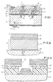
- a multi-layer ceramic (MLC) substrate 10 is shown in Fig. 1.
- MLC is known in the art to be comprised of a plurality of thin ceramic sheets which are then aligned and sintered together to form a thick MLC substrate for making circuit interconnections for semiconductor devices.
- the ceramic material can be the alumina ceramic (Al2O3) or the glass ceramic type, one form of which is known as alpha- cordierite.
- Contained within the layers 12 of substrate 10 are conductors which are used to carry electrical signals through the substrate 10. Some of these conductors are illustrated as vias 14, 16, and 18 which are used to carry signals to and from the top and bottom surfaces of substrate 10, where they can connect with other components.
- a multi-layer metal structure which includes a thin zirconium layer has shown excellent mechanical and electrical properties. While the actual structure of the multi-layer metallurgy varies depending upon the type of interconnection, the use of the zirconium layer is common to all structures.
- the multi-layer pad 22 which is used for connecting pin 24 to via 18, engineering change pad 28, and surface pads 31, consist of four layers.
- the capture pads 26 which are connected to vias 14 and 16 consist of a three layer metal structure.
- a 3-layer polyimide structure comprised of polyimide layers 36, 37, 38.
- This polyimide structure is used for redistribution, inter-chip wiring 27 and interconnections between the substrate 10 and semiconductor chip 34. Additionally, wiring within the polyimide layers can also be used to connect one semiconductor chip directly to other chips.
- a 4-layer structure comprising a zirconium adhesion layer, a copper layer, a reaction barrier layer, and a wettable surface layer is preferred.
- Examples of the types of pads which require a 4-layer structure are pad 22 which has pin 24 brazed to it; engineering change pad 28; and surface pads 31 which connect to the solder balls 32 on semiconductor chip 34.
- the sequence of metallizing the pads beginns with the alignment of a mask (not shown) with the substrate 40, which may be either ceramic, organic or metallic in nature.
- the type of mask used, metal, plastic, polymer, photoresist, etc. is not critical to this invention and can be any type commonly used in the art.
- the formation of the multi-layer thin film pad 42 beginns with the deposition of a thin layer of zirconium 44.
- the zirconium layer 44 can be deposited by electron gun evaporation, sputtering, ion plating or other methods known in the art.
- the thickness of the zirconium layer 44 is preferably within the range 3-200 nanometers.
- a layer 46 of copper, aluminum or gold is next deposited over zirconium layer 44, using the same deposition mask structure.
- Layer 46 can also be deposited using the deposition techniques described above, with a preferred thickness in the range 2-20 microns.
- reaction/diffusion barrier layer 48 with a thickness in the range 0.5-3.0 microns is deposited.
- the reaction barrier layer can be zirconium, titanium, chromium, cobalt, tungsten, molybdenum or nickel.
- a wettable surface layer 50 is applied to enhance the wettability of the multi-layer film for brazing or soldering.
- Gold in the range 0.3-10.0 microns has been found to be effective.
- a substrate 60 is provided.
- Substrate 60 can be ceramic, or a previously deposited layer of polyimide.
- a layer 62 of polyimide is sprayed or spun on, with a thickness of approximately 5.0 microns.
- a second layer 64 of soluble polyimide is applied. Layer 64 will be used as a lift-off layer after metal deposition.
- a photoresist layer 66 is applied and dried, and a metallization pattern is lithographically defined and developed as well-known in the art.
- layers 64 and 62 are etched in a reactive ion etch chanber using O2 or a mixture of O2/CF4, creating via 68.
- the metal layers are deposited as described previously. Lift-off is achieved by immersing the substrate 60 in a solvent capable of dissolving soluble polyimide layer 64, such as n-methylpyrrolidone (NMP).
- NMP n-methylpyrrolidone
- the metallurgy is to cover a portion of a metal layer previously applied, it may be necessary to sputter clean the surface to remove any oxidation that may have formed on the metal surface, prior to depositing an additional multi-layer structure.
- reaction barrier layer does not need to be as thick (3-200 nanometers is sufficient) and 2. the wettable surface layer is not needed. All other process steps, conditions, etc. are the same.
Abstract
Description
- This invention relates to a multi-layer wiring substrate composed of different materials, and comprising ceramic or polyimide.
- As the integrated circuit density continues to increase towards Very Large Scale Integration (VLSI), the increases in both the input/output (I/O) counts and wiring densities have placed stringent demands on the multi-layer chip packaging technologies. In order to interconnect large numbers of integrated circuit (IC) chips, each containing high densities of I/O terminals, the ability to produce fine and precise patterns with great reduction of lead pitch is becoming increasingly crucial to the success of future VLSI packaging technologies.
- Today's thick film multi-layer ceramic (MLC) technology has reached a limit, because the silk screening method is not capable of producing patterns with a minimum line width of less than 75µm, and the sintering process is plagued with large dimensional tolerances. Thick film MLC technology by itself is not enough to meet the requirements for advanced VLSI packaging technology.
- One method of providing inter-chip wiring and I/O interconnections utilizes thin film polyimide packages on top of a conventional MLC base. The structure consists of a MLC substrate as a base to supply current and mechanical support and thin film layers processed on top of the MLC base to provide inter-chip wiring and to fan-out the semiconductor chip contacts to the thin film wiring layers. Among the materials tested, the use of polyimide as a low dielectric insulating layer between finely patterned high conductivity copper layers achieves the best performance.
- One of the problems, however, with the use of copper for fine wiring, is that a pure copper to polyimide bond is not capable of withstanding the subsequent process and handling steps. Therefore, it is desirable to provide a method for enhancing the adhesion between copper and a polyimide substrate.
- The object of the invention as described in claim 1 is to provide a multi-layer wiring substrate comprising ceramic, polyimide and metallic layers, where good electrical contact, good mechanical adhesion between polyimide or ceramic substrate layers and selected metallic layers is favoured.
- In accordance with these objects, a thin layer of zirconium is used as an adhesion layer between a polyimide layer and a copper, aluminum, or gold layer. The adhesion strength between zirconium and polyimide is superior to alternative adhesion layers such as chromium or titanium. Furthermore, sputter cleaning of the polyimide surface is unnecessary with zirconium. As an alternative, zirconium and copper, aluminum, or gold can be co-deposited at the beginning of film deposition.
- Additionally, for those applications where polyimide is not necessary for packaging, zirconium can be used as an adhesion layer directly to a ceramic substrate. Following the zirconium layer, copper, aluminum, or gold can be deposited followed by a reaction barrier layer and a wettable surface layer such as gold. This type of structure can be used for pin brazing, chip joining, and/or wire connections.
- In the following, the invention will be more fully understood with reference to the description of an embodiment and the drawings wherein:
- Fig. 1 is a cross-sectional view of a multi-layer ceramic substrate with a multi-layer polyimide structure.
- Fig. 2 is a cross-sectional view of a substrate with a 4-layer metallic I/O pad.
- Fig. 3 is a cross-sectional view of a substrate with a polyimide layer and metal structure.
- A multi-layer ceramic (MLC)
substrate 10 is shown in Fig. 1. MLC is known in the art to be comprised of a plurality of thin ceramic sheets which are then aligned and sintered together to form a thick MLC substrate for making circuit interconnections for semiconductor devices. The ceramic material can be the alumina ceramic (Al₂O₃) or the glass ceramic type, one form of which is known as alpha- cordierite. Contained within thelayers 12 ofsubstrate 10 are conductors which are used to carry electrical signals through thesubstrate 10. Some of these conductors are illustrated asvias 14, 16, and 18 which are used to carry signals to and from the top and bottom surfaces ofsubstrate 10, where they can connect with other components. - For making electrical connections with
vias 14, 16, and 18, a multi-layer metal structure which includes a thin zirconium layer has shown excellent mechanical and electrical properties. While the actual structure of the multi-layer metallurgy varies depending upon the type of interconnection, the use of the zirconium layer is common to all structures. For example, themulti-layer pad 22 which is used for connectingpin 24 to via 18,engineering change pad 28, andsurface pads 31, consist of four layers. Thecapture pads 26 which are connected tovias 14 and 16 consist of a three layer metal structure. - Also shown in Fig. 1 is a 3-layer polyimide structure comprised of
polyimide layers inter-chip wiring 27 and interconnections between thesubstrate 10 andsemiconductor chip 34. Additionally, wiring within the polyimide layers can also be used to connect one semiconductor chip directly to other chips. - For metal pads that will be subjected to soldering or brazing for circuit interconnections, a 4-layer structure comprising a zirconium adhesion layer, a copper layer, a reaction barrier layer, and a wettable surface layer is preferred. Examples of the types of pads which require a 4-layer structure are
pad 22 which haspin 24 brazed to it;engineering change pad 28; andsurface pads 31 which connect to thesolder balls 32 onsemiconductor chip 34. - Referring to Fig. 2, the sequence of metallizing the pads beginns with the alignment of a mask (not shown) with the
substrate 40, which may be either ceramic, organic or metallic in nature. The type of mask used, metal, plastic, polymer, photoresist, etc. is not critical to this invention and can be any type commonly used in the art. If polyimide is not to be used as a dielectric layer, the formation of the multi-layerthin film pad 42 beginns with the deposition of a thin layer ofzirconium 44. Thezirconium layer 44 can be deposited by electron gun evaporation, sputtering, ion plating or other methods known in the art. The thickness of thezirconium layer 44 is preferably within the range 3-200 nanometers. - A
layer 46 of copper, aluminum or gold is next deposited overzirconium layer 44, using the same deposition mask structure.Layer 46 can also be deposited using the deposition techniques described above, with a preferred thickness in the range 2-20 microns. - To prevent
layer 46 from reacting with a solder or braze during subsequent manufacturing processes, a reaction/diffusion barrier layer 48 with a thickness in the range 0.5-3.0 microns is deposited. The reaction barrier layer can be zirconium, titanium, chromium, cobalt, tungsten, molybdenum or nickel. - Finally, a
wettable surface layer 50 is applied to enhance the wettability of the multi-layer film for brazing or soldering. Gold, in the range 0.3-10.0 microns has been found to be effective.If polyimide layers are to be used with the multi-layer metallurgy, the process described is modified to include additional steps. Referring to Fig.3, asubstrate 60 is provided.Substrate 60 can be ceramic, or a previously deposited layer of polyimide. Alayer 62 of polyimide is sprayed or spun on, with a thickness of approximately 5.0 microns. Following this layer, asecond layer 64 of soluble polyimide is applied.Layer 64 will be used as a lift-off layer after metal deposition. - A
photoresist layer 66 is applied and dried, and a metallization pattern is lithographically defined and developed as well-known in the art. Using the developed photoresist pattern as an etch mask,layers substrate 60 in a solvent capable of dissolvingsoluble polyimide layer 64, such as n-methylpyrrolidone (NMP). - If the metallurgy is to cover a portion of a metal layer previously applied, it may be necessary to sputter clean the surface to remove any oxidation that may have formed on the metal surface, prior to depositing an additional multi-layer structure.
- This same process can be repeated as necessary to create a multi-layer wiring structure as shown in Fig. 1.
- For metal pads or lines that will not be subjected to the stresses of brazing and/or soldering, such as
capture pads 26, the process outlined above can be followed with the following exceptions: 1. the reaction barrier layer does not need to be as thick (3-200 nanometers is sufficient) and 2. the wettable surface layer is not needed. All other process steps, conditions, etc. are the same.
Claims (5)
characterized
that zirconium is provided as an adhesion layer (44) between a selected metallic layer (46) and a polyimide substrate layer and between a selected metallic layer (46) and a ceramic substrate layer.
Applications Claiming Priority (2)
| Application Number | Priority Date | Filing Date | Title |
|---|---|---|---|
| US06/919,530 US4751349A (en) | 1986-10-16 | 1986-10-16 | Zirconium as an adhesion material in a multi-layer metallic structure |
| US919530 | 1992-07-24 |
Publications (3)
| Publication Number | Publication Date |
|---|---|
| EP0264134A2 true EP0264134A2 (en) | 1988-04-20 |
| EP0264134A3 EP0264134A3 (en) | 1988-09-21 |
| EP0264134B1 EP0264134B1 (en) | 1992-08-19 |
Family
ID=25442258
Family Applications (1)
| Application Number | Title | Priority Date | Filing Date |
|---|---|---|---|
| EP87115097A Expired - Lifetime EP0264134B1 (en) | 1986-10-16 | 1987-10-15 | Zirconium as an adhesion material in a multi-layer wiring substrate |
Country Status (4)
| Country | Link |
|---|---|
| US (1) | US4751349A (en) |
| EP (1) | EP0264134B1 (en) |
| JP (1) | JPS63110697A (en) |
| DE (1) | DE3781234D1 (en) |
Cited By (15)
| Publication number | Priority date | Publication date | Assignee | Title |
|---|---|---|---|---|
| EP0336869A2 (en) * | 1988-04-08 | 1989-10-11 | International Business Machines Corporation | A multilayered metallurgical structure for an electronic component |
| IT201900006736A1 (en) * | 2019-05-10 | 2020-11-10 | Applied Materials Inc | PACKAGE MANUFACTURING PROCEDURES |
| US10937726B1 (en) | 2019-11-27 | 2021-03-02 | Applied Materials, Inc. | Package structure with embedded core |
| US11063169B2 (en) | 2019-05-10 | 2021-07-13 | Applied Materials, Inc. | Substrate structuring methods |
| EP3807930A4 (en) * | 2018-06-18 | 2021-08-18 | Texas Instruments Incorporated | Zinc-cobalt barrier for interface in solder bond applications |
| US11232951B1 (en) | 2020-07-14 | 2022-01-25 | Applied Materials, Inc. | Method and apparatus for laser drilling blind vias |
| US11257790B2 (en) | 2020-03-10 | 2022-02-22 | Applied Materials, Inc. | High connectivity device stacking |
| US11342256B2 (en) | 2019-01-24 | 2022-05-24 | Applied Materials, Inc. | Method of fine redistribution interconnect formation for advanced packaging applications |
| US11404318B2 (en) | 2020-11-20 | 2022-08-02 | Applied Materials, Inc. | Methods of forming through-silicon vias in substrates for advanced packaging |
| US11400545B2 (en) | 2020-05-11 | 2022-08-02 | Applied Materials, Inc. | Laser ablation for package fabrication |
| US11454884B2 (en) | 2020-04-15 | 2022-09-27 | Applied Materials, Inc. | Fluoropolymer stamp fabrication method |
| US11521937B2 (en) | 2020-11-16 | 2022-12-06 | Applied Materials, Inc. | Package structures with built-in EMI shielding |
| US11676832B2 (en) | 2020-07-24 | 2023-06-13 | Applied Materials, Inc. | Laser ablation system for package fabrication |
| US11705365B2 (en) | 2021-05-18 | 2023-07-18 | Applied Materials, Inc. | Methods of micro-via formation for advanced packaging |
| US11931855B2 (en) | 2019-06-17 | 2024-03-19 | Applied Materials, Inc. | Planarization methods for packaging substrates |
Families Citing this family (9)
| Publication number | Priority date | Publication date | Assignee | Title |
|---|---|---|---|---|
| US4847445A (en) * | 1985-02-01 | 1989-07-11 | Tektronix, Inc. | Zirconium thin-film metal conductor systems |
| US5183973A (en) * | 1989-08-14 | 1993-02-02 | Santa Barbara Research Center | Flexible cable for interconnecting electronic components |
| JP2738600B2 (en) * | 1991-05-27 | 1998-04-08 | 京セラ株式会社 | Circuit board |
| US5436412A (en) * | 1992-10-30 | 1995-07-25 | International Business Machines Corporation | Interconnect structure having improved metallization |
| JP4428832B2 (en) * | 1999-08-27 | 2010-03-10 | 富士通株式会社 | Metal wiring structure, semiconductor device, and manufacturing method of semiconductor device |
| US6800815B1 (en) | 2001-01-16 | 2004-10-05 | National Semiconductor Corporation | Materials and structure for a high reliability bga connection between LTCC and PB boards |
| JP4448702B2 (en) * | 2004-01-30 | 2010-04-14 | 日東電工株式会社 | Method for manufacturing suspension board with circuit |
| KR100857365B1 (en) * | 2007-02-28 | 2008-09-05 | 주식회사 네패스 | Bump structure for semiconductor device |
| EP2767616A1 (en) * | 2013-02-15 | 2014-08-20 | Alstom Technology Ltd | Turbomachine component with an erosion and corrosion resistant coating system and method for manufacturing such a component |
Citations (4)
| Publication number | Priority date | Publication date | Assignee | Title |
|---|---|---|---|---|
| FR2041392A5 (en) * | 1969-04-23 | 1971-01-29 | Cii | |
| JPS5730334A (en) * | 1980-07-31 | 1982-02-18 | Toshiba Corp | Protection of wiring layer |
| FR2567684A1 (en) * | 1984-07-10 | 1986-01-17 | Nec Corp | MODULE HAVING A MULTILAYER CERAMIC SUBSTRATE AND A MULTILAYER CIRCUIT ON THE SUBSTRATE AND METHOD FOR THE PRODUCTION THEREOF |
| EP0190820A2 (en) * | 1985-02-01 | 1986-08-13 | Tektronix, Inc. | Zirconium thin-film metal conductor systems |
Family Cites Families (15)
| Publication number | Priority date | Publication date | Assignee | Title |
|---|---|---|---|---|
| US2857663A (en) * | 1954-02-09 | 1958-10-28 | Gen Electric | Metallic bond |
| US3379568A (en) * | 1964-12-21 | 1968-04-23 | North American Rockwell | Process for forming holes and multilayer interconnections through a dielectric |
| US3423821A (en) * | 1965-03-18 | 1969-01-28 | Hitachi Ltd | Method of producing thin film integrated circuits |
| US3461524A (en) * | 1966-11-02 | 1969-08-19 | Bell Telephone Labor Inc | Method for making closely spaced conductive layers |
| US3621442A (en) * | 1968-11-07 | 1971-11-16 | Allen Bradley Co | Terminal connection of electronic devices |
| US3798011A (en) * | 1969-01-31 | 1974-03-19 | Du Pont | Multilayered metal composite |
| US3647585A (en) * | 1969-05-23 | 1972-03-07 | Bell Telephone Labor Inc | Method of eliminating pinhole shorts in an air-isolated crossover |
| GB1248142A (en) * | 1969-06-20 | 1971-09-29 | Decca Ltd | Improvements in or relating to electrical circuits assemblies |
| US3737880A (en) * | 1971-09-10 | 1973-06-05 | Arvin Ind Inc | Flexible disc with air intake in turntable |
| US4042753A (en) * | 1972-09-22 | 1977-08-16 | Imperial Chemical Industries Limited | Composite conductor |
| US4016050A (en) * | 1975-05-12 | 1977-04-05 | Bell Telephone Laboratories, Incorporated | Conduction system for thin film and hybrid integrated circuits |
| JPS5212030A (en) * | 1975-07-16 | 1977-01-29 | Nippon Telegraph & Telephone | Serial printing system |
| US4153518A (en) * | 1977-11-18 | 1979-05-08 | Tektronix, Inc. | Method of making a metalized substrate having a thin film barrier layer |
| DE3136198A1 (en) * | 1981-01-15 | 1982-08-05 | Robert Bosch Gmbh, 7000 Stuttgart | "ELECTRONIC THICK FILM CIRCUIT" |
| JPS59167096A (en) * | 1983-03-11 | 1984-09-20 | 日本電気株式会社 | Circuit board |
-
1986
- 1986-10-16 US US06/919,530 patent/US4751349A/en not_active Expired - Fee Related
-
1987
- 1987-08-06 JP JP62195440A patent/JPS63110697A/en active Granted
- 1987-10-15 DE DE8787115097T patent/DE3781234D1/en not_active Expired - Lifetime
- 1987-10-15 EP EP87115097A patent/EP0264134B1/en not_active Expired - Lifetime
Patent Citations (4)
| Publication number | Priority date | Publication date | Assignee | Title |
|---|---|---|---|---|
| FR2041392A5 (en) * | 1969-04-23 | 1971-01-29 | Cii | |
| JPS5730334A (en) * | 1980-07-31 | 1982-02-18 | Toshiba Corp | Protection of wiring layer |
| FR2567684A1 (en) * | 1984-07-10 | 1986-01-17 | Nec Corp | MODULE HAVING A MULTILAYER CERAMIC SUBSTRATE AND A MULTILAYER CIRCUIT ON THE SUBSTRATE AND METHOD FOR THE PRODUCTION THEREOF |
| EP0190820A2 (en) * | 1985-02-01 | 1986-08-13 | Tektronix, Inc. | Zirconium thin-film metal conductor systems |
Non-Patent Citations (1)
| Title |
|---|
| PATENT ABSTRACTS OF JAPAN, vol. 6, no. 95 (E-110)[973], 3rd June 1982; & JP-A-57 30 334 (TOKYO SHIBAURA DENKI K.K.) 18-02-1982 * |
Cited By (30)
| Publication number | Priority date | Publication date | Assignee | Title |
|---|---|---|---|---|
| EP0336869B1 (en) * | 1988-04-08 | 1996-01-10 | International Business Machines Corporation | A multilayered metallurgical structure for an electronic component |
| EP0336869A2 (en) * | 1988-04-08 | 1989-10-11 | International Business Machines Corporation | A multilayered metallurgical structure for an electronic component |
| EP3807930A4 (en) * | 2018-06-18 | 2021-08-18 | Texas Instruments Incorporated | Zinc-cobalt barrier for interface in solder bond applications |
| US11587858B2 (en) | 2018-06-18 | 2023-02-21 | Texas Instruments Incorporated | Zinc-cobalt barrier for interface in solder bond applications |
| US11342256B2 (en) | 2019-01-24 | 2022-05-24 | Applied Materials, Inc. | Method of fine redistribution interconnect formation for advanced packaging applications |
| US11398433B2 (en) | 2019-05-10 | 2022-07-26 | Applied Materials, Inc. | Reconstituted substrate structure and fabrication methods for heterogeneous packaging integration |
| US11063169B2 (en) | 2019-05-10 | 2021-07-13 | Applied Materials, Inc. | Substrate structuring methods |
| US11887934B2 (en) | 2019-05-10 | 2024-01-30 | Applied Materials, Inc. | Package structure and fabrication methods |
| IT201900006736A1 (en) * | 2019-05-10 | 2020-11-10 | Applied Materials Inc | PACKAGE MANUFACTURING PROCEDURES |
| US11264331B2 (en) | 2019-05-10 | 2022-03-01 | Applied Materials, Inc. | Package structure and fabrication methods |
| US10886232B2 (en) | 2019-05-10 | 2021-01-05 | Applied Materials, Inc. | Package structure and fabrication methods |
| US11362235B2 (en) | 2019-05-10 | 2022-06-14 | Applied Materials, Inc. | Substrate structuring methods |
| US11521935B2 (en) | 2019-05-10 | 2022-12-06 | Applied Materials, Inc. | Package structure and fabrication methods |
| US11476202B2 (en) | 2019-05-10 | 2022-10-18 | Applied Materials, Inc. | Reconstituted substrate structure and fabrication methods for heterogeneous packaging integration |
| US11715700B2 (en) | 2019-05-10 | 2023-08-01 | Applied Materials, Inc. | Reconstituted substrate structure and fabrication methods for heterogeneous packaging integration |
| US11417605B2 (en) | 2019-05-10 | 2022-08-16 | Applied Materials, Inc. | Reconstituted substrate for radio frequency applications |
| US11931855B2 (en) | 2019-06-17 | 2024-03-19 | Applied Materials, Inc. | Planarization methods for packaging substrates |
| US11881447B2 (en) | 2019-11-27 | 2024-01-23 | Applied Materials, Inc. | Package core assembly and fabrication methods |
| US11862546B2 (en) | 2019-11-27 | 2024-01-02 | Applied Materials, Inc. | Package core assembly and fabrication methods |
| US10937726B1 (en) | 2019-11-27 | 2021-03-02 | Applied Materials, Inc. | Package structure with embedded core |
| US11742330B2 (en) | 2020-03-10 | 2023-08-29 | Applied Materials, Inc. | High connectivity device stacking |
| US11257790B2 (en) | 2020-03-10 | 2022-02-22 | Applied Materials, Inc. | High connectivity device stacking |
| US11927885B2 (en) | 2020-04-15 | 2024-03-12 | Applied Materials, Inc. | Fluoropolymer stamp fabrication method |
| US11454884B2 (en) | 2020-04-15 | 2022-09-27 | Applied Materials, Inc. | Fluoropolymer stamp fabrication method |
| US11400545B2 (en) | 2020-05-11 | 2022-08-02 | Applied Materials, Inc. | Laser ablation for package fabrication |
| US11232951B1 (en) | 2020-07-14 | 2022-01-25 | Applied Materials, Inc. | Method and apparatus for laser drilling blind vias |
| US11676832B2 (en) | 2020-07-24 | 2023-06-13 | Applied Materials, Inc. | Laser ablation system for package fabrication |
| US11521937B2 (en) | 2020-11-16 | 2022-12-06 | Applied Materials, Inc. | Package structures with built-in EMI shielding |
| US11404318B2 (en) | 2020-11-20 | 2022-08-02 | Applied Materials, Inc. | Methods of forming through-silicon vias in substrates for advanced packaging |
| US11705365B2 (en) | 2021-05-18 | 2023-07-18 | Applied Materials, Inc. | Methods of micro-via formation for advanced packaging |
Also Published As
| Publication number | Publication date |
|---|---|
| US4751349A (en) | 1988-06-14 |
| EP0264134A3 (en) | 1988-09-21 |
| JPH0214796B2 (en) | 1990-04-10 |
| EP0264134B1 (en) | 1992-08-19 |
| JPS63110697A (en) | 1988-05-16 |
| DE3781234D1 (en) | 1992-09-24 |
Similar Documents
| Publication | Publication Date | Title |
|---|---|---|
| EP0264134B1 (en) | Zirconium as an adhesion material in a multi-layer wiring substrate | |
| US3968193A (en) | Firing process for forming a multilayer glass-metal module | |
| US4463059A (en) | Layered metal film structures for LSI chip carriers adapted for solder bonding and wire bonding | |
| US4221047A (en) | Multilayered glass-ceramic substrate for mounting of semiconductor device | |
| US5892287A (en) | Semiconductor device including stacked chips having metal patterned on circuit surface and on edge side of chip | |
| US4918811A (en) | Multichip integrated circuit packaging method | |
| US4783695A (en) | Multichip integrated circuit packaging configuration and method | |
| US5244833A (en) | Method for manufacturing an integrated circuit chip bump electrode using a polymer layer and a photoresist layer | |
| US3805375A (en) | Composite integrated circuits including semiconductor chips mounted on a common substrate with connections made through a dielectric encapsulator | |
| KR100279036B1 (en) | Method of forming raised metallic contacts on electrical circuits for permanent bonding | |
| EP0171662B1 (en) | Method of fabricating a chip interposer | |
| US6261467B1 (en) | Direct deposit thin film single/multi chip module | |
| US5480835A (en) | Electrical interconnect and method for forming the same | |
| US5010389A (en) | Integrated circuit substrate with contacts thereon for a packaging structure | |
| US6800505B2 (en) | Semiconductor device including edge bond pads and related methods | |
| US5622895A (en) | Metallization for polymer-dielectric multichip modules | |
| GB2290171A (en) | Inductor chip device | |
| US6069026A (en) | Semiconductor device and method of fabrication | |
| US4982267A (en) | Integrated semiconductor package | |
| CA1039855A (en) | Process for producing a multi-chip wiring arrangement | |
| CA2077720C (en) | Process of forming electrical connections between conductive layers using thermosonic wire bonded bump vias and thick film techniques | |
| US6338973B1 (en) | Semiconductor device and method of fabrication | |
| US6372623B1 (en) | Semiconductor device and method of fabrication | |
| KR19990048003A (en) | Metal bump manufacturing method | |
| JP3723350B2 (en) | Wiring board and manufacturing method thereof |
Legal Events
| Date | Code | Title | Description |
|---|---|---|---|
| PUAI | Public reference made under article 153(3) epc to a published international application that has entered the european phase |
Free format text: ORIGINAL CODE: 0009012 |
|
| AK | Designated contracting states |
Kind code of ref document: A2 Designated state(s): DE FR GB |
|
| PUAL | Search report despatched |
Free format text: ORIGINAL CODE: 0009013 |
|
| AK | Designated contracting states |
Kind code of ref document: A3 Designated state(s): DE FR GB |
|
| 17P | Request for examination filed |
Effective date: 19880823 |
|
| 17Q | First examination report despatched |
Effective date: 19901008 |
|
| GRAA | (expected) grant |
Free format text: ORIGINAL CODE: 0009210 |
|
| AK | Designated contracting states |
Kind code of ref document: B1 Designated state(s): DE FR GB |
|
| PG25 | Lapsed in a contracting state [announced via postgrant information from national office to epo] |
Ref country code: FR Effective date: 19920819 Ref country code: DE Effective date: 19920819 |
|
| REF | Corresponds to: |
Ref document number: 3781234 Country of ref document: DE Date of ref document: 19920924 |
|
| PG25 | Lapsed in a contracting state [announced via postgrant information from national office to epo] |
Ref country code: GB Effective date: 19921119 |
|
| EN | Fr: translation not filed | ||
| PLBE | No opposition filed within time limit |
Free format text: ORIGINAL CODE: 0009261 |
|
| STAA | Information on the status of an ep patent application or granted ep patent |
Free format text: STATUS: NO OPPOSITION FILED WITHIN TIME LIMIT |
|
| GBPC | Gb: european patent ceased through non-payment of renewal fee |
Effective date: 19921119 |
|
| 26N | No opposition filed |