US10937726B1 - Package structure with embedded core - Google Patents
Package structure with embedded core Download PDFInfo
- Publication number
- US10937726B1 US10937726B1 US16/746,681 US202016746681A US10937726B1 US 10937726 B1 US10937726 B1 US 10937726B1 US 202016746681 A US202016746681 A US 202016746681A US 10937726 B1 US10937726 B1 US 10937726B1
- Authority
- US
- United States
- Prior art keywords
- layer
- vias
- core structure
- semiconductor device
- assembly
- Prior art date
- Legal status (The legal status is an assumption and is not a legal conclusion. Google has not performed a legal analysis and makes no representation as to the accuracy of the status listed.)
- Active
Links
Images


Classifications
-
- H—ELECTRICITY
- H10—SEMICONDUCTOR DEVICES; ELECTRIC SOLID-STATE DEVICES NOT OTHERWISE PROVIDED FOR
- H10W—GENERIC PACKAGES, INTERCONNECTIONS, CONNECTORS OR OTHER CONSTRUCTIONAL DETAILS OF DEVICES COVERED BY CLASS H10
- H10W70/00—Package substrates; Interposers; Redistribution layers [RDL]
- H10W70/60—Insulating or insulated package substrates; Interposers; Redistribution layers
- H10W70/62—Insulating or insulated package substrates; Interposers; Redistribution layers characterised by their interconnections
- H10W70/65—Shapes or dispositions of interconnections
-
- H01L23/49838—
-
- H01L21/486—
-
- H01L23/147—
-
- H01L23/49827—
-
- H01L23/49866—
-
- H—ELECTRICITY
- H10—SEMICONDUCTOR DEVICES; ELECTRIC SOLID-STATE DEVICES NOT OTHERWISE PROVIDED FOR
- H10W—GENERIC PACKAGES, INTERCONNECTIONS, CONNECTORS OR OTHER CONSTRUCTIONAL DETAILS OF DEVICES COVERED BY CLASS H10
- H10W40/00—Arrangements for thermal protection or thermal control
- H10W40/20—Arrangements for cooling
- H10W40/22—Arrangements for cooling characterised by their shape, e.g. having conical or cylindrical projections
- H10W40/226—Arrangements for cooling characterised by their shape, e.g. having conical or cylindrical projections characterised by projecting parts, e.g. fins to increase surface area
- H10W40/228—Arrangements for cooling characterised by their shape, e.g. having conical or cylindrical projections characterised by projecting parts, e.g. fins to increase surface area the projecting parts being wire-shaped or pin-shaped
-
- H—ELECTRICITY
- H10—SEMICONDUCTOR DEVICES; ELECTRIC SOLID-STATE DEVICES NOT OTHERWISE PROVIDED FOR
- H10W—GENERIC PACKAGES, INTERCONNECTIONS, CONNECTORS OR OTHER CONSTRUCTIONAL DETAILS OF DEVICES COVERED BY CLASS H10
- H10W70/00—Package substrates; Interposers; Redistribution layers [RDL]
- H10W70/01—Manufacture or treatment
- H10W70/05—Manufacture or treatment of insulating or insulated package substrates, or of interposers, or of redistribution layers
- H10W70/095—Manufacture or treatment of insulating or insulated package substrates, or of interposers, or of redistribution layers of vias therein
-
- H—ELECTRICITY
- H10—SEMICONDUCTOR DEVICES; ELECTRIC SOLID-STATE DEVICES NOT OTHERWISE PROVIDED FOR
- H10W—GENERIC PACKAGES, INTERCONNECTIONS, CONNECTORS OR OTHER CONSTRUCTIONAL DETAILS OF DEVICES COVERED BY CLASS H10
- H10W70/00—Package substrates; Interposers; Redistribution layers [RDL]
- H10W70/60—Insulating or insulated package substrates; Interposers; Redistribution layers
- H10W70/611—Insulating or insulated package substrates; Interposers; Redistribution layers for connecting multiple chips together
- H10W70/614—Insulating or insulated package substrates; Interposers; Redistribution layers for connecting multiple chips together the multiple chips being integrally enclosed
-
- H—ELECTRICITY
- H10—SEMICONDUCTOR DEVICES; ELECTRIC SOLID-STATE DEVICES NOT OTHERWISE PROVIDED FOR
- H10W—GENERIC PACKAGES, INTERCONNECTIONS, CONNECTORS OR OTHER CONSTRUCTIONAL DETAILS OF DEVICES COVERED BY CLASS H10
- H10W70/00—Package substrates; Interposers; Redistribution layers [RDL]
- H10W70/60—Insulating or insulated package substrates; Interposers; Redistribution layers
- H10W70/62—Insulating or insulated package substrates; Interposers; Redistribution layers characterised by their interconnections
- H10W70/63—Vias, e.g. via plugs
- H10W70/635—Through-vias
-
- H—ELECTRICITY
- H10—SEMICONDUCTOR DEVICES; ELECTRIC SOLID-STATE DEVICES NOT OTHERWISE PROVIDED FOR
- H10W—GENERIC PACKAGES, INTERCONNECTIONS, CONNECTORS OR OTHER CONSTRUCTIONAL DETAILS OF DEVICES COVERED BY CLASS H10
- H10W70/00—Package substrates; Interposers; Redistribution layers [RDL]
- H10W70/60—Insulating or insulated package substrates; Interposers; Redistribution layers
- H10W70/62—Insulating or insulated package substrates; Interposers; Redistribution layers characterised by their interconnections
- H10W70/65—Shapes or dispositions of interconnections
- H10W70/652—Cross-sectional shapes
-
- H—ELECTRICITY
- H10—SEMICONDUCTOR DEVICES; ELECTRIC SOLID-STATE DEVICES NOT OTHERWISE PROVIDED FOR
- H10W—GENERIC PACKAGES, INTERCONNECTIONS, CONNECTORS OR OTHER CONSTRUCTIONAL DETAILS OF DEVICES COVERED BY CLASS H10
- H10W70/00—Package substrates; Interposers; Redistribution layers [RDL]
- H10W70/60—Insulating or insulated package substrates; Interposers; Redistribution layers
- H10W70/62—Insulating or insulated package substrates; Interposers; Redistribution layers characterised by their interconnections
- H10W70/66—Conductive materials thereof
-
- H—ELECTRICITY
- H10—SEMICONDUCTOR DEVICES; ELECTRIC SOLID-STATE DEVICES NOT OTHERWISE PROVIDED FOR
- H10W—GENERIC PACKAGES, INTERCONNECTIONS, CONNECTORS OR OTHER CONSTRUCTIONAL DETAILS OF DEVICES COVERED BY CLASS H10
- H10W70/00—Package substrates; Interposers; Redistribution layers [RDL]
- H10W70/60—Insulating or insulated package substrates; Interposers; Redistribution layers
- H10W70/67—Insulating or insulated package substrates; Interposers; Redistribution layers characterised by their insulating layers or insulating parts
- H10W70/68—Shapes or dispositions thereof
- H10W70/685—Shapes or dispositions thereof comprising multiple insulating layers
-
- H—ELECTRICITY
- H10—SEMICONDUCTOR DEVICES; ELECTRIC SOLID-STATE DEVICES NOT OTHERWISE PROVIDED FOR
- H10W—GENERIC PACKAGES, INTERCONNECTIONS, CONNECTORS OR OTHER CONSTRUCTIONAL DETAILS OF DEVICES COVERED BY CLASS H10
- H10W70/00—Package substrates; Interposers; Redistribution layers [RDL]
- H10W70/60—Insulating or insulated package substrates; Interposers; Redistribution layers
- H10W70/67—Insulating or insulated package substrates; Interposers; Redistribution layers characterised by their insulating layers or insulating parts
- H10W70/69—Insulating materials thereof
- H10W70/698—Semiconductor materials that are electrically insulating, e.g. undoped silicon
-
- H—ELECTRICITY
- H10—SEMICONDUCTOR DEVICES; ELECTRIC SOLID-STATE DEVICES NOT OTHERWISE PROVIDED FOR
- H10W—GENERIC PACKAGES, INTERCONNECTIONS, CONNECTORS OR OTHER CONSTRUCTIONAL DETAILS OF DEVICES COVERED BY CLASS H10
- H10W72/00—Interconnections or connectors in packages
- H10W72/90—Bond pads, in general
-
- H—ELECTRICITY
- H10—SEMICONDUCTOR DEVICES; ELECTRIC SOLID-STATE DEVICES NOT OTHERWISE PROVIDED FOR
- H10W—GENERIC PACKAGES, INTERCONNECTIONS, CONNECTORS OR OTHER CONSTRUCTIONAL DETAILS OF DEVICES COVERED BY CLASS H10
- H10W90/00—Package configurations
- H10W90/701—Package configurations characterised by the relative positions of pads or connectors relative to package parts
-
- H—ELECTRICITY
- H10—SEMICONDUCTOR DEVICES; ELECTRIC SOLID-STATE DEVICES NOT OTHERWISE PROVIDED FOR
- H10W—GENERIC PACKAGES, INTERCONNECTIONS, CONNECTORS OR OTHER CONSTRUCTIONAL DETAILS OF DEVICES COVERED BY CLASS H10
- H10W90/00—Package configurations
- H10W90/401—Package configurations characterised by multiple insulating or insulated package substrates, interposers or RDLs
Definitions
- Embodiments of the present disclosure generally relate to electronic mounting structures and methods of forming the same. More specifically, embodiments described herein relate to semiconductor package and PCB assemblies and methods of forming the same.
- circuit chips have been fabricated on organic package substrates coupled to circuit boards (e.g. printed circuit boards (PCB's)) due to the ease of forming features and connections in the organic package substrates, as well as the relatively low package manufacturing costs associated with organic composites.
- PCB's printed circuit boards
- the utilization of organic package substrates and conventional interconnect PCB's becomes impractical due to limitations with material structuring resolution to sustain device scaling and associated performance requirements.
- 2.5D and 3D integrated circuits have been fabricated utilizing passive silicon interposers as redistribution layers to compensate for some of the limitations associated with organic package substrates.
- Silicon interposer utilization is driven by the potential for high-bandwidth density, lower-power chip-to-chip communication, and heterogeneous integration sought in advanced electronic mounting and packaging applications. Yet, the formation of features in silicon interposers, such as through-silicon vias (TSVs), is still difficult and costly. In particular, high costs are imposed by high-aspect-ratio silicon via etching, chemical mechanical planarization, and semiconductor back end of line (BEOL) interconnection.
- TSVs through-silicon vias
- BEOL semiconductor back end of line
- the present disclosure generally relates to electronic mounting structures and methods of forming the same.
- a semiconductor device assembly in one embodiment, includes a silicon core structure having a first surface opposing a second surface and a thickness less than about 1000 ⁇ m. One or more conductive interconnections are formed through the silicon core structure and protrude from the first surface and the second surface.
- the semiconductor device assembly further includes a first redistribution layer formed on the first surface and a second redistribution layer formed on the second surface. The first redistribution layer and the second redistribution layer each have one or more conductive contacts formed thereon.
- a semiconductor device assembly in one embodiment, includes a silicon core structure, a passivating layer, and a dielectric layer.
- the silicon core structure has a thickness less than about 1000 ⁇ m.
- the passivating layer surrounds the silicon core structure and includes a thermal oxide.
- the dielectric layer is formed on the passivating layer and includes an epoxy resin having silica particles disposed therein.
- a semiconductor device assembly in one embodiment, includes a silicon core structure, a passivating layer surrounding the silicon structure and including a thermal oxide, a dielectric layer surrounding the passivating layer and formed of an epoxy resin, and a redistribution layer formed on the dielectric layer.
- the redistribution layer further includes an adhesion layer formed on the dielectric layer and formed of molybdenum, a copper seed layer formed on the adhesion layer, and a copper layer formed on the copper seed layer.
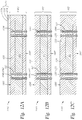
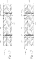
- FIG. 1A schematically illustrates a cross-sectional view of a semiconductor core assembly, according to an embodiment described herein.
- FIG. 1B schematically illustrates a cross-sectional view of a semiconductor core assembly, according to an embodiment described herein.
- FIG. 2 is a flow diagram that illustrates a process for forming the semiconductor core assemblies of FIGS. 1A and 1B , according to an embodiment described herein.
- FIG. 3 is a flow diagram that illustrates of a process for structuring a substrate for a semiconductor core assembly, according to an embodiment described herein.
- FIGS. 4A-4D schematically illustrate cross-sectional views of a substrate at different stages of the process depicted in FIG. 3 , according to an embodiment described herein.
- FIG. 5 is a flow diagram that illustrates a process for forming an insulating layer on a core structure for a semiconductor core assembly, according to an embodiment described herein.
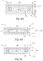
- FIGS. 6A-6I schematically illustrate cross-sectional views of a core structure at different stages of the process depicted in FIG. 5 , according to an embodiment described herein.
- FIG. 7 is a flow diagram that illustrates a process for forming an insulating layer on a core structure for a semiconductor core assembly, according to an embodiment described herein.
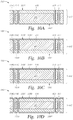
- FIGS. 8A-8E schematically illustrate cross-sectional views of a core structure at different stages of the process depicted in FIG. 7 , according to an embodiment described herein.
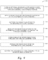
- FIG. 9 is a flow diagram that illustrates a process for forming interconnections in a semiconductor core assembly, according to an embodiment described herein.
- FIGS. 10A-10H schematically illustrate cross-sectional views of the semiconductor core assembly at different stages of the process depicted in FIG. 9 , according to an embodiment described herein.
- FIG. 11 is a flow diagram that illustrates a process for forming a redistribution layer on a semiconductor core assembly, according to an embodiment described herein.
- FIGS. 12A-12L schematically illustrate cross-sectional views of the semiconductor core assembly at different stages of the process depicted in FIG. 11 , according to an embodiment described herein.
- FIG. 13A schematically illustrates a cross-sectional view of a chip carrier structure including a semiconductor core assembly, according to an embodiment described herein.
- FIG. 13B schematically illustrates a cross-sectional view of a PCB structure including a semiconductor core assembly, according to an embodiment described herein.
- FIG. 13C schematically illustrates a cross-sectional view of a PCB structure including a semiconductor core assembly, according to an embodiment described herein.
- the present disclosure relates to semiconductor core assemblies and methods of forming the same.
- the semiconductor core assemblies described herein may be utilized to form semiconductor package assemblies, PCB assemblies, PCB spacer assemblies, chip carrier assemblies, intermediate carrier assemblies (e.g., for graphics cards), and the like.
- a silicon substrate core is structured by direct laser patterning. One or more conductive interconnections are formed in the substrate core and one or more redistribution layers are formed on surfaces thereof.
- the silicon substrate core may thereafter be utilized as a core structure for a semiconductor package, PCB, PCB spacer, chip carrier, intermediate carrier, or the like.
- the methods and apparatus disclosed herein include novel thin-form-factor semiconductor core structures intended to replace more conventional semiconductor package, PCB, and chip carrier structures utilizing glass fiber-filled epoxy frames.
- the scalability of current semiconductor packages, PCBs, spacers, and chip carriers is limited by the rigidity and lack of planarity of the materials typically utilized to form these various structures (e.g., epoxy molding compound, FR-4 and FR-5 grade woven fiberglass cloth with epoxy resin binders, and the like).
- the intrinsic properties of these materials cause difficulty in patterning and utilizing fine (e.g., micron scale) features formed therein.
- coefficient of thermal expansion (CTE) mismatch may occur between fiberglass frames, boards, molding compounds, and any chips disposed adjacent thereto. Therefore, current package, PCB, spacer, and carrier structures necessitate larger solder bumps with greater spacing to mitigate the effect of any warpage caused by CTE mismatch. Accordingly, conventional semiconductor package, PCB, spacer, and carrier frames are characterized by low through-structure electrical bandwidths, resulting in decreased overall power efficiency.
- the methods and apparatus disclosed herein provide semiconductor core structures that overcome many of the disadvantages associated with conventional semiconductor package, PCB, spacer, and carrier structures described above.
- FIGS. 1A and 1B illustrate cross-sectional views of a thin-form-factor semiconductor core assembly 100 according to some embodiments.
- the semiconductor core assembly 100 may be utilized for structural support and electrical interconnection of semiconductor packages mounted thereon.
- the semiconductor core assembly 100 may be utilized as a carrier structure for a surface-mounted device, such as a chip or graphics card.
- the semiconductor core assembly 100 generally includes a core structure 102 , an optional passivating layer 104 , and an insulating layer 118 .
- the core structure 102 includes a patterned (e.g., structured) substrate formed of any suitable substrate material.
- the core structure 102 includes a substrate formed from a III-V compound semiconductor material, silicon, crystalline silicon (e.g., Si ⁇ 100> or Si ⁇ 111>), silicon oxide, silicon germanium, doped or undoped silicon, doped or undoped polysilicon, silicon nitride, quartz, glass (e.g., borosilicate glass), sapphire, alumina, and/or ceramic materials.
- the core structure 102 includes a monocrystalline p-type or n-type silicon substrate.
- the core structure 102 includes a polycrystalline p-type or n-type silicon substrate.
- the core structure 102 includes a p-type or an n-type silicon solar substrate.
- the substrate utilized to form the core structure 102 may further have a polygonal or circular shape.
- the core structure 102 may include a substantially square silicon substrate having lateral dimensions between about 120 mm and about 180 mm, with or without chamfered edges.
- the core structure 102 may include a circular silicon-containing wafer having a diameter between about 20 mm and about 700 mm, such as between about 100 mm and about 50 mm, for example about 300 mm.
- the core structure 102 has a thickness T 1 between about 50 ⁇ m and about 1000 ⁇ m, such as a thickness T 1 between about 70 ⁇ m and about 800 ⁇ m.
- the core structure 102 has a thickness T 1 between about 80 ⁇ m and about 400 ⁇ m, such as a thickness T 1 between about 100 ⁇ m and about 200 ⁇ m.
- the core structure 102 has a thickness T 1 between about 70 ⁇ m and about 150 ⁇ m, such as a thickness T 1 between about 100 ⁇ m and about 130 ⁇ m.
- the core structure 102 has a thickness T 1 between about 700 ⁇ m and about 800 ⁇ m, such as a thickness T 1 between about 725 ⁇ m and about 775 ⁇ m.
- the core structure 102 further includes one or more holes or core vias 103 (hereinafter referred to as “core vias”) formed therein to enable conductive electrical interconnections to be routed through the core structure 102 .
- core vias 103 are substantially cylindrical in shape.
- the core vias 103 may be formed as singular and isolated core vias 103 through the core structure 102 or in one or more groupings or arrays.
- a minimum pitch P 1 between each core via 103 is less than about 1000 ⁇ m, such as between about 25 ⁇ m and about 200 ⁇ m.
- the pitch P 1 is between about 40 ⁇ m and about 150 ⁇ m.
- the one or more core vias 103 have a diameter V 1 less than about 500 ⁇ m, such as a diameter V 1 less than about 250 ⁇ m.
- the core vias 103 have a diameter V 1 between about 25 ⁇ m and about 100 ⁇ m, such as a diameter V 1 between about 30 ⁇ m and about 60 ⁇ m.
- the core vias 103 have a diameter V 1 of about 40 ⁇ m.
- the optional passivating layer 104 may be formed on one or more surfaces of the core structure 102 , including a first surface 106 , a second surface 108 , and one or more sidewalls of the core vias 103 .
- the passivating layer 104 is formed on substantially all exterior surfaces of the core structure 102 such that the passivating layer 104 substantially surrounds the core structure 102 .
- the passivating layer 104 provides a protective outer barrier for the core structure 102 against corrosion and other forms of damage.
- the passivating layer 104 is formed of an oxide film or layer, such as a thermal oxide layer.
- the passivating layer 104 has a thickness between about 100 nm and about 3 ⁇ m, such as a thickness between about 200 nm and about 2.5 ⁇ m. In one example, the passivating layer 104 has a thickness between about 300 nm and about 2 ⁇ m, such as a thickness of about 1.5 ⁇ m.
- the insulating layer 118 is formed on one or more surfaces of the core structure 102 or the passivating layer 104 and may substantially encase the passivating layer 104 and/or the core structure 102 . Thus, the insulating layer 118 may extend into the core vias 103 and coat the passivating layer 104 formed on the sidewalls thereof or directly coat the core structure 102 , thus defining the diameter V 2 as depicted in FIG. 1A .
- the insulating layer 118 has a thickness T 2 from an outer surface of the core structure 102 or the passivating layer 104 to an adjacent outer surface of the insulating layer 118 (e.g., major surfaces 105 , 107 ) that is less than about 50 ⁇ m, such as a thickness T 2 less than about 20 ⁇ m.
- the insulating layer 118 has thickness T 2 between about 5 ⁇ m and about 10 ⁇ m.
- the insulating layer 118 is formed of polymer-based dielectric materials.
- the insulating layer 118 is formed from a flowable build-up material. Accordingly, although hereinafter referred to as an “insulating layer,” the insulating layer 118 may also be described as a dielectric layer.
- the insulating layer 118 is formed of an epoxy resin material having a ceramic filler, such as silica (SiO 2 ) particles.
- Ceramic fillers that may be utilized to form the insulating layer 118 include aluminum nitride (AlN), aluminum oxide (Al 2 O 3 ), silicon carbide (SiC), silicon nitride (Si 3 N 4 , Sr 2 Ce 2 Ti 5 O 16 , zirconium silicate (ZrSiO 4 ), wollastonite (CaSiO 3 ), beryllium oxide (BeO), cerium dioxide (CeO 2 ), boron nitride (BN), calcium copper titanium oxide (CaCu 3 Ti 4 O 12 ), magnesium oxide (MgO), titanium dioxide (TiO 2 ), zinc oxide (ZnO) and the like.
- AlN aluminum nitride
- Al 2 O 3 silicon carbide
- Si 3 N 4 silicon nitride
- ZrSiO 4 zirconium silicate
- wollastonite CaSiO 3
- BeO beryllium oxide
- CeO 2 cerium dioxide
- BN boron
- the ceramic fillers utilized to form the insulating layer 118 have particles ranging in size between about 40 nm and about 1.5 ⁇ m, such as between about 80 nm and about 1 ⁇ m.
- the ceramic fillers have particles ranging in size between about 200 nm and about 800 nm, such as between about 300 nm and about 600 nm.
- the ceramic fillers include particles having a size less than about 10% of the width or diameter of adjacent core vias 103 in the core structure 102 , such as a size less than about 5% of the width or diameter of the core vias 103 .
- through-assembly vias 113 are formed through the insulating layer 118 where the insulating layer 118 extends into the core vias 103 .
- the through-assembly vias 113 may be centrally formed within the core vias 103 having the insulating layer 118 disposed therein.
- the insulating layer 118 forms one or more sidewalls of the through-assembly vias 113 , wherein the through-assembly vias 113 have a diameter V 2 lesser than the diameter V 1 of the core vias 103 .
- the through-assembly vias 113 have a diameter V 2 less than about 100 ⁇ m, such as less than about 75 ⁇ m.
- the through-assembly vias 113 have a diameter V 2 less than about 50 ⁇ m, such as less than about 35 ⁇ m.
- the through-assembly vias 113 have a diameter of between about 25 ⁇ m and about 50 ⁇ m, such as a diameter of between about 35 ⁇ m and about 40 ⁇ m.
- the through-assembly vias 113 provide channels through which one or more electrical interconnections 144 are formed in the semiconductor core assembly 100 .
- the electrical interconnections 144 are formed through the entire thickness of the semiconductor core assembly 100 (i.e. from a first major surface 105 to a second major surface 107 of the semiconductor core assembly 100 ).
- the electrical interconnections 144 may have a longitudinal length corresponding to a total thickness of the semiconductor core assembly 100 between about 50 ⁇ m and about 1000 ⁇ m, such as a longitudinal length between about 200 ⁇ m and about 800 ⁇ m.
- the electrical interconnections 144 have a longitudinal length of between about 400 ⁇ m and about 600 ⁇ m, such as longitudinal length of about 500 ⁇ m.
- the electrical interconnections 144 are only formed through a portion of the thickness of the semiconductor core assembly 100 .
- the electrical interconnections 144 may protrude from a major surface of the semiconductor core assembly 100 , such as the major surfaces 105 , 107 as depicted in FIG. 1A .
- the electrical interconnections 144 may be formed of any conductive materials used in the field of integrated circuits, circuit boards, chip carriers, and the like.
- the electrical interconnections 144 are formed of a metallic material, such as copper, aluminum, gold, nickel, silver, palladium, tin, or the like.
- the electrical interconnections 144 have a lateral thickness equal to the diameter V 2 of the through-assembly vias 113 in which they are formed.
- the semiconductor core assembly 100 further includes an adhesion layer 140 and/or a seed layer 142 formed thereon for electrical isolation of the electrical interconnections 144 .
- the adhesion layer 140 is formed on surfaces of the insulating layer 118 adjacent to the electrical interconnections 144 , including the sidewalls of the through-assembly vias 113 .
- the electrical interconnections 144 have a lateral thickness less than the diameter V 2 of the through-assembly vias 113 in which they are formed. In yet another embodiment, the electrical interconnections 144 only cover the surfaces of the sidewalls of the through-assembly vias 113 , and thus may have a hollow core therethrough.
- the adhesion layer 140 may be formed of any suitable materials, including but not limited to titanium, titanium nitride, tantalum, tantalum nitride, manganese, manganese oxide, molybdenum, cobalt oxide, cobalt nitride, and the like.
- the adhesion layer 140 has a thickness B 1 between about 10 nm and about 300 nm, such as between about 50 nm and about 150 nm.
- the adhesion layer 140 has a thickness B 1 between about 75 nm and about 125 nm, such as about 100 nm.
- the optional seed layer 142 comprises a conductive material, including but not limited to copper, tungsten, aluminum, silver, gold, or any other suitable materials or combinations thereof.
- the seed layer 142 may be formed on the adhesion layer 140 or directly on the sidewalls of the through-assembly vias 113 (e.g., on the insulating layer 118 without an adhesion layer therebetween).
- the seed layer 142 has a thickness between about 50 nm and about 500 nm, such as between about 100 nm and about 300 nm.
- the seed layer 142 has a thickness between about 150 nm and about 250 nm, such as about 200 nm.
- the semiconductor core assembly 100 further includes one or more redistribution layers 150 formed on a first side 175 and/or a second side 177 of the semiconductor core assembly 100 (the redistribution layer 150 is depicted as being formed on the second side 177 in FIG. 1B ).
- the redistribution layer 150 is formed of substantially the same materials as the insulating layer 118 (e.g., polymer-based dielectric materials), and thus forms an extension thereof.
- the redistribution layer 150 is formed of a different material than the insulating layer 118 .
- the redistribution layer 150 may be formed of a photodefinable polyimide material, a non-photosensitive polyimide, polybenzoxazole (PBO), benzocyclobutene (BCB), silicon dioxide, and/or silicon nitride.
- the redistribution layer 150 is formed from a different inorganic dielectric material than the insulating layer 118 .
- the redistribution layer 150 has a thickness between about 5 ⁇ m and about 50 ⁇ m, such as a thickness between about 10 ⁇ m and about 40 ⁇ m.
- the redistribution layer 150 has a thickness between about 20 ⁇ m and about 30 ⁇ m, such as about 25 ⁇ m.
- the redistribution layer 150 may include one or more redistribution connections 154 formed through redistribution vias 153 for relocating contact points of the electrical interconnections 144 to desired locations on the surfaces of the semiconductor core assembly 100 , such as the major surfaces 105 , 107 .
- the redistribution layer 150 may further include one or more external electrical connections (not shown) formed on the major surfaces 105 , 107 , such as a ball grid array or solder balls.
- the redistribution vias 153 and the redistribution connections 154 have substantially similar or smaller lateral dimensions relative to the through-assembly vias 113 and the electrical interconnections 144 , respectively.
- the redistribution vias 153 have a diameter V 3 between about 2 ⁇ m and about 50 ⁇ m, such as a diameter V 3 between about 10 ⁇ m and about 40 ⁇ m, such as a diameter V 3 between about 20 ⁇ m and about 30 ⁇ m.
- the redistribution layer 150 may include the adhesion layer 140 and the seed layer 142 formed on surfaces adjacent to the redistribution connections 154 , including sidewalls of the redistribution vias 153 .
- FIG. 2 illustrates a flow diagram of a representative method 200 of forming a semiconductor core assembly.
- the method 200 has multiple operations 210 , 220 , 230 , and 240 . Each operation is described in greater detail with reference to FIGS. 3-12L .
- the method may include one or more additional operations which are carried out before any of the defined operations, between two of the define operations, or after all the defined operations (except where the context excludes the possibility).
- the method 200 includes structuring a substrate to be utilized as a core structure (e.g., frame) at operation 210 , further described in greater detail with reference to FIGS. 3 and 4A-4D .
- a core structure e.g., frame
- an insulating layer is formed on the core structure 102 , further described in greater detail with reference to FIGS. 5, 6A-6I, 7, and 8A-8E .
- one or more interconnections are formed through the core structure 102 and the insulating layer, further described in greater detail with reference to FIGS. 9 and 10A-10H .
- a redistribution layer is formed on the insulating layer to relocate contact points of the interconnections to desired locations on a surface of an assembled core assembly and the core assembly is thereafter singulated.
- one or more additional redistribution layers may be formed in addition to the first redistribution layer, described in greater detail with reference to FIGS. 11 and 12A-12L .
- FIG. 3 illustrates a flow diagram of a representative method 300 for structuring a substrate 400 to be utilized as a core structure.
- FIGS. 4A-4D schematically illustrate cross-sectional views of a substrate 400 at various stages of the substrate structuring process 300 represented in FIG. 3 . Therefore, FIG. 3 and FIGS. 4A-4D are herein described together for clarity.
- the substrate 400 is formed of any suitable substrate material including but not limited to a III-V compound semiconductor material, silicon, crystalline silicon (e.g., Si ⁇ 100> or Si ⁇ 111>), silicon oxide, silicon germanium, doped or undoped silicon, doped or undoped polysilicon, silicon nitride, quartz, glass material (e.g., borosilicate glass), sapphire, alumina, and/or ceramic material.
- the substrate 400 is a monocrystalline p-type or n-type silicon substrate.
- the substrate 400 is a multicrystalline p-type or n-type silicon substrate.
- the substrate 400 is a p-type or an n-type silicon solar substrate.
- the substrate 400 may further have a polygonal or circular shape.
- the substrate 400 may include a substantially square silicon substrate having lateral dimensions between about 140 mm and about 180 mm, with or without chamfered edges.
- the substrate 400 may include a circular silicon containing wafer having a diameter between about 20 mm and about 700 mm, such as between about 100 mm and about 500 mm, for example about 300 mm.
- embodiments and examples described herein are conducted on substrates having a thickness between about 50 ⁇ m and about 1000 ⁇ m, such as a thickness between about 90 ⁇ m and about 780 ⁇ m.
- the substrate 400 has a thickness between about 100 ⁇ m and about 300 ⁇ m, such as a thickness between about 110 ⁇ m and about 200 ⁇ m.
- the substrate 400 may be sliced and separated from a bulk material by wire sawing, scribing and breaking, mechanical abrasive sawing, or laser cutting. Slicing typically causes mechanical defects or deformities in substrate surfaces formed therefrom, such as scratches, micro-cracking, chipping, and other mechanical defects.
- the substrate 400 is exposed to a first damage removal process at operation 310 to smoothen and planarize surfaces thereof and remove mechanical defects in preparation for later structuring operations.
- the substrate 400 may further be thinned by adjusting the process parameters of the first damage process. For example, a thickness of the substrate 400 may be decreased with increased exposure to the first damage removal process.
- the first damage removal process at operation 310 includes exposing the substrate 400 to a substrate polishing process and/or an etch process followed by rinsing and drying processes.
- operation 310 includes a chemical mechanical polishing (CMP) process.
- the etch process is a wet etch process including a buffered etch process that is selective for the removal of a desired material (e.g., contaminants and other undesirable compounds).
- the etch process is a wet etch process utilizing an isotropic aqueous etch process. Any suitable wet etchant or combination of wet etchants may be used for the wet etch process.
- the substrate 400 is immersed in an aqueous HF etching solution for etching.
- the substrate 400 is immersed in an aqueous KOH etching solution for etching.
- the etching solution is heated to a temperature between about 30° C. and about 100° C. during the etch process, such as between about 40° C. and 90° C.
- the etching solution is heated to a temperature of about 70° C.
- the etch process at operation 310 is a dry etch process.
- An example of a dry etch process includes a plasma-based dry etch process.
- the thickness of the substrate 400 is modulated by controlling the time of exposure of the substrate 400 to the etchants (e.g., etching solution) utilized during the etch process. For example, a final thickness of the substrate 400 is reduced with increased exposure to the etchants. Alternatively, the substrate 400 may have a greater final thickness with decreased exposure to the etchants.
- the now planarized and substantially defect-free substrate 400 is patterned to form one or more core vias 403 therein (four core vias 403 are depicted in the cross-section of substrate 400 in FIG. 4B ).
- the core vias 403 are utilized to form direct-contact electrical interconnections through the substrate 400 .
- the one or more core vias 403 may be formed by laser ablation (e.g. direct laser patterning). Any suitable laser ablation system may be utilized to form the one or more core vias 403 .
- the laser ablation system utilizes an infrared (IR) laser source.
- the laser source is a picosecond ultraviolet (UV) laser.
- the laser is a femtosecond UV laser.
- the laser source is a femtosecond green laser.
- the laser source of the laser ablation system generates a continuous or pulsed laser beam for patterning of the substrate 400 .
- the laser source may generate a pulsed laser beam having a frequency between 5 kHz and 500 kHz, such as between 10 kHz and about 200 kHz.
- the laser source is configured to deliver a pulsed laser beam at a wavelength between about 200 nm and about 1200 nm and a pulse duration between about 10 ns and about 5000 ns with an output power between about 10 Watts and about 100 Watts.
- the laser source is configured to form any desired pattern of features in the substrate 400 , including the core vias 403 .
- the substrate 400 is optionally coupled to a carrier plate (not shown) before being patterned.
- the optional carrier plate may provide mechanical support for the substrate 400 during patterning thereof and may prevent the substrate 400 from breaking.
- the carrier plate may be formed of any suitable chemically- and thermally-stable rigid material including but not limited to glass, ceramic, metal, or the like.
- the carrier plate has a thickness between about 1 mm and about 10 mm, such as between about 2 mm and about 5 mm.
- the carrier plate has a textured surface.
- the carrier plate has a polished or smoothened surface.
- the substrate 400 may be coupled to the carrier plate utilizing any suitable temporary bonding material, including but not limited to wax, glue, or similar bonding material.
- patterning the substrate 400 may cause unwanted mechanical defects in the surfaces of the substrate 400 , including chipping, cracking, and/or warping.
- the substrate 400 is exposed to a second damage removal and cleaning process at operation 330 substantially similar to the first damage removal process at operation 310 to smoothen the surfaces of the substrate 400 and remove unwanted debris.
- the second damage removal process includes exposing the substrate 400 to a wet or dry etch process, followed by rinsing and drying thereof. The etch process proceeds for a predetermined duration to smoothen the surfaces of the substrate 400 , and particularly the surfaces exposed to laser patterning operations.
- the etch process is utilized to remove any undesired debris remaining on the substrate 400 from the patterning process.
- the substrate 400 is exposed to a passivation process at operation 340 and FIG. 4D to grow or deposit a passivating film or layer, such as oxide layer 404 , on desired surfaces thereof (e.g., all surfaces of the substrate 400 ).
- the passivation process is a thermal oxidation process.
- the thermal oxidation process is performed at a temperature between about 800° C. and about 1200° C., such as between about 850° C. and about 1150° C.
- the thermal oxidation process is performed at a temperature between about 900° C. and about 1100° C., such as a temperature between about 950° C. and about 1050° C.
- the thermal oxidation process is a wet oxidation process utilizing water vapor as an oxidant. In one embodiment, the thermal oxidation process is a dry oxidation process utilizing molecular oxygen as the oxidant. It is contemplated that the substrate 400 may be exposed to any suitable passivation process at operation 340 to form the oxide layer 404 or any other suitable passivating layer thereon.
- the resulting oxide layer 404 generally has a thickness between about 100 nm and about 3 ⁇ m, such as between about 200 nm and about 2.5 ⁇ m. For example, the oxide layer 404 has a thickness between about 300 nm and about 2 ⁇ m, such as about 1.5 ⁇ m
- FIGS. 5 and 7 illustrate flow diagrams of representative methods 500 and 700 , respectively, for forming an insulating layer 618 on the core structure 402 .
- FIGS. 6A-6I schematically illustrate cross-sectional views of the core structure 402 at different stages of the method 500 depicted in FIG. 5
- FIGS. 8A-8E schematically illustrate cross-sectional views of the core structure 402 at different stages of the method 700 depicted in FIG. 7 .
- FIG. 5 and FIGS. 6A-6I are herein described together and FIG. 7 and FIGS. 8A-8E are herein described together.
- the method 500 begins at operation 502 and FIG. 6A wherein a first surface 406 of the core structure 402 at a first side 475 , now having the core vias 403 formed therein and the oxide layer 404 formed thereon, is placed on and affixed to a first insulating film 616 a .
- the first insulating film 616 a includes one or more layers formed of polymer-based dielectric materials.
- the first insulating film 616 a includes one or more layers formed of flowable build-up materials.
- the first insulating film 616 a includes a flowable epoxy resin layer 618 a .
- the epoxy resin layer 618 a has a thickness less than about 60 ⁇ m, such as between about 5 ⁇ m and about 50 ⁇ m.
- the epoxy resin layer 618 a has a thickness between about 10 ⁇ m and about 25 ⁇ m.
- the epoxy resin layer 618 a may be formed of a ceramic-filler-containing epoxy resin, such as an epoxy resin filled with (e.g., containing) silica (SiO 2 ) particles.
- ceramic fillers that may be used to form the epoxy resin layer 618 a and other layers of the insulating film 616 a include aluminum nitride (AlN), aluminum oxide (Al 2 O 3 ), silicon carbide (SiC), silicon nitride (Si 3 N 4 ), Sr 2 Ce 2 Ti 5 O 16 , zirconium silicate (ZrSiO 4 ), wollastonite (CaSiO 3 ), beryllium oxide (BeO), cerium dioxide (CeO 2 ), boron nitride (BN), calcium copper titanium oxide (CaCu 3 Ti 4 O 12 ), magnesium oxide (MgO), titanium dioxide (TiO 2 ), zinc oxide (ZnO) and the like.
- the ceramic fillers utilized to form the epoxy resin layer 618 a have particles ranging in size between about 40 nm and about 1.5 ⁇ m, such as between about 80 nm and about 1 ⁇ m.
- the ceramic fillers utilized to form the epoxy resin layer 618 a have particles ranging in size between about 200 nm and about 800 nm, such as between about 300 nm and about 600 nm.
- the first insulating film 616 a further includes one or more protective layers.
- the first insulating film 616 a includes a polyethylene terephthalate (PET) protective layer 622 a , such as a biaxial PET protective layer 622 a .
- PET polyethylene terephthalate
- the entire insulating film 616 a has a thickness less than about 120 ⁇ m, such as a thickness less than about 90 ⁇ m.
- the core structure 402 may then be placed on a carrier 624 adjacent the first side 475 thereof for additional mechanical stabilization during later processing operations.
- the carrier 624 is formed of any suitable mechanically and thermally stable material capable of withstanding temperatures above 100° C.
- the carrier 624 comprises polytetrafluoroethylene (PTFE).
- the carrier 624 is formed of polyethylene terephthalate (PET).
- a first protective film 660 is affixed to a second surface 408 on a second side 477 of the core structure 402 .
- the protective film 660 is coupled to the core structure 402 on the second side 477 and opposite of the first insulating film 616 a such that it covers the core vias 403 .
- the protective film 660 is formed of a material similar to that of the protective layer 622 a .
- the protective film 660 is formed of PET, such as biaxial PET.
- the protective film 660 may be formed of any suitable protective materials.
- the protective film 660 has a thickness between about 50 ⁇ m and about 150 ⁇ m.
- the core structure 402 now affixed to the insulating film 616 a at the first side 475 and the protective film 660 at the second side 477 , is exposed to a first lamination process at operation 506 .
- the core structure 402 is exposed to elevated temperatures, causing the epoxy resin layer 618 a of the insulating film 616 a to soften and flow into the open voids or volumes between the insulating film 616 a and the protective film 660 , such as into the core vias 403 .
- the core vias 403 become at least partially filled (e.g., occupied) with the insulating material of the epoxy resin layer 618 a , as depicted in FIG. 6C .
- the core structure 402 becomes partially surrounded by the insulating material of the epoxy resin layer 618 a.
- the lamination process is a vacuum lamination process that may be performed in an autoclave or other suitable device. In one embodiment, the lamination process is performed by use of a hot pressing process. In one embodiment, the lamination process is performed at a temperature between about 80° C. and about 140° C. and for a period between about 1 minute and about 30 minutes. In some embodiments, the lamination process includes the application of a pressure between about 1 psig and about 150 psig while a temperature between about 80° C. and about 140° C. is applied to core structure 402 and insulating film 616 a for a period between about 1 minute and about 30 minutes.
- the lamination process is performed by applying a pressure between about 10 psig and about 100 psig, and a temperature between about 100° C. and about 120° C. for a period between about 2 minutes and 10 minutes.
- the lamination process is performed at a temperature of about 110° C. for a period of about 5 minutes.
- the protective film 660 is removed and the core structure 402 , now having the laminated insulating material of the epoxy resin layer 618 a at least partially surrounding the core structure 402 and partially filling the core vias 403 , is placed on a second protective film 662 .
- the second protective film 662 is coupled to the core structure 402 adjacent the first side 475 such that the second protective film 662 is disposed against (e.g., adjacent) the protective layer 622 a of the insulating film 616 a .
- the core structure 402 now coupled to the protective film 662 , may be optionally placed on the carrier 624 for additional mechanical support on the first side 475 .
- the protective film 662 is placed on the carrier 624 prior to coupling the protective film 662 with the core structure 402 .
- the protective film 662 is substantially similar in composition to the protective film 660 .
- the protective film 662 may be formed of PET, such as biaxial PET.
- the protective film 662 may be formed of any suitable protective materials.
- the protective film 662 has a thickness between about 50 ⁇ m and about 150 ⁇ m.
- a second insulating film 616 b substantially similar to the first insulating film 616 a is placed over the second side 477 at operation 510 and FIG. 6E , thus replacing the protective film 660 .
- the second insulating film 616 b is positioned on the second side 477 of the core structure 402 such that an epoxy resin layer 618 b of the second insulating film 616 b covers the core vias 403 .
- the placement of the second insulating film 616 b on the core structure 402 may form one or more voids between the insulating film 616 b and the already-laminated insulating material of the epoxy resin layer 618 a that partially surrounds the core structure 402 and partially fills the core vias 403 .
- the second insulating film 616 b may include one or more layers formed of polymer-based dielectric materials similar to the insulating film 616 a . As depicted in FIG. 6E , the second insulating film 616 b includes an epoxy resin layer 618 b substantially similar to the epoxy resin layer 618 a described above.
- the second insulating film 616 b may further include a protective layer 622 b formed of similar materials to the protective layer 622 a , such as PET.
- a third protective film 664 is placed over the second insulating film 616 b , as depicted in FIG. 6F .
- the protective film 664 is substantially similar in composition to the protective films 660 , 662 .
- the protective film 664 is formed of PET, such as biaxial PET.
- the protective film 664 may be formed of any suitable protective materials.
- the protective film 664 has a thickness between about 50 ⁇ m and about 150 ⁇ m.
- the core structure 402 now affixed to the insulating film 616 b and the protective film 664 on the second side 477 and the protective film 662 and the optional carrier 624 on the first side 475 , is exposed to a second lamination process at operation 514 and FIG. 6G . Similar to the lamination process at operation 504 , the core structure 402 is exposed to elevated temperatures, causing the epoxy resin layer 618 b of the insulating film 616 b to soften and flow into any open voids or volumes between the insulating film 616 b and the already-laminated insulating material of the epoxy resin layer 618 a , thus integrating itself with the insulating material of the epoxy resin layer 618 a . Accordingly, the core vias 403 become completely filled (e.g. packed, sealed) with insulating material of both epoxy resin layers 618 a , 618 b.
- the second lamination process is a vacuum lamination process that may be performed in an autoclave or other suitable device.
- the lamination process is performed by use of a hot pressing process.
- the lamination process is performed at a temperature between about 80° C. and about 140° C. and for a period between about 1 minute and about 30 minutes.
- the lamination process includes the application of a pressure between about 1 psig and about 150 psig while a temperature between about 80° C. and about 140° C. is applied to the core structure 402 and the insulating film 616 a for a period between about 1 minute and about 30 minutes.
- the lamination process is performed by applying a pressure between about 10 psig and about 100 psig, and a temperature between about 100° C. and about 120° C. for a period between about 2 minutes and 10 minutes.
- the lamination process is performed at a temperature of about 110° C. for a period of about 5 minutes.
- the core structure 402 is disengaged from the carrier 624 at operation 516 and the protective films 662 , 664 are removed, resulting in a laminated intermediate core assembly 602 .
- the intermediate core assembly 602 includes the core structure 402 having one or more core vias 403 formed therethrough and filled with the insulating dielectric material of the insulating films 616 a , 616 b .
- the insulating dielectric material of the epoxy resin layers 618 a , 618 b further encases the core structure 402 having the oxide layer 404 formed thereon such that the insulating material covers at least two surfaces or sides of the core structure 402 (e.g., surfaces 406 , 408 ).
- the protective layers 622 a , 622 b are also removed from the intermediate core assembly 602 at operation 516 .
- the protective layers 622 a and 622 b , the carrier 624 , and the protective films 662 and 664 are removed from the intermediate core assembly 602 by any suitable mechanical processes such as peeling therefrom.
- the intermediate core assembly 602 Upon removal of the protective layers 622 a , 622 b and the protective films 662 , 664 , the intermediate core assembly 602 is exposed to a cure process to fully cure (i.e. harden through chemical reactions and cross-linking) the insulating dielectric material of the epoxy resin layers 618 a , 618 b , thus forming an insulating layer 618 .
- the insulating layer 618 substantially surrounds the core structure 402 and fills the core vias 403 .
- the insulating layer 618 contacts or encapsulates at least the 107 , 477 of the core structure 402 (including surfaces 406 , 408 ).
- the cure process is performed at high temperatures to fully cure the intermediate core assembly 602 .
- the cure process is performed at a temperature between about 140° C. and about 220° C. and for a period between about 15 minutes and about 45 minutes, such as a temperature between about 160° C. and about 200° C. and for a period between about 25 minutes and about 35 minutes.
- the cure process is performed at a temperature of about 180° C. for a period of about 30 minutes.
- the cure process at operation 516 is performed at or near ambient (e.g. atmospheric) pressure conditions.
- one or more through-assembly vias 613 are drilled through the intermediate core assembly 602 at operation 518 , forming channels through the entire thickness of the intermediate core assembly 602 for subsequent interconnection formation.
- the intermediate core assembly 602 may be placed on a carrier, such as the carrier 624 , for mechanical support during the formation of the through-assembly vias 613 .
- the through-assembly vias 613 are drilled through the core vias 403 that were formed in the core structure 402 and subsequently filled with the insulating layer 618 .
- the through-assembly vias 613 may be circumferentially surrounded by the insulating layer 618 filled within the core vias 403 .
- the ceramic-filler-containing epoxy resin material of the insulating layer 618 By having the ceramic-filler-containing epoxy resin material of the insulating layer 618 line the walls of the core vias 403 , capacitive coupling between the conductive silicon-based core structure 402 and interconnections 1044 (described with reference to FIG. 9 and FIGS. 10A-10H ) in the completed (e.g., final) semiconductor core assembly 1270 (described with reference to FIG. 11 and FIGS. 12K and 12L ) is significantly reduced as compared to other conventional interconnecting structures that utilize conventional via-insulating liners or films. Furthermore, the flowable nature of the epoxy resin material of the insulating layer 618 enables more consistent and reliable encapsulation and insulation, thus enhancing electrical performance by minimizing leakage current of the completed semiconductor core assembly 1270 .
- the through-assembly vias 613 have a diameter less than about 100 ⁇ m, such as less than about 75 ⁇ m.
- the through-assembly vias 613 have a diameter less than about 50 ⁇ m, such as less than about 35 ⁇ m.
- the through-assembly vias 613 have a diameter between about 25 ⁇ m and about 50 ⁇ m, such as a diameter between about 35 ⁇ m and about 40 ⁇ m.
- the through assembly vias 613 are formed using any suitable mechanical process.
- the through-assembly vias 613 are formed using a mechanical drilling process.
- through-assembly vias 613 are formed through the intermediate core assembly 602 by laser ablation.
- the through-assembly vias 613 are formed using an ultraviolet laser.
- the laser source utilized for laser ablation has a frequency between about 5 kHz and about 500 kHz.
- the laser source is configured to deliver a pulsed laser beam at a pulse duration between about 10 ns and about 100 ns with a pulse energy between about 50 microjoules ( ⁇ J) and about 500 ⁇ J.
- Utilizing an epoxy resin material containing small ceramic filler particles further promotes more precise and accurate laser patterning of small-diameter vias, such as the through-assembly vias 613 , as the small ceramic filler particles therein exhibit reduced laser light reflection, scattering, diffraction, and transmission of the laser light away from the area in which the via is to be formed during the laser ablation process.
- the through-assembly vias 613 are formed within (e.g., through) the core vias 403 in such a way that the remaining ceramic-filler-containing epoxy resin material (e.g., dielectric insulating material) on the sidewalls of the core vias 403 has an average thickness between about 1 ⁇ m and about 50 ⁇ m.
- the remaining ceramic-filler-containing epoxy resin material on the sidewalls of the core vias 403 has an average thickness between about 5 ⁇ m and about 40 ⁇ m, such as between about 10 ⁇ m and about 30 ⁇ m.
- the resulting structure after formation of the through-assembly vias 613 may be described as a “via-in-via” (e.g., a via centrally formed in a dielectric material within a via of the core structure).
- the via-in-via structure includes a dielectric sidewall passivation consisting of a ceramic-particle-filled epoxy material and disposed on a thin layer of thermal oxide formed on the sidewalls of the core vias 403 .
- the intermediate core assembly 602 is exposed to a de-smear process.
- any unwanted residues and/or debris caused by laser ablation during the formation of the through-assembly vias 613 are removed therefrom.
- the de-smear process thus cleans the through-assembly vias 613 for subsequent metallization.
- the de-smear process is a wet de-smear process. Any suitable solvents, etchants, and/or combinations thereof may be utilized for the wet de-smear process.
- methanol may be utilized as a solvent and copper (II) chloride dihydrate (CuCl 2 .H 2 O) as an etchant.
- CuCl 2 .H 2 O copper chloride dihydrate
- exposure duration of the intermediate core assembly 602 to the wet de-smear process may be varied.
- the de-smear process is a dry de-smear process.
- the de-smear process may be a plasma de-smear process with an O 2 /CF 4 mixture gas.
- the plasma de-smear process may include generating a plasma by applying a power of about 700 W and flowing O 2 :CF 4 at a ratio of about 10:1 (e.g., 100:10 sccm) for a time period between about 60 seconds and about 120 seconds.
- the de-smear process is a combination of wet and dry processes.
- the intermediate core assembly 602 is ready for formation of interconnection paths therein, described below with reference to FIG. 9 and FIGS. 10A-10H .
- FIG. 5 and FIGS. 6A-6I illustrate a representative method 500 for forming the intermediate core assembly 602 .
- FIG. 7 and FIGS. 8A-8E illustrate an alternative method 700 substantially similar to the method 500 but with fewer operations.
- the method 700 generally includes five operations 710 - 750 .
- operations 710 , 740 , and 750 of the method 700 are substantially similar to the operations 502 , 516 , and 518 of the method 500 , respectively.
- FIGS. 8B, 8C , and 8 D are herein described for clarity.
- a second insulating film 616 b is coupled to the second surface 408 on the opposing side 477 at operation 720 and FIG. 8B .
- the second insulating film 616 b is positioned on the surface 408 of the core structure 402 such that the epoxy resin layer 618 b of the second insulating film 616 b covers all of the core vias 403 .
- the core vias 403 form one or more voids or gaps between the insulating films 616 a and 616 b .
- a second carrier 625 is affixed to the protective layer 622 b of the second insulating film 616 b for additional mechanical support during later processing operations.
- the core structure 402 now affixed to the insulating films 616 a and 616 b on opposing sides thereof, is exposed to a single lamination process.
- the core structure 402 is exposed to elevated temperatures, causing the epoxy resin layers 618 a and 618 b of both insulating films 616 a , 616 b to soften and flow into the open voids or volumes created by the core vias 403 between the insulating films 616 a , 616 b . Accordingly, the core vias 403 become filled with the insulating material of the epoxy resin layers 618 a and 618 b.
- the lamination process at operation 730 may be a vacuum lamination process that may be performed in an autoclave or other suitable device.
- the lamination process is performed by use of a hot pressing process.
- the lamination process is performed at a temperature between about 80° C. and about 140° C. and for a period between about 1 minute and about 30 minutes.
- the lamination process includes the application of a pressure between about 1 psig and about 150 psig while a temperature between about 80° C. and about 140° C. is applied to core structure 402 and the insulating films 616 a , 616 b for a period between about 1 minute and about 30 minutes.
- the lamination process is performed at a pressure between about 10 psig and about 100 psig, a temperature between about 100° C. and about 120° C., and for a period between about 2 minutes and 10 minutes.
- the lamination process at operation 730 is performed at a temperature of about 110° C. for a period of about 5 minutes.
- the one or more protective layers of the insulating films 616 a , 616 b are removed from the core structure 402 , resulting in the laminated intermediate core assembly 602 .
- the protective layers 622 a , 622 b are removed from the core structure 402 , and thus the intermediate core assembly 602 is also disengaged from the first and second carriers 624 , 625 .
- the protective layers 622 a , 622 b and the carriers 624 , 625 are removed by any suitable mechanical processes such as peeling therefrom. As depicted in FIG.
- the intermediate core assembly 602 includes the core structure 402 having one or more core vias 403 formed therein and filled with the insulating dielectric material of the epoxy resin layers 618 a , 618 b .
- the insulating material further encases the core structure 402 such that the insulating material covers at least two surfaces or sides of the core structure 402 , for example, the surfaces 406 , 408 .
- the intermediate core assembly 602 Upon removal of the protective layers 622 a , 622 b , the intermediate core assembly 602 is exposed to a cure process to fully cure the insulating dielectric material of the epoxy resin layers 618 a , 618 b . Curing of the insulating material results in the formation of the insulating layer 618 . As depicted in FIG. 8D and similar to operation 516 corresponding with FIG. 6H , the insulating layer 618 substantially surrounds the core structure 402 and fills the core vias 403 .
- the cure process is performed at high temperatures to fully cure the intermediate core assembly 602 .
- the cure process is performed at a temperature between about 140° C. and about 220° C. and for a period between about 15 minutes and about 45 minutes, such as a temperature between about 160° C. and about 200° C. and for a period between about 25 minutes and about 35 minutes.
- the cure process is performed at a temperature of about 180° C. for a period of about 30 minutes.
- the cure process at operation 740 is performed at or near ambient (e.g. atmospheric) pressure conditions.
- the method 700 is substantially similar to operation 520 of the method 500 . Accordingly, one or more through-assembly vias 613 are drilled through the intermediate core assembly 602 , followed by exposing the intermediate core assembly 602 to a de-smear process. Upon completion of the de-smear process, the intermediate core assembly 602 is ready for formation of interconnection paths therein, as described below.
- FIG. 9 illustrates a flow diagram of a representative method 900 for forming electrical interconnections through the intermediate core assembly 602 .
- FIGS. 10A-10H schematically illustrate cross-sectional views of the intermediate core assembly 602 at different stages of the process of the method 900 depicted in FIG. 9 .
- FIG. 9 and FIGS. 10A-10H are herein described together for clarity.
- the electrical interconnections formed through the intermediate core assembly 602 are formed of copper.
- the method 900 generally begins at operation 910 and FIG. 10A wherein the intermediate core assembly 602 , having through-assembly vias 613 formed therein, has a barrier or adhesion layer 1040 and/or a seed layer 1042 formed thereon.
- An enlarged partial view of the adhesion layer 1040 and the seed layer 1042 formed on the intermediate core assembly 602 is depicted in FIG. 10H for reference.
- the adhesion layer 1040 may be formed on desired surfaces of the insulating layer 618 , such as surfaces corresponding with the major surfaces 1005 , 1007 of the intermediate core assembly 602 as well as sidewalls of the through-assembly vias 613 , to assist in promoting adhesion and blocking diffusion of the subsequently formed seed layer 1042 and electrical interconnections 1044 .
- the adhesion layer 1040 acts as an adhesion layer; in another embodiment, the adhesion layer 1040 acts as a barrier layer. In both embodiments, however, the adhesion layer 1040 will be hereinafter described as an “adhesion layer.”
- the adhesion layer 1040 is formed of titanium, titanium nitride, tantalum, tantalum nitride, manganese, manganese oxide, molybdenum, cobalt oxide, cobalt nitride, or any other suitable materials or combinations thereof.
- the adhesion layer 1040 has a thickness between about 10 nm and about 300 nm, such as between about 50 nm and about 150 nm.
- the adhesion layer 1040 has a thickness between about 75 nm and about 125 nm, such as about 100 nm.
- the adhesion layer 1040 is formed by any suitable deposition process, including but not limited to chemical vapor deposition (CVD), physical vapor deposition (PVD), plasma enhanced CVD (PECVD), atomic layer deposition (ALD), or the like.
- the seed layer 1042 may be formed on the adhesion layer 1040 or directly on the insulating layer 618 (e.g., without the formation of the adhesion layer 1040 ). In some embodiments, the seed layer 1042 is formed on all surfaces of the insulating layer 618 while the adhesion layer 1040 is only formed on desired surfaces or desired portions of surfaces of the insulating layer 618 . For example, the adhesion layer 1040 may be formed on the major surfaces 1005 , 1007 and not on the sidewalls of the through-assembly vias 613 while the seed layer 1042 is formed on the major surfaces 1005 , 1007 as well as sidewalls of the through-assembly vias 613 .
- the seed layer 1042 is formed of a conductive material such as copper, tungsten, aluminum, silver, gold, or any other suitable materials or combinations thereof.
- the seed layer 1042 has a thickness between about 0.05 ⁇ m and about 0.5 ⁇ m, such as a thickness between about 0.1 ⁇ m and about 0.3 ⁇ m.
- the seed layer 1042 has a thickness between about 0.15 ⁇ m and about 0.25 ⁇ m, such as about 0.2 ⁇ m.
- the seed layer 1042 has a thickness between about 0.1 ⁇ m and about 1.5 ⁇ m.
- the seed layer 1042 is formed by any suitable deposition process, such as CVD, PVD, PECVD, ALD dry processes, wet electroless plating processes, or the like.
- a copper seed layer 1042 may be formed on a molybdenum adhesion layer 1040 on the intermediate core assembly 602 .
- the molybdenum adhesion and copper seed layer combination enables improved adhesion with the surfaces of the insulating layer 618 and reduces undercut of conductive interconnect lines during a subsequent seed layer etch process at operation 970 .
- a spin-on/spray-on or dry resist film 1050 such as a photoresist, is applied to both major surfaces 1005 , 1007 of the intermediate core assembly 602 and subsequently patterned.
- the resist film 1050 is patterned via selective exposure to UV radiation.
- an adhesion promoter (not shown) is applied to the intermediate core assembly 602 prior to formation of the resist film 1050 .
- the adhesion promoter improves adhesion of the resist film 1050 to the intermediate core assembly 602 by producing an interfacial bonding layer for the resist film 1050 and by removing any moisture from the surface of the intermediate core assembly 602 .
- the adhesion promoter is formed of bis(trimethylsilyl)amine or hexamethyldisilizane (HMDS) and propylene glycol monomethyl ether acetate (PGMEA).
- the intermediate core assembly 602 is exposed to a resist film development process.
- development of the resist film 1050 results in exposure of the through-assembly vias 613 , which may now have an adhesion layer 1040 and/or a seed layer 1042 formed thereon.
- the film development process is a wet process, such as a wet process that includes exposing the resist film 1050 to a solvent.
- the film development process is a wet etch process utilizing an aqueous etch process.
- the film development process is a wet etch process utilizing a buffered etch process selective for a desired material. Any suitable wet solvents or combination of wet etchants may be used for the resist film development process.
- electrical interconnections 1044 are formed through the exposed through-assembly vias 613 and the resist film 1050 is thereafter removed.
- the interconnections 1044 are formed by any suitable methods, including electroplating and electroless plating.
- the resist film 1050 is removed via a wet process.
- the electrical interconnections 1044 may completely fill the through-assembly vias 613 and protrude from the surfaces 1005 , 1007 of the intermediate core assembly 602 upon removal of the resist film 1050 .
- the electrical interconnections 1044 may only line the sidewalls of the through-assembly vias 613 without completely filling the through-assembly vias 613 .
- the electrical interconnections 1044 are formed of copper.
- the electrical interconnections 1044 may be formed of any suitable conductive material including but not limited to aluminum, gold, nickel, silver, palladium, tin, or the like.
- the intermediate core assembly 602 having electrical interconnections 1044 formed therein is exposed to a seed layer etch process to remove the exposed adhesion layer 1040 and seed layer 1042 on external surfaces thereof (e.g., surfaces 1005 , 1007 ).
- the adhesion layer 1040 and/or seed layer 1042 formed between the electrical interconnections 1044 and the sidewalls of the through-assembly vias 613 may remain after the seed layer etch process.
- the seed layer etch is a wet etch process including a rinse and drying of the intermediate core assembly 602 .
- the seed layer etch process is a buffered etch process selective for a desired material such as copper, tungsten, aluminum, silver, or gold.
- the etch process is an aqueous etch process. Any suitable wet etchant or combination of wet etchants may be used for the seed layer etch process.
- one or more semiconductor core assemblies may be singulated from the intermediate core assembly 602 and utilized as a fully-functional electronic mounting or package structure.
- the one or more semiconductor core assemblies may be singulated and utilized as circuit board structures, chip carrier structures, integrated circuit packages, and the like.
- the intermediate core assembly 602 may have one or more redistribution layers 1260 (shown in FIGS. 12J and 12K ) formed thereon to reroute external contact points of the electrical interconnections 1044 to desired locations on the surfaces of the final semiconductor core assemblies.
- FIG. 11 illustrates a flow diagram of a representative method 1100 of forming a redistribution layer 1260 on the intermediate core assembly 602 .
- FIGS. 12A-12K schematically illustrate cross-sectional views of the intermediate core assembly 602 at different stages of the method 1100 depicted in FIG. 11 .
- FIG. 11 and FIGS. 12A-12K are herein described together for clarity.
- the method 1100 is substantially similar to the methods 500 , 700 , and 900 described above. Generally, the method 1100 begins at operation 1102 and FIG. 12A , wherein an insulating film 1216 is affixed to the intermediate core assembly 602 and is thereafter laminated.
- the insulating film 1216 is substantially similar to the insulating films 616 a , 616 b .
- the insulating film 1216 includes an epoxy resin layer 1218 and one or more protective layers.
- the insulating film 1216 may include a protective layer 1222 . Any suitable combination of layers and insulating materials is contemplated for the insulating film 1216 .
- an optional carrier 1224 is coupled to the insulating film 1216 for added support.
- a protective film (not shown) may be coupled to the insulating film 1216 .
- the epoxy resin layer 1218 has a thickness of less than about 60 ⁇ m, such as between about 5 ⁇ m and about 50 ⁇ m.
- the epoxy resin layer 1218 has a thickness of between about 10 ⁇ m and about 25 ⁇ m.
- the epoxy resin layer 1218 and the PET protective layer 1222 have a combined thickness of less than about 120 ⁇ m, such as a thickness of less than about 90 ⁇ m.
- the insulating film 1216 , and specifically the epoxy resin layer 1218 is affixed to a surface of the intermediate core assembly 602 having exposed electrical interconnections 1044 , such as the major surface 1005 .
- the intermediate core assembly 602 is exposed to a lamination process substantially similar to the lamination process described with regard to operations 506 , 514 , and 730 .
- the intermediate core assembly 602 is exposed to elevated temperatures to soften the epoxy resin layer 1218 of the insulating film 1216 , which subsequently bonds to the insulating layer 618 .
- the epoxy resin layer 1218 becomes integrated with the insulating layer 618 and forms an extension thereof, and will thus be described hereinafter as a singular insulating layer 618 .
- the integration of the epoxy resin layer 1218 and the insulating layer 618 further results in an enlarged insulating layer 618 enveloping the previously exposed electrical interconnections 1044 .
- the protective layer 1222 and the carrier 1224 are removed from the intermediate core assembly 602 by mechanical means, and the intermediate core assembly 602 is exposed to a cure process to fully harden the newly expanded insulating layer 618 .
- the cure process is substantially similar to the cure process described with reference to operations 516 and 740 .
- the cure process is performed at a temperature between about 140° C. and about 220° C. and for a period between about 15 minutes and about 45 minutes.
- the intermediate core assembly 602 is then selectively patterned by laser ablation at operation 1106 and FIG. 12C .
- the laser ablation process at operation 1106 forms one or more redistribution vias 1253 in the newly expanded insulating layer 618 and exposes desired electrical interconnections 1044 for redistribution of contact points thereof.
- the redistribution vias 1253 have a diameter substantially similar to or smaller than the diameter of the through-assembly vias 613 .
- the redistribution vias 1253 have a diameter between about 5 ⁇ m and about 600 ⁇ m, such as a diameter of between about 10 ⁇ m and about 50 ⁇ m, such as between about 20 ⁇ m and about 30 ⁇ m.
- the laser ablation process at operation 1106 is performed utilizing a CO 2 laser. In one embodiment, the laser ablation process at operation 1106 is performed utilizing a UV laser. In another embodiment, the laser ablation process at operation 1106 is performed utilizing a green laser.
- the laser source may generate a pulsed laser beam having a frequency between about 100 kHz and about 1000 kHz. In one example, the laser source is configured to deliver a pulsed laser beam at a wavelength of between about 100 nm and about 2000 nm, at a pulse duration between about 10E-4 ns and about 10E-2 ns, and with a pulse energy of between about 10 ⁇ J and about 300 ⁇ J.
- an adhesion layer 1240 and/or a seed layer 1242 are optionally formed on one or more surfaces of the insulating layer 618 .
- the adhesion layer 1240 and the seed layer 1242 are substantially similar to the adhesion layer 1040 and the seed layer 1042 , respectively.
- the adhesion layer 1240 is formed from titanium, titanium nitride, tantalum, tantalum nitride, manganese, manganese oxide, molybdenum, cobalt oxide, cobalt nitride, or any other suitable materials or combinations thereof.
- the adhesion layer 1240 has a thickness between about 10 nm and about 300 nm, such as a thickness between about 50 nm and about 150 nm.
- the adhesion layer 1240 has a thickness between about 75 nm and about 125 nm, such as about 100 nm.
- the adhesion layer 1240 may be formed by any suitable deposition process, including but not limited to CVD, PVD, PECVD, ALD, or the like.
- the seed layer 1242 is formed from a conductive material such as copper, tungsten, aluminum, silver, gold, or any other suitable materials or combinations thereof.
- the seed layer 1242 has a thickness between about 0.05 ⁇ m and about 0.5 ⁇ m, such as between about 0.1 ⁇ m and about 0.3 ⁇ m.
- the seed layer 1242 has a thickness between about 0.15 ⁇ m and about 0.25 ⁇ m, such as about 0.2 ⁇ m.
- the seed layer 1242 may be formed by any suitable deposition process, such as CVD, PVD, PECVD, ALD dry processes, wet electroless plating processes, or the like.
- a molybdenum adhesion layer 1240 and a copper seed layer 1242 are formed on the intermediate core assembly 602 to reduce the formation of undercut during a subsequent seed layer etch process at operation 1122 .
- a spin-on/spray-on or dry resist film 1250 such as a photoresist is applied over the seeded surfaces of the intermediate core assembly 602 and subsequently patterned and developed.
- an adhesion promoter (not shown) is applied to the intermediate core assembly 602 prior to placement of the resist film 1250 .
- the exposure and development of the resist film 1250 results in opening of the redistribution vias 1253 .
- patterning of the resist film 1250 may be performed by selectively exposing portions of the resist film 1250 to UV radiation, and subsequent development of the resist film 1250 by a wet process, such as a wet etch process.
- the resist film development process is a wet etch process utilizing a buffered etch process selective for a desired material.
- the resist film development process is a wet etch process utilizing an aqueous etch process. Any suitable wet etchant or combination of wet etchants may be used for the resist film development process.
- redistribution connections 1244 are formed through the exposed redistribution vias 1253 and the resist film 1250 is thereafter removed.
- the resist film 1250 is removed via a wet process.
- the redistribution connections 1244 fill the redistribution vias 1253 and protrude from the surfaces of the intermediate core assembly 602 upon removal of the resist film 1250 .
- the redistribution connections 1244 are formed of copper.
- the redistribution connections 1244 are formed of any suitable conductive material including but not limited to aluminum, gold, nickel, silver, palladium, tin, or the like. Any suitable methods may be utilized to form the redistribution connections 1244 , including electroplating and electroless deposition.
- the intermediate core assembly 602 having the redistribution connections 1244 formed thereon is exposed to a seed layer etch process substantially similar to that of operation 970 .
- the seed layer etch is a wet etch process including a rinse and drying of the intermediate core assembly 602 .
- the seed layer etch process is a wet etch process utilizing a buffered etch process selective for a desired material of the seed layer 1242 .
- the etch process is a wet etch process utilizing an aqueous etch process. Any suitable wet etchant or combination of wet etchants may be used for the seed layer etch process.
- one or more additional redistribution layers 1260 may be formed on the intermediate core assembly 602 utilizing the sequences and processed described above.
- one or more additional redistribution layers 1260 may be formed on the first redistribution layer 1260 and/or an opposing surface of the intermediate core assembly 602 , such as major surface 1007 .
- the one or more additional redistribution layers 1260 may be formed of polymer-based dielectric materials, such as a flowable build-up materials, that are different from the material of the first redistribution layer 1260 and/or the insulating layer 618 .
- the insulating layer 618 may be formed of an epoxy filled with ceramic fibers, while the first and/or any additional redistribution layers 1260 are formed of polyimide, BCB, and/or PBO.
- one or more completed semiconductor core assemblies 1270 may be singulated from the intermediate core assembly 602 after a desired number of redistribution layers 1260 is formed.
- the completed semiconductor core assemblies 1270 formed at operation 1120 may be utilized in any suitable package assembly, PCB assembly, PCB spacer assembly, chip carrier assembly, intermediate carrier assembly, and the like.
- a single semiconductor core assembly 1270 is utilized as a carrier for a chip 1360 in a chip carrier assembly 1300 .
- the chip 1360 may be any suitable type of chip, including a memory chip, a microprocessor, a complex system-on-a-chip (SoC), or a standard chip. Suitable types of memory chips include DRAM chips or NAND flash chips.
- the chip 1360 is a digital chip, an analog chip, or a mixed chip.
- the chip 1360 is disposed adjacent to one of the major surfaces 1005 , 1007 of the semiconductor core assembly 1270 .
- two or more chips 1360 may be disposed adjacent to a single major surface 1005 , 1007 .
- one or additional devices and/or structures may be disposed adjacent to the chip 1360 , such as one or more components of a PCB or a package substrate.
- one or more passives may be disposed adjacent to the chip 1360 , such as capacitors, resistors, inductors and the like.
- one or more connectors may be disposed adjacent to the chip 1360 .
- the chip 1360 includes one or more contacts 1348 formed on an active surface 1352 thereof. As depicted, the contacts 1348 are conductively coupled to one or more redistribution connections 1244 of the semiconductor core assembly 1270 by one of more solder bumps 1346 disposed between the active surface 1352 and the major surface 1005 . In some embodiments, the contacts 1348 may be conductively coupled to the one or more interconnections 1044 by the one or more solder bumps 1346 . In one embodiment, the contacts 1348 and/or the solder bumps 1346 are formed of a substantially similar material to that of the interconnections 1044 and the redistribution connections 1244 . For example, the contacts 1348 and the solder bumps 1346 may be formed of a conductive material such as copper, tungsten, aluminum, silver, gold, or any other suitable materials or combinations thereof.
- the solder bumps 1346 include C4 solder bumps. In one embodiment, the solder bumps 1346 include C2 (Cu-pillar with a solder cap) solder bumps. Utilization of C2 solder bumps may enable smaller pitch lengths and improved thermal and/or electrical properties for the chip carrier assembly 1300 .
- the solder bumps 1346 may be formed by any suitable wafer bumping processes, including but not limited to electrochemical deposition (ECD) and electroplating.
- a semiconductor core assembly 1270 is utilized in a PCB assembly 1302 .
- the semiconductor core assembly 1270 is configured to function as a PCB structure for supporting (e.g., carrying) a package assembly 1310 .
- the package assembly 1310 may be substantially similar in structure and material to the semiconductor core assembly 1270 , but includes an embedded die 1326 disposed within a cavity 1320 formed within the core structure 402 that is substantially surrounded by the insulating layer 618 .
- the embedded die 1326 may further include an active surface 1328 having one or more contacts 1330 formed thereon and coupled with interconnections 1342 and/or redistribution connections 1344 of the package assembly 1310 . Similar to the chip carrier assembly 1300 in FIG.
- the contacts 1330 and/or interconnections 1342 and/or redistribution connections 1344 of the package assembly 1310 are conductively coupled to the one or more redistribution connections 1244 of the semiconductor core assembly 1270 by the one of more solder bumps 1346 disposed between the active surface 1328 and the major surface 1005 .
- the contacts 1330 may be conductively coupled to the one or more interconnections 1044 by the one or more solder bumps 1346 .
- FIG. 13C depicts yet another exemplary embodiment utilizing the semiconductor core assembly 1270 as a PCB spacer structure in a PCB assembly 1304 .
- the semiconductor core assembly 1270 is disposed between two PCB's 1362 a , 1362 b and configured to position the first PCB 1362 a relative to the second PCB 1362 b such that a physical space remains between the first PCB 1362 a and the second PCB 1362 b while they are conductively connected.
- the PCB's 1362 a , 1362 b include one or more electrically conductive pads 1368 formed on major surfaces 1364 a , 1364 b thereof, respectively.
- the one or more conductive pads 1368 are conductively coupled to the redistribution connections 1244 and/or interconnections 1044 of the semiconductor core assembly 1270 via the one or more solder bumps 1346 . Similar the contacts 1330 , 1348 , the conductive pads 1368 are formed of a substantially similar material to that of the solder bumps 1346 , interconnections 1044 , and the redistribution connections 1244 to enable electrical conductivity therethrough. For example, the conductive pads 1368 may be formed of a conductive material such as copper, tungsten, aluminum, silver, gold, or any other suitable materials or combinations thereof.
- the utilization of the semiconductor core assembly 1270 in the embodiments shown above provides multiple advantages over conventional package, PCB, PCB spacer, and chip carrier structures. Such benefits include a thin-form-factor and high chip or die-to-package volume ratio, which enables greater I/O scaling to meet the ever-increasing bandwidth and power efficiency demands of artificial intelligence (AI) and high performance computing (HPC).
- AI artificial intelligence
- HPC high performance computing
- the utilization of a structured silicon frame provides optimal material stiffness and thermal conductivity for improved electrical performance, thermal management, and reliability of 3-dimensional integrated circuit (3D IC) architecture.
- 3D IC 3-dimensional integrated circuit
- the fabrication methods for through-assembly vias and via-in-via structures described herein provide high performance and flexibility for 3D integration with relatively low manufacturing costs as compared to conventional TSV technologies.
- high aspect ratio features may be formed on glass and/or silicon core structures, thus enabling the economical formation of thinner and narrower circuit boards, chip carriers, integrated circuit packages, and the like.
- the semiconductor core assemblies fabricated utilizing the methods described above provide the benefits of not only high I/O density and improved bandwidth and power, but also greater reliability with low stress attributed to the reduced weight/inertia and assembly architecture allowing flexible solder ball distribution. Further merits of the methods described above include economical manufacturing with dual-sided metallization capability and high production yield. Additionally, the utilization of a silicon core reduces or eliminates mismatch of the coefficient of thermal expansion (CTE) between the core assembly and any chips connected thereto, enabling the smaller soldering pitches and increased device density.
- CTE coefficient of thermal expansion
Landscapes
- Internal Circuitry In Semiconductor Integrated Circuit Devices (AREA)
- Physics & Mathematics (AREA)
- Geometry (AREA)
- Production Of Multi-Layered Print Wiring Board (AREA)
- Engineering & Computer Science (AREA)
- Microelectronics & Electronic Packaging (AREA)
- Semiconductor Lasers (AREA)
- Heterocyclic Carbon Compounds Containing A Hetero Ring Having Oxygen Or Sulfur (AREA)
- Combinations Of Printed Boards (AREA)
Abstract
The present disclosure relates to semiconductor core assemblies and methods of forming the same. The semiconductor core assemblies described herein may be utilized to form semiconductor package assemblies, PCB assemblies, PCB spacer assemblies, chip carrier assemblies, intermediate carrier assemblies (e.g., for graphics cards), and the like. In one embodiment, a silicon substrate core is structured by direct laser patterning. One or more conductive interconnections are formed in the substrate core and one or more redistribution layers are formed on surfaces thereof. The silicon substrate core may thereafter be utilized as a core structure for a semiconductor package, PCB, PCB spacer, chip carrier, intermediate carrier, or the like.
Description
This application is a continuation of U.S. application Ser. No. 16/698,680, filed Nov. 27, 2019 which is herein incorporated by reference in its entirety.
Embodiments of the present disclosure generally relate to electronic mounting structures and methods of forming the same. More specifically, embodiments described herein relate to semiconductor package and PCB assemblies and methods of forming the same.
Due to an ever-increasing demand for miniaturized electronic devices and components, the demand for faster processing capabilities with greater circuit densities imposes corresponding demands on the materials, structures, and processes used in the fabrication of such integrated circuit chips. Alongside these trends toward greater integration and performance, however, there exists the perpetual pursuit for reduced manufacturing costs.
Conventionally, integrated circuit chips have been fabricated on organic package substrates coupled to circuit boards (e.g. printed circuit boards (PCB's)) due to the ease of forming features and connections in the organic package substrates, as well as the relatively low package manufacturing costs associated with organic composites. However, as circuit densities are increased and electronic devices are further miniaturized, the utilization of organic package substrates and conventional interconnect PCB's becomes impractical due to limitations with material structuring resolution to sustain device scaling and associated performance requirements. More recently, 2.5D and 3D integrated circuits have been fabricated utilizing passive silicon interposers as redistribution layers to compensate for some of the limitations associated with organic package substrates. Silicon interposer utilization is driven by the potential for high-bandwidth density, lower-power chip-to-chip communication, and heterogeneous integration sought in advanced electronic mounting and packaging applications. Yet, the formation of features in silicon interposers, such as through-silicon vias (TSVs), is still difficult and costly. In particular, high costs are imposed by high-aspect-ratio silicon via etching, chemical mechanical planarization, and semiconductor back end of line (BEOL) interconnection.
Therefore, what is needed in the art are improved semiconductor package and PCB core assemblies having increased densities and methods of forming the same.
The present disclosure generally relates to electronic mounting structures and methods of forming the same.
In one embodiment, a semiconductor device assembly is provided. The semiconductor device assembly includes a silicon core structure having a first surface opposing a second surface and a thickness less than about 1000 μm. One or more conductive interconnections are formed through the silicon core structure and protrude from the first surface and the second surface. The semiconductor device assembly further includes a first redistribution layer formed on the first surface and a second redistribution layer formed on the second surface. The first redistribution layer and the second redistribution layer each have one or more conductive contacts formed thereon.
In one embodiment, a semiconductor device assembly is provided. The semiconductor device assembly includes a silicon core structure, a passivating layer, and a dielectric layer. The silicon core structure has a thickness less than about 1000 μm. The passivating layer surrounds the silicon core structure and includes a thermal oxide. The dielectric layer is formed on the passivating layer and includes an epoxy resin having silica particles disposed therein.
In one embodiment, a semiconductor device assembly is provided. The semiconductor device includes a silicon core structure, a passivating layer surrounding the silicon structure and including a thermal oxide, a dielectric layer surrounding the passivating layer and formed of an epoxy resin, and a redistribution layer formed on the dielectric layer. The redistribution layer further includes an adhesion layer formed on the dielectric layer and formed of molybdenum, a copper seed layer formed on the adhesion layer, and a copper layer formed on the copper seed layer.
So that the manner in which the above recited features of the present disclosure can be understood in detail, a more particular description of the disclosure, briefly summarized above, may be had by reference to embodiments, some of which are illustrated in the appended drawings. It is to be noted, however, that the appended drawings illustrate only exemplary embodiments and are therefore not to be considered limiting of its scope, and may admit to other equally effective embodiments.
To facilitate understanding, identical reference numerals have been used, where possible, to designate identical elements that are common to the Figures. It is contemplated that elements and features of one embodiment may be beneficially incorporated in other embodiments without further recitation.
The present disclosure relates to semiconductor core assemblies and methods of forming the same. The semiconductor core assemblies described herein may be utilized to form semiconductor package assemblies, PCB assemblies, PCB spacer assemblies, chip carrier assemblies, intermediate carrier assemblies (e.g., for graphics cards), and the like. In one embodiment, a silicon substrate core is structured by direct laser patterning. One or more conductive interconnections are formed in the substrate core and one or more redistribution layers are formed on surfaces thereof. The silicon substrate core may thereafter be utilized as a core structure for a semiconductor package, PCB, PCB spacer, chip carrier, intermediate carrier, or the like.
The methods and apparatus disclosed herein include novel thin-form-factor semiconductor core structures intended to replace more conventional semiconductor package, PCB, and chip carrier structures utilizing glass fiber-filled epoxy frames. Generally, the scalability of current semiconductor packages, PCBs, spacers, and chip carriers is limited by the rigidity and lack of planarity of the materials typically utilized to form these various structures (e.g., epoxy molding compound, FR-4 and FR-5 grade woven fiberglass cloth with epoxy resin binders, and the like). The intrinsic properties of these materials cause difficulty in patterning and utilizing fine (e.g., micron scale) features formed therein. Furthermore, as a result of the properties (e.g., insulativity) of currently-utilized materials, coefficient of thermal expansion (CTE) mismatch may occur between fiberglass frames, boards, molding compounds, and any chips disposed adjacent thereto. Therefore, current package, PCB, spacer, and carrier structures necessitate larger solder bumps with greater spacing to mitigate the effect of any warpage caused by CTE mismatch. Accordingly, conventional semiconductor package, PCB, spacer, and carrier frames are characterized by low through-structure electrical bandwidths, resulting in decreased overall power efficiency. The methods and apparatus disclosed herein provide semiconductor core structures that overcome many of the disadvantages associated with conventional semiconductor package, PCB, spacer, and carrier structures described above.
In one embodiment, the core structure 102 includes a patterned (e.g., structured) substrate formed of any suitable substrate material. For example, the core structure 102 includes a substrate formed from a III-V compound semiconductor material, silicon, crystalline silicon (e.g., Si<100> or Si<111>), silicon oxide, silicon germanium, doped or undoped silicon, doped or undoped polysilicon, silicon nitride, quartz, glass (e.g., borosilicate glass), sapphire, alumina, and/or ceramic materials. In one embodiment, the core structure 102 includes a monocrystalline p-type or n-type silicon substrate. In one embodiment, the core structure 102 includes a polycrystalline p-type or n-type silicon substrate. In another embodiment, the core structure 102 includes a p-type or an n-type silicon solar substrate. The substrate utilized to form the core structure 102 may further have a polygonal or circular shape. For example, the core structure 102 may include a substantially square silicon substrate having lateral dimensions between about 120 mm and about 180 mm, with or without chamfered edges. In another example, the core structure 102 may include a circular silicon-containing wafer having a diameter between about 20 mm and about 700 mm, such as between about 100 mm and about 50 mm, for example about 300 mm.
The core structure 102 has a thickness T1 between about 50 μm and about 1000 μm, such as a thickness T1 between about 70 μm and about 800 μm. For example, the core structure 102 has a thickness T1 between about 80 μm and about 400 μm, such as a thickness T1 between about 100 μm and about 200 μm. In another example, the core structure 102 has a thickness T1 between about 70 μm and about 150 μm, such as a thickness T1 between about 100 μm and about 130 μm. In another example, the core structure 102 has a thickness T1 between about 700 μm and about 800 μm, such as a thickness T1 between about 725 μm and about 775 μm.
The core structure 102 further includes one or more holes or core vias 103 (hereinafter referred to as “core vias”) formed therein to enable conductive electrical interconnections to be routed through the core structure 102. Generally, the one or more core vias 103 are substantially cylindrical in shape. However, other suitable morphologies for the core vias 103 are also contemplated. The core vias 103 may be formed as singular and isolated core vias 103 through the core structure 102 or in one or more groupings or arrays. In one embodiment, a minimum pitch P1 between each core via 103 is less than about 1000 μm, such as between about 25 μm and about 200 μm. For example, the pitch P1 is between about 40 μm and about 150 μm. In one embodiment, the one or more core vias 103 have a diameter V1 less than about 500 μm, such as a diameter V1 less than about 250 μm. For example, the core vias 103 have a diameter V1 between about 25 μm and about 100 μm, such as a diameter V1 between about 30 μm and about 60 μm. In one embodiment, the core vias 103 have a diameter V1 of about 40 μm.
The optional passivating layer 104 may be formed on one or more surfaces of the core structure 102, including a first surface 106, a second surface 108, and one or more sidewalls of the core vias 103. In one embodiment, the passivating layer 104 is formed on substantially all exterior surfaces of the core structure 102 such that the passivating layer 104 substantially surrounds the core structure 102. Thus, the passivating layer 104 provides a protective outer barrier for the core structure 102 against corrosion and other forms of damage. In one embodiment, the passivating layer 104 is formed of an oxide film or layer, such as a thermal oxide layer. In some examples, the passivating layer 104 has a thickness between about 100 nm and about 3 μm, such as a thickness between about 200 nm and about 2.5 μm. In one example, the passivating layer 104 has a thickness between about 300 nm and about 2 μm, such as a thickness of about 1.5 μm.
The insulating layer 118 is formed on one or more surfaces of the core structure 102 or the passivating layer 104 and may substantially encase the passivating layer 104 and/or the core structure 102. Thus, the insulating layer 118 may extend into the core vias 103 and coat the passivating layer 104 formed on the sidewalls thereof or directly coat the core structure 102, thus defining the diameter V2 as depicted in FIG. 1A . In one embodiment, the insulating layer 118 has a thickness T2 from an outer surface of the core structure 102 or the passivating layer 104 to an adjacent outer surface of the insulating layer 118 (e.g., major surfaces 105, 107) that is less than about 50 μm, such as a thickness T2 less than about 20 μm. For example, the insulating layer 118 has thickness T2 between about 5 μm and about 10 μm.
In one embodiment, the insulating layer 118 is formed of polymer-based dielectric materials. For example, the insulating layer 118 is formed from a flowable build-up material. Accordingly, although hereinafter referred to as an “insulating layer,” the insulating layer 118 may also be described as a dielectric layer. In a further embodiment, the insulating layer 118 is formed of an epoxy resin material having a ceramic filler, such as silica (SiO2) particles. Other examples of ceramic fillers that may be utilized to form the insulating layer 118 include aluminum nitride (AlN), aluminum oxide (Al2O3), silicon carbide (SiC), silicon nitride (Si3N4, Sr2Ce2Ti5O16, zirconium silicate (ZrSiO4), wollastonite (CaSiO3), beryllium oxide (BeO), cerium dioxide (CeO2), boron nitride (BN), calcium copper titanium oxide (CaCu3Ti4O12), magnesium oxide (MgO), titanium dioxide (TiO2), zinc oxide (ZnO) and the like. In some examples, the ceramic fillers utilized to form the insulating layer 118 have particles ranging in size between about 40 nm and about 1.5 μm, such as between about 80 nm and about 1 μm. For example, the ceramic fillers have particles ranging in size between about 200 nm and about 800 nm, such as between about 300 nm and about 600 nm. In some embodiments, the ceramic fillers include particles having a size less than about 10% of the width or diameter of adjacent core vias 103 in the core structure 102, such as a size less than about 5% of the width or diameter of the core vias 103.
One or more through-assembly holes or vias 113 (hereinafter referred to as “through-assembly vias”) are formed through the insulating layer 118 where the insulating layer 118 extends into the core vias 103. For example, the through-assembly vias 113 may be centrally formed within the core vias 103 having the insulating layer 118 disposed therein. Accordingly, the insulating layer 118 forms one or more sidewalls of the through-assembly vias 113, wherein the through-assembly vias 113 have a diameter V2 lesser than the diameter V1 of the core vias 103. In one embodiment, the through-assembly vias 113 have a diameter V2 less than about 100 μm, such as less than about 75 μm. For example, the through-assembly vias 113 have a diameter V2 less than about 50 μm, such as less than about 35 μm. In one embodiment, the through-assembly vias 113 have a diameter of between about 25 μm and about 50 μm, such as a diameter of between about 35 μm and about 40 μm.
The through-assembly vias 113 provide channels through which one or more electrical interconnections 144 are formed in the semiconductor core assembly 100. In one embodiment, the electrical interconnections 144 are formed through the entire thickness of the semiconductor core assembly 100 (i.e. from a first major surface 105 to a second major surface 107 of the semiconductor core assembly 100). For example, the electrical interconnections 144 may have a longitudinal length corresponding to a total thickness of the semiconductor core assembly 100 between about 50 μm and about 1000 μm, such as a longitudinal length between about 200 μm and about 800 μm. In one example, the electrical interconnections 144 have a longitudinal length of between about 400 μm and about 600 μm, such as longitudinal length of about 500 μm. In another embodiment, the electrical interconnections 144 are only formed through a portion of the thickness of the semiconductor core assembly 100. In further embodiments, the electrical interconnections 144 may protrude from a major surface of the semiconductor core assembly 100, such as the major surfaces 105, 107 as depicted in FIG. 1A . The electrical interconnections 144 may be formed of any conductive materials used in the field of integrated circuits, circuit boards, chip carriers, and the like. For example, the electrical interconnections 144 are formed of a metallic material, such as copper, aluminum, gold, nickel, silver, palladium, tin, or the like.
In the embodiment depicted in FIG. 1A , the electrical interconnections 144 have a lateral thickness equal to the diameter V2 of the through-assembly vias 113 in which they are formed. In another embodiment, such as depicted in FIG. 1B , the semiconductor core assembly 100 further includes an adhesion layer 140 and/or a seed layer 142 formed thereon for electrical isolation of the electrical interconnections 144. In one embodiment, the adhesion layer 140 is formed on surfaces of the insulating layer 118 adjacent to the electrical interconnections 144, including the sidewalls of the through-assembly vias 113. Thus, as depicted in FIG. 1B , the electrical interconnections 144 have a lateral thickness less than the diameter V2 of the through-assembly vias 113 in which they are formed. In yet another embodiment, the electrical interconnections 144 only cover the surfaces of the sidewalls of the through-assembly vias 113, and thus may have a hollow core therethrough.
The adhesion layer 140 may be formed of any suitable materials, including but not limited to titanium, titanium nitride, tantalum, tantalum nitride, manganese, manganese oxide, molybdenum, cobalt oxide, cobalt nitride, and the like. In one embodiment, the adhesion layer 140 has a thickness B1 between about 10 nm and about 300 nm, such as between about 50 nm and about 150 nm. For example, the adhesion layer 140 has a thickness B1 between about 75 nm and about 125 nm, such as about 100 nm.
The optional seed layer 142 comprises a conductive material, including but not limited to copper, tungsten, aluminum, silver, gold, or any other suitable materials or combinations thereof. The seed layer 142 may be formed on the adhesion layer 140 or directly on the sidewalls of the through-assembly vias 113 (e.g., on the insulating layer 118 without an adhesion layer therebetween). In one embodiment, the seed layer 142 has a thickness between about 50 nm and about 500 nm, such as between about 100 nm and about 300 nm. For example, the seed layer 142 has a thickness between about 150 nm and about 250 nm, such as about 200 nm.
In some embodiments, such as depicted in FIG. 1B , the semiconductor core assembly 100 further includes one or more redistribution layers 150 formed on a first side 175 and/or a second side 177 of the semiconductor core assembly 100 (the redistribution layer 150 is depicted as being formed on the second side 177 in FIG. 1B ). In one embodiment, the redistribution layer 150 is formed of substantially the same materials as the insulating layer 118 (e.g., polymer-based dielectric materials), and thus forms an extension thereof. In other embodiments, the redistribution layer 150 is formed of a different material than the insulating layer 118. For example, the redistribution layer 150 may be formed of a photodefinable polyimide material, a non-photosensitive polyimide, polybenzoxazole (PBO), benzocyclobutene (BCB), silicon dioxide, and/or silicon nitride. In another example, the redistribution layer 150 is formed from a different inorganic dielectric material than the insulating layer 118. In one embodiment, the redistribution layer 150 has a thickness between about 5 μm and about 50 μm, such as a thickness between about 10 μm and about 40 μm. For example, the redistribution layer 150 has a thickness between about 20 μm and about 30 μm, such as about 25 μm.
The redistribution layer 150 may include one or more redistribution connections 154 formed through redistribution vias 153 for relocating contact points of the electrical interconnections 144 to desired locations on the surfaces of the semiconductor core assembly 100, such as the major surfaces 105, 107. In some embodiments, the redistribution layer 150 may further include one or more external electrical connections (not shown) formed on the major surfaces 105, 107, such as a ball grid array or solder balls. Generally, the redistribution vias 153 and the redistribution connections 154 have substantially similar or smaller lateral dimensions relative to the through-assembly vias 113 and the electrical interconnections 144, respectively. For example, the redistribution vias 153 have a diameter V3 between about 2 μm and about 50 μm, such as a diameter V3 between about 10 μm and about 40 μm, such as a diameter V3 between about 20 μm and about 30 μm. Furthermore, the redistribution layer 150 may include the adhesion layer 140 and the seed layer 142 formed on surfaces adjacent to the redistribution connections 154, including sidewalls of the redistribution vias 153.
In general, the method 200 includes structuring a substrate to be utilized as a core structure (e.g., frame) at operation 210, further described in greater detail with reference to FIGS. 3 and 4A-4D . At operation 220, an insulating layer is formed on the core structure 102, further described in greater detail with reference to FIGS. 5, 6A-6I, 7, and 8A-8E . At operation 230, one or more interconnections are formed through the core structure 102 and the insulating layer, further described in greater detail with reference to FIGS. 9 and 10A-10H . At operation 240, a redistribution layer is formed on the insulating layer to relocate contact points of the interconnections to desired locations on a surface of an assembled core assembly and the core assembly is thereafter singulated. In some embodiments, one or more additional redistribution layers may be formed in addition to the first redistribution layer, described in greater detail with reference to FIGS. 11 and 12A-12L .
The method 300 begins at operation 310 and corresponding FIG. 4A . As described with reference to the core structure 102 above, the substrate 400 is formed of any suitable substrate material including but not limited to a III-V compound semiconductor material, silicon, crystalline silicon (e.g., Si<100> or Si<111>), silicon oxide, silicon germanium, doped or undoped silicon, doped or undoped polysilicon, silicon nitride, quartz, glass material (e.g., borosilicate glass), sapphire, alumina, and/or ceramic material. In one embodiment, the substrate 400 is a monocrystalline p-type or n-type silicon substrate. In one embodiment, the substrate 400 is a multicrystalline p-type or n-type silicon substrate. In another embodiment, the substrate 400 is a p-type or an n-type silicon solar substrate.
The substrate 400 may further have a polygonal or circular shape. For example, the substrate 400 may include a substantially square silicon substrate having lateral dimensions between about 140 mm and about 180 mm, with or without chamfered edges. In another example, the substrate 400 may include a circular silicon containing wafer having a diameter between about 20 mm and about 700 mm, such as between about 100 mm and about 500 mm, for example about 300 mm. Unless otherwise noted, embodiments and examples described herein are conducted on substrates having a thickness between about 50 μm and about 1000 μm, such as a thickness between about 90 μm and about 780 μm. For example, the substrate 400 has a thickness between about 100 μm and about 300 μm, such as a thickness between about 110 μm and about 200 μm.
Prior to operation 310, the substrate 400 may be sliced and separated from a bulk material by wire sawing, scribing and breaking, mechanical abrasive sawing, or laser cutting. Slicing typically causes mechanical defects or deformities in substrate surfaces formed therefrom, such as scratches, micro-cracking, chipping, and other mechanical defects. Thus, the substrate 400 is exposed to a first damage removal process at operation 310 to smoothen and planarize surfaces thereof and remove mechanical defects in preparation for later structuring operations. In some embodiments, the substrate 400 may further be thinned by adjusting the process parameters of the first damage process. For example, a thickness of the substrate 400 may be decreased with increased exposure to the first damage removal process.
The first damage removal process at operation 310 includes exposing the substrate 400 to a substrate polishing process and/or an etch process followed by rinsing and drying processes. In some embodiments, operation 310 includes a chemical mechanical polishing (CMP) process. In one embodiment, the etch process is a wet etch process including a buffered etch process that is selective for the removal of a desired material (e.g., contaminants and other undesirable compounds). In other embodiments, the etch process is a wet etch process utilizing an isotropic aqueous etch process. Any suitable wet etchant or combination of wet etchants may be used for the wet etch process. In one embodiment, the substrate 400 is immersed in an aqueous HF etching solution for etching. In another embodiment, the substrate 400 is immersed in an aqueous KOH etching solution for etching.
In some embodiments, the etching solution is heated to a temperature between about 30° C. and about 100° C. during the etch process, such as between about 40° C. and 90° C. For example, the etching solution is heated to a temperature of about 70° C. In still other embodiments, the etch process at operation 310 is a dry etch process. An example of a dry etch process includes a plasma-based dry etch process. The thickness of the substrate 400 is modulated by controlling the time of exposure of the substrate 400 to the etchants (e.g., etching solution) utilized during the etch process. For example, a final thickness of the substrate 400 is reduced with increased exposure to the etchants. Alternatively, the substrate 400 may have a greater final thickness with decreased exposure to the etchants.
At operation 320, the now planarized and substantially defect-free substrate 400 is patterned to form one or more core vias 403 therein (four core vias 403 are depicted in the cross-section of substrate 400 in FIG. 4B ). The core vias 403 are utilized to form direct-contact electrical interconnections through the substrate 400.
Generally, the one or more core vias 403 may be formed by laser ablation (e.g. direct laser patterning). Any suitable laser ablation system may be utilized to form the one or more core vias 403. In some examples, the laser ablation system utilizes an infrared (IR) laser source. In some examples, the laser source is a picosecond ultraviolet (UV) laser. In other examples, the laser is a femtosecond UV laser. In still other examples, the laser source is a femtosecond green laser. The laser source of the laser ablation system generates a continuous or pulsed laser beam for patterning of the substrate 400. For example, the laser source may generate a pulsed laser beam having a frequency between 5 kHz and 500 kHz, such as between 10 kHz and about 200 kHz. In one example, the laser source is configured to deliver a pulsed laser beam at a wavelength between about 200 nm and about 1200 nm and a pulse duration between about 10 ns and about 5000 ns with an output power between about 10 Watts and about 100 Watts. The laser source is configured to form any desired pattern of features in the substrate 400, including the core vias 403.
In some embodiments, the substrate 400 is optionally coupled to a carrier plate (not shown) before being patterned. The optional carrier plate may provide mechanical support for the substrate 400 during patterning thereof and may prevent the substrate 400 from breaking. The carrier plate may be formed of any suitable chemically- and thermally-stable rigid material including but not limited to glass, ceramic, metal, or the like. In some examples, the carrier plate has a thickness between about 1 mm and about 10 mm, such as between about 2 mm and about 5 mm. In one embodiment, the carrier plate has a textured surface. In other embodiments, the carrier plate has a polished or smoothened surface. The substrate 400 may be coupled to the carrier plate utilizing any suitable temporary bonding material, including but not limited to wax, glue, or similar bonding material.
In some embodiments, patterning the substrate 400 may cause unwanted mechanical defects in the surfaces of the substrate 400, including chipping, cracking, and/or warping. Thus, after performing operation 320 to form the core vias 403 in the substrate 400, the substrate 400 is exposed to a second damage removal and cleaning process at operation 330 substantially similar to the first damage removal process at operation 310 to smoothen the surfaces of the substrate 400 and remove unwanted debris. As described above, the second damage removal process includes exposing the substrate 400 to a wet or dry etch process, followed by rinsing and drying thereof. The etch process proceeds for a predetermined duration to smoothen the surfaces of the substrate 400, and particularly the surfaces exposed to laser patterning operations. In another aspect, the etch process is utilized to remove any undesired debris remaining on the substrate 400 from the patterning process.
After removal of mechanical defects in the substrate 400 at operation 330, the substrate 400 is exposed to a passivation process at operation 340 and FIG. 4D to grow or deposit a passivating film or layer, such as oxide layer 404, on desired surfaces thereof (e.g., all surfaces of the substrate 400). In one embodiment, the passivation process is a thermal oxidation process. The thermal oxidation process is performed at a temperature between about 800° C. and about 1200° C., such as between about 850° C. and about 1150° C. For example, the thermal oxidation process is performed at a temperature between about 900° C. and about 1100° C., such as a temperature between about 950° C. and about 1050° C. In one embodiment, the thermal oxidation process is a wet oxidation process utilizing water vapor as an oxidant. In one embodiment, the thermal oxidation process is a dry oxidation process utilizing molecular oxygen as the oxidant. It is contemplated that the substrate 400 may be exposed to any suitable passivation process at operation 340 to form the oxide layer 404 or any other suitable passivating layer thereon. The resulting oxide layer 404 generally has a thickness between about 100 nm and about 3 μm, such as between about 200 nm and about 2.5 μm. For example, the oxide layer 404 has a thickness between about 300 nm and about 2 μm, such as about 1.5 μm
Upon passivation, the substrate 400 is ready to be utilized as a core structure 402 for the formation of a core assembly, such as the semiconductor core assembly 100. FIGS. 5 and 7 illustrate flow diagrams of representative methods 500 and 700, respectively, for forming an insulating layer 618 on the core structure 402. FIGS. 6A-6I schematically illustrate cross-sectional views of the core structure 402 at different stages of the method 500 depicted in FIG. 5 , and FIGS. 8A-8E schematically illustrate cross-sectional views of the core structure 402 at different stages of the method 700 depicted in FIG. 7 . For clarity, FIG. 5 and FIGS. 6A-6I are herein described together and FIG. 7 and FIGS. 8A-8E are herein described together.
Generally, the method 500 begins at operation 502 and FIG. 6A wherein a first surface 406 of the core structure 402 at a first side 475, now having the core vias 403 formed therein and the oxide layer 404 formed thereon, is placed on and affixed to a first insulating film 616 a. In one embodiment, the first insulating film 616 a includes one or more layers formed of polymer-based dielectric materials. For example, the first insulating film 616 a includes one or more layers formed of flowable build-up materials. In one embodiment, the first insulating film 616 a includes a flowable epoxy resin layer 618 a. Generally, the epoxy resin layer 618 a has a thickness less than about 60 μm, such as between about 5 μm and about 50 μm. For example, the epoxy resin layer 618 a has a thickness between about 10 μm and about 25 μm.
The epoxy resin layer 618 a may be formed of a ceramic-filler-containing epoxy resin, such as an epoxy resin filled with (e.g., containing) silica (SiO2) particles. Other examples of ceramic fillers that may be used to form the epoxy resin layer 618 a and other layers of the insulating film 616 a include aluminum nitride (AlN), aluminum oxide (Al2O3), silicon carbide (SiC), silicon nitride (Si3N4), Sr2Ce2Ti5O16, zirconium silicate (ZrSiO4), wollastonite (CaSiO3), beryllium oxide (BeO), cerium dioxide (CeO2), boron nitride (BN), calcium copper titanium oxide (CaCu3Ti4O12), magnesium oxide (MgO), titanium dioxide (TiO2), zinc oxide (ZnO) and the like. In some examples, the ceramic fillers utilized to form the epoxy resin layer 618 a have particles ranging in size between about 40 nm and about 1.5 μm, such as between about 80 nm and about 1 μm. For example, the ceramic fillers utilized to form the epoxy resin layer 618 a have particles ranging in size between about 200 nm and about 800 nm, such as between about 300 nm and about 600 nm.
In some embodiments, the first insulating film 616 a further includes one or more protective layers. For example, the first insulating film 616 a includes a polyethylene terephthalate (PET) protective layer 622 a, such as a biaxial PET protective layer 622 a. However, any suitable number and combination of layers and materials is contemplated for the first insulating film 616 a. In some embodiments, the entire insulating film 616 a has a thickness less than about 120 μm, such as a thickness less than about 90 μm.
In some embodiments, after affixing the core structure 402 to the first insulating film 616 a, the core structure 402 may then be placed on a carrier 624 adjacent the first side 475 thereof for additional mechanical stabilization during later processing operations. Generally, the carrier 624 is formed of any suitable mechanically and thermally stable material capable of withstanding temperatures above 100° C. For example, in one embodiment the carrier 624 comprises polytetrafluoroethylene (PTFE). In another example, the carrier 624 is formed of polyethylene terephthalate (PET).
At operation 504 and FIG. 6B , a first protective film 660 is affixed to a second surface 408 on a second side 477 of the core structure 402. The protective film 660 is coupled to the core structure 402 on the second side 477 and opposite of the first insulating film 616 a such that it covers the core vias 403. In one embodiment, the protective film 660 is formed of a material similar to that of the protective layer 622 a. For example, the protective film 660 is formed of PET, such as biaxial PET. However, the protective film 660 may be formed of any suitable protective materials. In some embodiments, the protective film 660 has a thickness between about 50 μm and about 150 μm.
The core structure 402, now affixed to the insulating film 616 a at the first side 475 and the protective film 660 at the second side 477, is exposed to a first lamination process at operation 506. During the lamination process, the core structure 402 is exposed to elevated temperatures, causing the epoxy resin layer 618 a of the insulating film 616 a to soften and flow into the open voids or volumes between the insulating film 616 a and the protective film 660, such as into the core vias 403. Accordingly, the core vias 403 become at least partially filled (e.g., occupied) with the insulating material of the epoxy resin layer 618 a, as depicted in FIG. 6C . Further, the core structure 402 becomes partially surrounded by the insulating material of the epoxy resin layer 618 a.
In one embodiment, the lamination process is a vacuum lamination process that may be performed in an autoclave or other suitable device. In one embodiment, the lamination process is performed by use of a hot pressing process. In one embodiment, the lamination process is performed at a temperature between about 80° C. and about 140° C. and for a period between about 1 minute and about 30 minutes. In some embodiments, the lamination process includes the application of a pressure between about 1 psig and about 150 psig while a temperature between about 80° C. and about 140° C. is applied to core structure 402 and insulating film 616 a for a period between about 1 minute and about 30 minutes. For example, the lamination process is performed by applying a pressure between about 10 psig and about 100 psig, and a temperature between about 100° C. and about 120° C. for a period between about 2 minutes and 10 minutes. For example, the lamination process is performed at a temperature of about 110° C. for a period of about 5 minutes.
At operation 508, the protective film 660 is removed and the core structure 402, now having the laminated insulating material of the epoxy resin layer 618 a at least partially surrounding the core structure 402 and partially filling the core vias 403, is placed on a second protective film 662. As depicted in FIG. 6D , the second protective film 662 is coupled to the core structure 402 adjacent the first side 475 such that the second protective film 662 is disposed against (e.g., adjacent) the protective layer 622 a of the insulating film 616 a. In some embodiments, the core structure 402, now coupled to the protective film 662, may be optionally placed on the carrier 624 for additional mechanical support on the first side 475. In some embodiments, the protective film 662 is placed on the carrier 624 prior to coupling the protective film 662 with the core structure 402. Generally, the protective film 662 is substantially similar in composition to the protective film 660. For example, the protective film 662 may be formed of PET, such as biaxial PET. However, the protective film 662 may be formed of any suitable protective materials. In some embodiments, the protective film 662 has a thickness between about 50 μm and about 150 μm.
Upon coupling the core structure 402 to the second protective film 662, a second insulating film 616 b substantially similar to the first insulating film 616 a is placed over the second side 477 at operation 510 and FIG. 6E , thus replacing the protective film 660. In one embodiment, the second insulating film 616 b is positioned on the second side 477 of the core structure 402 such that an epoxy resin layer 618 b of the second insulating film 616 b covers the core vias 403. In one embodiment, the placement of the second insulating film 616 b on the core structure 402 may form one or more voids between the insulating film 616 b and the already-laminated insulating material of the epoxy resin layer 618 a that partially surrounds the core structure 402 and partially fills the core vias 403. The second insulating film 616 b may include one or more layers formed of polymer-based dielectric materials similar to the insulating film 616 a. As depicted in FIG. 6E , the second insulating film 616 b includes an epoxy resin layer 618 b substantially similar to the epoxy resin layer 618 a described above. The second insulating film 616 b may further include a protective layer 622 b formed of similar materials to the protective layer 622 a, such as PET.
At operation 512, a third protective film 664 is placed over the second insulating film 616 b, as depicted in FIG. 6F . Generally, the protective film 664 is substantially similar in composition to the protective films 660, 662. For example, the protective film 664 is formed of PET, such as biaxial PET. However, the protective film 664 may be formed of any suitable protective materials. In some embodiments, the protective film 664 has a thickness between about 50 μm and about 150 μm.
The core structure 402, now affixed to the insulating film 616 b and the protective film 664 on the second side 477 and the protective film 662 and the optional carrier 624 on the first side 475, is exposed to a second lamination process at operation 514 and FIG. 6G . Similar to the lamination process at operation 504, the core structure 402 is exposed to elevated temperatures, causing the epoxy resin layer 618 b of the insulating film 616 b to soften and flow into any open voids or volumes between the insulating film 616 b and the already-laminated insulating material of the epoxy resin layer 618 a, thus integrating itself with the insulating material of the epoxy resin layer 618 a. Accordingly, the core vias 403 become completely filled (e.g. packed, sealed) with insulating material of both epoxy resin layers 618 a, 618 b.
In one embodiment, the second lamination process is a vacuum lamination process that may be performed in an autoclave or other suitable device. In one embodiment, the lamination process is performed by use of a hot pressing process. In one embodiment, the lamination process is performed at a temperature between about 80° C. and about 140° C. and for a period between about 1 minute and about 30 minutes. In some embodiments, the lamination process includes the application of a pressure between about 1 psig and about 150 psig while a temperature between about 80° C. and about 140° C. is applied to the core structure 402 and the insulating film 616 a for a period between about 1 minute and about 30 minutes. For example, the lamination process is performed by applying a pressure between about 10 psig and about 100 psig, and a temperature between about 100° C. and about 120° C. for a period between about 2 minutes and 10 minutes. For example, the lamination process is performed at a temperature of about 110° C. for a period of about 5 minutes.
After lamination, the core structure 402 is disengaged from the carrier 624 at operation 516 and the protective films 662, 664 are removed, resulting in a laminated intermediate core assembly 602. As depicted in FIG. 6H , the intermediate core assembly 602 includes the core structure 402 having one or more core vias 403 formed therethrough and filled with the insulating dielectric material of the insulating films 616 a, 616 b. The insulating dielectric material of the epoxy resin layers 618 a, 618 b further encases the core structure 402 having the oxide layer 404 formed thereon such that the insulating material covers at least two surfaces or sides of the core structure 402 (e.g., surfaces 406, 408). In some examples, the protective layers 622 a, 622 b are also removed from the intermediate core assembly 602 at operation 516. Generally, the protective layers 622 a and 622 b, the carrier 624, and the protective films 662 and 664 are removed from the intermediate core assembly 602 by any suitable mechanical processes such as peeling therefrom.
Upon removal of the protective layers 622 a, 622 b and the protective films 662, 664, the intermediate core assembly 602 is exposed to a cure process to fully cure (i.e. harden through chemical reactions and cross-linking) the insulating dielectric material of the epoxy resin layers 618 a, 618 b, thus forming an insulating layer 618. The insulating layer 618 substantially surrounds the core structure 402 and fills the core vias 403. For example, the insulating layer 618 contacts or encapsulates at least the 107, 477 of the core structure 402 (including surfaces 406, 408).
In one embodiment, the cure process is performed at high temperatures to fully cure the intermediate core assembly 602. For example, the cure process is performed at a temperature between about 140° C. and about 220° C. and for a period between about 15 minutes and about 45 minutes, such as a temperature between about 160° C. and about 200° C. and for a period between about 25 minutes and about 35 minutes. For example, the cure process is performed at a temperature of about 180° C. for a period of about 30 minutes. In further embodiments, the cure process at operation 516 is performed at or near ambient (e.g. atmospheric) pressure conditions.
After curing, one or more through-assembly vias 613 are drilled through the intermediate core assembly 602 at operation 518, forming channels through the entire thickness of the intermediate core assembly 602 for subsequent interconnection formation. In some embodiments, the intermediate core assembly 602 may be placed on a carrier, such as the carrier 624, for mechanical support during the formation of the through-assembly vias 613. The through-assembly vias 613 are drilled through the core vias 403 that were formed in the core structure 402 and subsequently filled with the insulating layer 618. Thus, the through-assembly vias 613 may be circumferentially surrounded by the insulating layer 618 filled within the core vias 403. By having the ceramic-filler-containing epoxy resin material of the insulating layer 618 line the walls of the core vias 403, capacitive coupling between the conductive silicon-based core structure 402 and interconnections 1044 (described with reference to FIG. 9 and FIGS. 10A-10H ) in the completed (e.g., final) semiconductor core assembly 1270 (described with reference to FIG. 11 and FIGS. 12K and 12L ) is significantly reduced as compared to other conventional interconnecting structures that utilize conventional via-insulating liners or films. Furthermore, the flowable nature of the epoxy resin material of the insulating layer 618 enables more consistent and reliable encapsulation and insulation, thus enhancing electrical performance by minimizing leakage current of the completed semiconductor core assembly 1270.
In one embodiment, the through-assembly vias 613 have a diameter less than about 100 μm, such as less than about 75 μm. For example, the through-assembly vias 613 have a diameter less than about 50 μm, such as less than about 35 μm. In some embodiments, the through-assembly vias 613 have a diameter between about 25 μm and about 50 μm, such as a diameter between about 35 μm and about 40 μm. In one embodiment, the through assembly vias 613 are formed using any suitable mechanical process. For example, the through-assembly vias 613 are formed using a mechanical drilling process. In one embodiment, through-assembly vias 613 are formed through the intermediate core assembly 602 by laser ablation. For example, the through-assembly vias 613 are formed using an ultraviolet laser. In one embodiment, the laser source utilized for laser ablation has a frequency between about 5 kHz and about 500 kHz. In one embodiment, the laser source is configured to deliver a pulsed laser beam at a pulse duration between about 10 ns and about 100 ns with a pulse energy between about 50 microjoules (μJ) and about 500 μJ. Utilizing an epoxy resin material containing small ceramic filler particles further promotes more precise and accurate laser patterning of small-diameter vias, such as the through-assembly vias 613, as the small ceramic filler particles therein exhibit reduced laser light reflection, scattering, diffraction, and transmission of the laser light away from the area in which the via is to be formed during the laser ablation process.
In some embodiments, the through-assembly vias 613 are formed within (e.g., through) the core vias 403 in such a way that the remaining ceramic-filler-containing epoxy resin material (e.g., dielectric insulating material) on the sidewalls of the core vias 403 has an average thickness between about 1 μm and about 50 μm. For example, the remaining ceramic-filler-containing epoxy resin material on the sidewalls of the core vias 403 has an average thickness between about 5 μm and about 40 μm, such as between about 10 μm and about 30 μm. Accordingly, the resulting structure after formation of the through-assembly vias 613 may be described as a “via-in-via” (e.g., a via centrally formed in a dielectric material within a via of the core structure). The via-in-via structure includes a dielectric sidewall passivation consisting of a ceramic-particle-filled epoxy material and disposed on a thin layer of thermal oxide formed on the sidewalls of the core vias 403.
After formation of the through-assembly vias 613, the intermediate core assembly 602 is exposed to a de-smear process. During the de-smear process, any unwanted residues and/or debris caused by laser ablation during the formation of the through-assembly vias 613 are removed therefrom. The de-smear process thus cleans the through-assembly vias 613 for subsequent metallization. In one embodiment, the de-smear process is a wet de-smear process. Any suitable solvents, etchants, and/or combinations thereof may be utilized for the wet de-smear process. In one example, methanol may be utilized as a solvent and copper (II) chloride dihydrate (CuCl2.H2O) as an etchant. Depending on the residue thickness, exposure duration of the intermediate core assembly 602 to the wet de-smear process may be varied. In another embodiment, the de-smear process is a dry de-smear process. For example, the de-smear process may be a plasma de-smear process with an O2/CF4 mixture gas. The plasma de-smear process may include generating a plasma by applying a power of about 700 W and flowing O2:CF4 at a ratio of about 10:1 (e.g., 100:10 sccm) for a time period between about 60 seconds and about 120 seconds. In further embodiments, the de-smear process is a combination of wet and dry processes.
Following the de-smear process at operation 518, the intermediate core assembly 602 is ready for formation of interconnection paths therein, described below with reference to FIG. 9 and FIGS. 10A-10H .
As discussed above, FIG. 5 and FIGS. 6A-6I illustrate a representative method 500 for forming the intermediate core assembly 602. FIG. 7 and FIGS. 8A-8E illustrate an alternative method 700 substantially similar to the method 500 but with fewer operations. The method 700 generally includes five operations 710-750. However, operations 710, 740, and 750 of the method 700 are substantially similar to the operations 502, 516, and 518 of the method 500, respectively. Thus, only operations 720, 730, and 740, depicted in FIGS. 8B, 8C , and 8D, respectively, are herein described for clarity.
After fixing the first insulating film 616 a to the first surface 406 on the first side 475 of the core structure 402, a second insulating film 616 b is coupled to the second surface 408 on the opposing side 477 at operation 720 and FIG. 8B . In some embodiments, the second insulating film 616 b is positioned on the surface 408 of the core structure 402 such that the epoxy resin layer 618 b of the second insulating film 616 b covers all of the core vias 403. As depicted in FIG. 8B , the core vias 403 form one or more voids or gaps between the insulating films 616 a and 616 b. In some embodiments, a second carrier 625 is affixed to the protective layer 622 b of the second insulating film 616 b for additional mechanical support during later processing operations.
At operation 730 and FIG. 8C , the core structure 402, now affixed to the insulating films 616 a and 616 b on opposing sides thereof, is exposed to a single lamination process. During the single lamination process, the core structure 402 is exposed to elevated temperatures, causing the epoxy resin layers 618 a and 618 b of both insulating films 616 a, 616 b to soften and flow into the open voids or volumes created by the core vias 403 between the insulating films 616 a, 616 b. Accordingly, the core vias 403 become filled with the insulating material of the epoxy resin layers 618 a and 618 b.
Similar to the lamination processes described with reference to FIG. 5 and FIGS. 6A-6I , the lamination process at operation 730 may be a vacuum lamination process that may be performed in an autoclave or other suitable device. In another embodiment, the lamination process is performed by use of a hot pressing process. In one embodiment, the lamination process is performed at a temperature between about 80° C. and about 140° C. and for a period between about 1 minute and about 30 minutes. In some embodiments, the lamination process includes the application of a pressure between about 1 psig and about 150 psig while a temperature between about 80° C. and about 140° C. is applied to core structure 402 and the insulating films 616 a, 616 b for a period between about 1 minute and about 30 minutes. For example, the lamination process is performed at a pressure between about 10 psig and about 100 psig, a temperature between about 100° C. and about 120° C., and for a period between about 2 minutes and 10 minutes. For example, the lamination process at operation 730 is performed at a temperature of about 110° C. for a period of about 5 minutes.
At operation 740, the one or more protective layers of the insulating films 616 a, 616 b are removed from the core structure 402, resulting in the laminated intermediate core assembly 602. In one example, the protective layers 622 a, 622 b are removed from the core structure 402, and thus the intermediate core assembly 602 is also disengaged from the first and second carriers 624, 625. Generally, the protective layers 622 a, 622 b and the carriers 624, 625 are removed by any suitable mechanical processes such as peeling therefrom. As depicted in FIG. 8D , the intermediate core assembly 602 includes the core structure 402 having one or more core vias 403 formed therein and filled with the insulating dielectric material of the epoxy resin layers 618 a, 618 b. The insulating material further encases the core structure 402 such that the insulating material covers at least two surfaces or sides of the core structure 402, for example, the surfaces 406, 408.
Upon removal of the protective layers 622 a, 622 b, the intermediate core assembly 602 is exposed to a cure process to fully cure the insulating dielectric material of the epoxy resin layers 618 a, 618 b. Curing of the insulating material results in the formation of the insulating layer 618. As depicted in FIG. 8D and similar to operation 516 corresponding with FIG. 6H , the insulating layer 618 substantially surrounds the core structure 402 and fills the core vias 403.
In one embodiment, the cure process is performed at high temperatures to fully cure the intermediate core assembly 602. For example, the cure process is performed at a temperature between about 140° C. and about 220° C. and for a period between about 15 minutes and about 45 minutes, such as a temperature between about 160° C. and about 200° C. and for a period between about 25 minutes and about 35 minutes. For example, the cure process is performed at a temperature of about 180° C. for a period of about 30 minutes. In further embodiments, the cure process at operation 740 is performed at or near ambient (e.g. atmospheric) pressure conditions.
After curing at operation 740, the method 700 is substantially similar to operation 520 of the method 500. Accordingly, one or more through-assembly vias 613 are drilled through the intermediate core assembly 602, followed by exposing the intermediate core assembly 602 to a de-smear process. Upon completion of the de-smear process, the intermediate core assembly 602 is ready for formation of interconnection paths therein, as described below.
In one embodiment, the electrical interconnections formed through the intermediate core assembly 602 are formed of copper. Thus, the method 900 generally begins at operation 910 and FIG. 10A wherein the intermediate core assembly 602, having through-assembly vias 613 formed therein, has a barrier or adhesion layer 1040 and/or a seed layer 1042 formed thereon. An enlarged partial view of the adhesion layer 1040 and the seed layer 1042 formed on the intermediate core assembly 602 is depicted in FIG. 10H for reference. The adhesion layer 1040 may be formed on desired surfaces of the insulating layer 618, such as surfaces corresponding with the major surfaces 1005, 1007 of the intermediate core assembly 602 as well as sidewalls of the through-assembly vias 613, to assist in promoting adhesion and blocking diffusion of the subsequently formed seed layer 1042 and electrical interconnections 1044. Thus, in one embodiment, the adhesion layer 1040 acts as an adhesion layer; in another embodiment, the adhesion layer 1040 acts as a barrier layer. In both embodiments, however, the adhesion layer 1040 will be hereinafter described as an “adhesion layer.”
In one embodiment, the adhesion layer 1040 is formed of titanium, titanium nitride, tantalum, tantalum nitride, manganese, manganese oxide, molybdenum, cobalt oxide, cobalt nitride, or any other suitable materials or combinations thereof. In one embodiment, the adhesion layer 1040 has a thickness between about 10 nm and about 300 nm, such as between about 50 nm and about 150 nm. For example, the adhesion layer 1040 has a thickness between about 75 nm and about 125 nm, such as about 100 nm. The adhesion layer 1040 is formed by any suitable deposition process, including but not limited to chemical vapor deposition (CVD), physical vapor deposition (PVD), plasma enhanced CVD (PECVD), atomic layer deposition (ALD), or the like.
The seed layer 1042 may be formed on the adhesion layer 1040 or directly on the insulating layer 618 (e.g., without the formation of the adhesion layer 1040). In some embodiments, the seed layer 1042 is formed on all surfaces of the insulating layer 618 while the adhesion layer 1040 is only formed on desired surfaces or desired portions of surfaces of the insulating layer 618. For example, the adhesion layer 1040 may be formed on the major surfaces 1005, 1007 and not on the sidewalls of the through-assembly vias 613 while the seed layer 1042 is formed on the major surfaces 1005, 1007 as well as sidewalls of the through-assembly vias 613. The seed layer 1042 is formed of a conductive material such as copper, tungsten, aluminum, silver, gold, or any other suitable materials or combinations thereof. In one embodiment, the seed layer 1042 has a thickness between about 0.05 μm and about 0.5 μm, such as a thickness between about 0.1 μm and about 0.3 μm. For example, the seed layer 1042 has a thickness between about 0.15 μm and about 0.25 μm, such as about 0.2 μm. In one embodiment, the seed layer 1042 has a thickness between about 0.1 μm and about 1.5 μm. Similar to the adhesion layer 1040, the seed layer 1042 is formed by any suitable deposition process, such as CVD, PVD, PECVD, ALD dry processes, wet electroless plating processes, or the like. In one embodiment, a copper seed layer 1042 may be formed on a molybdenum adhesion layer 1040 on the intermediate core assembly 602. The molybdenum adhesion and copper seed layer combination enables improved adhesion with the surfaces of the insulating layer 618 and reduces undercut of conductive interconnect lines during a subsequent seed layer etch process at operation 970.
At operations 920 and 930, corresponding to FIGS. 10B and 10C , respectively, a spin-on/spray-on or dry resist film 1050, such as a photoresist, is applied to both major surfaces 1005, 1007 of the intermediate core assembly 602 and subsequently patterned. In one embodiment, the resist film 1050 is patterned via selective exposure to UV radiation. In one embodiment, an adhesion promoter (not shown) is applied to the intermediate core assembly 602 prior to formation of the resist film 1050. The adhesion promoter improves adhesion of the resist film 1050 to the intermediate core assembly 602 by producing an interfacial bonding layer for the resist film 1050 and by removing any moisture from the surface of the intermediate core assembly 602. In some embodiments, the adhesion promoter is formed of bis(trimethylsilyl)amine or hexamethyldisilizane (HMDS) and propylene glycol monomethyl ether acetate (PGMEA).
At operation 940, the intermediate core assembly 602 is exposed to a resist film development process. As depicted in FIG. 10D , development of the resist film 1050 results in exposure of the through-assembly vias 613, which may now have an adhesion layer 1040 and/or a seed layer 1042 formed thereon. In one embodiment, the film development process is a wet process, such as a wet process that includes exposing the resist film 1050 to a solvent. In one embodiment, the film development process is a wet etch process utilizing an aqueous etch process. For example, the film development process is a wet etch process utilizing a buffered etch process selective for a desired material. Any suitable wet solvents or combination of wet etchants may be used for the resist film development process.
At operations 950 and 960, corresponding to FIGS. 10E and 10F respectively, electrical interconnections 1044 are formed through the exposed through-assembly vias 613 and the resist film 1050 is thereafter removed. The interconnections 1044 are formed by any suitable methods, including electroplating and electroless plating. In one embodiment, the resist film 1050 is removed via a wet process. As depicted in FIGS. 10E and 10F , the electrical interconnections 1044 may completely fill the through-assembly vias 613 and protrude from the surfaces 1005, 1007 of the intermediate core assembly 602 upon removal of the resist film 1050. In some embodiments, the electrical interconnections 1044 may only line the sidewalls of the through-assembly vias 613 without completely filling the through-assembly vias 613. In one embodiment, the electrical interconnections 1044 are formed of copper. In other embodiments, the electrical interconnections 1044 may be formed of any suitable conductive material including but not limited to aluminum, gold, nickel, silver, palladium, tin, or the like.
At operation 970 and FIG. 10G , the intermediate core assembly 602 having electrical interconnections 1044 formed therein is exposed to a seed layer etch process to remove the exposed adhesion layer 1040 and seed layer 1042 on external surfaces thereof (e.g., surfaces 1005, 1007). In some embodiments, the adhesion layer 1040 and/or seed layer 1042 formed between the electrical interconnections 1044 and the sidewalls of the through-assembly vias 613 may remain after the seed layer etch process. In one embodiment, the seed layer etch is a wet etch process including a rinse and drying of the intermediate core assembly 602. In one embodiment, the seed layer etch process is a buffered etch process selective for a desired material such as copper, tungsten, aluminum, silver, or gold. In other embodiments, the etch process is an aqueous etch process. Any suitable wet etchant or combination of wet etchants may be used for the seed layer etch process.
Following the seed layer etch process at operation 970, one or more semiconductor core assemblies may be singulated from the intermediate core assembly 602 and utilized as a fully-functional electronic mounting or package structure. For example, the one or more semiconductor core assemblies may be singulated and utilized as circuit board structures, chip carrier structures, integrated circuit packages, and the like. Alternatively, the intermediate core assembly 602 may have one or more redistribution layers 1260 (shown in FIGS. 12J and 12K ) formed thereon to reroute external contact points of the electrical interconnections 1044 to desired locations on the surfaces of the final semiconductor core assemblies.
The method 1100 is substantially similar to the methods 500, 700, and 900 described above. Generally, the method 1100 begins at operation 1102 and FIG. 12A , wherein an insulating film 1216 is affixed to the intermediate core assembly 602 and is thereafter laminated. The insulating film 1216 is substantially similar to the insulating films 616 a, 616 b. In one embodiment, as depicted in FIG. 12A , the insulating film 1216 includes an epoxy resin layer 1218 and one or more protective layers. For example, the insulating film 1216 may include a protective layer 1222. Any suitable combination of layers and insulating materials is contemplated for the insulating film 1216. In some embodiments, an optional carrier 1224 is coupled to the insulating film 1216 for added support. In some embodiments, a protective film (not shown) may be coupled to the insulating film 1216.
Generally, the epoxy resin layer 1218 has a thickness of less than about 60 μm, such as between about 5 μm and about 50 μm. For example, the epoxy resin layer 1218 has a thickness of between about 10 μm and about 25 μm. In one embodiment, the epoxy resin layer 1218 and the PET protective layer 1222 have a combined thickness of less than about 120 μm, such as a thickness of less than about 90 μm. The insulating film 1216, and specifically the epoxy resin layer 1218, is affixed to a surface of the intermediate core assembly 602 having exposed electrical interconnections 1044, such as the major surface 1005.
After placement of the insulating film 1216, the intermediate core assembly 602 is exposed to a lamination process substantially similar to the lamination process described with regard to operations 506, 514, and 730. The intermediate core assembly 602 is exposed to elevated temperatures to soften the epoxy resin layer 1218 of the insulating film 1216, which subsequently bonds to the insulating layer 618. Thus, the epoxy resin layer 1218 becomes integrated with the insulating layer 618 and forms an extension thereof, and will thus be described hereinafter as a singular insulating layer 618. The integration of the epoxy resin layer 1218 and the insulating layer 618 further results in an enlarged insulating layer 618 enveloping the previously exposed electrical interconnections 1044.
At operation 1104 and FIG. 12B , the protective layer 1222 and the carrier 1224 are removed from the intermediate core assembly 602 by mechanical means, and the intermediate core assembly 602 is exposed to a cure process to fully harden the newly expanded insulating layer 618. In one embodiment, the cure process is substantially similar to the cure process described with reference to operations 516 and 740. For example, the cure process is performed at a temperature between about 140° C. and about 220° C. and for a period between about 15 minutes and about 45 minutes.
The intermediate core assembly 602 is then selectively patterned by laser ablation at operation 1106 and FIG. 12C . The laser ablation process at operation 1106 forms one or more redistribution vias 1253 in the newly expanded insulating layer 618 and exposes desired electrical interconnections 1044 for redistribution of contact points thereof. In one embodiment, the redistribution vias 1253 have a diameter substantially similar to or smaller than the diameter of the through-assembly vias 613. For example, the redistribution vias 1253 have a diameter between about 5 μm and about 600 μm, such as a diameter of between about 10 μm and about 50 μm, such as between about 20 μm and about 30 μm. In one embodiment, the laser ablation process at operation 1106 is performed utilizing a CO2 laser. In one embodiment, the laser ablation process at operation 1106 is performed utilizing a UV laser. In another embodiment, the laser ablation process at operation 1106 is performed utilizing a green laser. In one example, the laser source may generate a pulsed laser beam having a frequency between about 100 kHz and about 1000 kHz. In one example, the laser source is configured to deliver a pulsed laser beam at a wavelength of between about 100 nm and about 2000 nm, at a pulse duration between about 10E-4 ns and about 10E-2 ns, and with a pulse energy of between about 10 μJ and about 300 μJ.
At operation 1108 and FIG. 12D , an adhesion layer 1240 and/or a seed layer 1242 are optionally formed on one or more surfaces of the insulating layer 618. In one embodiment, the adhesion layer 1240 and the seed layer 1242 are substantially similar to the adhesion layer 1040 and the seed layer 1042, respectively. For example, the adhesion layer 1240 is formed from titanium, titanium nitride, tantalum, tantalum nitride, manganese, manganese oxide, molybdenum, cobalt oxide, cobalt nitride, or any other suitable materials or combinations thereof. In one embodiment, the adhesion layer 1240 has a thickness between about 10 nm and about 300 nm, such as a thickness between about 50 nm and about 150 nm. For example, the adhesion layer 1240 has a thickness between about 75 nm and about 125 nm, such as about 100 nm. The adhesion layer 1240 may be formed by any suitable deposition process, including but not limited to CVD, PVD, PECVD, ALD, or the like.
The seed layer 1242 is formed from a conductive material such as copper, tungsten, aluminum, silver, gold, or any other suitable materials or combinations thereof. In one embodiment, the seed layer 1242 has a thickness between about 0.05 μm and about 0.5 μm, such as between about 0.1 μm and about 0.3 μm. For example, the seed layer 1242 has a thickness between about 0.15 μm and about 0.25 μm, such as about 0.2 μm. Similar to the adhesion layer 1240, the seed layer 1242 may be formed by any suitable deposition process, such as CVD, PVD, PECVD, ALD dry processes, wet electroless plating processes, or the like. In one embodiment, a molybdenum adhesion layer 1240 and a copper seed layer 1242 are formed on the intermediate core assembly 602 to reduce the formation of undercut during a subsequent seed layer etch process at operation 1122.
At operations 1110, 1112, and 1114, corresponding to FIGS. 12E, 12F , and 12G, respectively, a spin-on/spray-on or dry resist film 1250, such as a photoresist, is applied over the seeded surfaces of the intermediate core assembly 602 and subsequently patterned and developed. In one embodiment, an adhesion promoter (not shown) is applied to the intermediate core assembly 602 prior to placement of the resist film 1250. The exposure and development of the resist film 1250 results in opening of the redistribution vias 1253. Thus, patterning of the resist film 1250 may be performed by selectively exposing portions of the resist film 1250 to UV radiation, and subsequent development of the resist film 1250 by a wet process, such as a wet etch process. In one embodiment, the resist film development process is a wet etch process utilizing a buffered etch process selective for a desired material. In other embodiments, the resist film development process is a wet etch process utilizing an aqueous etch process. Any suitable wet etchant or combination of wet etchants may be used for the resist film development process.
At operations 1116 and 1118, corresponding to FIGS. 12H and 12I , respectively, redistribution connections 1244 are formed through the exposed redistribution vias 1253 and the resist film 1250 is thereafter removed. In one embodiment, the resist film 1250 is removed via a wet process. As depicted in FIGS. 12H and 12I , the redistribution connections 1244 fill the redistribution vias 1253 and protrude from the surfaces of the intermediate core assembly 602 upon removal of the resist film 1250. In one embodiment, the redistribution connections 1244 are formed of copper. In other embodiments, the redistribution connections 1244 are formed of any suitable conductive material including but not limited to aluminum, gold, nickel, silver, palladium, tin, or the like. Any suitable methods may be utilized to form the redistribution connections 1244, including electroplating and electroless deposition.
At operation 1120 and FIG. 12J , the intermediate core assembly 602 having the redistribution connections 1244 formed thereon is exposed to a seed layer etch process substantially similar to that of operation 970. In one embodiment, the seed layer etch is a wet etch process including a rinse and drying of the intermediate core assembly 602. In one embodiment, the seed layer etch process is a wet etch process utilizing a buffered etch process selective for a desired material of the seed layer 1242. In other embodiments, the etch process is a wet etch process utilizing an aqueous etch process. Any suitable wet etchant or combination of wet etchants may be used for the seed layer etch process.
Upon completion of the seed layer etch process at operation 1120, one or more additional redistribution layers 1260 may be formed on the intermediate core assembly 602 utilizing the sequences and processed described above. For example, one or more additional redistribution layers 1260 may be formed on the first redistribution layer 1260 and/or an opposing surface of the intermediate core assembly 602, such as major surface 1007. In one embodiment, the one or more additional redistribution layers 1260 may be formed of polymer-based dielectric materials, such as a flowable build-up materials, that are different from the material of the first redistribution layer 1260 and/or the insulating layer 618. For example, in some embodiments, the insulating layer 618 may be formed of an epoxy filled with ceramic fibers, while the first and/or any additional redistribution layers 1260 are formed of polyimide, BCB, and/or PBO. Alternatively, at operation 1122 and FIG. 12K , one or more completed semiconductor core assemblies 1270 may be singulated from the intermediate core assembly 602 after a desired number of redistribution layers 1260 is formed.
The completed semiconductor core assemblies 1270 formed at operation 1120 may be utilized in any suitable package assembly, PCB assembly, PCB spacer assembly, chip carrier assembly, intermediate carrier assembly, and the like. In one exemplary embodiment depicted in FIG. 13A , a single semiconductor core assembly 1270 is utilized as a carrier for a chip 1360 in a chip carrier assembly 1300. The chip 1360 may be any suitable type of chip, including a memory chip, a microprocessor, a complex system-on-a-chip (SoC), or a standard chip. Suitable types of memory chips include DRAM chips or NAND flash chips. In some further examples, the chip 1360 is a digital chip, an analog chip, or a mixed chip. The chip 1360 is disposed adjacent to one of the major surfaces 1005, 1007 of the semiconductor core assembly 1270. In some embodiments, two or more chips 1360 may be disposed adjacent to a single major surface 1005, 1007. In another embodiment, one or additional devices and/or structures may be disposed adjacent to the chip 1360, such as one or more components of a PCB or a package substrate. For example, one or more passives may be disposed adjacent to the chip 1360, such as capacitors, resistors, inductors and the like. In another example, one or more connectors may be disposed adjacent to the chip 1360.
The chip 1360 includes one or more contacts 1348 formed on an active surface 1352 thereof. As depicted, the contacts 1348 are conductively coupled to one or more redistribution connections 1244 of the semiconductor core assembly 1270 by one of more solder bumps 1346 disposed between the active surface 1352 and the major surface 1005. In some embodiments, the contacts 1348 may be conductively coupled to the one or more interconnections 1044 by the one or more solder bumps 1346. In one embodiment, the contacts 1348 and/or the solder bumps 1346 are formed of a substantially similar material to that of the interconnections 1044 and the redistribution connections 1244. For example, the contacts 1348 and the solder bumps 1346 may be formed of a conductive material such as copper, tungsten, aluminum, silver, gold, or any other suitable materials or combinations thereof.
In one embodiment, the solder bumps 1346 include C4 solder bumps. In one embodiment, the solder bumps 1346 include C2 (Cu-pillar with a solder cap) solder bumps. Utilization of C2 solder bumps may enable smaller pitch lengths and improved thermal and/or electrical properties for the chip carrier assembly 1300. The solder bumps 1346 may be formed by any suitable wafer bumping processes, including but not limited to electrochemical deposition (ECD) and electroplating.
In another exemplary embodiment depicted in FIG. 13B , a semiconductor core assembly 1270 is utilized in a PCB assembly 1302. Accordingly, the semiconductor core assembly 1270 is configured to function as a PCB structure for supporting (e.g., carrying) a package assembly 1310. The package assembly 1310 may be substantially similar in structure and material to the semiconductor core assembly 1270, but includes an embedded die 1326 disposed within a cavity 1320 formed within the core structure 402 that is substantially surrounded by the insulating layer 618. The embedded die 1326 may further include an active surface 1328 having one or more contacts 1330 formed thereon and coupled with interconnections 1342 and/or redistribution connections 1344 of the package assembly 1310. Similar to the chip carrier assembly 1300 in FIG. 13A , the contacts 1330 and/or interconnections 1342 and/or redistribution connections 1344 of the package assembly 1310 are conductively coupled to the one or more redistribution connections 1244 of the semiconductor core assembly 1270 by the one of more solder bumps 1346 disposed between the active surface 1328 and the major surface 1005. In some embodiments, the contacts 1330 may be conductively coupled to the one or more interconnections 1044 by the one or more solder bumps 1346.
The utilization of the semiconductor core assembly 1270 in the embodiments shown above provides multiple advantages over conventional package, PCB, PCB spacer, and chip carrier structures. Such benefits include a thin-form-factor and high chip or die-to-package volume ratio, which enables greater I/O scaling to meet the ever-increasing bandwidth and power efficiency demands of artificial intelligence (AI) and high performance computing (HPC). The utilization of a structured silicon frame provides optimal material stiffness and thermal conductivity for improved electrical performance, thermal management, and reliability of 3-dimensional integrated circuit (3D IC) architecture. Furthermore, the fabrication methods for through-assembly vias and via-in-via structures described herein provide high performance and flexibility for 3D integration with relatively low manufacturing costs as compared to conventional TSV technologies.
By utilizing the methods described above, high aspect ratio features may be formed on glass and/or silicon core structures, thus enabling the economical formation of thinner and narrower circuit boards, chip carriers, integrated circuit packages, and the like. The semiconductor core assemblies fabricated utilizing the methods described above provide the benefits of not only high I/O density and improved bandwidth and power, but also greater reliability with low stress attributed to the reduced weight/inertia and assembly architecture allowing flexible solder ball distribution. Further merits of the methods described above include economical manufacturing with dual-sided metallization capability and high production yield. Additionally, the utilization of a silicon core reduces or eliminates mismatch of the coefficient of thermal expansion (CTE) between the core assembly and any chips connected thereto, enabling the smaller soldering pitches and increased device density.
While the foregoing is directed to embodiments of the present disclosure, other and further embodiments of the disclosure may be devised without departing from the basic scope thereof, and the scope thereof is determined by the claims that follow.
Claims (20)
1. A semiconductor device assembly, comprising:
a silicon core structure having a first side opposing a second side, the silicon core structure having a thickness less than 1000 μm, the silicon core structure further comprising:
a via comprising a via surface that defines an opening extending through the silicon core structure from the first side to the second side;
an oxide layer formed over the first side, the second side, and the via surface; and
a conductive interconnection formed through the via and protruding from the first side and the second side;
an insulating layer disposed over the oxide layer on the first side, the second side, and within the opening;
a first redistribution layer formed on the first side; and
a second redistribution layer formed on the second side, wherein the first redistribution layer and the second redistribution layer each have one or more conductive contacts formed thereon.
2. The semiconductor device assembly of claim 1 , wherein the oxide layer comprises a thermal oxide.
3. The semiconductor device assembly of claim 1 ,
wherein the insulating layer comprises an epoxy resin.
4. The semiconductor device assembly of claim 3 , wherein the epoxy resin comprises silica particles.
5. The semiconductor device assembly of claim 4 , wherein the silica particles in the insulating layer range in size between about 300 nm and about 600 nm.
6. The semiconductor device assembly of claim 3 , wherein the insulating layer has a thickness of between about 5 μm and about 50 μm.
7. The semiconductor device assembly of claim 3 , wherein the first redistribution layer and the second redistribution layer each further comprise:
an adhesion layer formed on the insulating layer, the adhesion layer comprising molybdenum;
a seed layer formed on the adhesion layer; and
a copper layer formed over the seed layer.
8. The semiconductor device assembly of claim 7 , wherein the adhesion layer has a thickness between about 10 nm and about 500 nm.
9. The semiconductor device assembly of claim 1 , wherein the conductive interconnection within the opening is circumferentially defined by the insulating layer, and the insulating layer within the opening is circumferentially defined by the oxide layer.
10. The semiconductor device assembly of claim 1 , wherein the silicon core structure comprises a polycrystalline p-type or n-type silicon substrate.
11. The semiconductor device assembly of claim 1 , wherein the conductive interconnection comprises a hollow core.
12. A semiconductor device assembly, comprising:
a silicon core structure having a first surface opposing a second surface, the silicon core structure having a thickness less than 1000 μm, the silicon core structure further comprising:
a via comprising a via surface that defines an opening extending through the silicon core structure from the first surface to the second surface; and
a passivating layer surrounding the silicon core structure, the passivating layer comprising a thermal oxide; and
a dielectric layer formed over the passivating layer on at least the first surface, the second surface, and within the opening, the dielectric layer comprising an epoxy resin having silica particles disposed therein.
13. The semiconductor device assembly of claim 12 , wherein the silicon core structure comprises a crystalline silicon substrate.
14. The semiconductor device assembly of claim 12 ,
wherein the via has a diameter less than about 500 μm.
15. The semiconductor device assembly of claim 14 , wherein the via is one of a plurality of vias disposed through the silicon core structure, a pitch between each via of the plurality of vias has a distance between about 40 μm and 1000 μm.
16. The semiconductor device assembly of claim 12 , further comprising a first redistribution layer formed on the dielectric layer.
17. The semiconductor device assembly of claim 16 , wherein the first redistribution layer further comprises:
an adhesion layer formed on the dielectric layer, the adhesion layer comprising molybdenum;
a seed layer formed on the adhesion layer; and
a copper layer formed over the seed layer.
18. The semiconductor device assembly of claim 12 , further comprising a conductive interconnection formed within the opening extending from the first side to the second side, the conductive interconnection circumferentially defined by the dielectric layer.
19. A semiconductor device assembly, comprising:
a silicon core structure having a first side opposing a second side and a plurality of vias that extend from the first side to the opposing second side, each of the plurality of vias comprising a via surface that defines an opening extending through the core silicon structure from the first side to the second side;
a passivating layer disposed over the first side, the second side and the via surface of each of the plurality of vias of the silicon core structure, the passivating layer comprising a thermal oxide;
a dielectric layer disposed over the passivating layer on the first side and the second side, and within the opening of each of the plurality of vias, the dielectric layer comprising an epoxy resin; and
a redistribution layer formed on the dielectric layer, the redistribution layer comprising:
an adhesion layer formed on the dielectric layer, the adhesion layer comprising molybdenum;
a copper seed layer formed on the adhesion layer; and
a copper layer formed on the copper seed layer.
20. The semiconductor device assembly of claim 19 , wherein
the dielectric layer further comprises a through assembly via that extends through the dielectric layer disposed within the opening of each of the plurality of vias,
each of the through assembly vias extend through the dielectric layer from the first side to the second side of the silicon core structure, and
each of the through assembly vias has a conductive interconnection formed therein.
Priority Applications (1)
| Application Number | Priority Date | Filing Date | Title |
|---|---|---|---|
| US16/746,681 US10937726B1 (en) | 2019-11-27 | 2020-01-17 | Package structure with embedded core |
Applications Claiming Priority (2)
| Application Number | Priority Date | Filing Date | Title |
|---|---|---|---|
| US16/698,680 US11862546B2 (en) | 2019-11-27 | 2019-11-27 | Package core assembly and fabrication methods |
| US16/746,681 US10937726B1 (en) | 2019-11-27 | 2020-01-17 | Package structure with embedded core |
Related Parent Applications (1)
| Application Number | Title | Priority Date | Filing Date |
|---|---|---|---|
| US16/698,680 Continuation US11862546B2 (en) | 2019-11-27 | 2019-11-27 | Package core assembly and fabrication methods |
Publications (1)
| Publication Number | Publication Date |
|---|---|
| US10937726B1 true US10937726B1 (en) | 2021-03-02 |
Family
ID=74682961
Family Applications (5)
| Application Number | Title | Priority Date | Filing Date |
|---|---|---|---|
| US16/698,680 Active 2040-05-18 US11862546B2 (en) | 2019-11-27 | 2019-11-27 | Package core assembly and fabrication methods |
| US16/746,681 Active US10937726B1 (en) | 2019-11-27 | 2020-01-17 | Package structure with embedded core |
| US16/886,704 Active US12087679B2 (en) | 2019-11-27 | 2020-05-28 | Package core assembly and fabrication methods |
| US17/227,867 Active 2040-01-05 US11881447B2 (en) | 2019-11-27 | 2021-04-12 | Package core assembly and fabrication methods |
| US17/227,837 Active 2039-11-27 US12374611B2 (en) | 2019-11-27 | 2021-04-12 | Package core assembly and fabrication methods |
Family Applications Before (1)
| Application Number | Title | Priority Date | Filing Date |
|---|---|---|---|
| US16/698,680 Active 2040-05-18 US11862546B2 (en) | 2019-11-27 | 2019-11-27 | Package core assembly and fabrication methods |
Family Applications After (3)
| Application Number | Title | Priority Date | Filing Date |
|---|---|---|---|
| US16/886,704 Active US12087679B2 (en) | 2019-11-27 | 2020-05-28 | Package core assembly and fabrication methods |
| US17/227,867 Active 2040-01-05 US11881447B2 (en) | 2019-11-27 | 2021-04-12 | Package core assembly and fabrication methods |
| US17/227,837 Active 2039-11-27 US12374611B2 (en) | 2019-11-27 | 2021-04-12 | Package core assembly and fabrication methods |
Country Status (6)
| Country | Link |
|---|---|
| US (5) | US11862546B2 (en) |
| JP (4) | JP7454668B2 (en) |
| KR (6) | KR102643053B1 (en) |
| CN (3) | CN114787989B (en) |
| TW (5) | TWI834012B (en) |
| WO (2) | WO2021108064A1 (en) |
Cited By (3)
| Publication number | Priority date | Publication date | Assignee | Title |
|---|---|---|---|---|
| US11315890B2 (en) | 2020-08-11 | 2022-04-26 | Applied Materials, Inc. | Methods of forming microvias with reduced diameter |
| US12094726B2 (en) | 2021-12-13 | 2024-09-17 | Applied Materials, Inc. | Adapting electrical, mechanical, and thermal properties of package substrates |
| US12616031B2 (en) | 2022-12-19 | 2026-04-28 | Avago Technologies International Sales Pte. Limited | Electromagnetic shielding structure |
Families Citing this family (20)
| Publication number | Priority date | Publication date | Assignee | Title |
|---|---|---|---|---|
| US11637057B2 (en) * | 2019-01-07 | 2023-04-25 | Qualcomm Incorporated | Uniform via pad structure having covered traces between partially covered pads |
| CN109994438B (en) * | 2019-03-29 | 2021-04-02 | 上海中航光电子有限公司 | Chip packaging structure and packaging method thereof |
| US11749629B2 (en) * | 2020-12-10 | 2023-09-05 | Advanced Micro Devices, Inc. | High-speed die connections using a conductive insert |
| KR20220160967A (en) * | 2021-05-28 | 2022-12-06 | (주)티에스이 | multi-layer printed circuit board made of different materials and manufacturing method of the same |
| WO2022251986A1 (en) * | 2021-05-29 | 2022-12-08 | 华为技术有限公司 | Chip packaging structure and preparation method therefor, and terminal device |
| US20230070053A1 (en) * | 2021-09-09 | 2023-03-09 | Applied Materials, Inc. | Stiffener frame for semiconductor device packages |
| EP4430663A4 (en) * | 2021-11-11 | 2025-11-05 | Applied Materials Inc | Semiconductor device housing |
| CN116247024A (en) * | 2021-12-08 | 2023-06-09 | 三星电子株式会社 | Semiconductor device and semiconductor package |
| JP2023089544A (en) * | 2021-12-16 | 2023-06-28 | キオクシア株式会社 | semiconductor equipment |
| US20230207492A1 (en) * | 2021-12-23 | 2023-06-29 | Aleksandar Aleksov | Coaxial inductor with plated high resistivity and high permeability magnetic material |
| US12598997B2 (en) | 2021-12-23 | 2026-04-07 | Intel Corporation | Inductor with integrated magnetics |
| US20230207439A1 (en) * | 2021-12-23 | 2023-06-29 | Adel A. Elsherbini | Package architecture with in-glass blind and through cavities to accommodate dies |
| US12412810B2 (en) * | 2022-03-25 | 2025-09-09 | Applied Materials, Inc. | Single side via fill process for through-vias |
| US12125824B2 (en) * | 2022-06-30 | 2024-10-22 | Taiwan Semiconductor Manufacturing Company, Ltd. | Semiconductor stack structure and manufacturing method thereof |
| EP4609297A4 (en) * | 2022-10-26 | 2026-03-18 | Samtec Inc | HIGH-SPEED DATA TRANSFER CONNECTION MODULE |
| US20240222142A1 (en) * | 2022-12-28 | 2024-07-04 | Applied Materials, Inc. | Efficient autocatalytic metallization of polymeric surfaces |
| US12431410B2 (en) * | 2023-01-06 | 2025-09-30 | Nanya Technology Corporation | Semiconductor device with polymer liner and method for fabricating the same |
| US20240321754A1 (en) * | 2023-03-21 | 2024-09-26 | Intel Corporation | Integrated circuit packages including substrates with encapsulated glass cores |
| TWI911764B (en) * | 2024-02-06 | 2026-01-11 | 同欣電子工業股份有限公司 | Multi-layer composite heat dissipation substrate |
| US20250391720A1 (en) * | 2024-06-21 | 2025-12-25 | Intel Corporation | Integrated circuit packages including substrates with encapsulated glass cores |
Citations (196)
| Publication number | Priority date | Publication date | Assignee | Title |
|---|---|---|---|---|
| EP0264134A2 (en) | 1986-10-16 | 1988-04-20 | International Business Machines Corporation | Zirconium as an adhesion material in a multi-layer wiring substrate |
| US5268194A (en) | 1990-08-10 | 1993-12-07 | Nippon Cmk Corp. | Method of packing filler into through-holes in a printed circuit board |
| US5353195A (en) | 1993-07-09 | 1994-10-04 | General Electric Company | Integral power and ground structure for multi-chip modules |
| US5474834A (en) | 1992-03-09 | 1995-12-12 | Kyocera Corporation | Superconducting circuit sub-assembly having an oxygen shielding barrier layer |
| US5767480A (en) | 1995-07-28 | 1998-06-16 | National Semiconductor Corporation | Hole generation and lead forming for integrated circuit lead frames using laser machining |
| US5783870A (en) | 1995-03-16 | 1998-07-21 | National Semiconductor Corporation | Method for connecting packages of a stacked ball grid array structure |
| US5841102A (en) | 1996-11-08 | 1998-11-24 | W. L. Gore & Associates, Inc. | Multiple pulse space processing to enhance via entrance formation at 355 nm |
| US5878485A (en) | 1991-06-04 | 1999-03-09 | Micron Technologoy, Inc. | Method for fabricating a carrier for testing unpackaged semiconductor dice |
| US6087719A (en) | 1997-04-25 | 2000-07-11 | Kabushiki Kaisha Toshiba | Chip for multi-chip semiconductor device and method of manufacturing the same |
| US6117704A (en) | 1999-03-31 | 2000-09-12 | Irvine Sensors Corporation | Stackable layers containing encapsulated chips |
| JP2001244591A (en) | 2001-02-06 | 2001-09-07 | Ngk Spark Plug Co Ltd | Wiring board and method of manufacturing the same |
| US20010030059A1 (en) | 1999-12-20 | 2001-10-18 | Yasuhiro Sugaya | Circuit component built-in module, radio device having the same, and method for producing the same |
| US20020036054A1 (en) | 1997-11-25 | 2002-03-28 | Seiichi Nakatani | Printed circuit board and method manufacturing the same |
| US20020048715A1 (en) | 2000-08-09 | 2002-04-25 | Bret Walczynski | Photoresist adhesive and method |
| US6384473B1 (en) | 2000-05-16 | 2002-05-07 | Sandia Corporation | Microelectronic device package with an integral window |
| US6388207B1 (en) | 2000-12-29 | 2002-05-14 | Intel Corporation | Electronic assembly with trench structures and methods of manufacture |
| US6388202B1 (en) | 1997-10-06 | 2002-05-14 | Motorola, Inc. | Multi layer printed circuit board |
| US20020070443A1 (en) | 2000-12-08 | 2002-06-13 | Xiao-Chun Mu | Microelectronic package having an integrated heat sink and build-up layers |
| JP2002246755A (en) | 2000-12-15 | 2002-08-30 | Ibiden Co Ltd | Manufacturing method of multilayer printed wiring board |
| US20020135058A1 (en) | 2001-01-19 | 2002-09-26 | Matsushita Electric Industrial Co., Ltd. | Component built-in module and method of manufacturing the same |
| US6459046B1 (en) | 2000-08-28 | 2002-10-01 | Matsushita Electric Industrial Co., Ltd. | Printed circuit board and method for producing the same |
| US6465084B1 (en) | 2001-04-12 | 2002-10-15 | International Business Machines Corporation | Method and structure for producing Z-axis interconnection assembly of printed wiring board elements |
| US20020158334A1 (en) | 2001-04-30 | 2002-10-31 | Intel Corporation | Microelectronic device having signal distribution functionality on an interfacial layer thereof |
| US6506632B1 (en) | 2002-02-15 | 2003-01-14 | Unimicron Technology Corp. | Method of forming IC package having downward-facing chip cavity |
| US6512182B2 (en) | 2001-03-12 | 2003-01-28 | Ngk Spark Plug Co., Ltd. | Wiring circuit board and method for producing same |
| US20030059976A1 (en) | 2001-09-24 | 2003-03-27 | Nathan Richard J. | Integrated package and methods for making same |
| US6555906B2 (en) | 2000-12-15 | 2003-04-29 | Intel Corporation | Microelectronic package having a bumpless laminated interconnection layer |
| US6576869B1 (en) | 1998-05-27 | 2003-06-10 | Excellon Automation Co. | Method and apparatus for drilling microvia holes in electrical circuit interconnection packages |
| JP2003188340A (en) | 2001-12-19 | 2003-07-04 | Matsushita Electric Ind Co Ltd | Component built-in module and manufacturing method thereof |
| US20030221864A1 (en) | 1998-10-06 | 2003-12-04 | Leif Bergstedt | Printed board assembly and method of its manufacture |
| US20030222330A1 (en) | 2000-01-10 | 2003-12-04 | Yunlong Sun | Passivation processing over a memory link |
| US6661084B1 (en) | 2000-05-16 | 2003-12-09 | Sandia Corporation | Single level microelectronic device package with an integral window |
| US6713719B1 (en) | 1999-09-30 | 2004-03-30 | Siemens Aktiengesellschaft | Method and device for laser drilling laminates |
| US6724638B1 (en) | 1999-09-02 | 2004-04-20 | Ibiden Co., Ltd. | Printed wiring board and method of producing the same |
| US20040080040A1 (en) | 2002-10-28 | 2004-04-29 | Sharp Kabushiki Kaisha | Semiconductor device and chip-stack semiconductor device |
| US6781093B2 (en) | 1999-08-03 | 2004-08-24 | Xsil Technology Limited | Circuit singulation system and method |
| JP2004311788A (en) | 2003-04-08 | 2004-11-04 | Matsushita Electric Ind Co Ltd | Sheet-shaped module and manufacturing method thereof |
| JP2004335641A (en) | 2003-05-06 | 2004-11-25 | Canon Inc | Manufacturing method of semiconductor device embedded substrate |
| US20050012217A1 (en) | 2002-12-11 | 2005-01-20 | Toshiaki Mori | Multilayer wiring board and manufacture method thereof |
| EP1536673A1 (en) | 2002-05-30 | 2005-06-01 | Taiyo Yuden Co., Ltd. | Composite multi-layer substrate and module using the substrate |
| US20060014532A1 (en) | 2004-07-15 | 2006-01-19 | Seligmann Doree D | Proximity-based authorization |
| US7028400B1 (en) | 2002-05-01 | 2006-04-18 | Amkor Technology, Inc. | Integrated circuit substrate having laser-exposed terminals |
| US20060128069A1 (en) | 2004-12-10 | 2006-06-15 | Phoenix Precision Technology Corporation | Package structure with embedded chip and method for fabricating the same |
| US20060145328A1 (en) | 2005-01-06 | 2006-07-06 | Shih-Ping Hsu | Three dimensional package structure with semiconductor chip embedded in substrate and method for fabricating the same |
| US7078788B2 (en) | 2000-08-16 | 2006-07-18 | Intel Corporation | Microelectronic substrates with integrated devices |
| US7091593B2 (en) | 2003-07-09 | 2006-08-15 | Matsushita Electric Industrial Co., Ltd. | Circuit board with built-in electronic component and method for manufacturing the same |
| US7105931B2 (en) | 2003-01-07 | 2006-09-12 | Abbas Ismail Attarwala | Electronic package and method |
| US7129117B2 (en) | 2004-09-09 | 2006-10-31 | Phoenix Precision Technology Corporation | Method of embedding semiconductor chip in support plate and embedded structure thereof |
| US20060283716A1 (en) * | 2003-07-08 | 2006-12-21 | Hooman Hafezi | Method of direct plating of copper on a ruthenium alloy |
| US7166914B2 (en) | 1994-07-07 | 2007-01-23 | Tessera, Inc. | Semiconductor package with heat sink |
| US7170152B2 (en) | 2004-03-11 | 2007-01-30 | Siliconware Precision Industries Co., Ltd. | Wafer level semiconductor package with build-up layer and method for fabricating the same |
| US20070035033A1 (en) | 2005-05-26 | 2007-02-15 | Volkan Ozguz | Stackable tier structure comprising high density feedthrough |
| US7192807B1 (en) | 2002-11-08 | 2007-03-20 | Amkor Technology, Inc. | Wafer level package and fabrication method |
| US7211899B2 (en) | 2002-01-18 | 2007-05-01 | Fujitsu Limited | Circuit substrate and method for fabricating the same |
| KR100714196B1 (en) | 2005-07-11 | 2007-05-02 | 삼성전기주식회사 | Printed Circuit Boards Incorporating Electrical Elements And Manufacturing Method Thereof |
| CN1971894A (en) | 2005-11-25 | 2007-05-30 | 全懋精密科技股份有限公司 | Chip-embedded modular structure |
| US7271012B2 (en) | 2003-07-15 | 2007-09-18 | Control Systemation, Inc. | Failure analysis methods and systems |
| US7312405B2 (en) | 2005-02-01 | 2007-12-25 | Phoenix Precision Technology Corporation | Module structure having embedded chips |
| US7321164B2 (en) | 2005-08-15 | 2008-01-22 | Phoenix Precision Technology Corporation | Stack structure with semiconductor chip embedded in carrier |
| KR20080052491A (en) | 2006-12-07 | 2008-06-11 | 어드벤스드 칩 엔지니어링 테크놀로지, 인크. | Multi-chip package structure and manufacturing method thereof |
| EP1478021B1 (en) | 2003-05-15 | 2008-07-16 | Sanyo Electric Co., Ltd. | Semiconductor device and manufacturing method thereof |
| US20080173999A1 (en) | 2007-01-23 | 2008-07-24 | Samsung Electronics Co., Ltd. | Stack package and method of manufacturing the same |
| US20080173792A1 (en) | 2007-01-23 | 2008-07-24 | Advanced Chip Engineering Technology Inc. | Image sensor module and the method of the same |
| US7449363B2 (en) | 2004-11-26 | 2008-11-11 | Phoenix Precision Technology Corporation | Semiconductor package substrate with embedded chip and fabrication method thereof |
| CN100463128C (en) | 2005-11-25 | 2009-02-18 | 全懋精密科技股份有限公司 | Three-dimensional packaging structure of semiconductor chip embedded substrate and manufacturing method thereof |
| US7511365B2 (en) | 2005-04-21 | 2009-03-31 | Industrial Technology Research Institute | Thermal enhanced low profile package structure |
| CN100502040C (en) | 2005-01-21 | 2009-06-17 | 株式会社半导体能源研究所 | Semiconductor device, method for manufacturing the same, and electronic apparatus |
| US20090243065A1 (en) | 2006-04-27 | 2009-10-01 | Mitsuo Sugino | Semiconductor Device and Method for Manufacturing Semiconductor Device |
| US20090250823A1 (en) | 2008-04-04 | 2009-10-08 | Racz Livia M | Electronic Modules and Methods for Forming the Same |
| CN100561696C (en) | 2007-03-01 | 2009-11-18 | 全懋精密科技股份有限公司 | Structure of embedded semiconductor chip and its manufacturing method |
| US20100013081A1 (en) | 2008-07-18 | 2010-01-21 | United Test And Assembly Center Ltd. | Packaging structural member |
| US7723838B2 (en) | 2004-01-20 | 2010-05-25 | Shinko Electric Industries Co., Ltd. | Package structure having semiconductor device embedded within wiring board |
| US20100144101A1 (en) | 2008-12-05 | 2010-06-10 | Stats Chippac, Ltd. | Semiconductor Device and Method of Forming Conductive Posts Embedded in Photosensitive Encapsulant |
| KR20100097893A (en) | 2009-02-27 | 2010-09-06 | 주식회사 티지솔라 | Method for manufacturing solar cell using substrare having concavo-convex activestructure |
| US7808799B2 (en) | 2006-04-25 | 2010-10-05 | Ngk Spark Plug Co., Ltd. | Wiring board |
| US7839649B2 (en) | 2006-12-25 | 2010-11-23 | Unimicron Technology Corp. | Circuit board structure having embedded semiconductor element and fabrication method thereof |
| US7843064B2 (en) | 2007-12-21 | 2010-11-30 | Taiwan Semiconductor Manufacturing Company, Ltd. | Structure and process for the formation of TSVs |
| US7852634B2 (en) | 2000-09-25 | 2010-12-14 | Ibiden Co., Ltd. | Semiconductor element, method of manufacturing semiconductor element, multi-layer printed circuit board, and method of manufacturing multi-layer printed circuit board |
| US7855460B2 (en) | 2007-04-25 | 2010-12-21 | Tdk Corporation | Electronic component to protect an interface between a conductor and an insulator and method for manufacturing the same |
| US7868464B2 (en) | 2004-09-16 | 2011-01-11 | Tdk Corporation | Multilayer substrate and manufacturing method thereof |
| US20110062594A1 (en) | 2008-10-16 | 2011-03-17 | Dai Nippon Printing, Co., Ltd. | Through hole electrode substrate, method for manufacturing the through hole electrode substrate, and semiconductor device using the through hole electrode substrate |
| US7915737B2 (en) | 2006-12-15 | 2011-03-29 | Sanyo Electric Co., Ltd. | Packing board for electronic device, packing board manufacturing method, semiconductor module, semiconductor module manufacturing method, and mobile device |
| US7932608B2 (en) | 2009-02-24 | 2011-04-26 | Taiwan Semiconductor Manufacturing Company, Ltd. | Through-silicon via formed with a post passivation interconnect structure |
| EP1845762B1 (en) | 2005-02-02 | 2011-05-25 | Ibiden Co., Ltd. | Multilayer printed wiring board |
| US7982305B1 (en) | 2008-10-20 | 2011-07-19 | Maxim Integrated Products, Inc. | Integrated circuit package including a three-dimensional fan-out / fan-in signal routing |
| US20110204505A1 (en) | 2010-02-23 | 2011-08-25 | Stats Chippac, Ltd. | Semiconductor Device and Method of Forming TMV and TSV in WLCSP Using Same Carrier |
| WO2011130300A1 (en) | 2010-04-12 | 2011-10-20 | Ikonics Corporation | Photoresist film and methods for abrasive etching and cutting |
| US20110291293A1 (en) | 2003-04-01 | 2011-12-01 | Imbera Electronics Oy | Method for manufacturing an electronic module and an electronic module |
| US20110316147A1 (en) | 2010-06-25 | 2011-12-29 | Taiwan Semiconductor Manufacturing Company, Ltd. | Embedded 3D Interposer Structure |
| US8137497B2 (en) | 2008-03-25 | 2012-03-20 | Shinko Electric Industries Co., Ltd. | Method of manufacturing wiring substrate |
| US20120146209A1 (en) * | 2010-12-14 | 2012-06-14 | Unimicron Technology Corporation | Packaging substrate having through-holed interposer embedded therein and fabrication method thereof |
| US20120164827A1 (en) | 2010-12-22 | 2012-06-28 | Applied Materials, Inc. | Fabrication of through-silicon vias on silicon wafers |
| JP5004378B2 (en) | 2001-01-10 | 2012-08-22 | イビデン株式会社 | Multilayer printed wiring board |
| US8283778B2 (en) | 2005-06-14 | 2012-10-09 | Cufer Asset Ltd. L.L.C. | Thermally balanced via |
| US8314343B2 (en) | 2007-09-05 | 2012-11-20 | Taiyo Yuden Co., Ltd. | Multi-layer board incorporating electronic component and method for producing the same |
| CA2481616C (en) | 2003-09-15 | 2013-01-08 | Rohm And Haas Electronic Materials, Llc | Device package and methods for the fabrication and testing thereof |
| JP5111342B2 (en) | 2008-12-01 | 2013-01-09 | 日本特殊陶業株式会社 | Wiring board |
| WO2013008415A1 (en) | 2011-07-08 | 2013-01-17 | パナソニック株式会社 | Wiring board and method for manufacturing three-dimensional wiring board |
| US8367943B2 (en) | 2005-02-02 | 2013-02-05 | Ibiden Co., Ltd. | Multilayered printed wiring board |
| US8426246B2 (en) | 2007-06-07 | 2013-04-23 | United Test And Assembly Center Ltd. | Vented die and package |
| US8476769B2 (en) | 2007-10-17 | 2013-07-02 | Taiwan Semiconductor Manufacturing Company, Ltd. | Through-silicon vias and methods for forming the same |
| US8518746B2 (en) | 2010-09-02 | 2013-08-27 | Stats Chippac, Ltd. | Semiconductor device and method of forming TSV semiconductor wafer with embedded semiconductor die |
| KR101301507B1 (en) | 2012-11-26 | 2013-09-04 | (주)씨엠코리아 | Semiconductor heater manufacturing method and heater thereusing |
| US8536695B2 (en) | 2011-03-08 | 2013-09-17 | Georgia Tech Research Corporation | Chip-last embedded interconnect structures |
| US8633397B2 (en) | 2009-08-25 | 2014-01-21 | Samsung Electro-Mechanics Co., Ltd. | Method of processing cavity of core substrate |
| US8698293B2 (en) | 2012-05-25 | 2014-04-15 | Infineon Technologies Ag | Multi-chip package and method of manufacturing thereof |
| US20140103499A1 (en) | 2012-10-11 | 2014-04-17 | International Business Machines Corporation | Advanced handler wafer bonding and debonding |
| US8772087B2 (en) | 2009-10-22 | 2014-07-08 | Infineon Technologies Ag | Method and apparatus for semiconductor device fabrication using a reconstituted wafer |
| KR20140086375A (en) | 2012-12-28 | 2014-07-08 | (재)한국나노기술원 | Manufacturing method of space transformer for glass base probe card and the space transformer for glass base probe card thereby |
| US8786098B2 (en) | 2010-10-11 | 2014-07-22 | Advanced Semiconductor Engineering, Inc. | Semiconductor element having conductive vias and semiconductor package having a semiconductor element with conductive vias and method for making the same |
| US20140252655A1 (en) | 2013-03-05 | 2014-09-11 | Maxim Integrated Products, Inc. | Fan-out and heterogeneous packaging of electronic components |
| US8877554B2 (en) | 2013-03-15 | 2014-11-04 | Taiwan Semiconductor Manufacturing Company, Ltd. | Packaged semiconductor devices, methods of packaging semiconductor devices, and PoP devices |
| US8890628B2 (en) | 2012-08-31 | 2014-11-18 | Intel Corporation | Ultra slim RF package for ultrabooks and smart phones |
| US8907471B2 (en) | 2009-12-24 | 2014-12-09 | Imec | Window interposed die packaging |
| US8952544B2 (en) | 2013-07-03 | 2015-02-10 | Taiwan Semiconductor Manufacturing Company Ltd. | Semiconductor device and manufacturing method thereof |
| KR101494413B1 (en) | 2013-05-29 | 2015-02-17 | 주식회사 네패스 | Support frame, and method of manufacturing semiconductor package using the same |
| US8980691B2 (en) | 2013-06-28 | 2015-03-17 | Stats Chippac, Ltd. | Semiconductor device and method of forming low profile 3D fan-out package |
| US8994185B2 (en) | 2011-12-14 | 2015-03-31 | Stats Chippac, Ltd. | Semiconductor device and method of forming vertical interconnect structure with conductive micro via array for 3-D Fo-WLCSP |
| JP5693977B2 (en) | 2011-01-11 | 2015-04-01 | 新光電気工業株式会社 | Wiring board and manufacturing method thereof |
| US8999759B2 (en) | 2009-09-08 | 2015-04-07 | Unimicron Technology Corporation | Method for fabricating packaging structure having embedded semiconductor element |
| JP5700241B2 (en) | 2009-11-09 | 2015-04-15 | 日立化成株式会社 | Multilayer wiring board and manufacturing method thereof |
| CN104637912A (en) | 2013-11-11 | 2015-05-20 | 英飞凌科技股份有限公司 | Electrically conductive frame on substrate for accommodating electronic chips |
| US9059186B2 (en) | 2008-07-14 | 2015-06-16 | Stats Chippac, Ltd. | Embedded semiconductor die package and method of making the same using metal frame carrier |
| US9064936B2 (en) | 2008-12-12 | 2015-06-23 | Stats Chippac, Ltd. | Semiconductor device and method of forming a vertical interconnect structure for 3-D FO-WLCSP |
| US9070637B2 (en) | 2011-03-17 | 2015-06-30 | Seiko Epson Corporation | Device-mounted substrate, infrared light sensor and through electrode forming method |
| US9099313B2 (en) | 2012-12-18 | 2015-08-04 | SK Hynix Inc. | Embedded package and method of manufacturing the same |
| US20150228416A1 (en) | 2013-08-08 | 2015-08-13 | Zhuhai Advanced Chip Carriers & Electronic Substrate Solutions Technologies Co. Ltd. | Polymer Frame for a Chip, Such That the Frame Comprises at Least One Via in Series with a Capacitor |
| US9159678B2 (en) | 2013-11-18 | 2015-10-13 | Taiwan Semiconductor Manufacturing Company Ltd. | Semiconductor device and manufacturing method thereof |
| US9161453B2 (en) | 2012-06-15 | 2015-10-13 | Shinko Electric Industries Co., Ltd. | Wiring board and method of manufacturing the same |
| EP2942808A1 (en) | 2013-01-07 | 2015-11-11 | A.L.M.T. Corp. | Ceramic wiring substrate, semiconductor device, and method for manufacturing ceramic wiring substrate |
| US9210809B2 (en) | 2010-12-20 | 2015-12-08 | Intel Corporation | Reduced PTH pad for enabling core routing and substrate layer count reduction |
| US20150359098A1 (en) | 2012-12-26 | 2015-12-10 | Hana Micron Inc. | Circuit Board Having Interposer Embedded Therein, Electronic Module Using Same, and Method for Manufacturing Same |
| US9224674B2 (en) | 2011-12-15 | 2015-12-29 | Intel Corporation | Packaged semiconductor die with bumpless die-package interface for bumpless build-up layer (BBUL) packages |
| US20150380356A1 (en) | 2013-09-26 | 2015-12-31 | General Electric Company | Embedded semiconductor device package and method of manufacturing thereof |
| US20160020163A1 (en) | 2014-07-16 | 2016-01-21 | Shinko Electric Industries Co., Ltd. | Wiring Substrate and Semiconductor Device |
| US20160049371A1 (en) | 2013-06-29 | 2016-02-18 | Intel Corporation | Interconnect structure comprising fine pitch backside metal redistribution lines combined with vias |
| US9275934B2 (en) | 2010-03-03 | 2016-03-01 | Georgia Tech Research Corporation | Through-package-via (TPV) structures on inorganic interposer and methods for fabricating same |
| US9355881B2 (en) | 2014-02-18 | 2016-05-31 | Infineon Technologies Ag | Semiconductor device including a dielectric material |
| US9396999B2 (en) | 2014-07-01 | 2016-07-19 | Freescale Semiconductor, Inc. | Wafer level packaging method |
| JP5981232B2 (en) | 2012-06-06 | 2016-08-31 | 新光電気工業株式会社 | Semiconductor package, semiconductor device, and semiconductor package manufacturing method |
| US20160336296A1 (en) | 2015-05-15 | 2016-11-17 | Samsung Electro-Mechanics Co., Ltd. | Electronic component package and package-on-package structure including the same |
| US9499397B2 (en) | 2014-03-31 | 2016-11-22 | Freescale Semiconductor, Inc. | Microelectronic packages having axially-partitioned hermetic cavities and methods for the fabrication thereof |
| US9554469B2 (en) | 2014-12-05 | 2017-01-24 | Zhuhai Advanced Chip Carriers & Electronic Substrate Solutions Technologies Co. Ltd. | Method of fabricating a polymer frame with a rectangular array of cavities |
| CN106531647A (en) | 2016-12-29 | 2017-03-22 | 华进半导体封装先导技术研发中心有限公司 | Fan-out chip packaging structure and packaging method thereof |
| US9660037B1 (en) | 2015-12-15 | 2017-05-23 | Infineon Technologies Austria Ag | Semiconductor wafer and method |
| WO2017111957A1 (en) | 2015-12-22 | 2017-06-29 | Intel Corporation | Semiconductor package with through bridge die connections |
| TWI594397B (en) | 2014-12-19 | 2017-08-01 | 英特爾Ip公司 | Stacked semiconductor device package with improved interconnect bandwidth |
| US20170229432A1 (en) | 2013-01-31 | 2017-08-10 | Taiwan Semiconductor Manufacturing Company, Ltd. | Die package with Openings Surrounding End-portions of Through Package Vias (TPVs) and Package on Package (PoP) Using the Die Package |
| US9735134B2 (en) | 2014-03-12 | 2017-08-15 | Taiwan Semiconductor Manufacturing Company, Ltd. | Packages with through-vias having tapered ends |
| US9748167B1 (en) | 2016-07-25 | 2017-08-29 | United Microelectronics Corp. | Silicon interposer, semiconductor package using the same, and fabrication method thereof |
| US9754849B2 (en) | 2014-12-23 | 2017-09-05 | Intel Corporation | Organic-inorganic hybrid structure for integrated circuit packages |
| US9837352B2 (en) | 2015-10-07 | 2017-12-05 | Advanced Semiconductor Engineering, Inc. | Semiconductor device and method for manufacturing the same |
| US9859258B2 (en) | 2016-05-17 | 2018-01-02 | Taiwan Semiconductor Manufacturing Company, Ltd. | Semiconductor device and method of manufacture |
| WO2018013122A1 (en) | 2016-07-14 | 2018-01-18 | Intel Corporation | Semiconductor package with embedded optical die |
| US9875970B2 (en) | 2016-04-25 | 2018-01-23 | Samsung Electro-Mechanics Co., Ltd. | Fan-out semiconductor package |
| US9887167B1 (en) | 2016-09-19 | 2018-02-06 | Advanced Semiconductor Engineering, Inc. | Embedded component package structure and method of manufacturing the same |
| US9887103B2 (en) | 2010-02-16 | 2018-02-06 | Deca Technologies, Inc. | Semiconductor device and method of adaptive patterning for panelized packaging |
| US20180116057A1 (en) | 2016-10-25 | 2018-04-26 | Ibiden Co., Ltd. | Printed wiring board and method for manufacturing printed wiring board |
| CN108028225A (en) | 2015-09-17 | 2018-05-11 | 德卡技术股份有限公司 | Thermally Enhanced Fully Molded Fan-Out Module |
| US9978720B2 (en) | 2015-07-06 | 2018-05-22 | Infineon Technologies Ag | Insulated die |
| US9997444B2 (en) | 2014-03-12 | 2018-06-12 | Intel Corporation | Microelectronic package having a passive microelectronic device disposed within a package body |
| US20180182727A1 (en) | 2015-08-11 | 2018-06-28 | Huatian Technology (Kunshan) Electronics Co., Ltd. | Embedded silicon substrate fan-out type packaging structure and manufacturing method therefor |
| US10014292B2 (en) | 2015-03-09 | 2018-07-03 | Monolithic 3D Inc. | 3D semiconductor device and structure |
| WO2018125184A1 (en) | 2016-12-30 | 2018-07-05 | Intel Corporation | Package substrate with high-density interconnect layer having pillar and via connections for fan out scaling |
| US10037975B2 (en) | 2016-08-31 | 2018-07-31 | Advanced Semiconductor Engineering, Inc. | Semiconductor device package and a method of manufacturing the same |
| JP6394136B2 (en) | 2014-07-14 | 2018-09-26 | 凸版印刷株式会社 | Package substrate and manufacturing method thereof |
| KR20180113885A (en) | 2017-04-07 | 2018-10-17 | 삼성전기주식회사 | Fan-out sensor package and optical-type fingerprint sensor module |
| US20180308792A1 (en) | 2015-09-25 | 2018-10-25 | Vivek Raghunathan | Thin electronic package elements using laser spallation |
| US10128177B2 (en) | 2014-05-06 | 2018-11-13 | Intel Corporation | Multi-layer package with integrated antenna |
| KR101922884B1 (en) | 2017-10-26 | 2018-11-28 | 삼성전기 주식회사 | Fan-out semiconductor package |
| US20180352658A1 (en) | 2017-06-02 | 2018-12-06 | Subtron Technology Co., Ltd. | Component embedded package carrier and manufacturing method thereof |
| US10153219B2 (en) | 2016-09-09 | 2018-12-11 | Samsung Electronics Co., Ltd. | Fan out wafer level package type semiconductor package and package on package type semiconductor package including the same |
| US10163803B1 (en) | 2017-06-20 | 2018-12-25 | Taiwan Semiconductor Manufacturing Co., Ltd. | Integrated fan-out packages and methods of forming the same |
| US20180376589A1 (en) * | 2017-06-26 | 2018-12-27 | Kyocera Corporation | Wiring board and method for manufacturing the same |
| US10170386B2 (en) | 2015-05-11 | 2019-01-01 | Samsung Electro-Mechanics Co., Ltd. | Electronic component package and method of manufacturing the same |
| US10177083B2 (en) | 2015-10-29 | 2019-01-08 | Intel Corporation | Alternative surfaces for conductive pad layers of silicon bridges for semiconductor packages |
| WO2019023213A1 (en) | 2017-07-24 | 2019-01-31 | Corning Incorporated | Precision structured glass articles, integrated circuit packages, optical devices, microfluidic devices, and methods for making the same |
| WO2019066988A1 (en) | 2017-09-30 | 2019-04-04 | Intel Corporation | Pcb/package embedded stack for double sided interconnect |
| US10256180B2 (en) | 2014-06-24 | 2019-04-09 | Ibis Innotech Inc. | Package structure and manufacturing method of package structure |
| US10269773B1 (en) | 2017-09-29 | 2019-04-23 | Taiwan Semiconductor Manufacturing Company, Ltd. | Semiconductor packages and methods of forming the same |
| US20190131270A1 (en) | 2017-10-31 | 2019-05-02 | Samsung Electro-Mechanics Co., Ltd. | Fan-out semiconductor package |
| US10297518B2 (en) | 2012-09-28 | 2019-05-21 | Stats Chippac, Ltd. | Semiconductor device and method of forming supporting layer over semiconductor die in thin fan-out wafer level chip scale package |
| US10297586B2 (en) | 2015-03-09 | 2019-05-21 | Monolithic 3D Inc. | Methods for processing a 3D semiconductor device |
| US10304765B2 (en) | 2017-06-08 | 2019-05-28 | Advanced Semiconductor Engineering, Inc. | Semiconductor device package |
| US20190189561A1 (en) | 2015-07-15 | 2019-06-20 | Chip Solutions, LLC | Semiconductor device and method with multiple redistribution layer and fine line capability |
| US10347585B2 (en) | 2017-10-20 | 2019-07-09 | Samsung Electro-Mechanics Co., Ltd. | Fan-out semiconductor package |
| JP6542616B2 (en) | 2015-08-27 | 2019-07-10 | 古河電気工業株式会社 | Method of manufacturing component built-in wiring board, component built-in wiring board and tape for fixing electronic component |
| US20190237430A1 (en) * | 2018-01-29 | 2019-08-01 | Globalfoundries Inc. | 3d ic package with rdl interposer and related method |
| KR102012443B1 (en) | 2016-09-21 | 2019-08-20 | 삼성전자주식회사 | Fan-out semiconductor package |
| US10410971B2 (en) | 2017-08-29 | 2019-09-10 | Qualcomm Incorporated | Thermal and electromagnetic interference shielding for die embedded in package substrate |
| US20190355680A1 (en) | 2018-05-21 | 2019-11-21 | Taiwan Semiconductor Manufacturing Company, Ltd. | Semiconductor Device and Method of Manufacture |
| US10515912B2 (en) | 2017-09-24 | 2019-12-24 | Intel Corporation | Integrated circuit packages |
| JP6626697B2 (en) | 2015-11-24 | 2019-12-25 | 京セラ株式会社 | Wiring board and method of manufacturing the same |
| US10522483B2 (en) | 2013-06-26 | 2019-12-31 | Intel Corporation | Package assembly for embedded die and associated techniques and configurations |
| US10553515B2 (en) | 2016-04-28 | 2020-02-04 | Intel Corporation | Integrated circuit structures with extended conductive pathways |
| US10658337B2 (en) | 2014-04-14 | 2020-05-19 | Taiwan Semiconductor Manufacturing Company | Packages and packaging methods for semiconductor devices, and packaged semiconductor devices |
Family Cites Families (228)
| Publication number | Priority date | Publication date | Assignee | Title |
|---|---|---|---|---|
| US3384203A (en) | 1966-01-13 | 1968-05-21 | Dayton Steel Foundry Co | Disk brakes |
| US4073610A (en) | 1976-02-05 | 1978-02-14 | Cox Bernard K | Apparatus for producing a foldable plastic strip |
| EP0164564A1 (en) | 1984-05-18 | 1985-12-18 | Siemens Aktiengesellschaft | Arrangement for the production of blind holes in a laminated construction |
| US5126016A (en) | 1991-02-01 | 1992-06-30 | International Business Machines Corporation | Circuitization of polymeric circuit boards with galvanic removal of chromium adhesion layers |
| JP2819523B2 (en) | 1992-10-09 | 1998-10-30 | インターナショナル・ビジネス・マシーンズ・コーポレイション | Printed wiring board and method of manufacturing the same |
| US5367143A (en) | 1992-12-30 | 1994-11-22 | International Business Machines Corporation | Apparatus and method for multi-beam drilling |
| US5841099A (en) | 1994-07-18 | 1998-11-24 | Electro Scientific Industries, Inc. | Method employing UV laser pulses of varied energy density to form depthwise self-limiting blind vias in multilayered targets |
| US5670262A (en) | 1995-05-09 | 1997-09-23 | The Dow Chemical Company | Printing wiring board(s) having polyimidebenzoxazole dielectric layer(s) and the manufacture thereof |
| US6013948A (en) | 1995-11-27 | 2000-01-11 | Micron Technology, Inc. | Stackable chip scale semiconductor package with mating contacts on opposed surfaces |
| US7062845B2 (en) | 1996-06-05 | 2006-06-20 | Laservia Corporation | Conveyorized blind microvia laser drilling system |
| AU3301197A (en) | 1996-06-05 | 1998-01-05 | Larry W. Burgess | Blind via laser drilling system |
| US6631558B2 (en) | 1996-06-05 | 2003-10-14 | Laservia Corporation | Blind via laser drilling system |
| EP0974817A4 (en) | 1997-04-03 | 2006-09-13 | Yamatake Corp | CIRCUIT BOARD AND SENSOR, AND PROCESS FOR PRODUCING THE SAME |
| JP3160252B2 (en) | 1997-12-11 | 2001-04-25 | イビデン株式会社 | Manufacturing method of multilayer printed wiring board |
| MY144503A (en) | 1998-09-14 | 2011-09-30 | Ibiden Co Ltd | Printed circuit board and method for its production |
| US6039889A (en) | 1999-01-12 | 2000-03-21 | Fujitsu Limited | Process flows for formation of fine structure layer pairs on flexible films |
| US6599836B1 (en) | 1999-04-09 | 2003-07-29 | Micron Technology, Inc. | Planarizing solutions, planarizing machines and methods for mechanical or chemical-mechanical planarization of microelectronic-device substrate assemblies |
| US6212769B1 (en) | 1999-06-29 | 2001-04-10 | International Business Machines Corporation | Process for manufacturing a printed wiring board |
| KR100347139B1 (en) | 1999-12-31 | 2002-08-03 | 주식회사 하이닉스반도체 | Filler of epoxy resin compositions for semiconductor package |
| US6392290B1 (en) | 2000-04-07 | 2002-05-21 | Siliconix Incorporated | Vertical structure for semiconductor wafer-level chip scale packages |
| US6927176B2 (en) | 2000-06-26 | 2005-08-09 | Applied Materials, Inc. | Cleaning method and solution for cleaning a wafer in a single wafer process |
| US6593240B1 (en) | 2000-06-28 | 2003-07-15 | Infineon Technologies, North America Corp | Two step chemical mechanical polishing process |
| US6841482B2 (en) | 2000-12-15 | 2005-01-11 | Xsil Technology Limited | Laser machining of semiconductor materials |
| JP4487229B2 (en) | 2000-12-28 | 2010-06-23 | 住友電気工業株式会社 | fθ lens |
| US7160432B2 (en) | 2001-03-14 | 2007-01-09 | Applied Materials, Inc. | Method and composition for polishing a substrate |
| WO2002076666A2 (en) | 2001-03-22 | 2002-10-03 | Xsil Technology Limited | A laser machining system and method |
| JP4062907B2 (en) * | 2001-11-12 | 2008-03-19 | 松下電器産業株式会社 | Circuit board and manufacturing method thereof |
| US6677552B1 (en) | 2001-11-30 | 2004-01-13 | Positive Light, Inc. | System and method for laser micro-machining |
| US20030162398A1 (en) | 2002-02-11 | 2003-08-28 | Small Robert J. | Catalytic composition for chemical-mechanical polishing, method of using same, and substrate treated with same |
| US7358157B2 (en) | 2002-03-27 | 2008-04-15 | Gsi Group Corporation | Method and system for high-speed precise laser trimming, scan lens system for use therein and electrical device produced thereby |
| WO2003090258A2 (en) | 2002-04-19 | 2003-10-30 | Xsil Technology Limited | Laser machining |
| JP3871609B2 (en) | 2002-05-27 | 2007-01-24 | 松下電器産業株式会社 | Semiconductor device and manufacturing method thereof |
| US20040107569A1 (en) * | 2002-12-05 | 2004-06-10 | John Guzek | Metal core substrate packaging |
| US7030481B2 (en) | 2002-12-09 | 2006-04-18 | Internation Business Machines Corporation | High density chip carrier with integrated passive devices |
| JP4133429B2 (en) * | 2003-02-24 | 2008-08-13 | 浜松ホトニクス株式会社 | Semiconductor device |
| US6964897B2 (en) * | 2003-06-09 | 2005-11-15 | International Business Machines Corporation | SOI trench capacitor cell incorporating a low-leakage floating body array transistor |
| JP4537753B2 (en) * | 2003-06-10 | 2010-09-08 | 大日本印刷株式会社 | Multilayer wiring board and manufacturing method thereof |
| US6951775B2 (en) | 2003-06-28 | 2005-10-04 | International Business Machines Corporation | Method for forming interconnects on thin wafers |
| US7345350B2 (en) * | 2003-09-23 | 2008-03-18 | Micron Technology, Inc. | Process and integration scheme for fabricating conductive components, through-vias and semiconductor components including conductive through-wafer vias |
| US7364985B2 (en) | 2003-09-29 | 2008-04-29 | Micron Technology, Inc. | Method for creating electrical pathways for semiconductor device structures using laser machining processes |
| US7064069B2 (en) | 2003-10-21 | 2006-06-20 | Micron Technology, Inc. | Substrate thinning including planarization |
| JP4081052B2 (en) | 2003-12-05 | 2008-04-23 | 三井金属鉱業株式会社 | Manufacturing method of printed circuit board |
| US7309515B2 (en) | 2004-02-04 | 2007-12-18 | Industrial Technology Research Institute | Method for fabricating an imprint mold structure |
| US20060000814A1 (en) | 2004-06-30 | 2006-01-05 | Bo Gu | Laser-based method and system for processing targeted surface material and article produced thereby |
| JP4265997B2 (en) | 2004-07-14 | 2009-05-20 | 富士通マイクロエレクトロニクス株式会社 | Semiconductor device and manufacturing method thereof |
| DE102004038852B4 (en) | 2004-08-10 | 2006-06-29 | Webasto Ag | injection molding machine |
| US20080090095A1 (en) | 2004-09-01 | 2008-04-17 | Sumitomo Metal Mining Co., Ltd. | Adhesiveless Copper Clad Laminates And Method For Manufacturing Thereof |
| US20060073234A1 (en) | 2004-10-06 | 2006-04-06 | Williams Michael E | Concrete stamp and method of manufacture |
| JP4564342B2 (en) | 2004-11-24 | 2010-10-20 | 大日本印刷株式会社 | Multilayer wiring board and manufacturing method thereof |
| TWI382795B (en) | 2005-03-04 | 2013-01-11 | 日立比亞機械股份有限公司 | A method of opening a printed circuit board and an opening device for a printed circuit board |
| US20070042563A1 (en) | 2005-08-19 | 2007-02-22 | Honeywell International Inc. | Single crystal based through the wafer connections technical field |
| JP4979213B2 (en) | 2005-08-31 | 2012-07-18 | オンセミコンダクター・トレーディング・リミテッド | Circuit board, circuit board manufacturing method, and circuit device |
| US20070077865A1 (en) | 2005-10-04 | 2007-04-05 | Cabot Microelectronics Corporation | Method for controlling polysilicon removal |
| KR100772639B1 (en) | 2005-10-18 | 2007-11-02 | 한국기계연구원 | Stamp for fine imprint lithography using diamond-like carbon thin film and its manufacturing method |
| KR100688701B1 (en) | 2005-12-14 | 2007-03-02 | 삼성전기주식회사 | Manufacturing Method of Printed Circuit Board with Landless Via Hole |
| JP2007201254A (en) | 2006-01-27 | 2007-08-09 | Ibiden Co Ltd | Semiconductor element built-in substrate, semiconductor element built-in type multilayer circuit board |
| US20080113283A1 (en) | 2006-04-28 | 2008-05-15 | Polyset Company, Inc. | Siloxane epoxy polymers for redistribution layer applications |
| US20100155899A1 (en) | 2006-05-01 | 2010-06-24 | Mitsubishi Chemical Corporation | Etching method, etching mask and method for manufacturing semiconductor device using the same |
| JP2007311676A (en) * | 2006-05-22 | 2007-11-29 | Sony Corp | Semiconductor device and manufacturing method thereof |
| US8022552B2 (en) | 2006-06-27 | 2011-09-20 | Megica Corporation | Integrated circuit and method for fabricating the same |
| KR100731112B1 (en) | 2006-07-24 | 2007-06-22 | 동부일렉트로닉스 주식회사 | CPM Slurry for Removing Photoresist |
| JP5252792B2 (en) | 2006-08-25 | 2013-07-31 | 日本ミクロコーティング株式会社 | Polishing method of tape substrate for oxide superconductor, oxide superconductor and substrate for oxide superconductor |
| JP4955349B2 (en) | 2006-09-07 | 2012-06-20 | 新光電気工業株式会社 | Semiconductor device |
| JP2008073740A (en) | 2006-09-22 | 2008-04-03 | Disco Abrasive Syst Ltd | Via hole processing method |
| KR20080037296A (en) | 2006-10-25 | 2008-04-30 | 삼성전자주식회사 | Thin film transistor substrate and manufacturing method thereof |
| US7427562B2 (en) | 2006-11-08 | 2008-09-23 | Motorla, Inc. | Method for fabricating closed vias in a printed circuit board |
| JP4376890B2 (en) * | 2006-12-04 | 2009-12-02 | イビデン株式会社 | Circuit board for mounting semiconductor chips |
| US7719079B2 (en) | 2007-01-18 | 2010-05-18 | International Business Machines Corporation | Chip carrier substrate capacitor and method for fabrication thereof |
| TWI343109B (en) * | 2007-03-23 | 2011-06-01 | Unimicron Technology Corp | Flip-chip substrate using aluminum oxide as its core sunbstrate |
| US7757196B2 (en) | 2007-04-04 | 2010-07-13 | Cisco Technology, Inc. | Optimizing application specific integrated circuit pinouts for high density interconnect printed circuit boards |
| KR100891805B1 (en) * | 2007-05-25 | 2009-04-07 | 주식회사 네패스 | Wafer-level system-in-package and manufacturing method thereof |
| US7932175B2 (en) | 2007-05-29 | 2011-04-26 | Freescale Semiconductor, Inc. | Method to form a via |
| US8710402B2 (en) | 2007-06-01 | 2014-04-29 | Electro Scientific Industries, Inc. | Method of and apparatus for laser drilling holes with improved taper |
| FR2917234B1 (en) | 2007-06-07 | 2009-11-06 | Commissariat Energie Atomique | MULTI-COMPONENT DEVICE INTEGRATED IN A SEMICONDUCTOR MATRIX |
| JP4551468B2 (en) | 2007-09-05 | 2010-09-29 | 太陽誘電株式会社 | Electronic component built-in multilayer board |
| WO2009050207A1 (en) | 2007-10-15 | 2009-04-23 | Interuniversitair Microelectronica Centrum Vzw | Method for producing electrical interconnects and devices made thereof |
| US7884015B2 (en) | 2007-12-06 | 2011-02-08 | Micron Technology, Inc. | Methods for forming interconnects in microelectronic workpieces and microelectronic workpieces formed using such methods |
| US7791174B2 (en) | 2008-03-07 | 2010-09-07 | Advanced Inquiry Systems, Inc. | Wafer translator having a silicon core isolated from signal paths by a ground plane |
| US7817686B2 (en) | 2008-03-27 | 2010-10-19 | Electro Scientific Industries, Inc. | Laser micromachining using programmable pulse shapes |
| US8598490B2 (en) | 2008-03-31 | 2013-12-03 | Electro Scientific Industries, Inc. | Methods and systems for laser processing a workpiece using a plurality of tailored laser pulse shapes |
| KR20090116168A (en) | 2008-05-06 | 2009-11-11 | 삼성전자주식회사 | Metal wiring board, thin film transistor board, and metal wiring formation method |
| US20090286402A1 (en) * | 2008-05-13 | 2009-11-19 | Applied Materials, Inc | Method for critical dimension shrink using conformal pecvd films |
| TWI363411B (en) | 2008-07-22 | 2012-05-01 | Advanced Semiconductor Eng | Embedded chip substrate and fabrication method thereof |
| BRPI0916391A2 (en) | 2008-07-22 | 2019-03-06 | Saint Gobain Abrasifs Sa | coated abrasives containing aggregates |
| US20100059876A1 (en) | 2008-09-05 | 2010-03-11 | Shinko Electric Industries Co., Ltd. | Electronic component package and method of manufacturing the same |
| US20100062287A1 (en) | 2008-09-10 | 2010-03-11 | Seagate Technology Llc | Method of polishing amorphous/crystalline glass to achieve a low rq & wq |
| US20100090339A1 (en) | 2008-09-12 | 2010-04-15 | Kumar Ananda H | Structures and Methods for Wafer Packages, and Probes |
| US7749900B2 (en) | 2008-09-30 | 2010-07-06 | Intel Corporation | Method and core materials for semiconductor packaging |
| TWI519369B (en) | 2008-10-10 | 2016-02-01 | Ipg微系統有限公司 | Laser machining systems,laser machining mathod, and optical head |
| JP2010129723A (en) | 2008-11-27 | 2010-06-10 | Shinko Electric Ind Co Ltd | Method of forming via hole |
| KR20100067966A (en) | 2008-12-12 | 2010-06-22 | 주식회사 동부하이텍 | Semiconductor device and method of manufacturing same |
| EP2377375B1 (en) | 2008-12-13 | 2016-01-27 | M-Solv Limited | Method and apparatus for laser machining relatively narrow and relatively wide structures |
| JP5306797B2 (en) * | 2008-12-26 | 2013-10-02 | 日本特殊陶業株式会社 | Manufacturing method of wiring board with built-in components |
| KR100997993B1 (en) | 2009-03-20 | 2010-12-03 | 삼성전기주식회사 | Circuit board having metal wiring of multi-layer structure and manufacturing method thereof |
| US8609512B2 (en) | 2009-03-27 | 2013-12-17 | Electro Scientific Industries, Inc. | Method for laser singulation of chip scale packages on glass substrates |
| WO2010122985A1 (en) | 2009-04-20 | 2010-10-28 | 日立化成工業株式会社 | Polishing liquid for semiconductor substrate and method for polishing semiconductor substrate |
| US7955942B2 (en) | 2009-05-18 | 2011-06-07 | Stats Chippac, Ltd. | Semiconductor device and method of forming a 3D inductor from prefabricated pillar frame |
| CN101898405A (en) | 2009-05-27 | 2010-12-01 | 鸿富锦精密工业(深圳)有限公司 | Mold runner combination |
| TWI594828B (en) | 2009-05-28 | 2017-08-11 | 伊雷克托科學工業股份有限公司 | Acousto-optic deflector applications in laser processing of features in a workpiece, and related laser processing method |
| US20100307798A1 (en) | 2009-06-03 | 2010-12-09 | Izadian Jamal S | Unified scalable high speed interconnects technologies |
| EP2461350B1 (en) | 2009-07-29 | 2018-02-28 | Nissan Chemical Industries, Ltd. | Use of a composition for forming resist underlayer film for nanoimprint lithography |
| US9721868B2 (en) * | 2009-07-30 | 2017-08-01 | Taiwan Semiconductor Manufacturing Company, Ltd. | Three dimensional integrated circuit (3DIC) having a thermally enhanced heat spreader embedded in a substrate |
| US8383457B2 (en) | 2010-09-03 | 2013-02-26 | Stats Chippac, Ltd. | Semiconductor device and method of forming interposer frame over semiconductor die to provide vertical interconnect |
| US8252665B2 (en) | 2009-09-14 | 2012-08-28 | Taiwan Semiconductor Manufacturing Company, Ltd. | Protection layer for adhesive material at wafer edge |
| KR101172647B1 (en) | 2009-10-22 | 2012-08-08 | 히다치 가세고교 가부시끼가이샤 | Polishing agent, concentrated one-pack type polishing agent, two-pack type polishing agent and method for polishing substrate |
| CN102230991B (en) | 2009-10-23 | 2013-01-09 | 鸿富锦精密工业(深圳)有限公司 | Optical fiber coupling connector |
| WO2011060017A2 (en) | 2009-11-11 | 2011-05-19 | Amprius, Inc | Intermediate layers for electrode fabrication |
| US8470708B2 (en) | 2010-02-25 | 2013-06-25 | Taiwan Semiconductor Manufacturing Company, Ltd. | Double patterning strategy for contact hole and trench in photolithography |
| JP2011216636A (en) | 2010-03-31 | 2011-10-27 | Murata Mfg Co Ltd | Substrate with built-in electronic component, electronic circuit module, and method for manufacturing of substrate with built-in electronic component |
| JP5527812B2 (en) | 2010-04-23 | 2014-06-25 | Necカシオモバイルコミュニケーションズ株式会社 | Portable terminal device and program |
| US8614266B2 (en) | 2010-05-05 | 2013-12-24 | Tyco Electronics Services Gmbh | Potting for electronic components |
| US8970006B2 (en) * | 2010-06-15 | 2015-03-03 | Stmicroelectronics S.R.L. | Vertical conductive connections in semiconductor substrates |
| EP2599583B1 (en) | 2010-07-26 | 2020-04-01 | Hamamatsu Photonics K.K. | Substrate processing method |
| JP2013534367A (en) | 2010-08-02 | 2013-09-02 | アトテツク・ドイチユラント・ゲゼルシヤフト・ミツト・ベシユレンクテル・ハフツング | Method for forming solder deposits and non-molten bumps on a substrate |
| JP2012043867A (en) | 2010-08-16 | 2012-03-01 | Fujikura Ltd | Laminated layer-type optical element package |
| JP2012069926A (en) | 2010-08-21 | 2012-04-05 | Ibiden Co Ltd | Printed wiring board and manufacturing method therefor |
| US8584354B2 (en) * | 2010-08-26 | 2013-11-19 | Corning Incorporated | Method for making glass interposer panels |
| US9167694B2 (en) * | 2010-11-02 | 2015-10-20 | Georgia Tech Research Corporation | Ultra-thin interposer assemblies with through vias |
| JP5608605B2 (en) | 2010-11-05 | 2014-10-15 | 新光電気工業株式会社 | Wiring board manufacturing method |
| US20120229990A1 (en) | 2011-03-08 | 2012-09-13 | Ibiden Co., Ltd. | Multilayer printed wiring board and method for manufacturing multilayer printed wiring board |
| WO2012142592A1 (en) | 2011-04-14 | 2012-10-18 | Georgia Tech Research Corporation | Through package via structures in panel-based silicon substrates and methods of making the same |
| JP5275401B2 (en) * | 2011-04-18 | 2013-08-28 | 新光電気工業株式会社 | WIRING BOARD, SEMICONDUCTOR DEVICE, AND WIRING BOARD MANUFACTURING METHOD |
| CN102800596A (en) * | 2011-05-24 | 2012-11-28 | 中国科学院微电子研究所 | Resin substrate for embedding active elements and its preparation method |
| JP2013074178A (en) | 2011-09-28 | 2013-04-22 | Ngk Spark Plug Co Ltd | Method for manufacturing wiring board with built-in component |
| CN102437110B (en) | 2011-11-30 | 2015-07-29 | 北京大学 | A kind of manufacture method of Graphene vertical interconnecting structure |
| JP2013153051A (en) * | 2012-01-25 | 2013-08-08 | Tokuyama Corp | Metallized ceramic via substrate and manufacturing method thereof |
| JP5907081B2 (en) | 2012-02-02 | 2016-04-20 | 信越化学工業株式会社 | Method for producing synthetic quartz glass substrate |
| US8772058B2 (en) | 2012-02-02 | 2014-07-08 | Harris Corporation | Method for making a redistributed wafer using transferrable redistribution layers |
| US9214353B2 (en) | 2012-02-26 | 2015-12-15 | Solexel, Inc. | Systems and methods for laser splitting and device layer transfer |
| JP2013207006A (en) | 2012-03-28 | 2013-10-07 | Toppan Printing Co Ltd | Wiring board with through electrode and manufacturing method of the same |
| JP2013222889A (en) | 2012-04-18 | 2013-10-28 | Mitsubishi Chemicals Corp | Interlayer filler composition for three-dimensional lamination type semiconductor device and coating liquid thereof |
| DE102012210472B4 (en) | 2012-06-21 | 2024-12-12 | Robert Bosch Gmbh | Method for producing a component with an electrical via |
| US9576889B2 (en) | 2012-06-25 | 2017-02-21 | Research Triangle Institute | Three-dimensional electronic packages utilizing unpatterned adhesive layer |
| JP2014038904A (en) | 2012-08-13 | 2014-02-27 | Elpida Memory Inc | Semiconductor device |
| CN103635017B (en) | 2012-08-24 | 2016-12-28 | 碁鼎科技秦皇岛有限公司 | Circuit board and preparation method thereof |
| SE538062C2 (en) * | 2012-09-27 | 2016-02-23 | Silex Microsystems Ab | Chemically plated metal wire through silicon |
| KR20150056633A (en) | 2012-09-28 | 2015-05-26 | 생-고뱅 세라믹스 앤드 플라스틱스, 인코포레이티드 | Modified microgrinding process |
| CN102890591B (en) | 2012-09-28 | 2016-03-09 | 北京京东方光电科技有限公司 | The manufacture method of a kind of touch-screen, touch control display apparatus and touch-screen |
| JP2015038912A (en) * | 2012-10-25 | 2015-02-26 | イビデン株式会社 | Electronic component incorporated wiring board and manufacturing method thereof |
| KR101425492B1 (en) | 2012-11-15 | 2014-08-04 | 주식회사 이오테크닉스 | Laser machining apparatus and method thereof |
| US9368438B2 (en) * | 2012-12-28 | 2016-06-14 | Taiwan Semiconductor Manufacturing Company, Ltd. | Package on package (PoP) bonding structures |
| US9236305B2 (en) | 2013-01-25 | 2016-01-12 | Applied Materials, Inc. | Wafer dicing with etch chamber shield ring for film frame wafer applications |
| KR102035055B1 (en) | 2013-05-14 | 2019-10-23 | 엘지디스플레이 주식회사 | Laser irradiation device and method for manufacturing organic light emitting diode display device using the same |
| US20160122696A1 (en) | 2013-05-17 | 2016-05-05 | Advanced Technology Materials, Inc. | Compositions and methods for removing ceria particles from a surface |
| US20140353019A1 (en) * | 2013-05-30 | 2014-12-04 | Deepak ARORA | Formation of dielectric with smooth surface |
| JP6214930B2 (en) | 2013-05-31 | 2017-10-18 | スナップトラック・インコーポレーテッド | Multilayer wiring board |
| TWI634826B (en) | 2013-06-17 | 2018-09-01 | 味之素股份有限公司 | Manufacturing method of built-in component wiring substrate, built-in component two-layer wiring substrate, and semiconductor device |
| KR20150009123A (en) | 2013-07-15 | 2015-01-26 | 삼성전자주식회사 | Apparatus of processing semiconductor using LASERs |
| US9349788B2 (en) | 2013-08-08 | 2016-05-24 | Zhuhai Advanced Chip Carriers & Electronic Substrate Solutions Technologies Co. Ltd. | Thin film capacitors embedded in polymer dielectric |
| JP6286169B2 (en) | 2013-09-26 | 2018-02-28 | 新光電気工業株式会社 | Wiring board and manufacturing method thereof |
| US20160270242A1 (en) | 2013-11-14 | 2016-09-15 | Amogreentech Co., Ltd. | Flexible printed circuit board and method for manufacturing same |
| WO2015083345A1 (en) | 2013-12-04 | 2015-06-11 | 日本特殊陶業株式会社 | Wiring board with embedded components and manufacturing method thereof |
| JP2015109346A (en) * | 2013-12-04 | 2015-06-11 | 日本特殊陶業株式会社 | Component incorporated wiring board and manufacturing method thereof |
| WO2015126438A1 (en) | 2014-02-20 | 2015-08-27 | Applied Materials, Inc. | Laser ablation platform for solar cells |
| CN106537576B (en) * | 2014-04-01 | 2019-08-27 | 应用材料公司 | Integrated Metal Spacer and Air Gap Interconnects |
| US9326373B2 (en) | 2014-04-09 | 2016-04-26 | Finisar Corporation | Aluminum nitride substrate |
| US9589786B2 (en) | 2014-04-28 | 2017-03-07 | National Center For Advanced Packaging Co., Ltd | Method for polishing a polymer surface |
| US8980727B1 (en) | 2014-05-07 | 2015-03-17 | Applied Materials, Inc. | Substrate patterning using hybrid laser scribing and plasma etching processing schemes |
| CN105336670B (en) | 2014-07-14 | 2018-07-10 | 中芯国际集成电路制造(上海)有限公司 | Semiconductor structure and forming method thereof |
| KR20160013706A (en) | 2014-07-28 | 2016-02-05 | 삼성전기주식회사 | Printed circuit board and method of manufacturing the same |
| CN105436718A (en) | 2014-08-26 | 2016-03-30 | 安捷利电子科技(苏州)有限公司 | UV laser drilling method for preparing blind holes controllable in taper |
| WO2016043761A1 (en) | 2014-09-18 | 2016-03-24 | Intel Corporation | Method of embedding wlcsp components in e-wlb and e-plb |
| KR102268386B1 (en) | 2014-09-30 | 2021-06-23 | 삼성전기주식회사 | Circuit board |
| KR20160048277A (en) | 2014-10-23 | 2016-05-04 | 에스케이하이닉스 주식회사 | Embedded package and method of fabricating the same |
| JP6428164B2 (en) | 2014-10-31 | 2018-11-28 | 日立化成株式会社 | Semiconductor device and manufacturing method thereof |
| JP2016102964A (en) | 2014-11-28 | 2016-06-02 | 株式会社Joled | Method of manufacturing display panel and method of repairing display panel |
| US10269722B2 (en) | 2014-12-15 | 2019-04-23 | Bridge Semiconductor Corp. | Wiring board having component integrated with leadframe and method of making the same |
| US9318376B1 (en) | 2014-12-15 | 2016-04-19 | Freescale Semiconductor, Inc. | Through substrate via with diffused conductive component |
| CN107406752B (en) | 2015-03-10 | 2020-05-08 | 日立化成株式会社 | Polishing agent, stock solution for polishing agent, and polishing method |
| JP2016171118A (en) | 2015-03-11 | 2016-09-23 | イビデン株式会社 | Circuit board and manufacturing method thereof |
| US10730755B2 (en) | 2015-03-31 | 2020-08-04 | Jgc Catalysts And Chemicals Ltd. | Silica-based composite fine-particle dispersion, method for producing same, and polishing slurry including silica-based composite fine-particle dispersion |
| MY181499A (en) | 2015-05-04 | 2020-12-23 | Adventive Tech Ltd | Low-profile footed power package |
| US20160329299A1 (en) | 2015-05-05 | 2016-11-10 | Mediatek Inc. | Fan-out package structure including antenna |
| US10199337B2 (en) | 2015-05-11 | 2019-02-05 | Samsung Electro-Mechanics Co., Ltd. | Electronic component package and method of manufacturing the same |
| US9837484B2 (en) | 2015-05-27 | 2017-12-05 | STATS ChipPAC Pte. Ltd. | Semiconductor device and method of forming substrate including embedded component with symmetrical structure |
| US10636753B2 (en) | 2015-07-29 | 2020-04-28 | STATS ChipPAC Pte. Ltd. | Antenna in embedded wafer-level ball-grid array package |
| US9601461B2 (en) | 2015-08-12 | 2017-03-21 | Semtech Corporation | Semiconductor device and method of forming inverted pyramid cavity semiconductor package |
| JP2017050315A (en) | 2015-08-31 | 2017-03-09 | イビデン株式会社 | Printed wiring board and printed wiring board manufacturing method |
| CN108140603B (en) | 2015-10-04 | 2023-02-28 | 应用材料公司 | Substrate supports and baffle equipment |
| TW201717343A (en) | 2015-11-04 | 2017-05-16 | 華亞科技股份有限公司 | Packaging package component and manufacturing method thereof |
| US10570257B2 (en) | 2015-11-16 | 2020-02-25 | Applied Materials, Inc. | Copolymerized high temperature bonding component |
| US9793204B2 (en) | 2015-11-17 | 2017-10-17 | Taiwan Semiconductor Manufacturing Company Limited | Method of manufacturing semiconductor structure comprising plurality of through holes using metal hard mask |
| TWI591778B (en) * | 2015-11-20 | 2017-07-11 | 力成科技股份有限公司 | Semiconductor package avoiding electric broken in through via |
| WO2017111814A1 (en) | 2015-12-26 | 2017-06-29 | Intel Corporation | Low resistance interconnect |
| US9773757B2 (en) | 2016-01-19 | 2017-09-26 | Taiwan Semiconductor Manufacturing Company, Ltd. | Devices, packaged semiconductor devices, and semiconductor device packaging methods |
| CN105575913B (en) | 2016-02-23 | 2019-02-01 | 华天科技(昆山)电子有限公司 | Embedded silicon substrate fan-out 3D package structure |
| CN105575938B (en) | 2016-02-26 | 2018-10-26 | 中国科学院微电子研究所 | A silicon-based adapter plate and its preparation method |
| JP6700855B2 (en) | 2016-02-26 | 2020-05-27 | 株式会社フジミインコーポレーテッド | Polishing method |
| KR102394895B1 (en) | 2016-04-22 | 2022-05-04 | 니끼 쇼꾸바이 카세이 가부시키가이샤 | Silica-based composite fine particle dispersion and method for preparing the same |
| JP6099067B1 (en) | 2016-04-26 | 2017-03-22 | 株式会社フジミインコーポレーテッド | Polishing composition |
| WO2017200705A1 (en) | 2016-05-20 | 2017-11-23 | ARES Materials, Inc. | Polymer substrate for flexible electronics microfabrication and methods of use |
| US10043740B2 (en) * | 2016-07-12 | 2018-08-07 | Intel Coporation | Package with passivated interconnects |
| JP6262836B1 (en) | 2016-07-28 | 2018-01-17 | 株式会社バイコウスキージャパン | Polishing abrasive grains, method for producing the same, polishing slurry containing the same, and polishing method using the same |
| KR102736227B1 (en) | 2016-07-29 | 2024-12-03 | 삼성전자주식회사 | Circuit board and semiconductor package |
| US10333493B2 (en) | 2016-08-25 | 2019-06-25 | General Electric Company | Embedded RF filter package structure and method of manufacturing thereof |
| US10930596B2 (en) | 2016-09-30 | 2021-02-23 | Intel Corporation | Embedded die on interposer packages |
| KR102059403B1 (en) | 2016-10-04 | 2019-12-26 | 삼성전자주식회사 | Fan-out semiconductor package |
| JP6816486B2 (en) * | 2016-12-07 | 2021-01-20 | 凸版印刷株式会社 | Manufacturing method of core substrate, multilayer wiring board, semiconductor package, semiconductor module, copper-clad substrate, and core substrate |
| KR102561987B1 (en) | 2017-01-11 | 2023-07-31 | 삼성전기주식회사 | Semiconductor package and manufacturing method for the same |
| US9972589B1 (en) * | 2017-03-30 | 2018-05-15 | Intel Corporation | Integrated circuit package substrate with microstrip architecture and electrically grounded surface conductive layer |
| JP6827663B2 (en) | 2017-04-24 | 2021-02-10 | 株式会社荏原製作所 | Substrate polishing device |
| JP6909430B2 (en) | 2017-05-12 | 2021-07-28 | 大日本印刷株式会社 | Manufacturing method of through electrode substrate, mounting substrate including through electrode substrate, and through electrode substrate |
| US10211072B2 (en) | 2017-06-23 | 2019-02-19 | Applied Materials, Inc. | Method of reconstituted substrate formation for advanced packaging applications |
| US11024979B2 (en) | 2017-09-29 | 2021-06-01 | Taiwan Semiconductor Manufacturing Co., Ltd. | 3D IC antenna array with laminated high-k dielectric |
| US10515827B2 (en) | 2017-10-31 | 2019-12-24 | Taiwan Semiconductor Manufacturing Co., Ltd. | Method for forming chip package with recessed interposer substrate |
| TWI736780B (en) | 2017-10-31 | 2021-08-21 | 台灣積體電路製造股份有限公司 | Chip package and methods of forming the same |
| US10134687B1 (en) | 2017-12-14 | 2018-11-20 | Amkor Technology, Inc. | Semiconductor device and method of manufacturing a semiconductor device |
| US10468339B2 (en) | 2018-01-19 | 2019-11-05 | Taiwan Semiconductor Manufacturing Company, Ltd. | Heterogeneous fan-out structure and method of manufacture |
| TWI791769B (en) | 2018-02-27 | 2023-02-11 | 日商迪愛生股份有限公司 | Electronic component packaging and manufacturing method thereof |
| CN111868920A (en) | 2018-03-15 | 2020-10-30 | 应用材料公司 | Planarization for semiconductor device packaging manufacturing processes |
| US10948818B2 (en) | 2018-03-19 | 2021-03-16 | Applied Materials, Inc. | Methods and apparatus for creating a large area imprint without a seam |
| US10356903B1 (en) | 2018-03-28 | 2019-07-16 | Apple Inc. | System-in-package including opposing circuit boards |
| US11178772B2 (en) | 2018-03-29 | 2021-11-16 | At&S Austria Technologie & Systemtechnik Aktiengesellschaft | Component carrier connected with a separate tilted component carrier for short electric connection |
| JP6997670B2 (en) | 2018-04-23 | 2022-01-17 | 新光電気工業株式会社 | Wiring board and its manufacturing method |
| US11355459B2 (en) | 2018-05-17 | 2022-06-07 | Intel Corpoation | Embedding magnetic material, in a cored or coreless semiconductor package |
| US10955606B2 (en) | 2018-05-30 | 2021-03-23 | Applied Materials, Inc. | Method of imprinting tilt angle light gratings |
| US10424530B1 (en) * | 2018-06-21 | 2019-09-24 | Intel Corporation | Electrical interconnections with improved compliance due to stress relaxation and method of making |
| US10705268B2 (en) | 2018-06-29 | 2020-07-07 | Applied Materials, Inc. | Gap fill of imprinted structure with spin coated high refractive index material for optical components |
| US11064611B2 (en) | 2018-06-29 | 2021-07-13 | Ipg Photonics Corporation | Patterning and removal of circuit board material using ultrafast lasers |
| CN112292627B (en) | 2018-07-11 | 2022-07-15 | 大族激光科技产业集团股份有限公司 | Telecentric Lenses and Laser Processing Equipment |
| US11424197B2 (en) | 2018-07-27 | 2022-08-23 | Taiwan Semiconductor Manufacturing Company, Ltd. | Package, package structure with redistributing circuits and antenna elements and method of manufacturing the same |
| US10971461B2 (en) | 2018-08-16 | 2021-04-06 | Taiwan Semiconductor Manufacturing Company, Ltd. | Semiconductor device and method of manufacture |
| CN111199888A (en) | 2018-11-20 | 2020-05-26 | 奥特斯奥地利科技与系统技术有限公司 | Component carrier including PID and method of making component carrier |
| WO2020180149A1 (en) | 2019-03-07 | 2020-09-10 | 에스케이씨 주식회사 | Packaging substrate and semiconductor apparatus comprising same |
| IT201900006740A1 (en) | 2019-05-10 | 2020-11-10 | Applied Materials Inc | SUBSTRATE STRUCTURING PROCEDURES |
| IT201900006736A1 (en) | 2019-05-10 | 2020-11-10 | Applied Materials Inc | PACKAGE MANUFACTURING PROCEDURES |
| US11764150B2 (en) | 2019-07-03 | 2023-09-19 | Intel Corporation | Inductors for package substrates |
| US11676832B2 (en) | 2020-07-24 | 2023-06-13 | Applied Materials, Inc. | Laser ablation system for package fabrication |
-
2019
- 2019-11-27 US US16/698,680 patent/US11862546B2/en active Active
-
2020
- 2020-01-17 US US16/746,681 patent/US10937726B1/en active Active
- 2020-05-28 US US16/886,704 patent/US12087679B2/en active Active
- 2020-10-28 CN CN202080082028.8A patent/CN114787989B/en active Active
- 2020-10-28 JP JP2022529569A patent/JP7454668B2/en active Active
- 2020-10-28 CN CN202510910567.0A patent/CN120809684A/en active Pending
- 2020-10-28 KR KR1020227021429A patent/KR102643053B1/en active Active
- 2020-10-28 WO PCT/US2020/057787 patent/WO2021108064A1/en not_active Ceased
- 2020-10-28 KR KR1020247000907A patent/KR102937176B1/en active Active
- 2020-10-28 KR KR1020247006643A patent/KR102810278B1/en active Active
- 2020-10-28 KR KR1020267006734A patent/KR20260038964A/en active Pending
- 2020-10-28 KR KR1020257015880A patent/KR102931690B1/en active Active
- 2020-10-28 JP JP2022529566A patent/JP7524323B2/en active Active
- 2020-10-28 WO PCT/US2020/057788 patent/WO2021108065A1/en not_active Ceased
- 2020-10-28 CN CN202080081984.4A patent/CN114762099B/en active Active
- 2020-10-28 KR KR1020227021424A patent/KR102625123B1/en active Active
- 2020-11-19 TW TW109140506A patent/TWI834012B/en active
- 2020-11-19 TW TW112135866A patent/TWI873865B/en active
- 2020-11-19 TW TW114101424A patent/TW202523012A/en unknown
- 2020-11-19 TW TW113105238A patent/TWI886794B/en active
- 2020-11-19 TW TW109140460A patent/TWI819252B/en active
-
2021
- 2021-04-12 US US17/227,867 patent/US11881447B2/en active Active
- 2021-04-12 US US17/227,837 patent/US12374611B2/en active Active
-
2024
- 2024-03-11 JP JP2024036936A patent/JP7767487B2/en active Active
-
2025
- 2025-10-29 JP JP2025182604A patent/JP2026031969A/en active Pending
Patent Citations (229)
| Publication number | Priority date | Publication date | Assignee | Title |
|---|---|---|---|---|
| EP0264134A2 (en) | 1986-10-16 | 1988-04-20 | International Business Machines Corporation | Zirconium as an adhesion material in a multi-layer wiring substrate |
| US5268194A (en) | 1990-08-10 | 1993-12-07 | Nippon Cmk Corp. | Method of packing filler into through-holes in a printed circuit board |
| US5878485A (en) | 1991-06-04 | 1999-03-09 | Micron Technologoy, Inc. | Method for fabricating a carrier for testing unpackaged semiconductor dice |
| US5474834A (en) | 1992-03-09 | 1995-12-12 | Kyocera Corporation | Superconducting circuit sub-assembly having an oxygen shielding barrier layer |
| US5353195A (en) | 1993-07-09 | 1994-10-04 | General Electric Company | Integral power and ground structure for multi-chip modules |
| US7166914B2 (en) | 1994-07-07 | 2007-01-23 | Tessera, Inc. | Semiconductor package with heat sink |
| US5783870A (en) | 1995-03-16 | 1998-07-21 | National Semiconductor Corporation | Method for connecting packages of a stacked ball grid array structure |
| US5767480A (en) | 1995-07-28 | 1998-06-16 | National Semiconductor Corporation | Hole generation and lead forming for integrated circuit lead frames using laser machining |
| US5841102A (en) | 1996-11-08 | 1998-11-24 | W. L. Gore & Associates, Inc. | Multiple pulse space processing to enhance via entrance formation at 355 nm |
| US6087719A (en) | 1997-04-25 | 2000-07-11 | Kabushiki Kaisha Toshiba | Chip for multi-chip semiconductor device and method of manufacturing the same |
| US6388202B1 (en) | 1997-10-06 | 2002-05-14 | Motorola, Inc. | Multi layer printed circuit board |
| US20020036054A1 (en) | 1997-11-25 | 2002-03-28 | Seiichi Nakatani | Printed circuit board and method manufacturing the same |
| US6576869B1 (en) | 1998-05-27 | 2003-06-10 | Excellon Automation Co. | Method and apparatus for drilling microvia holes in electrical circuit interconnection packages |
| US20030221864A1 (en) | 1998-10-06 | 2003-12-04 | Leif Bergstedt | Printed board assembly and method of its manufacture |
| US6117704A (en) | 1999-03-31 | 2000-09-12 | Irvine Sensors Corporation | Stackable layers containing encapsulated chips |
| US6781093B2 (en) | 1999-08-03 | 2004-08-24 | Xsil Technology Limited | Circuit singulation system and method |
| US20130286615A1 (en) | 1999-09-02 | 2013-10-31 | Ibiden Co., Ltd. | Printed circuit board and method of manufacturing printed circuit board |
| US6724638B1 (en) | 1999-09-02 | 2004-04-20 | Ibiden Co., Ltd. | Printed wiring board and method of producing the same |
| US7978478B2 (en) | 1999-09-02 | 2011-07-12 | Ibiden Co., Ltd. | Printed circuit board |
| US6713719B1 (en) | 1999-09-30 | 2004-03-30 | Siemens Aktiengesellschaft | Method and device for laser drilling laminates |
| US20010030059A1 (en) | 1999-12-20 | 2001-10-18 | Yasuhiro Sugaya | Circuit component built-in module, radio device having the same, and method for producing the same |
| US20030222330A1 (en) | 2000-01-10 | 2003-12-04 | Yunlong Sun | Passivation processing over a memory link |
| US6538312B1 (en) | 2000-05-16 | 2003-03-25 | Sandia Corporation | Multilayered microelectronic device package with an integral window |
| US6661084B1 (en) | 2000-05-16 | 2003-12-09 | Sandia Corporation | Single level microelectronic device package with an integral window |
| US6489670B1 (en) | 2000-05-16 | 2002-12-03 | Sandia Corporation | Sealed symmetric multilayered microelectronic device package with integral windows |
| US6495895B1 (en) | 2000-05-16 | 2002-12-17 | Sandia Corporation | Bi-level multilayered microelectronic device package with an integral window |
| US6384473B1 (en) | 2000-05-16 | 2002-05-07 | Sandia Corporation | Microelectronic device package with an integral window |
| US20020048715A1 (en) | 2000-08-09 | 2002-04-25 | Bret Walczynski | Photoresist adhesive and method |
| US7078788B2 (en) | 2000-08-16 | 2006-07-18 | Intel Corporation | Microelectronic substrates with integrated devices |
| US6459046B1 (en) | 2000-08-28 | 2002-10-01 | Matsushita Electric Industrial Co., Ltd. | Printed circuit board and method for producing the same |
| US6799369B2 (en) | 2000-08-28 | 2004-10-05 | Matsushita Electric Industrial Co., Ltd. | Printed circuit board and method for producing the same |
| US7852634B2 (en) | 2000-09-25 | 2010-12-14 | Ibiden Co., Ltd. | Semiconductor element, method of manufacturing semiconductor element, multi-layer printed circuit board, and method of manufacturing multi-layer printed circuit board |
| US20020070443A1 (en) | 2000-12-08 | 2002-06-13 | Xiao-Chun Mu | Microelectronic package having an integrated heat sink and build-up layers |
| JP2002246755A (en) | 2000-12-15 | 2002-08-30 | Ibiden Co Ltd | Manufacturing method of multilayer printed wiring board |
| US6555906B2 (en) | 2000-12-15 | 2003-04-29 | Intel Corporation | Microelectronic package having a bumpless laminated interconnection layer |
| JP4108285B2 (en) | 2000-12-15 | 2008-06-25 | イビデン株式会社 | Manufacturing method of multilayer printed wiring board |
| US6388207B1 (en) | 2000-12-29 | 2002-05-14 | Intel Corporation | Electronic assembly with trench structures and methods of manufacture |
| JP5004378B2 (en) | 2001-01-10 | 2012-08-22 | イビデン株式会社 | Multilayer printed wiring board |
| US20020135058A1 (en) | 2001-01-19 | 2002-09-26 | Matsushita Electric Industrial Co., Ltd. | Component built-in module and method of manufacturing the same |
| JP2001244591A (en) | 2001-02-06 | 2001-09-07 | Ngk Spark Plug Co Ltd | Wiring board and method of manufacturing the same |
| US6512182B2 (en) | 2001-03-12 | 2003-01-28 | Ngk Spark Plug Co., Ltd. | Wiring circuit board and method for producing same |
| US6465084B1 (en) | 2001-04-12 | 2002-10-15 | International Business Machines Corporation | Method and structure for producing Z-axis interconnection assembly of printed wiring board elements |
| US6894399B2 (en) | 2001-04-30 | 2005-05-17 | Intel Corporation | Microelectronic device having signal distribution functionality on an interfacial layer thereof |
| US20020158334A1 (en) | 2001-04-30 | 2002-10-31 | Intel Corporation | Microelectronic device having signal distribution functionality on an interfacial layer thereof |
| US20030059976A1 (en) | 2001-09-24 | 2003-03-27 | Nathan Richard J. | Integrated package and methods for making same |
| JP2003188340A (en) | 2001-12-19 | 2003-07-04 | Matsushita Electric Ind Co Ltd | Component built-in module and manufacturing method thereof |
| US7211899B2 (en) | 2002-01-18 | 2007-05-01 | Fujitsu Limited | Circuit substrate and method for fabricating the same |
| US6506632B1 (en) | 2002-02-15 | 2003-01-14 | Unimicron Technology Corp. | Method of forming IC package having downward-facing chip cavity |
| US7028400B1 (en) | 2002-05-01 | 2006-04-18 | Amkor Technology, Inc. | Integrated circuit substrate having laser-exposed terminals |
| EP1536673A1 (en) | 2002-05-30 | 2005-06-01 | Taiyo Yuden Co., Ltd. | Composite multi-layer substrate and module using the substrate |
| US20040080040A1 (en) | 2002-10-28 | 2004-04-29 | Sharp Kabushiki Kaisha | Semiconductor device and chip-stack semiconductor device |
| US7932595B1 (en) | 2002-11-08 | 2011-04-26 | Amkor Technology, Inc. | Electronic component package comprising fan-out traces |
| US9406645B1 (en) | 2002-11-08 | 2016-08-02 | Amkor Technology, Inc. | Wafer level package and fabrication method |
| US7714431B1 (en) | 2002-11-08 | 2010-05-11 | Amkor Technology, Inc. | Electronic component package comprising fan-out and fan-in traces |
| US8710649B1 (en) | 2002-11-08 | 2014-04-29 | Amkor Technology, Inc. | Wafer level package and fabrication method |
| US7192807B1 (en) | 2002-11-08 | 2007-03-20 | Amkor Technology, Inc. | Wafer level package and fabrication method |
| US7690109B2 (en) | 2002-12-11 | 2010-04-06 | Dai Nippon Printing Co., Ltd. | Method of manufacturing a multilayer wiring board |
| US20050012217A1 (en) | 2002-12-11 | 2005-01-20 | Toshiaki Mori | Multilayer wiring board and manufacture method thereof |
| US7091589B2 (en) | 2002-12-11 | 2006-08-15 | Dai Nippon Printing Co., Ltd. | Multilayer wiring board and manufacture method thereof |
| US8069560B2 (en) | 2002-12-11 | 2011-12-06 | Dai Nippon Printing Co., Ltd. | Method of manufacturing multilayer wiring board |
| US7105931B2 (en) | 2003-01-07 | 2006-09-12 | Abbas Ismail Attarwala | Electronic package and method |
| US9363898B2 (en) | 2003-04-01 | 2016-06-07 | Ge Embedded Electronics Oy | Method for manufacturing an electronic module and an electronic module |
| US20110291293A1 (en) | 2003-04-01 | 2011-12-01 | Imbera Electronics Oy | Method for manufacturing an electronic module and an electronic module |
| US8704359B2 (en) | 2003-04-01 | 2014-04-22 | Ge Embedded Electronics Oy | Method for manufacturing an electronic module and an electronic module |
| JP2004311788A (en) | 2003-04-08 | 2004-11-04 | Matsushita Electric Ind Co Ltd | Sheet-shaped module and manufacturing method thereof |
| JP2004335641A (en) | 2003-05-06 | 2004-11-25 | Canon Inc | Manufacturing method of semiconductor device embedded substrate |
| EP1478021B1 (en) | 2003-05-15 | 2008-07-16 | Sanyo Electric Co., Ltd. | Semiconductor device and manufacturing method thereof |
| US20060283716A1 (en) * | 2003-07-08 | 2006-12-21 | Hooman Hafezi | Method of direct plating of copper on a ruthenium alloy |
| US7091593B2 (en) | 2003-07-09 | 2006-08-15 | Matsushita Electric Industrial Co., Ltd. | Circuit board with built-in electronic component and method for manufacturing the same |
| US7271012B2 (en) | 2003-07-15 | 2007-09-18 | Control Systemation, Inc. | Failure analysis methods and systems |
| CA2481616C (en) | 2003-09-15 | 2013-01-08 | Rohm And Haas Electronic Materials, Llc | Device package and methods for the fabrication and testing thereof |
| US7723838B2 (en) | 2004-01-20 | 2010-05-25 | Shinko Electric Industries Co., Ltd. | Package structure having semiconductor device embedded within wiring board |
| US7170152B2 (en) | 2004-03-11 | 2007-01-30 | Siliconware Precision Industries Co., Ltd. | Wafer level semiconductor package with build-up layer and method for fabricating the same |
| US20060014532A1 (en) | 2004-07-15 | 2006-01-19 | Seligmann Doree D | Proximity-based authorization |
| US7129117B2 (en) | 2004-09-09 | 2006-10-31 | Phoenix Precision Technology Corporation | Method of embedding semiconductor chip in support plate and embedded structure thereof |
| US7274099B2 (en) | 2004-09-09 | 2007-09-25 | Phoenix Precision Technology Corp. | Method of embedding semiconductor chip in support plate |
| US7868464B2 (en) | 2004-09-16 | 2011-01-11 | Tdk Corporation | Multilayer substrate and manufacturing method thereof |
| US7449363B2 (en) | 2004-11-26 | 2008-11-11 | Phoenix Precision Technology Corporation | Semiconductor package substrate with embedded chip and fabrication method thereof |
| US20060128069A1 (en) | 2004-12-10 | 2006-06-15 | Phoenix Precision Technology Corporation | Package structure with embedded chip and method for fabricating the same |
| US20060145328A1 (en) | 2005-01-06 | 2006-07-06 | Shih-Ping Hsu | Three dimensional package structure with semiconductor chip embedded in substrate and method for fabricating the same |
| CN100502040C (en) | 2005-01-21 | 2009-06-17 | 株式会社半导体能源研究所 | Semiconductor device, method for manufacturing the same, and electronic apparatus |
| US7312405B2 (en) | 2005-02-01 | 2007-12-25 | Phoenix Precision Technology Corporation | Module structure having embedded chips |
| US8367943B2 (en) | 2005-02-02 | 2013-02-05 | Ibiden Co., Ltd. | Multilayered printed wiring board |
| EP1845762B1 (en) | 2005-02-02 | 2011-05-25 | Ibiden Co., Ltd. | Multilayer printed wiring board |
| US7511365B2 (en) | 2005-04-21 | 2009-03-31 | Industrial Technology Research Institute | Thermal enhanced low profile package structure |
| US7754530B2 (en) | 2005-04-21 | 2010-07-13 | Industrial Technology Research Institute | Thermal enhanced low profile package structure and method for fabricating the same |
| US20070035033A1 (en) | 2005-05-26 | 2007-02-15 | Volkan Ozguz | Stackable tier structure comprising high density feedthrough |
| US8283778B2 (en) | 2005-06-14 | 2012-10-09 | Cufer Asset Ltd. L.L.C. | Thermally balanced via |
| KR100714196B1 (en) | 2005-07-11 | 2007-05-02 | 삼성전기주식회사 | Printed Circuit Boards Incorporating Electrical Elements And Manufacturing Method Thereof |
| US7321164B2 (en) | 2005-08-15 | 2008-01-22 | Phoenix Precision Technology Corporation | Stack structure with semiconductor chip embedded in carrier |
| CN1971894A (en) | 2005-11-25 | 2007-05-30 | 全懋精密科技股份有限公司 | Chip-embedded modular structure |
| CN100524717C (en) | 2005-11-25 | 2009-08-05 | 全懋精密科技股份有限公司 | Modular structure with embedded chip |
| CN100463128C (en) | 2005-11-25 | 2009-02-18 | 全懋精密科技股份有限公司 | Three-dimensional packaging structure of semiconductor chip embedded substrate and manufacturing method thereof |
| US7808799B2 (en) | 2006-04-25 | 2010-10-05 | Ngk Spark Plug Co., Ltd. | Wiring board |
| US20090243065A1 (en) | 2006-04-27 | 2009-10-01 | Mitsuo Sugino | Semiconductor Device and Method for Manufacturing Semiconductor Device |
| KR20080052491A (en) | 2006-12-07 | 2008-06-11 | 어드벤스드 칩 엔지니어링 테크놀로지, 인크. | Multi-chip package structure and manufacturing method thereof |
| US7915737B2 (en) | 2006-12-15 | 2011-03-29 | Sanyo Electric Co., Ltd. | Packing board for electronic device, packing board manufacturing method, semiconductor module, semiconductor module manufacturing method, and mobile device |
| US7839649B2 (en) | 2006-12-25 | 2010-11-23 | Unimicron Technology Corp. | Circuit board structure having embedded semiconductor element and fabrication method thereof |
| US20080173792A1 (en) | 2007-01-23 | 2008-07-24 | Advanced Chip Engineering Technology Inc. | Image sensor module and the method of the same |
| US20080173999A1 (en) | 2007-01-23 | 2008-07-24 | Samsung Electronics Co., Ltd. | Stack package and method of manufacturing the same |
| CN100561696C (en) | 2007-03-01 | 2009-11-18 | 全懋精密科技股份有限公司 | Structure of embedded semiconductor chip and its manufacturing method |
| US7855460B2 (en) | 2007-04-25 | 2010-12-21 | Tdk Corporation | Electronic component to protect an interface between a conductor and an insulator and method for manufacturing the same |
| US8426246B2 (en) | 2007-06-07 | 2013-04-23 | United Test And Assembly Center Ltd. | Vented die and package |
| US8314343B2 (en) | 2007-09-05 | 2012-11-20 | Taiyo Yuden Co., Ltd. | Multi-layer board incorporating electronic component and method for producing the same |
| US8476769B2 (en) | 2007-10-17 | 2013-07-02 | Taiwan Semiconductor Manufacturing Company, Ltd. | Through-silicon vias and methods for forming the same |
| US7843064B2 (en) | 2007-12-21 | 2010-11-30 | Taiwan Semiconductor Manufacturing Company, Ltd. | Structure and process for the formation of TSVs |
| US8137497B2 (en) | 2008-03-25 | 2012-03-20 | Shinko Electric Industries Co., Ltd. | Method of manufacturing wiring substrate |
| US20090250823A1 (en) | 2008-04-04 | 2009-10-08 | Racz Livia M | Electronic Modules and Methods for Forming the Same |
| US9059186B2 (en) | 2008-07-14 | 2015-06-16 | Stats Chippac, Ltd. | Embedded semiconductor die package and method of making the same using metal frame carrier |
| US8384203B2 (en) | 2008-07-18 | 2013-02-26 | United Test And Assembly Center Ltd. | Packaging structural member |
| US9142487B2 (en) | 2008-07-18 | 2015-09-22 | United Test And Assembly Center Ltd. | Packaging structural member |
| US20100013081A1 (en) | 2008-07-18 | 2010-01-21 | United Test And Assembly Center Ltd. | Packaging structural member |
| US9704726B2 (en) | 2008-07-18 | 2017-07-11 | UTAC Headquarters Pte. Ltd. | Packaging structural member |
| US20110062594A1 (en) | 2008-10-16 | 2011-03-17 | Dai Nippon Printing, Co., Ltd. | Through hole electrode substrate, method for manufacturing the through hole electrode substrate, and semiconductor device using the through hole electrode substrate |
| US8921995B1 (en) | 2008-10-20 | 2014-12-30 | Maxim Intergrated Products, Inc. | Integrated circuit package including a three-dimensional fan-out/fan-in signal routing |
| US7982305B1 (en) | 2008-10-20 | 2011-07-19 | Maxim Integrated Products, Inc. | Integrated circuit package including a three-dimensional fan-out / fan-in signal routing |
| JP5111342B2 (en) | 2008-12-01 | 2013-01-09 | 日本特殊陶業株式会社 | Wiring board |
| US20100144101A1 (en) | 2008-12-05 | 2010-06-10 | Stats Chippac, Ltd. | Semiconductor Device and Method of Forming Conductive Posts Embedded in Photosensitive Encapsulant |
| US9064936B2 (en) | 2008-12-12 | 2015-06-23 | Stats Chippac, Ltd. | Semiconductor device and method of forming a vertical interconnect structure for 3-D FO-WLCSP |
| US8390125B2 (en) | 2009-02-24 | 2013-03-05 | Taiwan Semiconductor Manufacturing Company, Ltd. | Through-silicon via formed with a post passivation interconnect structure |
| US7932608B2 (en) | 2009-02-24 | 2011-04-26 | Taiwan Semiconductor Manufacturing Company, Ltd. | Through-silicon via formed with a post passivation interconnect structure |
| KR20100097893A (en) | 2009-02-27 | 2010-09-06 | 주식회사 티지솔라 | Method for manufacturing solar cell using substrare having concavo-convex activestructure |
| US8633397B2 (en) | 2009-08-25 | 2014-01-21 | Samsung Electro-Mechanics Co., Ltd. | Method of processing cavity of core substrate |
| US8999759B2 (en) | 2009-09-08 | 2015-04-07 | Unimicron Technology Corporation | Method for fabricating packaging structure having embedded semiconductor element |
| US8772087B2 (en) | 2009-10-22 | 2014-07-08 | Infineon Technologies Ag | Method and apparatus for semiconductor device fabrication using a reconstituted wafer |
| JP5700241B2 (en) | 2009-11-09 | 2015-04-15 | 日立化成株式会社 | Multilayer wiring board and manufacturing method thereof |
| US8907471B2 (en) | 2009-12-24 | 2014-12-09 | Imec | Window interposed die packaging |
| US9887103B2 (en) | 2010-02-16 | 2018-02-06 | Deca Technologies, Inc. | Semiconductor device and method of adaptive patterning for panelized packaging |
| US20110204505A1 (en) | 2010-02-23 | 2011-08-25 | Stats Chippac, Ltd. | Semiconductor Device and Method of Forming TMV and TSV in WLCSP Using Same Carrier |
| US9275934B2 (en) | 2010-03-03 | 2016-03-01 | Georgia Tech Research Corporation | Through-package-via (TPV) structures on inorganic interposer and methods for fabricating same |
| WO2011130300A1 (en) | 2010-04-12 | 2011-10-20 | Ikonics Corporation | Photoresist film and methods for abrasive etching and cutting |
| US20110316147A1 (en) | 2010-06-25 | 2011-12-29 | Taiwan Semiconductor Manufacturing Company, Ltd. | Embedded 3D Interposer Structure |
| US8518746B2 (en) | 2010-09-02 | 2013-08-27 | Stats Chippac, Ltd. | Semiconductor device and method of forming TSV semiconductor wafer with embedded semiconductor die |
| US8786098B2 (en) | 2010-10-11 | 2014-07-22 | Advanced Semiconductor Engineering, Inc. | Semiconductor element having conductive vias and semiconductor package having a semiconductor element with conductive vias and method for making the same |
| US20120146209A1 (en) * | 2010-12-14 | 2012-06-14 | Unimicron Technology Corporation | Packaging substrate having through-holed interposer embedded therein and fabrication method thereof |
| US9210809B2 (en) | 2010-12-20 | 2015-12-08 | Intel Corporation | Reduced PTH pad for enabling core routing and substrate layer count reduction |
| US20120164827A1 (en) | 2010-12-22 | 2012-06-28 | Applied Materials, Inc. | Fabrication of through-silicon vias on silicon wafers |
| JP5693977B2 (en) | 2011-01-11 | 2015-04-01 | 新光電気工業株式会社 | Wiring board and manufacturing method thereof |
| US8536695B2 (en) | 2011-03-08 | 2013-09-17 | Georgia Tech Research Corporation | Chip-last embedded interconnect structures |
| US9070637B2 (en) | 2011-03-17 | 2015-06-30 | Seiko Epson Corporation | Device-mounted substrate, infrared light sensor and through electrode forming method |
| WO2013008415A1 (en) | 2011-07-08 | 2013-01-17 | パナソニック株式会社 | Wiring board and method for manufacturing three-dimensional wiring board |
| US8994185B2 (en) | 2011-12-14 | 2015-03-31 | Stats Chippac, Ltd. | Semiconductor device and method of forming vertical interconnect structure with conductive micro via array for 3-D Fo-WLCSP |
| US9224674B2 (en) | 2011-12-15 | 2015-12-29 | Intel Corporation | Packaged semiconductor die with bumpless die-package interface for bumpless build-up layer (BBUL) packages |
| US8698293B2 (en) | 2012-05-25 | 2014-04-15 | Infineon Technologies Ag | Multi-chip package and method of manufacturing thereof |
| JP5981232B2 (en) | 2012-06-06 | 2016-08-31 | 新光電気工業株式会社 | Semiconductor package, semiconductor device, and semiconductor package manufacturing method |
| KR101975302B1 (en) | 2012-06-15 | 2019-08-28 | 신꼬오덴기 고교 가부시키가이샤 | Wiring board and method of manufacturing the same |
| US9161453B2 (en) | 2012-06-15 | 2015-10-13 | Shinko Electric Industries Co., Ltd. | Wiring board and method of manufacturing the same |
| US8890628B2 (en) | 2012-08-31 | 2014-11-18 | Intel Corporation | Ultra slim RF package for ultrabooks and smart phones |
| US10297518B2 (en) | 2012-09-28 | 2019-05-21 | Stats Chippac, Ltd. | Semiconductor device and method of forming supporting layer over semiconductor die in thin fan-out wafer level chip scale package |
| US20140103499A1 (en) | 2012-10-11 | 2014-04-17 | International Business Machines Corporation | Advanced handler wafer bonding and debonding |
| KR101301507B1 (en) | 2012-11-26 | 2013-09-04 | (주)씨엠코리아 | Semiconductor heater manufacturing method and heater thereusing |
| US9099313B2 (en) | 2012-12-18 | 2015-08-04 | SK Hynix Inc. | Embedded package and method of manufacturing the same |
| US20150359098A1 (en) | 2012-12-26 | 2015-12-10 | Hana Micron Inc. | Circuit Board Having Interposer Embedded Therein, Electronic Module Using Same, and Method for Manufacturing Same |
| KR20140086375A (en) | 2012-12-28 | 2014-07-08 | (재)한국나노기술원 | Manufacturing method of space transformer for glass base probe card and the space transformer for glass base probe card thereby |
| EP2942808A1 (en) | 2013-01-07 | 2015-11-11 | A.L.M.T. Corp. | Ceramic wiring substrate, semiconductor device, and method for manufacturing ceramic wiring substrate |
| US20170229432A1 (en) | 2013-01-31 | 2017-08-10 | Taiwan Semiconductor Manufacturing Company, Ltd. | Die package with Openings Surrounding End-portions of Through Package Vias (TPVs) and Package on Package (PoP) Using the Die Package |
| US20140252655A1 (en) | 2013-03-05 | 2014-09-11 | Maxim Integrated Products, Inc. | Fan-out and heterogeneous packaging of electronic components |
| US8877554B2 (en) | 2013-03-15 | 2014-11-04 | Taiwan Semiconductor Manufacturing Company, Ltd. | Packaged semiconductor devices, methods of packaging semiconductor devices, and PoP devices |
| KR101494413B1 (en) | 2013-05-29 | 2015-02-17 | 주식회사 네패스 | Support frame, and method of manufacturing semiconductor package using the same |
| US10522483B2 (en) | 2013-06-26 | 2019-12-31 | Intel Corporation | Package assembly for embedded die and associated techniques and configurations |
| US8980691B2 (en) | 2013-06-28 | 2015-03-17 | Stats Chippac, Ltd. | Semiconductor device and method of forming low profile 3D fan-out package |
| US20160049371A1 (en) | 2013-06-29 | 2016-02-18 | Intel Corporation | Interconnect structure comprising fine pitch backside metal redistribution lines combined with vias |
| US9111914B2 (en) | 2013-07-03 | 2015-08-18 | Taiwan Semiconductor Manufacturing Company Ltd. | Fan out package, semiconductor device and manufacturing method thereof |
| US8952544B2 (en) | 2013-07-03 | 2015-02-10 | Taiwan Semiconductor Manufacturing Company Ltd. | Semiconductor device and manufacturing method thereof |
| US20150228416A1 (en) | 2013-08-08 | 2015-08-13 | Zhuhai Advanced Chip Carriers & Electronic Substrate Solutions Technologies Co. Ltd. | Polymer Frame for a Chip, Such That the Frame Comprises at Least One Via in Series with a Capacitor |
| US20150380356A1 (en) | 2013-09-26 | 2015-12-31 | General Electric Company | Embedded semiconductor device package and method of manufacturing thereof |
| CN104637912A (en) | 2013-11-11 | 2015-05-20 | 英飞凌科技股份有限公司 | Electrically conductive frame on substrate for accommodating electronic chips |
| US9530752B2 (en) | 2013-11-11 | 2016-12-27 | Infineon Technologies Ag | Method for forming electronic components |
| US9159678B2 (en) | 2013-11-18 | 2015-10-13 | Taiwan Semiconductor Manufacturing Company Ltd. | Semiconductor device and manufacturing method thereof |
| US9355881B2 (en) | 2014-02-18 | 2016-05-31 | Infineon Technologies Ag | Semiconductor device including a dielectric material |
| US9735134B2 (en) | 2014-03-12 | 2017-08-15 | Taiwan Semiconductor Manufacturing Company, Ltd. | Packages with through-vias having tapered ends |
| US9997444B2 (en) | 2014-03-12 | 2018-06-12 | Intel Corporation | Microelectronic package having a passive microelectronic device disposed within a package body |
| US9499397B2 (en) | 2014-03-31 | 2016-11-22 | Freescale Semiconductor, Inc. | Microelectronic packages having axially-partitioned hermetic cavities and methods for the fabrication thereof |
| US10053359B2 (en) | 2014-03-31 | 2018-08-21 | Nxp Usa, Inc. | Microelectronic packages having axially-partitioned hermetic cavities and methods for the fabrication thereof |
| US10658337B2 (en) | 2014-04-14 | 2020-05-19 | Taiwan Semiconductor Manufacturing Company | Packages and packaging methods for semiconductor devices, and packaged semiconductor devices |
| US10128177B2 (en) | 2014-05-06 | 2018-11-13 | Intel Corporation | Multi-layer package with integrated antenna |
| US10256180B2 (en) | 2014-06-24 | 2019-04-09 | Ibis Innotech Inc. | Package structure and manufacturing method of package structure |
| US9698104B2 (en) | 2014-07-01 | 2017-07-04 | Nxp Usa, Inc. | Integrated electronic package and stacked assembly thereof |
| US9396999B2 (en) | 2014-07-01 | 2016-07-19 | Freescale Semiconductor, Inc. | Wafer level packaging method |
| JP6394136B2 (en) | 2014-07-14 | 2018-09-26 | 凸版印刷株式会社 | Package substrate and manufacturing method thereof |
| US20160020163A1 (en) | 2014-07-16 | 2016-01-21 | Shinko Electric Industries Co., Ltd. | Wiring Substrate and Semiconductor Device |
| US9554469B2 (en) | 2014-12-05 | 2017-01-24 | Zhuhai Advanced Chip Carriers & Electronic Substrate Solutions Technologies Co. Ltd. | Method of fabricating a polymer frame with a rectangular array of cavities |
| TWI594397B (en) | 2014-12-19 | 2017-08-01 | 英特爾Ip公司 | Stacked semiconductor device package with improved interconnect bandwidth |
| US9754849B2 (en) | 2014-12-23 | 2017-09-05 | Intel Corporation | Organic-inorganic hybrid structure for integrated circuit packages |
| US10297586B2 (en) | 2015-03-09 | 2019-05-21 | Monolithic 3D Inc. | Methods for processing a 3D semiconductor device |
| US10014292B2 (en) | 2015-03-09 | 2018-07-03 | Monolithic 3D Inc. | 3D semiconductor device and structure |
| US10170386B2 (en) | 2015-05-11 | 2019-01-01 | Samsung Electro-Mechanics Co., Ltd. | Electronic component package and method of manufacturing the same |
| US20160336296A1 (en) | 2015-05-15 | 2016-11-17 | Samsung Electro-Mechanics Co., Ltd. | Electronic component package and package-on-package structure including the same |
| US10109588B2 (en) | 2015-05-15 | 2018-10-23 | Samsung Electro-Mechanics Co., Ltd. | Electronic component package and package-on-package structure including the same |
| US9978720B2 (en) | 2015-07-06 | 2018-05-22 | Infineon Technologies Ag | Insulated die |
| US20190189561A1 (en) | 2015-07-15 | 2019-06-20 | Chip Solutions, LLC | Semiconductor device and method with multiple redistribution layer and fine line capability |
| US20180182727A1 (en) | 2015-08-11 | 2018-06-28 | Huatian Technology (Kunshan) Electronics Co., Ltd. | Embedded silicon substrate fan-out type packaging structure and manufacturing method therefor |
| JP6542616B2 (en) | 2015-08-27 | 2019-07-10 | 古河電気工業株式会社 | Method of manufacturing component built-in wiring board, component built-in wiring board and tape for fixing electronic component |
| CN108028225A (en) | 2015-09-17 | 2018-05-11 | 德卡技术股份有限公司 | Thermally Enhanced Fully Molded Fan-Out Module |
| US20180308792A1 (en) | 2015-09-25 | 2018-10-25 | Vivek Raghunathan | Thin electronic package elements using laser spallation |
| US9837352B2 (en) | 2015-10-07 | 2017-12-05 | Advanced Semiconductor Engineering, Inc. | Semiconductor device and method for manufacturing the same |
| US10177083B2 (en) | 2015-10-29 | 2019-01-08 | Intel Corporation | Alternative surfaces for conductive pad layers of silicon bridges for semiconductor packages |
| JP6626697B2 (en) | 2015-11-24 | 2019-12-25 | 京セラ株式会社 | Wiring board and method of manufacturing the same |
| US9660037B1 (en) | 2015-12-15 | 2017-05-23 | Infineon Technologies Austria Ag | Semiconductor wafer and method |
| WO2017111957A1 (en) | 2015-12-22 | 2017-06-29 | Intel Corporation | Semiconductor package with through bridge die connections |
| US9875970B2 (en) | 2016-04-25 | 2018-01-23 | Samsung Electro-Mechanics Co., Ltd. | Fan-out semiconductor package |
| US10553515B2 (en) | 2016-04-28 | 2020-02-04 | Intel Corporation | Integrated circuit structures with extended conductive pathways |
| US10090284B2 (en) | 2016-05-17 | 2018-10-02 | Taiwan Semiconductor Manufacturing Company, Ltd. | Semiconductor device and method of manufacture |
| US9859258B2 (en) | 2016-05-17 | 2018-01-02 | Taiwan Semiconductor Manufacturing Company, Ltd. | Semiconductor device and method of manufacture |
| WO2018013122A1 (en) | 2016-07-14 | 2018-01-18 | Intel Corporation | Semiconductor package with embedded optical die |
| US9748167B1 (en) | 2016-07-25 | 2017-08-29 | United Microelectronics Corp. | Silicon interposer, semiconductor package using the same, and fabrication method thereof |
| US10037975B2 (en) | 2016-08-31 | 2018-07-31 | Advanced Semiconductor Engineering, Inc. | Semiconductor device package and a method of manufacturing the same |
| US10153219B2 (en) | 2016-09-09 | 2018-12-11 | Samsung Electronics Co., Ltd. | Fan out wafer level package type semiconductor package and package on package type semiconductor package including the same |
| US9887167B1 (en) | 2016-09-19 | 2018-02-06 | Advanced Semiconductor Engineering, Inc. | Embedded component package structure and method of manufacturing the same |
| KR102012443B1 (en) | 2016-09-21 | 2019-08-20 | 삼성전자주식회사 | Fan-out semiconductor package |
| US20180116057A1 (en) | 2016-10-25 | 2018-04-26 | Ibiden Co., Ltd. | Printed wiring board and method for manufacturing printed wiring board |
| CN106531647A (en) | 2016-12-29 | 2017-03-22 | 华进半导体封装先导技术研发中心有限公司 | Fan-out chip packaging structure and packaging method thereof |
| WO2018125184A1 (en) | 2016-12-30 | 2018-07-05 | Intel Corporation | Package substrate with high-density interconnect layer having pillar and via connections for fan out scaling |
| KR20180113885A (en) | 2017-04-07 | 2018-10-17 | 삼성전기주식회사 | Fan-out sensor package and optical-type fingerprint sensor module |
| US20180352658A1 (en) | 2017-06-02 | 2018-12-06 | Subtron Technology Co., Ltd. | Component embedded package carrier and manufacturing method thereof |
| US10304765B2 (en) | 2017-06-08 | 2019-05-28 | Advanced Semiconductor Engineering, Inc. | Semiconductor device package |
| US10163803B1 (en) | 2017-06-20 | 2018-12-25 | Taiwan Semiconductor Manufacturing Co., Ltd. | Integrated fan-out packages and methods of forming the same |
| US20180376589A1 (en) * | 2017-06-26 | 2018-12-27 | Kyocera Corporation | Wiring board and method for manufacturing the same |
| WO2019023213A1 (en) | 2017-07-24 | 2019-01-31 | Corning Incorporated | Precision structured glass articles, integrated circuit packages, optical devices, microfluidic devices, and methods for making the same |
| US10410971B2 (en) | 2017-08-29 | 2019-09-10 | Qualcomm Incorporated | Thermal and electromagnetic interference shielding for die embedded in package substrate |
| US10515912B2 (en) | 2017-09-24 | 2019-12-24 | Intel Corporation | Integrated circuit packages |
| US10269773B1 (en) | 2017-09-29 | 2019-04-23 | Taiwan Semiconductor Manufacturing Company, Ltd. | Semiconductor packages and methods of forming the same |
| WO2019066988A1 (en) | 2017-09-30 | 2019-04-04 | Intel Corporation | Pcb/package embedded stack for double sided interconnect |
| US10347585B2 (en) | 2017-10-20 | 2019-07-09 | Samsung Electro-Mechanics Co., Ltd. | Fan-out semiconductor package |
| US20190131224A1 (en) | 2017-10-26 | 2019-05-02 | Samsung Electro-Mechanics Co., Ltd. | Fan-out semiconductor package |
| KR101922884B1 (en) | 2017-10-26 | 2018-11-28 | 삼성전기 주식회사 | Fan-out semiconductor package |
| US20190131270A1 (en) | 2017-10-31 | 2019-05-02 | Samsung Electro-Mechanics Co., Ltd. | Fan-out semiconductor package |
| US20190237430A1 (en) * | 2018-01-29 | 2019-08-01 | Globalfoundries Inc. | 3d ic package with rdl interposer and related method |
| US20190355680A1 (en) | 2018-05-21 | 2019-11-21 | Taiwan Semiconductor Manufacturing Company, Ltd. | Semiconductor Device and Method of Manufacture |
Non-Patent Citations (48)
| Title |
|---|
| Allresist Gmbh-Strausberg et al: "Resist-Wiki: Adhesion promoter HMDS and diphenylsilanedio (AR 300-80)-. . . -Allresist GmbH-Strausberg, Germany", Apr. 12, 2019 (Apr. 12, 2019), XP055663206, Retrieved from the Internet: URL:https://web.archive.org/web/2019041220micals-adhesion-promoter-hmds-and-diphenyl2908/https://www.allresist.com/process-chemicals-adhesion-promoter-hmds-and-diphenylsilanedio/, [retrieved on Jan. 29, 2020]. |
| Allresist Gmbh—Strausberg et al: "Resist-Wiki: Adhesion promoter HMDS and diphenylsilanedio (AR 300-80)—. . . —Allresist GmbH—Strausberg, Germany", Apr. 12, 2019 (Apr. 12, 2019), XP055663206, Retrieved from the Internet: URL:https://web.archive.org/web/2019041220micals-adhesion-promoter-hmds-and-diphenyl2908/https://www.allresist.com/process-chemicals-adhesion-promoter-hmds-and-diphenylsilanedio/, [retrieved on Jan. 29, 2020]. |
| Amit Kelkar, et al. "Novel Mold-free Fan-out Wafer Level Package using Silicon Wafer", IMAPS 2016-49th International Symposium on Microelectronics-Pasadena, CA USA-Oct. 10-13, 2016, 5 pages. (IMAPS 2016-49th International Symposium on Microelectronics-Pasadena, CA USA-Oct. 10-13, 2016, 5 pages.). |
| Amit Kelkar, et al. "Novel Mold-free Fan-out Wafer Level Package using Silicon Wafer", IMPAS 2016-49th International Symposium on Microelectronics-Pasadena, CA USA-Oct. 10-13, 2016, 5 pages. |
| Amit Kelkar, et al. "Novel Mold-free Fan-out Wafer Level Package using Silicon Wafer", IMAPS 2016—49th International Symposium on Microelectronics—Pasadena, CA USA—Oct. 10-13, 2016, 5 pages. (IMAPS 2016—49th International Symposium on Microelectronics—Pasadena, CA USA—Oct. 10-13, 2016, 5 pages.). |
| Amit Kelkar, et al. "Novel Mold-free Fan-out Wafer Level Package using Silicon Wafer", IMPAS 2016—49th International Symposium on Microelectronics—Pasadena, CA USA—Oct. 10-13, 2016, 5 pages. |
| Arifur Rahman. "System-Level Performance Evaluation of Three-Dimensional Integrated Circuits", vol. 8, No. 6, Dec. 2000. pp. 671-678. |
| Chien-Wei Chien et al "Chip Embedded Wafer Level Packaging Technology for Stacked RF-SiP Application",2007 IEEE, pp. 305-310. |
| Chien-Wei Chien et al. "3D Chip Stack With Wafer Through Hole Technology". 6 pages. |
| Daquan Yu, "Embedded Silicon Fan-Out (eSiFO®) Technology for Wafer-Level System Integration", 2019 Advances in Embedded and Fan-Out Wafer-Level Packaging Technologies, First Edition. pp. 169-184. |
| Doany, F.E., et al.-"Laser release process to obtain freestanding multilayer metal-polyimide circuits," IBM Journal of Research and Development, vol. 41, Issue 1/2, Jan./Mar. 1997, pp. 151-157. |
| Doany, F.E., et al.—"Laser release process to obtain freestanding multilayer metal-polyimide circuits," IBM Journal of Research and Development, vol. 41, Issue 1/2, Jan./Mar. 1997, pp. 151-157. |
| Dyer, P.E., et al.-"Nanosecond photoacoustic studies on ultraviolet laser ablation of organic polymers," Applied Physics Letters, vol. 48, No. 6, Feb. 10, 1986, pp. 445-447. |
| Dyer, P.E., et al.—"Nanosecond photoacoustic studies on ultraviolet laser ablation of organic polymers," Applied Physics Letters, vol. 48, No. 6, Feb. 10, 1986, pp. 445-447. |
| Han et al. -"Process Feasibility and Reliability Performance of Fine Pitch Si Bare Chip Embedded in Through Cavity of Substrate Core," IEEE Trans. Components, Packaging and Manuf. Tech., vol. 5, No. 4, pp. 551-561, 2015. [Han et al. IEEE Trans. Components, Packaging and Manuf. Tech., vol. 5, No. 4, pp. 551-561, 2015.]. |
| Han et al. —"Process Feasibility and Reliability Performance of Fine Pitch Si Bare Chip Embedded in Through Cavity of Substrate Core," IEEE Trans. Components, Packaging and Manuf. Tech., vol. 5, No. 4, pp. 551-561, 2015. [Han et al. IEEE Trans. Components, Packaging and Manuf. Tech., vol. 5, No. 4, pp. 551-561, 2015.]. |
| Han et al.-"Through Cavity Core Device Embedded Substrate for Ultra-Fine-Pitch Si Bare Chips; (Fabrication feasibility and residual stress evaluation)", ICEP-IAAC, 2015, pp. 174-179. [Han et al., ICEP-IAAC, 2015, pp. 174-179.]. |
| Han et al.—"Through Cavity Core Device Embedded Substrate for Ultra-Fine-Pitch Si Bare Chips; (Fabrication feasibility and residual stress evaluation)", ICEP-IAAC, 2015, pp. 174-179. [Han et al., ICEP-IAAC, 2015, pp. 174-179.]. |
| Han, Younggun, et al.-"Evaluation of Residual Stress and Warpage of Device Embedded Substrates with Piezo-Resistive Sensor Silicon Chips" technical paper, Jul. 31, 2015, pp. 81-94. |
| Han, Younggun, et al.—"Evaluation of Residual Stress and Warpage of Device Embedded Substrates with Piezo-Resistive Sensor Silicon Chips" technical paper, Jul. 31, 2015, pp. 81-94. |
| International Search Report and Written Opinion for Application No. PCT/US2020/026832 dated Jul. 23, 2020. |
| Italian search report and written opinion for Application No. IT 201900006736 dated Mar. 2, 2020. |
| Italian Search Report and Written Opinion for Application No. IT 201900006740 dated Mar. 4, 2020. |
| Junghoon Yeom', et al. "Critical Aspect Ratio Dependence in Deep Reactive Ion Etching of Silicon", 2003 IEEE. pp. 1631-1634. |
| K. Sakuma et al. "3D Stacking Technology with Low-Volume Lead-Free Interconnections", IBM T.J. Watson Research Center. 2007 IEEE, pp. 627-632. |
| Kenji Takahashi et al. "Current Status of Research and Development for Three-Dimensional Chip Stack Technology", Jpn. J. Appl. Phys. vol. 40 (2001) pp. 3032-3037, Part 1, No. 4B, Apr. 2001. 6 pages. |
| Knickerbocker, J.U., et al.-"Development of next-generation system-on-package (SOP) technology based on silicon carriers with fine-pitch chip interconnection," IBM Journal of Research and Development, vol. 49, Issue 4/5, Jul./Sep. 2005, pp. 725-753. |
| Knickerbocker, J.U., et al.—"Development of next-generation system-on-package (SOP) technology based on silicon carriers with fine-pitch chip interconnection," IBM Journal of Research and Development, vol. 49, Issue 4/5, Jul./Sep. 2005, pp. 725-753. |
| Knickerbocker, John U., et al.-"3-D Silicon Integration and Silicon Packaging Technology Using Silicon Through-Vias," IEEE Journal of Solid-State Circuits, vol. 41, No. 8, Aug. 2006, pp. 1718-1725. |
| Knickerbocker, John U., et al.—"3-D Silicon Integration and Silicon Packaging Technology Using Silicon Through-Vias," IEEE Journal of Solid-State Circuits, vol. 41, No. 8, Aug. 2006, pp. 1718-1725. |
| L. Wang, et al. "High aspect ratio through-wafer interconnections for 3Dmicrosystems", 2003 IEEE. pp. 634-637. |
| Li-Cheng Shen et al. "A Clamped Through Silicon Via (TSV) Interconnection for Stacked Chip Bonding Using Metal Cap on Pad and Metal col. Forming in Via", 2008 IEEE. |
| Narayan, C., et al.-"Thin Film Transfer Process for Low Cost MCM's," Proceedings of 1993 IEEE/CHMT Intemational Electronic Manufacturing Technology Symposium, Oct. 4-6, 1993, pp. 373-380. |
| Narayan, C., et al.—"Thin Film Transfer Process for Low Cost MCM's," Proceedings of 1993 IEEE/CHMT Intemational Electronic Manufacturing Technology Symposium, Oct. 4-6, 1993, pp. 373-380. |
| NT Nguyen et al. "Through-Wafer Copper Electroplating for Three-Dimensional Interconnects", Journal of Micromechanics and Microengineering. 12 (2002) 395-399. 2002 IOP. |
| PCT International Search Report and Written Opinion dated Aug. 28, 2020, for International Application No. PCT/US2020/032245. |
| Ronald Hon et al. "Multi-Stack Flip Chip 3D Packaging with Copper Plated Through-Silicon Vertical Interconnection", 2005 IEEE. pp. 384-389. |
| S. W. Ricky Lee et al. "3D Stacked Flip Chip Packaging with Through Silicon Vias and Copper Plating or Conductive Adhesive Filling", 2005 IEEE, pp. 798-801. |
| Shen, Li-Cheng, et al.-"A Clamped Through Silicon Via (TSV) Interconnection for Stacked Chip Bonding Using Metal Cap on Pad and Metal Column Forming in Via," Proceedings of 2008 Electronic Components and Technology conference, pp. 544-549. |
| Shen, Li-Cheng, et al.—"A Clamped Through Silicon Via (TSV) Interconnection for Stacked Chip Bonding Using Metal Cap on Pad and Metal Column Forming in Via," Proceedings of 2008 Electronic Components and Technology conference, pp. 544-549. |
| Shi, Tailong, et al.-"First Demonstration of Panel Glass Fan-out (GFO) Packages for High I/O Density and High Frequency Multi-chip Integration," Proceedings of 2017 IEEE 67th Electronic Components and Technology conference, May 30-Jun. 2, 2017, pp. 41-46. |
| Shi, Tailong, et al.—"First Demonstration of Panel Glass Fan-out (GFO) Packages for High I/O Density and High Frequency Multi-chip Integration," Proceedings of 2017 IEEE 67th Electronic Components and Technology conference, May 30-Jun. 2, 2017, pp. 41-46. |
| Srinivasan, R., et al.-"Ultraviolet Laser Ablation of Organic Polymers," Chemical Reviews, 1989, vol. 89, No. 6, pp. 1303-1316. |
| Srinivasan, R., et al.—"Ultraviolet Laser Ablation of Organic Polymers," Chemical Reviews, 1989, vol. 89, No. 6, pp. 1303-1316. |
| Tailong Shi et al. "First Demonstration of Panel Glass Fan-out (GFO) Packages for High I/O Density and High Frequency Multi-Chip Integration", 2017 IEEE 67th Electronic Components and Technology Conference, 6 pages. |
| Wu et al., Microelect. Eng., vol. 87 2010, pp. 505-509. |
| Yu, Daquan-"Embedded Silicon Fan-out (eSiFO) Technology for Wafer-Level System Integration," Advances in Embedded and Fan-Out Wafer-Level Packaging Technologies, First Edition, edited by Beth Keser and Steffen Kroehnert, published 2019 by John Wiley & Sons, Inc., pp. 169-184. |
| Yu, Daquan—"Embedded Silicon Fan-out (eSiFO) Technology for Wafer-Level System Integration," Advances in Embedded and Fan-Out Wafer-Level Packaging Technologies, First Edition, edited by Beth Keser and Steffen Kroehnert, published 2019 by John Wiley & Sons, Inc., pp. 169-184. |
Cited By (4)
| Publication number | Priority date | Publication date | Assignee | Title |
|---|---|---|---|---|
| US11315890B2 (en) | 2020-08-11 | 2022-04-26 | Applied Materials, Inc. | Methods of forming microvias with reduced diameter |
| US11798903B2 (en) | 2020-08-11 | 2023-10-24 | Applied Materials, Inc. | Methods of forming microvias with reduced diameter |
| US12094726B2 (en) | 2021-12-13 | 2024-09-17 | Applied Materials, Inc. | Adapting electrical, mechanical, and thermal properties of package substrates |
| US12616031B2 (en) | 2022-12-19 | 2026-04-28 | Avago Technologies International Sales Pte. Limited | Electromagnetic shielding structure |
Also Published As
Similar Documents
| Publication | Publication Date | Title |
|---|---|---|
| US10937726B1 (en) | Package structure with embedded core | |
| US12051653B2 (en) | Reconstituted substrate for radio frequency applications | |
| US20230070053A1 (en) | Stiffener frame for semiconductor device packages |
Legal Events
| Date | Code | Title | Description |
|---|---|---|---|
| FEPP | Fee payment procedure |
Free format text: ENTITY STATUS SET TO UNDISCOUNTED (ORIGINAL EVENT CODE: BIG.); ENTITY STATUS OF PATENT OWNER: LARGE ENTITY |
|
| STCF | Information on status: patent grant |
Free format text: PATENTED CASE |
|
| MAFP | Maintenance fee payment |
Free format text: PAYMENT OF MAINTENANCE FEE, 4TH YEAR, LARGE ENTITY (ORIGINAL EVENT CODE: M1551); ENTITY STATUS OF PATENT OWNER: LARGE ENTITY Year of fee payment: 4 |