US9564408B2 - Space transformer - Google Patents
Space transformer Download PDFInfo
- Publication number
- US9564408B2 US9564408B2 US14/229,405 US201414229405A US9564408B2 US 9564408 B2 US9564408 B2 US 9564408B2 US 201414229405 A US201414229405 A US 201414229405A US 9564408 B2 US9564408 B2 US 9564408B2
- Authority
- US
- United States
- Prior art keywords
- semiconductor substrate
- pattern
- electrical contacts
- contacts
- pitch
- Prior art date
- Legal status (The legal status is an assumption and is not a legal conclusion. Google has not performed a legal analysis and makes no representation as to the accuracy of the status listed.)
- Active
Links
- 239000000758 substrate Substances 0.000 claims abstract description 121
- 239000004065 semiconductor Substances 0.000 claims abstract description 107
- 239000004020 conductor Substances 0.000 claims abstract description 41
- 238000000034 method Methods 0.000 claims abstract description 26
- 239000003989 dielectric material Substances 0.000 claims abstract description 14
- 239000000463 material Substances 0.000 claims description 33
- 229910000679 solder Inorganic materials 0.000 claims description 22
- 230000004888 barrier function Effects 0.000 claims description 20
- 229910052710 silicon Inorganic materials 0.000 claims description 11
- 239000010703 silicon Substances 0.000 claims description 11
- 238000009792 diffusion process Methods 0.000 claims description 5
- 238000009413 insulation Methods 0.000 claims description 5
- 230000008878 coupling Effects 0.000 claims description 4
- 238000010168 coupling process Methods 0.000 claims description 4
- 238000005859 coupling reaction Methods 0.000 claims description 4
- 239000011295 pitch Substances 0.000 description 21
- 238000004891 communication Methods 0.000 description 15
- XUIMIQQOPSSXEZ-UHFFFAOYSA-N Silicon Chemical group [Si] XUIMIQQOPSSXEZ-UHFFFAOYSA-N 0.000 description 10
- VYPSYNLAJGMNEJ-UHFFFAOYSA-N Silicium dioxide Chemical compound O=[Si]=O VYPSYNLAJGMNEJ-UHFFFAOYSA-N 0.000 description 8
- 230000000873 masking effect Effects 0.000 description 5
- RYGMFSIKBFXOCR-UHFFFAOYSA-N Copper Chemical compound [Cu] RYGMFSIKBFXOCR-UHFFFAOYSA-N 0.000 description 4
- 238000005229 chemical vapour deposition Methods 0.000 description 4
- 229910052802 copper Inorganic materials 0.000 description 4
- 239000010949 copper Substances 0.000 description 4
- 229910052751 metal Inorganic materials 0.000 description 4
- 239000002184 metal Substances 0.000 description 4
- 239000000377 silicon dioxide Substances 0.000 description 4
- 230000006870 function Effects 0.000 description 3
- 239000012778 molding material Substances 0.000 description 3
- PXHVJJICTQNCMI-UHFFFAOYSA-N Nickel Chemical compound [Ni] PXHVJJICTQNCMI-UHFFFAOYSA-N 0.000 description 2
- 229910052581 Si3N4 Inorganic materials 0.000 description 2
- 229910000577 Silicon-germanium Inorganic materials 0.000 description 2
- LEVVHYCKPQWKOP-UHFFFAOYSA-N [Si].[Ge] Chemical compound [Si].[Ge] LEVVHYCKPQWKOP-UHFFFAOYSA-N 0.000 description 2
- 230000015572 biosynthetic process Effects 0.000 description 2
- 238000005530 etching Methods 0.000 description 2
- PCHJSUWPFVWCPO-UHFFFAOYSA-N gold Chemical compound [Au] PCHJSUWPFVWCPO-UHFFFAOYSA-N 0.000 description 2
- 229910052737 gold Inorganic materials 0.000 description 2
- 239000010931 gold Substances 0.000 description 2
- WPYVAWXEWQSOGY-UHFFFAOYSA-N indium antimonide Chemical compound [Sb]#[In] WPYVAWXEWQSOGY-UHFFFAOYSA-N 0.000 description 2
- RPQDHPTXJYYUPQ-UHFFFAOYSA-N indium arsenide Chemical compound [In]#[As] RPQDHPTXJYYUPQ-UHFFFAOYSA-N 0.000 description 2
- 238000004519 manufacturing process Methods 0.000 description 2
- 238000001465 metallisation Methods 0.000 description 2
- 238000012545 processing Methods 0.000 description 2
- 235000012239 silicon dioxide Nutrition 0.000 description 2
- HQVNEWCFYHHQES-UHFFFAOYSA-N silicon nitride Chemical compound N12[Si]34N5[Si]62N3[Si]51N64 HQVNEWCFYHHQES-UHFFFAOYSA-N 0.000 description 2
- MZLGASXMSKOWSE-UHFFFAOYSA-N tantalum nitride Chemical compound [Ta]#N MZLGASXMSKOWSE-UHFFFAOYSA-N 0.000 description 2
- WFKWXMTUELFFGS-UHFFFAOYSA-N tungsten Chemical compound [W] WFKWXMTUELFFGS-UHFFFAOYSA-N 0.000 description 2
- 229910052721 tungsten Inorganic materials 0.000 description 2
- 239000010937 tungsten Substances 0.000 description 2
- JBRZTFJDHDCESZ-UHFFFAOYSA-N AsGa Chemical compound [As]#[Ga] JBRZTFJDHDCESZ-UHFFFAOYSA-N 0.000 description 1
- 229910002601 GaN Inorganic materials 0.000 description 1
- 229910005540 GaP Inorganic materials 0.000 description 1
- 229910001218 Gallium arsenide Inorganic materials 0.000 description 1
- JMASRVWKEDWRBT-UHFFFAOYSA-N Gallium nitride Chemical compound [Ga]#N JMASRVWKEDWRBT-UHFFFAOYSA-N 0.000 description 1
- 229910000673 Indium arsenide Inorganic materials 0.000 description 1
- ATJFFYVFTNAWJD-UHFFFAOYSA-N Tin Chemical compound [Sn] ATJFFYVFTNAWJD-UHFFFAOYSA-N 0.000 description 1
- RTAQQCXQSZGOHL-UHFFFAOYSA-N Titanium Chemical compound [Ti] RTAQQCXQSZGOHL-UHFFFAOYSA-N 0.000 description 1
- MDPILPRLPQYEEN-UHFFFAOYSA-N aluminium arsenide Chemical compound [As]#[Al] MDPILPRLPQYEEN-UHFFFAOYSA-N 0.000 description 1
- 238000000231 atomic layer deposition Methods 0.000 description 1
- 238000003486 chemical etching Methods 0.000 description 1
- 150000001875 compounds Chemical class 0.000 description 1
- 238000000151 deposition Methods 0.000 description 1
- 238000010586 diagram Methods 0.000 description 1
- 238000010292 electrical insulation Methods 0.000 description 1
- 230000005670 electromagnetic radiation Effects 0.000 description 1
- 230000005669 field effect Effects 0.000 description 1
- HZXMRANICFIONG-UHFFFAOYSA-N gallium phosphide Chemical compound [Ga]#P HZXMRANICFIONG-UHFFFAOYSA-N 0.000 description 1
- 229910052732 germanium Inorganic materials 0.000 description 1
- GNPVGFCGXDBREM-UHFFFAOYSA-N germanium atom Chemical compound [Ge] GNPVGFCGXDBREM-UHFFFAOYSA-N 0.000 description 1
- 239000011521 glass Substances 0.000 description 1
- 230000007774 longterm Effects 0.000 description 1
- 238000013508 migration Methods 0.000 description 1
- 229910021421 monocrystalline silicon Inorganic materials 0.000 description 1
- 229910052759 nickel Inorganic materials 0.000 description 1
- 150000004767 nitrides Chemical class 0.000 description 1
- 239000011368 organic material Substances 0.000 description 1
- 229920000620 organic polymer Polymers 0.000 description 1
- 238000004806 packaging method and process Methods 0.000 description 1
- 238000012536 packaging technology Methods 0.000 description 1
- 238000000059 patterning Methods 0.000 description 1
- 229920002120 photoresistant polymer Polymers 0.000 description 1
- 238000005498 polishing Methods 0.000 description 1
- 230000035755 proliferation Effects 0.000 description 1
- 239000007787 solid Substances 0.000 description 1
- 238000003860 storage Methods 0.000 description 1
- 239000000126 substance Substances 0.000 description 1
- 239000010936 titanium Substances 0.000 description 1
- 229910052719 titanium Inorganic materials 0.000 description 1
- 238000012546 transfer Methods 0.000 description 1
- 238000001039 wet etching Methods 0.000 description 1
Images


Classifications
-
- H—ELECTRICITY
- H01—ELECTRIC ELEMENTS
- H01L—SEMICONDUCTOR DEVICES NOT COVERED BY CLASS H10
- H01L24/00—Arrangements for connecting or disconnecting semiconductor or solid-state bodies; Methods or apparatus related thereto
- H01L24/01—Means for bonding being attached to, or being formed on, the surface to be connected, e.g. chip-to-package, die-attach, "first-level" interconnects; Manufacturing methods related thereto
- H01L24/10—Bump connectors ; Manufacturing methods related thereto
- H01L24/11—Manufacturing methods
-
- H—ELECTRICITY
- H01—ELECTRIC ELEMENTS
- H01L—SEMICONDUCTOR DEVICES NOT COVERED BY CLASS H10
- H01L21/00—Processes or apparatus adapted for the manufacture or treatment of semiconductor or solid state devices or of parts thereof
- H01L21/02—Manufacture or treatment of semiconductor devices or of parts thereof
- H01L21/04—Manufacture or treatment of semiconductor devices or of parts thereof the devices having potential barriers, e.g. a PN junction, depletion layer or carrier concentration layer
- H01L21/48—Manufacture or treatment of parts, e.g. containers, prior to assembly of the devices, using processes not provided for in a single one of the subgroups H01L21/06 - H01L21/326
- H01L21/4814—Conductive parts
- H01L21/4846—Leads on or in insulating or insulated substrates, e.g. metallisation
- H01L21/4853—Connection or disconnection of other leads to or from a metallisation, e.g. pins, wires, bumps
-
- H—ELECTRICITY
- H01—ELECTRIC ELEMENTS
- H01L—SEMICONDUCTOR DEVICES NOT COVERED BY CLASS H10
- H01L21/00—Processes or apparatus adapted for the manufacture or treatment of semiconductor or solid state devices or of parts thereof
- H01L21/02—Manufacture or treatment of semiconductor devices or of parts thereof
- H01L21/04—Manufacture or treatment of semiconductor devices or of parts thereof the devices having potential barriers, e.g. a PN junction, depletion layer or carrier concentration layer
- H01L21/48—Manufacture or treatment of parts, e.g. containers, prior to assembly of the devices, using processes not provided for in a single one of the subgroups H01L21/06 - H01L21/326
- H01L21/4814—Conductive parts
- H01L21/4846—Leads on or in insulating or insulated substrates, e.g. metallisation
- H01L21/4857—Multilayer substrates
-
- H—ELECTRICITY
- H01—ELECTRIC ELEMENTS
- H01L—SEMICONDUCTOR DEVICES NOT COVERED BY CLASS H10
- H01L23/00—Details of semiconductor or other solid state devices
- H01L23/48—Arrangements for conducting electric current to or from the solid state body in operation, e.g. leads, terminal arrangements ; Selection of materials therefor
- H01L23/488—Arrangements for conducting electric current to or from the solid state body in operation, e.g. leads, terminal arrangements ; Selection of materials therefor consisting of soldered or bonded constructions
- H01L23/498—Leads, i.e. metallisations or lead-frames on insulating substrates, e.g. chip carriers
- H01L23/49811—Additional leads joined to the metallisation on the insulating substrate, e.g. pins, bumps, wires, flat leads
- H01L23/49816—Spherical bumps on the substrate for external connection, e.g. ball grid arrays [BGA]
-
- H—ELECTRICITY
- H01—ELECTRIC ELEMENTS
- H01L—SEMICONDUCTOR DEVICES NOT COVERED BY CLASS H10
- H01L23/00—Details of semiconductor or other solid state devices
- H01L23/48—Arrangements for conducting electric current to or from the solid state body in operation, e.g. leads, terminal arrangements ; Selection of materials therefor
- H01L23/488—Arrangements for conducting electric current to or from the solid state body in operation, e.g. leads, terminal arrangements ; Selection of materials therefor consisting of soldered or bonded constructions
- H01L23/498—Leads, i.e. metallisations or lead-frames on insulating substrates, e.g. chip carriers
- H01L23/49822—Multilayer substrates
-
- H—ELECTRICITY
- H01—ELECTRIC ELEMENTS
- H01L—SEMICONDUCTOR DEVICES NOT COVERED BY CLASS H10
- H01L24/00—Arrangements for connecting or disconnecting semiconductor or solid-state bodies; Methods or apparatus related thereto
- H01L24/01—Means for bonding being attached to, or being formed on, the surface to be connected, e.g. chip-to-package, die-attach, "first-level" interconnects; Manufacturing methods related thereto
- H01L24/02—Bonding areas ; Manufacturing methods related thereto
- H01L24/03—Manufacturing methods
-
- H—ELECTRICITY
- H01—ELECTRIC ELEMENTS
- H01L—SEMICONDUCTOR DEVICES NOT COVERED BY CLASS H10
- H01L24/00—Arrangements for connecting or disconnecting semiconductor or solid-state bodies; Methods or apparatus related thereto
- H01L24/01—Means for bonding being attached to, or being formed on, the surface to be connected, e.g. chip-to-package, die-attach, "first-level" interconnects; Manufacturing methods related thereto
- H01L24/02—Bonding areas ; Manufacturing methods related thereto
- H01L24/04—Structure, shape, material or disposition of the bonding areas prior to the connecting process
- H01L24/06—Structure, shape, material or disposition of the bonding areas prior to the connecting process of a plurality of bonding areas
-
- H—ELECTRICITY
- H01—ELECTRIC ELEMENTS
- H01L—SEMICONDUCTOR DEVICES NOT COVERED BY CLASS H10
- H01L24/00—Arrangements for connecting or disconnecting semiconductor or solid-state bodies; Methods or apparatus related thereto
- H01L24/80—Methods for connecting semiconductor or other solid state bodies using means for bonding being attached to, or being formed on, the surface to be connected
- H01L24/81—Methods for connecting semiconductor or other solid state bodies using means for bonding being attached to, or being formed on, the surface to be connected using a bump connector
-
- H—ELECTRICITY
- H01—ELECTRIC ELEMENTS
- H01L—SEMICONDUCTOR DEVICES NOT COVERED BY CLASS H10
- H01L24/00—Arrangements for connecting or disconnecting semiconductor or solid-state bodies; Methods or apparatus related thereto
- H01L24/91—Methods for connecting semiconductor or solid state bodies including different methods provided for in two or more of groups H01L24/80 - H01L24/90
- H01L24/92—Specific sequence of method steps
-
- H—ELECTRICITY
- H01—ELECTRIC ELEMENTS
- H01L—SEMICONDUCTOR DEVICES NOT COVERED BY CLASS H10
- H01L25/00—Assemblies consisting of a plurality of individual semiconductor or other solid state devices ; Multistep manufacturing processes thereof
- H01L25/03—Assemblies consisting of a plurality of individual semiconductor or other solid state devices ; Multistep manufacturing processes thereof all the devices being of a type provided for in the same subgroup of groups H01L27/00 - H01L33/00, or in a single subclass of H10K, H10N, e.g. assemblies of rectifier diodes
- H01L25/04—Assemblies consisting of a plurality of individual semiconductor or other solid state devices ; Multistep manufacturing processes thereof all the devices being of a type provided for in the same subgroup of groups H01L27/00 - H01L33/00, or in a single subclass of H10K, H10N, e.g. assemblies of rectifier diodes the devices not having separate containers
- H01L25/065—Assemblies consisting of a plurality of individual semiconductor or other solid state devices ; Multistep manufacturing processes thereof all the devices being of a type provided for in the same subgroup of groups H01L27/00 - H01L33/00, or in a single subclass of H10K, H10N, e.g. assemblies of rectifier diodes the devices not having separate containers the devices being of a type provided for in group H01L27/00
- H01L25/0657—Stacked arrangements of devices
-
- H—ELECTRICITY
- H01—ELECTRIC ELEMENTS
- H01L—SEMICONDUCTOR DEVICES NOT COVERED BY CLASS H10
- H01L2224/00—Indexing scheme for arrangements for connecting or disconnecting semiconductor or solid-state bodies and methods related thereto as covered by H01L24/00
- H01L2224/01—Means for bonding being attached to, or being formed on, the surface to be connected, e.g. chip-to-package, die-attach, "first-level" interconnects; Manufacturing methods related thereto
- H01L2224/02—Bonding areas; Manufacturing methods related thereto
- H01L2224/04—Structure, shape, material or disposition of the bonding areas prior to the connecting process
- H01L2224/06—Structure, shape, material or disposition of the bonding areas prior to the connecting process of a plurality of bonding areas
- H01L2224/061—Disposition
- H01L2224/0618—Disposition being disposed on at least two different sides of the body, e.g. dual array
- H01L2224/06181—On opposite sides of the body
-
- H—ELECTRICITY
- H01—ELECTRIC ELEMENTS
- H01L—SEMICONDUCTOR DEVICES NOT COVERED BY CLASS H10
- H01L2224/00—Indexing scheme for arrangements for connecting or disconnecting semiconductor or solid-state bodies and methods related thereto as covered by H01L24/00
- H01L2224/01—Means for bonding being attached to, or being formed on, the surface to be connected, e.g. chip-to-package, die-attach, "first-level" interconnects; Manufacturing methods related thereto
- H01L2224/10—Bump connectors; Manufacturing methods related thereto
- H01L2224/12—Structure, shape, material or disposition of the bump connectors prior to the connecting process
- H01L2224/13—Structure, shape, material or disposition of the bump connectors prior to the connecting process of an individual bump connector
- H01L2224/13001—Core members of the bump connector
- H01L2224/1302—Disposition
- H01L2224/13022—Disposition the bump connector being at least partially embedded in the surface
-
- H—ELECTRICITY
- H01—ELECTRIC ELEMENTS
- H01L—SEMICONDUCTOR DEVICES NOT COVERED BY CLASS H10
- H01L2224/00—Indexing scheme for arrangements for connecting or disconnecting semiconductor or solid-state bodies and methods related thereto as covered by H01L24/00
- H01L2224/01—Means for bonding being attached to, or being formed on, the surface to be connected, e.g. chip-to-package, die-attach, "first-level" interconnects; Manufacturing methods related thereto
- H01L2224/10—Bump connectors; Manufacturing methods related thereto
- H01L2224/12—Structure, shape, material or disposition of the bump connectors prior to the connecting process
- H01L2224/13—Structure, shape, material or disposition of the bump connectors prior to the connecting process of an individual bump connector
- H01L2224/13001—Core members of the bump connector
- H01L2224/1302—Disposition
- H01L2224/13023—Disposition the whole bump connector protruding from the surface
-
- H—ELECTRICITY
- H01—ELECTRIC ELEMENTS
- H01L—SEMICONDUCTOR DEVICES NOT COVERED BY CLASS H10
- H01L2224/00—Indexing scheme for arrangements for connecting or disconnecting semiconductor or solid-state bodies and methods related thereto as covered by H01L24/00
- H01L2224/01—Means for bonding being attached to, or being formed on, the surface to be connected, e.g. chip-to-package, die-attach, "first-level" interconnects; Manufacturing methods related thereto
- H01L2224/10—Bump connectors; Manufacturing methods related thereto
- H01L2224/12—Structure, shape, material or disposition of the bump connectors prior to the connecting process
- H01L2224/13—Structure, shape, material or disposition of the bump connectors prior to the connecting process of an individual bump connector
- H01L2224/13001—Core members of the bump connector
- H01L2224/13099—Material
- H01L2224/131—Material with a principal constituent of the material being a metal or a metalloid, e.g. boron [B], silicon [Si], germanium [Ge], arsenic [As], antimony [Sb], tellurium [Te] and polonium [Po], and alloys thereof
- H01L2224/13101—Material with a principal constituent of the material being a metal or a metalloid, e.g. boron [B], silicon [Si], germanium [Ge], arsenic [As], antimony [Sb], tellurium [Te] and polonium [Po], and alloys thereof the principal constituent melting at a temperature of less than 400°C
- H01L2224/13111—Tin [Sn] as principal constituent
-
- H—ELECTRICITY
- H01—ELECTRIC ELEMENTS
- H01L—SEMICONDUCTOR DEVICES NOT COVERED BY CLASS H10
- H01L2224/00—Indexing scheme for arrangements for connecting or disconnecting semiconductor or solid-state bodies and methods related thereto as covered by H01L24/00
- H01L2224/01—Means for bonding being attached to, or being formed on, the surface to be connected, e.g. chip-to-package, die-attach, "first-level" interconnects; Manufacturing methods related thereto
- H01L2224/10—Bump connectors; Manufacturing methods related thereto
- H01L2224/15—Structure, shape, material or disposition of the bump connectors after the connecting process
- H01L2224/16—Structure, shape, material or disposition of the bump connectors after the connecting process of an individual bump connector
- H01L2224/161—Disposition
- H01L2224/16135—Disposition the bump connector connecting between different semiconductor or solid-state bodies, i.e. chip-to-chip
- H01L2224/16145—Disposition the bump connector connecting between different semiconductor or solid-state bodies, i.e. chip-to-chip the bodies being stacked
-
- H—ELECTRICITY
- H01—ELECTRIC ELEMENTS
- H01L—SEMICONDUCTOR DEVICES NOT COVERED BY CLASS H10
- H01L2224/00—Indexing scheme for arrangements for connecting or disconnecting semiconductor or solid-state bodies and methods related thereto as covered by H01L24/00
- H01L2224/01—Means for bonding being attached to, or being formed on, the surface to be connected, e.g. chip-to-package, die-attach, "first-level" interconnects; Manufacturing methods related thereto
- H01L2224/10—Bump connectors; Manufacturing methods related thereto
- H01L2224/15—Structure, shape, material or disposition of the bump connectors after the connecting process
- H01L2224/16—Structure, shape, material or disposition of the bump connectors after the connecting process of an individual bump connector
- H01L2224/161—Disposition
- H01L2224/16151—Disposition the bump connector connecting between a semiconductor or solid-state body and an item not being a semiconductor or solid-state body, e.g. chip-to-substrate, chip-to-passive
- H01L2224/16221—Disposition the bump connector connecting between a semiconductor or solid-state body and an item not being a semiconductor or solid-state body, e.g. chip-to-substrate, chip-to-passive the body and the item being stacked
- H01L2224/16225—Disposition the bump connector connecting between a semiconductor or solid-state body and an item not being a semiconductor or solid-state body, e.g. chip-to-substrate, chip-to-passive the body and the item being stacked the item being non-metallic, e.g. insulating substrate with or without metallisation
-
- H—ELECTRICITY
- H01—ELECTRIC ELEMENTS
- H01L—SEMICONDUCTOR DEVICES NOT COVERED BY CLASS H10
- H01L2224/00—Indexing scheme for arrangements for connecting or disconnecting semiconductor or solid-state bodies and methods related thereto as covered by H01L24/00
- H01L2224/01—Means for bonding being attached to, or being formed on, the surface to be connected, e.g. chip-to-package, die-attach, "first-level" interconnects; Manufacturing methods related thereto
- H01L2224/10—Bump connectors; Manufacturing methods related thereto
- H01L2224/15—Structure, shape, material or disposition of the bump connectors after the connecting process
- H01L2224/17—Structure, shape, material or disposition of the bump connectors after the connecting process of a plurality of bump connectors
- H01L2224/171—Disposition
- H01L2224/1718—Disposition being disposed on at least two different sides of the body, e.g. dual array
- H01L2224/17181—On opposite sides of the body
-
- H—ELECTRICITY
- H01—ELECTRIC ELEMENTS
- H01L—SEMICONDUCTOR DEVICES NOT COVERED BY CLASS H10
- H01L2224/00—Indexing scheme for arrangements for connecting or disconnecting semiconductor or solid-state bodies and methods related thereto as covered by H01L24/00
- H01L2224/80—Methods for connecting semiconductor or other solid state bodies using means for bonding being attached to, or being formed on, the surface to be connected
- H01L2224/81—Methods for connecting semiconductor or other solid state bodies using means for bonding being attached to, or being formed on, the surface to be connected using a bump connector
- H01L2224/818—Bonding techniques
- H01L2224/81801—Soldering or alloying
-
- H—ELECTRICITY
- H01—ELECTRIC ELEMENTS
- H01L—SEMICONDUCTOR DEVICES NOT COVERED BY CLASS H10
- H01L2224/00—Indexing scheme for arrangements for connecting or disconnecting semiconductor or solid-state bodies and methods related thereto as covered by H01L24/00
- H01L2224/91—Methods for connecting semiconductor or solid state bodies including different methods provided for in two or more of groups H01L2224/80 - H01L2224/90
- H01L2224/92—Specific sequence of method steps
- H01L2224/9202—Forming additional connectors after the connecting process
-
- H—ELECTRICITY
- H01—ELECTRIC ELEMENTS
- H01L—SEMICONDUCTOR DEVICES NOT COVERED BY CLASS H10
- H01L2224/00—Indexing scheme for arrangements for connecting or disconnecting semiconductor or solid-state bodies and methods related thereto as covered by H01L24/00
- H01L2224/93—Batch processes
- H01L2224/94—Batch processes at wafer-level, i.e. with connecting carried out on a wafer comprising a plurality of undiced individual devices
-
- H—ELECTRICITY
- H01—ELECTRIC ELEMENTS
- H01L—SEMICONDUCTOR DEVICES NOT COVERED BY CLASS H10
- H01L2225/00—Details relating to assemblies covered by the group H01L25/00 but not provided for in its subgroups
- H01L2225/03—All the devices being of a type provided for in the same subgroup of groups H01L27/00 - H01L33/648 and H10K99/00
- H01L2225/04—All the devices being of a type provided for in the same subgroup of groups H01L27/00 - H01L33/648 and H10K99/00 the devices not having separate containers
- H01L2225/065—All the devices being of a type provided for in the same subgroup of groups H01L27/00 - H01L33/648 and H10K99/00 the devices not having separate containers the devices being of a type provided for in group H01L27/00
- H01L2225/06503—Stacked arrangements of devices
- H01L2225/06513—Bump or bump-like direct electrical connections between devices, e.g. flip-chip connection, solder bumps
-
- H—ELECTRICITY
- H01—ELECTRIC ELEMENTS
- H01L—SEMICONDUCTOR DEVICES NOT COVERED BY CLASS H10
- H01L2225/00—Details relating to assemblies covered by the group H01L25/00 but not provided for in its subgroups
- H01L2225/03—All the devices being of a type provided for in the same subgroup of groups H01L27/00 - H01L33/648 and H10K99/00
- H01L2225/04—All the devices being of a type provided for in the same subgroup of groups H01L27/00 - H01L33/648 and H10K99/00 the devices not having separate containers
- H01L2225/065—All the devices being of a type provided for in the same subgroup of groups H01L27/00 - H01L33/648 and H10K99/00 the devices not having separate containers the devices being of a type provided for in group H01L27/00
- H01L2225/06503—Stacked arrangements of devices
- H01L2225/06517—Bump or bump-like direct electrical connections from device to substrate
-
- H—ELECTRICITY
- H01—ELECTRIC ELEMENTS
- H01L—SEMICONDUCTOR DEVICES NOT COVERED BY CLASS H10
- H01L2225/00—Details relating to assemblies covered by the group H01L25/00 but not provided for in its subgroups
- H01L2225/03—All the devices being of a type provided for in the same subgroup of groups H01L27/00 - H01L33/648 and H10K99/00
- H01L2225/04—All the devices being of a type provided for in the same subgroup of groups H01L27/00 - H01L33/648 and H10K99/00 the devices not having separate containers
- H01L2225/065—All the devices being of a type provided for in the same subgroup of groups H01L27/00 - H01L33/648 and H10K99/00 the devices not having separate containers the devices being of a type provided for in group H01L27/00
- H01L2225/06503—Stacked arrangements of devices
- H01L2225/06527—Special adaptation of electrical connections, e.g. rewiring, engineering changes, pressure contacts, layout
-
- H—ELECTRICITY
- H01—ELECTRIC ELEMENTS
- H01L—SEMICONDUCTOR DEVICES NOT COVERED BY CLASS H10
- H01L2225/00—Details relating to assemblies covered by the group H01L25/00 but not provided for in its subgroups
- H01L2225/03—All the devices being of a type provided for in the same subgroup of groups H01L27/00 - H01L33/648 and H10K99/00
- H01L2225/04—All the devices being of a type provided for in the same subgroup of groups H01L27/00 - H01L33/648 and H10K99/00 the devices not having separate containers
- H01L2225/065—All the devices being of a type provided for in the same subgroup of groups H01L27/00 - H01L33/648 and H10K99/00 the devices not having separate containers the devices being of a type provided for in group H01L27/00
- H01L2225/06503—Stacked arrangements of devices
- H01L2225/06555—Geometry of the stack, e.g. form of the devices, geometry to facilitate stacking
- H01L2225/06568—Geometry of the stack, e.g. form of the devices, geometry to facilitate stacking the devices decreasing in size, e.g. pyramidical stack
-
- H—ELECTRICITY
- H01—ELECTRIC ELEMENTS
- H01L—SEMICONDUCTOR DEVICES NOT COVERED BY CLASS H10
- H01L23/00—Details of semiconductor or other solid state devices
- H01L23/48—Arrangements for conducting electric current to or from the solid state body in operation, e.g. leads, terminal arrangements ; Selection of materials therefor
- H01L23/488—Arrangements for conducting electric current to or from the solid state body in operation, e.g. leads, terminal arrangements ; Selection of materials therefor consisting of soldered or bonded constructions
- H01L23/498—Leads, i.e. metallisations or lead-frames on insulating substrates, e.g. chip carriers
- H01L23/49811—Additional leads joined to the metallisation on the insulating substrate, e.g. pins, bumps, wires, flat leads
-
- H—ELECTRICITY
- H01—ELECTRIC ELEMENTS
- H01L—SEMICONDUCTOR DEVICES NOT COVERED BY CLASS H10
- H01L24/00—Arrangements for connecting or disconnecting semiconductor or solid-state bodies; Methods or apparatus related thereto
- H01L24/01—Means for bonding being attached to, or being formed on, the surface to be connected, e.g. chip-to-package, die-attach, "first-level" interconnects; Manufacturing methods related thereto
- H01L24/10—Bump connectors ; Manufacturing methods related thereto
- H01L24/15—Structure, shape, material or disposition of the bump connectors after the connecting process
- H01L24/17—Structure, shape, material or disposition of the bump connectors after the connecting process of a plurality of bump connectors
-
- H—ELECTRICITY
- H01—ELECTRIC ELEMENTS
- H01L—SEMICONDUCTOR DEVICES NOT COVERED BY CLASS H10
- H01L25/00—Assemblies consisting of a plurality of individual semiconductor or other solid state devices ; Multistep manufacturing processes thereof
- H01L25/18—Assemblies consisting of a plurality of individual semiconductor or other solid state devices ; Multistep manufacturing processes thereof the devices being of types provided for in two or more different subgroups of the same main group of groups H01L27/00 - H01L33/00, or in a single subclass of H10K, H10N
-
- H—ELECTRICITY
- H01—ELECTRIC ELEMENTS
- H01L—SEMICONDUCTOR DEVICES NOT COVERED BY CLASS H10
- H01L2924/00—Indexing scheme for arrangements or methods for connecting or disconnecting semiconductor or solid-state bodies as covered by H01L24/00
-
- H—ELECTRICITY
- H01—ELECTRIC ELEMENTS
- H01L—SEMICONDUCTOR DEVICES NOT COVERED BY CLASS H10
- H01L2924/00—Indexing scheme for arrangements or methods for connecting or disconnecting semiconductor or solid-state bodies as covered by H01L24/00
- H01L2924/10—Details of semiconductor or other solid state devices to be connected
- H01L2924/102—Material of the semiconductor or solid state bodies
- H01L2924/1025—Semiconducting materials
- H01L2924/10251—Elemental semiconductors, i.e. Group IV
- H01L2924/10253—Silicon [Si]
-
- H—ELECTRICITY
- H01—ELECTRIC ELEMENTS
- H01L—SEMICONDUCTOR DEVICES NOT COVERED BY CLASS H10
- H01L2924/00—Indexing scheme for arrangements or methods for connecting or disconnecting semiconductor or solid-state bodies as covered by H01L24/00
- H01L2924/10—Details of semiconductor or other solid state devices to be connected
- H01L2924/11—Device type
- H01L2924/14—Integrated circuits
-
- H—ELECTRICITY
- H01—ELECTRIC ELEMENTS
- H01L—SEMICONDUCTOR DEVICES NOT COVERED BY CLASS H10
- H01L2924/00—Indexing scheme for arrangements or methods for connecting or disconnecting semiconductor or solid-state bodies as covered by H01L24/00
- H01L2924/15—Details of package parts other than the semiconductor or other solid state devices to be connected
- H01L2924/181—Encapsulation
-
- H—ELECTRICITY
- H01—ELECTRIC ELEMENTS
- H01L—SEMICONDUCTOR DEVICES NOT COVERED BY CLASS H10
- H01L2924/00—Indexing scheme for arrangements or methods for connecting or disconnecting semiconductor or solid-state bodies as covered by H01L24/00
- H01L2924/20—Parameters
- H01L2924/206—Length ranges
- H01L2924/2064—Length ranges larger or equal to 1 micron less than 100 microns
Definitions
- FIG. 1 shows a side view of an embodiment of an assembly including a space transformer.
- FIG. 2 shows a cross-sectional side view of another embodiment of an assembly including space transformer.
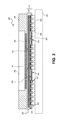
- FIG. 3 shows a side view of another embodiment of an assembly including a space transformer and a multi-chip package assembly.
- FIG. 4 shows a top view of the structure of FIG. 3 and shows dies are each I/O chip/module, graphics chip/module, and logic (cores) chip/module.
- FIG. 5 illustrates the computing device in accordance with one implementation.
- FIG. 6 shows the structure of FIG. 5 following the introduction of build-up layers on the structure.
- FIG. 7 shows the structure of FIG. 6 following the thinning of semiconductor substrate.
- FIG. 8 shows the structure of FIG. 7 following the introduction of a molding material on the structure.
- FIG. 9 shows the structure of FIG. 8 following the etching of openings or cavities through semiconductor substrate to contact pads.
- FIG. 10 shows the structure of FIG. 9 following the introduction of an optional barrier layer on the backside of the semiconductor substrate.
- FIG. 11 shows the structure of FIG. 10 following the formation of openings through barrier layer material to contact pads.
- FIG. 12 shows the structure of FIG. 11 following the introduction of solder connections to the contact pads.
- FIG. 13 illustrates the computing device in accordance with one implementation.
- an apparatus is operable as a space transformer and includes a planar semiconductor substrate including a plurality of devices formed in and/or on a device side of the semiconductor substrate and a first pattern of electrical contacts also formed on the device side of the semiconductor substrate.
- the apparatus also includes a plurality of layers of conductive material alternating between dielectric material on the device side of the semiconductor substrate.
- the plurality of layers of conductive material include a wiring layer including a second pattern of electrical contracts.
- a backside of the semiconductor substrate includes openings through the substrate to the first pattern of electrical contacts.
- a space transformer in one embodiment, a die or die is connected to one of the first pattern of electrical contacts and the second pattern of electrical contacts through, for example, solder connections.
- the other of the first pattern of electrical contacts and the second pattern of electrical contacts may be connected through, for example, solder connections to a substrate, such as a package substrate or a printed circuit board.
- a substrate such as a package substrate or a printed circuit board.
- FIG. 1 shows a side view of an embodiment of an assembly including a space transformer.
- assembly 100 includes space transformer 110 including semiconductor substrate 120 .
- Semiconductor substrate 120 includes device side 125 and backside 130 opposing device side 125 .
- Device side 125 includes active device or circuitry region 135 including, for example, components such as transistors and interconnects that are tailored to tasks such as high speed input/output (I/O), radio frequency (RF) and/or power delivery, or repeaters for die-to-die productivity.
- Device side 125 also includes an interconnect stack including at least one routing layer (fan out metal layer), a via layer and a pattern of contacts 140 on a surface of semiconductor substrate 120 .
- FIG. 1 shows layers of conductive material including conductive material layer 157 , conductive material layer 158 and conductive material layer 159 .
- a surface of build-up portion 145 includes a pattern of contacts connected to one or more of conductive material layer 157 , conductive material layer 158 and conductive material layer 159 and to contacts 140 through conductive vias.
- FIG. 1 shows representative conductive vias 154 between conductive material layer 159 and contacts 155 .
- Active device/circuitry regions 135 and the devices/circuits are connected ultimately to die 180 by conductive vias (e.g., conductive vias 154 ) and one or more of conductive material layers (metal layers) 157 - 159 .
- a portion of the contacts and vias to die 180 may also be through a conductive material layer(s) different than the conductive material layers illustrated in build-up portion 145 .
- FIG. 1 illustratively shows conductive via 153 between active device/circuitry region 135 and such other conductive material layer(s).
- each of conductive material layers 157 - 159 is, for example, a conductive material, while the conductive vias may be a copper, tungsten, gold or other metal suitable, for example, to contact semiconductor devices directly.
- conductive material layers 157 - 159 Disposed between contact points 155 and the layers of conductive material and semiconductor substrate 120 in structure 100 of FIG. 1 are layers of dielectric material (dielectric layer 161 , dielectric layer 162 , dielectric layer 163 and dielectric layer 164 , respectively).
- FIG. 1 shows semiconductor substrate 120 having openings 137 from backside 130 through a thickness of the substrate to contacts 140 .
- FIG. 1 shows solder balls 190 disposed through openings 137 to contacts 140 .
- the solder connections are operable to connect assembly 100 to contacts of substrate 193 such as a package substrate or a printed circuit board.
- FIG. 1 also shows contacts 155 on an opposite side of space transformer 110 connected to die 180 that is, for example, a microprocessor or other die.
- the connection of die 180 to contacts 155 is through solder connections 185 .
- contacts 155 have a pitch similar to contacts 182 of die 180 .
- Contacts 140 of space transformer 110 have a pitch to correspond with a pitch of substrate 193 .
- the pitch of contacts 140 is greater than a pitch of contacts 155 (contacts 155 are at a finer pitch than contacts 140 ).
- Surrounding die 180 on space transformer 110 is mold material 195 of, for example, an organic dielectric.
- substrate 120 or a device layer or layers of substrate 120 is a single crystal silicon, silicon-germanium or a narrow band-gap semiconductor material such as indium arsenide (InAs), or indium antimony (InSb) (having a band gap that is comparatively smaller than a band gap of silicon).
- Active device/circuitry region 135 may contain integrated circuits that allow for supplying some or all necessary I/O function to die 180 , RF/radio function, power delivery and repeater or die-to-die communication. Devices and circuits in active device/circuitry region 135 do not need to be manufactured in the same process as, for example, die 180 (e.g., a logic die).
- the device layers and dimensions can be tailored to fit specific functional needs.
- power transistors in active device/circuitry region 135 can have specific gate dielectric thicknesses that may be not be compatible with conventional logic manufacturing processes.
- additional capacitance needed for power delivery can be added.
- RF-transistors can have dimensions and structures (e.g., multi-gate-finger field effect transistors) tailored to have optimal characteristics for the intended RF frequencies and functions.
- device side 125 of semiconductor substrate includes barrier layer 132 of, for example, tantalum nitride (TaN) and/or dielectric layer 134 of, for example, silicon dioxide.
- Barrier layer 132 and/or dielectric layer 134 are introduced (e.g., via chemical vapor deposition) to a thickness in one aspect, to inhibit the diffusion of metal (e.g., copper) from contacts 140 into the semiconductor material and bump-to-bump electrical insulation.
- barrier layer 132 may be omitted and only dielectric layer 134 may be formed on the substrate.
- FIG. 2 shows a cross-sectional side view of another embodiment of an assembly including space transformer.
- Assembly 200 includes space transformer 210 including semiconductor substrate 220 having device side 225 and backside 230 .
- Device side 225 includes active device/circuitry region 235 and contacts 240 .
- build-up layer 245 of a plurality of layers of conductive material alternating between layers of dielectric material.
- the plurality of layers of conductive material include a wiring layer including a pattern of electrical contacts 255 on a surface of build-up layer 245 (a surface of space transformer 210 opposite semiconductor substrate 220 ).
- Active device/circuitry region 235 and the devices associated with semiconductor substrate 220 are ultimately connected to die 180 by conductive vias (e.g., conductive vias 254 between contacts 255 and a layer of conductive material in build-up layer 245 ).
- a portion of the contacts and vias to die 280 may also be through conductive material layer(s) different than the conductive material layers illustrated in build-up layer 245 .
- FIG. 2 illustratively shows conductive vias 253 between active device/circuitry region 235 and such other conductive material layer(s).
- FIG. 2 shows openings 237 through semiconductor substrate 220 to contacts 240 .
- the solder connections (solder balls 290 ) are disposed in openings 237 to contacts 240 .
- the solder connections are operable to connect space transformer 210 to substrate 293 such as a package substrate or printed circuit board.
- Contacts 255 are operable to connect space transformer 210 to a die (a microprocessor die) or dies such as die 280 through, for example, solder connections. As illustrated in FIG. 2 , contacts 255 have a finer pitch than contacts 240 .
- FIG. 2 shows mold material 295 disposed on space transformer 210 surrounding die 280 .
- FIG. 2 illustrates an embodiment where semiconductor substrate 220 or a device layer(s) of semiconductor substrate 220 is a wide band-gap semiconductor material such as gallium nitride or other Group III-V nitride material or a narrow-gap material that can be made semi-insulating by, for example, appropriate doping, or insulating such as, for example, gallium arsenide, aluminum arsenide or gallium phosphide. Since these semiconductor materials are sufficiently insulating or entirely insulating in the case of wide band-gap materials, a barrier and/or insulation layer on semiconductor substrate may not be needed as indicated in FIG. 2 .
- a wide band-gap semiconductor material such as gallium nitride or other Group III-V nitride material or a narrow-gap material that can be made semi-insulating by, for example, appropriate doping, or insulating such as, for example, gallium arsenide, aluminum arsenide or gallium phosphide. Since
- FIG. 3 shows a side view of another embodiment of an assembly including a space transformer and a multi-chip package assembly.
- Assembly 300 includes space transformer 310 including semiconductor substrate 320 and build-up layers 345 disposed on a device side of semiconductor substrate 320 .
- Semiconductor substrate 320 includes device side 325 including active device region 335 and a pattern of contacts 340 and backside 330 . Openings 337 are made through semiconductor substrate 320 to contacts 340 .
- Build-up layer 345 of alternating layers of conductive material and dielectric material is disposed on device side 325 of semiconductor substrate 320 .
- An opposite side of build-up layer 345 includes contacts 355 .
- Contacts 340 are operable to connect space transformer 310 to a substrate such as a package substrate or printed circuit board.
- FIG. 3 shows each of die 381 A, 382 A and 383 A connected to contacts 355 through, for example, solder connections.
- Die 381 A is, for example, an I/O chip/module
- die 382 A is, for example, a graphics chip/module
- die 383 A is, for example, logic (cores) chip/module.
- the individual chips are embedded in mold compound 395 of, for example, an organic material.
- FIG. 4 shows a top view of the structure of FIG.
- dies 381 A and 381 B are each, for example, I/O chip/module; dies 382 A, 382 B and 382 C are each graphics chip/module; and dies 383 A, 383 B, 383 C and 383 D are each logic (cores) chip/module.
- FIG. 3 and FIG. 4 illustrate an embodiment where late binding may be achieved independent of the active circuitry in a space transformer.
- active device/circuitry regions 335 of space transformer 310 may provide additional functionality such as power delivery, RF circuits, radios to the respective dice mounted on the space transformer.
- FIGS. 5-12 show an embodiment of a method for assembling a structure such as shown in FIG. 1 .
- FIG. 5 shows a portion of a semiconductor substrate such as a wafer.
- Substrate 420 is, for example, a silicon wafer.
- integrated circuit devices and circuits are formed in active device/circuitry regions 435 according to semiconductor processing techniques.
- Such devices and circuits e.g., interconnects
- gate and junction region (source region/drain region) metallization may be formed in a surface of a substrate.
- Additional metallization on a device side of semiconductor substrate may include an interconnect stack comprising at least one routing layer and a conductive via layer associated with active device/circuitry regions 435 .
- Further interconnect on substrate 420 includes at least one routing layer and associated conductive vias for a pad layer including a pattern of contact pads 440 .
- alternative semiconductor material may be introduced on the substrate.
- alternative semiconductor material e.g., germanium, Group III-V semiconductor, etc.
- germanium, Group III-V semiconductor, etc. may be introduced, for example, in a graded fashion.
- FIG. 6 shows the structure of FIG. 5 following the introduction of build-up layers on the structure.
- FIG. 6 shows build-up layers including layers of conductive material alternating between dielectric materials on a device side of semiconductor substrate 420 .
- suitable dielectric material includes chemical vapor deposition (CVD) deposited silicon dioxide (SiO 2 ), silicon nitride (Si 3 N 4 ) and dielectric material having a dielectric constant less than SiO 2 (a low k dielectric material).
- the conductive material and conductive via material is representatively a copper material deposited according to a dual- or single-damascene process.
- a conductive material of a copper material is disclosed for conductive via material
- via material particularly via material contacting devices in device/circuitry region 455
- the number of layers of conductive material in build-up layer 445 can vary as desired.
- a superior layer of conductive material includes a pattern of contact pads 455 having a pitch corresponding to a contact pitch of a die.
- FIG. 6 shows die 480 connected to contact pads 455 through, for example, solder connections.
- FIG. 6 also shows conductive vias 453 between active device/circuitry region 435 and a conductive material layer of build-up layer 445 .
- FIG. 7 shows the structure of FIG. 6 following the thinning of semiconductor substrate 420 .
- substrate 420 may be thinned by, for example, grinding the substrate down to the appropriate thickness by a mechanical grinding process.
- One representative thickness of substrate 420 is 25 ⁇ m or less.
- Other techniques including chemical mechanical polishing, wet etching and a plasma dry chemical etching.
- FIG. 8 shows the structure of FIG. 7 following the introduction of a molding material on the structure.
- FIG. 8 shows molding material 495 of, for example, an organic polymer on a surface of build-up layer 445 and surrounding die 480 .
- FIG. 8 also shows the structure after forming openings 510 through semiconductor substrate 420 in areas corresponding to contact pads 440 .
- FIG. 8 shows masking layer 505 of, for example, a photoresist having openings 510 to areas corresponding to location of contact pads 440 on an opposite side of semiconductor substrate 420 .
- FIG. 9 shows the structure of FIG. 8 following the etching of openings or cavities through semiconductor substrate 420 to contact pads 440 .
- a semiconductor substrate of, for example, silicon may be etched with a reactive ion etch to form the cavities.
- FIG. 9 also shows the structure following the removal of the masking layer.
- FIG. 10 shows the structure of FIG. 9 following the introduction of an optional barrier layer on the backside of the semiconductor substrate.
- FIG. 10 shows barrier layer 515 deposited as a blanket over the backside of semiconductor substrate.
- a suitable material for barrier layer 515 is tantalum nitride (TaN).
- TaN tantalum nitride
- One deposition technique is a chemical vapor deposition, another is atomic layer deposition.
- FIG. 11 shows the structure of FIG. 10 following the formation of openings through a material for barrier layer 515 to contact pads 440 .
- a process to form the openings includes the introduction of a masking material on barrier layer with openings to areas above the contact pads and followed by a reactive via etch through the barrier material to the contact pads and subsequent removal of the masking material.
- a dielectric layer may be conformally introduced as a blanket across the substrate and patterned similar to the barrier layer.
- FIG. 12 shows the structure of FIG. 11 following the introduction of solder connections to the contact pads.
- FIG. 12 shows solder connection 520 of, for example, tin-based solder introduction to contact pads 440 .
- the structure may be singulated from, for example, other structures formed on the substrate base (e.g., singulated from a wafer).
- the structure may be connected to a substrate, such as a package substrate.
- FIG. 13 illustrates computing device 600 in accordance with one implementation.
- Computing device 600 houses board 602 .
- Board 602 may include a number of components, including but not limited to processor 604 and at least one communication chip 606 .
- Processor 604 is physically and electrically coupled to board 602 .
- at least one communication chip 606 is also physically and electrically coupled to board 602 .
- communication chip 606 is part of processor 604 .
- computing device 600 may include other components that may or may not be physically and electrically coupled to board 602 .
- these other components include, but are not limited to, volatile memory (e.g., DRAM), non-volatile memory (e.g., ROM), flash memory, a graphics processor, a digital signal processor, a crypto processor, a chipset, an antenna, a display, a touchscreen display, a touchscreen controller, a battery, an audio codec, a video codec, a power amplifier, a global positioning system (GPS) device, a compass, an accelerometer, a gyroscope, a speaker, a camera, and a mass storage device (such as hard disk drive, compact disk (CD), digital versatile disk (DVD), and so forth).
- volatile memory e.g., DRAM
- non-volatile memory e.g., ROM
- flash memory e.g., a graphics processor, a digital signal processor, a crypto processor, a chipset, an antenna
- Communication chip 606 enables wireless communications for the transfer of data to and from computing device 600 .
- wireless and its derivatives may be used to describe circuits, devices, systems, methods, techniques, communications channels, etc., that may communicate data through the use of modulated electromagnetic radiation through a non-solid medium. The term does not imply that the associated devices do not contain any wires, although in some embodiments they might not.
- Communication chip 606 may implement any of a number of wireless standards or protocols, including but not limited to Wi-Fi (IEEE 802.11 family), WiMAX (IEEE 802.16 family), IEEE 802.20, long term evolution (LTE), Ev-DO, HSPA+, HSDPA+, HSUPA+, EDGE, GSM, GPRS, CDMA, TDMA, DECT, Bluetooth, derivatives thereof, as well as any other wireless protocols that are designated as 3G, 4G, 5G, and beyond.
- Computing device 600 may include a plurality of communication chips 606 .
- first communication chip 606 may be dedicated to shorter range wireless communications such as Wi-Fi and Bluetooth and second communication chip 606 may be dedicated to longer range wireless communications such as GPS, EDGE, GPRS, CDMA, WiMAX, LTE, Ev-DO, and others.
- Processor 604 of computing device 600 includes an integrated circuit die packaged within processor 604 .
- the package includes an integrated circuit die connected to a space transformer where the space transformer has an active device/circuitry region such as described above.
- the term “processor” may refer to any device or portion of a device that processes electronic data from registers and/or memory to transform that electronic data into other electronic data that may be stored in registers and/or memory.
- Communication chip 606 also includes an integrated circuit die packaged within communication chip 606 .
- the package includes an integrated circuit die connected to a space transformer where the space transformer has an active device/circuitry region such as described above.
- computing device 600 may be a laptop, a netbook, a notebook, an ultrabook, a smartphone, a tablet, a personal digital assistant (PDA), an ultra mobile PC, a mobile phone, a desktop computer, a server, a printer, a scanner, a monitor, a set-top box, an entertainment control unit, a digital camera, a portable music player, or a digital video recorder.
- computing device 600 may be any other electronic device that processes data.
- Example 1 is an apparatus including a planar semiconductor substrate including a plurality of devices and a first pattern of electrical contacts formed on the first surface of the semiconductor substrate; and a plurality of layers of conductive material alternating between dielectric material on the first surface of the semiconductor substrate, the plurality of layers of conductive material including a wiring layer including a second pattern of electrical contacts, wherein the second surface of the semiconductor substrate includes openings to the first pattern of electrical contacts.
- the first pattern of electrical contacts in the apparatus of Example 1 includes a first pitch and the second plurality of contacts include a second pitch and the first pitch is greater than the second pitch.
- Example 3 the plurality of devices in the apparatus of Example 1 are operable to perform a task related to at least one of high speed input/output, radio frequency, or power delivery.
- the thickness of the semiconductor substrate in the apparatus of Example 1 includes less than about 25 microns.
- Example 5 the apparatus of Example 1 further includes at least one of a diffusion barrier layer and an insulation layer disposed on the second surface of the semiconductor substrate.
- Example 6 the semiconductor substrate in the apparatus of Example 1 includes a narrow band gap semiconductor material including silicon.
- Example 7 the semiconductor substrate in the apparatus of Example 1 includes a wide band gap semiconductor material.
- Example 8 the apparatus of Example 1 further includes a die coupled to one of the first pattern of electrical contacts and the second pattern of electrical contacts.
- Example 9 is an apparatus, including a space transformer including a semiconductor substrate including a plurality of devices and a first pattern of electrical contacts on a first side of the semiconductor substrate and a plurality of layers of conductive material alternating between dielectric material on the first side of the semiconductor substrate, the plurality of layers of conductive material including a first wiring layer including a second pattern of electrical contacts; and at least one integrated circuit chip mounted on one of the first side and the second side of the semiconductor substrate.
- a second side of the semiconductor substrate in the apparatus of Example 9 includes openings to the first pattern of electrical contacts.
- the first pattern of electrical contacts in the apparatus of Example 9 includes a first pitch and the second pattern of contacts include a second pitch and the first pitch is greater than the second pitch.
- Example 12 the plurality of devices in the apparatus of Example 9 are operable to perform a task related to at least one of high speed input/output, radio frequency, or power delivery.
- the thickness of the semiconductor substrate in the apparatus of Example 9 includes less than about 25 microns.
- Example 14 the apparatus of Example 9 further includes at least one of a diffusion barrier layer and an insulation layer disposed on a second surface of the semiconductor substrate.
- the semiconductor substrate in the apparatus of Example 9 includes a narrow band gap semiconductor material including silicon.
- Example 16 the semiconductor substrate in the apparatus of Example 9 includes a wide band gap semiconductor material.
- Example 17 the apparatus of Example 9 further includes a package substrate coupled to the other of the first side and the second side of the semiconductor substrate.
- Example 18 is a method including forming openings through a semiconductor substrate of a space transformer to a first pattern of electrical contacts on the semiconductor substrate, the space transformer including an interconnect stack on the semiconductor substrate, the interconnect stack including at least one routing layer and a pad layer including a second pattern of electrical contacts; and coupling an integrated circuit chip to one of the first pattern of electrical contacts and the second pattern of electrical contacts.
- Example 19 the method of Example 18 further includes forming a barrier layer on the semiconductor substrate.
- Example 20 the method of Example 18 further includes forming solder bumps on the first pattern of electrical contacts.
- Example 21 the method of Example 20 further includes coupling the solder bumps to contacts of a package.
Landscapes
- Engineering & Computer Science (AREA)
- Microelectronics & Electronic Packaging (AREA)
- Power Engineering (AREA)
- Computer Hardware Design (AREA)
- Physics & Mathematics (AREA)
- Condensed Matter Physics & Semiconductors (AREA)
- General Physics & Mathematics (AREA)
- Manufacturing & Machinery (AREA)
- Ceramic Engineering (AREA)
- Internal Circuitry In Semiconductor Integrated Circuit Devices (AREA)
- Geometry (AREA)
- Wire Bonding (AREA)
Abstract
Description
Claims (22)
Priority Applications (3)
| Application Number | Priority Date | Filing Date | Title |
|---|---|---|---|
| US14/229,405 US9564408B2 (en) | 2014-03-28 | 2014-03-28 | Space transformer |
| TW104103468A TWI552269B (en) | 2014-03-28 | 2015-02-02 | Apparatus operable as space transformer, apparatus with space transformer and method for semiconductor packaging |
| JP2015026002A JP2015192145A (en) | 2014-03-28 | 2015-02-13 | space transformer |
Applications Claiming Priority (1)
| Application Number | Priority Date | Filing Date | Title |
|---|---|---|---|
| US14/229,405 US9564408B2 (en) | 2014-03-28 | 2014-03-28 | Space transformer |
Publications (2)
| Publication Number | Publication Date |
|---|---|
| US20150279774A1 US20150279774A1 (en) | 2015-10-01 |
| US9564408B2 true US9564408B2 (en) | 2017-02-07 |
Family
ID=54191446
Family Applications (1)
| Application Number | Title | Priority Date | Filing Date |
|---|---|---|---|
| US14/229,405 Active US9564408B2 (en) | 2014-03-28 | 2014-03-28 | Space transformer |
Country Status (3)
| Country | Link |
|---|---|
| US (1) | US9564408B2 (en) |
| JP (1) | JP2015192145A (en) |
| TW (1) | TWI552269B (en) |
Cited By (1)
| Publication number | Priority date | Publication date | Assignee | Title |
|---|---|---|---|---|
| US11217565B2 (en) * | 2012-12-22 | 2022-01-04 | Monolithic 3D Inc. | Method to form a 3D semiconductor device and structure |
Families Citing this family (3)
| Publication number | Priority date | Publication date | Assignee | Title |
|---|---|---|---|---|
| CN108604587B (en) * | 2015-12-26 | 2023-01-13 | 英特尔公司 | On-chip integrated passive device |
| US20170287838A1 (en) * | 2016-04-02 | 2017-10-05 | Intel Corporation | Electrical interconnect bridge |
| KR101973444B1 (en) * | 2017-10-19 | 2019-04-29 | 삼성전기주식회사 | Semiconductor package |
Citations (7)
| Publication number | Priority date | Publication date | Assignee | Title |
|---|---|---|---|---|
| US20040155357A1 (en) * | 2003-02-11 | 2004-08-12 | Kwun-Yao Ho | [chip package structure and manufacturing process thereof] |
| US20060163743A1 (en) * | 2005-01-21 | 2006-07-27 | Semiconductor Energy Laboratory Co., Ltd. | Semiconductor device and method for manufacturing the same, and electric device |
| JP2009059822A (en) | 2007-08-30 | 2009-03-19 | Fujitsu Ltd | Capacitor embedded interposer, semiconductor device with the same, and manufacturing method for the capacitor embedded interposer |
| US20090160011A1 (en) * | 2007-12-24 | 2009-06-25 | Petari Incorporation | Isolator and method of manufacturing the same |
| WO2010047228A1 (en) | 2008-10-21 | 2010-04-29 | 日本電気株式会社 | Wiring board and method for manufacturing same |
| US20110121444A1 (en) * | 2009-11-24 | 2011-05-26 | Albert Wu | Embedded chip packages |
| US20130089701A1 (en) | 2011-10-06 | 2013-04-11 | Electro Scientific Industries, Inc. | Substrate containing aperture and methods of forming the same |
Family Cites Families (2)
| Publication number | Priority date | Publication date | Assignee | Title |
|---|---|---|---|---|
| JP2013120838A (en) * | 2011-12-07 | 2013-06-17 | Elpida Memory Inc | Semiconductor device and semiconductor chip |
| JP5919943B2 (en) * | 2012-03-27 | 2016-05-18 | 凸版印刷株式会社 | Silicon interposer |
-
2014
- 2014-03-28 US US14/229,405 patent/US9564408B2/en active Active
-
2015
- 2015-02-02 TW TW104103468A patent/TWI552269B/en active
- 2015-02-13 JP JP2015026002A patent/JP2015192145A/en active Pending
Patent Citations (7)
| Publication number | Priority date | Publication date | Assignee | Title |
|---|---|---|---|---|
| US20040155357A1 (en) * | 2003-02-11 | 2004-08-12 | Kwun-Yao Ho | [chip package structure and manufacturing process thereof] |
| US20060163743A1 (en) * | 2005-01-21 | 2006-07-27 | Semiconductor Energy Laboratory Co., Ltd. | Semiconductor device and method for manufacturing the same, and electric device |
| JP2009059822A (en) | 2007-08-30 | 2009-03-19 | Fujitsu Ltd | Capacitor embedded interposer, semiconductor device with the same, and manufacturing method for the capacitor embedded interposer |
| US20090160011A1 (en) * | 2007-12-24 | 2009-06-25 | Petari Incorporation | Isolator and method of manufacturing the same |
| WO2010047228A1 (en) | 2008-10-21 | 2010-04-29 | 日本電気株式会社 | Wiring board and method for manufacturing same |
| US20110121444A1 (en) * | 2009-11-24 | 2011-05-26 | Albert Wu | Embedded chip packages |
| US20130089701A1 (en) | 2011-10-06 | 2013-04-11 | Electro Scientific Industries, Inc. | Substrate containing aperture and methods of forming the same |
Non-Patent Citations (3)
| Title |
|---|
| Intel Corporation, "Final Office Action", JP Application No. 2015-026002, (Jul. 26, 2016). |
| Intel Corporation, "First Office Action", JP Application No. 2015-026002, (Mar. 1, 2016). |
| Intel Corporation, "Office action with search report", TW Application No. 104103468, (Feb. 24, 2016). |
Cited By (1)
| Publication number | Priority date | Publication date | Assignee | Title |
|---|---|---|---|---|
| US11217565B2 (en) * | 2012-12-22 | 2022-01-04 | Monolithic 3D Inc. | Method to form a 3D semiconductor device and structure |
Also Published As
| Publication number | Publication date |
|---|---|
| TW201543615A (en) | 2015-11-16 |
| JP2015192145A (en) | 2015-11-02 |
| TWI552269B (en) | 2016-10-01 |
| US20150279774A1 (en) | 2015-10-01 |
Similar Documents
| Publication | Publication Date | Title |
|---|---|---|
| US11424195B2 (en) | Microelectronic assemblies having front end under embedded radio frequency die | |
| US11594524B2 (en) | Fabrication and use of through silicon vias on double sided interconnect device | |
| US11640942B2 (en) | Microelectronic component having molded regions with through-mold vias | |
| US20220285278A1 (en) | Via structures having tapered profiles for embedded interconnect bridge substrates | |
| US20130285257A1 (en) | 3d interconnect structure comprising through-silicon vias combined with fine pitch backside metal redistribution lines fabricated using a dual damascene type approach | |
| US20130256910A1 (en) | 3d interconnect structure comprising fine pitch single damascene backside metal redistribution lines combined with through-silicon vias | |
| US11652059B2 (en) | Composite interposer structure and method of providing same | |
| US11688692B2 (en) | Embedded multi-die interconnect bridge having a substrate with conductive pathways and a molded material region with through-mold vias | |
| US20200273779A1 (en) | Vertically stacked transistor devices with isolation wall structures containing an electrical conductor | |
| US20240030188A1 (en) | Monolithic chip stacking using a die with double-sided interconnect layers | |
| EP4016615A1 (en) | Inter-component material in microelectronic assemblies having direct bonding | |
| US9564408B2 (en) | Space transformer | |
| US20230130935A1 (en) | Skip level vias in metallization layers for integrated circuit devices | |
| KR102367994B1 (en) | Heterogeneous integration of ultra-thin functional blocks by solid-state adhesives and selective transfer | |
| EP4152366A2 (en) | Microelectronic assemblies including solder and non-solder interconnects | |
| EP4016607A1 (en) | Inter-component material in microelectronic assemblies having direct bonding | |
| US10770429B2 (en) | Microelectronic device stacks having interior window wirebonding | |
| US11824002B2 (en) | Variable pitch and stack height for high performance interconnects | |
| US20200335434A1 (en) | Metal oxycarbide resists as leave behind plugs | |
| US20200098921A1 (en) | Vertically stacked cmos with upfront m0 interconnect | |
| US20190393191A1 (en) | Packages of stacking integrated circuits | |
| US20230197685A1 (en) | Multiple wafer stack architecture to enable singulation |
Legal Events
| Date | Code | Title | Description |
|---|---|---|---|
| AS | Assignment |
Owner name: INTEL CORPORATION, CALIFORNIA Free format text: ASSIGNMENT OF ASSIGNORS INTEREST;ASSIGNORS:ALEKSOV, ALEKSANDAR;SWAN, JOHANNA M.;SIGNING DATES FROM 20140327 TO 20140331;REEL/FRAME:032620/0851 |
|
| FEPP | Fee payment procedure |
Free format text: PAYOR NUMBER ASSIGNED (ORIGINAL EVENT CODE: ASPN); ENTITY STATUS OF PATENT OWNER: LARGE ENTITY |
|
| STCF | Information on status: patent grant |
Free format text: PATENTED CASE |
|
| MAFP | Maintenance fee payment |
Free format text: PAYMENT OF MAINTENANCE FEE, 4TH YEAR, LARGE ENTITY (ORIGINAL EVENT CODE: M1551); ENTITY STATUS OF PATENT OWNER: LARGE ENTITY Year of fee payment: 4 |
|
| AS | Assignment |
Owner name: TAHOE RESEARCH, LTD., IRELAND Free format text: ASSIGNMENT OF ASSIGNORS INTEREST;ASSIGNOR:INTEL CORPORATION;REEL/FRAME:061175/0176 Effective date: 20220718 |
|
| MAFP | Maintenance fee payment |
Free format text: PAYMENT OF MAINTENANCE FEE, 8TH YEAR, LARGE ENTITY (ORIGINAL EVENT CODE: M1552); ENTITY STATUS OF PATENT OWNER: LARGE ENTITY Year of fee payment: 8 |