JP2006100760A - 薄膜トランジスタおよびその製造方法 - Google Patents
薄膜トランジスタおよびその製造方法 Download PDFInfo
- Publication number
- JP2006100760A JP2006100760A JP2004378476A JP2004378476A JP2006100760A JP 2006100760 A JP2006100760 A JP 2006100760A JP 2004378476 A JP2004378476 A JP 2004378476A JP 2004378476 A JP2004378476 A JP 2004378476A JP 2006100760 A JP2006100760 A JP 2006100760A
- Authority
- JP
- Japan
- Prior art keywords
- thin film
- semiconductor thin
- insulating film
- electrode
- film
- Prior art date
- Legal status (The legal status is an assumption and is not a legal conclusion. Google has not performed a legal analysis and makes no representation as to the accuracy of the status listed.)
- Pending
Links
- 239000010409 thin film Substances 0.000 title claims abstract description 257
- 238000004519 manufacturing process Methods 0.000 title claims abstract description 34
- 239000010408 film Substances 0.000 claims abstract description 219
- 239000004065 semiconductor Substances 0.000 claims abstract description 187
- 230000001681 protective effect Effects 0.000 claims abstract description 75
- XLOMVQKBTHCTTD-UHFFFAOYSA-N Zinc monoxide Chemical compound [Zn]=O XLOMVQKBTHCTTD-UHFFFAOYSA-N 0.000 claims abstract description 57
- 238000005530 etching Methods 0.000 claims abstract description 35
- 239000011787 zinc oxide Substances 0.000 claims abstract description 28
- HEMHJVSKTPXQMS-UHFFFAOYSA-M Sodium hydroxide Chemical compound [OH-].[Na+] HEMHJVSKTPXQMS-UHFFFAOYSA-M 0.000 claims description 39
- 238000000034 method Methods 0.000 claims description 38
- 239000007864 aqueous solution Substances 0.000 claims description 20
- 239000000758 substrate Substances 0.000 claims description 15
- 229910052751 metal Inorganic materials 0.000 claims description 10
- 239000002184 metal Substances 0.000 claims description 10
- 230000002093 peripheral effect Effects 0.000 claims description 9
- 238000011946 reduction process Methods 0.000 claims description 5
- 239000000463 material Substances 0.000 claims description 3
- 238000000638 solvent extraction Methods 0.000 claims 1
- 239000000243 solution Substances 0.000 description 35
- 230000005540 biological transmission Effects 0.000 description 27
- IAZDPXIOMUYVGZ-UHFFFAOYSA-N Dimethylsulphoxide Chemical compound CS(C)=O IAZDPXIOMUYVGZ-UHFFFAOYSA-N 0.000 description 24
- 239000004973 liquid crystal related substance Substances 0.000 description 18
- 229910052581 Si3N4 Inorganic materials 0.000 description 16
- HQVNEWCFYHHQES-UHFFFAOYSA-N silicon nitride Chemical compound N12[Si]34N5[Si]62N3[Si]51N64 HQVNEWCFYHHQES-UHFFFAOYSA-N 0.000 description 16
- 238000000206 photolithography Methods 0.000 description 14
- 239000011521 glass Substances 0.000 description 10
- 229910052782 aluminium Inorganic materials 0.000 description 8
- XAGFODPZIPBFFR-UHFFFAOYSA-N aluminium Chemical compound [Al] XAGFODPZIPBFFR-UHFFFAOYSA-N 0.000 description 8
- 238000005268 plasma chemical vapour deposition Methods 0.000 description 8
- VYZAMTAEIAYCRO-UHFFFAOYSA-N Chromium Chemical compound [Cr] VYZAMTAEIAYCRO-UHFFFAOYSA-N 0.000 description 7
- 229910052804 chromium Inorganic materials 0.000 description 7
- 239000011651 chromium Substances 0.000 description 7
- 238000004544 sputter deposition Methods 0.000 description 7
- 230000015572 biosynthetic process Effects 0.000 description 6
- 239000003792 electrolyte Substances 0.000 description 6
- 239000003960 organic solvent Substances 0.000 description 6
- 238000009751 slip forming Methods 0.000 description 4
- 229910018503 SF6 Inorganic materials 0.000 description 3
- 229910021417 amorphous silicon Inorganic materials 0.000 description 3
- 239000004020 conductor Substances 0.000 description 3
- 238000001312 dry etching Methods 0.000 description 3
- 238000001020 plasma etching Methods 0.000 description 3
- SFZCNBIFKDRMGX-UHFFFAOYSA-N sulfur hexafluoride Chemical compound FS(F)(F)(F)(F)F SFZCNBIFKDRMGX-UHFFFAOYSA-N 0.000 description 3
- 229960000909 sulfur hexafluoride Drugs 0.000 description 3
- NBIIXXVUZAFLBC-UHFFFAOYSA-N Phosphoric acid Chemical compound OP(O)(O)=O NBIIXXVUZAFLBC-UHFFFAOYSA-N 0.000 description 2
- 238000009792 diffusion process Methods 0.000 description 2
- 150000002500 ions Chemical class 0.000 description 2
- 239000011159 matrix material Substances 0.000 description 2
- 239000000126 substance Substances 0.000 description 2
- 206010021143 Hypoxia Diseases 0.000 description 1
- DGAQECJNVWCQMB-PUAWFVPOSA-M Ilexoside XXIX Chemical compound C[C@@H]1CC[C@@]2(CC[C@@]3(C(=CC[C@H]4[C@]3(CC[C@@H]5[C@@]4(CC[C@@H](C5(C)C)OS(=O)(=O)[O-])C)C)[C@@H]2[C@]1(C)O)C)C(=O)O[C@H]6[C@@H]([C@H]([C@@H]([C@H](O6)CO)O)O)O.[Na+] DGAQECJNVWCQMB-PUAWFVPOSA-M 0.000 description 1
- 239000002253 acid Substances 0.000 description 1
- 239000003513 alkali Substances 0.000 description 1
- 229910000147 aluminium phosphate Inorganic materials 0.000 description 1
- 238000005266 casting Methods 0.000 description 1
- 230000006866 deterioration Effects 0.000 description 1
- 239000007788 liquid Substances 0.000 description 1
- 238000000059 patterning Methods 0.000 description 1
- 238000007747 plating Methods 0.000 description 1
- 229910052708 sodium Inorganic materials 0.000 description 1
- 239000011734 sodium Substances 0.000 description 1
- 238000007740 vapor deposition Methods 0.000 description 1
Images


Classifications
-
- H—ELECTRICITY
- H01—ELECTRIC ELEMENTS
- H01L—SEMICONDUCTOR DEVICES NOT COVERED BY CLASS H10
- H01L29/00—Semiconductor devices adapted for rectifying, amplifying, oscillating or switching, or capacitors or resistors with at least one potential-jump barrier or surface barrier, e.g. PN junction depletion layer or carrier concentration layer; Details of semiconductor bodies or of electrodes thereof ; Multistep manufacturing processes therefor
- H01L29/66—Types of semiconductor device ; Multistep manufacturing processes therefor
- H01L29/68—Types of semiconductor device ; Multistep manufacturing processes therefor controllable by only the electric current supplied, or only the electric potential applied, to an electrode which does not carry the current to be rectified, amplified or switched
- H01L29/76—Unipolar devices, e.g. field effect transistors
- H01L29/772—Field effect transistors
- H01L29/78—Field effect transistors with field effect produced by an insulated gate
- H01L29/786—Thin film transistors, i.e. transistors with a channel being at least partly a thin film
- H01L29/7869—Thin film transistors, i.e. transistors with a channel being at least partly a thin film having a semiconductor body comprising an oxide semiconductor material, e.g. zinc oxide, copper aluminium oxide, cadmium stannate
-
- H—ELECTRICITY
- H01—ELECTRIC ELEMENTS
- H01L—SEMICONDUCTOR DEVICES NOT COVERED BY CLASS H10
- H01L29/00—Semiconductor devices adapted for rectifying, amplifying, oscillating or switching, or capacitors or resistors with at least one potential-jump barrier or surface barrier, e.g. PN junction depletion layer or carrier concentration layer; Details of semiconductor bodies or of electrodes thereof ; Multistep manufacturing processes therefor
- H01L29/40—Electrodes ; Multistep manufacturing processes therefor
- H01L29/41—Electrodes ; Multistep manufacturing processes therefor characterised by their shape, relative sizes or dispositions
- H01L29/417—Electrodes ; Multistep manufacturing processes therefor characterised by their shape, relative sizes or dispositions carrying the current to be rectified, amplified or switched
- H01L29/41725—Source or drain electrodes for field effect devices
- H01L29/41733—Source or drain electrodes for field effect devices for thin film transistors with insulated gate
-
- H—ELECTRICITY
- H01—ELECTRIC ELEMENTS
- H01L—SEMICONDUCTOR DEVICES NOT COVERED BY CLASS H10
- H01L29/00—Semiconductor devices adapted for rectifying, amplifying, oscillating or switching, or capacitors or resistors with at least one potential-jump barrier or surface barrier, e.g. PN junction depletion layer or carrier concentration layer; Details of semiconductor bodies or of electrodes thereof ; Multistep manufacturing processes therefor
- H01L29/40—Electrodes ; Multistep manufacturing processes therefor
- H01L29/43—Electrodes ; Multistep manufacturing processes therefor characterised by the materials of which they are formed
- H01L29/45—Ohmic electrodes
- H01L29/456—Ohmic electrodes on silicon
- H01L29/458—Ohmic electrodes on silicon for thin film silicon, e.g. source or drain electrode
-
- H—ELECTRICITY
- H01—ELECTRIC ELEMENTS
- H01L—SEMICONDUCTOR DEVICES NOT COVERED BY CLASS H10
- H01L29/00—Semiconductor devices adapted for rectifying, amplifying, oscillating or switching, or capacitors or resistors with at least one potential-jump barrier or surface barrier, e.g. PN junction depletion layer or carrier concentration layer; Details of semiconductor bodies or of electrodes thereof ; Multistep manufacturing processes therefor
- H01L29/66—Types of semiconductor device ; Multistep manufacturing processes therefor
- H01L29/66007—Multistep manufacturing processes
- H01L29/66075—Multistep manufacturing processes of devices having semiconductor bodies comprising group 14 or group 13/15 materials
- H01L29/66227—Multistep manufacturing processes of devices having semiconductor bodies comprising group 14 or group 13/15 materials the devices being controllable only by the electric current supplied or the electric potential applied, to an electrode which does not carry the current to be rectified, amplified or switched, e.g. three-terminal devices
- H01L29/66409—Unipolar field-effect transistors
- H01L29/66477—Unipolar field-effect transistors with an insulated gate, i.e. MISFET
- H01L29/66742—Thin film unipolar transistors
-
- H—ELECTRICITY
- H01—ELECTRIC ELEMENTS
- H01L—SEMICONDUCTOR DEVICES NOT COVERED BY CLASS H10
- H01L29/00—Semiconductor devices adapted for rectifying, amplifying, oscillating or switching, or capacitors or resistors with at least one potential-jump barrier or surface barrier, e.g. PN junction depletion layer or carrier concentration layer; Details of semiconductor bodies or of electrodes thereof ; Multistep manufacturing processes therefor
- H01L29/66—Types of semiconductor device ; Multistep manufacturing processes therefor
- H01L29/66007—Multistep manufacturing processes
- H01L29/66969—Multistep manufacturing processes of devices having semiconductor bodies not comprising group 14 or group 13/15 materials
-
- H—ELECTRICITY
- H01—ELECTRIC ELEMENTS
- H01L—SEMICONDUCTOR DEVICES NOT COVERED BY CLASS H10
- H01L29/00—Semiconductor devices adapted for rectifying, amplifying, oscillating or switching, or capacitors or resistors with at least one potential-jump barrier or surface barrier, e.g. PN junction depletion layer or carrier concentration layer; Details of semiconductor bodies or of electrodes thereof ; Multistep manufacturing processes therefor
- H01L29/66—Types of semiconductor device ; Multistep manufacturing processes therefor
- H01L29/68—Types of semiconductor device ; Multistep manufacturing processes therefor controllable by only the electric current supplied, or only the electric potential applied, to an electrode which does not carry the current to be rectified, amplified or switched
- H01L29/76—Unipolar devices, e.g. field effect transistors
- H01L29/772—Field effect transistors
- H01L29/78—Field effect transistors with field effect produced by an insulated gate
- H01L29/786—Thin film transistors, i.e. transistors with a channel being at least partly a thin film
- H01L29/78606—Thin film transistors, i.e. transistors with a channel being at least partly a thin film with supplementary region or layer in the thin film or in the insulated bulk substrate supporting it for controlling or increasing the safety of the device
- H01L29/78618—Thin film transistors, i.e. transistors with a channel being at least partly a thin film with supplementary region or layer in the thin film or in the insulated bulk substrate supporting it for controlling or increasing the safety of the device characterised by the drain or the source properties, e.g. the doping structure, the composition, the sectional shape or the contact structure
-
- H—ELECTRICITY
- H01—ELECTRIC ELEMENTS
- H01L—SEMICONDUCTOR DEVICES NOT COVERED BY CLASS H10
- H01L29/00—Semiconductor devices adapted for rectifying, amplifying, oscillating or switching, or capacitors or resistors with at least one potential-jump barrier or surface barrier, e.g. PN junction depletion layer or carrier concentration layer; Details of semiconductor bodies or of electrodes thereof ; Multistep manufacturing processes therefor
- H01L29/66—Types of semiconductor device ; Multistep manufacturing processes therefor
- H01L29/68—Types of semiconductor device ; Multistep manufacturing processes therefor controllable by only the electric current supplied, or only the electric potential applied, to an electrode which does not carry the current to be rectified, amplified or switched
- H01L29/76—Unipolar devices, e.g. field effect transistors
- H01L29/772—Field effect transistors
- H01L29/78—Field effect transistors with field effect produced by an insulated gate
- H01L29/786—Thin film transistors, i.e. transistors with a channel being at least partly a thin film
- H01L29/78696—Thin film transistors, i.e. transistors with a channel being at least partly a thin film characterised by the structure of the channel, e.g. multichannel, transverse or longitudinal shape, length or width, doping structure, or the overlap or alignment between the channel and the gate, the source or the drain, or the contacting structure of the channel
Abstract
【解決手段】 まず、真性酸化亜鉛からなる半導体薄膜8の上面全体に保護膜9を形成し、その上に上層絶縁膜12を成膜する。次に、上層絶縁膜12および保護膜9にコンタクトホール10、11を形成する。この場合、チャネル長Lは2つのコンタクトホール10、11間の間隔により決定され、チャネル幅Wはコンタクトホール10、11の所定方向の寸法により決定される。これにより、半導体薄膜8にサイドエッチングがやや生じても、チャネル長Lおよびチャネル幅Wに寸法変化が生じることはない。
【選択図】 図1
Description
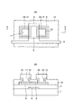
図1(A)はこの発明の第1実施形態としての薄膜トランジスタを備えた液晶表示素子の要部の透過平面図を示し、図1(B)は図1(A)のB−B線に沿う断面図を示す。この液晶表示素子はガラス基板1を備えている。ガラス基板1の上面には、マトリクス状に配置された複数の画素電極2と、各画素電極2に接続された薄膜トランジスタ3と、行方向に配置され、各薄膜トランジスタ3に走査信号を供給する走査ライン4と、列方向に配置され、各薄膜トランジスタ3にデータ信号を供給するデータライン5とが設けられている。
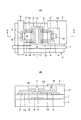
図12(A)はこの発明の第2実施形態としての薄膜トランジスタを備えた液晶表示素子の要部の透過平面図を示し、図12(B)は図12(A)のB−B線に沿う断面図を示す。この液晶表示素子において、図1(A)、(B)に示す場合と異なる点は、オーミックコンタクト層13、14を備えておらず、ソース電極15およびドレイン電極16をコンタクトホール10、11を介して半導体薄膜8に直接接続した点である。
図13(A)はこの発明の第3実施形態としての薄膜トランジスタを備えた液晶表示素子の要部の透過平面図を示し、図13(B)は図13(A)のB−B線に沿う断面図を示す。この液晶表示素子において、図1(A)、(B)に示す場合と異なる点は、上層絶縁膜12を備えていない点である。したがって、上層絶縁膜12を成膜する工程を省略することができる。
図14(A)はこの発明の第4実施形態としての薄膜トランジスタを備えた液晶表示素子の要部の透過平面図を示し、図14(B)は図14(A)のB−B線に沿う断面図を示す。この液晶表示素子において、図1(A)、(B)に示す場合と大きく異なる点は、上層絶縁膜12を備えておらず、平面ほぼ十字形状の半導体薄膜8(図18(A)参照)の上面中央部にコンタクトホールを有しない保護膜9を設け、半導体薄膜8のチャネル方向の端面a、それに直交する方向の端面a’、a”をオーミックコンタクト層13、14で覆った点である。
図23(A)はこの発明の第5実施形態としての薄膜トランジスタを備えた液晶表示素子の要部の透過平面図を示し、図23(B)は図23(A)のB−B線に沿う断面図を示す。この液晶表示素子において、図14(A)、(B)に示す場合と異なる点は、オーミックコンタクト層13、14を備えておらず、ソース電極15およびドレイン電極16を半導体薄膜8に直接接続した点である。
半導体薄膜形成用層8aおよびオーミックコンタクト層形成用層23、33の成膜は、プラズマCVD法に限らず、スパッタ法、蒸着法、キャスト法、メッキ法等であってもよい。また、オーミックコンタクト層13、14は、n型酸化亜鉛に限らず、p型酸化亜鉛であってもよく、また酸素欠損を生じさせて導電率を変化させた酸化亜鉛であってもよい。
2 画素電極
3 薄膜トランジスタ
4 走査ライン
5 データライン
6 ゲート電極
7 ゲート絶縁膜
8 半導体薄膜
9 保護膜
10、11 コンタクトホール
12 上層絶縁膜
13、14 オーミックコンタクト層
15 ソース電極
16 ドレイン電極
17 オーバーコート膜
18 コンタクトホール
Claims (33)
- 半導体薄膜と、該半導体薄膜の一面に形成されたゲート絶縁膜と、該ゲート絶縁膜を介して前記半導体薄膜に対向して形成されたゲート電極と、前記半導体薄膜に電気的に接続されたソース電極およびドレイン電極を有する薄膜トランジスタであって、
前記半導体薄膜の周辺部上に、該半導体薄膜の端面と同一形状の端面を有する絶縁膜が形成され、該絶縁膜から露出された前記半導体薄膜に前記ソース電極および前記ドレイン電極が接続されていることを特徴とする薄膜トランジスタ。 - 請求項1に記載の発明において、前記絶縁膜から露出された前記半導体薄膜のチャネル領域上に対応してソース電極用およびドレイン電極用のコンタクトホールに仕切る中央絶縁膜が設けられていることを特徴とする薄膜トランジスタ。
- 請求項2に記載の発明において、前記中央絶縁膜は前記絶縁膜と同一の材料により同一の厚さに設けられていることを特徴とする薄膜トランジスタ。
- 請求項2に記載の発明において、前記絶縁膜、前記中央絶縁膜および前記半導体薄膜上に、前記各コンタクトホールに対応する部分にコンタクトホールを有する上層絶縁膜が設けられ、前記各コンタクトホールを介して露出された前記半導体薄膜の上面およびその各近傍の前記上層絶縁膜の上面にそれぞれオーミックコンタクト層が設けられていることを特徴とする薄膜トランジスタ。
- 請求項4に記載の発明において、前記各オーミックコンタクト層上に前記ソース電極および前記ドレイン電極が前記各オーミックコンタクト層を完全に覆うように設けられていることを特徴とする薄膜トランジスタ。
- 請求項2に記載の発明において、前記絶縁膜、前記中央絶縁膜および前記半導体薄膜を含む前記ゲート絶縁膜上に、前記各コンタクトホールに対応する部分にコンタクトホールを有する上層絶縁膜が設けられ、前記各コンタクトホールを介して露出された前記半導体薄膜に低抵抗化処理が施され、前記各コンタクトホールを介して露出された前記半導体薄膜の上面およびその各近傍の前記上層絶縁膜の上面に前記ソース電極および前記ドレイン電極が設けられていることを特徴とする薄膜トランジスタ。
- 請求項2に記載の発明において、前記各コンタクトホールを介して露出された前記半導体薄膜の上面およびその各近傍の前記絶縁膜と前記保護膜の上面にそれぞれオーミックコンタクト層が設けられていることを特徴とする薄膜トランジスタ。
- 請求項7に記載の発明において、前記各オーミックコンタクト層上に前記ソース電極および前記ドレイン電極が前記各オーミックコンタクト層を完全に覆うように設けられていることを特徴とする薄膜トランジスタ。
- 半導体薄膜と、該半導体薄膜の一面に形成されたゲート絶縁膜と、該ゲート絶縁膜を介して前記半導体薄膜に対向して形成されたゲート電極と、前記半導体薄膜のソース領域およびドレイン領域上にそれぞれ形成されたオーミックコンタクト層を有する薄膜トランジスタであって、
前記ゲート電極上における前記半導体薄膜のチャネル領域上に中央絶縁膜が設けられ、前記オーミックコンタクト層がそれぞれ前記中央絶縁膜の上面端部から前記半導体薄膜の上面全長および少なくとも前記半導体薄膜のチャネル方向の端面を覆って設けられていることを特徴とする薄膜トランジスタ。 - 半導体薄膜と、該半導体薄膜の一面に設けられたゲート絶縁膜と、該ゲート絶縁膜を介して前記半導体薄膜に対向して設けられたゲート電極と、前記半導体薄膜に電気的に接続されたソース電極およびドレイン電極を有する薄膜トランジスタであって、
前記ゲート電極上における前記半導体薄膜のチャネル領域上に中央絶縁膜が設けられ、前記中央絶縁膜によって覆われずに露出された前記半導体薄膜に低抵抗化処理が施され、前記ソース電極および前記ドレイン電極が、それぞれ、前記中央絶縁膜の上面端部から前記半導体薄膜の上面全長および少なくとも前記半導体薄膜のチャネル方向の端面を覆って設けられていることを特徴とする薄膜トランジスタ。 - 請求項10に記載の発明において、前記ソース電極と前記半導体薄膜の間および前記ドレイン電極と前記半導体薄膜の間に、それぞれ、前記中央絶縁膜の端部上から前記半導体薄膜の上面全体および少なくとも前記半導体薄膜のチャネル方向の端面を覆うコンタクト層が設けられていることを特徴とする薄膜トランジスタ。
- 請求項1〜11のいずれかに記載の発明において、前記絶縁膜、前記ソース電極および前記ドレイン電極を覆うオーバーコート膜を有することを特徴とする薄膜トランジスタ。
- 請求項12に記載の発明において、前記オーバーコート膜の上面に画素電極が前記ソース電極に接続されて設けられていることを特徴とする薄膜トランジスタ。
- 半導体薄膜と、該半導体薄膜の一面に設けられたゲート絶縁膜と、該ゲート絶縁膜を介して前記半導体薄膜に対向して設けられたゲート電極と、前記半導体薄膜に電気的に接続されたソース電極およびドレイン電極を有する薄膜トランジスタの製造方法であって、
半導体薄膜および絶縁膜を積層して形成し、前記絶縁膜および前記半導体薄膜をエッチングして少なくとも前記半導体薄膜の周辺部上に、該半導体薄膜の端面と同一形状の端面を有する絶縁膜を形成し、該絶縁膜から露出された前記半導体薄膜に接続される前記ソース電極および前記ドレイン電極を形成することを特徴とする薄膜トランジスタの製造方法。 - 請求項14に記載の発明において、前記絶縁膜および前記半導体薄膜を連続してエッチングすることを特徴とする薄膜トランジスタの製造方法。
- 請求項14に記載の発明において、前記半導体薄膜は亜鉛酸化物を主たる材料とし、前記半導体薄膜のエッチングは、アルカリ水溶液を用いることを特徴とする薄膜トランジスタの製造方法。
- 請求項16に記載の発明において、前記アルカリ水溶液は2〜10wt%の水酸化ナトリウム水溶液であることを特徴とする薄膜トランジスタの製造方法。
- 請求項14に記載の発明において、前記絶縁膜から露出された前記半導体薄膜のチャネル領域上に対応してソース電極用およびドレイン電極用のコンタクトホールに仕切る中央絶縁膜を形成することを特徴とする薄膜トランジスタの製造方法。
- 請求項18に記載の発明において、前記絶縁膜、前記中央絶縁膜および前記半導体薄膜上に上層絶縁膜を形成し、前記各コンタクトホールに対応する部分にコンタクトホールを形成し、各コンタクトホールを介して露出された前記半導体薄膜の上面およびその各近傍の前記上層絶縁膜の上面にそれぞれオーミックコンタクト層を形成することを特徴とする薄膜トランジスタの製造方法。
- 請求項19に記載の発明において、前記各オーミックコンタクト層上に前記ソース電極および前記ドレイン電極を前記各オーミックコンタクト層を完全に覆うように形成することを特徴とする薄膜トランジスタの製造方法。
- 請求項18に記載の発明において、前記絶縁膜、前記中央絶縁膜および前記半導体薄膜上に、前記各コンタクトホールに対応する部分にコンタクトホールを有する上層絶縁膜を形成し、前記各コンタクトホールを介して前記半導体薄膜の上面およびその各近傍の前記上層絶縁膜の上面に前記ソース電極および前記ドレイン電極を形成し、いずれかの工程で前記上層絶縁膜および前記各コンタクトホールを介して露出された前記半導体薄膜に低抵抗化処理を施すことを特徴とする薄膜トランジスタの製造方法。
- 請求項21に記載の発明において、前記各コンタクトホールを介して露出された前記半導体薄膜の上面およびその各近傍の前記絶縁膜の上面にそれぞれオーミックコンタクト層を形成することを特徴とする薄膜トランジスタの製造方法。
- 請求項19に記載の発明において、前記各オーミックコンタクト層上に前記ソース電極および前記ドレイン電極を前記各オーミックコンタクト層を完全に覆うように形成することを特徴とする薄膜トランジスタの製造方法。
- 基板上に、半導体薄膜と、該半導体薄膜の一面に設けられたゲート絶縁膜と、該ゲート絶縁膜を介して前記半導体薄膜に対向して設けられたゲート電極と、前記半導体薄膜のソース領域およびドレイン領域上に形成されたオーミックコンタクト層とを有する薄膜トランジスタを形成する薄膜トランジスタの製造方法であって、
半導体薄膜をエッチングによりデバイスサイズに形成し、前記ゲート電極上における前記半導体薄膜のチャネル領域上に中央絶縁膜を設け、前記オーミックコンタクト層を前記中央絶縁膜、半導体薄膜および前記基板の露出面全面に成膜し、その後、エッチングにより、前記オーミックコンタクト層を前記中央絶縁膜上で分離され、前記中央絶縁膜の端部から前記半導体薄膜の上面全長および少なくとも前記半導体薄膜のチャネル方向の端面を覆うように形成することを特徴とする薄膜トランジスタの製造方法。 - 基板上に、半導体薄膜と、該半導体薄膜の一面に設けられたゲート絶縁膜と、該ゲート絶縁膜を介して前記半導体薄膜に対向して設けられたゲート電極と、前記半導体薄膜に電気的に接続されたソース電極およびドレイン電極を有する薄膜トランジスタの製造方法であって、
半導体薄膜をエッチングによりデバイスサイズに形成し、前記ゲート電極上における前記半導体薄膜のチャネル領域上に中央絶縁膜を設け、前記ソース電極およびドレイン電極形成用の金属層を前記中央絶縁膜、前記半導体膜および前記基板の露出面全面に成膜し、次に、エッチングにより、前記半導体薄膜の上面に前記ソース電極および前記ドレイン電極をそれぞれ前記中央絶縁膜の端部から前記半導体薄膜の上面全長および少なくとも前記半導体薄膜のチャネル方向の端面を覆うように形成し、いずれかの工程で前記に中央絶縁膜よって覆われずに露出された前記半導体薄膜に低抵抗化処理を施すことを特徴とする薄膜トランジスタの製造方法。 - 請求項24または25に記載の発明において、前記半導体薄膜は亜鉛酸化物を主たる材料とし、前記半導体薄膜のエッチングは、アルカリ水溶液を用いて行うことを特徴とする薄膜トランジスタの製造方法。
- 請求項26に記載の発明において、前記アルカリ水溶液は2〜10wt%の水酸化ナトリウム水溶液であることを特徴とする薄膜トランジスタの製造方法。
- 請求項24〜27に記載の発明において、前記中央絶縁膜の形成工程は、前記ゲート電極をマスクとした裏面露光を行なう工程を含むことを特徴とする薄膜トランジスタの製造方法。
- 半導体薄膜と、該半導体薄膜の一面に設けられたゲート絶縁膜と、該ゲート絶縁膜を介して前記半導体薄膜に対向して設けられたゲート電極と、前記半導体薄膜に電気的に接続されたソース電極およびドレイン電極を有する薄膜トランジスタの製造方法であって、
半導体薄膜形成用層上に絶縁膜を形成し、該絶縁膜をマスクとして前記半導体薄膜形成用層をエッチングして前記半導体薄膜を形成し、前記絶縁膜にソース電極用およびドレイン電極用のコンタクトホールを形成し、前記各コンタクトホールを介して露出された前記半導体薄膜に接続される前記ソース電極やよび前記ドレイン電極を形成することを特徴とする薄膜トランジスタの製造方法。 - 請求項29に記載の発明において、前記絶縁膜および前記半導体薄膜上に上層絶縁膜を形成し、前記各コンタクトホールに対応する部分にコンタクトホールを形成し、各コンタクトホールを介して露出された前記半導体薄膜の上面およびその各近傍の前記上層絶縁膜の上面にそれぞれオーミックコンタクト層を形成することを特徴とする薄膜トランジスタの製造方法。
- 請求項30に記載の発明において、前記各オーミックコンタクト層上に前記ソース電極および前記ドレイン電極を前記各オーミックコンタクト層を完全に覆うように形成することを特徴とする薄膜トランジスタの製造方法。
- 請求項29〜31記載の発明において、前記半導体薄膜は亜鉛酸化物を主たる材料とし、前記半導体薄膜形成用層のエッチングは、アルカリ水溶液を用いて行うことを特徴とする薄膜トランジスタの製造方法。
- 請求項32に記載の発明において、前記アルカリ水溶液は2〜10wt%の水酸化ナトリウム水溶液であることを特徴とする薄膜トランジスタの製造方法。
Priority Applications (8)
| Application Number | Priority Date | Filing Date | Title |
|---|---|---|---|
| JP2004378476A JP2006100760A (ja) | 2004-09-02 | 2004-12-28 | 薄膜トランジスタおよびその製造方法 |
| US11/219,171 US7385224B2 (en) | 2004-09-02 | 2005-09-01 | Thin film transistor having an etching protection film and manufacturing method thereof |
| TW094130031A TWI302033B (en) | 2004-09-02 | 2005-09-02 | Thin film transistor and its manufacturing method |
| KR1020077004614A KR101192071B1 (ko) | 2004-09-02 | 2005-09-02 | 박막 트랜지스터와 그 제조방법 |
| EP10009733.6A EP2264770A3 (en) | 2004-09-02 | 2005-09-02 | Thin film transistor and its manufacturing method |
| PCT/JP2005/016566 WO2006025609A2 (en) | 2004-09-02 | 2005-09-02 | Thin film transistor and its manufacturing method |
| CN2005800296495A CN101032027B (zh) | 2004-09-02 | 2005-09-02 | 薄膜晶体管及其制造方法 |
| EP05778343A EP1787333A2 (en) | 2004-09-02 | 2005-09-02 | Thin film transistor and its manufacturing method |
Applications Claiming Priority (2)
| Application Number | Priority Date | Filing Date | Title |
|---|---|---|---|
| JP2004255307 | 2004-09-02 | ||
| JP2004378476A JP2006100760A (ja) | 2004-09-02 | 2004-12-28 | 薄膜トランジスタおよびその製造方法 |
Related Child Applications (1)
| Application Number | Title | Priority Date | Filing Date |
|---|---|---|---|
| JP2009256844A Division JP5333160B2 (ja) | 2004-09-02 | 2009-11-10 | 薄膜トランジスタおよびその製造方法 |
Publications (1)
| Publication Number | Publication Date |
|---|---|
| JP2006100760A true JP2006100760A (ja) | 2006-04-13 |
Family
ID=35219630
Family Applications (1)
| Application Number | Title | Priority Date | Filing Date |
|---|---|---|---|
| JP2004378476A Pending JP2006100760A (ja) | 2004-09-02 | 2004-12-28 | 薄膜トランジスタおよびその製造方法 |
Country Status (6)
| Country | Link |
|---|---|
| US (1) | US7385224B2 (ja) |
| EP (2) | EP2264770A3 (ja) |
| JP (1) | JP2006100760A (ja) |
| KR (1) | KR101192071B1 (ja) |
| TW (1) | TWI302033B (ja) |
| WO (1) | WO2006025609A2 (ja) |
Cited By (42)
| Publication number | Priority date | Publication date | Assignee | Title |
|---|---|---|---|---|
| JP2008028141A (ja) * | 2006-07-21 | 2008-02-07 | Casio Comput Co Ltd | 半導体装置の製造方法 |
| JP2008060099A (ja) * | 2006-08-29 | 2008-03-13 | Casio Comput Co Ltd | 薄膜トランジスタおよびその製造方法 |
| JP2008205469A (ja) * | 2007-02-16 | 2008-09-04 | Samsung Electronics Co Ltd | 薄膜トランジスタ及びその製造方法 |
| JP2009135380A (ja) * | 2007-05-30 | 2009-06-18 | Canon Inc | 酸化物半導体を用いた薄膜トランジスタの製造方法および表示装置 |
| JP2010062549A (ja) * | 2008-08-08 | 2010-03-18 | Semiconductor Energy Lab Co Ltd | 半導体装置の作製方法 |
| JP2010073894A (ja) * | 2008-09-18 | 2010-04-02 | Sony Corp | 薄膜トランジスタおよびその製造方法 |
| JP2010098304A (ja) * | 2008-09-19 | 2010-04-30 | Semiconductor Energy Lab Co Ltd | 表示装置 |
| JP2010161373A (ja) * | 2009-01-12 | 2010-07-22 | Samsung Mobile Display Co Ltd | 薄膜トランジスタ及びその製造方法、並びに薄膜トランジスタを備える平板表示装置 |
| JP2010166038A (ja) * | 2008-12-19 | 2010-07-29 | Semiconductor Energy Lab Co Ltd | 半導体装置の作製方法 |
| WO2011013522A1 (en) * | 2009-07-31 | 2011-02-03 | Semiconductor Energy Laboratory Co., Ltd. | Semiconductor device and manufacturing method thereof |
| JP2011077106A (ja) * | 2009-09-29 | 2011-04-14 | Dainippon Printing Co Ltd | 薄膜集積回路装置及びその製造方法 |
| WO2012020525A1 (ja) * | 2010-08-07 | 2012-02-16 | シャープ株式会社 | 薄膜トランジスタ基板及びそれを備えた液晶表示装置 |
| US8143115B2 (en) | 2006-12-05 | 2012-03-27 | Canon Kabushiki Kaisha | Method for manufacturing thin film transistor using oxide semiconductor and display apparatus |
| WO2012053161A1 (ja) * | 2010-10-18 | 2012-04-26 | シャープ株式会社 | 薄膜トランジスタ基板の製造方法およびその方法により製造された薄膜トランジスタ基板 |
| WO2012060362A1 (ja) * | 2010-11-04 | 2012-05-10 | シャープ株式会社 | 半導体装置、表示装置、ならびに半導体装置および表示装置の製造方法 |
| JP2012099796A (ja) * | 2010-10-07 | 2012-05-24 | Semiconductor Energy Lab Co Ltd | 薄膜素子の作製方法及び半導体装置の作製方法 |
| CN102646718A (zh) * | 2008-12-03 | 2012-08-22 | 索尼株式会社 | 薄膜晶体管、显示单元和制造薄膜晶体管的方法 |
| JP2012525000A (ja) * | 2009-04-21 | 2012-10-18 | シーブライト・インコーポレイテッド | 二重自己整合式金属酸化物薄膜トランジスタ |
| JP2012248865A (ja) * | 2009-12-21 | 2012-12-13 | Sharp Corp | アクティブマトリクス基板及びそれを備えた表示パネル |
| JP2013506294A (ja) * | 2009-09-24 | 2013-02-21 | アプライド マテリアルズ インコーポレイテッド | ソース・ドレイン金属エッチングのためのウェットプロセスを用いた金属酸化物又は金属酸窒化物tftの製造方法 |
| JP2013115099A (ja) * | 2011-11-25 | 2013-06-10 | Sony Corp | トランジスタ、表示装置および電子機器 |
| JP2013153140A (ja) * | 2011-12-02 | 2013-08-08 | Semiconductor Energy Lab Co Ltd | 半導体装置及びその作製方法 |
| KR20130092848A (ko) * | 2012-02-13 | 2013-08-21 | 삼성전자주식회사 | 박막 트랜지스터 및 이를 채용한 디스플레이 패널 |
| JP2013258358A (ja) * | 2012-06-14 | 2013-12-26 | Japan Display Inc | 表示装置及びその製造方法 |
| KR20140010100A (ko) * | 2011-03-02 | 2014-01-23 | 어플라이드 머티어리얼스, 인코포레이티드 | 오프셋 전극 tft 구조 |
| JP2014524666A (ja) * | 2011-08-22 | 2014-09-22 | 京東方科技集團股▲ふん▼有限公司 | 酸化物tftアレイ基板及びその製造方法並びに電子デバイス |
| JP2015504246A (ja) * | 2011-12-31 | 2015-02-05 | 京東方科技集團股▲ふん▼有限公司 | 薄膜トランジスタ、アレイ基板及びその製造方法、並びに表示装置 |
| JP2015053520A (ja) * | 2009-02-13 | 2015-03-19 | 株式会社半導体エネルギー研究所 | 半導体装置 |
| JP2015079969A (ja) * | 2009-08-07 | 2015-04-23 | 株式会社半導体エネルギー研究所 | 発光装置 |
| JP2015130490A (ja) * | 2013-12-02 | 2015-07-16 | 株式会社半導体エネルギー研究所 | 半導体装置 |
| JP2015144290A (ja) * | 2009-03-27 | 2015-08-06 | 株式会社半導体エネルギー研究所 | 表示装置 |
| JP2015525000A (ja) * | 2012-07-25 | 2015-08-27 | 京東方科技集團股▲ふん▼有限公司 | 薄膜トランジスタ、アレイ基板及びその製作方法、ディスプレイ |
| JP2015159301A (ja) * | 2009-12-04 | 2015-09-03 | 株式会社半導体エネルギー研究所 | 直流変換回路 |
| KR20160022334A (ko) * | 2011-06-10 | 2016-02-29 | 가부시키가이샤 한도오따이 에네루기 켄큐쇼 | 반도체 장치의 제작 방법 |
| JP2016034023A (ja) * | 2014-07-29 | 2016-03-10 | 株式会社半導体エネルギー研究所 | 半導体装置およびその作製方法、電子機器 |
| KR101680847B1 (ko) * | 2009-05-29 | 2016-11-29 | 가부시키가이샤 한도오따이 에네루기 켄큐쇼 | 반도체 장치 및 그 제작 방법 |
| JP2017108163A (ja) * | 2011-09-29 | 2017-06-15 | 株式会社半導体エネルギー研究所 | 半導体装置 |
| KR101814315B1 (ko) * | 2013-03-21 | 2018-01-02 | 보에 테크놀로지 그룹 컴퍼니 리미티드 | 박막 트랜지스터 및 그 제조 방법, 어레이 기판, 및 디스플레이 디바이스 |
| KR101847355B1 (ko) | 2010-03-30 | 2018-04-09 | 가부시키가이샤 제이올레드 | 박막 트랜지스터 및 그 제조 방법과 디스플레이 장치 |
| JP2018125536A (ja) * | 2009-09-04 | 2018-08-09 | 株式会社半導体エネルギー研究所 | 表示装置 |
| JP2018174354A (ja) * | 2009-09-04 | 2018-11-08 | 株式会社半導体エネルギー研究所 | 半導体装置 |
| JP2018537861A (ja) * | 2015-12-16 | 2018-12-20 | 鴻富錦精密工業(深▲セン▼)有限公司 | 薄膜トランジスタの基板及びその製造方法 |
Families Citing this family (1812)
| Publication number | Priority date | Publication date | Assignee | Title |
|---|---|---|---|---|
| TWI562380B (en) * | 2005-01-28 | 2016-12-11 | Semiconductor Energy Lab Co Ltd | Semiconductor device, electronic device, and method of manufacturing semiconductor device |
| TWI481024B (zh) | 2005-01-28 | 2015-04-11 | Semiconductor Energy Lab | 半導體裝置,電子裝置,和半導體裝置的製造方法 |
| US7928938B2 (en) | 2005-04-19 | 2011-04-19 | Semiconductor Energy Laboratory Co., Ltd. | Semiconductor device including memory circuit, display device and electronic apparatus |
| US8629819B2 (en) | 2005-07-14 | 2014-01-14 | Semiconductor Energy Laboratory Co., Ltd. | Semiconductor device and driving method thereof |
| EP1758072A3 (en) * | 2005-08-24 | 2007-05-02 | Semiconductor Energy Laboratory Co., Ltd. | Display device and driving method thereof |
| EP1995787A3 (en) * | 2005-09-29 | 2012-01-18 | Semiconductor Energy Laboratory Co, Ltd. | Semiconductor device having oxide semiconductor layer and manufacturing method therof |
| CN101577293B (zh) * | 2005-11-15 | 2012-09-19 | 株式会社半导体能源研究所 | 半导体器件及其制造方法 |
| EP2924498A1 (en) | 2006-04-06 | 2015-09-30 | Semiconductor Energy Laboratory Co, Ltd. | Liquid crystal desplay device, semiconductor device, and electronic appliance |
| US20070261951A1 (en) * | 2006-04-06 | 2007-11-15 | Yan Ye | Reactive sputtering zinc oxide transparent conductive oxides onto large area substrates |
| US7674662B2 (en) * | 2006-07-19 | 2010-03-09 | Applied Materials, Inc. | Process for making thin film field effect transistors using zinc oxide |
| JP5116277B2 (ja) | 2006-09-29 | 2013-01-09 | 株式会社半導体エネルギー研究所 | 半導体装置、表示装置、液晶表示装置、表示モジュール及び電子機器 |
| US7646015B2 (en) * | 2006-10-31 | 2010-01-12 | Semiconductor Energy Laboratory Co., Ltd. | Manufacturing method of semiconductor device and semiconductor device |
| US8275080B2 (en) * | 2006-11-17 | 2012-09-25 | Comtech Mobile Datacom Corporation | Self-supporting simplex packets |
| US20080121877A1 (en) * | 2006-11-27 | 2008-05-29 | 3M Innovative Properties Company | Thin film transistor with enhanced stability |
| US7655127B2 (en) * | 2006-11-27 | 2010-02-02 | 3M Innovative Properties Company | Method of fabricating thin film transistor |
| JP2008151963A (ja) * | 2006-12-15 | 2008-07-03 | Semiconductor Energy Lab Co Ltd | 半導体装置及び半導体装置の駆動方法 |
| US20080254613A1 (en) * | 2007-04-10 | 2008-10-16 | Applied Materials, Inc. | Methods for forming metal interconnect structure for thin film transistor applications |
| US7927713B2 (en) * | 2007-04-27 | 2011-04-19 | Applied Materials, Inc. | Thin film semiconductor material produced through reactive sputtering of zinc target using nitrogen gases |
| JP5542297B2 (ja) | 2007-05-17 | 2014-07-09 | 株式会社半導体エネルギー研究所 | 液晶表示装置、表示モジュール及び電子機器 |
| JP4989309B2 (ja) | 2007-05-18 | 2012-08-01 | 株式会社半導体エネルギー研究所 | 液晶表示装置 |
| JP5361249B2 (ja) * | 2007-05-31 | 2013-12-04 | キヤノン株式会社 | 酸化物半導体を用いた薄膜トランジスタの製造方法 |
| US8354674B2 (en) * | 2007-06-29 | 2013-01-15 | Semiconductor Energy Laboratory Co., Ltd. | Semiconductor device wherein a property of a first semiconductor layer is different from a property of a second semiconductor layer |
| WO2009014155A1 (en) | 2007-07-25 | 2009-01-29 | Semiconductor Energy Laboratory Co., Ltd. | Photoelectric conversion device and electronic device having the same |
| KR20090011704A (ko) * | 2007-07-27 | 2009-02-02 | 삼성전자주식회사 | 박막 트랜지스터 기판 및 그 제조 방법 |
| NO332409B1 (no) * | 2008-01-24 | 2012-09-17 | Well Technology As | Anordning og fremgangsmate for a isolere en seksjon av et bronnhull |
| US8143093B2 (en) * | 2008-03-20 | 2012-03-27 | Applied Materials, Inc. | Process to make metal oxide thin film transistor array with etch stopping layer |
| US7879698B2 (en) * | 2008-03-24 | 2011-02-01 | Applied Materials, Inc. | Integrated process system and process sequence for production of thin film transistor arrays using doped or compounded metal oxide semiconductor |
| US9041202B2 (en) | 2008-05-16 | 2015-05-26 | Semiconductor Energy Laboratory Co., Ltd. | Semiconductor device and manufacturing method of the same |
| US8314765B2 (en) | 2008-06-17 | 2012-11-20 | Semiconductor Energy Laboratory Co., Ltd. | Driver circuit, display device, and electronic device |
| KR100963027B1 (ko) * | 2008-06-30 | 2010-06-10 | 삼성모바일디스플레이주식회사 | 박막 트랜지스터, 그의 제조 방법 및 박막 트랜지스터를구비하는 평판 표시 장치 |
| US8258511B2 (en) | 2008-07-02 | 2012-09-04 | Applied Materials, Inc. | Thin film transistors using multiple active channel layers |
| KR102549916B1 (ko) | 2008-07-10 | 2023-06-29 | 가부시키가이샤 한도오따이 에네루기 켄큐쇼 | 발광장치 및 전자기기 |
| US9666719B2 (en) * | 2008-07-31 | 2017-05-30 | Semiconductor Energy Laboratory Co., Ltd. | Semiconductor device and manufacturing method thereof |
| US8945981B2 (en) | 2008-07-31 | 2015-02-03 | Semiconductor Energy Laboratory Co., Ltd. | Semiconductor device and manufacturing method thereof |
| TWI495108B (zh) * | 2008-07-31 | 2015-08-01 | Semiconductor Energy Lab | 半導體裝置的製造方法 |
| TWI491048B (zh) * | 2008-07-31 | 2015-07-01 | Semiconductor Energy Lab | 半導體裝置 |
| TWI577027B (zh) * | 2008-07-31 | 2017-04-01 | 半導體能源研究所股份有限公司 | 半導體裝置及其製造方法 |
| TWI508282B (zh) | 2008-08-08 | 2015-11-11 | Semiconductor Energy Lab | 半導體裝置及其製造方法 |
| JP5480554B2 (ja) | 2008-08-08 | 2014-04-23 | 株式会社半導体エネルギー研究所 | 半導体装置 |
| JP5525778B2 (ja) | 2008-08-08 | 2014-06-18 | 株式会社半導体エネルギー研究所 | 半導体装置 |
| TWI500160B (zh) * | 2008-08-08 | 2015-09-11 | Semiconductor Energy Lab | 半導體裝置及其製造方法 |
| US8039433B2 (en) * | 2008-08-19 | 2011-10-18 | Warsaw Orthopedic, Inc. | Osteogenic compositions containing a coloring agent |
| US9082857B2 (en) | 2008-09-01 | 2015-07-14 | Semiconductor Energy Laboratory Co., Ltd. | Semiconductor device comprising an oxide semiconductor layer |
| TWI606592B (zh) * | 2008-09-01 | 2017-11-21 | 半導體能源研究所股份有限公司 | 半導體裝置的製造方法 |
| JP5627071B2 (ja) | 2008-09-01 | 2014-11-19 | 株式会社半導体エネルギー研究所 | 半導体装置の作製方法 |
| WO2010029859A1 (en) * | 2008-09-12 | 2010-03-18 | Semiconductor Energy Laboratory Co., Ltd. | Semiconductor device and method for manufacturing the same |
| KR101644406B1 (ko) | 2008-09-12 | 2016-08-01 | 가부시키가이샤 한도오따이 에네루기 켄큐쇼 | 표시 장치 |
| KR101545460B1 (ko) * | 2008-09-12 | 2015-08-18 | 가부시키가이샤 한도오따이 에네루기 켄큐쇼 | 반도체 장치 및 그 생산 방법 |
| KR101783193B1 (ko) * | 2008-09-12 | 2017-09-29 | 가부시키가이샤 한도오따이 에네루기 켄큐쇼 | 표시 장치 |
| CN102160102B (zh) | 2008-09-19 | 2013-11-06 | 株式会社半导体能源研究所 | 显示装置 |
| KR102426826B1 (ko) | 2008-09-19 | 2022-08-01 | 가부시키가이샤 한도오따이 에네루기 켄큐쇼 | 반도체 장치 |
| CN102160105B (zh) * | 2008-09-19 | 2014-06-11 | 株式会社半导体能源研究所 | 显示装置及其制造方法 |
| KR101507324B1 (ko) | 2008-09-19 | 2015-03-31 | 가부시키가이샤 한도오따이 에네루기 켄큐쇼 | 표시 장치 |
| KR101611643B1 (ko) * | 2008-10-01 | 2016-04-11 | 가부시키가이샤 한도오따이 에네루기 켄큐쇼 | 반도체 장치 |
| CN101714546B (zh) | 2008-10-03 | 2014-05-14 | 株式会社半导体能源研究所 | 显示装置及其制造方法 |
| KR101803720B1 (ko) | 2008-10-03 | 2017-12-01 | 가부시키가이샤 한도오따이 에네루기 켄큐쇼 | 표시 장치 |
| EP2172977A1 (en) | 2008-10-03 | 2010-04-07 | Semiconductor Energy Laboratory Co., Ltd. | Display device |
| KR20160113329A (ko) | 2008-10-03 | 2016-09-28 | 가부시키가이샤 한도오따이 에네루기 켄큐쇼 | 표시장치 |
| EP2172804B1 (en) | 2008-10-03 | 2016-05-11 | Semiconductor Energy Laboratory Co, Ltd. | Display device |
| CN101719493B (zh) | 2008-10-08 | 2014-05-14 | 株式会社半导体能源研究所 | 显示装置 |
| JP5484853B2 (ja) * | 2008-10-10 | 2014-05-07 | 株式会社半導体エネルギー研究所 | 半導体装置の作製方法 |
| KR101799601B1 (ko) * | 2008-10-16 | 2017-11-20 | 가부시키가이샤 한도오따이 에네루기 켄큐쇼 | 발광 표시 장치 |
| JP5361651B2 (ja) | 2008-10-22 | 2013-12-04 | 株式会社半導体エネルギー研究所 | 半導体装置の作製方法 |
| US8741702B2 (en) | 2008-10-24 | 2014-06-03 | Semiconductor Energy Laboratory Co., Ltd. | Method for manufacturing semiconductor device |
| US8106400B2 (en) | 2008-10-24 | 2012-01-31 | Semiconductor Energy Laboratory Co., Ltd. | Semiconductor device and method for manufacturing the same |
| KR101667909B1 (ko) * | 2008-10-24 | 2016-10-28 | 가부시키가이샤 한도오따이 에네루기 켄큐쇼 | 반도체장치의 제조방법 |
| JP5616012B2 (ja) | 2008-10-24 | 2014-10-29 | 株式会社半導体エネルギー研究所 | 半導体装置の作製方法 |
| KR101310473B1 (ko) | 2008-10-24 | 2013-09-24 | 가부시키가이샤 한도오따이 에네루기 켄큐쇼 | 반도체 장치 |
| EP2180518B1 (en) | 2008-10-24 | 2018-04-25 | Semiconductor Energy Laboratory Co, Ltd. | Method for manufacturing semiconductor device |
| WO2010047288A1 (en) * | 2008-10-24 | 2010-04-29 | Semiconductor Energy Laboratory Co., Ltd. | Method for manufacturing semiconductordevice |
| JP5442234B2 (ja) | 2008-10-24 | 2014-03-12 | 株式会社半導体エネルギー研究所 | 半導体装置及び表示装置 |
| KR101631454B1 (ko) | 2008-10-31 | 2016-06-17 | 가부시키가이샤 한도오따이 에네루기 켄큐쇼 | 논리회로 |
| KR101603303B1 (ko) | 2008-10-31 | 2016-03-14 | 가부시키가이샤 한도오따이 에네루기 켄큐쇼 | 도전성 산질화물 및 도전성 산질화물막의 제작 방법 |
| KR101634411B1 (ko) * | 2008-10-31 | 2016-06-28 | 가부시키가이샤 한도오따이 에네루기 켄큐쇼 | 구동 회로, 표시 장치 및 전자 장치 |
| TWI633605B (zh) | 2008-10-31 | 2018-08-21 | 半導體能源研究所股份有限公司 | 半導體裝置及其製造方法 |
| TWI467663B (zh) | 2008-11-07 | 2015-01-01 | Semiconductor Energy Lab | 半導體裝置和該半導體裝置的製造方法 |
| TW201921700A (zh) | 2008-11-07 | 2019-06-01 | 日商半導體能源研究所股份有限公司 | 半導體裝置和其製造方法 |
| CN101740631B (zh) * | 2008-11-07 | 2014-07-16 | 株式会社半导体能源研究所 | 半导体装置及该半导体装置的制造方法 |
| KR101659703B1 (ko) * | 2008-11-07 | 2016-09-26 | 가부시키가이샤 한도오따이 에네루기 켄큐쇼 | 반도체 장치 |
| EP2184783B1 (en) | 2008-11-07 | 2012-10-03 | Semiconductor Energy Laboratory Co, Ltd. | Semiconductor device and method for manufacturing the same |
| TWI535037B (zh) * | 2008-11-07 | 2016-05-21 | 半導體能源研究所股份有限公司 | 半導體裝置和其製造方法 |
| TWI502739B (zh) | 2008-11-13 | 2015-10-01 | Semiconductor Energy Lab | 半導體裝置及其製造方法 |
| KR101432764B1 (ko) * | 2008-11-13 | 2014-08-21 | 가부시키가이샤 한도오따이 에네루기 켄큐쇼 | 반도체장치의 제조방법 |
| US8232947B2 (en) | 2008-11-14 | 2012-07-31 | Semiconductor Energy Laboratory Co., Ltd. | Liquid crystal display device |
| JP2010153802A (ja) | 2008-11-20 | 2010-07-08 | Semiconductor Energy Lab Co Ltd | 半導体装置及び半導体装置の作製方法 |
| KR102556313B1 (ko) | 2008-11-21 | 2023-07-18 | 가부시키가이샤 한도오따이 에네루기 켄큐쇼 | 표시 장치 |
| TWI654754B (zh) * | 2008-11-28 | 2019-03-21 | 日商半導體能源研究所股份有限公司 | 液晶顯示裝置 |
| TWI508304B (zh) | 2008-11-28 | 2015-11-11 | Semiconductor Energy Lab | 半導體裝置和其製造方法 |
| TWI585955B (zh) * | 2008-11-28 | 2017-06-01 | 半導體能源研究所股份有限公司 | 光感測器及顯示裝置 |
| KR101472771B1 (ko) * | 2008-12-01 | 2014-12-15 | 가부시키가이샤 한도오따이 에네루기 켄큐쇼 | 반도체 장치 및 그 제작 방법 |
| US9721825B2 (en) | 2008-12-02 | 2017-08-01 | Arizona Board Of Regents, A Body Corporate Of The State Of Arizona, Acting For And On Behalf Of Arizona State University | Method of providing a flexible semiconductor device and flexible semiconductor device thereof |
| US9601530B2 (en) | 2008-12-02 | 2017-03-21 | Arizona Board Of Regents, A Body Corporated Of The State Of Arizona, Acting For And On Behalf Of Arizona State University | Dual active layer semiconductor device and method of manufacturing the same |
| US9991311B2 (en) | 2008-12-02 | 2018-06-05 | Arizona Board Of Regents On Behalf Of Arizona State University | Dual active layer semiconductor device and method of manufacturing the same |
| US20100133094A1 (en) * | 2008-12-02 | 2010-06-03 | Applied Materials, Inc. | Transparent conductive film with high transmittance formed by a reactive sputter deposition |
| JP5491833B2 (ja) * | 2008-12-05 | 2014-05-14 | 株式会社半導体エネルギー研究所 | 半導体装置 |
| CN103456794B (zh) | 2008-12-19 | 2016-08-10 | 株式会社半导体能源研究所 | 晶体管的制造方法 |
| EP2515337B1 (en) | 2008-12-24 | 2016-02-24 | Semiconductor Energy Laboratory Co., Ltd. | Driver circuit and semiconductor device |
| US8383470B2 (en) * | 2008-12-25 | 2013-02-26 | Semiconductor Energy Laboratory Co., Ltd. | Thin film transistor (TFT) having a protective layer and manufacturing method thereof |
| US8114720B2 (en) * | 2008-12-25 | 2012-02-14 | Semiconductor Energy Laboratory Co., Ltd. | Semiconductor device and manufacturing method thereof |
| US8441007B2 (en) | 2008-12-25 | 2013-05-14 | Semiconductor Energy Laboratory Co., Ltd. | Display device and manufacturing method thereof |
| TWI549198B (zh) | 2008-12-26 | 2016-09-11 | 半導體能源研究所股份有限公司 | 半導體裝置及其製造方法 |
| JP5590877B2 (ja) * | 2008-12-26 | 2014-09-17 | 株式会社半導体エネルギー研究所 | 半導体装置 |
| US20100163406A1 (en) * | 2008-12-30 | 2010-07-01 | Applied Materials, Inc. | Substrate support in a reactive sputter chamber |
| KR101648927B1 (ko) * | 2009-01-16 | 2016-08-17 | 가부시키가이샤 한도오따이 에네루기 켄큐쇼 | 반도체 장치 및 그 제작 방법 |
| US8492756B2 (en) | 2009-01-23 | 2013-07-23 | Semiconductor Energy Laboratory Co., Ltd. | Semiconductor device and method for manufacturing the same |
| US8436350B2 (en) * | 2009-01-30 | 2013-05-07 | Semiconductor Energy Laboratory Co., Ltd. | Semiconductor device using an oxide semiconductor with a plurality of metal clusters |
| JP4752925B2 (ja) * | 2009-02-04 | 2011-08-17 | ソニー株式会社 | 薄膜トランジスタおよび表示装置 |
| US8367486B2 (en) | 2009-02-05 | 2013-02-05 | Semiconductor Energy Laboratory Co., Ltd. | Transistor and method for manufacturing the transistor |
| US8174021B2 (en) | 2009-02-06 | 2012-05-08 | Semiconductor Energy Laboratory Co., Ltd. | Semiconductor device and method of manufacturing the semiconductor device |
| US8749930B2 (en) * | 2009-02-09 | 2014-06-10 | Semiconductor Energy Laboratory Co., Ltd. | Protection circuit, semiconductor device, photoelectric conversion device, and electronic device |
| US8247812B2 (en) * | 2009-02-13 | 2012-08-21 | Semiconductor Energy Laboratory Co., Ltd. | Transistor, semiconductor device including the transistor, and manufacturing method of the transistor and the semiconductor device |
| CN101840936B (zh) | 2009-02-13 | 2014-10-08 | 株式会社半导体能源研究所 | 包括晶体管的半导体装置及其制造方法 |
| US8247276B2 (en) | 2009-02-20 | 2012-08-21 | Semiconductor Energy Laboratory Co., Ltd. | Thin film transistor, method for manufacturing the same, and semiconductor device |
| US8841661B2 (en) * | 2009-02-25 | 2014-09-23 | Semiconductor Energy Laboratory Co., Ltd. | Staggered oxide semiconductor TFT semiconductor device and manufacturing method thereof |
| US8704216B2 (en) | 2009-02-27 | 2014-04-22 | Semiconductor Energy Laboratory Co., Ltd. | Semiconductor device and manufacturing method thereof |
| US20100224878A1 (en) | 2009-03-05 | 2010-09-09 | Semiconductor Energy Laboratory Co., Ltd. | Semiconductor device |
| US8461582B2 (en) * | 2009-03-05 | 2013-06-11 | Semiconductor Energy Laboratory Co., Ltd. | Semiconductor device and method for manufacturing the same |
| US20100224880A1 (en) * | 2009-03-05 | 2010-09-09 | Semiconductor Energy Laboratory Co., Ltd. | Semiconductor device |
| JP5504008B2 (ja) | 2009-03-06 | 2014-05-28 | 株式会社半導体エネルギー研究所 | 半導体装置 |
| EP2406826B1 (en) | 2009-03-12 | 2017-08-23 | Semiconductor Energy Laboratory Co, Ltd. | Method for manufacturing semiconductor device |
| TWI485781B (zh) * | 2009-03-13 | 2015-05-21 | Semiconductor Energy Lab | 半導體裝置及該半導體裝置的製造方法 |
| US8450144B2 (en) * | 2009-03-26 | 2013-05-28 | Semiconductor Energy Laboratory Co., Ltd. | Semiconductor device and method for manufacturing the same |
| KR101681884B1 (ko) | 2009-03-27 | 2016-12-05 | 가부시키가이샤 한도오따이 에네루기 켄큐쇼 | 반도체장치, 표시장치 및 전자기기 |
| KR101752640B1 (ko) | 2009-03-27 | 2017-06-30 | 가부시키가이샤 한도오따이 에네루기 켄큐쇼 | 반도체장치 |
| TWI485851B (zh) * | 2009-03-30 | 2015-05-21 | Semiconductor Energy Lab | 半導體裝置及其製造方法 |
| US8338226B2 (en) * | 2009-04-02 | 2012-12-25 | Semiconductor Energy Laboratory Co., Ltd. | Method for manufacturing semiconductor device |
| TWI489628B (zh) | 2009-04-02 | 2015-06-21 | Semiconductor Energy Lab | 半導體裝置和其製造方法 |
| US8441047B2 (en) | 2009-04-10 | 2013-05-14 | Semiconductor Energy Laboratory Co., Ltd. | Semiconductor device and method for manufacturing the same |
| TWI535023B (zh) | 2009-04-16 | 2016-05-21 | 半導體能源研究所股份有限公司 | 半導體裝置和其製造方法 |
| CN102422426B (zh) * | 2009-05-01 | 2016-06-01 | 株式会社半导体能源研究所 | 半导体装置的制造方法 |
| JP5751762B2 (ja) | 2009-05-21 | 2015-07-22 | 株式会社半導体エネルギー研究所 | 半導体装置 |
| KR101362025B1 (ko) * | 2009-05-29 | 2014-02-13 | 아리조나 보드 오브 리젠츠 퍼 앤 온 비하프 오브 아리조나 스테이트 유니버시티 | 고온에서 가요성 반도체 장치를 제공하는 방법 및 그 가요성 반도체 장치 |
| EP2256795B1 (en) | 2009-05-29 | 2014-11-19 | Semiconductor Energy Laboratory Co., Ltd. | Manufacturing method for oxide semiconductor device |
| JP5564331B2 (ja) | 2009-05-29 | 2014-07-30 | 株式会社半導体エネルギー研究所 | 半導体装置の作製方法 |
| KR101291395B1 (ko) | 2009-06-30 | 2013-07-30 | 가부시키가이샤 한도오따이 에네루기 켄큐쇼 | 반도체 장치 제조 방법 |
| WO2011001879A1 (en) | 2009-06-30 | 2011-01-06 | Semiconductor Energy Laboratory Co., Ltd. | Method for manufacturing semiconductor device |
| KR101810699B1 (ko) | 2009-06-30 | 2018-01-25 | 가부시키가이샤 한도오따이 에네루기 켄큐쇼 | 반도체 장치 제작 방법 |
| CN104576748B (zh) | 2009-06-30 | 2019-03-15 | 株式会社半导体能源研究所 | 半导体装置的制造方法 |
| US20110000175A1 (en) * | 2009-07-01 | 2011-01-06 | Husqvarna Consumer Outdoor Products N.A. Inc. | Variable speed controller |
| JP5663214B2 (ja) * | 2009-07-03 | 2015-02-04 | 株式会社半導体エネルギー研究所 | 半導体装置の作製方法 |
| KR102106460B1 (ko) | 2009-07-03 | 2020-05-04 | 가부시키가이샤 한도오따이 에네루기 켄큐쇼 | 반도체 장치의 제작 방법 |
| KR101476817B1 (ko) | 2009-07-03 | 2014-12-26 | 가부시키가이샤 한도오따이 에네루기 켄큐쇼 | 트랜지스터를 갖는 표시 장치 및 그 제작 방법 |
| KR101642620B1 (ko) | 2009-07-10 | 2016-07-25 | 가부시키가이샤 한도오따이 에네루기 켄큐쇼 | 반도체 장치 및 그 제조 방법 |
| KR102011614B1 (ko) | 2009-07-10 | 2019-08-16 | 가부시키가이샤 한도오따이 에네루기 켄큐쇼 | 반도체 장치 및 그 제조 방법 |
| KR20210131462A (ko) | 2009-07-10 | 2021-11-02 | 가부시키가이샤 한도오따이 에네루기 켄큐쇼 | 액정 표시 장치의 제작 방법 |
| KR101739154B1 (ko) * | 2009-07-17 | 2017-05-23 | 가부시키가이샤 한도오따이 에네루기 켄큐쇼 | 반도체 장치 및 그 제조 방법 |
| WO2011007677A1 (en) | 2009-07-17 | 2011-01-20 | Semiconductor Energy Laboratory Co., Ltd. | Semiconductor device and method for manufacturing the same |
| WO2011007682A1 (en) | 2009-07-17 | 2011-01-20 | Semiconductor Energy Laboratory Co., Ltd. | Method of manufacturing semiconductor device |
| WO2011010545A1 (en) | 2009-07-18 | 2011-01-27 | Semiconductor Energy Laboratory Co., Ltd. | Semiconductor device and method for manufacturing the same |
| KR101414926B1 (ko) | 2009-07-18 | 2014-07-04 | 가부시키가이샤 한도오따이 에네루기 켄큐쇼 | 반도체 장치 및 반도체 장치 제조 방법 |
| CN105070749B (zh) | 2009-07-18 | 2019-08-09 | 株式会社半导体能源研究所 | 半导体装置以及制造半导体装置的方法 |
| KR101782176B1 (ko) | 2009-07-18 | 2017-09-26 | 가부시키가이샤 한도오따이 에네루기 켄큐쇼 | 반도체 장치 및 반도체 장치의 제조 방법 |
| WO2011010542A1 (en) * | 2009-07-23 | 2011-01-27 | Semiconductor Energy Laboratory Co., Ltd. | Semiconductor device and method for manufacturing the same |
| KR101785992B1 (ko) | 2009-07-24 | 2017-10-18 | 가부시키가이샤 한도오따이 에네루기 켄큐쇼 | 반도체 장치 |
| CN103489871B (zh) | 2009-07-31 | 2016-03-23 | 株式会社半导体能源研究所 | 半导体装置及其制造方法 |
| WO2011013502A1 (en) | 2009-07-31 | 2011-02-03 | Semiconductor Energy Laboratory Co., Ltd. | Semiconductor device and manufacturing method thereof |
| WO2011013523A1 (en) * | 2009-07-31 | 2011-02-03 | Semiconductor Energy Laboratory Co., Ltd. | Semiconductor device and method for manufacturing the same |
| KR101967480B1 (ko) * | 2009-07-31 | 2019-04-09 | 가부시키가이샤 한도오따이 에네루기 켄큐쇼 | 반도체 장치 및 그 제조 방법 |
| EP2284891B1 (en) | 2009-08-07 | 2019-07-24 | Semiconductor Energy Laboratory Co, Ltd. | Semiconductor device and manufacturing method thereof |
| TWI830077B (zh) | 2009-08-07 | 2024-01-21 | 日商半導體能源研究所股份有限公司 | 半導體裝置 |
| TWI604594B (zh) * | 2009-08-07 | 2017-11-01 | 半導體能源研究所股份有限公司 | 半導體裝置及包括該半導體裝置之電話、錶、和顯示裝置 |
| TWI596741B (zh) * | 2009-08-07 | 2017-08-21 | 半導體能源研究所股份有限公司 | 半導體裝置和其製造方法 |
| JP5642447B2 (ja) | 2009-08-07 | 2014-12-17 | 株式会社半導体エネルギー研究所 | 半導体装置 |
| TWI634642B (zh) | 2009-08-07 | 2018-09-01 | 半導體能源研究所股份有限公司 | 半導體裝置和其製造方法 |
| US8115883B2 (en) | 2009-08-27 | 2012-02-14 | Semiconductor Energy Laboratory Co., Ltd. | Display device and method for manufacturing the same |
| WO2011027649A1 (en) * | 2009-09-02 | 2011-03-10 | Semiconductor Energy Laboratory Co., Ltd. | Semiconductor device including a transistor, and manufacturing method of semiconductor device |
| WO2011027702A1 (en) * | 2009-09-04 | 2011-03-10 | Semiconductor Energy Laboratory Co., Ltd. | Light-emitting device and method for manufacturing the same |
| WO2011027701A1 (en) | 2009-09-04 | 2011-03-10 | Semiconductor Energy Laboratory Co., Ltd. | Light-emitting device and method for manufacturing the same |
| WO2011027715A1 (en) | 2009-09-04 | 2011-03-10 | Semiconductor Energy Laboratory Co., Ltd. | Manufacturing method of semiconductor device |
| KR101746198B1 (ko) | 2009-09-04 | 2017-06-12 | 가부시키가이샤 한도오따이 에네루기 켄큐쇼 | 표시장치 및 전자기기 |
| WO2011027676A1 (en) | 2009-09-04 | 2011-03-10 | Semiconductor Energy Laboratory Co., Ltd. | Semiconductor device and manufacturing method thereof |
| US9805641B2 (en) * | 2009-09-04 | 2017-10-31 | Semiconductor Energy Laboratory Co., Ltd. | Display device and electronic device including the same |
| KR102221207B1 (ko) | 2009-09-04 | 2021-03-03 | 가부시키가이샤 한도오따이 에네루기 켄큐쇼 | 발광 장치 및 발광 장치를 제작하기 위한 방법 |
| KR101836532B1 (ko) | 2009-09-04 | 2018-04-19 | 가부시키가이샤 한도오따이 에네루기 켄큐쇼 | 반도체 장치 및 그 제작 방법 |
| KR101709749B1 (ko) | 2009-09-16 | 2017-03-08 | 가부시키가이샤 한도오따이 에네루기 켄큐쇼 | 표시 장치의 구동 방법 및 표시 장치 |
| KR101730347B1 (ko) | 2009-09-16 | 2017-04-27 | 가부시키가이샤 한도오따이 에네루기 켄큐쇼 | 반도체 장치 및 그 제작 방법 |
| KR102157249B1 (ko) * | 2009-09-16 | 2020-09-17 | 가부시키가이샤 한도오따이 에네루기 켄큐쇼 | 반도체 장치 및 그 제조 방법 |
| WO2011034012A1 (en) * | 2009-09-16 | 2011-03-24 | Semiconductor Energy Laboratory Co., Ltd. | Logic circuit, light emitting device, semiconductor device, and electronic device |
| US9715845B2 (en) | 2009-09-16 | 2017-07-25 | Semiconductor Energy Laboratory Co., Ltd. | Semiconductor display device |
| KR102009813B1 (ko) | 2009-09-16 | 2019-08-12 | 가부시키가이샤 한도오따이 에네루기 켄큐쇼 | 발광 장치 및 이의 제조 방법 |
| WO2011033909A1 (en) * | 2009-09-16 | 2011-03-24 | Semiconductor Energy Laboratory Co., Ltd. | Driver circuit, display device including the driver circuit, and electronic device including the display device |
| KR101301461B1 (ko) * | 2009-09-16 | 2013-08-29 | 가부시키가이샤 한도오따이 에네루기 켄큐쇼 | 반도체 장치 및 산화물 반도체층 |
| KR101342179B1 (ko) | 2009-09-24 | 2013-12-16 | 가부시키가이샤 한도오따이 에네루기 켄큐쇼 | 반도체 소자 및 그 제조 방법 |
| WO2011036999A1 (en) * | 2009-09-24 | 2011-03-31 | Semiconductor Energy Laboratory Co., Ltd. | Oxide semiconductor film and semiconductor device |
| WO2011036993A1 (en) | 2009-09-24 | 2011-03-31 | Semiconductor Energy Laboratory Co., Ltd. | Driver circuit, display device including the driver circuit, and electronic appliance including the display device |
| WO2011036981A1 (en) * | 2009-09-24 | 2011-03-31 | Semiconductor Energy Laboratory Co., Ltd. | Semiconductor device |
| KR102111468B1 (ko) | 2009-09-24 | 2020-05-15 | 가부시키가이샤 한도오따이 에네루기 켄큐쇼 | 반도체 장치 및 그 제조 방법 |
| CN105161543A (zh) | 2009-09-24 | 2015-12-16 | 株式会社半导体能源研究所 | 半导体器件及其制造方法 |
| WO2011037008A1 (en) | 2009-09-24 | 2011-03-31 | Semiconductor Energy Laboratory Co., Ltd. | Method for manufacturing oxide semiconductor film and method for manufacturing semiconductor device |
| WO2011036987A1 (en) | 2009-09-24 | 2011-03-31 | Semiconductor Energy Laboratory Co., Ltd. | Display device |
| TWI512997B (zh) | 2009-09-24 | 2015-12-11 | Semiconductor Energy Lab | 半導體裝置,電源電路,和半導體裝置的製造方法 |
| US8840763B2 (en) * | 2009-09-28 | 2014-09-23 | Applied Materials, Inc. | Methods for stable process in a reactive sputtering process using zinc or doped zinc target |
| KR20120080575A (ko) * | 2009-09-30 | 2012-07-17 | 가부시키가이샤 한도오따이 에네루기 켄큐쇼 | 레독스 커패시터 및 그 제작 방법 |
| KR101767035B1 (ko) * | 2009-10-01 | 2017-08-10 | 가부시키가이샤 한도오따이 에네루기 켄큐쇼 | 반도체 장치 및 그 제작 방법 |
| WO2011043182A1 (en) | 2009-10-05 | 2011-04-14 | Semiconductor Energy Laboratory Co., Ltd. | Method for removing electricity and method for manufacturing semiconductor device |
| KR20120084751A (ko) | 2009-10-05 | 2012-07-30 | 가부시키가이샤 한도오따이 에네루기 켄큐쇼 | 반도체 장치 및 그 제작 방법 |
| KR101376461B1 (ko) | 2009-10-08 | 2014-03-19 | 가부시키가이샤 한도오따이 에네루기 켄큐쇼 | 산화물 반도체층 및 반도체 장치 |
| KR101991006B1 (ko) | 2009-10-08 | 2019-06-20 | 가부시키가이샤 한도오따이 에네루기 켄큐쇼 | 반도체 장치 |
| KR101759504B1 (ko) * | 2009-10-09 | 2017-07-19 | 가부시키가이샤 한도오따이 에네루기 켄큐쇼 | 발광 표시 장치 및 이를 포함한 전자 기기 |
| WO2011043206A1 (en) | 2009-10-09 | 2011-04-14 | Semiconductor Energy Laboratory Co., Ltd. | Semiconductor device |
| KR20120083341A (ko) * | 2009-10-09 | 2012-07-25 | 가부시키가이샤 한도오따이 에네루기 켄큐쇼 | 액정 표시 장치 및 액정 표시 장치를 포함하는 전자 기기 |
| WO2011043164A1 (en) * | 2009-10-09 | 2011-04-14 | Semiconductor Energy Laboratory Co., Ltd. | Semiconductor device and method for manufacturing the semiconductor device |
| WO2011043215A1 (en) * | 2009-10-09 | 2011-04-14 | Semiconductor Energy Laboratory Co., Ltd. | Shift register and display device and driving method thereof |
| KR101754701B1 (ko) * | 2009-10-09 | 2017-07-06 | 가부시키가이샤 한도오따이 에네루기 켄큐쇼 | 반도체 장치 및 이를 제조하기 위한 방법 |
| KR101820973B1 (ko) * | 2009-10-09 | 2018-01-22 | 가부시키가이샤 한도오따이 에네루기 켄큐쇼 | 반도체 장치 및 반도체 장치 제조 방법 |
| WO2011043195A1 (en) | 2009-10-09 | 2011-04-14 | Semiconductor Energy Laboratory Co., Ltd. | Semiconductor device |
| KR101959693B1 (ko) * | 2009-10-09 | 2019-03-18 | 가부시키가이샤 한도오따이 에네루기 켄큐쇼 | 반도체 장치 및 그 제조 방법 |
| WO2011043194A1 (en) | 2009-10-09 | 2011-04-14 | Semiconductor Energy Laboratory Co., Ltd. | Semiconductor device and method for manufacturing the same |
| KR102000410B1 (ko) | 2009-10-09 | 2019-07-15 | 가부시키가이샤 한도오따이 에네루기 켄큐쇼 | 표시 장치 |
| KR101680047B1 (ko) * | 2009-10-14 | 2016-11-28 | 가부시키가이샤 한도오따이 에네루기 켄큐쇼 | 반도체 장치 및 그 제작 방법 |
| KR101915251B1 (ko) | 2009-10-16 | 2018-11-06 | 가부시키가이샤 한도오따이 에네루기 켄큐쇼 | 반도체 장치 |
| KR101426723B1 (ko) * | 2009-10-16 | 2014-08-07 | 가부시키가이샤 한도오따이 에네루기 켄큐쇼 | 표시 장치 |
| KR101903918B1 (ko) | 2009-10-16 | 2018-10-02 | 가부시키가이샤 한도오따이 에네루기 켄큐쇼 | 논리 회로 및 반도체 장치 |
| KR101945301B1 (ko) | 2009-10-16 | 2019-02-07 | 가부시키가이샤 한도오따이 에네루기 켄큐쇼 | 반도체 장치, 표시 장치 및 전자 장치 |
| KR102375647B1 (ko) | 2009-10-16 | 2022-03-17 | 가부시키가이샤 한도오따이 에네루기 켄큐쇼 | 액정 표시 장치 및 이를 구비한 전자 장치 |
| KR101751908B1 (ko) | 2009-10-21 | 2017-06-28 | 가부시키가이샤 한도오따이 에네루기 켄큐쇼 | 전압 조정 회로 |
| WO2011048968A1 (en) | 2009-10-21 | 2011-04-28 | Semiconductor Energy Laboratory Co., Ltd. | Semiconductor device |
| KR101789309B1 (ko) | 2009-10-21 | 2017-10-23 | 가부시키가이샤 한도오따이 에네루기 켄큐쇼 | 아날로그 회로 및 반도체 장치 |
| KR101803554B1 (ko) | 2009-10-21 | 2017-11-30 | 가부시키가이샤 한도오따이 에네루기 켄큐쇼 | 반도체 장치 제작방법 |
| KR101847656B1 (ko) * | 2009-10-21 | 2018-05-24 | 가부시키가이샤 한도오따이 에네루기 켄큐쇼 | 반도체 장치 및 그 제조 방법 |
| KR20170130641A (ko) * | 2009-10-21 | 2017-11-28 | 가부시키가이샤 한도오따이 에네루기 켄큐쇼 | 액정 표시 장치 및 그 액정 표시 장치를 구비하는 전자기기 |
| WO2011048923A1 (en) | 2009-10-21 | 2011-04-28 | Semiconductor Energy Laboratory Co., Ltd. | E-book reader |
| KR20120096463A (ko) | 2009-10-21 | 2012-08-30 | 가부시키가이샤 한도오따이 에네루기 켄큐쇼 | 표시 장치 및 표시 장치를 갖는 전자 기기 |
| KR101930682B1 (ko) | 2009-10-29 | 2018-12-18 | 가부시키가이샤 한도오따이 에네루기 켄큐쇼 | 반도체 장치 |
| KR20220153647A (ko) | 2009-10-29 | 2022-11-18 | 가부시키가이샤 한도오따이 에네루기 켄큐쇼 | 반도체 장치 |
| CN102484471B (zh) * | 2009-10-30 | 2015-04-01 | 株式会社半导体能源研究所 | 驱动器电路、包括该驱动器电路的显示设备和包括该显示设备的电子设备 |
| WO2011052382A1 (en) | 2009-10-30 | 2011-05-05 | Semiconductor Energy Laboratory Co., Ltd. | Semiconductor device and method for manufacturing the same |
| CN105070717B (zh) | 2009-10-30 | 2019-01-01 | 株式会社半导体能源研究所 | 半导体装置 |
| CN102576172B (zh) * | 2009-10-30 | 2016-01-27 | 株式会社半导体能源研究所 | 液晶显示设备、其驱动方法以及包括该液晶显示设备的电子电器 |
| WO2011052410A1 (en) * | 2009-10-30 | 2011-05-05 | Semiconductor Energy Laboratory Co., Ltd. | Power diode, rectifier, and semiconductor device including the same |
| WO2011052366A1 (en) | 2009-10-30 | 2011-05-05 | Semiconductor Energy Laboratory Co., Ltd. | Voltage regulator circuit |
| WO2011052437A1 (en) | 2009-10-30 | 2011-05-05 | Semiconductor Energy Laboratory Co., Ltd. | Non-linear element, display device including non-linear element, and electronic device including display device |
| SG188112A1 (en) | 2009-10-30 | 2013-03-28 | Semiconductor Energy Lab | Logic circuit and semiconductor device |
| CN102668095B (zh) * | 2009-10-30 | 2016-08-03 | 株式会社半导体能源研究所 | 晶体管 |
| CN104867982B (zh) * | 2009-10-30 | 2018-08-03 | 株式会社半导体能源研究所 | 半导体装置及其制造方法 |
| KR101837102B1 (ko) | 2009-10-30 | 2018-03-09 | 가부시키가이샤 한도오따이 에네루기 켄큐쇼 | 반도체 장치 |
| EP2494597A4 (en) * | 2009-10-30 | 2015-03-18 | Semiconductor Energy Lab | SEMICONDUCTOR COMPONENT |
| WO2011052411A1 (en) * | 2009-10-30 | 2011-05-05 | Semiconductor Energy Laboratory Co., Ltd. | Transistor |
| KR101796909B1 (ko) | 2009-10-30 | 2017-12-12 | 가부시키가이샤 한도오따이 에네루기 켄큐쇼 | 비선형 소자, 표시 장치, 및 전자 기기 |
| KR101952065B1 (ko) | 2009-11-06 | 2019-02-25 | 가부시키가이샤 한도오따이 에네루기 켄큐쇼 | 반도체 장치 및 그 동작 방법 |
| JP5539846B2 (ja) | 2009-11-06 | 2014-07-02 | 株式会社半導体エネルギー研究所 | 評価方法、半導体装置の作製方法 |
| KR101761432B1 (ko) | 2009-11-06 | 2017-07-25 | 가부시키가이샤 한도오따이 에네루기 켄큐쇼 | 반도체 장치 |
| KR102286284B1 (ko) | 2009-11-06 | 2021-08-06 | 가부시키가이샤 한도오따이 에네루기 켄큐쇼 | 반도체 장치 및 그 제작 방법 |
| CN102598284B (zh) * | 2009-11-06 | 2015-04-15 | 株式会社半导体能源研究所 | 半导体器件 |
| CN104485341A (zh) | 2009-11-06 | 2015-04-01 | 株式会社半导体能源研究所 | 半导体装置 |
| WO2011055644A1 (en) | 2009-11-06 | 2011-05-12 | Semiconductor Energy Laboratory Co., Ltd. | Method for manufacturing semiconductor device |
| KR102378013B1 (ko) | 2009-11-06 | 2022-03-24 | 가부시키가이샤 한도오따이 에네루기 켄큐쇼 | 반도체 장치 및 반도체 장치의 제작 방법 |
| WO2011055769A1 (en) * | 2009-11-06 | 2011-05-12 | Semiconductor Energy Laboratory Co., Ltd. | Method for manufacturing semiconductor element and semiconductor device, and deposition apparatus |
| WO2011055669A1 (en) | 2009-11-06 | 2011-05-12 | Semiconductor Energy Laboratory Co., Ltd. | Semiconductor device |
| KR101727469B1 (ko) * | 2009-11-06 | 2017-04-17 | 가부시키가이샤 한도오따이 에네루기 켄큐쇼 | 표시 장치 |
| CN102598279B (zh) * | 2009-11-06 | 2015-10-07 | 株式会社半导体能源研究所 | 半导体装置 |
| KR101893332B1 (ko) | 2009-11-13 | 2018-08-31 | 가부시키가이샤 한도오따이 에네루기 켄큐쇼 | 반도체 장치 및 반도체 장치의 구동 방법 |
| KR20220116369A (ko) | 2009-11-13 | 2022-08-22 | 가부시키가이샤 한도오따이 에네루기 켄큐쇼 | 표시 장치 및 이 표시 장치를 구비한 전자 기기 |
| WO2011058852A1 (en) | 2009-11-13 | 2011-05-19 | Semiconductor Energy Laboratory Co., Ltd. | Semiconductor device |
| WO2011058913A1 (en) | 2009-11-13 | 2011-05-19 | Semiconductor Energy Laboratory Co., Ltd. | Semiconductor device and manufacturing method thereof |
| KR101738996B1 (ko) * | 2009-11-13 | 2017-05-23 | 가부시키가이샤 한도오따이 에네루기 켄큐쇼 | 불휘발성 메모리 소자를 포함하는 장치 |
| WO2011058882A1 (en) | 2009-11-13 | 2011-05-19 | Semiconductor Energy Laboratory Co., Ltd. | Sputtering target and manufacturing method thereof, and transistor |
| CN102668097B (zh) * | 2009-11-13 | 2015-08-12 | 株式会社半导体能源研究所 | 半导体器件及其制造方法 |
| KR101975741B1 (ko) * | 2009-11-13 | 2019-05-09 | 가부시키가이샤 한도오따이 에네루기 켄큐쇼 | 타깃 재료의 포장 방법 및 타깃의 장착 방법 |
| WO2011058867A1 (en) * | 2009-11-13 | 2011-05-19 | Semiconductor Energy Laboratory Co., Ltd. | Sputtering target and method for manufacturing the same, and transistor |
| KR102513073B1 (ko) | 2009-11-13 | 2023-03-24 | 가부시키가이샤 한도오따이 에네루기 켄큐쇼 | 반도체 장치 및 그 제작 방법 |
| WO2011062029A1 (en) | 2009-11-18 | 2011-05-26 | Semiconductor Energy Laboratory Co., Ltd. | Memory device |
| KR102451852B1 (ko) | 2009-11-20 | 2022-10-11 | 가부시키가이샤 한도오따이 에네루기 켄큐쇼 | 반도체 장치 |
| KR101800852B1 (ko) | 2009-11-20 | 2017-12-20 | 가부시키가이샤 한도오따이 에네루기 켄큐쇼 | 반도체 장치 |
| KR101945660B1 (ko) | 2009-11-20 | 2019-02-07 | 가부시키가이샤 한도오따이 에네루기 켄큐쇼 | 트랜지스터 |
| WO2011062041A1 (en) * | 2009-11-20 | 2011-05-26 | Semiconductor Energy Laboratory Co., Ltd. | Transistor |
| KR101370301B1 (ko) * | 2009-11-20 | 2014-03-05 | 가부시키가이샤 한도오따이 에네루기 켄큐쇼 | 반도체 장치의 제작 방법 |
| CN104332177B (zh) | 2009-11-20 | 2018-05-08 | 株式会社半导体能源研究所 | 非易失性锁存电路和逻辑电路,以及使用其的半导体器件 |
| KR101790365B1 (ko) * | 2009-11-20 | 2017-10-25 | 가부시키가이샤 한도오따이 에네루기 켄큐쇼 | 반도체 장치 |
| JP5762723B2 (ja) | 2009-11-20 | 2015-08-12 | 株式会社半導体エネルギー研究所 | 変調回路及びそれを備えた半導体装置 |
| KR101693914B1 (ko) | 2009-11-20 | 2017-01-06 | 가부시키가이샤 한도오따이 에네루기 켄큐쇼 | 반도체 장치 |
| WO2011062067A1 (en) * | 2009-11-20 | 2011-05-26 | Semiconductor Energy Laboratory Co., Ltd. | Semiconductor device |
| KR101662359B1 (ko) * | 2009-11-24 | 2016-10-04 | 가부시키가이샤 한도오따이 에네루기 켄큐쇼 | 메모리 셀을 포함하는 반도체 장치 |
| KR101911382B1 (ko) * | 2009-11-27 | 2018-10-24 | 가부시키가이샤 한도오따이 에네루기 켄큐쇼 | 반도체 장치 |
| WO2011065209A1 (en) * | 2009-11-27 | 2011-06-03 | Semiconductor Energy Laboratory Co., Ltd. | Non-linear element, display device including non-linear element, and electronic device including display device |
| KR20180059577A (ko) | 2009-11-27 | 2018-06-04 | 가부시키가이샤 한도오따이 에네루기 켄큐쇼 | 반도체 장치 |
| KR101517944B1 (ko) | 2009-11-27 | 2015-05-06 | 가부시키가이샤 한도오따이 에네루기 켄큐쇼 | 반도체 장치 및 반도체 장치의 제작방법 |
| KR101824124B1 (ko) | 2009-11-28 | 2018-02-01 | 가부시키가이샤 한도오따이 에네루기 켄큐쇼 | 반도체 장치 및 그 제작 방법 |
| KR101329849B1 (ko) | 2009-11-28 | 2013-11-14 | 가부시키가이샤 한도오따이 에네루기 켄큐쇼 | 반도체 장치 및 그 제조 방법 |
| WO2011065216A1 (en) | 2009-11-28 | 2011-06-03 | Semiconductor Energy Laboratory Co., Ltd. | Stacked oxide material, semiconductor device, and method for manufacturing the semiconductor device |
| WO2011065210A1 (en) * | 2009-11-28 | 2011-06-03 | Semiconductor Energy Laboratory Co., Ltd. | Stacked oxide material, semiconductor device, and method for manufacturing the semiconductor device |
| KR20180030255A (ko) | 2009-11-30 | 2018-03-21 | 가부시키가이샤 한도오따이 에네루기 켄큐쇼 | 액정 표시 장치, 액정 표시 장치의 구동 방법, 및 이 액정 표시 장치를 구비하는 전자기기 |
| KR101943109B1 (ko) | 2009-12-04 | 2019-01-28 | 가부시키가이샤 한도오따이 에네루기 켄큐쇼 | 반도체 장치 및 그 제조 방법 |
| KR102250803B1 (ko) | 2009-12-04 | 2021-05-11 | 가부시키가이샤 한도오따이 에네루기 켄큐쇼 | 반도체 장치 |
| KR102462239B1 (ko) | 2009-12-04 | 2022-11-03 | 가부시키가이샤 한도오따이 에네루기 켄큐쇼 | 반도체 장치 |
| CN104795323B (zh) * | 2009-12-04 | 2017-12-29 | 株式会社半导体能源研究所 | 半导体装置及其制造方法 |
| WO2011068028A1 (en) * | 2009-12-04 | 2011-06-09 | Semiconductor Energy Laboratory Co., Ltd. | Semiconductor element, semiconductor device, and method for manufacturing the same |
| KR101800038B1 (ko) * | 2009-12-04 | 2017-11-21 | 가부시키가이샤 한도오따이 에네루기 켄큐쇼 | 표시 장치 |
| JP2011139052A (ja) * | 2009-12-04 | 2011-07-14 | Semiconductor Energy Lab Co Ltd | 半導体記憶装置 |
| WO2011068106A1 (en) * | 2009-12-04 | 2011-06-09 | Semiconductor Energy Laboratory Co., Ltd. | Display device and electronic device including the same |
| WO2011068032A1 (en) * | 2009-12-04 | 2011-06-09 | Semiconductor Energy Laboratory Co., Ltd. | Display device |
| KR20120107107A (ko) | 2009-12-04 | 2012-09-28 | 가부시키가이샤 한도오따이 에네루기 켄큐쇼 | 반도체 장치 |
| JP5584103B2 (ja) * | 2009-12-04 | 2014-09-03 | 株式会社半導体エネルギー研究所 | 半導体装置 |
| WO2011068016A1 (en) * | 2009-12-04 | 2011-06-09 | Semiconductor Energy Laboratory Co., Ltd. | Semiconductor device |
| KR20120106786A (ko) | 2009-12-08 | 2012-09-26 | 가부시키가이샤 한도오따이 에네루기 켄큐쇼 | 반도체 장치 및 그 제작 방법 |
| KR101835300B1 (ko) | 2009-12-08 | 2018-03-08 | 가부시키가이샤 한도오따이 에네루기 켄큐쇼 | 반도체 장치 및 그 제작 방법 |
| KR20170061194A (ko) | 2009-12-10 | 2017-06-02 | 가부시키가이샤 한도오따이 에네루기 켄큐쇼 | 표시 장치의 구동 방법 및 표시 장치 |
| JP5727204B2 (ja) | 2009-12-11 | 2015-06-03 | 株式会社半導体エネルギー研究所 | 半導体装置の作製方法 |
| KR101804589B1 (ko) | 2009-12-11 | 2018-01-10 | 가부시키가이샤 한도오따이 에네루기 켄큐쇼 | 반도체 장치 및 그 제조 방법 |
| KR20120102748A (ko) | 2009-12-11 | 2012-09-18 | 가부시키가이샤 한도오따이 에네루기 켄큐쇼 | 전계 효과 트랜지스터 |
| KR101720072B1 (ko) | 2009-12-11 | 2017-03-27 | 가부시키가이샤 한도오따이 에네루기 켄큐쇼 | 불휘발성 래치 회로와 논리 회로, 및 이를 사용한 반도체 장치 |
| WO2011070929A1 (en) | 2009-12-11 | 2011-06-16 | Semiconductor Energy Laboratory Co., Ltd. | Semiconductor device and electronic device |
| WO2011070928A1 (en) | 2009-12-11 | 2011-06-16 | Semiconductor Energy Laboratory Co., Ltd. | Semiconductor device |
| JP5185357B2 (ja) * | 2009-12-17 | 2013-04-17 | 株式会社半導体エネルギー研究所 | 半導体装置 |
| CN105140245B (zh) | 2009-12-18 | 2018-07-17 | 株式会社半导体能源研究所 | 液晶显示设备和电子设备 |
| CN102725784B (zh) | 2009-12-18 | 2016-03-23 | 株式会社半导体能源研究所 | 具有光学传感器的显示设备及其驱动方法 |
| US9057758B2 (en) * | 2009-12-18 | 2015-06-16 | Semiconductor Energy Laboratory Co., Ltd. | Method for measuring current, method for inspecting semiconductor device, semiconductor device, and test element group |
| WO2011074393A1 (en) | 2009-12-18 | 2011-06-23 | Semiconductor Energy Laboratory Co., Ltd. | Method for driving liquid crystal display device |
| WO2011074379A1 (en) | 2009-12-18 | 2011-06-23 | Semiconductor Energy Laboratory Co., Ltd. | Liquid crystal display device and driving method thereof |
| KR101729933B1 (ko) | 2009-12-18 | 2017-04-25 | 가부시키가이샤 한도오따이 에네루기 켄큐쇼 | 불휘발성 래치 회로와 논리 회로, 및 이를 사용한 반도체 장치 |
| KR101813460B1 (ko) | 2009-12-18 | 2017-12-29 | 가부시키가이샤 한도오따이 에네루기 켄큐쇼 | 반도체 장치 |
| WO2011074409A1 (en) | 2009-12-18 | 2011-06-23 | Semiconductor Energy Laboratory Co., Ltd. | Method for manufacturing semiconductor device |
| WO2011074407A1 (en) * | 2009-12-18 | 2011-06-23 | Semiconductor Energy Laboratory Co., Ltd. | Semiconductor device and method for manufacturing the same |
| CN102652396B (zh) * | 2009-12-23 | 2015-12-16 | 株式会社半导体能源研究所 | 半导体装置 |
| KR20120101716A (ko) | 2009-12-24 | 2012-09-14 | 가부시키가이샤 한도오따이 에네루기 켄큐쇼 | 표시 장치 및 전자 기기 |
| KR20110074354A (ko) * | 2009-12-24 | 2011-06-30 | 삼성전자주식회사 | 메모리소자 및 그 동작방법 |
| WO2011077916A1 (en) | 2009-12-24 | 2011-06-30 | Semiconductor Energy Laboratory Co., Ltd. | Display device |
| WO2011077978A1 (en) | 2009-12-25 | 2011-06-30 | Semiconductor Energy Laboratory Co., Ltd. | Method for manufacturing display device |
| US8441009B2 (en) * | 2009-12-25 | 2013-05-14 | Semiconductor Energy Laboratory Co., Ltd. | Semiconductor device and manufacturing method thereof |
| WO2011077925A1 (en) * | 2009-12-25 | 2011-06-30 | Semiconductor Energy Laboratory Co., Ltd. | Method for driving liquid crystal display device |
| CN102656801B (zh) | 2009-12-25 | 2016-04-27 | 株式会社半导体能源研究所 | 存储器装置、半导体器件和电子装置 |
| WO2011077966A1 (en) * | 2009-12-25 | 2011-06-30 | Semiconductor Energy Laboratory Co., Ltd. | Semiconductor device and method for manufacturing the same |
| CN102804360B (zh) | 2009-12-25 | 2014-12-17 | 株式会社半导体能源研究所 | 半导体装置 |
| EP3550604A1 (en) | 2009-12-25 | 2019-10-09 | Semiconductor Energy Laboratory Co., Ltd. | Semiconductor device |
| KR20120106873A (ko) | 2009-12-28 | 2012-09-26 | 가부시키가이샤 한도오따이 에네루기 켄큐쇼 | 반도체 장치의 제작 방법 |
| WO2011080998A1 (en) * | 2009-12-28 | 2011-07-07 | Semiconductor Energy Laboratory Co., Ltd. | Semiconductor device |
| WO2011081041A1 (en) * | 2009-12-28 | 2011-07-07 | Semiconductor Energy Laboratory Co., Ltd. | Semiconductor device and method for manufacturing the semiconductor device |
| CN102656691B (zh) | 2009-12-28 | 2015-07-29 | 株式会社半导体能源研究所 | 存储器装置和半导体装置 |
| EP2519969A4 (en) | 2009-12-28 | 2016-07-06 | Semiconductor Energy Lab | SEMICONDUCTOR COMPONENT |
| KR101749944B1 (ko) | 2009-12-28 | 2017-06-22 | 가부시키가이샤 한도오따이 에네루기 켄큐쇼 | 액정 표시 장치 및 전자 기기 |
| US8288767B2 (en) * | 2010-01-04 | 2012-10-16 | National Taiwan University | Thin-film transistor and forming method thereof |
| KR20120099483A (ko) | 2010-01-15 | 2012-09-10 | 가부시키가이샤 한도오따이 에네루기 켄큐쇼 | 반도체 장치 및 이를 구동하는 방법 |
| WO2011086846A1 (en) | 2010-01-15 | 2011-07-21 | Semiconductor Energy Laboratory Co., Ltd. | Semiconductor device |
| KR101748763B1 (ko) * | 2010-01-15 | 2017-06-20 | 가부시키가이샤 한도오따이 에네루기 켄큐쇼 | 반도체 장치 및 전자 기기 |
| WO2011086847A1 (en) | 2010-01-15 | 2011-07-21 | Semiconductor Energy Laboratory Co., Ltd. | Semiconductor device |
| WO2011086812A1 (en) * | 2010-01-15 | 2011-07-21 | Semiconductor Energy Laboratory Co., Ltd. | Semiconductor device |
| KR101791279B1 (ko) * | 2010-01-15 | 2017-10-27 | 가부시키가이샤 한도오따이 에네루기 켄큐쇼 | 반도체 장치 |
| US8780629B2 (en) * | 2010-01-15 | 2014-07-15 | Semiconductor Energy Laboratory Co., Ltd. | Semiconductor device and driving method thereof |
| KR102395345B1 (ko) | 2010-01-20 | 2022-05-10 | 가부시키가이샤 한도오따이 에네루기 켄큐쇼 | 전자 기기 |
| KR101861991B1 (ko) | 2010-01-20 | 2018-05-30 | 가부시키가이샤 한도오따이 에네루기 켄큐쇼 | 신호 처리 회로 및 신호 처리 회로를 구동하기 위한 방법 |
| KR102257147B1 (ko) | 2010-01-20 | 2021-05-27 | 가부시키가이샤 한도오따이 에네루기 켄큐쇼 | 표시 장치 및 휴대 전화기 |
| WO2011089843A1 (en) | 2010-01-20 | 2011-07-28 | Semiconductor Energy Laboratory Co., Ltd. | Method for driving display device |
| EP2526622B1 (en) | 2010-01-20 | 2015-09-23 | Semiconductor Energy Laboratory Co. Ltd. | Semiconductor device |
| US9984617B2 (en) * | 2010-01-20 | 2018-05-29 | Semiconductor Energy Laboratory Co., Ltd. | Display device including light emitting element |
| WO2011089832A1 (en) | 2010-01-20 | 2011-07-28 | Semiconductor Energy Laboratory Co., Ltd. | Method for driving display device and liquid crystal display device |
| CN102714023B (zh) * | 2010-01-20 | 2016-05-04 | 株式会社半导体能源研究所 | 液晶显示设备的驱动方法 |
| US8415731B2 (en) * | 2010-01-20 | 2013-04-09 | Semiconductor Energy Laboratory Co., Ltd. | Semiconductor storage device with integrated capacitor and having transistor overlapping sections |
| WO2011090087A1 (en) | 2010-01-20 | 2011-07-28 | Semiconductor Energy Laboratory Co., Ltd. | Display method of display device |
| WO2011089848A1 (en) | 2010-01-20 | 2011-07-28 | Semiconductor Energy Laboratory Co., Ltd. | Electronic device and electronic system |
| KR101829309B1 (ko) | 2010-01-22 | 2018-02-19 | 가부시키가이샤 한도오따이 에네루기 켄큐쇼 | 반도체 장치 |
| KR102088281B1 (ko) * | 2010-01-22 | 2020-03-13 | 가부시키가이샤 한도오따이 에네루기 켄큐쇼 | 반도체 장치 |
| CN102714209B (zh) | 2010-01-22 | 2015-09-16 | 株式会社半导体能源研究所 | 半导体存储器件及其驱动方法 |
| US8879010B2 (en) | 2010-01-24 | 2014-11-04 | Semiconductor Energy Laboratory Co., Ltd. | Display device |
| CN106057162B (zh) | 2010-01-24 | 2019-01-22 | 株式会社半导体能源研究所 | 显示装置 |
| KR101805378B1 (ko) | 2010-01-24 | 2017-12-06 | 가부시키가이샤 한도오따이 에네루기 켄큐쇼 | 표시 장치와 이의 제조 방법 |
| KR101800850B1 (ko) * | 2010-01-29 | 2017-11-23 | 가부시키가이샤 한도오따이 에네루기 켄큐쇼 | 반도체 기억 장치 |
| WO2011093151A1 (en) | 2010-01-29 | 2011-08-04 | Semiconductor Energy Laboratory Co., Ltd. | Semiconductor device and electronic device including the same |
| KR20120120330A (ko) | 2010-01-29 | 2012-11-01 | 가부시키가이샤 한도오따이 에네루기 켄큐쇼 | 반도체 장치 |
| KR101862823B1 (ko) * | 2010-02-05 | 2018-05-30 | 가부시키가이샤 한도오따이 에네루기 켄큐쇼 | 반도체 장치 및 반도체 장치의 구동 방법 |
| KR101791713B1 (ko) | 2010-02-05 | 2017-10-30 | 가부시키가이샤 한도오따이 에네루기 켄큐쇼 | 전계 효과 트랜지스터 및 반도체 장치 |
| CN105590964B (zh) * | 2010-02-05 | 2019-01-04 | 株式会社半导体能源研究所 | 半导体装置 |
| WO2011096153A1 (en) | 2010-02-05 | 2011-08-11 | Semiconductor Energy Laboratory Co., Ltd. | Display device |
| US8436403B2 (en) | 2010-02-05 | 2013-05-07 | Semiconductor Energy Laboratory Co., Ltd. | Semiconductor device including transistor provided with sidewall and electronic appliance |
| CN106847816A (zh) | 2010-02-05 | 2017-06-13 | 株式会社半导体能源研究所 | 半导体装置 |
| WO2011096271A1 (en) | 2010-02-05 | 2011-08-11 | Semiconductor Energy Laboratory Co., Ltd. | Semiconductor device and method for manufacturing semiconductor device |
| US9391209B2 (en) | 2010-02-05 | 2016-07-12 | Semiconductor Energy Laboratory Co., Ltd. | Semiconductor device |
| KR101399611B1 (ko) | 2010-02-05 | 2014-05-27 | 가부시키가이샤 한도오따이 에네루기 켄큐쇼 | 반도체 장치, 및 반도체 장치의 제조 방법 |
| WO2011096264A1 (en) | 2010-02-05 | 2011-08-11 | Semiconductor Energy Laboratory Co., Ltd. | Semiconductor device and method of driving semiconductor device |
| CN102725842B (zh) * | 2010-02-05 | 2014-12-03 | 株式会社半导体能源研究所 | 半导体器件 |
| KR101810261B1 (ko) | 2010-02-10 | 2017-12-18 | 가부시키가이샤 한도오따이 에네루기 켄큐쇼 | 전계 효과 트랜지스터 |
| US8947337B2 (en) | 2010-02-11 | 2015-02-03 | Semiconductor Energy Laboratory Co., Ltd. | Display device |
| WO2011099335A1 (en) | 2010-02-12 | 2011-08-18 | Semiconductor Energy Laboratory Co., Ltd. | Semiconductor device and method for manufacturing the same |
| US8617920B2 (en) * | 2010-02-12 | 2013-12-31 | Semiconductor Energy Laboratory Co., Ltd. | Semiconductor device and manufacturing method thereof |
| KR101924318B1 (ko) * | 2010-02-12 | 2018-12-03 | 가부시키가이샤 한도오따이 에네루기 켄큐쇼 | 반도체 장치 및 그 구동 방법 |
| WO2011099389A1 (en) | 2010-02-12 | 2011-08-18 | Semiconductor Energy Laboratory Co., Ltd. | Semiconductor device and driving method of the same |
| WO2011099360A1 (en) | 2010-02-12 | 2011-08-18 | Semiconductor Energy Laboratory Co., Ltd. | Semiconductor device and method for driving the same |
| KR101830196B1 (ko) | 2010-02-12 | 2018-02-20 | 가부시키가이샤 한도오따이 에네루기 켄큐쇼 | 반도체 장치 및 그 구동 방법 |
| CN102741915B (zh) | 2010-02-12 | 2015-12-16 | 株式会社半导体能源研究所 | 显示装置及驱动方法 |
| WO2011099376A1 (en) * | 2010-02-12 | 2011-08-18 | Semiconductor Energy Laboratory Co., Ltd. | Liquid crystal display device and electronic device |
| KR101817054B1 (ko) * | 2010-02-12 | 2018-01-11 | 가부시키가이샤 한도오따이 에네루기 켄큐쇼 | 반도체 장치 및 이를 포함한 표시 장치 |
| KR20230145240A (ko) | 2010-02-18 | 2023-10-17 | 가부시키가이샤 한도오따이 에네루기 켄큐쇼 | 반도체 장치 |
| WO2011102183A1 (en) | 2010-02-19 | 2011-08-25 | Semiconductor Energy Laboratory Co., Ltd. | Semiconductor device |
| WO2011102190A1 (en) * | 2010-02-19 | 2011-08-25 | Semiconductor Energy Laboratory Co., Ltd. | Demodulation circuit and rfid tag including the demodulation circuit |
| WO2011102233A1 (en) * | 2010-02-19 | 2011-08-25 | Semiconductor Energy Laboratory Co., Ltd. | Semiconductor device |
| WO2011102248A1 (en) * | 2010-02-19 | 2011-08-25 | Semiconductor Energy Laboratory Co., Ltd. | Liquid crystal display device and electronic device |
| US8928644B2 (en) * | 2010-02-19 | 2015-01-06 | Semiconductor Energy Laboratory Co., Ltd. | Display device and method for driving display device |
| KR102049472B1 (ko) | 2010-02-19 | 2019-11-27 | 가부시키가이샤 한도오따이 에네루기 켄큐쇼 | 반도체 장치 |
| KR20180110212A (ko) | 2010-02-19 | 2018-10-08 | 가부시키가이샤 한도오따이 에네루기 켄큐쇼 | 트랜지스터 및 이를 이용한 표시 장치 |
| JP5740169B2 (ja) * | 2010-02-19 | 2015-06-24 | 株式会社半導体エネルギー研究所 | トランジスタの作製方法 |
| WO2011102206A1 (en) * | 2010-02-19 | 2011-08-25 | Semiconductor Energy Laboratory Co., Ltd. | Semiconductor memory device, driving method thereof, and method for manufacturing semiconductor device |
| WO2011102228A1 (en) | 2010-02-19 | 2011-08-25 | Semiconductor Energy Laboratory Co., Ltd. | Semiconductor device and driving method of semiconductor device |
| KR102081035B1 (ko) * | 2010-02-19 | 2020-02-24 | 가부시키가이샤 한도오따이 에네루기 켄큐쇼 | 반도체 장치의 제조 방법 |
| KR101912804B1 (ko) | 2010-02-23 | 2018-10-30 | 가부시키가이샤 한도오따이 에네루기 켄큐쇼 | 반도체 장치 |
| WO2011105268A1 (en) * | 2010-02-26 | 2011-09-01 | Semiconductor Energy Laboratory Co., Ltd. | Method for manufacturing semiconductor device |
| US9000438B2 (en) | 2010-02-26 | 2015-04-07 | Semiconductor Energy Laboratory Co., Ltd. | Semiconductor device and manufacturing method thereof |
| KR102598388B1 (ko) | 2010-02-26 | 2023-11-03 | 가부시키가이샤 한도오따이 에네루기 켄큐쇼 | 액정 표시 장치 |
| KR101780841B1 (ko) | 2010-02-26 | 2017-09-21 | 가부시키가이샤 한도오따이 에네루기 켄큐쇼 | 반도체 장치 |
| WO2011105310A1 (en) | 2010-02-26 | 2011-09-01 | Semiconductor Energy Laboratory Co., Ltd. | Semiconductor device |
| WO2011105184A1 (en) | 2010-02-26 | 2011-09-01 | Semiconductor Energy Laboratory Co., Ltd. | Method for manufacturing semiconductor device |
| KR20130009978A (ko) * | 2010-02-26 | 2013-01-24 | 가부시키가이샤 한도오따이 에네루기 켄큐쇼 | 반도체 소자의 제조 방법 및 성막 장치 |
| CN102770903B (zh) * | 2010-02-26 | 2015-10-07 | 株式会社半导体能源研究所 | 显示装置及具备该显示装置的电子书阅读器 |
| KR101733765B1 (ko) * | 2010-02-26 | 2017-05-08 | 가부시키가이샤 한도오따이 에네루기 켄큐쇼 | 표시장치 및 표시장치의 구동 방법 |
| DE112011106185B3 (de) | 2010-03-02 | 2023-05-04 | Semiconductor Energy Laboratory Co., Ltd. | Impulssignal-Ausgangsschaltung und Schieberegister |
| WO2011108345A1 (en) * | 2010-03-02 | 2011-09-09 | Semiconductor Energy Laboratory Co., Ltd. | Pulse signal output circuit and shift register |
| KR101389120B1 (ko) | 2010-03-02 | 2014-04-25 | 가부시키가이샤 한도오따이 에네루기 켄큐쇼 | 펄스 신호 출력 회로 및 시프트 레지스터 |
| KR101767037B1 (ko) | 2010-03-02 | 2017-08-10 | 가부시키가이샤 한도오따이 에네루기 켄큐쇼 | 승압 회로 및 승압 회로를 포함하는 rfid 태그 |
| KR101932909B1 (ko) * | 2010-03-04 | 2018-12-27 | 가부시키가이샤 한도오따이 에네루기 켄큐쇼 | 반도체 메모리 장치 및 반도체 장치 |
| WO2011108346A1 (en) * | 2010-03-05 | 2011-09-09 | Semiconductor Energy Laboratory Co., Ltd. | Manufacturing method of oxide semiconductor film and manufacturing method of transistor |
| KR20130008037A (ko) * | 2010-03-05 | 2013-01-21 | 가부시키가이샤 한도오따이 에네루기 켄큐쇼 | 반도체 장치를 제작하는 방법 |
| KR102341927B1 (ko) * | 2010-03-05 | 2021-12-23 | 가부시키가이샤 한도오따이 에네루기 켄큐쇼 | 표시 장치 |
| WO2011108374A1 (en) * | 2010-03-05 | 2011-09-09 | Semiconductor Energy Laboratory Co., Ltd. | Semiconductor device and method for manufacturing semiconductor device |
| KR101812467B1 (ko) * | 2010-03-08 | 2017-12-27 | 가부시키가이샤 한도오따이 에네루기 켄큐쇼 | 반도체 장치 |
| KR101874784B1 (ko) | 2010-03-08 | 2018-07-06 | 가부시키가이샤 한도오따이 에네루기 켄큐쇼 | 반도체 장치 |
| CN106449649B (zh) | 2010-03-08 | 2019-09-27 | 株式会社半导体能源研究所 | 半导体装置及半导体装置的制造方法 |
| WO2011111490A1 (en) | 2010-03-08 | 2011-09-15 | Semiconductor Energy Laboratory Co., Ltd. | Semiconductor device and driving method thereof |
| WO2011111504A1 (en) | 2010-03-08 | 2011-09-15 | Semiconductor Energy Laboratory Co., Ltd. | Electronic device and electronic system |
| WO2011111505A1 (en) | 2010-03-08 | 2011-09-15 | Semiconductor Energy Laboratory Co., Ltd. | Semiconductor device and method for manufacturing semiconductor device |
| TWI594173B (zh) * | 2010-03-08 | 2017-08-01 | 半導體能源研究所股份有限公司 | 電子裝置及電子系統 |
| KR101823853B1 (ko) * | 2010-03-12 | 2018-02-01 | 가부시키가이샤 한도오따이 에네루기 켄큐쇼 | 반도체 장치 및 그 제작 방법 |
| KR101761558B1 (ko) * | 2010-03-12 | 2017-07-26 | 가부시키가이샤 한도오따이 에네루기 켄큐쇼 | 입력 회로를 구동하는 방법 및 입출력 장치를 구동하는 방법 |
| KR101840185B1 (ko) | 2010-03-12 | 2018-03-20 | 가부시키가이샤 한도오따이 에네루기 켄큐쇼 | 회로를 구동하는 방법 및 표시 장치를 구동하는 방법 |
| US8900362B2 (en) * | 2010-03-12 | 2014-12-02 | Semiconductor Energy Laboratory Co., Ltd. | Manufacturing method of gallium oxide single crystal |
| KR101773992B1 (ko) | 2010-03-12 | 2017-09-01 | 가부시키가이샤 한도오따이 에네루기 켄큐쇼 | 반도체 장치 |
| CN102782622B (zh) * | 2010-03-12 | 2016-11-02 | 株式会社半导体能源研究所 | 显示装置的驱动方法 |
| WO2011114866A1 (en) * | 2010-03-17 | 2011-09-22 | Semiconductor Energy Laboratory Co., Ltd. | Memory device and semiconductor device |
| KR101840797B1 (ko) * | 2010-03-19 | 2018-03-21 | 가부시키가이샤 한도오따이 에네루기 켄큐쇼 | 반도체 메모리 장치 |
| WO2011114867A1 (en) * | 2010-03-19 | 2011-09-22 | Semiconductor Energy Laboratory Co., Ltd. | Semiconductor device and driving method of semiconductor device |
| US20110227082A1 (en) | 2010-03-19 | 2011-09-22 | Semiconductor Energy Laboratory Co., Ltd. | Semiconductor device |
| CN102812547B (zh) * | 2010-03-19 | 2015-09-09 | 株式会社半导体能源研究所 | 半导体装置 |
| WO2011114868A1 (en) | 2010-03-19 | 2011-09-22 | Semiconductor Energy Laboratory Co., Ltd. | Semiconductor device |
| WO2011118351A1 (en) * | 2010-03-25 | 2011-09-29 | Semiconductor Energy Laboratory Co., Ltd. | Semiconductor device |
| KR101921047B1 (ko) | 2010-03-26 | 2018-11-23 | 가부시키가이샤 한도오따이 에네루기 켄큐쇼 | 반도체 장치를 제작하는 방법 |
| KR101862539B1 (ko) * | 2010-03-26 | 2018-05-31 | 가부시키가이샤 한도오따이 에네루기 켄큐쇼 | 반도체 장치 |
| WO2011118741A1 (en) * | 2010-03-26 | 2011-09-29 | Semiconductor Energy Laboratory Co., Ltd. | Method for manufacturing semiconductor device |
| JP5731244B2 (ja) * | 2010-03-26 | 2015-06-10 | 株式会社半導体エネルギー研究所 | 半導体装置の作製方法 |
| WO2011118510A1 (en) * | 2010-03-26 | 2011-09-29 | Semiconductor Energy Laboratory Co., Ltd. | Method for manufacturing semiconductor device |
| WO2011122280A1 (en) | 2010-03-31 | 2011-10-06 | Semiconductor Energy Laboratory Co., Ltd. | Semiconductor display device |
| WO2011122299A1 (en) | 2010-03-31 | 2011-10-06 | Semiconductor Energy Laboratory Co., Ltd. | Driving method of liquid crystal display device |
| KR20130069583A (ko) | 2010-03-31 | 2013-06-26 | 가부시키가이샤 한도오따이 에네루기 켄큐쇼 | 필드 시퀀셜 구동형 표시 장치 |
| KR101814367B1 (ko) | 2010-03-31 | 2018-01-04 | 가부시키가이샤 한도오따이 에네루기 켄큐쇼 | 액정 표시 장치 및 그 구동 방법 |
| WO2011122514A1 (en) | 2010-03-31 | 2011-10-06 | Semiconductor Energy Laboratory Co., Ltd. | Power supply device and driving method thereof |
| US8884282B2 (en) | 2010-04-02 | 2014-11-11 | Semiconductor Energy Laboratory Co., Ltd. | Semiconductor device |
| KR101977152B1 (ko) | 2010-04-02 | 2019-05-10 | 가부시키가이샤 한도오따이 에네루기 켄큐쇼 | 반도체 장치 |
| US9196739B2 (en) | 2010-04-02 | 2015-11-24 | Semiconductor Energy Laboratory Co., Ltd. | Semiconductor device including oxide semiconductor film and metal oxide film |
| US9147768B2 (en) | 2010-04-02 | 2015-09-29 | Semiconductor Energy Laboratory Co., Ltd. | Semiconductor device having an oxide semiconductor and a metal oxide film |
| WO2011122364A1 (en) | 2010-04-02 | 2011-10-06 | Semiconductor Energy Laboratory Co., Ltd. | Semiconductor device |
| US9190522B2 (en) | 2010-04-02 | 2015-11-17 | Semiconductor Energy Laboratory Co., Ltd. | Semiconductor device having an oxide semiconductor |
| WO2011125432A1 (en) | 2010-04-07 | 2011-10-13 | Semiconductor Energy Laboratory Co., Ltd. | Semiconductor memory device |
| CN102918650B (zh) | 2010-04-07 | 2017-03-22 | 株式会社半导体能源研究所 | 晶体管 |
| KR101850926B1 (ko) | 2010-04-09 | 2018-04-20 | 가부시키가이샤 한도오따이 에네루기 켄큐쇼 | 반도체 장치 |
| US8653514B2 (en) | 2010-04-09 | 2014-02-18 | Semiconductor Energy Laboratory Co., Ltd. | Semiconductor device and method for manufacturing the same |
| US8207025B2 (en) | 2010-04-09 | 2012-06-26 | Semiconductor Energy Laboratory Co., Ltd. | Manufacturing method of semiconductor device |
| WO2011125806A1 (en) | 2010-04-09 | 2011-10-13 | Semiconductor Energy Laboratory Co., Ltd. | Manufacturing method of semiconductor device |
| KR101748901B1 (ko) | 2010-04-09 | 2017-06-19 | 가부시키가이샤 한도오따이 에네루기 켄큐쇼 | 액정 표시 장치 및 그 구동 방법 |
| WO2011125456A1 (en) | 2010-04-09 | 2011-10-13 | Semiconductor Energy Laboratory Co., Ltd. | Semiconductor device |
| WO2011125455A1 (en) | 2010-04-09 | 2011-10-13 | Semiconductor Energy Laboratory Co., Ltd. | Oxide semiconductor memory device |
| US8854583B2 (en) | 2010-04-12 | 2014-10-07 | Semiconductor Energy Laboratory Co., Ltd. | Semiconductor device and liquid crystal display device |
| JP5744366B2 (ja) | 2010-04-12 | 2015-07-08 | 株式会社半導体エネルギー研究所 | 液晶表示装置 |
| KR101881729B1 (ko) | 2010-04-16 | 2018-07-27 | 가부시키가이샤 한도오따이 에네루기 켄큐쇼 | 성막 방법 및 반도체 장치를 제작하기 위한 방법 |
| KR20130061678A (ko) | 2010-04-16 | 2013-06-11 | 가부시키가이샤 한도오따이 에네루기 켄큐쇼 | 전원 회로 |
| WO2011129233A1 (en) | 2010-04-16 | 2011-10-20 | Semiconductor Energy Laboratory Co., Ltd. | Semiconductor device |
| JP2011237418A (ja) | 2010-04-16 | 2011-11-24 | Semiconductor Energy Lab Co Ltd | 電流測定方法、半導体装置の検査方法、半導体装置、および特性評価用回路 |
| US8692243B2 (en) | 2010-04-20 | 2014-04-08 | Semiconductor Energy Laboratory Co., Ltd. | Semiconductor device and method for manufacturing the same |
| KR101877377B1 (ko) | 2010-04-23 | 2018-07-11 | 가부시키가이샤 한도오따이 에네루기 켄큐쇼 | 반도체 장치의 제작 방법 |
| US9537043B2 (en) | 2010-04-23 | 2017-01-03 | Semiconductor Energy Laboratory Co., Ltd. | Photoelectric conversion device and manufacturing method thereof |
| KR101636008B1 (ko) | 2010-04-23 | 2016-07-06 | 가부시키가이샤 한도오따이 에네루기 켄큐쇼 | 반도체 장치 및 반도체 장치의 제작 방법 |
| CN102859704B (zh) | 2010-04-23 | 2016-08-03 | 株式会社半导体能源研究所 | 半导体装置的制造方法 |
| KR101854421B1 (ko) | 2010-04-23 | 2018-05-03 | 가부시키가이샤 한도오따이 에네루기 켄큐쇼 | 반도체 장치의 제작 방법 |
| WO2011132591A1 (en) | 2010-04-23 | 2011-10-27 | Semiconductor Energy Laboratory Co., Ltd. | Method for manufacturing semiconductor device |
| KR101833082B1 (ko) | 2010-04-23 | 2018-02-27 | 가부시키가이샤 한도오따이 에네루기 켄큐쇼 | 표시 장치 및 그 구동 방법 |
| KR102434906B1 (ko) | 2010-04-23 | 2022-08-23 | 가부시키가이샤 한도오따이 에네루기 켄큐쇼 | 반도체 장치의 제작 방법 |
| WO2011135999A1 (en) | 2010-04-27 | 2011-11-03 | Semiconductor Energy Laboratory Co., Ltd. | Semiconductor memory device |
| US9697788B2 (en) | 2010-04-28 | 2017-07-04 | Semiconductor Energy Laboratory Co., Ltd. | Liquid crystal display device |
| US8890555B2 (en) | 2010-04-28 | 2014-11-18 | Semiconductor Energy Laboratory Co., Ltd. | Method for measuring transistor |
| WO2011135987A1 (en) | 2010-04-28 | 2011-11-03 | Semiconductor Energy Laboratory Co., Ltd. | Method for manufacturing semiconductor device |
| WO2011136018A1 (en) | 2010-04-28 | 2011-11-03 | Semiconductor Energy Laboratory Co., Ltd. | Liquid crystal display device and electronic appliance |
| US9349325B2 (en) | 2010-04-28 | 2016-05-24 | Semiconductor Energy Laboratory Co., Ltd. | Liquid crystal display device and electronic device |
| KR20190110632A (ko) | 2010-04-28 | 2019-09-30 | 가부시키가이샤 한도오따이 에네루기 켄큐쇼 | 표시 장치 |
| US9478185B2 (en) | 2010-05-12 | 2016-10-25 | Semiconductor Energy Laboratory Co., Ltd. | Electro-optical display device and display method thereof |
| US9064473B2 (en) | 2010-05-12 | 2015-06-23 | Semiconductor Energy Laboratory Co., Ltd. | Electro-optical display device and display method thereof |
| JP5797449B2 (ja) | 2010-05-13 | 2015-10-21 | 株式会社半導体エネルギー研究所 | 半導体装置の評価方法 |
| WO2011142467A1 (en) | 2010-05-14 | 2011-11-17 | Semiconductor Energy Laboratory Co., Ltd. | Method for manufacturing semiconductor device |
| WO2011142371A1 (en) | 2010-05-14 | 2011-11-17 | Semiconductor Energy Laboratory Co., Ltd. | Semiconductor device |
| TWI511236B (zh) | 2010-05-14 | 2015-12-01 | Semiconductor Energy Lab | 半導體裝置 |
| US8664658B2 (en) | 2010-05-14 | 2014-03-04 | Semiconductor Energy Laboratory Co., Ltd. | Semiconductor device |
| US8588000B2 (en) | 2010-05-20 | 2013-11-19 | Semiconductor Energy Laboratory Co., Ltd. | Semiconductor memory device having a reading transistor with a back-gate electrode |
| US9490368B2 (en) | 2010-05-20 | 2016-11-08 | Semiconductor Energy Laboratory Co., Ltd. | Semiconductor device and manufacturing method of the same |
| JP5923248B2 (ja) | 2010-05-20 | 2016-05-24 | 株式会社半導体エネルギー研究所 | 半導体装置 |
| US8624239B2 (en) * | 2010-05-20 | 2014-01-07 | Semiconductor Energy Laboratory Co., Ltd. | Semiconductor device |
| US9496405B2 (en) | 2010-05-20 | 2016-11-15 | Semiconductor Energy Laboratory Co., Ltd. | Method for manufacturing semiconductor device including step of adding cation to oxide semiconductor layer |
| JP5766012B2 (ja) | 2010-05-21 | 2015-08-19 | 株式会社半導体エネルギー研究所 | 液晶表示装置 |
| WO2012021196A2 (en) | 2010-05-21 | 2012-02-16 | Arizona Board Of Regents, For And On Behalf Of Arizona State University | Method for manufacturing electronic devices and electronic devices thereof |
| JP5714973B2 (ja) | 2010-05-21 | 2015-05-07 | 株式会社半導体エネルギー研究所 | 半導体装置 |
| WO2012021197A2 (en) | 2010-05-21 | 2012-02-16 | Arizona Board Of Regents, For And On Behalf Of Arizona State University | Method of manufacturing electronic devices on both sides of a carrier substrate and electronic devices thereof |
| WO2011145707A1 (en) | 2010-05-21 | 2011-11-24 | Semiconductor Energy Laboratory Co., Ltd. | Semiconductor device and display device |
| KR101872927B1 (ko) | 2010-05-21 | 2018-06-29 | 가부시키가이샤 한도오따이 에네루기 켄큐쇼 | 반도체 장치 |
| WO2011145538A1 (en) | 2010-05-21 | 2011-11-24 | Semiconductor Energy Laboratory Co., Ltd. | Semiconductor device and manufacturing method thereof |
| WO2011145537A1 (en) | 2010-05-21 | 2011-11-24 | Semiconductor Energy Laboratory Co., Ltd. | Liquid crystal display device |
| JP5852793B2 (ja) | 2010-05-21 | 2016-02-03 | 株式会社半導体エネルギー研究所 | 液晶表示装置の作製方法 |
| US8629438B2 (en) | 2010-05-21 | 2014-01-14 | Semiconductor Energy Laboratory Co., Ltd. | Semiconductor device and manufacturing method thereof |
| WO2011145706A1 (en) | 2010-05-21 | 2011-11-24 | Semiconductor Energy Laboratory Co., Ltd. | Semiconductor device and display device |
| WO2011145484A1 (en) | 2010-05-21 | 2011-11-24 | Semiconductor Energy Laboratory Co., Ltd. | Semiconductor device |
| KR101808198B1 (ko) | 2010-05-21 | 2017-12-12 | 가부시키가이샤 한도오따이 에네루기 켄큐쇼 | 반도체 장치의 제작 방법 |
| WO2011145632A1 (en) | 2010-05-21 | 2011-11-24 | Semiconductor Energy Laboratory Co., Ltd. | Semiconductor device and method of manufacturing the same |
| WO2011145633A1 (en) | 2010-05-21 | 2011-11-24 | Semiconductor Energy Laboratory Co., Ltd. | Semiconductor device |
| WO2011145634A1 (en) | 2010-05-21 | 2011-11-24 | Semiconductor Energy Laboratory Co., Ltd. | Semiconductor device |
| WO2011145468A1 (en) | 2010-05-21 | 2011-11-24 | Semiconductor Energy Laboratory Co., Ltd. | Memory device and semiconductor device |
| JP5749975B2 (ja) | 2010-05-28 | 2015-07-15 | 株式会社半導体エネルギー研究所 | 光検出装置、及び、タッチパネル |
| US8895375B2 (en) | 2010-06-01 | 2014-11-25 | Semiconductor Energy Laboratory Co., Ltd. | Field effect transistor and method for manufacturing the same |
| US8779433B2 (en) | 2010-06-04 | 2014-07-15 | Semiconductor Energy Laboratory Co., Ltd. | Semiconductor device |
| KR101894897B1 (ko) | 2010-06-04 | 2018-09-04 | 가부시키가이샤 한도오따이 에네루기 켄큐쇼 | 반도체 장치 |
| WO2011152254A1 (en) | 2010-06-04 | 2011-12-08 | Semiconductor Energy Laboratory Co., Ltd. | Semiconductor device |
| WO2011152286A1 (en) | 2010-06-04 | 2011-12-08 | Semiconductor Energy Laboratory Co., Ltd. | Semiconductor device |
| WO2011155295A1 (en) | 2010-06-10 | 2011-12-15 | Semiconductor Energy Laboratory Co., Ltd. | Dc/dc converter, power supply circuit, and semiconductor device |
| WO2011155502A1 (en) | 2010-06-11 | 2011-12-15 | Semiconductor Energy Laboratory Co., Ltd. | Semiconductor device and method for manufacturing the same |
| WO2011155302A1 (en) | 2010-06-11 | 2011-12-15 | Semiconductor Energy Laboratory Co., Ltd. | Semiconductor device |
| US8610180B2 (en) | 2010-06-11 | 2013-12-17 | Semiconductor Energy Laboratory Co., Ltd. | Gas sensor and method for manufacturing the gas sensor |
| JP5797471B2 (ja) | 2010-06-16 | 2015-10-21 | 株式会社半導体エネルギー研究所 | 入出力装置 |
| JP5823740B2 (ja) | 2010-06-16 | 2015-11-25 | 株式会社半導体エネルギー研究所 | 入出力装置 |
| US9209314B2 (en) | 2010-06-16 | 2015-12-08 | Semiconductor Energy Laboratory Co., Ltd. | Field effect transistor |
| KR101862808B1 (ko) | 2010-06-18 | 2018-05-30 | 가부시키가이샤 한도오따이 에네루기 켄큐쇼 | 반도체 장치 |
| US8637802B2 (en) | 2010-06-18 | 2014-01-28 | Semiconductor Energy Laboratory Co., Ltd. | Photosensor, semiconductor device including photosensor, and light measurement method using photosensor |
| US8552425B2 (en) | 2010-06-18 | 2013-10-08 | Semiconductor Energy Laboratory Co., Ltd. | Semiconductor device |
| WO2011158704A1 (en) | 2010-06-18 | 2011-12-22 | Semiconductor Energy Laboratory Co., Ltd. | Method for manufacturing semiconductor device |
| WO2011162147A1 (en) | 2010-06-23 | 2011-12-29 | Semiconductor Energy Laboratory Co., Ltd. | Semiconductor device |
| KR101746197B1 (ko) | 2010-06-25 | 2017-06-12 | 가부시키가이샤 한도오따이 에네루기 켄큐쇼 | 반도체 장치의 제작 방법 및 반도체 장치의 검사 방법 |
| WO2011162104A1 (en) | 2010-06-25 | 2011-12-29 | Semiconductor Energy Laboratory Co., Ltd. | Semiconductor device and method for driving the same |
| KR20120000499A (ko) | 2010-06-25 | 2012-01-02 | 가부시키가이샤 한도오따이 에네루기 켄큐쇼 | 트랜지스터 및 반도체 장치 |
| WO2012002236A1 (en) | 2010-06-29 | 2012-01-05 | Semiconductor Energy Laboratory Co., Ltd. | Wiring board, semiconductor device, and manufacturing methods thereof |
| KR101822526B1 (ko) | 2010-06-30 | 2018-01-26 | 가부시키가이샤 한도오따이 에네루기 켄큐쇼 | 반도체 장치와 그 제작 방법 |
| US8441010B2 (en) | 2010-07-01 | 2013-05-14 | Semiconductor Energy Laboratory Co., Ltd. | Semiconductor device |
| KR101350751B1 (ko) | 2010-07-01 | 2014-01-10 | 가부시키가이샤 한도오따이 에네루기 켄큐쇼 | 액정 표시 장치의 구동 방법 |
| US9473714B2 (en) | 2010-07-01 | 2016-10-18 | Semiconductor Energy Laboratory Co., Ltd. | Solid-state imaging device and semiconductor display device |
| KR102233958B1 (ko) | 2010-07-02 | 2021-03-29 | 가부시키가이샤 한도오따이 에네루기 켄큐쇼 | 반도체 장치 및 그 제작 방법 |
| US9336739B2 (en) | 2010-07-02 | 2016-05-10 | Semiconductor Energy Laboratory Co., Ltd. | Liquid crystal display device |
| WO2012002186A1 (en) | 2010-07-02 | 2012-01-05 | Semiconductor Energy Laboratory Co., Ltd. | Semiconductor device |
| TWI541782B (zh) | 2010-07-02 | 2016-07-11 | 半導體能源研究所股份有限公司 | 液晶顯示裝置 |
| JP5792524B2 (ja) | 2010-07-02 | 2015-10-14 | 株式会社半導体エネルギー研究所 | 装置 |
| KR20130090405A (ko) | 2010-07-02 | 2013-08-13 | 가부시키가이샤 한도오따이 에네루기 켄큐쇼 | 액정 표시 장치 |
| US8605059B2 (en) | 2010-07-02 | 2013-12-10 | Semiconductor Energy Laboratory Co., Ltd. | Input/output device and driving method thereof |
| US8642380B2 (en) | 2010-07-02 | 2014-02-04 | Semiconductor Energy Laboratory Co., Ltd. | Manufacturing method of semiconductor device |
| CN102959713B (zh) | 2010-07-02 | 2017-05-10 | 株式会社半导体能源研究所 | 半导体装置 |
| WO2012008192A1 (ja) * | 2010-07-15 | 2012-01-19 | シャープ株式会社 | 回路基板、表示装置、及び、回路基板の製造方法 |
| WO2012008286A1 (en) | 2010-07-16 | 2012-01-19 | Semiconductor Energy Laboratory Co., Ltd. | Semiconductor device |
| WO2012008304A1 (en) | 2010-07-16 | 2012-01-19 | Semiconductor Energy Laboratory Co., Ltd. | Semiconductor device |
| US8785241B2 (en) | 2010-07-16 | 2014-07-22 | Semiconductor Energy Laboratory Co., Ltd. | Semiconductor device and manufacturing method thereof |
| WO2012008390A1 (en) | 2010-07-16 | 2012-01-19 | Semiconductor Energy Laboratory Co., Ltd. | Semiconductor device |
| US8519387B2 (en) | 2010-07-26 | 2013-08-27 | Semiconductor Energy Laboratory Co., Ltd. | Semiconductor device and method for manufacturing |
| JP5735872B2 (ja) | 2010-07-27 | 2015-06-17 | 株式会社半導体エネルギー研究所 | 半導体装置 |
| KR20180088759A (ko) | 2010-07-27 | 2018-08-06 | 가부시키가이샤 한도오따이 에네루기 켄큐쇼 | 반도체 장치 및 그 제작 방법 |
| KR101108178B1 (ko) * | 2010-07-27 | 2012-01-31 | 삼성모바일디스플레이주식회사 | 박막 트랜지스터 센서 및 박막 트랜지스터 제조 방법 |
| TWI565001B (zh) | 2010-07-28 | 2017-01-01 | 半導體能源研究所股份有限公司 | 半導體裝置及半導體裝置的驅動方法 |
| JP5846789B2 (ja) | 2010-07-29 | 2016-01-20 | 株式会社半導体エネルギー研究所 | 半導体装置 |
| WO2012014786A1 (en) | 2010-07-30 | 2012-02-02 | Semiconductor Energy Laboratory Co., Ltd. | Semicondcutor device and manufacturing method thereof |
| KR101842181B1 (ko) | 2010-08-04 | 2018-03-26 | 가부시키가이샤 한도오따이 에네루기 켄큐쇼 | 반도체 장치 |
| US8537600B2 (en) | 2010-08-04 | 2013-09-17 | Semiconductor Energy Laboratory Co., Ltd. | Low off-state leakage current semiconductor memory device |
| US8928466B2 (en) | 2010-08-04 | 2015-01-06 | Semiconductor Energy Laboratory Co., Ltd. | Semiconductor device |
| JP5739257B2 (ja) | 2010-08-05 | 2015-06-24 | 株式会社半導体エネルギー研究所 | 半導体装置の作製方法 |
| US8422272B2 (en) | 2010-08-06 | 2013-04-16 | Semiconductor Energy Laboratory Co., Ltd. | Semiconductor device and driving method thereof |
| US8803164B2 (en) | 2010-08-06 | 2014-08-12 | Semiconductor Energy Laboratory Co., Ltd. | Solid-state image sensing device and semiconductor display device |
| JP5832181B2 (ja) | 2010-08-06 | 2015-12-16 | 株式会社半導体エネルギー研究所 | 液晶表示装置 |
| WO2012017844A1 (en) | 2010-08-06 | 2012-02-09 | Semiconductor Energy Laboratory Co., Ltd. | Semiconductor device |
| US8792284B2 (en) | 2010-08-06 | 2014-07-29 | Semiconductor Energy Laboratory Co., Ltd. | Oxide semiconductor memory device |
| JP5671418B2 (ja) | 2010-08-06 | 2015-02-18 | 株式会社半導体エネルギー研究所 | 半導体装置の駆動方法 |
| US8467231B2 (en) | 2010-08-06 | 2013-06-18 | Semiconductor Energy Laboratory Co., Ltd. | Semiconductor device and driving method thereof |
| TWI605549B (zh) | 2010-08-06 | 2017-11-11 | 半導體能源研究所股份有限公司 | 半導體裝置 |
| JP5743790B2 (ja) | 2010-08-06 | 2015-07-01 | 株式会社半導体エネルギー研究所 | 半導体装置 |
| TWI555128B (zh) | 2010-08-06 | 2016-10-21 | 半導體能源研究所股份有限公司 | 半導體裝置及半導體裝置的驅動方法 |
| US8467232B2 (en) | 2010-08-06 | 2013-06-18 | Semiconductor Energy Laboratory Co., Ltd. | Semiconductor device |
| CN107947763B (zh) | 2010-08-06 | 2021-12-28 | 株式会社半导体能源研究所 | 半导体集成电路 |
| US8582348B2 (en) | 2010-08-06 | 2013-11-12 | Semiconductor Energy Laboratory Co., Ltd. | Semiconductor device and method for driving semiconductor device |
| TWI559409B (zh) | 2010-08-16 | 2016-11-21 | 半導體能源研究所股份有限公司 | 半導體裝置之製造方法 |
| US9129703B2 (en) | 2010-08-16 | 2015-09-08 | Semiconductor Energy Laboratory Co., Ltd. | Method for driving semiconductor memory device |
| JP5848912B2 (ja) | 2010-08-16 | 2016-01-27 | 株式会社半導体エネルギー研究所 | 液晶表示装置の制御回路、液晶表示装置、及び当該液晶表示装置を具備する電子機器 |
| US9343480B2 (en) | 2010-08-16 | 2016-05-17 | Semiconductor Energy Laboratory Co., Ltd. | Semiconductor device |
| TWI508294B (zh) | 2010-08-19 | 2015-11-11 | Semiconductor Energy Lab | 半導體裝置 |
| US8759820B2 (en) | 2010-08-20 | 2014-06-24 | Semiconductor Energy Laboratory Co., Ltd. | Semiconductor device |
| US8685787B2 (en) | 2010-08-25 | 2014-04-01 | Semiconductor Energy Laboratory Co., Ltd. | Manufacturing method of semiconductor device |
| US8508276B2 (en) | 2010-08-25 | 2013-08-13 | Semiconductor Energy Laboratory Co., Ltd. | Semiconductor device including latch circuit |
| US8883555B2 (en) | 2010-08-25 | 2014-11-11 | Semiconductor Energy Laboratory Co., Ltd. | Electronic device, manufacturing method of electronic device, and sputtering target |
| US9058047B2 (en) | 2010-08-26 | 2015-06-16 | Semiconductor Energy Laboratory Co., Ltd. | Semiconductor device |
| JP2013009285A (ja) | 2010-08-26 | 2013-01-10 | Semiconductor Energy Lab Co Ltd | 信号処理回路及びその駆動方法 |
| JP5727892B2 (ja) | 2010-08-26 | 2015-06-03 | 株式会社半導体エネルギー研究所 | 半導体装置 |
| US8603841B2 (en) | 2010-08-27 | 2013-12-10 | Semiconductor Energy Laboratory Co., Ltd. | Manufacturing methods of semiconductor device and light-emitting display device |
| US8592261B2 (en) | 2010-08-27 | 2013-11-26 | Semiconductor Energy Laboratory Co., Ltd. | Method for designing semiconductor device |
| CN106298794B (zh) | 2010-08-27 | 2019-07-30 | 株式会社半导体能源研究所 | 存储器件及半导体器件 |
| JP5674594B2 (ja) | 2010-08-27 | 2015-02-25 | 株式会社半導体エネルギー研究所 | 半導体装置及び半導体装置の駆動方法 |
| JP5763474B2 (ja) | 2010-08-27 | 2015-08-12 | 株式会社半導体エネルギー研究所 | 光センサ |
| US8450123B2 (en) | 2010-08-27 | 2013-05-28 | Semiconductor Energy Laboratory Co., Ltd. | Oxygen diffusion evaluation method of oxide film stacked body |
| JP5806043B2 (ja) | 2010-08-27 | 2015-11-10 | 株式会社半導体エネルギー研究所 | 半導体装置の作製方法 |
| US8593858B2 (en) | 2010-08-31 | 2013-11-26 | Semiconductor Energy Laboratory Co., Ltd. | Driving method of semiconductor device |
| US8634228B2 (en) | 2010-09-02 | 2014-01-21 | Semiconductor Energy Laboratory Co., Ltd. | Driving method of semiconductor device |
| US8575610B2 (en) | 2010-09-02 | 2013-11-05 | Semiconductor Energy Laboratory Co., Ltd. | Semiconductor device and method for driving the same |
| US8728860B2 (en) | 2010-09-03 | 2014-05-20 | Semiconductor Energy Laboratory Co., Ltd. | Method for manufacturing semiconductor device |
| WO2012029638A1 (en) | 2010-09-03 | 2012-03-08 | Semiconductor Energy Laboratory Co., Ltd. | Semiconductor device |
| KR20180015760A (ko) | 2010-09-03 | 2018-02-13 | 가부시키가이샤 한도오따이 에네루기 켄큐쇼 | 전계 효과 트랜지스터 및 반도체 장치의 제조 방법 |
| WO2012029612A1 (en) | 2010-09-03 | 2012-03-08 | Semiconductor Energy Laboratory Co., Ltd. | Sputtering target and method for manufacturing semiconductor device |
| US8487844B2 (en) | 2010-09-08 | 2013-07-16 | Semiconductor Energy Laboratory Co., Ltd. | EL display device and electronic device including the same |
| JP2012256819A (ja) | 2010-09-08 | 2012-12-27 | Semiconductor Energy Lab Co Ltd | 半導体装置 |
| US8520426B2 (en) | 2010-09-08 | 2013-08-27 | Semiconductor Energy Laboratory Co., Ltd. | Method for driving semiconductor device |
| US8797487B2 (en) | 2010-09-10 | 2014-08-05 | Semiconductor Energy Laboratory Co., Ltd. | Transistor, liquid crystal display device, and manufacturing method thereof |
| KR101824125B1 (ko) | 2010-09-10 | 2018-02-01 | 가부시키가이샤 한도오따이 에네루기 켄큐쇼 | 표시 장치 |
| US9142568B2 (en) | 2010-09-10 | 2015-09-22 | Semiconductor Energy Laboratory Co., Ltd. | Method for manufacturing light-emitting display device |
| KR20120026970A (ko) | 2010-09-10 | 2012-03-20 | 가부시키가이샤 한도오따이 에네루기 켄큐쇼 | 반도체 장치 및 발광 장치 |
| US8766253B2 (en) | 2010-09-10 | 2014-07-01 | Semiconductor Energy Laboratory Co., Ltd. | Semiconductor device |
| JP5815337B2 (ja) | 2010-09-13 | 2015-11-17 | 株式会社半導体エネルギー研究所 | 半導体装置 |
| JP2012256821A (ja) | 2010-09-13 | 2012-12-27 | Semiconductor Energy Lab Co Ltd | 記憶装置 |
| US9496743B2 (en) | 2010-09-13 | 2016-11-15 | Semiconductor Energy Laboratory Co., Ltd. | Power receiving device and wireless power feed system |
| KR101872926B1 (ko) | 2010-09-13 | 2018-06-29 | 가부시키가이샤 한도오따이 에네루기 켄큐쇼 | 반도체 장치 |
| TWI543166B (zh) | 2010-09-13 | 2016-07-21 | 半導體能源研究所股份有限公司 | 半導體裝置 |
| KR101952235B1 (ko) | 2010-09-13 | 2019-02-26 | 가부시키가이샤 한도오따이 에네루기 켄큐쇼 | 표시 장치 |
| US8664097B2 (en) | 2010-09-13 | 2014-03-04 | Semiconductor Energy Laboratory Co., Ltd. | Manufacturing method of semiconductor device |
| US8647919B2 (en) | 2010-09-13 | 2014-02-11 | Semiconductor Energy Laboratory Co., Ltd. | Light-emitting display device and method for manufacturing the same |
| JP5827520B2 (ja) | 2010-09-13 | 2015-12-02 | 株式会社半導体エネルギー研究所 | 半導体記憶装置 |
| US8558960B2 (en) | 2010-09-13 | 2013-10-15 | Semiconductor Energy Laboratory Co., Ltd. | Liquid crystal display device and method for manufacturing the same |
| US8546161B2 (en) | 2010-09-13 | 2013-10-01 | Semiconductor Energy Laboratory Co., Ltd. | Manufacturing method of thin film transistor and liquid crystal display device |
| US9546416B2 (en) | 2010-09-13 | 2017-01-17 | Semiconductor Energy Laboratory Co., Ltd. | Method of forming crystalline oxide semiconductor film |
| US8592879B2 (en) | 2010-09-13 | 2013-11-26 | Semiconductor Energy Laboratory Co., Ltd. | Method for manufacturing semiconductor device |
| US8835917B2 (en) | 2010-09-13 | 2014-09-16 | Semiconductor Energy Laboratory Co., Ltd. | Semiconductor device, power diode, and rectifier |
| US8871565B2 (en) | 2010-09-13 | 2014-10-28 | Semiconductor Energy Laboratory Co., Ltd. | Method for manufacturing semiconductor device |
| KR101932576B1 (ko) | 2010-09-13 | 2018-12-26 | 가부시키가이샤 한도오따이 에네루기 켄큐쇼 | 반도체 장치 및 그 제작 방법 |
| TWI539453B (zh) | 2010-09-14 | 2016-06-21 | 半導體能源研究所股份有限公司 | 記憶體裝置和半導體裝置 |
| WO2012035984A1 (en) | 2010-09-15 | 2012-03-22 | Semiconductor Energy Laboratory Co., Ltd. | Semiconductor device and display device |
| US9230994B2 (en) | 2010-09-15 | 2016-01-05 | Semiconductor Energy Laboratory Co., Ltd. | Liquid crystal display device |
| KR20180124158A (ko) | 2010-09-15 | 2018-11-20 | 가부시키가이샤 한도오따이 에네루기 켄큐쇼 | 액정 표시 장치 및 그 제작 방법 |
| JP2012256012A (ja) | 2010-09-15 | 2012-12-27 | Semiconductor Energy Lab Co Ltd | 表示装置 |
| US8767443B2 (en) | 2010-09-22 | 2014-07-01 | Semiconductor Energy Laboratory Co., Ltd. | Semiconductor memory device and method for inspecting the same |
| KR101856722B1 (ko) | 2010-09-22 | 2018-05-10 | 가부시키가이샤 한도오따이 에네루기 켄큐쇼 | 파워 절연 게이트형 전계 효과 트랜지스터 |
| US8792260B2 (en) | 2010-09-27 | 2014-07-29 | Semiconductor Energy Laboratory Co., Ltd. | Rectifier circuit and semiconductor device using the same |
| TWI574259B (zh) | 2010-09-29 | 2017-03-11 | 半導體能源研究所股份有限公司 | 半導體記憶體裝置和其驅動方法 |
| TWI620176B (zh) | 2010-10-05 | 2018-04-01 | 半導體能源研究所股份有限公司 | 半導體記憶體裝置及其驅動方法 |
| US8716646B2 (en) | 2010-10-08 | 2014-05-06 | Semiconductor Energy Laboratory Co., Ltd. | Photoelectric conversion device and method for operating the same |
| US8679986B2 (en) | 2010-10-14 | 2014-03-25 | Semiconductor Energy Laboratory Co., Ltd. | Method for manufacturing display device |
| US8803143B2 (en) | 2010-10-20 | 2014-08-12 | Semiconductor Energy Laboratory Co., Ltd. | Thin film transistor including buffer layers with high resistivity |
| US8546892B2 (en) | 2010-10-20 | 2013-10-01 | Semiconductor Energy Laboratory Co., Ltd. | Semiconductor device and method for manufacturing semiconductor device |
| TWI543158B (zh) | 2010-10-25 | 2016-07-21 | 半導體能源研究所股份有限公司 | 半導體儲存裝置及其驅動方法 |
| JP5771505B2 (ja) | 2010-10-29 | 2015-09-02 | 株式会社半導体エネルギー研究所 | 受信回路 |
| KR20120045178A (ko) * | 2010-10-29 | 2012-05-09 | 삼성전자주식회사 | 박막 트랜지스터 및 이의 제조 방법 |
| WO2012057296A1 (en) | 2010-10-29 | 2012-05-03 | Semiconductor Energy Laboratory Co., Ltd. | Storage device |
| KR101924231B1 (ko) | 2010-10-29 | 2018-11-30 | 가부시키가이샤 한도오따이 에네루기 켄큐쇼 | 반도체 기억 장치 |
| CN105732401A (zh) | 2010-11-02 | 2016-07-06 | 宇部兴产株式会社 | (酰胺氨基烷烃)金属化合物及使用所述金属化合物制备含金属的薄膜的方法 |
| US8916866B2 (en) | 2010-11-03 | 2014-12-23 | Semiconductor Energy Laboratory Co., Ltd. | Semiconductor device |
| US8957468B2 (en) | 2010-11-05 | 2015-02-17 | Semiconductor Energy Laboratory Co., Ltd. | Variable capacitor and liquid crystal display device |
| WO2012060253A1 (en) | 2010-11-05 | 2012-05-10 | Semiconductor Energy Laboratory Co., Ltd. | Semiconductor device |
| TWI555205B (zh) | 2010-11-05 | 2016-10-21 | 半導體能源研究所股份有限公司 | 半導體裝置及半導體裝置的製造方法 |
| KR101952733B1 (ko) | 2010-11-05 | 2019-02-27 | 가부시키가이샤 한도오따이 에네루기 켄큐쇼 | 반도체 장치 |
| JP6010291B2 (ja) | 2010-11-05 | 2016-10-19 | 株式会社半導体エネルギー研究所 | 表示装置の駆動方法 |
| US8569754B2 (en) | 2010-11-05 | 2013-10-29 | Semiconductor Energy Laboratory Co., Ltd. | Semiconductor device and manufacturing method thereof |
| US9087744B2 (en) | 2010-11-05 | 2015-07-21 | Semiconductor Energy Laboratory Co., Ltd. | Semiconductor device and method for driving transistor |
| US8902637B2 (en) | 2010-11-08 | 2014-12-02 | Semiconductor Energy Laboratory Co., Ltd. | Semiconductor memory device comprising inverting amplifier circuit and driving method thereof |
| TWI593115B (zh) | 2010-11-11 | 2017-07-21 | 半導體能源研究所股份有限公司 | 半導體裝置及其製造方法 |
| TWI541981B (zh) | 2010-11-12 | 2016-07-11 | 半導體能源研究所股份有限公司 | 半導體裝置 |
| US8854865B2 (en) | 2010-11-24 | 2014-10-07 | Semiconductor Energy Laboratory Co., Ltd. | Semiconductor memory device |
| US8936965B2 (en) | 2010-11-26 | 2015-01-20 | Semiconductor Energy Laboratory Co., Ltd. | Semiconductor device and manufacturing method thereof |
| US8823092B2 (en) | 2010-11-30 | 2014-09-02 | Semiconductor Energy Laboratory Co., Ltd. | Semiconductor device and manufacturing method thereof |
| US8809852B2 (en) | 2010-11-30 | 2014-08-19 | Semiconductor Energy Laboratory Co., Ltd. | Semiconductor film, semiconductor element, semiconductor device, and method for manufacturing the same |
| US8816425B2 (en) | 2010-11-30 | 2014-08-26 | Semiconductor Energy Laboratory Co., Ltd. | Semiconductor device and method for manufacturing the same |
| US8629496B2 (en) | 2010-11-30 | 2014-01-14 | Semiconductor Energy Laboratory Co., Ltd. | Semiconductor device and method for manufacturing the same |
| US9103724B2 (en) | 2010-11-30 | 2015-08-11 | Semiconductor Energy Laboratory Co., Ltd. | Semiconductor device comprising photosensor comprising oxide semiconductor, method for driving the semiconductor device, method for driving the photosensor, and electronic device |
| TWI562379B (en) | 2010-11-30 | 2016-12-11 | Semiconductor Energy Lab Co Ltd | Semiconductor device and method for manufacturing semiconductor device |
| US8461630B2 (en) | 2010-12-01 | 2013-06-11 | Semiconductor Energy Laboratory Co., Ltd. | Semiconductor device and manufacturing method thereof |
| TWI632551B (zh) | 2010-12-03 | 2018-08-11 | 半導體能源研究所股份有限公司 | 積體電路,其驅動方法,及半導體裝置 |
| KR102637010B1 (ko) | 2010-12-03 | 2024-02-16 | 가부시키가이샤 한도오따이 에네루기 켄큐쇼 | 산화물 반도체막 및 반도체 장치 |
| JP5908263B2 (ja) | 2010-12-03 | 2016-04-26 | 株式会社半導体エネルギー研究所 | Dc−dcコンバータ |
| JP5856827B2 (ja) | 2010-12-09 | 2016-02-10 | 株式会社半導体エネルギー研究所 | 半導体装置 |
| TWI534905B (zh) | 2010-12-10 | 2016-05-21 | 半導體能源研究所股份有限公司 | 顯示裝置及顯示裝置之製造方法 |
| JP2012256020A (ja) | 2010-12-15 | 2012-12-27 | Semiconductor Energy Lab Co Ltd | 半導体装置及びその駆動方法 |
| US9202822B2 (en) | 2010-12-17 | 2015-12-01 | Semiconductor Energy Laboratory Co., Ltd. | Semiconductor device and manufacturing method thereof |
| US8894825B2 (en) | 2010-12-17 | 2014-11-25 | Semiconductor Energy Laboratory Co., Ltd. | Sputtering target, method for manufacturing the same, manufacturing semiconductor device |
| US8730416B2 (en) | 2010-12-17 | 2014-05-20 | Semiconductor Energy Laboratory Co., Ltd. | Liquid crystal display device |
| JP2012142562A (ja) | 2010-12-17 | 2012-07-26 | Semiconductor Energy Lab Co Ltd | 半導体記憶装置 |
| US9024317B2 (en) | 2010-12-24 | 2015-05-05 | Semiconductor Energy Laboratory Co., Ltd. | Semiconductor circuit, method for driving the same, storage device, register circuit, display device, and electronic device |
| US8829512B2 (en) | 2010-12-28 | 2014-09-09 | Semiconductor Energy Laboratory Co., Ltd. | Semiconductor device and method for manufacturing the same |
| JP2012151453A (ja) | 2010-12-28 | 2012-08-09 | Semiconductor Energy Lab Co Ltd | 半導体装置および半導体装置の駆動方法 |
| JP6030298B2 (ja) | 2010-12-28 | 2016-11-24 | 株式会社半導体エネルギー研究所 | 緩衝記憶装置及び信号処理回路 |
| US9048142B2 (en) | 2010-12-28 | 2015-06-02 | Semiconductor Energy Laboratory Co., Ltd. | Semiconductor device |
| US8735892B2 (en) | 2010-12-28 | 2014-05-27 | Semiconductor Energy Laboratory Co., Ltd. | Semiconductor device using oxide semiconductor |
| JP5852874B2 (ja) | 2010-12-28 | 2016-02-03 | 株式会社半導体エネルギー研究所 | 半導体装置 |
| US9911858B2 (en) | 2010-12-28 | 2018-03-06 | Semiconductor Energy Laboratory Co., Ltd. | Semiconductor device and method for manufacturing the same |
| US8941112B2 (en) | 2010-12-28 | 2015-01-27 | Semiconductor Energy Laboratory Co., Ltd. | Semiconductor device and method for manufacturing the same |
| JP5864054B2 (ja) | 2010-12-28 | 2016-02-17 | 株式会社半導体エネルギー研究所 | 半導体装置 |
| WO2012090799A1 (en) | 2010-12-28 | 2012-07-05 | Semiconductor Energy Laboratory Co., Ltd. | Semiconductor device and method for manufacturing the same |
| WO2012090973A1 (en) | 2010-12-28 | 2012-07-05 | Semiconductor Energy Laboratory Co., Ltd. | Semiconductor device and manufacturing method thereof |
| JP5993141B2 (ja) | 2010-12-28 | 2016-09-14 | 株式会社半導体エネルギー研究所 | 記憶装置 |
| US9443984B2 (en) | 2010-12-28 | 2016-09-13 | Semiconductor Energy Laboratory Co., Ltd. | Semiconductor device and manufacturing method thereof |
| TWI525614B (zh) | 2011-01-05 | 2016-03-11 | 半導體能源研究所股份有限公司 | 儲存元件、儲存裝置、及信號處理電路 |
| TWI535032B (zh) | 2011-01-12 | 2016-05-21 | 半導體能源研究所股份有限公司 | 半導體裝置的製造方法 |
| US8536571B2 (en) | 2011-01-12 | 2013-09-17 | Semiconductor Energy Laboratory Co., Ltd. | Manufacturing method of semiconductor device |
| US8912080B2 (en) | 2011-01-12 | 2014-12-16 | Semiconductor Energy Laboratory Co., Ltd. | Manufacturing method of the semiconductor device |
| TWI570809B (zh) | 2011-01-12 | 2017-02-11 | 半導體能源研究所股份有限公司 | 半導體裝置及其製造方法 |
| JP5977523B2 (ja) | 2011-01-12 | 2016-08-24 | 株式会社半導体エネルギー研究所 | トランジスタの作製方法 |
| US8421071B2 (en) | 2011-01-13 | 2013-04-16 | Semiconductor Energy Laboratory Co., Ltd. | Memory device |
| US8575678B2 (en) | 2011-01-13 | 2013-11-05 | Semiconductor Energy Laboratory Co., Ltd. | Semiconductor memory device with floating gate |
| JP5859839B2 (ja) | 2011-01-14 | 2016-02-16 | 株式会社半導体エネルギー研究所 | 記憶素子の駆動方法、及び、記憶素子 |
| TWI619230B (zh) | 2011-01-14 | 2018-03-21 | 半導體能源研究所股份有限公司 | 半導體記憶裝置 |
| KR102026718B1 (ko) | 2011-01-14 | 2019-09-30 | 가부시키가이샤 한도오따이 에네루기 켄큐쇼 | 기억장치, 반도체 장치, 검출 방법 |
| JP5897910B2 (ja) | 2011-01-20 | 2016-04-06 | 株式会社半導体エネルギー研究所 | 半導体装置の作製方法 |
| TWI570920B (zh) | 2011-01-26 | 2017-02-11 | 半導體能源研究所股份有限公司 | 半導體裝置及其製造方法 |
| WO2012102182A1 (en) | 2011-01-26 | 2012-08-02 | Semiconductor Energy Laboratory Co., Ltd. | Semiconductor device |
| JP5798933B2 (ja) | 2011-01-26 | 2015-10-21 | 株式会社半導体エネルギー研究所 | 信号処理回路 |
| TWI614747B (zh) | 2011-01-26 | 2018-02-11 | 半導體能源研究所股份有限公司 | 記憶體裝置及半導體裝置 |
| TW202320146A (zh) | 2011-01-26 | 2023-05-16 | 日商半導體能源研究所股份有限公司 | 半導體裝置及其製造方法 |
| CN103348464B (zh) | 2011-01-26 | 2016-01-13 | 株式会社半导体能源研究所 | 半导体装置及其制造方法 |
| TWI602303B (zh) | 2011-01-26 | 2017-10-11 | 半導體能源研究所股份有限公司 | 半導體裝置及其製造方法 |
| TWI525619B (zh) | 2011-01-27 | 2016-03-11 | 半導體能源研究所股份有限公司 | 記憶體電路 |
| WO2012102181A1 (en) | 2011-01-27 | 2012-08-02 | Semiconductor Energy Laboratory Co., Ltd. | Semiconductor device |
| KR102233959B1 (ko) | 2011-01-28 | 2021-03-29 | 가부시키가이샤 한도오따이 에네루기 켄큐쇼 | 반도체 장치의 제작 방법 및 반도체 장치 |
| WO2012102281A1 (en) | 2011-01-28 | 2012-08-02 | Semiconductor Energy Laboratory Co., Ltd. | Semiconductor device |
| US8634230B2 (en) | 2011-01-28 | 2014-01-21 | Semiconductor Energy Laboratory Co., Ltd. | Semiconductor device and method for driving the same |
| US9494829B2 (en) | 2011-01-28 | 2016-11-15 | Semiconductor Energy Laboratory Co., Ltd. | Semiconductor device and liquid crystal display device containing the same |
| US9799773B2 (en) | 2011-02-02 | 2017-10-24 | Semiconductor Energy Laboratory Co., Ltd. | Transistor and semiconductor device |
| TWI520273B (zh) | 2011-02-02 | 2016-02-01 | 半導體能源研究所股份有限公司 | 半導體儲存裝置 |
| US8513773B2 (en) | 2011-02-02 | 2013-08-20 | Semiconductor Energy Laboratory Co., Ltd. | Capacitor and semiconductor device including dielectric and N-type semiconductor |
| US8780614B2 (en) | 2011-02-02 | 2014-07-15 | Semiconductor Energy Laboratory Co., Ltd. | Semiconductor memory device |
| US9431400B2 (en) | 2011-02-08 | 2016-08-30 | Semiconductor Energy Laboratory Co., Ltd. | Semiconductor memory device and method for manufacturing the same |
| US8787083B2 (en) | 2011-02-10 | 2014-07-22 | Semiconductor Energy Laboratory Co., Ltd. | Memory circuit |
| US9167234B2 (en) | 2011-02-14 | 2015-10-20 | Semiconductor Energy Laboratory Co., Ltd. | Display device |
| US8975680B2 (en) | 2011-02-17 | 2015-03-10 | Semiconductor Energy Laboratory Co., Ltd. | Semiconductor memory device and method manufacturing semiconductor memory device |
| KR101899880B1 (ko) | 2011-02-17 | 2018-09-18 | 가부시키가이샤 한도오따이 에네루기 켄큐쇼 | 프로그래머블 lsi |
| US8643007B2 (en) | 2011-02-23 | 2014-02-04 | Semiconductor Energy Laboratory Co., Ltd. | Semiconductor device |
| US8709920B2 (en) | 2011-02-24 | 2014-04-29 | Semiconductor Energy Laboratory Co., Ltd. | Method for manufacturing semiconductor device |
| US9443455B2 (en) | 2011-02-25 | 2016-09-13 | Semiconductor Energy Laboratory Co., Ltd. | Display device having a plurality of pixels |
| US9691772B2 (en) | 2011-03-03 | 2017-06-27 | Semiconductor Energy Laboratory Co., Ltd. | Semiconductor memory device including memory cell which includes transistor and capacitor |
| US9646829B2 (en) | 2011-03-04 | 2017-05-09 | Semiconductor Energy Laboratory Co., Ltd. | Manufacturing method of semiconductor device |
| US9023684B2 (en) | 2011-03-04 | 2015-05-05 | Semiconductor Energy Laboratory Co., Ltd. | Semiconductor device and manufacturing method thereof |
| US8785933B2 (en) | 2011-03-04 | 2014-07-22 | Semiconductor Energy Laboratory Co., Ltd. | Semiconductor device |
| JP5898527B2 (ja) | 2011-03-04 | 2016-04-06 | 株式会社半導体エネルギー研究所 | 半導体装置 |
| US8659015B2 (en) | 2011-03-04 | 2014-02-25 | Semiconductor Energy Laboratory Co., Ltd. | Semiconductor device |
| US8841664B2 (en) | 2011-03-04 | 2014-09-23 | Semiconductor Energy Laboratory Co., Ltd. | Semiconductor device |
| US8659957B2 (en) | 2011-03-07 | 2014-02-25 | Semiconductor Energy Laboratory Co., Ltd. | Semiconductor device and method of driving semiconductor device |
| JP5827145B2 (ja) | 2011-03-08 | 2015-12-02 | 株式会社半導体エネルギー研究所 | 信号処理回路 |
| US9099437B2 (en) | 2011-03-08 | 2015-08-04 | Semiconductor Energy Laboratory Co., Ltd. | Semiconductor device |
| US8625085B2 (en) | 2011-03-08 | 2014-01-07 | Semiconductor Energy Laboratory Co., Ltd. | Defect evaluation method for semiconductor |
| US8541781B2 (en) | 2011-03-10 | 2013-09-24 | Semiconductor Energy Laboratory Co., Ltd. | Semiconductor device and method for manufacturing the same |
| WO2012121265A1 (en) | 2011-03-10 | 2012-09-13 | Semiconductor Energy Laboratory Co., Ltd. | Memory device and method for manufacturing the same |
| US8772849B2 (en) | 2011-03-10 | 2014-07-08 | Semiconductor Energy Laboratory Co., Ltd. | Semiconductor memory device |
| US8760903B2 (en) | 2011-03-11 | 2014-06-24 | Semiconductor Energy Laboratory Co., Ltd. | Storage circuit |
| TWI521612B (zh) | 2011-03-11 | 2016-02-11 | 半導體能源研究所股份有限公司 | 半導體裝置的製造方法 |
| JP2012209543A (ja) | 2011-03-11 | 2012-10-25 | Semiconductor Energy Lab Co Ltd | 半導体装置 |
| TWI624878B (zh) | 2011-03-11 | 2018-05-21 | 半導體能源研究所股份有限公司 | 半導體裝置的製造方法 |
| JP5933300B2 (ja) | 2011-03-16 | 2016-06-08 | 株式会社半導体エネルギー研究所 | 半導体装置 |
| JP5933897B2 (ja) | 2011-03-18 | 2016-06-15 | 株式会社半導体エネルギー研究所 | 半導体装置 |
| KR101995682B1 (ko) | 2011-03-18 | 2019-07-02 | 가부시키가이샤 한도오따이 에네루기 켄큐쇼 | 산화물 반도체막, 반도체 장치, 및 반도체 장치의 제작 방법 |
| US8859330B2 (en) | 2011-03-23 | 2014-10-14 | Semiconductor Energy Laboratory Co., Ltd. | Method for manufacturing semiconductor device |
| JP5839474B2 (ja) | 2011-03-24 | 2016-01-06 | 株式会社半導体エネルギー研究所 | 信号処理回路 |
| US8987728B2 (en) | 2011-03-25 | 2015-03-24 | Semiconductor Energy Laboratory Co., Ltd. | Semiconductor device and method of manufacturing semiconductor device |
| US8686416B2 (en) | 2011-03-25 | 2014-04-01 | Semiconductor Energy Laboratory Co., Ltd. | Oxide semiconductor film and semiconductor device |
| US9219159B2 (en) | 2011-03-25 | 2015-12-22 | Semiconductor Energy Laboratory Co., Ltd. | Method for forming oxide semiconductor film and method for manufacturing semiconductor device |
| US9012904B2 (en) | 2011-03-25 | 2015-04-21 | Semiconductor Energy Laboratory Co., Ltd. | Semiconductor device and method for manufacturing the same |
| TWI582999B (zh) | 2011-03-25 | 2017-05-11 | 半導體能源研究所股份有限公司 | 場效電晶體及包含該場效電晶體之記憶體與半導體電路 |
| US8956944B2 (en) | 2011-03-25 | 2015-02-17 | Semiconductor Energy Laboratory Co., Ltd. | Semiconductor device and method for manufacturing the same |
| TWI545652B (zh) | 2011-03-25 | 2016-08-11 | 半導體能源研究所股份有限公司 | 半導體裝置及其製造方法 |
| JP6053098B2 (ja) | 2011-03-28 | 2016-12-27 | 株式会社半導体エネルギー研究所 | 半導体装置 |
| US8927329B2 (en) | 2011-03-30 | 2015-01-06 | Semiconductor Energy Laboratory Co., Ltd. | Method for manufacturing oxide semiconductor device with improved electronic properties |
| JP5879165B2 (ja) | 2011-03-30 | 2016-03-08 | 株式会社半導体エネルギー研究所 | 半導体装置 |
| TWI567735B (zh) | 2011-03-31 | 2017-01-21 | 半導體能源研究所股份有限公司 | 記憶體電路,記憶體單元,及訊號處理電路 |
| US9082860B2 (en) | 2011-03-31 | 2015-07-14 | Semiconductor Energy Laboratory Co., Ltd. | Semiconductor device |
| US8686486B2 (en) | 2011-03-31 | 2014-04-01 | Semiconductor Energy Laboratory Co., Ltd. | Memory device |
| US8541266B2 (en) | 2011-04-01 | 2013-09-24 | Semiconductor Energy Laboratory Co., Ltd. | Method for manufacturing semiconductor device |
| JP5982147B2 (ja) | 2011-04-01 | 2016-08-31 | 株式会社半導体エネルギー研究所 | 発光装置 |
| US9960278B2 (en) | 2011-04-06 | 2018-05-01 | Yuhei Sato | Manufacturing method of semiconductor device |
| US9012905B2 (en) | 2011-04-08 | 2015-04-21 | Semiconductor Energy Laboratory Co., Ltd. | Semiconductor device including transistor comprising oxide semiconductor and method for manufacturing the same |
| TWI567736B (zh) | 2011-04-08 | 2017-01-21 | 半導體能源研究所股份有限公司 | 記憶體元件及信號處理電路 |
| JP2012256406A (ja) | 2011-04-08 | 2012-12-27 | Semiconductor Energy Lab Co Ltd | 記憶装置、及び当該記憶装置を用いた半導体装置 |
| US9093538B2 (en) | 2011-04-08 | 2015-07-28 | Semiconductor Energy Laboratory Co., Ltd. | Semiconductor device and method for manufacturing the same |
| US8854867B2 (en) | 2011-04-13 | 2014-10-07 | Semiconductor Energy Laboratory Co., Ltd. | Memory device and driving method of the memory device |
| US9478668B2 (en) | 2011-04-13 | 2016-10-25 | Semiconductor Energy Laboratory Co., Ltd. | Oxide semiconductor film and semiconductor device |
| JP5883699B2 (ja) | 2011-04-13 | 2016-03-15 | 株式会社半導体エネルギー研究所 | プログラマブルlsi |
| US8878174B2 (en) | 2011-04-15 | 2014-11-04 | Semiconductor Energy Laboratory Co., Ltd. | Semiconductor element, memory circuit, integrated circuit, and driving method of the integrated circuit |
| US8779488B2 (en) | 2011-04-15 | 2014-07-15 | Semiconductor Energy Laboratory Co., Ltd. | Semiconductor memory device |
| US8878270B2 (en) | 2011-04-15 | 2014-11-04 | Semiconductor Energy Laboratory Co., Ltd. | Semiconductor memory device |
| US9070776B2 (en) | 2011-04-15 | 2015-06-30 | Semiconductor Energy Laboratory Co., Ltd. | Semiconductor device and driving method thereof |
| JP6001900B2 (ja) | 2011-04-21 | 2016-10-05 | 株式会社半導体エネルギー研究所 | 信号処理回路 |
| US8916868B2 (en) | 2011-04-22 | 2014-12-23 | Semiconductor Energy Laboratory Co., Ltd. | Semiconductor device and method for manufacturing semiconductor device |
| US9331206B2 (en) | 2011-04-22 | 2016-05-03 | Semiconductor Energy Laboratory Co., Ltd. | Oxide material and semiconductor device |
| US10079053B2 (en) | 2011-04-22 | 2018-09-18 | Semiconductor Energy Laboratory Co., Ltd. | Memory element and memory device |
| US8941958B2 (en) | 2011-04-22 | 2015-01-27 | Semiconductor Energy Laboratory Co., Ltd. | Semiconductor device |
| US8809854B2 (en) | 2011-04-22 | 2014-08-19 | Semiconductor Energy Laboratory Co., Ltd. | Semiconductor device |
| US9006803B2 (en) | 2011-04-22 | 2015-04-14 | Semiconductor Energy Laboratory Co., Ltd. | Semiconductor device and method for manufacturing thereof |
| US8797788B2 (en) | 2011-04-22 | 2014-08-05 | Semiconductor Energy Laboratory Co., Ltd. | Semiconductor device |
| US8932913B2 (en) | 2011-04-22 | 2015-01-13 | Semiconductor Energy Laboratory Co., Ltd. | Manufacturing method of semiconductor device |
| US8878288B2 (en) | 2011-04-22 | 2014-11-04 | Semiconductor Energy Laboratory Co., Ltd. | Semiconductor device |
| CN105931967B (zh) | 2011-04-27 | 2019-05-03 | 株式会社半导体能源研究所 | 半导体装置的制造方法 |
| US8729545B2 (en) | 2011-04-28 | 2014-05-20 | Semiconductor Energy Laboratory Co., Ltd. | Semiconductor memory device |
| US8681533B2 (en) | 2011-04-28 | 2014-03-25 | Semiconductor Energy Laboratory Co., Ltd. | Memory circuit, signal processing circuit, and electronic device |
| KR101919056B1 (ko) | 2011-04-28 | 2018-11-15 | 가부시키가이샤 한도오따이 에네루기 켄큐쇼 | 반도체 회로 |
| US9935622B2 (en) | 2011-04-28 | 2018-04-03 | Semiconductor Energy Laboratory Co., Ltd. | Comparator and semiconductor device including comparator |
| TWI525615B (zh) | 2011-04-29 | 2016-03-11 | 半導體能源研究所股份有限公司 | 半導體儲存裝置 |
| US8785923B2 (en) | 2011-04-29 | 2014-07-22 | Semiconductor Energy Laboratory Co., Ltd. | Semiconductor device |
| US9111795B2 (en) | 2011-04-29 | 2015-08-18 | Semiconductor Energy Laboratory Co., Ltd. | Semiconductor device with capacitor connected to memory element through oxide semiconductor film |
| US8446171B2 (en) | 2011-04-29 | 2013-05-21 | Semiconductor Energy Laboratory Co., Ltd. | Signal processing unit |
| US8476927B2 (en) | 2011-04-29 | 2013-07-02 | Semiconductor Energy Laboratory Co., Ltd. | Programmable logic device |
| KR101963457B1 (ko) | 2011-04-29 | 2019-03-28 | 가부시키가이샤 한도오따이 에네루기 켄큐쇼 | 반도체 기억 장치 및 그 구동 방법 |
| US8848464B2 (en) | 2011-04-29 | 2014-09-30 | Semiconductor Energy Laboratory Co., Ltd. | Semiconductor device and method of driving semiconductor device |
| US9614094B2 (en) | 2011-04-29 | 2017-04-04 | Semiconductor Energy Laboratory Co., Ltd. | Semiconductor device including oxide semiconductor layer and method for driving the same |
| TW202230814A (zh) | 2011-05-05 | 2022-08-01 | 日商半導體能源研究所股份有限公司 | 半導體裝置及其製造方法 |
| WO2012153473A1 (en) | 2011-05-06 | 2012-11-15 | Semiconductor Energy Laboratory Co., Ltd. | Semiconductor device |
| US9117701B2 (en) | 2011-05-06 | 2015-08-25 | Semiconductor Energy Laboratory Co., Ltd. | Semiconductor device |
| US8809928B2 (en) | 2011-05-06 | 2014-08-19 | Semiconductor Energy Laboratory Co., Ltd. | Semiconductor device, memory device, and method for manufacturing the semiconductor device |
| TWI568181B (zh) | 2011-05-06 | 2017-01-21 | 半導體能源研究所股份有限公司 | 邏輯電路及半導體裝置 |
| US8709922B2 (en) | 2011-05-06 | 2014-04-29 | Semiconductor Energy Laboratory Co., Ltd. | Semiconductor device |
| KR101874144B1 (ko) | 2011-05-06 | 2018-07-03 | 가부시키가이샤 한도오따이 에네루기 켄큐쇼 | 반도체 기억 장치 |
| US9443844B2 (en) | 2011-05-10 | 2016-09-13 | Semiconductor Energy Laboratory Co., Ltd. | Gain cell semiconductor memory device and driving method thereof |
| TWI541978B (zh) | 2011-05-11 | 2016-07-11 | 半導體能源研究所股份有限公司 | 半導體裝置及半導體裝置之驅動方法 |
| US8946066B2 (en) | 2011-05-11 | 2015-02-03 | Semiconductor Energy Laboratory Co., Ltd. | Method of manufacturing semiconductor device |
| KR101854197B1 (ko) * | 2011-05-12 | 2018-06-21 | 삼성디스플레이 주식회사 | 표시 기판 및 이의 제조 방법 |
| TWI557711B (zh) | 2011-05-12 | 2016-11-11 | 半導體能源研究所股份有限公司 | 顯示裝置的驅動方法 |
| US8847233B2 (en) | 2011-05-12 | 2014-09-30 | Semiconductor Energy Laboratory Co., Ltd. | Semiconductor device having a trenched insulating layer coated with an oxide semiconductor film |
| US9954110B2 (en) | 2011-05-13 | 2018-04-24 | Semiconductor Energy Laboratory Co., Ltd. | EL display device and electronic device |
| JP5959296B2 (ja) | 2011-05-13 | 2016-08-02 | 株式会社半導体エネルギー研究所 | 半導体装置およびその製造方法 |
| TWI536502B (zh) | 2011-05-13 | 2016-06-01 | 半導體能源研究所股份有限公司 | 記憶體電路及電子裝置 |
| JP6013773B2 (ja) | 2011-05-13 | 2016-10-25 | 株式会社半導体エネルギー研究所 | 半導体装置 |
| JP5886128B2 (ja) | 2011-05-13 | 2016-03-16 | 株式会社半導体エネルギー研究所 | 半導体装置 |
| KR101921772B1 (ko) | 2011-05-13 | 2018-11-23 | 가부시키가이샤 한도오따이 에네루기 켄큐쇼 | 반도체 장치 |
| US9093539B2 (en) | 2011-05-13 | 2015-07-28 | Semiconductor Energy Laboratory Co., Ltd. | Semiconductor device and method for manufacturing the same |
| JP5886127B2 (ja) | 2011-05-13 | 2016-03-16 | 株式会社半導体エネルギー研究所 | 半導体装置 |
| WO2012157472A1 (en) | 2011-05-13 | 2012-11-22 | Semiconductor Energy Laboratory Co., Ltd. | Semiconductor device |
| US9048788B2 (en) | 2011-05-13 | 2015-06-02 | Semiconductor Energy Laboratory Co., Ltd. | Semiconductor device comprising a photoelectric conversion portion |
| JP6110075B2 (ja) | 2011-05-13 | 2017-04-05 | 株式会社半導体エネルギー研究所 | 表示装置 |
| KR101952570B1 (ko) | 2011-05-13 | 2019-02-27 | 가부시키가이샤 한도오따이 에네루기 켄큐쇼 | 반도체 장치 및 그 제작 방법 |
| WO2012157532A1 (en) | 2011-05-16 | 2012-11-22 | Semiconductor Energy Laboratory Co., Ltd. | Programmable logic device |
| TWI570891B (zh) | 2011-05-17 | 2017-02-11 | 半導體能源研究所股份有限公司 | 半導體裝置 |
| TWI552150B (zh) | 2011-05-18 | 2016-10-01 | 半導體能源研究所股份有限公司 | 半導體儲存裝置 |
| US9673823B2 (en) | 2011-05-18 | 2017-06-06 | Semiconductor Energy Laboratory Co., Ltd. | Semiconductor device and method of driving semiconductor device |
| US8779799B2 (en) | 2011-05-19 | 2014-07-15 | Semiconductor Energy Laboratory Co., Ltd. | Logic circuit |
| US8709889B2 (en) | 2011-05-19 | 2014-04-29 | Semiconductor Energy Laboratory Co., Ltd. | Semiconductor memory device and manufacturing method thereof |
| KR101991735B1 (ko) | 2011-05-19 | 2019-06-21 | 가부시키가이샤 한도오따이 에네루기 켄큐쇼 | 반도체 집적 회로 |
| US8837203B2 (en) | 2011-05-19 | 2014-09-16 | Semiconductor Energy Laboratory Co., Ltd. | Semiconductor device |
| US8581625B2 (en) | 2011-05-19 | 2013-11-12 | Semiconductor Energy Laboratory Co., Ltd. | Programmable logic device |
| KR102093909B1 (ko) | 2011-05-19 | 2020-03-26 | 가부시키가이샤 한도오따이 에네루기 켄큐쇼 | 회로 및 회로의 구동 방법 |
| KR102081792B1 (ko) | 2011-05-19 | 2020-02-26 | 가부시키가이샤 한도오따이 에네루기 켄큐쇼 | 연산회로 및 연산회로의 구동방법 |
| JP6006975B2 (ja) | 2011-05-19 | 2016-10-12 | 株式会社半導体エネルギー研究所 | 半導体装置の作製方法 |
| TWI559683B (zh) | 2011-05-20 | 2016-11-21 | 半導體能源研究所股份有限公司 | 半導體積體電路 |
| JP6013680B2 (ja) | 2011-05-20 | 2016-10-25 | 株式会社半導体エネルギー研究所 | 半導体装置 |
| TWI557739B (zh) | 2011-05-20 | 2016-11-11 | 半導體能源研究所股份有限公司 | 半導體積體電路 |
| JP5951351B2 (ja) | 2011-05-20 | 2016-07-13 | 株式会社半導体エネルギー研究所 | 加算器及び全加算器 |
| JP5820336B2 (ja) | 2011-05-20 | 2015-11-24 | 株式会社半導体エネルギー研究所 | 半導体装置 |
| US8508256B2 (en) | 2011-05-20 | 2013-08-13 | Semiconductor Energy Laboratory Co., Ltd. | Semiconductor integrated circuit |
| TWI616873B (zh) | 2011-05-20 | 2018-03-01 | 半導體能源研究所股份有限公司 | 儲存裝置及信號處理電路 |
| JP5947099B2 (ja) | 2011-05-20 | 2016-07-06 | 株式会社半導体エネルギー研究所 | 半導体装置 |
| CN102789808B (zh) | 2011-05-20 | 2018-03-06 | 株式会社半导体能源研究所 | 存储器装置和用于驱动存储器装置的方法 |
| TWI614995B (zh) | 2011-05-20 | 2018-02-11 | 半導體能源研究所股份有限公司 | 鎖相迴路及使用此鎖相迴路之半導體裝置 |
| JP6091083B2 (ja) | 2011-05-20 | 2017-03-08 | 株式会社半導体エネルギー研究所 | 記憶装置 |
| JP5892852B2 (ja) | 2011-05-20 | 2016-03-23 | 株式会社半導体エネルギー研究所 | プログラマブルロジックデバイス |
| JP5936908B2 (ja) | 2011-05-20 | 2016-06-22 | 株式会社半導体エネルギー研究所 | パリティビット出力回路およびパリティチェック回路 |
| JP6013682B2 (ja) | 2011-05-20 | 2016-10-25 | 株式会社半導体エネルギー研究所 | 半導体装置の駆動方法 |
| WO2012161059A1 (en) | 2011-05-20 | 2012-11-29 | Semiconductor Energy Laboratory Co., Ltd. | Semiconductor device and method for driving the same |
| JP5886496B2 (ja) | 2011-05-20 | 2016-03-16 | 株式会社半導体エネルギー研究所 | 半導体装置 |
| WO2012160963A1 (en) | 2011-05-20 | 2012-11-29 | Semiconductor Energy Laboratory Co., Ltd. | Semiconductor device |
| JP6082189B2 (ja) | 2011-05-20 | 2017-02-15 | 株式会社半導体エネルギー研究所 | 記憶装置及び信号処理回路 |
| JP5820335B2 (ja) | 2011-05-20 | 2015-11-24 | 株式会社半導体エネルギー研究所 | 半導体装置 |
| US9336845B2 (en) | 2011-05-20 | 2016-05-10 | Semiconductor Energy Laboratory Co., Ltd. | Register circuit including a volatile memory and a nonvolatile memory |
| JP6030334B2 (ja) | 2011-05-20 | 2016-11-24 | 株式会社半導体エネルギー研究所 | 記憶装置 |
| US20120298998A1 (en) | 2011-05-25 | 2012-11-29 | Semiconductor Energy Laboratory Co., Ltd. | Method for forming oxide semiconductor film, semiconductor device, and method for manufacturing semiconductor device |
| US9171840B2 (en) | 2011-05-26 | 2015-10-27 | Semiconductor Energy Laboratory Co., Ltd. | Semiconductor device and manufacturing method thereof |
| KR101912971B1 (ko) | 2011-05-26 | 2018-10-29 | 가부시키가이샤 한도오따이 에네루기 켄큐쇼 | 분주 회로 및 분주 회로를 이용한 반도체 장치 |
| US8610482B2 (en) | 2011-05-27 | 2013-12-17 | Semiconductor Energy Laboratory Co., Ltd. | Trimming circuit and method for driving trimming circuit |
| JP5912844B2 (ja) | 2011-05-31 | 2016-04-27 | 株式会社半導体エネルギー研究所 | プログラマブルロジックデバイス |
| US9467047B2 (en) | 2011-05-31 | 2016-10-11 | Semiconductor Energy Laboratory Co., Ltd. | DC-DC converter, power source circuit, and semiconductor device |
| US8669781B2 (en) | 2011-05-31 | 2014-03-11 | Semiconductor Energy Laboratory Co., Ltd. | Semiconductor device |
| JP5890251B2 (ja) | 2011-06-08 | 2016-03-22 | 株式会社半導体エネルギー研究所 | 通信方法 |
| KR102124557B1 (ko) | 2011-06-08 | 2020-06-18 | 가부시키가이샤 한도오따이 에네루기 켄큐쇼 | 스퍼터링 타겟, 스퍼터링 타겟의 제조 방법 및 박막의 형성 방법 |
| JP2013016243A (ja) | 2011-06-09 | 2013-01-24 | Semiconductor Energy Lab Co Ltd | 記憶装置 |
| US8958263B2 (en) | 2011-06-10 | 2015-02-17 | Semiconductor Energy Laboratory Co., Ltd. | Semiconductor device |
| US8891285B2 (en) | 2011-06-10 | 2014-11-18 | Semiconductor Energy Laboratory Co., Ltd. | Semiconductor memory device |
| JP6104522B2 (ja) | 2011-06-10 | 2017-03-29 | 株式会社半導体エネルギー研究所 | 半導体装置 |
| US9112036B2 (en) | 2011-06-10 | 2015-08-18 | Semiconductor Energy Laboratory Co., Ltd. | Manufacturing method of semiconductor device |
| US8804405B2 (en) | 2011-06-16 | 2014-08-12 | Semiconductor Energy Laboratory Co., Ltd. | Memory device and semiconductor device |
| TWI557910B (zh) | 2011-06-16 | 2016-11-11 | 半導體能源研究所股份有限公司 | 半導體裝置及其製造方法 |
| US9299852B2 (en) | 2011-06-16 | 2016-03-29 | Semiconductor Energy Laboratory Co., Ltd. | Semiconductor device and method for manufacturing the same |
| US8901554B2 (en) | 2011-06-17 | 2014-12-02 | Semiconductor Energy Laboratory Co., Ltd. | Semiconductor device including channel formation region including oxide semiconductor |
| US9099885B2 (en) | 2011-06-17 | 2015-08-04 | Semiconductor Energy Laboratory Co., Ltd. | Wireless power feeding system |
| KR102377750B1 (ko) | 2011-06-17 | 2022-03-23 | 가부시키가이샤 한도오따이 에네루기 켄큐쇼 | 액정 디스플레이 장치 |
| US9166055B2 (en) | 2011-06-17 | 2015-10-20 | Semiconductor Energy Laboratory Co., Ltd. | Semiconductor device and method for manufacturing the same |
| KR20130007426A (ko) | 2011-06-17 | 2013-01-18 | 가부시키가이샤 한도오따이 에네루기 켄큐쇼 | 반도체 장치 및 그 제작 방법 |
| US8673426B2 (en) | 2011-06-29 | 2014-03-18 | Semiconductor Energy Laboratory Co., Ltd. | Driver circuit, method of manufacturing the driver circuit, and display device including the driver circuit |
| US8878589B2 (en) | 2011-06-30 | 2014-11-04 | Semiconductor Energy Laboratory Co., Ltd. | Semiconductor device and driving method thereof |
| WO2013005380A1 (en) | 2011-07-01 | 2013-01-10 | Semiconductor Energy Laboratory Co., Ltd. | Semiconductor device and manufacturing method thereof |
| US9318506B2 (en) | 2011-07-08 | 2016-04-19 | Semiconductor Energy Laboratory Co., Ltd. | Semiconductor device and manufacturing method thereof |
| US9385238B2 (en) | 2011-07-08 | 2016-07-05 | Semiconductor Energy Laboratory Co., Ltd. | Transistor using oxide semiconductor |
| US9490241B2 (en) | 2011-07-08 | 2016-11-08 | Semiconductor Energy Laboratory Co., Ltd. | Semiconductor device comprising a first inverter and a second inverter |
| US8748886B2 (en) | 2011-07-08 | 2014-06-10 | Semiconductor Energy Laboratory Co., Ltd. | Semiconductor device and method for manufacturing semiconductor device |
| KR102014876B1 (ko) | 2011-07-08 | 2019-08-27 | 가부시키가이샤 한도오따이 에네루기 켄큐쇼 | 반도체 장치 및 반도체 장치의 제작 방법 |
| US8952377B2 (en) | 2011-07-08 | 2015-02-10 | Semiconductor Energy Laboratory Co., Ltd. | Semiconductor device and manufacturing method thereof |
| US9214474B2 (en) | 2011-07-08 | 2015-12-15 | Semiconductor Energy Laboratory Co., Ltd. | Semiconductor device and method for manufacturing semiconductor device |
| US9496138B2 (en) | 2011-07-08 | 2016-11-15 | Semiconductor Energy Laboratory Co., Ltd. | Method for manufacturing oxide semiconductor film, method for manufacturing semiconductor device, and semiconductor device |
| US8847220B2 (en) | 2011-07-15 | 2014-09-30 | Semiconductor Energy Laboratory Co., Ltd. | Semiconductor device |
| US9200952B2 (en) | 2011-07-15 | 2015-12-01 | Semiconductor Energy Laboratory Co., Ltd. | Semiconductor device comprising a photodetector and an analog arithmetic circuit |
| US8836626B2 (en) | 2011-07-15 | 2014-09-16 | Semiconductor Energy Laboratory Co., Ltd. | Semiconductor device and method for driving the same |
| JP2013042117A (ja) | 2011-07-15 | 2013-02-28 | Semiconductor Energy Lab Co Ltd | 半導体装置 |
| US8946812B2 (en) | 2011-07-21 | 2015-02-03 | Semiconductor Energy Laboratory Co., Ltd. | Semiconductor device and manufacturing method thereof |
| JP6013685B2 (ja) | 2011-07-22 | 2016-10-25 | 株式会社半導体エネルギー研究所 | 半導体装置 |
| US8643008B2 (en) | 2011-07-22 | 2014-02-04 | Semiconductor Energy Laboratory Co., Ltd. | Semiconductor device |
| US8716073B2 (en) | 2011-07-22 | 2014-05-06 | Semiconductor Energy Laboratory Co., Ltd. | Method for processing oxide semiconductor film and method for manufacturing semiconductor device |
| KR102297329B1 (ko) | 2011-07-22 | 2021-09-01 | 가부시키가이샤 한도오따이 에네루기 켄큐쇼 | 발광 장치 |
| US9012993B2 (en) | 2011-07-22 | 2015-04-21 | Semiconductor Energy Laboratory Co., Ltd. | Semiconductor device |
| US9070775B2 (en) * | 2011-08-03 | 2015-06-30 | Ignis Innovations Inc. | Thin film transistor |
| US8994019B2 (en) | 2011-08-05 | 2015-03-31 | Semiconductor Energy Laboratory Co., Ltd. | Semiconductor device |
| US8718224B2 (en) | 2011-08-05 | 2014-05-06 | Semiconductor Energy Laboratory Co., Ltd. | Pulse signal output circuit and shift register |
| JP6006572B2 (ja) | 2011-08-18 | 2016-10-12 | 株式会社半導体エネルギー研究所 | 半導体装置 |
| JP6128775B2 (ja) | 2011-08-19 | 2017-05-17 | 株式会社半導体エネルギー研究所 | 半導体装置 |
| TWI575494B (zh) | 2011-08-19 | 2017-03-21 | 半導體能源研究所股份有限公司 | 半導體裝置的驅動方法 |
| JP6116149B2 (ja) | 2011-08-24 | 2017-04-19 | 株式会社半導体エネルギー研究所 | 半導体装置 |
| TWI637483B (zh) | 2011-08-29 | 2018-10-01 | 日商半導體能源研究所股份有限公司 | 半導體裝置 |
| US9252279B2 (en) | 2011-08-31 | 2016-02-02 | Semiconductor Energy Laboratory Co., Ltd. | Semiconductor device and manufacturing method thereof |
| US9660092B2 (en) | 2011-08-31 | 2017-05-23 | Semiconductor Energy Laboratory Co., Ltd. | Oxide semiconductor thin film transistor including oxygen release layer |
| JP6016532B2 (ja) | 2011-09-07 | 2016-10-26 | 株式会社半導体エネルギー研究所 | 半導体装置 |
| JP6050054B2 (ja) | 2011-09-09 | 2016-12-21 | 株式会社半導体エネルギー研究所 | 半導体装置 |
| US8802493B2 (en) | 2011-09-13 | 2014-08-12 | Semiconductor Energy Laboratory Co., Ltd. | Manufacturing method of oxide semiconductor device |
| JP5825744B2 (ja) | 2011-09-15 | 2015-12-02 | 株式会社半導体エネルギー研究所 | パワー絶縁ゲート型電界効果トランジスタ |
| US8952379B2 (en) | 2011-09-16 | 2015-02-10 | Semiconductor Energy Laboratory Co., Ltd. | Semiconductor device |
| US9082663B2 (en) | 2011-09-16 | 2015-07-14 | Semiconductor Energy Laboratory Co., Ltd. | Semiconductor device and manufacturing method thereof |
| WO2013039126A1 (en) | 2011-09-16 | 2013-03-21 | Semiconductor Energy Laboratory Co., Ltd. | Semiconductor device |
| JP5832399B2 (ja) | 2011-09-16 | 2015-12-16 | 株式会社半導体エネルギー研究所 | 発光装置 |
| CN103022012B (zh) | 2011-09-21 | 2017-03-01 | 株式会社半导体能源研究所 | 半导体存储装置 |
| WO2013042643A1 (en) | 2011-09-22 | 2013-03-28 | Semiconductor Energy Laboratory Co., Ltd. | Photodetector and method for driving photodetector |
| WO2013042562A1 (en) | 2011-09-22 | 2013-03-28 | Semiconductor Energy Laboratory Co., Ltd. | Semiconductor device |
| US8841675B2 (en) | 2011-09-23 | 2014-09-23 | Semiconductor Energy Laboratory Co., Ltd. | Minute transistor |
| US9431545B2 (en) | 2011-09-23 | 2016-08-30 | Semiconductor Energy Laboratory Co., Ltd. | Semiconductor device and method for manufacturing the same |
| KR102108572B1 (ko) | 2011-09-26 | 2020-05-07 | 가부시키가이샤 한도오따이 에네루기 켄큐쇼 | 반도체 장치 및 반도체 장치의 제작 방법 |
| JP2013084333A (ja) | 2011-09-28 | 2013-05-09 | Semiconductor Energy Lab Co Ltd | シフトレジスタ回路 |
| SG11201505088UA (en) | 2011-09-29 | 2015-08-28 | Semiconductor Energy Lab | Semiconductor device |
| KR20140056392A (ko) | 2011-09-29 | 2014-05-09 | 가부시키가이샤 한도오따이 에네루기 켄큐쇼 | 반도체 장치 |
| KR101506303B1 (ko) | 2011-09-29 | 2015-03-26 | 가부시키가이샤 한도오따이 에네루기 켄큐쇼 | 반도체 장치, 및 반도체 장치의 제작 방법 |
| JP5806905B2 (ja) | 2011-09-30 | 2015-11-10 | 株式会社半導体エネルギー研究所 | 半導体装置 |
| US8982607B2 (en) | 2011-09-30 | 2015-03-17 | Semiconductor Energy Laboratory Co., Ltd. | Memory element and signal processing circuit |
| US20130087784A1 (en) | 2011-10-05 | 2013-04-11 | Semiconductor Energy Laboratory Co., Ltd. | Semiconductor device and manufacturing method thereof |
| JP2013093565A (ja) | 2011-10-07 | 2013-05-16 | Semiconductor Energy Lab Co Ltd | 半導体装置 |
| JP2013093561A (ja) | 2011-10-07 | 2013-05-16 | Semiconductor Energy Lab Co Ltd | 酸化物半導体膜及び半導体装置 |
| JP6022880B2 (ja) | 2011-10-07 | 2016-11-09 | 株式会社半導体エネルギー研究所 | 半導体装置及び半導体装置の作製方法 |
| JP6026839B2 (ja) | 2011-10-13 | 2016-11-16 | 株式会社半導体エネルギー研究所 | 半導体装置 |
| US8637864B2 (en) | 2011-10-13 | 2014-01-28 | Semiconductor Energy Laboratory Co., Ltd. | Semiconductor device and method of manufacturing the same |
| US9287405B2 (en) | 2011-10-13 | 2016-03-15 | Semiconductor Energy Laboratory Co., Ltd. | Semiconductor device comprising oxide semiconductor |
| US9018629B2 (en) | 2011-10-13 | 2015-04-28 | Semiconductor Energy Laboratory Co., Ltd. | Semiconductor device and method for manufacturing semiconductor device |
| JP5912394B2 (ja) | 2011-10-13 | 2016-04-27 | 株式会社半導体エネルギー研究所 | 半導体装置 |
| US9117916B2 (en) | 2011-10-13 | 2015-08-25 | Semiconductor Energy Laboratory Co., Ltd. | Semiconductor device comprising oxide semiconductor film |
| KR20130040706A (ko) | 2011-10-14 | 2013-04-24 | 가부시키가이샤 한도오따이 에네루기 켄큐쇼 | 반도체 장치 및 반도체 장치의 제작 방법 |
| IN2014DN03274A (ja) | 2011-10-14 | 2015-05-22 | Semiconductor Energy Lab | |
| KR20130043063A (ko) | 2011-10-19 | 2013-04-29 | 가부시키가이샤 한도오따이 에네루기 켄큐쇼 | 반도체 장치 및 반도체 장치의 제작 방법 |
| TWI567985B (zh) | 2011-10-21 | 2017-01-21 | 半導體能源研究所股份有限公司 | 半導體裝置及其製造方法 |
| JP6226518B2 (ja) | 2011-10-24 | 2017-11-08 | 株式会社半導体エネルギー研究所 | 半導体装置 |
| KR101976212B1 (ko) | 2011-10-24 | 2019-05-07 | 가부시키가이샤 한도오따이 에네루기 켄큐쇼 | 반도체 장치 및 반도체 장치의 제작 방법 |
| JP6045285B2 (ja) | 2011-10-24 | 2016-12-14 | 株式会社半導体エネルギー研究所 | 半導体装置の作製方法 |
| JP6082562B2 (ja) | 2011-10-27 | 2017-02-15 | 株式会社半導体エネルギー研究所 | 半導体装置 |
| KR20130046357A (ko) | 2011-10-27 | 2013-05-07 | 가부시키가이샤 한도오따이 에네루기 켄큐쇼 | 반도체 장치 |
| KR20140086954A (ko) | 2011-10-28 | 2014-07-08 | 가부시키가이샤 한도오따이 에네루기 켄큐쇼 | 반도체 장치 및 그 제작 방법 |
| US8604472B2 (en) | 2011-11-09 | 2013-12-10 | Semiconductor Energy Laboratory Co., Ltd. | Semiconductor device |
| JP5933895B2 (ja) | 2011-11-10 | 2016-06-15 | 株式会社半導体エネルギー研究所 | 半導体装置および半導体装置の作製方法 |
| JP6076038B2 (ja) | 2011-11-11 | 2017-02-08 | 株式会社半導体エネルギー研究所 | 表示装置の作製方法 |
| US8796682B2 (en) | 2011-11-11 | 2014-08-05 | Semiconductor Energy Laboratory Co., Ltd. | Method for manufacturing a semiconductor device |
| US9082861B2 (en) | 2011-11-11 | 2015-07-14 | Semiconductor Energy Laboratory Co., Ltd. | Transistor with oxide semiconductor channel having protective layer |
| US8878177B2 (en) | 2011-11-11 | 2014-11-04 | Semiconductor Energy Laboratory Co., Ltd. | Semiconductor device and method for manufacturing semiconductor device |
| CN103918025B (zh) | 2011-11-11 | 2016-12-21 | 株式会社半导体能源研究所 | 信号线驱动电路以及液晶显示装置 |
| JP6122275B2 (ja) | 2011-11-11 | 2017-04-26 | 株式会社半導体エネルギー研究所 | 表示装置 |
| WO2013072966A1 (ja) * | 2011-11-17 | 2013-05-23 | パナソニック株式会社 | 薄膜半導体装置及びその製造方法 |
| KR20130055521A (ko) | 2011-11-18 | 2013-05-28 | 가부시키가이샤 한도오따이 에네루기 켄큐쇼 | 반도체 소자, 및 반도체 소자의 제작 방법, 및 반도체 소자를 포함하는 반도체 장치 |
| US8969130B2 (en) | 2011-11-18 | 2015-03-03 | Semiconductor Energy Laboratory Co., Ltd. | Insulating film, formation method thereof, semiconductor device, and manufacturing method thereof |
| US8962386B2 (en) | 2011-11-25 | 2015-02-24 | Semiconductor Energy Laboratory Co., Ltd. | Semiconductor device and method for manufacturing the same |
| US8951899B2 (en) | 2011-11-25 | 2015-02-10 | Semiconductor Energy Laboratory | Method for manufacturing semiconductor device |
| US8829528B2 (en) | 2011-11-25 | 2014-09-09 | Semiconductor Energy Laboratory Co., Ltd. | Semiconductor device including groove portion extending beyond pixel electrode |
| JP6125211B2 (ja) | 2011-11-25 | 2017-05-10 | 株式会社半導体エネルギー研究所 | 半導体装置の作製方法 |
| JP6099368B2 (ja) | 2011-11-25 | 2017-03-22 | 株式会社半導体エネルギー研究所 | 記憶装置 |
| US9057126B2 (en) | 2011-11-29 | 2015-06-16 | Semiconductor Energy Laboratory Co., Ltd. | Method for manufacturing sputtering target and method for manufacturing semiconductor device |
| US20130137232A1 (en) | 2011-11-30 | 2013-05-30 | Semiconductor Energy Laboratory Co., Ltd. | Method for forming oxide semiconductor film and method for manufacturing semiconductor device |
| JP6147992B2 (ja) | 2011-11-30 | 2017-06-14 | 株式会社半導体エネルギー研究所 | 半導体装置 |
| TWI588910B (zh) | 2011-11-30 | 2017-06-21 | 半導體能源研究所股份有限公司 | 半導體裝置的製造方法 |
| US9299728B2 (en) | 2011-11-30 | 2016-03-29 | Joled Inc. | Display panel and method for producing display panel |
| US9076871B2 (en) | 2011-11-30 | 2015-07-07 | Semiconductor Energy Laboratory Co., Ltd. | Semiconductor device and method for manufacturing the same |
| TWI591611B (zh) | 2011-11-30 | 2017-07-11 | 半導體能源研究所股份有限公司 | 半導體顯示裝置 |
| KR102072244B1 (ko) | 2011-11-30 | 2020-01-31 | 가부시키가이샤 한도오따이 에네루기 켄큐쇼 | 반도체 장치 및 반도체 장치의 제작 방법 |
| US8981367B2 (en) | 2011-12-01 | 2015-03-17 | Semiconductor Energy Laboratory Co., Ltd. | Semiconductor device |
| TWI621185B (zh) | 2011-12-01 | 2018-04-11 | 半導體能源研究所股份有限公司 | 半導體裝置及半導體裝置的製造方法 |
| JP6050662B2 (ja) | 2011-12-02 | 2016-12-21 | 株式会社半導体エネルギー研究所 | 半導体装置及び半導体装置の作製方法 |
| JP2013137853A (ja) | 2011-12-02 | 2013-07-11 | Semiconductor Energy Lab Co Ltd | 記憶装置および記憶装置の駆動方法 |
| US9257422B2 (en) | 2011-12-06 | 2016-02-09 | Semiconductor Energy Laboratory Co., Ltd. | Signal processing circuit and method for driving signal processing circuit |
| US9076505B2 (en) | 2011-12-09 | 2015-07-07 | Semiconductor Energy Laboratory Co., Ltd. | Memory device |
| US10002968B2 (en) | 2011-12-14 | 2018-06-19 | Semiconductor Energy Laboratory Co., Ltd. | Semiconductor device and display device including the same |
| WO2013089115A1 (en) | 2011-12-15 | 2013-06-20 | Semiconductor Energy Laboratory Co., Ltd. | Semiconductor device and method for manufacturing the same |
| JP6105266B2 (ja) | 2011-12-15 | 2017-03-29 | 株式会社半導体エネルギー研究所 | 記憶装置 |
| US8785258B2 (en) | 2011-12-20 | 2014-07-22 | Semiconductor Energy Laboratory Co., Ltd. | Method for manufacturing semiconductor device |
| JP2013149953A (ja) | 2011-12-20 | 2013-08-01 | Semiconductor Energy Lab Co Ltd | 半導体装置及び半導体装置の作製方法 |
| JP2013130802A (ja) | 2011-12-22 | 2013-07-04 | Semiconductor Energy Lab Co Ltd | 半導体装置、画像表示装置、記憶装置、及び電子機器 |
| US8907392B2 (en) | 2011-12-22 | 2014-12-09 | Semiconductor Energy Laboratory Co., Ltd. | Semiconductor memory device including stacked sub memory cells |
| US8748240B2 (en) | 2011-12-22 | 2014-06-10 | Semiconductor Energy Laboratory Co., Ltd. | Method for manufacturing semiconductor device |
| TWI569446B (zh) | 2011-12-23 | 2017-02-01 | 半導體能源研究所股份有限公司 | 半導體元件、半導體元件的製造方法、及包含半導體元件的半導體裝置 |
| JP6012450B2 (ja) | 2011-12-23 | 2016-10-25 | 株式会社半導体エネルギー研究所 | 半導体装置の駆動方法 |
| WO2013094547A1 (en) | 2011-12-23 | 2013-06-27 | Semiconductor Energy Laboratory Co., Ltd. | Semiconductor device and method for manufacturing the same |
| TWI613824B (zh) | 2011-12-23 | 2018-02-01 | 半導體能源研究所股份有限公司 | 半導體裝置 |
| TWI580189B (zh) | 2011-12-23 | 2017-04-21 | 半導體能源研究所股份有限公司 | 位準位移電路及半導體積體電路 |
| JP6033071B2 (ja) | 2011-12-23 | 2016-11-30 | 株式会社半導体エネルギー研究所 | 半導体装置 |
| JP6053490B2 (ja) | 2011-12-23 | 2016-12-27 | 株式会社半導体エネルギー研究所 | 半導体装置の作製方法 |
| US8704221B2 (en) | 2011-12-23 | 2014-04-22 | Semiconductor Energy Laboratory Co., Ltd. | Semiconductor device |
| WO2013099537A1 (en) | 2011-12-26 | 2013-07-04 | Semiconductor Energy Laboratory Co., Ltd. | Motion recognition device |
| TWI584383B (zh) | 2011-12-27 | 2017-05-21 | 半導體能源研究所股份有限公司 | 半導體裝置及其製造方法 |
| KR102100425B1 (ko) | 2011-12-27 | 2020-04-13 | 가부시키가이샤 한도오따이 에네루기 켄큐쇼 | 반도체 장치 및 반도체 장치의 제작 방법 |
| KR102103913B1 (ko) | 2012-01-10 | 2020-04-23 | 가부시키가이샤 한도오따이 에네루기 켄큐쇼 | 반도체 장치 및 반도체 장치의 제작 방법 |
| JP5828911B2 (ja) * | 2012-01-11 | 2015-12-09 | シャープ株式会社 | 半導体装置、表示装置および半導体装置の製造方法 |
| US8836555B2 (en) | 2012-01-18 | 2014-09-16 | Semiconductor Energy Laboratory Co., Ltd. | Circuit, sensor circuit, and semiconductor device using the sensor circuit |
| US8969867B2 (en) | 2012-01-18 | 2015-03-03 | Semiconductor Energy Laboratory Co., Ltd. | Semiconductor device |
| US9040981B2 (en) | 2012-01-20 | 2015-05-26 | Semiconductor Energy Laboratory Co., Ltd. | Semiconductor device |
| US9099560B2 (en) | 2012-01-20 | 2015-08-04 | Semiconductor Energy Laboratory Co., Ltd. | Semiconductor device and manufacturing method thereof |
| KR102147870B1 (ko) | 2012-01-23 | 2020-08-25 | 가부시키가이샤 한도오따이 에네루기 켄큐쇼 | 반도체 장치 |
| US9653614B2 (en) | 2012-01-23 | 2017-05-16 | Semiconductor Energy Laboratory Co., Ltd. | Semiconductor device and method for manufacturing the same |
| WO2013111756A1 (en) | 2012-01-25 | 2013-08-01 | Semiconductor Energy Laboratory Co., Ltd. | Semiconductor device and method for manufacturing semiconductor device |
| US8956912B2 (en) | 2012-01-26 | 2015-02-17 | Semiconductor Energy Laboratory Co., Ltd. | Method for manufacturing semiconductor device |
| US9006733B2 (en) | 2012-01-26 | 2015-04-14 | Semiconductor Energy Laboratory Co., Ltd. | Semiconductor device and method for manufacturing thereof |
| US9419146B2 (en) | 2012-01-26 | 2016-08-16 | Semiconductor Energy Laboratory Co., Ltd. | Semiconductor device and method for manufacturing the same |
| TW201901972A (zh) | 2012-01-26 | 2019-01-01 | 日商半導體能源研究所股份有限公司 | 半導體裝置及半導體裝置的製造方法 |
| JP6091905B2 (ja) | 2012-01-26 | 2017-03-08 | 株式会社半導体エネルギー研究所 | 半導体装置 |
| TWI561951B (en) | 2012-01-30 | 2016-12-11 | Semiconductor Energy Lab Co Ltd | Power supply circuit |
| TWI562361B (en) | 2012-02-02 | 2016-12-11 | Semiconductor Energy Lab Co Ltd | Semiconductor device |
| US9196741B2 (en) | 2012-02-03 | 2015-11-24 | Semiconductor Energy Laboratory Co., Ltd. | Semiconductor device |
| US9362417B2 (en) | 2012-02-03 | 2016-06-07 | Semiconductor Energy Laboratory Co., Ltd. | Semiconductor device |
| KR102101167B1 (ko) | 2012-02-03 | 2020-04-16 | 가부시키가이샤 한도오따이 에네루기 켄큐쇼 | 반도체 장치 |
| US8916424B2 (en) | 2012-02-07 | 2014-12-23 | Semiconductor Energy Laboratory Co., Ltd. | Method for manufacturing semiconductor device |
| US9859114B2 (en) | 2012-02-08 | 2018-01-02 | Semiconductor Energy Laboratory Co., Ltd. | Oxide semiconductor device with an oxygen-controlling insulating layer |
| JP6125850B2 (ja) | 2012-02-09 | 2017-05-10 | 株式会社半導体エネルギー研究所 | 半導体装置及び半導体装置の作製方法 |
| US20130207111A1 (en) | 2012-02-09 | 2013-08-15 | Semiconductor Energy Laboratory Co., Ltd. | Semiconductor device, display device including semiconductor device, electronic device including semiconductor device, and method for manufacturing semiconductor device |
| US9112037B2 (en) | 2012-02-09 | 2015-08-18 | Semiconductor Energy Laboratory Co., Ltd. | Semiconductor device |
| JP5981157B2 (ja) | 2012-02-09 | 2016-08-31 | 株式会社半導体エネルギー研究所 | 半導体装置 |
| US8817516B2 (en) | 2012-02-17 | 2014-08-26 | Semiconductor Energy Laboratory Co., Ltd. | Memory circuit and semiconductor device |
| JP2014063557A (ja) | 2012-02-24 | 2014-04-10 | Semiconductor Energy Lab Co Ltd | 記憶装置及び半導体装置 |
| US20130221345A1 (en) | 2012-02-28 | 2013-08-29 | Semiconductor Energy Laboratory Co., Ltd. | Semiconductor device and method for manufacturing the same |
| JP6151530B2 (ja) | 2012-02-29 | 2017-06-21 | 株式会社半導体エネルギー研究所 | イメージセンサ、カメラ、及び監視システム |
| US9312257B2 (en) | 2012-02-29 | 2016-04-12 | Semiconductor Energy Laboratory Co., Ltd. | Semiconductor device |
| US8988152B2 (en) | 2012-02-29 | 2015-03-24 | Semiconductor Energy Laboratory Co., Ltd. | Semiconductor device |
| JP6220526B2 (ja) | 2012-02-29 | 2017-10-25 | 株式会社半導体エネルギー研究所 | 半導体装置の作製方法 |
| JP6046514B2 (ja) | 2012-03-01 | 2016-12-14 | 株式会社半導体エネルギー研究所 | 半導体装置 |
| JP2013183001A (ja) | 2012-03-01 | 2013-09-12 | Semiconductor Energy Lab Co Ltd | 半導体装置 |
| US8975917B2 (en) | 2012-03-01 | 2015-03-10 | Semiconductor Energy Laboratory Co., Ltd. | Programmable logic device |
| US9735280B2 (en) | 2012-03-02 | 2017-08-15 | Semiconductor Energy Laboratory Co., Ltd. | Semiconductor device, method for manufacturing semiconductor device, and method for forming oxide film |
| US9287370B2 (en) | 2012-03-02 | 2016-03-15 | Semiconductor Energy Laboratory Co., Ltd. | Memory device comprising a transistor including an oxide semiconductor and semiconductor device including the same |
| US9176571B2 (en) | 2012-03-02 | 2015-11-03 | Semiconductor Energy Laboratories Co., Ltd. | Microprocessor and method for driving microprocessor |
| JP6100559B2 (ja) | 2012-03-05 | 2017-03-22 | 株式会社半導体エネルギー研究所 | 半導体記憶装置 |
| JP6041707B2 (ja) | 2012-03-05 | 2016-12-14 | 株式会社半導体エネルギー研究所 | ラッチ回路および半導体装置 |
| US8995218B2 (en) | 2012-03-07 | 2015-03-31 | Semiconductor Energy Laboratory Co., Ltd. | Semiconductor device |
| US8981370B2 (en) | 2012-03-08 | 2015-03-17 | Semiconductor Energy Laboratory Co., Ltd. | Semiconductor device |
| CN104160295B (zh) | 2012-03-09 | 2017-09-15 | 株式会社半导体能源研究所 | 半导体装置的驱动方法 |
| CN104170001B (zh) | 2012-03-13 | 2017-03-01 | 株式会社半导体能源研究所 | 发光装置及其驱动方法 |
| US9058892B2 (en) | 2012-03-14 | 2015-06-16 | Semiconductor Energy Laboratory Co., Ltd. | Semiconductor device and shift register |
| JP6168795B2 (ja) | 2012-03-14 | 2017-07-26 | 株式会社半導体エネルギー研究所 | 半導体装置の作製方法 |
| US9117409B2 (en) | 2012-03-14 | 2015-08-25 | Semiconductor Energy Laboratory Co., Ltd. | Light-emitting display device with transistor and capacitor discharging gate of driving electrode and oxide semiconductor layer |
| KR102108248B1 (ko) | 2012-03-14 | 2020-05-07 | 가부시키가이샤 한도오따이 에네루기 켄큐쇼 | 산화물 반도체막, 트랜지스터, 및 반도체 장치 |
| US9541386B2 (en) | 2012-03-21 | 2017-01-10 | Semiconductor Energy Laboratory Co., Ltd. | Distance measurement device and distance measurement system |
| JP6169376B2 (ja) | 2012-03-28 | 2017-07-26 | 株式会社半導体エネルギー研究所 | 電池管理ユニット、保護回路、蓄電装置 |
| US9349849B2 (en) | 2012-03-28 | 2016-05-24 | Semiconductor Energy Laboratory Co., Ltd. | Semiconductor device and electronic device including the semiconductor device |
| US9324449B2 (en) | 2012-03-28 | 2016-04-26 | Semiconductor Energy Laboratory Co., Ltd. | Driver circuit, signal processing unit having the driver circuit, method for manufacturing the signal processing unit, and display device |
| US9786793B2 (en) | 2012-03-29 | 2017-10-10 | Semiconductor Energy Laboratory Co., Ltd. | Semiconductor device comprising oxide semiconductor layer including regions with different concentrations of resistance-reducing elements |
| KR102044725B1 (ko) | 2012-03-29 | 2019-11-14 | 가부시키가이샤 한도오따이 에네루기 켄큐쇼 | 전원 제어 장치 |
| JP6139187B2 (ja) | 2012-03-29 | 2017-05-31 | 株式会社半導体エネルギー研究所 | 半導体装置 |
| JP2013229013A (ja) | 2012-03-29 | 2013-11-07 | Semiconductor Energy Lab Co Ltd | アレイコントローラ及びストレージシステム |
| US8941113B2 (en) | 2012-03-30 | 2015-01-27 | Semiconductor Energy Laboratory Co., Ltd. | Semiconductor element, semiconductor device, and manufacturing method of semiconductor element |
| US8999773B2 (en) | 2012-04-05 | 2015-04-07 | Semiconductor Energy Laboratory Co., Ltd. | Processing method of stacked-layer film and manufacturing method of semiconductor device |
| US9711110B2 (en) | 2012-04-06 | 2017-07-18 | Semiconductor Energy Laboratory Co., Ltd. | Display device comprising grayscale conversion portion and display portion |
| US9793444B2 (en) | 2012-04-06 | 2017-10-17 | Semiconductor Energy Laboratory Co., Ltd. | Display device and electronic device |
| US8901556B2 (en) | 2012-04-06 | 2014-12-02 | Semiconductor Energy Laboratory Co., Ltd. | Insulating film, method for manufacturing semiconductor device, and semiconductor device |
| JP2013232885A (ja) | 2012-04-06 | 2013-11-14 | Semiconductor Energy Lab Co Ltd | 半導体リレー |
| JP5975907B2 (ja) | 2012-04-11 | 2016-08-23 | 株式会社半導体エネルギー研究所 | 半導体装置 |
| US9208849B2 (en) | 2012-04-12 | 2015-12-08 | Semiconductor Energy Laboratory Co., Ltd. | Semiconductor device and method for driving semiconductor device, and electronic device |
| US9276121B2 (en) | 2012-04-12 | 2016-03-01 | Semiconductor Energy Laboratory Co., Ltd. | Semiconductor device and method for manufacturing the same |
| JP6128906B2 (ja) | 2012-04-13 | 2017-05-17 | 株式会社半導体エネルギー研究所 | 半導体装置 |
| US9030232B2 (en) | 2012-04-13 | 2015-05-12 | Semiconductor Energy Laboratory Co., Ltd. | Isolator circuit and semiconductor device |
| KR102254731B1 (ko) | 2012-04-13 | 2021-05-20 | 가부시키가이샤 한도오따이 에네루기 켄큐쇼 | 반도체 장치 |
| JP6059566B2 (ja) | 2012-04-13 | 2017-01-11 | 株式会社半導体エネルギー研究所 | 半導体装置の作製方法 |
| JP6143423B2 (ja) | 2012-04-16 | 2017-06-07 | 株式会社半導体エネルギー研究所 | 半導体装置の製造方法 |
| JP6001308B2 (ja) * | 2012-04-17 | 2016-10-05 | 株式会社半導体エネルギー研究所 | 半導体装置 |
| JP6076612B2 (ja) | 2012-04-17 | 2017-02-08 | 株式会社半導体エネルギー研究所 | 半導体装置 |
| US9219164B2 (en) | 2012-04-20 | 2015-12-22 | Semiconductor Energy Laboratory Co., Ltd. | Semiconductor device with oxide semiconductor channel |
| US9029863B2 (en) | 2012-04-20 | 2015-05-12 | Semiconductor Energy Laboratory Co., Ltd. | Semiconductor device and method for manufacturing the same |
| US9006024B2 (en) | 2012-04-25 | 2015-04-14 | Semiconductor Energy Laboratory Co., Ltd. | Method for manufacturing semiconductor device |
| US9230683B2 (en) | 2012-04-25 | 2016-01-05 | Semiconductor Energy Laboratory Co., Ltd. | Semiconductor device and driving method thereof |
| US9236408B2 (en) | 2012-04-25 | 2016-01-12 | Semiconductor Energy Laboratory Co., Ltd. | Oxide semiconductor device including photodiode |
| US9285848B2 (en) | 2012-04-27 | 2016-03-15 | Semiconductor Energy Laboratory Co., Ltd. | Power reception control device, power reception device, power transmission and reception system, and electronic device |
| JP6199583B2 (ja) | 2012-04-27 | 2017-09-20 | 株式会社半導体エネルギー研究所 | 半導体装置 |
| US8860022B2 (en) | 2012-04-27 | 2014-10-14 | Semiconductor Energy Laboratory Co., Ltd. | Oxide semiconductor film and semiconductor device |
| US9331689B2 (en) | 2012-04-27 | 2016-05-03 | Semiconductor Energy Laboratory Co., Ltd. | Power supply circuit and semiconductor device including the same |
| JP6100071B2 (ja) | 2012-04-30 | 2017-03-22 | 株式会社半導体エネルギー研究所 | 半導体装置の作製方法 |
| US9048323B2 (en) | 2012-04-30 | 2015-06-02 | Semiconductor Energy Laboratory Co., Ltd. | Semiconductor device |
| JP6228381B2 (ja) | 2012-04-30 | 2017-11-08 | 株式会社半導体エネルギー研究所 | 半導体装置 |
| JP6035195B2 (ja) | 2012-05-01 | 2016-11-30 | 株式会社半導体エネルギー研究所 | 半導体装置の作製方法 |
| US9007090B2 (en) | 2012-05-01 | 2015-04-14 | Semiconductor Energy Laboratory Co., Ltd. | Method of driving semiconductor device |
| US9703704B2 (en) | 2012-05-01 | 2017-07-11 | Semiconductor Energy Laboratory Co., Ltd. | Semiconductor device |
| US8866510B2 (en) | 2012-05-02 | 2014-10-21 | Semiconductor Energy Laboratory Co., Ltd. | Semiconductor device |
| KR102025722B1 (ko) | 2012-05-02 | 2019-09-26 | 가부시키가이샤 한도오따이 에네루기 켄큐쇼 | 온도 센서 회로, 및 온도 센서 회로를 사용한 반도체 장치 |
| JP6227890B2 (ja) | 2012-05-02 | 2017-11-08 | 株式会社半導体エネルギー研究所 | 信号処理回路および制御回路 |
| US9104395B2 (en) | 2012-05-02 | 2015-08-11 | Semiconductor Energy Laboratory Co., Ltd. | Processor and driving method thereof |
| JP6243136B2 (ja) | 2012-05-02 | 2017-12-06 | 株式会社半導体エネルギー研究所 | スイッチングコンバータ |
| SG10201608665WA (en) | 2012-05-02 | 2016-12-29 | Semiconductor Energy Lab Co Ltd | Programmable logic device |
| US9261943B2 (en) | 2012-05-02 | 2016-02-16 | Semiconductor Energy Laboratory Co., Ltd. | Semiconductor device and driving method thereof |
| KR20130125717A (ko) | 2012-05-09 | 2013-11-19 | 가부시키가이샤 한도오따이 에네루기 켄큐쇼 | 반도체 장치 및 그 구동 방법 |
| CN104285302B (zh) | 2012-05-10 | 2017-08-22 | 株式会社半导体能源研究所 | 半导体装置 |
| KR102069158B1 (ko) | 2012-05-10 | 2020-01-22 | 가부시키가이샤 한도오따이 에네루기 켄큐쇼 | 배선의 형성 방법, 반도체 장치, 및 반도체 장치의 제작 방법 |
| KR102222438B1 (ko) | 2012-05-10 | 2021-03-04 | 가부시키가이샤 한도오따이 에네루기 켄큐쇼 | 반도체 장치 및 표시 장치 |
| KR102087443B1 (ko) | 2012-05-11 | 2020-03-10 | 가부시키가이샤 한도오따이 에네루기 켄큐쇼 | 반도체 장치 및 그 구동 방법 |
| DE102013207324A1 (de) | 2012-05-11 | 2013-11-14 | Semiconductor Energy Laboratory Co., Ltd. | Halbleitervorrichtung und elektronisches Gerät |
| TWI670553B (zh) | 2012-05-16 | 2019-09-01 | 日商半導體能源研究所股份有限公司 | 半導體裝置及觸控面板 |
| US8929128B2 (en) | 2012-05-17 | 2015-01-06 | Semiconductor Energy Laboratory Co., Ltd. | Storage device and writing method of the same |
| US9817032B2 (en) | 2012-05-23 | 2017-11-14 | Semiconductor Energy Laboratory Co., Ltd. | Measurement device |
| JP6050721B2 (ja) | 2012-05-25 | 2016-12-21 | 株式会社半導体エネルギー研究所 | 半導体装置 |
| JP6250955B2 (ja) | 2012-05-25 | 2017-12-20 | 株式会社半導体エネルギー研究所 | 半導体装置の駆動方法 |
| KR102164990B1 (ko) | 2012-05-25 | 2020-10-13 | 가부시키가이샤 한도오따이 에네루기 켄큐쇼 | 기억 소자의 구동 방법 |
| CN104321967B (zh) | 2012-05-25 | 2018-01-09 | 株式会社半导体能源研究所 | 可编程逻辑装置及半导体装置 |
| JP2014003594A (ja) | 2012-05-25 | 2014-01-09 | Semiconductor Energy Lab Co Ltd | 半導体装置及びその駆動方法 |
| US9147706B2 (en) | 2012-05-29 | 2015-09-29 | Semiconductor Energy Laboratory Co., Ltd. | Semiconductor device having sensor circuit having amplifier circuit |
| JP6377317B2 (ja) | 2012-05-30 | 2018-08-22 | 株式会社半導体エネルギー研究所 | プログラマブルロジックデバイス |
| US8995607B2 (en) | 2012-05-31 | 2015-03-31 | Semiconductor Energy Laboratory Co., Ltd. | Pulse signal output circuit and shift register |
| WO2013179922A1 (en) | 2012-05-31 | 2013-12-05 | Semiconductor Energy Laboratory Co., Ltd. | Semiconductor device and method for manufacturing the same |
| US9048265B2 (en) | 2012-05-31 | 2015-06-02 | Semiconductor Energy Laboratory Co., Ltd. | Method for manufacturing semiconductor device comprising oxide semiconductor layer |
| US8785928B2 (en) | 2012-05-31 | 2014-07-22 | Semiconductor Energy Laboratory Co., Ltd. | Semiconductor device |
| KR102388690B1 (ko) | 2012-05-31 | 2022-04-19 | 가부시키가이샤 한도오따이 에네루기 켄큐쇼 | 반도체 장치 |
| JP6158588B2 (ja) | 2012-05-31 | 2017-07-05 | 株式会社半導体エネルギー研究所 | 発光装置 |
| US8872174B2 (en) | 2012-06-01 | 2014-10-28 | Semiconductor Energy Laboratory Co., Ltd. | Light-emitting device |
| JP6108960B2 (ja) | 2012-06-01 | 2017-04-05 | 株式会社半導体エネルギー研究所 | 半導体装置、処理装置 |
| WO2013180016A1 (en) | 2012-06-01 | 2013-12-05 | Semiconductor Energy Laboratory Co., Ltd. | Semiconductor device and alarm device |
| US9135182B2 (en) | 2012-06-01 | 2015-09-15 | Semiconductor Energy Laboratory Co., Ltd. | Central processing unit and driving method thereof |
| US9916793B2 (en) | 2012-06-01 | 2018-03-13 | Semiconductor Energy Laboratory Co., Ltd. | Semiconductor device and method of driving the same |
| KR102113160B1 (ko) | 2012-06-15 | 2020-05-20 | 가부시키가이샤 한도오따이 에네루기 켄큐쇼 | 반도체 장치 |
| US8901557B2 (en) | 2012-06-15 | 2014-12-02 | Semiconductor Energy Laboratory Co., Ltd. | Semiconductor device |
| US9059219B2 (en) | 2012-06-27 | 2015-06-16 | Semiconductor Energy Laboratory Co., Ltd. | Semiconductor device and method for manufacturing semiconductor device |
| US8873308B2 (en) | 2012-06-29 | 2014-10-28 | Semiconductor Energy Laboratory Co., Ltd. | Signal processing circuit |
| TWI596778B (zh) | 2012-06-29 | 2017-08-21 | 半導體能源研究所股份有限公司 | 半導體裝置及半導體裝置的製造方法 |
| US9742378B2 (en) | 2012-06-29 | 2017-08-22 | Semiconductor Energy Laboratory Co., Ltd. | Pulse output circuit and semiconductor device |
| KR102161077B1 (ko) | 2012-06-29 | 2020-09-29 | 가부시키가이샤 한도오따이 에네루기 켄큐쇼 | 반도체 장치 |
| CN104380444A (zh) | 2012-06-29 | 2015-02-25 | 株式会社半导体能源研究所 | 半导体装置 |
| KR102082794B1 (ko) | 2012-06-29 | 2020-02-28 | 가부시키가이샤 한도오따이 에네루기 켄큐쇼 | 표시 장치의 구동 방법, 및 표시 장치 |
| US9083327B2 (en) | 2012-07-06 | 2015-07-14 | Semiconductor Energy Laboratory Co., Ltd. | Semiconductor device and method of driving semiconductor device |
| US9190525B2 (en) | 2012-07-06 | 2015-11-17 | Semiconductor Energy Laboratory Co., Ltd. | Semiconductor device including oxide semiconductor layer |
| US9054678B2 (en) | 2012-07-06 | 2015-06-09 | Semiconductor Energy Laboratory Co., Ltd. | Semiconductor device and driving method thereof |
| KR102099262B1 (ko) | 2012-07-11 | 2020-04-09 | 가부시키가이샤 한도오따이 에네루기 켄큐쇼 | 액정 표시 장치, 및 액정 표시 장치의 구동 방법 |
| JP2014032399A (ja) | 2012-07-13 | 2014-02-20 | Semiconductor Energy Lab Co Ltd | 液晶表示装置 |
| JP6006558B2 (ja) | 2012-07-17 | 2016-10-12 | 株式会社半導体エネルギー研究所 | 半導体装置及びその製造方法 |
| CN108987416B (zh) | 2012-07-20 | 2023-07-04 | 株式会社半导体能源研究所 | 显示装置及具有该显示装置的电子设备 |
| WO2014013959A1 (en) | 2012-07-20 | 2014-01-23 | Semiconductor Energy Laboratory Co., Ltd. | Semiconductor device and method for manufacturing semiconductor device |
| JP6185311B2 (ja) | 2012-07-20 | 2017-08-23 | 株式会社半導体エネルギー研究所 | 電源制御回路、及び信号処理回路 |
| WO2014013958A1 (en) | 2012-07-20 | 2014-01-23 | Semiconductor Energy Laboratory Co., Ltd. | Display device |
| TWI476934B (zh) * | 2012-07-25 | 2015-03-11 | Innocom Tech Shenzhen Co Ltd | 薄膜電晶體基板、其顯示器及其製造方法 |
| CN103579355B (zh) * | 2012-07-25 | 2016-12-07 | 群康科技(深圳)有限公司 | 薄膜晶体管基板及其制造方法和包括该基板的显示器 |
| KR20140013931A (ko) | 2012-07-26 | 2014-02-05 | 가부시키가이샤 한도오따이 에네루기 켄큐쇼 | 액정 표시 장치 |
| JP2014042004A (ja) | 2012-07-26 | 2014-03-06 | Semiconductor Energy Lab Co Ltd | 半導体装置及びその作製方法 |
| JP6224931B2 (ja) | 2012-07-27 | 2017-11-01 | 株式会社半導体エネルギー研究所 | 半導体装置 |
| JP6134598B2 (ja) | 2012-08-02 | 2017-05-24 | 株式会社半導体エネルギー研究所 | 半導体装置 |
| JP2014045175A (ja) | 2012-08-02 | 2014-03-13 | Semiconductor Energy Lab Co Ltd | 半導体装置 |
| CN108054175A (zh) | 2012-08-03 | 2018-05-18 | 株式会社半导体能源研究所 | 半导体装置 |
| IN2015DN01663A (ja) | 2012-08-03 | 2015-07-03 | Semiconductor Energy Lab | |
| US10557192B2 (en) | 2012-08-07 | 2020-02-11 | Semiconductor Energy Laboratory Co., Ltd. | Method for using sputtering target and method for forming oxide film |
| US9885108B2 (en) | 2012-08-07 | 2018-02-06 | Semiconductor Energy Laboratory Co., Ltd. | Method for forming sputtering target |
| JP2014199899A (ja) | 2012-08-10 | 2014-10-23 | 株式会社半導体エネルギー研究所 | 半導体装置 |
| US9245958B2 (en) | 2012-08-10 | 2016-01-26 | Semiconductor Energy Laboratory Co., Ltd. | Semiconductor device and method for manufacturing the same |
| WO2014024808A1 (en) | 2012-08-10 | 2014-02-13 | Semiconductor Energy Laboratory Co., Ltd. | Semiconductor device and manufacturing method thereof |
| CN108305895B (zh) | 2012-08-10 | 2021-08-03 | 株式会社半导体能源研究所 | 半导体装置及其制造方法 |
| KR102171650B1 (ko) | 2012-08-10 | 2020-10-29 | 가부시키가이샤 한도오따이 에네루기 켄큐쇼 | 반도체 장치 및 그 제작 방법 |
| JP2014057296A (ja) | 2012-08-10 | 2014-03-27 | Semiconductor Energy Lab Co Ltd | 半導体装置の駆動方法 |
| JP6220597B2 (ja) | 2012-08-10 | 2017-10-25 | 株式会社半導体エネルギー研究所 | 半導体装置 |
| JP2014057298A (ja) | 2012-08-10 | 2014-03-27 | Semiconductor Energy Lab Co Ltd | 半導体装置の駆動方法 |
| US9929276B2 (en) | 2012-08-10 | 2018-03-27 | Semiconductor Energy Laboratory Co., Ltd. | Semiconductor device and method for manufacturing the same |
| US8937307B2 (en) | 2012-08-10 | 2015-01-20 | Semiconductor Energy Laboratory Co., Ltd. | Semiconductor device |
| TWI581404B (zh) | 2012-08-10 | 2017-05-01 | 半導體能源研究所股份有限公司 | 半導體裝置以及該半導體裝置的驅動方法 |
| US8872120B2 (en) | 2012-08-23 | 2014-10-28 | Semiconductor Energy Laboratory Co., Ltd. | Imaging device and method for driving the same |
| KR102069683B1 (ko) | 2012-08-24 | 2020-01-23 | 가부시키가이샤 한도오따이 에네루기 켄큐쇼 | 방사선 검출 패널, 방사선 촬상 장치, 및 화상 진단 장치 |
| KR20140029202A (ko) | 2012-08-28 | 2014-03-10 | 가부시키가이샤 한도오따이 에네루기 켄큐쇼 | 표시 장치 |
| KR102161078B1 (ko) | 2012-08-28 | 2020-09-29 | 가부시키가이샤 한도오따이 에네루기 켄큐쇼 | 표시 장치 및 그 제작 방법 |
| DE102013216824A1 (de) | 2012-08-28 | 2014-03-06 | Semiconductor Energy Laboratory Co., Ltd. | Halbleitervorrichtung |
| US9625764B2 (en) | 2012-08-28 | 2017-04-18 | Semiconductor Energy Laboratory Co., Ltd. | Display device and electronic device |
| TWI575663B (zh) | 2012-08-31 | 2017-03-21 | 半導體能源研究所股份有限公司 | 半導體裝置 |
| US8947158B2 (en) | 2012-09-03 | 2015-02-03 | Semiconductor Energy Laboratory Co., Ltd. | Semiconductor device and electronic device |
| WO2014034820A1 (en) | 2012-09-03 | 2014-03-06 | Semiconductor Energy Laboratory Co., Ltd. | Microcontroller |
| DE102013217278B4 (de) | 2012-09-12 | 2017-03-30 | Semiconductor Energy Laboratory Co., Ltd. | Photodetektorschaltung, Bildgebungsvorrichtung und Verfahren zum Ansteuern einer Photodetektorschaltung |
| US9018624B2 (en) | 2012-09-13 | 2015-04-28 | Semiconductor Energy Laboratory Co., Ltd. | Display device and electronic appliance |
| CN111477634B (zh) | 2012-09-13 | 2023-11-14 | 株式会社半导体能源研究所 | 半导体装置 |
| US8981372B2 (en) | 2012-09-13 | 2015-03-17 | Semiconductor Energy Laboratory Co., Ltd. | Display device and electronic appliance |
| TWI595659B (zh) | 2012-09-14 | 2017-08-11 | 半導體能源研究所股份有限公司 | 半導體裝置及其製造方法 |
| US8927985B2 (en) | 2012-09-20 | 2015-01-06 | Semiconductor Energy Laboratory Co., Ltd. | Semiconductor device |
| WO2014046222A1 (en) | 2012-09-24 | 2014-03-27 | Semiconductor Energy Laboratory Co., Ltd. | Display device |
| TWI746200B (zh) | 2012-09-24 | 2021-11-11 | 日商半導體能源研究所股份有限公司 | 半導體裝置 |
| MY168067A (en) * | 2012-10-02 | 2018-10-11 | Sharp Kk | Semiconductor device, and display device |
| JP6290576B2 (ja) | 2012-10-12 | 2018-03-07 | 株式会社半導体エネルギー研究所 | 液晶表示装置及びその駆動方法 |
| TWI681233B (zh) | 2012-10-12 | 2020-01-01 | 日商半導體能源研究所股份有限公司 | 液晶顯示裝置、觸控面板及液晶顯示裝置的製造方法 |
| JP6351947B2 (ja) | 2012-10-12 | 2018-07-04 | 株式会社半導体エネルギー研究所 | 液晶表示装置の作製方法 |
| KR102226090B1 (ko) | 2012-10-12 | 2021-03-09 | 가부시키가이샤 한도오따이 에네루기 켄큐쇼 | 반도체 장치의 제작 방법 및 반도체 장치의 제조 장치 |
| JP5951442B2 (ja) | 2012-10-17 | 2016-07-13 | 株式会社半導体エネルギー研究所 | 半導体装置 |
| KR102168987B1 (ko) | 2012-10-17 | 2020-10-22 | 가부시키가이샤 한도오따이 에네루기 켄큐쇼 | 마이크로컨트롤러 및 그 제조 방법 |
| JP6283191B2 (ja) | 2012-10-17 | 2018-02-21 | 株式会社半導体エネルギー研究所 | 半導体装置 |
| WO2014061535A1 (en) | 2012-10-17 | 2014-04-24 | Semiconductor Energy Laboratory Co., Ltd. | Semiconductor device |
| JP6059501B2 (ja) | 2012-10-17 | 2017-01-11 | 株式会社半導体エネルギー研究所 | 半導体装置の作製方法 |
| WO2014061567A1 (en) | 2012-10-17 | 2014-04-24 | Semiconductor Energy Laboratory Co., Ltd. | Programmable logic device |
| JP2014082388A (ja) | 2012-10-17 | 2014-05-08 | Semiconductor Energy Lab Co Ltd | 半導体装置 |
| TWI591966B (zh) | 2012-10-17 | 2017-07-11 | 半導體能源研究所股份有限公司 | 可編程邏輯裝置及可編程邏輯裝置的驅動方法 |
| US9166021B2 (en) | 2012-10-17 | 2015-10-20 | Semiconductor Energy Laboratory Co., Ltd. | Semiconductor device and method for manufacturing the same |
| KR102094568B1 (ko) | 2012-10-17 | 2020-03-27 | 가부시키가이샤 한도오따이 에네루기 켄큐쇼 | 반도체 장치 및 그의 제작 방법 |
| JP6021586B2 (ja) | 2012-10-17 | 2016-11-09 | 株式会社半導体エネルギー研究所 | 半導体装置 |
| KR102220279B1 (ko) | 2012-10-19 | 2021-02-24 | 가부시키가이샤 한도오따이 에네루기 켄큐쇼 | 산화물 반도체막을 포함하는 다층막 및 반도체 장치의 제작 방법 |
| JP6204145B2 (ja) | 2012-10-23 | 2017-09-27 | 株式会社半導体エネルギー研究所 | 半導体装置 |
| TWI637517B (zh) | 2012-10-24 | 2018-10-01 | 半導體能源研究所股份有限公司 | 半導體裝置及其製造方法 |
| WO2014065343A1 (en) | 2012-10-24 | 2014-05-01 | Semiconductor Energy Laboratory Co., Ltd. | Semiconductor device |
| KR102130184B1 (ko) | 2012-10-24 | 2020-07-03 | 가부시키가이샤 한도오따이 에네루기 켄큐쇼 | 반도체 장치 |
| KR102279459B1 (ko) | 2012-10-24 | 2021-07-19 | 가부시키가이샤 한도오따이 에네루기 켄큐쇼 | 반도체 장치 및 그 제작 방법 |
| US9287411B2 (en) | 2012-10-24 | 2016-03-15 | Semiconductor Energy Laboratory Co., Ltd. | Semiconductor device and method for manufacturing the same |
| WO2014065389A1 (en) | 2012-10-25 | 2014-05-01 | Semiconductor Energy Laboratory Co., Ltd. | Central control system |
| JP6219562B2 (ja) | 2012-10-30 | 2017-10-25 | 株式会社半導体エネルギー研究所 | 表示装置及び電子機器 |
| WO2014073374A1 (en) | 2012-11-06 | 2014-05-15 | Semiconductor Energy Laboratory Co., Ltd. | Semiconductor device and driving method thereof |
| KR20220150439A (ko) | 2012-11-08 | 2022-11-10 | 가부시키가이샤 한도오따이 에네루기 켄큐쇼 | 디스플레이 장치 |
| CN103811417B (zh) | 2012-11-08 | 2016-07-27 | 瀚宇彩晶股份有限公司 | 像素结构的制作方法 |
| JP6220641B2 (ja) | 2012-11-15 | 2017-10-25 | 株式会社半導体エネルギー研究所 | 半導体装置 |
| TWI608616B (zh) | 2012-11-15 | 2017-12-11 | 半導體能源研究所股份有限公司 | 半導體裝置 |
| TWI605593B (zh) | 2012-11-15 | 2017-11-11 | 半導體能源研究所股份有限公司 | 半導體裝置 |
| TWI620323B (zh) | 2012-11-16 | 2018-04-01 | 半導體能源研究所股份有限公司 | 半導體裝置 |
| JP6285150B2 (ja) | 2012-11-16 | 2018-02-28 | 株式会社半導体エネルギー研究所 | 半導体装置 |
| JP6317059B2 (ja) | 2012-11-16 | 2018-04-25 | 株式会社半導体エネルギー研究所 | 半導体装置及び表示装置 |
| TWI600157B (zh) | 2012-11-16 | 2017-09-21 | 半導體能源研究所股份有限公司 | 半導體裝置 |
| KR102148549B1 (ko) | 2012-11-28 | 2020-08-26 | 가부시키가이샤 한도오따이 에네루기 켄큐쇼 | 표시 장치 |
| US9412764B2 (en) | 2012-11-28 | 2016-08-09 | Semiconductor Energy Laboratory Co., Ltd. | Semiconductor device, display device, and electronic device |
| TWI627483B (zh) | 2012-11-28 | 2018-06-21 | 半導體能源研究所股份有限公司 | 顯示裝置及電視接收機 |
| TWI662698B (zh) | 2012-11-28 | 2019-06-11 | 日商半導體能源研究所股份有限公司 | 顯示裝置 |
| US9263531B2 (en) | 2012-11-28 | 2016-02-16 | Semiconductor Energy Laboratory Co., Ltd. | Oxide semiconductor film, film formation method thereof, and semiconductor device |
| TWI624949B (zh) | 2012-11-30 | 2018-05-21 | 半導體能源研究所股份有限公司 | 半導體裝置 |
| US9246011B2 (en) | 2012-11-30 | 2016-01-26 | Semiconductor Energy Laboratory Co., Ltd. | Semiconductor device |
| WO2014084152A1 (en) | 2012-11-30 | 2014-06-05 | Semiconductor Energy Laboratory Co., Ltd. | Semiconductor device |
| US9594281B2 (en) | 2012-11-30 | 2017-03-14 | Semiconductor Energy Laboratory Co., Ltd. | Liquid crystal display device |
| US9153649B2 (en) | 2012-11-30 | 2015-10-06 | Semiconductor Energy Laboratory Co., Ltd. | Semiconductor device and method for evaluating semiconductor device |
| JP2014130336A (ja) | 2012-11-30 | 2014-07-10 | Semiconductor Energy Lab Co Ltd | 表示装置 |
| KR102207028B1 (ko) | 2012-12-03 | 2021-01-22 | 가부시키가이샤 한도오따이 에네루기 켄큐쇼 | 반도체 장치 |
| JP2014135478A (ja) | 2012-12-03 | 2014-07-24 | Semiconductor Energy Lab Co Ltd | 半導体装置およびその作製方法 |
| US9349593B2 (en) | 2012-12-03 | 2016-05-24 | Semiconductor Energy Laboratory Co., Ltd. | Method for manufacturing semiconductor device |
| JP6254834B2 (ja) | 2012-12-06 | 2017-12-27 | 株式会社半導体エネルギー研究所 | 半導体装置 |
| US9577446B2 (en) | 2012-12-13 | 2017-02-21 | Semiconductor Energy Laboratory Co., Ltd. | Power storage system and power storage device storing data for the identifying power storage device |
| TWI611419B (zh) | 2012-12-24 | 2018-01-11 | 半導體能源研究所股份有限公司 | 可程式邏輯裝置及半導體裝置 |
| KR102459007B1 (ko) | 2012-12-25 | 2022-10-27 | 가부시키가이샤 한도오따이 에네루기 켄큐쇼 | 반도체 장치 |
| US9905585B2 (en) | 2012-12-25 | 2018-02-27 | Semiconductor Energy Laboratory Co., Ltd. | Semiconductor device comprising capacitor |
| DE112013006219T5 (de) | 2012-12-25 | 2015-09-24 | Semiconductor Energy Laboratory Co., Ltd. | Halbleitervorrichtung und deren Herstellungsverfahren |
| KR102241249B1 (ko) | 2012-12-25 | 2021-04-15 | 가부시키가이샤 한도오따이 에네루기 켄큐쇼 | 저항 소자, 표시 장치, 및 전자기기 |
| US9437273B2 (en) | 2012-12-26 | 2016-09-06 | Semiconductor Energy Laboratory Co., Ltd. | Semiconductor device |
| WO2014104267A1 (en) | 2012-12-28 | 2014-07-03 | Semiconductor Energy Laboratory Co., Ltd. | Semiconductor device |
| CN110137181A (zh) | 2012-12-28 | 2019-08-16 | 株式会社半导体能源研究所 | 半导体装置及半导体装置的制造方法 |
| JP2014143410A (ja) | 2012-12-28 | 2014-08-07 | Semiconductor Energy Lab Co Ltd | 半導体装置およびその作製方法 |
| JP6329762B2 (ja) | 2012-12-28 | 2018-05-23 | 株式会社半導体エネルギー研究所 | 半導体装置 |
| TWI607510B (zh) | 2012-12-28 | 2017-12-01 | 半導體能源研究所股份有限公司 | 半導體裝置及半導體裝置的製造方法 |
| US9316695B2 (en) | 2012-12-28 | 2016-04-19 | Semiconductor Energy Laboratory Co., Ltd. | Semiconductor device |
| US9391096B2 (en) | 2013-01-18 | 2016-07-12 | Semiconductor Energy Laboratory Co., Ltd. | Semiconductor device and method for manufacturing the same |
| TWI614813B (zh) | 2013-01-21 | 2018-02-11 | 半導體能源研究所股份有限公司 | 半導體裝置的製造方法 |
| US9190172B2 (en) | 2013-01-24 | 2015-11-17 | Semiconductor Energy Laboratory Co., Ltd. | Semiconductor device |
| JP6223198B2 (ja) | 2013-01-24 | 2017-11-01 | 株式会社半導体エネルギー研究所 | 半導体装置 |
| JP5807076B2 (ja) | 2013-01-24 | 2015-11-10 | 株式会社半導体エネルギー研究所 | 半導体装置 |
| US9466725B2 (en) | 2013-01-24 | 2016-10-11 | Semiconductor Energy Laboratory Co., Ltd. | Semiconductor device and method for manufacturing the same |
| TWI619010B (zh) | 2013-01-24 | 2018-03-21 | 半導體能源研究所股份有限公司 | 半導體裝置 |
| US8981374B2 (en) | 2013-01-30 | 2015-03-17 | Semiconductor Energy Laboratory Co., Ltd. | Semiconductor device |
| TWI593025B (zh) | 2013-01-30 | 2017-07-21 | 半導體能源研究所股份有限公司 | 氧化物半導體層的處理方法 |
| US9076825B2 (en) * | 2013-01-30 | 2015-07-07 | Semiconductor Energy Laboratory Co., Ltd. | Semiconductor device and method for manufacturing the semiconductor device |
| TWI618252B (zh) | 2013-02-12 | 2018-03-11 | 半導體能源研究所股份有限公司 | 半導體裝置 |
| KR102112367B1 (ko) | 2013-02-12 | 2020-05-18 | 가부시키가이샤 한도오따이 에네루기 켄큐쇼 | 반도체 장치 |
| US8952723B2 (en) | 2013-02-13 | 2015-02-10 | Semiconductor Energy Laboratory Co., Ltd. | Programmable logic device and semiconductor device |
| US9190527B2 (en) | 2013-02-13 | 2015-11-17 | Semiconductor Energy Laboratory Co., Ltd. | Semiconductor device and manufacturing method of semiconductor device |
| WO2014125979A1 (en) | 2013-02-13 | 2014-08-21 | Semiconductor Energy Laboratory Co., Ltd. | Programmable logic device and semiconductor device |
| US9231111B2 (en) | 2013-02-13 | 2016-01-05 | Semiconductor Energy Laboratory Co., Ltd. | Semiconductor device |
| US9318484B2 (en) | 2013-02-20 | 2016-04-19 | Semiconductor Energy Laboratory Co., Ltd. | Semiconductor device |
| KR20140106042A (ko) * | 2013-02-25 | 2014-09-03 | 삼성디스플레이 주식회사 | 박막 트랜지스터 기판 및 그 제조방법 |
| TWI611566B (zh) | 2013-02-25 | 2018-01-11 | 半導體能源研究所股份有限公司 | 顯示裝置和電子裝置 |
| US9293544B2 (en) | 2013-02-26 | 2016-03-22 | Semiconductor Energy Laboratory Co., Ltd. | Semiconductor device having buried channel structure |
| TWI612321B (zh) | 2013-02-27 | 2018-01-21 | 半導體能源研究所股份有限公司 | 成像裝置 |
| TWI611567B (zh) | 2013-02-27 | 2018-01-11 | 半導體能源研究所股份有限公司 | 半導體裝置、驅動電路及顯示裝置 |
| US9373711B2 (en) | 2013-02-27 | 2016-06-21 | Semiconductor Energy Laboratory Co., Ltd. | Semiconductor device |
| JP2014195243A (ja) | 2013-02-28 | 2014-10-09 | Semiconductor Energy Lab Co Ltd | 半導体装置 |
| JP2014195241A (ja) | 2013-02-28 | 2014-10-09 | Semiconductor Energy Lab Co Ltd | 半導体装置 |
| KR102238682B1 (ko) | 2013-02-28 | 2021-04-08 | 가부시키가이샤 한도오따이 에네루기 켄큐쇼 | 반도체 장치와 그 제작 방법 |
| JP6141777B2 (ja) | 2013-02-28 | 2017-06-07 | 株式会社半導体エネルギー研究所 | 半導体装置の作製方法 |
| US9276125B2 (en) | 2013-03-01 | 2016-03-01 | Semiconductor Energy Laboratory Co., Ltd. | Semiconductor device and method for manufacturing the same |
| US9647152B2 (en) | 2013-03-01 | 2017-05-09 | Semiconductor Energy Laboratory Co., Ltd. | Sensor circuit and semiconductor device including sensor circuit |
| KR102153110B1 (ko) | 2013-03-06 | 2020-09-07 | 가부시키가이샤 한도오따이 에네루기 켄큐쇼 | 반도체막 및 반도체 장치 |
| US9269315B2 (en) | 2013-03-08 | 2016-02-23 | Semiconductor Energy Laboratory Co., Ltd. | Driving method of semiconductor device |
| US8947121B2 (en) | 2013-03-12 | 2015-02-03 | Semiconductor Energy Laboratory Co., Ltd. | Programmable logic device |
| TWI644433B (zh) | 2013-03-13 | 2018-12-11 | 半導體能源研究所股份有限公司 | 半導體裝置 |
| JP6298662B2 (ja) | 2013-03-14 | 2018-03-20 | 株式会社半導体エネルギー研究所 | 半導体装置 |
| JP6283237B2 (ja) | 2013-03-14 | 2018-02-21 | 株式会社半導体エネルギー研究所 | 半導体装置 |
| KR102290247B1 (ko) | 2013-03-14 | 2021-08-13 | 가부시키가이샤 한도오따이 에네루기 켄큐쇼 | 반도체 장치와 그 제작 방법 |
| JP2014199709A (ja) | 2013-03-14 | 2014-10-23 | 株式会社半導体エネルギー研究所 | 記憶装置、半導体装置 |
| KR20150128820A (ko) | 2013-03-14 | 2015-11-18 | 가부시키가이샤 한도오따이 에네루기 켄큐쇼 | 반도체 장치의 구동 방법 및 반도체 장치 |
| KR20150128823A (ko) | 2013-03-14 | 2015-11-18 | 가부시키가이샤 한도오따이 에네루기 켄큐쇼 | 반도체 장치의 구동 방법 및 반도체 장치 |
| US9294075B2 (en) | 2013-03-14 | 2016-03-22 | Semiconductor Energy Laboratory Co., Ltd. | Semiconductor device |
| TWI722545B (zh) | 2013-03-15 | 2021-03-21 | 日商半導體能源研究所股份有限公司 | 半導體裝置 |
| US9786350B2 (en) | 2013-03-18 | 2017-10-10 | Semiconductor Energy Laboratory Co., Ltd. | Memory device |
| US9153650B2 (en) | 2013-03-19 | 2015-10-06 | Semiconductor Energy Laboratory Co., Ltd. | Oxide semiconductor |
| US9577107B2 (en) | 2013-03-19 | 2017-02-21 | Semiconductor Energy Laboratory Co., Ltd. | Oxide semiconductor film and method for forming oxide semiconductor film |
| US9007092B2 (en) | 2013-03-22 | 2015-04-14 | Semiconductor Energy Laboratory Co., Ltd. | Semiconductor device |
| JP6355374B2 (ja) | 2013-03-22 | 2018-07-11 | 株式会社半導体エネルギー研究所 | 半導体装置の作製方法 |
| JP6093726B2 (ja) | 2013-03-22 | 2017-03-08 | 株式会社半導体エネルギー研究所 | 半導体装置 |
| US10347769B2 (en) | 2013-03-25 | 2019-07-09 | Semiconductor Energy Laboratory Co., Ltd. | Thin film transistor with multi-layer source/drain electrodes |
| JP6272713B2 (ja) | 2013-03-25 | 2018-01-31 | 株式会社半導体エネルギー研究所 | プログラマブルロジックデバイス及び半導体装置 |
| WO2014157019A1 (en) | 2013-03-25 | 2014-10-02 | Semiconductor Energy Laboratory Co., Ltd. | Semiconductor device |
| JP6376788B2 (ja) | 2013-03-26 | 2018-08-22 | 株式会社半導体エネルギー研究所 | 半導体装置およびその作製方法 |
| JP6316630B2 (ja) | 2013-03-26 | 2018-04-25 | 株式会社半導体エネルギー研究所 | 半導体装置 |
| US9608122B2 (en) | 2013-03-27 | 2017-03-28 | Semiconductor Energy Laboratory Co., Ltd. | Semiconductor device and method for manufacturing the same |
| JP2014209209A (ja) | 2013-03-28 | 2014-11-06 | 株式会社半導体エネルギー研究所 | 表示装置 |
| US9368636B2 (en) | 2013-04-01 | 2016-06-14 | Semiconductor Energy Laboratory Co., Ltd. | Method for manufacturing a semiconductor device comprising a plurality of oxide semiconductor layers |
| JP6300589B2 (ja) | 2013-04-04 | 2018-03-28 | 株式会社半導体エネルギー研究所 | 半導体装置の作製方法 |
| US9112460B2 (en) | 2013-04-05 | 2015-08-18 | Semiconductor Energy Laboratory Co., Ltd. | Signal processing device |
| JP6224338B2 (ja) | 2013-04-11 | 2017-11-01 | 株式会社半導体エネルギー研究所 | 半導体装置、表示装置及び半導体装置の作製方法 |
| JP6198434B2 (ja) | 2013-04-11 | 2017-09-20 | 株式会社半導体エネルギー研究所 | 表示装置及び電子機器 |
| US10304859B2 (en) | 2013-04-12 | 2019-05-28 | Semiconductor Energy Laboratory Co., Ltd. | Semiconductor device having an oxide film on an oxide semiconductor film |
| TWI620324B (zh) | 2013-04-12 | 2018-04-01 | 半導體能源研究所股份有限公司 | 半導體裝置 |
| JP6280794B2 (ja) | 2013-04-12 | 2018-02-14 | 株式会社半導体エネルギー研究所 | 半導体装置及びその駆動方法 |
| JP6333028B2 (ja) | 2013-04-19 | 2018-05-30 | 株式会社半導体エネルギー研究所 | 記憶装置及び半導体装置 |
| JP6456598B2 (ja) | 2013-04-19 | 2019-01-23 | 株式会社半導体エネルギー研究所 | 表示装置 |
| US9915848B2 (en) | 2013-04-19 | 2018-03-13 | Semiconductor Energy Laboratory Co., Ltd. | Display device and electronic device |
| WO2014175296A1 (en) | 2013-04-24 | 2014-10-30 | Semiconductor Energy Laboratory Co., Ltd. | Display device |
| US9893192B2 (en) | 2013-04-24 | 2018-02-13 | Semiconductor Energy Laboratory Co., Ltd. | Semiconductor device |
| JP6401483B2 (ja) | 2013-04-26 | 2018-10-10 | 株式会社半導体エネルギー研究所 | 半導体装置の作製方法 |
| JP6396671B2 (ja) | 2013-04-26 | 2018-09-26 | 株式会社半導体エネルギー研究所 | 半導体装置 |
| TWI644434B (zh) | 2013-04-29 | 2018-12-11 | 日商半導體能源研究所股份有限公司 | 半導體裝置及其製造方法 |
| TWI631711B (zh) | 2013-05-01 | 2018-08-01 | 半導體能源研究所股份有限公司 | 半導體裝置 |
| KR102222344B1 (ko) | 2013-05-02 | 2021-03-02 | 가부시키가이샤 한도오따이 에네루기 켄큐쇼 | 반도체 장치 |
| US9882058B2 (en) | 2013-05-03 | 2018-01-30 | Semiconductor Energy Laboratory Co., Ltd. | Semiconductor device |
| US9231002B2 (en) | 2013-05-03 | 2016-01-05 | Semiconductor Energy Laboratory Co., Ltd. | Display device and electronic device |
| CN105190902B (zh) | 2013-05-09 | 2019-01-29 | 株式会社半导体能源研究所 | 半导体装置及其制造方法 |
| US9704894B2 (en) | 2013-05-10 | 2017-07-11 | Semiconductor Energy Laboratory Co., Ltd. | Display device including pixel electrode including oxide |
| US9246476B2 (en) | 2013-05-10 | 2016-01-26 | Semiconductor Energy Laboratory Co., Ltd. | Driver circuit |
| TWI621337B (zh) | 2013-05-14 | 2018-04-11 | 半導體能源研究所股份有限公司 | 信號處理裝置 |
| TWI669824B (zh) | 2013-05-16 | 2019-08-21 | 日商半導體能源研究所股份有限公司 | 半導體裝置 |
| TWI618058B (zh) | 2013-05-16 | 2018-03-11 | 半導體能源研究所股份有限公司 | 半導體裝置 |
| US9312392B2 (en) | 2013-05-16 | 2016-04-12 | Semiconductor Energy Laboratory Co., Ltd. | Semiconductor device |
| TWI639235B (zh) | 2013-05-16 | 2018-10-21 | 半導體能源研究所股份有限公司 | 半導體裝置 |
| TWI638519B (zh) | 2013-05-17 | 2018-10-11 | 半導體能源研究所股份有限公司 | 可程式邏輯裝置及半導體裝置 |
| US10032872B2 (en) | 2013-05-17 | 2018-07-24 | Semiconductor Energy Laboratory Co., Ltd. | Semiconductor device, method for manufacturing the same, and apparatus for manufacturing semiconductor device |
| JP6298353B2 (ja) | 2013-05-17 | 2018-03-20 | 株式会社半導体エネルギー研究所 | 半導体装置 |
| US9209795B2 (en) | 2013-05-17 | 2015-12-08 | Semiconductor Energy Laboratory Co., Ltd. | Signal processing device and measuring method |
| US9754971B2 (en) | 2013-05-18 | 2017-09-05 | Semiconductor Energy Laboratory Co., Ltd. | Semiconductor device |
| US9647125B2 (en) | 2013-05-20 | 2017-05-09 | Semiconductor Energy Laboratory Co., Ltd. | Semiconductor device and method for manufacturing the same |
| TWI664731B (zh) | 2013-05-20 | 2019-07-01 | 半導體能源研究所股份有限公司 | 半導體裝置 |
| KR102442752B1 (ko) | 2013-05-20 | 2022-09-14 | 가부시키가이샤 한도오따이 에네루기 켄큐쇼 | 반도체 장치 |
| US9343579B2 (en) | 2013-05-20 | 2016-05-17 | Semiconductor Energy Laboratory Co., Ltd. | Semiconductor device |
| WO2014188893A1 (en) | 2013-05-20 | 2014-11-27 | Semiconductor Energy Laboratory Co., Ltd. | Semiconductor device |
| DE102014208859B4 (de) | 2013-05-20 | 2021-03-11 | Semiconductor Energy Laboratory Co., Ltd. | Halbleitervorrichtung |
| US9293599B2 (en) | 2013-05-20 | 2016-03-22 | Semiconductor Energy Laboratory Co., Ltd. | Semiconductor device and method for manufacturing the same |
| US10416504B2 (en) | 2013-05-21 | 2019-09-17 | Semiconductor Energy Laboratory Co., Ltd. | Liquid crystal display device |
| WO2014188983A1 (en) | 2013-05-21 | 2014-11-27 | Semiconductor Energy Laboratory Co., Ltd. | Oxide semiconductor film and formation method thereof |
| JP6400336B2 (ja) | 2013-06-05 | 2018-10-03 | 株式会社半導体エネルギー研究所 | 半導体装置 |
| JP6374221B2 (ja) | 2013-06-05 | 2018-08-15 | 株式会社半導体エネルギー研究所 | 半導体装置 |
| TWI624936B (zh) | 2013-06-05 | 2018-05-21 | 半導體能源研究所股份有限公司 | 顯示裝置 |
| JP6475424B2 (ja) | 2013-06-05 | 2019-02-27 | 株式会社半導体エネルギー研究所 | 半導体装置 |
| TWI649606B (zh) | 2013-06-05 | 2019-02-01 | 日商半導體能源研究所股份有限公司 | 顯示裝置及電子裝置 |
| JP2015195327A (ja) | 2013-06-05 | 2015-11-05 | 株式会社半導体エネルギー研究所 | 半導体装置 |
| US9773915B2 (en) | 2013-06-11 | 2017-09-26 | Semiconductor Energy Laboratory Co., Ltd. | Semiconductor device and manufacturing method thereof |
| KR102282108B1 (ko) | 2013-06-13 | 2021-07-26 | 가부시키가이샤 한도오따이 에네루기 켄큐쇼 | 반도체 장치 |
| JP6368155B2 (ja) | 2013-06-18 | 2018-08-01 | 株式会社半導体エネルギー研究所 | プログラマブルロジックデバイス |
| TWI652822B (zh) | 2013-06-19 | 2019-03-01 | 日商半導體能源研究所股份有限公司 | 氧化物半導體膜及其形成方法 |
| US9035301B2 (en) | 2013-06-19 | 2015-05-19 | Semiconductor Energy Laboratory Co., Ltd. | Imaging device |
| TWI633650B (zh) | 2013-06-21 | 2018-08-21 | 半導體能源研究所股份有限公司 | 半導體裝置 |
| US9515094B2 (en) | 2013-06-26 | 2016-12-06 | Semiconductor Energy Laboratory Co., Ltd. | Storage device and semiconductor device |
| KR20230053723A (ko) | 2013-06-27 | 2023-04-21 | 가부시키가이샤 한도오따이 에네루기 켄큐쇼 | 반도체 장치 |
| JP6352070B2 (ja) | 2013-07-05 | 2018-07-04 | 株式会社半導体エネルギー研究所 | 半導体装置 |
| US9312349B2 (en) | 2013-07-08 | 2016-04-12 | Semiconductor Energy Laboratory Co., Ltd. | Semiconductor device and method for manufacturing semiconductor device |
| US20150008428A1 (en) | 2013-07-08 | 2015-01-08 | Semiconductor Energy Laboratory Co., Ltd. | Semiconductor device and method for manufacturing semiconductor device |
| US9666697B2 (en) | 2013-07-08 | 2017-05-30 | Semiconductor Energy Laboratory Co., Ltd. | Semiconductor device and method for manufacturing semiconductor device including an electron trap layer |
| US9293480B2 (en) | 2013-07-10 | 2016-03-22 | Semiconductor Energy Laboratory Co., Ltd. | Semiconductor device and display device including the semiconductor device |
| US9424950B2 (en) | 2013-07-10 | 2016-08-23 | Semiconductor Energy Laboratory Co., Ltd. | Semiconductor device |
| US9818763B2 (en) | 2013-07-12 | 2017-11-14 | Semiconductor Energy Laboratory Co., Ltd. | Display device and method for manufacturing display device |
| JP6018607B2 (ja) | 2013-07-12 | 2016-11-02 | 株式会社半導体エネルギー研究所 | 半導体装置 |
| JP6322503B2 (ja) | 2013-07-16 | 2018-05-09 | 株式会社半導体エネルギー研究所 | 半導体装置 |
| JP6516978B2 (ja) | 2013-07-17 | 2019-05-22 | 株式会社半導体エネルギー研究所 | 半導体装置 |
| US9443592B2 (en) | 2013-07-18 | 2016-09-13 | Semiconductor Energy Laboratory Co., Ltd. | Semiconductor device and method for manufacturing semiconductor device |
| TWI608523B (zh) | 2013-07-19 | 2017-12-11 | 半導體能源研究所股份有限公司 | Oxide semiconductor film, method of manufacturing oxide semiconductor film, and semiconductor device |
| US9379138B2 (en) | 2013-07-19 | 2016-06-28 | Semiconductor Energy Laboratory Co., Ltd. | Imaging device with drive voltage dependent on external light intensity |
| US9395070B2 (en) | 2013-07-19 | 2016-07-19 | Semiconductor Energy Laboratory Co., Ltd. | Support of flexible component and light-emitting device |
| US10529740B2 (en) | 2013-07-25 | 2020-01-07 | Semiconductor Energy Laboratory Co., Ltd. | Semiconductor device including semiconductor layer and conductive layer |
| TWI636309B (zh) | 2013-07-25 | 2018-09-21 | 日商半導體能源研究所股份有限公司 | 液晶顯示裝置及電子裝置 |
| TWI632688B (zh) | 2013-07-25 | 2018-08-11 | 半導體能源研究所股份有限公司 | 半導體裝置以及半導體裝置的製造方法 |
| TWI641208B (zh) | 2013-07-26 | 2018-11-11 | 日商半導體能源研究所股份有限公司 | 直流對直流轉換器 |
| JP6460592B2 (ja) | 2013-07-31 | 2019-01-30 | 株式会社半導体エネルギー研究所 | Dcdcコンバータ、及び半導体装置 |
| JP6410496B2 (ja) | 2013-07-31 | 2018-10-24 | 株式会社半導体エネルギー研究所 | マルチゲート構造のトランジスタ |
| US9343288B2 (en) | 2013-07-31 | 2016-05-17 | Semiconductor Energy Laboratory Co., Ltd. | Semiconductor device |
| TWI635750B (zh) | 2013-08-02 | 2018-09-11 | 半導體能源研究所股份有限公司 | 攝像裝置以及其工作方法 |
| US9496330B2 (en) | 2013-08-02 | 2016-11-15 | Semiconductor Energy Laboratory Co., Ltd. | Oxide semiconductor film and semiconductor device |
| JP2015053477A (ja) | 2013-08-05 | 2015-03-19 | 株式会社半導体エネルギー研究所 | 半導体装置および半導体装置の作製方法 |
| JP6345023B2 (ja) | 2013-08-07 | 2018-06-20 | 株式会社半導体エネルギー研究所 | 半導体装置およびその作製方法 |
| KR102304824B1 (ko) | 2013-08-09 | 2021-09-23 | 가부시키가이샤 한도오따이 에네루기 켄큐쇼 | 반도체 장치 |
| US9601591B2 (en) | 2013-08-09 | 2017-03-21 | Semiconductor Energy Laboratory Co., Ltd. | Method for manufacturing semiconductor device |
| JP6329843B2 (ja) | 2013-08-19 | 2018-05-23 | 株式会社半導体エネルギー研究所 | 半導体装置 |
| US9374048B2 (en) | 2013-08-20 | 2016-06-21 | Semiconductor Energy Laboratory Co., Ltd. | Signal processing device, and driving method and program thereof |
| US9385592B2 (en) | 2013-08-21 | 2016-07-05 | Semiconductor Energy Laboratory Co., Ltd. | Charge pump circuit and semiconductor device including the same |
| KR102232133B1 (ko) | 2013-08-22 | 2021-03-24 | 가부시키가이샤 한도오따이 에네루기 켄큐쇼 | 반도체 장치 |
| KR102244553B1 (ko) | 2013-08-23 | 2021-04-23 | 가부시키가이샤 한도오따이 에네루기 켄큐쇼 | 용량 소자 및 반도체 장치 |
| US9443987B2 (en) | 2013-08-23 | 2016-09-13 | Semiconductor Energy Laboratory Co., Ltd. | Semiconductor device |
| TWI749810B (zh) | 2013-08-28 | 2021-12-11 | 日商半導體能源研究所股份有限公司 | 顯示裝置 |
| US9552767B2 (en) | 2013-08-30 | 2017-01-24 | Semiconductor Energy Laboratory Co., Ltd. | Light-emitting device |
| US9360564B2 (en) | 2013-08-30 | 2016-06-07 | Semiconductor Energy Laboratory Co., Ltd. | Imaging device |
| JP6426402B2 (ja) | 2013-08-30 | 2018-11-21 | 株式会社半導体エネルギー研究所 | 表示装置 |
| WO2015030150A1 (en) | 2013-08-30 | 2015-03-05 | Semiconductor Energy Laboratory Co., Ltd. | Storage circuit and semiconductor device |
| US9590109B2 (en) | 2013-08-30 | 2017-03-07 | Semiconductor Energy Laboratory Co., Ltd. | Semiconductor device and method for manufacturing the same |
| US9449853B2 (en) | 2013-09-04 | 2016-09-20 | Semiconductor Energy Laboratory Co., Ltd. | Method for manufacturing semiconductor device comprising electron trap layer |
| JP6406926B2 (ja) | 2013-09-04 | 2018-10-17 | 株式会社半導体エネルギー研究所 | 半導体装置 |
| US9607991B2 (en) | 2013-09-05 | 2017-03-28 | Semiconductor Energy Laboratory Co., Ltd. | Semiconductor device |
| US10008513B2 (en) | 2013-09-05 | 2018-06-26 | Semiconductor Energy Laboratory Co., Ltd. | Semiconductor device |
| JP6345544B2 (ja) | 2013-09-05 | 2018-06-20 | 株式会社半導体エネルギー研究所 | 半導体装置の作製方法 |
| KR102294507B1 (ko) | 2013-09-06 | 2021-08-30 | 가부시키가이샤 한도오따이 에네루기 켄큐쇼 | 반도체 장치 |
| JP6401977B2 (ja) | 2013-09-06 | 2018-10-10 | 株式会社半導体エネルギー研究所 | 半導体装置 |
| US9590110B2 (en) | 2013-09-10 | 2017-03-07 | Semiconductor Energy Laboratory Co., Ltd. | Ultraviolet light sensor circuit |
| TWI640014B (zh) | 2013-09-11 | 2018-11-01 | 半導體能源研究所股份有限公司 | 記憶體裝置、半導體裝置及電子裝置 |
| US9893194B2 (en) | 2013-09-12 | 2018-02-13 | Semiconductor Energy Laboratory Co., Ltd. | Method for manufacturing semiconductor device |
| US9269822B2 (en) | 2013-09-12 | 2016-02-23 | Semiconductor Energy Laboratory Co., Ltd. | Semiconductor device and method for manufacturing semiconductor device |
| TWI646690B (zh) | 2013-09-13 | 2019-01-01 | 半導體能源研究所股份有限公司 | 半導體裝置及其製造方法 |
| US9805952B2 (en) | 2013-09-13 | 2017-10-31 | Semiconductor Energy Laboratory Co., Ltd. | Method for manufacturing semiconductor device |
| US9461126B2 (en) | 2013-09-13 | 2016-10-04 | Semiconductor Energy Laboratory Co., Ltd. | Transistor, clocked inverter circuit, sequential circuit, and semiconductor device including sequential circuit |
| CN105531621B (zh) | 2013-09-13 | 2019-11-12 | 株式会社半导体能源研究所 | 显示装置 |
| JP2015079946A (ja) | 2013-09-13 | 2015-04-23 | 株式会社半導体エネルギー研究所 | 半導体装置の作製方法 |
| JP6467171B2 (ja) | 2013-09-17 | 2019-02-06 | 株式会社半導体エネルギー研究所 | 半導体装置 |
| US9269915B2 (en) | 2013-09-18 | 2016-02-23 | Semiconductor Energy Laboratory Co., Ltd. | Display device |
| JP6347704B2 (ja) | 2013-09-18 | 2018-06-27 | 株式会社半導体エネルギー研究所 | 半導体装置 |
| TWI677989B (zh) | 2013-09-19 | 2019-11-21 | 日商半導體能源研究所股份有限公司 | 半導體裝置及其製造方法 |
| US9425217B2 (en) | 2013-09-23 | 2016-08-23 | Semiconductor Energy Laboratory Co., Ltd. | Semiconductor device |
| JP2015084418A (ja) | 2013-09-23 | 2015-04-30 | 株式会社半導体エネルギー研究所 | 半導体装置 |
| TWI633668B (zh) | 2013-09-23 | 2018-08-21 | 半導體能源研究所股份有限公司 | 半導體裝置 |
| JP6570817B2 (ja) | 2013-09-23 | 2019-09-04 | 株式会社半導体エネルギー研究所 | 半導体装置 |
| JP6383616B2 (ja) | 2013-09-25 | 2018-08-29 | 株式会社半導体エネルギー研究所 | 半導体装置 |
| US9799774B2 (en) | 2013-09-26 | 2017-10-24 | Semiconductor Energy Laboratory Co., Ltd. | Switch circuit, semiconductor device, and system |
| JP6392603B2 (ja) | 2013-09-27 | 2018-09-19 | 株式会社半導体エネルギー研究所 | 半導体装置 |
| WO2015045213A1 (ja) * | 2013-09-30 | 2015-04-02 | パナソニック株式会社 | 薄膜トランジスタ基板及びその製造方法 |
| JP6581765B2 (ja) | 2013-10-02 | 2019-09-25 | 株式会社半導体エネルギー研究所 | ブートストラップ回路、およびブートストラップ回路を有する半導体装置 |
| JP6386323B2 (ja) | 2013-10-04 | 2018-09-05 | 株式会社半導体エネルギー研究所 | 半導体装置 |
| CN103928397B (zh) * | 2013-10-08 | 2017-10-13 | 上海天马微电子有限公司 | 一种tft阵列基板及其制备方法和显示装置 |
| TW202203465A (zh) | 2013-10-10 | 2022-01-16 | 日商半導體能源研究所股份有限公司 | 液晶顯示裝置 |
| US9293592B2 (en) | 2013-10-11 | 2016-03-22 | Semiconductor Energy Laboratory Co., Ltd. | Semiconductor device and method for manufacturing semiconductor device |
| JP6591739B2 (ja) | 2013-10-16 | 2019-10-16 | 株式会社半導体エネルギー研究所 | 演算処理装置の駆動方法 |
| TWI621127B (zh) | 2013-10-18 | 2018-04-11 | 半導體能源研究所股份有限公司 | 運算處理裝置及其驅動方法 |
| TWI642170B (zh) | 2013-10-18 | 2018-11-21 | 半導體能源研究所股份有限公司 | 顯示裝置及電子裝置 |
| DE102014220672A1 (de) | 2013-10-22 | 2015-05-07 | Semiconductor Energy Laboratory Co., Ltd. | Halbleitervorrichtung |
| US9276128B2 (en) | 2013-10-22 | 2016-03-01 | Semiconductor Energy Laboratory Co., Ltd. | Semiconductor device, method for manufacturing the same, and etchant used for the same |
| CN105659369B (zh) | 2013-10-22 | 2019-10-22 | 株式会社半导体能源研究所 | 半导体装置及半导体装置的制造方法 |
| KR20160074514A (ko) | 2013-10-22 | 2016-06-28 | 가부시키가이샤 한도오따이 에네루기 켄큐쇼 | 표시 장치 |
| WO2015060133A1 (en) | 2013-10-22 | 2015-04-30 | Semiconductor Energy Laboratory Co., Ltd. | Semiconductor device |
| US9455349B2 (en) | 2013-10-22 | 2016-09-27 | Semiconductor Energy Laboratory Co., Ltd. | Oxide semiconductor thin film transistor with reduced impurity diffusion |
| JP2015179247A (ja) | 2013-10-22 | 2015-10-08 | 株式会社半導体エネルギー研究所 | 表示装置 |
| US9583516B2 (en) | 2013-10-25 | 2017-02-28 | Semiconductor Energy Laboratory Co., Ltd. | Display device |
| JP6457239B2 (ja) | 2013-10-31 | 2019-01-23 | 株式会社半導体エネルギー研究所 | 半導体装置 |
| US9590111B2 (en) | 2013-11-06 | 2017-03-07 | Semiconductor Energy Laboratory Co., Ltd. | Semiconductor device and display device including the semiconductor device |
| JP6440457B2 (ja) | 2013-11-07 | 2018-12-19 | 株式会社半導体エネルギー研究所 | 半導体装置 |
| JP6478562B2 (ja) | 2013-11-07 | 2019-03-06 | 株式会社半導体エネルギー研究所 | 半導体装置 |
| US9385054B2 (en) | 2013-11-08 | 2016-07-05 | Semiconductor Energy Laboratory Co., Ltd. | Data processing device and manufacturing method thereof |
| JP2015118724A (ja) | 2013-11-13 | 2015-06-25 | 株式会社半導体エネルギー研究所 | 半導体装置及び半導体装置の駆動方法 |
| JP6393590B2 (ja) | 2013-11-22 | 2018-09-19 | 株式会社半導体エネルギー研究所 | 半導体装置 |
| JP6426437B2 (ja) | 2013-11-22 | 2018-11-21 | 株式会社半導体エネルギー研究所 | 半導体装置 |
| JP6486660B2 (ja) | 2013-11-27 | 2019-03-20 | 株式会社半導体エネルギー研究所 | 表示装置 |
| JP2016001712A (ja) | 2013-11-29 | 2016-01-07 | 株式会社半導体エネルギー研究所 | 半導体装置の作製方法 |
| US20150155313A1 (en) | 2013-11-29 | 2015-06-04 | Semiconductor Energy Laboratory Co., Ltd. | Semiconductor device |
| US9882014B2 (en) | 2013-11-29 | 2018-01-30 | Semiconductor Energy Laboratory Co., Ltd. | Semiconductor device and method for manufacturing the same |
| CN110047760A (zh) | 2013-12-02 | 2019-07-23 | 株式会社半导体能源研究所 | 显示装置及其制造方法 |
| KR20220047897A (ko) | 2013-12-02 | 2022-04-19 | 가부시키가이샤 한도오따이 에네루기 켄큐쇼 | 표시 장치 |
| US9991392B2 (en) | 2013-12-03 | 2018-06-05 | Semiconductor Energy Laboratory Co., Ltd. | Semiconductor device and manufacturing method thereof |
| JP2016027597A (ja) | 2013-12-06 | 2016-02-18 | 株式会社半導体エネルギー研究所 | 半導体装置 |
| US9349751B2 (en) | 2013-12-12 | 2016-05-24 | Semiconductor Energy Laboratory Co., Ltd. | Semiconductor device |
| JP6537264B2 (ja) | 2013-12-12 | 2019-07-03 | 株式会社半導体エネルギー研究所 | 半導体装置 |
| TWI642186B (zh) | 2013-12-18 | 2018-11-21 | 日商半導體能源研究所股份有限公司 | 半導體裝置 |
| TWI666770B (zh) | 2013-12-19 | 2019-07-21 | 日商半導體能源研究所股份有限公司 | 半導體裝置 |
| US9379192B2 (en) | 2013-12-20 | 2016-06-28 | Semiconductor Energy Laboratory Co., Ltd. | Semiconductor device |
| JP6444714B2 (ja) | 2013-12-20 | 2018-12-26 | 株式会社半導体エネルギー研究所 | 半導体装置の作製方法 |
| WO2015097586A1 (en) | 2013-12-25 | 2015-07-02 | Semiconductor Energy Laboratory Co., Ltd. | Semiconductor device |
| TWI637484B (zh) | 2013-12-26 | 2018-10-01 | 日商半導體能源研究所股份有限公司 | 半導體裝置 |
| JP6402017B2 (ja) | 2013-12-26 | 2018-10-10 | 株式会社半導体エネルギー研究所 | 半導体装置 |
| WO2015097596A1 (en) | 2013-12-26 | 2015-07-02 | Semiconductor Energy Laboratory Co., Ltd. | Semiconductor device |
| US9960280B2 (en) | 2013-12-26 | 2018-05-01 | Semiconductor Energy Laboratory Co., Ltd. | Semiconductor device |
| WO2015097589A1 (en) | 2013-12-26 | 2015-07-02 | Semiconductor Energy Laboratory Co., Ltd. | Semiconductor device |
| US9397149B2 (en) | 2013-12-27 | 2016-07-19 | Semiconductor Energy Laboratory Co., Ltd. | Semiconductor device |
| JP6506545B2 (ja) | 2013-12-27 | 2019-04-24 | 株式会社半導体エネルギー研究所 | 半導体装置 |
| KR102309629B1 (ko) | 2013-12-27 | 2021-10-07 | 가부시키가이샤 한도오따이 에네루기 켄큐쇼 | 발광 장치 |
| JP6506961B2 (ja) | 2013-12-27 | 2019-04-24 | 株式会社半導体エネルギー研究所 | 液晶表示装置 |
| US9577110B2 (en) | 2013-12-27 | 2017-02-21 | Semiconductor Energy Laboratory Co., Ltd. | Semiconductor device including an oxide semiconductor and the display device including the semiconductor device |
| US9349418B2 (en) | 2013-12-27 | 2016-05-24 | Semiconductor Energy Laboratory Co., Ltd. | Semiconductor device and method for driving the same |
| WO2015097593A1 (en) | 2013-12-27 | 2015-07-02 | Semiconductor Energy Laboratory Co., Ltd. | Semiconductor device |
| US9472678B2 (en) | 2013-12-27 | 2016-10-18 | Semiconductor Energy Laboratory Co., Ltd. | Semiconductor device |
| JP6446258B2 (ja) | 2013-12-27 | 2018-12-26 | 株式会社半導体エネルギー研究所 | トランジスタ |
| JP6444723B2 (ja) | 2014-01-09 | 2018-12-26 | 株式会社半導体エネルギー研究所 | 装置 |
| US9300292B2 (en) | 2014-01-10 | 2016-03-29 | Semiconductor Energy Laboratory Co., Ltd. | Circuit including transistor |
| US9401432B2 (en) | 2014-01-16 | 2016-07-26 | Semiconductor Energy Laboratory Co., Ltd. | Semiconductor device and electronic device |
| US9379713B2 (en) | 2014-01-17 | 2016-06-28 | Semiconductor Energy Laboratory Co., Ltd. | Data processing device and driving method thereof |
| WO2015156891A2 (en) | 2014-01-23 | 2015-10-15 | Arizona Board Of Regents, Acting For And On Behalf Of Arizona State University | Method of providing a flexible semiconductor device and flexible semiconductor device thereof |
| US10381224B2 (en) | 2014-01-23 | 2019-08-13 | Arizona Board Of Regents On Behalf Of Arizona State University | Method of providing an electronic device and electronic device thereof |
| WO2017034645A2 (en) | 2015-06-09 | 2017-03-02 | ARIZONA BOARD OF REGENTS, a body corporate for THE STATE OF ARIZONA for and on behalf of ARIZONA STATE UNIVERSITY | Method of providing an electronic device and electronic device thereof |
| KR102306200B1 (ko) | 2014-01-24 | 2021-09-30 | 가부시키가이샤 한도오따이 에네루기 켄큐쇼 | 반도체 장치 |
| WO2015114476A1 (en) | 2014-01-28 | 2015-08-06 | Semiconductor Energy Laboratory Co., Ltd. | Semiconductor device |
| US9929044B2 (en) | 2014-01-30 | 2018-03-27 | Semiconductor Energy Laboratory Co., Ltd. | Method of manufacturing semiconductor device |
| US9929279B2 (en) | 2014-02-05 | 2018-03-27 | Semiconductor Energy Laboratory Co., Ltd. | Semiconductor device and manufacturing method thereof |
| TWI665778B (zh) | 2014-02-05 | 2019-07-11 | 日商半導體能源研究所股份有限公司 | 半導體裝置、模組及電子裝置 |
| US9443876B2 (en) | 2014-02-05 | 2016-09-13 | Semiconductor Energy Laboratory Co., Ltd. | Semiconductor device, display device including the semiconductor device, display module including the display device, and electronic device including the semiconductor device, the display device, and the display module |
| US9653487B2 (en) | 2014-02-05 | 2017-05-16 | Semiconductor Energy Laboratory Co., Ltd. | Semiconductor device, manufacturing method thereof, module, and electronic device |
| JP6473626B2 (ja) | 2014-02-06 | 2019-02-20 | 株式会社半導体エネルギー研究所 | 半導体装置 |
| CN105960633B (zh) | 2014-02-07 | 2020-06-19 | 株式会社半导体能源研究所 | 半导体装置、装置及电子设备 |
| JP6534530B2 (ja) | 2014-02-07 | 2019-06-26 | 株式会社半導体エネルギー研究所 | 半導体装置 |
| TWI658597B (zh) | 2014-02-07 | 2019-05-01 | 日商半導體能源研究所股份有限公司 | 半導體裝置 |
| JP2015165226A (ja) | 2014-02-07 | 2015-09-17 | 株式会社半導体エネルギー研究所 | 装置 |
| US10055232B2 (en) | 2014-02-07 | 2018-08-21 | Semiconductor Energy Laboratory Co., Ltd. | Semiconductor device comprising memory circuit |
| US9869716B2 (en) | 2014-02-07 | 2018-01-16 | Semiconductor Energy Laboratory Co., Ltd. | Device comprising programmable logic element |
| TWI803431B (zh) | 2014-02-11 | 2023-05-21 | 日商半導體能源研究所股份有限公司 | 顯示裝置及電子裝置 |
| WO2015125042A1 (en) | 2014-02-19 | 2015-08-27 | Semiconductor Energy Laboratory Co., Ltd. | Oxide, semiconductor device, module, and electronic device |
| JP6506566B2 (ja) | 2014-02-21 | 2019-04-24 | 株式会社半導体エネルギー研究所 | 電流測定方法 |
| JP2015172991A (ja) | 2014-02-21 | 2015-10-01 | 株式会社半導体エネルギー研究所 | 半導体装置、電子部品、及び電子機器 |
| CN111524967A (zh) | 2014-02-21 | 2020-08-11 | 株式会社半导体能源研究所 | 半导体膜、晶体管、半导体装置、显示装置以及电子设备 |
| US9294096B2 (en) | 2014-02-28 | 2016-03-22 | Semiconductor Energy Laboratory Co., Ltd. | Semiconductor device |
| US10074576B2 (en) | 2014-02-28 | 2018-09-11 | Semiconductor Energy Laboratory Co., Ltd. | Semiconductor memory device |
| CN112233982A (zh) | 2014-02-28 | 2021-01-15 | 株式会社半导体能源研究所 | 半导体装置的制造方法 |
| US9564535B2 (en) | 2014-02-28 | 2017-02-07 | Semiconductor Energy Laboratory Co., Ltd. | Semiconductor device, display device including the semiconductor device, display module including the display device, and electronic appliance including the semiconductor device, the display device, and the display module |
| KR102329066B1 (ko) | 2014-02-28 | 2021-11-18 | 가부시키가이샤 한도오따이 에네루기 켄큐쇼 | 반도체 장치 및 그 구동 방법, 및 전자 기기 |
| JP6474280B2 (ja) | 2014-03-05 | 2019-02-27 | 株式会社半導体エネルギー研究所 | 半導体装置 |
| KR20150104518A (ko) | 2014-03-05 | 2015-09-15 | 가부시키가이샤 한도오따이 에네루기 켄큐쇼 | 레벨 시프터 회로 |
| US10096489B2 (en) | 2014-03-06 | 2018-10-09 | Semiconductor Energy Laboratory Co., Ltd. | Method for manufacturing semiconductor device |
| US9537478B2 (en) | 2014-03-06 | 2017-01-03 | Semiconductor Energy Laboratory Co., Ltd. | Semiconductor device |
| US9397637B2 (en) | 2014-03-06 | 2016-07-19 | Semiconductor Energy Laboratory Co., Ltd. | Voltage controlled oscillator, semiconductor device, and electronic device |
| JP6625328B2 (ja) | 2014-03-06 | 2019-12-25 | 株式会社半導体エネルギー研究所 | 半導体装置の駆動方法 |
| KR102267237B1 (ko) | 2014-03-07 | 2021-06-18 | 가부시키가이샤 한도오따이 에네루기 켄큐쇼 | 반도체 장치 및 전자 기기 |
| WO2015132694A1 (en) | 2014-03-07 | 2015-09-11 | Semiconductor Energy Laboratory Co., Ltd. | Touch sensor, touch panel, and manufacturing method of touch panel |
| JP6585354B2 (ja) | 2014-03-07 | 2019-10-02 | 株式会社半導体エネルギー研究所 | 半導体装置 |
| US9443872B2 (en) | 2014-03-07 | 2016-09-13 | Semiconductor Energy Laboratory Co., Ltd. | Semiconductor device |
| JP6442321B2 (ja) | 2014-03-07 | 2018-12-19 | 株式会社半導体エネルギー研究所 | 半導体装置及びその駆動方法、並びに電子機器 |
| US9711536B2 (en) | 2014-03-07 | 2017-07-18 | Semiconductor Energy Laboratory Co., Ltd. | Semiconductor device, electronic component, and electronic device |
| US9653611B2 (en) | 2014-03-07 | 2017-05-16 | Semiconductor Energy Laboratory Co., Ltd. | Semiconductor device |
| WO2015132697A1 (en) | 2014-03-07 | 2015-09-11 | Semiconductor Energy Laboratory Co., Ltd. | Semiconductor device |
| US9419622B2 (en) | 2014-03-07 | 2016-08-16 | Semiconductor Energy Laboratory Co., Ltd. | Semiconductor device |
| KR20160132405A (ko) | 2014-03-12 | 2016-11-18 | 가부시키가이샤 한도오따이 에네루기 켄큐쇼 | 반도체 장치 |
| JP6525421B2 (ja) | 2014-03-13 | 2019-06-05 | 株式会社半導体エネルギー研究所 | 半導体装置 |
| US9324747B2 (en) | 2014-03-13 | 2016-04-26 | Semiconductor Energy Laboratory Co., Ltd. | Imaging device |
| US9640669B2 (en) | 2014-03-13 | 2017-05-02 | Semiconductor Energy Laboratory Co., Ltd. | Semiconductor device, display device including the semiconductor device, display module including the display device, and electronic appliance including the semiconductor device, the display device, and the display module |
| JP6541376B2 (ja) | 2014-03-13 | 2019-07-10 | 株式会社半導体エネルギー研究所 | プログラマブルロジックデバイスの動作方法 |
| JP6677449B2 (ja) | 2014-03-13 | 2020-04-08 | 株式会社半導体エネルギー研究所 | 半導体装置の駆動方法 |
| KR102450562B1 (ko) | 2014-03-13 | 2022-10-07 | 가부시키가이샤 한도오따이 에네루기 켄큐쇼 | 촬상 장치 |
| JP6560508B2 (ja) | 2014-03-13 | 2019-08-14 | 株式会社半導体エネルギー研究所 | 半導体装置 |
| WO2015136412A1 (en) | 2014-03-14 | 2015-09-17 | Semiconductor Energy Laboratory Co., Ltd. | Circuit system |
| US9299848B2 (en) | 2014-03-14 | 2016-03-29 | Semiconductor Energy Laboratory Co., Ltd. | Semiconductor device, RF tag, and electronic device |
| US10361290B2 (en) | 2014-03-14 | 2019-07-23 | Semiconductor Energy Laboratory Co., Ltd. | Method for manufacturing semiconductor device comprising adding oxygen to buffer film and insulating film |
| US9887212B2 (en) | 2014-03-14 | 2018-02-06 | Semiconductor Energy Laboratory Co., Ltd. | Semiconductor device and electronic device |
| JP2015188071A (ja) | 2014-03-14 | 2015-10-29 | 株式会社半導体エネルギー研究所 | 半導体装置 |
| WO2015140656A1 (en) | 2014-03-18 | 2015-09-24 | Semiconductor Energy Laboratory Co., Ltd. | Semiconductor device and manufacturing method thereof |
| JP6509596B2 (ja) | 2014-03-18 | 2019-05-08 | 株式会社半導体エネルギー研究所 | 半導体装置 |
| US9887291B2 (en) | 2014-03-19 | 2018-02-06 | Semiconductor Energy Laboratory Co., Ltd. | Semiconductor device, display device including the semiconductor device, display module including the display device, and electronic device including the semiconductor device, the display device, or the display module |
| US9842842B2 (en) | 2014-03-19 | 2017-12-12 | Semiconductor Energy Laboratory Co., Ltd. | Semiconductor memory device and semiconductor device and electronic device having the same |
| JP6495698B2 (ja) | 2014-03-20 | 2019-04-03 | 株式会社半導体エネルギー研究所 | 半導体装置、電子部品、及び電子機器 |
| TWI657488B (zh) | 2014-03-20 | 2019-04-21 | 日商半導體能源研究所股份有限公司 | 半導體裝置、具有該半導體裝置的顯示裝置、具有該顯示裝置的顯示模組以及具有該半導體裝置、該顯示裝置和該顯示模組的電子裝置 |
| WO2015145292A1 (en) | 2014-03-28 | 2015-10-01 | Semiconductor Energy Laboratory Co., Ltd. | Transistor and semiconductor device |
| JP6487738B2 (ja) | 2014-03-31 | 2019-03-20 | 株式会社半導体エネルギー研究所 | 半導体装置、電子部品 |
| TWI695375B (zh) | 2014-04-10 | 2020-06-01 | 日商半導體能源研究所股份有限公司 | 記憶體裝置及半導體裝置 |
| US9147607B1 (en) | 2014-04-10 | 2015-09-29 | The United States Of America As Represented By The Secretary Of The Air Force | Method of fabricating ultra short gate length thin film transistors using optical lithography |
| US9082794B1 (en) | 2014-04-10 | 2015-07-14 | The United States Of America As Represented By The Secretary Of The Air Force | Metal oxide thin film transistor fabrication method |
| US9674470B2 (en) | 2014-04-11 | 2017-06-06 | Semiconductor Energy Laboratory Co., Ltd. | Semiconductor device, method for driving semiconductor device, and method for driving electronic device |
| TWI646782B (zh) | 2014-04-11 | 2019-01-01 | 日商半導體能源研究所股份有限公司 | 保持電路、保持電路的驅動方法以及包括保持電路的半導體裝置 |
| JP6635670B2 (ja) | 2014-04-11 | 2020-01-29 | 株式会社半導体エネルギー研究所 | 半導体装置 |
| JP6541398B2 (ja) | 2014-04-11 | 2019-07-10 | 株式会社半導体エネルギー研究所 | 半導体装置 |
| KR102511325B1 (ko) | 2014-04-18 | 2023-03-20 | 가부시키가이샤 한도오따이 에네루기 켄큐쇼 | 표시 장치 및 그 동작 방법 |
| WO2015159179A1 (en) | 2014-04-18 | 2015-10-22 | Semiconductor Energy Laboratory Co., Ltd. | Semiconductor device and electronic device |
| US9768315B2 (en) | 2014-04-18 | 2017-09-19 | Semiconductor Energy Laboratory Co., Ltd. | Semiconductor device and display device having the same |
| JP6613044B2 (ja) | 2014-04-22 | 2019-11-27 | 株式会社半導体エネルギー研究所 | 表示装置、表示モジュール、及び電子機器 |
| KR102380829B1 (ko) | 2014-04-23 | 2022-03-31 | 가부시키가이샤 한도오따이 에네루기 켄큐쇼 | 촬상 장치 |
| US9780226B2 (en) | 2014-04-25 | 2017-10-03 | Semiconductor Energy Laboratory Co., Ltd. | Semiconductor device and manufacturing method thereof |
| KR102330412B1 (ko) | 2014-04-25 | 2021-11-25 | 가부시키가이샤 한도오따이 에네루기 켄큐쇼 | 반도체 장치, 전자 부품, 및 전자 기기 |
| JP6468686B2 (ja) | 2014-04-25 | 2019-02-13 | 株式会社半導体エネルギー研究所 | 入出力装置 |
| TWI643457B (zh) | 2014-04-25 | 2018-12-01 | 日商半導體能源研究所股份有限公司 | 半導體裝置 |
| US10043913B2 (en) | 2014-04-30 | 2018-08-07 | Semiconductor Energy Laboratory Co., Ltd. | Semiconductor film, semiconductor device, display device, module, and electronic device |
| TWI679624B (zh) | 2014-05-02 | 2019-12-11 | 日商半導體能源研究所股份有限公司 | 半導體裝置 |
| US10656799B2 (en) | 2014-05-02 | 2020-05-19 | Semiconductor Energy Laboratory Co., Ltd. | Display device and operation method thereof |
| JP6537341B2 (ja) | 2014-05-07 | 2019-07-03 | 株式会社半導体エネルギー研究所 | 半導体装置 |
| JP6653997B2 (ja) | 2014-05-09 | 2020-02-26 | 株式会社半導体エネルギー研究所 | 表示補正回路及び表示装置 |
| KR102466741B1 (ko) | 2014-05-13 | 2022-11-15 | 아리조나 보드 오브 리젠츠 온 비하프 오브 아리조나 스테이트 유니버시티 | 전자 디바이스를 제공하는 방법 |
| KR102333604B1 (ko) | 2014-05-15 | 2021-11-30 | 가부시키가이샤 한도오따이 에네루기 켄큐쇼 | 반도체 장치, 이 반도체 장치를 포함하는 표시 장치 |
| JP2015233130A (ja) | 2014-05-16 | 2015-12-24 | 株式会社半導体エネルギー研究所 | 半導体基板および半導体装置の作製方法 |
| JP6612056B2 (ja) | 2014-05-16 | 2019-11-27 | 株式会社半導体エネルギー研究所 | 撮像装置、及び監視装置 |
| JP6580863B2 (ja) | 2014-05-22 | 2019-09-25 | 株式会社半導体エネルギー研究所 | 半導体装置、健康管理システム |
| TWI672804B (zh) | 2014-05-23 | 2019-09-21 | 日商半導體能源研究所股份有限公司 | 半導體裝置的製造方法 |
| JP6616102B2 (ja) | 2014-05-23 | 2019-12-04 | 株式会社半導体エネルギー研究所 | 記憶装置及び電子機器 |
| US10020403B2 (en) | 2014-05-27 | 2018-07-10 | Semiconductor Energy Laboratory Co., Ltd. | Semiconductor device |
| WO2015181679A1 (en) * | 2014-05-27 | 2015-12-03 | Semiconductor Energy Laboratory Co., Ltd. | Semiconductor device and method for manufacturing the same |
| US9874775B2 (en) | 2014-05-28 | 2018-01-23 | Semiconductor Energy Laboratory Co., Ltd. | Liquid crystal display device and electronic device |
| JP6525722B2 (ja) | 2014-05-29 | 2019-06-05 | 株式会社半導体エネルギー研究所 | 記憶装置、電子部品、及び電子機器 |
| KR20150138026A (ko) | 2014-05-29 | 2015-12-09 | 가부시키가이샤 한도오따이 에네루기 켄큐쇼 | 반도체 장치 |
| JP6653129B2 (ja) | 2014-05-29 | 2020-02-26 | 株式会社半導体エネルギー研究所 | 記憶装置 |
| KR102418666B1 (ko) | 2014-05-29 | 2022-07-11 | 가부시키가이샤 한도오따이 에네루기 켄큐쇼 | 촬상 소자, 전자 기기, 촬상 소자의 구동 방법, 및 전자 기기의 구동 방법 |
| KR102354008B1 (ko) | 2014-05-29 | 2022-01-24 | 가부시키가이샤 한도오따이 에네루기 켄큐쇼 | 반도체 장치, 반도체 장치의 제작 방법 및 전자 기기 |
| TWI663726B (zh) | 2014-05-30 | 2019-06-21 | Semiconductor Energy Laboratory Co., Ltd. | 半導體裝置、模組及電子裝置 |
| KR102373263B1 (ko) | 2014-05-30 | 2022-03-10 | 가부시키가이샤 한도오따이 에네루기 켄큐쇼 | 반도체 장치 및 이를 제조하기 위한 방법 |
| US9831238B2 (en) | 2014-05-30 | 2017-11-28 | Semiconductor Energy Laboratory Co., Ltd. | Semiconductor device including insulating film having opening portion and conductive film in the opening portion |
| JP6537892B2 (ja) | 2014-05-30 | 2019-07-03 | 株式会社半導体エネルギー研究所 | 半導体装置、及び電子機器 |
| KR102398950B1 (ko) | 2014-05-30 | 2022-05-17 | 가부시키가이샤 한도오따이 에네루기 켄큐쇼 | 반도체 장치, 이의 제조 방법, 및 전자 장치 |
| JP6538426B2 (ja) | 2014-05-30 | 2019-07-03 | 株式会社半導体エネルギー研究所 | 半導体装置及び電子機器 |
| TWI646658B (zh) | 2014-05-30 | 2019-01-01 | 日商半導體能源研究所股份有限公司 | 半導體裝置 |
| KR102344782B1 (ko) | 2014-06-13 | 2021-12-28 | 가부시키가이샤 한도오따이 에네루기 켄큐쇼 | 입력 장치 및 입출력 장치 |
| KR102437450B1 (ko) | 2014-06-13 | 2022-08-30 | 가부시키가이샤 한도오따이 에네루기 켄큐쇼 | 반도체 장치, 및 반도체 장치를 포함하는 전자 기기 |
| JP2016015475A (ja) | 2014-06-13 | 2016-01-28 | 株式会社半導体エネルギー研究所 | 半導体装置、及び電子機器 |
| TWI663733B (zh) | 2014-06-18 | 2019-06-21 | 日商半導體能源研究所股份有限公司 | 電晶體及半導體裝置 |
| TWI666776B (zh) | 2014-06-20 | 2019-07-21 | 日商半導體能源研究所股份有限公司 | 半導體裝置以及包括該半導體裝置的顯示裝置 |
| KR20150146409A (ko) | 2014-06-20 | 2015-12-31 | 가부시키가이샤 한도오따이 에네루기 켄큐쇼 | 반도체 장치, 표시 장치, 입출력 장치, 및 전자 기기 |
| US9722090B2 (en) | 2014-06-23 | 2017-08-01 | Semiconductor Energy Laboratory Co., Ltd. | Semiconductor device including first gate oxide semiconductor film, and second gate |
| JP6545541B2 (ja) | 2014-06-25 | 2019-07-17 | 株式会社半導体エネルギー研究所 | 撮像装置、監視装置、及び電子機器 |
| US10002971B2 (en) | 2014-07-03 | 2018-06-19 | Semiconductor Energy Laboratory Co., Ltd. | Semiconductor device and display device including the semiconductor device |
| US9647129B2 (en) | 2014-07-04 | 2017-05-09 | Semiconductor Energy Laboratory Co., Ltd. | Semiconductor device |
| US9729809B2 (en) | 2014-07-11 | 2017-08-08 | Semiconductor Energy Laboratory Co., Ltd. | Semiconductor device and driving method of semiconductor device or electronic device |
| US9461179B2 (en) | 2014-07-11 | 2016-10-04 | Semiconductor Energy Laboratory Co., Ltd. | Thin film transistor device (TFT) comprising stacked oxide semiconductor layers and having a surrounded channel structure |
| DE112015003266T5 (de) | 2014-07-15 | 2017-04-13 | Semiconductor Energy Laboratory Co., Ltd. | Halbleitervorrichtung, Herstellungsverfahren dafür und Anzeigevorrichtung mit der Halbleitervorrichtung |
| KR102422059B1 (ko) | 2014-07-18 | 2022-07-15 | 가부시키가이샤 한도오따이 에네루기 켄큐쇼 | 반도체 장치, 촬상 장치, 및 전자 기기 |
| JP6581825B2 (ja) | 2014-07-18 | 2019-09-25 | 株式会社半導体エネルギー研究所 | 表示システム |
| US9312280B2 (en) | 2014-07-25 | 2016-04-12 | Semiconductor Energy Laboratory Co., Ltd. | Semiconductor device |
| WO2016012893A1 (en) | 2014-07-25 | 2016-01-28 | Semiconductor Energy Laboratory Co., Ltd. | Oscillator circuit and semiconductor device including the same |
| KR102533396B1 (ko) | 2014-07-31 | 2023-05-26 | 가부시키가이샤 한도오따이 에네루기 켄큐쇼 | 표시 장치 및 전자 장치 |
| JP6555956B2 (ja) | 2014-07-31 | 2019-08-07 | 株式会社半導体エネルギー研究所 | 撮像装置、監視装置、及び電子機器 |
| US9705004B2 (en) | 2014-08-01 | 2017-07-11 | Semiconductor Energy Laboratory Co., Ltd. | Semiconductor device |
| JP6652342B2 (ja) | 2014-08-08 | 2020-02-19 | 株式会社半導体エネルギー研究所 | 半導体装置 |
| US9595955B2 (en) | 2014-08-08 | 2017-03-14 | Semiconductor Energy Laboratory Co., Ltd. | Semiconductor device including power storage elements and switches |
| JP6553444B2 (ja) | 2014-08-08 | 2019-07-31 | 株式会社半導体エネルギー研究所 | 半導体装置 |
| US10147747B2 (en) | 2014-08-21 | 2018-12-04 | Semiconductor Energy Laboratory Co., Ltd. | Semiconductor device, manufacturing method thereof, and electronic device |
| US10032888B2 (en) | 2014-08-22 | 2018-07-24 | Semiconductor Energy Laboratory Co., Ltd. | Semiconductor device, method for manufacturing semiconductor device, and electronic appliance having semiconductor device |
| US10559667B2 (en) | 2014-08-25 | 2020-02-11 | Semiconductor Energy Laboratory Co., Ltd. | Semiconductor device and method for measuring current of semiconductor device |
| KR102509203B1 (ko) | 2014-08-29 | 2023-03-14 | 가부시키가이샤 한도오따이 에네루기 켄큐쇼 | 촬상 장치 및 전자 기기 |
| WO2016034983A1 (en) * | 2014-09-02 | 2016-03-10 | Semiconductor Energy Laboratory Co., Ltd. | Imaging device and electronic device |
| KR102329498B1 (ko) | 2014-09-04 | 2021-11-19 | 가부시키가이샤 한도오따이 에네루기 켄큐쇼 | 반도체 장치 |
| US9766517B2 (en) | 2014-09-05 | 2017-09-19 | Semiconductor Energy Laboratory Co., Ltd. | Display device and display module |
| TW201614626A (en) | 2014-09-05 | 2016-04-16 | Semiconductor Energy Lab | Display device and electronic device |
| US9722091B2 (en) | 2014-09-12 | 2017-08-01 | Semiconductor Energy Laboratory Co., Ltd. | Method for manufacturing semiconductor device |
| JP6676316B2 (ja) | 2014-09-12 | 2020-04-08 | 株式会社半導体エネルギー研究所 | 半導体装置の作製方法 |
| JP2016066788A (ja) | 2014-09-19 | 2016-04-28 | 株式会社半導体エネルギー研究所 | 半導体膜の評価方法および半導体装置の作製方法 |
| US9401364B2 (en) | 2014-09-19 | 2016-07-26 | Semiconductor Energy Laboratory Co., Ltd. | Semiconductor device, electronic component, and electronic device |
| DE112015004272T5 (de) | 2014-09-19 | 2017-06-01 | Semiconductor Energy Laboratory Co., Ltd. | Herstellungsverfahren der Halbleitervorrichtung |
| KR20160034200A (ko) | 2014-09-19 | 2016-03-29 | 가부시키가이샤 한도오따이 에네루기 켄큐쇼 | 반도체 장치의 제작 방법 |
| US10071904B2 (en) | 2014-09-25 | 2018-09-11 | Semiconductor Energy Laboratory Co., Ltd. | Semiconductor device, display module, and electronic device |
| US10170055B2 (en) | 2014-09-26 | 2019-01-01 | Semiconductor Energy Laboratory Co., Ltd. | Display device and driving method thereof |
| JP2016111677A (ja) | 2014-09-26 | 2016-06-20 | 株式会社半導体エネルギー研究所 | 半導体装置、無線センサ、及び電子機器 |
| WO2016046685A1 (en) | 2014-09-26 | 2016-03-31 | Semiconductor Energy Laboratory Co., Ltd. | Imaging device |
| JP6633330B2 (ja) | 2014-09-26 | 2020-01-22 | 株式会社半導体エネルギー研究所 | 半導体装置 |
| US9450581B2 (en) | 2014-09-30 | 2016-09-20 | Semiconductor Energy Laboratory Co., Ltd. | Logic circuit, semiconductor device, electronic component, and electronic device |
| WO2016055894A1 (en) | 2014-10-06 | 2016-04-14 | Semiconductor Energy Laboratory Co., Ltd. | Semiconductor device and electronic device |
| US9698170B2 (en) | 2014-10-07 | 2017-07-04 | Semiconductor Energy Laboratory Co., Ltd. | Semiconductor device, display module, and electronic device |
| CN106796918A (zh) | 2014-10-10 | 2017-05-31 | 株式会社半导体能源研究所 | 半导体装置、电路板及电子设备 |
| CN112671388A (zh) | 2014-10-10 | 2021-04-16 | 株式会社半导体能源研究所 | 逻辑电路、处理单元、电子构件以及电子设备 |
| US9991393B2 (en) | 2014-10-16 | 2018-06-05 | Semiconductor Energy Laboratory Co., Ltd. | Semiconductor device, module, and electronic device |
| JP6645793B2 (ja) | 2014-10-17 | 2020-02-14 | 株式会社半導体エネルギー研究所 | 半導体装置 |
| WO2016063159A1 (en) | 2014-10-20 | 2016-04-28 | Semiconductor Energy Laboratory Co., Ltd. | Semiconductor device and manufacturing method thereof, module, and electronic device |
| US10068927B2 (en) | 2014-10-23 | 2018-09-04 | Semiconductor Energy Laboratory Co., Ltd. | Semiconductor device, display module, and electronic device |
| JP6615565B2 (ja) | 2014-10-24 | 2019-12-04 | 株式会社半導体エネルギー研究所 | 半導体装置 |
| US9704704B2 (en) | 2014-10-28 | 2017-07-11 | Semiconductor Energy Laboratory Co., Ltd. | Semiconductor device and display device including the same |
| TWI652362B (zh) | 2014-10-28 | 2019-03-01 | 日商半導體能源研究所股份有限公司 | 氧化物及其製造方法 |
| WO2016067144A1 (en) | 2014-10-28 | 2016-05-06 | Semiconductor Energy Laboratory Co., Ltd. | Display device, manufacturing method of display device, and electronic device |
| JP6780927B2 (ja) | 2014-10-31 | 2020-11-04 | 株式会社半導体エネルギー研究所 | 半導体装置 |
| US10680017B2 (en) | 2014-11-07 | 2020-06-09 | Semiconductor Energy Laboratory Co., Ltd. | Light-emitting element including EL layer, electrode which has high reflectance and a high work function, display device, electronic device, and lighting device |
| US9584707B2 (en) | 2014-11-10 | 2017-02-28 | Semiconductor Energy Laboratory Co., Ltd. | Imaging device and electronic device |
| US9548327B2 (en) | 2014-11-10 | 2017-01-17 | Semiconductor Energy Laboratory Co., Ltd. | Imaging device having a selenium containing photoelectric conversion layer |
| US9438234B2 (en) | 2014-11-21 | 2016-09-06 | Semiconductor Energy Laboratory Co., Ltd. | Logic circuit and semiconductor device including logic circuit |
| TWI699897B (zh) | 2014-11-21 | 2020-07-21 | 日商半導體能源研究所股份有限公司 | 半導體裝置 |
| TWI711165B (zh) | 2014-11-21 | 2020-11-21 | 日商半導體能源研究所股份有限公司 | 半導體裝置及電子裝置 |
| JP6563313B2 (ja) | 2014-11-21 | 2019-08-21 | 株式会社半導体エネルギー研究所 | 半導体装置、及び電子機器 |
| DE112015005339T5 (de) | 2014-11-28 | 2017-08-17 | Semiconductor Energy Laboratory Co., Ltd. | Halbleitervorrichtung, Modul und elektronisches Gerät |
| JP6647841B2 (ja) | 2014-12-01 | 2020-02-14 | 株式会社半導体エネルギー研究所 | 酸化物の作製方法 |
| JP6647846B2 (ja) | 2014-12-08 | 2020-02-14 | 株式会社半導体エネルギー研究所 | 半導体装置 |
| JP6667267B2 (ja) | 2014-12-08 | 2020-03-18 | 株式会社半導体エネルギー研究所 | 半導体装置 |
| US9773832B2 (en) | 2014-12-10 | 2017-09-26 | Semiconductor Energy Laboratory Co., Ltd. | Semiconductor device and electronic device |
| CN107004722A (zh) | 2014-12-10 | 2017-08-01 | 株式会社半导体能源研究所 | 半导体装置及其制造方法 |
| JP6689062B2 (ja) | 2014-12-10 | 2020-04-28 | 株式会社半導体エネルギー研究所 | 半導体装置 |
| JP6833315B2 (ja) | 2014-12-10 | 2021-02-24 | 株式会社半導体エネルギー研究所 | 半導体装置、及び電子機器 |
| WO2016092416A1 (en) | 2014-12-11 | 2016-06-16 | Semiconductor Energy Laboratory Co., Ltd. | Semiconductor device, memory device, and electronic device |
| JP2016116220A (ja) | 2014-12-16 | 2016-06-23 | 株式会社半導体エネルギー研究所 | 半導体装置、及び電子機器 |
| JP6676354B2 (ja) | 2014-12-16 | 2020-04-08 | 株式会社半導体エネルギー研究所 | 半導体装置 |
| KR102581808B1 (ko) | 2014-12-18 | 2023-09-21 | 가부시키가이샤 한도오따이 에네루기 켄큐쇼 | 반도체 장치, 센서 장치, 및 전자 기기 |
| US9741742B2 (en) | 2014-12-22 | 2017-08-22 | Arizona Board Of Regents, A Body Corporate Of The State Of Arizona, Acting For And On Behalf Of Arizona State University | Deformable electronic device and methods of providing and using deformable electronic device |
| US10446582B2 (en) | 2014-12-22 | 2019-10-15 | Arizona Board Of Regents On Behalf Of Arizona State University | Method of providing an imaging system and imaging system thereof |
| TWI686874B (zh) | 2014-12-26 | 2020-03-01 | 日商半導體能源研究所股份有限公司 | 半導體裝置、顯示裝置、顯示模組、電子裝置、氧化物及氧化物的製造方法 |
| US10396210B2 (en) | 2014-12-26 | 2019-08-27 | Semiconductor Energy Laboratory Co., Ltd. | Semiconductor device with stacked metal oxide and oxide semiconductor layers and display device including the semiconductor device |
| KR20170101233A (ko) | 2014-12-26 | 2017-09-05 | 가부시키가이샤 한도오따이 에네루기 켄큐쇼 | 스퍼터링용 타깃의 제작 방법 |
| CN111933668A (zh) | 2014-12-29 | 2020-11-13 | 株式会社半导体能源研究所 | 半导体装置 |
| US10522693B2 (en) | 2015-01-16 | 2019-12-31 | Semiconductor Energy Laboratory Co., Ltd. | Memory device and electronic device |
| US9443564B2 (en) | 2015-01-26 | 2016-09-13 | Semiconductor Energy Laboratory Co., Ltd. | Semiconductor device, electronic component, and electronic device |
| US9812587B2 (en) | 2015-01-26 | 2017-11-07 | Semiconductor Energy Laboratory Co., Ltd. | Semiconductor device and manufacturing method thereof |
| US9954112B2 (en) | 2015-01-26 | 2018-04-24 | Semiconductor Energy Laboratory Co., Ltd. | Semiconductor device and manufacturing method thereof |
| TWI710124B (zh) | 2015-01-30 | 2020-11-11 | 日商半導體能源研究所股份有限公司 | 成像裝置及電子裝置 |
| US9647132B2 (en) | 2015-01-30 | 2017-05-09 | Semiconductor Energy Laboratory Co., Ltd. | Semiconductor device and memory device |
| WO2016125049A1 (en) | 2015-02-02 | 2016-08-11 | Semiconductor Energy Laboratory Co., Ltd. | Oxide and manufacturing method thereof |
| CN107210226B (zh) | 2015-02-04 | 2020-12-22 | 株式会社半导体能源研究所 | 半导体装置的制造方法 |
| US9660100B2 (en) | 2015-02-06 | 2017-05-23 | Semiconductor Energy Laboratory Co., Ltd. | Semiconductor device and method for manufacturing the same |
| TWI683365B (zh) | 2015-02-06 | 2020-01-21 | 日商半導體能源研究所股份有限公司 | 裝置及其製造方法以及電子裝置 |
| JP6717604B2 (ja) | 2015-02-09 | 2020-07-01 | 株式会社半導体エネルギー研究所 | 半導体装置、中央処理装置及び電子機器 |
| US9954113B2 (en) | 2015-02-09 | 2018-04-24 | Semiconductor Energy Laboratory Co., Ltd. | Transistor including oxide semiconductor, semiconductor device including the transistor, and electronic device including the transistor |
| TWI685113B (zh) | 2015-02-11 | 2020-02-11 | 日商半導體能源研究所股份有限公司 | 半導體裝置及其製造方法 |
| US9818880B2 (en) | 2015-02-12 | 2017-11-14 | Semiconductor Energy Laboratory Co., Ltd. | Semiconductor device and display device including the semiconductor device |
| JP2016154225A (ja) | 2015-02-12 | 2016-08-25 | 株式会社半導体エネルギー研究所 | 半導体装置およびその作製方法 |
| KR102585396B1 (ko) | 2015-02-12 | 2023-10-10 | 가부시키가이샤 한도오따이 에네루기 켄큐쇼 | 산화물 반도체막 및 반도체 장치 |
| US10249644B2 (en) | 2015-02-13 | 2019-04-02 | Semiconductor Energy Laboratory Co., Ltd. | Semiconductor device and manufacturing method of the same |
| US10403646B2 (en) | 2015-02-20 | 2019-09-03 | Semiconductor Energy Laboratory Co., Ltd. | Semiconductor device and method for manufacturing the same |
| US9489988B2 (en) | 2015-02-20 | 2016-11-08 | Semiconductor Energy Laboratory Co., Ltd. | Memory device |
| US9991394B2 (en) | 2015-02-20 | 2018-06-05 | Semiconductor Energy Laboratory Co., Ltd. | Semiconductor device and fabrication method thereof |
| JP6711642B2 (ja) | 2015-02-25 | 2020-06-17 | 株式会社半導体エネルギー研究所 | 半導体装置 |
| JP6739185B2 (ja) | 2015-02-26 | 2020-08-12 | 株式会社半導体エネルギー研究所 | ストレージシステム、およびストレージ制御回路 |
| US9653613B2 (en) | 2015-02-27 | 2017-05-16 | Semiconductor Energy Laboratory Co., Ltd. | Semiconductor device and manufacturing method thereof |
| JP6744108B2 (ja) | 2015-03-02 | 2020-08-19 | 株式会社半導体エネルギー研究所 | トランジスタ、トランジスタの作製方法、半導体装置および電子機器 |
| CN113223967A (zh) | 2015-03-03 | 2021-08-06 | 株式会社半导体能源研究所 | 半导体装置、该半导体装置的制造方法或包括该半导体装置的显示装置 |
| TWI718125B (zh) | 2015-03-03 | 2021-02-11 | 日商半導體能源研究所股份有限公司 | 半導體裝置及其製造方法 |
| KR102526654B1 (ko) | 2015-03-03 | 2023-04-26 | 가부시키가이샤 한도오따이 에네루기 켄큐쇼 | 산화물 반도체막, 상기 산화물 반도체막을 포함하는 반도체 장치, 및 상기 반도체 장치를 포함하는 표시 장치 |
| JP6681117B2 (ja) | 2015-03-13 | 2020-04-15 | 株式会社半導体エネルギー研究所 | 半導体装置 |
| US10008609B2 (en) | 2015-03-17 | 2018-06-26 | Semiconductor Energy Laboratory Co., Ltd. | Semiconductor device, method for manufacturing the same, or display device including the same |
| JP2016225602A (ja) | 2015-03-17 | 2016-12-28 | 株式会社半導体エネルギー研究所 | 半導体装置およびその作製方法 |
| US9964799B2 (en) | 2015-03-17 | 2018-05-08 | Semiconductor Energy Laboratory Co., Ltd. | Display device, display module, and electronic device |
| KR102560862B1 (ko) | 2015-03-17 | 2023-07-27 | 가부시키가이샤 한도오따이 에네루기 켄큐쇼 | 터치 패널 |
| JP2016177280A (ja) | 2015-03-18 | 2016-10-06 | 株式会社半導体エネルギー研究所 | 表示装置および電子機器、並びに表示装置の駆動方法 |
| US10147823B2 (en) | 2015-03-19 | 2018-12-04 | Semiconductor Energy Laboratory Co., Ltd. | Semiconductor device |
| JP6662665B2 (ja) | 2015-03-19 | 2020-03-11 | 株式会社半導体エネルギー研究所 | 液晶表示装置及び該液晶表示装置を用いた電子機器 |
| KR102582523B1 (ko) | 2015-03-19 | 2023-09-26 | 가부시키가이샤 한도오따이 에네루기 켄큐쇼 | 반도체 장치 및 전자 기기 |
| KR20160114511A (ko) | 2015-03-24 | 2016-10-05 | 가부시키가이샤 한도오따이 에네루기 켄큐쇼 | 반도체 장치의 제작 방법 |
| JP6688116B2 (ja) | 2015-03-24 | 2020-04-28 | 株式会社半導体エネルギー研究所 | 撮像装置および電子機器 |
| US9842938B2 (en) | 2015-03-24 | 2017-12-12 | Semiconductor Energy Laboratory Co., Ltd. | Semiconductor device and display device including semiconductor device |
| US10096715B2 (en) | 2015-03-26 | 2018-10-09 | Semiconductor Energy Laboratory Co., Ltd. | Semiconductor device, method for manufacturing the same, and electronic device |
| US10429704B2 (en) | 2015-03-26 | 2019-10-01 | Semiconductor Energy Laboratory Co., Ltd. | Display device, display module including the display device, and electronic device including the display device or the display module |
| US9806200B2 (en) | 2015-03-27 | 2017-10-31 | Semiconductor Energy Laboratory Co., Ltd. | Semiconductor device |
| JP6736321B2 (ja) | 2015-03-27 | 2020-08-05 | 株式会社半導体エネルギー研究所 | 半導体装置の製造方法 |
| TWI695513B (zh) | 2015-03-27 | 2020-06-01 | 日商半導體能源研究所股份有限公司 | 半導體裝置及電子裝置 |
| TW202316486A (zh) | 2015-03-30 | 2023-04-16 | 日商半導體能源研究所股份有限公司 | 半導體裝置的製造方法 |
| US9716852B2 (en) | 2015-04-03 | 2017-07-25 | Semiconductor Energy Laboratory Co., Ltd. | Broadcast system |
| US10389961B2 (en) | 2015-04-09 | 2019-08-20 | Semiconductor Energy Laboratory Co., Ltd. | Imaging device and electronic device |
| KR20230098354A (ko) | 2015-04-13 | 2023-07-03 | 가부시키가이샤 한도오따이 에네루기 켄큐쇼 | 반도체 장치 |
| US10372274B2 (en) | 2015-04-13 | 2019-08-06 | Semiconductor Energy Laboratory Co., Ltd. | Semiconductor device and touch panel |
| US10460984B2 (en) | 2015-04-15 | 2019-10-29 | Semiconductor Energy Laboratory Co., Ltd. | Method for fabricating electrode and semiconductor device |
| US10056497B2 (en) | 2015-04-15 | 2018-08-21 | Semiconductor Energy Laboratory Co., Ltd. | Semiconductor device and manufacturing method thereof |
| US9916791B2 (en) | 2015-04-16 | 2018-03-13 | Semiconductor Energy Laboratory Co., Ltd. | Display device, electronic device, and method for driving display device |
| US10192995B2 (en) | 2015-04-28 | 2019-01-29 | Semiconductor Energy Laboratory Co., Ltd. | Semiconductor device and manufacturing method thereof |
| US10002970B2 (en) | 2015-04-30 | 2018-06-19 | Semiconductor Energy Laboratory Co., Ltd. | Semiconductor device, manufacturing method of the same, or display device including the same |
| KR102549926B1 (ko) | 2015-05-04 | 2023-06-29 | 가부시키가이샤 한도오따이 에네루기 켄큐쇼 | 반도체 장치, 반도체 장치의 제작 방법, 및 전자기기 |
| US10671204B2 (en) | 2015-05-04 | 2020-06-02 | Semiconductor Energy Laboratory Co., Ltd. | Touch panel and data processor |
| JP6681780B2 (ja) | 2015-05-07 | 2020-04-15 | 株式会社半導体エネルギー研究所 | 表示システムおよび電子機器 |
| TWI693719B (zh) | 2015-05-11 | 2020-05-11 | 日商半導體能源研究所股份有限公司 | 半導體裝置的製造方法 |
| DE102016207737A1 (de) | 2015-05-11 | 2016-11-17 | Semiconductor Energy Laboratory Co., Ltd. | Halbleitervorrichtung, Verfahren zum Herstellen der Halbleitervorrichtung, Reifen und beweglicher Gegenstand |
| US11728356B2 (en) | 2015-05-14 | 2023-08-15 | Semiconductor Energy Laboratory Co., Ltd. | Photoelectric conversion element and imaging device |
| JP6935171B2 (ja) | 2015-05-14 | 2021-09-15 | 株式会社半導体エネルギー研究所 | 半導体装置 |
| US9627034B2 (en) | 2015-05-15 | 2017-04-18 | Semiconductor Energy Laboratory Co., Ltd. | Electronic device |
| US9837547B2 (en) | 2015-05-22 | 2017-12-05 | Semiconductor Energy Laboratory Co., Ltd. | Semiconductor device comprising oxide conductor and display device including the semiconductor device |
| KR20240014632A (ko) | 2015-05-22 | 2024-02-01 | 가부시키가이샤 한도오따이 에네루기 켄큐쇼 | 반도체 장치, 및 상기 반도체 장치를 포함하는 표시 장치 |
| JP2016225614A (ja) | 2015-05-26 | 2016-12-28 | 株式会社半導体エネルギー研究所 | 半導体装置 |
| JP6773453B2 (ja) | 2015-05-26 | 2020-10-21 | 株式会社半導体エネルギー研究所 | 記憶装置及び電子機器 |
| US10139663B2 (en) | 2015-05-29 | 2018-11-27 | Semiconductor Energy Laboratory Co., Ltd. | Input/output device and electronic device |
| KR102553553B1 (ko) | 2015-06-12 | 2023-07-10 | 가부시키가이샤 한도오따이 에네루기 켄큐쇼 | 촬상 장치, 및 그 동작 방법 및 전자 기기 |
| DE112016002769T5 (de) | 2015-06-19 | 2018-03-29 | Semiconductor Energy Laboratory Co., Ltd. | Halbleitervorrichtung, Herstellungsverfahren dafür und elektronisches Gerät |
| US9860465B2 (en) | 2015-06-23 | 2018-01-02 | Semiconductor Energy Laboratory Co., Ltd. | Imaging device and electronic device |
| US9935633B2 (en) | 2015-06-30 | 2018-04-03 | Semiconductor Energy Laboratory Co., Ltd. | Logic circuit, semiconductor device, electronic component, and electronic device |
| US10290573B2 (en) | 2015-07-02 | 2019-05-14 | Semiconductor Energy Laboratory Co., Ltd. | Semiconductor device and electronic device |
| US9917209B2 (en) | 2015-07-03 | 2018-03-13 | Semiconductor Energy Laboratory Co., Ltd. | Manufacturing method of semiconductor device including step of forming trench over semiconductor |
| US10181531B2 (en) | 2015-07-08 | 2019-01-15 | Semiconductor Energy Laboratory Co., Ltd. | Semiconductor device including transistor having low parasitic capacitance |
| JP2017022377A (ja) | 2015-07-14 | 2017-01-26 | 株式会社半導体エネルギー研究所 | 半導体装置 |
| US10501003B2 (en) | 2015-07-17 | 2019-12-10 | Semiconductor Energy Laboratory Co., Ltd. | Semiconductor device, lighting device, and vehicle |
| US10985278B2 (en) | 2015-07-21 | 2021-04-20 | Semiconductor Energy Laboratory Co., Ltd. | Method for manufacturing semiconductor device |
| US10978489B2 (en) | 2015-07-24 | 2021-04-13 | Semiconductor Energy Laboratory Co., Ltd. | Semiconductor device, display panel, method for manufacturing semiconductor device, method for manufacturing display panel, and information processing device |
| US11024725B2 (en) | 2015-07-24 | 2021-06-01 | Semiconductor Energy Laboratory Co., Ltd. | Semiconductor device including metal oxide film |
| US11189736B2 (en) | 2015-07-24 | 2021-11-30 | Semiconductor Energy Laboratory Co., Ltd. | Semiconductor device and manufacturing method thereof |
| US10424671B2 (en) | 2015-07-29 | 2019-09-24 | Semiconductor Energy Laboratory Co., Ltd. | Semiconductor device, circuit board, and electronic device |
| US10585506B2 (en) | 2015-07-30 | 2020-03-10 | Semiconductor Energy Laboratory Co., Ltd. | Display device with high visibility regardless of illuminance of external light |
| CN106409919A (zh) | 2015-07-30 | 2017-02-15 | 株式会社半导体能源研究所 | 半导体装置以及包括该半导体装置的显示装置 |
| KR102513517B1 (ko) | 2015-07-30 | 2023-03-22 | 가부시키가이샤 한도오따이 에네루기 켄큐쇼 | 반도체 장치 및 전자 기기 |
| US9825177B2 (en) | 2015-07-30 | 2017-11-21 | Semiconductor Energy Laboratory Co., Ltd. | Manufacturing method of a semiconductor device using multiple etching mask |
| US9911861B2 (en) | 2015-08-03 | 2018-03-06 | Semiconductor Energy Laboratory Co., Ltd. | Semiconductor device, manufacturing method of the same, and electronic device |
| US9876946B2 (en) | 2015-08-03 | 2018-01-23 | Semiconductor Energy Laboratory Co., Ltd. | Imaging device and electronic device |
| JP6791661B2 (ja) | 2015-08-07 | 2020-11-25 | 株式会社半導体エネルギー研究所 | 表示パネル |
| US9893202B2 (en) | 2015-08-19 | 2018-02-13 | Semiconductor Energy Laboratory Co., Ltd. | Manufacturing method of semiconductor device |
| JP2017041877A (ja) | 2015-08-21 | 2017-02-23 | 株式会社半導体エネルギー研究所 | 半導体装置、電子部品、および電子機器 |
| US9666606B2 (en) | 2015-08-21 | 2017-05-30 | Semiconductor Energy Laboratory Co., Ltd. | Semiconductor device and electronic device |
| US9773919B2 (en) | 2015-08-26 | 2017-09-26 | Semiconductor Energy Laboratory Co., Ltd. | Semiconductor device and manufacturing method thereof |
| WO2017037564A1 (en) | 2015-08-28 | 2017-03-09 | Semiconductor Energy Laboratory Co., Ltd. | Oxide semiconductor, transistor, and semiconductor device |
| JP2017050537A (ja) | 2015-08-31 | 2017-03-09 | 株式会社半導体エネルギー研究所 | 半導体装置 |
| US9911756B2 (en) | 2015-08-31 | 2018-03-06 | Semiconductor Energy Laboratory Co., Ltd. | Semiconductor device including transistor and electronic device surrounded by layer having assigned band gap to prevent electrostatic discharge damage |
| US20180190679A1 (en) * | 2015-09-11 | 2018-07-05 | Mitsubishi Electric Corporation | Thin film transistor substrate and method for manufacturing same |
| JP6807683B2 (ja) | 2015-09-11 | 2021-01-06 | 株式会社半導体エネルギー研究所 | 入出力パネル |
| SG10201607278TA (en) | 2015-09-18 | 2017-04-27 | Semiconductor Energy Lab Co Ltd | Semiconductor device and electronic device |
| JP2017063420A (ja) | 2015-09-25 | 2017-03-30 | 株式会社半導体エネルギー研究所 | 半導体装置 |
| WO2017055967A1 (en) | 2015-09-30 | 2017-04-06 | Semiconductor Energy Laboratory Co., Ltd. | Semiconductor device and electronic device |
| WO2017064590A1 (en) | 2015-10-12 | 2017-04-20 | Semiconductor Energy Laboratory Co., Ltd. | Method for manufacturing semiconductor device |
| WO2017064587A1 (en) | 2015-10-12 | 2017-04-20 | Semiconductor Energy Laboratory Co., Ltd. | Display panel, input/output device, data processor, and method for manufacturing display panel |
| US9852926B2 (en) | 2015-10-20 | 2017-12-26 | Semiconductor Energy Laboratory Co., Ltd. | Manufacturing method for semiconductor device |
| CN107077639A (zh) | 2015-10-23 | 2017-08-18 | 株式会社半导体能源研究所 | 半导体装置及电子设备 |
| US20170118479A1 (en) | 2015-10-23 | 2017-04-27 | Semiconductor Energy Laboratory Co., Ltd. | Semiconductor device and electronic device |
| US10007161B2 (en) | 2015-10-26 | 2018-06-26 | Semiconductor Energy Laboratory Co., Ltd. | Display device |
| SG10201608814YA (en) | 2015-10-29 | 2017-05-30 | Semiconductor Energy Lab Co Ltd | Semiconductor device and method for manufacturing the semiconductor device |
| US9773787B2 (en) | 2015-11-03 | 2017-09-26 | Semiconductor Energy Laboratory Co., Ltd. | Semiconductor device, memory device, electronic device, or method for driving the semiconductor device |
| US9741400B2 (en) | 2015-11-05 | 2017-08-22 | Semiconductor Energy Laboratory Co., Ltd. | Semiconductor device, memory device, electronic device, and method for operating the semiconductor device |
| JP6796461B2 (ja) | 2015-11-18 | 2020-12-09 | 株式会社半導体エネルギー研究所 | 半導体装置、コンピュータ及び電子機器 |
| US10868045B2 (en) | 2015-12-11 | 2020-12-15 | Semiconductor Energy Laboratory Co., Ltd. | Transistor, semiconductor device, and electronic device |
| WO2017098369A1 (en) * | 2015-12-11 | 2017-06-15 | Semiconductor Energy Laboratory Co., Ltd. | Oxide semiconductor film, semiconductor device, and display device |
| JP2018032839A (ja) | 2015-12-11 | 2018-03-01 | 株式会社半導体エネルギー研究所 | トランジスタ、回路、半導体装置、表示装置および電子機器 |
| US10050152B2 (en) | 2015-12-16 | 2018-08-14 | Semiconductor Energy Laboratory Co., Ltd. | Transistor, semiconductor device, and electronic device |
| WO2017103731A1 (en) | 2015-12-18 | 2017-06-22 | Semiconductor Energy Laboratory Co., Ltd. | Semiconductor device and display device including the same |
| US10177142B2 (en) | 2015-12-25 | 2019-01-08 | Semiconductor Energy Laboratory Co., Ltd. | Circuit, logic circuit, processor, electronic component, and electronic device |
| KR102595042B1 (ko) | 2015-12-28 | 2023-10-26 | 가부시키가이샤 한도오따이 에네루기 켄큐쇼 | 반도체 장치 및 반도체 장치를 포함하는 표시 장치 |
| JP6851814B2 (ja) | 2015-12-29 | 2021-03-31 | 株式会社半導体エネルギー研究所 | トランジスタ |
| KR20180099725A (ko) | 2015-12-29 | 2018-09-05 | 가부시키가이샤 한도오따이 에네루기 켄큐쇼 | 금속 산화물막 및 반도체 장치 |
| JP2017135698A (ja) | 2015-12-29 | 2017-08-03 | 株式会社半導体エネルギー研究所 | 半導体装置、コンピュータ及び電子機器 |
| JP6827328B2 (ja) | 2016-01-15 | 2021-02-10 | 株式会社半導体エネルギー研究所 | 半導体装置及び電子機器 |
| JP6692645B2 (ja) * | 2016-01-15 | 2020-05-13 | 株式会社ジャパンディスプレイ | 半導体装置 |
| KR102330089B1 (ko) | 2016-01-18 | 2021-12-01 | 가부시키가이샤 한도오따이 에네루기 켄큐쇼 | 금속 산화물막, 반도체 장치, 및 표시 장치 |
| JP6839986B2 (ja) | 2016-01-20 | 2021-03-10 | 株式会社半導体エネルギー研究所 | 半導体装置の作製方法 |
| JP6822853B2 (ja) | 2016-01-21 | 2021-01-27 | 株式会社半導体エネルギー研究所 | 記憶装置及び記憶装置の駆動方法 |
| US10411013B2 (en) | 2016-01-22 | 2019-09-10 | Semiconductor Energy Laboratory Co., Ltd. | Semiconductor device and memory device |
| US10700212B2 (en) | 2016-01-28 | 2020-06-30 | Semiconductor Energy Laboratory Co., Ltd. | Semiconductor device, semiconductor wafer, module, electronic device, and manufacturing method thereof |
| US10115741B2 (en) | 2016-02-05 | 2018-10-30 | Semiconductor Energy Laboratory Co., Ltd. | Semiconductor device and electronic device |
| US10250247B2 (en) | 2016-02-10 | 2019-04-02 | Semiconductor Energy Laboratory Co., Ltd. | Semiconductor device, electronic component, and electronic device |
| CN114284364A (zh) | 2016-02-12 | 2022-04-05 | 株式会社半导体能源研究所 | 半导体装置以及包括该半导体装置的显示装置 |
| JP6970511B2 (ja) | 2016-02-12 | 2021-11-24 | 株式会社半導体エネルギー研究所 | トランジスタ |
| US9954003B2 (en) | 2016-02-17 | 2018-04-24 | Semiconductor Energy Laboratory Co., Ltd. | Semiconductor device and electronic device |
| WO2017149428A1 (en) | 2016-03-04 | 2017-09-08 | Semiconductor Energy Laboratory Co., Ltd. | Semiconductor device, manufacturing method thereof, and display device including the semiconductor device |
| WO2017149413A1 (en) | 2016-03-04 | 2017-09-08 | Semiconductor Energy Laboratory Co., Ltd. | Semiconductor device and manufacturing method thereof |
| US10263114B2 (en) | 2016-03-04 | 2019-04-16 | Semiconductor Energy Laboratory Co., Ltd. | Semiconductor device, method for manufacturing the same, or display device including the same |
| JP6904730B2 (ja) | 2016-03-08 | 2021-07-21 | 株式会社半導体エネルギー研究所 | 撮像装置 |
| US9882064B2 (en) | 2016-03-10 | 2018-01-30 | Semiconductor Energy Laboratory Co., Ltd. | Transistor and electronic device |
| US10096720B2 (en) | 2016-03-25 | 2018-10-09 | Semiconductor Energy Laboratory Co., Ltd. | Transistor, semiconductor device, and electronic device |
| WO2017168283A1 (ja) | 2016-04-01 | 2017-10-05 | 株式会社半導体エネルギー研究所 | 複合酸化物半導体、当該複合酸化物半導体を用いた半導体装置、当該半導体装置を有する表示装置 |
| CN109074296B (zh) | 2016-04-15 | 2023-09-12 | 株式会社半导体能源研究所 | 半导体装置、电子构件及电子设备 |
| US10236875B2 (en) | 2016-04-15 | 2019-03-19 | Semiconductor Energy Laboratory Co., Ltd. | Semiconductor device and method for operating the semiconductor device |
| KR102358829B1 (ko) | 2016-05-19 | 2022-02-07 | 가부시키가이샤 한도오따이 에네루기 켄큐쇼 | 복합 산화물 반도체 및 트랜지스터 |
| KR102296809B1 (ko) | 2016-06-03 | 2021-08-31 | 가부시키가이샤 한도오따이 에네루기 켄큐쇼 | 금속 산화물 및 전계 효과 트랜지스터 |
| KR102330605B1 (ko) | 2016-06-22 | 2021-11-24 | 가부시키가이샤 한도오따이 에네루기 켄큐쇼 | 반도체 장치 |
| US10411003B2 (en) | 2016-10-14 | 2019-09-10 | Semiconductor Energy Laboratory Co., Ltd. | Semiconductor device and method for manufacturing the same |
| CN114115609A (zh) | 2016-11-25 | 2022-03-01 | 株式会社半导体能源研究所 | 显示装置及其工作方法 |
| CN108878515B (zh) | 2017-05-12 | 2022-02-25 | 京东方科技集团股份有限公司 | 薄膜晶体管及其制备方法、阵列基板 |
| WO2019025893A1 (ja) | 2017-07-31 | 2019-02-07 | 株式会社半導体エネルギー研究所 | 半導体装置、および半導体装置の作製方法 |
| JP6782211B2 (ja) * | 2017-09-08 | 2020-11-11 | 株式会社東芝 | 透明電極、それを用いた素子、および素子の製造方法 |
| WO2019145803A1 (ja) | 2018-01-24 | 2019-08-01 | 株式会社半導体エネルギー研究所 | 半導体装置、電子部品、及び電子機器 |
| JP7293190B2 (ja) | 2018-03-16 | 2023-06-19 | 株式会社半導体エネルギー研究所 | 半導体装置 |
| WO2020012276A1 (ja) | 2018-07-09 | 2020-01-16 | 株式会社半導体エネルギー研究所 | 半導体装置 |
| US11948945B2 (en) | 2019-05-31 | 2024-04-02 | Semiconductor Energy Laboratory Co., Ltd. | Semiconductor device and wireless communication device with the semiconductor device |
| US11842937B2 (en) * | 2021-07-30 | 2023-12-12 | Wolfspeed, Inc. | Encapsulation stack for improved humidity performance and related fabrication methods |
Citations (6)
| Publication number | Priority date | Publication date | Assignee | Title |
|---|---|---|---|---|
| JPS5950564A (ja) * | 1982-09-16 | 1984-03-23 | Matsushita Electric Ind Co Ltd | 薄膜トランジスタの製造方法 |
| JPS6189671A (ja) * | 1984-10-08 | 1986-05-07 | Matsushita Electric Ind Co Ltd | 薄膜トランジスタの製造方法 |
| JPS63279228A (ja) * | 1987-05-11 | 1988-11-16 | Oki Electric Ind Co Ltd | 液晶表示装置 |
| JPH07273342A (ja) * | 1994-03-31 | 1995-10-20 | Casio Comput Co Ltd | 薄膜トランジスタの製造方法 |
| JP2001326364A (ja) * | 2000-03-10 | 2001-11-22 | Semiconductor Energy Lab Co Ltd | 半導体装置及びその作製方法 |
| JP2003086808A (ja) * | 2001-09-10 | 2003-03-20 | Masashi Kawasaki | 薄膜トランジスタおよびマトリクス表示装置 |
Family Cites Families (17)
| Publication number | Priority date | Publication date | Assignee | Title |
|---|---|---|---|---|
| JPS6088471A (ja) | 1983-10-20 | 1985-05-18 | Matsushita Electric Ind Co Ltd | 電界効果トランジスタ |
| JPS60134471A (ja) | 1983-12-22 | 1985-07-17 | Seiko Epson Corp | 半導体装置 |
| US5474941A (en) * | 1990-12-28 | 1995-12-12 | Sharp Kabushiki Kaisha | Method for producing an active matrix substrate |
| JP3175225B2 (ja) | 1991-09-05 | 2001-06-11 | カシオ計算機株式会社 | 薄膜トランジスタの製造方法 |
| JPH0643497A (ja) * | 1992-07-24 | 1994-02-18 | Sharp Corp | 液晶表示装置 |
| JPH08264790A (ja) * | 1995-03-22 | 1996-10-11 | Toshiba Corp | 薄膜電解効果トランジスタ及び液晶表示装置 |
| WO1998004406A1 (fr) | 1996-07-26 | 1998-02-05 | Asahi Glass Company Ltd. | Pellicule conductrice transparente et procede pour former une electrode transparente |
| US6184960B1 (en) * | 1998-01-30 | 2001-02-06 | Sharp Kabushiki Kaisha | Method of making a reflective type LCD including providing a protective metal film over a connecting electrode during at least one portion of the manufacturing process |
| US6528816B1 (en) * | 1998-06-19 | 2003-03-04 | Thomas Jackson | Integrated inorganic/organic complementary thin-film transistor circuit and a method for its production |
| TW557387B (en) | 1998-10-01 | 2003-10-11 | Samsung Electronics Co Ltd | Thin film transistor array panels for liquid crystal displays and methods of manufacturing the same |
| JP3276930B2 (ja) * | 1998-11-17 | 2002-04-22 | 科学技術振興事業団 | トランジスタ及び半導体装置 |
| JP4562835B2 (ja) * | 1999-11-05 | 2010-10-13 | 株式会社半導体エネルギー研究所 | 半導体装置の作製方法 |
| US6998656B2 (en) * | 2003-02-07 | 2006-02-14 | Hewlett-Packard Development Company, L.P. | Transparent double-injection field-effect transistor |
| DE60127611T2 (de) * | 2000-05-09 | 2007-12-27 | Denso Corp., Kariya | Anlassverfahren für einen Verbrennungsmotor gemäss Freilauf-Haltezustand |
| KR100720087B1 (ko) * | 2000-07-31 | 2007-05-18 | 삼성전자주식회사 | 표시 소자용 배선 및 이를 이용한 박막 트랜지스터 기판및 그 제조 방법 |
| US7067843B2 (en) * | 2002-10-11 | 2006-06-27 | E. I. Du Pont De Nemours And Company | Transparent oxide semiconductor thin film transistors |
| US7250930B2 (en) * | 2003-02-07 | 2007-07-31 | Hewlett-Packard Development Company, L.P. | Transparent active-matrix display |
-
2004
- 2004-12-28 JP JP2004378476A patent/JP2006100760A/ja active Pending
-
2005
- 2005-09-01 US US11/219,171 patent/US7385224B2/en not_active Expired - Fee Related
- 2005-09-02 TW TW094130031A patent/TWI302033B/zh not_active IP Right Cessation
- 2005-09-02 EP EP10009733.6A patent/EP2264770A3/en not_active Withdrawn
- 2005-09-02 WO PCT/JP2005/016566 patent/WO2006025609A2/en active Application Filing
- 2005-09-02 KR KR1020077004614A patent/KR101192071B1/ko not_active IP Right Cessation
- 2005-09-02 EP EP05778343A patent/EP1787333A2/en not_active Withdrawn
Patent Citations (6)
| Publication number | Priority date | Publication date | Assignee | Title |
|---|---|---|---|---|
| JPS5950564A (ja) * | 1982-09-16 | 1984-03-23 | Matsushita Electric Ind Co Ltd | 薄膜トランジスタの製造方法 |
| JPS6189671A (ja) * | 1984-10-08 | 1986-05-07 | Matsushita Electric Ind Co Ltd | 薄膜トランジスタの製造方法 |
| JPS63279228A (ja) * | 1987-05-11 | 1988-11-16 | Oki Electric Ind Co Ltd | 液晶表示装置 |
| JPH07273342A (ja) * | 1994-03-31 | 1995-10-20 | Casio Comput Co Ltd | 薄膜トランジスタの製造方法 |
| JP2001326364A (ja) * | 2000-03-10 | 2001-11-22 | Semiconductor Energy Lab Co Ltd | 半導体装置及びその作製方法 |
| JP2003086808A (ja) * | 2001-09-10 | 2003-03-20 | Masashi Kawasaki | 薄膜トランジスタおよびマトリクス表示装置 |
Cited By (101)
| Publication number | Priority date | Publication date | Assignee | Title |
|---|---|---|---|---|
| JP2008028141A (ja) * | 2006-07-21 | 2008-02-07 | Casio Comput Co Ltd | 半導体装置の製造方法 |
| JP2008060099A (ja) * | 2006-08-29 | 2008-03-13 | Casio Comput Co Ltd | 薄膜トランジスタおよびその製造方法 |
| US8143115B2 (en) | 2006-12-05 | 2012-03-27 | Canon Kabushiki Kaisha | Method for manufacturing thin film transistor using oxide semiconductor and display apparatus |
| JP2008205469A (ja) * | 2007-02-16 | 2008-09-04 | Samsung Electronics Co Ltd | 薄膜トランジスタ及びその製造方法 |
| US8614442B2 (en) | 2007-02-16 | 2013-12-24 | Samsung Electronics Co., Ltd. | Thin film transistor and method of forming the same |
| JP2009135380A (ja) * | 2007-05-30 | 2009-06-18 | Canon Inc | 酸化物半導体を用いた薄膜トランジスタの製造方法および表示装置 |
| KR101558198B1 (ko) | 2008-08-08 | 2015-10-08 | 가부시키가이샤 한도오따이 에네루기 켄큐쇼 | 반도체 장치의 제작 방법 및 반도체 장치 |
| US9236456B2 (en) | 2008-08-08 | 2016-01-12 | Semiconductor Energy Laboratory Co., Ltd. | Method for manufacturing semiconductor device |
| JP2010062549A (ja) * | 2008-08-08 | 2010-03-18 | Semiconductor Energy Lab Co Ltd | 半導体装置の作製方法 |
| US8946703B2 (en) | 2008-08-08 | 2015-02-03 | Semiconductor Energy Laboratory Co., Ltd. | Method for manufacturing semiconductor device |
| US8729547B2 (en) | 2008-08-08 | 2014-05-20 | Semiconductor Energy Laboratory Co., Ltd. | Method for manufacturing semiconductor device |
| US10205030B2 (en) | 2008-08-08 | 2019-02-12 | Semiconductor Energy Laboratory Co., Ltd. | Method for manufacturing semiconductor device |
| KR101805381B1 (ko) | 2008-08-08 | 2017-12-06 | 가부시키가이샤 한도오따이 에네루기 켄큐쇼 | 반도체 장치 |
| US9793416B2 (en) | 2008-08-08 | 2017-10-17 | Semiconductor Energy Laboratory Co., Ltd. | Method for manufacturing semiconductor device |
| US9166058B2 (en) | 2008-08-08 | 2015-10-20 | Semiconductor Energy Laboratory Co., Ltd. | Method for manufacturing semiconductor device |
| US9437748B2 (en) | 2008-08-08 | 2016-09-06 | Semiconductor Energy Laboratory Co., Ltd. | Method for manufacturing semiconductor device |
| JP4623179B2 (ja) * | 2008-09-18 | 2011-02-02 | ソニー株式会社 | 薄膜トランジスタおよびその製造方法 |
| JP2010073894A (ja) * | 2008-09-18 | 2010-04-02 | Sony Corp | 薄膜トランジスタおよびその製造方法 |
| US11139359B2 (en) | 2008-09-19 | 2021-10-05 | Semiconductor Energy Laboratory Co., Ltd. | Semiconductor device |
| JP2010098304A (ja) * | 2008-09-19 | 2010-04-30 | Semiconductor Energy Lab Co Ltd | 表示装置 |
| US9478597B2 (en) | 2008-09-19 | 2016-10-25 | Semiconductor Energy Laboratory Co., Ltd. | Semiconductor device |
| CN102646718A (zh) * | 2008-12-03 | 2012-08-22 | 索尼株式会社 | 薄膜晶体管、显示单元和制造薄膜晶体管的方法 |
| US8883554B2 (en) | 2008-12-19 | 2014-11-11 | Semiconductor Energy Laboratory Co., Ltd. | Method for manufacturing a semiconductor device using an oxide semiconductor |
| JP2010166038A (ja) * | 2008-12-19 | 2010-07-29 | Semiconductor Energy Lab Co Ltd | 半導体装置の作製方法 |
| JP2015035608A (ja) * | 2008-12-19 | 2015-02-19 | 株式会社半導体エネルギー研究所 | 半導体装置及びその作製方法 |
| JP2010161373A (ja) * | 2009-01-12 | 2010-07-22 | Samsung Mobile Display Co Ltd | 薄膜トランジスタ及びその製造方法、並びに薄膜トランジスタを備える平板表示装置 |
| JP2022008364A (ja) * | 2009-02-13 | 2022-01-13 | 株式会社半導体エネルギー研究所 | 表示装置、電子機器 |
| JP2015053520A (ja) * | 2009-02-13 | 2015-03-19 | 株式会社半導体エネルギー研究所 | 半導体装置 |
| JP6974650B1 (ja) * | 2009-02-13 | 2021-12-01 | 株式会社半導体エネルギー研究所 | 表示装置、電子機器 |
| JP2015144290A (ja) * | 2009-03-27 | 2015-08-06 | 株式会社半導体エネルギー研究所 | 表示装置 |
| US9705003B2 (en) | 2009-03-27 | 2017-07-11 | Semiconductor Energy Laboratory Co., Ltd. | Semiconductor device including first and second gate electrodes and stack of insulating layers |
| JP2012525000A (ja) * | 2009-04-21 | 2012-10-18 | シーブライト・インコーポレイテッド | 二重自己整合式金属酸化物薄膜トランジスタ |
| KR20200104271A (ko) * | 2009-05-29 | 2020-09-03 | 가부시키가이샤 한도오따이 에네루기 켄큐쇼 | 반도체 장치 및 그 제작 방법 |
| US9947797B2 (en) | 2009-05-29 | 2018-04-17 | Semiconductor Energy Laboratory Co., Ltd. | Semiconductor device and method for manufacturing the same |
| JP2020065048A (ja) * | 2009-05-29 | 2020-04-23 | 株式会社半導体エネルギー研究所 | 半導体装置 |
| KR101680847B1 (ko) * | 2009-05-29 | 2016-11-29 | 가부시키가이샤 한도오따이 에네루기 켄큐쇼 | 반도체 장치 및 그 제작 방법 |
| KR102346526B1 (ko) * | 2009-05-29 | 2021-12-31 | 가부시키가이샤 한도오따이 에네루기 켄큐쇼 | 반도체 장치 및 그 제작 방법 |
| KR20190102165A (ko) * | 2009-05-29 | 2019-09-03 | 가부시키가이샤 한도오따이 에네루기 켄큐쇼 | 반도체 장치 및 그 제작 방법 |
| KR102150573B1 (ko) * | 2009-05-29 | 2020-09-01 | 가부시키가이샤 한도오따이 에네루기 켄큐쇼 | 반도체 장치 및 그 제작 방법 |
| US11947228B2 (en) | 2009-07-31 | 2024-04-02 | Semiconductor Energy Laboratory Co., Ltd. | Semiconductor device |
| US11106101B2 (en) | 2009-07-31 | 2021-08-31 | Semiconductor Energy Laboratory Co., Ltd. | Display device |
| US8772093B2 (en) | 2009-07-31 | 2014-07-08 | Semiconductor Energy Laboratory Co., Ltd. | Manufacturing method of semiconductor device |
| JP2019068076A (ja) * | 2009-07-31 | 2019-04-25 | 株式会社半導体エネルギー研究所 | 半導体装置 |
| WO2011013522A1 (en) * | 2009-07-31 | 2011-02-03 | Semiconductor Energy Laboratory Co., Ltd. | Semiconductor device and manufacturing method thereof |
| US8809856B2 (en) | 2009-07-31 | 2014-08-19 | Semiconductor Energy Laboratory Co., Ltd. | Semiconductor device |
| US8384079B2 (en) | 2009-07-31 | 2013-02-26 | Semiconductor Energy Laboratory Co., Ltd. | Oxide semiconductor device |
| JP2011049548A (ja) * | 2009-07-31 | 2011-03-10 | Semiconductor Energy Lab Co Ltd | 半導体装置およびその作製方法 |
| US10079306B2 (en) | 2009-07-31 | 2018-09-18 | Semiconductor Energy Laboratory Co., Ltd. | Semiconductor device |
| US9142570B2 (en) | 2009-07-31 | 2015-09-22 | Semiconductor Energy Laboratory Co., Ltd. | Semiconductor device |
| US9515192B2 (en) | 2009-07-31 | 2016-12-06 | Semiconductor Energy Laboratory Co., Ltd. | Semiconductor device |
| JP2014033211A (ja) * | 2009-07-31 | 2014-02-20 | Semiconductor Energy Lab Co Ltd | 半導体装置 |
| US10680111B2 (en) | 2009-07-31 | 2020-06-09 | Semiconductor Energy Laboratory Co., Ltd. | Oxide semiconductor device |
| JP2019049714A (ja) * | 2009-08-07 | 2019-03-28 | 株式会社半導体エネルギー研究所 | アクティブマトリクス型表示装置 |
| JP2015079969A (ja) * | 2009-08-07 | 2015-04-23 | 株式会社半導体エネルギー研究所 | 発光装置 |
| US10665615B2 (en) | 2009-09-04 | 2020-05-26 | Semiconductor Energy Laboratory Co., Ltd. | Transistor and display device |
| US11862643B2 (en) | 2009-09-04 | 2024-01-02 | Semiconductor Energy Laboratory Co., Ltd. | Transistor and display device |
| JP2018174354A (ja) * | 2009-09-04 | 2018-11-08 | 株式会社半導体エネルギー研究所 | 半導体装置 |
| US10418384B2 (en) | 2009-09-04 | 2019-09-17 | Semiconductor Energy Laboratory Co., Ltd. | Transistor and display device |
| JP2019091939A (ja) * | 2009-09-04 | 2019-06-13 | 株式会社半導体エネルギー研究所 | 半導体装置 |
| JP2020003798A (ja) * | 2009-09-04 | 2020-01-09 | 株式会社半導体エネルギー研究所 | 表示装置 |
| US11094717B2 (en) | 2009-09-04 | 2021-08-17 | Semiconductor Energy Laboratory Co., Ltd. | Transistor and display device |
| JP2020109861A (ja) * | 2009-09-04 | 2020-07-16 | 株式会社半導体エネルギー研究所 | 表示装置 |
| JP2018125536A (ja) * | 2009-09-04 | 2018-08-09 | 株式会社半導体エネルギー研究所 | 表示装置 |
| JP2013506294A (ja) * | 2009-09-24 | 2013-02-21 | アプライド マテリアルズ インコーポレイテッド | ソース・ドレイン金属エッチングのためのウェットプロセスを用いた金属酸化物又は金属酸窒化物tftの製造方法 |
| JP2011077106A (ja) * | 2009-09-29 | 2011-04-14 | Dainippon Printing Co Ltd | 薄膜集積回路装置及びその製造方法 |
| JP2015159301A (ja) * | 2009-12-04 | 2015-09-03 | 株式会社半導体エネルギー研究所 | 直流変換回路 |
| JP2012248865A (ja) * | 2009-12-21 | 2012-12-13 | Sharp Corp | アクティブマトリクス基板及びそれを備えた表示パネル |
| KR101847355B1 (ko) | 2010-03-30 | 2018-04-09 | 가부시키가이샤 제이올레드 | 박막 트랜지스터 및 그 제조 방법과 디스플레이 장치 |
| US9069219B2 (en) | 2010-08-07 | 2015-06-30 | Sharp Kabushiki Kaisha | Thin film transistor substrate and liquid crystal display device provided with same |
| WO2012020525A1 (ja) * | 2010-08-07 | 2012-02-16 | シャープ株式会社 | 薄膜トランジスタ基板及びそれを備えた液晶表示装置 |
| KR101609033B1 (ko) * | 2010-08-07 | 2016-04-04 | 샤프 가부시키가이샤 | 박막 트랜지스터 기판 및 이를 구비한 액정표시장치 |
| US9917197B2 (en) | 2010-10-07 | 2018-03-13 | Semiconductor Energy Laboratory Co., Ltd. | Thin film element, semiconductor device, and method for manufacturing the same |
| JP2012099796A (ja) * | 2010-10-07 | 2012-05-24 | Semiconductor Energy Lab Co Ltd | 薄膜素子の作製方法及び半導体装置の作製方法 |
| US9437743B2 (en) | 2010-10-07 | 2016-09-06 | Semiconductor Energy Laboratory Co., Ltd. | Thin film element, semiconductor device, and method for manufacturing the same |
| WO2012053161A1 (ja) * | 2010-10-18 | 2012-04-26 | シャープ株式会社 | 薄膜トランジスタ基板の製造方法およびその方法により製造された薄膜トランジスタ基板 |
| JPWO2012053161A1 (ja) * | 2010-10-18 | 2014-02-24 | シャープ株式会社 | 薄膜トランジスタ基板の製造方法およびその方法により製造された薄膜トランジスタ基板 |
| WO2012060362A1 (ja) * | 2010-11-04 | 2012-05-10 | シャープ株式会社 | 半導体装置、表示装置、ならびに半導体装置および表示装置の製造方法 |
| JP5275523B2 (ja) * | 2010-11-04 | 2013-08-28 | シャープ株式会社 | 表示装置、ならびに半導体装置および表示装置の製造方法 |
| US8940566B2 (en) | 2010-11-04 | 2015-01-27 | Sharp Kabushiki Kaisha | Semiconductor device, display device, and production method for semiconductor device and display device |
| KR101960889B1 (ko) * | 2011-03-02 | 2019-03-21 | 어플라이드 머티어리얼스, 인코포레이티드 | 오프셋 전극 tft 구조 |
| KR20140010100A (ko) * | 2011-03-02 | 2014-01-23 | 어플라이드 머티어리얼스, 인코포레이티드 | 오프셋 전극 tft 구조 |
| KR20160022334A (ko) * | 2011-06-10 | 2016-02-29 | 가부시키가이샤 한도오따이 에네루기 켄큐쇼 | 반도체 장치의 제작 방법 |
| KR102188546B1 (ko) | 2011-06-10 | 2020-12-08 | 가부시키가이샤 한도오따이 에네루기 켄큐쇼 | 반도체 장치의 제작 방법 |
| US10833202B2 (en) | 2011-06-10 | 2020-11-10 | Semiconductor Energy Laboratory Co., Ltd. | Manufacturing method of semiconductor device |
| KR102112302B1 (ko) * | 2011-06-10 | 2020-05-18 | 가부시키가이샤 한도오따이 에네루기 켄큐쇼 | 반도체 장치의 제작 방법 |
| KR20200054931A (ko) * | 2011-06-10 | 2020-05-20 | 가부시키가이샤 한도오따이 에네루기 켄큐쇼 | 반도체 장치의 제작 방법 |
| JP2014524666A (ja) * | 2011-08-22 | 2014-09-22 | 京東方科技集團股▲ふん▼有限公司 | 酸化物tftアレイ基板及びその製造方法並びに電子デバイス |
| JP2017108163A (ja) * | 2011-09-29 | 2017-06-15 | 株式会社半導体エネルギー研究所 | 半導体装置 |
| US9905702B2 (en) | 2011-09-29 | 2018-02-27 | Semiconductor Energy Laboratory Co., Ltd. | Semiconductor device and method for manufacturing the same |
| JP2013115099A (ja) * | 2011-11-25 | 2013-06-10 | Sony Corp | トランジスタ、表示装置および電子機器 |
| JP2013153140A (ja) * | 2011-12-02 | 2013-08-08 | Semiconductor Energy Lab Co Ltd | 半導体装置及びその作製方法 |
| JP2015504246A (ja) * | 2011-12-31 | 2015-02-05 | 京東方科技集團股▲ふん▼有限公司 | 薄膜トランジスタ、アレイ基板及びその製造方法、並びに表示装置 |
| KR20130092848A (ko) * | 2012-02-13 | 2013-08-21 | 삼성전자주식회사 | 박막 트랜지스터 및 이를 채용한 디스플레이 패널 |
| JP2013258358A (ja) * | 2012-06-14 | 2013-12-26 | Japan Display Inc | 表示装置及びその製造方法 |
| US9496292B2 (en) | 2012-06-14 | 2016-11-15 | Japan Display Inc. | Display device and manufacturing method for same |
| JP2015525000A (ja) * | 2012-07-25 | 2015-08-27 | 京東方科技集團股▲ふん▼有限公司 | 薄膜トランジスタ、アレイ基板及びその製作方法、ディスプレイ |
| KR101814315B1 (ko) * | 2013-03-21 | 2018-01-02 | 보에 테크놀로지 그룹 컴퍼니 리미티드 | 박막 트랜지스터 및 그 제조 방법, 어레이 기판, 및 디스플레이 디바이스 |
| JP2015130490A (ja) * | 2013-12-02 | 2015-07-16 | 株式会社半導体エネルギー研究所 | 半導体装置 |
| US10103274B2 (en) | 2013-12-02 | 2018-10-16 | Semiconductor Energy Laboratory Co., Ltd. | Semiconductor device |
| JP2016034023A (ja) * | 2014-07-29 | 2016-03-10 | 株式会社半導体エネルギー研究所 | 半導体装置およびその作製方法、電子機器 |
| JP2018537861A (ja) * | 2015-12-16 | 2018-12-20 | 鴻富錦精密工業(深▲セン▼)有限公司 | 薄膜トランジスタの基板及びその製造方法 |
Also Published As
| Publication number | Publication date |
|---|---|
| EP1787333A2 (en) | 2007-05-23 |
| TW200620676A (en) | 2006-06-16 |
| EP2264770A3 (en) | 2014-08-27 |
| US20060043447A1 (en) | 2006-03-02 |
| WO2006025609A3 (en) | 2006-04-27 |
| KR101192071B1 (ko) | 2012-10-17 |
| KR20070053233A (ko) | 2007-05-23 |
| US7385224B2 (en) | 2008-06-10 |
| EP2264770A2 (en) | 2010-12-22 |
| TWI302033B (en) | 2008-10-11 |
| WO2006025609A2 (en) | 2006-03-09 |
Similar Documents
| Publication | Publication Date | Title |
|---|---|---|
| JP5333160B2 (ja) | 薄膜トランジスタおよびその製造方法 | |
| JP2006100760A (ja) | 薄膜トランジスタおよびその製造方法 | |
| JP2006344849A (ja) | 薄膜トランジスタ | |
| US9368635B2 (en) | Array substrate, method for manufacturing the same and display device | |
| JP4569295B2 (ja) | 薄膜トランジスタおよびその製造方法 | |
| JP2007157916A (ja) | Tft基板及びtft基板の製造方法 | |
| JP2006269469A (ja) | 薄膜トランジスタおよびその製造方法 | |
| JP5413549B2 (ja) | 薄膜トランジスタパネルおよびその製造方法 | |
| JP2015501549A (ja) | 薄膜トランジスターアレイ基板 | |
| JP5332091B2 (ja) | 薄膜トランジスタの製造方法 | |
| CN109860305B (zh) | 薄膜晶体管及其制作方法、显示基板和显示装置 | |
| US20170186879A1 (en) | Thin Film Transistor, Array Substrate and Manufacturing Processes of Them | |
| JP4458048B2 (ja) | 薄膜トランジスタの製造方法 | |
| KR20120058109A (ko) | 박막 트랜지스터 표시판의 제조 방법 | |
| JP5200366B2 (ja) | 薄膜トランジスタパネルおよびその製造方法 | |
| US10249648B2 (en) | Manufacturing methods of array substrates and array substrates | |
| CN115312546A (zh) | 阵列基板及其制备方法、显示面板 | |
| CN111584555B (zh) | 阵列基板的制作方法及阵列基板、显示装置 | |
| KR20160129160A (ko) | 박막 트랜지스터 표시판 및 그 제조 방법 | |
| KR102068964B1 (ko) | 액정표시장치용 어레이 기판 및 그 제조 방법 | |
| US11469258B2 (en) | Display panel and display device | |
| KR20090129824A (ko) | 박막 트랜지스터 기판 및 그 제조 방법 | |
| JP2005345585A (ja) | 表示装置およびその製造方法 |
Legal Events
| Date | Code | Title | Description |
|---|---|---|---|
| RD02 | Notification of acceptance of power of attorney |
Free format text: JAPANESE INTERMEDIATE CODE: A7422 Effective date: 20060210 |
|
| RD04 | Notification of resignation of power of attorney |
Free format text: JAPANESE INTERMEDIATE CODE: A7424 Effective date: 20060314 |
|
| RD04 | Notification of resignation of power of attorney |
Free format text: JAPANESE INTERMEDIATE CODE: A7424 Effective date: 20080519 |
|
| A131 | Notification of reasons for refusal |
Free format text: JAPANESE INTERMEDIATE CODE: A131 Effective date: 20090929 |
|
| A521 | Request for written amendment filed |
Free format text: JAPANESE INTERMEDIATE CODE: A523 Effective date: 20091110 |
|
| A131 | Notification of reasons for refusal |
Free format text: JAPANESE INTERMEDIATE CODE: A131 Effective date: 20101116 |
|
| A521 | Request for written amendment filed |
Free format text: JAPANESE INTERMEDIATE CODE: A523 Effective date: 20101206 |
|
| A02 | Decision of refusal |
Free format text: JAPANESE INTERMEDIATE CODE: A02 Effective date: 20111011 |