EP1815530B1 - Feldeffekttransistor mit einem amorphen oxid - Google Patents
Feldeffekttransistor mit einem amorphen oxid Download PDFInfo
- Publication number
- EP1815530B1 EP1815530B1 EP05806736.4A EP05806736A EP1815530B1 EP 1815530 B1 EP1815530 B1 EP 1815530B1 EP 05806736 A EP05806736 A EP 05806736A EP 1815530 B1 EP1815530 B1 EP 1815530B1
- Authority
- EP
- European Patent Office
- Prior art keywords
- film
- gate
- oxide
- layer
- amorphous
- Prior art date
- Legal status (The legal status is an assumption and is not a legal conclusion. Google has not performed a legal analysis and makes no representation as to the accuracy of the status listed.)
- Active
Links
- 230000005669 field effect Effects 0.000 title claims description 27
- 239000001301 oxygen Substances 0.000 claims description 100
- 229910052760 oxygen Inorganic materials 0.000 claims description 100
- QVGXLLKOCUKJST-UHFFFAOYSA-N atomic oxygen Chemical compound [O] QVGXLLKOCUKJST-UHFFFAOYSA-N 0.000 claims description 96
- 108091006149 Electron carriers Proteins 0.000 claims description 64
- 239000000463 material Substances 0.000 claims description 34
- 239000012298 atmosphere Substances 0.000 claims description 32
- VYPSYNLAJGMNEJ-UHFFFAOYSA-N Silicium dioxide Chemical compound O=[Si]=O VYPSYNLAJGMNEJ-UHFFFAOYSA-N 0.000 claims description 30
- RUDFQVOCFDJEEF-UHFFFAOYSA-N yttrium(III) oxide Inorganic materials [O-2].[O-2].[O-2].[Y+3].[Y+3] RUDFQVOCFDJEEF-UHFFFAOYSA-N 0.000 claims description 29
- 239000011777 magnesium Substances 0.000 claims description 27
- 239000013078 crystal Substances 0.000 claims description 25
- CJNBYAVZURUTKZ-UHFFFAOYSA-N hafnium(IV) oxide Inorganic materials O=[Hf]=O CJNBYAVZURUTKZ-UHFFFAOYSA-N 0.000 claims description 19
- 238000002161 passivation Methods 0.000 claims description 19
- 150000001875 compounds Chemical class 0.000 claims description 16
- GWEVSGVZZGPLCZ-UHFFFAOYSA-N Titan oxide Chemical compound O=[Ti]=O GWEVSGVZZGPLCZ-UHFFFAOYSA-N 0.000 claims description 15
- 229910021417 amorphous silicon Inorganic materials 0.000 claims description 15
- -1 BaTa2O6 Inorganic materials 0.000 claims description 14
- CPLXHLVBOLITMK-UHFFFAOYSA-N Magnesium oxide Chemical compound [Mg]=O CPLXHLVBOLITMK-UHFFFAOYSA-N 0.000 claims description 13
- 229910052681 coesite Inorganic materials 0.000 claims description 13
- 229910052906 cristobalite Inorganic materials 0.000 claims description 13
- 239000012212 insulator Substances 0.000 claims description 13
- 239000000377 silicon dioxide Substances 0.000 claims description 13
- 229910052682 stishovite Inorganic materials 0.000 claims description 13
- 229910052905 tridymite Inorganic materials 0.000 claims description 13
- 238000004544 sputter deposition Methods 0.000 claims description 10
- 238000000151 deposition Methods 0.000 claims description 9
- 239000000395 magnesium oxide Substances 0.000 claims description 9
- 229910052751 metal Inorganic materials 0.000 claims description 9
- 239000002184 metal Substances 0.000 claims description 9
- 229910019092 Mg-O Inorganic materials 0.000 claims description 8
- 229910019395 Mg—O Inorganic materials 0.000 claims description 8
- OGIDPMRJRNCKJF-UHFFFAOYSA-N titanium oxide Inorganic materials [Ti]=O OGIDPMRJRNCKJF-UHFFFAOYSA-N 0.000 claims description 7
- 229910002370 SrTiO3 Inorganic materials 0.000 claims description 6
- HQVNEWCFYHHQES-UHFFFAOYSA-N silicon nitride Chemical compound N12[Si]34N5[Si]62N3[Si]51N64 HQVNEWCFYHHQES-UHFFFAOYSA-N 0.000 claims description 6
- AXZKOIWUVFPNLO-UHFFFAOYSA-N magnesium;oxygen(2-) Chemical compound [O-2].[Mg+2] AXZKOIWUVFPNLO-UHFFFAOYSA-N 0.000 claims description 5
- TWNQGVIAIRXVLR-UHFFFAOYSA-N oxo(oxoalumanyloxy)alumane Chemical compound O=[Al]O[Al]=O TWNQGVIAIRXVLR-UHFFFAOYSA-N 0.000 claims description 5
- 229910003781 PbTiO3 Inorganic materials 0.000 claims description 4
- 229910052581 Si3N4 Inorganic materials 0.000 claims description 4
- 229910009369 Zn Mg Inorganic materials 0.000 claims description 4
- 229910007573 Zn-Mg Inorganic materials 0.000 claims description 4
- 239000004973 liquid crystal related substance Substances 0.000 claims description 4
- PBCFLUZVCVVTBY-UHFFFAOYSA-N tantalum pentoxide Inorganic materials O=[Ta](=O)O[Ta](=O)=O PBCFLUZVCVVTBY-UHFFFAOYSA-N 0.000 claims description 4
- 239000010408 film Substances 0.000 description 313
- 239000010410 layer Substances 0.000 description 160
- 238000000034 method Methods 0.000 description 108
- 239000000758 substrate Substances 0.000 description 84
- 239000010409 thin film Substances 0.000 description 66
- 230000015572 biosynthetic process Effects 0.000 description 61
- 230000008569 process Effects 0.000 description 52
- 229910007541 Zn O Inorganic materials 0.000 description 33
- 239000011521 glass Substances 0.000 description 32
- 239000000203 mixture Substances 0.000 description 29
- 229910052737 gold Inorganic materials 0.000 description 25
- 239000010931 gold Substances 0.000 description 25
- PCHJSUWPFVWCPO-UHFFFAOYSA-N gold Chemical compound [Au] PCHJSUWPFVWCPO-UHFFFAOYSA-N 0.000 description 24
- 238000007740 vapor deposition Methods 0.000 description 23
- LFQSCWFLJHTTHZ-UHFFFAOYSA-N Ethanol Chemical compound CCO LFQSCWFLJHTTHZ-UHFFFAOYSA-N 0.000 description 22
- 239000004065 semiconductor Substances 0.000 description 20
- 230000007547 defect Effects 0.000 description 19
- PJXISJQVUVHSOJ-UHFFFAOYSA-N indium(III) oxide Inorganic materials [O-2].[O-2].[O-2].[In+3].[In+3] PJXISJQVUVHSOJ-UHFFFAOYSA-N 0.000 description 19
- 238000000206 photolithography Methods 0.000 description 18
- 230000003247 decreasing effect Effects 0.000 description 15
- 238000004519 manufacturing process Methods 0.000 description 15
- 229920000139 polyethylene terephthalate Polymers 0.000 description 15
- 239000005020 polyethylene terephthalate Substances 0.000 description 15
- 239000008186 active pharmaceutical agent Substances 0.000 description 14
- CSCPPACGZOOCGX-UHFFFAOYSA-N Acetone Chemical compound CC(C)=O CSCPPACGZOOCGX-UHFFFAOYSA-N 0.000 description 12
- 230000007423 decrease Effects 0.000 description 12
- 238000010894 electron beam technology Methods 0.000 description 12
- XOLBLPGZBRYERU-UHFFFAOYSA-N tin dioxide Chemical compound O=[Sn]=O XOLBLPGZBRYERU-UHFFFAOYSA-N 0.000 description 12
- 230000008859 change Effects 0.000 description 11
- 229920002799 BoPET Polymers 0.000 description 10
- 229910052738 indium Inorganic materials 0.000 description 10
- 229910020923 Sn-O Inorganic materials 0.000 description 9
- 238000002360 preparation method Methods 0.000 description 9
- 229910052725 zinc Inorganic materials 0.000 description 9
- XKRFYHLGVUSROY-UHFFFAOYSA-N Argon Chemical compound [Ar] XKRFYHLGVUSROY-UHFFFAOYSA-N 0.000 description 8
- PNEYBMLMFCGWSK-UHFFFAOYSA-N aluminium oxide Inorganic materials [O-2].[O-2].[O-2].[Al+3].[Al+3] PNEYBMLMFCGWSK-UHFFFAOYSA-N 0.000 description 8
- 238000004458 analytical method Methods 0.000 description 8
- 125000004429 atom Chemical group 0.000 description 8
- 229910052593 corundum Inorganic materials 0.000 description 8
- 239000012071 phase Substances 0.000 description 8
- 229910001845 yogo sapphire Inorganic materials 0.000 description 8
- 239000007789 gas Substances 0.000 description 7
- 239000002345 surface coating layer Substances 0.000 description 7
- 229910052782 aluminium Inorganic materials 0.000 description 6
- 238000001354 calcination Methods 0.000 description 6
- 239000003153 chemical reaction reagent Substances 0.000 description 6
- 239000004020 conductor Substances 0.000 description 6
- 230000008021 deposition Effects 0.000 description 6
- 238000011156 evaluation Methods 0.000 description 6
- 239000012535 impurity Substances 0.000 description 6
- 230000006698 induction Effects 0.000 description 6
- 150000002500 ions Chemical class 0.000 description 6
- 239000004033 plastic Substances 0.000 description 6
- 229920003023 plastic Polymers 0.000 description 6
- 239000002985 plastic film Substances 0.000 description 6
- 230000002265 prevention Effects 0.000 description 6
- 229920006395 saturated elastomer Polymers 0.000 description 6
- 229910052710 silicon Inorganic materials 0.000 description 6
- 238000005245 sintering Methods 0.000 description 6
- 238000000235 small-angle X-ray scattering Methods 0.000 description 6
- 229910052718 tin Inorganic materials 0.000 description 6
- 229910021642 ultra pure water Inorganic materials 0.000 description 6
- 239000012498 ultrapure water Substances 0.000 description 6
- 238000005401 electroluminescence Methods 0.000 description 5
- 229910052749 magnesium Inorganic materials 0.000 description 5
- 238000002156 mixing Methods 0.000 description 5
- 229920006255 plastic film Polymers 0.000 description 5
- 239000002904 solvent Substances 0.000 description 5
- 229910052727 yttrium Inorganic materials 0.000 description 5
- IJGRMHOSHXDMSA-UHFFFAOYSA-N Atomic nitrogen Chemical compound N#N IJGRMHOSHXDMSA-UHFFFAOYSA-N 0.000 description 4
- 229910052786 argon Inorganic materials 0.000 description 4
- 229910052796 boron Inorganic materials 0.000 description 4
- 239000000969 carrier Substances 0.000 description 4
- 230000001747 exhibiting effect Effects 0.000 description 4
- 229910052733 gallium Inorganic materials 0.000 description 4
- QZQVBEXLDFYHSR-UHFFFAOYSA-N gallium(III) oxide Inorganic materials O=[Ga]O[Ga]=O QZQVBEXLDFYHSR-UHFFFAOYSA-N 0.000 description 4
- 238000010438 heat treatment Methods 0.000 description 4
- 229920002120 photoresistant polymer Polymers 0.000 description 4
- 235000019592 roughness Nutrition 0.000 description 4
- XLOMVQKBTHCTTD-UHFFFAOYSA-N zinc oxide Inorganic materials [Zn]=O XLOMVQKBTHCTTD-UHFFFAOYSA-N 0.000 description 4
- 229910052765 Lutetium Inorganic materials 0.000 description 3
- 238000000560 X-ray reflectometry Methods 0.000 description 3
- 229910052784 alkaline earth metal Inorganic materials 0.000 description 3
- 229910052791 calcium Inorganic materials 0.000 description 3
- 239000002772 conduction electron Substances 0.000 description 3
- 238000005137 deposition process Methods 0.000 description 3
- 229910052732 germanium Inorganic materials 0.000 description 3
- 229910021480 group 4 element Inorganic materials 0.000 description 3
- 229910021478 group 5 element Inorganic materials 0.000 description 3
- 238000003475 lamination Methods 0.000 description 3
- 230000031700 light absorption Effects 0.000 description 3
- 239000011159 matrix material Substances 0.000 description 3
- 238000005259 measurement Methods 0.000 description 3
- 230000007246 mechanism Effects 0.000 description 3
- 229910052758 niobium Inorganic materials 0.000 description 3
- 229910052715 tantalum Inorganic materials 0.000 description 3
- 229910052721 tungsten Inorganic materials 0.000 description 3
- 229910052720 vanadium Inorganic materials 0.000 description 3
- 238000005019 vapor deposition process Methods 0.000 description 3
- 229910052726 zirconium Inorganic materials 0.000 description 3
- 229910017083 AlN Inorganic materials 0.000 description 2
- MYMOFIZGZYHOMD-UHFFFAOYSA-N Dioxygen Chemical compound O=O MYMOFIZGZYHOMD-UHFFFAOYSA-N 0.000 description 2
- 229910016697 EuO Inorganic materials 0.000 description 2
- 230000005355 Hall effect Effects 0.000 description 2
- XUIMIQQOPSSXEZ-UHFFFAOYSA-N Silicon Chemical compound [Si] XUIMIQQOPSSXEZ-UHFFFAOYSA-N 0.000 description 2
- 238000002441 X-ray diffraction Methods 0.000 description 2
- 238000000862 absorption spectrum Methods 0.000 description 2
- 239000010949 copper Substances 0.000 description 2
- 229910001882 dioxygen Inorganic materials 0.000 description 2
- 239000007772 electrode material Substances 0.000 description 2
- 238000005530 etching Methods 0.000 description 2
- 229910052735 hafnium Inorganic materials 0.000 description 2
- 125000005843 halogen group Chemical group 0.000 description 2
- 230000006872 improvement Effects 0.000 description 2
- 238000011835 investigation Methods 0.000 description 2
- 229910021645 metal ion Inorganic materials 0.000 description 2
- 150000002739 metals Chemical class 0.000 description 2
- 229910052757 nitrogen Inorganic materials 0.000 description 2
- 230000003287 optical effect Effects 0.000 description 2
- 230000003071 parasitic effect Effects 0.000 description 2
- 239000010703 silicon Substances 0.000 description 2
- 230000006641 stabilisation Effects 0.000 description 2
- 238000011105 stabilization Methods 0.000 description 2
- 239000000126 substance Substances 0.000 description 2
- 238000006467 substitution reaction Methods 0.000 description 2
- 239000012808 vapor phase Substances 0.000 description 2
- 229910004866 Cd-Zn Inorganic materials 0.000 description 1
- RYGMFSIKBFXOCR-UHFFFAOYSA-N Copper Chemical compound [Cu] RYGMFSIKBFXOCR-UHFFFAOYSA-N 0.000 description 1
- 229910005226 Ga2O2 Inorganic materials 0.000 description 1
- 229910052774 Proactinium Inorganic materials 0.000 description 1
- RTAQQCXQSZGOHL-UHFFFAOYSA-N Titanium Chemical compound [Ti] RTAQQCXQSZGOHL-UHFFFAOYSA-N 0.000 description 1
- 229910008649 Tl2O3 Inorganic materials 0.000 description 1
- 229910045601 alloy Inorganic materials 0.000 description 1
- 239000000956 alloy Substances 0.000 description 1
- XAGFODPZIPBFFR-UHFFFAOYSA-N aluminium Chemical compound [Al] XAGFODPZIPBFFR-UHFFFAOYSA-N 0.000 description 1
- 239000012300 argon atmosphere Substances 0.000 description 1
- 239000000919 ceramic Substances 0.000 description 1
- 229910010293 ceramic material Inorganic materials 0.000 description 1
- 238000012512 characterization method Methods 0.000 description 1
- 238000010276 construction Methods 0.000 description 1
- 238000001816 cooling Methods 0.000 description 1
- 229910052802 copper Inorganic materials 0.000 description 1
- 230000006866 deterioration Effects 0.000 description 1
- 238000011161 development Methods 0.000 description 1
- 230000018109 developmental process Effects 0.000 description 1
- 238000009792 diffusion process Methods 0.000 description 1
- 238000004299 exfoliation Methods 0.000 description 1
- 238000013213 extrapolation Methods 0.000 description 1
- 229920002457 flexible plastic Polymers 0.000 description 1
- 229920006015 heat resistant resin Polymers 0.000 description 1
- 230000001771 impaired effect Effects 0.000 description 1
- 239000011810 insulating material Substances 0.000 description 1
- 238000009413 insulation Methods 0.000 description 1
- QTQRFJQXXUPYDI-UHFFFAOYSA-N oxo(oxothallanyloxy)thallane Chemical compound O=[Tl]O[Tl]=O QTQRFJQXXUPYDI-UHFFFAOYSA-N 0.000 description 1
- 239000002245 particle Substances 0.000 description 1
- 230000035515 penetration Effects 0.000 description 1
- 238000009832 plasma treatment Methods 0.000 description 1
- 229910021420 polycrystalline silicon Inorganic materials 0.000 description 1
- 238000002128 reflection high energy electron diffraction Methods 0.000 description 1
- 229920005989 resin Polymers 0.000 description 1
- 239000011347 resin Substances 0.000 description 1
- 229910052709 silver Inorganic materials 0.000 description 1
- 238000004611 spectroscopical analysis Methods 0.000 description 1
- 238000001228 spectrum Methods 0.000 description 1
- 238000007725 thermal activation Methods 0.000 description 1
- 229910052719 titanium Inorganic materials 0.000 description 1
- 239000010936 titanium Substances 0.000 description 1
- 238000002834 transmittance Methods 0.000 description 1
- XLYOFNOQVPJJNP-UHFFFAOYSA-N water Chemical compound O XLYOFNOQVPJJNP-UHFFFAOYSA-N 0.000 description 1
Images


Classifications
-
- H—ELECTRICITY
- H01—ELECTRIC ELEMENTS
- H01L—SEMICONDUCTOR DEVICES NOT COVERED BY CLASS H10
- H01L29/00—Semiconductor devices adapted for rectifying, amplifying, oscillating or switching, or capacitors or resistors with at least one potential-jump barrier or surface barrier, e.g. PN junction depletion layer or carrier concentration layer; Details of semiconductor bodies or of electrodes thereof ; Multistep manufacturing processes therefor
- H01L29/40—Electrodes ; Multistep manufacturing processes therefor
- H01L29/43—Electrodes ; Multistep manufacturing processes therefor characterised by the materials of which they are formed
- H01L29/49—Metal-insulator-semiconductor electrodes, e.g. gates of MOSFET
- H01L29/51—Insulating materials associated therewith
-
- H—ELECTRICITY
- H01—ELECTRIC ELEMENTS
- H01L—SEMICONDUCTOR DEVICES NOT COVERED BY CLASS H10
- H01L21/00—Processes or apparatus adapted for the manufacture or treatment of semiconductor or solid state devices or of parts thereof
- H01L21/02—Manufacture or treatment of semiconductor devices or of parts thereof
- H01L21/02104—Forming layers
- H01L21/02365—Forming inorganic semiconducting materials on a substrate
- H01L21/02367—Substrates
- H01L21/0237—Materials
- H01L21/02422—Non-crystalline insulating materials, e.g. glass, polymers
-
- H—ELECTRICITY
- H01—ELECTRIC ELEMENTS
- H01L—SEMICONDUCTOR DEVICES NOT COVERED BY CLASS H10
- H01L21/00—Processes or apparatus adapted for the manufacture or treatment of semiconductor or solid state devices or of parts thereof
- H01L21/02—Manufacture or treatment of semiconductor devices or of parts thereof
- H01L21/02104—Forming layers
- H01L21/02365—Forming inorganic semiconducting materials on a substrate
- H01L21/02518—Deposited layers
- H01L21/02521—Materials
- H01L21/02551—Group 12/16 materials
- H01L21/02554—Oxides
-
- H—ELECTRICITY
- H01—ELECTRIC ELEMENTS
- H01L—SEMICONDUCTOR DEVICES NOT COVERED BY CLASS H10
- H01L21/00—Processes or apparatus adapted for the manufacture or treatment of semiconductor or solid state devices or of parts thereof
- H01L21/02—Manufacture or treatment of semiconductor devices or of parts thereof
- H01L21/02104—Forming layers
- H01L21/02365—Forming inorganic semiconducting materials on a substrate
- H01L21/02518—Deposited layers
- H01L21/02521—Materials
- H01L21/02565—Oxide semiconducting materials not being Group 12/16 materials, e.g. ternary compounds
-
- H—ELECTRICITY
- H01—ELECTRIC ELEMENTS
- H01L—SEMICONDUCTOR DEVICES NOT COVERED BY CLASS H10
- H01L21/00—Processes or apparatus adapted for the manufacture or treatment of semiconductor or solid state devices or of parts thereof
- H01L21/02—Manufacture or treatment of semiconductor devices or of parts thereof
- H01L21/02104—Forming layers
- H01L21/02365—Forming inorganic semiconducting materials on a substrate
- H01L21/02612—Formation types
- H01L21/02617—Deposition types
- H01L21/02631—Physical deposition at reduced pressure, e.g. MBE, sputtering, evaporation
-
- H—ELECTRICITY
- H01—ELECTRIC ELEMENTS
- H01L—SEMICONDUCTOR DEVICES NOT COVERED BY CLASS H10
- H01L29/00—Semiconductor devices adapted for rectifying, amplifying, oscillating or switching, or capacitors or resistors with at least one potential-jump barrier or surface barrier, e.g. PN junction depletion layer or carrier concentration layer; Details of semiconductor bodies or of electrodes thereof ; Multistep manufacturing processes therefor
- H01L29/40—Electrodes ; Multistep manufacturing processes therefor
- H01L29/43—Electrodes ; Multistep manufacturing processes therefor characterised by the materials of which they are formed
- H01L29/49—Metal-insulator-semiconductor electrodes, e.g. gates of MOSFET
- H01L29/4908—Metal-insulator-semiconductor electrodes, e.g. gates of MOSFET for thin film semiconductor, e.g. gate of TFT
-
- H—ELECTRICITY
- H01—ELECTRIC ELEMENTS
- H01L—SEMICONDUCTOR DEVICES NOT COVERED BY CLASS H10
- H01L29/00—Semiconductor devices adapted for rectifying, amplifying, oscillating or switching, or capacitors or resistors with at least one potential-jump barrier or surface barrier, e.g. PN junction depletion layer or carrier concentration layer; Details of semiconductor bodies or of electrodes thereof ; Multistep manufacturing processes therefor
- H01L29/66—Types of semiconductor device ; Multistep manufacturing processes therefor
- H01L29/66007—Multistep manufacturing processes
- H01L29/66969—Multistep manufacturing processes of devices having semiconductor bodies not comprising group 14 or group 13/15 materials
-
- H—ELECTRICITY
- H01—ELECTRIC ELEMENTS
- H01L—SEMICONDUCTOR DEVICES NOT COVERED BY CLASS H10
- H01L29/00—Semiconductor devices adapted for rectifying, amplifying, oscillating or switching, or capacitors or resistors with at least one potential-jump barrier or surface barrier, e.g. PN junction depletion layer or carrier concentration layer; Details of semiconductor bodies or of electrodes thereof ; Multistep manufacturing processes therefor
- H01L29/66—Types of semiconductor device ; Multistep manufacturing processes therefor
- H01L29/68—Types of semiconductor device ; Multistep manufacturing processes therefor controllable by only the electric current supplied, or only the electric potential applied, to an electrode which does not carry the current to be rectified, amplified or switched
- H01L29/76—Unipolar devices, e.g. field effect transistors
- H01L29/772—Field effect transistors
- H01L29/78—Field effect transistors with field effect produced by an insulated gate
- H01L29/786—Thin film transistors, i.e. transistors with a channel being at least partly a thin film
- H01L29/7869—Thin film transistors, i.e. transistors with a channel being at least partly a thin film having a semiconductor body comprising an oxide semiconductor material, e.g. zinc oxide, copper aluminium oxide, cadmium stannate
- H01L29/78693—Thin film transistors, i.e. transistors with a channel being at least partly a thin film having a semiconductor body comprising an oxide semiconductor material, e.g. zinc oxide, copper aluminium oxide, cadmium stannate the semiconducting oxide being amorphous
Definitions
- the present invention relates to a field effect transistor employing an amorphous oxide.
- FPD flat panel display
- EL electroluminescence
- TFT field-effect thin film transistor
- the transistor employing the silicon thin film cannot by directly formed on a less heat-resistant resin substrate, since the production of the silicon thin film transistor requires a relatively high-temperature in the process,
- US 2003/218222 A1 discloses partially transparent FETs with substantially insulating ZnO, SnO 2 , or In 2 O 3 in the channel.
- WO 03/098699 and US 2005/0173734 disclose TFTs using ZnO, Mg-Zn oxide, and Cd-Zn oxide and channel layers comprising amorphous ZnO.
- US 2004/127 038 A1 discloses TFTs comprising transparent polycrystalline Zn, In, or Sn oxide.
- EP-A-1443130 discloses a superlattice single-crystal thin film consisting of Zn-In-Ga oxide and a MISFET transistor using said film.
- the priority document JP2002 266012 of EP-A-1443130 discloses an amorphous oxide thin film transistor.
- Orita et al disclose in Philos. Mag. B, vol. 81, 2001, n. 5, p. 501-515 amorphous transparent conductive films comprising an In or In-Ga-Zn oxide with carrier concentrations of more than 10 19 /cm 3 .
- Nomura et al disclose in Preparation and Characterization, vol. 445, no. 2, 2003, p. 322-326 transparent MISFETs using a channel comprising a Zn-In-Ga oxide single-crystalline film with carrier concentrations as low as 10 14 /cm 3 .
- Narushima et al disclose in Adv. Mater., vol. 15, no. 17, 2003, p.
- JP 2004-103957 A discloses a transparent TFT using a single crystal oxide comprising In and Zn as active layer.
- JP 2000-044236 A discloses a manufacturing method for transparent oxide films comprising In and Zn and having electron carrier densities of 10 18 /cm 3 to 10 22 /cm 3 .
- a transistor has not been obtained which satisfies simultaneously all of the properties of transparency and electric properties of the TFT, properties of the gate-insulating film, prevention of current leakage, and adhesiveness between the active layer and the substrate.
- the present invention intends to provide a novel field effect transistor employing an amorphous oxide.
- the present invention intends further to obtain a transistor which is excellent in at least one of the properties of transparency and electric properties of the TFT, properties of the gate-insulating film, prevention of current leakage, and adhesiveness between the active layer and the substrate.
- the inventors of the present invention investigated the amorphous oxide film Zn x M y In z O (x+3y/2+3z/2) (M: at least one element of Al and Ga) mentioned in Japanese Patent Application Laid-Open No. 2000-044236 .
- This material contains electron carriers at a concentration not less than 1 ⁇ 10 18 /cm 3 , and is suitable as a simple transparent electrode.
- the oxide containing the electron carrier at a concentration of not less than 1 ⁇ 10 18 /cm 3 used in a channel layer of TFT cannot give a sufficient on-off ratio, and is not suitable for the normally-off TFT.
- a conventional amorphous oxide film cannot provide a film of a carrier concentration of less than 1 ⁇ 10 18 /cm 3 .
- the inventors of the present invention prepared a TFT by use of an amorphous oxide of a carrier concentration of less than 1 ⁇ 10 18 /cm 3 as an active layer of a field-effect transistor.
- the TFT was found to have desired properties and to be useful for an image display apparatus like a light emission apparatus.
- the inventors of the present invention investigated a material InGaO 3 (ZnO) m and the film forming conditions of this material, and found that the carrier concentration of this material can be controlled to be less than 1 ⁇ 10 18 /cm 3 by controlling the oxygen atmosphere conditions in the film formation.
- a novel field-effect transistor is provided by using an amorphous oxide as the active layer, which is an In-Ga-Zn oxide or an In-Ga-Zn-Mg oxide and has an electron carrier concentration lower than 10 17 /cm 3 at a temperature of 25° C, and in which the electron mobility tends to increase with the increase of the electron carrier concentration.
- an amorphous oxide which is an In-Ga-Zn oxide or an In-Ga-Zn-Mg oxide and has an electron carrier concentration lower than 10 17 /cm 3 at a temperature of 25° C, and in which the electron mobility tends to increase with the increase of the electron carrier concentration.
- Other examples are outside the scope of the invention claimed but serve for explanation.
- amorphous thin films of semi-insulating oxides have characteristics that the electron mobility therein increases with increase in number of conduction electrons, and further found further that a TFT prepared by use of such a film has improved transistor characteristics such as the on-off ratio, the saturation current in a pinch-off state, and the switching rate.
- the current between the drain terminal and the source terminal in an off-state can be controlled to be less than 10 microamperes, preferably less than 0.1 microamperes for the electron mobility of higher than 1 cm 2 /V.sec, preferably higher than 5 cm 2 /V.sec and at the carrier concentration of less than 1 ⁇ 10 18 /cm 3 , and better less than 1 ⁇ 10 17 /cm 3 as in the transistor of the present invention as claimed.
- the saturation current after pinch-off can be increased to 10 microampere or more and the on-off ratio can be raised to be higher than 1 ⁇ 10 3 for the electron mobility higher than 1 cm 2 /V.sec, preferably higher than 5 cm 2 /V.sec.
- the saturation current can be increased in correspondence with the increase of the electron mobility.
- the nearly all of the transistor characteristics are improved such as increase of the on-off ratio, increase of the saturation current, and increase of the switching rate.
- the increase in number of electrons decreases the electron mobility owing to collision between the electrons.
- the structure of the aforementioned TFT may be a stagger (top gate) structure in which a gate-insulating film and a gate terminal are formed successively on a semiconductor channel layer, or a reversed stagger (bottom gate) structure in which a gate-insulating film and a semiconductor channel layer are formed successively on a gate terminal.
- a specific example of the amorphous oxide constituting the active layer is an oxide containing In-Ga-Zn-O, represented by InGaO 3 (ZnO) m (m: a natural number of less than 6) in a crystal state.
- Another example is an oxide containing In-Ga-Zn-Mg-O, represented by InGaO 3 (Zn 1-x Mg x O) m (m: a natural number of less than 6; 0 ⁇ x ⁇ 1), containing electron carriers at a concentration of less than 1 ⁇ 10 17 /cm 3 .
- the amorphous oxide films exhibit preferably an electron mobility of higher than 1 cm 2 /V.sec.
- a TFT can be prepared which is normally-off with a gate current of less than 0.1 microampere in a transistor off-state, having an on-off ratio of higher than 1 ⁇ 10 3 , and being transparent to visible light and flexible.
- the substrate for forming the transparent film includes glass, plates, plastic plates, and plastic films.
- a transistor is prepared by forming an electrode layer from at least one of layers constituted of SnO 2 , In 2 O 3 , ITO, Tl 3 O 3 , TlOF, SrTiO 3 , EuO, TiO, or VO as the transparent electrode.
- a transistor is prepared by forming an electrode layer from at least one of layers constituted of Au, Ag, Al, or Cu as the electrode.
- a transistor is prepared by forming a gate insulator from at least one of layers constituted of Y 2 O 3 or HfO 2 , a mixed crystal compound thereof, or SiO 2 , Si 3 N 4 , TiO 2 , Ta 2 O 5 , PbTiO 3 , BaTa 2 O 6 , SrTiO 3 , MgO, or AlN, or an amorphous matter thereof.
- the film is formed in an oxygen gas-containing atmosphere without intentional addition of an impurity for increasing the electric resistance.
- the field-effect transistor of this embodiment belongs to the category of the aforementioned first, second, and third aspects of the invention.
- transparent to visible light signifies a state in which the material is transparent to at least a part of the visible light wavelength region.
- the transparency signifies a state of not only no light absorption but also penetration of a part of the visible light.
- the transmittance of visible light is not lower than 40%, more preferably not lower than 60%, still more preferably not lower than 80%.
- a highly transparent device is realized by making transparent at least a portion of the electrode or another member constituting the transistor.
- all of the source electrode, the drain electrode, the gate electrode, and the gate-insulating film are transparent to the visible light.
- Examples of electrodes transparent to visible light are those formed from SnO 3 , In 2 O 3 , ITO, Tl 2 O 3 , TlOF, SrTiO 3 , EuO, TiO, or VO.
- an electrode material transparent to visible light has a low electric conductivity, or a high electric resistance. Therefore, a display device which has wiring formed entirely from such an electrode material will have a high parasitic resistance. Therefore, the wiring is constituted of lamination of a first layer formed from a material transparent to the visible light and a second layer formed from gold, copper, aluminum, or a like metal or alloy containing the metal. Specifically, for instance, the transparent first layer is used around the transistor, other portion is formed by lamination of the first layer and the second layer, and the lead-wiring is formed by the second layer having a high electrical conductivity, whereby the parasitic resistance can be decreased.
- the aforementioned source electrode, drain electrode, or gate electrode itself may be formed by the lamination structure.
- the active layer of the field-effect transistor of the third aspect of the present invention is constituted of the amorphous oxide transparent to visible light as mentioned above.
- This active layer constitutes preferably a normally-off type transistor.
- the active layer is formed from an amorphous oxide which contains the carriers at a concentration of not less than 1 ⁇ 10 17 /cm 3 , not tending to increase the electron mobility with increase of the carrier concentration, and being transparent to visible light, and at least one of the source electrode, drain electrode, and gate electrode is transparent to visible light.
- a device having a broader region of transparency can be produced by making transparent at least a part of the electrodes or other members constituting the transistor.
- the field-effect transistor of this embodiment belongs to the category of the above fourth and fifth aspects of the invention.
- the active layer of this embodiment is preferably constituted of an transparent amorphous oxide containing at least In-Ga-Zn-O, represented by InGaO 3 (ZnO) m (m: a natural number of less than 6) in a crystal state, containing carriers at a concentration of less than 1 ⁇ 10 17 /cm 3 ; or a transparent amorphous oxide containing In-Ga-Zn-Mg-O, represented by InGaO 3 (Zn 1-x Mg x O) m (m: a natural number of less than 6; 0 ⁇ x ⁇ 1) in a crystal state.
- the first layer constituting the gate-insulating film is constituted of, for example, HfO 2 or Y 2 O 3 , or a mixed crystal compound thereof.
- the second layer is constituted, for example, of SiO 2 , Si 3 N 4 , TiO 2 , Ta 2 O 5 , PbTiO 3 , BaTa 2 O 6 , SrTiO 3 , MgO, or AlN, or an amorphous structure containing the above substance.
- the above materials of the first layer and the second layer are examples, and the materials of the first and the second layers may be used respectively for the second and the first layers.
- HfO 2 and Y 2 O 3 are excellent material having a high current driving ability owing to the high dielectric constant.
- use of the HfO 2 or Y 2 O 3 as the gate-insulating film in combination with the channel layer constituted of InGaO 3 (ZnO) m or InGaO 3 (Zn 1-x Mg x O) m gives a TFT exhibiting a remarkably high mobility and a low threshold.
- the mechanism thereof is not known, but presumably the HfO 2 or Y 2 O 3 forms an excellent interface with InGaO 3 (ZnO) m or InGaO 3 (Zn 1-x Mg x O) m to serve to improve the interfacial properties.
- the gate-insulating film is further required not to cause gate leakage.
- the gate leakage is liable to occur at a level-difference portion at the end of source electrode 6 and drain electrode 5 as shown in Fig. 5 . Therefore, the thickness of gate-insulating layer 3 is preferably equal to the thickness of source electrode 6 and drain electrode 5, or twice the thickness thereof.
- HfO 2 or Y 2 O 3 is capable of forming a satisfactory interface with an amorphous oxide such as InGaO 3 (ZnO) m or InGaO 3 (Zn 1-x Mg x O) m . Therefore, such a gate-insulating film is used only around the interface with the channel layer, and thereon a second gate-insulating layer is formed from an inexpensive material such as SiO 2 and Al 2 O 3 in the predetermined thickness. That is, the second gate electrode serves as a current leakage-preventing layer.
- an amorphous oxide such as InGaO 3 (ZnO) m or InGaO 3 (Zn 1-x Mg x O) m . Therefore, such a gate-insulating film is used only around the interface with the channel layer, and thereon a second gate-insulating layer is formed from an inexpensive material such as SiO 2 and Al 2 O 3 in the predetermined thickness. That is, the second gate electrode serves as a current leakage-preventing layer.
- the gate leakage can be prevented effectively while the excellent interfacial property of HfO 2 or Y 2 O 3 is sufficiently utilized. Therefore, according to the present invention, even with a smaller amount of Hf or Y, a TFT can be obtained which exhibits a high mobility, a low threshold, and yet has high reliability without gate leakage.
- the aforementioned constitution is particularly suitable for a large-area TFT panel in view of the high performance and low production cost.
- a problem can arise when an electroconductive layer or the like is formed or etching is conducted on the surface of the channel layer constituted of InGaO 3 (ZnO) m or InGaO 3 (Zn 1-x Mg x O) m before the formation of the gate-insulating layer on the channel layer: the current in the formed TFT is liable to change with time or gate shortage is liable to occur.
- the detailed mechanism therefor is not known, presumably the phenomena may be caused by unexpected diffusion of an impurity in the channel layer, impaired surface flatness, or formation of particles.
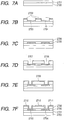
- Figs. 7A to 7F show a constitution of a TFT and a process for production thereof to avoid the above problems:
- the surface of channel layer 2701 is not damaged by formation of conductive layer and other films and etching, so that a TFT is obtained with high performance and high reliability.
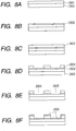
- Figs. 8A to 8F and Figs. 9G to 9L show a more effective TFT constitution and production thereof for prevention of gate leakage and increasing driving performance of the gate electrode.
- first gate-insulating layer 2802 covers entirely channel layer 2801, but does not cover drain electrode 2808 and source electrode 2809. Therefore, the heights of the surfaces of first gate-insulating film 2802, drain electrode 2808, and source electrode 2809 are made uniform. Accordingly, the difference in the level of the second gate-insulating film 2809 is little, so that leakage is not caused at the gate, and second gate-insulating film 2809 can be made thin correspondingly to increase the capacity of the gate electrode and to increase the driving performance.
- Figs. 7A to 7F , and Figs. 8A to 8F and Figs. 9G to 9L are expected to be effective for a gate-insulating film constituted of usual insulating material.
- the above constitutions and processes are especially effective for a channel layer employing an aforementioned transparent amorphous oxide containing at least In-Ga-Zn-O, represented by InGaO 3 (ZnO) m (m: a natural number of less than 6) in a crystal state, containing carriers at a concentration of less than 1 ⁇ 10 17 /cm 3 , or a transparent amorphous oxide containing In-Ga-Zn-Mg-O, represented by InGaO 3 (Zn 1-x Mg x O) m (m: a natural number of less than 6; 0 ⁇ x ⁇ 1) in a crystal state; and employing a gate-insulating film constituted of HfO 2 or Y 2 O 3 .
- a TFT can be obtained which exhibits a high mobility and a low threshold, causing less gate leakage, and having stable characteristics.
- a large-area TFT panel produced according to the present invention has balanced characteristics with high reliability.
- the field-effect transistor of this embodiment belongs to the category of the above seventh, eighth and ninth aspects of the invention.
- the passivation layer in the fifth aspect includes two conceptions.
- the passivation layer of a first conception is a separate layer provided between the active layer and the gate-insulating layer and constituted of a material different from that of the active layer or the gate-insulating layer.
- This passivation layer of the first concept is hereinafter referred to a "passivated layer".
- the passivated layer is composed, for example, of amorphous silicon oxide, amorphous silicon nitride, titanium oxide, aluminum oxide, magnesium oxide, or the like.
- the passivation layer of a second conception is an outermost surface portion of the active layer treated with oxygen plasma.
- the treatment for formation of the passivation layer of the second conception is hereinafter referred to as "passivation treatment".
- passivation treatment another layer composed of a material different from that of the active layer and the gate-insulating layer is not provided.
- a passivated layer of the first concept composed of amorphous silicon oxide may be further formed.
- the passivated layer or the passivation treatment prevents deterioration of the ability of the gate-insulating film: the passivation layer serves as a current leakage-preventing layer.
- the surface-coating layer in the field-effect transistor of the sixth aspect of the present invention is formed from amorphous silicon nitride, amorphous silicon oxide, amorphous silicon nitride, titanium oxide, aluminum oxide, magnesium oxide, or a like material.
- the surface-coating layer may be constituted of the same material as the aforementioned passivation layer or a different material.
- the surface-coating layer improves the adhesiveness between the substrate and the active layer, serving as adhesion-improving layer to prevent film exfoliation, to decrease current leakage, and so forth. Further the surface-coating layer can mitigate projection and depression on the substrate to decrease current leakage and to improve the on-off ratio of the transistor.
- the gate-insulating film is preferably constituted of Al 2 O 3 , Y 2 O 3 , HfO 2 , or a mixed crystal compound containing two or more thereof. Any defect on the interface between gate-insulating thin film and the thin channel layer decreases the electron mobility and causes hysteresis in transistor characteristics. The current leakage depends largely on the kind of the gate-insulating film. Therefore the gate-insulating film should be selected to be suitable to the channel layer.
- the interfacial passivation layer which is one aspect of the present invention, enables formation of a TFT in which current leakage and hysteresis are decreased and electron mobility is increased.
- the TFT can be formed either in a stagger structure or in a reversed stagger structure since the gate-insulating layer and the channel layer can be formed at a room temperature.
- the thin film transistor is a three-terminal element having a gate terminal, a source terminal, and a drain terminal.
- the TFT is an active element which employs a semiconductor film formed on an insulating substrate made of a ceramic material, a glass material, or a plastic material as a channel layer for movement of electrons or holes; and controls the current flowing through the channel layer by applying a voltage to the gate to switch the current between the source terminal and the drain terminal.
- the electron carrier concentration can be controlled by controlling the oxygen defect quantity as desired.
- the quantity of oxygen (oxygen defect quantity) in the transparent oxide film is controlled by forming the film in an atmosphere containing oxygen at a prescribed concentration. Otherwise, the oxygen defect quantity may be controlled (decreased or increased) after the film formation by post treatment of the oxide film in an atmosphere containing oxygen.
- the temperature of the oxygen-containing atmosphere is controlled in a range from 0 to 300°C, preferably from 25 to 250°C, more preferably from 100 to 200°C.
- film may be formed in an oxygen-containing atmosphere and then post-treated in an oxygen-containing atmosphere. Otherwise the film may be formed without control of the oxygen partial pressure and post-treated in an oxygen-containing atmosphere, insofar as the intended electron carrier concentration (less than 1 ⁇ 10 17 /cm 3 ) can be obtained.
- the lower limit of the electron carrier concentration in the present invention is, for example, 1 ⁇ 10 14 /cm 3 , depending on the kind of the element, circuit, or device employing the produced oxide film.
- the electron carrier concentration in the amorphous oxide in the present invention is a value measured at a room temperature.
- the room temperature is a temperature in the range from 0°C to about 40°C, for example, 25°C.
- the electron carrier concentration in the amorphous oxide in the present invention does not need to be less than 1 ⁇ 10 17 /cm 3 throughout the entire range from 0 to 40°C.
- the electron carrier concentration of less than 10 17 /cm 3 at a temperature of 25°C is acceptable.
- a normally-off TFT can be produced at a high yield.
- the expression “less than 10 18 /cm 3” means “preferably less than 1 ⁇ 10 18 /cm 3 and more preferably less than 1.0 ⁇ 10 18 /cm 3 ". The same logic applies to “less than 10 17 /cm 3 ".
- the electron carrier concentration can be measured by measurement of a Hall Effect.
- the amorphous oxide in the present invention is an oxide which exhibits a halo pattern and no characteristic diffraction line in an X-ray diffraction spectrometry.
- the lower limit of the electron carrier concentration is, for example, 1 ⁇ 10 12 /cm 3 , but is not limited insofar as it is applicable as a channel layer of a TFT.
- the electron carrier concentration is adjusted by controlling the material, composition ratio, production conditions, and so forth of the amorphous oxide as in the Examples and Reference Examples outside the scope of the invention as claimed described later to be in the range, for instance, from 1 ⁇ 10 13 /cm 3 to 1 ⁇ 10 17 /cm 3 , more preferably from 1 ⁇ 10 15 /cm 3 to 1 ⁇ 10 16 /cm 3 .
- the amorphous oxide according to the invention as claimed is an In-Ga-Zn oxide or an In-Ga-Zn-Mg oxide.
- examples of other oxides can be selected suitably from In oxides, In x Zn 1-x oxides (0.2 ⁇ x ⁇ 1), In x Sn 1-x oxides (0.8 ⁇ x ⁇ 1), and In x (Zn,Sn) 1-x oxides (0.15 ⁇ x ⁇ 1).
- the In x (Zn,Sn) 1-x oxide can also be represented by In x (Zn y Sn 1-y ) 1-x (0 ⁇ y ⁇ 1).
- the In oxide contains neither Zn nor Sn, the In can be partly substituted by Ga: In x Ga 1-x oxide (0 ⁇ x ⁇ 1).
- One group of the aforementioned oxides are characteristically constituted of In-Ga-Zn-O, represented by InGaO 3 (ZnO) m (m: a natural number of less than 6) in a crystal state, and containing electron carriers at a concentration of less than 1 ⁇ 10 17 /cm 3 .
- the other group of the aforementioned oxides are characteristically constituted of In-Ga-Zn-Mg-O, represented by InGaO 3 (Zn 1-x Mg x O) m (m: a natural number of less than 6, and 0 ⁇ x ⁇ 1) in a crystal state, and containing electron carriers at a concentration of less than 1 ⁇ 10 17 /cm 3 .
- the film constituted of such an oxide is preferably designed to exhibit preferably an electron mobility of higher than 1 cm 2 /V.sec.
- a TFT By use of the above film as the channel layer, a TFT can be prepared which is normally-off with a gate current of less than 0.1 microampere in a transistor off-state, having an on-off ratio of higher than 1 ⁇ 10 3 , being transparent to visible light and flexible.
- the substrate for forming the transparent film includes glass plates, plastic plates, and plastic films.
- At least one of layers constituted of Al 2 O 3 , Y 2 O 3 or HfO 2 , or a mixed crystal compound thereof is useful as the gate-insulating film.
- the film is formed in an oxygen gas-containing atmosphere without intentional addition of an impurity for increasing the electric resistance to the amorphous oxide.
- the inventors of the present invention found that the amorphous thin films of semi-insulating oxides have characteristics that the electron mobility therein increases with increase in number of conduction electrons, and further found that a TFT prepared by use of the film is improved in transistor characteristics such as the on-off ratio, the saturation current in a pinch-off state, and the switching rate. Thus a normally-off type TFT can be produced by use of the amorphous oxide.
- the electron mobility can be made higher than 1 cm 2 /V.sec, preferably higher than 5 cm 2 /V.sec.
- the current between the drain terminal and the source terminal at an off-state (no gate voltage applied) can be controlled to be less than 10 microamperes, preferably less than more than 0.1 microamperes at the carrier concentration of lower than 1 ⁇ 10 17 /cm 3 , preferably lower than 1 ⁇ 10 16 /cm 3 .
- the saturation current after pinch-off can be raised to 10 microamperes or more and the on-off ratio can be raised to be higher than 1 ⁇ 10 3 for the electron mobility higher than 1 cm 2 /V.sec, preferably higher than 5 cm 2 /V.sec.
- the saturation current can be increased in correspondence with the increase of the electron mobility.
- the transistor characteristics can be improved, such as increase of the on-off ratio, increase of the saturation current, and increase of the switching rate.
- the increase of electrons decreases the electron mobility owing to collision between electrons.
- the structure of the aforementioned TFT may be a stagger (top gate) structure in which a gate-insulating film and a gate terminal are successively formed on a semiconductor channel layer, or a reversed stagger (bottom gate) structure in which a gate-insulating film and a semiconductor channel layer successively on a gate terminal.
- the amorphous oxide thin film having the composition InGaO 3 (ZnO) m (m: a natural number of less than 6) in a crystal state is stable up to a high temperature of 800°C or higher when m is less than 6, whereas with increase of m, namely with increase of the ratio of ZnO to InGaO 3 near to the composition of ZnO, the oxide tends to crystallize. Therefore, the value m of the oxide is preferably less than 6 for use as the channel layer of the amorphous TFT.
- the film formation is conducted preferably by a gas phase film formation process by use of a target of a polycrystalline sintered compact having a composition InGaO 3 (ZnO) m .
- a gas phase film formation process by use of a target of a polycrystalline sintered compact having a composition InGaO 3 (ZnO) m .
- sputtering, and pulse laser vapor deposition are suitable.
- the sputtering is particularly suitable for the mass-production.
- the inventors of the present invention produced an In-Ga-Zn-O film by a pulse laser vapor deposition by use of the apparatus shown in Fig. 11 .
- the film-forming was carried out by using such a PLD film-forming apparatus as shown in Fig. 11 .
- the numerals indicate the followings: 701, an RP (rotary pump); 702, a TMP (turbo molecular pump); 703, a preliminary chamber; 704, an electron gun for RHEED; 705, a substrate-holding means for rotating and vertically moving the substrate; 706, a laser-introducing window; 707, a substrate; 708, a target; 709, a radical source; 710, a gas inlet; 711, a target-holding means for rotating and vertically moving the target; 712, a bypass line; 713, a main line; 714, a TMP (turbo molecular pump); 715, an RP (rotary pump); 716, a titanium getter pump; 717, a shutter; 718, an IG (ion manometer); 719, a PG (Pirani gage); 720, a BG (baratron gage); and 721, a growth chamber.
- An In-Ga-Zn-O type amorphous oxide semiconductor thin film was deposited on an SiO 2 glass substrate (Corning Co.: 1737) by a pulse laser vapor deposition employing a KrF excimer laser.
- the substrate was washed ultrasonically for defatting with acetone, ethanol, and ultrapure water each for five minutes, and dried in the air at 100°C.
- the polycrystalline target was an InGaO 3 (ZnO) 4 sintered compact (size: 20 mm diameter, 5 mm thick), which had been prepared by wet-mixing In 2 O 3 , Ga 2 O 3 , and ZnO (each 4N reagent) as the source material (solvent: ethanol), calcining the mixture (1000°C, 2 hours), dry-crushing it, and sintering it (1550°C, 2 hours).
- the target had an electro conductivity of 90 S/cm.
- the film formation was conducted by controlling the final vacuum of the growth chamber to be 2 ⁇ 10 -6 Pa, and the oxygen partial pressure during the growth to be 6.5 Pa.
- the oxygen partial pressure in growth chamber 721 was 6.5 Pa
- the substrate temperature was 25°C.
- the distance between target 708 and film-holding substrate 707 was 30 mm, the power introduced through introduction window 716 was in the range of 1.5-3 mJ/cm 2 /pulse.
- the pulse width was 20 nsec, the repeating frequency was 10 Hz, and the irradiation spot size was 1 ⁇ 1 mm square. Under the above conditions, the film was formed at a rate of 7 nm/min.
- the resulting thin film was examined by small angle X-ray scattered method (SAXS) (thin film method, incidence angle: 0.5°): no clear diffraction peak was observed.
- SAXS small angle X-ray scattered method
- the mean square roughness (Rrms) was found to be about 0.5 nm, and the film thickness to be about 120 nm.
- XRF fluorescence X-ray spectrometric analysis
- the electric conductivity was less than about 1 ⁇ 10 -2 S/cm.
- the electron carrier concentration was estimated to be not more than 1 ⁇ 10 -16 /cm 3 .
- the electron mobility was estimated to be about 5 cm 2 /V.sec. From light absorption spectrum analysis, the optical bandgap energy breadth of the resulting amorphous thin film was estimated to be about 3 eV.
- the obtained In-Ga-Zn-O type thin film is a transparent flat thin film having an amorphous phase of a composition near to a crystalline InGaO 3 (ZnO) 4 , having less oxygen defect, and having lower electric conductivity.
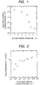
- Fig. 1 shows dependency of the electron carrier concentration in the formed transparent amorphous oxide thin film on the oxygen partial pressure for the film of a composition of InGaO 3 (ZnO) m (m: an integer less than 6) in an assumed crystalline state under the same film formation conditions as in the above Example.
- the electron carrier concentration could be lowered to less than 1 ⁇ 10 17 /cm 3 as shown in Fig. 1 .
- the substrate was kept nearly at room temperature without intentional heating.
- the substrate temperature is kept preferably at a temperature lower than 100°C.
- the higher oxygen partial pressure enables decrease of the electron carrier concentration.
- the thin InGaO 3 (ZnO) 4 film formed at the substrate temperature of 25°C and the oxygen partial pressure of 5 Pa had a lower electron carrier concentration of 1 ⁇ 10 16 /cm 3 .
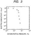
- the electron mobility was higher than 1 cm 2 /V.sec as shown in Fig. 2 .
- the film deposited by the pulse laser vapor deposition at an oxygen partial pressure of higher than 6.5 Pa as in this Example has a rough surface, being not suitable for a channel layer of the TFT.
- a normally-off type transistor can be constructed by using a transparent thin amorphous oxide represented by InGaO 3 (ZnO) m (m: a number less than 6) in a crystal state formed at an oxygen partial pressure of higher than 4.5 Pa, preferably higher than 5 Pa, but lower than 6.5 Pa by a pulse laser vapor deposition method in the above Example.
- ZnO InGaO 3
- the above obtained thin film exhibited an electron mobility higher than 1 cm 2 /V, and the on-off ratio could be made higher than 1 ⁇ 10 3 .
- the oxygen partial pressure is controlled in the range preferably from 4.5 Pa to 6.5 Pa.
- the oxygen partial pressure conditions, the constitution of the film formation apparatus, the kind and composition of the film-forming material should be controlled.
- a top-gate type MISFET element as shown in Fig. 5 was produced by forming an amorphous oxide with the aforementioned apparatus at an oxygen partial pressure of 6.5 Pa.
- a semi-insulating amorphous InGaO 3 (ZnO) 4 film of 120 nm thick was formed for use for channel layer 2 by the above method of formation of amorphous thin Ga-Ga-Zn-O film.
- an InGaO 3 (ZnO) 4 film having a higher electro conductivity and a gold film were laminated respectively in a thickness of 30 nm by pulse laser deposition at an oxygen partial pressure of lower than 1 Pa in the chamber.
- drain terminal 5 and source terminal 6 were formed by photolithography and a lift-off method.
- a Y 2 O 3 film for gate-insulating film 3 was formed by an electron beam vapor deposition method (thickness: 90 nm, relative dielectric constant: about 15, leak current density: 1 ⁇ 10 -3 A/cm 3 at application of 0.5 MV/cm).
- a gold film was formed, and gate terminal 4 was formed by photolithography and lifting-off.
- Fig. 6 shows current-voltage characteristics of the MISFET element measured at room temperature.
- the channel is understood to be an n-type semiconductor from the increase of the drain current I DS with the increase of the drain voltage V DS .
- the on-off ratio of the transistor was higher than 1 ⁇ 10 3 . From the output characteristics, the field effect mobility was calculated to be about 7 cm 2 (Vs) -1 . Irradiation of visible light did not change the transistor characteristics of the produced element according to the same measurement.
- a thin film transistor can be produced which has a channel layer containing electron carriers at a lower concentration to achieve higher electric resistance and exhibiting a higher electron mobility.
- the above amorphous oxide has excellent characteristics that the electron mobility increases with the increase of the electron carrier concentration, and exhibits degenerate conduction.
- the thin film was formed on a glass substrate.
- a plastic plate or film is useful as the substrate since the film formation can be conducted at room temperature.
- the amorphous oxide obtained in this Example absorbs visible light only little to give transparent flexible TFT.
- Fig. 12 The SP process was conducted by use of the apparatus shown in Fig. 12 .
- the numerals indicates the followings: 807, a substrate for film formation; 808, a target; 805, a substrate-holding means equipped with a cooling mechanism; 814, a turbo molecular pump; 815, a rotary pump; 817, a shutter; 818, an ion manometer; 819, a Pirani gage; 821, a growth chamber; and 830, a gate valve.
- Substrate 807 for film formation was an SiO 2 glass substrate (Corning Co.: 1737) which had been washed ultrasonically for defatting with acetone, ethanol, and ultrapure water respectively for 5 minutes, and dried at 100°C in the air.
- the target was a polycrystalline sintered compact having a composition of InGaO 3 (ZnO) 4 (size: 20 nm diameter, 5 mm thick), which had been prepared by wet-mixing In 2 O 3 , Ga 2 O 3 , and ZnO (each 4N reagent) as the source material (solvent: ethanol), calcining the mixture (1000°C, 2 hours), dry-crushing it, and sintering (1550°C, 2 hours).
- Target 808 had an electro conductivity of 90 S/cm, being semi-insulating.
- the final vacuum degree of growth chamber 821 was 1 ⁇ 10 -4 Torr.
- the total pressure of the oxygen and argon gas was kept constant within the range of 4 to 0.1 ⁇ 10 -1 Pa.
- the partial pressure ratio of argon to oxygen was changed in the range of the oxygen partial pressure from 1 ⁇ 10 -3 to 2 ⁇ 10 -1 Pa.
- the substrate temperature was room temperature.
- the distance between target 808 and substrate 807 for film formation was 30 mm.
- the inputted electric power was RF 180 W, and the film forming rate was 10 nm/min.
- the resulting thin film was examined by small angle X-ray scattering method (SAXS) (thin film method, incidence angle: 0.5°): no clear diffraction peak was observed.
- SAXS small angle X-ray scattering method
- the obtained In-Ga-Zn-O type thin film was judged to be amorphous.
- the mean square roughness (Rrms) was found to be about 0.5 nm, and the film thickness to be about 120 nm.
- XRF fluorescence X-ray spectrometric analysis
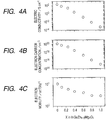
- Fig. 3 shows the result.
- the electric conductivity can be lowered to less than 10 S/cm by conducting the film formation in an atmosphere having an oxygen partial pressure higher then 3 ⁇ 10 -2 Pa.
- the electron carrier number could be decreased by increase of the oxygen partial pressure.
- the thin InGaO 3 (ZnO) 4 film formed at the substrate temperature of 25°C and the oxygen partial pressure or 1 ⁇ 10 -1 Pa had a lower electric conductivity of about 1 ⁇ 10 -10 S/cm. Further, the thin InGaO 3 (ZnO) 4 film formed at the oxygen partial pressure or 1 ⁇ 10 -1 Pa had an excessively high electric resistance, having the electric conductivity not measurable. With this film, although the electron mobility was not measurable, the electron mobility was estimated to be about 1 cm 2 /V.sec by extrapolation from the values of the films of high electron carrier concentration.
- a normally-off transistor having the on-off ratio of higher than 1 ⁇ 10 3 could be obtained by use of a transparent thin amorphous oxide film constituted of In-Ga-Zn-O represented in a crystal state by InGaO 3 (ZnO) m (m: a natural number of less than 6) produced by sputtering vapor deposition in an argon atmosphere containing oxygen at a partial pressure of higher than 3 ⁇ 10 -2 Pa, preferably higher than 5 ⁇ 10 -1 Pa.
- the film formation by sputtering is conducted in the oxygen partial pressure ranging from 3 ⁇ 10 -2 Pa to 5 ⁇ 10 -1 Pa.
- the electron mobility increases with increase in number of the conductive electrons, as shown in Fig. 2 .
- the oxygen defect can be decreased, and thereby the electron carrier concentration can be decreased.
- the electron mobility can be high, since no grain interface exists essentially in the amorphous state differently from polycrystalline state.
- a high-resistance amorphous film InGaO 3 (Zn 1-x Mg x O) m (m: an natural number less than 6; 0 ⁇ x ⁇ 1) can be obtained by using, as the target, polycrystalline InGaO 3 (Zn 1-x Mg x O) m even at an oxygen partial pressure less than 1 Pa.
- the electron carrier concentration lower than 1 ⁇ 10 16 /cm (resistance: about 1 ⁇ 10 -2 S/cm) can be achieved by pulse laser deposition in an atmosphere containing oxygen at a partial pressure of 0.8 Pa.
- the electron mobility is lower than that of the Mg-free film, but the decrease is slight: the electron mobility is about 5 cm 2 /V.sec at room temperature, being higher by about one digit than that of amorphous silicon.
- increase of the Mg content decreases both the electric conductivity and the electron mobility. Therefore, the content of the Mg ranges preferably from 20% to 85% (0.2 ⁇ ⁇ ⁇ 0.85).
- the oxygen defect are decreased by control of the oxygen partial pressure, and the electron carrier concentration can be decreased without addition of specific impurity ions.
- the electron mobility can be high, since no grain interface exists essentially in the amorphous state, being different from polycrystalline state. Further, since the electric conductivity can be decreased without addition of specific impurity ions, the electron mobility can be kept high without scattering by the impurity.
- the gate-insulating film contains preferably a mixed crystal compound containing two or more of Al 2 O 3 , Y 2 O 3 , HfO 2 , and compounds thereof.
- the current leakage can be decreased by use of an Al 2 O 3 film, the hysteresis can be made smaller by use of a Y 2 O 3 film, and the electron mobility can be increased by use of an HfO 2 film having a high dielectric constant.
- TFT can be formed which causes smaller current leakage, less hysteresis, and exhibiting a higher electron mobility. Since the gate-insulating film forming process and the channel layer forming process can be conducted at room temperature, the TFT can be formed in a stagger constitution or in a reversed stagger constitution.
- the TFT thus formed is a three-terminal element having a gate terminal, a source terminal, and a drain terminal.
- This TFT is formed by forming a semiconductor thin film on a insulating substrate of a ceramics, glass, or plastics as a channel layer for transport of electrons or holes, and serves as an active element having a function of controlling the current flowing through the channel layer by application of a voltage to the gate terminal, and switching the current between the source terminal and the drain terminal.
- the amount of the oxygen in the amorphous oxide film is controlled by controlling the oxygen concentration in the film-forming atmosphere. Otherwise the oxygen defect quantity can be controlled (decreased or increase) by post-treatment of the oxide film in an oxygen-containing atmosphere as a preferred embodiment.
- the temperature of the oxygen-containing atmosphere is controlled in the range from 0°C to 300°C, preferably from 25°C to 250°C, more preferably from 100°C to 200°C.
- a film may be formed in an oxygen-containing atmosphere and further post-treated in an oxygen-containing atmosphere. Otherwise the film is formed without control of the oxygen partial pressure and post-treatment is conducted in an oxygen-containing atmosphere, insofar as the intended electron carrier concentration (less than 1 ⁇ 10 17 /cm 3 ) can be achieved.
- the lower limit of the electron carrier concentration in the present invention is, for example, 1 ⁇ 10 14 /cm 3 , depending on the kind of the element, circuit, or device employing the produced oxide film.
- the amorphous oxide used in the active layer is an In-Ga-Zn oxide or an In-Ga-Zn-Mg oxide.
- Amorphous oxides outside the scope of the claims are reference examples not forming part of the invention as claimed.
- an amorphous oxide composed of at least one oxide of the elements of Zn, In, and Sn is useful for an amorphous oxide film of a low carrier concentration and high electron mobility.
- This amorphous oxide film was found to have a specific property that increase in number of conductive electrons therein increases the electron mobility.
- a normally-off type TFT can be produced which is excellent in transistor properties such as the on-off ratio, the saturation current in the pinch-off state, and the switching rate.
- a complex oxide can be formed by incorporating additionally one of the elements shown below into the above amorphous oxide containing at least one of the elements of Zn, In, and Sn, the additional elements including:
- the present invention also provides a field-effect transistor employing the above mentioned amorphous oxide or amorphous oxide film as the channel layer.
- a field-effect transistor is prepared which is employs an amorphous oxide film having an electron carrier concentration of less than 1 ⁇ 10 17 /cm 3 but more than 1 ⁇ 10 15 /cm 3 as the channel layer, and having a source terminal and a drain terminal, and a gate terminal with interposition of a gate-insulating film.
- a voltage of about 5 V is applied between the source and drain terminals without application of gate voltage, the electric current between the source and drain terminals is about 1 ⁇ 10 -7 amperes.
- the electron mobility in the oxide crystal becomes larger with increase of the overlap of the s-orbitals of the metal ions.
- the electron mobility is in the range from 0.1 to 200 cm 2 /V.sec.
- oxygen arid metal ions are bonded by ionic bonds without orientation of the chemical bonds, having a random structure. Therefore in the oxide in an amorphous state, the electron mobility can be comparable to that in a crystal state.
- the electron mobility in the amorphous oxide of the present invention ranges from about 0.01 to 20 cm 2 /V.sec.
- the gate-insulating film is preferably formed from Al 2 O 3 , Y 2 O 3 , HfO 2 , or a mixed crystal compound containing two or more thereof.
- the presence of a defect at the interface between the gate-insulating thin film and the thin channel layer film lowers the electron mobility and causes hysteresis of the transistor characteristics.
- the current leakage depends greatly on the kind of the gate-insulating film. Therefore the gate-insulating film should be selected to be suitable for the channel layer.
- the current leakage can be decreased by use of an Al 2 O 3 film, the hysteresis can be made smaller by use of a Y 2 O 3 film, and the electron mobility can be increased by use of an HfO 2 film having a high dielectric constant.
- TFT can be formed which causes smaller current leakage, less hysteresis, and exhibiting a higher electron mobility. Since the gate-insulating film-forming process and the channel layer-forming process can be conducted at room temperature, the TFT can be formed in a stagger constitution or in a reversed stagger constitution.
- the In 2 O 3 oxide film can be formed through a gas-phase process, and addition of moisture in a partial pressure of about 0.1 Pa to the film-forming atmosphere makes the formed film amorphous.
- ZnO and SnO 2 respectively cannot readily be formed in an amorphous film state.
- In 2 O 3 is added in an amount of 20 atom%.
- In 2 O 3 is added in an amount of 90 atom%.
- gaseous nitrogen is introduced in a partial pressure of about 0.1 Pa in the film formation atmosphere.
- an element capable of forming a complex oxide selected from Group-2 elements M2 having an atomic number lower than Zn (Mg, and Ca), Group-3 elements M3 having an atomic number lower than In (B, Al, Ga, and Y), Group-4 elements M4 having an atomic number lower than Sn (Si, Ge, and Zr), Group-5 elements M5 (V, Nb, and Ta), and Lu, and W.
- the addition of the above element stabilizes the amorphous film at room temperature, and broadens the composition range for amorphous film formation.
- addition of B, Si, or Ge tending to form a covalent bond is effective for amorphous phase stabilization.
- Addition of a complex oxide constituted of ions having largely different ion radiuses is effective for amorphous phase stabilization.
- In should be contained more than about 20 atom%.
- addition of Mg in an amount equivalent to In enables formation of stable amorphous film in the composition range of In of not less than about 15 atom%.
- an amorphous oxide film of the electron carrier concentration ranging from 1 ⁇ 10 15 /cm 3 to 1 ⁇ 10 17 /cm 3 can be obtained by controlling the film forming atmosphere.
- An amorphous oxide film can be suitably formed by a vapor phase process such as a pulse laser vapor deposition process (PLD process), a sputtering process (SP process), and an electron-beam vapor deposition.
- a vapor phase process such as a pulse laser vapor deposition process (PLD process), a sputtering process (SP process), and an electron-beam vapor deposition.
- PLD process pulse laser vapor deposition process
- SP process sputtering process
- electron-beam vapor deposition electron-beam vapor deposition
- An In-Zn-Ga-O type amorphous oxide was deposited on a glass substrate (Corning Co.: 1737) by a PLD process employing a KrF excimer laser with a polycrystal sintered compact as the target having a composition of InGaO 3 (ZnO) or InGaO 3 (ZnO) 4 .
- the substrate temperature was 25°C.
- SAXS small angle X-ray scattering method
- the mean square roughnesses (Rrms) of the thin films were found to be about 0.5 nm, and the film thicknesses to be about 120 nm.
- Amorphous oxide films were formed at various oxygen partial pressure of the film-forming atmosphere with the target having the composition of InGaO 3 (ZnO) 4 .
- the formed amorphous oxide films were measured for the electron carrier concentration.
- Fig. 1 shows the results.
- the electron carrier concentration could be lowered to less than 1 ⁇ 10 18 /cm 3 as shown in Fig. 1 .
- the substrate was kept nearly at room temperature without intentional heating.
- the surfaces of the obtained amorphous oxide films were flat.
- the electron carrier concentration was 1 ⁇ 10 16 /cm 3
- the electroconductivity was 1 ⁇ 10 -2 S/cm
- the electron mobility therein was estimated to be about 5 cm 2 /V.sec.
- the optical bandgap energy breadth of the formed amorphous oxide film was estimated to be about 3 eV.
- the higher oxygen partial pressure further lowered the electron carrier concentration.
- the electron carrier concentration was lowered to 8 ⁇ 10 15 /cm 3 (electroconductivity: about 8 ⁇ 10 -3 S/cm).
- the electron mobility in the film was estimated to be 1 cm 2 /V.sec or more.
- the PLD process at the oxygen partial pressure of 6.5 Pa or higher, the deposited film has a rough surface, being not suitable for use as the channel layer of the TFT.
- the In-Zn-Ga-O type amorphous oxide films were formed at various oxygen partial pressures in the film-forming atmosphere with the target constituted of a polycrystalline sintered compact having the composition of InGaO 3 (ZnO) 4 .
- the ersulting films were examined for the relation between the electron carrier concentration and the electron mobility.
- Fig. 2 shows the results.
- the electron mobility increased from about 3 cm 2 /V.sec to about 11 cm 2 /V.sec.
- the same tendency was observed with the amorphous oxide films obtained with the polycrystalline sintered InGaO 3 (ZnO) target.
- a film of InGaO 3 (Zn 1-x Mg x O) 4 (0 ⁇ x ⁇ 1) was formed on a glass substrate by a PLD process with an InGaO 3 (Zn 1-x Mg x O) 4 target (0 ⁇ x ⁇ 1).
- the apparatus employed was the one shown in Fig. 11 .
- An SiO 2 glass substrate (Corning Co.: 1737) was used as the substrate.
- the substrate was washed ultrasonically for defatting with acetone, ethanol, and ultrapure water each for five minutes, and dried in the air at 100 ⁇ .
- the target was prepared by wet-mixing source materials In 2 O 3 , Ga 2 O 3 , and ZnO (each 4N reagent) (solvent: ethanol), calcining the mixture (1000°C, 2 hours), dry-crushing it, and sintering it (1550°C, 2 hours).
- the final pressure in the growth chamber was 2 ⁇ 10 -6 Pa.
- the oxygen partial pressure during the growth was controlled at 0.8 Pa.
- the substrate temperature was room temperature (25°C).
- the distance between the target and the substrate for film formation was 30 mm.
- the KrF excimer laser was irradiated at a power of 1.5mJ/cm 2 /pulse with the pulse width of 20 nsec, the repeating frequency of 10 Hz, and the irradiation spot size of 1x1 mm square.
- the film-forming rate was 7 nm/min.
- the oxygen partial pressure in the film-forming atmosphere was. 0.8 Pa.
- the substrate temperature was 25°C.
- the resulting thin film was examined by small angle X-ray scattering method (SAXS) (thin film method, incidence angle: 0.5°): no clear diffraction peak was observed.
- SAXS small angle X-ray scattering method
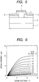
- In-Zn-Ga-Mg-O type amorphous oxide films were formed at the oxygen partial pressure of 0.8 Pa in a film-forming atmosphere to investigate the dependency of the conductivity, the electron carrier concentration, and the electron mobility on the x-value.
- Figs. 4A, 4B, and 4C show the results.
- the electron carrier concentration was decreased to be less than 1 ⁇ 10 18 /cm 3 .
- the electron mobility was higher than 1 cm 2 /V.
- the electron carrier concentration less than 1 ⁇ 10 16 /cm 3 could be achieved in the film prepared by a pulse laser deposition process with the target in which 80 atom% of Zn is replaced by Mg and at the oxygen partial pressure of 0.8 Pa (electric resistance: about 1 ⁇ 10 -2 S.cm).
- the electron mobility is decreased in comparison with the Mg-free film, but the decrease is slight.
- the electron mobility in the films is about 5 cm 2 /V.sec, which is higher by about one digit than that of amorphous silicon.
- both the electric conductivity and the electron mobility in the film decrease with increase of the Mg content. Therefore, the Mg content in the film is preferably more than 20 atom% and less than 85 atom% (0.2 ⁇ x ⁇ 0.85), more preferably 0.5 ⁇ x ⁇ 0.85.
- An In 2 O 3 film was formed on a 200 ⁇ m-thick PET film by use of a target constituted of In 2 O 3 polycrystalline sintered compact by a PLD process employing a KrF excimer laser.
- the apparatus used is shown in Fig. 11 .
- the substrate for the film formation was an SiO 2 glass substrate (Corning Co.: 1737).
- the substrate was washed ultrasonically for defatting with acetone, ethanol, and ultrapure water each for five minutes, and dried in the air at 100°C.
- the target was an In 2 O 3 sintered compact (size: 20 mm diameter, 5 mm thick), which had been prepared by calcining the source material In 2 O 3 (4N reagent) (1000°C, 2 hours), dry-crushing it, and sintering it (1550°C, 2 hours).
- the final vacuum of the growth chamber was 2 ⁇ 10 -6 Pa, the oxygen partial pressure during the growth was 5 Pa, and the substrate temperature was 25°C.
- the water vapor partial pressure was 0.1 Pa, and oxygen radicals were generated by the oxygen radical-generating assembly by application of 200W.
- the distance between the target and the film-holding substrate was 40 mm
- the power of the Krf excimer laser was 0.5 mJ/cm 2 /pulse
- the pulse width was 20 nsec
- the repeating frequency was 10 Hz
- the irradiation spot size was 1x1 mm square.
- the film-forming rate was of 3 nm/min.
- the resulting thin film was examined by small angle X-ray scattering method (SAXS) (thin film method, incidence angle: 0.5°): no clear diffraction peak was observed, which shows that the obtained In-O type oxide film was amorphous.
- SAXS small angle X-ray scattering method
- the electron carrier concentration was 5 ⁇ 10 17 /cm 3
- the electron mobility was about 7 cm 2 /V.sec.
- An In-Sn-O type oxide film was formed on a 200 ⁇ m-thick PET film by use of a target constituted of polycrystalline sintered compact of (In 0.9 Sn 0.1 )O 3.1 by a PLD process employing a KrF excimer laser.
- the apparatus used is shown in Fig. 11 .
- the substrate for the film formation was an SiO 2 glass substrate (Corning Co.: 1737).
- the substrate was washed ultrasonically for defatting with acetone, ethanol, and ultrapure water each for five minutes, and dried in the air at 100°C.
- the target was an In 2 O 3 -SnO 2 sintered compact (size: 20 mm diameter, 5 mm thick), which had been prepared by wet-mixing the source materials In 2 O 3 -SnO 2 (4N reagents) (solvent: ethanol), calcining the mixture (1000°C, 2 hours), dry-crushing it, and sintering it (1550°C, 2 hours).
- the substrate was kept at room temperature.
- the oxygen partial pressure was 5 Pa.
- the nitrogen partial pressure was 0.1 Pa.
- Oxygen radicals were generated by the oxygen radical-generating assembly by application of 200W.
- the distance between the target and the film-holding substrate was 30 mm
- the power of the Krf excimer laser was 1.5 mJ/cm 2 /pulse
- the pulse width was 20 nsec
- the repeating frequency was 10 Hz
- the irradiation spot size was 1 ⁇ 1 mm square.
- the film-forming rate was of 6 nm/min.
- the resulting thin film was examined by small angle X-ray scattering method (SAXS) (thin film method, incidence angle: 0.5°): no clear diffraction peak was detected, which shows that the obtained In-Sn-O type oxide film is amorphous.
- SAXS small angle X-ray scattering method
- the electron carrier concentration was 8 ⁇ 10 17 /cm 3
- the electron mobility was about 5 cm 2 /V.sec.
- the film thickness was 100 nm.
- the substrate for the film was an SiO 2 glass substrate (Corning Co.:1737).
- the substrate was washed ultrasonically for defatting with acetone, ethanol, and ultrapure water each for five minutes, and dried in the air at 100°C.
- This target was prepared by wet-mixing the source materials In 2 O 3 -Ga 2 O 2 (4N reagents) (solvent: ethanol), calcining the mixture (1000°C, 2 hours), dry-crushing it, and sintering it (1550°C, 2 hours).
- the final pressure of the growth chamber was 2 ⁇ 10 -6 Pa.
- the oxygen partial pressure during the growth was 1 Pa.
- the substrate was at room temperature.
- the distance between the target and the film-holding substrate was 30 mm.
- the power of the Krf excimer laser was 1.5 mJ/cm 2 /pulse.
- the pulse width was 20 nsec.
- the repeating frequency was 10 Hz.
- the irradiation spot size was 1x1 mm square.
- the film-forming rate was of 6 nm/min.
- the substrate temperature was 25°C.
- the oxygen pressure was 1 Pa.
- the resulting film was examined by small angle X-ray scattering method (SAXS) (thin film method, incidence angle: 0.5°): no clear diffraction peak was detected, which shows that the obtained In-Ga-O type oxide film is amorphous.
- SAXS small angle X-ray scattering method
- the electron carrier concentration was 8 ⁇ 10 16 /cm 3
- the electron mobility was about 1 cm 2 /V.sec.
- a top gate type TFT element shown in Fig. 5 was prepared.
- an In-Ga-Zn-O type amorphous oxide film was prepared on glass substrate 1 by the aforementioned PLS apparatus with a target constituted of a polycrystalline sintered compact having a composition of InGaO 3 (ZnO) 4 at an oxygen partial pressure of 5 Pa.
- the formed In-Ga-Zn-O film had a thickness of 120 nm, and was used as channel layer 2.
- drain terminal 5 and source terminal 6 were formed by photolithography and a lift-off method.
- gate-insulating film 3 was formed by electron beam vapor deposition (thickness: 90 nm, relative dielectric constant: about 15, leakage current density: 1 ⁇ 10 -3 A/cm 2 under application of 0.5 MV/cm). Further thereon, a gold film was formed and therefrom gate terminal 4 was formed by photolithography and a lift-off method.
- the channel length was 50 ⁇ m, and the channel width was 200 ⁇ m.
- Fig. 6 shows current-voltage characteristics of the TFT element at room temperature. Drain current I DS increased with increase of drain voltage V DS , which shows that the channel is of an n-type conduction.
- the on-off ratio of the transistor was higher than 1 ⁇ 10 3 . From the output characteristics, the field effect mobility was calculated to be about 7 cm 2 (Vs) -1 in the saturation region. Irradiation of visible light did not change the transistor characteristics of the produced element according to the same measurement.
- an amorphous oxide of the electron carrier concentration lower than 1 ⁇ 10 17 /cm 3 is used as a channel layer of a TFT.
- the electron carrier concentration is more preferably less than 1 ⁇ 10 16 /cm 3 .
- a top gate type TFT element shown in Fig. 5 was prepared.
- an In-Ga-Zn-O type amorphous oxide film was prepared on polyethylene terephthalate (PET) film 1 by the aforementioned PLS apparatus with a target constituted of a polycrystalline sintered compact having a composition of InGaO 3 (ZnO) at an oxygen partial pressure of 5 Pa in the atmosphere.
- the formed film had a thickness of 120 nm, and was used as channel layer 2.
- drain terminal 5 and source terminal 6 were formed by photolithography and a lift-off method.
- gate-insulating film 3 was formed by an electron beam vapor deposition method. Further thereon, a gold film was formed and therefrom gate terminal 4 was formed by photolithography and a lift-off method. The channel length was 50 pm, and the channel width was 200 ⁇ m.
- Three TFTs of the above structure were prepared by using respectively one of the three kinds of gate-insulating films: Y 2 O 3 (140 nm thick), Al 2 O 3 (130 ⁇ m thick), and HfO 2 (140 ⁇ m thick).
- the TFT elements formed on a PET film had current-voltage characteristics similar to that shown. in Fig. 6 at room temperature. Drain current I DS increased with increase of drain voltage V DS , which shows that the channel is of an n-type conduction. This is consistent with the fact that an amorphous In-Ga-Zn-O type semiconductor is of an n type.
- the on-off ratio of the transistor was higher than 1 ⁇ 10 3 . From the output characteristics, the field effect mobility was calculated to be about 7 cm 2 (Vs) -1 in the saturation region.
- the elements formed on the PET film were curved at a curvature radius of 30 mm, and in this state, transistor characteristics were measured. However the no change was observed in the transistor characteristics. Irradiation of visible light did not change the transistor characteristics.
- the TFT employing the Al 3 O 3 film as the gate-insulating film has also transistor characteristics similar to that shown in Fig. 6 .
- the on-off ratio of the transistor was higher than 1 ⁇ 10 2 . From the output characteristics, the field effect mobility was calculated to be about 2 cm 2 (Vs) -1 in the saturation region.
- the TFT employing the HfO 2 film as the gate-insulating film has also transistor characteristics similar to that shown in Fig. 6 .
- the on-off ratio of the transistor was higher than 1 ⁇ 10 2 . From the output characteristics, the field effect mobility was calculated to be about 10 cm 2 (Vs) -1 in the saturation region.
- a top gate type TFT element shown in Fig. 5 was prepared.
- an In 2 O 3 type amorphous oxide film was formed on polyethylene terephthalate (PET) film 1 by the PLD method as channel layer 2 in a thickness of 80 nm.
- drain terminal 5 and source terminal 6 were formed by photolithography and a lift-off method.
- gate-insulating film 3 was formed by an electron beam vapor deposition method. Further thereon, a gold film was formed and therefrom gate terminal 4 was formed by photolithography and a lift-off method.
- drain current I DS increased with increase of drain voltage V DS , which shows that the channel is an n-type conductor. This is consistent with the fact that an amorphous In-O type amorphous oxide film is an n type conductor.
- the on-off ratio of the transistor was about 1 ⁇ 10 2 . From the output characteristics, the field effect mobility was calculated to be about 1 ⁇ 10 cm 2 (Vs) -1 in the saturation region.
- the TFT element formed on a glass substrate had similar characteristics.
- the elements formed on the PET film were curved in a curvature radius of 30 mm, and in this state, transistor characteristics were measured. No change was observed in the transistor characteristics.
- a top gate type TFT element shown in Fig. 5 was prepared.
- an In-Sn-O type amorphous oxide film was formed in a thickness of 100 nm as channel layer 2 on polyethylene terephthalate (PET) film 1 by the PLD method.
- drain terminal 5 and source terminal 6 were formed by photolithography and a lift-off method.
- gate-insulating film 3 was formed by an electron beam vapor deposition method. Further thereon, a gold film was formed and therefrom gate terminal 4 was formed by photolithography and a lift-off method.
- drain current I DS increased with increase of drain voltage V DS , which shows that the channel is an n-type conductor. This is consistent with the fact that an amorphous In-Sn-O type amorphous oxide film is an n type conductor.
- the on-off ratio of the transistor was about 1 ⁇ 10 3 . From the output characteristics, the field effect mobility was calculated to be about 5 cm 2 (Vs) -1 in the saturation range.
- the TFT element formed on a glass substrate had similar characteristics.
- the elements formed on the PET film were curved at a curvature radius of 30 mm, and in this state, transistor characteristics were measured. No change was caused thereby in the transistor characteristics.
- a top gate type TFT element shown in Fig. 5 was prepared.
- an In-Ga-O type amorphous oxide film was formed in a thickness of 120 nm as channel layer 2 on polyethylene terephthalate (PET) film 1 by the PLD method shown in Example 6.
- drain terminal 5 and source terminal 6 were formed by photolithography and a lift-off method.
- gate-insulating film 3 was formed by an electron beam vapor deposition method. Further thereon, a gold film was formed and therefrom gate terminal 4 was formed by photolithography and a lift-off method.
- drain current I DS increased with increase of drain voltage V DS , which shows that the channel is an n-type conductor. This is consistent with the fact that an amorphous In-Ga-O type amorphous oxide film is an n type conductor.
- the on-off ratio of the transistor was about 1 ⁇ 10 2 . From the output characteristics, the field effect mobility was calculated to be about 0.8 cm 2 (Vs) -1 in the saturation range.
- the TFT element formed on a glass substrate had similar characteristics.
- the elements formed on the PET film were curved at a curvature radius of 30 mm, and in this state, transistor characteristics were measured. No change was caused thereby in the transistor characteristics.
- the amorphous oxide of the electron carrier concentration of lower than 1 ⁇ 10 17 /cm 3 is used as the channel layer of the TFT.
- the electron carrier concentration is more preferably not higher than 1 ⁇ 10 16 /cm 3 .
- An In-Zn-Ga-O type amorphous oxide is deposited on a glass substrate (Corning Co.: 1737) by a pulse laser vapor deposition method employing a KrF excimer laser with a polycrystalline sintered compact having a composition of InGaO 3 (ZnO) 4 as the target.
- a top gate type MISFET element as shown in Fig. 5 is prepared.
- a 40nm-thick semi-insulating amorphous film of InGaO 3 (ZnO) 4 is formed as channel layer 2 on glass substrate 1 through the above amorphous In-Ga-Zn-O thin film formation process.
- drain terminal 5 and source terminal 6 are formed by photolithography and a lift-off method.
- a Y 2 O 3 film as gate-insulating film 3 is formed by an electron beam vapor deposition method (thickness 100 nm, relative dielectric constant: about 15). Further thereon, a gold film was formed, and therefrom gate terminal 4 was formed by photolithography and a lift-off method.
- the TFT can be made locally transparent to visible light by not conducting gold film formation at least on one of the drain electrode and the source electrode to keep there transparent.
- ITO of high conductivity may be used in formation of the source electrode, the drain electrode, or the gate electrode, and the gold film is not formed thereon.
- TFT can be formed which is transparent in the visible light region. Such a TFT is preferred for driving on a display.
- the source electrode, the drain electrode, and the gate electrode are transparent, and the wiring for the electric connection is formed from a metal of high conductivity.
- the metal wiring is laminated on the transparent electrodes.
- a 30nm-thick semi-insulating amorphous film of InGaO 3 (ZnO) 4 is formed as channel layer 2 on glass substrate 1.
- drain terminal 5 and source terminal 6 are formed by photolithography and a lift-off method.
- a TiO 2 film as gate-insulating film 3 is formed by an electron beam vapor deposition method (thickness 110 nm, relative dielectric constant: about 11). Further thereon, a gold film was formed, and therefrom gate terminal 4 was formed by photolithography and a lift-off method.
- a device which is transparent to visible light at the portions of drain terminal and the source terminal.
- An In-Zn-Ga-O type amorphous oxide is deposited on a glass substrate (Corning Co.: 1737) by a pulse laser vapor deposition method employing a KrF excimer laser with a polycrystalline sintered compact having a composition of InGaO 3 (ZnO) 4 as the target.
- a top gate type TFT panel is prepared through steps Shown in Figs. 7A to 7F .
- a top gate type TFT panel is produced through steps of Figs. 8A to 8F and 9G to 9L .
- the present invention enables production of TFT panels reliable and suitable for driving large-area liquid crystal panels and organic EL panels.
- An In-Zn-Ga-O type amorphous oxide thin film is deposited on a glass substrate (Corning Co.: 1737) by a pulse laser vapor deposition method employing a KrF excimer laser.
- a top gate type MISFET element shown in Fig. 10 is prepared.
- Surface-coating layer 5010 (amorphous silicon nitride layer: 300 nm) which is one of the present invention is deposited on plastic film (PET) 5001.
- a semi-insulating amorphous InGaO 3 (ZnO) 4 film is deposited in a 35 nm thickness as channel layer 5002 by the aforementioned process for producing an amorphous In-Ga-Zn-O thin film.
- interfacial passivation layer 5100 (amorphous silicon layer: 3 nm) which is one of the present invention is deposited.
- Drain terminal 5007 and source terminal 5006 are formed by photolithography and a lift-off method.
- gate-insulating film 5003 (thickness: 70 nm, relative dielectric constant: about 15), and thereon gold film is formed and therefrom gate terminal 5004 is formed by photolithography and a lift-off method.
- the thin films such as the surface coating layer
- another material such as amorphous silicon, titanium oxide, aluminum oxide, and magnesium oxide may be used. This is preferable for improvement of adhesiveness to the substrate, decrease of roughness of substrate surface, and prevention of current leakage in the element.
- the thin films such as the passivation layer
- another material such as amorphous silicon nitride, titanium oxide, aluminum oxide, and magnesium oxide may be used. This is preferable for improvement of the gate-insulating layer, and prevention of current leakage.
- the simple passivation treatment can be sufficient.
- an oxygen plasma treatment O 2 : 5 sccm, 20 W, 20 sec
- an interfacial passivation layer may be laminated additionally for prevention of current leakage in the element.
- the transistor employing the transparent oxide film of the present invention is used as a switching element for LCDs and organic EL display apparatuses.
- the present invention is also applicable widely to flexible display devices employing a flexible material such as a plastic film, IC cards, ID tags, and so forth.
Claims (13)
- Feldeffekttransistor mit einer Source-Elektrode (6; 2704; 5006), einer Drain-Elektrode (5; 2703; 5007), einem Gate-Isolator (3; 2705, 2706; 5003), einer Gate-Elektrode (4; 2712; 5004) und einer aktiven Schicht (2; 2701; 5002), die aus amorphem Oxid gebildet ist,wobei das amorphe Oxid ein In-Ga-Zn-Oxid oder ein In-Ga-Zn-Mg-Oxid ist,das eine Elektronenträgerkonzentration von weniger als 1017/cm3 bei einer Temperatur von 25° C aufweistund in dem sich die Elektronenmobilität tendenziell mit der Erhöhung der Elektronenträgerkonzentration erhöht.
- Transistor nach Anspruch 1, wobei der Gate-Isolator ein Mehrschicht-Gate-Isolator ist, mit einer ersten Schicht (2705) in Kontakt mit der aktiven Schicht (2701) und einer zweiten Schicht (2706), deren Material sich von demjenigen der ersten Schicht unterscheidet und die eine Laminierung auf der ersten Schicht bildet.
- Transistor nach Anspruch 2, wobei die erste Schicht (2705) eine Isolierschicht ist, die HfO2, Y2O3 oder eine HfO2 oder Y2O3 beinhaltende Mischkristallverbindung enthält.
- Transistor nach Anspruch 3, wobei die zweite Schicht (2706) eine Isolierschicht ist, die SiO2, Si3N4, TiO2, Ta2O5, PbTiO3, BaTa2O6, SrTiO3, MgO oder AIN enthält, oder eine amorphe Struktur enthält, die SiO2, Si3N4, TiO2, Ta2O5, PbTiO3, BaTa2O6, SrTiO3, MgO oder AIN beinhaltet.
- Transistor nach einem der Ansprüche 1 bis 4,
wobei zwischen der aktiven Schicht (5002) und einem Gate-Isolator mit einer hohen dielektrischen Konstante (5003) eine Passivierungsschicht (5100) aus amorphem Siliziumoxid, amorphem Siliziumnitrid, Titanoxid, Aluminiumoxid oder Magnesiumoxid vorgesehen ist. - Transistor nach Anspruch 5, wobei der Gate-Isolator mit hoher dielektischer Konstante einen Y2O3-Film umfasst.
- Transistor nach einem der Ansprüche 1 bis 6, wobei zumindest eine von der Source-Elektrode (6), der Drain-Elektrode (5) und der Gate-Elektrode (4) bei sichtbarem Licht transparent ist.
- Transistor nach Anspruch 7, der eine Metallleiterbahn aufweist, die mit zumindest einer von der Source-Elektrode, der Drain-Elektrode und der Gate-Elektrode verbunden ist.
- Transistor nach einem der Ansprüche 1 bis 8, wobei das amorphe Oxid ein aus einem Target der Zusammensetzung InGaO3(ZnO)m hergestelltes In-Ga-Zn-Oxid ist, wobei m eine natürliche Zahl kleiner als 6 ist, oder ein aus einem Target der Zusammensetzung InGaO3(Zn1-xMgxO)m hergestelltes In-Ga-Zn-Mg-Oxide ist, wobei m eine natürliche Zahl kleiner als 6 und 0<x≤1 ist, und zwar unter Verwendung eines Sputter- oder Pulslaserabscheideverfahrens in einer Sauerstoff enthaltenden Atmosphäre.
- Feldeffekttransistor nach einem der Ansprüche 1 bis 9, wobei der Transistor ein Transistor vom Normally-Off-Typ ist.
- Flüssigkristallanzeigevorrichtung, umfassend den Transistor nach einem der Ansprüche 1 bis 10 als ein Schaltelement zum Treiben der Vorrichtung.
- Organische EL-Anzeigevorrichtung, umfassend den Transistor nach einem der Ansprüche 1 bis 10 als ein Schaltelement zum Treiben der Vorrichtung.
- TFT-Display oder flexibles Display oder ID-Tag, umfassend den Feldeffekttransistor nach einem der Ansprüche 1 bis 10.
Applications Claiming Priority (2)
| Application Number | Priority Date | Filing Date | Title |
|---|---|---|---|
| JP2004326683 | 2004-11-10 | ||
| PCT/JP2005/020982 WO2006051995A1 (en) | 2004-11-10 | 2005-11-09 | Field effect transistor employing an amorphous oxide |
Publications (2)
| Publication Number | Publication Date |
|---|---|
| EP1815530A1 EP1815530A1 (de) | 2007-08-08 |
| EP1815530B1 true EP1815530B1 (de) | 2021-02-17 |
Family
ID=35695582
Family Applications (1)
| Application Number | Title | Priority Date | Filing Date |
|---|---|---|---|
| EP05806736.4A Active EP1815530B1 (de) | 2004-11-10 | 2005-11-09 | Feldeffekttransistor mit einem amorphen oxid |
Country Status (10)
| Country | Link |
|---|---|
| US (2) | US7868326B2 (de) |
| EP (1) | EP1815530B1 (de) |
| JP (1) | JP5118812B2 (de) |
| KR (2) | KR100889796B1 (de) |
| CN (1) | CN101057338B (de) |
| AU (1) | AU2005302964B2 (de) |
| BR (1) | BRPI0517560B8 (de) |
| CA (1) | CA2585071A1 (de) |
| RU (1) | RU2358355C2 (de) |
| WO (1) | WO2006051995A1 (de) |
Families Citing this family (1871)
| Publication number | Priority date | Publication date | Assignee | Title |
|---|---|---|---|---|
| US7863611B2 (en) | 2004-11-10 | 2011-01-04 | Canon Kabushiki Kaisha | Integrated circuits utilizing amorphous oxides |
| US7453065B2 (en) | 2004-11-10 | 2008-11-18 | Canon Kabushiki Kaisha | Sensor and image pickup device |
| US7829444B2 (en) * | 2004-11-10 | 2010-11-09 | Canon Kabushiki Kaisha | Field effect transistor manufacturing method |
| RU2402106C2 (ru) * | 2004-11-10 | 2010-10-20 | Кэнон Кабусики Кайся | Аморфный оксид и полевой транзистор с его использованием |
| US7868326B2 (en) | 2004-11-10 | 2011-01-11 | Canon Kabushiki Kaisha | Field effect transistor |
| KR20070085879A (ko) | 2004-11-10 | 2007-08-27 | 캐논 가부시끼가이샤 | 발광 장치 |
| US7791072B2 (en) | 2004-11-10 | 2010-09-07 | Canon Kabushiki Kaisha | Display |
| US7579224B2 (en) * | 2005-01-21 | 2009-08-25 | Semiconductor Energy Laboratory Co., Ltd. | Method for manufacturing a thin film semiconductor device |
| TWI445178B (zh) | 2005-01-28 | 2014-07-11 | Semiconductor Energy Lab | 半導體裝置,電子裝置,和半導體裝置的製造方法 |
| TWI412138B (zh) * | 2005-01-28 | 2013-10-11 | Semiconductor Energy Lab | 半導體裝置,電子裝置,和半導體裝置的製造方法 |
| US7858451B2 (en) * | 2005-02-03 | 2010-12-28 | Semiconductor Energy Laboratory Co., Ltd. | Electronic device, semiconductor device and manufacturing method thereof |
| US7948171B2 (en) * | 2005-02-18 | 2011-05-24 | Semiconductor Energy Laboratory Co., Ltd. | Light emitting device |
| US7928938B2 (en) * | 2005-04-19 | 2011-04-19 | Semiconductor Energy Laboratory Co., Ltd. | Semiconductor device including memory circuit, display device and electronic apparatus |
| US7710739B2 (en) | 2005-04-28 | 2010-05-04 | Semiconductor Energy Laboratory Co., Ltd. | Semiconductor device and display device |
| US8629819B2 (en) | 2005-07-14 | 2014-01-14 | Semiconductor Energy Laboratory Co., Ltd. | Semiconductor device and driving method thereof |
| EP1758072A3 (de) * | 2005-08-24 | 2007-05-02 | Semiconductor Energy Laboratory Co., Ltd. | Anzeigevorrichtung und ihr Steuerungsverfahren |
| JP5058469B2 (ja) * | 2005-09-06 | 2012-10-24 | キヤノン株式会社 | スパッタリングターゲットおよび該ターゲットを用いた薄膜の形成方法 |
| JP5006598B2 (ja) * | 2005-09-16 | 2012-08-22 | キヤノン株式会社 | 電界効果型トランジスタ |
| US7712009B2 (en) * | 2005-09-21 | 2010-05-04 | Semiconductor Energy Laboratory Co., Ltd. | Cyclic redundancy check circuit and semiconductor device having the cyclic redundancy check circuit |
| EP1998375A3 (de) | 2005-09-29 | 2012-01-18 | Semiconductor Energy Laboratory Co, Ltd. | Halbleitervorrichtung mit Halbleiter-Oxidschicht und Herstellungsverfahren |
| WO2007043493A1 (en) | 2005-10-14 | 2007-04-19 | Semiconductor Energy Laboratory Co., Ltd. | Semiconductor device and manufacturing method thereof |
| JP5037808B2 (ja) | 2005-10-20 | 2012-10-03 | キヤノン株式会社 | アモルファス酸化物を用いた電界効果型トランジスタ、及び該トランジスタを用いた表示装置 |
| KR20090115222A (ko) * | 2005-11-15 | 2009-11-04 | 가부시키가이샤 한도오따이 에네루기 켄큐쇼 | 반도체장치 제조방법 |
| EP1843194A1 (de) | 2006-04-06 | 2007-10-10 | Semiconductor Energy Laboratory Co., Ltd. | Flüssigkristallanzeige, Halbleitervorrichtung und elektronisches Gerät |
| KR100785038B1 (ko) * | 2006-04-17 | 2007-12-12 | 삼성전자주식회사 | 비정질 ZnO계 TFT |
| US7443202B2 (en) * | 2006-06-02 | 2008-10-28 | Semiconductor Energy Laboratory Co., Ltd. | Semiconductor device and electronic apparatus having the same |
| US7651896B2 (en) * | 2006-08-30 | 2010-01-26 | Semiconductor Energy Laboratory Co., Ltd. | Method for manufacturing semiconductor device |
| JP5116277B2 (ja) | 2006-09-29 | 2013-01-09 | 株式会社半導体エネルギー研究所 | 半導体装置、表示装置、液晶表示装置、表示モジュール及び電子機器 |
| US7646015B2 (en) * | 2006-10-31 | 2010-01-12 | Semiconductor Energy Laboratory Co., Ltd. | Manufacturing method of semiconductor device and semiconductor device |
| US8143115B2 (en) | 2006-12-05 | 2012-03-27 | Canon Kabushiki Kaisha | Method for manufacturing thin film transistor using oxide semiconductor and display apparatus |
| WO2008069255A1 (en) * | 2006-12-05 | 2008-06-12 | Canon Kabushiki Kaisha | Method for manufacturing thin film transistor using oxide semiconductor and display apparatus |
| JP4785721B2 (ja) | 2006-12-05 | 2011-10-05 | キヤノン株式会社 | エッチング方法、パターン形成方法、薄膜トランジスタの製造方法及びエッチング液 |
| US8784700B2 (en) | 2006-12-13 | 2014-07-22 | Idemitsu Kosan Co., Ltd. | Sputtering target and oxide semiconductor film |
| KR101363555B1 (ko) | 2006-12-14 | 2014-02-19 | 삼성디스플레이 주식회사 | 박막 트랜지스터 기판 및 그 제조 방법 |
| KR100787464B1 (ko) * | 2007-01-08 | 2007-12-26 | 삼성에스디아이 주식회사 | 박막 트랜지스터, 및 그 제조방법 |
| JP4662075B2 (ja) * | 2007-02-02 | 2011-03-30 | 株式会社ブリヂストン | 薄膜トランジスタ及びその製造方法 |
| KR101312259B1 (ko) * | 2007-02-09 | 2013-09-25 | 삼성전자주식회사 | 박막 트랜지스터 및 그 제조방법 |
| KR101410926B1 (ko) | 2007-02-16 | 2014-06-24 | 삼성전자주식회사 | 박막 트랜지스터 및 그 제조방법 |
| KR101509663B1 (ko) | 2007-02-16 | 2015-04-06 | 삼성전자주식회사 | 산화물 반도체층 형성 방법 및 이를 이용한 반도체 소자제조방법 |
| US8436349B2 (en) * | 2007-02-20 | 2013-05-07 | Canon Kabushiki Kaisha | Thin-film transistor fabrication process and display device |
| JP5121254B2 (ja) * | 2007-02-28 | 2013-01-16 | キヤノン株式会社 | 薄膜トランジスタおよび表示装置 |
| US8333913B2 (en) | 2007-03-20 | 2012-12-18 | Idemitsu Kosan Co., Ltd. | Sputtering target, oxide semiconductor film and semiconductor device |
| JP5320746B2 (ja) * | 2007-03-28 | 2013-10-23 | 凸版印刷株式会社 | 薄膜トランジスタ |
| KR20080088284A (ko) * | 2007-03-29 | 2008-10-02 | 삼성전자주식회사 | 플래시 메모리 소자 |
| KR101334181B1 (ko) * | 2007-04-20 | 2013-11-28 | 삼성전자주식회사 | 선택적으로 결정화된 채널층을 갖는 박막 트랜지스터 및 그제조 방법 |
| WO2008139860A1 (ja) | 2007-05-07 | 2008-11-20 | Idemitsu Kosan Co., Ltd. | 半導体薄膜、半導体薄膜の製造方法、および、半導体素子 |
| US8748879B2 (en) | 2007-05-08 | 2014-06-10 | Idemitsu Kosan Co., Ltd. | Semiconductor device, thin film transistor and a method for producing the same |
| JP5522889B2 (ja) | 2007-05-11 | 2014-06-18 | 出光興産株式会社 | In−Ga−Zn−Sn系酸化物焼結体、及び物理成膜用ターゲット |
| JP5542297B2 (ja) | 2007-05-17 | 2014-07-09 | 株式会社半導体エネルギー研究所 | 液晶表示装置、表示モジュール及び電子機器 |
| JP5542296B2 (ja) | 2007-05-17 | 2014-07-09 | 株式会社半導体エネルギー研究所 | 液晶表示装置、表示モジュール及び電子機器 |
| JP4989309B2 (ja) | 2007-05-18 | 2012-08-01 | 株式会社半導体エネルギー研究所 | 液晶表示装置 |
| US7897482B2 (en) * | 2007-05-31 | 2011-03-01 | Semiconductor Energy Laboratory Co., Ltd. | Semiconductor device and manufacturing method thereof |
| KR101415561B1 (ko) | 2007-06-14 | 2014-08-07 | 삼성디스플레이 주식회사 | 박막 트랜지스터 표시판 및 그의 제조 방법 |
| CN101681925B (zh) * | 2007-06-19 | 2011-11-30 | 三星电子株式会社 | 氧化物半导体及包含该氧化物半导体的薄膜晶体管 |
| US7935964B2 (en) * | 2007-06-19 | 2011-05-03 | Samsung Electronics Co., Ltd. | Oxide semiconductors and thin film transistors comprising the same |
| US8354674B2 (en) * | 2007-06-29 | 2013-01-15 | Semiconductor Energy Laboratory Co., Ltd. | Semiconductor device wherein a property of a first semiconductor layer is different from a property of a second semiconductor layer |
| KR100889688B1 (ko) * | 2007-07-16 | 2009-03-19 | 삼성모바일디스플레이주식회사 | 반도체 활성층 제조 방법, 그를 이용한 박막 트랜지스터의제조 방법 및 반도체 활성층을 구비하는 박막 트랜지스터 |
| US7988871B2 (en) | 2007-07-20 | 2011-08-02 | Lg Display Co., Ltd. | Method of lifting off and fabricating array substrate for liquid crystal display device using the same |
| KR101072379B1 (ko) * | 2007-07-20 | 2011-10-11 | 엘지디스플레이 주식회사 | 리프트오프 방법 및 이를 이용한 액정표시장치용 어레이기판의 제조방법 |
| WO2009014155A1 (en) | 2007-07-25 | 2009-01-29 | Semiconductor Energy Laboratory Co., Ltd. | Photoelectric conversion device and electronic device having the same |
| US8058096B2 (en) * | 2007-07-31 | 2011-11-15 | Hewlett Packard Development Company, L.P. | Microelectronic device |
| KR100959460B1 (ko) * | 2007-11-16 | 2010-05-25 | 주식회사 동부하이텍 | 투명 박막 트랜지스터 및 투명 박막 트랜지스터의 제조방법 |
| KR101270174B1 (ko) * | 2007-12-03 | 2013-05-31 | 삼성전자주식회사 | 산화물 반도체 박막 트랜지스터의 제조방법 |
| WO2009075161A1 (ja) * | 2007-12-12 | 2009-06-18 | Idemitsu Kosan Co., Ltd. | パターン化結晶質半導体薄膜、薄膜トランジスタの製造方法、及び電界効果型トランジスタ |
| KR100959109B1 (ko) | 2007-12-24 | 2010-05-26 | 삼성모바일디스플레이주식회사 | 박막 트랜지스터 및 그의 제조방법과, 그를 구비하는평판표시장치 |
| KR100976459B1 (ko) * | 2007-12-27 | 2010-08-17 | 삼성모바일디스플레이주식회사 | 박막 트랜지스터 및 제조방법 및 그를 구비하는평판표시장치 |
| NO332409B1 (no) * | 2008-01-24 | 2012-09-17 | Well Technology As | Anordning og fremgangsmate for a isolere en seksjon av et bronnhull |
| US8017045B2 (en) | 2008-04-16 | 2011-09-13 | Electronics And Telecommunications Research Institute | Composition for oxide semiconductor thin film and field effect transistor using the composition |
| KR101496148B1 (ko) * | 2008-05-15 | 2015-02-27 | 삼성전자주식회사 | 반도체소자 및 그 제조방법 |
| US9041202B2 (en) * | 2008-05-16 | 2015-05-26 | Semiconductor Energy Laboratory Co., Ltd. | Semiconductor device and manufacturing method of the same |
| KR101468591B1 (ko) * | 2008-05-29 | 2014-12-04 | 삼성전자주식회사 | 산화물 반도체 및 이를 포함하는 박막 트랜지스터 |
| KR101224769B1 (ko) * | 2008-06-10 | 2013-01-21 | 제이엑스 닛코 닛세키 킨조쿠 가부시키가이샤 | 스퍼터링용 산화물 소결체 타겟 및 그 제조 방법 |
| US8314765B2 (en) | 2008-06-17 | 2012-11-20 | Semiconductor Energy Laboratory Co., Ltd. | Driver circuit, display device, and electronic device |
| US20100006837A1 (en) * | 2008-07-09 | 2010-01-14 | Electronics And Telecommunications Research Institute | Composition for oxide semiconductor thin film, field effect transistor using the composition and method of fabricating the transistor |
| WO2010004944A1 (en) | 2008-07-10 | 2010-01-14 | Semiconductor Energy Laboratory Co., Ltd. | Light-emitting device and electronic device using the same |
| US8945981B2 (en) | 2008-07-31 | 2015-02-03 | Semiconductor Energy Laboratory Co., Ltd. | Semiconductor device and manufacturing method thereof |
| TWI500159B (zh) | 2008-07-31 | 2015-09-11 | Semiconductor Energy Lab | 半導體裝置和其製造方法 |
| TWI476921B (zh) | 2008-07-31 | 2015-03-11 | Semiconductor Energy Lab | 半導體裝置及其製造方法 |
| TWI450399B (zh) * | 2008-07-31 | 2014-08-21 | Semiconductor Energy Lab | 半導體裝置及其製造方法 |
| JP5616038B2 (ja) | 2008-07-31 | 2014-10-29 | 株式会社半導体エネルギー研究所 | 半導体装置の作製方法 |
| TWI424506B (zh) | 2008-08-08 | 2014-01-21 | Semiconductor Energy Lab | 半導體裝置的製造方法 |
| TWI500160B (zh) * | 2008-08-08 | 2015-09-11 | Semiconductor Energy Lab | 半導體裝置及其製造方法 |
| JP5525778B2 (ja) * | 2008-08-08 | 2014-06-18 | 株式会社半導体エネルギー研究所 | 半導体装置 |
| JP5480554B2 (ja) | 2008-08-08 | 2014-04-23 | 株式会社半導体エネルギー研究所 | 半導体装置 |
| TWI508282B (zh) | 2008-08-08 | 2015-11-11 | Semiconductor Energy Lab | 半導體裝置及其製造方法 |
| JP5627071B2 (ja) | 2008-09-01 | 2014-11-19 | 株式会社半導体エネルギー研究所 | 半導体装置の作製方法 |
| US8021916B2 (en) | 2008-09-01 | 2011-09-20 | Semiconductor Energy Laboratory Co., Ltd. | Method for manufacturing semiconductor device |
| US9082857B2 (en) * | 2008-09-01 | 2015-07-14 | Semiconductor Energy Laboratory Co., Ltd. | Semiconductor device comprising an oxide semiconductor layer |
| WO2010029865A1 (en) | 2008-09-12 | 2010-03-18 | Semiconductor Energy Laboratory Co., Ltd. | Display device |
| KR20160063402A (ko) * | 2008-09-12 | 2016-06-03 | 가부시키가이샤 한도오따이 에네루기 켄큐쇼 | 디스플레이 장치 |
| KR101783193B1 (ko) | 2008-09-12 | 2017-09-29 | 가부시키가이샤 한도오따이 에네루기 켄큐쇼 | 표시 장치 |
| KR101665734B1 (ko) * | 2008-09-12 | 2016-10-24 | 가부시키가이샤 한도오따이 에네루기 켄큐쇼 | 반도체 장치 및 그 생산 방법 |
| KR101313126B1 (ko) * | 2008-09-19 | 2013-10-01 | 가부시키가이샤 한도오따이 에네루기 켄큐쇼 | 표시장치 |
| WO2010032638A1 (en) | 2008-09-19 | 2010-03-25 | Semiconductor Energy Laboratory Co., Ltd. | Display device |
| CN102160103B (zh) | 2008-09-19 | 2013-09-11 | 株式会社半导体能源研究所 | 显示装置 |
| KR102413263B1 (ko) | 2008-09-19 | 2022-06-27 | 가부시키가이샤 한도오따이 에네루기 켄큐쇼 | 반도체장치 |
| KR101874327B1 (ko) * | 2008-09-19 | 2018-07-05 | 가부시키가이샤 한도오따이 에네루기 켄큐쇼 | 표시장치 |
| KR101611643B1 (ko) * | 2008-10-01 | 2016-04-11 | 가부시키가이샤 한도오따이 에네루기 켄큐쇼 | 반도체 장치 |
| WO2010038596A1 (en) * | 2008-10-03 | 2010-04-08 | Semiconductor Energy Laboratory Co., Ltd. | Modulation circuit and semiconductor device including the same |
| KR101652693B1 (ko) | 2008-10-03 | 2016-09-01 | 가부시키가이샤 한도오따이 에네루기 켄큐쇼 | 표시 장치 |
| CN103928476A (zh) | 2008-10-03 | 2014-07-16 | 株式会社半导体能源研究所 | 显示装置及其制造方法 |
| EP2172977A1 (de) | 2008-10-03 | 2010-04-07 | Semiconductor Energy Laboratory Co., Ltd. | Anzeigevorrichtung |
| KR20230106737A (ko) | 2008-10-03 | 2023-07-13 | 가부시키가이샤 한도오따이 에네루기 켄큐쇼 | 표시장치 및 표시장치를 구비한 전자기기 |
| EP2172804B1 (de) * | 2008-10-03 | 2016-05-11 | Semiconductor Energy Laboratory Co, Ltd. | Anzeigevorrichtung |
| CN101719493B (zh) | 2008-10-08 | 2014-05-14 | 株式会社半导体能源研究所 | 显示装置 |
| JP5484853B2 (ja) | 2008-10-10 | 2014-05-07 | 株式会社半導体エネルギー研究所 | 半導体装置の作製方法 |
| KR101799601B1 (ko) * | 2008-10-16 | 2017-11-20 | 가부시키가이샤 한도오따이 에네루기 켄큐쇼 | 발광 표시 장치 |
| JP5361651B2 (ja) | 2008-10-22 | 2013-12-04 | 株式会社半導体エネルギー研究所 | 半導体装置の作製方法 |
| KR20180137606A (ko) | 2008-10-24 | 2018-12-27 | 가부시키가이샤 한도오따이 에네루기 켄큐쇼 | 반도체 장치 및 그 제조 방법 |
| US8106400B2 (en) | 2008-10-24 | 2012-01-31 | Semiconductor Energy Laboratory Co., Ltd. | Semiconductor device and method for manufacturing the same |
| KR101667909B1 (ko) | 2008-10-24 | 2016-10-28 | 가부시키가이샤 한도오따이 에네루기 켄큐쇼 | 반도체장치의 제조방법 |
| US8741702B2 (en) | 2008-10-24 | 2014-06-03 | Semiconductor Energy Laboratory Co., Ltd. | Method for manufacturing semiconductor device |
| JP5616012B2 (ja) | 2008-10-24 | 2014-10-29 | 株式会社半導体エネルギー研究所 | 半導体装置の作製方法 |
| JP5442234B2 (ja) | 2008-10-24 | 2014-03-12 | 株式会社半導体エネルギー研究所 | 半導体装置及び表示装置 |
| WO2010047288A1 (en) | 2008-10-24 | 2010-04-29 | Semiconductor Energy Laboratory Co., Ltd. | Method for manufacturing semiconductordevice |
| EP2180518B1 (de) | 2008-10-24 | 2018-04-25 | Semiconductor Energy Laboratory Co, Ltd. | Herstellungsverfahren für Halbleitervorrichtung |
| KR101631454B1 (ko) | 2008-10-31 | 2016-06-17 | 가부시키가이샤 한도오따이 에네루기 켄큐쇼 | 논리회로 |
| TWI496295B (zh) | 2008-10-31 | 2015-08-11 | Semiconductor Energy Lab | 半導體裝置及其製造方法 |
| KR101603303B1 (ko) | 2008-10-31 | 2016-03-14 | 가부시키가이샤 한도오따이 에네루기 켄큐쇼 | 도전성 산질화물 및 도전성 산질화물막의 제작 방법 |
| WO2010050419A1 (en) * | 2008-10-31 | 2010-05-06 | Semiconductor Energy Laboratory Co., Ltd. | Driver circuit and display device |
| TW202404099A (zh) | 2008-11-07 | 2024-01-16 | 日商半導體能源研究所股份有限公司 | 半導體裝置和其製造方法 |
| EP2184783B1 (de) * | 2008-11-07 | 2012-10-03 | Semiconductor Energy Laboratory Co, Ltd. | Halbleiterbauelement und Verfahren zu seiner Herstellung |
| CN101740631B (zh) * | 2008-11-07 | 2014-07-16 | 株式会社半导体能源研究所 | 半导体装置及该半导体装置的制造方法 |
| TWI467663B (zh) | 2008-11-07 | 2015-01-01 | Semiconductor Energy Lab | 半導體裝置和該半導體裝置的製造方法 |
| TWI535037B (zh) | 2008-11-07 | 2016-05-21 | 半導體能源研究所股份有限公司 | 半導體裝置和其製造方法 |
| KR20110084523A (ko) | 2008-11-07 | 2011-07-25 | 가부시키가이샤 한도오따이 에네루기 켄큐쇼 | 반도체 장치 |
| TWI656645B (zh) | 2008-11-13 | 2019-04-11 | 日商半導體能源研究所股份有限公司 | 半導體裝置及其製造方法 |
| KR101432764B1 (ko) | 2008-11-13 | 2014-08-21 | 가부시키가이샤 한도오따이 에네루기 켄큐쇼 | 반도체장치의 제조방법 |
| US8232947B2 (en) | 2008-11-14 | 2012-07-31 | Semiconductor Energy Laboratory Co., Ltd. | Liquid crystal display device |
| JP2010153802A (ja) | 2008-11-20 | 2010-07-08 | Semiconductor Energy Lab Co Ltd | 半導体装置及び半導体装置の作製方法 |
| KR101291384B1 (ko) | 2008-11-21 | 2013-07-30 | 가부시키가이샤 한도오따이 에네루기 켄큐쇼 | 반도체 장치 |
| US8344387B2 (en) * | 2008-11-28 | 2013-01-01 | Semiconductor Energy Laboratory Co., Ltd. | Semiconductor device and method for manufacturing the same |
| TWI595297B (zh) * | 2008-11-28 | 2017-08-11 | 半導體能源研究所股份有限公司 | 液晶顯示裝置 |
| TWI585955B (zh) * | 2008-11-28 | 2017-06-01 | 半導體能源研究所股份有限公司 | 光感測器及顯示裝置 |
| KR101472771B1 (ko) * | 2008-12-01 | 2014-12-15 | 가부시키가이샤 한도오따이 에네루기 켄큐쇼 | 반도체 장치 및 그 제작 방법 |
| TWI633371B (zh) | 2008-12-03 | 2018-08-21 | 半導體能源研究所股份有限公司 | 液晶顯示裝置 |
| JP5491833B2 (ja) * | 2008-12-05 | 2014-05-14 | 株式会社半導体エネルギー研究所 | 半導体装置 |
| JP2010140919A (ja) | 2008-12-09 | 2010-06-24 | Hitachi Ltd | 酸化物半導体装置及びその製造方法並びにアクティブマトリクス基板 |
| CN102257621B (zh) | 2008-12-19 | 2013-08-21 | 株式会社半导体能源研究所 | 晶体管的制造方法 |
| WO2010071183A1 (en) * | 2008-12-19 | 2010-06-24 | Semiconductor Energy Laboratory Co., Ltd. | Method for manufacturing semiconductor device |
| EP2515337B1 (de) * | 2008-12-24 | 2016-02-24 | Semiconductor Energy Laboratory Co., Ltd. | Treiberschaltung und halbleiterbauelement |
| US8441007B2 (en) | 2008-12-25 | 2013-05-14 | Semiconductor Energy Laboratory Co., Ltd. | Display device and manufacturing method thereof |
| TWI476915B (zh) | 2008-12-25 | 2015-03-11 | Semiconductor Energy Lab | 半導體裝置及其製造方法 |
| US8114720B2 (en) | 2008-12-25 | 2012-02-14 | Semiconductor Energy Laboratory Co., Ltd. | Semiconductor device and manufacturing method thereof |
| KR101719350B1 (ko) * | 2008-12-25 | 2017-03-23 | 가부시키가이샤 한도오따이 에네루기 켄큐쇼 | 반도체 장치 및 그 제작 방법 |
| TWI475616B (zh) * | 2008-12-26 | 2015-03-01 | Semiconductor Energy Lab | 半導體裝置及其製造方法 |
| JP5590877B2 (ja) | 2008-12-26 | 2014-09-17 | 株式会社半導体エネルギー研究所 | 半導体装置 |
| KR101064402B1 (ko) * | 2009-01-12 | 2011-09-14 | 삼성모바일디스플레이주식회사 | 박막 트랜지스터, 그의 제조 방법 및 박막 트랜지스터를 구비하는 평판 표시 장치 |
| KR101648927B1 (ko) * | 2009-01-16 | 2016-08-17 | 가부시키가이샤 한도오따이 에네루기 켄큐쇼 | 반도체 장치 및 그 제작 방법 |
| US8492756B2 (en) * | 2009-01-23 | 2013-07-23 | Semiconductor Energy Laboratory Co., Ltd. | Semiconductor device and method for manufacturing the same |
| US8436350B2 (en) * | 2009-01-30 | 2013-05-07 | Semiconductor Energy Laboratory Co., Ltd. | Semiconductor device using an oxide semiconductor with a plurality of metal clusters |
| US8367486B2 (en) | 2009-02-05 | 2013-02-05 | Semiconductor Energy Laboratory Co., Ltd. | Transistor and method for manufacturing the transistor |
| US8174021B2 (en) | 2009-02-06 | 2012-05-08 | Semiconductor Energy Laboratory Co., Ltd. | Semiconductor device and method of manufacturing the semiconductor device |
| US8749930B2 (en) * | 2009-02-09 | 2014-06-10 | Semiconductor Energy Laboratory Co., Ltd. | Protection circuit, semiconductor device, photoelectric conversion device, and electronic device |
| US8278657B2 (en) * | 2009-02-13 | 2012-10-02 | Semiconductor Energy Laboratory Co., Ltd. | Transistor, semiconductor device including the transistor, and manufacturing method of the transistor and the semiconductor device |
| CN101840936B (zh) | 2009-02-13 | 2014-10-08 | 株式会社半导体能源研究所 | 包括晶体管的半导体装置及其制造方法 |
| US8247812B2 (en) * | 2009-02-13 | 2012-08-21 | Semiconductor Energy Laboratory Co., Ltd. | Transistor, semiconductor device including the transistor, and manufacturing method of the transistor and the semiconductor device |
| US8247276B2 (en) | 2009-02-20 | 2012-08-21 | Semiconductor Energy Laboratory Co., Ltd. | Thin film transistor, method for manufacturing the same, and semiconductor device |
| US8841661B2 (en) * | 2009-02-25 | 2014-09-23 | Semiconductor Energy Laboratory Co., Ltd. | Staggered oxide semiconductor TFT semiconductor device and manufacturing method thereof |
| US8704216B2 (en) | 2009-02-27 | 2014-04-22 | Semiconductor Energy Laboratory Co., Ltd. | Semiconductor device and manufacturing method thereof |
| US20100224878A1 (en) | 2009-03-05 | 2010-09-09 | Semiconductor Energy Laboratory Co., Ltd. | Semiconductor device |
| US8461582B2 (en) * | 2009-03-05 | 2013-06-11 | Semiconductor Energy Laboratory Co., Ltd. | Semiconductor device and method for manufacturing the same |
| US20100224880A1 (en) * | 2009-03-05 | 2010-09-09 | Semiconductor Energy Laboratory Co., Ltd. | Semiconductor device |
| KR101671210B1 (ko) | 2009-03-06 | 2016-11-01 | 가부시키가이샤 한도오따이 에네루기 켄큐쇼 | 반도체 장치 및 반도체 장치의 제작 방법 |
| WO2010103935A1 (en) * | 2009-03-12 | 2010-09-16 | Semiconductor Energy Laboratory Co., Ltd. | Method for manufacturing semiconductor device |
| TWI485781B (zh) * | 2009-03-13 | 2015-05-21 | Semiconductor Energy Lab | 半導體裝置及該半導體裝置的製造方法 |
| US8450144B2 (en) * | 2009-03-26 | 2013-05-28 | Semiconductor Energy Laboratory Co., Ltd. | Semiconductor device and method for manufacturing the same |
| KR101752640B1 (ko) | 2009-03-27 | 2017-06-30 | 가부시키가이샤 한도오따이 에네루기 켄큐쇼 | 반도체장치 |
| TWI617029B (zh) * | 2009-03-27 | 2018-03-01 | 半導體能源研究所股份有限公司 | 半導體裝置 |
| KR101681884B1 (ko) | 2009-03-27 | 2016-12-05 | 가부시키가이샤 한도오따이 에네루기 켄큐쇼 | 반도체장치, 표시장치 및 전자기기 |
| US8927981B2 (en) * | 2009-03-30 | 2015-01-06 | Semiconductor Energy Laboratory Co., Ltd. | Semiconductor device and method for manufacturing the same |
| TWI489628B (zh) * | 2009-04-02 | 2015-06-21 | Semiconductor Energy Lab | 半導體裝置和其製造方法 |
| US8338226B2 (en) * | 2009-04-02 | 2012-12-25 | Semiconductor Energy Laboratory Co., Ltd. | Method for manufacturing semiconductor device |
| JP5615018B2 (ja) | 2009-04-10 | 2014-10-29 | 株式会社半導体エネルギー研究所 | 半導体装置および半導体装置の作製方法 |
| JP5724157B2 (ja) * | 2009-04-13 | 2015-05-27 | 日立金属株式会社 | 酸化物半導体ターゲット及びそれを用いた酸化物半導体装置の製造方法 |
| TWI476917B (zh) | 2009-04-16 | 2015-03-11 | Semiconductor Energy Lab | 半導體裝置和其製造方法 |
| WO2010119952A1 (ja) * | 2009-04-17 | 2010-10-21 | 株式会社ブリヂストン | 薄膜トランジスタ、及び薄膜トランジスタの製造方法 |
| KR101690216B1 (ko) * | 2009-05-01 | 2016-12-27 | 가부시키가이샤 한도오따이 에네루기 켄큐쇼 | 반도체 장치의 제작 방법 |
| JP5751762B2 (ja) | 2009-05-21 | 2015-07-22 | 株式会社半導体エネルギー研究所 | 半導体装置 |
| JP5760298B2 (ja) * | 2009-05-21 | 2015-08-05 | ソニー株式会社 | 薄膜トランジスタ、表示装置、および電子機器 |
| EP2256814B1 (de) | 2009-05-29 | 2019-01-16 | Semiconductor Energy Laboratory Co, Ltd. | Oxid-Halbleiterbauelement und Verfahren zu seiner Herstellung |
| JP5564331B2 (ja) * | 2009-05-29 | 2014-07-30 | 株式会社半導体エネルギー研究所 | 半導体装置の作製方法 |
| EP2256795B1 (de) * | 2009-05-29 | 2014-11-19 | Semiconductor Energy Laboratory Co., Ltd. | Herstellungsverfahren für Oxidhalbleiterbauelement |
| WO2010140548A1 (ja) | 2009-06-05 | 2010-12-09 | Jx日鉱日石金属株式会社 | 酸化物焼結体、その製造方法及び酸化物焼結体製造用原料粉末 |
| US9024311B2 (en) | 2009-06-24 | 2015-05-05 | Sharp Kabushiki Kaisha | Thin film transistor, method for manufacturing same, active matrix substrate, display panel and display device |
| US8865516B2 (en) | 2009-06-29 | 2014-10-21 | Sharp Kabushiki Kaisha | Oxide semiconductor, thin film transistor array substrate and production method thereof, and display device |
| EP2449595B1 (de) | 2009-06-30 | 2017-07-26 | Semiconductor Energy Laboratory Co, Ltd. | Herstellungsverfahren für halbleiterbauelement |
| WO2011002046A1 (en) | 2009-06-30 | 2011-01-06 | Semiconductor Energy Laboratory Co., Ltd. | Method for manufacturing semiconductor device |
| KR101944656B1 (ko) | 2009-06-30 | 2019-04-17 | 가부시키가이샤 한도오따이 에네루기 켄큐쇼 | 반도체 장치 제조 방법 |
| WO2011001879A1 (en) * | 2009-06-30 | 2011-01-06 | Semiconductor Energy Laboratory Co., Ltd. | Method for manufacturing semiconductor device |
| TW201103090A (en) * | 2009-07-01 | 2011-01-16 | Univ Nat Chiao Tung | Method for manufacturing a self-aligned thin film transistor and a structure of the same |
| US20110000175A1 (en) * | 2009-07-01 | 2011-01-06 | Husqvarna Consumer Outdoor Products N.A. Inc. | Variable speed controller |
| KR101476817B1 (ko) | 2009-07-03 | 2014-12-26 | 가부시키가이샤 한도오따이 에네루기 켄큐쇼 | 트랜지스터를 갖는 표시 장치 및 그 제작 방법 |
| KR102503687B1 (ko) | 2009-07-03 | 2023-02-27 | 가부시키가이샤 한도오따이 에네루기 켄큐쇼 | 반도체 장치의 제작 방법 |
| JP5663214B2 (ja) * | 2009-07-03 | 2015-02-04 | 株式会社半導体エネルギー研究所 | 半導体装置の作製方法 |
| KR20210131462A (ko) | 2009-07-10 | 2021-11-02 | 가부시키가이샤 한도오따이 에네루기 켄큐쇼 | 액정 표시 장치의 제작 방법 |
| WO2011004723A1 (en) | 2009-07-10 | 2011-01-13 | Semiconductor Energy Laboratory Co., Ltd. | Semiconductor device and manufacturing method the same |
| KR101801500B1 (ko) | 2009-07-10 | 2017-11-24 | 가부시키가이샤 한도오따이 에네루기 켄큐쇼 | 반도체 장치 및 그 제조 방법 |
| WO2011007682A1 (en) * | 2009-07-17 | 2011-01-20 | Semiconductor Energy Laboratory Co., Ltd. | Method of manufacturing semiconductor device |
| WO2011007675A1 (en) * | 2009-07-17 | 2011-01-20 | Semiconductor Energy Laboratory Co., Ltd. | Semiconductor device and manufacturing method thereof |
| WO2011007677A1 (en) | 2009-07-17 | 2011-01-20 | Semiconductor Energy Laboratory Co., Ltd. | Semiconductor device and method for manufacturing the same |
| KR101870460B1 (ko) | 2009-07-18 | 2018-06-22 | 가부시키가이샤 한도오따이 에네루기 켄큐쇼 | 반도체 장치 및 반도체 장치의 제조 방법 |
| EP2457256B1 (de) | 2009-07-18 | 2020-06-17 | Semiconductor Energy Laboratory Co., Ltd. | Halbleiterbauelement und herstellungsverfahren dafür |
| WO2011010541A1 (en) | 2009-07-18 | 2011-01-27 | Semiconductor Energy Laboratory Co., Ltd. | Semiconductor device and method for manufacturing the same |
| WO2011010545A1 (en) | 2009-07-18 | 2011-01-27 | Semiconductor Energy Laboratory Co., Ltd. | Semiconductor device and method for manufacturing the same |
| WO2011010542A1 (en) * | 2009-07-23 | 2011-01-27 | Semiconductor Energy Laboratory Co., Ltd. | Semiconductor device and method for manufacturing the same |
| KR101904811B1 (ko) | 2009-07-24 | 2018-10-05 | 가부시키가이샤 한도오따이 에네루기 켄큐쇼 | 반도체 장치 |
| WO2011013502A1 (en) * | 2009-07-31 | 2011-02-03 | Semiconductor Energy Laboratory Co., Ltd. | Semiconductor device and manufacturing method thereof |
| KR102386147B1 (ko) | 2009-07-31 | 2022-04-14 | 가부시키가이샤 한도오따이 에네루기 켄큐쇼 | 반도체 디바이스 및 그 형성 방법 |
| CN102473735B (zh) | 2009-07-31 | 2015-08-12 | 株式会社半导体能源研究所 | 半导体装置及其制造方法 |
| CN102473734B (zh) * | 2009-07-31 | 2015-08-12 | 株式会社半导体能源研究所 | 半导体装置及其制造方法 |
| WO2011013523A1 (en) | 2009-07-31 | 2011-02-03 | Semiconductor Energy Laboratory Co., Ltd. | Semiconductor device and method for manufacturing the same |
| TWI559501B (zh) | 2009-08-07 | 2016-11-21 | 半導體能源研究所股份有限公司 | 半導體裝置和其製造方法 |
| TWI700810B (zh) | 2009-08-07 | 2020-08-01 | 日商半導體能源研究所股份有限公司 | 半導體裝置和其製造方法 |
| EP2284891B1 (de) | 2009-08-07 | 2019-07-24 | Semiconductor Energy Laboratory Co, Ltd. | Halbleiterbauelement und dessen Herstellungsverfahren |
| JP5642447B2 (ja) | 2009-08-07 | 2014-12-17 | 株式会社半導体エネルギー研究所 | 半導体装置 |
| TWI596741B (zh) * | 2009-08-07 | 2017-08-21 | 半導體能源研究所股份有限公司 | 半導體裝置和其製造方法 |
| JP5663231B2 (ja) * | 2009-08-07 | 2015-02-04 | 株式会社半導体エネルギー研究所 | 発光装置 |
| TWI604594B (zh) * | 2009-08-07 | 2017-11-01 | 半導體能源研究所股份有限公司 | 半導體裝置及包括該半導體裝置之電話、錶、和顯示裝置 |
| US8115883B2 (en) | 2009-08-27 | 2012-02-14 | Semiconductor Energy Laboratory Co., Ltd. | Display device and method for manufacturing the same |
| WO2011027649A1 (en) * | 2009-09-02 | 2011-03-10 | Semiconductor Energy Laboratory Co., Ltd. | Semiconductor device including a transistor, and manufacturing method of semiconductor device |
| CN104681447A (zh) * | 2009-09-04 | 2015-06-03 | 株式会社半导体能源研究所 | 半导体器件的制造方法 |
| WO2011027656A1 (en) | 2009-09-04 | 2011-03-10 | Semiconductor Energy Laboratory Co., Ltd. | Transistor and display device |
| WO2011027676A1 (en) | 2009-09-04 | 2011-03-10 | Semiconductor Energy Laboratory Co., Ltd. | Semiconductor device and manufacturing method thereof |
| WO2011027701A1 (en) | 2009-09-04 | 2011-03-10 | Semiconductor Energy Laboratory Co., Ltd. | Light-emitting device and method for manufacturing the same |
| KR101851926B1 (ko) | 2009-09-04 | 2018-04-25 | 가부시키가이샤 한도오따이 에네루기 켄큐쇼 | 발광 장치 및 발광 장치를 제작하기 위한 방법 |
| WO2011027702A1 (en) * | 2009-09-04 | 2011-03-10 | Semiconductor Energy Laboratory Co., Ltd. | Light-emitting device and method for manufacturing the same |
| KR101746198B1 (ko) | 2009-09-04 | 2017-06-12 | 가부시키가이샤 한도오따이 에네루기 켄큐쇼 | 표시장치 및 전자기기 |
| WO2011027664A1 (en) * | 2009-09-04 | 2011-03-10 | Semiconductor Energy Laboratory Co., Ltd. | Liquid crystal display device and method for manufacturing the same |
| CN105810753A (zh) | 2009-09-04 | 2016-07-27 | 株式会社半导体能源研究所 | 半导体器件及其制造方法 |
| JP5700626B2 (ja) * | 2009-09-04 | 2015-04-15 | 株式会社半導体エネルギー研究所 | El表示装置 |
| KR101700470B1 (ko) * | 2009-09-16 | 2017-01-26 | 가부시키가이샤 한도오따이 에네루기 켄큐쇼 | 구동 회로, 구동 회로를 포함하는 표시 장치 및 표시 장치를 포함하는 전자 기기 |
| WO2011034068A1 (en) | 2009-09-16 | 2011-03-24 | Semiconductor Energy Laboratory Co., Ltd. | Light-emitting device and manufacturing method thereof |
| KR20170116246A (ko) * | 2009-09-16 | 2017-10-18 | 가부시키가이샤 한도오따이 에네루기 켄큐쇼 | 반도체 장치 및 그 제조 방법 |
| KR20170046186A (ko) | 2009-09-16 | 2017-04-28 | 가부시키가이샤 한도오따이 에네루기 켄큐쇼 | 반도체 장치 및 전자 기기 |
| WO2011034012A1 (en) * | 2009-09-16 | 2011-03-24 | Semiconductor Energy Laboratory Co., Ltd. | Logic circuit, light emitting device, semiconductor device, and electronic device |
| WO2011033914A1 (en) | 2009-09-16 | 2011-03-24 | Semiconductor Energy Laboratory Co., Ltd. | Driving method of display device and display device |
| CN105448937A (zh) | 2009-09-16 | 2016-03-30 | 株式会社半导体能源研究所 | 晶体管及显示设备 |
| US9715845B2 (en) | 2009-09-16 | 2017-07-25 | Semiconductor Energy Laboratory Co., Ltd. | Semiconductor display device |
| TWI512997B (zh) | 2009-09-24 | 2015-12-11 | Semiconductor Energy Lab | 半導體裝置,電源電路,和半導體裝置的製造方法 |
| KR101713356B1 (ko) | 2009-09-24 | 2017-03-07 | 가부시키가이샤 한도오따이 에네루기 켄큐쇼 | 구동 회로, 상기 구동 회로를 포함하는 표시 장치, 및 상기 표시 장치를 포함하는 전자 기기 |
| KR101914026B1 (ko) | 2009-09-24 | 2018-11-01 | 가부시키가이샤 한도오따이 에네루기 켄큐쇼 | 산화물 반도체막 및 반도체 장치 |
| WO2011037050A1 (en) | 2009-09-24 | 2011-03-31 | Semiconductor Energy Laboratory Co., Ltd. | Semiconductor device and manufacturing method thereof |
| KR101707260B1 (ko) * | 2009-09-24 | 2017-02-15 | 가부시키가이샤 한도오따이 에네루기 켄큐쇼 | 반도체 장치 |
| KR101788538B1 (ko) * | 2009-09-24 | 2017-10-20 | 가부시키가이샤 한도오따이 에네루기 켄큐쇼 | 표시 장치 |
| WO2011037213A1 (en) | 2009-09-24 | 2011-03-31 | Semiconductor Energy Laboratory Co., Ltd. | Semiconductor device and method for manufacturing the same |
| WO2011037008A1 (en) | 2009-09-24 | 2011-03-31 | Semiconductor Energy Laboratory Co., Ltd. | Method for manufacturing oxide semiconductor film and method for manufacturing semiconductor device |
| KR101809759B1 (ko) | 2009-09-24 | 2018-01-18 | 가부시키가이샤 한도오따이 에네루기 켄큐쇼 | 반도체 소자 및 그 제조 방법 |
| JP5613508B2 (ja) * | 2009-09-30 | 2014-10-22 | 株式会社半導体エネルギー研究所 | レドックスキャパシタ |
| WO2011040213A1 (en) * | 2009-10-01 | 2011-04-07 | Semiconductor Energy Laboratory Co., Ltd. | Semiconductor device and method for manufacturing the same |
| KR20120084751A (ko) * | 2009-10-05 | 2012-07-30 | 가부시키가이샤 한도오따이 에네루기 켄큐쇼 | 반도체 장치 및 그 제작 방법 |
| WO2011043182A1 (en) | 2009-10-05 | 2011-04-14 | Semiconductor Energy Laboratory Co., Ltd. | Method for removing electricity and method for manufacturing semiconductor device |
| KR101877149B1 (ko) * | 2009-10-08 | 2018-07-10 | 가부시키가이샤 한도오따이 에네루기 켄큐쇼 | 산화물 반도체층, 반도체 장치 및 그 제조 방법 |
| KR102108943B1 (ko) | 2009-10-08 | 2020-05-12 | 가부시키가이샤 한도오따이 에네루기 켄큐쇼 | 반도체 장치 |
| WO2011043162A1 (en) * | 2009-10-09 | 2011-04-14 | Semiconductor Energy Laboratory Co., Ltd. | Semiconductor device and method for manufacturing the semiconductor device |
| WO2011043206A1 (en) | 2009-10-09 | 2011-04-14 | Semiconductor Energy Laboratory Co., Ltd. | Semiconductor device |
| WO2011043194A1 (en) | 2009-10-09 | 2011-04-14 | Semiconductor Energy Laboratory Co., Ltd. | Semiconductor device and method for manufacturing the same |
| CN112242173A (zh) * | 2009-10-09 | 2021-01-19 | 株式会社半导体能源研究所 | 半导体器件 |
| KR101949670B1 (ko) | 2009-10-09 | 2019-02-19 | 가부시키가이샤 한도오따이 에네루기 켄큐쇼 | 반도체 장치 |
| WO2011043164A1 (en) * | 2009-10-09 | 2011-04-14 | Semiconductor Energy Laboratory Co., Ltd. | Semiconductor device and method for manufacturing the semiconductor device |
| US9171640B2 (en) | 2009-10-09 | 2015-10-27 | Semiconductor Energy Laboratory Co., Ltd. | Shift register and display device |
| EP2486593B1 (de) | 2009-10-09 | 2017-02-01 | Semiconductor Energy Laboratory Co., Ltd. | Halbleiterbauelement und herstellungsverfahren dafür |
| KR101835748B1 (ko) | 2009-10-09 | 2018-03-07 | 가부시키가이샤 한도오따이 에네루기 켄큐쇼 | 발광 표시 장치 및 이를 포함한 전자 기기 |
| KR102070268B1 (ko) | 2009-10-09 | 2020-01-29 | 가부시키가이샤 한도오따이 에네루기 켄큐쇼 | 반도체 장치 |
| KR20120083341A (ko) * | 2009-10-09 | 2012-07-25 | 가부시키가이샤 한도오따이 에네루기 켄큐쇼 | 액정 표시 장치 및 액정 표시 장치를 포함하는 전자 기기 |
| WO2011046003A1 (en) * | 2009-10-14 | 2011-04-21 | Semiconductor Energy Laboratory Co., Ltd. | Semiconductor device and manufacturing method thereof |
| KR101915251B1 (ko) | 2009-10-16 | 2018-11-06 | 가부시키가이샤 한도오따이 에네루기 켄큐쇼 | 반도체 장치 |
| KR101745747B1 (ko) | 2009-10-16 | 2017-06-27 | 가부시키가이샤 한도오따이 에네루기 켄큐쇼 | 논리 회로 및 반도체 장치 |
| KR101717460B1 (ko) | 2009-10-16 | 2017-03-17 | 가부시키가이샤 한도오따이 에네루기 켄큐쇼 | 액정 표시 장치 및 액정 표시 장치를 포함한 전자 기기 |
| KR102065330B1 (ko) | 2009-10-16 | 2020-01-13 | 가부시키가이샤 한도오따이 에네루기 켄큐쇼 | 액정 표시 장치의 제작 방법 |
| KR101988819B1 (ko) | 2009-10-16 | 2019-06-12 | 가부시키가이샤 한도오따이 에네루기 켄큐쇼 | 액정 표시 장치 및 이를 구비한 전자 장치 |
| WO2011048923A1 (en) | 2009-10-21 | 2011-04-28 | Semiconductor Energy Laboratory Co., Ltd. | E-book reader |
| KR102023128B1 (ko) * | 2009-10-21 | 2019-09-19 | 가부시키가이샤 한도오따이 에네루기 켄큐쇼 | 아날로그 회로 및 반도체 장치 |
| KR101751908B1 (ko) | 2009-10-21 | 2017-06-28 | 가부시키가이샤 한도오따이 에네루기 켄큐쇼 | 전압 조정 회로 |
| CN102576734B (zh) * | 2009-10-21 | 2015-04-22 | 株式会社半导体能源研究所 | 显示装置和包括显示装置的电子设备 |
| KR101801959B1 (ko) * | 2009-10-21 | 2017-11-27 | 가부시키가이샤 한도오따이 에네루기 켄큐쇼 | 액정 표시 장치 및 그 액정 표시 장치를 구비하는 전자기기 |
| KR101812683B1 (ko) | 2009-10-21 | 2017-12-27 | 가부시키가이샤 한도오따이 에네루기 켄큐쇼 | 반도체 장치 제작방법 |
| CN102723364B (zh) | 2009-10-21 | 2015-02-25 | 株式会社半导体能源研究所 | 半导体器件 |
| WO2011048959A1 (en) | 2009-10-21 | 2011-04-28 | Semiconductor Energy Laboratory Co., Ltd. | Semiconductor device and method for manufacturing the same |
| KR20240042253A (ko) | 2009-10-29 | 2024-04-01 | 가부시키가이샤 한도오따이 에네루기 켄큐쇼 | 반도체 장치 |
| WO2011052351A1 (en) * | 2009-10-29 | 2011-05-05 | Semiconductor Energy Laboratory Co., Ltd. | Semiconductor device |
| KR20120099657A (ko) | 2009-10-30 | 2012-09-11 | 가부시키가이샤 한도오따이 에네루기 켄큐쇼 | 트랜지스터 |
| KR101740684B1 (ko) | 2009-10-30 | 2017-05-26 | 가부시키가이샤 한도오따이 에네루기 켄큐쇼 | 파워 다이오드, 정류기 및 그것을 가지는 반도체 장치 |
| KR101499494B1 (ko) | 2009-10-30 | 2015-03-06 | 가부시키가이샤 한도오따이 에네루기 켄큐쇼 | 논리 회로 및 반도체 장치 |
| KR20120091243A (ko) | 2009-10-30 | 2012-08-17 | 가부시키가이샤 한도오따이 에네루기 켄큐쇼 | 반도체 장치 |
| KR101751712B1 (ko) * | 2009-10-30 | 2017-06-28 | 가부시키가이샤 한도오따이 에네루기 켄큐쇼 | 전압 조정 회로 |
| WO2011052488A1 (en) | 2009-10-30 | 2011-05-05 | Semiconductor Energy Laboratory Co., Ltd. | Semiconductor device |
| WO2011052367A1 (en) * | 2009-10-30 | 2011-05-05 | Semiconductor Energy Laboratory Co., Ltd. | Semiconductor device |
| WO2011052368A1 (en) * | 2009-10-30 | 2011-05-05 | Semiconductor Energy Laboratory Co., Ltd. | Driver circuit, display device including the driver circuit, and electronic device including the display device |
| KR101835155B1 (ko) * | 2009-10-30 | 2018-03-06 | 가부시키가이샤 한도오따이 에네루기 켄큐쇼 | 액정 표시 장치, 액정 표시 장치의 구동 방법 및 액정 표시 장치를 포함하는 전자 기기 |
| WO2011052411A1 (en) * | 2009-10-30 | 2011-05-05 | Semiconductor Energy Laboratory Co., Ltd. | Transistor |
| KR101796909B1 (ko) | 2009-10-30 | 2017-12-12 | 가부시키가이샤 한도오따이 에네루기 켄큐쇼 | 비선형 소자, 표시 장치, 및 전자 기기 |
| WO2011052437A1 (en) * | 2009-10-30 | 2011-05-05 | Semiconductor Energy Laboratory Co., Ltd. | Non-linear element, display device including non-linear element, and electronic device including display device |
| KR20120102653A (ko) | 2009-10-30 | 2012-09-18 | 가부시키가이샤 한도오따이 에네루기 켄큐쇼 | 반도체 장치 및 반도체 장치의 제작방법 |
| WO2011052382A1 (en) * | 2009-10-30 | 2011-05-05 | Semiconductor Energy Laboratory Co., Ltd. | Semiconductor device and method for manufacturing the same |
| CN102598279B (zh) * | 2009-11-06 | 2015-10-07 | 株式会社半导体能源研究所 | 半导体装置 |
| KR101932407B1 (ko) | 2009-11-06 | 2018-12-27 | 가부시키가이샤 한도오따이 에네루기 켄큐쇼 | 반도체 장치 및 그 제작 방법 |
| WO2011055625A1 (en) | 2009-11-06 | 2011-05-12 | Semiconductor Energy Laboratory Co., Ltd. | Semiconductor device and operating method thereof |
| KR20120093952A (ko) * | 2009-11-06 | 2012-08-23 | 가부시키가이샤 한도오따이 에네루기 켄큐쇼 | 반도체 소자 및 반도체 장치 제조 방법과, 성막 장치 |
| WO2011055660A1 (en) | 2009-11-06 | 2011-05-12 | Semiconductor Energy Laboratory Co., Ltd. | Semiconductor device |
| KR101824854B1 (ko) | 2009-11-06 | 2018-02-01 | 가부시키가이샤 한도오따이 에네루기 켄큐쇼 | 반도체 장치 |
| KR101824123B1 (ko) * | 2009-11-06 | 2018-02-01 | 가부시키가이샤 한도오따이 에네루기 켄큐쇼 | 반도체 장치 |
| CN104465318B (zh) | 2009-11-06 | 2018-04-24 | 株式会社半导体能源研究所 | 制造半导体器件的方法 |
| JP5539846B2 (ja) | 2009-11-06 | 2014-07-02 | 株式会社半導体エネルギー研究所 | 評価方法、半導体装置の作製方法 |
| WO2011055638A1 (en) | 2009-11-06 | 2011-05-12 | Semiconductor Energy Laboratory Co., Ltd. | Display device |
| KR101959370B1 (ko) | 2009-11-06 | 2019-03-19 | 가부시키가이샤 한도오따이 에네루기 켄큐쇼 | 반도체 장치 및 반도체 장치의 제작 방법 |
| WO2011055644A1 (en) | 2009-11-06 | 2011-05-12 | Semiconductor Energy Laboratory Co., Ltd. | Method for manufacturing semiconductor device |
| US9177974B2 (en) | 2009-11-09 | 2015-11-03 | Sharp Kabushiki Kaisha | Active matrix substrate and liquid crystal display panel including the same, and method for manufacturing active matrix substrate with gate insulating film not provided where auxiliary capacitor is provided |
| KR101113370B1 (ko) * | 2009-11-11 | 2012-02-29 | 삼성모바일디스플레이주식회사 | 박막트랜지스터 및 이를 구비한 유기전계 발광 표시장치 |
| KR101975741B1 (ko) * | 2009-11-13 | 2019-05-09 | 가부시키가이샤 한도오따이 에네루기 켄큐쇼 | 타깃 재료의 포장 방법 및 타깃의 장착 방법 |
| WO2011058867A1 (en) * | 2009-11-13 | 2011-05-19 | Semiconductor Energy Laboratory Co., Ltd. | Sputtering target and method for manufacturing the same, and transistor |
| KR101893332B1 (ko) | 2009-11-13 | 2018-08-31 | 가부시키가이샤 한도오따이 에네루기 켄큐쇼 | 반도체 장치 및 반도체 장치의 구동 방법 |
| WO2011058865A1 (en) * | 2009-11-13 | 2011-05-19 | Semiconductor Energy Laboratory Co., Ltd. | Semiconductor devi ce |
| KR101738996B1 (ko) * | 2009-11-13 | 2017-05-23 | 가부시키가이샤 한도오따이 에네루기 켄큐쇼 | 불휘발성 메모리 소자를 포함하는 장치 |
| KR20120094013A (ko) | 2009-11-13 | 2012-08-23 | 가부시키가이샤 한도오따이 에네루기 켄큐쇼 | 스퍼터링 타겟 및 그 제조방법, 및 트랜지스터 |
| WO2011058913A1 (en) * | 2009-11-13 | 2011-05-19 | Semiconductor Energy Laboratory Co., Ltd. | Semiconductor device and manufacturing method thereof |
| KR20230041840A (ko) * | 2009-11-13 | 2023-03-24 | 가부시키가이샤 한도오따이 에네루기 켄큐쇼 | 반도체 장치 및 그 제작 방법 |
| KR20230107711A (ko) * | 2009-11-13 | 2023-07-17 | 가부시키가이샤 한도오따이 에네루기 켄큐쇼 | 표시 장치 및 이 표시 장치를 구비한 전자 기기 |
| KR101721850B1 (ko) | 2009-11-13 | 2017-03-31 | 가부시키가이샤 한도오따이 에네루기 켄큐쇼 | 반도체 장치 |
| WO2011062029A1 (en) | 2009-11-18 | 2011-05-26 | Semiconductor Energy Laboratory Co., Ltd. | Memory device |
| KR101995704B1 (ko) | 2009-11-20 | 2019-07-03 | 가부시키가이샤 한도오따이 에네루기 켄큐쇼 | 반도체 장치의 제작 방법 |
| KR101800854B1 (ko) * | 2009-11-20 | 2017-11-23 | 가부시키가이샤 한도오따이 에네루기 켄큐쇼 | 트랜지스터 |
| JP5612299B2 (ja) * | 2009-11-20 | 2014-10-22 | 株式会社半導体エネルギー研究所 | トランジスタの作製方法 |
| JP5762723B2 (ja) | 2009-11-20 | 2015-08-12 | 株式会社半導体エネルギー研究所 | 変調回路及びそれを備えた半導体装置 |
| WO2011062067A1 (en) * | 2009-11-20 | 2011-05-26 | Semiconductor Energy Laboratory Co., Ltd. | Semiconductor device |
| KR20190124813A (ko) | 2009-11-20 | 2019-11-05 | 가부시키가이샤 한도오따이 에네루기 켄큐쇼 | 반도체 장치 |
| KR101800852B1 (ko) | 2009-11-20 | 2017-12-20 | 가부시키가이샤 한도오따이 에네루기 켄큐쇼 | 반도체 장치 |
| KR20200124769A (ko) | 2009-11-20 | 2020-11-03 | 가부시키가이샤 한도오따이 에네루기 켄큐쇼 | 트랜지스터 |
| WO2011062068A1 (en) * | 2009-11-20 | 2011-05-26 | Semiconductor Energy Laboratory Co., Ltd. | Semiconductor device |
| MY166309A (en) | 2009-11-20 | 2018-06-25 | Semiconductor Energy Lab | Nonvolatile latch circuit and logic circuit, and semiconductor device using the same |
| KR101922849B1 (ko) | 2009-11-20 | 2018-11-27 | 가부시키가이샤 한도오따이 에네루기 켄큐쇼 | 반도체 장치 |
| KR101662359B1 (ko) * | 2009-11-24 | 2016-10-04 | 가부시키가이샤 한도오따이 에네루기 켄큐쇼 | 메모리 셀을 포함하는 반도체 장치 |
| WO2011065209A1 (en) * | 2009-11-27 | 2011-06-03 | Semiconductor Energy Laboratory Co., Ltd. | Non-linear element, display device including non-linear element, and electronic device including display device |
| KR101803254B1 (ko) * | 2009-11-27 | 2017-11-30 | 가부시키가이샤 한도오따이 에네루기 켄큐쇼 | 반도체 장치 |
| CN103400857B (zh) | 2009-11-27 | 2016-12-28 | 株式会社半导体能源研究所 | 半导体装置和及其制造方法 |
| WO2011065198A1 (en) * | 2009-11-27 | 2011-06-03 | Semiconductor Energy Laboratory Co., Ltd. | Semiconductor device |
| KR101520024B1 (ko) | 2009-11-28 | 2015-05-14 | 가부시키가이샤 한도오따이 에네루기 켄큐쇼 | 반도체 장치 및 그 제작 방법 |
| KR101329849B1 (ko) | 2009-11-28 | 2013-11-14 | 가부시키가이샤 한도오따이 에네루기 켄큐쇼 | 반도체 장치 및 그 제조 방법 |
| WO2011065210A1 (en) * | 2009-11-28 | 2011-06-03 | Semiconductor Energy Laboratory Co., Ltd. | Stacked oxide material, semiconductor device, and method for manufacturing the semiconductor device |
| CN105206514B (zh) | 2009-11-28 | 2018-04-10 | 株式会社半导体能源研究所 | 层叠的氧化物材料、半导体器件、以及用于制造该半导体器件的方法 |
| CN102648490B (zh) | 2009-11-30 | 2016-08-17 | 株式会社半导体能源研究所 | 液晶显示设备、用于驱动该液晶显示设备的方法、以及包括该液晶显示设备的电子设备 |
| KR102462239B1 (ko) | 2009-12-04 | 2022-11-03 | 가부시키가이샤 한도오따이 에네루기 켄큐쇼 | 반도체 장치 |
| KR20180077332A (ko) * | 2009-12-04 | 2018-07-06 | 가부시키가이샤 한도오따이 에네루기 켄큐쇼 | 반도체 장치 및 그 제작 방법 |
| KR101501420B1 (ko) * | 2009-12-04 | 2015-03-10 | 가부시키가이샤 한도오따이 에네루기 켄큐쇼 | 표시 장치 |
| WO2011068106A1 (en) * | 2009-12-04 | 2011-06-09 | Semiconductor Energy Laboratory Co., Ltd. | Display device and electronic device including the same |
| WO2011068028A1 (en) | 2009-12-04 | 2011-06-09 | Semiconductor Energy Laboratory Co., Ltd. | Semiconductor element, semiconductor device, and method for manufacturing the same |
| JP5584103B2 (ja) * | 2009-12-04 | 2014-09-03 | 株式会社半導体エネルギー研究所 | 半導体装置 |
| KR20120107107A (ko) * | 2009-12-04 | 2012-09-28 | 가부시키가이샤 한도오따이 에네루기 켄큐쇼 | 반도체 장치 |
| JP2011139052A (ja) * | 2009-12-04 | 2011-07-14 | Semiconductor Energy Lab Co Ltd | 半導体記憶装置 |
| CN103746001B (zh) | 2009-12-04 | 2017-05-03 | 株式会社半导体能源研究所 | 显示装置 |
| KR101943109B1 (ko) | 2009-12-04 | 2019-01-28 | 가부시키가이샤 한도오따이 에네루기 켄큐쇼 | 반도체 장치 및 그 제조 방법 |
| WO2011068037A1 (en) | 2009-12-04 | 2011-06-09 | Semiconductor Energy Laboratory Co., Ltd. | Semiconductor device and manufacturing method thereof |
| WO2011068025A1 (en) | 2009-12-04 | 2011-06-09 | Semiconductor Energy Laboratory Co., Ltd. | Dc converter circuit and power supply circuit |
| KR20120103676A (ko) * | 2009-12-04 | 2012-09-19 | 가부시키가이샤 한도오따이 에네루기 켄큐쇼 | 반도체 장치 |
| KR101945171B1 (ko) | 2009-12-08 | 2019-02-07 | 가부시키가이샤 한도오따이 에네루기 켄큐쇼 | 반도체 장치 |
| WO2011070892A1 (en) | 2009-12-08 | 2011-06-16 | Semiconductor Energy Laboratory Co., Ltd. | Semiconductor device and manufacturing method thereof |
| RU2503085C1 (ru) * | 2009-12-09 | 2013-12-27 | Шарп Кабусики Кайся | Полупроводниковое устройство и способ его изготовления |
| WO2011070902A1 (en) | 2009-12-10 | 2011-06-16 | Semiconductor Energy Laboratory Co., Ltd. | Display device and driving method thereof |
| JP5727204B2 (ja) | 2009-12-11 | 2015-06-03 | 株式会社半導体エネルギー研究所 | 半導体装置の作製方法 |
| WO2011070887A1 (en) | 2009-12-11 | 2011-06-16 | Semiconductor Energy Laboratory Co., Ltd. | Field effect transistor |
| WO2011070929A1 (en) | 2009-12-11 | 2011-06-16 | Semiconductor Energy Laboratory Co., Ltd. | Semiconductor device and electronic device |
| KR101804589B1 (ko) * | 2009-12-11 | 2018-01-10 | 가부시키가이샤 한도오따이 에네루기 켄큐쇼 | 반도체 장치 및 그 제조 방법 |
| WO2011070905A1 (en) | 2009-12-11 | 2011-06-16 | Semiconductor Energy Laboratory Co., Ltd. | Nonvolatile latch circuit and logic circuit, and semiconductor device using the same |
| KR101770976B1 (ko) | 2009-12-11 | 2017-08-24 | 가부시키가이샤 한도오따이 에네루기 켄큐쇼 | 반도체 장치 |
| JP5185357B2 (ja) * | 2009-12-17 | 2013-04-17 | 株式会社半導体エネルギー研究所 | 半導体装置 |
| CN102652356B (zh) * | 2009-12-18 | 2016-02-17 | 株式会社半导体能源研究所 | 半导体装置 |
| KR101763660B1 (ko) * | 2009-12-18 | 2017-08-01 | 가부시키가이샤 한도오따이 에네루기 켄큐쇼 | 액정 표시 장치 및 그 구동 방법 |
| WO2011074394A1 (en) | 2009-12-18 | 2011-06-23 | Semiconductor Energy Laboratory Co., Ltd. | Display device including optical sensor and driving method thereof |
| KR101768433B1 (ko) | 2009-12-18 | 2017-08-16 | 가부시키가이샤 한도오따이 에네루기 켄큐쇼 | 반도체 장치 제작 방법 |
| KR101867003B1 (ko) * | 2009-12-18 | 2018-06-12 | 가부시키가이샤 한도오따이 에네루기 켄큐쇼 | 액정 표시 장치 및 전자 기기 |
| US9057758B2 (en) * | 2009-12-18 | 2015-06-16 | Semiconductor Energy Laboratory Co., Ltd. | Method for measuring current, method for inspecting semiconductor device, semiconductor device, and test element group |
| CN105390110B (zh) | 2009-12-18 | 2019-04-30 | 株式会社半导体能源研究所 | 显示设备及其驱动方法 |
| WO2011074408A1 (en) | 2009-12-18 | 2011-06-23 | Semiconductor Energy Laboratory Co., Ltd. | Non-volatile latch circuit and logic circuit, and semiconductor device using the same |
| WO2011074407A1 (en) | 2009-12-18 | 2011-06-23 | Semiconductor Energy Laboratory Co., Ltd. | Semiconductor device and method for manufacturing the same |
| KR20120115318A (ko) * | 2009-12-23 | 2012-10-17 | 가부시키가이샤 한도오따이 에네루기 켄큐쇼 | 반도체 장치 |
| KR20120101716A (ko) * | 2009-12-24 | 2012-09-14 | 가부시키가이샤 한도오따이 에네루기 켄큐쇼 | 표시 장치 및 전자 기기 |
| WO2011077916A1 (en) | 2009-12-24 | 2011-06-30 | Semiconductor Energy Laboratory Co., Ltd. | Display device |
| KR101301463B1 (ko) | 2009-12-25 | 2013-08-29 | 가부시키가이샤 한도오따이 에네루기 켄큐쇼 | 반도체 장치 및 이를 제작하기 위한 방법 |
| US8441009B2 (en) * | 2009-12-25 | 2013-05-14 | Semiconductor Energy Laboratory Co., Ltd. | Semiconductor device and manufacturing method thereof |
| WO2011077925A1 (en) * | 2009-12-25 | 2011-06-30 | Semiconductor Energy Laboratory Co., Ltd. | Method for driving liquid crystal display device |
| WO2011077978A1 (en) | 2009-12-25 | 2011-06-30 | Semiconductor Energy Laboratory Co., Ltd. | Method for manufacturing display device |
| KR101780218B1 (ko) | 2009-12-25 | 2017-09-21 | 가부시키가이샤 한도오따이 에네루기 켄큐쇼 | 반도체 장치 |
| SG10201408329SA (en) * | 2009-12-25 | 2015-02-27 | Semiconductor Energy Lab | Memory device, semiconductor device, and electronic device |
| CN104716139B (zh) | 2009-12-25 | 2018-03-30 | 株式会社半导体能源研究所 | 半导体装置 |
| WO2011081009A1 (en) | 2009-12-28 | 2011-07-07 | Semiconductor Energy Laboratory Co., Ltd. | Method for manufacturing semiconductor device |
| WO2011080999A1 (en) * | 2009-12-28 | 2011-07-07 | Semiconductor Energy Laboratory Co., Ltd. | Semiconductor device |
| CN105353551A (zh) | 2009-12-28 | 2016-02-24 | 株式会社半导体能源研究所 | 液晶显示装置及电子设备 |
| WO2011081041A1 (en) | 2009-12-28 | 2011-07-07 | Semiconductor Energy Laboratory Co., Ltd. | Semiconductor device and method for manufacturing the semiconductor device |
| EP2519972B1 (de) | 2009-12-28 | 2019-06-12 | Semiconductor Energy Laboratory Co. Ltd. | Halbleitervorrichtung |
| KR101762316B1 (ko) | 2009-12-28 | 2017-07-27 | 가부시키가이샤 한도오따이 에네루기 켄큐쇼 | 반도체 장치 |
| CN102742003B (zh) | 2010-01-15 | 2015-01-28 | 株式会社半导体能源研究所 | 半导体器件 |
| KR101791279B1 (ko) * | 2010-01-15 | 2017-10-27 | 가부시키가이샤 한도오따이 에네루기 켄큐쇼 | 반도체 장치 |
| CN102725841B (zh) * | 2010-01-15 | 2016-10-05 | 株式会社半导体能源研究所 | 半导体器件 |
| EP2524395A4 (de) | 2010-01-15 | 2014-06-18 | Semiconductor Energy Lab | Halbleiterbauelement und ansteuerungsverfahren dafür |
| CN102714208B (zh) | 2010-01-15 | 2015-05-20 | 株式会社半导体能源研究所 | 半导体装置 |
| KR101748763B1 (ko) | 2010-01-15 | 2017-06-20 | 가부시키가이샤 한도오따이 에네루기 켄큐쇼 | 반도체 장치 및 전자 기기 |
| US8780629B2 (en) * | 2010-01-15 | 2014-07-15 | Semiconductor Energy Laboratory Co., Ltd. | Semiconductor device and driving method thereof |
| KR101889382B1 (ko) | 2010-01-20 | 2018-08-17 | 가부시키가이샤 한도오따이 에네루기 켄큐쇼 | 전자 기기 및 전자 시스템 |
| KR101745749B1 (ko) | 2010-01-20 | 2017-06-12 | 가부시키가이샤 한도오따이 에네루기 켄큐쇼 | 반도체 장치 |
| KR101842860B1 (ko) | 2010-01-20 | 2018-03-28 | 가부시키가이샤 한도오따이 에네루기 켄큐쇼 | 표시 장치의 구동 방법 |
| US8415731B2 (en) * | 2010-01-20 | 2013-04-09 | Semiconductor Energy Laboratory Co., Ltd. | Semiconductor storage device with integrated capacitor and having transistor overlapping sections |
| KR102415143B1 (ko) | 2010-01-20 | 2022-07-01 | 가부시키가이샤 한도오따이 에네루기 켄큐쇼 | 표시 장치 및 휴대 전화기 |
| KR102011801B1 (ko) * | 2010-01-20 | 2019-08-19 | 가부시키가이샤 한도오따이 에네루기 켄큐쇼 | 액정 표시 장치의 구동 방법 |
| KR101750126B1 (ko) * | 2010-01-20 | 2017-06-22 | 가부시키가이샤 한도오따이 에네루기 켄큐쇼 | 표시 장치의 구동 방법 및 액정 표시 장치 |
| KR101916012B1 (ko) | 2010-01-20 | 2018-11-08 | 가부시키가이샤 한도오따이 에네루기 켄큐쇼 | 전자 기기 |
| KR101861991B1 (ko) | 2010-01-20 | 2018-05-30 | 가부시키가이샤 한도오따이 에네루기 켄큐쇼 | 신호 처리 회로 및 신호 처리 회로를 구동하기 위한 방법 |
| WO2011090087A1 (en) * | 2010-01-20 | 2011-07-28 | Semiconductor Energy Laboratory Co., Ltd. | Display method of display device |
| US9984617B2 (en) | 2010-01-20 | 2018-05-29 | Semiconductor Energy Laboratory Co., Ltd. | Display device including light emitting element |
| WO2011089852A1 (en) | 2010-01-22 | 2011-07-28 | Semiconductor Energy Laboratory Co., Ltd. | Semiconductor memory device and driving method thereof |
| KR101773641B1 (ko) | 2010-01-22 | 2017-09-12 | 가부시키가이샤 한도오따이 에네루기 켄큐쇼 | 반도체 장치 |
| KR102244389B1 (ko) * | 2010-01-22 | 2021-04-26 | 가부시키가이샤 한도오따이 에네루기 켄큐쇼 | 반도체 장치 |
| KR101805378B1 (ko) * | 2010-01-24 | 2017-12-06 | 가부시키가이샤 한도오따이 에네루기 켄큐쇼 | 표시 장치와 이의 제조 방법 |
| US8879010B2 (en) | 2010-01-24 | 2014-11-04 | Semiconductor Energy Laboratory Co., Ltd. | Display device |
| KR101815838B1 (ko) | 2010-01-24 | 2018-01-08 | 가부시키가이샤 한도오따이 에네루기 켄큐쇼 | 표시 장치 |
| CN102714001B (zh) | 2010-01-29 | 2015-11-25 | 株式会社半导体能源研究所 | 半导体装置与包含半导体装置的电子装置 |
| WO2011093150A1 (en) | 2010-01-29 | 2011-08-04 | Semiconductor Energy Laboratory Co., Ltd. | Semiconductor device |
| KR101299256B1 (ko) * | 2010-01-29 | 2013-08-22 | 가부시키가이샤 한도오따이 에네루기 켄큐쇼 | 반도체 기억 장치 |
| CN102687275B (zh) * | 2010-02-05 | 2016-01-27 | 株式会社半导体能源研究所 | 半导体装置 |
| US8436403B2 (en) | 2010-02-05 | 2013-05-07 | Semiconductor Energy Laboratory Co., Ltd. | Semiconductor device including transistor provided with sidewall and electronic appliance |
| KR101822962B1 (ko) * | 2010-02-05 | 2018-01-31 | 가부시키가이샤 한도오따이 에네루기 켄큐쇼 | 반도체 장치 |
| WO2011096153A1 (en) | 2010-02-05 | 2011-08-11 | Semiconductor Energy Laboratory Co., Ltd. | Display device |
| US9391209B2 (en) | 2010-02-05 | 2016-07-12 | Semiconductor Energy Laboratory Co., Ltd. | Semiconductor device |
| KR102094131B1 (ko) * | 2010-02-05 | 2020-03-30 | 가부시키가이샤 한도오따이 에네루기 켄큐쇼 | 반도체 장치를 구동하는 방법 |
| WO2011096264A1 (en) | 2010-02-05 | 2011-08-11 | Semiconductor Energy Laboratory Co., Ltd. | Semiconductor device and method of driving semiconductor device |
| CN105405747B (zh) | 2010-02-05 | 2020-03-13 | 株式会社半导体能源研究所 | 半导体装置和制造半导体装置的方法 |
| WO2011096263A1 (en) | 2010-02-05 | 2011-08-11 | Semiconductor Energy Laboratory Co., Ltd. | Semiconductor device and method for manufacturing the same |
| WO2011096286A1 (en) | 2010-02-05 | 2011-08-11 | Semiconductor Energy Laboratory Co., Ltd. | Field effect transistor and semiconductor device |
| KR101862823B1 (ko) * | 2010-02-05 | 2018-05-30 | 가부시키가이샤 한도오따이 에네루기 켄큐쇼 | 반도체 장치 및 반도체 장치의 구동 방법 |
| KR101810261B1 (ko) | 2010-02-10 | 2017-12-18 | 가부시키가이샤 한도오따이 에네루기 켄큐쇼 | 전계 효과 트랜지스터 |
| US8947337B2 (en) * | 2010-02-11 | 2015-02-03 | Semiconductor Energy Laboratory Co., Ltd. | Display device |
| WO2011099335A1 (en) | 2010-02-12 | 2011-08-18 | Semiconductor Energy Laboratory Co., Ltd. | Semiconductor device and method for manufacturing the same |
| CN102742002B (zh) | 2010-02-12 | 2015-01-28 | 株式会社半导体能源研究所 | 半导体器件及其驱动方法 |
| KR101830196B1 (ko) | 2010-02-12 | 2018-02-20 | 가부시키가이샤 한도오따이 에네루기 켄큐쇼 | 반도체 장치 및 그 구동 방법 |
| WO2011099360A1 (en) | 2010-02-12 | 2011-08-18 | Semiconductor Energy Laboratory Co., Ltd. | Semiconductor device and method for driving the same |
| US8617920B2 (en) | 2010-02-12 | 2013-12-31 | Semiconductor Energy Laboratory Co., Ltd. | Semiconductor device and manufacturing method thereof |
| WO2011099336A1 (en) | 2010-02-12 | 2011-08-18 | Semiconductor Energy Laboratory Co., Ltd. | Semiconductor device and driving method thereof |
| KR20180001594A (ko) | 2010-02-12 | 2018-01-04 | 가부시키가이샤 한도오따이 에네루기 켄큐쇼 | 표시 장치 및 구동 방법 |
| WO2011099368A1 (en) * | 2010-02-12 | 2011-08-18 | Semiconductor Energy Laboratory Co., Ltd. | Semiconductor device and display device including the same |
| KR101814222B1 (ko) * | 2010-02-12 | 2018-01-02 | 가부시키가이샤 한도오따이 에네루기 켄큐쇼 | 액정 표시 장치 및 전자 장치 |
| KR20230145240A (ko) | 2010-02-18 | 2023-10-17 | 가부시키가이샤 한도오따이 에네루기 켄큐쇼 | 반도체 장치 |
| KR101832119B1 (ko) | 2010-02-19 | 2018-02-26 | 가부시키가이샤 한도오따이 에네루기 켄큐쇼 | 반도체 장치 |
| KR101780748B1 (ko) * | 2010-02-19 | 2017-09-21 | 가부시키가이샤 한도오따이 에네루기 켄큐쇼 | 복조회로 및 복조회로를 이용한 rfid 태그 |
| KR101906151B1 (ko) | 2010-02-19 | 2018-10-11 | 가부시키가이샤 한도오따이 에네루기 켄큐쇼 | 트랜지스터 및 이를 이용한 표시 장치 |
| KR101889285B1 (ko) * | 2010-02-19 | 2018-08-20 | 가부시키가이샤 한도오따이 에네루기 켄큐쇼 | 반도체 메모리 장치, 그 구동 방법, 및 반도체 장치 제작 방법 |
| CN102754163B (zh) * | 2010-02-19 | 2015-11-25 | 株式会社半导体能源研究所 | 半导体器件 |
| JP5740169B2 (ja) * | 2010-02-19 | 2015-06-24 | 株式会社半導体エネルギー研究所 | トランジスタの作製方法 |
| CN102812421B (zh) | 2010-02-19 | 2016-05-18 | 株式会社半导体能源研究所 | 显示设备及其驱动方法 |
| CN105826363B (zh) * | 2010-02-19 | 2020-01-14 | 株式会社半导体能源研究所 | 半导体装置及其制造方法 |
| CN102754162B (zh) | 2010-02-19 | 2015-12-09 | 株式会社半导体能源研究所 | 半导体器件及半导体器件的驱动方法 |
| CN104617105B (zh) | 2010-02-19 | 2018-01-26 | 株式会社半导体能源研究所 | 半导体装置 |
| WO2011102248A1 (en) | 2010-02-19 | 2011-08-25 | Semiconductor Energy Laboratory Co., Ltd. | Liquid crystal display device and electronic device |
| KR101772246B1 (ko) | 2010-02-23 | 2017-08-28 | 가부시키가이샤 한도오따이 에네루기 켄큐쇼 | 표시 장치, 반도체 장치, 및 그 구동 방법 |
| KR20130009978A (ko) * | 2010-02-26 | 2013-01-24 | 가부시키가이샤 한도오따이 에네루기 켄큐쇼 | 반도체 소자의 제조 방법 및 성막 장치 |
| WO2011105218A1 (en) * | 2010-02-26 | 2011-09-01 | Semiconductor Energy Laboratory Co., Ltd. | Display device and e-book reader provided therewith |
| KR102480055B1 (ko) * | 2010-02-26 | 2022-12-23 | 가부시키가이샤 한도오따이 에네루기 켄큐쇼 | 액정 표시 장치 |
| CN106328085B (zh) * | 2010-02-26 | 2020-07-28 | 株式会社半导体能源研究所 | 显示设备及其驱动方法 |
| WO2011105210A1 (en) | 2010-02-26 | 2011-09-01 | Semiconductor Energy Laboratory Co., Ltd. | Liquid crystal display device |
| CN102782859B (zh) | 2010-02-26 | 2015-07-29 | 株式会社半导体能源研究所 | 半导体装置的制造方法 |
| US9000438B2 (en) * | 2010-02-26 | 2015-04-07 | Semiconductor Energy Laboratory Co., Ltd. | Semiconductor device and manufacturing method thereof |
| WO2011105198A1 (en) | 2010-02-26 | 2011-09-01 | Semiconductor Energy Laboratory Co., Ltd. | Semiconductor device |
| WO2011105310A1 (en) | 2010-02-26 | 2011-09-01 | Semiconductor Energy Laboratory Co., Ltd. | Semiconductor device |
| KR101838628B1 (ko) | 2010-03-02 | 2018-03-14 | 가부시키가이샤 한도오따이 에네루기 켄큐쇼 | 펄스 신호 출력 회로 및 시프트 레지스터 |
| KR101389120B1 (ko) | 2010-03-02 | 2014-04-25 | 가부시키가이샤 한도오따이 에네루기 켄큐쇼 | 펄스 신호 출력 회로 및 시프트 레지스터 |
| KR101706292B1 (ko) * | 2010-03-02 | 2017-02-14 | 가부시키가이샤 한도오따이 에네루기 켄큐쇼 | 펄스 신호 출력 회로 및 시프트 레지스터 |
| KR101767037B1 (ko) | 2010-03-02 | 2017-08-10 | 가부시키가이샤 한도오따이 에네루기 켄큐쇼 | 승압 회로 및 승압 회로를 포함하는 rfid 태그 |
| KR101932909B1 (ko) * | 2010-03-04 | 2018-12-27 | 가부시키가이샤 한도오따이 에네루기 켄큐쇼 | 반도체 메모리 장치 및 반도체 장치 |
| KR101878206B1 (ko) * | 2010-03-05 | 2018-07-16 | 가부시키가이샤 한도오따이 에네루기 켄큐쇼 | 산화물 반도체막의 제작 방법 및 트랜지스터의 제작 방법 |
| KR101867272B1 (ko) | 2010-03-05 | 2018-06-15 | 가부시키가이샤 한도오따이 에네루기 켄큐쇼 | 반도체 장치와 그의 제작 방법 |
| WO2011108374A1 (en) * | 2010-03-05 | 2011-09-09 | Semiconductor Energy Laboratory Co., Ltd. | Semiconductor device and method for manufacturing semiconductor device |
| KR20130008037A (ko) * | 2010-03-05 | 2013-01-21 | 가부시키가이샤 한도오따이 에네루기 켄큐쇼 | 반도체 장치를 제작하는 방법 |
| CN102792677B (zh) | 2010-03-08 | 2015-08-05 | 株式会社半导体能源研究所 | 半导体器件及其制造方法 |
| KR101812467B1 (ko) * | 2010-03-08 | 2017-12-27 | 가부시키가이샤 한도오따이 에네루기 켄큐쇼 | 반도체 장치 |
| WO2011111505A1 (en) * | 2010-03-08 | 2011-09-15 | Semiconductor Energy Laboratory Co., Ltd. | Semiconductor device and method for manufacturing semiconductor device |
| TWI594173B (zh) * | 2010-03-08 | 2017-08-01 | 半導體能源研究所股份有限公司 | 電子裝置及電子系統 |
| WO2011111490A1 (en) | 2010-03-08 | 2011-09-15 | Semiconductor Energy Laboratory Co., Ltd. | Semiconductor device and driving method thereof |
| WO2011111503A1 (en) * | 2010-03-08 | 2011-09-15 | Semiconductor Energy Laboratory Co., Ltd. | Semiconductor device and method for manufacturing semiconductor device |
| KR101791253B1 (ko) | 2010-03-08 | 2017-11-20 | 가부시키가이샤 한도오따이 에네루기 켄큐쇼 | 전자기기 및 전자 시스템 |
| KR101770550B1 (ko) * | 2010-03-12 | 2017-08-23 | 가부시키가이샤 한도오따이 에네루기 켄큐쇼 | 표시 장치의 구동 방법 |
| KR101823853B1 (ko) * | 2010-03-12 | 2018-02-01 | 가부시키가이샤 한도오따이 에네루기 켄큐쇼 | 반도체 장치 및 그 제작 방법 |
| WO2011111506A1 (en) | 2010-03-12 | 2011-09-15 | Semiconductor Energy Laboratory Co., Ltd. | Method for driving circuit and method for driving display device |
| KR101761558B1 (ko) * | 2010-03-12 | 2017-07-26 | 가부시키가이샤 한도오따이 에네루기 켄큐쇼 | 입력 회로를 구동하는 방법 및 입출력 장치를 구동하는 방법 |
| WO2011111529A1 (en) | 2010-03-12 | 2011-09-15 | Semiconductor Energy Laboratory Co., Ltd. | Semiconductor device |
| US8900362B2 (en) * | 2010-03-12 | 2014-12-02 | Semiconductor Energy Laboratory Co., Ltd. | Manufacturing method of gallium oxide single crystal |
| WO2011114866A1 (en) | 2010-03-17 | 2011-09-22 | Semiconductor Energy Laboratory Co., Ltd. | Memory device and semiconductor device |
| WO2011114905A1 (en) | 2010-03-19 | 2011-09-22 | Semiconductor Energy Laboratory Co., Ltd. | Semiconductor memory device |
| WO2011114868A1 (en) | 2010-03-19 | 2011-09-22 | Semiconductor Energy Laboratory Co., Ltd. | Semiconductor device |
| US20110227082A1 (en) | 2010-03-19 | 2011-09-22 | Semiconductor Energy Laboratory Co., Ltd. | Semiconductor device |
| KR101891065B1 (ko) * | 2010-03-19 | 2018-08-24 | 가부시키가이샤 한도오따이 에네루기 켄큐쇼 | 반도체 장치 및 반도체 장치 구동 방법 |
| WO2011114919A1 (en) * | 2010-03-19 | 2011-09-22 | Semiconductor Energy Laboratory Co., Ltd. | Semiconductor device |
| WO2011118351A1 (en) * | 2010-03-25 | 2011-09-29 | Semiconductor Energy Laboratory Co., Ltd. | Semiconductor device |
| JP5731244B2 (ja) * | 2010-03-26 | 2015-06-10 | 株式会社半導体エネルギー研究所 | 半導体装置の作製方法 |
| WO2011118741A1 (en) | 2010-03-26 | 2011-09-29 | Semiconductor Energy Laboratory Co., Ltd. | Method for manufacturing semiconductor device |
| KR101862539B1 (ko) * | 2010-03-26 | 2018-05-31 | 가부시키가이샤 한도오따이 에네루기 켄큐쇼 | 반도체 장치 |
| KR102112065B1 (ko) * | 2010-03-26 | 2020-06-04 | 가부시키가이샤 한도오따이 에네루기 켄큐쇼 | 반도체 장치 |
| KR101435970B1 (ko) | 2010-03-26 | 2014-08-29 | 가부시키가이샤 한도오따이 에네루기 켄큐쇼 | 반도체 장치를 제작하는 방법 |
| KR101814367B1 (ko) | 2010-03-31 | 2018-01-04 | 가부시키가이샤 한도오따이 에네루기 켄큐쇼 | 액정 표시 장치 및 그 구동 방법 |
| WO2011122514A1 (en) | 2010-03-31 | 2011-10-06 | Semiconductor Energy Laboratory Co., Ltd. | Power supply device and driving method thereof |
| WO2011122299A1 (en) | 2010-03-31 | 2011-10-06 | Semiconductor Energy Laboratory Co., Ltd. | Driving method of liquid crystal display device |
| KR20130069583A (ko) | 2010-03-31 | 2013-06-26 | 가부시키가이샤 한도오따이 에네루기 켄큐쇼 | 필드 시퀀셜 구동형 표시 장치 |
| CN102844873B (zh) | 2010-03-31 | 2015-06-17 | 株式会社半导体能源研究所 | 半导体显示装置 |
| KR102141064B1 (ko) | 2010-04-02 | 2020-08-04 | 가부시키가이샤 한도오따이 에네루기 켄큐쇼 | 반도체 장치 |
| US9196739B2 (en) | 2010-04-02 | 2015-11-24 | Semiconductor Energy Laboratory Co., Ltd. | Semiconductor device including oxide semiconductor film and metal oxide film |
| US8884282B2 (en) | 2010-04-02 | 2014-11-11 | Semiconductor Energy Laboratory Co., Ltd. | Semiconductor device |
| KR20180122756A (ko) | 2010-04-02 | 2018-11-13 | 가부시키가이샤 한도오따이 에네루기 켄큐쇼 | 반도체 장치 |
| US9147768B2 (en) | 2010-04-02 | 2015-09-29 | Semiconductor Energy Laboratory Co., Ltd. | Semiconductor device having an oxide semiconductor and a metal oxide film |
| US9190522B2 (en) | 2010-04-02 | 2015-11-17 | Semiconductor Energy Laboratory Co., Ltd. | Semiconductor device having an oxide semiconductor |
| KR101884031B1 (ko) | 2010-04-07 | 2018-07-31 | 가부시키가이샤 한도오따이 에네루기 켄큐쇼 | 반도체 기억 장치 |
| WO2011125453A1 (en) | 2010-04-07 | 2011-10-13 | Semiconductor Energy Laboratory Co., Ltd. | Transistor |
| WO2011125806A1 (en) | 2010-04-09 | 2011-10-13 | Semiconductor Energy Laboratory Co., Ltd. | Manufacturing method of semiconductor device |
| US8653514B2 (en) | 2010-04-09 | 2014-02-18 | Semiconductor Energy Laboratory Co., Ltd. | Semiconductor device and method for manufacturing the same |
| WO2011125456A1 (en) | 2010-04-09 | 2011-10-13 | Semiconductor Energy Laboratory Co., Ltd. | Semiconductor device |
| KR20130036739A (ko) | 2010-04-09 | 2013-04-12 | 가부시키가이샤 한도오따이 에네루기 켄큐쇼 | 산화물 반도체 메모리 장치 |
| US8207025B2 (en) | 2010-04-09 | 2012-06-26 | Semiconductor Energy Laboratory Co., Ltd. | Manufacturing method of semiconductor device |
| KR101850926B1 (ko) | 2010-04-09 | 2018-04-20 | 가부시키가이샤 한도오따이 에네루기 켄큐쇼 | 반도체 장치 |
| DE112011101260T5 (de) | 2010-04-09 | 2013-05-02 | Semiconductor Energy Laboratory Co., Ltd. | Flüssigkristall-Anzeigevorrichtung und Verfahren zum Ansteuern derselben |
| JP5744366B2 (ja) | 2010-04-12 | 2015-07-08 | 株式会社半導体エネルギー研究所 | 液晶表示装置 |
| US8854583B2 (en) | 2010-04-12 | 2014-10-07 | Semiconductor Energy Laboratory Co., Ltd. | Semiconductor device and liquid crystal display device |
| WO2011129209A1 (en) | 2010-04-16 | 2011-10-20 | Semiconductor Energy Laboratory Co., Ltd. | Power source circuit |
| US8552712B2 (en) | 2010-04-16 | 2013-10-08 | Semiconductor Energy Laboratory Co., Ltd. | Current measurement method, inspection method of semiconductor device, semiconductor device, and test element group |
| WO2011129233A1 (en) | 2010-04-16 | 2011-10-20 | Semiconductor Energy Laboratory Co., Ltd. | Semiconductor device |
| CN102844847B (zh) | 2010-04-16 | 2015-09-23 | 株式会社半导体能源研究所 | 沉积方法及半导体装置的制造方法 |
| US8692243B2 (en) | 2010-04-20 | 2014-04-08 | Semiconductor Energy Laboratory Co., Ltd. | Semiconductor device and method for manufacturing the same |
| KR101748404B1 (ko) | 2010-04-23 | 2017-06-16 | 가부시키가이샤 한도오따이 에네루기 켄큐쇼 | 반도체 장치 및 반도체 장치의 제작 방법 |
| CN106057907B (zh) | 2010-04-23 | 2019-10-22 | 株式会社半导体能源研究所 | 半导体装置的制造方法 |
| CN102870151B (zh) | 2010-04-23 | 2016-03-30 | 株式会社半导体能源研究所 | 显示装置以及其驱动方法 |
| KR101754380B1 (ko) | 2010-04-23 | 2017-07-05 | 가부시키가이샤 한도오따이 에네루기 켄큐쇼 | 반도체 장치의 제작 방법 |
| KR20180054919A (ko) | 2010-04-23 | 2018-05-24 | 가부시키가이샤 한도오따이 에네루기 켄큐쇼 | 반도체 장치의 제작 방법 |
| WO2011132591A1 (en) | 2010-04-23 | 2011-10-27 | Semiconductor Energy Laboratory Co., Ltd. | Method for manufacturing semiconductor device |
| KR101877377B1 (ko) | 2010-04-23 | 2018-07-11 | 가부시키가이샤 한도오따이 에네루기 켄큐쇼 | 반도체 장치의 제작 방법 |
| US9537043B2 (en) | 2010-04-23 | 2017-01-03 | Semiconductor Energy Laboratory Co., Ltd. | Photoelectric conversion device and manufacturing method thereof |
| WO2011135999A1 (en) | 2010-04-27 | 2011-11-03 | Semiconductor Energy Laboratory Co., Ltd. | Semiconductor memory device |
| US8890555B2 (en) | 2010-04-28 | 2014-11-18 | Semiconductor Energy Laboratory Co., Ltd. | Method for measuring transistor |
| WO2011136018A1 (en) | 2010-04-28 | 2011-11-03 | Semiconductor Energy Laboratory Co., Ltd. | Liquid crystal display device and electronic appliance |
| WO2011135987A1 (en) | 2010-04-28 | 2011-11-03 | Semiconductor Energy Laboratory Co., Ltd. | Method for manufacturing semiconductor device |
| US9697788B2 (en) | 2010-04-28 | 2017-07-04 | Semiconductor Energy Laboratory Co., Ltd. | Liquid crystal display device |
| SG184809A1 (en) | 2010-04-28 | 2012-11-29 | Semiconductor Energy Lab | Semiconductor display device and driving method the same |
| US9349325B2 (en) | 2010-04-28 | 2016-05-24 | Semiconductor Energy Laboratory Co., Ltd. | Liquid crystal display device and electronic device |
| US9478185B2 (en) | 2010-05-12 | 2016-10-25 | Semiconductor Energy Laboratory Co., Ltd. | Electro-optical display device and display method thereof |
| US9064473B2 (en) | 2010-05-12 | 2015-06-23 | Semiconductor Energy Laboratory Co., Ltd. | Electro-optical display device and display method thereof |
| JP5797449B2 (ja) | 2010-05-13 | 2015-10-21 | 株式会社半導体エネルギー研究所 | 半導体装置の評価方法 |
| TWI511236B (zh) | 2010-05-14 | 2015-12-01 | Semiconductor Energy Lab | 半導體裝置 |
| US8664658B2 (en) | 2010-05-14 | 2014-03-04 | Semiconductor Energy Laboratory Co., Ltd. | Semiconductor device |
| WO2011142371A1 (en) | 2010-05-14 | 2011-11-17 | Semiconductor Energy Laboratory Co., Ltd. | Semiconductor device |
| KR101806271B1 (ko) | 2010-05-14 | 2017-12-07 | 가부시키가이샤 한도오따이 에네루기 켄큐쇼 | 반도체 장치의 제작 방법 |
| US9496405B2 (en) | 2010-05-20 | 2016-11-15 | Semiconductor Energy Laboratory Co., Ltd. | Method for manufacturing semiconductor device including step of adding cation to oxide semiconductor layer |
| US8416622B2 (en) | 2010-05-20 | 2013-04-09 | Semiconductor Energy Laboratory Co., Ltd. | Driving method of a semiconductor device with an inverted period having a negative potential applied to a gate of an oxide semiconductor transistor |
| US8624239B2 (en) | 2010-05-20 | 2014-01-07 | Semiconductor Energy Laboratory Co., Ltd. | Semiconductor device |
| US9490368B2 (en) | 2010-05-20 | 2016-11-08 | Semiconductor Energy Laboratory Co., Ltd. | Semiconductor device and manufacturing method of the same |
| US8588000B2 (en) | 2010-05-20 | 2013-11-19 | Semiconductor Energy Laboratory Co., Ltd. | Semiconductor memory device having a reading transistor with a back-gate electrode |
| WO2011145537A1 (en) | 2010-05-21 | 2011-11-24 | Semiconductor Energy Laboratory Co., Ltd. | Liquid crystal display device |
| WO2011145468A1 (en) | 2010-05-21 | 2011-11-24 | Semiconductor Energy Laboratory Co., Ltd. | Memory device and semiconductor device |
| JP5714973B2 (ja) | 2010-05-21 | 2015-05-07 | 株式会社半導体エネルギー研究所 | 半導体装置 |
| CN105957802A (zh) | 2010-05-21 | 2016-09-21 | 株式会社半导体能源研究所 | 半导体装置及其制造方法 |
| WO2011145484A1 (en) | 2010-05-21 | 2011-11-24 | Semiconductor Energy Laboratory Co., Ltd. | Semiconductor device |
| WO2011145707A1 (en) | 2010-05-21 | 2011-11-24 | Semiconductor Energy Laboratory Co., Ltd. | Semiconductor device and display device |
| JP5852793B2 (ja) | 2010-05-21 | 2016-02-03 | 株式会社半導体エネルギー研究所 | 液晶表示装置の作製方法 |
| JP5766012B2 (ja) | 2010-05-21 | 2015-08-19 | 株式会社半導体エネルギー研究所 | 液晶表示装置 |
| WO2011145706A1 (en) | 2010-05-21 | 2011-11-24 | Semiconductor Energy Laboratory Co., Ltd. | Semiconductor device and display device |
| WO2011145633A1 (en) | 2010-05-21 | 2011-11-24 | Semiconductor Energy Laboratory Co., Ltd. | Semiconductor device |
| CN102906881B (zh) | 2010-05-21 | 2016-02-10 | 株式会社半导体能源研究所 | 半导体装置 |
| WO2011145634A1 (en) | 2010-05-21 | 2011-11-24 | Semiconductor Energy Laboratory Co., Ltd. | Semiconductor device |
| US8629438B2 (en) | 2010-05-21 | 2014-01-14 | Semiconductor Energy Laboratory Co., Ltd. | Semiconductor device and manufacturing method thereof |
| CN102906882B (zh) | 2010-05-21 | 2015-11-25 | 株式会社半导体能源研究所 | 半导体装置及其制造方法 |
| KR101808198B1 (ko) | 2010-05-21 | 2017-12-12 | 가부시키가이샤 한도오따이 에네루기 켄큐쇼 | 반도체 장치의 제작 방법 |
| JP5749975B2 (ja) | 2010-05-28 | 2015-07-15 | 株式会社半導体エネルギー研究所 | 光検出装置、及び、タッチパネル |
| US9123820B2 (en) | 2010-05-31 | 2015-09-01 | Sharp Kabushiki Kaisha | Thin film transistor including semiconductor oxide layer having reduced resistance regions |
| US8895375B2 (en) | 2010-06-01 | 2014-11-25 | Semiconductor Energy Laboratory Co., Ltd. | Field effect transistor and method for manufacturing the same |
| US8723174B2 (en) | 2010-06-02 | 2014-05-13 | Sharp Kabushiki Kaisha | Thin film transistor, contact structure, substrate, display device, and methods for manufacturing the same |
| WO2011152254A1 (en) | 2010-06-04 | 2011-12-08 | Semiconductor Energy Laboratory Co., Ltd. | Semiconductor device |
| WO2011152286A1 (en) | 2010-06-04 | 2011-12-08 | Semiconductor Energy Laboratory Co., Ltd. | Semiconductor device |
| US8779433B2 (en) | 2010-06-04 | 2014-07-15 | Semiconductor Energy Laboratory Co., Ltd. | Semiconductor device |
| WO2011152233A1 (en) | 2010-06-04 | 2011-12-08 | Semiconductor Energy Laboratory Co., Ltd. | Semiconductor device |
| WO2011155295A1 (en) | 2010-06-10 | 2011-12-15 | Semiconductor Energy Laboratory Co., Ltd. | Dc/dc converter, power supply circuit, and semiconductor device |
| WO2011155302A1 (en) | 2010-06-11 | 2011-12-15 | Semiconductor Energy Laboratory Co., Ltd. | Semiconductor device |
| US8610180B2 (en) | 2010-06-11 | 2013-12-17 | Semiconductor Energy Laboratory Co., Ltd. | Gas sensor and method for manufacturing the gas sensor |
| CN102939659B (zh) | 2010-06-11 | 2016-08-17 | 株式会社半导体能源研究所 | 半导体器件及半导体器件的制造方法 |
| JP5797471B2 (ja) | 2010-06-16 | 2015-10-21 | 株式会社半導体エネルギー研究所 | 入出力装置 |
| JP5766519B2 (ja) * | 2010-06-16 | 2015-08-19 | 株式会社半導体エネルギー研究所 | 入出力装置 |
| US9209314B2 (en) | 2010-06-16 | 2015-12-08 | Semiconductor Energy Laboratory Co., Ltd. | Field effect transistor |
| JP5823740B2 (ja) | 2010-06-16 | 2015-11-25 | 株式会社半導体エネルギー研究所 | 入出力装置 |
| KR101783352B1 (ko) | 2010-06-17 | 2017-10-10 | 삼성디스플레이 주식회사 | 평판 표시 장치 및 그 제조 방법 |
| US8552425B2 (en) | 2010-06-18 | 2013-10-08 | Semiconductor Energy Laboratory Co., Ltd. | Semiconductor device |
| WO2011158704A1 (en) | 2010-06-18 | 2011-12-22 | Semiconductor Energy Laboratory Co., Ltd. | Method for manufacturing semiconductor device |
| KR101862808B1 (ko) | 2010-06-18 | 2018-05-30 | 가부시키가이샤 한도오따이 에네루기 켄큐쇼 | 반도체 장치 |
| US8637802B2 (en) | 2010-06-18 | 2014-01-28 | Semiconductor Energy Laboratory Co., Ltd. | Photosensor, semiconductor device including photosensor, and light measurement method using photosensor |
| WO2011162147A1 (en) | 2010-06-23 | 2011-12-29 | Semiconductor Energy Laboratory Co., Ltd. | Semiconductor device |
| KR20120000499A (ko) | 2010-06-25 | 2012-01-02 | 가부시키가이샤 한도오따이 에네루기 켄큐쇼 | 트랜지스터 및 반도체 장치 |
| WO2011162104A1 (en) | 2010-06-25 | 2011-12-29 | Semiconductor Energy Laboratory Co., Ltd. | Semiconductor device and method for driving the same |
| US8912016B2 (en) | 2010-06-25 | 2014-12-16 | Semiconductor Energy Laboratory Co., Ltd. | Manufacturing method and test method of semiconductor device |
| US9437454B2 (en) | 2010-06-29 | 2016-09-06 | Semiconductor Energy Laboratory Co., Ltd. | Wiring board, semiconductor device, and manufacturing methods thereof |
| KR101822526B1 (ko) | 2010-06-30 | 2018-01-26 | 가부시키가이샤 한도오따이 에네루기 켄큐쇼 | 반도체 장치와 그 제작 방법 |
| KR101801960B1 (ko) | 2010-07-01 | 2017-11-27 | 가부시키가이샤 한도오따이 에네루기 켄큐쇼 | 액정 표시 장치의 구동 방법 |
| US8441010B2 (en) | 2010-07-01 | 2013-05-14 | Semiconductor Energy Laboratory Co., Ltd. | Semiconductor device |
| JP5771079B2 (ja) | 2010-07-01 | 2015-08-26 | 株式会社半導体エネルギー研究所 | 撮像装置 |
| US9336739B2 (en) | 2010-07-02 | 2016-05-10 | Semiconductor Energy Laboratory Co., Ltd. | Liquid crystal display device |
| TWI541782B (zh) | 2010-07-02 | 2016-07-11 | 半導體能源研究所股份有限公司 | 液晶顯示裝置 |
| KR101995851B1 (ko) | 2010-07-02 | 2019-07-03 | 가부시키가이샤 한도오따이 에네루기 켄큐쇼 | 반도체 장치 |
| WO2012002186A1 (en) | 2010-07-02 | 2012-01-05 | Semiconductor Energy Laboratory Co., Ltd. | Semiconductor device |
| KR102354354B1 (ko) | 2010-07-02 | 2022-01-20 | 가부시키가이샤 한도오따이 에네루기 켄큐쇼 | 반도체 장치 및 그 제작 방법 |
| JP5792524B2 (ja) | 2010-07-02 | 2015-10-14 | 株式会社半導体エネルギー研究所 | 装置 |
| KR20130090405A (ko) | 2010-07-02 | 2013-08-13 | 가부시키가이샤 한도오따이 에네루기 켄큐쇼 | 액정 표시 장치 |
| US8605059B2 (en) | 2010-07-02 | 2013-12-10 | Semiconductor Energy Laboratory Co., Ltd. | Input/output device and driving method thereof |
| US8642380B2 (en) | 2010-07-02 | 2014-02-04 | Semiconductor Energy Laboratory Co., Ltd. | Manufacturing method of semiconductor device |
| US8513720B2 (en) | 2010-07-14 | 2013-08-20 | Sharp Laboratories Of America, Inc. | Metal oxide semiconductor thin film transistors |
| WO2012008390A1 (en) | 2010-07-16 | 2012-01-19 | Semiconductor Energy Laboratory Co., Ltd. | Semiconductor device |
| US8785241B2 (en) | 2010-07-16 | 2014-07-22 | Semiconductor Energy Laboratory Co., Ltd. | Semiconductor device and manufacturing method thereof |
| WO2012008286A1 (en) | 2010-07-16 | 2012-01-19 | Semiconductor Energy Laboratory Co., Ltd. | Semiconductor device |
| CN103003934B (zh) | 2010-07-16 | 2015-07-01 | 株式会社半导体能源研究所 | 半导体器件 |
| JP5917035B2 (ja) | 2010-07-26 | 2016-05-11 | 株式会社半導体エネルギー研究所 | 半導体装置 |
| KR101853516B1 (ko) | 2010-07-27 | 2018-04-30 | 가부시키가이샤 한도오따이 에네루기 켄큐쇼 | 반도체 장치 |
| JP5836680B2 (ja) | 2010-07-27 | 2015-12-24 | 株式会社半導体エネルギー研究所 | 半導体装置及びその作製方法 |
| TWI565001B (zh) | 2010-07-28 | 2017-01-01 | 半導體能源研究所股份有限公司 | 半導體裝置及半導體裝置的驅動方法 |
| JP5846789B2 (ja) | 2010-07-29 | 2016-01-20 | 株式会社半導体エネルギー研究所 | 半導体装置 |
| US9293597B2 (en) | 2010-07-30 | 2016-03-22 | Hitachi, Ltd. | Oxide semiconductor device |
| JP5718072B2 (ja) * | 2010-07-30 | 2015-05-13 | 三星ディスプレイ株式會社Samsung Display Co.,Ltd. | 薄膜トランジスタの半導体層用酸化物およびスパッタリングターゲット、並びに薄膜トランジスタ |
| JP5540972B2 (ja) | 2010-07-30 | 2014-07-02 | 日立金属株式会社 | 酸化物半導体ターゲットおよび酸化物半導体膜の製造方法 |
| WO2012014786A1 (en) | 2010-07-30 | 2012-02-02 | Semiconductor Energy Laboratory Co., Ltd. | Semicondcutor device and manufacturing method thereof |
| KR101842181B1 (ko) | 2010-08-04 | 2018-03-26 | 가부시키가이샤 한도오따이 에네루기 켄큐쇼 | 반도체 장치 |
| US8537600B2 (en) | 2010-08-04 | 2013-09-17 | Semiconductor Energy Laboratory Co., Ltd. | Low off-state leakage current semiconductor memory device |
| US8928466B2 (en) | 2010-08-04 | 2015-01-06 | Semiconductor Energy Laboratory Co., Ltd. | Semiconductor device |
| JP5739257B2 (ja) | 2010-08-05 | 2015-06-24 | 株式会社半導体エネルギー研究所 | 半導体装置の作製方法 |
| US8792284B2 (en) | 2010-08-06 | 2014-07-29 | Semiconductor Energy Laboratory Co., Ltd. | Oxide semiconductor memory device |
| US8803164B2 (en) | 2010-08-06 | 2014-08-12 | Semiconductor Energy Laboratory Co., Ltd. | Solid-state image sensing device and semiconductor display device |
| US8422272B2 (en) | 2010-08-06 | 2013-04-16 | Semiconductor Energy Laboratory Co., Ltd. | Semiconductor device and driving method thereof |
| US8467232B2 (en) | 2010-08-06 | 2013-06-18 | Semiconductor Energy Laboratory Co., Ltd. | Semiconductor device |
| TWI545587B (zh) | 2010-08-06 | 2016-08-11 | 半導體能源研究所股份有限公司 | 半導體裝置及驅動半導體裝置的方法 |
| CN103026416B (zh) | 2010-08-06 | 2016-04-27 | 株式会社半导体能源研究所 | 半导体装置 |
| DE112011102644B4 (de) | 2010-08-06 | 2019-12-05 | Semiconductor Energy Laboratory Co., Ltd. | Integrierte Halbleiterschaltung |
| JP5671418B2 (ja) | 2010-08-06 | 2015-02-18 | 株式会社半導体エネルギー研究所 | 半導体装置の駆動方法 |
| TWI524347B (zh) | 2010-08-06 | 2016-03-01 | 半導體能源研究所股份有限公司 | 半導體裝置及其驅動方法 |
| JP5832181B2 (ja) | 2010-08-06 | 2015-12-16 | 株式会社半導体エネルギー研究所 | 液晶表示装置 |
| TWI605549B (zh) | 2010-08-06 | 2017-11-11 | 半導體能源研究所股份有限公司 | 半導體裝置 |
| TWI555128B (zh) | 2010-08-06 | 2016-10-21 | 半導體能源研究所股份有限公司 | 半導體裝置及半導體裝置的驅動方法 |
| US8467231B2 (en) | 2010-08-06 | 2013-06-18 | Semiconductor Energy Laboratory Co., Ltd. | Semiconductor device and driving method thereof |
| US9129703B2 (en) | 2010-08-16 | 2015-09-08 | Semiconductor Energy Laboratory Co., Ltd. | Method for driving semiconductor memory device |
| TWI621184B (zh) | 2010-08-16 | 2018-04-11 | 半導體能源研究所股份有限公司 | 半導體裝置之製造方法 |
| JP5848912B2 (ja) | 2010-08-16 | 2016-01-27 | 株式会社半導体エネルギー研究所 | 液晶表示装置の制御回路、液晶表示装置、及び当該液晶表示装置を具備する電子機器 |
| US9343480B2 (en) | 2010-08-16 | 2016-05-17 | Semiconductor Energy Laboratory Co., Ltd. | Semiconductor device |
| TWI508294B (zh) | 2010-08-19 | 2015-11-11 | Semiconductor Energy Lab | 半導體裝置 |
| US8759820B2 (en) | 2010-08-20 | 2014-06-24 | Semiconductor Energy Laboratory Co., Ltd. | Semiconductor device |
| US8883555B2 (en) | 2010-08-25 | 2014-11-11 | Semiconductor Energy Laboratory Co., Ltd. | Electronic device, manufacturing method of electronic device, and sputtering target |
| US8508276B2 (en) | 2010-08-25 | 2013-08-13 | Semiconductor Energy Laboratory Co., Ltd. | Semiconductor device including latch circuit |
| US8685787B2 (en) | 2010-08-25 | 2014-04-01 | Semiconductor Energy Laboratory Co., Ltd. | Manufacturing method of semiconductor device |
| JP5727892B2 (ja) | 2010-08-26 | 2015-06-03 | 株式会社半導体エネルギー研究所 | 半導体装置 |
| US9058047B2 (en) | 2010-08-26 | 2015-06-16 | Semiconductor Energy Laboratory Co., Ltd. | Semiconductor device |
| JP2013009285A (ja) | 2010-08-26 | 2013-01-10 | Semiconductor Energy Lab Co Ltd | 信号処理回路及びその駆動方法 |
| KR20120020073A (ko) | 2010-08-27 | 2012-03-07 | 가부시키가이샤 한도오따이 에네루기 켄큐쇼 | 반도체 장치의 설계 방법 |
| US8603841B2 (en) | 2010-08-27 | 2013-12-10 | Semiconductor Energy Laboratory Co., Ltd. | Manufacturing methods of semiconductor device and light-emitting display device |
| CN103081092B (zh) | 2010-08-27 | 2016-11-09 | 株式会社半导体能源研究所 | 存储器件及半导体器件 |
| US8450123B2 (en) | 2010-08-27 | 2013-05-28 | Semiconductor Energy Laboratory Co., Ltd. | Oxygen diffusion evaluation method of oxide film stacked body |
| JP5674594B2 (ja) | 2010-08-27 | 2015-02-25 | 株式会社半導体エネルギー研究所 | 半導体装置及び半導体装置の駆動方法 |
| JP5806043B2 (ja) | 2010-08-27 | 2015-11-10 | 株式会社半導体エネルギー研究所 | 半導体装置の作製方法 |
| JP5763474B2 (ja) | 2010-08-27 | 2015-08-12 | 株式会社半導体エネルギー研究所 | 光センサ |
| JP5702689B2 (ja) | 2010-08-31 | 2015-04-15 | 株式会社半導体エネルギー研究所 | 半導体装置の駆動方法、及び半導体装置 |
| US8575610B2 (en) | 2010-09-02 | 2013-11-05 | Semiconductor Energy Laboratory Co., Ltd. | Semiconductor device and method for driving the same |
| US8634228B2 (en) | 2010-09-02 | 2014-01-21 | Semiconductor Energy Laboratory Co., Ltd. | Driving method of semiconductor device |
| KR20180105252A (ko) | 2010-09-03 | 2018-09-27 | 가부시키가이샤 한도오따이 에네루기 켄큐쇼 | 전계 효과 트랜지스터 및 반도체 장치의 제조 방법 |
| WO2012029612A1 (en) | 2010-09-03 | 2012-03-08 | Semiconductor Energy Laboratory Co., Ltd. | Sputtering target and method for manufacturing semiconductor device |
| WO2012029596A1 (en) | 2010-09-03 | 2012-03-08 | Semiconductor Energy Laboratory Co., Ltd. | Method for manufacturing semiconductor device |
| WO2012029638A1 (en) | 2010-09-03 | 2012-03-08 | Semiconductor Energy Laboratory Co., Ltd. | Semiconductor device |
| US8487844B2 (en) | 2010-09-08 | 2013-07-16 | Semiconductor Energy Laboratory Co., Ltd. | EL display device and electronic device including the same |
| JP2012256819A (ja) | 2010-09-08 | 2012-12-27 | Semiconductor Energy Lab Co Ltd | 半導体装置 |
| US8520426B2 (en) | 2010-09-08 | 2013-08-27 | Semiconductor Energy Laboratory Co., Ltd. | Method for driving semiconductor device |
| KR20120026970A (ko) | 2010-09-10 | 2012-03-20 | 가부시키가이샤 한도오따이 에네루기 켄큐쇼 | 반도체 장치 및 발광 장치 |
| KR101824125B1 (ko) | 2010-09-10 | 2018-02-01 | 가부시키가이샤 한도오따이 에네루기 켄큐쇼 | 표시 장치 |
| US9142568B2 (en) | 2010-09-10 | 2015-09-22 | Semiconductor Energy Laboratory Co., Ltd. | Method for manufacturing light-emitting display device |
| US8766253B2 (en) | 2010-09-10 | 2014-07-01 | Semiconductor Energy Laboratory Co., Ltd. | Semiconductor device |
| US8797487B2 (en) | 2010-09-10 | 2014-08-05 | Semiconductor Energy Laboratory Co., Ltd. | Transistor, liquid crystal display device, and manufacturing method thereof |
| US8546161B2 (en) | 2010-09-13 | 2013-10-01 | Semiconductor Energy Laboratory Co., Ltd. | Manufacturing method of thin film transistor and liquid crystal display device |
| JP2012256821A (ja) | 2010-09-13 | 2012-12-27 | Semiconductor Energy Lab Co Ltd | 記憶装置 |
| JP5827520B2 (ja) | 2010-09-13 | 2015-12-02 | 株式会社半導体エネルギー研究所 | 半導体記憶装置 |
| KR101932576B1 (ko) | 2010-09-13 | 2018-12-26 | 가부시키가이샤 한도오따이 에네루기 켄큐쇼 | 반도체 장치 및 그 제작 방법 |
| US8592879B2 (en) | 2010-09-13 | 2013-11-26 | Semiconductor Energy Laboratory Co., Ltd. | Method for manufacturing semiconductor device |
| TWI543166B (zh) | 2010-09-13 | 2016-07-21 | 半導體能源研究所股份有限公司 | 半導體裝置 |
| US9496743B2 (en) | 2010-09-13 | 2016-11-15 | Semiconductor Energy Laboratory Co., Ltd. | Power receiving device and wireless power feed system |
| US9546416B2 (en) | 2010-09-13 | 2017-01-17 | Semiconductor Energy Laboratory Co., Ltd. | Method of forming crystalline oxide semiconductor film |
| US8558960B2 (en) | 2010-09-13 | 2013-10-15 | Semiconductor Energy Laboratory Co., Ltd. | Liquid crystal display device and method for manufacturing the same |
| US8664097B2 (en) | 2010-09-13 | 2014-03-04 | Semiconductor Energy Laboratory Co., Ltd. | Manufacturing method of semiconductor device |
| KR101872926B1 (ko) | 2010-09-13 | 2018-06-29 | 가부시키가이샤 한도오따이 에네루기 켄큐쇼 | 반도체 장치 |
| KR101952235B1 (ko) | 2010-09-13 | 2019-02-26 | 가부시키가이샤 한도오따이 에네루기 켄큐쇼 | 표시 장치 |
| US8647919B2 (en) | 2010-09-13 | 2014-02-11 | Semiconductor Energy Laboratory Co., Ltd. | Light-emitting display device and method for manufacturing the same |
| JP5815337B2 (ja) | 2010-09-13 | 2015-11-17 | 株式会社半導体エネルギー研究所 | 半導体装置 |
| US8871565B2 (en) | 2010-09-13 | 2014-10-28 | Semiconductor Energy Laboratory Co., Ltd. | Method for manufacturing semiconductor device |
| US8835917B2 (en) | 2010-09-13 | 2014-09-16 | Semiconductor Energy Laboratory Co., Ltd. | Semiconductor device, power diode, and rectifier |
| TWI539453B (zh) | 2010-09-14 | 2016-06-21 | 半導體能源研究所股份有限公司 | 記憶體裝置和半導體裝置 |
| KR20180124158A (ko) | 2010-09-15 | 2018-11-20 | 가부시키가이샤 한도오따이 에네루기 켄큐쇼 | 액정 표시 장치 및 그 제작 방법 |
| KR101426515B1 (ko) | 2010-09-15 | 2014-08-05 | 가부시키가이샤 한도오따이 에네루기 켄큐쇼 | 반도체 장치 및 표시 장치 |
| US9230994B2 (en) | 2010-09-15 | 2016-01-05 | Semiconductor Energy Laboratory Co., Ltd. | Liquid crystal display device |
| JP2012256012A (ja) | 2010-09-15 | 2012-12-27 | Semiconductor Energy Lab Co Ltd | 表示装置 |
| KR101856722B1 (ko) | 2010-09-22 | 2018-05-10 | 가부시키가이샤 한도오따이 에네루기 켄큐쇼 | 파워 절연 게이트형 전계 효과 트랜지스터 |
| US8767443B2 (en) | 2010-09-22 | 2014-07-01 | Semiconductor Energy Laboratory Co., Ltd. | Semiconductor memory device and method for inspecting the same |
| US8792260B2 (en) | 2010-09-27 | 2014-07-29 | Semiconductor Energy Laboratory Co., Ltd. | Rectifier circuit and semiconductor device using the same |
| TWI574259B (zh) | 2010-09-29 | 2017-03-11 | 半導體能源研究所股份有限公司 | 半導體記憶體裝置和其驅動方法 |
| TWI691960B (zh) | 2010-10-05 | 2020-04-21 | 日商半導體能源研究所股份有限公司 | 半導體記憶體裝置及其驅動方法 |
| TWI556317B (zh) | 2010-10-07 | 2016-11-01 | 半導體能源研究所股份有限公司 | 薄膜元件、半導體裝置以及它們的製造方法 |
| US8716646B2 (en) | 2010-10-08 | 2014-05-06 | Semiconductor Energy Laboratory Co., Ltd. | Photoelectric conversion device and method for operating the same |
| US8679986B2 (en) | 2010-10-14 | 2014-03-25 | Semiconductor Energy Laboratory Co., Ltd. | Method for manufacturing display device |
| US8803143B2 (en) | 2010-10-20 | 2014-08-12 | Semiconductor Energy Laboratory Co., Ltd. | Thin film transistor including buffer layers with high resistivity |
| US8546892B2 (en) | 2010-10-20 | 2013-10-01 | Semiconductor Energy Laboratory Co., Ltd. | Semiconductor device and method for manufacturing semiconductor device |
| TWI543158B (zh) | 2010-10-25 | 2016-07-21 | 半導體能源研究所股份有限公司 | 半導體儲存裝置及其驅動方法 |
| WO2012057296A1 (en) | 2010-10-29 | 2012-05-03 | Semiconductor Energy Laboratory Co., Ltd. | Storage device |
| KR101924231B1 (ko) | 2010-10-29 | 2018-11-30 | 가부시키가이샤 한도오따이 에네루기 켄큐쇼 | 반도체 기억 장치 |
| JP5771505B2 (ja) | 2010-10-29 | 2015-09-02 | 株式会社半導体エネルギー研究所 | 受信回路 |
| CN103313993A (zh) | 2010-11-02 | 2013-09-18 | 宇部兴产株式会社 | (酰胺氨基烷烃)金属化合物及使用所述金属化合物制备含金属的薄膜的方法 |
| US8916866B2 (en) | 2010-11-03 | 2014-12-23 | Semiconductor Energy Laboratory Co., Ltd. | Semiconductor device |
| US9087744B2 (en) | 2010-11-05 | 2015-07-21 | Semiconductor Energy Laboratory Co., Ltd. | Semiconductor device and method for driving transistor |
| US8957468B2 (en) | 2010-11-05 | 2015-02-17 | Semiconductor Energy Laboratory Co., Ltd. | Variable capacitor and liquid crystal display device |
| TWI555205B (zh) | 2010-11-05 | 2016-10-21 | 半導體能源研究所股份有限公司 | 半導體裝置及半導體裝置的製造方法 |
| KR101952733B1 (ko) | 2010-11-05 | 2019-02-27 | 가부시키가이샤 한도오따이 에네루기 켄큐쇼 | 반도체 장치 |
| KR101973212B1 (ko) | 2010-11-05 | 2019-04-26 | 가부시키가이샤 한도오따이 에네루기 켄큐쇼 | 반도체 장치 |
| JP6010291B2 (ja) | 2010-11-05 | 2016-10-19 | 株式会社半導体エネルギー研究所 | 表示装置の駆動方法 |
| US8569754B2 (en) | 2010-11-05 | 2013-10-29 | Semiconductor Energy Laboratory Co., Ltd. | Semiconductor device and manufacturing method thereof |
| US8902637B2 (en) | 2010-11-08 | 2014-12-02 | Semiconductor Energy Laboratory Co., Ltd. | Semiconductor memory device comprising inverting amplifier circuit and driving method thereof |
| TWI654764B (zh) | 2010-11-11 | 2019-03-21 | 日商半導體能源研究所股份有限公司 | 半導體裝置及其製造方法 |
| TWI541981B (zh) | 2010-11-12 | 2016-07-11 | 半導體能源研究所股份有限公司 | 半導體裝置 |
| US8854865B2 (en) | 2010-11-24 | 2014-10-07 | Semiconductor Energy Laboratory Co., Ltd. | Semiconductor memory device |
| US8936965B2 (en) | 2010-11-26 | 2015-01-20 | Semiconductor Energy Laboratory Co., Ltd. | Semiconductor device and manufacturing method thereof |
| US8816425B2 (en) | 2010-11-30 | 2014-08-26 | Semiconductor Energy Laboratory Co., Ltd. | Semiconductor device and method for manufacturing the same |
| US8823092B2 (en) | 2010-11-30 | 2014-09-02 | Semiconductor Energy Laboratory Co., Ltd. | Semiconductor device and manufacturing method thereof |
| TWI562379B (en) | 2010-11-30 | 2016-12-11 | Semiconductor Energy Lab Co Ltd | Semiconductor device and method for manufacturing semiconductor device |
| US8629496B2 (en) | 2010-11-30 | 2014-01-14 | Semiconductor Energy Laboratory Co., Ltd. | Semiconductor device and method for manufacturing the same |
| US9103724B2 (en) | 2010-11-30 | 2015-08-11 | Semiconductor Energy Laboratory Co., Ltd. | Semiconductor device comprising photosensor comprising oxide semiconductor, method for driving the semiconductor device, method for driving the photosensor, and electronic device |
| US8809852B2 (en) | 2010-11-30 | 2014-08-19 | Semiconductor Energy Laboratory Co., Ltd. | Semiconductor film, semiconductor element, semiconductor device, and method for manufacturing the same |
| US8461630B2 (en) | 2010-12-01 | 2013-06-11 | Semiconductor Energy Laboratory Co., Ltd. | Semiconductor device and manufacturing method thereof |
| TWI590249B (zh) | 2010-12-03 | 2017-07-01 | 半導體能源研究所股份有限公司 | 積體電路,其驅動方法,及半導體裝置 |
| KR102637010B1 (ko) * | 2010-12-03 | 2024-02-16 | 가부시키가이샤 한도오따이 에네루기 켄큐쇼 | 산화물 반도체막 및 반도체 장치 |
| JP5908263B2 (ja) | 2010-12-03 | 2016-04-26 | 株式会社半導体エネルギー研究所 | Dc−dcコンバータ |
| US8957462B2 (en) | 2010-12-09 | 2015-02-17 | Semiconductor Energy Laboratory Co., Ltd. | Semiconductor device comprising an N-type transistor with an N-type semiconductor containing nitrogen as a gate |
| TWI534905B (zh) | 2010-12-10 | 2016-05-21 | 半導體能源研究所股份有限公司 | 顯示裝置及顯示裝置之製造方法 |
| JP2012256020A (ja) | 2010-12-15 | 2012-12-27 | Semiconductor Energy Lab Co Ltd | 半導体装置及びその駆動方法 |
| US9202822B2 (en) | 2010-12-17 | 2015-12-01 | Semiconductor Energy Laboratory Co., Ltd. | Semiconductor device and manufacturing method thereof |
| US8894825B2 (en) | 2010-12-17 | 2014-11-25 | Semiconductor Energy Laboratory Co., Ltd. | Sputtering target, method for manufacturing the same, manufacturing semiconductor device |
| US8730416B2 (en) | 2010-12-17 | 2014-05-20 | Semiconductor Energy Laboratory Co., Ltd. | Liquid crystal display device |
| JP2012142562A (ja) | 2010-12-17 | 2012-07-26 | Semiconductor Energy Lab Co Ltd | 半導体記憶装置 |
| US9024317B2 (en) | 2010-12-24 | 2015-05-05 | Semiconductor Energy Laboratory Co., Ltd. | Semiconductor circuit, method for driving the same, storage device, register circuit, display device, and electronic device |
| JP5852874B2 (ja) | 2010-12-28 | 2016-02-03 | 株式会社半導体エネルギー研究所 | 半導体装置 |
| JP6030298B2 (ja) | 2010-12-28 | 2016-11-24 | 株式会社半導体エネルギー研究所 | 緩衝記憶装置及び信号処理回路 |
| WO2012090973A1 (en) | 2010-12-28 | 2012-07-05 | Semiconductor Energy Laboratory Co., Ltd. | Semiconductor device and manufacturing method thereof |
| US9048142B2 (en) | 2010-12-28 | 2015-06-02 | Semiconductor Energy Laboratory Co., Ltd. | Semiconductor device |
| US9443984B2 (en) | 2010-12-28 | 2016-09-13 | Semiconductor Energy Laboratory Co., Ltd. | Semiconductor device and manufacturing method thereof |
| JP5993141B2 (ja) | 2010-12-28 | 2016-09-14 | 株式会社半導体エネルギー研究所 | 記憶装置 |
| JP2012151453A (ja) | 2010-12-28 | 2012-08-09 | Semiconductor Energy Lab Co Ltd | 半導体装置および半導体装置の駆動方法 |
| WO2012090974A1 (en) | 2010-12-28 | 2012-07-05 | Semiconductor Energy Laboratory Co., Ltd. | Semiconductor device and method for manufacturing the same |
| JP5973165B2 (ja) | 2010-12-28 | 2016-08-23 | 株式会社半導体エネルギー研究所 | 半導体装置 |
| JP5864054B2 (ja) | 2010-12-28 | 2016-02-17 | 株式会社半導体エネルギー研究所 | 半導体装置 |
| JP5975635B2 (ja) | 2010-12-28 | 2016-08-23 | 株式会社半導体エネルギー研究所 | 半導体装置 |
| WO2012090799A1 (en) | 2010-12-28 | 2012-07-05 | Semiconductor Energy Laboratory Co., Ltd. | Semiconductor device and method for manufacturing the same |
| US8941112B2 (en) | 2010-12-28 | 2015-01-27 | Semiconductor Energy Laboratory Co., Ltd. | Semiconductor device and method for manufacturing the same |
| TWI525614B (zh) | 2011-01-05 | 2016-03-11 | 半導體能源研究所股份有限公司 | 儲存元件、儲存裝置、及信號處理電路 |
| JP5977523B2 (ja) | 2011-01-12 | 2016-08-24 | 株式会社半導体エネルギー研究所 | トランジスタの作製方法 |
| JP5982125B2 (ja) | 2011-01-12 | 2016-08-31 | 株式会社半導体エネルギー研究所 | 半導体装置の作製方法 |
| TWI570809B (zh) | 2011-01-12 | 2017-02-11 | 半導體能源研究所股份有限公司 | 半導體裝置及其製造方法 |
| TWI535032B (zh) | 2011-01-12 | 2016-05-21 | 半導體能源研究所股份有限公司 | 半導體裝置的製造方法 |
| US8536571B2 (en) | 2011-01-12 | 2013-09-17 | Semiconductor Energy Laboratory Co., Ltd. | Manufacturing method of semiconductor device |
| US8575678B2 (en) | 2011-01-13 | 2013-11-05 | Semiconductor Energy Laboratory Co., Ltd. | Semiconductor memory device with floating gate |
| US8421071B2 (en) | 2011-01-13 | 2013-04-16 | Semiconductor Energy Laboratory Co., Ltd. | Memory device |
| TWI619230B (zh) | 2011-01-14 | 2018-03-21 | 半導體能源研究所股份有限公司 | 半導體記憶裝置 |
| JP5859839B2 (ja) | 2011-01-14 | 2016-02-16 | 株式会社半導体エネルギー研究所 | 記憶素子の駆動方法、及び、記憶素子 |
| KR102026718B1 (ko) | 2011-01-14 | 2019-09-30 | 가부시키가이샤 한도오따이 에네루기 켄큐쇼 | 기억장치, 반도체 장치, 검출 방법 |
| JP5897910B2 (ja) | 2011-01-20 | 2016-04-06 | 株式会社半導体エネルギー研究所 | 半導体装置の作製方法 |
| WO2012102183A1 (en) | 2011-01-26 | 2012-08-02 | Semiconductor Energy Laboratory Co., Ltd. | Semiconductor device and manufacturing method thereof |
| TW202211311A (zh) | 2011-01-26 | 2022-03-16 | 日商半導體能源研究所股份有限公司 | 半導體裝置及其製造方法 |
| JP5798933B2 (ja) | 2011-01-26 | 2015-10-21 | 株式会社半導体エネルギー研究所 | 信号処理回路 |
| TWI570920B (zh) | 2011-01-26 | 2017-02-11 | 半導體能源研究所股份有限公司 | 半導體裝置及其製造方法 |
| TWI614747B (zh) | 2011-01-26 | 2018-02-11 | 半導體能源研究所股份有限公司 | 記憶體裝置及半導體裝置 |
| TWI552345B (zh) | 2011-01-26 | 2016-10-01 | 半導體能源研究所股份有限公司 | 半導體裝置及其製造方法 |
| WO2012102182A1 (en) | 2011-01-26 | 2012-08-02 | Semiconductor Energy Laboratory Co., Ltd. | Semiconductor device |
| TWI525619B (zh) | 2011-01-27 | 2016-03-11 | 半導體能源研究所股份有限公司 | 記憶體電路 |
| WO2012102181A1 (en) | 2011-01-27 | 2012-08-02 | Semiconductor Energy Laboratory Co., Ltd. | Semiconductor device |
| WO2012102281A1 (en) | 2011-01-28 | 2012-08-02 | Semiconductor Energy Laboratory Co., Ltd. | Semiconductor device |
| US8634230B2 (en) | 2011-01-28 | 2014-01-21 | Semiconductor Energy Laboratory Co., Ltd. | Semiconductor device and method for driving the same |
| KR101984218B1 (ko) | 2011-01-28 | 2019-05-30 | 가부시키가이샤 한도오따이 에네루기 켄큐쇼 | 반도체 장치의 제작 방법 및 반도체 장치 |
| US9494829B2 (en) | 2011-01-28 | 2016-11-15 | Semiconductor Energy Laboratory Co., Ltd. | Semiconductor device and liquid crystal display device containing the same |
| US8513773B2 (en) | 2011-02-02 | 2013-08-20 | Semiconductor Energy Laboratory Co., Ltd. | Capacitor and semiconductor device including dielectric and N-type semiconductor |
| TWI520273B (zh) | 2011-02-02 | 2016-02-01 | 半導體能源研究所股份有限公司 | 半導體儲存裝置 |
| US9799773B2 (en) | 2011-02-02 | 2017-10-24 | Semiconductor Energy Laboratory Co., Ltd. | Transistor and semiconductor device |
| US8780614B2 (en) | 2011-02-02 | 2014-07-15 | Semiconductor Energy Laboratory Co., Ltd. | Semiconductor memory device |
| US9431400B2 (en) | 2011-02-08 | 2016-08-30 | Semiconductor Energy Laboratory Co., Ltd. | Semiconductor memory device and method for manufacturing the same |
| US8787083B2 (en) | 2011-02-10 | 2014-07-22 | Semiconductor Energy Laboratory Co., Ltd. | Memory circuit |
| US9167234B2 (en) | 2011-02-14 | 2015-10-20 | Semiconductor Energy Laboratory Co., Ltd. | Display device |
| KR101899880B1 (ko) | 2011-02-17 | 2018-09-18 | 가부시키가이샤 한도오따이 에네루기 켄큐쇼 | 프로그래머블 lsi |
| US8975680B2 (en) | 2011-02-17 | 2015-03-10 | Semiconductor Energy Laboratory Co., Ltd. | Semiconductor memory device and method manufacturing semiconductor memory device |
| US8643007B2 (en) | 2011-02-23 | 2014-02-04 | Semiconductor Energy Laboratory Co., Ltd. | Semiconductor device |
| US8709920B2 (en) | 2011-02-24 | 2014-04-29 | Semiconductor Energy Laboratory Co., Ltd. | Method for manufacturing semiconductor device |
| US9443455B2 (en) | 2011-02-25 | 2016-09-13 | Semiconductor Energy Laboratory Co., Ltd. | Display device having a plurality of pixels |
| US9691772B2 (en) | 2011-03-03 | 2017-06-27 | Semiconductor Energy Laboratory Co., Ltd. | Semiconductor memory device including memory cell which includes transistor and capacitor |
| JP5898527B2 (ja) | 2011-03-04 | 2016-04-06 | 株式会社半導体エネルギー研究所 | 半導体装置 |
| US9023684B2 (en) | 2011-03-04 | 2015-05-05 | Semiconductor Energy Laboratory Co., Ltd. | Semiconductor device and manufacturing method thereof |
| US8659015B2 (en) | 2011-03-04 | 2014-02-25 | Semiconductor Energy Laboratory Co., Ltd. | Semiconductor device |
| US8841664B2 (en) | 2011-03-04 | 2014-09-23 | Semiconductor Energy Laboratory Co., Ltd. | Semiconductor device |
| US8785933B2 (en) | 2011-03-04 | 2014-07-22 | Semiconductor Energy Laboratory Co., Ltd. | Semiconductor device |
| US9646829B2 (en) | 2011-03-04 | 2017-05-09 | Semiconductor Energy Laboratory Co., Ltd. | Manufacturing method of semiconductor device |
| US8659957B2 (en) | 2011-03-07 | 2014-02-25 | Semiconductor Energy Laboratory Co., Ltd. | Semiconductor device and method of driving semiconductor device |
| US9099437B2 (en) | 2011-03-08 | 2015-08-04 | Semiconductor Energy Laboratory Co., Ltd. | Semiconductor device |
| JP5827145B2 (ja) | 2011-03-08 | 2015-12-02 | 株式会社半導体エネルギー研究所 | 信号処理回路 |
| US8625085B2 (en) | 2011-03-08 | 2014-01-07 | Semiconductor Energy Laboratory Co., Ltd. | Defect evaluation method for semiconductor |
| US8541781B2 (en) | 2011-03-10 | 2013-09-24 | Semiconductor Energy Laboratory Co., Ltd. | Semiconductor device and method for manufacturing the same |
| US8772849B2 (en) | 2011-03-10 | 2014-07-08 | Semiconductor Energy Laboratory Co., Ltd. | Semiconductor memory device |
| WO2012121265A1 (en) | 2011-03-10 | 2012-09-13 | Semiconductor Energy Laboratory Co., Ltd. | Memory device and method for manufacturing the same |
| US8760903B2 (en) | 2011-03-11 | 2014-06-24 | Semiconductor Energy Laboratory Co., Ltd. | Storage circuit |
| TWI521612B (zh) | 2011-03-11 | 2016-02-11 | 半導體能源研究所股份有限公司 | 半導體裝置的製造方法 |
| TWI624878B (zh) | 2011-03-11 | 2018-05-21 | 半導體能源研究所股份有限公司 | 半導體裝置的製造方法 |
| JP2012209543A (ja) | 2011-03-11 | 2012-10-25 | Semiconductor Energy Lab Co Ltd | 半導体装置 |
| JP5933300B2 (ja) | 2011-03-16 | 2016-06-08 | 株式会社半導体エネルギー研究所 | 半導体装置 |
| KR101900525B1 (ko) | 2011-03-18 | 2018-09-19 | 가부시키가이샤 한도오따이 에네루기 켄큐쇼 | 산화물 반도체막, 반도체 장치, 및 반도체 장치의 제작 방법 |
| JP5933897B2 (ja) | 2011-03-18 | 2016-06-15 | 株式会社半導体エネルギー研究所 | 半導体装置 |
| US8859330B2 (en) | 2011-03-23 | 2014-10-14 | Semiconductor Energy Laboratory Co., Ltd. | Method for manufacturing semiconductor device |
| JP5839474B2 (ja) | 2011-03-24 | 2016-01-06 | 株式会社半導体エネルギー研究所 | 信号処理回路 |
| US9012904B2 (en) | 2011-03-25 | 2015-04-21 | Semiconductor Energy Laboratory Co., Ltd. | Semiconductor device and method for manufacturing the same |
| US8987728B2 (en) | 2011-03-25 | 2015-03-24 | Semiconductor Energy Laboratory Co., Ltd. | Semiconductor device and method of manufacturing semiconductor device |
| US8956944B2 (en) | 2011-03-25 | 2015-02-17 | Semiconductor Energy Laboratory Co., Ltd. | Semiconductor device and method for manufacturing the same |
| TWI538215B (zh) | 2011-03-25 | 2016-06-11 | 半導體能源研究所股份有限公司 | 場效電晶體及包含該場效電晶體之記憶體與半導體電路 |
| US8686416B2 (en) | 2011-03-25 | 2014-04-01 | Semiconductor Energy Laboratory Co., Ltd. | Oxide semiconductor film and semiconductor device |
| TWI545652B (zh) | 2011-03-25 | 2016-08-11 | 半導體能源研究所股份有限公司 | 半導體裝置及其製造方法 |
| US9219159B2 (en) | 2011-03-25 | 2015-12-22 | Semiconductor Energy Laboratory Co., Ltd. | Method for forming oxide semiconductor film and method for manufacturing semiconductor device |
| JP6053098B2 (ja) | 2011-03-28 | 2016-12-27 | 株式会社半導体エネルギー研究所 | 半導体装置 |
| JP5879165B2 (ja) | 2011-03-30 | 2016-03-08 | 株式会社半導体エネルギー研究所 | 半導体装置 |
| US8927329B2 (en) | 2011-03-30 | 2015-01-06 | Semiconductor Energy Laboratory Co., Ltd. | Method for manufacturing oxide semiconductor device with improved electronic properties |
| US9082860B2 (en) | 2011-03-31 | 2015-07-14 | Semiconductor Energy Laboratory Co., Ltd. | Semiconductor device |
| TWI567735B (zh) | 2011-03-31 | 2017-01-21 | 半導體能源研究所股份有限公司 | 記憶體電路,記憶體單元,及訊號處理電路 |
| US8686486B2 (en) | 2011-03-31 | 2014-04-01 | Semiconductor Energy Laboratory Co., Ltd. | Memory device |
| US8541266B2 (en) | 2011-04-01 | 2013-09-24 | Semiconductor Energy Laboratory Co., Ltd. | Method for manufacturing semiconductor device |
| JP5982147B2 (ja) | 2011-04-01 | 2016-08-31 | 株式会社半導体エネルギー研究所 | 発光装置 |
| US9960278B2 (en) | 2011-04-06 | 2018-05-01 | Yuhei Sato | Manufacturing method of semiconductor device |
| US9012905B2 (en) | 2011-04-08 | 2015-04-21 | Semiconductor Energy Laboratory Co., Ltd. | Semiconductor device including transistor comprising oxide semiconductor and method for manufacturing the same |
| US8743590B2 (en) | 2011-04-08 | 2014-06-03 | Semiconductor Energy Laboratory Co., Ltd. | Memory device and semiconductor device using the same |
| US9093538B2 (en) | 2011-04-08 | 2015-07-28 | Semiconductor Energy Laboratory Co., Ltd. | Semiconductor device and method for manufacturing the same |
| US9142320B2 (en) | 2011-04-08 | 2015-09-22 | Semiconductor Energy Laboratory Co., Ltd. | Memory element and signal processing circuit |
| US9478668B2 (en) | 2011-04-13 | 2016-10-25 | Semiconductor Energy Laboratory Co., Ltd. | Oxide semiconductor film and semiconductor device |
| US8854867B2 (en) | 2011-04-13 | 2014-10-07 | Semiconductor Energy Laboratory Co., Ltd. | Memory device and driving method of the memory device |
| JP5883699B2 (ja) | 2011-04-13 | 2016-03-15 | 株式会社半導体エネルギー研究所 | プログラマブルlsi |
| US9070776B2 (en) | 2011-04-15 | 2015-06-30 | Semiconductor Energy Laboratory Co., Ltd. | Semiconductor device and driving method thereof |
| US8779488B2 (en) | 2011-04-15 | 2014-07-15 | Semiconductor Energy Laboratory Co., Ltd. | Semiconductor memory device |
| JP6045176B2 (ja) | 2011-04-15 | 2016-12-14 | 株式会社半導体エネルギー研究所 | 半導体装置 |
| US8878174B2 (en) | 2011-04-15 | 2014-11-04 | Semiconductor Energy Laboratory Co., Ltd. | Semiconductor element, memory circuit, integrated circuit, and driving method of the integrated circuit |
| JP6001900B2 (ja) | 2011-04-21 | 2016-10-05 | 株式会社半導体エネルギー研究所 | 信号処理回路 |
| US8916868B2 (en) | 2011-04-22 | 2014-12-23 | Semiconductor Energy Laboratory Co., Ltd. | Semiconductor device and method for manufacturing semiconductor device |
| US9331206B2 (en) | 2011-04-22 | 2016-05-03 | Semiconductor Energy Laboratory Co., Ltd. | Oxide material and semiconductor device |
| US10079053B2 (en) | 2011-04-22 | 2018-09-18 | Semiconductor Energy Laboratory Co., Ltd. | Memory element and memory device |
| US8809854B2 (en) | 2011-04-22 | 2014-08-19 | Semiconductor Energy Laboratory Co., Ltd. | Semiconductor device |
| US8878288B2 (en) | 2011-04-22 | 2014-11-04 | Semiconductor Energy Laboratory Co., Ltd. | Semiconductor device |
| US8941958B2 (en) | 2011-04-22 | 2015-01-27 | Semiconductor Energy Laboratory Co., Ltd. | Semiconductor device |
| JP5946683B2 (ja) | 2011-04-22 | 2016-07-06 | 株式会社半導体エネルギー研究所 | 半導体装置 |
| US9006803B2 (en) | 2011-04-22 | 2015-04-14 | Semiconductor Energy Laboratory Co., Ltd. | Semiconductor device and method for manufacturing thereof |
| US8932913B2 (en) | 2011-04-22 | 2015-01-13 | Semiconductor Energy Laboratory Co., Ltd. | Manufacturing method of semiconductor device |
| CN105931967B (zh) | 2011-04-27 | 2019-05-03 | 株式会社半导体能源研究所 | 半导体装置的制造方法 |
| US8729545B2 (en) | 2011-04-28 | 2014-05-20 | Semiconductor Energy Laboratory Co., Ltd. | Semiconductor memory device |
| KR101919056B1 (ko) | 2011-04-28 | 2018-11-15 | 가부시키가이샤 한도오따이 에네루기 켄큐쇼 | 반도체 회로 |
| US8681533B2 (en) | 2011-04-28 | 2014-03-25 | Semiconductor Energy Laboratory Co., Ltd. | Memory circuit, signal processing circuit, and electronic device |
| US9935622B2 (en) | 2011-04-28 | 2018-04-03 | Semiconductor Energy Laboratory Co., Ltd. | Comparator and semiconductor device including comparator |
| US9111795B2 (en) | 2011-04-29 | 2015-08-18 | Semiconductor Energy Laboratory Co., Ltd. | Semiconductor device with capacitor connected to memory element through oxide semiconductor film |
| US9614094B2 (en) | 2011-04-29 | 2017-04-04 | Semiconductor Energy Laboratory Co., Ltd. | Semiconductor device including oxide semiconductor layer and method for driving the same |
| TWI525615B (zh) | 2011-04-29 | 2016-03-11 | 半導體能源研究所股份有限公司 | 半導體儲存裝置 |
| KR101963457B1 (ko) | 2011-04-29 | 2019-03-28 | 가부시키가이샤 한도오따이 에네루기 켄큐쇼 | 반도체 기억 장치 및 그 구동 방법 |
| US8476927B2 (en) | 2011-04-29 | 2013-07-02 | Semiconductor Energy Laboratory Co., Ltd. | Programmable logic device |
| US8785923B2 (en) | 2011-04-29 | 2014-07-22 | Semiconductor Energy Laboratory Co., Ltd. | Semiconductor device |
| US8848464B2 (en) | 2011-04-29 | 2014-09-30 | Semiconductor Energy Laboratory Co., Ltd. | Semiconductor device and method of driving semiconductor device |
| US8446171B2 (en) | 2011-04-29 | 2013-05-21 | Semiconductor Energy Laboratory Co., Ltd. | Signal processing unit |
| RU2466476C1 (ru) * | 2011-05-03 | 2012-11-10 | Государственное образовательное учреждение высшего профессионального образования Кабардино-Балкарский государственный университет им. Х.М. Бербекова | Способ изготовления полупроводникового прибора |
| TWI573277B (zh) | 2011-05-05 | 2017-03-01 | 半導體能源研究所股份有限公司 | 半導體裝置及其製造方法 |
| US8709922B2 (en) | 2011-05-06 | 2014-04-29 | Semiconductor Energy Laboratory Co., Ltd. | Semiconductor device |
| WO2012153473A1 (en) | 2011-05-06 | 2012-11-15 | Semiconductor Energy Laboratory Co., Ltd. | Semiconductor device |
| US8809928B2 (en) | 2011-05-06 | 2014-08-19 | Semiconductor Energy Laboratory Co., Ltd. | Semiconductor device, memory device, and method for manufacturing the semiconductor device |
| TWI568181B (zh) | 2011-05-06 | 2017-01-21 | 半導體能源研究所股份有限公司 | 邏輯電路及半導體裝置 |
| US9117701B2 (en) | 2011-05-06 | 2015-08-25 | Semiconductor Energy Laboratory Co., Ltd. | Semiconductor device |
| WO2012153697A1 (en) | 2011-05-06 | 2012-11-15 | Semiconductor Energy Laboratory Co., Ltd. | Semiconductor memory device |
| US9443844B2 (en) | 2011-05-10 | 2016-09-13 | Semiconductor Energy Laboratory Co., Ltd. | Gain cell semiconductor memory device and driving method thereof |
| US8946066B2 (en) | 2011-05-11 | 2015-02-03 | Semiconductor Energy Laboratory Co., Ltd. | Method of manufacturing semiconductor device |
| TWI541978B (zh) | 2011-05-11 | 2016-07-11 | 半導體能源研究所股份有限公司 | 半導體裝置及半導體裝置之驅動方法 |
| US8847233B2 (en) | 2011-05-12 | 2014-09-30 | Semiconductor Energy Laboratory Co., Ltd. | Semiconductor device having a trenched insulating layer coated with an oxide semiconductor film |
| TWI557711B (zh) | 2011-05-12 | 2016-11-11 | 半導體能源研究所股份有限公司 | 顯示裝置的驅動方法 |
| WO2012157463A1 (en) | 2011-05-13 | 2012-11-22 | Semiconductor Energy Laboratory Co., Ltd. | Semiconductor device |
| WO2012157533A1 (en) | 2011-05-13 | 2012-11-22 | Semiconductor Energy Laboratory Co., Ltd. | Semiconductor device |
| KR101940570B1 (ko) | 2011-05-13 | 2019-01-21 | 가부시키가이샤 한도오따이 에네루기 켄큐쇼 | El 표시 장치 및 그 전자 기기 |
| US9093539B2 (en) | 2011-05-13 | 2015-07-28 | Semiconductor Energy Laboratory Co., Ltd. | Semiconductor device and method for manufacturing the same |
| JP6013773B2 (ja) | 2011-05-13 | 2016-10-25 | 株式会社半導体エネルギー研究所 | 半導体装置 |
| JP5959296B2 (ja) | 2011-05-13 | 2016-08-02 | 株式会社半導体エネルギー研究所 | 半導体装置およびその製造方法 |
| US9048788B2 (en) | 2011-05-13 | 2015-06-02 | Semiconductor Energy Laboratory Co., Ltd. | Semiconductor device comprising a photoelectric conversion portion |
| JP5886128B2 (ja) | 2011-05-13 | 2016-03-16 | 株式会社半導体エネルギー研究所 | 半導体装置 |
| WO2012157472A1 (en) | 2011-05-13 | 2012-11-22 | Semiconductor Energy Laboratory Co., Ltd. | Semiconductor device |
| TWI536502B (zh) | 2011-05-13 | 2016-06-01 | 半導體能源研究所股份有限公司 | 記憶體電路及電子裝置 |
| US9397222B2 (en) | 2011-05-13 | 2016-07-19 | Semiconductor Energy Laboratory Co., Ltd. | Display device and electronic device |
| US9466618B2 (en) | 2011-05-13 | 2016-10-11 | Semiconductor Energy Laboratory Co., Ltd. | Semiconductor device including two thin film transistors and method of manufacturing the same |
| CN103534950B (zh) | 2011-05-16 | 2017-07-04 | 株式会社半导体能源研究所 | 可编程逻辑装置 |
| TWI570891B (zh) | 2011-05-17 | 2017-02-11 | 半導體能源研究所股份有限公司 | 半導體裝置 |
| US9673823B2 (en) | 2011-05-18 | 2017-06-06 | Semiconductor Energy Laboratory Co., Ltd. | Semiconductor device and method of driving semiconductor device |
| TWI552150B (zh) | 2011-05-18 | 2016-10-01 | 半導體能源研究所股份有限公司 | 半導體儲存裝置 |
| US8779799B2 (en) | 2011-05-19 | 2014-07-15 | Semiconductor Energy Laboratory Co., Ltd. | Logic circuit |
| KR102081792B1 (ko) | 2011-05-19 | 2020-02-26 | 가부시키가이샤 한도오따이 에네루기 켄큐쇼 | 연산회로 및 연산회로의 구동방법 |
| US9117920B2 (en) | 2011-05-19 | 2015-08-25 | Semiconductor Energy Laboratory Co., Ltd. | Method for manufacturing semiconductor device using oxide semiconductor |
| US8709889B2 (en) | 2011-05-19 | 2014-04-29 | Semiconductor Energy Laboratory Co., Ltd. | Semiconductor memory device and manufacturing method thereof |
| US8581625B2 (en) | 2011-05-19 | 2013-11-12 | Semiconductor Energy Laboratory Co., Ltd. | Programmable logic device |
| KR101991735B1 (ko) | 2011-05-19 | 2019-06-21 | 가부시키가이샤 한도오따이 에네루기 켄큐쇼 | 반도체 집적 회로 |
| KR102093909B1 (ko) | 2011-05-19 | 2020-03-26 | 가부시키가이샤 한도오따이 에네루기 켄큐쇼 | 회로 및 회로의 구동 방법 |
| US8837203B2 (en) | 2011-05-19 | 2014-09-16 | Semiconductor Energy Laboratory Co., Ltd. | Semiconductor device |
| JP5947099B2 (ja) | 2011-05-20 | 2016-07-06 | 株式会社半導体エネルギー研究所 | 半導体装置 |
| JP6013682B2 (ja) | 2011-05-20 | 2016-10-25 | 株式会社半導体エネルギー研究所 | 半導体装置の駆動方法 |
| JP5820336B2 (ja) | 2011-05-20 | 2015-11-24 | 株式会社半導体エネルギー研究所 | 半導体装置 |
| JP5951351B2 (ja) | 2011-05-20 | 2016-07-13 | 株式会社半導体エネルギー研究所 | 加算器及び全加算器 |
| TWI557739B (zh) | 2011-05-20 | 2016-11-11 | 半導體能源研究所股份有限公司 | 半導體積體電路 |
| JP5892852B2 (ja) | 2011-05-20 | 2016-03-23 | 株式会社半導体エネルギー研究所 | プログラマブルロジックデバイス |
| TWI616873B (zh) | 2011-05-20 | 2018-03-01 | 半導體能源研究所股份有限公司 | 儲存裝置及信號處理電路 |
| JP6030334B2 (ja) | 2011-05-20 | 2016-11-24 | 株式会社半導体エネルギー研究所 | 記憶装置 |
| TWI501226B (zh) | 2011-05-20 | 2015-09-21 | Semiconductor Energy Lab | 記憶體裝置及驅動記憶體裝置的方法 |
| JP6082189B2 (ja) | 2011-05-20 | 2017-02-15 | 株式会社半導体エネルギー研究所 | 記憶装置及び信号処理回路 |
| TWI559683B (zh) | 2011-05-20 | 2016-11-21 | 半導體能源研究所股份有限公司 | 半導體積體電路 |
| TWI570730B (zh) | 2011-05-20 | 2017-02-11 | 半導體能源研究所股份有限公司 | 半導體裝置 |
| WO2012161059A1 (en) | 2011-05-20 | 2012-11-29 | Semiconductor Energy Laboratory Co., Ltd. | Semiconductor device and method for driving the same |
| KR101922397B1 (ko) | 2011-05-20 | 2018-11-28 | 가부시키가이샤 한도오따이 에네루기 켄큐쇼 | 반도체 장치 |
| JP6091083B2 (ja) | 2011-05-20 | 2017-03-08 | 株式会社半導体エネルギー研究所 | 記憶装置 |
| JP5936908B2 (ja) | 2011-05-20 | 2016-06-22 | 株式会社半導体エネルギー研究所 | パリティビット出力回路およびパリティチェック回路 |
| JP5886496B2 (ja) | 2011-05-20 | 2016-03-16 | 株式会社半導体エネルギー研究所 | 半導体装置 |
| JP6013680B2 (ja) | 2011-05-20 | 2016-10-25 | 株式会社半導体エネルギー研究所 | 半導体装置 |
| JP5820335B2 (ja) | 2011-05-20 | 2015-11-24 | 株式会社半導体エネルギー研究所 | 半導体装置 |
| US8508256B2 (en) | 2011-05-20 | 2013-08-13 | Semiconductor Energy Laboratory Co., Ltd. | Semiconductor integrated circuit |
| TWI614995B (zh) | 2011-05-20 | 2018-02-11 | 半導體能源研究所股份有限公司 | 鎖相迴路及使用此鎖相迴路之半導體裝置 |
| US20120298998A1 (en) | 2011-05-25 | 2012-11-29 | Semiconductor Energy Laboratory Co., Ltd. | Method for forming oxide semiconductor film, semiconductor device, and method for manufacturing semiconductor device |
| US9171840B2 (en) | 2011-05-26 | 2015-10-27 | Semiconductor Energy Laboratory Co., Ltd. | Semiconductor device and manufacturing method thereof |
| KR101912971B1 (ko) | 2011-05-26 | 2018-10-29 | 가부시키가이샤 한도오따이 에네루기 켄큐쇼 | 분주 회로 및 분주 회로를 이용한 반도체 장치 |
| US8610482B2 (en) | 2011-05-27 | 2013-12-17 | Semiconductor Energy Laboratory Co., Ltd. | Trimming circuit and method for driving trimming circuit |
| RU2460172C1 (ru) * | 2011-05-30 | 2012-08-27 | Закрытое акционерное общество "Научно-производственная фирма "Микран" | Транзистор на основе полупроводникового соединения и способ его изготовления |
| US9467047B2 (en) | 2011-05-31 | 2016-10-11 | Semiconductor Energy Laboratory Co., Ltd. | DC-DC converter, power source circuit, and semiconductor device |
| JP5912844B2 (ja) | 2011-05-31 | 2016-04-27 | 株式会社半導体エネルギー研究所 | プログラマブルロジックデバイス |
| US8669781B2 (en) | 2011-05-31 | 2014-03-11 | Semiconductor Energy Laboratory Co., Ltd. | Semiconductor device |
| JP5890251B2 (ja) | 2011-06-08 | 2016-03-22 | 株式会社半導体エネルギー研究所 | 通信方法 |
| KR102432070B1 (ko) | 2011-06-08 | 2022-08-11 | 가부시키가이샤 한도오따이 에네루기 켄큐쇼 | 스퍼터링 타겟, 스퍼터링 타겟의 제조 방법 및 박막의 형성 방법 |
| JP2013016243A (ja) | 2011-06-09 | 2013-01-24 | Semiconductor Energy Lab Co Ltd | 記憶装置 |
| JP6009226B2 (ja) | 2011-06-10 | 2016-10-19 | 株式会社半導体エネルギー研究所 | 半導体装置の作製方法 |
| JP6005401B2 (ja) | 2011-06-10 | 2016-10-12 | 株式会社半導体エネルギー研究所 | 半導体装置の作製方法 |
| US8958263B2 (en) | 2011-06-10 | 2015-02-17 | Semiconductor Energy Laboratory Co., Ltd. | Semiconductor device |
| JP6104522B2 (ja) | 2011-06-10 | 2017-03-29 | 株式会社半導体エネルギー研究所 | 半導体装置 |
| US8891285B2 (en) | 2011-06-10 | 2014-11-18 | Semiconductor Energy Laboratory Co., Ltd. | Semiconductor memory device |
| US9299852B2 (en) | 2011-06-16 | 2016-03-29 | Semiconductor Energy Laboratory Co., Ltd. | Semiconductor device and method for manufacturing the same |
| US8804405B2 (en) | 2011-06-16 | 2014-08-12 | Semiconductor Energy Laboratory Co., Ltd. | Memory device and semiconductor device |
| TWI557910B (zh) | 2011-06-16 | 2016-11-11 | 半導體能源研究所股份有限公司 | 半導體裝置及其製造方法 |
| US8901554B2 (en) | 2011-06-17 | 2014-12-02 | Semiconductor Energy Laboratory Co., Ltd. | Semiconductor device including channel formation region including oxide semiconductor |
| US9099885B2 (en) | 2011-06-17 | 2015-08-04 | Semiconductor Energy Laboratory Co., Ltd. | Wireless power feeding system |
| KR20130007426A (ko) | 2011-06-17 | 2013-01-18 | 가부시키가이샤 한도오따이 에네루기 켄큐쇼 | 반도체 장치 및 그 제작 방법 |
| US9166055B2 (en) | 2011-06-17 | 2015-10-20 | Semiconductor Energy Laboratory Co., Ltd. | Semiconductor device and method for manufacturing the same |
| SG10201505586UA (en) | 2011-06-17 | 2015-08-28 | Semiconductor Energy Lab | Semiconductor device and method for manufacturing the same |
| US8673426B2 (en) | 2011-06-29 | 2014-03-18 | Semiconductor Energy Laboratory Co., Ltd. | Driver circuit, method of manufacturing the driver circuit, and display device including the driver circuit |
| US8878589B2 (en) | 2011-06-30 | 2014-11-04 | Semiconductor Energy Laboratory Co., Ltd. | Semiconductor device and driving method thereof |
| WO2013005380A1 (en) | 2011-07-01 | 2013-01-10 | Semiconductor Energy Laboratory Co., Ltd. | Semiconductor device and manufacturing method thereof |
| US9490241B2 (en) | 2011-07-08 | 2016-11-08 | Semiconductor Energy Laboratory Co., Ltd. | Semiconductor device comprising a first inverter and a second inverter |
| US9385238B2 (en) | 2011-07-08 | 2016-07-05 | Semiconductor Energy Laboratory Co., Ltd. | Transistor using oxide semiconductor |
| US8748886B2 (en) | 2011-07-08 | 2014-06-10 | Semiconductor Energy Laboratory Co., Ltd. | Semiconductor device and method for manufacturing semiconductor device |
| US8952377B2 (en) | 2011-07-08 | 2015-02-10 | Semiconductor Energy Laboratory Co., Ltd. | Semiconductor device and manufacturing method thereof |
| US9496138B2 (en) | 2011-07-08 | 2016-11-15 | Semiconductor Energy Laboratory Co., Ltd. | Method for manufacturing oxide semiconductor film, method for manufacturing semiconductor device, and semiconductor device |
| US9318506B2 (en) | 2011-07-08 | 2016-04-19 | Semiconductor Energy Laboratory Co., Ltd. | Semiconductor device and manufacturing method thereof |
| US9214474B2 (en) | 2011-07-08 | 2015-12-15 | Semiconductor Energy Laboratory Co., Ltd. | Semiconductor device and method for manufacturing semiconductor device |
| KR102014876B1 (ko) | 2011-07-08 | 2019-08-27 | 가부시키가이샤 한도오따이 에네루기 켄큐쇼 | 반도체 장치 및 반도체 장치의 제작 방법 |
| US8836626B2 (en) | 2011-07-15 | 2014-09-16 | Semiconductor Energy Laboratory Co., Ltd. | Semiconductor device and method for driving the same |
| US8847220B2 (en) | 2011-07-15 | 2014-09-30 | Semiconductor Energy Laboratory Co., Ltd. | Semiconductor device |
| US9200952B2 (en) | 2011-07-15 | 2015-12-01 | Semiconductor Energy Laboratory Co., Ltd. | Semiconductor device comprising a photodetector and an analog arithmetic circuit |
| JP2013042117A (ja) | 2011-07-15 | 2013-02-28 | Semiconductor Energy Lab Co Ltd | 半導体装置 |
| US8946812B2 (en) | 2011-07-21 | 2015-02-03 | Semiconductor Energy Laboratory Co., Ltd. | Semiconductor device and manufacturing method thereof |
| US9012993B2 (en) | 2011-07-22 | 2015-04-21 | Semiconductor Energy Laboratory Co., Ltd. | Semiconductor device |
| US8716073B2 (en) | 2011-07-22 | 2014-05-06 | Semiconductor Energy Laboratory Co., Ltd. | Method for processing oxide semiconductor film and method for manufacturing semiconductor device |
| US8643008B2 (en) | 2011-07-22 | 2014-02-04 | Semiconductor Energy Laboratory Co., Ltd. | Semiconductor device |
| KR20140051268A (ko) | 2011-07-22 | 2014-04-30 | 가부시키가이샤 한도오따이 에네루기 켄큐쇼 | 발광 장치 |
| JP6013685B2 (ja) | 2011-07-22 | 2016-10-25 | 株式会社半導体エネルギー研究所 | 半導体装置 |
| US8994019B2 (en) | 2011-08-05 | 2015-03-31 | Semiconductor Energy Laboratory Co., Ltd. | Semiconductor device |
| US8718224B2 (en) | 2011-08-05 | 2014-05-06 | Semiconductor Energy Laboratory Co., Ltd. | Pulse signal output circuit and shift register |
| JP6006572B2 (ja) | 2011-08-18 | 2016-10-12 | 株式会社半導体エネルギー研究所 | 半導体装置 |
| JP6128775B2 (ja) | 2011-08-19 | 2017-05-17 | 株式会社半導体エネルギー研究所 | 半導体装置 |
| TWI575494B (zh) | 2011-08-19 | 2017-03-21 | 半導體能源研究所股份有限公司 | 半導體裝置的驅動方法 |
| JP6116149B2 (ja) | 2011-08-24 | 2017-04-19 | 株式会社半導体エネルギー研究所 | 半導体装置 |
| TWI668839B (zh) | 2011-08-29 | 2019-08-11 | 日商半導體能源研究所股份有限公司 | 半導體裝置 |
| US9660092B2 (en) | 2011-08-31 | 2017-05-23 | Semiconductor Energy Laboratory Co., Ltd. | Oxide semiconductor thin film transistor including oxygen release layer |
| US9252279B2 (en) | 2011-08-31 | 2016-02-02 | Semiconductor Energy Laboratory Co., Ltd. | Semiconductor device and manufacturing method thereof |
| JP6016532B2 (ja) | 2011-09-07 | 2016-10-26 | 株式会社半導体エネルギー研究所 | 半導体装置 |
| JP6050054B2 (ja) | 2011-09-09 | 2016-12-21 | 株式会社半導体エネルギー研究所 | 半導体装置 |
| US8802493B2 (en) | 2011-09-13 | 2014-08-12 | Semiconductor Energy Laboratory Co., Ltd. | Manufacturing method of oxide semiconductor device |
| JP5825744B2 (ja) | 2011-09-15 | 2015-12-02 | 株式会社半導体エネルギー研究所 | パワー絶縁ゲート型電界効果トランジスタ |
| US8952379B2 (en) | 2011-09-16 | 2015-02-10 | Semiconductor Energy Laboratory Co., Ltd. | Semiconductor device |
| US9082663B2 (en) | 2011-09-16 | 2015-07-14 | Semiconductor Energy Laboratory Co., Ltd. | Semiconductor device and manufacturing method thereof |
| JP5832399B2 (ja) | 2011-09-16 | 2015-12-16 | 株式会社半導体エネルギー研究所 | 発光装置 |
| WO2013039126A1 (en) | 2011-09-16 | 2013-03-21 | Semiconductor Energy Laboratory Co., Ltd. | Semiconductor device |
| CN103022012B (zh) | 2011-09-21 | 2017-03-01 | 株式会社半导体能源研究所 | 半导体存储装置 |
| WO2013042562A1 (en) | 2011-09-22 | 2013-03-28 | Semiconductor Energy Laboratory Co., Ltd. | Semiconductor device |
| WO2013042643A1 (en) | 2011-09-22 | 2013-03-28 | Semiconductor Energy Laboratory Co., Ltd. | Photodetector and method for driving photodetector |
| US9431545B2 (en) | 2011-09-23 | 2016-08-30 | Semiconductor Energy Laboratory Co., Ltd. | Semiconductor device and method for manufacturing the same |
| US8841675B2 (en) | 2011-09-23 | 2014-09-23 | Semiconductor Energy Laboratory Co., Ltd. | Minute transistor |
| KR102108572B1 (ko) | 2011-09-26 | 2020-05-07 | 가부시키가이샤 한도오따이 에네루기 켄큐쇼 | 반도체 장치 및 반도체 장치의 제작 방법 |
| JP2013084333A (ja) | 2011-09-28 | 2013-05-09 | Semiconductor Energy Lab Co Ltd | シフトレジスタ回路 |
| CN107068766B (zh) | 2011-09-29 | 2020-12-29 | 株式会社半导体能源研究所 | 半导体装置 |
| KR101506303B1 (ko) | 2011-09-29 | 2015-03-26 | 가부시키가이샤 한도오따이 에네루기 켄큐쇼 | 반도체 장치, 및 반도체 장치의 제작 방법 |
| US8716708B2 (en) | 2011-09-29 | 2014-05-06 | Semiconductor Energy Laboratory Co., Ltd. | Semiconductor device and method for manufacturing the same |
| KR20140056392A (ko) | 2011-09-29 | 2014-05-09 | 가부시키가이샤 한도오따이 에네루기 켄큐쇼 | 반도체 장치 |
| US8982607B2 (en) | 2011-09-30 | 2015-03-17 | Semiconductor Energy Laboratory Co., Ltd. | Memory element and signal processing circuit |
| JP5806905B2 (ja) | 2011-09-30 | 2015-11-10 | 株式会社半導体エネルギー研究所 | 半導体装置 |
| US20130087784A1 (en) | 2011-10-05 | 2013-04-11 | Semiconductor Energy Laboratory Co., Ltd. | Semiconductor device and manufacturing method thereof |
| JP6022880B2 (ja) | 2011-10-07 | 2016-11-09 | 株式会社半導体エネルギー研究所 | 半導体装置及び半導体装置の作製方法 |
| JP2013093561A (ja) | 2011-10-07 | 2013-05-16 | Semiconductor Energy Lab Co Ltd | 酸化物半導体膜及び半導体装置 |
| JP2013093565A (ja) | 2011-10-07 | 2013-05-16 | Semiconductor Energy Lab Co Ltd | 半導体装置 |
| JP5912394B2 (ja) | 2011-10-13 | 2016-04-27 | 株式会社半導体エネルギー研究所 | 半導体装置 |
| US8637864B2 (en) | 2011-10-13 | 2014-01-28 | Semiconductor Energy Laboratory Co., Ltd. | Semiconductor device and method of manufacturing the same |
| US9287405B2 (en) | 2011-10-13 | 2016-03-15 | Semiconductor Energy Laboratory Co., Ltd. | Semiconductor device comprising oxide semiconductor |
| JP6026839B2 (ja) | 2011-10-13 | 2016-11-16 | 株式会社半導体エネルギー研究所 | 半導体装置 |
| US9018629B2 (en) | 2011-10-13 | 2015-04-28 | Semiconductor Energy Laboratory Co., Ltd. | Semiconductor device and method for manufacturing semiconductor device |
| US9117916B2 (en) | 2011-10-13 | 2015-08-25 | Semiconductor Energy Laboratory Co., Ltd. | Semiconductor device comprising oxide semiconductor film |
| KR20130040706A (ko) | 2011-10-14 | 2013-04-24 | 가부시키가이샤 한도오따이 에네루기 켄큐쇼 | 반도체 장치 및 반도체 장치의 제작 방법 |
| SG11201504615UA (en) | 2011-10-14 | 2015-07-30 | Semiconductor Energy Lab | Semiconductor device |
| KR20130042867A (ko) | 2011-10-19 | 2013-04-29 | 삼성디스플레이 주식회사 | 보호막 용액 조성물, 박막 트랜지스터 표시판 및 박막 트랜지스터 표시판 제조 방법 |
| KR20130043063A (ko) | 2011-10-19 | 2013-04-29 | 가부시키가이샤 한도오따이 에네루기 켄큐쇼 | 반도체 장치 및 반도체 장치의 제작 방법 |
| TWI567985B (zh) | 2011-10-21 | 2017-01-21 | 半導體能源研究所股份有限公司 | 半導體裝置及其製造方法 |
| KR102067051B1 (ko) | 2011-10-24 | 2020-01-16 | 가부시키가이샤 한도오따이 에네루기 켄큐쇼 | 반도체 장치 및 반도체 장치의 제작 방법 |
| KR101976212B1 (ko) | 2011-10-24 | 2019-05-07 | 가부시키가이샤 한도오따이 에네루기 켄큐쇼 | 반도체 장치 및 반도체 장치의 제작 방법 |
| JP6226518B2 (ja) | 2011-10-24 | 2017-11-08 | 株式会社半導体エネルギー研究所 | 半導体装置 |
| JP6082562B2 (ja) | 2011-10-27 | 2017-02-15 | 株式会社半導体エネルギー研究所 | 半導体装置 |
| KR20130046357A (ko) | 2011-10-27 | 2013-05-07 | 가부시키가이샤 한도오따이 에네루기 켄큐쇼 | 반도체 장치 |
| WO2013061895A1 (en) | 2011-10-28 | 2013-05-02 | Semiconductor Energy Laboratory Co., Ltd. | Semiconductor device and manufacturing method thereof |
| KR102012981B1 (ko) | 2011-11-09 | 2019-08-21 | 가부시키가이샤 한도오따이 에네루기 켄큐쇼 | 반도체 장치 |
| JP5933895B2 (ja) | 2011-11-10 | 2016-06-15 | 株式会社半導体エネルギー研究所 | 半導体装置および半導体装置の作製方法 |
| US9082861B2 (en) | 2011-11-11 | 2015-07-14 | Semiconductor Energy Laboratory Co., Ltd. | Transistor with oxide semiconductor channel having protective layer |
| US8878177B2 (en) | 2011-11-11 | 2014-11-04 | Semiconductor Energy Laboratory Co., Ltd. | Semiconductor device and method for manufacturing semiconductor device |
| CN103918025B (zh) | 2011-11-11 | 2016-12-21 | 株式会社半导体能源研究所 | 信号线驱动电路以及液晶显示装置 |
| US8796682B2 (en) | 2011-11-11 | 2014-08-05 | Semiconductor Energy Laboratory Co., Ltd. | Method for manufacturing a semiconductor device |
| JP6076038B2 (ja) | 2011-11-11 | 2017-02-08 | 株式会社半導体エネルギー研究所 | 表示装置の作製方法 |
| JP6122275B2 (ja) | 2011-11-11 | 2017-04-26 | 株式会社半導体エネルギー研究所 | 表示装置 |
| US10026847B2 (en) | 2011-11-18 | 2018-07-17 | Semiconductor Energy Laboratory Co., Ltd. | Semiconductor element, method for manufacturing semiconductor element, and semiconductor device including semiconductor element |
| US8969130B2 (en) | 2011-11-18 | 2015-03-03 | Semiconductor Energy Laboratory Co., Ltd. | Insulating film, formation method thereof, semiconductor device, and manufacturing method thereof |
| US8962386B2 (en) | 2011-11-25 | 2015-02-24 | Semiconductor Energy Laboratory Co., Ltd. | Semiconductor device and method for manufacturing the same |
| US8772094B2 (en) | 2011-11-25 | 2014-07-08 | Semiconductor Energy Laboratory Co., Ltd. | Method for manufacturing semiconductor device |
| US8829528B2 (en) | 2011-11-25 | 2014-09-09 | Semiconductor Energy Laboratory Co., Ltd. | Semiconductor device including groove portion extending beyond pixel electrode |
| US8951899B2 (en) | 2011-11-25 | 2015-02-10 | Semiconductor Energy Laboratory | Method for manufacturing semiconductor device |
| JP6099368B2 (ja) | 2011-11-25 | 2017-03-22 | 株式会社半導体エネルギー研究所 | 記憶装置 |
| US9057126B2 (en) | 2011-11-29 | 2015-06-16 | Semiconductor Energy Laboratory Co., Ltd. | Method for manufacturing sputtering target and method for manufacturing semiconductor device |
| TWI591611B (zh) | 2011-11-30 | 2017-07-11 | 半導體能源研究所股份有限公司 | 半導體顯示裝置 |
| TWI669760B (zh) | 2011-11-30 | 2019-08-21 | 日商半導體能源研究所股份有限公司 | 半導體裝置的製造方法 |
| JP6147992B2 (ja) | 2011-11-30 | 2017-06-14 | 株式会社半導体エネルギー研究所 | 半導体装置 |
| KR102072244B1 (ko) | 2011-11-30 | 2020-01-31 | 가부시키가이샤 한도오따이 에네루기 켄큐쇼 | 반도체 장치 및 반도체 장치의 제작 방법 |
| US9076871B2 (en) | 2011-11-30 | 2015-07-07 | Semiconductor Energy Laboratory Co., Ltd. | Semiconductor device and method for manufacturing the same |
| US20130137232A1 (en) | 2011-11-30 | 2013-05-30 | Semiconductor Energy Laboratory Co., Ltd. | Method for forming oxide semiconductor film and method for manufacturing semiconductor device |
| TWI621183B (zh) | 2011-12-01 | 2018-04-11 | 半導體能源研究所股份有限公司 | 半導體裝置及半導體裝置的製造方法 |
| US8981367B2 (en) | 2011-12-01 | 2015-03-17 | Semiconductor Energy Laboratory Co., Ltd. | Semiconductor device |
| JP6050662B2 (ja) | 2011-12-02 | 2016-12-21 | 株式会社半導体エネルギー研究所 | 半導体装置及び半導体装置の作製方法 |
| WO2013080900A1 (en) | 2011-12-02 | 2013-06-06 | Semiconductor Energy Laboratory Co., Ltd. | Semiconductor device and method for manufacturing the same |
| JP2013137853A (ja) | 2011-12-02 | 2013-07-11 | Semiconductor Energy Lab Co Ltd | 記憶装置および記憶装置の駆動方法 |
| US9257422B2 (en) | 2011-12-06 | 2016-02-09 | Semiconductor Energy Laboratory Co., Ltd. | Signal processing circuit and method for driving signal processing circuit |
| JP6081171B2 (ja) | 2011-12-09 | 2017-02-15 | 株式会社半導体エネルギー研究所 | 記憶装置 |
| US10002968B2 (en) | 2011-12-14 | 2018-06-19 | Semiconductor Energy Laboratory Co., Ltd. | Semiconductor device and display device including the same |
| WO2013089115A1 (en) | 2011-12-15 | 2013-06-20 | Semiconductor Energy Laboratory Co., Ltd. | Semiconductor device and method for manufacturing the same |
| JP6105266B2 (ja) | 2011-12-15 | 2017-03-29 | 株式会社半導体エネルギー研究所 | 記憶装置 |
| JP2013149953A (ja) | 2011-12-20 | 2013-08-01 | Semiconductor Energy Lab Co Ltd | 半導体装置及び半導体装置の作製方法 |
| US8785258B2 (en) | 2011-12-20 | 2014-07-22 | Semiconductor Energy Laboratory Co., Ltd. | Method for manufacturing semiconductor device |
| US8748240B2 (en) | 2011-12-22 | 2014-06-10 | Semiconductor Energy Laboratory Co., Ltd. | Method for manufacturing semiconductor device |
| JP2013130802A (ja) | 2011-12-22 | 2013-07-04 | Semiconductor Energy Lab Co Ltd | 半導体装置、画像表示装置、記憶装置、及び電子機器 |
| US8907392B2 (en) | 2011-12-22 | 2014-12-09 | Semiconductor Energy Laboratory Co., Ltd. | Semiconductor memory device including stacked sub memory cells |
| TWI569446B (zh) | 2011-12-23 | 2017-02-01 | 半導體能源研究所股份有限公司 | 半導體元件、半導體元件的製造方法、及包含半導體元件的半導體裝置 |
| JP6033071B2 (ja) | 2011-12-23 | 2016-11-30 | 株式会社半導体エネルギー研究所 | 半導体装置 |
| WO2013094547A1 (en) | 2011-12-23 | 2013-06-27 | Semiconductor Energy Laboratory Co., Ltd. | Semiconductor device and method for manufacturing the same |
| TWI580189B (zh) | 2011-12-23 | 2017-04-21 | 半導體能源研究所股份有限公司 | 位準位移電路及半導體積體電路 |
| US8796683B2 (en) | 2011-12-23 | 2014-08-05 | Semiconductor Energy Laboratory Co., Ltd. | Semiconductor device |
| US8704221B2 (en) | 2011-12-23 | 2014-04-22 | Semiconductor Energy Laboratory Co., Ltd. | Semiconductor device |
| JP6053490B2 (ja) | 2011-12-23 | 2016-12-27 | 株式会社半導体エネルギー研究所 | 半導体装置の作製方法 |
| JP6012450B2 (ja) | 2011-12-23 | 2016-10-25 | 株式会社半導体エネルギー研究所 | 半導体装置の駆動方法 |
| WO2013099537A1 (en) | 2011-12-26 | 2013-07-04 | Semiconductor Energy Laboratory Co., Ltd. | Motion recognition device |
| KR102100425B1 (ko) | 2011-12-27 | 2020-04-13 | 가부시키가이샤 한도오따이 에네루기 켄큐쇼 | 반도체 장치 및 반도체 장치의 제작 방법 |
| TWI584383B (zh) | 2011-12-27 | 2017-05-21 | 半導體能源研究所股份有限公司 | 半導體裝置及其製造方法 |
| KR102103913B1 (ko) | 2012-01-10 | 2020-04-23 | 가부시키가이샤 한도오따이 에네루기 켄큐쇼 | 반도체 장치 및 반도체 장치의 제작 방법 |
| US8969867B2 (en) | 2012-01-18 | 2015-03-03 | Semiconductor Energy Laboratory Co., Ltd. | Semiconductor device |
| JP2013168926A (ja) | 2012-01-18 | 2013-08-29 | Semiconductor Energy Lab Co Ltd | 回路、センサ回路及びセンサ回路を用いた半導体装置 |
| US9040981B2 (en) | 2012-01-20 | 2015-05-26 | Semiconductor Energy Laboratory Co., Ltd. | Semiconductor device |
| US9099560B2 (en) | 2012-01-20 | 2015-08-04 | Semiconductor Energy Laboratory Co., Ltd. | Semiconductor device and manufacturing method thereof |
| KR102296696B1 (ko) | 2012-01-23 | 2021-09-02 | 가부시키가이샤 한도오따이 에네루기 켄큐쇼 | 반도체 장치 |
| US9653614B2 (en) | 2012-01-23 | 2017-05-16 | Semiconductor Energy Laboratory Co., Ltd. | Semiconductor device and method for manufacturing the same |
| KR101302481B1 (ko) * | 2012-01-25 | 2013-09-02 | 삼성코닝정밀소재 주식회사 | 산화물 반도체 타겟, 이를 통해 증착된 액티브층을 갖는 박막 트랜지스터 및 이를 구비하는 디스플레이 장치 |
| KR102412138B1 (ko) | 2012-01-25 | 2022-06-22 | 가부시키가이샤 한도오따이 에네루기 켄큐쇼 | 반도체 장치 및 반도체 장치의 제작 방법 |
| US9006733B2 (en) | 2012-01-26 | 2015-04-14 | Semiconductor Energy Laboratory Co., Ltd. | Semiconductor device and method for manufacturing thereof |
| US8956912B2 (en) | 2012-01-26 | 2015-02-17 | Semiconductor Energy Laboratory Co., Ltd. | Method for manufacturing semiconductor device |
| TWI642193B (zh) | 2012-01-26 | 2018-11-21 | 半導體能源研究所股份有限公司 | 半導體裝置及半導體裝置的製造方法 |
| JP6091905B2 (ja) | 2012-01-26 | 2017-03-08 | 株式会社半導体エネルギー研究所 | 半導体装置 |
| US9419146B2 (en) | 2012-01-26 | 2016-08-16 | Semiconductor Energy Laboratory Co., Ltd. | Semiconductor device and method for manufacturing the same |
| TWI561951B (en) | 2012-01-30 | 2016-12-11 | Semiconductor Energy Lab Co Ltd | Power supply circuit |
| TWI604609B (zh) | 2012-02-02 | 2017-11-01 | 半導體能源研究所股份有限公司 | 半導體裝置 |
| US9362417B2 (en) | 2012-02-03 | 2016-06-07 | Semiconductor Energy Laboratory Co., Ltd. | Semiconductor device |
| US9196741B2 (en) | 2012-02-03 | 2015-11-24 | Semiconductor Energy Laboratory Co., Ltd. | Semiconductor device |
| KR102101167B1 (ko) | 2012-02-03 | 2020-04-16 | 가부시키가이샤 한도오따이 에네루기 켄큐쇼 | 반도체 장치 |
| US8916424B2 (en) | 2012-02-07 | 2014-12-23 | Semiconductor Energy Laboratory Co., Ltd. | Method for manufacturing semiconductor device |
| US9859114B2 (en) | 2012-02-08 | 2018-01-02 | Semiconductor Energy Laboratory Co., Ltd. | Oxide semiconductor device with an oxygen-controlling insulating layer |
| US9112037B2 (en) | 2012-02-09 | 2015-08-18 | Semiconductor Energy Laboratory Co., Ltd. | Semiconductor device |
| US20130207111A1 (en) | 2012-02-09 | 2013-08-15 | Semiconductor Energy Laboratory Co., Ltd. | Semiconductor device, display device including semiconductor device, electronic device including semiconductor device, and method for manufacturing semiconductor device |
| JP6125850B2 (ja) | 2012-02-09 | 2017-05-10 | 株式会社半導体エネルギー研究所 | 半導体装置及び半導体装置の作製方法 |
| JP5981157B2 (ja) | 2012-02-09 | 2016-08-31 | 株式会社半導体エネルギー研究所 | 半導体装置 |
| US8817516B2 (en) | 2012-02-17 | 2014-08-26 | Semiconductor Energy Laboratory Co., Ltd. | Memory circuit and semiconductor device |
| JP2014063557A (ja) | 2012-02-24 | 2014-04-10 | Semiconductor Energy Lab Co Ltd | 記憶装置及び半導体装置 |
| US20130221345A1 (en) | 2012-02-28 | 2013-08-29 | Semiconductor Energy Laboratory Co., Ltd. | Semiconductor device and method for manufacturing the same |
| JP6220526B2 (ja) | 2012-02-29 | 2017-10-25 | 株式会社半導体エネルギー研究所 | 半導体装置の作製方法 |
| US8988152B2 (en) | 2012-02-29 | 2015-03-24 | Semiconductor Energy Laboratory Co., Ltd. | Semiconductor device |
| JP6151530B2 (ja) | 2012-02-29 | 2017-06-21 | 株式会社半導体エネルギー研究所 | イメージセンサ、カメラ、及び監視システム |
| US9312257B2 (en) | 2012-02-29 | 2016-04-12 | Semiconductor Energy Laboratory Co., Ltd. | Semiconductor device |
| JP2013183001A (ja) | 2012-03-01 | 2013-09-12 | Semiconductor Energy Lab Co Ltd | 半導体装置 |
| US8975917B2 (en) | 2012-03-01 | 2015-03-10 | Semiconductor Energy Laboratory Co., Ltd. | Programmable logic device |
| JP6046514B2 (ja) | 2012-03-01 | 2016-12-14 | 株式会社半導体エネルギー研究所 | 半導体装置 |
| US9176571B2 (en) | 2012-03-02 | 2015-11-03 | Semiconductor Energy Laboratories Co., Ltd. | Microprocessor and method for driving microprocessor |
| US9287370B2 (en) | 2012-03-02 | 2016-03-15 | Semiconductor Energy Laboratory Co., Ltd. | Memory device comprising a transistor including an oxide semiconductor and semiconductor device including the same |
| US9735280B2 (en) | 2012-03-02 | 2017-08-15 | Semiconductor Energy Laboratory Co., Ltd. | Semiconductor device, method for manufacturing semiconductor device, and method for forming oxide film |
| JP6100559B2 (ja) | 2012-03-05 | 2017-03-22 | 株式会社半導体エネルギー研究所 | 半導体記憶装置 |
| US8754693B2 (en) | 2012-03-05 | 2014-06-17 | Semiconductor Energy Laboratory Co., Ltd. | Latch circuit and semiconductor device |
| US8995218B2 (en) | 2012-03-07 | 2015-03-31 | Semiconductor Energy Laboratory Co., Ltd. | Semiconductor device |
| US8981370B2 (en) | 2012-03-08 | 2015-03-17 | Semiconductor Energy Laboratory Co., Ltd. | Semiconductor device |
| CN104160295B (zh) | 2012-03-09 | 2017-09-15 | 株式会社半导体能源研究所 | 半导体装置的驱动方法 |
| KR20140136975A (ko) | 2012-03-13 | 2014-12-01 | 가부시키가이샤 한도오따이 에네루기 켄큐쇼 | 발광 장치 및 그 구동 방법 |
| US9058892B2 (en) | 2012-03-14 | 2015-06-16 | Semiconductor Energy Laboratory Co., Ltd. | Semiconductor device and shift register |
| KR102108248B1 (ko) | 2012-03-14 | 2020-05-07 | 가부시키가이샤 한도오따이 에네루기 켄큐쇼 | 산화물 반도체막, 트랜지스터, 및 반도체 장치 |
| JP6168795B2 (ja) | 2012-03-14 | 2017-07-26 | 株式会社半導体エネルギー研究所 | 半導体装置の作製方法 |
| US9117409B2 (en) | 2012-03-14 | 2015-08-25 | Semiconductor Energy Laboratory Co., Ltd. | Light-emitting display device with transistor and capacitor discharging gate of driving electrode and oxide semiconductor layer |
| US9541386B2 (en) | 2012-03-21 | 2017-01-10 | Semiconductor Energy Laboratory Co., Ltd. | Distance measurement device and distance measurement system |
| US9349849B2 (en) | 2012-03-28 | 2016-05-24 | Semiconductor Energy Laboratory Co., Ltd. | Semiconductor device and electronic device including the semiconductor device |
| JP6169376B2 (ja) | 2012-03-28 | 2017-07-26 | 株式会社半導体エネルギー研究所 | 電池管理ユニット、保護回路、蓄電装置 |
| US9324449B2 (en) | 2012-03-28 | 2016-04-26 | Semiconductor Energy Laboratory Co., Ltd. | Driver circuit, signal processing unit having the driver circuit, method for manufacturing the signal processing unit, and display device |
| JP6139187B2 (ja) | 2012-03-29 | 2017-05-31 | 株式会社半導体エネルギー研究所 | 半導体装置 |
| JP2013229013A (ja) | 2012-03-29 | 2013-11-07 | Semiconductor Energy Lab Co Ltd | アレイコントローラ及びストレージシステム |
| US9786793B2 (en) | 2012-03-29 | 2017-10-10 | Semiconductor Energy Laboratory Co., Ltd. | Semiconductor device comprising oxide semiconductor layer including regions with different concentrations of resistance-reducing elements |
| KR102044725B1 (ko) | 2012-03-29 | 2019-11-14 | 가부시키가이샤 한도오따이 에네루기 켄큐쇼 | 전원 제어 장치 |
| US8941113B2 (en) | 2012-03-30 | 2015-01-27 | Semiconductor Energy Laboratory Co., Ltd. | Semiconductor element, semiconductor device, and manufacturing method of semiconductor element |
| US8999773B2 (en) | 2012-04-05 | 2015-04-07 | Semiconductor Energy Laboratory Co., Ltd. | Processing method of stacked-layer film and manufacturing method of semiconductor device |
| US8947155B2 (en) | 2012-04-06 | 2015-02-03 | Semiconductor Energy Laboratory Co., Ltd. | Solid-state relay |
| US9711110B2 (en) | 2012-04-06 | 2017-07-18 | Semiconductor Energy Laboratory Co., Ltd. | Display device comprising grayscale conversion portion and display portion |
| US9793444B2 (en) | 2012-04-06 | 2017-10-17 | Semiconductor Energy Laboratory Co., Ltd. | Display device and electronic device |
| US8901556B2 (en) | 2012-04-06 | 2014-12-02 | Semiconductor Energy Laboratory Co., Ltd. | Insulating film, method for manufacturing semiconductor device, and semiconductor device |
| JP5975907B2 (ja) | 2012-04-11 | 2016-08-23 | 株式会社半導体エネルギー研究所 | 半導体装置 |
| US9208849B2 (en) | 2012-04-12 | 2015-12-08 | Semiconductor Energy Laboratory Co., Ltd. | Semiconductor device and method for driving semiconductor device, and electronic device |
| JP2013236068A (ja) | 2012-04-12 | 2013-11-21 | Semiconductor Energy Lab Co Ltd | 半導体装置及び半導体装置の作製方法 |
| US9030232B2 (en) | 2012-04-13 | 2015-05-12 | Semiconductor Energy Laboratory Co., Ltd. | Isolator circuit and semiconductor device |
| JP6128906B2 (ja) | 2012-04-13 | 2017-05-17 | 株式会社半導体エネルギー研究所 | 半導体装置 |
| KR20230004930A (ko) | 2012-04-13 | 2023-01-06 | 가부시키가이샤 한도오따이 에네루기 켄큐쇼 | 반도체 장치 |
| JP6059566B2 (ja) | 2012-04-13 | 2017-01-11 | 株式会社半導体エネルギー研究所 | 半導体装置の作製方法 |
| JP6143423B2 (ja) | 2012-04-16 | 2017-06-07 | 株式会社半導体エネルギー研究所 | 半導体装置の製造方法 |
| JP6076612B2 (ja) | 2012-04-17 | 2017-02-08 | 株式会社半導体エネルギー研究所 | 半導体装置 |
| JP6001308B2 (ja) | 2012-04-17 | 2016-10-05 | 株式会社半導体エネルギー研究所 | 半導体装置 |
| US9219164B2 (en) | 2012-04-20 | 2015-12-22 | Semiconductor Energy Laboratory Co., Ltd. | Semiconductor device with oxide semiconductor channel |
| US9029863B2 (en) | 2012-04-20 | 2015-05-12 | Semiconductor Energy Laboratory Co., Ltd. | Semiconductor device and method for manufacturing the same |
| US9006024B2 (en) | 2012-04-25 | 2015-04-14 | Semiconductor Energy Laboratory Co., Ltd. | Method for manufacturing semiconductor device |
| US9230683B2 (en) | 2012-04-25 | 2016-01-05 | Semiconductor Energy Laboratory Co., Ltd. | Semiconductor device and driving method thereof |
| US9236408B2 (en) | 2012-04-25 | 2016-01-12 | Semiconductor Energy Laboratory Co., Ltd. | Oxide semiconductor device including photodiode |
| US9331689B2 (en) | 2012-04-27 | 2016-05-03 | Semiconductor Energy Laboratory Co., Ltd. | Power supply circuit and semiconductor device including the same |
| US9285848B2 (en) | 2012-04-27 | 2016-03-15 | Semiconductor Energy Laboratory Co., Ltd. | Power reception control device, power reception device, power transmission and reception system, and electronic device |
| JP6199583B2 (ja) | 2012-04-27 | 2017-09-20 | 株式会社半導体エネルギー研究所 | 半導体装置 |
| US8860022B2 (en) | 2012-04-27 | 2014-10-14 | Semiconductor Energy Laboratory Co., Ltd. | Oxide semiconductor film and semiconductor device |
| JP6100071B2 (ja) | 2012-04-30 | 2017-03-22 | 株式会社半導体エネルギー研究所 | 半導体装置の作製方法 |
| US9048323B2 (en) | 2012-04-30 | 2015-06-02 | Semiconductor Energy Laboratory Co., Ltd. | Semiconductor device |
| JP6228381B2 (ja) | 2012-04-30 | 2017-11-08 | 株式会社半導体エネルギー研究所 | 半導体装置 |
| US9703704B2 (en) | 2012-05-01 | 2017-07-11 | Semiconductor Energy Laboratory Co., Ltd. | Semiconductor device |
| US9007090B2 (en) | 2012-05-01 | 2015-04-14 | Semiconductor Energy Laboratory Co., Ltd. | Method of driving semiconductor device |
| JP6035195B2 (ja) | 2012-05-01 | 2016-11-30 | 株式会社半導体エネルギー研究所 | 半導体装置の作製方法 |
| DE112013002281T5 (de) | 2012-05-02 | 2015-03-05 | Semiconductor Energy Laboratory Co., Ltd. | Programmierbare Logikvorrichtung |
| JP6227890B2 (ja) | 2012-05-02 | 2017-11-08 | 株式会社半導体エネルギー研究所 | 信号処理回路および制御回路 |
| KR102025722B1 (ko) | 2012-05-02 | 2019-09-26 | 가부시키가이샤 한도오따이 에네루기 켄큐쇼 | 온도 센서 회로, 및 온도 센서 회로를 사용한 반도체 장치 |
| JP6243136B2 (ja) | 2012-05-02 | 2017-12-06 | 株式会社半導体エネルギー研究所 | スイッチングコンバータ |
| JP2013250965A (ja) | 2012-05-02 | 2013-12-12 | Semiconductor Energy Lab Co Ltd | 半導体装置およびその駆動方法 |
| US8866510B2 (en) | 2012-05-02 | 2014-10-21 | Semiconductor Energy Laboratory Co., Ltd. | Semiconductor device |
| JP6100076B2 (ja) | 2012-05-02 | 2017-03-22 | 株式会社半導体エネルギー研究所 | プロセッサ |
| KR20130125717A (ko) | 2012-05-09 | 2013-11-19 | 가부시키가이샤 한도오따이 에네루기 켄큐쇼 | 반도체 장치 및 그 구동 방법 |
| KR102551443B1 (ko) | 2012-05-10 | 2023-07-06 | 가부시키가이샤 한도오따이 에네루기 켄큐쇼 | 반도체 장치 |
| WO2013168687A1 (en) | 2012-05-10 | 2013-11-14 | Semiconductor Energy Laboratory Co., Ltd. | Semiconductor device |
| KR102069158B1 (ko) | 2012-05-10 | 2020-01-22 | 가부시키가이샤 한도오따이 에네루기 켄큐쇼 | 배선의 형성 방법, 반도체 장치, 및 반도체 장치의 제작 방법 |
| DE102013022449B3 (de) | 2012-05-11 | 2019-11-07 | Semiconductor Energy Laboratory Co., Ltd. | Halbleitervorrichtung und elektronisches Gerät |
| KR102087443B1 (ko) | 2012-05-11 | 2020-03-10 | 가부시키가이샤 한도오따이 에네루기 켄큐쇼 | 반도체 장치 및 그 구동 방법 |
| US8994891B2 (en) | 2012-05-16 | 2015-03-31 | Semiconductor Energy Laboratory Co., Ltd. | Semiconductor device and touch panel |
| US8929128B2 (en) | 2012-05-17 | 2015-01-06 | Semiconductor Energy Laboratory Co., Ltd. | Storage device and writing method of the same |
| US9817032B2 (en) | 2012-05-23 | 2017-11-14 | Semiconductor Energy Laboratory Co., Ltd. | Measurement device |
| JP6050721B2 (ja) | 2012-05-25 | 2016-12-21 | 株式会社半導体エネルギー研究所 | 半導体装置 |
| WO2013176199A1 (en) | 2012-05-25 | 2013-11-28 | Semiconductor Energy Laboratory Co., Ltd. | Programmable logic device and semiconductor device |
| JP2014003594A (ja) | 2012-05-25 | 2014-01-09 | Semiconductor Energy Lab Co Ltd | 半導体装置及びその駆動方法 |
| JP6250955B2 (ja) | 2012-05-25 | 2017-12-20 | 株式会社半導体エネルギー研究所 | 半導体装置の駆動方法 |
| KR102164990B1 (ko) | 2012-05-25 | 2020-10-13 | 가부시키가이샤 한도오따이 에네루기 켄큐쇼 | 기억 소자의 구동 방법 |
| US9147706B2 (en) | 2012-05-29 | 2015-09-29 | Semiconductor Energy Laboratory Co., Ltd. | Semiconductor device having sensor circuit having amplifier circuit |
| JP6377317B2 (ja) | 2012-05-30 | 2018-08-22 | 株式会社半導体エネルギー研究所 | プログラマブルロジックデバイス |
| US8785928B2 (en) | 2012-05-31 | 2014-07-22 | Semiconductor Energy Laboratory Co., Ltd. | Semiconductor device |
| KR102119914B1 (ko) | 2012-05-31 | 2020-06-05 | 가부시키가이샤 한도오따이 에네루기 켄큐쇼 | 반도체 장치 및 그 제작 방법 |
| US9048265B2 (en) | 2012-05-31 | 2015-06-02 | Semiconductor Energy Laboratory Co., Ltd. | Method for manufacturing semiconductor device comprising oxide semiconductor layer |
| CN104380473B (zh) | 2012-05-31 | 2017-10-13 | 株式会社半导体能源研究所 | 半导体装置 |
| US8995607B2 (en) | 2012-05-31 | 2015-03-31 | Semiconductor Energy Laboratory Co., Ltd. | Pulse signal output circuit and shift register |
| JP6158588B2 (ja) | 2012-05-31 | 2017-07-05 | 株式会社半導体エネルギー研究所 | 発光装置 |
| JP6108960B2 (ja) | 2012-06-01 | 2017-04-05 | 株式会社半導体エネルギー研究所 | 半導体装置、処理装置 |
| US8872174B2 (en) | 2012-06-01 | 2014-10-28 | Semiconductor Energy Laboratory Co., Ltd. | Light-emitting device |
| US9916793B2 (en) | 2012-06-01 | 2018-03-13 | Semiconductor Energy Laboratory Co., Ltd. | Semiconductor device and method of driving the same |
| KR20150023547A (ko) | 2012-06-01 | 2015-03-05 | 가부시키가이샤 한도오따이 에네루기 켄큐쇼 | 반도체 디바이스 및 경보 장치 |
| US9135182B2 (en) | 2012-06-01 | 2015-09-15 | Semiconductor Energy Laboratory Co., Ltd. | Central processing unit and driving method thereof |
| US8901557B2 (en) | 2012-06-15 | 2014-12-02 | Semiconductor Energy Laboratory Co., Ltd. | Semiconductor device |
| JP2014027263A (ja) | 2012-06-15 | 2014-02-06 | Semiconductor Energy Lab Co Ltd | 半導体装置およびその作製方法 |
| US9059219B2 (en) | 2012-06-27 | 2015-06-16 | Semiconductor Energy Laboratory Co., Ltd. | Semiconductor device and method for manufacturing semiconductor device |
| US9742378B2 (en) | 2012-06-29 | 2017-08-22 | Semiconductor Energy Laboratory Co., Ltd. | Pulse output circuit and semiconductor device |
| KR102082794B1 (ko) | 2012-06-29 | 2020-02-28 | 가부시키가이샤 한도오따이 에네루기 켄큐쇼 | 표시 장치의 구동 방법, 및 표시 장치 |
| KR102099445B1 (ko) | 2012-06-29 | 2020-04-09 | 가부시키가이샤 한도오따이 에네루기 켄큐쇼 | 반도체 장치 및 반도체 장치의 제작 방법 |
| US8873308B2 (en) | 2012-06-29 | 2014-10-28 | Semiconductor Energy Laboratory Co., Ltd. | Signal processing circuit |
| KR20200019269A (ko) | 2012-06-29 | 2020-02-21 | 가부시키가이샤 한도오따이 에네루기 켄큐쇼 | 반도체 장치 |
| KR102161077B1 (ko) | 2012-06-29 | 2020-09-29 | 가부시키가이샤 한도오따이 에네루기 켄큐쇼 | 반도체 장치 |
| US9054678B2 (en) | 2012-07-06 | 2015-06-09 | Semiconductor Energy Laboratory Co., Ltd. | Semiconductor device and driving method thereof |
| US9083327B2 (en) | 2012-07-06 | 2015-07-14 | Semiconductor Energy Laboratory Co., Ltd. | Semiconductor device and method of driving semiconductor device |
| US9190525B2 (en) | 2012-07-06 | 2015-11-17 | Semiconductor Energy Laboratory Co., Ltd. | Semiconductor device including oxide semiconductor layer |
| KR102099262B1 (ko) | 2012-07-11 | 2020-04-09 | 가부시키가이샤 한도오따이 에네루기 켄큐쇼 | 액정 표시 장치, 및 액정 표시 장치의 구동 방법 |
| JP2014032399A (ja) | 2012-07-13 | 2014-02-20 | Semiconductor Energy Lab Co Ltd | 液晶表示装置 |
| JP6006558B2 (ja) | 2012-07-17 | 2016-10-12 | 株式会社半導体エネルギー研究所 | 半導体装置及びその製造方法 |
| KR102141977B1 (ko) | 2012-07-20 | 2020-08-06 | 가부시키가이샤 한도오따이 에네루기 켄큐쇼 | 반도체 장치 및 반도체 장치의 제조 방법 |
| KR102101000B1 (ko) | 2012-07-20 | 2020-04-14 | 가부시키가이샤 한도오따이 에네루기 켄큐쇼 | 표시 장치 |
| KR102368865B1 (ko) | 2012-07-20 | 2022-03-02 | 가부시키가이샤 한도오따이 에네루기 켄큐쇼 | 표시 장치, 및 표시 장치를 포함하는 전자 장치 |
| JP6185311B2 (ja) | 2012-07-20 | 2017-08-23 | 株式会社半導体エネルギー研究所 | 電源制御回路、及び信号処理回路 |
| KR102004398B1 (ko) | 2012-07-24 | 2019-07-29 | 삼성디스플레이 주식회사 | 표시 장치 및 그 제조 방법 |
| JP2014042004A (ja) | 2012-07-26 | 2014-03-06 | Semiconductor Energy Lab Co Ltd | 半導体装置及びその作製方法 |
| KR20140013931A (ko) | 2012-07-26 | 2014-02-05 | 가부시키가이샤 한도오따이 에네루기 켄큐쇼 | 액정 표시 장치 |
| JP6224931B2 (ja) | 2012-07-27 | 2017-11-01 | 株式会社半導体エネルギー研究所 | 半導体装置 |
| JP6134598B2 (ja) | 2012-08-02 | 2017-05-24 | 株式会社半導体エネルギー研究所 | 半導体装置 |
| JP2014045175A (ja) | 2012-08-02 | 2014-03-13 | Semiconductor Energy Lab Co Ltd | 半導体装置 |
| SG11201505225TA (en) | 2012-08-03 | 2015-08-28 | Semiconductor Energy Lab | Oxide semiconductor stacked film and semiconductor device |
| DE112013003841T5 (de) | 2012-08-03 | 2015-04-30 | Semiconductor Energy Laboratory Co., Ltd. | Halbleitervorrichtung |
| US9885108B2 (en) | 2012-08-07 | 2018-02-06 | Semiconductor Energy Laboratory Co., Ltd. | Method for forming sputtering target |
| US10557192B2 (en) | 2012-08-07 | 2020-02-11 | Semiconductor Energy Laboratory Co., Ltd. | Method for using sputtering target and method for forming oxide film |
| US9929276B2 (en) | 2012-08-10 | 2018-03-27 | Semiconductor Energy Laboratory Co., Ltd. | Semiconductor device and method for manufacturing the same |
| JP2014199899A (ja) | 2012-08-10 | 2014-10-23 | 株式会社半導体エネルギー研究所 | 半導体装置 |
| JP6220597B2 (ja) | 2012-08-10 | 2017-10-25 | 株式会社半導体エネルギー研究所 | 半導体装置 |
| JP2014057298A (ja) | 2012-08-10 | 2014-03-27 | Semiconductor Energy Lab Co Ltd | 半導体装置の駆動方法 |
| JP6211843B2 (ja) | 2012-08-10 | 2017-10-11 | 株式会社半導体エネルギー研究所 | 半導体装置 |
| JP2014057296A (ja) | 2012-08-10 | 2014-03-27 | Semiconductor Energy Lab Co Ltd | 半導体装置の駆動方法 |
| US8937307B2 (en) | 2012-08-10 | 2015-01-20 | Semiconductor Energy Laboratory Co., Ltd. | Semiconductor device |
| CN104584229B (zh) | 2012-08-10 | 2018-05-15 | 株式会社半导体能源研究所 | 半导体装置及其制造方法 |
| TWI581404B (zh) | 2012-08-10 | 2017-05-01 | 半導體能源研究所股份有限公司 | 半導體裝置以及該半導體裝置的驅動方法 |
| KR102171650B1 (ko) | 2012-08-10 | 2020-10-29 | 가부시키가이샤 한도오따이 에네루기 켄큐쇼 | 반도체 장치 및 그 제작 방법 |
| US9245958B2 (en) | 2012-08-10 | 2016-01-26 | Semiconductor Energy Laboratory Co., Ltd. | Semiconductor device and method for manufacturing the same |
| US8872120B2 (en) | 2012-08-23 | 2014-10-28 | Semiconductor Energy Laboratory Co., Ltd. | Imaging device and method for driving the same |
| KR102069683B1 (ko) | 2012-08-24 | 2020-01-23 | 가부시키가이샤 한도오따이 에네루기 켄큐쇼 | 방사선 검출 패널, 방사선 촬상 장치, 및 화상 진단 장치 |
| KR20140029202A (ko) | 2012-08-28 | 2014-03-10 | 가부시키가이샤 한도오따이 에네루기 켄큐쇼 | 표시 장치 |
| KR102161078B1 (ko) | 2012-08-28 | 2020-09-29 | 가부시키가이샤 한도오따이 에네루기 켄큐쇼 | 표시 장치 및 그 제작 방법 |
| DE102013216824A1 (de) | 2012-08-28 | 2014-03-06 | Semiconductor Energy Laboratory Co., Ltd. | Halbleitervorrichtung |
| US9625764B2 (en) | 2012-08-28 | 2017-04-18 | Semiconductor Energy Laboratory Co., Ltd. | Display device and electronic device |
| TWI657539B (zh) | 2012-08-31 | 2019-04-21 | 日商半導體能源研究所股份有限公司 | 半導體裝置 |
| US8947158B2 (en) | 2012-09-03 | 2015-02-03 | Semiconductor Energy Laboratory Co., Ltd. | Semiconductor device and electronic device |
| WO2014034820A1 (en) | 2012-09-03 | 2014-03-06 | Semiconductor Energy Laboratory Co., Ltd. | Microcontroller |
| DE102013217278B4 (de) | 2012-09-12 | 2017-03-30 | Semiconductor Energy Laboratory Co., Ltd. | Photodetektorschaltung, Bildgebungsvorrichtung und Verfahren zum Ansteuern einer Photodetektorschaltung |
| US8981372B2 (en) | 2012-09-13 | 2015-03-17 | Semiconductor Energy Laboratory Co., Ltd. | Display device and electronic appliance |
| KR102250010B1 (ko) | 2012-09-13 | 2021-05-11 | 가부시키가이샤 한도오따이 에네루기 켄큐쇼 | 반도체 장치 |
| US9018624B2 (en) | 2012-09-13 | 2015-04-28 | Semiconductor Energy Laboratory Co., Ltd. | Display device and electronic appliance |
| TWI799011B (zh) | 2012-09-14 | 2023-04-11 | 日商半導體能源研究所股份有限公司 | 半導體裝置及其製造方法 |
| TWI746200B (zh) | 2012-09-24 | 2021-11-11 | 日商半導體能源研究所股份有限公司 | 半導體裝置 |
| WO2014046222A1 (en) | 2012-09-24 | 2014-03-27 | Semiconductor Energy Laboratory Co., Ltd. | Display device |
| JP6290576B2 (ja) | 2012-10-12 | 2018-03-07 | 株式会社半導体エネルギー研究所 | 液晶表示装置及びその駆動方法 |
| TWI681233B (zh) | 2012-10-12 | 2020-01-01 | 日商半導體能源研究所股份有限公司 | 液晶顯示裝置、觸控面板及液晶顯示裝置的製造方法 |
| JP6351947B2 (ja) | 2012-10-12 | 2018-07-04 | 株式会社半導体エネルギー研究所 | 液晶表示装置の作製方法 |
| KR102226090B1 (ko) | 2012-10-12 | 2021-03-09 | 가부시키가이샤 한도오따이 에네루기 켄큐쇼 | 반도체 장치의 제작 방법 및 반도체 장치의 제조 장치 |
| KR102046996B1 (ko) | 2012-10-16 | 2019-11-21 | 삼성디스플레이 주식회사 | 박막 트랜지스터 표시판 |
| JP6021586B2 (ja) | 2012-10-17 | 2016-11-09 | 株式会社半導体エネルギー研究所 | 半導体装置 |
| WO2014061535A1 (en) | 2012-10-17 | 2014-04-24 | Semiconductor Energy Laboratory Co., Ltd. | Semiconductor device |
| JP2014082388A (ja) | 2012-10-17 | 2014-05-08 | Semiconductor Energy Lab Co Ltd | 半導体装置 |
| JP6283191B2 (ja) | 2012-10-17 | 2018-02-21 | 株式会社半導体エネルギー研究所 | 半導体装置 |
| TWI591966B (zh) | 2012-10-17 | 2017-07-11 | 半導體能源研究所股份有限公司 | 可編程邏輯裝置及可編程邏輯裝置的驅動方法 |
| JP6059501B2 (ja) | 2012-10-17 | 2017-01-11 | 株式会社半導体エネルギー研究所 | 半導体装置の作製方法 |
| US9166021B2 (en) | 2012-10-17 | 2015-10-20 | Semiconductor Energy Laboratory Co., Ltd. | Semiconductor device and method for manufacturing the same |
| KR102102589B1 (ko) | 2012-10-17 | 2020-04-22 | 가부시키가이샤 한도오따이 에네루기 켄큐쇼 | 프로그램 가능한 논리 장치 |
| JP5951442B2 (ja) | 2012-10-17 | 2016-07-13 | 株式会社半導体エネルギー研究所 | 半導体装置 |
| WO2014061762A1 (en) | 2012-10-17 | 2014-04-24 | Semiconductor Energy Laboratory Co., Ltd. | Semiconductor device and method for manufacturing the same |
| KR102168987B1 (ko) | 2012-10-17 | 2020-10-22 | 가부시키가이샤 한도오따이 에네루기 켄큐쇼 | 마이크로컨트롤러 및 그 제조 방법 |
| KR102220279B1 (ko) | 2012-10-19 | 2021-02-24 | 가부시키가이샤 한도오따이 에네루기 켄큐쇼 | 산화물 반도체막을 포함하는 다층막 및 반도체 장치의 제작 방법 |
| JP6204145B2 (ja) | 2012-10-23 | 2017-09-27 | 株式会社半導体エネルギー研究所 | 半導体装置 |
| WO2014065343A1 (en) | 2012-10-24 | 2014-05-01 | Semiconductor Energy Laboratory Co., Ltd. | Semiconductor device |
| US9287411B2 (en) | 2012-10-24 | 2016-03-15 | Semiconductor Energy Laboratory Co., Ltd. | Semiconductor device and method for manufacturing the same |
| KR102279459B1 (ko) | 2012-10-24 | 2021-07-19 | 가부시키가이샤 한도오따이 에네루기 켄큐쇼 | 반도체 장치 및 그 제작 방법 |
| TWI691084B (zh) | 2012-10-24 | 2020-04-11 | 日商半導體能源研究所股份有限公司 | 半導體裝置及其製造方法 |
| KR102130184B1 (ko) | 2012-10-24 | 2020-07-03 | 가부시키가이샤 한도오따이 에네루기 켄큐쇼 | 반도체 장치 |
| WO2014065389A1 (en) | 2012-10-25 | 2014-05-01 | Semiconductor Energy Laboratory Co., Ltd. | Central control system |
| JP6219562B2 (ja) | 2012-10-30 | 2017-10-25 | 株式会社半導体エネルギー研究所 | 表示装置及び電子機器 |
| TWI618075B (zh) | 2012-11-06 | 2018-03-11 | 半導體能源研究所股份有限公司 | 半導體裝置及其驅動方法 |
| TWI555068B (zh) | 2012-11-08 | 2016-10-21 | 半導體能源研究所股份有限公司 | 金屬氧化物膜及形成金屬氧化物膜的方法 |
| TWI605593B (zh) | 2012-11-15 | 2017-11-11 | 半導體能源研究所股份有限公司 | 半導體裝置 |
| JP6220641B2 (ja) | 2012-11-15 | 2017-10-25 | 株式会社半導体エネルギー研究所 | 半導体装置 |
| TWI608616B (zh) | 2012-11-15 | 2017-12-11 | 半導體能源研究所股份有限公司 | 半導體裝置 |
| JP6285150B2 (ja) | 2012-11-16 | 2018-02-28 | 株式会社半導体エネルギー研究所 | 半導体装置 |
| JP6317059B2 (ja) | 2012-11-16 | 2018-04-25 | 株式会社半導体エネルギー研究所 | 半導体装置及び表示装置 |
| TWI661553B (zh) | 2012-11-16 | 2019-06-01 | 日商半導體能源研究所股份有限公司 | 半導體裝置 |
| TWI620323B (zh) | 2012-11-16 | 2018-04-01 | 半導體能源研究所股份有限公司 | 半導體裝置 |
| US9412764B2 (en) | 2012-11-28 | 2016-08-09 | Semiconductor Energy Laboratory Co., Ltd. | Semiconductor device, display device, and electronic device |
| TWI613759B (zh) | 2012-11-28 | 2018-02-01 | 半導體能源研究所股份有限公司 | 顯示裝置 |
| WO2014084153A1 (en) | 2012-11-28 | 2014-06-05 | Semiconductor Energy Laboratory Co., Ltd. | Display device |
| TWI627483B (zh) | 2012-11-28 | 2018-06-21 | 半導體能源研究所股份有限公司 | 顯示裝置及電視接收機 |
| US9263531B2 (en) | 2012-11-28 | 2016-02-16 | Semiconductor Energy Laboratory Co., Ltd. | Oxide semiconductor film, film formation method thereof, and semiconductor device |
| US9153649B2 (en) | 2012-11-30 | 2015-10-06 | Semiconductor Energy Laboratory Co., Ltd. | Semiconductor device and method for evaluating semiconductor device |
| WO2014084152A1 (en) | 2012-11-30 | 2014-06-05 | Semiconductor Energy Laboratory Co., Ltd. | Semiconductor device |
| JP2014130336A (ja) | 2012-11-30 | 2014-07-10 | Semiconductor Energy Lab Co Ltd | 表示装置 |
| US9246011B2 (en) | 2012-11-30 | 2016-01-26 | Semiconductor Energy Laboratory Co., Ltd. | Semiconductor device |
| US9594281B2 (en) | 2012-11-30 | 2017-03-14 | Semiconductor Energy Laboratory Co., Ltd. | Liquid crystal display device |
| TWI582993B (zh) | 2012-11-30 | 2017-05-11 | 半導體能源研究所股份有限公司 | 半導體裝置 |
| JP2014135478A (ja) | 2012-12-03 | 2014-07-24 | Semiconductor Energy Lab Co Ltd | 半導体装置およびその作製方法 |
| JP6320009B2 (ja) | 2012-12-03 | 2018-05-09 | 株式会社半導体エネルギー研究所 | 半導体装置及びその作製方法 |
| KR102207028B1 (ko) | 2012-12-03 | 2021-01-22 | 가부시키가이샤 한도오따이 에네루기 켄큐쇼 | 반도체 장치 |
| JP6254834B2 (ja) | 2012-12-06 | 2017-12-27 | 株式会社半導体エネルギー研究所 | 半導体装置 |
| US9577446B2 (en) | 2012-12-13 | 2017-02-21 | Semiconductor Energy Laboratory Co., Ltd. | Power storage system and power storage device storing data for the identifying power storage device |
| FR2999806A1 (fr) | 2012-12-19 | 2014-06-20 | Commissariat Energie Atomique | Procede de fabrication d'une structure, notamment de type mis, en particulier pour diode electroluminescente. |
| TWI611419B (zh) | 2012-12-24 | 2018-01-11 | 半導體能源研究所股份有限公司 | 可程式邏輯裝置及半導體裝置 |
| KR102241249B1 (ko) | 2012-12-25 | 2021-04-15 | 가부시키가이샤 한도오따이 에네루기 켄큐쇼 | 저항 소자, 표시 장치, 및 전자기기 |
| KR102209871B1 (ko) | 2012-12-25 | 2021-02-01 | 가부시키가이샤 한도오따이 에네루기 켄큐쇼 | 반도체 장치 |
| WO2014103901A1 (en) | 2012-12-25 | 2014-07-03 | Semiconductor Energy Laboratory Co., Ltd. | Semiconductor device and method for manufacturing the same |
| US9905585B2 (en) | 2012-12-25 | 2018-02-27 | Semiconductor Energy Laboratory Co., Ltd. | Semiconductor device comprising capacitor |
| JP2014142986A (ja) | 2012-12-26 | 2014-08-07 | Semiconductor Energy Lab Co Ltd | 半導体装置 |
| KR102151696B1 (ko) | 2012-12-28 | 2020-09-03 | 가부시키가이샤 한도오따이 에네루기 켄큐쇼 | 반도체 장치, 및 반도체 장치의 제작 방법 |
| JP2014143410A (ja) | 2012-12-28 | 2014-08-07 | Semiconductor Energy Lab Co Ltd | 半導体装置およびその作製方法 |
| TWI607510B (zh) | 2012-12-28 | 2017-12-01 | 半導體能源研究所股份有限公司 | 半導體裝置及半導體裝置的製造方法 |
| JP6329762B2 (ja) | 2012-12-28 | 2018-05-23 | 株式会社半導体エネルギー研究所 | 半導体装置 |
| US9316695B2 (en) | 2012-12-28 | 2016-04-19 | Semiconductor Energy Laboratory Co., Ltd. | Semiconductor device |
| KR20230023050A (ko) | 2012-12-28 | 2023-02-16 | 가부시키가이샤 한도오따이 에네루기 켄큐쇼 | 반도체 장치 |
| US9391096B2 (en) | 2013-01-18 | 2016-07-12 | Semiconductor Energy Laboratory Co., Ltd. | Semiconductor device and method for manufacturing the same |
| TWI614813B (zh) | 2013-01-21 | 2018-02-11 | 半導體能源研究所股份有限公司 | 半導體裝置的製造方法 |
| JP5807076B2 (ja) | 2013-01-24 | 2015-11-10 | 株式会社半導体エネルギー研究所 | 半導体装置 |
| JP6223198B2 (ja) | 2013-01-24 | 2017-11-01 | 株式会社半導体エネルギー研究所 | 半導体装置 |
| US9466725B2 (en) | 2013-01-24 | 2016-10-11 | Semiconductor Energy Laboratory Co., Ltd. | Semiconductor device and method for manufacturing the same |
| TWI619010B (zh) | 2013-01-24 | 2018-03-21 | 半導體能源研究所股份有限公司 | 半導體裝置 |
| US9190172B2 (en) | 2013-01-24 | 2015-11-17 | Semiconductor Energy Laboratory Co., Ltd. | Semiconductor device |
| US8981374B2 (en) | 2013-01-30 | 2015-03-17 | Semiconductor Energy Laboratory Co., Ltd. | Semiconductor device |
| US9076825B2 (en) | 2013-01-30 | 2015-07-07 | Semiconductor Energy Laboratory Co., Ltd. | Semiconductor device and method for manufacturing the semiconductor device |
| US9105658B2 (en) | 2013-01-30 | 2015-08-11 | Semiconductor Energy Laboratory Co., Ltd. | Method for processing oxide semiconductor layer |
| TWI618252B (zh) | 2013-02-12 | 2018-03-11 | 半導體能源研究所股份有限公司 | 半導體裝置 |
| KR102112367B1 (ko) | 2013-02-12 | 2020-05-18 | 가부시키가이샤 한도오따이 에네루기 켄큐쇼 | 반도체 장치 |
| US8952723B2 (en) | 2013-02-13 | 2015-02-10 | Semiconductor Energy Laboratory Co., Ltd. | Programmable logic device and semiconductor device |
| US9231111B2 (en) | 2013-02-13 | 2016-01-05 | Semiconductor Energy Laboratory Co., Ltd. | Semiconductor device |
| WO2014125979A1 (en) | 2013-02-13 | 2014-08-21 | Semiconductor Energy Laboratory Co., Ltd. | Programmable logic device and semiconductor device |
| US9190527B2 (en) | 2013-02-13 | 2015-11-17 | Semiconductor Energy Laboratory Co., Ltd. | Semiconductor device and manufacturing method of semiconductor device |
| US9318484B2 (en) | 2013-02-20 | 2016-04-19 | Semiconductor Energy Laboratory Co., Ltd. | Semiconductor device |
| TWI611566B (zh) | 2013-02-25 | 2018-01-11 | 半導體能源研究所股份有限公司 | 顯示裝置和電子裝置 |
| JP6329779B2 (ja) * | 2013-02-25 | 2018-05-23 | 株式会社半導体エネルギー研究所 | 半導体装置 |
| US9293544B2 (en) | 2013-02-26 | 2016-03-22 | Semiconductor Energy Laboratory Co., Ltd. | Semiconductor device having buried channel structure |
| US9373711B2 (en) | 2013-02-27 | 2016-06-21 | Semiconductor Energy Laboratory Co., Ltd. | Semiconductor device |
| TWI612321B (zh) | 2013-02-27 | 2018-01-21 | 半導體能源研究所股份有限公司 | 成像裝置 |
| TWI611567B (zh) | 2013-02-27 | 2018-01-11 | 半導體能源研究所股份有限公司 | 半導體裝置、驅動電路及顯示裝置 |
| JP6141777B2 (ja) | 2013-02-28 | 2017-06-07 | 株式会社半導体エネルギー研究所 | 半導体装置の作製方法 |
| JP2014195241A (ja) | 2013-02-28 | 2014-10-09 | Semiconductor Energy Lab Co Ltd | 半導体装置 |
| KR102238682B1 (ko) | 2013-02-28 | 2021-04-08 | 가부시키가이샤 한도오따이 에네루기 켄큐쇼 | 반도체 장치와 그 제작 방법 |
| JP2014195243A (ja) | 2013-02-28 | 2014-10-09 | Semiconductor Energy Lab Co Ltd | 半導体装置 |
| US9276125B2 (en) | 2013-03-01 | 2016-03-01 | Semiconductor Energy Laboratory Co., Ltd. | Semiconductor device and method for manufacturing the same |
| US9647152B2 (en) | 2013-03-01 | 2017-05-09 | Semiconductor Energy Laboratory Co., Ltd. | Sensor circuit and semiconductor device including sensor circuit |
| KR102153110B1 (ko) | 2013-03-06 | 2020-09-07 | 가부시키가이샤 한도오따이 에네루기 켄큐쇼 | 반도체막 및 반도체 장치 |
| US9269315B2 (en) | 2013-03-08 | 2016-02-23 | Semiconductor Energy Laboratory Co., Ltd. | Driving method of semiconductor device |
| JP2014175503A (ja) * | 2013-03-08 | 2014-09-22 | Kobe Steel Ltd | 薄膜トランジスタの半導体層用酸化物、薄膜トランジスタおよび表示装置 |
| US8947121B2 (en) | 2013-03-12 | 2015-02-03 | Semiconductor Energy Laboratory Co., Ltd. | Programmable logic device |
| TWI644433B (zh) | 2013-03-13 | 2018-12-11 | 半導體能源研究所股份有限公司 | 半導體裝置 |
| JP6298662B2 (ja) | 2013-03-14 | 2018-03-20 | 株式会社半導体エネルギー研究所 | 半導体装置 |
| WO2014142043A1 (en) | 2013-03-14 | 2014-09-18 | Semiconductor Energy Laboratory Co., Ltd. | Method for driving semiconductor device and semiconductor device |
| US9294075B2 (en) | 2013-03-14 | 2016-03-22 | Semiconductor Energy Laboratory Co., Ltd. | Semiconductor device |
| JP6283237B2 (ja) | 2013-03-14 | 2018-02-21 | 株式会社半導体エネルギー研究所 | 半導体装置 |
| JP2014199709A (ja) | 2013-03-14 | 2014-10-23 | 株式会社半導体エネルギー研究所 | 記憶装置、半導体装置 |
| JP2014199708A (ja) | 2013-03-14 | 2014-10-23 | 株式会社半導体エネルギー研究所 | 半導体装置の駆動方法 |
| KR102290247B1 (ko) | 2013-03-14 | 2021-08-13 | 가부시키가이샤 한도오따이 에네루기 켄큐쇼 | 반도체 장치와 그 제작 방법 |
| US9245650B2 (en) | 2013-03-15 | 2016-01-26 | Semiconductor Energy Laboratory Co., Ltd. | Semiconductor device |
| US9786350B2 (en) | 2013-03-18 | 2017-10-10 | Semiconductor Energy Laboratory Co., Ltd. | Memory device |
| US9577107B2 (en) | 2013-03-19 | 2017-02-21 | Semiconductor Energy Laboratory Co., Ltd. | Oxide semiconductor film and method for forming oxide semiconductor film |
| US9153650B2 (en) | 2013-03-19 | 2015-10-06 | Semiconductor Energy Laboratory Co., Ltd. | Oxide semiconductor |
| JP6093726B2 (ja) | 2013-03-22 | 2017-03-08 | 株式会社半導体エネルギー研究所 | 半導体装置 |
| JP6355374B2 (ja) | 2013-03-22 | 2018-07-11 | 株式会社半導体エネルギー研究所 | 半導体装置の作製方法 |
| US9007092B2 (en) | 2013-03-22 | 2015-04-14 | Semiconductor Energy Laboratory Co., Ltd. | Semiconductor device |
| WO2014157019A1 (en) | 2013-03-25 | 2014-10-02 | Semiconductor Energy Laboratory Co., Ltd. | Semiconductor device |
| JP6272713B2 (ja) | 2013-03-25 | 2018-01-31 | 株式会社半導体エネルギー研究所 | プログラマブルロジックデバイス及び半導体装置 |
| US10347769B2 (en) | 2013-03-25 | 2019-07-09 | Semiconductor Energy Laboratory Co., Ltd. | Thin film transistor with multi-layer source/drain electrodes |
| JP6376788B2 (ja) | 2013-03-26 | 2018-08-22 | 株式会社半導体エネルギー研究所 | 半導体装置およびその作製方法 |
| JP6316630B2 (ja) | 2013-03-26 | 2018-04-25 | 株式会社半導体エネルギー研究所 | 半導体装置 |
| US9608122B2 (en) | 2013-03-27 | 2017-03-28 | Semiconductor Energy Laboratory Co., Ltd. | Semiconductor device and method for manufacturing the same |
| JP2014209209A (ja) | 2013-03-28 | 2014-11-06 | 株式会社半導体エネルギー研究所 | 表示装置 |
| WO2014156601A1 (ja) | 2013-03-29 | 2014-10-02 | Jx日鉱日石金属株式会社 | Igzoスパッタリングターゲット及びigzo膜 |
| US9368636B2 (en) | 2013-04-01 | 2016-06-14 | Semiconductor Energy Laboratory Co., Ltd. | Method for manufacturing a semiconductor device comprising a plurality of oxide semiconductor layers |
| JP6300589B2 (ja) | 2013-04-04 | 2018-03-28 | 株式会社半導体エネルギー研究所 | 半導体装置の作製方法 |
| US9112460B2 (en) | 2013-04-05 | 2015-08-18 | Semiconductor Energy Laboratory Co., Ltd. | Signal processing device |
| JP6198434B2 (ja) | 2013-04-11 | 2017-09-20 | 株式会社半導体エネルギー研究所 | 表示装置及び電子機器 |
| JP6224338B2 (ja) | 2013-04-11 | 2017-11-01 | 株式会社半導体エネルギー研究所 | 半導体装置、表示装置及び半導体装置の作製方法 |
| TWI620324B (zh) | 2013-04-12 | 2018-04-01 | 半導體能源研究所股份有限公司 | 半導體裝置 |
| JP6280794B2 (ja) | 2013-04-12 | 2018-02-14 | 株式会社半導体エネルギー研究所 | 半導体装置及びその駆動方法 |
| US10304859B2 (en) | 2013-04-12 | 2019-05-28 | Semiconductor Energy Laboratory Co., Ltd. | Semiconductor device having an oxide film on an oxide semiconductor film |
| JP6333028B2 (ja) | 2013-04-19 | 2018-05-30 | 株式会社半導体エネルギー研究所 | 記憶装置及び半導体装置 |
| JP6456598B2 (ja) | 2013-04-19 | 2019-01-23 | 株式会社半導体エネルギー研究所 | 表示装置 |
| US9915848B2 (en) | 2013-04-19 | 2018-03-13 | Semiconductor Energy Laboratory Co., Ltd. | Display device and electronic device |
| US9893192B2 (en) | 2013-04-24 | 2018-02-13 | Semiconductor Energy Laboratory Co., Ltd. | Semiconductor device |
| WO2014175296A1 (en) | 2013-04-24 | 2014-10-30 | Semiconductor Energy Laboratory Co., Ltd. | Display device |
| JP6396671B2 (ja) | 2013-04-26 | 2018-09-26 | 株式会社半導体エネルギー研究所 | 半導体装置 |
| JP6401483B2 (ja) | 2013-04-26 | 2018-10-10 | 株式会社半導体エネルギー研究所 | 半導体装置の作製方法 |
| TWI644434B (zh) | 2013-04-29 | 2018-12-11 | 日商半導體能源研究所股份有限公司 | 半導體裝置及其製造方法 |
| TWI631711B (zh) | 2013-05-01 | 2018-08-01 | 半導體能源研究所股份有限公司 | 半導體裝置 |
| KR102222344B1 (ko) | 2013-05-02 | 2021-03-02 | 가부시키가이샤 한도오따이 에네루기 켄큐쇼 | 반도체 장치 |
| US9882058B2 (en) | 2013-05-03 | 2018-01-30 | Semiconductor Energy Laboratory Co., Ltd. | Semiconductor device |
| US9231002B2 (en) | 2013-05-03 | 2016-01-05 | Semiconductor Energy Laboratory Co., Ltd. | Display device and electronic device |
| CN105190902B (zh) | 2013-05-09 | 2019-01-29 | 株式会社半导体能源研究所 | 半导体装置及其制造方法 |
| US9246476B2 (en) | 2013-05-10 | 2016-01-26 | Semiconductor Energy Laboratory Co., Ltd. | Driver circuit |
| US9704894B2 (en) | 2013-05-10 | 2017-07-11 | Semiconductor Energy Laboratory Co., Ltd. | Display device including pixel electrode including oxide |
| TWI621337B (zh) | 2013-05-14 | 2018-04-11 | 半導體能源研究所股份有限公司 | 信號處理裝置 |
| TWI618058B (zh) | 2013-05-16 | 2018-03-11 | 半導體能源研究所股份有限公司 | 半導體裝置 |
| TWI669824B (zh) | 2013-05-16 | 2019-08-21 | 日商半導體能源研究所股份有限公司 | 半導體裝置 |
| US9312392B2 (en) | 2013-05-16 | 2016-04-12 | Semiconductor Energy Laboratory Co., Ltd. | Semiconductor device |
| TWI639235B (zh) | 2013-05-16 | 2018-10-21 | 半導體能源研究所股份有限公司 | 半導體裝置 |
| US9209795B2 (en) | 2013-05-17 | 2015-12-08 | Semiconductor Energy Laboratory Co., Ltd. | Signal processing device and measuring method |
| US9172369B2 (en) | 2013-05-17 | 2015-10-27 | Semiconductor Energy Laboratory Co., Ltd. | Programmable logic device and semiconductor device |
| US9454923B2 (en) | 2013-05-17 | 2016-09-27 | Semiconductor Energy Laboratory Co., Ltd. | Semiconductor device |
| US10032872B2 (en) | 2013-05-17 | 2018-07-24 | Semiconductor Energy Laboratory Co., Ltd. | Semiconductor device, method for manufacturing the same, and apparatus for manufacturing semiconductor device |
| US9754971B2 (en) | 2013-05-18 | 2017-09-05 | Semiconductor Energy Laboratory Co., Ltd. | Semiconductor device |
| DE102014208859B4 (de) | 2013-05-20 | 2021-03-11 | Semiconductor Energy Laboratory Co., Ltd. | Halbleitervorrichtung |
| KR102358739B1 (ko) | 2013-05-20 | 2022-02-08 | 가부시키가이샤 한도오따이 에네루기 켄큐쇼 | 반도체 장치 |
| US9343579B2 (en) | 2013-05-20 | 2016-05-17 | Semiconductor Energy Laboratory Co., Ltd. | Semiconductor device |
| US9647125B2 (en) | 2013-05-20 | 2017-05-09 | Semiconductor Energy Laboratory Co., Ltd. | Semiconductor device and method for manufacturing the same |
| US9293599B2 (en) | 2013-05-20 | 2016-03-22 | Semiconductor Energy Laboratory Co., Ltd. | Semiconductor device and method for manufacturing the same |
| CN109888022A (zh) | 2013-05-20 | 2019-06-14 | 株式会社半导体能源研究所 | 半导体装置 |
| TWI664731B (zh) | 2013-05-20 | 2019-07-01 | 半導體能源研究所股份有限公司 | 半導體裝置 |
| KR20160009626A (ko) | 2013-05-21 | 2016-01-26 | 가부시키가이샤 한도오따이 에네루기 켄큐쇼 | 산화물 반도체막 및 그 형성 방법 |
| US10416504B2 (en) | 2013-05-21 | 2019-09-17 | Semiconductor Energy Laboratory Co., Ltd. | Liquid crystal display device |
| TWI624936B (zh) | 2013-06-05 | 2018-05-21 | 半導體能源研究所股份有限公司 | 顯示裝置 |
| JP6400336B2 (ja) | 2013-06-05 | 2018-10-03 | 株式会社半導体エネルギー研究所 | 半導体装置 |
| US9806198B2 (en) | 2013-06-05 | 2017-10-31 | Semiconductor Energy Laboratory Co., Ltd. | Semiconductor device and method for manufacturing the same |
| TWI687748B (zh) | 2013-06-05 | 2020-03-11 | 日商半導體能源研究所股份有限公司 | 顯示裝置及電子裝置 |
| JP6475424B2 (ja) | 2013-06-05 | 2019-02-27 | 株式会社半導体エネルギー研究所 | 半導体装置 |
| JP2015195327A (ja) | 2013-06-05 | 2015-11-05 | 株式会社半導体エネルギー研究所 | 半導体装置 |
| US9773915B2 (en) | 2013-06-11 | 2017-09-26 | Semiconductor Energy Laboratory Co., Ltd. | Semiconductor device and manufacturing method thereof |
| TWI641112B (zh) | 2013-06-13 | 2018-11-11 | 半導體能源研究所股份有限公司 | 半導體裝置 |
| JP6368155B2 (ja) | 2013-06-18 | 2018-08-01 | 株式会社半導体エネルギー研究所 | プログラマブルロジックデバイス |
| TWI652822B (zh) | 2013-06-19 | 2019-03-01 | 日商半導體能源研究所股份有限公司 | 氧化物半導體膜及其形成方法 |
| US9035301B2 (en) | 2013-06-19 | 2015-05-19 | Semiconductor Energy Laboratory Co., Ltd. | Imaging device |
| TWI633650B (zh) | 2013-06-21 | 2018-08-21 | 半導體能源研究所股份有限公司 | 半導體裝置 |
| JP6357363B2 (ja) | 2013-06-26 | 2018-07-11 | 株式会社半導体エネルギー研究所 | 記憶装置 |
| KR102269460B1 (ko) | 2013-06-27 | 2021-06-28 | 가부시키가이샤 한도오따이 에네루기 켄큐쇼 | 반도체 장치 |
| JP6352070B2 (ja) | 2013-07-05 | 2018-07-04 | 株式会社半導体エネルギー研究所 | 半導体装置 |
| US9666697B2 (en) | 2013-07-08 | 2017-05-30 | Semiconductor Energy Laboratory Co., Ltd. | Semiconductor device and method for manufacturing semiconductor device including an electron trap layer |
| US9312349B2 (en) | 2013-07-08 | 2016-04-12 | Semiconductor Energy Laboratory Co., Ltd. | Semiconductor device and method for manufacturing semiconductor device |
| US20150008428A1 (en) | 2013-07-08 | 2015-01-08 | Semiconductor Energy Laboratory Co., Ltd. | Semiconductor device and method for manufacturing semiconductor device |
| US9293480B2 (en) | 2013-07-10 | 2016-03-22 | Semiconductor Energy Laboratory Co., Ltd. | Semiconductor device and display device including the semiconductor device |
| TWI654614B (zh) | 2013-07-10 | 2019-03-21 | 日商半導體能源研究所股份有限公司 | 半導體裝置 |
| JP6400961B2 (ja) | 2013-07-12 | 2018-10-03 | 株式会社半導体エネルギー研究所 | 表示装置 |
| JP6018607B2 (ja) | 2013-07-12 | 2016-11-02 | 株式会社半導体エネルギー研究所 | 半導体装置 |
| JP6322503B2 (ja) | 2013-07-16 | 2018-05-09 | 株式会社半導体エネルギー研究所 | 半導体装置 |
| JP6516978B2 (ja) | 2013-07-17 | 2019-05-22 | 株式会社半導体エネルギー研究所 | 半導体装置 |
| US9443592B2 (en) | 2013-07-18 | 2016-09-13 | Semiconductor Energy Laboratory Co., Ltd. | Semiconductor device and method for manufacturing semiconductor device |
| TWI608523B (zh) | 2013-07-19 | 2017-12-11 | 半導體能源研究所股份有限公司 | Oxide semiconductor film, method of manufacturing oxide semiconductor film, and semiconductor device |
| US9395070B2 (en) | 2013-07-19 | 2016-07-19 | Semiconductor Energy Laboratory Co., Ltd. | Support of flexible component and light-emitting device |
| US9379138B2 (en) | 2013-07-19 | 2016-06-28 | Semiconductor Energy Laboratory Co., Ltd. | Imaging device with drive voltage dependent on external light intensity |
| TWI636309B (zh) | 2013-07-25 | 2018-09-21 | 日商半導體能源研究所股份有限公司 | 液晶顯示裝置及電子裝置 |
| TWI632688B (zh) | 2013-07-25 | 2018-08-11 | 半導體能源研究所股份有限公司 | 半導體裝置以及半導體裝置的製造方法 |
| US10529740B2 (en) | 2013-07-25 | 2020-01-07 | Semiconductor Energy Laboratory Co., Ltd. | Semiconductor device including semiconductor layer and conductive layer |
| TWI641208B (zh) | 2013-07-26 | 2018-11-11 | 日商半導體能源研究所股份有限公司 | 直流對直流轉換器 |
| JP6460592B2 (ja) | 2013-07-31 | 2019-01-30 | 株式会社半導体エネルギー研究所 | Dcdcコンバータ、及び半導体装置 |
| JP6410496B2 (ja) | 2013-07-31 | 2018-10-24 | 株式会社半導体エネルギー研究所 | マルチゲート構造のトランジスタ |
| US9343288B2 (en) | 2013-07-31 | 2016-05-17 | Semiconductor Energy Laboratory Co., Ltd. | Semiconductor device |
| TWI635750B (zh) | 2013-08-02 | 2018-09-11 | 半導體能源研究所股份有限公司 | 攝像裝置以及其工作方法 |
| US9496330B2 (en) | 2013-08-02 | 2016-11-15 | Semiconductor Energy Laboratory Co., Ltd. | Oxide semiconductor film and semiconductor device |
| JP2015053477A (ja) | 2013-08-05 | 2015-03-19 | 株式会社半導体エネルギー研究所 | 半導体装置および半導体装置の作製方法 |
| JP6345023B2 (ja) | 2013-08-07 | 2018-06-20 | 株式会社半導体エネルギー研究所 | 半導体装置およびその作製方法 |
| KR102304824B1 (ko) | 2013-08-09 | 2021-09-23 | 가부시키가이샤 한도오따이 에네루기 켄큐쇼 | 반도체 장치 |
| US9601591B2 (en) | 2013-08-09 | 2017-03-21 | Semiconductor Energy Laboratory Co., Ltd. | Method for manufacturing semiconductor device |
| JP6329843B2 (ja) | 2013-08-19 | 2018-05-23 | 株式会社半導体エネルギー研究所 | 半導体装置 |
| US9374048B2 (en) | 2013-08-20 | 2016-06-21 | Semiconductor Energy Laboratory Co., Ltd. | Signal processing device, and driving method and program thereof |
| TWI663820B (zh) | 2013-08-21 | 2019-06-21 | 日商半導體能源研究所股份有限公司 | 電荷泵電路以及具備電荷泵電路的半導體裝置 |
| KR102232133B1 (ko) | 2013-08-22 | 2021-03-24 | 가부시키가이샤 한도오따이 에네루기 켄큐쇼 | 반도체 장치 |
| US9443987B2 (en) | 2013-08-23 | 2016-09-13 | Semiconductor Energy Laboratory Co., Ltd. | Semiconductor device |
| KR102244553B1 (ko) | 2013-08-23 | 2021-04-23 | 가부시키가이샤 한도오따이 에네루기 켄큐쇼 | 용량 소자 및 반도체 장치 |
| TW202334724A (zh) | 2013-08-28 | 2023-09-01 | 日商半導體能源研究所股份有限公司 | 顯示裝置 |
| US9360564B2 (en) | 2013-08-30 | 2016-06-07 | Semiconductor Energy Laboratory Co., Ltd. | Imaging device |
| US9552767B2 (en) | 2013-08-30 | 2017-01-24 | Semiconductor Energy Laboratory Co., Ltd. | Light-emitting device |
| WO2015030150A1 (en) | 2013-08-30 | 2015-03-05 | Semiconductor Energy Laboratory Co., Ltd. | Storage circuit and semiconductor device |
| JP6426402B2 (ja) | 2013-08-30 | 2018-11-21 | 株式会社半導体エネルギー研究所 | 表示装置 |
| US9590109B2 (en) | 2013-08-30 | 2017-03-07 | Semiconductor Energy Laboratory Co., Ltd. | Semiconductor device and method for manufacturing the same |
| JP6406926B2 (ja) | 2013-09-04 | 2018-10-17 | 株式会社半導体エネルギー研究所 | 半導体装置 |
| US9449853B2 (en) | 2013-09-04 | 2016-09-20 | Semiconductor Energy Laboratory Co., Ltd. | Method for manufacturing semiconductor device comprising electron trap layer |
| US9607991B2 (en) | 2013-09-05 | 2017-03-28 | Semiconductor Energy Laboratory Co., Ltd. | Semiconductor device |
| JP6345544B2 (ja) | 2013-09-05 | 2018-06-20 | 株式会社半導体エネルギー研究所 | 半導体装置の作製方法 |
| US10008513B2 (en) | 2013-09-05 | 2018-06-26 | Semiconductor Energy Laboratory Co., Ltd. | Semiconductor device |
| KR102294507B1 (ko) | 2013-09-06 | 2021-08-30 | 가부시키가이샤 한도오따이 에네루기 켄큐쇼 | 반도체 장치 |
| JP6401977B2 (ja) | 2013-09-06 | 2018-10-10 | 株式会社半導体エネルギー研究所 | 半導体装置 |
| US9590110B2 (en) | 2013-09-10 | 2017-03-07 | Semiconductor Energy Laboratory Co., Ltd. | Ultraviolet light sensor circuit |
| TWI640014B (zh) | 2013-09-11 | 2018-11-01 | 半導體能源研究所股份有限公司 | 記憶體裝置、半導體裝置及電子裝置 |
| US9269822B2 (en) | 2013-09-12 | 2016-02-23 | Semiconductor Energy Laboratory Co., Ltd. | Semiconductor device and method for manufacturing semiconductor device |
| US9893194B2 (en) | 2013-09-12 | 2018-02-13 | Semiconductor Energy Laboratory Co., Ltd. | Method for manufacturing semiconductor device |
| TWI646690B (zh) | 2013-09-13 | 2019-01-01 | 半導體能源研究所股份有限公司 | 半導體裝置及其製造方法 |
| JP6429540B2 (ja) | 2013-09-13 | 2018-11-28 | 株式会社半導体エネルギー研究所 | 半導体装置の作製方法 |
| US9716003B2 (en) | 2013-09-13 | 2017-07-25 | Semiconductor Energy Laboratory Co., Ltd. | Method of manufacturing semiconductor device |
| US9461126B2 (en) | 2013-09-13 | 2016-10-04 | Semiconductor Energy Laboratory Co., Ltd. | Transistor, clocked inverter circuit, sequential circuit, and semiconductor device including sequential circuit |
| CN105531621B (zh) | 2013-09-13 | 2019-11-12 | 株式会社半导体能源研究所 | 显示装置 |
| JP6467171B2 (ja) | 2013-09-17 | 2019-02-06 | 株式会社半導体エネルギー研究所 | 半導体装置 |
| US9269915B2 (en) | 2013-09-18 | 2016-02-23 | Semiconductor Energy Laboratory Co., Ltd. | Display device |
| JP6347704B2 (ja) | 2013-09-18 | 2018-06-27 | 株式会社半導体エネルギー研究所 | 半導体装置 |
| TWI677989B (zh) | 2013-09-19 | 2019-11-21 | 日商半導體能源研究所股份有限公司 | 半導體裝置及其製造方法 |
| TWI633668B (zh) * | 2013-09-23 | 2018-08-21 | 半導體能源研究所股份有限公司 | 半導體裝置 |
| US9425217B2 (en) | 2013-09-23 | 2016-08-23 | Semiconductor Energy Laboratory Co., Ltd. | Semiconductor device |
| JP6570817B2 (ja) | 2013-09-23 | 2019-09-04 | 株式会社半導体エネルギー研究所 | 半導体装置 |
| JP2015084418A (ja) | 2013-09-23 | 2015-04-30 | 株式会社半導体エネルギー研究所 | 半導体装置 |
| JP6383616B2 (ja) | 2013-09-25 | 2018-08-29 | 株式会社半導体エネルギー研究所 | 半導体装置 |
| WO2015046025A1 (en) | 2013-09-26 | 2015-04-02 | Semiconductor Energy Laboratory Co., Ltd. | Switch circuit, semiconductor device, and system |
| JP6392603B2 (ja) | 2013-09-27 | 2018-09-19 | 株式会社半導体エネルギー研究所 | 半導体装置 |
| JP6581765B2 (ja) | 2013-10-02 | 2019-09-25 | 株式会社半導体エネルギー研究所 | ブートストラップ回路、およびブートストラップ回路を有する半導体装置 |
| JP6386323B2 (ja) | 2013-10-04 | 2018-09-05 | 株式会社半導体エネルギー研究所 | 半導体装置 |
| TW202339281A (zh) | 2013-10-10 | 2023-10-01 | 日商半導體能源研究所股份有限公司 | 液晶顯示裝置 |
| US9293592B2 (en) | 2013-10-11 | 2016-03-22 | Semiconductor Energy Laboratory Co., Ltd. | Semiconductor device and method for manufacturing semiconductor device |
| US9245593B2 (en) | 2013-10-16 | 2016-01-26 | Semiconductor Energy Laboratory Co., Ltd. | Method for driving arithmetic processing unit |
| TWI621127B (zh) | 2013-10-18 | 2018-04-11 | 半導體能源研究所股份有限公司 | 運算處理裝置及其驅動方法 |
| TWI642170B (zh) | 2013-10-18 | 2018-11-21 | 半導體能源研究所股份有限公司 | 顯示裝置及電子裝置 |
| KR102244460B1 (ko) | 2013-10-22 | 2021-04-23 | 가부시키가이샤 한도오따이 에네루기 켄큐쇼 | 반도체 장치 |
| KR102436895B1 (ko) | 2013-10-22 | 2022-08-26 | 가부시키가이샤 한도오따이 에네루기 켄큐쇼 | 반도체 장치와 그 제작 방법 |
| KR20160074514A (ko) | 2013-10-22 | 2016-06-28 | 가부시키가이샤 한도오따이 에네루기 켄큐쇼 | 표시 장치 |
| DE102014220672A1 (de) | 2013-10-22 | 2015-05-07 | Semiconductor Energy Laboratory Co., Ltd. | Halbleitervorrichtung |
| US9455349B2 (en) | 2013-10-22 | 2016-09-27 | Semiconductor Energy Laboratory Co., Ltd. | Oxide semiconductor thin film transistor with reduced impurity diffusion |
| US9276128B2 (en) | 2013-10-22 | 2016-03-01 | Semiconductor Energy Laboratory Co., Ltd. | Semiconductor device, method for manufacturing the same, and etchant used for the same |
| JP2015179247A (ja) | 2013-10-22 | 2015-10-08 | 株式会社半導体エネルギー研究所 | 表示装置 |
| US9583516B2 (en) | 2013-10-25 | 2017-02-28 | Semiconductor Energy Laboratory Co., Ltd. | Display device |
| JP6457239B2 (ja) | 2013-10-31 | 2019-01-23 | 株式会社半導体エネルギー研究所 | 半導体装置 |
| US9590111B2 (en) | 2013-11-06 | 2017-03-07 | Semiconductor Energy Laboratory Co., Ltd. | Semiconductor device and display device including the semiconductor device |
| JP6478562B2 (ja) | 2013-11-07 | 2019-03-06 | 株式会社半導体エネルギー研究所 | 半導体装置 |
| JP6440457B2 (ja) | 2013-11-07 | 2018-12-19 | 株式会社半導体エネルギー研究所 | 半導体装置 |
| US9385054B2 (en) | 2013-11-08 | 2016-07-05 | Semiconductor Energy Laboratory Co., Ltd. | Data processing device and manufacturing method thereof |
| JP2015118724A (ja) | 2013-11-13 | 2015-06-25 | 株式会社半導体エネルギー研究所 | 半導体装置及び半導体装置の駆動方法 |
| JP6393590B2 (ja) | 2013-11-22 | 2018-09-19 | 株式会社半導体エネルギー研究所 | 半導体装置 |
| JP6426437B2 (ja) | 2013-11-22 | 2018-11-21 | 株式会社半導体エネルギー研究所 | 半導体装置 |
| JP6486660B2 (ja) | 2013-11-27 | 2019-03-20 | 株式会社半導体エネルギー研究所 | 表示装置 |
| US20150155313A1 (en) | 2013-11-29 | 2015-06-04 | Semiconductor Energy Laboratory Co., Ltd. | Semiconductor device |
| JP2016001712A (ja) | 2013-11-29 | 2016-01-07 | 株式会社半導体エネルギー研究所 | 半導体装置の作製方法 |
| US9882014B2 (en) | 2013-11-29 | 2018-01-30 | Semiconductor Energy Laboratory Co., Ltd. | Semiconductor device and method for manufacturing the same |
| KR102516162B1 (ko) | 2013-12-02 | 2023-03-29 | 가부시키가이샤 한도오따이 에네루기 켄큐쇼 | 표시 장치 및 그 제조방법 |
| US9601634B2 (en) | 2013-12-02 | 2017-03-21 | Semiconductor Energy Laboratory Co., Ltd. | Semiconductor device |
| WO2015083034A1 (en) | 2013-12-02 | 2015-06-11 | Semiconductor Energy Laboratory Co., Ltd. | Display device |
| US9991392B2 (en) | 2013-12-03 | 2018-06-05 | Semiconductor Energy Laboratory Co., Ltd. | Semiconductor device and manufacturing method thereof |
| JP2016027597A (ja) | 2013-12-06 | 2016-02-18 | 株式会社半導体エネルギー研究所 | 半導体装置 |
| US9349751B2 (en) | 2013-12-12 | 2016-05-24 | Semiconductor Energy Laboratory Co., Ltd. | Semiconductor device |
| JP6537264B2 (ja) | 2013-12-12 | 2019-07-03 | 株式会社半導体エネルギー研究所 | 半導体装置 |
| TWI642186B (zh) | 2013-12-18 | 2018-11-21 | 日商半導體能源研究所股份有限公司 | 半導體裝置 |
| TWI721409B (zh) | 2013-12-19 | 2021-03-11 | 日商半導體能源研究所股份有限公司 | 半導體裝置 |
| US9379192B2 (en) | 2013-12-20 | 2016-06-28 | Semiconductor Energy Laboratory Co., Ltd. | Semiconductor device |
| JP6444714B2 (ja) | 2013-12-20 | 2018-12-26 | 株式会社半導体エネルギー研究所 | 半導体装置の作製方法 |
| WO2015097586A1 (en) | 2013-12-25 | 2015-07-02 | Semiconductor Energy Laboratory Co., Ltd. | Semiconductor device |
| TWI637484B (zh) | 2013-12-26 | 2018-10-01 | 日商半導體能源研究所股份有限公司 | 半導體裝置 |
| US9960280B2 (en) | 2013-12-26 | 2018-05-01 | Semiconductor Energy Laboratory Co., Ltd. | Semiconductor device |
| KR20220163502A (ko) | 2013-12-26 | 2022-12-09 | 가부시키가이샤 한도오따이 에네루기 켄큐쇼 | 반도체 장치 |
| JP6402017B2 (ja) | 2013-12-26 | 2018-10-10 | 株式会社半導体エネルギー研究所 | 半導体装置 |
| WO2015097596A1 (en) | 2013-12-26 | 2015-07-02 | Semiconductor Energy Laboratory Co., Ltd. | Semiconductor device |
| US9577110B2 (en) | 2013-12-27 | 2017-02-21 | Semiconductor Energy Laboratory Co., Ltd. | Semiconductor device including an oxide semiconductor and the display device including the semiconductor device |
| US9349418B2 (en) | 2013-12-27 | 2016-05-24 | Semiconductor Energy Laboratory Co., Ltd. | Semiconductor device and method for driving the same |
| US9397149B2 (en) | 2013-12-27 | 2016-07-19 | Semiconductor Energy Laboratory Co., Ltd. | Semiconductor device |
| KR102320576B1 (ko) | 2013-12-27 | 2021-11-02 | 가부시키가이샤 한도오따이 에네루기 켄큐쇼 | 반도체 장치 |
| JP6506545B2 (ja) | 2013-12-27 | 2019-04-24 | 株式会社半導体エネルギー研究所 | 半導体装置 |
| JP6506961B2 (ja) | 2013-12-27 | 2019-04-24 | 株式会社半導体エネルギー研究所 | 液晶表示装置 |
| JP6446258B2 (ja) | 2013-12-27 | 2018-12-26 | 株式会社半導体エネルギー研究所 | トランジスタ |
| KR20220046701A (ko) | 2013-12-27 | 2022-04-14 | 가부시키가이샤 한도오따이 에네루기 켄큐쇼 | 발광 장치 |
| JP6488124B2 (ja) | 2013-12-27 | 2019-03-20 | 株式会社半導体エネルギー研究所 | 半導体装置 |
| JP6444723B2 (ja) | 2014-01-09 | 2018-12-26 | 株式会社半導体エネルギー研究所 | 装置 |
| US9300292B2 (en) | 2014-01-10 | 2016-03-29 | Semiconductor Energy Laboratory Co., Ltd. | Circuit including transistor |
| US9401432B2 (en) | 2014-01-16 | 2016-07-26 | Semiconductor Energy Laboratory Co., Ltd. | Semiconductor device and electronic device |
| US9379713B2 (en) | 2014-01-17 | 2016-06-28 | Semiconductor Energy Laboratory Co., Ltd. | Data processing device and driving method thereof |
| KR102306200B1 (ko) | 2014-01-24 | 2021-09-30 | 가부시키가이샤 한도오따이 에네루기 켄큐쇼 | 반도체 장치 |
| WO2015114476A1 (en) | 2014-01-28 | 2015-08-06 | Semiconductor Energy Laboratory Co., Ltd. | Semiconductor device |
| US9929044B2 (en) | 2014-01-30 | 2018-03-27 | Semiconductor Energy Laboratory Co., Ltd. | Method of manufacturing semiconductor device |
| TWI665778B (zh) | 2014-02-05 | 2019-07-11 | 日商半導體能源研究所股份有限公司 | 半導體裝置、模組及電子裝置 |
| US9653487B2 (en) | 2014-02-05 | 2017-05-16 | Semiconductor Energy Laboratory Co., Ltd. | Semiconductor device, manufacturing method thereof, module, and electronic device |
| US9929279B2 (en) | 2014-02-05 | 2018-03-27 | Semiconductor Energy Laboratory Co., Ltd. | Semiconductor device and manufacturing method thereof |
| US9443876B2 (en) | 2014-02-05 | 2016-09-13 | Semiconductor Energy Laboratory Co., Ltd. | Semiconductor device, display device including the semiconductor device, display module including the display device, and electronic device including the semiconductor device, the display device, and the display module |
| JP6473626B2 (ja) | 2014-02-06 | 2019-02-20 | 株式会社半導体エネルギー研究所 | 半導体装置 |
| US10055232B2 (en) | 2014-02-07 | 2018-08-21 | Semiconductor Energy Laboratory Co., Ltd. | Semiconductor device comprising memory circuit |
| TWI685116B (zh) | 2014-02-07 | 2020-02-11 | 日商半導體能源研究所股份有限公司 | 半導體裝置 |
| JP6545970B2 (ja) | 2014-02-07 | 2019-07-17 | 株式会社半導体エネルギー研究所 | 装置 |
| WO2015118436A1 (en) | 2014-02-07 | 2015-08-13 | Semiconductor Energy Laboratory Co., Ltd. | Semiconductor device, device, and electronic device |
| US9479175B2 (en) | 2014-02-07 | 2016-10-25 | Semiconductor Energy Laboratory Co., Ltd. | Semiconductor device and electronic device |
| JP2015165226A (ja) | 2014-02-07 | 2015-09-17 | 株式会社半導体エネルギー研究所 | 装置 |
| KR102393626B1 (ko) | 2014-02-11 | 2022-05-02 | 가부시키가이샤 한도오따이 에네루기 켄큐쇼 | 표시 장치 및 전자 기기 |
| WO2015125042A1 (en) | 2014-02-19 | 2015-08-27 | Semiconductor Energy Laboratory Co., Ltd. | Oxide, semiconductor device, module, and electronic device |
| TWI675004B (zh) | 2014-02-21 | 2019-10-21 | 日商半導體能源研究所股份有限公司 | 半導體膜、電晶體、半導體裝置、顯示裝置以及電子裝置 |
| US9817040B2 (en) | 2014-02-21 | 2017-11-14 | Semiconductor Energy Laboratory Co., Ltd. | Measuring method of low off-state current of transistor |
| JP2015172991A (ja) | 2014-02-21 | 2015-10-01 | 株式会社半導体エネルギー研究所 | 半導体装置、電子部品、及び電子機器 |
| JP6542542B2 (ja) | 2014-02-28 | 2019-07-10 | 株式会社半導体エネルギー研究所 | 半導体装置 |
| CN112233982A (zh) | 2014-02-28 | 2021-01-15 | 株式会社半导体能源研究所 | 半导体装置的制造方法 |
| US9564535B2 (en) | 2014-02-28 | 2017-02-07 | Semiconductor Energy Laboratory Co., Ltd. | Semiconductor device, display device including the semiconductor device, display module including the display device, and electronic appliance including the semiconductor device, the display device, and the display module |
| US9294096B2 (en) | 2014-02-28 | 2016-03-22 | Semiconductor Energy Laboratory Co., Ltd. | Semiconductor device |
| US10074576B2 (en) | 2014-02-28 | 2018-09-11 | Semiconductor Energy Laboratory Co., Ltd. | Semiconductor memory device |
| JP6474280B2 (ja) | 2014-03-05 | 2019-02-27 | 株式会社半導体エネルギー研究所 | 半導体装置 |
| KR20150104518A (ko) | 2014-03-05 | 2015-09-15 | 가부시키가이샤 한도오따이 에네루기 켄큐쇼 | 레벨 시프터 회로 |
| JP6625328B2 (ja) | 2014-03-06 | 2019-12-25 | 株式会社半導体エネルギー研究所 | 半導体装置の駆動方法 |
| US10096489B2 (en) | 2014-03-06 | 2018-10-09 | Semiconductor Energy Laboratory Co., Ltd. | Method for manufacturing semiconductor device |
| US9537478B2 (en) | 2014-03-06 | 2017-01-03 | Semiconductor Energy Laboratory Co., Ltd. | Semiconductor device |
| US9397637B2 (en) | 2014-03-06 | 2016-07-19 | Semiconductor Energy Laboratory Co., Ltd. | Voltage controlled oscillator, semiconductor device, and electronic device |
| US9711536B2 (en) | 2014-03-07 | 2017-07-18 | Semiconductor Energy Laboratory Co., Ltd. | Semiconductor device, electronic component, and electronic device |
| KR102267237B1 (ko) | 2014-03-07 | 2021-06-18 | 가부시키가이샤 한도오따이 에네루기 켄큐쇼 | 반도체 장치 및 전자 기기 |
| US9419622B2 (en) | 2014-03-07 | 2016-08-16 | Semiconductor Energy Laboratory Co., Ltd. | Semiconductor device |
| JP6442321B2 (ja) | 2014-03-07 | 2018-12-19 | 株式会社半導体エネルギー研究所 | 半導体装置及びその駆動方法、並びに電子機器 |
| WO2015132694A1 (en) | 2014-03-07 | 2015-09-11 | Semiconductor Energy Laboratory Co., Ltd. | Touch sensor, touch panel, and manufacturing method of touch panel |
| JP6585354B2 (ja) | 2014-03-07 | 2019-10-02 | 株式会社半導体エネルギー研究所 | 半導体装置 |
| US9443872B2 (en) | 2014-03-07 | 2016-09-13 | Semiconductor Energy Laboratory Co., Ltd. | Semiconductor device |
| WO2015132697A1 (en) | 2014-03-07 | 2015-09-11 | Semiconductor Energy Laboratory Co., Ltd. | Semiconductor device |
| JP6607681B2 (ja) | 2014-03-07 | 2019-11-20 | 株式会社半導体エネルギー研究所 | 半導体装置 |
| WO2015136413A1 (en) | 2014-03-12 | 2015-09-17 | Semiconductor Energy Laboratory Co., Ltd. | Semiconductor device |
| KR20230062676A (ko) | 2014-03-13 | 2023-05-09 | 가부시키가이샤 한도오따이 에네루기 켄큐쇼 | 촬상 장치 |
| JP6525421B2 (ja) | 2014-03-13 | 2019-06-05 | 株式会社半導体エネルギー研究所 | 半導体装置 |
| JP6560508B2 (ja) | 2014-03-13 | 2019-08-14 | 株式会社半導体エネルギー研究所 | 半導体装置 |
| US9324747B2 (en) | 2014-03-13 | 2016-04-26 | Semiconductor Energy Laboratory Co., Ltd. | Imaging device |
| JP6677449B2 (ja) | 2014-03-13 | 2020-04-08 | 株式会社半導体エネルギー研究所 | 半導体装置の駆動方法 |
| US9640669B2 (en) | 2014-03-13 | 2017-05-02 | Semiconductor Energy Laboratory Co., Ltd. | Semiconductor device, display device including the semiconductor device, display module including the display device, and electronic appliance including the semiconductor device, the display device, and the display module |
| JP6541376B2 (ja) | 2014-03-13 | 2019-07-10 | 株式会社半導体エネルギー研究所 | プログラマブルロジックデバイスの動作方法 |
| US9299848B2 (en) | 2014-03-14 | 2016-03-29 | Semiconductor Energy Laboratory Co., Ltd. | Semiconductor device, RF tag, and electronic device |
| KR102252213B1 (ko) | 2014-03-14 | 2021-05-14 | 가부시키가이샤 한도오따이 에네루기 켄큐쇼 | 회로 시스템 |
| US9887212B2 (en) | 2014-03-14 | 2018-02-06 | Semiconductor Energy Laboratory Co., Ltd. | Semiconductor device and electronic device |
| JP6559444B2 (ja) | 2014-03-14 | 2019-08-14 | 株式会社半導体エネルギー研究所 | 半導体装置の作製方法 |
| JP2015188071A (ja) | 2014-03-14 | 2015-10-29 | 株式会社半導体エネルギー研究所 | 半導体装置 |
| JP6509596B2 (ja) | 2014-03-18 | 2019-05-08 | 株式会社半導体エネルギー研究所 | 半導体装置 |
| WO2015140656A1 (en) | 2014-03-18 | 2015-09-24 | Semiconductor Energy Laboratory Co., Ltd. | Semiconductor device and manufacturing method thereof |
| US9842842B2 (en) | 2014-03-19 | 2017-12-12 | Semiconductor Energy Laboratory Co., Ltd. | Semiconductor memory device and semiconductor device and electronic device having the same |
| US9887291B2 (en) | 2014-03-19 | 2018-02-06 | Semiconductor Energy Laboratory Co., Ltd. | Semiconductor device, display device including the semiconductor device, display module including the display device, and electronic device including the semiconductor device, the display device, or the display module |
| TWI657488B (zh) | 2014-03-20 | 2019-04-21 | 日商半導體能源研究所股份有限公司 | 半導體裝置、具有該半導體裝置的顯示裝置、具有該顯示裝置的顯示模組以及具有該半導體裝置、該顯示裝置和該顯示模組的電子裝置 |
| JP6495698B2 (ja) | 2014-03-20 | 2019-04-03 | 株式会社半導体エネルギー研究所 | 半導体装置、電子部品、及び電子機器 |
| KR102332469B1 (ko) | 2014-03-28 | 2021-11-30 | 가부시키가이샤 한도오따이 에네루기 켄큐쇼 | 트랜지스터 및 반도체 장치 |
| JP6487738B2 (ja) | 2014-03-31 | 2019-03-20 | 株式会社半導体エネルギー研究所 | 半導体装置、電子部品 |
| TWI735206B (zh) | 2014-04-10 | 2021-08-01 | 日商半導體能源研究所股份有限公司 | 記憶體裝置及半導體裝置 |
| JP6541398B2 (ja) | 2014-04-11 | 2019-07-10 | 株式会社半導体エネルギー研究所 | 半導体装置 |
| JP6635670B2 (ja) | 2014-04-11 | 2020-01-29 | 株式会社半導体エネルギー研究所 | 半導体装置 |
| TWI646782B (zh) | 2014-04-11 | 2019-01-01 | 日商半導體能源研究所股份有限公司 | 保持電路、保持電路的驅動方法以及包括保持電路的半導體裝置 |
| US9674470B2 (en) | 2014-04-11 | 2017-06-06 | Semiconductor Energy Laboratory Co., Ltd. | Semiconductor device, method for driving semiconductor device, and method for driving electronic device |
| KR20160144492A (ko) | 2014-04-18 | 2016-12-16 | 가부시키가이샤 한도오따이 에네루기 켄큐쇼 | 반도체 장치 및 전자 장치 |
| WO2015159183A2 (en) | 2014-04-18 | 2015-10-22 | Semiconductor Energy Laboratory Co., Ltd. | Semiconductor device and display device having the same |
| KR102511325B1 (ko) | 2014-04-18 | 2023-03-20 | 가부시키가이샤 한도오따이 에네루기 켄큐쇼 | 표시 장치 및 그 동작 방법 |
| JP6613044B2 (ja) | 2014-04-22 | 2019-11-27 | 株式会社半導体エネルギー研究所 | 表示装置、表示モジュール、及び電子機器 |
| KR102380829B1 (ko) | 2014-04-23 | 2022-03-31 | 가부시키가이샤 한도오따이 에네루기 켄큐쇼 | 촬상 장치 |
| JP6468686B2 (ja) | 2014-04-25 | 2019-02-13 | 株式会社半導体エネルギー研究所 | 入出力装置 |
| TWI643457B (zh) | 2014-04-25 | 2018-12-01 | 日商半導體能源研究所股份有限公司 | 半導體裝置 |
| US9780226B2 (en) | 2014-04-25 | 2017-10-03 | Semiconductor Energy Laboratory Co., Ltd. | Semiconductor device and manufacturing method thereof |
| KR102330412B1 (ko) | 2014-04-25 | 2021-11-25 | 가부시키가이샤 한도오따이 에네루기 켄큐쇼 | 반도체 장치, 전자 부품, 및 전자 기기 |
| US10043913B2 (en) | 2014-04-30 | 2018-08-07 | Semiconductor Energy Laboratory Co., Ltd. | Semiconductor film, semiconductor device, display device, module, and electronic device |
| US10656799B2 (en) | 2014-05-02 | 2020-05-19 | Semiconductor Energy Laboratory Co., Ltd. | Display device and operation method thereof |
| TWI679624B (zh) | 2014-05-02 | 2019-12-11 | 日商半導體能源研究所股份有限公司 | 半導體裝置 |
| JP6537341B2 (ja) | 2014-05-07 | 2019-07-03 | 株式会社半導体エネルギー研究所 | 半導体装置 |
| JP6653997B2 (ja) | 2014-05-09 | 2020-02-26 | 株式会社半導体エネルギー研究所 | 表示補正回路及び表示装置 |
| KR102333604B1 (ko) | 2014-05-15 | 2021-11-30 | 가부시키가이샤 한도오따이 에네루기 켄큐쇼 | 반도체 장치, 이 반도체 장치를 포함하는 표시 장치 |
| JP6612056B2 (ja) | 2014-05-16 | 2019-11-27 | 株式会社半導体エネルギー研究所 | 撮像装置、及び監視装置 |
| JP2015233130A (ja) | 2014-05-16 | 2015-12-24 | 株式会社半導体エネルギー研究所 | 半導体基板および半導体装置の作製方法 |
| JP6580863B2 (ja) | 2014-05-22 | 2019-09-25 | 株式会社半導体エネルギー研究所 | 半導体装置、健康管理システム |
| JP6616102B2 (ja) | 2014-05-23 | 2019-12-04 | 株式会社半導体エネルギー研究所 | 記憶装置及び電子機器 |
| TWI672804B (zh) | 2014-05-23 | 2019-09-21 | 日商半導體能源研究所股份有限公司 | 半導體裝置的製造方法 |
| DE112015002491T5 (de) * | 2014-05-27 | 2017-03-02 | Semiconductor Energy Laboratory Co., Ltd. | Halbleitervorrichtung und Herstellungsverfahren dafür |
| US10020403B2 (en) | 2014-05-27 | 2018-07-10 | Semiconductor Energy Laboratory Co., Ltd. | Semiconductor device |
| US9874775B2 (en) | 2014-05-28 | 2018-01-23 | Semiconductor Energy Laboratory Co., Ltd. | Liquid crystal display device and electronic device |
| KR20150138026A (ko) | 2014-05-29 | 2015-12-09 | 가부시키가이샤 한도오따이 에네루기 켄큐쇼 | 반도체 장치 |
| JP6653129B2 (ja) | 2014-05-29 | 2020-02-26 | 株式会社半導体エネルギー研究所 | 記憶装置 |
| KR102418666B1 (ko) | 2014-05-29 | 2022-07-11 | 가부시키가이샤 한도오따이 에네루기 켄큐쇼 | 촬상 소자, 전자 기기, 촬상 소자의 구동 방법, 및 전자 기기의 구동 방법 |
| JP6615490B2 (ja) | 2014-05-29 | 2019-12-04 | 株式会社半導体エネルギー研究所 | 半導体装置及び電子機器 |
| JP6525722B2 (ja) | 2014-05-29 | 2019-06-05 | 株式会社半導体エネルギー研究所 | 記憶装置、電子部品、及び電子機器 |
| KR102259172B1 (ko) | 2014-05-30 | 2021-06-01 | 가부시키가이샤 한도오따이 에네루기 켄큐쇼 | 반도체 장치, 이의 제조 방법, 및 전자 장치 |
| JP6537892B2 (ja) | 2014-05-30 | 2019-07-03 | 株式会社半導体エネルギー研究所 | 半導体装置、及び電子機器 |
| JP6538426B2 (ja) | 2014-05-30 | 2019-07-03 | 株式会社半導体エネルギー研究所 | 半導体装置及び電子機器 |
| US9831238B2 (en) | 2014-05-30 | 2017-11-28 | Semiconductor Energy Laboratory Co., Ltd. | Semiconductor device including insulating film having opening portion and conductive film in the opening portion |
| TWI646658B (zh) | 2014-05-30 | 2019-01-01 | 日商半導體能源研究所股份有限公司 | 半導體裝置 |
| SG10201912585TA (en) | 2014-05-30 | 2020-02-27 | Semiconductor Energy Lab | Semiconductor device and method for manufacturing the same |
| TWI663726B (zh) | 2014-05-30 | 2019-06-21 | Semiconductor Energy Laboratory Co., Ltd. | 半導體裝置、模組及電子裝置 |
| JP2016015475A (ja) | 2014-06-13 | 2016-01-28 | 株式会社半導体エネルギー研究所 | 半導体装置、及び電子機器 |
| WO2015189731A1 (en) | 2014-06-13 | 2015-12-17 | Semiconductor Energy Laboratory Co., Ltd. | Semiconductor device and electronic device including the semiconductor device |
| KR102344782B1 (ko) | 2014-06-13 | 2021-12-28 | 가부시키가이샤 한도오따이 에네루기 켄큐쇼 | 입력 장치 및 입출력 장치 |
| TWI663733B (zh) | 2014-06-18 | 2019-06-21 | 日商半導體能源研究所股份有限公司 | 電晶體及半導體裝置 |
| TWI666776B (zh) | 2014-06-20 | 2019-07-21 | 日商半導體能源研究所股份有限公司 | 半導體裝置以及包括該半導體裝置的顯示裝置 |
| KR20150146409A (ko) | 2014-06-20 | 2015-12-31 | 가부시키가이샤 한도오따이 에네루기 켄큐쇼 | 반도체 장치, 표시 장치, 입출력 장치, 및 전자 기기 |
| US9722090B2 (en) | 2014-06-23 | 2017-08-01 | Semiconductor Energy Laboratory Co., Ltd. | Semiconductor device including first gate oxide semiconductor film, and second gate |
| JP6545541B2 (ja) | 2014-06-25 | 2019-07-17 | 株式会社半導体エネルギー研究所 | 撮像装置、監視装置、及び電子機器 |
| US10002971B2 (en) | 2014-07-03 | 2018-06-19 | Semiconductor Energy Laboratory Co., Ltd. | Semiconductor device and display device including the semiconductor device |
| US9647129B2 (en) | 2014-07-04 | 2017-05-09 | Semiconductor Energy Laboratory Co., Ltd. | Semiconductor device |
| US9461179B2 (en) | 2014-07-11 | 2016-10-04 | Semiconductor Energy Laboratory Co., Ltd. | Thin film transistor device (TFT) comprising stacked oxide semiconductor layers and having a surrounded channel structure |
| CN106537604B (zh) | 2014-07-15 | 2020-09-11 | 株式会社半导体能源研究所 | 半导体装置及其制造方法以及包括该半导体装置的显示装置 |
| KR102422059B1 (ko) | 2014-07-18 | 2022-07-15 | 가부시키가이샤 한도오따이 에네루기 켄큐쇼 | 반도체 장치, 촬상 장치, 및 전자 기기 |
| JP6581825B2 (ja) | 2014-07-18 | 2019-09-25 | 株式会社半導体エネルギー研究所 | 表示システム |
| WO2016012893A1 (en) | 2014-07-25 | 2016-01-28 | Semiconductor Energy Laboratory Co., Ltd. | Oscillator circuit and semiconductor device including the same |
| US9312280B2 (en) | 2014-07-25 | 2016-04-12 | Semiconductor Energy Laboratory Co., Ltd. | Semiconductor device |
| US10115830B2 (en) | 2014-07-29 | 2018-10-30 | Semiconductor Energy Laboratory Co., Ltd. | Semiconductor device, manufacturing method thereof, and electronic device |
| WO2016016765A1 (en) | 2014-07-31 | 2016-02-04 | Semiconductor Energy Laboratory Co., Ltd. | Display device and electronic device |
| JP6555956B2 (ja) | 2014-07-31 | 2019-08-07 | 株式会社半導体エネルギー研究所 | 撮像装置、監視装置、及び電子機器 |
| US9705004B2 (en) | 2014-08-01 | 2017-07-11 | Semiconductor Energy Laboratory Co., Ltd. | Semiconductor device |
| JP6652342B2 (ja) | 2014-08-08 | 2020-02-19 | 株式会社半導体エネルギー研究所 | 半導体装置 |
| US9595955B2 (en) | 2014-08-08 | 2017-03-14 | Semiconductor Energy Laboratory Co., Ltd. | Semiconductor device including power storage elements and switches |
| JP6553444B2 (ja) | 2014-08-08 | 2019-07-31 | 株式会社半導体エネルギー研究所 | 半導体装置 |
| US10147747B2 (en) | 2014-08-21 | 2018-12-04 | Semiconductor Energy Laboratory Co., Ltd. | Semiconductor device, manufacturing method thereof, and electronic device |
| US10032888B2 (en) | 2014-08-22 | 2018-07-24 | Semiconductor Energy Laboratory Co., Ltd. | Semiconductor device, method for manufacturing semiconductor device, and electronic appliance having semiconductor device |
| US10559667B2 (en) | 2014-08-25 | 2020-02-11 | Semiconductor Energy Laboratory Co., Ltd. | Semiconductor device and method for measuring current of semiconductor device |
| KR102509203B1 (ko) | 2014-08-29 | 2023-03-14 | 가부시키가이샤 한도오따이 에네루기 켄큐쇼 | 촬상 장치 및 전자 기기 |
| WO2016034983A1 (en) | 2014-09-02 | 2016-03-10 | Semiconductor Energy Laboratory Co., Ltd. | Imaging device and electronic device |
| KR102329498B1 (ko) | 2014-09-04 | 2021-11-19 | 가부시키가이샤 한도오따이 에네루기 켄큐쇼 | 반도체 장치 |
| US9766517B2 (en) | 2014-09-05 | 2017-09-19 | Semiconductor Energy Laboratory Co., Ltd. | Display device and display module |
| TW201614626A (en) | 2014-09-05 | 2016-04-16 | Semiconductor Energy Lab | Display device and electronic device |
| JP6676316B2 (ja) | 2014-09-12 | 2020-04-08 | 株式会社半導体エネルギー研究所 | 半導体装置の作製方法 |
| US9722091B2 (en) | 2014-09-12 | 2017-08-01 | Semiconductor Energy Laboratory Co., Ltd. | Method for manufacturing semiconductor device |
| US9401364B2 (en) | 2014-09-19 | 2016-07-26 | Semiconductor Energy Laboratory Co., Ltd. | Semiconductor device, electronic component, and electronic device |
| KR102513878B1 (ko) | 2014-09-19 | 2023-03-24 | 가부시키가이샤 한도오따이 에네루기 켄큐쇼 | 반도체 장치의 제작 방법 |
| JP2016066788A (ja) | 2014-09-19 | 2016-04-28 | 株式会社半導体エネルギー研究所 | 半導体膜の評価方法および半導体装置の作製方法 |
| KR20160034200A (ko) | 2014-09-19 | 2016-03-29 | 가부시키가이샤 한도오따이 에네루기 켄큐쇼 | 반도체 장치의 제작 방법 |
| US10071904B2 (en) | 2014-09-25 | 2018-09-11 | Semiconductor Energy Laboratory Co., Ltd. | Semiconductor device, display module, and electronic device |
| WO2016046685A1 (en) | 2014-09-26 | 2016-03-31 | Semiconductor Energy Laboratory Co., Ltd. | Imaging device |
| JP2016111677A (ja) | 2014-09-26 | 2016-06-20 | 株式会社半導体エネルギー研究所 | 半導体装置、無線センサ、及び電子機器 |
| JP6633330B2 (ja) | 2014-09-26 | 2020-01-22 | 株式会社半導体エネルギー研究所 | 半導体装置 |
| US10170055B2 (en) | 2014-09-26 | 2019-01-01 | Semiconductor Energy Laboratory Co., Ltd. | Display device and driving method thereof |
| US9450581B2 (en) | 2014-09-30 | 2016-09-20 | Semiconductor Energy Laboratory Co., Ltd. | Logic circuit, semiconductor device, electronic component, and electronic device |
| KR20170068511A (ko) | 2014-10-06 | 2017-06-19 | 가부시키가이샤 한도오따이 에네루기 켄큐쇼 | 반도체 장치 및 전자 기기 |
| US9698170B2 (en) | 2014-10-07 | 2017-07-04 | Semiconductor Energy Laboratory Co., Ltd. | Semiconductor device, display module, and electronic device |
| CN112671388A (zh) | 2014-10-10 | 2021-04-16 | 株式会社半导体能源研究所 | 逻辑电路、处理单元、电子构件以及电子设备 |
| WO2016055903A1 (en) | 2014-10-10 | 2016-04-14 | Semiconductor Energy Laboratory Co., Ltd. | Semiconductor device, circuit board, and electronic device |
| US9991393B2 (en) | 2014-10-16 | 2018-06-05 | Semiconductor Energy Laboratory Co., Ltd. | Semiconductor device, module, and electronic device |
| JP6645793B2 (ja) | 2014-10-17 | 2020-02-14 | 株式会社半導体エネルギー研究所 | 半導体装置 |
| WO2016063159A1 (en) | 2014-10-20 | 2016-04-28 | Semiconductor Energy Laboratory Co., Ltd. | Semiconductor device and manufacturing method thereof, module, and electronic device |
| JP6501385B2 (ja) * | 2014-10-22 | 2019-04-17 | 日本放送協会 | 薄膜トランジスタおよびその製造方法 |
| US10068927B2 (en) | 2014-10-23 | 2018-09-04 | Semiconductor Energy Laboratory Co., Ltd. | Semiconductor device, display module, and electronic device |
| JP6615565B2 (ja) | 2014-10-24 | 2019-12-04 | 株式会社半導体エネルギー研究所 | 半導体装置 |
| US9704704B2 (en) | 2014-10-28 | 2017-07-11 | Semiconductor Energy Laboratory Co., Ltd. | Semiconductor device and display device including the same |
| TWI652362B (zh) | 2014-10-28 | 2019-03-01 | 日商半導體能源研究所股份有限公司 | 氧化物及其製造方法 |
| CN113540130A (zh) | 2014-10-28 | 2021-10-22 | 株式会社半导体能源研究所 | 显示装置、显示装置的制造方法及电子设备 |
| US9793905B2 (en) | 2014-10-31 | 2017-10-17 | Semiconductor Energy Laboratory Co., Ltd. | Semiconductor device |
| US10680017B2 (en) | 2014-11-07 | 2020-06-09 | Semiconductor Energy Laboratory Co., Ltd. | Light-emitting element including EL layer, electrode which has high reflectance and a high work function, display device, electronic device, and lighting device |
| US9548327B2 (en) | 2014-11-10 | 2017-01-17 | Semiconductor Energy Laboratory Co., Ltd. | Imaging device having a selenium containing photoelectric conversion layer |
| US9584707B2 (en) | 2014-11-10 | 2017-02-28 | Semiconductor Energy Laboratory Co., Ltd. | Imaging device and electronic device |
| TWI711165B (zh) | 2014-11-21 | 2020-11-21 | 日商半導體能源研究所股份有限公司 | 半導體裝置及電子裝置 |
| TWI699897B (zh) | 2014-11-21 | 2020-07-21 | 日商半導體能源研究所股份有限公司 | 半導體裝置 |
| US9438234B2 (en) | 2014-11-21 | 2016-09-06 | Semiconductor Energy Laboratory Co., Ltd. | Logic circuit and semiconductor device including logic circuit |
| JP6563313B2 (ja) | 2014-11-21 | 2019-08-21 | 株式会社半導体エネルギー研究所 | 半導体装置、及び電子機器 |
| TWI669819B (zh) | 2014-11-28 | 2019-08-21 | 日商半導體能源研究所股份有限公司 | 半導體裝置、模組以及電子裝置 |
| JP6647841B2 (ja) | 2014-12-01 | 2020-02-14 | 株式会社半導体エネルギー研究所 | 酸化物の作製方法 |
| US9768317B2 (en) | 2014-12-08 | 2017-09-19 | Semiconductor Energy Laboratory Co., Ltd. | Semiconductor device, manufacturing method of semiconductor device, and electronic device |
| JP6667267B2 (ja) | 2014-12-08 | 2020-03-18 | 株式会社半導体エネルギー研究所 | 半導体装置 |
| US9773832B2 (en) | 2014-12-10 | 2017-09-26 | Semiconductor Energy Laboratory Co., Ltd. | Semiconductor device and electronic device |
| CN113793872A (zh) | 2014-12-10 | 2021-12-14 | 株式会社半导体能源研究所 | 半导体装置及其制造方法 |
| JP6833315B2 (ja) | 2014-12-10 | 2021-02-24 | 株式会社半導体エネルギー研究所 | 半導体装置、及び電子機器 |
| JP6689062B2 (ja) | 2014-12-10 | 2020-04-28 | 株式会社半導体エネルギー研究所 | 半導体装置 |
| WO2016092416A1 (en) | 2014-12-11 | 2016-06-16 | Semiconductor Energy Laboratory Co., Ltd. | Semiconductor device, memory device, and electronic device |
| JP2016116220A (ja) | 2014-12-16 | 2016-06-23 | 株式会社半導体エネルギー研究所 | 半導体装置、及び電子機器 |
| JP6676354B2 (ja) | 2014-12-16 | 2020-04-08 | 株式会社半導体エネルギー研究所 | 半導体装置 |
| KR102581808B1 (ko) | 2014-12-18 | 2023-09-21 | 가부시키가이샤 한도오따이 에네루기 켄큐쇼 | 반도체 장치, 센서 장치, 및 전자 기기 |
| KR20170101233A (ko) | 2014-12-26 | 2017-09-05 | 가부시키가이샤 한도오따이 에네루기 켄큐쇼 | 스퍼터링용 타깃의 제작 방법 |
| US10396210B2 (en) | 2014-12-26 | 2019-08-27 | Semiconductor Energy Laboratory Co., Ltd. | Semiconductor device with stacked metal oxide and oxide semiconductor layers and display device including the semiconductor device |
| TWI686874B (zh) | 2014-12-26 | 2020-03-01 | 日商半導體能源研究所股份有限公司 | 半導體裝置、顯示裝置、顯示模組、電子裝置、氧化物及氧化物的製造方法 |
| CN111933668A (zh) | 2014-12-29 | 2020-11-13 | 株式会社半导体能源研究所 | 半导体装置 |
| US10522693B2 (en) | 2015-01-16 | 2019-12-31 | Semiconductor Energy Laboratory Co., Ltd. | Memory device and electronic device |
| US9954112B2 (en) | 2015-01-26 | 2018-04-24 | Semiconductor Energy Laboratory Co., Ltd. | Semiconductor device and manufacturing method thereof |
| US9812587B2 (en) | 2015-01-26 | 2017-11-07 | Semiconductor Energy Laboratory Co., Ltd. | Semiconductor device and manufacturing method thereof |
| US9443564B2 (en) | 2015-01-26 | 2016-09-13 | Semiconductor Energy Laboratory Co., Ltd. | Semiconductor device, electronic component, and electronic device |
| TWI710124B (zh) | 2015-01-30 | 2020-11-11 | 日商半導體能源研究所股份有限公司 | 成像裝置及電子裝置 |
| US9647132B2 (en) | 2015-01-30 | 2017-05-09 | Semiconductor Energy Laboratory Co., Ltd. | Semiconductor device and memory device |
| KR20170109231A (ko) | 2015-02-02 | 2017-09-28 | 가부시키가이샤 한도오따이 에네루기 켄큐쇼 | 산화물 및 그 제작 방법 |
| DE112016000607T5 (de) | 2015-02-04 | 2017-11-16 | Semiconductor Energy Laboratory Co., Ltd. | Halbleitervorrichtung, Verfahren zum Herstellen der Halbleitervorrichtung oder Anzeigevorrichtung, die die Halbleitervorrichtung umfasst |
| US9660100B2 (en) | 2015-02-06 | 2017-05-23 | Semiconductor Energy Laboratory Co., Ltd. | Semiconductor device and method for manufacturing the same |
| TWI683365B (zh) | 2015-02-06 | 2020-01-21 | 日商半導體能源研究所股份有限公司 | 裝置及其製造方法以及電子裝置 |
| JP6674269B2 (ja) | 2015-02-09 | 2020-04-01 | 株式会社半導体エネルギー研究所 | 半導体装置、及び半導体装置の作製方法 |
| JP6717604B2 (ja) | 2015-02-09 | 2020-07-01 | 株式会社半導体エネルギー研究所 | 半導体装置、中央処理装置及び電子機器 |
| TWI685113B (zh) | 2015-02-11 | 2020-02-11 | 日商半導體能源研究所股份有限公司 | 半導體裝置及其製造方法 |
| CN114512547A (zh) | 2015-02-12 | 2022-05-17 | 株式会社半导体能源研究所 | 氧化物半导体膜及半导体装置 |
| JP2016154225A (ja) | 2015-02-12 | 2016-08-25 | 株式会社半導体エネルギー研究所 | 半導体装置およびその作製方法 |
| US9818880B2 (en) | 2015-02-12 | 2017-11-14 | Semiconductor Energy Laboratory Co., Ltd. | Semiconductor device and display device including the semiconductor device |
| JP6758844B2 (ja) | 2015-02-13 | 2020-09-23 | 株式会社半導体エネルギー研究所 | 表示装置 |
| US9489988B2 (en) | 2015-02-20 | 2016-11-08 | Semiconductor Energy Laboratory Co., Ltd. | Memory device |
| US9991394B2 (en) | 2015-02-20 | 2018-06-05 | Semiconductor Energy Laboratory Co., Ltd. | Semiconductor device and fabrication method thereof |
| US10403646B2 (en) | 2015-02-20 | 2019-09-03 | Semiconductor Energy Laboratory Co., Ltd. | Semiconductor device and method for manufacturing the same |
| JP6711642B2 (ja) | 2015-02-25 | 2020-06-17 | 株式会社半導体エネルギー研究所 | 半導体装置 |
| JP6739185B2 (ja) | 2015-02-26 | 2020-08-12 | 株式会社半導体エネルギー研究所 | ストレージシステム、およびストレージ制御回路 |
| US9653613B2 (en) | 2015-02-27 | 2017-05-16 | Semiconductor Energy Laboratory Co., Ltd. | Semiconductor device and manufacturing method thereof |
| JP6744108B2 (ja) | 2015-03-02 | 2020-08-19 | 株式会社半導体エネルギー研究所 | トランジスタ、トランジスタの作製方法、半導体装置および電子機器 |
| CN113223967A (zh) | 2015-03-03 | 2021-08-06 | 株式会社半导体能源研究所 | 半导体装置、该半导体装置的制造方法或包括该半导体装置的显示装置 |
| TWI718125B (zh) | 2015-03-03 | 2021-02-11 | 日商半導體能源研究所股份有限公司 | 半導體裝置及其製造方法 |
| CN107406966B (zh) | 2015-03-03 | 2020-11-20 | 株式会社半导体能源研究所 | 氧化物半导体膜、包括该氧化物半导体膜的半导体装置以及包括该半导体装置的显示装置 |
| JP6681117B2 (ja) | 2015-03-13 | 2020-04-15 | 株式会社半導体エネルギー研究所 | 半導体装置 |
| US10008609B2 (en) | 2015-03-17 | 2018-06-26 | Semiconductor Energy Laboratory Co., Ltd. | Semiconductor device, method for manufacturing the same, or display device including the same |
| CN107430461B (zh) | 2015-03-17 | 2022-01-28 | 株式会社半导体能源研究所 | 触摸屏 |
| US9964799B2 (en) | 2015-03-17 | 2018-05-08 | Semiconductor Energy Laboratory Co., Ltd. | Display device, display module, and electronic device |
| JP2016225602A (ja) | 2015-03-17 | 2016-12-28 | 株式会社半導体エネルギー研究所 | 半導体装置およびその作製方法 |
| JP2016177280A (ja) | 2015-03-18 | 2016-10-06 | 株式会社半導体エネルギー研究所 | 表示装置および電子機器、並びに表示装置の駆動方法 |
| US10147823B2 (en) | 2015-03-19 | 2018-12-04 | Semiconductor Energy Laboratory Co., Ltd. | Semiconductor device |
| KR102582523B1 (ko) | 2015-03-19 | 2023-09-26 | 가부시키가이샤 한도오따이 에네루기 켄큐쇼 | 반도체 장치 및 전자 기기 |
| JP6662665B2 (ja) | 2015-03-19 | 2020-03-11 | 株式会社半導体エネルギー研究所 | 液晶表示装置及び該液晶表示装置を用いた電子機器 |
| KR20160114511A (ko) | 2015-03-24 | 2016-10-05 | 가부시키가이샤 한도오따이 에네루기 켄큐쇼 | 반도체 장치의 제작 방법 |
| US9634048B2 (en) | 2015-03-24 | 2017-04-25 | Semiconductor Energy Laboratory Co., Ltd. | Imaging device and electronic device |
| US9842938B2 (en) | 2015-03-24 | 2017-12-12 | Semiconductor Energy Laboratory Co., Ltd. | Semiconductor device and display device including semiconductor device |
| US10096715B2 (en) | 2015-03-26 | 2018-10-09 | Semiconductor Energy Laboratory Co., Ltd. | Semiconductor device, method for manufacturing the same, and electronic device |
| US10429704B2 (en) | 2015-03-26 | 2019-10-01 | Semiconductor Energy Laboratory Co., Ltd. | Display device, display module including the display device, and electronic device including the display device or the display module |
| JP6736321B2 (ja) | 2015-03-27 | 2020-08-05 | 株式会社半導体エネルギー研究所 | 半導体装置の製造方法 |
| TWI695513B (zh) | 2015-03-27 | 2020-06-01 | 日商半導體能源研究所股份有限公司 | 半導體裝置及電子裝置 |
| US9806200B2 (en) | 2015-03-27 | 2017-10-31 | Semiconductor Energy Laboratory Co., Ltd. | Semiconductor device |
| TW202316486A (zh) | 2015-03-30 | 2023-04-16 | 日商半導體能源研究所股份有限公司 | 半導體裝置的製造方法 |
| US9716852B2 (en) | 2015-04-03 | 2017-07-25 | Semiconductor Energy Laboratory Co., Ltd. | Broadcast system |
| US10389961B2 (en) | 2015-04-09 | 2019-08-20 | Semiconductor Energy Laboratory Co., Ltd. | Imaging device and electronic device |
| KR102546189B1 (ko) | 2015-04-13 | 2023-06-22 | 가부시키가이샤 한도오따이 에네루기 켄큐쇼 | 반도체 장치 |
| US10372274B2 (en) | 2015-04-13 | 2019-08-06 | Semiconductor Energy Laboratory Co., Ltd. | Semiconductor device and touch panel |
| US10460984B2 (en) | 2015-04-15 | 2019-10-29 | Semiconductor Energy Laboratory Co., Ltd. | Method for fabricating electrode and semiconductor device |
| US10056497B2 (en) | 2015-04-15 | 2018-08-21 | Semiconductor Energy Laboratory Co., Ltd. | Semiconductor device and manufacturing method thereof |
| JP2016206659A (ja) | 2015-04-16 | 2016-12-08 | 株式会社半導体エネルギー研究所 | 表示装置および電子機器、並びに表示装置の駆動方法 |
| US10192995B2 (en) | 2015-04-28 | 2019-01-29 | Semiconductor Energy Laboratory Co., Ltd. | Semiconductor device and manufacturing method thereof |
| US10002970B2 (en) | 2015-04-30 | 2018-06-19 | Semiconductor Energy Laboratory Co., Ltd. | Semiconductor device, manufacturing method of the same, or display device including the same |
| US10671204B2 (en) | 2015-05-04 | 2020-06-02 | Semiconductor Energy Laboratory Co., Ltd. | Touch panel and data processor |
| KR102549926B1 (ko) | 2015-05-04 | 2023-06-29 | 가부시키가이샤 한도오따이 에네루기 켄큐쇼 | 반도체 장치, 반도체 장치의 제작 방법, 및 전자기기 |
| JP6681780B2 (ja) | 2015-05-07 | 2020-04-15 | 株式会社半導体エネルギー研究所 | 表示システムおよび電子機器 |
| DE102016207737A1 (de) | 2015-05-11 | 2016-11-17 | Semiconductor Energy Laboratory Co., Ltd. | Halbleitervorrichtung, Verfahren zum Herstellen der Halbleitervorrichtung, Reifen und beweglicher Gegenstand |
| TWI693719B (zh) | 2015-05-11 | 2020-05-11 | 日商半導體能源研究所股份有限公司 | 半導體裝置的製造方法 |
| JP6935171B2 (ja) | 2015-05-14 | 2021-09-15 | 株式会社半導体エネルギー研究所 | 半導体装置 |
| US11728356B2 (en) | 2015-05-14 | 2023-08-15 | Semiconductor Energy Laboratory Co., Ltd. | Photoelectric conversion element and imaging device |
| US9627034B2 (en) | 2015-05-15 | 2017-04-18 | Semiconductor Energy Laboratory Co., Ltd. | Electronic device |
| WO2016189414A1 (en) | 2015-05-22 | 2016-12-01 | Semiconductor Energy Laboratory Co., Ltd. | Semiconductor device and display device including the semiconductor device |
| US9837547B2 (en) | 2015-05-22 | 2017-12-05 | Semiconductor Energy Laboratory Co., Ltd. | Semiconductor device comprising oxide conductor and display device including the semiconductor device |
| JP6773453B2 (ja) | 2015-05-26 | 2020-10-21 | 株式会社半導体エネルギー研究所 | 記憶装置及び電子機器 |
| JP2016225614A (ja) | 2015-05-26 | 2016-12-28 | 株式会社半導体エネルギー研究所 | 半導体装置 |
| US10139663B2 (en) | 2015-05-29 | 2018-11-27 | Semiconductor Energy Laboratory Co., Ltd. | Input/output device and electronic device |
| KR102553553B1 (ko) | 2015-06-12 | 2023-07-10 | 가부시키가이샤 한도오따이 에네루기 켄큐쇼 | 촬상 장치, 및 그 동작 방법 및 전자 기기 |
| KR102593883B1 (ko) | 2015-06-19 | 2023-10-24 | 가부시키가이샤 한도오따이 에네루기 켄큐쇼 | 반도체 장치, 그 제작 방법, 및 전자 기기 |
| US9860465B2 (en) | 2015-06-23 | 2018-01-02 | Semiconductor Energy Laboratory Co., Ltd. | Imaging device and electronic device |
| US9935633B2 (en) | 2015-06-30 | 2018-04-03 | Semiconductor Energy Laboratory Co., Ltd. | Logic circuit, semiconductor device, electronic component, and electronic device |
| US10290573B2 (en) | 2015-07-02 | 2019-05-14 | Semiconductor Energy Laboratory Co., Ltd. | Semiconductor device and electronic device |
| US9917209B2 (en) | 2015-07-03 | 2018-03-13 | Semiconductor Energy Laboratory Co., Ltd. | Manufacturing method of semiconductor device including step of forming trench over semiconductor |
| US10181531B2 (en) | 2015-07-08 | 2019-01-15 | Semiconductor Energy Laboratory Co., Ltd. | Semiconductor device including transistor having low parasitic capacitance |
| US10955976B2 (en) * | 2015-07-09 | 2021-03-23 | Hewlett-Packard Development Company, L.P. | Flexible display |
| JP2017022377A (ja) | 2015-07-14 | 2017-01-26 | 株式会社半導体エネルギー研究所 | 半導体装置 |
| US10501003B2 (en) | 2015-07-17 | 2019-12-10 | Semiconductor Energy Laboratory Co., Ltd. | Semiconductor device, lighting device, and vehicle |
| US10985278B2 (en) | 2015-07-21 | 2021-04-20 | Semiconductor Energy Laboratory Co., Ltd. | Method for manufacturing semiconductor device |
| US10978489B2 (en) | 2015-07-24 | 2021-04-13 | Semiconductor Energy Laboratory Co., Ltd. | Semiconductor device, display panel, method for manufacturing semiconductor device, method for manufacturing display panel, and information processing device |
| US11024725B2 (en) | 2015-07-24 | 2021-06-01 | Semiconductor Energy Laboratory Co., Ltd. | Semiconductor device including metal oxide film |
| US11189736B2 (en) | 2015-07-24 | 2021-11-30 | Semiconductor Energy Laboratory Co., Ltd. | Semiconductor device and manufacturing method thereof |
| US10424671B2 (en) | 2015-07-29 | 2019-09-24 | Semiconductor Energy Laboratory Co., Ltd. | Semiconductor device, circuit board, and electronic device |
| CN106409919A (zh) | 2015-07-30 | 2017-02-15 | 株式会社半导体能源研究所 | 半导体装置以及包括该半导体装置的显示装置 |
| JP6802656B2 (ja) | 2015-07-30 | 2020-12-16 | 株式会社半導体エネルギー研究所 | メモリセルの作製方法及び半導体装置の作製方法 |
| US9825177B2 (en) | 2015-07-30 | 2017-11-21 | Semiconductor Energy Laboratory Co., Ltd. | Manufacturing method of a semiconductor device using multiple etching mask |
| US10585506B2 (en) | 2015-07-30 | 2020-03-10 | Semiconductor Energy Laboratory Co., Ltd. | Display device with high visibility regardless of illuminance of external light |
| US9911861B2 (en) | 2015-08-03 | 2018-03-06 | Semiconductor Energy Laboratory Co., Ltd. | Semiconductor device, manufacturing method of the same, and electronic device |
| US9876946B2 (en) | 2015-08-03 | 2018-01-23 | Semiconductor Energy Laboratory Co., Ltd. | Imaging device and electronic device |
| JP6791661B2 (ja) | 2015-08-07 | 2020-11-25 | 株式会社半導体エネルギー研究所 | 表示パネル |
| US9893202B2 (en) | 2015-08-19 | 2018-02-13 | Semiconductor Energy Laboratory Co., Ltd. | Manufacturing method of semiconductor device |
| JP2017041877A (ja) | 2015-08-21 | 2017-02-23 | 株式会社半導体エネルギー研究所 | 半導体装置、電子部品、および電子機器 |
| US9666606B2 (en) | 2015-08-21 | 2017-05-30 | Semiconductor Energy Laboratory Co., Ltd. | Semiconductor device and electronic device |
| US9773919B2 (en) | 2015-08-26 | 2017-09-26 | Semiconductor Energy Laboratory Co., Ltd. | Semiconductor device and manufacturing method thereof |
| WO2017037564A1 (en) | 2015-08-28 | 2017-03-09 | Semiconductor Energy Laboratory Co., Ltd. | Oxide semiconductor, transistor, and semiconductor device |
| JP2017050537A (ja) | 2015-08-31 | 2017-03-09 | 株式会社半導体エネルギー研究所 | 半導体装置 |
| US9911756B2 (en) | 2015-08-31 | 2018-03-06 | Semiconductor Energy Laboratory Co., Ltd. | Semiconductor device including transistor and electronic device surrounded by layer having assigned band gap to prevent electrostatic discharge damage |
| JP6807683B2 (ja) | 2015-09-11 | 2021-01-06 | 株式会社半導体エネルギー研究所 | 入出力パネル |
| SG10201607278TA (en) | 2015-09-18 | 2017-04-27 | Semiconductor Energy Lab Co Ltd | Semiconductor device and electronic device |
| JP2017063420A (ja) | 2015-09-25 | 2017-03-30 | 株式会社半導体エネルギー研究所 | 半導体装置 |
| WO2017055967A1 (en) | 2015-09-30 | 2017-04-06 | Semiconductor Energy Laboratory Co., Ltd. | Semiconductor device and electronic device |
| WO2017064590A1 (en) | 2015-10-12 | 2017-04-20 | Semiconductor Energy Laboratory Co., Ltd. | Method for manufacturing semiconductor device |
| WO2017064587A1 (en) | 2015-10-12 | 2017-04-20 | Semiconductor Energy Laboratory Co., Ltd. | Display panel, input/output device, data processor, and method for manufacturing display panel |
| US9852926B2 (en) | 2015-10-20 | 2017-12-26 | Semiconductor Energy Laboratory Co., Ltd. | Manufacturing method for semiconductor device |
| US20170118479A1 (en) | 2015-10-23 | 2017-04-27 | Semiconductor Energy Laboratory Co., Ltd. | Semiconductor device and electronic device |
| KR102084378B1 (ko) | 2015-10-23 | 2020-03-03 | 가부시키가이샤 한도오따이 에네루기 켄큐쇼 | 반도체 장치 및 전자 기기 |
| US10007161B2 (en) | 2015-10-26 | 2018-06-26 | Semiconductor Energy Laboratory Co., Ltd. | Display device |
| SG10201608814YA (en) | 2015-10-29 | 2017-05-30 | Semiconductor Energy Lab Co Ltd | Semiconductor device and method for manufacturing the semiconductor device |
| US9773787B2 (en) | 2015-11-03 | 2017-09-26 | Semiconductor Energy Laboratory Co., Ltd. | Semiconductor device, memory device, electronic device, or method for driving the semiconductor device |
| US9741400B2 (en) | 2015-11-05 | 2017-08-22 | Semiconductor Energy Laboratory Co., Ltd. | Semiconductor device, memory device, electronic device, and method for operating the semiconductor device |
| US10312373B2 (en) * | 2015-11-17 | 2019-06-04 | Ricoh Company, Ltd. | Field-effect transistor (FET) having oxide insulating layer disposed on gate insulating film and between source and drain electrodes, and display element, display and system including said FET, and method of manufacturing said FET |
| JP6796461B2 (ja) | 2015-11-18 | 2020-12-09 | 株式会社半導体エネルギー研究所 | 半導体装置、コンピュータ及び電子機器 |
| CN105573549B (zh) * | 2015-12-08 | 2018-12-25 | 上海天马微电子有限公司 | 阵列基板、触控屏和触控显示装置及其制作方法 |
| JP6607013B2 (ja) | 2015-12-08 | 2019-11-20 | 株式会社リコー | 電界効果型トランジスタ、表示素子、画像表示装置、及びシステム |
| JP2018032839A (ja) | 2015-12-11 | 2018-03-01 | 株式会社半導体エネルギー研究所 | トランジスタ、回路、半導体装置、表示装置および電子機器 |
| JP6887243B2 (ja) | 2015-12-11 | 2021-06-16 | 株式会社半導体エネルギー研究所 | トランジスタ、半導体装置、電子機器及び半導ウエハ |
| US10050152B2 (en) | 2015-12-16 | 2018-08-14 | Semiconductor Energy Laboratory Co., Ltd. | Transistor, semiconductor device, and electronic device |
| KR20180095836A (ko) | 2015-12-18 | 2018-08-28 | 가부시키가이샤 한도오따이 에네루기 켄큐쇼 | 반도체 장치 및 상기 반도체 장치를 포함한 표시 장치 |
| US10177142B2 (en) | 2015-12-25 | 2019-01-08 | Semiconductor Energy Laboratory Co., Ltd. | Circuit, logic circuit, processor, electronic component, and electronic device |
| CN108475699B (zh) | 2015-12-28 | 2021-11-16 | 株式会社半导体能源研究所 | 半导体装置、包括该半导体装置的显示装置 |
| JP2017135698A (ja) | 2015-12-29 | 2017-08-03 | 株式会社半導体エネルギー研究所 | 半導体装置、コンピュータ及び電子機器 |
| JP6851814B2 (ja) | 2015-12-29 | 2021-03-31 | 株式会社半導体エネルギー研究所 | トランジスタ |
| CN108473334B (zh) | 2015-12-29 | 2021-03-12 | 株式会社半导体能源研究所 | 金属氧化物膜以及半导体装置 |
| JP6827328B2 (ja) | 2016-01-15 | 2021-02-10 | 株式会社半導体エネルギー研究所 | 半導体装置及び電子機器 |
| KR102419913B1 (ko) | 2016-01-18 | 2022-07-12 | 가부시키가이샤 한도오따이 에네루기 켄큐쇼 | 금속 산화물막, 반도체 장치, 및 표시 장치 |
| JP6839986B2 (ja) | 2016-01-20 | 2021-03-10 | 株式会社半導体エネルギー研究所 | 半導体装置の作製方法 |
| US9887010B2 (en) | 2016-01-21 | 2018-02-06 | Semiconductor Energy Laboratory Co., Ltd. | Semiconductor device, memory device, and driving method thereof |
| US10411013B2 (en) | 2016-01-22 | 2019-09-10 | Semiconductor Energy Laboratory Co., Ltd. | Semiconductor device and memory device |
| RU168641U1 (ru) * | 2016-01-26 | 2017-02-13 | Акционерное общество "Научно-исследовательский институт полупроводниковых приборов" (АО "НИИПП") | Конструкция высокочастотного полевого транзистора с дополнительным полевым электродом |
| US10700212B2 (en) | 2016-01-28 | 2020-06-30 | Semiconductor Energy Laboratory Co., Ltd. | Semiconductor device, semiconductor wafer, module, electronic device, and manufacturing method thereof |
| US10115741B2 (en) | 2016-02-05 | 2018-10-30 | Semiconductor Energy Laboratory Co., Ltd. | Semiconductor device and electronic device |
| US10250247B2 (en) | 2016-02-10 | 2019-04-02 | Semiconductor Energy Laboratory Co., Ltd. | Semiconductor device, electronic component, and electronic device |
| KR102655935B1 (ko) | 2016-02-12 | 2024-04-11 | 가부시키가이샤 한도오따이 에네루기 켄큐쇼 | 반도체 장치 및 상기 반도체 장치를 포함하는 표시 장치 |
| JP6970511B2 (ja) | 2016-02-12 | 2021-11-24 | 株式会社半導体エネルギー研究所 | トランジスタ |
| US9954003B2 (en) | 2016-02-17 | 2018-04-24 | Semiconductor Energy Laboratory Co., Ltd. | Semiconductor device and electronic device |
| CN109075205A (zh) * | 2016-03-02 | 2018-12-21 | 国立大学法人东京工业大学 | 氧化物半导体化合物、具备氧化物半导体化合物的层的半导体元件和层叠体 |
| US10263114B2 (en) | 2016-03-04 | 2019-04-16 | Semiconductor Energy Laboratory Co., Ltd. | Semiconductor device, method for manufacturing the same, or display device including the same |
| CN115954389A (zh) | 2016-03-04 | 2023-04-11 | 株式会社半导体能源研究所 | 半导体装置以及包括该半导体装置的显示装置 |
| WO2017149413A1 (en) | 2016-03-04 | 2017-09-08 | Semiconductor Energy Laboratory Co., Ltd. | Semiconductor device and manufacturing method thereof |
| JP6904730B2 (ja) | 2016-03-08 | 2021-07-21 | 株式会社半導体エネルギー研究所 | 撮像装置 |
| US9882064B2 (en) | 2016-03-10 | 2018-01-30 | Semiconductor Energy Laboratory Co., Ltd. | Transistor and electronic device |
| US10096720B2 (en) | 2016-03-25 | 2018-10-09 | Semiconductor Energy Laboratory Co., Ltd. | Transistor, semiconductor device, and electronic device |
| WO2017168283A1 (ja) | 2016-04-01 | 2017-10-05 | 株式会社半導体エネルギー研究所 | 複合酸化物半導体、当該複合酸化物半導体を用いた半導体装置、当該半導体装置を有する表示装置 |
| US10236875B2 (en) | 2016-04-15 | 2019-03-19 | Semiconductor Energy Laboratory Co., Ltd. | Semiconductor device and method for operating the semiconductor device |
| KR102295315B1 (ko) | 2016-04-15 | 2021-08-30 | 가부시키가이샤 한도오따이 에네루기 켄큐쇼 | 반도체 장치, 전자 부품, 및 전자 기기 |
| KR102492209B1 (ko) | 2016-05-19 | 2023-01-27 | 가부시키가이샤 한도오따이 에네루기 켄큐쇼 | 복합 산화물 반도체 및 트랜지스터 |
| WO2017208119A1 (en) | 2016-06-03 | 2017-12-07 | Semiconductor Energy Laboratory Co., Ltd. | Metal oxide and field-effect transistor |
| KR102330605B1 (ko) | 2016-06-22 | 2021-11-24 | 가부시키가이샤 한도오따이 에네루기 켄큐쇼 | 반도체 장치 |
| US10411003B2 (en) | 2016-10-14 | 2019-09-10 | Semiconductor Energy Laboratory Co., Ltd. | Semiconductor device and method for manufacturing the same |
| CN108109592B (zh) | 2016-11-25 | 2022-01-25 | 株式会社半导体能源研究所 | 显示装置及其工作方法 |
| WO2019025893A1 (ja) | 2017-07-31 | 2019-02-07 | 株式会社半導体エネルギー研究所 | 半導体装置、および半導体装置の作製方法 |
| JP6782211B2 (ja) * | 2017-09-08 | 2020-11-11 | 株式会社東芝 | 透明電極、それを用いた素子、および素子の製造方法 |
| JP7293190B2 (ja) | 2018-03-16 | 2023-06-19 | 株式会社半導体エネルギー研究所 | 半導体装置 |
| WO2020012276A1 (ja) | 2018-07-09 | 2020-01-16 | 株式会社半導体エネルギー研究所 | 半導体装置 |
| KR102180242B1 (ko) * | 2019-02-19 | 2020-11-18 | 한양대학교 산학협력단 | 고유전율 트랜지스터 및 그 제조방법 |
| WO2020174540A1 (ja) * | 2019-02-25 | 2020-09-03 | 株式会社ニコン | 半導体装置、pHセンサ及びバイオセンサ並びに半導体装置の製造方法 |
| US11948945B2 (en) | 2019-05-31 | 2024-04-02 | Semiconductor Energy Laboratory Co., Ltd. | Semiconductor device and wireless communication device with the semiconductor device |
Citations (2)
| Publication number | Priority date | Publication date | Assignee | Title |
|---|---|---|---|---|
| JP2000044236A (ja) * | 1998-07-24 | 2000-02-15 | Hoya Corp | 透明導電性酸化物薄膜を有する物品及びその製造方法 |
| US20030047785A1 (en) * | 2001-09-10 | 2003-03-13 | Masahi Kawasaki | Thin film transistor and matrix display device |
Family Cites Families (29)
| Publication number | Priority date | Publication date | Assignee | Title |
|---|---|---|---|---|
| JPH05251705A (ja) * | 1992-03-04 | 1993-09-28 | Fuji Xerox Co Ltd | 薄膜トランジスタ |
| JP3066944B2 (ja) * | 1993-12-27 | 2000-07-17 | キヤノン株式会社 | 光電変換装置、その駆動方法及びそれを有するシステム |
| JP3573363B2 (ja) | 1994-07-14 | 2004-10-06 | キヤノン株式会社 | 薄膜半導体太陽電池の製造方法 |
| JP3308785B2 (ja) * | 1995-11-10 | 2002-07-29 | キヤノン株式会社 | 光起電力素子 |
| JP2003050405A (ja) * | 2000-11-15 | 2003-02-21 | Matsushita Electric Ind Co Ltd | 薄膜トランジスタアレイ、その製造方法およびそれを用いた表示パネル |
| JP2002289859A (ja) | 2001-03-23 | 2002-10-04 | Minolta Co Ltd | 薄膜トランジスタ |
| US6642131B2 (en) * | 2001-06-21 | 2003-11-04 | Matsushita Electric Industrial Co., Ltd. | Method of forming a silicon-containing metal-oxide gate dielectric by depositing a high dielectric constant film on a silicon substrate and diffusing silicon from the substrate into the high dielectric constant film |
| EP1443130B1 (de) | 2001-11-05 | 2011-09-28 | Japan Science and Technology Agency | Homologer einkristalliner dünner film mit natürlichem supergitter, herstellungsverfahren dafür und vorrichtung, bei der der einkristalline dünne film verwendet wird |
| JP4164562B2 (ja) * | 2002-09-11 | 2008-10-15 | 独立行政法人科学技術振興機構 | ホモロガス薄膜を活性層として用いる透明薄膜電界効果型トランジスタ |
| JP3792579B2 (ja) * | 2002-01-29 | 2006-07-05 | シャープ株式会社 | 液晶表示装置 |
| JP2003298062A (ja) | 2002-03-29 | 2003-10-17 | Sharp Corp | 薄膜トランジスタ及びその製造方法 |
| US7339187B2 (en) | 2002-05-21 | 2008-03-04 | State Of Oregon Acting By And Through The Oregon State Board Of Higher Education On Behalf Of Oregon State University | Transistor structures |
| AU2003236143A1 (en) * | 2002-05-22 | 2003-12-02 | Masashi Kawasaki | Semiconductor device and display comprising same |
| US7067843B2 (en) * | 2002-10-11 | 2006-06-27 | E. I. Du Pont De Nemours And Company | Transparent oxide semiconductor thin film transistors |
| US7297977B2 (en) | 2004-03-12 | 2007-11-20 | Hewlett-Packard Development Company, L.P. | Semiconductor device |
| US7282782B2 (en) | 2004-03-12 | 2007-10-16 | Hewlett-Packard Development Company, L.P. | Combined binary oxide semiconductor device |
| US7145174B2 (en) * | 2004-03-12 | 2006-12-05 | Hewlett-Packard Development Company, Lp. | Semiconductor device |
| US7242039B2 (en) | 2004-03-12 | 2007-07-10 | Hewlett-Packard Development Company, L.P. | Semiconductor device |
| US7250627B2 (en) | 2004-03-12 | 2007-07-31 | Hewlett-Packard Development Company, L.P. | Semiconductor device |
| EP2246894B2 (de) | 2004-03-12 | 2018-10-10 | Japan Science and Technology Agency | Amorpher Oxid- und Dünnschichttransistor |
| US8314420B2 (en) | 2004-03-12 | 2012-11-20 | Hewlett-Packard Development Company, L.P. | Semiconductor device with multiple component oxide channel |
| US7642573B2 (en) | 2004-03-12 | 2010-01-05 | Hewlett-Packard Development Company, L.P. | Semiconductor device |
| RU2402106C2 (ru) | 2004-11-10 | 2010-10-20 | Кэнон Кабусики Кайся | Аморфный оксид и полевой транзистор с его использованием |
| KR20070085879A (ko) * | 2004-11-10 | 2007-08-27 | 캐논 가부시끼가이샤 | 발광 장치 |
| US7868326B2 (en) * | 2004-11-10 | 2011-01-11 | Canon Kabushiki Kaisha | Field effect transistor |
| US7791072B2 (en) * | 2004-11-10 | 2010-09-07 | Canon Kabushiki Kaisha | Display |
| US7863611B2 (en) * | 2004-11-10 | 2011-01-04 | Canon Kabushiki Kaisha | Integrated circuits utilizing amorphous oxides |
| US7829444B2 (en) * | 2004-11-10 | 2010-11-09 | Canon Kabushiki Kaisha | Field effect transistor manufacturing method |
| US7453065B2 (en) * | 2004-11-10 | 2008-11-18 | Canon Kabushiki Kaisha | Sensor and image pickup device |
-
2005
- 2005-11-09 US US11/269,647 patent/US7868326B2/en active Active
- 2005-11-09 RU RU2007121702/28A patent/RU2358355C2/ru active
- 2005-11-09 BR BRPI0517560A patent/BRPI0517560B8/pt active IP Right Grant
- 2005-11-09 EP EP05806736.4A patent/EP1815530B1/de active Active
- 2005-11-09 KR KR1020077012790A patent/KR100889796B1/ko active IP Right Grant
- 2005-11-09 WO PCT/JP2005/020982 patent/WO2006051995A1/en active Application Filing
- 2005-11-09 KR KR1020087026655A patent/KR100911698B1/ko active IP Right Grant
- 2005-11-09 CN CN200580038272XA patent/CN101057338B/zh active Active
- 2005-11-09 JP JP2005325371A patent/JP5118812B2/ja active Active
- 2005-11-09 AU AU2005302964A patent/AU2005302964B2/en active Active
- 2005-11-09 CA CA002585071A patent/CA2585071A1/en not_active Abandoned
-
2010
- 2010-09-15 US US12/882,647 patent/US8168974B2/en active Active
Patent Citations (2)
| Publication number | Priority date | Publication date | Assignee | Title |
|---|---|---|---|---|
| JP2000044236A (ja) * | 1998-07-24 | 2000-02-15 | Hoya Corp | 透明導電性酸化物薄膜を有する物品及びその製造方法 |
| US20030047785A1 (en) * | 2001-09-10 | 2003-03-13 | Masahi Kawasaki | Thin film transistor and matrix display device |
Non-Patent Citations (1)
| Title |
|---|
| NARUSHIMA S ET AL: "A p-Type Amorphous Oxide Semiconductor and Room Temperature Fabrication of Amorphous Oxide p-n Heterojunction Diodes", ADVANCED MATERIALS, WILEY - V C H VERLAG GMBH & CO. KGAA, DE, vol. 15, no. 17, 3 September 2003 (2003-09-03), pages 1409 - 1413, XP002544235, ISSN: 0935-9648, DOI: 10.1002/ADMA.200304947 * |
Also Published As
| Publication number | Publication date |
|---|---|
| JP2006173580A (ja) | 2006-06-29 |
| WO2006051995A1 (en) | 2006-05-18 |
| CN101057338B (zh) | 2011-03-16 |
| JP5118812B2 (ja) | 2013-01-16 |
| US20060113539A1 (en) | 2006-06-01 |
| AU2005302964A1 (en) | 2006-05-18 |
| RU2358355C2 (ru) | 2009-06-10 |
| BRPI0517560B8 (pt) | 2018-12-11 |
| AU2005302964B2 (en) | 2010-11-04 |
| RU2007121702A (ru) | 2008-12-20 |
| CA2585071A1 (en) | 2006-05-18 |
| BRPI0517560B1 (pt) | 2017-12-12 |
| KR20080106368A (ko) | 2008-12-04 |
| BRPI0517560A (pt) | 2008-10-14 |
| US7868326B2 (en) | 2011-01-11 |
| KR100911698B1 (ko) | 2009-08-10 |
| KR20070085828A (ko) | 2007-08-27 |
| US20110012107A1 (en) | 2011-01-20 |
| CN101057338A (zh) | 2007-10-17 |
| EP1815530A1 (de) | 2007-08-08 |
| KR100889796B1 (ko) | 2009-03-20 |
| US8168974B2 (en) | 2012-05-01 |
Similar Documents
| Publication | Publication Date | Title |
|---|---|---|
| EP1815530B1 (de) | Feldeffekttransistor mit einem amorphen oxid | |
| US10615287B2 (en) | Amorphous oxide and field effect transistor | |
| US20180323313A1 (en) | Lcd and organic el display | |
| US7906780B2 (en) | Field effect transistor | |
| TWI405334B (zh) | 場效電晶體 | |
| WO2009075242A1 (en) | Oxide field effect transistor |
Legal Events
| Date | Code | Title | Description |
|---|---|---|---|
| PUAI | Public reference made under article 153(3) epc to a published international application that has entered the european phase |
Free format text: ORIGINAL CODE: 0009012 |
|
| 17P | Request for examination filed |
Effective date: 20070611 |
|
| AK | Designated contracting states |
Kind code of ref document: A1 Designated state(s): AT BE BG CH CY CZ DE DK EE ES FI FR GB GR HU IE IS IT LI LT LU LV MC NL PL PT RO SE SI SK TR |
|
| 17Q | First examination report despatched |
Effective date: 20070917 |
|
| RIN1 | Information on inventor provided before grant (corrected) |
Inventor name: NOMURA, KENJI Inventor name: KAMIYA, TOSHIO,TOKYO INSTITUTE OF TECHNOLOGY Inventor name: HOSONO, HIDEO,TOKYO INSTITUTE OF TECHNOLOGY Inventor name: NAKAGAWA, KATSUMI,CANON KABUSHIKI KAISHA Inventor name: SANO, MASAFUMI,CANON KABUSHIKI KAISHA |
|
| DAX | Request for extension of the european patent (deleted) | ||
| STAA | Information on the status of an ep patent application or granted ep patent |
Free format text: STATUS: EXAMINATION IS IN PROGRESS |
|
| RIC1 | Information provided on ipc code assigned before grant |
Ipc: H01L 29/786 20060101AFI20200108BHEP Ipc: H01L 29/51 20060101ALI20200108BHEP Ipc: H01L 21/02 20060101ALI20200108BHEP Ipc: H01L 29/49 20060101ALI20200108BHEP Ipc: H01L 29/66 20060101ALI20200108BHEP |
|
| GRAP | Despatch of communication of intention to grant a patent |
Free format text: ORIGINAL CODE: EPIDOSNIGR1 |
|
| STAA | Information on the status of an ep patent application or granted ep patent |
Free format text: STATUS: GRANT OF PATENT IS INTENDED |
|
| RIN1 | Information on inventor provided before grant (corrected) |
Inventor name: NAKAGAWA, KATSUMI Inventor name: SANO, MASAFUMI Inventor name: NOMURA, KENJI Inventor name: KAMIYA, TOSHIO Inventor name: HOSONO, HIDEO |
|
| INTG | Intention to grant announced |
Effective date: 20200310 |
|
| GRAS | Grant fee paid |
Free format text: ORIGINAL CODE: EPIDOSNIGR3 |
|
| GRAJ | Information related to disapproval of communication of intention to grant by the applicant or resumption of examination proceedings by the epo deleted |
Free format text: ORIGINAL CODE: EPIDOSDIGR1 |
|
| GRAL | Information related to payment of fee for publishing/printing deleted |
Free format text: ORIGINAL CODE: EPIDOSDIGR3 |
|
| STAA | Information on the status of an ep patent application or granted ep patent |
Free format text: STATUS: EXAMINATION IS IN PROGRESS |
|
| INTC | Intention to grant announced (deleted) | ||
| RAP1 | Party data changed (applicant data changed or rights of an application transferred) |
Owner name: CANON KABUSHIKI KAISHA Owner name: TOKYO INSTITUTE OF TECHNOLOGY |
|
| RIN1 | Information on inventor provided before grant (corrected) |
Inventor name: NAKAGAWA, KATSUMI Inventor name: KAMIYA, TOSHIO Inventor name: SANO, MASAFUMI Inventor name: NOMURA, KENJI Inventor name: HOSONO, HIDEO |
|
| GRAP | Despatch of communication of intention to grant a patent |
Free format text: ORIGINAL CODE: EPIDOSNIGR1 |
|
| STAA | Information on the status of an ep patent application or granted ep patent |
Free format text: STATUS: GRANT OF PATENT IS INTENDED |
|
| INTG | Intention to grant announced |
Effective date: 20200828 |
|
| GRAA | (expected) grant |
Free format text: ORIGINAL CODE: 0009210 |
|
| STAA | Information on the status of an ep patent application or granted ep patent |
Free format text: STATUS: THE PATENT HAS BEEN GRANTED |
|
| AK | Designated contracting states |
Kind code of ref document: B1 Designated state(s): AT BE BG CH CY CZ DE DK EE ES FI FR GB GR HU IE IS IT LI LT LU LV MC NL PL PT RO SE SI SK TR |
|
| REG | Reference to a national code |
Ref country code: GB Ref legal event code: FG4D |
|
| REG | Reference to a national code |
Ref country code: CH Ref legal event code: EP |
|
| REG | Reference to a national code |
Ref country code: DE Ref legal event code: R096 Ref document number: 602005057138 Country of ref document: DE |
|
| REG | Reference to a national code |
Ref country code: AT Ref legal event code: REF Ref document number: 1362613 Country of ref document: AT Kind code of ref document: T Effective date: 20210315 |
|
| REG | Reference to a national code |
Ref country code: IE Ref legal event code: FG4D |
|
| REG | Reference to a national code |
Ref country code: LT Ref legal event code: MG9D |
|
| REG | Reference to a national code |
Ref country code: NL Ref legal event code: MP Effective date: 20210217 |
|
| PG25 | Lapsed in a contracting state [announced via postgrant information from national office to epo] |
Ref country code: LT Free format text: LAPSE BECAUSE OF FAILURE TO SUBMIT A TRANSLATION OF THE DESCRIPTION OR TO PAY THE FEE WITHIN THE PRESCRIBED TIME-LIMIT Effective date: 20210217 Ref country code: FI Free format text: LAPSE BECAUSE OF FAILURE TO SUBMIT A TRANSLATION OF THE DESCRIPTION OR TO PAY THE FEE WITHIN THE PRESCRIBED TIME-LIMIT Effective date: 20210217 Ref country code: GR Free format text: LAPSE BECAUSE OF FAILURE TO SUBMIT A TRANSLATION OF THE DESCRIPTION OR TO PAY THE FEE WITHIN THE PRESCRIBED TIME-LIMIT Effective date: 20210518 Ref country code: PT Free format text: LAPSE BECAUSE OF FAILURE TO SUBMIT A TRANSLATION OF THE DESCRIPTION OR TO PAY THE FEE WITHIN THE PRESCRIBED TIME-LIMIT Effective date: 20210617 Ref country code: BG Free format text: LAPSE BECAUSE OF FAILURE TO SUBMIT A TRANSLATION OF THE DESCRIPTION OR TO PAY THE FEE WITHIN THE PRESCRIBED TIME-LIMIT Effective date: 20210517 |
|
| REG | Reference to a national code |
Ref country code: AT Ref legal event code: MK05 Ref document number: 1362613 Country of ref document: AT Kind code of ref document: T Effective date: 20210217 |
|
| PG25 | Lapsed in a contracting state [announced via postgrant information from national office to epo] |
Ref country code: LV Free format text: LAPSE BECAUSE OF FAILURE TO SUBMIT A TRANSLATION OF THE DESCRIPTION OR TO PAY THE FEE WITHIN THE PRESCRIBED TIME-LIMIT Effective date: 20210217 Ref country code: NL Free format text: LAPSE BECAUSE OF FAILURE TO SUBMIT A TRANSLATION OF THE DESCRIPTION OR TO PAY THE FEE WITHIN THE PRESCRIBED TIME-LIMIT Effective date: 20210217 Ref country code: PL Free format text: LAPSE BECAUSE OF FAILURE TO SUBMIT A TRANSLATION OF THE DESCRIPTION OR TO PAY THE FEE WITHIN THE PRESCRIBED TIME-LIMIT Effective date: 20210217 Ref country code: SE Free format text: LAPSE BECAUSE OF FAILURE TO SUBMIT A TRANSLATION OF THE DESCRIPTION OR TO PAY THE FEE WITHIN THE PRESCRIBED TIME-LIMIT Effective date: 20210217 |
|
| PG25 | Lapsed in a contracting state [announced via postgrant information from national office to epo] |
Ref country code: IS Free format text: LAPSE BECAUSE OF FAILURE TO SUBMIT A TRANSLATION OF THE DESCRIPTION OR TO PAY THE FEE WITHIN THE PRESCRIBED TIME-LIMIT Effective date: 20210617 |
|
| PG25 | Lapsed in a contracting state [announced via postgrant information from national office to epo] |
Ref country code: EE Free format text: LAPSE BECAUSE OF FAILURE TO SUBMIT A TRANSLATION OF THE DESCRIPTION OR TO PAY THE FEE WITHIN THE PRESCRIBED TIME-LIMIT Effective date: 20210217 Ref country code: CZ Free format text: LAPSE BECAUSE OF FAILURE TO SUBMIT A TRANSLATION OF THE DESCRIPTION OR TO PAY THE FEE WITHIN THE PRESCRIBED TIME-LIMIT Effective date: 20210217 Ref country code: AT Free format text: LAPSE BECAUSE OF FAILURE TO SUBMIT A TRANSLATION OF THE DESCRIPTION OR TO PAY THE FEE WITHIN THE PRESCRIBED TIME-LIMIT Effective date: 20210217 |
|
| REG | Reference to a national code |
Ref country code: DE Ref legal event code: R097 Ref document number: 602005057138 Country of ref document: DE |
|
| PG25 | Lapsed in a contracting state [announced via postgrant information from national office to epo] |
Ref country code: RO Free format text: LAPSE BECAUSE OF FAILURE TO SUBMIT A TRANSLATION OF THE DESCRIPTION OR TO PAY THE FEE WITHIN THE PRESCRIBED TIME-LIMIT Effective date: 20210217 Ref country code: ES Free format text: LAPSE BECAUSE OF FAILURE TO SUBMIT A TRANSLATION OF THE DESCRIPTION OR TO PAY THE FEE WITHIN THE PRESCRIBED TIME-LIMIT Effective date: 20210217 Ref country code: DK Free format text: LAPSE BECAUSE OF FAILURE TO SUBMIT A TRANSLATION OF THE DESCRIPTION OR TO PAY THE FEE WITHIN THE PRESCRIBED TIME-LIMIT Effective date: 20210217 Ref country code: SK Free format text: LAPSE BECAUSE OF FAILURE TO SUBMIT A TRANSLATION OF THE DESCRIPTION OR TO PAY THE FEE WITHIN THE PRESCRIBED TIME-LIMIT Effective date: 20210217 |
|
| PLBE | No opposition filed within time limit |
Free format text: ORIGINAL CODE: 0009261 |
|
| STAA | Information on the status of an ep patent application or granted ep patent |
Free format text: STATUS: NO OPPOSITION FILED WITHIN TIME LIMIT |
|
| 26N | No opposition filed |
Effective date: 20211118 |
|
| PG25 | Lapsed in a contracting state [announced via postgrant information from national office to epo] |
Ref country code: SI Free format text: LAPSE BECAUSE OF FAILURE TO SUBMIT A TRANSLATION OF THE DESCRIPTION OR TO PAY THE FEE WITHIN THE PRESCRIBED TIME-LIMIT Effective date: 20210217 |
|
| PG25 | Lapsed in a contracting state [announced via postgrant information from national office to epo] |
Ref country code: IT Free format text: LAPSE BECAUSE OF FAILURE TO SUBMIT A TRANSLATION OF THE DESCRIPTION OR TO PAY THE FEE WITHIN THE PRESCRIBED TIME-LIMIT Effective date: 20210217 |
|
| PG25 | Lapsed in a contracting state [announced via postgrant information from national office to epo] |
Ref country code: IS Free format text: LAPSE BECAUSE OF FAILURE TO SUBMIT A TRANSLATION OF THE DESCRIPTION OR TO PAY THE FEE WITHIN THE PRESCRIBED TIME-LIMIT Effective date: 20210617 |
|
| PG25 | Lapsed in a contracting state [announced via postgrant information from national office to epo] |
Ref country code: MC Free format text: LAPSE BECAUSE OF FAILURE TO SUBMIT A TRANSLATION OF THE DESCRIPTION OR TO PAY THE FEE WITHIN THE PRESCRIBED TIME-LIMIT Effective date: 20210217 |
|
| REG | Reference to a national code |
Ref country code: CH Ref legal event code: PL |
|
| GBPC | Gb: european patent ceased through non-payment of renewal fee |
Effective date: 20211109 |
|
| PG25 | Lapsed in a contracting state [announced via postgrant information from national office to epo] |
Ref country code: LU Free format text: LAPSE BECAUSE OF NON-PAYMENT OF DUE FEES Effective date: 20211109 Ref country code: BE Free format text: LAPSE BECAUSE OF NON-PAYMENT OF DUE FEES Effective date: 20211130 |
|
| REG | Reference to a national code |
Ref country code: BE Ref legal event code: MM Effective date: 20211130 |
|
| PG25 | Lapsed in a contracting state [announced via postgrant information from national office to epo] |
Ref country code: IE Free format text: LAPSE BECAUSE OF NON-PAYMENT OF DUE FEES Effective date: 20211109 Ref country code: GB Free format text: LAPSE BECAUSE OF NON-PAYMENT OF DUE FEES Effective date: 20211109 |
|
| PG25 | Lapsed in a contracting state [announced via postgrant information from national office to epo] |
Ref country code: FR Free format text: LAPSE BECAUSE OF NON-PAYMENT OF DUE FEES Effective date: 20211130 |
|
| PG25 | Lapsed in a contracting state [announced via postgrant information from national office to epo] |
Ref country code: HU Free format text: LAPSE BECAUSE OF FAILURE TO SUBMIT A TRANSLATION OF THE DESCRIPTION OR TO PAY THE FEE WITHIN THE PRESCRIBED TIME-LIMIT; INVALID AB INITIO Effective date: 20051109 Ref country code: CY Free format text: LAPSE BECAUSE OF FAILURE TO SUBMIT A TRANSLATION OF THE DESCRIPTION OR TO PAY THE FEE WITHIN THE PRESCRIBED TIME-LIMIT Effective date: 20210217 |
|
| PG25 | Lapsed in a contracting state [announced via postgrant information from national office to epo] |
Ref country code: LI Free format text: LAPSE BECAUSE OF NON-PAYMENT OF DUE FEES Effective date: 20220630 Ref country code: CH Free format text: LAPSE BECAUSE OF NON-PAYMENT OF DUE FEES Effective date: 20220630 |
|
| PGFP | Annual fee paid to national office [announced via postgrant information from national office to epo] |
Ref country code: DE Payment date: 20231019 Year of fee payment: 19 |