US8058096B2 - Microelectronic device - Google Patents
Microelectronic device Download PDFInfo
- Publication number
- US8058096B2 US8058096B2 US11/888,055 US88805507A US8058096B2 US 8058096 B2 US8058096 B2 US 8058096B2 US 88805507 A US88805507 A US 88805507A US 8058096 B2 US8058096 B2 US 8058096B2
- Authority
- US
- United States
- Prior art keywords
- oxide semiconductor
- semiconductor channel
- oxide
- patterned
- oxygen containing
- Prior art date
- Legal status (The legal status is an assumption and is not a legal conclusion. Google has not performed a legal analysis and makes no representation as to the accuracy of the status listed.)
- Active, expires
Links
- 238000004377 microelectronic Methods 0.000 title description 10
- 239000004065 semiconductor Substances 0.000 claims abstract description 47
- 238000000034 method Methods 0.000 claims abstract description 31
- QVGXLLKOCUKJST-UHFFFAOYSA-N atomic oxygen Chemical compound [O] QVGXLLKOCUKJST-UHFFFAOYSA-N 0.000 claims abstract description 24
- 239000001301 oxygen Substances 0.000 claims abstract description 24
- 229910052760 oxygen Inorganic materials 0.000 claims abstract description 24
- 238000000059 patterning Methods 0.000 claims abstract description 9
- 239000010409 thin film Substances 0.000 claims abstract description 6
- YVTHLONGBIQYBO-UHFFFAOYSA-N zinc indium(3+) oxygen(2-) Chemical compound [O--].[Zn++].[In+3] YVTHLONGBIQYBO-UHFFFAOYSA-N 0.000 claims description 9
- 238000004519 manufacturing process Methods 0.000 claims description 8
- 239000011701 zinc Substances 0.000 claims description 6
- 229910052738 indium Inorganic materials 0.000 claims description 5
- 150000001768 cations Chemical class 0.000 claims description 4
- 229910052733 gallium Inorganic materials 0.000 claims description 4
- 239000007789 gas Substances 0.000 claims description 4
- 229910052718 tin Inorganic materials 0.000 claims description 4
- 229910052725 zinc Inorganic materials 0.000 claims description 4
- 238000001552 radio frequency sputter deposition Methods 0.000 claims description 3
- 238000000137 annealing Methods 0.000 claims 4
- XUIMIQQOPSSXEZ-UHFFFAOYSA-N Silicon Chemical compound [Si] XUIMIQQOPSSXEZ-UHFFFAOYSA-N 0.000 description 4
- 229910052710 silicon Inorganic materials 0.000 description 4
- 239000010703 silicon Substances 0.000 description 4
- AJNVQOSZGJRYEI-UHFFFAOYSA-N digallium;oxygen(2-) Chemical compound [O-2].[O-2].[O-2].[Ga+3].[Ga+3] AJNVQOSZGJRYEI-UHFFFAOYSA-N 0.000 description 3
- 229910001195 gallium oxide Inorganic materials 0.000 description 3
- 239000010931 gold Substances 0.000 description 3
- 239000010936 titanium Substances 0.000 description 3
- VYPSYNLAJGMNEJ-UHFFFAOYSA-N Silicium dioxide Chemical compound O=[Si]=O VYPSYNLAJGMNEJ-UHFFFAOYSA-N 0.000 description 2
- RTAQQCXQSZGOHL-UHFFFAOYSA-N Titanium Chemical compound [Ti] RTAQQCXQSZGOHL-UHFFFAOYSA-N 0.000 description 2
- XLOMVQKBTHCTTD-UHFFFAOYSA-N Zinc monoxide Chemical compound [Zn]=O XLOMVQKBTHCTTD-UHFFFAOYSA-N 0.000 description 2
- 239000003574 free electron Substances 0.000 description 2
- PCHJSUWPFVWCPO-UHFFFAOYSA-N gold Chemical compound [Au] PCHJSUWPFVWCPO-UHFFFAOYSA-N 0.000 description 2
- 229910052737 gold Inorganic materials 0.000 description 2
- 238000009832 plasma treatment Methods 0.000 description 2
- 239000000758 substrate Substances 0.000 description 2
- 229910052719 titanium Inorganic materials 0.000 description 2
- BSYNRYMUTXBXSQ-UHFFFAOYSA-N Aspirin Chemical compound CC(=O)OC1=CC=CC=C1C(O)=O BSYNRYMUTXBXSQ-UHFFFAOYSA-N 0.000 description 1
- 230000004888 barrier function Effects 0.000 description 1
- 239000003638 chemical reducing agent Substances 0.000 description 1
- 239000003795 chemical substances by application Substances 0.000 description 1
- 229910052681 coesite Inorganic materials 0.000 description 1
- 229910052906 cristobalite Inorganic materials 0.000 description 1
- 238000005530 etching Methods 0.000 description 1
- APFVFJFRJDLVQX-UHFFFAOYSA-N indium atom Chemical compound [In] APFVFJFRJDLVQX-UHFFFAOYSA-N 0.000 description 1
- 229910003437 indium oxide Inorganic materials 0.000 description 1
- NJWNEWQMQCGRDO-UHFFFAOYSA-N indium zinc Chemical compound [Zn].[In] NJWNEWQMQCGRDO-UHFFFAOYSA-N 0.000 description 1
- PJXISJQVUVHSOJ-UHFFFAOYSA-N indium(iii) oxide Chemical compound [O-2].[O-2].[O-2].[In+3].[In+3] PJXISJQVUVHSOJ-UHFFFAOYSA-N 0.000 description 1
- AMGQUBHHOARCQH-UHFFFAOYSA-N indium;oxotin Chemical compound [In].[Sn]=O AMGQUBHHOARCQH-UHFFFAOYSA-N 0.000 description 1
- 239000011261 inert gas Substances 0.000 description 1
- 238000012986 modification Methods 0.000 description 1
- 230000004048 modification Effects 0.000 description 1
- KYKLWYKWCAYAJY-UHFFFAOYSA-N oxotin;zinc Chemical compound [Zn].[Sn]=O KYKLWYKWCAYAJY-UHFFFAOYSA-N 0.000 description 1
- 238000004157 plasmatron Methods 0.000 description 1
- 239000000377 silicon dioxide Substances 0.000 description 1
- 229910052682 stishovite Inorganic materials 0.000 description 1
- XOLBLPGZBRYERU-UHFFFAOYSA-N tin dioxide Chemical compound O=[Sn]=O XOLBLPGZBRYERU-UHFFFAOYSA-N 0.000 description 1
- 229910001887 tin oxide Inorganic materials 0.000 description 1
- 229910052905 tridymite Inorganic materials 0.000 description 1
- 239000011787 zinc oxide Substances 0.000 description 1
Images


Classifications
-
- H—ELECTRICITY
- H01—ELECTRIC ELEMENTS
- H01L—SEMICONDUCTOR DEVICES NOT COVERED BY CLASS H10
- H01L29/00—Semiconductor devices adapted for rectifying, amplifying, oscillating or switching, or capacitors or resistors with at least one potential-jump barrier or surface barrier, e.g. PN junction depletion layer or carrier concentration layer; Details of semiconductor bodies or of electrodes thereof ; Multistep manufacturing processes therefor
- H01L29/66—Types of semiconductor device ; Multistep manufacturing processes therefor
- H01L29/68—Types of semiconductor device ; Multistep manufacturing processes therefor controllable by only the electric current supplied, or only the electric potential applied, to an electrode which does not carry the current to be rectified, amplified or switched
- H01L29/76—Unipolar devices, e.g. field effect transistors
- H01L29/772—Field effect transistors
- H01L29/78—Field effect transistors with field effect produced by an insulated gate
- H01L29/786—Thin film transistors, i.e. transistors with a channel being at least partly a thin film
- H01L29/7869—Thin film transistors, i.e. transistors with a channel being at least partly a thin film having a semiconductor body comprising an oxide semiconductor material, e.g. zinc oxide, copper aluminium oxide, cadmium stannate
-
- H—ELECTRICITY
- H01—ELECTRIC ELEMENTS
- H01L—SEMICONDUCTOR DEVICES NOT COVERED BY CLASS H10
- H01L29/00—Semiconductor devices adapted for rectifying, amplifying, oscillating or switching, or capacitors or resistors with at least one potential-jump barrier or surface barrier, e.g. PN junction depletion layer or carrier concentration layer; Details of semiconductor bodies or of electrodes thereof ; Multistep manufacturing processes therefor
- H01L29/66—Types of semiconductor device ; Multistep manufacturing processes therefor
- H01L29/66007—Multistep manufacturing processes
- H01L29/66969—Multistep manufacturing processes of devices having semiconductor bodies not comprising group 14 or group 13/15 materials
Definitions
- Microelectronic devices such as thin film transistors (TFTs) may include oxide semiconductor channel layers.
- Use of oxide semiconductor channel layers may allow the fabrication of optically transparent TFTs, and may allow process advantages such as low temperature processing on plastic substrates.
- oxide semiconductor channel layers may exhibit fabrication challenges such as increased channel conductivity following certain process steps, such as photolithographic patterning. Increased conductivity of the oxide semiconductor channel layer may result in a TFT that is not easily turned off. Accordingly, there may be a need to provide a process to produce TFTs including oxide semiconductor channel layers having reduced conductivity.
- FIG. 1 is a schematic side cross-sectional view of one example embodiment of a microelectronic device.
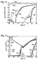
- FIGS. 2 and 3 are graphs showing experimental data for sample microelectronic devices including an etched photolithographic oxide semiconductor channel layer.
- FIGS. 4 and 5 are graphs showing experimental data for sample microelectronic devices including a lift-off photolithographic oxide semiconductor channel layer.
- FIG. 1 is a schematic side cross-sectional view of one example embodiment of a microelectronic device 10 manufactured in accordance with one example embodiment of a method of manufacturing a microelectronic device.
- device 10 may include an unpatterned gate contact 12 formed on an unpatterned p-type silicon (Si) wafer 14 .
- Gate contact 12 may be manufactured of titanium and gold (Ti/Au) wherein the titanium region 20 has a thickness 22 of 10 nanometers (nm) and the gold region 16 has a thickness 18 of 300 nm.
- Silicon wafer 14 may be a 150 millimeter (mm) p-type silicon wafer which may function as the TFT gate.
- the gate contact 12 may be formed on wafer 14 utilizing backside processing techniques.
- Silicon wafer 14 may include an unpatterned gate dielectric 24 formed thereon.
- Gate dielectric 24 may be manufactured of SiO 2 , for example, and may have a thickness 26 of 100 nm. Gate dielectric 24 may be formed on wafer 14 utilizing frontside processing techniques.
- Device 10 may further include a source 28 and a drain 30 each formed on gate dielectric 24 .
- Both source 28 and drain 30 may be manufactured of indium tin oxide (ITO), for example, and may each have a thickness 32 and 34 , respectively, of about 200 nm.
- Device 10 may further include a channel 36 having a thickness 38 of about 50 nm, which may be manufactured of an oxide semiconductor, and which may operatively connect source 28 and drain 30 .
- Oxide semiconductor channel 36 may be manufactured of zinc oxide, tin oxide, indium oxide, gallium oxide, zinc indium oxide, zinc tin oxide, indium gallium oxide, zinc indium gallium oxide, and any combination thereof, for example.
- the oxide semiconductor channel 36 may define an oxide with cations selected from at least one of Zn, In, Ga, and Sn.
- the source 28 and drain 30 electrodes are formed on gate dielectric 24 by RF sputtering and lift-off photolithographic patterning to define desired lateral dimensions, as suitable for the device or circuit being fabricated.
- Oxide semiconductor channel 36 of zinc indium oxide (ZIO) is then formed by rf sputtering with a target composition of ZnIn 4 O 7 to thickness 38 of 50 nm and lift-off or etch photolithographic patterning to define desired lateral dimensions, as suitable for the device or circuit being fabricated.
- the entire structure 10 is then annealed in air at a temperature of 175 degrees Celsius (C) for sixty minutes, with a ramp up and a ramp down temperature gradient of two degrees Celsius per minute to reach the maximum temperature of 175 degrees Celsius, for example.
- the oxide semiconductor channel 36 is then exposed to an oxygen containing plasma treatment for a time of at least two minutes, and approximately four minutes, at an energy level of at least 900 Watts, and approximately 1,000 Watts, at a oxygen (O 2 ) flow rate of at least 30 sccm, and approximately 40 sccm, and at a pressure of at least 40 mTorr, and approximately 50 mTorr.
- an oxygen containing plasma treatment for a time of at least two minutes, and approximately four minutes, at an energy level of at least 900 Watts, and approximately 1,000 Watts, at a oxygen (O 2 ) flow rate of at least 30 sccm, and approximately 40 sccm, and at a pressure of at least 40 mTorr, and approximately 50 mTorr.
- the oxide semiconductor channel 36 is once again annealed in air at a temperature of 175 degrees Celsius for sixty minutes, with a ramp up and a ramp down temperature gradient of two degrees Celsius per minute, for example.
- This example process yields a bottom gate coplanar type TFT microelectronic device 10 with a blanket gate contact 12 , a blanket gate dielectric 24 , and with photolithographic patterned source 28 , drain 30 and oxide semiconductor channel 36 .
- top-gate TFT is oriented such that the gate electrode lies above the channel (wherein the term “above” is defined with respect to the surface of the substrate upon which the TFT is disposed);
- bottom-gate TFT is oriented such that the gate electrode lies below the channel;
- a double-gate TFT includes two gate electrodes, one above and the other below the channel.
- the source and drain electrodes are positioned on the same side of the channel as is the gate electrode; conversely, in a staggered electrode configuration, source and drain electrodes are positioned on the opposite side of the channel as is the gate electrode.
- a device 10 manufactured according to the present method has excellent on-to-off ratios and allows control of the turn-on voltage of the device 10 .
- the oxide semiconductor channel layer 36 defines a channel conductance of effectively zero at a turn-on voltage of the thin film transistor, wherein a channel conductance of “effectively zero” is defined as a channel sheet resistance greater than or equal to about 10 8 Ohms/square.
- a channel conductance of “effectively zero” may be achieved when the TFT channel is effectively depleted of any equilibrium population of free electrons with the application of a suitable negative gate voltage, such as a voltage in a range of negative fifteen to zero volts.
- the oxygen containing plasma may include other gases in addition or in combination with oxygen, such as inert or non-inert gases, including He, Ar, Kr, N 2 , N 2 O, and the like.
- the plasma may also be described as a non-reducing agent gas containing oxygen (O 2 or another oxygen-containing species), and/or a non-etching agent gas containing oxygen (O 2 or another oxygen-containing species).
- the oxygen containing plasma may be formed according to one of many methods including, but not limited to: concentric cylinder and planar dielectric barrier, pulsed corona, e-beam, hollow cathode, electron cyclotron resonance, helicon, helical resonator, inductively/transformer coupled, plasmatron, plasma torch, and flow discharge, and the like, for example.
- FIGS. 2 and 3 are graphs showing experimental data for a sample microelectronic device 10 including an etched photolithographically-patterned oxide semiconductor channel layer 36 of zinc indium oxide (ZIO).
- FIG. 2 shows drain current versus gate-to-source voltage (I D -V GS ), taken in double-sweep mode (i.e., V GS is swept from ⁇ 30 V to +30 V, then back to ⁇ 30 V wherein the directional arrows in the figures show the direction of the sweep), for a TFT test structure.
- FIG. 3 shows mobility versus gate-to-source voltage (u-V GS ) for a TFT test structure.
- FIGS. 2 and 3 show electrical data taken following the first 175 C anneal 40 ( 40 a for a first test device and 40 b for a second test device), following the oxygen containing plasma exposure 42 ( 42 a for a first test device and 42 b for a second test device), and following the second 175 C anneal 44 ( 44 a for a first test device and 44 b for a second test device).
- the device performance is poor as seen in the large split (hysteresis/instability) between the forward and reverse portions of the V GS sweep (the arrows show the direction of the V GS sweep), and reduced mobility (low maximum “on” I D ).
- the mobility increases to a value of approximately fifteen to twenty cm 2 /V s, the split between forward and reverse portions of the V GS sweep is greatly reduced, and the turn-on voltage (V on ) magnitude remains at a workable, although moderately negative, value.
- FIGS. 4 and 5 are graphs showing experimental data for a sample microelectronic device 10 including a lift-off photolithographically-patterned oxide semiconductor channel layer 36 of zinc indium oxide (ZIO).
- FIG. 4 shows drain current versus gate-to-source voltage (I D -V GS ), taken in double-sweep mode (i.e., V GS is swept from ⁇ 30 V to +30 V, then back to ⁇ 30 V), for a TFT test structure.
- FIG. 5 shows mobility versus gate-to-source voltage (U-V GS ) for a TFT test structure.
- FIGS. 4 and 5 show electrical data taken following the first 175 C anneal 46 ( 46 a for a first test device and 46 b for a second test device), following the oxygen containing plasma exposure 48 ( 48 a for a first test device and 48 b for a second test device), and following the second 175 C anneal 50 ( 50 a for a first test device and 50 b for a second test device).
- the device performance is poor as seen in the large split (hysteresis/instability) between the forward and reverse portions of the V GS sweep (the arrows show the direction the V GS sweep), and reduced mobility (low maximum “on” I D ).
- the mobility increases to a value of approximately fifteen to twenty cm 2 /V s, the split between forward and reverse portions of the V GS sweep is greatly reduced, and the turn-on voltage (V on ) magnitude remains at a workable, although moderately negative, value.
Abstract
Description
Claims (15)
Priority Applications (1)
| Application Number | Priority Date | Filing Date | Title |
|---|---|---|---|
| US11/888,055 US8058096B2 (en) | 2007-07-31 | 2007-07-31 | Microelectronic device |
Applications Claiming Priority (1)
| Application Number | Priority Date | Filing Date | Title |
|---|---|---|---|
| US11/888,055 US8058096B2 (en) | 2007-07-31 | 2007-07-31 | Microelectronic device |
Publications (2)
| Publication Number | Publication Date |
|---|---|
| US20090035899A1 US20090035899A1 (en) | 2009-02-05 |
| US8058096B2 true US8058096B2 (en) | 2011-11-15 |
Family
ID=40338545
Family Applications (1)
| Application Number | Title | Priority Date | Filing Date |
|---|---|---|---|
| US11/888,055 Active 2030-03-21 US8058096B2 (en) | 2007-07-31 | 2007-07-31 | Microelectronic device |
Country Status (1)
| Country | Link |
|---|---|
| US (1) | US8058096B2 (en) |
Cited By (1)
| Publication number | Priority date | Publication date | Assignee | Title |
|---|---|---|---|---|
| US20120050940A1 (en) * | 2008-03-12 | 2012-03-01 | Nachiket Raravikar | Nanolithographic method of manufacturing an embedded passive device for a microelectronic application, and microelectronic device containing same |
Families Citing this family (10)
| Publication number | Priority date | Publication date | Assignee | Title |
|---|---|---|---|---|
| US8058096B2 (en) * | 2007-07-31 | 2011-11-15 | Hewlett Packard Development Company, L.P. | Microelectronic device |
| US20100019239A1 (en) * | 2008-07-23 | 2010-01-28 | Electronics And Telecommunications Research Institute | Method of fabricating zto thin film, thin film transistor employing the same, and method of fabricating thin film transistor |
| KR101610606B1 (en) * | 2009-07-03 | 2016-04-07 | 가부시키가이샤 한도오따이 에네루기 켄큐쇼 | Method for manufacturing semiconductor device |
| TWI589042B (en) * | 2010-01-20 | 2017-06-21 | 半導體能源研究所股份有限公司 | Light-emitting device, flexible light-emitting device, electronic device, lighting apparatus, and method of manufacturing light-emitting device and flexible-light emitting device |
| US9000442B2 (en) * | 2010-01-20 | 2015-04-07 | Semiconductor Energy Laboratory Co., Ltd. | Light-emitting device, flexible light-emitting device, electronic device, and method for manufacturing light-emitting device and flexible-light emitting device |
| TWI438868B (en) * | 2010-07-30 | 2014-05-21 | Au Optronics Corp | Complementary metal oxide semiconductor transistor and fabricating method thereof |
| US8728860B2 (en) | 2010-09-03 | 2014-05-20 | Semiconductor Energy Laboratory Co., Ltd. | Method for manufacturing semiconductor device |
| JP5645737B2 (en) * | 2011-04-01 | 2014-12-24 | 株式会社神戸製鋼所 | Thin film transistor structure and display device |
| KR20130111873A (en) | 2012-04-02 | 2013-10-11 | 단국대학교 산학협력단 | Manufacturing method for a thin film transistor array panel |
| US9356156B2 (en) * | 2013-05-24 | 2016-05-31 | Cbrite Inc. | Stable high mobility MOTFT and fabrication at low temperature |
Citations (13)
| Publication number | Priority date | Publication date | Assignee | Title |
|---|---|---|---|---|
| US5554547A (en) | 1992-09-29 | 1996-09-10 | Hyundai Electronics Industries Co., Ltd. | Process for the production of thin film transistor using oxygen plasma |
| US20020052059A1 (en) | 1998-09-03 | 2002-05-02 | Chun-Gi Lyu | Manufacturing method of a thin film transistor |
| US20060113539A1 (en) * | 2004-11-10 | 2006-06-01 | Canon Kabushiki Kaisha | Field effect transistor |
| US20060197092A1 (en) * | 2005-03-03 | 2006-09-07 | Randy Hoffman | System and method for forming conductive material on a substrate |
| US20070054507A1 (en) * | 2005-09-06 | 2007-03-08 | Canon Kabushiki Kaisha | Method of fabricating oxide semiconductor device |
| US20070075365A1 (en) * | 2005-10-03 | 2007-04-05 | Peter Mardilovich | Thin-film transistor and method of making the same |
| US20070085847A1 (en) | 2005-10-18 | 2007-04-19 | Semiconductor Energy Laboratory Co., Ltd. | Display device and driving method thereof |
| US20080023703A1 (en) * | 2006-07-31 | 2008-01-31 | Randy Hoffman | System and method for manufacturing a thin-film device |
| US7427776B2 (en) * | 2004-10-07 | 2008-09-23 | Hewlett-Packard Development Company, L.P. | Thin-film transistor and methods |
| US20080296568A1 (en) * | 2007-05-29 | 2008-12-04 | Samsung Electronics Co., Ltd | Thin film transistors and methods of manufacturing the same |
| US20090035899A1 (en) * | 2007-07-31 | 2009-02-05 | Gregory Herman | Microelectronic device |
| US20090166616A1 (en) * | 2007-12-26 | 2009-07-02 | Hitachi, Ltd. | Oxide semiconductor device and surface treatment method of oxide semiconductor |
| US20100090215A1 (en) * | 2007-04-25 | 2010-04-15 | Jung-Hyoung Lee | Thin film transistor and method for preparing the same |
-
2007
- 2007-07-31 US US11/888,055 patent/US8058096B2/en active Active
Patent Citations (14)
| Publication number | Priority date | Publication date | Assignee | Title |
|---|---|---|---|---|
| US5554547A (en) | 1992-09-29 | 1996-09-10 | Hyundai Electronics Industries Co., Ltd. | Process for the production of thin film transistor using oxygen plasma |
| US20020052059A1 (en) | 1998-09-03 | 2002-05-02 | Chun-Gi Lyu | Manufacturing method of a thin film transistor |
| US7427776B2 (en) * | 2004-10-07 | 2008-09-23 | Hewlett-Packard Development Company, L.P. | Thin-film transistor and methods |
| US20060113539A1 (en) * | 2004-11-10 | 2006-06-01 | Canon Kabushiki Kaisha | Field effect transistor |
| US20060197092A1 (en) * | 2005-03-03 | 2006-09-07 | Randy Hoffman | System and method for forming conductive material on a substrate |
| US20070054507A1 (en) * | 2005-09-06 | 2007-03-08 | Canon Kabushiki Kaisha | Method of fabricating oxide semiconductor device |
| US20070075365A1 (en) * | 2005-10-03 | 2007-04-05 | Peter Mardilovich | Thin-film transistor and method of making the same |
| US20070085847A1 (en) | 2005-10-18 | 2007-04-19 | Semiconductor Energy Laboratory Co., Ltd. | Display device and driving method thereof |
| US20080023703A1 (en) * | 2006-07-31 | 2008-01-31 | Randy Hoffman | System and method for manufacturing a thin-film device |
| US20090289250A1 (en) * | 2006-07-31 | 2009-11-26 | Randy Hoffman | System And Method For Manufacturing A Thin-film Device |
| US20100090215A1 (en) * | 2007-04-25 | 2010-04-15 | Jung-Hyoung Lee | Thin film transistor and method for preparing the same |
| US20080296568A1 (en) * | 2007-05-29 | 2008-12-04 | Samsung Electronics Co., Ltd | Thin film transistors and methods of manufacturing the same |
| US20090035899A1 (en) * | 2007-07-31 | 2009-02-05 | Gregory Herman | Microelectronic device |
| US20090166616A1 (en) * | 2007-12-26 | 2009-07-02 | Hitachi, Ltd. | Oxide semiconductor device and surface treatment method of oxide semiconductor |
Cited By (2)
| Publication number | Priority date | Publication date | Assignee | Title |
|---|---|---|---|---|
| US20120050940A1 (en) * | 2008-03-12 | 2012-03-01 | Nachiket Raravikar | Nanolithographic method of manufacturing an embedded passive device for a microelectronic application, and microelectronic device containing same |
| US8724290B2 (en) * | 2008-03-12 | 2014-05-13 | Intel Corporation | Nanolithographic method of manufacturing an embedded passive device for a microelectronic application, and microelectronic device containing same |
Also Published As
| Publication number | Publication date |
|---|---|
| US20090035899A1 (en) | 2009-02-05 |
Similar Documents
| Publication | Publication Date | Title |
|---|---|---|
| US8058096B2 (en) | Microelectronic device | |
| US9608127B2 (en) | Amorphous oxide thin film transistor, method for manufacturing the same, and display panel | |
| JP6043244B2 (en) | Thin film transistor | |
| US7468304B2 (en) | Method of fabricating oxide semiconductor device | |
| US8492761B2 (en) | Field-effect transistor and method for fabricating field-effect transistor | |
| US8466462B2 (en) | Thin film transistor and method of fabricating the same | |
| JP5127183B2 (en) | Thin film transistor manufacturing method using amorphous oxide semiconductor film | |
| US10615266B2 (en) | Thin-film transistor, manufacturing method thereof, and array substrate | |
| KR101413655B1 (en) | Fabrication method of oxide semiconductor thin film transistor | |
| US20160043227A1 (en) | Thin film transistor and manufacturing method thereof | |
| US20080203387A1 (en) | Thin film transistor and method of manufacturing the same | |
| JP2009021536A (en) | Method of manufacturing semiconductor active layer, method of manufacturing thin film transistor using the same and thin film transistor having semiconductor active layer | |
| JP2010183108A (en) | Field effect transistor using amorphous oxide film as channel layer, method for manufacturing field effect transistor using amorphous oxide film as channel layer, and method for manufacturing amorphous oxide film | |
| EP3295475B1 (en) | Thin film transistor, array substrate and display device having the same, and method of manufacturing thereof | |
| KR100991559B1 (en) | Method for manufacturing thin film transistor and thin film transistor manufactured by the method | |
| JP2008108985A (en) | Method of manufacturing semiconductor element | |
| US20100321279A1 (en) | Transistor, electronic device including a transistor and methods of manufacturing the same | |
| JP5098152B2 (en) | Thin film transistor manufacturing method | |
| TW201802892A (en) | Method for fabricating fully self-aligned dual-gate thin film transistors | |
| WO2020211851A1 (en) | Thin film transistor and preparation method therefor, array substrate, and display device | |
| TW201405835A (en) | A method for fabricating a thin film transistor | |
| Xiao et al. | Back channel anodization amorphous indium gallium zinc oxide thin-film transistors process | |
| CN108417620B (en) | Oxide insulator thin film and thin film transistor | |
| JP2010258126A (en) | Thin-film transistor and method for manufacturing the same | |
| Li et al. | Back-channel etched double layer in-WO/In-W-Zn-O thin-film transistors |
Legal Events
| Date | Code | Title | Description |
|---|---|---|---|
| AS | Assignment |
Owner name: HEWLETT-PACKARD DEVELOPMENT COMPANY, L.P., TEXAS Free format text: ASSIGNMENT OF ASSIGNORS INTEREST;ASSIGNORS:HERMAN, GREGORY;HOFFMAN, RANDY;YAMASHITA, TSUYOSHI;AND OTHERS;REEL/FRAME:019694/0187;SIGNING DATES FROM 20070725 TO 20070730 Owner name: HEWLETT-PACKARD DEVELOPMENT COMPANY, L.P., TEXAS Free format text: ASSIGNMENT OF ASSIGNORS INTEREST;ASSIGNORS:HERMAN, GREGORY;HOFFMAN, RANDY;YAMASHITA, TSUYOSHI;AND OTHERS;SIGNING DATES FROM 20070725 TO 20070730;REEL/FRAME:019694/0187 |
|
| STCF | Information on status: patent grant |
Free format text: PATENTED CASE |
|
| CC | Certificate of correction | ||
| FPAY | Fee payment |
Year of fee payment: 4 |
|
| MAFP | Maintenance fee payment |
Free format text: PAYMENT OF MAINTENANCE FEE, 8TH YEAR, LARGE ENTITY (ORIGINAL EVENT CODE: M1552); ENTITY STATUS OF PATENT OWNER: LARGE ENTITY Year of fee payment: 8 |
|
| MAFP | Maintenance fee payment |
Free format text: PAYMENT OF MAINTENANCE FEE, 12TH YEAR, LARGE ENTITY (ORIGINAL EVENT CODE: M1553); ENTITY STATUS OF PATENT OWNER: LARGE ENTITY Year of fee payment: 12 |