EP3229077A1 - Procédé et appareil d'exposition et procédé de fabrication de dispositif - Google Patents
Procédé et appareil d'exposition et procédé de fabrication de dispositif Download PDFInfo
- Publication number
- EP3229077A1 EP3229077A1 EP17170796.1A EP17170796A EP3229077A1 EP 3229077 A1 EP3229077 A1 EP 3229077A1 EP 17170796 A EP17170796 A EP 17170796A EP 3229077 A1 EP3229077 A1 EP 3229077A1
- Authority
- EP
- European Patent Office
- Prior art keywords
- light
- areas
- area
- amount
- optical
- Prior art date
- Legal status (The legal status is an assumption and is not a legal conclusion. Google has not performed a legal analysis and makes no representation as to the accuracy of the status listed.)
- Ceased
Links
Images


Classifications
-
- H—ELECTRICITY
- H01—ELECTRIC ELEMENTS
- H01L—SEMICONDUCTOR DEVICES NOT COVERED BY CLASS H10
- H01L21/00—Processes or apparatus adapted for the manufacture or treatment of semiconductor or solid state devices or of parts thereof
- H01L21/02—Manufacture or treatment of semiconductor devices or of parts thereof
- H01L21/027—Making masks on semiconductor bodies for further photolithographic processing not provided for in group H01L21/18 or H01L21/34
- H01L21/0271—Making masks on semiconductor bodies for further photolithographic processing not provided for in group H01L21/18 or H01L21/34 comprising organic layers
- H01L21/0273—Making masks on semiconductor bodies for further photolithographic processing not provided for in group H01L21/18 or H01L21/34 comprising organic layers characterised by the treatment of photoresist layers
- H01L21/0274—Photolithographic processes
- H01L21/0275—Photolithographic processes using lasers
-
- G—PHYSICS
- G03—PHOTOGRAPHY; CINEMATOGRAPHY; ANALOGOUS TECHNIQUES USING WAVES OTHER THAN OPTICAL WAVES; ELECTROGRAPHY; HOLOGRAPHY
- G03B—APPARATUS OR ARRANGEMENTS FOR TAKING PHOTOGRAPHS OR FOR PROJECTING OR VIEWING THEM; APPARATUS OR ARRANGEMENTS EMPLOYING ANALOGOUS TECHNIQUES USING WAVES OTHER THAN OPTICAL WAVES; ACCESSORIES THEREFOR
- G03B27/00—Photographic printing apparatus
- G03B27/32—Projection printing apparatus, e.g. enlarger, copying camera
- G03B27/42—Projection printing apparatus, e.g. enlarger, copying camera for automatic sequential copying of the same original
-
- G—PHYSICS
- G03—PHOTOGRAPHY; CINEMATOGRAPHY; ANALOGOUS TECHNIQUES USING WAVES OTHER THAN OPTICAL WAVES; ELECTROGRAPHY; HOLOGRAPHY
- G03F—PHOTOMECHANICAL PRODUCTION OF TEXTURED OR PATTERNED SURFACES, e.g. FOR PRINTING, FOR PROCESSING OF SEMICONDUCTOR DEVICES; MATERIALS THEREFOR; ORIGINALS THEREFOR; APPARATUS SPECIALLY ADAPTED THEREFOR
- G03F7/00—Photomechanical, e.g. photolithographic, production of textured or patterned surfaces, e.g. printing surfaces; Materials therefor, e.g. comprising photoresists; Apparatus specially adapted therefor
- G03F7/20—Exposure; Apparatus therefor
- G03F7/2002—Exposure; Apparatus therefor with visible light or UV light, through an original having an opaque pattern on a transparent support, e.g. film printing, projection printing; by reflection of visible or UV light from an original such as a printed image
- G03F7/2004—Exposure; Apparatus therefor with visible light or UV light, through an original having an opaque pattern on a transparent support, e.g. film printing, projection printing; by reflection of visible or UV light from an original such as a printed image characterised by the use of a particular light source, e.g. fluorescent lamps or deep UV light
- G03F7/2006—Exposure; Apparatus therefor with visible light or UV light, through an original having an opaque pattern on a transparent support, e.g. film printing, projection printing; by reflection of visible or UV light from an original such as a printed image characterised by the use of a particular light source, e.g. fluorescent lamps or deep UV light using coherent light; using polarised light
-
- G—PHYSICS
- G03—PHOTOGRAPHY; CINEMATOGRAPHY; ANALOGOUS TECHNIQUES USING WAVES OTHER THAN OPTICAL WAVES; ELECTROGRAPHY; HOLOGRAPHY
- G03F—PHOTOMECHANICAL PRODUCTION OF TEXTURED OR PATTERNED SURFACES, e.g. FOR PRINTING, FOR PROCESSING OF SEMICONDUCTOR DEVICES; MATERIALS THEREFOR; ORIGINALS THEREFOR; APPARATUS SPECIALLY ADAPTED THEREFOR
- G03F7/00—Photomechanical, e.g. photolithographic, production of textured or patterned surfaces, e.g. printing surfaces; Materials therefor, e.g. comprising photoresists; Apparatus specially adapted therefor
- G03F7/70—Microphotolithographic exposure; Apparatus therefor
- G03F7/70058—Mask illumination systems
- G03F7/70091—Illumination settings, i.e. intensity distribution in the pupil plane or angular distribution in the field plane; On-axis or off-axis settings, e.g. annular, dipole or quadrupole settings; Partial coherence control, i.e. sigma or numerical aperture [NA]
- G03F7/701—Off-axis setting using an aperture
-
- G—PHYSICS
- G03—PHOTOGRAPHY; CINEMATOGRAPHY; ANALOGOUS TECHNIQUES USING WAVES OTHER THAN OPTICAL WAVES; ELECTROGRAPHY; HOLOGRAPHY
- G03F—PHOTOMECHANICAL PRODUCTION OF TEXTURED OR PATTERNED SURFACES, e.g. FOR PRINTING, FOR PROCESSING OF SEMICONDUCTOR DEVICES; MATERIALS THEREFOR; ORIGINALS THEREFOR; APPARATUS SPECIALLY ADAPTED THEREFOR
- G03F7/00—Photomechanical, e.g. photolithographic, production of textured or patterned surfaces, e.g. printing surfaces; Materials therefor, e.g. comprising photoresists; Apparatus specially adapted therefor
- G03F7/70—Microphotolithographic exposure; Apparatus therefor
- G03F7/70058—Mask illumination systems
- G03F7/70091—Illumination settings, i.e. intensity distribution in the pupil plane or angular distribution in the field plane; On-axis or off-axis settings, e.g. annular, dipole or quadrupole settings; Partial coherence control, i.e. sigma or numerical aperture [NA]
- G03F7/70108—Off-axis setting using a light-guiding element, e.g. diffractive optical elements [DOEs] or light guides
-
- G—PHYSICS
- G03—PHOTOGRAPHY; CINEMATOGRAPHY; ANALOGOUS TECHNIQUES USING WAVES OTHER THAN OPTICAL WAVES; ELECTROGRAPHY; HOLOGRAPHY
- G03F—PHOTOMECHANICAL PRODUCTION OF TEXTURED OR PATTERNED SURFACES, e.g. FOR PRINTING, FOR PROCESSING OF SEMICONDUCTOR DEVICES; MATERIALS THEREFOR; ORIGINALS THEREFOR; APPARATUS SPECIALLY ADAPTED THEREFOR
- G03F7/00—Photomechanical, e.g. photolithographic, production of textured or patterned surfaces, e.g. printing surfaces; Materials therefor, e.g. comprising photoresists; Apparatus specially adapted therefor
- G03F7/70—Microphotolithographic exposure; Apparatus therefor
- G03F7/70058—Mask illumination systems
- G03F7/7015—Details of optical elements
- G03F7/70158—Diffractive optical elements
-
- G—PHYSICS
- G03—PHOTOGRAPHY; CINEMATOGRAPHY; ANALOGOUS TECHNIQUES USING WAVES OTHER THAN OPTICAL WAVES; ELECTROGRAPHY; HOLOGRAPHY
- G03F—PHOTOMECHANICAL PRODUCTION OF TEXTURED OR PATTERNED SURFACES, e.g. FOR PRINTING, FOR PROCESSING OF SEMICONDUCTOR DEVICES; MATERIALS THEREFOR; ORIGINALS THEREFOR; APPARATUS SPECIALLY ADAPTED THEREFOR
- G03F7/00—Photomechanical, e.g. photolithographic, production of textured or patterned surfaces, e.g. printing surfaces; Materials therefor, e.g. comprising photoresists; Apparatus specially adapted therefor
- G03F7/70—Microphotolithographic exposure; Apparatus therefor
- G03F7/70058—Mask illumination systems
- G03F7/70191—Optical correction elements, filters or phase plates for controlling intensity, wavelength, polarisation, phase or the like
-
- G—PHYSICS
- G03—PHOTOGRAPHY; CINEMATOGRAPHY; ANALOGOUS TECHNIQUES USING WAVES OTHER THAN OPTICAL WAVES; ELECTROGRAPHY; HOLOGRAPHY
- G03F—PHOTOMECHANICAL PRODUCTION OF TEXTURED OR PATTERNED SURFACES, e.g. FOR PRINTING, FOR PROCESSING OF SEMICONDUCTOR DEVICES; MATERIALS THEREFOR; ORIGINALS THEREFOR; APPARATUS SPECIALLY ADAPTED THEREFOR
- G03F7/00—Photomechanical, e.g. photolithographic, production of textured or patterned surfaces, e.g. printing surfaces; Materials therefor, e.g. comprising photoresists; Apparatus specially adapted therefor
- G03F7/70—Microphotolithographic exposure; Apparatus therefor
- G03F7/70483—Information management; Active and passive control; Testing; Wafer monitoring, e.g. pattern monitoring
- G03F7/7055—Exposure light control in all parts of the microlithographic apparatus, e.g. pulse length control or light interruption
- G03F7/70566—Polarisation control
Definitions
- the present invention relates to an exposure technology used to transfer mask-pattern on substrates such as wafers in a lithography process for fabricating various kinds of devices such as semiconductor elements, liquid crystal displays, thin-film magnetic heads and, more particularly to an exposure technology using an illuminating technology related to the so-called deformed illumination. Further, the present invention relates to a technology for fabricating the device using the exposure technology.
- the apparatus for the projection exposure of the batch exposure system such as the step-and-repeat system or the scan exposure system such as the step-and-scan system have been used to transfer the pattern of the reticle (or photo-mask etc.) as the mask on the wafers (or vitreous plate etc.) as the substrates intended for exposure in the lithography process for fabricating semiconductor elements (or liquid crystal displays etc.).
- the kind of apparatus for the projection exposure it is desirable to transfer various kinds of pattern on the wafers with each high resolution.
- the pattern being required very fine high resolution of those intended transfer is the so-called contact hole.
- the contact hole includes the densely massed contact hole having a plurality of predetermined shaped aperture arranged with predetermined fine pitch and the isolated contact hole being substantially comprised of a single aperture.
- the so-called deformed illumination system deformed light source system
- the so-called deformed light source system which allows the amount of light of the illumination light to be enlarged in one or more areas (particularly four areas) being eccentric for optical axis at the pupil plane of the illumination system, is effective (refer to Japanese Patent Applications Laid-open No. Hei 5-67558 (corresponding with US Patent NO. 6,094,305 ) and NO. 2001-176766 (corresponding to US Patent NO. 6,563,567 )).
- the illumination system which allows the amount of light of the illumination light to be enlarged in a relatively small round area centering optical axis at the pupil plane of the illumination system, that is, the illumination system that allows the ⁇ value, being a coherence factor of the illumination system to be relatively lessened (hereinafter, it will be called "small ⁇ illumination system" for convenience of description), is known to be effective.
- the pattern of the densely massed contact hole with fine pitch and the isolated contact hole can be transferred on the wafer with high resolution through the deformed illumination system and the small ⁇ illumination system respectively.
- the resolution is not sufficient in the direction in which the pat tern can be regarded as the isolated pattern, with using the traditional deformed illumination system for this purpose, while it is not sufficient in the direction in which the pattern is arranged with the fine pitch, with using the small ⁇ illumination system.
- the first object of the present invention is to provide an exposure technology for simultaneously transferring the pattern having various kinds of pitches with high resolution respectively.
- the second object of the present invention is to provide an exposure technology for transferring the pattern, which is arranged in one direction periodically and is substantially isolated (pattern densely massed in one direction) in terms of the orthogonal direction, with high resolution.
- the third object of the present invention is to provide a manufacturing technology for fabricating the device including various kinds of patterns or including the pattern densely massed in one direction with high accuracy and yet high throughput.
- the first exposure method which is an exposure method for illuminating a mask (R) with an optical beam from an illumination system (12) to expose a substrate (W) with the optical beam through the mask and a projection system (PL) , characterized in that a light amount distribution of the optical beam on a predetermined plane (Q1; Q3) with respect to the illumination system is set such that an amount of light is set larger in nine areas than in an area other than the nine areas, the nine areas including a first area (28; 28R) and eight areas (29A to 29D, 30A to 30D), an outer contour of the first area including an optical axis (BX) of the illumination system, and the eight areas being arranged so as to encompass the first area and each of the eight areas being smaller than the first area.
- such a pattern that is great in pitch and can be substantially regarded as the isolated contact hole by means of the optical beam passing through the first area is transferred with high resolution
- the pattern which includes the patterns ranging from the pattern with around middle pitch to the pattern with fine pitch like the densely massed contact hole by means of the optical beam passing through the eight areas enclosing the first area is transferred with high resolution. Accordingly, it is able to simultaneously transfer the patterns having various kinds of pitches with high resolution respectively.
- the first area to be located at the center is an annular zone area (28R).
- the annular illumination at the first area the resolution and the depth of focus might be improved in some cases.
- the amount of light (intensity per unit area e.g.) at the first area to be located in the center may be made different from the amount of light at the surround areas enclosing it.
- the predetermined plane is a pupil plane (Q1) of the illumination system
- the nine areas in which the amount of light on the predetermined plane is greater than the amount of light at the area other than the nine areas comprises the first area (28), four second areas (29A to 29D) which are arranged along a first circumference (32A) that encloses the first area and which are respectively smaller than the first area, and four third areas (30A to 30D) which are arranged along a second circumference (32B) that encloses the first circumference and which are respectively smaller than the first area.
- the pattern having the around middle pitch is transferred with high resolution by means of the optical beam passing through the second areas, and the pattern having the fine pitch is transferred with high resolution by means of the optical beam passing through the third areas.
- the first area (28), two of the second areas (29A, 29C), and two of the third areas (30A, 30C) are arranged along a first straight line (31A) passing through the optical axis (BX) of the illumination system, and the first area, the other two of the second areas (29B, 29D), and the other two of the third areas (30B, 30D) are arranged along a second straight line (31B) which is orthogonal to the first straight line and which passes through the optical axis of the illumination system.
- the conventional pattern intended to transfer is two-dimensionally arranged along two directions orthogonal to each other (one of them will be called "arranging direction of pattern"). Then, by making the direction of the first straight line (or the second straight line) intersect the arranging direction of the pattern (preferably making it intersect at 45 degree), the pattern having various kinds of the pitches two-dimensionally arranged can be transferred with high resolution respectively.
- the radius (r1) when the first area is made circular, and the radii (r2, r3) when the second and third areas are made circular are preferably set to the following bounds with the maximum ⁇ value (this will be assumed ⁇ ) of the illumination system assumed to be a reference.
- the first area, second areas, and third areas are set to other shape different from the circles such as the square, the regular hexagon or the shape having one quarter circle, the sizes of them preferable equal those of the circulars.
- the outer radius (r1) is preferably set to the bounds of an equation (1), as follows: 0.2 ⁇ ⁇ r 1 ⁇ 0.4 ⁇ 0.75 ⁇ ⁇ r 2 ⁇ 0.2 ⁇ 0.75 ⁇ ⁇ r 3 ⁇ 0.2 ⁇
- the second exposure method according to the present invention which is an exposure method for illuminating a mask (R) with an optical beam from an illumination system (12) to expose a substrate (W) with the optical beam through the mask and a projection system (PL), has a step of setting a light amount distribution of the optical beamon a predetermined plane (Q1 ; Q3) with respect to the illumination system is set such that an amount of light is set larger in five areas than in an area other than the five areas, the five areas including a first area of an annular zone shape (33R) in which an outer contour of the first area including an optical axis (BX) of the illumination system, and the four areas (34A to 34D) being arranged so as to encompass the first area and each of the four areas being smaller than the first area.
- a predetermined plane Q1 ; Q3
- such a pattern that is large in the pitch and can be substantially regarded as the isolated contact hole is transferred by means of the optical beam passing through the annular first area is transferred with high resolution, and the pattern having fine pitch like the densely massed contact hole by means of the optical beam passing through the four areas enclosing the first area is transferred with high resolution. Accordingly, it is able to simultaneously transfer the patterns having various kinds of the pitches with high resolution respectively.
- the predetermined plane is a pupil plane (Q1) of the illumination system
- the five areas in which the amount of light on the predetermined plane is greater than the amount of light at the area other than the five areas comprises the first area (33R) and four second areas (34A to 34D) which are arranged, at intervals of substantially 90 degree therebetween, along a circumference (35) that encloses the first area and which are respectively smaller than the first area.
- the pattern having the fine pitch is transferred with high resolution by means of the optical beam passing through the second areas.
- the conventional pattern intended to transfer is two-dimensionally arranged along two directions orthogonal to each other (one of them will be called "arranging direction of pattern"). Then, by making the direction, in which the second areas are arranged intersect the arranging direction of the pattern (preferably making it intersect at 45 degree), the pattern having various kinds of the pitches two-dimensionally arranged can be transferred with high resolution respectively.
- the radius (r1) when the first area is made annular with its contour assumed to be circular and the radius (r2) when the second area is made circular is preferably set within the bounds of the equations (1) and (2) described above with the maximum ⁇ value (this will be assumed ⁇ ) of the illumination system assumed to be a reference. This enables the pattern having various kinds of the pitches to be transferred with high resolution.
- an optical beam generated from each of the areas which have large amount of light which are arranged out of the optical axis of the illumination system on the predetermined plane is linear polarization.
- a direction of polarization of the optical beam on the predetermined plane is substantially coincident with a circumference direction (that is, the optical beam may be S polarization).
- the third method for exposure according to the present invention which is an exposure method having a step for illuminating a mask (R1) with an optical beam from an illumination system (12) to expose a substrate (W) with the optical beam through the mask and a projection system (PL), has a step of setting a light amount distribution of the optical beam on a predetermined plane (Q1 ; Q3) with respect to the illumination system is set such that an amount of light is set larger in three areas (54, 55A, 55B; 62, 63A, and 63B) than in the area other than these.
- the patterns are transferred with high resolution the direction of which the patterns are isolate by means of optical beam passing through the center of the three areas, and the patterns are transferred with high resolution the direction of which the patterns are periodically arranged by means of optical beam passing through the two areas which sandwich the center area.
- the three areas having large amount of light include a first area (54; 62) near an optical axis of the illumination system, and a second area (55A; 63A) and a third area (55B; 63B) which are arranged along a straight line passing through the optical axis so as to sandwich the first area.
- the three areas having large amount of light include a first area (54; 62) near an optical axis of the illumination system, and a second area and a third area (55A, 55B; 63A, 63B) which are arranged with the approximately same distance from the optical axis.
- compositions by providing (paralleling) the direction of which the three areas are arranged to the direction of which the one direction dense pattern is periodically arranged, it is able to transfer the one directional high density pattern to the two directions of the isolated and periodical ones with high resolution.
- a pattern formed on the mask includes a one directionally high density pattern (52, 53) which is periodically arranged along a predetermined first axis (X axis) and which is substantially isolated in a direction of a second axis (Y axis) orthogonal to the first axis
- the three areas having large amount of light are preferably arranged with a distance therebetween in a parallel direction to the first axis.
- the three areas having large amount of light are preferably arranged along a straight line which is parallel to the first axis and which passes through the optical axis of the illumination system.
- a center area of the three areas having large amount of light is preferably set such that an amount of light of a center part thereof is smaller than an amount of light of a part other than the center part. Whereby, it is able to increase the resolution in the direction of which the pattern is isolated and to widen the depth of focus.
- the center area is around an annular zone area (54) as an example.
- the center area comprises a plurality of areas (54A1, 54A2) separated from each other.
- the plurality of areas separated from each other, which are the center area are arranged along a predetermined straight line passing through the optical axis of the illumination system on the predetermined plane as an example.
- an arranging direction of the plurality of areas separated from each other, which are the center area is determined according to a size of the center area as another example.
- the three areas have outlines which are the substantially same with each other as an example. Further, the sizes of the three areas having large amount of light respectively correspond to 0.1 times 0.2 times of a maximum ⁇ value of the illumination system. Whereby, the deep depth of focus is obtained according to the simulation of the present invention.
- the two areas (63A, 63B) of the three areas having large amount of light which are arranged at both ends with respect to the direction parallel to the first axis, may respectively have longitudinal directions which are substantially coincident with a direction parallel to the second axis. Whereby, it is able to enhance the resolution corresponding to the one directional high density pattern and to avoid the reduction of the amount of light.
- center area (62A) of the three areas having large amount of light may have a longitudinal direction which is substantially coincident with the direction parallel to the first axis.
- an optical beam generated from a center area of the three areas having large amount of light may linear polarization, a directions of polarization is substantially coincident with a direction parallel to the first or second axis.
- an optical beam generated from a center area of the three areas having large amount of light and optical beams generated from the other two areas may have different polarization states from each other.
- a polarization direction of the optical beam generated from the center area (62A) and a polarization direction of the optical beams generated from the other two (63A, 63B) areas are orthogonal to each other.
- a size of the center area of the three areas having great amount of light and sizes of the other two areas may be different from each other.
- the optical beams generated from the other two areas except for the center area of the three areas having large amount of light may be respectively linear polarization.
- the directions of polarization of optical beams distributed in the other two areas on the predetermined plane may be respectively substantially coincident with a circumference direction (that is, the optical beam may be S polarization).
- the predetermined plane is a pupil plane of the illumination system.
- a predetermined plane is the conjugate plane for the pupil plane of the illumination system or the pupil of the projection system (or its conjugate plane). In this case, it is obtained the highest resolution.
- the first exposure apparatus in an exposure apparatus which an illumination system (12) illuminates a mask (R) with an optical beam; and a projection system (PL) which exposes a substrate (W) with the optical beam from the mask, characterized by comprising an optical member (21; 42) which sets a light amount distribution of the optical beam on a predetermined plane (Q1; Q3) with respect to the illumination system such that an amount of light is set larger in nine areas than in an area other than the nine areas, the nine areas including a first area (28; 28R) and eight areas (29A to 29D, 30A to 30D), an outer contour of the first area including an optical axis (BX) of the illumination system, and the eight areas being arranged so as to encompass the first area and each of the eight areas being smaller than the first area.
- the optical members With the optical members, it is able to simultaneously transfer patterns having various kinds of pitch with high resolution respectively.
- the central first area is an annular zone area (28R).
- the predetermined plane is a pupil plane (Q1) of the illumination system
- the nine areas in which the amount of light at the predetermined plane is greater than the amount of light at the area other than the nine areas comprises the first area (28), four second areas (29A to 29D) which are arranged along a first circumference (32A) that encloses the first area and which are respectively smaller than the first area, and four third areas (30A to 30D which are arranged along a second circumference (32B) that encloses the first circumference and which are respectively smaller than the first area.
- the first area (28), the two second areas (29A, 29C), and two of the third areas (30A, 30C) are arranged along a first straight line (31A) passing through the optical axis (BX) of the illumination system, and the first area, the other two of the second areas (29B, 29D), and the other two of the third areas (30B, 30D) are arranged along a second straight line (31B) which is orthogonal to the first straight line and which passes through the optical axis of the illumination system.
- each area preferably satisfies the conditions of the equations (1) to (3).
- the second exposure apparatus in an exposure apparatus which an illumination system (12) which illuminates a mask (R) with an optical beam; and a projection system (PL) which exposes a substrate (W) with the optical beam from the mask, characterized by comprising an optical member which sets a light amount distribution of the optical beam on a predetermined plane (Q1; Q3) with respect to the illumination system such that an amount of light is set larger in five areas than in an area other than the five areas, the five areas including a first area (33R) of an annular zone shape and four areas (34A to 34D), an outer contour of the first area including an optical axis (BX) of the illumination system, and the four areas being arranged so as to encompass the first area and each of the four areas being smaller than the first area.
- the optical members With the optical members, it is able to simultaneously transfer patterns having various kinds of pitch with high resolution respectively.
- the predetermined plane is a pupil plane (Q1) of the illumination system
- the five areas in which the amount of light on the predetermined plane is greater than the amount of light at the area other than the five areas comprises the first area (33R) and four second areas (34A to 34D) which are arranged, at intervals of substantially 90 degree therebetween, along a circumference (35) that encloses the first area and which are respectively smaller than the first area.
- each area preferably satisfies the conditions of the equations (1) to (3).
- the illumination system includes an optical integrator (5) which substantially uniformalize illuminance within an illuminant area on the mask on which the optical beam is irradiated, and the optical member is arranged at an incident side of the optical integrator in the illumination system, and the optical member includes a diffractive optical element (21) which diffracts the optical beam to a plurality of directions.
- the optical integrator which substantially uniformalize illuminance within an illuminant area on the mask on which the optical beam is irradiated
- the optical member is arranged at an incident side of the optical integrator in the illumination system, and the optical member includes a diffractive optical element (21) which diffracts the optical beam to a plurality of directions.
- the illumination system includes an optical integrator (5) which substantially uniformalize illuminance within an illuminant area on the mask on which the optical beam is irradiated, and the optical member is arranged on the predetermined plane or a conjugate plane thereof, and the optical member includes an aperture stop (42) defining an area in which an amount of light is enhanced on the predetermined plane.
- the aperture stop has a simple structure and can easily set the preferable distribution of the amount of light.
- the optical member can preferably set different plural light amount distributions including a distribution which enhances the amount of light at the plurality of areas. Whereby, it is able to expose various kinds of pattern with optimum irradiating condition.
- an optical beam generated from each of the areas which have large amount of light and which are arranged out of the optical axis of the illumination system on the predetermined plane may be linear polarization.
- a direction of polarization of the optical beam on the predetermined plane may substantially coincident with a circumference direction (that is, the optical beam may be S polarization).
- the optical member may further includes a polarization member which generates optical beams respectively distributed at different areas on the predetermined plane, and a polarization setting member which sets polarization states of the optical beams generated from the polarization member in the illumination system.
- An example of the polarization member is a diffractive optical element (21) which generates diffracted light to a plurality of directions on an optical path of the illumination system.
- the opticalmember includes movable members (71, 72) which are arranged at an exit side of the polarization member, and which can change a positional relation between each area outside the optical axis on the predetermined plane and the optical axis of the illumination system, and the polarization setting member may be arranged between the polarization member and the movable member.
- the movable members may include at least one movable prism (71) which has an inclined plane (71b) through which an optical beam distributed in a predetermined area including a plurality of areas outside the optical axis except the first area on the predetermined plane passes, the at least one movable prism moves along the optical axis of the illumination system.
- the optical member includes at least one movable prism (71, 72) which can change positions of a plurality of areas which enclose the first area and which have greater amount of light than an area other than the plurality of areas.
- the movable prism as an example, has an inclined plane (71b) through which an optical beam distributed in a predetermined area including a plurality of areas outside the optical axis except the first area on the predetermined plane passes, and the movable prism moves along the optical axis of the illumination system.
- the movable prism as another example, has a flat plane (71a) through which an optical beam distributed in the first area passes and which is approximately orthogonal to the optical axis of the illumination system.
- the third exposure apparatus in an exposure apparatus which an illumination system (12) illuminates a mask (R) with an optical beam; and a projection system (PL) which exposes a substrate (W)with the optical beam from the mask, characterized by comprising an optical member which sets a light amount distribution of the optical beam on a predetermined plane (Q1; Q3) with respect to the illumination system such that an amount of light is set larger in a first area (28, 28R) and a plurality of areas than in an area other than the first area and the plurality of areas, the first area substantially including an optical axis of the illumination system, and the plurality of areas being arranged outside the first areas, wherein the optical member (21) includes a polarization member which generates optical beams respectively distributed at different areas on the predetermined plane, and at least one movable prism having a flat plane through which an optical beam generated from the polarization member and distributed in the first area passes and which is approximately orthogonal to the optical axis of the illumination system and an inclined plane through
- the diffractive optical member it is able to simultaneously transfer pattern having various kinds of pitch with high resolution respectively. Further, with the movable prism, it is able to adjust the characteristic of the image-forming according to the kind of the pattern to be transferred.
- the illumination system includes an optical integrator (5) which substantially uniformalize illuminance within an illuminant area on the mask on which the optical beam is irradiated, and the movable prism is arranged at an incident side of the optical integrator in the illumination system, and the movable prism moves along the optical axis.
- optical beams generated from the plurality of areas arranged outside the first area are respectively linear polarization (S polarization) in which the polarization direction thereof being substantially coincident with a circumference direction on the predetermined plane.
- the optical member can preferably set different plural light amount distributions including a distribution which enhances the amount of light at the plurality of areas including the first area.
- an illumination system (12) illuminates a mask(R) with an optical beam; and a projection system (PL) which exposes a substrate (W) with the optical beam from the mask, characterized by comprising optical members (22A, 22B; 42A, 42B) which set a light amount distribution of the optical beam on a predetermined plane with respect to the illumination system such that an amount of light is set larger in three areas (54, 55A, 55B; 62, 63A, 63B) separated from each other than in an area other than the three areas.
- the optical member With using the optical member, it is able to transfer the one direction dense pattern to the two directions of the isolated and periodical ones with high resolution.
- the three areas having large amount of light preferably include a first area (54; 62) near an optical axis of the illumination optical system, and a second area (55A; 63A) and a third area (55B; 63B) which are arranged along a straight line passing through the optical axis so as to sandwich the first area.
- the three areas having large amount of light may include a first area (54; 62) near an optical axis of the illumination optical system, and a second area and a third area (55A, 55B; 63A, 63B) which are arranged with the approximately same distance from the optical axis.
- compositions if a first axis (X axis) direction in which a high density pattern formed on the mask is periodically arranged and a second axis (Y axis) direction in which the high density pattern (52, 53) is arranged substantially isolatedly, the second axis direction being orthogonal to the first axis direction, the three areas having large amount of light are arranged with a distance therebetween in a parallel direction to the first axis direction. Whereby, it is able to transfer the one direction dense pattern with high resolution along the first axis and the second axis respectively. Further, the three areas having large amount of light are arranged along a straight line which passes through the optical axis of the illumination system and which is parallel to the first axis.
- a center area of the three areas having large amount of light is set such that an amount of light of a center part thereof is smaller than an amount of light of a part other than the center part.
- the center area is substantially an annular zone area (54) as an example.
- the center area comprises a plurality of areas (54A1, 54A2) separated from each other as another example.
- the plurality of areas separated from each other, which are the center area are arranged along a predetermined straight line passing through the optical axis of the illumination optical system on the predetermined plane as an example.
- an arranging direction of the plurality of areas separated from each other, which are the center area is determined according to a size of the center area as another example.
- the sizes of the three areas having large amount of light respectively correspond to 0.1 times 0.2 times of a maximum ⁇ value of the illumination system. Whereby, the deep depth of focus is obtained according to the present invention.
- two areas (63A, 63B) of the three areas having large amount of light which are arranged at both ends with respect to the direction parallel to the first axis, respectively have longitudinal directions which are substantially coincident with a direction parallel to the second axis.
- a center area (62A) of the three areas having large amount of light has a longitudinal direction which is substantially coincident with the direction parallel to the first axis.
- an optical beam generated from a center area of the three areas having large amount of light is linear polarization, a directions of polarization is substantially coincident with a direction parallel to the first or second axis.
- an optical beam generated from a center area of the three areas having large amount of light and optical beams generated from the other two areas may have different polarization states from each other.
- a polarization direction of the optical beam generated from the center area and a polarization direction of the optical beams generated from the other two areas are orthogonal to each other.
- a size of the center area of the three areas having great amount of light and sizes of the other two areas may be different from each other.
- optical beams generated from the other two areas except for the center area of the three areas having large amount of light are respectively linear polarization.
- directions of polarization of optical beams distributed in the other two areas on the predetermined plane are respectively substantially coincident with a circumference direction (S polarization).
- the optical member includes a polarization member which generates optical beams respectively distributed at different areas on the predetermined plane
- the exposure apparatus further comprises a polarization setting member which sets polarization states of the optical beams generated from the polarization member in the illumination system.
- the optical member includes a movable member (71, 72) which is arranged at an exit side of the polarization member, and which can change a positional relation between the other two areas except for the center area of the three areas having large amount of light and the optical axis of the illumination system, and the polarization setting member is arranged between the polarization member and the movable member.
- the movable member includes at least one movable prism (72) which has an inclined plane through which an optical beam distributed in a predetermined area including the other two areas except for the center area on the predetermined plane passes, and the at least one movable prism moves along the optical axis of the illumination system.
- the optical member may include at least one movable prism (71, 72) which can change positions of the other two areas except for the center area of the three areas having large amount of light.
- the movable prism as an example, has an inclined plane (71b) through which an optical beam distributed in a predetermined area including the other two areas except for the center area on the predetermined plane passes, and the movable prism moves along the optical axis of the illumination system.
- the movable prism may have a flat plane (71a) through which an optical beam distributed in the center area on the predetermined plane passes and which is approximately orthogonal to the optical axis of the illumination system.
- the illumination system includes an optical integrator which substantially uniformalize illuminance within an illuminant area on the mask on which the optical beam is irradiated, and the movable prism is arranged at an incident side of the optical integrator (4) in the illumination system.
- a predetermined plane is, as an example, a pupil plane (Q1) of the illumination system.
- the illumination system includes an optical integrator (5) which substantially uniformalize illuminance within an illuminant area on the mask on which the optical beam is irradiated, and the optical members (22A, 22B) include a diffractive optical element which is arranged at an incident plane side of the optical integrator in the illumination system. With this constitution, it is able to obtain a high efficiency.
- the illumination system includes an optical integrator (5) which substantially uniformalize illuminance within an illuminant area on the mask on which the optical beam is irradiated, and the optical member is arranged on the predetermined plane or a conjugate plane thereof, and the optical member includes an aperture stop (42A; 42B) defining the three areas.
- the optical members can preferably set different plural light amount distributions including a light amount distribution which enhances the amount of light in the three areas. Whereby, it is able to transfer various kinds of patterns with high resolution.
- method for fabricating device according to the present invention is method for fabricating device including lithography process in which patterns (R) are transferred to the photosensitive material (W) by using the exposure method or apparatus according to the present invention.
- the exposure method or apparatus according to the present invention With the exposure method or apparatus according to the present invention, the mass production of devices including various kinds of patterns or one direction pattern with high accuracy.
- the present invention when setting the distribution of a predetermined plane relating to the illumination system so as to increase the amount of light at a predetermined nine or five areas, it is able to simultaneously transfer patterns having various kinds of pitches with high resolution respectively.
- center first area annular it is able to more improve the resolution and depth of focus. Furthermore, by controlling the state of polarization of the optical beam, it might be able to more improve the resolution and the like.
- the present invention when setting the distribution of a predetermined plane relating to the illumination system so as to increase the amount of light at a predetermined three areas, it is able to transfer one direction patterns with high resolution.
- the pattern formed at the mask is periodically arranged along a predetermined first axis and includes the one direction dense pattern which is substantially isolated in the direction of the second axis orthogonal to the first axis, by arranging the three areas in which the amount of light is great with distance in the parallel direction to the first axis, it is able to transfer the one direction dense pattern with high resolution both directions of arranging the one direction dense pattern to periodical and isolatable ones. Further, in the present invention, with setting the state of polarization of the optical beam oriented from the three areas in which the amount of light is great, it might be to improve the resolution and the like for a predetermined pattern.
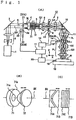
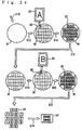
- Fig. 1 (A) shows a composition of the projection exposure apparatus of this embodiment
- a KrF excimer laser light source (wave-length 248 nm) is used as an exposure light source 1.
- the laser light sources such as an ArF excimer laser light source (wave-length 193 nm), a F 2 laser light source (wave-length 157 nm), a Fr 2 laser light source (wave-length 146 nm), or an Ar 2 laser light source (wave-length 126 nm) ; or high frequency generating apparatus such as a high frequency generating light source of a YAGI laser or a solid laser (for example semiconductor laser etc.) can be used as a exposure light source 1.
- An illumination light L 1 comprised of ultraviolet pulse light as an optical beam for exposure (exposure beam) emitted from exposure light source 1 goes into the first diffractive optical element 21 through an optical path folding miller 3, after changing the cross-sectional shape of the optical beam into the desirable shape with beam expander 2, and is changed the optical beam DL which diffracts to the plural directions in order to be obtained a predetermined distribution of amount of light at a predetermined plane (for example pupil plane of the illumination system) as described after.
- the diffractive optical element 21 as a part of the optical member for setting distribution of amount of light is mounted to a revolver 24, the second diffractive optical element 22 having other diffractive characteristic and further, diffractive optical element (not shown) having another diffractive characteristic are also mounted.
- a main control system 17 controlling over the all operation of the apparatus controls the revolving angle of the revolver 24 through a driver 23, by setting one of the diffractive optical element 21 and 22 etc. on the optical path of the illumination light L 1, can change the condition of illumination.
- the optical beam DL diffracted by the diffractive optical element 21 is gathered by a relay lens 4, is gathered on an incident plane of the fly' eye lens 5 as an optical integrator, through a first prism 71 and a second prism 72 (movable prism).
- the diffractive optical element 21 is arranged at a position slightly deviated from a front focus of the relay lens 4 to the exposure light source 1 than, and the incident plane of fly' eye lens 5 is approximately arranged at the position of the back focus of the relay lens 4.
- a plurality of optical beams diffracted to the different directions are respectively gathered at the different areas on the incident plane of the fly' eye lens 5, a plane light source (2-dimentional light source comprised of many light source images in this embodiment) of distribution approximately corresponding to the amount of light of the incident plane is formed.
- a combined lens system comprised of the relay lens 4 and fly' eye lens 5
- the exit plane of the diffractive optical element 21 and the exit plane Q1 of the fly' eye lens 5 have approximately be conjugate (imaging relation).
- the diffractive optical element 21, the first prism 71, and the second prism 72 are corresponding to an optical member for setting a predetermined distribution of amount of light.
- the first prism 71 is a member which forms a parallel flat plate 71 at circular area of which the center is an optical axis BX (discuss later) of a illumination system, and forms a concave cone 71 b around the circular area;
- the second prism 72 is a member which forms inverted concave and convex for the first prism 71, and forms a parallel flat plate as a whole by combining with the first prism 71.
- a optical beam passing the circular area of the center of the first prism 71 and the second prism 72 distributes to areas which are a center of a distribution of amount of light on the exit plane Q1 on the fly' eye lens 5 in which amount of light is enhanced;
- a optical beam passing the cone part (slope plane) around the first prism 71 and the second prism 72 distributes to a plurality of areas (or a predetermined area including the plurality of areas) in which amount of light is enhanced around the distribution of amount of light.
- the second prism 72 is only supported movably by a driving mechanism (not shown), thus by changing the distance between the first prism 71 and the second prism 72 by moving the second prism 72 along the optical axis BX, the position of a plurality of peripheral areas in which the amount of light is great can adjust to the radial direction, without changing the central distribution (position of areas 28, 33 etc. described bellow) of the distribution of amount of light at the exit plane Q1 on the fly' eye lens 5.
- a prism having not a cone but a pyramid may be used instead of the first prism 71 and the second prism 72. Furthermore, it is allow moving this position along the optical axis BX by only using the first prism 71 instead of the first prism 71 and the second prism 72. Further, as shown Fig. 1 (C) , it is allow using a pair of prisms 71A, 71B shaped like a letter V which has diffractive power to one direction and has not diffractive power to orthogonal direction, as the movable prism.
- each rectangle area (in this embodiment, the parallel flat plate) of its center is approximately orthogonal to the optical axis BX and two slope planes of the around area are approximately symmetric with respect to a plane being orthogonal to the paper of Fig. 1 (C) including the optical axis BX.
- another pair of prisms 71C, 71D constructed by revolving the pair of prisms 71A, 71B by 90 degrees about the optical axis BX maybe arranged. Whereby, it is able to independently adjust each position (distance from the optical axis BX) being orthogonal each other in which amount of light is great.
- the prism described above whose slope plane is the cone, pyramid, or shaped like a letter V the center flat plate is the parallel flat plate, it may be aperture part (hollow part) by cutting at lest one part of the center part, or may be an integral solid by making a plurality of members independently. In particular, the latter may be an integral solid by only dividing the peripheral slope plate except the center flat plate part into a plurality of parts.
- the fly' eye lens 5 is, as an example, a bundle of many lens elements each of which has a rectangular cross-section whose vertical and horizontal width is about a few of millimeter, the shape cross-section of each lens element is approximately similar to a slim piece of illumination area on a reticle.
- a micro fly' eye lens constructed by binding many micro lenses whose shape cross-section is rectangular with about a few tens of micrometer or circular with diameter of about a few tens of micrometer can be used.
- the illumination light L1 comprises optical beam emitted from the fly' eye lens 5 is onetime gathered on the plane Q2 by a condenser lens system 6.
- a fixed field stop (fixed blind) 7 for limiting an illumination area on a reticle R as an illuminated target toa slimshape orthogonal to scan direction, i.e., not- scan direction is arranged at slight front side of the plane Q2, a movable field stop (movable blind) 8 on the plane Q2.
- the movable field stop is used to prevent from useless exposure by controlling the width of the scan direction of the illumination area at the front and back of the scan exposure, and to limit the width of the not-scan direction of the illumination area during the scan exposure.
- a reticle stage driving system 16 described bellow controls open/close operation of the movable field stop 8 through a driving section 13 in sync with operation of the reticle stage.
- An illumination system 12 is composed of the exposure light source 1, a beam expander 2, the miller 3, the diffractive optical element 21 (or other diffractive optical element), the relay lens 4, fly' eye lens 5, the condenser lens system 6, field stop 7, 8, the imaging-lens system 9, the miller 10, and the main condenser lens system 11.
- An optical axis of the illumination system 12 is regarded as the optical axis BX.
- the exit plane Q1 of the fly' eye lens 5 is substantially coincident to an optical Fourier transform plane for the pupil plane of the illumination system 12, i.e., reticle: the plane Q2 in which the movable field stop 8 is arranged is a conjugate plane with the reticle plane.
- the fixed field stop 7, for example, may be arranged near the reticle plane.
- the imaging-circuit patterns within illumination area of the reticle R via a projection optical system PL of both side telecentrics as a projection system, transfers a resist layer of one shot area among a plurality of shot areas on a wafer W as a substrate arranged on an image-forming plane of the projection optical system PL with a predetermined downsizing magnification ⁇ (for example, ⁇ is 1/4, 1/5 etc.).
- ⁇ for example, ⁇ is 1/4, 1/5 etc.
- the reticle R and wafer W is respectively regarded as a first object and second object.
- the wafer W as substrate for exposure is a circular substrate such as semiconductor (silicon etc.) or SOI (silicon on insulator) whose diameter is 200 or 300 mm, for example.
- An optical axis AX of the projection optical system PL is coincident to an optical axis BX of the illumination system on the reticle R. Furthermore, a pupil plane Q3 (optical Fourier transform plane for the reticle plane) on the projection optical system PL is conjugate with the exit plane Q1 (the pupil plane of the illumination system 12) of the fly' eye lens 5.
- the projection optical system PL of this embodiment other one except the diffractive system can be used, for example, a catadioptric projection optical system having a plurality of optical systems having optical cross-axes each other as disclosed in Japanese Patent Application: TOKUKAI 2000-47114 (corresponding to US Patent NO.
- a catadioptric projection optical system and the like which has an optical system including an optical axis intends from a reticle to a wafer and a catadioptric optical system including an optical axis being approximately orthogonal to that optical axis, and which forms an intermediate image twice in its interior as disclosed in international publication (WO): 01/065296 brochure (corresponding to US publication 2003/0011755A1 ).
- WO international publication
- 01/065296 brochure corresponding to US publication 2003/0011755A1 .
- the projection optical system PL with considering that a Z axis is paralleled to the optical axis AX, a X axis is not-scan direction (the direction parallel to the paper in Fig. 1 (A) , in this case) orthogonal to the scan direction, and a Y axis is the scan direction (the direction orthogonal to the paper in Fig. 1 (A) , in this case), as follows:
- the reticle R is adsorbed and held on the reticle stage 14; the reticle stage 14 is mounted so as to move with a constant velocity along the Y direction on a reticle base 15, and to slightly move along rotating directions about the X , Y, and Z axis.
- the position of the reticle stage 14 is measured by a laser interferometer in a reticle driving system 16.
- the reticle driving system 16 controls the position and velocity of the reticle stage 14 through driving mechanism not shown, based on the measured information and control information from a main control system 17.
- the wafer W is adsorbed and held on a wafer stage 18 through wafer holder not shown; the wafer stage 18 is movably mounted in the X and Y directions on a wafer base 19.
- the position of the wafer stage 18 is measured by a laser interferometer in a wafer driving system 20.
- the wafer driving system 20 controls the position and velocity of the wafer stage 18 through driving mechanism not shown, based on the measured information and control information from the main control system 17.
- a focusing mechanism for fitting the surface of the wafer into the image-forming plane of the projection optical system PL is assembled in the wafer stage 18 during the scan exposure, based on measured information of an auto-focus sensor not shown.
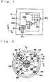
- Fig. 2 shows an example of a pattern (original pattern) for transferring formed on a reticle R; in Fig. 2 , a 2-dimentional pattern with three kinds of contact holes arranging pattern 25A, 25B, and 25C of approximate squares with pitch P1, P2, and P3 at the X, Y directions in a pattern region PA of the reticle R.
- Each pattern 25A, 25B, and 25C may be a transmission pattern formed in a light shielded film, or may conversely be a light shielded pattern formed in a transmission part.
- each pattern 25A, 25B, and 25C is around equal to 1/2 or smaller than corresponding pitch P1, P2, and P3 respectively, however, the width of pattern 25B, 25C with larger pitch can be around equal to pattern 25A with most fine pitch.
- the pitch P1, P2, and P3 are set to gradually become several-fold, as follows: P 1 ⁇ P 2 ⁇ P 3
- the projection magnification ⁇ of the projection optical system PL in Fig. 1 (A) is 1/4-fold
- pitch P1, P2, and P3 on the reticle plane are respectively set, as an example, around 300 nm, 600 nm, and 900 nm. That is, the original patterns on the reticle plane include a first pattern for dense contact holes with fine pitch, a second pattern for dense contact holes with around middle pitch, and a third pattern for contact holes arranged with large pitch substantially regarding as the isolated contact holes. In order to transfer an image of these original patterns on wafer onetime with high accuracy, as shown Fig.
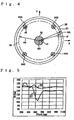
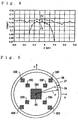
- Fig. 3 shows the distribution of amount of light of the illumination light IL at the exit plane Q1 (pupil plane of the illumination system) of the fly' eye lens 5.
- the direction on the exit plane Q1 corresponding to the X direction and Y direction (i.e., the arranging direction of the pattern to transfer) on the reticle R is respectively def ined the X direction and Ydirection.
- NA the numerical aperture of the object side (reticle side) of the projection optical system PL in Fig. 1 (A)
- NA PL the numerical aperture of the image side (wafer side)
- the maximum value among the numerical apertures of the illumination light IL incident to the reticle R from the illumination system 12 is NA IL
- the value of ratio (coherence factor) of the maximum numerical aperture NA IL to the numerical aperture NA of the projection optical system PL is called maximum ⁇ value in this embodiment
- maximum ⁇ value is ⁇ . That is, the illumination light of maximum ⁇ value is the light incident on the reticle R with the maximum angle among the illumination light IL.
- a maximum outer circle 26 indicates an outer area passed through virtual optical beam having the same numerical aperture as the numerical aperture NA at the incident side of the projection optical system PL
- an inner circle 27 indicates a circle is tangent to areas passed through illumination light having numerical aperture of the maximum ⁇ value ( ⁇ ): all illumination light pass though within the circle 27.
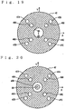
- 3 approximately has a constant amount of light at nine areas with distance each other which include a circular area 28 with radius r1 centered an optical axis BX of the illumination system 12, four circular areas 29A, 29B, 29C, and 29D with radius r2 whose centers are arranged along a first circle 32A with radius R1 enclosing the area 28, and four circular areas 30A, 30B, 30C, and 30D with radius r3 whose centers are arranged along a second circle 32B with radius R2 enclosing the areas 29A to 29D, and has distribution of amount of light of lower amount of light (approximate 0 in this embodiment) at other areas than the constant amount of light.
- the amount of light, near the outline of the area 28, areas 29A to 29D, and areas 30A to 30D may have distributions which gradually decrease toward the outside.
- the center area 28 corresponds to a first area; the four areas 29A to 29D enclosing the area 28 correspond to second areas; further the four areas 30A to 30D enclosing the areas 29A to 29D correspond to third areas.
- the radii r1 to r3 and R1, R2 respectively indicates the length (distance between point passed through the optical beam of the maximum ⁇ value and the optical axis BX) corresponding the maximum ⁇ value ( ⁇ ) as unit.
- the center area 28 is set larger than other eight areas 29A to 29D and 30A to 30D (r1 > r2 > r3). Further, since the arranging directions of the 2-dimentional patterns as the targets to transfer are the X direction and Y direction, it is defined that a straight line crossed to the X direction by 45 degrees in clock winding is a straight line 31A; a straight line (the straight line crossed to the X direction by 45 degrees in counter clock winding) is a straight line 31B.
- the center of the center area 28, the middle two areas 29A and 29C, and other most outer two areas 30A and 30C is arranged on the first straight line 31A; the center of the center area 28, the middle other two areas 29B and 29D, and other most outer two areas 30B and 30D is arranged on the second straight line 31B. That is, the eight areas 29A to 29D and 30A to 30D enclosing the center area 28 are arranged along the two directions being orthogonal with revolving the two arranging directions by 45 degrees, which are orthogonal, in which patterns as the targets for transfer.
- the diffractive characteristic of the diffractive optical element 21 in Fig. 1 (A) is set, so as to obtain the distribution of amount of light in which the amount of light approximately becomes constant at the area 28, the areas 29A to 29D, and the areas 30A to 30D in Fig. 3 satisfying the condition of the equations (7) to (10): approximately becomes 0 at other areas.
- the diffractive optical element 21, as an example can fabricate by forming a concave and convex grating having approximately systematically along in the direction of the straight line 31A, and a concave and convex grating having approximately systematically along in the direction of the straight line 31B of Fig. 3 .
- the aperture stop whose aperture is formed at the part corresponding to the area 28, the areas 29A to 29D, and the areas 30A to 30D in Fig. 3 , may be arranged at the exit plane Q1 (pupil plane) of the fly' eye lens 5 or its conjugate plane. Also in this case, it is advantage of high efficiency for using the illumination light L1.
- this inventor have evaluated the CD (critical dimension), through the simulation of the computer, which is obtained by transferring a downsizing image of pattern of contact holes with various kinds of pith arranged on the reticleplane to the wafer through the projection optical system PL, under the distribution of amount of light in which the amount of light becomes constant at the nine areas comprising the area 28, the areas 29A to 29D, and the areas 30A to 30D in Fig. 3 satisfying the condition of the equations (7) to (10) : becomes 0 at the other areas.
- the CD used is the line width of patterns transferred.
- the numerical aperture NA PL of the image side (wafer side) of the projection optical system PL in Fig. 1(A) is 0.82
- projection magnification ⁇ is 1/4-fold
- the curve 36 in Fig. 5 shows the simulation result of the CD value in case that the amount of light becomes constant at the nine areas on the pupil plane, the horizontal axis is the pitch (nm) of the pattern transferred on the reticle plane, vertical axis is the CD value (nm) in Fig. 5 .
- the pitch 280 to 1120 nm is equivalent of 70 to 280 nm at the wafer side.
- the preferable CD value having approximately constant across the wide range of pitch 280 to 1120 nm.
- the radius r1 of the area 28, the radii r2 of the areas 29A to 29D, and the radii r2 of the areas 30A to 30D may be the ranges, as follows: 0.2 ⁇ ⁇ r 1 ⁇ 0.4 ⁇ 0.75 ⁇ ⁇ r 2 ⁇ 0.2 ⁇ 0.75 ⁇ ⁇ r 3 ⁇ 0.2 ⁇
- the radius R1 of the first circle 32A and the radius R2 of the second circle 32B may be changed up to around ⁇ 10% of the equations (9) and (10).
- the numerical aperture NA PL of the image side, the projection magnification ⁇ , and the maximum ⁇ value ( ⁇ ) in the projection optical system PL can be taken any values though the values described above.
- the maximum ⁇ value ( ⁇ ) by changing the distance between prism 71 and 72 in Fig. 1(A) , the radial position of the areas 29A to 29D, and the areas 30A to 30D with peripheral area in which the amount of light is great among the distribution of amount of light in Fig.
- Fig. 3 (the distance from the optical axis BX relating to the X direction and Y direction) may only be changed.
- Fig. 1(C) by using two pairs of prism 71A, 71B and 71C, 71D, the position of the areas 29A to 29D, and the areas 30A to 30D with peripheral area in which the amount of light is great among the distribution of amount of light in Fig. 3 (the distance from the optical axis BX) in the X direction and Y direction may independently controlled.
- the amount of light of the center area 28 e.g., intensity per unit size
- the amount of light of the four areas 29A to 29D along the peripheral first circle 32A and that of the four areas 30A to 30D along the peripheral second circle 32B may be different.
- the relative amount of these lights may be adjusted so that the optimum resolution is obtained for each pattern, for example.
- a distribution of amount of light becoming great amount of light of the five areas including four slim areas 130A, 130B, 130C, and 130D which are substantially connected to the radial each two areas 29A, 29B, 29C, 29D, 30A, 30B, 30C, and 30D of the radial in Fig. 3 respectively and the center area 28 may be used. Also in this case, it is almost able to transfer patterns having various kinds of pitch with high resolution.
- the amount of light of the connecting parts of two areas in the radial may around equal to that of the two areas, or may be different from that of the two areas, for example smaller.
- annular may be used instead of the center area 28 as the first area.
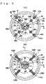
- Fig. 6(A) shows a distribution of amount of light of the illumination light L1 on the exit plane Q1 (pupil plane of the illumination system 12) of fly' eye lens 5 in Fig. 1(A) , when the first area is the area of annular.
- the amount of light of the area 28R of annular consist of the outer radius r1, the inner radius r1R, and the center of the optical axis BX and that of the nine areas including the area 28, the areas 29A to 29D, and the areas 30A to 30D are approximately constant; and amount of light of the illumination light at the other areas is approximately 0.
- the condition other than it is the same as that of the case where the amount of light in Fig. 3 is used.
- the light distributed at the peripheral areas 29A to 29D, and the areas 30A to 30D in Fig. 6(A) may be linear polarization.
- the light distributed at the peripheral areas may be S polarization (vertical direction for the incident plane) whose polarization direction is the tangent direction.
- S polarization vertical direction for the incident plane
- the resolution etc. for the specific pattern might be enhanced. It is the similar to the case of using the distribution of amount of light in Fig. 3 or 6(B) .
- the optical beam is preferably changed into that of the linear polarization whose polarization direction is approximately coincident to the circumference direction.
- the polarization setting member is preferably arranged between one of the plurality of prisms (movable member) described above which is arranged at the most upstream side (light source side) and incident side, for example the lens4, or the diffractive optical element 21 and the lens4.
- the center circular area 28 may be the area of the annular similar to Fig. 6(A) .
- the diffractive optical element 21 in this embodiment sets the distribution of amount of light on the pupil plane of the illumination system 12 as a predetermined plane to a predetermined state; the predetermined plane may be the pupil plane Q3 of the projection optical system PL.
- the distribution of amount of light is set which is approximately constant at the first area including the axis AX and the eight areas enclosing it, and which is lower at the other areas.
- the area 28 (or 28R), each of the areas 29A to 29D, and the areas 30A to 30D, in which amount of light is approximately constant on the pupil plane is the circular (or annular) however, each circular (or annular) can be an area of ellipse (ellipse annular).
- the area of circular (or annular) can be an area of polygon (or frame shape of polygon), or can be combination of the area of circular (or annular) and the area of polygon.
- Fig. 9 shows possible another distribution of amount of light on the pupil plane, as shown Fig. 9 , the distribution of amount of light is approximately constant at the center square (right square or right hexagon etc. is possible) area 28A, four square areas 30E to 30 H enclosing it, and lower than it at the other areas.
- the positions and sizes of the areas may be respectively similar to those of the area 28, areas 29A to 29D, and the areas 30A to 30D.
- an area of frame type may be used instead of the center area 28A in Fig. 9 .
- a second diffractive optical element 22 having different diffractive characteristic is provided to the revolver 24 in Fig. 1(A) .
- the second diffractive optical element 22 With setting the second diffractive optical element 22 on the optical path of the illumination light IL, distribution of amount of light which is approximate constant amount of light at the five areas of the exit plane Q1 (pupil plane) of the fly-eye lens 5, and the lower (approximate 0 in this embodiment) than it at the other area is obtained.
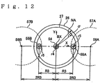
- Fig. 7(A) shows a distribution of amount of light of the illumination light IL on the exit plane Q1 (pupil plane) of fly-eye lens 5 in Fig. 1(A) , when the second diffractive optical element 22 is used.
- Fig. 7(A) with marking the same notes to the parts corresponding to in Fig.
- the distribution of amount of light at five areas with distance each other including an area 33R (first area) of circular annular consist of the outer radius r1, the inner radius r1R, and the center of the optical axis BX of the illumination system 12, and four circular areas 34A, 34B, 35C, and 35D (second area) arranging along the a circle 35 having radius R3 with radius r5 and 90 degrees distance enclosing the area 33R is approximately constant; and is smaller (approximate 0 in this embodiment) than the constant amount of light.
- the outer outline of the center area 33R is set larger than that of other four areas 34A to 34D (r4>r5).
- the preferable range of the radius r4 is similar to that of the radius r1 of the equation (13), and the preferable range of the radius R3 and radius r5 are similar to that of the radius R2 of the equation (10) and radius r2 of the equation (14) respectively.
- the outer four areas 34A to 34D are respectively arranged along the straight lines pass through the optical axis BX and cross by 45 degrees in the X direction (or Y direction).
- This inventor has evaluated the CD (critical dimension), through the simulation of the computer, which is obtained by transferring a downsizing image of pattern of contact holes with various kinds of pith arranged on the reticle plane to the wafer through the projection optical system PL, under the distribution of amount of light in which the amount of light becomes constant at the five areas comprising the area 33, and the areas 34A to 34D in Fig. 4 satisfying the condition of the equations (16) and (17) becomes 0 at the areas in addition thereto.
- the exposure wave length is ArF laser light
- the numerical aperture NA PL of the image side (wafer side) of the projection optical system PL in Fig. 1(A) is 0.78
- projection magnification ⁇ is 1/4-fold
- the maximum ⁇ value ( ⁇ ) is 0.9.
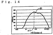
- the curves of line graph F1, F2 in Fig. 8 show the simulation result of the CD value in case that the amount of light becomes constant at the five areas on the pupil plane, the horizontal axis is the defocus amount of wafer ( ⁇ m), vertical axis is the line width ( ⁇ m) (line width on wafer) of the pattern well transferred as the CD value. Furthermore, approximate flat curve F1 indicates simulation result for the pattern of contact holes with line width 140 nm, pitch 220; mountain-shaped curve F2 indicates simulation result for the isolated pattern with line width 140 nm. As shown F1, F2, approximately constant CD value with range in which the defocus amount is around -0.2 ⁇ m to 0.2 ⁇ m is obtained. Accordingly, various kinds of pattern from the isolated pattern to the pattern with fine contact holes with high accuracy and wide depth of focus.
- Fig. 7(A) it can be set the amount of light of the center area 33R (e.g., intensity per unit size) and that of the peripheral four areas 34A to 34D differ.
- the relative amount of these lights may be adjusted so as to be obtained the optimum resolution at each pattern for example.
- a distribution of amount of light becoming great amount of light of the area 134 which is a starfish shape having an aperture at the center or a star shape substantially connected the four areas 34A to 34D and the center annular zone area 33R in the radial direction may be used.
- the amount of light of the central part of the area 134 may be not 0 only smaller. Also in this case, it is almost able to transfer patterns having various kinds of pitch with high resolution.
- the amount of light of the connected part getting longer to radial direction may be around equal to those of the peripheral and center areas, or may be different from those, for example smaller than those.
- the light distributed at the peripheral areas 34A to 34D in Fig. 7(A) may be linear polarization.
- the light distributed at the peripheral areas may be S polarization (vertical direction for the incident plane) whose polarization direction is the tangent direction.
- the resolution etc. for the specific pattern might be enhanced. It is the similar to the case of using the distribution of amount of light in Fig. 7(B) .
- the light distributing the peripheral area getting longer to the radial direction, particularly its part corresponding to the peripheral areas 34A to 34D in Fig. 7(A) may be the linear polarization whose polarization becomes the tangent direction.
- the light distributed at the peripheral areas is non-polarization or whose polarization direction is not coincidental to the circumference direction, as described above, for example, it is preferable to provide polarization setting member between the diffractive optical element 21 and the fly-eye lens 5.
- Fig. 4 shows the distribution of amount of light in which the amount of light is set constant at a circular area 33 instead of the center annular zone area 33R in Fig. 7(A) , and the amount of light is set constant at four areas 34A to 34D enclosing it as with Fig. 7(A) .
- This inventor have evaluated the CD (critical dimension), through the simulation of the computer, which is obtained by transferring a downsizing image of pattern of contact holes with various kinds of pith arranged on the reticle plane to the wafer through the projection optical system PL, under the distribution of amount of light in which the amount of light becomes constant at the five areas comprising the area 33, and the areas 34A to 34D in Fig. 4 satisfying the condition of the equations (18) and (19) : becomes 0 at the other areas.
- the values of the numerical aperture NA PL of the image side (wafer side) of the projection optical system PL in Fig. 1(A) , projection magnification ⁇ , and the maximum ⁇ value ( ⁇ ) are similar to the equation (12) in the Fig. 3 .
- the dotted line curve 37 in Fig. 5 shows the simulation result of CD value in which the amount of light becomes constant at the five areas of this pupil plane, as shown in the curve 37; the CD value is low around pitch 500 to 700 nm.
- the second embodiment according to the present invention will be described accompanying Fig. 10 to Fig. 17 .
- the exposure is fundamentally performed by using the scan exposure type projection optical apparatus in Fig. 1 (A) .
- a diffractive optical element 22A (described bellow in detail) having different characteristic is used instead of the diffractive optical element 21 in Fig. 1(A) .
- the diffractive optical element 22A, the first prism 71, and the second prism 72 are corresponding to an optical member for setting a predetermined distribution of amount of light.
- the prism 71, 72 (or the first prism 71 only) are used as movable prism.
- Fig. 10 it is allow using a pair of prisms 71A, 71B shaped like a letter V which has diffractive power to one direction and has not diffractive power to orthogonal direction, as the movable prism.
- the prisms 71A, 71B are arranged so that each rectangle area (in this embodiment, the parallel flat plate) of its center is approximately orthogonal to the optical axis BX and two slope planes of the around area are approximately symmetric with respect to a plane being orthogonal to the paper of Fig. 1 (A) including the optical axis BX.
- a reticle RA is loaded on the reticle stage 14 instead of the reticle R in Fig. 1(A) .
- Fig. 11(A) shows an example of a pattern (original pattern) for transferring formed on the reticle RA loaded on the reticle stage 14 in Fig. 1(A) .
- a pattern 52 for the one directional high density pattern is formed, in which square aperture patterns 51 having width a in the X direction and width b in the Y direction, are periodically arranged in the X direction (non-scan direction in this embodiment) with pitch P at the pattern region PA.
- the pitch P is fine pitch (for example, around 150 nm length converted to projection image on wafer W) which is close to approximate limited resolution of the projection exposure apparatus in this embodiment, the width a of the X direction is around 1/2 of the pitch P, and the width b of the Y direction is around equal to the width a to 10-fold (around a to 10a).
- the pattern 52 is one directional high density pattern which can regard an isolated pattern about the Y direction (scan direction in this embodiment) .
- the pattern 52 is the periodical pattern arranging four aperture pattern 51 in X direction, the number of the aperture pattern 51 may be 2 or any than 2.
- the aperture pattern 51 is the transmission pattern formed in a light shielded film, a light shielded pattern provided in transmission part may be used instead of it.
- another pattern 53 for one directional high density pattern is also formed at a position distant from the pattern 52 in the Y direction, in which square aperture patterns 51 with pitch Q larger than the pitch P.
- the pattern 52 and 53 are actually small pattern whose length of X direction is a few ⁇ m or less, various kinds of other pattern (not shown) may be formed on the pattern region PA of the reticle RA.
- Fig.11(B) when pattern 52A, 52B, and 52C, in which aperture pattern 51 is arranged in the X direction with pitch P respectively, are formed with considerably larger pitch than pitch P in the Y direction, each of pattern 52A, 52B, and 52C is regarded as one directional high density pattern, can be the target for transfer in this embodiment.
- the plurality of periodic pattern may only be arranged with the distance, so as to be isolated for orthogonal direction (Y direction) to the periodic direction, and their number may be arbitrary.
- Fig. 1(A) In order to transfer image of these original patterns on wafer with high accuracy, as shown Fig. 1(A) in this embodiment, with arranging the diffractive optical element 22A on the optical path of an illumination light IL, the distribution of amount of light (strength distribution) of the illumination light IL at the exit plane Q1 (pupil plane) of the fly-eye lens 5 as a predetermined plane.
- Fig. 12 shows the distribution of amount of light of the illumination light IL at the exit plane Q1 (pupil plane of the illumination system 12) of the fly-eye lens 5 in Fig. 1 in this embodiment.
- the direction on the exit plane Q1 corresponding to the X direction (periodically arranging direction) and Y direction (regarding as isolated direction) on the reticle R is respectively defined the X direction and Y direction.
- NA the numerical aperture of the object side (reticle side) of the projection optical system PL in Fig. 1(A)
- NA PL the numerical aperture of the image side (wafer side)
- the maximum value among the numerical apertures of the illumination light IL incident to the reticle R from the illumination system 12 is NA IL
- the value of ratio (coherence factor) of the maximum numerical aperture NA IL to the numerical aperture NA of the projection optical system PL is called maximum ⁇ value in this embodiment
- maximum ⁇ value is ⁇ IL . That is, the illumination light of maximum ⁇ value is the light incident on the reticle R with the maximum angle among the illumination light IL.
- a maximum outer circle 26 indicates an outer area passed through virtual optical beam having the same numerical aperture as the numerical aperture NA at the incident side of the projection optical system PL
- an inner circle 27 indicates a circle is tangent to areas passed through illumination light having numerical aperture of the maximum ⁇ value ( ⁇ IL ) ; all illumination light pass though within the circle 27.
- the illumination light IL in Fig. 12 , has the distribution of amount of light with the approximate constant amount of light at the three areas (hatched areas) including the annular zone area 54 with the radius r4 which centers on the optical axis BX of the illumination system 12 and the two circular areas 55A, 55B with the radius r5 sandwiching the area 54 in the X direction; and with the smaller amount of light (approximate 0 in this embodiment) than the constant amount of light.
- the centers of the three areas 54, 55A, and 55B are arranged along the straight line which passes through the optical axis of the illumination system and parallels the X axis (periodically arranging direction of one directional high density pattern as target for transfer), the distance between the each center of the area 55A and 55B both ends and the optical axis BX is respectively R3.
- the annular zone area 54 has 1/2 annular in which the inner radius is 1/2 of the outer radius r4, 1/3 annular in which the inner radius is 1/3 of the outer radius r4, or 2/3 annular in which the inner radius is 2/3 of the outer radius r4 and the like.
- the circular area 54A with the radius r4 can be used instead of the annular zone area 54.
- a plurality of areas substantially split can be used instead of the annular zone area 54. Concretely, as shown in Fig.
- the distribution of amount of light at the two half-circular (or circular etc.) areas 54A1, 54A2 split in the Y direction (or X direction), in which the amount of light become great, may be used instead of the annular zone area 54.
- the amount of light may become great at a four-way split area in the X direction and Y direction (or direction crossed these axes) instead of the annular zone area 54.
- distribution in which the amount of light gradually decreases toward outer may be near the outline of the area 54, 55A, 55B.
- the center area 54 is corresponding to the first area, and the two areas 54A and 54B sandwiching it is respectively corresponding to the second area and third area.
- the radii r4, r5 and R3 respectively indicate the radius ⁇ in the equation (6B) (distance between point passed through the optical beam of the maximum ⁇ value and the optical axis BX) corresponding to the maximum ⁇ value ( ⁇ IL ) as unit.
- the radii r4, r5 are preferably set within around 0.1 ⁇ to 0.2 ⁇ respectively, as follows: 0.1 ⁇ ⁇ r 4 ⁇ 0.2 ⁇ 0.1 ⁇ ⁇ r 5 ⁇ 0.2 ⁇
- radius r4 and radius r5 are preferably equal, as follows: r 4 ⁇ r 5
- the diffractive characteristic of the diffractive optical element 21 in Fig. 1 (A) is set, so as to obtain the distribution of amount of light in which the amount of light approximately becomes constant at the area 54, the areas 55A, 55B in Fig. 12 satisfying the condition of the equations (21) to (24) ; approximately becomes 0 at other areas.
- the diffractive optical element 22A as an example, can fabricate by forming a concave and convex grating having approximately systematically along in the direction of the straight line 31A, and a concave and convex grating having approximately systematically along the X axis of Fig. 12 .
- the diffractive optical element 22A may be a combination of a plurality of phase type diffractive gratings.
- the diffractive optical element 22A is phase type, it is advantage of high efficiency for using light.
- it is able to use an optical element changing refractive index distribution corresponding to a diffractive grating distribution as an optical element 22A.
- a construction and a method for fabricating having a specific diffractive characteristic is closely disclosed, for example, in Japanese Patent Application Laid-open No. 2001-176766 (corresponding to US Patent NO. 6,563,567 ) by this applicant.
- the amount of light distribution obtained by diffraction optical device 22A is set to be approximately the predetermined of light at a region including regions 54, 55A and 55B in Fig. 12 .
- an aperture stop where an aperture is formed at a portion corresponding to the regions 54, 55A and 55B in Fig. 12 may be disposed on the emission plane Q1 (pupil plane) of the fly eye lens 5 in Fig. 1 (A) . Also in this case, advantage in which utilization efficiency of the illumination light IL is high is obtained.
- Fig. 13(A) shows diffraction light (focus light flux) diffracted in the isolated Y direction from the pattern 52.
- Fig. 13(B) shows diffraction light (focus light flux) diffracted in the periodic X direction from the pattern 52.
- light beams 58, 59 and 60 show the illumination light IL passed through the regions 54, 55A and 55B on the pupil plane of the illumination system in Fig. 12 respectively.
- the diffraction light generated from the pattern 52 (aperture pattern 51) due to the light beams 58, 59 and 60 generates, in the Y direction, with distribution in which the diffraction light is generated most strongly at the center, and the larger the tilt angle, the lower the intensity decreases, as shown in Fig. 13(A) .
- the pattern 52 of this embodiment is approximately the resolution limit, therefore, the positive primary light 59P from the pattern 52 due to one light beam 59 is made incident into the projection optical system PL in Fig. 1 (A) in parallel to the other zero-order light 60, while, the negative primary light 60M from the pattern 52 due to the other light beam 60 is made incident into the projection optical system PL in Fig. 1(A) in parallel to one zero-order light 59.
- wavelengths of incident light beams 58, 59 and 60 are taken to as ⁇
- exit angle in the X direction to the normal line of the pattern 52 of the zero-order light 59 is taken to as ⁇
- exit angle in the X direction to the normal line of the pattern 52 of the zero-order light 60 is taken to as - ⁇
- Fig. 13(B) among the other light beams 59, the light beam passed through the adjacent aperture pattern 51 with interval P of the X direction is taken to as the light beams 59A and 59B.
- equation (26) corresponds to the case in which focal distance fQ1 at the side of the emission plane Q1 of the partial optical system between the emission plane Q1 (pupil plane) in the illumination system 12 in Fig. 1A and the reticle plane is set to 1.
- Equation (26) corresponds to the case in which focal distance fQ1 at the side of the emission plane Q1 of the partial optical system between the emission plane Q1 (pupil plane) in the illumination system 12 in Fig. 1A and the reticle plane is set to 1.
- equation (27A) indicates resolution limit of X direction (cycle direction) in the object plane (reticle plane) of the projection exposure apparatus of this embodiment, in which the larger is the interval R3 while making ⁇ larger or while making radius r5 smaller, the less it is possible to make the pitch P to be the resolution limit smaller.
- the pitch P is converted intopitch ⁇ P as the following equation, which the pitch ⁇ P is length on the wafer.
- the pitch ⁇ P becomes the resolution limit in the X direction on the image plane (wafer plane) of the projection optical system PL.
- ⁇ ⁇ P ⁇ ⁇ ⁇ / 2 ⁇ ⁇ r 5
- the wavelength ⁇ is set to 193.306 nm.
- numerical aperture NA PL at the wafer side of the projection optical system PL is taken to be 0.85
- projection scale factor ⁇ of the projection optical system PL is taken to be 1/4
- ⁇ IL to be ⁇ value of illumination system 12 is taken to be 0.90
- radius r5 of the regions 55A and 55B in Fig. 12 is taken to be 0.14 ⁇ , that is called as "the first illumination condition”.
- the resolution limit ⁇ P at the image plane side under this condition becomes about 147 nm as shown in next equation from relationship of the equations (6B) and (27B).
- ⁇ ⁇ P 146.7 nm
- Fig. 12 can be regarded as the drawing showing amount of light distribution in the X direction in the pupil plane Q3 of the projection optical system PL in Fig. 1 (A) .
- the regions 54, 55A and 55B in Fig. 12 correspond to position through which the zero-order light of the illumination light IL is passed, and the positive primary light in the X direction of the illumination light IL according to the pattern 52 in Fig.
- the negative primary light in the X direction of the illumination light IL according to the pattern 52 becomes distribution in which the amount of light distribution in the circumference 27 is moved in parallel toward the region in the circumference 57B with the spaced point 56A as the center, which the spaced point 56B is spaced from the optical axis BX (optical axis AX) by only interval 2 ⁇ R3 in the -X direction.
- the positive primary light (or the negative primary light) of the light beam passing through the region 55B (or 55A) passes through the region 55A (or 55B), therefore, the image of the pattern 52 is projected on the wafer with high resolution.
- the present inventor in order to obtain the optimum balance between radius r4 of central region 54 and radius r5 of the regions 55A and 55B at both ends in Fig. 12 , has calculated depth of focus (DOF) of the image according to the projection optical system PL with simulation of the computer while varying the radius r4 gradually.
- the condition in addition to the r4, at this time, is the same as the above described first illumination condition, and the radius r5 is 0.14 ⁇ .
- the pitch P of the pattern 52 in Fig.
- the pitch P, and the widths a and b are lengths which are converted on the image plane of the projection optical system PL respectively.
- the curved line 61 in Fig. 14 shows the simulation results, and the horizontal axis in Fig. 14 is the radius r4 (unit is ⁇ ) of the region 54 (center ⁇ ) of the center of Fig. 12 , and the vertical axis is calculation results of the depth of focus (DOF) (nm) corresponding to the value of the radius r4.
- DOF depth of focus
- pattern 53 of the one directional high density contact hole existing in the position spaced from the pattern 52 of Fig. 11(A) arrangement direction is the same as that of the pattern 52, and the pitch Q is larger than the pitch P, therefore, the pattern 53 is transferred on the wafer with high resolution under the above described illumination condition.
- the pattern of the reticle RA including the pattern 52 of the one directional high density contact hole of Fig. 11 (A) is capable of being transferred on the wafer W in the X direction and the Y direction with high resolution.
- At least one of 2 regions 55A and 55B except for the central region 54 is allowed that distance of the optical axis BX concerning the direction in parallel to the cyclic direction of the other pattern is not zero, or the distance is allowed to be set in accordance with the pitch of the other pattern, for instance.
- numerical aperture NA PL at the image side of the projection optical system PL, the projection scale factor ⁇ , and the maximum ⁇ value ( ⁇ IL) of the illumination system 12 are capable of taking arbitrary value without restricting the value to the above described values.
- position (distance of the optical axis BX concerning X direction to the region 55B) in the radius direction of the regions 55A and 55B where peripheral amount of light is large among amount of light distribution of Fig. 12 is allowed to be varied while varying interval between prisms 71 and 72 of Fig. 1 (A) to.control the maximum ⁇ value ( ⁇ IL), or the interval R3 of Fig. 12 .
- the amount of light (for instance, intensity per unit area) of the center region 54 is made different from the amount of light of peripheral 2 regions 55A and 55B. Relative largeness of these light quantities is allowed to be adjusted so that the optimum resolution can be obtained every transferring pattern, for instance.
- distributed light in peripheral regions 55A and 55B of Fig. 12 may be made linearly polarized light.
- the light distributed on the peripheral regions 55A and 55B is made S polarization in which the polarizing direction is direction of the tangential line (vertical direction to incident plane).
- the lights which are respectively distributed at three regions having large peripheral amount of light described above while being generated from the light source 1 are non-polarized lights, or the polarizing direction thereof do not agree with the direction of the tangential line
- the lights are converted into the light beam of the linear polarized light in which the polarizing direction approximately agrees with the direction of the tangential line upon disposing the polarization setting member such as a half-wave plate or a quarter-wave plate or so forth on the optical path through which the lights distributed at respective regions are passed between the diffraction optical device 21 (polarizing member) and the fly eye lens 5, for instance.
- the polarization setting member at incident side of one prism (movable member), which is movable along the optical axis BX and disposed at the most upstream (light source side) between one pair of the prisms described above, for instance, between the movable member and the lens 4, or between the diffraction optical device described above and the lens 4.
- the polarization setting member it is not necessary to move the polarization setting member in accordance with variation of direction of travel of the light beam (optical path) caused by exchange of the diffraction optical device or interval change of one pair of prisms or so forth, or it is not necessary to form the polarization setting member largely in anticipation of its variation.
- the diffraction optical device 22A in this embodiment sets the amount of light distribution on the pupil plane of the illumination system 12 as the predetermined plane into predetermined condition, however, the predetermined plane is possible to be the pupil plane Q3 of the projection optical system PL of Fig. 1(A) .
- the amount of light distribution which becomes approximately constant in the first region including the optical axis AX and in two regions putting the first region therebetween, and becomes lower amount of light than it at the region in addition thereto, is set in the pupil plane Q3 of the projection optical system PL.
- the regions 54, 55A and 55B which have approximately constant amount of light on the pupil plane, have circular form (or annular form), however, outward form of those regions are possible to be respective oval regions. Further, outward form of each region is possible to be rectangular region as described later, furthermore, outward form of each region is possible to be combined between the circular (or oval) region and the rectangular region.
- Fig. 15(B) shows another possible amount of light distribution on its pupil plane, as shown in Fig. 15(B) , the amount of light distribution becomes approximately the predetermined of light at the frame shaped region 54B of the center rectangular shape (regular hexagon or so forth is possible in addition to square), and at two rectangular regions 55C and 55D, which put the region 54B therebetween in the X direction, and the amount of light distribution becomes low at the region in addition thereto.
- position and area of the rectangular (or frame shape) region are allowed to be approximately the same as the position and area of the regions 54, 55A and 55B of Fig. 12 .
- the second diffraction optical device 22B When the second diffraction optical device 22B is mounted on the optical path of the illumination light IL, there is obtained the amount of light distribution, which becomes approximately the predetermined of light at three regions 62, 63A and 63B of Fig. 16 (A) , and becomes the amount of light lower than it (approximate zero in this embodiment) in the region in addition thereto, at the emission plane Q1 (pupil plane) of the fly eye lens 5.
- Fig. 16(A) shows the amount of light distribution of the illumination light IL in the emission plane Q1 (the pupil plane of the illumination system 12) of the fly eye lens 5 in Fig. 1 (A) in the case that the second diffraction optical device 22B is used.
- Fig. 16 (A) where the same sign is added to corresponding part to Fig.
- oval regions 63A and 63B (the second region and the third region) having the shape in which slender in the Y direction is external form, width in the X direction is t, and length in the Y direction is h (h>t), so as to put the circular region 62 (the first region) of the radius r6 between these two oval regions 63A and 63B in the X direction, with the optical axis BX of the illumination system 12 in Fig. 1(A) as the center, so that the interval from the optical axis BX to each center becomes R4.
- the center region 62 is allowed to be the annular shape.
- Two slender oval regions 63A and 63B are the overlapped region in which the region in the circumference 27 having the radius ⁇ is overlapped by the region in the circumferences 65A and 65B whose radii are NA (or ⁇ is possible) by employing the positions 64A and 64B, which have the interval of R5 from the optical axis BX, as the center.
- the interval R4 is set longer than the interval R3 from the optical axis BX in Fig. 12 to the center of the regions 55A and 55B, the intervals R4 and R5 are capable of being expressed with the following equations.
- R 4 ⁇ ⁇ t / 2 >
- R 5 R 4 + NA ⁇ t / 2
- t/2 is set to the degree of 0.05 ⁇ .
- the resolution limit P in the X direction on the object plane of the corresponding projection optical system PL to the equation (27A) in these cases becomes smaller than the value of the equation (27A) as the following equation.
- P ⁇ 2 ⁇ R 4 ⁇ ⁇ / 2 ⁇ R 3
- the present inventor in order to obtain the optimum balance between radius r6 of central region 62 and half width (t/2) of the oval regions 63A and 63B at both ends, has calculated depth of focus (DOF) of the image according to the projection optical system PL by simulation of the computer while varying the radius r6 gradually.
- the wavelength ⁇ is set to 193.306 nm.
- Numerical aperture NA PL at the wafer side of the projection optical system PL is taken to be 0.85
- projection scale factor ⁇ is taken to be 1/4
- ⁇ IL to be ⁇ value of illumination system 12 is taken to be 0.93
- the half width (t/2) of the oval regions 63A and 63B is taken to be 0.05 ⁇ .
- the pitch P of the pattern 52, in Fig. 11(A) of the object of transfer is taken to be 140 nm to be approximately resolution limit
- the width a in the X direction of the aperture pattern 51 is taken to be 70 nm.
- the pitch P, and the widths a and b are lengths which are converted on the image plane of the projection optical system PL respectively.
- the curved line 66 in Fig. 17 shows the simulation results, and the horizontal axis in Fig. 17 is the radius r6 (unit is ⁇ ) of the region 62 (center ⁇ ) of the center of Fig. 16(A) , and the vertical axis is calculation results of the depth of focus (DOF) (nm) corresponding to the value of the radius r6.
- DOF depth of focus
- the amount of light (for instance, intensity per unit area) of the center regions 62 and 62A is made different from the amount of light of peripheral regions 63A and 63B.
- distributed light in peripheral regions 63A and 63B in Figs. 16(A) and 16(B) may be made linearly polarized light (for instance, longitudinal direction is the polarizing direction).
- the light distributed at the peripheral oval regions 63A and 63B is made the linear polarized light (S polarized light) in which the polarizing direction is the longitudinal direction thereof as shown by the arrows PC and PB (that is, the longitudinal direction is the direction corresponding to isolated direction of the pattern of the reticle in Fig. 11(A) ).
- the light distributed at the center oval region 62A is made the linear polarized light in which the polarizing direction is the longitudinal direction thereof (that is, the longitudinal direction is the direction corresponding to the cycle direction of pattern of the reticle in Fig. 11(A) ) as shown in the arrow PA.
- the polarizing direction is the longitudinal direction thereof (that is, the longitudinal direction is the direction corresponding to the cycle direction of pattern of the reticle in Fig. 11(A) ) as shown in the arrow PA.
- the polarization setting member is provided between the diffraction optical device and the fly eye lens 5.
- the amount of light distribution in Fig. 16(B) when the lights distributed at the center region 62A are the non polarized lights, or the polarizing direction thereof does not agree with the longitudinal direction, it is preferable that its polarized condition is adjusted by the above polarization setting member.
- the first embodiment uses member including the diffraction optical devices 21, 22 as the optical member for setting the predetermined amount of light distribution, on the contrary, this embodiment uses the aperture stop as the optical member thereof, and in Fig. 18 , there is attached the same symbol to a portion corresponding to Fig. 1 (A) to omit its detailed description.
- Fig. 18 shows a configuration of the projection exposure apparatus of this embodiment
- the illumination light IL from the exposure light source 1 is made incident into the fly-eye lens 5 via the beam expander 2 and the mirror 3.
- the aperture stop ( ⁇ stop) 42 as the optical member for obtaining the predetermined amount of light distribution at the emission plane Q1 as the predetermined plane, in the emission plane Q1 (the pupil plane of the illumination system 12) of the fly-eye lens 5 of this embodiment.
- the aperture stop 42 is mounted on the revolver 41, and the revolver 41 is mounted with another aperture stop 44, and further, still another aperture stop (not shown in the drawings).
- the present embodiment is so constituted that the illumination condition is capable of being switched upon providing either of the aperture stops 42, 44 and so forth at the emission plane Q1 (pupil plane) while controlling the rotation angle of the revolver 41 via the driver 43 by the main control system 17.
- the illumination light IL passed through the aperture stop 42 illuminates a slender illumination region of the pattern plane (reticle plane) of the reticle R as the mask with uniform intensity distribution via the condenser lens system 6, the field stops 7, 8, the image-forming lens system 9, the mirror 10 and the main condenser lens system 11.
- the illumination system 12 of the present embodiment is constituted by the exposure light source 1, the beam expander 2, the mirror 3, the fly-eye lens 5, the aperture stop 42 (or another aperture stop), the condenser lens system 6, the field stops 7, 8, the image-forming lens system 9, the mirror 10 and the main condenser lens system 11.
- the constitution in addition to the above is the same as the embodiment in Fig. 1(A) .
- the pattern on the reticle R of the object of transfer is the pattern including the contact hole having three-kind of different pitches as shown in Fig. 2 .
- the aperture stop 42 in Fig. 18 in accordance with this, forms nine apertures in the shading plate to obtain the same amount of light distribution as the amount of light distribution in Fig. 3 .
- Fig. 19 shows the shape of the aperture stop 42.
- the aperture stop 42 in the aperture stop 42 comprised of the shading plate, the aperture stop 42 is formed with nine apertures each of which is spaced mutually, which include a circular shaped aperture 45 with the optical axis BX of the illumination system 12 as the center, four circular shaped apertures 46A, 46B, 46C and 46D in which respective centers are disposed along the first circumference surrounding the aperture 45, and four circular shaped apertures 47A, 47B, 47C and 47D in which the centers thereof are disposed along the second circumference surrounding the apertures 46A to 46D.
- positions and shapes of the aperture 45, apertures 46A to 46D, and apertures 47A to 47D are the same as that of the region 28, region 29A to 29D, and regions 30A to 30D in which amount of light is approximately constant on the respective amount of light distribution in Fig. 3 .
- the aperture stop 42 by employing the aperture stop 42, the amount of light distribution on the emission plane Q1 (pupil plane) of the fly-eye lens 5 becomes approximately constant at nine regions shown in Fig. 3 like the first embodiment, and becomes low at the region in addition thereto, therefore, it is possible to transfer the reticle pattern image including the contact hole having various kind of pitch as Fig. 2 on the wafer at once with high resolution.
- the aperture stop 42 is used as this embodiment, the utilization efficiency of the illumination light IL decreases, however, there is advantage that it is possible to set the amount of light distribution at the predetermined plane (the pupil plane or so forth of the illumination system 12) into the required condition accurately using simple constitution.
- the aperture stop 44 in Fig. 18 is the stop in which the annular region 33R in Fig. 7(A) and corresponding parts to the regions 34A to 34D are made the bracelet shaped aperture 48R and the circular shaped apertures 49A to 49D respectively. Accordingly, by installing the aperture stop 44 on the emission plane Q1 (pupil plane) of the fly-eye lens 5, the amount of light distribution on the pupil plane, like Fig. 7 (A) , becomes approximately constant at five regions, and becomes approximately zero at the region in addition thereto, therefore, there is obtained the wide depth of focus and high resolution with respect to the patterns having various kind of pitches.
- a part other than the aperture is taken to as the light shielding part in the aperture stops 42, 44, however, it is also allowed that a part other than the aperture is taken to as a light attenuating part (a part where the light transmittance is small).
- the amount of light does not become zero in the region other than five regions or nine regions.
- the aperture stop is disposed on the pupil plane or the conjugated plane thereof of the illumination system 12, however, it is allowed that the aperture stop is disposed on a part adjacent to the incident plane of the fly-eye lens 5, for instance.
- the second embodiment employs the member including the diffractive optical elements 22A and 22B as the optical member for setting a predetermined distribution of amount of light
- this embodiment employs the aperture stop as its optical member.
- the scan exposure type of the projection exposure apparatus of Fig. 18 is employed for exposure.
- aperture stops 42A and 42B to be later described are used instead of the aperture stops 42 and 44 of Fig. 18 respectively, and the reticle stage RA of Fig. 11 (A) is loaded onto the reticle stage 14 instead of the reticle R.
- the pattern of the reticle RA being an object of transfer, is a pattern 52 including the pattern of one directional high density contact hole that is arranged in a pitch P in the X direction shown in Fig. 11 (A) .
- the aperture stop 42A of Fig. 18 is produced by forming three apertures in the shading plate in order to obtain the distribution of amount of light identical to that of Fig. 12 .
- Fig. 22 (A) shows a shape of its aperture stop 42A and in Fig. 22(A) , the aperture stops 42A to be composed of the shading plate has the three apertures including an annular aperture 66 with the optical axis BX of the illumination system 12 of Fig. 18 centered, and two circular apertures arranged so as to hold its aperture 66 between them, each of which is spaced from each other.
- the position and shape of the apertures 66, 67A and 67B are identical to areas 54, 55A and 55B having approximately constant amount of light on the distribution of amount of light of Fig. 12 respectively.
- the distribution of amount of light on the exit plane Q1 (pupil plane) of the fly-eye lens 5 becomes approximately constant in three areas shown in Fig. 12 similarly to the second embodiment, and it becomes low in the area other than it, whereby the image of the pattern of the reticle including the pattern 52 of the one directional high density contact hole can be transferred onto the wafer with a high resolution in the X direction and the Y direction.
- the utilizationefficiencyof the illumination light 1L is lowered; however there exists an advantage that the simple configuration enables the distribution of amount of light on a predetermined plane (the pupil plane of the illumination system 12 or its conjugate plane) to be accurately set in a desired state.
- the second aperture stop 42B of Fig. 18 is an aperture stop having the aperture 68 and slender oval apertures 69A and 69B formed responding to the circular area 62 and the slender oval areas 63A and 63B of Fig. 16 respectively. Accordingly, installing the aperture stop 42B on the exit plane Q1 (pupil plane) of the fly-eye lens 5 of Fig. 18 enables the pattern of the one directional high density contact hole to be transferred onto the wafer with a high resolution and yet at a deep depth of focus, similarly to the case of employing the illumination condition of Fig. 16 (A) .
- the aperture stop forming the distribution of amount of light shown in Fig. 15(A) to Fig. 15(C) and Fig. 16(B) can be used.
- the aperture stop may be arranged not only on the pupil plane of the illumination system 12 or its conjugate plane, but also arranged closely to the incident plane of, for example, the fly-eye lens 5.
- the section other than each of the aperture stops 42A and 42B is assumed to be a shading section; however the section other than its aperture may be assumed to be a light-reducing section (the portion having less quantity of light). In this case, with the distribution of amount of light on the pupil plane of the illumination optical-system 12, the amount of quantity does not become zero on the area other than three areas.
- the above-mentioned first to fourth embodiments employ the fly-eye lens as an optical integrator (uniformizer or homogenizer), whereas this embodiment uses an inner-plane reflection type integrator, for example, a rod type integrator as the optical integrator.
- Fig. 23 shows the main part of the illumination system of the projection exposure apparatus of this embodiment, and this optical system of Fig. 23 is arranged, for example, between the mirror 3 of the illumination system 12 and the fixed field stop 7 of Fig. 1 (A) .
- the illumination light 1L from the exposure light source which is not shown in the figure, enters the diffractive optical element 21 having an identical configuration to that of the first embodiment or the diffractive optical element 22A having an identical configuration to that of the second embodiment.
- the diffracted light from the diffractive optical element 21 (or 22A) is gathered in nine (or three) areas on the plane Q4 as a predetermined plane via a relay lens 152.
- the illumination light that has passed through the plane Q4 is gathered in the incident plane of a rod integrator 151 via a condenser lens 153.
- the plane Q4 is approximately positioned at the frontal focus plane of the condenser lens 153
- the incident plane of the rod integrator 151 is approximately positioned at the rear focus of the condenser lens 153.
- the exit plane Q5 of the rod integrator 151 is a conjugate plane with the recticle plane
- the fixed field stop 154 is arranged in the vicinity of this exit plane Q5, and closely hereto a movable field stop (not show in the figure) is arranged.
- the illumination light to be injected from the rod integrator 151 illuminates a pattern of the reticle, which is not shown in the figure, through the optical system similar to the imaging lens system 9 and the main condenser lens system 11.
- the distribution of amount of light shown in Fig. 3 (or Fig. 12 ) on the plane Q4 is set by using the diffractive optical element 21 (or 22A), thereby enabling the image of the pattern (or pattern including the one directional high density contact hole) including the variously pitched contact holes to be transferred onto the wafer at a time and with a high precision.
- the aperture stop provided with nine apertures similar to the aperture stop 42 of Fig. 19 and Fig. 20 , or the aperture stop 44 of Fig. 21 may be arranged on the plane Q4.
- the foregoing deflection setting member may be installed on the plane Q4.
- the diffractive optical element 22B of Fig. 1 (A) for setting the distribution of amount of light of Fig. 16 (A) may be arranged instead of the diffractive optical element 22A.
- the foregoing deflection setting member may be installed on the plane Q4.
- one pair of the interval-variable prisms 71 and 72 (movableprisms) of Fig. 1 (A) may arranged for example, between a lens 152 of Fig. 23 and the plane Q4 to make the position in the radial direction of the area, in which the amount of light of the vicinity is large, variable.
- the rod integrator 151 can be used the light-transmissive optical member that is of polygonal column shape, for example, of square column shape, of hexagonal column shape, etc. or the reflective member of such hollow metal etc. that is of polygonal column shape or of cylindrical column shape as mentioned above.
- the focus point of the illumination light 1L(diffracted light) 1L by the condenser lens 153 should be deviated from the incident plane of the rod integrator 151.
- the plane Q4 is assumed to be a predetermined plane (equivalent to the pupil plane of the optical system or its conjugate plane); however the predetermined plane is not limited hereto, and for example, it may be a plane between the rod integrator 151 and the reticle R (or the reticle RA).
- the predetermined plane is not limited hereto, and for example, it may be a plane between the rod integrator 151 and the reticle R (or the reticle RA).
- its aperture stop may be arranged in the downstream side (reticle side) of the rod integrator 151.
- the utilization efficiency of the illumination light is lowered; however the diffractive optical element different from the foregoing diffractive optical elements (21 and 22) may be employed, thereby to distribute its diffracted light on a predetermined area including the area other than nine or five areas.
- the aperture stop that is used in conjunction with the foregoing diffractive optical elements does not need always to have five or nine areas shown in Fig. 19 to Fig. 21 , and the point is that it is enough to have the shading section or the light-reducing section for setting the distribution of amount of light of the diffracted light (illumination light 1L), which is generated from the diffractive optical element and is distributed on the pupil plane of the illumination system or its conjugate plane, to the distribution of amount of light shown in Fig. 3 , Fig. 6 (A) , and Fig. 7 (A) .
- the diffractive optical element which is employed for setting the distribution of amount of light of Fig. 3 or Fig.
- the aperture stop 4 may be used in conjunction with the aperture stop for partially shadowing or light-reducing the center of the center areas 29 or 33 of its distribution of amount of light, thereby to set the distribution of amount of light of Fig. 6 (A) or Fig. 7 (A) , and no necessity exists for forming the aperture, which corresponds to its distribution of amount of light (of five or nine areas in which the amount of light is enhanced) that should be set, on this aperture stop.
- At least one part of the optical system (4; 152 and 153) that is provided between the diffractive optical element to be arranged within the illumination system and the optical integrator (5; 151) is assumed to be a zoom lens (afocal system), thereby to make the size of the nine or five areas, in which the illumination light 1L on the pupil plane of the illumination system is distributed, variable.
- at least one pair of the foregoing interval-variable prisms may be built in its optical system (4; 152 and 153).
- each of the vicinities of the apexes of one pair of the prisms is cut out, thereby to assume the part, through which the illumination light 1L to be distributed on the center area passes, to be an approximately vertical plane to the light axis BX of the illumination system.
- the formation optical system (equivalent to the optical member), which is comprised of only a plurality of the diffractive optical elements that are arranged for replacement in the illumination system, or the formation optical system having its plurality of the diffractive optical elements and the optical system, in which at least one of the foregoing zoom lens and one pair of the prisms is built, combined, when the optical integrator is the fly eye lens 5, the intensity distribution of the illumination 1L on its incident plane is caused to change, and when the optical integrator is the inner-plane reflection type integrator 151, the range of the incident angle of the illumination light 1L that enters the its incident plane is changed, thereby allowing the distribution of amount of light ( shape or size of the secondary light source) of the illumination light 1L on the pupil plane of the illumination system, i.e.
- a plurality of the diffractive optical element to be hold in the revolver 24 are not limited to only the foregoing diffractive optical elements 21 and 22, and may include at least one out of the four diffractive optical elements to be used, for example, for each of the illuminating having small ⁇ , the annular illumination, the bipolar illumination, and the tetra-polar illumination.
- the foregoing aperture stop may be combined with its formation optical system.
- one (including the foregoing diffractive optical element etc. except the aperture stop) out of the formation optical system may be arranged in the upstream side of the optical integrator (between the light source 1 and the optical integrator), and its aperture stop may be arranged in the downstream side of the optical integrator.
- the pitch in the X direction of three patterns 25A to 25C shown in Fig. 2 is identical to that in the Y direction thereof respectively, whereby as shown in Fig. 3 , the straight lines 31A and 31B, in which nine areas in which the illumination 1L on the pupil plane of the illumination system is distributed are arranged, intersect each other in the optical axis of the illumination system; however when the pitch in the X direction of three patterns 25A to 25C differs from that in the Y direction thereof, the straight lines 31A and 31B do not intersect each other, that is, the distance in the X direction to the optical axis differs from the distance in the Y direction hereto in four middle areas 29A to 29D respectively, and yet the distance in the X direction to the optical axis differs from the distance in the Y direction hereto in four most peripheral areas 30A to 30D respectively. Additionally, the number (kind) of the pattern to be formed on the reticle is not limited to three
- each position of the four or eight areas except the center area, in which the light quantity on the pupil plane is enhanced is made variable; however the number of its neighboring area is not limited to four or eight, and for example, two is acceptable.
- the diffractive optical element different from the foregoing diffractive optical elements 22A and 22B may be employed, thereby to distribute its diffracted light on a predetermined area including the area other than three areas even though the utilization efficiency becomes low.
- the aperture stop which is used in conjunction with the foregoing diffractive optical element, does not need always to have the three apertures shown in Fig. 22 , and the point is that it is enough to have the shading section or the light-reducing section for setting the distribution of amount of light of the diffracted light (the illumination light 1L), which is generated from the diffractive optical element and is distributed on the pupil plane of the illumination system or its conjugate plane, to, for example, the distribution of amount of light shown in Fig. 12 , Fig. 15 and Fig. 16(A) .
- the diffractive optical element which is employed for setting the distribution of amount of light of Fig.
- the aperture stop 15 (A) may be used in conjunction with the aperture stop for partially shading or light-reducing the center of the center area 54A of its distribution of amount of light, thereby to set the distribution of amount of light of Fig. 12 , and no necessity exists for forming the aperture corresponding to its distribution of amount of light which should be set (three areas in which amount of light is enhanced), on this aperture stop.
- At least one part of the optical system (4; 152 and 153) that is provided between the diffractive optical element to be arrange within the illumination system and the optical integrator (4; 152 and 153) may be assumed to be a zoon lens (afocal system), there by make the size of three areas, in which the illumination light 1L on the pupil plane of the illumination system is distributed, variable. Further, one pair of the foregoing interval-variable prisms may be built in its optical system (4; 152 and 153).
- the formation optical system (equivalent to the optical member), which is comprised of only a plurality of the diffractive optical elements that are arranged for replacement in the illumination system, or the formation optical system, which has its plurality of the diffractive optical elements and the optical system, in which at least one of the foregoing zoom lens and one pair of the prisms is built, combined, when the optical integrator is the fly eye lens 5, the intensity distribution of the illumination 1L on its incident plane is caused to change, and when the optical integrator is the inner-plane-reflection type integrator 151, the range of the incident angle of the illumination light 1L that enters its incident plane is caused to change, thereby allowing the distribution of amount of light ( shape or size of the secondary light source) of the illumination light 1L on the pupil plane of the illumination system, i.e.
- a plurality of the diffractive optical element to be hold in the revolver 24 are not limited only to the foregoing diffractive optical elements 21 and 22, and may include at least one out of the four diffractive optical elements to be used for, for example, each of the small ⁇ illumination, the annular illumination, the bipolar illumination, and the tetra-polar illumination.
- its formation optical system and the foregoing aperture stop may be combined.
- one (including the foregoing diffractive optical element etc.) except the aperture stop out of the formation optical system may be arranged in the upstream side of the optical integrator (between the light source 1 and the optical integrator), and its aperture stop may be arranged in the downstream side of the optical integrator.
- the pattern being an object of transfer is the pattern of the one directional high density contact hole (one directional high density contact hole) ; however the pattern, being an object of transfer, can be regarded as a pattern that is substantially isolated in one direction, and it is apparent that any pattern is acceptable so log as it is a pattern including the pattern to be periodically formed in the direction intersecting it (for example, orthogonal hereto).
- three areas in which the amount of light is enhanced with the distribution of amount of light of the illumination light 1L on the pupil plane of the illumination light system 12, which is substantially conjugate with the pupil plane Q3 of the projection optical system PL, or its conjugate plane (or predetermined plane), are adapted to be arranged along a straight line, which is parallel to the periodical direction of the foregoing one directional high density pattern, on its predetermined plane, and passes through the optical axis of the illumination optical light system, however its three areas do not need always to be arranged on the identical straight line.
- At least one of the remaining two areas except the center area may be deviated from the above-mentioned straight line in the Y direction, and its two areas are caused to differ from each other in the distances to the optical axis of the illumination system with regard to the Y direction light.
- the center area out of the foregoing three areas may be not only of circle shape but also of annular shape or of square frame shape; however its shape (distribution of amount of light) is not restricted hereto. That is, with its center area, similarly to the annulus etc. the amount of light of the center thereof may be set to be smaller than that of other part, and for example, it may be comprised of a plurality of the areas (its shape is arbitrary), each of which is separated from the other.
- its number or position of the plurality of the areas may be set so that the gravity center of amount of light of the center area approximately coincides with the optical axis of the illumination system, and for example, the number is preferably the total 2 n of n areas (n is a natural number) in which the center (gravity center) is out of the optical axis and the distances to the optical axis are approximately identical, and n areas which are symmetrically arranged to these n areas with regard to the optical axis.
- the plurality of the areas each of which is separated from the other in its center area may be arranged in a predetermined straight line that passes through the optical axis of the illumination system 12 on the foregoing predetermined plane, and, for example, may be arranged along the identical straight line, and for example, may be two areas to be arranged along the identical straight line.
- its array direction may be decided responding to the size of its center area (equivalent to the ⁇ value), and it is preferable that its array direction is caused to approximately coincide with that (X direction) of the foregoing three areas, for example, when the size of the center area is relatively small, and conversely, it is preferable that its array direction is caused to be approximately orthogonal to that (X direction) of the foregoing three areas (that is, it is assumed to the Y direction).
- the formation optical system to be employed for altering the illumination condition of the reticle is adapted to include a plurality of the diffractive optical elements; however instead of these diffractive optical elements, for example, a plurality of the lens elements having different aberrations may be employed for replacement.
- altering the interval of the prisms 71 and 72 i.e. the distance of each area, in which the intensity on the pupil plane of the illumination system 12 is enhanced, to the optical axis BX allows the shape of each area to be changed responding to its alteration.
- the foregoing zoom lens the foregoing cylindrical lens or the like may be employed, thereby to suppress (lessen) a change in its shape.
- the projection exposure apparatus of Fig. 1 may employ a double integrator technique in which two optical integrators are arranged along the optical axis BX within the illumination system 12, and these two optical integrators differ from each other in its kind.
- the distribution of amount of light of the illumination light on the pupil plane of the illumination system is enhanced in a plurality of the areas; however, for example, when the amount of light is reduced gradually, the so-called area in which the amount of light is enhanced points to the area in which the amount of light becomes equal to or more than a predetermined value.
- the optical material of the refractive member such as the substrate of the diffractive optical elements 21, 22, 22A, and 22B, the glass substrate composing the reticles R and RA, and the lens composing the projection optical system PL is preferably formed of the material selected from a group of fluoride crystal such as quartzite (CaF 2 ), magnesium fluoride, and lithium fluoride, quartz glass having fluorine and hydrogen doped, quartz glass of which the structure determining temperature is 1200 K or less, and yet of which the hydroxyl group concentration is 1000 ppm or more (for example, disclosed in Japanese Patent No.
- quartz glass of which the structure determining temperature is 1200 K or less, and yet of which the hydrogen molecule concentration is 1x10 17 molecules/cm 3 or more, quartz glass of which the structure determining temperature is 1200 K or less, and yet of which the base concentration is 500 ppm or less, and quartz glass of which the structure determining temperature is 1200 K or less, of which the hydrogen molecule concentration is 1x10 17 molecules/cm 3 or more and yet of which the chlorine concentration is 50 ppm or less (For example, disclosed in Japanese Patent No. 2936138 publication by filed this applicant (corresponding to US Patent No. 5, 908, 82 )).
- the synthesized quarts in addition to each of the above-mentioned substances as its optical material.
- Fig. 24 shows an example of the process of fabricating the semiconductor device, and in Fig. 24 , at first, a wafer W is fabricated from a silicon semiconductor etc. Thereafter, a photo resist is coated on the wafer W (step S10), and in a next step, the reticle R1 is loaded onto the reticle stage of the projection exposure apparatus of the above-mentioned embodiments ( Fig. 1 (A) or Fig. 18 ) to transfer (expose) the pattern (donated by a code A) of the reticle R1 (for example, the reticle R of Fig. 2 ) to the entire shot areas SE on the wafer WE with the scan exposure system.
- the wafer W is for example, a wafer having a diameter of 300 mm (12-inch wafer), the shot area SE of which the width is 25 mm in the non-scan direction and 33 mm in the scan direction respectively, is of rectangular area.
- a step S14 by performing the developing, the etching, and the ion implantation, a predetermined pattern is formed in each shot area of the wafer W.
- a step S16 the photo resist is coated on the wafer W (step S10), and thereafter, in a next step S18, the reticle R2 (for example, the reticle RA of Fig. 11 (A) is loaded onto the reticle stage of the projection exposure apparatus of the above-mentioned embodiments ( Fig. 1 (A) or Fig. 18 ) to transfer (expose) the pattern (donated by a code B) of the reticle R2 (for example, the reticle R of Fig. 2 ) to the entire shot areas SE on the wafer WE with the scan exposure system.
- a step S20 by performing the developing, the etching, and the ion implantation, a predetermined pattern is formed in each shot area of the wafer W.
- step S16 to step S20 The exposure step to the pattern formation step described above (step S16 to step S20) are repeated by the number of times necessary for fabricating the desired semiconductor device.
- step S22 the dicing step of cutting each chip CP off the wafer W one by one
- step S24 the packaging step etc.
- the semiconductor device SP is fabricated as a product.
- the illumination system to be composed of a plurality of lens and the projection optical system are built in the main frame of the exposure apparatus to make an optical adjustment
- the reticle stage and the wafer stage to be composed of a number of machine parts are mounted on the main frame of the exposure apparatus to connect the wiring cables and the pipes, and to further make a comprehensive adjustment (electric adjustment, operational confirmation, etc.), thereby enabling the projection exposure apparatus of the above-mentioned embodiments to be manufactured.
- the projection exposure apparatus is desirably manufactured in a clean room in which the temperature and the cleanliness are controlled.
- the present invention can apply not only to the case of making an exposure with scan exposure type of the projection exposure apparatus, but also to the case of making an exposure with the batch exposure type of the projection exposure apparatus such as the stepper.
- the scale factor of the projection optical system in these cases may be a one-to-one factor, and may be an enlarged scale factor.
- the present invention can apply, for example, to the case of making an exposure with the liquid-penetration type of the projection exposure apparatus disclosed in international Publication Number (WO) 99/49504 etc.
- the liquid-penetration type of the projection exposure apparatus may be of the scan exposure technique employing the reflective/refractive type of the projection optical system, or may be of the static exposure technique employing the projection optical system of which the projection scale factor is 1/8. In the latter liquid-penetration type of the projection exposure apparatus, so as to form a large pattern on the substrate, the step and stitch technique explained in the above-mentioned embodiment is preferably employed.
- the application of the liquid-penetration type of the projection exposure apparatus of the above-mentioned embodiment is not limited to that of the exposure apparatus for fabricating the semiconductor element, and for example, it can be widely applied for the exposure apparatus for the display apparatus such as the liquid display element or the plasma display, which is formed on the angular glass plate, or the exposure apparatus for fabricating the various devices such as the imaging element (CCD etc.), the micro-machine, the thinly coated magnetic head, and the DNA chip. Further, the present invention can apply to the exposure step (exposure apparatus) in fabricating the reticle having the reticle pattern of the various devices using the photolithography step.
- the device including the various patterns can be manufactured with a high precision and yet with a high throughput.
- the device including the one-direction mass pattern can be fabricated at a high precision.
Landscapes
- Physics & Mathematics (AREA)
- General Physics & Mathematics (AREA)
- Engineering & Computer Science (AREA)
- Computer Hardware Design (AREA)
- Condensed Matter Physics & Semiconductors (AREA)
- Manufacturing & Machinery (AREA)
- Microelectronics & Electronic Packaging (AREA)
- Power Engineering (AREA)
- Optics & Photonics (AREA)
- Exposure And Positioning Against Photoresist Photosensitive Materials (AREA)
- Exposure Of Semiconductors, Excluding Electron Or Ion Beam Exposure (AREA)
- Microscoopes, Condenser (AREA)
- Optical Elements Other Than Lenses (AREA)
- Diffracting Gratings Or Hologram Optical Elements (AREA)
Applications Claiming Priority (7)
| Application Number | Priority Date | Filing Date | Title |
|---|---|---|---|
| JP2003105920 | 2003-04-09 | ||
| JP2003299628 | 2003-08-25 | ||
| JP2003307806 | 2003-08-29 | ||
| JP2003329194 | 2003-09-19 | ||
| JP2003329309 | 2003-09-22 | ||
| EP04724369A EP1612849B1 (fr) | 2003-04-09 | 2004-03-30 | Procede et dispositif d'exposition et procede de production dudit dispositif |
| EP10012876.8A EP2270597B1 (fr) | 2003-04-09 | 2004-03-30 | Procédé d'exposition, appareil d'exposition et procédé de production d'un dispositif |
Related Parent Applications (3)
| Application Number | Title | Priority Date | Filing Date |
|---|---|---|---|
| EP04724369A Division EP1612849B1 (fr) | 2003-04-09 | 2004-03-30 | Procede et dispositif d'exposition et procede de production dudit dispositif |
| EP10012876.8A Division-Into EP2270597B1 (fr) | 2003-04-09 | 2004-03-30 | Procédé d'exposition, appareil d'exposition et procédé de production d'un dispositif |
| EP10012876.8A Division EP2270597B1 (fr) | 2003-04-09 | 2004-03-30 | Procédé d'exposition, appareil d'exposition et procédé de production d'un dispositif |
Publications (1)
| Publication Number | Publication Date |
|---|---|
| EP3229077A1 true EP3229077A1 (fr) | 2017-10-11 |
Family
ID=33163211
Family Applications (6)
| Application Number | Title | Priority Date | Filing Date |
|---|---|---|---|
| EP07017146.7A Expired - Lifetime EP1857880B1 (fr) | 2003-04-09 | 2004-03-30 | Procédé et appareil d'exposition et procédé de fabrication de dispositif |
| EP17170796.1A Ceased EP3229077A1 (fr) | 2003-04-09 | 2004-03-30 | Procédé et appareil d'exposition et procédé de fabrication de dispositif |
| EP04724369A Expired - Lifetime EP1612849B1 (fr) | 2003-04-09 | 2004-03-30 | Procede et dispositif d'exposition et procede de production dudit dispositif |
| EP17170800.1A Ceased EP3226073A3 (fr) | 2003-04-09 | 2004-03-30 | Procédé et appareil d'exposition et procédé de fabrication de dispositif |
| EP10012876.8A Expired - Lifetime EP2270597B1 (fr) | 2003-04-09 | 2004-03-30 | Procédé d'exposition, appareil d'exposition et procédé de production d'un dispositif |
| EP09015058.2A Expired - Lifetime EP2157480B1 (fr) | 2003-04-09 | 2004-03-30 | Procédé et appareil d'exposition et procédé de fabrication d'un dispositif |
Family Applications Before (1)
| Application Number | Title | Priority Date | Filing Date |
|---|---|---|---|
| EP07017146.7A Expired - Lifetime EP1857880B1 (fr) | 2003-04-09 | 2004-03-30 | Procédé et appareil d'exposition et procédé de fabrication de dispositif |
Family Applications After (4)
| Application Number | Title | Priority Date | Filing Date |
|---|---|---|---|
| EP04724369A Expired - Lifetime EP1612849B1 (fr) | 2003-04-09 | 2004-03-30 | Procede et dispositif d'exposition et procede de production dudit dispositif |
| EP17170800.1A Ceased EP3226073A3 (fr) | 2003-04-09 | 2004-03-30 | Procédé et appareil d'exposition et procédé de fabrication de dispositif |
| EP10012876.8A Expired - Lifetime EP2270597B1 (fr) | 2003-04-09 | 2004-03-30 | Procédé d'exposition, appareil d'exposition et procédé de production d'un dispositif |
| EP09015058.2A Expired - Lifetime EP2157480B1 (fr) | 2003-04-09 | 2004-03-30 | Procédé et appareil d'exposition et procédé de fabrication d'un dispositif |
Country Status (7)
| Country | Link |
|---|---|
| US (9) | US7446858B2 (fr) |
| EP (6) | EP1857880B1 (fr) |
| JP (10) | JP4735258B2 (fr) |
| KR (11) | KR101547077B1 (fr) |
| HK (3) | HK1140550A1 (fr) |
| TW (5) | TWI434144B (fr) |
| WO (1) | WO2004090952A1 (fr) |
Families Citing this family (54)
| Publication number | Priority date | Publication date | Assignee | Title |
|---|---|---|---|---|
| KR101547077B1 (ko) * | 2003-04-09 | 2015-08-25 | 가부시키가이샤 니콘 | 노광 방법 및 장치, 그리고 디바이스 제조 방법 |
| US6842223B2 (en) | 2003-04-11 | 2005-01-11 | Nikon Precision Inc. | Enhanced illuminator for use in photolithographic systems |
| TWI573175B (zh) | 2003-10-28 | 2017-03-01 | 尼康股份有限公司 | 照明光學裝置、曝光裝置、曝光方法以及元件製造 方法 |
| TW201809801A (zh) | 2003-11-20 | 2018-03-16 | 日商尼康股份有限公司 | 光學照明裝置、曝光裝置、曝光方法、以及元件製造方法 |
| US20070019179A1 (en) * | 2004-01-16 | 2007-01-25 | Damian Fiolka | Polarization-modulating optical element |
| US8270077B2 (en) | 2004-01-16 | 2012-09-18 | Carl Zeiss Smt Gmbh | Polarization-modulating optical element |
| CN101726863B (zh) | 2004-01-16 | 2012-08-29 | 卡尔蔡司Smt有限责任公司 | 偏振调制光学元件 |
| TWI395068B (zh) | 2004-01-27 | 2013-05-01 | 尼康股份有限公司 | 光學系統、曝光裝置以及曝光方法 |
| TWI389174B (zh) | 2004-02-06 | 2013-03-11 | 尼康股份有限公司 | 偏光變換元件、光學照明裝置、曝光裝置以及曝光方法 |
| US20050225740A1 (en) * | 2004-03-31 | 2005-10-13 | Padlyar Sushil D | Light source for photolithography |
| DE102004035595B4 (de) * | 2004-04-09 | 2008-02-07 | Carl Zeiss Smt Ag | Verfahren zur Justage eines Projektionsobjektives |
| US7324280B2 (en) * | 2004-05-25 | 2008-01-29 | Asml Holding N.V. | Apparatus for providing a pattern of polarization |
| JP4599936B2 (ja) * | 2004-08-17 | 2010-12-15 | 株式会社ニコン | 照明光学装置、照明光学装置の調整方法、露光装置、および露光方法 |
| JP2006179516A (ja) * | 2004-12-20 | 2006-07-06 | Toshiba Corp | 露光装置、露光方法及び半導体装置の製造方法 |
| TWI453795B (zh) * | 2005-01-21 | 2014-09-21 | 尼康股份有限公司 | 照明光學裝置、曝光裝置、曝光方法以及元件製造方法 |
| JP4612849B2 (ja) * | 2005-03-01 | 2011-01-12 | キヤノン株式会社 | 露光方法、露光装置及びデバイス製造方法 |
| JP4591155B2 (ja) * | 2005-03-30 | 2010-12-01 | 株式会社ニコン | 露光方法及び装置、並びにデバイス製造方法 |
| JP4676815B2 (ja) * | 2005-05-26 | 2011-04-27 | ルネサスエレクトロニクス株式会社 | 露光装置および露光方法 |
| JP2007123333A (ja) * | 2005-10-25 | 2007-05-17 | Canon Inc | 露光方法 |
| JP2007189079A (ja) * | 2006-01-13 | 2007-07-26 | Canon Inc | 照明光学系、当該照明光学系を有する露光装置及びデバイス製造方法 |
| JP5103901B2 (ja) | 2006-01-27 | 2012-12-19 | 富士通セミコンダクター株式会社 | 半導体装置の製造方法 |
| JP5569556B2 (ja) * | 2006-01-27 | 2014-08-13 | 富士通セミコンダクター株式会社 | 半導体装置の製造方法 |
| US7924341B2 (en) * | 2006-06-05 | 2011-04-12 | Ricoh Co., Ltd. | Optical subsystem with descriptors of its image quality |
| DE102006032810A1 (de) * | 2006-07-14 | 2008-01-17 | Carl Zeiss Smt Ag | Beleuchtungsoptik für eine Mikrolithografie-Projektionsbelichtungsanlage, Beleuchtungssystem mit einer derartigen Beleuchtungsoptik, mikrolithografie-Projektionsbelichtungsanlage mit einem derartigen Beleuchtungssystem, mikrolithografisches Herstellungsverfahren für Bauelemente sowie mit diesem Verfahren hergestelltes Bauelement |
| JP2008041710A (ja) * | 2006-08-01 | 2008-02-21 | Fujitsu Ltd | 照明光学装置、露光方法及び設計方法 |
| JP4883482B2 (ja) * | 2006-08-18 | 2012-02-22 | 株式会社ニコン | 照明光学装置、露光装置、およびデバイス製造方法 |
| JP2008071791A (ja) * | 2006-09-12 | 2008-03-27 | Canon Inc | 照明光学系、露光装置およびデバイス製造方法 |
| EP1950594A1 (fr) * | 2007-01-17 | 2008-07-30 | Carl Zeiss SMT AG | Système optique, installation d'éclairage à projection pour la microlithographie dotée d'une telle système optique, procédé de fabrication d'un composant microstructuré à l'aide d'une telle installation d'éclairage à projection, composant microstructuré fabriqué selon ce procédé de fabrication, ainsi qu'utilisation d'une telle système optique |
| US8472005B2 (en) * | 2007-02-22 | 2013-06-25 | Taiwan Semiconductor Manufacturing Company, Ltd. | Methodology for implementing enhanced optical lithography for hole patterning in semiconductor fabrication |
| US9366969B2 (en) * | 2007-02-22 | 2016-06-14 | Taiwan Semiconductor Manufacturing Company, Ltd. | Methodology for implementing enhanced optical lithography for hole patterning in semiconductor fabrication |
| TWM324785U (en) * | 2007-04-16 | 2008-01-01 | Young Optics Inc | Illumination system |
| US20080297753A1 (en) * | 2007-05-31 | 2008-12-04 | Micron Technology, Inc. | Apparatus and method for defect-free microlithography |
| JP2009130091A (ja) * | 2007-11-22 | 2009-06-11 | Canon Inc | 照明光学装置、露光装置及びデバイス製造方法 |
| DE102008041179B4 (de) * | 2008-08-12 | 2010-11-04 | Carl Zeiss Smt Ag | Beleuchtungsoptik für eine Mikrolithografie-Projektionsbelichtungsanlage |
| US8233210B2 (en) * | 2008-12-30 | 2012-07-31 | Intel Corporation | Illumination aperture for optical lithography |
| EP2427261A1 (fr) * | 2009-05-08 | 2012-03-14 | Southern Research Institute | Systèmes et procédés pour réduire l'émission de mercure |
| US20110037962A1 (en) * | 2009-08-17 | 2011-02-17 | Nikon Corporation | Polarization converting unit, illumination optical system, exposure apparatus, and device manufacturing method |
| DE102009045217B3 (de) | 2009-09-30 | 2011-04-07 | Carl Zeiss Smt Gmbh | Katadioptrisches Projektionsobjektiv |
| NL2005522A (en) | 2009-10-28 | 2011-05-02 | Asml Netherlands Bv | Pattern selection for full-chip source and mask optimization. |
| JP5617256B2 (ja) * | 2010-01-27 | 2014-11-05 | 株式会社ニコン | 液晶表示素子の製造方法及び露光装置 |
| US20110205519A1 (en) * | 2010-02-25 | 2011-08-25 | Nikon Corporation | Polarization converting unit, illumination optical system, exposure apparatus, and device manufacturing method |
| JP5366019B2 (ja) * | 2010-08-02 | 2013-12-11 | 株式会社ニコン | 伝送光学系、照明光学系、露光装置、およびデバイス製造方法 |
| US10720075B2 (en) * | 2010-09-23 | 2020-07-21 | Pamela Saha | Cellophane cut out kits for optical art |
| KR101528397B1 (ko) * | 2010-12-28 | 2015-06-11 | 칼 짜이스 에스엠티 게엠베하 | 마이크로리소그래피 투영 노광 장치의 조명 시스템 |
| WO2012100791A1 (fr) * | 2011-01-29 | 2012-08-02 | Carl Zeiss Smt Gmbh | Système d'éclairage d'un appareil d'exposition par projection micro-lithographique |
| JP5807761B2 (ja) * | 2011-06-06 | 2015-11-10 | 株式会社ニコン | 照明方法、照明光学装置、及び露光装置 |
| CN106154756B (zh) | 2015-04-07 | 2020-10-09 | 联华电子股份有限公司 | 照明系统以及使用其形成鳍状结构的方法 |
| CN106707691B (zh) * | 2015-07-15 | 2018-10-16 | 上海微电子装备(集团)股份有限公司 | 曝光装置及方法 |
| JP6632252B2 (ja) * | 2015-08-21 | 2020-01-22 | キヤノン株式会社 | 検出装置、インプリント装置、物品の製造方法及び照明光学系 |
| US9709897B2 (en) | 2015-10-28 | 2017-07-18 | Cymer, Llc | Polarization control of pulsed light beam |
| DE102017115262B9 (de) * | 2017-07-07 | 2021-05-27 | Carl Zeiss Smt Gmbh | Verfahren zur Charakterisierung einer Maske für die Mikrolithographie |
| WO2019138479A1 (fr) * | 2018-01-11 | 2019-07-18 | 三菱電機株式会社 | Composant optique de diffraction et dispositif de génération de motif optique |
| JP7038562B2 (ja) * | 2018-02-13 | 2022-03-18 | キヤノン株式会社 | 検出装置、リソグラフィ装置、および物品の製造方法 |
| JP7208787B2 (ja) * | 2018-12-26 | 2023-01-19 | キヤノン株式会社 | 照明光学系、露光装置、および物品の製造方法 |
Citations (13)
| Publication number | Priority date | Publication date | Assignee | Title |
|---|---|---|---|---|
| JPH0567558A (ja) | 1991-09-06 | 1993-03-19 | Nikon Corp | 露光方法 |
| JPH0653120A (ja) * | 1992-07-27 | 1994-02-25 | Nikon Corp | 照明光学装置 |
| JPH06177006A (ja) * | 1992-12-01 | 1994-06-24 | Nippon Telegr & Teleph Corp <Ntt> | 投影露光装置 |
| US5348837A (en) * | 1991-09-24 | 1994-09-20 | Hitachi, Ltd. | Projection exposure apparatus and pattern forming method for use therewith |
| JP2770224B2 (ja) | 1995-01-06 | 1998-06-25 | 株式会社ニコン | 光リソグラフィ−用石英ガラス、それを含む光学部材、それを用いた露光装置、並びにその製造方法 |
| US5908482A (en) | 1995-01-06 | 1999-06-01 | Nikon Corporation | Method for producing a silica glass |
| JP2936138B2 (ja) | 1995-01-06 | 1999-08-23 | 株式会社ニコン | 石英ガラス、それを含む光学部材、並びにその製造方法 |
| WO1999049504A1 (fr) | 1998-03-26 | 1999-09-30 | Nikon Corporation | Procede et systeme d'exposition par projection |
| JP2000047114A (ja) | 1998-07-29 | 2000-02-18 | Carl Zeiss:Fa | カタディオプトリック光学系およびそれを有する露光装置 |
| JP2001176766A (ja) | 1998-10-29 | 2001-06-29 | Nikon Corp | 照明装置及び投影露光装置 |
| WO2001065296A1 (fr) | 2000-03-03 | 2001-09-07 | Nikon Corporation | Systeme optique de reflexion/refraction et dispositif d'exposition par projection contenant celui-ci |
| US6563576B2 (en) | 2000-11-07 | 2003-05-13 | Binder + Co. Aktiengesellschaft | Diode light source for a line scan camera |
| US6563567B1 (en) | 1998-12-17 | 2003-05-13 | Nikon Corporation | Method and apparatus for illuminating a surface using a projection imaging apparatus |
Family Cites Families (1001)
| Publication number | Priority date | Publication date | Assignee | Title |
|---|---|---|---|---|
| JP3293882B2 (ja) * | 1992-03-27 | 2002-06-17 | 株式会社東芝 | 投影露光装置 |
| GB856621A (en) | 1956-07-20 | 1960-12-21 | Nat Res Dev | Improvements in or relating to polarising microscopes |
| US3146294A (en) | 1959-02-13 | 1964-08-25 | American Optical Corp | Interference microscope optical systems |
| US3180216A (en) | 1962-08-13 | 1965-04-27 | American Optical Corp | System and apparatus for variable phase microscopy |
| US3758201A (en) | 1971-07-15 | 1973-09-11 | American Optical Corp | Optical system for improved eye refraction |
| US3892469A (en) | 1974-02-01 | 1975-07-01 | Hughes Aircraft Co | Electro-optical variable focal length lens using optical ring polarizer |
| US3892470A (en) | 1974-02-01 | 1975-07-01 | Hughes Aircraft Co | Optical device for transforming monochromatic linearly polarized light to ring polarized light |
| FR2385241A1 (fr) | 1976-12-23 | 1978-10-20 | Marie G R P | Convertisseurs de mode de polarisation pour faisceaux laser et generateurs de plasma les utilisant |
| US4103260A (en) | 1977-01-03 | 1978-07-25 | Hughes Aircraft Company | Spatial polarization coding electro-optical transmitter |
| US4198123A (en) | 1977-03-23 | 1980-04-15 | Baxter Travenol Laboratories, Inc. | Optical scrambler for depolarizing light |
| FR2413678A1 (fr) | 1977-12-28 | 1979-07-27 | Marie G R P | Convertisseurs de mode d'une onde non confinante en une onde confinante dans l'infrarouge lointain |
| US4286843A (en) | 1979-05-14 | 1981-09-01 | Reytblatt Zinovy V | Polariscope and filter therefor |
| JPS5857066B2 (ja) | 1979-06-29 | 1983-12-17 | 古河電気工業株式会社 | リニアモ−タ |
| EP0023231B1 (fr) | 1979-07-27 | 1982-08-11 | Tabarelli, Werner, Dr. | Procédé de lithographic optique et dispositif pour copier un dessin sur une plaquette semiconductrice |
| FR2465241A1 (fr) | 1979-09-10 | 1981-03-20 | Thomson Csf | Dispositif illuminateur destine a fournir un faisceau d'eclairement a distribution d'intensite ajustable et systeme de transfert de motifs comprenant un tel dispositif |
| FR2474708B1 (fr) | 1980-01-24 | 1987-02-20 | Dme | Procede de microphotolithographie a haute resolution de traits |
| US4346164A (en) | 1980-10-06 | 1982-08-24 | Werner Tabarelli | Photolithographic method for the manufacture of integrated circuits |
| JPS57117238A (en) | 1981-01-14 | 1982-07-21 | Nippon Kogaku Kk <Nikon> | Exposing and baking device for manufacturing integrated circuit with illuminometer |
| JPS57152129A (en) | 1981-03-13 | 1982-09-20 | Sanyo Electric Co Ltd | Developing method of resist |
| JPS57153433A (en) | 1981-03-18 | 1982-09-22 | Hitachi Ltd | Manufacturing device for semiconductor |
| JPS5849932A (ja) | 1981-09-21 | 1983-03-24 | Ushio Inc | 照度分布パタ−ンの調整器 |
| JPS5845502U (ja) | 1981-09-21 | 1983-03-26 | 株式会社津山金属製作所 | 広角反射器 |
| JPS58115945A (ja) | 1981-12-29 | 1983-07-09 | Toyoda Gosei Co Ltd | ハンドル部への電力伝送と信号送受方法 |
| JPS58202448A (ja) | 1982-05-21 | 1983-11-25 | Hitachi Ltd | 露光装置 |
| DD206607A1 (de) | 1982-06-16 | 1984-02-01 | Mikroelektronik Zt Forsch Tech | Verfahren und vorrichtung zur beseitigung von interferenzeffekten |
| JPS5919912A (ja) | 1982-07-26 | 1984-02-01 | Hitachi Ltd | 液浸距離保持装置 |
| DD242880A1 (de) | 1983-01-31 | 1987-02-11 | Kuch Karl Heinz | Einrichtung zur fotolithografischen strukturuebertragung |
| JPS59155843U (ja) | 1983-03-31 | 1984-10-19 | 鐘淵化学工業株式会社 | 車輛用電源装置 |
| JPS59226317A (ja) | 1983-06-06 | 1984-12-19 | Nippon Kogaku Kk <Nikon> | 照明装置 |
| DD221563A1 (de) | 1983-09-14 | 1985-04-24 | Mikroelektronik Zt Forsch Tech | Immersionsobjektiv fuer die schrittweise projektionsabbildung einer maskenstruktur |
| JPS59155843A (ja) | 1984-01-27 | 1984-09-05 | Hitachi Ltd | 露光装置 |
| DD224448A1 (de) | 1984-03-01 | 1985-07-03 | Zeiss Jena Veb Carl | Einrichtung zur fotolithografischen strukturuebertragung |
| JPS6144429A (ja) | 1984-08-09 | 1986-03-04 | Nippon Kogaku Kk <Nikon> | 位置合わせ方法、及び位置合せ装置 |
| JPS6145923A (ja) | 1984-08-10 | 1986-03-06 | Aronshiya:Kk | 反射式ロ−タリ−エンコ−ダ−用回転デイスクの製作方法 |
| JPH0682598B2 (ja) | 1984-10-11 | 1994-10-19 | 日本電信電話株式会社 | 投影露光装置 |
| JPS61217434A (ja) | 1985-03-20 | 1986-09-27 | Mitsubishi Chem Ind Ltd | 搬送用装置 |
| JPS6194342U (fr) | 1984-11-27 | 1986-06-18 | ||
| JPS61156736A (ja) | 1984-12-27 | 1986-07-16 | Canon Inc | 露光装置 |
| JPS61196532A (ja) | 1985-02-26 | 1986-08-30 | Canon Inc | 露光装置 |
| JPS61251025A (ja) | 1985-04-30 | 1986-11-08 | Canon Inc | 投影露光装置 |
| JPS61270049A (ja) | 1985-05-24 | 1986-11-29 | Toshiba Corp | テ−ブル装置 |
| JPS622539A (ja) | 1985-06-28 | 1987-01-08 | Canon Inc | 照明光学系 |
| JPS622540A (ja) | 1985-06-28 | 1987-01-08 | Canon Inc | ライトインテグレ−タとそれを含むケ−ラ−照明系 |
| DE3523641C1 (de) | 1985-07-02 | 1986-12-18 | Max-Planck-Gesellschaft zur Förderung der Wissenschaften e.V., 3400 Göttingen | Einrichtung zum Selektieren von rotationssymmetrischen Polarisationskomponenten einesLichtbuendels und Verwendung einer solchen Einrichtung |
| US4683420A (en) | 1985-07-10 | 1987-07-28 | Westinghouse Electric Corp. | Acousto-optic system for testing high speed circuits |
| JPS6217705A (ja) | 1985-07-16 | 1987-01-26 | Nippon Kogaku Kk <Nikon> | テレセントリツク光学系用照明装置 |
| JPS6265326A (ja) | 1985-09-18 | 1987-03-24 | Hitachi Ltd | 露光装置 |
| JPS62100161A (ja) | 1985-10-23 | 1987-05-09 | Shin Etsu Chem Co Ltd | 平面モ−タ |
| JPS62120026A (ja) | 1985-11-20 | 1987-06-01 | Fujitsu Ltd | X線露光装置 |
| JPS62121417A (ja) | 1985-11-22 | 1987-06-02 | Hitachi Ltd | 液浸対物レンズ装置 |
| JPH07105323B2 (ja) | 1985-11-22 | 1995-11-13 | 株式会社日立製作所 | 露光方法 |
| JPS62153710A (ja) | 1985-12-27 | 1987-07-08 | Furukawa Alum Co Ltd | ロ−タリエンコ−ダ用反射基板の製造方法 |
| US4744615A (en) | 1986-01-29 | 1988-05-17 | International Business Machines Corporation | Laser beam homogenizer |
| JPH0782981B2 (ja) | 1986-02-07 | 1995-09-06 | 株式会社ニコン | 投影露光方法及び装置 |
| JPS62188316A (ja) | 1986-02-14 | 1987-08-17 | Canon Inc | 投影露光装置 |
| JPS62203526A (ja) | 1986-02-28 | 1987-09-08 | トヨタ自動車株式会社 | 無線電力伝送装置 |
| JPH0666246B2 (ja) | 1986-05-14 | 1994-08-24 | キヤノン株式会社 | 照明光学系 |
| JP2506616B2 (ja) | 1986-07-02 | 1996-06-12 | キヤノン株式会社 | 露光装置及びそれを用いた回路の製造方法 |
| JPS6336526A (ja) | 1986-07-30 | 1988-02-17 | Oki Electric Ind Co Ltd | ウエハ露光装置 |
| JPH0695511B2 (ja) | 1986-09-17 | 1994-11-24 | 大日本スクリ−ン製造株式会社 | 洗浄乾燥処理方法 |
| JPS63128713A (ja) | 1986-11-19 | 1988-06-01 | Matsushita Electric Ind Co Ltd | 走査型露光装置のデイスト−シヨン補正方法 |
| JPS63131008A (ja) | 1986-11-20 | 1988-06-03 | Fujitsu Ltd | 光学的アライメント方法 |
| JPS63141313A (ja) | 1986-12-03 | 1988-06-13 | Hitachi Ltd | 薄板変形装置 |
| JPS63157419A (ja) | 1986-12-22 | 1988-06-30 | Toshiba Corp | 微細パタ−ン転写装置 |
| JPS63160192A (ja) | 1986-12-23 | 1988-07-02 | 株式会社明電舎 | 高周波加熱装置の接続導体 |
| JPS63231217A (ja) | 1987-03-19 | 1988-09-27 | Omron Tateisi Electronics Co | 移動量測定装置 |
| JPH0718699B2 (ja) | 1987-05-08 | 1995-03-06 | 株式会社ニコン | 表面変位検出装置 |
| JPS6426704A (en) | 1987-05-11 | 1989-01-30 | Jiei Shirinian Jiyon | Pocket structure of garment |
| JPS63292005A (ja) | 1987-05-25 | 1988-11-29 | Nikon Corp | 走り誤差補正をなした移動量検出装置 |
| JPH07117371B2 (ja) | 1987-07-14 | 1995-12-18 | 株式会社ニコン | 測定装置 |
| JPS6468926A (en) | 1987-09-09 | 1989-03-15 | Nikon Corp | Measurement of image distortion in projection optical system |
| US4981342A (en) | 1987-09-24 | 1991-01-01 | Allergan Inc. | Multifocal birefringent lens system |
| JPH0191419A (ja) | 1987-10-01 | 1989-04-11 | Canon Inc | 露光装置 |
| JPH01115033A (ja) | 1987-10-28 | 1989-05-08 | Hitachi Ltd | ガス放電表示装置 |
| JPH01147516A (ja) | 1987-12-04 | 1989-06-09 | Canon Inc | ビーム位置制御装置 |
| JP2728133B2 (ja) | 1987-12-09 | 1998-03-18 | 株式会社リコー | デジタル画像形成装置 |
| JPH01202833A (ja) | 1988-02-09 | 1989-08-15 | Toshiba Corp | 高精度xyステージ装置 |
| JPH0831513B2 (ja) | 1988-02-22 | 1996-03-27 | 株式会社ニコン | 基板の吸着装置 |
| JPH0545102Y2 (fr) | 1988-02-24 | 1993-11-17 | ||
| JPH01255404A (ja) | 1988-04-05 | 1989-10-12 | Toshiba Corp | 浮上用電磁石装置 |
| US4952815A (en) | 1988-04-14 | 1990-08-28 | Nikon Corporation | Focusing device for projection exposure apparatus |
| JPH01278240A (ja) | 1988-04-28 | 1989-11-08 | Tokyo Electron Ltd | 半導体製造装置用無停電電源 |
| JPH01276043A (ja) | 1988-04-28 | 1989-11-06 | Mitsubishi Cable Ind Ltd | 導波路型液体検知器 |
| JPH01286478A (ja) | 1988-05-13 | 1989-11-17 | Hitachi Ltd | ビーム均一化光学系おゆび製造法 |
| JPH01292343A (ja) | 1988-05-19 | 1989-11-24 | Fujitsu Ltd | ペリクル |
| JPH01314247A (ja) | 1988-06-13 | 1989-12-19 | Fuji Plant Kogyo Kk | プリント基板の自動露光装置 |
| JPH0831514B2 (ja) | 1988-06-21 | 1996-03-27 | 株式会社ニコン | 基板の吸着装置 |
| JPH0242382A (ja) | 1988-08-02 | 1990-02-13 | Canon Inc | 移動ステージ構造 |
| JPH0265149A (ja) | 1988-08-30 | 1990-03-05 | Mitsubishi Electric Corp | 半導体装置 |
| JP2729058B2 (ja) | 1988-08-31 | 1998-03-18 | 山形日本電気株式会社 | 半導体装置の露光装置 |
| JPH0297239A (ja) | 1988-09-30 | 1990-04-09 | Canon Inc | 露光装置用電源装置 |
| JP2682067B2 (ja) | 1988-10-17 | 1997-11-26 | 株式会社ニコン | 露光装置及び露光方法 |
| JP2697014B2 (ja) | 1988-10-26 | 1998-01-14 | 株式会社ニコン | 露光装置及び露光方法 |
| JPH02139146A (ja) | 1988-11-15 | 1990-05-29 | Matsushita Electric Ind Co Ltd | 一段6自由度位置決めテーブル |
| JP2940553B2 (ja) | 1988-12-21 | 1999-08-25 | 株式会社ニコン | 露光方法 |
| US5253110A (en) | 1988-12-22 | 1993-10-12 | Nikon Corporation | Illumination optical arrangement |
| JPH07104442B2 (ja) | 1989-04-06 | 1995-11-13 | 旭硝子株式会社 | フッ化マグネシウム膜及び低反射膜の製造方法 |
| DE3907136A1 (de) | 1989-03-06 | 1990-09-13 | Jagenberg Ag | Vorrichtung zum verbinden von materialbahnen |
| JPH02261073A (ja) | 1989-03-29 | 1990-10-23 | Sony Corp | 超音波モータ |
| JPH02287308A (ja) | 1989-04-03 | 1990-11-27 | Mikhailovich Khodosovich Vladimir | 光学ユニットのマウント内のレンズの中心合わせの方法 |
| JPH02285320A (ja) | 1989-04-27 | 1990-11-22 | Olympus Optical Co Ltd | 内視鏡の絞装置 |
| JP2527807B2 (ja) | 1989-05-09 | 1996-08-28 | 住友大阪セメント株式会社 | 光学的連想識別装置 |
| JPH02298431A (ja) | 1989-05-12 | 1990-12-10 | Mitsubishi Electric Corp | 放電加工装置 |
| JPH02311237A (ja) | 1989-05-25 | 1990-12-26 | Fuji Electric Co Ltd | 搬送装置 |
| JPH0341399A (ja) | 1989-07-10 | 1991-02-21 | Nikon Corp | 多層膜反射鏡の製造方法 |
| JPH0364811A (ja) | 1989-07-31 | 1991-03-20 | Okazaki Seisakusho:Kk | 中空心線miケーブルと中空心線miケーブルの製造方法 |
| JPH0372298A (ja) | 1989-08-14 | 1991-03-27 | Nikon Corp | 多層膜反射鏡の製造方法 |
| JPH0394445A (ja) | 1989-09-06 | 1991-04-19 | Mitsubishi Electric Corp | 半導体ウエハ搬送システム |
| JPH03132663A (ja) | 1989-10-18 | 1991-06-06 | Fujitsu Ltd | ペリクル |
| JPH03134341A (ja) | 1989-10-20 | 1991-06-07 | Fuji Photo Film Co Ltd | ダンパ機構、防振機構およびこのダンパ機構等を組み込む光ビーム走査装置 |
| JP2784225B2 (ja) | 1989-11-28 | 1998-08-06 | 双葉電子工業株式会社 | 相対移動量測定装置 |
| JP3067142B2 (ja) | 1989-11-28 | 2000-07-17 | 富士通株式会社 | ホトマスクの検査装置及びホトマスクの検査方法 |
| JPH03211812A (ja) | 1990-01-17 | 1991-09-17 | Canon Inc | 露光装置 |
| JPH03263810A (ja) | 1990-03-14 | 1991-11-25 | Sumitomo Heavy Ind Ltd | 半導体露光装置の振動制御方法 |
| JP2624560B2 (ja) | 1990-04-20 | 1997-06-25 | 日鐵溶接工業株式会社 | ガスシールドアーク溶接用フラックス入りワイヤ |
| JPH0710897B2 (ja) | 1990-04-27 | 1995-02-08 | 日本油脂株式会社 | プラスチックレンズ |
| JPH0432154A (ja) | 1990-05-25 | 1992-02-04 | Iwasaki Electric Co Ltd | メタルハライドランプ装置 |
| JP2897355B2 (ja) | 1990-07-05 | 1999-05-31 | 株式会社ニコン | アライメント方法,露光装置,並びに位置検出方法及び装置 |
| JP3077176B2 (ja) | 1990-08-13 | 2000-08-14 | 株式会社ニコン | 露光方法、装置、及び素子製造方法 |
| US7656504B1 (en) | 1990-08-21 | 2010-02-02 | Nikon Corporation | Projection exposure apparatus with luminous flux distribution |
| JP3049774B2 (ja) | 1990-12-27 | 2000-06-05 | 株式会社ニコン | 投影露光装置及び方法、並びに素子製造方法 |
| JP2995820B2 (ja) | 1990-08-21 | 1999-12-27 | 株式会社ニコン | 露光方法及び方法,並びにデバイス製造方法 |
| JPH04130710A (ja) | 1990-09-21 | 1992-05-01 | Hitachi Ltd | 露光装置 |
| JP2548834B2 (ja) | 1990-09-25 | 1996-10-30 | 三菱電機株式会社 | 電子ビーム寸法測定装置 |
| JPH04133414A (ja) | 1990-09-26 | 1992-05-07 | Nec Yamaguchi Ltd | 縮小投影露光装置 |
| JPH04152512A (ja) | 1990-10-16 | 1992-05-26 | Fujitsu Ltd | ウエハチャック |
| DE4033556A1 (de) | 1990-10-22 | 1992-04-23 | Suess Kg Karl | Messanordnung fuer x,y,(phi)-koordinatentische |
| US5072126A (en) | 1990-10-31 | 1991-12-10 | International Business Machines Corporation | Promixity alignment using polarized illumination and double conjugate projection lens |
| JPH04179115A (ja) | 1990-11-08 | 1992-06-25 | Nec Kyushu Ltd | 縮小投影露光装置 |
| US6252647B1 (en) | 1990-11-15 | 2001-06-26 | Nikon Corporation | Projection exposure apparatus |
| US6710855B2 (en) * | 1990-11-15 | 2004-03-23 | Nikon Corporation | Projection exposure apparatus and method |
| JP3094439B2 (ja) | 1990-11-21 | 2000-10-03 | 株式会社ニコン | 露光方法 |
| JPH0480052U (fr) | 1990-11-27 | 1992-07-13 | ||
| JPH04235558A (ja) | 1991-01-11 | 1992-08-24 | Toshiba Corp | 露光装置 |
| JP3084760B2 (ja) | 1991-02-28 | 2000-09-04 | 株式会社ニコン | 露光方法及び露光装置 |
| JP3084761B2 (ja) | 1991-02-28 | 2000-09-04 | 株式会社ニコン | 露光方法及びマスク |
| JP3255168B2 (ja) * | 1991-02-28 | 2002-02-12 | 株式会社ニコン | 露光方法及びその露光方法を用いたデバイス製造方法、及び露光装置 |
| JP3200894B2 (ja) * | 1991-03-05 | 2001-08-20 | 株式会社日立製作所 | 露光方法及びその装置 |
| JP2860174B2 (ja) | 1991-03-05 | 1999-02-24 | 三菱電機株式会社 | 化学気相成長装置 |
| JPH04280619A (ja) | 1991-03-08 | 1992-10-06 | Canon Inc | ウエハ保持方法およびその保持装置 |
| JPH04282539A (ja) | 1991-03-11 | 1992-10-07 | Hitachi Ltd | 反射・帯電防止膜の形成方法 |
| JPH05259069A (ja) | 1991-03-13 | 1993-10-08 | Tokyo Electron Ltd | ウエハ周辺露光方法 |
| JPH04211110A (ja) | 1991-03-20 | 1992-08-03 | Hitachi Ltd | 投影式露光方法 |
| JPH04296092A (ja) | 1991-03-26 | 1992-10-20 | Matsushita Electric Ind Co Ltd | リフロー装置 |
| JP2602345Y2 (ja) | 1991-03-29 | 2000-01-11 | 京セラ株式会社 | 静圧軸受装置 |
| US5251222A (en) | 1991-04-01 | 1993-10-05 | Teledyne Industries, Inc. | Active multi-stage cavity sensor |
| JPH04305915A (ja) | 1991-04-02 | 1992-10-28 | Nikon Corp | 密着型露光装置 |
| JPH04305917A (ja) | 1991-04-02 | 1992-10-28 | Nikon Corp | 密着型露光装置 |
| JP3200874B2 (ja) | 1991-07-10 | 2001-08-20 | 株式会社ニコン | 投影露光装置 |
| JPH04330961A (ja) | 1991-05-01 | 1992-11-18 | Matsushita Electron Corp | 現像処理装置 |
| FR2676288B1 (fr) | 1991-05-07 | 1994-06-17 | Thomson Csf | Collecteur d'eclairage pour projecteur. |
| JPH04343307A (ja) | 1991-05-20 | 1992-11-30 | Ricoh Co Ltd | レーザー調整装置 |
| JP2884830B2 (ja) | 1991-05-28 | 1999-04-19 | キヤノン株式会社 | 自動焦点合せ装置 |
| JPH0590128A (ja) | 1991-06-13 | 1993-04-09 | Nikon Corp | 露光装置 |
| US5541026A (en) | 1991-06-13 | 1996-07-30 | Nikon Corporation | Exposure apparatus and photo mask |
| JPH0545886A (ja) | 1991-08-12 | 1993-02-26 | Nikon Corp | 角形基板の露光装置 |
| US5272501A (en) | 1991-08-28 | 1993-12-21 | Nikon Corporation | Projection exposure apparatus |
| JPH0562877A (ja) | 1991-09-02 | 1993-03-12 | Yasuko Shinohara | 光によるlsi製造縮小投影露光装置の光学系 |
| KR950004968B1 (ko) | 1991-10-15 | 1995-05-16 | 가부시키가이샤 도시바 | 투영노광 장치 |
| JPH05109601A (ja) | 1991-10-15 | 1993-04-30 | Nikon Corp | 露光装置及び露光方法 |
| JPH05129184A (ja) | 1991-10-30 | 1993-05-25 | Canon Inc | 投影露光装置 |
| JPH05127086A (ja) | 1991-11-01 | 1993-05-25 | Matsushita Electric Ind Co Ltd | 光強度の均一化方法およびそれを用いた露光装置 |
| JP3203719B2 (ja) | 1991-12-26 | 2001-08-27 | 株式会社ニコン | 露光装置、その露光装置により製造されるデバイス、露光方法、およびその露光方法を用いたデバイス製造方法 |
| JPH05199680A (ja) | 1992-01-17 | 1993-08-06 | Honda Motor Co Ltd | 電源装置 |
| JPH0794969B2 (ja) | 1992-01-29 | 1995-10-11 | 株式会社ソルテック | 位置合せ方法及びその装置 |
| JP3194155B2 (ja) * | 1992-01-31 | 2001-07-30 | キヤノン株式会社 | 半導体デバイスの製造方法及びそれを用いた投影露光装置 |
| JPH05217837A (ja) | 1992-02-04 | 1993-08-27 | Toshiba Corp | Xy移動テーブル |
| JP2796005B2 (ja) | 1992-02-10 | 1998-09-10 | 三菱電機株式会社 | 投影露光装置及び偏光子 |
| JP3153372B2 (ja) | 1992-02-26 | 2001-04-09 | 東京エレクトロン株式会社 | 基板処理装置 |
| JPH05241324A (ja) | 1992-02-26 | 1993-09-21 | Nikon Corp | フォトマスク及び露光方法 |
| JPH05243364A (ja) | 1992-03-02 | 1993-09-21 | Hitachi Ltd | 半導体ウェハの除電方法およびそれを用いた半導体集積回路製造装置 |
| JP3278896B2 (ja) | 1992-03-31 | 2002-04-30 | キヤノン株式会社 | 照明装置及びそれを用いた投影露光装置 |
| US5312513A (en) | 1992-04-03 | 1994-05-17 | Texas Instruments Incorporated | Methods of forming multiple phase light modulators |
| JPH05304072A (ja) | 1992-04-08 | 1993-11-16 | Nec Corp | 半導体装置の製造方法 |
| JP3242693B2 (ja) | 1992-05-15 | 2001-12-25 | 富士通株式会社 | ペリクル貼り付け装置 |
| JP2673130B2 (ja) | 1992-05-20 | 1997-11-05 | 株式会社キトー | 走行用レールの吊下支持装置 |
| JPH065603A (ja) | 1992-06-17 | 1994-01-14 | Sony Corp | 半導体装置 |
| JP2946950B2 (ja) | 1992-06-25 | 1999-09-13 | キヤノン株式会社 | 照明装置及びそれを用いた露光装置 |
| JPH0629204A (ja) | 1992-07-08 | 1994-02-04 | Fujitsu Ltd | レジスト現像方法及び装置 |
| JPH0636054A (ja) | 1992-07-20 | 1994-02-10 | Mitsubishi Electric Corp | ワンチップマイクロコンピュータ |
| JPH06188169A (ja) | 1992-08-24 | 1994-07-08 | Canon Inc | 結像方法及び該方法を用いる露光装置及び該方法を用いるデバイス製造方法 |
| JPH07318847A (ja) | 1994-05-26 | 1995-12-08 | Nikon Corp | 照明光学装置 |
| JPH06104167A (ja) | 1992-09-18 | 1994-04-15 | Hitachi Ltd | 露光装置及び半導体装置の製造方法 |
| US6404482B1 (en) * | 1992-10-01 | 2002-06-11 | Nikon Corporation | Projection exposure method and apparatus |
| JP2884947B2 (ja) | 1992-10-01 | 1999-04-19 | 株式会社ニコン | 投影露光装置、露光方法および半導体集積回路の製造方法 |
| JPH06118623A (ja) | 1992-10-07 | 1994-04-28 | Fujitsu Ltd | レチクル及びこれを用いた半導体露光装置 |
| JP2724787B2 (ja) | 1992-10-09 | 1998-03-09 | キヤノン株式会社 | 位置決め装置 |
| JPH06124873A (ja) | 1992-10-09 | 1994-05-06 | Canon Inc | 液浸式投影露光装置 |
| JPH06124872A (ja) | 1992-10-14 | 1994-05-06 | Canon Inc | 像形成方法及び該方法を用いて半導体装置を製造する方法 |
| US5459000A (en) | 1992-10-14 | 1995-10-17 | Canon Kabushiki Kaisha | Image projection method and device manufacturing method using the image projection method |
| JP3322274B2 (ja) | 1992-10-29 | 2002-09-09 | 株式会社ニコン | 投影露光方法及び投影露光装置 |
| JPH06148399A (ja) | 1992-11-05 | 1994-05-27 | Nikon Corp | X線用多層膜ミラーおよびx線顕微鏡 |
| JPH06163350A (ja) * | 1992-11-19 | 1994-06-10 | Matsushita Electron Corp | 投影露光方法および装置 |
| JP2753930B2 (ja) | 1992-11-27 | 1998-05-20 | キヤノン株式会社 | 液浸式投影露光装置 |
| JPH06177007A (ja) | 1992-12-01 | 1994-06-24 | Nippon Telegr & Teleph Corp <Ntt> | 投影露光装置 |
| JP2866267B2 (ja) | 1992-12-11 | 1999-03-08 | 三菱電機株式会社 | 光描画装置およびウェハ基板の光描画方法 |
| JP2698521B2 (ja) | 1992-12-14 | 1998-01-19 | キヤノン株式会社 | 反射屈折型光学系及び該光学系を備える投影露光装置 |
| JPH06181157A (ja) | 1992-12-15 | 1994-06-28 | Nikon Corp | 低発塵性の装置 |
| JPH06186025A (ja) | 1992-12-16 | 1994-07-08 | Yunisun:Kk | 三次元測定装置 |
| JP2520833B2 (ja) | 1992-12-21 | 1996-07-31 | 東京エレクトロン株式会社 | 浸漬式の液処理装置 |
| JP3201027B2 (ja) * | 1992-12-22 | 2001-08-20 | 株式会社ニコン | 投影露光装置及び方法 |
| JP3316833B2 (ja) | 1993-03-26 | 2002-08-19 | 株式会社ニコン | 走査露光方法、面位置設定装置、走査型露光装置、及び前記方法を使用するデバイス製造方法 |
| JPH06204121A (ja) | 1992-12-28 | 1994-07-22 | Canon Inc | 照明装置及びそれを用いた投影露光装置 |
| JP2765422B2 (ja) | 1992-12-28 | 1998-06-18 | キヤノン株式会社 | 露光装置及びそれを用いた半導体素子の製造方法 |
| JP2786070B2 (ja) | 1993-01-29 | 1998-08-13 | セントラル硝子株式会社 | 透明板状体の検査方法およびその装置 |
| JPH07245258A (ja) | 1994-03-08 | 1995-09-19 | Nikon Corp | 露光方法及び露光装置 |
| US5739898A (en) | 1993-02-03 | 1998-04-14 | Nikon Corporation | Exposure method and apparatus |
| JPH06241720A (ja) | 1993-02-18 | 1994-09-02 | Sony Corp | 変位量の測定方法及び変位計 |
| JPH06244082A (ja) | 1993-02-19 | 1994-09-02 | Nikon Corp | 投影露光装置 |
| JP3412704B2 (ja) | 1993-02-26 | 2003-06-03 | 株式会社ニコン | 投影露光方法及び装置、並びに露光装置 |
| JP3747958B2 (ja) | 1995-04-07 | 2006-02-22 | 株式会社ニコン | 反射屈折光学系 |
| JP3291818B2 (ja) * | 1993-03-16 | 2002-06-17 | 株式会社ニコン | 投影露光装置、及び該装置を用いる半導体集積回路製造方法 |
| JP3537843B2 (ja) | 1993-03-19 | 2004-06-14 | 株式会社テクノ菱和 | クリーンルーム用イオナイザー |
| JPH0777191B2 (ja) | 1993-04-06 | 1995-08-16 | 日本電気株式会社 | 露光光投射装置 |
| JP3309871B2 (ja) | 1993-04-27 | 2002-07-29 | 株式会社ニコン | 投影露光方法及び装置、並びに素子製造方法 |
| JPH06326174A (ja) | 1993-05-12 | 1994-11-25 | Hitachi Ltd | ウェハ真空吸着装置 |
| JP3265503B2 (ja) | 1993-06-11 | 2002-03-11 | 株式会社ニコン | 露光方法及び装置 |
| US6304317B1 (en) | 1993-07-15 | 2001-10-16 | Nikon Corporation | Projection apparatus and method |
| JP3463335B2 (ja) | 1994-02-17 | 2003-11-05 | 株式会社ニコン | 投影露光装置 |
| JP3291849B2 (ja) | 1993-07-15 | 2002-06-17 | 株式会社ニコン | 露光方法、デバイス形成方法、及び露光装置 |
| US5677757A (en) | 1994-03-29 | 1997-10-14 | Nikon Corporation | Projection exposure apparatus |
| JPH0757992A (ja) | 1993-08-13 | 1995-03-03 | Nikon Corp | 投影露光装置 |
| JPH0757993A (ja) | 1993-08-13 | 1995-03-03 | Nikon Corp | 投影露光装置 |
| JP3844787B2 (ja) | 1993-09-02 | 2006-11-15 | 日産化学工業株式会社 | フッ化マグネシウム水和物ゾルとその製造法 |
| JP3359123B2 (ja) | 1993-09-20 | 2002-12-24 | キヤノン株式会社 | 収差補正光学系 |
| KR0153796B1 (ko) | 1993-09-24 | 1998-11-16 | 사토 후미오 | 노광장치 및 노광방법 |
| JP3099933B2 (ja) * | 1993-12-28 | 2000-10-16 | 株式会社東芝 | 露光方法及び露光装置 |
| JPH07122469A (ja) | 1993-10-20 | 1995-05-12 | Nikon Corp | 投影露光装置 |
| KR0166612B1 (ko) | 1993-10-29 | 1999-02-01 | 가나이 쓰토무 | 패턴노광방법 및 그 장치와 그것에 이용되는 마스크와 그것을 이용하여 만들어진 반도체 집적회로 |
| JP3505810B2 (ja) | 1993-10-29 | 2004-03-15 | 株式会社日立製作所 | パターン露光方法及びその装置 |
| JP3376045B2 (ja) | 1993-11-09 | 2003-02-10 | キヤノン株式会社 | 走査型露光装置及び該走査型露光装置を用いるデバイス製造方法 |
| JPH07134955A (ja) | 1993-11-11 | 1995-05-23 | Hitachi Ltd | 表示装置およびその反射率調整方法 |
| JP3339144B2 (ja) | 1993-11-11 | 2002-10-28 | 株式会社ニコン | 走査型露光装置及び露光方法 |
| JP3278303B2 (ja) | 1993-11-12 | 2002-04-30 | キヤノン株式会社 | 走査型露光装置及び該走査型露光装置を用いるデバイス製造方法 |
| JPH07147223A (ja) * | 1993-11-26 | 1995-06-06 | Hitachi Ltd | パターン形成方法 |
| DE69434108T2 (de) | 1993-12-01 | 2006-02-02 | Sharp K.K. | Display für dreidimensionale Bilder |
| JPH07161622A (ja) | 1993-12-10 | 1995-06-23 | Nikon Corp | 投影露光装置 |
| JPH07167998A (ja) | 1993-12-15 | 1995-07-04 | Nikon Corp | レーザープラズマx線源用標的 |
| JP3487517B2 (ja) | 1993-12-16 | 2004-01-19 | 株式会社リコー | 往復移動装置 |
| JP3508190B2 (ja) | 1993-12-21 | 2004-03-22 | セイコーエプソン株式会社 | 照明装置及び投写型表示装置 |
| JPH07183201A (ja) | 1993-12-21 | 1995-07-21 | Nec Corp | 露光装置および露光方法 |
| JPH07190741A (ja) | 1993-12-27 | 1995-07-28 | Nippon Telegr & Teleph Corp <Ntt> | 測定誤差補正法 |
| JPH07220989A (ja) | 1994-01-27 | 1995-08-18 | Canon Inc | 露光装置及びこれを用いたデバイス製造方法 |
| JPH07220990A (ja) | 1994-01-28 | 1995-08-18 | Hitachi Ltd | パターン形成方法及びその露光装置 |
| JP2715895B2 (ja) * | 1994-01-31 | 1998-02-18 | 日本電気株式会社 | 光強度分布シミュレーション方法 |
| JP3372633B2 (ja) | 1994-02-04 | 2003-02-04 | キヤノン株式会社 | 位置合わせ方法及びそれを用いた位置合わせ装置 |
| JP2836483B2 (ja) * | 1994-05-13 | 1998-12-14 | 日本電気株式会社 | 照明光学装置 |
| US5559583A (en) * | 1994-02-24 | 1996-09-24 | Nec Corporation | Exposure system and illuminating apparatus used therein and method for exposing a resist film on a wafer |
| JPH07239212A (ja) | 1994-02-28 | 1995-09-12 | Nikon Corp | 位置検出装置 |
| JPH07243814A (ja) | 1994-03-03 | 1995-09-19 | Fujitsu Ltd | 線幅測定方法 |
| JPH07263315A (ja) | 1994-03-25 | 1995-10-13 | Toshiba Corp | 投影露光装置 |
| US20020080338A1 (en) | 1994-03-29 | 2002-06-27 | Nikon Corporation | Projection exposure apparatus |
| US6333776B1 (en) | 1994-03-29 | 2001-12-25 | Nikon Corporation | Projection exposure apparatus |
| US5528118A (en) | 1994-04-01 | 1996-06-18 | Nikon Precision, Inc. | Guideless stage with isolated reaction stage |
| US5874820A (en) | 1995-04-04 | 1999-02-23 | Nikon Corporation | Window frame-guided stage mechanism |
| JPH07283119A (ja) | 1994-04-14 | 1995-10-27 | Hitachi Ltd | 露光装置および露光方法 |
| JPH088177A (ja) | 1994-04-22 | 1996-01-12 | Canon Inc | 投影露光装置及びそれを用いたデバイスの製造方法 |
| JP3193567B2 (ja) | 1994-04-27 | 2001-07-30 | キヤノン株式会社 | 基板収容容器 |
| JP3555230B2 (ja) | 1994-05-18 | 2004-08-18 | 株式会社ニコン | 投影露光装置 |
| JPH07335748A (ja) | 1994-06-07 | 1995-12-22 | Miyazaki Oki Electric Co Ltd | 半導体素子の製造方法 |
| EP0687956B2 (fr) | 1994-06-17 | 2005-11-23 | Carl Zeiss SMT AG | Dispositif d'illumination |
| US5473465A (en) | 1994-06-24 | 1995-12-05 | Ye; Chun | Optical rotator and rotation-angle-variable half-waveplate rotator |
| JP3800616B2 (ja) | 1994-06-27 | 2006-07-26 | 株式会社ニコン | 目標物移動装置、位置決め装置及び可動ステージ装置 |
| JP3090577B2 (ja) | 1994-06-29 | 2000-09-25 | 浜松ホトニクス株式会社 | 導電体層除去方法およびシステム |
| JP3205663B2 (ja) | 1994-06-29 | 2001-09-04 | 日本電子株式会社 | 荷電粒子ビーム装置 |
| JPH0822948A (ja) | 1994-07-08 | 1996-01-23 | Nikon Corp | 走査型露光装置 |
| JP3205468B2 (ja) | 1994-07-25 | 2001-09-04 | 株式会社日立製作所 | ウエハチャックを備えた処理装置および露光装置 |
| JPH0846751A (ja) | 1994-07-29 | 1996-02-16 | Sanyo Electric Co Ltd | 照明光学系 |
| JP3613288B2 (ja) | 1994-10-18 | 2005-01-26 | 株式会社ニコン | 露光装置用のクリーニング装置 |
| CN1128381C (zh) | 1994-10-26 | 2003-11-19 | 精工爱普生株式会社 | 液晶装置和使用该液晶装置的电子设备 |
| JPH08136475A (ja) | 1994-11-14 | 1996-05-31 | Kawasaki Steel Corp | 板状材の表面観察装置 |
| JPH08151220A (ja) | 1994-11-28 | 1996-06-11 | Nippon Sekiei Glass Kk | 石英ガラスの成形方法 |
| JPH08162397A (ja) | 1994-11-30 | 1996-06-21 | Canon Inc | 投影露光装置及びそれを用いた半導体デバイスの製造方法 |
| JPH08171054A (ja) | 1994-12-16 | 1996-07-02 | Nikon Corp | 反射屈折光学系 |
| JPH08195375A (ja) | 1995-01-17 | 1996-07-30 | Sony Corp | 回転乾燥方法および回転乾燥装置 |
| JPH08203803A (ja) | 1995-01-24 | 1996-08-09 | Nikon Corp | 露光装置 |
| JP3521544B2 (ja) | 1995-05-24 | 2004-04-19 | 株式会社ニコン | 露光装置 |
| JP3312164B2 (ja) | 1995-04-07 | 2002-08-05 | 日本電信電話株式会社 | 真空吸着装置 |
| JPH08297699A (ja) | 1995-04-26 | 1996-11-12 | Hitachi Ltd | 製造不良解析支援システム、製造システム、および製造不良解析支援方法 |
| JPH08316125A (ja) | 1995-05-19 | 1996-11-29 | Hitachi Ltd | 投影露光方法及び露光装置 |
| US5663785A (en) | 1995-05-24 | 1997-09-02 | International Business Machines Corporation | Diffraction pupil filler modified illuminator for annular pupil fills |
| US5631721A (en) | 1995-05-24 | 1997-05-20 | Svg Lithography Systems, Inc. | Hybrid illumination system for use in photolithography |
| US5680588A (en) * | 1995-06-06 | 1997-10-21 | International Business Machines Corporation | Method and system for optimizing illumination in an optical photolithography projection imaging system |
| KR0155830B1 (ko) * | 1995-06-19 | 1998-11-16 | 김광호 | 변형노광장치 및 노광방법 |
| JP3531297B2 (ja) | 1995-06-19 | 2004-05-24 | 株式会社ニコン | 投影露光装置及び投影露光方法 |
| KR100474578B1 (ko) | 1995-06-23 | 2005-06-21 | 가부시키가이샤 니콘 | 노광장치와그제조방법,조명광학장치와그제조방법,노광방법,조명광학계의제조방법및반도체소자의제조방법 |
| JP3561556B2 (ja) | 1995-06-29 | 2004-09-02 | 株式会社ルネサステクノロジ | マスクの製造方法 |
| JP3637639B2 (ja) | 1995-07-10 | 2005-04-13 | 株式会社ニコン | 露光装置 |
| JPH09108551A (ja) | 1995-08-11 | 1997-04-28 | Mitsubishi Rayon Co Ltd | 浄水器 |
| JPH0961686A (ja) | 1995-08-23 | 1997-03-07 | Nikon Corp | プラスチックレンズ |
| JPH0982626A (ja) | 1995-09-12 | 1997-03-28 | Nikon Corp | 投影露光装置 |
| JP3487527B2 (ja) | 1995-09-14 | 2004-01-19 | 株式会社東芝 | 光屈折装置 |
| JPH0992593A (ja) | 1995-09-21 | 1997-04-04 | Nikon Corp | 投影露光装置 |
| US5815247A (en) * | 1995-09-21 | 1998-09-29 | Siemens Aktiengesellschaft | Avoidance of pattern shortening by using off axis illumination with dipole and polarizing apertures |
| DE19535392A1 (de) * | 1995-09-23 | 1997-03-27 | Zeiss Carl Fa | Radial polarisationsdrehende optische Anordnung und Mikrolithographie-Projektionsbelichtungsanlage damit |
| JP3433403B2 (ja) | 1995-10-16 | 2003-08-04 | 三星電子株式会社 | ステッパのインタフェース装置 |
| JPH09134870A (ja) | 1995-11-10 | 1997-05-20 | Hitachi Ltd | パターン形成方法および形成装置 |
| JPH09148406A (ja) | 1995-11-24 | 1997-06-06 | Dainippon Screen Mfg Co Ltd | 基板搬送装置 |
| JPH09151658A (ja) | 1995-11-30 | 1997-06-10 | Nichibei Co Ltd | 移動間仕切壁のランナ連結装置 |
| JPH09160004A (ja) | 1995-12-01 | 1997-06-20 | Denso Corp | 液晶セル及びその空セル |
| JP3406957B2 (ja) | 1995-12-06 | 2003-05-19 | キヤノン株式会社 | 光学素子及びそれを用いた露光装置 |
| JPH09162106A (ja) | 1995-12-11 | 1997-06-20 | Nikon Corp | 走査型露光装置 |
| JPH09178415A (ja) | 1995-12-25 | 1997-07-11 | Nikon Corp | 光波干渉測定装置 |
| JPH09184787A (ja) | 1995-12-28 | 1997-07-15 | Olympus Optical Co Ltd | 光学レンズ用解析評価装置 |
| JP3232473B2 (ja) | 1996-01-10 | 2001-11-26 | キヤノン株式会社 | 投影露光装置及びそれを用いたデバイスの製造方法 |
| JP3189661B2 (ja) | 1996-02-05 | 2001-07-16 | ウシオ電機株式会社 | 光源装置 |
| JP3576685B2 (ja) * | 1996-02-07 | 2004-10-13 | キヤノン株式会社 | 露光装置及びそれを用いたデバイスの製造方法 |
| JPH09227294A (ja) | 1996-02-26 | 1997-09-02 | Toyo Commun Equip Co Ltd | 人工水晶の製造方法 |
| JPH09232213A (ja) | 1996-02-26 | 1997-09-05 | Nikon Corp | 投影露光装置 |
| JPH09243892A (ja) | 1996-03-06 | 1997-09-19 | Matsushita Electric Ind Co Ltd | 光学素子 |
| JP3782151B2 (ja) | 1996-03-06 | 2006-06-07 | キヤノン株式会社 | エキシマレーザー発振装置のガス供給装置 |
| JP3601174B2 (ja) | 1996-03-14 | 2004-12-15 | 株式会社ニコン | 露光装置及び露光方法 |
| JPH09281077A (ja) | 1996-04-16 | 1997-10-31 | Hitachi Ltd | キャピラリ−電気泳動装置 |
| RU2084941C1 (ru) | 1996-05-06 | 1997-07-20 | Йелстаун Корпорейшн Н.В. | Адаптивный оптический модуль |
| JP2691341B2 (ja) | 1996-05-27 | 1997-12-17 | 株式会社ニコン | 投影露光装置 |
| JPH09326338A (ja) | 1996-06-04 | 1997-12-16 | Nikon Corp | 製造管理装置 |
| JPH09325255A (ja) | 1996-06-06 | 1997-12-16 | Olympus Optical Co Ltd | 電子カメラ |
| JPH103039A (ja) | 1996-06-14 | 1998-01-06 | Nikon Corp | 反射屈折光学系 |
| JPH102865A (ja) | 1996-06-18 | 1998-01-06 | Nikon Corp | レチクルの検査装置およびその検査方法 |
| JPH1020195A (ja) | 1996-06-28 | 1998-01-23 | Nikon Corp | 反射屈折光学系 |
| JPH1032160A (ja) | 1996-07-17 | 1998-02-03 | Toshiba Corp | パターン露光方法及び露光装置 |
| JP3646415B2 (ja) | 1996-07-18 | 2005-05-11 | ソニー株式会社 | マスク欠陥の検出方法 |
| JPH1038517A (ja) | 1996-07-23 | 1998-02-13 | Canon Inc | 光学式変位測定装置 |
| JP3646757B2 (ja) | 1996-08-22 | 2005-05-11 | 株式会社ニコン | 投影露光方法及び装置 |
| JPH1079337A (ja) | 1996-09-04 | 1998-03-24 | Nikon Corp | 投影露光装置 |
| JPH1055713A (ja) | 1996-08-08 | 1998-02-24 | Ushio Inc | 紫外線照射装置 |
| JPH1062305A (ja) | 1996-08-19 | 1998-03-06 | Advantest Corp | Ccdカメラの感度補正方法およびccdカメラ感度補正機能付lcdパネル表示試験システム |
| JPH1082611A (ja) | 1996-09-10 | 1998-03-31 | Nikon Corp | 面位置検出装置 |
| JPH1092735A (ja) | 1996-09-13 | 1998-04-10 | Nikon Corp | 露光装置 |
| JP2914315B2 (ja) | 1996-09-20 | 1999-06-28 | 日本電気株式会社 | 走査型縮小投影露光装置及びディストーション測定方法 |
| KR200153240Y1 (ko) | 1996-09-30 | 1999-08-02 | 전주범 | 후면투사형 텔레비젼의 리어커버 구조 |
| JPH10104427A (ja) | 1996-10-03 | 1998-04-24 | Sankyo Seiki Mfg Co Ltd | 波長板およびそれを備えた光ピックアップ装置 |
| DE19781041B4 (de) | 1996-10-08 | 2010-02-18 | Citizen Holdings Co., Ltd., Nishitokyo | Optische Vorrichtung |
| JPH10116760A (ja) | 1996-10-08 | 1998-05-06 | Nikon Corp | 露光装置及び基板保持装置 |
| JPH10116778A (ja) | 1996-10-09 | 1998-05-06 | Canon Inc | スキャン露光装置 |
| JPH10116779A (ja) | 1996-10-11 | 1998-05-06 | Nikon Corp | ステージ装置 |
| JP3955985B2 (ja) | 1996-10-16 | 2007-08-08 | 株式会社ニコン | マーク位置検出装置及び方法 |
| KR100191329B1 (ko) | 1996-10-23 | 1999-06-15 | 윤종용 | 인터넷상에서의 원격교육방법 및 그 장치. |
| JP3991166B2 (ja) | 1996-10-25 | 2007-10-17 | 株式会社ニコン | 照明光学装置および該照明光学装置を備えた露光装置 |
| JPH10135099A (ja) | 1996-10-25 | 1998-05-22 | Sony Corp | 露光装置及び露光方法 |
| JP4029182B2 (ja) | 1996-11-28 | 2008-01-09 | 株式会社ニコン | 露光方法 |
| JP4029183B2 (ja) | 1996-11-28 | 2008-01-09 | 株式会社ニコン | 投影露光装置及び投影露光方法 |
| IL130137A (en) | 1996-11-28 | 2003-07-06 | Nikon Corp | Exposure apparatus and an exposure method |
| JP3624065B2 (ja) | 1996-11-29 | 2005-02-23 | キヤノン株式会社 | 基板搬送装置、半導体製造装置および露光装置 |
| JPH10169249A (ja) | 1996-12-12 | 1998-06-23 | Ohbayashi Corp | 免震構造 |
| JPH10189700A (ja) | 1996-12-20 | 1998-07-21 | Sony Corp | ウェーハ保持機構 |
| DE69735016T2 (de) | 1996-12-24 | 2006-08-17 | Asml Netherlands B.V. | Lithographisches Gerät mit zwei Objekthaltern |
| US5841500A (en) | 1997-01-09 | 1998-11-24 | Tellium, Inc. | Wedge-shaped liquid crystal cell |
| JP2910716B2 (ja) * | 1997-01-16 | 1999-06-23 | 日本電気株式会社 | 光強度計算のパラメトリック解析方法 |
| JPH10206714A (ja) | 1997-01-20 | 1998-08-07 | Canon Inc | レンズ移動装置 |
| JP2926325B2 (ja) | 1997-01-23 | 1999-07-28 | 株式会社ニコン | 走査露光方法 |
| JPH10209018A (ja) | 1997-01-24 | 1998-08-07 | Nippon Telegr & Teleph Corp <Ntt> | X線マスクフレームおよびx線マスクの保持方法 |
| JP3612920B2 (ja) | 1997-02-14 | 2005-01-26 | ソニー株式会社 | 光学記録媒体の原盤作製用露光装置 |
| JPH10255319A (ja) | 1997-03-12 | 1998-09-25 | Hitachi Maxell Ltd | 原盤露光装置及び方法 |
| JPH10294268A (ja) | 1997-04-16 | 1998-11-04 | Nikon Corp | 投影露光装置及び位置合わせ方法 |
| JP3747566B2 (ja) | 1997-04-23 | 2006-02-22 | 株式会社ニコン | 液浸型露光装置 |
| JPH118194A (ja) | 1997-04-25 | 1999-01-12 | Nikon Corp | 露光条件測定方法、投影光学系の評価方法及びリソグラフィシステム |
| JP3817836B2 (ja) | 1997-06-10 | 2006-09-06 | 株式会社ニコン | 露光装置及びその製造方法並びに露光方法及びデバイス製造方法 |
| JPH113856A (ja) | 1997-06-11 | 1999-01-06 | Canon Inc | 投影露光方法及び投影露光装置 |
| JP3233341B2 (ja) | 1997-06-12 | 2001-11-26 | 船井電機株式会社 | 製パン機およびこれに用いられる記録媒体 |
| JPH113849A (ja) | 1997-06-12 | 1999-01-06 | Sony Corp | 可変変形照明フィルタ及び半導体露光装置 |
| JPH1114876A (ja) | 1997-06-19 | 1999-01-22 | Nikon Corp | 光学構造体、その光学構造体を組み込んだ投影露光用光学系及び投影露光装置 |
| JPH1116816A (ja) | 1997-06-25 | 1999-01-22 | Nikon Corp | 投影露光装置、該装置を用いた露光方法、及び該装置を用いた回路デバイスの製造方法 |
| JPH1140657A (ja) | 1997-07-23 | 1999-02-12 | Nikon Corp | 試料保持装置および走査型露光装置 |
| US6829041B2 (en) | 1997-07-29 | 2004-12-07 | Canon Kabushiki Kaisha | Projection optical system and projection exposure apparatus having the same |
| JP3264224B2 (ja) * | 1997-08-04 | 2002-03-11 | キヤノン株式会社 | 照明装置及びそれを用いた投影露光装置 |
| JP3413074B2 (ja) | 1997-08-29 | 2003-06-03 | キヤノン株式会社 | 露光装置およびデバイス製造方法 |
| JPH1187237A (ja) | 1997-09-10 | 1999-03-30 | Nikon Corp | アライメント装置 |
| JP4164905B2 (ja) | 1997-09-25 | 2008-10-15 | 株式会社ニコン | 電磁力モータ、ステージ装置および露光装置 |
| JP2000106340A (ja) | 1997-09-26 | 2000-04-11 | Nikon Corp | 露光装置及び走査露光方法、並びにステージ装置 |
| JPH11111819A (ja) | 1997-09-30 | 1999-04-23 | Asahi Kasei Micro Syst Co Ltd | ウェハーの固定方法及び露光装置 |
| JPH11111818A (ja) | 1997-10-03 | 1999-04-23 | Oki Electric Ind Co Ltd | ウェハ保持装置及びウェハ保持具 |
| JPH11111601A (ja) | 1997-10-06 | 1999-04-23 | Nikon Corp | 露光方法及び装置 |
| JPH11195602A (ja) | 1997-10-07 | 1999-07-21 | Nikon Corp | 投影露光方法及び装置 |
| JP3097620B2 (ja) | 1997-10-09 | 2000-10-10 | 日本電気株式会社 | 走査型縮小投影露光装置 |
| JP4210871B2 (ja) | 1997-10-31 | 2009-01-21 | 株式会社ニコン | 露光装置 |
| JPH11142556A (ja) | 1997-11-13 | 1999-05-28 | Nikon Corp | ステージ制御方法、ステージ装置、及び該装置を備えた露光装置 |
| JPH11150062A (ja) | 1997-11-14 | 1999-06-02 | Nikon Corp | 除振装置及び露光装置並びに除振台の除振方法 |
| JPH11162831A (ja) | 1997-11-21 | 1999-06-18 | Nikon Corp | 投影露光装置及び投影露光方法 |
| JPH11283903A (ja) | 1998-03-30 | 1999-10-15 | Nikon Corp | 投影光学系検査装置及び同装置を備えた投影露光装置 |
| AU1175799A (en) | 1997-11-21 | 1999-06-15 | Nikon Corporation | Projection aligner and projection exposure method |
| JPH11163103A (ja) | 1997-11-25 | 1999-06-18 | Hitachi Ltd | 半導体装置の製造方法および製造装置 |
| JPH11159571A (ja) | 1997-11-28 | 1999-06-15 | Nikon Corp | 機械装置、露光装置及び露光装置の運転方法 |
| JPH11166990A (ja) | 1997-12-04 | 1999-06-22 | Nikon Corp | ステージ装置及び露光装置並びに走査型露光装置 |
| JPH11176727A (ja) | 1997-12-11 | 1999-07-02 | Nikon Corp | 投影露光装置 |
| AU1504799A (en) | 1997-12-16 | 1999-07-05 | Nikon Corporation | Aligner, exposure method and method of manufacturing device |
| JP3673633B2 (ja) | 1997-12-16 | 2005-07-20 | キヤノン株式会社 | 投影光学系の組立調整方法 |
| US6208407B1 (en) | 1997-12-22 | 2001-03-27 | Asm Lithography B.V. | Method and apparatus for repetitively projecting a mask pattern on a substrate, using a time-saving height measurement |
| TW449672B (en) | 1997-12-25 | 2001-08-11 | Nippon Kogaku Kk | Process and apparatus for manufacturing photomask and method of manufacturing the same |
| AU1689899A (en) | 1997-12-26 | 1999-07-19 | Nikon Corporation | Exposure method and exposure apparatus |
| JPH11204390A (ja) | 1998-01-14 | 1999-07-30 | Canon Inc | 半導体製造装置およびデバイス製造方法 |
| US5831301A (en) * | 1998-01-28 | 1998-11-03 | International Business Machines Corp. | Trench storage dram cell including a step transfer device |
| JPH11219882A (ja) | 1998-02-02 | 1999-08-10 | Nikon Corp | ステージ及び露光装置 |
| JP3820728B2 (ja) | 1998-02-04 | 2006-09-13 | 東レ株式会社 | 基板の測定装置 |
| JPH11288879A (ja) | 1998-02-04 | 1999-10-19 | Hitachi Ltd | 露光条件決定方法とその装置ならびに半導体装置の製造方法 |
| JPH11233434A (ja) | 1998-02-17 | 1999-08-27 | Nikon Corp | 露光条件決定方法、露光方法、露光装置、及びデバイスの製造方法 |
| JP4207240B2 (ja) | 1998-02-20 | 2009-01-14 | 株式会社ニコン | 露光装置用照度計、リソグラフィ・システム、照度計の較正方法およびマイクロデバイスの製造方法 |
| DE19807120A1 (de) | 1998-02-20 | 1999-08-26 | Zeiss Carl Fa | Optisches System mit Polarisationskompensator |
| JPH11239758A (ja) | 1998-02-26 | 1999-09-07 | Dainippon Screen Mfg Co Ltd | 基板処理装置 |
| JPH11260791A (ja) | 1998-03-10 | 1999-09-24 | Toshiba Mach Co Ltd | 半導体ウエハの乾燥方法および乾燥装置 |
| JPH11260686A (ja) | 1998-03-11 | 1999-09-24 | Toshiba Corp | 露光方法 |
| US5908982A (en) | 1998-03-18 | 1999-06-01 | The United States Of America As Represented By The Secretary Of The Navy | Test apparatus for rotary drive |
| JPH11264756A (ja) | 1998-03-18 | 1999-09-28 | Tokyo Electron Ltd | 液面検出器および液面検出方法、ならびに基板処理装置 |
| WO1999049366A1 (fr) | 1998-03-20 | 1999-09-30 | Nikon Corporation | Photomasque et systeme d'exposition par projection |
| EP1069600A4 (fr) | 1998-03-24 | 2002-11-20 | Nikon Corp | Illuminateur, procede et appareil d'exposition, procede de fabrication dudit dispositif |
| AU2958299A (en) | 1998-03-26 | 1999-10-18 | Nikon Corporation | Exposure method and system, photomask, method of manufacturing photomask, micro-device and method of manufacturing micro-device |
| DE69931690T2 (de) * | 1998-04-08 | 2007-06-14 | Asml Netherlands B.V. | Lithographischer Apparat |
| JPH11307610A (ja) | 1998-04-22 | 1999-11-05 | Nikon Corp | 基板搬送装置及び露光装置 |
| US6238063B1 (en) | 1998-04-27 | 2001-05-29 | Nikon Corporation | Illumination optical apparatus and projection exposure apparatus |
| JPH11312631A (ja) | 1998-04-27 | 1999-11-09 | Nikon Corp | 照明光学装置および露光装置 |
| JP4090115B2 (ja) | 1998-06-09 | 2008-05-28 | 信越ポリマー株式会社 | 基板収納容器 |
| JP3985346B2 (ja) | 1998-06-12 | 2007-10-03 | 株式会社ニコン | 投影露光装置、投影露光装置の調整方法、及び投影露光方法 |
| AU4167199A (en) | 1998-06-17 | 2000-01-05 | Nikon Corporation | Method for producing mask |
| JP2000012453A (ja) | 1998-06-18 | 2000-01-14 | Nikon Corp | 露光装置及びその使用方法、露光方法、並びにマスクの製造方法 |
| JP2000021748A (ja) | 1998-06-30 | 2000-01-21 | Canon Inc | 露光方法および露光装置 |
| JP2000021742A (ja) | 1998-06-30 | 2000-01-21 | Canon Inc | 露光方法および露光装置 |
| DE19829612A1 (de) | 1998-07-02 | 2000-01-05 | Zeiss Carl Fa | Beleuchtungssystem der Mikrolithographie mit Depolarisator |
| JP2000032403A (ja) | 1998-07-14 | 2000-01-28 | Sony Corp | データ伝送方法、データ送信装置及び受信装置 |
| JP2000029202A (ja) | 1998-07-15 | 2000-01-28 | Nikon Corp | マスクの製造方法 |
| JP2000036449A (ja) | 1998-07-17 | 2000-02-02 | Nikon Corp | 露光装置 |
| JP2000058436A (ja) | 1998-08-11 | 2000-02-25 | Nikon Corp | 投影露光装置及び露光方法 |
| AU4930099A (en) | 1998-08-18 | 2000-03-14 | Nikon Corporation | Illuminator and projection exposure apparatus |
| JP2000081320A (ja) | 1998-09-03 | 2000-03-21 | Canon Inc | 面位置検出装置及びそれを用いたデバイスの製造方法 |
| JP2000092815A (ja) | 1998-09-10 | 2000-03-31 | Canon Inc | ステージ装置および該ステージ装置を用いた露光装置 |
| JP4132397B2 (ja) | 1998-09-16 | 2008-08-13 | 積水化学工業株式会社 | 光硬化性樹脂組成物、液晶注入口封止剤及び液晶表示セル |
| JP2000097616A (ja) | 1998-09-22 | 2000-04-07 | Nikon Corp | 干渉計 |
| US6031658A (en) | 1998-09-25 | 2000-02-29 | University Of Central Florida | Digital control polarization based optical scanner |
| JP4065923B2 (ja) | 1998-09-29 | 2008-03-26 | 株式会社ニコン | 照明装置及び該照明装置を備えた投影露光装置、該照明装置による投影露光方法、及び該投影露光装置の調整方法 |
| JP2000121491A (ja) | 1998-10-20 | 2000-04-28 | Nikon Corp | 光学系の評価方法 |
| JP2000147346A (ja) | 1998-11-09 | 2000-05-26 | Toshiba Corp | モールドレンズの取付機構 |
| JP2000180371A (ja) | 1998-12-11 | 2000-06-30 | Sharp Corp | 異物検査装置および半導体工程装置 |
| KR20000048227A (ko) | 1998-12-17 | 2000-07-25 | 오노 시게오 | 이미지 투사 장치를 이용한 표면 조명 방법 및 조명 광학시스템 |
| US6406148B1 (en) | 1998-12-31 | 2002-06-18 | Texas Instruments Incorporated | Electronic color switching in field sequential video displays |
| KR20010088279A (ko) | 1999-01-06 | 2001-09-26 | 시마무라 테루오 | 투영광학계, 그 제조방법, 및 이를 사용한 투영노광장치 |
| JP4146952B2 (ja) | 1999-01-11 | 2008-09-10 | キヤノン株式会社 | 露光装置およびデバイス製造方法 |
| JP2000208407A (ja) | 1999-01-19 | 2000-07-28 | Nikon Corp | 露光装置 |
| JP2000243684A (ja) | 1999-02-18 | 2000-09-08 | Canon Inc | 露光装置およびデバイス製造方法 |
| JP2000240717A (ja) | 1999-02-19 | 2000-09-05 | Canon Inc | 能動的除振装置 |
| JP2000252201A (ja) | 1999-03-02 | 2000-09-14 | Nikon Corp | 面位置検出方法および装置、これらを用いた投影露光方法および装置、半導体デバイス製造方法 |
| JP2000286176A (ja) | 1999-03-31 | 2000-10-13 | Hitachi Ltd | 半導体基板処理装置における処理状況の表示方法及び半導体基板処理装置 |
| JP2000283889A (ja) | 1999-03-31 | 2000-10-13 | Nikon Corp | 投影光学系の検査装置及び検査方法、露光装置、並びに、マイクロデバイスの製造方法 |
| JP2001174615A (ja) | 1999-04-15 | 2001-06-29 | Nikon Corp | 回折光学素子、該素子の製造方法、該素子を備える照明装置、投影露光装置、露光方法、及び光ホモジナイザー、該光ホモジナイザーの製造方法 |
| AU4143000A (en) | 1999-04-28 | 2000-11-17 | Nikon Corporation | Exposure method and apparatus |
| DE19921795A1 (de) | 1999-05-11 | 2000-11-23 | Zeiss Carl Fa | Projektions-Belichtungsanlage und Belichtungsverfahren der Mikrolithographie |
| AU3193800A (en) | 1999-05-18 | 2000-12-05 | Nikon Corporation | Exposure method, illuminating device, and exposure system |
| US6498869B1 (en) | 1999-06-14 | 2002-12-24 | Xiaotian Steve Yao | Devices for depolarizing polarized light |
| JP2000003874A (ja) | 1999-06-15 | 2000-01-07 | Nikon Corp | 露光方法及び露光装置 |
| JP2001007015A (ja) | 1999-06-25 | 2001-01-12 | Canon Inc | ステージ装置 |
| WO2001003170A1 (fr) | 1999-06-30 | 2001-01-11 | Nikon Corporation | Procede et dispositif d'exposition |
| AU5848100A (en) | 1999-07-05 | 2001-01-22 | Nikon Corporation | Method for producing quartz glass member and quartz glass member produced thereby |
| JP2001020951A (ja) | 1999-07-07 | 2001-01-23 | Toto Ltd | 静圧気体軸受 |
| JP2001023996A (ja) | 1999-07-08 | 2001-01-26 | Sony Corp | 半導体製造方法 |
| DE10029938A1 (de) | 1999-07-09 | 2001-07-05 | Zeiss Carl | Optisches System für das Vakuum-Ultraviolett |
| JP2001037201A (ja) | 1999-07-21 | 2001-02-09 | Nikon Corp | モータ装置、ステージ装置及び露光装置 |
| JP2001100311A (ja) | 1999-07-23 | 2001-04-13 | Seiko Epson Corp | プロジェクタ |
| JP2001044097A (ja) | 1999-07-26 | 2001-02-16 | Matsushita Electric Ind Co Ltd | 露光装置 |
| US6280034B1 (en) | 1999-07-30 | 2001-08-28 | Philips Electronics North America Corporation | Efficient two-panel projection system employing complementary illumination |
| JP3110023B1 (ja) | 1999-09-02 | 2000-11-20 | 岩堀 雅行 | 燃料放出装置 |
| JP4362857B2 (ja) | 1999-09-10 | 2009-11-11 | 株式会社ニコン | 光源装置及び露光装置 |
| JP2001083472A (ja) | 1999-09-10 | 2001-03-30 | Nikon Corp | 光変調装置、光源装置、及び露光装置 |
| AU6865300A (en) | 1999-09-10 | 2001-04-17 | Nikon Corporation | Light source and wavelength stabilization control method, exposure apparatus andexposure method, method for producing exposure apparatus, and device manufactur ing method and device |
| WO2001022480A1 (fr) | 1999-09-20 | 2001-03-29 | Nikon Corporation | Mecanisme a attelages paralleles, systeme d'exposition et procede de fabrication, et procede de fabrication de dispositifs |
| WO2001023933A1 (fr) | 1999-09-29 | 2001-04-05 | Nikon Corporation | Systeme optique de projection |
| EP1139138A4 (fr) | 1999-09-29 | 2006-03-08 | Nikon Corp | Procede et dispositif d'exposition par projection, et systeme optique de projection |
| JP2001097734A (ja) | 1999-09-30 | 2001-04-10 | Toshiba Ceramics Co Ltd | 石英ガラス製容器およびその製造方法 |
| WO2001027978A1 (fr) | 1999-10-07 | 2001-04-19 | Nikon Corporation | Substrat, dispositif a etage, procede d'attaque d'etage, systeme d'exposition et procede d'exposition |
| JP2001110707A (ja) | 1999-10-08 | 2001-04-20 | Orc Mfg Co Ltd | 周辺露光装置の光学系 |
| JP2001118773A (ja) | 1999-10-18 | 2001-04-27 | Nikon Corp | ステージ装置及び露光装置 |
| JP2001135560A (ja) | 1999-11-04 | 2001-05-18 | Nikon Corp | 照明光学装置、該照明光学装置を備えた露光装置、および該露光装置を用いたマイクロデバイス製造方法 |
| WO2001035451A1 (fr) | 1999-11-09 | 2001-05-17 | Nikon Corporation | Illuminateur, aligneur, et procede de fabrication d'un tel dispositif |
| JP2001144004A (ja) | 1999-11-16 | 2001-05-25 | Nikon Corp | 露光方法、露光装置、及びデバイス製造方法 |
| US6361909B1 (en) * | 1999-12-06 | 2002-03-26 | Industrial Technology Research Institute | Illumination aperture filter design using superposition |
| JP2001167996A (ja) | 1999-12-10 | 2001-06-22 | Tokyo Electron Ltd | 基板処理装置 |
| TW546550B (en) * | 1999-12-13 | 2003-08-11 | Asml Netherlands Bv | An illuminator for a lithography apparatus, a lithography apparatus comprising such an illuminator, and a manufacturing method employing such a lithography apparatus |
| JP2002118058A (ja) | 2000-01-13 | 2002-04-19 | Nikon Corp | 投影露光装置及び方法 |
| JP2001203140A (ja) | 2000-01-20 | 2001-07-27 | Nikon Corp | ステージ装置、露光装置及びデバイス製造方法 |
| JP3413485B2 (ja) | 2000-01-31 | 2003-06-03 | 住友重機械工業株式会社 | リニアモータにおける推力リップル測定方法 |
| JP2005233979A (ja) | 2000-02-09 | 2005-09-02 | Nikon Corp | 反射屈折光学系 |
| JP4018309B2 (ja) | 2000-02-14 | 2007-12-05 | 松下電器産業株式会社 | 回路パラメータ抽出方法、半導体集積回路の設計方法および装置 |
| JP2001228404A (ja) | 2000-02-14 | 2001-08-24 | Nikon Engineering Co Ltd | 落射型顕微鏡、プローブカードの検査装置、および、プローブカードの製造方法 |
| JP3302965B2 (ja) | 2000-02-15 | 2002-07-15 | 株式会社東芝 | 露光装置の検査方法 |
| JP2001228401A (ja) | 2000-02-16 | 2001-08-24 | Canon Inc | 投影光学系、および該投影光学系による投影露光装置、デバイス製造方法 |
| SG124257A1 (en) | 2000-02-25 | 2006-08-30 | Nikon Corp | Exposure apparatus and exposure method capable of controlling illumination distribution |
| JP2001313250A (ja) | 2000-02-25 | 2001-11-09 | Nikon Corp | 露光装置、その調整方法、及び前記露光装置を用いるデバイス製造方法 |
| JP2002100561A (ja) | 2000-07-19 | 2002-04-05 | Nikon Corp | 露光方法及び装置、並びにデバイス製造方法 |
| JP2001242269A (ja) | 2000-03-01 | 2001-09-07 | Nikon Corp | ステージ装置及びステージ駆動方法並びに露光装置及び露光方法 |
| DE10010131A1 (de) | 2000-03-03 | 2001-09-06 | Zeiss Carl | Mikrolithographie - Projektionsbelichtung mit tangentialer Polarisartion |
| JP2001264696A (ja) | 2000-03-16 | 2001-09-26 | Canon Inc | 照明光学系及びそれを備えた露光装置 |
| JP2001265581A (ja) | 2000-03-21 | 2001-09-28 | Canon Inc | ソフトウエアの不正使用防止システムおよび不正使用防止方法 |
| JP2001267227A (ja) | 2000-03-21 | 2001-09-28 | Canon Inc | 除振システム、露光装置およびデバイス製造方法 |
| JP2001272764A (ja) | 2000-03-24 | 2001-10-05 | Canon Inc | 投影露光用フォトマスク、およびそれを用いた投影露光方法 |
| JP2001338868A (ja) | 2000-03-24 | 2001-12-07 | Nikon Corp | 照度計測装置及び露光装置 |
| JP4689064B2 (ja) | 2000-03-30 | 2011-05-25 | キヤノン株式会社 | 露光装置およびデバイス製造方法 |
| JP2001282526A (ja) | 2000-03-31 | 2001-10-12 | Canon Inc | ソフトウェア管理装置、方法、及びコンピュータ読み取り可能な記憶媒体 |
| JP3927753B2 (ja) | 2000-03-31 | 2007-06-13 | キヤノン株式会社 | 露光装置及びデバイス製造方法 |
| JP2001296105A (ja) | 2000-04-12 | 2001-10-26 | Nikon Corp | 面位置検出装置、並びに該検出装置を用いた露光装置および露光方法 |
| JP2001297976A (ja) | 2000-04-17 | 2001-10-26 | Canon Inc | 露光方法及び露光装置 |
| JP2001307983A (ja) | 2000-04-20 | 2001-11-02 | Nikon Corp | ステージ装置及び露光装置 |
| JP3514439B2 (ja) | 2000-04-20 | 2004-03-31 | キヤノン株式会社 | 光学要素の支持構造、および該支持構造を用いて構成された露光装置と、該装置によるデバイス等の製造方法 |
| JP2001304332A (ja) | 2000-04-24 | 2001-10-31 | Canon Inc | 能動制振装置 |
| JP2002014005A (ja) | 2000-04-25 | 2002-01-18 | Nikon Corp | 空間像計測方法、結像特性計測方法、空間像計測装置及び露光装置 |
| EP1277088A1 (fr) | 2000-04-25 | 2003-01-22 | Silicon Valley Group, Inc. | Systeme de reduction optique avec elimination de polarisation induite par diffraction de reticule |
| DE60124524T2 (de) | 2000-04-25 | 2007-03-08 | Asml Holding, N.V. | Optisches reduktionssystem mit kontrolle der belichtungspolarisation |
| JP2002057097A (ja) | 2000-05-31 | 2002-02-22 | Nikon Corp | 露光装置、及びマイクロデバイス並びにその製造方法 |
| JP2002016124A (ja) | 2000-06-28 | 2002-01-18 | Sony Corp | ウェーハ搬送アーム機構 |
| JP2002015978A (ja) | 2000-06-29 | 2002-01-18 | Canon Inc | 露光装置 |
| JP2002043213A (ja) | 2000-07-25 | 2002-02-08 | Nikon Corp | ステージ装置および露光装置 |
| KR100775796B1 (ko) | 2000-08-18 | 2007-11-12 | 가부시키가이샤 니콘 | 광학소자 유지장치 |
| JP3645801B2 (ja) | 2000-08-24 | 2005-05-11 | ペンタックス株式会社 | ビーム列検出方法および検出用位相フィルター |
| JP2002071513A (ja) | 2000-08-28 | 2002-03-08 | Nikon Corp | 液浸系顕微鏡対物レンズ用干渉計および液浸系顕微鏡対物レンズの評価方法 |
| JP4504537B2 (ja) | 2000-08-29 | 2010-07-14 | 芝浦メカトロニクス株式会社 | スピン処理装置 |
| JP2002075835A (ja) | 2000-08-30 | 2002-03-15 | Nikon Corp | 照明光学装置および該照明光学装置を備えた露光装置 |
| US6373614B1 (en) | 2000-08-31 | 2002-04-16 | Cambridge Research Instrumentation Inc. | High performance polarization controller and polarization sensor |
| JP2002093690A (ja) | 2000-09-19 | 2002-03-29 | Hitachi Ltd | 半導体装置の製造方法 |
| JP2002093686A (ja) | 2000-09-19 | 2002-03-29 | Nikon Corp | ステージ装置及び露光装置 |
| JP2002091922A (ja) | 2000-09-20 | 2002-03-29 | Fujitsu General Ltd | アプリケーションソフトとコンテンツの配信管理方法と配信管理システム |
| KR100877022B1 (ko) | 2000-10-10 | 2009-01-07 | 가부시키가이샤 니콘 | 결상성능의 평가방법 |
| JP4245286B2 (ja) | 2000-10-23 | 2009-03-25 | 株式会社ニコン | 反射屈折光学系および該光学系を備えた露光装置 |
| JP2002141270A (ja) | 2000-11-01 | 2002-05-17 | Nikon Corp | 露光装置 |
| US20020075467A1 (en) | 2000-12-20 | 2002-06-20 | Nikon Corporation | Exposure apparatus and method |
| JP2002158157A (ja) | 2000-11-17 | 2002-05-31 | Nikon Corp | 照明光学装置および露光装置並びにマイクロデバイスの製造方法 |
| JP2002162655A (ja) | 2000-11-27 | 2002-06-07 | Sony Corp | 光学装置 |
| JP2002170495A (ja) | 2000-11-28 | 2002-06-14 | Akira Sekino | 隔壁一体型合成樹脂背面基板 |
| JP2002231619A (ja) * | 2000-11-29 | 2002-08-16 | Nikon Corp | 照明光学装置および該照明光学装置を備えた露光装置 |
| JP2002190438A (ja) | 2000-12-21 | 2002-07-05 | Nikon Corp | 露光装置 |
| JP2002198284A (ja) | 2000-12-25 | 2002-07-12 | Nikon Corp | ステージ装置および露光装置 |
| JP2002195912A (ja) | 2000-12-27 | 2002-07-10 | Nikon Corp | 光学特性計測方法及び装置、露光装置、並びにデバイス製造方法 |
| JP2002203763A (ja) | 2000-12-27 | 2002-07-19 | Nikon Corp | 光学特性計測方法及び装置、信号感度設定方法、露光装置、並びにデバイス製造方法 |
| JP2002202221A (ja) | 2000-12-28 | 2002-07-19 | Nikon Corp | 位置検出方法、位置検出装置、光学特性測定方法、光学特性測定装置、露光装置、及びデバイス製造方法 |
| JP3495992B2 (ja) | 2001-01-26 | 2004-02-09 | キヤノン株式会社 | 補正装置、露光装置、デバイス製造方法及びデバイス |
| US6563566B2 (en) * | 2001-01-29 | 2003-05-13 | International Business Machines Corporation | System and method for printing semiconductor patterns using an optimized illumination and reticle |
| JP2002229215A (ja) | 2001-01-30 | 2002-08-14 | Nikon Corp | 露光方法及び露光装置 |
| JP2002227924A (ja) | 2001-01-31 | 2002-08-14 | Canon Inc | 制震ダンパ及び制震ダンパを備えた露光装置 |
| SE0100336L (sv) | 2001-02-05 | 2002-08-06 | Micronic Laser Systems Ab | Adresseringsmetod och apparat som använder densamma tekniskt område |
| JP4345098B2 (ja) | 2001-02-06 | 2009-10-14 | 株式会社ニコン | 露光装置及び露光方法、並びにデバイス製造方法 |
| DE10113612A1 (de) | 2001-02-23 | 2002-09-05 | Zeiss Carl | Teilobjektiv in einem Beleuchtungssystem |
| TWI285295B (en) * | 2001-02-23 | 2007-08-11 | Asml Netherlands Bv | Illumination optimization in lithography |
| US6611316B2 (en) | 2001-02-27 | 2003-08-26 | Asml Holding N.V. | Method and system for dual reticle image exposure |
| JP2002258487A (ja) | 2001-02-28 | 2002-09-11 | Nikon Corp | 露光方法及び露光装置 |
| JP4501292B2 (ja) | 2001-03-05 | 2010-07-14 | コニカミノルタホールディングス株式会社 | 被塗布基材及び塗布材の塗布方法並びに素子の製造方法 |
| JPWO2002080185A1 (ja) | 2001-03-28 | 2004-07-22 | 株式会社ニコン | ステージ装置及び露光装置、並びにデバイス製造方法 |
| JP2002289505A (ja) | 2001-03-28 | 2002-10-04 | Nikon Corp | 露光装置,露光装置の調整方法,マイクロデバイスの製造方法 |
| JP2002365783A (ja) | 2001-04-05 | 2002-12-18 | Sony Corp | マスクパターンの作成装置、高解像度マスクの作製装置及び作製方法、並びにレジストパターン形成方法 |
| JP2002305140A (ja) | 2001-04-06 | 2002-10-18 | Nikon Corp | 露光装置及び基板処理システム |
| WO2002084850A1 (fr) | 2001-04-09 | 2002-10-24 | Kabushiki Kaisha Yaskawa Denki | Induit de moteur lineaire protege et moteur lineaire protege |
| JP2002324743A (ja) * | 2001-04-24 | 2002-11-08 | Canon Inc | 露光方法及び装置 |
| US7217503B2 (en) * | 2001-04-24 | 2007-05-15 | Canon Kabushiki Kaisha | Exposure method and apparatus |
| JP3937903B2 (ja) | 2001-04-24 | 2007-06-27 | キヤノン株式会社 | 露光方法及び装置 |
| JP2002329651A (ja) | 2001-04-27 | 2002-11-15 | Nikon Corp | 露光装置、露光装置の製造方法、及びマイクロデバイスの製造方法 |
| DE10124566A1 (de) | 2001-05-15 | 2002-11-21 | Zeiss Carl | Optisches Abbildungssystem mit Polarisationsmitteln und Quarzkristallplatte hierfür |
| EP1390783A2 (fr) | 2001-05-15 | 2004-02-25 | Carl Zeiss | Objectif comportant des lentilles de cristal de fluorure |
| DE10123725A1 (de) | 2001-05-15 | 2002-11-21 | Zeiss Carl | Projektionsbelichtungsanlage der Mikrolithographie, Optisches System und Herstellverfahren |
| DE10124474A1 (de) | 2001-05-19 | 2002-11-21 | Zeiss Carl | Mikrolithographisches Belichtungsverfahren sowie Projektionsobjektiv zur Durchführung des Verfahrens |
| US7053988B2 (en) | 2001-05-22 | 2006-05-30 | Carl Zeiss Smt Ag. | Optically polarizing retardation arrangement, and microlithography projection exposure machine |
| DE10124803A1 (de) | 2001-05-22 | 2002-11-28 | Zeiss Carl | Polarisator und Mikrolithographie-Projektionsanlage mit Polarisator |
| JP2002353105A (ja) | 2001-05-24 | 2002-12-06 | Nikon Corp | 照明光学装置,該照明光学装置を備えた露光装置,およびマイクロデバイスの製造方法 |
| JP2002359174A (ja) | 2001-05-31 | 2002-12-13 | Mitsubishi Electric Corp | 露光工程管理システム、露光工程管理方法、および露光工程を管理するためのプログラム |
| JP2002359176A (ja) | 2001-05-31 | 2002-12-13 | Canon Inc | 照明装置、照明制御方法、露光装置、デバイス製造方法及びデバイス |
| JP4622160B2 (ja) | 2001-05-31 | 2011-02-02 | 旭硝子株式会社 | 回折格子一体型旋光子および光ヘッド装置 |
| JP4401060B2 (ja) | 2001-06-01 | 2010-01-20 | エーエスエムエル ネザーランズ ビー.ブイ. | リトグラフ装置、およびデバイス製造方法 |
| JP4689081B2 (ja) | 2001-06-06 | 2011-05-25 | キヤノン株式会社 | 露光装置、調整方法、およびデバイス製造方法 |
| JP3734432B2 (ja) | 2001-06-07 | 2006-01-11 | 三星電子株式会社 | マスク搬送装置、マスク搬送システム及びマスク搬送方法 |
| US7034322B2 (en) * | 2001-06-07 | 2006-04-25 | Euv Llc | Fluid jet electric discharge source |
| WO2002101804A1 (fr) | 2001-06-11 | 2002-12-19 | Nikon Corporation | Dispositif d'exposition, procede de fabrication et element de passage de flux de stabilisation de temperature |
| JP2002367523A (ja) | 2001-06-12 | 2002-12-20 | Matsushita Electric Ind Co Ltd | プラズマディスプレイパネルとプラズマディスプレイパネルの製造方法 |
| JPWO2002103766A1 (ja) | 2001-06-13 | 2004-10-07 | 株式会社ニコン | 走査露光方法及び走査型露光装置、並びにデバイス製造方法 |
| JP2002373849A (ja) | 2001-06-15 | 2002-12-26 | Canon Inc | 露光装置 |
| US6788385B2 (en) | 2001-06-21 | 2004-09-07 | Nikon Corporation | Stage device, exposure apparatus and method |
| US6831731B2 (en) | 2001-06-28 | 2004-12-14 | Nikon Corporation | Projection optical system and an exposure apparatus with the projection optical system |
| JPWO2003003429A1 (ja) | 2001-06-28 | 2004-10-21 | 株式会社ニコン | 投影光学系、露光装置および方法 |
| JP2003015314A (ja) * | 2001-07-02 | 2003-01-17 | Nikon Corp | 照明光学装置および該照明光学装置を備えた露光装置 |
| JP2003015040A (ja) | 2001-07-04 | 2003-01-15 | Nikon Corp | 投影光学系および該投影光学系を備えた露光装置 |
| JP2003017003A (ja) | 2001-07-04 | 2003-01-17 | Canon Inc | ランプおよび光源装置 |
| US6727992B2 (en) | 2001-07-06 | 2004-04-27 | Zygo Corporation | Method and apparatus to reduce effects of sheared wavefronts on interferometric phase measurements |
| JP3507459B2 (ja) | 2001-07-09 | 2004-03-15 | キヤノン株式会社 | 照明装置、露光装置及びデバイス製造方法 |
| US6788389B2 (en) | 2001-07-10 | 2004-09-07 | Nikon Corporation | Production method of projection optical system |
| JP2003028673A (ja) | 2001-07-10 | 2003-01-29 | Canon Inc | 光学式エンコーダ、半導体製造装置、デバイス製造方法、半導体製造工場および半導体製造装置の保守方法 |
| EP1280007B1 (fr) | 2001-07-24 | 2008-06-18 | ASML Netherlands B.V. | Appareil pour la production des images |
| JP2003045712A (ja) | 2001-07-26 | 2003-02-14 | Japan Aviation Electronics Industry Ltd | 防水コイル及びその製造方法 |
| JP4522024B2 (ja) | 2001-07-27 | 2010-08-11 | キヤノン株式会社 | 水銀ランプ、照明装置及び露光装置 |
| JP2003043223A (ja) | 2001-07-30 | 2003-02-13 | Nikon Corp | 結晶材料で形成されたビームスプリッターおよび波長板、並びにこれらの結晶光学部品を備えた光学装置、露光装置並びに検査装置 |
| ITTO20010802A1 (it) * | 2001-08-08 | 2003-02-08 | Skf Ind Spa | Dispositivo di rilevamento della velocita' angolare dei cuscinetti. |
| JP2003059799A (ja) | 2001-08-10 | 2003-02-28 | Nikon Corp | 照明光学系、露光装置、及びマイクロデバイスの製造方法 |
| JP2003059803A (ja) | 2001-08-14 | 2003-02-28 | Canon Inc | 露光装置 |
| JP2003068600A (ja) | 2001-08-22 | 2003-03-07 | Canon Inc | 露光装置、および基板チャックの冷却方法 |
| JP2003068604A (ja) * | 2001-08-23 | 2003-03-07 | Nikon Corp | 照明光学装置および該照明光学装置を備えた露光装置 |
| JP2003068607A (ja) | 2001-08-23 | 2003-03-07 | Nikon Corp | 露光装置および露光方法 |
| TW554411B (en) | 2001-08-23 | 2003-09-21 | Nikon Corp | Exposure apparatus |
| JP4183166B2 (ja) | 2001-08-31 | 2008-11-19 | 京セラ株式会社 | 位置決め装置用部材 |
| JP2003075703A (ja) | 2001-08-31 | 2003-03-12 | Konica Corp | 光学ユニット及び光学装置 |
| WO2003021352A1 (fr) | 2001-08-31 | 2003-03-13 | Canon Kabushiki Kaisha | Reticule et procede de mesure de caracteristiques optiques |
| JP2003081654A (ja) | 2001-09-06 | 2003-03-19 | Toshiba Ceramics Co Ltd | 合成石英ガラスおよびその製造方法 |
| JPWO2003023832A1 (ja) | 2001-09-07 | 2004-12-24 | 株式会社ニコン | 露光方法及び装置、並びにデバイス製造方法 |
| JP2003084445A (ja) | 2001-09-13 | 2003-03-19 | Canon Inc | 走査型露光装置および露光方法 |
| JP2003090978A (ja) | 2001-09-17 | 2003-03-28 | Canon Inc | 照明装置、露光装置及びデバイス製造方法 |
| JP4160286B2 (ja) | 2001-09-21 | 2008-10-01 | 東芝マイクロエレクトロニクス株式会社 | Lsiパターンの寸法測定箇所選定方法 |
| JP3910032B2 (ja) | 2001-09-25 | 2007-04-25 | 大日本スクリーン製造株式会社 | 基板現像装置 |
| JP4396804B2 (ja) | 2001-09-28 | 2010-01-13 | 敏郎 鈴木 | 鋼梁の開口部補強構造 |
| JP2003114387A (ja) | 2001-10-04 | 2003-04-18 | Nikon Corp | 反射屈折光学系および該光学系を備える投影露光装置 |
| JP4412450B2 (ja) | 2001-10-05 | 2010-02-10 | 信越化学工業株式会社 | 反射防止フィルター |
| JP2003124095A (ja) | 2001-10-11 | 2003-04-25 | Nikon Corp | 投影露光方法及び装置、並びにデバイス製造方法 |
| JP2003130132A (ja) | 2001-10-22 | 2003-05-08 | Nec Ameniplantex Ltd | 除振機構 |
| US6970232B2 (en) | 2001-10-30 | 2005-11-29 | Asml Netherlands B.V. | Structures and methods for reducing aberration in integrated circuit fabrication systems |
| JP2003202523A (ja) | 2001-11-02 | 2003-07-18 | Nec Viewtechnology Ltd | 偏光ユニット、該偏光ユニットを用いた偏光照明装置及び該偏光照明装置を用いた投写型表示装置 |
| US6577379B1 (en) | 2001-11-05 | 2003-06-10 | Micron Technology, Inc. | Method and apparatus for shaping and/or orienting radiation irradiating a microlithographic substrate |
| JP4362999B2 (ja) | 2001-11-12 | 2009-11-11 | 株式会社ニコン | 露光装置及び露光方法、並びにデバイス製造方法 |
| US6900915B2 (en) | 2001-11-14 | 2005-05-31 | Ricoh Company, Ltd. | Light deflecting method and apparatus efficiently using a floating mirror |
| JP4307813B2 (ja) | 2001-11-14 | 2009-08-05 | 株式会社リコー | 光偏向方法並びに光偏向装置及びその光偏向装置の製造方法並びにその光偏向装置を具備する光情報処理装置及び画像形成装置及び画像投影表示装置及び光伝送装置 |
| JP3809095B2 (ja) | 2001-11-29 | 2006-08-16 | ペンタックス株式会社 | 露光装置用光源システムおよび露光装置 |
| JP2003161882A (ja) | 2001-11-29 | 2003-06-06 | Nikon Corp | 投影光学系、露光装置および露光方法 |
| JP2003166856A (ja) | 2001-11-29 | 2003-06-13 | Fuji Electric Co Ltd | 光学式エンコーダ |
| JP3945569B2 (ja) | 2001-12-06 | 2007-07-18 | 東京応化工業株式会社 | 現像装置 |
| JP3888207B2 (ja) | 2002-04-10 | 2007-02-28 | 松下電器産業株式会社 | 生体情報測定装置 |
| JP2003249443A (ja) | 2001-12-21 | 2003-09-05 | Nikon Corp | ステージ装置、ステージ位置管理方法、露光方法及び露光装置、並びにデバイス製造方法 |
| JP2003188087A (ja) | 2001-12-21 | 2003-07-04 | Sony Corp | 露光方法および露光装置並びに半導体装置の製造方法 |
| TW200301848A (en) | 2002-01-09 | 2003-07-16 | Nikon Corp | Exposure apparatus and exposure method |
| TW200302507A (en) | 2002-01-21 | 2003-08-01 | Nikon Corp | Stage device and exposure device |
| JP3809381B2 (ja) | 2002-01-28 | 2006-08-16 | キヤノン株式会社 | リニアモータ、ステージ装置、露光装置及びデバイス製造方法 |
| JP2003229347A (ja) | 2002-01-31 | 2003-08-15 | Canon Inc | 半導体製造装置 |
| JP2003233001A (ja) | 2002-02-07 | 2003-08-22 | Canon Inc | 反射型投影光学系、露光装置及びデバイス製造方法 |
| DE10206061A1 (de) | 2002-02-08 | 2003-09-04 | Carl Zeiss Semiconductor Mfg S | Polarisationsoptimiertes Beleuchtungssystem |
| US20050134825A1 (en) | 2002-02-08 | 2005-06-23 | Carl Zeiss Smt Ag | Polarization-optimized illumination system |
| JP2003240906A (ja) | 2002-02-20 | 2003-08-27 | Dainippon Printing Co Ltd | 反射防止体およびその製造方法 |
| JP2003257812A (ja) | 2002-02-27 | 2003-09-12 | Nikon Corp | 結像光学系の評価方法、結像光学系の調整方法、露光装置および露光方法 |
| JP2003258071A (ja) | 2002-02-28 | 2003-09-12 | Nikon Corp | 基板保持装置及び露光装置 |
| WO2003075328A1 (fr) | 2002-03-01 | 2003-09-12 | Nikon Corporation | Procede de reglage d'un systeme optique de projection, procede de prediction, procede d'evaluation, procede de reglage, procede d'exposition, dispositif d'exposition, programme et procede de fabrication dudit dispositif |
| JP3984841B2 (ja) | 2002-03-07 | 2007-10-03 | キヤノン株式会社 | 歪み計測装置、歪み抑制装置、及び露光装置、並びにデバイス製造方法 |
| JP2003263119A (ja) | 2002-03-07 | 2003-09-19 | Fuji Xerox Co Ltd | リブ付き電極およびその製造方法 |
| DE10210899A1 (de) | 2002-03-08 | 2003-09-18 | Zeiss Carl Smt Ag | Refraktives Projektionsobjektiv für Immersions-Lithographie |
| JP3975787B2 (ja) | 2002-03-12 | 2007-09-12 | ソニー株式会社 | 固体撮像素子 |
| JP4100011B2 (ja) | 2002-03-13 | 2008-06-11 | セイコーエプソン株式会社 | 表面処理装置、有機el装置の製造装置及び製造方法 |
| US7085052B2 (en) | 2002-03-14 | 2006-08-01 | Optellios, Inc. | Over-parameterized polarization controller |
| US20050094268A1 (en) | 2002-03-14 | 2005-05-05 | Carl Zeiss Smt Ag | Optical system with birefringent optical elements |
| JP4335495B2 (ja) | 2002-03-27 | 2009-09-30 | 株式会社日立ハイテクノロジーズ | 定圧チャンバ、それを用いた照射装置及び回路パターンの検査装置 |
| JP2003297727A (ja) | 2002-04-03 | 2003-10-17 | Nikon Corp | 照明光学装置、露光装置および露光方法 |
| WO2003085708A1 (fr) | 2002-04-09 | 2003-10-16 | Nikon Corporation | Procede d'exposition, dispositif d'exposition et procede de fabrication dudit dispositif |
| IL164483A0 (en) | 2002-04-10 | 2005-12-18 | Fujinon Corp | Exposure head, exposure apparatus, and applicationthereof |
| DE10310690A1 (de) | 2002-04-12 | 2003-10-30 | Heidelberger Druckmasch Ag | Bogenführungseinrichtung in einer bogenverarbeitenden Maschine |
| JP4089272B2 (ja) | 2002-04-18 | 2008-05-28 | コニカミノルタホールディングス株式会社 | 銀塩光熱写真ドライイメージング材料及びその画像記録方法 |
| JP3950732B2 (ja) * | 2002-04-23 | 2007-08-01 | キヤノン株式会社 | 照明光学系、照明方法及び露光装置 |
| JP4333078B2 (ja) | 2002-04-26 | 2009-09-16 | 株式会社ニコン | 投影光学系、該投影光学系を備えた露光装置および該投影光学系を用いた露光方法並びにデバイス製造方法 |
| EP1499560B1 (fr) | 2002-04-29 | 2005-12-14 | Micronic Laser Systems Ab | Dispositif de protection d'une puce et procede d'exploitation d'une puce |
| US20050095749A1 (en) | 2002-04-29 | 2005-05-05 | Mathias Krellmann | Device for protecting a chip and method for operating a chip |
| JP2003329309A (ja) | 2002-05-08 | 2003-11-19 | Noritz Corp | 給湯器 |
| JP2003329194A (ja) | 2002-05-15 | 2003-11-19 | Tlv Co Ltd | 液体圧送装置のモニタリングシステム |
| JP4324957B2 (ja) | 2002-05-27 | 2009-09-02 | 株式会社ニコン | 照明光学装置、露光装置および露光方法 |
| SG108320A1 (en) | 2002-05-31 | 2005-01-28 | Asml Netherlands Bv | Kit of parts for assembling an optical element, method of assembling an optical element, optical element, lithographic apparatus, and device manufacturing method |
| JP2004015187A (ja) | 2002-06-04 | 2004-01-15 | Fuji Photo Film Co Ltd | 撮影補助システム、デジタルカメラ、及びサーバ |
| JP4037179B2 (ja) | 2002-06-04 | 2008-01-23 | 東京エレクトロン株式会社 | 洗浄方法、洗浄装置 |
| JP2004014876A (ja) | 2002-06-07 | 2004-01-15 | Nikon Corp | 調整方法、空間像計測方法及び像面計測方法、並びに露光装置 |
| JP3448812B2 (ja) | 2002-06-14 | 2003-09-22 | 株式会社ニコン | マーク検知装置、及びそれを有する露光装置、及びその露光装置を用いた半導体素子又は液晶表示素子の製造方法 |
| JP2004022708A (ja) | 2002-06-14 | 2004-01-22 | Nikon Corp | 結像光学系、照明光学系、露光装置及び露光方法 |
| JP2004179172A (ja) | 2002-06-26 | 2004-06-24 | Nikon Corp | 露光装置及び露光方法並びにデバイス製造方法 |
| JP4012771B2 (ja) | 2002-06-28 | 2007-11-21 | 富士通エフ・アイ・ピー株式会社 | ライセンス管理方法、ライセンス管理システム、ライセンス管理プログラム |
| JP2004039952A (ja) | 2002-07-05 | 2004-02-05 | Tokyo Electron Ltd | プラズマ処理装置の監視方法およびプラズマ処理装置 |
| JP2004040039A (ja) | 2002-07-08 | 2004-02-05 | Sony Corp | 露光方法の選択方法 |
| JP2004045063A (ja) | 2002-07-09 | 2004-02-12 | Topcon Corp | 光学式ロータリーエンコーダ板の製造方法および光学式ロータリーエンコーダ板 |
| JP2004051717A (ja) | 2002-07-17 | 2004-02-19 | Mitsubishi Heavy Ind Ltd | バイオマスのガス化装置 |
| WO2004012013A2 (fr) | 2002-07-26 | 2004-02-05 | Massachusetts Institute Of Technology | Systemes et procedes d'imagerie optique mettant en application un eclairage polarise et un filtre pupille coordonne |
| JP2004063847A (ja) | 2002-07-30 | 2004-02-26 | Nikon Corp | 露光装置、露光方法、及びステージ装置 |
| JP2004063988A (ja) | 2002-07-31 | 2004-02-26 | Canon Inc | 照明光学系、当該照明光学系を有する露光装置及びデバイス製造方法 |
| JP2004071851A (ja) | 2002-08-07 | 2004-03-04 | Canon Inc | 半導体露光方法及び露光装置 |
| JP2004085612A (ja) | 2002-08-22 | 2004-03-18 | Matsushita Electric Ind Co Ltd | ハーフトーン位相シフトマスク、その製造方法およびそれを用いたパターン形成方法 |
| JP4095376B2 (ja) | 2002-08-28 | 2008-06-04 | キヤノン株式会社 | 露光装置及び方法、並びに、デバイス製造方法 |
| JP2004095653A (ja) | 2002-08-29 | 2004-03-25 | Nikon Corp | 露光装置 |
| JP2004145269A (ja) | 2002-08-30 | 2004-05-20 | Nikon Corp | 投影光学系、反射屈折型投影光学系、走査型露光装置及び露光方法 |
| US7293847B2 (en) | 2002-08-31 | 2007-11-13 | Samsung Electronics Co., Ltd. | Cabinet for recessed refrigerators |
| JP2004103674A (ja) | 2002-09-06 | 2004-04-02 | Renesas Technology Corp | 半導体集積回路装置の製造方法 |
| JP2004101362A (ja) | 2002-09-10 | 2004-04-02 | Canon Inc | ステージ位置計測および位置決め装置 |
| JP2004098012A (ja) | 2002-09-12 | 2004-04-02 | Seiko Epson Corp | 薄膜形成方法、薄膜形成装置、光学素子、有機エレクトロルミネッセンス素子、半導体素子および電子機器 |
| JP2004104654A (ja) | 2002-09-12 | 2004-04-02 | Ricoh Co Ltd | 画像読取装置 |
| JP2004111579A (ja) | 2002-09-17 | 2004-04-08 | Canon Inc | 露光方法及び装置 |
| JP4269610B2 (ja) | 2002-09-17 | 2009-05-27 | 株式会社ニコン | 露光装置及び露光装置の製造方法 |
| JP3958163B2 (ja) * | 2002-09-19 | 2007-08-15 | キヤノン株式会社 | 露光方法 |
| KR100480620B1 (ko) | 2002-09-19 | 2005-03-31 | 삼성전자주식회사 | 마이크로 미러 어레이를 구비한 노광 장치 및 이를 이용한노광 방법 |
| JP2004119497A (ja) | 2002-09-24 | 2004-04-15 | Huabang Electronic Co Ltd | 半導体製造設備と方法 |
| JP4333866B2 (ja) | 2002-09-26 | 2009-09-16 | 大日本スクリーン製造株式会社 | 基板処理方法および基板処理装置 |
| JP2004128307A (ja) | 2002-10-04 | 2004-04-22 | Nikon Corp | 露光装置及びその調整方法 |
| JP2004134682A (ja) | 2002-10-15 | 2004-04-30 | Nikon Corp | 気体シリンダ、ステージ装置及び露光装置 |
| US6665119B1 (en) | 2002-10-15 | 2003-12-16 | Eastman Kodak Company | Wire grid polarizer |
| JP2004140145A (ja) | 2002-10-17 | 2004-05-13 | Nikon Corp | 露光装置 |
| JP2004146702A (ja) | 2002-10-25 | 2004-05-20 | Nikon Corp | 光学特性計測方法、露光方法及びデバイス製造方法 |
| JP2004153096A (ja) | 2002-10-31 | 2004-05-27 | Nikon Corp | 露光装置 |
| JP2004153064A (ja) | 2002-10-31 | 2004-05-27 | Nikon Corp | 露光装置 |
| JP2004152705A (ja) | 2002-11-01 | 2004-05-27 | Matsushita Electric Ind Co Ltd | 有機エレクトロルミネッセンス素子の製造方法 |
| JP2004165249A (ja) | 2002-11-11 | 2004-06-10 | Sony Corp | 露光装置及び露光方法 |
| CN100568101C (zh) | 2002-11-12 | 2009-12-09 | Asml荷兰有限公司 | 光刻装置和器件制造方法 |
| JP2004163555A (ja) | 2002-11-12 | 2004-06-10 | Olympus Corp | 落射顕微鏡及び落射顕微鏡用対物レンズ |
| JP2004165416A (ja) | 2002-11-13 | 2004-06-10 | Nikon Corp | 露光装置及び建屋 |
| JP2004172471A (ja) | 2002-11-21 | 2004-06-17 | Nikon Corp | 露光方法及び露光装置 |
| JP4378938B2 (ja) | 2002-11-25 | 2009-12-09 | 株式会社ニコン | 露光装置、及びデバイス製造方法 |
| US6844927B2 (en) | 2002-11-27 | 2005-01-18 | Kla-Tencor Technologies Corporation | Apparatus and methods for removing optical abberations during an optical inspection |
| US6958806B2 (en) | 2002-12-02 | 2005-10-25 | Asml Netherlands B.V. | Lithographic apparatus and device manufacturing method |
| TW200412617A (en) | 2002-12-03 | 2004-07-16 | Nikon Corp | Optical illumination device, method for adjusting optical illumination device, exposure device and exposure method |
| JP4314555B2 (ja) | 2002-12-03 | 2009-08-19 | 株式会社ニコン | リニアモータ装置、ステージ装置、及び露光装置 |
| KR20050085236A (ko) | 2002-12-10 | 2005-08-29 | 가부시키가이샤 니콘 | 노광 장치 및 디바이스 제조 방법 |
| CN1723541B (zh) | 2002-12-10 | 2010-06-02 | 株式会社尼康 | 曝光装置和器件制造方法 |
| WO2004053959A1 (fr) | 2002-12-10 | 2004-06-24 | Nikon Corporation | Dispositif optique et appareil de projection d'ambiance utilisant un tel dispositif optique |
| JP2004301825A (ja) | 2002-12-10 | 2004-10-28 | Nikon Corp | 面位置検出装置、露光方法、及びデバイス製造方法 |
| US6992750B2 (en) | 2002-12-10 | 2006-01-31 | Canon Kabushiki Kaisha | Exposure apparatus and method |
| EP1571698A4 (fr) | 2002-12-10 | 2006-06-21 | Nikon Corp | Appareil d'exposition, procede d'exposition et procede de fabrication d'un dispositif |
| JP4232449B2 (ja) | 2002-12-10 | 2009-03-04 | 株式会社ニコン | 露光方法、露光装置、及びデバイス製造方法 |
| SG165169A1 (en) | 2002-12-10 | 2010-10-28 | Nikon Corp | Liquid immersion exposure apparatus |
| JP4352874B2 (ja) | 2002-12-10 | 2009-10-28 | 株式会社ニコン | 露光装置及びデバイス製造方法 |
| AU2003289272A1 (en) | 2002-12-10 | 2004-06-30 | Nikon Corporation | Surface position detection apparatus, exposure method, and device porducing method |
| JP4595320B2 (ja) | 2002-12-10 | 2010-12-08 | 株式会社ニコン | 露光装置、及びデバイス製造方法 |
| US20040108973A1 (en) | 2002-12-10 | 2004-06-10 | Kiser David K. | Apparatus for generating a number of color light components |
| AU2003289239A1 (en) | 2002-12-10 | 2004-06-30 | Nikon Corporation | Exposure system and device producing method |
| DE10257766A1 (de) | 2002-12-10 | 2004-07-15 | Carl Zeiss Smt Ag | Verfahren zur Einstellung einer gewünschten optischen Eigenschaft eines Projektionsobjektivs sowie mikrolithografische Projektionsbelichtungsanlage |
| KR101037057B1 (ko) | 2002-12-10 | 2011-05-26 | 가부시키가이샤 니콘 | 노광 장치 및 디바이스 제조 방법 |
| AU2003302831A1 (en) | 2002-12-10 | 2004-06-30 | Nikon Corporation | Exposure method, exposure apparatus and method for manufacturing device |
| JP2004193425A (ja) | 2002-12-12 | 2004-07-08 | Nikon Corp | 移動制御方法及び装置、露光装置、並びにデバイス製造方法 |
| JP2004198748A (ja) | 2002-12-19 | 2004-07-15 | Nikon Corp | オプティカルインテグレータ、照明光学装置、露光装置および露光方法 |
| JP2004205698A (ja) | 2002-12-24 | 2004-07-22 | Nikon Corp | 投影光学系、露光装置および露光方法 |
| US6891655B2 (en) | 2003-01-02 | 2005-05-10 | Micronic Laser Systems Ab | High energy, low energy density, radiation-resistant optics used with micro-electromechanical devices |
| JP2004221253A (ja) | 2003-01-14 | 2004-08-05 | Nikon Corp | 露光装置 |
| EP1583946B1 (fr) | 2003-01-15 | 2006-11-08 | Micronic Laser Systems Ab | Procede de detection d'un pixel defectueux |
| JP2004224421A (ja) | 2003-01-27 | 2004-08-12 | Tokyo Autom Mach Works Ltd | 製品供給装置 |
| JP2004228497A (ja) | 2003-01-27 | 2004-08-12 | Nikon Corp | 露光装置及び電子デバイスの製造方法 |
| JP2004241666A (ja) | 2003-02-07 | 2004-08-26 | Nikon Corp | 計測方法及び露光方法 |
| JP2004007417A (ja) | 2003-02-10 | 2004-01-08 | Fujitsu Ltd | 情報提供システム |
| JP4366948B2 (ja) | 2003-02-14 | 2009-11-18 | 株式会社ニコン | 照明光学装置、露光装置および露光方法 |
| WO2004086468A1 (fr) | 2003-02-26 | 2004-10-07 | Nikon Corporation | Appareil et procede d'exposition, procede de production de l'appareil |
| JP2004259828A (ja) | 2003-02-25 | 2004-09-16 | Nikon Corp | 半導体露光装置 |
| JP2004259985A (ja) | 2003-02-26 | 2004-09-16 | Sony Corp | レジストパターン形成装置およびその形成方法、および、当該方法を用いた半導体装置の製造方法 |
| JP4604452B2 (ja) | 2003-02-26 | 2011-01-05 | 株式会社ニコン | 露光装置、露光方法、及びデバイス製造方法 |
| JP2004260081A (ja) | 2003-02-27 | 2004-09-16 | Nikon Corp | 紫外域用反射ミラー装置及びそれを用いた投影露光装置 |
| JP4305003B2 (ja) | 2003-02-27 | 2009-07-29 | 株式会社ニコン | Euv光学系及びeuv露光装置 |
| JP2004260115A (ja) | 2003-02-27 | 2004-09-16 | Nikon Corp | ステージ装置、露光装置、及びデバイス製造方法 |
| US7206059B2 (en) | 2003-02-27 | 2007-04-17 | Asml Netherlands B.V. | Stationary and dynamic radial transverse electric polarizer for high numerical aperture systems |
| US6943941B2 (en) | 2003-02-27 | 2005-09-13 | Asml Netherlands B.V. | Stationary and dynamic radial transverse electric polarizer for high numerical aperture systems |
| WO2004086470A1 (fr) | 2003-03-25 | 2004-10-07 | Nikon Corporation | Systeme d'exposition et procede de production de dispositifs |
| JP2004294202A (ja) | 2003-03-26 | 2004-10-21 | Seiko Epson Corp | 画面の欠陥検出方法及び装置 |
| JP4265257B2 (ja) | 2003-03-28 | 2009-05-20 | 株式会社ニコン | 露光装置及び露光方法、フィルム構造体 |
| JP4496711B2 (ja) | 2003-03-31 | 2010-07-07 | 株式会社ニコン | 露光装置及び露光方法 |
| JP2004304135A (ja) | 2003-04-01 | 2004-10-28 | Nikon Corp | 露光装置、露光方法及びマイクロデバイスの製造方法 |
| JP4374964B2 (ja) | 2003-09-26 | 2009-12-02 | 株式会社ニコン | 石英ガラスの成形方法及び成形装置 |
| DE602004020200D1 (de) | 2003-04-07 | 2009-05-07 | Nippon Kogaku Kk | Belichtungsgerät und verfahren zur herstellung einer vorrichtung |
| JP4281397B2 (ja) | 2003-04-07 | 2009-06-17 | 株式会社ニコン | 石英ガラスの成形装置 |
| JP4288413B2 (ja) | 2003-04-07 | 2009-07-01 | 株式会社ニコン | 石英ガラスの成形方法及び成形装置 |
| JP4341277B2 (ja) | 2003-04-07 | 2009-10-07 | 株式会社ニコン | 石英ガラスの成形方法 |
| WO2004091079A1 (fr) | 2003-04-07 | 2004-10-21 | Kabushiki Kaisha Yaskawa Denki | Induit de moteur lineaire a enveloppe metallique et moteur lineaire a enveloppe metallique |
| JP4465974B2 (ja) | 2003-04-07 | 2010-05-26 | 株式会社ニコン | 石英ガラスの成形装置 |
| KR101547077B1 (ko) | 2003-04-09 | 2015-08-25 | 가부시키가이샤 니콘 | 노광 방법 및 장치, 그리고 디바이스 제조 방법 |
| US6842223B2 (en) * | 2003-04-11 | 2005-01-11 | Nikon Precision Inc. | Enhanced illuminator for use in photolithographic systems |
| JP4428115B2 (ja) | 2003-04-11 | 2010-03-10 | 株式会社ニコン | 液浸リソグラフィシステム |
| JP2004319724A (ja) | 2003-04-16 | 2004-11-11 | Ses Co Ltd | 半導体洗浄装置に於ける洗浄槽の構造 |
| WO2004094940A1 (fr) | 2003-04-23 | 2004-11-04 | Nikon Corporation | Systeme d'interferometre, methode de traitement de signal dans un systeme d'interferometre, etape faisant appel a cette methode de traitement de signal |
| JP2004327660A (ja) | 2003-04-24 | 2004-11-18 | Nikon Corp | 走査型投影露光装置、露光方法及びデバイス製造方法 |
| JP2006524349A (ja) | 2003-04-24 | 2006-10-26 | メトコネックス カナダ インコーポレイティッド | 高フィルファクターアレイのための、連接式サスペンション構造を有する微小電子機械システム2次元ミラー |
| US7095546B2 (en) | 2003-04-24 | 2006-08-22 | Metconnex Canada Inc. | Micro-electro-mechanical-system two dimensional mirror with articulated suspension structures for high fill factor arrays |
| JP2004335808A (ja) | 2003-05-08 | 2004-11-25 | Sony Corp | パターン転写装置、パターン転写方法およびプログラム |
| JP2004335864A (ja) | 2003-05-09 | 2004-11-25 | Nikon Corp | 露光装置及び露光方法 |
| JP4487168B2 (ja) | 2003-05-09 | 2010-06-23 | 株式会社ニコン | ステージ装置及びその駆動方法、並びに露光装置 |
| US7511886B2 (en) | 2003-05-13 | 2009-03-31 | Carl Zeiss Smt Ag | Optical beam transformation system and illumination system comprising an optical beam transformation system |
| JP2004342987A (ja) | 2003-05-19 | 2004-12-02 | Canon Inc | ステージ装置 |
| TW200507055A (en) | 2003-05-21 | 2005-02-16 | Nikon Corp | Polarized cancellation element, illumination device, exposure device, and exposure method |
| TWI463533B (zh) | 2003-05-23 | 2014-12-01 | 尼康股份有限公司 | An exposure method, an exposure apparatus, and an element manufacturing method |
| TWI616932B (zh) | 2003-05-23 | 2018-03-01 | Nikon Corp | Exposure device and component manufacturing method |
| JP2005012190A (ja) | 2003-05-23 | 2005-01-13 | Nikon Corp | 結像光学系の評価方法、結像光学系の調整方法、露光装置および露光方法 |
| JP2004349645A (ja) | 2003-05-26 | 2004-12-09 | Sony Corp | 液浸差動排液静圧浮上パッド、原盤露光装置および液侵差動排液による露光方法 |
| KR101915914B1 (ko) | 2003-05-28 | 2018-11-06 | 가부시키가이샤 니콘 | 노광 방법, 노광 장치, 및 디바이스 제조 방법 |
| JP2004356410A (ja) | 2003-05-29 | 2004-12-16 | Nikon Corp | 露光装置及び露光方法 |
| DE10324477A1 (de) | 2003-05-30 | 2004-12-30 | Carl Zeiss Smt Ag | Mikrolithographische Projektionsbelichtungsanlage |
| KR101087516B1 (ko) | 2003-06-04 | 2011-11-28 | 가부시키가이샤 니콘 | 스테이지 장치, 고정 방법, 노광 장치, 노광 방법, 및디바이스의 제조 방법 |
| JP2005005295A (ja) | 2003-06-09 | 2005-01-06 | Nikon Corp | ステージ装置及び露光装置 |
| JP2005005395A (ja) | 2003-06-10 | 2005-01-06 | Nikon Corp | ガス給排気方法及び装置、鏡筒、露光装置及び方法 |
| JP2005005521A (ja) | 2003-06-12 | 2005-01-06 | Nikon Corp | 露光装置、露光方法、および偏光状態測定装置 |
| KR101289979B1 (ko) | 2003-06-19 | 2013-07-26 | 가부시키가이샤 니콘 | 노광 장치 및 디바이스 제조방법 |
| JP2005011990A (ja) | 2003-06-19 | 2005-01-13 | Nikon Corp | 走査型投影露光装置、走査型投影露光装置の照度キャリブレーション方法及び露光方法 |
| US6867844B2 (en) | 2003-06-19 | 2005-03-15 | Asml Holding N.V. | Immersion photolithography system and method using microchannel nozzles |
| JP2005019628A (ja) | 2003-06-25 | 2005-01-20 | Nikon Corp | 光学装置、露光装置、並びにデバイス製造方法 |
| DE10328938A1 (de) | 2003-06-27 | 2005-01-20 | Carl Zeiss Smt Ag | Korrektureinrichtung zur Kompensation von Störungen der Polarisationsverteilung sowie Projektionsobjektiv für die Mikrolithografie |
| JP3862678B2 (ja) | 2003-06-27 | 2006-12-27 | キヤノン株式会社 | 露光装置及びデバイス製造方法 |
| JP2005024890A (ja) | 2003-07-02 | 2005-01-27 | Renesas Technology Corp | 偏光子、投影レンズ系、露光装置及び露光方法 |
| JP2005026634A (ja) | 2003-07-04 | 2005-01-27 | Sony Corp | 露光装置および半導体装置の製造方法 |
| JP4515385B2 (ja) | 2003-07-09 | 2010-07-28 | 株式会社ニコン | 露光装置、露光方法、及びデバイス製造方法 |
| KR101296501B1 (ko) | 2003-07-09 | 2013-08-13 | 가부시키가이샤 니콘 | 노광 장치 및 디바이스 제조 방법 |
| WO2005008754A1 (fr) | 2003-07-18 | 2005-01-27 | Nikon Corporation | Procede de mesure de lumiere parasite, procede d'exposition, et masque de mesure de lumiere parasite |
| WO2005010963A1 (fr) | 2003-07-24 | 2005-02-03 | Nikon Corporation | Systeme optique d'eclairage, systeme d'exposition et procede d'exposition |
| JP4492600B2 (ja) | 2003-07-28 | 2010-06-30 | 株式会社ニコン | 露光装置及び露光方法、並びにデバイス製造方法 |
| JP4492239B2 (ja) | 2003-07-28 | 2010-06-30 | 株式会社ニコン | 露光装置及びデバイス製造方法、並びに露光装置の制御方法 |
| JP2005050718A (ja) | 2003-07-30 | 2005-02-24 | Furukawa Electric Co Ltd:The | フラットケーブル用端子接続治具 |
| JP2005051147A (ja) | 2003-07-31 | 2005-02-24 | Nikon Corp | 露光方法及び露光装置 |
| JP2005055811A (ja) | 2003-08-07 | 2005-03-03 | Olympus Corp | 光学部材、この光学部材を組み込む光学機器、及びその光学機器の組み立て方法 |
| JP2005064210A (ja) | 2003-08-12 | 2005-03-10 | Nikon Corp | 露光方法、該露光方法を利用した電子デバイスの製造方法及び露光装置 |
| JP4262031B2 (ja) | 2003-08-19 | 2009-05-13 | キヤノン株式会社 | 露光装置及びデバイスの製造方法 |
| TWI245163B (en) | 2003-08-29 | 2005-12-11 | Asml Netherlands Bv | Lithographic apparatus and device manufacturing method |
| KR101345020B1 (ko) | 2003-08-29 | 2013-12-26 | 가부시키가이샤 니콘 | 액체회수장치, 노광장치, 노광방법 및 디바이스 제조방법 |
| JP4305095B2 (ja) | 2003-08-29 | 2009-07-29 | 株式会社ニコン | 光学部品の洗浄機構を搭載した液浸投影露光装置及び液浸光学部品洗浄方法 |
| TWI263859B (en) | 2003-08-29 | 2006-10-11 | Asml Netherlands Bv | Lithographic apparatus and device manufacturing method |
| JP4218475B2 (ja) | 2003-09-11 | 2009-02-04 | 株式会社ニコン | 極端紫外線光学系及び露光装置 |
| EP1668421A2 (fr) | 2003-09-12 | 2006-06-14 | Carl Zeiss SMT AG | Systeme d'eclairage pour une installation d'exposition de projection de microlithographie |
| JP2005091023A (ja) | 2003-09-12 | 2005-04-07 | Minolta Co Ltd | 光学式エンコーダおよびそれを備えた撮像装置 |
| DE10343333A1 (de) | 2003-09-12 | 2005-04-14 | Carl Zeiss Smt Ag | Beleuchtungssystem für eine Mikrolithographie-Projektionsbelichtungsanlage |
| JP4323903B2 (ja) | 2003-09-12 | 2009-09-02 | キヤノン株式会社 | 照明光学系及びそれを用いた露光装置 |
| JP4444920B2 (ja) | 2003-09-19 | 2010-03-31 | 株式会社ニコン | 露光装置及びデバイス製造方法 |
| JP2005093324A (ja) | 2003-09-19 | 2005-04-07 | Toshiba Corp | 画像表示装置に用いるガラス基板、ガラス基板の製造方法、およびガラス基板の製造装置 |
| JP2005093948A (ja) | 2003-09-19 | 2005-04-07 | Nikon Corp | 露光装置及びその調整方法、露光方法、並びにデバイス製造方法 |
| JP2005123586A (ja) | 2003-09-25 | 2005-05-12 | Matsushita Electric Ind Co Ltd | 投影装置および投影方法 |
| KR101119723B1 (ko) | 2003-09-26 | 2012-03-23 | 칼 짜이스 에스엠티 게엠베하 | 마이크로 리소그래피 투영 노광 |
| US7408616B2 (en) | 2003-09-26 | 2008-08-05 | Carl Zeiss Smt Ag | Microlithographic exposure method as well as a projection exposure system for carrying out the method |
| JP2005108925A (ja) | 2003-09-29 | 2005-04-21 | Nikon Corp | 照明光学装置、露光装置および露光方法 |
| JP4385702B2 (ja) | 2003-09-29 | 2009-12-16 | 株式会社ニコン | 露光装置及び露光方法 |
| JP4513299B2 (ja) | 2003-10-02 | 2010-07-28 | 株式会社ニコン | 露光装置、露光方法、及びデバイス製造方法 |
| JP4470433B2 (ja) | 2003-10-02 | 2010-06-02 | 株式会社ニコン | 露光装置、露光方法、及びデバイス製造方法 |
| JP2005114882A (ja) | 2003-10-06 | 2005-04-28 | Hitachi High-Tech Electronics Engineering Co Ltd | 処理ステージの基板載置方法、基板露光ステージおよび基板露光装置 |
| KR20060126949A (ko) | 2003-10-08 | 2006-12-11 | 가부시키가이샤 니콘 | 기판 반송 장치와 기판 반송 방법, 노광 장치와 노광 방법,및 디바이스 제조 방법 |
| JP2005116831A (ja) | 2003-10-08 | 2005-04-28 | Nikon Corp | 投影露光装置、露光方法、及びデバイス製造方法 |
| JP2005136364A (ja) | 2003-10-08 | 2005-05-26 | Zao Nikon Co Ltd | 基板搬送装置、露光装置、並びにデバイス製造方法 |
| JPWO2005036619A1 (ja) | 2003-10-09 | 2007-11-22 | 株式会社ニコン | 照明光学装置、露光装置および露光方法 |
| WO2005036620A1 (fr) | 2003-10-10 | 2005-04-21 | Nikon Corporation | Methode d'exposition, dispositif d'exposition et son procede de fabrication |
| EP1524558A1 (fr) | 2003-10-15 | 2005-04-20 | ASML Netherlands B.V. | Appareil lithographique et procédé pour la production d'un dispositif |
| JP2005127460A (ja) | 2003-10-27 | 2005-05-19 | Mitsubishi Heavy Ind Ltd | 免震除振床システム |
| TWI573175B (zh) | 2003-10-28 | 2017-03-01 | 尼康股份有限公司 | 照明光學裝置、曝光裝置、曝光方法以及元件製造 方法 |
| EP1679738A4 (fr) | 2003-10-28 | 2008-08-06 | Nikon Corp | Appareil d'exposition, procede d'exposition et procede pour produire le dispositif |
| JP2005140999A (ja) | 2003-11-06 | 2005-06-02 | Nikon Corp | 光学系、光学系の調整方法、露光装置、および露光方法 |
| WO2005048326A1 (fr) | 2003-11-13 | 2005-05-26 | Nikon Corporation | Appareil a fente variable, appareil d'eclairage, appareil et procede d'exposition, et procede de production d'appareil |
| WO2005048325A1 (fr) | 2003-11-17 | 2005-05-26 | Nikon Corporation | Procede d'entrainement d'etage, appareil a etage et appareil d'exposition |
| TW201809801A (zh) | 2003-11-20 | 2018-03-16 | 日商尼康股份有限公司 | 光學照明裝置、曝光裝置、曝光方法、以及元件製造方法 |
| JP4470095B2 (ja) | 2003-11-20 | 2010-06-02 | 株式会社ニコン | 照明光学装置、露光装置および露光方法 |
| JP4976094B2 (ja) | 2003-11-20 | 2012-07-18 | 株式会社ニコン | 照明光学装置、露光装置、露光方法、およびマイクロデバイスの製造方法 |
| JP4552428B2 (ja) | 2003-12-02 | 2010-09-29 | 株式会社ニコン | 照明光学装置、投影露光装置、露光方法及びデバイス製造方法 |
| US6970233B2 (en) | 2003-12-03 | 2005-11-29 | Texas Instruments Incorporated | System and method for custom-polarized photolithography illumination |
| JP2005175176A (ja) | 2003-12-11 | 2005-06-30 | Nikon Corp | 露光方法及びデバイス製造方法 |
| JP2005175177A (ja) | 2003-12-11 | 2005-06-30 | Nikon Corp | 光学装置及び露光装置 |
| KR101119813B1 (ko) | 2003-12-15 | 2012-03-06 | 가부시키가이샤 니콘 | 스테이지 장치, 노광 장치, 및 노광 방법 |
| JP3102327U (ja) | 2003-12-17 | 2004-07-02 | 国統国際股▲ふん▼有限公司 | 可撓管の漏れ止め機構 |
| JP4954444B2 (ja) | 2003-12-26 | 2012-06-13 | 株式会社ニコン | 流路形成部材、露光装置及びデバイス製造方法 |
| EP3376523A1 (fr) | 2004-01-05 | 2018-09-19 | Nikon Corporation | Appareil d'exposition, procédé d'exposition et procédé de production d'un dispositif |
| JP4586367B2 (ja) | 2004-01-14 | 2010-11-24 | 株式会社ニコン | ステージ装置及び露光装置 |
| CN101726863B (zh) | 2004-01-16 | 2012-08-29 | 卡尔蔡司Smt有限责任公司 | 偏振调制光学元件 |
| US20070019179A1 (en) | 2004-01-16 | 2007-01-25 | Damian Fiolka | Polarization-modulating optical element |
| US8270077B2 (en) | 2004-01-16 | 2012-09-18 | Carl Zeiss Smt Gmbh | Polarization-modulating optical element |
| EP1709636A2 (fr) | 2004-01-16 | 2006-10-11 | Koninklijke Philips Electronics N.V. | Systeme optique |
| JP4474927B2 (ja) | 2004-01-20 | 2010-06-09 | 株式会社ニコン | 露光方法及び露光装置、デバイス製造方法 |
| JP2005209705A (ja) | 2004-01-20 | 2005-08-04 | Nikon Corp | 露光装置及びデバイス製造方法 |
| JP4319189B2 (ja) | 2004-01-26 | 2009-08-26 | 株式会社ニコン | 露光装置及びデバイス製造方法 |
| TWI395068B (zh) | 2004-01-27 | 2013-05-01 | 尼康股份有限公司 | 光學系統、曝光裝置以及曝光方法 |
| US7580559B2 (en) | 2004-01-29 | 2009-08-25 | Asml Holding N.V. | System and method for calibrating a spatial light modulator |
| KR101276392B1 (ko) | 2004-02-03 | 2013-06-19 | 가부시키가이샤 니콘 | 노광 장치 및 디바이스 제조 방법 |
| TWI389174B (zh) | 2004-02-06 | 2013-03-11 | 尼康股份有限公司 | 偏光變換元件、光學照明裝置、曝光裝置以及曝光方法 |
| EP1724815B1 (fr) | 2004-02-10 | 2012-06-13 | Nikon Corporation | Aligneur, procede de fabrication de dispositif, procede de maintenance et procede d alignement |
| JP4370992B2 (ja) | 2004-02-18 | 2009-11-25 | 株式会社ニコン | 光学素子及び露光装置 |
| US20080151200A1 (en) | 2004-02-19 | 2008-06-26 | Nikon Corporation | Exposure Apparatus and Device Manufacturing Method |
| JP2005234359A (ja) | 2004-02-20 | 2005-09-02 | Ricoh Co Ltd | 走査光学系光学特性測定装置、走査光学系光学特性測定装置校正方法、走査光学系及び画像形成装置 |
| JP4693088B2 (ja) | 2004-02-20 | 2011-06-01 | 株式会社ニコン | 照明光学装置、露光装置、および露光方法 |
| WO2005081292A1 (fr) | 2004-02-20 | 2005-09-01 | Nikon Corporation | Appareil d’exposition, procede d’alimentation et de recuperation, procede d’exposition, et procede de fabrication de l’appareil |
| JP4333404B2 (ja) | 2004-02-25 | 2009-09-16 | 株式会社ニコン | 搬送装置、搬送方法、露光装置、露光方法、及びデバイス製造方法 |
| JP2005243904A (ja) | 2004-02-26 | 2005-09-08 | Nikon Corp | 照明光学装置、露光装置及び露光方法 |
| DE102004010569A1 (de) | 2004-02-26 | 2005-09-15 | Carl Zeiss Smt Ag | Beleuchtungssystem für eine Mikrolithographie-Projektionsbelichtungsanlage |
| US6977718B1 (en) | 2004-03-02 | 2005-12-20 | Advanced Micro Devices, Inc. | Lithography method and system with adjustable reflector |
| JP2005251549A (ja) | 2004-03-04 | 2005-09-15 | Nikon Corp | マイクロスイッチ及びマイクロスイッチの駆動方法 |
| JP2005259789A (ja) | 2004-03-09 | 2005-09-22 | Nikon Corp | 検知システム及び露光装置、デバイス製造方法 |
| JP2005257740A (ja) | 2004-03-09 | 2005-09-22 | Nikon Corp | 投影光学系、露光装置、および露光方法 |
| JP4778685B2 (ja) | 2004-03-10 | 2011-09-21 | 株式会社日立ハイテクノロジーズ | 半導体デバイスのパターン形状評価方法及びその装置 |
| JP4497968B2 (ja) | 2004-03-18 | 2010-07-07 | キヤノン株式会社 | 照明装置、露光装置及びデバイス製造方法 |
| JP2005268700A (ja) | 2004-03-22 | 2005-09-29 | Nikon Corp | ステージ装置及び露光装置 |
| JP2005276932A (ja) | 2004-03-23 | 2005-10-06 | Nikon Corp | 露光装置及びデバイス製造方法 |
| JP2005302826A (ja) | 2004-04-07 | 2005-10-27 | Nikon Corp | 照明光学装置、露光装置及び露光方法 |
| JP4474979B2 (ja) | 2004-04-15 | 2010-06-09 | 株式会社ニコン | ステージ装置及び露光装置 |
| EP2490248A3 (fr) | 2004-04-19 | 2018-01-03 | Nikon Corporation | Appareil d'exposition et procédé de fabrication du dispositif |
| JP2005311020A (ja) | 2004-04-21 | 2005-11-04 | Nikon Corp | 露光方法及びデバイス製造方法 |
| JP4776891B2 (ja) | 2004-04-23 | 2011-09-21 | キヤノン株式会社 | 照明光学系、露光装置、及びデバイス製造方法 |
| JP4569157B2 (ja) | 2004-04-27 | 2010-10-27 | 株式会社ニコン | 反射型投影光学系および該反射型投影光学系を備えた露光装置 |
| US7324280B2 (en) | 2004-05-25 | 2008-01-29 | Asml Holding N.V. | Apparatus for providing a pattern of polarization |
| JP4389666B2 (ja) | 2004-05-26 | 2009-12-24 | パナソニック電工株式会社 | シンク |
| JP2005340605A (ja) | 2004-05-28 | 2005-12-08 | Nikon Corp | 露光装置およびその調整方法 |
| JP5159027B2 (ja) | 2004-06-04 | 2013-03-06 | キヤノン株式会社 | 照明光学系及び露光装置 |
| JP2006005197A (ja) | 2004-06-18 | 2006-01-05 | Canon Inc | 露光装置 |
| JP4419701B2 (ja) | 2004-06-21 | 2010-02-24 | 株式会社ニコン | 石英ガラスの成形装置 |
| JP2006017895A (ja) | 2004-06-30 | 2006-01-19 | Integrated Solutions:Kk | 露光装置 |
| JP4444743B2 (ja) | 2004-07-07 | 2010-03-31 | キヤノン株式会社 | 露光装置及びデバイス製造方法 |
| JP2006024819A (ja) | 2004-07-09 | 2006-01-26 | Renesas Technology Corp | 液浸露光装置、及び電子デバイスの製造方法 |
| US7283209B2 (en) | 2004-07-09 | 2007-10-16 | Carl Zeiss Smt Ag | Illumination system for microlithography |
| EP1788694A4 (fr) | 2004-07-15 | 2014-07-02 | Nikon Corp | Equipement pour moteur planaire, equipement a etages, equipement d'exposition et methode de fabrication du dispositif |
| JP2006032750A (ja) | 2004-07-20 | 2006-02-02 | Canon Inc | 液浸型投影露光装置、及びデバイス製造方法 |
| EP1621930A3 (fr) | 2004-07-29 | 2011-07-06 | Carl Zeiss SMT GmbH | Système d'illumination pour un appareil d'exposition par projection microlithographique |
| JP4411158B2 (ja) | 2004-07-29 | 2010-02-10 | キヤノン株式会社 | 露光装置 |
| JP2006049758A (ja) | 2004-08-09 | 2006-02-16 | Nikon Corp | 露光装置の制御方法、並びに、これを用いた露光方法及び装置 |
| JP2006054364A (ja) | 2004-08-13 | 2006-02-23 | Nikon Corp | 基板吸着装置、露光装置 |
| JP4599936B2 (ja) | 2004-08-17 | 2010-12-15 | 株式会社ニコン | 照明光学装置、照明光学装置の調整方法、露光装置、および露光方法 |
| KR20070048164A (ko) | 2004-08-18 | 2007-05-08 | 가부시키가이샤 니콘 | 노광 장치 및 디바이스 제조 방법 |
| JP2006073584A (ja) | 2004-08-31 | 2006-03-16 | Nikon Corp | 露光装置及び方法並びにデバイス製造方法 |
| JP4779973B2 (ja) | 2004-09-01 | 2011-09-28 | 株式会社ニコン | 基板ホルダ及びステージ装置並びに露光装置 |
| US7433046B2 (en) | 2004-09-03 | 2008-10-07 | Carl Ziess Meditec, Inc. | Patterned spinning disk based optical phase shifter for spectral domain optical coherence tomography |
| JP4772306B2 (ja) | 2004-09-06 | 2011-09-14 | 株式会社東芝 | 液浸光学装置及び洗浄方法 |
| JP2006080281A (ja) | 2004-09-09 | 2006-03-23 | Nikon Corp | ステージ装置、ガスベアリング装置、露光装置、並びにデバイス製造方法 |
| WO2006028188A1 (fr) | 2004-09-10 | 2006-03-16 | Nikon Corporation | Appareil à étage et appareil d’exposition |
| US8130362B2 (en) | 2004-09-14 | 2012-03-06 | Nikon Corporation | Correction method and exposure apparatus |
| JP2006086141A (ja) | 2004-09-14 | 2006-03-30 | Nikon Corp | 投影光学系、露光装置、および露光方法 |
| EP1804279A4 (fr) | 2004-09-17 | 2008-04-09 | Nikon Corp | Substrat pour exposition, procede d'exposition et procede de fabrication de dispositif |
| JP2006086442A (ja) | 2004-09-17 | 2006-03-30 | Nikon Corp | ステージ装置及び露光装置 |
| JP4804358B2 (ja) | 2004-09-27 | 2011-11-02 | 浜松ホトニクス株式会社 | 空間光変調装置、光学処理装置、及びカップリングプリズムの使用方法 |
| JP2006100363A (ja) | 2004-09-28 | 2006-04-13 | Canon Inc | 露光装置、露光方法、及びデバイス製造方法。 |
| JP4747545B2 (ja) | 2004-09-30 | 2011-08-17 | 株式会社ニコン | ステージ装置及び露光装置並びにデバイス製造方法 |
| US7245353B2 (en) | 2004-10-12 | 2007-07-17 | Asml Netherlands B.V. | Lithographic apparatus, device manufacturing method |
| JP4335114B2 (ja) | 2004-10-18 | 2009-09-30 | 日本碍子株式会社 | マイクロミラーデバイス |
| GB2419208A (en) | 2004-10-18 | 2006-04-19 | Qinetiq Ltd | Optical correlation employing an optical bit delay |
| JP2006120985A (ja) | 2004-10-25 | 2006-05-11 | Nikon Corp | 照明光学装置、露光装置、および露光方法 |
| JP2006128192A (ja) | 2004-10-26 | 2006-05-18 | Nikon Corp | 保持装置、鏡筒、及び露光装置、並びにデバイス製造方法 |
| EP2472332B1 (fr) | 2004-11-01 | 2014-03-12 | Nikon Corporation | Appareil d'exposition et méthode de fabrication d'un dispositif |
| US7271874B2 (en) | 2004-11-02 | 2007-09-18 | Asml Holding N.V. | Method and apparatus for variable polarization control in a lithography system |
| JP4517354B2 (ja) | 2004-11-08 | 2010-08-04 | 株式会社ニコン | 露光装置及びデバイス製造方法 |
| EP1816671A4 (fr) | 2004-11-11 | 2010-01-13 | Nikon Corp | Procede d' exposition, procede de fabrication de dispositif et substrat |
| JP2006140366A (ja) | 2004-11-15 | 2006-06-01 | Nikon Corp | 投影光学系及び露光装置 |
| WO2006064851A1 (fr) | 2004-12-15 | 2006-06-22 | Nikon Corporation | Appareil de maintien de substrat, appareil d’exposition et méthode pour fabriquer le dispositif |
| JP2005150759A (ja) | 2004-12-15 | 2005-06-09 | Nikon Corp | 走査型露光装置 |
| JP2006170811A (ja) | 2004-12-16 | 2006-06-29 | Nikon Corp | 多層膜反射鏡、euv露光装置、及び軟x線光学機器 |
| JP2006170899A (ja) | 2004-12-17 | 2006-06-29 | Sendai Nikon:Kk | 光電式エンコーダ |
| JP2006179516A (ja) | 2004-12-20 | 2006-07-06 | Toshiba Corp | 露光装置、露光方法及び半導体装置の製造方法 |
| EP1830456A1 (fr) | 2004-12-24 | 2007-09-05 | Nikon Corporation | Appareil de guidage magnetique, appareil a platine, appareil d'exposition et procede de fabrication de dispositif |
| JP2006177865A (ja) | 2004-12-24 | 2006-07-06 | Ntn Corp | 磁気エンコーダおよびそれを備えた車輪用軸受装置 |
| JP4402582B2 (ja) | 2004-12-27 | 2010-01-20 | 大日本印刷株式会社 | 大型フォトマスク用ケース及びケース交換装置 |
| US20060138349A1 (en) | 2004-12-27 | 2006-06-29 | Asml Netherlands B.V. | Lithographic apparatus and device manufacturing method |
| US7345740B2 (en) | 2004-12-28 | 2008-03-18 | Asml Netherlands B.V. | Polarized radiation in lithographic apparatus and device manufacturing method |
| US7312852B2 (en) | 2004-12-28 | 2007-12-25 | Asml Netherlands B.V. | Polarized radiation in lithographic apparatus and device manufacturing method |
| JP4632793B2 (ja) | 2005-01-12 | 2011-02-16 | 京セラ株式会社 | ナビゲーション機能付き携帯型端末機 |
| TWI453795B (zh) | 2005-01-21 | 2014-09-21 | 尼康股份有限公司 | 照明光學裝置、曝光裝置、曝光方法以及元件製造方法 |
| WO2006077958A1 (fr) | 2005-01-21 | 2006-07-27 | Nikon Corporation | Moteur lineaire, appareil d’etage et appareil d’exposition |
| US20060164711A1 (en) | 2005-01-24 | 2006-07-27 | Asml Holding N.V. | System and method utilizing an electrooptic modulator |
| KR101240130B1 (ko) | 2005-01-25 | 2013-03-07 | 가부시키가이샤 니콘 | 노광 장치, 노광 방법, 및 마이크로 디바이스 제조 방법 |
| WO2006085524A1 (fr) | 2005-02-14 | 2006-08-17 | Nikon Corporation | Équipement d’exposition |
| JP4650619B2 (ja) | 2005-03-09 | 2011-03-16 | 株式会社ニコン | 駆動ユニット、光学ユニット、光学装置、並びに露光装置 |
| JP2006253572A (ja) | 2005-03-14 | 2006-09-21 | Nikon Corp | ステージ装置、露光装置、及びデバイス製造方法 |
| WO2006100889A1 (fr) | 2005-03-23 | 2006-09-28 | Konica Minolta Holdings, Inc. | Procede pour former une couche el organique |
| JP4561425B2 (ja) | 2005-03-24 | 2010-10-13 | ソニー株式会社 | ホログラム記録再生装置およびホログラム記録再生方法 |
| JP4858744B2 (ja) | 2005-03-24 | 2012-01-18 | 株式会社ニコン | 露光装置 |
| JP2006278820A (ja) | 2005-03-30 | 2006-10-12 | Nikon Corp | 露光方法及び装置 |
| JP4546315B2 (ja) | 2005-04-07 | 2010-09-15 | 株式会社神戸製鋼所 | 微細加工用型の製造方法 |
| CN102520592A (zh) | 2005-04-27 | 2012-06-27 | 株式会社尼康 | 曝光方法、曝光装置、组件制造方法、以及膜的评估方法 |
| JP4676815B2 (ja) | 2005-05-26 | 2011-04-27 | ルネサスエレクトロニクス株式会社 | 露光装置および露光方法 |
| JP2006351586A (ja) | 2005-06-13 | 2006-12-28 | Nikon Corp | 照明装置、投影露光装置、及びマイクロデバイスの製造方法 |
| JP4710427B2 (ja) | 2005-06-15 | 2011-06-29 | 株式会社ニコン | 光学素子保持装置、鏡筒及び露光装置並びにデバイスの製造方法 |
| DE102005030839A1 (de) | 2005-07-01 | 2007-01-11 | Carl Zeiss Smt Ag | Projektionsbelichtungsanlage mit einer Mehrzahl von Projektionsobjektiven |
| US7317512B2 (en) | 2005-07-11 | 2008-01-08 | Asml Netherlands B.V. | Different polarization in cross-section of a radiation beam in a lithographic apparatus and device manufacturing method |
| JP5309565B2 (ja) | 2005-08-05 | 2013-10-09 | 株式会社ニコン | ステージ装置、露光装置、方法、露光方法、及びデバイス製造方法 |
| JP2007048819A (ja) | 2005-08-08 | 2007-02-22 | Nikon Corp | 面位置検出装置、露光装置及びマイクロデバイスの製造方法 |
| JP2007043980A (ja) | 2005-08-11 | 2007-02-22 | Sanei Gen Ffi Inc | 焼成和洋菓子用品質改良剤 |
| US20070058151A1 (en) | 2005-09-13 | 2007-03-15 | Asml Netherlands B.V. | Optical element for use in lithography apparatus and method of conditioning radiation beam |
| JP2007087306A (ja) | 2005-09-26 | 2007-04-05 | Yokohama National Univ | 目標画像指定作成方式 |
| JP2007093546A (ja) | 2005-09-30 | 2007-04-12 | Nikon Corp | エンコーダシステム、ステージ装置及び露光装置 |
| JP4640090B2 (ja) | 2005-10-04 | 2011-03-02 | ウシオ電機株式会社 | 放電ランプ用ホルダー、および放電ランプ保持機構 |
| JP2007113939A (ja) | 2005-10-18 | 2007-05-10 | Nikon Corp | 計測装置及び計測方法、ステージ装置、並びに露光装置及び露光方法 |
| JP2007120333A (ja) | 2005-10-25 | 2007-05-17 | Mitsubishi Heavy Ind Ltd | ロケット用燃焼器の噴射管およびロケット用燃焼器 |
| JP2007120334A (ja) | 2005-10-25 | 2007-05-17 | Denso Corp | 車両駆動システムの異常診断装置 |
| JP4809037B2 (ja) | 2005-10-27 | 2011-11-02 | 日本カニゼン株式会社 | 黒色めっき膜およびその形成方法、めっき膜を有する物品 |
| WO2007055237A1 (fr) | 2005-11-09 | 2007-05-18 | Nikon Corporation | Appareil et procede d'exposition, et procede de fabrication de dispositif |
| KR20080066041A (ko) | 2005-11-10 | 2008-07-15 | 가부시키가이샤 니콘 | 조명 광학 장치, 노광 장치 및 노광 방법 |
| JPWO2007055373A1 (ja) | 2005-11-14 | 2009-04-30 | 株式会社ニコン | 液体回収部材、露光装置、露光方法、及びデバイス製造方法 |
| JP2007142313A (ja) | 2005-11-22 | 2007-06-07 | Nikon Corp | 計測工具及び調整方法 |
| JP2007144864A (ja) | 2005-11-29 | 2007-06-14 | Sanyo Electric Co Ltd | 積層構造体およびそれを用いた冷凍装置 |
| EP1965414A4 (fr) | 2005-12-06 | 2010-08-25 | Nikon Corp | Procede d' exposition, appareil d' exposition, et procede de fabrication du dispositif |
| JP4968076B2 (ja) | 2005-12-08 | 2012-07-04 | 株式会社ニコン | 基板保持装置、露光装置、露光方法、及びデバイス製造方法 |
| JP4800901B2 (ja) | 2005-12-12 | 2011-10-26 | 矢崎総業株式会社 | 電圧検出装置及び絶縁インタフェース |
| US20070166134A1 (en) | 2005-12-20 | 2007-07-19 | Motoko Suzuki | Substrate transfer method, substrate transfer apparatus and exposure apparatus |
| JP2007170938A (ja) | 2005-12-21 | 2007-07-05 | Sendai Nikon:Kk | エンコーダ |
| JP2007207821A (ja) | 2006-01-31 | 2007-08-16 | Nikon Corp | 可変スリット装置、照明装置、露光装置、露光方法及びデバイスの製造方法 |
| JP2007220767A (ja) | 2006-02-15 | 2007-08-30 | Canon Inc | 露光装置及びデバイス製造方法 |
| JP2007227637A (ja) | 2006-02-23 | 2007-09-06 | Canon Inc | 液浸露光装置 |
| US20090002830A1 (en) | 2006-02-27 | 2009-01-01 | Nikon Corporation | Dichroic Filter |
| JP2007234110A (ja) | 2006-02-28 | 2007-09-13 | Toshiba Corp | 光情報記録装置および光情報記録装置の制御方法 |
| JP4929762B2 (ja) | 2006-03-03 | 2012-05-09 | 株式会社ニコン | 露光装置、露光方法、及びデバイス製造方法 |
| DE102006015213A1 (de) | 2006-03-30 | 2007-10-11 | Carl Zeiss Smt Ag | Polarisationsbeeinflussende optische Anordnung |
| JP2007280623A (ja) | 2006-04-03 | 2007-10-25 | Seiko Epson Corp | 熱処理装置、薄膜形成装置及び熱処理方法 |
| JP2007295702A (ja) | 2006-04-24 | 2007-11-08 | Toshiba Mach Co Ltd | リニアモータ、および、ステージ駆動装置 |
| WO2007132862A1 (fr) | 2006-05-16 | 2007-11-22 | Nikon Corporation | Système optique de projection, procédé d'exposition, appareil d'exposition, et procédé de fabrication de dispositif |
| JP4893112B2 (ja) | 2006-06-03 | 2012-03-07 | 株式会社ニコン | 高周波回路コンポーネント |
| JP4873138B2 (ja) | 2006-06-21 | 2012-02-08 | 富士ゼロックス株式会社 | 情報処理装置及びプログラム |
| JP2008041710A (ja) | 2006-08-01 | 2008-02-21 | Fujitsu Ltd | 照明光学装置、露光方法及び設計方法 |
| JP2008058580A (ja) | 2006-08-31 | 2008-03-13 | Canon Inc | 画像形成装置、監視装置、制御方法、及びプログラム |
| JP2008064924A (ja) | 2006-09-06 | 2008-03-21 | Seiko Epson Corp | 定着装置及び画像形成装置 |
| WO2008041575A1 (fr) | 2006-09-29 | 2008-04-10 | Nikon Corporation | Dispositif formant platine et dispositif d'exposition |
| JP2007051300A (ja) | 2006-10-10 | 2007-03-01 | Teijin Chem Ltd | 難燃性樹脂組成物 |
| JP4924879B2 (ja) | 2006-11-14 | 2012-04-25 | 株式会社ニコン | エンコーダ |
| WO2008061681A2 (fr) | 2006-11-21 | 2008-05-29 | Carl Zeiss Smt Ag | Optique d'éclairage pour la microlithographie par projection et procédé de mesure et de contrôle pour une telle optique d'éclairage |
| WO2008065977A1 (fr) | 2006-11-27 | 2008-06-05 | Nikon Corporation | Procédé d'exposition, procédé de formation de motif, dispositif d'exposition, et procédé de fabrication du dispositif |
| JP2007274881A (ja) | 2006-12-01 | 2007-10-18 | Nikon Corp | 移動体装置、微動体及び露光装置 |
| WO2008075742A1 (fr) | 2006-12-20 | 2008-06-26 | Nikon Corporation | Méthode d'entretien, méthode d'exposition, dispositif d'exposition et méthode de fabrication du dispositif |
| DE102007027985A1 (de) | 2006-12-21 | 2008-06-26 | Carl Zeiss Smt Ag | Optisches System, insbesondere Beleuchtungseinrichtung oder Projektionsobjektiv einer mikrolithographischen Projektionsbelichtungsanlage |
| JP4910679B2 (ja) | 2006-12-21 | 2012-04-04 | 株式会社ニコン | 可変キャパシタ、可変キャパシタ装置、高周波回路用フィルタ及び高周波回路 |
| WO2008078668A1 (fr) | 2006-12-26 | 2008-07-03 | Miura Co., Ltd. | Procédé d'alimentation en eau d'appoint pour une alimentation en eau de chaudière |
| CA2673917C (fr) | 2006-12-27 | 2015-01-27 | Sanofi-Aventis | Derives d'isoquinolone substitues par une cycloalkylamine |
| JP5146323B2 (ja) | 2006-12-27 | 2013-02-20 | 株式会社ニコン | ステージ装置、露光装置、及びデバイスの製造方法 |
| WO2008090975A1 (fr) | 2007-01-26 | 2008-07-31 | Nikon Corporation | Structure de support et appareil d'exposition |
| CN101681092B (zh) | 2007-05-09 | 2012-07-25 | 株式会社尼康 | 光罩用基板、光罩用基板的成形构件、光罩用基板的制造方法、光罩、及使用光罩的曝光方法 |
| EP2154481B1 (fr) | 2007-05-31 | 2024-07-03 | Panasonic Intellectual Property Corporation of America | Dispositif de capture d'image, serveur de fourniture d'informations supplémentaires, et système de filtrage d'informations supplémentaires |
| JP5194650B2 (ja) | 2007-08-31 | 2013-05-08 | 株式会社ニコン | 電子カメラ |
| US8451427B2 (en) | 2007-09-14 | 2013-05-28 | Nikon Corporation | Illumination optical system, exposure apparatus, optical element and manufacturing method thereof, and device manufacturing method |
| US20090091730A1 (en) | 2007-10-03 | 2009-04-09 | Nikon Corporation | Spatial light modulation unit, illumination apparatus, exposure apparatus, and device manufacturing method |
| JP5267029B2 (ja) | 2007-10-12 | 2013-08-21 | 株式会社ニコン | 照明光学装置、露光装置及びデバイスの製造方法 |
| CN101681123B (zh) | 2007-10-16 | 2013-06-12 | 株式会社尼康 | 照明光学系统、曝光装置以及元件制造方法 |
| JP4499774B2 (ja) | 2007-10-24 | 2010-07-07 | 株式会社半導体エネルギー研究所 | 絶縁ゲイト型半導体装置 |
| US8379187B2 (en) | 2007-10-24 | 2013-02-19 | Nikon Corporation | Optical unit, illumination optical apparatus, exposure apparatus, and device manufacturing method |
| JP2010004008A (ja) | 2007-10-31 | 2010-01-07 | Nikon Corp | 光学ユニット、照明光学装置、露光装置、露光方法、およびデバイス製造方法 |
| US9116346B2 (en) | 2007-11-06 | 2015-08-25 | Nikon Corporation | Illumination apparatus, illumination method, exposure apparatus, and device manufacturing method |
| WO2009153925A1 (fr) | 2008-06-17 | 2009-12-23 | 株式会社ニコン | Procédé et appareil de nanoimpression |
| WO2009157154A1 (fr) | 2008-06-26 | 2009-12-30 | 株式会社ニコン | Procédé et appareil pour fabriquer un élément d'affichage |
| KR20110028473A (ko) | 2008-06-30 | 2011-03-18 | 가부시키가이샤 니콘 | 표시 소자의 제조 방법 및 제조 장치, 박막 트랜지스터의 제조 방법 및 제조 장치, 및 회로 형성 장치 |
| US20110037962A1 (en) | 2009-08-17 | 2011-02-17 | Nikon Corporation | Polarization converting unit, illumination optical system, exposure apparatus, and device manufacturing method |
| US20110205519A1 (en) | 2010-02-25 | 2011-08-25 | Nikon Corporation | Polarization converting unit, illumination optical system, exposure apparatus, and device manufacturing method |
-
2004
- 2004-03-30 KR KR1020147016570A patent/KR101547077B1/ko active IP Right Grant
- 2004-03-30 EP EP07017146.7A patent/EP1857880B1/fr not_active Expired - Lifetime
- 2004-03-30 WO PCT/JP2004/004522 patent/WO2004090952A1/fr active Search and Examination
- 2004-03-30 KR KR1020127034128A patent/KR101532824B1/ko active IP Right Grant
- 2004-03-30 EP EP17170796.1A patent/EP3229077A1/fr not_active Ceased
- 2004-03-30 KR KR1020097010159A patent/KR101187612B1/ko active IP Right Grant
- 2004-03-30 KR KR1020137026632A patent/KR101484435B1/ko active IP Right Grant
- 2004-03-30 JP JP2005505207A patent/JP4735258B2/ja not_active Expired - Fee Related
- 2004-03-30 KR KR20057018973A patent/KR101163435B1/ko active IP Right Grant
- 2004-03-30 KR KR1020157005285A patent/KR20150036786A/ko not_active IP Right Cessation
- 2004-03-30 KR KR1020177003484A patent/KR20170018113A/ko not_active Application Discontinuation
- 2004-03-30 KR KR1020127008342A patent/KR101346406B1/ko active IP Right Grant
- 2004-03-30 EP EP04724369A patent/EP1612849B1/fr not_active Expired - Lifetime
- 2004-03-30 EP EP17170800.1A patent/EP3226073A3/fr not_active Ceased
- 2004-03-30 KR KR1020117006842A patent/KR101124179B1/ko active IP Right Grant
- 2004-03-30 KR KR1020097010158A patent/KR20090077827A/ko not_active Application Discontinuation
- 2004-03-30 KR KR1020127034127A patent/KR101503992B1/ko active IP Right Grant
- 2004-03-30 EP EP10012876.8A patent/EP2270597B1/fr not_active Expired - Lifetime
- 2004-03-30 EP EP09015058.2A patent/EP2157480B1/fr not_active Expired - Lifetime
- 2004-04-09 TW TW98115513A patent/TWI434144B/zh not_active IP Right Cessation
- 2004-04-09 TW TW102142028A patent/TWI582543B/zh not_active IP Right Cessation
- 2004-04-09 TW TW96119463A patent/TW200813647A/zh not_active IP Right Cessation
- 2004-04-09 TW TW93109836A patent/TW200428161A/zh not_active IP Right Cessation
- 2004-04-09 TW TW106109738A patent/TW201727388A/zh unknown
-
2005
- 2005-10-11 US US11/246,642 patent/US7446858B2/en not_active Expired - Lifetime
-
2007
- 2007-09-20 US US11/902,277 patent/US8675177B2/en not_active Expired - Fee Related
- 2007-09-20 US US11/902,282 patent/US9164393B2/en not_active Expired - Fee Related
- 2007-09-27 JP JP2007251263A patent/JP5003382B2/ja not_active Expired - Fee Related
-
2009
- 2009-03-12 US US12/382,277 patent/US9146474B2/en not_active Expired - Fee Related
- 2009-06-24 JP JP2009149426A patent/JP5232086B2/ja not_active Expired - Lifetime
-
2010
- 2010-07-08 HK HK10106654.2A patent/HK1140550A1/xx not_active IP Right Cessation
- 2010-12-22 JP JP2010286303A patent/JP5333429B2/ja not_active Expired - Fee Related
-
2012
- 2012-03-30 JP JP2012080675A patent/JP5731434B2/ja not_active Expired - Lifetime
-
2013
- 2013-05-08 US US13/890,142 patent/US9678437B2/en not_active Expired - Fee Related
- 2013-05-09 US US13/890,547 patent/US9885959B2/en not_active Expired - Lifetime
- 2013-12-27 JP JP2013272100A patent/JP5731630B2/ja not_active Expired - Lifetime
-
2014
- 2014-12-19 JP JP2014256977A patent/JP6137159B2/ja not_active Expired - Fee Related
-
2015
- 2015-12-07 JP JP2015238871A patent/JP6187574B2/ja not_active Expired - Fee Related
-
2017
- 2017-01-05 JP JP2017000747A patent/JP2017097372A/ja not_active Ceased
- 2017-02-06 US US15/425,554 patent/US20170146913A1/en not_active Abandoned
- 2017-02-06 US US15/425,532 patent/US20170248853A1/en not_active Abandoned
-
2018
- 2018-02-02 JP JP2018017563A patent/JP2018106179A/ja active Pending
- 2018-03-06 HK HK18103187.7A patent/HK1244890A1/zh unknown
- 2018-03-06 HK HK18103157.3A patent/HK1244547A1/zh unknown
- 2018-11-26 US US16/199,964 patent/US20190137886A1/en not_active Abandoned
Patent Citations (16)
| Publication number | Priority date | Publication date | Assignee | Title |
|---|---|---|---|---|
| US6094305A (en) | 1991-09-06 | 2000-07-25 | Nikon Corporation | Exposure method and apparatus therefor |
| JPH0567558A (ja) | 1991-09-06 | 1993-03-19 | Nikon Corp | 露光方法 |
| US5348837A (en) * | 1991-09-24 | 1994-09-20 | Hitachi, Ltd. | Projection exposure apparatus and pattern forming method for use therewith |
| JPH0653120A (ja) * | 1992-07-27 | 1994-02-25 | Nikon Corp | 照明光学装置 |
| JPH06177006A (ja) * | 1992-12-01 | 1994-06-24 | Nippon Telegr & Teleph Corp <Ntt> | 投影露光装置 |
| JP2770224B2 (ja) | 1995-01-06 | 1998-06-25 | 株式会社ニコン | 光リソグラフィ−用石英ガラス、それを含む光学部材、それを用いた露光装置、並びにその製造方法 |
| US5908482A (en) | 1995-01-06 | 1999-06-01 | Nikon Corporation | Method for producing a silica glass |
| JP2936138B2 (ja) | 1995-01-06 | 1999-08-23 | 株式会社ニコン | 石英ガラス、それを含む光学部材、並びにその製造方法 |
| WO1999049504A1 (fr) | 1998-03-26 | 1999-09-30 | Nikon Corporation | Procede et systeme d'exposition par projection |
| JP2000047114A (ja) | 1998-07-29 | 2000-02-18 | Carl Zeiss:Fa | カタディオプトリック光学系およびそれを有する露光装置 |
| US6496306B1 (en) | 1998-07-29 | 2002-12-17 | Carl-Zeiss Stiftung | Catadioptric optical system and exposure apparatus having the same |
| JP2001176766A (ja) | 1998-10-29 | 2001-06-29 | Nikon Corp | 照明装置及び投影露光装置 |
| US6563567B1 (en) | 1998-12-17 | 2003-05-13 | Nikon Corporation | Method and apparatus for illuminating a surface using a projection imaging apparatus |
| WO2001065296A1 (fr) | 2000-03-03 | 2001-09-07 | Nikon Corporation | Systeme optique de reflexion/refraction et dispositif d'exposition par projection contenant celui-ci |
| US20030011755A1 (en) | 2000-03-03 | 2003-01-16 | Yasuhiro Omura | Projection exposure apparatus and method, catadioptric optical system and manufacturing method of devices |
| US6563576B2 (en) | 2000-11-07 | 2003-05-13 | Binder + Co. Aktiengesellschaft | Diode light source for a line scan camera |
Also Published As
Similar Documents
| Publication | Publication Date | Title |
|---|---|---|
| EP1857880B1 (fr) | Procédé et appareil d'exposition et procédé de fabrication de dispositif |
Legal Events
| Date | Code | Title | Description |
|---|---|---|---|
| PUAI | Public reference made under article 153(3) epc to a published international application that has entered the european phase |
Free format text: ORIGINAL CODE: 0009012 |
|
| 17P | Request for examination filed |
Effective date: 20170512 |
|
| AC | Divisional application: reference to earlier application |
Ref document number: 2270597 Country of ref document: EP Kind code of ref document: P Ref document number: 1612849 Country of ref document: EP Kind code of ref document: P |
|
| AK | Designated contracting states |
Kind code of ref document: A1 Designated state(s): AT BE BG CH CY CZ DE DK EE ES FI FR GB GR HU IE IT LI LU MC NL PL PT RO SE SI SK TR |
|
| 17Q | First examination report despatched |
Effective date: 20170925 |
|
| REG | Reference to a national code |
Ref country code: HK Ref legal event code: DE Ref document number: 1244547 Country of ref document: HK |
|
| STAA | Information on the status of an ep patent application or granted ep patent |
Free format text: STATUS: THE APPLICATION HAS BEEN REFUSED |
|
| 18R | Application refused |
Effective date: 20191012 |