EP2527920A1 - Illumination optical apparatus, exposure apparatus, and device manufacturing method - Google Patents
Illumination optical apparatus, exposure apparatus, and device manufacturing method Download PDFInfo
- Publication number
- EP2527920A1 EP2527920A1 EP12173802A EP12173802A EP2527920A1 EP 2527920 A1 EP2527920 A1 EP 2527920A1 EP 12173802 A EP12173802 A EP 12173802A EP 12173802 A EP12173802 A EP 12173802A EP 2527920 A1 EP2527920 A1 EP 2527920A1
- Authority
- EP
- European Patent Office
- Prior art keywords
- illumination
- illumination optical
- optical
- optical system
- spatial light
- Prior art date
- Legal status (The legal status is an assumption and is not a legal conclusion. Google has not performed a legal analysis and makes no representation as to the accuracy of the status listed.)
- Granted
Links
- 230000003287 optical effect Effects 0.000 title claims abstract description 238
- 238000005286 illumination Methods 0.000 title claims abstract description 113
- 238000004519 manufacturing process Methods 0.000 title claims description 22
- 238000009826 distribution Methods 0.000 claims description 54
- 210000001747 pupil Anatomy 0.000 claims description 38
- 239000000758 substrate Substances 0.000 claims description 37
- 238000000034 method Methods 0.000 claims description 8
- 238000001459 lithography Methods 0.000 claims description 4
- 230000005540 biological transmission Effects 0.000 claims description 2
- 239000004065 semiconductor Substances 0.000 description 9
- 239000010408 film Substances 0.000 description 8
- 230000000694 effects Effects 0.000 description 6
- 239000000463 material Substances 0.000 description 6
- 238000012545 processing Methods 0.000 description 6
- 238000012546 transfer Methods 0.000 description 6
- 238000013461 design Methods 0.000 description 5
- 238000010586 diagram Methods 0.000 description 5
- 238000013519 translation Methods 0.000 description 5
- 230000006866 deterioration Effects 0.000 description 4
- 239000011521 glass Substances 0.000 description 4
- 230000015572 biosynthetic process Effects 0.000 description 3
- 238000011161 development Methods 0.000 description 3
- 238000005530 etching Methods 0.000 description 3
- 238000012805 post-processing Methods 0.000 description 3
- 238000007781 pre-processing Methods 0.000 description 3
- IJGRMHOSHXDMSA-UHFFFAOYSA-N Atomic nitrogen Chemical compound N#N IJGRMHOSHXDMSA-UHFFFAOYSA-N 0.000 description 2
- 229910052691 Erbium Inorganic materials 0.000 description 2
- XUIMIQQOPSSXEZ-UHFFFAOYSA-N Silicon Chemical compound [Si] XUIMIQQOPSSXEZ-UHFFFAOYSA-N 0.000 description 2
- 238000001444 catalytic combustion detection Methods 0.000 description 2
- 239000000919 ceramic Substances 0.000 description 2
- 230000003111 delayed effect Effects 0.000 description 2
- UYAHIZSMUZPPFV-UHFFFAOYSA-N erbium Chemical compound [Er] UYAHIZSMUZPPFV-UHFFFAOYSA-N 0.000 description 2
- 239000000835 fiber Substances 0.000 description 2
- 238000007689 inspection Methods 0.000 description 2
- 239000004973 liquid crystal related substance Substances 0.000 description 2
- 238000012544 monitoring process Methods 0.000 description 2
- 230000002093 peripheral effect Effects 0.000 description 2
- 230000000452 restraining effect Effects 0.000 description 2
- 229910052710 silicon Inorganic materials 0.000 description 2
- 239000010703 silicon Substances 0.000 description 2
- 239000000725 suspension Substances 0.000 description 2
- 238000012360 testing method Methods 0.000 description 2
- 239000010409 thin film Substances 0.000 description 2
- 229910052769 Ytterbium Inorganic materials 0.000 description 1
- 239000000470 constituent Substances 0.000 description 1
- 239000013078 crystal Substances 0.000 description 1
- 238000010894 electron beam technology Methods 0.000 description 1
- 238000005538 encapsulation Methods 0.000 description 1
- 238000005516 engineering process Methods 0.000 description 1
- 230000008020 evaporation Effects 0.000 description 1
- 238000001704 evaporation Methods 0.000 description 1
- 238000003384 imaging method Methods 0.000 description 1
- 239000007943 implant Substances 0.000 description 1
- 239000011261 inert gas Substances 0.000 description 1
- 238000005468 ion implantation Methods 0.000 description 1
- 150000002500 ions Chemical class 0.000 description 1
- 229910052757 nitrogen Inorganic materials 0.000 description 1
- 230000003647 oxidation Effects 0.000 description 1
- 238000007254 oxidation reaction Methods 0.000 description 1
- 238000004806 packaging method and process Methods 0.000 description 1
- 239000002210 silicon-based material Substances 0.000 description 1
- NAWDYIZEMPQZHO-UHFFFAOYSA-N ytterbium Chemical compound [Yb] NAWDYIZEMPQZHO-UHFFFAOYSA-N 0.000 description 1
Images



Classifications
-
- G—PHYSICS
- G02—OPTICS
- G02B—OPTICAL ELEMENTS, SYSTEMS OR APPARATUS
- G02B26/00—Optical devices or arrangements for the control of light using movable or deformable optical elements
- G02B26/08—Optical devices or arrangements for the control of light using movable or deformable optical elements for controlling the direction of light
-
- G—PHYSICS
- G03—PHOTOGRAPHY; CINEMATOGRAPHY; ANALOGOUS TECHNIQUES USING WAVES OTHER THAN OPTICAL WAVES; ELECTROGRAPHY; HOLOGRAPHY
- G03F—PHOTOMECHANICAL PRODUCTION OF TEXTURED OR PATTERNED SURFACES, e.g. FOR PRINTING, FOR PROCESSING OF SEMICONDUCTOR DEVICES; MATERIALS THEREFOR; ORIGINALS THEREFOR; APPARATUS SPECIALLY ADAPTED THEREFOR
- G03F7/00—Photomechanical, e.g. photolithographic, production of textured or patterned surfaces, e.g. printing surfaces; Materials therefor, e.g. comprising photoresists; Apparatus specially adapted therefor
- G03F7/70—Microphotolithographic exposure; Apparatus therefor
- G03F7/70058—Mask illumination systems
- G03F7/70091—Illumination settings, i.e. intensity distribution in the pupil plane or angular distribution in the field plane; On-axis or off-axis settings, e.g. annular, dipole or quadrupole settings; Partial coherence control, i.e. sigma or numerical aperture [NA]
- G03F7/70116—Off-axis setting using a programmable means, e.g. liquid crystal display [LCD], digital micromirror device [DMD] or pupil facets
-
- G—PHYSICS
- G02—OPTICS
- G02B—OPTICAL ELEMENTS, SYSTEMS OR APPARATUS
- G02B26/00—Optical devices or arrangements for the control of light using movable or deformable optical elements
- G02B26/02—Optical devices or arrangements for the control of light using movable or deformable optical elements for controlling the intensity of light
-
- G—PHYSICS
- G02—OPTICS
- G02B—OPTICAL ELEMENTS, SYSTEMS OR APPARATUS
- G02B26/00—Optical devices or arrangements for the control of light using movable or deformable optical elements
- G02B26/08—Optical devices or arrangements for the control of light using movable or deformable optical elements for controlling the direction of light
- G02B26/0816—Optical devices or arrangements for the control of light using movable or deformable optical elements for controlling the direction of light by means of one or more reflecting elements
- G02B26/0833—Optical devices or arrangements for the control of light using movable or deformable optical elements for controlling the direction of light by means of one or more reflecting elements the reflecting element being a micromechanical device, e.g. a MEMS mirror, DMD
-
- G—PHYSICS
- G03—PHOTOGRAPHY; CINEMATOGRAPHY; ANALOGOUS TECHNIQUES USING WAVES OTHER THAN OPTICAL WAVES; ELECTROGRAPHY; HOLOGRAPHY
- G03F—PHOTOMECHANICAL PRODUCTION OF TEXTURED OR PATTERNED SURFACES, e.g. FOR PRINTING, FOR PROCESSING OF SEMICONDUCTOR DEVICES; MATERIALS THEREFOR; ORIGINALS THEREFOR; APPARATUS SPECIALLY ADAPTED THEREFOR
- G03F7/00—Photomechanical, e.g. photolithographic, production of textured or patterned surfaces, e.g. printing surfaces; Materials therefor, e.g. comprising photoresists; Apparatus specially adapted therefor
- G03F7/20—Exposure; Apparatus therefor
-
- G—PHYSICS
- G03—PHOTOGRAPHY; CINEMATOGRAPHY; ANALOGOUS TECHNIQUES USING WAVES OTHER THAN OPTICAL WAVES; ELECTROGRAPHY; HOLOGRAPHY
- G03F—PHOTOMECHANICAL PRODUCTION OF TEXTURED OR PATTERNED SURFACES, e.g. FOR PRINTING, FOR PROCESSING OF SEMICONDUCTOR DEVICES; MATERIALS THEREFOR; ORIGINALS THEREFOR; APPARATUS SPECIALLY ADAPTED THEREFOR
- G03F7/00—Photomechanical, e.g. photolithographic, production of textured or patterned surfaces, e.g. printing surfaces; Materials therefor, e.g. comprising photoresists; Apparatus specially adapted therefor
- G03F7/70—Microphotolithographic exposure; Apparatus therefor
- G03F7/70058—Mask illumination systems
- G03F7/70083—Non-homogeneous intensity distribution in the mask plane
-
- G—PHYSICS
- G03—PHOTOGRAPHY; CINEMATOGRAPHY; ANALOGOUS TECHNIQUES USING WAVES OTHER THAN OPTICAL WAVES; ELECTROGRAPHY; HOLOGRAPHY
- G03F—PHOTOMECHANICAL PRODUCTION OF TEXTURED OR PATTERNED SURFACES, e.g. FOR PRINTING, FOR PROCESSING OF SEMICONDUCTOR DEVICES; MATERIALS THEREFOR; ORIGINALS THEREFOR; APPARATUS SPECIALLY ADAPTED THEREFOR
- G03F7/00—Photomechanical, e.g. photolithographic, production of textured or patterned surfaces, e.g. printing surfaces; Materials therefor, e.g. comprising photoresists; Apparatus specially adapted therefor
- G03F7/70—Microphotolithographic exposure; Apparatus therefor
- G03F7/70058—Mask illumination systems
- G03F7/7015—Details of optical elements
- G03F7/70158—Diffractive optical elements
-
- G—PHYSICS
- G03—PHOTOGRAPHY; CINEMATOGRAPHY; ANALOGOUS TECHNIQUES USING WAVES OTHER THAN OPTICAL WAVES; ELECTROGRAPHY; HOLOGRAPHY
- G03F—PHOTOMECHANICAL PRODUCTION OF TEXTURED OR PATTERNED SURFACES, e.g. FOR PRINTING, FOR PROCESSING OF SEMICONDUCTOR DEVICES; MATERIALS THEREFOR; ORIGINALS THEREFOR; APPARATUS SPECIALLY ADAPTED THEREFOR
- G03F7/00—Photomechanical, e.g. photolithographic, production of textured or patterned surfaces, e.g. printing surfaces; Materials therefor, e.g. comprising photoresists; Apparatus specially adapted therefor
- G03F7/70—Microphotolithographic exposure; Apparatus therefor
- G03F7/708—Construction of apparatus, e.g. environment aspects, hygiene aspects or materials
- G03F7/70808—Construction details, e.g. housing, load-lock, seals or windows for passing light in or out of apparatus
- G03F7/70833—Mounting of optical systems, e.g. mounting of illumination system, projection system or stage systems on base-plate or ground
-
- G—PHYSICS
- G03—PHOTOGRAPHY; CINEMATOGRAPHY; ANALOGOUS TECHNIQUES USING WAVES OTHER THAN OPTICAL WAVES; ELECTROGRAPHY; HOLOGRAPHY
- G03F—PHOTOMECHANICAL PRODUCTION OF TEXTURED OR PATTERNED SURFACES, e.g. FOR PRINTING, FOR PROCESSING OF SEMICONDUCTOR DEVICES; MATERIALS THEREFOR; ORIGINALS THEREFOR; APPARATUS SPECIALLY ADAPTED THEREFOR
- G03F7/00—Photomechanical, e.g. photolithographic, production of textured or patterned surfaces, e.g. printing surfaces; Materials therefor, e.g. comprising photoresists; Apparatus specially adapted therefor
- G03F7/70—Microphotolithographic exposure; Apparatus therefor
- G03F7/70216—Mask projection systems
- G03F7/70283—Mask effects on the imaging process
- G03F7/70291—Addressable masks, e.g. spatial light modulators [SLMs], digital micro-mirror devices [DMDs] or liquid crystal display [LCD] patterning devices
Definitions
- the present invention relates to an illumination optical apparatus for illuminating an illumination target object, an exposure apparatus having the illumination optical apparatus, and a device manufacturing method using the exposure apparatus.
- the conventional exposure apparatus for example, described in Japanese Patent Application Laid-open No. 2002-353105 was proposed as an exposure apparatus to be used in manufacture of micro devices such as semiconductor integrated circuits.
- This exposure apparatus has an illumination optical apparatus for illuminating a mask such as a reticle on which a predetermined pattern is formed; and a projection optical apparatus for projecting a pattern image formed by illumination of the mask with the illumination optical apparatus, onto a substrate such as a wafer or a glass plate coated with a photosensitive material.
- the illumination optical apparatus has a spatial light modulation member for adjusting a pupil luminance distribution on an illumination target surface of the mask.
- This spatial light modulation member has a plurality of reflecting optical elements arranged in an array form, and a reflecting surface of each reflecting optical element is coated with a reflecting film.
- Each reflecting optical element is so configured that exposure light from a light source is reflected toward the mask by the reflecting surface thereof.
- each reflecting optical element is so configured that an angle of inclination of the reflecting surface can be changed with respect to a direction of incidence of the exposure light to the reflecting surface thereof.
- the pupil luminance distribution on the illumination target surface of the mask was appropriately adjusted by changing the angle of inclination of the reflecting surface relative to the optical axis of the exposure light in each reflecting optical element.
- the reflecting surface of each reflecting optical element forming the spatial light modulation member is very difficult to coat with a reflecting film having relatively high durability. Therefore, the reflecting surface is coated with a reflecting film having relatively low durability. For this reason, the life of the spatial light modulation member becomes shorter because the reflecting film deteriorates earlier with increase in the intensity of the exposure light emitted from the light source and because a larger quantity of light reaches a drive portion of each reflecting optical element so as to cause breakage of the drive portion.
- the spatial light modulation member may be replaced earlier when the intensity of the exposure light is relatively high, than when the intensity of the exposure light is relatively low.
- the spatial light modulation member may be replaced in a state in which the drive of the exposure apparatus is temporarily suspended. Therefore, the higher the intensity of the exposure light emitted from the light source, the earlier the timing of replacement of the spatial light modulation member; there was thus the concern of decrease in efficiency of manufacture of micro devices due to the increase in output of the light source in the exposure apparatus in which the spatial light modulation member was arranged in the optical path of the exposure light.
- the present invention has been accomplished in view of the above-discussed circumstances and an object of the invention is to provide an illumination optical apparatus, an exposure apparatus, and a device manufacturing method capable of contributing to increase in manufacture efficiency of devices with increase in output of the light source even in the case where the spatial light modulation member is arranged in the optical path of the light emitted from the light source.
- An illumination optical apparatus is an illumination optical apparatus which guides light emitted from a light source and traveling along a predetermined optical path, to an illumination target object, the illumination optical apparatus comprising: a plurality of spatial light modulation members in which a plurality of reflecting optical elements each including a movable reflecting surface are arranged in an array form; wherein at least one of the spatial light modulation members is arranged in the optical path.
- the light emitted from the light source is guided to the illumination target object by the plurality of spatial light modulation members arranged in the array form.
- the timing of replacement of the spatial light modulation member with temporary suspension of drive of the exposure apparatus can be delayed by increase in the number of spatial light modulation members used, when compared with the conventional case where the light emitted from the light source is guided to the illumination target object with the use of one spatial light modulation member. Therefore, a contribution can be made to increase in manufacture efficiency of devices with increase in output of the light source, even in the case where the spatial light modulation member is arranged in the optical path of the light emitted from the light source.
- the present invention successfully achieves the contribution to increase in manufacture efficiency of devices with increase in output of the light source.
- an exposure apparatus 11 of the present embodiment is composed of an illumination optical apparatus 13 to which exposure light EL from an exposure light source 12 is supplied, a reticle stage 14 holding a reticle R (which may be a photomask) on which a predetermined pattern is formed, a projection optical device 15, and a wafer stage 16 holding a wafer W having a surface coated with a photosensitive material such as a resist.
- the exposure light source 12 consists of, for example, an ArF excimer laser light source.
- the exposure light EL emitted from the exposure light source 12 passes through the illumination optical apparatus 13 to be so adjusted as to evenly illuminate the pattern on the reticle R.
- the reticle stage 14 is arranged on the object plane side of the projection optical device 15 described later, so that a mounting surface of the reticle R is approximately perpendicular to the direction of the optical axis of the projection optical device 15.
- This projection optical device 15 has a barrel 17 internally filled with an inert gas such as nitrogen, and a plurality of lenses not shown are disposed along the optical path of the exposure light EL in this barrel 17.
- An image of the pattern on the reticle R illuminated with the exposure light EL is projected and transferred in a reduced state at a predetermined reducing rate through the projection optical device 15, onto the wafer W on the wafer stage 16.
- the optical path herein refers to a path in which light is intended to pass in a use state.
- the illumination optical apparatus 13 of the present embodiment will be described below on the basis of Fig. 1 .
- the illumination optical apparatus 13 is provided with a relay optical system 18 into which the exposure light EL emitted from the exposure light source 12 is incident.
- This relay optical system 18 is typically composed of a first positive lens 19, a negative lens 20, and a second positive lens 21 arranged along the optical axis AX1 in the order named from the exposure light source 12 side.
- the exposure light EL incident from the exposure light source 12 into the relay optical system 18 is emitted in an enlarged state of its sectional shape to the opposite side to the exposure light source 12.
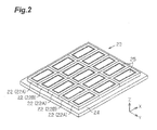
- a reflecting optical system 23 has a configuration in which a plurality of movable multi-mirrors 22 (only fifteen of which are illustrated in Fig. 2 ) are arranged in an array form, as shown in Figs. 1 and 2 , and is disposed in an unmovable state on the opposite side to the exposure light source 12 with respect to the relay optical system 18.
- This reflecting optical system 23 has a base 24 of a planar plate shape and, mirror rows in each of which three movable multi-mirrors 22 are juxtaposed in the X-direction, are formed in five lines in the Y-direction on the base 24.
- Each movable multi-mirror 22 is provided with an effective region 25 of a nearly rectangular shape capable of reflecting the exposure light EL and the exposure light EL impinges upon each of the effective regions 25 of all the movable multi-mirrors 22.
- the above-described arrangement of movable multi-mirrors 22 i.e., three in the X-direction and five in the Y-direction
- the arrangement and number of movable multi-mirrors 22 may be those different from the above-described arrangement.
- the exposure light EL reflected on each movable multi-mirror 22 travels through a condenser optical system (distribution forming optical system) 26 arranged along the optical axis AX2 making a predetermined angle with the optical axis AX1 on the entrance side of each movable multi-mirror 22, into an optical integrator (fly's eye lens in the present embodiment) 27.
- the front focal point of the condenser optical system 26 is located near an arrangement plane P1 where each mirror element in each movable multi-mirror 22 is located, and the rear focal point of the condenser optical system 26 is located on a plane P2 near an entrance surface of the optical integrator 27.
- This optical integrator 27 has a configuration in which a plurality of lens elements 28 (only five of which are shown in Fig. 1 ) are two-dimensionally arranged.
- the exposure light EL incident into the optical integrator 27 is split into a plurality of beams by the lens elements 28.
- a large number of light source images are formed on the right side plane (or image plane) in Fig. 1 of the optical integrator 27.
- a pupil luminance distribution in an illumination region illuminated with the exposure light EL on the reticle R is appropriately adjusted.
- the reticle R arranged on an illumination target surface of the illumination optical system IL is illuminated by Köhler illumination, using the secondary light source formed by the optical integrator 27, as a light source.
- a position P3 where the secondary light source is formed is optically conjugate with a position P4 of an aperture stop AS of the projection optical system PL and the forming plane P3 of the secondary light source can be called an illumination pupil plane of the illumination optical system IL.
- the illumination target surface (a plane where the mask M is arranged, or a plane where the wafer W is arranged in the case where the illumination optical system is considered to include the projection optical system PL) is an optical Fourier transform plane of the illumination pupil plane.
- a splitting mirror for reflecting part of the exposure light EL is provided on the exit side of the optical integrator 27 and an exposure amount sensor SE1 is provided so as to receive light reflected by the splitting mirror.
- the exposure amount can be controlled by monitoring the output of the exposure amount sensor SE1.
- the wafer stage 16 is provided with a pupil luminance distribution detector SE2 for monitoring the pupil luminance distribution of exposure light arriving at the wafer W.
- a pupil luminance distribution detector SE2 for monitoring the pupil luminance distribution of exposure light arriving at the wafer W.
- the configuration of this pupil intensity distribution detector is disclosed, for example, in Japanese Patent Application Laid-open No. 2006-59834 and U.S. Pat. Published Application No. 2008/0030707 corresponding thereto. U.S. Pat. Published Application No. 2008/0030707 is incorporated herein by reference.
- movable multi-mirror 22 The configuration of movable multi-mirror 22 will be described below on the basis of Figs. 2 to 4 .
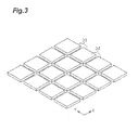
- the movable multi-mirror 22 has a plurality of mirror elements 33 of a square shape on their plan view with a reflecting surface 34 coated with a reflecting film, and the mirror elements 33 are arranged in an array form. In order to reduce a loss in light quantity in the reflecting optical system 23, these mirror elements 33 are arranged with a gap as small as possible between mirror elements 33 adjacent to each other. Each mirror element 33 is movable to change an angle of inclination to the optical path of exposure light EL. In the description hereinafter, the "angle of inclination of the mirror element 33 to the optical path of exposure light EL" will be referred to simply as an "inclination angle of mirror element 33." As shown in Fig. 1 , the mirror elements of the movable multi-mirrors 22 are arranged along the arrangement plane P1 located on the XY plane.
- the reflecting optical system 23 of the present embodiment is composed of plural types (two types in the present embodiment) of movable multi-mirrors 22A, 22B. Specifically, the mirror row located on the nearest side in the Y-direction in Fig. 2 , the mirror row located in the middle among the mirror rows, and the mirror row located on the farthest side each are composed of first movable multi-mirrors 22A, while the other mirror rows each are composed of second movable multi-mirrors 22B.
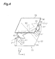
- the first movable multi-mirror 22A is composed of a plurality of mirror elements 33 rotatable around a first axis S1, as shown in Fig. 4 .
- the second movable multi-mirror 22B is composed of a plurality of mirror elements 33 rotatable around a second axis S2 nearly perpendicular to the first axis S1.
- the first axis S1 is an axis corresponding to a first diagonal line among the two diagonal lines of the mirror element 33 and the second axis S2 is an axis corresponding to a second diagonal line perpendicular to the first diagonal line.
- a drive unit for the mirror element 33 forming the first movable multi-mirror 22A will be described below on the basis of Fig. 4 . Since a drive unit for the mirror element 33 forming the second movable multi-mirror 22B has the same configuration as the drive unit for the mirror element 33 forming the first movable multi-mirror 22A except that the mirror element 33 is rotated around the second axis S2, the description thereof is omitted herein.
- the drive unit 35 for the mirror element 33 forming the first movable multi-mirror 22A is provided with a base member 36 of a square plate shape corresponding to the shape of the mirror element 33, and support members 37 stand at two corners located on the first axis S1 out of the four corners of the base member 3 6.
- the drive unit 35 is provided with a hinge member 38 extending in the extending direction of the first axis S1, and the hinge member 38 is supported in a rotatable state around the first axis S1 on the support members 37.
- a projection 39 projecting in the Z-direction is provided in the central part in the longitudinal direction of the hinge member 38 and the mirror element 33 is fixed through the projection 39 to the hinge member 3 8.
- First electrode portions 40 extending in two directions perpendicular to the first axis S1 from the hinge member 38 are formed on the first end side and on the second end side, respectively, in the longitudinal direction of the hinge member 38.
- Second electrode portions 41 are also provided at respective positions corresponding to the four first electrode portions 40, on the base member 36.
- the exposure light EL incident to each of the movable multi-mirrors 22A, 22B is folded into a direction corresponding to the inclination angle of each mirror element 33 to which the light is incident. Since the condenser optical system 26 which can be regarded as a distribution forming optical system has a function to convert the angle information of incident light into position information, the sectional shape of exposure light EL on the plane P2 near the entrance surface of the optical integrator 27 is changed into any size and shape by individually adjusting the inclination angles of the respective mirror elements 33.
- This condenser optical system 26 superimposes part of the exposure light EL having passed via the movable multi-mirrors 22A, and part of the exposure light having passed via the movable multi-mirrors 22B, at least in part on the plane P2. Since the exposure light beams from the plurality of movable multi-mirrors 22A, 22B are superimposed, it is feasible to enhance evenness of light intensity in the superimposed region.
- the light spatially angle-modulated by the movable multi-mirrors 22A, 22B is converted into the spatially modulated light by the condenser optical system 26, to form the pupil intensity distribution as a desired light intensity distribution on the plane P2.
- the pupil intensity distribution is a light intensity distribution (luminance distribution) on the illumination pupil plane of the illumination optical system or on a plane optically conjugate with the illumination pupil plane.
- a high correlation is demonstrated between the overall light intensity distribution formed on the plane P2 near the entrance surface of the optical integrator 27 and the overall light intensity distribution (pupil intensity distribution) of the entire secondary light source. For this reason, light intensity distributions on the entrance surface of the optical integrator 27 and on the planes P3, P4 optically conjugate with the entrance surface can also be called pupil intensity distributions.
- the secondary light source with the light intensity distribution approximately equal to the exposure light EL with the sectional shape modified in the desired size and shape is formed on the plane P3 which is also the rear focal plane of the optical integrator 27. Furthermore, a light intensity distribution corresponding to the pupil intensity distribution formed on the plane P3 is also formed at other illumination pupil positions optically conjugate with the rear focal plane of the optical integrator 27, i.e., at the pupil position of the condenser optical system 32 and at the pupil position of the projection optical system PL.
- the pupil intensity distribution can be, for example, a light intensity distribution of an annular shape or a multi-polar shape (dipolar, quadrupolar, or other shape). It is feasible to implement annular illumination with formation of the annular pupil intensity distribution, or to implement multi-polar illumination with formation of the multi-polar pupil intensity distribution.
- the exposure light EL emitted from the exposure light source 12 is reflected toward the condenser optical system 26 by all the movable multi-mirrors 22A, 22B forming the reflecting optical system 23 and guided to the reticle R. For this reason, even when the exposure light EL from the exposure light source 12 has a higher power, the intensity of exposure light EL incident to each movable multi-mirror 22A, 22B is lower than in the conventional case where the entire exposure light EL emitted from the exposure light source 12 is incident to one movable multi-mirror 22.
- the rotating direction of the mirror elements 33 forming the first movable multi-mirrors 22A is different from the rotating direction of the mirror elements 33 forming the second movable multi-mirrors 22B. For this reason, degrees of freedom can be higher in change in the size and shape of exposure light EL to illuminate the reticle R, than in the case where the reflecting optical system 23 is composed of only one type of movable multi-mirrors 22 (e.g., the first movable multi-mirrors 22A).
- the second embodiment of the present invention will be described next according to Fig. 5 .
- the second embodiment is different in the optical element arranged between the exposure light source 12 and the reflecting optical system 23, from the first embodiment. Therefore, only the differences from the first embodiment will be mainly explained in the description below and the components identical or equivalent to those in the first embodiment will be denoted by the same reference symbols, without redundant description.
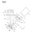
- a truncated pyramid axicon pair 50 arranged along the optical axis AX1 is provided between the exposure light source 12 and the reflecting optical system 23 and this truncated pyramid axicon pair 50 is composed of a first prism member 51 arranged on the exposure light source 12 side and a second prism member 52 arranged on the reflecting optical system 23 side.
- a plane perpendicular to the optical axis of the exposure light EL is formed on the exposure light source 12 side and a refracting surface 51a of a concave shape is formed on the reflecting optical system 23 side.
- This refracting surface 51a is composed of a center part of a planar shape perpendicular to the optical axis of the exposure light EL, and a peripheral pyramid part corresponding to side faces of a rectangular pyramid centered on the optical axis.
- a plane perpendicular to the optical axis of the exposure light EL is formed on the reflecting optical system 23 side and a refracting surface 52a of a convex shape corresponding to the shape of the refracting surface 51a of the first prism member 51 is formed on the first prism member 51 side.
- This refracting surface 52a is composed of a center part of a planar shape perpendicular to the optical axis of the exposure light EL, and a peripheral pyramid part corresponding to side faces of a rectangular pyramid centered on the optical axis.
- the prism members 51, 52 are arranged with a space of a predetermined distance h between them in the optical path of exposure light EL, the exposure light EL incident from the exposure light source 12 into the truncated pyramid axicon pair 50 is split into a plurality of beams.
- the predetermined distance h is so adjusted that the effective regions 25 of the movable multi-mirrors 22 are located in traveling directions of the respective beams. For this reason, the beams split by the truncated pyramid axicon pair 50 are reflected toward the condenser optical system 26 on the respective effective regions 25 of the movable multi-mirrors 22 arranged in the array form.
- the present embodiment achieves the effects described below, in addition to the effects (1) and (2) in the first embodiment.
- the effective regions of the movable multi-mirrors 22 are located in the traveling directions of the respective beams split by the truncated pyramid axicon pair 50. For this reason, the exposure light EL is scarcely incident to the positions other than the locations of the movable multi-mirrors 22 in the reflecting optical system 23 and to the portions other than the effective regions 25 of the movable multi-mirrors 22. Therefore, a loss in light quantity can be reduced in the reflecting optical system 23.
- the above-described structure can be regarded as a configuration wherein the entrance-side optical axis AX1 being an axis of the optical path of the light emitted from the light source 12 is interposed between the first position where the movable multi-mirror 22a is arranged and the second position where another movable multi-mirror 22c is arranged among the plurality of movable multi-mirrors 22.
- the truncated pyramid axicon pair 50 (beam splitter) splits the beam in a plane including the optical axis AX1 (i.e., in the XY plane in the drawing).
- the third embodiment of the present invention will be described below according to Fig. 6 .
- the third embodiment is different in the optical element for splitting the exposure light EL into a plurality of optical paths, from the second embodiment. Therefore, only the differences from each of the above embodiments will be mainly explained in the description hereinafter and the components identical or equivalent to those in the above embodiments will be denoted by the same reference symbols, without redundant description.
- a diffractive optical element 55 for multi-polar illumination (e.g., for quadrupolar illumination) is provided between the exposure light source 12 and the reflecting optical system 23.
- This diffractive optical element 55 is a transmission type diffractive optical element and is made by forming level differences at the pitch approximately equal to the wavelength of the exposure light EL in a transparent substrate.
- This diffractive optical element 55 is so configured that when parallel exposure light EL is incident thereto, it splits the exposure light EL into a plurality of (e.g., four) beams.
- multi-polar (e.g., quadrupolar) illumination regions are formed on the reflecting optical system 23.
- the arrangement of the diffractive optical element 55 is so adjusted that the effective regions 25 of the movable multi-mirrors 22 are located in the respective beams formed by splitting the incident exposure light EL.
- the diffractive optical element 55 has a plurality of wavefront division regions in the plane of the diffractive optical element 55, in order to form an approximately even illumination region in each of the plurality of regions separated by a predetermined distance. Wavefront division regions belonging to a first set among the plurality of wavefront division regions direct the exposure light EL incident thereto, toward a first illumination region out of the plurality of illumination regions.
- first illumination region to be superposedly illuminated by a plurality of beams having passed via the wavefront division regions belonging to the first set, and to have an even illuminance distribution.
- wavefront division regions belonging to a second set different from the first set among me plurality of wavefront division regions direct the exposure light EL incident thereto, toward a second illumination region different from the first illumination region out of the plurality of illumination regions.
- the diffractive optical element 55 of the present embodiment can be the one disclosed in U.S. Pat. No. 5,850,300 .
- U.S. Pat. No. 5,850,300 is incorporated herein by reference.
- the present embodiment achieves the effect described below, in addition to the effects (1) to (4) in the second embodiment.
- the diffractive optical element 55 makes the light intensity distribution even
- the plurality of movable multi-mirrors 22 are illuminated with light of the even intensity distribution even when the intensity distribution is uneven in the cross section of the light EL emitted from the light source 12. For this reason, it is feasible to enhance the controllability of the pupil luminance distribution formed on the plane P2.
- the movable multi-mirrors 22 are illuminated with light of an uneven intensity distribution, this unevenness of the intensity distribution will affect the pupil luminance distribution and each mirror element of the movable multi-mirrors 22 can be controlled in consideration of this unevenness. Therefore, the control becomes complicated.
- the fourth embodiment of the present invention will be described below according to Fig. 7 .
- the fourth embodiment is different in the optical element for splitting the exposure light EL into a plurality of optical paths, from the second and third embodiments. Therefore, only the differences from each of the above embodiments will be mainly explained in the description below and the components identical or equivalent to those in the embodiments will be denoted by the same reference symbols, without redundant description.
- a fly's eye lens 60 is provided between the exposure light source 12 and the reflecting optical system 23 and the fly's eye lens 60 is composed of a plurality of lens elements 61 (only four of which are shown in Fig. 7 ) as arranged two-dimensionally.
- a relay optical system 18A is disposed between the fly's eye lens 60 and the reflecting optical system 23 and the relay optical system 18A refocuses a plurality of beams split by the fly's eye lens 60, in respective effective regions 25 of the movable multi-mirrors 22.
- the movable multi-mirrors 22 are arranged so as to positionally correspond to the respective lens elements 61 of the fly's eye lens 60.
- the reflecting optical system 23 is so configured that four movable multi-mirrors 22 are arrayed along the X-direction. This configuration achieves the same operational effects as in each of the aforementioned second and third embodiments.
- the exposure light EL incident to each movable multi-mirror 22 is mostly reflected toward the condenser optical system 26, but part of the rest (which will be referred to hereinafter as "return light") can be reflected toward the fly's eye lens 60.
- This return light is restrained from entering the fly's eye lens 60, by the relay optical system 18A arranged between the reflecting optical system 23 and the fly's eye lens 60. For this reason, the large number of light source images formed on the image plane of the fly's eye lens 60 can be prevented from being disturbed by the return light.
- the relay optical system can be regarded as a restraining member which restrains the return light from each movable multi-mirror 22 from entering the beam splitter.
- the fifth embodiment of the present invention will be described below according to Fig. 8 .
- the fifth embodiment is different from the first embodiment in that the exposure light EL impinges upon only some movable multi-mirrors 22 out of the movable multi-mirrors 22 forming the reflecting optical system 23. Therefore, only the differences from the first embodiment will be mainly explained in the description hereinafter and the components identical or equivalent to those in the first embodiment will be denoted by the same reference symbols, without redundant description.
- the illumination optical apparatus 13 of the present embodiment is provided with a moving mechanism 65 for moving the reflecting optical system 23 along the X-direction.
- a plurality of movable multi-mirrors 22 are arranged along the X-direction.
- the exposure light EL emitted from the exposure light source 12 is incident to some movable multi-mirrors 22 (e.g., two movable multi-mirrors 22) out of these movable multi-mirrors 22, while the exposure light EL is not incident to the other movable multi-mirrors 22.
- the moving mechanism 65 is actuated to guide the exposure light EL onto the movable multi-mirrors 22 to which the exposure light EL has not been guided heretofore.
- control unit 66 sends a control signal to instruct replacement of the movable multi-mirrors 22, to the moving mechanism 65.
- the exposure apparatus 11 of the present embodiment allows the movable multi-mirrors 22 to which the exposure light EL emitted from the exposure light source 12 is incident, to be replaced with others, without temporary suspension of drive of the exposure apparatus 11. Therefore, a contribution can be made to increase in manufacture efficiency of semiconductor devices with increase in output of the exposure light source 12, even in the case where the movable multi-mirrors 22 are arranged in the optical path of the exposure light EL emitted from the exposure light source 12.
- the reflecting optical system 23 may be one composed of three or more types of movable multi-mirrors 22, 22A, 22B.
- the reflecting optical system 23 may have a configuration having third movable multi-mirrors consisting of mirror elements 33 rotatable around a third axis (e.g., an axis extending in the X-direction) intersecting with the first axis S1 and the second axis S2, in addition to the first movable multi-mirrors 22A and the second movable multi-mirrors 22B.
- the first movable multi-mirrors 22A may be those having mirror elements 33 rotatable around an axis parallel to the first axis S1.
- the second movable multi-mirrors 22B may be those having mirror elements 33 rotatable around an axis parallel to the second axis S2.
- the first axis S1 does not have to be one extending along a diagonal line of each mirror element 33, but may be, for example, an axis extending along the X-direction.
- the second axis S2 may be an axis extending along the Y-direction.
- the reflecting optical system 23 may be one consisting of one type of movable multi-mirrors 22 (e.g., the first movable multi-mirrors 22A).
- the movable multi-mirrors 22 to which the exposure light EL is incident may be switched at intervals of a predetermined time.
- the number of movable multi-mirrors 22 to which the exposure light EL is incident may be an arbitrary number except for two (e.g., one or three).
- the apparatus may be so configured as to switch at least only one of them to which the exposure light EL is incident.
- the movable multi-mirrors 22 may be those having mirror elements 33 rotatable around mutually orthogonal axes (those having two degrees of freedom for inclination).
- the spatial light modulation members of this type can be selected, for example, from those disclosed in Japanese Patent Application Laid-open (Translation of PCT Application) No. 10-503300 and European Patent Application Publication EP 779530 corresponding thereto, Japanese Patent Application Laid-open No. 2004-78136 and U.S. Pat. No. 6,900,915 corresponding thereto, Japanese Patent Application Laid-open (Translation of PCT Application) No. 2006-524349 and U.S. Pat. No. 7,095,546 corresponding thereto, and Japanese Patent Application Laid-open No. 2006-113437 .
- European Patent Application Publication EP 779530 , U.S. Pat. No. 6,900,915 , and U.S. Pat. No. 7,095,546 are incorporated herein by reference.
- the movable multi-mirrors 22 were those in which the orientations (inclinations) of the mirror elements arranged two-dimensionally could be individually controlled, but it is also possible, for example, to use spatial light modulation members in which heights (positions) of reflecting surfaces arranged two-dimensionally can be individually controlled.
- Such spatial light modulation members can be, for example, those disclosed in Japanese Patent Application Laid-open No. 6-281869 and U.S. Pat. No. 5,312,513 corresponding thereto, and in Fig. 1d in Japanese Patent Application Laid-open (Translation of PCT Application) No. 2004-520618 and U.S. Pat. No. 6,885,493 corresponding thereto.
- the movable multi-mirrors 22 may be modified, for example, according to the disclosure in Japanese Patent Application Laid-open (Translation of PCT Application) No. 2006-513442 and U.S. Pat. No. 6,891,655 corresponding thereto or according to the disclosure in Japanese Patent Application Laid-open (Translation of PCT Application) No. 2005-524112 and U.S. Pat. Published Application No. 2005/0095749 corresponding thereto.
- U.S. Pat. No. 6,891,655 and U.S. Pat. Published Application No. 2005/0095749 are incorporated herein by reference.
- 2006/0203214 , 2006/0170901 , and 2007/0146676 teachings of the U.S Pat. Published Application Nos. 2006/0203214 , 2006/0170901 , and 2007/0146676 are incorporated herein by reference.
- the exposure apparatus 11 may be an exposure apparatus which transfers a circuit pattern from a mother reticle onto a glass substrate, a silicon wafer, or the like, in order to manufacture a reticle or a mask to be used in photo exposure apparatus, EUV exposure apparatus, X-ray exposure apparatus, electron beam exposure apparatus, and so on, as well as the micro devices such as the semiconductor devices.
- the exposure apparatus 11 may also be an exposure apparatus used in manufacture of displays including liquid-crystal display devices (LCDs) and others, to transfer a device pattern onto a glass plate, an exposure apparatus used in manufacture of thin-film magnetic heads or the like to transfer a device pattern onto a ceramic wafer or the like, or an exposure apparatus used in manufacture of imaging devices such as CCDs.
- LCDs liquid-crystal display devices
- the illumination optical apparatus 13 in each of the embodiments can be mounted on a scanning stepper configured to transfer a pattern of an illumination target object onto a substrate in a state in which the illumination target object and the substrate are relatively moved, and to successively move the substrate stepwise, and can also be mounted on a stepper of the step-and-repeat method configured to transfer a pattern of an illumination target object onto a substrate in a state in which the illumination target object and the substrate are stationary, and to successively move the substrate stepwise.
- the exposure light source 12 may be, for example, an exposure light source capable of supplying the g-line (436 nm), the i-line (365 nm), the KrF excimer laser (248 nm), the F 2 laser (157 nm), the Kr 2 laser (146 nm), the Ar 2 laser (126 nm), or the like.
- the exposure light source 12 may also be an exposure light source capable of supplying a harmonic obtained by amplifying a single-wavelength laser beam in the infrared region or in the visible region lased from a DFB semiconductor laser or a fiber laser, for example, by a fiber amplifier doped with erbium (or with both of erbium and ytterbium), and converting the wavelength into ultraviolet light with a nonlinear optical crystal.
- Fig. 9 is a drawing showing a flowchart of a manufacture example of micro devices (semiconductor chips such as ICs and LSIs, liquid crystal panels, CCDs, thin-film magnetic heads, micromachines, etc.).
- the first step S101 (design step) is to design the function and performance of micro devices (e.g., design the circuitry for semiconductor devices or the like) and to design a pattern for realizing the function.
- the subsequent step S102 (mask production step) is to produce a mask (reticle R or the like) on which the designed circuit pattern is formed.
- step S103 substrate production step is to produce a substrate of a material such as silicon, glass, or ceramics (which becomes a wafer W where a silicon material is used).
- the next step S104 is to form an actual circuit and others on the substrate by the lithography technology and others, as described below, using the mask and the substrate prepared in the steps S101-S103.
- the next step S105 (device assembly step) is to assemble devices using the substrate processed in step S104.
- This step S105 includes such steps as a dicing step, a bonding step, and a packaging step (chip encapsulation) as occasion may demand.
- the final step S106 is to perform such inspections as an operation check test and a durability test of the micro devices fabricated in step S105. After completion of these steps, the micro devices are completed and shipped.
- Fig. 10 is a drawing showing an example of detailed steps in the step S104 in the case of semiconductor devices.
- Step S111 is to oxidize the surface of the substrate.
- Step S112 is to form an insulating film on the surface of the substrate.
- Step S113 is to form electrodes on the substrate by evaporation.
- Step S114 is to implant ions into the substrate.
- Each of the above steps S111-S114 constitutes a preprocessing step in each stage of substrate processing and is executed as selected according to a process necessary in each stage.
- the first step S115 is to apply a photosensitive material onto the substrate.
- the subsequent step S116 is to transfer the circuit pattern of the mask onto the wafer by the above-described lithography system (exposure apparatus 11).
- the next step S117 is to develop the substrate exposed in step S116, to form a mask layer consisting of the circuit pattern on the surface of the substrate.
- step S118 etching step subsequent thereto, the exposed member is removed by etching from the portions other than the resist-remaining portions.
- step S119 resist removal step
- the steps S118 and S119 are to process the surface of the substrate through the mask layer.
Landscapes
- Physics & Mathematics (AREA)
- General Physics & Mathematics (AREA)
- Optics & Photonics (AREA)
- Exposure And Positioning Against Photoresist Photosensitive Materials (AREA)
- Health & Medical Sciences (AREA)
- Engineering & Computer Science (AREA)
- Environmental & Geological Engineering (AREA)
- Epidemiology (AREA)
- Public Health (AREA)
- Exposure Of Semiconductors, Excluding Electron Or Ion Beam Exposure (AREA)
- Microscoopes, Condenser (AREA)
- Optical Elements Other Than Lenses (AREA)
- Mechanical Light Control Or Optical Switches (AREA)
- Diffracting Gratings Or Hologram Optical Elements (AREA)
- Lenses (AREA)
- Mounting And Adjusting Of Optical Elements (AREA)
Abstract
Description
- The present invention relates to an illumination optical apparatus for illuminating an illumination target object, an exposure apparatus having the illumination optical apparatus, and a device manufacturing method using the exposure apparatus.
- The conventional exposure apparatus, for example, described in Japanese Patent Application Laid-open No.
2002-353105 - The illumination optical apparatus has a spatial light modulation member for adjusting a pupil luminance distribution on an illumination target surface of the mask. This spatial light modulation member has a plurality of reflecting optical elements arranged in an array form, and a reflecting surface of each reflecting optical element is coated with a reflecting film. Each reflecting optical element is so configured that exposure light from a light source is reflected toward the mask by the reflecting surface thereof.
- Furthermore, each reflecting optical element is so configured that an angle of inclination of the reflecting surface can be changed with respect to a direction of incidence of the exposure light to the reflecting surface thereof. The pupil luminance distribution on the illumination target surface of the mask was appropriately adjusted by changing the angle of inclination of the reflecting surface relative to the optical axis of the exposure light in each reflecting optical element.
- In recent years, there are strong desires for increase in power of exposure light for achieving increase in efficiency of projection of the pattern image onto the substrate and enhancement of accuracy. It is, however, very difficult to coat the reflecting surface of each reflecting optical element forming the spatial light modulation member, with a reflecting film having relatively high durability. Therefore, the reflecting surface is coated with a reflecting film having relatively low durability. For this reason, the life of the spatial light modulation member becomes shorter because the reflecting film deteriorates earlier with increase in the intensity of the exposure light emitted from the light source and because a larger quantity of light reaches a drive portion of each reflecting optical element so as to cause breakage of the drive portion. The spatial light modulation member may be replaced earlier when the intensity of the exposure light is relatively high, than when the intensity of the exposure light is relatively low.
- In the exposure apparatus of the configuration as described above, however, the spatial light modulation member may be replaced in a state in which the drive of the exposure apparatus is temporarily suspended. Therefore, the higher the intensity of the exposure light emitted from the light source, the earlier the timing of replacement of the spatial light modulation member; there was thus the concern of decrease in efficiency of manufacture of micro devices due to the increase in output of the light source in the exposure apparatus in which the spatial light modulation member was arranged in the optical path of the exposure light.
- The present invention has been accomplished in view of the above-discussed circumstances and an object of the invention is to provide an illumination optical apparatus, an exposure apparatus, and a device manufacturing method capable of contributing to increase in manufacture efficiency of devices with increase in output of the light source even in the case where the spatial light modulation member is arranged in the optical path of the light emitted from the light source.
- An illumination optical apparatus according to the present invention is an illumination optical apparatus which guides light emitted from a light source and traveling along a predetermined optical path, to an illumination target object, the illumination optical apparatus comprising: a plurality of spatial light modulation members in which a plurality of reflecting optical elements each including a movable reflecting surface are arranged in an array form; wherein at least one of the spatial light modulation members is arranged in the optical path.
- In the above configuration, the light emitted from the light source is guided to the illumination target object by the plurality of spatial light modulation members arranged in the array form. For this reason, the timing of replacement of the spatial light modulation member with temporary suspension of drive of the exposure apparatus can be delayed by increase in the number of spatial light modulation members used, when compared with the conventional case where the light emitted from the light source is guided to the illumination target object with the use of one spatial light modulation member. Therefore, a contribution can be made to increase in manufacture efficiency of devices with increase in output of the light source, even in the case where the spatial light modulation member is arranged in the optical path of the light emitted from the light source.
- The present invention successfully achieves the contribution to increase in manufacture efficiency of devices with increase in output of the light source.
-
-
Fig. 1 is a schematic configuration diagram showing an exposure apparatus in the first embodiment. -
Fig. 2 is a schematic perspective view showing a movable multi-mirror in the first embodiment. -
Fig. 3 is a schematic perspective view showing an array form of mirror elements forming a movable multi-mirror. -
Fig. 4 is a schematic perspective view showing a configuration of a drive unit to drive a mirror element. -
Fig. 5 is a schematic configuration diagram showing a part of an illumination optical apparatus in the second embodiment. -
Fig. 6 is a schematic configuration diagram showing a part of an illumination optical apparatus in the third embodiment. -
Fig. 7 is a schematic configuration diagram showing a part of an illumination optical apparatus in the fourth embodiment. -
Fig. 8 is a schematic configuration diagram showing a part of an illumination optical apparatus in the fifth embodiment. -
Fig. 9 is a flowchart of a manufacture example of devices. -
Fig. 10 is a detailed flowchart about processing of a substrate in the case of semiconductor devices. - The first embodiment as a specific example of the present invention will be described below on the basis of
Figs. 1 to 4 . - As shown in
Fig. 1 , anexposure apparatus 11 of the present embodiment is composed of an illuminationoptical apparatus 13 to which exposure light EL from anexposure light source 12 is supplied, areticle stage 14 holding a reticle R (which may be a photomask) on which a predetermined pattern is formed, a projectionoptical device 15, and awafer stage 16 holding a wafer W having a surface coated with a photosensitive material such as a resist. Theexposure light source 12 consists of, for example, an ArF excimer laser light source. The exposure light EL emitted from theexposure light source 12 passes through the illuminationoptical apparatus 13 to be so adjusted as to evenly illuminate the pattern on the reticle R. - The
reticle stage 14 is arranged on the object plane side of the projectionoptical device 15 described later, so that a mounting surface of the reticle R is approximately perpendicular to the direction of the optical axis of the projectionoptical device 15. This projectionoptical device 15 has abarrel 17 internally filled with an inert gas such as nitrogen, and a plurality of lenses not shown are disposed along the optical path of the exposure light EL in thisbarrel 17. An image of the pattern on the reticle R illuminated with the exposure light EL is projected and transferred in a reduced state at a predetermined reducing rate through the projectionoptical device 15, onto the wafer W on thewafer stage 16. The optical path herein refers to a path in which light is intended to pass in a use state. - The illumination
optical apparatus 13 of the present embodiment will be described below on the basis ofFig. 1 . - The illumination
optical apparatus 13 is provided with a relayoptical system 18 into which the exposure light EL emitted from theexposure light source 12 is incident. This relayoptical system 18 is typically composed of a firstpositive lens 19, anegative lens 20, and a secondpositive lens 21 arranged along the optical axis AX1 in the order named from theexposure light source 12 side. The exposure light EL incident from theexposure light source 12 into the relayoptical system 18 is emitted in an enlarged state of its sectional shape to the opposite side to theexposure light source 12. - In the illumination
optical apparatus 13, a reflectingoptical system 23 has a configuration in which a plurality of movable multi-mirrors 22 (only fifteen of which are illustrated inFig. 2 ) are arranged in an array form, as shown inFigs. 1 and2 , and is disposed in an unmovable state on the opposite side to theexposure light source 12 with respect to the relayoptical system 18. This reflectingoptical system 23 has abase 24 of a planar plate shape and, mirror rows in each of which three movable multi-mirrors 22 are juxtaposed in the X-direction, are formed in five lines in the Y-direction on thebase 24. Each movable multi-mirror 22 is provided with aneffective region 25 of a nearly rectangular shape capable of reflecting the exposure light EL and the exposure light EL impinges upon each of theeffective regions 25 of all the movable multi-mirrors 22. The above-described arrangement of movable multi-mirrors 22 (i.e., three in the X-direction and five in the Y-direction) is just an example, and the arrangement and number of movable multi-mirrors 22 may be those different from the above-described arrangement. - The exposure light EL reflected on each movable multi-mirror 22 travels through a condenser optical system (distribution forming optical system) 26 arranged along the optical axis AX2 making a predetermined angle with the optical axis AX1 on the entrance side of each movable multi-mirror 22, into an optical integrator (fly's eye lens in the present embodiment) 27. The front focal point of the condenser
optical system 26 is located near an arrangement plane P1 where each mirror element in each movable multi-mirror 22 is located, and the rear focal point of the condenseroptical system 26 is located on a plane P2 near an entrance surface of theoptical integrator 27. Thisoptical integrator 27 has a configuration in which a plurality of lens elements 28 (only five of which are shown inFig. 1 ) are two-dimensionally arranged. The exposure light EL incident into theoptical integrator 27 is split into a plurality of beams by thelens elements 28. As a consequence, a large number of light source images are formed on the right side plane (or image plane) inFig. 1 of theoptical integrator 27. - The exposure light EL emitted from the
optical integrator 27, which consists of beams emitted from the large number of light source images, travels through a condenseroptical system 29 to illuminate a mask blind 30 in a superposedly condensed state. The exposure light EL having passed through anaperture 31 of the mask blind 30 travels through a condenseroptical system 32 to illuminate a reticle R. A pupil luminance distribution in an illumination region illuminated with the exposure light EL on the reticle R is appropriately adjusted. - In the present embodiment, the reticle R arranged on an illumination target surface of the illumination optical system IL is illuminated by Köhler illumination, using the secondary light source formed by the
optical integrator 27, as a light source. For this reason, a position P3 where the secondary light source is formed is optically conjugate with a position P4 of an aperture stop AS of the projection optical system PL and the forming plane P3 of the secondary light source can be called an illumination pupil plane of the illumination optical system IL. Typically, the illumination target surface (a plane where the mask M is arranged, or a plane where the wafer W is arranged in the case where the illumination optical system is considered to include the projection optical system PL) is an optical Fourier transform plane of the illumination pupil plane. - In the present embodiment, a splitting mirror for reflecting part of the exposure light EL is provided on the exit side of the
optical integrator 27 and an exposure amount sensor SE1 is provided so as to receive light reflected by the splitting mirror. The exposure amount can be controlled by monitoring the output of the exposure amount sensor SE1. - In the present embodiment, the
wafer stage 16 is provided with a pupil luminance distribution detector SE2 for monitoring the pupil luminance distribution of exposure light arriving at the wafer W. The configuration of this pupil intensity distribution detector is disclosed, for example, in Japanese Patent Application Laid-open No.2006-59834 U.S. Pat. Published Application No. 2008/0030707 corresponding thereto.U.S. Pat. Published Application No. 2008/0030707 is incorporated herein by reference. - The configuration of movable multi-mirror 22 will be described below on the basis of
Figs. 2 to 4 . - As shown in
Figs. 2 and3 , themovable multi-mirror 22 has a plurality ofmirror elements 33 of a square shape on their plan view with a reflectingsurface 34 coated with a reflecting film, and themirror elements 33 are arranged in an array form. In order to reduce a loss in light quantity in the reflectingoptical system 23, thesemirror elements 33 are arranged with a gap as small as possible betweenmirror elements 33 adjacent to each other. Eachmirror element 33 is movable to change an angle of inclination to the optical path of exposure light EL. In the description hereinafter, the "angle of inclination of themirror element 33 to the optical path of exposure light EL" will be referred to simply as an "inclination angle ofmirror element 33." As shown inFig. 1 , the mirror elements of themovable multi-mirrors 22 are arranged along the arrangement plane P1 located on the XY plane. - The reflecting
optical system 23 of the present embodiment is composed of plural types (two types in the present embodiment) of movable multi-mirrors 22A, 22B. Specifically, the mirror row located on the nearest side in the Y-direction inFig. 2 , the mirror row located in the middle among the mirror rows, and the mirror row located on the farthest side each are composed of firstmovable multi-mirrors 22A, while the other mirror rows each are composed of secondmovable multi-mirrors 22B. The firstmovable multi-mirror 22A is composed of a plurality ofmirror elements 33 rotatable around a first axis S1, as shown inFig. 4 . On the other hand, the second movable multi-mirror 22B is composed of a plurality ofmirror elements 33 rotatable around a second axis S2 nearly perpendicular to the first axis S1. The first axis S1 is an axis corresponding to a first diagonal line among the two diagonal lines of themirror element 33 and the second axis S2 is an axis corresponding to a second diagonal line perpendicular to the first diagonal line. - A drive unit for the
mirror element 33 forming the firstmovable multi-mirror 22A will be described below on the basis ofFig. 4 . Since a drive unit for themirror element 33 forming the second movable multi-mirror 22B has the same configuration as the drive unit for themirror element 33 forming the first movable multi-mirror 22A except that themirror element 33 is rotated around the second axis S2, the description thereof is omitted herein. - As shown in
Fig. 4 , thedrive unit 35 for themirror element 33 forming the firstmovable multi-mirror 22A is provided with abase member 36 of a square plate shape corresponding to the shape of themirror element 33, andsupport members 37 stand at two corners located on the first axis S1 out of the four corners of thebase member 3 6. Thedrive unit 35 is provided with ahinge member 38 extending in the extending direction of the first axis S1, and thehinge member 38 is supported in a rotatable state around the first axis S1 on thesupport members 37. Aprojection 39 projecting in the Z-direction is provided in the central part in the longitudinal direction of thehinge member 38 and themirror element 33 is fixed through theprojection 39 to thehinge member 3 8. -
First electrode portions 40 extending in two directions perpendicular to the first axis S1 from thehinge member 38 are formed on the first end side and on the second end side, respectively, in the longitudinal direction of thehinge member 38.Second electrode portions 41 are also provided at respective positions corresponding to the fourfirst electrode portions 40, on thebase member 36. When a potential difference is made between each pair offirst electrode portion 40 andsecond electrode portion 41 in a mutually corresponding relation, thehinge member 38 rotates around the first axis S1 because of electrostatic forces acting based on these potential differences, whereby themirror element 33 rotates around the first axis S1. Namely, the inclination angle ofmirror element 33 can be controlled by adjusting each of the potential differences between each of the pairs ofelectrode portions - The exposure light EL incident to each of the
movable multi-mirrors mirror element 33 to which the light is incident. Since the condenseroptical system 26 which can be regarded as a distribution forming optical system has a function to convert the angle information of incident light into position information, the sectional shape of exposure light EL on the plane P2 near the entrance surface of theoptical integrator 27 is changed into any size and shape by individually adjusting the inclination angles of therespective mirror elements 33. This condenseroptical system 26 superimposes part of the exposure light EL having passed via themovable multi-mirrors 22A, and part of the exposure light having passed via the movable multi-mirrors 22B, at least in part on the plane P2. Since the exposure light beams from the plurality of movable multi-mirrors 22A, 22B are superimposed, it is feasible to enhance evenness of light intensity in the superimposed region. - In other words, the light spatially angle-modulated by the
movable multi-mirrors optical system 26, to form the pupil intensity distribution as a desired light intensity distribution on the plane P2. - The pupil intensity distribution is a light intensity distribution (luminance distribution) on the illumination pupil plane of the illumination optical system or on a plane optically conjugate with the illumination pupil plane. When the number of wavefront divisions by the
optical integrator 27 is relatively large, a high correlation is demonstrated between the overall light intensity distribution formed on the plane P2 near the entrance surface of theoptical integrator 27 and the overall light intensity distribution (pupil intensity distribution) of the entire secondary light source. For this reason, light intensity distributions on the entrance surface of theoptical integrator 27 and on the planes P3, P4 optically conjugate with the entrance surface can also be called pupil intensity distributions. - In this manner, the secondary light source with the light intensity distribution approximately equal to the exposure light EL with the sectional shape modified in the desired size and shape is formed on the plane P3 which is also the rear focal plane of the
optical integrator 27. Furthermore, a light intensity distribution corresponding to the pupil intensity distribution formed on the plane P3 is also formed at other illumination pupil positions optically conjugate with the rear focal plane of theoptical integrator 27, i.e., at the pupil position of the condenseroptical system 32 and at the pupil position of the projection optical system PL. - The pupil intensity distribution can be, for example, a light intensity distribution of an annular shape or a multi-polar shape (dipolar, quadrupolar, or other shape). It is feasible to implement annular illumination with formation of the annular pupil intensity distribution, or to implement multi-polar illumination with formation of the multi-polar pupil intensity distribution.
- Therefore, the present embodiment achieves the effects described below.
- (1) The exposure light EL emitted from the
exposure light source 12 is reflected toward the condenseroptical system 26 by all themovable multi-mirrors optical system 23 and guided to the reticle R. For this reason, even when the exposure light EL from theexposure light source 12 has a higher power, the intensity of exposure light EL incident to eachmovable multi-mirror exposure light source 12 is incident to onemovable multi-mirror 22. As a consequence, deterioration of the reflecting film over the reflecting surface of eachmirror element 33 to which the exposure light EL is incident becomes slower than in the conventional case, so as to lengthen the lives of themovable multi-mirrors movable multi-mirrors exposure light source 12 even in the case where themovable multi-mirrors exposure light source 12. - (2) The rotating direction of the
mirror elements 33 forming the firstmovable multi-mirrors 22A is different from the rotating direction of themirror elements 33 forming the secondmovable multi-mirrors 22B. For this reason, degrees of freedom can be higher in change in the size and shape of exposure light EL to illuminate the reticle R, than in the case where the reflectingoptical system 23 is composed of only one type of movable multi-mirrors 22 (e.g., the first movable multi-mirrors 22A). - (3) Since the angle α between the arrangement plane P1 and the entrance-side optical axis AX1 and the angle β between the arrangement plane P1 and the exit-side optical axis AX2 are so set as to direct zero-order reflected light N from the portions other than the
mirror elements 33 of themovable multi-mirrors effective regions 25 of themovable multi-mirrors optical system 26, it is feasible to prevent the zero-order reflected light from affecting the pupil luminance distribution and, typically, to prevent the zero-order reflected light from forming a light spot at a position near the optical axis AX2. - The second embodiment of the present invention will be described next according to
Fig. 5 . The second embodiment is different in the optical element arranged between theexposure light source 12 and the reflectingoptical system 23, from the first embodiment. Therefore, only the differences from the first embodiment will be mainly explained in the description below and the components identical or equivalent to those in the first embodiment will be denoted by the same reference symbols, without redundant description. - As shown in
Fig. 5 , a truncated pyramid axicon pair 50 arranged along the optical axis AX1 is provided between theexposure light source 12 and the reflectingoptical system 23 and this truncated pyramid axicon pair 50 is composed of afirst prism member 51 arranged on theexposure light source 12 side and a second prism member 52 arranged on the reflectingoptical system 23 side. In thefirst prism member 51, a plane perpendicular to the optical axis of the exposure light EL is formed on theexposure light source 12 side and a refracting surface 51a of a concave shape is formed on the reflectingoptical system 23 side. This refracting surface 51a is composed of a center part of a planar shape perpendicular to the optical axis of the exposure light EL, and a peripheral pyramid part corresponding to side faces of a rectangular pyramid centered on the optical axis. - In the second prism member 52, a plane perpendicular to the optical axis of the exposure light EL is formed on the reflecting
optical system 23 side and a refractingsurface 52a of a convex shape corresponding to the shape of the refracting surface 51a of thefirst prism member 51 is formed on thefirst prism member 51 side. This refractingsurface 52a is composed of a center part of a planar shape perpendicular to the optical axis of the exposure light EL, and a peripheral pyramid part corresponding to side faces of a rectangular pyramid centered on the optical axis. - When the
prism members 51, 52 are arranged with a space of a predetermined distance h between them in the optical path of exposure light EL, the exposure light EL incident from theexposure light source 12 into the truncated pyramid axicon pair 50 is split into a plurality of beams. The predetermined distance h is so adjusted that theeffective regions 25 of themovable multi-mirrors 22 are located in traveling directions of the respective beams. For this reason, the beams split by the truncated pyramid axicon pair 50 are reflected toward the condenseroptical system 26 on the respectiveeffective regions 25 of themovable multi-mirrors 22 arranged in the array form. - Therefore, the present embodiment achieves the effects described below, in addition to the effects (1) and (2) in the first embodiment.
- (3) The effective regions of the
movable multi-mirrors 22 are located in the traveling directions of the respective beams split by the truncated pyramid axicon pair 50. For this reason, the exposure light EL is scarcely incident to the positions other than the locations of the movable multi-mirrors 22 in the reflectingoptical system 23 and to the portions other than theeffective regions 25 of themovable multi-mirrors 22. Therefore, a loss in light quantity can be reduced in the reflectingoptical system 23. Furthermore, it is feasible to restrain promotion of deterioration of themovable multi-mirrors 22 due to increase in temperature based on illumination with the exposure light EL in the positions other than the locations of the movable multi-mirrors 22 in the reflectingoptical system 23 and the portions other than theeffective regions 25 of themovable multi-mirrors 22. - (4) Since no member with power (inverse of the focal length) is arranged in the optical path between the truncated pyramid axicon pair 50, which can be regarded as a beam splitter, and the
movable multi-mirrors optical system 26 will become spread, which will make control of the pupil luminance distribution difficult. - In the present embodiment, the above-described structure can be regarded as a configuration wherein the entrance-side optical axis AX1 being an axis of the optical path of the light emitted from the
light source 12 is interposed between the first position where the movable multi-mirror 22a is arranged and the second position where another movable multi-mirror 22c is arranged among the plurality ofmovable multi-mirrors 22. Furthermore, it can also be regarded as a configuration wherein the truncated pyramid axicon pair 50 (beam splitter) splits the beam in a plane including the optical axis AX1 (i.e., in the XY plane in the drawing). - The third embodiment of the present invention will be described below according to
Fig. 6 . The third embodiment is different in the optical element for splitting the exposure light EL into a plurality of optical paths, from the second embodiment. Therefore, only the differences from each of the above embodiments will be mainly explained in the description hereinafter and the components identical or equivalent to those in the above embodiments will be denoted by the same reference symbols, without redundant description. - As shown in
Fig. 6 , a diffractiveoptical element 55 for multi-polar illumination (e.g., for quadrupolar illumination) is provided between theexposure light source 12 and the reflectingoptical system 23. This diffractiveoptical element 55 is a transmission type diffractive optical element and is made by forming level differences at the pitch approximately equal to the wavelength of the exposure light EL in a transparent substrate. This diffractiveoptical element 55 is so configured that when parallel exposure light EL is incident thereto, it splits the exposure light EL into a plurality of (e.g., four) beams. As a result, multi-polar (e.g., quadrupolar) illumination regions are formed on the reflectingoptical system 23. The arrangement of the diffractiveoptical element 55 is so adjusted that theeffective regions 25 of themovable multi-mirrors 22 are located in the respective beams formed by splitting the incident exposure light EL. - The diffractive
optical element 55 has a plurality of wavefront division regions in the plane of the diffractiveoptical element 55, in order to form an approximately even illumination region in each of the plurality of regions separated by a predetermined distance. Wavefront division regions belonging to a first set among the plurality of wavefront division regions direct the exposure light EL incident thereto, toward a first illumination region out of the plurality of illumination regions. - This causes the first illumination region to be superposedly illuminated by a plurality of beams having passed via the wavefront division regions belonging to the first set, and to have an even illuminance distribution. Similarly, wavefront division regions belonging to a second set different from the first set among me plurality of wavefront division regions direct the exposure light EL incident thereto, toward a second illumination region different from the first illumination region out of the plurality of illumination regions. This causes the second illumination region to be superposedly illuminated by a plurality of beams having passed via the wavefront division regions belonging to the second set, and to have an even illuminance distribution.
- For example, the diffractive
optical element 55 of the present embodiment can be the one disclosed inU.S. Pat. No. 5,850,300 .U.S. Pat. No. 5,850,300 is incorporated herein by reference. - Therefore, the present embodiment achieves the effect described below, in addition to the effects (1) to (4) in the second embodiment.
- (5) Since the diffractive
optical element 55 makes the light intensity distribution even, the plurality ofmovable multi-mirrors 22 are illuminated with light of the even intensity distribution even when the intensity distribution is uneven in the cross section of the light EL emitted from thelight source 12. For this reason, it is feasible to enhance the controllability of the pupil luminance distribution formed on the plane P2. On the other hand, when themovable multi-mirrors 22 are illuminated with light of an uneven intensity distribution, this unevenness of the intensity distribution will affect the pupil luminance distribution and each mirror element of themovable multi-mirrors 22 can be controlled in consideration of this unevenness. Therefore, the control becomes complicated. - The fourth embodiment of the present invention will be described below according to
Fig. 7 . The fourth embodiment is different in the optical element for splitting the exposure light EL into a plurality of optical paths, from the second and third embodiments. Therefore, only the differences from each of the above embodiments will be mainly explained in the description below and the components identical or equivalent to those in the embodiments will be denoted by the same reference symbols, without redundant description. - As shown in
Fig. 7 , a fly'seye lens 60 is provided between theexposure light source 12 and the reflectingoptical system 23 and the fly'seye lens 60 is composed of a plurality of lens elements 61 (only four of which are shown inFig. 7 ) as arranged two-dimensionally. A relayoptical system 18A is disposed between the fly'seye lens 60 and the reflectingoptical system 23 and the relayoptical system 18A refocuses a plurality of beams split by the fly'seye lens 60, in respectiveeffective regions 25 of themovable multi-mirrors 22. - In the reflecting
optical system 23 of the present embodiment, themovable multi-mirrors 22 are arranged so as to positionally correspond to therespective lens elements 61 of the fly'seye lens 60. For example, in a case where the fly'seye lens 60 is one in which four lens elements are arrayed in the X-direction, the reflectingoptical system 23 is so configured that fourmovable multi-mirrors 22 are arrayed along the X-direction. This configuration achieves the same operational effects as in each of the aforementioned second and third embodiments. - The exposure light EL incident to each
movable multi-mirror 22 is mostly reflected toward the condenseroptical system 26, but part of the rest (which will be referred to hereinafter as "return light") can be reflected toward the fly'seye lens 60. This return light is restrained from entering the fly'seye lens 60, by the relayoptical system 18A arranged between the reflectingoptical system 23 and the fly'seye lens 60. For this reason, the large number of light source images formed on the image plane of the fly'seye lens 60 can be prevented from being disturbed by the return light. As described above, the relay optical system can be regarded as a restraining member which restrains the return light from each movable multi-mirror 22 from entering the beam splitter. - The fifth embodiment of the present invention will be described below according to
Fig. 8 . The fifth embodiment is different from the first embodiment in that the exposure light EL impinges upon only somemovable multi-mirrors 22 out of themovable multi-mirrors 22 forming the reflectingoptical system 23. Therefore, only the differences from the first embodiment will be mainly explained in the description hereinafter and the components identical or equivalent to those in the first embodiment will be denoted by the same reference symbols, without redundant description. - As shown in
Fig. 8 , the illuminationoptical apparatus 13 of the present embodiment is provided with a movingmechanism 65 for moving the reflectingoptical system 23 along the X-direction. In the reflectingoptical system 23, a plurality of movable multi-mirrors 22 (only five of which are shown inFig. 8 ) are arranged along the X-direction. The exposure light EL emitted from theexposure light source 12 is incident to some movable multi-mirrors 22 (e.g., two movable multi-mirrors 22) out of thesemovable multi-mirrors 22, while the exposure light EL is not incident to the othermovable multi-mirrors 22. - When the intensity of the exposure light EL for forming the pattern image on the wafer W becomes lowered or when the pupil luminance distribution on the wafer W becomes disturbed, based on a secular change in characteristics of the
movable multi-mirrors 22 to which the exposure light EL is incident (e.g., based on deterioration of the reflecting film or deterioration of thedrive unit 35 for the mirror element 33), the movingmechanism 65 is actuated to guide the exposure light EL onto themovable multi-mirrors 22 to which the exposure light EL has not been guided heretofore. - For example, in a case where the output of the exposure amount sensor SE1 monitored becomes lowered, or in a case where a deviation of the pupil luminance distribution measured by the pupil luminance distribution detector SE2, from a target value becomes off a permissible range, the
control unit 66 sends a control signal to instruct replacement of themovable multi-mirrors 22, to the movingmechanism 65. - As described above, the
exposure apparatus 11 of the present embodiment allows themovable multi-mirrors 22 to which the exposure light EL emitted from theexposure light source 12 is incident, to be replaced with others, without temporary suspension of drive of theexposure apparatus 11. Therefore, a contribution can be made to increase in manufacture efficiency of semiconductor devices with increase in output of theexposure light source 12, even in the case where themovable multi-mirrors 22 are arranged in the optical path of the exposure light EL emitted from theexposure light source 12. - Each of the above embodiments may be modified into another embodiment as described below.
- In each embodiment, the reflecting
optical system 23 may be one composed of three or more types ofmovable multi-mirrors optical system 23 may have a configuration having third movable multi-mirrors consisting ofmirror elements 33 rotatable around a third axis (e.g., an axis extending in the X-direction) intersecting with the first axis S1 and the second axis S2, in addition to the firstmovable multi-mirrors 22A and the secondmovable multi-mirrors 22B. - In each embodiment, the first
movable multi-mirrors 22A may be those havingmirror elements 33 rotatable around an axis parallel to the first axis S1. Similarly, the second movable multi-mirrors 22B may be those havingmirror elements 33 rotatable around an axis parallel to the second axis S2. - In each embodiment, the first axis S1 does not have to be one extending along a diagonal line of each
mirror element 33, but may be, for example, an axis extending along the X-direction. In this case, the second axis S2 may be an axis extending along the Y-direction. - In each embodiment, the reflecting
optical system 23 may be one consisting of one type of movable multi-mirrors 22 (e.g., the first movable multi-mirrors 22A). - In the fifth embodiment, the
movable multi-mirrors 22 to which the exposure light EL is incident may be switched at intervals of a predetermined time. - In the fifth embodiment, the number of
movable multi-mirrors 22 to which the exposure light EL is incident, may be an arbitrary number except for two (e.g., one or three). - In the fifth embodiment, where the
movable multi-mirrors 22 to which the exposure light EL is incident are switched, the apparatus may be so configured as to switch at least only one of them to which the exposure light EL is incident. - In each embodiment, the
movable multi-mirrors 22 may be those havingmirror elements 33 rotatable around mutually orthogonal axes (those having two degrees of freedom for inclination). The spatial light modulation members of this type can be selected, for example, from those disclosed in Japanese Patent Application Laid-open (Translation of PCT Application) No.10-503300 EP 779530 2004-78136 U.S. Pat. No. 6,900,915 corresponding thereto, Japanese Patent Application Laid-open (Translation of PCT Application) No.2006-524349 U.S. Pat. No. 7,095,546 corresponding thereto, and Japanese Patent Application Laid-open No.2006-113437 EP 779530 U.S. Pat. No. 6,900,915 , andU.S. Pat. No. 7,095,546 are incorporated herein by reference. - In each embodiment, the
movable multi-mirrors 22 were those in which the orientations (inclinations) of the mirror elements arranged two-dimensionally could be individually controlled, but it is also possible, for example, to use spatial light modulation members in which heights (positions) of reflecting surfaces arranged two-dimensionally can be individually controlled. Such spatial light modulation members can be, for example, those disclosed in Japanese Patent Application Laid-open No.6-281869 U.S. Pat. No. 5,312,513 corresponding thereto, and inFig. 1d in Japanese Patent Application Laid-open (Translation of PCT Application) No.2004-520618 U.S. Pat. No. 6,885,493 corresponding thereto. These spatial light modulation members are able to apply the same action as a diffracting surface, to incident light through formation of a two-dimensional height distribution.U.S. Pat. No. 5,312,513 andU.S. Pat. No. 6,885,493 are incorporated herein by reference. - In each embodiment, the
movable multi-mirrors 22 may be modified, for example, according to the disclosure in Japanese Patent Application Laid-open (Translation of PCT Application) No.2006-513442 U.S. Pat. No. 6,891,655 corresponding thereto or according to the disclosure in Japanese Patent Application Laid-open (Translation of PCT Application) No.2005-524112 U.S. Pat. Published Application No. 2005/0095749 corresponding thereto.U.S. Pat. No. 6,891,655 andU.S. Pat. Published Application No. 2005/0095749 are incorporated herein by reference.
In each embodiment, it is also possible to apply the so-called polarized illumination method disclosed inU.S Pat. Published Application Nos. 2006/0203214 ,2006/0170901 , and2007/0146676 . Teachings of theU.S Pat. Published Application Nos. 2006/0203214 ,2006/0170901 , and2007/0146676 are incorporated herein by reference. - In each embodiment, the
exposure apparatus 11 may be an exposure apparatus which transfers a circuit pattern from a mother reticle onto a glass substrate, a silicon wafer, or the like, in order to manufacture a reticle or a mask to be used in photo exposure apparatus, EUV exposure apparatus, X-ray exposure apparatus, electron beam exposure apparatus, and so on, as well as the micro devices such as the semiconductor devices. Theexposure apparatus 11 may also be an exposure apparatus used in manufacture of displays including liquid-crystal display devices (LCDs) and others, to transfer a device pattern onto a glass plate, an exposure apparatus used in manufacture of thin-film magnetic heads or the like to transfer a device pattern onto a ceramic wafer or the like, or an exposure apparatus used in manufacture of imaging devices such as CCDs. - The illumination
optical apparatus 13 in each of the embodiments can be mounted on a scanning stepper configured to transfer a pattern of an illumination target object onto a substrate in a state in which the illumination target object and the substrate are relatively moved, and to successively move the substrate stepwise, and can also be mounted on a stepper of the step-and-repeat method configured to transfer a pattern of an illumination target object onto a substrate in a state in which the illumination target object and the substrate are stationary, and to successively move the substrate stepwise. - In each embodiment, the
exposure light source 12 may be, for example, an exposure light source capable of supplying the g-line (436 nm), the i-line (365 nm), the KrF excimer laser (248 nm), the F2 laser (157 nm), the Kr2 laser (146 nm), the Ar2 laser (126 nm), or the like. Theexposure light source 12 may also be an exposure light source capable of supplying a harmonic obtained by amplifying a single-wavelength laser beam in the infrared region or in the visible region lased from a DFB semiconductor laser or a fiber laser, for example, by a fiber amplifier doped with erbium (or with both of erbium and ytterbium), and converting the wavelength into ultraviolet light with a nonlinear optical crystal. - The below will describe an embodiment of a manufacture method of micro devices using the device manufacturing method with the
exposure apparatus 11 of the embodiments of the present invention in the lithography process.Fig. 9 is a drawing showing a flowchart of a manufacture example of micro devices (semiconductor chips such as ICs and LSIs, liquid crystal panels, CCDs, thin-film magnetic heads, micromachines, etc.). - The first step S101 (design step) is to design the function and performance of micro devices (e.g., design the circuitry for semiconductor devices or the like) and to design a pattern for realizing the function. The subsequent step S102 (mask production step) is to produce a mask (reticle R or the like) on which the designed circuit pattern is formed. On the other hand, step S103 (substrate production step) is to produce a substrate of a material such as silicon, glass, or ceramics (which becomes a wafer W where a silicon material is used).
- The next step S104 (substrate processing step) is to form an actual circuit and others on the substrate by the lithography technology and others, as described below, using the mask and the substrate prepared in the steps S101-S103. The next step S105 (device assembly step) is to assemble devices using the substrate processed in step S104. This step S105 includes such steps as a dicing step, a bonding step, and a packaging step (chip encapsulation) as occasion may demand. The final step S106 (inspection step) is to perform such inspections as an operation check test and a durability test of the micro devices fabricated in step S105. After completion of these steps, the micro devices are completed and shipped.
-
Fig. 10 is a drawing showing an example of detailed steps in the step S104 in the case of semiconductor devices. - Step S111 (oxidation step) is to oxidize the surface of the substrate. Step S112 (CVD step) is to form an insulating film on the surface of the substrate. Step S113 (electrode forming step) is to form electrodes on the substrate by evaporation. Step S114 (ion implantation step) is to implant ions into the substrate. Each of the above steps S111-S114 constitutes a preprocessing step in each stage of substrate processing and is executed as selected according to a process necessary in each stage.
- After completion of the above-described preprocessing steps in the stages of the substrate processing, post-processing steps are executed as described below. In the post-processing steps, the first step S115 (resist forming step) is to apply a photosensitive material onto the substrate. The subsequent step S116 (exposure step) is to transfer the circuit pattern of the mask onto the wafer by the above-described lithography system (exposure apparatus 11). The next step S117 (development step) is to develop the substrate exposed in step S116, to form a mask layer consisting of the circuit pattern on the surface of the substrate. In step S118 (etching step) subsequent thereto, the exposed member is removed by etching from the portions other than the resist-remaining portions. The following step S119 (resist removal step) is to remove the photosensitive material unnecessary after the etching. Namely, the steps S118 and S119 are to process the surface of the substrate through the mask layer. By repeatedly carrying out these preprocessing steps and post-processing steps, circuit patterns are multiply formed on the substrate.
- It should be noted that the embodiments explained above were described for easier understanding of the present invention but not for restricting the present invention. Therefore, each of the elements disclosed in the embodiments is intended to embrace all design changes and equivalents belonging to the technical scope of the present invention. Each of the constituent elements and others in the above embodiments can be applied in any combination or the like.
The following numbered paragraphs set out particular combinations of features which are considered relevant to particular embodiments of the present disclosure. - 1. An illumination optical apparatus which guides light emitted from a light source and traveling along a predetermined optical path, to an illumination target object, the illumination optical apparatus comprising: a plurality of spatial light modulation members in which a plurality of reflecting optical elements each including a movable reflecting surface are arranged in an array form; wherein at least one of the spatial light modulation members is arranged in the optical path.
- 2. The illumination optical apparatus according to
paragraph 1, wherein the spatial light modulation members are arranged in the array form so that every spatial light modulation member is located in the optical path. - 3. The illumination optical apparatus according to
paragraph 1, further comprising a moving mechanism which moves the spatial light modulation members in a direction intersecting with an axis of the light emitted from the light source, in the optical path. - 4. The illumination optical apparatus according to
paragraph 3, further comprising:- a light intensity detector which is disposed on the farther side from the light source with respect to a position where the spatial light modulation members are arranged, and which detects an intensity of light having passed via the spatial light modulation member; and
- a controller which drives the moving mechanism on the basis of an output from the light intensity detector.
- 5. The illumination optical apparatus according to
paragraph 3 or 4, further comprising:- a distribution forming optical system which condenses light having passed via the spatial light modulation member, to form a predetermined light intensity distribution on an illumination pupil of the illumination optical apparatus;
- a light intensity distribution detector which detects the light intensity distribution formed on the illumination pupil; and
- a controller which drives the moving mechanism on the basis of an output from the light intensity distribution detector.
- 6. The illumination optical apparatus according to any one of
paragraphs 1 to 3, further comprising a beam splitter which is disposed on the light source side with respect to the spatial light modulation members and which splits the light emitted from the light source, into a plurality of beams, wherein the spatial light modulation members are arranged in respective optical paths of the beams. - 7. The illumination optical apparatus according to paragraph 6, further comprising a restraining member which is disposed between the spatial light modulation members and the beam splitter and which restrains return light from the spatial light modulation members from entering the beam splitter.
- 8. The illumination optical apparatus according to paragraph 6, wherein there is no optical member with power arranged in an optical path between the beam splitter and the spatial light modulation members.
- 9. The illumination optical apparatus according to any one of
paragraphs 1 to 8, wherein the plurality of spatial light modulation members comprise a first spatial light modulation member arranged at a first position, and a second spatial light modulation member arranged at a second position different from the first position, and wherein an axis of the optical path of the light emitted from the light source is interposed between the first and second positions. - 10. The illumination optical apparatus according to paragraph 9, further comprising a beam splitter which is disposed on the light source side with respect to the spatial light modulation members and which splits the light emitted from the light source, into a plurality of beams, wherein the beam splitter splits the light emitted from the light source, into the plurality of beams in a plane including the axis of the optical path of the light emitted from the light source.
- 11. The illumination optical apparatus according to any one of
paragraphs 1 to 10, further comprising a distribution forming optical system which condenses light having passed via the spatial light modulation member, to form a predetermined light intensity distribution on an illumination pupil of the illumination optical apparatus. - 12. The illumination optical apparatus according to
paragraph 11, wherein the plurality of spatial light modulation members are so configured as to prevent zero-order light having passed via a surface portion other than the plurality of reflecting optical elements and substantially parallel to an arrangement surface on which the plurality of reflecting optical elements are arranged, from passing through an entrance pupil of the distribution forming optical system. - 13. The illumination optical apparatus according to
paragraph 12, wherein the distribution forming optical system is so configured as to be able to superimpose at least a part of a beam having passed via one of the plurality of spatial light modulation members and at least a part of another one of the plurality of spatial light modulation members, on the illumination pupil. - 14. The illumination optical apparatus according to any one of
paragraphs 1 to 13, wherein each of the reflecting optical elements is movable for changing an angle of inclination of the reflecting surface relative to an axis of light incident to the reflecting surface. - 15. The illumination optical apparatus according to
paragraph 14, wherein each of the reflecting optical elements forming at least one spatial light modulation member out of the spatial light modulation members is rotatable around a first axis or around an axis parallel to the first axis, and wherein each of the reflecting optical elements forming another spatial light modulation member different from said at least one spatial light modulation member is rotatable around a second axis intersecting with the first axis, or around an axis parallel to the second axis. - 16. An exposure apparatus comprising: the illumination optical apparatus as set forth in any one of
paragraphs 1 to 15;
a holding mechanism to hold an illumination target object on which a predetermined pattern is formed; and
a projection optical device for projecting a pattern image formed when the light emitted from the light source is guided through the illumination optical apparatus onto the illumination target object, onto a substrate coated with a photosensitive material. - 17. A device manufacturing method comprising:
- an exposure step of performing exposure of the predetermined pattern on the substrate, using the exposure apparatus as set forth in
paragraph 16; - a development step of developing the substrate to form a mask layer in a shape corresponding to the predetermined pattern on a surface of the substrate, after the exposure step; and
- a processing step of processing the surface of the substrate through the mask layer, after the development step.
- an exposure step of performing exposure of the predetermined pattern on the substrate, using the exposure apparatus as set forth in
- 18. An illumination optical apparatus which guides light emitted from a light source and traveling along a predetermined optical path, to an illumination target object, the illumination optical apparatus comprising:
- a spatial light modulation member, arranged in the optical path, in which a plurality of reflecting optical elements each including a movable reflecting surface are arranged in an array form; and
- a diffractive optical element arranged in the optical path, wherein light from the light source reaches to the illumination target object via the spatial light modulation member and the diffractive optical element.
- 19. The illumination optical apparatus according to
paragraph 18, wherein the diffractive optical element and the spatial light modulation member arranged in a series. - 20. The illumination optical apparatus according to
paragraph
Claims (13)
- An illumination optical system for illuminating a target plane with illumination light from a light source, the illumination optical system comprising:a spatial light modulator (23) arranged in an optical path of the illumination optical system to form a desired light intensity distribution at a pupil position of the illumination optical system or a position optically conjugate with the pupil position; andan optical element (55) arranged in the optical path on an incidence side of the spatial light modulator and having a plurality of wavefront division regions arranged such the spatial light modulator is superposedly illuminated by a plurality of beams from the plurality of wavefront division regions.
- The illumination optical system according to any preceding claim, wherein the optical element is a transmission type diffraction optical element.
- The illumination optical system according to any preceding claim, wherein the optical element is arranged to superposedly illuminate a first region of the spatial light modulation member with beams originating from a first set of wavefront division regions and to superposedly illuminate a second region of the spatial light modulation member with beams originating from a second set of wavefront division regions.
- The illumination optical apparatus according to any preceding claim, wherein the spatial light modulator comprises a plurality of modulation members.
- The illumination optical apparatus according to Claim 4, wherein the modulation members are reflecting elements, each of whose angle of inclination to an incident optical axis is adjustable.
- The illumination optical apparatus according to Claim 4, wherein the modulation members are reflecting elements, each of whose height along an incident optical axis is adjustable.
- The illumination optical apparatus according to any preceding claim further comprising a distribution-forming optical system (26) arranged to form a spatial light distribution on the basis of the angle distribution of light travelling from the spatial light modulator.
- The illumination optical apparatus according to Claim 7 further comprising an optical integrator (27), wherein the distribution-forming optical system has a back focal plane near an entrance surface of the optical integrator and a front focal plane near an arrangement plane of the plurality of lens elements.
- The illumination optical apparatus according to Claim 8, where in an entrance side of the optical integrator defines an illumination pupil plane (P3).
- The illumination optical apparatus according to any preceding claim, wherein the plurality of lens elements together constitute a fly's eye lens.
- Use of the illumination optical apparatus according to any one of Claims 1 to 10 to illuminate a pattern for exposure of a substrate.
- An exposure method for lithography comprising the steps of exposing a substrate using a pattern illuminated by using an illumination optical apparatus according to Claims 1 to 11.
- A device manufacturing method comprising steps of:exposing a substrate using the method of Claim 12; anddeveloping the substrate.
Applications Claiming Priority (3)
| Application Number | Priority Date | Filing Date | Title |
|---|---|---|---|
| JP2007266691 | 2007-10-12 | ||
| EP12171299A EP2498132A1 (en) | 2007-10-12 | 2008-10-10 | Illumination optical apparatus, exposure apparatus, and device manufacturing method |
| EP08837064A EP2181360A1 (en) | 2007-10-12 | 2008-10-10 | Illumination optical apparatus, exposure apparatus, and device manufacturing method |
Related Parent Applications (5)
| Application Number | Title | Priority Date | Filing Date |
|---|---|---|---|
| EP08837064A Division EP2181360A1 (en) | 2007-10-12 | 2008-10-10 | Illumination optical apparatus, exposure apparatus, and device manufacturing method |
| EP08837064.8 Division | 2008-10-10 | ||
| EP12171299A Division-Into EP2498132A1 (en) | 2007-10-12 | 2008-10-10 | Illumination optical apparatus, exposure apparatus, and device manufacturing method |
| EP12171299A Division EP2498132A1 (en) | 2007-10-12 | 2008-10-10 | Illumination optical apparatus, exposure apparatus, and device manufacturing method |
| EP12171299.6 Division | 2012-06-08 |
Publications (2)
| Publication Number | Publication Date |
|---|---|
| EP2527920A1 true EP2527920A1 (en) | 2012-11-28 |
| EP2527920B1 EP2527920B1 (en) | 2017-08-30 |
Family
ID=40224031
Family Applications (5)
| Application Number | Title | Priority Date | Filing Date |
|---|---|---|---|
| EP12173802.5A Not-in-force EP2527920B1 (en) | 2007-10-12 | 2008-10-10 | Illumination optical apparatus, exposure apparatus, and device manufacturing method |
| EP12171299A Withdrawn EP2498132A1 (en) | 2007-10-12 | 2008-10-10 | Illumination optical apparatus, exposure apparatus, and device manufacturing method |
| EP08837064A Withdrawn EP2181360A1 (en) | 2007-10-12 | 2008-10-10 | Illumination optical apparatus, exposure apparatus, and device manufacturing method |
| EP12173801.7A Not-in-force EP2515171B1 (en) | 2007-10-12 | 2008-10-10 | Illumination optical apparatus and device manufacturing method |
| EP12173803A Withdrawn EP2518564A1 (en) | 2007-10-12 | 2008-10-10 | Illumination optical apparatus and device manufacturing method |
Family Applications After (4)
| Application Number | Title | Priority Date | Filing Date |
|---|---|---|---|
| EP12171299A Withdrawn EP2498132A1 (en) | 2007-10-12 | 2008-10-10 | Illumination optical apparatus, exposure apparatus, and device manufacturing method |
| EP08837064A Withdrawn EP2181360A1 (en) | 2007-10-12 | 2008-10-10 | Illumination optical apparatus, exposure apparatus, and device manufacturing method |
| EP12173801.7A Not-in-force EP2515171B1 (en) | 2007-10-12 | 2008-10-10 | Illumination optical apparatus and device manufacturing method |
| EP12173803A Withdrawn EP2518564A1 (en) | 2007-10-12 | 2008-10-10 | Illumination optical apparatus and device manufacturing method |
Country Status (7)
| Country | Link |
|---|---|
| US (3) | US9097981B2 (en) |
| EP (5) | EP2527920B1 (en) |
| JP (6) | JP5267029B2 (en) |
| KR (4) | KR20100081972A (en) |
| CN (3) | CN101681117B (en) |
| TW (1) | TWI459149B (en) |
| WO (1) | WO2009048170A1 (en) |
Families Citing this family (37)
| Publication number | Priority date | Publication date | Assignee | Title |
|---|---|---|---|---|
| KR20170018113A (en) * | 2003-04-09 | 2017-02-15 | 가부시키가이샤 니콘 | Exposure method and apparatus, and device manufacturing method |
| TW201834020A (en) | 2003-10-28 | 2018-09-16 | 日商尼康股份有限公司 | Illumination optical device, exposure device, exposure method, and component manufacturing method |
| TW201809801A (en) * | 2003-11-20 | 2018-03-16 | 日商尼康股份有限公司 | Optical illumination device, exposure device, exposure method, and component manufacturing method |
| TWI395068B (en) | 2004-01-27 | 2013-05-01 | 尼康股份有限公司 | Optical system, exposure device, and exposure method |
| TWI389174B (en) | 2004-02-06 | 2013-03-11 | 尼康股份有限公司 | Polarization changing device, optical illumination apparatus, light-exposure apparatus and light-exposure method |
| US8451427B2 (en) | 2007-09-14 | 2013-05-28 | Nikon Corporation | Illumination optical system, exposure apparatus, optical element and manufacturing method thereof, and device manufacturing method |
| JP5267029B2 (en) | 2007-10-12 | 2013-08-21 | 株式会社ニコン | Illumination optical apparatus, exposure apparatus, and device manufacturing method |
| SG185313A1 (en) | 2007-10-16 | 2012-11-29 | Nikon Corp | Illumination optical system, exposure apparatus, and device manufacturing method |
| CN101681123B (en) * | 2007-10-16 | 2013-06-12 | 株式会社尼康 | Illumination optical system, exposure apparatus, and device manufacturing method |
| US8379187B2 (en) | 2007-10-24 | 2013-02-19 | Nikon Corporation | Optical unit, illumination optical apparatus, exposure apparatus, and device manufacturing method |
| US9116346B2 (en) | 2007-11-06 | 2015-08-25 | Nikon Corporation | Illumination apparatus, illumination method, exposure apparatus, and device manufacturing method |
| EP2282188B1 (en) | 2008-05-28 | 2015-03-11 | Nikon Corporation | Illumination optical system and exposure apparatus |
| KR20120031050A (en) * | 2009-06-17 | 2012-03-29 | 에이에스엠엘 네델란즈 비.브이. | Lithographic apparatus and method |
| EP2454636B1 (en) | 2009-07-17 | 2013-06-05 | Carl Zeiss SMT GmbH | Microlithographic projection exposure apparatus and method of measuring a parameter related to an optical surface contained therein |
| US20110037962A1 (en) * | 2009-08-17 | 2011-02-17 | Nikon Corporation | Polarization converting unit, illumination optical system, exposure apparatus, and device manufacturing method |
| JP5598733B2 (en) | 2009-12-23 | 2014-10-01 | 株式会社ニコン | Spatial light modulation unit, illumination optical system, exposure apparatus, and device manufacturing method |
| WO2011102109A1 (en) | 2010-02-20 | 2011-08-25 | 株式会社ニコン | Light source optimizing method, exposure method, device manufacturing method, program, exposure apparatus, lithography system, light source evaluation method, and light source modulation method |
| US20110205519A1 (en) | 2010-02-25 | 2011-08-25 | Nikon Corporation | Polarization converting unit, illumination optical system, exposure apparatus, and device manufacturing method |
| JP5700272B2 (en) * | 2010-04-13 | 2015-04-15 | 株式会社ニコン | Illumination optical system, exposure apparatus, and device manufacturing method |
| KR101154005B1 (en) | 2010-04-30 | 2012-06-07 | 에스케이하이닉스 주식회사 | Method for managing a diffraction optical element of an exposure device |
| JP2012004465A (en) | 2010-06-19 | 2012-01-05 | Nikon Corp | Illumination optical system, exposure equipment, and device manufacturing method |
| DE102011006100A1 (en) * | 2011-03-25 | 2012-09-27 | Carl Zeiss Smt Gmbh | Mirror array |
| US10120283B2 (en) * | 2011-06-06 | 2018-11-06 | Nikon Corporation | Illumination method, illumination optical device, and exposure device |
| TWI587002B (en) | 2011-06-13 | 2017-06-11 | 尼康股份有限公司 | Lighting method |
| US8823921B2 (en) * | 2011-08-19 | 2014-09-02 | Ultratech, Inc. | Programmable illuminator for a photolithography system |
| US9732934B2 (en) | 2011-10-28 | 2017-08-15 | Nikon Corporation | Illumination device for optimizing polarization in an illumination pupil |
| WO2013115208A1 (en) * | 2012-02-03 | 2013-08-08 | 株式会社ニコン | Transmission optical system, illumination optical system, exposure device, and device manufacturing method |
| DE102013201509A1 (en) * | 2012-02-17 | 2013-08-22 | Carl Zeiss Smt Gmbh | Optical component |
| DE102013201506A1 (en) * | 2012-02-17 | 2013-08-22 | Carl Zeiss Smt Gmbh | Optical component |
| WO2015080057A1 (en) * | 2013-11-27 | 2015-06-04 | 株式会社ニコン | Spatial light modulator, optical drawing apparatus, exposure apparatus, and method for manufacturing device |
| JP6269096B2 (en) * | 2014-01-21 | 2018-01-31 | 株式会社ニコン | Microscope device and microscope system |
| TWI707207B (en) * | 2014-11-27 | 2020-10-11 | 德商卡爾蔡司Smt有限公司 | Lithography apparatus comprising a plurality of individually controllable write heads |
| JPWO2017159693A1 (en) * | 2016-03-14 | 2019-01-10 | 株式会社ニコン | Exposure apparatus, exposure method, lithography method, and device manufacturing method |
| JP6993100B2 (en) * | 2017-04-27 | 2022-01-13 | オリンパス株式会社 | Observation device and observation method |
| CN110398880B (en) * | 2018-04-24 | 2021-09-28 | 台湾积体电路制造股份有限公司 | Exposure apparatus and exposure method |
| CN111856745B (en) * | 2019-04-30 | 2023-03-17 | 上海微电子装备(集团)股份有限公司 | Light irradiation device |
| US20250044602A1 (en) * | 2023-08-01 | 2025-02-06 | Lumentum Operations Llc | Optical module with tilted-plane optical paths |
Citations (20)
| Publication number | Priority date | Publication date | Assignee | Title |
|---|---|---|---|---|
| US5312513A (en) | 1992-04-03 | 1994-05-17 | Texas Instruments Incorporated | Methods of forming multiple phase light modulators |
| EP0779530A1 (en) | 1996-05-06 | 1997-06-18 | Yalestown Corporation N.V. | Adaptive optical module |
| US5850300A (en) | 1994-02-28 | 1998-12-15 | Digital Optics Corporation | Diffractive beam homogenizer having free-form fringes |
| JPH113849A (en) * | 1997-06-12 | 1999-01-06 | Sony Corp | Variable deformation illumination filter and semiconductor exposure apparatus |
| EP1262836A1 (en) * | 2001-06-01 | 2002-12-04 | Asml | Lithographic apparatus |
| JP2002353105A (en) | 2001-05-24 | 2002-12-06 | Nikon Corp | Illumination optical device, exposure apparatus having the illumination optical device, and method for manufacturing microdevice |
| JP2004078136A (en) | 2001-11-14 | 2004-03-11 | Ricoh Co Ltd | Optical deflecting method, optical deflecting device, method of manufacturing the optical deflecting device, optical information processing device, image forming apparatus, image projection display device, and optical transmission device including the optical deflecting device |
| JP2004520618A (en) | 2001-02-05 | 2004-07-08 | マイクロニック・レーザー・システムズ・エイビー | Method and apparatus for reducing hysteresis or hysteresis effects in movable microelements |
| WO2005026843A2 (en) * | 2003-09-12 | 2005-03-24 | Carl Zeiss Smt Ag | Illumination system for a microlithography projection exposure installation |
| US20050095749A1 (en) | 2002-04-29 | 2005-05-05 | Mathias Krellmann | Device for protecting a chip and method for operating a chip |
| US6891655B2 (en) | 2003-01-02 | 2005-05-10 | Micronic Laser Systems Ab | High energy, low energy density, radiation-resistant optics used with micro-electromechanical devices |
| US6900915B2 (en) | 2001-11-14 | 2005-05-31 | Ricoh Company, Ltd. | Light deflecting method and apparatus efficiently using a floating mirror |
| JP2005524112A (en) | 2002-04-29 | 2005-08-11 | フラウンホーファー−ゲゼルシャフト・ツール・フェルデルング・デル・アンゲヴァンテン・フォルシュング・アインゲトラーゲネル・フェライン | Chip protector and chip operating method |
| JP2006059834A (en) | 2004-08-17 | 2006-03-02 | Nikon Corp | Illumination optical apparatus, adjustment method of illumination optical apparatus, exposure apparatus, and exposure method |
| JP2006113437A (en) | 2004-10-18 | 2006-04-27 | Ngk Insulators Ltd | Micromirror device |
| US20060170901A1 (en) | 2004-02-06 | 2006-08-03 | Nikon Corporation | Polarization-modulating element, illumination optical apparatus, exposure apparatus, and exposure method |
| US7095546B2 (en) | 2003-04-24 | 2006-08-22 | Metconnex Canada Inc. | Micro-electro-mechanical-system two dimensional mirror with articulated suspension structures for high fill factor arrays |
| US20060203214A1 (en) | 2003-10-28 | 2006-09-14 | Nikon Corporation | Illumination optical apparatus and projection exposure apparatus |
| JP2006524349A (en) | 2003-04-24 | 2006-10-26 | メトコネックス カナダ インコーポレイティッド | Microelectromechanical system two-dimensional mirror with articulated suspension structure for high fill factor arrays |
| US20070146676A1 (en) | 2005-01-21 | 2007-06-28 | Nikon Corporation | Method of adjusting lighting optical device, lighting optical device, exposure system, and exposure method |
Family Cites Families (884)
| Publication number | Priority date | Publication date | Assignee | Title |
|---|---|---|---|---|
| JP3293882B2 (en) | 1992-03-27 | 2002-06-17 | 株式会社東芝 | Projection exposure equipment |
| JPS444993Y1 (en) | 1964-05-28 | 1969-02-24 | ||
| JPS5857066B2 (en) | 1979-06-29 | 1983-12-17 | 古河電気工業株式会社 | linear motor |
| ATE1462T1 (en) | 1979-07-27 | 1982-08-15 | Werner W. Dr. Tabarelli | OPTICAL LITHOGRAPHY PROCESS AND DEVICE FOR COPYING A PATTERN ONTO A SEMICONDUCTOR DISC. |
| FR2474708B1 (en) | 1980-01-24 | 1987-02-20 | Dme | HIGH-RESOLUTION MICROPHOTOLITHOGRAPHY PROCESS |
| US4346164A (en) | 1980-10-06 | 1982-08-24 | Werner Tabarelli | Photolithographic method for the manufacture of integrated circuits |
| JPS57117238A (en) | 1981-01-14 | 1982-07-21 | Nippon Kogaku Kk <Nikon> | Exposing and baking device for manufacturing integrated circuit with illuminometer |
| JPS57152129A (en) | 1981-03-13 | 1982-09-20 | Sanyo Electric Co Ltd | Developing method of resist |
| JPS57153433A (en) | 1981-03-18 | 1982-09-22 | Hitachi Ltd | Manufacturing device for semiconductor |
| JPS5849932A (en) | 1981-09-21 | 1983-03-24 | Ushio Inc | Adjuster for illuminance distribution pattern |
| JPS5845502U (en) | 1981-09-21 | 1983-03-26 | 株式会社津山金属製作所 | wide angle reflector |
| JPS58115945A (en) | 1981-12-29 | 1983-07-09 | Toyoda Gosei Co Ltd | Power transmission and signal transmission and reception method to steering section |
| JPS58202448A (en) | 1982-05-21 | 1983-11-25 | Hitachi Ltd | exposure equipment |
| DD206607A1 (en) | 1982-06-16 | 1984-02-01 | Mikroelektronik Zt Forsch Tech | METHOD AND DEVICE FOR ELIMINATING INTERFERENCE EFFECTS |
| JPS5919912A (en) | 1982-07-26 | 1984-02-01 | Hitachi Ltd | Immersion distance holding device |
| DD242880A1 (en) | 1983-01-31 | 1987-02-11 | Kuch Karl Heinz | DEVICE FOR PHOTOLITHOGRAPHIC STRUCTURAL TRANSMISSION |
| JPS59226317A (en) | 1983-06-06 | 1984-12-19 | Nippon Kogaku Kk <Nikon> | Illuminating device |
| DD221563A1 (en) | 1983-09-14 | 1985-04-24 | Mikroelektronik Zt Forsch Tech | IMMERSIONS OBJECTIVE FOR THE STEP-BY-STEP PROJECTION IMAGING OF A MASK STRUCTURE |
| JPS59155843A (en) | 1984-01-27 | 1984-09-05 | Hitachi Ltd | Exposing device |
| DD224448A1 (en) | 1984-03-01 | 1985-07-03 | Zeiss Jena Veb Carl | DEVICE FOR PHOTOLITHOGRAPHIC STRUCTURAL TRANSMISSION |
| JPS6144429A (en) | 1984-08-09 | 1986-03-04 | Nippon Kogaku Kk <Nikon> | Alignment method |
| JPS6145923A (en) | 1984-08-10 | 1986-03-06 | Aronshiya:Kk | Manufacture of rotary disk for reflection type rotary encoder |
| JPH0682598B2 (en) | 1984-10-11 | 1994-10-19 | 日本電信電話株式会社 | Projection exposure device |
| JPS61217434A (en) | 1985-03-20 | 1986-09-27 | Mitsubishi Chem Ind Ltd | Conveying device |
| JPS6194342U (en) | 1984-11-27 | 1986-06-18 | ||
| JPS61156736A (en) | 1984-12-27 | 1986-07-16 | Canon Inc | exposure equipment |
| JPS61196532A (en) | 1985-02-26 | 1986-08-30 | Canon Inc | Exposure device |
| JPS61251025A (en) | 1985-04-30 | 1986-11-08 | Canon Inc | Projection exposing apparatus |
| JPS61270049A (en) | 1985-05-24 | 1986-11-29 | Toshiba Corp | Table device |
| JPS622540A (en) | 1985-06-28 | 1987-01-08 | Canon Inc | Light integrator and Koehler lighting system including it |
| JPS622539A (en) | 1985-06-28 | 1987-01-08 | Canon Inc | Illumination optical system |
| US4683420A (en) | 1985-07-10 | 1987-07-28 | Westinghouse Electric Corp. | Acousto-optic system for testing high speed circuits |
| JPS6217705A (en) | 1985-07-16 | 1987-01-26 | Nippon Kogaku Kk <Nikon> | Illumination device for telecentric optical system |
| JPS6265326A (en) | 1985-09-18 | 1987-03-24 | Hitachi Ltd | Exposure device |
| JPS62100161A (en) | 1985-10-23 | 1987-05-09 | Shin Etsu Chem Co Ltd | Planar motor |
| JPS62120026A (en) | 1985-11-20 | 1987-06-01 | Fujitsu Ltd | X-ray exposing apparatus |
| JPS62121417A (en) | 1985-11-22 | 1987-06-02 | Hitachi Ltd | Immersion objective lens device |
| JPH07105323B2 (en) | 1985-11-22 | 1995-11-13 | 株式会社日立製作所 | Exposure method |
| JPS62153710A (en) | 1985-12-27 | 1987-07-08 | Furukawa Alum Co Ltd | Preparation of reflective substrate for rotary encoder |
| JPH0782981B2 (en) | 1986-02-07 | 1995-09-06 | 株式会社ニコン | Projection exposure method and apparatus |
| JPS62188316A (en) | 1986-02-14 | 1987-08-17 | Canon Inc | Projection exposure device |
| JPS62203526A (en) | 1986-02-28 | 1987-09-08 | トヨタ自動車株式会社 | Radio power transmitter |
| JP2506616B2 (en) | 1986-07-02 | 1996-06-12 | キヤノン株式会社 | Exposure apparatus and circuit manufacturing method using the same |
| JPS6336526A (en) | 1986-07-30 | 1988-02-17 | Oki Electric Ind Co Ltd | Wafer exposure equipment |
| JPH0695511B2 (en) | 1986-09-17 | 1994-11-24 | 大日本スクリ−ン製造株式会社 | Washing and drying treatment method |
| JPS63128713A (en) | 1986-11-19 | 1988-06-01 | Matsushita Electric Ind Co Ltd | Correction of distortion in scanning aligner |
| JPS63131008A (en) | 1986-11-20 | 1988-06-03 | Fujitsu Ltd | Optical alignment method |
| JPS63141313A (en) | 1986-12-03 | 1988-06-13 | Hitachi Ltd | Thin plate deforming device |
| JPS63157419A (en) | 1986-12-22 | 1988-06-30 | Toshiba Corp | Fine pattern transfer apparatus |
| JPS63160192A (en) | 1986-12-23 | 1988-07-02 | 株式会社明電舎 | Connecting conductor of radio frequency heater |
| JPS63231217A (en) | 1987-03-19 | 1988-09-27 | Omron Tateisi Electronics Co | Measuring instrument for movement quantity |
| JPH0718699B2 (en) | 1987-05-08 | 1995-03-06 | 株式会社ニコン | Surface displacement detector |
| JPS63292005A (en) | 1987-05-25 | 1988-11-29 | Nikon Corp | Travel amount detection device with running error correction |
| JPH07117371B2 (en) | 1987-07-14 | 1995-12-18 | 株式会社ニコン | measuring device |
| JPS6426704U (en) | 1987-08-07 | 1989-02-15 | ||
| JPS6468926A (en) | 1987-09-09 | 1989-03-15 | Nikon Corp | Measurement of image distortion in projection optical system |
| JPH0191419A (en) | 1987-10-01 | 1989-04-11 | Canon Inc | Aligner |
| JPH01115033A (en) | 1987-10-28 | 1989-05-08 | Hitachi Ltd | Gas discharge display device |
| JPH01147516A (en) | 1987-12-04 | 1989-06-09 | Canon Inc | Beam position controller |
| JP2728133B2 (en) | 1987-12-09 | 1998-03-18 | 株式会社リコー | Digital image forming equipment |
| JPH01202833A (en) | 1988-02-09 | 1989-08-15 | Toshiba Corp | High precision XY stage device |
| JPH0831513B2 (en) | 1988-02-22 | 1996-03-27 | 株式会社ニコン | Substrate suction device |
| JPH0545102Y2 (en) | 1988-02-24 | 1993-11-17 | ||
| JPH01255404A (en) | 1988-04-05 | 1989-10-12 | Toshiba Corp | Electromagnet device for levitation |
| JPH01278240A (en) | 1988-04-28 | 1989-11-08 | Tokyo Electron Ltd | Uninterruptible power source for apparatus for manufacture of semiconductor |
| JPH01276043A (en) | 1988-04-28 | 1989-11-06 | Mitsubishi Cable Ind Ltd | Waveguide type liquid detector |
| JPH01286478A (en) | 1988-05-13 | 1989-11-17 | Hitachi Ltd | Beam uniformizing optical system and manufacture thereof |
| JPH01292343A (en) | 1988-05-19 | 1989-11-24 | Fujitsu Ltd | Pellicle |
| JPH01314247A (en) | 1988-06-13 | 1989-12-19 | Fuji Plant Kogyo Kk | Automatic exposing device for printed circuit board |
| JPH0831514B2 (en) | 1988-06-21 | 1996-03-27 | 株式会社ニコン | Substrate suction device |
| JPH0242382A (en) | 1988-08-02 | 1990-02-13 | Canon Inc | Moving stage structure |
| JPH0265149A (en) | 1988-08-30 | 1990-03-05 | Mitsubishi Electric Corp | Semiconductor device |
| JP2729058B2 (en) | 1988-08-31 | 1998-03-18 | 山形日本電気株式会社 | Exposure equipment for semiconductor devices |
| JPH0297239A (en) | 1988-09-30 | 1990-04-09 | Canon Inc | Power source equipment for aligner |
| JP2682067B2 (en) | 1988-10-17 | 1997-11-26 | 株式会社ニコン | Exposure apparatus and exposure method |
| JP2697014B2 (en) | 1988-10-26 | 1998-01-14 | 株式会社ニコン | Exposure apparatus and exposure method |
| JPH02139146A (en) | 1988-11-15 | 1990-05-29 | Matsushita Electric Ind Co Ltd | Positioning table of one step six degrees of freedom |
| JP2940553B2 (en) | 1988-12-21 | 1999-08-25 | 株式会社ニコン | Exposure method |
| JPH07104442B2 (en) | 1989-04-06 | 1995-11-13 | 旭硝子株式会社 | Method for producing magnesium fluoride film and low reflection film |
| DE3907136A1 (en) | 1989-03-06 | 1990-09-13 | Jagenberg Ag | DEVICE FOR JOINING MATERIAL RAILS |
| JPH02261073A (en) | 1989-03-29 | 1990-10-23 | Sony Corp | Ultrasonic motor |
| JPH02287308A (en) | 1989-04-03 | 1990-11-27 | Mikhailovich Khodosovich Vladimir | Method for centering lenses in optical unit mount |
| JPH02285320A (en) | 1989-04-27 | 1990-11-22 | Olympus Optical Co Ltd | Stop device for endoscope |
| JP2527807B2 (en) | 1989-05-09 | 1996-08-28 | 住友大阪セメント株式会社 | Optical associative identification device |
| JPH02298431A (en) | 1989-05-12 | 1990-12-10 | Mitsubishi Electric Corp | Electric discharge machining equipment |
| JPH02311237A (en) | 1989-05-25 | 1990-12-26 | Fuji Electric Co Ltd | Carrying device |
| JPH0341399A (en) | 1989-07-10 | 1991-02-21 | Nikon Corp | Manufacture of multilayered film reflecting mirror |
| JPH0364811A (en) | 1989-07-31 | 1991-03-20 | Okazaki Seisakusho:Kk | Hollow core wire mi cable and manufacture thereof |
| JPH0372298A (en) | 1989-08-14 | 1991-03-27 | Nikon Corp | Manufacturing method of multilayer reflective mirror |
| JPH0394445A (en) | 1989-09-06 | 1991-04-19 | Mitsubishi Electric Corp | Semiconductor wafer transfer system |
| JPH03132663A (en) | 1989-10-18 | 1991-06-06 | Fujitsu Ltd | Pellicle |
| JPH03134341A (en) | 1989-10-20 | 1991-06-07 | Fuji Photo Film Co Ltd | Damper mechanism, vibrationproof mechanism and optical beam scanning device into which this damper mechanism, etc. are incorporated |
| JP2784225B2 (en) | 1989-11-28 | 1998-08-06 | 双葉電子工業株式会社 | Relative displacement measurement device |
| JP3067142B2 (en) | 1989-11-28 | 2000-07-17 | 富士通株式会社 | Photomask inspection apparatus and photomask inspection method |
| JPH03211812A (en) | 1990-01-17 | 1991-09-17 | Canon Inc | exposure equipment |
| JPH03263810A (en) | 1990-03-14 | 1991-11-25 | Sumitomo Heavy Ind Ltd | Vibration control method of semiconductor aligner |
| JPH0710897B2 (en) | 1990-04-27 | 1995-02-08 | 日本油脂株式会社 | Plastic lens |
| JPH0432154A (en) | 1990-05-25 | 1992-02-04 | Iwasaki Electric Co Ltd | Metal halide lamp device |
| US5153428A (en) * | 1990-06-15 | 1992-10-06 | Hamamatsu Photonics K.K. | Confocal laser scanning microscope having relay lens and a slit for removing stray light |
| JP2897355B2 (en) | 1990-07-05 | 1999-05-31 | 株式会社ニコン | Alignment method, exposure apparatus, and position detection method and apparatus |
| JP3077176B2 (en) | 1990-08-13 | 2000-08-14 | 株式会社ニコン | Exposure method, apparatus, and element manufacturing method |
| JP3049774B2 (en) | 1990-12-27 | 2000-06-05 | 株式会社ニコン | Projection exposure apparatus and method, and element manufacturing method |
| JP2995820B2 (en) | 1990-08-21 | 1999-12-27 | 株式会社ニコン | Exposure method and method, and device manufacturing method |
| JPH04130710A (en) | 1990-09-21 | 1992-05-01 | Hitachi Ltd | Apparatus for exposure of light |
| JP2548834B2 (en) | 1990-09-25 | 1996-10-30 | 三菱電機株式会社 | Electron beam dimension measuring device |
| JPH04133414A (en) | 1990-09-26 | 1992-05-07 | Nec Yamaguchi Ltd | Reduced projection and aligner |
| JPH04152512A (en) | 1990-10-16 | 1992-05-26 | Fujitsu Ltd | Wafer chuck |
| DE4033556A1 (en) | 1990-10-22 | 1992-04-23 | Suess Kg Karl | MEASURING ARRANGEMENT FOR X, Y, (PHI) COORDINATE TABLES |
| JPH04179115A (en) | 1990-11-08 | 1992-06-25 | Nec Kyushu Ltd | Contracted projection aligner |
| JP3094439B2 (en) | 1990-11-21 | 2000-10-03 | 株式会社ニコン | Exposure method |
| JPH0480052U (en) | 1990-11-27 | 1992-07-13 | ||
| JPH04235558A (en) | 1991-01-11 | 1992-08-24 | Toshiba Corp | Exposure device |
| JP3084761B2 (en) | 1991-02-28 | 2000-09-04 | 株式会社ニコン | Exposure method and mask |
| JP3084760B2 (en) | 1991-02-28 | 2000-09-04 | 株式会社ニコン | Exposure method and exposure apparatus |
| JP3255168B2 (en) | 1991-02-28 | 2002-02-12 | 株式会社ニコン | Exposure method, device manufacturing method using the exposure method, and exposure apparatus |
| JP2860174B2 (en) | 1991-03-05 | 1999-02-24 | 三菱電機株式会社 | Chemical vapor deposition equipment |
| JP3200894B2 (en) | 1991-03-05 | 2001-08-20 | 株式会社日立製作所 | Exposure method and apparatus |
| JPH04280619A (en) | 1991-03-08 | 1992-10-06 | Canon Inc | Wafer retaining method and retaining device |
| JPH04282539A (en) | 1991-03-11 | 1992-10-07 | Hitachi Ltd | Method for forming reflection-charge preventing film |
| JPH05259069A (en) | 1991-03-13 | 1993-10-08 | Tokyo Electron Ltd | Method of exposing periphery of wafer |
| JPH04211110A (en) | 1991-03-20 | 1992-08-03 | Hitachi Ltd | Projection aligner and aligning method |
| JPH04296092A (en) | 1991-03-26 | 1992-10-20 | Matsushita Electric Ind Co Ltd | Reflow device |
| JP2602345Y2 (en) | 1991-03-29 | 2000-01-11 | 京セラ株式会社 | Hydrostatic bearing device |
| US5251222A (en) | 1991-04-01 | 1993-10-05 | Teledyne Industries, Inc. | Active multi-stage cavity sensor |
| JPH04305917A (en) | 1991-04-02 | 1992-10-28 | Nikon Corp | Adhesion type exposure device |
| JPH04305915A (en) | 1991-04-02 | 1992-10-28 | Nikon Corp | Adhesion type exposure device |
| JP3200874B2 (en) | 1991-07-10 | 2001-08-20 | 株式会社ニコン | Projection exposure equipment |
| JPH04330961A (en) | 1991-05-01 | 1992-11-18 | Matsushita Electron Corp | Development processing equipment |
| FR2676288B1 (en) | 1991-05-07 | 1994-06-17 | Thomson Csf | LIGHT COLLECTOR FOR PROJECTOR. |
| JPH04343307A (en) | 1991-05-20 | 1992-11-30 | Ricoh Co Ltd | Laser adjusting device |
| JP2884830B2 (en) | 1991-05-28 | 1999-04-19 | キヤノン株式会社 | Automatic focusing device |
| JPH0590128A (en) | 1991-06-13 | 1993-04-09 | Nikon Corp | Aligner |
| JPH0513292A (en) | 1991-07-02 | 1993-01-22 | Nikon Corp | Exposure equipment |
| JPH0545886A (en) | 1991-08-12 | 1993-02-26 | Nikon Corp | Square substrate exposure system |
| JPH0562877A (en) | 1991-09-02 | 1993-03-12 | Yasuko Shinohara | Optical system for lsi manufacturing contraction projection aligner by light |
| JPH05109601A (en) | 1991-10-15 | 1993-04-30 | Nikon Corp | Aligner and exposure method |
| JPH05129184A (en) | 1991-10-30 | 1993-05-25 | Canon Inc | Projection exposure device |
| JPH05127086A (en) | 1991-11-01 | 1993-05-25 | Matsushita Electric Ind Co Ltd | Method for uniformizing light intensity and exposure device using the same |
| JP3203719B2 (en) | 1991-12-26 | 2001-08-27 | 株式会社ニコン | Exposure apparatus, device manufactured by the exposure apparatus, exposure method, and device manufacturing method using the exposure method |
| JPH05199680A (en) | 1992-01-17 | 1993-08-06 | Honda Motor Co Ltd | Power supply |
| JPH0794969B2 (en) | 1992-01-29 | 1995-10-11 | 株式会社ソルテック | Positioning method and device thereof |
| JP3194155B2 (en) | 1992-01-31 | 2001-07-30 | キヤノン株式会社 | Semiconductor device manufacturing method and projection exposure apparatus using the same |
| JPH05217837A (en) | 1992-02-04 | 1993-08-27 | Toshiba Corp | X-y movable table |
| JP3153372B2 (en) | 1992-02-26 | 2001-04-09 | 東京エレクトロン株式会社 | Substrate processing equipment |
| JPH05241324A (en) | 1992-02-26 | 1993-09-21 | Nikon Corp | Photomask and exposure method |
| JPH05243364A (en) | 1992-03-02 | 1993-09-21 | Hitachi Ltd | Method of destaticizing semiconductor wafer and semiconductor integrated circuit manufacturing apparatus using the same |
| JP3278896B2 (en) | 1992-03-31 | 2002-04-30 | キヤノン株式会社 | Illumination apparatus and projection exposure apparatus using the same |
| JPH05304072A (en) | 1992-04-08 | 1993-11-16 | Nec Corp | Manufacture of semiconductor device |
| JP3242693B2 (en) | 1992-05-15 | 2001-12-25 | 富士通株式会社 | Pellicle sticking device |
| JP2673130B2 (en) | 1992-05-20 | 1997-11-05 | 株式会社キトー | Suspension support device for traveling rail |
| JPH0629204A (en) | 1992-07-08 | 1994-02-04 | Fujitsu Ltd | Method and apparatus for development of resist |
| JP3246615B2 (en) | 1992-07-27 | 2002-01-15 | 株式会社ニコン | Illumination optical device, exposure apparatus, and exposure method |
| JPH06188169A (en) | 1992-08-24 | 1994-07-08 | Canon Inc | Imaging method, exposure apparatus using the method, and device manufacturing method using the method |
| JPH07318847A (en) | 1994-05-26 | 1995-12-08 | Nikon Corp | Lighting optics |
| JPH06104167A (en) | 1992-09-18 | 1994-04-15 | Hitachi Ltd | Exposure apparatus and semiconductor device manufacturing method |
| JP2599827Y2 (en) | 1992-10-01 | 1999-09-20 | 株式会社ニコン | Pellicle frame |
| JP2884947B2 (en) | 1992-10-01 | 1999-04-19 | 株式会社ニコン | Projection exposure apparatus, exposure method, and method of manufacturing semiconductor integrated circuit |
| JPH06124873A (en) | 1992-10-09 | 1994-05-06 | Canon Inc | Immersion projection exposure system |
| JP2724787B2 (en) | 1992-10-09 | 1998-03-09 | キヤノン株式会社 | Positioning device |
| JPH06124872A (en) | 1992-10-14 | 1994-05-06 | Canon Inc | Image forming method and manufacture of semiconductor device using the method |
| JP3322274B2 (en) | 1992-10-29 | 2002-09-09 | 株式会社ニコン | Projection exposure method and projection exposure apparatus |
| JPH06148399A (en) | 1992-11-05 | 1994-05-27 | Nikon Corp | Multilayer mirror for X-ray and X-ray microscope |
| JPH06163350A (en) | 1992-11-19 | 1994-06-10 | Matsushita Electron Corp | Projection exposure method and device thereof |
| US5383000A (en) | 1992-11-24 | 1995-01-17 | General Signal Corporation | Partial coherence varier for microlithographic system |
| JP2753930B2 (en) | 1992-11-27 | 1998-05-20 | キヤノン株式会社 | Immersion type projection exposure equipment |
| JPH06177007A (en) | 1992-12-01 | 1994-06-24 | Nippon Telegr & Teleph Corp <Ntt> | Projection exposure device |
| JPH06181157A (en) | 1992-12-15 | 1994-06-28 | Nikon Corp | Low dust generation device |
| JPH06186025A (en) | 1992-12-16 | 1994-07-08 | Yunisun:Kk | Three dimensional measuring device |
| JP2520833B2 (en) | 1992-12-21 | 1996-07-31 | 東京エレクトロン株式会社 | Immersion type liquid treatment device |
| JP3201027B2 (en) | 1992-12-22 | 2001-08-20 | 株式会社ニコン | Projection exposure apparatus and method |
| JP3316833B2 (en) | 1993-03-26 | 2002-08-19 | 株式会社ニコン | Scanning exposure method, surface position setting device, scanning type exposure device, and device manufacturing method using the method |
| JPH06204121A (en) | 1992-12-28 | 1994-07-22 | Canon Inc | Illuminator and projection aligner using the same |
| JP2765422B2 (en) | 1992-12-28 | 1998-06-18 | キヤノン株式会社 | Exposure apparatus and method for manufacturing semiconductor device using the same |
| JP2786070B2 (en) | 1993-01-29 | 1998-08-13 | セントラル硝子株式会社 | Inspection method and apparatus for transparent plate |
| JPH07245258A (en) | 1994-03-08 | 1995-09-19 | Nikon Corp | Exposure method and exposure apparatus |
| JPH06241720A (en) | 1993-02-18 | 1994-09-02 | Sony Corp | Displacement amount measuring method and displacement meter |
| JPH06244082A (en) | 1993-02-19 | 1994-09-02 | Nikon Corp | Projection exposure device |
| JP3412704B2 (en) | 1993-02-26 | 2003-06-03 | 株式会社ニコン | Projection exposure method and apparatus, and exposure apparatus |
| JP3747958B2 (en) | 1995-04-07 | 2006-02-22 | 株式会社ニコン | Catadioptric optics |
| JP3291818B2 (en) | 1993-03-16 | 2002-06-17 | 株式会社ニコン | Projection exposure apparatus and semiconductor integrated circuit manufacturing method using the apparatus |
| JP3537843B2 (en) | 1993-03-19 | 2004-06-14 | 株式会社テクノ菱和 | Clean room ionizer |
| US5461410A (en) * | 1993-03-29 | 1995-10-24 | Texas Instruments Incorporated | Gray scale printing using spatial light modulators |
| JPH0777191B2 (en) | 1993-04-06 | 1995-08-16 | 日本電気株式会社 | Exposure light projection device |
| US5815248A (en) | 1993-04-22 | 1998-09-29 | Nikon Corporation | Illumination optical apparatus and method having a wavefront splitter and an optical integrator |
| JP3309871B2 (en) | 1993-04-27 | 2002-07-29 | 株式会社ニコン | Projection exposure method and apparatus, and element manufacturing method |
| JPH06326174A (en) | 1993-05-12 | 1994-11-25 | Hitachi Ltd | Wafer vacuum suction device |
| JP3265503B2 (en) | 1993-06-11 | 2002-03-11 | 株式会社ニコン | Exposure method and apparatus |
| JP3844787B2 (en) | 1993-09-02 | 2006-11-15 | 日産化学工業株式会社 | Magnesium fluoride hydrate sol and its production method |
| JP3359123B2 (en) | 1993-09-20 | 2002-12-24 | キヤノン株式会社 | Aberration correction optical system |
| JP3099933B2 (en) | 1993-12-28 | 2000-10-16 | 株式会社東芝 | Exposure method and exposure apparatus |
| JPH07122469A (en) | 1993-10-20 | 1995-05-12 | Nikon Corp | Projection exposure device |
| JP3376045B2 (en) | 1993-11-09 | 2003-02-10 | キヤノン株式会社 | Scanning exposure apparatus and device manufacturing method using the scanning exposure apparatus |
| JPH07134955A (en) | 1993-11-11 | 1995-05-23 | Hitachi Ltd | Display device and its reflectance adjustment method |
| JP3339144B2 (en) | 1993-11-11 | 2002-10-28 | 株式会社ニコン | Scanning exposure apparatus and exposure method |
| JP3278303B2 (en) | 1993-11-12 | 2002-04-30 | キヤノン株式会社 | Scanning exposure apparatus and device manufacturing method using the scanning exposure apparatus |
| JPH07147223A (en) | 1993-11-26 | 1995-06-06 | Hitachi Ltd | Pattern formation method |
| EP1209508B1 (en) | 1993-12-01 | 2004-10-27 | Sharp Kabushiki Kaisha | Display for 3D images |
| JPH07167998A (en) | 1993-12-15 | 1995-07-04 | Nikon Corp | Target for laser plasma X-ray source |
| JP3487517B2 (en) | 1993-12-16 | 2004-01-19 | 株式会社リコー | Reciprocating device |
| JPH07183201A (en) | 1993-12-21 | 1995-07-21 | Nec Corp | Exposure device and method therefor |
| JP3508190B2 (en) | 1993-12-21 | 2004-03-22 | セイコーエプソン株式会社 | Lighting device and projection display device |
| JPH07190741A (en) | 1993-12-27 | 1995-07-28 | Nippon Telegr & Teleph Corp <Ntt> | Measurement error correction method |
| JPH07220989A (en) | 1994-01-27 | 1995-08-18 | Canon Inc | Exposure apparatus and device manufacturing method using the same |
| JPH07220990A (en) | 1994-01-28 | 1995-08-18 | Hitachi Ltd | Pattern forming method and exposure apparatus thereof |
| JP3372633B2 (en) | 1994-02-04 | 2003-02-04 | キヤノン株式会社 | Positioning method and positioning apparatus using the same |
| JP2836483B2 (en) | 1994-05-13 | 1998-12-14 | 日本電気株式会社 | Illumination optics |
| US5610733A (en) * | 1994-02-28 | 1997-03-11 | Digital Optics Corporation | Beam-homogenizer |
| JPH07239212A (en) | 1994-02-28 | 1995-09-12 | Nikon Corp | Position detector |
| JPH07243814A (en) | 1994-03-03 | 1995-09-19 | Fujitsu Ltd | Line width measurement method |
| JPH07263315A (en) | 1994-03-25 | 1995-10-13 | Toshiba Corp | Projection exposure device |
| US5874820A (en) | 1995-04-04 | 1999-02-23 | Nikon Corporation | Window frame-guided stage mechanism |
| US5528118A (en) | 1994-04-01 | 1996-06-18 | Nikon Precision, Inc. | Guideless stage with isolated reaction stage |
| JPH07283119A (en) | 1994-04-14 | 1995-10-27 | Hitachi Ltd | Exposure apparatus and exposure method |
| JP3193567B2 (en) | 1994-04-27 | 2001-07-30 | キヤノン株式会社 | Substrate storage container |
| JP3555230B2 (en) | 1994-05-18 | 2004-08-18 | 株式会社ニコン | Projection exposure equipment |
| JPH07335748A (en) | 1994-06-07 | 1995-12-22 | Miyazaki Oki Electric Co Ltd | Manufacture of semiconductor element |
| JP3800616B2 (en) | 1994-06-27 | 2006-07-26 | 株式会社ニコン | Target moving device, positioning device, and movable stage device |
| JP3205663B2 (en) | 1994-06-29 | 2001-09-04 | 日本電子株式会社 | Charged particle beam equipment |
| JP3090577B2 (en) | 1994-06-29 | 2000-09-25 | 浜松ホトニクス株式会社 | Conductor layer removal method and system |
| JPH0822948A (en) | 1994-07-08 | 1996-01-23 | Nikon Corp | Scanning exposure device |
| JP3205468B2 (en) | 1994-07-25 | 2001-09-04 | 株式会社日立製作所 | Processing apparatus and exposure apparatus having wafer chuck |
| JPH0846751A (en) | 1994-07-29 | 1996-02-16 | Sanyo Electric Co Ltd | Illumination optical system |
| JP3613288B2 (en) | 1994-10-18 | 2005-01-26 | 株式会社ニコン | Cleaning device for exposure apparatus |
| JPH08136475A (en) | 1994-11-14 | 1996-05-31 | Kawasaki Steel Corp | Plate material surface observation device |
| JPH08151220A (en) | 1994-11-28 | 1996-06-11 | Nippon Sekiei Glass Kk | Method for molding quartz glass |
| JPH08162397A (en) | 1994-11-30 | 1996-06-21 | Canon Inc | Projection exposure apparatus and semiconductor device manufacturing method using the same |
| JPH08171054A (en) | 1994-12-16 | 1996-07-02 | Nikon Corp | Catadioptric system |
| JPH08195375A (en) | 1995-01-17 | 1996-07-30 | Sony Corp | Rotary drying method and rotary drying device |
| JPH08203803A (en) | 1995-01-24 | 1996-08-09 | Nikon Corp | Exposure equipment |
| JP3521544B2 (en) | 1995-05-24 | 2004-04-19 | 株式会社ニコン | Exposure equipment |
| JP3312164B2 (en) | 1995-04-07 | 2002-08-05 | 日本電信電話株式会社 | Vacuum suction device |
| JPH08297699A (en) | 1995-04-26 | 1996-11-12 | Hitachi Ltd | Manufacturing defect analysis support system, manufacturing system, and manufacturing defect analysis support method |
| JPH08313842A (en) | 1995-05-15 | 1996-11-29 | Nikon Corp | Illumination optical system and exposure apparatus including the optical system |
| JPH08316125A (en) | 1995-05-19 | 1996-11-29 | Hitachi Ltd | Projection exposure method and exposure apparatus |
| US5680588A (en) | 1995-06-06 | 1997-10-21 | International Business Machines Corporation | Method and system for optimizing illumination in an optical photolithography projection imaging system |
| JP3531297B2 (en) | 1995-06-19 | 2004-05-24 | 株式会社ニコン | Projection exposure apparatus and projection exposure method |
| JP3561556B2 (en) | 1995-06-29 | 2004-09-02 | 株式会社ルネサステクノロジ | Manufacturing method of mask |
| JP3637639B2 (en) | 1995-07-10 | 2005-04-13 | 株式会社ニコン | Exposure equipment |
| JPH09108551A (en) | 1995-08-11 | 1997-04-28 | Mitsubishi Rayon Co Ltd | Water purifier |
| JPH0961686A (en) | 1995-08-23 | 1997-03-07 | Nikon Corp | Plastic lens |
| JPH0982626A (en) | 1995-09-12 | 1997-03-28 | Nikon Corp | Projection exposure device |
| JP3487527B2 (en) | 1995-09-14 | 2004-01-19 | 株式会社東芝 | Light refraction device |
| JPH0992593A (en) | 1995-09-21 | 1997-04-04 | Nikon Corp | Projection exposure device |
| US5815247A (en) | 1995-09-21 | 1998-09-29 | Siemens Aktiengesellschaft | Avoidance of pattern shortening by using off axis illumination with dipole and polarizing apertures |
| DE19535392A1 (en) | 1995-09-23 | 1997-03-27 | Zeiss Carl Fa | Radial polarization-rotating optical arrangement and microlithography projection exposure system with it |
| KR100505202B1 (en) * | 1995-09-27 | 2005-11-25 | 칼 짜이스 에스엠테 아게 | Zoom device |
| JP3433403B2 (en) | 1995-10-16 | 2003-08-04 | 三星電子株式会社 | Stepper interface device |
| JPH09134870A (en) | 1995-11-10 | 1997-05-20 | Hitachi Ltd | Pattern forming method and forming apparatus |
| JPH09148406A (en) | 1995-11-24 | 1997-06-06 | Dainippon Screen Mfg Co Ltd | Substrate carrying apparatus |
| JPH09151658A (en) | 1995-11-30 | 1997-06-10 | Nichibei Co Ltd | Runner connection device for moving partition wall |
| JPH09160004A (en) | 1995-12-01 | 1997-06-20 | Denso Corp | Liquid crystal cell and its empty cell |
| JP3406957B2 (en) | 1995-12-06 | 2003-05-19 | キヤノン株式会社 | Optical element and exposure apparatus using the same |
| JPH09162106A (en) | 1995-12-11 | 1997-06-20 | Nikon Corp | Scanning exposure equipment |
| JPH09178415A (en) | 1995-12-25 | 1997-07-11 | Nikon Corp | Light wave interferometer |
| JPH09184787A (en) | 1995-12-28 | 1997-07-15 | Olympus Optical Co Ltd | Analysis/evaluation device for optical lens |
| JP3232473B2 (en) | 1996-01-10 | 2001-11-26 | キヤノン株式会社 | Projection exposure apparatus and device manufacturing method using the same |
| JP3189661B2 (en) | 1996-02-05 | 2001-07-16 | ウシオ電機株式会社 | Light source device |
| JP3576685B2 (en) | 1996-02-07 | 2004-10-13 | キヤノン株式会社 | Exposure apparatus and device manufacturing method using the same |
| JPH09227294A (en) | 1996-02-26 | 1997-09-02 | Toyo Commun Equip Co Ltd | Production of artificial quartz crystal |
| JPH09232213A (en) | 1996-02-26 | 1997-09-05 | Nikon Corp | Projection exposure equipment |
| JPH09243892A (en) | 1996-03-06 | 1997-09-19 | Matsushita Electric Ind Co Ltd | Optical element |
| JP3782151B2 (en) | 1996-03-06 | 2006-06-07 | キヤノン株式会社 | Gas supply device for excimer laser oscillator |
| JP3601174B2 (en) | 1996-03-14 | 2004-12-15 | 株式会社ニコン | Exposure apparatus and exposure method |
| JPH09281077A (en) | 1996-04-16 | 1997-10-31 | Hitachi Ltd | Capillary electrophoresis device |
| JP2691341B2 (en) | 1996-05-27 | 1997-12-17 | 株式会社ニコン | Projection exposure equipment |
| JPH09326338A (en) | 1996-06-04 | 1997-12-16 | Nikon Corp | Manufacturing control device |
| JPH09325255A (en) | 1996-06-06 | 1997-12-16 | Olympus Optical Co Ltd | Electronic camera |
| JPH103039A (en) | 1996-06-14 | 1998-01-06 | Nikon Corp | Catoptric system |
| JPH102865A (en) | 1996-06-18 | 1998-01-06 | Nikon Corp | Reticle inspection apparatus and inspection method |
| JPH1020195A (en) | 1996-06-28 | 1998-01-23 | Nikon Corp | Catoptric system |
| JPH1032160A (en) | 1996-07-17 | 1998-02-03 | Toshiba Corp | Pattern exposure method and exposure apparatus |
| JP3646415B2 (en) | 1996-07-18 | 2005-05-11 | ソニー株式会社 | Mask defect detection method |
| JPH1038517A (en) | 1996-07-23 | 1998-02-13 | Canon Inc | Optical displacement measuring device |
| JPH1079337A (en) | 1996-09-04 | 1998-03-24 | Nikon Corp | Projection exposure equipment |
| JP3646757B2 (en) | 1996-08-22 | 2005-05-11 | 株式会社ニコン | Projection exposure method and apparatus |
| JPH1055713A (en) | 1996-08-08 | 1998-02-24 | Ushio Inc | UV irradiation device |
| JPH1062305A (en) | 1996-08-19 | 1998-03-06 | Advantest Corp | Sensitivity correcting method of ccd camera, and lcd panel display test system with ccd camera sensitivity correcting function |
| JPH1082611A (en) | 1996-09-10 | 1998-03-31 | Nikon Corp | Surface position detection device |
| JPH1092735A (en) | 1996-09-13 | 1998-04-10 | Nikon Corp | Exposure equipment |
| JP2914315B2 (en) | 1996-09-20 | 1999-06-28 | 日本電気株式会社 | Scanning reduction projection exposure apparatus and distortion measuring method |
| JPH10104427A (en) | 1996-10-03 | 1998-04-24 | Sankyo Seiki Mfg Co Ltd | Wavelength plate, and optical pickup unit equipped with the same |
| JPH10116760A (en) | 1996-10-08 | 1998-05-06 | Nikon Corp | Exposure device and substrate holding device |
| JPH10116778A (en) | 1996-10-09 | 1998-05-06 | Canon Inc | Scan exposure equipment |
| JPH10116779A (en) | 1996-10-11 | 1998-05-06 | Nikon Corp | Stage equipment |
| JP3955985B2 (en) | 1996-10-16 | 2007-08-08 | 株式会社ニコン | Mark position detection apparatus and method |
| KR100191329B1 (en) | 1996-10-23 | 1999-06-15 | 윤종용 | Method and apparatus for distance education on the Internet. |
| JP3991166B2 (en) | 1996-10-25 | 2007-10-17 | 株式会社ニコン | Illumination optical apparatus and exposure apparatus provided with the illumination optical apparatus |
| JPH10135099A (en) | 1996-10-25 | 1998-05-22 | Sony Corp | Exposure apparatus and exposure method |
| JP4029182B2 (en) | 1996-11-28 | 2008-01-09 | 株式会社ニコン | Exposure method |
| JP4029183B2 (en) | 1996-11-28 | 2008-01-09 | 株式会社ニコン | Projection exposure apparatus and projection exposure method |
| SG102627A1 (en) | 1996-11-28 | 2004-03-26 | Nikon Corp | Lithographic device |
| JP3624065B2 (en) | 1996-11-29 | 2005-02-23 | キヤノン株式会社 | Substrate transport apparatus, semiconductor manufacturing apparatus, and exposure apparatus |
| JPH10169249A (en) | 1996-12-12 | 1998-06-23 | Ohbayashi Corp | Base isolating structure |
| JPH10189700A (en) | 1996-12-20 | 1998-07-21 | Sony Corp | Wafer holding mechanism |
| JP2910716B2 (en) | 1997-01-16 | 1999-06-23 | 日本電気株式会社 | Parametric analysis method of light intensity calculation |
| JPH10206714A (en) | 1997-01-20 | 1998-08-07 | Canon Inc | Lens moving device |
| JP2926325B2 (en) | 1997-01-23 | 1999-07-28 | 株式会社ニコン | Scanning exposure method |
| JPH10209018A (en) | 1997-01-24 | 1998-08-07 | Nippon Telegr & Teleph Corp <Ntt> | X-ray mask frame and method of holding X-ray mask |
| JP3612920B2 (en) | 1997-02-14 | 2005-01-26 | ソニー株式会社 | Exposure apparatus for producing an optical recording medium master |
| JPH10255319A (en) | 1997-03-12 | 1998-09-25 | Hitachi Maxell Ltd | Master exposure apparatus and method |
| JPH10294268A (en) | 1997-04-16 | 1998-11-04 | Nikon Corp | Projection exposure apparatus and alignment method |
| JP3747566B2 (en) | 1997-04-23 | 2006-02-22 | 株式会社ニコン | Immersion exposure equipment |
| JPH118194A (en) | 1997-04-25 | 1999-01-12 | Nikon Corp | Exposure condition measurement method, projection optical system evaluation method, and lithography system |
| JP3817836B2 (en) | 1997-06-10 | 2006-09-06 | 株式会社ニコン | EXPOSURE APPARATUS, ITS MANUFACTURING METHOD, EXPOSURE METHOD, AND DEVICE MANUFACTURING METHOD |
| JPH113856A (en) | 1997-06-11 | 1999-01-06 | Canon Inc | Projection exposure method and projection exposure apparatus |
| JPH1114876A (en) | 1997-06-19 | 1999-01-22 | Nikon Corp | Optical structure, projection exposure optical system incorporating the optical structure, and projection exposure apparatus |
| JPH1116816A (en) | 1997-06-25 | 1999-01-22 | Nikon Corp | Projection exposure apparatus, exposure method using the apparatus, and method for manufacturing circuit device using the apparatus |
| JPH1140657A (en) | 1997-07-23 | 1999-02-12 | Nikon Corp | Sample holding device and scanning exposure device |
| JP3264224B2 (en) | 1997-08-04 | 2002-03-11 | キヤノン株式会社 | Illumination apparatus and projection exposure apparatus using the same |
| JP3413074B2 (en) | 1997-08-29 | 2003-06-03 | キヤノン株式会社 | Exposure apparatus and device manufacturing method |
| JPH1187237A (en) | 1997-09-10 | 1999-03-30 | Nikon Corp | Alignment device |
| JP4164905B2 (en) | 1997-09-25 | 2008-10-15 | 株式会社ニコン | Electromagnetic force motor, stage apparatus and exposure apparatus |
| JP2000106340A (en) | 1997-09-26 | 2000-04-11 | Nikon Corp | Exposure apparatus, scanning exposure method, and stage apparatus |
| JPH11111819A (en) | 1997-09-30 | 1999-04-23 | Asahi Kasei Micro Syst Co Ltd | Wafer fixing method and light exposing device |
| JPH11111818A (en) | 1997-10-03 | 1999-04-23 | Oki Electric Ind Co Ltd | Holding device and holder for wafer |
| JPH11111601A (en) | 1997-10-06 | 1999-04-23 | Nikon Corp | Exposure method and apparatus |
| JPH11195602A (en) | 1997-10-07 | 1999-07-21 | Nikon Corp | Projection exposure method and apparatus |
| JP3097620B2 (en) | 1997-10-09 | 2000-10-10 | 日本電気株式会社 | Scanning reduction projection exposure equipment |
| JP4210871B2 (en) | 1997-10-31 | 2009-01-21 | 株式会社ニコン | Exposure equipment |
| JPH11142556A (en) | 1997-11-13 | 1999-05-28 | Nikon Corp | Stage control method, stage apparatus, and exposure apparatus having the apparatus |
| JPH11150062A (en) | 1997-11-14 | 1999-06-02 | Nikon Corp | Vibration isolation apparatus, exposure apparatus and vibration isolation method for vibration isolation table |
| WO1999027568A1 (en) | 1997-11-21 | 1999-06-03 | Nikon Corporation | Projection aligner and projection exposure method |
| JPH11162831A (en) | 1997-11-21 | 1999-06-18 | Nikon Corp | Projection exposure apparatus and projection exposure method |
| JPH11283903A (en) | 1998-03-30 | 1999-10-15 | Nikon Corp | Projection optical system inspection apparatus and projection exposure apparatus having the same |
| JPH11163103A (en) | 1997-11-25 | 1999-06-18 | Hitachi Ltd | Semiconductor device manufacturing method and manufacturing apparatus |
| JPH11159571A (en) | 1997-11-28 | 1999-06-15 | Nikon Corp | Mechanical device, exposure apparatus, and method of operating exposure apparatus |
| JPH11166990A (en) | 1997-12-04 | 1999-06-22 | Nikon Corp | Stage apparatus, exposure apparatus, and scanning exposure apparatus |
| JPH11176727A (en) | 1997-12-11 | 1999-07-02 | Nikon Corp | Projection exposure equipment |
| JP3673633B2 (en) | 1997-12-16 | 2005-07-20 | キヤノン株式会社 | Assembling and adjusting method of projection optical system |
| WO1999031716A1 (en) | 1997-12-16 | 1999-06-24 | Nikon Corporation | Aligner, exposure method and method of manufacturing device |
| TW449672B (en) | 1997-12-25 | 2001-08-11 | Nippon Kogaku Kk | Process and apparatus for manufacturing photomask and method of manufacturing the same |
| JPH11204390A (en) | 1998-01-14 | 1999-07-30 | Canon Inc | Semiconductor manufacturing apparatus and device manufacturing method |
| JPH11219882A (en) | 1998-02-02 | 1999-08-10 | Nikon Corp | Stage and exposure equipment |
| JPH11288879A (en) | 1998-02-04 | 1999-10-19 | Hitachi Ltd | Exposure condition determining method, apparatus therefor, and method of manufacturing semiconductor device |
| JP3820728B2 (en) | 1998-02-04 | 2006-09-13 | 東レ株式会社 | Substrate measuring device |
| JPH11233434A (en) | 1998-02-17 | 1999-08-27 | Nikon Corp | Exposure condition determination method, exposure method, exposure apparatus, and device manufacturing method |
| JP4207240B2 (en) | 1998-02-20 | 2009-01-14 | 株式会社ニコン | Illuminometer for exposure apparatus, lithography system, illuminometer calibration method, and microdevice manufacturing method |
| JPH11239758A (en) | 1998-02-26 | 1999-09-07 | Dainippon Screen Mfg Co Ltd | Substrate processing equipment |
| SE9800665D0 (en) * | 1998-03-02 | 1998-03-02 | Micronic Laser Systems Ab | Improved method for projection printing using a micromirror SLM |
| JPH11260791A (en) | 1998-03-10 | 1999-09-24 | Toshiba Mach Co Ltd | Drying method of semiconductor wafer and drying equipment |
| JPH11260686A (en) | 1998-03-11 | 1999-09-24 | Toshiba Corp | Exposure method |
| JPH11264756A (en) | 1998-03-18 | 1999-09-28 | Tokyo Electron Ltd | Liquid level detector, liquid level detection method, and substrate processing apparatus |
| WO1999049366A1 (en) | 1998-03-20 | 1999-09-30 | Nikon Corporation | Photomask and projection exposure system |
| EP1083462A4 (en) | 1998-03-26 | 2003-12-03 | Nikon Corp | EXPOSURE METHOD AND SYSTEM, PHOTOMASK AND ITS MANUFACTURING METHOD, MICRO-COMPONENT AND ITS MANUFACTURING METHOD |
| WO1999049504A1 (en) | 1998-03-26 | 1999-09-30 | Nikon Corporation | Projection exposure method and system |
| JPH11307610A (en) | 1998-04-22 | 1999-11-05 | Nikon Corp | Substrate transfer device and exposure device |
| JPH11312631A (en) | 1998-04-27 | 1999-11-09 | Nikon Corp | Illumination optical device and exposure device |
| JP4090115B2 (en) | 1998-06-09 | 2008-05-28 | 信越ポリマー株式会社 | Substrate storage container |
| WO1999066370A1 (en) | 1998-06-17 | 1999-12-23 | Nikon Corporation | Method for producing mask |
| JP2000012453A (en) | 1998-06-18 | 2000-01-14 | Nikon Corp | Exposure apparatus, method of using the same, exposure method, and method of manufacturing mask |
| JP2000021748A (en) | 1998-06-30 | 2000-01-21 | Canon Inc | Exposure method and exposure apparatus |
| JP2000021742A (en) | 1998-06-30 | 2000-01-21 | Canon Inc | Exposure method and exposure apparatus |
| DE19829612A1 (en) | 1998-07-02 | 2000-01-05 | Zeiss Carl Fa | Microlithography lighting system with depolarizer |
| JP2000032403A (en) | 1998-07-14 | 2000-01-28 | Sony Corp | Data transmission method, data transmission device and reception device |
| JP2000029202A (en) | 1998-07-15 | 2000-01-28 | Nikon Corp | Manufacturing method of mask |
| JP2000036449A (en) | 1998-07-17 | 2000-02-02 | Nikon Corp | Exposure equipment |
| JP2000058436A (en) | 1998-08-11 | 2000-02-25 | Nikon Corp | Projection exposure apparatus and exposure method |
| WO2000011706A1 (en) | 1998-08-18 | 2000-03-02 | Nikon Corporation | Illuminator and projection exposure apparatus |
| JP2000081320A (en) | 1998-09-03 | 2000-03-21 | Canon Inc | Surface position detecting apparatus and device manufacturing method using the same |
| JP2000092815A (en) | 1998-09-10 | 2000-03-31 | Canon Inc | Stage apparatus and exposure apparatus using the stage apparatus |
| JP4132397B2 (en) | 1998-09-16 | 2008-08-13 | 積水化学工業株式会社 | Photocurable resin composition, liquid crystal inlet sealing agent and liquid crystal display cell |
| JP2000097616A (en) | 1998-09-22 | 2000-04-07 | Nikon Corp | Interferometer |
| JP4065923B2 (en) | 1998-09-29 | 2008-03-26 | 株式会社ニコン | Illumination apparatus, projection exposure apparatus including the illumination apparatus, projection exposure method using the illumination apparatus, and adjustment method of the projection exposure apparatus |
| JP2000121498A (en) | 1998-10-15 | 2000-04-28 | Nikon Corp | Method and apparatus for evaluating imaging performance |
| JP2000121491A (en) | 1998-10-20 | 2000-04-28 | Nikon Corp | Evaluation method of optical system |
| US6466304B1 (en) | 1998-10-22 | 2002-10-15 | Asm Lithography B.V. | Illumination device for projection system and method for fabricating |
| JP2001176766A (en) | 1998-10-29 | 2001-06-29 | Nikon Corp | Illumination device and projection exposure device |
| JP2000147346A (en) | 1998-11-09 | 2000-05-26 | Toshiba Corp | Mounting mechanism for molded lenses |
| JP2000180371A (en) | 1998-12-11 | 2000-06-30 | Sharp Corp | Foreign matter inspection equipment and semiconductor processing equipment |
| US6406148B1 (en) | 1998-12-31 | 2002-06-18 | Texas Instruments Incorporated | Electronic color switching in field sequential video displays |
| JP4146952B2 (en) | 1999-01-11 | 2008-09-10 | キヤノン株式会社 | Exposure apparatus and device manufacturing method |
| JP2000208407A (en) | 1999-01-19 | 2000-07-28 | Nikon Corp | Exposure equipment |
| JPH1198U (en) | 1999-02-08 | 1999-07-21 | 株式会社ニコン | Pellicle frame |
| JP2000243684A (en) | 1999-02-18 | 2000-09-08 | Canon Inc | Exposure apparatus and device manufacturing method |
| JP2000240717A (en) | 1999-02-19 | 2000-09-05 | Canon Inc | Active vibration isolation device |
| JP2000252201A (en) | 1999-03-02 | 2000-09-14 | Nikon Corp | Surface position detecting method and apparatus, projection exposure method and apparatus using the same, and semiconductor device manufacturing method |
| JP2000286176A (en) | 1999-03-31 | 2000-10-13 | Hitachi Ltd | Display method of processing status in semiconductor substrate processing apparatus and semiconductor substrate processing apparatus |
| JP2000283889A (en) | 1999-03-31 | 2000-10-13 | Nikon Corp | Projection optical system inspection apparatus and inspection method, exposure apparatus, and microdevice manufacturing method |
| WO2000067303A1 (en) | 1999-04-28 | 2000-11-09 | Nikon Corporation | Exposure method and apparatus |
| DE19921795A1 (en) | 1999-05-11 | 2000-11-23 | Zeiss Carl Fa | Projection exposure system and exposure method of microlithography |
| JP2000003874A (en) | 1999-06-15 | 2000-01-07 | Nikon Corp | Exposure method and exposure apparatus |
| JP2001007015A (en) | 1999-06-25 | 2001-01-12 | Canon Inc | Stage equipment |
| WO2001003170A1 (en) | 1999-06-30 | 2001-01-11 | Nikon Corporation | Exposure method and device |
| JP2001020951A (en) | 1999-07-07 | 2001-01-23 | Toto Ltd | Static pressure gas bearing |
| JP2001023996A (en) | 1999-07-08 | 2001-01-26 | Sony Corp | Semiconductor manufacturing method |
| DE10029938A1 (en) | 1999-07-09 | 2001-07-05 | Zeiss Carl | Optical system for projection exposure device, includes optical element which consists of magnesium fluoride, as main constituent |
| JP2001037201A (en) | 1999-07-21 | 2001-02-09 | Nikon Corp | Motor device, stage device, and exposure device |
| JP2001044097A (en) | 1999-07-26 | 2001-02-16 | Matsushita Electric Ind Co Ltd | Exposure equipment |
| US6280034B1 (en) | 1999-07-30 | 2001-08-28 | Philips Electronics North America Corporation | Efficient two-panel projection system employing complementary illumination |
| JP3110023B1 (en) | 1999-09-02 | 2000-11-20 | 岩堀 雅行 | Fuel release device |
| JP4362857B2 (en) | 1999-09-10 | 2009-11-11 | 株式会社ニコン | Light source apparatus and exposure apparatus |
| JP2001083472A (en) | 1999-09-10 | 2001-03-30 | Nikon Corp | Light modulation device, light source device, and exposure device |
| KR100699241B1 (en) | 1999-09-20 | 2007-03-27 | 가부시키가이샤 니콘 | Parallel link mechanism, exposure apparatus and manufacturing method thereof, and device manufacturing method |
| JP2001097734A (en) | 1999-09-30 | 2001-04-10 | Toshiba Ceramics Co Ltd | Quartz glass container and manufacturing method thereof |
| KR100625625B1 (en) | 1999-10-07 | 2006-09-20 | 가부시키가이샤 니콘 | Substrate, stage device, stage driving method, exposure apparatus and exposure method |
| JP2001110707A (en) | 1999-10-08 | 2001-04-20 | Orc Mfg Co Ltd | Optical system of peripheral exposure equipment |
| JP2001118773A (en) | 1999-10-18 | 2001-04-27 | Nikon Corp | Stage device and exposure device |
| JP2001135560A (en) | 1999-11-04 | 2001-05-18 | Nikon Corp | Illumination optical apparatus, exposure apparatus having the illumination optical apparatus, and method for manufacturing microdevice using the exposure apparatus |
| JP2001135562A (en) * | 1999-11-05 | 2001-05-18 | Hitachi Ltd | Lithography equipment |
| JP2001144004A (en) | 1999-11-16 | 2001-05-25 | Nikon Corp | Exposure method, exposure apparatus, and device manufacturing method |
| JP2001167996A (en) | 1999-12-10 | 2001-06-22 | Tokyo Electron Ltd | Substrate processing equipment |
| EP1109067B1 (en) | 1999-12-13 | 2006-05-24 | ASML Netherlands B.V. | Illuminator |
| JP2002118058A (en) | 2000-01-13 | 2002-04-19 | Nikon Corp | Projection aligner and projection exposure method |
| JP2001203140A (en) | 2000-01-20 | 2001-07-27 | Nikon Corp | Stage apparatus, exposure apparatus and device manufacturing method |
| JP3413485B2 (en) | 2000-01-31 | 2003-06-03 | 住友重機械工業株式会社 | Thrust ripple measurement method for linear motor |
| JP2005233979A (en) | 2000-02-09 | 2005-09-02 | Nikon Corp | Catadioptric optics |
| JP4018309B2 (en) | 2000-02-14 | 2007-12-05 | 松下電器産業株式会社 | Circuit parameter extraction method, semiconductor integrated circuit design method and apparatus |
| JP2001228404A (en) | 2000-02-14 | 2001-08-24 | Nikon Engineering Co Ltd | Epi-illumination microscope, probe card inspection device, and probe card manufacturing method |
| JP2001228401A (en) | 2000-02-16 | 2001-08-24 | Canon Inc | Projection optical system, projection exposure apparatus using the projection optical system, and device manufacturing method |
| JP2002100561A (en) | 2000-07-19 | 2002-04-05 | Nikon Corp | Exposure method and apparatus, and device manufacturing method |
| JP2001313250A (en) | 2000-02-25 | 2001-11-09 | Nikon Corp | Exposure apparatus, adjustment method thereof, and device manufacturing method using the exposure apparatus |
| JP2001242269A (en) | 2000-03-01 | 2001-09-07 | Nikon Corp | Stage apparatus, stage driving method, exposure apparatus and exposure method |
| US7301605B2 (en) | 2000-03-03 | 2007-11-27 | Nikon Corporation | Projection exposure apparatus and method, catadioptric optical system and manufacturing method of devices |
| DE10010131A1 (en) | 2000-03-03 | 2001-09-06 | Zeiss Carl | Microlithography projection exposure with tangential polarization involves using light with preferred direction of polarization oriented perpendicularly with respect to plane of incidence |
| JP2001267227A (en) | 2000-03-21 | 2001-09-28 | Canon Inc | Vibration isolation system, exposure apparatus and device manufacturing method |
| JP2001265581A (en) | 2000-03-21 | 2001-09-28 | Canon Inc | Software unauthorized use prevention system and unauthorized use prevention method |
| JP2001338868A (en) | 2000-03-24 | 2001-12-07 | Nikon Corp | Illuminance measurement device and exposure device |
| JP2001272764A (en) | 2000-03-24 | 2001-10-05 | Canon Inc | Photomask for projection exposure and projection exposure method using the same |
| JP4689064B2 (en) | 2000-03-30 | 2011-05-25 | キヤノン株式会社 | Exposure apparatus and device manufacturing method |
| JP2001282526A (en) | 2000-03-31 | 2001-10-12 | Canon Inc | Software management device, method, and computer-readable storage medium |
| JP2001296105A (en) | 2000-04-12 | 2001-10-26 | Nikon Corp | Surface position detection device, exposure device and exposure method using the detection device |
| JP2001297976A (en) | 2000-04-17 | 2001-10-26 | Canon Inc | Exposure method and exposure apparatus |
| JP2001307983A (en) | 2000-04-20 | 2001-11-02 | Nikon Corp | Stage device and exposure device |
| JP3514439B2 (en) | 2000-04-20 | 2004-03-31 | キヤノン株式会社 | Support structure for optical element, exposure apparatus configured using the support structure, and method for manufacturing devices and the like using the apparatus |
| JP2001304332A (en) | 2000-04-24 | 2001-10-31 | Canon Inc | Active vibration suppression device |
| JP2002014005A (en) | 2000-04-25 | 2002-01-18 | Nikon Corp | Aerial image measurement method, imaging characteristic measurement method, aerial image measurement device, and exposure device |
| US6522483B2 (en) | 2000-04-25 | 2003-02-18 | Silicon Valley Group, Inc. | Optical reduction system with elimination of reticle diffraction induced bias |
| EP1277073B1 (en) | 2000-04-25 | 2006-11-15 | ASML Holding N.V. | Optical reduction system with control of illumination polarization |
| JP2002057097A (en) | 2000-05-31 | 2002-02-22 | Nikon Corp | Exposure apparatus, micro device, and manufacturing method thereof |
| JP4811623B2 (en) | 2000-06-14 | 2011-11-09 | 株式会社ニコン | Projection optical system and exposure apparatus provided with the projection optical system |
| KR20010112107A (en) | 2000-06-14 | 2001-12-20 | 시마무라 테루오 | Projection optical system and exposure apparatus having its projection optical system |
| JP2002016124A (en) | 2000-06-28 | 2002-01-18 | Sony Corp | Wafer transfer arm mechanism |
| JP2002015978A (en) | 2000-06-29 | 2002-01-18 | Canon Inc | Exposure equipment |
| JP2002043213A (en) | 2000-07-25 | 2002-02-08 | Nikon Corp | Stage equipment and exposure equipment |
| EP1312965B1 (en) | 2000-08-18 | 2007-01-17 | Nikon Corporation | Optical element holding device |
| JP3645801B2 (en) | 2000-08-24 | 2005-05-11 | ペンタックス株式会社 | Beam train detection method and phase filter for detection |
| JP2002071513A (en) | 2000-08-28 | 2002-03-08 | Nikon Corp | Interferometer for immersion microscope objective lens and method of evaluating immersion microscope objective lens |
| JP4504537B2 (en) | 2000-08-29 | 2010-07-14 | 芝浦メカトロニクス株式会社 | Spin processing equipment |
| JP2002093686A (en) | 2000-09-19 | 2002-03-29 | Nikon Corp | Stage device and exposure device |
| JP2002093690A (en) | 2000-09-19 | 2002-03-29 | Hitachi Ltd | Method for manufacturing semiconductor device |
| JP2002091922A (en) | 2000-09-20 | 2002-03-29 | Fujitsu General Ltd | Application software and content distribution management method and distribution management system |
| JP4245286B2 (en) | 2000-10-23 | 2009-03-25 | 株式会社ニコン | Catadioptric optical system and exposure apparatus provided with the optical system |
| JP2002141270A (en) | 2000-11-01 | 2002-05-17 | Nikon Corp | Exposure equipment |
| US20020075467A1 (en) | 2000-12-20 | 2002-06-20 | Nikon Corporation | Exposure apparatus and method |
| JP2002158157A (en) | 2000-11-17 | 2002-05-31 | Nikon Corp | Illumination optical apparatus, exposure apparatus, and method for manufacturing microdevice |
| JP2002170495A (en) | 2000-11-28 | 2002-06-14 | Akira Sekino | Integrate barrier rib synthetic resin rear substrate |
| JP2002231619A (en) | 2000-11-29 | 2002-08-16 | Nikon Corp | Illumination optical device and exposure apparatus having the illumination optical device |
| JP2002190438A (en) | 2000-12-21 | 2002-07-05 | Nikon Corp | Exposure equipment |
| JP2002198284A (en) | 2000-12-25 | 2002-07-12 | Nikon Corp | Stage equipment and exposure equipment |
| JP2002195912A (en) | 2000-12-27 | 2002-07-10 | Nikon Corp | Optical characteristic measuring method and apparatus, exposure apparatus, and device manufacturing method |
| JP2002203763A (en) | 2000-12-27 | 2002-07-19 | Nikon Corp | Optical characteristic measuring method and apparatus, signal sensitivity setting method, exposure apparatus, and device manufacturing method |
| JP2002202221A (en) | 2000-12-28 | 2002-07-19 | Nikon Corp | Position detecting method, position detecting device, optical characteristic measuring method, optical characteristic measuring device, exposure apparatus, and device manufacturing method |
| JP3495992B2 (en) | 2001-01-26 | 2004-02-09 | キヤノン株式会社 | Correction apparatus, exposure apparatus, device manufacturing method and device |
| US6563566B2 (en) | 2001-01-29 | 2003-05-13 | International Business Machines Corporation | System and method for printing semiconductor patterns using an optimized illumination and reticle |
| JP2002227924A (en) | 2001-01-31 | 2002-08-14 | Canon Inc | Vibration control damper and exposure apparatus with vibration control damper |
| JP4345098B2 (en) | 2001-02-06 | 2009-10-14 | 株式会社ニコン | Exposure apparatus, exposure method, and device manufacturing method |
| TWI285295B (en) | 2001-02-23 | 2007-08-11 | Asml Netherlands Bv | Illumination optimization in lithography |
| DE10113612A1 (en) | 2001-02-23 | 2002-09-05 | Zeiss Carl | Sub-objective for illumination system has two lens groups, second lens group with at least first lens with negative refractive index and at least second lens with positive refractive index |
| EP1364257A1 (en) | 2001-02-27 | 2003-11-26 | ASML US, Inc. | Simultaneous imaging of two reticles |
| JP2002258487A (en) | 2001-02-28 | 2002-09-11 | Nikon Corp | Exposure method and exposure apparatus |
| JP4501292B2 (en) | 2001-03-05 | 2010-07-14 | コニカミノルタホールディングス株式会社 | Coating substrate, coating material coating method, and element manufacturing method |
| JP2002289505A (en) | 2001-03-28 | 2002-10-04 | Nikon Corp | Exposure apparatus, method of adjusting exposure apparatus, method of manufacturing micro device |
| WO2002080185A1 (en) | 2001-03-28 | 2002-10-10 | Nikon Corporation | Stage device, exposure device, and method of manufacturing device |
| JP2002365783A (en) | 2001-04-05 | 2002-12-18 | Sony Corp | Apparatus for producing mask pattern, apparatus and method for producing high-resolution mask, and method for forming resist pattern |
| JP2002305140A (en) | 2001-04-06 | 2002-10-18 | Nikon Corp | Exposure apparatus and substrate processing system |
| WO2002084850A1 (en) | 2001-04-09 | 2002-10-24 | Kabushiki Kaisha Yaskawa Denki | Canned linear motor armature and canned linear motor |
| JP2002324743A (en) | 2001-04-24 | 2002-11-08 | Canon Inc | Exposure method and apparatus |
| JP2002329651A (en) | 2001-04-27 | 2002-11-15 | Nikon Corp | Exposure apparatus, method of manufacturing exposure apparatus, and method of manufacturing micro device |
| DE10124566A1 (en) | 2001-05-15 | 2002-11-21 | Zeiss Carl | Optical imaging system with polarizing agents and quartz crystal plate therefor |
| DE10124803A1 (en) | 2001-05-22 | 2002-11-28 | Zeiss Carl | Polarizer and microlithography projection system with polarizer |
| JP2002359174A (en) | 2001-05-31 | 2002-12-13 | Mitsubishi Electric Corp | EXPOSURE PROCESS MANAGEMENT SYSTEM, EXPOSURE PROCESS MANAGEMENT METHOD, AND PROGRAM FOR MANAGING EXPOSURE PROCESS |
| JP4622160B2 (en) | 2001-05-31 | 2011-02-02 | 旭硝子株式会社 | Diffraction grating integrated optical rotator and optical head device |
| US7015491B2 (en) | 2001-06-01 | 2006-03-21 | Asml Netherlands B.V. | Lithographic apparatus, device manufacturing method and device manufactured thereby, control system |
| JP4689081B2 (en) | 2001-06-06 | 2011-05-25 | キヤノン株式会社 | Exposure apparatus, adjustment method, and device manufacturing method |
| JP3734432B2 (en) | 2001-06-07 | 2006-01-11 | 三星電子株式会社 | Mask transfer device, mask transfer system, and mask transfer method |
| WO2002101804A1 (en) | 2001-06-11 | 2002-12-19 | Nikon Corporation | Exposure device, device manufacturing method, and temperature stabilization flow passage device |
| JP2002367523A (en) | 2001-06-12 | 2002-12-20 | Matsushita Electric Ind Co Ltd | Plasma display panel and method of manufacturing plasma display panel |
| WO2002103766A1 (en) | 2001-06-13 | 2002-12-27 | Nikon Corporation | Scanning exposure method and scanning exposure system, and device production method |
| JP2002373849A (en) | 2001-06-15 | 2002-12-26 | Canon Inc | Exposure equipment |
| US6788385B2 (en) | 2001-06-21 | 2004-09-07 | Nikon Corporation | Stage device, exposure apparatus and method |
| JP2003017003A (en) | 2001-07-04 | 2003-01-17 | Canon Inc | Lamp and light source device |
| JP2003015040A (en) | 2001-07-04 | 2003-01-15 | Nikon Corp | Projection optical system and exposure apparatus having the projection optical system |
| JP2003028673A (en) | 2001-07-10 | 2003-01-29 | Canon Inc | Optical encoder, semiconductor manufacturing apparatus, device manufacturing method, semiconductor manufacturing factory, and semiconductor manufacturing apparatus maintenance method |
| EP1280007B1 (en) | 2001-07-24 | 2008-06-18 | ASML Netherlands B.V. | Imaging apparatus |
| JP2003045712A (en) | 2001-07-26 | 2003-02-14 | Japan Aviation Electronics Industry Ltd | Waterproof coil and manufacturing method thereof |
| JP4522024B2 (en) | 2001-07-27 | 2010-08-11 | キヤノン株式会社 | Mercury lamp, illumination device and exposure device |
| JP2003043223A (en) | 2001-07-30 | 2003-02-13 | Nikon Corp | Beam splitter and wave plate made of crystalline material, and optical device, exposure device, and inspection device having these crystal optical components |
| JP2003059803A (en) | 2001-08-14 | 2003-02-28 | Canon Inc | Exposure equipment |
| JP2003059286A (en) | 2001-08-20 | 2003-02-28 | Mitsubishi Electric Corp | Semiconductor device |
| JP2003068600A (en) | 2001-08-22 | 2003-03-07 | Canon Inc | Exposure apparatus and substrate chuck cooling method |
| JP2003075703A (en) | 2001-08-31 | 2003-03-12 | Konica Corp | Optical unit and optical device |
| JP4183166B2 (en) | 2001-08-31 | 2008-11-19 | 京セラ株式会社 | Positioning device components |
| JP2003081654A (en) | 2001-09-06 | 2003-03-19 | Toshiba Ceramics Co Ltd | Synthetic quartz glass and method for producing the same |
| JPWO2003023832A1 (en) | 2001-09-07 | 2004-12-24 | 株式会社ニコン | Exposure method and apparatus, and device manufacturing method |
| US6819490B2 (en) | 2001-09-10 | 2004-11-16 | Micronic Laser Systems Ab | Homogenization of a spatially coherent radiation beam and printing and inspection, respectively, of a pattern on a workpiece |
| SE0103006D0 (en) | 2001-09-10 | 2001-09-10 | Micronic Lasersystems Ab | Homogenization of a spatially coherent radiation beam and reading / writing of a pattern on a workpiece |
| JP2003084445A (en) | 2001-09-13 | 2003-03-19 | Canon Inc | Scanning exposure apparatus and exposure method |
| JP4160286B2 (en) | 2001-09-21 | 2008-10-01 | 東芝マイクロエレクトロニクス株式会社 | LSI pattern dimension measurement location selection method |
| JP3910032B2 (en) | 2001-09-25 | 2007-04-25 | 大日本スクリーン製造株式会社 | Substrate developing device |
| JP4082160B2 (en) | 2001-10-01 | 2008-04-30 | ソニー株式会社 | Prism and projection device |
| DE60227854D1 (en) | 2001-10-01 | 2008-09-04 | Sony Corp | Polarization-selective prism for a projector |
| JP2003114387A (en) | 2001-10-04 | 2003-04-18 | Nikon Corp | Catadioptric optical system and projection exposure apparatus having the optical system |
| JP4412450B2 (en) | 2001-10-05 | 2010-02-10 | 信越化学工業株式会社 | Anti-reflective filter |
| JP2003124095A (en) | 2001-10-11 | 2003-04-25 | Nikon Corp | Projection exposure method and apparatus, and device manufacturing method |
| JP2003130132A (en) | 2001-10-22 | 2003-05-08 | Nec Ameniplantex Ltd | Vibration isolation mechanism |
| US6577379B1 (en) | 2001-11-05 | 2003-06-10 | Micron Technology, Inc. | Method and apparatus for shaping and/or orienting radiation irradiating a microlithographic substrate |
| JP4362999B2 (en) | 2001-11-12 | 2009-11-11 | 株式会社ニコン | Exposure apparatus, exposure method, and device manufacturing method |
| JP2003161882A (en) | 2001-11-29 | 2003-06-06 | Nikon Corp | Projection optical system, exposure apparatus and exposure method |
| JP3809095B2 (en) | 2001-11-29 | 2006-08-16 | ペンタックス株式会社 | Light source system for exposure apparatus and exposure apparatus |
| JP2003166856A (en) | 2001-11-29 | 2003-06-13 | Fuji Electric Co Ltd | Optical encoder |
| JP3945569B2 (en) | 2001-12-06 | 2007-07-18 | 東京応化工業株式会社 | Development device |
| JP2003188087A (en) | 2001-12-21 | 2003-07-04 | Sony Corp | Exposure method, exposure apparatus, and method of manufacturing semiconductor device |
| JP2003249443A (en) | 2001-12-21 | 2003-09-05 | Nikon Corp | Stage apparatus, stage position management method, exposure method, exposure apparatus, and device manufacturing method |
| US6577429B1 (en) | 2002-01-15 | 2003-06-10 | Eastman Kodak Company | Laser projection display system |
| TW200302507A (en) | 2002-01-21 | 2003-08-01 | Nikon Corp | Stage device and exposure device |
| JP3809381B2 (en) | 2002-01-28 | 2006-08-16 | キヤノン株式会社 | Linear motor, stage apparatus, exposure apparatus, and device manufacturing method |
| JP2003229347A (en) | 2002-01-31 | 2003-08-15 | Canon Inc | Semiconductor manufacturing equipment |
| JP2003233001A (en) | 2002-02-07 | 2003-08-22 | Canon Inc | Reflection type projection optical system, exposure apparatus and device manufacturing method |
| JP2003240906A (en) | 2002-02-20 | 2003-08-27 | Dainippon Printing Co Ltd | Antireflection body and method of manufacturing the same |
| JP2003258071A (en) | 2002-02-28 | 2003-09-12 | Nikon Corp | Substrate holding device and exposure device |
| JP4352458B2 (en) | 2002-03-01 | 2009-10-28 | 株式会社ニコン | Projection optical system adjustment method, prediction method, evaluation method, adjustment method, exposure method and exposure apparatus, exposure apparatus manufacturing method, program, and device manufacturing method |
| JP2003263119A (en) | 2002-03-07 | 2003-09-19 | Fuji Xerox Co Ltd | Rib-attached electrode and its manufacturing method |
| JP3984841B2 (en) | 2002-03-07 | 2007-10-03 | キヤノン株式会社 | Distortion measuring apparatus, distortion suppressing apparatus, exposure apparatus, and device manufacturing method |
| DE10210899A1 (en) | 2002-03-08 | 2003-09-18 | Zeiss Carl Smt Ag | Refractive projection lens for immersion lithography |
| JP3975787B2 (en) | 2002-03-12 | 2007-09-12 | ソニー株式会社 | Solid-state image sensor |
| JP4100011B2 (en) | 2002-03-13 | 2008-06-11 | セイコーエプソン株式会社 | Surface treatment apparatus, organic EL device manufacturing apparatus, and manufacturing method |
| JP4335495B2 (en) | 2002-03-27 | 2009-09-30 | 株式会社日立ハイテクノロジーズ | Constant pressure chamber, irradiation apparatus using the same, and circuit pattern inspection apparatus |
| JP2003297727A (en) | 2002-04-03 | 2003-10-17 | Nikon Corp | Illumination optical device, exposure apparatus and exposure method |
| TWI278721B (en) | 2002-04-09 | 2007-04-11 | Nikon Corp | Exposure method, exposure apparatus, and manufacturing method of device |
| US6960035B2 (en) | 2002-04-10 | 2005-11-01 | Fuji Photo Film Co., Ltd. | Laser apparatus, exposure head, exposure apparatus, and optical fiber connection method |
| KR20050003356A (en) | 2002-04-10 | 2005-01-10 | 후지 샤신 필름 가부시기가이샤 | Exposure head, exposure apparatus, and its application |
| JP2004006440A (en) * | 2002-04-10 | 2004-01-08 | Fuji Photo Film Co Ltd | Laser apparatus, exposure head, and exposure device |
| DE10310690A1 (en) | 2002-04-12 | 2003-10-30 | Heidelberger Druckmasch Ag | Sheet guide in sheet-processing machine especially rotary printer has pick-up pieces, free air jet nozzles and air cushion |
| JP4037179B2 (en) | 2002-06-04 | 2008-01-23 | 東京エレクトロン株式会社 | Cleaning method, cleaning device |
| JP2004015187A (en) | 2002-06-04 | 2004-01-15 | Fuji Photo Film Co Ltd | Imaging assistance system, digital camera, and server |
| JP2004014876A (en) | 2002-06-07 | 2004-01-15 | Nikon Corp | Adjustment method, method for measuring spatial image, method for measuring image surface, and exposure device |
| DE60319462T2 (en) | 2002-06-11 | 2009-03-12 | Asml Netherlands B.V. | Lithographic apparatus and method for making an article |
| JP2004022708A (en) | 2002-06-14 | 2004-01-22 | Nikon Corp | Imaging optical system, illumination optical system, exposure apparatus and exposure method |
| JP2004179172A (en) | 2002-06-26 | 2004-06-24 | Nikon Corp | Exposure apparatus, exposure method, and device manufacturing method |
| JP4012771B2 (en) | 2002-06-28 | 2007-11-21 | 富士通エフ・アイ・ピー株式会社 | License management method, license management system, license management program |
| JP4546019B2 (en) * | 2002-07-03 | 2010-09-15 | 株式会社日立製作所 | Exposure equipment |
| JP2004039952A (en) | 2002-07-05 | 2004-02-05 | Tokyo Electron Ltd | Monitoring method of plasma processing apparatus and plasma processing apparatus |
| JP2004040039A (en) | 2002-07-08 | 2004-02-05 | Sony Corp | How to choose the exposure method |
| JP2004045063A (en) | 2002-07-09 | 2004-02-12 | Topcon Corp | Method of manufacturing optical rotary encoder plate and optical rotary encoder plate |
| JP2004063847A (en) | 2002-07-30 | 2004-02-26 | Nikon Corp | Exposure apparatus, exposure method, and stage apparatus |
| JP2004071851A (en) | 2002-08-07 | 2004-03-04 | Canon Inc | Semiconductor exposure method and exposure apparatus |
| JP2004085612A (en) | 2002-08-22 | 2004-03-18 | Matsushita Electric Ind Co Ltd | Halftone phase shift mask, manufacturing method thereof, and pattern forming method using the same |
| JP4095376B2 (en) | 2002-08-28 | 2008-06-04 | キヤノン株式会社 | Exposure apparatus and method, and device manufacturing method |
| JP4214547B2 (en) | 2002-08-29 | 2009-01-28 | 株式会社オーク製作所 | Beam shaping optical element and pattern writing apparatus having the same |
| JP2004095653A (en) | 2002-08-29 | 2004-03-25 | Nikon Corp | Exposure equipment |
| JP2004145269A (en) | 2002-08-30 | 2004-05-20 | Nikon Corp | Projection optical system, catadioptric projection optical system, scanning exposure apparatus and exposure method |
| SE0202584D0 (en) | 2002-09-02 | 2002-09-02 | Micronic Laser Systems Ab | A method and device for coherence reduction |
| US20050141583A1 (en) | 2002-09-02 | 2005-06-30 | Torbjorn Sandstrom | Method and device for coherence reduction |
| EP1395049A1 (en) | 2002-09-02 | 2004-03-03 | Sony International (Europe) GmbH | Illumination unit for a projection system |
| JP2004103674A (en) | 2002-09-06 | 2004-04-02 | Renesas Technology Corp | Method of manufacturing semiconductor integrated circuit device |
| JP2004101362A (en) | 2002-09-10 | 2004-04-02 | Canon Inc | Stage position measurement and positioning device |
| JP2004098012A (en) | 2002-09-12 | 2004-04-02 | Seiko Epson Corp | Thin film forming method, thin film forming apparatus, optical element, organic electroluminescent element, semiconductor element, and electronic equipment |
| JP2004111579A (en) | 2002-09-17 | 2004-04-08 | Canon Inc | Exposure method and apparatus |
| JP4269610B2 (en) | 2002-09-17 | 2009-05-27 | 株式会社ニコン | Exposure apparatus and method of manufacturing exposure apparatus |
| KR100480620B1 (en) * | 2002-09-19 | 2005-03-31 | 삼성전자주식회사 | Exposing equipment including a Micro Mirror Array and exposing method using the exposing equipment |
| JP2004119497A (en) | 2002-09-24 | 2004-04-15 | Huabang Electronic Co Ltd | Semiconductor manufacturing facilities and methods |
| JP4333866B2 (en) | 2002-09-26 | 2009-09-16 | 大日本スクリーン製造株式会社 | Substrate processing method and substrate processing apparatus |
| JP2005018013A (en) | 2002-09-30 | 2005-01-20 | Fuji Photo Film Co Ltd | Illumination optical system, and aligner and exposure method using it |
| US6958867B2 (en) | 2002-09-30 | 2005-10-25 | Fuji Photo Film Co., Ltd. | Illumination optical system, exposure device using the illumination optical system, and exposure method |
| JP2004128307A (en) | 2002-10-04 | 2004-04-22 | Nikon Corp | Exposure apparatus and adjustment method thereof |
| JP2004134682A (en) | 2002-10-15 | 2004-04-30 | Nikon Corp | Gas cylinder, stage device and exposure device |
| US6665119B1 (en) | 2002-10-15 | 2003-12-16 | Eastman Kodak Company | Wire grid polarizer |
| JP2004140145A (en) | 2002-10-17 | 2004-05-13 | Nikon Corp | Exposure equipment |
| JP2004146702A (en) | 2002-10-25 | 2004-05-20 | Nikon Corp | Optical property measuring method, exposure method and device manufacturing method |
| JP2004153096A (en) | 2002-10-31 | 2004-05-27 | Nikon Corp | Exposure equipment |
| JP2004153064A (en) | 2002-10-31 | 2004-05-27 | Nikon Corp | Exposure equipment |
| JP2004152705A (en) | 2002-11-01 | 2004-05-27 | Matsushita Electric Ind Co Ltd | Method for manufacturing organic electroluminescence device |
| JP2004165249A (en) | 2002-11-11 | 2004-06-10 | Sony Corp | Exposure apparatus and exposure method |
| JP2004163555A (en) | 2002-11-12 | 2004-06-10 | Olympus Corp | Vertical illumination microscope and objective for vertical illumination microscope |
| SG121819A1 (en) | 2002-11-12 | 2006-05-26 | Asml Netherlands Bv | Lithographic apparatus and device manufacturing method |
| JP2004165416A (en) | 2002-11-13 | 2004-06-10 | Nikon Corp | Exposure equipment and building |
| JP2004172471A (en) | 2002-11-21 | 2004-06-17 | Nikon Corp | Exposure method and exposure apparatus |
| JP4378938B2 (en) | 2002-11-25 | 2009-12-09 | 株式会社ニコン | Exposure apparatus and device manufacturing method |
| US6844927B2 (en) | 2002-11-27 | 2005-01-18 | Kla-Tencor Technologies Corporation | Apparatus and methods for removing optical abberations during an optical inspection |
| US6958806B2 (en) | 2002-12-02 | 2005-10-25 | Asml Netherlands B.V. | Lithographic apparatus and device manufacturing method |
| TW200412617A (en) | 2002-12-03 | 2004-07-16 | Nikon Corp | Optical illumination device, method for adjusting optical illumination device, exposure device and exposure method |
| JP4314555B2 (en) | 2002-12-03 | 2009-08-19 | 株式会社ニコン | Linear motor device, stage device, and exposure device |
| EP1571695A4 (en) | 2002-12-10 | 2008-10-15 | Nikon Corp | EXPOSURE APPARATUS AND METHOD FOR MANUFACTURING THE SAME |
| AU2003289272A1 (en) | 2002-12-10 | 2004-06-30 | Nikon Corporation | Surface position detection apparatus, exposure method, and device porducing method |
| EP1571700A4 (en) | 2002-12-10 | 2007-09-12 | Nikon Corp | OPTICAL DEVICE AND APPARATUS FOR PROJECTING AMBIENCE USING SUCH AN OPTICAL DEVICE |
| AU2003302831A1 (en) | 2002-12-10 | 2004-06-30 | Nikon Corporation | Exposure method, exposure apparatus and method for manufacturing device |
| AU2003289271A1 (en) | 2002-12-10 | 2004-06-30 | Nikon Corporation | Exposure apparatus, exposure method and method for manufacturing device |
| CN101872135B (en) | 2002-12-10 | 2013-07-31 | 株式会社尼康 | Exposure system and device producing method |
| KR101157002B1 (en) | 2002-12-10 | 2012-06-21 | 가부시키가이샤 니콘 | Exposure apparatus and method for manufacturing device |
| DE10257766A1 (en) | 2002-12-10 | 2004-07-15 | Carl Zeiss Smt Ag | Method for setting a desired optical property of a projection lens and microlithographic projection exposure system |
| JP2004301825A (en) | 2002-12-10 | 2004-10-28 | Nikon Corp | Surface position detecting device, exposure method, and device manufacturing method |
| JP4595320B2 (en) | 2002-12-10 | 2010-12-08 | 株式会社ニコン | Exposure apparatus and device manufacturing method |
| EP1571701A4 (en) | 2002-12-10 | 2008-04-09 | Nikon Corp | EXPOSURE APPARATUS AND METHOD FOR MANUFACTURING THE DEVICE |
| JP4352874B2 (en) | 2002-12-10 | 2009-10-28 | 株式会社ニコン | Exposure apparatus and device manufacturing method |
| US20040108973A1 (en) | 2002-12-10 | 2004-06-10 | Kiser David K. | Apparatus for generating a number of color light components |
| SG171468A1 (en) | 2002-12-10 | 2011-06-29 | Nikon Corp | Exposure apparatus and method for producing device |
| JP4232449B2 (en) | 2002-12-10 | 2009-03-04 | 株式会社ニコン | Exposure method, exposure apparatus, and device manufacturing method |
| JP2004193425A (en) | 2002-12-12 | 2004-07-08 | Nikon Corp | Movement control method and apparatus, exposure apparatus, and device manufacturing method |
| JP2004198748A (en) | 2002-12-19 | 2004-07-15 | Nikon Corp | Optical integrator, illumination optical device, exposure apparatus, and exposure method |
| JP2004205698A (en) | 2002-12-24 | 2004-07-22 | Nikon Corp | Projection optical system, exposure apparatus and exposure method |
| JP2004221253A (en) | 2003-01-14 | 2004-08-05 | Nikon Corp | Exposure equipment |
| DE602004003125T2 (en) | 2003-01-15 | 2007-08-23 | Micronic Laser Systems Ab | METHOD FOR DETECTING A DEFECTIVE PIXEL |
| JP2004224421A (en) | 2003-01-27 | 2004-08-12 | Tokyo Autom Mach Works Ltd | Product feeding apparatus |
| JP2004228497A (en) | 2003-01-27 | 2004-08-12 | Nikon Corp | Exposure apparatus and electronic device manufacturing method |
| JP4280509B2 (en) | 2003-01-31 | 2009-06-17 | キヤノン株式会社 | Projection exposure mask, projection exposure mask manufacturing method, projection exposure apparatus, and projection exposure method |
| JP2004241666A (en) | 2003-02-07 | 2004-08-26 | Nikon Corp | Measurement method and exposure method |
| JP2004007417A (en) | 2003-02-10 | 2004-01-08 | Fujitsu Ltd | Information provision system |
| JP2004266259A (en) * | 2003-02-10 | 2004-09-24 | Nikon Corp | Illumination optical device, exposure apparatus, and exposure method |
| JP4366948B2 (en) | 2003-02-14 | 2009-11-18 | 株式会社ニコン | Illumination optical apparatus, exposure apparatus, and exposure method |
| JP2004259828A (en) | 2003-02-25 | 2004-09-16 | Nikon Corp | Semiconductor exposure equipment |
| JP4604452B2 (en) | 2003-02-26 | 2011-01-05 | 株式会社ニコン | Exposure apparatus, exposure method, and device manufacturing method |
| EP2466621B1 (en) | 2003-02-26 | 2015-04-01 | Nikon Corporation | Exposure apparatus, exposure method, and method for producing device |
| JP2004259985A (en) | 2003-02-26 | 2004-09-16 | Sony Corp | Resist pattern forming apparatus, method of forming the same, and method of manufacturing semiconductor device using the method |
| JP2004260115A (en) | 2003-02-27 | 2004-09-16 | Nikon Corp | Stage apparatus, exposure apparatus, and device manufacturing method |
| JP4305003B2 (en) | 2003-02-27 | 2009-07-29 | 株式会社ニコン | EUV optical system and EUV exposure apparatus |
| JP2004260081A (en) | 2003-02-27 | 2004-09-16 | Nikon Corp | Ultraviolet reflection mirror device and projection exposure apparatus using the same |
| SE0300516D0 (en) | 2003-02-28 | 2003-02-28 | Micronic Laser Systems Ab | SLM direct writer |
| KR101181688B1 (en) | 2003-03-25 | 2012-09-19 | 가부시키가이샤 니콘 | Exposure system and device production method |
| JP2004294202A (en) | 2003-03-26 | 2004-10-21 | Seiko Epson Corp | Screen defect detection method and apparatus |
| JP4265257B2 (en) | 2003-03-28 | 2009-05-20 | 株式会社ニコン | Exposure apparatus, exposure method, and film structure |
| JP4496711B2 (en) | 2003-03-31 | 2010-07-07 | 株式会社ニコン | Exposure apparatus and exposure method |
| JP2004304135A (en) | 2003-04-01 | 2004-10-28 | Nikon Corp | Exposure apparatus, exposure method, and method for manufacturing micro device |
| JP4281397B2 (en) | 2003-04-07 | 2009-06-17 | 株式会社ニコン | Quartz glass molding equipment |
| WO2004091079A1 (en) | 2003-04-07 | 2004-10-21 | Kabushiki Kaisha Yaskawa Denki | Canned linear motor armature and canned linear motor |
| JP4288413B2 (en) | 2003-04-07 | 2009-07-01 | 株式会社ニコン | Quartz glass molding method and molding apparatus |
| JP4902201B2 (en) | 2003-04-07 | 2012-03-21 | 株式会社ニコン | Exposure apparatus, exposure method, and device manufacturing method |
| JP4465974B2 (en) | 2003-04-07 | 2010-05-26 | 株式会社ニコン | Quartz glass molding equipment |
| JP4374964B2 (en) | 2003-09-26 | 2009-12-02 | 株式会社ニコン | Quartz glass molding method and molding apparatus |
| JP4341277B2 (en) | 2003-04-07 | 2009-10-07 | 株式会社ニコン | Method of forming quartz glass |
| JP4428115B2 (en) | 2003-04-11 | 2010-03-10 | 株式会社ニコン | Immersion lithography system |
| JP2004319724A (en) | 2003-04-16 | 2004-11-11 | Ses Co Ltd | Structure of washing tub in semiconductor washing apparatus |
| JPWO2004094940A1 (en) | 2003-04-23 | 2006-07-13 | 株式会社ニコン | Interferometer system, signal processing method in interferometer system, and stage using the signal processing method |
| JP2004327660A (en) | 2003-04-24 | 2004-11-18 | Nikon Corp | Scanning projection exposure apparatus, exposure method, and device manufacturing method |
| JP2004335808A (en) | 2003-05-08 | 2004-11-25 | Sony Corp | Pattern transfer device, pattern transfer method and program |
| JP2004335864A (en) | 2003-05-09 | 2004-11-25 | Nikon Corp | Exposure apparatus and exposure method |
| JP4487168B2 (en) | 2003-05-09 | 2010-06-23 | 株式会社ニコン | Stage apparatus, driving method thereof, and exposure apparatus |
| JP2004342987A (en) | 2003-05-19 | 2004-12-02 | Canon Inc | Stage equipment |
| TW200507055A (en) | 2003-05-21 | 2005-02-16 | Nikon Corp | Polarized cancellation element, illumination device, exposure device, and exposure method |
| TWI421911B (en) | 2003-05-23 | 2014-01-01 | 尼康股份有限公司 | An exposure method, an exposure apparatus, and an element manufacturing method |
| TWI424470B (en) | 2003-05-23 | 2014-01-21 | 尼康股份有限公司 | A method of manufacturing an exposure apparatus and an element |
| JP2004349645A (en) | 2003-05-26 | 2004-12-09 | Sony Corp | Immersion differential drainage static pressure floating pad, master exposure apparatus and exposure method using immersion differential drainage |
| CN100541717C (en) | 2003-05-28 | 2009-09-16 | 株式会社尼康 | Exposure method, exposure apparatus, and device manufacturing method |
| JP2004356410A (en) | 2003-05-29 | 2004-12-16 | Nikon Corp | Exposure apparatus and exposure method |
| US7061591B2 (en) * | 2003-05-30 | 2006-06-13 | Asml Holding N.V. | Maskless lithography systems and methods utilizing spatial light modulator arrays |
| DE10324477A1 (en) | 2003-05-30 | 2004-12-30 | Carl Zeiss Smt Ag | Microlithographic projection exposure system |
| JPWO2004109780A1 (en) | 2003-06-04 | 2006-07-20 | 株式会社ニコン | STAGE APPARATUS, FIXING METHOD, EXPOSURE APPARATUS, EXPOSURE METHOD, AND DEVICE MANUFACTURING METHOD |
| JP2005005295A (en) | 2003-06-09 | 2005-01-06 | Nikon Corp | Stage apparatus and exposure apparatus |
| JP2005005395A (en) | 2003-06-10 | 2005-01-06 | Nikon Corp | Gas supply / exhaust method and apparatus, lens barrel, exposure apparatus and method |
| JP2005005521A (en) | 2003-06-12 | 2005-01-06 | Nikon Corp | Exposure apparatus, exposure method, and polarization state measuring apparatus |
| US6867844B2 (en) | 2003-06-19 | 2005-03-15 | Asml Holding N.V. | Immersion photolithography system and method using microchannel nozzles |
| JP2005011990A (en) | 2003-06-19 | 2005-01-13 | Nikon Corp | Scanning projection exposure apparatus, illuminance calibration method and exposure method for scanning projection exposure apparatus |
| TWI515770B (en) | 2003-06-19 | 2016-01-01 | 尼康股份有限公司 | An exposure apparatus, an exposure method, and an element manufacturing method |
| JP2005019628A (en) | 2003-06-25 | 2005-01-20 | Nikon Corp | Optical apparatus, exposure apparatus, and device manufacturing method |
| JP3862678B2 (en) | 2003-06-27 | 2006-12-27 | キヤノン株式会社 | Exposure apparatus and device manufacturing method |
| JP2005024890A (en) * | 2003-07-02 | 2005-01-27 | Renesas Technology Corp | Polarizer, projection lens system, aligner, and exposure method |
| JP2005026634A (en) | 2003-07-04 | 2005-01-27 | Sony Corp | Exposure apparatus and semiconductor device manufacturing method |
| ATE513309T1 (en) | 2003-07-09 | 2011-07-15 | Nikon Corp | EXPOSURE DEVICE AND METHOD FOR PRODUCING COMPONENTS |
| WO2005006418A1 (en) | 2003-07-09 | 2005-01-20 | Nikon Corporation | Exposure apparatus and method for manufacturing device |
| JP2005032909A (en) | 2003-07-10 | 2005-02-03 | Fuji Photo Film Co Ltd | Lighting optical system and aligner using it |
| WO2005008754A1 (en) | 2003-07-18 | 2005-01-27 | Nikon Corporation | Flare measurement method, exposure method, and flare measurement mask |
| JP4492239B2 (en) | 2003-07-28 | 2010-06-30 | 株式会社ニコン | Exposure apparatus, device manufacturing method, and exposure apparatus control method |
| JP4492600B2 (en) | 2003-07-28 | 2010-06-30 | 株式会社ニコン | Exposure apparatus, exposure method, and device manufacturing method |
| JP2005051147A (en) | 2003-07-31 | 2005-02-24 | Nikon Corp | Exposure method and exposure apparatus |
| JP2005055811A (en) | 2003-08-07 | 2005-03-03 | Olympus Corp | Optical member, optical apparatus having the optical member incorporated therein, and method of assembling the optical apparatus |
| JP2005064210A (en) | 2003-08-12 | 2005-03-10 | Nikon Corp | EXPOSURE METHOD, ELECTRONIC DEVICE MANUFACTURING METHOD USING THE EXPOSURE METHOD, AND EXPOSURE APPARATUS |
| JP4262031B2 (en) | 2003-08-19 | 2009-05-13 | キヤノン株式会社 | Exposure apparatus and device manufacturing method |
| EP3163375B1 (en) | 2003-08-29 | 2019-01-09 | Nikon Corporation | Exposure apparatus and exposure method |
| TWI263859B (en) | 2003-08-29 | 2006-10-11 | Asml Netherlands Bv | Lithographic apparatus and device manufacturing method |
| TWI245163B (en) | 2003-08-29 | 2005-12-11 | Asml Netherlands Bv | Lithographic apparatus and device manufacturing method |
| JP4305095B2 (en) | 2003-08-29 | 2009-07-29 | 株式会社ニコン | Immersion projection exposure apparatus equipped with an optical component cleaning mechanism and immersion optical component cleaning method |
| JP4218475B2 (en) | 2003-09-11 | 2009-02-04 | 株式会社ニコン | Extreme ultraviolet optical system and exposure apparatus |
| JP2005091023A (en) | 2003-09-12 | 2005-04-07 | Minolta Co Ltd | Optical encoder and imaging device equipped therewith |
| DE10343333A1 (en) * | 2003-09-12 | 2005-04-14 | Carl Zeiss Smt Ag | Illumination system for microlithography projection exposure system, has mirror arrangement with array of individual mirrors that is controlled individually by changing angular distribution of light incident on mirror arrangement |
| JP2005093948A (en) | 2003-09-19 | 2005-04-07 | Nikon Corp | Exposure apparatus and adjustment method thereof, exposure method, and device manufacturing method |
| WO2005029559A1 (en) | 2003-09-19 | 2005-03-31 | Nikon Corporation | Exposure apparatus and device producing method |
| JP2005093324A (en) | 2003-09-19 | 2005-04-07 | Toshiba Corp | Glass substrate used for image display device, glass substrate manufacturing method, and glass substrate manufacturing apparatus |
| JP2005123586A (en) | 2003-09-25 | 2005-05-12 | Matsushita Electric Ind Co Ltd | Projection apparatus and projection method |
| US7064880B2 (en) | 2003-09-25 | 2006-06-20 | Matsushita Electric Industrial Co., Ltd. | Projector and projection method |
| WO2005031292A1 (en) | 2003-09-26 | 2005-04-07 | Tidal Photonics, Inc. | Apparatus and methods relating to enhanced spectral measurement systems |
| JP4385702B2 (en) | 2003-09-29 | 2009-12-16 | 株式会社ニコン | Exposure apparatus and exposure method |
| JP4470433B2 (en) | 2003-10-02 | 2010-06-02 | 株式会社ニコン | Exposure apparatus, exposure method, and device manufacturing method |
| JP4513299B2 (en) | 2003-10-02 | 2010-07-28 | 株式会社ニコン | Exposure apparatus, exposure method, and device manufacturing method |
| JP2005114882A (en) | 2003-10-06 | 2005-04-28 | Hitachi High-Tech Electronics Engineering Co Ltd | Substrate mounting method for processing stage, substrate exposure stage, and substrate exposure apparatus |
| JP2005116831A (en) | 2003-10-08 | 2005-04-28 | Nikon Corp | Projection exposure apparatus, exposure method, and device manufacturing method |
| JP2005136364A (en) | 2003-10-08 | 2005-05-26 | Zao Nikon Co Ltd | Substrate transport apparatus, exposure apparatus, and device manufacturing method |
| EP1672682A4 (en) | 2003-10-08 | 2008-10-15 | Zao Nikon Co Ltd | APPARATUS AND METHOD FOR TRANSPORTING SUBSTRATE, APPARATUS AND METHOD FOR EXPOSING, AND DEVICE PRODUCING METHOD |
| JPWO2005036619A1 (en) | 2003-10-09 | 2007-11-22 | 株式会社ニコン | Illumination optical apparatus, exposure apparatus, and exposure method |
| JPWO2005036620A1 (en) | 2003-10-10 | 2006-12-28 | 株式会社ニコン | Exposure method, exposure apparatus, and device manufacturing method |
| EP1524558A1 (en) | 2003-10-15 | 2005-04-20 | ASML Netherlands B.V. | Lithographic apparatus and device manufacturing method |
| JP2005127460A (en) | 2003-10-27 | 2005-05-19 | Mitsubishi Heavy Ind Ltd | Base isolation and quake removing floor system |
| EP1679738A4 (en) | 2003-10-28 | 2008-08-06 | Nikon Corp | EXPOSURE APPARATUS, EXPOSURE METHOD, AND METHOD FOR PRODUCING THE DEVICE |
| JP4195434B2 (en) | 2003-10-31 | 2008-12-10 | エーエスエムエル ネザーランズ ビー.ブイ. | Lithographic apparatus and device manufacturing method |
| JP2005140999A (en) | 2003-11-06 | 2005-06-02 | Nikon Corp | Optical system, optical system adjustment method, exposure apparatus, and exposure method |
| TWI387855B (en) | 2003-11-13 | 2013-03-01 | 尼康股份有限公司 | A variable slit device, a lighting device, an exposure device, an exposure method, and an element manufacturing method |
| WO2005048325A1 (en) | 2003-11-17 | 2005-05-26 | Nikon Corporation | Stage drive method, stage apparatus, and exposure apparatus |
| JP4470095B2 (en) | 2003-11-20 | 2010-06-02 | 株式会社ニコン | Illumination optical apparatus, exposure apparatus, and exposure method |
| JP4552428B2 (en) | 2003-12-02 | 2010-09-29 | 株式会社ニコン | Illumination optical apparatus, projection exposure apparatus, exposure method, and device manufacturing method |
| JP2005175176A (en) | 2003-12-11 | 2005-06-30 | Nikon Corp | Exposure method and device manufacturing method |
| JP2005175177A (en) | 2003-12-11 | 2005-06-30 | Nikon Corp | Optical apparatus and exposure apparatus |
| DE602004030481D1 (en) | 2003-12-15 | 2011-01-20 | Nippon Kogaku Kk | STAGE SYSTEM, EXPOSURE DEVICE AND EXPOSURE METHOD |
| JP3102327U (en) | 2003-12-17 | 2004-07-02 | 国統国際股▲ふん▼有限公司 | Flexible tube leakage prevention mechanism |
| JP4954444B2 (en) | 2003-12-26 | 2012-06-13 | 株式会社ニコン | Channel forming member, exposure apparatus, and device manufacturing method |
| EP3376523A1 (en) | 2004-01-05 | 2018-09-19 | Nikon Corporation | Exposure apparatus, exposure method, and device producing method |
| JP4586367B2 (en) | 2004-01-14 | 2010-11-24 | 株式会社ニコン | Stage apparatus and exposure apparatus |
| JP4474927B2 (en) | 2004-01-20 | 2010-06-09 | 株式会社ニコン | Exposure method, exposure apparatus, and device manufacturing method |
| JP2005209705A (en) | 2004-01-20 | 2005-08-04 | Nikon Corp | Exposure apparatus and device manufacturing method |
| US7697110B2 (en) | 2004-01-26 | 2010-04-13 | Nikon Corporation | Exposure apparatus and device manufacturing method |
| US7580559B2 (en) | 2004-01-29 | 2009-08-25 | Asml Holding N.V. | System and method for calibrating a spatial light modulator |
| EP1713114B1 (en) | 2004-02-03 | 2018-09-19 | Nikon Corporation | Exposure apparatus and device manufacturing method |
| KR101166007B1 (en) | 2004-02-10 | 2012-07-17 | 가부시키가이샤 니콘 | Aligner, device manufacturing method, maintenance method and aligning method |
| JP4370992B2 (en) | 2004-02-18 | 2009-11-25 | 株式会社ニコン | Optical element and exposure apparatus |
| WO2005081291A1 (en) | 2004-02-19 | 2005-09-01 | Nikon Corporation | Exposure apparatus and method of producing device |
| JP4693088B2 (en) | 2004-02-20 | 2011-06-01 | 株式会社ニコン | Illumination optical apparatus, exposure apparatus, and exposure method |
| KR101106497B1 (en) | 2004-02-20 | 2012-01-20 | 가부시키가이샤 니콘 | Exposure apparatus, supply method and recovery method, exposure method, and device producing method |
| JP2005234359A (en) | 2004-02-20 | 2005-09-02 | Ricoh Co Ltd | Scanning optical system optical characteristic measuring apparatus, scanning optical system optical characteristic measuring apparatus calibration method, scanning optical system, and image forming apparatus |
| JP4333404B2 (en) | 2004-02-25 | 2009-09-16 | 株式会社ニコン | Conveying apparatus, conveying method, exposure apparatus, exposure method, and device manufacturing method |
| JP2005243904A (en) | 2004-02-26 | 2005-09-08 | Nikon Corp | Illumination optical apparatus, exposure apparatus, and exposure method |
| JP4864869B2 (en) | 2004-02-26 | 2012-02-01 | カール・ツァイス・エスエムティー・ゲーエムベーハー | Illumination system for microlithographic projection exposure apparatus |
| JP2005243870A (en) * | 2004-02-26 | 2005-09-08 | Pentax Corp | Pattern drawing device |
| US6977718B1 (en) | 2004-03-02 | 2005-12-20 | Advanced Micro Devices, Inc. | Lithography method and system with adjustable reflector |
| JP2005251549A (en) | 2004-03-04 | 2005-09-15 | Nikon Corp | Microswitch and driving method of microswitch |
| JP2005259789A (en) | 2004-03-09 | 2005-09-22 | Nikon Corp | Detection system, exposure apparatus, and device manufacturing method |
| JP2005257740A (en) | 2004-03-09 | 2005-09-22 | Nikon Corp | Projection optical system, exposure apparatus, and exposure method |
| JP4778685B2 (en) | 2004-03-10 | 2011-09-21 | 株式会社日立ハイテクノロジーズ | Pattern shape evaluation method and apparatus for semiconductor device |
| JP2005268700A (en) | 2004-03-22 | 2005-09-29 | Nikon Corp | Stage apparatus and exposure apparatus |
| JP2005276932A (en) | 2004-03-23 | 2005-10-06 | Nikon Corp | Exposure apparatus and device manufacturing method |
| JP2005309380A (en) * | 2004-03-26 | 2005-11-04 | Fuji Photo Film Co Ltd | Image exposure device |
| JP2005302825A (en) | 2004-04-07 | 2005-10-27 | Canon Inc | Exposure system |
| JP4474979B2 (en) | 2004-04-15 | 2010-06-09 | 株式会社ニコン | Stage apparatus and exposure apparatus |
| EP1753016B1 (en) | 2004-04-19 | 2012-06-20 | Nikon Corporation | Exposure apparatus and device producing method |
| JP2005311020A (en) | 2004-04-21 | 2005-11-04 | Nikon Corp | Exposure method and device manufacturing method |
| JP4569157B2 (en) | 2004-04-27 | 2010-10-27 | 株式会社ニコン | Reflective projection optical system and exposure apparatus provided with the reflective projection optical system |
| JP2005340605A (en) | 2004-05-28 | 2005-12-08 | Nikon Corp | Exposure apparatus and adjustment method thereof |
| JP5159027B2 (en) | 2004-06-04 | 2013-03-06 | キヤノン株式会社 | Illumination optical system and exposure apparatus |
| US7123348B2 (en) * | 2004-06-08 | 2006-10-17 | Asml Netherlands B.V | Lithographic apparatus and method utilizing dose control |
| JP2006005197A (en) | 2004-06-18 | 2006-01-05 | Canon Inc | Exposure equipment |
| JP4419701B2 (en) | 2004-06-21 | 2010-02-24 | 株式会社ニコン | Quartz glass molding equipment |
| US7116403B2 (en) | 2004-06-28 | 2006-10-03 | Asml Netherlands B.V | Lithographic apparatus and device manufacturing method |
| US7116404B2 (en) * | 2004-06-30 | 2006-10-03 | Asml Netherlands B.V | Lithographic apparatus and device manufacturing method |
| JP2006017895A (en) | 2004-06-30 | 2006-01-19 | Integrated Solutions:Kk | Aligner |
| JP4444743B2 (en) | 2004-07-07 | 2010-03-31 | キヤノン株式会社 | Exposure apparatus and device manufacturing method |
| US7283209B2 (en) | 2004-07-09 | 2007-10-16 | Carl Zeiss Smt Ag | Illumination system for microlithography |
| JP2006024819A (en) | 2004-07-09 | 2006-01-26 | Renesas Technology Corp | Immersion exposure apparatus and manufacturing method for electronic device |
| US7259827B2 (en) | 2004-07-14 | 2007-08-21 | Asml Netherlands B.V. | Diffuser unit, lithographic apparatus, method for homogenizing a beam of radiation, a device manufacturing method and device manufactured thereby |
| JPWO2006006730A1 (en) | 2004-07-15 | 2008-05-01 | 株式会社ニコン | Planar motor apparatus, stage apparatus, exposure apparatus, and device manufacturing method |
| JP2006032750A (en) | 2004-07-20 | 2006-02-02 | Canon Inc | Immersion projection exposure apparatus and device manufacturing method |
| JP4411158B2 (en) | 2004-07-29 | 2010-02-10 | キヤノン株式会社 | Exposure equipment |
| JP2006049758A (en) | 2004-08-09 | 2006-02-16 | Nikon Corp | Exposure apparatus control method, and exposure method and apparatus using the same |
| JP2006054328A (en) | 2004-08-12 | 2006-02-23 | Nikon Corp | Illumination optical apparatus, exposure apparatus, and microdevice manufacturing method |
| JP2006054364A (en) | 2004-08-13 | 2006-02-23 | Nikon Corp | Substrate adsorption device, exposure device |
| KR20070048164A (en) | 2004-08-18 | 2007-05-08 | 가부시키가이샤 니콘 | Exposure apparatus and device manufacturing method |
| JP2006073584A (en) | 2004-08-31 | 2006-03-16 | Nikon Corp | Exposure apparatus and method, and device manufacturing method |
| KR101187611B1 (en) | 2004-09-01 | 2012-10-08 | 가부시키가이샤 니콘 | Substrate holder, stage apparatus, and exposure apparatus |
| JP4772306B2 (en) | 2004-09-06 | 2011-09-14 | 株式会社東芝 | Immersion optical device and cleaning method |
| JP2006080281A (en) | 2004-09-09 | 2006-03-23 | Nikon Corp | Stage apparatus, gas bearing apparatus, exposure apparatus, and device manufacturing method |
| KR20070048722A (en) | 2004-09-10 | 2007-05-09 | 가부시키가이샤 니콘 | Stage device and exposure device |
| US7079225B2 (en) * | 2004-09-14 | 2006-07-18 | Asml Netherlands B.V | Lithographic apparatus and device manufacturing method |
| JP2006086141A (en) | 2004-09-14 | 2006-03-30 | Nikon Corp | Projection optical system, exposure apparatus, and exposure method |
| EP1804278A4 (en) | 2004-09-14 | 2011-03-02 | Nikon Corp | Correction method and exposure device |
| US20080318152A1 (en) | 2004-09-17 | 2008-12-25 | Takeyuki Mizutani | Substrate for Exposure, Exposure Method and Device Manufacturing Method |
| JP2006086442A (en) | 2004-09-17 | 2006-03-30 | Nikon Corp | Stage apparatus and exposure apparatus |
| WO2006035775A1 (en) | 2004-09-27 | 2006-04-06 | Hamamatsu Photonics K.K. | Spatial light modulator, optical processor, coupling prism and method for using coupling prism |
| JP2006100363A (en) | 2004-09-28 | 2006-04-13 | Canon Inc | Exposure apparatus, exposure method, and device manufacturing method. |
| JP4747545B2 (en) | 2004-09-30 | 2011-08-17 | 株式会社ニコン | Stage apparatus, exposure apparatus, and device manufacturing method |
| US7177012B2 (en) | 2004-10-18 | 2007-02-13 | Asml Netherlands B.V. | Lithographic apparatus and device manufacturing method |
| GB2419208A (en) | 2004-10-18 | 2006-04-19 | Qinetiq Ltd | Optical correlation employing an optical bit delay |
| JP2006120985A (en) | 2004-10-25 | 2006-05-11 | Nikon Corp | Illumination optical apparatus, exposure apparatus, and exposure method |
| JP2006128192A (en) | 2004-10-26 | 2006-05-18 | Nikon Corp | Holding device, lens barrel, exposure apparatus, and device manufacturing method |
| WO2006049134A1 (en) | 2004-11-01 | 2006-05-11 | Nikon Corporation | Exposure apparatus and device producing method |
| JP4517354B2 (en) | 2004-11-08 | 2010-08-04 | 株式会社ニコン | Exposure apparatus and device manufacturing method |
| EP1816671A4 (en) | 2004-11-11 | 2010-01-13 | Nikon Corp | EXPOSURE METHOD, DEVICE MANUFACTURING METHOD, AND SUBSTRATE |
| JP2006140366A (en) | 2004-11-15 | 2006-06-01 | Nikon Corp | Projection optical system and exposure apparatus |
| US7333177B2 (en) * | 2004-11-30 | 2008-02-19 | Asml Netherlands B.V. | Lithographic apparatus and device manufacturing method |
| JP2005150759A (en) | 2004-12-15 | 2005-06-09 | Nikon Corp | Scanning exposure equipment |
| WO2006064851A1 (en) | 2004-12-15 | 2006-06-22 | Nikon Corporation | Substrate holding apparatus, exposure apparatus and device manufacturing method |
| JP2006170811A (en) | 2004-12-16 | 2006-06-29 | Nikon Corp | Multilayer reflector, EUV exposure apparatus, and soft X-ray optical instrument |
| JP2006171426A (en) | 2004-12-16 | 2006-06-29 | Fuji Photo Film Co Ltd | Illumination optical system and exposure apparatus using the same |
| JP2006170899A (en) | 2004-12-17 | 2006-06-29 | Sendai Nikon:Kk | Photoelectric encoder |
| KR20070090876A (en) | 2004-12-24 | 2007-09-06 | 가부시키가이샤 니콘 | Magnetic guidance apparatus, stage apparatus, exposure apparatus, and device manufacturing method |
| JP2006177865A (en) | 2004-12-24 | 2006-07-06 | Ntn Corp | Magnetic encoder and bearing for wheel equipped with it |
| US20060138349A1 (en) | 2004-12-27 | 2006-06-29 | Asml Netherlands B.V. | Lithographic apparatus and device manufacturing method |
| JP4402582B2 (en) | 2004-12-27 | 2010-01-20 | 大日本印刷株式会社 | Case for large photomask and case changer |
| JP4632793B2 (en) | 2005-01-12 | 2011-02-16 | 京セラ株式会社 | Portable terminal with navigation function |
| KR101208387B1 (en) | 2005-01-21 | 2012-12-05 | 가부시키가이샤 니콘 | Linear motor, stage apparatus, and exposure apparatus |
| JP2006208432A (en) | 2005-01-25 | 2006-08-10 | Fuji Photo Film Co Ltd | Exposure method and apparatus |
| KR100664325B1 (en) | 2005-02-04 | 2007-01-04 | 삼성전자주식회사 | Optical tunnels and projection devices comprising the same |
| JP2006216917A (en) * | 2005-02-07 | 2006-08-17 | Canon Inc | Illumination optical system, exposure apparatus, and device manufacturing method |
| WO2006085626A1 (en) * | 2005-02-14 | 2006-08-17 | Nikon Corporation | Exposure method and system, and method for fabricating device |
| WO2006085524A1 (en) | 2005-02-14 | 2006-08-17 | Nikon Corporation | Exposure equipment |
| JP4650619B2 (en) | 2005-03-09 | 2011-03-16 | 株式会社ニコン | Drive unit, optical unit, optical apparatus, and exposure apparatus |
| JP2006253572A (en) | 2005-03-14 | 2006-09-21 | Nikon Corp | Stage apparatus, exposure apparatus, and device manufacturing method |
| EP1866700A1 (en) | 2005-03-15 | 2007-12-19 | Carl Zeiss SMT AG | Projection exposure method and projection exposure system therefor |
| JP5125503B2 (en) | 2005-03-23 | 2013-01-23 | コニカミノルタホールディングス株式会社 | Manufacturing method of organic EL element |
| JP4561425B2 (en) | 2005-03-24 | 2010-10-13 | ソニー株式会社 | Hologram recording / reproducing apparatus and hologram recording / reproducing method |
| JP4858744B2 (en) | 2005-03-24 | 2012-01-18 | 株式会社ニコン | Exposure equipment |
| US7548302B2 (en) | 2005-03-29 | 2009-06-16 | Asml Netherlands B.V. | Lithographic apparatus and device manufacturing method |
| US7317506B2 (en) | 2005-03-29 | 2008-01-08 | Asml Netherlands B.V. | Variable illumination source |
| JP2006278820A (en) | 2005-03-30 | 2006-10-12 | Nikon Corp | Exposure method and apparatus |
| JP4493538B2 (en) * | 2005-03-31 | 2010-06-30 | 富士通株式会社 | Wavelength selective switch |
| JP4546315B2 (en) | 2005-04-07 | 2010-09-15 | 株式会社神戸製鋼所 | Manufacturing method of mold for microfabrication |
| WO2006118108A1 (en) | 2005-04-27 | 2006-11-09 | Nikon Corporation | Exposure method, exposure apparatus, method for manufacturing device, and film evaluation method |
| US7400382B2 (en) | 2005-04-28 | 2008-07-15 | Asml Holding N.V. | Light patterning device using tilting mirrors in a superpixel form |
| JP4230525B2 (en) | 2005-05-12 | 2009-02-25 | 有限会社テクノドリーム二十一 | Three-dimensional shape measuring method and apparatus |
| JP4771753B2 (en) | 2005-06-08 | 2011-09-14 | 新光電気工業株式会社 | Surface light source control apparatus and surface light source control method |
| JP2006343023A (en) | 2005-06-08 | 2006-12-21 | Mitsubishi Heavy Ind Ltd | Cooler |
| JP2006351586A (en) | 2005-06-13 | 2006-12-28 | Nikon Corp | Illumination apparatus, projection exposure apparatus, and microdevice manufacturing method |
| JP4710427B2 (en) | 2005-06-15 | 2011-06-29 | 株式会社ニコン | Optical element holding apparatus, lens barrel, exposure apparatus, and device manufacturing method |
| DE102005030839A1 (en) | 2005-07-01 | 2007-01-11 | Carl Zeiss Smt Ag | Projection exposure system with a plurality of projection lenses |
| CN100526992C (en) | 2005-07-01 | 2009-08-12 | 株式会社尼康 | Exposure apparatus, exposure method, device manufacturing method |
| JP4684774B2 (en) | 2005-07-05 | 2011-05-18 | 株式会社ナノシステムソリューションズ | Exposure equipment |
| JP2007027188A (en) * | 2005-07-12 | 2007-02-01 | Nano System Solutions:Kk | Forming method of exposure lighting light source, exposure lighting light source apparatus, and exposure method and apparatus |
| EP1918983A4 (en) | 2005-08-05 | 2010-03-31 | Nikon Corp | PLATINUM APPARATUS AND EXPOSURE APPARATUS |
| JP2007048819A (en) | 2005-08-08 | 2007-02-22 | Nikon Corp | Surface position detection apparatus, exposure apparatus, and microdevice manufacturing method |
| JP2007043980A (en) | 2005-08-11 | 2007-02-22 | Sanei Gen Ffi Inc | Quality improver for baked Japanese and Western confectionery |
| JP2007087306A (en) | 2005-09-26 | 2007-04-05 | Yokohama National Univ | Target image designation creation method |
| JP2007093546A (en) | 2005-09-30 | 2007-04-12 | Nikon Corp | Encoder system, stage apparatus and exposure apparatus |
| JP4640090B2 (en) | 2005-10-04 | 2011-03-02 | ウシオ電機株式会社 | Discharge lamp holder and discharge lamp holding mechanism |
| JP2007113939A (en) | 2005-10-18 | 2007-05-10 | Nikon Corp | MEASUREMENT DEVICE AND MEASUREMENT METHOD, STAGE DEVICE, EXPOSURE DEVICE AND EXPOSURE METHOD |
| JP2007120333A (en) | 2005-10-25 | 2007-05-17 | Mitsubishi Heavy Ind Ltd | Injection pipe of combustor for rocket and combustor for rocket |
| JP2007120334A (en) | 2005-10-25 | 2007-05-17 | Denso Corp | Abnormality diagnosis device for vehicle drive system |
| JP4809037B2 (en) | 2005-10-27 | 2011-11-02 | 日本カニゼン株式会社 | Black plating film, method for forming the same, and article having plating film |
| WO2007055237A1 (en) | 2005-11-09 | 2007-05-18 | Nikon Corporation | Exposure apparatus, exposure method and device manufacturing method |
| JP2007150295A (en) | 2005-11-10 | 2007-06-14 | Carl Zeiss Smt Ag | Optical device comprising raster element, and irradiation system comprising the optical device |
| EP1962328B1 (en) | 2005-11-14 | 2013-01-16 | Nikon Corporation | Exposure apparatus, exposure method, and device fabricating method |
| WO2007058188A1 (en) | 2005-11-15 | 2007-05-24 | Nikon Corporation | Exposure apparatus, exposure method and device manufacturing method |
| JP2007142313A (en) | 2005-11-22 | 2007-06-07 | Nikon Corp | Measuring tool and adjustment method |
| JP2007144864A (en) | 2005-11-29 | 2007-06-14 | Sanyo Electric Co Ltd | Laminated structure and refrigeration unit using the same |
| KR20080071552A (en) | 2005-12-06 | 2008-08-04 | 가부시키가이샤 니콘 | Exposure method, exposure apparatus and device manufacturing method |
| EP2768016B1 (en) | 2005-12-08 | 2017-10-25 | Nikon Corporation | Exposure apparatus and method |
| JP4800901B2 (en) | 2005-12-12 | 2011-10-26 | 矢崎総業株式会社 | Voltage detection device and insulation interface |
| US20070166134A1 (en) | 2005-12-20 | 2007-07-19 | Motoko Suzuki | Substrate transfer method, substrate transfer apparatus and exposure apparatus |
| JP2007170938A (en) | 2005-12-21 | 2007-07-05 | Sendai Nikon:Kk | Encoder |
| JP2007178727A (en) * | 2005-12-28 | 2007-07-12 | Seiko Epson Corp | Lighting device and projector |
| JP2007207821A (en) | 2006-01-31 | 2007-08-16 | Nikon Corp | Variable slit device, illumination device, exposure apparatus, exposure method, and device manufacturing method |
| US7532378B2 (en) | 2006-02-21 | 2009-05-12 | Semiconductor Energy Laboratory Co., Ltd. | Laser irradiation apparatus, method of laser irradiation, and method for manufacturing semiconductor device |
| JP2007258691A (en) | 2006-02-21 | 2007-10-04 | Semiconductor Energy Lab Co Ltd | Device for laser irradiation, method of laser irradiation, and method of fabricating semiconductor device |
| JP2007227637A (en) | 2006-02-23 | 2007-09-06 | Canon Inc | Immersion exposure equipment |
| US7525642B2 (en) | 2006-02-23 | 2009-04-28 | Asml Netherlands B.V. | Lithographic apparatus and device manufacturing method |
| US20090002830A1 (en) | 2006-02-27 | 2009-01-01 | Nikon Corporation | Dichroic Filter |
| JP2007234110A (en) | 2006-02-28 | 2007-09-13 | Toshiba Corp | Optical information recording apparatus and method for controlling optical information recording apparatus |
| JP4929762B2 (en) | 2006-03-03 | 2012-05-09 | 株式会社ニコン | Exposure apparatus, exposure method, and device manufacturing method |
| KR20080108226A (en) | 2006-03-03 | 2008-12-12 | 가부시키가이샤 니콘 | Exposure method and apparatus, and device manufacturing method |
| JP4879619B2 (en) * | 2006-03-20 | 2012-02-22 | オリンパス株式会社 | Laser processing equipment |
| JP2007280623A (en) | 2006-04-03 | 2007-10-25 | Seiko Epson Corp | Heat treatment apparatus, thin film forming apparatus, and heat treatment method |
| JP2007295702A (en) | 2006-04-24 | 2007-11-08 | Toshiba Mach Co Ltd | Linear motor, and stage drive device |
| JPWO2007132862A1 (en) | 2006-05-16 | 2009-09-24 | 株式会社ニコン | Projection optical system, exposure method, exposure apparatus, and device manufacturing method |
| JP4893112B2 (en) | 2006-06-03 | 2012-03-07 | 株式会社ニコン | High frequency circuit components |
| JP4873138B2 (en) | 2006-06-21 | 2012-02-08 | 富士ゼロックス株式会社 | Information processing apparatus and program |
| JP5182090B2 (en) | 2006-08-02 | 2013-04-10 | 株式会社ニコン | Defect detection apparatus and defect detection method |
| JP4883482B2 (en) | 2006-08-18 | 2012-02-22 | 株式会社ニコン | Illumination optical apparatus, exposure apparatus, and device manufacturing method |
| JP2008058580A (en) | 2006-08-31 | 2008-03-13 | Canon Inc | Image forming apparatus, monitoring apparatus, control method, and program |
| JP2008064924A (en) | 2006-09-06 | 2008-03-21 | Seiko Epson Corp | Fixing apparatus and image forming apparatus |
| JP5141979B2 (en) | 2006-09-29 | 2013-02-13 | 株式会社ニコン | Stage apparatus and exposure apparatus |
| KR100855628B1 (en) | 2006-10-02 | 2008-09-03 | 삼성전기주식회사 | Device and method for inspecting optical modulator |
| US7804603B2 (en) | 2006-10-03 | 2010-09-28 | Asml Netherlands B.V. | Measurement apparatus and method |
| JP2007051300A (en) | 2006-10-10 | 2007-03-01 | Teijin Chem Ltd | Flame retardant resin composition |
| JP4924879B2 (en) | 2006-11-14 | 2012-04-25 | 株式会社ニコン | Encoder |
| WO2008061681A2 (en) | 2006-11-21 | 2008-05-29 | Carl Zeiss Smt Ag | Illumination lens system for projection microlithography, and measuring and monitoring method for such an illumination lens system |
| WO2008065977A1 (en) | 2006-11-27 | 2008-06-05 | Nikon Corporation | Exposure method, pattern forming method, exposure device, and device manufacturing method |
| JP2007274881A (en) | 2006-12-01 | 2007-10-18 | Nikon Corp | Mobile device, fine moving body, and exposure apparatus |
| JP4910679B2 (en) | 2006-12-21 | 2012-04-04 | 株式会社ニコン | Variable capacitor, variable capacitor device, high frequency circuit filter and high frequency circuit |
| WO2008078668A1 (en) | 2006-12-26 | 2008-07-03 | Miura Co., Ltd. | Method of feeding makeup water for boiler water supply |
| EP2998983B1 (en) | 2006-12-27 | 2018-03-21 | Nikon Corporation | Stage apparatus, exposure apparatus and device fabricating method |
| TW200846838A (en) | 2007-01-26 | 2008-12-01 | Nikon Corp | Support structure and exposure apparatus |
| JP4639338B2 (en) * | 2007-03-20 | 2011-02-23 | 国立大学法人 大分大学 | Rib cage boundary detection method from chest X-ray image |
| US9250536B2 (en) | 2007-03-30 | 2016-02-02 | Asml Netherlands B.V. | Lithographic apparatus and method |
| US8937706B2 (en) | 2007-03-30 | 2015-01-20 | Asml Netherlands B.V. | Lithographic apparatus and method |
| US20080259304A1 (en) | 2007-04-20 | 2008-10-23 | Asml Netherlands B.V. | Lithographic apparatus and method |
| WO2008131928A1 (en) | 2007-04-25 | 2008-11-06 | Carl Zeiss Smt Ag | Illumination system for illuminating a mask in a microlithographic exposure apparatus |
| KR101497886B1 (en) | 2007-05-09 | 2015-03-04 | 가부시키가이샤 니콘 | Photomask substrate, photomask substrate forming member, photomask substrate manufacturing method, photomask, and exposure method using photomask |
| RU2463663C2 (en) | 2007-05-31 | 2012-10-10 | Панасоник Корпорэйшн | Image capturing apparatus, additional information providing and additional information filtering system |
| US7573564B2 (en) | 2007-06-26 | 2009-08-11 | The United States Of America As Represented By The Secretary Of The Army | Systems for doppler tracking using photonic mixing detectors |
| JP5090803B2 (en) * | 2007-06-29 | 2012-12-05 | 株式会社オーク製作所 | Drawing device |
| JP5194650B2 (en) | 2007-08-31 | 2013-05-08 | 株式会社ニコン | Electronic camera |
| US8451427B2 (en) | 2007-09-14 | 2013-05-28 | Nikon Corporation | Illumination optical system, exposure apparatus, optical element and manufacturing method thereof, and device manufacturing method |
| US20090091730A1 (en) | 2007-10-03 | 2009-04-09 | Nikon Corporation | Spatial light modulation unit, illumination apparatus, exposure apparatus, and device manufacturing method |
| JP5267029B2 (en) | 2007-10-12 | 2013-08-21 | 株式会社ニコン | Illumination optical apparatus, exposure apparatus, and device manufacturing method |
| CN101681123B (en) | 2007-10-16 | 2013-06-12 | 株式会社尼康 | Illumination optical system, exposure apparatus, and device manufacturing method |
| SG185313A1 (en) | 2007-10-16 | 2012-11-29 | Nikon Corp | Illumination optical system, exposure apparatus, and device manufacturing method |
| US8379187B2 (en) | 2007-10-24 | 2013-02-19 | Nikon Corporation | Optical unit, illumination optical apparatus, exposure apparatus, and device manufacturing method |
| JP4499774B2 (en) | 2007-10-24 | 2010-07-07 | 株式会社半導体エネルギー研究所 | Insulated gate type semiconductor device |
| WO2009153925A1 (en) | 2008-06-17 | 2009-12-23 | 株式会社ニコン | Nano-imprint method and apparatus |
| JP5467531B2 (en) | 2008-06-26 | 2014-04-09 | 株式会社ニコン | Display element manufacturing method and manufacturing apparatus |
| WO2010001537A1 (en) | 2008-06-30 | 2010-01-07 | 株式会社ニコン | Method and apparatus for manufacturing display element, method and apparatus for manufacturing thin film transistor, and circuit forming apparatus |
-
2008
- 2008-10-06 JP JP2008259522A patent/JP5267029B2/en not_active Expired - Fee Related
- 2008-10-09 TW TW097138813A patent/TWI459149B/en not_active IP Right Cessation
- 2008-10-10 EP EP12173802.5A patent/EP2527920B1/en not_active Not-in-force
- 2008-10-10 EP EP12171299A patent/EP2498132A1/en not_active Withdrawn
- 2008-10-10 WO PCT/JP2008/068909 patent/WO2009048170A1/en not_active Ceased
- 2008-10-10 EP EP08837064A patent/EP2181360A1/en not_active Withdrawn
- 2008-10-10 EP EP12173801.7A patent/EP2515171B1/en not_active Not-in-force
- 2008-10-10 CN CN200880015567.9A patent/CN101681117B/en not_active Expired - Fee Related
- 2008-10-10 KR KR1020107005948A patent/KR20100081972A/en not_active Ceased
- 2008-10-10 CN CN201310052720.8A patent/CN103149806B/en not_active Expired - Fee Related
- 2008-10-10 KR KR20157005375A patent/KR20150031493A/en not_active Abandoned
- 2008-10-10 KR KR1020187034279A patent/KR20180129981A/en not_active Ceased
- 2008-10-10 CN CN201310052891.0A patent/CN103149807B/en not_active Expired - Fee Related
- 2008-10-10 KR KR1020177015056A patent/KR101924745B1/en not_active Expired - Fee Related
- 2008-10-10 EP EP12173803A patent/EP2518564A1/en not_active Withdrawn
- 2008-10-13 US US12/250,519 patent/US9097981B2/en not_active Expired - Fee Related
-
2013
- 2013-03-18 JP JP2013055204A patent/JP5673715B2/en not_active Expired - Fee Related
-
2014
- 2014-12-18 JP JP2014255739A patent/JP5867576B2/en not_active Expired - Fee Related
-
2015
- 2015-05-19 US US14/716,168 patent/US10101666B2/en not_active Expired - Fee Related
- 2015-11-16 JP JP2015223763A patent/JP2016035593A/en active Pending
-
2016
- 2016-11-10 JP JP2016220064A patent/JP2017045064A/en active Pending
-
2017
- 2017-12-14 JP JP2017239322A patent/JP6525045B2/en not_active Expired - Fee Related
-
2018
- 2018-07-06 US US16/028,959 patent/US20180314162A1/en not_active Abandoned
Patent Citations (25)
| Publication number | Priority date | Publication date | Assignee | Title |
|---|---|---|---|---|
| US5312513A (en) | 1992-04-03 | 1994-05-17 | Texas Instruments Incorporated | Methods of forming multiple phase light modulators |
| JPH06281869A (en) | 1992-04-03 | 1994-10-07 | Texas Instr Inc <Ti> | Method and equipment for polyphase optical modulation |
| US5850300A (en) | 1994-02-28 | 1998-12-15 | Digital Optics Corporation | Diffractive beam homogenizer having free-form fringes |
| EP0779530A1 (en) | 1996-05-06 | 1997-06-18 | Yalestown Corporation N.V. | Adaptive optical module |
| JPH10503300A (en) | 1996-05-06 | 1998-03-24 | イェイルズタウン コーポレイション エヌ ヴェー | Adaptive optical module |
| JPH113849A (en) * | 1997-06-12 | 1999-01-06 | Sony Corp | Variable deformation illumination filter and semiconductor exposure apparatus |
| JP2004520618A (en) | 2001-02-05 | 2004-07-08 | マイクロニック・レーザー・システムズ・エイビー | Method and apparatus for reducing hysteresis or hysteresis effects in movable microelements |
| US6885493B2 (en) | 2001-02-05 | 2005-04-26 | Micronic Lasersystems Ab | Method and a device for reducing hysteresis or imprinting in a movable micro-element |
| JP2002353105A (en) | 2001-05-24 | 2002-12-06 | Nikon Corp | Illumination optical device, exposure apparatus having the illumination optical device, and method for manufacturing microdevice |
| EP1262836A1 (en) * | 2001-06-01 | 2002-12-04 | Asml | Lithographic apparatus |
| JP2004078136A (en) | 2001-11-14 | 2004-03-11 | Ricoh Co Ltd | Optical deflecting method, optical deflecting device, method of manufacturing the optical deflecting device, optical information processing device, image forming apparatus, image projection display device, and optical transmission device including the optical deflecting device |
| US6900915B2 (en) | 2001-11-14 | 2005-05-31 | Ricoh Company, Ltd. | Light deflecting method and apparatus efficiently using a floating mirror |
| US20050095749A1 (en) | 2002-04-29 | 2005-05-05 | Mathias Krellmann | Device for protecting a chip and method for operating a chip |
| JP2005524112A (en) | 2002-04-29 | 2005-08-11 | フラウンホーファー−ゲゼルシャフト・ツール・フェルデルング・デル・アンゲヴァンテン・フォルシュング・アインゲトラーゲネル・フェライン | Chip protector and chip operating method |
| US6891655B2 (en) | 2003-01-02 | 2005-05-10 | Micronic Laser Systems Ab | High energy, low energy density, radiation-resistant optics used with micro-electromechanical devices |
| JP2006513442A (en) | 2003-01-02 | 2006-04-20 | マイクロニック レーザー システムズ アクチボラゲット | High energy, low energy density radiation resistance optical elements used with micro electromechanical elements |
| US7095546B2 (en) | 2003-04-24 | 2006-08-22 | Metconnex Canada Inc. | Micro-electro-mechanical-system two dimensional mirror with articulated suspension structures for high fill factor arrays |
| JP2006524349A (en) | 2003-04-24 | 2006-10-26 | メトコネックス カナダ インコーポレイティッド | Microelectromechanical system two-dimensional mirror with articulated suspension structure for high fill factor arrays |
| WO2005026843A2 (en) * | 2003-09-12 | 2005-03-24 | Carl Zeiss Smt Ag | Illumination system for a microlithography projection exposure installation |
| US20060203214A1 (en) | 2003-10-28 | 2006-09-14 | Nikon Corporation | Illumination optical apparatus and projection exposure apparatus |
| US20060170901A1 (en) | 2004-02-06 | 2006-08-03 | Nikon Corporation | Polarization-modulating element, illumination optical apparatus, exposure apparatus, and exposure method |
| JP2006059834A (en) | 2004-08-17 | 2006-03-02 | Nikon Corp | Illumination optical apparatus, adjustment method of illumination optical apparatus, exposure apparatus, and exposure method |
| US20080030707A1 (en) | 2004-08-17 | 2008-02-07 | Nikon Corporation | Lighting Optical Device, Regulation Method for Lighting Optical Device, Exposure System, and Exposure Method |
| JP2006113437A (en) | 2004-10-18 | 2006-04-27 | Ngk Insulators Ltd | Micromirror device |
| US20070146676A1 (en) | 2005-01-21 | 2007-06-28 | Nikon Corporation | Method of adjusting lighting optical device, lighting optical device, exposure system, and exposure method |
Also Published As
Similar Documents
| Publication | Publication Date | Title |
|---|---|---|
| EP2515171B1 (en) | Illumination optical apparatus and device manufacturing method | |
| EP1293834B1 (en) | Illumination apparatus | |
| US8947635B2 (en) | Illumination optical system, exposure apparatus, and device manufacturing method | |
| HK1177001A (en) | Illumination optical apparatus, exposure apparatus, and device manufacturing method | |
| HK1175259A (en) | Illumination optical apparatus and device manufacturing method | |
| HK1174102A (en) | Illumination optical apparatus, exposure apparatus, and device manufacturing method | |
| HK1175258A (en) | Illumination optical apparatus and device manufacturing method | |
| HK1175259B (en) | Illumination optical apparatus and device manufacturing method | |
| HK1177001B (en) | Illumination optical apparatus, exposure apparatus, and device manufacturing method | |
| JP5239830B2 (en) | Illumination optical system, exposure apparatus, and device manufacturing method | |
| HK1136648B (en) | Illumination optical apparatus, exposure apparatus, and device manufacturing method | |
| HK1180776B (en) | Illumination optical apparatus, exposure apparatus, and device manufacturing method | |
| HK1180775B (en) | Illumination optical apparatus, exposure apparatus, and device manufacturing method |
Legal Events
| Date | Code | Title | Description |
|---|---|---|---|
| PUAI | Public reference made under article 153(3) epc to a published international application that has entered the european phase |
Free format text: ORIGINAL CODE: 0009012 |
|
| AC | Divisional application: reference to earlier application |
Ref document number: 2498132 Country of ref document: EP Kind code of ref document: P Ref document number: 2181360 Country of ref document: EP Kind code of ref document: P |
|
| AK | Designated contracting states |
Kind code of ref document: A1 Designated state(s): AT BE BG CH CY CZ DE DK EE ES FI FR GB GR HR HU IE IS IT LI LT LU LV MC MT NL NO PL PT RO SE SI SK TR |
|
| 17P | Request for examination filed |
Effective date: 20130517 |
|
| 17Q | First examination report despatched |
Effective date: 20130617 |
|
| REG | Reference to a national code |
Ref country code: HK Ref legal event code: DE Ref document number: 1177001 Country of ref document: HK |
|
| RAP1 | Party data changed (applicant data changed or rights of an application transferred) |
Owner name: NIKON CORPORATION |
|
| GRAP | Despatch of communication of intention to grant a patent |
Free format text: ORIGINAL CODE: EPIDOSNIGR1 |
|
| INTG | Intention to grant announced |
Effective date: 20170220 |
|
| GRAS | Grant fee paid |
Free format text: ORIGINAL CODE: EPIDOSNIGR3 |
|
| GRAJ | Information related to disapproval of communication of intention to grant by the applicant or resumption of examination proceedings by the epo deleted |
Free format text: ORIGINAL CODE: EPIDOSDIGR1 |
|
| GRAL | Information related to payment of fee for publishing/printing deleted |
Free format text: ORIGINAL CODE: EPIDOSDIGR3 |
|
| GRAR | Information related to intention to grant a patent recorded |
Free format text: ORIGINAL CODE: EPIDOSNIGR71 |
|
| GRAA | (expected) grant |
Free format text: ORIGINAL CODE: 0009210 |
|
| INTC | Intention to grant announced (deleted) | ||
| INTG | Intention to grant announced |
Effective date: 20170720 |
|
| AC | Divisional application: reference to earlier application |
Ref document number: 2498132 Country of ref document: EP Kind code of ref document: P Ref document number: 2181360 Country of ref document: EP Kind code of ref document: P |
|
| AK | Designated contracting states |
Kind code of ref document: B1 Designated state(s): AT BE BG CH CY CZ DE DK EE ES FI FR GB GR HR HU IE IS IT LI LT LU LV MC MT NL NO PL PT RO SE SI SK TR |
|
| REG | Reference to a national code |
Ref country code: GB Ref legal event code: FG4D |
|
| REG | Reference to a national code |
Ref country code: CH Ref legal event code: EP |
|
| REG | Reference to a national code |
Ref country code: AT Ref legal event code: REF Ref document number: 924137 Country of ref document: AT Kind code of ref document: T Effective date: 20170915 |
|
| REG | Reference to a national code |
Ref country code: IE Ref legal event code: FG4D |
|
| REG | Reference to a national code |
Ref country code: DE Ref legal event code: R096 Ref document number: 602008051958 Country of ref document: DE |
|
| REG | Reference to a national code |
Ref country code: NL Ref legal event code: FP |
|
| REG | Reference to a national code |
Ref country code: LT Ref legal event code: MG4D |
|
| REG | Reference to a national code |
Ref country code: AT Ref legal event code: MK05 Ref document number: 924137 Country of ref document: AT Kind code of ref document: T Effective date: 20170830 |
|
| PG25 | Lapsed in a contracting state [announced via postgrant information from national office to epo] |
Ref country code: LT Free format text: LAPSE BECAUSE OF FAILURE TO SUBMIT A TRANSLATION OF THE DESCRIPTION OR TO PAY THE FEE WITHIN THE PRESCRIBED TIME-LIMIT Effective date: 20170830 Ref country code: HR Free format text: LAPSE BECAUSE OF FAILURE TO SUBMIT A TRANSLATION OF THE DESCRIPTION OR TO PAY THE FEE WITHIN THE PRESCRIBED TIME-LIMIT Effective date: 20170830 Ref country code: SE Free format text: LAPSE BECAUSE OF FAILURE TO SUBMIT A TRANSLATION OF THE DESCRIPTION OR TO PAY THE FEE WITHIN THE PRESCRIBED TIME-LIMIT Effective date: 20170830 Ref country code: FI Free format text: LAPSE BECAUSE OF FAILURE TO SUBMIT A TRANSLATION OF THE DESCRIPTION OR TO PAY THE FEE WITHIN THE PRESCRIBED TIME-LIMIT Effective date: 20170830 Ref country code: AT Free format text: LAPSE BECAUSE OF FAILURE TO SUBMIT A TRANSLATION OF THE DESCRIPTION OR TO PAY THE FEE WITHIN THE PRESCRIBED TIME-LIMIT Effective date: 20170830 Ref country code: NO Free format text: LAPSE BECAUSE OF FAILURE TO SUBMIT A TRANSLATION OF THE DESCRIPTION OR TO PAY THE FEE WITHIN THE PRESCRIBED TIME-LIMIT Effective date: 20171130 |
|
| PG25 | Lapsed in a contracting state [announced via postgrant information from national office to epo] |
Ref country code: GR Free format text: LAPSE BECAUSE OF FAILURE TO SUBMIT A TRANSLATION OF THE DESCRIPTION OR TO PAY THE FEE WITHIN THE PRESCRIBED TIME-LIMIT Effective date: 20171201 Ref country code: ES Free format text: LAPSE BECAUSE OF FAILURE TO SUBMIT A TRANSLATION OF THE DESCRIPTION OR TO PAY THE FEE WITHIN THE PRESCRIBED TIME-LIMIT Effective date: 20170830 Ref country code: LV Free format text: LAPSE BECAUSE OF FAILURE TO SUBMIT A TRANSLATION OF THE DESCRIPTION OR TO PAY THE FEE WITHIN THE PRESCRIBED TIME-LIMIT Effective date: 20170830 Ref country code: BG Free format text: LAPSE BECAUSE OF FAILURE TO SUBMIT A TRANSLATION OF THE DESCRIPTION OR TO PAY THE FEE WITHIN THE PRESCRIBED TIME-LIMIT Effective date: 20171130 Ref country code: IS Free format text: LAPSE BECAUSE OF FAILURE TO SUBMIT A TRANSLATION OF THE DESCRIPTION OR TO PAY THE FEE WITHIN THE PRESCRIBED TIME-LIMIT Effective date: 20171230 |
|
| REG | Reference to a national code |
Ref country code: HK Ref legal event code: GR Ref document number: 1177001 Country of ref document: HK |
|
| PG25 | Lapsed in a contracting state [announced via postgrant information from national office to epo] |
Ref country code: RO Free format text: LAPSE BECAUSE OF FAILURE TO SUBMIT A TRANSLATION OF THE DESCRIPTION OR TO PAY THE FEE WITHIN THE PRESCRIBED TIME-LIMIT Effective date: 20170830 Ref country code: DK Free format text: LAPSE BECAUSE OF FAILURE TO SUBMIT A TRANSLATION OF THE DESCRIPTION OR TO PAY THE FEE WITHIN THE PRESCRIBED TIME-LIMIT Effective date: 20170830 Ref country code: PL Free format text: LAPSE BECAUSE OF FAILURE TO SUBMIT A TRANSLATION OF THE DESCRIPTION OR TO PAY THE FEE WITHIN THE PRESCRIBED TIME-LIMIT Effective date: 20170830 Ref country code: CZ Free format text: LAPSE BECAUSE OF FAILURE TO SUBMIT A TRANSLATION OF THE DESCRIPTION OR TO PAY THE FEE WITHIN THE PRESCRIBED TIME-LIMIT Effective date: 20170830 |
|
| PG25 | Lapsed in a contracting state [announced via postgrant information from national office to epo] |
Ref country code: EE Free format text: LAPSE BECAUSE OF FAILURE TO SUBMIT A TRANSLATION OF THE DESCRIPTION OR TO PAY THE FEE WITHIN THE PRESCRIBED TIME-LIMIT Effective date: 20170830 Ref country code: SK Free format text: LAPSE BECAUSE OF FAILURE TO SUBMIT A TRANSLATION OF THE DESCRIPTION OR TO PAY THE FEE WITHIN THE PRESCRIBED TIME-LIMIT Effective date: 20170830 Ref country code: MC Free format text: LAPSE BECAUSE OF FAILURE TO SUBMIT A TRANSLATION OF THE DESCRIPTION OR TO PAY THE FEE WITHIN THE PRESCRIBED TIME-LIMIT Effective date: 20170830 Ref country code: IT Free format text: LAPSE BECAUSE OF FAILURE TO SUBMIT A TRANSLATION OF THE DESCRIPTION OR TO PAY THE FEE WITHIN THE PRESCRIBED TIME-LIMIT Effective date: 20170830 |
|
| REG | Reference to a national code |
Ref country code: CH Ref legal event code: PL Ref country code: DE Ref legal event code: R097 Ref document number: 602008051958 Country of ref document: DE |
|
| PLBE | No opposition filed within time limit |
Free format text: ORIGINAL CODE: 0009261 |
|
| STAA | Information on the status of an ep patent application or granted ep patent |
Free format text: STATUS: NO OPPOSITION FILED WITHIN TIME LIMIT |
|
| GBPC | Gb: european patent ceased through non-payment of renewal fee |
Effective date: 20171130 |
|
| REG | Reference to a national code |
Ref country code: FR Ref legal event code: ST Effective date: 20180629 |
|
| PG25 | Lapsed in a contracting state [announced via postgrant information from national office to epo] |
Ref country code: LU Free format text: LAPSE BECAUSE OF NON-PAYMENT OF DUE FEES Effective date: 20171010 Ref country code: CH Free format text: LAPSE BECAUSE OF NON-PAYMENT OF DUE FEES Effective date: 20171031 Ref country code: LI Free format text: LAPSE BECAUSE OF NON-PAYMENT OF DUE FEES Effective date: 20171031 |
|
| 26N | No opposition filed |
Effective date: 20180531 |
|
| PG25 | Lapsed in a contracting state [announced via postgrant information from national office to epo] |
Ref country code: SI Free format text: LAPSE BECAUSE OF FAILURE TO SUBMIT A TRANSLATION OF THE DESCRIPTION OR TO PAY THE FEE WITHIN THE PRESCRIBED TIME-LIMIT Effective date: 20170830 Ref country code: FR Free format text: LAPSE BECAUSE OF NON-PAYMENT OF DUE FEES Effective date: 20171031 |
|
| PG25 | Lapsed in a contracting state [announced via postgrant information from national office to epo] |
Ref country code: MT Free format text: LAPSE BECAUSE OF NON-PAYMENT OF DUE FEES Effective date: 20171010 |
|
| PG25 | Lapsed in a contracting state [announced via postgrant information from national office to epo] |
Ref country code: GB Free format text: LAPSE BECAUSE OF NON-PAYMENT OF DUE FEES Effective date: 20171130 |
|
| PG25 | Lapsed in a contracting state [announced via postgrant information from national office to epo] |
Ref country code: HU Free format text: LAPSE BECAUSE OF FAILURE TO SUBMIT A TRANSLATION OF THE DESCRIPTION OR TO PAY THE FEE WITHIN THE PRESCRIBED TIME-LIMIT; INVALID AB INITIO Effective date: 20081010 |
|
| PG25 | Lapsed in a contracting state [announced via postgrant information from national office to epo] |
Ref country code: CY Free format text: LAPSE BECAUSE OF NON-PAYMENT OF DUE FEES Effective date: 20170830 |
|
| PGFP | Annual fee paid to national office [announced via postgrant information from national office to epo] |
Ref country code: NL Payment date: 20190912 Year of fee payment: 12 |
|
| PGFP | Annual fee paid to national office [announced via postgrant information from national office to epo] |
Ref country code: BE Payment date: 20190917 Year of fee payment: 12 |
|
| PGFP | Annual fee paid to national office [announced via postgrant information from national office to epo] |
Ref country code: IE Payment date: 20191010 Year of fee payment: 12 Ref country code: DE Payment date: 20190924 Year of fee payment: 12 |
|
| PG25 | Lapsed in a contracting state [announced via postgrant information from national office to epo] |
Ref country code: TR Free format text: LAPSE BECAUSE OF FAILURE TO SUBMIT A TRANSLATION OF THE DESCRIPTION OR TO PAY THE FEE WITHIN THE PRESCRIBED TIME-LIMIT Effective date: 20170830 |
|
| PG25 | Lapsed in a contracting state [announced via postgrant information from national office to epo] |
Ref country code: PT Free format text: LAPSE BECAUSE OF FAILURE TO SUBMIT A TRANSLATION OF THE DESCRIPTION OR TO PAY THE FEE WITHIN THE PRESCRIBED TIME-LIMIT Effective date: 20170830 |
|
| REG | Reference to a national code |
Ref country code: DE Ref legal event code: R119 Ref document number: 602008051958 Country of ref document: DE |
|
| REG | Reference to a national code |
Ref country code: NL Ref legal event code: MM Effective date: 20201101 |
|
| REG | Reference to a national code |
Ref country code: BE Ref legal event code: MM Effective date: 20201031 |
|
| PG25 | Lapsed in a contracting state [announced via postgrant information from national office to epo] |
Ref country code: NL Free format text: LAPSE BECAUSE OF NON-PAYMENT OF DUE FEES Effective date: 20201101 Ref country code: DE Free format text: LAPSE BECAUSE OF NON-PAYMENT OF DUE FEES Effective date: 20210501 |
|
| PG25 | Lapsed in a contracting state [announced via postgrant information from national office to epo] |
Ref country code: BE Free format text: LAPSE BECAUSE OF NON-PAYMENT OF DUE FEES Effective date: 20201031 |
|
| PG25 | Lapsed in a contracting state [announced via postgrant information from national office to epo] |
Ref country code: IE Free format text: LAPSE BECAUSE OF NON-PAYMENT OF DUE FEES Effective date: 20201010 |