JP4029182B2 - Exposure method - Google Patents
Exposure method Download PDFInfo
- Publication number
- JP4029182B2 JP4029182B2 JP33284696A JP33284696A JP4029182B2 JP 4029182 B2 JP4029182 B2 JP 4029182B2 JP 33284696 A JP33284696 A JP 33284696A JP 33284696 A JP33284696 A JP 33284696A JP 4029182 B2 JP4029182 B2 JP 4029182B2
- Authority
- JP
- Japan
- Prior art keywords
- stage
- substrate
- wafer
- alignment
- exposure
- Prior art date
- Legal status (The legal status is an assumption and is not a legal conclusion. Google has not performed a legal analysis and makes no representation as to the accuracy of the status listed.)
- Expired - Lifetime
Links
Images


Classifications
-
- G—PHYSICS
- G03—PHOTOGRAPHY; CINEMATOGRAPHY; ANALOGOUS TECHNIQUES USING WAVES OTHER THAN OPTICAL WAVES; ELECTROGRAPHY; HOLOGRAPHY
- G03F—PHOTOMECHANICAL PRODUCTION OF TEXTURED OR PATTERNED SURFACES, e.g. FOR PRINTING, FOR PROCESSING OF SEMICONDUCTOR DEVICES; MATERIALS THEREFOR; ORIGINALS THEREFOR; APPARATUS SPECIALLY ADAPTED THEREFOR
- G03F7/00—Photomechanical, e.g. photolithographic, production of textured or patterned surfaces, e.g. printing surfaces; Materials therefor, e.g. comprising photoresists; Apparatus specially adapted therefor
- G03F7/70—Microphotolithographic exposure; Apparatus therefor
- G03F7/70691—Handling of masks or workpieces
- G03F7/70733—Handling masks and workpieces, e.g. exchange of workpiece or mask, transport of workpiece or mask
-
- G—PHYSICS
- G03—PHOTOGRAPHY; CINEMATOGRAPHY; ANALOGOUS TECHNIQUES USING WAVES OTHER THAN OPTICAL WAVES; ELECTROGRAPHY; HOLOGRAPHY
- G03F—PHOTOMECHANICAL PRODUCTION OF TEXTURED OR PATTERNED SURFACES, e.g. FOR PRINTING, FOR PROCESSING OF SEMICONDUCTOR DEVICES; MATERIALS THEREFOR; ORIGINALS THEREFOR; APPARATUS SPECIALLY ADAPTED THEREFOR
- G03F7/00—Photomechanical, e.g. photolithographic, production of textured or patterned surfaces, e.g. printing surfaces; Materials therefor, e.g. comprising photoresists; Apparatus specially adapted therefor
- G03F7/70—Microphotolithographic exposure; Apparatus therefor
- G03F7/70691—Handling of masks or workpieces
- G03F7/70716—Stages
Description
【0001】
【発明の属する技術分野】
本発明は、露光方法及び露光装置に係り、更に詳しくは、半導体素子や液晶表示素子等をリソグラフィ工程で製造する際に用いられるマスクパターンを投影光学系を介して感応基板上に露光する露光方法及び露光装置、あるいは半導体素子、半導体素子製造用マスク等の製造のため、レーザ光、電子線その他の荷電粒子線等で感応基板上にパターンを直接描画する描画装置等の露光装置に関する。本発明は、感応基板を保持する基板ステージを複数有する点に特徴を有するものである。
【0002】
【従来の技術】
従来より、半導体素子又は液晶表示素子等をフォトリソグラフィ工程で製造する場合に、種々の露光装置が使用されているが、現在では、フォトマスク又はレチクル(以下、「レチクル」と総称する)のパターン像を、投影光学系を介して表面にフォトレジスト等の感光材が塗布されたウエハ又はガラスプレート等の基板(以下、適宜「感応基板」又は「ウエハ」と称する)上に転写する投影露光装置が一般的に使用されている。近年では、この投影露光装置として、感応基板を2次元的に移動自在な基板ステージ上に載置し、この基板ステージにより感応基板を歩進(ステッピング)させて、レチクルのパターン像を感応基板上の各ショット領域に順次露光する動作を繰り返す、所謂ステップ・アンド・リピート方式の縮小投影露光装置(いわゆるステッパー)が主流となっている。
【0003】
最近になって、このステッパー等の静止型露光装置に改良を加えた、ステップ・アンド・スキャン方式の投影露光装置(例えば特開平7−176468号公報に記載された様な走査型露光装置)も比較的多く用いられるようになってきた。このステップ・アンド・スキャン方式の投影露光装置は、▲1▼ステッパーに比べると大フィールドをより小さな光学系で露光できるため、投影光学系の製造が容易であるとともに、大フィールド露光によるショット数の減少により高スループットが期待出来る、▲2▼投影光学系に対してレチクル及びウエハを相対走査することで平均化効果があり、ディストーションや焦点深度の向上が期待出来る等のメリットがある。
【0004】
この種の投影露光装置においては、露光に先立ってレチクルとウエハとの位置合わせ(アライメント)を高精度に行う必要がある。このアライメントを行うために、ウエハ上には以前のフォトリソグラフィ工程で形成(露光転写)された位置検出用マーク(アライメントマーク)が設けられており、このアライメントマークの位置を検出することで、ウエハ(又はウエハ上の回路パターン)の正確な位置を検出することができる。
【0005】
アライメントマークを検出するアライメント顕微鏡としては、大別して投影レンズを介してマーク検出を行なうオンアクシス方式と、投影レンズを介さずマーク検出を行なうオフアクシス方式のものとがあるが、今後の主流になるであろうエキシマレーザ光源を用いる投影露光装置では、オフアクシス方式のアライメント顕微鏡が最適である。これは、投影レンズは露光光に対して色収差の補正がなされているので、オンアクシスの場合、アライメント光が集光できないか、集光できたとしても色収差による誤差が非常に大きなものとなるのに対し、オフアクシス方式のアライメント顕微鏡は、投影レンズとは別に設けられていることから、このような色収差を考慮することなく、自由な光学設計が可能であること、及び種々のアライメント系が使用できるからである。例えば、位相差顕微鏡や微分干渉顕微鏡等も使用できる。
【0006】
ところで、この種の投影露光装置における処理の流れは、大要次のようになっている。
【0007】
▲1▼ まず、ウエハローダを使ってウエハをウエハテーブル上にロードするウエハロード工程が行なわれ、次いでウエハ外形を基準とする等によりいわゆるサーチアライメントが行なわれる。
【0008】
▲2▼ 次に、ウエハ上の各ショット領域の位置を正確に求めるファインアライメント工程が行なわれる。このファインアライメント工程は、一般にEGA(エンハンスト・グローバル・アライメント)方式が用いられ、この方式は、ウエハ内の複数のサンプルショットを選択しておき、当該サンプルショットに付設されたアライメントマーク(ウエハマーク)の位置を順次計測し、この計測結果とショット配列の設計値とに基づいて、いわゆる最小自乗法等による統計演算を行なって、ウエハ上の全ショット配列データを求めるものであり(特開昭61−44429号公報等参照)、高スループットで各ショット領域の座標位置を比較的高精度に求めることができる。
【0009】
▲3▼ 次に、上述したEGA方式等により求めた各ショット領域の座標位置と予め計測したベースライン量とに基づいて露光位置にウエハ上の各ショット領域を順次位置決めしつつ、投影光学系を介してレチクルのパターン像をウエハ上に転写する露光工程が行なわれる。
【0010】
▲4▼ 次に、露光処理されたウエハテーブル上のウエハをウエハアンローダを使ってアンロードさせるウエハアンロード工程が行なわれる。このウエハアンロード工程は、上記▲1▼のウエハロード工程と同時に行なわれる。すなわち、▲1▼と▲4▼とによってウエハ交換工程が構成される。
【0011】
このように、従来の投影露光装置では、ウエハ交換(サーチアライメントを含む)→ファインアライメント→露光→ウエハ交換……のように、大きく3つの動作が1つのウエハステージを用いて繰り返し行なわれている。
【0012】
【発明が解決しようとする課題】
上述した投影露光装置は、主として半導体素子等の量産機として使用されるものであることから、一定時間内にどれだけの枚数のウエハを露光処理できるかという処理能力、すなわちスループットを向上させることが必然的に要請される。
【0013】
これに関し、現状の投影露光装置では、上述した3つの動作がシーケンシャルに行われることから、スループット向上のためには、各動作に要する時間を短縮する必要があるが、ウエハ交換(サーチアライメントを含む)は、ウエハ1枚に対して一動作が行なわれるだけであるから改善の効果は比較的小さい。また、ファインアライメントに要する時間は、上述したEGA方式を用いる際にショットのサンプリング数を少なくしたり、ショット単体の計測時間を短縮することにより、短縮することができるが、これらのことは、却ってアライメント精度を劣化させることになるため、安易にファインアライメントに要する時間を短縮することはできない。
【0014】
従って、結論的には、露光に要する時間を短縮することがスループット向上のためには、最も効果的であるということになるが、この露光動作には、ステッパーの場合、純粋なウエハ露光時間とショット間のステッピング時間とを含んでおり、ウエハ露光時間の短縮には光源の光量が大きいことが必須となるが、この種の投影露光装置では上記スループット面の他に、重要な条件として、▲1▼解像度、▲2▼焦点深度(DOF:Depth of Forcus )、▲3▼線幅制御精度等があり、解像度Rは、露光波長をλとし、投影レンズの開口数をN.A.(Numerical Aperture )とすると、λ/N.A.に比例し、焦点深度DOFはλ/(N.A.)2 に比例する。このため、光源としては波長の短いものであることも必要であり、従来用いられていた超高圧水銀ランプの輝線(g線、i線)等に比べパワーが大きく、短波長であるという両方の要件を満たすものとして先に述べたエキシマレーザが今後の主流になると言われ、これより波長が短く、光量が大きく、露光装置の光源として適切な光源は、現段階では考えられていない。従って、光源としてエキシマレーザを用いる場合以上のスループットの向上はあまり期待できず、光源の工夫によるスループットの向上にも限界がある。
【0015】
一方、ショット間のステッピング時間の短縮のためには、ウエハを保持するステージの最高速度、最高加速度を向上させる必要があるが、最高速度、最高加速度の向上はステージの位置決め精度の劣化を招きやすいという不都合があった。この他、ステップ・アンド・スキャン方式のような走査型投影露光装置の場合は、レチクルとウエハの相対走査速度を上げることによりウエハの露光時間の短縮が可能であるが、相対走査速度の向上は同期精度の劣化を招き易いので、安易に走査速度を上げることができない。従って、ステージの制御性を向上させることが必要となる。
【0016】
しかしながら、特に今後主流になるであろうエキシマレーザ光源を用いる投影露光装置のようにオフアクシスアライメント顕微鏡を用いる装置では、ステージの制御性を向上させることは、容易ではない。すなわち、この種の投影露光装置では、投影光学系を介してのマスクパターンの露光時と、アライメント時との両方でウエハステージの位置をアッベ誤差なく正確に管理し、高精度な重ね合わせを実現するためには、レーザ干渉計の測長軸が投影光学系の投影中心とアライメント顕微鏡の検出中心とをそれぞれ通るように設定する必要があり、しかも露光時のステージの移動範囲内とアライメント時のステージの移動範囲内との両方で前記投影光学系の投影中心を通る測長軸とアライメント顕微鏡の検出中心を通る測長軸とが共に切れないようにする必要があるため、ステージが必然的に大型化するからである。
【0017】
以上より、前述した3つの動作の個々の動作に要する時間を短縮するという手法では、何らのデメリットなくスループットを向上させることは困難であり、これとは別の手法によりスループットを向上させる新技術の出現が待望されていた。
【0018】
本発明は、かかる事情の下になされたもので、請求項1に記載の発明の目的は、スループットを向上させることができるとともに、ベースライン量に無関係に基板ステージの大きさを定めることができる露光方法を提供することにある。
【0020】
【課題を解決するための手段】
前述した3つの動作、すなわちウエハ交換(サーチアライメントを含む)、ファインアライメント、及び露光動作の内の複数動作同士を部分的にでも同時並行的に処理できれば、これらの動作をシーケンシャルに行なう場合に比べて、スループットを向上させることができると考えられる。本発明は、かかる観点に着目してなされたもので、以下のような方法及び構成を採用する。すなわち、
本発明は、マスク(R)に形成されたパターンの像を投影光学系(PL)を介して感応基板(W)上に露光する露光方法であって、感応基板(W)を保持して各々同一の平面内を独立に移動可能な2つの基板ステージ(WS1、WS2)を用意し;前記2つの基板ステージ(WS1、WS2)の内の一方の基板ステージ(WS1又はWS2)に保持された感応基板(W)上に前記投影光学系(PL)を介して前記マスク(R)のパターン像を露光し;前記一方の基板ステージ(WS1又はWS2)に保持された感応基板(W)の露光中に、前記2つの基板ステージの内の他方の基板ステージ(WS2又はWS1)に保持された感応基板(W)上の位置合わせマークと前記他方のステージ(WS2又はWS1)上の基準点との位置関係を計測し;前記一方の基板ステージに保持された感応基板の露光終了後に、前記他方の基板ステージ上の基準点を前記投影光学系(PL)の投影領域内に位置決めした状態で、その投影領域内の所定の基準点に対する前記他方の基板ステージ上の基準点の位置ずれ及び前記他方の基板ステージの座標位置を検出し;前記計測された位置関係、前記検出された位置ずれ及び前記検出された座標位置に基づいて前記他方の基板ステージの移動を制御し、前記他方のステージに保持された感応基板と前記マスクのパターン像との位置合わせを行い、前記各基板ステージが、ステージ本体と、この本体上に着脱自在に搭載され基板を保持する基板保持部材とを有し、該基板保持部材の側面には干渉計用反射面が設けられ、且つ前記基板保持部材の上面には前記基準点として基準マークが形成され、前記一方の基板ステージに保持された感応基板の露光終了後に、前記一方と他方のステージの前記基板保持部材の入れ替えが行われることを特徴とする露光方法である。
【0021】
これによれば、2つの基板ステージ(WS1、WS2)の内の一方の基板ステージ(WS1又はWS2)に保持された感応基板(W)上に前記投影光学系(PL)を介して前記マスク(R)のパターン像の露光が行われる間に、(1)2つの基板ステージの内の他方の基板ステージ(WS2又はWS1)に保持された感応基板(W)上の位置合わせマークと他方のステージ(WS2又はWS1)上の基準点との位置関係が計測される。このように、一方の基板ステージ側の露光動作と他方の基板ステージ側のアライメント動作(他方の基板ステージに保持された感応基板上の位置合わせマークと他方のステージ上の基準点との位置関係の計測)とを並行して行なうことができるので、これらの動作をシーケンシャルに行なっていた従来技術に比べてスループットの向上を図ることが可能である。
【0022】
そして、上記の一方の基板ステージに保持された感応基板の露光終了後に、前記他方の基板ステージ(WS2又はWS1)の基板保持部材上の基準点(基準マーク)を投影光学系(PL)の投影領域内に位置決めした状態で、(2)その投影領域内の所定の基準点に対する他方の基板ステージの基板保持部材上の基準点(基準マーク)の位置ずれ及び(3)その位置ずれ検出時の他方の基板ステージの座標位置が検出される。その後に、(1)計測された位置関係、(2)検出された位置ずれ及び(3)検出された座標位置に基づいて他方の基板ステージ(WS2又はWS1)の移動を制御し、他方のステージに保持された感応基板と前記マスクのパターン像との位置合わせが行われる。
【0023】
このため、(1)の他方の基板ステージ上の所定の基準点と感応基板上の位置合わせマークとの位置関係の計測時に当該基板ステージの位置を管理する干渉計(あるいは座標系)と、(2)、(3)の位置ずれ検出及び基板ステージの座標位置の検出の際のステージの位置を管理する干渉計(あるいは座標系)とが同一でも異なっていても何らの不都合なく、マスクのパターン像と前記他方の基板ステージに搭載された感応基板との位置合わせを高精度に行なうことができる。
【0024】
従って、例えば位置合わせマークを検出するマーク検出系としてオフアクシスのアライメント系を用いる場合、投影光学系の投影領域内の所定の基準点(マスクのパターン像の投影中心)とアライメント系の検出中心との位置関係、すなわちベースライン量の計測が不要となり、結果的に投影光学系とアライメント系とが大きく離れていても何らの不都合がないので、ベースライン量に無関係に基板ステージの大きさを設定することができ、基板ステージを小型・軽量化しても何らの不都合なく、感応基板の全面に対してマーク位置計測、投影光学系を介したパターンの露光を行なうことができる。この場合、ベースライン量の変動の影響を受けることもない。
【0040】
【発明の実施の形態】
《第1の実施形態》
以下、本発明の第1の実施形態を図1ないし図4に基づいて説明する。
【0041】
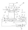
図1には、第1の実施形態に係る露光装置100の構成が示されている。この露光装置100は、ステップ・アンド・リピート方式の縮小投影型露光装置(いわゆるステッパー)である。
【0042】
この投影露光装置100は、照明系IOPと、マスクとしてのレチクルRを保持するレチクルステージRST、レチクルRに形成されたパターンの像を感応基板としてのウエハW上に投影する投影光学系PL、ウエハWを保持してベース12上をXY2次方向に移動可能な第1基板ステージとしてのウエハステージWS1及びウエハWを保持してベース12上をウエハステージWS1とは独立にXY2次元方向に移動可能な第2基板ステージとしてのウエハステージWS2、2つのウエハステージWS1,WS2のそれぞれの位置を計測する干渉計システム26と、CPU,ROM,RAM,I/Oインターフェース等を含んで構成されるミニコンピュータ(又はマイクロコンピュータ)から成り装置全体を統括制御する制御手段としての主制御装置28等を備えている。
【0043】
前記照明系IOPは、光源(水銀ランプ又はエキシマレーザ等)と、フライアイレンズ、リレーレンズ、コンデンサレンズ等から成る照明光学系とから構成されている。この照明系IOPは、光源からの露光用の照明光ILによってレチクルRの下面(パターン形成面)のパターンを均一な照度分布で照明する。ここで、露光用照明光ILとしては、水銀ランプのi線等の輝線、又はKrF、ArF等のエキシマレーザ光等が用いられる。
【0044】
レチクルステージRST上には不図示の固定手段を介してレチクルRが固定されており、このレチクルステージRSTは、不図示の駆動系によってX軸方向(図1における紙面直交方向)、Y軸方向(図1における紙面左右方向)及びθ方向(XY面内の回転方向)に微小駆動可能とされている。これにより、このレチクルステージRSTは、レチクルRのパターンの中心(レチクルセンタ)が投影光学系PLの光軸Aeとほぼ一致する状態でレチクルRを位置決め(レチクルアライメント)できるようになっている。図1では、このレチクルアライメントが行われた状態が示されている。
【0045】
投影光学系PLは、その光軸AeがレチクルステージRSTの移動面に直交するZ軸方向とされ、ここでは両側テレセントリックで、所定の縮小倍率β(βは例えば1/5)を有するものが使用されている。このため、レチクルRのパターンとウエハW上のショット領域との位置合わせ(アライメント)が行われた状態で、照明光ILによりレチクルRが均一な照度で照明されると、パターン形成面のパターンが投影光学系PLにより縮小倍率βで縮小されて、フォトレジストが塗布されたウエハW上に投影され、ウエハW上の各ショット領域にパターンの縮小像が形成される。
【0046】
また、本実施形態では、投影光学系PLのX軸方向一側(図1における左側)の側面には、ウエハステージWS1,WS2の露光時のX軸方向位置管理の基準となるX固定鏡14Xが固定され、同様に投影光学系PLのY軸方向一側(図1における紙面奥側)の側面には、ウエハステージWS1,WS2の露光時のY軸方向位置管理の基準となるY固定鏡14Yが固定されている(図3参照)。
【0047】
前記ウエハステージWS1、WS2の底面には、不図示の気体静圧軸受がそれぞれ設けられており、これらの気体静圧軸受によってウエハステージWS1、WS2はベース12上面との間に数ミクロン(μm)程度のクリアランスを介してそれぞれベース12上方に浮上支持されている。これらのウエハステージWS1、WS2のX軸方向一側(図1における左側)の面及びY軸方向一側(図1における紙面奥側)の面には、それぞれ鏡面加工が施され、干渉計システム26からの測長ビームを反射するための移動鏡として機能する反射面がそれぞれ形成されている。
【0048】
また、ウエハステージWS1、WS2の底面には、マグネットがそれぞれ固定されており、ベース内の所定範囲(具体的には、投影光学系PL下方近傍の所定領域及びアライメント顕微鏡WA下方近傍の所定領域)に埋め込まれた不図示の駆動コイルによって発生する電磁力によりウエハステージWS1、WS2はベース12上をXY2次元方向に移動する。すなわち、ウエハステージWS1、WS2底面のマグネットとベース12内に埋め込まれた駆動コイルとによってウエハステージWS1、WS2の駆動手段としてのいわゆるムービングマグネット型のリニアモータが構成されている。このリニアモータの駆動コイルの駆動電流が、主制御装置28によって制御される。
【0049】
ウエハステージWS1,WS2上には不図示のウエハホルダを介して真空吸着等によってウエハWがそれぞれ保持されている。また、これらのウエハステージWS1,WS2上には、その表面がウエハWの表面と同じ高さになるような基準マーク板FM1、FM2がそれぞれ固定されている。一方の基準マーク板FM1の表面には、図2の平面図に示されるように、その長手方向中央部に後述するウエハアライメント顕微鏡WAで計測するためのマークWMが形成され、このマークWMの長手方向両側に投影光学系PLを通してレチクルRとの相対的な位置計測に用いる一対のマークRMが形成されている。他方の基準マーク板FM2上にもこれとも全く同様のマークWM、RMが形成されている。
【0050】
更に、本実施形態では、投影光学系PLからXY軸に対しほぼ45度の方向に所定距離、例えば3000mm離れた位置にウエハWに形成された位置検出用マーク(アライメントマーク)を検出するアライメント系としてのオフ・アクシス方式のアライメント顕微鏡WAが設けられている。ウエハWには、前層までの露光、プロセス処理により段差ができており、その中には、ウエハ上の各ショット領域の位置を測定するための位置検出用マーク(アライメントマーク)も含まれており、このアライメントマークをアライメント顕微鏡WAにより計測するのである。
【0051】
アライメント顕微鏡WAとしては、ここでは、画像処理方式のいわゆるFIA(field Image Alignment )系のアライメント顕微鏡が用いられている。これによれば、ハロゲンランプ等のブロードバンドな照明光を発する不図示の光源から発せられた照明光が不図示の対物レンズを通過した後ウエハW(又は基準マーク板FM)上に照射され、そのウエハW表面の不図示のウエハマーク領域からの反射光が対物レンズ、不図示の指標板を順次透過して不図示のCCD等の撮像面上にウエハマークの像、及び指標板上の指標の像が結像される。これらの像の光電変換信号が信号処理ユニット16内の不図示の信号処理回路により処理され、不図示の演算回路によってウエハマークと指標との相対位置が算出され、この相対位置が主制御装置28に伝えられる。主制御装置28では、この相対位置と干渉計システム26の計測値とに基づいてウエハW上のアライメントマークの位置を算出する。
【0052】
また、アライメント顕微鏡WAのX軸方向一側(図1における左側)の側面には、ウエハステージWS1,WS2のアライメント動作時のX軸方向位置管理の基準となるX固定鏡18Xが固定され、同様にアライメント顕微鏡WAのY軸方向一側(図1における紙面奥側)の側面には、ウエハステージWS1,WS2の露光動作時のY軸方向位置管理の基準となるY固定鏡18Yが固定されている。
【0053】
なお、アライメント顕微鏡としてはFIA系に限らず、LIA(Laser Interferometric Alignment) 系やLSA(Laser Step Alignment)系等の他の光アライメント系は勿論、位相差顕微鏡や微分干渉顕微鏡等の他の光学装置や、トンネル効果を利用して試料表面の原子レベルの凹凸を検出するSTM(Scanning Tunnel Microscope:走査型トンネル顕微鏡)や原子間力(引力や斥力)を利用して試料表面の原子分子レベルの凹凸を検出するAFM(Atomic Force Microscope :原子間力顕微鏡)等の非光学装置等を使用することも可能である。
【0054】
更に、本実施形態の投影露光装置100では、レチクルRの上方に、投影光学系PLを介した基準マーク板FM上の基準マークRMの像とレチクルR上のレチクルアライメントマーク(図示省略)とを同時に観察するためのマーク位置検出手段としてのレチクルアライメント顕微鏡52A、52Bが設けられている。レチクルアライメント顕微鏡52A、52Bの検出信号S1、S2は、主制御装置28に供給されるようになっている。この場合、レチクルRからの検出光をそれぞれレチクルアライメント顕微鏡52A、52Bに導くための偏向ミラー54A、54Bが当該各レチクルアライメント顕微鏡52A、52Bと一体的にユニット化されて、一対の顕微鏡ユニット56A、56Bが構成されている。これらの顕微鏡ユニット56A、56Bは、露光シーケンスが開始されると、主制御装置28からの指令により、不図示のミラー駆動装置によって、レチクルパターン面にかからない位置まで退避されるようになっている。
【0055】
次に、ウエハステージWS1、WS2の位置を管理する図1の干渉計システム26について詳述する。
【0056】
この干渉計システム26は、実際には、図3に示されるように、X軸方向位置計測用の第1のレーザ干渉計26Xeと、Y軸方向位置計測用の第2のレーザ干渉計26Yeと、X軸方向位置計測用の第3のレーザ干渉計26Xaと、Y軸方向位置計測用の第4のレーザ干渉計26Yaとを含んで構成されているが、図1ではこれらが代表的に干渉計システム26として図示されている。
【0057】
第1のレーザ干渉計26Xeは、X固定鏡14Xに対して投影光学系PLの投影中心を通るX軸方向のレファレンスビームXe1を投射するとともに、ウエハステージ(WS1又はWS2)の反射面に対して測長ビームXe2を投射し、これら2本のビームの反射光が一つに重ねられて干渉させられたその干渉状態に基づいて固定鏡14Xに対するウエハステージ反射面の変位を計測する。
【0058】
また、第2のレーザ干渉計26Yeは、Y固定鏡14Yに対して投影光学系PLの投影中心を通るY軸方向のレファレンスビームYe1を投射するとともに、ウエハステージ(WS1又はWS2)の反射面に対して測長ビームYe2を投射し、これら2本のビームの反射光が一つに重ねられて干渉させられたその干渉状態に基づいて固定鏡14Yに対するウエハステージ反射面の変位を計測する。
【0059】
また、第3のレーザ干渉計26Xaは、X固定鏡18Xに対してアライメント顕微鏡WAの検出中心を通るX軸方向のレファレンスビームXa1を投射するとともに、ウエハステージ(WS1又はWS2)の反射面に対して測長ビームXa2を投射し、これら2本のビームの反射光が一つに重ねられて干渉させられたその干渉状態に基づいて固定鏡18Xに対するウエハステージ反射面の変位を計測する。
【0060】
また、第4のレーザ干渉計26Yaは、Y固定鏡18Yに対してアライメント顕微鏡WAの検出中心を通るY軸方向のレファレンスビームYa1を投射するとともに、ウエハステージ(WS1又はWS2)の反射面に対して測長ビームYa2を投射し、これら2本のビームの反射光が一つに重ねられて干渉させられたその干渉状態に基づいて固定鏡18Yに対するウエハステージ反射面の変位を計測する。
【0061】
ここで、レファレンスビームXe1及び測長ビームXe2から成る第1のレーザ干渉計26Xeの測長軸を第1測長軸Xe、レファレンスビームYe1及び測長ビームYe2から成る第2のレーザ干渉計26Yeの測長軸を第2測長軸Ye、レファレンスビームXa1及び測長ビームXa2から成る第3のレーザ干渉計26Xaの測長軸を第3測長軸Xa、レファレンスビームYa1及び測長ビームYa2から成る第4のレーザ干渉計26Yaの測長軸を第4測長軸Yaと呼ぶものとすると、第1測長軸Xeと第2測長軸Yeとは、投影光学系PLの投影中心(光軸Ae中心と一致)で垂直に交差しており、第3測長軸Xaと第4測長軸Yaとは、アライメント顕微鏡WAの検出中心で垂直に交差している。これにより、後述するように、ウエハW上の位置検出用マーク(アライメントマーク)の計測時にも、ウエハW上へのパターンの露光時にもウエハステージのヨーイング等によるアッベ誤差の影響を受けることなく、それぞれの計測軸方向でウエハステージの位置を正確に計測できるようになっている。なお、測定精度を向上させるべく、上記第1ないし第4のレーザ干渉計として、2周波数のヘテロダイン干渉計を用いることがより一層望ましい。
【0062】
図1に戻り、干渉計システム26の計測値は主制御装置28に供給され、主制御装置28ではこの干渉計システム26の計測値をモニタしつつ、前述したリニアモータを介してウエハステージWS1,WS2を位置制御する。
【0063】
図3からも明らかなように、本第1の実施形態の場合、ウエハステージWS1又はWS2上のウエハWに対して投影光学系PLを介したレチクルパターンの露光が行なわれる間は、第1、第2のレーザ干渉計26Xe,26Yeによってウエハステージの位置が管理され、アライメント顕微鏡WAによりウエハW上の位置検出用マーク(アライメントマーク)の計測が行なわれる間は、第3、第4のレーザ干渉計26Xa,26Yaによってウエハステージの位置が管理されるようになっている。しかしながら、露光が終了した後、あるいはアライメントマークの計測が終了した後は、各測長軸がそれぞれのウエハステージの反射面に当たらなくなるので、干渉計システム26によるウエハステージの位置管理は困難となる。
【0064】
このため、本実施形態の投影露光装置100では、ウエハステージWS1を図3中に仮想線で示される第3位置と、図3中に実線で示される第2位置と、図3中でウエハステージWS2が位置する第1位置との3地点間で自在に移動させる移動手段としての第1のロボットアーム20と、同様にウエハステージWS2を上記第1位置と、第2位置と、第3位置との3地点間で自在に移動させる移動手段としての第2のロボットアーム22とが設けられている。これら第1、第2のロボットアーム20、22も主制御装置28によって制御され、これら第1、第2のロボットアーム20、22のウエハステージの位置制御精度は、概ね±1μm程度となっている。これらのロボットアーム20、22としては、公知の構成の有関節ロボットアームが用いられているので、詳細な説明は省略するが、上記の位置制御精度を確実に実現するために、図3中に符号24A、24Bで示されるような上下動ピンをストッパとして併せて設けるようにしても良い。
【0065】
ここで、第3位置、第2位置及び第1位置について簡単に説明すると、第3位置とは、外部の基板搬送機構の一部を構成する搬送アーム50とウエハステージ(WS1、WS2)との間でウエハWの受け渡しが行なわれるウエハ交換位置を意味し、第2位置とは、ウエハWのローディングが終了した後、ウエハステージ上のウエハWに対しアライメントが行なわれる位置であって第3測長軸Xaと第4測長軸Yaとが共にウエハステージの反射面に当たる任意の位置を意味し、第1位置とは、ウエハのアライメントが終了した後、ウエハステージ上のウエハWに対し露光が行なわれる位置であって第1測長軸Xeと第2測長軸Yeとが共にウエハステージの反射面に当たる任意の位置を意味する。
【0066】
本実施形態では、上述したように、図3中に示される位置が、それぞれ第1位置、第2位置、第3位置として定められているものとするが、第2位置は、上記の定義を満足するのであれば、如何なる位置を定めてもよく、例えば、基準マーク板FM上のマークWMがアライメント顕微鏡WAの検出領域内となる位置を第2位置としても良い。同様に、第1位置も、上記の定義を満足するのであれば、如何なる位置を定めてもよく、例えば、基準マーク板FM上のマークRMが投影光学系PLの投影領域内となる位置を第1位置としても良い。
【0067】
次に、上述のようにして構成された本実施形態の投影露光装置100の全体的な動作の流れを説明する。
【0068】
▲1▼ 前提として、ウエハステージWS1が第3位置にあり、ウエハステージWS2が第1位置にあるものとする。
【0069】
まず、ウエハステージWS1と搬送アーム50との間でウエハ交換が行なわれる。このウエハ交換は、ウエハステージWS1上のセンターアップ(ウエハアップ機構)と搬送アーム50とによって従来と同様にして行なわれるので、ここでは詳細な説明するは省略するが、先に述べたようにロボットアームの位置決め精度は概ね±1um以下なので、搬送アーム50の位置決め精度もこれとほぼ同程度であるものとする。このウエハ交換に先だって、ウエハWは不図示のプリアライメント装置によりX,Y,θ方向に概略位置決めがなされており、ウエハステージ上へのロード位置が大きくずれることはなく、例えば基準マーク板FM1に対するウエハWのロード位置も上記の±1um以下の誤差範囲内となっている。
【0070】
このウエハ交換中、ウエハステージWS1はレーザ干渉計で位置が管理されていないが、第1のロボットアーム20がウエハステージWS1を捉えているので、ウエハステージWS1が勝手な所に行くというような不都合は生じない。なお、第1のロボットアーム20により捉えられている間は、ウエハステージWS1を駆動するリニアモータは停止しているものとする(以下において同じ)。
【0071】
ウエハ交換(ウエハステージWS1上へのウエハWのロード)が終了すると、主制御装置28では、第1のロボットアーム20を制御してウエハステージWS1を図3中に実線で示される第2位置へ移動させ、この位置で、第3、第4のレーザ干渉計26Xa,26Yaを同時にリセットする。このリセットが終了すると、第1のロボットアーム20はここでの役目を終えるので、該第1のロボットアーム20は主制御装置28からの指示に応じて不図示の駆動系によりウエハステージWS1を離れて邪魔にならない位置に待避される。
【0072】
上記の第3、第4のレーザ干渉計26Xa,26Yaのリセット終了後、主制御装置28では干渉計26Xa,26Yaの計測値をモニタしつつ、ウエハステージWS1上の基準マーク板FM1上のマークWMがアライメント顕微鏡WAの検出領域内に位置決めされるようにウエハステージWS1を前述したリニアモータを介して位置制御する。ここで、第1のロボットアーム20による第2位置への位置決め精度は、前述の如く、概ね±1um以下が可能であり、この第2位置で干渉計測長軸がリセットされているので、その後は0.01μm程度の分解能で設計値(ウエハステージWS1の反射面と基準マーク板上のマークWMとの設計上の相対位置関係)に基づいて位置制御が可能であり、結果的に、アライメント顕微鏡WAによるマークWM計測にとって十分な精度でウエハステージWS1が位置決めされる。なお、第2位置を、ウエハステージWS1上の基準マーク板FM1上のマークWMがアライメント顕微鏡WAの検出領域内に位置決めされる位置に設定する場合には、上記の干渉計リセット後のウエハステージWS1の移動は不要であるので、スループットの面ではより一層望ましい。
【0073】
次に、アライメント顕微鏡WAによって該アライメント顕微鏡WAの検出中心(指標中心)を基準とする基準マーク板FM1上のマークWMの位置(ΔWX ,ΔWY )が計測され、主制御装置28ではこの計測中の第3、第4のレーザ干渉計26Xa,26Yaの計測値の平均値(X0 ,Y0 )を求める。これによりレーザ干渉計26Xa,26Yaの計測値が(X0 −ΔWX ,Y0 −ΔWY )を示すとき基準マーク板FM1上のマークWMがアライメント顕微鏡WAの検出中心(指標中心)の真下にいることが分かる。上記の第3、第4のレーザ干渉計26Xa,26Yaのリセット後の一連の動作を以下においてはW−SETと呼ぶものとする。
【0074】
このようにして、一方のウエハステージWS1上でウエハ交換、干渉計リセット及びW−SETの一連の動作が行なわれる間に、他方のウエハステージWS2上では、次のような動作が行なわれる。
【0075】
すなわち、ウエハステージWS2は、前述の如く、第2のロボットアーム22により第1位置へ移動されており、この第1位置への位置決め制御も±1um以下の精度で行なわれている。この第1位置へのウエハステージWS2の移動が完了すると同時に、主制御装置28では第1、第2のレーザ干渉計26Xe,26Yeをリセットする。
【0076】
この第1、第2のレーザ干渉計26Xe,26Yeのリセットが終了すると、第2のロボットアーム22はここでの役目を終えるので、該第2のロボットアームは主制御装置28からの指示に応じて不図示の駆動系によりウエハステージWS2を離れて邪魔にならない位置に待避される。
【0077】
次に、主制御装置28ではレーザ干渉計26Xe,26Yeの計測値をモニタしつつ、基準マーク板FM2上のマークRMが、投影光学系PLの投影領域内でレチクルRに形成されているレチクルアライメントマーク(図示省略)に投影光学系を介して重なる位置に、位置決めされるように、リニアモータを介してウエハステージWS2の位置を制御する。この場合、第2のロボットアーム22による第1位置への位置決め精度は、前述の如く、概ね±1um以下が可能であり、この第1位置で干渉計測長軸がリセットされているので、その後は0.01μm程度の分解能で設計値(ウエハステージWS2の反射面と基準マーク板FM2上のマークRMとの設計上の相対位置関係)に基づいて位置制御が可能であり、結果的に、レチクルアライメント顕微鏡52A、52Bでレチクルアライメントマークと基準マーク板FM上のマークRMを同時に観測するには必要十分な精度でウエハステージWS2は位置決めされる。
【0078】
次に、レチクルアライメント顕微鏡52A、52BによってレチクルR上のレチクルアライメントマークと基準マーク板FM2上のマークRMの相対間隔(ΔRX,ΔRY)、すなわち投影光学系PLの投影領域内の所定の基準点としてのレチクルRのパターン像の投影中心に対するウエハステージWS2上の基準点である基準マークRM中心との位置ずれ(ΔRX ,ΔRY )が計測され、主制御装置28では、このレチクルアライメント顕微鏡52A、52Bの計測値を取り込むと同時に、その時のレーザ干渉計26Xe,26Yeの計測値(X1 ,Y1 )を読み取る。これにより、レーザ干渉計26Xe,26Yeの計測値が(X1 −ΔRX,Y1 −ΔRY )となる位置が、レチクルアライメントマークと基準マーク板FM2上のマークRMがちょうど投影光学系PLを介して重なる位置であることが分かる。上記の第1、第2のレーザ干渉計26Xe,26Yeのリセット後の一連の動作を以下においてはR−SETと呼ぶものとする。
【0079】
▲2▼次に、ウエハステージWS1側のウエハアライメントとウエハステージWS2側の露光とが並行して行なわれる。
【0080】
すなわち、前述した第3、第4のレーザ干渉計26Xa、26Yaのリセット後は、ウエハステージWS1の位置は、レーザ干渉計26Xa、26Yaの計測値に基づいて管理されており、主制御装置28ではウエハW上の複数のショット領域の内、予め定められた特定のサンプルショットの位置検出用マーク(アライメントマーク)位置の計測を、干渉計26Ya、26Xaの計測値をモニタしつつリニアモータを介してウエハステージWS1を順次移動して、アライメント顕微鏡WAの出力に基づいて(Xa,Ya)座標系上で行なう。この場合、基準マーク板FM1上のマークWMがアライメント顕微鏡WAの検出中心の真下に来るときの干渉計の計測値(X0 −ΔX ,Y0 −ΔY )が求まっているため、この値と、基準マークWAと各アライメントマークの相対位置の設計値とに基づいてウエハW上の各アライメントマークをウエハアライメント顕微鏡WAの検出領域内に位置決めするためにはレーザ干渉計26Ya、26Xaの計測値がどの値を示す位置にウエハステージWS1を移動させれば良いかが演算で求められ、この演算結果に基づいてウエハステージWS1が順次移動される。
【0081】
ウエハWのX、Y、θの位置合わせのためには、最低でもX計測マーク2個とY計測マーク1個(またはX計測マーク1個とY計測マーク2個)を計測を行なえば足りるが、ここでは、EGAサンプルショットとして、一直線上に無いX計測マーク3個以上、一直線上に無いY計測マーク3個以上の計測が行なわれるものとする。
【0082】
そして、この計測した各サンプルショットのアライメントマーク(ウエハマーク)位置と設計上のショット領域の配列データとを用いて、例えば特開昭61−44429号公報等に開示されるような最小自乗法による統計演算を行なって、ウエハW上の上記複数ショット領域の全配列データを求める。但し、計算結果は、先に求めた基準マーク板FM1上のマークWMがアライメント顕微鏡WAの検出中心の直下に来たときの干渉計の値(X0 −ΔX ,Y0 −ΔY )と差をとって、基準マーク板FM1上の基準マークWAを基準とするデータに変換しておくことが望ましい。これにより、基準マーク板FM1上のマークWMとウエハW上の各ショット領域の基準点との相対的な位置関係が必要にして十分に分かる。
【0083】
このようにして、ウエハステージWS1側でファインアライメント(EGA)が行なわれるのと並行して、ウエハステージWS2側では、次のようにしてレチクルRのパターン像とウエハW上のショット領域の既成のパターンとの重ね合わせ露光が行なわれる。
【0084】
すなわち、主制御装置28では上記の位置ずれ誤差の計測結果と、そのときのウエハステージWS2の座標位置(Xe,Ye)と、予めアライメント動作により上記と同様にして算出している基準マーク板FM2上の基準マークWAを基準とする各ショットの配列座標データとに基づいて、干渉計26Ye、26Xeの計測値をモニタしつつウエハW上の各ショット領域を露光位置に位置決めしつつ、照明光学系内のシャッタを開閉制御しながら、ステップ・アンド・リピート方式でレチクルパターンをウエハW上に順次露光する。ここで、ウエハステージWS2上のウエハWに対する露光に先立って、干渉計26Xe、26Yeをリセットしている(干渉計の測長軸が一旦切れている)にもかかわらず、高精度な重ね合わせが可能な理由について、詳述すると、基準マーク板FM2上のマークWMとマークRMとの間隔は既知であり、これに先立って行われたファインアライメント(EGA)により前述と同様にして基準マーク板FM2上のマークWMとウエハW上の各ショット領域の基準点との相対的な位置関係が算出されており、レチクルR上のレチクルアライメントマークがレチクルR上のどこに存在するか(即ち、投影光学系PLの投影領域内の所定の基準点であるレチクルのパターン像の投影中心(投影光学系PLの投影中心とほぼ一致)とウエハステージWS2上の基準点であるマークRMとの相対位置関係)も計測されているので、これらの計測結果に基づき、第1、第2のレーザ干渉計26Xe、26Yeの計測値がどの値になればレチクルRのパターン像とウエハW上各ショット領域がぴったり重なるかは明白だからである。
【0085】
▲3▼ 上述のようにして、ウエハステージWS1側でファインアライメント(EGA)が終了し、ウエハステージWS2側でウエハW上の全てのショット領域に対するレチクルパターンの露光が終了すると、ウエハステージWS1を投影光学系PLの下方の第1位置へ移動し、ウエハステージWS2をウエハ交換位置である第3位置に移動する。
【0086】
すなわち、ウエハステージWS1は主制御装置28からの指示に応じて第1のロボットアーム20によって捕捉され、第1位置へ移動される。この第1位置への位置決め制御も±1um以下の精度で行なわれる。この第1位置へのウエハステージWS1の移動が完了すると同時に、主制御装置28では第1、第2のレーザ干渉計26Xe,26Yeをリセットする。
【0087】
このリセットが終了すると、第1のロボットアーム20はここでの役目を終えるので、該第1のロボットアーム20は主制御装置28からの指示に応じて不図示の駆動系によりウエハステージWS1を離れて邪魔にならない位置に待避される。
【0088】
次に、主制御装置28では先に述べたウエハステージWS2側と同様にして、R−SETを行なう。これにより、レチクルアライメントマークと基準マーク板FM1上のマークRMの相対間隔(ΔRX ,ΔRY )、すなわち投影光学系PLの投影領域内の所定の基準点としてのレチクルRのパターン像の投影中心に対するウエハステージWS2上の基準点である基準マークRM中心との位置ずれ(ΔRX ,ΔRY )及びこの位置ずれ計測時のステージ座標位置(X1 ,Y1 )が計測される。
【0089】
ウエハステージWS1側で上述のようにして、干渉計リセット及びR−SETが行われる間に、主制御装置28からの指示に応じて第2のロボットアーム22が露光動作が終了したウエハステージWS2を捕捉し、ウエハ交換のためウエハ受け渡し位置(第3位置)にウエハステージWS2を移動させ、以後前述したウエハステージWS1側と同様にしてウエハ交換、干渉計リセット及びW−SETが行われる。
【0090】
▲4▼ 次いで、主制御装置28では、前述と同様に、ウエハステージWS1側でステップ・アンド・リピート方式でレチクルパターンがウエハW上に順次露光されるのと並行して、ウエハステージWS2側でファインアライメント(EGA)が行なわれるように両ステージの動作を制御する。
【0091】
▲5▼その後は、これまでに説明した▲1▼〜▲4▼の動作が順次繰り返されるように、主制御装置28によって、両ステージWS1、WS2の動作、第1、第2のロボットアームの動作が制御される。
【0092】
以上説明した、両ステージWS1、WS2上で行われるの並行動作の流れが、図4に示されている。
【0093】
以上説明したように、本第1の実施形態に係る投影露光装置100によると、ウエハステージWS1及びウエハステージWS2の内の一方のステージ側の露光動作と他方のステージ側のファインアライメント動作を並行して行なうことができるので、ウエハ交換(サーチアライメントを含む)、ファインアライメント、露光をシーケンシャルに行なっていた従来技術に比べて、スループットの大幅な向上が期待できる。通常、露光処理シーケンスの中では、ファインアライメント動作と露光動作に要する時間の割合が大きいからである。
【0094】
また、上記実施形態によると、干渉計システム26の測長軸が切れることを前提としているので、各ウエハステージの反射面(移動鏡を用いる場合は該移動鏡)の長さは、ウエハ直径より僅かに長い程度で十分であることから、測長軸が切れてはいけないことを前提としていた従来技術に比べて、ウエハステージの小型・軽量化が可能であり、これによりステージ制御性能の向上が期待される。
【0095】
さらに、上記実施形態では、干渉計システムの測長軸が切れることを前提とし、アライメント前、露光前それぞれにおいてステージ上の基準マーク板FM上のマーク位置を測定するので、投影光学系PLの投影中心とアライメント顕微鏡WAの検出中心との中心間距離(ベースライン量)はいくら長くなっても特に不都合はなく、投影光学系PLとアライメント顕微鏡WAの間隔をある程度十分に離して、ウエハステージWS1とウエハステージWS2とが干渉等を生じることなく、ウエハアライメントと露光とを時間的に並行して行なうことができる。
【0096】
また、上記実施形態では、投影光学系PLの投影中心で垂直に交差する第1測長軸Xeと第2測長軸Ye、及びアライメント顕微鏡WAの検出中心で垂直に交差する第3測長軸Xaと第4測長軸Yaを干渉計システム26が備えていることから、アライメント動作時及び露光時のいずれの時においてもウエハステージの2次元位置を正確に管理することができる。
【0097】
これに加え、投影光学系PLの側面、アライメント顕微鏡WAの側面に干渉計用固定鏡14X、14Y、18X、18Yを固定したことから、アライメント計測中、露光中に固定鏡位置の変動がない限り、仮に経時的変化や装置の振動等によって固定鏡位置が変動しても、この変動によりウエハステージの位置制御精度が低下する等の不都合が生じることがない。従って、例えば、アライメント顕微鏡WAを上下動可能な構成にしても何らの不都合をも生じない。
【0098】
なお、上記第1の実施形態では、第1、第2のロボットアーム20、22により、ウエハステージWS1、ウエハステージWS2を第1位置、第2位置及び第3位置の3地点間で移動させる場合について説明したが、本発明がこれに限定させるものではなく、例えば第2位置でウエハ交換を行なうようにする場合には、第1、第2のロボットアーム20、22により、ウエハステージWS1、ウエハステージWS2を第1位置と第2位置間で移動させるようにしても良い。この場合には、主制御装置28では、ウエハステージWS1及びウエハステージWS2の内の一方のステージ上のウエハWの露光動作と、他方のステージ上のウエハWのアライメント動作とが並行して行われるように両ステージの動作を制御した後に、第1、第2のロボットアーム20、22により両ステージの位置を入れ替えることとなる。
【0099】
また、上記第1の実施形態では、EGA計測に基づいてステップ・アンド・リピート方式の露光がステージ上のウエハWに対して行われる場合について説明したが、これに限らず、ダイ・バイ・ダイによってアライメント、露光を繰り返しながらウエハW上の各ショット領域に順次レチクルのパターン像を投影露光しても良い。この場合であっても、アライメント時にステージ上の基準マーク板FMに形成されたマークWMに対する各アライメントマークの相対位置が計測されるので、この相対位置に基づいて上記と同様にして、各ショット領域にレチクルパターン像を重ね合わせることができる。かかるダイ・バイ・ダイ方式は、ウエハW上のショット領域の数が少ない場合に採用することが望ましい。ショット領域の数が多い場合は、スループットの低下を防止する観点から考えて前述したEGAによる方が望ましい。
【0100】
また、上記第1の実施形態では、第1のロボットアーム20が一方のステージWS1を第1位置、第2位置及び第3位置の3地点間で移動させ、第2のロボットアーム22が他方のステージWS2を第1位置、第2位置及び第3位置の3地点間で移動させる場合について説明したが、本発明がこれに限定されることはなく、例えば一方のロボットアーム20がステージWS1(又はWS2)を第1位置から第3位置まで運ぶ途中で第1位置、第2位置及び第3位置以外のある位置まで運んで放し、他方のロボットアーム22が該ステージWS1(又はWS2)をこの位置から第3位置まで移動させる等の方式を採用することにより、一方のロボットアーム20を両ステージの第2位置と第1位置との搬送専用とし、他方のロボットアーム2を両ステージの第3位置と第2位置との搬送専用とすることも可能である。
【0101】
また、干渉計システム26を構成する各レーザ干渉計として、多軸の干渉計を用い、ウエハステージのX、Yの並進位置のみでなく、ヨーイングや、ピッチングをも計測するようにしても良い。
【0102】
《第2の実施形態》
次に、本発明の第2の実施形態を図5に基づいて説明する。ここで、前述した第1の実施形態と同一若しくは同等の構成部分については、同一の符号を用いるとともにその説明を省略するものとする。
【0103】
この第2の実施形態は、ウエハステージWS1が、ステージ本体WS1aと、このステージ本体WS1a上に着脱可能な同一形状の基板保持部材WS1bとの2部分に分離可能に構成され、同様にウエハステージWS2が、ステージ本体WS2aと、このステージ本体WS2a上に着脱可能な同一形状の基板保持部材WS2bとの2部分に分離可能に構成されている点に特徴を有する。
【0104】
基板保持部材WS1b、WS2bには、ウエハWが不図示のウエハホルダを介して吸着保持されているとともに、干渉計用移動鏡として機能する反射面がその側面にそれぞれ形成されている。また、これらの基板保持部材WS1b、WS2bには、その上面に基準マーク板FM1、FM2がそれぞれ設けられている。
【0105】
本第2の実施形態では、前述した第1の形態とほぼ同様にして、ウエハステージWS1、WS2上で並行処理が行われるが、一方のステージ側でアライメント動作が終了し、他方のステージ側で露光動作が終了した時点で、主制御装置28により第1、第2のロボットアーム20、22が制御され、アライメント動作が終了したステージ側の基板保持部材WS1b(又はWS2b)が第1位置で停止しているステージ本体WS2a上に搬送(移動)されるのと並行して、露光が終了したステージ側の基板保持部材WS2b(又はWS1b)が第2位置で停止しているステージ本体WS1a上に搬送され、このようにして基板保持部材WS1b、WS2bの交換が行われる。基板保持部材WS1b、WS2bが交換される際、干渉計システム26の測長軸は切れるためウエハステージWS1、WS2の位置管理が不能となるので、その間はステージストッパ30a、30bが出てきて両ステージ本体WS1a、WS2aをその位置に保持するようになっている。この場合、ウエハ交換は、不図示の搬送アームにより第2位置で行われる。
【0106】
ここで、本第2の実施形態では、図5から容易に想像されるように、第2位置として、例えば基準マーク板FM上のマークWMがアライメント顕微鏡WAの検出領域内となる位置が、第1位置として、基準マーク板FM上のマークRMが投影光学系PLの投影領域内となる位置がそれぞれ定められており、従って、主制御装置28により基板保持部材WS1b、WS2bのステージ本体上への移動とともに干渉計システム26の測長軸のリセット及びR−SET又はW−SETが行なわれることとなる。
【0107】
この第2の実施形態によっても、前述した第1の実施形態と同等の効果を得ることができる。
【0108】
なお、上記第2の実施形態では、第1、第2のロボットアーム20、22が基板保持部材を第1位置と第2位置間で移動させる場合について説明したが、第1、第2のロボットアーム20、22が、前述した第1の実施形態と同様に、基板保持部材を第1位置、第2位置及び第3位置の3地点間で移動させるようにしても良い。この場合には、ウエハ交換を投影光学系PL、アライメント顕微鏡WAと無関係な所で行なうことができるので、例えばアライメント顕微鏡WA下方のワーキングディスタンスが狭い場合であっても、アライメント顕微鏡WAがウエハ交換の障害になる等の不都合がない。
【0109】
なお、上記第1、第2の実施形態では、干渉計システム26の測長軸が一旦切れる際の対策として、ロボットアームや、ステージストッパなるものを使用する場合について説明したが、これに限らず、例えばウエハステージ下面に二次元グレーティングを刻んでおき、ステージ走り面の下から光学式のエンコーダにより位置を読み取っても良く、干渉計測長軸が一旦切れた状態でステージを次の位置へ正確に移動させることができる手段、又はステージ本体を所定の位置で停止させたまま保持できるものであれば、如何なる手段を用いても良い。
【0110】
また、上記第1、第2の実施形態では、独立に移動するウエハステージが2つ設けられた場合について説明したが、独立に移動するウエハステージを3つ以上設けても良い。ウエハステージを3つ設けた場合には、例えば露光動作、アライメント動作、ウエハ平坦度測定動作を並行して行なうことができる。また、投影光学系PLやアライメント顕微鏡WAを複数設けて良い。投影光学系が複数ある場合には、アライメント動作と異なる二種類のパターンの露光動作とを同時並行的に行なうことができ、いわゆる二重露光等に適する。
【0111】
更に、上記実施形態では、本発明がステップ・アンド・リピート方式の投影露光装置に適用された場合を例示したが、本発明の適用範囲がこれに限定されるものではなく、本発明はいわゆるステップ・アンド・スキャン方式の投影露光装置は勿論、この他、例えば電子ビーム直接描画装置等の他の露光装置にも適用できるものである。
【0112】
【発明の効果】
以上説明したように、本発明によれば、スループットを向上させることができるとともに、ベースライン量に無関係に基板ステージの大きさを定めることができるという従来にない優れた露光方法が提供される。
【0113】
また、本発明によれば、一方の基板ステージ上の露光動作と他方のステージ上のアライメント動作とを並行処理することにより、スループットを向上させることができるという効果がある。
【図面の簡単な説明】
【図1】第1の実施形態に係る露光装置の全体構成を概略的に示す図である。
【図2】図1の一方のウエハステージの概略平面図である。
【図3】図1の装置の概略平面図である。
【図4】図1の装置における動作の流れを示す図である。
【図5】第2の実施形態に露光装置の主要部の構成を示す概略平面図である。
【符号の説明】
14X、18X X固定鏡(固定鏡)
14Y、18Y Y固定鏡(固定鏡)
20 第1のロボットアーム(移動手段)
22 第2のロボットアーム(移動手段)
26 干渉計システム
28 主制御装置(制御手段)
50 搬送アーム(基板搬送機構の一部)
52A、52B レチクルアライメント顕微鏡(マーク位置検出手段)
100 露光装置
WS1a、WS2a ステージ本体
WS1b、WS2b 基板保持部材
FM1、FM2 基準マーク板
WM、RM 基準マーク
R レチクル(マスク)
W ウエハ(感応基板)
PL 投影光学系
WS1 ウエハステージ(第1基板ステージ)
WS2 ウエハステージ(第2基板ステージ)
WA アライメント顕微鏡(アライメント系)
Xe 第1測長軸
Ye 第2測長軸
Xa 第3測長軸
Ya 第4測長軸[0001]
BACKGROUND OF THE INVENTION
The present invention relates to an exposure method and an exposure apparatus. More specifically, the present invention relates to an exposure method in which a mask pattern used when manufacturing a semiconductor element, a liquid crystal display element or the like in a lithography process is exposed on a sensitive substrate via a projection optical system. Further, the present invention relates to an exposure apparatus such as a drawing apparatus that directly draws a pattern on a sensitive substrate with a laser beam, an electron beam, or other charged particle beam for manufacturing a semiconductor element, a mask for manufacturing a semiconductor element, and the like. The present invention is characterized by having a plurality of substrate stages for holding a sensitive substrate.
[0002]
[Prior art]
Conventionally, various exposure apparatuses have been used for manufacturing a semiconductor element or a liquid crystal display element in a photolithography process. Currently, a pattern of a photomask or a reticle (hereinafter, collectively referred to as “reticle”) is used. A projection exposure apparatus for transferring an image onto a substrate such as a wafer or a glass plate (hereinafter referred to as “sensitive substrate” or “wafer” as appropriate) having a surface coated with a photosensitive material such as a photoresist via a projection optical system. Is commonly used. In recent years, as this projection exposure apparatus, a sensitive substrate is placed on a two-dimensionally movable substrate stage, and the sensitive substrate is stepped (stepped) by this substrate stage, so that the pattern image of the reticle is placed on the sensitive substrate. The so-called step-and-repeat type reduction projection exposure apparatus (so-called stepper), which repeats the operation of sequentially exposing each shot area, is the mainstream.
[0003]
Recently, a step-and-scan type projection exposure apparatus (for example, a scanning exposure apparatus as described in Japanese Patent Application Laid-Open No. 7-176468), which is an improvement on a static exposure apparatus such as a stepper, has also been developed. It has come to be used relatively frequently. This step-and-scan type projection exposure apparatus can expose a large field with a smaller optical system as compared with (1) a stepper. Therefore, the projection optical system can be easily manufactured and the number of shots by large field exposure can be reduced. High throughput can be expected due to the decrease, and (2) there are advantages such as an effect of averaging by relatively scanning the reticle and wafer with respect to the projection optical system, and an improvement in distortion and depth of focus.
[0004]
In this type of projection exposure apparatus, it is necessary to align the reticle and wafer with high accuracy prior to exposure. In order to perform this alignment, a position detection mark (alignment mark) formed (exposure transfer) formed in the previous photolithography process is provided on the wafer. By detecting the position of this alignment mark, the wafer The exact position of (or the circuit pattern on the wafer) can be detected.
[0005]
There are two types of alignment microscopes that detect alignment marks: an on-axis method that detects marks through a projection lens and an off-axis method that detects marks without using a projection lens. In an exposure apparatus that uses an excimer laser light source, an off-axis alignment microscope is optimal. This is because the projection lens is corrected for chromatic aberration with respect to the exposure light, so in the case of on-axis, the alignment light cannot be collected or even if it can be collected, the error due to chromatic aberration becomes very large. On the other hand, since the off-axis alignment microscope is provided separately from the projection lens, free optical design is possible without considering such chromatic aberration, and various alignment systems are used. Because it can. For example, a phase contrast microscope or a differential interference microscope can be used.
[0006]
By the way, the flow of processing in this type of projection exposure apparatus is roughly as follows.
[0007]
(1) First, a wafer loading process of loading a wafer onto a wafer table using a wafer loader is performed, and so-called search alignment is performed by using the wafer outer shape as a reference.
[0008]
{Circle around (2)} Next, a fine alignment process for accurately determining the position of each shot area on the wafer is performed. In this fine alignment process, an EGA (Enhanced Global Alignment) method is generally used. In this method, a plurality of sample shots in a wafer are selected, and an alignment mark (wafer mark) attached to the sample shot is selected. Are sequentially measured, and based on the measurement result and the design value of the shot arrangement, a statistical calculation is performed by a so-called least square method or the like to obtain all shot arrangement data on the wafer (Japanese Patent Laid-Open No. 61). -44429, etc.), the coordinate position of each shot area can be obtained with relatively high accuracy with high throughput.
[0009]
(3) Next, based on the coordinate position of each shot area obtained by the above-described EGA method or the like and the baseline amount measured in advance, each shot area on the wafer is sequentially positioned at the exposure position, and the projection optical system is An exposure process for transferring the pattern image of the reticle onto the wafer is performed.
[0010]
(4) Next, a wafer unloading step is performed in which the wafer on the wafer table subjected to the exposure process is unloaded using a wafer unloader. This wafer unloading step is performed simultaneously with the wafer loading step (1). That is, (1) and (4) constitute a wafer exchange process.
[0011]
As described above, in the conventional projection exposure apparatus, three major operations are repeatedly performed using one wafer stage, such as wafer exchange (including search alignment) → fine alignment → exposure → wafer exchange. .
[0012]
[Problems to be solved by the invention]
Since the projection exposure apparatus described above is mainly used as a mass production machine for semiconductor elements and the like, it is possible to improve the processing capability, ie, throughput, of how many wafers can be exposed within a certain time. Necessarily requested.
[0013]
In this regard, in the current projection exposure apparatus, since the three operations described above are performed sequentially, it is necessary to reduce the time required for each operation in order to improve the throughput. The effect of improvement is relatively small because only one operation is performed on one wafer. Further, the time required for fine alignment can be shortened by reducing the number of shots when using the above-described EGA method or by shortening the measurement time of a single shot. Since the alignment accuracy is degraded, the time required for fine alignment cannot be easily reduced.
[0014]
Therefore, it can be concluded that shortening the exposure time is the most effective for improving the throughput, but in this exposure operation, in the case of a stepper, a pure wafer exposure time is used. In order to shorten the wafer exposure time, a large amount of light from the light source is essential to shorten the wafer exposure time. However, in this type of projection exposure apparatus, in addition to the above throughput, as an important condition, ▲ (1) Resolution, (2) Depth of Forcus (DOF), (3) Linewidth control accuracy, etc. The resolution R is the exposure wavelength is λ and the numerical aperture of the projection lens is N.P. A. (Numerical Aperture), λ / N. A. And the depth of focus DOF is λ / (NA) 2 Is proportional to For this reason, it is also necessary for the light source to have a short wavelength, both of which have a large power and a short wavelength compared to the bright lines (g-line, i-line) etc. of the ultra-high pressure mercury lamps conventionally used. The excimer laser described above as satisfying the requirements is said to become the mainstream in the future, and a light source having a shorter wavelength and a larger amount of light and suitable as a light source for an exposure apparatus has not been considered at this stage. Accordingly, the improvement in throughput beyond the case where an excimer laser is used as the light source cannot be expected so much, and there is a limit to the improvement in throughput by devising the light source.
[0015]
On the other hand, in order to shorten the stepping time between shots, it is necessary to improve the maximum speed and maximum acceleration of the stage holding the wafer. However, the improvement in the maximum speed and maximum acceleration tends to cause deterioration of the positioning accuracy of the stage. There was an inconvenience. In addition, in the case of a scanning projection exposure apparatus such as the step-and-scan method, the exposure time of the wafer can be shortened by increasing the relative scanning speed of the reticle and the wafer. Since the synchronization accuracy is likely to deteriorate, the scanning speed cannot be easily increased. Therefore, it is necessary to improve the controllability of the stage.
[0016]
However, it is not easy to improve the controllability of the stage in an apparatus using an off-axis alignment microscope, such as a projection exposure apparatus using an excimer laser light source that will become the mainstream in the future. In other words, this type of projection exposure system accurately manages the position of the wafer stage, both during exposure of the mask pattern via the projection optical system and during alignment, without Abbe error, and achieves high-precision overlay. In order to achieve this, it is necessary to set the measurement axis of the laser interferometer so that it passes through the projection center of the projection optical system and the detection center of the alignment microscope, and within the stage moving range during exposure and during alignment. The stage is inevitably necessary because the length measurement axis passing through the projection center of the projection optical system and the length measurement axis passing through the detection center of the alignment microscope must not be cut off both within the range of movement of the stage. This is because the size is increased.
[0017]
From the above, it is difficult to improve the throughput without any demerit by the method of shortening the time required for each of the three operations described above, and a new technique for improving the throughput by a method different from this. The appearance was long-awaited.
[0018]
The present invention has been made under such circumstances, and the object of the present invention is to improve the throughput and to determine the size of the substrate stage regardless of the baseline amount. It is to provide an exposure method.
[0020]
[Means for Solving the Problems]
If the above-mentioned three operations, that is, wafer exchange (including search alignment), fine alignment, and exposure operations, can be processed partially or simultaneously in parallel, these operations are performed sequentially. Thus, it is considered that the throughput can be improved. The present invention has been made paying attention to such a viewpoint, and employs the following method and configuration. That is,
The present invention is an exposure method in which an image of a pattern formed on a mask (R) is exposed on a sensitive substrate (W) via a projection optical system (PL), each holding the sensitive substrate (W). Two substrate stages (WS1, WS2) that can be moved independently within the same plane are prepared; the sensitivity held by one of the two substrate stages (WS1, WS2) (WS1 or WS2) Exposing the pattern image of the mask (R) onto the substrate (W) via the projection optical system (PL); during the exposure of the sensitive substrate (W) held on the one substrate stage (WS1 or WS2) Further, the position of the alignment mark on the sensitive substrate (W) held on the other substrate stage (WS2 or WS1) of the two substrate stages and the reference point on the other stage (WS2 or WS1) Measure the relationship After the exposure of the sensitive substrate held on the one substrate stage, the reference point on the other substrate stage is positioned in the projection region of the projection optical system (PL), and a predetermined point in the projection region is set. Detecting a positional deviation of the reference point on the other substrate stage and a coordinate position of the other substrate stage with respect to a reference point; based on the measured positional relationship, the detected positional deviation and the detected coordinate position The movement of the other substrate stage is controlled to align the sensitive substrate held on the other stage with the pattern image of the mask. Each substrate stage has a stage main body and a substrate holding member that is detachably mounted on the main body and holds the substrate, and a reflection surface for an interferometer is provided on a side surface of the substrate holding member, In addition, a reference mark is formed as the reference point on the upper surface of the substrate holding member, and after the exposure of the sensitive substrate held on the one substrate stage, the substrate holding member on the one and the other stage is replaced. Be called An exposure method characterized by the above.
[0021]
According to this, on the sensitive substrate (W) held on one substrate stage (WS1 or WS2) of the two substrate stages (WS1, WS2), the mask (via the projection optical system (PL)). While exposure of the pattern image of R) is performed, (1) The positional relationship between the alignment mark on the sensitive substrate (W) held on the other substrate stage (WS2 or WS1) of the two substrate stages and the reference point on the other stage (WS2 or WS1) is measured. The In this way, the exposure operation on one substrate stage side and the alignment operation on the other substrate stage side (the positional relationship between the alignment mark on the sensitive substrate held on the other substrate stage and the reference point on the other stage) Measurement) can be performed in parallel, so that it is possible to improve the throughput as compared with the prior art in which these operations are performed sequentially.
[0022]
After the exposure of the sensitive substrate held on the one substrate stage, the other substrate stage (WS2 or WS1) Board holding member With the upper reference point (reference mark) positioned in the projection area of the projection optical system (PL), (2) the other substrate stage with respect to a predetermined reference point in the projection area Board holding member The positional deviation of the upper reference point (reference mark) and (3) the coordinate position of the other substrate stage when the positional deviation is detected are detected. Thereafter, the movement of the other substrate stage (WS2 or WS1) is controlled based on (1) the measured positional relationship, (2) the detected positional deviation, and (3) the detected coordinate position, and the other stage The sensitive substrate held on the mask and the pattern image of the mask are aligned.
[0023]
For this reason, (1) Relationship between a predetermined reference point on the other substrate stage and an alignment mark on the sensitive substrate Measurement An interferometer (or coordinate system) that sometimes manages the position of the substrate stage, (2) , (3) Even if the interferometer (or coordinate system) that manages the position of the stage at the time of detecting the displacement of the substrate and the coordinate position of the substrate stage is the same or different, there is no inconvenience, and the pattern image of the mask and the other substrate Positioning with the sensitive substrate mounted on the stage can be performed with high accuracy.
[0024]
Therefore, for example, when an off-axis alignment system is used as a mark detection system for detecting an alignment mark, a predetermined reference point (projection center of the mask pattern image) in the projection area of the projection optical system and a detection center of the alignment system Therefore, there is no need to measure the positional relationship, that is, the baseline amount. As a result, there is no inconvenience even if the projection optical system and the alignment system are far apart, so the size of the substrate stage is set regardless of the baseline amount. Even if the substrate stage is reduced in size and weight, it is possible to perform mark position measurement and pattern exposure via the projection optical system on the entire surface of the sensitive substrate without any inconvenience. In this case, it is not affected by fluctuations in the baseline amount.
[0040]
DETAILED DESCRIPTION OF THE INVENTION
<< First Embodiment >>
Hereinafter, a first embodiment of the present invention will be described with reference to FIGS.
[0041]
FIG. 1 shows a configuration of an
[0042]
The
[0043]
The illumination system IOP includes a light source (such as a mercury lamp or excimer laser) and an illumination optical system including a fly-eye lens, a relay lens, a condenser lens, and the like. The illumination system IOP illuminates the pattern on the lower surface (pattern formation surface) of the reticle R with a uniform illuminance distribution by illumination light IL for exposure from a light source. Here, as the illumination light IL for exposure, a bright line such as i-line of a mercury lamp, or excimer laser light such as KrF or ArF is used.
[0044]
A reticle R is fixed on the reticle stage RST via a fixing means (not shown). This reticle stage RST is driven by a driving system (not shown) in the X-axis direction (perpendicular to the paper surface in FIG. 1) and Y-axis direction ( It can be finely driven in the left and right direction in FIG. 1 and in the θ direction (rotation direction in the XY plane). Thus, the reticle stage RST can position the reticle R (reticle alignment) in a state where the center of the pattern of the reticle R (reticle center) substantially coincides with the optical axis Ae of the projection optical system PL. FIG. 1 shows a state in which this reticle alignment is performed.
[0045]
The projection optical system PL has an optical axis Ae that is in the Z-axis direction orthogonal to the moving surface of the reticle stage RST. Here, the projection optical system PL is bilaterally telecentric and has a predetermined reduction magnification β (β is, for example, 1/5). Has been. For this reason, when the reticle R is illuminated with uniform illuminance by the illumination light IL in a state where the pattern of the reticle R and the shot area on the wafer W are aligned, the pattern on the pattern forming surface is changed. The image is reduced by the projection optical system PL at the reduction magnification β and projected onto the wafer W coated with the photoresist, and a reduced image of the pattern is formed in each shot area on the wafer W.
[0046]
In the present embodiment, the X fixed
[0047]
Gas-static pressure bearings (not shown) are provided on the bottom surfaces of the wafer stages WS1 and WS2, respectively, and the wafer stages WS1 and WS2 are several microns (μm) between the upper surface of the
[0048]
Further, magnets are respectively fixed to the bottom surfaces of the wafer stages WS1 and WS2, and a predetermined range in the base (specifically, a predetermined region near the projection optical system PL and a predetermined region near the alignment microscope WA). The wafer stages WS1 and WS2 move in the XY two-dimensional direction on the
[0049]
Wafers W are held on wafer stages WS1 and WS2 by vacuum suction or the like via a wafer holder (not shown). Further, fiducial mark plates FM1 and FM2 are fixed on the wafer stages WS1 and WS2, respectively, so that the surfaces thereof are the same height as the surface of the wafer W. On the surface of one fiducial mark plate FM1, as shown in the plan view of FIG. 2, a mark WM for measurement with a wafer alignment microscope WA described later is formed at the center in the longitudinal direction. A pair of marks RM used for relative position measurement with the reticle R is formed on both sides in the direction through the projection optical system PL. The same marks WM and RM are also formed on the other reference mark plate FM2.
[0050]
Further, in the present embodiment, an alignment system that detects a position detection mark (alignment mark) formed on the wafer W at a predetermined distance, for example, 3000 mm away from the projection optical system PL in a direction approximately 45 degrees with respect to the XY axis. An off-axis alignment microscope WA is provided. The wafer W has a level difference due to exposure and process processing up to the previous layer, and includes a position detection mark (alignment mark) for measuring the position of each shot area on the wafer. The alignment mark is measured by the alignment microscope WA.
[0051]
As the alignment microscope WA, here, a so-called FIA (field image alignment) type alignment microscope of an image processing system is used. According to this, illumination light emitted from a light source (not shown) that emits broadband illumination light such as a halogen lamp passes through an objective lens (not shown) and then is irradiated onto the wafer W (or the reference mark plate FM). Reflected light from a wafer mark area (not shown) on the surface of the wafer W is sequentially transmitted through an objective lens and an index plate (not shown), and an image of the wafer mark and an index on the index plate are displayed on an imaging surface such as a CCD (not shown). An image is formed. The photoelectric conversion signals of these images are processed by a signal processing circuit (not shown) in the signal processing unit 16, and a relative position between the wafer mark and the index is calculated by an arithmetic circuit (not shown), and this relative position is determined by the
[0052]
Further, an
[0053]
The alignment microscope is not limited to the FIA system, but other optical devices such as a phase contrast microscope and a differential interference microscope as well as other optical alignment systems such as a LIA (Laser Interferometric Alignment) system and an LSA (Laser Step Alignment) system. Also, atomic level irregularities on the sample surface using STM (Scanning Tunnel Microscope) that detects the atomic level irregularities on the sample surface using the tunnel effect and atomic force (attraction and repulsive force) It is also possible to use a non-optical device such as an AFM (Atomic Force Microscope) that detects the above.
[0054]
Further, in the
[0055]
Next, the
[0056]
As shown in FIG. 3, the
[0057]
The first laser interferometer 26Xe is a reference beam X in the X-axis direction passing through the projection center of the projection optical system PL with respect to the X fixed
[0058]
Further, the second laser interferometer 26Ye has a reference beam Y in the Y-axis direction passing through the projection center of the projection optical system PL with respect to the Y fixed
[0059]
Further, the third laser interferometer 26Xa has a reference beam X in the X-axis direction passing through the detection center of the alignment microscope WA with respect to the X fixed
[0060]
Further, the fourth laser interferometer 26Ya has a reference beam Y in the Y-axis direction passing through the detection center of the alignment microscope WA with respect to the Y fixed
[0061]
Where reference beam X e1 And measuring beam X e2 The measurement axis of the first laser interferometer 26Xe comprising the first measurement axis Xe and the reference beam Y e1 And measuring beam Y e2 The measurement axis of the second laser interferometer 26Ye comprising the second measurement axis Ye and the reference beam X a1 And measuring beam X a2 The measurement axis of the third laser interferometer 26Xa comprising the third measurement axis Xa and the reference beam Y a1 And measuring beam Y a2 If the length measuring axis of the fourth laser interferometer 26Ya is called the fourth length measuring axis Ya, the first length measuring axis Xe and the second length measuring axis Ye are the projection center of the projection optical system PL ( The third measurement axis Xa and the fourth measurement axis Ya intersect perpendicularly at the detection center of the alignment microscope WA. As a result, as described later, the position detection mark (alignment mark) on the wafer W is not affected by the Abbe error due to the yawing of the wafer stage or the like when the pattern is exposed on the wafer W. The position of the wafer stage can be accurately measured in each measurement axis direction. In order to improve the measurement accuracy, it is more desirable to use a two-frequency heterodyne interferometer as the first to fourth laser interferometers.
[0062]
Returning to FIG. 1, the measurement value of the
[0063]
As is apparent from FIG. 3, in the case of the first embodiment, while the reticle pattern is exposed to the wafer W on the wafer stage WS1 or WS2 via the projection optical system PL, the first, While the position of the wafer stage is managed by the second laser interferometers 26Xe and 26Ye and the position detection mark (alignment mark) on the wafer W is measured by the alignment microscope WA, the third and fourth laser interferences are performed. The position of the wafer stage is managed by the total 26Xa and 26Ya. However, after the exposure is finished or after the alignment mark measurement is finished, each measuring axis does not come into contact with the reflecting surface of the respective wafer stage, so that the position management of the wafer stage by the
[0064]
For this reason, in the
[0065]
Here, the third position, the second position, and the first position will be briefly described. The third position refers to the relationship between the
[0066]
In the present embodiment, as described above, the positions shown in FIG. 3 are defined as the first position, the second position, and the third position, respectively. If satisfied, any position may be determined. For example, the position where the mark WM on the reference mark plate FM is within the detection region of the alignment microscope WA may be set as the second position. Similarly, the first position may be any position as long as the above definition is satisfied. For example, the position where the mark RM on the reference mark plate FM is within the projection area of the projection optical system PL is determined. One position may be used.
[0067]
Next, an overall operation flow of the
[0068]
(1) As a premise, it is assumed that wafer stage WS1 is in the third position and wafer stage WS2 is in the first position.
[0069]
First, the wafer is exchanged between wafer stage WS1 and transfer
[0070]
During the wafer exchange, the position of the wafer stage WS1 is not managed by the laser interferometer, but the
[0071]
When the wafer exchange (loading of wafer W onto wafer stage WS1) is completed,
[0072]
After the resetting of the third and fourth laser interferometers 26Xa and 26Ya, the
[0073]
Next, the position (ΔW) of the mark WM on the reference mark plate FM1 with reference to the detection center (index center) of the alignment microscope WA by the alignment microscope WA. X , ΔW Y ) Is measured, and the
[0074]
In this way, while a series of operations of wafer exchange, interferometer reset and W-SET are performed on one wafer stage WS1, the following operations are performed on the other wafer stage WS2.
[0075]
That is, the wafer stage WS2 is moved to the first position by the
[0076]
When the resetting of the first and second laser interferometers 26Xe and 26Ye is finished, the
[0077]
Next, the
[0078]
Next, the relative intervals (ΔRX, ΔRY) between the reticle alignment mark on the reticle R and the mark RM on the reference mark plate FM2 by the
[0079]
(2) Next, wafer alignment on the wafer stage WS1 side and exposure on the wafer stage WS2 side are performed in parallel.
[0080]
That is, after the above-described reset of the third and fourth laser interferometers 26Xa and 26Ya, the position of the wafer stage WS1 is managed based on the measurement values of the laser interferometers 26Xa and 26Ya. Measurement of the position detection mark (alignment mark) position of a predetermined specific sample shot among a plurality of shot areas on the wafer W is performed via a linear motor while monitoring the measurement values of the interferometers 26Ya and 26Xa. The wafer stage WS1 is sequentially moved and performed on the (Xa, Ya) coordinate system based on the output of the alignment microscope WA. In this case, the measured value (X of the interferometer when the mark WM on the reference mark plate FM1 is directly below the detection center of the alignment microscope WA. 0 -Δ X , Y 0 -Δ Y In order to position each alignment mark on the wafer W within the detection area of the wafer alignment microscope WA based on this value and the design value of the relative position of the reference mark WA and each alignment mark. The position at which the measured values of the laser interferometers 26Ya and 26Xa should be moved is determined by calculation, and the wafer stage WS1 is sequentially moved based on the calculation result.
[0081]
In order to align X, Y, and θ of the wafer W, it is sufficient to measure at least two X measurement marks and one Y measurement mark (or one X measurement mark and two Y measurement marks). Here, as an EGA sample shot, it is assumed that three or more X measurement marks that are not on a straight line and three or more Y measurement marks that are not on a straight line are measured.
[0082]
Then, using the measured alignment mark (wafer mark) position of each sample shot and the design shot area arrangement data, the least square method disclosed in, for example, Japanese Patent Application Laid-Open No. 61-44429 is used. Statistical calculation is performed to obtain all array data of the plurality of shot areas on the wafer W. However, the calculation result is based on the interferometer value (X) when the mark WM on the reference mark plate FM1 obtained earlier is just below the detection center of the alignment microscope WA. 0 -Δ X , Y 0 -Δ Y It is desirable to convert the data into data based on the reference mark WA on the reference mark plate FM1. Thus, the relative positional relationship between the mark WM on the reference mark plate FM1 and the reference point of each shot area on the wafer W is necessary and sufficiently understood.
[0083]
In this way, in parallel with the fine alignment (EGA) being performed on the wafer stage WS1 side, on the wafer stage WS2 side, the pattern image of the reticle R and the existing shot area on the wafer W are formed as follows. Overlay exposure with the pattern is performed.
[0084]
That is, in the
[0085]
(3) As described above, fine alignment (EGA) is completed on the wafer stage WS1 side, and when exposure of the reticle pattern to all shot areas on the wafer W is completed on the wafer stage WS2 side, the wafer stage WS1 is projected. The wafer stage WS2 is moved to a first position below the optical system PL, and the wafer stage WS2 is moved to a third position which is a wafer exchange position.
[0086]
That is, the wafer stage WS1 is captured by the
[0087]
When this reset is finished, the
[0088]
Next,
[0089]
As described above, while the interferometer reset and R-SET are performed on the wafer stage WS1 side, the
[0090]
(4) Next, in the
[0091]
(5) After that, the operations of the stages WS1 and WS2 and the operations of the first and second robot arms are performed by the
[0092]
FIG. 4 shows the flow of the parallel operation performed on both stages WS1 and WS2 described above.
[0093]
As described above, according to the
[0094]
Further, according to the above embodiment, since the length measurement axis of the
[0095]
Furthermore, in the above-described embodiment, it is assumed that the measurement axis of the interferometer system is cut, and the mark position on the reference mark plate FM on the stage is measured before alignment and before exposure, so the projection of the projection optical system PL There is no particular inconvenience no matter how long the distance between the center and the detection center of the alignment microscope WA (baseline amount) increases. The distance between the projection optical system PL and the alignment microscope WA is sufficiently separated to a certain extent. Wafer alignment and exposure can be performed in parallel in time without causing interference with wafer stage WS2.
[0096]
In the above-described embodiment, the first measurement axis Xe and the second measurement axis Ye that intersect perpendicularly at the projection center of the projection optical system PL, and the third measurement axis that intersects perpendicularly at the detection center of the alignment microscope WA. Since the
[0097]
In addition, since the fixed mirrors 14X, 14Y, 18X, and 18Y for interferometers are fixed to the side surface of the projection optical system PL and the side surface of the alignment microscope WA, unless the fixed mirror position varies during alignment measurement and exposure. Even if the position of the fixed mirror fluctuates due to a change with time, vibration of the apparatus, or the like, there is no inconvenience such as a decrease in the position control accuracy of the wafer stage due to this fluctuation. Therefore, for example, even if the alignment microscope WA is configured to be movable up and down, no inconvenience occurs.
[0098]
In the first embodiment, the first and
[0099]
In the first embodiment, the case where the exposure of the step-and-repeat method is performed on the wafer W on the stage based on the EGA measurement has been described. Thus, the pattern image of the reticle may be projected and exposed to each shot area on the wafer W while repeating alignment and exposure. Even in this case, since the relative position of each alignment mark with respect to the mark WM formed on the reference mark plate FM on the stage is measured during alignment, each shot area is similarly determined based on this relative position. A reticle pattern image can be superimposed on the surface. Such a die-by-die method is desirably employed when the number of shot areas on the wafer W is small. When the number of shot areas is large, it is preferable to use the EGA described above from the viewpoint of preventing a reduction in throughput.
[0100]
In the first embodiment, the
[0101]
Further, as each laser interferometer constituting the
[0102]
<< Second Embodiment >>
Next, a second embodiment of the present invention will be described with reference to FIG. Here, the same reference numerals are used for the same or equivalent components as those in the first embodiment described above, and descriptions thereof are omitted.
[0103]
In the second embodiment, the wafer stage WS1 is configured to be separable into two parts: a stage main body WS1a and a substrate holding member WS1b having the same shape that can be attached to and detached from the stage main body WS1a. Similarly, the wafer stage WS2 However, it is characterized in that it is configured to be separable into two parts: a stage main body WS2a and a substrate holding member WS2b of the same shape that can be attached to and detached from the stage main body WS2a.
[0104]
On the substrate holding members WS1b and WS2b, a wafer W is sucked and held via a wafer holder (not shown), and a reflecting surface functioning as an interferometer moving mirror is formed on each side surface. The substrate holding members WS1b and WS2b are provided with reference mark plates FM1 and FM2 on the upper surfaces thereof.
[0105]
In the second embodiment, parallel processing is performed on the wafer stages WS1 and WS2 in substantially the same manner as the first embodiment described above, but the alignment operation is completed on one stage side, and the other stage side is finished. When the exposure operation is completed, the first and
[0106]
Here, in the second embodiment, as can be easily imagined from FIG. 5, as the second position, for example, the position where the mark WM on the reference mark plate FM is in the detection region of the alignment microscope WA is the first position. As positions, the positions at which the marks RM on the reference mark plate FM are within the projection area of the projection optical system PL are respectively determined. Accordingly, the
[0107]
According to the second embodiment, the same effect as that of the first embodiment can be obtained.
[0108]
In the second embodiment, the case where the first and
[0109]
In the first and second embodiments, the case where a robot arm or a stage stopper is used is described as a countermeasure when the measuring axis of the
[0110]
In the first and second embodiments, the case where two wafer stages that move independently are provided, but three or more wafer stages that move independently may be provided. When three wafer stages are provided, for example, an exposure operation, an alignment operation, and a wafer flatness measurement operation can be performed in parallel. A plurality of projection optical systems PL and alignment microscopes WA may be provided. When there are a plurality of projection optical systems, an alignment operation and an exposure operation of two types of patterns different from each other can be performed in parallel, which is suitable for so-called double exposure.
[0111]
Furthermore, in the above-described embodiment, the case where the present invention is applied to a step-and-repeat type projection exposure apparatus is illustrated, but the scope of the present invention is not limited to this, and the present invention is a so-called step. Of course, the present invention can be applied to other exposure apparatuses such as an electron beam direct writing apparatus as well as an AND-scan type projection exposure apparatus.
[0112]
【The invention's effect】
As explained above, The present invention According to the invention, it is possible to improve the throughput and to provide an unprecedented excellent exposure method capable of determining the size of the substrate stage regardless of the baseline amount.
[0113]
Also, Book According to the invention, there is an effect that the throughput can be improved by performing the exposure operation on one substrate stage and the alignment operation on the other stage in parallel.
[Brief description of the drawings]
FIG. 1 is a drawing schematically showing an overall configuration of an exposure apparatus according to a first embodiment.
2 is a schematic plan view of one wafer stage of FIG. 1. FIG.
FIG. 3 is a schematic plan view of the apparatus of FIG.
FIG. 4 is a diagram showing an operation flow in the apparatus of FIG. 1;
FIG. 5 is a schematic plan view showing a configuration of a main part of an exposure apparatus according to a second embodiment.
[Explanation of symbols]
14X, 18X X fixed mirror (fixed mirror)
14Y, 18Y Y fixed mirror (fixed mirror)
20 First robot arm (moving means)
22 Second robot arm (moving means)
26 Interferometer system
28 Main controller (control means)
50 Transfer arm (part of substrate transfer mechanism)
52A, 52B reticle alignment microscope (mark position detection means)
100 exposure equipment
WS1a, WS2a Stage body
WS1b, WS2b Substrate holding member
FM1, FM2 Reference mark plate
WM, RM reference mark
R reticle (mask)
W wafer (sensitive substrate)
PL projection optical system
WS1 Wafer stage (first substrate stage)
WS2 wafer stage (second substrate stage)
WA alignment microscope (alignment system)
Xe First measuring axis
Ye Second measuring axis
Xa 3rd measuring axis
Ya 4th measuring axis
Claims (4)
感応基板を保持して各々同一の平面内を独立に移動可能な2つの基板ステージを用意し、
前記2つの基板ステージの内の一方の基板ステージに保持された感応基板上に前記投影光学系を介して前記マスクのパターン像を露光し、
前記一方の基板ステージに保持された感応基板の露光中に、前記2つの基板ステージの内の他方の基板ステージに保持された感応基板上の位置合わせマークと前記他方のステージ上の基準点との位置関係を計測し、
前記一方の基板ステージに保持された感応基板の露光終了後に、前記他方の基板ステージ上の基準点を前記投影光学系の投影領域内に位置決めした状態で、その投影領域内の所定の基準点に対する前記他方の基板ステージ上の基準点の位置ずれ及び前記他方の基板ステージの座標位置を検出し、
前記計測された位置関係、前記検出された位置ずれ及び前記検出された座標位置に基づいて前記他方の基板ステージの移動を制御し、前記他方のステージに保持された感応基板と前記マスクのパターン像との位置合わせを行い、
前記各基板ステージが、ステージ本体と、この本体上に着脱自在に搭載され基板を保持する基板保持部材とを有し、該基板保持部材の側面には干渉計用反射面が設けられ、且つ前記基板保持部材の上面には前記基準点として基準マークが形成され、
前記一方の基板ステージに保持された感応基板の露光終了後に、前記一方と他方のステージの前記基板保持部材の入れ替えが行われることを特徴とする露光方法。An exposure method in which an image of a pattern formed on a mask is exposed on a sensitive substrate via a projection optical system,
Prepare two substrate stages that can hold the sensitive substrate and move independently in the same plane,
Exposing the pattern image of the mask on the sensitive substrate held on one of the two substrate stages via the projection optical system;
During exposure of the sensitive substrate held on the one substrate stage, an alignment mark on the sensitive substrate held on the other of the two substrate stages and a reference point on the other stage Measure the positional relationship,
After the exposure of the sensitive substrate held on the one substrate stage, the reference point on the other substrate stage is positioned in the projection area of the projection optical system, and the predetermined reference point in the projection area is set. Detecting a positional shift of a reference point on the other substrate stage and a coordinate position of the other substrate stage;
Based on the measured positional relationship, the detected displacement and the detected coordinate position, the movement of the other substrate stage is controlled, and the pattern image of the sensitive substrate and the mask held on the other stage There line alignment with,
Each of the substrate stages has a stage main body and a substrate holding member that is detachably mounted on the main body and holds the substrate, a reflection surface for an interferometer is provided on a side surface of the substrate holding member, and A reference mark is formed as the reference point on the upper surface of the substrate holding member,
Exposure method characterized by after completion of exposure of the sensitive substrate held on the one substrate stage, the replacement of the substrate holding member of the one and the other stage is performed.
前記感応基板上の位置合わせマークは前記投影光学系とは離れた位置でアライメント系によって検出され、
前記干渉計システムは、前記投影光学系の投影中心で相互に垂直に交差する第1測長軸及び第2測長軸と、前記アライメント系の検出中心で相互に垂直に交差する第3測長軸及び第4測長軸とを備え、
前記一方と他方のステージの前記基板保持部材の位置を入れ替える際に、前記干渉計システムの測長軸をリセットすることを特徴とする請求項1に記載の露光方法。The position information of the two substrate stages is measured by an interferometer system,
The alignment mark on the sensitive substrate is detected by an alignment system at a position away from the projection optical system,
The interferometer system includes a first measurement axis and a second measurement axis that intersect perpendicularly at the projection center of the projection optical system, and a third measurement that intersects perpendicularly at the detection center of the alignment system. An axis and a fourth measuring axis,
2. The exposure method according to claim 1, wherein the length measuring axis of the interferometer system is reset when the positions of the substrate holding members of the one stage and the other stage are switched.
Priority Applications (32)
| Application Number | Priority Date | Filing Date | Title |
|---|---|---|---|
| JP33284696A JP4029182B2 (en) | 1996-11-28 | 1996-11-28 | Exposure method |
| KR1020017006773A KR20030096435A (en) | 1996-11-28 | 1997-11-28 | Aligner and method for exposure |
| CNB011216425A CN1244020C (en) | 1996-11-28 | 1997-11-28 | Exposure device |
| SG200103142A SG88824A1 (en) | 1996-11-28 | 1997-11-28 | Projection exposure method |
| AU50678/98A AU5067898A (en) | 1996-11-28 | 1997-11-28 | Aligner and method for exposure |
| IL13013797A IL130137A (en) | 1996-11-28 | 1997-11-28 | Exposure apparatus and an exposure method |
| EP97913467A EP0951054B1 (en) | 1996-11-28 | 1997-11-28 | Aligner and method for exposure |
| DE69738910T DE69738910D1 (en) | 1996-11-28 | 1997-11-28 | ALIGNMENT DEVICE AND EXPOSURE METHOD |
| CNB011216433A CN1244021C (en) | 1996-11-28 | 1997-11-28 | Photoetching device and exposure method |
| SG200005339A SG93267A1 (en) | 1996-11-28 | 1997-11-28 | An exposure apparatus and an exposure method |
| CNB011176652A CN1244018C (en) | 1996-11-28 | 1997-11-28 | Expoure method and equipment producing method |
| EP08005700A EP1944654A3 (en) | 1996-11-28 | 1997-11-28 | An exposure apparatus and an exposure method |
| CNB011176660A CN1244019C (en) | 1996-11-28 | 1997-11-28 | Exposure apparatus and exposure method |
| PCT/JP1997/004350 WO1998024115A1 (en) | 1996-11-28 | 1997-11-28 | Aligner and method for exposure |
| AT97913467T ATE404906T1 (en) | 1996-11-28 | 1997-11-28 | ALIGNMENT DEVICE AND EXPOSURE METHOD |
| CNB971811172A CN1144263C (en) | 1996-11-28 | 1997-11-28 | Aligner and method for exposure |
| SG200103141A SG88823A1 (en) | 1996-11-28 | 1997-11-28 | Projection exposure apparatus |
| SG200103143A SG102627A1 (en) | 1996-11-28 | 1997-11-28 | Lithographic device |
| KR1019997004747A KR100315249B1 (en) | 1996-11-28 | 1999-05-28 | Aligner and method for exposure |
| KR1019997004939A KR100314557B1 (en) | 1996-11-28 | 1999-06-03 | Aligner and method for exposure |
| HK00103393A HK1024104A1 (en) | 1996-11-28 | 2000-06-05 | Aligner and method for exposure |
| US09/666,407 US6400441B1 (en) | 1996-11-28 | 2000-09-20 | Projection exposure apparatus and method |
| US09/714,620 US6549269B1 (en) | 1996-11-28 | 2000-11-17 | Exposure apparatus and an exposure method |
| US09/714,943 US6341007B1 (en) | 1996-11-28 | 2000-11-20 | Exposure apparatus and method |
| US09/716,405 US6590634B1 (en) | 1996-11-28 | 2000-11-21 | Exposure apparatus and method |
| KR1020017006771A KR100315250B1 (en) | 1996-11-28 | 2001-05-30 | Aligner and method for exposure |
| KR1020017006772A KR100315251B1 (en) | 1996-11-28 | 2001-05-30 | Aligner and method for exposure |
| US10/024,147 US6798491B2 (en) | 1996-11-28 | 2001-12-21 | Exposure apparatus and an exposure method |
| KR1020020072335A KR20060086496A (en) | 1996-11-28 | 2002-11-20 | Aligner and method for exposure |
| KR1020020072333A KR20060086495A (en) | 1996-11-28 | 2002-11-20 | Aligner and method for exposure |
| US10/879,144 US7177008B2 (en) | 1996-11-28 | 2004-06-30 | Exposure apparatus and method |
| US11/647,492 US7256869B2 (en) | 1996-11-28 | 2006-12-29 | Exposure apparatus and an exposure method |
Applications Claiming Priority (1)
| Application Number | Priority Date | Filing Date | Title |
|---|---|---|---|
| JP33284696A JP4029182B2 (en) | 1996-11-28 | 1996-11-28 | Exposure method |
Related Child Applications (1)
| Application Number | Title | Priority Date | Filing Date |
|---|---|---|---|
| JP2007112572A Division JP4196411B2 (en) | 2007-04-23 | 2007-04-23 | Exposure apparatus and device manufacturing method |
Publications (2)
| Publication Number | Publication Date |
|---|---|
| JPH10163099A JPH10163099A (en) | 1998-06-19 |
| JP4029182B2 true JP4029182B2 (en) | 2008-01-09 |
Family
ID=18259456
Family Applications (1)
| Application Number | Title | Priority Date | Filing Date |
|---|---|---|---|
| JP33284696A Expired - Lifetime JP4029182B2 (en) | 1996-11-28 | 1996-11-28 | Exposure method |
Country Status (1)
| Country | Link |
|---|---|
| JP (1) | JP4029182B2 (en) |
Families Citing this family (189)
| Publication number | Priority date | Publication date | Assignee | Title |
|---|---|---|---|---|
| EP1139138A4 (en) | 1999-09-29 | 2006-03-08 | Nikon Corp | Projection exposure method and apparatus and projection optical system |
| WO2001023933A1 (en) | 1999-09-29 | 2001-04-05 | Nikon Corporation | Projection optical system |
| US7301605B2 (en) | 2000-03-03 | 2007-11-27 | Nikon Corporation | Projection exposure apparatus and method, catadioptric optical system and manufacturing method of devices |
| TW497013B (en) * | 2000-09-07 | 2002-08-01 | Asm Lithography Bv | Method for calibrating a lithographic projection apparatus and apparatus capable of applying such a method |
| JP2002287023A (en) | 2001-03-27 | 2002-10-03 | Nikon Corp | Projection optical system, projection aligner equipped with projection optical system, and projection aligning method |
| SG150388A1 (en) | 2002-12-10 | 2009-03-30 | Nikon Corp | Exposure apparatus and method for producing device |
| AU2003289007A1 (en) | 2002-12-10 | 2004-06-30 | Nikon Corporation | Optical device and projection exposure apparatus using such optical device |
| TWI621923B (en) | 2003-02-26 | 2018-04-21 | Nikon Corp | Exposure apparatus, exposure method, and component manufacturing method |
| EP1610361B1 (en) | 2003-03-25 | 2014-05-21 | Nikon Corporation | Exposure system and device production method |
| KR101484435B1 (en) | 2003-04-09 | 2015-01-19 | 가부시키가이샤 니콘 | Exposure method and apparatus, and device manufacturing method |
| KR101238142B1 (en) | 2003-04-10 | 2013-02-28 | 가부시키가이샤 니콘 | Environmental system including a transport region for an immersion lithography apparatus |
| KR101886027B1 (en) | 2003-04-10 | 2018-09-06 | 가부시키가이샤 니콘 | Environmental system including vaccum scavange for an immersion lithography apparatus |
| KR101697896B1 (en) | 2003-04-11 | 2017-01-18 | 가부시키가이샤 니콘 | Apparatus and method for maintaining immersion fluid in the gap under the projection lens during wafer exchange in an immersion lithography machine |
| JP4837556B2 (en) | 2003-04-11 | 2011-12-14 | 株式会社ニコン | Optical element cleaning method in immersion lithography |
| US7348575B2 (en) | 2003-05-06 | 2008-03-25 | Nikon Corporation | Projection optical system, exposure apparatus, and exposure method |
| SG10201405231YA (en) | 2003-05-06 | 2014-09-26 | Nippon Kogaku Kk | Projection optical system, exposure apparatus, and exposure method |
| TW201806001A (en) | 2003-05-23 | 2018-02-16 | 尼康股份有限公司 | Exposure device and device manufacturing method |
| TWI463533B (en) | 2003-05-23 | 2014-12-01 | 尼康股份有限公司 | An exposure method, an exposure apparatus, and an element manufacturing method |
| KR101618419B1 (en) | 2003-05-28 | 2016-05-04 | 가부시키가이샤 니콘 | Exposure method, exposure device, and device manufacturing method |
| EP3104396B1 (en) | 2003-06-13 | 2018-03-21 | Nikon Corporation | Exposure method, substrate stage, exposure apparatus, and device manufacturing method |
| TWI540612B (en) | 2003-06-19 | 2016-07-01 | 尼康股份有限公司 | An exposure apparatus, an exposure method, and an element manufacturing method |
| KR101211451B1 (en) | 2003-07-09 | 2012-12-12 | 가부시키가이샤 니콘 | Exposure apparatus and method for manufacturing device |
| EP2264531B1 (en) | 2003-07-09 | 2013-01-16 | Nikon Corporation | Exposure apparatus and device manufacturing method |
| KR101343720B1 (en) | 2003-07-28 | 2013-12-20 | 가부시키가이샤 니콘 | Exposure apparatus device producing method and exposure apparatus controlling method |
| EP1503244A1 (en) | 2003-07-28 | 2005-02-02 | ASML Netherlands B.V. | Lithographic projection apparatus and device manufacturing method |
| KR101915921B1 (en) | 2003-08-21 | 2019-01-07 | 가부시키가이샤 니콘 | Exposure apparatus, exposure method, and device producing method |
| TWI536121B (en) | 2003-08-26 | 2016-06-01 | 尼康股份有限公司 | Exposure apparatus and exposure method |
| JP4325622B2 (en) | 2003-08-29 | 2009-09-02 | 株式会社ニコン | Exposure apparatus and device manufacturing method |
| JP4492538B2 (en) | 2003-08-29 | 2010-06-30 | 株式会社ニコン | Exposure equipment |
| US6954256B2 (en) | 2003-08-29 | 2005-10-11 | Asml Netherlands B.V. | Gradient immersion lithography |
| JP3870182B2 (en) | 2003-09-09 | 2007-01-17 | キヤノン株式会社 | Exposure apparatus and device manufacturing method |
| US8208198B2 (en) | 2004-01-14 | 2012-06-26 | Carl Zeiss Smt Gmbh | Catadioptric projection objective |
| EP3007207B1 (en) | 2003-09-26 | 2017-03-08 | Nikon Corporation | A projection exposure apparatus, cleaning and maintenance methods of a projection exposure apparatus, and device manufacturing method |
| TWI525660B (en) | 2003-09-29 | 2016-03-11 | 尼康股份有限公司 | An exposure apparatus and an exposure method, and an element manufacturing method |
| KR101319108B1 (en) | 2003-09-29 | 2013-10-17 | 가부시키가이샤 니콘 | Projection exposure device, projection exposure method, and device manufacturing method |
| TWI553701B (en) | 2003-10-09 | 2016-10-11 | 尼康股份有限公司 | Exposure apparatus and exposure method, component manufacturing method |
| KR20140049044A (en) | 2003-10-22 | 2014-04-24 | 가부시키가이샤 니콘 | Exposure apparatus, exposure method, and method for manufacturing device |
| TWI569308B (en) | 2003-10-28 | 2017-02-01 | 尼康股份有限公司 | Optical illumination device, exposure device, exposure method and device manufacturing method |
| EP1679738A4 (en) | 2003-10-28 | 2008-08-06 | Nikon Corp | Exposure apparatus, exposure method, and device producing method |
| CN100461336C (en) | 2003-10-31 | 2009-02-11 | 株式会社尼康 | Exposure apparatus and device producing method |
| TWI385414B (en) | 2003-11-20 | 2013-02-11 | 尼康股份有限公司 | Optical illuminating apparatus, illuminating method, exposure apparatus, exposure method and device fabricating method |
| CN102163004B (en) | 2003-12-03 | 2014-04-09 | 株式会社尼康 | Exposure apparatus, exposure method and device producing method |
| KR101681852B1 (en) | 2003-12-15 | 2016-12-01 | 가부시키가이샤 니콘 | Stage system, exposure apparatus and exposure method |
| WO2005067013A1 (en) | 2004-01-05 | 2005-07-21 | Nikon Corporation | Exposure apparatus, exposure method, and device producing method |
| US20080151364A1 (en) | 2004-01-14 | 2008-06-26 | Carl Zeiss Smt Ag | Catadioptric projection objective |
| EP2037489A3 (en) | 2004-01-15 | 2010-01-06 | Nikon Corporation | Exposure apparatus and device producing method |
| KR101204157B1 (en) | 2004-01-20 | 2012-11-22 | 칼 짜이스 에스엠테 게엠베하 | Microlithographic projection exposure apparatus and measuring device for a projection lens |
| WO2005071717A1 (en) | 2004-01-26 | 2005-08-04 | Nikon Corporation | Exposure apparatus and device producing method |
| TWI395068B (en) | 2004-01-27 | 2013-05-01 | 尼康股份有限公司 | Optical system, exposure device and method of exposure |
| US7589822B2 (en) | 2004-02-02 | 2009-09-15 | Nikon Corporation | Stage drive method and stage unit, exposure apparatus, and device manufacturing method |
| US7990516B2 (en) | 2004-02-03 | 2011-08-02 | Nikon Corporation | Immersion exposure apparatus and device manufacturing method with liquid detection apparatus |
| KR101942136B1 (en) | 2004-02-04 | 2019-01-24 | 가부시키가이샤 니콘 | Exposure apparatus, exposure method, and device producing method |
| TWI412067B (en) | 2004-02-06 | 2013-10-11 | 尼康股份有限公司 | Polarization changing device, optical illumination apparatus, light-exposure apparatus and light-exposure method |
| KR101166007B1 (en) | 2004-02-10 | 2012-07-17 | 가부시키가이샤 니콘 | Aligner, device manufacturing method, maintenance method and aligning method |
| EP1727188A4 (en) | 2004-02-20 | 2008-11-26 | Nikon Corp | Exposure apparatus, supply method and recovery method, exposure method, and device producing method |
| DE102004013886A1 (en) | 2004-03-16 | 2005-10-06 | Carl Zeiss Smt Ag | Multiple Exposure Method, Microlithography Projection Exposure System and Projection System |
| TW201816844A (en) | 2004-03-25 | 2018-05-01 | 日商尼康股份有限公司 | Exposure apparatus, exposure method, and device manufacturing method |
| US7034917B2 (en) | 2004-04-01 | 2006-04-25 | Asml Netherlands B.V. | Lithographic apparatus, device manufacturing method and device manufactured thereby |
| EP2490248A3 (en) | 2004-04-19 | 2018-01-03 | Nikon Corporation | Exposure apparatus and device manufacturing method |
| WO2005111689A2 (en) | 2004-05-17 | 2005-11-24 | Carl Zeiss Smt Ag | Catadioptric projection objective with intermediate images |
| US7486381B2 (en) | 2004-05-21 | 2009-02-03 | Asml Netherlands B.V. | Lithographic apparatus and device manufacturing method |
| KR101257960B1 (en) | 2004-06-04 | 2013-04-24 | 칼 짜이스 에스엠테 게엠베하 | System for measuring the image quality of an optical imaging system |
| SG153813A1 (en) | 2004-06-09 | 2009-07-29 | Nikon Corp | Substrate holding device, exposure apparatus having same, exposure method, method for producing device, and liquid repellent plate |
| WO2005122218A1 (en) | 2004-06-09 | 2005-12-22 | Nikon Corporation | Exposure system and device production method |
| KR101556454B1 (en) | 2004-06-10 | 2015-10-13 | 가부시키가이샤 니콘 | Exposure equipment, exposure method and device manufacturing method |
| US8508713B2 (en) | 2004-06-10 | 2013-08-13 | Nikon Corporation | Exposure apparatus, exposure method, and method for producing device |
| US8373843B2 (en) | 2004-06-10 | 2013-02-12 | Nikon Corporation | Exposure apparatus, exposure method, and method for producing device |
| KR20120026639A (en) | 2004-06-10 | 2012-03-19 | 가부시키가이샤 니콘 | Exposure apparatus, exposure method, and device producing method |
| US8717533B2 (en) | 2004-06-10 | 2014-05-06 | Nikon Corporation | Exposure apparatus, exposure method, and method for producing device |
| EP3098835B1 (en) | 2004-06-21 | 2017-07-26 | Nikon Corporation | Exposure apparatus, exposure method and device manufacturing method |
| US8698998B2 (en) | 2004-06-21 | 2014-04-15 | Nikon Corporation | Exposure apparatus, method for cleaning member thereof, maintenance method for exposure apparatus, maintenance device, and method for producing device |
| KR101378688B1 (en) | 2004-06-21 | 2014-03-27 | 가부시키가이샤 니콘 | Exposure equipment and device manufacturing method |
| US7463330B2 (en) | 2004-07-07 | 2008-12-09 | Asml Netherlands B.V. | Lithographic apparatus and device manufacturing method |
| ATE441937T1 (en) | 2004-07-12 | 2009-09-15 | Nikon Corp | EXPOSURE DEVICE AND COMPONENT PRODUCTION METHOD |
| KR101202231B1 (en) | 2004-07-21 | 2012-11-16 | 가부시키가이샤 니콘 | Exposure method and method for producing device |
| EP3267257B1 (en) | 2004-08-03 | 2019-02-13 | Nikon Corporation | Exposure apparatus, exposure method, and method for producing device |
| ATE535015T1 (en) | 2004-09-01 | 2011-12-15 | Nikon Corp | SUBSTRATE HOLDER, STAGE DEVICE AND EXPOSURE DEVICE |
| JP4780412B2 (en) | 2004-09-13 | 2011-09-28 | 株式会社ニコン | Projection optical system, projection optical system manufacturing method, exposure apparatus, and exposure method |
| WO2006030908A1 (en) | 2004-09-17 | 2006-03-23 | Nikon Corporation | Substrate holding apparatus, exposure apparatus and device manufacturing method |
| TWI417940B (en) | 2004-09-17 | 2013-12-01 | 尼康股份有限公司 | Exposure apparatus, exposure method, and device manufacturing method |
| CN101032068B (en) | 2004-10-01 | 2010-12-22 | 株式会社尼康 | Linear motor, stage apparatus and exposure apparatus |
| EP3306647A1 (en) | 2004-10-15 | 2018-04-11 | Nikon Corporation | Exposure apparatus and device manufacturing method |
| US8040489B2 (en) | 2004-10-26 | 2011-10-18 | Nikon Corporation | Substrate processing method, exposure apparatus, and method for producing device by immersing substrate in second liquid before immersion exposure through first liquid |
| KR101318037B1 (en) | 2004-11-01 | 2013-10-14 | 가부시키가이샤 니콘 | Exposure apparatus and device producing method |
| JP4565270B2 (en) | 2004-11-11 | 2010-10-20 | 株式会社ニコン | Exposure method, device manufacturing method |
| EP1826813A4 (en) | 2004-12-01 | 2009-05-13 | Nikon Corp | Stage device and exposure apparatus |
| EP1821337B1 (en) | 2004-12-06 | 2016-05-11 | Nikon Corporation | Maintenance method |
| JP4752473B2 (en) | 2004-12-09 | 2011-08-17 | 株式会社ニコン | Exposure apparatus, exposure method, and device manufacturing method |
| TWI493600B (en) | 2004-12-15 | 2015-07-21 | 尼康股份有限公司 | A substrate holding device, an exposure device, and a device manufacturing method |
| US7450217B2 (en) | 2005-01-12 | 2008-11-11 | Asml Netherlands B.V. | Exposure apparatus, coatings for exposure apparatus, lithographic apparatus, device manufacturing method, and device manufactured thereby |
| WO2006080516A1 (en) | 2005-01-31 | 2006-08-03 | Nikon Corporation | Exposure apparatus and method for manufacturing device |
| JP4844186B2 (en) | 2005-03-18 | 2011-12-28 | 株式会社ニコン | Plate member, substrate holding apparatus, exposure apparatus and exposure method, and device manufacturing method |
| US8638422B2 (en) | 2005-03-18 | 2014-01-28 | Nikon Corporation | Exposure method, exposure apparatus, method for producing device, and method for evaluating exposure apparatus |
| EP1863071B1 (en) | 2005-03-25 | 2016-09-21 | Nikon Corporation | Shot shape measuring method, mask |
| WO2006106832A1 (en) | 2005-03-30 | 2006-10-12 | Nikon Corporation | Method for determining exposure conditions, exposure method, exposure device, and apparatus for producing device |
| USRE43576E1 (en) | 2005-04-08 | 2012-08-14 | Asml Netherlands B.V. | Dual stage lithographic apparatus and device manufacturing method |
| KR101555707B1 (en) | 2005-04-18 | 2015-09-25 | 가부시키가이샤 니콘 | Exposure device exposure method and device manufacturing method |
| EP1876637A4 (en) | 2005-04-28 | 2010-01-27 | Nikon Corp | Exposure method, exposure apparatus and device manufacturing method |
| KR101762083B1 (en) | 2005-05-12 | 2017-07-26 | 가부시키가이샤 니콘 | Projection optical system, exposure apparatus and exposure method |
| US8253924B2 (en) | 2005-05-24 | 2012-08-28 | Nikon Corporation | Exposure method, exposure apparatus and device manufacturing method |
| EP1895571A4 (en) | 2005-06-21 | 2011-04-27 | Nikon Corp | Exposure apparatus, exposure method, maintenance method and device manufacturing method |
| US7924416B2 (en) | 2005-06-22 | 2011-04-12 | Nikon Corporation | Measurement apparatus, exposure apparatus, and device manufacturing method |
| US8693006B2 (en) | 2005-06-28 | 2014-04-08 | Nikon Corporation | Reflector, optical element, interferometer system, stage device, exposure apparatus, and device fabricating method |
| JP5194792B2 (en) | 2005-06-30 | 2013-05-08 | 株式会社ニコン | Exposure apparatus and method, exposure apparatus maintenance method, and device manufacturing method |
| CN100565799C (en) | 2005-07-11 | 2009-12-02 | 株式会社尼康 | Exposure device and manufacturing method |
| WO2007023813A1 (en) | 2005-08-23 | 2007-03-01 | Nikon Corporation | Exposure apparatus, exposure method, and device manufacturing method |
| US8111374B2 (en) | 2005-09-09 | 2012-02-07 | Nikon Corporation | Analysis method, exposure method, and device manufacturing method |
| JP5055579B2 (en) | 2005-09-09 | 2012-10-24 | 株式会社ニコン | Exposure apparatus, exposure method, and device manufacturing method |
| WO2007034838A1 (en) | 2005-09-21 | 2007-03-29 | Nikon Corporation | Exposure device, exposure method, and device fabrication method |
| US8681314B2 (en) | 2005-10-24 | 2014-03-25 | Nikon Corporation | Stage device and coordinate correction method for the same, exposure apparatus, and device manufacturing method |
| KR20080063304A (en) | 2005-11-01 | 2008-07-03 | 가부시키가이샤 니콘 | Exposure apparatus, exposure method and device manufacturing method |
| JPWO2007055199A1 (en) | 2005-11-09 | 2009-04-30 | 株式会社ニコン | Exposure apparatus and method, and device manufacturing method |
| WO2007055373A1 (en) | 2005-11-14 | 2007-05-18 | Nikon Corporation | Liquid recovery member, exposure apparatus, exposure method, and device production method |
| JPWO2007058188A1 (en) | 2005-11-15 | 2009-04-30 | 株式会社ニコン | Exposure apparatus, exposure method, and device manufacturing method |
| EP1953806A1 (en) | 2005-11-16 | 2008-08-06 | Nikon Corporation | Substrate processing method, photomask manufacturing method, photomask and device manufacturing method |
| JP2007165869A (en) | 2005-11-21 | 2007-06-28 | Nikon Corp | Exposure method and method for manufacturing device using same, exposure device, and method and device of processing substrate |
| US7803516B2 (en) | 2005-11-21 | 2010-09-28 | Nikon Corporation | Exposure method, device manufacturing method using the same, exposure apparatus, and substrate processing method and apparatus |
| US8125610B2 (en) | 2005-12-02 | 2012-02-28 | ASML Metherlands B.V. | Method for preventing or reducing contamination of an immersion type projection apparatus and an immersion type lithographic apparatus |
| US7782442B2 (en) | 2005-12-06 | 2010-08-24 | Nikon Corporation | Exposure apparatus, exposure method, projection optical system and device producing method |
| EP1970944A4 (en) | 2005-12-06 | 2010-04-28 | Nikon Corp | Exposure apparatus, exposure method, projection optical system and device manufacturing method |
| KR20080071552A (en) | 2005-12-06 | 2008-08-04 | 가부시키가이샤 니콘 | Exposure method, exposure apparatus, and method for manufacturing device |
| KR101704310B1 (en) | 2005-12-08 | 2017-02-07 | 가부시키가이샤 니콘 | Substrate holding device, exposure device, exposure method, and device fabrication method |
| JP5182557B2 (en) | 2005-12-28 | 2013-04-17 | 株式会社ニコン | Pattern forming method, pattern forming apparatus, and device manufacturing method |
| US8411271B2 (en) | 2005-12-28 | 2013-04-02 | Nikon Corporation | Pattern forming method, pattern forming apparatus, and device manufacturing method |
| KR20080088579A (en) | 2005-12-28 | 2008-10-02 | 가부시키가이샤 니콘 | Exposure apparatus, exposure method, and device production method |
| WO2007094431A1 (en) | 2006-02-16 | 2007-08-23 | Nikon Corporation | Exposure apparatus, exposing method, and device manufacturing method |
| EP1986223A4 (en) | 2006-02-16 | 2010-08-25 | Nikon Corp | Exposure apparatus, exposing method, and device manufacturing method |
| KR20080101865A (en) | 2006-02-16 | 2008-11-21 | 가부시키가이샤 니콘 | Exposure apparatus, exposing method, and device manufacturing method |
| US7714982B2 (en) | 2006-02-16 | 2010-05-11 | Nikon Corporation | Exposure apparatus, exposure method, and device manufacturing method |
| US8134681B2 (en) | 2006-02-17 | 2012-03-13 | Nikon Corporation | Adjustment method, substrate processing method, substrate processing apparatus, exposure apparatus, inspection apparatus, measurement and/or inspection system, processing apparatus, computer system, program and information recording medium |
| KR101400571B1 (en) | 2006-02-21 | 2014-05-28 | 가부시키가이샤 니콘 | Measuring device and method, processing device and method, pattern forming device and method, exposing device and method, and device fabricating method |
| CN101986209B (en) | 2006-02-21 | 2012-06-20 | 株式会社尼康 | Exposure apparatus, exposure method and device manufacturing method |
| EP3293577A1 (en) | 2006-02-21 | 2018-03-14 | Nikon Corporation | Exposure apparatus, exposure method and device manufacturing method |
| KR20080108226A (en) | 2006-03-03 | 2008-12-12 | 가부시키가이샤 니콘 | Exposure method and apparatus, and device manufacturing method |
| WO2007102484A1 (en) | 2006-03-07 | 2007-09-13 | Nikon Corporation | Device manufacturing method, device manufacturing system, and measuring/examining instrument |
| EP1995768A4 (en) | 2006-03-13 | 2013-02-06 | Nikon Corp | Exposure apparatus, maintenance method, exposure method and device manufacturing method |
| US20070242254A1 (en) | 2006-03-17 | 2007-10-18 | Nikon Corporation | Exposure apparatus and device manufacturing method |
| US8982322B2 (en) | 2006-03-17 | 2015-03-17 | Nikon Corporation | Exposure apparatus and device manufacturing method |
| US20080013062A1 (en) | 2006-03-23 | 2008-01-17 | Nikon Corporation | Exposure apparatus, exposure method, and device manufacturing method |
| EP2006899A4 (en) | 2006-04-05 | 2011-12-28 | Nikon Corp | Stage apparatus, exposure apparatus, stage control method, exposure method and device manufacturing method |
| DE102006021797A1 (en) | 2006-05-09 | 2007-11-15 | Carl Zeiss Smt Ag | Optical imaging device with thermal damping |
| WO2007129753A1 (en) | 2006-05-10 | 2007-11-15 | Nikon Corporation | Exposure apparatus and device manufacturing method |
| CN101410948B (en) | 2006-05-18 | 2011-10-26 | 株式会社尼康 | Exposure method and apparatus, maintenance method and device manufacturing method |
| US7728462B2 (en) | 2006-05-18 | 2010-06-01 | Nikon Corporation | Monolithic stage devices providing motion in six degrees of freedom |
| TW200818256A (en) | 2006-05-22 | 2008-04-16 | Nikon Corp | Exposure method and apparatus, maintenance method, and device manufacturing method |
| CN101385124B (en) | 2006-05-23 | 2011-02-09 | 株式会社尼康 | Maintenance method, exposure method and apparatus, and device manufacturing method |
| KR20090023545A (en) | 2006-05-31 | 2009-03-05 | 가부시키가이샤 니콘 | Exposure apparatus and exposure method |
| JPWO2007142350A1 (en) | 2006-06-09 | 2009-10-29 | 株式会社ニコン | Pattern forming method and pattern forming apparatus, exposure method and exposure apparatus, and device manufacturing method |
| EP2037487A4 (en) | 2006-06-09 | 2014-07-02 | Nikon Corp | Apparatus with mobile body, exposure apparatus, exposure method and device manufacturing method |
| EP2043134A4 (en) | 2006-06-30 | 2012-01-25 | Nikon Corp | Maintenance method, exposure method and apparatus and device manufacturing method |
| US20080073563A1 (en) | 2006-07-01 | 2008-03-27 | Nikon Corporation | Exposure apparatus that includes a phase change circulation system for movers |
| JP5339056B2 (en) | 2006-07-14 | 2013-11-13 | 株式会社ニコン | Exposure apparatus and device manufacturing method |
| JP5151981B2 (en) | 2006-08-30 | 2013-02-27 | 株式会社ニコン | Exposure apparatus and device manufacturing method |
| KR101419195B1 (en) | 2006-09-08 | 2014-07-15 | 가부시키가이샤 니콘 | Mask, exposure apparatus and device manufacturing method |
| WO2008029884A1 (en) | 2006-09-08 | 2008-03-13 | Nikon Corporation | Cleaning member, cleaning method and device manufacturing method |
| US7592760B2 (en) * | 2006-09-11 | 2009-09-22 | Asml Netherlands B.V. | Lithographic apparatus and device manufacturing method |
| US7872730B2 (en) | 2006-09-15 | 2011-01-18 | Nikon Corporation | Immersion exposure apparatus and immersion exposure method, and device manufacturing method |
| WO2008044612A1 (en) | 2006-09-29 | 2008-04-17 | Nikon Corporation | Exposure apparatus, exposure method, and device manufacturing method |
| KR101549709B1 (en) | 2006-11-09 | 2015-09-11 | 가부시키가이샤 니콘 | Holding unit position detecting system and exposure system moving method position detecting method exposure method adjusting method of detection system and device producing method |
| JP5055971B2 (en) | 2006-11-16 | 2012-10-24 | 株式会社ニコン | Surface treatment method, surface treatment apparatus, exposure method, exposure apparatus, and device manufacturing method |
| US20080156356A1 (en) | 2006-12-05 | 2008-07-03 | Nikon Corporation | Cleaning liquid, cleaning method, liquid generating apparatus, exposure apparatus, and device fabricating method |
| US8004651B2 (en) | 2007-01-23 | 2011-08-23 | Nikon Corporation | Liquid recovery system, immersion exposure apparatus, immersion exposing method, and device fabricating method |
| JP5454136B2 (en) | 2007-03-01 | 2014-03-26 | 株式会社ニコン | Pellicle frame apparatus, mask, reticle apparatus, exposure method, exposure apparatus, and device manufacturing method |
| US8134685B2 (en) | 2007-03-23 | 2012-03-13 | Nikon Corporation | Liquid recovery system, immersion exposure apparatus, immersion exposing method, and device fabricating method |
| US8300207B2 (en) | 2007-05-17 | 2012-10-30 | Nikon Corporation | Exposure apparatus, immersion system, exposing method, and device fabricating method |
| US8098362B2 (en) | 2007-05-30 | 2012-01-17 | Nikon Corporation | Detection device, movable body apparatus, pattern formation apparatus and pattern formation method, exposure apparatus and exposure method, and device manufacturing method |
| EP2187430B1 (en) | 2007-07-24 | 2018-10-03 | Nikon Corporation | Position measuring system, exposure apparatus, position measuring method, exposure method, and device manufacturing method |
| JP5177449B2 (en) | 2007-07-24 | 2013-04-03 | 株式会社ニコン | Moving body driving method and moving body driving system, pattern forming method and apparatus, exposure method and apparatus, and device manufacturing method |
| US8547527B2 (en) | 2007-07-24 | 2013-10-01 | Nikon Corporation | Movable body drive method and movable body drive system, pattern formation method and pattern formation apparatus, and device manufacturing method |
| US8194232B2 (en) | 2007-07-24 | 2012-06-05 | Nikon Corporation | Movable body drive method and movable body drive system, pattern formation method and apparatus, exposure method and apparatus, position control method and position control system, and device manufacturing method |
| US8237919B2 (en) | 2007-08-24 | 2012-08-07 | Nikon Corporation | Movable body drive method and movable body drive system, pattern formation method and apparatus, exposure method and apparatus, and device manufacturing method for continuous position measurement of movable body before and after switching between sensor heads |
| US8218129B2 (en) | 2007-08-24 | 2012-07-10 | Nikon Corporation | Movable body drive method and movable body drive system, pattern formation method and apparatus, exposure method and apparatus, device manufacturing method, measuring method, and position measurement system |
| US8023106B2 (en) | 2007-08-24 | 2011-09-20 | Nikon Corporation | Movable body drive method and movable body drive system, pattern formation method and apparatus, exposure method and apparatus, and device manufacturing method |
| US8867022B2 (en) | 2007-08-24 | 2014-10-21 | Nikon Corporation | Movable body drive method and movable body drive system, pattern formation method and apparatus, and device manufacturing method |
| US9304412B2 (en) | 2007-08-24 | 2016-04-05 | Nikon Corporation | Movable body drive method and movable body drive system, pattern formation method and apparatus, exposure method and apparatus, device manufacturing method, and measuring method |
| US8421994B2 (en) | 2007-09-27 | 2013-04-16 | Nikon Corporation | Exposure apparatus |
| JP5267029B2 (en) | 2007-10-12 | 2013-08-21 | 株式会社ニコン | Illumination optical apparatus, exposure apparatus, and device manufacturing method |
| US8379187B2 (en) | 2007-10-24 | 2013-02-19 | Nikon Corporation | Optical unit, illumination optical apparatus, exposure apparatus, and device manufacturing method |
| US9116346B2 (en) | 2007-11-06 | 2015-08-25 | Nikon Corporation | Illumination apparatus, illumination method, exposure apparatus, and device manufacturing method |
| US20090153824A1 (en) * | 2007-12-17 | 2009-06-18 | Kla-Tencor Corporation | Multiple chuck scanning stage |
| JP5097166B2 (en) | 2008-05-28 | 2012-12-12 | エーエスエムエル ネザーランズ ビー.ブイ. | Lithographic apparatus and method of operating the apparatus |
| NL2003363A (en) | 2008-09-10 | 2010-03-15 | Asml Netherlands Bv | Lithographic apparatus, method of manufacturing an article for a lithographic apparatus and device manufacturing method. |
| US8384875B2 (en) | 2008-09-29 | 2013-02-26 | Nikon Corporation | Exposure apparatus, exposure method, and method for producing device |
| US9312159B2 (en) | 2009-06-09 | 2016-04-12 | Nikon Corporation | Transport apparatus and exposure apparatus |
| JP2013054144A (en) * | 2011-09-02 | 2013-03-21 | Nikon Corp | Alignment method, exposure method, method of manufacturing device, and method of manufacturing flat panel display |
| JP6271831B2 (en) * | 2012-11-07 | 2018-01-31 | キヤノン株式会社 | Exposure apparatus and device manufacturing method using the same |
| JP2015032800A (en) | 2013-08-07 | 2015-02-16 | キヤノン株式会社 | Lithographic apparatus and article manufacturing method |
| WO2018141713A1 (en) * | 2017-02-03 | 2018-08-09 | Asml Netherlands B.V. | Exposure apparatus |
| WO2022215692A1 (en) * | 2021-04-09 | 2022-10-13 | 株式会社ニコン | Exposure apparatus, method for manufacturing device, method for manufacturing flat panel display, and exposure method |
-
1996
- 1996-11-28 JP JP33284696A patent/JP4029182B2/en not_active Expired - Lifetime
Also Published As
| Publication number | Publication date |
|---|---|
| JPH10163099A (en) | 1998-06-19 |
Similar Documents
| Publication | Publication Date | Title |
|---|---|---|
| JP4029182B2 (en) | Exposure method | |
| US7256869B2 (en) | Exposure apparatus and an exposure method | |
| JP4029183B2 (en) | Projection exposure apparatus and projection exposure method | |
| US6327022B1 (en) | Projection exposure method and apparatus | |
| JP4029180B2 (en) | Projection exposure apparatus and projection exposure method | |
| US6894763B2 (en) | Exposure apparatus and methods utilizing plural mask and object stages movable in opposite directions, and methods of producing devices using the same | |
| US6678038B2 (en) | Apparatus and methods for detecting tool-induced shift in microlithography apparatus | |
| EP1115032B1 (en) | Scanning exposure apparatus, exposure method using the same, and device manufacturing method | |
| JP4029181B2 (en) | Projection exposure equipment | |
| KR100869306B1 (en) | Lithographic apparatus and device manufacturing method | |
| JP2007251160A (en) | Lithographic apparatus and device manufacturing method | |
| JP4196411B2 (en) | Exposure apparatus and device manufacturing method | |
| JP3658091B2 (en) | Scanning exposure method and device manufacturing method using the method | |
| JP2006121119A (en) | Projection exposing method and apparatus | |
| US6307616B1 (en) | Exposure apparatus and substrate handling system therefor | |
| JPH11214295A (en) | Aligner, light exposure conditions determination, exposure method, and device manufacture |
Legal Events
| Date | Code | Title | Description |
|---|---|---|---|
| A521 | Written amendment |
Free format text: JAPANESE INTERMEDIATE CODE: A523 Effective date: 20050119 |
|
| A131 | Notification of reasons for refusal |
Free format text: JAPANESE INTERMEDIATE CODE: A131 Effective date: 20070222 |
|
| A521 | Written amendment |
Free format text: JAPANESE INTERMEDIATE CODE: A523 Effective date: 20070423 |
|
| A131 | Notification of reasons for refusal |
Free format text: JAPANESE INTERMEDIATE CODE: A131 Effective date: 20070530 |
|
| A521 | Written amendment |
Free format text: JAPANESE INTERMEDIATE CODE: A523 Effective date: 20070730 |
|
| TRDD | Decision of grant or rejection written | ||
| A01 | Written decision to grant a patent or to grant a registration (utility model) |
Free format text: JAPANESE INTERMEDIATE CODE: A01 Effective date: 20070913 |
|
| A61 | First payment of annual fees (during grant procedure) |
Free format text: JAPANESE INTERMEDIATE CODE: A61 Effective date: 20070926 |
|
| R150 | Certificate of patent or registration of utility model |
Free format text: JAPANESE INTERMEDIATE CODE: R150 |
|
| FPAY | Renewal fee payment (event date is renewal date of database) |
Free format text: PAYMENT UNTIL: 20101026 Year of fee payment: 3 |
|
| FPAY | Renewal fee payment (event date is renewal date of database) |
Free format text: PAYMENT UNTIL: 20101026 Year of fee payment: 3 |
|
| FPAY | Renewal fee payment (event date is renewal date of database) |
Free format text: PAYMENT UNTIL: 20171026 Year of fee payment: 10 |
|
| EXPY | Cancellation because of completion of term |