JP2004335808A - Pattern transfer device, pattern transfer method and program - Google Patents
Pattern transfer device, pattern transfer method and program Download PDFInfo
- Publication number
- JP2004335808A JP2004335808A JP2003130833A JP2003130833A JP2004335808A JP 2004335808 A JP2004335808 A JP 2004335808A JP 2003130833 A JP2003130833 A JP 2003130833A JP 2003130833 A JP2003130833 A JP 2003130833A JP 2004335808 A JP2004335808 A JP 2004335808A
- Authority
- JP
- Japan
- Prior art keywords
- mold
- transfer
- pattern
- distortion
- magnification
- Prior art date
- Legal status (The legal status is an assumption and is not a legal conclusion. Google has not performed a legal analysis and makes no representation as to the accuracy of the status listed.)
- Pending
Links
Images


Abstract
Description
【0001】
【発明の属する技術分野】
本発明は、例えば半導体製造におけるパターン形成に使用されるパターン転写装置、パターン転写方法およびプログラムに関する。
【0002】
【従来の技術】
デバイスの微細化とともに、現在量産で用いられているフォトリソグラフィの技術的な限界が予想されている。これを打破するための取り組みは3つに分類される。
【0003】
第1に、用いる波長(現在の主流は、KrFレーザの248nm、あるはArFレーザの193nm)は変えずに、近接効果補正(OPC:Optical Proximity Correction) や位相シフトマスクなど、いわゆる超解像技術(RET:Resolution Enhancement Technique) を駆使して、現在のスキームを可能な限り延命させることである。
【0004】
第2に、用いる光の波長を短くすることであり、フッ素レーザ(波長157nm)、さらには極紫外光(波長13nm)を利用した技術が開発されている。
【0005】
第3に、X線、電子線(EB)あるいはイオンビーム等の新しい放射源を用いることである。これには、近接X線リソグラフィ(PXL:Proximity X−ray Lithography)、電子線転写リソグラフィ(EPL:Electron−beam Projection Lithography) 、イオンビーム転写リソグラフィ(IPL:Ion−beam Projection Lithography)、および近接電子線リソグラフィ(PEL:Proximity Electron Lithography) がある。
【0006】
しかし、これらのリソグラフィは技術的難易度が高く、かつ装置およびマスクのコストが極めて高くなると予想されている。唯一PELのみが、その簡易な装置構成により、現在のフォトリソグラフィ装置よりも安価な装置を実現できる可能性がある。
【0007】
高解像かつ安価なリソグラフィとして、ナノインプリントリソグラフィ(NIL:Nano Imprint Lithography) が提案されている(非特許文献1参照)。この方法の原理は、マスクに光や荷電粒子を照射し透過した像を光学系によりウエハ上に結像させるという、従来のリソグラフィの原理とは全く異なる。簡単に述べるなら、デバイスパターンを表面の凹凸として有する”スタンプ ”を作製し、これをレジスト塗布したウエハ上に圧印することでパターンを転写するのである。この方法は、装置がシンプルで極めて安価に製作できる上に、スタンプに相当するモールド(鋳型)を精密に加工すれば、10nm以下の極めて微細なパターンをも転写できることがわかっている。
【0008】
NILでは、基板にレジストを塗布し、基板を加熱することでレジストの塑性を増加させ、モールドを押し付ける。その後、基板を冷却して、モールドを引き離すと、通常のリソグラフィで形成されたのと同様なレジストにパターンが転写される。その他にも、レジストおよびエッチングなしで直接パターンを加工してしまう方法も提案されている(例えば、非特許文献2参照。)
【0009】
【特許文献1】
米国特許第5831272号明細書
【特許文献2】
米国特許第4334156号明細書
【非特許文献1】
S.Y.Chou et al.,Science 272,85(1996)
【非特許文献2】
S.Y.Chou et al.,Nature 417,835(2002)
【非特許文献3】
A. Messiah, Quantum Mechanics, p.1068(1966, North−Holland Publishing, Amsterdam)
【非特許文献4】
L.E.Ocola et al.,J.Vac.Sci.Technol.B19, 2659(2001)
【非特許文献5】
C.J.Martin et al.,J.Vac.Sci.Technol.B20,2891(2002)
【0010】
【発明が解決しようとする課題】
通常のリソグラフィにおいては、前工程で生じたチップの歪みを何らかのアライメントシステムにより検出し、転写光学系によって補正することができる。例えば、PELにおいては、電子光学系の副変更レンズを用いてEBの入射方向を変調させることにより、下地との重ね合わせ精度を向上させることができる(特許文献1,2参照)。
【0011】
一方、ナノインプリントリソグラフィでは、剛性の高いモールドを機械的に圧着することで、パターンを転写するので、たとえ下地の歪みを正確に検出しても、それを補正することができない。これにより、ナノインプリントリソグラフィを他のリソグラフィと併用することが困難となり、ナノインプリントリソグラフィの実用化を阻んでいる。
【0012】
本発明は上記の事情に鑑みてなされたものであり、その目的は、被転写体の歪みに合わせて転写パターンを補正することができ、被転写体との重ね合わせ精度を向上させることができるパターン転写装置、パターン転写方法およびプログラムを提供することにある。
【0013】
【課題を解決するための手段】
上記の目的を達成するため、本発明のパターン転写装置は、モールドに形成されたパターンを被転写体に押圧して、転写するパターン転写装置であって、被転写体に対するモールドの姿勢を制御して、前記モールドのパターンを押圧した際に得られる前記転写パターンを変位させる姿勢制御手段と、前記被転写体に対し前記モールドを前記姿勢をもって押圧する押圧手段とを有する。
【0014】
上記の本発明のパターン転写装置では、姿勢制御手段により、被転写体に対するモールドの姿勢を制御して、モールドのパターンを押圧した際に得られる転写パターンを変位させることが可能となっている。このモールドの姿勢としては、例えばモールドを任意のオイラー角により回転させて達成することにより、全ての姿勢が得られる。
このような姿勢をもってモールドを被転写体に対し押圧することにより、モールドのパターンを被転写体に投影させたのと実質的に等しい転写パターンが得られる。従って、モールドに形成されたパターン自体の寸法は固定でも、被転写体の下地のパターンの歪みに追従した転写パターンが得られる。
【0015】
上記の目的を達成するため、本発明のパターン転写方法は、モールドに形成されたパターンを被転写体に押圧して、前記被転写体あるいは前記モールドを移動させて前記被転写体に押圧する工程を繰り返し行うパターン転写方法であって、前記被転写体の歪みを検出する工程と、検出された前記歪みに合わせた転写パターンとなるように、前記被転写体に対するモールドの姿勢を制御する工程と、前記被転写体に対し前記姿勢をもって前記モールドを押圧する工程とを有する。
【0016】
上記の本発明のパターン転写方法では、検出された歪みに合わせた転写パターンとなるように、被転写体に対するモールドの姿勢を制御して、被転写体に対しモールドを押圧している。このモールドの姿勢としては、例えばモールドを任意のオイラー角により回転させて達成することにより、全ての姿勢が得られる。
このような姿勢をもってモールドを被転写体に対し押圧することにより、モールドのパターンを被転写体に投影させたのと実質的に等しい転写パターンが得られる。従って、モールドに形成されたパターン自体の寸法は固定でも、被転写体の下地のパターンの歪みに追従した転写パターンが得られる。
【0017】
上記の目的を達成するため、本発明のプログラムは、被転写体に対するモールドの転写条件を決定するための処理をコンピュータに実行させるプログラムであって、検出された前記被転写体のアライメントマークの位置に基づいて、前記被転写体の歪みを決定する手順と、前記モールドを任意のオイラー角で回転させた場合に、モールドに形成されたパターンが前記歪みに合わせた転写パターンに変換されるのに必要なオイラー角を算出する手順と、を実行させる。
【0018】
上記の本発明のプログラムでは、被転写体のアライメントマークの位置に基づいて、被転写体の歪みに合わせた転写パターンとなるように、必要なオイラー角が算出される。
上記で得られたオイラー角でモールドを回転させて得られる姿勢をもって、モールドを被転写体に対し押圧することにより、被転写体の下地のパターンの歪みに追従した転写パターンが得られる。
【0019】
【発明の実施の形態】
以下に、本発明の実施の形態について、図面を参照して説明する。
【0020】
発明の背景
現在開発されているリソグラフィのシステムをそのままナノインプリントリソグラフィ(以下、NILと称する)に転用できると有用である。本実施形態では、このうち、LEEPL(Low−energy electron−beam proximity−projection lithography)のシステムを転用する例について説明する。LEEPLは、ギャップ30μm以下の近接露光であり、そこで用いられるギャップ制御技術やマスクレベリング技術等はNILに応用できる。LEEPL装置から電子光学系を取り去り、ウエハステージにインプリント用加圧機構を取り付ける等の小改造で、大きな技術的障壁なくスムーズにPELからナノインプリントに移行することができる。以下に記述するように、マスク構造を工夫すれば、現在LEEPL装置で用いられている散乱光アライメント(SLA:Scattering Light Alignment) も利用できる。
【0021】
また、後述するSOI基板を用いたモールドの製造には、LEEPL用ステンシルマスク製造インフラがそのまま利用できる。例えば、PELマスクもNILモールドも等倍マスクなので、マスク製造に必要なEB描画技術などを有効に利用できる。
【0022】
本実施形態では、上述したように今までの等倍近接露光の技術を応用して、高精度な重ね合わせ精度をもつNILの実現を図る例について説明するが、以下に示す装置構成および転写プロセスと同様の機能を果たすものであれば、特に限定されるものではない。
【0023】
パターン転写装置
図1は、本実施形態に係るパターン転写装置の概略構成図である。図1に示すパターン転写装置は、いわゆるNILに使用されるものである。
図1に示すパターン転写装置は、大別して、基板ステージ1と、モールドステージ2と、アライメント光学系3と、加圧機構(押圧手段)4と、倍率調整手段(寸法調整手段)5とを有する。さらに、本実施形態では、基板ステージ1あるいはモールドステージ2のいずれかに、後述する姿勢制御手段が付加されている。
【0024】
基板ステージ1は、例えばレジスト等の被転写膜12を有する基板10を保持し、その位置を制御すべく平面方向に駆動可能となっている。基板ステージ1は、加熱手段としてのヒータ1aを備え、例えば基板10を加熱して、熱可塑性樹脂のレジストからなる被転写膜12を軟化させる。基板10は、例えば半導体ウエハであり、基板10には基板側アライメントマーク11が形成されている。
【0025】
モールドステージ2は、例えば、後述する姿勢制御手段を備えており、モールド20を保持し基板10に対する姿勢を制御する。モールド20は、被転写膜12に転写すべき凹凸構造のモールドパターンと、モールド側アライメントマーク21を備え、例えば、板状の金属、ガラス、半導体層等が用いられる。モールド側アライメントマーク21は、アライメント光学系3が存在する側のモールド20の表面に形成される。
【0026】
アライメント光学系3は、基板10の歪み(より詳細には各チップの歪み)、および基板10とモールド20の位置を検出するために、および基板側アライメントマーク11およびモールド側アライメントマーク21からの散乱光を観測する。
【0027】
加圧機構4は、基板10に対しモールド20を圧着させて、モールドのパターンを被転写膜12に転写するための設けられる。加圧機構4は、例えば、加圧板41と、加圧板41を押圧する油圧式ポンプ42と、油圧ポンプ42による圧力印加を解除する圧力弁43とを有する。油圧式ポンプ42は、加圧面内に均一な圧力を印加する。圧力弁43を開けることにより、基板10とモールド20との圧力印加は解除されて、基板10とモールド20は引き離される。本実施形態では、基板ステージ1を押圧するように加圧機構4が設けられている。
【0028】
倍率調整手段5は、モールド20の寸法を調整するために、モールド20のパターンの全体を所定の倍率で拡大あるいは縮小させる。倍率調整手段5は、光源51およびレンズ52を有し、モールド20の温度を制御して熱膨張または熱収縮させることにより倍率を調整する。なお、加熱光を発生する光源は、キセノンランプの他、ハロゲンランプ、YAGレーザ、CO2 レーザ等を使用することができる。レンズ52は、光源で発生した加熱光を拡大し、モールド21に均一に照射するため設けられており、例えばコリメータレンズを採用することができる。
【0029】
あるいは、倍率調整手段5は、横方向からの荷重によりモールド20のパターンの全体を所定の倍率で拡大あるいは縮小させるものとして、モールド20の水平方向の両側に位置する荷重印加手段53を有する。なお、倍率調整手段5として、加熱による寸法調整あるいは荷重による寸法調整のいずれか一つを採用すればよい。
【0030】
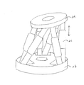
上記のパターン転写装置において、本実施形態では、モールドステージ20が任意のオイラー角で回転可能な自由度をもっている点に特徴を有する。図2は、モールドステージ20の一例を示す構成図である。
【0031】
図2に示すように、モールドステージ20は、可動ステージ2aと、固定ステージ2bと、可動ステージ2aと固定ステージ2bとを連結する6本の脚部2cを有する。図2に示すモールドステージ20は、図1とは上下を反転して図解しており、図2において可動ステージ2a上にモールド20が保持される。
【0032】
各脚部2cは、矢印で示す長手方向に伸縮可能に構成されており、かつ、固定ステージ2bに支持された支点を軸として、その方向を変化させることができるように構成されている。各脚部2cの方向が変化した場合においても、各脚部2cは他方の可動ステージ2aに対し回動可能に連結された状態にある。このように構成されていることにより、可動ステージ2aを支持する6本の脚部2cの長さと方向を変化させることにより、可動ステージ2aの自由な回転を可能にしている。
【0033】
歪み補正のアルゴリズム
次に、可動ステージ2aのオイラー回転による,基板10の歪みを補正するアルゴリズムについて説明する。ここでは、基板10として複数のチップが生産されるウエハの場合を例に説明する。
【0034】
NILによりパターンを重ね合わせる基板10の下地チップの線形歪みは、次の4つの量、X方向の倍率mX 、Y方向の倍率mY 、回転角θ、直行度ψで表される。また、倍率の1からのずれをμX =mX −1、μY =mY −1として定義する。
【0035】
モールドステージ上のXYZ座標を考えると、図3に示すように、モールドの任意の回転は、オイラー角(α、β、γ)で表すことができる(例えば、非特許文献3参照)。ここで、α、β、γは、それぞれY、Z、およびX軸まわりの回転角である。
【0036】
上記したように、図2で示したようなステージにより、モールドを任意のオイラー角で回転させることが可能である。モールドをXとY方向別々に変形させることは困難なので、モールド全体を倍率mで拡大あるいは縮小し、その後にオイラー回転を行う。回転角は、モールド上のパターンをウエハ上へ投影したものとウエハ上のチップとの重ね合わせ誤差が最小になるように決定する。
一般に、オイラー回転による座標の変換は、下記式(1)に示す行列で表される。
【0037】
【数1】

ここで、回転角は十分小さいので、角度に関する2次の項のみをとると、上記式(1)の行列は、下記式(2)のように簡単になる。
【0039】
【数2】
モールド面のウエハ面への投影は、下記式(3)のようになる。
【0041】
【数3】
一方、チップ歪みは下記式(4)に示す行列で表される(例えば、非特許文献4参照)。
【0043】
【数4】
上記式(3)と(4)とを比較すると、下記式(5)および(6)に示す関係が成立する。
【0045】
【数5】
![]()
【数6】
上記式(5)によりβは決まるが、αとγは一意的には決まらない。そこで、モールド全体の倍率も考慮すると、下記式(7)および(8)に示す関係が成立する。
【0048】
【数7】
【数8】
以上の式(5)〜式(8)に示すように、4変数に対して4つの式が連立しているので、これを解くことにより、倍率とオイラー角を一意的に決定することができる。
【0051】
歪み補正方法
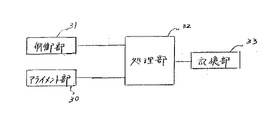
図4は、本実施形態に係るプログラムが読み込まれることにより、倍率とオイラー角を制御する歪み補正方法を実現するパターン転写装置の要部ブロック図である。
【0052】
すなわち、パターン転写装置は、アライメントマークを検出するアライメント部30およびモールドステージの動作を制御する制御部31に接続された処理部32と、本実施形態に係るプログラムが格納された記憶部33とを有する。
【0053】
アライメント部30は、図1のアライメント光学系3に相当し、基板側アライメントマーク11やモールド側アライメントマーク21を検出する。
【0054】
制御部31は、処理部32からオイラー回転率についての信号を入力し、この信号に基づいて、可動ステージをオイラー回転させるべくモールドステージの脚部2cを制御する。また、処理部32からモールドの倍率についての信号を入力し、この倍率となるように倍率調整手段5によるモールド20への加熱あるいは荷重を制御する。
【0055】
処理部32および記憶部33は、主としてパーソナルコンピュータやワークステーション等の計算機から構成される。記憶部33としては、ハードディスクやフレキシブルディスク等の磁気記憶装置、CD−ROM等の読み出し専用メモリ、光磁気ディスクなど、各種の記録媒体が適用される。
【0056】
上記式(5)〜(8)の演算ステップが手順として記述されたプログラムが記憶部33に格納されており、実行する際には処理部32の不図示のメインメモリに読み込まれて不図示のCPUで実行される。
【0057】
図5に、処理部による処理のフローチャートを示す。
処理部32は、アライメント部30からのアライメントデータに基づいて、演算によりチップ歪みを算出し(ステップST1)、このチップ歪および上記の関係式(5)〜(8)に基づいてリアルタイムに転写単位領域であるチップ毎に必要なモールドステージを回転させるためのオイラー角とモールドの倍率を決定し、制御部31に出力する(ステップST2)。
以上のようにして決定されたオイラー角およびモールドの倍率に基づいて、制御部31によりモールドステージの姿勢と、モールドの寸法が調整される。
【0058】
例えば、図6(a)に示すように、転写単位領域としてのチップが存在する場合に、理想的な格子EからX方向およびY方向に均一な倍率で広がっているようなチップCh1の歪みに対しては、当該歪みに合わせるようにしてモールドの倍率を調整することにより、重ね合わせ精度が向上する。
【0059】
但し、モールドの倍率の調整は、直交性を満たしかつ等方性の倍率をもった歪みにしか対応できないため、図6(b)に示すように非直交性となったチップCh2の歪みや、図6(c)に示すようにX,Y方向で倍率差がある場合のチップCh3の歪みに対応することはできない。
【0060】
従って、図6(b)に示す非直交性のチップCh2の歪みに対しては、下地のチップの歪みに合わせた転写パターンとなるように、モールドステージによりモールドの姿勢が制御される。すなわち、モールドパターンは、理想的な格子Eに対応したものであるが、モールドの姿勢を変えて転写することにより、転写されたパターンは非直交性となる。
【0061】
また、図6(c)に示すX,Y方向の倍率差があるチップCh3の歪みに対しても、モールドステージによりモールドの姿勢を制御することにより補正する。すなわち、モールドの姿勢を変えて転写することにより、転写されたパターンは、X方向とY方向とで独立の倍率となる。
【0062】
さらに、図6(a)〜図6(c)に示す歪みを組み合わせたようなチップ歪みに対しても、上記したようにモールドの倍率および姿勢の双方を制御することにより、転写パターンを下地パターンに追従させることができ、その結果良好な重ね合わせ精度を実現することができる。
【0063】
アライメント方法
上記のパターン転写装置によるアライメントマークの検出方法について説明する。本例では、上記した被転写体である基板10の基板側アライメントマーク11とモールド側アライメントマーク21の相対位置を、モールド20を通して同時に検出するTTR(Through The Reticle)方式として、散乱光アライメント(SLA:Scattering Light Alignment) を用いる方法を述べる。なお、下地チップの歪みが正確に測定可能なアライメント方式であれば、これ以外の方法を用いることもできる。
【0064】
図7は、SLAアライメント方式を説明するための図である。なお、図7では、モールド20は凹凸パターンは省略しており、アライメントマークに着目した部分のみ示している。また、基板10側も被転写膜12は省略して示している。
【0065】
図7に示すように、モールド20には、モールド側アライメントマーク21とアライメントマークを検出するためのマーク検出用窓22が形成されている。モールド側アライメントマーク21は、モールド20の表面に形成された溝であっても貫通孔であってもよい。
【0066】
平行な光束のアライメント光L1,L2は、モールド面(図7でX−Y平面に平行な面)に対して斜方から照射される。すなわち、アライメント光L1,L2の光軸は、図7のY−Z平面に平行である。
【0067】
マーク検出用窓22を通って基板側アライメントマーク11で反射、散乱され再度マーク検出用窓22を通ってきたアライメント光L1を検出する。また、モールド側アライメントマーク21で反射、散乱されたアライメント光L2を検出する。
【0068】
例えば、図7(b)に示すように、複数の基板側アライメントマーク11およびモールド側アライメントマーク21が形成されており、検出された基板側アライメントマーク11およびモールド側アライメントマーク21の相対位置とアライメント光L1,L2の傾き角θとの相対関係から、モールド20に対するチップ歪みの検出のためのアライメントデータが作製される。
【0069】
上記のSLAアライメント方式は、もともとPXL(Pdoximity X−ray Lithography)のために開発された方法である。PXLの場合、X線の入射方向をふさがないために、アライメント光学系は、斜めに配置されている。一方、NILと称されるパターン転写装置では、このような制約がないので、アライメント光学系を垂直に配置してもよい。これにより、マーク検出用窓22の面積を小さくすることができる。
【0070】
以上のように、アライメント方法としては、電子線やX線あるいはイオンビームを用いたリソグラフィに使用されているアライメント光学系を同様に採用することができ、アライメントシステムに制限はない。
【0071】
転写プロセス
次に、上記のパターン転写装置による転写プロセスの一例について、図8に示すフローチャートおよび図9に示す工程断面図を参照して説明する。
【0072】
まず、例えば被転写膜12としてレジストを塗布した基板10を基板ステージ1により保持し(ステップST11)、凹凸構造のモールドパターンを有するモールド20をモールドステージ2により保持する(ステップST12)。これにより、図9(a)に示すように、基板10とモールド20とを近接させる。
【0073】
次に、基板ステージ1のヒータ1aにより基板10を加熱することにより、レジストの塑性を増加させる(ステップST13)。また、アライメント光学系3により基板側アライメントマーク11およびモールド側アライメントマーク21を検出して、チップとモールド20の相対位置や、基板10の各チップの倍率や非直交性やX,Y方向の倍率差といった歪みを検出する(ステップST14)。
【0074】
次に、アライメントマーク検出工程で検出されたモールド20とチップとの相対位置に基づいて、例えば基板ステージ1の制御により、モールド12とチップとの相対位置を最適に合わせる(ステップST15)。
【0075】
次に、アライメントマーク検出工程で検出された転写単位領域であるチップの歪みに応じてモールドステージ2によりモールド20の姿勢を制御し、倍率調整手段5によりモールド20の倍率を制御する(ステップST16)。
【0076】
次に、図9(b)に示すように、基板10とモールド20とを圧着させる(ステップST17)。基板10とモールド20との圧着は、油圧式ポンプ42によって基板ステージ1の下方より押圧される。この圧着によって、軟化している熱可塑性のレジストからなる被転写膜12は変形し、モールドパターンが転写される。
【0077】
次に、図9(c)に示すように、基板10を冷却した後、モールド20を引き離すと、レジストからなる被転写膜12に凹凸構造のパターンが形成される(ステップST18)。本実施形態では、ヒーター1aによる加熱を止めて基板10を冷却し、油圧ポンプ42の圧力弁43を開けて圧力を解除し、モールド20を引き離す。なお、モールド圧着時に、モールドの背後から紫外光を照射させてレジストを硬化させることもできる。この場合、モールドは石英等の光を透過させる材料で製造する必要がある。
【0078】
その後、図9(d)に示すように、エッチングにより凹部に残留しているレジストからなる被転写膜12が除去され、通常のリソグラフィで形成されたものと同様なレジストパターンが形成される。
【0079】
以上のステップST13〜ST18の処理を繰り返し各チップに行うことにより、例えばウエハからなる基板10の全面への転写プロセスが終了する。基板2の図示しない被加工膜は、上記のレジストをエッチングマスクとしてエッチングすることにより、加工される。
【0080】
上記の転写プロセスにおいて、モールドをレジストに印加するための距離が大きくなると、モールド20の変形やレジストのパターンの歪みが大きくなることから、薄膜レジストによるプロセスを用いることが好ましい。例えば、被転写膜21として、ArFリソグラフィの多層レジストプロセスの中間層として用いられるSOG(Spin−On−Glass)を70nm塗布した上に、PMMA(Poly−Methlmethacrylate) を70nm塗布する。この場合には、ステップST13のレジスト軟化工程では、基板を175℃まで加熱し、ステップST17の圧着工程では、4.4MPaの圧力でモールドをレジストに押し付けることで、パターンが転写される。
【0081】
また、ステップST17におけるモールドの圧着の圧力は、モールドの変形が許容範囲内になるように決定する必要がある。この最適値は、インプリント・プロセスの有限要素法(FEM)シミュレーションにより決定することができる(例えば、非特許文献5参照)。モールドの圧着時間は、形成されたレジストパターン断面の走査電子顕微鏡(SEM)観察等によってすることができる。
【0082】
なお、上記では代表的な方法のみを説明したが、NILと称される転写プロセスには様々なバリエーションがあり、いずれのバリエーションに対しても本実施形態に係るパターン転写装置およびパターン転写方法は適用可能である。
【0083】
例えば、レジストなしで直接モールドをシリコン基板に接触させ、モールド背後からレーザーを照射させることで、接触部のシリコンを溶融させ、ステップST19に示すエッチング工程なしで直接パターン加工してしまう方法が提案されており、これに適用することもできる。従って、本実施形態は、図8および図9に示すフローに限定されない(例えば、非特許文献2参照。)。
【0084】
モールド製造方法
次に、モールド製造方法について説明する。例えば現在マスク製造のためにも使用されているSOI(Silicon On Insulator) 基板を材料とする例について説明する。シリコン基板は、紫外(UV)光を透過しないので、上記したUV照射によりレジストを硬化させる方法には用いることはできない。しかし、シリコンをエッチングして微細なパターンを形成する技術は、デバイス製造、あるいはEPL,PEL用ステンシルマスク製造において非常に研究・開発されているので、微細なパターンを有するモールドを製造するためには、石英基板よりもシリコン基板の方が有利であると考えられるからである。但し、本発明では特にモールドを作製するための基板に限定はない。
【0085】
例えば、図10(a)に示すように、貼り合わせ法により製造された直径200mmのSOI基板を用いる場合、SOI層203の厚さが600nm、埋め込み酸化物層202の厚さが1000nm、シリコン基板201の厚さが725μmのSOI基板を用いることができる。
【0086】
まず、図10(b)に示すように、モールド側アライメントマーク21を加工する。これは、SOI基板の裏面、すなわち、シリコン基板201にレジストを塗布し、リソグラフィにより、図7(b)で示すようなドット状のパターンを描画し、レジストをマスクとしてシリコン基板201をエッチングすることにより得られる。各ドットのサイズは、0.3μm×1.5μmで、それが縦100μmの範囲に6列並んでいる。
【0087】
次に、図10(c)に示すように、SLAを用いるためのマーク検出用窓22を形成する。但し、透明な石英基板を用いる場合は、この窓は不要である。SOI基板の裏面に厚さ10μmのレジストを塗布し、窓に相当する領域の2か所を、例えば120μm×50μmの寸法で、コンタクトアライナー等で露光および現像する。これを、ICPエッチャーで埋め込み酸化物層202まで貫通させる。シリコンとその酸化物とのエッチング選択比は1000以上あるので、エッチングは埋め込み酸化物層202で止まる。
【0088】
次に、図11(d)に示すように、例えばSOI基板をHF溶液に浸漬させることにより、マーク検出用窓22の領域に露出した埋め込み酸化物層202を除去する。これにより、マーク検出用窓22の部分は、例えば厚さが600nmのSOI層のみが残る。
【0089】
SOI層の表面にレジストを塗布し、EB描画機により被転写膜に形成すべきデバイスパターンを描画し、かつ、マーク検出用窓に相当する薄膜となった領域も描画する。レジストは、例えば、化学増幅型のポジレジストを200nmの厚さで塗布する。現像後、レジストをマスクとしてエッチングすると、デバイスパターンが加工されると同時に、マーク検出用窓に相当する部分のSOI層203も除去されて、マーク検出用窓が開口する。薄膜となったSOI層の部分が貫通すると、イオンやラジカルが侵入するので、治具でエッチャーのステージを保護しておくことが好ましい。
以上のようにして、図11(e)に示すSOI基板より作製されたモールドが完成する。
【0090】
以上説明したように、本実施形態では、モールド20を任意のオイラー角により回転させて基板10に対するモールド20の姿勢を制御することにより、基板10に配置された各チップの非直交性の歪みや、X,Y方向で倍率差があるような歪みに追従した転写パターンを形成することができ、下地のパターンとの重ね合わせ精度を向上させることができる。
【0091】
また、モールド20に対し加熱あるいは横方向からの均一な荷重をかけることにより、モールド20の寸法を調整することにより、転写パターンの倍率を調整することもでき、下地のパターンとの重ね合わせ精度を向上させることができる。
【0092】
このように重ね合わせ精度が向上することにより、他のリソグラフィとの併用が可能となり、パターン転写装置の実用化が促進される。パターン転写装置の実現により、デバイスの製造コストの低減を図ることができる。また、上記したパターン転写装置は、PELの装置技術を応用して達成することができる。
【0093】
さらに、PELのステンシルマスク製造技術を用いてモールドを製造することにより、マスクとモールドの価格を下げることができる。
【0094】
本発明は、上記の実施形態の説明に限定されない。例えば、本実施形態では、本発明の姿勢制御手段がモールドステージに備えられている例について説明したが、基板ステージに備えられていてもよい。
【0095】
また、本実施形態では、SLAを用いたダイバイダイアライメント方式によりチップ歪みをインラインで補正して転写する例について説明したが、これに限定されるものではない。
【0096】
例えば、同じロットの基板(ウエハ)から一枚抜き出して、ウエハの各チップにモールドのアライメントマークを転写して、転写マークと各チップのアライメントマークとを検出することで、予め基板のチップ毎の歪みを決定しておいてもよい。この場合には、同一ロットの基板のチップ歪みの分布は全て等しいと推測して、他の基板の転写処理に際しチップ毎にモールドの姿勢を制御してパターン転写を行う。
【0097】
あるいは、グローバルアライメント方式を採用することもできる。この場合には、基板(ウエハ)のアライメントマークをオフライン観測し、各チップの歪みを予め検出しておく。そして、同一ロットの基板のチップ歪みの分布は全て等しいと推測して、他の基板の転写処理に際しチップ毎にモールドの姿勢を制御してパターン転写を行う。
その他、本発明の要旨を逸脱しない範囲で、種々の変更が可能である。
【0098】
【発明の効果】
本発明によれば、被転写体の歪みに合わせて転写パターンを補正することができ、被転写体との重ね合わせ精度を向上させることができる。
【図面の簡単な説明】
【図1】本実施形態に係るパターン転写装置の一例を示す概略構成図である。
【図2】モールドステージの一例を示す構成図である。
【図3】モールドステージによる歪み補正のアルゴリズムを説明するための図である。
【図4】本実施形態に係るパターン転写装置のうち、倍率とオイラー角を制御する要部構成を示すブロック図である。
【図5】本実施形態に係るパターン転写方法による、歪み補正のためのフローチャートである。
【図6】本実施形態に係るパターン転写装置による歪み補正を説明するための図である。
【図7】本実施形態に係るパターン転写装置によるアライメント方法を説明するための図である。
【図8】本実施形態に係るパターン転写方法のフローチャートである。
【図9】本実施形態に係るパターン転写方法を説明するための工程断面図である。
【図10】本実施形態に係るパターン転写方法に使用されるモールドの製造における工程断面図である。
【図11】本実施形態に係るパターン転写方法に使用されるモールドの製造における工程断面図である。
【符号の説明】
1…基板ステージ、1a…ヒータ、2…モールドステージ、2a…可動ステージ、2b…固定ステージ、2c…脚部、3…アライメント光学系、4…加圧機構、5…倍率調整手段、10…基板、11…基板側アライメントマーク、12…被転写膜、20…モールド、21…モールド側アライメントマーク、22…マーク検出用窓、30…アライメント部、31…制御部、32…処理部、33…記憶部、41…加圧板、42…油圧ポンプ、43…圧力弁、51…光源、52…レンズ、53…荷重印加手段、L1,L2…アライメント光、201…シリコン基板、202…埋め込み酸化物層、203…SOI層。[0001]
TECHNICAL FIELD OF THE INVENTION
The present invention relates to a pattern transfer device, a pattern transfer method, and a program used for pattern formation in semiconductor manufacturing, for example.
[0002]
[Prior art]
With the miniaturization of devices, technical limitations of photolithography currently used in mass production are expected. Efforts to overcome this fall into three categories.
[0003]
First, so-called super-resolution techniques such as proximity effect correction (OPC: Optical Proximity Correction) and phase shift masks without changing the wavelength used (currently the mainstream is 248 nm of KrF laser or 193 nm of ArF laser). (RET: Resolution Enhancement Technique) to extend the life of the current scheme as much as possible.
[0004]
Second, the wavelength of the light to be used is shortened, and a technique using a fluorine laser (wavelength: 157 nm) and further using extreme ultraviolet light (wavelength: 13 nm) has been developed.
[0005]
Third, the use of new radiation sources, such as X-rays, electron beams (EB) or ion beams. This includes proximity X-ray lithography (PXL), electron-beam projection lithography (EPL), ion-beam transfer lithography (IPL: electron-beam and electron-line lithography), and electron beam-transfer lithography (EPL). There is lithography (PEL: Proximity Electron Lithography).
[0006]
However, these lithography techniques are expected to be technically difficult and the equipment and mask costs will be very high. Only PEL may be able to realize a device that is less expensive than current photolithography devices due to its simple device configuration.
[0007]
Nanoimprint lithography (NIL: Nano Imprint Lithography) has been proposed as high-resolution and inexpensive lithography (see Non-Patent Document 1). The principle of this method is completely different from the conventional lithography principle of irradiating a mask with light or charged particles and forming an image transmitted through the optical system on a wafer. To put it simply, a "stamp" having a device pattern as surface irregularities is prepared, and the pattern is transferred by imprinting the stamp onto a resist-coated wafer. It is known that this method is simple and can be manufactured extremely inexpensively, and it is also possible to transfer an extremely fine pattern of 10 nm or less by precisely processing a mold corresponding to a stamp.
[0008]
In NIL, a resist is applied to a substrate, and the plasticity of the resist is increased by heating the substrate, and a mold is pressed. Thereafter, when the substrate is cooled and the mold is separated, the pattern is transferred to a resist similar to that formed by ordinary lithography. In addition, a method of directly processing a pattern without using a resist and etching has been proposed (for example, see Non-Patent Document 2).
[0009]
[Patent Document 1]
U.S. Pat. No. 5,831,272
[Patent Document 2]
U.S. Pat. No. 4,334,156
[Non-patent document 1]
S. Y. Chou et al. , Science 272, 85 (1996).
[Non-patent document 2]
S. Y. Chou et al. , Nature 417, 835 (2002).
[Non-Patent Document 3]
A. Messiah, Quantum Mechanics, p. 1068 (1966, North-Holland Publishing, Amsterdam).
[Non-patent document 4]
L. E. FIG. Ocolla et al. , J. et al. Vac. Sci. Technol. B19, 2659 (2001)
[Non-Patent Document 5]
C. J. Martin et al. , J. et al. Vac. Sci. Technol. B20, 2891 (2002)
[0010]
[Problems to be solved by the invention]
In ordinary lithography, a chip distortion generated in a previous process can be detected by some kind of alignment system and corrected by a transfer optical system. For example, in the PEL, by modulating the incident direction of the EB using a sub-change lens of the electron optical system, it is possible to improve the overlay accuracy with the base (see
[0011]
On the other hand, in nanoimprint lithography, a pattern is transferred by mechanically pressing a mold having high rigidity. Therefore, even if the distortion of the base is accurately detected, it cannot be corrected. This makes it difficult to use nanoimprint lithography in combination with other lithography, which hinders the practical use of nanoimprint lithography.
[0012]
The present invention has been made in view of the above circumstances, and an object of the present invention is to correct a transfer pattern in accordance with distortion of a transferred object, and to improve overlay accuracy with the transferred object. An object of the present invention is to provide a pattern transfer device, a pattern transfer method, and a program.
[0013]
[Means for Solving the Problems]
In order to achieve the above object, a pattern transfer device of the present invention is a pattern transfer device that presses a pattern formed on a mold against a transfer target to transfer the pattern, and controls a posture of the mold with respect to the transfer target. And an attitude control means for displacing the transfer pattern obtained when the pattern of the mold is pressed, and a pressing means for pressing the mold with the attitude against the object to be transferred.
[0014]
In the above-described pattern transfer apparatus of the present invention, the attitude of the mold with respect to the object to be transferred is controlled by the attitude control means, and the transfer pattern obtained when the pattern of the mold is pressed can be displaced. As the posture of the mold, for example, by rotating the mold by an arbitrary Euler angle, all postures can be obtained.
By pressing the mold against the object to be transferred in such a posture, a transfer pattern substantially equal to that obtained by projecting the pattern of the mold onto the object to be transferred can be obtained. Therefore, even if the dimensions of the pattern itself formed on the mold are fixed, a transfer pattern that follows the distortion of the pattern on the base of the object to be transferred can be obtained.
[0015]
In order to achieve the above object, a pattern transfer method according to the present invention includes a step of pressing a pattern formed on a mold against a transfer target, moving the transfer target or the mold, and pressing against the transfer target. It is a pattern transfer method of repeatedly performing, the step of detecting the distortion of the transferred object, and the step of controlling the attitude of the mold with respect to the transferred object, so that a transfer pattern according to the detected distortion Pressing the mold with the posture against the transfer object.
[0016]
In the above-described pattern transfer method of the present invention, the mold is pressed against the object to be transferred by controlling the attitude of the mold relative to the object to be transferred so as to obtain a transfer pattern corresponding to the detected distortion. As the posture of the mold, for example, by rotating the mold by an arbitrary Euler angle, all postures can be obtained.
By pressing the mold against the object to be transferred in such a posture, a transfer pattern substantially equal to that obtained by projecting the pattern of the mold onto the object to be transferred can be obtained. Therefore, even if the dimensions of the pattern itself formed on the mold are fixed, a transfer pattern that follows the distortion of the pattern on the base of the object to be transferred can be obtained.
[0017]
In order to achieve the above object, a program according to the present invention is a program for causing a computer to execute a process for determining a transfer condition of a mold to a transfer target, wherein a position of the detected alignment mark of the transfer target is detected. A procedure for determining the distortion of the object to be transferred based on the above, and when the mold is rotated at an arbitrary Euler angle, the pattern formed on the mold is converted into a transfer pattern corresponding to the distortion. Calculating a required Euler angle.
[0018]
According to the above-described program of the present invention, a required Euler angle is calculated based on the position of the alignment mark on the transfer target so that a transfer pattern corresponding to the distortion of the transfer target is obtained.
By pressing the mold against the object to be transferred in a posture obtained by rotating the mold at the Euler angle obtained above, a transfer pattern that follows the distortion of the pattern on the base of the object to be transferred is obtained.
[0019]
BEST MODE FOR CARRYING OUT THE INVENTION
Hereinafter, embodiments of the present invention will be described with reference to the drawings.
[0020]
Background of the Invention
It is useful to be able to convert a currently developed lithography system to nanoimprint lithography (hereinafter, referred to as NIL) as it is. In the present embodiment, an example in which the LEEPL (Low-energy Electron-Beam Proximity-Projection Lithography) system is used will be described. LEEPL is proximity exposure with a gap of 30 μm or less, and the gap control technology, mask leveling technology, and the like used therefor can be applied to NIL. With minor modifications such as removing the electron optical system from the LEEPL device and attaching a pressure mechanism for imprinting to the wafer stage, it is possible to smoothly shift from PEL to nanoimprinting without a large technical barrier. As described below, a scattered light alignment (SLA: Scattering Light Alignment) currently used in the LEEPL apparatus can be used if the mask structure is devised.
[0021]
Further, for manufacturing a mold using an SOI substrate described later, the stencil mask manufacturing infrastructure for LEEPL can be used as it is. For example, since both the PEL mask and the NIL mold are equal-size masks, it is possible to effectively use EB drawing technology and the like necessary for manufacturing the mask.
[0022]
In the present embodiment, as described above, an example of realizing an NIL having high overlay accuracy by applying the conventional 1: 1 proximity exposure technology will be described. There is no particular limitation as long as it performs the same function as.
[0023]
Pattern transfer device
FIG. 1 is a schematic configuration diagram of a pattern transfer device according to the present embodiment. The pattern transfer device shown in FIG. 1 is used for so-called NIL.
The pattern transfer apparatus shown in FIG. 1 roughly includes a
[0024]
The
[0025]
The
[0026]
The alignment optical system 3 is used to detect the distortion of the substrate 10 (more specifically, the distortion of each chip), the position of the
[0027]
The pressing mechanism 4 is provided for pressing the
[0028]
The magnification adjusting means 5 enlarges or reduces the entire pattern of the
[0029]
Alternatively, the magnification adjusting means 5 has load applying means 53 positioned on both sides of the
[0030]
In the above-described pattern transfer apparatus, the present embodiment is characterized in that the
[0031]
As shown in FIG. 2, the
[0032]
Each leg 2c is configured to be extendable and contractible in the longitudinal direction indicated by an arrow, and is configured to be able to change its direction around a fulcrum supported by the fixed stage 2b. Even when the direction of each leg 2c changes, each leg 2c is in a state of being rotatably connected to the other movable stage 2a. With such a configuration, the length and direction of the six legs 2c supporting the movable stage 2a are changed, thereby enabling free rotation of the movable stage 2a.
[0033]
Algorithm for distortion correction
Next, an algorithm for correcting the distortion of the
[0034]
The linear distortion of the underlying chip of the
[0035]
Considering the XYZ coordinates on the mold stage, as shown in FIG. 3, an arbitrary rotation of the mold can be represented by Euler angles (α, β, γ) (for example, see Non-Patent Document 3). Here, α, β, and γ are rotation angles about the Y, Z, and X axes, respectively.
[0036]
As described above, it is possible to rotate the mold at an arbitrary Euler angle by the stage as shown in FIG. Since it is difficult to deform the mold separately in the X and Y directions, the entire mold is enlarged or reduced at a magnification m, and then Euler rotation is performed. The rotation angle is determined so that the overlay error between the projection of the pattern on the mold onto the wafer and the chips on the wafer is minimized.
In general, the transformation of coordinates by Euler rotation is represented by a matrix represented by the following equation (1).
[0037]
(Equation 1)
Here, since the rotation angle is sufficiently small, if only the quadratic term relating to the angle is taken, the matrix of the above equation (1) is simplified as in the following equation (2).
[0039]
(Equation 2)
The projection of the mold surface onto the wafer surface is represented by the following equation (3).
[0041]
(Equation 3)
On the other hand, chip distortion is represented by a matrix represented by the following equation (4) (for example, see Non-Patent Document 4).
[0043]
(Equation 4)
When the above equations (3) and (4) are compared, the following equations (5) and (6) are established.
[0045]
(Equation 5)
![]()
(Equation 6)
Although β is determined by the above equation (5), α and γ are not uniquely determined. Therefore, when the magnification of the entire mold is also taken into account, the relations shown in the following equations (7) and (8) hold.
[0048]
(Equation 7)
(Equation 8)
As shown in the above formulas (5) to (8), since four formulas are simultaneously provided for four variables, by solving these, the magnification and Euler angle can be uniquely determined. .
[0051]
Distortion correction method
FIG. 4 is a main block diagram of a pattern transfer apparatus that realizes a distortion correction method for controlling a magnification and an Euler angle by reading a program according to the present embodiment.
[0052]
That is, the pattern transfer apparatus includes a
[0053]
The
[0054]
The control unit 31 receives a signal about the Euler rotation rate from the
[0055]
The
[0056]
A program in which the calculation steps of the above equations (5) to (8) are described as a procedure is stored in the
[0057]
FIG. 5 shows a flowchart of the processing by the processing unit.
The
Based on the Euler angle and the magnification of the mold determined as described above, the controller 31 adjusts the attitude of the mold stage and the dimensions of the mold.
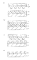
[0058]
For example, as shown in FIG. 6A, when there is a chip as a transfer unit area, the distortion of the chip Ch1 that spreads from the ideal lattice E at a uniform magnification in the X direction and the Y direction is reduced. On the other hand, by adjusting the magnification of the mold to match the distortion, the overlay accuracy is improved.
[0059]
However, since the adjustment of the magnification of the mold can cope only with the distortion that satisfies the orthogonality and has the isotropic magnification, the distortion of the chip Ch2 that has become non-orthogonal as shown in FIG. As shown in FIG. 6C, it is impossible to cope with the distortion of the chip Ch3 when there is a magnification difference in the X and Y directions.
[0060]
Accordingly, with respect to the distortion of the non-orthogonal chip Ch2 shown in FIG. 6B, the mold posture is controlled by the mold stage so that the transfer pattern matches the distortion of the underlying chip. That is, although the mold pattern corresponds to the ideal lattice E, the transferred pattern becomes non-orthogonal by transferring while changing the posture of the mold.
[0061]
The distortion of the chip Ch3 having the magnification difference in the X and Y directions shown in FIG. 6C is also corrected by controlling the attitude of the mold by the mold stage. That is, by transferring while changing the posture of the mold, the transferred pattern has independent magnifications in the X direction and the Y direction.
[0062]
Further, even with respect to chip distortion such as a combination of the distortions shown in FIGS. 6 (a) to 6 (c), by controlling both the magnification and the posture of the mold as described above, the transfer pattern is changed to the base pattern. , And as a result, good overlay accuracy can be realized.
[0063]
Alignment method
A method of detecting an alignment mark by the above-described pattern transfer device will be described. In this example, a scattered light alignment (SLA) method is used as a TTR (Through The Reticle) method for simultaneously detecting the relative positions of the substrate-
[0064]
FIG. 7 is a diagram for explaining the SLA alignment method. Note that, in FIG. 7, the
[0065]
As shown in FIG. 7, the
[0066]
The parallel alignment light beams L1 and L2 are emitted obliquely to the mold surface (the surface parallel to the XY plane in FIG. 7). That is, the optical axes of the alignment lights L1 and L2 are parallel to the YZ plane in FIG.
[0067]
The alignment light L1 reflected and scattered by the substrate
[0068]
For example, as shown in FIG. 7B, a plurality of substrate-side alignment marks 11 and mold-side alignment marks 21 are formed, and the detected relative positions of the substrate-side alignment marks 11 and the mold-side alignment marks 21 are aligned. From the relative relationship between the light L1 and L2 and the inclination angle θ, alignment data for detecting chip distortion with respect to the
[0069]
The above-mentioned SLA alignment method is a method originally developed for PXL (Pdoxicity X-ray Lithography). In the case of PXL, the alignment optical system is arranged obliquely because the incident direction of X-rays is not blocked. On the other hand, in a pattern transfer apparatus called NIL, there is no such restriction, and the alignment optical system may be arranged vertically. Thus, the area of the
[0070]
As described above, as the alignment method, an alignment optical system used for lithography using an electron beam, an X-ray, or an ion beam can be similarly employed, and the alignment system is not limited.
[0071]
Transfer process
Next, an example of a transfer process by the above-described pattern transfer device will be described with reference to a flowchart shown in FIG. 8 and a process cross-sectional view shown in FIG.
[0072]
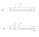
First, for example, the
[0073]
Next, the plasticity of the resist is increased by heating the
[0074]
Next, based on the relative position between the
[0075]
Next, the attitude of the
[0076]
Next, as shown in FIG. 9B, the
[0077]
Next, as shown in FIG. 9C, when the
[0078]
Thereafter, as shown in FIG. 9D, the
[0079]
By repeating the processing of steps ST13 to ST18 on each chip, the transfer process onto the entire surface of the
[0080]
In the above transfer process, if the distance for applying the mold to the resist increases, the deformation of the
[0081]
In addition, the pressure for pressing the mold in step ST17 needs to be determined so that the deformation of the mold falls within an allowable range. This optimum value can be determined by a finite element method (FEM) simulation of the imprint process (for example, see Non-Patent Document 5). The compression bonding time of the mold can be determined by observing a cross section of the formed resist pattern with a scanning electron microscope (SEM) or the like.
[0082]
Although only the representative method has been described above, there are various variations in the transfer process called NIL, and the pattern transfer apparatus and the pattern transfer method according to the present embodiment are applicable to any of the variations. It is possible.
[0083]
For example, a method has been proposed in which a mold is brought into direct contact with a silicon substrate without a resist, and a laser is irradiated from behind the mold to melt the silicon at the contact portion and directly pattern work without an etching step shown in step ST19. And can be applied to this. Therefore, the present embodiment is not limited to the flows shown in FIGS. 8 and 9 (for example, see Non-Patent Document 2).
[0084]
Mold manufacturing method
Next, a mold manufacturing method will be described. For example, an example will be described in which an SOI (Silicon On Insulator) substrate which is currently used for manufacturing a mask is used as a material. Since the silicon substrate does not transmit ultraviolet (UV) light, it cannot be used for the above method of curing the resist by UV irradiation. However, the technology of forming a fine pattern by etching silicon has been very researched and developed in device manufacturing or stencil mask manufacturing for EPL and PEL. This is because a silicon substrate is considered to be more advantageous than a quartz substrate. However, in the present invention, there is no particular limitation on a substrate for producing a mold.
[0085]
For example, as shown in FIG. 10A, when an SOI substrate having a diameter of 200 mm manufactured by a bonding method is used, the thickness of the
[0086]
First, as shown in FIG. 10B, the mold-
[0087]
Next, as shown in FIG. 10C, a
[0088]
Next, as shown in FIG. 11D, for example, the buried
[0089]
A resist is applied to the surface of the SOI layer, a device pattern to be formed on the transfer target film is drawn by an EB drawing machine, and a thin film region corresponding to a mark detection window is also drawn. As the resist, for example, a chemically amplified positive resist is applied with a thickness of 200 nm. After development, when the resist is used as a mask, the device pattern is processed, and at the same time, the
As described above, a mold manufactured from the SOI substrate shown in FIG. 11E is completed.
[0090]
As described above, in the present embodiment, by controlling the attitude of the
[0091]
In addition, by applying a uniform load from the lateral direction or heating the
[0092]
By improving the overlay accuracy as described above, it is possible to use the pattern transfer apparatus together with other lithography, and the practical use of the pattern transfer apparatus is promoted. By realizing the pattern transfer device, the manufacturing cost of the device can be reduced. The above-described pattern transfer device can be achieved by applying PEL device technology.
[0093]
Further, by manufacturing the mold using the stencil mask manufacturing technology of PEL, the cost of the mask and the mold can be reduced.
[0094]
The present invention is not limited to the above embodiments. For example, in the present embodiment, the example in which the attitude control means of the present invention is provided on the mold stage has been described, but it may be provided on the substrate stage.
[0095]
Further, in the present embodiment, an example in which the chip distortion is corrected in-line by the die-by-die alignment method using the SLA and the transfer is performed is described, but the present invention is not limited to this.
[0096]
For example, one chip is extracted from a substrate (wafer) of the same lot, the alignment mark of the mold is transferred to each chip of the wafer, and the transfer mark and the alignment mark of each chip are detected. The distortion may be determined. In this case, it is assumed that the distributions of the chip distortions of the substrates of the same lot are all the same, and the pattern transfer is performed by controlling the attitude of the mold for each chip in the transfer processing of another substrate.
[0097]
Alternatively, a global alignment method can be adopted. In this case, the alignment mark of the substrate (wafer) is observed off-line, and the distortion of each chip is detected in advance. Then, it is presumed that the distributions of the chip distortions of the substrates of the same lot are all equal, and the pattern transfer is performed by controlling the attitude of the mold for each chip in the transfer processing of another substrate.
In addition, various changes can be made without departing from the spirit of the present invention.
[0098]
【The invention's effect】
ADVANTAGE OF THE INVENTION According to this invention, a transfer pattern can be corrected according to the distortion of a to-be-transferred body, and the overlay precision with a to-be-transferred body can be improved.
[Brief description of the drawings]
FIG. 1 is a schematic configuration diagram illustrating an example of a pattern transfer device according to an embodiment.
FIG. 2 is a configuration diagram illustrating an example of a mold stage.
FIG. 3 is a diagram for explaining an algorithm of distortion correction by a mold stage.
FIG. 4 is a block diagram illustrating a main configuration of a pattern transfer apparatus according to the present embodiment that controls a magnification and an Euler angle.
FIG. 5 is a flowchart for distortion correction by the pattern transfer method according to the embodiment.
FIG. 6 is a diagram for explaining distortion correction by the pattern transfer device according to the embodiment.
FIG. 7 is a diagram for explaining an alignment method by the pattern transfer device according to the embodiment.
FIG. 8 is a flowchart of a pattern transfer method according to the embodiment.
FIG. 9 is a process sectional view for explaining the pattern transfer method according to the embodiment.
FIG. 10 is a process sectional view in the manufacture of a mold used in the pattern transfer method according to the embodiment.
FIG. 11 is a process sectional view in the manufacture of a mold used in the pattern transfer method according to the embodiment.
[Explanation of symbols]
DESCRIPTION OF
Claims (11)
被転写体に対するモールドの姿勢を制御して、前記モールドのパターンを押圧した際に得られる前記転写パターンを変位させる姿勢制御手段と、
前記被転写体に対し前記モールドを前記姿勢をもって押圧する押圧手段と
を有するパターン転写装置。A pattern transfer device that presses a pattern formed on a mold against a transfer target to transfer the pattern,
Attitude control means for controlling the attitude of the mold with respect to the transferred object, and displacing the transfer pattern obtained when the pattern of the mold is pressed;
Pressing means for pressing the mold against the transfer object in the posture.
請求項1記載のパターン転写装置。2. The pattern transfer apparatus according to claim 1, further comprising a dimension adjusting unit that adjusts a dimension of the mold to correct a magnification of the mold.
請求項1記載のパターン転写装置。2. The pattern transfer apparatus according to claim 1, wherein the attitude control means controls the attitude of the mold with respect to the transfer target by rotating the mold at an arbitrary Euler angle.
請求項1記載のパターン転写装置。2. The pattern transfer apparatus according to claim 1, wherein the posture control unit controls the posture of the mold with respect to the transfer target by rotating the transfer target by an arbitrary Euler angle. 3.
前記被転写体の歪みを検出する工程と、
検出された前記歪みに合わせた転写パターンとなるように、前記被転写体に対するモールドの姿勢を制御する工程と、
前記被転写体に対し前記姿勢をもって前記モールドを押圧する工程と
を有するパターン転写方法。A pattern transfer method in which a pattern formed on a mold is pressed against an object to be transferred, and the step of pressing the object to be transferred by moving the object or the mold is repeated.
Detecting the distortion of the transfer object,
Controlling the orientation of the mold with respect to the transferred object, so as to be a transfer pattern in accordance with the detected distortion,
Pressing the mold with the posture against the transfer object.
請求項5記載のパターン転写方法。6. The pattern transfer method according to claim 5, further comprising a step of controlling a dimension of the mold and correcting a magnification of the mold after the step of detecting the distortion of the transfer target body and before the step of pressing the mold. .
請求項6記載のパターン転写方法。7. The pattern transfer method according to claim 6, wherein in the step of correcting the magnification of the mold, the magnification of the mold is corrected by controlling the temperature of the mold.
請求項6記載のパターン転写方法。7. The pattern transfer method according to claim 6, wherein in the step of correcting the magnification of the mold, the magnification of the mold is corrected by a load on the mold.
請求項5記載のパターン転写方法。In the step of detecting the distortion of the transfer object, the alignment mark of the transfer unit area of the transfer object and the alignment mark of the mold are observed for each transfer, and the transfer unit area for the mold is determined based on the position of the alignment mark. The pattern transfer method according to claim 5, wherein distortion of the pattern is detected.
検出された前記被転写体のアライメントマークの位置に基づいて、前記被転写体の歪みを決定する手順と、
前記モールドを任意のオイラー角で回転させた場合に、モールドに形成されたパターンが前記歪みに合わせた転写パターンに変換されるために必要なオイラー角を算出する手順と、を実行させる
プログラム。A program that causes a computer to execute a process for determining a transfer condition of a mold to a transfer target,
A procedure for determining the distortion of the transfer object based on the detected position of the alignment mark of the transfer object,
And calculating a Euler angle required to convert a pattern formed on the mold into a transfer pattern matched to the distortion when the mold is rotated at an arbitrary Euler angle.
請求項10記載のプログラム。In the procedure for calculating the transfer conditions, when the dimensions of the mold are changed at an arbitrary magnification and rotated at an arbitrary Euler angle, the pattern formed on the mold is converted into a transfer pattern matched to the distortion. The program according to claim 10, wherein a magnification and an Euler angle required for the calculation are calculated.
Priority Applications (1)
| Application Number | Priority Date | Filing Date | Title |
|---|---|---|---|
| JP2003130833A JP2004335808A (en) | 2003-05-08 | 2003-05-08 | Pattern transfer device, pattern transfer method and program |
Applications Claiming Priority (1)
| Application Number | Priority Date | Filing Date | Title |
|---|---|---|---|
| JP2003130833A JP2004335808A (en) | 2003-05-08 | 2003-05-08 | Pattern transfer device, pattern transfer method and program |
Publications (1)
| Publication Number | Publication Date |
|---|---|
| JP2004335808A true JP2004335808A (en) | 2004-11-25 |
Family
ID=33506217
Family Applications (1)
| Application Number | Title | Priority Date | Filing Date |
|---|---|---|---|
| JP2003130833A Pending JP2004335808A (en) | 2003-05-08 | 2003-05-08 | Pattern transfer device, pattern transfer method and program |
Country Status (1)
| Country | Link |
|---|---|
| JP (1) | JP2004335808A (en) |
Cited By (32)
| Publication number | Priority date | Publication date | Assignee | Title |
|---|---|---|---|---|
| WO2006082867A1 (en) * | 2005-02-02 | 2006-08-10 | Scivax Corporation | Hybrid contacting/detaching system |
| JP2007088374A (en) * | 2005-09-26 | 2007-04-05 | Dainippon Screen Mfg Co Ltd | Manufacturing method of semiconductor device |
| JP2007165400A (en) * | 2005-12-09 | 2007-06-28 | Canon Inc | Processing method |
| JP2007200953A (en) * | 2006-01-24 | 2007-08-09 | Hitachi Ltd | Patterning method and patterning apparatus |
| JP2007242893A (en) * | 2006-03-08 | 2007-09-20 | Toshiba Corp | Pattern transfer method and apparatus thereof |
| JP2007305647A (en) * | 2006-05-09 | 2007-11-22 | Toppan Printing Co Ltd | Nano-imprint system and nano-imprint method |
| JP2008522412A (en) * | 2004-11-30 | 2008-06-26 | モレキュラー・インプリンツ・インコーポレーテッド | Interference analysis to produce nanoscale devices |
| JP2008221821A (en) * | 2006-04-18 | 2008-09-25 | Canon Inc | Pattern transfer device, imprint device, pattern transfer method, and alignment method |
| US7547205B2 (en) | 2005-04-27 | 2009-06-16 | Industrial Technology Research Institute | Microimprint/nanoimprint uniform pressing apparatus |
| JP2009545163A (en) * | 2006-07-24 | 2009-12-17 | ヒューレット−パッカード デベロップメント カンパニー エル.ピー. | Alignment for contact lithography |
| WO2009153925A1 (en) * | 2008-06-17 | 2009-12-23 | 株式会社ニコン | Nano-imprint method and apparatus |
| JP2010080863A (en) * | 2008-09-29 | 2010-04-08 | Nikon Corp | Transfer apparatus and device manufacturing method |
| JP2010080861A (en) * | 2008-09-29 | 2010-04-08 | Nikon Corp | Transfer apparatus and device manufacturing method |
| US7794222B2 (en) | 2005-06-08 | 2010-09-14 | Canon Kabushiki Kaisha | Mold, pattern forming method, and pattern forming apparatus |
| JP2011029235A (en) * | 2009-07-21 | 2011-02-10 | Toshiba Corp | Imprint device and imprint method |
| US7927089B2 (en) | 2005-06-08 | 2011-04-19 | Canon Kabushiki Kaisha | Mold, apparatus including mold, pattern transfer apparatus, and pattern forming method |
| JP2012505544A (en) * | 2008-10-10 | 2012-03-01 | モレキュラー・インプリンツ・インコーポレーテッド | Energy source for curing in imprint lithography systems |
| JP2012076307A (en) * | 2010-09-30 | 2012-04-19 | Toppan Printing Co Ltd | Pattern printing method |
| WO2013047851A1 (en) * | 2011-09-29 | 2013-04-04 | Fujifilm Corporation | Nanoimprinting method, nanoimprinting apparatus for executing the nanoimprinting method, and method for producing patterned substrates |
| WO2013111606A1 (en) * | 2012-01-27 | 2013-08-01 | Canon Kabushiki Kaisha | Imprint apparatus and article manufacturing method using same |
| JP2013165278A (en) * | 2013-03-25 | 2013-08-22 | Canon Inc | Processing device |
| US20130271945A1 (en) | 2004-02-06 | 2013-10-17 | Nikon Corporation | Polarization-modulating element, illumination optical apparatus, exposure apparatus, and exposure method |
| KR101348184B1 (en) | 2007-01-19 | 2014-01-07 | 삼성디스플레이 주식회사 | Impriting apparatus and imprint method |
| JP2014241396A (en) * | 2013-05-14 | 2014-12-25 | キヤノン株式会社 | Imprint device, imprint method, and manufacturing method for article |
| US9341954B2 (en) | 2007-10-24 | 2016-05-17 | Nikon Corporation | Optical unit, illumination optical apparatus, exposure apparatus, and device manufacturing method |
| US9423698B2 (en) | 2003-10-28 | 2016-08-23 | Nikon Corporation | Illumination optical apparatus and projection exposure apparatus |
| JP2017050428A (en) * | 2015-09-02 | 2017-03-09 | キヤノン株式会社 | Imprint device, imprint method and production method for article |
| US9678437B2 (en) | 2003-04-09 | 2017-06-13 | Nikon Corporation | Illumination optical apparatus having distribution changing member to change light amount and polarization member to set polarization in circumference direction |
| US9678332B2 (en) | 2007-11-06 | 2017-06-13 | Nikon Corporation | Illumination apparatus, illumination method, exposure apparatus, and device manufacturing method |
| US9885872B2 (en) | 2003-11-20 | 2018-02-06 | Nikon Corporation | Illumination optical apparatus, exposure apparatus, and exposure method with optical integrator and polarization member that changes polarization state of light |
| US9891539B2 (en) | 2005-05-12 | 2018-02-13 | Nikon Corporation | Projection optical system, exposure apparatus, and exposure method |
| US10101666B2 (en) | 2007-10-12 | 2018-10-16 | Nikon Corporation | Illumination optical apparatus, exposure apparatus, and device manufacturing method |
-
2003
- 2003-05-08 JP JP2003130833A patent/JP2004335808A/en active Pending
Cited By (49)
| Publication number | Priority date | Publication date | Assignee | Title |
|---|---|---|---|---|
| US9885959B2 (en) | 2003-04-09 | 2018-02-06 | Nikon Corporation | Illumination optical apparatus having deflecting member, lens, polarization member to set polarization in circumference direction, and optical integrator |
| US9678437B2 (en) | 2003-04-09 | 2017-06-13 | Nikon Corporation | Illumination optical apparatus having distribution changing member to change light amount and polarization member to set polarization in circumference direction |
| US9760014B2 (en) | 2003-10-28 | 2017-09-12 | Nikon Corporation | Illumination optical apparatus and projection exposure apparatus |
| US9423698B2 (en) | 2003-10-28 | 2016-08-23 | Nikon Corporation | Illumination optical apparatus and projection exposure apparatus |
| US10281632B2 (en) | 2003-11-20 | 2019-05-07 | Nikon Corporation | Illumination optical apparatus, exposure apparatus, and exposure method with optical member with optical rotatory power to rotate linear polarization direction |
| US9885872B2 (en) | 2003-11-20 | 2018-02-06 | Nikon Corporation | Illumination optical apparatus, exposure apparatus, and exposure method with optical integrator and polarization member that changes polarization state of light |
| US20130271945A1 (en) | 2004-02-06 | 2013-10-17 | Nikon Corporation | Polarization-modulating element, illumination optical apparatus, exposure apparatus, and exposure method |
| US10007194B2 (en) | 2004-02-06 | 2018-06-26 | Nikon Corporation | Polarization-modulating element, illumination optical apparatus, exposure apparatus, and exposure method |
| US10234770B2 (en) | 2004-02-06 | 2019-03-19 | Nikon Corporation | Polarization-modulating element, illumination optical apparatus, exposure apparatus, and exposure method |
| US10241417B2 (en) | 2004-02-06 | 2019-03-26 | Nikon Corporation | Polarization-modulating element, illumination optical apparatus, exposure apparatus, and exposure method |
| JP2008522412A (en) * | 2004-11-30 | 2008-06-26 | モレキュラー・インプリンツ・インコーポレーテッド | Interference analysis to produce nanoscale devices |
| WO2006082867A1 (en) * | 2005-02-02 | 2006-08-10 | Scivax Corporation | Hybrid contacting/detaching system |
| US7547205B2 (en) | 2005-04-27 | 2009-06-16 | Industrial Technology Research Institute | Microimprint/nanoimprint uniform pressing apparatus |
| US9891539B2 (en) | 2005-05-12 | 2018-02-13 | Nikon Corporation | Projection optical system, exposure apparatus, and exposure method |
| US7927089B2 (en) | 2005-06-08 | 2011-04-19 | Canon Kabushiki Kaisha | Mold, apparatus including mold, pattern transfer apparatus, and pattern forming method |
| US9046793B2 (en) | 2005-06-08 | 2015-06-02 | Canon Kabushiki Kaisha | Light transmissive mold and apparatus for imprinting a pattern onto a material applied on a semiconductor workpiece and related methods |
| US7794222B2 (en) | 2005-06-08 | 2010-09-14 | Canon Kabushiki Kaisha | Mold, pattern forming method, and pattern forming apparatus |
| US8770958B2 (en) | 2005-06-08 | 2014-07-08 | Canon Kabushiki Kaisha | Pattern forming method and pattern forming apparatus in which a substrate and a mold are aligned in an in-plane direction |
| JP2007088374A (en) * | 2005-09-26 | 2007-04-05 | Dainippon Screen Mfg Co Ltd | Manufacturing method of semiconductor device |
| JP2007165400A (en) * | 2005-12-09 | 2007-06-28 | Canon Inc | Processing method |
| JP4736821B2 (en) * | 2006-01-24 | 2011-07-27 | 株式会社日立製作所 | Pattern forming method and pattern forming apparatus |
| JP2007200953A (en) * | 2006-01-24 | 2007-08-09 | Hitachi Ltd | Patterning method and patterning apparatus |
| JP2007242893A (en) * | 2006-03-08 | 2007-09-20 | Toshiba Corp | Pattern transfer method and apparatus thereof |
| JP2008221821A (en) * | 2006-04-18 | 2008-09-25 | Canon Inc | Pattern transfer device, imprint device, pattern transfer method, and alignment method |
| JP2007305647A (en) * | 2006-05-09 | 2007-11-22 | Toppan Printing Co Ltd | Nano-imprint system and nano-imprint method |
| JP2009545163A (en) * | 2006-07-24 | 2009-12-17 | ヒューレット−パッカード デベロップメント カンパニー エル.ピー. | Alignment for contact lithography |
| KR101348184B1 (en) | 2007-01-19 | 2014-01-07 | 삼성디스플레이 주식회사 | Impriting apparatus and imprint method |
| US10101666B2 (en) | 2007-10-12 | 2018-10-16 | Nikon Corporation | Illumination optical apparatus, exposure apparatus, and device manufacturing method |
| US9857599B2 (en) | 2007-10-24 | 2018-01-02 | Nikon Corporation | Optical unit, illumination optical apparatus, exposure apparatus, and device manufacturing method |
| US9341954B2 (en) | 2007-10-24 | 2016-05-17 | Nikon Corporation | Optical unit, illumination optical apparatus, exposure apparatus, and device manufacturing method |
| US9678332B2 (en) | 2007-11-06 | 2017-06-13 | Nikon Corporation | Illumination apparatus, illumination method, exposure apparatus, and device manufacturing method |
| WO2009153925A1 (en) * | 2008-06-17 | 2009-12-23 | 株式会社ニコン | Nano-imprint method and apparatus |
| JPWO2009153925A1 (en) * | 2008-06-17 | 2011-11-24 | 株式会社ニコン | Nanoimprint method and apparatus |
| JP2010080863A (en) * | 2008-09-29 | 2010-04-08 | Nikon Corp | Transfer apparatus and device manufacturing method |
| JP2010080861A (en) * | 2008-09-29 | 2010-04-08 | Nikon Corp | Transfer apparatus and device manufacturing method |
| JP2012505544A (en) * | 2008-10-10 | 2012-03-01 | モレキュラー・インプリンツ・インコーポレーテッド | Energy source for curing in imprint lithography systems |
| JP2011029235A (en) * | 2009-07-21 | 2011-02-10 | Toshiba Corp | Imprint device and imprint method |
| JP2012076307A (en) * | 2010-09-30 | 2012-04-19 | Toppan Printing Co Ltd | Pattern printing method |
| JP2013074258A (en) * | 2011-09-29 | 2013-04-22 | Fujifilm Corp | Nanoimprint method and nanoimprint device for use therein and manufacturing method of patterned substrate |
| WO2013047851A1 (en) * | 2011-09-29 | 2013-04-04 | Fujifilm Corporation | Nanoimprinting method, nanoimprinting apparatus for executing the nanoimprinting method, and method for producing patterned substrates |
| US9851634B2 (en) | 2012-01-27 | 2017-12-26 | Canon Kabushiki Kaisha | Imprint apparatus |
| WO2013111606A1 (en) * | 2012-01-27 | 2013-08-01 | Canon Kabushiki Kaisha | Imprint apparatus and article manufacturing method using same |
| KR20140107517A (en) * | 2012-01-27 | 2014-09-04 | 캐논 가부시끼가이샤 | Imprint apparatus and article manufacturing method using same |
| KR101656161B1 (en) | 2012-01-27 | 2016-09-08 | 캐논 가부시끼가이샤 | Imprint apparatus and article manufacturing method using same |
| CN104067373A (en) * | 2012-01-27 | 2014-09-24 | 佳能株式会社 | Imprint apparatus and article manufacturing method using same |
| JP2013165278A (en) * | 2013-03-25 | 2013-08-22 | Canon Inc | Processing device |
| JP2014241396A (en) * | 2013-05-14 | 2014-12-25 | キヤノン株式会社 | Imprint device, imprint method, and manufacturing method for article |
| US10493667B2 (en) | 2013-05-14 | 2019-12-03 | Canon Kabushiki Kaisha | Imprint apparatus, imprint method, and method of manufacturing article |
| JP2017050428A (en) * | 2015-09-02 | 2017-03-09 | キヤノン株式会社 | Imprint device, imprint method and production method for article |
Similar Documents
| Publication | Publication Date | Title |
|---|---|---|
| JP2004335808A (en) | Pattern transfer device, pattern transfer method and program | |
| JP4478424B2 (en) | Microfabrication apparatus and device manufacturing method | |
| JP4827513B2 (en) | Processing method | |
| US7323130B2 (en) | Magnification correction employing out-of-plane distortion of a substrate | |
| US6929762B2 (en) | Method of reducing pattern distortions during imprint lithography processes | |
| US7019819B2 (en) | Chucking system for modulating shapes of substrates | |
| JP6019685B2 (en) | Nanoimprint method and nanoimprint apparatus | |
| JP2005101201A (en) | Nano-imprint system | |
| JP4262267B2 (en) | MOLD, IMPRINT APPARATUS AND DEVICE MANUFACTURING METHOD | |
| JP2004259985A (en) | Resist pattern forming device, method for forming resist pattern and method for manufacturing semiconductor device using the forming method | |
| US11837469B2 (en) | Imprint apparatus, imprint method, and method of manufacturing semiconductor device | |
| JP4194514B2 (en) | Exposure mask design method and manufacturing method | |
| EP1795958A1 (en) | Method of fabricating nanoimprint mold | |
| JP2007027361A (en) | Mold for imprint | |
| JP2007299994A (en) | Machining device and method, and device manufacturing method | |
| JP5050532B2 (en) | Imprint mold, imprint mold manufacturing method, and surface modification apparatus | |
| JP2005085922A (en) | Method of manufacturing mask, and the mask having very small opening | |
| US20200363716A1 (en) | Imprint method, imprint apparatus, manufacturing method of mold, and article manufacturing method | |
| Choi et al. | Layer-to-layer alignment for step and flash imprint lithography | |
| JP6277588B2 (en) | Pattern forming method and nanoimprint template manufacturing method | |
| JP7089411B2 (en) | Molding equipment and manufacturing method of articles | |
| JP3984935B2 (en) | Near-field exposure mask and method of manufacturing near-field exposure mask | |
| WO2021172003A1 (en) | Film formation device, film formation method, and article manufacturing method | |
| JP2004235221A (en) | Manufacturing method of mask, forming method of pattern, photomask for measuring distortion and manufacturing method of semiconductor device | |
| JP2009274348A (en) | Mold method for manufacturing |