JP2007258691A - Device for laser irradiation, method of laser irradiation, and method of fabricating semiconductor device - Google Patents
Device for laser irradiation, method of laser irradiation, and method of fabricating semiconductor device Download PDFInfo
- Publication number
- JP2007258691A JP2007258691A JP2007038802A JP2007038802A JP2007258691A JP 2007258691 A JP2007258691 A JP 2007258691A JP 2007038802 A JP2007038802 A JP 2007038802A JP 2007038802 A JP2007038802 A JP 2007038802A JP 2007258691 A JP2007258691 A JP 2007258691A
- Authority
- JP
- Japan
- Prior art keywords
- laser
- laser beam
- optical element
- diffractive optical
- film
- Prior art date
- Legal status (The legal status is an assumption and is not a legal conclusion. Google has not performed a legal analysis and makes no representation as to the accuracy of the status listed.)
- Withdrawn
Links
Images


Landscapes
- Exposure Of Semiconductors, Excluding Electron Or Ion Beam Exposure (AREA)
- Recrystallisation Techniques (AREA)
- Exposure And Positioning Against Photoresist Photosensitive Materials (AREA)
- Semiconductor Memories (AREA)
- Thin Film Transistor (AREA)
Abstract
Description
本発明は、レーザ直接描画法などで行われるレーザ照射を効率よく行うためのレーザ照射装置およびレーザ照射方法に関するものである。また、前記のレーザ照射の工程を含んで作製された半導体装置の作製方法に関するものである。 The present invention relates to a laser irradiation apparatus and a laser irradiation method for efficiently performing laser irradiation performed by a laser direct drawing method or the like. Further, the present invention relates to a method for manufacturing a semiconductor device manufactured including the laser irradiation step.
半導体装置製造工程やプリント基板製造工程などにおいて、回路の集積化に伴い、微細加工が必須となっている。一般にそのような微細加工は、回路パターンを書き込んだフォトマスクを事前に作製し、そのパターンを基板に転写するレーザ露光技術によって行われている。しかし、フォトマスクを使用する方法ではマスクの作製に費用、時間がかかる。そのため、近年ではフォトマスクを使用しないプロセス(以下、マスクレスプロセスという)が注目されている。マスクレスプロセスとして代表的なものとしてレーザ直接描画法がある。レーザ直接描画法では、スパッタリングなどにより成膜された導電膜上に感光性材料を吐出または塗布し、その上にレーザビーム直接描画装置を用いてレーザビームを照射する。その際に、レーザビームの照射を選択的に行い、さらに現像を行うことによりレーザビームが照射された領域にマスクを形成する。次に、このマスクを用いて導電膜をエッチングすることにより、導電膜を所望のパターンに形成することができる。これにより、TFT(薄膜トランジスタ)やICの回路パターンを作製することができる。 In a semiconductor device manufacturing process, a printed circuit board manufacturing process, and the like, microfabrication is indispensable with circuit integration. In general, such fine processing is performed by a laser exposure technique in which a photomask on which a circuit pattern is written is prepared in advance and the pattern is transferred to a substrate. However, in the method using a photomask, the production of the mask takes cost and time. Therefore, in recent years, a process that does not use a photomask (hereinafter referred to as a maskless process) has attracted attention. As a typical maskless process, there is a laser direct writing method. In the laser direct drawing method, a photosensitive material is ejected or applied onto a conductive film formed by sputtering or the like, and a laser beam is irradiated thereon using a laser beam direct drawing apparatus. At that time, laser beam irradiation is selectively performed, and further development is performed to form a mask in the region irradiated with the laser beam. Next, the conductive film can be formed into a desired pattern by etching the conductive film using this mask. Thereby, a TFT (thin film transistor) or IC circuit pattern can be produced.
レーザ直接描画法で所望の照射パターンを形成するため、デジタル・マイクロミラー・デバイス(DMD)を用いてレーザビームを複数のビームスポットに分割する方法が知られている。DMDは、微小なマイクロミラーを2次元的に配列したものであり、それぞれのミラーが個別に動作することにより、所望の照射パターンを照射面に作りだすことができる。また、DMDを構成する複数のマイクロミラーの応答時間はμsec程度と極めて小さいため、複数のパターンを高速に切り替えることができる。そのような利点から、DMDを利用したレーザ露光装置が提案されている(例えば特許文献1)。 In order to form a desired irradiation pattern by a laser direct drawing method, a method of dividing a laser beam into a plurality of beam spots using a digital micromirror device (DMD) is known. The DMD is a two-dimensional array of minute micromirrors, and a desired irradiation pattern can be created on the irradiation surface by operating each mirror individually. In addition, since the response time of the plurality of micromirrors constituting the DMD is as small as about μsec, a plurality of patterns can be switched at high speed. From such advantages, a laser exposure apparatus using DMD has been proposed (for example, Patent Document 1).
DMDは、複数の微小なマイクロミラーを2次元的に複数配列した反射型光学変調素子である。DMDは、マイクロミラー、マイクロミラーを固定するヒンジ、ヨーク、CMOSメモリ半導体などから構成されており、マイクロミラー下部に生じさせた静電気力により個々のマイクロミラーの傾きを制御するものである。マイクロミラーは一辺が数十μm程度で作製することができ、それぞれのマイクロミラーは、アドレス電極に加わる信号”1”と”0”に対応して、角度が±10°程度可変となる。 The DMD is a reflective optical modulation element in which a plurality of minute micromirrors are two-dimensionally arranged. The DMD is composed of a micromirror, a hinge for fixing the micromirror, a yoke, a CMOS memory semiconductor, and the like, and controls the inclination of each micromirror by electrostatic force generated below the micromirror. The micromirror can be manufactured with a side of about several tens of μm, and the angle of each micromirror is variable by about ± 10 ° corresponding to the signals “1” and “0” applied to the address electrodes.
DMDを用いてレーザ照射を行う場合、個々のマイクロミラーにより形成されるビームスポットは、それぞれ等しいビーム特性を有することが必要である。特に、半導体膜の露光プロセスなどでは、数μmサイズの微細加工が要求されている。そのため、そのような微細加工を正確に行うため、ビームスポットのスポットサイズ、エネルギーなどを高い水準で均質化させる必要がある。そこで、DMDにレーザビームを入射させ、照射パターンを形成する際に、あらかじめレーザビームのエネルギー分布を均一化させている。レーザビームを均一化する方法としては、拡散板、カレイドスコープや、アレイレンズなどを用いる方法がある。
しかしながら、上記の方法により均一化されたレーザビームを用いたとしても、DMDにより反射されたそれぞれのレーザビームが異なるビーム特性を有することがあった。DMDを構成する複数のマイクロミラーは、それぞれ独立して動作するため、ミラー間には隙間がある構成となっている。ミラー間の隙間は各マイクロミラーを独立に動作させるためのマージン領域となっており、無くすことは不可能である。この隙間とミラー外縁部で反射されたレーザビームなどが迷光となり、所望のビームパターン以外の場所にビームスポットが形成されてしまう問題があった。また、マイクロミラーは、完全な平面ではなく、製造過程でその形状に歪みが生じることがある。この歪みは、マイクロミラーの外縁部で特に大きく、この部分で反射されたレーザビームが迷光となることがあった。そこで、レーザビームを集光するマイクロレンズの前または後ろにスリットを設け、迷光を遮蔽する方法が提案されている。しかしこの方法の場合、迷光がスリットの開口部を通過してしまうことがあり得るため、たとえスリットを複数枚使用したとしても、迷光の影響を完全に排除することは不可能である。 However, even when a laser beam made uniform by the above method is used, each laser beam reflected by the DMD sometimes has different beam characteristics. Since the plurality of micromirrors constituting the DMD operate independently of each other, there are gaps between the mirrors. The gap between the mirrors is a margin area for operating each micromirror independently, and cannot be eliminated. The laser beam reflected by the gap and the outer edge of the mirror becomes stray light, and there is a problem that a beam spot is formed at a place other than a desired beam pattern. Also, the micromirror is not a perfect plane, and its shape may be distorted during the manufacturing process. This distortion is particularly large at the outer edge of the micromirror, and the laser beam reflected at this portion may become stray light. In view of this, a method has been proposed in which a slit is provided in front of or behind a microlens for condensing a laser beam to shield stray light. However, in this method, stray light may pass through the opening of the slit. Therefore, even if a plurality of slits are used, it is impossible to completely eliminate the influence of stray light.
また、従来のDMDを使用した露光機では、DMDを構成するマイクロミラーで反射されたそれぞれのレーザビームを集光させるマイクロレンズアレイが不可欠となっていた。マイクロレンズアレイは、それぞれのレーザビームに対応する複数のレンズを配列したものである。しかし、マイクロレンズアレイを使用する場合、例えば、紫外光領域のレーザビームに対してはマイクロレンズアレイの母材として石英などを使用しなくてはならず非常に高価な装置構成となっていた。また、マイクロレンズアレイを使用しない方法としては、マイクロミラーで反射されたレーザビームをピンホールに通すことで成形し、ピンホール開口部の像を縮小光学系により照射面に投影する方法などが考えられている。しかし、この方法の場合、ピンホールにより大部分のレーザビームが遮光されてしまうため、エネルギーの利用効率の点で問題がある。また、ピンホールが熱により変形し、ビームスポットの形状や照射位置がずれるという問題を完全に回避することは困難であった。 In addition, in a conventional exposure apparatus using a DMD, a microlens array for condensing each laser beam reflected by a micromirror constituting the DMD is indispensable. The microlens array is an array of a plurality of lenses corresponding to each laser beam. However, when a microlens array is used, for example, quartz or the like must be used as a base material of the microlens array for a laser beam in the ultraviolet region, resulting in a very expensive apparatus configuration. In addition, as a method that does not use a microlens array, there is a method in which a laser beam reflected by a micromirror is shaped by passing it through a pinhole, and an image of the pinhole opening is projected onto the irradiation surface by a reduction optical system. It has been. However, this method has a problem in terms of energy use efficiency because most of the laser beam is shielded by the pinhole. Further, it has been difficult to completely avoid the problem that the pinhole is deformed by heat and the shape and irradiation position of the beam spot are shifted.
本発明は、上記の問題を解決し、レーザビームの利用効率を向上させると同時に、DMDにおける迷光の影響を排除し、均一なビームスポットで照射パターンを形成することのできるレーザ照射装置及びレーザ照射方法を提供することを目的とする。 The present invention solves the above problems and improves the utilization efficiency of the laser beam, and at the same time, eliminates the influence of stray light in the DMD, and can form an irradiation pattern with a uniform beam spot and laser irradiation. It aims to provide a method.
本発明のレーザ照射装置は、少なくともレーザ発振器と回折光学素子と微少なミラー(以下、マイクロミラーという)が二次元的に複数並べられた光学素子(デジタルマイクロミラーデバイス(DMD)などとよばれる。以下、DMDという)とを有する。なお、レーザ発振器から射出したレーザビームは回折光学素子によって複数のレーザビームに分割され、前記レーザビームはマイクロミラーにおいて偏向される。ここで、複数のマイクロミラーはそれぞれ個別に調整することができる。それぞれのマイクロミラーの角度を個別に設定することにより、それぞれのマイクロミラーで偏向されるレーザビームは基板上の所望の位置に照射される。 The laser irradiation apparatus of the present invention is called an optical element (digital micromirror device (DMD)) in which at least a laser oscillator, a diffractive optical element, and a minute mirror (hereinafter referred to as a micromirror) are two-dimensionally arranged. (Hereinafter referred to as DMD). The laser beam emitted from the laser oscillator is divided into a plurality of laser beams by a diffractive optical element, and the laser beam is deflected by a micromirror. Here, the plurality of micromirrors can be individually adjusted. By individually setting the angle of each micromirror, the laser beam deflected by each micromirror is irradiated to a desired position on the substrate.
本発明のレーザ照射装置は、レーザビームを射出するレーザ発振器と、レーザ発振器から射出されたレーザビームを複数のレーザビームに分割する回折光学素子と、回折光学素子により複数に分割されたレーザビームのそれぞれを、偏向する複数のマイクロミラーと、複数のマイクロミラーによって偏向されたそれぞれのレーザビームが照射される被照射体(以下、物体ともいう)を載置する搬送ステージと、を有することを特徴とする。複数のレーザビームのそれぞれは複数のマイクロミラーのそれぞれの中央部または中央部と隅の間に集光される。複数のレーザビームのそれぞれのスポットサイズは複数のマイクロミラーのそれぞれの表面積の大きさよりも小さいことが好ましい。 A laser irradiation apparatus of the present invention includes a laser oscillator that emits a laser beam, a diffractive optical element that divides the laser beam emitted from the laser oscillator into a plurality of laser beams, and a laser beam that is divided into a plurality of parts by the diffractive optical element. Each having a plurality of micromirrors for deflecting, and a transfer stage on which an irradiated body (hereinafter also referred to as an object) irradiated with each laser beam deflected by the plurality of micromirrors is mounted. And Each of the plurality of laser beams is collected at the center of each of the plurality of micromirrors or between the center and the corner. The spot size of each of the plurality of laser beams is preferably smaller than the size of the surface area of each of the plurality of micromirrors.
本発明のレーザ照射装置において、回折光学素子は透過型回折光学素子又は反射型回折光学素子であることを特徴とする。 In the laser irradiation apparatus of the present invention, the diffractive optical element is a transmissive diffractive optical element or a reflective diffractive optical element.
本発明のレーザ照射装置において、複数に分割されたレーザビームのそれぞれは互いに等しいエネルギーを有することを特徴とする。 In the laser irradiation apparatus of the present invention, each of the plurality of divided laser beams has the same energy.
本発明のレーザ照射装置において、回折光学素子と、前記搬送ステージとの間に配置された投影レンズを有することを特徴とする。 The laser irradiation apparatus of the present invention includes a projection lens disposed between the diffractive optical element and the transport stage.
本発明のレーザ照射方法は、レーザ発振器から射出したレーザビームを回折光学素子に入射して複数に分割し、複数に分割されたレーザビームを複数のマイクロミラーにおいて偏向して搬送ステージに載置された被照射体に照射することを特徴とする。複数のレーザビームのそれぞれは複数のマイクロミラーのそれぞれの中央部または中央部と隅の間に集光される。複数のレーザビームのそれぞれのスポットサイズは複数のマイクロミラーのそれぞれの表面積の大きさよりも小さいことが好ましい。 In the laser irradiation method of the present invention, a laser beam emitted from a laser oscillator is incident on a diffractive optical element and divided into a plurality of parts, and the divided laser beams are deflected by a plurality of micromirrors and placed on a transport stage. It is characterized by irradiating the irradiated object. Each of the plurality of laser beams is collected at the center of each of the plurality of micromirrors or between the center and the corner. The spot size of each of the plurality of laser beams is preferably smaller than the size of the surface area of each of the plurality of micromirrors.
本発明のレーザ照射方法は、レーザ発振器から射出したレーザビームを回折光学素子に入射して少なくとも第1のレーザビームと第2のレーザビームに分割し、第1のレーザビームを第1のマイクロミラーに入射させ、第2のレーザビームを第2のマイクロミラーに入射させ、第1のマイクロミラー及び第2のマイクロミラーにおいて偏向された第1のレーザビーム及び第2のレーザビームを被照射面上に照射することを特徴とする。第1のレーザビームは第1のマイクロミラーの中央部または中央部と隅の間に集光され、第2のレーザビームは第2のマイクロミラーの中央部または中央部と隅の間に集光される。第1のレーザビームのスポットサイズは第1のマイクロミラーの表面積の大きさよりも小さく、第2のレーザビームのスポットサイズは第2のマイクロミラーの表面積の大きさよりも小さいことが好ましい。 According to the laser irradiation method of the present invention, a laser beam emitted from a laser oscillator is incident on a diffractive optical element and divided into at least a first laser beam and a second laser beam, and the first laser beam is divided into a first micromirror. , The second laser beam is incident on the second micromirror, and the first laser beam and the second laser beam deflected by the first micromirror and the second micromirror are incident on the irradiated surface. It is characterized by irradiating. The first laser beam is focused between the center or the center and the corner of the first micromirror, and the second laser beam is focused between the center or the center and the corner of the second micromirror. Is done. The spot size of the first laser beam is preferably smaller than the surface area of the first micromirror, and the spot size of the second laser beam is preferably smaller than the surface area of the second micromirror.
本発明のレーザ照射方法において、回折光学素子は透過型回折光学素子又は反射型回折光学素子であることを特徴とする。 In the laser irradiation method of the present invention, the diffractive optical element is a transmissive diffractive optical element or a reflective diffractive optical element.
本発明のレーザ照射方法において、複数に分割されたレーザビームのそれぞれは互いに等しいエネルギーを有することを特徴とする。 In the laser irradiation method of the present invention, each of the laser beams divided into a plurality has the same energy.
本発明のレーザ照射方法において、複数に分割されたレーザビームは投影レンズを通過した後、前記被照射面上に照射されることを特徴とする。 In the laser irradiation method of the present invention, the laser beam divided into a plurality is irradiated onto the irradiated surface after passing through the projection lens.
本発明の半導体装置の作製方法は、基板上にソース電極又はドレイン電極を有する複数の島状半導体層を形成し、複数の島状半導体層上に第1の層間絶縁膜を形成し、第1の層間絶縁膜を介して複数の島状半導体層上に、それぞれゲート電極を形成し、ゲート電極上に第2の層間絶縁膜を形成し、第2の層間絶縁膜上にレジストを設け、レジストに、回折光学素子を通過して複数に分岐された後、それぞれマイクロミラーによって偏向されたレーザビームを照射し、レーザビームが照射されたレジストを現像して第1の層間絶縁膜及び第2の層間絶縁膜をエッチングし、選択的にコンタクトホールを形成することを特徴とする。複数のレーザビームのそれぞれは複数のマイクロミラーのそれぞれの中央部または中央部と隅の間に集光される。複数のレーザビームのそれぞれのスポットサイズは複数のマイクロミラーのそれぞれの表面積の大きさよりも小さいことが好ましい。 According to a method for manufacturing a semiconductor device of the present invention, a plurality of island-shaped semiconductor layers having a source electrode or a drain electrode are formed over a substrate, a first interlayer insulating film is formed over the plurality of island-shaped semiconductor layers, A gate electrode is formed on each of the plurality of island-like semiconductor layers through the interlayer insulating film, a second interlayer insulating film is formed on the gate electrode, a resist is provided on the second interlayer insulating film, Then, after passing through the diffractive optical element and being branched into a plurality of parts, each of them is irradiated with a laser beam deflected by a micromirror, and the resist irradiated with the laser beam is developed to develop the first interlayer insulating film and the second interlayer insulating film. The interlayer insulating film is etched to selectively form contact holes. Each of the plurality of laser beams is collected at the center of each of the plurality of micromirrors or between the center and the corner. The spot size of each of the plurality of laser beams is preferably smaller than the size of the surface area of each of the plurality of micromirrors.
本発明により、レーザビームのビームスポットをマイクロミラーよりも小さなスポットサイズとすることができるため、DMDを構成するマイクロミラー間の隙間、または、マイクロミラー外縁部により生じる迷光の影響を排除することができる。また、レーザビームの利用効率を向上させることが出来る。さらに、マイクロミラーの隙間へのレーザビームの侵入を防止することができるため、デバイスの損傷や、誤作動を防止することが可能となる。また、回折光学素子としてレーザビームのエネルギーを均一化させる機能を備えたものを用いる場合、光学系内に新たにビームホモジナイザを設置する必要がないため、光学系内の素子数を低減することが可能である。また、回折光学素子によりビームスポットを集光することが可能であるため、マイクロレンズアレイを用いてレーザビームを集光する必要がなく光学系内の素子数を低減することが可能である。以上の構成により、光学系内の素子数を少なくすることができ、安価にレーザ照射装置を構成することが可能である。また、光学系内の素子数を少なくすることができるため、レーザ照射装置の小型化が可能である。 According to the present invention, the beam spot of the laser beam can be set to a spot size smaller than that of the micromirror, so that it is possible to eliminate the influence of stray light caused by the gap between the micromirrors constituting the DMD or the outer edge of the micromirror. it can. In addition, the utilization efficiency of the laser beam can be improved. Furthermore, since it is possible to prevent the laser beam from entering the gap between the micromirrors, it is possible to prevent device damage and malfunction. In addition, when using a diffractive optical element having a function of uniformizing the energy of a laser beam, it is not necessary to newly install a beam homogenizer in the optical system, so the number of elements in the optical system can be reduced. Is possible. Further, since the beam spot can be condensed by the diffractive optical element, it is not necessary to condense the laser beam using the microlens array, and the number of elements in the optical system can be reduced. With the above configuration, the number of elements in the optical system can be reduced, and a laser irradiation apparatus can be configured at low cost. In addition, since the number of elements in the optical system can be reduced, the laser irradiation apparatus can be downsized.
また、本発明により、レーザビームの偏向方向を短時間で切り替えることができるため、種々の照射パターンを切り替えながらレーザ照射を行うことができる。また、複数のビームスポットを一度に形成することができる。そのため、複雑な照射パターンを形成する場合においても効率良くレーザ照射を行うことができる。本装置を半導体膜上のレーザ直接描画プロセスに適用すると、IDチップのROM作製などの量産性を容易に向上させることが可能となる。 In addition, according to the present invention, since the deflection direction of the laser beam can be switched in a short time, laser irradiation can be performed while switching various irradiation patterns. In addition, a plurality of beam spots can be formed at a time. Therefore, even when a complicated irradiation pattern is formed, laser irradiation can be performed efficiently. When this apparatus is applied to a laser direct writing process on a semiconductor film, it is possible to easily improve mass productivity such as production of an ID chip ROM.
以下、本発明の実施の態様について、図面を参照して説明する。但し、本発明は多くの異なる態様で実施することが可能であり、本発明の趣旨及びその範囲から逸脱することなくその形態及び詳細を様々に変更し得ることは当業者であれば容易に理解される。従って、本実施の形態の記載内容に限定して解釈されるものではない。なお、以下に示す図面において、同一部分又は同様な機能を有する部分には同一の符号を付し、その繰り返しの説明は省略する。 Hereinafter, embodiments of the present invention will be described with reference to the drawings. However, the present invention can be implemented in many different modes, and those skilled in the art can easily understand that the modes and details can be variously changed without departing from the spirit and scope of the present invention. Is done. Therefore, the present invention is not construed as being limited to the description of this embodiment mode. Note that in the drawings described below, the same portions or portions having similar functions are denoted by the same reference numerals, and repetitive description thereof is omitted.
(実施の形態1)
本実施の形態では、透過型回折光学素子によりレーザビームを複数に分割してDMDに入射して、基板表面に選択的にレーザビームを照射する例について示す。
(Embodiment 1)
In this embodiment mode, an example in which a laser beam is divided into a plurality of parts by a transmission type diffractive optical element and incident on a DMD, and the laser beam is selectively irradiated onto the substrate surface will be described.
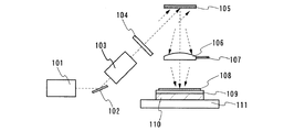
図1に、本実施の形態のレーザ照射装置の模式図を示す。なお、図1において、破線矢印で示す方向はレーザビームの進行方向である。ここで、レーザ発振器101から射出したレーザビームは、ミラー102で偏向され、エキスパンダ103に入射する。エキスパンダ103は、例えば凸レンズを2枚配置することにより、レーザビームのビーム径を拡大する機能を有するものである。
FIG. 1 shows a schematic diagram of the laser irradiation apparatus of the present embodiment. In FIG. 1, the direction indicated by the broken-line arrow is the direction of travel of the laser beam. Here, the laser beam emitted from the
次に、エキスパンダ103を通過したレーザビームは回折光学素子104に入射する。なお、ここでエキスパンダ103は、ビーム径を拡大することにより、回折光学素子104の切削間隔などの、設計上の制約を緩和するために使用するものである。したがって、レーザ発振器から射出されるレーザビームのビーム径が十分大きい場合にはエキスパンダ103は使用しなくともかまわない。また、回折光学素子104はレーザビームを分割し、複数のビームスポットを形成するために使用する。なお、ここでは回折光学素子104として透過型の回折光学素子を使用した例について示すが、本発明のレーザ照射装置はこの構成に限定されない。例えば反射型の回折光学素子を光学系内に配置する構成としてもよい。
Next, the laser beam that has passed through the
回折光学素子104は、分割された複数のレーザビームそれぞれが等しいビームパラメータを持つように設計することが可能なため、例えばガウシアン状のエネルギー分布を持つレーザビームを使用したとしても、回折光学素子を使用することにより、等しいエネルギーを持つ複数のレーザビームを形成することができる。これにより複数のレーザビームによるそれぞれの露光時間を揃えることが出来るため、処理時間を最小にすることができる。なお、ここで用いる回折光学素子は、その面構造の回折現象によりレーザビームの挙動をコントロールするものである。回折光学素子の設計は、ORA(Optimal Rotation Angle)法などにより、位相分布を最適化することにより行うことができる。また、波動光学的解析を行うことのできる光学設計ソフトで回折光学素子を自動設計することも可能である。回折光学素子の物理形状としては、2値位相格子、あるいは、多値位相格子または連続位相格子などを適用することができる。
Since the diffractive
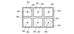
次に、回折光学素子104により分割されたレーザビームがDMD105にそれぞれ集光される。DMDを構成するマイクロミラーの数は、回折光学素子により分割されたレーザビームの数と等しいかそれ以上であることが好ましく、それぞれのレーザビームは異なるマイクロミラー面上に集光される。そして、マイクロミラーで反射されて投影レンズ106方向へ偏向される。ここで、マイクロミラーにおけるレーザビームの入射位置について説明するために、図2にDMD表面の一部を示す。図2の201はDMDを構成するマイクロミラーである。なお、図2では6枚のマイクロミラー201を有するDMDについて説明するが、マイクロミラーの枚数はこれに限定されない。また、202で示された領域はマイクロミラー間にある隙間を示しており、マイクロミラー間の隙間202にレーザビームが入射すると迷光の原因になる。また、上記のマイクロミラー201間の隙間202から、デバイス内部にレーザビームが入り込むことで温度上昇やデバイスの損傷が起こり、チャタリングなどの動作不良を引き起こす問題もある。そこで、本発明のレーザ照射装置では、回折光学素子により、ビームスポットを分割し、マイクロミラー201の表面積よりも小さいスポットサイズにレーザビームを集光する。例えば図中の点線で示すスポット203のように、マイクロミラー201中央部にレーザビームを集光するとよい。ここで、マイクロミラー201に形状的な歪みがある場合、歪みはマイクロミラーの四隅において特に大きくなる。したがって、マイクロミラー201の中央部にレーザビームを集光することで、歪みに起因するビームスポット形状の変動を防止できる。なお、マイクロミラー201中央部の領域205は、マイクロミラーの角度調整機構であるヨークに接続するヒンジが形成されている領域である。したがって、該ヒンジがビームスポットの形状の変動の原因となる場合には、領域205を避けるようにビームスポットを、マイクロミラー中心部とマイクロミラーの隅の間である204の位置などに集光させる構成としてもよい。なおこのような位置にビームスポットを形成したい場合、ビームスポットの径を数μm程度まで集光する必要がある。この場合、図示しないが、回折光学素子104により形成されるビームスポットを投影光学系によりDMD105上に縮小投影する構成としてもよい。以上の構成により、DMD105において、迷光等によるレーザビームの損失を防止し、レーザビームの利用効率を向上させることが可能である。
Next, the laser beams divided by the diffractive
次に、DMD105で反射して照射面方向に偏向されたレーザビームは、投影レンズ106に入射する(図1)。投影レンズ106はDMD105上に形成されたビームスポットを照射面である基板108に投影するために配置するものである。そのため、投影レンズ106は、DMD105と基板108が互いに共役となる位置に配置されている。ここで、DMD105を構成する複数のマイクロミラーは、デジタル的にその設置角度が制御される。例えば、基板上にレーザ照射を行う場合、マイクロミラーの傾斜角度を+10度とし、基板上にレーザ照射を行わない場合、マイクロミラーの傾斜角度を−10度とする。ここで、マイクロミラーの傾斜角度が−10度のときは、マイクロミラーにより反射されたレーザビームは遮光板107上に到達し遮光されるため、基板108表面に照射されない。上記の構成によりレーザビームの基板108へ照射する場合(オン)と照射しない場合(オフ)を制御することができるため、基板108上に所望の照射パターンを形成することができる。
Next, the laser beam reflected by the
本実施の形態において、基板108は吸着ステージ109に吸着されている。さらに吸着ステージ109はX方向に動作する搬送ステージ110とY方向に動作する搬送ステージ111上に設置されている。これにより、ある露光領域の照射が終わったところで、搬送ステージ110または111を動作させ、新たな露光領域に対して所望の照射パターンでレーザ照射を行う。このサイクルを繰り返すことにより、基板全面にレーザ照射を行うことが可能になる。本実施の形態では、基板108を吸着ステージ109に固定したが、固定方法はこれに限定させず、単純な固定具により基板を上からステージに押さえつけて固定するなどその他の方法でも構わない。
In the present embodiment, the
本実施の形態に示した方法でレーザ照射を行うことにより、レーザ照射パターンを高速に切り替え、基板上に効率よくレーザ照射することが可能になる。本発明のレーザ照射装置は複数のレーザビームを照射して露光プロセスを行うことができるので、ROMのように露光するパターンを頻繁に変更する製品の作製工程に適用することで生産性を高めることができる。例えば、IDチップのROM作製工程などに応用すれば、複数のパターンを持つIDチップを安価に量産することができる。 By performing laser irradiation by the method described in this embodiment mode, it is possible to switch the laser irradiation pattern at high speed and efficiently perform laser irradiation on the substrate. Since the laser irradiation apparatus of the present invention can perform an exposure process by irradiating a plurality of laser beams, the productivity can be improved by applying it to a manufacturing process of a product that frequently changes a pattern to be exposed like a ROM. Can do. For example, if it is applied to a ROM manufacturing process of an ID chip, ID chips having a plurality of patterns can be mass-produced at low cost.
(実施の形態2)
本実施の形態では、反射型回折光学素子によりレーザビームを複数に分割してDMDに入射させレーザ照射する例について示す。
(Embodiment 2)
In this embodiment mode, an example in which a laser beam is divided into a plurality of parts by a reflection type diffractive optical element and incident on a DMD for laser irradiation is shown.
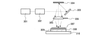
図3に本実施の形態のレーザ照射装置の模式図を示す。図3において、レーザ発振器301から射出したレーザビームは、エキスパンダ302に入射する。なお、図3中の破線矢印はレーザビームの進行方向を示している。エキスパンダ302は、例えば凸レンズを2枚配置することにより、レーザビームのビーム径を拡大する機能を有するものである。エキスパンダ302を通過したレーザビームは反射型の回折光学素子303に入射する。なお、ここでエキスパンダ302は、ビーム径を拡大することにより、回折光学素子303の切削間隔などの、設計上の制約を緩和するために使用するものである。したがって、レーザ発振器から射出されるレーザビームのビーム径が十分大きい場合にはエキスパンダ302は使用しなくともかまわない。また、回折光学素子303はレーザビームを分割し、複数のビームスポットを形成するために使用する。また、回折光学素子303は分割された複数のビームスポットそれぞれが等しいビームパラメータを持つように設計することが可能なため、例えばガウシアン状のエネルギー分布を持つレーザビームを使用したとしても、回折光学素子を使用することにより、等しいエネルギーを持つ複数のビームスポットを形成することができる。これにより複数のレーザビームによるそれぞれの露光時間を揃えることが出来るため、処理時間を最小にすることができる。なおここで用いる回折光学素子は、その面構造の回折現象によりレーザビームの挙動をコントロールするものである。回折光学素子の設計は、ORA(Optimal Rotation Angle)法などにより、位相分布を最適化することにより行うことができる。また、波動光学的解析を行うことのできる光学設計ソフトで回折光学素子を自動設計することも可能である。回折光学素子の形状としては、2値位相格子、あるいは、多値位相格子または連続位相格子などを適用することができる。
FIG. 3 shows a schematic diagram of the laser irradiation apparatus of the present embodiment. In FIG. 3, the laser beam emitted from the
次に、回折光学素子303により分割されたレーザビームがDMD304にそれぞれ集光される。DMDを構成するマイクロミラーの数は、回折光学素子により分割されたレーザビームの数と等しいかそれ以上であることが好ましく、それぞれのレーザビームは異なるマイクロミラー面上に集光される。
Next, the laser beams divided by the diffractive
次に、DMD304で反射して、照射面方向に偏向されたレーザビームは、投影レンズ305に入射する(図3)。投影レンズ305はDMD304上に形成されたビームスポットを照射面である基板307に投影するために配置するものである。そのため、投影レンズ305は、DMD304と基板307が互いに共役となる位置に配置されている。ここで、DMD304を構成する複数のマイクロミラーは、デジタル的にその設置角度が制御される。例えば、基板上にレーザ照射を行う場合、マイクロミラーの傾斜角度を+10度とし、基板上にレーザ照射を行わない場合、マイクロミラーの傾斜角度を−10度とする。ここで、マイクロミラーの傾斜角度が−10度のときは、マイクロミラーにより反射されたレーザビームは遮光板306上に到達し遮光されるため、基板307表面に照射されない。上記の構成によりレーザビームの基板307表面へ照射する場合(オン)と照射しない場合(オフ)を制御することができるため、基板上に所望の照射パターンを形成することができる。本実施の形態では、回折光学素子303の像をDMD304上に形成したため、DMD304と照射面と共役の関係としたが、回折光学素子の像は、必ずしもDMD上に形成しなくてもよく、回折光学素子の像と照射面を共役の関係として回折光学素子の像を照射面上に形成してもよい。
Next, the laser beam reflected by the
本実施の形態において、基板307は、吸着ステージ308に吸着されている。さらに吸着ステージ308はX方向に動作する搬送ステージ309とY方向に動作する搬送ステージ310上に設置されている。これにより、ある露光領域の照射が終わったところで、搬送ステージ309または310を動作させ、新たな露光領域に対して所望の照射パターンでレーザ照射を行う。このサイクルを繰り返すことにより、基板全面にレーザ照射を行うことが可能になる。本実施の形態では、基板を吸着ステージ308に固定したが、固定方法はこれに限定させず、単純な固定具により基板を上からステージに押さえつけて固定するなどその他の方法でも構わない。
In the present embodiment, the
本実施の形態に示した方法でレーザ照射を行うことにより、レーザ照射パターンを高速に切り替え、基板上に効率よくレーザ照射することが可能になる。本発明のレーザ照射装置は複数のレーザビームを照射して露光プロセスを行うことができるので、ROMのように露光するパターンを頻繁に変更する製品の作製工程に適用することで生産性を高めることができる。例えば、IDチップのROM作製工程などに応用すれば、複数のパターンを持つIDチップを安価に量産することができる。 By performing laser irradiation by the method described in this embodiment mode, it is possible to switch the laser irradiation pattern at high speed and efficiently perform laser irradiation on the substrate. Since the laser irradiation apparatus of the present invention can perform an exposure process by irradiating a plurality of laser beams, the productivity can be improved by applying it to a manufacturing process of a product that frequently changes a pattern to be exposed like a ROM. Can do. For example, if it is applied to a ROM manufacturing process of an ID chip, ID chips having a plurality of patterns can be mass-produced at low cost.
(実施の形態3)
本実施の形態では、DMDにより2方向に反射されたレーザビームを照射面の異なる領域に転送し、スループットを向上させてレーザ照射する例について示す。
(Embodiment 3)
In this embodiment mode, an example in which a laser beam reflected in two directions by a DMD is transferred to different regions on an irradiation surface and laser irradiation is performed with improved throughput will be described.
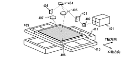
図4に本実施の形態のレーザ照射装置の斜視図を示す。レーザ発振器401から射出されたレーザビームは、ミラー402で偏向される。偏向されたレーザビームは回折光学素子403を通過する。回折光学素子403はレーザビームを分割し、複数のビームスポットを形成するために使用する。また、分割された複数のビームスポットそれぞれが等しいビームパラメータを持つように回折光学素子を設計することが可能なため、例えばガウシアン状のエネルギー分布を持つビームを使用したとしても、回折光学素子を使用することにより、等しいエネルギーを持つ複数のビームスポットを形成することができる。これにより複数のレーザビームの露光時間を揃えることが出来るため、処理時間を最小にすることができる。なおここで用いる回折光学素子は、その面構造の回折現象によりレーザビームの挙動をコントロールするものである。回折光学素子の設計は、ORA(Optimal Rotation Angle)法などにより、位相分布を最適化することにより行うことができる。また、波動光学的解析を行うことのできる光学設計ソフトで自動設計することも可能である。回折光学素子の形状としては、2値位相格子、あるいは、多値位相格子または連続位相格子などを適用することができる。
FIG. 4 is a perspective view of the laser irradiation apparatus of the present embodiment. The laser beam emitted from the
次に、回折光学素子403により分割されたレーザビームがDMD404にそれぞれ集光される。DMD404を構成するマイクロミラーの数は、回折光学素子により分割されたレーザビームの数と等しいかそれ以上であることが好ましく、それぞれのレーザビームは異なるマイクロミラー面上に集光される。以上の構成により、DMD404において、迷光等によるレーザビームの損失を防止し、レーザビームの利用効率を向上させることが可能である。
Next, the laser beams divided by the diffractive
DMD404を構成する複数のマイクロミラーは、反射面の角度をデジタル的に制御することができる。本実施の形態では、DMDを構成する複数のマイクロミラーの傾斜角度を+12度または−12度とすることができるDMDについて説明する。本実施の形態において、マイクロミラーの傾斜角度を+12度とした場合、DMD404で反射されたレーザビームは投影レンズ405を通過する。なお、投影レンズ405は、DMD404上の像を照射面に転送する機能を有しており、+12度の傾斜角度を有するマイクロミラー上に形成されたビームスポットを基板408上に投影してレーザ照射することができる。一方、マイクロミラーの傾斜角度を−12度とした場合、DMDで反射されたレーザビームはミラー406により再度反射される。ミラー406により反射されたレーザビームは投影レンズ407を通過する。投影レンズ407は、DMD上の像を照射面に転送する機能を有しており、−12度の傾斜角度を有するマイクロミラー上に形成されたビームスポットを基板408上に投影してレーザ照射することができる。上記のように、DMD404を用いて、基板上の所望の位置にレーザ照射することにより、固有のパターンを持つIDチップなどを形成することができる。
The plurality of micromirrors constituting the
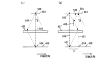
ここで、DMD404に入射してから基板408へ照射されるまでのレーザビームの光路について図5を用いて説明する。図5は、DMD404と基板408との間の断面の模式図である。なお、点線矢印で示す方向はレーザビームの進行方向である。図5(a)は、マイクロミラーの傾斜角度が+12度のとき、つまりDMD404、投影レンズ405を経て基板408へ照射されるまでのレーザビームの光路図である。なお、図5(a)では説明を簡単にするために、DMD404の中心部である点508に照射されるレーザビームについて説明する。DMD404で反射されたレーザビームは紙面垂直方向(Y軸方向)に+24度の角度に偏向される。また、紙面内におけるレーザビームの入射角度をθとすると、レーザビームはX軸方向においてθの反射角度で偏向され、光路501を進行する。さらにレーザビームは投影レンズ405に入射する。投影レンズ405は、その中心を通る軸503が、DMD404の中心位置を通過するように設置されている。また、投影レンズ405は、DMD404と基板408とを互いに共役の関係とする位置に配置される。上記の構成により、基板408において、DMD404の直下の点504にレーザビームが転送される。
Here, the optical path of the laser beam from the incidence on the
図5(b)は、マイクロミラーの傾斜角度が−12度のとき、つまりDMD404、ミラー406、投影レンズ407を経て基板408へ照射されるまでのレーザビームの光路図である。なお、図5(b)では説明を簡単にするために、DMD404の中心部である点508に照射されるレーザビームについて説明する。DMD404で反射されたレーザビームは紙面垂直方向(Y軸方向)に−24度の角度に偏向される。また、紙面内におけるレーザビームの入射角度をθとすると、レーザビームはX軸方向においてθの反射角度で偏向され、光路502を進行する。光路502の途中にはミラー406が設置されており、ミラー406により反射されたレーザビームは投影レンズ407に入射する。投影レンズ407は、DMD404と基板408とを互いに共役の関係とする位置に配置される。ここで、ミラー406は、その反射面がレーザビームの照射面に対して垂直となるように設置する。これにより、光路501と光路502とを互いに等しい距離とすることができる。したがって、投影レンズ405と407とは、同一の焦点距離を有するレンズを使用することができる。また、図5(a)と図5(b)の構成は互いに等しい投影倍率とすることができる。
FIG. 5B is an optical path diagram of a laser beam until the micro mirror has an inclination angle of −12 degrees, that is, until the
また、図5(b)の構成では、光路途中のミラー406によりレーザビームが偏向されるため、基板408上に照射されるレーザビームの位置を調整することが可能である。例えば、ミラー406で反射されたレーザビームを、レーザビームの進行方向と逆側に延長すると、DMD404の位置を紙面水平方向に延長した直線と点505において交差する。ここで、ミラー406から点505までの線分と、光路502のうちの点508からミラー406までの線分とは、ミラー406を軸として線対称となっている。したがって、仮想的には、点505の位置にDMD404の中心部である点508があるとみなすことができる。ここで、DMD404の中心部と点505までの距離をdとすると、投影レンズの中心軸506を、DMD404の中心部を通過する軸503から距離d離れた位置に設置する。これにより、点505のほぼ直下の点507にレーザビームを転送することができる。以上の方法で図5(a)と図5(b)の光学系を構成することにより、2つの領域にそれぞれ異なる照射パターンを同時に形成することができる。
In the configuration of FIG. 5B, the laser beam is deflected by the
照射パターンが形成される基板408は吸着ステージ409に吸着されている。さらに吸着ステージ409はX軸方向に動作する搬送ステージ410とY軸方向に動作する搬送ステージ411上に設置されている。これにより、ある露光領域の照射が終わったところで、搬送ステージ410または411を動作させ、新たな露光領域に対して所望の照射パターンでレーザ照射を行う。このサイクルを繰り返すことにより、基板全面にレーザ照射を行うことが可能になる。本実施の形態では、基板を吸着ステージ409に固定したが、固定方法はこれに限定させず、単純な固定具により基板を上からステージに押さえつけて固定するなどその他の方法でも構わない。
The
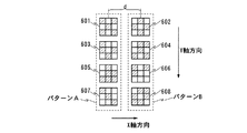
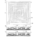
ここで、照射面に形成される照射パターンについて図6を例にして説明する。図6は3行×3列の描画パターンを形成する例である。パターンA(601、603、605、607)は、図5(a)の構成により形成される照射パターンである。また、パターンB(602、604、606、608)は、図5(b)の構成により形成される照射パターンである。パターンAおよびBにおいて、斜線で示した領域はレーザビームが照射される領域であり、パターンAとパターンBは互いに反転した照射パターンとなっている。例えば、照射パターン602は照射パターン601の未照射領域に相当する部分にのみレーザ照射が行われるパターンとなっている。また、パターンAの中心とパターンBの中心は、X軸方向に距離d離れた領域に形成されている。これにより、異なるパターンを持つ照射パターンを同時に形成することができる。したがって、図中Y軸方向に基板を搬送しながらレーザ照射を行う場合、パターンAとパターンBを同時に形成しながらレーザ照射することができるため、スループットが向上する。
Here, the irradiation pattern formed on the irradiation surface will be described with reference to FIG. FIG. 6 shows an example in which a drawing pattern of 3 rows × 3 columns is formed. Pattern A (601, 603, 605, 607) is an irradiation pattern formed by the configuration of FIG. Pattern B (602, 604, 606, 608) is an irradiation pattern formed by the configuration shown in FIG. In the patterns A and B, the hatched area is an area irradiated with the laser beam, and the pattern A and the pattern B are irradiation patterns that are reversed from each other. For example, the
上記の方法でレーザ照射を行うことにより、レーザ照射パターンを高速に切り替え、基板上に効率よくレーザ照射することが可能になる。なお、このような照射パターンを作る方法は、ランダムな照射パターンを形成することが必要となるIDチップの作製などに特に適している。そのため、本発明のレーザ照射装置をIDチップのROM作製工程などに応用すれば、複数のパターンを持つIDチップを安価に量産することができる。 By performing laser irradiation by the above method, it is possible to switch the laser irradiation pattern at high speed and to efficiently perform laser irradiation on the substrate. In addition, the method of creating such an irradiation pattern is particularly suitable for producing an ID chip that requires the formation of a random irradiation pattern. Therefore, if the laser irradiation apparatus of the present invention is applied to a ROM manufacturing process of an ID chip, ID chips having a plurality of patterns can be mass-produced at a low cost.
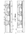
本実施例では、絶縁基板上に不揮発性メモリ回路、変調回路、復調回路、論理回路などに用いるTFTを作製する方法について図7を用いて説明する。なお、本実施例では半導体素子としてnチャネル型の薄膜トランジスタ(以下TFTと記す)、pチャネル型TFTを例に挙げて示すが、本発明においてメモリ部および論理回路部に含まれる半導体素子はこれに限定されない。また、本実施例で示す作製方法は一例であって、絶縁基板上での半導体素子の作製方法を限定するものではない。なお、本実施例で作製するTFTは、メモリ部においてデータを記憶する際、トランジスタをビット線に接続するか否かにより”0”か”1”のバイナリ情報を決定するコンタクト書き込みと呼ばれる方法で記憶する。 In this embodiment, a method for manufacturing a TFT used for a nonvolatile memory circuit, a modulation circuit, a demodulation circuit, a logic circuit, or the like over an insulating substrate will be described with reference to FIGS. Note that in this embodiment, an n-channel thin film transistor (hereinafter referred to as TFT) and a p-channel TFT are shown as examples of the semiconductor element. However, in the present invention, the semiconductor element included in the memory portion and the logic circuit portion is described here. It is not limited. Further, the manufacturing method shown in this embodiment is an example, and the manufacturing method of a semiconductor element over an insulating substrate is not limited. The TFT manufactured in this embodiment is a method called contact writing in which binary information of “0” or “1” is determined depending on whether or not a transistor is connected to a bit line when data is stored in a memory portion. Remember.
まず、ガラス基板である絶縁基板3000上に酸化シリコン膜、窒化シリコン膜等の絶縁膜、または、酸化窒化シリコン膜、窒化酸化シリコン膜などの絶縁膜から成る下地膜3001、3002を形成する。例えば、下地膜3001として酸化窒化シリコン膜を10nm以上200nm以下、下地膜3002として酸化窒化水素化シリコン膜を50nm以上200nm以下の厚さに順に積層形成する。
First,
次に、下地膜3002上に、非結晶構造を有する半導体膜を形成し、当該半導体膜をレーザ結晶化法や熱結晶化法によって結晶化し、結晶質半導体膜を形成する。次いで、結晶質半導体膜を加工して島状半導体層3003、3004、3005を形成する。この島状半導体層3003、3004、3005は、25nm以上80nm以下程度の厚さで形成する。結晶質半導体膜の材料に限定はないが、好ましくはシリコンまたはシリコン・ゲルマニウム(SiGe)合金などで形成すると良い。
Next, a semiconductor film having an amorphous structure is formed over the
次いで、島状半導体層3003、3004、3005を覆うゲート絶縁膜3006を形成する。ゲート絶縁膜3006はプラズマCVD法またはスパッタ法を用い、厚さを10nm以上80nm以下程度としてシリコンを含む絶縁材料で形成する。
Next, a
そして、ゲート絶縁膜3006上に第1の導電層を形成する。続いて第1の導電層上に、第2の導電層を形成し、積層された第1の導電層と第2の導電層を一括でエッチングして、TFTのゲート電極3011、3012、3013を形成する。
Then, a first conductive layer is formed over the
本実施例では、第1の導電層をTaNで50〜100nmの厚さに形成し、第2の導電層をWで100〜300nmの厚さに形成する。ただし、導電層の材料は特に限定されず、いずれもTa、W、Ti、Mo、Al、Cuなどから選ばれた元素、または前記元素を主成分とする合金材料もしくは化合物材料で形成してもよい。 In this embodiment, the first conductive layer is formed with TaN to a thickness of 50 to 100 nm, and the second conductive layer is formed with W to a thickness of 100 to 300 nm. However, the material of the conductive layer is not particularly limited, and any of them may be formed of an element selected from Ta, W, Ti, Mo, Al, Cu, or the like, or an alloy material or a compound material containing the element as a main component. Good.
次に論理回路部で用いるpチャネル型TFTにp型を付与する元素のドーピングを行い、第1の不純物領域3016、3017を形成する。続いてメモリ部、論理回路部で用いるnチャネル型TFTのLDD領域を形成するために、n型を付与する元素のドーピングを行い、第2の不純物領域3018、3019を形成する。その後、サイドウォール3020、3021を形成して、メモリ部、論理回路部で用いるnチャネル型TFTにn型を付与するドーピングを行い第3の不純物領域3022、3023を形成する。これらのドーピング方法はイオンドープ法もしくはイオン注入法で行えばよい。以上までの工程で島状半導体層3003、3004、3005のそれぞれに不純物領域が形成される。
Next, the p-channel TFT used in the logic circuit portion is doped with an element imparting p-type conductivity to form
次に、島状半導体層3003、3004、3005のそれぞれに添加された不純物元素を活性化する工程を行う。この工程はファーネスアニール炉を用いる熱アニール法で行う。その他に、レーザアニール法、またはラピッドサーマルアニール法(RTA法)を適用することができる。または、3%以上の水素を含む雰囲気中で、300〜450℃で1〜12時間の熱処理を行い、島状半導体層を水素化する工程を行う。水素化の他の手段として、プラズマ水素化(プラズマにより励起された水素を用いる)を行ってもよい。
Next, a step of activating the impurity element added to each of the island-shaped
次いで、第1の層間絶縁膜3024を酸化窒化シリコン膜で形成する。第1の層間絶縁膜3024の膜厚は、ゲート絶縁膜と同程度の10〜80nmとする。続いてアクリルなどの有機絶縁物材料から成る第2の層間絶縁膜3025を形成する。または、第2の層間絶縁膜3025として有機絶縁物材料の代わりに無機材料を用いることもできる。無機材料としては無機SiO2やプラズマCVD法で作製したSiO2(PCVD‐SiO2)、SOG(Spin on Glass;塗布珪素酸化膜)等が用いられる。
Next, a first
続いて、第2の層間絶縁膜3025上の全面にレジストをスピンコート法で設け、ゲート絶縁膜3006、第1の層間絶縁膜3024、第2の層間絶縁膜3025にコンタクトホール3031、3032を作製する(図7)。本実施例において、不揮発性メモリ回路のメモリ部以外の箇所のエッチング工程は第1の露光手段(たとえばミラープロジェクション露光、ステップ・アンド・リピート露光(ステッパー露光)、ステップ・アンド・スキャン露光など)によって行っている。上記の第1の露光手段によって、第2の層間絶縁膜3025上に設けたレジストを感光させ、パターンを形成し、そのレジストをマスクとしてエッチングをおこなう。この工程は、図8(A)に示すように、まず第2の層間絶縁膜3025上にレジストを塗布し、ベークをおこなう。つぎに不揮発性メモリ回路のメモリ部以外の箇所を前述した第1の露光手段、すなわちミラープロジェクション露光、ステップ・アンド・リピート露光、ステップ・アンド・スキャン露光などによってレジストを露光して感光させ、パターンを形成している(図8(B))。このような露光手段は、同じパターンをいくつも露光する際には非常に有効である。
Subsequently, a resist is provided over the entire surface of the second
次に、実施の形態1〜3に示したレーザ照射装置を用いた第2の露光手段によってレジストを露光することで、不揮発性メモリ回路のメモリ部のコンタクトホールのパターン、またはメモリ部のコンタクトホールおよびチップの一部のコンタクトホールのパターンを形成する(図8(C))。図7において、メモリ部のコンタクトホール3033は第2の露光手段で形成する。
Next, the resist is exposed by the second exposure means using the laser irradiation apparatus described in
次に、現像等の処理(図8(D))をおこなったあと、層間膜のエッチングをおこない、第1の露光手段及び第2の露光手段によってパターンを形成したコンタクトホール3031、3032、3033を形成する(図8(E))。
Next, after processing such as development (FIG. 8D), the interlayer film is etched, and
そして、メモリ部において島状半導体層のソース領域、ドレイン領域とコンタクトをとる電極3026、3027を形成する。また、論理回路部においても同様に、電極3028、3029、3030を形成する。
Then,
以上の説明において、コンタクトホール形成工程において、第1の露光手段(ミラープロジェクション露光、ステップ・アンド・リピート露光、またはステップ・アンド・スキャン露光)と第2の露光手段(実施の形態1〜3に示したレーザ照射方法を用いた露光方法)とを組み合わせることで、同一基板上に複数のコンタクトホールを形成する工程を述べたが、上記方法はコンタクトホール形成工程に限らず、ソース配線又はドレイン配線の形成工程やドーピング工程などその他の工程で用いてもよい。また、必ずしも第1の露光手段と第2の露光手段とを組み合わせる必要はなく、全ての露光工程において第2の露光手段を用いてもよい。第2の露光手段を用いることで、レーザ照射パターンを高速で切り替えながら、所望の位置に高速にレーザ照射することが可能となり、半導体装置の作製時間を短縮し、かつ精度よく作製することができる。 In the above description, in the contact hole forming step, the first exposure means (mirror projection exposure, step-and-repeat exposure, or step-and-scan exposure) and the second exposure means (in the first to third embodiments). The step of forming a plurality of contact holes on the same substrate by combining with the exposure method using the laser irradiation method shown) has been described. However, the above method is not limited to the contact hole forming step, and the source wiring or the drain wiring It may be used in other processes such as a forming process and a doping process. Further, it is not always necessary to combine the first exposure unit and the second exposure unit, and the second exposure unit may be used in all the exposure steps. By using the second exposure means, it is possible to perform laser irradiation at a desired position at high speed while switching the laser irradiation pattern at high speed, thereby shortening the manufacturing time of the semiconductor device and manufacturing it with high accuracy. .
また、以上においては、第1の露光手段の次に第2の露光手段を用いているが、まず第2の露光手段で、メモリ部を形成し、その後に第1の露光手段で他の回路部分を形成してもよい。 In the above description, the second exposure unit is used after the first exposure unit. First, the second exposure unit forms a memory unit, and then the first exposure unit performs another circuit. A portion may be formed.
以上のようにして、記憶素子3034を有するメモリ部と、LDD構造のnチャネル型TFT3035およびシングルドレイン構造のpチャネル型TFT3036を有する論理回路部と、を同一の基板上に形成することができる(図7参照)。
As described above, the memory portion including the
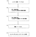
また、図9のフロー図に示すように、一度メモリ部以外領域を形成し、その後で不揮発性メモリ回路のメモリ部を形成してもよい。図9に示す工程は、まず、第2の層間絶縁膜3025上にレジストを塗布し、ベークをおこなう(図9(A))。次に、第1の露光手段(ミラープロジェクション露光、ステップ・アンド・リピート露光、ステップ・アンド・スキャン露光など)でメモリ部以外の領域のパターンを形成するために、レジストの露光をおこなう。(図9(B))。次に、第1の露光手段で感光したレジストの現像、ベークなどをおこなう。(図9(C))。次に、エッチングを行いメモリ部以外の領域のパターンを形成する(図9(D))。次に、再度、層間絶縁膜3025上にレジストを塗布し、ベークをおこなう(図9(E))。次に、実施の形態1〜3に示した露光装置を用いた第2の露光手段にて、不揮発性メモリ回路のメモリ部のパターンを形成するため、レジストを露光する(図9(F))。次に、第2の露光手段で感光したレジストの現像、ベークをおこなう(図9(G))。最後に、エッチングをおこない不揮発性メモリ回路のメモリ部を形成する(図9(H))。このようにして、個々のチップごとに異なるデータの記憶が可能であり、且つ、スループットを落とさずに半導体装置の製造が可能になる。実施の形態1〜3に示したレーザ照射装置は、複雑または複数の照射ポイントを一度に精度良くレーザ照射できるため、ROMの作製工程のように複数の照射ポイントに対してレーザ照射を必要とする装置の作製工程において効率よくレーザ照射を行うことができる。よって、IDチップのROM作製などの量産性を容易に向上させることが可能となる。
In addition, as shown in the flowchart of FIG. 9, a region other than the memory portion may be formed once, and then the memory portion of the nonvolatile memory circuit may be formed. In the step shown in FIG. 9, first, a resist is applied over the second
本実施例では、メモリ部および論理回路部を形成し、フレキシブル基板へ転写するまでの作製方法について図10、図11を用いて説明する。なお、本実施例では半導体素子として、不揮発性メモリ素子、nチャネル型TFT、およびpチャネル型TFTを例に挙げて示すが、本発明においてメモリ部および論理回路部に含まれる半導体素子はこれに限定されない。また、この作製方法は一例であって、絶縁基板上での作製方法を限定するものではない。 In this embodiment, a manufacturing method until a memory portion and a logic circuit portion are formed and transferred to a flexible substrate will be described with reference to FIGS. In this embodiment, as a semiconductor element, a nonvolatile memory element, an n-channel TFT, and a p-channel TFT are shown as examples. However, in the present invention, the semiconductor element included in the memory portion and the logic circuit portion is described here. It is not limited. Further, this manufacturing method is an example, and the manufacturing method over an insulating substrate is not limited.
まず、図10に示すように、絶縁基板3000上に剥離層4000を形成する。剥離層4000は、非晶質シリコン、多結晶シリコン、単結晶シリコン、微結晶シリコン(セミアモルファスシリコンを含む)等、シリコンを主成分とする層を用いることができる。剥離層4000は、スパッタ法、プラズマCVD法等を用いて形成することができる。本実施例では、膜厚500nm程度の非晶質シリコンをスパッタ法で形成し、剥離層4000として用いる。続いて剥離層4000上に下地膜3001を形成し、その後、実施例1に示した作業工程と同様に、記憶素子3034を有するメモリ部、nチャネル型TFT3035及びpチャネル型TFT3036を有する論理回路部を形成する。
First, as illustrated in FIG. 10, the
次に、第2の層間絶縁膜3025上に第3の層間絶縁膜4001を形成し、パッド4002〜4005を形成する。パッド4002〜4005としては、Ag、Au、Cu、Pd、Cr、Mo、Ti、Ta、W、Alなどの金属、または、金属化合物を、1つまたは複数有する導電材料を用いることができる。
Next, a third
そしてパッド4002〜4005を覆うように、第3の層間絶縁膜4001上に保護層4006を形成する。保護層4006は、後に剥離層4000をエッチングにより除去する際に、パッド4002〜4005を保護することができる材料を用いる。例えば、水またはアルコール類に可溶なエポキシ系、アクリレート系、シリコーン系の樹脂を全面に塗布することで保護層4006を形成することができる(図10(A))。
Then, a
次に、剥離層4000を分離するための溝4007を形成する(図10(B)参照)。溝4007は、剥離層4000が露出する程度であれば良い。溝4007の形成は、エッチング、ダイシング、スクライビングなどの方法を用いることができる。
Next, a
次に、剥離層4000をエッチングにより除去する(図11(A)参照)。本実施例では、エッチングガスとしてフッ化ハロゲンを用い、該ガスを溝4007から導入する。本実施の形態では、例えばClF3(三フッ化塩素)を用い、温度:350℃、流量:300sccm、気圧:800Pa、時間:3hの条件で行う。また、ClF3ガスに窒素を混ぜたガスを用いても良い。ClF3等のフッ化ハロゲンを用いることで、剥離層4000が選択的にエッチングされ、絶縁基板3000を剥離することができる。なおフッ化ハロゲンは、気体であっても液体であってもどちらでも良い。
Next, the
次に、剥離されたメモリ部および論理回路部を、接着剤4008を用いて支持体4009に貼り合わせる(図11(B)参照)。接着剤4008は、支持体4009と下地膜3001とを貼り合わせることができる材料を用いる。接着剤4008は、例えば反応硬化型接着剤、熱硬化型接着剤、紫外線硬化型接着剤等の光硬化型接着剤、嫌気型接着剤などの各種硬化型接着剤を用いることができる。
Next, the peeled memory portion and logic circuit portion are attached to a
支持体4009として、フレキシブルな紙またはフレキシブルなプラスチックなどの有機材料を用いることができる。または支持体4009として、フレキシブルな無機材料を用いていても良い。支持体4009は集積回路において発生した熱を拡散させるために、2W/mK以上30W/mK以下程度の高い熱伝導率を有するのが望ましい。
As the
なおメモリ部および論理回路部の集積回路を絶縁基板3000から剥離する方法は、本実施の形態で示したようにシリコンを主成分とする層のエッチングを用いる方法に限定されず、他の様々な方法を用いることができる。例えば、耐熱性の高い基板と集積回路の間に金属酸化膜を設け、該金属酸化膜を結晶化により脆弱化して集積回路を剥離することができる。また例えば、剥離層をレーザー光の照射により破壊し、集積回路を基板から剥離することもできる。また例えば、集積回路が形成された基板を機械的に削除または溶液やガスによるエッチングで除去することで、集積回路を基板から剥離することもできる。
Note that the method for separating the integrated circuit of the memory portion and the logic circuit portion from the insulating
また対象物の表面が曲面を有しており、それにより該曲面に貼り合わされたIDチップの支持体が、錐面、柱面など母線の移動によって描かれる曲面を有するように曲がってしまう場合、該母線の方向とTFTのキャリアが移動する方向とを揃えておくことが望ましい。上記構成により、支持体が曲がっても、それによってTFTの特性に影響が出るのを抑えることができる。また、島状の半導体膜が集積回路内において占める面積の割合を、1%以上30%以下程度とすることで、支持体が曲がっても、それによってTFTの特性に影響が出るのをより抑えることができる。 In addition, when the surface of the object has a curved surface, and the ID chip support bonded to the curved surface is bent so as to have a curved surface drawn by movement of the generatrix such as a cone surface or a column surface, It is desirable to align the direction of the bus and the direction in which the TFT carrier moves. With the above configuration, even if the support is bent, it can be suppressed that the characteristics of the TFT are affected thereby. In addition, the ratio of the area occupied by the island-shaped semiconductor film in the integrated circuit is set to about 1% to 30%, so that even if the support is bent, the TFT characteristics are further suppressed from being affected. be able to.
本実施例において、メモリ部は、実施の形態1〜3に示したレーザ照射装置を用いて作製している。よって、レーザ照射パターンを高速に切り替えることができ、ROMのようにランダムな照射パターンを形成する必要がある装置の作成工程において効率よくレーザ照射を行うことができる。そのため、IDチップのROM作製などの量産性を容易に向上させることが可能となる。
In this example, the memory portion is manufactured using the laser irradiation apparatus described in any of
次に、マスクROMを用いた不揮発性メモリ回路の実施例を図12に示す。図12に示す不揮発性メモリ回路は本発明のレーザ照射装置を用いて作製され、TFTのドレイン端子のコンタクトホールを開口するかどうかで、記憶状態を表すものである。 Next, an example of a nonvolatile memory circuit using a mask ROM is shown in FIG. The nonvolatile memory circuit shown in FIG. 12 is manufactured using the laser irradiation apparatus of the present invention, and represents a memory state depending on whether or not a contact hole of a drain terminal of a TFT is opened.
以下、マスクROMを用いた不揮発性メモリ回路の動作について、図12を用いて説明する。図12の不揮発性メモリ回路は説明簡略化のため、4ビットのメモリ回路としているが、本発明の実施は、4ビットに限定されるものではない。図12に示す不揮発性メモリ回路は列デコーダ701、行デコーダ702、アンプ715、nチャネル型TFT703〜706、ビット線(データ線)709、710、ワード線707、708、電源線713、列スイッチ711、712、出力配線717、負荷抵抗714、出力端子716、電源1、電源2によって構成されている。負荷抵抗714の代わりに定電流源を用いても良い。
Hereinafter, the operation of the nonvolatile memory circuit using the mask ROM will be described with reference to FIG. The non-volatile memory circuit of FIG. 12 is a 4-bit memory circuit for the sake of simplicity, but the implementation of the present invention is not limited to 4 bits. 12 includes a
電源1はハイ電位を設定する電位であり、電源2はロウ電位を設定する電位である。ただしTFT703〜706をpチャネル型TFTとする場合においては、電源1はロウ電位を設定し、電源2はハイ電位を設定する。以下の説明ではTFT703〜706はnチャネル型TFTとし、電源1は+3V、電源2は0Vを供給する構成とするが適宜変えてもよい。また、メモリセル718〜721は、TFT703〜706によって構成される。
The
以下、読み出しをおこなう場合について説明をおこなう。メモリセル718のデータを読み出す場合は、行デコーダ702を動作させ、ワード線707をアクティブ状態とする。それによってTFT703、704はオンとなる。次に、列デコーダ701を動作させ、列スイッチ711をオンさせる。それによってビット線(データ線)709、出力配線717、負荷抵抗714、アンプ715が接続される。TFT703がオンしているので、電流は電源1から、負荷抵抗714、出力配線717、列スイッチ711、ビット線709、TFT703、電源線713を介して電源2へ流れる。これによってメモリセル718の出力はロウになる。
Hereinafter, a case where reading is performed will be described. When reading data from the
メモリセル719のデータを読み出す場合は、行デコーダ702を動作させ、ワード線707をアクティブとする。それによってTFT703、704はオンとなる。次に、列デコーダ701を動作させ、列スイッチ712をオンさせる。それによってビット線(データ線)710、出力配線717、負荷抵抗714、アンプ715が接続される。TFT703がオンしているが、TFT704のドレイン端子はどこにも接続されていないため、電流は流れない。電源1の電位が負荷抵抗714、出力配線717、列スイッチ712、ビット線710に供給されるが、電流が流れないのでメモリセル719の出力はハイになる。
When reading data from the
メモリセル720のデータを読み出す場合は、行デコーダ702を動作させ、ワード線708をアクティブとする。それによってTFT705、706はオンとなる。次に、列デコーダ701を動作させ、列スイッチ711をオンさせる。それによってビット線709、出力配線717、負荷抵抗714、アンプ715が接続される。TFT705がオンしているが、TFT705のドレイン端子はどこにも接続されていないため、電流は流れない。電源1の電位が負荷抵抗714、出力配線717、列スイッチ711、ビット線709に供給されるが、電流が流れないのでメモリセル720の出力はハイになる。
When reading data from the
メモリセル721のデータを読み出す場合は、行デコーダ702を動作させ、ワード線708をアクティブとする。それによってTFT705、706はオンとなる。次に、列デコーダ701を動作させ、列スイッチ712をオンさせる。それによってビット線710、出力配線717、負荷抵抗714、アンプ715が接続される。TFT706がオンしているので、電流は電源1から、負荷抵抗714、出力配線717、列スイッチ712、ビット線710、TFT706、電源線713を介して電源2へ流れる。これによってメモリセル721の出力はロウになる。このようにして、メモリに記憶されたデータを出力端子716に読み出すことができる。
When reading data from the
本実施例では本発明を用いて形成した不揮発性メモリ回路に外付けのアンテナをつけた例について図13、図14を用いて説明する。 In this embodiment, an example in which an external antenna is attached to a nonvolatile memory circuit formed using the present invention will be described with reference to FIGS.
図13(A)は不揮発性メモリ回路の周りを一面のアンテナで覆ったものである。基板1000上にアンテナ1001を構成し、本発明を用いて形成した不揮発性メモリ回路1002を接続する。図面では不揮発性メモリ回路1002の周りをアンテナ1001で覆う構成になっているが、基板全面をアンテナ1001で覆い、その上に電極を構成した不揮発性メモリ回路1002を貼り付けるような構造を取っても良い。
In FIG. 13A, the non-volatile memory circuit is covered with a single antenna. An
図13(B)は細いアンテナを不揮発性メモリ回路の周りを回るように配置したものである。基板1003上にアンテナ1004を構成し、本発明を用いて形成した不揮発性メモリ回路1005を接続する。なお、アンテナの配線の配置は一例であってこれに限定するものではない。
FIG. 13B shows a thin antenna arranged around a nonvolatile memory circuit. An
図13(C)は高周波数のアンテナである。基板1006上にアンテナ1007を構成し、本発明を用いて形成した不揮発性メモリ回路1008を接続する。
FIG. 13C illustrates a high frequency antenna. An
図13(D)は180度無指向性(どの方向からでも同じく受信可能)なアンテナである。基板1009上にアンテナ1010を構成し、本発明を用いて形成した不揮発性メモリ回路1011を接続する。
FIG. 13D illustrates an antenna that is 180 degrees omnidirectional (same reception is possible from any direction). An
図13(E)は棒状に長く伸ばしたアンテナである。基板1012上にアンテナ1013を構成し、本発明を用いて形成した不揮発性メモリ回路1014を接続する。
FIG. 13E shows an antenna elongated in a rod shape. An
本発明を用いて形成した不揮発性メモリ回路とこれらのアンテナへの接続は公知の方法で行うことができる。例えばアンテナと不揮発性メモリ回路をワイヤボンディング接続やバンプ接続を用いて接続する、あるいはチップ化した不揮発性メモリ回路の一面を電極にしてアンテナに貼り付けるという方法を取ってもよい。この方式ではACF(anisotropic conductive film;異方性導電性フィルム)を用いて貼り付けることができる。 The nonvolatile memory circuit formed using the present invention and connection to these antennas can be performed by a known method. For example, a method of connecting the antenna and the nonvolatile memory circuit using wire bonding connection or bump connection, or sticking the antenna to the antenna using one surface of the nonvolatile memory circuit as an electrode may be used. In this method, it can be attached using an ACF (anisotropy conductive film).
アンテナに必要な長さは受信に用いる周波数によって適正な長さが異なる。一般には波長の整数分の1の長さにすると良いとされる。例えば周波数が2.45GHzの場合は約60mm(1/2波長)または、約30mm(1/4波長)とすれば良い。 The length required for the antenna differs depending on the frequency used for reception. In general, the length is preferably an integral number of a wavelength. For example, when the frequency is 2.45 GHz, it may be about 60 mm (1/2 wavelength) or about 30 mm (1/4 wavelength).
また、本発明の不揮発性メモリ回路上に基板を取りつけ、さらにその上にアンテナを構成してもよい。図14(A)〜(C)にその一例として不揮発性メモリ回路上に基板1100を取りつけ、らせん状のアンテナ1101を配置したものの上面図および断面図を示す。図14(B)、(C)は、図14(A)に示した上面図をそれぞれ鎖線A−B、鎖線C−Dで切断した断面図を示す。
Further, a substrate may be mounted on the nonvolatile memory circuit of the present invention, and an antenna may be further formed thereon. As an example, FIGS. 14A to 14C are a top view and a cross-sectional view of a substrate in which a
なお、本実施例に示した例はごく一例であり、アンテナの形状を限定するものではない。本発明はあらゆる形状のアンテナについて実施することが可能である。 Note that the example shown in this embodiment is just an example, and does not limit the shape of the antenna. The present invention can be implemented with any shape of antenna.
本実施例では、図15〜17を参照して、TFTを含む薄膜集積回路装置の具体的な作製方法について説明する。ここでは、簡単のため、nチャネル型TFTとpチャネル型TFTを用いたCPU(論理回路部)とメモリ部の断面構造を示すことによって、その作製方法について説明する。 In this embodiment, a specific method for manufacturing a thin film integrated circuit device including a TFT will be described with reference to FIGS. Here, for the sake of simplicity, a manufacturing method will be described by showing a cross-sectional structure of a CPU (logic circuit portion) using n-channel TFTs and p-channel TFTs and a memory portion.
まず、基板60上に、剥離層61を形成する(図15(A))。ここでは、ガラス基板(例えば、コーニング社製1737基板)上に、50nmの膜厚のa−Si膜(非晶質シリコン膜)を減圧CVD法により形成した。なお、基板60としては、ガラス基板の他にも、石英基板、アルミナなど絶縁物質で形成される基板、シリコンウエハ基板、後工程の処理温度に耐え得る耐熱性を有するプラスチック基板等を用いることができる。
First, the
また、剥離層61としては、非晶質シリコンの他に、多結晶シリコン、単結晶シリコン、SAS(セミアモルファスシリコン(微結晶シリコン、マイクロクリスタルシリコンともいう。))等、シリコンを主成分とする膜を用いることが望ましいが、これらに限定されるものではない。剥離層61は、減圧CVD法の他にも、プラズマCVD法、スパッタ法等によって形成しても良い。また、リンなどの不純物をドープした膜を用いてもよい。また、剥離層61の膜厚は、50nm以上60nm以下程度とするのが望ましい。SASに関しては、30nm以上50nm以下程度の膜厚としてもよい。
In addition to the amorphous silicon, the
次に、剥離層61上に、保護膜55(下地膜、下地絶縁膜と呼ぶこともある。)を形成する(図15(A))。ここでは、保護膜55を剥離層61側から順に、膜厚100nmのSiON(窒素を含む酸化珪素)膜、膜厚50nmのSiNO(酸素を含む窒化珪素)膜、膜厚100nmのSiON膜の3層構造としたが、材質、膜厚、積層数は、これに限定されるものではない。例えば、下層のSiON膜に代えて、膜厚0.5μm以上3μm以下程度のシロキサン等の耐熱性樹脂をスピンコート法、スリットコーター法、液滴吐出法などによって形成しても良い。また、窒化珪素膜(SiN、Si3N4等)を用いてもよい。また、上層のSiON膜に代えて、酸化珪素膜を用いてもよい。また、それぞれの膜厚は、0.05μm以上3μm以下程度とするのが望ましく、その範囲から自由に選択することができる。
Next, a protective film 55 (also referred to as a base film or a base insulating film) is formed over the separation layer 61 (FIG. 15A). Here, in order from the
ここで、酸化珪素膜は、SiH4とO2の混合ガス、TEOS(テトラエトキシシラン)とO2の混合ガス等の混合ガスを用い、熱CVD、プラズマCVD、常圧CVD、バイアスECRCVD等の方法によって形成することができる。また、窒化珪素膜は、例えば、SiH4とNH3の混合ガスを用い、プラズマCVDによって形成することができる。また、SiON膜又はSiNO膜は、例えば、SiH4とN2Oの混合ガスを用い、プラズマCVDによって形成することができる。 Here, the silicon oxide film uses a mixed gas such as a mixed gas of SiH 4 and O 2, a mixed gas of TEOS (tetraethoxysilane) and O 2 , etc., such as thermal CVD, plasma CVD, atmospheric pressure CVD, and bias ECRCVD. It can be formed by a method. The silicon nitride film can be formed by plasma CVD using a mixed gas of SiH 4 and NH 3 , for example. The SiON film or SiNO film can be formed by plasma CVD using a mixed gas of SiH 4 and N 2 O, for example.
なお、剥離層61及び島状半導体膜57として、a−Si等の珪素を主成分とする材料を用いる場合には、それらに接する保護膜55としては、密着性確保の点から、SiOxNy(x>y>0)を用いてもよい。
In addition, when using the material which has silicon as main components, such as a-Si, as the
次に、保護膜55上に、薄膜集積回路装置のCPU(論理回路部)やメモリ部を構成する薄膜トランジスタ(TFT)を形成する。なお、TFT以外にも、有機TFT、薄膜ダイオード等の薄膜能動素子を形成することもできる。
Next, a thin film transistor (TFT) constituting a CPU (logic circuit portion) and a memory portion of the thin film integrated circuit device is formed on the
TFTの作製方法として、まず、保護膜55上に、島状半導体膜57を形成する(図15(B))。島状半導体膜57は、非晶質半導体、結晶性半導体、又はセミアモルファス半導体で形成する。いずれも、シリコン、シリコン・ゲルマニウム(SiGe)等を主成分とする半導体膜を用いることができる。
As a method for manufacturing a TFT, first, an island-shaped
ここでは、70nmの膜厚の非晶質珪素膜を形成し、さらにその表面を、ニッケルを含む溶液で処理した。さらに、500〜750℃の熱結晶化工程によって結晶質シリコン半導体膜を形成した後、レーザ結晶化を行って結晶性を改善した。また、半導体膜の成膜方法としては、プラズマCVD法、スパッタ法、LPCVD法などを用いてもよい。半導体膜の結晶化方法としては、レーザ結晶化法、熱結晶化法、他の触媒(Fe,Ru,Rh,Pd,Os,Ir,Pt,Cu,Au等)を用いた熱結晶化、あるいはそれらを交互に複数回行ってもよい。 Here, an amorphous silicon film having a thickness of 70 nm was formed, and the surface thereof was further treated with a solution containing nickel. Further, after a crystalline silicon semiconductor film was formed by a thermal crystallization process at 500 to 750 ° C., laser crystallization was performed to improve crystallinity. Further, as a method for forming the semiconductor film, a plasma CVD method, a sputtering method, an LPCVD method, or the like may be used. As a method for crystallizing a semiconductor film, laser crystallization, thermal crystallization, thermal crystallization using other catalysts (Fe, Ru, Rh, Pd, Os, Ir, Pt, Cu, Au, etc.), or You may perform them alternately several times.
また、非晶質半導体膜の結晶化処理としては、連続発振のレーザを用いてもよい。結晶化に際し大粒径の結晶を得るためには、連続発振が可能な固体レーザを用い、基本波の第2高調波〜第4高調波を適用するのが好ましい(この場合の結晶化をCWLCという)。例えば、Nd:YVO4レーザー(基本波1064nm)の第2高調波(532nm)や第3高調波(355nm)を適用すればよい。連続発振のレーザを用いる場合には、出力10Wの連続発振のYVO4レーザから射出されたレーザ光を非線形光学素子により高調波に変換する。また、共振器の中にYVO4結晶又はGdVO4結晶と非線形光学素子を入れて、高調波を射出する方法もある。そして、好ましくは光学系により照射面にて、ビームスポットの形状が矩形状または楕円形状のレーザ光に成形して、被処理体に照射する。このときのエネルギー密度は0.01〜100MW/cm2程度(好ましくは0.1〜10MW/cm2)が必要である。そして、10〜2000cm/s程度の速度で、レーザ光に対して相対的に半導体膜を移動させて照射すればよい。 Alternatively, a continuous wave laser may be used for the crystallization treatment of the amorphous semiconductor film. In order to obtain a crystal having a large grain size upon crystallization, it is preferable to use a solid-state laser capable of continuous oscillation and apply the second to fourth harmonics of the fundamental wave (the crystallization in this case is defined as CWLC). Called). For example, a second harmonic (532 nm) or a third harmonic (355 nm) of an Nd: YVO 4 laser (fundamental wave 1064 nm) may be applied. In the case of using a continuous wave laser, laser light emitted from a continuous wave YVO 4 laser having an output of 10 W is converted into a harmonic by a non-linear optical element. In addition, there is a method in which a YVO 4 crystal or a GdVO 4 crystal and a nonlinear optical element are placed in a resonator to emit harmonics. Preferably, the beam spot is shaped into a rectangular or elliptical laser beam on the irradiation surface by an optical system, and the object is irradiated. At this time, the energy density of approximately 0.01 to 100 MW / cm 2 (preferably 0.1 to 10 MW / cm 2) is required. Then, irradiation may be performed by moving the semiconductor film relative to the laser light at a speed of about 10 to 2000 cm / s.
また、パルス発振のレーザを用いる場合、通常、数十Hz〜数百Hzの周波数帯を用いるが、それよりも著しく高い10MHz以上の発振周波数を有するパルス発振レーザを用いてもよい(この場合の結晶化をMHzLCという)。パルス発振でレーザ光を半導体膜に照射してから半導体膜が完全に固化するまでの時間は数十nsec〜数百nsecと言われているため、上記高周波数帯を用いることで、半導体膜がレーザ光によって溶融してから固化するまでに、次のパルスのレーザ光を照射できる。よって、従来のパルス発振のレーザを用いる場合と異なり、半導体膜中において固液界面を連続的に移動させることができるので、走査方向に向かって連続的に成長した結晶粒を有する半導体膜が形成される。具体的には、含まれる結晶粒の走査方向における幅が10〜30μm、走査方向に対して垂直な方向における幅が1〜5μm程度の結晶粒の集合を形成することができる。該走査方向に沿って長く延びた単結晶の結晶粒を形成することで、少なくともTFTのチャネル方向には結晶粒界のほとんど存在しない半導体膜の形成が可能となる。 In the case of using a pulsed laser, a frequency band of several tens Hz to several hundreds Hz is usually used, but a pulsed laser having an oscillation frequency of 10 MHz or higher that is significantly higher than that may be used (in this case) Crystallization is referred to as MHzLC). It is said that the time from when the semiconductor film is irradiated with laser light by pulse oscillation until the semiconductor film is completely solidified is said to be several tens of nanoseconds to several hundreds of nanoseconds. The laser light of the next pulse can be irradiated after being melted by the laser light and solidifying. Therefore, unlike the case of using a conventional pulsed laser, the solid-liquid interface can be continuously moved in the semiconductor film, so that a semiconductor film having crystal grains continuously grown in the scanning direction is formed. Is done. Specifically, a set of crystal grains having a width of 10 to 30 μm in the scanning direction of the included crystal grains and a width of about 1 to 5 μm in a direction perpendicular to the scanning direction can be formed. By forming single crystal grains extending long along the scanning direction, it is possible to form a semiconductor film having almost no crystal grain boundaries in at least the channel direction of the TFT.
なお、保護膜55の一部に耐熱性有機樹脂であるシロキサンを用いた場合には、上記結晶化の際に、半導体膜中から熱が漏れることを防止することができ、効率よく結晶化を行うことができる。
Note that when siloxane which is a heat-resistant organic resin is used as a part of the
上記の方法によって結晶性半導体膜を得る。なお、結晶の成長方向は、ソース領域、チャネル形成領域、ドレイン領域方向においてそろっていることが望ましい。また、結晶層の厚さは、20〜200nm(好ましくは40〜170nm、さらに好ましくは、50〜150nm)となるようにするのがよい。その後、半導体膜上に酸化膜を介して、金属触媒をゲッタリングするための非晶質珪素膜を成膜し、500〜750℃の熱処理によってゲッタリング処理を行う。さらに、TFT素子のしきい値電圧を制御するために、結晶性半導体膜に対し、1013/cm2程度のドーズ量のホウ素イオンを注入する。その後、レジストをマスクとしてエッチングを行うことにより、島状半導体膜57を形成する。
A crystalline semiconductor film is obtained by the above method. Note that the crystal growth direction is preferably aligned in the source region, channel formation region, and drain region direction. The thickness of the crystal layer is preferably 20 to 200 nm (preferably 40 to 170 nm, more preferably 50 to 150 nm). Thereafter, an amorphous silicon film for gettering the metal catalyst is formed on the semiconductor film through an oxide film, and gettering is performed by heat treatment at 500 to 750 ° C. Further, in order to control the threshold voltage of the TFT element, boron ions having a dose of about 10 13 / cm 2 are implanted into the crystalline semiconductor film. Thereafter, the island-shaped
なお、結晶性半導体膜を形成するにあたっては、ジシラン(Si2H6)とフッ化ゲルマニウム(GeF4)を原料ガスとして、LPCVD(減圧CVD)法によって、多結晶半導体膜を直接形成しても良い。ガス流量比は、Si2H6/GeF4=20/0.9、成膜温度は400〜500℃、キャリアガスとしてHe又はArを用いることができるが、これに限定されるものではない。 In forming the crystalline semiconductor film, the polycrystalline semiconductor film may be directly formed by LPCVD (low pressure CVD) using disilane (Si 2 H 6 ) and germanium fluoride (GeF 4 ) as source gases. good. The gas flow rate ratio is Si 2 H 6 / GeF 4 = 20 / 0.9, the film formation temperature is 400 to 500 ° C., and He or Ar can be used as a carrier gas, but is not limited thereto.
なお、TFT内の特にチャネル領域には、1×1019cm−3以上1×1022cm−3以下、好ましくは1×1019cm−3以上5×1020cm−3以下の水素又はハロゲンが添加されているのがよい。SASに関しては、1×1019cm−3以上2×1021cm−3以下とするのが望ましい。いずれにしても、ICチップに用いられる単結晶に含まれる水素又はハロゲンの含有量よりも多く含有させておくことが望ましい。これにより、TFT部に局部クラックが生じても、水素又はハロゲンによってターミネート(終端)されうる。
Note that in particular in the channel region in the TFT, hydrogen or halogen of 1 × 10 19
次に、島状半導体膜57上にゲート絶縁膜58を形成する(図15(B))。ゲート絶縁膜58はプラズマCVD法又はスパッタリング法などの薄膜形成法を用い、窒化珪素、酸化珪素、窒化酸化珪素又は酸化窒化珪素を含む膜を、単層で、又は積層させて形成することが好ましい。積層する場合には、例えば、基板側から酸化珪素膜、窒化珪素膜、酸化珪素膜の3層構造とするのがよい。
Next, a
次に、ゲート電極56を形成する(図15(C))。ここでは、SiとW(タングステン)をスパッタ法により積層形成した後に、レジスト62をマスクとしてエッチングを行うことにより、ゲート電極56を形成した。勿論、ゲート電極56の材料、構造、作製方法は、これに限定されるものではなく、適宜選択することができる。例えば、n型を付与する不純物がドーピングされたSiとNiSi(ニッケルシリサイド)との積層構造や、TaN(窒化タンタル)とW(タングステン)の積層構造としてもよい。また、種々の導電材料を用いて単層で、ゲート電極を形成しても良い。
Next, the
また、レジストマスクの代わりに、SiOx等のマスクを用いてもよい。この場合、SiOx、SiON等のマスク(ハードマスクと呼ばれる)のパターン形成工程が加わるが、エッチング時におけるマスクの膜減りがレジストを用いたときよりも少ないため、所望の幅のゲート電極を形成することができる。また、レジスト62を用いずに、液滴吐出法を用いて選択的にゲート電極56を形成しても良い。
In place of the resist mask, a mask such as SiOx may be used. In this case, a pattern forming step of a mask (referred to as a hard mask) of SiOx, SiON or the like is added, but since the film thickness of the mask at the time of etching is less than that when a resist is used, a gate electrode having a desired width is formed. be able to. Alternatively, the
導電材料としては、導電膜の機能に応じて種々の材料を選択することができる。また、ゲート電極56とアンテナとを同時に形成する場合には、それらの機能を考慮して材料を選択すればよい。
As the conductive material, various materials can be selected depending on the function of the conductive film. In the case where the
なお、ゲート電極56をエッチング形成する際のエッチングガスとしては、CF4、Cl2、O2の混合ガスやCl2ガスを用いたが、これに限定されるものではない。
Note that although a mixed gas of CF 4 , Cl 2 , and O 2 or a Cl 2 gas is used as an etching gas for forming the
次に、pチャネル型TFT70、72となる部分をレジスト63で覆い、ゲート電極をマスクとして、nチャネル型TFT69、71の島状半導体膜中に、n型を付与する不純物元素64(例えば、P(リン)又はAs(砒素))を低濃度にドープする(第1のドーピング工程、図15(D))。第1のドーピング工程の条件は、ドーズ量:1×10¹³/cm2以上6×1013/cm2以下、加速電圧:50kV以上70kV以下としたが、これに限定されるものではない。この第1のドーピング工程によって、ゲート絶縁膜58を介してドープがなされ、一対の低濃度不純物領域65が形成される。なお、第1のドーピング工程は、pチャネル型TFT領域をレジストで覆わずに、全面に行っても良い。
Next, the portions to be the p-
次に、レジスト63をアッシング等により除去した後、nチャネル型TFT領域を覆うレジスト66を新たに形成し、ゲート電極をマスクとして、pチャネル型TFT70、72の島状半導体膜中に、p型を付与する不純物元素67(例えば、B(ホウ素))を高濃度にドープする(第2のドーピング工程、図15(E))。第2のドーピング工程の条件は、ドーズ量:1×10¹⁶/cm2以上3×1016/cm2以下、加速電圧:20kV以上40kV以下として行う。この第2のドーピング工程によって、ゲート絶縁膜58を介してp型を付与する不純物元素67がドープされ、一対のp型の高濃度不純物領域68が形成される。
Next, after removing the resist 63 by ashing or the like, a resist 66 covering the n-channel TFT region is newly formed, and a p-type is formed in the island-shaped semiconductor films of the p-
次に、レジスト66をアッシング等により除去した後、基板表面に、絶縁膜75を形成した(図16(A))。ここでは、膜厚100nmのSiO2膜をプラズマCVD法によって形成した。その後、エッチバック法により、絶縁膜75、ゲート絶縁膜58をエッチング除去し、サイドウォール(側壁)76を自己整合的(セルフアライン)に形成した(図16(B))。エッチングガスとしては、CHF3とHeの混合ガスを用いた。なお、サイドウォールを形成する工程は、これらに限定されるものではない。
Next, after removing the resist 66 by ashing or the like, an insulating
なお、サイドウォール76の形成方法は上記に限定されるものではない。例えば、図17に示した方法を用いることができる。図17(A)は、絶縁膜75を二層又はそれ以上の積層構造とした例を示している。絶縁膜75としては、例えば、膜厚100nmのSiON(酸窒化珪素)膜と、膜厚200nmのLTO膜(Low Temperature Oxide、低温酸化膜)の2層構造とした。ここでは、SiON膜は、プラズマCVD法で形成し、LTO膜としては、SiO2膜を減圧CVD法で形成した。その後、エッチバックを行うことにより、L字状と円弧状からなるサイドウォール76が形成される。
The method for forming the
また、図17(B)は、エッチバック時に、ゲート絶縁膜58を残すようにエッチングを行った例を示している。この場合の絶縁膜75は、単層構造でも積層構造でも良い。
FIG. 17B shows an example in which etching is performed so as to leave the
上記サイドウォールは、後に高濃度のn型を付与する不純物をドーピングし、サイドウォール76の下部に低濃度不純物領域又はノンドープのオフセット領域を形成する際のマスクとして機能するものである。上述したサイドウォールのいずれの形成方法においても、形成したい低濃度不純物領域又はオフセット領域の幅によって、エッチバックの条件を適宜変更すればよい。
The sidewall functions as a mask when a low concentration impurity region or a non-doped offset region is formed below the
次に、pチャネル型TFT領域を覆うレジスト77を新たに形成し、ゲート電極56及びサイドウォール76をマスクとして、n型を付与する不純物元素78(例えば、P(リン)又はAs(砒素))を高濃度にドープする(第3のドーピング工程、図16(C))。第3のドーピング工程の条件は、ドーズ量:1×10¹³/cm2以上5×1015/cm2以下、加速電圧:60kV以上100kV以下として行う。この第3のドーピング工程によってn型を付与する不純物元素78のドープがなされ、一対のn型の高濃度不純物領域79が形成される。
Next, a resist 77 is newly formed to cover the p-channel TFT region, and an n-type impurity element 78 (for example, P (phosphorus) or As (arsenic)) is used with the
なお、レジスト77をアッシング等により除去した後、不純物領域の熱活性化を行っても良い。例えば、50nmのSiON膜を成膜した後、550℃、4時間、窒素雰囲気下において、加熱処理を行えばよい。また、水素を含むSiNx膜を、100nmの膜厚に形成した後、410℃、1時間、窒素雰囲気下において、加熱処理を行うことにより、結晶性半導体膜の欠陥を改善することができる。これは、例えば、結晶性シリコン中に存在するダングリングボンドを終端させるものであり、水素化処理工程などと呼ばれる。さらに、この後、TFTを保護するキャップ絶縁膜として、膜厚600nmのSiON膜を形成する。なお、水素化処理工程は、該SiON膜形成後に行っても良い。この場合、SiNxとSiNx上に形成されたSiON膜は連続成膜することができる。このように、TFT上には、基板側からSiON、SiNx、SiONの順に3層の絶縁膜が形成されることになるが、その構造や材料はこれらに限定されるものではない。また、これらの絶縁膜は、TFTを保護する機能をも有しているため、できるだけ形成しておくのが望ましい。 Note that after removing the resist 77 by ashing or the like, the impurity region may be thermally activated. For example, after a 50 nm SiON film is formed, heat treatment may be performed in a nitrogen atmosphere at 550 ° C. for 4 hours. In addition, after the SiNx film containing hydrogen is formed to a thickness of 100 nm, defects in the crystalline semiconductor film can be improved by performing heat treatment at 410 ° C. for 1 hour in a nitrogen atmosphere. This terminates dangling bonds existing in, for example, crystalline silicon, and is called a hydrogenation process. Thereafter, a SiON film having a film thickness of 600 nm is formed as a cap insulating film for protecting the TFT. Note that the hydrogenation process may be performed after the formation of the SiON film. In this case, SiNx and the SiON film formed on SiNx can be continuously formed. As described above, three layers of insulating films are formed on the TFT in the order of SiON, SiNx, and SiON from the substrate side, but the structure and material are not limited to these. In addition, these insulating films have a function of protecting the TFT, so that it is desirable to form them as much as possible.
次に、TFT上に、層間膜53を形成する(図16(D))。層間膜53としては、ポリイミド、アクリル、ポリアミドや、シロキサン等の耐熱性有機樹脂を用いることができる。形成方法としては、その材料に応じて、スピンコート、ディップ、スプレー塗布、液滴吐出法(インクジェット法、スクリーン印刷、オフセット印刷等)、ドクターナイフ、ロールコーター、カーテンコーター、ナイフコーター等を採用することができる。また、層間膜53として無機材料を用いてもよく、その際には、酸化珪素、窒化珪素、酸窒化珪素、PSG(リンガラス)、BPSG(リンボロンガラス)、アルミナ膜等を用いることができる。なお、これらの絶縁膜を積層させて、層間膜53を形成しても良い。
Next, an
さらに、層間膜53上に、保護膜54を形成しても良い。保護膜54としては、DLC(ダイヤモンドライクカーボン)或いは窒化炭素(CN)等の炭素を有する膜、又は、酸化珪素膜、窒化珪素膜或いは窒化酸化珪素膜等を用いることができる。形成方法としては、プラズマCVD法や、大気圧プラズマ等を用いることができる。あるいは、ポリイミド、アクリル、ポリアミド、レジスト又はベンゾシクロブテン等の感光性又は非感光性の有機材料や、シロキサン等の耐熱性有機樹脂を用いてもよい。
Further, a
なお、層間膜53又は保護膜54と、後に形成される配線を構成する導電材料等との熱膨張率の差から生じる応力によって、これらの膜の膜剥がれや割れが生じるのを防ぐために、層間膜53又は保護膜54中にフィラーを混入させておいても良い。
In order to prevent the film from peeling or cracking of these films due to the stress caused by the difference in thermal expansion coefficient between the
次に、層間膜53上に、レジストを形成した後、エッチングによりコンタクトホールを形成し、TFT同士を接続する配線51及び外部アンテナと接続するための接続配線21を形成する(図16(D))。上記の工程において、メモリ部74におけるコンタクトホールは、実施の形態1〜3に示したレーザ照射装置を用いた第2の露光手段によって、形成する。また、コンタクトホール開口時のエッチングに用いられるガスは、CHF3とHeの混合ガスを用いたが、これに限定されるものではない。また、配線51と接続配線21は同一材料を用いて同時に形成しても良いし、別々に形成しても良い。ここでは、TFTと接続される配線51は、Ti、TiN、Al−Si、Ti、TiNの順に形成した5層構造とし、スパッタ法によって形成した後、エッチングして形成する。
Next, after a resist is formed over the
なお、Al層において、Siを混入させることにより、配線形成時のレジストベークにおけるヒロックの発生を防止することができる。また、Siの代わりに、0.5%程度のCuを混入させても良い。また、TiやTiNでAl−Si層を挟むことにより、耐ヒロック性がさらに向上する。なお、配線形成時には、SiON等からなる上記ハードマスクを用いるのが望ましい。なお、配線の材料や、形成方法はこれらに限定されるものではなく、前述したゲート電極56に用いられる材料を採用しても良い。
In addition, by mixing Si in the Al layer, generation of hillocks in resist baking at the time of wiring formation can be prevented. Further, instead of Si, about 0.5% Cu may be mixed. Further, the hillock resistance is further improved by sandwiching the Al—Si layer with Ti or TiN. It is desirable to use the hard mask made of SiON or the like when forming the wiring. Note that the wiring material and the formation method are not limited to these, and the material used for the
なお、本実施例では、CPU73、メモリ部74等を構成するTFT領域とアンテナと接続する端子部80のみを同一基板上に形成する場合について示したが、TFT領域とアンテナとを同一基板上に形成する場合にも、本実施例を適用できる。この場合には、層間膜53又は保護膜54上にアンテナを形成し、さらに、別の保護膜で覆うと良い。アンテナの導電材料としては、Ag、Au、Al、Cu、Zn、Sn、Ni、Cr、Fe、Co若しくはTi、又はそれらを含む合金を用いることができるが、これらに限定されるものではない。また、配線とアンテナで材料が異なっていても良い。なお、配線及びアンテナは、展性、延性に富む金属材料を有するように形成し、更に好ましくは膜厚を厚くして変形による応力に耐えるようにするのが望ましい。
In this embodiment, the case where only the TFT region constituting the
また、アンテナの形成方法としては、スパッタ法によって全面成膜した後、レジストマスクを用いてエッチングして形成してもよいし、液滴吐出法によってノズルを用いて選択的に形成しても良い。なお、ここでいう液滴吐出法には、インクジェット法のみならず、オフセット印刷法やスクリーン印刷等も含まれる。配線とアンテナは、同時に形成しても良いし、一方を先に形成した後に、他方が乗り上げるように形成しても良い。 As a method for forming the antenna, the entire surface may be formed by sputtering and then etched using a resist mask, or may be selectively formed using a nozzle by a droplet discharge method. . Note that the droplet discharge method here includes not only an inkjet method but also an offset printing method and a screen printing. The wiring and the antenna may be formed at the same time, or may be formed so that the other rides on after forming one first.
以上の工程を経て、TFTからなる薄膜集積回路装置が完成する。なお、本実施例では、トップゲート構造としたが、ボトムゲート構造(逆スタガ構造)としてもよい。なお、TFTのような薄膜能動素子(アクティブエレメント)の存在しない領域には、下地絶縁膜材料、層間絶縁膜材料、配線材料が主として設けられているが、該領域は、薄膜集積回路装置全体の50%以上、好ましくは70%以上95%以下程度の割合を占めていることが望ましい。これにより、IDチップを曲げやすくし、IDラベル等の完成品の取り扱いが容易となる。この場合、TFT部を含むアクティブエレメントの島状半導体領域(アイランド)は、薄膜集積回路装置全体の1%以上30%以下、好ましくは、5%以上15%以下程度の割合を占めているのがよい。 Through the above steps, a thin film integrated circuit device composed of TFTs is completed. Although the top gate structure is used in this embodiment, a bottom gate structure (reverse stagger structure) may be used. Note that a base insulating film material, an interlayer insulating film material, and a wiring material are mainly provided in a region where there is no thin film active element (active element) such as a TFT. It is desirable to occupy a ratio of about 50% or more, preferably about 70% or more and 95% or less. This makes it easy to bend the ID chip and facilitates handling of finished products such as ID labels. In this case, the island-shaped semiconductor region (island) of the active element including the TFT portion occupies a ratio of 1% to 30%, preferably 5% to 15% of the entire thin film integrated circuit device. Good.
また、図16(D)に示すように、薄膜集積回路装置におけるTFTの半導体層から下部の保護膜までの距離(tunder)と、半導体層から上部の層間膜(保護膜が形成されている場合には該保護膜)までの距離(tover)が、等しく又はほぼ等しくなるように、上下の保護膜又は層間膜の厚さを調整するのが望ましい。このようにして、半導体層を薄膜集積回路装置の中央に配置することで、半導体層への応力を緩和することができ、クラックの発生を防止することができる。 Further, as shown in FIG. 16D , the distance ( tunder ) from the semiconductor layer of the TFT to the lower protective film and the upper interlayer film (protective film from the semiconductor layer are formed in the thin film integrated circuit device. In this case, it is desirable to adjust the thicknesses of the upper and lower protective films or interlayer films so that the distance (t over ) to the protective film is equal or substantially equal. Thus, by disposing the semiconductor layer in the center of the thin film integrated circuit device, stress on the semiconductor layer can be relieved and cracking can be prevented.
本実施例において、メモリ部は、実施の形態1〜3に示したレーザ照射装置を用いて作製している。よって、レーザ照射パターンを高速に切り替えることができ、ROMのようにランダムな照射パターンを形成する必要がある装置の作成工程において効率よくレーザ照射を行うことができる。そのため、IDチップのROM作製などの量産性を容易に向上させることが可能となる。
In this example, the memory portion is manufactured using the laser irradiation apparatus described in any of
本発明を利用して作製した半導体装置を、ICカード、ICタグ、RFIDタグ、トランスポンダ、紙幣、有価証券、パスポート、電子機器、バッグ及び衣類に用いることができる。本実施例では、ICカード、IDタグおよびIDチップなどの例について図18を用いて説明する。 A semiconductor device manufactured using the present invention can be used for an IC card, an IC tag, an RFID tag, a transponder, a bill, a securities, a passport, an electronic device, a bag, and clothes. In this embodiment, an example of an IC card, an ID tag, an ID chip, and the like will be described with reference to FIG.
図18(A)はICカードであり、個人の識別用のほかに内蔵されたメモリ回路が書き換え可能であることを利用して現金を使わずに代金の決済が可能なクレジットカード、あるいは電子マネーといったような使い方もできる。ICカード1600の中に本発明を用いたメモリ回路1601を組み込んでいる。
FIG. 18A shows an IC card, which is a credit card or electronic money that can be used for payment without using cash by utilizing the fact that a built-in memory circuit can be rewritten in addition to personal identification. You can also use it. A
図18(B)はIDタグであり、個人の識別用のほかに、小型化可能であることから特定の場所での入場管理などに用いることができる。IDタグ1610の中に本発明を用いたメモリ回路1611を組み込んでいる。
FIG. 18B shows an ID tag, which can be used for admission management in a specific place because it can be miniaturized in addition to personal identification. A
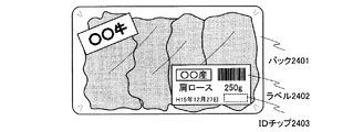
図18(C)はスーパーマーケットなどの小売店で商品を扱う際の商品管理を行うためのIDチップ1622を商品1620に貼付した例である。本発明はIDチップ1622内のメモリ回路に適用される。このようにIDチップ1622を商品1620に貼付することにより、在庫管理が容易になるだけではなく、万引きなどの被害を防ぐことも可能である。図面ではIDチップ1622が剥がれ落ちてしまうことを防ぐために接着を兼ねた保護膜1621を用いているが、IDチップ1622を接着剤によって直接商品1620に貼付するような構造を取っていてもよい。また、商品1620に貼付する構造上、IDチップ1622は、実施例2で挙げたフレキシブル基板を用いて作製すると好ましい。
FIG. 18C shows an example in which an
図18(D)は商品製造時に識別用のIDチップを組み込んだ例である。図面では例としてディスプレイの筐体1630にIDチップ1631を組み込まれている。本発明はIDチップ1631内のメモリ回路に適用される。このような構造を取ることにより製造メーカーにおいて、商品の識別、または流通管理などを容易に行うことができる。なお、図面ではディスプレイの筐体を例として取り上げているが、本発明はこれに限定されることはなく、さまざまな電子機器、物品に対して適用することが可能である。
FIG. 18D shows an example in which an ID chip for identification is incorporated at the time of product manufacture. In the drawing, an
図18(E)は物品搬送用の荷札である。図面では荷札1640内にIDチップ1641が組み込まれている。本発明はIDチップ1641内のメモリ回路に適用される。このような構造を取ることにより搬送先の選別や商品の流通管理などを容易に行うことができる。なお、図面では、紐で物品に荷札をくくりつけるような構造を取っているが、本発明はこれに限定されることはなく、シール材のようなものを用いて物品に直接荷札を貼付するような構造を取ってもよい。
FIG. 18E shows an article transport tag. In the drawing, an
図18(F)は本1650にIDチップ1652が組み込まれたものである。本発明はIDチップ1652内のメモリ回路に適用される。このような構造を取ることにより書店における流通管理や図書館などでの貸し出し処理などを容易に行うことができる。なお、図面ではIDチップ1652が剥がれ落ちてしまうことを防ぐために接着を兼ねた保護膜1651を用いているが、IDチップ1652を接着剤によって直接本1650に貼付するような構造を取る、または本1650の表紙にIDチップ1652を埋め込む構造を取っていてもよい。
FIG. 18F shows an
図18(G)は紙幣1660にIDチップ1661が組み込まれたものである。本発明はIDチップ1661内のメモリ回路に適用される。このような構造を取ることにより偽札の流通を阻止することが容易に行える。なお、紙幣の性質上IDチップ1661が剥がれ落ちるのを防ぐために紙幣1660に埋め込むような構造を取るとより好ましい。本発明は紙幣に限らず、有価証券、パスポートなど紙を材質にしたものに適用可能である。
FIG. 18G illustrates an example in which an
図18(H)は靴1670にIDチップ1672が組み込まれたものである。本発明はIDチップ1672内のメモリ回路に適用される。このような構造を取ることにより製造メーカーの識別、または商品の流通管理などを容易に行うことができる。図面ではIDチップ1672が剥がれ落ちてしまうことを防ぐために接着を兼ねた保護膜1671を用いているが、IDチップ1672を接着剤を用いて直接貼付するような構造を取る、または靴1670に埋め込む構造を取っていてもよい。本発明は靴に限らず、バッグ、衣類など身に付けるものに適用可能である。
FIG. 18H shows an shoe in which an
次にセキュリティ確保のため、例えば、盗難防止又は偽造防止を目的として、多様な物品へIDチップを実装する場合を説明する。 Next, in order to ensure security, for example, a case where ID chips are mounted on various articles for the purpose of preventing theft or forgery will be described.
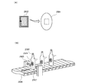
盗難防止を目的としてIDチップを使用する例として、バッグにIDチップを実装する場合を説明する。本発明はIDチップ2202内のメモリ回路に適応される。図19に示すように、バッグ2201にIDチップ2202を実装する。例えば、バッグ2201の底又は側面の一部等にIDチップ2202を実装することができる。IDチップ2202は非常に薄型で小さいため、バッグ2201のデザイン性を低下させずに実装することができる。加えてIDチップ2202は透光性を有するため、IDチップ2202が実装されているか否かの判断が困難である。そのため、盗難者によってIDチップ2202が取り外される可能性が低い。 As an example of using an ID chip for the purpose of preventing theft, a case where the ID chip is mounted on a bag will be described. The present invention is applied to a memory circuit in the ID chip 2202. As shown in FIG. 19, an ID chip 2202 is mounted on a bag 2201. For example, the ID chip 2202 can be mounted on the bottom or part of the side surface of the bag 2201. Since the ID chip 2202 is very thin and small, it can be mounted without deteriorating the design of the bag 2201. In addition, since the ID chip 2202 has a light-transmitting property, it is difficult to determine whether or not the ID chip 2202 is mounted. Therefore, the possibility that the ID chip 2202 is removed by the theft is low.
このようなIDチップ2202を実装したバッグ2201が盗難された場合、例えばGPS(Global Positioning System)を用いてバッグ2201の現在位置に関する情報を得ることができる。なおGPSとは、GPS用の衛星から信号が送られた時間と、それが受け取られた時間との時間差を求め、これをもとに測位するシステムである。 When the bag 2201 on which such an ID chip 2202 is mounted is stolen, information on the current position of the bag 2201 can be obtained using, for example, GPS (Global Positioning System). The GPS is a system that obtains a time difference between the time when a signal is sent from a GPS satellite and the time when the signal is received, and performs positioning based on the time difference.
また盗難された物品以外に、バッグ2201を忘れた場合や落とした場合などにも、GPSを用いて現在位置に関する情報を得ることができる。 In addition to the stolen article, information on the current position can be obtained using GPS even when the bag 2201 is forgotten or dropped.
またバッグ2201以外にも、自動車、自転車等の乗物、時計やアクセサリーにIDチップを実装することができる。 In addition to the bag 2201, an ID chip can be mounted on a vehicle such as an automobile or a bicycle, a watch, or an accessory.
次に偽造防止を目的としてIDチップを使用する例として、パスポートや免許証等にIDチップを実装する場合を説明する。 Next, as an example of using an ID chip for the purpose of preventing forgery, a case where the ID chip is mounted on a passport, a license, or the like will be described.
図20(A)に、IDチップを実装したパスポート2301を示す。図20(A)ではIDチップ2302がパスポート2301の表紙に実装されているが、その他のページに実装してもよい。また、IDチップ2302は透光性を有するため表面に実装してもよい。またIDチップ2302を表紙等の材料で挟み込むようにし、表紙の内部に実装することも可能である。
FIG. 20A shows a
図20(B)には、IDチップを実装した免許証2303を示す。図20(B)では、IDチップ2304が免許証2303の内部に実装されている。またIDチップ2304は透光性を有するため、免許証2303の印刷面上に設けても構わない。例えば、IDチップ2304は免許証2303の印字面上に実装し、その上下に熱硬化性を有する樹脂膜を1組ずつ配置して挟み込み、熱でフィルムを圧着することによって、IDチップ2304を実装した免許証2303を覆うことができる。またIDチップ2304を免許証2303の材料で挟み込むようにし、内部に実装することも可能である。
FIG. 20B shows a
以上のような物品にIDチップを実装することにより、偽造を防止することができる。加えて非常に薄型で小さいIDチップを用いるため、パスポートや免許証等のデザイン性を損ねることがない。さらにIDチップは透光性を有するため、表面に実装しても構わない。 Forgery can be prevented by mounting the ID chip on the article as described above. In addition, since a very thin and small ID chip is used, the design such as a passport and a license is not impaired. Furthermore, since the ID chip has translucency, it may be mounted on the surface.
またIDチップを実装することにより、パスポートや免許証等の管理を簡便に行うことができる。さらにパスポートや免許証等に直接情報を記入することなく、IDチップに保存することができるため、プライバシーを守ることができる。 In addition, by installing the ID chip, it is possible to easily manage passports and licenses. Furthermore, since information can be stored in the ID chip without directly entering information in a passport or a license, privacy can be protected.
次に、安全管理を行うため、食料品等の商品へIDチップを実装する場合を図21を用いて説明する。 Next, in order to perform safety management, a case where an ID chip is mounted on a commodity such as food will be described with reference to FIG.
図21は、IDチップ2403を実装したラベル2402と、当該ラベル2402が貼られた肉のパック2401を示す。IDチップ2403はラベル2402の表面に実装していてもよいし、ラベル2402内部に実装してもよい。また野菜等の生鮮食品の場合、生鮮食品を覆うラップにIDチップを実装してもよい。 FIG. 21 shows a label 2402 on which an ID chip 2403 is mounted and a meat pack 2401 to which the label 2402 is attached. The ID chip 2403 may be mounted on the surface of the label 2402 or may be mounted inside the label 2402. In the case of fresh food such as vegetables, an ID chip may be mounted on a wrap that covers the fresh food.
IDチップ2403には、商品の生産地、生産者、加工年月日、賞味期限等の商品に関する基本事項を記録することができる。このような基本事項は、書き換える必要がないためMROM等の書き換え不能なメモリを用いて記録するとよい。更には商品を用いた調理例等の応用事項をIDチップ2403に記録することができる。このような応用事項は、EEPROM等の書き換え及び消去可能なメモリを用いて記録するとよい。 The ID chip 2403 can record basic items related to the product such as the product production location, producer, processing date, and expiration date. Such basic matters do not need to be rewritten, and are preferably recorded using a non-rewritable memory such as MROM. Furthermore, application items such as cooking examples using products can be recorded in the ID chip 2403. Such application items may be recorded using a rewritable and erasable memory such as an EEPROM.
また食料品の安全管理を行うためには、加工前の動植物の状態を知り得ることが重要である。そのため、動植物内にIDチップを埋め込み、リーダ装置によって動植物に関する情報を取得するとよい。動植物に関する情報とは、飼育地、飼料、飼育者、伝染病の感染の有無等である。 In addition, it is important to be able to know the state of animals and plants before processing in order to carry out food safety management. Therefore, it is preferable to embed an ID chip in animals and plants and acquire information on animals and plants by a reader device. Information on animals and plants includes breeding grounds, feed, breeders, presence of infectious diseases, and the like.
またIDチップに、商品の値段が記録されていれば、従来のバーコードを用いる方式よりも、簡便、短時間に商品の精算を行うことが可能となる。すなわち、IDチップが実装された複数の商品を一挙に精算することができる。但し、このように複数のIDチップを一度に読み取る場合、アンチコリジョン機能をリーダ装置に搭載する必要がある。 Further, if the price of the product is recorded on the ID chip, the product can be settled more easily and in a shorter time than the method using the conventional barcode. That is, it is possible to settle a plurality of products on which the ID chip is mounted all at once. However, when reading a plurality of ID chips at the same time, it is necessary to mount an anti-collision function in the reader device.
さらにIDチップの通信距離によっては、レジスターと商品との距離が遠くても、商品の精算を可能とすることができる。またIDチップは万引きの防止を目的とした利用も可能である。 Furthermore, depending on the communication distance of the ID chip, the product can be settled even if the distance between the register and the product is long. The ID chip can be used for the purpose of preventing shoplifting.
さらにIDチップは、バーコード、磁気テープ等のその他の情報媒体と併用することもできる。例えば、IDチップには書き換え不要な基本事項を記録し、バーコードには更新すべき情報、例えば値引き価格や特価情報を記録するとよい。バーコードはIDチップと異なり、情報の修正を簡便に行うことができるからである。 Furthermore, the ID chip can be used in combination with other information media such as a barcode and a magnetic tape. For example, basic items that do not need to be rewritten are recorded on the ID chip, and information to be updated, such as discount prices and special price information, may be recorded on the barcode. This is because, unlike an ID chip, a bar code can easily correct information.
このようにIDチップを商品に実装することにより、消費者へ提供できる情報を増大させることができる。 By mounting the ID chip on the product in this manner, information that can be provided to consumers can be increased.
次に図22を用いて、物流管理を行うため、ビール瓶等の商品へIDチップを実装する場合を説明する。例えば、図22(A)に示すように、ラベル2501を用いてビール瓶にIDチップ2502を実装することができる。
Next, a case where an ID chip is mounted on a product such as a beer bottle for distribution management will be described with reference to FIG. For example, as shown in FIG. 22A, a
IDチップ2502には、ビールの製造日、製造場所、使用材料等の基本事項を記録する。このような基本事項は、書き換える必要がないためマスクROM等の書き換え不能なメモリを用いて記録するとよい。加えてIDチップには、各ビール瓶の配送先、配送日時等の個別事項を記録する。例えば、図22(B)に示すように、ビール瓶2503が、各々ベルトコンベア2506により流れ、ライタ装置2505を通過するときに、ラベル2504に内蔵されたIDチップ2507に各配送先、配送日時を記録することができる。このような個別事項は、EEPROM等の書き換え及び消去可能なメモリを用いて記録するとよい。
The
また配達先から購入された商品情報がネットワークを通じて物流管理センターへ送信されると、この商品情報に基づき、ライタ装置又は当該ライタ装置を制御するパーソナルコンピュータ等が配送先や配送日時を算出し、IDチップへ記録するようなシステムを構築するとよい。 When the product information purchased from the delivery destination is transmitted to the distribution management center through the network, the writer device or a personal computer that controls the writer device calculates the delivery destination and the delivery date and time based on this product information. A system that records on a chip should be constructed.
また一般的にビール瓶の配達はケース毎に行われるため、ケース毎、又は複数のケース毎にIDチップを実装し、個別事項を記録することもできる。 Moreover, since delivery of a beer bottle is generally performed for each case, an ID chip can be mounted for each case or for each of a plurality of cases to record individual matters.
このような複数の配達先が記録されうる飲料品は、IDチップを実装することにより、手作業で行う入力にかかる時間を削減でき、それに起因した入力ミスを低減することができる。加えて物流管理の分野において最もコストのかかる人件費用を削減することができる。従って、IDチップを実装したことにより、ミスの少ない、低コストな物流管理を行うことができる。 By installing an ID chip in such a beverage product in which a plurality of delivery destinations can be recorded, the time required for manual input can be reduced, and input errors caused by the input can be reduced. In addition, labor costs that are the most expensive in the field of logistics management can be reduced. Therefore, by mounting the ID chip, it is possible to carry out low-cost logistics management with few mistakes.
さらに配達先において、ビールに合う食料品や、ビールを使った料理法等の応用事項を記録してもよい。その結果、食料品等の宣伝を兼ねることができ、消費者の購買意欲を高めることができる。このような応用事項は、EEPROM等の書き換え、消去可能なメモリを用いて記録するとよい。このようにIDチップを実装することにより、消費者へ提供できる情報を増大させることができるため、消費者は安心して商品を購入することができる。 Furthermore, application items such as foods suitable for beer and cooking methods using beer may be recorded at the delivery destination. As a result, it can serve as an advertisement for foods and the like, and the consumer's willingness to purchase can be enhanced. Such application items may be recorded using a rewritable and erasable memory such as an EEPROM. By mounting the ID chip in this way, information that can be provided to the consumer can be increased, so that the consumer can purchase the product with peace of mind.
製造管理を行うため、IDチップを実装した製造品と、当該IDチップの情報に基づき制御される製造装置(製造ロボット)について説明する。 In order to perform manufacturing management, a manufactured product on which an ID chip is mounted and a manufacturing apparatus (manufacturing robot) controlled based on information on the ID chip will be described.
オリジナル商品を生産する場合、生産ラインでは商品にIDチップを実装し、IDチップに記録されたオリジナル情報に基づくように商品を生産することができる。例えば、ドアの塗装色を自由に選択する自動車の生産ラインにおいては、自動車の一部にIDチップを実装し、当該IDチップからの情報に基づき、塗装装置を制御することができる。 When producing an original product, an ID chip is mounted on the product on the production line, and the product can be produced based on the original information recorded on the ID chip. For example, in an automobile production line in which the paint color of a door is freely selected, an ID chip can be mounted on a part of the automobile, and the coating apparatus can be controlled based on information from the ID chip.
上記のように、自動車の一部にIDチップを実装する結果、事前に生産ラインに投入される自動車の順序や同色を有する数を調整する必要がない。強いては、自動車の順序や数に合わせるように塗装装置を制御するプログラムを設定しなくてすむ。すなわち製造装置は、自動車に実装されたIDチップの情報に基づき、個別に動作することができる。 As described above, as a result of mounting the ID chip on a part of the automobile, it is not necessary to adjust the order of the automobiles to be put on the production line or the number having the same color in advance. For this reason, it is not necessary to set a program for controlling the painting apparatus to match the order and number of cars. That is, the manufacturing apparatus can operate individually based on the information of the ID chip mounted on the automobile.
このようにIDチップは様々な場所で使用することができる。そしてIDチップに記録された情報により、製造に関する固有情報を得ることができ、当該情報に基づき製造装置を制御することができる。 Thus, the ID chip can be used in various places. And the specific information regarding manufacture can be obtained from the information recorded on the ID chip, and the manufacturing apparatus can be controlled based on the information.
次に、本発明に係るIDチップを用いたICカードを、電子マネーとして利用する形態について説明する。図23に、ICカード2601を用いて、決済をおこなっている様子を示す。ICカード2601は、本発明に係るIDチップ2602を有している。ICカード2601の利用の際には、レジスター2603、リーダ/ライタ2604を用いる。IDチップ2602には、ICカード2601に入金されている金額の情報が保持されており、リーダ/ライタ2604は該金額の情報を非接触で読み取り、レジスター2603に送信することができる。レジスター2603では、ICカード2601に入金されている金額が、決済する金額以上であることを確認し、決済を行なう。そしてリーダ/ライタ2604に決済後の残額の情報を送信する。リーダ/ライタ2604は残額の情報を、ICカード2601のIDチップ2602に書き込むことができる。
Next, a mode in which an IC card using the ID chip according to the present invention is used as electronic money will be described. FIG. 23 shows how payment is performed using the
なおリーダ/ライタ2604に、暗証番号などを入力することができるキー2605を付加し、第三者によってICカード2601を用いた決済が無断で行なわれるのを制限できるようにしても良い。
Note that a key 2605 capable of inputting a personal identification number or the like may be added to the reader /
なお、本実施例に示した例はごく一例であり、これらの用途に限定するものではないことを付記する。 It should be noted that the examples shown in the present embodiment are only examples and are not limited to these applications.
以上の様に、本発明の適用範囲は極めて広く、あらゆる物品の個体認識用のチップとして適用することが可能である。 As described above, the application range of the present invention is extremely wide, and can be applied as a chip for individual recognition of any article.
本発明は、複数のレーザビームを被照射体に同時に照射して任意のパターンを描画できるレーザ照射装置及びレーザ照射方法である。この発明は、上記したようにROMの製作工程で用いることができるのみでなく、半導体プロセスにおける露光工程に適用することができる。また、レーザビームを被照射体に照射して所望の処理をする(例えば、文字の刻印など)ものに適用することができる。 The present invention is a laser irradiation apparatus and a laser irradiation method capable of drawing an arbitrary pattern by simultaneously irradiating an irradiated object with a plurality of laser beams. As described above, the present invention can be applied not only to the ROM manufacturing process but also to an exposure process in a semiconductor process. Further, the present invention can be applied to an object to be irradiated with a laser beam to perform desired processing (for example, character marking).
101 レーザ発振器
102 ミラー
103 エキスパンダ
104 回折光学素子
105 DMD
106 投影レンズ
107 遮光板
108 基板
109 吸着ステージ
110 搬送ステージ
111 搬送ステージ
101
106
Claims (12)
前記レーザ発振器から射出されたレーザビームを複数のレーザビームに分割する回折光学素子と、
前記回折光学素子により分割されたレーザビームを、偏向する複数のマイクロミラーと、
前記複数のマイクロミラーによって偏向されたそれぞれのレーザビームが照射される被照射体を載置する搬送ステージと、を有することを特徴とするレーザ照射装置。 A laser oscillator for emitting a laser beam;
A diffractive optical element for dividing a laser beam emitted from the laser oscillator into a plurality of laser beams;
A plurality of micromirrors for deflecting the laser beam divided by the diffractive optical element;
A laser irradiation apparatus comprising: a transfer stage on which an object to be irradiated to which each laser beam deflected by the plurality of micromirrors is irradiated is placed.
前記回折光学素子は透過型回折光学素子又は反射型回折光学素子であることを特徴とするレーザ照射装置。 In claim 1,
The diffractive optical element is a transmissive diffractive optical element or a reflective diffractive optical element.
前記複数に分割されたレーザビームは、互いに等しいエネルギーを有することを特徴とするレーザ照射装置。 In claim 1 or claim 2,
The laser irradiation apparatus according to claim 1, wherein the plurality of divided laser beams have equal energy.
前記回折光学素子と、前記搬送ステージとの間に配置された投影レンズを有することを特徴とするレーザ照射装置。 In any one of Claims 1 thru | or 3,
A laser irradiation apparatus comprising a projection lens disposed between the diffractive optical element and the transfer stage.
前記複数に分割されたレーザビームのスポットサイズは、前記マイクロミラーの表面積の大きさよりも小さいことを特徴とするレーザ照射装置。 In any one of Claims 1 thru | or 4,
The laser irradiation apparatus according to claim 1, wherein a spot size of the plurality of divided laser beams is smaller than a surface area of the micromirror.
前記複数に分割されたレーザビームを複数のマイクロミラーにおいて偏向して搬送ステージに載置された被照射体に照射することを特徴とするレーザ照射方法。 The laser beam emitted from the laser oscillator is incident on the diffractive optical element and divided into a plurality of parts,
A laser irradiation method characterized in that the laser beam divided into a plurality of beams is deflected by a plurality of micromirrors and irradiated onto an irradiated object placed on a transfer stage.
前記複数に分割されたレーザビームのうちの1つのレーザビームを第1のマイクロミラーに入射させ、他の1つのレーザビームを第2のマイクロミラーに入射させ、前記第1のマイクロミラー及び前記第2のマイクロミラーにおいて偏向された前記レーザビームを被照射面上に照射することを特徴とするレーザ照射方法。 The laser beam emitted from the laser oscillator is incident on the diffractive optical element and divided into a plurality of parts,
One of the plurality of divided laser beams is incident on a first micromirror, and the other one laser beam is incident on a second micromirror, and the first micromirror and the first micromirror A laser irradiation method comprising irradiating an irradiated surface with the laser beam deflected by two micromirrors.
前記回折光学素子は透過型回折光学素子又は反射型回折光学素子であることを特徴とするレーザ照射方法。 In claim 6 or claim 7,
The laser irradiation method, wherein the diffractive optical element is a transmissive diffractive optical element or a reflective diffractive optical element.
前記複数に分割されたレーザビームは互いに等しいエネルギーを有することを特徴とするレーザ照射方法。 In any one of Claims 6 to 8,
The laser irradiation method, wherein the plurality of divided laser beams have equal energy.
前記複数に分割されたレーザビームは、前記回折光学素子と、前記搬送ステージとの間に配置された投影レンズを通過した後、前記被照射面上に照射されることを特徴とするレーザ照射方法。 In any one of Claims 6 thru | or 9,
The laser beam splitting into a plurality of beams is irradiated onto the irradiated surface after passing through a projection lens disposed between the diffractive optical element and the transport stage. .
前記複数に分割されたレーザビームは、前記マイクロミラーの中央部または中央部と隅の間に集光されることを特徴とするレーザ照射方法。 In any one of Claims 6 to 10,
The laser irradiation method according to claim 1, wherein the laser beam divided into a plurality of portions is condensed between a central portion or a central portion and a corner of the micromirror.
前記複数の島状半導体層上に第1の層間絶縁膜を形成し、
前記第1の層間絶縁膜を介して前記複数の島状半導体層上に、それぞれゲート電極を形成し、
前記ゲート電極上に第2の層間絶縁膜を形成し、
前記第2の層間絶縁膜上にレジストを設け、
回折光学素子を通過して複数に分岐したレーザビームを、複数のマイクロミラーによって偏向し、
前記複数のマイクロミラーによって偏向されたそれぞれのレーザビームを前記レジストに照射し、
前記レーザビームが照射された前記レジストを現像し、
前記レジストをマスクとして、前記第1の層間絶縁膜及び前記第2の層間絶縁膜をエッチングし、選択的にコンタクトホールを形成することを特徴とする半導体装置の作製方法。 Forming a plurality of island-shaped semiconductor layers having a source electrode or a drain electrode on a substrate;
Forming a first interlayer insulating film on the plurality of island-shaped semiconductor layers;
Forming a gate electrode on each of the plurality of island-like semiconductor layers via the first interlayer insulating film;
Forming a second interlayer insulating film on the gate electrode;
Providing a resist on the second interlayer insulating film;
A laser beam branched into a plurality of beams through the diffractive optical element is deflected by a plurality of micromirrors,
Irradiating the resist with each laser beam deflected by the plurality of micromirrors;
Developing the resist irradiated with the laser beam;
A method of manufacturing a semiconductor device, wherein the first interlayer insulating film and the second interlayer insulating film are etched using the resist as a mask to selectively form contact holes.
Priority Applications (1)
| Application Number | Priority Date | Filing Date | Title |
|---|---|---|---|
| JP2007038802A JP2007258691A (en) | 2006-02-21 | 2007-02-20 | Device for laser irradiation, method of laser irradiation, and method of fabricating semiconductor device |
Applications Claiming Priority (2)
| Application Number | Priority Date | Filing Date | Title |
|---|---|---|---|
| JP2006044201 | 2006-02-21 | ||
| JP2007038802A JP2007258691A (en) | 2006-02-21 | 2007-02-20 | Device for laser irradiation, method of laser irradiation, and method of fabricating semiconductor device |
Publications (2)
| Publication Number | Publication Date |
|---|---|
| JP2007258691A true JP2007258691A (en) | 2007-10-04 |
| JP2007258691A5 JP2007258691A5 (en) | 2010-04-02 |
Family
ID=38632575
Family Applications (1)
| Application Number | Title | Priority Date | Filing Date |
|---|---|---|---|
| JP2007038802A Withdrawn JP2007258691A (en) | 2006-02-21 | 2007-02-20 | Device for laser irradiation, method of laser irradiation, and method of fabricating semiconductor device |
Country Status (1)
| Country | Link |
|---|---|
| JP (1) | JP2007258691A (en) |
Cited By (14)
| Publication number | Priority date | Publication date | Assignee | Title |
|---|---|---|---|---|
| JP2009117812A (en) * | 2007-10-16 | 2009-05-28 | Nikon Corp | Illumination optical system, exposure apparatus, and device manufacturing method |
| WO2009078223A1 (en) * | 2007-12-17 | 2009-06-25 | Nikon Corporation | Spatial light modulating unit, illumination optical system, aligner, and device manufacturing method |
| JP2009158911A (en) * | 2007-06-14 | 2009-07-16 | Asml Netherlands Bv | Illumination of patterning device based on interference for use in maskless lithography |
| WO2009104272A1 (en) * | 2008-02-22 | 2009-08-27 | リン グループ エルエルシー | Total transaction system using identification card |
| US7975913B2 (en) | 2006-08-22 | 2011-07-12 | Rynne Group, Llc | Discernment card and a discernment card business system using the discernment card |
| JP2013048237A (en) * | 2011-08-19 | 2013-03-07 | Ultratech Inc | Programmable light-emitting body used for photolithography system |
| US9341954B2 (en) | 2007-10-24 | 2016-05-17 | Nikon Corporation | Optical unit, illumination optical apparatus, exposure apparatus, and device manufacturing method |
| US9678332B2 (en) | 2007-11-06 | 2017-06-13 | Nikon Corporation | Illumination apparatus, illumination method, exposure apparatus, and device manufacturing method |
| JP2018041951A (en) * | 2016-09-08 | 2018-03-15 | マッパー・リソグラフィー・アイピー・ビー.ブイ. | Secure chip including serial number |
| JP2018041950A (en) * | 2016-09-08 | 2018-03-15 | マッパー・リソグラフィー・アイピー・ビー.ブイ. | Method and system for fabricating unique chip using charged particle multi-beamlet lithography system |
| JP2018074133A (en) * | 2016-10-27 | 2018-05-10 | マッパー・リソグラフィー・アイピー・ビー.ブイ. | Manufacture of unique chip by using charged particle multi-beamlet lithography system |
| JP2018077494A (en) * | 2007-10-12 | 2018-05-17 | 株式会社ニコン | Illumination optical apparatus, exposure apparatus, and method for manufacturing device |
| WO2020129562A1 (en) * | 2018-12-18 | 2020-06-25 | 株式会社ブイ・テクノロジー | Laser annealing apparatus |
| JP7471488B2 (en) | 2007-12-03 | 2024-04-19 | 株式会社半導体エネルギー研究所 | Semiconductor Device |
Citations (10)
| Publication number | Priority date | Publication date | Assignee | Title |
|---|---|---|---|---|
| JP2002228818A (en) * | 2001-02-05 | 2002-08-14 | Taiyo Yuden Co Ltd | Diffraction optical device for laser beam machining and device and method for laser beam machining |
| JP2004062149A (en) * | 2002-06-07 | 2004-02-26 | Fuji Photo Film Co Ltd | Transmissive 2-dimensional optical modulation element and exposure device using the same |
| JP2004062156A (en) * | 2002-06-07 | 2004-02-26 | Fuji Photo Film Co Ltd | Exposure head and exposure apparatus |
| JP2004062155A (en) * | 2002-06-07 | 2004-02-26 | Fuji Photo Film Co Ltd | Exposure head and exposure device |
| JP2005209798A (en) * | 2004-01-21 | 2005-08-04 | Fuji Photo Film Co Ltd | Method and device for exposing image |
| JP2005208491A (en) * | 2004-01-26 | 2005-08-04 | Fuji Photo Film Co Ltd | Optical modulation element, optical modulation element array and image forming apparatus |
| WO2005084873A1 (en) * | 2004-03-02 | 2005-09-15 | Sumitomo Heavy Industries, Ltd. | Laser beam application device and pattern drawing method |
| JP2005275325A (en) * | 2004-03-26 | 2005-10-06 | Fuji Photo Film Co Ltd | Image exposing device |
| JP2006108465A (en) * | 2004-10-07 | 2006-04-20 | Nikon Corp | Optical characteristic measurement equipment and exposure device |
| JP2007235117A (en) * | 2006-02-03 | 2007-09-13 | Semiconductor Energy Lab Co Ltd | Manufacturing method of memory cell, laser irradiation apparatus, and laser irradiation method |
-
2007
- 2007-02-20 JP JP2007038802A patent/JP2007258691A/en not_active Withdrawn
Patent Citations (10)
| Publication number | Priority date | Publication date | Assignee | Title |
|---|---|---|---|---|
| JP2002228818A (en) * | 2001-02-05 | 2002-08-14 | Taiyo Yuden Co Ltd | Diffraction optical device for laser beam machining and device and method for laser beam machining |
| JP2004062149A (en) * | 2002-06-07 | 2004-02-26 | Fuji Photo Film Co Ltd | Transmissive 2-dimensional optical modulation element and exposure device using the same |
| JP2004062156A (en) * | 2002-06-07 | 2004-02-26 | Fuji Photo Film Co Ltd | Exposure head and exposure apparatus |
| JP2004062155A (en) * | 2002-06-07 | 2004-02-26 | Fuji Photo Film Co Ltd | Exposure head and exposure device |
| JP2005209798A (en) * | 2004-01-21 | 2005-08-04 | Fuji Photo Film Co Ltd | Method and device for exposing image |
| JP2005208491A (en) * | 2004-01-26 | 2005-08-04 | Fuji Photo Film Co Ltd | Optical modulation element, optical modulation element array and image forming apparatus |
| WO2005084873A1 (en) * | 2004-03-02 | 2005-09-15 | Sumitomo Heavy Industries, Ltd. | Laser beam application device and pattern drawing method |
| JP2005275325A (en) * | 2004-03-26 | 2005-10-06 | Fuji Photo Film Co Ltd | Image exposing device |
| JP2006108465A (en) * | 2004-10-07 | 2006-04-20 | Nikon Corp | Optical characteristic measurement equipment and exposure device |
| JP2007235117A (en) * | 2006-02-03 | 2007-09-13 | Semiconductor Energy Lab Co Ltd | Manufacturing method of memory cell, laser irradiation apparatus, and laser irradiation method |
Cited By (17)
| Publication number | Priority date | Publication date | Assignee | Title |
|---|---|---|---|---|
| US7975913B2 (en) | 2006-08-22 | 2011-07-12 | Rynne Group, Llc | Discernment card and a discernment card business system using the discernment card |
| JP2009158911A (en) * | 2007-06-14 | 2009-07-16 | Asml Netherlands Bv | Illumination of patterning device based on interference for use in maskless lithography |
| US10101666B2 (en) | 2007-10-12 | 2018-10-16 | Nikon Corporation | Illumination optical apparatus, exposure apparatus, and device manufacturing method |
| JP2018077494A (en) * | 2007-10-12 | 2018-05-17 | 株式会社ニコン | Illumination optical apparatus, exposure apparatus, and method for manufacturing device |
| JP2009117812A (en) * | 2007-10-16 | 2009-05-28 | Nikon Corp | Illumination optical system, exposure apparatus, and device manufacturing method |
| US9341954B2 (en) | 2007-10-24 | 2016-05-17 | Nikon Corporation | Optical unit, illumination optical apparatus, exposure apparatus, and device manufacturing method |
| US9857599B2 (en) | 2007-10-24 | 2018-01-02 | Nikon Corporation | Optical unit, illumination optical apparatus, exposure apparatus, and device manufacturing method |
| US9678332B2 (en) | 2007-11-06 | 2017-06-13 | Nikon Corporation | Illumination apparatus, illumination method, exposure apparatus, and device manufacturing method |
| JP7471488B2 (en) | 2007-12-03 | 2024-04-19 | 株式会社半導体エネルギー研究所 | Semiconductor Device |
| WO2009078223A1 (en) * | 2007-12-17 | 2009-06-25 | Nikon Corporation | Spatial light modulating unit, illumination optical system, aligner, and device manufacturing method |
| WO2009104272A1 (en) * | 2008-02-22 | 2009-08-27 | リン グループ エルエルシー | Total transaction system using identification card |
| TWI497229B (en) * | 2011-08-19 | 2015-08-21 | Ultratech Inc | Photolithography system and photolithography method |
| JP2013048237A (en) * | 2011-08-19 | 2013-03-07 | Ultratech Inc | Programmable light-emitting body used for photolithography system |
| JP2018041951A (en) * | 2016-09-08 | 2018-03-15 | マッパー・リソグラフィー・アイピー・ビー.ブイ. | Secure chip including serial number |
| JP2018041950A (en) * | 2016-09-08 | 2018-03-15 | マッパー・リソグラフィー・アイピー・ビー.ブイ. | Method and system for fabricating unique chip using charged particle multi-beamlet lithography system |
| JP2018074133A (en) * | 2016-10-27 | 2018-05-10 | マッパー・リソグラフィー・アイピー・ビー.ブイ. | Manufacture of unique chip by using charged particle multi-beamlet lithography system |
| WO2020129562A1 (en) * | 2018-12-18 | 2020-06-25 | 株式会社ブイ・テクノロジー | Laser annealing apparatus |
Similar Documents
| Publication | Publication Date | Title |
|---|---|---|
| KR101418730B1 (en) | Laser irradiation apparatus, method of laser irradiation, and method for manufacturing semiconductor device | |
| JP2007258691A (en) | Device for laser irradiation, method of laser irradiation, and method of fabricating semiconductor device | |
| JP4776941B2 (en) | Semiconductor device manufacturing method, IC card, IC tag, RFID, transponder, banknote, securities, passport, electronic device, bag, and clothing | |
| US8426324B2 (en) | Manufacturing method of memory element, laser irradiation apparatus, and laser irradiation method | |
| US7663473B2 (en) | Semiconductor device, IC card, IC tag, RFID, transponder, bills, securities, passport, electronic apparatus, bag, and clothes | |
| JP5395348B2 (en) | Method for manufacturing semiconductor device | |
| JP4718850B2 (en) | Semiconductor devices, IC cards, IC tags, RFID, transponders, banknotes, securities, passports, electronic devices, bags, and clothing | |
| JP4836466B2 (en) | Semiconductor device | |
| US8580700B2 (en) | Method for manufacturing semiconductor device | |
| JP5178022B2 (en) | Method for manufacturing memory element | |
| KR101123753B1 (en) | Laser irradiation apparatus and method for manufacturing semiconductor device | |
| JP5386064B2 (en) | Method for manufacturing semiconductor device | |
| JP4776940B2 (en) | Integrated circuit, semiconductor device, and wireless chip | |
| JP5227499B2 (en) | Laser irradiation device | |
| JP4836523B2 (en) | Semiconductor devices, IC cards, IC tags, RFID, transponders, banknotes, securities, passports, electronic devices, bags, and clothing | |
| JP5121119B2 (en) | Chip loading |
Legal Events
| Date | Code | Title | Description |
|---|---|---|---|
| A521 | Request for written amendment filed |
Free format text: JAPANESE INTERMEDIATE CODE: A523 Effective date: 20100212 |
|
| A621 | Written request for application examination |
Free format text: JAPANESE INTERMEDIATE CODE: A621 Effective date: 20100212 |
|
| A977 | Report on retrieval |
Free format text: JAPANESE INTERMEDIATE CODE: A971007 Effective date: 20120124 |
|
| A131 | Notification of reasons for refusal |
Free format text: JAPANESE INTERMEDIATE CODE: A131 Effective date: 20120131 |
|
| A521 | Request for written amendment filed |
Free format text: JAPANESE INTERMEDIATE CODE: A523 Effective date: 20120329 |
|
| A02 | Decision of refusal |
Free format text: JAPANESE INTERMEDIATE CODE: A02 Effective date: 20120717 |
|
| A761 | Written withdrawal of application |
Free format text: JAPANESE INTERMEDIATE CODE: A761 Effective date: 20121009 |