EP2645407B1 - Optisches Beleuchtungssystem und Projektionsbelichtungsvorrichtung - Google Patents
Optisches Beleuchtungssystem und Projektionsbelichtungsvorrichtung Download PDFInfo
- Publication number
- EP2645407B1 EP2645407B1 EP13165340.4A EP13165340A EP2645407B1 EP 2645407 B1 EP2645407 B1 EP 2645407B1 EP 13165340 A EP13165340 A EP 13165340A EP 2645407 B1 EP2645407 B1 EP 2645407B1
- Authority
- EP
- European Patent Office
- Prior art keywords
- illumination
- polarization
- light
- birefringent
- optical
- Prior art date
- Legal status (The legal status is an assumption and is not a legal conclusion. Google has not performed a legal analysis and makes no representation as to the accuracy of the status listed.)
- Not-in-force
Links
Images


Classifications
-
- G—PHYSICS
- G03—PHOTOGRAPHY; CINEMATOGRAPHY; ANALOGOUS TECHNIQUES USING WAVES OTHER THAN OPTICAL WAVES; ELECTROGRAPHY; HOLOGRAPHY
- G03F—PHOTOMECHANICAL PRODUCTION OF TEXTURED OR PATTERNED SURFACES, e.g. FOR PRINTING, FOR PROCESSING OF SEMICONDUCTOR DEVICES; MATERIALS THEREFOR; ORIGINALS THEREFOR; APPARATUS SPECIALLY ADAPTED THEREFOR
- G03F7/00—Photomechanical, e.g. photolithographic, production of textured or patterned surfaces, e.g. printing surfaces; Materials therefor, e.g. comprising photoresists; Apparatus specially adapted therefor
- G03F7/70—Microphotolithographic exposure; Apparatus therefor
- G03F7/70058—Mask illumination systems
- G03F7/70191—Optical correction elements, filters or phase plates for controlling intensity, wavelength, polarisation, phase or the like
-
- G—PHYSICS
- G02—OPTICS
- G02B—OPTICAL ELEMENTS, SYSTEMS OR APPARATUS
- G02B27/00—Optical systems or apparatus not provided for by any of the groups G02B1/00 - G02B26/00, G02B30/00
- G02B27/28—Optical systems or apparatus not provided for by any of the groups G02B1/00 - G02B26/00, G02B30/00 for polarising
- G02B27/286—Optical systems or apparatus not provided for by any of the groups G02B1/00 - G02B26/00, G02B30/00 for polarising for controlling or changing the state of polarisation, e.g. transforming one polarisation state into another
-
- G—PHYSICS
- G02—OPTICS
- G02B—OPTICAL ELEMENTS, SYSTEMS OR APPARATUS
- G02B5/00—Optical elements other than lenses
- G02B5/30—Polarising elements
- G02B5/3083—Birefringent or phase retarding elements
-
- G—PHYSICS
- G03—PHOTOGRAPHY; CINEMATOGRAPHY; ANALOGOUS TECHNIQUES USING WAVES OTHER THAN OPTICAL WAVES; ELECTROGRAPHY; HOLOGRAPHY
- G03F—PHOTOMECHANICAL PRODUCTION OF TEXTURED OR PATTERNED SURFACES, e.g. FOR PRINTING, FOR PROCESSING OF SEMICONDUCTOR DEVICES; MATERIALS THEREFOR; ORIGINALS THEREFOR; APPARATUS SPECIALLY ADAPTED THEREFOR
- G03F7/00—Photomechanical, e.g. photolithographic, production of textured or patterned surfaces, e.g. printing surfaces; Materials therefor, e.g. comprising photoresists; Apparatus specially adapted therefor
- G03F7/70—Microphotolithographic exposure; Apparatus therefor
- G03F7/70058—Mask illumination systems
- G03F7/70091—Illumination settings, i.e. intensity distribution in the pupil plane or angular distribution in the field plane; On-axis or off-axis settings, e.g. annular, dipole or quadrupole settings; Partial coherence control, i.e. sigma or numerical aperture [NA]
- G03F7/70108—Off-axis setting using a light-guiding element, e.g. diffractive optical elements [DOEs] or light guides
-
- G—PHYSICS
- G03—PHOTOGRAPHY; CINEMATOGRAPHY; ANALOGOUS TECHNIQUES USING WAVES OTHER THAN OPTICAL WAVES; ELECTROGRAPHY; HOLOGRAPHY
- G03F—PHOTOMECHANICAL PRODUCTION OF TEXTURED OR PATTERNED SURFACES, e.g. FOR PRINTING, FOR PROCESSING OF SEMICONDUCTOR DEVICES; MATERIALS THEREFOR; ORIGINALS THEREFOR; APPARATUS SPECIALLY ADAPTED THEREFOR
- G03F7/00—Photomechanical, e.g. photolithographic, production of textured or patterned surfaces, e.g. printing surfaces; Materials therefor, e.g. comprising photoresists; Apparatus specially adapted therefor
- G03F7/70—Microphotolithographic exposure; Apparatus therefor
- G03F7/70058—Mask illumination systems
- G03F7/7015—Details of optical elements
- G03F7/70158—Diffractive optical elements
-
- G—PHYSICS
- G03—PHOTOGRAPHY; CINEMATOGRAPHY; ANALOGOUS TECHNIQUES USING WAVES OTHER THAN OPTICAL WAVES; ELECTROGRAPHY; HOLOGRAPHY
- G03F—PHOTOMECHANICAL PRODUCTION OF TEXTURED OR PATTERNED SURFACES, e.g. FOR PRINTING, FOR PROCESSING OF SEMICONDUCTOR DEVICES; MATERIALS THEREFOR; ORIGINALS THEREFOR; APPARATUS SPECIALLY ADAPTED THEREFOR
- G03F7/00—Photomechanical, e.g. photolithographic, production of textured or patterned surfaces, e.g. printing surfaces; Materials therefor, e.g. comprising photoresists; Apparatus specially adapted therefor
- G03F7/70—Microphotolithographic exposure; Apparatus therefor
- G03F7/70483—Information management; Active and passive control; Testing; Wafer monitoring, e.g. pattern monitoring
- G03F7/7055—Exposure light control in all parts of the microlithographic apparatus, e.g. pulse length control or light interruption
- G03F7/70566—Polarisation control
-
- G—PHYSICS
- G03—PHOTOGRAPHY; CINEMATOGRAPHY; ANALOGOUS TECHNIQUES USING WAVES OTHER THAN OPTICAL WAVES; ELECTROGRAPHY; HOLOGRAPHY
- G03F—PHOTOMECHANICAL PRODUCTION OF TEXTURED OR PATTERNED SURFACES, e.g. FOR PRINTING, FOR PROCESSING OF SEMICONDUCTOR DEVICES; MATERIALS THEREFOR; ORIGINALS THEREFOR; APPARATUS SPECIALLY ADAPTED THEREFOR
- G03F7/00—Photomechanical, e.g. photolithographic, production of textured or patterned surfaces, e.g. printing surfaces; Materials therefor, e.g. comprising photoresists; Apparatus specially adapted therefor
- G03F7/70—Microphotolithographic exposure; Apparatus therefor
- G03F7/708—Construction of apparatus, e.g. environment aspects, hygiene aspects or materials
- G03F7/7095—Materials, e.g. materials for housing, stage or other support having particular properties, e.g. weight, strength, conductivity, thermal expansion coefficient
- G03F7/70958—Optical materials or coatings, e.g. with particular transmittance, reflectance or anti-reflection properties
- G03F7/70966—Birefringence
-
- G—PHYSICS
- G03—PHOTOGRAPHY; CINEMATOGRAPHY; ANALOGOUS TECHNIQUES USING WAVES OTHER THAN OPTICAL WAVES; ELECTROGRAPHY; HOLOGRAPHY
- G03F—PHOTOMECHANICAL PRODUCTION OF TEXTURED OR PATTERNED SURFACES, e.g. FOR PRINTING, FOR PROCESSING OF SEMICONDUCTOR DEVICES; MATERIALS THEREFOR; ORIGINALS THEREFOR; APPARATUS SPECIALLY ADAPTED THEREFOR
- G03F7/00—Photomechanical, e.g. photolithographic, production of textured or patterned surfaces, e.g. printing surfaces; Materials therefor, e.g. comprising photoresists; Apparatus specially adapted therefor
- G03F7/70—Microphotolithographic exposure; Apparatus therefor
- G03F7/70216—Mask projection systems
- G03F7/70341—Details of immersion lithography aspects, e.g. exposure media or control of immersion liquid supply
Definitions
- the present invention relates to illumination technology and exposure technology used in the lithography step for fabricating various devices, e.g., semiconductor integrated circuits (LSI and the like), image pickup devices, or liquid crystal displays and, more particularly, to illumination technology and exposure technology for illuminating a mask pattern with light in a predetermined polarization state. Furthermore, the present invention relates to device fabrication technology using the exposure technology.
- a method adopted is to project a demagnified image of a pattern on a reticle (or a photomask or the like) as a mask on which the pattern to be formed is drawn at a proportional magnification of about 4-5 times, through a projection optical system onto a wafer (or glass plate or the like) as a substrate to be exposed (photosensitive body) to effect exposure and transfer of the image.
- Projection exposure apparatus used for the exposure and transfer include those of a stationary exposure type such as steppers, and those of a scanning exposure type such as scanning steppers.
- the resolution of the projection optical system is proportional to a value obtained by dividing an exposure wavelength by a numerical aperture (NA) of the projection optical system.
- the numerical aperture (NA) of the projection optical system is given by multiplying a sine (sin) of a maximum angle of incidence of illumination light for exposure onto the wafer, by a refractive index of a medium through which the light passes.
- the exposure wavelength of the projection exposure apparatus has been decreased toward shorter wavelengths.
- the mainstream exposure wavelength at present is 248 nm of KrF excimer laser, and the shorter wavelength of 193 nm of ArF excimer laser is also close to practical use.
- so called super resolution techniques such as a method using a so-called phase shift reticle, and annular illumination, dipole illumination, and quadrupole illumination to control angles of incidence of the illumination light onto the reticle in a predetermined distribution.
- the annular illumination is to limit the incidence angle range of illumination light onto the reticle to predetermined angles, i.e., to limit the distribution of illumination light on the pupil plane of the illumination optical system to within a predetermined annular region centered on the optical axis of the illumination optical system, thereby offering the effect of improvement in the resolution and depth of focus (e.g., reference is made to Japanese Patent Application Laid-Open No. 61-91662 ).
- the dipole illumination and quadrupole illumination are applied to cases where the pattern on the reticle is one with specific directionality, and are arranged to limit, as well as the incidence angle range, the direction of incidence of the illumination light to a direction suitable for the directionality of the pattern, thereby achieving great improvement in the resolution and depth of focus (e.g., reference is made to Japanese Patent Application Laid-Open No. 4-101148 or U.S. Pat. No. 6,233,041 equivalent thereto and to Japanese Patent Application Laid-Open No. 4-225357 or U.S. Pat. No. 6,211,944 equivalent thereto).
- the illumination light emitted from the recently mainstream narrow-band KrF excimer laser source is uniform, linearly polarized light. If the light is kept in that polarization state and guided to the reticle, the reticle will be illuminated with the uniform, linearly polarized light, and it is thus needless to mention that it is infeasible to obtain the linearly polarized light with the polarization direction matched with the circumferential direction of the annular region on the pupil plane of the illumination optical system as described above,
- This method used only energy in the predetermined linear polarization component out of the energy of the illumination light of random polarization, i.e., only approximately half energy as the illumination light onto the reticle, and thus posed the problem of large loss in quantity of the illumination light and large loss in exposure power on the wafer in turn, resulting in reduction in processing performance (throughput) of the exposure apparatus.
- an illumination optical apparatus as recited in Claim 1 below.
- R reticle R wafer; ILS illumination optical system; AX2 optical axis of illumination system; nf fast axis; ns slow axis; 1 exposure light source; 4 polarization controlling member; 9a, 9b diffractive optical elements; 12 first birefringent member; 13 second birefringent member; 14 fly's eye lens; 25 projection optical system; 36 specific annular region; 41, 42 conical prisms
- the present example is an application of the present invention to a case where exposure is performed by a projection exposure apparatus of the scanning exposure type (scanning stepper) according to the step-and-scan method.
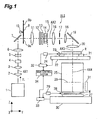
- Fig. 1 is a drawing showing a schematic configuration of the projection exposure apparatus of the present example partly cut, and in this Fig. 1 the projection exposure apparatus of the present example is provided with an illumination optical system ILS and a projection optical system 25.
- the former illumination optical system ILS is provided with a plurality of optical members arranged along the optical axis (optical axis of illumination system) AX1, AX2, AX3 from an exposure light source 1 (light source) to a condenser lens 20 (the details of which will be described later), and illuminates an illumination field on a pattern surface (reticle surface) of reticle R as a mask under a uniform illuminance distribution with illumination light for exposure (exposure light) IL as an exposure beam from the exposure light source 1.
- illumination optical system ILS is provided with a plurality of optical members arranged along the optical axis (optical axis of illumination system) AX1, AX2, AX3 from an exposure light source 1 (light source) to a condenser lens 20 (the details
- the latter projection optical system 25 projects a demagnified image at a projection magnification M (where M is a demagnification rate, e.g., 1/4 or 1/5) of a pattern in the illumination field on the reticle R, under the illumination light into an exposure region on one shot area on a wafer W coated with a photoresist, as a substrate to be exposed (substrate) or as a photosensitive body.
- M is a demagnification rate, e.g., 1/4 or 1/5
- the reticle R and wafer W can also be regarded as a first object and as a second object, respectively.
- the wafer W is, for example, a substrate of disk shape with the radius of about 200-300 mm of a semiconductor (silicon or the like) or SOI (silicon on insulator) or the like.
- the projection optical system 25 of the present example is, for example, a dioptric system, but can also be a catadioptric system or the like.
- a coordinate system as to the projection optical system 25, reticle R, and wafer W is defined as follows in Fig. 1 : the Z-axis is taken in parallel with the optical axis AX4 of the projection optical system 25, the Y-axis along the scanning direction of reticle R and wafer W (direction parallel to the plane of Fig. 1 ) during scanning exposure in the plane (XY plane) perpendicular to the Z-axis, and the X-axis along the non-scanning direction (direction normal to the plane of Fig. 1 ).
- the illumination field on the reticle R is a region elongated in the X-direction being the non-scanning direction
- an exposure region on the wafer W is an elongated region conjugate with the illumination field.
- the optical axis AX4 of the projection optical system 25 agrees with the optical axis of illumination system AX3 on the reticle R.
- the reticle R on which a pattern to be transferred by exposure is formed is stuck and held on a reticle stage 21, and the reticle stage 21 moves at a constant speed in the Y-direction on a reticle base 22 and finely moves in the X-direction, in the Y-direction, and in the rotational direction about the Z-axis so as to compensate for a synchronization error, to effect scanning of reticle R.
- the X-directional and Y-directional positions and the angle of rotation of the reticle stage 21 are measured by means of moving mirror 23 provided thereon, and laser interferometer 24.
- a reticle stage driving system 32 controls the position and speed of reticle stage 21 through a driving mechanism (not shown) such as a linear motor.
- a reticle alignment microscope (not shown) for reticle alignment is disposed above the marginal region of the reticle R.
- the wafer W is stuck and held through a wafer holder (not shown) on a wafer stage 27, and the wafer stage 27 is mounted on a wafer base 30 so that it can move at a constant speed in the Y-direction and achieve step movement in the X-direction and in the Y-direction.
- the wafer stage 27 is also provided with a Z-leveling mechanism for aligning the surface of wafer W with the image plane of the projection optical system 25, based on measurements of an unrepresented autofocus sensor.
- the X-directional and Y-directional positions and the angle of rotation of the wafer stage 27 are measured by means of moving mirror 28 provided thereon, and laser interferometer 29.
- a wafer stage driving system 33 controls the position and speed of the wafer stage 27 through a driving mechanism (not shown) such as a linear motor.
- a driving mechanism such as a linear motor.
- an alignment sensor 31 of the off-axis method and, for example, the FIA (Field Image Alignment) method for detecting positions of marks for alignment on the wafer W is disposed in the vicinity of the projection optical system 25.
- alignment of the reticle R is carried out with the aforementioned reticle alignment microscope, and alignment of the wafer W is carried out by detecting the positions of the positioning marks formed along with a circuit pattern in a previous exposure step on the wafer W, by means of the alignment sensor 31.
- the apparatus repeatedly carries out the operation of driving the reticle stage 21 and wafer stage 27 in a state in which the illumination light IL illuminates the illumination field on the reticle R, to synchronously scan the reticle R and one shot area on the wafer W in the Y-direction, and the operation of terminating emission of the illumination light IL and driving the wafer stage 27 to effect step movement of the wafer W in the X-direction and in the Y-direction.
- a ratio of scanning speeds of the reticle stage 21 and the wafer stage 27 during the synchronous scanning is equal to a projection magnification M of the projection optical system 25, in order to keep the imaging relation between the reticle R and the wafer W through the projection optical system 25.
- an ArF (argon fluorine) excimer laser (wavelength 193 nm) is used as the exposure light source 1 of the present example.
- the exposure light source 1 can also be another laser light source, e.g., a KrF (krypton fluorine) excimer laser (wavelength 248 nm), an F 2 (fluorine molecule) laser (wavelength 157 nm), or a Kr 2 (krypton molecule) laser (wavelength 146 nm).
- These laser light sources are narrow-band lasers or wavelength-selected lasers, and the illumination light IL emitted from the exposure light source 1 is in a polarization state consisting primarily of linear polarization because of the narrowing of band or wavelength selection.
- the illumination light IL immediately after emitted from the exposure light source 1 consists primarily of linearly polarized light whose polarization direction (direction of the electric field) coincides with the X-direction in Fig. 1 .
- the illumination light IL emitted from the exposure light source 1 travels along the optical axis of illumination system AX1 and through relay lenses 2, 3 to enter a polarization controlling member 4 (detailed later) as a polarization controlling mechanism.
- the illumination light IL emerging from the polarization controlling member 4 travels through a zoom optical system (5, 6) consisting of a combination of a concave lens 5 and a convex lens 6, and is then reflected by a mirror 7 for bending of optical path to enter a Diffractive Optical Element (DOE) 9a along the optical axis of illumination system AX2.
- DOE Diffractive Optical Element
- the diffractive optical element 9a is comprised of a phase type diffraction grating, and the illumination light IL incident thereto travels as diffracted into predetermined directions.
- a diffraction angle and direction of each diffracted light from the diffractive optical element 9a as a beam limiting member correspond to a position of the illumination light IL on the pupil plane 15 of the illumination optical system ILS and to an angle and direction of incidence of the illumination light IL to the reticle R.
- a plurality of diffractive optical elements, including the diffractive optical element 9a and another diffractive optical element 9b with different diffraction action, are arranged on a member 8 of turret shape.
- the apparatus is constructed for example as follows: the member 8 is driven by a replacing mechanism 10 under control of the main control system 34 to load the diffractive optical element 9a or the like at an arbitrary position on the member 8 to the position on the optical axis of illumination system AX2, whereby the incidence angle range and direction of the illumination light to the reticle R (or the position of the illumination light on the pupil plane 15) can be set to a desired range in accordance with the pattern of the reticle R.
- the incidence angle range can also be finely adjusted supplementarily by moving each of the concave lens 5 and the convex lens 6 constituting the aforementioned zoom optical system (5, 6) in the direction of the optical axis of illumination system AX1.
- the illumination light (diffracted light) IL emerging from the diffractive optical element 9a travels along the optical axis of illumination system AX2 and through relay lens 11 to successively enter the first birefringent member 12 and second birefringent member 13 being the plurality of birefringent members in the present invention.
- the details of these birefringent members will be described later.
- a fly's eye lens 14 being an optical integrator (illuminance uniforming member) is disposed behind the birefringent member 13.
- the illumination light IL emerging from the fly's eye lens 14 travels via relay lens 16, field stop 17, and condenser lens 18 to a mirror 19 for bending of optical path, and the illumination light IL reflected thereon then travels along the optical axis of illumination system AX3 and through condenser lens 20 to illuminate the reticle R.
- the pattern on the reticle R illuminated in this manner is projected and transferred onto the wafer W by the projection optical system 25 as described above.
- the field stop 17 may be constructed of separate components of a fixed field stop and a movable field stop.
- the exit-side surface of the fly's eye lens 14 is located near the pupil plane 15 of the illumination optical system ILS.
- the pupil plane 15 acts as an optical Fourier transform plane with respect to the pattern surface (reticle surface) of the reticle R through the optical members (relay lens 16, field stop 17, condenser lenses 18, 20, and mirror 19) in the illumination optical system ILS from the pupil plane 15 to the reticle R. Namely, the illumination light emerging from a point on the pupil plane 15 is converted into an approximately parallel beam to illuminate the reticle R while being incident at a predetermined incidence angle and incidence direction. The incidence angle and incidence direction are determined according to the position of the beam on the pupil plane 15.
- the path bending mirrors 7, 19 are not always indispensable in terms of optical performance, but if the illumination optical system ILS is arranged on a line the total height of the exposure apparatus (the height in the Z-direction) will increase; therefore, they are arranged at appropriate positions in the illumination optical system ILS for the purpose of space saving.
- the optical axis of illumination system AX1 coincides with the optical axis of illumination system AX2 through reflection on the mirror 7, and the optical axis of illumination system AX2 further coincides with the optical axis of illumination system AX3 through reflection on the mirror 19.
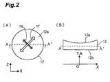
- the first birefringent member 12 is a member of disk shape made of a birefringent material such as a uniaxial crystal, and the optical axis thereof is in its in-plane direction (direction parallel to the plane normal to the optical axis of illumination system AX2).
- the size (diameter) in the in-plane direction of the first birefringent member 12 is larger than the beam size of the illumination light IL at the position where the birefringent member 12 is located.
- Fig. 2(A) is a view of the birefringent member 12 in Fig. 1 viewed to the +Y direction and along the optical axis of illumination system AX2 and in the birefringent member 12, as shown in Fig. 2(A) , the fast axis nf, which is an axial direction to minimize the refractive index for linearly polarized light with the polarization direction parallel thereto, is directed in a direction rotated by 45° from each coordinate axis (X-axis and Z-axis) in the XZ coordinate system with the same coordinate axes as in Fig. 1 .
- the slow axis ns which is an axial direction to maximize the refractive index for linearly polarized light with the polarization direction parallel thereto, is naturally orthogonal to the fast axis nf and is also directed in a direction rotated by 45° from both of the X-axis and Z-axis.
- the thickness of the first birefringent member 12 is not uniform in a plane parallel to the plane of Fig. 2(A) , and varies according to X-coordinates (positions in the X-direction).
- Fig. 2(B) is a sectional view of the birefringent member 12 along line AA' in Fig. 2(A) and, as shown in Fig. 2(B) , the birefringent member 12 has such a shape that it is thin at the center (the optical axis of illumination system) and thick in the marginal region in the X-direction.
- the thickness of the first birefringent member 12 is uniform in the Z-direction in Fig. 2(A) and thus the birefringent member 12 is of a shape like a negative cylinder lens as a whole.
- a beam passing through such a birefringent member generally has a path difference (polarization phase difference) between a linear polarization component with the polarization direction (i.e., "vibrating direction of the electric field of light,” which will also apply to the description hereinafter) coinciding with the direction of the fast axis nf, and a linear polarization component with the polarization direction coinciding with the direction of the slow axis ns.
- the refractive index of the birefringent member is low for linearly polarized light parallel to the fast axis nf, so that the traveling speed of the same polarized light is high.
- the refractive index of the birefringent member is high for linearly polarized light parallel to the slow axis ns, so that the traveling speed of the same polarized light is low. Therefore, there appears a path difference (polarization phase difference) between the two polarized beams. Therefore, the first birefringent member 12 functions as a first nonuniform wavelength plate in which the polarization phase difference given to transmitted light differs according to locations.
- the thickness of the first birefringent member 12 is optimized to make the path difference due to the birefringent member 12 equal to an integer multiple of a wavelength, the phases of the two beams cannot be substantially discriminated from each other, and a state substantially having no optical path difference can be realized.
- the thickness T1 of the center part of the birefringent member 12 is set to such thickness.
- the shape of the birefringent member 12 is so set that the polarization phase difference becomes 0.5 (in the unit of the wavelength of the illumination light) at positions of ⁇ 1 apart in the X-direction from the center of the first birefringent member 12 (where 1 represents a reference length and is located inside the outer diameter of the first birefringent member 12).
- ⁇ is a proportionality coefficient, and the value of ⁇ varies depending upon the aforementioned index difference between the fast axis and the slow axis of the birefringent material used, or the like as the thickness T1 of the center part does.
- the refractive indices of crystalline quartz are as follows: the refractive index of 1.6638 for an ordinary ray and the refractive index of 1.6774 for an extraordinary ray in the ArF excimer laser light with the wavelength of 193 nm. Therefore, the fast axis is the polarization direction of the ordinary ray and the slow axis the polarization direction of the extraordinary ray.
- the thickness of crystalline quartz corresponding to the 122.7 wavelengths is obtained by calculation of 122.7 ⁇ 193/1.6638, and is equivalent to 14239 nm, i.e., 14.239 ⁇ m.
- the thickness of crystalline quartz can be set to a half of the above thickness, i.e., 7.12 ⁇ m.
- the polarization phase difference ⁇ P1 made by the first birefringent member 12 is represented as follows as a function of position X in the X-direction.
- ⁇ P ⁇ 1 0.5 ⁇ 1.7 ⁇ X 4 - 0.7 ⁇ X 2
- the thickness of the first birefringent member 12 is a spacing between its entrance surface 12a and exit surface 12b, and each of shapes of the entrance surface 12a and exit surface 12b may be arbitrary as long as they satisfy the aforementioned relation between thickness and X-directional position for formation of the phase difference. From the viewpoint of processing of surface shape, however, processing becomes easier if either surface is a plane, and it is thus desirable to make, for example, the exit surface 12b as a plane in practice, as shown in Fig. 2(B) . In this case, where the value of the thickness TA on the exit surface 12b is 0, values of thickness TA of the entrance surface 12a are equal to those of TA determined by Eq (1). It is a matter of course that the entrance surface 12a is constructed as a plane.
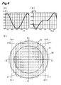
- Fig. 4(A) is a diagram showing the relation between polarization phase difference ⁇ P1 (in the unit of the wavelength of illumination light) and position X represented by Eq (2).
- Fig. 5 is a drawing showing polarization states of the illumination light emerging from the first birefringent member 12 and in Fig. 5 a polarization state of illumination light distributed at each position on the XZ coordinates is indicated by a line segment, a circle, or an ellipse with the center at each position.
- the illumination light is in a polarization state consisting primarily of linear polarization and a direction of the line segment indicates a polarization direction thereof.
- the illumination light is in a polarization state consisting primarily of elliptic polarization and a direction of the major axis of the ellipse indicates a direction in which the linear polarization component in the elliptic polarization is maximum.
- the illumination light is in a polarization state consisting primarily of circular polarization.
- the first birefringent member 12 acts as a so-called half wavelength plate.
- the illumination light IL emitted from the exposure light source 1 in Fig. 1 consists primarily of the linearly polarized light polarized in the X-direction as described previously, and the half wavelength plate has the fast axis nf and slow axis ns rotated 45° relative to the X-direction being the polarization direction of the incident light (or of the illumination light). Therefore, as shown in Fig.
- the polarization state of the illumination light passing near the positions ⁇ 1 (reference length) apart in the X-direction from the center in the first birefringent member 12 is converted into the polarization state consisting primarily of linear polarization in the Z-direction by the action of the half wavelength plate.
- the polarization phase difference ⁇ 1 is 0.25 and the first birefringent member 12 acts as a so-called quarter wavelength plate. For this reason, the illumination light passing this part is converted into a polarization state consisting primarily of circular polarization.
- polarization states consisting primarily of elliptic polarization in different shapes according to the positions.
- the polarization states are as shown in Fig. 5 .
- the illumination light IL in the different polarization states according to the passing locations through the first birefringent member 12 is incident to the second birefringent member 13.
- the second birefringent member 13 is also a member of disk shape made of a birefringent material.
- Fig. 3(A) is a view of the second birefringent member 13 in Fig. 1 , viewed to the +Y direction and along the optical axis of illumination system AX2, and, as shown in Fig. 3(A) , the fast axis nf of the second birefringent member 13 is set in parallel with the Z-axis of the XZ coordinate system with the same coordinate axes as those in Fig. 1 and the slow axis ns is set in parallel with the X-axis, different from the aforementioned first birefringent member 12. Concerning the second birefringent member 13, the size (diameter) in the in-plane direction thereof is larger than the beam size of the illumination light IL at the position where the second birefringent member 13 is located.
- Fig. 3(B) is a sectional view of the second birefringent member 13 along line BB' in Fig. 3(A) , and, as shown in Fig. 3(B) , the birefringent member 13 has such a shape that it is thin at the left end (near B) and thick at the right end (near B').
- the thickness of the second birefringent member 13 is uniform in the direction orthogonal to the XZ direction. Therefore, the second birefringent member 13 also functions as a second nonuniform wavelength plate in which the polarization phase difference given to the transmitted light differs according to locations.
- T T ⁇ 2 + ⁇ ⁇ 2.5 ⁇ XZ 5 - 1.5 ⁇ XZ 3
- ⁇ is a proportionality coefficient and the value of ⁇ differs depending upon the aforementioned index difference between the fast axis and the slow axis of the birefringent material used, or the like as the thickness T2 of the center part does.
- the thickness T2 of the center part is so set that the polarization phase difference ⁇ P2 of the second birefringent member 13 is 0.25 (in the unit of the wavelength of the illumination light), i.e., that the center part functions as a quarter wavelength plate.
- the birefringent member 13 is also so set that the polarization phase differences ⁇ P2 at the positions +1 (reference length) and -1 apart in the XZ direction are +0.75 and -0.25, respectively. This means that differences of +0.5 and -0.5, respectively, are made between the polarization phase differences at the positions of interest and at the center.
- the thickness thereof is so set that the polarization phase difference ⁇ P2 is represented by the following equation.
- ⁇ P ⁇ 2 0.25 + 0.5 ⁇ 2.5 ⁇ XZ 5 - 1.5 ⁇ XZ 3
- the thickness T2 of the center part can be set to an (integer +1/4) multiple of 14.239 ⁇ m and the proportionality coefficient ⁇ to 7.12 ⁇ m.
- Fig. 4(B) is a drawing showing the relation between polarization phase difference ⁇ P2 and position XZ of Eq (4).
- the second birefringent member 13 again converts the illumination light in the different polarization states according to the passing locations through the first birefringent member 12, into polarization states according to locations.
- Fig. 4(C) shows the polarization states of the illumination light IL emerging from the second birefringent member 13.
- Fig. 4(C) is illustrated in the same manner as the aforementioned illustration method in Fig. 5 , and, in Fig. 4(C) , a polarization state of illumination light distributed at each position on XZ coordinates is indicated by a line segment (linear polarization) or an ellipse (elliptic polarization) with the center at each position.
- the first birefringent member 12 and the second birefringent member 13 are located immediately before the fly's eye lens 14 and the exit-side surface of the fly's eye lens 14 is located near the pupil plane 15 in the illumination optical system ILS. For this reason, the first birefringent member 12 and the second birefringent member 13 are located at positions substantially equivalent to the pupil plane 15 in the illumination optical system ILS.
- the illumination light IL passing through the first birefringent member 12 and the second birefringent member 13 is incident at incidence angles and incidence directions determined according to the locations, into the reticle R.
- the incidence direction of the beam is a direction equal to an azimuth of that point from the origin.
- Exterior circle C1 and interior circle C2 shown in Fig. 4(C) and Fig. 5 are boundaries of a distribution of the illumination light for forming predetermined annular illumination on the reticle R.
- the radii of the respective circles C1, C2 are determined as follows: the radius of the exterior circle C1 is 1.15 and the radius of the interior circle C2 0.85, where the unit is the reference length used in determining the thickness shapes (thickness profiles) of the first birefringent member 12 and the second birefringent member 13. Namely, an annular ratio of the annular illumination (radius of interior circle/radius of exterior circle) is assumed to be 0.74.
- the illumination light emerging from the second birefringent member 13 is in polarization states consisting primarily of linear polarization with the polarization direction along the circumferential direction of a specific annular region 3 6, in the specific annular region 36 which is an annular region between the exterior circle C1 and the interior circle C2.
- the polarization states of the illumination light on the X-axis and on the Z-axis are almost equal.
- the polarization states at positions approximately 45° apart from each axis about the origin are almost circular polarization in Fig. 5 , but are linear polarization along the circumferential direction of the specific annular region in Fig. 4(C) .
- the actual radius of the exterior circle C1 of the specific annular region 36 is determined by the numerical aperture (NA) on the reticle R side of the projection optical system 25 in Fig. 1 , the focal length of the optical system consisting of the relay lens 16 and condenser lenses 18, 20 in the illumination optical system ILS, and the value of coherence factor (illumination ⁇ ) to be set, and the radius of the interior circle C2 is a value determined further by the annular ratio to be set.
- NA numerical aperture
- the thickness shapes of the first birefringent member 12 and second birefringent member 13 are determined so that the polarization directions of the illumination light distributed in the specific annular region 36 are coincident with the circumferential direction of the annular region at the respective positions.
- the thickness shapes of the first birefringent member 12 and the second birefringent member 13 means that the shapes are proportionally enlarged or reduced in the XZ plane and unevenness amounts thereof are kept unchanged in the Y-direction (traveling direction of light).
- the polarization directions of the illumination light distributed in the specific annular region can be made coincident with the circumferential direction of the annular region at each position, with no light quantity loss of the illumination beam, by the first and second nonuniform wavelength plates.
- the illumination light incident through the specific annular region 36 onto the reticle R among the illumination light, i.e., the specific illumination beam incident in the specific incidence angle range to the reticle R is light in the polarization state consisting primarily of S-polarization whose polarization direction lies along the direction normal to the entrance plane. This improves the contrast, resolution, depth of focus, etc. of the transferred image, depending upon the periodicity of the pattern to be transferred, in some cases (the details of which will be described later).
- the configurations of the first birefringent member 12 and the second birefringent member 13 are basically the same as those in the aforementioned first example. Namely, the first birefringent member 12 has the direction of the fast axis and the thickness shape as shown in Fig. 2(A) and Fig. 2(B) and the second birefringent member 13 has the direction of the fast axis and the thickness shape as shown in Fig. 3(A) and Fig. 3(B) . In the present example, however, the function forms for the thicknesses of the two birefringent members 12, 13 are different.
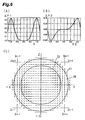
- Fig. 6(A) corresponding to Fig. 4(A) , shows a characteristic of polarization phase difference ⁇ P1 by the first birefringent member 12 versus X-directional position in the second example.
- the polarization phase difference ⁇ P1 in Fig. 6(A) is represented by the following function including a trigonometric function about position X.
- ⁇ P ⁇ 1 0.265 ⁇ 1 - cos ⁇ ⁇ X 2
- This polarization phase difference ⁇ P1 can be realized by expressing the thickness TA of the first birefringent member 12 by the following function for the X-directional position X.
- TA T ⁇ 1 + ⁇ ⁇ 1 - cos ⁇ ⁇ X 2
- ⁇ represents a proportionality coefficient.
- the thickness T1 at the center can be set to an integer multiple of 14.239 ⁇ m and the proportionality coefficient ⁇ to 3.77 ⁇ m.
- the value of 3.77 ⁇ m is obtained by multiplying the thickness of crystalline quartz for giving the polarization phase difference of one wavelength, 14.239 ⁇ m, by the coefficient of 0.265 in Eq (5) above.
- Fig. 6(B) shows a characteristic of polarization phase difference ⁇ P2 by the second birefringent member 13 versus XZ-directional position in the second example.
- the polarization phase difference ⁇ P2 in Fig. 6(B) can be represented by the following function including a trigonometric function about position XZ.
- ⁇ P ⁇ 2 0.25 + 0.5 ⁇ sin 0.5 ⁇ ⁇ ⁇ XZ 3
- the polarization phase difference ⁇ P2 can be realized by expressing the thickness TB of the second birefringent member 13 by the following function for the position XZ in the XZ direction.
- TB T ⁇ 2 + ⁇ ⁇ sin 0.5 ⁇ ⁇ ⁇ XZ 3
- ⁇ is a proportionality coefficient.
- the thickness T2 at the center can be set to an (integer + 1/4) multiple of 14.239 ⁇ m, and the proportionality coefficient ⁇ to 7.12 ⁇ m.
- first birefringent member 12 and the second birefringent member 13 also function as first and second nonuniform wavelength plates, respectively, in which the polarization phase difference given to the transmitted light differs according to locations. Then the linearly polarized light incident in a polarized state in the X-direction into the first birefringent member 12 is converted into the polarization distribution shown in Fig. 6(C) to emerge from the second birefringent member 13.
- the first birefringent member 12 and second birefringent member 13 of the present second example can make the polarization states of illumination light distributed in the specific annular region 36 between the exterior circle C1 and the interior circle C2, closer to linear polarization parallel to the circumferential direction of the annular region 36 than those in the first example.
- the reason for it is that the first birefringent member 12 and second birefringent member 13 of the present second example adopt the thickness shapes (i.e., surface shapes) determined by the high-order functions of trigonometric functions and thus they enable higher-accuracy polarization control.
- first birefringent member 12 and second birefringent member 13 in the first example are represented by the functions of at most order 5, they offer the advantage that processing is easy and production cost is low, though they are slightly inferior in the polarization control performance.
- first and second birefringent members 12, 13 it is also possible, for example, to adopt a configuration wherein the surface shape of the first birefringent member 12 is a cylindrical surface (surface of a circular cross section in the X-direction) and wherein the surface shape of the second birefringent member 13 is a tapered surface (inclined plane).
- the polarization control performance in this case is worse than in the first embodiment, but satisfactory effect can be achieved thereby depending upon use of the projection exposure apparatus. Therefore, it can realize a high-performance exposure apparatus while achieving the reduction of production cost.
- the configuration wherein the surface shape of the second birefringent member 13 is the tapered surface means that the polarization phase difference of a beam passing through the second birefringent member 13 is defined in a linear form (linear function) according to locations in the plane of the second birefringent member 13.
- the shapes of the first birefringent member 12 and the second birefringent member 13 in Fig. 1 are not limited to the shapes shown in the above first and second examples, but may be any shapes that can make the polarization state of transmitted light in the specific annular region coincide with the circumferential direction in each part.
- the shapes of the first birefringent member 12 and second birefringent member 13 may be stepwise shapes with stepped shape changes at predetermined positions, instead of the shapes represented by the aforementioned continuous and differentiable continuous functions.
- Such stepwise shapes can be formed suitably by etching, instead of mechanical or mechanochemical polishing.
- the first birefringent member 12 is preferably one that gives the polarization phase difference with 2-fold rotation symmetry around the optical axis of illumination system AX2. It is a matter of course that this embraces the nonuniform wavelength plate having the thickness of an even function in the X-direction and the constant thickness in the Y-direction, as shown in the above-described first and second examples.
- the second birefringent member 13 is desirably the nonuniform wavelength plate that gives the polarization phase difference with 1-fold rotation symmetry about the optical axis of the illumination system AX2.
- the 1-fold rotation symmetry refers to a state in which the distribution of polarization phase differences is approximately symmetric with respect to one axis out of two axes orthogonal to the optical axis of illumination system AX2 and approximately antisymmetric with respect to the other axis.
- the antisymmetry generally refers to a function that provides equal absolute values but opposite signs with inversion of a coordinate axis, but the antisymmetry herein also embraces functions obtained by adding an offset of a constant to general antisymmetric functions. It is needless to mention that this encompasses the nonuniform wavelength plate having the thickness determined by an odd function with an offset in the XZ-direction and the constant thickness in the direction orthogonal thereto, as shown in the above-described first and second examples.
- first birefringent member 12 and second birefringent member 13, and the directions of the fast axes thereof are not limited to those described in the above first and second examples, either.
- three or more birefringent members may be arranged in series along the traveling direction of the illumination light (along the optical axis of illumination system AX2), and the rotational relation around the optical axis AX2 between the directions of the fast axes is not limited to 45°, either.
- a potential configuration is such that the direction of the fast axis of at least one birefringent member out of the plurality of birefringent members is different from the directions of the fast axes of the other birefringent members, in order to convert the polarization state of the illumination light into linear polarization nearly parallel to the circumferential direction in at least a partial region of the aforementioned specific annular region and, desirably, in the almost entire circumferential region.
- the materials of the birefringent members 12, 13 and others are not limited to crystalline quartz described above, either, but other birefringent materials are also applicable. It is also possible to use the intrinsic birefringence of fluorite to form the birefringent members.
- a material originally having no birefringence, e.g., synthetic quartz, comes to have the birefringent property when subjected to stress or the like. It can also be used for the birefringent members 12, 13 and others.
- the birefringent members 12, 13 can also be made using a composite material obtained by bonding a material with birefringence onto a transparent substrate without birefringence.
- the aforementioned thicknesses are, of course, thicknesses of the material with birefringence.
- the bonding herein may be implemented not only by mechanical joining such as adhesion or press, but also by a method of forming a thin film with birefringence on the transparent substrate by means such as vapor deposition or the like.
- first and second examples vary depending upon the magnitude of birefringence of the material used, but, even in cases where materials except for crystalline quartz are used, the aforementioned shape determining method can also be applied and the shapes are determined thereby, of course.
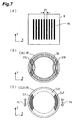
- Fig. 7(A) shows an example of fine periodic pattern PX formed on the reticle R in Fig. 1 .
- the periodic pattern PX is a pattern with periodicity in the X-direction in the same XYZ coordinate system as in Fig. 1 , and the pitch PT thereof is 140 nm as a converted value in terms of the scale on the wafer W in consideration of the projection magnification of the projection optical system 25 in Fig. 1 .
- Fig. 7(B) shows a distribution of diffracted light formed in the pupil plane 26 (cf. Fig.
- Fig. 7(C) is a drawing showing the condition for annular illumination for illuminating the pattern PX, and the pattern PX is illuminated with the illumination light from the annular region ILO satisfying the above condition for annular illumination, in the pupil plane 15 of the illumination optical system ILS in Fig. 1 .
- the whole of 0-order diffracted light D0 in Fig. 7(B) from the periodic pattern PX is distributed in the pupil plane 26 and passes through the projection optical system 25 to reach the wafer W, but the 1-order diffracted light D1R and D1L can be transmitted only in part through the pupil plane 26 and the projection optical system 25.
- An image of the pattern PX on the reticle R is formed as an interference fringe pattern between the 0-order diffracted light D0 and the 1-order diffracted light D1R, D1L on the wafer W, but an interference fringe pattern is formed only by a pair of 0-order diffracted light and 1-order diffracted light generated from the illumination light emitted from the same position on the pupil plane 15 of the illumination optical system ILS.
- the 1-order diffracted light D1L located at the left end of the pupil plane 26 in Fig. 7(B) is to be paired with the part of the 0-order diffracted light D0 located at the right end, and those diffracted light beams originate in the illumination light from the right-end partial region ILR in the annular region IL0 in Fig. 7(C) .
- the 1-order diffracted light D1R located at the right end of the pupil plane 26 in Fig. 7(B) is to be paired with the part of the 0-order diffracted light D0 located at the left end, and those diffracted light beams originate in the illumination light from the left-end partial region ILL in the annular region ILO in Fig. 7(C) .
- beams contributing to imaging of the pattern PX among the illumination light emitted from the annular region ILO on the pupil plane 15 of the illumination optical system ILS are limited to those in the partial region ILR and partial region ILL, and the illumination light emitted from the other regions in the annular region ILO is illumination light not contributing to imaging of the pattern PX.
- Non-patent Document 1 Thimothy A. Brunner, et al.: "High NA Lithographic imaging at Brewster's angle," SPIE Vol. 4691, pp.1-24 (2002 ) and others report that on the occasion of exposure of a pattern with periodicity in the X-direction and with the longitudinal direction along the Y-direction like the pattern PX, the contrast of its projected image is improved by illumination with linear polarization having the polarization direction along the Y-direction on the reticle R.
- the diffracted light distribution is also one rotated 90° from that shown in Fig. 7(B) .
- the partial regions through which the illumination light contributing to image formation of the periodic pattern passes are also located at the positions resulting from 90° rotation of the partial region ILR and partial region ILL shown in Fig. 7(C) (i.e., at the upper end and at the lower end in Fig. 7(C) ) and the preferred polarization state is linear polarization with the polarization direction coincident with the X-direction.
- Fig. 8(A) is a perspective view showing the simplified relation between the pupil plane 15 of the illumination optical system ILS and the reticle R in Fig. 1 , without illustration of the relay lens 16, condenser lenses 18, 20, and others in Fig. 1 .
- the illumination light distributed in the annular region ILO in Fig. 8(A) is desirably linear polarization in the Y-direction (the depth direction in the plane of Fig.
- the reticle R includes not only the patterns in the X-direction and in the Y-direction but also patterns in intermediate directions (45° and 135° directions), it is desirable to use linear polarization with the polarization direction perfectly coincident with the circumferential direction of the annular region, taking orientations of these patterns into consideration as well.
- the above-described polarization states do not always realize effective polarization states for the patterns perpendicular to the patterns with orientations suitable for the polarization states of the respective portions in the annular region ILO.
- the illumination light polarized in the X-direction from the partial region ILU is not in a preferred polarization state for imaging of the pattern PX with the periodicity in the X-direction and with the longitudinal direction along the Y-direction.
- the linear polarization almost coincident with the circumferential direction of the annular region ILO on the pupil plane 15 of the illumination optical system ILS is incident as so-called S-polarization to the reticle R.
- the S-polarization refers to linear polarization with the polarization direction perpendicular to a plane of incidence in which a beam is incident to an object (which is a plane including a normal to the object, and the beam).
- the illumination light ILL1 from the partial region ILL consisting of linearly polarized light in the direction coincident with the circumferential direction of the annular region ILO is incident as S-polarization with the polarization direction EF1 normal to the plane of incidence (the plane of Fig.
- the illumination light ILD1 on the similar partial region ILD is also incident as S-polarization with the polarization direction EF2 normal to the plane of incidence (the plane of Fig. 8(C) ), as shown in Fig. 8(C) , to the reticle R.
- the illumination light from the partial regions ILR, ILU at the positions symmetric with the foregoing partial regions ILL, ILD with respect to the optical axis AX41 of the illumination optical system is also incident as S-polarization to the reticle R by virtue of symmetry, because each illumination light on the partial region ILR, ILU has the polarization direction coincident with the circumferential direction of the annular region ILO. It is the general property of the annular illumination that angles of incidence of the illumination light distributed on the annular region ILO, to the reticle R are in a predetermined angular region with the center at an angle ⁇ from the optical axis AX41 of the illumination optical system (i.e., a normal to the reticle R).
- a beam incident at the angles of incidence to the reticle R will be referred to hereinafter as "specific illumination beam.”
- the angle ⁇ and angular range can be determined based on the wavelength of the illumination light, the pitch of the pattern to be transferred, on the reticle R, and so on.
- the foregoing first and second birefringent members 12, 13 convert the polarization state of the illumination light distributed in the specific annular region between the predetermined outside radius (exterior circle C1) and inside radius (interior circle C2) determined from the shapes peculiar to the members, into the polarization state consisting primarily of linear polarization parallel to the circumferential direction of the specific annular region, and it is not easy to change the radii (C2, C1).
- a desirable configuration is such that a plurality of conical prisms 41, 42 of a zoom type are disposed between the first and second birefringent members 12, 13 and the optical integrator such as the fly's eye lens 14 in Fig. 1 , as shown in Fig. 9 , to make the radii of the foregoing specific annular region variable.
- the optical integrator such as the fly's eye lens 14 in Fig. 1 , as shown in Fig. 9
- the plurality of conical prisms of the zoom type are a concave conical prism 41 with a concave conical surface 41 b and a convex conical prism 42 with a convex conical surface 42a, which are arranged with a spacing DD variable between them and along the optical axis of illumination system AX2.
- the illumination light distributed in the specific annular region with the center at an average radius RI after passage through the first and second birefringent members 12, 13 is enlarged to a radius RO on the entrance plane of the fly's eye lens 14 and on the pupil plane 15 of the illumination optical system being the exit plane of the fly's eye lens 14, by the zoom type conical prisms 41, 42.
- This radius RO can be enlarged by increasing the spacing DD between the two conical prisms 41, 42 and can be reduced by decreasing the spacing DD.
- a zoom optical system can be used instead of the foregoing zoom type conical prisms 41, 42.
- the above embodiment was described on the premise that the illumination light quantity distribution formed on the pupil plane 15 of the illumination optical system ILS in Fig. 1 is the annular region, i.e., that it is applied to the annular illumination, but the illumination condition that can be realized by the projection exposure apparatus of Fig. 1 is not always limited to the annular illumination. Namely, since the birefringent members 12, 13 of Fig. 1 and the zoom type conical prisms 41, 42 of Fig.
- the distribution of the illumination light is further limited to within a specific partial region in the specific annular region, i.e., where the distribution of the illumination light is limited, for example, to the partial regions ILL, ILR in Fig. 7(C) , they can convert the illumination light distributed in the partial regions, into illumination light consisting primarily of linear polarization with the polarization direction parallel to the circumferential direction of the specific annular region.
- the diffractive optical element 9a in Fig. 1 is replaced with such a diffractive optical member that the diffracted light (illumination light) generated from the other diffractive optical element is concentrated in the further specific discrete regions in the specific annular region on the first birefringent member 12 and on the second birefringent member 13.
- the locations where the illumination light is condensed are, for example, two locations of the partial regions ILL, ILR in Fig. 7(C) , but are not limited to this example.
- the illumination light may be condensed at arbitrary locations in the specific annular region, and the number of locations may be four. The locations may be selected according to the shape of the pattern as an exposed object on the reticle R.
- an optical member group as a combination of a convex polyhedron prism and a concave polyhedron prism of pyramid shape or the like with a variable spacing similarly.
- the light quantity distribution thereof is preferably substantially 0 in certain cases.
- manufacturing error or the like of the diffractive optical element 9a and others could produce diffracted light (hereinafter referred to as "error light") in directions except for the desired directions from the diffractive optical element 9a and others and cause the illumination light to be distributed in the regions except for the above partial regions. It is thus also possible, for example, to adopt a configuration wherein a stop is disposed on the entrance surface side or on the exit surface side of the fly's eye lens 14 in Fig. 1 to block the error light. This makes the illumination light quantity distributions in the plurality of specific regions perfectly discrete.
- the illumination light quantity distribution in the region except for the specific regions does not always have to be 0 in such cases.
- the limitation of the distribution of the illumination light quantity on the pupil plane 15 to within the further specific regions in the specific annular region results in further limiting the incidence directions thereof to only the aforementioned plurality of substantially discrete directions, in addition to the restriction on the range of incidence angles by the annular illumination.
- a stop is disposed on the entrance surface side or on the exit surface side of the fly's eye lens 14 to block the error light distributed in the regions except for the specific annular region.
- the above embodiment was arranged to use the fly's eye lens 14 as an optical integrator, but it is also possible to use an internal reflection type integrator (e.g., glass rod) as an optical integrator.
- an internal reflection type integrator e.g., glass rod
- the exit plane of the glass rod is not located on the pupil plane 14 of the illumination optical system, but is located on a plane conjugate with the reticle R.
- the laser light source as the exposure light source 1 was arranged to emit the linearly polarized light polarized in the X-direction, but the laser light source, depending upon its type, can emit linearly polarized light polarized in the Z-direction in Fig. 1 , or a beam in another polarization state.
- the birefringent members 12, 13 described in the above first and second examples are rotated 90° about the optical axis of illumination system AX2, whereby the illumination light can be obtained in much the same polarization state as the polarization state shown in Fig. 4(C) and Fig. 6(C) (precisely, illumination light in a state resulting from 90° rotation of the state shown in the two figures).
- the polarization controlling member 4 (polarization controlling mechanism) in Fig. 1 may be used to convert the Y-directional linear polarization emitted from the exposure light source 1, into X-directional linear polarization.
- This polarization controlling member 4 can be readily substantialized by a so-called half wavelength plate.
- the exposure light source 1 emits light of circular polarization or elliptic polarization, it can also be converted into the desired Z-directional linear polarization, similarly using a half wavelength plate or a quarter wavelength plate as the polarization controlling member 4.
- the polarization controlling member 4 is not necessarily able to convert a beam in an arbitrary polarization state emitted from the exposure light source 1, into the Z-directional polarization without loss in light quantity. Therefore, the exposure light source 1 needs to generate a beam in a single polarization state (beam that can be converted into linear polarization without loss in light quantity by a wavelength plate or the like), such as linear polarization, circular polarization, or elliptic polarization.
- the intensity of the beam except for the aforementioned single polarization state is not so high relative to the total intensity of the illumination light, the adverse effect of the beam except for the single polarization state is not so significant on the imaging characteristics, and thus the beam emitted from the exposure light source 1 may contain the beam except for the single polarization state to some extent (e.g., approximately 20% or less of the total light quantity).
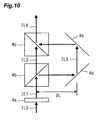
- the polarization controlling member 4 in Fig. 1 may be implemented by adopting an element or optical system capable of converting the polarization state of the beam emitted from the light source such as a laser, into random polarization or the like according to need. This can be realized, for example, by two polarization beam splitters 4b, 4c or the like as shown in Fig. 10 .
- Fig. 10 shows a polarization control optical system which can be placed at the position of the polarization controlling member 4 in Fig. 1 .
- an illumination beam IL0 (corresponding to the illumination light IL in Fig. 1 ) consisting of linearly polarized light is incident to a rotatable wavelength plate 4a consisting of a half wavelength plate or quarter wavelength plate. This converts the illumination beam IL0 into an illumination beam IL1 of linear polarization inclined at 45° from the plane of Fig.
- the first polarization beam splitter 4b divides the illumination beam IL1 into a beam IL2 of P-polarization component and a beam IL3 of S-polarization component with respect to its dividing surface.
- One beam IL2 travels straight upward through the prism 4b in Fig. 10 , and the other beam IL3 is reflected to the right in Fig. 10 .
- the beam IL2 traveling straight is then incident to the polarization beam splitter 4c and, because of the polarization characteristics thereof, the beam IL2 travels straight in the polarization beam splitter 4c and then travels as a beam IL4 upward in Fig. 10 .
- the reflected beam IL3 is reflected by mirrors 4d, 4e and then enters the polarization beam splitter 4c to be reflected again therein.
- the reflected beam IL3 merges with the beam IL4 traveling straight.
- DL represents each of the spacings between the polarization beam splitters 4b, 4c and the mirrors 4d, 4e
- this path length difference of 2 ⁇ DL is set longer than the coherent length of the illumination beam, there is no coherence between the two beams, so that the merged light can be substantially of random polarization.
- the illumination light IL transmitted thereby is always of random polarization and could be a hindrance to implementation of the polarization state in the above embodiment.
- this hindrance will not be caused in principle in the optical system shown in Fig. 10 because the rotatable wavelength plate 4a can be rotated to convert the polarization state of the illumination light IL1 transmitted by the rotatable wavelength plate 4a, into linear polarization the whole of which passes through the first beam splitter 4b.
- the following simple method can also offer an effect similar to that by the random polarization illumination.
- This can be implemented as follows: the polarization state of the illumination light IL incident to the first birefringent member 12 in Fig. 1 is set to polarization in the direction 45° apart from the X-direction and Z-direction in Fig. 1 , whereby the illumination light distributed in the specific annular region is converted into approximately circular polarization.
- the projection exposure apparatus of the present embodiment is used in applications in which the circular polarization can be deemed approximately as random polarization, i.e., in applications in which the imaging performance required is relatively not so high, it is also feasible to achieve the effect similar to that by the random polarization illumination, by a configuration wherein the polarization controlling member 4 in Fig. 1 is constructed, for example, of a half wavelength plate whereby the polarization state of the illumination light incident to the first birefringent member 12 is set to polarization in the direction inclined at 45° from the X-axis and Z-axis as described above.
- the polarization controlling member 4 is constructed, for example, of a quarter wavelength plate whereby the polarization state of the illumination light incident to the first birefringent member 12 is set to circular polarization.
- the apparatus is provided with a mechanism capable of wholly rotating each of the birefringent members, such as the first birefringent member 12 and the second birefringent member 13 in Fig. 1 , independently about the optical axis of illumination system AX2, and the direction of rotation of each birefringent member is set so that the fast axis (or slow axis) of each birefringent member is in parallel with the direction of linear polarization of the illumination light.
- the illumination light travels through each birefringent member, without being affected by the converting action of the polarization state at all, and emerges as keeping the linear polarization at the time of incidence.
- the setting of the linear polarization state in the one predetermined direction may be implemented by providing a replacing mechanism and replacing the birefringent members and others all together thereby.
- the replacing mechanism is arranged to set plural sets of birefringent member groups therein and wherein they can be replaceably arranged on the position on the optical axis of illumination system AX2.
- each birefringent member group is preferably provided with the characteristics of converting the illumination light into linear polarization along the circumferential direction of the specific annular region, in the specific annular region with the outside radius and inside radius different among the groups.
- a preferred case to use the illumination light of linear polarization in the one predetermined direction as described above is, for example, exposure of a phase shift reticle of a spatial frequency modulation type with a pattern aligned along a direction.
- the coherence factor ( ⁇ value) of the illumination light is preferably not more than about 0.4.
- linear polarization in the Z-direction Z-polarization
- the aforementioned polarization controlling member 4 or the like is used to switch the polarization direction of the incident light to the birefringent members, without retracting them to outside the optical path of the illumination optical system, whereby it becomes feasible to realize the illumination light being the illumination beam with the illumination ⁇ of not more than about 0.4 and being light polarized in the X-direction or in the Z-direction (polarization in the X-direction or in the Y-direction, respectively, on the reticle R in Fig. 1 ), suitable for illumination onto the spatial frequency modulation type phase shift reticle.
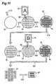
- Fig. 11 shows an example of production steps of semiconductor devices and in this Fig. 11 , a wafer W is first made of a silicon semiconductor or the like. Thereafter, a photoresist is applied onto the wafer W (step S10) and in the next step S 12, a reticle (assumed to be R1) is loaded on the reticle stage of the projection exposure apparatus of the above embodiment ( Fig. 1 ), the wafer W is loaded on the wafer stage, and a pattern on the reticle R1 (indicated by symbol A) is transferred (to effect exposure) into all shot areas SE on the wafer W by the scanning exposure method. On this occasion double exposure is carried out according to need.
- the wafer W is, for example, a wafer with the diameter of 300 mm (12-inch wafer), and the size of each shot area SE is, for example, a rectangular region with the width of 25 mm in the non-scanning direction and the width of 33 mm in the scanning direction.
- development, etching, ion implantation, and so on are carried out to form a predetermined pattern in each shot area SE on the wafer W.
- next step S16 a photoresist is applied onto the wafer W and in step S 18 thereafter, a reticle (assumed to be R2) is loaded on the reticle stage of the projection exposure apparatus of the above embodiment ( Fig. 1 ), the wafer W is loaded on the wafer stage, and a pattern on the reticle R2 (indicated by symbol B) is transferred (to effect exposure) into each shot area SE on the wafer W by the scanning exposure method.
- next step S20 development, etching, ion implantation, and so on of the wafer W are carried out to form a predetermined pattern in each shot area on the wafer W.
- step S16 to step S20 The above exposure step to pattern forming step (step S16 to step S20) are repeated the number of times necessary for production of desired semiconductor devices. Then semiconductor devices SP as products are fabricated through a dicing step (step S22) of separating chips CP on the wafer W from each other, a bonding step, and a packaging step and others (step S24).
- the exposure step enables the reticle to be illuminated with the illumination light (exposure beam) in the predetermined polarization state with increased efficiency of utilization thereof. Therefore, the resolution and others are improved for periodic patterns with a fine pitch or the like, so that higher-integration and higher-performance semiconductor integrated circuits can be fabricated at low cost and at high throughput.
- the projection exposure apparatus of the above embodiment can be produced as follows: the illumination optical system and projection optical system composed of a plurality of lenses are incorporated in the main body of the exposure apparatus, optical adjustment is carried out for the optics, the reticle stage and wafer stage comprised of a number of mechanical parts are attached to the main body of the exposure apparatus, wires and tubes are connected thereto, and overall conditioning processes (electric adjustment, confirmation of operation, etc.) are further carried out.
- the production of the projection exposure apparatus is preferably carried out in a clean room in which the temperature, cleanliness, etc. are controlled.
- the present invention is applicable not only to the projection exposure apparatus of the scanning exposure type, but also to the projection exposure apparatus of the full exposure type such as steppers.
- the magnification of the projection optical system used may be a demagnification rate, a 1:1 magnification, or an enlargement magnification.
- the present invention is also applicable, for example, to the liquid immersion type exposure apparatus as disclosed in International Publication (WO) 99/49504 or the like.
- the usage of the projection exposure apparatus of the present invention is not limited to the exposure apparatus for fabrication of semiconductor devices, but it is also commonly applicable, for example, to exposure apparatus for display devices such as liquid crystal display devices formed on rectangular glass plates, or plasma displays, and to exposure apparatus for fabricating various devices such as image pickup devices (CCDs or the like), micromachines, thin film magnetic heads, and DNA chips. Furthermore, the present invention is also applicable to the exposure step (exposure apparatus) in production of masks (photomasks including X-ray masks, reticles, etc.) with mask patterns for various devices by the photolithography step.
- the illumination optical system (2-20) in the projection exposure apparatus in the aforementioned embodiment is also applicable to the illumination optical apparatus for illuminating the first object such as the reticle R.
- a first advantage obtainable with embodiments of the present disclosure is to provide an exposure technology capable of reducing loss in light quantity on the occasion of illuminating a mask such as a reticle with illumination light in a predetermined polarization state.
- a second advantage of embodiments of the present disclosure is to provide an illumination technology and exposure technology capable of lessening reduction in quantity of illumination light and improving the resolution and others with little degradation of processing performance as a result, on the occasion of setting a polarization state of illumination light in each region such as an annular, dipole, or quadrupole region to a predetermined state on a pupil plane of an illumination optical system.
- Another advantage of embodiments of the present disclosure is to provide a device fabrication technology capable of fabricating high-performance devices with high processing performance, using the foregoing exposure technology.
- a first projection exposure apparatus is a projection exposure apparatus comprising an illumination optical system (ILS) for illuminating a first object (R) with illumination light from a light source (1), and a projection optical system (25) for projecting an image of a pattern on the first object onto a second object (W), wherein the light source generates the illumination light in a substantially single polarization state, wherein the illumination optical system comprises at least two birefringent members (12, 13) arranged along a traveling direction of the illumination light, wherein a direction of a fast axis of at least one birefringent member out of the birefringent members is different from a direction of a fast axis of the other birefringent member, and wherein a specific illumination beam incident in a specific incidence angle range onto the first object among the illumination light is light in a polarization state consisting primarily of S-polarization.
- IVS illumination optical system
- a first illumination optical apparatus is an illumination optical apparatus for illuminating a first object (R) with illumination light from a light source (1), comprising at least two birefringent members (12, 13) arranged along a traveling direction of the illumination light, wherein a direction of a fast axis of at least one birefringent member out of the birefringent members is different from a direction of a fast axis of the other birefringent member, and wherein a specific illumination beam incident in a specific incidence angle range onto the first object among the illumination light in a substantially single polarization state supplied from the light source is light in a polarization state consisting primarily of S-polarization.
- thicknesses of the birefringent members are set in their respective predetermined distributions, whereby the polarization after passage of the illumination light emitted from the light source, through the plurality of birefringent members, can be, for example, in a state consisting primarily of polarization in the circumferential direction around the optical axis in an annular region centered around the optical axis.
- An exit surface of the birefringent members is located, for example, at a position near the pupil plane of the illumination optical system, whereby the first object is illuminated with the illumination light (specific illumination beam) having passed through the annular region and kept in the predetermined polarization state consisting primarily of S-polarization, with little loss in quantity of light.
- the apparatus may comprise a beam limiting member (9a, 9b) for limiting the illumination light incident to the first object, to the specific illumination beam.
- a beam limiting member (9a, 9b) for limiting the illumination light incident to the first object, to the specific illumination beam.
- the beam limiting member may be configured to further limit the direction of incidence of the illumination light incident to the first object, to a plurality of specific, substantially discrete directions. Since this implements illumination such as the dipole illumination or quadrupole illumination, improvement is made in imaging characteristics of a line-and-space pattern arranged at a fine pitch in a predetermined direction.
- a second projection exposure apparatus is a projection exposure apparatus comprising an illumination optical system (ILS) for illuminating a first object (R) with illumination light from a light source (1), and a projection optical system (25) for projecting an image of a pattern on the first object onto a second object (W), wherein the light source generates the illumination light in a substantially single polarization state, wherein the illumination optical system comprises at least two birefringent members (12, 13) arranged along a traveling direction of the illumination light, wherein a direction of a fast axis of at least one birefringent member out of the birefringent members is different from a direction of a fast axis of the other birefringent member, and wherein the illumination light passing through at least a partial region in a specific annular region (36) being a predetermined annular region centered around an optical axis of the illumination optical system, in a pupil plane in the illumination optical system or in a plane near the pupil plane is in a polarization state
- thicknesses of the birefringent members are set in their respective predetermined distributions, whereby the polarization state of at least part of the illumination light passing through the specific annular region among the illumination light emitted from the light source becomes the state consisting primarily of linear polarization with the polarization direction along the circumferential direction of the specific annular region (the predetermined polarization state), with little loss in quantity of light.
- the apparatus may comprise a beam limiting member (9a, 9b) for limiting the illumination light incident to the first object, to a beam substantially distributed in the specific annular region.
- the beam limiting member may be configured to further limit the beam to within a plurality of substantially discrete regions in the specific annular region.
- the beam limiting member includes a diffractive optical element disposed between the light source (1) and the birefringent members (12, 13), as an example. Use of the diffractive optical element enables further reduction in loss of light quantity.
- At least one member out of the birefringent members is a nonuniform wavelength plate (12, 13) in which a polarization phase difference, which is a phase difference given between a linear polarization component parallel to the fast axis and a linear polarization component parallel to the slow axis in transmitted light, nonlinearly varies depending upon locations in the member.
- a polarization phase difference which is a phase difference given between a linear polarization component parallel to the fast axis and a linear polarization component parallel to the slow axis in transmitted light, nonlinearly varies depending upon locations in the member.
- the nonuniform wavelength plate may include a first nonuniform wavelength plate (12) for giving the specific illumination beam or the illumination light distributed in the specific annular region, the polarization phase difference with 2-fold rotation symmetry about the optical axis of the illumination optical system.
- the nonuniform wavelength plate may further include a second nonuniform wavelength plate (13) for giving the specific illumination beam or the illumination light distributed in the specific annular region, the polarization phase difference with 1-fold rotation symmetry about the optical axis of the illumination optical system.
- the first and second nonuniform wavelength plates have directions of their fast axes shifted 45° from each other with a rotation center on the optical axis of the illumination optical system. This facilitates the control of the polarization state of the illumination light after passage through the two nonuniform wavelength plates.
- the apparatus may further comprise an optical integrator (14) disposed between the birefringent members and the first object. This improves uniformity of illuminance distribution on the first object.
- the apparatus may further comprise a zoom optical system, a space-variable conical prism group (41, 42), or a polyhedron prism group disposed between the plurality of birefringent members and the optical integrator.
- the zoom optical system or the like is used to control the size and position of the specific annular region (the annular region or substantially discrete partial regions therein) in accordance with the pitch or the like of the pattern on the first object, whereby improvement can be made in the imaging characteristics in exposure of patterns of various pitches.
- the optical integrator is a fly's eye lens as an example.
- the apparatus may also comprise a polarization controlling mechanism (4) disposed between the light source and the plurality of birefringent members and arranged to convert the polarization state of the illumination light from the light source. This permits the apparatus to convert the polarization state of the illumination light from the light source into the polarization state suitable for the plurality of birefringent members, with little loss in quantity of light.
- the apparatus may comprise a rotating mechanism for enabling some or all of the birefringent members to be rotated about the optical axis of the illumination optical system. This permits the apparatus to supply the illumination light from the light source, in a polarization state suitable for the birefringent member of interest, to the birefringent member.
- the apparatus may comprise plural sets of the birefringent members, and a birefringent member replacing mechanism for replaceably arranging the birefringent members in the plural sets, in the illumination optical system. This makes the apparatus compatible with various patterns to be transferred.
- a third projection exposure apparatus is a projection exposure apparatus comprising an illumination optical system (ILS) for illuminating a first object (R) with illumination light from a light source (1), and a projection optical system (25) for projecting an image of a pattern on the first object onto a second object (W), wherein the light source generates the illumination light in a substantially single polarization state, and wherein the illumination optical system comprises a diffractive optical element (9a, 9b) and a birefringent member (12, 13) arranged in order along a traveling direction of the illumination light.
- ILS illumination optical system
- a second illumination optical apparatus is an illumination optical apparatus for illuminating a first object with illumination light from a light source, comprising a diffractive optical element and a birefringent member arranged in order along a traveling direction of the illumination light.
- the use of the birefringent member enables the apparatus to efficiently illuminate the first object, for example, with the illumination light in a predetermined polarization state consisting primarily of S-polarization. Furthermore, the diffractive optical element is used to limit a light quantity distribution of the illumination light incident to the birefringent member to an annular shape or the like, whereby loss in light quantity can be made extremely small.
- the diffractive optical element substantially limits the illumination light incident to the first object, to a specific illumination beam incident in a specific incidence angle range to the first object, and the birefringent member converts the specific illumination beam into light in a polarization state consisting primarily of S-polarization.
- the diffractive optical element may be configured to further limit a direction of incidence of the illumination light incident to the first object, to a plurality of specific, substantially discrete directions.
- the diffractive optical element may be configured to substantially limit the illumination light to a beam distributed in a specific annular region being a predetermined annular region centered about the optical axis of the illumination optical system, on the pupil plane in the illumination optical system, and the birefringent member may be configured to convert the beam into a polarization state consisting primarily of linear polarization with a polarization direction along a circumferential direction.
- the diffractive optical element may be configured to further limit the beam to within a plurality of substantially discrete regions in the specific annular region.
- An exposure method is a method of exposing a photosensitive body (W) as a second object to an image of a pattern on a mask (R) as a first object, using the projection exposure apparatus of the present disclosure.
- a device fabrication method is a device fabrication method comprising a lithography step, wherein in the lithography step a pattern is transferred onto a photosensitive body by the exposure method of the present disclosure. This permits the pattern to be transferred with high processing performance and with high imaging characteristics.
- the present disclosure involves controlling the polarization state of the illumination light by use of the plurality of birefringent members or controlling the polarization state of the illumination light by use of the diffractive optical element and the birefringent member arranged in order along the traveling direction of the illumination light, and thus reduces the loss in light quantity in illuminating the first object (mask) with the illumination light in the predetermined polarization state.
- the use of the beam limiting member permits the polarization state of the illumination light passing through at least a partial region in the specific annular region to be set to the state consisting primarily of linear polarization parallel to the circumferential direction of the specific annular region, with little reduction in quantity of the illumination light, in illuminating the first object by the annular illumination, dipole illumination, quadrupole illumination, or the like.
- the present disclosure successfully provides the illumination optical apparatus, projection exposure apparatus, and exposure method capable of realizing improvement in the imaging characteristics, without degradation of processing performance (throughput).
- the device fabrication method of the present disclosure enables enhancement of utilization efficiency of the exposure beam (illumination light) and permits a predetermined pattern to be formed with high accuracy. Therefore, it permits various devices such as semiconductor integrated circuits to be fabricated with high accuracy and high processing performance (throughput).
Claims (24)
- Optische Beleuchtungsvorrichtung zum Beleuchten einer Struktur auf einer Maske (R) mit Beleuchtungslicht durch eine Blendenebene der optischen Beleuchtungsvorrichtung, die optische Beleuchtungsvorrichtung mit:einem optischen Integrator (14), der in einem optischen Pfad des Beleuchtungslichts angeordnet ist;wobei die Vorrichtung gekennzeichnet ist durch:ein doppelbrechendes Element (12), das ein doppelbrechendes Material aufweist, gekennzeichnet durch einen ersten Brechungsindex für linear polarisiertes Licht, das in einer zu einer schnellen Achse des doppelbrechenden Materials parallelen Richtung polarisiert ist, und einen zweiten Brechungsindex für linear polarisiertes Licht, das in einer zu einer langsamen Achse des doppelbrechenden Materials parallelen Richtung polarisiert ist, wobei das doppelbrechende Element in dem optischen Pfad auf einer Einfallsseite des optischen Integrator angeordnet ist und eingerichtet ist, einen Polarisationszustand des Beleuchtungslichts so zu ändern, dass ein erster und zweiter Strahl des Beleuchtungslichts in unterschiedlichen Richtungen auf der Blendenebene polarisiert werden, wobei der erste Strahl ein Strahl ist, der durch einen ersten Bereich auf der Blendenebene weg von einer optischen Achse der Beleuchtungsvorrichtung gelangt, und der zweite Strahl ein Strahl ist, der durch einen zu dem ersten Bereich unterschiedlichen zweiten Bereich auf der Blendenebene weg von der optischen Achse gelangt,wobei das doppelbrechende Element so eingerichtet ist, dass sich eine optische Pfadlänge des ersten Strahls in dem doppelbrechenden Material von einer optischen Pfadlänge des zweiten Strahls in dem doppelbrechenden Material unterscheidet, undwobei das doppelbrechende Element eingerichtet ist, den Polarisationszustand des Beleuchtungslichts so zu ändern, dass der erste und zweite Strahl jeweils in einer im Wesentlichen Umfangsrichtung um die optische Achse auf der Blendenebene polarisiert sind.
- Optische Beleuchtungsvorrichtung nach Anspruch 1, bei der das doppelbrechende Element eingerichtet ist, den Polarisationszustand des Beleuchtungslicht so zu ändern, dass eine Polarisationsrichtung des ersten Strahls in dem ersten Bereich eine erste Polarisationsrichtung entlang der Umfangsrichtung ist, und eine Polarisationsrichtung des zweiten Strahls in dem zweiten Bereich eine zweite Polarisationsrichtung entlang der Umfangsrichtung ist, die sich von der ersten Polarisationsrichtung unterscheidet.
- Optische Beleuchtungsvorrichtung nach Anspruch 2, bei der die erste Richtung und die zweite Richtung senkrecht zueinander sind.
- Optische Beleuchtungsvorrichtung nach einem der Ansprüche 1 bis 3, wobei die Vorrichtung eingerichtet ist, Beleuchtungslicht von der Blendenebene auf die Struktur in einem Polarisationszustand zu strahlen, in dem eine Hauptkomponente S-polarisiertes Licht ist.
- Optische Beleuchtungsvorrichtung nach einem der Ansprüche 1 bis 4, bei welcher der erste und zweite Bereich auf der Blendenebene in einem ringförmigen Bereich (36) um die optische Achse angeordnet sind.
- Optische Beleuchtungsvorrichtung nach einem der Ansprüche 1 bis 4, bei welcher der erste und zweite Bereich auf der Blendenebene jeweils einer einer Vielzahl getrennter Bereiche (ILL, ILR) in einem ringförmigen Bereich um die optische Achse ist.
- Optische Beleuchtungsvorrichtung nach einem der Ansprüche 1 bis 4, bei welcher der erste und zweite Bereich auf der Blendenebene jeweils einer einer Vielzahl getrennter Bereiche ist, die zumindest in einer im Wesentlichen Umfangsrichtung um die optische Achse voneinander getrennt sind.
- Optische Beleuchtungsvorrichtung nach Anspruch 6 oder 7, bei der die Vielzahl getrennter Bereiche auf der Blendenebene mindestens ein Paar Bereiche aufweist, das symmetrisch in Bezug auf die optische Achse angeordnet ist.
- Optische Beleuchtungsvorrichtung nach einem der Ansprüche 1 bis 8, ferner mit einem optischen Element (41, 42), das in dem optischen Pfad zwischen dem doppelbrechenden Element und dem optischen Integrator angeordnet ist, und eingerichtet ist, eine Lichtmengenverteilung des Beleuchtungslichts auf der Blendenebene zu verändern, in der eine Lichtmenge eines Bereichs, der den ersten und zweiten Bereich aufweist und weg von der optischen Achse ist, größer ist als die eines Bereichs, der die optische Achse aufweist.
- Optische Beleuchtungsvorrichtung nach Anspruch 9, bei der das optische Element eingerichtet ist, einen Abstand zwischen dem Bereich und der optischen Achse auf der Blendenebene zu ändern.
- Optische Beleuchtungsvorrichtung nach einem der Ansprüche 1 bis 10, ferner mit einem Polarisationssteuerungselement (4), das in dem optischen Pfad auf einer Einfallsseite des doppelbrechenden Elements angeordnet ist, und eingerichtet ist, einen Polarisationszustand des Beleuchtungslichts von einem ersten Polarisationszustand, der einen im Wesentlichen einzelnen Polarisationszustand aufweist, in einen zweiten Polarisationszustand zu ändern, der sich von dem ersten Polarisationszustand unterscheidet.
- Optische Beleuchtungsvorrichtung nach Anspruch 11, bei der eine Hauptkomponente in dem zweiten Polarisationszustand linear polarisiertes Licht ist, das im Wesentlichen eine einzige Polarisationsrichtung aufweist.
- Optische Beleuchtungsvorrichtung nach Anspruch 11, bei der das Polarisationssteuerungselement für ein Umschalten einer Polarisationsrichtung einer Hauptkomponente in dem zweiten Polarisationszustand zwischen einer ersten Richtung und einer zweiten Richtung eingerichtet ist.
- Optische Beleuchtungsvorrichtung nach einem der Ansprüche 11 bis 13, bei der die Hauptkomponente in dem ersten Polarisationszustand linear polarisiertes Licht, kreisförmig polarisiertes Licht oder elliptisch polarisiertes Licht ist.
- Optische Beleuchtungsvorrichtung nach einem der Ansprüche 11 bis 14, bei der das Polarisationssteuerungselement einer Halbwellenlängenplatte und/oder eine Viertelwellenlängenplatte aufweist.
- Optische Beleuchtungsvorrichtung nach einem der Ansprüche 1 bis 15, bei der das doppelbrechende Element ein erstes doppelbrechendes Element (12) und ein zweites doppelbrechendes Element (13), das in dem optischen Pfad des ersten doppelbrechenden Elements und des optischen Integrators angeordnet ist, aufweist.
- Optische Beleuchtungsvorrichtung nach Anspruch 16, bei der das doppelbrechende Element kein optisches Element in dem optischen Pfad zwischen dem ersten doppelbrechenden Element und dem zweiten doppelbrechenden Element aufweist.
- Optische Beleuchtungsvorrichtung nach einem der Ansprüche 1 bis 17, bei der eine Austrittsfläche des optischen Integrators bei einer Position angeordnet ist, die im Wesentlichen der Blendenebene entspricht.
- Optische Beleuchtungsvorrichtung nach einem der Ansprüche 1 bis 17, bei der eine Austrittsfläche des optischen Integrators im Wesentlichen mit einer optischen Fouriertransformationsebene in Bezug auf eine Ebene zusammenfällt, auf der die Struktur angeordnet ist.
- Belichtungsvorrichtung zum Belichten eines Substrats mit Licht von einer Struktur auf einer Maske, die Belichtungsvorrichtung mit:einer Bühne (27) zum Halten des Substrats,der optischen Beleuchtungsvorrichtung nach einem der Ansprüche 1 bis 19 zum Beleuchten der Struktur mit Licht; undeinem optischen Projektionssystem zum Projizieren eines Bilds der mit dem Licht beleuchteten Struktur auf das durch die Bühne gehaltene Substrat.
- Belichtungsvorrichtung nach Anspruch 20, wobei die Vorrichtung angeordnet ist, um das Substrat mit dem Licht durch eine Flüssigkeit zu belichten.
- Belichtungsverfahren zum Belichten eines Substrats mit Licht von einer Struktur auf einer Maske, das Belichtungsverfahren umfassend:Halten des Substrats durch eine Bühne (27);Beleuchten der Struktur mit dem Licht durch Verwendung der optischen Beleuchtungsvorrichtung nach einem der Ansprüche 1 bis 19; undProjizieren eines Bilds der mit dem Licht beleuchteten Struktur auf das durch die Bühne gehaltene Substrat.
- Belichtungsverfahren nach Anspruch 22, bei dem das Substrat mit dem Licht durch Flüssigkeit belichtet wird.
- Einrichtungsherstellungsverfahren, umfassend:Übertragen einer Struktur auf ein Substrat durch Verwendung des Belichtungsverfahren nach Anspruch 22 oder 23; undEntwickeln des Substrats, auf das die Struktur übertragen wird.
Applications Claiming Priority (2)
| Application Number | Priority Date | Filing Date | Title |
|---|---|---|---|
| JP2003367963 | 2003-10-28 | ||
| EP04817303.3A EP1681710B1 (de) | 2003-10-28 | 2004-10-26 | Optische beleuchtungseinrichtung und projektions-ausrichtungsvorrichtung |
Related Parent Applications (3)
| Application Number | Title | Priority Date | Filing Date |
|---|---|---|---|
| EP04817303.3 Division | 2004-10-26 | ||
| EP04817303.3A Division EP1681710B1 (de) | 2003-10-28 | 2004-10-26 | Optische beleuchtungseinrichtung und projektions-ausrichtungsvorrichtung |
| EP04817303.3A Division-Into EP1681710B1 (de) | 2003-10-28 | 2004-10-26 | Optische beleuchtungseinrichtung und projektions-ausrichtungsvorrichtung |
Publications (3)
| Publication Number | Publication Date |
|---|---|
| EP2645407A2 EP2645407A2 (de) | 2013-10-02 |
| EP2645407A3 EP2645407A3 (de) | 2014-07-30 |
| EP2645407B1 true EP2645407B1 (de) | 2015-08-12 |
Family
ID=34510324
Family Applications (7)
| Application Number | Title | Priority Date | Filing Date |
|---|---|---|---|
| EP13165338.8A Not-in-force EP2654073B1 (de) | 2003-10-28 | 2004-10-26 | Optisches Beleuchtungssystem und Projektionsbelichtungsvorrichtung |
| EP13165340.4A Not-in-force EP2645407B1 (de) | 2003-10-28 | 2004-10-26 | Optisches Beleuchtungssystem und Projektionsbelichtungsvorrichtung |
| EP13165334.7A Not-in-force EP2645405B1 (de) | 2003-10-28 | 2004-10-26 | Optisches Beleuchtungssystem und Projektionsbelichtungsvorrichtung |
| EP13165335.4A Not-in-force EP2645406B1 (de) | 2003-10-28 | 2004-10-26 | Optisches Beleuchtungssystem und Projektionsbelichtungsvorrichtung |
| EP15167562.6A Not-in-force EP2927935B1 (de) | 2003-10-28 | 2004-10-26 | Optisches beleuchtungssystem und projektionsbelichtungsvorrichtung |
| EP17158868.4A Withdrawn EP3229076A3 (de) | 2003-10-28 | 2004-10-26 | Optisches beleuchtungssystem und projektionsbelichtungsvorrichtung |
| EP04817303.3A Not-in-force EP1681710B1 (de) | 2003-10-28 | 2004-10-26 | Optische beleuchtungseinrichtung und projektions-ausrichtungsvorrichtung |
Family Applications Before (1)
| Application Number | Title | Priority Date | Filing Date |
|---|---|---|---|
| EP13165338.8A Not-in-force EP2654073B1 (de) | 2003-10-28 | 2004-10-26 | Optisches Beleuchtungssystem und Projektionsbelichtungsvorrichtung |
Family Applications After (5)
| Application Number | Title | Priority Date | Filing Date |
|---|---|---|---|
| EP13165334.7A Not-in-force EP2645405B1 (de) | 2003-10-28 | 2004-10-26 | Optisches Beleuchtungssystem und Projektionsbelichtungsvorrichtung |
| EP13165335.4A Not-in-force EP2645406B1 (de) | 2003-10-28 | 2004-10-26 | Optisches Beleuchtungssystem und Projektionsbelichtungsvorrichtung |
| EP15167562.6A Not-in-force EP2927935B1 (de) | 2003-10-28 | 2004-10-26 | Optisches beleuchtungssystem und projektionsbelichtungsvorrichtung |
| EP17158868.4A Withdrawn EP3229076A3 (de) | 2003-10-28 | 2004-10-26 | Optisches beleuchtungssystem und projektionsbelichtungsvorrichtung |
| EP04817303.3A Not-in-force EP1681710B1 (de) | 2003-10-28 | 2004-10-26 | Optische beleuchtungseinrichtung und projektions-ausrichtungsvorrichtung |
Country Status (8)
| Country | Link |
|---|---|
| US (8) | US9140992B2 (de) |
| EP (7) | EP2654073B1 (de) |
| JP (14) | JP4543331B2 (de) |
| KR (13) | KR101020455B1 (de) |
| CN (3) | CN101387754B (de) |
| HK (6) | HK1130091A1 (de) |
| TW (9) | TWI474132B (de) |
| WO (1) | WO2005041277A1 (de) |
Families Citing this family (65)
| Publication number | Priority date | Publication date | Assignee | Title |
|---|---|---|---|---|
| KR101124179B1 (ko) | 2003-04-09 | 2012-03-27 | 가부시키가이샤 니콘 | 노광 방법 및 장치, 그리고 디바이스 제조 방법 |
| TWI474132B (zh) | 2003-10-28 | 2015-02-21 | 尼康股份有限公司 | 照明光學裝置、投影曝光裝置、曝光方法以及元件製造方法 |
| TWI612338B (zh) * | 2003-11-20 | 2018-01-21 | 尼康股份有限公司 | 光學照明裝置、曝光裝置、曝光方法、以及元件製造方法 |
| US7292315B2 (en) * | 2003-12-19 | 2007-11-06 | Asml Masktools B.V. | Optimized polarization illumination |
| US20070019179A1 (en) | 2004-01-16 | 2007-01-25 | Damian Fiolka | Polarization-modulating optical element |
| KR101165862B1 (ko) | 2004-01-16 | 2012-07-17 | 칼 짜이스 에스엠티 게엠베하 | 편광변조 광학소자 |
| US8270077B2 (en) | 2004-01-16 | 2012-09-18 | Carl Zeiss Smt Gmbh | Polarization-modulating optical element |
| TWI395068B (zh) | 2004-01-27 | 2013-05-01 | 尼康股份有限公司 | 光學系統、曝光裝置以及曝光方法 |
| TWI360837B (en) | 2004-02-06 | 2012-03-21 | Nikon Corp | Polarization changing device, optical illumination |
| DE102004035595B4 (de) | 2004-04-09 | 2008-02-07 | Carl Zeiss Smt Ag | Verfahren zur Justage eines Projektionsobjektives |
| US7324280B2 (en) | 2004-05-25 | 2008-01-29 | Asml Holding N.V. | Apparatus for providing a pattern of polarization |
| EP1924890A1 (de) | 2005-09-14 | 2008-05-28 | Carl Zeiss SMT AG | Optisches system eines mikrolithographischen belichtungssystems |
| JP5067162B2 (ja) * | 2005-11-10 | 2012-11-07 | 株式会社ニコン | 照明光学装置、露光装置、および露光方法 |
| JP2007258575A (ja) | 2006-03-24 | 2007-10-04 | Canon Inc | 照明装置、当該照明装置を有する露光装置及びデバイス製造方法 |
| WO2007145139A1 (ja) * | 2006-06-16 | 2007-12-21 | Nikon Corporation | 可変スリット装置、照明装置、露光装置、露光方法及びデバイス製造方法 |
| DE102006032810A1 (de) | 2006-07-14 | 2008-01-17 | Carl Zeiss Smt Ag | Beleuchtungsoptik für eine Mikrolithografie-Projektionsbelichtungsanlage, Beleuchtungssystem mit einer derartigen Beleuchtungsoptik, mikrolithografie-Projektionsbelichtungsanlage mit einem derartigen Beleuchtungssystem, mikrolithografisches Herstellungsverfahren für Bauelemente sowie mit diesem Verfahren hergestelltes Bauelement |
| DE102006032878A1 (de) * | 2006-07-15 | 2008-01-17 | Carl Zeiss Smt Ag | Beleuchtungssystem einer mikrolithographischen Projektionsbelichtungsanlage |
| DE102007010650A1 (de) * | 2007-03-02 | 2008-09-04 | Carl Zeiss Smt Ag | Beleuchtungseinrichtung einer mikrolithographischen Projektionsbelichtungsanlage |
| US7952685B2 (en) * | 2007-03-15 | 2011-05-31 | Carl Zeiss Smt Ag | Illuminator for a lithographic apparatus and method |
| DE102007019831B4 (de) | 2007-04-25 | 2012-03-01 | Carl Zeiss Smt Gmbh | Beleuchtungseinrichtung einer mikrolithographischen Projektionsbelichtungsanlage |
| US8451427B2 (en) | 2007-09-14 | 2013-05-28 | Nikon Corporation | Illumination optical system, exposure apparatus, optical element and manufacturing method thereof, and device manufacturing method |
| DE102007043958B4 (de) | 2007-09-14 | 2011-08-25 | Carl Zeiss SMT GmbH, 73447 | Beleuchtungseinrichtung einer mikrolithographischen Projektionsbelichtungsanlage |
| US20090091730A1 (en) * | 2007-10-03 | 2009-04-09 | Nikon Corporation | Spatial light modulation unit, illumination apparatus, exposure apparatus, and device manufacturing method |
| US8715909B2 (en) | 2007-10-05 | 2014-05-06 | Infineon Technologies Ag | Lithography systems and methods of manufacturing using thereof |
| JP5267029B2 (ja) | 2007-10-12 | 2013-08-21 | 株式会社ニコン | 照明光学装置、露光装置及びデバイスの製造方法 |
| CN101681123B (zh) * | 2007-10-16 | 2013-06-12 | 株式会社尼康 | 照明光学系统、曝光装置以及元件制造方法 |
| CN101681125B (zh) * | 2007-10-16 | 2013-08-21 | 株式会社尼康 | 照明光学系统、曝光装置以及元件制造方法 |
| JP5326259B2 (ja) * | 2007-11-08 | 2013-10-30 | 株式会社ニコン | 照明光学装置、露光装置、およびデバイス製造方法 |
| JP5751470B2 (ja) * | 2008-08-20 | 2015-07-22 | 国立大学法人東北大学 | 形状・傾斜検知及び/又は計測光学装置及び方法並びにその関連装置 |
| WO2010073794A1 (ja) | 2008-12-24 | 2010-07-01 | 株式会社 ニコン | 照明光学系、露光装置及びデバイスの製造方法 |
| WO2010105640A1 (en) | 2009-03-19 | 2010-09-23 | Carl Zeiss Smt Ag | Illumination system of a microlithographic projection exposure apparatus |
| TW201102765A (en) | 2009-07-01 | 2011-01-16 | Nikon Corp | Grinding device, grinding method, exposure device and production method of a device |
| US20110037962A1 (en) * | 2009-08-17 | 2011-02-17 | Nikon Corporation | Polarization converting unit, illumination optical system, exposure apparatus, and device manufacturing method |
| DE102011003035A1 (de) * | 2010-02-08 | 2011-08-11 | Carl Zeiss SMT GmbH, 73447 | Polarisationsbeeinflussende optische Anordnung, sowie optisches System einer mikrolithographischen Projektionsbelichtungsanlage |
| US9389519B2 (en) | 2010-02-25 | 2016-07-12 | Nikon Corporation | Measuring method and measuring apparatus of pupil transmittance distribution, exposure method and exposure apparatus, and device manufacturing method |
| US20110205519A1 (en) * | 2010-02-25 | 2011-08-25 | Nikon Corporation | Polarization converting unit, illumination optical system, exposure apparatus, and device manufacturing method |
| CN102803589A (zh) * | 2010-03-19 | 2012-11-28 | 宇部兴产株式会社 | 纤维束用无机纤维及其制造方法、由这种纤维束用无机纤维构成的复合材料用无机纤维束、以及用这种纤维束强化的陶瓷基复合材料 |
| DE102010029905A1 (de) | 2010-06-10 | 2011-12-15 | Carl Zeiss Smt Gmbh | Optisches System einer mikrolithographischen Projektionsbelichtungsanlage |
| JP2012004465A (ja) | 2010-06-19 | 2012-01-05 | Nikon Corp | 照明光学系、露光装置、およびデバイス製造方法 |
| US20120212722A1 (en) | 2011-02-21 | 2012-08-23 | Nikon Corporation | Fast Illumination Simulator Based on a Calibrated Flexible Point Spread Function |
| US10120283B2 (en) * | 2011-06-06 | 2018-11-06 | Nikon Corporation | Illumination method, illumination optical device, and exposure device |
| JP5905126B2 (ja) * | 2012-01-17 | 2016-04-20 | エーエスエムエル ネザーランズ ビー.ブイ. | リソグラフィ装置及びデバイス製造方法 |
| KR101961893B1 (ko) * | 2012-02-21 | 2019-03-26 | 삼성디스플레이 주식회사 | 노광기 및 노광기 제어 방법 |
| CN104094091B (zh) * | 2012-03-27 | 2016-08-24 | 日本先锋公司 | 半导体发光元件用测定装置以及半导体发光元件用测定方法 |
| DE102012212864A1 (de) * | 2012-07-23 | 2013-08-22 | Carl Zeiss Smt Gmbh | Optisches System, insbesondere einer mikrolithographischen Projektionsbelichtungsanlage |
| EP2720072A1 (de) * | 2012-10-12 | 2014-04-16 | Vision Engineering Limited | Optisches Instrument mit diffraktivem Element |
| DE102013204453B4 (de) * | 2013-03-14 | 2019-11-21 | Carl Zeiss Smt Gmbh | Optisches System für eine mikrolithographische Projektionsbelichtungsanlage, mikrolithographische Projektionsbelichtungsanlage und Verfahren zur mikrolithographischen Herstellung mikrostrukturierter Bauelemente |
| US9995850B2 (en) * | 2013-06-06 | 2018-06-12 | Kla-Tencor Corporation | System, method and apparatus for polarization control |
| CN103454865A (zh) * | 2013-09-05 | 2013-12-18 | 中国科学院光电技术研究所 | 一种深紫外光刻照明系统 |
| TWI561327B (en) * | 2013-10-16 | 2016-12-11 | Asm Tech Singapore Pte Ltd | Laser scribing apparatus comprising adjustable spatial filter and method for etching semiconductor substrate |
| JP2017521697A (ja) * | 2014-07-08 | 2017-08-03 | エーエスエムエル ネザーランズ ビー.ブイ. | リソグラフィ装置及び方法 |
| JP6632252B2 (ja) | 2015-08-21 | 2020-01-22 | キヤノン株式会社 | 検出装置、インプリント装置、物品の製造方法及び照明光学系 |
| KR102411536B1 (ko) * | 2017-10-11 | 2022-06-22 | 삼성디스플레이 주식회사 | 증착 마스크 제조방법 및 제조장치 |
| AT520794B1 (de) | 2017-12-20 | 2019-11-15 | Prinoth Ag | Schneefahrzeug |
| DE102018201009A1 (de) * | 2018-01-23 | 2019-07-25 | Carl Zeiss Smt Gmbh | Beleuchtungsoptik für die Projektionslithographie |
| JP7148295B2 (ja) * | 2018-07-04 | 2022-10-05 | キヤノン株式会社 | 制御装置、露光装置及び物品の製造方法 |
| US10942135B2 (en) | 2018-11-14 | 2021-03-09 | Kla Corporation | Radial polarizer for particle detection |
| JP7240162B2 (ja) * | 2018-12-14 | 2023-03-15 | キヤノン株式会社 | 露光装置、露光方法及び物品の製造方法 |
| US10948423B2 (en) | 2019-02-17 | 2021-03-16 | Kla Corporation | Sensitive particle detection with spatially-varying polarization rotator and polarizer |
| JP7257853B2 (ja) * | 2019-04-02 | 2023-04-14 | キヤノン株式会社 | 位置検出装置、露光装置および物品製造方法 |
| TWI725827B (zh) * | 2020-04-24 | 2021-04-21 | 力晶積成電子製造股份有限公司 | 影像感測模組 |
| US11853845B2 (en) * | 2020-09-02 | 2023-12-26 | Cognex Corporation | Machine vision system and method with multi-aperture optics assembly |
| CN112630879B (zh) * | 2020-12-25 | 2022-09-30 | 中国工程物理研究院激光聚变研究中心 | 一种相位延迟元件及相位延迟装置 |
| JP7468406B2 (ja) * | 2021-02-26 | 2024-04-16 | 株式会社島津製作所 | フーリエ変換赤外分光光度計 |
| KR20230138188A (ko) | 2022-03-23 | 2023-10-05 | 숭실대학교산학협력단 | 차량통과 높이판별 장치 및 그 제어방법 |
Family Cites Families (1006)
| Publication number | Priority date | Publication date | Assignee | Title |
|---|---|---|---|---|
| JP3293882B2 (ja) | 1992-03-27 | 2002-06-17 | 株式会社東芝 | 投影露光装置 |
| GB856621A (en) | 1956-07-20 | 1960-12-21 | Nat Res Dev | Improvements in or relating to polarising microscopes |
| US3146294A (en) | 1959-02-13 | 1964-08-25 | American Optical Corp | Interference microscope optical systems |
| US3180216A (en) | 1962-08-13 | 1965-04-27 | American Optical Corp | System and apparatus for variable phase microscopy |
| JPS444993Y1 (de) | 1964-05-28 | 1969-02-24 | ||
| US3758201A (en) * | 1971-07-15 | 1973-09-11 | American Optical Corp | Optical system for improved eye refraction |
| US3892470A (en) | 1974-02-01 | 1975-07-01 | Hughes Aircraft Co | Optical device for transforming monochromatic linearly polarized light to ring polarized light |
| US3892469A (en) | 1974-02-01 | 1975-07-01 | Hughes Aircraft Co | Electro-optical variable focal length lens using optical ring polarizer |
| FR2385241A1 (fr) | 1976-12-23 | 1978-10-20 | Marie G R P | Convertisseurs de mode de polarisation pour faisceaux laser et generateurs de plasma les utilisant |
| US4103260A (en) | 1977-01-03 | 1978-07-25 | Hughes Aircraft Company | Spatial polarization coding electro-optical transmitter |
| US4198123A (en) | 1977-03-23 | 1980-04-15 | Baxter Travenol Laboratories, Inc. | Optical scrambler for depolarizing light |
| FR2413678A1 (fr) | 1977-12-28 | 1979-07-27 | Marie G R P | Convertisseurs de mode d'une onde non confinante en une onde confinante dans l'infrarouge lointain |
| US4286843A (en) | 1979-05-14 | 1981-09-01 | Reytblatt Zinovy V | Polariscope and filter therefor |
| JPS5857066B2 (ja) | 1979-06-29 | 1983-12-17 | 古河電気工業株式会社 | リニアモ−タ |
| ATE1462T1 (de) | 1979-07-27 | 1982-08-15 | Werner W. Dr. Tabarelli | Optisches lithographieverfahren und einrichtung zum kopieren eines musters auf eine halbleiterscheibe. |
| FR2465241A1 (fr) | 1979-09-10 | 1981-03-20 | Thomson Csf | Dispositif illuminateur destine a fournir un faisceau d'eclairement a distribution d'intensite ajustable et systeme de transfert de motifs comprenant un tel dispositif |
| FR2474708B1 (fr) | 1980-01-24 | 1987-02-20 | Dme | Procede de microphotolithographie a haute resolution de traits |
| US4346164A (en) | 1980-10-06 | 1982-08-24 | Werner Tabarelli | Photolithographic method for the manufacture of integrated circuits |
| JPS57117238A (en) | 1981-01-14 | 1982-07-21 | Nippon Kogaku Kk <Nikon> | Exposing and baking device for manufacturing integrated circuit with illuminometer |
| JPS57152129A (en) | 1981-03-13 | 1982-09-20 | Sanyo Electric Co Ltd | Developing method of resist |
| JPS57153433A (en) | 1981-03-18 | 1982-09-22 | Hitachi Ltd | Manufacturing device for semiconductor |
| JPS5849932A (ja) | 1981-09-21 | 1983-03-24 | Ushio Inc | 照度分布パタ−ンの調整器 |
| JPS5845502U (ja) | 1981-09-21 | 1983-03-26 | 株式会社津山金属製作所 | 広角反射器 |
| JPS58115945A (ja) | 1981-12-29 | 1983-07-09 | Toyoda Gosei Co Ltd | ハンドル部への電力伝送と信号送受方法 |
| JPS58202448A (ja) | 1982-05-21 | 1983-11-25 | Hitachi Ltd | 露光装置 |
| DD206607A1 (de) | 1982-06-16 | 1984-02-01 | Mikroelektronik Zt Forsch Tech | Verfahren und vorrichtung zur beseitigung von interferenzeffekten |
| JPS5919912A (ja) | 1982-07-26 | 1984-02-01 | Hitachi Ltd | 液浸距離保持装置 |
| DD242880A1 (de) | 1983-01-31 | 1987-02-11 | Kuch Karl Heinz | Einrichtung zur fotolithografischen strukturuebertragung |
| JPS59226317A (ja) | 1983-06-06 | 1984-12-19 | Nippon Kogaku Kk <Nikon> | 照明装置 |
| DD221563A1 (de) | 1983-09-14 | 1985-04-24 | Mikroelektronik Zt Forsch Tech | Immersionsobjektiv fuer die schrittweise projektionsabbildung einer maskenstruktur |
| JPS59155843A (ja) | 1984-01-27 | 1984-09-05 | Hitachi Ltd | 露光装置 |
| DD224448A1 (de) | 1984-03-01 | 1985-07-03 | Zeiss Jena Veb Carl | Einrichtung zur fotolithografischen strukturuebertragung |
| JPS6144429A (ja) | 1984-08-09 | 1986-03-04 | Nippon Kogaku Kk <Nikon> | 位置合わせ方法、及び位置合せ装置 |
| JPS6145923A (ja) | 1984-08-10 | 1986-03-06 | Aronshiya:Kk | 反射式ロ−タリ−エンコ−ダ−用回転デイスクの製作方法 |
| JPH0682598B2 (ja) | 1984-10-11 | 1994-10-19 | 日本電信電話株式会社 | 投影露光装置 |
| JPS61217434A (ja) | 1985-03-20 | 1986-09-27 | Mitsubishi Chem Ind Ltd | 搬送用装置 |
| JPS6194342U (de) | 1984-11-27 | 1986-06-18 | ||
| JPS61156736A (ja) | 1984-12-27 | 1986-07-16 | Canon Inc | 露光装置 |
| JPS61196532A (ja) | 1985-02-26 | 1986-08-30 | Canon Inc | 露光装置 |
| JPS61251025A (ja) | 1985-04-30 | 1986-11-08 | Canon Inc | 投影露光装置 |
| JPS61270049A (ja) | 1985-05-24 | 1986-11-29 | Toshiba Corp | テ−ブル装置 |
| JPS622539A (ja) | 1985-06-28 | 1987-01-08 | Canon Inc | 照明光学系 |
| JPS622540A (ja) | 1985-06-28 | 1987-01-08 | Canon Inc | ライトインテグレ−タとそれを含むケ−ラ−照明系 |
| DE3523641C1 (de) | 1985-07-02 | 1986-12-18 | Max-Planck-Gesellschaft zur Förderung der Wissenschaften e.V., 3400 Göttingen | Einrichtung zum Selektieren von rotationssymmetrischen Polarisationskomponenten einesLichtbuendels und Verwendung einer solchen Einrichtung |
| US4683420A (en) | 1985-07-10 | 1987-07-28 | Westinghouse Electric Corp. | Acousto-optic system for testing high speed circuits |
| JPS6217705A (ja) | 1985-07-16 | 1987-01-26 | Nippon Kogaku Kk <Nikon> | テレセントリツク光学系用照明装置 |
| JPS6265326A (ja) | 1985-09-18 | 1987-03-24 | Hitachi Ltd | 露光装置 |
| JPS62100161A (ja) | 1985-10-23 | 1987-05-09 | Shin Etsu Chem Co Ltd | 平面モ−タ |
| JPS62120026A (ja) | 1985-11-20 | 1987-06-01 | Fujitsu Ltd | X線露光装置 |
| JPH07105323B2 (ja) | 1985-11-22 | 1995-11-13 | 株式会社日立製作所 | 露光方法 |
| JPS62121417A (ja) | 1985-11-22 | 1987-06-02 | Hitachi Ltd | 液浸対物レンズ装置 |
| JPS62153710A (ja) | 1985-12-27 | 1987-07-08 | Furukawa Alum Co Ltd | ロ−タリエンコ−ダ用反射基板の製造方法 |
| US4744615A (en) | 1986-01-29 | 1988-05-17 | International Business Machines Corporation | Laser beam homogenizer |
| JPH0782981B2 (ja) | 1986-02-07 | 1995-09-06 | 株式会社ニコン | 投影露光方法及び装置 |
| JPS62188316A (ja) | 1986-02-14 | 1987-08-17 | Canon Inc | 投影露光装置 |
| JPS62203526A (ja) | 1986-02-28 | 1987-09-08 | トヨタ自動車株式会社 | 無線電力伝送装置 |
| JPH0666246B2 (ja) | 1986-05-14 | 1994-08-24 | キヤノン株式会社 | 照明光学系 |
| JP2506616B2 (ja) | 1986-07-02 | 1996-06-12 | キヤノン株式会社 | 露光装置及びそれを用いた回路の製造方法 |
| JPS6336526A (ja) | 1986-07-30 | 1988-02-17 | Oki Electric Ind Co Ltd | ウエハ露光装置 |
| JPS6344726A (ja) * | 1986-08-12 | 1988-02-25 | Norihisa Ito | エキシマレ−ザを用いたステツパの照明光学装置 |
| JPH0695511B2 (ja) | 1986-09-17 | 1994-11-24 | 大日本スクリ−ン製造株式会社 | 洗浄乾燥処理方法 |
| JPS63128713A (ja) | 1986-11-19 | 1988-06-01 | Matsushita Electric Ind Co Ltd | 走査型露光装置のデイスト−シヨン補正方法 |
| JPS63131008A (ja) | 1986-11-20 | 1988-06-03 | Fujitsu Ltd | 光学的アライメント方法 |
| JPS63141313A (ja) | 1986-12-03 | 1988-06-13 | Hitachi Ltd | 薄板変形装置 |
| JPS63157419A (ja) | 1986-12-22 | 1988-06-30 | Toshiba Corp | 微細パタ−ン転写装置 |
| JPS63160192A (ja) | 1986-12-23 | 1988-07-02 | 株式会社明電舎 | 高周波加熱装置の接続導体 |
| JPS63231217A (ja) | 1987-03-19 | 1988-09-27 | Omron Tateisi Electronics Co | 移動量測定装置 |
| JPH0718699B2 (ja) | 1987-05-08 | 1995-03-06 | 株式会社ニコン | 表面変位検出装置 |
| JPS6426704A (en) | 1987-05-11 | 1989-01-30 | Jiei Shirinian Jiyon | Pocket structure of garment |
| JPS63292005A (ja) | 1987-05-25 | 1988-11-29 | Nikon Corp | 走り誤差補正をなした移動量検出装置 |
| JPH07117371B2 (ja) | 1987-07-14 | 1995-12-18 | 株式会社ニコン | 測定装置 |
| JPS6468926A (en) | 1987-09-09 | 1989-03-15 | Nikon Corp | Measurement of image distortion in projection optical system |
| US4981342A (en) | 1987-09-24 | 1991-01-01 | Allergan Inc. | Multifocal birefringent lens system |
| JPH0191419A (ja) | 1987-10-01 | 1989-04-11 | Canon Inc | 露光装置 |
| JPH01115033A (ja) | 1987-10-28 | 1989-05-08 | Hitachi Ltd | ガス放電表示装置 |
| JPH01147516A (ja) | 1987-12-04 | 1989-06-09 | Canon Inc | ビーム位置制御装置 |
| JP2728133B2 (ja) | 1987-12-09 | 1998-03-18 | 株式会社リコー | デジタル画像形成装置 |
| JPH01202833A (ja) | 1988-02-09 | 1989-08-15 | Toshiba Corp | 高精度xyステージ装置 |
| JPH0831513B2 (ja) | 1988-02-22 | 1996-03-27 | 株式会社ニコン | 基板の吸着装置 |
| JPH0545102Y2 (de) | 1988-02-24 | 1993-11-17 | ||
| JPH01255404A (ja) | 1988-04-05 | 1989-10-12 | Toshiba Corp | 浮上用電磁石装置 |
| US4952815A (en) | 1988-04-14 | 1990-08-28 | Nikon Corporation | Focusing device for projection exposure apparatus |
| JPH01278240A (ja) | 1988-04-28 | 1989-11-08 | Tokyo Electron Ltd | 半導体製造装置用無停電電源 |
| JPH01276043A (ja) | 1988-04-28 | 1989-11-06 | Mitsubishi Cable Ind Ltd | 導波路型液体検知器 |
| JPH01286478A (ja) | 1988-05-13 | 1989-11-17 | Hitachi Ltd | ビーム均一化光学系おゆび製造法 |
| JPH01292343A (ja) | 1988-05-19 | 1989-11-24 | Fujitsu Ltd | ペリクル |
| JPH01314247A (ja) | 1988-06-13 | 1989-12-19 | Fuji Plant Kogyo Kk | プリント基板の自動露光装置 |
| JPH0831514B2 (ja) | 1988-06-21 | 1996-03-27 | 株式会社ニコン | 基板の吸着装置 |
| JPH0242382A (ja) | 1988-08-02 | 1990-02-13 | Canon Inc | 移動ステージ構造 |
| JPH0265149A (ja) | 1988-08-30 | 1990-03-05 | Mitsubishi Electric Corp | 半導体装置 |
| JP2729058B2 (ja) | 1988-08-31 | 1998-03-18 | 山形日本電気株式会社 | 半導体装置の露光装置 |
| JPH0297239A (ja) | 1988-09-30 | 1990-04-09 | Canon Inc | 露光装置用電源装置 |
| JP2682067B2 (ja) | 1988-10-17 | 1997-11-26 | 株式会社ニコン | 露光装置及び露光方法 |
| JP2697014B2 (ja) | 1988-10-26 | 1998-01-14 | 株式会社ニコン | 露光装置及び露光方法 |
| JPH02139146A (ja) | 1988-11-15 | 1990-05-29 | Matsushita Electric Ind Co Ltd | 一段6自由度位置決めテーブル |
| JP2940553B2 (ja) | 1988-12-21 | 1999-08-25 | 株式会社ニコン | 露光方法 |
| US5253110A (en) | 1988-12-22 | 1993-10-12 | Nikon Corporation | Illumination optical arrangement |
| JPH07104442B2 (ja) | 1989-04-06 | 1995-11-13 | 旭硝子株式会社 | フッ化マグネシウム膜及び低反射膜の製造方法 |
| DE3907136A1 (de) | 1989-03-06 | 1990-09-13 | Jagenberg Ag | Vorrichtung zum verbinden von materialbahnen |
| JPH02261073A (ja) | 1989-03-29 | 1990-10-23 | Sony Corp | 超音波モータ |
| JPH02287308A (ja) | 1989-04-03 | 1990-11-27 | Mikhailovich Khodosovich Vladimir | 光学ユニットのマウント内のレンズの中心合わせの方法 |
| JPH02285320A (ja) | 1989-04-27 | 1990-11-22 | Olympus Optical Co Ltd | 内視鏡の絞装置 |
| JP2527807B2 (ja) | 1989-05-09 | 1996-08-28 | 住友大阪セメント株式会社 | 光学的連想識別装置 |
| JPH02298431A (ja) | 1989-05-12 | 1990-12-10 | Mitsubishi Electric Corp | 放電加工装置 |
| JPH02311237A (ja) | 1989-05-25 | 1990-12-26 | Fuji Electric Co Ltd | 搬送装置 |
| JPH0757992B2 (ja) | 1989-07-10 | 1995-06-21 | 株式会社伊藤製作所 | 親綱張設方法 |
| JPH0341399A (ja) | 1989-07-10 | 1991-02-21 | Nikon Corp | 多層膜反射鏡の製造方法 |
| JPH0364811A (ja) | 1989-07-31 | 1991-03-20 | Okazaki Seisakusho:Kk | 中空心線miケーブルと中空心線miケーブルの製造方法 |
| JPH0368607A (ja) | 1989-08-08 | 1991-03-25 | Asahi Chem Ind Co Ltd | 立体規則性アクリロニトリル重合体を製造する方法 |
| JPH0372298A (ja) | 1989-08-14 | 1991-03-27 | Nikon Corp | 多層膜反射鏡の製造方法 |
| JPH0394445A (ja) | 1989-09-06 | 1991-04-19 | Mitsubishi Electric Corp | 半導体ウエハ搬送システム |
| JPH03132663A (ja) | 1989-10-18 | 1991-06-06 | Fujitsu Ltd | ペリクル |
| JPH03134341A (ja) | 1989-10-20 | 1991-06-07 | Fuji Photo Film Co Ltd | ダンパ機構、防振機構およびこのダンパ機構等を組み込む光ビーム走査装置 |
| JP2784225B2 (ja) | 1989-11-28 | 1998-08-06 | 双葉電子工業株式会社 | 相対移動量測定装置 |
| JP3067142B2 (ja) | 1989-11-28 | 2000-07-17 | 富士通株式会社 | ホトマスクの検査装置及びホトマスクの検査方法 |
| JPH03211812A (ja) | 1990-01-17 | 1991-09-17 | Canon Inc | 露光装置 |
| JPH03263810A (ja) | 1990-03-14 | 1991-11-25 | Sumitomo Heavy Ind Ltd | 半導体露光装置の振動制御方法 |
| JPH0710897B2 (ja) | 1990-04-27 | 1995-02-08 | 日本油脂株式会社 | プラスチックレンズ |
| JPH0432154A (ja) | 1990-05-25 | 1992-02-04 | Iwasaki Electric Co Ltd | メタルハライドランプ装置 |
| JP2897355B2 (ja) | 1990-07-05 | 1999-05-31 | 株式会社ニコン | アライメント方法,露光装置,並びに位置検出方法及び装置 |
| JP3077176B2 (ja) | 1990-08-13 | 2000-08-14 | 株式会社ニコン | 露光方法、装置、及び素子製造方法 |
| US7656504B1 (en) | 1990-08-21 | 2010-02-02 | Nikon Corporation | Projection exposure apparatus with luminous flux distribution |
| JP3049774B2 (ja) | 1990-12-27 | 2000-06-05 | 株式会社ニコン | 投影露光装置及び方法、並びに素子製造方法 |
| JP2995820B2 (ja) | 1990-08-21 | 1999-12-27 | 株式会社ニコン | 露光方法及び方法,並びにデバイス製造方法 |
| JPH04130710A (ja) | 1990-09-21 | 1992-05-01 | Hitachi Ltd | 露光装置 |
| JP2548834B2 (ja) | 1990-09-25 | 1996-10-30 | 三菱電機株式会社 | 電子ビーム寸法測定装置 |
| JPH04133414A (ja) | 1990-09-26 | 1992-05-07 | Nec Yamaguchi Ltd | 縮小投影露光装置 |
| JPH04152512A (ja) | 1990-10-16 | 1992-05-26 | Fujitsu Ltd | ウエハチャック |
| DE4033556A1 (de) | 1990-10-22 | 1992-04-23 | Suess Kg Karl | Messanordnung fuer x,y,(phi)-koordinatentische |
| US5072126A (en) | 1990-10-31 | 1991-12-10 | International Business Machines Corporation | Promixity alignment using polarized illumination and double conjugate projection lens |
| JPH04179115A (ja) | 1990-11-08 | 1992-06-25 | Nec Kyushu Ltd | 縮小投影露光装置 |
| US6252647B1 (en) | 1990-11-15 | 2001-06-26 | Nikon Corporation | Projection exposure apparatus |
| US6710855B2 (en) | 1990-11-15 | 2004-03-23 | Nikon Corporation | Projection exposure apparatus and method |
| JP3094439B2 (ja) | 1990-11-21 | 2000-10-03 | 株式会社ニコン | 露光方法 |
| JPH0480052U (de) | 1990-11-27 | 1992-07-13 | ||
| JPH04235558A (ja) | 1991-01-11 | 1992-08-24 | Toshiba Corp | 露光装置 |
| JP3084760B2 (ja) | 1991-02-28 | 2000-09-04 | 株式会社ニコン | 露光方法及び露光装置 |
| JP3084761B2 (ja) | 1991-02-28 | 2000-09-04 | 株式会社ニコン | 露光方法及びマスク |
| JP3255168B2 (ja) | 1991-02-28 | 2002-02-12 | 株式会社ニコン | 露光方法及びその露光方法を用いたデバイス製造方法、及び露光装置 |
| JP2860174B2 (ja) | 1991-03-05 | 1999-02-24 | 三菱電機株式会社 | 化学気相成長装置 |
| JP3200894B2 (ja) | 1991-03-05 | 2001-08-20 | 株式会社日立製作所 | 露光方法及びその装置 |
| JPH04280619A (ja) | 1991-03-08 | 1992-10-06 | Canon Inc | ウエハ保持方法およびその保持装置 |
| JPH04282539A (ja) | 1991-03-11 | 1992-10-07 | Hitachi Ltd | 反射・帯電防止膜の形成方法 |
| JPH05259069A (ja) | 1991-03-13 | 1993-10-08 | Tokyo Electron Ltd | ウエハ周辺露光方法 |
| JPH04211110A (ja) | 1991-03-20 | 1992-08-03 | Hitachi Ltd | 投影式露光方法 |
| JPH04296092A (ja) | 1991-03-26 | 1992-10-20 | Matsushita Electric Ind Co Ltd | リフロー装置 |
| JP2602345Y2 (ja) | 1991-03-29 | 2000-01-11 | 京セラ株式会社 | 静圧軸受装置 |
| US5251222A (en) | 1991-04-01 | 1993-10-05 | Teledyne Industries, Inc. | Active multi-stage cavity sensor |
| JPH04305915A (ja) | 1991-04-02 | 1992-10-28 | Nikon Corp | 密着型露光装置 |
| JPH04305917A (ja) | 1991-04-02 | 1992-10-28 | Nikon Corp | 密着型露光装置 |
| JP3200874B2 (ja) | 1991-07-10 | 2001-08-20 | 株式会社ニコン | 投影露光装置 |
| JPH04330961A (ja) | 1991-05-01 | 1992-11-18 | Matsushita Electron Corp | 現像処理装置 |
| FR2676288B1 (fr) | 1991-05-07 | 1994-06-17 | Thomson Csf | Collecteur d'eclairage pour projecteur. |
| JPH04343307A (ja) | 1991-05-20 | 1992-11-30 | Ricoh Co Ltd | レーザー調整装置 |
| JP2884830B2 (ja) | 1991-05-28 | 1999-04-19 | キヤノン株式会社 | 自動焦点合せ装置 |
| US5541026A (en) * | 1991-06-13 | 1996-07-30 | Nikon Corporation | Exposure apparatus and photo mask |
| JPH0590128A (ja) | 1991-06-13 | 1993-04-09 | Nikon Corp | 露光装置 |
| JPH0545886A (ja) | 1991-08-12 | 1993-02-26 | Nikon Corp | 角形基板の露光装置 |
| US5272501A (en) | 1991-08-28 | 1993-12-21 | Nikon Corporation | Projection exposure apparatus |
| JPH0562877A (ja) | 1991-09-02 | 1993-03-12 | Yasuko Shinohara | 光によるlsi製造縮小投影露光装置の光学系 |
| KR950004968B1 (ko) | 1991-10-15 | 1995-05-16 | 가부시키가이샤 도시바 | 투영노광 장치 |
| JPH05109601A (ja) | 1991-10-15 | 1993-04-30 | Nikon Corp | 露光装置及び露光方法 |
| JPH05129184A (ja) | 1991-10-30 | 1993-05-25 | Canon Inc | 投影露光装置 |
| JPH05127086A (ja) | 1991-11-01 | 1993-05-25 | Matsushita Electric Ind Co Ltd | 光強度の均一化方法およびそれを用いた露光装置 |
| JP3203719B2 (ja) | 1991-12-26 | 2001-08-27 | 株式会社ニコン | 露光装置、その露光装置により製造されるデバイス、露光方法、およびその露光方法を用いたデバイス製造方法 |
| JPH05199680A (ja) | 1992-01-17 | 1993-08-06 | Honda Motor Co Ltd | 電源装置 |
| JPH0794969B2 (ja) | 1992-01-29 | 1995-10-11 | 株式会社ソルテック | 位置合せ方法及びその装置 |
| JP3194155B2 (ja) | 1992-01-31 | 2001-07-30 | キヤノン株式会社 | 半導体デバイスの製造方法及びそれを用いた投影露光装置 |
| JPH05217837A (ja) | 1992-02-04 | 1993-08-27 | Toshiba Corp | Xy移動テーブル |
| JP2796005B2 (ja) | 1992-02-10 | 1998-09-10 | 三菱電機株式会社 | 投影露光装置及び偏光子 |
| JPH05241324A (ja) | 1992-02-26 | 1993-09-21 | Nikon Corp | フォトマスク及び露光方法 |
| JP3153372B2 (ja) | 1992-02-26 | 2001-04-09 | 東京エレクトロン株式会社 | 基板処理装置 |
| JPH05243364A (ja) | 1992-03-02 | 1993-09-21 | Hitachi Ltd | 半導体ウェハの除電方法およびそれを用いた半導体集積回路製造装置 |
| JP3278896B2 (ja) * | 1992-03-31 | 2002-04-30 | キヤノン株式会社 | 照明装置及びそれを用いた投影露光装置 |
| US5312513A (en) | 1992-04-03 | 1994-05-17 | Texas Instruments Incorporated | Methods of forming multiple phase light modulators |
| JPH05304072A (ja) | 1992-04-08 | 1993-11-16 | Nec Corp | 半導体装置の製造方法 |
| JP3242693B2 (ja) | 1992-05-15 | 2001-12-25 | 富士通株式会社 | ペリクル貼り付け装置 |
| JP2673130B2 (ja) | 1992-05-20 | 1997-11-05 | 株式会社キトー | 走行用レールの吊下支持装置 |
| JP2946950B2 (ja) | 1992-06-25 | 1999-09-13 | キヤノン株式会社 | 照明装置及びそれを用いた露光装置 |
| JPH0629204A (ja) | 1992-07-08 | 1994-02-04 | Fujitsu Ltd | レジスト現像方法及び装置 |
| JP3246615B2 (ja) * | 1992-07-27 | 2002-01-15 | 株式会社ニコン | 照明光学装置、露光装置、及び露光方法 |
| JPH06188169A (ja) | 1992-08-24 | 1994-07-08 | Canon Inc | 結像方法及び該方法を用いる露光装置及び該方法を用いるデバイス製造方法 |
| JPH07318847A (ja) | 1994-05-26 | 1995-12-08 | Nikon Corp | 照明光学装置 |
| JPH06104167A (ja) | 1992-09-18 | 1994-04-15 | Hitachi Ltd | 露光装置及び半導体装置の製造方法 |
| JP2884947B2 (ja) | 1992-10-01 | 1999-04-19 | 株式会社ニコン | 投影露光装置、露光方法および半導体集積回路の製造方法 |
| JP2599827Y2 (ja) | 1992-10-01 | 1999-09-20 | 株式会社ニコン | ペリクルフレーム |
| US6404482B1 (en) | 1992-10-01 | 2002-06-11 | Nikon Corporation | Projection exposure method and apparatus |
| JPH06118623A (ja) | 1992-10-07 | 1994-04-28 | Fujitsu Ltd | レチクル及びこれを用いた半導体露光装置 |
| JP2724787B2 (ja) | 1992-10-09 | 1998-03-09 | キヤノン株式会社 | 位置決め装置 |
| JPH06124873A (ja) | 1992-10-09 | 1994-05-06 | Canon Inc | 液浸式投影露光装置 |
| US5459000A (en) | 1992-10-14 | 1995-10-17 | Canon Kabushiki Kaisha | Image projection method and device manufacturing method using the image projection method |
| JPH06124872A (ja) | 1992-10-14 | 1994-05-06 | Canon Inc | 像形成方法及び該方法を用いて半導体装置を製造する方法 |
| JP3322274B2 (ja) | 1992-10-29 | 2002-09-09 | 株式会社ニコン | 投影露光方法及び投影露光装置 |
| JPH06148399A (ja) | 1992-11-05 | 1994-05-27 | Nikon Corp | X線用多層膜ミラーおよびx線顕微鏡 |
| JPH06163350A (ja) | 1992-11-19 | 1994-06-10 | Matsushita Electron Corp | 投影露光方法および装置 |
| JP2753930B2 (ja) | 1992-11-27 | 1998-05-20 | キヤノン株式会社 | 液浸式投影露光装置 |
| JPH06177007A (ja) | 1992-12-01 | 1994-06-24 | Nippon Telegr & Teleph Corp <Ntt> | 投影露光装置 |
| JP2866267B2 (ja) | 1992-12-11 | 1999-03-08 | 三菱電機株式会社 | 光描画装置およびウェハ基板の光描画方法 |
| JP2698521B2 (ja) * | 1992-12-14 | 1998-01-19 | キヤノン株式会社 | 反射屈折型光学系及び該光学系を備える投影露光装置 |
| JPH06181157A (ja) | 1992-12-15 | 1994-06-28 | Nikon Corp | 低発塵性の装置 |
| JPH06186025A (ja) | 1992-12-16 | 1994-07-08 | Yunisun:Kk | 三次元測定装置 |
| JP2520833B2 (ja) | 1992-12-21 | 1996-07-31 | 東京エレクトロン株式会社 | 浸漬式の液処理装置 |
| JP3201027B2 (ja) | 1992-12-22 | 2001-08-20 | 株式会社ニコン | 投影露光装置及び方法 |
| JP3316833B2 (ja) | 1993-03-26 | 2002-08-19 | 株式会社ニコン | 走査露光方法、面位置設定装置、走査型露光装置、及び前記方法を使用するデバイス製造方法 |
| JP2765422B2 (ja) | 1992-12-28 | 1998-06-18 | キヤノン株式会社 | 露光装置及びそれを用いた半導体素子の製造方法 |
| JPH06204121A (ja) | 1992-12-28 | 1994-07-22 | Canon Inc | 照明装置及びそれを用いた投影露光装置 |
| JP2786070B2 (ja) | 1993-01-29 | 1998-08-13 | セントラル硝子株式会社 | 透明板状体の検査方法およびその装置 |
| JPH07245258A (ja) | 1994-03-08 | 1995-09-19 | Nikon Corp | 露光方法及び露光装置 |
| US5739898A (en) | 1993-02-03 | 1998-04-14 | Nikon Corporation | Exposure method and apparatus |
| JPH06241720A (ja) | 1993-02-18 | 1994-09-02 | Sony Corp | 変位量の測定方法及び変位計 |
| JPH06244082A (ja) | 1993-02-19 | 1994-09-02 | Nikon Corp | 投影露光装置 |
| JP3412704B2 (ja) | 1993-02-26 | 2003-06-03 | 株式会社ニコン | 投影露光方法及び装置、並びに露光装置 |
| JP3747958B2 (ja) | 1995-04-07 | 2006-02-22 | 株式会社ニコン | 反射屈折光学系 |
| JP3291818B2 (ja) | 1993-03-16 | 2002-06-17 | 株式会社ニコン | 投影露光装置、及び該装置を用いる半導体集積回路製造方法 |
| JP3537843B2 (ja) | 1993-03-19 | 2004-06-14 | 株式会社テクノ菱和 | クリーンルーム用イオナイザー |
| JPH0777191B2 (ja) | 1993-04-06 | 1995-08-16 | 日本電気株式会社 | 露光光投射装置 |
| JP3309871B2 (ja) | 1993-04-27 | 2002-07-29 | 株式会社ニコン | 投影露光方法及び装置、並びに素子製造方法 |
| JPH06326174A (ja) | 1993-05-12 | 1994-11-25 | Hitachi Ltd | ウェハ真空吸着装置 |
| JP3265503B2 (ja) | 1993-06-11 | 2002-03-11 | 株式会社ニコン | 露光方法及び装置 |
| JP3463335B2 (ja) | 1994-02-17 | 2003-11-05 | 株式会社ニコン | 投影露光装置 |
| JP3291849B2 (ja) | 1993-07-15 | 2002-06-17 | 株式会社ニコン | 露光方法、デバイス形成方法、及び露光装置 |
| US6304317B1 (en) | 1993-07-15 | 2001-10-16 | Nikon Corporation | Projection apparatus and method |
| US5677757A (en) | 1994-03-29 | 1997-10-14 | Nikon Corporation | Projection exposure apparatus |
| JPH0757992A (ja) | 1993-08-13 | 1995-03-03 | Nikon Corp | 投影露光装置 |
| JPH0757993A (ja) | 1993-08-13 | 1995-03-03 | Nikon Corp | 投影露光装置 |
| JP3844787B2 (ja) | 1993-09-02 | 2006-11-15 | 日産化学工業株式会社 | フッ化マグネシウム水和物ゾルとその製造法 |
| JPH07167988A (ja) | 1993-09-20 | 1995-07-04 | Hitachi Ltd | 沸騰水型熱中性子炉及び沸騰水型熱中性子炉の運転方法 |
| JP3359123B2 (ja) | 1993-09-20 | 2002-12-24 | キヤノン株式会社 | 収差補正光学系 |
| KR0153796B1 (ko) * | 1993-09-24 | 1998-11-16 | 사토 후미오 | 노광장치 및 노광방법 |
| JP3099933B2 (ja) | 1993-12-28 | 2000-10-16 | 株式会社東芝 | 露光方法及び露光装置 |
| JPH07122469A (ja) | 1993-10-20 | 1995-05-12 | Nikon Corp | 投影露光装置 |
| KR0166612B1 (ko) | 1993-10-29 | 1999-02-01 | 가나이 쓰토무 | 패턴노광방법 및 그 장치와 그것에 이용되는 마스크와 그것을 이용하여 만들어진 반도체 집적회로 |
| JP3376045B2 (ja) | 1993-11-09 | 2003-02-10 | キヤノン株式会社 | 走査型露光装置及び該走査型露光装置を用いるデバイス製造方法 |
| JPH07134955A (ja) | 1993-11-11 | 1995-05-23 | Hitachi Ltd | 表示装置およびその反射率調整方法 |
| JP3339144B2 (ja) | 1993-11-11 | 2002-10-28 | 株式会社ニコン | 走査型露光装置及び露光方法 |
| JP3278303B2 (ja) | 1993-11-12 | 2002-04-30 | キヤノン株式会社 | 走査型露光装置及び該走査型露光装置を用いるデバイス製造方法 |
| JPH07147223A (ja) | 1993-11-26 | 1995-06-06 | Hitachi Ltd | パターン形成方法 |
| EP0656555B1 (de) | 1993-12-01 | 2003-03-19 | Sharp Kabushiki Kaisha | Display für dreidimensionale Bilder |
| JPH07161622A (ja) | 1993-12-10 | 1995-06-23 | Nikon Corp | 投影露光装置 |
| JPH07167998A (ja) | 1993-12-15 | 1995-07-04 | Nikon Corp | レーザープラズマx線源用標的 |
| JP3487517B2 (ja) | 1993-12-16 | 2004-01-19 | 株式会社リコー | 往復移動装置 |
| JPH07183201A (ja) * | 1993-12-21 | 1995-07-21 | Nec Corp | 露光装置および露光方法 |
| JP3508190B2 (ja) | 1993-12-21 | 2004-03-22 | セイコーエプソン株式会社 | 照明装置及び投写型表示装置 |
| JPH07190741A (ja) | 1993-12-27 | 1995-07-28 | Nippon Telegr & Teleph Corp <Ntt> | 測定誤差補正法 |
| US5602673A (en) * | 1993-12-29 | 1997-02-11 | Lucent Technologies Inc. | Optical isolator without polarization mode dispersion |
| JPH07220989A (ja) | 1994-01-27 | 1995-08-18 | Canon Inc | 露光装置及びこれを用いたデバイス製造方法 |
| JPH07220990A (ja) | 1994-01-28 | 1995-08-18 | Hitachi Ltd | パターン形成方法及びその露光装置 |
| JP2715895B2 (ja) | 1994-01-31 | 1998-02-18 | 日本電気株式会社 | 光強度分布シミュレーション方法 |
| JP3372633B2 (ja) | 1994-02-04 | 2003-02-04 | キヤノン株式会社 | 位置合わせ方法及びそれを用いた位置合わせ装置 |
| JP2836483B2 (ja) | 1994-05-13 | 1998-12-14 | 日本電気株式会社 | 照明光学装置 |
| US5559583A (en) * | 1994-02-24 | 1996-09-24 | Nec Corporation | Exposure system and illuminating apparatus used therein and method for exposing a resist film on a wafer |
| JPH07239212A (ja) | 1994-02-28 | 1995-09-12 | Nikon Corp | 位置検出装置 |
| JPH07243814A (ja) | 1994-03-03 | 1995-09-19 | Fujitsu Ltd | 線幅測定方法 |
| JPH07263315A (ja) | 1994-03-25 | 1995-10-13 | Toshiba Corp | 投影露光装置 |
| US6333776B1 (en) | 1994-03-29 | 2001-12-25 | Nikon Corporation | Projection exposure apparatus |
| US20020080338A1 (en) | 1994-03-29 | 2002-06-27 | Nikon Corporation | Projection exposure apparatus |
| JPH07270122A (ja) * | 1994-03-30 | 1995-10-20 | Canon Inc | 変位検出装置、該変位検出装置を備えた露光装置およびデバイスの製造方法 |
| US5874820A (en) | 1995-04-04 | 1999-02-23 | Nikon Corporation | Window frame-guided stage mechanism |
| US5528118A (en) | 1994-04-01 | 1996-06-18 | Nikon Precision, Inc. | Guideless stage with isolated reaction stage |
| JPH07283119A (ja) | 1994-04-14 | 1995-10-27 | Hitachi Ltd | 露光装置および露光方法 |
| JPH088177A (ja) | 1994-04-22 | 1996-01-12 | Canon Inc | 投影露光装置及びそれを用いたデバイスの製造方法 |
| JP3193567B2 (ja) | 1994-04-27 | 2001-07-30 | キヤノン株式会社 | 基板収容容器 |
| JP3555230B2 (ja) | 1994-05-18 | 2004-08-18 | 株式会社ニコン | 投影露光装置 |
| JPH07335748A (ja) | 1994-06-07 | 1995-12-22 | Miyazaki Oki Electric Co Ltd | 半導体素子の製造方法 |
| EP0687956B2 (de) | 1994-06-17 | 2005-11-23 | Carl Zeiss SMT AG | Beleuchtungseinrichtung |
| US5473465A (en) | 1994-06-24 | 1995-12-05 | Ye; Chun | Optical rotator and rotation-angle-variable half-waveplate rotator |
| JP3800616B2 (ja) | 1994-06-27 | 2006-07-26 | 株式会社ニコン | 目標物移動装置、位置決め装置及び可動ステージ装置 |
| JP3205663B2 (ja) | 1994-06-29 | 2001-09-04 | 日本電子株式会社 | 荷電粒子ビーム装置 |
| JP3090577B2 (ja) | 1994-06-29 | 2000-09-25 | 浜松ホトニクス株式会社 | 導電体層除去方法およびシステム |
| JPH0822948A (ja) | 1994-07-08 | 1996-01-23 | Nikon Corp | 走査型露光装置 |
| JP3205468B2 (ja) | 1994-07-25 | 2001-09-04 | 株式会社日立製作所 | ウエハチャックを備えた処理装置および露光装置 |
| JPH0846751A (ja) | 1994-07-29 | 1996-02-16 | Sanyo Electric Co Ltd | 照明光学系 |
| JP3613288B2 (ja) | 1994-10-18 | 2005-01-26 | 株式会社ニコン | 露光装置用のクリーニング装置 |
| EP0740181B1 (de) | 1994-10-26 | 2004-10-13 | Seiko Epson Corporation | Flüssigkristallvorrichtung und elektronisches gerät |
| JPH08136475A (ja) | 1994-11-14 | 1996-05-31 | Kawasaki Steel Corp | 板状材の表面観察装置 |
| JPH08151220A (ja) | 1994-11-28 | 1996-06-11 | Nippon Sekiei Glass Kk | 石英ガラスの成形方法 |
| JPH08162397A (ja) | 1994-11-30 | 1996-06-21 | Canon Inc | 投影露光装置及びそれを用いた半導体デバイスの製造方法 |
| JPH08171054A (ja) | 1994-12-16 | 1996-07-02 | Nikon Corp | 反射屈折光学系 |
| JPH08203803A (ja) | 1995-01-24 | 1996-08-09 | Nikon Corp | 露光装置 |
| JP3521544B2 (ja) | 1995-05-24 | 2004-04-19 | 株式会社ニコン | 露光装置 |
| JP3312164B2 (ja) | 1995-04-07 | 2002-08-05 | 日本電信電話株式会社 | 真空吸着装置 |
| JPH08297699A (ja) | 1995-04-26 | 1996-11-12 | Hitachi Ltd | 製造不良解析支援システム、製造システム、および製造不良解析支援方法 |
| JPH08316125A (ja) | 1995-05-19 | 1996-11-29 | Hitachi Ltd | 投影露光方法及び露光装置 |
| US5631721A (en) | 1995-05-24 | 1997-05-20 | Svg Lithography Systems, Inc. | Hybrid illumination system for use in photolithography |
| US5663785A (en) * | 1995-05-24 | 1997-09-02 | International Business Machines Corporation | Diffraction pupil filler modified illuminator for annular pupil fills |
| US5680588A (en) | 1995-06-06 | 1997-10-21 | International Business Machines Corporation | Method and system for optimizing illumination in an optical photolithography projection imaging system |
| JP3531297B2 (ja) | 1995-06-19 | 2004-05-24 | 株式会社ニコン | 投影露光装置及び投影露光方法 |
| KR0155830B1 (ko) | 1995-06-19 | 1998-11-16 | 김광호 | 변형노광장치 및 노광방법 |
| KR100474578B1 (ko) | 1995-06-23 | 2005-06-21 | 가부시키가이샤 니콘 | 노광장치와그제조방법,조명광학장치와그제조방법,노광방법,조명광학계의제조방법및반도체소자의제조방법 |
| JP3561556B2 (ja) | 1995-06-29 | 2004-09-02 | 株式会社ルネサステクノロジ | マスクの製造方法 |
| JP3637639B2 (ja) | 1995-07-10 | 2005-04-13 | 株式会社ニコン | 露光装置 |
| JPH09108551A (ja) | 1995-08-11 | 1997-04-28 | Mitsubishi Rayon Co Ltd | 浄水器 |
| JPH0961686A (ja) | 1995-08-23 | 1997-03-07 | Nikon Corp | プラスチックレンズ |
| JPH0982626A (ja) | 1995-09-12 | 1997-03-28 | Nikon Corp | 投影露光装置 |
| JP3487527B2 (ja) | 1995-09-14 | 2004-01-19 | 株式会社東芝 | 光屈折装置 |
| JPH0992593A (ja) | 1995-09-21 | 1997-04-04 | Nikon Corp | 投影露光装置 |
| US5815247A (en) | 1995-09-21 | 1998-09-29 | Siemens Aktiengesellschaft | Avoidance of pattern shortening by using off axis illumination with dipole and polarizing apertures |
| DE19535392A1 (de) | 1995-09-23 | 1997-03-27 | Zeiss Carl Fa | Radial polarisationsdrehende optische Anordnung und Mikrolithographie-Projektionsbelichtungsanlage damit |
| JP3433403B2 (ja) | 1995-10-16 | 2003-08-04 | 三星電子株式会社 | ステッパのインタフェース装置 |
| JPH09134870A (ja) | 1995-11-10 | 1997-05-20 | Hitachi Ltd | パターン形成方法および形成装置 |
| JPH09148406A (ja) | 1995-11-24 | 1997-06-06 | Dainippon Screen Mfg Co Ltd | 基板搬送装置 |
| JPH09151658A (ja) | 1995-11-30 | 1997-06-10 | Nichibei Co Ltd | 移動間仕切壁のランナ連結装置 |
| JPH09160004A (ja) | 1995-12-01 | 1997-06-20 | Denso Corp | 液晶セル及びその空セル |
| JP3406957B2 (ja) | 1995-12-06 | 2003-05-19 | キヤノン株式会社 | 光学素子及びそれを用いた露光装置 |
| JPH09162106A (ja) | 1995-12-11 | 1997-06-20 | Nikon Corp | 走査型露光装置 |
| JPH09178415A (ja) | 1995-12-25 | 1997-07-11 | Nikon Corp | 光波干渉測定装置 |
| JPH09184787A (ja) | 1995-12-28 | 1997-07-15 | Olympus Optical Co Ltd | 光学レンズ用解析評価装置 |
| JP3232473B2 (ja) | 1996-01-10 | 2001-11-26 | キヤノン株式会社 | 投影露光装置及びそれを用いたデバイスの製造方法 |
| JP3189661B2 (ja) | 1996-02-05 | 2001-07-16 | ウシオ電機株式会社 | 光源装置 |
| JP3576685B2 (ja) | 1996-02-07 | 2004-10-13 | キヤノン株式会社 | 露光装置及びそれを用いたデバイスの製造方法 |
| JPH09232213A (ja) | 1996-02-26 | 1997-09-05 | Nikon Corp | 投影露光装置 |
| JPH09227294A (ja) | 1996-02-26 | 1997-09-02 | Toyo Commun Equip Co Ltd | 人工水晶の製造方法 |
| JP3782151B2 (ja) | 1996-03-06 | 2006-06-07 | キヤノン株式会社 | エキシマレーザー発振装置のガス供給装置 |
| JPH09243892A (ja) | 1996-03-06 | 1997-09-19 | Matsushita Electric Ind Co Ltd | 光学素子 |
| JP3601174B2 (ja) | 1996-03-14 | 2004-12-15 | 株式会社ニコン | 露光装置及び露光方法 |
| JPH09281077A (ja) | 1996-04-16 | 1997-10-31 | Hitachi Ltd | キャピラリ−電気泳動装置 |
| RU2084941C1 (ru) | 1996-05-06 | 1997-07-20 | Йелстаун Корпорейшн Н.В. | Адаптивный оптический модуль |
| JP2691341B2 (ja) | 1996-05-27 | 1997-12-17 | 株式会社ニコン | 投影露光装置 |
| JPH09326338A (ja) | 1996-06-04 | 1997-12-16 | Nikon Corp | 製造管理装置 |
| JPH09325255A (ja) | 1996-06-06 | 1997-12-16 | Olympus Optical Co Ltd | 電子カメラ |
| JPH103039A (ja) | 1996-06-14 | 1998-01-06 | Nikon Corp | 反射屈折光学系 |
| JPH102865A (ja) | 1996-06-18 | 1998-01-06 | Nikon Corp | レチクルの検査装置およびその検査方法 |
| JPH1020195A (ja) | 1996-06-28 | 1998-01-23 | Nikon Corp | 反射屈折光学系 |
| JPH1032160A (ja) | 1996-07-17 | 1998-02-03 | Toshiba Corp | パターン露光方法及び露光装置 |
| JP3646415B2 (ja) | 1996-07-18 | 2005-05-11 | ソニー株式会社 | マスク欠陥の検出方法 |
| JPH1038517A (ja) | 1996-07-23 | 1998-02-13 | Canon Inc | 光学式変位測定装置 |
| JP3646757B2 (ja) | 1996-08-22 | 2005-05-11 | 株式会社ニコン | 投影露光方法及び装置 |
| JPH1079337A (ja) * | 1996-09-04 | 1998-03-24 | Nikon Corp | 投影露光装置 |
| JPH1055713A (ja) | 1996-08-08 | 1998-02-24 | Ushio Inc | 紫外線照射装置 |
| JPH1062305A (ja) | 1996-08-19 | 1998-03-06 | Advantest Corp | Ccdカメラの感度補正方法およびccdカメラ感度補正機能付lcdパネル表示試験システム |
| JPH1082611A (ja) | 1996-09-10 | 1998-03-31 | Nikon Corp | 面位置検出装置 |
| JPH1092735A (ja) | 1996-09-13 | 1998-04-10 | Nikon Corp | 露光装置 |
| JP2914315B2 (ja) | 1996-09-20 | 1999-06-28 | 日本電気株式会社 | 走査型縮小投影露光装置及びディストーション測定方法 |
| KR200153240Y1 (ko) | 1996-09-30 | 1999-08-02 | 전주범 | 후면투사형 텔레비젼의 리어커버 구조 |
| JPH10104427A (ja) | 1996-10-03 | 1998-04-24 | Sankyo Seiki Mfg Co Ltd | 波長板およびそれを備えた光ピックアップ装置 |
| JPH10116760A (ja) | 1996-10-08 | 1998-05-06 | Nikon Corp | 露光装置及び基板保持装置 |
| US6191829B1 (en) | 1996-10-08 | 2001-02-20 | Citizen Watch Co., Ltd. | Optical apparatus for optically rotating a portion of a polarization axis of a linearly polarized light |
| JPH10116778A (ja) | 1996-10-09 | 1998-05-06 | Canon Inc | スキャン露光装置 |
| JPH10116779A (ja) | 1996-10-11 | 1998-05-06 | Nikon Corp | ステージ装置 |
| JP3955985B2 (ja) | 1996-10-16 | 2007-08-08 | 株式会社ニコン | マーク位置検出装置及び方法 |
| KR100191329B1 (ko) | 1996-10-23 | 1999-06-15 | 윤종용 | 인터넷상에서의 원격교육방법 및 그 장치. |
| JPH10135099A (ja) | 1996-10-25 | 1998-05-22 | Sony Corp | 露光装置及び露光方法 |
| JP3991166B2 (ja) | 1996-10-25 | 2007-10-17 | 株式会社ニコン | 照明光学装置および該照明光学装置を備えた露光装置 |
| JP4029183B2 (ja) | 1996-11-28 | 2008-01-09 | 株式会社ニコン | 投影露光装置及び投影露光方法 |
| SG102627A1 (en) | 1996-11-28 | 2004-03-26 | Nikon Corp | Lithographic device |
| JP4029182B2 (ja) | 1996-11-28 | 2008-01-09 | 株式会社ニコン | 露光方法 |
| JP3624065B2 (ja) | 1996-11-29 | 2005-02-23 | キヤノン株式会社 | 基板搬送装置、半導体製造装置および露光装置 |
| JPH10169249A (ja) | 1996-12-12 | 1998-06-23 | Ohbayashi Corp | 免震構造 |
| JPH10189700A (ja) | 1996-12-20 | 1998-07-21 | Sony Corp | ウェーハ保持機構 |
| JP2000505958A (ja) | 1996-12-24 | 2000-05-16 | コーニンクレッカ フィリップス エレクトロニクス エヌ ヴィ | 2個の物品ホルダを有する二次元バランス位置決め装置及びこの位置決め装置を有するリソグラフ装置 |
| US5841500A (en) | 1997-01-09 | 1998-11-24 | Tellium, Inc. | Wedge-shaped liquid crystal cell |
| JP2910716B2 (ja) | 1997-01-16 | 1999-06-23 | 日本電気株式会社 | 光強度計算のパラメトリック解析方法 |
| JPH10206714A (ja) | 1997-01-20 | 1998-08-07 | Canon Inc | レンズ移動装置 |
| JP2926325B2 (ja) | 1997-01-23 | 1999-07-28 | 株式会社ニコン | 走査露光方法 |
| JPH10209018A (ja) | 1997-01-24 | 1998-08-07 | Nippon Telegr & Teleph Corp <Ntt> | X線マスクフレームおよびx線マスクの保持方法 |
| JP3612920B2 (ja) | 1997-02-14 | 2005-01-26 | ソニー株式会社 | 光学記録媒体の原盤作製用露光装置 |
| JPH10255319A (ja) | 1997-03-12 | 1998-09-25 | Hitachi Maxell Ltd | 原盤露光装置及び方法 |
| JPH10294268A (ja) | 1997-04-16 | 1998-11-04 | Nikon Corp | 投影露光装置及び位置合わせ方法 |
| JP3747566B2 (ja) * | 1997-04-23 | 2006-02-22 | 株式会社ニコン | 液浸型露光装置 |
| JPH118194A (ja) | 1997-04-25 | 1999-01-12 | Nikon Corp | 露光条件測定方法、投影光学系の評価方法及びリソグラフィシステム |
| JP3817836B2 (ja) | 1997-06-10 | 2006-09-06 | 株式会社ニコン | 露光装置及びその製造方法並びに露光方法及びデバイス製造方法 |
| JPH113856A (ja) | 1997-06-11 | 1999-01-06 | Canon Inc | 投影露光方法及び投影露光装置 |
| JPH113849A (ja) | 1997-06-12 | 1999-01-06 | Sony Corp | 可変変形照明フィルタ及び半導体露光装置 |
| JPH1114876A (ja) | 1997-06-19 | 1999-01-22 | Nikon Corp | 光学構造体、その光学構造体を組み込んだ投影露光用光学系及び投影露光装置 |
| JPH1116816A (ja) | 1997-06-25 | 1999-01-22 | Nikon Corp | 投影露光装置、該装置を用いた露光方法、及び該装置を用いた回路デバイスの製造方法 |
| JPH1140657A (ja) | 1997-07-23 | 1999-02-12 | Nikon Corp | 試料保持装置および走査型露光装置 |
| US6829041B2 (en) * | 1997-07-29 | 2004-12-07 | Canon Kabushiki Kaisha | Projection optical system and projection exposure apparatus having the same |
| JP3264224B2 (ja) | 1997-08-04 | 2002-03-11 | キヤノン株式会社 | 照明装置及びそれを用いた投影露光装置 |
| JP3413074B2 (ja) | 1997-08-29 | 2003-06-03 | キヤノン株式会社 | 露光装置およびデバイス製造方法 |
| JPH1187237A (ja) | 1997-09-10 | 1999-03-30 | Nikon Corp | アライメント装置 |
| JP4164905B2 (ja) | 1997-09-25 | 2008-10-15 | 株式会社ニコン | 電磁力モータ、ステージ装置および露光装置 |
| JP2000106340A (ja) | 1997-09-26 | 2000-04-11 | Nikon Corp | 露光装置及び走査露光方法、並びにステージ装置 |
| JPH11111819A (ja) | 1997-09-30 | 1999-04-23 | Asahi Kasei Micro Syst Co Ltd | ウェハーの固定方法及び露光装置 |
| JPH11111818A (ja) | 1997-10-03 | 1999-04-23 | Oki Electric Ind Co Ltd | ウェハ保持装置及びウェハ保持具 |
| JPH11111601A (ja) | 1997-10-06 | 1999-04-23 | Nikon Corp | 露光方法及び装置 |
| JPH11195602A (ja) | 1997-10-07 | 1999-07-21 | Nikon Corp | 投影露光方法及び装置 |
| JP3097620B2 (ja) | 1997-10-09 | 2000-10-10 | 日本電気株式会社 | 走査型縮小投影露光装置 |
| JP4210871B2 (ja) | 1997-10-31 | 2009-01-21 | 株式会社ニコン | 露光装置 |
| JPH11142556A (ja) | 1997-11-13 | 1999-05-28 | Nikon Corp | ステージ制御方法、ステージ装置、及び該装置を備えた露光装置 |
| JPH11150062A (ja) | 1997-11-14 | 1999-06-02 | Nikon Corp | 除振装置及び露光装置並びに除振台の除振方法 |
| JPH11283903A (ja) | 1998-03-30 | 1999-10-15 | Nikon Corp | 投影光学系検査装置及び同装置を備えた投影露光装置 |
| JPH11162831A (ja) | 1997-11-21 | 1999-06-18 | Nikon Corp | 投影露光装置及び投影露光方法 |
| WO1999027568A1 (fr) | 1997-11-21 | 1999-06-03 | Nikon Corporation | Graveur de motifs a projection et procede de sensibilisation a projection |
| JPH11163103A (ja) | 1997-11-25 | 1999-06-18 | Hitachi Ltd | 半導体装置の製造方法および製造装置 |
| JPH11159571A (ja) | 1997-11-28 | 1999-06-15 | Nikon Corp | 機械装置、露光装置及び露光装置の運転方法 |
| JPH11166990A (ja) | 1997-12-04 | 1999-06-22 | Nikon Corp | ステージ装置及び露光装置並びに走査型露光装置 |
| JPH11176727A (ja) | 1997-12-11 | 1999-07-02 | Nikon Corp | 投影露光装置 |
| AU1504799A (en) | 1997-12-16 | 1999-07-05 | Nikon Corporation | Aligner, exposure method and method of manufacturing device |
| JP3673633B2 (ja) | 1997-12-16 | 2005-07-20 | キヤノン株式会社 | 投影光学系の組立調整方法 |
| US6208407B1 (en) | 1997-12-22 | 2001-03-27 | Asm Lithography B.V. | Method and apparatus for repetitively projecting a mask pattern on a substrate, using a time-saving height measurement |
| TW449672B (en) | 1997-12-25 | 2001-08-11 | Nippon Kogaku Kk | Process and apparatus for manufacturing photomask and method of manufacturing the same |
| WO1999034417A1 (fr) | 1997-12-26 | 1999-07-08 | Nikon Corporation | Procede d'exposition et appareil d'exposition |
| JPH11204390A (ja) | 1998-01-14 | 1999-07-30 | Canon Inc | 半導体製造装置およびデバイス製造方法 |
| JPH11219882A (ja) | 1998-02-02 | 1999-08-10 | Nikon Corp | ステージ及び露光装置 |
| JPH11288879A (ja) | 1998-02-04 | 1999-10-19 | Hitachi Ltd | 露光条件決定方法とその装置ならびに半導体装置の製造方法 |
| JP3820728B2 (ja) | 1998-02-04 | 2006-09-13 | 東レ株式会社 | 基板の測定装置 |
| JPH11233434A (ja) | 1998-02-17 | 1999-08-27 | Nikon Corp | 露光条件決定方法、露光方法、露光装置、及びデバイスの製造方法 |
| JP4207240B2 (ja) | 1998-02-20 | 2009-01-14 | 株式会社ニコン | 露光装置用照度計、リソグラフィ・システム、照度計の較正方法およびマイクロデバイスの製造方法 |
| DE19807120A1 (de) | 1998-02-20 | 1999-08-26 | Zeiss Carl Fa | Optisches System mit Polarisationskompensator |
| JPH11239758A (ja) | 1998-02-26 | 1999-09-07 | Dainippon Screen Mfg Co Ltd | 基板処理装置 |
| JPH11260791A (ja) | 1998-03-10 | 1999-09-24 | Toshiba Mach Co Ltd | 半導体ウエハの乾燥方法および乾燥装置 |
| JPH11260686A (ja) | 1998-03-11 | 1999-09-24 | Toshiba Corp | 露光方法 |
| JPH11264756A (ja) | 1998-03-18 | 1999-09-28 | Tokyo Electron Ltd | 液面検出器および液面検出方法、ならびに基板処理装置 |
| AU2747899A (en) | 1998-03-20 | 1999-10-18 | Nikon Corporation | Photomask and projection exposure system |
| EP1069600A4 (de) | 1998-03-24 | 2002-11-20 | Nikon Corp | Belichtungsvorrichtung und -verfahren, und herstellungsverfahren einer solchen vorrichtung |
| EP1083462A4 (de) | 1998-03-26 | 2003-12-03 | Nikon Corp | Belichtungsverfahren und system, photomaske, verfahren zu deren herstellung, mikroelement, verfahren zu dessen herstellung |
| AU2747999A (en) * | 1998-03-26 | 1999-10-18 | Nikon Corporation | Projection exposure method and system |
| DE69931690T2 (de) | 1998-04-08 | 2007-06-14 | Asml Netherlands B.V. | Lithographischer Apparat |
| JPH11307610A (ja) | 1998-04-22 | 1999-11-05 | Nikon Corp | 基板搬送装置及び露光装置 |
| JPH11312631A (ja) | 1998-04-27 | 1999-11-09 | Nikon Corp | 照明光学装置および露光装置 |
| US6238063B1 (en) | 1998-04-27 | 2001-05-29 | Nikon Corporation | Illumination optical apparatus and projection exposure apparatus |
| JP4090115B2 (ja) | 1998-06-09 | 2008-05-28 | 信越ポリマー株式会社 | 基板収納容器 |
| JP3985346B2 (ja) * | 1998-06-12 | 2007-10-03 | 株式会社ニコン | 投影露光装置、投影露光装置の調整方法、及び投影露光方法 |
| AU4167199A (en) | 1998-06-17 | 2000-01-05 | Nikon Corporation | Method for producing mask |
| JP2000012453A (ja) | 1998-06-18 | 2000-01-14 | Nikon Corp | 露光装置及びその使用方法、露光方法、並びにマスクの製造方法 |
| JP2000021748A (ja) | 1998-06-30 | 2000-01-21 | Canon Inc | 露光方法および露光装置 |
| JP2000021742A (ja) | 1998-06-30 | 2000-01-21 | Canon Inc | 露光方法および露光装置 |
| DE19829612A1 (de) * | 1998-07-02 | 2000-01-05 | Zeiss Carl Fa | Beleuchtungssystem der Mikrolithographie mit Depolarisator |
| JP2000032403A (ja) | 1998-07-14 | 2000-01-28 | Sony Corp | データ伝送方法、データ送信装置及び受信装置 |
| JP2000029202A (ja) | 1998-07-15 | 2000-01-28 | Nikon Corp | マスクの製造方法 |
| JP2000036449A (ja) | 1998-07-17 | 2000-02-02 | Nikon Corp | 露光装置 |
| JP2000058436A (ja) | 1998-08-11 | 2000-02-25 | Nikon Corp | 投影露光装置及び露光方法 |
| WO2000011706A1 (fr) | 1998-08-18 | 2000-03-02 | Nikon Corporation | Illuminateur et appareil d'exposition a la projection |
| JP2000081320A (ja) | 1998-09-03 | 2000-03-21 | Canon Inc | 面位置検出装置及びそれを用いたデバイスの製造方法 |
| JP2000092815A (ja) | 1998-09-10 | 2000-03-31 | Canon Inc | ステージ装置および該ステージ装置を用いた露光装置 |
| JP4132397B2 (ja) | 1998-09-16 | 2008-08-13 | 積水化学工業株式会社 | 光硬化性樹脂組成物、液晶注入口封止剤及び液晶表示セル |
| JP2000097616A (ja) | 1998-09-22 | 2000-04-07 | Nikon Corp | 干渉計 |
| US6031658A (en) * | 1998-09-25 | 2000-02-29 | University Of Central Florida | Digital control polarization based optical scanner |
| JP4065923B2 (ja) * | 1998-09-29 | 2008-03-26 | 株式会社ニコン | 照明装置及び該照明装置を備えた投影露光装置、該照明装置による投影露光方法、及び該投影露光装置の調整方法 |
| JP2000121491A (ja) | 1998-10-20 | 2000-04-28 | Nikon Corp | 光学系の評価方法 |
| JP2001176766A (ja) * | 1998-10-29 | 2001-06-29 | Nikon Corp | 照明装置及び投影露光装置 |
| JP2000147346A (ja) | 1998-11-09 | 2000-05-26 | Toshiba Corp | モールドレンズの取付機構 |
| DE19856575A1 (de) * | 1998-12-08 | 2000-09-14 | Zeiss Carl Fa | Projektions-Mikrolithographiegerät |
| JP2000180371A (ja) | 1998-12-11 | 2000-06-30 | Sharp Corp | 異物検査装置および半導体工程装置 |
| JP4051473B2 (ja) * | 1998-12-17 | 2008-02-27 | 株式会社ニコン | 照明光学装置および該照明光学装置を備えた露光装置 |
| EP1014196A3 (de) | 1998-12-17 | 2002-05-29 | Nikon Corporation | Beleuchtungsverfahren und -System für einen optischen Projektionsapparat |
| US6563567B1 (en) * | 1998-12-17 | 2003-05-13 | Nikon Corporation | Method and apparatus for illuminating a surface using a projection imaging apparatus |
| US6406148B1 (en) | 1998-12-31 | 2002-06-18 | Texas Instruments Incorporated | Electronic color switching in field sequential video displays |
| JP4207389B2 (ja) | 1999-01-06 | 2009-01-14 | 株式会社ニコン | 投影光学系、その製造方法、及びそれを用いた投影露光装置 |
| JP4146952B2 (ja) | 1999-01-11 | 2008-09-10 | キヤノン株式会社 | 露光装置およびデバイス製造方法 |
| JP2000208407A (ja) | 1999-01-19 | 2000-07-28 | Nikon Corp | 露光装置 |
| JPH1198U (ja) | 1999-02-08 | 1999-07-21 | 株式会社ニコン | ペリクルフレ―ム |
| JP2000243684A (ja) | 1999-02-18 | 2000-09-08 | Canon Inc | 露光装置およびデバイス製造方法 |
| JP2000240717A (ja) | 1999-02-19 | 2000-09-05 | Canon Inc | 能動的除振装置 |
| JP2000252201A (ja) | 1999-03-02 | 2000-09-14 | Nikon Corp | 面位置検出方法および装置、これらを用いた投影露光方法および装置、半導体デバイス製造方法 |
| JP2000283889A (ja) | 1999-03-31 | 2000-10-13 | Nikon Corp | 投影光学系の検査装置及び検査方法、露光装置、並びに、マイクロデバイスの製造方法 |
| JP2000286176A (ja) | 1999-03-31 | 2000-10-13 | Hitachi Ltd | 半導体基板処理装置における処理状況の表示方法及び半導体基板処理装置 |
| JP2001174615A (ja) | 1999-04-15 | 2001-06-29 | Nikon Corp | 回折光学素子、該素子の製造方法、該素子を備える照明装置、投影露光装置、露光方法、及び光ホモジナイザー、該光ホモジナイザーの製造方法 |
| WO2000067303A1 (fr) * | 1999-04-28 | 2000-11-09 | Nikon Corporation | Procede et appareil d'exposition |
| DE19921795A1 (de) | 1999-05-11 | 2000-11-23 | Zeiss Carl Fa | Projektions-Belichtungsanlage und Belichtungsverfahren der Mikrolithographie |
| AU3193800A (en) | 1999-05-18 | 2000-12-05 | Nikon Corporation | Exposure method, illuminating device, and exposure system |
| US6498869B1 (en) | 1999-06-14 | 2002-12-24 | Xiaotian Steve Yao | Devices for depolarizing polarized light |
| JP2000003874A (ja) | 1999-06-15 | 2000-01-07 | Nikon Corp | 露光方法及び露光装置 |
| JP2001007015A (ja) | 1999-06-25 | 2001-01-12 | Canon Inc | ステージ装置 |
| WO2001003170A1 (fr) | 1999-06-30 | 2001-01-11 | Nikon Corporation | Procede et dispositif d'exposition |
| AU5848100A (en) | 1999-07-05 | 2001-01-22 | Nikon Corporation | Method for producing quartz glass member and quartz glass member produced thereby |
| JP2001020951A (ja) | 1999-07-07 | 2001-01-23 | Toto Ltd | 静圧気体軸受 |
| JP2001023996A (ja) | 1999-07-08 | 2001-01-26 | Sony Corp | 半導体製造方法 |
| DE10029938A1 (de) | 1999-07-09 | 2001-07-05 | Zeiss Carl | Optisches System für das Vakuum-Ultraviolett |
| JP2001037201A (ja) | 1999-07-21 | 2001-02-09 | Nikon Corp | モータ装置、ステージ装置及び露光装置 |
| JP2001100311A (ja) | 1999-07-23 | 2001-04-13 | Seiko Epson Corp | プロジェクタ |
| JP2001044097A (ja) | 1999-07-26 | 2001-02-16 | Matsushita Electric Ind Co Ltd | 露光装置 |
| US6280034B1 (en) | 1999-07-30 | 2001-08-28 | Philips Electronics North America Corporation | Efficient two-panel projection system employing complementary illumination |
| JP3110023B1 (ja) | 1999-09-02 | 2000-11-20 | 岩堀 雅行 | 燃料放出装置 |
| JP2001083472A (ja) | 1999-09-10 | 2001-03-30 | Nikon Corp | 光変調装置、光源装置、及び露光装置 |
| AU6865300A (en) | 1999-09-10 | 2001-04-17 | Nikon Corporation | Light source and wavelength stabilization control method, exposure apparatus andexposure method, method for producing exposure apparatus, and device manufactur ing method and device |
| JP4362857B2 (ja) | 1999-09-10 | 2009-11-11 | 株式会社ニコン | 光源装置及び露光装置 |
| KR100699241B1 (ko) | 1999-09-20 | 2007-03-27 | 가부시키가이샤 니콘 | 패럴렐 링크기구, 노광장치 및 그의 제조방법, 그리고디바이스 제조방법 |
| WO2001023935A1 (fr) | 1999-09-29 | 2001-04-05 | Nikon Corporation | Procede et dispositif d'exposition par projection, et systeme optique de projection |
| WO2001023933A1 (fr) | 1999-09-29 | 2001-04-05 | Nikon Corporation | Systeme optique de projection |
| JP2001097734A (ja) | 1999-09-30 | 2001-04-10 | Toshiba Ceramics Co Ltd | 石英ガラス製容器およびその製造方法 |
| WO2001027978A1 (fr) | 1999-10-07 | 2001-04-19 | Nikon Corporation | Substrat, dispositif a etage, procede d'attaque d'etage, systeme d'exposition et procede d'exposition |
| JP2001110707A (ja) | 1999-10-08 | 2001-04-20 | Orc Mfg Co Ltd | 周辺露光装置の光学系 |
| JP2001118773A (ja) | 1999-10-18 | 2001-04-27 | Nikon Corp | ステージ装置及び露光装置 |
| JP2001135560A (ja) | 1999-11-04 | 2001-05-18 | Nikon Corp | 照明光学装置、該照明光学装置を備えた露光装置、および該露光装置を用いたマイクロデバイス製造方法 |
| WO2001035451A1 (fr) | 1999-11-09 | 2001-05-17 | Nikon Corporation | Illuminateur, aligneur, et procede de fabrication d'un tel dispositif |
| JP2001144004A (ja) | 1999-11-16 | 2001-05-25 | Nikon Corp | 露光方法、露光装置、及びデバイス製造方法 |
| US6361909B1 (en) | 1999-12-06 | 2002-03-26 | Industrial Technology Research Institute | Illumination aperture filter design using superposition |
| JP2001167996A (ja) | 1999-12-10 | 2001-06-22 | Tokyo Electron Ltd | 基板処理装置 |
| JP2002118058A (ja) | 2000-01-13 | 2002-04-19 | Nikon Corp | 投影露光装置及び方法 |
| JP2001203140A (ja) | 2000-01-20 | 2001-07-27 | Nikon Corp | ステージ装置、露光装置及びデバイス製造方法 |
| JP3413485B2 (ja) | 2000-01-31 | 2003-06-03 | 住友重機械工業株式会社 | リニアモータにおける推力リップル測定方法 |
| JP2005233979A (ja) | 2000-02-09 | 2005-09-02 | Nikon Corp | 反射屈折光学系 |
| JP2001228404A (ja) | 2000-02-14 | 2001-08-24 | Nikon Engineering Co Ltd | 落射型顕微鏡、プローブカードの検査装置、および、プローブカードの製造方法 |
| JP4018309B2 (ja) | 2000-02-14 | 2007-12-05 | 松下電器産業株式会社 | 回路パラメータ抽出方法、半導体集積回路の設計方法および装置 |
| JP3302965B2 (ja) | 2000-02-15 | 2002-07-15 | 株式会社東芝 | 露光装置の検査方法 |
| JP2001228401A (ja) | 2000-02-16 | 2001-08-24 | Canon Inc | 投影光学系、および該投影光学系による投影露光装置、デバイス製造方法 |
| JP2002100561A (ja) | 2000-07-19 | 2002-04-05 | Nikon Corp | 露光方法及び装置、並びにデバイス製造方法 |
| SG124257A1 (en) * | 2000-02-25 | 2006-08-30 | Nikon Corp | Exposure apparatus and exposure method capable of controlling illumination distribution |
| JP2001313250A (ja) | 2000-02-25 | 2001-11-09 | Nikon Corp | 露光装置、その調整方法、及び前記露光装置を用いるデバイス製造方法 |
| JP2001242269A (ja) | 2000-03-01 | 2001-09-07 | Nikon Corp | ステージ装置及びステージ駆動方法並びに露光装置及び露光方法 |
| US7301605B2 (en) | 2000-03-03 | 2007-11-27 | Nikon Corporation | Projection exposure apparatus and method, catadioptric optical system and manufacturing method of devices |
| DE10010131A1 (de) * | 2000-03-03 | 2001-09-06 | Zeiss Carl | Mikrolithographie - Projektionsbelichtung mit tangentialer Polarisartion |
| JP2001264696A (ja) | 2000-03-16 | 2001-09-26 | Canon Inc | 照明光学系及びそれを備えた露光装置 |
| JP2001267227A (ja) | 2000-03-21 | 2001-09-28 | Canon Inc | 除振システム、露光装置およびデバイス製造方法 |
| JP2001265581A (ja) | 2000-03-21 | 2001-09-28 | Canon Inc | ソフトウエアの不正使用防止システムおよび不正使用防止方法 |
| JP2001272764A (ja) | 2000-03-24 | 2001-10-05 | Canon Inc | 投影露光用フォトマスク、およびそれを用いた投影露光方法 |
| JP2001338868A (ja) | 2000-03-24 | 2001-12-07 | Nikon Corp | 照度計測装置及び露光装置 |
| JP4689064B2 (ja) | 2000-03-30 | 2011-05-25 | キヤノン株式会社 | 露光装置およびデバイス製造方法 |
| JP2001282526A (ja) | 2000-03-31 | 2001-10-12 | Canon Inc | ソフトウェア管理装置、方法、及びコンピュータ読み取り可能な記憶媒体 |
| JP3927753B2 (ja) * | 2000-03-31 | 2007-06-13 | キヤノン株式会社 | 露光装置及びデバイス製造方法 |
| JP4545874B2 (ja) * | 2000-04-03 | 2010-09-15 | キヤノン株式会社 | 照明光学系、および該照明光学系を備えた露光装置と該露光装置によるデバイスの製造方法 |
| JP2001296105A (ja) | 2000-04-12 | 2001-10-26 | Nikon Corp | 面位置検出装置、並びに該検出装置を用いた露光装置および露光方法 |
| JP2001297976A (ja) | 2000-04-17 | 2001-10-26 | Canon Inc | 露光方法及び露光装置 |
| JP3514439B2 (ja) | 2000-04-20 | 2004-03-31 | キヤノン株式会社 | 光学要素の支持構造、および該支持構造を用いて構成された露光装置と、該装置によるデバイス等の製造方法 |
| JP2001307983A (ja) | 2000-04-20 | 2001-11-02 | Nikon Corp | ステージ装置及び露光装置 |
| JP2001304332A (ja) | 2000-04-24 | 2001-10-31 | Canon Inc | 能動制振装置 |
| DE60124524T2 (de) | 2000-04-25 | 2007-03-08 | Asml Holding, N.V. | Optisches reduktionssystem mit kontrolle der belichtungspolarisation |
| JP2002014005A (ja) | 2000-04-25 | 2002-01-18 | Nikon Corp | 空間像計測方法、結像特性計測方法、空間像計測装置及び露光装置 |
| JP2003532282A (ja) | 2000-04-25 | 2003-10-28 | エーエスエムエル ユーエス,インコーポレイテッド | レチクル回折誘起バイアスのない光学縮小システム |
| JP2002057097A (ja) | 2000-05-31 | 2002-02-22 | Nikon Corp | 露光装置、及びマイクロデバイス並びにその製造方法 |
| JP2002016124A (ja) | 2000-06-28 | 2002-01-18 | Sony Corp | ウェーハ搬送アーム機構 |
| JP2002015978A (ja) | 2000-06-29 | 2002-01-18 | Canon Inc | 露光装置 |
| JP2002043213A (ja) | 2000-07-25 | 2002-02-08 | Nikon Corp | ステージ装置および露光装置 |
| EP1312965B1 (de) | 2000-08-18 | 2007-01-17 | Nikon Corporation | Haltevorrichtung für optisches Element |
| JP3645801B2 (ja) | 2000-08-24 | 2005-05-11 | ペンタックス株式会社 | ビーム列検出方法および検出用位相フィルター |
| JP2002071513A (ja) | 2000-08-28 | 2002-03-08 | Nikon Corp | 液浸系顕微鏡対物レンズ用干渉計および液浸系顕微鏡対物レンズの評価方法 |
| JP4504537B2 (ja) | 2000-08-29 | 2010-07-14 | 芝浦メカトロニクス株式会社 | スピン処理装置 |
| JP2002075835A (ja) | 2000-08-30 | 2002-03-15 | Nikon Corp | 照明光学装置および該照明光学装置を備えた露光装置 |
| US6373614B1 (en) | 2000-08-31 | 2002-04-16 | Cambridge Research Instrumentation Inc. | High performance polarization controller and polarization sensor |
| JP2002093690A (ja) | 2000-09-19 | 2002-03-29 | Hitachi Ltd | 半導体装置の製造方法 |
| JP2002093686A (ja) | 2000-09-19 | 2002-03-29 | Nikon Corp | ステージ装置及び露光装置 |
| JP2002091922A (ja) | 2000-09-20 | 2002-03-29 | Fujitsu General Ltd | アプリケーションソフトとコンテンツの配信管理方法と配信管理システム |
| WO2002031570A1 (fr) | 2000-10-10 | 2002-04-18 | Nikon Corporation | Procede d'evaluation de la qualite d'images |
| JP4245286B2 (ja) | 2000-10-23 | 2009-03-25 | 株式会社ニコン | 反射屈折光学系および該光学系を備えた露光装置 |
| JP2002141270A (ja) | 2000-11-01 | 2002-05-17 | Nikon Corp | 露光装置 |
| US20020075467A1 (en) | 2000-12-20 | 2002-06-20 | Nikon Corporation | Exposure apparatus and method |
| JP2002158157A (ja) | 2000-11-17 | 2002-05-31 | Nikon Corp | 照明光学装置および露光装置並びにマイクロデバイスの製造方法 |
| JP2002162655A (ja) | 2000-11-27 | 2002-06-07 | Sony Corp | 光学装置 |
| JP2002170495A (ja) | 2000-11-28 | 2002-06-14 | Akira Sekino | 隔壁一体型合成樹脂背面基板 |
| JP2002231619A (ja) * | 2000-11-29 | 2002-08-16 | Nikon Corp | 照明光学装置および該照明光学装置を備えた露光装置 |
| JP2002190438A (ja) | 2000-12-21 | 2002-07-05 | Nikon Corp | 露光装置 |
| JP2002198284A (ja) | 2000-12-25 | 2002-07-12 | Nikon Corp | ステージ装置および露光装置 |
| JP2002195912A (ja) | 2000-12-27 | 2002-07-10 | Nikon Corp | 光学特性計測方法及び装置、露光装置、並びにデバイス製造方法 |
| JP2002203763A (ja) | 2000-12-27 | 2002-07-19 | Nikon Corp | 光学特性計測方法及び装置、信号感度設定方法、露光装置、並びにデバイス製造方法 |
| JP2002202221A (ja) | 2000-12-28 | 2002-07-19 | Nikon Corp | 位置検出方法、位置検出装置、光学特性測定方法、光学特性測定装置、露光装置、及びデバイス製造方法 |
| US6430260B1 (en) * | 2000-12-29 | 2002-08-06 | General Electric Company | X-ray tube anode cooling device and systems incorporating same |
| JP3495992B2 (ja) | 2001-01-26 | 2004-02-09 | キヤノン株式会社 | 補正装置、露光装置、デバイス製造方法及びデバイス |
| US6563566B2 (en) | 2001-01-29 | 2003-05-13 | International Business Machines Corporation | System and method for printing semiconductor patterns using an optimized illumination and reticle |
| JP2002229215A (ja) | 2001-01-30 | 2002-08-14 | Nikon Corp | 露光方法及び露光装置 |
| JP2002227924A (ja) | 2001-01-31 | 2002-08-14 | Canon Inc | 制震ダンパ及び制震ダンパを備えた露光装置 |
| SE0100336L (sv) | 2001-02-05 | 2002-08-06 | Micronic Laser Systems Ab | Adresseringsmetod och apparat som använder densamma tekniskt område |
| KR20040007444A (ko) | 2001-02-06 | 2004-01-24 | 가부시키가이샤 니콘 | 노광장치 및 노광방법, 그리고 디바이스 제조방법 |
| US6669805B2 (en) * | 2001-02-16 | 2003-12-30 | International Business Machines Corporation | Drill stack formation |
| TWI285295B (en) | 2001-02-23 | 2007-08-11 | Asml Netherlands Bv | Illumination optimization in lithography |
| DE10113612A1 (de) | 2001-02-23 | 2002-09-05 | Zeiss Carl | Teilobjektiv in einem Beleuchtungssystem |
| EP1364257A1 (de) | 2001-02-27 | 2003-11-26 | ASML US, Inc. | Gleichzeitige abbildung von zwei retikeln |
| JP2002258487A (ja) | 2001-02-28 | 2002-09-11 | Nikon Corp | 露光方法及び露光装置 |
| JP4501292B2 (ja) | 2001-03-05 | 2010-07-14 | コニカミノルタホールディングス株式会社 | 被塗布基材及び塗布材の塗布方法並びに素子の製造方法 |
| JP2002289505A (ja) * | 2001-03-28 | 2002-10-04 | Nikon Corp | 露光装置,露光装置の調整方法,マイクロデバイスの製造方法 |
| JPWO2002080185A1 (ja) | 2001-03-28 | 2004-07-22 | 株式会社ニコン | ステージ装置及び露光装置、並びにデバイス製造方法 |
| JP2002365783A (ja) | 2001-04-05 | 2002-12-18 | Sony Corp | マスクパターンの作成装置、高解像度マスクの作製装置及び作製方法、並びにレジストパターン形成方法 |
| JP2002305140A (ja) | 2001-04-06 | 2002-10-18 | Nikon Corp | 露光装置及び基板処理システム |
| WO2002084850A1 (fr) | 2001-04-09 | 2002-10-24 | Kabushiki Kaisha Yaskawa Denki | Induit de moteur lineaire protege et moteur lineaire protege |
| JP2002324743A (ja) | 2001-04-24 | 2002-11-08 | Canon Inc | 露光方法及び装置 |
| JP3937903B2 (ja) | 2001-04-24 | 2007-06-27 | キヤノン株式会社 | 露光方法及び装置 |
| EP1384117A2 (de) | 2001-04-24 | 2004-01-28 | Canon Kabushiki Kaisha | Belichtungsverfahren und -vorrichtung |
| JP2002329651A (ja) | 2001-04-27 | 2002-11-15 | Nikon Corp | 露光装置、露光装置の製造方法、及びマイクロデバイスの製造方法 |
| JP2003050455A (ja) * | 2001-05-11 | 2003-02-21 | Nikon Corp | マスクおよびその製造方法、光学素子およびその製造方法、並びに該光学素子を備えた照明光学装置および露光装置 |
| DE10124566A1 (de) | 2001-05-15 | 2002-11-21 | Zeiss Carl | Optisches Abbildungssystem mit Polarisationsmitteln und Quarzkristallplatte hierfür |
| EP1390783A2 (de) * | 2001-05-15 | 2004-02-25 | Carl Zeiss | Objektiv mit fluorid-kristall-linsen |
| DE10123725A1 (de) * | 2001-05-15 | 2002-11-21 | Zeiss Carl | Projektionsbelichtungsanlage der Mikrolithographie, Optisches System und Herstellverfahren |
| DE10124474A1 (de) * | 2001-05-19 | 2002-11-21 | Zeiss Carl | Mikrolithographisches Belichtungsverfahren sowie Projektionsobjektiv zur Durchführung des Verfahrens |
| DE10124803A1 (de) | 2001-05-22 | 2002-11-28 | Zeiss Carl | Polarisator und Mikrolithographie-Projektionsanlage mit Polarisator |
| US7053988B2 (en) * | 2001-05-22 | 2006-05-30 | Carl Zeiss Smt Ag. | Optically polarizing retardation arrangement, and microlithography projection exposure machine |
| JP2002353105A (ja) | 2001-05-24 | 2002-12-06 | Nikon Corp | 照明光学装置,該照明光学装置を備えた露光装置,およびマイクロデバイスの製造方法 |
| JP4622160B2 (ja) | 2001-05-31 | 2011-02-02 | 旭硝子株式会社 | 回折格子一体型旋光子および光ヘッド装置 |
| JP2002359176A (ja) | 2001-05-31 | 2002-12-13 | Canon Inc | 照明装置、照明制御方法、露光装置、デバイス製造方法及びデバイス |
| JP2002359174A (ja) | 2001-05-31 | 2002-12-13 | Mitsubishi Electric Corp | 露光工程管理システム、露光工程管理方法、および露光工程を管理するためのプログラム |
| KR100576746B1 (ko) * | 2001-06-01 | 2006-05-03 | 에이에스엠엘 네델란즈 비.브이. | 리소그래피장치, 디바이스제조방법, 그 디바이스,제어시스템, 컴퓨터프로그램, 및 컴퓨터프로그램물 |
| JP4689081B2 (ja) | 2001-06-06 | 2011-05-25 | キヤノン株式会社 | 露光装置、調整方法、およびデバイス製造方法 |
| JP3734432B2 (ja) | 2001-06-07 | 2006-01-11 | 三星電子株式会社 | マスク搬送装置、マスク搬送システム及びマスク搬送方法 |
| WO2002101804A1 (fr) | 2001-06-11 | 2002-12-19 | Nikon Corporation | Dispositif d'exposition, procede de fabrication et element de passage de flux de stabilisation de temperature |
| JP2002367523A (ja) | 2001-06-12 | 2002-12-20 | Matsushita Electric Ind Co Ltd | プラズマディスプレイパネルとプラズマディスプレイパネルの製造方法 |
| KR20030036254A (ko) | 2001-06-13 | 2003-05-09 | 가부시키가이샤 니콘 | 주사노광방법 및 주사형 노광장치 그리고 디바이스 제조방법 |
| JP2002373849A (ja) | 2001-06-15 | 2002-12-26 | Canon Inc | 露光装置 |
| US6788385B2 (en) | 2001-06-21 | 2004-09-07 | Nikon Corporation | Stage device, exposure apparatus and method |
| JPWO2003003429A1 (ja) | 2001-06-28 | 2004-10-21 | 株式会社ニコン | 投影光学系、露光装置および方法 |
| US6831731B2 (en) | 2001-06-28 | 2004-12-14 | Nikon Corporation | Projection optical system and an exposure apparatus with the projection optical system |
| JP2003015314A (ja) | 2001-07-02 | 2003-01-17 | Nikon Corp | 照明光学装置および該照明光学装置を備えた露光装置 |
| JP2003017003A (ja) | 2001-07-04 | 2003-01-17 | Canon Inc | ランプおよび光源装置 |
| JP2003015040A (ja) | 2001-07-04 | 2003-01-15 | Nikon Corp | 投影光学系および該投影光学系を備えた露光装置 |
| US6727992B2 (en) | 2001-07-06 | 2004-04-27 | Zygo Corporation | Method and apparatus to reduce effects of sheared wavefronts on interferometric phase measurements |
| JP3507459B2 (ja) | 2001-07-09 | 2004-03-15 | キヤノン株式会社 | 照明装置、露光装置及びデバイス製造方法 |
| US6788389B2 (en) * | 2001-07-10 | 2004-09-07 | Nikon Corporation | Production method of projection optical system |
| JP2003028673A (ja) | 2001-07-10 | 2003-01-29 | Canon Inc | 光学式エンコーダ、半導体製造装置、デバイス製造方法、半導体製造工場および半導体製造装置の保守方法 |
| EP1280007B1 (de) | 2001-07-24 | 2008-06-18 | ASML Netherlands B.V. | Bilderzeugungsapparat |
| JP2003045712A (ja) | 2001-07-26 | 2003-02-14 | Japan Aviation Electronics Industry Ltd | 防水コイル及びその製造方法 |
| JP4522024B2 (ja) | 2001-07-27 | 2010-08-11 | キヤノン株式会社 | 水銀ランプ、照明装置及び露光装置 |
| JP2003043223A (ja) | 2001-07-30 | 2003-02-13 | Nikon Corp | 結晶材料で形成されたビームスプリッターおよび波長板、並びにこれらの結晶光学部品を備えた光学装置、露光装置並びに検査装置 |
| JP2003059799A (ja) | 2001-08-10 | 2003-02-28 | Nikon Corp | 照明光学系、露光装置、及びマイクロデバイスの製造方法 |
| JP2003059803A (ja) | 2001-08-14 | 2003-02-28 | Canon Inc | 露光装置 |
| JP2003068600A (ja) | 2001-08-22 | 2003-03-07 | Canon Inc | 露光装置、および基板チャックの冷却方法 |
| JP2003068604A (ja) | 2001-08-23 | 2003-03-07 | Nikon Corp | 照明光学装置および該照明光学装置を備えた露光装置 |
| TW554411B (en) | 2001-08-23 | 2003-09-21 | Nikon Corp | Exposure apparatus |
| JP2003068607A (ja) | 2001-08-23 | 2003-03-07 | Nikon Corp | 露光装置および露光方法 |
| WO2003021352A1 (fr) | 2001-08-31 | 2003-03-13 | Canon Kabushiki Kaisha | Reticule et procede de mesure de caracteristiques optiques |
| JP2003075703A (ja) | 2001-08-31 | 2003-03-12 | Konica Corp | 光学ユニット及び光学装置 |
| JP4183166B2 (ja) | 2001-08-31 | 2008-11-19 | 京セラ株式会社 | 位置決め装置用部材 |
| JP2003081654A (ja) | 2001-09-06 | 2003-03-19 | Toshiba Ceramics Co Ltd | 合成石英ガラスおよびその製造方法 |
| WO2003023832A1 (fr) | 2001-09-07 | 2003-03-20 | Nikon Corporation | Procede et systeme d'exposition, et procede de construction de dispositif associe |
| JP2003084445A (ja) | 2001-09-13 | 2003-03-19 | Canon Inc | 走査型露光装置および露光方法 |
| JP2003090978A (ja) | 2001-09-17 | 2003-03-28 | Canon Inc | 照明装置、露光装置及びデバイス製造方法 |
| JP4160286B2 (ja) | 2001-09-21 | 2008-10-01 | 東芝マイクロエレクトロニクス株式会社 | Lsiパターンの寸法測定箇所選定方法 |
| JP3910032B2 (ja) | 2001-09-25 | 2007-04-25 | 大日本スクリーン製造株式会社 | 基板現像装置 |
| JP2003114387A (ja) | 2001-10-04 | 2003-04-18 | Nikon Corp | 反射屈折光学系および該光学系を備える投影露光装置 |
| JP4412450B2 (ja) | 2001-10-05 | 2010-02-10 | 信越化学工業株式会社 | 反射防止フィルター |
| JP2003124095A (ja) | 2001-10-11 | 2003-04-25 | Nikon Corp | 投影露光方法及び装置、並びにデバイス製造方法 |
| JP2003130132A (ja) | 2001-10-22 | 2003-05-08 | Nec Ameniplantex Ltd | 除振機構 |
| US6970232B2 (en) | 2001-10-30 | 2005-11-29 | Asml Netherlands B.V. | Structures and methods for reducing aberration in integrated circuit fabrication systems |
| JP2003202523A (ja) | 2001-11-02 | 2003-07-18 | Nec Viewtechnology Ltd | 偏光ユニット、該偏光ユニットを用いた偏光照明装置及び該偏光照明装置を用いた投写型表示装置 |
| US6577379B1 (en) | 2001-11-05 | 2003-06-10 | Micron Technology, Inc. | Method and apparatus for shaping and/or orienting radiation irradiating a microlithographic substrate |
| JP4362999B2 (ja) | 2001-11-12 | 2009-11-11 | 株式会社ニコン | 露光装置及び露光方法、並びにデバイス製造方法 |
| US6900915B2 (en) | 2001-11-14 | 2005-05-31 | Ricoh Company, Ltd. | Light deflecting method and apparatus efficiently using a floating mirror |
| JP4307813B2 (ja) | 2001-11-14 | 2009-08-05 | 株式会社リコー | 光偏向方法並びに光偏向装置及びその光偏向装置の製造方法並びにその光偏向装置を具備する光情報処理装置及び画像形成装置及び画像投影表示装置及び光伝送装置 |
| JP3809095B2 (ja) | 2001-11-29 | 2006-08-16 | ペンタックス株式会社 | 露光装置用光源システムおよび露光装置 |
| JP2003161882A (ja) | 2001-11-29 | 2003-06-06 | Nikon Corp | 投影光学系、露光装置および露光方法 |
| JP2003166856A (ja) | 2001-11-29 | 2003-06-13 | Fuji Electric Co Ltd | 光学式エンコーダ |
| JP3945569B2 (ja) | 2001-12-06 | 2007-07-18 | 東京応化工業株式会社 | 現像装置 |
| US20040035942A1 (en) * | 2001-12-07 | 2004-02-26 | Silverman Martin S. | Dynamic virtual magnetic stripe |
| JP2003188087A (ja) * | 2001-12-21 | 2003-07-04 | Sony Corp | 露光方法および露光装置並びに半導体装置の製造方法 |
| JP2003249443A (ja) | 2001-12-21 | 2003-09-05 | Nikon Corp | ステージ装置、ステージ位置管理方法、露光方法及び露光装置、並びにデバイス製造方法 |
| TW200301848A (en) | 2002-01-09 | 2003-07-16 | Nikon Corp | Exposure apparatus and exposure method |
| TW200302507A (en) | 2002-01-21 | 2003-08-01 | Nikon Corp | Stage device and exposure device |
| JP3809381B2 (ja) | 2002-01-28 | 2006-08-16 | キヤノン株式会社 | リニアモータ、ステージ装置、露光装置及びデバイス製造方法 |
| JP2003229347A (ja) | 2002-01-31 | 2003-08-15 | Canon Inc | 半導体製造装置 |
| JP2003233001A (ja) | 2002-02-07 | 2003-08-22 | Canon Inc | 反射型投影光学系、露光装置及びデバイス製造方法 |
| JP2003240906A (ja) | 2002-02-20 | 2003-08-27 | Dainippon Printing Co Ltd | 反射防止体およびその製造方法 |
| JP2003257812A (ja) | 2002-02-27 | 2003-09-12 | Nikon Corp | 結像光学系の評価方法、結像光学系の調整方法、露光装置および露光方法 |
| JP2003258071A (ja) | 2002-02-28 | 2003-09-12 | Nikon Corp | 基板保持装置及び露光装置 |
| WO2003075328A1 (fr) | 2002-03-01 | 2003-09-12 | Nikon Corporation | Procede de reglage d'un systeme optique de projection, procede de prediction, procede d'evaluation, procede de reglage, procede d'exposition, dispositif d'exposition, programme et procede de fabrication dudit dispositif |
| JP3984841B2 (ja) | 2002-03-07 | 2007-10-03 | キヤノン株式会社 | 歪み計測装置、歪み抑制装置、及び露光装置、並びにデバイス製造方法 |
| JP2003263119A (ja) | 2002-03-07 | 2003-09-19 | Fuji Xerox Co Ltd | リブ付き電極およびその製造方法 |
| DE10210899A1 (de) | 2002-03-08 | 2003-09-18 | Zeiss Carl Smt Ag | Refraktives Projektionsobjektiv für Immersions-Lithographie |
| JP3975787B2 (ja) | 2002-03-12 | 2007-09-12 | ソニー株式会社 | 固体撮像素子 |
| JP4100011B2 (ja) | 2002-03-13 | 2008-06-11 | セイコーエプソン株式会社 | 表面処理装置、有機el装置の製造装置及び製造方法 |
| US20050094268A1 (en) * | 2002-03-14 | 2005-05-05 | Carl Zeiss Smt Ag | Optical system with birefringent optical elements |
| US7085052B2 (en) | 2002-03-14 | 2006-08-01 | Optellios, Inc. | Over-parameterized polarization controller |
| JP4335495B2 (ja) | 2002-03-27 | 2009-09-30 | 株式会社日立ハイテクノロジーズ | 定圧チャンバ、それを用いた照射装置及び回路パターンの検査装置 |
| JP2003297727A (ja) | 2002-04-03 | 2003-10-17 | Nikon Corp | 照明光学装置、露光装置および露光方法 |
| JPWO2003085708A1 (ja) | 2002-04-09 | 2005-08-18 | 株式会社ニコン | 露光方法及び露光装置、並びにデバイス製造方法 |
| US6894712B2 (en) | 2002-04-10 | 2005-05-17 | Fuji Photo Film Co., Ltd. | Exposure head, exposure apparatus, and application thereof |
| DE10310690A1 (de) | 2002-04-12 | 2003-10-30 | Heidelberger Druckmasch Ag | Bogenführungseinrichtung in einer bogenverarbeitenden Maschine |
| JP3950732B2 (ja) | 2002-04-23 | 2007-08-01 | キヤノン株式会社 | 照明光学系、照明方法及び露光装置 |
| JP4333078B2 (ja) | 2002-04-26 | 2009-09-16 | 株式会社ニコン | 投影光学系、該投影光学系を備えた露光装置および該投影光学系を用いた露光方法並びにデバイス製造方法 |
| US20050095749A1 (en) | 2002-04-29 | 2005-05-05 | Mathias Krellmann | Device for protecting a chip and method for operating a chip |
| EP1499560B1 (de) | 2002-04-29 | 2005-12-14 | Micronic Laser Systems Ab | Vorrichtung zum schutz eines chips und verfahren zu dessen anwendung |
| JP4324957B2 (ja) | 2002-05-27 | 2009-09-02 | 株式会社ニコン | 照明光学装置、露光装置および露光方法 |
| TWI233004B (en) | 2002-05-31 | 2005-05-21 | Asml Netherlands Bv | Kit of parts for assembling an optical element, method of assembling an optical element, optical element, lithographic apparatus, and device manufacturing method |
| JP2004015187A (ja) | 2002-06-04 | 2004-01-15 | Fuji Photo Film Co Ltd | 撮影補助システム、デジタルカメラ、及びサーバ |
| JP4037179B2 (ja) | 2002-06-04 | 2008-01-23 | 東京エレクトロン株式会社 | 洗浄方法、洗浄装置 |
| JP2004014876A (ja) | 2002-06-07 | 2004-01-15 | Nikon Corp | 調整方法、空間像計測方法及び像面計測方法、並びに露光装置 |
| JP3448812B2 (ja) | 2002-06-14 | 2003-09-22 | 株式会社ニコン | マーク検知装置、及びそれを有する露光装置、及びその露光装置を用いた半導体素子又は液晶表示素子の製造方法 |
| JP2004022708A (ja) | 2002-06-14 | 2004-01-22 | Nikon Corp | 結像光学系、照明光学系、露光装置及び露光方法 |
| JP2004179172A (ja) | 2002-06-26 | 2004-06-24 | Nikon Corp | 露光装置及び露光方法並びにデバイス製造方法 |
| JP4012771B2 (ja) | 2002-06-28 | 2007-11-21 | 富士通エフ・アイ・ピー株式会社 | ライセンス管理方法、ライセンス管理システム、ライセンス管理プログラム |
| JP2004039952A (ja) | 2002-07-05 | 2004-02-05 | Tokyo Electron Ltd | プラズマ処理装置の監視方法およびプラズマ処理装置 |
| JP2004040039A (ja) | 2002-07-08 | 2004-02-05 | Sony Corp | 露光方法の選択方法 |
| JP2004045063A (ja) | 2002-07-09 | 2004-02-12 | Topcon Corp | 光学式ロータリーエンコーダ板の製造方法および光学式ロータリーエンコーダ板 |
| JP2004051717A (ja) | 2002-07-17 | 2004-02-19 | Mitsubishi Heavy Ind Ltd | バイオマスのガス化装置 |
| US6965484B2 (en) | 2002-07-26 | 2005-11-15 | Massachusetts Institute Of Technology | Optical imaging systems and methods using polarized illumination and coordinated pupil filter |
| JP2004063847A (ja) | 2002-07-30 | 2004-02-26 | Nikon Corp | 露光装置、露光方法、及びステージ装置 |
| JP2004063988A (ja) | 2002-07-31 | 2004-02-26 | Canon Inc | 照明光学系、当該照明光学系を有する露光装置及びデバイス製造方法 |
| JP2004071851A (ja) | 2002-08-07 | 2004-03-04 | Canon Inc | 半導体露光方法及び露光装置 |
| JP2004085612A (ja) | 2002-08-22 | 2004-03-18 | Matsushita Electric Ind Co Ltd | ハーフトーン位相シフトマスク、その製造方法およびそれを用いたパターン形成方法 |
| JP4095376B2 (ja) | 2002-08-28 | 2008-06-04 | キヤノン株式会社 | 露光装置及び方法、並びに、デバイス製造方法 |
| JP2004095653A (ja) | 2002-08-29 | 2004-03-25 | Nikon Corp | 露光装置 |
| JP2004145269A (ja) | 2002-08-30 | 2004-05-20 | Nikon Corp | 投影光学系、反射屈折型投影光学系、走査型露光装置及び露光方法 |
| US7293847B2 (en) | 2002-08-31 | 2007-11-13 | Samsung Electronics Co., Ltd. | Cabinet for recessed refrigerators |
| JP2004092833A (ja) * | 2002-09-02 | 2004-03-25 | Mazda Motor Corp | 磁気ばねマウント装置 |
| JP2004103674A (ja) | 2002-09-06 | 2004-04-02 | Renesas Technology Corp | 半導体集積回路装置の製造方法 |
| JP4189724B2 (ja) * | 2002-09-09 | 2008-12-03 | 株式会社ニコン | 露光装置および露光方法 |
| JP2004101362A (ja) | 2002-09-10 | 2004-04-02 | Canon Inc | ステージ位置計測および位置決め装置 |
| JP2004098012A (ja) | 2002-09-12 | 2004-04-02 | Seiko Epson Corp | 薄膜形成方法、薄膜形成装置、光学素子、有機エレクトロルミネッセンス素子、半導体素子および電子機器 |
| JP2004111579A (ja) | 2002-09-17 | 2004-04-08 | Canon Inc | 露光方法及び装置 |
| JP4269610B2 (ja) | 2002-09-17 | 2009-05-27 | 株式会社ニコン | 露光装置及び露光装置の製造方法 |
| JP3958163B2 (ja) * | 2002-09-19 | 2007-08-15 | キヤノン株式会社 | 露光方法 |
| KR100480620B1 (ko) | 2002-09-19 | 2005-03-31 | 삼성전자주식회사 | 마이크로 미러 어레이를 구비한 노광 장치 및 이를 이용한노광 방법 |
| JP2004119497A (ja) | 2002-09-24 | 2004-04-15 | Huabang Electronic Co Ltd | 半導体製造設備と方法 |
| JP4333866B2 (ja) | 2002-09-26 | 2009-09-16 | 大日本スクリーン製造株式会社 | 基板処理方法および基板処理装置 |
| JP2004128307A (ja) | 2002-10-04 | 2004-04-22 | Nikon Corp | 露光装置及びその調整方法 |
| JP2004134682A (ja) | 2002-10-15 | 2004-04-30 | Nikon Corp | 気体シリンダ、ステージ装置及び露光装置 |
| US6665119B1 (en) | 2002-10-15 | 2003-12-16 | Eastman Kodak Company | Wire grid polarizer |
| JP2004140145A (ja) | 2002-10-17 | 2004-05-13 | Nikon Corp | 露光装置 |
| JP2004146702A (ja) | 2002-10-25 | 2004-05-20 | Nikon Corp | 光学特性計測方法、露光方法及びデバイス製造方法 |
| JP2004153064A (ja) | 2002-10-31 | 2004-05-27 | Nikon Corp | 露光装置 |
| JP2004153096A (ja) | 2002-10-31 | 2004-05-27 | Nikon Corp | 露光装置 |
| JP2004152705A (ja) | 2002-11-01 | 2004-05-27 | Matsushita Electric Ind Co Ltd | 有機エレクトロルミネッセンス素子の製造方法 |
| JP2004165249A (ja) | 2002-11-11 | 2004-06-10 | Sony Corp | 露光装置及び露光方法 |
| CN100568101C (zh) | 2002-11-12 | 2009-12-09 | Asml荷兰有限公司 | 光刻装置和器件制造方法 |
| JP2004163555A (ja) | 2002-11-12 | 2004-06-10 | Olympus Corp | 落射顕微鏡及び落射顕微鏡用対物レンズ |
| JP2004165416A (ja) | 2002-11-13 | 2004-06-10 | Nikon Corp | 露光装置及び建屋 |
| JP2004172471A (ja) | 2002-11-21 | 2004-06-17 | Nikon Corp | 露光方法及び露光装置 |
| JP4378938B2 (ja) | 2002-11-25 | 2009-12-09 | 株式会社ニコン | 露光装置、及びデバイス製造方法 |
| US6844927B2 (en) | 2002-11-27 | 2005-01-18 | Kla-Tencor Technologies Corporation | Apparatus and methods for removing optical abberations during an optical inspection |
| US6958806B2 (en) | 2002-12-02 | 2005-10-25 | Asml Netherlands B.V. | Lithographic apparatus and device manufacturing method |
| JP4314555B2 (ja) | 2002-12-03 | 2009-08-19 | 株式会社ニコン | リニアモータ装置、ステージ装置、及び露光装置 |
| TW200412617A (en) * | 2002-12-03 | 2004-07-16 | Nikon Corp | Optical illumination device, method for adjusting optical illumination device, exposure device and exposure method |
| AU2003289271A1 (en) | 2002-12-10 | 2004-06-30 | Nikon Corporation | Exposure apparatus, exposure method and method for manufacturing device |
| CN1717776A (zh) | 2002-12-10 | 2006-01-04 | 株式会社尼康 | 光学元件及使用该光学元件的投影曝光装置 |
| AU2003289272A1 (en) | 2002-12-10 | 2004-06-30 | Nikon Corporation | Surface position detection apparatus, exposure method, and device porducing method |
| EP1429190B1 (de) * | 2002-12-10 | 2012-05-09 | Canon Kabushiki Kaisha | Belichtungsapparat und -verfahren |
| WO2004053951A1 (ja) | 2002-12-10 | 2004-06-24 | Nikon Corporation | 露光方法及び露光装置並びにデバイス製造方法 |
| JP2004301825A (ja) | 2002-12-10 | 2004-10-28 | Nikon Corp | 面位置検出装置、露光方法、及びデバイス製造方法 |
| DE10257766A1 (de) | 2002-12-10 | 2004-07-15 | Carl Zeiss Smt Ag | Verfahren zur Einstellung einer gewünschten optischen Eigenschaft eines Projektionsobjektivs sowie mikrolithografische Projektionsbelichtungsanlage |
| SG171468A1 (en) | 2002-12-10 | 2011-06-29 | Nikon Corp | Exposure apparatus and method for producing device |
| JP4352874B2 (ja) | 2002-12-10 | 2009-10-28 | 株式会社ニコン | 露光装置及びデバイス製造方法 |
| JP4595320B2 (ja) | 2002-12-10 | 2010-12-08 | 株式会社ニコン | 露光装置、及びデバイス製造方法 |
| SG150388A1 (en) | 2002-12-10 | 2009-03-30 | Nikon Corp | Exposure apparatus and method for producing device |
| US20040108973A1 (en) | 2002-12-10 | 2004-06-10 | Kiser David K. | Apparatus for generating a number of color light components |
| EP1571696A4 (de) | 2002-12-10 | 2008-03-26 | Nikon Corp | Expositionsgerüt und herstellungsverfahren dafür |
| WO2004053955A1 (ja) | 2002-12-10 | 2004-06-24 | Nikon Corporation | 露光装置及びデバイス製造方法 |
| AU2003302830A1 (en) | 2002-12-10 | 2004-06-30 | Nikon Corporation | Exposure apparatus and method for manufacturing device |
| JP4232449B2 (ja) | 2002-12-10 | 2009-03-04 | 株式会社ニコン | 露光方法、露光装置、及びデバイス製造方法 |
| JP2004193425A (ja) | 2002-12-12 | 2004-07-08 | Nikon Corp | 移動制御方法及び装置、露光装置、並びにデバイス製造方法 |
| JP2004198748A (ja) | 2002-12-19 | 2004-07-15 | Nikon Corp | オプティカルインテグレータ、照明光学装置、露光装置および露光方法 |
| JP2004205698A (ja) | 2002-12-24 | 2004-07-22 | Nikon Corp | 投影光学系、露光装置および露光方法 |
| US6891655B2 (en) | 2003-01-02 | 2005-05-10 | Micronic Laser Systems Ab | High energy, low energy density, radiation-resistant optics used with micro-electromechanical devices |
| JP2004221253A (ja) | 2003-01-14 | 2004-08-05 | Nikon Corp | 露光装置 |
| CN1723384A (zh) | 2003-01-15 | 2006-01-18 | 麦克罗尼克激光系统公司 | 检测缺陷像素的方法 |
| JP2004224421A (ja) | 2003-01-27 | 2004-08-12 | Tokyo Autom Mach Works Ltd | 製品供給装置 |
| JP2004228497A (ja) | 2003-01-27 | 2004-08-12 | Nikon Corp | 露光装置及び電子デバイスの製造方法 |
| JP2004241666A (ja) | 2003-02-07 | 2004-08-26 | Nikon Corp | 計測方法及び露光方法 |
| JP2004007417A (ja) | 2003-02-10 | 2004-01-08 | Fujitsu Ltd | 情報提供システム |
| JP4366948B2 (ja) | 2003-02-14 | 2009-11-18 | 株式会社ニコン | 照明光学装置、露光装置および露光方法 |
| US6916831B2 (en) | 2003-02-24 | 2005-07-12 | The University Of North Carolina At Chapel Hill | Flavone acetic acid analogs and methods of use thereof |
| JP2004259828A (ja) | 2003-02-25 | 2004-09-16 | Nikon Corp | 半導体露光装置 |
| KR101381538B1 (ko) | 2003-02-26 | 2014-04-04 | 가부시키가이샤 니콘 | 노광 장치, 노광 방법 및 디바이스 제조 방법 |
| JP2004259985A (ja) | 2003-02-26 | 2004-09-16 | Sony Corp | レジストパターン形成装置およびその形成方法、および、当該方法を用いた半導体装置の製造方法 |
| JP4604452B2 (ja) | 2003-02-26 | 2011-01-05 | 株式会社ニコン | 露光装置、露光方法、及びデバイス製造方法 |
| JP2004260115A (ja) | 2003-02-27 | 2004-09-16 | Nikon Corp | ステージ装置、露光装置、及びデバイス製造方法 |
| JP2004260081A (ja) | 2003-02-27 | 2004-09-16 | Nikon Corp | 紫外域用反射ミラー装置及びそれを用いた投影露光装置 |
| US7206059B2 (en) | 2003-02-27 | 2007-04-17 | Asml Netherlands B.V. | Stationary and dynamic radial transverse electric polarizer for high numerical aperture systems |
| US6943941B2 (en) | 2003-02-27 | 2005-09-13 | Asml Netherlands B.V. | Stationary and dynamic radial transverse electric polarizer for high numerical aperture systems |
| JP4305003B2 (ja) | 2003-02-27 | 2009-07-29 | 株式会社ニコン | Euv光学系及びeuv露光装置 |
| WO2004086470A1 (ja) | 2003-03-25 | 2004-10-07 | Nikon Corporation | 露光装置及びデバイス製造方法 |
| JP2004294202A (ja) | 2003-03-26 | 2004-10-21 | Seiko Epson Corp | 画面の欠陥検出方法及び装置 |
| JP4265257B2 (ja) | 2003-03-28 | 2009-05-20 | 株式会社ニコン | 露光装置及び露光方法、フィルム構造体 |
| JP4496711B2 (ja) | 2003-03-31 | 2010-07-07 | 株式会社ニコン | 露光装置及び露光方法 |
| JP2004304135A (ja) | 2003-04-01 | 2004-10-28 | Nikon Corp | 露光装置、露光方法及びマイクロデバイスの製造方法 |
| WO2004090956A1 (ja) | 2003-04-07 | 2004-10-21 | Nikon Corporation | 露光装置及びデバイス製造方法 |
| WO2004091079A1 (ja) | 2003-04-07 | 2004-10-21 | Kabushiki Kaisha Yaskawa Denki | キャンド・リニアモータ電機子およびキャンド・リニアモータ |
| JP4374964B2 (ja) | 2003-09-26 | 2009-12-02 | 株式会社ニコン | 石英ガラスの成形方法及び成形装置 |
| JP4465974B2 (ja) | 2003-04-07 | 2010-05-26 | 株式会社ニコン | 石英ガラスの成形装置 |
| JP4341277B2 (ja) | 2003-04-07 | 2009-10-07 | 株式会社ニコン | 石英ガラスの成形方法 |
| JP4288413B2 (ja) | 2003-04-07 | 2009-07-01 | 株式会社ニコン | 石英ガラスの成形方法及び成形装置 |
| JP4281397B2 (ja) | 2003-04-07 | 2009-06-17 | 株式会社ニコン | 石英ガラスの成形装置 |
| KR101124179B1 (ko) | 2003-04-09 | 2012-03-27 | 가부시키가이샤 니콘 | 노광 방법 및 장치, 그리고 디바이스 제조 방법 |
| US6842223B2 (en) | 2003-04-11 | 2005-01-11 | Nikon Precision Inc. | Enhanced illuminator for use in photolithographic systems |
| JP4428115B2 (ja) | 2003-04-11 | 2010-03-10 | 株式会社ニコン | 液浸リソグラフィシステム |
| JP2004319724A (ja) | 2003-04-16 | 2004-11-11 | Ses Co Ltd | 半導体洗浄装置に於ける洗浄槽の構造 |
| WO2004094940A1 (ja) | 2003-04-23 | 2004-11-04 | Nikon Corporation | 干渉計システム、干渉計システムにおける信号処理方法、該信号処理方法を用いるステージ |
| US7095546B2 (en) | 2003-04-24 | 2006-08-22 | Metconnex Canada Inc. | Micro-electro-mechanical-system two dimensional mirror with articulated suspension structures for high fill factor arrays |
| WO2004094301A1 (en) | 2003-04-24 | 2004-11-04 | Metconnex Canada Inc. | A micro-electro-mechanical-system two dimensional mirror with articulated suspension structures for high fill factor arrays |
| JP2004327660A (ja) | 2003-04-24 | 2004-11-18 | Nikon Corp | 走査型投影露光装置、露光方法及びデバイス製造方法 |
| JP2004335808A (ja) | 2003-05-08 | 2004-11-25 | Sony Corp | パターン転写装置、パターン転写方法およびプログラム |
| JP4487168B2 (ja) | 2003-05-09 | 2010-06-23 | 株式会社ニコン | ステージ装置及びその駆動方法、並びに露光装置 |
| JP2004335864A (ja) | 2003-05-09 | 2004-11-25 | Nikon Corp | 露光装置及び露光方法 |
| US7511886B2 (en) | 2003-05-13 | 2009-03-31 | Carl Zeiss Smt Ag | Optical beam transformation system and illumination system comprising an optical beam transformation system |
| JP2004342987A (ja) | 2003-05-19 | 2004-12-02 | Canon Inc | ステージ装置 |
| TW200507055A (en) | 2003-05-21 | 2005-02-16 | Nikon Corp | Polarized cancellation element, illumination device, exposure device, and exposure method |
| JP2005012190A (ja) | 2003-05-23 | 2005-01-13 | Nikon Corp | 結像光学系の評価方法、結像光学系の調整方法、露光装置および露光方法 |
| TWI503865B (zh) | 2003-05-23 | 2015-10-11 | 尼康股份有限公司 | A method of manufacturing an exposure apparatus and an element |
| TWI463533B (zh) | 2003-05-23 | 2014-12-01 | 尼康股份有限公司 | An exposure method, an exposure apparatus, and an element manufacturing method |
| JP2004349645A (ja) | 2003-05-26 | 2004-12-09 | Sony Corp | 液浸差動排液静圧浮上パッド、原盤露光装置および液侵差動排液による露光方法 |
| KR20110110320A (ko) | 2003-05-28 | 2011-10-06 | 가부시키가이샤 니콘 | 노광 방법, 노광 장치, 및 디바이스 제조 방법 |
| JP2004356410A (ja) | 2003-05-29 | 2004-12-16 | Nikon Corp | 露光装置及び露光方法 |
| DE10324477A1 (de) | 2003-05-30 | 2004-12-30 | Carl Zeiss Smt Ag | Mikrolithographische Projektionsbelichtungsanlage |
| WO2004109780A1 (ja) | 2003-06-04 | 2004-12-16 | Nikon Corporation | ステージ装置、固定方法、露光装置、露光方法、及びデバイスの製造方法 |
| JP2005005295A (ja) | 2003-06-09 | 2005-01-06 | Nikon Corp | ステージ装置及び露光装置 |
| JP2005005395A (ja) | 2003-06-10 | 2005-01-06 | Nikon Corp | ガス給排気方法及び装置、鏡筒、露光装置及び方法 |
| JP2005005521A (ja) | 2003-06-12 | 2005-01-06 | Nikon Corp | 露光装置、露光方法、および偏光状態測定装置 |
| KR101265450B1 (ko) | 2003-06-19 | 2013-05-16 | 가부시키가이샤 니콘 | 노광 장치 및 디바이스 제조방법 |
| US6867844B2 (en) | 2003-06-19 | 2005-03-15 | Asml Holding N.V. | Immersion photolithography system and method using microchannel nozzles |
| JP2005011990A (ja) | 2003-06-19 | 2005-01-13 | Nikon Corp | 走査型投影露光装置、走査型投影露光装置の照度キャリブレーション方法及び露光方法 |
| JP2005019628A (ja) | 2003-06-25 | 2005-01-20 | Nikon Corp | 光学装置、露光装置、並びにデバイス製造方法 |
| JP3862678B2 (ja) | 2003-06-27 | 2006-12-27 | キヤノン株式会社 | 露光装置及びデバイス製造方法 |
| DE10328938A1 (de) | 2003-06-27 | 2005-01-20 | Carl Zeiss Smt Ag | Korrektureinrichtung zur Kompensation von Störungen der Polarisationsverteilung sowie Projektionsobjektiv für die Mikrolithografie |
| JP2005024890A (ja) | 2003-07-02 | 2005-01-27 | Renesas Technology Corp | 偏光子、投影レンズ系、露光装置及び露光方法 |
| JP2005026634A (ja) | 2003-07-04 | 2005-01-27 | Sony Corp | 露光装置および半導体装置の製造方法 |
| KR101296501B1 (ko) | 2003-07-09 | 2013-08-13 | 가부시키가이샤 니콘 | 노광 장치 및 디바이스 제조 방법 |
| EP2264531B1 (de) | 2003-07-09 | 2013-01-16 | Nikon Corporation | Belichtungsgerät und Verfahren zur Herstellung einer Vorrichtung |
| EP1652972B1 (de) * | 2003-07-10 | 2012-05-30 | Nikon Corporation | Herstellungsverfahren für ein expositionssystem |
| WO2005008754A1 (ja) | 2003-07-18 | 2005-01-27 | Nikon Corporation | フレア計測方法、露光方法、及びフレア計測用のマスク |
| US20060171138A1 (en) * | 2003-07-24 | 2006-08-03 | Kenichi Muramatsu | Illuminating optical system, exposure system and exposure method |
| JP4492600B2 (ja) | 2003-07-28 | 2010-06-30 | 株式会社ニコン | 露光装置及び露光方法、並びにデバイス製造方法 |
| JP4492239B2 (ja) | 2003-07-28 | 2010-06-30 | 株式会社ニコン | 露光装置及びデバイス製造方法、並びに露光装置の制御方法 |
| JP2005051147A (ja) | 2003-07-31 | 2005-02-24 | Nikon Corp | 露光方法及び露光装置 |
| JP2005055811A (ja) | 2003-08-07 | 2005-03-03 | Olympus Corp | 光学部材、この光学部材を組み込む光学機器、及びその光学機器の組み立て方法 |
| JP2005064210A (ja) | 2003-08-12 | 2005-03-10 | Nikon Corp | 露光方法、該露光方法を利用した電子デバイスの製造方法及び露光装置 |
| JP4262031B2 (ja) | 2003-08-19 | 2009-05-13 | キヤノン株式会社 | 露光装置及びデバイスの製造方法 |
| TWI263859B (en) | 2003-08-29 | 2006-10-11 | Asml Netherlands Bv | Lithographic apparatus and device manufacturing method |
| JP4305095B2 (ja) | 2003-08-29 | 2009-07-29 | 株式会社ニコン | 光学部品の洗浄機構を搭載した液浸投影露光装置及び液浸光学部品洗浄方法 |
| KR101345020B1 (ko) | 2003-08-29 | 2013-12-26 | 가부시키가이샤 니콘 | 액체회수장치, 노광장치, 노광방법 및 디바이스 제조방법 |
| TWI245163B (en) | 2003-08-29 | 2005-12-11 | Asml Netherlands Bv | Lithographic apparatus and device manufacturing method |
| JP4218475B2 (ja) | 2003-09-11 | 2009-02-04 | 株式会社ニコン | 極端紫外線光学系及び露光装置 |
| JP4323903B2 (ja) | 2003-09-12 | 2009-09-02 | キヤノン株式会社 | 照明光学系及びそれを用いた露光装置 |
| DE10343333A1 (de) | 2003-09-12 | 2005-04-14 | Carl Zeiss Smt Ag | Beleuchtungssystem für eine Mikrolithographie-Projektionsbelichtungsanlage |
| JP2005091023A (ja) | 2003-09-12 | 2005-04-07 | Minolta Co Ltd | 光学式エンコーダおよびそれを備えた撮像装置 |
| KR101159867B1 (ko) | 2003-09-12 | 2012-06-26 | 칼 짜이스 에스엠티 게엠베하 | 마이크로리소그래피 투사 노출 장치용 조명 시스템 |
| WO2005029559A1 (ja) | 2003-09-19 | 2005-03-31 | Nikon Corporation | 露光装置及びデバイス製造方法 |
| JP2005093324A (ja) | 2003-09-19 | 2005-04-07 | Toshiba Corp | 画像表示装置に用いるガラス基板、ガラス基板の製造方法、およびガラス基板の製造装置 |
| JP2005093948A (ja) | 2003-09-19 | 2005-04-07 | Nikon Corp | 露光装置及びその調整方法、露光方法、並びにデバイス製造方法 |
| JP2005123586A (ja) | 2003-09-25 | 2005-05-12 | Matsushita Electric Ind Co Ltd | 投影装置および投影方法 |
| DE60321241D1 (de) | 2003-09-26 | 2008-07-03 | Zeiss Carl Smt Ag | Belichtungsverfahren sowie Projektions-Belichtungssystem zur Ausführung des Verfahrens |
| US7408616B2 (en) | 2003-09-26 | 2008-08-05 | Carl Zeiss Smt Ag | Microlithographic exposure method as well as a projection exposure system for carrying out the method |
| JP2005108925A (ja) | 2003-09-29 | 2005-04-21 | Nikon Corp | 照明光学装置、露光装置および露光方法 |
| JP4385702B2 (ja) | 2003-09-29 | 2009-12-16 | 株式会社ニコン | 露光装置及び露光方法 |
| JP4513299B2 (ja) | 2003-10-02 | 2010-07-28 | 株式会社ニコン | 露光装置、露光方法、及びデバイス製造方法 |
| JP4470433B2 (ja) | 2003-10-02 | 2010-06-02 | 株式会社ニコン | 露光装置、露光方法、及びデバイス製造方法 |
| JP2007507549A (ja) * | 2003-10-06 | 2007-03-29 | グラクソ グループ リミテッド | キナーゼ阻害剤としての1,6,7−三置換アザベンゾイミダゾールの調製 |
| JP2005114882A (ja) | 2003-10-06 | 2005-04-28 | Hitachi High-Tech Electronics Engineering Co Ltd | 処理ステージの基板載置方法、基板露光ステージおよび基板露光装置 |
| JP2005116831A (ja) | 2003-10-08 | 2005-04-28 | Nikon Corp | 投影露光装置、露光方法、及びデバイス製造方法 |
| JP4335213B2 (ja) | 2003-10-08 | 2009-09-30 | 株式会社蔵王ニコン | 基板搬送装置、露光装置、デバイス製造方法 |
| JP2005136364A (ja) | 2003-10-08 | 2005-05-26 | Zao Nikon Co Ltd | 基板搬送装置、露光装置、並びにデバイス製造方法 |
| WO2005036619A1 (ja) | 2003-10-09 | 2005-04-21 | Nikon Corporation | 照明光学装置、露光装置および露光方法 |
| WO2005036620A1 (ja) | 2003-10-10 | 2005-04-21 | Nikon Corporation | 露光方法及び露光装置、並びにデバイス製造方法 |
| EP1524558A1 (de) | 2003-10-15 | 2005-04-20 | ASML Netherlands B.V. | Lithographischer Apparat und Verfahren zur Herstellung einer Vorrichtung |
| JP2005127460A (ja) | 2003-10-27 | 2005-05-19 | Mitsubishi Heavy Ind Ltd | 免震除振床システム |
| EP1679738A4 (de) | 2003-10-28 | 2008-08-06 | Nikon Corp | Belichtungsvorrichtung, belichtungsverfahren und bauelementeherstellungsverfahren |
| TWI474132B (zh) | 2003-10-28 | 2015-02-21 | 尼康股份有限公司 | 照明光學裝置、投影曝光裝置、曝光方法以及元件製造方法 |
| JP2005140999A (ja) | 2003-11-06 | 2005-06-02 | Nikon Corp | 光学系、光学系の調整方法、露光装置、および露光方法 |
| WO2005048326A1 (ja) | 2003-11-13 | 2005-05-26 | Nikon Corporation | 可変スリット装置、照明装置、露光装置、露光方法及びデバイスの製造方法 |
| WO2005048325A1 (ja) | 2003-11-17 | 2005-05-26 | Nikon Corporation | ステージ駆動方法及びステージ装置並びに露光装置 |
| TWI612338B (zh) | 2003-11-20 | 2018-01-21 | 尼康股份有限公司 | 光學照明裝置、曝光裝置、曝光方法、以及元件製造方法 |
| JP4470095B2 (ja) | 2003-11-20 | 2010-06-02 | 株式会社ニコン | 照明光学装置、露光装置および露光方法 |
| JP4976094B2 (ja) | 2003-11-20 | 2012-07-18 | 株式会社ニコン | 照明光学装置、露光装置、露光方法、およびマイクロデバイスの製造方法 |
| JP4552428B2 (ja) | 2003-12-02 | 2010-09-29 | 株式会社ニコン | 照明光学装置、投影露光装置、露光方法及びデバイス製造方法 |
| US6970233B2 (en) | 2003-12-03 | 2005-11-29 | Texas Instruments Incorporated | System and method for custom-polarized photolithography illumination |
| JP2005175177A (ja) | 2003-12-11 | 2005-06-30 | Nikon Corp | 光学装置及び露光装置 |
| JP2005175176A (ja) | 2003-12-11 | 2005-06-30 | Nikon Corp | 露光方法及びデバイス製造方法 |
| KR101281397B1 (ko) | 2003-12-15 | 2013-07-02 | 가부시키가이샤 니콘 | 스테이지 장치, 노광 장치, 및 노광 방법 |
| JP3102327U (ja) | 2003-12-17 | 2004-07-02 | 国統国際股▲ふん▼有限公司 | 可撓管の漏れ止め機構 |
| JP4954444B2 (ja) | 2003-12-26 | 2012-06-13 | 株式会社ニコン | 流路形成部材、露光装置及びデバイス製造方法 |
| ATE467902T1 (de) | 2004-01-05 | 2010-05-15 | Nikon Corp | Belichtungsvorrichtung, belichtungsverfahren und bauelementeherstellungsverfahren |
| JP4586367B2 (ja) | 2004-01-14 | 2010-11-24 | 株式会社ニコン | ステージ装置及び露光装置 |
| US20070195676A1 (en) | 2004-01-16 | 2007-08-23 | Koninklijke Philips Electronic, N.V. | Optical system |
| US20070019179A1 (en) | 2004-01-16 | 2007-01-25 | Damian Fiolka | Polarization-modulating optical element |
| US8270077B2 (en) | 2004-01-16 | 2012-09-18 | Carl Zeiss Smt Gmbh | Polarization-modulating optical element |
| KR101165862B1 (ko) | 2004-01-16 | 2012-07-17 | 칼 짜이스 에스엠티 게엠베하 | 편광변조 광학소자 |
| JP4474927B2 (ja) | 2004-01-20 | 2010-06-09 | 株式会社ニコン | 露光方法及び露光装置、デバイス製造方法 |
| JP2005209705A (ja) | 2004-01-20 | 2005-08-04 | Nikon Corp | 露光装置及びデバイス製造方法 |
| WO2005071717A1 (ja) | 2004-01-26 | 2005-08-04 | Nikon Corporation | 露光装置及びデバイス製造方法 |
| TWI395068B (zh) | 2004-01-27 | 2013-05-01 | 尼康股份有限公司 | 光學系統、曝光裝置以及曝光方法 |
| US7580559B2 (en) | 2004-01-29 | 2009-08-25 | Asml Holding N.V. | System and method for calibrating a spatial light modulator |
| KR101276392B1 (ko) | 2004-02-03 | 2013-06-19 | 가부시키가이샤 니콘 | 노광 장치 및 디바이스 제조 방법 |
| TWI360837B (en) | 2004-02-06 | 2012-03-21 | Nikon Corp | Polarization changing device, optical illumination |
| US7557900B2 (en) | 2004-02-10 | 2009-07-07 | Nikon Corporation | Exposure apparatus, device manufacturing method, maintenance method, and exposure method |
| JP4370992B2 (ja) | 2004-02-18 | 2009-11-25 | 株式会社ニコン | 光学素子及び露光装置 |
| US20080151200A1 (en) | 2004-02-19 | 2008-06-26 | Nikon Corporation | Exposure Apparatus and Device Manufacturing Method |
| JP2005234359A (ja) | 2004-02-20 | 2005-09-02 | Ricoh Co Ltd | 走査光学系光学特性測定装置、走査光学系光学特性測定装置校正方法、走査光学系及び画像形成装置 |
| JP4693088B2 (ja) | 2004-02-20 | 2011-06-01 | 株式会社ニコン | 照明光学装置、露光装置、および露光方法 |
| EP1727188A4 (de) | 2004-02-20 | 2008-11-26 | Nikon Corp | Belichtungsvorrichtung, zuführungsverfahren und rückgewinnungsverfahren, belichtungsverfahren und vorrichtungsherstellungsverfahren |
| JP4333404B2 (ja) | 2004-02-25 | 2009-09-16 | 株式会社ニコン | 搬送装置、搬送方法、露光装置、露光方法、及びデバイス製造方法 |
| DE102004010569A1 (de) | 2004-02-26 | 2005-09-15 | Carl Zeiss Smt Ag | Beleuchtungssystem für eine Mikrolithographie-Projektionsbelichtungsanlage |
| JP2005243904A (ja) | 2004-02-26 | 2005-09-08 | Nikon Corp | 照明光学装置、露光装置及び露光方法 |
| US6977718B1 (en) | 2004-03-02 | 2005-12-20 | Advanced Micro Devices, Inc. | Lithography method and system with adjustable reflector |
| JP2005251549A (ja) | 2004-03-04 | 2005-09-15 | Nikon Corp | マイクロスイッチ及びマイクロスイッチの駆動方法 |
| JP2005259789A (ja) | 2004-03-09 | 2005-09-22 | Nikon Corp | 検知システム及び露光装置、デバイス製造方法 |
| JP2005257740A (ja) | 2004-03-09 | 2005-09-22 | Nikon Corp | 投影光学系、露光装置、および露光方法 |
| JP4778685B2 (ja) | 2004-03-10 | 2011-09-21 | 株式会社日立ハイテクノロジーズ | 半導体デバイスのパターン形状評価方法及びその装置 |
| JP4497968B2 (ja) | 2004-03-18 | 2010-07-07 | キヤノン株式会社 | 照明装置、露光装置及びデバイス製造方法 |
| JP2005268700A (ja) | 2004-03-22 | 2005-09-29 | Nikon Corp | ステージ装置及び露光装置 |
| JP2005276932A (ja) | 2004-03-23 | 2005-10-06 | Nikon Corp | 露光装置及びデバイス製造方法 |
| JP2005302826A (ja) | 2004-04-07 | 2005-10-27 | Nikon Corp | 照明光学装置、露光装置及び露光方法 |
| JP4474979B2 (ja) | 2004-04-15 | 2010-06-09 | 株式会社ニコン | ステージ装置及び露光装置 |
| KR101330370B1 (ko) | 2004-04-19 | 2013-11-15 | 가부시키가이샤 니콘 | 노광 장치 및 디바이스 제조 방법 |
| JP2005311020A (ja) | 2004-04-21 | 2005-11-04 | Nikon Corp | 露光方法及びデバイス製造方法 |
| JP4776891B2 (ja) * | 2004-04-23 | 2011-09-21 | キヤノン株式会社 | 照明光学系、露光装置、及びデバイス製造方法 |
| JP4569157B2 (ja) | 2004-04-27 | 2010-10-27 | 株式会社ニコン | 反射型投影光学系および該反射型投影光学系を備えた露光装置 |
| US7324280B2 (en) | 2004-05-25 | 2008-01-29 | Asml Holding N.V. | Apparatus for providing a pattern of polarization |
| JP2005340605A (ja) | 2004-05-28 | 2005-12-08 | Nikon Corp | 露光装置およびその調整方法 |
| JP5159027B2 (ja) | 2004-06-04 | 2013-03-06 | キヤノン株式会社 | 照明光学系及び露光装置 |
| JP2006005197A (ja) | 2004-06-18 | 2006-01-05 | Canon Inc | 露光装置 |
| JP4419701B2 (ja) | 2004-06-21 | 2010-02-24 | 株式会社ニコン | 石英ガラスの成形装置 |
| JP2006005319A (ja) * | 2004-06-21 | 2006-01-05 | Canon Inc | 照明光学系及び方法、露光装置及びデバイス製造方法 |
| JP2006017895A (ja) | 2004-06-30 | 2006-01-19 | Integrated Solutions:Kk | 露光装置 |
| JP4444743B2 (ja) | 2004-07-07 | 2010-03-31 | キヤノン株式会社 | 露光装置及びデバイス製造方法 |
| JP2006024819A (ja) | 2004-07-09 | 2006-01-26 | Renesas Technology Corp | 液浸露光装置、及び電子デバイスの製造方法 |
| US7283209B2 (en) | 2004-07-09 | 2007-10-16 | Carl Zeiss Smt Ag | Illumination system for microlithography |
| JPWO2006006730A1 (ja) | 2004-07-15 | 2008-05-01 | 株式会社ニコン | 平面モータ装置、ステージ装置、露光装置及びデバイスの製造方法 |
| JP2006032750A (ja) | 2004-07-20 | 2006-02-02 | Canon Inc | 液浸型投影露光装置、及びデバイス製造方法 |
| EP1621930A3 (de) | 2004-07-29 | 2011-07-06 | Carl Zeiss SMT GmbH | Beleuchtungssystem für eine mikrolithographische Projektionsbelichtungsanlage |
| JP4411158B2 (ja) | 2004-07-29 | 2010-02-10 | キヤノン株式会社 | 露光装置 |
| JP2006049758A (ja) | 2004-08-09 | 2006-02-16 | Nikon Corp | 露光装置の制御方法、並びに、これを用いた露光方法及び装置 |
| JP2006054364A (ja) | 2004-08-13 | 2006-02-23 | Nikon Corp | 基板吸着装置、露光装置 |
| JP4599936B2 (ja) | 2004-08-17 | 2010-12-15 | 株式会社ニコン | 照明光学装置、照明光学装置の調整方法、露光装置、および露光方法 |
| WO2006019124A1 (ja) | 2004-08-18 | 2006-02-23 | Nikon Corporation | 露光装置及びデバイス製造方法 |
| JP2006073584A (ja) | 2004-08-31 | 2006-03-16 | Nikon Corp | 露光装置及び方法並びにデバイス製造方法 |
| JP4779973B2 (ja) | 2004-09-01 | 2011-09-28 | 株式会社ニコン | 基板ホルダ及びステージ装置並びに露光装置 |
| US7433046B2 (en) | 2004-09-03 | 2008-10-07 | Carl Ziess Meditec, Inc. | Patterned spinning disk based optical phase shifter for spectral domain optical coherence tomography |
| JP4772306B2 (ja) | 2004-09-06 | 2011-09-14 | 株式会社東芝 | 液浸光学装置及び洗浄方法 |
| JP2006080281A (ja) | 2004-09-09 | 2006-03-23 | Nikon Corp | ステージ装置、ガスベアリング装置、露光装置、並びにデバイス製造方法 |
| KR20070048722A (ko) | 2004-09-10 | 2007-05-09 | 가부시키가이샤 니콘 | 스테이지 장치 및 노광 장치 |
| WO2006030727A1 (ja) | 2004-09-14 | 2006-03-23 | Nikon Corporation | 補正方法及び露光装置 |
| JP2006086141A (ja) | 2004-09-14 | 2006-03-30 | Nikon Corp | 投影光学系、露光装置、および露光方法 |
| EP1804279A4 (de) | 2004-09-17 | 2008-04-09 | Nikon Corp | Substrat zur belichtung, belichtungsverfahren und bauelementeherstellungsverfahren |
| JP2006086442A (ja) | 2004-09-17 | 2006-03-30 | Nikon Corp | ステージ装置及び露光装置 |
| WO2006035775A1 (ja) | 2004-09-27 | 2006-04-06 | Hamamatsu Photonics K.K. | 空間光変調装置、光学処理装置、カップリングプリズム、及び、カップリングプリズムの使用方法 |
| JP2006100363A (ja) | 2004-09-28 | 2006-04-13 | Canon Inc | 露光装置、露光方法、及びデバイス製造方法。 |
| JP4747545B2 (ja) | 2004-09-30 | 2011-08-17 | 株式会社ニコン | ステージ装置及び露光装置並びにデバイス製造方法 |
| US7245353B2 (en) | 2004-10-12 | 2007-07-17 | Asml Netherlands B.V. | Lithographic apparatus, device manufacturing method |
| JP4335114B2 (ja) | 2004-10-18 | 2009-09-30 | 日本碍子株式会社 | マイクロミラーデバイス |
| GB2419208A (en) | 2004-10-18 | 2006-04-19 | Qinetiq Ltd | Optical correlation employing an optical bit delay |
| JP2006120985A (ja) | 2004-10-25 | 2006-05-11 | Nikon Corp | 照明光学装置、露光装置、および露光方法 |
| JP2006128192A (ja) | 2004-10-26 | 2006-05-18 | Nikon Corp | 保持装置、鏡筒、及び露光装置、並びにデバイス製造方法 |
| SG157357A1 (en) | 2004-11-01 | 2009-12-29 | Nikon Corp | Exposure apparatus and device fabricating method |
| US7271874B2 (en) | 2004-11-02 | 2007-09-18 | Asml Holding N.V. | Method and apparatus for variable polarization control in a lithography system |
| JP4517354B2 (ja) | 2004-11-08 | 2010-08-04 | 株式会社ニコン | 露光装置及びデバイス製造方法 |
| KR20070085214A (ko) | 2004-11-11 | 2007-08-27 | 가부시키가이샤 니콘 | 노광 방법, 디바이스 제조 방법, 및 기판 |
| JP2006140366A (ja) | 2004-11-15 | 2006-06-01 | Nikon Corp | 投影光学系及び露光装置 |
| JP2005150759A (ja) | 2004-12-15 | 2005-06-09 | Nikon Corp | 走査型露光装置 |
| WO2006064851A1 (ja) | 2004-12-15 | 2006-06-22 | Nikon Corporation | 基板保持装置、露光装置、及びデバイス製造方法 |
| JP2006170811A (ja) | 2004-12-16 | 2006-06-29 | Nikon Corp | 多層膜反射鏡、euv露光装置、及び軟x線光学機器 |
| JP2006170899A (ja) | 2004-12-17 | 2006-06-29 | Sendai Nikon:Kk | 光電式エンコーダ |
| JP2006179516A (ja) | 2004-12-20 | 2006-07-06 | Toshiba Corp | 露光装置、露光方法及び半導体装置の製造方法 |
| JP2006177865A (ja) | 2004-12-24 | 2006-07-06 | Ntn Corp | 磁気エンコーダおよびそれを備えた車輪用軸受装置 |
| KR20070090876A (ko) | 2004-12-24 | 2007-09-06 | 가부시키가이샤 니콘 | 자기 안내 장치, 스테이지 장치, 노광 장치, 및 디바이스의제조 방법 |
| JP4402582B2 (ja) | 2004-12-27 | 2010-01-20 | 大日本印刷株式会社 | 大型フォトマスク用ケース及びケース交換装置 |
| US20060138349A1 (en) | 2004-12-27 | 2006-06-29 | Asml Netherlands B.V. | Lithographic apparatus and device manufacturing method |
| US7345740B2 (en) | 2004-12-28 | 2008-03-18 | Asml Netherlands B.V. | Polarized radiation in lithographic apparatus and device manufacturing method |
| US7312852B2 (en) | 2004-12-28 | 2007-12-25 | Asml Netherlands B.V. | Polarized radiation in lithographic apparatus and device manufacturing method |
| JP4632793B2 (ja) | 2005-01-12 | 2011-02-16 | 京セラ株式会社 | ナビゲーション機能付き携帯型端末機 |
| TWI453796B (zh) | 2005-01-21 | 2014-09-21 | 尼康股份有限公司 | 偏光變更單元以及元件製造方法 |
| US8053937B2 (en) | 2005-01-21 | 2011-11-08 | Nikon Corporation | Linear motor, stage apparatus and exposure apparatus |
| US20060164711A1 (en) | 2005-01-24 | 2006-07-27 | Asml Holding N.V. | System and method utilizing an electrooptic modulator |
| KR101240130B1 (ko) | 2005-01-25 | 2013-03-07 | 가부시키가이샤 니콘 | 노광 장치, 노광 방법, 및 마이크로 디바이스 제조 방법 |
| WO2006085524A1 (ja) | 2005-02-14 | 2006-08-17 | Nikon Corporation | 露光装置 |
| JP4650619B2 (ja) | 2005-03-09 | 2011-03-16 | 株式会社ニコン | 駆動ユニット、光学ユニット、光学装置、並びに露光装置 |
| JP2006253572A (ja) | 2005-03-14 | 2006-09-21 | Nikon Corp | ステージ装置、露光装置、及びデバイス製造方法 |
| JP5125503B2 (ja) | 2005-03-23 | 2013-01-23 | コニカミノルタホールディングス株式会社 | 有機el素子の製造方法 |
| JP4858744B2 (ja) | 2005-03-24 | 2012-01-18 | 株式会社ニコン | 露光装置 |
| JP4561425B2 (ja) | 2005-03-24 | 2010-10-13 | ソニー株式会社 | ホログラム記録再生装置およびホログラム記録再生方法 |
| JP2006278820A (ja) | 2005-03-30 | 2006-10-12 | Nikon Corp | 露光方法及び装置 |
| JP4546315B2 (ja) | 2005-04-07 | 2010-09-15 | 株式会社神戸製鋼所 | 微細加工用型の製造方法 |
| EP1879219A4 (de) | 2005-04-27 | 2012-08-08 | Nikon Corp | Belichtungsverfahren, belichtungsvorrichtung, verfahren zur bauelementeherstellung und filmevaluierungsverfahren |
| JP4676815B2 (ja) | 2005-05-26 | 2011-04-27 | ルネサスエレクトロニクス株式会社 | 露光装置および露光方法 |
| JP2006351586A (ja) | 2005-06-13 | 2006-12-28 | Nikon Corp | 照明装置、投影露光装置、及びマイクロデバイスの製造方法 |
| JP4710427B2 (ja) | 2005-06-15 | 2011-06-29 | 株式会社ニコン | 光学素子保持装置、鏡筒及び露光装置並びにデバイスの製造方法 |
| DE102005030839A1 (de) | 2005-07-01 | 2007-01-11 | Carl Zeiss Smt Ag | Projektionsbelichtungsanlage mit einer Mehrzahl von Projektionsobjektiven |
| US7317512B2 (en) * | 2005-07-11 | 2008-01-08 | Asml Netherlands B.V. | Different polarization in cross-section of a radiation beam in a lithographic apparatus and device manufacturing method |
| WO2007018127A1 (ja) | 2005-08-05 | 2007-02-15 | Nikon Corporation | ステージ装置及び露光装置 |
| JP2007048819A (ja) | 2005-08-08 | 2007-02-22 | Nikon Corp | 面位置検出装置、露光装置及びマイクロデバイスの製造方法 |
| JP2007043980A (ja) | 2005-08-11 | 2007-02-22 | Sanei Gen Ffi Inc | 焼成和洋菓子用品質改良剤 |
| US20070058151A1 (en) | 2005-09-13 | 2007-03-15 | Asml Netherlands B.V. | Optical element for use in lithography apparatus and method of conditioning radiation beam |
| JP2007087306A (ja) | 2005-09-26 | 2007-04-05 | Yokohama National Univ | 目標画像指定作成方式 |
| JP2007093546A (ja) | 2005-09-30 | 2007-04-12 | Nikon Corp | エンコーダシステム、ステージ装置及び露光装置 |
| JP4640090B2 (ja) | 2005-10-04 | 2011-03-02 | ウシオ電機株式会社 | 放電ランプ用ホルダー、および放電ランプ保持機構 |
| JP2007113939A (ja) | 2005-10-18 | 2007-05-10 | Nikon Corp | 計測装置及び計測方法、ステージ装置、並びに露光装置及び露光方法 |
| JP2007120334A (ja) | 2005-10-25 | 2007-05-17 | Denso Corp | 車両駆動システムの異常診断装置 |
| JP2007120333A (ja) | 2005-10-25 | 2007-05-17 | Mitsubishi Heavy Ind Ltd | ロケット用燃焼器の噴射管およびロケット用燃焼器 |
| JP4809037B2 (ja) | 2005-10-27 | 2011-11-02 | 日本カニゼン株式会社 | 黒色めっき膜およびその形成方法、めっき膜を有する物品 |
| TW200719095A (en) | 2005-11-09 | 2007-05-16 | Nikon Corp | Exposure apparatus, exposure method and device manufacturing method |
| JP5067162B2 (ja) | 2005-11-10 | 2012-11-07 | 株式会社ニコン | 照明光学装置、露光装置、および露光方法 |
| TWI397945B (zh) | 2005-11-14 | 2013-06-01 | 尼康股份有限公司 | A liquid recovery member, an exposure apparatus, an exposure method, and an element manufacturing method |
| JP2007142313A (ja) | 2005-11-22 | 2007-06-07 | Nikon Corp | 計測工具及び調整方法 |
| JP2007144864A (ja) | 2005-11-29 | 2007-06-14 | Sanyo Electric Co Ltd | 積層構造体およびそれを用いた冷凍装置 |
| JP5194799B2 (ja) | 2005-12-06 | 2013-05-08 | 株式会社ニコン | 露光方法、露光装置、及びデバイス製造方法 |
| WO2007066758A1 (ja) | 2005-12-08 | 2007-06-14 | Nikon Corporation | 基板保持装置、露光装置、露光方法、及びデバイス製造方法 |
| JP4800901B2 (ja) | 2005-12-12 | 2011-10-26 | 矢崎総業株式会社 | 電圧検出装置及び絶縁インタフェース |
| JP2007170938A (ja) | 2005-12-21 | 2007-07-05 | Sendai Nikon:Kk | エンコーダ |
| JP2007207821A (ja) | 2006-01-31 | 2007-08-16 | Nikon Corp | 可変スリット装置、照明装置、露光装置、露光方法及びデバイスの製造方法 |
| JP2007220767A (ja) | 2006-02-15 | 2007-08-30 | Canon Inc | 露光装置及びデバイス製造方法 |
| JP2007227637A (ja) | 2006-02-23 | 2007-09-06 | Canon Inc | 液浸露光装置 |
| CN101389982A (zh) | 2006-02-27 | 2009-03-18 | 株式会社尼康 | 分色镜 |
| JP2007234110A (ja) | 2006-02-28 | 2007-09-13 | Toshiba Corp | 光情報記録装置および光情報記録装置の制御方法 |
| JP4929762B2 (ja) | 2006-03-03 | 2012-05-09 | 株式会社ニコン | 露光装置、露光方法、及びデバイス製造方法 |
| DE102006015213A1 (de) | 2006-03-30 | 2007-10-11 | Carl Zeiss Smt Ag | Polarisationsbeeinflussende optische Anordnung |
| JP2007280623A (ja) | 2006-04-03 | 2007-10-25 | Seiko Epson Corp | 熱処理装置、薄膜形成装置及び熱処理方法 |
| JP2007295702A (ja) | 2006-04-24 | 2007-11-08 | Toshiba Mach Co Ltd | リニアモータ、および、ステージ駆動装置 |
| JPWO2007132862A1 (ja) | 2006-05-16 | 2009-09-24 | 株式会社ニコン | 投影光学系、露光方法、露光装置、及びデバイス製造方法 |
| JP4893112B2 (ja) | 2006-06-03 | 2012-03-07 | 株式会社ニコン | 高周波回路コンポーネント |
| JP4873138B2 (ja) | 2006-06-21 | 2012-02-08 | 富士ゼロックス株式会社 | 情報処理装置及びプログラム |
| JP2008041710A (ja) | 2006-08-01 | 2008-02-21 | Fujitsu Ltd | 照明光学装置、露光方法及び設計方法 |
| JP2008058580A (ja) | 2006-08-31 | 2008-03-13 | Canon Inc | 画像形成装置、監視装置、制御方法、及びプログラム |
| JP2008064924A (ja) | 2006-09-06 | 2008-03-21 | Seiko Epson Corp | 定着装置及び画像形成装置 |
| WO2008041575A1 (fr) | 2006-09-29 | 2008-04-10 | Nikon Corporation | Dispositif formant platine et dispositif d'exposition |
| JP2007051300A (ja) | 2006-10-10 | 2007-03-01 | Teijin Chem Ltd | 難燃性樹脂組成物 |
| JP4924879B2 (ja) | 2006-11-14 | 2012-04-25 | 株式会社ニコン | エンコーダ |
| WO2008061681A2 (de) | 2006-11-21 | 2008-05-29 | Carl Zeiss Smt Ag | Beleuchtungsoptik für die projektions-mikrolithografie sowie mess- und überwachungsverfahren für eine derartige beleuchtungsoptik |
| TWI452437B (zh) | 2006-11-27 | 2014-09-11 | 尼康股份有限公司 | An exposure method, a pattern forming method, and an exposure apparatus, and an element manufacturing method |
| JP2007274881A (ja) | 2006-12-01 | 2007-10-18 | Nikon Corp | 移動体装置、微動体及び露光装置 |
| JP4910679B2 (ja) | 2006-12-21 | 2012-04-04 | 株式会社ニコン | 可変キャパシタ、可変キャパシタ装置、高周波回路用フィルタ及び高周波回路 |
| DE102007027985A1 (de) | 2006-12-21 | 2008-06-26 | Carl Zeiss Smt Ag | Optisches System, insbesondere Beleuchtungseinrichtung oder Projektionsobjektiv einer mikrolithographischen Projektionsbelichtungsanlage |
| WO2008078668A1 (ja) | 2006-12-26 | 2008-07-03 | Miura Co., Ltd. | ボイラ給水用補給水の供給方法 |
| RU2457203C2 (ru) | 2006-12-27 | 2012-07-27 | Санофи-Авентис | Замещенные циклоалкиламином производные изохинолона |
| WO2008078688A1 (ja) | 2006-12-27 | 2008-07-03 | Nikon Corporation | ステージ装置、露光装置、及びデバイスの製造方法 |
| WO2008090975A1 (ja) | 2007-01-26 | 2008-07-31 | Nikon Corporation | 支持構造体及び露光装置 |
| JP5226225B2 (ja) | 2007-02-02 | 2013-07-03 | 甲府カシオ株式会社 | 配線基板の半田接合構造 |
| KR101497886B1 (ko) | 2007-05-09 | 2015-03-04 | 가부시키가이샤 니콘 | 포토마스크용 기판, 포토마스크용 기판의 성형 부재, 포토마스크용 기판의 제조 방법, 포토마스크, 및 포토마스크를 사용한 노광 방법 |
| US8264584B2 (en) | 2007-05-31 | 2012-09-11 | Panasonic Corporation | Image capturing apparatus, additional information providing server, and additional information filtering system |
| JP5194650B2 (ja) | 2007-08-31 | 2013-05-08 | 株式会社ニコン | 電子カメラ |
| US8451427B2 (en) | 2007-09-14 | 2013-05-28 | Nikon Corporation | Illumination optical system, exposure apparatus, optical element and manufacturing method thereof, and device manufacturing method |
| FR2921042B1 (fr) * | 2007-09-14 | 2010-05-14 | Airbus | Dispositif de generation de fumee pour aeronef et aeronef equipe d'un tel dispositif |
| US20090091730A1 (en) | 2007-10-03 | 2009-04-09 | Nikon Corporation | Spatial light modulation unit, illumination apparatus, exposure apparatus, and device manufacturing method |
| JP5267029B2 (ja) | 2007-10-12 | 2013-08-21 | 株式会社ニコン | 照明光学装置、露光装置及びデバイスの製造方法 |
| CN101681123B (zh) | 2007-10-16 | 2013-06-12 | 株式会社尼康 | 照明光学系统、曝光装置以及元件制造方法 |
| JP4499774B2 (ja) | 2007-10-24 | 2010-07-07 | 株式会社半導体エネルギー研究所 | 絶縁ゲイト型半導体装置 |
| US8379187B2 (en) | 2007-10-24 | 2013-02-19 | Nikon Corporation | Optical unit, illumination optical apparatus, exposure apparatus, and device manufacturing method |
| JP2010004008A (ja) | 2007-10-31 | 2010-01-07 | Nikon Corp | 光学ユニット、照明光学装置、露光装置、露光方法、およびデバイス製造方法 |
| US9116346B2 (en) | 2007-11-06 | 2015-08-25 | Nikon Corporation | Illumination apparatus, illumination method, exposure apparatus, and device manufacturing method |
| WO2009153925A1 (ja) | 2008-06-17 | 2009-12-23 | 株式会社ニコン | ナノインプリント方法及び装置 |
| WO2009157154A1 (ja) | 2008-06-26 | 2009-12-30 | 株式会社ニコン | 表示素子の製造方法及び製造装置 |
| WO2010001537A1 (ja) | 2008-06-30 | 2010-01-07 | 株式会社ニコン | 表示素子の製造方法及び製造装置、薄膜トランジスタの製造方法及び製造装置、及び回路形成装置 |
| US20110037962A1 (en) | 2009-08-17 | 2011-02-17 | Nikon Corporation | Polarization converting unit, illumination optical system, exposure apparatus, and device manufacturing method |
| US20110205519A1 (en) | 2010-02-25 | 2011-08-25 | Nikon Corporation | Polarization converting unit, illumination optical system, exposure apparatus, and device manufacturing method |
-
2004
- 2004-10-15 TW TW101141665A patent/TWI474132B/zh not_active IP Right Cessation
- 2004-10-15 TW TW105123963A patent/TWI609409B/zh not_active IP Right Cessation
- 2004-10-15 TW TW106136844A patent/TWI628698B/zh not_active IP Right Cessation
- 2004-10-15 TW TW096138500A patent/TWI457712B/zh not_active IP Right Cessation
- 2004-10-15 TW TW107118204A patent/TW201834020A/zh unknown
- 2004-10-15 TW TW103116066A patent/TWI573175B/zh not_active IP Right Cessation
- 2004-10-15 TW TW100136531A patent/TWI511179B/zh not_active IP Right Cessation
- 2004-10-15 TW TW103116064A patent/TWI569308B/zh not_active IP Right Cessation
- 2004-10-15 TW TW093131323A patent/TWI360158B/zh not_active IP Right Cessation
- 2004-10-26 EP EP13165338.8A patent/EP2654073B1/de not_active Not-in-force
- 2004-10-26 CN CN200810211496.1A patent/CN101387754B/zh not_active Expired - Fee Related
- 2004-10-26 KR KR1020087019081A patent/KR101020455B1/ko active IP Right Review Request
- 2004-10-26 WO PCT/JP2004/015853 patent/WO2005041277A1/ja active Application Filing
- 2004-10-26 KR KR1020177001659A patent/KR101921434B1/ko active IP Right Grant
- 2004-10-26 KR KR1020107008441A patent/KR20100061552A/ko not_active IP Right Cessation
- 2004-10-26 KR KR1020077022489A patent/KR100839686B1/ko active IP Right Review Request
- 2004-10-26 EP EP13165340.4A patent/EP2645407B1/de not_active Not-in-force
- 2004-10-26 KR KR1020147003559A patent/KR101640327B1/ko active IP Right Grant
- 2004-10-26 KR KR1020107008438A patent/KR101514104B1/ko active IP Right Grant
- 2004-10-26 EP EP13165334.7A patent/EP2645405B1/de not_active Not-in-force
- 2004-10-26 JP JP2005515005A patent/JP4543331B2/ja not_active Expired - Fee Related
- 2004-10-26 EP EP13165335.4A patent/EP2645406B1/de not_active Not-in-force
- 2004-10-26 CN CN200910126047A patent/CN101526758A/zh active Pending
- 2004-10-26 EP EP15167562.6A patent/EP2927935B1/de not_active Not-in-force
- 2004-10-26 KR KR1020117001502A patent/KR101531739B1/ko active IP Right Grant
- 2004-10-26 EP EP17158868.4A patent/EP3229076A3/de not_active Withdrawn
- 2004-10-26 CN CNB2004800314145A patent/CN100481325C/zh active Active
- 2004-10-26 KR KR1020147003554A patent/KR101518188B1/ko active IP Right Grant
- 2004-10-26 EP EP04817303.3A patent/EP1681710B1/de not_active Not-in-force
- 2004-10-26 KR KR1020167000485A patent/KR20160011695A/ko not_active Application Discontinuation
- 2004-10-26 KR KR1020157002576A patent/KR101699827B1/ko active IP Right Grant
- 2004-10-26 KR KR1020067008368A patent/KR100869390B1/ko active IP Right Review Request
- 2004-10-26 KR KR1020087019082A patent/KR101020378B1/ko active IP Right Review Request
- 2004-10-26 KR KR1020107008444A patent/KR101083926B1/ko active IP Right Grant
-
2006
- 2006-04-26 US US11/410,952 patent/US9140992B2/en not_active Expired - Fee Related
-
2008
- 2008-03-25 JP JP2008077129A patent/JP4543341B2/ja not_active Expired - Fee Related
- 2008-12-23 US US12/318,216 patent/US9140993B2/en not_active Expired - Fee Related
-
2009
- 2009-07-17 US US12/458,635 patent/US9244359B2/en not_active Expired - Fee Related
- 2009-08-03 HK HK09107083.4A patent/HK1130091A1/xx not_active IP Right Cessation
-
2010
- 2010-04-05 JP JP2010087010A patent/JP5333322B2/ja not_active Expired - Fee Related
-
2011
- 2011-06-22 JP JP2011138703A patent/JP5333528B2/ja not_active Expired - Fee Related
-
2013
- 2013-04-22 JP JP2013089688A patent/JP5668780B2/ja not_active Expired - Fee Related
- 2013-04-22 JP JP2013089687A patent/JP5668779B2/ja not_active Expired - Fee Related
- 2013-05-08 US US13/889,798 patent/US9423697B2/en active Active
- 2013-05-09 US US13/890,603 patent/US9146476B2/en not_active Expired - Fee Related
-
2014
- 2014-02-28 HK HK14102043.7A patent/HK1189097A1/xx not_active IP Right Cessation
- 2014-02-28 HK HK14102041.9A patent/HK1189095A1/zh not_active IP Right Cessation
- 2014-03-12 HK HK14102473.6A patent/HK1189426A1/xx not_active IP Right Cessation
- 2014-04-21 JP JP2014087766A patent/JP5780337B2/ja not_active Expired - Fee Related
- 2014-04-21 JP JP2014087750A patent/JP5854082B2/ja not_active Expired - Fee Related
- 2014-09-26 JP JP2014197119A patent/JP5854103B2/ja not_active Expired - Fee Related
- 2014-10-24 JP JP2014216964A patent/JP2015065441A/ja active Pending
- 2014-10-24 JP JP2014216961A patent/JP5854107B2/ja not_active Expired - Fee Related
-
2015
- 2015-05-15 US US14/713,385 patent/US9760014B2/en not_active Expired - Fee Related
- 2015-05-15 US US14/713,428 patent/US9423698B2/en active Active
- 2015-10-05 JP JP2015198071A patent/JP6323425B2/ja active Active
-
2016
- 2016-02-19 HK HK16101897.4A patent/HK1214033A1/zh not_active IP Right Cessation
- 2016-11-10 JP JP2016220063A patent/JP2017054138A/ja active Pending
-
2017
- 2017-04-26 US US15/497,861 patent/US20170227698A1/en not_active Abandoned
-
2018
- 2018-01-24 JP JP2018009819A patent/JP2018116279A/ja active Pending
- 2018-03-06 HK HK18103186.8A patent/HK1244889A1/zh unknown
Also Published As
Similar Documents
| Publication | Publication Date | Title |
|---|---|---|
| EP2645407B1 (de) | Optisches Beleuchtungssystem und Projektionsbelichtungsvorrichtung |
Legal Events
| Date | Code | Title | Description |
|---|---|---|---|
| PUAI | Public reference made under article 153(3) epc to a published international application that has entered the european phase |
Free format text: ORIGINAL CODE: 0009012 |
|
| AC | Divisional application: reference to earlier application |
Ref document number: 1681710 Country of ref document: EP Kind code of ref document: P |
|
| AK | Designated contracting states |
Kind code of ref document: A2 Designated state(s): AT BE BG CH CY CZ DE DK EE ES FI FR GB GR HU IE IT LI LU MC NL PL PT RO SE SI SK TR |
|
| REG | Reference to a national code |
Ref country code: HK Ref legal event code: DE Ref document number: 1189097 Country of ref document: HK |
|
| PUAL | Search report despatched |
Free format text: ORIGINAL CODE: 0009013 |
|
| AK | Designated contracting states |
Kind code of ref document: A3 Designated state(s): AT BE BG CH CY CZ DE DK EE ES FI FR GB GR HU IE IT LI LU MC NL PL PT RO SE SI SK TR |
|
| RIC1 | Information provided on ipc code assigned before grant |
Ipc: G02B 27/28 20060101ALI20140620BHEP Ipc: G02B 19/00 20060101ALI20140620BHEP Ipc: G03F 7/20 20060101ALI20140620BHEP Ipc: H01L 21/027 20060101AFI20140620BHEP |
|
| 17P | Request for examination filed |
Effective date: 20141127 |
|
| RBV | Designated contracting states (corrected) |
Designated state(s): AT BE BG CH CY CZ DE DK EE ES FI FR GB GR HU IE IT LI LU MC NL PL PT RO SE SI SK TR |
|
| GRAJ | Information related to disapproval of communication of intention to grant by the applicant or resumption of examination proceedings by the epo deleted |
Free format text: ORIGINAL CODE: EPIDOSDIGR1 |
|
| GRAP | Despatch of communication of intention to grant a patent |
Free format text: ORIGINAL CODE: EPIDOSNIGR1 |
|
| GRAP | Despatch of communication of intention to grant a patent |
Free format text: ORIGINAL CODE: EPIDOSNIGR1 |
|
| INTG | Intention to grant announced |
Effective date: 20150420 |
|
| GRAS | Grant fee paid |
Free format text: ORIGINAL CODE: EPIDOSNIGR3 |
|
| GRAA | (expected) grant |
Free format text: ORIGINAL CODE: 0009210 |
|
| AC | Divisional application: reference to earlier application |
Ref document number: 1681710 Country of ref document: EP Kind code of ref document: P |
|
| AK | Designated contracting states |
Kind code of ref document: B1 Designated state(s): AT BE BG CH CY CZ DE DK EE ES FI FR GB GR HU IE IT LI LU MC NL PL PT RO SE SI SK TR |
|
| REG | Reference to a national code |
Ref country code: GB Ref legal event code: FG4D |
|
| REG | Reference to a national code |
Ref country code: CH Ref legal event code: EP |
|
| REG | Reference to a national code |
Ref country code: AT Ref legal event code: REF Ref document number: 742803 Country of ref document: AT Kind code of ref document: T Effective date: 20150815 |
|
| RAP2 | Party data changed (patent owner data changed or rights of a patent transferred) |
Owner name: NIKON CORPORATION |
|
| REG | Reference to a national code |
Ref country code: IE Ref legal event code: FG4D |
|
| REG | Reference to a national code |
Ref country code: DE Ref legal event code: R096 Ref document number: 602004047690 Country of ref document: DE |
|
| REG | Reference to a national code |
Ref country code: FR Ref legal event code: PLFP Year of fee payment: 12 |
|
| REG | Reference to a national code |
Ref country code: AT Ref legal event code: MK05 Ref document number: 742803 Country of ref document: AT Kind code of ref document: T Effective date: 20150812 |
|
| REG | Reference to a national code |
Ref country code: NL Ref legal event code: FP |
|
| PG25 | Lapsed in a contracting state [announced via postgrant information from national office to epo] |
Ref country code: GR Free format text: LAPSE BECAUSE OF FAILURE TO SUBMIT A TRANSLATION OF THE DESCRIPTION OR TO PAY THE FEE WITHIN THE PRESCRIBED TIME-LIMIT Effective date: 20151113 Ref country code: FI Free format text: LAPSE BECAUSE OF FAILURE TO SUBMIT A TRANSLATION OF THE DESCRIPTION OR TO PAY THE FEE WITHIN THE PRESCRIBED TIME-LIMIT Effective date: 20150812 |
|
| PG25 | Lapsed in a contracting state [announced via postgrant information from national office to epo] |
Ref country code: AT Free format text: LAPSE BECAUSE OF FAILURE TO SUBMIT A TRANSLATION OF THE DESCRIPTION OR TO PAY THE FEE WITHIN THE PRESCRIBED TIME-LIMIT Effective date: 20150812 Ref country code: ES Free format text: LAPSE BECAUSE OF FAILURE TO SUBMIT A TRANSLATION OF THE DESCRIPTION OR TO PAY THE FEE WITHIN THE PRESCRIBED TIME-LIMIT Effective date: 20150812 Ref country code: PT Free format text: LAPSE BECAUSE OF FAILURE TO SUBMIT A TRANSLATION OF THE DESCRIPTION OR TO PAY THE FEE WITHIN THE PRESCRIBED TIME-LIMIT Effective date: 20151214 Ref country code: PL Free format text: LAPSE BECAUSE OF FAILURE TO SUBMIT A TRANSLATION OF THE DESCRIPTION OR TO PAY THE FEE WITHIN THE PRESCRIBED TIME-LIMIT Effective date: 20150812 Ref country code: SE Free format text: LAPSE BECAUSE OF FAILURE TO SUBMIT A TRANSLATION OF THE DESCRIPTION OR TO PAY THE FEE WITHIN THE PRESCRIBED TIME-LIMIT Effective date: 20150812 |
|
| PG25 | Lapsed in a contracting state [announced via postgrant information from national office to epo] |
Ref country code: SK Free format text: LAPSE BECAUSE OF FAILURE TO SUBMIT A TRANSLATION OF THE DESCRIPTION OR TO PAY THE FEE WITHIN THE PRESCRIBED TIME-LIMIT Effective date: 20150812 Ref country code: EE Free format text: LAPSE BECAUSE OF FAILURE TO SUBMIT A TRANSLATION OF THE DESCRIPTION OR TO PAY THE FEE WITHIN THE PRESCRIBED TIME-LIMIT Effective date: 20150812 Ref country code: DK Free format text: LAPSE BECAUSE OF FAILURE TO SUBMIT A TRANSLATION OF THE DESCRIPTION OR TO PAY THE FEE WITHIN THE PRESCRIBED TIME-LIMIT Effective date: 20150812 Ref country code: CZ Free format text: LAPSE BECAUSE OF FAILURE TO SUBMIT A TRANSLATION OF THE DESCRIPTION OR TO PAY THE FEE WITHIN THE PRESCRIBED TIME-LIMIT Effective date: 20150812 |
|
| REG | Reference to a national code |
Ref country code: HK Ref legal event code: GR Ref document number: 1189097 Country of ref document: HK Ref country code: DE Ref legal event code: R097 Ref document number: 602004047690 Country of ref document: DE |
|
| PG25 | Lapsed in a contracting state [announced via postgrant information from national office to epo] |
Ref country code: LU Free format text: LAPSE BECAUSE OF FAILURE TO SUBMIT A TRANSLATION OF THE DESCRIPTION OR TO PAY THE FEE WITHIN THE PRESCRIBED TIME-LIMIT Effective date: 20151026 Ref country code: RO Free format text: LAPSE BECAUSE OF FAILURE TO SUBMIT A TRANSLATION OF THE DESCRIPTION OR TO PAY THE FEE WITHIN THE PRESCRIBED TIME-LIMIT Effective date: 20150812 |
|
| REG | Reference to a national code |
Ref country code: CH Ref legal event code: PL |
|
| PLBE | No opposition filed within time limit |
Free format text: ORIGINAL CODE: 0009261 |
|
| STAA | Information on the status of an ep patent application or granted ep patent |
Free format text: STATUS: NO OPPOSITION FILED WITHIN TIME LIMIT |
|
| PG25 | Lapsed in a contracting state [announced via postgrant information from national office to epo] |
Ref country code: MC Free format text: LAPSE BECAUSE OF FAILURE TO SUBMIT A TRANSLATION OF THE DESCRIPTION OR TO PAY THE FEE WITHIN THE PRESCRIBED TIME-LIMIT Effective date: 20150812 |
|
| 26N | No opposition filed |
Effective date: 20160513 |
|
| GBPC | Gb: european patent ceased through non-payment of renewal fee |
Effective date: 20151112 |
|
| PG25 | Lapsed in a contracting state [announced via postgrant information from national office to epo] |
Ref country code: CH Free format text: LAPSE BECAUSE OF NON-PAYMENT OF DUE FEES Effective date: 20151031 Ref country code: LI Free format text: LAPSE BECAUSE OF NON-PAYMENT OF DUE FEES Effective date: 20151031 |
|
| PG25 | Lapsed in a contracting state [announced via postgrant information from national office to epo] |
Ref country code: SI Free format text: LAPSE BECAUSE OF FAILURE TO SUBMIT A TRANSLATION OF THE DESCRIPTION OR TO PAY THE FEE WITHIN THE PRESCRIBED TIME-LIMIT Effective date: 20150812 |
|
| REG | Reference to a national code |
Ref country code: FR Ref legal event code: PLFP Year of fee payment: 13 |
|
| PG25 | Lapsed in a contracting state [announced via postgrant information from national office to epo] |
Ref country code: GB Free format text: LAPSE BECAUSE OF NON-PAYMENT OF DUE FEES Effective date: 20151112 |
|
| PG25 | Lapsed in a contracting state [announced via postgrant information from national office to epo] |
Ref country code: BE Free format text: LAPSE BECAUSE OF FAILURE TO SUBMIT A TRANSLATION OF THE DESCRIPTION OR TO PAY THE FEE WITHIN THE PRESCRIBED TIME-LIMIT Effective date: 20150812 |
|
| PG25 | Lapsed in a contracting state [announced via postgrant information from national office to epo] |
Ref country code: BG Free format text: LAPSE BECAUSE OF FAILURE TO SUBMIT A TRANSLATION OF THE DESCRIPTION OR TO PAY THE FEE WITHIN THE PRESCRIBED TIME-LIMIT Effective date: 20150812 Ref country code: HU Free format text: LAPSE BECAUSE OF FAILURE TO SUBMIT A TRANSLATION OF THE DESCRIPTION OR TO PAY THE FEE WITHIN THE PRESCRIBED TIME-LIMIT; INVALID AB INITIO Effective date: 20041026 |
|
| PG25 | Lapsed in a contracting state [announced via postgrant information from national office to epo] |
Ref country code: CY Free format text: LAPSE BECAUSE OF FAILURE TO SUBMIT A TRANSLATION OF THE DESCRIPTION OR TO PAY THE FEE WITHIN THE PRESCRIBED TIME-LIMIT Effective date: 20150812 |
|
| REG | Reference to a national code |
Ref country code: FR Ref legal event code: PLFP Year of fee payment: 14 |
|
| PG25 | Lapsed in a contracting state [announced via postgrant information from national office to epo] |
Ref country code: TR Free format text: LAPSE BECAUSE OF FAILURE TO SUBMIT A TRANSLATION OF THE DESCRIPTION OR TO PAY THE FEE WITHIN THE PRESCRIBED TIME-LIMIT Effective date: 20150812 |
|
| REG | Reference to a national code |
Ref country code: FR Ref legal event code: PLFP Year of fee payment: 15 |
|
| PGFP | Annual fee paid to national office [announced via postgrant information from national office to epo] |
Ref country code: FR Payment date: 20190913 Year of fee payment: 16 Ref country code: NL Payment date: 20190912 Year of fee payment: 16 |
|
| PGFP | Annual fee paid to national office [announced via postgrant information from national office to epo] |
Ref country code: IE Payment date: 20191010 Year of fee payment: 16 Ref country code: DE Payment date: 20191015 Year of fee payment: 16 |
|
| PGFP | Annual fee paid to national office [announced via postgrant information from national office to epo] |
Ref country code: IT Payment date: 20191009 Year of fee payment: 16 |
|
| REG | Reference to a national code |
Ref country code: DE Ref legal event code: R119 Ref document number: 602004047690 Country of ref document: DE |
|
| REG | Reference to a national code |
Ref country code: NL Ref legal event code: MM Effective date: 20201101 |
|
| PG25 | Lapsed in a contracting state [announced via postgrant information from national office to epo] |
Ref country code: NL Free format text: LAPSE BECAUSE OF NON-PAYMENT OF DUE FEES Effective date: 20201101 Ref country code: DE Free format text: LAPSE BECAUSE OF NON-PAYMENT OF DUE FEES Effective date: 20210501 Ref country code: FR Free format text: LAPSE BECAUSE OF NON-PAYMENT OF DUE FEES Effective date: 20201031 |
|
| PG25 | Lapsed in a contracting state [announced via postgrant information from national office to epo] |
Ref country code: IE Free format text: LAPSE BECAUSE OF NON-PAYMENT OF DUE FEES Effective date: 20201026 Ref country code: IT Free format text: LAPSE BECAUSE OF NON-PAYMENT OF DUE FEES Effective date: 20201026 |