EP4178926B1 - Anzeigeartikel mit diffraktiven, antiblendoberflächen und dünnen, dauerhaften antireflexionsbeschichtungen - Google Patents
Anzeigeartikel mit diffraktiven, antiblendoberflächen und dünnen, dauerhaften antireflexionsbeschichtungen Download PDFInfo
- Publication number
- EP4178926B1 EP4178926B1 EP21749923.5A EP21749923A EP4178926B1 EP 4178926 B1 EP4178926 B1 EP 4178926B1 EP 21749923 A EP21749923 A EP 21749923A EP 4178926 B1 EP4178926 B1 EP 4178926B1
- Authority
- EP
- European Patent Office
- Prior art keywords
- less
- display
- substrate
- structural features
- refractive index
- Prior art date
- Legal status (The legal status is an assumption and is not a legal conclusion. Google has not performed a legal analysis and makes no representation as to the accuracy of the status listed.)
- Active
Links
Images











Classifications
-
- G—PHYSICS
- G02—OPTICS
- G02B—OPTICAL ELEMENTS, SYSTEMS OR APPARATUS
- G02B1/00—Optical elements characterised by the material of which they are made; Optical coatings for optical elements
- G02B1/10—Optical coatings produced by application to, or surface treatment of, optical elements
- G02B1/11—Anti-reflection coatings
- G02B1/113—Anti-reflection coatings using inorganic layer materials only
- G02B1/115—Multilayers
-
- C—CHEMISTRY; METALLURGY
- C03—GLASS; MINERAL OR SLAG WOOL
- C03C—CHEMICAL COMPOSITION OF GLASSES, GLAZES OR VITREOUS ENAMELS; SURFACE TREATMENT OF GLASS; SURFACE TREATMENT OF FIBRES OR FILAMENTS MADE FROM GLASS, MINERALS OR SLAGS; JOINING GLASS TO GLASS OR OTHER MATERIALS
- C03C15/00—Surface treatment of glass, not in the form of fibres or filaments, by etching
-
- C—CHEMISTRY; METALLURGY
- C03—GLASS; MINERAL OR SLAG WOOL
- C03C—CHEMICAL COMPOSITION OF GLASSES, GLAZES OR VITREOUS ENAMELS; SURFACE TREATMENT OF GLASS; SURFACE TREATMENT OF FIBRES OR FILAMENTS MADE FROM GLASS, MINERALS OR SLAGS; JOINING GLASS TO GLASS OR OTHER MATERIALS
- C03C17/00—Surface treatment of glass, not in the form of fibres or filaments, by coating
- C03C17/22—Surface treatment of glass, not in the form of fibres or filaments, by coating with other inorganic material
- C03C17/225—Nitrides
-
- C—CHEMISTRY; METALLURGY
- C03—GLASS; MINERAL OR SLAG WOOL
- C03C—CHEMICAL COMPOSITION OF GLASSES, GLAZES OR VITREOUS ENAMELS; SURFACE TREATMENT OF GLASS; SURFACE TREATMENT OF FIBRES OR FILAMENTS MADE FROM GLASS, MINERALS OR SLAGS; JOINING GLASS TO GLASS OR OTHER MATERIALS
- C03C17/00—Surface treatment of glass, not in the form of fibres or filaments, by coating
- C03C17/34—Surface treatment of glass, not in the form of fibres or filaments, by coating with at least two coatings having different compositions
- C03C17/3411—Surface treatment of glass, not in the form of fibres or filaments, by coating with at least two coatings having different compositions with at least two coatings of inorganic materials
- C03C17/3429—Surface treatment of glass, not in the form of fibres or filaments, by coating with at least two coatings having different compositions with at least two coatings of inorganic materials at least one of the coatings being a non-oxide coating
- C03C17/3435—Surface treatment of glass, not in the form of fibres or filaments, by coating with at least two coatings having different compositions with at least two coatings of inorganic materials at least one of the coatings being a non-oxide coating comprising a nitride, oxynitride, boronitride or carbonitride
-
- C—CHEMISTRY; METALLURGY
- C03—GLASS; MINERAL OR SLAG WOOL
- C03C—CHEMICAL COMPOSITION OF GLASSES, GLAZES OR VITREOUS ENAMELS; SURFACE TREATMENT OF GLASS; SURFACE TREATMENT OF FIBRES OR FILAMENTS MADE FROM GLASS, MINERALS OR SLAGS; JOINING GLASS TO GLASS OR OTHER MATERIALS
- C03C21/00—Treatment of glass, not in the form of fibres or filaments, by diffusing ions or metals in the surface
- C03C21/001—Treatment of glass, not in the form of fibres or filaments, by diffusing ions or metals in the surface in liquid phase, e.g. molten salts, solutions
- C03C21/002—Treatment of glass, not in the form of fibres or filaments, by diffusing ions or metals in the surface in liquid phase, e.g. molten salts, solutions to perform ion-exchange between alkali ions
-
- C—CHEMISTRY; METALLURGY
- C23—COATING METALLIC MATERIAL; COATING MATERIAL WITH METALLIC MATERIAL; CHEMICAL SURFACE TREATMENT; DIFFUSION TREATMENT OF METALLIC MATERIAL; COATING BY VACUUM EVAPORATION, BY SPUTTERING, BY ION IMPLANTATION OR BY CHEMICAL VAPOUR DEPOSITION, IN GENERAL; INHIBITING CORROSION OF METALLIC MATERIAL OR INCRUSTATION IN GENERAL
- C23C—COATING METALLIC MATERIAL; COATING MATERIAL WITH METALLIC MATERIAL; SURFACE TREATMENT OF METALLIC MATERIAL BY DIFFUSION INTO THE SURFACE, BY CHEMICAL CONVERSION OR SUBSTITUTION; COATING BY VACUUM EVAPORATION, BY SPUTTERING, BY ION IMPLANTATION OR BY CHEMICAL VAPOUR DEPOSITION, IN GENERAL
- C23C14/00—Coating by vacuum evaporation, by sputtering or by ion implantation of the coating forming material
- C23C14/02—Pretreatment of the material to be coated
- C23C14/021—Cleaning or etching treatments
-
- C—CHEMISTRY; METALLURGY
- C23—COATING METALLIC MATERIAL; COATING MATERIAL WITH METALLIC MATERIAL; CHEMICAL SURFACE TREATMENT; DIFFUSION TREATMENT OF METALLIC MATERIAL; COATING BY VACUUM EVAPORATION, BY SPUTTERING, BY ION IMPLANTATION OR BY CHEMICAL VAPOUR DEPOSITION, IN GENERAL; INHIBITING CORROSION OF METALLIC MATERIAL OR INCRUSTATION IN GENERAL
- C23C—COATING METALLIC MATERIAL; COATING MATERIAL WITH METALLIC MATERIAL; SURFACE TREATMENT OF METALLIC MATERIAL BY DIFFUSION INTO THE SURFACE, BY CHEMICAL CONVERSION OR SUBSTITUTION; COATING BY VACUUM EVAPORATION, BY SPUTTERING, BY ION IMPLANTATION OR BY CHEMICAL VAPOUR DEPOSITION, IN GENERAL
- C23C14/00—Coating by vacuum evaporation, by sputtering or by ion implantation of the coating forming material
- C23C14/04—Coating on selected surface areas, e.g. using masks
- C23C14/042—Coating on selected surface areas, e.g. using masks using masks
-
- C—CHEMISTRY; METALLURGY
- C23—COATING METALLIC MATERIAL; COATING MATERIAL WITH METALLIC MATERIAL; CHEMICAL SURFACE TREATMENT; DIFFUSION TREATMENT OF METALLIC MATERIAL; COATING BY VACUUM EVAPORATION, BY SPUTTERING, BY ION IMPLANTATION OR BY CHEMICAL VAPOUR DEPOSITION, IN GENERAL; INHIBITING CORROSION OF METALLIC MATERIAL OR INCRUSTATION IN GENERAL
- C23C—COATING METALLIC MATERIAL; COATING MATERIAL WITH METALLIC MATERIAL; SURFACE TREATMENT OF METALLIC MATERIAL BY DIFFUSION INTO THE SURFACE, BY CHEMICAL CONVERSION OR SUBSTITUTION; COATING BY VACUUM EVAPORATION, BY SPUTTERING, BY ION IMPLANTATION OR BY CHEMICAL VAPOUR DEPOSITION, IN GENERAL
- C23C16/00—Chemical coating by decomposition of gaseous compounds, without leaving reaction products of surface material in the coating, i.e. chemical vapour deposition [CVD] processes
- C23C16/02—Pretreatment of the material to be coated
- C23C16/0227—Pretreatment of the material to be coated by cleaning or etching
-
- C—CHEMISTRY; METALLURGY
- C23—COATING METALLIC MATERIAL; COATING MATERIAL WITH METALLIC MATERIAL; CHEMICAL SURFACE TREATMENT; DIFFUSION TREATMENT OF METALLIC MATERIAL; COATING BY VACUUM EVAPORATION, BY SPUTTERING, BY ION IMPLANTATION OR BY CHEMICAL VAPOUR DEPOSITION, IN GENERAL; INHIBITING CORROSION OF METALLIC MATERIAL OR INCRUSTATION IN GENERAL
- C23C—COATING METALLIC MATERIAL; COATING MATERIAL WITH METALLIC MATERIAL; SURFACE TREATMENT OF METALLIC MATERIAL BY DIFFUSION INTO THE SURFACE, BY CHEMICAL CONVERSION OR SUBSTITUTION; COATING BY VACUUM EVAPORATION, BY SPUTTERING, BY ION IMPLANTATION OR BY CHEMICAL VAPOUR DEPOSITION, IN GENERAL
- C23C16/00—Chemical coating by decomposition of gaseous compounds, without leaving reaction products of surface material in the coating, i.e. chemical vapour deposition [CVD] processes
- C23C16/04—Coating on selected surface areas, e.g. using masks
- C23C16/042—Coating on selected surface areas, e.g. using masks using masks
-
- G—PHYSICS
- G02—OPTICS
- G02B—OPTICAL ELEMENTS, SYSTEMS OR APPARATUS
- G02B1/00—Optical elements characterised by the material of which they are made; Optical coatings for optical elements
- G02B1/10—Optical coatings produced by application to, or surface treatment of, optical elements
- G02B1/11—Anti-reflection coatings
-
- G—PHYSICS
- G02—OPTICS
- G02B—OPTICAL ELEMENTS, SYSTEMS OR APPARATUS
- G02B1/00—Optical elements characterised by the material of which they are made; Optical coatings for optical elements
- G02B1/10—Optical coatings produced by application to, or surface treatment of, optical elements
- G02B1/11—Anti-reflection coatings
- G02B1/118—Anti-reflection coatings having sub-optical wavelength surface structures designed to provide an enhanced transmittance, e.g. moth-eye structures
-
- G—PHYSICS
- G02—OPTICS
- G02B—OPTICAL ELEMENTS, SYSTEMS OR APPARATUS
- G02B1/00—Optical elements characterised by the material of which they are made; Optical coatings for optical elements
- G02B1/10—Optical coatings produced by application to, or surface treatment of, optical elements
- G02B1/14—Protective coatings, e.g. hard coatings
-
- G—PHYSICS
- G02—OPTICS
- G02B—OPTICAL ELEMENTS, SYSTEMS OR APPARATUS
- G02B27/00—Optical systems or apparatus not provided for by any of the groups G02B1/00 - G02B26/00, G02B30/00
- G02B27/42—Diffraction optics, i.e. systems including a diffractive element being designed for providing a diffractive effect
- G02B27/4205—Diffraction optics, i.e. systems including a diffractive element being designed for providing a diffractive effect having a diffractive optical element [DOE] contributing to image formation, e.g. whereby modulation transfer function MTF or optical aberrations are relevant
-
- G—PHYSICS
- G02—OPTICS
- G02B—OPTICAL ELEMENTS, SYSTEMS OR APPARATUS
- G02B27/00—Optical systems or apparatus not provided for by any of the groups G02B1/00 - G02B26/00, G02B30/00
- G02B27/42—Diffraction optics, i.e. systems including a diffractive element being designed for providing a diffractive effect
- G02B27/4272—Diffraction optics, i.e. systems including a diffractive element being designed for providing a diffractive effect having plural diffractive elements positioned sequentially along the optical path
-
- G—PHYSICS
- G02—OPTICS
- G02B—OPTICAL ELEMENTS, SYSTEMS OR APPARATUS
- G02B5/00—Optical elements other than lenses
- G02B5/02—Diffusing elements; Afocal elements
- G02B5/0205—Diffusing elements; Afocal elements characterised by the diffusing properties
- G02B5/021—Diffusing elements; Afocal elements characterised by the diffusing properties the diffusion taking place at the element's surface, e.g. by means of surface roughening or microprismatic structures
-
- G—PHYSICS
- G02—OPTICS
- G02B—OPTICAL ELEMENTS, SYSTEMS OR APPARATUS
- G02B5/00—Optical elements other than lenses
- G02B5/02—Diffusing elements; Afocal elements
- G02B5/0205—Diffusing elements; Afocal elements characterised by the diffusing properties
- G02B5/021—Diffusing elements; Afocal elements characterised by the diffusing properties the diffusion taking place at the element's surface, e.g. by means of surface roughening or microprismatic structures
- G02B5/0221—Diffusing elements; Afocal elements characterised by the diffusing properties the diffusion taking place at the element's surface, e.g. by means of surface roughening or microprismatic structures the surface having an irregular structure
-
- G—PHYSICS
- G02—OPTICS
- G02B—OPTICAL ELEMENTS, SYSTEMS OR APPARATUS
- G02B5/00—Optical elements other than lenses
- G02B5/02—Diffusing elements; Afocal elements
- G02B5/0268—Diffusing elements; Afocal elements characterized by the fabrication or manufacturing method
-
- G—PHYSICS
- G09—EDUCATION; CRYPTOGRAPHY; DISPLAY; ADVERTISING; SEALS
- G09F—DISPLAYING; ADVERTISING; SIGNS; LABELS OR NAME-PLATES; SEALS
- G09F9/00—Indicating arrangements for variable information in which the information is built-up on a support by selection or combination of individual elements
- G09F9/30—Indicating arrangements for variable information in which the information is built-up on a support by selection or combination of individual elements in which the desired character or characters are formed by combining individual elements
-
- C—CHEMISTRY; METALLURGY
- C03—GLASS; MINERAL OR SLAG WOOL
- C03C—CHEMICAL COMPOSITION OF GLASSES, GLAZES OR VITREOUS ENAMELS; SURFACE TREATMENT OF GLASS; SURFACE TREATMENT OF FIBRES OR FILAMENTS MADE FROM GLASS, MINERALS OR SLAGS; JOINING GLASS TO GLASS OR OTHER MATERIALS
- C03C2204/00—Glasses, glazes or enamels with special properties
- C03C2204/08—Glass having a rough surface
-
- C—CHEMISTRY; METALLURGY
- C03—GLASS; MINERAL OR SLAG WOOL
- C03C—CHEMICAL COMPOSITION OF GLASSES, GLAZES OR VITREOUS ENAMELS; SURFACE TREATMENT OF GLASS; SURFACE TREATMENT OF FIBRES OR FILAMENTS MADE FROM GLASS, MINERALS OR SLAGS; JOINING GLASS TO GLASS OR OTHER MATERIALS
- C03C2217/00—Coatings on glass
- C03C2217/70—Properties of coatings
-
- C—CHEMISTRY; METALLURGY
- C03—GLASS; MINERAL OR SLAG WOOL
- C03C—CHEMICAL COMPOSITION OF GLASSES, GLAZES OR VITREOUS ENAMELS; SURFACE TREATMENT OF GLASS; SURFACE TREATMENT OF FIBRES OR FILAMENTS MADE FROM GLASS, MINERALS OR SLAGS; JOINING GLASS TO GLASS OR OTHER MATERIALS
- C03C2218/00—Methods for coating glass
- C03C2218/10—Deposition methods
- C03C2218/15—Deposition methods from the vapour phase
-
- C—CHEMISTRY; METALLURGY
- C03—GLASS; MINERAL OR SLAG WOOL
- C03C—CHEMICAL COMPOSITION OF GLASSES, GLAZES OR VITREOUS ENAMELS; SURFACE TREATMENT OF GLASS; SURFACE TREATMENT OF FIBRES OR FILAMENTS MADE FROM GLASS, MINERALS OR SLAGS; JOINING GLASS TO GLASS OR OTHER MATERIALS
- C03C2218/00—Methods for coating glass
- C03C2218/10—Deposition methods
- C03C2218/15—Deposition methods from the vapour phase
- C03C2218/152—Deposition methods from the vapour phase by cvd
-
- C—CHEMISTRY; METALLURGY
- C03—GLASS; MINERAL OR SLAG WOOL
- C03C—CHEMICAL COMPOSITION OF GLASSES, GLAZES OR VITREOUS ENAMELS; SURFACE TREATMENT OF GLASS; SURFACE TREATMENT OF FIBRES OR FILAMENTS MADE FROM GLASS, MINERALS OR SLAGS; JOINING GLASS TO GLASS OR OTHER MATERIALS
- C03C2218/00—Methods for coating glass
- C03C2218/10—Deposition methods
- C03C2218/15—Deposition methods from the vapour phase
- C03C2218/152—Deposition methods from the vapour phase by cvd
- C03C2218/153—Deposition methods from the vapour phase by cvd by plasma-enhanced cvd
-
- C—CHEMISTRY; METALLURGY
- C03—GLASS; MINERAL OR SLAG WOOL
- C03C—CHEMICAL COMPOSITION OF GLASSES, GLAZES OR VITREOUS ENAMELS; SURFACE TREATMENT OF GLASS; SURFACE TREATMENT OF FIBRES OR FILAMENTS MADE FROM GLASS, MINERALS OR SLAGS; JOINING GLASS TO GLASS OR OTHER MATERIALS
- C03C2218/00—Methods for coating glass
- C03C2218/10—Deposition methods
- C03C2218/15—Deposition methods from the vapour phase
- C03C2218/154—Deposition methods from the vapour phase by sputtering
- C03C2218/155—Deposition methods from the vapour phase by sputtering by reactive sputtering
-
- C—CHEMISTRY; METALLURGY
- C03—GLASS; MINERAL OR SLAG WOOL
- C03C—CHEMICAL COMPOSITION OF GLASSES, GLAZES OR VITREOUS ENAMELS; SURFACE TREATMENT OF GLASS; SURFACE TREATMENT OF FIBRES OR FILAMENTS MADE FROM GLASS, MINERALS OR SLAGS; JOINING GLASS TO GLASS OR OTHER MATERIALS
- C03C2218/00—Methods for coating glass
- C03C2218/30—Aspects of methods for coating glass not covered above
- C03C2218/34—Masking
-
- C—CHEMISTRY; METALLURGY
- C03—GLASS; MINERAL OR SLAG WOOL
- C03C—CHEMICAL COMPOSITION OF GLASSES, GLAZES OR VITREOUS ENAMELS; SURFACE TREATMENT OF GLASS; SURFACE TREATMENT OF FIBRES OR FILAMENTS MADE FROM GLASS, MINERALS OR SLAGS; JOINING GLASS TO GLASS OR OTHER MATERIALS
- C03C3/00—Glass compositions
- C03C3/04—Glass compositions containing silica
- C03C3/076—Glass compositions containing silica with 40% to 90% silica, by weight
-
- C—CHEMISTRY; METALLURGY
- C03—GLASS; MINERAL OR SLAG WOOL
- C03C—CHEMICAL COMPOSITION OF GLASSES, GLAZES OR VITREOUS ENAMELS; SURFACE TREATMENT OF GLASS; SURFACE TREATMENT OF FIBRES OR FILAMENTS MADE FROM GLASS, MINERALS OR SLAGS; JOINING GLASS TO GLASS OR OTHER MATERIALS
- C03C3/00—Glass compositions
- C03C3/04—Glass compositions containing silica
- C03C3/076—Glass compositions containing silica with 40% to 90% silica, by weight
- C03C3/083—Glass compositions containing silica with 40% to 90% silica, by weight containing aluminium oxide or an iron compound
-
- G—PHYSICS
- G02—OPTICS
- G02B—OPTICAL ELEMENTS, SYSTEMS OR APPARATUS
- G02B2207/00—Coding scheme for general features or characteristics of optical elements and systems of subclass G02B, but not including elements and systems which would be classified in G02B6/00 and subgroups
- G02B2207/101—Nanooptics
Definitions
- the present disclosure generally relates to display articles with diffractive, antiglare surfaces with thin, durable antireflective coatings, particularly display articles comprising a substrate with one or more primary surfaces with a diffractive surface region having antiglare characteristics and a multilayer antireflective coating thereon.
- Antiglare surfaces are often used in display devices such as LCD screens, tablets, smartphones, OLEDs and touch screens to avoid or reduce specular reflection of ambient light.
- these antiglare surfaces are formed by providing a level of roughness to one or more surfaces of the glass and/or films on the glass to spread and scatter incident light
- Antiglare surfaces in the form of a roughened glass surface are often used on the front surfaces of these display devices to reduce the apparent visibility of external reflections from the display and improve readability of the display under differing lighting conditions.
- cover articles are often used to protect devices within electronic products, to provide a user interface for input and/or display, and/or for many other functions.
- Such products include mobile devices, for example smart phones, smart watches, mp3 players and computer tablets.
- These display articles may also benefit from some transparency, scratch-resistance, abrasion resistance or a combination thereof. These applications often demand scratch-resistance and strong optical performance characteristics, in terms of maximum light transmittance and minimum reflectance.
- These display articles are often used in applications (e.g., mobile devices) with packaging constraints. In particular, many of these applications can significantly benefit from reductions in overall thickness, even reductions of a few percent. In addition, many of the applications that employ such display and non-display articles benefit from low manufacturing cost, e.g., through the minimization of raw material costs, minimization of process complexity and yield improvements. Smaller packaging with optical and mechanical property performance attributes comparable to existing display and non-display articles can also serve the desire for reduced manufacturing cost (e.g., through less raw material costs, through reductions in the number of layers in an anti-reflective structure, reduced process time leading to higher manufacturing throughout and therefore lower capital equipment cost per part, etc.).
- reduced manufacturing cost e.g., through less raw material costs, through reductions in the number of layers in an anti-reflective structure, reduced process time leading to higher manufacturing throughout and therefore lower capital equipment cost per part, etc.
- cover display articles can be improved by using various anti-reflective coatings; however, known anti-reflective coatings are susceptible to wear or abrasion. Such abrasion can compromise any optical performance improvements achieved by the anti-reflective coating.
- Abrasion damage can include reciprocating sliding contact from counter face objects (e.g., fingers).
- abrasion damage can generate heat, which can degrade chemical bonds in the film materials and cause flaking and other types of damage to the cover glass. Since abrasion damage is often experienced over a longer term than the single events that cause scratches, the coating materials disposed experiencing abrasion damage can also oxidize, which further degrades the durability of the coating
- US 2017/285227 A1 discloses textured cover substrates with anti-glare characteristics for consumer electronic devices.
- a display article includes: a substrate comprising a thickness and a primary surface; a diffractive surface region defined by the primary surface; and an antireflective coating disposed on the diffractive surface region defined by the primary surface of the substrate.
- the diffractive surface region comprises a plurality of structural features that comprises a plurality of different heights in a multimodal distribution.
- the substrate exhibits a sparkle of less than 4%, as measured by pixel power deviation (PPD 140 ) at an incident angle of 0° from normal, and a transmittance haze of less than 40% from an incident angle of 0° from normal.
- the antireflection coating comprises a plurality of alternating high refractive index and low refractive index layers.
- each of the low refractive index layers comprises a refractive index of less than or equal to about 1.8
- each of the high refractive index layers comprises a refractive index of greater than 1.8.
- the article exhibits a first-surface average specular reflectance (% R ) of less than 0.2% at an incident angle of 20° from normal in the visible spectrum from about 450 nm to 650 nm.
- the article exhibits a maximum hardness of 8 GPa or greater, as measured by a Berkovich Indenter Hardness Test over an indentation depth of 50 nm or greater.
- a display article includes: a substrate comprising a thickness and a primary surface; a diffractive surface region defined by the primary surface; and an antireflective coating disposed on the diffractive surface region defined by the primary surface of the substrate.
- the diffractive surface region comprises a plurality of structural features comprising a pitch of less than 125 ⁇ m and a fill fraction from 30% to 70%, each structural feature comprising a diameter from 5 ⁇ m to 120 ⁇ m.
- the substrate exhibits a sparkle of less than 4%, as measured by pixel power deviation (PPD 140 ) at an incident angle of 0° from normal, and a transmittance haze of less than 40% from an incident angle of 0° from normal.
- the antireflection coating comprises a plurality of alternating high refractive index and low refractive index layers. Further, each of the low refractive index layers comprises a refractive index of less than or equal to about 1.8, and each of the high refractive index layers comprises a refractive index of greater than 1.8.
- the article exhibits a first-surface average specular reflectance (% R ) of less than 0.2% at an incident angle of 20° from normal in the visible spectrum from about 450 nm to 650 nm. In addition, the article exhibits a maximum hardness of 8 GPa or greater, as measured by a Berkovich Indenter Hardness Test over an indentation depth of 50 nm or greater.
- a display article includes: a substrate comprising a thickness and a primary surface; a diffractive surface region defined by the primary surface; and an antireflective coating disposed on the diffractive surface region defined by the primary surface of the substrate.
- the diffractive surface region comprises a plurality of structural features comprising a pitch of less than 125 ⁇ m and a fill fraction from 30% to 70%. Each structural feature comprises a height or depth from 50 nm to 250 nm.
- the antireflection coating comprises a plurality of alternating high refractive index and low refractive index layers.
- each of the low refractive index layers comprises a refractive index of less than or equal to about 1.8
- each of the high refractive index layers comprises a refractive index of greater than 1.8.
- the article exhibits a first-surface average specular reflectance (%R) of less than 0.2% at an incident angle of 20° from normal in the visible spectrum from about 450 nm to 650 nm.
- the article exhibits a maximum hardness of 8 GPa or greater, as measured by a Berkovich Indenter Hardness Test over an indentation depth of 50 nm or greater.
- Ranges can be expressed herein as from “about” one particular value, and/or to "about” another particular value. When such a range is expressed, another embodiment includes from the one particular value and/or to the other particular value. Similarly, when values are expressed as approximations, by use of the antecedent "about,” it will be understood that the particular value forms another embodiment. It will be further understood that the endpoints of each of the ranges are significant both in relation to the other endpoint, and independently of the other endpoint.
- the "Berkovich Indenter Hardness Test” includes measuring the hardness of a material on a surface thereof by indenting the surface with a diamond Berkovich indenter.
- the Berkovich Indenter Hardness Test includes indenting the air-side surface 61 of an antireflective coating 60 of a display article 100 of the disclosure (see FIGS.
- hardness and “maximum hardness” both refer to as-measured hardness values, not averages of hardness values. Similarly, when hardness is measured at an indentation depth, the value of the hardness obtained from the Berkovich Indenter Hardness Test is given for that particular indentation depth.
- aspects of the disclosure generally pertain to display articles with a combination of antireflective (AR) and antiglare (AG) optical properties, along with mechanical strength and wear resistance.
- These display articles advantageously possess lower first surface specular reflectance levels (e.g., lower than 0.08% at 20° incidence from normal) as compared to articles solely with AR or AG properties and characteristics.
- the display articles have one or more diffractive, AG substrate surfaces (e.g., a diffractive surface region with structural features, such as pillars, that comprise different heights in a multimodal distribution) with a thin, durable multilayer AR coating (e.g., with a plurality of alternating low and high refractive index layers).
- the diffractive AG surface region can scatter light in both transmission and reflection, it can also reduce the appearance of buried reflections in the display.
- the multilayer AR coating can be disposed over the diffractive AG surface region of the substrate, creating an overall lower specular reflectance for the combined structure. This approach is complementary because it results in two different, additive optical mechanisms.
- the diffractive AG surface region lowers specular reflectance through diffractive scattering of specular reflected light into non-specular reflection angles, while the multilayer AR coating reduces specular reflectance through thin film interference.
- these display articles have antiglare properties, such as low pixel power deviation (PPD 140 ) (e.g., less than 4%) and low transmitted haze (e.g., less than 40%).
- the AR coating can enable the article to exhibit a maximum hardness of 8 GPa or greater, as measured by a Berkovich Indenter Hardness Test along an indentation depth of 50 nm or greater.
- Additional aspects of the disclosure generally pertain to display articles with diffractive, antiglare surfaces and methods of making the same, particularly display articles comprising a substrate with one or more primary surfaces with a diffractive surface region and antiglare characteristics.
- the display articles and substrates of the disclosure employ an engineered diffractive surface region with antiglare properties, such as low distinctness of image (DOI), low pixel power deviation (PPD 140 ) and low transmitted haze.
- DOE distinctness of image
- PPD 140 low pixel power deviation
- transmitted haze transmitted haze
- the diffractive surface regions possess structural features, such as holes and/or pillars, with a diameter of less than 100 ⁇ m, a pitch of less than 125 ⁇ m and a fill fraction of 40 to 55%.
- the diffractive surface regions, as including these holes and/or pillars, can enable the display articles employing them to exhibit a first-surface reflectance DOI of less than 80%, a PPD 140 of less than 4%, and a transmitted haze of less than 20%. Further, these properties are achievable without the additional presence of any antireflective coating structures over the diffractive surface region.
- the diffractive surface region in some embodiments, can have a multimodal distribution (e.g., a bimodal distribution) of surface heights with a height and/or depth of from 120 to 200 nm, which can reduce specular reflectance through diffractive interference.
- a multimodal distribution e.g., a bimodal distribution
- the display articles of the disclosure as including a diffractive surface region (and with or without an antireflection coating), offer several advantages over display articles with conventional approaches to achieving antireflective characteristics.
- the display articles of the disclosure can suppress specular reflectance by a factor of 10x or more using diffractive light scattering, while also achieving a combination of low haze, low sparkle and high mechanical durability.
- the high mechanical durability is associated with the relatively low aspect ratio of the structural features of the diffractive surface region.
- some display articles according to the disclosure employ a diffractive surface region and a multilayer antireflective coating structure to achieve specular reductions of greater than 20x, 50x or even 100x.
- the planar step-like and semi-planar morphology, together with the controlled structure depths of less than 1 micron, or less than 250 nm, of the diffractive surface region allows them to be easily fabricated with much lower consumption of glass material and etching chemicals (such as HF) compared to conventional etched, antiglare glass substrates, leading to less environmental waste and potential cost benefits.
- etching chemicals such as HF
- Various processes can be employed to create these structures (e.g., organic mask and etching, organic mask and vapor deposition, organic mask and liquid phase deposited oxide), which can aid in maintaining low manufacturing costs.
- a further advantage of these display articles is that they can exhibit a combination of antiglare, optical properties not achievable from conventional antiglare approaches.
- the display articles of the disclosure, as incorporating a diffractive surface region have achieved a DOI of less than 80%, a PPD 140 of less than 2% and a haze of less than 5%.
- a display article 100 is depicted as including a substrate 10 with a plurality of primary surfaces 12 and 14, and a thickness 13.
- the primary surface 12 of the substrate 10 also includes a diffractive surface region 30a.
- the primary surface 12 has a diffractive surface region 30a defined thereon such that the diffractive surface region 30a is formed from or otherwise part of the substrate 10, as shown in FIG. 1A .
- a diffractive surface region 30a can also be defined by the primary surface 14 of the substrate 10.
- the diffractive surface region 30a is defined by both of primary surfaces 12 and 14.
- the diffractive surface region 30a includes a plurality of structural features 20 that comprises a plurality of different heights and/or depths in a multimodal distribution.
- the diffractive surface region 30a shown in FIGS. 1A and 1B can describe a surface comprised of circular pillars or holes (i.e., the structural features 20) with a fixed set of a few possible discrete height or depth levels above or below the primary surface 12 of the substrate 10.
- Each feature 20, in some instances, can have a planar top characterized by a single height or depth.
- These features 20 may have the same or a finite number of different diameters.
- the placement of the features 20 can be random, but this is by design or otherwise purposely engineered and not a random function of the manufacturing process.
- the manufacturing process can use some form of precision, engineered masking to produce the designed feature shapes exactly (to within some tolerance).
- a diffractive surface region 30a with a plurality of structural features 20 with a plurality of different heights in a "multimodal distribution” means that diffractive surface region 30a consists primarily of two (e.g., a bimodal distribution), three (e.g., a trimodal distribution), four, five or more distinct and purposely engineered average or primary heights, and each of these average or primary heights consists of distributions whose widths are less than or comparable to the vertical separation between the heights.
- the exemplary diffractive surface region 30a comprises a plurality of heights and/or depths in a bimodal distribution.
- a "bimodal distribution” means that the diffractive surface region 30a consists primarily of two distinct and purposely engineered average or primary heights, and each of these average or primary heights consists of distributions whose widths are less than or comparable to the vertical separation between the heights.
- the plurality of structural features 20 includes pillars and/or holes and these pillars and/or holes make up a multimodal distribution of surface heights and/or depths.
- the diffractive surface region 30a can comprise a two-dimensional array of circular, square, hexagonal, polygonal, or irregular structural features 20. Further, these structural features 20 can be arranged in an ordered or a semi-ordered array - essentially, any of various array schemes that are reproducibly fabricated and do not depend on manufacturing process randomness for their function.
- the diffractive surface region 30a comprises a plurality of structural features 20 that comprises a plurality of different heights in a multimodal distribution and is distributed across the surface region 30a in a semi-ordered or an ordered array.
- the substrate 10 can exhibit a sparkle of less than 4%, as measured by PPD 140 at an incident angle of 0° from normal.
- the substrate 10 can also exhibit a DOI of less than 80% at an incident angle of 20° from normal.
- the substrate 10 of the display article 100 can exhibit a transmittance haze of less than 40% from an incident angle of 0° from normal.
- Embodiments of the display article 100 depicted in FIGS. 1A and 1B can also exhibit a combination of these optical properties.
- the multimodal distribution of the diffractive surface region 30a further includes a first portion of structural features 22a, 22a' at a first average height 24a (or, interchangeably referred to as a first average depth 24a) and a second portion of structural features 22b, 22b' at a second average height 24b (or, interchangeably referred to as a second average depth 24b).
- the first portion of structural features 22a, 22a' can be pillars 22a, as shown in exemplary form in FIG. 1A .
- the first portion of structural features 22a, 22a' can be holes 22a', as shown in exemplary form in FIG. 1B .
- the second portion of structural features 22b, 22b' can be a set of ligaments 22b (e.g., as shown in FIG. 1A situated between the pillars 22a) or mesas 22b' (e.g., as shown in FIG. 1B situated between the holes 22a') between the first portion of structural features 22a, 22a'.
- the ligaments 22b can be the ligaments, matrixes or other comparable structure between the first portion of the structural features 22a, 22a', when the first portion is configured as pillars 22a.
- the mesas 22b' can be mesas, plateaus, matrixes or other comparable structure between the first portion of the structural features 22a, 22a', when the first portion is configured as holes 22a'.
- the second portion of structural features 22b, 22b' like the first portion of structural features 22a, 22a', includes a distribution of surface heights with a second average height 24b.
- the first average height 24a of the pillars 22a or the first average depth 24a of the holes 22a' can range from about 25 nm to about 300 nm, from about 50 nm to about 250 nm, from about 75 nm to about 225 nm, from about 100 nm to about 200 nm, from about 120 nm to about 180 nm, or from about 130 nm to about 170 nm.
- the display article 100 depicted in FIGS. 1A and 1B includes a substrate 10 with a diffractive surface region 30a that can include a plurality of structural features 20 of different heights in a multimodal distribution.
- This multimodal distribution can have a plurality of surface height modes, e.g., the distribution may be bimodal (e.g., with a first portion of structural features 22a, 22a' and a second portion of structural features 22b, 22b'), tri-modal, four-modal, five-modal, etc.
- the diffractive surface region 30a is configured such that each of these modes is characterized by a distinct peak of surface height vs. area fraction within the distribution of surface heights.
- peaks may be distinguished by a decrease in area fraction of at least 20%, at least 50% or at least 80% from the peak surface height value between the distinct peaks associated with each of the modes. Further, the peaks of each of the modes may have a varying width, and the area fraction does not need to drop to zero between the peaks of the distribution. In some embodiments, however, the area fraction for heights in between each of the peaks on a surface height vs. area chart may drop to zero or close to zero.
- the multimodal distribution of the diffractive surface region 30a can be further characterized such that the difference between the first average height 24a and the second average height 24b is from about 25 nm to about 300 nm, from about 50 nm to about 250 nm, from about 75 nm to about 225 nm, from about 100 nm to about 200 nm, from about 120 nm to about 200 nm, from about 120 nm to about 180 nm, from about 130 nm to about 170 nm, or from about 140 nm to about 180 nm.
- the difference between the first average height 24a and the second average height 24b can be about 25 nm, 50 nm, 75 nm, 100 nm, 120 nm, 125 nm, 140 nm, 150 nm, 175 nm, 180 nm, 200 nm, 225 nm, 250 nm, 275 nm, 300 nm, and all height differences between the foregoing levels.
- the difference between the first average height 24a and the second average height 24b may be in a range that corresponds to about 1 ⁇ 4 of the wavelength of visible light in air, or odd multiples of the 1 ⁇ 4 of the wavelength of visible light
- the diffractive surface region 30a includes a first planar region 21a that corresponds to the first average height 24a of the first portion of structural features 22a, 22a' and a second planar region 21b that corresponds to the second average height 24b of the second portion of structural features 22b, 22b'. That is, each of the first and second planar regions 21a and 21b, respectively, is planar in the sense that these regions have close to the same surface height (i.e., within one mode of the surface height vs. area fraction distribution of the surface heights of the plurality of structural features 20).
- each of these planar regions 21a and 21b can be characterized by a surface height variation (or roughness) within the planar region of less than 50 nm root-mean-square (RMS) variation, less than 20 nm RMS, less than 10 nm RMS, less than 5 nm RMS, less than 2 nm RMS, or less than 1 nm RMS.
- RMS root-mean-square
- each of these planar regions 21a and 21b can be characterized by a surface height variation from 0.1 nm RMS to 50 nm RMS, from 0.1 nm RMS to 20 nm RMS, from 0.1 nm RMS to 10 nm RMS, or from 0.1 nm RMS to 1 nm RMS.
- planar regions 21a and 21b can also include individual sub-regions or domains (not shown) having an average area within each domain of greater than 5 ⁇ m 2 , greater than 10 ⁇ m 2 , greater than 20 ⁇ m 2 , greater than 50 ⁇ m 2 , or greater than 100 ⁇ m 2 .
- the diffractive surface region 30a can include two or more planar regions (e.g., first and second planar regions 21a and 21b). Further, each of these planar regions (e.g., plateaus, mesas, etc.) can be substantially planar, meaning that more than 50%, more than 80%, or more than 90% of the diffractive surface region 30a is planar. In some embodiments, the total surface area of the first and second planar regions 21a and 21b is at least 50%, at least 60%, at least 70%, at least 80%, or at least 90% of a total surface area of the diffractive surface region 30a.
- the article is characterized by a low level of sparkle.
- the diffractive surface region 30a associated with the substrate 10 of these articles can produce light deflections leading to an image artifact called "sparkle".
- Display "sparkle” or “dazzle” is a generally undesirable side effect that can occur when introducing antiglare or light scattering surfaces into a pixelated display system such as, for example, an LCD, an OLED, touch screens, or the like, and differs in type and origin from the type of "sparkle” or “speckle” that has been observed and characterized in projection or laser systems.
- Sparkle is associated with a very fine grainy appearance of the display and may appear to have a shift in the pattern of the grains with changing viewing angle of the display.
- Display sparkle may be manifested as bright and dark or colored spots at approximately the pixel-level size scale.
- pixel power deviation and “PPD 140” refer to the quantitative measurement for display sparkle.
- sparkle is used interchangeably with “pixel power deviation” and “PPD 140 .”
- PPD 140 is calculated by image analysis of display pixels according to the following procedure. A grid box is drawn around each LCD pixel. The total power within each grid box is then calculated from charge-coupled device (CCD) camera data and assigned as the total power for each pixel. The total power for each LCD pixel thus becomes an array of numbers, for which the mean and standard deviation may be calculated. The PPD 140 value is defined as the standard deviation of total power per pixel divided by the mean power per pixel (times 1.00). The total power collected from each LCD pixel by the eye simulator camera is measured and the standard deviation of total pixel power (PPD 140 ) is calculated across the measurement area, which typically comprises about 30 ⁇ 30 LCD pixels.
- the details of a measurement system and image processing calculation that are used to obtain PPD 140 values are described in U.S. Patent No. 9,411,180 entitled “Apparatus and Method for Determining Sparkle,. Further, unless otherwise noted, the SMS-1000 system (Display-Messtechnik & Systeme GmbH & Co. KG) is employed to generate and evaluate the PPD 140 measurements of this disclosure.
- the PPD 140 measurement system includes: a pixelated source comprising a plurality of pixels (e.g., a Lenovo Z50 140 ppi laptop), wherein each of the plurality of pixels has referenced indices i and j ; and an imaging system optically disposed along an optical path originating from the pixelated source.
- the imaging system comprises: an imaging device disposed along the optical path and having a pixelated sensitive area comprising a second plurality of pixels, wherein each of the second plurality of pixels are referenced with indices m and n ; and a diaphragm disposed on the optical path between the pixelated source and the imaging device, wherein the diaphragm has an adjustable collection angle for an image originating in the pixelated source.
- the image processing calculation includes: acquiring a pixelated image of the transparent sample, the pixelated image comprising a plurality of pixels; determining boundaries between adjacent pixels in the pixelated image; integrating within the boundaries to obtain an integrated energy for each source pixel in the pixelated image; and calculating a standard deviation of the integrated energy for each source pixel, wherein the standard deviation is the power per pixel dispersion.
- PPI pixels per inch
- the substrate 10 exhibits a sparkle of less than 4%, 3.5%, 3%, 2.5%, 2%, 1.5%, 1%, 0.5%, and all sparkle threshold values between the foregoing levels, as measured by PPD 140 at an incident angle of 0° from normal with a 140 ppi LCD display.
- the substrate 10 can exhibit a sparkle of 3.5%, 3.25%, 3%, 2.75%, 2.5%, 2.25%, 2%, 1.75%, 1.5%, 1.25%, 1%, 0.75%, 0.5%, and all sparkle values between the foregoing levels, as measured by PPD 140 at an incident angle of 0° from normal.
- the article can also be configured for optimal antiglare performance, as manifested by low distinctness of image (DOI) values.
- DOI is equal to 100*(R s - R 0.3° )/R s , where R s is the specular reflectance flux measured from incident light (at 20° from normal) directed onto the diffractive surface region 30a of the display article 100 of the disclosure and R 0.3° is the reflectance flux measured from the same incident light at 0.3° from the specular reflectance flux, R s .
- the DOI values and measurements reported in this disclosure are obtained according to the ASTM D5767-18, entitled “Standard Test Method for Instrumental Measurement of Distinctness-of-Image (DOI) Gloss of Coated Surfaces using a Rhopoint IQ Gloss Haze & DOI Meter” (Rhopoint Instruments Ltd.).
- the substrate 10 exhibits a DOI of less than 90%, 85%, 80%, 75%, 70%, 65%, 60%, 55%, 50%, 45%, 40%, and all DOI threshold values between the foregoing levels, as measured at an incident angle of 20° from normal.
- the substrate 10 can exhibit a DOI of 87.5%, 85%, 82.5%, 80%, 77.5%, 75%, 72.5%, 70%, 67.5%, 65%, 62.5%, 60%, 57.5%, 55%, 52.5%, 50%, 47.5%, 45%, 42.5%, 40%, and all DOI values between the foregoing levels, as measured at an incident angle of 20° from normal.
- transmission haze and “haze” refer to the percentage of transmitted light scattered outside an angular cone of about ⁇ 2.5° in accordance with ASTM D1003, entitled “Standard Test Method for Haze and Luminous Transmittance of Transparent Plastics,”.
- transmission haze is generally close to zero.
- the articles can be characterized by a haze of less than 20%.
- the substrate 10 can also exhibit a transmittance haze of less than 40%, 35%, 30%, 25%, 20%, 15%, 10%, 5%, and all haze threshold values between the foregoing levels, as measured at an incident angle of 0° from normal.
- the substrate 10 can exhibit a transmittance haze of 38%, 36%, 34%, 32%, 30%, 28%, 26%, 24%, 22%, 20%, 18%, 17%, 16%, 15%, 14%, 13%, 12%, 11%, 10%, 9%, 8%, 7%, 6%, 5%, 4%, 3%, 2%, 1%, and all haze values between the foregoing levels, as measured at an incident angle of 0° from normal.
- the diffractive surface region 30a of the substrate 10 can effect a reduction in specular reflectance ( Rs ) and absolute specular reflectance (%R).
- specular reflectance ( Rs ) is defined as the total reflected light from the first surface of the substrate 10 (e.g., primary surface 12) within a cone of angles of +/- 0.1°, or as the peak intensity of light within this specular angular range.
- the Rhopoint IQ meter reports an Rs value in gloss units that is normalized to a maximum of 100 for a flat glass having an index of 1.567 illuminated at 20° angle of incidence and no back-surface reflectance.
- a glass is known to have a first-surface absolute specular reflectance (% R ) of 4.91%
- Rs values in gloss units (GU) reported by the Rhopoint IQ meter can be converted to an absolute specular reflectance (% R ) by multiplying by a factor of 4.91/100.
- implementations of the display article 100 are configured such that they exhibit a reduction in the specular reflectance ( Rs ) or absolute specular reflectance (% R ) by a factor of 2, a factor of 4, a factor of 5, or a factor of 10 or more as compared to the same surface of a substrate, but lacking the diffractive surface region 30a.
- the substrate 10 e.g., a glass composition having a refractive index of about 1.51
- the diffractive surface region 30a can exhibit a first-surface absolute specular reflectance (%R) of less than 2%, less than 1.5%, less than 1%, less than 0.8%, less than 0.6%, less than 0.5%, less than 0.4%, or even less than 0.25%, as measured at an incident angle of 20° from normal, at wavelengths between 450 nm and 650 nm.
- %R first-surface absolute specular reflectance
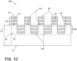
- a display article 100 is depicted with the same features and attributes as the display article 100 shown in FIGS. 1A and 1B , with like-numbered elements having substantially the same functions and structures. Further, the display article 100 depicted in FIG. 1C employs an antireflective coating 60 disposed on the primary surface 12 of the substrate 10, to further improve the antiglare effect of the display article 100. In embodiments, the display article 100, as depicted in FIG.
- the antireflective coating 60 is particularly beneficial for end use applications requiring transmittance and some degree of transmitted scattering (e.g., for display devices that include features that result in subsurface reflectance such as touch sensor layers, thin film transistor layers, indium-tin-oxide layers, and other subsurface features).
- the antireflective coating 60 is configured according to a multilayer antireflective coating or film structure, as prepared to effect antiglare, optical properties for the article employing it.
- the antireflective coating 60 includes a plurality of alternating low refractive index and high refractive index layers 62 and 64, respectively.
- the antireflective coating 60 can have a total of three (3) to nine (9) layers, three (3) to six (6) layers, three (3) to five (5) layers, e.g., 3 layers, 4 layers, 5 layers, 6 layers, 7 layers, 8 layers or 9 layers in total.
- each of the low index layers 62 comprises a refractive index of less than or equal to about 1.8 and about the same or greater than a refractive index of the substrate 10; and each of the high refractive index layers 64 comprises a refractive index that is greater than 1.8.
- the display article 100 can exhibit a first-surface absolute specular reflectance (% R ) of less than 0.5%, less than 0.4%, less than 0.3%, less than 0.2%, or even less than 0.1%, as measured at an incident angle of 0-20° from normal. Further, according to some embodiments, the display article 100 can exhibit a first-surface absolute specular reflectance (% R ) of less than 0.5%, less than 0.4%, less than 0.3%, less than 0.2%, or even less than 0.1%, as measured at an incident angle of 0-20° from normal at one or more wavelengths between 450 nm and 650 nm.
- the antiglare effects afforded by the addition of the antireflective coating 60 in the display article 100 shown in FIG. 1C should be approximately additive in a proportional sense. That is, the diffractive surface region 30a of a display article 100 shown in FIGS. 1A and 1B can lower the specular reflectance of the primary surface 12 of the substrate 10 by a factor of 10, and the addition of the antireflective coating 60 can further lower the specular reflectance by a factor of 10, leading to a reduction in the specular reflectance of the display article 100 of FIG. 1C of about a factor of 100. As such, it is believed that the display article 100, as configured according to FIG.
- 1C can, according to some embodiments, exhibit a first-surface absolute specular reflectance (%R) of less than 0.1%, less than 0.08%, less than 0.06%, less than 0.05%, less than 0.04%, or even less than 0.025%, as measured at an incident angle of 0-20° from normal at one or more wavelengths between 450 nm and 650 nm.
- %R first-surface absolute specular reflectance
- a low refractive index layer 62 of the antireflective coating 60 is disposed directly on the diffractive surface region 30a of the primary surface 12 of the substrate 10. Further, according to the embodiment shown in FIG. 1C , a low refractive index layer 62 is disposed as the top-most layer of the display article 100 and the antireflective coating 60 has a total of five (5) layers, i.e., a multilayer structure with five (5) low and high refractive index layers: 62/64/62/64/62.
- Suitable materials for the low refractive index layer 62 include: SiO 2 , Al 2 O 3 , GeO 2 , SiO x , AlO x N y , SiO x N y , SiAl y O x N y , MgO and MgAl 2 O 4 .
- Suitable materials for the high refractive index layer 64 include: Al 2 O 3 , AlO x N y , SiO x N y , SiAl y O x N y , AlN, SiN x , Si 3 N 4 , Nb 2 O 5 , Ta 2 O 5 , HfO 2 , TiO 2 , ZrO 2 , Y 2 O 3 , and diamond-like carbon.
- each of the low and high index layers 62 and 64 can range from about 1 nm to about 250 nm and the total thickness of the antireflective coating 60 can range from about 5 nm to about 3000 nm, 5 nm to 2500 nm, 5 nm to 2000 nm, from 5 nm to 1500 nm, from 5 nm to 1000 nm, from 5 nm to 750 nm, from 5 nm to 500 nm, from 5 nm to 450 nm, from 5 nm to 400 nm, from 5 nm to 350 nm, from 5 nm to 300 nm, from 5 nm to 275 nm, from 5 nm to 260 nm, from 5 nm to 250 nm, from 100 nm to 500 nm, from 100 nm to 400 nm, from 100 nm to 350 nm, from 100 nm to 300 nm, from 100 nm to 500 nm
- the antireflection coating 60 can be configured with a scratch resistant layer.
- the scratch resistant layer can be the farthest, middlemost or lowest high refractive index layer 64 from the substrate 10.
- the scratch resistant layer is the thickest high refractive index layer 64 in the antireflection coating 60 and may also comprise one of Si 3 N 4 , SiN x and SiO x N y .
- the scratch resistant layer can also have a physical thickness from 50 nm to 2000 nm, from 50 nm to 1000 nm, from 50 nm to 500 nm, from 50 nm to 400 nm, from 50 nm to 300 nm, from 50 nm to 200 nm, 50 nm to 150 nm, 75 nm to 175 nm, 100 nm to 160 nm, and all thickness values within the foregoing ranges.
- the structure of the antireflection coating 60 can be configured with a design as listed below in Table 1A.
- the antireflection coating 60 has a total thickness of 260.5 nm, and employs a scratch resistant layer with a thickness of 105.9 nm and a SiO x N y composition.
- the structure of the antireflection coating 60 can be configured with a design as listed below in Table 1B.
- the antireflection coating 60 has a total thickness of 338.4 nm, and employs a scratch resistant layer with a thickness of 158.5 nm and a SiN x composition.
- the structure of the antireflection coating 60 can be configured with a design as listed below in Table 1C.
- the antireflection coating 60 has a total thickness of 301.48 nm, and employs a scratch resistant layer with a thickness of 135.0 nm and a SiN x composition.
- the structure of the antireflection coating 60 can be configured with a design as listed below in Table ID.
- the antireflection coating 60 has a total thickness of 295.5 nm, and employs a scratch resistant layer with a thickness of 128.0 nm and a SiN x composition.
- TABLE 1D Layer Material Refractive Index (@ 550 nm) Thickness (nm) Air 1 1 SiO 2 1.465 90.4 2 SiN x 2.043 128.0 3 SiO 2 1.465 37.8 4 SiN x 2.043 14.4 5 SiO 2 1.465 25.0 Substrate ion-exchanged, strengthened glass 1.506 Total thickness 295.5
- the display article 100 can exhibit a first-surface average visible specular (or average photopic specular, as understood by those with skill in the field of the disclosure) reflectance (% R ) of less than 1%, 0.9%, 0.8%, 0.7%, 0.6% 0.5%, less than 0.4%, less than 0.3%, less than 0.2%, less than 0.15%, less than 0.1%, or even less than 0.8%, as measured at any incident angle from about 5° to 20° from normal and detected with an angular aperture (in angular range) of +/- 0.1 degrees in the visible spectrum from about 450 nm to 650 nm.
- % R first-surface average visible specular reflectance
- the display article 100 can exhibit a first-surface average specular (or average photopic specular) reflectance (%R) of less than 1%, 0.9%, 0.8%, 0.7%, 0.6%, 0.5%, less than 0.4%, less than 0.3%, less than 0.2%, or even less than 0.1%, as measured at an incident angle from about 5° to 20° from normal at wavelengths from 450 nm to 650 nm.
- %R first-surface average specular reflectance
- the first-surface specular reflectance of the display article 100 shown in FIG. 1C can be evaluated using a Rhopoint IQ Goniophotometer instrument to obtain specular reflectance value report levels (Rspec or Rs ) in a small aperture range of +/- 0.1 degrees (e.g., as compared to +/- 2 degrees for other common instruments). This small angular aperture provides better resolution of specular and non-specular reflected light.
- the display article 100 can exhibit specular reflectance value report levels (Rspec) of less than 5, less than 4, less than 3, or even less than 2.
- the Rspec values measured from the display articles 100 using a Rhopoint IQ Goniophotometer can be normalized to obtain the average specular (or average photopic specular) reflectance (%R) ranges and levels reported above through multiplying by the previously mentioned conversion factor of 4.91/100.
- Rspec * 4.91/100 % R .
- the reflectance levels of the display article 100 of FIG. 1C can be characterized through gloss measurements, which also can be conducted with a Rhopoint IQ instrument.
- the display article 100 can exhibit gloss levels of less than 10, or less than 5, as measured at 20° incidence, which correspond to reflectance (%R) values of less than 0.5%, or less than 0.25%, at 20° incidence with +/- 0.9° angular acceptance.
- the display article 100 can exhibit gloss levels of less than 45, less than 40, or less than 35, as measured at 60° incidence, which correspond to reflectance (%R) values of less than 2.25%, less than 2%, or less than 1.75%, at 60° incidence with +/- 2.2° angular acceptance.
- the display article 100 shown in FIG. 1C can also exhibit sparkle of less than 5%, as measured by pixel power deviation (PPD 140 ) at an incident angle of 0° from normal, according to some embodiments.
- the display article 100 shown in exemplary form in FIG. 1D can exhibit sparkle levels of less than 4%, 3.5%, 3%, 2.5%, 2%, 1.5%, 1%, or 0.5%, as measured by pixel power deviation (PPD 140 ) at an incident angle of 0° from normal.
- the display article 100 of FIG. 1D exhibits sparkle levels from 5% to 0.1%, from 5% to 0.5%, from 5% to 1%, and all sparkle levels in the foregoing ranges.
- the article can exhibit a two-surface transmittance level of greater than 90%, 91%, 92%, 93%, 94%, or even 95%.
- These two-surface transmittance levels are reported for display articles 100 with one antireflection coating 60 disposed on the diffractive surface region 30a, as defined with the primary surface 12 of the substrate 10.
- the other primary surface 14 of the substrate 10 remains bare, and has an intrinsic reflectance of about 4%, meaning that the maximum possible two-surface transmittance for these display articles 100 is about 96%.
- the article can exhibit transmittance haze values of less than 40%, according to embodiments.
- the display article 100 shown in exemplary form in FIG. 1C can exhibit transmittance haze levels of less than 40%, 35%, 30%, 25%, 20%, 15%, 10%, or 5%.
- the display article 100 can exhibit transmittance haze levels of about 40%, 37.5%, 35%, 32.5%, 30%, 27.5%, 25%, 22.5%, 20%, 17.5%, 15%, 12.25%, 10%, 7.5%, 5%, 1%, and all transmittance haze values between the foregoing levels.
- the display article 100 of FIG. 1C can exhibit transmittance haze levels from 50% to 0.5%, 50% to 1%, 50% to 5%, 40% to 0.5%, 40% to 1%, 40% to 5%, 30% to 0.5%, 30% to 1%, 30% to 5%, 20% to 0.5%, 20% to 1%, 20% to 5%, 10% to 0.5%, 10% to 1%, and all transmittance haze values in the foregoing ranges.
- the display article 100 of FIG. 1C can exhibit reflected haze levels of less than 3 0%, less than 25%, less than 20%, less than 10%, or even less than 8%.
- such display articles 100 can exhibit a reflected haze level of 29%, 28%, 27%, 26%, 25%, 22.5%, 20%, 15%, 10%, 8%, 6%, 4%, 2%, and all reflected haze values between the foregoing levels.
- the display article 100 shown in FIG. 1C can also exhibit distinctness of image (DOI) levels of 95% or less, 90% or less, or even 80% or less, as measured at an incident angle of 20° from normal.
- DOI distinctness of image
- the display article 100 shown in exemplary form in FIG. 1C can exhibit DOI levels of less than 99%, 95%, 90%, 85%, 80%, 75%, 70%, 65%, 60%, or 55%, as measured at an incident angle of 20° from normal.
- 1C exhibits DOI levels from 99% to 40%, from 99% to 50%, from 95% to 40%, from 95% to 50%, from 90% to 40%, from 90% to 50%, from 85% to 40%, from 85% to 50%, from 80% to 40%, and from 80% to 50%, and all DOI levels in the foregoing ranges.
- each of these articles can exhibit a maximum hardness of 8 GPa or greater as measured on the air-side surface 61 of the antireflection coating 60 by a Berkovich Indenter Hardness Test along an indentation depth of 50 nm or greater.
- the display article 100 can exhibit a maximum hardness level of 8 GPa, 9 GPa, 10 GPa, 11 GPa, 12 GPa, 13 GPa, 14 GPa, 15 GPa, 16 GPa, 17 GPa, 18 GPa, 19 GPa, 20 GPa, or even higher values, or any maximum hardness value between the foregoing levels, as measured with a Berkovich Indenter Hardness Test along an indentation depth of 50 nm or greater, or 100 nm or greater.
- Preferred ranges of the maximum hardness of the antireflection coating 60 are greater than 8 GPa, 9 GPa, 10 GPa, 11 GPa, or even greater than 12 GPa, with a total thickness of the coating being less than 500 nm, less than 400 nm, less than 350 nm, or even less than 300 nm.
- the substrate 10 of the display article 100 can be configured with a multi-component glass composition having about 40 mol % to 80 mol % silica and a balance of one or more other constituents, e.g., alumina, calcium oxide, sodium oxide, boron oxide, etc.
- the bulk composition of the substrate 10 is selected from the group consisting of aluminosilicate glass, a borosilicate glass and a phosphosilicate glass.
- the bulk composition of the substrate 10 is selected from the group consisting of aluminosilicate glass, a borosilicate glass, a phosphosilicate glass, a soda lime glass, an alkali aluminosilicate glass, and an alkali aluminoborosilicate glass.
- the substrate 10 is a glass-based substrate, including, but not limited to, glass-ceramic materials that comprise a glass component at about 90% or greater by weight and a ceramic component.
- the substrate 10 can be a polymer material, with durability and mechanical properties suitable for the development and retention of the diffractive surface region 30a.
- the substrate 10 has a bulk composition that comprises an alkali aluminosilicate glass that comprises alumina, at least one alkali metal and, in some embodiments, greater than 50 mol % SiO 2 , in other embodiments, at least 58 mol % SiO 2 , and in still other embodiments, at least 60 mol % SiOz, wherein the ratio (Al 2 O 3 (mol%) + B 2 O 3 (mol%)) / ⁇ alkali metal modifiers (mol%) > 1, where the modifiers are alkali metal oxides.
- This glass in particular embodiments, comprises, consists essentially of, or consists of about 58 mol % to about 72 mol % SiO 2 ; about 9 mol % to about 17 mol % Al 2 O 3 ; about 2 mol % to about 12 mol % B 2 O 3 ; about 8 mol % to about 16 mol % Na 2 O; and 0 mol % to about 4 mol % K 2 O, wherein the ratio (Al 2 O 3 (mol%) + B 2 O 3 (mol%)) / ⁇ alkali metal modifiers (mol%) > 1, where the modifiers are alkali metal oxides.
- the substrate 10 has a bulk composition that comprises an alkali aluminosilicate glass comprising, consisting essentially of: or consisting of: about 61 mol % to about 75 mol % SiO 2 ; about 7 mol % to about 15 mol % Al 2 O 3 ; 0 mol % to about 12 mol % B 2 O 3 ; about 9 mol % to about 21 mol % Na 2 O; 0 mol % to about 4 mol % K 2 O; 0 mol % to about 7 mol % MgO; and 0 mol % to about 3 mol % CaO.
- an alkali aluminosilicate glass comprising, consisting essentially of: or consisting of: about 61 mol % to about 75 mol % SiO 2 ; about 7 mol % to about 15 mol % Al 2 O 3 ; 0 mol % to about 12 mol % B 2 O 3 ; about 9 mol % to about
- the substrate 10 has a bulk composition that comprises an alkali aluminosilicate glass comprising, consisting essentially of, or consisting of: about 60 mol % to about 70 mol % SiO 2 ; about 6 mol % to about 14 mol % Al 2 O 3 ; 0 mol % to about 15 mol % B 2 O 3 ; 0 mol % to about 15 mol % Li 2 O; 0 mol % to about 20 mol % Na 2 O; 0 mol % to about 10 mol % K 2 O; 0 mol % to about 8 mol % MgO; 0 mol % to about 10 mol % CaO; 0 mol % to about 5 mol % ZrO 2 ; 0 mol % to about 1 mol % SnO 2 ; 0 mol % to about 1 mol % CeOz; less than about 50 ppm As 2 O 3 ; and less than about 50 ppm As 2
- the substrate 10 has a bulk composition that comprises an alkali aluminosilicate glass comprising, consisting essentially of, or consisting of: about 64 mol % to about 68 mol % SiOa; about 12 mol % to about 16 mol % Na 2 O; about 8 mol % to about 12 mol % Al 2 O 3 ; 0 mol % to about 3 mol % B 2 O 3 ; about 2 mol % to about 5 mol % K 2 O; about 4 mol % to about 6 mol % MgO; and 0 mol % to about 5 mol % CaO, wherein: 66 mol % ⁇ SiO 2 +B 2 O 3 +CaO ⁇ 69 mol %; Na 2 O+K 2 O+B 2 O 3 +MgO+CaO+SrO>10 mol %; 5 mol % ⁇ MgO+CaO+SrO ⁇ 8 mol %; (Na 2 O
- the substrate 10 comprises, in some embodiments: about 40 to about 70 mol % SiO 2 ; 0 to about 28 mol % B 2 O 3 ; about 0 to about 28 mol % Al 2 O 3 ; about 1 to about 14 mol % P 2 O 5 ; and about 12 to about 16 mol % R 2 O.
- the glass substrate comprises: about 40 to about 64 mol % SiO 2 ; 0 to about 8 mol % B 2 O 3 ; about 16 to about 28 mol % Al 2 O 3 ; about 2 to about 12 mol % P 2 O 5 ; and about 12 to about 16 mol % R 2 O.
- the substrate 10 may further comprise at least one alkaline earth metal oxide such as, but not limited to, MgO or CaO.
- the substrate 10 has a bulk composition that is substantially free of lithium; i.e., the glass comprises less than 1 mol % Li 2 O and, in other embodiments, less than 0.1 mol % Li 2 O and, in other embodiments, 0.01 mol % Li 2 O, and in still other embodiments, 0 mol % Li 2 O.
- such glasses are free of at least one of arsenic, antimony, and barium; i.e., the glass comprises less than 1 mol % and, in other embodiments, less than 0.1 mol %, and in still other embodiments, 0 mol % of As 2 O 3 , Sb 2 O 3 , and/or BaO.
- the substrate 10 has a bulk composition that comprises, consists essentially of or consists of a glass composition, such as Corning ® Eagle XG ® glass, Corning ® Gorilla ® glass, Corning ® Gorilla ® Glass 2, Corning ® Gorilla ® Glass 3, Corning ® Gorilla ® Glass 4 or Corning ® Gorilla ® Glass 5.
- a glass composition such as Corning ® Eagle XG ® glass, Corning ® Gorilla ® glass, Corning ® Gorilla ® Glass 2, Corning ® Gorilla ® Glass 3, Corning ® Gorilla ® Glass 4 or Corning ® Gorilla ® Glass 5.
- the substrate 10 of the display article 100 depicted in FIGS. 1A-1C can possess an ion-exchangeable glass composition that is strengthened by either chemical or thermal means that are known in the art.
- the substrate 10 is chemically strengthened by ion exchange.
- metal ions at or near a primary surface 12 and/or primary surface 14 of the substrate 10 are exchanged for larger metal ions having the same valence as the metal ions in the glass substrate.
- the exchange is generally carried out by contacting the substrate 10 with an ion exchange medium such as, for example, a molten salt bath that contains the larger metal ion.
- the metal ions are typically monovalent metal ions such as, for example, alkali metal ions.
- chemical strengthening of a substrate 10 that contains sodium ions by ion exchange is accomplished by immersing the substrate 10 in an ion exchange bath comprising a molten potassium salt such as potassium nitrate (KNO 3 ) or the like.
- the ions in the surface layer of the substrate 10 and the larger ions are monovalent alkali metal cations, such as Li + (when present in the glass), Na + , K + , Rb + , and Cs + .
- monovalent cations in the surface layer of the substrate 10 may be replaced with monovalent cations other than alkali metal cations, such as Ag + or the like.
- the replacement of small metal ions by larger metal ions in the ion exchange process creates a compressive stress region 50 in the substrate 10 that extends from the primary surface 12 to a depth 52 (referred to as the "depth of layer") that is under compressive stress.
- a compressive stress region can be formed in the glass substrate that extends from the primary surface 14 to a depth (not shown in FIGS. 1A-1C ) that is comparable in nature to the compressive stress region 50. More particularly, this compressive stress at the primary surface 14 of the glass substrate is balanced by a tensile stress (also referred to as "central tension") within the interior of the glass substrate.
- the primary surface 12 of the substrate 10 described herein when strengthened by ion exchange, has a compressive stress of at least 350 MPa, and the region under compressive stress extends to a depth 52, i.e., depth of layer, of at least 15 ⁇ m below the primary surface 12.
- Ion exchange processes are typically carried out by immersing the substrate 10 in a molten salt bath containing the larger ions to be exchanged with the smaller ions in the glass.
- parameters for the ion exchange process including, but not limited to, bath composition and temperature, immersion time, the number of immersions of the glass in a salt bath (or baths), use of multiple salt baths, additional steps such as annealing, washing, and the like, are generally determined by the composition of the glass and the desired depth of layer and compressive stress of the glass as a result of the strengthening operation.
- ion exchange of alkali metal-containing glasses may be achieved by immersion in at least one molten bath containing a salt such as, but not limited to, nitrates, sulfates, and chlorides of the larger alkali metal ion.
- a salt such as, but not limited to, nitrates, sulfates, and chlorides of the larger alkali metal ion.
- the temperature of the molten salt bath typically is in a range from about 380°C up to about 450°C, while immersion times range from about 15 minutes up to about 16 hours. However, temperatures and immersion times different from those described above may also be used.
- Such ion exchange treatments when employed with a substrate 10 having an alkali aluminosilicate glass composition, result in a compressive stress region 50 having a depth 52 (depth of layer) ranging from about 10 ⁇ m up to at least 50 ⁇ m with a compressive stress ranging from about 200 MPa up to about 800 MPa, and a central tension of less than about 100 MPa.
- etching processes that can be employed to create the diffractive surface region 30a of the display article 100 shown in FIGS. 1A-1C can remove alkali metal ions from the substrate 10 that would otherwise be replaced by a larger alkali metal ion during an ion exchange process, a preference exists for developing a compressive stress region 50 in the display article 100 after the formation and development of the diffractive surface region 30a.
- a compressive stress region 50 can be developed in the substrate 10 prior to development of the diffractive surface region 30a to a depth 52 sufficient to account for some loss in the depth of layer in the region 50 associated with the various treatments associated with forming the diffractive surface region 30a, as outlined below.
- the diffractive surface region 30a may be created by an additive or coating process rather than a substrate etching process, in which case it may be desirable to develop the compressive stress region 50 before this additive or coating process.
- the article can further include an easy-to-clean (ETC) coating (not shown) disposed over the diffractive surface region 30a.
- ETC easy-to-clean
- the ETC coating is deposited over the diffractive surface region 30a such that its surface morphology generally mirrors the underlying morphology of the diffractive surface region 30a.
- the display article 100 further includes a smudge-resistant fluorine-based ETC coating, deposited on at least a portion of the diffractive surface region 30a.
- the ETC coating comprises at least one amphiphobic substance having fluorine termination groups to provide the diffractive surface region 30a with amphiphobicity (i.e., hydrophobicity and oleophobicity, or lack of affinity for both oils and water), thus minimizing wetting of the surface by water and/or oils.
- the fluorine termination groups of the ETC coating are less polar than a surface having -OH termination groups, and therefore minimize hydrogen (i.e., Van der Waals) bonding between particles and liquids.
- bonding-and adhesion- is minimized. Consequently, mass transport of fingerprint oils and debris from the finger of a person to the ETC coating is minimized.
- the ETC coating is formed by exchanging the hydrogen found in terminal OH groups on the diffractive surface region 30a of the display article 100 with a fluorine-based moiety such as, for example, a fluorine-containing monomer (e.g., a fluorosilane), to form a glass having terminal fluorinated groups.
- a fluorine-based moiety such as, for example, a fluorine-containing monomer (e.g., a fluorosilane), to form a glass having terminal fluorinated groups.
- an ETC coating of the display article 100 depicted in FIGS. 1A-1C comprises a self-assembled monolayer of a fluorine-terminating molecular chain.
- the ETC coating comprises a thin, fluoro-polymeric coating and, in yet another embodiment, the ETC coating comprises silica soot particles that have been treated to have pendent fluorocarbon groups attached to the soot particles.
- Such ETC coatings can be applied to the diffractive surface region 30a of the display article 100 by dipping, vapor coating, spraying, application with a roller, or other suitable method known in the art After the ETC coating has been applied, it may be "cured" at temperatures ranging from about 25°C up to about 150°C and, in another embodiment, at temperatures ranging from about 40°C up to about 100°C. Curing times can range from about 1 up to about 4 hours, and may be carried out in an atmosphere containing 40-95% moisture. After curing, the display article 100 with an ETC coating can be solvent rinsed to remove any unbound coating and air-dried prior to use.
- the diffractive surface region 30a includes a plurality of structural features 20 with a first portion of structural features 22a, 22a' and a second portion of structural features 22b, 22b'.
- first portion of structural features 22a e.g., pillars
- 22a' e.g., holes
- the first portion of structural features 22a can be defined by a pitch 42a of less than 125 ⁇ m
- the second portion of structural features 22b, 22b' can be defined by a pitch 42b (see FIG. 1A ) substantially the same or different from the pitch 42a.
- the second portion of structural features 22b, 22b' (e.g., ligaments, mesas) can be defined by a pitch 42b of less than 125 ⁇ m, with the pitch 42a substantially the same as or different from the pitch 42b.
- the pitch 42a and 42b of the first and second portion of structural features 22a, 22a' and 22b, 22b' are pitch values of these features, as would be commonly understood by those of ordinary skill in the field of the disclosure.
- the pitch 42a and/or 42b of the first and second portion of structural features 22a, 22a' and 22b, 22b', respectively can be less than 125 ⁇ m, 110 ⁇ m, 100 ⁇ m, 90 ⁇ m, 80 ⁇ m, 70 ⁇ m, 60 ⁇ m, 50 ⁇ m, 40 ⁇ m, 30 ⁇ m, 20 ⁇ m and all pitch values between these upper thresholds of the pitch value.
- the pitch values 42a, 42b may have a lower threshold, e.g., the pitch values may be larger than about 2 microns, larger than 5 microns, or larger than 10 microns.
- embodiments are configured such that the first or the second portion of structural features 22a, 22a' (e.g., pillars or holes) or 22b, 22b' (e.g., ligaments or mesas), respectively, is at a fill fraction from about 30% to 70%, with the other portion (i.e., 22a, 22a' or 22b, 22b') at a fill fraction of 100% minus the fill fraction of the first or second portions 22a, 22a' or 22b, 22b'.
- structural features 22a, 22a' e.g., pillars or holes
- 22b, 22b' e.g., ligaments or mesas
- the first portion of structural features 22a, 22a' or second portion of structural features 22b, 22b' of the diffractive surface region 30a can be configured at a fill fraction from about 30% to 70%, from about 35% to 65%, from about 40% to 60%, or from about 40% to 55%.
- the first or second portions 22a, 22a' or 22b, 22b' can be configured within the diffractive surface region 30a such that they have a fill fraction of 30%, 35%, 40%, 45%, 50%, 55%, 60%, 65%, 70%, and all fill fraction levels between the foregoing values.
- the diffractive surface region 30a is arranged within the primary surface 12 of the substrate 10 such that each of the plurality of structural features 20, e.g., the first and second portions 22a, 22a' and 22b, 22b', has a diameter 32a, 32b of less than 125 ⁇ m, or less than 100 ⁇ m.
- the diameter 32a, 32b of the first and second portion of structural features 22a, 22a' and 22b, 22b' represents the effective diameter or longest width dimension of these features at their full width height maximum (FWHM), as would be commonly understood by those of ordinary skill in the field of the disclosure.
- the diameter 32a, 32b of the structural features of the first and second portions 22a, 22a' and 22b, 22b' can be less than 125 ⁇ m, 120 ⁇ m, 110 ⁇ m, 100 ⁇ m, 90 ⁇ m, 80 ⁇ m, 70 ⁇ m, 60 ⁇ m, 50 ⁇ m, 40 ⁇ m, 30 ⁇ m, 20 ⁇ m, 10 ⁇ m, 5 ⁇ m, and all diameter values less than the foregoing diameters.
- the diameter 32a, 32b of the structural features of the first and second portions 22a, 22a' and 22b, 22b' can also range from 5 ⁇ m to 120 ⁇ m, 5 ⁇ m to 100 ⁇ m, 5 ⁇ m to 80 ⁇ m, or 10 ⁇ m to 100 ⁇ m, for example.
- the diffractive surface region 30a is configured such that each of the structural features 20 has an aspect ratio of more than 10.
- the aspect ratio of each of the structural features 20, e.g., the first and second portion of structural features 22a, 22a' and 22b, 22b' is given by the average diameter 32a, 32b divided by the respective average height 24a, 24b.
- the aspect ratio of the structural features 20 of the diffractive surface region 30a is more than 10, more than 20, more than 50, or more than 100.
- a first portion of structural features 22a, 22a' with an average diameter 32a of 20 ⁇ m and an average height 24a of 0.2 ⁇ m corresponds to an aspect ratio of 100.
- the diffractive surface region 30a is substantially flat or planar, at least as viewed under ambient lighting without any magnification aids.
- the aspect ratio of the structural features of the display article 100 shown in FIG. 1C can be greater than or equal to 50, which helps ensure that the antireflection coating 60 disposed thereon does not result in significant edge effects or shadowing that degrade the optical performance of the surface.
- the structural features 20 of the diffractive surface region 30a can be configured according to a period 47 to effect antiglare properties.
- the structural features 20 of the diffractive surface region 30a are configured with a period 47 that ranges from 1 ⁇ m to 200 ⁇ m, from 5 ⁇ m to 200 ⁇ m, from 5 ⁇ m to 150 ⁇ m, from 5 ⁇ m to 100 ⁇ m, from 5 ⁇ m to 50 ⁇ m, from 5 ⁇ m to 30 ⁇ m, from 20 ⁇ m to 150 ⁇ m, from 20 ⁇ m to 100 ⁇ m, from 10 ⁇ m to 30 ⁇ m, from 10 ⁇ m to 20 ⁇ m, and all period values between the foregoing ranges.
- the structural features 20 can be configured with a relatively large period 47 on the order of about 100 ⁇ m (e.g., from about 70 to 200 ⁇ m) for end use applications of the display article 100 that benefit from maximizing a scattered light component near 0.3°, such as in the case where the application has a particular DOI target.
- Such DOI targets may require a scattered light component at or near 0.3° from the specular reflection direction, which can be enhanced by relatively large structural features 20.
- smaller structural features 20 may be desirable, e.g., with a period 47 that ranges from about 5 to 30 ⁇ m and, according to some implementations, is semi-randomized to minimize color and/or Moiré artifacts.
- the level and type of feature randomization in the X-Y dimension can be very important to achieving low PPD while also minimizing other display artifacts such as Moiré or color banding.
- traditional, perfectly ordered grating-like structures are not preferred for the articles of the disclosure.
- Structural features 20 that range from about 5 to 30 um can affect DOI, and can be designed to achieve DOI values, e.g., below 90 or below 80, so it is not essential to have larger structural features 20 to have some effect on DOI.
- the randomization of the structural features 20 at the period 47 can be characterized by a variation in nearest-neighbor distances over a distribution range which may be limited to 1.2, 1.3, 1.4 or 1.5x a minimum distance or an average distance.
- the period 47 can be configured to range from 5 ⁇ m to 30 ⁇ m, from 10 ⁇ m to 30 ⁇ m, and from 10 ⁇ m to 20 ⁇ m, which can lower DOI to less than 90, or even less than 80, while still maintaining desirable, low sparkle levels.
- a diffractive optical model can illustrate the principles of the diffractive surface region 30a.
- Optical modeling calculations were performed using Gsolver ⁇ , a commercially available software package.
- the Gsolver ⁇ package employs a rigorous, coupled-wave analysis to find solutions for Maxwell's equations, which can govern the optical performance of a diffraction grating.
- the Gsolver ⁇ software can be applied to a linear, rectangular diffractive antiglare structure as shown in FIG. 2 .
- the rectangular nature of the diffractive antiglare structure shown in FIG. 2 departs from the structural features 20 of the diffractive surface region 30a in the sense that the structural features 20 can comprise pillars, holes, mesas, plateaus, polygons, and other discrete, non-rectangular shapes. Nevertheless, the calculations conducted on the schematic shown in FIG. 2 demonstrate trends and provide data that is useful in the definition of the structural features 20 of the diffractive surface region 30a that is consistent with the principles of this disclosure.
- the as-modeled diffractive antiglare structure has a period of 20 ⁇ m and is integrated within the surface of a glass substrate having a refractive index of 1.518 at 550 nm.
- incident light at a wavelength of 550 nm is directed against the diffractive antiglare structure at an incident angle of 20 degrees. For optimal antiglare properties, it is generally desirable to suppress the zero order reflected light (i.e., specular light).
- the zero order curve is the amplitude of the specular reflectance and, as shown in the figure, is suppressed close to 0% at a structure depth of 0.14 to 0.15 ⁇ m.
- the specular reflectance can be suppressed by a factor of 10 compared to flat glass over a structure depth range of about 0.12 to 0.17 ⁇ m, which corresponds to about 1 ⁇ 4 of the wavelength of light in air.
- a second minimum in specular reflectance is observed at the 3 ⁇ 4 wavelength structure depth.
- the amplitude of the transmitted diffracted orders for the same structure as shown in FIGS. 2 and 3A is provided.
- Specular transmission is greater than 78% of the transmittance of flat glass at a structure depth of -0.15 ⁇ m, which is also the preferred depth for minimization of specular reflectance.
- the total transmission (considering all angles) remains close to the flat glass value, and the majority of scattered light in transmission is within 10 degrees or 5 degrees of the specular direction for preferred embodiments.
- plots of diffraction efficiency in reflection as a function of structure depth for the diffractive antiglare structure depicted in FIG. 2 at fill fractions of 15%, 30% and 70%, respectively, are provided.
- the diffractive structures with these fill fractions at 15%, 30% and 70% do not allow the zero order (specular) reflectance to drop to zero.
- the preferred fill fraction for simple bimodal height, single material structure such as this one is close to 50%, or in the range of 35% to 65%, as modeled and depicted in FIG. 2 .
- FIG. 5 a plot of diffraction efficiency in reflection as a function of structure depth for the diffractive antiglare structure depicted in FIG. 2 with varying incident light wavelengths is provided.
- this figure illustrates the effect of incident light wavelengths on the suppression of specular reflection, particularly at the zero order.
- the optimal structure depth varies with wavelength, as shown in FIG. 5 , a single structure depth near the first 1 ⁇ 4 wavelength minimum (at the arrow) can successfully achieve a 10x reduction in specular reflectance for all visible light wavelengths from 450 to 650 nm.
- these figures generally provide guidance for the display article 100 to be configured to minimize specular reflectance while maximizing specular transmittance. Further, these figures illustrate how the depth of the diffractive antiglare structure (e.g., as serving as the general basis for the diffractive surface region 30a) affects specular reflectance.
- the modeled linear diffractive antiglare structure of FIG. 2 differs from the diffractive surface region 30a of the display articles 100 shown in FIGS. 1A-1C , as the latter contains a plurality of structural features 20, such as pillars, holes, polygons and other discrete features disposed in an ordered or semi-ordered array.
- FIGS. 1A-1C contains a plurality of structural features 20, such as pillars, holes, polygons and other discrete features disposed in an ordered or semi-ordered array.
- the height or depth of the structural features 20 of the diffractive surface region 30a is preferably maintained from 50 to 250 nm, 75 to 225 nm, 100 to 200 nm, 120 to 190 nm or from 140 to 190 nm.
- the two-dimensional array of structural features 20 of the diffractive surface region 30a can be fabricated by many processes, such as optical lithography (photomask), inkjet printing, laser patterning and/or screen printing once the intended structure for the surface region 30a has been defined.
- optical lithography photomask
- inkjet printing laser patterning and/or screen printing once the intended structure for the surface region 30a has been defined.
- the selection of the process depends on the resolution of the structural features 20 (e.g., in terms of diameter and/or pitch) and the technical capabilities of the given process.
- the design can be converted to a computer-aided design (CAD) file and then used with any of the foregoing processes to transfer it to a substrate 10 to create the 'engineered' diffractive surface region 30a.
- CAD computer-aided design
- the method 200 includes: a step 202 of masking a substrate 10 comprising a thickness 13 and a primary surface 12 with a mask; a step 204 of forming a diffractive surface region 30a within the primary surface 12 of the substrate 10; and a step 206 of removing the mask from the substrate 10.
- the net result of the method 200 is a display article 100, for example, as depicted in FIGS. 1A and 1B .
- the method 200 further includes a step 208 of forming an antireflective coating 60 over the diffractive surface region 30a, to define the display article 100 (see FIG. 1C and corresponding description).
- the diffractive surface region 30a comprises a plurality of structural features 20 that comprises a plurality of different heights in a multimodal distribution.
- the multimodal distribution further comprises a first portion of structural features 22a, 22a' at a first average height 24a and a second portion of structural features 22b, 22b' at a second average height 24b.
- the substrate 10, as fabricated according to the method 200 exhibits a sparkle of less than 4%, as measured by PPD 140 at an incident angle of 0° from normal, a DOI of less than 80% at an incident angle of 20° from normal, and a transmittance haze of less than 20% from an incident angle of 0° from normal.
- the step 202 of masking the substrate 10 can include one or more of screen print masking, inkjet print masking and photoresist masking.
- the step 204 of forming the diffractive surface region 30a includes etching the primary surface 12 of the substrate 10 through the mask to form the diffractive surface region 30a, wherein each structural feature is a hole at a depth from 50 nm to 250 nm.
- the step 204 for example, can be conducted by etching the substrate 10, as comprising a glass composition, with an HF/HNO 3 etchant.
- the wet etching solution employed in step 204 can consist of hydrofluoric acid (HF, 49 w/w%) and nitric acid (HNO 3 , 69 w/w%) combinations with 0.1-5 v/v% HF and 0.1-5 v/v% HNO 3 .
- Typical concentrations used to achieve 100-250 nm etching depths are 0.1 v/v% HF/1 v/v% HNO 3 to 0.5 v/v% HF/1 v/v% HNO 3 solutions.
- etching in step 204 can be carried out using a dip or spray etch process from room temperature to about 45°C.
- the step 204 of forming the diffractive surface region 30a can include depositing a film on the primary surface 12 of the substrate 10 through the mask (e.g., by sputtering, evaporation, or chemical vapor deposition) to form the diffractive surface region 30a, and each structural feature is a pillar at a height from 50 nm to 250 nm.
- the diffractive surface region can also be formed by masking plus 'dry etching', plasma-based etching, reactive ion etching, or other vacuum-based etching methods.
- such a film can be deposited through the mask with a liquid phase silica layer or other oxide layer, followed by mask removal and lift off.
- the articles 100 disclosed herein may be incorporated into a device article, e.g., a device article with a display (or display device articles) (e.g., consumer electronics, including mobile phones, tablets, computers, navigation systems, wearable devices (e.g., watches) and the like), augmented-reality displays, heads-up displays, glasses-based displays, architectural device articles, transportation device articles (e.g., automotive, trains, aircraft, sea craft, etc.), appliance device articles, or any device article that benefits from some transparency, scratch-resistance, abrasion resistance or a combination thereof.
- a device article e.g., as consistent with the articles 100 depicted in FIG.
- FIGS. 18A and 18B show a consumer electronic device 1800 including a housing 1802 having a front 1804, a back 1806, and side surfaces 1808; electrical components (not shown) that are at least partially inside or entirely within the housing and including at least a controller, a memory, and a display 1810 at or adjacent to the front surface of the housing; and a cover substrate 1812 at or over the front surface of the housing such that it is over the display.
- the cover substrate 1812 may include any of the articles disclosed herein.
- at least one of a portion of the housing or the cover glass comprises the articles disclosed herein.
- a photomask/optical lithography process was used to develop the diffractive surface region structures shown in these images.
- a light-sensitive polymer i.e., a photoresist
- the ideal photoresist image has the exact shape of the designed or intended pattern in the plane of the substrate, with vertical walls through the thickness of the resist ( ⁇ 3 ⁇ m for spin-coatable resists, ⁇ 20 ⁇ m for dry film resists, and ⁇ 15 ⁇ m for screen-coatable photoresists).
- the final resist pattern When exposed, the final resist pattern is binary with parts of the substrate covered with resist while other parts are completely uncovered.
- the general sequence of processing steps for a typical photolithography process is as follows: substrate preparation (clean and dehydration followed by an adhesion promoter for spin-coatable resist, e.g., hexamethyl disilazane (HMDS), photoresist spin coat, prebake, exposure, and development (i.e., step 202), followed by a wet etching process to transfer the binary image onto glass (i.e., step 204).
- the final step is to strip the resist after the resist pattern has been transferred into the underlying layer (i.e., step 206).
- post bake and post exposure bake steps are required to ensure resist adhesion during wet etching process.
- FIGS. 7A-7D optical micrographs are provided of diffractive surface regions of aluminosilicate glass substrates prepared according to this example with preferred etch depths in the range of 100 to 250 nm for the holes. These diffractive surface regions were prepared according to the foregoing photomasking process, followed by an etching process. More particularly, the wet etching solution used to prepare the samples of FIGS. 7A-7D consisted of hydrofluoric acid (HF, 49 w/w%) and nitric acid (HNO 3 , 69 w/w%) with 0.1-5 v/v% HF and 0.1-5 v/v% HNO 3 .
- HF hydrofluoric acid
- HNO 3 nitric acid
- FIGS. 7A and 7B show two-dimensional (2D) ordered arrays of structural features of diffractive surface regions at two spatial frequencies: (a) structural features with a diameter of 12 ⁇ m with a pitch of 17 ⁇ m ( FIG. 7A ) (referred to as a "12-17" array); and (b) structural features with a 25 ⁇ m diameter and a pitch of 50 ⁇ m (referred to as a "25-50" array).
- FIGS. 7C and 7D show 2D arrays of structural features of diffractive surface regions with a randomly packed structure at two spatial frequencies: (a) a 50 ⁇ m structural feature diameter with a minimum pitch of 60 ⁇ m ( FIG. 7C ) (referred to as a "50-60" array); and (b) a 12 ⁇ m structural feature diameter with a minimum pitch of 14 ⁇ m (referred to as a "12-14" array).
- etch depth as a function of etch time to form two structural features of diffractive surface regions according to this example.
- structural features having a diameter of 12 ⁇ m and 50 ⁇ m are etched at various etch times and the resulting etch depths are plotted (e.g., as consistent with the structures shown in FIGS. 7D and 7C , respectively).
- the substrate is a glass composition and it was etched with a 49 vol% stock solution of HF.
- Etch depth was measured using a stylus-based profilometer (with a Z depth resolution set at ⁇ 5 ⁇ m, ⁇ 200 ⁇ m scan, 3 regions with a 3 mg force) or a Bruker ContourGT-X white light interferometer (with a 20x or 50x objective lens, green narrow-band light, in a single field of view image).
- a stylus-based profilometer with a Z depth resolution set at ⁇ 5 ⁇ m, ⁇ 200 ⁇ m scan, 3 regions with a 3 mg force
- a Bruker ContourGT-X white light interferometer with a 20x or 50x objective lens, green narrow-band light, in a single field of view image.
- the larger structural features i.e., those at a diameter of about 50 ⁇ m
- etch faster at longer times as compared to smaller structural features i.e., those at a diameter of about 12 ⁇ m
- plots are provided of DOI as a function of etch depth for the structural features of the diffractive surface regions depicted in FIGS. 7C and 7D above, as having different sizes and fill fractions.
- the DOI levels of the 50-60 array of structural features (see also FIG. 7C ) at fill fractions of 36% and 50% is shown as a function of etch depth.
- the DOI levels of the 12-14 array of structural features (see also FIG. 7D ) at fill fractions of 20% and 50% is shown as a function of etch depth.
- both arrays of structural features demonstrate that the minimum DOI is observed at an etch depth from about 150 to 180 nm, as generally predicted or otherwise suggested by the modeling outlined earlier and shown in FIGS. 2-5 .
- plots are provided of measured PPD 140 and haze as a function of etch depth for structural features having different sizes and fill fractions from this example.
- the 50-60 array of structural features see also FIG. 7C ) at fill fractions of 36% and 50% exhibits minimum PPD 140 and haze values at low etch depths of less than 0.2 ⁇ m.
- plots are provided of measured PPD 140 and haze as a function of etch depth for structural features having different sizes and fill fractions from this example.
- the 12-17 array of structural features see also FIG.
- FIGS. 10A-10D demonstrate that these arrays of structural features at periods of 60 ⁇ m and 17 ⁇ m, respectively, show that PPD 140 and haze increase as a function of etch depth. Further, the samples having a larger spatial frequency (i.e., the 50-60 array) have more of an impact on PPD 140 with increasing etch depth (see FIG. 10A ), and the samples having a higher frequency (i.e., the 12-17 array) have more of an impact on haze with increasing etch depth (see FIG. 10D ).
- an array of structural features i.e., holes
- a glass substrate with depths of 0.15 ⁇ m, 0.2 ⁇ m and 0.23 ⁇ m (Samples 950, 951, 952, respectively) according to a method consistent with the principles of the disclosure.
- Table 2 below lists the optical properties measured on these samples, including PPD 140 (%, as measured in a display unit at 0°), transmissivity (%), haze (%, as measured in transmission at 0°), DOI (coupled, %, as measured in reflectance at 20°) and specular reflectance, Rs (coupled, GU, as measured in reflectance at 20°).
- the sample (950) with an etch depth of 0.15 ⁇ m exhibits DOI ⁇ 80%, PPD 140 ⁇ 2%, and a haze ⁇ 5%, as consistent with the diffractive surface regions consistent with the disclosure.
- an optical image and surface height distribution bar of the diffractive surface region of the sample with best combination of optical properties from Table 2 (Sample 950) is provided. More specifically, the structural features of this sample (Sample 950) have a depth of about 150 nm, a fill fraction of 50%, a 12 ⁇ m feature diameter/size and a minimum pitch of 14 ⁇ m.
- FIG. 11B an angular spectra plot is provided of the samples from Table 2 in this example. More particularly, the plot of FIG. 11B shows amplitude of reflectance vs. reflectance angle for Samples 950-952. It is evident from FIG.
- samples with an array of structural features defining a diffractive surface region were made using screen printing and etching, generating pillars on a glass surface.
- the target pillar size/diameter was 75 ⁇ m on the screen print pattern, which after wetting with the etchant on the glass expanded closer to a diameter of about 100 ⁇ m.
- the target pitch for these samples was 125 ⁇ m in a hexagonal pattern with a target fill fraction of 55% (the actual fill fraction was closer to 56%).
- the screen print pattern was made using an ink on a clean glass surface.
- Table 3 lists the samples made according to this example, which reflect various etch times that result in various etch depths (i.e., pillar heights), and optical properties associated with these samples (sparkle, haze, DOI and Rs). Further, as noted earlier, the first-surface specular reflectance ( Rs , in gloss units (GU) can be converted to 20° angle of incidence, first-surface absolute specular reflectance (%R) by multiplying them by a factor of 4.91/100. As is evident from Table 3, the optimal etch depth range in terms of the optical property measurements corresponds to ⁇ 1/4 wavelength of light in air, i.e., the samples at etch depths of 0.141 and 0.172 ⁇ m.
- an angular spectra plot is provided for the sample in this example with an etch depth of ⁇ 0.172 ⁇ m (C17-T10a-75H-E60-Bare-C), with the plot depicting amplitude of reflectance vs. reflectance angle.
- the optimal etch depth for obtaining low DOI and low Rs lies in the range of 120 to 180 nm for the structural features, and the other etch depths do not exhibit this combination of optical properties.
- FIGS. 13A and 13B optical images are provided of the diffractive surface region and structural features of the sample depicted in FIG. 12 and Table 3 with an etch depth of 0.172 ⁇ m (C17-T10a-75H-E60-Bare-C), as viewed before and after removal of the ink as part of the screen printing and etching process.
- the target size/diameter of these features was about 75 ⁇ m; however, upon expansion of the ink upon drying, the actual size of the screen-printed features (i.e., the mask) ranged from 101 to 110 ⁇ m for the specific features depicted in FIG. 13A .
- the regions around these ink circles were etched, thus forming the pillars of this example.
- the preferred etch depth is at about 1 ⁇ 4 wavelength of light between 0.1 and 0.2 ⁇ m with regard to reductions in DOI.
- a second preferred etch depth in terms of DOI is located at about % wavelength of the light at an etch depth between 0.4 and 0.5 ⁇ m.
- the % wavelength etch depth can be less desirable because of its effect on transmitted light, as shown by the higher PPD 140 values in Table 3, as well as its lesser impact on DOI as relative to the samples at the 1 ⁇ 4 wavelength etch depth.
- diffractive surface regions of the display articles of the disclosure employ structural features having a multimodal distribution of surface heights (e.g., a bimodal distribution of surface heights)
- embodiments of these diffractive surface regions employ spatial randomization of the features in the X-Y dimension.
- two X-Y pattern randomizations are employed for the diffractive surface regions - a "hard sphere” distribution and a "Poisson disk” distribution.
- the former hard sphere pattern design targeted structural features at approximate 50% fill fractions, and samples with structural features having 12 ⁇ m and 50 ⁇ m diameters, respectively, were prepared according to this pattern.
- the latter Poisson disk pattern design targeted structural features at approximate 36% fill fractions.
- Each of these X-Y randomization schemes can also target diffractive surface regions with structural features at different fill fractions, feature depths, and combinations with antireflective coatings. Further, as is evident from this example and noted earlier, the level and type of feature randomization in the X-Y dimension can be very important to achieving low PPD while also minimizing other display artifacts such as Moiré or color banding.
- X-Y pattern randomization can be defined in different ways.
- One method is hexagonality with FIG. 15 showing the definition of hexagonality ( H ).
- Hexagonality is a metric for quantifying locally how close a pattern is to a hexagonal lattice.
- the hexagonality ( H ) at that point is computed using the angles of its six nearest neighbors with respect to an arbitrary axis.
- the spatial distribution of the plurality of structural features can have a mean hexagonality ( H ) that ranges from 0.4 to 1.0, according to embodiments of the disclosure.
- H mean hexagonality
- the variables ⁇ k represent the angles of the six nearest neighbors. On a hexagonal lattice, these six angles all differ by 60 degrees ( ⁇ /3 radians); therefore, the exponents in the six summands differ by 2 ⁇ radians and the six complex numbers in the summation are all the same.
- H is unity in that case.
- a perfect hexagonal lattice has a mean hexagonality ( H ) of 1.0.
- a completely random, stationary Poisson distribution of points has a mean hexagonality ( H ) of approximately 0.36, or 36%.
- the plurality of structural features 20 can be characterized with a non-random spatial distribution such that H ranges from 0.4 to 0.95, from 0.4 to 0.9, from 0.4 to 0.8, from 0.36 to 0.9, from 0.36 to 0.8, from 0.36 to 0.7, and all mean hexagonality ( H ) values and ranges between the foregoing ranges.
- this pattern was employed in the formation of the structural features of the diffractive surface region depicted in FIGS. 7C and 7D .
- These patterns were generated using a molecular dynamics simulation tool (LAMMPS) to generate the pattern.
- LAMMPS molecular dynamics simulation tool
- a gas of "molecules" representing the features was initially placed on a two-dimensional hexagonal lattice to fix the fill fraction at 50%. Then the gas was heated and allowed to randomize in two dimensions. The molecules were endowed with a repulsive hard-sphere potential to maintain the minimum specified spacing.
- the example pattern in FIG. 7C has a mean hexagonality ( H ) of 49% (see also FIG. 15 ), indicating a large deviation from a regular lattice.
- the "12-14" and “50-60” arrays have pattern geometries that are the same: the 50-60 pattern is simply the 12-14 pattern scaled up by an overall factor of 50/12. This scaling does not impact fill fraction, hexagonality or feature distribution functions (aside from an obvious scaling of axes), but it does impact the optical performance of the texture.
- the distribution of nearest neighbor distances (defined as center-to-center spacing of features in the X-Y space) of the 12/14 pattern is shown in FIG. 16A . Its periodogram is shown in FIG. 16B . Instead of spatial frequency, the X-axis of FIG. 16B is converted to off-specular scattering angle in degrees, for an optical wavelength of 0.55 ⁇ m.
- FIGS. 9A and 10A has a larger distribution of nearest neighbor distances and a lower fill fraction (36%).
- the structural features of these samples were arranged in a Poisson disk pattern that was generated using a "dart throwing" algorithm. This algorithm ensures an absolute minimum feature spacing (60 ⁇ m in this example), but is not very efficient at filling space.
- the mean hexagonality ( H ) is lower, at 41%.
- the distribution of nearest neighbor distances for the 50/60 Poisson disk pattern is shown in FIG. 17A . Its periodogram is shown in FIG. 17B . Instead of spatial frequency, the X-axis of FIG. 17B is converted to off-specular scattering angle in degrees, for an optical wavelength of 0.55 ⁇ m.
- a display article was fabricated with a method consistent with the embodiment of FIG. 6 (see corresponding description) with a strengthened, aluminosilicate glass substrate having a primary surface with a diffractive surface region and a multilayer AR coating structure disposed thereon.
- the diffractive surface region comprises structural features in the form of holes etched into the glass surface having a diameter of about 12 ⁇ m.
- the holes have a randomized pattern that was generated through photolithography (see FIG. 6 and corresponding description), a 14 ⁇ m minimum pitch, a targeted hole area fill fraction of 50% and an etch depth of about 0.16 ⁇ m to 0.17 ⁇ m (160-170 nm).
- the positions of the holes were randomized using a ⁇ hard sphere' pattern (see preceding Example).
- the glass substrate was strengthened by ion-exchange and the entire surface (as including the diffractive surface region) was coated with a 5-layer AR coating using reactive sputtering, with the layer design shown in Table 1A (i.e., with a total thickness of about 261 nm).
- the AR coating evenly coats the mesas and valleys of the diffractive AG surface region, allowing both the multilayer AR interference effects and the diffractive AG effects to operate simultaneously. This is due to the optical design strategy and the high precision fabrication (dimensional control) of both the diffractive surface morphology and the multilayer AR coating.
- ⁇ Edge effects' from the edges of the surface texture valleys are minimized in part by the design approach which uses relatively large (12 micron diameter) holes / valleys, as compared to the relatively thin (0.26 ⁇ m) AR coating thickness and relatively shallow (0.16 ⁇ m) etch depth.
- Table 4 summarizes the optical performance demonstrated experimentally for the samples in this example having a diffractive AG surface region and a multilayer AR coating (Ex. 5B), compared to a sample having a diffractive AG surface region without the multilayer AR (Ex. 5A), and the same multilayer AR coated on a glass substrate with no diffractive surface region (Comp. Ex. 5).
- These results show the enhanced performance that can be achieved using the combined diffractive AG surface region plus multilayer AR coating approach.
- the specular reflectance of 0.077% for Ex. 5B is significantly lower than for either Ex. 5A (0.25%) or Comp. Ex. 5 (0.61%) alone.
- the specular reflectance values in Table 4 were measured using a Rhopoint IQ Goniophotometer, which is somewhat unique relative to other instruments for measuring specular reflectance, in that the specular reflectance value report (Rspec) is measured in a small angular aperture range of +/- 0.1 degrees (compared to +/- 2 degrees for other common instruments). This small angular aperture gives a higher resolution of separation between specular and non-specular reflected light.
- Using either calculation method gives practically the same values, thus multiplying by the ratio 4.16%/85, 100%/2000, or 4.91/100 gives the same result, within practical measurement error ranges.
- the gloss units in Table 4 below can be converted to % Reflectance values.
- the reason for the difference between %R calculated from the 20° gloss and %R calculated from 20 degree Rspec is the different angular acceptance of the gloss measurement, which is +/- 0.9 degrees from the specular angle, according to the method of ASTM D523, as opposed to +/- 0.1 degrees angular acceptance range for the measured Rspec value.
- the angular acceptance range for 60° gloss is +/- 2.2 degrees
- for 85° gloss is +/- 2.0 degrees (all angular acceptance values are in the plane of the measurement).
- Rhopoint IQ measured values in Table 4 below were measured in the coupled state (leading to 1 st -surface values), meaning that the back surface of the glass sample was coupled with an index-matching oil to an absorber, which effectively removes reflectance from the back surface of the sample (back surface reflectance not included in measured values).
- Pixel power deviation (PPD), or sparkle, values were measured using an internal instrument ('SMS1') according to the methods of U.S. Patent No. 9,411,180 (US '180) on a 140 PPI display, as referenced to the native display pixel power variations.
- “Sparkle,” “sparkle contrast,” “display sparkle,” “pixel power deviation,” “PPD”, or like terms refers to the visual phenomenon that occurs when a textured transparent surface is combined with a pixelated display.
- quantitation of sparkle involves imaging a lit display or simulated display with the textured surface in the field of view.
- the calculation of sparkle for an area P is equal to ⁇ (P)/ ⁇ (P), where ⁇ (P) is the standard deviation of the distribution of integrated intensity for each display pixel contained within area P divided by the mean intensity ⁇ (P).
- ⁇ (P) is the standard deviation of the distribution of integrated intensity for each display pixel contained within area P divided by the mean intensity ⁇ (P).
- % Transmittance and % Transmitted haze values reported in Table 4 are two-surface measurements (i.e., as between both primary surfaces of the substrate) that are performed using a BYK Haze-Card instrument TABLE4 Instrument used to measure: BYK Haze-Card Internal (SMS1) Rhopoint IQ, Coupled measurements Sample %T Trans. Haze % PPD 140 % Refl. Haze % Gloss 20° Gloss 60° Gloss 85° DOI 20° Rspec 20° (GU) 1-side specular %R, @20°, ⁇ 0.1° aperture* Ex. 5A - Diffractive AG 92.9 6.20 1.32 32.9 12.4 50.6 94.7 77.9 5.1 0.25 Ex.
- a first aspect of the disclosure pertains to a display article.
- the display article comprises: a substrate comprising a thickness and a primary surface; and the primary surface having defined thereon a diffractive surface region.
- the diffractive surface region comprises a plurality of structural features that comprises a plurality of different heights in a multimodal distribution.
- the substrate exhibits a sparkle of less than 4%, as measured by pixel power deviation (PPD 140 ) at an incident angle of 0° from normal, a distinctness of image (DOI) of less than 80% at an incident angle of 20° from normal, and a transmittance haze of less than 20% from an incident angle of 0° from normal.
- PPD 140 pixel power deviation
- DOI distinctness of image
- the first aspect is provided, wherein the plurality of structural features further comprises a first portion of structural features having a first average height and a second portion of structural features having a second average height
- the second aspect is provided, wherein the first average height and the second average height have a difference of from 50 nm to 250 nm.
- the second aspect is provided, wherein the first average height and the second average height have a difference of from 120 nm to 200 nm.
- any one of the second through fourth aspects is provided, wherein the diffractive surface region further comprises a first planar region corresponding to the first average height and a second planar region corresponding to the second average height. Further, each of the first planar region and the second planar region comprises a root-mean-square (RMS) height variation of less than 50 nm.
- RMS root-mean-square
- the fifth aspect is provided, wherein the first and second planar regions have a total surface area that is at least 50% of a total surface area of the diffractive surface region.
- any one of the first through sixth aspects is provided, wherein the substrate comprises a glass composition.
- any one of the first through seventh aspects is provided, wherein the substrate further exhibits a sparkle of less than 2%, as measured by PPD 140 at an incident angle of 0° from normal.
- any one of the first through eighth aspects is provided, wherein the substrate further exhibits a transmittance haze of less than 5% from an incident angle of 0° from normal.
- any one of the first through ninth aspects is provided, wherein the substrate further exhibits a first-surface absolute specular reflectance (%R) of less than 1% at an incident angle of 20° from normal.
- %R first-surface absolute specular reflectance
- any one of the first through tenth aspects is provided, further comprising an antireflective coating disposed on the primary surface of the substrate.
- the antireflective coating comprises a plurality of alternating high refractive index and low refractive index layers.
- Each of the low refractive index layers comprises a refractive index of less than or equal to about 1.8
- each of the high refractive index layers comprises a refractive index that is greater than 1.8.
- the article exhibits a first-surface absolute specular reflectance (% R ) of less than 0.1% at an incident angle of 20° from normal.
- a twelfth aspect of the disclosure pertains to a display article.
- the display article comprises: a substrate comprising a thickness and a primary surface; and the primary surface having defined thereon a diffractive surface region.
- the diffractive surface region comprises a plurality of structural features comprising a pitch of less than 125 ⁇ m and a fill fraction from 30% to 70%, each structural feature comprising a diameter of less than 100 ⁇ m.
- the substrate exhibits a sparkle of less than 4%, as measured by pixel power deviation (PPD) at an incident angle of 0° from normal, a distinctness of image (DOI) of less than 80% at an incident angle of 20° from normal, and a transmittance haze of less than 20% from an incident angle of 0° from normal.
- PPD pixel power deviation
- DOI distinctness of image
- the twelfth aspect is provided, wherein the substrate comprises a glass composition.
- the twelfth or the thirteenth aspect is provided, wherein the substrate further exhibits a sparkle of less than 2%, as measured by PPD 140 at an incident angle of 0° from normal.
- any one of the twelfth through fourteenth aspects is provided, wherein the substrate further exhibits a transmittance haze of less than 5% from an incident angle of 0° from normal.
- any one of the twelfth through fifteenth aspects is provided, wherein the substrate further exhibits a first-surface absolute specular reflectance (%R) of less than 1% at an incident angle of 20° from normal.
- %R first-surface absolute specular reflectance
- any one of the twelfth through sixteenth aspects is provided, wherein a first portion of the plurality of structural features comprises pillars having a first average height from 50 nm to 250 nm.
- the seventeenth aspect is provided, wherein the plurality of structural features further comprises a plurality of heights in a multimodal distribution.
- the multimodal distribution further comprises the first portion of structural features at the first average height and a second portion of structural features at a second average height. Further, the first portion of the distribution has a first fill fraction from 30 to 70% and the second portion of the distribution has a second fill fraction of 100% minus the first fill fraction.
- any one of the twelfth through sixteenth aspects is provided, wherein a first portion of the plurality of structural features comprises holes having a first average depth from 50 nm to 250 nm.
- the nineteenth aspect is provided, wherein the plurality of structural features further comprises a plurality of depths in a multimodal distribution.
- the multimodal distribution further comprises the first portion of structural features at the first average depth and a second portion of structural features at a second average depth. Further, the first portion of the distribution has a first fill fraction from 30 to 70% and the second portion of the distribution has a second fill fraction of 100% minus the first fill fraction.
- any one of the twelfth through twentieth aspects is provided, wherein the fill fraction is from 40% to 55%.
- each structural feature further comprises an aspect ratio of more than 10.
- any one of the twelfth through twenty-second aspects is provided, wherein the plurality of structural features further comprises a period of from 5 ⁇ m to 100 ⁇ m.
- any one of the twelfth through sixteenth aspects is provided, further comprising an antireflective coating disposed on the primary surface of the substrate.
- the antireflective coating comprises a plurality of alternating high refractive index and low refractive index layers.
- Each of the low refractive index layers comprises a refractive index of less than or equal to about 1.8 and about the same or greater than a refractive index of the substrate.
- Each of the high refractive index layers comprises a refractive index that is greater than 1.8.
- the article exhibits a first-surface absolute specular reflectance (%R) of less than 0.1% at an incident angle of 20° from normal.
- a twenty-fifth aspect of the disclosure pertains to a display article.
- the display article comprises: a substrate comprising a thickness and a primary surface; and the primary surface having defined thereon a diffractive surface region.
- the diffractive surface region comprises a plurality of structural features comprising a pitch of less than 125 ⁇ m, and a fill fraction from 30% to 70%. Further, each structural feature comprises a height or depth of from 50 nm to 250 nm.
- the twenty-fifth aspect is provided, wherein the plurality of structural features further comprises a non-random spatial distribution.
- the twenty-fifth or twenty-sixth aspect is provided, wherein the substrate exhibits a sparkle of less than 4%, as measured by pixel power deviation (PPD 140 ) at an incident angle of 0° from normal, a distinctness of image (DOI) of less than 80% at an incident angle of 20° from normal, and a transmittance haze of less than 20% from an incident angle of 0° from normal.
- PPD 140 pixel power deviation
- DOI distinctness of image
- any one of the twenty-fifth through twenty-eighth aspects is provided, wherein a first portion of the plurality of structural features comprises pillars having a first average height from 50 nm to 250 nm.
- the twenty-ninth aspect is provided, wherein the height of each pillar is from 120 nm to 180 nm.
- any one of the twenty-fifth through twenty-eighth aspects is provided, wherein a first portion of the plurality of structural features comprises holes having a first average depth from 50 nm to 250 nm.
- the thirty-first aspect is provided, wherein the depth of each hole is from 120 nm to 180 nm.
- any one of the twenty-fifth through thirty-second aspects is provided, further comprising an antireflective coating disposed on the primary surface of the substrate.
- the antireflective coating comprises a plurality of alternating high refractive index and low refractive index layers.
- Each of the low refractive index layers comprises a refractive index of less than or equal to about 1.8 and about the same or greater than a refractive index of the substrate.
- Each of the high refractive index layers comprises a refractive index that is greater than 1.8.
- the article exhibits a first-surface absolute specular reflectance (% Rs ) of less than 0.1% at an incident angle of 20° from normal.
- a thirty-fourth aspect of the disclosure pertains to a method of making a display article.
- the method comprises: masking a substrate comprising a thickness and a primary surface with a mask; forming a diffractive surface region within the primary surface of the substrate; and removing the mask from the substrate.
- the diffractive surface region comprises a plurality of structural features that comprises a plurality of different heights in a multimodal distribution.
- the multimodal distribution further comprises a first portion of structural features at a first average height and a second portion of structural features at a second average height Further, the substrate exhibits a sparkle of less than 4%, as measured by pixel power deviation (PPD 140 ) at an incident angle of 0° from normal, a distinctness of image (DOI) of less than 80% at an incident angle of 20° from normal, and a transmittance haze of less than 20% from an incident angle of 0° from normal.
- PPD 140 pixel power deviation
- DOI distinctness of image
- the thirty-fourth aspect is provided, wherein the step of masking comprises one or more of screen print masking, inkjet print masking, photoresist masking.
- the thirty-fourth or thirty-fifth aspect comprises etching the primary surface of the substrate through the mask to form the diffractive surface region, and wherein each structural feature is a hole comprising a depth from 50 nm to 250 nm.
- the thirty-fourth or thirty-fifth aspect comprises depositing a film on the primary surface of the substrate through the mask to form the diffractive surface region, and wherein each structural feature is a pillar comprising a height from 50 nm to 250 nm.
- a display article includes: a substrate comprising a thickness and a primary surface; a diffractive surface region defined by the primary surface; and an antireflective coating disposed on the diffractive surface region defined by the primary surface of the substrate.
- the diffractive surface region comprises a plurality of structural features that comprises a plurality of different heights in a multimodal distribution.
- the substrate exhibits a sparkle of less than 4%, as measured by pixel power deviation (PPD 140 ) at an incident angle of 0° from normal, and a transmittance haze of less than 40% from an incident angle of 0° from normal.
- the antireflection coating comprises a plurality of alternating high refractive index and low refractive index layers. Further, each of the low refractive index layers comprises a refractive index of less than or equal to about 1.8, and each of the high refractive index layers comprises a refractive index of greater than 1.8.
- the article exhibits a first-surface average specular reflectance (%R) of less than 0.2% at an incident angle of 20° from normal in the visible spectrum from about 450 nm to 650 nm. In addition, the article exhibits a maximum hardness of 8 GPa or greater, as measured by a Berkovich Indenter Hardness Test over an indentation depth of 50 nm or greater.
- the thirty-eighth aspect is provided, wherein the antireflective coating comprises a total physical thickness from 200 nm to 500 nm, and wherein the antireflective coating has a total of three (3) to nine (9) layers.
- each high refractive index layer comprises one of Si 3 N 4 , SiN x and SiO x N y .
- any one of the thirty-eighth through fortieth aspects is provided, wherein one of the low refractive index layers is disposed directly on the primary surface of the substrate.
- each low refractive index layer comprises SiO 2 or SiO x .
- any one of the thirty-eighth through forty-second aspects is provided, wherein the antireflective coating further comprises a scratch resistant layer which is the thickest high refractive index layer, wherein the scratch resistant layer comprises one of Si 3 N 4 , SiN x and SiO x N y having a physical thickness from 50 nm to 200 nm, and further wherein the antireflective coating has a total of three (3) to six (6) layers.
- the forty-third aspect is provided, wherein the total physical thickness of the antireflective coating is from 200 nm to 350 nm and the physical thickness of the scratch resistant layer is from about 75 nm to 175 nm.
- the forty-third aspect is provided, wherein the total physical thickness of the antireflective coating is from 250 nm to 340 nm and the physical thickness of the scratch resistant layer is from 100 nm to 160 nm.
- any one of the thirty-eighth through forty-fifth aspects is provided, wherein the plurality of structural features further comprises a first portion of structural features having a first average height and a second portion of structural features having a second average height.
- the forty-sixth aspect is provided, wherein the first average height and the second average height have a difference of from 120 nm to 200 nm.
- any one of the thirty-eighth through forty-seventh aspects is provided, wherein the substrate comprises a glass substrate or a glass-ceramic substrate.
- any one of the thirty-eighth through forty-eighth aspects is provided, wherein the sparkle is less than 2%, as measured by PPD 140 at an incident angle of 0° from normal.
- any one of the thirty-eighth through forty-ninth aspects is provided, wherein the transmittance haze is less than 10% from an incident angle of 0° from normal.
- any one of the thirty-eighth through fiftieth aspects is provided, wherein the first-surface average specular reflectance (%R) is less than 0.1% at an incident angle of 20° from normal in the visible spectrum from about 450 nm to 650 nm.
- a consumer electronic product which includes: a housing comprising a front surface, a back surface and side surfaces; electrical components at least partially within the housing, the electrical components comprising a controller, a memory, and a display, the display at or adjacent to the front surface of the housing; and a cover substrate disposed over the display. At least one portion of the housing or the cover substrate comprises the article of any one of the thirty-eighth through fifty-first aspects is provided.
- a display article includes: a substrate comprising a thickness and a primary surface; a diffractive surface region defined by the primary surface; and an antireflective coating disposed on the diffractive surface region defined by the primary surface of the substrate.
- the diffractive surface region comprises a plurality of structural features comprising a pitch of less than 125 ⁇ m and a fill fraction from 30% to 70%, each structural feature comprising a diameter from 5 ⁇ m to 120 ⁇ m.
- the substrate exhibits a sparkle of less than 4%, as measured by pixel power deviation (PPD 140 ) at an incident angle of 0° from normal, and a transmittance haze of less than 40% from an incident angle of 0° from normal.
- the antireflection coating comprises a plurality of alternating high refractive index and low refractive index layers. Further, each of the low refractive index layers comprises a refractive index of less than or equal to about 1.8, and each of the high refractive index layers comprises a refractive index of greater than 1.8.
- the article exhibits a first-surface average specular reflectance (% R ) of less than 0.2% at an incident angle of 20° from normal in the visible spectrum from about 450 nm to 650 nm. In addition, the article exhibits a maximum hardness of 8 GPa or greater, as measured by a Berkovich Indenter Hardness Test over an indentation depth of 50 nm or greater.
- the fifty-third aspect is provided, wherein the antireflective coating comprises a total physical thickness from 200 nm to 500 nm, and wherein the antireflective coating has a total of three (3) to nine (9) layers.
- each high refractive index layer comprises one of Si 3 N 4 , SiN x and SiO x N y .
- any one of the fifty-third through fifty-fifth aspects is provided, wherein one of the low refractive index layers is disposed directly on the primary surface of the substrate.
- each low refractive index layer comprises SiO 2 or SiO x .
- any one of the fifty-third through fifty-seventh aspects is provided, wherein the antireflective coating further comprises a scratch resistant layer which is the thickest high refractive index layer, wherein the scratch resistant layer comprises one of Si 3 N 4 , SiN x and SiO x N y having a physical thickness from 50 nm to 200 nm, and further wherein the antireflective coating has three (3) to six (6) layers.
- any one of the fifty-third through fifty-eighth aspects is provided, wherein the substrate comprises a glass substrate or a glass-ceramic substrate.
- any one of the fifty-third through fifty-ninth aspects is provided, wherein the sparkle is less than 2%, as measured by PPD 140 at an incident angle of 0° from normal.
- any one of the fifty-third through sixtieth aspects is provided, wherein the transmittance haze is less than 10% from an incident angle of 0° from normal.
- any one of the fifty-third through sixty-first aspects is provided, wherein the first-surface average specular reflectance (%R) is less than 0.1% at an incident angle of 20° from normal in the visible spectrum from about 450 nm to 650 nm.
- any one of the fifty-third through sixty-second aspects is provided, wherein a first portion of the plurality of structural features comprises pillars having a first average height from 50 nm to 250 nm.
- any one of the fifty-third through sixty-second aspects is provided, wherein a first portion of the plurality of structural features comprises holes having a first average depth from 50 nm to 250 nm.
- any one of the fifty-third through sixty-fourth aspects is provided, wherein the fill fraction is from 40% to 55%.
- each structural feature further comprises an aspect ratio of greater than or equal to 50.
- a consumer electronic product which includes: a housing comprising a front surface, a back surface and side surfaces; electrical components at least partially within the housing, the electrical components comprising a controller, a memory, and a display, the display at or adjacent to the front surface of the housing; and a cover substrate disposed over the display. At least one portion of the housing or the cover substrate comprises the article of any one of the fifty-third through sixty-sixth aspects.
- a display article includes: a substrate comprising a thickness and a primary surface; a diffractive surface region defined by the primary surface; and an antireflective coating disposed on the diffractive surface region defined by the primary surface of the substrate.
- the diffractive surface region comprises a plurality of structural features comprising a pitch of less than 125 ⁇ m and a fill fraction from 30% to 70%, each structural feature comprises a height or depth from 50 nm to 250 nm.
- the antireflection coating comprises a plurality of alternating high refractive index and low refractive index layers.
- each of the low refractive index layers comprises a refractive index of less than or equal to about 1.8
- each of the high refractive index layers comprises a refractive index of greater than 1.8.
- the article exhibits a first-surface average specular reflectance (%R) of less than 0.2% at an incident angle of 20° from normal in the visible spectrum from about 450 nm to 650 nm.
- the article exhibits a maximum hardness of 8 GPa or greater, as measured by a Berkovich Indenter Hardness Test over an indentation depth of 50 nm or greater.
- the sixty-eighth aspect is provided, wherein the plurality of structural features further comprises a non-random spatial distribution.
- the sixty-eighth aspect or the sixty-ninth aspect is provided, wherein a first portion of the plurality of structural features comprises pillars having a first average height from 50 nm to 250 nm.
- the sixty-eighth aspect or the sixty-ninth aspect is provided, wherein a first portion of the plurality of structural features comprises holes having a first average depth from 50 nm to 250 nm.
- each structural feature further comprises an aspect ratio of greater than or equal to 50.
- any one of the sixty-eighth through seventy-second aspects is provided, wherein the substrate comprises a glass substrate or a glass-ceramic substrate.
- a consumer electronic product which includes: a housing comprising a front surface, a back surface and side surfaces; electrical components at least partially within the housing, the electrical components comprising a controller, a memory, and a display, the display at or adjacent to the front surface of the housing; and a cover substrate disposed over the display. At least one portion of the housing or the cover substrate comprises the article of any one of the sixty-eighth through seventy-third aspects.
Landscapes
- Chemical & Material Sciences (AREA)
- Physics & Mathematics (AREA)
- General Physics & Mathematics (AREA)
- Engineering & Computer Science (AREA)
- Optics & Photonics (AREA)
- Organic Chemistry (AREA)
- Materials Engineering (AREA)
- Chemical Kinetics & Catalysis (AREA)
- General Chemical & Material Sciences (AREA)
- Mechanical Engineering (AREA)
- Metallurgy (AREA)
- Life Sciences & Earth Sciences (AREA)
- Geochemistry & Mineralogy (AREA)
- Manufacturing & Machinery (AREA)
- Inorganic Chemistry (AREA)
- Theoretical Computer Science (AREA)
- Laminated Bodies (AREA)
- Devices For Indicating Variable Information By Combining Individual Elements (AREA)
- Optical Elements Other Than Lenses (AREA)
- Diffracting Gratings Or Hologram Optical Elements (AREA)
- Electroluminescent Light Sources (AREA)
- Surface Treatment Of Optical Elements (AREA)
- Surface Treatment Of Glass (AREA)
Claims (14)
- Anzeigeartikel, aufweisend:ein Substrat (10), das eine Dicke (13) und eine primäre Oberfläche (12) aufweist;einen diffraktiven Oberflächenbereich (30a), der durch die primäre Oberfläche (12) definiert ist; undeine Antireflexionsbeschichtung (60), die auf dem diffraktiven Oberflächenbereich (30a) angeordnet ist, der durch die primäre Oberfläche (12) des Substrats (10) definiert ist,wobei das Substrat (10) ein Glassubstrat oder ein GlasKeramik-Substrat umfasst,wobei der diffraktive Oberflächenbereich (30a) eine Vielzahl von Strukturmerkmalen (20) aufweist, die eine Vielzahl von unterschiedlichen Höhen in einer multimodalen Verteilung aufweisen,wobei das Substrat (10) eine Brillanz von weniger als 4%, gemessen durch eine Pixelleistungsabweichung (PPD140) bei einem Einfallswinkel von 0° zur Normalen und eine Durchlässigkeitstrübung von weniger als 40% ab einem Einfallswinkel von 0° zur Normalen aufweist,wobei die Antireflexionsbeschichtung (60) eine Vielzahl von sich abwechselnden Schichten (64, 62) mit hohem Brechungsindex bzw. niedrigem Brechungsindex aufweist,wobei jede der Schichten (62) mit niedrigem Brechungsindex einen Brechungsindex von weniger als oder gleich ca. 1,8 aufweist, und jede der Schichten (64) mit hohem Brechungsindex einen Brechungsindex von größer als 1,8 aufweist,wobei der Artikel (100) einen mittleren Spiegelreflexionsgrad (%R) der ersten Oberfläche von weniger als 0,2% bei einem Einfallswinkel von 20° zur Normalen im sichtbaren Spektrum von ca. 450 nm bis 650 nm aufweist, unddarüber hinaus wobei der Artikel (100) eine maximale Härte von 8 GPa oder mehr aufweist, gemessen durch einen Berkovich-Eindringkörper-Härtetest über eine Eindringtiefe von 50 nm oder mehr.
- Anzeigeartikel nach Anspruch 1, wobei die Antireflexionsbeschichtung (60) eine physische Gesamtdicke von 200 nm bis 500 nm hat und die Antireflexionsbeschichtung (60) insgesamt drei (3) bis neun (9) Schichten aufweist.
- Anzeigeartikel nach Anspruch 1 oder Anspruch 2, wobei jede Schicht (64) mit hohem Brechungsindex Si3N4, SiNX oder SiOXNY aufweist.
- Anzeigeartikel nach einem der Ansprüche 1 bis 3, wobei eine der Schichten (62) mit niedrigem Brechungsindex direkt auf der primären Oberfläche (12) des Substrats (10) angeordnet ist.
- Anzeigeartikel nach einem der Ansprüche 1 bis 4, wobei jede Schicht (62) mit niedrigem Brechungsindex SiO2 oder SiOx aufweist.
- Anzeigeartikel nach einem der Ansprüche 1 bis 5, wobei die Antireflexionsbeschichtung (60) ferner eine kratzfeste Schicht umfasst, welche die dickste Schicht mit hohem Brechungsindex ist, wobei die kratzfeste Schicht Si3N4, SiNx oder SiOxNy mit einer physischen Dicke von 50 nm bis 200 nm aufweist, und ferner die Antireflexionsbeschichtung (60) insgesamt drei (3) bis sechs (6) Schichten hat.
- Anzeigeartikel nach Anspruch 6, wobei die physische Gesamtdicke der Antireflexionsbeschichtung (60) 200 nm bis 350 nm und die physische Dicke der kratzfesten Schicht ca. 75 nm bis 175 nm beträgt.
- Anzeigeartikel nach Anspruch 6, wobei die physische Gesamtdicke der Antireflexionsbeschichtung (60) 250 nm bis 340 nm und die physische Dicke der kratzfesten Schicht 100 nm bis 160 nm beträgt.
- Anzeigeartikel nach einem der Ansprüche 1 bis 8, wobei die Vielzahl von Strukturmerkmalen (20) darüber hinaus einen ersten Teilbereich von Strukturmerkmalen (22a, 22a') mit einer ersten mittleren Höhe und einen zweiten Teilbereich von Strukturmerkmalen (22b, 22b') mit einer zweiten mittleren Höhe aufweisen.
- Anzeigeartikel nach Anspruch 9, wobei die erste mittlere Höhe und die zweite mittlere Höhe einen Unterschied von 120 nm bis 200 nm aufweisen.
- Anzeigeartikel nach einem der Ansprüche 1 bis 10, wobei die Brillanz weniger als 2% beträgt, gemessen durch PPD140 bei einem Einfallswinkel von 0° zur Normalen.
- Anzeigeartikel nach einem der Ansprüche 1 bis 11, wobei die Durchlässigkeitstrübung ab einem Einfallswinkel von 0° zur Normalen weniger als 10% beträgt.
- Anzeigeartikel nach einem der Ansprüche 1 bis 12, wobei der mittlere Spiegelreflexionsgrad (%R) der ersten Oberfläche bei einem Einfallswinkel von 20° zur Normalen im sichtbaren Spektrum von ca. 450 nm bis 650 nm weniger als 0,1% beträgt.
- Verbraucherelektronikprodukt, aufweisend:ein Gehäuse (1802) mit einer vorderen Oberfläche (1804), einer rückwärtigen Oberfläche (1806) und Seitenoberflächen (1808);elektronische Bauteile zumindest teilweise innerhalb des Gehäuses (1802), wobei die elektronischen Bauteile eine Steuereinheit, einen Speicher und eine Anzeige (1810) aufweisen, wobei sich die Anzeige (1810) bei oder angrenzend an die vordere Oberfläche (1804) des Gehäuses (1802) befindet; undein Abdeckungssubstrat (1812), das über der Anzeige (1810) angeordnet ist,wobei zumindest ein Teilbereich des Gehäuses (1802) oder des Abdeckungssubstrats (1812) den Artikel (100) nach einem der Ansprüche 1 bis 13 aufweist.
Applications Claiming Priority (2)
| Application Number | Priority Date | Filing Date | Title |
|---|---|---|---|
| US202063049843P | 2020-07-09 | 2020-07-09 | |
| PCT/US2021/040771 WO2022011069A1 (en) | 2020-07-09 | 2021-07-08 | Display articles with diffractive, antiglare surfaces and thin, durable antireflection coatings |
Publications (2)
| Publication Number | Publication Date |
|---|---|
| EP4178926A1 EP4178926A1 (de) | 2023-05-17 |
| EP4178926B1 true EP4178926B1 (de) | 2024-05-15 |
Family
ID=77155899
Family Applications (5)
| Application Number | Title | Priority Date | Filing Date |
|---|---|---|---|
| EP21749454.1A Pending EP4178925A1 (de) | 2020-07-09 | 2021-07-08 | Anzeigeartikel mit diffraktiven, antiblendoberflächen und verfahren zur herstellung davon |
| EP21749923.5A Active EP4178926B1 (de) | 2020-07-09 | 2021-07-08 | Anzeigeartikel mit diffraktiven, antiblendoberflächen und dünnen, dauerhaften antireflexionsbeschichtungen |
| EP21749043.2A Active EP4178924B1 (de) | 2020-07-09 | 2021-07-08 | Anzeigeartikel mit antiblendoberflächen und dünnen, dauerhaften antireflexionsbeschichtungen |
| EP24170610.0A Pending EP4375255A3 (de) | 2020-07-09 | 2021-07-08 | Anzeigeartikel mit antiblendoberflächen und dünnen, dauerhaften antireflexionsbeschichtungen |
| EP21749924.3A Pending EP4178923A1 (de) | 2020-07-09 | 2021-07-08 | Texturiertes gebiet zur spiegelreflexion mit niedrigbrechendem substrat |
Family Applications Before (1)
| Application Number | Title | Priority Date | Filing Date |
|---|---|---|---|
| EP21749454.1A Pending EP4178925A1 (de) | 2020-07-09 | 2021-07-08 | Anzeigeartikel mit diffraktiven, antiblendoberflächen und verfahren zur herstellung davon |
Family Applications After (3)
| Application Number | Title | Priority Date | Filing Date |
|---|---|---|---|
| EP21749043.2A Active EP4178924B1 (de) | 2020-07-09 | 2021-07-08 | Anzeigeartikel mit antiblendoberflächen und dünnen, dauerhaften antireflexionsbeschichtungen |
| EP24170610.0A Pending EP4375255A3 (de) | 2020-07-09 | 2021-07-08 | Anzeigeartikel mit antiblendoberflächen und dünnen, dauerhaften antireflexionsbeschichtungen |
| EP21749924.3A Pending EP4178923A1 (de) | 2020-07-09 | 2021-07-08 | Texturiertes gebiet zur spiegelreflexion mit niedrigbrechendem substrat |
Country Status (7)
| Country | Link |
|---|---|
| US (10) | US12386101B2 (de) |
| EP (5) | EP4178925A1 (de) |
| JP (1) | JP7839596B2 (de) |
| KR (4) | KR102816633B1 (de) |
| CN (6) | CN120928487A (de) |
| TW (5) | TWI915388B (de) |
| WO (6) | WO2022011068A1 (de) |
Families Citing this family (16)
| Publication number | Priority date | Publication date | Assignee | Title |
|---|---|---|---|---|
| US9110230B2 (en) | 2013-05-07 | 2015-08-18 | Corning Incorporated | Scratch-resistant articles with retained optical properties |
| US9366784B2 (en) | 2013-05-07 | 2016-06-14 | Corning Incorporated | Low-color scratch-resistant articles with a multilayer optical film |
| TWI821234B (zh) | 2018-01-09 | 2023-11-11 | 美商康寧公司 | 具光改變特徵之塗覆製品及用於製造彼等之方法 |
| CN111204989A (zh) * | 2018-11-22 | 2020-05-29 | 康宁股份有限公司 | 低翘曲的强化制品以及制造其的不对称离子交换方法 |
| US12386101B2 (en) | 2020-07-09 | 2025-08-12 | Corning Incorporated | Textured region of a substrate to reduce specular reflectance incorporating surface features with an elliptical perimeter or segments thereof, and method of making the same |
| WO2022115553A1 (en) * | 2020-11-30 | 2022-06-02 | Corning Incorporated | Textured glass-based articles with multiple haze levels and processes of producing the same |
| WO2023283058A1 (en) * | 2021-07-06 | 2023-01-12 | Corning Incorporated | Anti-glare substrate for a display article with a textured region including one or more surfaces at two, three, or four elevations, and surfaces features providing at least a portion of the one or more surfaces, and method of making the same |
| WO2023192030A1 (en) * | 2022-03-30 | 2023-10-05 | Corning Incorporated | Multi-level structured surface for anti-glare application and associated methods |
| US20240028070A1 (en) * | 2022-07-22 | 2024-01-25 | Apple Inc. | Coatings for Textured Glass |
| KR20250097935A (ko) * | 2022-10-28 | 2025-06-30 | 코닝 인코포레이티드 | 전이 표면이 경사진 눈부심 방지 표면을 갖는 물품 및 관련 방법 |
| EP4609236A1 (de) * | 2022-10-28 | 2025-09-03 | Corning Incorporated | Artikel mit blendfreien oberflächen mit niedrigem glitzern mit minimalen farbartefakten |
| WO2024118373A1 (en) * | 2022-11-30 | 2024-06-06 | Corning Incorporated | Textured articles and methods for making the same |
| WO2024123720A1 (en) | 2022-12-08 | 2024-06-13 | Corning Incorporated | Coated articles with an anti-fingerprint coating or surface-modifying layer and methods of making the same |
| KR20250160136A (ko) * | 2023-03-17 | 2025-11-11 | 코닝 인코포레이티드 | 전자 디바이스 디스플레이에 맞춤화된 스크린 보호기 |
| KR20260048290A (ko) * | 2023-08-03 | 2026-04-09 | 코닝 인코포레이티드 | 내마모 특성을 갖는 눈부심-방지 표면 |
| WO2025136775A1 (en) * | 2023-12-21 | 2025-06-26 | Corning Incorporated | Antiglare articles |
Family Cites Families (886)
| Publication number | Priority date | Publication date | Assignee | Title |
|---|---|---|---|---|
| USD31977S (en) | 1899-11-16 | 1899-12-12 | John Schmitt | Design for a housing for gear-wheels |
| US3067021A (en) | 1955-12-08 | 1962-12-04 | Wheelabrator Corp | Subbing surfaces |
| US3150032A (en) | 1956-06-25 | 1964-09-22 | Rubenstein David | Abuse resistant articles of manufacture and method of making |
| US3413058A (en) | 1964-07-09 | 1968-11-26 | Minnesota Mining & Mfg | Reflex-reflecting articles |
| US3934961A (en) | 1970-10-29 | 1976-01-27 | Canon Kabushiki Kaisha | Three layer anti-reflection film |
| JPS5314227B2 (de) | 1973-06-18 | 1978-05-16 | ||
| GB1517585A (en) | 1974-11-13 | 1978-07-12 | Mobay Chemical Corp | Process for the production of a polyamino-polyphenyl-(poly)-methylene polyamine |
| US4033667A (en) | 1975-09-12 | 1977-07-05 | Bell Telephone Laboratories, Incorporated | Multimode optical fiber |
| US3989350A (en) | 1975-09-12 | 1976-11-02 | Bell Telephone Laboratories, Incorporated | Multimode optical fiber |
| CA1077787A (en) | 1975-11-21 | 1980-05-20 | National Aeronautics And Space Administration | Abrasion resistant coatings for plastic surfaces |
| US4423925A (en) | 1979-07-13 | 1984-01-03 | Times Fiber Communications, Inc. | Graded optical waveguides |
| US4298366A (en) | 1979-07-13 | 1981-11-03 | Times Fiber Communications, Inc. | Graded start rods for the production of optical waveguides |
| US4310595A (en) | 1980-10-31 | 1982-01-12 | Corning Glass Works | Peraluminious nepheline/kalsilite glass-ceramics |
| US4504519A (en) | 1981-10-21 | 1985-03-12 | Rca Corporation | Diamond-like film and process for producing same |
| JPS58127463A (ja) | 1982-01-25 | 1983-07-29 | Nippon Telegr & Teleph Corp <Ntt> | 密着形イメ−ジセンサ |
| DE3230388A1 (de) | 1982-08-14 | 1984-02-16 | Karl Schmidt Gmbh, 7107 Neckarsulm | Verfahren zum verbinden einer in ein aus einem leichtmetallwerkstoff gegossenes bauteil fuer brennkraftmaschinen eingiessbare aus einem keramikwerkstoff bestehende einlage |
| DE3248103C1 (de) | 1982-12-24 | 1987-11-12 | W.C. Heraeus Gmbh, 6450 Hanau | Tiegel zum Ziehen von Einkristallen |
| JPS59138440A (ja) | 1983-01-27 | 1984-08-08 | 豊田合成株式会社 | セラミツクス被膜層を有する樹脂成形体 |
| NL8301824A (nl) | 1983-05-24 | 1984-12-17 | Philips Nv | Optisch element bestaande uit een doorzichtig substraat en een antireflectieve bekleding voor het golflengtegebied in het nabije infrarood. |
| JPS60119114A (ja) | 1983-11-30 | 1985-06-26 | Murata Mfg Co Ltd | 表面波装置 |
| DE3422289A1 (de) | 1984-06-15 | 1985-12-19 | Hoechst Ag, 6230 Frankfurt | Verfahren zur verbesserung der gebrauchseigenschaften von tufted-bodenbelaegen |
| EP0166363B1 (de) | 1984-06-26 | 1991-08-07 | Asahi Glass Company Ltd. | Durchsichtiger schwer schmutzender Gegenstand mit niedriger Reflexion |
| US4705356A (en) | 1984-07-13 | 1987-11-10 | Optical Coating Laboratory, Inc. | Thin film optical variable article having substantial color shift with angle and method |
| US5300951A (en) | 1985-11-28 | 1994-04-05 | Kabushiki Kaisha Toshiba | Member coated with ceramic material and method of manufacturing the same |
| US4995684A (en) | 1986-06-18 | 1991-02-26 | Raytheon Company | Impact resistant and tempered optical elements |
| US5071206A (en) | 1986-06-30 | 1991-12-10 | Southwall Technologies Inc. | Color-corrected heat-reflecting composite films and glazing products containing the same |
| US5332888A (en) | 1986-08-20 | 1994-07-26 | Libbey-Owens-Ford Co. | Sputtered multi-layer color compatible solar control coating |
| LU86722A1 (fr) | 1986-12-23 | 1988-07-14 | Glaverbel | Feuille en matiere vitreuse portant un dessin grave et procede pour graver un dessin sur un substrat en matiere vitreuse |
| JPS63238260A (ja) | 1987-03-25 | 1988-10-04 | Unitika Ltd | 熱線反射膜の形成方法 |
| JPS63265846A (ja) | 1987-04-22 | 1988-11-02 | Nippon Sheet Glass Co Ltd | 曲げ熱線反射ガラス及びその製造方法 |
| JPH0735267B2 (ja) | 1987-04-22 | 1995-04-19 | 日本板硝子株式会社 | 曲げ熱線反射ガラスの製造方法 |
| US4945282A (en) | 1987-12-10 | 1990-07-31 | Hitachi, Ltd. | Image display panel having antistatic film with transparent and electroconductive properties and process for processing same |
| US4851095A (en) | 1988-02-08 | 1989-07-25 | Optical Coating Laboratory, Inc. | Magnetron sputtering apparatus and process |
| EP0329386B1 (de) | 1988-02-18 | 1994-08-03 | MITSUI TOATSU CHEMICALS, Inc. | S-alkylthiocarbamat-Basisharz, dieses Harz enthaltende Kunststofflinse und Verfahren zu ihrer Herstellung |
| US4826734A (en) | 1988-03-03 | 1989-05-02 | Union Carbide Corporation | Tungsten carbide-cobalt coatings for various articles |
| US5605609A (en) | 1988-03-03 | 1997-02-25 | Asahi Glass Company Ltd. | Method for forming low refractive index film comprising silicon dioxide |
| US4896928A (en) | 1988-08-29 | 1990-01-30 | Coherent, Inc. | Chromatically invariant multilayer dielectric thin film coating |
| JPH02156448A (ja) | 1988-12-08 | 1990-06-15 | Daicel Chem Ind Ltd | 光磁気記録媒体 |
| JPH0277434A (ja) | 1989-05-29 | 1990-03-16 | Toray Ind Inc | 透明被覆層を有する成形体 |
| CA2017471C (en) | 1989-07-19 | 2000-10-24 | Matthew Eric Krisl | Optical interference coatings and lamps using same |
| USD326303S (en) | 1989-07-25 | 1992-05-19 | Ray Cook Company | Golf putter head |
| DE68925125T2 (de) | 1989-09-29 | 1996-05-30 | Mitsubishi Rayon Co | Herstellungsverfahren eines optischen Gradientenindexübertragungselements aus Kunststoff |
| US5178911A (en) | 1989-11-30 | 1993-01-12 | The President And Fellows Of Harvard College | Process for chemical vapor deposition of main group metal nitrides |
| US5527596A (en) | 1990-09-27 | 1996-06-18 | Diamonex, Incorporated | Abrasion wear resistant coated substrate product |
| US5637353A (en) | 1990-09-27 | 1997-06-10 | Monsanto Company | Abrasion wear resistant coated substrate product |
| US5268217A (en) | 1990-09-27 | 1993-12-07 | Diamonex, Incorporated | Abrasion wear resistant coated substrate product |
| JPH04250834A (ja) | 1991-01-07 | 1992-09-07 | Fuji Photo Film Co Ltd | 精密ろ過膜 |
| US5535056A (en) | 1991-05-15 | 1996-07-09 | Donnelly Corporation | Method for making elemental semiconductor mirror for vehicles |
| DE4128547A1 (de) | 1991-08-28 | 1993-03-04 | Leybold Ag | Verfahren und vorrichtung fuer die herstellung einer entspiegelungsschicht auf linsen |
| TW266301B (de) | 1991-09-19 | 1995-12-21 | Philips Nv | |
| DE4131517A1 (de) * | 1991-09-21 | 1993-03-25 | Hoechst Ag | Verfahren zur herstellung von entspiegelten oberflaechen |
| JP2668472B2 (ja) | 1991-10-17 | 1997-10-27 | 信越化学工業株式会社 | 含フッ素有機ケイ素化合物 |
| EP0548972B1 (de) | 1991-12-26 | 1997-04-23 | Asahi Glass Company Ltd. | Ein transparentes Filmbeschichtetes Substrat |
| US5234769A (en) | 1992-04-16 | 1993-08-10 | Deposition Sciences, Inc. | Wear resistant transparent dielectric coatings |
| US5342681A (en) | 1992-08-28 | 1994-08-30 | Texas Instruments Incorporated | Absorbing, low reflecting coating for visible and infrared light |
| EP0592986B1 (de) | 1992-10-12 | 1998-07-08 | Sumitomo Electric Industries, Limited | Ultradünnes Filmlaminat |
| FR2697242B1 (fr) | 1992-10-22 | 1994-12-16 | Saint Gobain Vitrage Int | Vitrage trempé chimique. |
| US5557313A (en) | 1992-11-12 | 1996-09-17 | Tdk Corporation | Wear-resistant protective film for thermal head and method of producing the same |
| JP2875945B2 (ja) | 1993-01-28 | 1999-03-31 | アプライド マテリアルズ インコーポレイテッド | Cvdにより大面積のガラス基板上に高堆積速度でシリコン窒化薄膜を堆積する方法 |
| JP2974879B2 (ja) | 1993-04-07 | 1999-11-10 | アルプス電気株式会社 | プラズマcvdによる合成方法 |
| US5549953A (en) | 1993-04-29 | 1996-08-27 | National Research Council Of Canada | Optical recording media having optically-variable security properties |
| BE1007662A3 (nl) | 1993-10-18 | 1995-09-05 | Philips Electronics Nv | Beeldweergeefinrichting met een beeldscherm voorzien van een antistatische en lichtabsorberende bekledingslaag. |
| US5737472A (en) | 1993-12-17 | 1998-04-07 | Audio-Images S.A.R.L. | Optical fiber with multiple point lateral illumination |
| GB9400259D0 (en) * | 1994-01-07 | 1994-03-02 | Pilkington Plc | Substrate for a magnetic disc and manufacture thereof |
| US5909314A (en) | 1994-02-15 | 1999-06-01 | Dai Nippon Printing Co., Ltd. | Optical functional materials and process for producing the same |
| US5846649A (en) | 1994-03-03 | 1998-12-08 | Monsanto Company | Highly durable and abrasion-resistant dielectric coatings for lenses |
| US5618619A (en) | 1994-03-03 | 1997-04-08 | Monsanto Company | Highly abrasion-resistant, flexible coatings for soft substrates |
| JP3374299B2 (ja) | 1994-04-20 | 2003-02-04 | 大日本印刷株式会社 | 防眩フィルム |
| JPH07331115A (ja) | 1994-06-10 | 1995-12-19 | Toyo Ink Mfg Co Ltd | 反射防止膜用組成物 |
| JPH0864848A (ja) | 1994-08-23 | 1996-03-08 | Canon Inc | 光電気変換装置、反射防止膜及び電極基板 |
| DE4430363A1 (de) | 1994-08-26 | 1996-02-29 | Leybold Ag | Optische Linse aus einem klarsichtigen Kunststoff |
| KR960014166A (ko) | 1994-10-14 | 1996-05-22 | 양승택 | 황화를 이용한 고분자 grin 렌즈의 제조방법 |
| DE4445427C2 (de) | 1994-12-20 | 1997-04-30 | Schott Glaswerke | Plasma-CVD-Verfahren zur Herstellung einer Gradientenschicht |
| US5811191A (en) | 1994-12-27 | 1998-09-22 | Ppg Industries, Inc. | Multilayer antireflective coating with a graded base layer |
| EP0728618A3 (de) | 1995-02-22 | 1996-11-06 | Gentex Corp | Abblendbarer Rückblickspiegel für Kraftfahrzeuge |
| FR2730990B1 (fr) * | 1995-02-23 | 1997-04-04 | Saint Gobain Vitrage | Substrat transparent a revetement anti-reflets |
| DE69521409T2 (de) | 1995-03-01 | 2002-05-16 | Sumitomo Electric Industries, Inc. | Boraluminiumnitrid-Beschichtung und Verfahren zu ihrer Herstellung |
| US5719705A (en) | 1995-06-07 | 1998-02-17 | Sola International, Inc. | Anti-static anti-reflection coating |
| FR2736632B1 (fr) | 1995-07-12 | 1997-10-24 | Saint Gobain Vitrage | Vitrage muni d'une couche conductrice et/ou bas-emissive |
| JPH0968602A (ja) | 1995-08-30 | 1997-03-11 | Nikon Corp | 反射防止層を有する光学物品 |
| DE19537263C2 (de) | 1995-10-06 | 1998-02-26 | Fraunhofer Ges Forschung | Transparente Wärmeschutzfolie und Verfahren zu deren Herstellung |
| US5846650A (en) | 1996-05-10 | 1998-12-08 | Minnesota Mining And Manufacturing Company | Anti-reflective, abrasion resistant, anti-fogging coated articles and methods |
| JP3225348B2 (ja) | 1996-06-15 | 2001-11-05 | 有限会社野上商事 | 草取り鎌 |
| WO1998010916A1 (en) | 1996-09-12 | 1998-03-19 | University Of Florida | A novel production method for objects with radially-varying properties |
| US6172812B1 (en) | 1997-01-27 | 2001-01-09 | Peter D. Haaland | Anti-reflection coatings and coated articles |
| FR2759362B1 (fr) | 1997-02-10 | 1999-03-12 | Saint Gobain Vitrage | Substrat transparent muni d'au moins une couche mince a base de nitrure ou d'oxynitrure de silicium et son procede d'obtention |
| GB9703616D0 (en) | 1997-02-21 | 1997-04-09 | Univ Paisley | Thin films |
| JPH10253840A (ja) | 1997-03-07 | 1998-09-25 | Sumitomo Wiring Syst Ltd | 屈折率分布型プラスチック光ファイバの製造方法および製造装置 |
| US6482524B1 (en) | 1997-03-11 | 2002-11-19 | Nippon Sheet Glass Co., Ltd. | Substrate having a treatment surface |
| AU741691C (en) | 1997-05-16 | 2004-08-12 | Hoya Kabushiki Kaisha | Plastic optical component having a reflection prevention film and mechanism for making reflection prevention film thickness uniform |
| US6495251B1 (en) | 1997-06-20 | 2002-12-17 | Ppg Industries Ohio, Inc. | Silicon oxynitride protective coatings |
| KR20010020598A (ko) | 1997-07-02 | 2001-03-15 | 콜비 안드레아 엘 | 지루성 피부염, 비듬, 건선 및 여드름을 치료하기 위해디클로로페닐 이미다졸디옥솔란을 함유하는 조성물을사용하는 방법 및 이의 조성물 |
| US5935716A (en) | 1997-07-07 | 1999-08-10 | Libbey-Owens-Ford Co. | Anti-reflective films |
| US6129980A (en) | 1997-07-11 | 2000-10-10 | Fuji Photo Film Co., Ltd. | Anti-reflection film and display device having the same |
| ATE259074T1 (de) | 1997-07-21 | 2004-02-15 | Euratom | Verfahren zur herstellung eines hohlraumresonators in einer lichtleitfaser, insbesondre für einen interferometrischen sensor, und durch dieses verfahren hergestellter hohlraumresonator |
| CN1112594C (zh) | 1997-10-02 | 2003-06-25 | 旭硝子株式会社 | 折射率分布型光学树脂材料 |
| US5867239A (en) | 1997-10-17 | 1999-02-02 | Minnesota Mining And Manufacturing Company | Wide angle optical retarder |
| JPH11125704A (ja) | 1997-10-22 | 1999-05-11 | Dainippon Printing Co Ltd | レンチキュラーレンズシート及びその製造方法 |
| US6607829B1 (en) | 1997-11-13 | 2003-08-19 | Massachusetts Institute Of Technology | Tellurium-containing nanocrystalline materials |
| EP0918044A1 (de) | 1997-11-19 | 1999-05-26 | Glaverbel | Sonnenschutzverglasung |
| US6074730A (en) | 1997-12-31 | 2000-06-13 | The Boc Group, Inc. | Broad-band antireflection coating having four sputtered layers |
| US6045894A (en) | 1998-01-13 | 2000-04-04 | 3M Innovative Properties Company | Clear to colored security film |
| TW415888B (en) | 1998-02-17 | 2000-12-21 | Nippon Kayaku Kk | Transparent sheet or film |
| US6800378B2 (en) | 1998-02-19 | 2004-10-05 | 3M Innovative Properties Company | Antireflection films for use with displays |
| KR100563419B1 (ko) | 1998-02-24 | 2006-03-22 | 아사히 가라스 가부시키가이샤 | 광 흡수성 반사방지체 및 그 제조 방법 |
| JP3938636B2 (ja) | 1998-02-25 | 2007-06-27 | Hoya株式会社 | 高屈折率プラスチックレンズ及びその製造方法 |
| EP0947601A1 (de) | 1998-03-26 | 1999-10-06 | ESSILOR INTERNATIONAL Compagnie Générale d'Optique | Organisches Substrat mit optischen Schichten hergestellt mittels Magnetron-Zerstäubung und Verfahren |
| US6391400B1 (en) | 1998-04-08 | 2002-05-21 | Thomas A. Russell | Thermal control films suitable for use in glazing |
| US6583935B1 (en) | 1998-05-28 | 2003-06-24 | Cpfilms Inc. | Low reflection, high transmission, touch-panel membrane |
| FR2781062B1 (fr) | 1998-07-09 | 2002-07-12 | Saint Gobain Vitrage | Vitrage a proprietes optiques et/ou energetiques electrocommandables |
| US7378146B1 (en) | 1998-08-05 | 2008-05-27 | International Business Machines Corporation | Transparent hard coats for optical elements |
| US6165598A (en) | 1998-08-14 | 2000-12-26 | Libbey-Owens-Ford Co. | Color suppressed anti-reflective glass |
| US6217272B1 (en) | 1998-10-01 | 2001-04-17 | Applied Science And Technology, Inc. | In-line sputter deposition system |
| JP2000121806A (ja) | 1998-10-19 | 2000-04-28 | Fuji Photo Film Co Ltd | 反射防止膜 |
| FR2784984B1 (fr) | 1998-10-22 | 2001-10-26 | Saint Gobain Vitrage | Substrat transparent muni d'un empilement de couches minces |
| JP3900506B2 (ja) | 1998-11-06 | 2007-04-04 | Jsr株式会社 | 液状硬化性樹脂組成物、その硬化物および反射防止膜 |
| ATE335211T1 (de) | 1998-11-30 | 2006-08-15 | Asahi Glass Co Ltd | Entspiegelungsfilm für fenster einer transportvorrichtung, glas mit entspiegelungsfilm,laminiertes glas und herstellungsverfahren |
| JP2000171605A (ja) | 1998-12-08 | 2000-06-23 | Sony Corp | 反射防止膜および表示装置 |
| JP2000171601A (ja) | 1998-12-08 | 2000-06-23 | Sony Corp | 反射防止膜および表示装置 |
| US6398925B1 (en) | 1998-12-18 | 2002-06-04 | Ppg Industries Ohio, Inc. | Methods and apparatus for producing silver based low emissivity coatings without the use of metal primer layers and articles produced thereby |
| US6088166A (en) | 1998-12-22 | 2000-07-11 | Dicon Fiberoptics, Inc. | Miniaturization of gradient index lens used in optical components |
| JP2000214302A (ja) | 1999-01-20 | 2000-08-04 | Dainippon Printing Co Ltd | 反射防止フィルム及びその製造方法 |
| JP2000275404A (ja) | 1999-03-24 | 2000-10-06 | Fuji Photo Film Co Ltd | 防眩性を有する反射防止膜およびその製造方法 |
| US6173979B1 (en) | 1999-04-30 | 2001-01-16 | Bernard Mould Ltd. | Vehicle running board construction |
| US6303225B1 (en) | 2000-05-24 | 2001-10-16 | Guardian Industries Corporation | Hydrophilic coating including DLC on substrate |
| US6338901B1 (en) | 1999-05-03 | 2002-01-15 | Guardian Industries Corporation | Hydrophobic coating including DLC on substrate |
| WO2000069784A1 (en) | 1999-05-18 | 2000-11-23 | Cardinal Ig Company | Hard, scratch-resistant coatings for substrates |
| FR2793889B1 (fr) | 1999-05-20 | 2002-06-28 | Saint Gobain Vitrage | Substrat transparent a revetement anti-reflets |
| US6355344B1 (en) | 1999-05-21 | 2002-03-12 | Tyco Adhesives Lp | Non-fogging pressure sensitive adhesive film material |
| US9786194B2 (en) | 1999-06-11 | 2017-10-10 | Sydney Hyman | Image making medium compositions and images |
| WO2000077085A1 (en) | 1999-06-11 | 2000-12-21 | Sydney Hyman | Image making medium |
| US6440551B1 (en) | 1999-06-14 | 2002-08-27 | Cpfilms, Inc. | Light-stable colored transparent composite films |
| EP1069088A1 (de) | 1999-07-16 | 2001-01-17 | Asahi Glass Co., Ltd. | Blendschutz - und Entspiegelungsbeschichtung und Verfahren zur Herstellung |
| LU90420B1 (fr) | 1999-07-20 | 2001-01-22 | Glaverbel | Couche pyrolitique d'oxynitrure d'aluminium et vitrage comportant cette couche |
| US6254913B1 (en) | 1999-08-27 | 2001-07-03 | Morinda, Inc. | Morinda citrifolia dietary fiber and method |
| JP4250834B2 (ja) | 1999-10-29 | 2009-04-08 | ソニー株式会社 | 触媒スパッタリングによる薄膜形成方法 |
| FR2800998B1 (fr) | 1999-11-17 | 2002-04-26 | Saint Gobain Vitrage | Substrat transparent comportant un revetement antireflet |
| JP2001192821A (ja) | 2000-01-07 | 2001-07-17 | Nippon Sheet Glass Co Ltd | 被膜を基体に被覆する方法およびその方法を用いた物品 |
| JP2001281406A (ja) | 2000-03-28 | 2001-10-10 | Fuji Photo Film Co Ltd | 防眩性反射防止フィルム、偏光板および液晶表示装置 |
| JP2001281402A (ja) | 2000-03-29 | 2001-10-10 | Fuji Photo Film Co Ltd | 防眩性フイルム、防眩性反射防止フィルム、偏光板および画像表示装置 |
| DE10018935A1 (de) | 2000-04-17 | 2001-10-18 | Bayer Ag | Kratzfeste Beschichtungen |
| EP1148037A1 (de) | 2000-04-19 | 2001-10-24 | Blösch Holding AG | Herstellungsverfahren für eine Entspiegelungsschicht auf Uhrengläsern |
| KR100761184B1 (ko) | 2000-04-20 | 2007-10-04 | 디에스엠 아이피 어셋츠 비.브이. | 경화성 수지 조성물, 경화 필름 및 복합 제품 |
| JP2001311806A (ja) | 2000-04-27 | 2001-11-09 | Mitsubishi Rayon Co Ltd | 光拡散性シート、その製造方法および透過型スクリーン |
| JP2001303246A (ja) | 2000-04-27 | 2001-10-31 | Nippon Sheet Glass Co Ltd | 撥水性膜の成膜方法およびその方法により得られる撥水性膜が成膜された物品 |
| US6337771B1 (en) | 2000-05-03 | 2002-01-08 | Applied Vacuum Coating Technologies Co., Ltd. | Anti-reflection high conductivity multi-layer coating on CRT surface made by vacuum sputtering and wet coating |
| WO2002000772A1 (fr) | 2000-06-28 | 2002-01-03 | Teijin Limited | Film polyester a double orientation, film adhesif et film lamelle |
| DE60122837T2 (de) | 2000-07-27 | 2007-09-06 | Asahi Glass Co., Ltd. | Mit Antireflexionsfilmen ausgestattetes Substrat und dessen Herstellungsverfahren |
| JP2002116303A (ja) | 2000-07-27 | 2002-04-19 | Asahi Glass Co Ltd | 反射防止膜付き基体とその製造方法 |
| US6416872B1 (en) | 2000-08-30 | 2002-07-09 | Cp Films, Inc. | Heat reflecting film with low visible reflectance |
| JP4225675B2 (ja) | 2000-09-07 | 2009-02-18 | 富士フイルム株式会社 | 防眩性反射防止フィルムおよび液晶表示装置 |
| US6743516B2 (en) | 2000-09-29 | 2004-06-01 | Guardian Industries Corporation | Highly durable hydrophobic coatings and methods |
| US6485854B1 (en) | 2000-10-19 | 2002-11-26 | General Motors Corporation | Gas-liquid separator for fuel cell system |
| JP2002202402A (ja) | 2000-10-31 | 2002-07-19 | Fuji Photo Film Co Ltd | 防眩性反射防止フィルムおよび画像表示装置 |
| KR100381014B1 (ko) | 2000-11-01 | 2003-04-26 | 한국전자통신연구원 | 선형 광 변조기를 이용하여 진폭 잡음을 억제시킨 광 세기변조 장치 및 그 방법 |
| US6663950B2 (en) | 2000-11-14 | 2003-12-16 | Cpfilms, Inc. | Optically active film composite |
| US6535333B1 (en) | 2000-11-21 | 2003-03-18 | 3M Innovative Properties Company | Optical system with reduced color shift |
| US6690499B1 (en) | 2000-11-22 | 2004-02-10 | Displaytech, Inc. | Multi-state light modulator with non-zero response time and linear gray scale |
| JP2002174810A (ja) | 2000-12-08 | 2002-06-21 | Hoya Corp | ディスプレイ用ガラス基板及びその製造方法並びにこれを用いたディスプレイ |
| FR2818272B1 (fr) | 2000-12-15 | 2003-08-29 | Saint Gobain | Vitrage muni d'un empilement de couches minces pour la protection solaire et/ou l'isolation thermique |
| US7253861B2 (en) | 2000-12-28 | 2007-08-07 | Asahi Glass Company | Liquid crystal optical element comprising a resin layer having a surface hardness of b or less |
| JP4795588B2 (ja) | 2001-01-12 | 2011-10-19 | 株式会社東芝 | 窒化けい素製耐摩耗性部材 |
| EP1352269A2 (de) | 2001-01-15 | 2003-10-15 | 3M Innovative Properties Company | Mehrschichtiger im infraroten reflektierender film mit hoher und glatter transmission im sichtbaren wellenlängenbereich und laminierte damit hergestellte gegenstände |
| CN1318722A (zh) | 2001-01-17 | 2001-10-24 | 任春严 | 多种能源利用装置 |
| JP2002210906A (ja) | 2001-01-23 | 2002-07-31 | Teijin Ltd | 光学用ポリエステルフィルムおよび積層体 |
| JP2002212317A (ja) | 2001-01-24 | 2002-07-31 | Teijin Ltd | 光学用フィルムおよび積層体 |
| CN1312450A (zh) | 2001-02-28 | 2001-09-12 | 任春严 | 节水、节能的装置和方法 |
| JP2002267835A (ja) | 2001-03-09 | 2002-09-18 | Asahi Optical Co Ltd | 屈折率分散の決定方法および屈折率分布の決定方法 |
| US6875468B2 (en) | 2001-04-06 | 2005-04-05 | Rwe Solar Gmbh | Method and device for treating and/or coating a surface of an object |
| WO2002084338A2 (en) | 2001-04-10 | 2002-10-24 | Fuji Photo Film Co., Ltd. | Antireflection film, polarizing plate, and apparatus for displaying an image |
| US20040005482A1 (en) | 2001-04-17 | 2004-01-08 | Tomio Kobayashi | Antireflection film and antireflection layer-affixed plastic substrate |
| US6524714B1 (en) | 2001-05-03 | 2003-02-25 | Guardian Industries Corp. | Heat treatable coated articles with metal nitride layer and methods of making same |
| US20020167629A1 (en) | 2001-05-11 | 2002-11-14 | Blanchard Randall D. | Sunlight readable display with reduced ambient specular reflection |
| US6667121B2 (en) | 2001-05-17 | 2003-12-23 | Guardian Industries Corp. | Heat treatable coated article with anti-migration barrier between dielectric and solar control layer portion, and methods of making same |
| ATE341441T1 (de) | 2001-05-29 | 2006-10-15 | Essilor Int | Verfahren zum übertragen einer hydrophobischen deckschicht von einer giessform auf ein optisches substrat |
| US6986857B2 (en) | 2001-05-29 | 2006-01-17 | Essilor International Compagnie Generale D'optique | Method for preparing a mold part useful for transferring a coating onto an optical substrate |
| JP4421142B2 (ja) | 2001-06-08 | 2010-02-24 | Agcテクノグラス株式会社 | 光学デバイスおよび光学デバイスの製造方法 |
| JP3656591B2 (ja) | 2001-06-28 | 2005-06-08 | ソニー株式会社 | 光学記録媒体製造用スタンパの製造方法および光学記録媒体の製造方法 |
| EP1275623A1 (de) | 2001-07-09 | 2003-01-15 | VIDEOCOLOR S.p.A. | Verfahren zur Herstellung einer mit einer glänzenden und reibungsbeständigen Aussenschicht beschichteten Glasfrontplatte für ein Kathodenstrahlrohr |
| WO2003009767A1 (en) | 2001-07-20 | 2003-02-06 | Element Six B.V. | Cutting tool and method |
| JP2003026826A (ja) | 2001-07-23 | 2003-01-29 | Fuji Photo Film Co Ltd | 光学用ポリエステルフィルム、ハードコートフィルムおよびその製造方法 |
| FR2827855B1 (fr) | 2001-07-25 | 2004-07-02 | Saint Gobain | Vitrage muni d'un empilement de couches minces reflechissant les infrarouges et/ou le rayonnement solaire |
| AUPR678701A0 (en) | 2001-08-03 | 2001-08-23 | Sola International Holdings Ltd | Scratch masking coatings for optical substrates |
| CA2457791C (en) | 2001-08-20 | 2010-08-03 | Nova-Plasma Inc. | Coatings with low permeation of gases and vapors |
| US6908480B2 (en) | 2001-08-29 | 2005-06-21 | Swaminathan Jayaraman | Structurally variable stents |
| KR100953927B1 (ko) | 2001-09-04 | 2010-04-22 | 다이니폰 인사츠 가부시키가이샤 | 코팅 조성물, 그것으로 형성된 코팅, 반사 방지막, 반사방지 필름 및 화상 표시장치 |
| JP2003082127A (ja) | 2001-09-07 | 2003-03-19 | Teijin Dupont Films Japan Ltd | 光学用二軸配向ポリエステルフィルムおよびその積層体 |
| US6605358B1 (en) | 2001-09-13 | 2003-08-12 | Guardian Industries Corp. | Low-E matchable coated articles, and methods |
| AT413560B (de) | 2001-09-26 | 2006-03-15 | Swarco Futurit Verkehrssignals | Fahrbahn-markierungsleuchte |
| US7351447B2 (en) | 2001-10-12 | 2008-04-01 | Bridgestone Corporation | Method of producing anti-reflection film |
| JP2003131011A (ja) | 2001-10-29 | 2003-05-08 | Nippon Electric Glass Co Ltd | 多層膜およびそれを用いた多層膜付き基体 |
| JP4016178B2 (ja) | 2001-11-06 | 2007-12-05 | ソニー株式会社 | 表示装置及び反射防止用基体 |
| US7241485B2 (en) | 2001-11-09 | 2007-07-10 | Toray Industries, Inc. | Protective film for glass |
| JP2003215310A (ja) | 2001-11-15 | 2003-07-30 | Konica Corp | 光学レンズ及び光情報記録再生装置 |
| JP4036076B2 (ja) | 2001-12-12 | 2008-01-23 | チッソ株式会社 | 液晶性フルオレン誘導体およびその重合体 |
| US7414009B2 (en) | 2001-12-21 | 2008-08-19 | Showa Denko K.K. | Highly active photocatalyst particles, method of production therefor, and use thereof |
| JP3958055B2 (ja) | 2002-02-04 | 2007-08-15 | キヤノン株式会社 | 測距及び測光装置 |
| JP3953829B2 (ja) | 2002-02-20 | 2007-08-08 | 大日本印刷株式会社 | 表面が強化された反射防止層、反射防止材、および反射防止体 |
| DE60301337T2 (de) | 2002-02-25 | 2006-06-08 | Fuji Photo Film Co., Ltd., Minami-Ashigara | Blendschutz- und entspiegelungsbeschichtung, polarisationsplatte und display-bauelement damit |
| DE10219812A1 (de) | 2002-05-02 | 2003-11-13 | Univ Dresden Tech | Bauteile mit kristallinen Beschichtungen des Systems Aluminiumoxid/Siliziumoxid und Verfahren zu deren Herstellung |
| DE10209949A1 (de) | 2002-03-06 | 2003-09-25 | Schott Glas | Glaskörper mit poröser Beschichtung |
| FR2836912B1 (fr) | 2002-03-06 | 2004-11-26 | Saint Gobain | Susbstrat transparent a revetement antireflets avec proprietes de resistance a l'abrasion |
| JP2003266607A (ja) | 2002-03-14 | 2003-09-24 | Fuji Photo Film Co Ltd | ハードコートフィルム及びこれを設けた画像表示装置 |
| JP4174344B2 (ja) | 2002-03-15 | 2008-10-29 | 日東電工株式会社 | 反射防止フィルム、その製造方法、光学素子および画像表示装置 |
| US6783253B2 (en) | 2002-03-21 | 2004-08-31 | Guardian Industries Corp. | First surface mirror with DLC coating |
| JP2003285343A (ja) | 2002-03-29 | 2003-10-07 | Konica Corp | 光学薄膜の製造方法及び光学薄膜 |
| US6919946B2 (en) | 2002-04-16 | 2005-07-19 | 3M Innovative Properties Company | Compensators for liquid crystal displays and the use and manufacture of the compensators |
| US20050233091A1 (en) | 2002-05-08 | 2005-10-20 | Devendra Kumar | Plasma-assisted coating |
| TWI290328B (en) | 2002-05-23 | 2007-11-21 | Nof Corp | Transparent conductive laminated film and touch panel |
| JP4096163B2 (ja) | 2002-06-05 | 2008-06-04 | 富士ゼロックス株式会社 | 画像構造及びこれを作成する画像形成装置 |
| JP2004029240A (ja) | 2002-06-24 | 2004-01-29 | Fuji Photo Film Co Ltd | 防眩性反射防止フィルムの製造方法 |
| FR2841894B1 (fr) | 2002-07-03 | 2006-03-10 | Saint Gobain | Substrat transparent comportant un revetement antireflet |
| JP4393042B2 (ja) | 2002-08-05 | 2010-01-06 | 大日本印刷株式会社 | 防眩性反射防止部材、及び光学部材 |
| EP1543357B1 (de) | 2002-08-15 | 2010-07-14 | FUJIFILM Corporation | Antireflexfilm, polarisationsplatte und bildanzeigeeinrichtung |
| US7426328B2 (en) | 2002-08-28 | 2008-09-16 | Phosistor Technologies, Inc. | Varying refractive index optical medium using at least two materials with thicknesses less than a wavelength |
| US7643719B1 (en) | 2003-03-14 | 2010-01-05 | Phosistor Technologies, Inc. | Superlens and a method for making the same |
| US7015640B2 (en) | 2002-09-11 | 2006-03-21 | General Electric Company | Diffusion barrier coatings having graded compositions and devices incorporating the same |
| EP1537057B1 (de) | 2002-09-14 | 2008-05-07 | Schott AG | Verfahren zur herstellung von schichten und schichtsystemen sowie beschichtetes substrat |
| US6707610B1 (en) | 2002-09-20 | 2004-03-16 | Huper Optik International Pte Ltd | Reducing the susceptibility of titanium nitride optical layers to crack |
| US8618219B2 (en) | 2002-10-15 | 2013-12-31 | Exxonmobil Chemical Patents Inc. | Propylene copolymers for adhesive applications |
| JP2004138662A (ja) | 2002-10-15 | 2004-05-13 | Fuji Photo Film Co Ltd | 反射防止膜、反射防止フィルムおよび画像表示装置 |
| JP2004147246A (ja) | 2002-10-28 | 2004-05-20 | Matsushita Electric Ind Co Ltd | 圧電振動子、それを用いたフィルタ及び圧電振動子の調整方法 |
| EP1418448A1 (de) | 2002-11-06 | 2004-05-12 | Koninklijke DSM N.V. | Herstellung einer mechanisch haltbaren, einlagigen Beschichtung mit Antireflex-Eigenschaften |
| JP2004163549A (ja) | 2002-11-11 | 2004-06-10 | Pentax Corp | 反射防止膜 |
| AU2003282388A1 (en) | 2002-11-25 | 2004-06-18 | Fuji Photo Film Co., Ltd. | Anti-reflection film, polarizing plate and liquid crystal display device |
| TW586322B (en) | 2002-12-18 | 2004-05-01 | Prodisc Technology Inc | Rear projection screen, optical component of a rear projection screen and method for manufacturing thereof |
| DE602004029009D1 (de) | 2003-01-21 | 2010-10-21 | Teijin Dupont Films Japan Ltd | Laminatfolie |
| RU2359929C2 (ru) | 2003-02-14 | 2009-06-27 | Агк Флэт Гласс Юроп Са | Стеклянная панель с многослойным покрытием |
| JP2004244594A (ja) | 2003-02-17 | 2004-09-02 | Asahi Kasei Corp | 環状共役ジエン系共重合体 |
| US7463821B2 (en) | 2003-03-20 | 2008-12-09 | Pixar | Flat panel image to film transfer method and apparatus |
| JP2004291303A (ja) | 2003-03-26 | 2004-10-21 | Fuji Photo Film Co Ltd | 防眩性反射防止フィルムの製造方法及び装置並びに防眩性反射防止フィルム |
| JP2004294616A (ja) | 2003-03-26 | 2004-10-21 | Fuji Photo Film Co Ltd | 防眩性反射防止フィルムの製造方法及び装置並びに防眩性反射防止フィルム |
| TWI305865B (en) | 2003-03-31 | 2009-02-01 | Shinetsu Chemical Co | Photomask blank, photomask, and method of manufacture |
| TWI370700B (en) | 2003-03-31 | 2012-08-11 | Dainippon Printing Co Ltd | Protective coat and method for manufacturing thereof |
| JP4217097B2 (ja) | 2003-04-03 | 2009-01-28 | ダイセル化学工業株式会社 | 防眩性フィルム |
| JP2004333901A (ja) | 2003-05-08 | 2004-11-25 | Optimax Technology Corp | 防眩反射防止膜の製造方法 |
| US20040233174A1 (en) | 2003-05-19 | 2004-11-25 | Robrecht Michael J. | Vibration sensing touch input device |
| FR2856627B1 (fr) | 2003-06-26 | 2006-08-11 | Saint Gobain | Substrat transparent muni d'un revetement avec proprietes de resistance mecanique |
| JP4475016B2 (ja) | 2003-06-30 | 2010-06-09 | 東レ株式会社 | ハードコートフィルム、反射防止フィルムおよび画像表示装置 |
| KR20050007940A (ko) | 2003-07-12 | 2005-01-21 | 삼성전자주식회사 | 면광원 장치, 이의 제조 방법, 이를 이용한 백라이트어셈블리 및 이를 갖는 액정표시장치 |
| JP2005042072A (ja) | 2003-07-25 | 2005-02-17 | Fuji Photo Film Co Ltd | 硬化性組成物及びそれを用いた硬化処理物品 |
| JP2005070724A (ja) | 2003-08-05 | 2005-03-17 | Asahi Glass Co Ltd | プラズマディスプレイパネル用光学フィルタ |
| FR2858816B1 (fr) | 2003-08-13 | 2006-11-17 | Saint Gobain | Substrat transparent comportant un revetement antireflet |
| DE10342398B4 (de) | 2003-09-13 | 2008-05-29 | Schott Ag | Schutzschicht für einen Körper sowie Verfahren zur Herstellung und Verwendung von Schutzschichten |
| DE10342397B4 (de) | 2003-09-13 | 2008-04-03 | Schott Ag | Transparente Schutzschicht für einen Körper und deren Verwendung |
| KR101183742B1 (ko) | 2003-10-01 | 2012-09-17 | 나가세케무텍쿠스가부시키가이샤 | 다관능성 (메트)아크릴레이트 및 그 제조 방법 |
| WO2005033752A1 (ja) | 2003-10-06 | 2005-04-14 | Dai Nippon Printing Co., Ltd. | 防眩フィルム |
| JP2005114649A (ja) | 2003-10-10 | 2005-04-28 | Citizen Watch Co Ltd | 時計用カバーガラス |
| US7727917B2 (en) | 2003-10-24 | 2010-06-01 | Schott Ag | Lithia-alumina-silica containing glass compositions and glasses suitable for chemical tempering and articles made using the chemically tempered glass |
| FR2861853B1 (fr) | 2003-10-30 | 2006-02-24 | Soitec Silicon On Insulator | Substrat avec adaptation d'indice |
| TWI354120B (en) | 2003-11-05 | 2011-12-11 | Sumitomo Chemical Co | Antiglare film and image display device |
| CA2550446A1 (en) | 2003-12-18 | 2005-07-07 | Afg Industries, Inc. | Protective layer for optical coatings with enhanced corrosion and scratch resistance |
| JP2005187640A (ja) | 2003-12-25 | 2005-07-14 | Tosoh Corp | マレイミド・オレフィン共重合体組成物 |
| JP2005187639A (ja) | 2003-12-25 | 2005-07-14 | Tosoh Corp | 透明性樹脂組成物 |
| TWI388876B (zh) | 2003-12-26 | 2013-03-11 | Fujifilm Corp | 抗反射膜、偏光板,其製造方法,液晶顯示元件,液晶顯示裝置,及影像顯示裝置 |
| JP2005219223A (ja) | 2004-02-03 | 2005-08-18 | Konica Minolta Opto Inc | 防汚層、防汚層の製造方法、防汚性反射防止フィルム、偏光板及び画像表示装置 |
| JP2005227415A (ja) | 2004-02-12 | 2005-08-25 | Crd:Kk | 反射防止フィルム及びディスプレイ用板 |
| FR2866643B1 (fr) | 2004-02-24 | 2006-05-26 | Saint Gobain | Substrat, notamment verrier, a surface hydrophobe, avec une durabilite amelioree des proprietes hydrophobes |
| US7189456B2 (en) | 2004-03-04 | 2007-03-13 | Transitions Optical, Inc. | Photochromic optical article |
| JP2005246296A (ja) | 2004-03-05 | 2005-09-15 | Hitachi Chem Co Ltd | 有機物直接塗装用光触媒性金属酸化物−有機物質混合液、金属酸化物含有組成物、光触媒性被膜の製造法、得られた光触媒性被膜及び光触媒性部材 |
| US9222169B2 (en) | 2004-03-15 | 2015-12-29 | Sharp Laboratories Of America, Inc. | Silicon oxide-nitride-carbide thin-film with embedded nanocrystalline semiconductor particles |
| JP2005274527A (ja) | 2004-03-26 | 2005-10-06 | Cimeo Precision Co Ltd | 時計用カバーガラス |
| WO2005093465A1 (ja) | 2004-03-29 | 2005-10-06 | Hoya Corporation | 反射防止膜を有する光学部材 |
| JP4544952B2 (ja) | 2004-03-31 | 2010-09-15 | 大日本印刷株式会社 | 反射防止積層体 |
| WO2005096502A1 (en) | 2004-04-02 | 2005-10-13 | Kaben Research Inc. | Multiple stage delta sigma modulators |
| JP2005300576A (ja) | 2004-04-06 | 2005-10-27 | Konica Minolta Opto Inc | 防眩性反射防止フィルム、偏光板及び表示装置 |
| US7202504B2 (en) | 2004-05-20 | 2007-04-10 | Semiconductor Energy Laboratory Co., Ltd. | Light-emitting element and display device |
| WO2005121265A1 (ja) | 2004-06-11 | 2005-12-22 | Toray Industries, Inc. | シロキサン系塗料、光学物品およびシロキサン系塗料の製造方法 |
| US20070063147A1 (en) | 2004-06-14 | 2007-03-22 | Semiconductor Energy Laboratory Co., Ltd. | Doping device |
| JP2006003676A (ja) | 2004-06-18 | 2006-01-05 | Lintec Corp | 表示画面用機能フィルム及びその製造法 |
| TWI245919B (en) | 2004-06-24 | 2005-12-21 | Polylite Taiwan Co Ltd | Method for manufacturing a light deflect/color change lens from polycarbonate and other plastic materials |
| US7311975B2 (en) | 2004-06-25 | 2007-12-25 | Centre Luxembourgeois De Recherches Pour Le Verre Et La Ceramique S.A. (C.R.V.C.) | Coated article having low-E coating with ion beam treated IR reflecting layer and corresponding method |
| US7229533B2 (en) | 2004-06-25 | 2007-06-12 | Guardian Industries Corp. | Method of making coated article having low-E coating with ion beam treated and/or formed IR reflecting layer |
| US7550067B2 (en) | 2004-06-25 | 2009-06-23 | Guardian Industries Corp. | Coated article with ion treated underlayer and corresponding method |
| US7585396B2 (en) | 2004-06-25 | 2009-09-08 | Guardian Industries Corp. | Coated article with ion treated overcoat layer and corresponding method |
| JP4449616B2 (ja) | 2004-07-21 | 2010-04-14 | パナソニック株式会社 | タッチパネル |
| US7255940B2 (en) | 2004-07-26 | 2007-08-14 | General Electric Company | Thermal barrier coatings with high fracture toughness underlayer for improved impact resistance |
| JP2006047504A (ja) | 2004-08-02 | 2006-02-16 | Dainippon Printing Co Ltd | 反射防止積層体 |
| JP2006079067A (ja) | 2004-08-12 | 2006-03-23 | Fuji Photo Film Co Ltd | 反射防止フィルム |
| US20070285776A1 (en) | 2004-08-12 | 2007-12-13 | Fujifilm Corporation | Anti-Reflection Film |
| EP1799883A2 (de) | 2004-08-18 | 2007-06-27 | Dow Corning Corporation | Beschichtete substrate und verfahren zu ihrer herstellung |
| KR20070102983A (ko) | 2004-09-03 | 2007-10-22 | 프라운호퍼-게젤샤프트 츄어 푀르더룽 데어 안게반텐 포르슝에.파우. | 필름 형성 물질 및 상기 물질에 대한 조사에 의한 표면양각 및 광학 이방성 구조의 제조 |
| KR20060024545A (ko) | 2004-09-14 | 2006-03-17 | (주)케이디티 | 고휘도 유기 발광 표시장치 |
| ZA200609062B (en) | 2004-09-23 | 2008-08-27 | Element Six Pty Ltd | Coated abrasive materials and method of manufacture |
| JP4429862B2 (ja) | 2004-10-06 | 2010-03-10 | 日東電工株式会社 | ハードコートフィルム、反射防止ハードコートフィルム、光学素子および画像表示装置 |
| JP4674074B2 (ja) | 2004-10-12 | 2011-04-20 | リケンテクノス株式会社 | ハードコートフィルム及び反射防止フィルム |
| JP4887612B2 (ja) | 2004-10-20 | 2012-02-29 | 日油株式会社 | 減反射材及びそれを用いた電子画像表示装置 |
| JP4612827B2 (ja) | 2004-10-25 | 2011-01-12 | キヤノン株式会社 | 反射防止膜 |
| US20060115651A1 (en) | 2004-11-30 | 2006-06-01 | Guardian Industries Corp. | Painted glass tiles, panels and the like and method for producing painted glass tiles and panels |
| KR100715500B1 (ko) | 2004-11-30 | 2007-05-07 | (주)케이디티 | 미세공동 유기 발광 소자와 광 여기 발광층을 이용한 광원 |
| US20060153979A1 (en) | 2004-11-30 | 2006-07-13 | Fuji Photo Film Co., Ltd. | Anti-glare and anti-reflection film, polarizing plate using the anti-glare and anti-reflection film, and liquid crystal display device using the polarizing plate |
| KR20070087079A (ko) | 2004-12-17 | 2007-08-27 | 에이에프지 인더스트리즈, 인크. | 광학 코팅용 공기 산화 가능한 내긁힘성 보호층 |
| US7498058B2 (en) | 2004-12-20 | 2009-03-03 | Ppg Industries Ohio, Inc. | Substrates coated with a polycrystalline functional coating |
| KR20060072072A (ko) | 2004-12-22 | 2006-06-27 | 닛토덴코 가부시키가이샤 | 방현성 하드 코팅 필름 및 그의 제조 방법 |
| CN100502609C (zh) | 2004-12-29 | 2009-06-17 | 郑岩 | 场致发光线 |
| US8619365B2 (en) | 2004-12-29 | 2013-12-31 | Corning Incorporated | Anti-reflective coating for optical windows and elements |
| US20060154044A1 (en) | 2005-01-07 | 2006-07-13 | Pentax Corporation | Anti-reflection coating and optical element having such anti-reflection coating for image sensors |
| JP2006208726A (ja) | 2005-01-27 | 2006-08-10 | Dainippon Printing Co Ltd | 光学機能シート |
| JP4855781B2 (ja) | 2005-02-01 | 2012-01-18 | 日東電工株式会社 | 反射防止ハードコートフィルム、光学素子および画像表示装置 |
| EP2279909B1 (de) | 2005-02-02 | 2012-06-06 | Flabeg GmbH & Co. KG | Rückblickspiegel für Kraftfahrzeuge |
| TW200700510A (en) | 2005-02-25 | 2007-01-01 | Optimax Tech Corp | Inorganic-organic hybrid nanocomposite antiglare and antireflection coatings |
| EP1705162A1 (de) | 2005-03-23 | 2006-09-27 | EMPA Eidgenössische Materialprüfungs- und Forschungsanstalt | Beschichtetes Substrat und Verfahren zur Herstellung eines beschichteten Substrats |
| US7149032B2 (en) | 2005-03-29 | 2006-12-12 | Tomoegawa Paper Co., Ltd. | Anti-glare film |
| CN1653880A (zh) | 2005-04-07 | 2005-08-17 | 杨崇杰 | 设施立地向阳园 |
| JP2006352105A (ja) | 2005-05-19 | 2006-12-28 | Sharp Corp | 光送信デバイスおよびそれを用いた光源装置 |
| JP4760275B2 (ja) | 2005-05-23 | 2011-08-31 | ソニー株式会社 | 液晶表示装置 |
| CN100394215C (zh) | 2005-05-26 | 2008-06-11 | 财团法人工业技术研究院 | 三维纳米多孔薄膜及其制造方法 |
| US7535462B2 (en) | 2005-06-02 | 2009-05-19 | Eastman Kodak Company | Touchscreen with one carbon nanotube conductive layer |
| US7593004B2 (en) | 2005-06-02 | 2009-09-22 | Eastman Kodak Company | Touchscreen with conductive layer comprising carbon nanotubes |
| US20060286465A1 (en) | 2005-06-15 | 2006-12-21 | Ji-Suk Kim | Film type filter and display apparatus comprising the same |
| US7781493B2 (en) | 2005-06-20 | 2010-08-24 | Dow Global Technologies Inc. | Protective coating for window glass |
| JP5283146B2 (ja) | 2005-07-01 | 2013-09-04 | 株式会社ジャパンディスプレイ | 液晶表示装置 |
| TWI292340B (en) | 2005-07-13 | 2008-01-11 | Ind Tech Res Inst | Antireflective transparent zeolite hardcoat film, method for fabricating the same, and solution capable of forming said transparent zeolite film |
| US7423442B2 (en) | 2005-07-22 | 2008-09-09 | Texas Instruments Incorporated | System and method for early qualification of semiconductor devices |
| FR2889202B1 (fr) | 2005-08-01 | 2007-09-14 | Saint Gobain | Procede de depot d'une couche anti-rayure |
| US20070030569A1 (en) | 2005-08-04 | 2007-02-08 | Guardian Industries Corp. | Broad band antireflection coating and method of making same |
| DE102005040266A1 (de) | 2005-08-24 | 2007-03-01 | Schott Ag | Verfahren und Vorrichtung zur innenseitigen Plasmabehandlung von Hohlkörpern |
| JP2007055064A (ja) | 2005-08-24 | 2007-03-08 | Toray Ind Inc | 積層ポリエステルフィルム |
| US8480282B2 (en) | 2005-08-30 | 2013-07-09 | Lg Display Co., Ltd. | Reflective plate and method for manufacturing the same and backlight unit for liquid crystal display device using the same |
| JP2007072372A (ja) | 2005-09-09 | 2007-03-22 | Fujifilm Corp | 反射防止フィルム、その製造方法、および画像表示装置 |
| US8304078B2 (en) | 2005-09-12 | 2012-11-06 | Saxon Glass Technologies, Inc. | Chemically strengthened lithium aluminosilicate glass having high strength effective to resist fracture upon flexing |
| CN1936623A (zh) | 2005-09-20 | 2007-03-28 | 车王电子股份有限公司 | 后视镜的玻璃镜片 |
| WO2007034715A1 (ja) | 2005-09-21 | 2007-03-29 | Konica Minolta Opto, Inc. | 防眩性反射防止フィルム及び防眩性反射防止フィルムの製造方法 |
| JP2007086521A (ja) | 2005-09-22 | 2007-04-05 | Fujifilm Corp | 反射防止積層体 |
| JP4765069B2 (ja) | 2005-09-26 | 2011-09-07 | 国立大学法人東北大学 | 窒化物コーティング法 |
| CN1940601A (zh) | 2005-09-26 | 2007-04-04 | 力特光电科技股份有限公司 | 抗眩抗反射膜及使用该膜的偏光板和显示装置 |
| WO2007039161A1 (en) | 2005-09-27 | 2007-04-12 | Schott Ag | Mask blanc and photomasks having antireflective properties |
| JP2007099557A (ja) | 2005-10-04 | 2007-04-19 | Nippon Electric Glass Co Ltd | 強化ガラス物品およびその製造方法 |
| JP2007114377A (ja) | 2005-10-19 | 2007-05-10 | Fujifilm Corp | 防眩フィルム、防眩性反射防止フィルム、偏光板及び画像表示装置 |
| JP2009037735A (ja) | 2005-10-28 | 2009-02-19 | Toshiba Corp | 平面型画像表示装置 |
| US20070097509A1 (en) | 2005-10-31 | 2007-05-03 | Nevitt Timothy J | Optical elements for high contrast applications |
| FR2893023B1 (fr) | 2005-11-08 | 2007-12-21 | Saint Gobain | Substrat muni d'un empilement a proprietes thermiques |
| KR100709879B1 (ko) | 2005-11-18 | 2007-04-20 | 삼성에스디아이 주식회사 | 플라즈마 디스플레이 패널의 필름형 필터 |
| KR20070054850A (ko) | 2005-11-24 | 2007-05-30 | 삼성에스디아이 주식회사 | 플라즈마 디스플레이 패널용 필름형 전면 필터 및 그의제조방법 |
| JP4790396B2 (ja) | 2005-12-02 | 2011-10-12 | 学校法人東京理科大学 | 透明膜の製造方法 |
| JP2007156205A (ja) | 2005-12-07 | 2007-06-21 | Toray Ind Inc | 平面ディスプレイ用フィルター、平面ディスプレイおよび平面ディスプレイ用フィルターの製造方法 |
| KR101224621B1 (ko) | 2005-12-14 | 2013-01-22 | 도레이첨단소재 주식회사 | 도전성/자성 입자를 함유한 하드코트 및 방현성 반사 방지필름의 제조방법 |
| US7553543B2 (en) | 2005-12-16 | 2009-06-30 | E. I. Du Pont De Nemours And Company | Composite structure having a fluoroelastomeric anti-reflective coating with non-fluorinated cross-linking |
| FR2895522B1 (fr) | 2005-12-23 | 2008-04-11 | Saint Gobain | Substrat transparent comportant un revetement antireflet |
| KR101298355B1 (ko) | 2005-12-23 | 2013-08-20 | 쓰리엠 이노베이티브 프로퍼티즈 컴파니 | 열가소성 실리콘 블록 공중합체를 포함하는 필름 |
| EP1967891B1 (de) | 2005-12-28 | 2014-01-08 | Tokai Optical Co., Ltd. | Brillenlinse und brille |
| CN2859579Y (zh) | 2005-12-29 | 2007-01-17 | 深圳市中柏电脑技术有限公司 | 带防护层的液晶显示器 |
| US8013845B2 (en) | 2005-12-30 | 2011-09-06 | Flatfrog Laboratories Ab | Optical touch pad with multilayer waveguide |
| JP4958536B2 (ja) | 2006-01-12 | 2012-06-20 | 富士フイルム株式会社 | 反射防止膜 |
| DE102006002596A1 (de) | 2006-01-18 | 2007-07-19 | Tesa Ag | Verbundfolie |
| ITMI20060094A1 (it) | 2006-01-20 | 2007-07-21 | Alice Engineering | Pellicola trasferibile per il tivestimento di superfici procedimento per la sua realizzazione e procedimento di applicazione |
| TWI447443B (zh) | 2006-02-28 | 2014-08-01 | Fujifilm Corp | 偏光板及液晶顯示器 |
| EP1829835A1 (de) | 2006-03-03 | 2007-09-05 | Applied Materials GmbH & Co. KG | Infrarotstrahlung reflektierendes Schichtsystem sowie Verfahren zu seiner Herstellung |
| JP2007240707A (ja) | 2006-03-07 | 2007-09-20 | Konica Minolta Opto Inc | 防眩性反射防止フィルムの製造方法、防眩性反射防止フィルム及び画像表示装置 |
| FR2898295B1 (fr) | 2006-03-10 | 2013-08-09 | Saint Gobain | Substrat transparent antireflet presentant une couleur neutre en reflexion |
| US8360574B2 (en) | 2006-03-20 | 2013-01-29 | High Performance Optics, Inc. | High performance selective light wavelength filtering providing improved contrast sensitivity |
| US8882267B2 (en) | 2006-03-20 | 2014-11-11 | High Performance Optics, Inc. | High energy visible light filter systems with yellowness index values |
| US8124215B2 (en) | 2006-03-28 | 2012-02-28 | Nitto Denko Corporation | Hard-coated antiglare film, method of manufacturing the same, optical device, polarizing plate, and image display |
| JP2007271958A (ja) | 2006-03-31 | 2007-10-18 | Toppan Printing Co Ltd | 反射防止積層体およびその製造方法、ならびに光学機能性フィルタおよび光学表示装置 |
| JP2007271953A (ja) | 2006-03-31 | 2007-10-18 | Toppan Printing Co Ltd | レンズアレイシートおよび透過型スクリーン |
| US20070237918A1 (en) | 2006-04-06 | 2007-10-11 | 3M Innovative Properties Company | Wrapping material comprising a multilayer film as tear strip |
| US8599301B2 (en) | 2006-04-17 | 2013-12-03 | Omnivision Technologies, Inc. | Arrayed imaging systems having improved alignment and associated methods |
| EP1847569B1 (de) | 2006-04-21 | 2010-01-06 | Ems-Chemie Ag | Transparente Polyamid-Formmassen |
| JP2007298667A (ja) | 2006-04-28 | 2007-11-15 | Hitachi Chem Co Ltd | 光学フィルタ |
| JP5252811B2 (ja) | 2006-05-16 | 2013-07-31 | 日東電工株式会社 | 防眩性ハードコートフィルム、偏光板および画像表示装置 |
| DE102006024524A1 (de) | 2006-05-23 | 2007-12-06 | Von Ardenne Anlagentechnik Gmbh | Infrarotstrahlung reflektierendes, transparentes Schichtsystem |
| JP4119925B2 (ja) | 2006-05-25 | 2008-07-16 | 大日本印刷株式会社 | 反射防止フィルム |
| US7796123B1 (en) | 2006-06-20 | 2010-09-14 | Eastman Kodak Company | Touchscreen with carbon nanotube conductive layers |
| JP2008003425A (ja) | 2006-06-23 | 2008-01-10 | Nippon Zeon Co Ltd | 偏光板 |
| US7903338B1 (en) | 2006-07-08 | 2011-03-08 | Cirrex Systems Llc | Method and system for managing light at an optical interface |
| JP2008032949A (ja) | 2006-07-28 | 2008-02-14 | Sony Corp | 反射防止膜、金属膜の加熱方法、及び、加熱装置 |
| CN101432639A (zh) | 2006-08-11 | 2009-05-13 | 夏普株式会社 | 反射防止膜、偏光板、液晶显示元件和显示元件 |
| JPWO2008020587A1 (ja) | 2006-08-14 | 2010-01-07 | 大日本印刷株式会社 | 防眩性光学積層体 |
| JPWO2008020610A1 (ja) | 2006-08-18 | 2010-01-07 | 大日本印刷株式会社 | 光学積層体、偏光板及び画像表示装置 |
| US8088502B2 (en) | 2006-09-20 | 2012-01-03 | Battelle Memorial Institute | Nanostructured thin film optical coatings |
| JP2008133535A (ja) | 2006-10-26 | 2008-06-12 | Ube Nitto Kasei Co Ltd | 金属ナノ粒子付着基材の製造方法、基材付着性金属ナノ粒子形成用組成物、金属層被覆基材の製造方法、無電解めっき前処理方法、無電解めっき前処理用組成物および無電解めっき品 |
| TW200835597A (en) | 2006-10-30 | 2008-09-01 | Lofo High Tech Film Gmbh | Plasticizer for protective films |
| JP5125345B2 (ja) | 2007-09-19 | 2013-01-23 | 日立化成工業株式会社 | 液晶表示装置 |
| JP5048304B2 (ja) | 2006-11-02 | 2012-10-17 | リケンテクノス株式会社 | ハードコートフィルムおよび反射防止フィルム |
| WO2008062605A1 (fr) | 2006-11-21 | 2008-05-29 | Nittetsu Mining Co., Ltd | Composition de résine, matériau de revêtement antiréfléchissant, matériau de revêtement anti-éblouissement, revêtement antiréfléchissant, film antiréfléchissant, film anti-éblouissement, revêtements anticorrosion, matériau de revêtement anti |
| FR2909187B1 (fr) | 2006-11-23 | 2009-01-02 | Essilor Int | Article d'optique comportant un revetement anti-abrasion et anti-rayures bicouche, et procede de fabrication |
| KR20080048578A (ko) | 2006-11-29 | 2008-06-03 | 김현회 | 광고기능을 가지는 디스플레이용 보호필터 제조방법 및 그보호필터 |
| KR20080057443A (ko) | 2006-12-20 | 2008-06-25 | 삼성전자주식회사 | 액정 표시 장치 |
| JP2008158156A (ja) | 2006-12-22 | 2008-07-10 | Konica Minolta Opto Inc | 防眩性反射防止フィルム、その製造方法及び表示装置 |
| JP5298857B2 (ja) | 2007-01-12 | 2013-09-25 | コニカミノルタ株式会社 | 反射防止フィルムの製造方法 |
| CN101236264A (zh) | 2007-02-01 | 2008-08-06 | 甘国工 | 高透光率透明树脂的显示器保护屏及使用该屏的液晶显示器 |
| WO2008097507A1 (en) | 2007-02-06 | 2008-08-14 | American Solar Technologies, Inc. | Solar electric module with redirection of incident light |
| BE1017460A6 (nl) | 2007-02-09 | 2008-10-07 | Leo Vermeulen Consulting Lvc | Lenticulair folie. |
| EP1962110A1 (de) | 2007-02-14 | 2008-08-27 | Sony Corporation | Antiglanzfolie, Herstellungsverfahren dafür und Anzeigevorrichtung damit |
| JP5140288B2 (ja) | 2007-02-21 | 2013-02-06 | 株式会社ビッグバイオ | 抗菌処理方法 |
| JP4155337B1 (ja) | 2007-02-21 | 2008-09-24 | ソニー株式会社 | 防眩性フィルムおよびその製造方法、ならびに表示装置 |
| JP2008242425A (ja) | 2007-02-26 | 2008-10-09 | Seiko Epson Corp | 光学物品およびその製造方法 |
| TWI577653B (zh) | 2007-03-02 | 2017-04-11 | 日本電氣硝子股份有限公司 | 強化板玻璃及其製造方法 |
| WO2008126528A1 (ja) | 2007-03-12 | 2008-10-23 | Konica Minolta Opto, Inc. | 防眩性反射防止フィルムの製造方法、防眩性反射防止フィルム、偏光板及び表示装置 |
| JP5271575B2 (ja) | 2007-03-20 | 2013-08-21 | 富士フイルム株式会社 | 反射防止フィルム、偏光板、および画像表示装置 |
| CN100570406C (zh) | 2007-04-27 | 2009-12-16 | 甘国工 | 液晶显示器用的安全玻璃保护屏及使用该屏的液晶显示器 |
| TW200848835A (en) | 2007-06-12 | 2008-12-16 | Eternal Chemical Co Ltd | Scratch-resistant optical film having organic particles with highly uniform particle size |
| FR2917510B1 (fr) | 2007-06-13 | 2012-01-27 | Essilor Int | Article d'optique revetu d'un revetement antireflet comprenant une sous-couche partiellement formee sous assistance ionique et procede de fabrication |
| US7978402B2 (en) | 2007-06-28 | 2011-07-12 | General Electric Company | Robust window for infrared energy |
| WO2009001911A1 (ja) | 2007-06-28 | 2008-12-31 | Sony Corporation | 光学フィルムおよびその製造方法、並びにそれを用いた防眩性偏光子および表示装置 |
| KR20100037117A (ko) | 2007-07-03 | 2010-04-08 | 쓰리엠 이노베이티브 프로퍼티즈 컴파니 | 투과성 광학 필름을 갖는 백라이트 조립체 |
| WO2009008240A1 (ja) | 2007-07-10 | 2009-01-15 | Konica Minolta Opto, Inc. | 防眩性フィルム、これを用いた防眩性反射防止フィルム、偏光板、及び表示装置 |
| DE102007033338B4 (de) | 2007-07-16 | 2010-06-02 | Schott Ag | Hartstoffbeschichteter Glas- oder Glaskeramik-Artikel und Verfahren zu dessen Herstellung sowie Verwendung des Glas- oder Glaskeramik-Artikels |
| JP2009025384A (ja) | 2007-07-17 | 2009-02-05 | Fujifilm Corp | 反射防止フィルム、偏光板、および画像表示装置 |
| KR20090009612A (ko) | 2007-07-20 | 2009-01-23 | 엘지디스플레이 주식회사 | 스퍼터링을 통한 무기절연막 형성방법 |
| JP5467490B2 (ja) | 2007-08-03 | 2014-04-09 | 日本電気硝子株式会社 | 強化ガラス基板の製造方法及び強化ガラス基板 |
| US8208097B2 (en) | 2007-08-08 | 2012-06-26 | Samsung Corning Precision Materials Co., Ltd. | Color compensation multi-layered member for display apparatus, optical filter for display apparatus having the same and display apparatus having the same |
| US20120131730A1 (en) | 2007-08-10 | 2012-05-31 | Gilad Shoham | Contoured Face Shields and Method of Producing Optically Clear Parts |
| JP5076729B2 (ja) | 2007-08-20 | 2012-11-21 | 凸版印刷株式会社 | 反射防止フィルム及びそれを用いた偏光板 |
| TW200910169A (en) | 2007-08-24 | 2009-03-01 | Onetouch Technologies Co Ltd | Touch panel structure |
| JP4380752B2 (ja) | 2007-09-11 | 2009-12-09 | 凸版印刷株式会社 | 反射防止積層体の製造方法 |
| EP3327170B1 (de) | 2007-09-12 | 2020-11-04 | Flisom AG | Vorrichtung zum herstellen eines verbindungsfilms |
| JP2009088503A (ja) | 2007-09-14 | 2009-04-23 | Mitsubishi Chemicals Corp | 太陽電池用積層カバー基板、太陽電池、並びに、太陽電池用積層カバー基板の製造方法 |
| CN101715365A (zh) | 2007-09-21 | 2010-05-26 | 坎姆越科技有限公司 | 抗反射用光催化组合物和涂布有所述组合物的玻璃衬底 |
| CN101809512B (zh) | 2007-09-26 | 2012-05-23 | 西铁城控股株式会社 | 钟表用护罩玻璃 |
| JP2009098657A (ja) * | 2007-09-26 | 2009-05-07 | Fujifilm Corp | 液晶表示装置 |
| US8119267B2 (en) | 2007-09-28 | 2012-02-21 | Hoya Corporation | Glass substrate for magnetic disk and manufacturing method of the same |
| US7978744B2 (en) | 2007-09-28 | 2011-07-12 | Sanyo Electric Co., Ltd. | Nitride based semiconductor laser device with oxynitride protective films on facets |
| US7924898B2 (en) | 2007-09-28 | 2011-04-12 | Sanyo Electric Co., Ltd. | Nitride based semiconductor laser device with oxynitride protective coatings on facets |
| US8893711B2 (en) | 2007-10-18 | 2014-11-25 | Alliance For Sustainable Energy, Llc | High temperature solar selective coatings |
| EP2212726A1 (de) | 2007-10-30 | 2010-08-04 | 3M Innovative Properties Company | Optischer mehrfach-stapel-bandpassfilm mit elektromagnetischer störungsabschirmung für optische anzeigefilter |
| JP5262066B2 (ja) | 2007-10-31 | 2013-08-14 | 凸版印刷株式会社 | 反射防止フィルムの製造方法及びこれを含む偏光板の製造方法 |
| JP2009116219A (ja) | 2007-11-09 | 2009-05-28 | Seiko Epson Corp | 反射防止膜、反射防止膜の形成方法、及び透光部材 |
| JP2009116220A (ja) | 2007-11-09 | 2009-05-28 | Seiko Epson Corp | 反射防止膜、反射防止膜の形成方法、及び透光部材 |
| JP2009116218A (ja) | 2007-11-09 | 2009-05-28 | Seiko Epson Corp | 反射防止膜、反射防止膜の形成方法、及び透光部材 |
| DE112008002367A5 (de) | 2007-11-21 | 2010-12-16 | Lofo High Tech Film Gmbh | Verwendung bestimmter UV-Absorber in flächigen Materialien und/oder Linsen und damit zusammenhängende Erfindungsgegenstände |
| JP2009128820A (ja) | 2007-11-27 | 2009-06-11 | Hoya Corp | 多層反射防止膜を有するプラスチックレンズおよびその製造方法 |
| KR101415573B1 (ko) | 2007-11-30 | 2014-07-04 | 삼성디스플레이 주식회사 | 액정표시장치 |
| US20100311868A1 (en) | 2007-11-30 | 2010-12-09 | E. I. Du Pont De Nemours And Company | Low refractive index composition, abrasion resistant anti-reflective coating, and method for forming abrasion resistant anti-reflective coating |
| WO2009069150A1 (en) | 2007-11-30 | 2009-06-04 | Anna University - Chennai | Non-stoichiometric titanium nitride films |
| WO2009075348A1 (ja) | 2007-12-12 | 2009-06-18 | Bridgestone Corporation | 光学フィルタ、ディスプレイ用光学フィルタ及びこれを備えたディスプレイ並びにプラズマディスプレイパネル |
| CN201165502Y (zh) | 2007-12-13 | 2008-12-17 | 叶隆泰 | 抗反射防静电透明胶膜 |
| CN101903301B (zh) | 2007-12-18 | 2012-12-19 | Hoya株式会社 | 便携式终端用防护玻璃及其制造方法、以及便携式终端装置 |
| JP2009149468A (ja) | 2007-12-20 | 2009-07-09 | Nippon Electric Glass Co Ltd | 結晶化ガラス基板の製造方法及び結晶化ガラス基板 |
| JP2009175725A (ja) | 2007-12-28 | 2009-08-06 | Nippon Shokubai Co Ltd | 防眩性積層体 |
| KR101492306B1 (ko) | 2008-02-01 | 2015-02-11 | 도레이 카부시키가이샤 | 적층 필름 및 성형체, 반사체 |
| WO2009099615A1 (en) | 2008-02-05 | 2009-08-13 | Corning Incorporated | Damage resistant glass article for use as a cover plate in electronic devices |
| JP5285300B2 (ja) | 2008-02-25 | 2013-09-11 | Hoya株式会社 | 光学部材 |
| JP2009204837A (ja) | 2008-02-27 | 2009-09-10 | Sumitomo Chemical Co Ltd | 防眩フィルム、防眩性偏光板および画像表示装置 |
| JP2009204506A (ja) | 2008-02-28 | 2009-09-10 | Seiko Epson Corp | 透光性部材、時計、および透光性部材の製造方法 |
| US20090223437A1 (en) | 2008-03-07 | 2009-09-10 | Ballard Claudio R | Gauge having synthetic sapphire lens |
| FR2928461B1 (fr) | 2008-03-10 | 2011-04-01 | Saint Gobain | Substrat transparent comportant un revetement antireflet |
| JP5603322B2 (ja) | 2008-03-20 | 2014-10-08 | エージーシー グラス ユーロップ | フィルム被覆板ガラス |
| TWI425244B (zh) | 2008-03-26 | 2014-02-01 | Nat Applied Res Laboratories | 抗反射膜及其製成方法 |
| US20110120554A1 (en) | 2008-03-27 | 2011-05-26 | Rensselaer Polytechnic Institute | Ultra-low reflectance broadband omni-directional anti-reflection coating |
| JP2009265601A (ja) | 2008-03-31 | 2009-11-12 | Kyocera Corp | 多芯フェルールおよび多芯フェルールの製造方法 |
| CN201201777Y (zh) | 2008-04-17 | 2009-03-04 | 王俭 | 脚窝式安全带盒 |
| EP2270554A4 (de) | 2008-04-24 | 2013-01-09 | Asahi Glass Co Ltd | Reflexionsarmes glas und schutzplatte für eine anzeige |
| WO2009131073A1 (ja) | 2008-04-24 | 2009-10-29 | 日東電工株式会社 | 透明基板 |
| TWI510361B (zh) | 2008-04-29 | 2015-12-01 | 新加坡科技研究局 | 無機性多層阻隔薄膜及其製備方法 |
| JPWO2009133833A1 (ja) | 2008-04-30 | 2011-09-01 | Hoya株式会社 | 光学素子及び反射防止膜 |
| JP5478836B2 (ja) | 2008-05-01 | 2014-04-23 | ソニー株式会社 | 光記録媒体、液状活性エネルギー線硬化型反応性架橋樹脂組成物 |
| CA2629555A1 (en) | 2008-05-14 | 2009-11-14 | Gerard Voon | Related/overlapping innovations in health/energy/transport/farming and infrastructure |
| US7858194B2 (en) | 2008-05-27 | 2010-12-28 | Innovation & Infinity Global Corp. | Extreme low resistivity light attenuation anti-reflection coating structure in order to increase transmittance of blue light and method for manufacturing the same |
| US8491718B2 (en) | 2008-05-28 | 2013-07-23 | Karin Chaudhari | Methods of growing heteroepitaxial single crystal or large grained semiconductor films and devices thereon |
| JP5444846B2 (ja) | 2008-05-30 | 2014-03-19 | 旭硝子株式会社 | ディスプレイ装置用ガラス板 |
| JP2011527661A (ja) | 2008-07-11 | 2011-11-04 | コーニング インコーポレイテッド | 民生用途のための圧縮面を有するガラス |
| FR2933961B1 (fr) | 2008-07-16 | 2013-06-21 | Valois Sas | Dispositif applicateur de produit fluide. |
| US8187671B2 (en) | 2008-07-28 | 2012-05-29 | Centre Luxembourgeois De Recherches Pour Le Verre Et La Ceramique S.A. (C.R.V.C.) | Method of making heat treated coated article using diamond-like carbon (DLC) coating and protective film including removal of protective film via blasting |
| JP5777109B2 (ja) | 2008-07-29 | 2015-09-09 | コーニング インコーポレイテッド | ガラスの化学強化のための二段階イオン交換 |
| JP5326407B2 (ja) | 2008-07-31 | 2013-10-30 | セイコーエプソン株式会社 | 時計用カバーガラス、および時計 |
| KR20100013836A (ko) | 2008-08-01 | 2010-02-10 | 제일모직주식회사 | 시트움 저항성이 우수한 광학 시트 및 이를 이용한액정표시장치용 백라이트 유닛 |
| FR2934689B1 (fr) | 2008-08-04 | 2010-09-17 | Essilor Int | Article d'optique comportant une couche antistatique limitant la perception des franges d'interferences, presentant une excellente transmission lumineuse et son procede de fabrication. |
| KR20100019922A (ko) | 2008-08-11 | 2010-02-19 | 주식회사 룩스온 | 나노 다공성 반사방지막 및 그의 제조방법 |
| US20100074949A1 (en) | 2008-08-13 | 2010-03-25 | William Rowe | Pharmaceutical composition and administration thereof |
| WO2010021746A1 (en) | 2008-08-21 | 2010-02-25 | Corning Incorporated | Durable glass housings/enclosures for electronic devices |
| JP2010061044A (ja) | 2008-09-05 | 2010-03-18 | Fujifilm Corp | 反射防止フィルム、偏光板および画像表示装置 |
| DE102008041869A1 (de) | 2008-09-08 | 2010-03-25 | Carl Zeiss Vision Gmbh | Brillenlinse mit farbneutraler Antireflexbeschichtung und Verfahren zu deren Herstellung |
| CN101349769A (zh) | 2008-09-11 | 2009-01-21 | 北京有色金属研究总院 | 光学元件用AlON保护膜的制备方法 |
| JP5439783B2 (ja) | 2008-09-29 | 2014-03-12 | ソニー株式会社 | 光学素子、反射防止機能付き光学部品、および原盤 |
| CN101724812A (zh) | 2008-10-24 | 2010-06-09 | 山东力诺新材料有限公司 | 一种涂层及其制造方法 |
| DE102008054139B4 (de) | 2008-10-31 | 2010-11-11 | Schott Ag | Glas- oder Glaskeramik-Substrat mit Kratzschutzbeschichtung, dessen Verwendung und Verfahren zu dessen Herstellung |
| EP2899170B1 (de) | 2008-11-07 | 2016-08-31 | Nitto Denko Corporation | Transparentes Substrat und Verfahren zur Herstellung davon |
| JP2010153810A (ja) | 2008-11-21 | 2010-07-08 | Sanyo Electric Co Ltd | 窒化物系半導体レーザ素子および光ピックアップ装置 |
| DE102008058318B3 (de) | 2008-11-21 | 2010-06-17 | Schott Ag | Kratzfeste Silikonbeschichtung für Kochflächen aus Glas oder Glaskeramik |
| JP2010125719A (ja) | 2008-11-28 | 2010-06-10 | Nippon Steel Chem Co Ltd | 飛散防止性能付きガラス |
| JP4513921B2 (ja) | 2008-12-09 | 2010-07-28 | ソニー株式会社 | 光学体およびその製造方法、窓材、ブラインド、ロールカーテン、ならびに障子 |
| US20100149483A1 (en) | 2008-12-12 | 2010-06-17 | Chiavetta Iii Stephen V | Optical Filter for Selectively Blocking Light |
| JP5363508B2 (ja) | 2008-12-25 | 2013-12-11 | 東海ゴム工業株式会社 | 透明積層フィルムおよびその製造方法 |
| JP2010167410A (ja) | 2008-12-26 | 2010-08-05 | Fujifilm Corp | 中空微粒子の製造方法、それにより得られる中空微粒子及びその分散液、並びにこの中空微粒子を用いた反射防止フィルム |
| JP4678437B2 (ja) | 2008-12-29 | 2011-04-27 | ソニー株式会社 | 光学素子およびその製造方法、ならびに表示装置 |
| US9435916B2 (en) | 2008-12-30 | 2016-09-06 | 3M Innovative Properties Company | Antireflective articles and methods of making the same |
| SG172429A1 (en) | 2008-12-30 | 2011-07-28 | 3M Innovative Properties Co | Architectural articles comprising a fluoropolymeric multilayer optical film and methods of making the same |
| FR2940966B1 (fr) | 2009-01-09 | 2011-03-04 | Saint Gobain | Substrat hydrophobe comprenant un primage du type oxycarbure de silicium active par plasma |
| JP5724171B2 (ja) * | 2009-01-09 | 2015-05-27 | ソニー株式会社 | 光学素子およびその製造方法、原盤およびその製造方法、ならびに表示装置 |
| JP2010191412A (ja) | 2009-01-21 | 2010-09-02 | Toppan Printing Co Ltd | 防眩フィルム |
| JP5659494B2 (ja) | 2009-02-17 | 2015-01-28 | 凸版印刷株式会社 | 反射防止フィルム及びその製造方法、偏光板、透過型液晶ディスプレイ |
| US8341976B2 (en) | 2009-02-19 | 2013-01-01 | Corning Incorporated | Method of separating strengthened glass |
| JP2010244016A (ja) | 2009-03-18 | 2010-10-28 | Toppan Printing Co Ltd | 防眩フィルム、偏光板、透過型液晶ディスプレイ |
| JP4695725B2 (ja) | 2009-03-30 | 2011-06-08 | 新日本製鐵株式会社 | プレコート金属板及びその製造方法 |
| JP5658435B2 (ja) | 2009-03-31 | 2015-01-28 | リンテック株式会社 | マスクフィルム用部材、それを用いたマスクフィルムの製造方法及び感光性樹脂印刷版の製造方法 |
| US9376593B2 (en) | 2009-04-30 | 2016-06-28 | Enki Technology, Inc. | Multi-layer coatings |
| US8864897B2 (en) | 2009-04-30 | 2014-10-21 | Enki Technology, Inc. | Anti-reflective and anti-soiling coatings with self-cleaning properties |
| JP5486840B2 (ja) | 2009-05-14 | 2014-05-07 | リンテック株式会社 | 反射防止フィルム及びそれを用いた偏光板 |
| JP5273673B2 (ja) | 2009-05-15 | 2013-08-28 | スターテング工業株式会社 | 小型エンジンの始動装置 |
| TWI477615B (zh) | 2009-06-05 | 2015-03-21 | 住友化學股份有限公司 | Production method of inorganic particle composite |
| JP5927457B2 (ja) | 2009-06-16 | 2016-06-01 | 東海光学株式会社 | 光学製品及び眼鏡プラスチックレンズ |
| JP2011017782A (ja) | 2009-07-07 | 2011-01-27 | Olympus Corp | 反射防止膜 |
| US20120107607A1 (en) | 2009-07-17 | 2012-05-03 | Mitsui Chemicals, Inc. | Multilayered material and method of producing the same |
| JP5588135B2 (ja) | 2009-08-10 | 2014-09-10 | ホーヤ レンズ マニュファクチャリング フィリピン インク | 光学物品の製造方法 |
| CN201483977U (zh) | 2009-08-31 | 2010-05-26 | 沈阳木本实业有限公司 | 一种多功能书写板 |
| FR2949775B1 (fr) | 2009-09-10 | 2013-08-09 | Saint Gobain Performance Plast | Substrat de protection pour dispositif collecteur ou emetteur de rayonnement |
| CN102024508B (zh) | 2009-09-14 | 2013-05-01 | 群康科技(深圳)有限公司 | 导电片结构 |
| WO2011034845A1 (en) | 2009-09-16 | 2011-03-24 | 3M Innovative Properties Company | Fluorinated coating and phototools made therewith |
| KR101378603B1 (ko) | 2009-10-16 | 2014-03-25 | 다이니폰 인사츠 가부시키가이샤 | 광학 필름 및 디스플레이 패널 |
| JP5433372B2 (ja) | 2009-10-20 | 2014-03-05 | フクビ化学工業株式会社 | 反射防止強化ガラスの製造方法 |
| WO2011049124A1 (ja) | 2009-10-22 | 2011-04-28 | 日東電工株式会社 | 透明基板 |
| DE102009050568A1 (de) | 2009-10-23 | 2011-04-28 | Schott Ag | Einrichtung mit verminderten Reibeigenschaften |
| JP5416546B2 (ja) | 2009-10-23 | 2014-02-12 | 日東電工株式会社 | 透明基板 |
| JP5448064B2 (ja) | 2009-10-28 | 2014-03-19 | 日本電気硝子株式会社 | 強化板ガラス及びその製造方法 |
| KR20110047596A (ko) | 2009-10-30 | 2011-05-09 | 동우 화인켐 주식회사 | 하드 코팅용 조성물, 이를 포함하는 하드 코팅 필름 및 편광 필름 |
| US9987820B2 (en) | 2009-11-17 | 2018-06-05 | Arkema France | Multilayer structures containing biopolymers |
| CN102939269B (zh) | 2009-11-25 | 2015-11-25 | 旭硝子株式会社 | 显示器保护玻璃用玻璃基板及其制造方法 |
| DE102009056933A1 (de) | 2009-12-04 | 2011-06-09 | Giesecke & Devrient Gmbh | Sicherheitselement mit Farbfilter, Wertdokument mit so einem solchen Sicherheitselement sowie Herstellungsverfahren eines solchen Sicherheitselementes |
| JP5549216B2 (ja) | 2009-12-22 | 2014-07-16 | 凸版印刷株式会社 | 透明導電性積層体およびその製造方法ならびにタッチパネル |
| JP5589379B2 (ja) | 2009-12-25 | 2014-09-17 | 旭硝子株式会社 | ディスプレイカバーガラス用ガラス基板の製造方法 |
| KR101103041B1 (ko) | 2009-12-30 | 2012-01-05 | 미래나노텍(주) | 반사 방지 필름 및 그 제조방법 |
| KR101276621B1 (ko) | 2009-12-31 | 2013-06-19 | 코오롱인더스트리 주식회사 | 보호필름 |
| JP2011150821A (ja) | 2010-01-20 | 2011-08-04 | Fujifilm Corp | エレクトロルミネッセンス素子 |
| WO2011096276A1 (en) * | 2010-02-05 | 2011-08-11 | Semiconductor Energy Laboratory Co., Ltd. | Liquid crystal display device |
| DE102010009584B4 (de) | 2010-02-26 | 2015-01-08 | Schott Ag | Chemisch vorgespanntes Glas, Verfahren zu seiner Herstellung sowie Verwendung desselben |
| US8939606B2 (en) | 2010-02-26 | 2015-01-27 | Guardian Industries Corp. | Heatable lens for luminaires, and/or methods of making the same |
| US20120301676A1 (en) | 2010-03-05 | 2012-11-29 | Hiroaki Ushida | Optical film and process for producing the same |
| JP5819930B2 (ja) | 2010-03-26 | 2015-11-24 | スリーエム イノベイティブ プロパティズ カンパニー | 非平坦化フィルム及びその製造プロセス |
| CN201732354U (zh) | 2010-04-11 | 2011-02-02 | 宸鸿科技(厦门)有限公司 | 加强触控面板接合强度的堆栈结构 |
| KR101787131B1 (ko) | 2010-04-15 | 2017-10-18 | 닛토덴코 가부시키가이샤 | 하드 코트 필름, 편광판, 화상 표시 장치 및 하드 코트 필름의 제조 방법 |
| US9017566B2 (en) | 2010-04-30 | 2015-04-28 | Corning Incorporated | Anti-glare surface treatment method and articles thereof |
| US8992786B2 (en) | 2010-04-30 | 2015-03-31 | Corning Incorporated | Anti-glare surface and method of making |
| WO2011138967A1 (ja) | 2010-05-07 | 2011-11-10 | 株式会社ニコン | 導電性摺動膜、導電性摺動膜が形成された部材、及びその製造方法 |
| CN201707457U (zh) | 2010-05-21 | 2011-01-12 | 许福义 | 多层膜屏幕保护贴 |
| BE1019346A3 (fr) | 2010-05-25 | 2012-06-05 | Agc Glass Europe | Vitrage de controle solaire. |
| JP5533257B2 (ja) | 2010-05-25 | 2014-06-25 | Jnc株式会社 | 重合性液晶化合物、組成物およびその重合体 |
| FR2960654B1 (fr) | 2010-05-27 | 2012-06-15 | Commissariat Energie Atomique | Filtre optique propre a traiter un rayonnement d'incidence variable et detecteur comprenant un tel filtre |
| US8471282B2 (en) | 2010-06-07 | 2013-06-25 | Koninklijke Philips Electronics N.V. | Passivation for a semiconductor light emitting device |
| SG185666A1 (en) | 2010-06-10 | 2012-12-28 | 3M Innovative Properties Co | Display device and method of lc panel protection |
| JP2010202514A (ja) | 2010-06-10 | 2010-09-16 | Hoya Corp | 携帯型液晶ディスプレイ用のガラス基板及びその製造方法並びにこれを用いた携帯型液晶ディスプレイ |
| JP5508946B2 (ja) | 2010-06-16 | 2014-06-04 | デクセリアルズ株式会社 | 光学体、窓材、建具、日射遮蔽装置、および建築物 |
| US9056584B2 (en) | 2010-07-08 | 2015-06-16 | Gentex Corporation | Rearview assembly for a vehicle |
| TWI547746B (zh) | 2010-07-13 | 2016-09-01 | 元太科技工業股份有限公司 | 顯示器 |
| JPWO2012008587A1 (ja) | 2010-07-16 | 2013-09-09 | 旭硝子株式会社 | 赤外線反射基板および合わせガラス |
| KR101147416B1 (ko) | 2010-07-26 | 2012-05-23 | 삼성모바일디스플레이주식회사 | 표시 장치 |
| CN102345093B (zh) | 2010-07-29 | 2016-01-13 | 鸿富锦精密工业(深圳)有限公司 | 壳体及其制作方法 |
| EP2598456A2 (de) | 2010-07-29 | 2013-06-05 | AGC Glass Europe | Glassubstrat mit interferenzfärbung für eine verkleidungsplatte |
| SG187145A1 (en) | 2010-08-05 | 2013-02-28 | 3M Innovative Properties Co | Multilayer film comprising matte surface layer and articles |
| US8973401B2 (en) | 2010-08-06 | 2015-03-10 | Corning Incorporated | Coated, antimicrobial, chemically strengthened glass and method of making |
| JP5586017B2 (ja) | 2010-08-20 | 2014-09-10 | 東海光学株式会社 | 光学製品及び眼鏡プラスチックレンズ |
| US20120052271A1 (en) | 2010-08-26 | 2012-03-01 | Sinue Gomez | Two-step method for strengthening glass |
| US9796619B2 (en) | 2010-09-03 | 2017-10-24 | Guardian Glass, LLC | Temperable three layer antirefrlective coating, coated article including temperable three layer antirefrlective coating, and/or method of making the same |
| US8693097B2 (en) | 2010-09-03 | 2014-04-08 | Guardian Industries Corp. | Temperable three layer antireflective coating, coated article including temperable three layer antireflective coating, and/or method of making the same |
| JP5255611B2 (ja) | 2010-09-17 | 2013-08-07 | Hoya株式会社 | ディスプレイ用ガラス基板及びその製造方法並びにこれを用いたディスプレイ |
| US20120070603A1 (en) | 2010-09-21 | 2012-03-22 | Fu-Yi Hsu | Screen protective sticker |
| EP2619799A1 (de) | 2010-09-22 | 2013-07-31 | Dow Corning Corporation | Elektronischer artikel und verfahren zu seiner herstellung |
| US10073195B2 (en) | 2010-09-30 | 2018-09-11 | Dai Nippon Printing Co., Ltd. | Optical layered body, polarizer and image display device |
| NZ707530A (en) | 2010-10-05 | 2017-04-28 | Anpac Bio-Medical Science Co Ltd | Micro-devices for disease detection |
| AU2015252116A1 (en) | 2010-10-05 | 2015-11-26 | Anpac Bio-Medical Science Co., Ltd. | Micro-Devices For Disease Detection |
| GB2485522B (en) | 2010-10-11 | 2012-10-31 | Fu-Yi Hsu | Screen protective sticker structure |
| RU2013121799A (ru) | 2010-10-14 | 2014-11-20 | Конинклейке Филипс Электроникс Н.В. | Набор для претаргетинга, способ и агенты, применяемые в нем |
| US20120099188A1 (en) | 2010-10-20 | 2012-04-26 | AEgis Technologies Group, Inc. | Laser Protection Structures and Methods of Fabrication |
| US8469551B2 (en) | 2010-10-20 | 2013-06-25 | 3M Innovative Properties Company | Light extraction films for increasing pixelated OLED output with reduced blur |
| FR2966934B3 (fr) | 2010-10-27 | 2012-12-21 | Fu-Yi Hsu | Structure de film adhesif de protection d'ecran |
| US9652089B2 (en) | 2010-11-09 | 2017-05-16 | Tpk Touch Solutions Inc. | Touch panel stackup |
| CN201945707U (zh) | 2011-01-18 | 2011-08-24 | 深圳市盛波光电科技有限公司 | 一种3d立体显示偏光片 |
| CN102109630B (zh) | 2011-01-18 | 2013-01-23 | 深圳市盛波光电科技有限公司 | 一种3d立体显示偏光片及其制备方法 |
| EP2492251B1 (de) | 2011-02-23 | 2017-01-04 | Schott Ag | Substrat mit Antireflexionsbeschichtung und Verahren zu dessen Herstellung |
| US9411180B2 (en) | 2011-02-28 | 2016-08-09 | Corning Incorporated | Apparatus and method for determining sparkle |
| JP6013378B2 (ja) | 2011-02-28 | 2016-10-25 | コーニング インコーポレイテッド | ディスプレイのスパークルが低い防眩表面を有するガラス |
| KR101647181B1 (ko) | 2011-02-28 | 2016-08-09 | 호야 가부시키가이샤 | 광학렌즈 |
| CN102681042A (zh) | 2011-03-08 | 2012-09-19 | 东莞市纳利光学材料有限公司 | 一种防眩膜的制备方法 |
| JP2012189760A (ja) | 2011-03-10 | 2012-10-04 | Seiko Epson Corp | 光フィルター、光フィルターモジュール、分光測定器および光機器 |
| CN201984393U (zh) | 2011-03-18 | 2011-09-21 | 深圳市中柏电脑技术有限公司 | 一种电脑一体机 |
| EA034095B1 (ru) | 2011-03-24 | 2019-12-26 | Сэн-Гобэн Гласс Франс | Прозрачная подложка, снабженная тонкопленочной многослойной системой, и составной стеклопакет |
| JP5655660B2 (ja) | 2011-03-25 | 2015-01-21 | 日油株式会社 | 近赤外線遮蔽フィルム及びこれを用いた近赤外線遮蔽体 |
| KR101651161B1 (ko) | 2011-03-29 | 2016-08-25 | 후지필름 가부시키가이샤 | 3d 화상 표시용 광학 필름, 3d 화상 표시 장치 및 3d 화상 표시 시스템 |
| TWI444944B (zh) | 2011-03-29 | 2014-07-11 | E Ink Holdings Inc | 彩色顯示器以及顯示器製造方法 |
| US8981015B2 (en) | 2011-03-31 | 2015-03-17 | Sabic Global Technologies B.V. | Flame retardant poly(siloxane) copolymer compositions, methods of manufacture, and articles formed therefrom |
| JP5736214B2 (ja) | 2011-03-31 | 2015-06-17 | 株式会社日本触媒 | (メタ)アクリル重合体を含む成形体の製造方法 |
| JP5556724B2 (ja) | 2011-03-31 | 2014-07-23 | 旭硝子株式会社 | 化学強化ガラスの製造方法 |
| US9499436B2 (en) | 2011-04-01 | 2016-11-22 | Guardian Industries Corp. | Light scattering coating for greenhouse applications, and/or coated article including the same |
| US9042019B2 (en) | 2011-04-15 | 2015-05-26 | Qspex Technologies, Inc. | Anti-reflective lenses and methods for manufacturing the same |
| WO2012145677A2 (en) | 2011-04-20 | 2012-10-26 | The Regents Of The University Of Michigan | Spectrum filtering for visual displays and imaging having minimal angle dependence |
| US9272947B2 (en) | 2011-05-02 | 2016-03-01 | Corning Incorporated | Glass article having antireflective layer and method of making |
| US9446979B2 (en) * | 2011-11-02 | 2016-09-20 | Corning Incorporated | Method for sparkle control and articles thereof |
| JP6117478B2 (ja) | 2011-04-22 | 2017-04-19 | 日東電工株式会社 | 粘着型機能性フィルム及び表示装置 |
| WO2012144499A1 (ja) | 2011-04-22 | 2012-10-26 | 旭硝子株式会社 | 積層体、その製造方法及び用途 |
| JP2012228811A (ja) | 2011-04-26 | 2012-11-22 | Mitsubishi Gas Chemical Co Inc | 合成樹脂積層体 |
| JP2012230290A (ja) | 2011-04-27 | 2012-11-22 | Seiko Epson Corp | 光フィルター、光フィルターモジュール、分光測定器および光機器 |
| EP2703851B1 (de) | 2011-04-28 | 2016-05-25 | Asahi Glass Company, Limited | Antireflektierende stapel |
| KR101121207B1 (ko) | 2011-05-03 | 2012-03-22 | 윤택진 | 내식성이 우수한 저굴절 특성의 반사 방지 코팅 조성물, 및 이의 제조방법 |
| CN102278833A (zh) | 2011-05-16 | 2011-12-14 | 山东桑乐光热设备有限公司 | 一种耐高温的选择性吸收涂层及制造方法 |
| JP2012242449A (ja) | 2011-05-16 | 2012-12-10 | Sony Chemical & Information Device Corp | 位相差素子及びその製造方法 |
| CN103688195B (zh) | 2011-05-17 | 2017-03-08 | 佳能电子株式会社 | 光学滤波器和光学设备 |
| US20120291840A1 (en) * | 2011-05-18 | 2012-11-22 | Glenn Eric Kohnke | Patterned textured glass compatible with laser scribing |
| KR20120129643A (ko) | 2011-05-20 | 2012-11-28 | 동우 화인켐 주식회사 | 방현성 반사방지 코팅용 조성물, 이를 이용한 방현성 반사방지 필름, 편광판 및 표시장치 |
| BE1019988A3 (fr) | 2011-05-24 | 2013-03-05 | Agc Glass Europe | Substrat verrier transparent portant un revetement de couches successives. |
| US9573842B2 (en) | 2011-05-27 | 2017-02-21 | Corning Incorporated | Transparent glass substrate having antiglare surface |
| US9535280B2 (en) * | 2011-05-27 | 2017-01-03 | Corning Incorporated | Engineered antiglare surface to reduce display sparkle |
| CA2838581A1 (en) | 2011-06-06 | 2012-12-13 | Asahi Glass Company, Limited | Optical filter, solid-state imaging element, imaging device lens and imaging device |
| US20120327568A1 (en) | 2011-06-24 | 2012-12-27 | Anna-Katrina Shedletsky | Thin Film Coatings for Glass Members |
| US20140090974A1 (en) | 2011-06-30 | 2014-04-03 | Agc Glass Europe | Temperable and non-temperable transparent nanocomposite layers |
| US8694474B2 (en) | 2011-07-06 | 2014-04-08 | Microsoft Corporation | Block entropy encoding for word compression |
| US20130021669A1 (en) | 2011-07-21 | 2013-01-24 | Raydex Technology, Inc. | Spectrally Tunable Optical Filter |
| WO2013023359A1 (zh) | 2011-08-16 | 2013-02-21 | 深圳市盛波光电科技有限公司 | 一种薄型一体化的3d立体显示偏光片及其制备方法 |
| CN202182978U (zh) | 2011-08-19 | 2012-04-04 | 天马微电子股份有限公司 | 一种液晶光阀眼镜及立体显示系统 |
| CN202171708U (zh) | 2011-08-19 | 2012-03-21 | 天马微电子股份有限公司 | 液晶光阀眼镜及立体显示系统 |
| CN202177751U (zh) | 2011-08-19 | 2012-03-28 | 天马微电子股份有限公司 | 一种液晶光阀眼镜及立体显示系统 |
| DE102011081234A1 (de) | 2011-08-19 | 2013-02-21 | Schott Ag | Glaskeramik, die wenigstens teilweise mit einer Hartstoffschicht versehen ist |
| CN202615053U (zh) | 2011-08-19 | 2012-12-19 | 天马微电子股份有限公司 | 一种3d液晶眼镜 |
| CN202177765U (zh) | 2011-08-19 | 2012-03-28 | 天马微电子股份有限公司 | 一种液晶光阀眼镜及立体显示系统 |
| TWI509292B (zh) | 2011-09-07 | 2015-11-21 | Hon Hai Prec Ind Co Ltd | 鏡片及具有該鏡片的鏡頭模組 |
| KR20130031689A (ko) | 2011-09-21 | 2013-03-29 | 삼성코닝정밀소재 주식회사 | 적층체 |
| JP5816040B2 (ja) | 2011-09-28 | 2015-11-17 | 三菱電線工業株式会社 | スパークテスタヘッド |
| KR101194257B1 (ko) | 2011-10-12 | 2012-10-29 | 주식회사 케이씨씨 | 광대역 반사방지 다층코팅을 갖는 태양전지용 투명 기판 및 그 제조방법 |
| JP5938189B2 (ja) | 2011-10-12 | 2016-06-22 | デクセリアルズ株式会社 | 光学体、窓材、建具および日射遮蔽装置 |
| EP2581789B1 (de) | 2011-10-14 | 2020-04-29 | Fundació Institut de Ciències Fotòniques | Optisch transparente und elektrisch leitfähige Beschichtungen und Verfahren zu ihrer Ablagerung auf einem Substrat |
| JP5662982B2 (ja) | 2011-10-28 | 2015-02-04 | Hoya株式会社 | 反射防止膜および光学素子 |
| JP2013097356A (ja) | 2011-11-07 | 2013-05-20 | Toppan Printing Co Ltd | 反射防止フィルム製造方法、反射防止フィルム、偏光板、および表示装置 |
| TWI479486B (zh) | 2011-11-15 | 2015-04-01 | Ritedia Corp | 光透射氮化鋁保護層及相關裝置及方法 |
| FR2982607A1 (fr) | 2011-11-16 | 2013-05-17 | Saint Gobain | Materiau fonctionnel a haute durabilite |
| FR2982754B1 (fr) | 2011-11-21 | 2014-07-25 | Seb Sa | Surface de cuisson resistante au tachage et article culinaire ou appareil electromenager comportant une telle surface de cuisson |
| US20130127202A1 (en) | 2011-11-23 | 2013-05-23 | Shandon Dee Hart | Strengthened Glass and Glass Laminates Having Asymmetric Impact Resistance |
| BE1020331A4 (fr) | 2011-11-29 | 2013-08-06 | Agc Glass Europe | Vitrage de contrôle solaire. |
| US10077207B2 (en) | 2011-11-30 | 2018-09-18 | Corning Incorporated | Optical coating method, apparatus and product |
| US9023457B2 (en) | 2011-11-30 | 2015-05-05 | Corning Incorporated | Textured surfaces and methods of making and using same |
| US20150174625A1 (en) | 2011-11-30 | 2015-06-25 | Corning Incorporated | Articles with monolithic, structured surfaces and methods for making and using same |
| TWI588112B (zh) | 2011-11-30 | 2017-06-21 | 康寧公司 | 用於製造具光學及易於清潔之塗層的玻璃製品之製程 |
| US20130135741A1 (en) | 2011-11-30 | 2013-05-30 | Christopher Morton Lee | Optical coating method, apparatus and product |
| US9957609B2 (en) | 2011-11-30 | 2018-05-01 | Corning Incorporated | Process for making of glass articles with optical and easy-to-clean coatings |
| US8968831B2 (en) | 2011-12-06 | 2015-03-03 | Guardian Industries Corp. | Coated articles including anti-fingerprint and/or smudge-reducing coatings, and/or methods of making the same |
| EP2602655B1 (de) | 2011-12-08 | 2024-04-03 | Essilor International | Ophthalmischer Filter |
| EP2602653B1 (de) | 2011-12-08 | 2020-09-16 | Essilor International | Methode zum Bestimmen der Konfiguration eines ophthalmischen Filters |
| JP6099236B2 (ja) | 2011-12-09 | 2017-03-22 | コニカミノルタ株式会社 | 反射防止膜 |
| WO2013088856A1 (ja) | 2011-12-16 | 2013-06-20 | 旭硝子株式会社 | ディスプレイ用カバーガラス、ディスプレイ用カバーガラスの製造方法 |
| CN103171230A (zh) | 2011-12-21 | 2013-06-26 | 鼎力光学有限公司 | 功能性保护贴的制造方法 |
| US9932663B2 (en) | 2011-12-23 | 2018-04-03 | Hong Kong Baptist University | Sapphire thin film coated substrate |
| US9695501B2 (en) | 2014-09-12 | 2017-07-04 | Hong Kong Baptist University | Sapphire thin film coated substrate |
| CN104160311A (zh) | 2012-01-04 | 2014-11-19 | 瑞达克斯科技有限公司 | 使用纳米多孔结晶材料的光学薄膜层之结构及方法 |
| KR20130081575A (ko) | 2012-01-09 | 2013-07-17 | (주)도 은 | 반사 방지 코팅막 및 그 제조 방법 |
| CN104040379B (zh) | 2012-01-10 | 2016-02-10 | 纳卢克斯株式会社 | 光学多层膜 |
| JP2013142817A (ja) | 2012-01-11 | 2013-07-22 | Dainippon Printing Co Ltd | 反射防止フィルム、偏光板及び画像表示装置 |
| JP6201756B2 (ja) | 2012-01-11 | 2017-09-27 | コニカミノルタ株式会社 | 赤外遮蔽フィルム |
| US20130183489A1 (en) | 2012-01-13 | 2013-07-18 | Melissa Danielle Cremer | Reflection-resistant glass articles and methods for making and using same |
| JP2013156523A (ja) | 2012-01-31 | 2013-08-15 | Topcon Corp | 基板 |
| US9725357B2 (en) | 2012-10-12 | 2017-08-08 | Corning Incorporated | Glass articles having films with moderate adhesion and retained strength |
| DE102012002927A1 (de) | 2012-02-14 | 2013-08-14 | Fraunhofer-Gesellschaft zur Förderung der angewandten Forschung e.V. | Gegenstand mit reflexionsmindernder Beschichtung und Verfahren zu dessen Herstellung |
| CN103305816B (zh) | 2012-03-14 | 2015-07-15 | 北京科技大学 | 一种高功率的微波等离子体金刚石膜化学气相沉积装置 |
| JP2012132022A (ja) | 2012-03-26 | 2012-07-12 | Grandex Co Ltd | コーティング塗料 |
| JP2013205634A (ja) | 2012-03-28 | 2013-10-07 | Toppan Printing Co Ltd | 光学フィルムおよびその製造方法 |
| US20150083464A1 (en) | 2012-03-30 | 2015-03-26 | Applied Materials, Inc. | Transparent body for use in a touch screen panel manufacturing method and system |
| WO2013143615A1 (en) | 2012-03-30 | 2013-10-03 | Applied Materials, Inc. | Transparent body for use in a touch panel and its manufacturing method and apparatus |
| CN102627407B (zh) | 2012-04-13 | 2014-06-18 | 苏州耀亮光电科技有限公司 | 一种玻璃满面防眩和局部不防眩处理工艺 |
| EP2839956A1 (de) | 2012-04-17 | 2015-02-25 | Mitsubishi Gas Chemical Company, Inc. | Laminatkörper |
| WO2013160233A1 (en) | 2012-04-24 | 2013-10-31 | Empa Eidgenössische Materialprüfungs- Und Forschungsanstalt | Scratch resistant coating structure and use as optical filter or uv-blocking filter |
| JP2013226666A (ja) | 2012-04-24 | 2013-11-07 | Mitsubishi Gas Chemical Co Inc | 合成樹脂積層体 |
| KR102141256B1 (ko) | 2012-05-22 | 2020-08-05 | 디에스엠 아이피 어셋츠 비.브이. | 하이브리드 유기-무기 나노-입자 |
| DE102012208700A1 (de) * | 2012-05-24 | 2013-11-28 | Takata AG | Gurtaufroller |
| CN104684858B (zh) * | 2012-05-29 | 2017-10-24 | 康宁股份有限公司 | 对玻璃表面进行织构化的方法 |
| US9007937B2 (en) | 2012-06-02 | 2015-04-14 | International Business Machines Corporation | Techniques for segregating circuit-switched traffic from packet-switched traffic in radio access networks |
| JP2013252992A (ja) | 2012-06-07 | 2013-12-19 | Nippon Electric Glass Co Ltd | 誘電体多層膜、誘電体多層膜付ガラス板及び誘電体多層膜付ガラス板の製造方法 |
| JP2013258209A (ja) | 2012-06-11 | 2013-12-26 | Nitto Denko Corp | 封止シート、発光ダイオード装置およびその製造方法 |
| CN103508678B (zh) | 2012-06-14 | 2015-06-17 | 中国科学院理化技术研究所 | 耐磨的含有介孔的增透涂层的制备方法及耐磨的含有介孔的增透涂层 |
| CN202661651U (zh) | 2012-06-21 | 2013-01-09 | 绵阳龙华薄膜有限公司 | 光学薄膜 |
| CN102736136B (zh) | 2012-06-21 | 2015-04-22 | 四川龙华光电薄膜股份有限公司 | 光学薄膜 |
| DE102012105571B4 (de) * | 2012-06-26 | 2017-03-09 | Ovd Kinegram Ag | Dekorelement sowie Sicherheitsdokument mit einem Dekorelement |
| CN202904161U (zh) | 2012-06-28 | 2013-04-24 | 天马微电子股份有限公司 | 液晶光阀及液晶光阀3d眼镜 |
| EP2870505B1 (de) | 2012-07-09 | 2020-07-29 | Corning Incorporated | Transparente blend- und glitzerschutzstrukturen |
| US9588263B2 (en) | 2012-08-17 | 2017-03-07 | Corning Incorporated | Display element having buried scattering anti-glare layer |
| FR2995451B1 (fr) | 2012-09-11 | 2014-10-24 | Commissariat Energie Atomique | Procede de metallisation d'une cellule photovoltaique et cellule photovoltaique ainsi obtenue |
| JP6051710B2 (ja) | 2012-09-14 | 2016-12-27 | リコーイメージング株式会社 | 反射防止膜、それを用いた光学部材、及び光学機器 |
| TWI606986B (zh) | 2012-10-03 | 2017-12-01 | 康寧公司 | 用於保護玻璃表面的物理氣相沉積層 |
| KR102047017B1 (ko) | 2012-10-03 | 2019-11-20 | 코닝 인코포레이티드 | 표면-개질 유리 기판 |
| JP5825685B2 (ja) | 2012-10-11 | 2015-12-02 | 株式会社タムロン | 反射防止膜の製造方法 |
| EP2906418B1 (de) | 2012-10-12 | 2021-05-26 | Corning Incorporated | Artikel mit beibehaltener festigkeit |
| JP2014081522A (ja) | 2012-10-17 | 2014-05-08 | Fujifilm Corp | 反射防止膜を備えた光学部材およびその製造方法 |
| JP2016001201A (ja) | 2012-10-17 | 2016-01-07 | 旭硝子株式会社 | 反射防止性を有するガラスの製造方法 |
| US20140111859A1 (en) | 2012-10-19 | 2014-04-24 | Corning Incorporated | Scratch resistant polarizing articles and methods for making and using same |
| US20140113120A1 (en) | 2012-10-19 | 2014-04-24 | Ppg Industries Ohio, Inc. | Anti-color banding topcoat for coated articles |
| US8854623B2 (en) | 2012-10-25 | 2014-10-07 | Corning Incorporated | Systems and methods for measuring a profile characteristic of a glass sample |
| CN102967947A (zh) | 2012-10-30 | 2013-03-13 | 丁鹏飞 | 一种眼镜片膜层的制作方法 |
| CN202924088U (zh) | 2012-11-06 | 2013-05-08 | 东莞市纳利光学材料有限公司 | 一种防眩光保护膜 |
| CN202924096U (zh) | 2012-11-07 | 2013-05-08 | 东莞市纳利光学材料有限公司 | 一种抗冲击自动修复防眩膜 |
| US20140131091A1 (en) | 2012-11-09 | 2014-05-15 | Nicholas James Smith | Phase transformation coating for improved scratch resistance |
| KR20140061842A (ko) | 2012-11-14 | 2014-05-22 | 백승호 | 반사방지 효과, 초친수 작용 및 UV-Cut 특성을 갖는 수계 광촉매 제조 및 이를 적용한 유리제품 |
| CN203025361U (zh) | 2012-11-14 | 2013-06-26 | 东莞市纳利光学材料有限公司 | 一种液晶显示器用防眩膜 |
| US9718249B2 (en) | 2012-11-16 | 2017-08-01 | Apple Inc. | Laminated aluminum oxide cover component |
| CN102923969B (zh) | 2012-11-22 | 2015-01-07 | 江苏秀强玻璃工艺股份有限公司 | 可见光减反射和防油污双功能镀膜玻璃及其制备方法 |
| CN107255841B (zh) | 2012-11-30 | 2020-01-03 | Agc株式会社 | 近红外线截止滤波器 |
| US20140154661A1 (en) | 2012-11-30 | 2014-06-05 | Corning Incorporated | Durable glass articles for use as writable erasable marker boards |
| KR102243475B1 (ko) | 2012-11-30 | 2021-04-23 | 코닝 인코포레이티드 | 반사 감소된 유리 물품 및 이를 제조하는 방법 및 용도 |
| CN103013219B (zh) | 2012-12-10 | 2014-07-16 | 合肥乐凯科技产业有限公司 | 一种防眩硬涂层用固化树脂组成物及防眩硬涂膜 |
| CN103013196A (zh) | 2012-12-18 | 2013-04-03 | 上海迪道科技有限公司 | 用于无机非金属材料表面改性的超薄纳米涂层的制造方法 |
| US9568362B2 (en) | 2012-12-19 | 2017-02-14 | Viavi Solutions Inc. | Spectroscopic assembly and method |
| US20140174532A1 (en) | 2012-12-21 | 2014-06-26 | Michael P. Stewart | Optimized anti-reflection coating layer for crystalline silicon solar cells |
| US20150346403A1 (en) | 2012-12-27 | 2015-12-03 | Konica Minolta, Inc. | Ir cut filter and image capturing device including same |
| KR20140084686A (ko) | 2012-12-27 | 2014-07-07 | 코닝정밀소재 주식회사 | 투명 도전성 기재, 이의 제조방법, 및 이를 구비한 터치 패널 |
| TWI493270B (zh) | 2012-12-28 | 2015-07-21 | E Ink Holdings Inc | 顯示裝置及顯示裝置的製造方法 |
| CN104871047B (zh) | 2012-12-28 | 2017-04-26 | 旭硝子株式会社 | 近红外线截止滤光片 |
| CN105027000B (zh) | 2013-01-08 | 2017-08-15 | 科思创德国股份有限公司 | 具有“昼/夜”效果的背投膜 |
| WO2014117333A1 (en) | 2013-01-30 | 2014-08-07 | Stokvis Tapes (Shanghai) Co. Ltd. | Display devices and methods of assembly |
| CN103099529B (zh) | 2013-01-30 | 2013-12-04 | 华建耐尔特(北京)低碳科技有限公司 | 节能导光多功能窗帘 |
| CN103073196B (zh) | 2013-02-08 | 2015-12-02 | 福耀玻璃工业集团股份有限公司 | 一种低辐射镀膜玻璃及其夹层玻璃制品 |
| US9703010B2 (en) | 2013-02-08 | 2017-07-11 | Corning Incorporated | Articles with anti-reflective high-hardness coatings and related methods |
| US9977157B2 (en) | 2013-02-13 | 2018-05-22 | Guardian Europe S.à r.l. | Dielectric mirror |
| KR102161958B1 (ko) | 2013-02-19 | 2020-10-06 | 에이지씨 가부시키가이샤 | 투명 기체의 광학 특성을 평가하는 방법 |
| US20140233106A1 (en) | 2013-02-21 | 2014-08-21 | Fraunhofer-Gesellschaft zur Foerderung der angewandten Forschung e.V. | Object with reflection-reducing coating and method for the production thereof |
| JP2014194530A (ja) | 2013-02-28 | 2014-10-09 | Asahi Glass Co Ltd | 光学素子 |
| US9323097B2 (en) | 2013-03-01 | 2016-04-26 | Vladimir Kleptsyn | Reflective color filter and color display device |
| KR101336934B1 (ko) | 2013-03-05 | 2013-12-03 | 크루셜텍 (주) | 커버글라스 및 이의 제조 방법 |
| US9328422B2 (en) | 2013-03-06 | 2016-05-03 | Corning Incorporated | Crystallization and bleaching of diamond-like carbon and silicon oxynitride thin films |
| US9012261B2 (en) | 2013-03-13 | 2015-04-21 | Intermolecular, Inc. | High productivity combinatorial screening for stable metal oxide TFTs |
| US8974066B2 (en) * | 2013-03-14 | 2015-03-10 | Intermolecular, Inc. | Optical coatings with plate-shaped particles and methods for forming the same |
| KR101578914B1 (ko) | 2013-03-15 | 2015-12-18 | 주식회사 엘지화학 | 플라스틱 필름 |
| WO2014193513A2 (en) | 2013-03-15 | 2014-12-04 | Enki Technology, Inc. | Tuning the anti-reflective, abrasion resistance, anti-soiling and self-cleaning properties of transparent coatings for different glass substrates and solar cells |
| US20160041308A1 (en) | 2013-03-28 | 2016-02-11 | Ceramtec-Etec Gmbh | Ceramic having a functional coating |
| JP2014201456A (ja) * | 2013-04-02 | 2014-10-27 | 旭硝子株式会社 | ガラス構造体の製造方法およびガラス構造体 |
| CN103254670B (zh) | 2013-04-03 | 2016-05-11 | 沭阳凤凰美术颜料有限公司 | 一种玻璃画颜料 |
| JP6269657B2 (ja) | 2013-04-10 | 2018-01-31 | 旭硝子株式会社 | 赤外線遮蔽フィルタ、固体撮像素子、および撮像・表示装置 |
| WO2014168189A1 (ja) | 2013-04-10 | 2014-10-16 | 旭硝子株式会社 | 赤外線遮蔽フィルタ |
| GB201306611D0 (en) | 2013-04-11 | 2013-05-29 | Pilkington Group Ltd | Heat treatable coated glass pane |
| KR20140126039A (ko) | 2013-04-22 | 2014-10-30 | 삼성전자주식회사 | 디스플레이 장치 |
| US20140320422A1 (en) | 2013-04-26 | 2014-10-30 | Georgia Tech Research Coporation | Touch-sensitive panel for a communication device |
| US9798163B2 (en) | 2013-05-05 | 2017-10-24 | High Performance Optics, Inc. | Selective wavelength filtering with reduced overall light transmission |
| US9340465B2 (en) | 2013-05-06 | 2016-05-17 | Massachusetts Institute Of Technology, Inc. | Alkali metal ion source with moderate rate of ion release and methods of forming |
| US9703011B2 (en) | 2013-05-07 | 2017-07-11 | Corning Incorporated | Scratch-resistant articles with a gradient layer |
| US9359261B2 (en) | 2013-05-07 | 2016-06-07 | Corning Incorporated | Low-color scratch-resistant articles with a multilayer optical film |
| US9366784B2 (en) | 2013-05-07 | 2016-06-14 | Corning Incorporated | Low-color scratch-resistant articles with a multilayer optical film |
| US9110230B2 (en) | 2013-05-07 | 2015-08-18 | Corning Incorporated | Scratch-resistant articles with retained optical properties |
| US9684097B2 (en) | 2013-05-07 | 2017-06-20 | Corning Incorporated | Scratch-resistant articles with retained optical properties |
| CN203260587U (zh) | 2013-05-13 | 2013-10-30 | 明基材料有限公司 | 有机发光显示器 |
| EP2999672A1 (de) | 2013-05-23 | 2016-03-30 | Corning Incorporated | Glas-folie-laminate mit gesteuerter ausfallfestigkeit |
| CN103302934B (zh) | 2013-05-25 | 2015-09-23 | 甘春丽 | 一种防污调光隔热膜 |
| KR101616918B1 (ko) | 2013-05-31 | 2016-04-29 | 제일모직주식회사 | 색 변화 저감용 광학 필름 및 이를 채용한 유기 발광 표시 장치 |
| US20140368029A1 (en) | 2013-06-13 | 2014-12-18 | Hyundai Motor Company | System for providing vehicle manipulation device information |
| EP3008135B1 (de) | 2013-06-14 | 2019-10-23 | Covestro Deutschland AG | Blendfreie, mikrostrukturierte und speziell beschichtete folie |
| TWI576621B (zh) | 2013-06-21 | 2017-04-01 | Lg化學股份有限公司 | 偏光器保護膜、其製備方法以及含有該偏光器之偏光板 |
| JP2015006650A (ja) | 2013-06-26 | 2015-01-15 | 須知 晃一 | システム構成構造細胞複合諸物体の製造方法と構成材料 |
| BR112016000120B1 (pt) | 2013-07-05 | 2022-02-08 | Essilor International | Artigo óptico compreendendo um revestimento anti-reflexo com uma reflexão muito reduzida no domínio visível |
| EP3022164B1 (de) | 2013-07-17 | 2018-10-10 | Ferro Corporation | Verfahren zur herstellung von beständiger glasemaille |
| WO2015008556A1 (ja) | 2013-07-18 | 2015-01-22 | 日本合成化学工業株式会社 | 樹脂成形体、ディスプレイ用保護板及びタッチパネル基板、並びに樹脂成形体の自己修復方法 |
| JP5435168B2 (ja) | 2013-07-23 | 2014-03-05 | セイコーエプソン株式会社 | 透光性部材および時計 |
| WO2015015338A2 (en) | 2013-07-27 | 2015-02-05 | Zeguo Qiu | A method for automatic classification separately collection and automatic transportation of solid waste |
| CN103395247B (zh) | 2013-07-30 | 2015-05-13 | 深圳欧菲光科技股份有限公司 | 盖板玻璃及其制备方法 |
| CN203620645U (zh) | 2013-08-01 | 2014-06-04 | 京程科技股份有限公司 | 二氧化钛—二氧化硅光触媒薄膜的结构 |
| EP3027572B1 (de) | 2013-08-01 | 2018-03-07 | Corning Incorporated | Verfahren und vorrichtung zur bereitstellung eines substrats mit einer beschichtung mit einem elastizitätsmodulgradienten |
| CN203535376U (zh) | 2013-08-22 | 2014-04-09 | 威赛尼特科技有限公司 | 光学正投硬幕 |
| CN104418511B (zh) | 2013-08-28 | 2016-12-28 | 中国科学院理化技术研究所 | 在玻璃基板上构造超亲水的增透复合涂层的方法 |
| JP2013234571A (ja) | 2013-08-28 | 2013-11-21 | Taruno Kazuo | 未来の別の美瑛街に出来る世界遺産を目指す為の永遠に壊さないクリスタルダイヤ硝子ビルに伴う終身介護システムの著作権原本。 |
| US20160207825A1 (en) | 2013-08-29 | 2016-07-21 | Corning Incorporated | Laminates with a polymeric scratch resistant layer |
| JP6253655B2 (ja) | 2013-08-30 | 2017-12-27 | 株式会社日本触媒 | (メタ)アクリル系樹脂 |
| TWI500978B (zh) | 2013-09-02 | 2015-09-21 | Largan Precision Co Ltd | 紅外線濾除元件 |
| CN104422971A (zh) | 2013-09-11 | 2015-03-18 | 佛山普立华科技有限公司 | 增透膜的制造方法 |
| TWI686621B (zh) | 2013-09-13 | 2020-03-01 | 美商康寧公司 | 具有多層光學膜的低色偏抗刮物件 |
| US10160688B2 (en) | 2013-09-13 | 2018-12-25 | Corning Incorporated | Fracture-resistant layered-substrates and articles including the same |
| JP6152761B2 (ja) | 2013-09-18 | 2017-06-28 | 日本電気硝子株式会社 | 膜付部材及びその製造方法 |
| WO2015041257A1 (ja) | 2013-09-18 | 2015-03-26 | 旭硝子株式会社 | 低反射膜付き強化ガラス板およびその製造方法 |
| JP6071822B2 (ja) | 2013-09-18 | 2017-02-01 | 富士フイルム株式会社 | 画像形成方法 |
| JP2015068944A (ja) | 2013-09-27 | 2015-04-13 | 大日本印刷株式会社 | 反射防止物品 |
| CN103499852B (zh) | 2013-10-10 | 2016-01-13 | 中国科学院上海技术物理研究所 | 可见光通信用蓝光滤膜 |
| KR102362297B1 (ko) | 2013-10-14 | 2022-02-14 | 코닝 인코포레이티드 | 중간 접착력 및 잔류 강도를 갖는 필름을 갖는 유리 제품 |
| US20150111725A1 (en) | 2013-10-21 | 2015-04-23 | Peter C. Van Buskirk | Photocatalytic thin film devices |
| EP3060960B1 (de) | 2013-10-22 | 2018-12-05 | Vlyte Innovations Limited | Elektrophoretisches gerät mit breitem arbeitstemperaturbereich |
| CN104559625A (zh) | 2013-10-28 | 2015-04-29 | 常州光辉化工有限公司 | 一种热熔型自发光道路标线涂料及其生产工艺 |
| JP2015111241A (ja) | 2013-10-30 | 2015-06-18 | 日本電波工業株式会社 | 光学部品 |
| KR101517051B1 (ko) | 2013-10-30 | 2015-05-04 | 김종현 | 안전거울 및 이의 제작방법 |
| US9663400B2 (en) | 2013-11-08 | 2017-05-30 | Corning Incorporated | Scratch-resistant liquid based coatings for glass |
| WO2015070254A1 (en) | 2013-11-11 | 2015-05-14 | General Plasma, Inc. | Multiple layer anti-reflective coating |
| CN203567294U (zh) | 2013-11-21 | 2014-04-30 | 深圳市瑞丰锦铭科技有限公司 | 一种新型屏幕保护膜 |
| WO2015084253A1 (en) | 2013-12-02 | 2015-06-11 | Ng Poh Mun Louis | We glass business and coating technology |
| WO2015084247A1 (en) | 2013-12-05 | 2015-06-11 | Delaval Holding Ab | Time-of-flight camera system, robot milking system comprising a time-of-flight camera system and method of operating a time-of-flight camera system |
| WO2015085283A1 (en) | 2013-12-06 | 2015-06-11 | General Plasma Inc. | Durable anti-reflective coated substrates for use in electronic-devices displays and other related technology |
| US9880328B2 (en) | 2013-12-12 | 2018-01-30 | Corning Incorporated | Transparent diffusers for lightguides and luminaires |
| JP6586092B2 (ja) | 2013-12-19 | 2019-10-02 | コーニング インコーポレイテッド | ディスプレイ用途のための起伏加工表面 |
| TWI522241B (zh) | 2013-12-25 | 2016-02-21 | 恆顥科技股份有限公司 | 用於貼合於基板的貼膜 |
| CN203689480U (zh) | 2013-12-25 | 2014-07-02 | 龚士杰 | 一种双触控智能镜屏 |
| CN103707578B (zh) | 2013-12-26 | 2015-08-05 | 贵阳嘉瑜光电科技咨询中心 | 一种蓝宝石-玻璃层压片的制备方法 |
| US20150185554A1 (en) | 2013-12-31 | 2015-07-02 | Shenzhen China Star Optoelectronics Technology Co. Ltd. | Liquid crystal display and method for manufacturing the same |
| WO2015108266A1 (ko) | 2014-01-20 | 2015-07-23 | 엠엔지솔루션 주식회사 | 보호글래스 제조 방법 |
| JP6320057B2 (ja) | 2014-01-29 | 2018-05-09 | キヤノン株式会社 | 光学フィルタおよび光学装置 |
| JP2015163684A (ja) | 2014-01-29 | 2015-09-10 | 日本合成化学工業株式会社 | 樹脂成形体、及びその用途 |
| CN103823307B (zh) | 2014-02-14 | 2016-08-17 | 京东方科技集团股份有限公司 | 真三维立体成像装置和显示装置 |
| JP6474383B2 (ja) | 2014-02-24 | 2019-03-06 | キヤノンオプトロン株式会社 | 防汚膜付光学部材およびタッチパネル式ディスプレイ |
| JP2015169874A (ja) | 2014-03-10 | 2015-09-28 | キヤノン株式会社 | 光学素子および光学系、並びに光学素子の製造方法 |
| JP2015171770A (ja) | 2014-03-11 | 2015-10-01 | 新日鉄住金化学株式会社 | 飛散防止性能付きガラス |
| JP6402772B2 (ja) | 2014-03-14 | 2018-10-10 | 日本電気硝子株式会社 | ディスプレイのカバー部材及びその製造方法 |
| KR101617438B1 (ko) * | 2014-03-17 | 2016-05-03 | 고봉홍 | 스마트 탄약보급시스템 |
| US10214445B2 (en) | 2014-03-21 | 2019-02-26 | Corning Incorporated | Articles with patterned coatings |
| DE102014104798B4 (de) | 2014-04-03 | 2021-04-22 | Schott Ag | Harte anti-Reflex-Beschichtungen sowie deren Herstellung und Verwendung |
| DE102014104799B4 (de) | 2014-04-03 | 2021-03-18 | Schott Ag | Substrat mit einer Beschichtung zur Erhöhung der Kratzfestigkeit, Verfahren zu dessen Herstellung und dessen Verwendung |
| CN103921487B (zh) | 2014-04-04 | 2015-09-30 | 武汉理工大学 | 一种防眩光与可见光减反射双功能镀膜玻璃及其制备方法 |
| CN104977633B (zh) | 2014-04-08 | 2018-07-17 | 株式会社巴川制纸所 | 保护膜、薄膜层压体和偏光板 |
| WO2015164068A2 (en) | 2014-04-09 | 2015-10-29 | Dow Corning Corporation | Optical element |
| CN103934756B (zh) | 2014-04-20 | 2016-10-05 | 杭州道盈信息科技有限公司 | 防眩光玻璃的制作工艺 |
| TWI599489B (zh) | 2014-04-25 | 2017-09-21 | 財團法人工業技術研究院 | 面板封裝結構 |
| CN103964705A (zh) | 2014-05-12 | 2014-08-06 | 无锡海特新材料研究院有限公司 | 多功能汽车玻璃贴膜的制备方法 |
| US9335444B2 (en) | 2014-05-12 | 2016-05-10 | Corning Incorporated | Durable and scratch-resistant anti-reflective articles |
| US11267973B2 (en) | 2014-05-12 | 2022-03-08 | Corning Incorporated | Durable anti-reflective articles |
| KR101489358B1 (ko) | 2014-05-12 | 2015-02-06 | 이상필 | 압축공기용 정화장치 |
| TWI690723B (zh) | 2014-05-23 | 2020-04-11 | 美商康寧公司 | 具有減少刮傷及指紋能見度的低對比防反射製品 |
| KR20170015459A (ko) | 2014-06-10 | 2017-02-08 | 후지필름 가부시키가이샤 | 광학 기능층 형성용 조성물, 이를 이용한 고체 촬상 소자 및 카메라 모듈, 또한 광학 기능층의 패턴 형성 방법, 고체 촬상 소자 및 카메라 모듈의 제조 방법 |
| JP2016009172A (ja) | 2014-06-26 | 2016-01-18 | 大日本印刷株式会社 | 調光装置および区画部材 |
| JP6681381B2 (ja) | 2014-07-09 | 2020-04-15 | エージーシー グラス ユーロップAgc Glass Europe | 低スパークルガラス板 |
| WO2016010009A1 (ja) | 2014-07-16 | 2016-01-21 | 旭硝子株式会社 | カバーガラス |
| GB2523859B (en) | 2014-08-01 | 2016-10-19 | Dupont Teijin Films U S Ltd Partnership | Polyester film assembly |
| US9790593B2 (en) | 2014-08-01 | 2017-10-17 | Corning Incorporated | Scratch-resistant materials and articles including the same |
| JP2016041778A (ja) | 2014-08-14 | 2016-03-31 | 株式会社巴川製紙所 | 保護フィルム、フィルム積層体および偏光板 |
| CN105445820A (zh) | 2014-08-21 | 2016-03-30 | 宸鸿科技(厦门)有限公司 | 光学膜组件 |
| CN105446558B (zh) | 2014-08-27 | 2019-06-28 | 欧浦登(顺昌)光学有限公司 | 一种双层单面导电线电极膜的电容式触摸屏及制造方法 |
| KR102585251B1 (ko) | 2014-08-28 | 2023-10-05 | 코닝 인코포레이티드 | 코팅 유리에서 강도 및/또는 변형률 손실 완화를 위한 방법 및 장치 |
| DE102014013528B4 (de) * | 2014-09-12 | 2022-06-23 | Schott Ag | Beschichtetes Glas-oder Glaskeramiksubstrat mit beständigen multifunktionellen Oberflächeneigenschaften, Verfahren zu dessen Herstellung und dessen Verwendung |
| DE102014013527A1 (de) | 2014-09-12 | 2016-03-17 | Schott Ag | Verfahren zur Herstellung eines beschichteten, chemisch vorgespannten Glassubstrats mit Antifingerprint-Eigenschaften sowie das hergestellte Glassubstrat |
| DE102014013550A1 (de) | 2014-09-12 | 2016-03-31 | Schott Ag | Beschichtetes chemisch vorgespanntes flexibles dünnes Glas |
| WO2016047059A1 (ja) | 2014-09-22 | 2016-03-31 | パナソニックIpマネジメント株式会社 | 反射防止部材 |
| US10543061B2 (en) * | 2014-10-03 | 2020-01-28 | 3M Innovative Properties Company | Methods for managing the scattering of incident light and articles created therefrom |
| US20160368308A1 (en) | 2014-10-14 | 2016-12-22 | Corning Incorporated | Method of decorating a substrate surface and articles thereby |
| WO2016069113A1 (en) | 2014-10-31 | 2016-05-06 | Corning Incorporated | Anti-glare substrates with a uniform textured surface and low sparkle and methods of making the same |
| WO2016076168A1 (ja) | 2014-11-11 | 2016-05-19 | シャープ株式会社 | 半導体装置およびその製造方法 |
| US9586857B2 (en) * | 2014-11-17 | 2017-03-07 | International Business Machines Corporation | Controlling fragmentation of chemically strengthened glass |
| JP6693420B2 (ja) | 2014-11-20 | 2020-05-13 | Agc株式会社 | 透明板、タッチパッド、およびタッチパネル |
| CN105737103B (zh) | 2014-12-10 | 2018-07-20 | 深圳市光峰光电技术有限公司 | 波长转换装置及相关荧光色轮和投影装置 |
| CN104553126B (zh) | 2014-12-24 | 2017-08-11 | 宜昌南玻显示器件有限公司 | 减反射玻璃及其制备方法 |
| CN104845544B (zh) | 2014-12-31 | 2017-05-03 | 东莞市纳利光学材料有限公司 | 一种双结构的抗菌抗眩抗刮保护膜及制备方法 |
| CN204727835U (zh) | 2014-12-31 | 2015-10-28 | 东莞市纳利光学材料有限公司 | 一种双结构的抗菌抗眩抗刮保护膜 |
| KR102451061B1 (ko) | 2015-01-19 | 2022-10-05 | 코닝 인코포레이티드 | 지문-방지 표면을 갖는 인클로저 |
| CN104659066B (zh) | 2015-02-05 | 2018-02-13 | 京东方科技集团股份有限公司 | 一种显示面板及其制作方法和显示装置 |
| KR20170138438A (ko) * | 2015-03-24 | 2017-12-15 | 막스-플랑크-게젤샤프트 츄어 푀르더룽 데어 비쎈샤프텐 에.파우. | 매개층을 이용한 유기 및 무기 기재 내 및 그 위에서의 나노구조물 제조 |
| JP6720473B2 (ja) | 2015-04-09 | 2020-07-08 | Dic株式会社 | 発光装置、照明器具及び情報表示装置ならびに発光装置の製造方法 |
| JP6873050B2 (ja) | 2015-05-15 | 2021-05-19 | コーニング インコーポレイテッド | 光取り出し特徴構造物を含むガラス物品およびその製作方法 |
| JP6601492B2 (ja) | 2015-05-22 | 2019-11-06 | ダイキン工業株式会社 | 表面処理層を有する物品の製造方法 |
| US9809730B2 (en) | 2015-06-10 | 2017-11-07 | Upm Raflatac Oy | Printable label comprising a clear face layer and a clear adhesive layer |
| JP6266844B2 (ja) | 2015-06-16 | 2018-01-24 | Jxtgエネルギー株式会社 | シート状透明積層体、それを備えた透明スクリーン、およびそれを備えた映像投影システム |
| DE102015007830B4 (de) * | 2015-06-18 | 2017-12-28 | e.solutions GmbH | Optische Baugruppe, elektronisches Gerät und Kraftfahrzeug mit einer optischen Baugruppe sowie Verfahren zum Herstellen einer optischen Baugruppe |
| JP2015167470A (ja) | 2015-06-23 | 2015-09-24 | 墫野 和夫 | 国の全額借金返済と都道府県市町村区の全額借金返済後に対して自給自足型の農業及び漁業及び林業及び中小企業が世界トップの日本円銀行団体と世界最高銀行団体に成る為の完全自給自足物流通システムに対しての知的所有財産を使った財団経営の未来的農業漁業林業一体型中小工企業体システム。 |
| JP6997074B2 (ja) | 2015-07-07 | 2022-01-17 | スリーエム イノベイティブ プロパティズ カンパニー | 導光物品 |
| DE102015213075A1 (de) | 2015-07-13 | 2017-01-19 | Schott Ag | Asymmetrisch aufgebaute, auf beiden Oberflächenseiten chemisch vorgespannte Dünnglasscheibe, Verfahren zu deren Herstellung sowie deren Verwendung |
| US20170018408A1 (en) * | 2015-07-15 | 2017-01-19 | Lam Research Corporation | Use of sintered nanograined yttrium-based ceramics as etch chamber components |
| CN106378880A (zh) | 2015-07-27 | 2017-02-08 | 惠州市德赛西威汽车电子股份有限公司 | 车载中控一体化塑胶曲面面板模内装饰成型的制造方法 |
| CN204894681U (zh) | 2015-08-19 | 2015-12-23 | 东莞市银通玻璃有限公司 | 一种高强度装饰玻璃 |
| KR20170028190A (ko) | 2015-09-03 | 2017-03-13 | 주식회사 엠코드 | 차량용 디스플레이의 글래스 또는 필름 코팅층 및 그 코팅방법 |
| DE102015114877B4 (de) | 2015-09-04 | 2020-10-01 | Schott Ag | Kratzfeste Antireflexbeschichtung und mobiles elektronisches Gerät |
| CN107683267A (zh) | 2015-09-11 | 2018-02-09 | 日本电气硝子株式会社 | 显示器用罩部件及其制造方法 |
| WO2017041307A1 (en) | 2015-09-11 | 2017-03-16 | Schott Glass Technologies (Suzhou) Co. Ltd. | Method for producing a toughened glass article with a durable functional coating and a toughened glass article with a durable functional coating |
| JP2018536177A (ja) | 2015-09-14 | 2018-12-06 | コーニング インコーポレイテッド | 高光線透過性かつ耐擦傷性反射防止物品 |
| CN106338783B (zh) | 2015-09-17 | 2018-08-14 | 湖北航天化学技术研究所 | 一种防眩抗反射光学膜及其制备方法和应用 |
| JP6582974B2 (ja) | 2015-12-28 | 2019-10-02 | Agc株式会社 | カバーガラスおよびその製造方法 |
| CN205368144U (zh) | 2016-01-12 | 2016-07-06 | 慧思维(天津)科技有限公司 | 防眩增透玻璃 |
| US11795102B2 (en) | 2016-01-26 | 2023-10-24 | Corning Incorporated | Non-contact coated glass and related coating system and method |
| WO2017135261A1 (ja) | 2016-02-01 | 2017-08-10 | 旭硝子株式会社 | 透光性構造体 |
| WO2017136507A1 (en) | 2016-02-05 | 2017-08-10 | Sabic Global Technologies B.V. | Foldable cover assembly, method of manufacture, and device comprising the foldable cover assembly |
| CN105688560A (zh) | 2016-02-26 | 2016-06-22 | 侯英翔 | 提高煤的经济价值及煤作为降尘材料的制作方法 |
| EP3210947A1 (de) | 2016-02-29 | 2017-08-30 | Agfa-Gevaert | Verfahren zur herstellung eines geätzten glasartikels |
| EP3426614B1 (de) | 2016-03-09 | 2024-11-20 | Corning Incorporated | Kaltformung von komplex gekrümmten glasartikeln |
| CN105859148B (zh) | 2016-03-29 | 2018-03-20 | 中科院广州化学有限公司南雄材料生产基地 | 一种玻璃表面防眩涂层材料及其制备方法 |
| CN205687804U (zh) | 2016-04-01 | 2016-11-16 | 江苏秀强玻璃工艺股份有限公司 | 截止蓝紫光和减反射可见光显示屏保护基片 |
| US10401539B2 (en) | 2016-04-21 | 2019-09-03 | Corning Incorporated | Coated articles with light-altering features and methods for the production thereof |
| JP7258555B2 (ja) | 2016-04-29 | 2023-04-17 | ショット グラス テクノロジーズ (スゾウ) カンパニー リミテッド | 高強度の超薄ガラスおよびその製造方法 |
| CN105843452B (zh) | 2016-05-13 | 2019-11-01 | 中航华东光电有限公司 | 一种集成电阻触摸功能的低反射oled显示装置 |
| JP2019520303A (ja) | 2016-06-13 | 2019-07-18 | コーニング インコーポレイテッド | 傷がつきにくい光透過性材料及び物品 |
| JP6844396B2 (ja) | 2016-06-30 | 2021-03-17 | Agc株式会社 | 紫外線透過フィルタ |
| CN205818592U (zh) | 2016-07-08 | 2016-12-21 | 安徽省光学膜材料工程研究院有限公司 | 一种屏幕滤光保护片 |
| CN106113837A (zh) | 2016-07-08 | 2016-11-16 | 安徽省光学膜材料工程研究院有限公司 | 一种屏幕滤光保护片 |
| WO2018031926A1 (en) * | 2016-08-11 | 2018-02-15 | Tokyo Electron Limited | Method for etch-based planarization of a substrate |
| JP2019189465A (ja) | 2016-08-29 | 2019-10-31 | Agc株式会社 | 防眩性板ガラスの製造方法 |
| CN106199812B (zh) | 2016-08-30 | 2019-08-06 | 苏州柔彩新材料科技有限公司 | 一种薄化多功能偏光片及其制备方法和应用 |
| CN106431004A (zh) | 2016-09-06 | 2017-02-22 | 江苏秀强玻璃工艺股份有限公司 | 截止蓝光和减反射双功能镀膜玻璃及其制备方法 |
| KR102616406B1 (ko) | 2016-09-30 | 2023-12-20 | 엘지디스플레이 주식회사 | 표시장치 |
| KR102505252B1 (ko) | 2016-12-30 | 2023-03-03 | 코닝 인코포레이티드 | 잔류 압축 응력을 갖는 광학 코팅(optical coating)이 있는 코팅된 제품 |
| US10725230B1 (en) * | 2017-04-18 | 2020-07-28 | Amazon Technologies, Inc. | Dual-color frontlit displays with near uniform color mixing |
| CN106941545A (zh) | 2017-05-05 | 2017-07-11 | 浙江昱鑫光电科技有限公司 | 手机3d曲面盖板 |
| EP3622332A2 (de) | 2017-05-08 | 2020-03-18 | Corning Incorporated | Reflektierende, farbige oder farbwechselnde kratzfeste beschichtungen und artikel |
| CN107310209A (zh) | 2017-05-19 | 2017-11-03 | 合肥市惠科精密模具有限公司 | 一种多功能amoled屏保护膜 |
| CN107042642A (zh) | 2017-06-14 | 2017-08-15 | 深圳市利和腾鑫科技有限公司 | 一种防爆膜的加工方法 |
| KR102282272B1 (ko) | 2017-08-04 | 2021-07-28 | 주식회사 다이셀 | 방현 필름 |
| US10919473B2 (en) | 2017-09-13 | 2021-02-16 | Corning Incorporated | Sensing system and glass material for vehicles |
| US11548810B2 (en) | 2017-09-14 | 2023-01-10 | Corning Incorporated | Textured glass-based articles with scratch resistance and methods of making the same |
| FR3072958B1 (fr) * | 2017-10-30 | 2022-05-06 | Eurokera | Article vitroceramique muni d'une couche et procede d'obtention |
| TWI821234B (zh) * | 2018-01-09 | 2023-11-11 | 美商康寧公司 | 具光改變特徵之塗覆製品及用於製造彼等之方法 |
| EP3759530A1 (de) * | 2018-03-02 | 2021-01-06 | Corning Incorporated | Antireflektierende beschichtungen und gegenstände und verfahren zu deren herstellung |
| WO2019187512A1 (ja) * | 2018-03-27 | 2019-10-03 | 富士フイルム株式会社 | 透光部材、画像表示装置および時計 |
| CN115432936B (zh) | 2018-07-09 | 2023-09-01 | 日本板硝子株式会社 | 玻璃板 |
| CN114085038A (zh) | 2018-08-17 | 2022-02-25 | 康宁股份有限公司 | 具有薄的耐久性减反射结构的无机氧化物制品 |
| US12092836B2 (en) * | 2018-10-26 | 2024-09-17 | Viavi Solutions Inc. | Optical element and optical system |
| EP3684640B1 (de) | 2018-12-10 | 2021-09-29 | Corning Incorporated | Dynamisch biegbare fahrzeuginnenraumanzeigesysteme |
| US11372137B2 (en) | 2019-05-29 | 2022-06-28 | Apple Inc. | Textured cover assemblies for display applications |
| CN113891866B (zh) | 2019-05-30 | 2024-03-08 | 康宁股份有限公司 | 纹理化玻璃制品及其制造方法 |
| US11109500B2 (en) * | 2019-06-05 | 2021-08-31 | Apple Inc. | Textured glass component for an electronic device enclosure |
| TW202120967A (zh) | 2019-09-09 | 2021-06-01 | 美商康寧公司 | 具紋理、防眩玻璃製品及其製作方法 |
| US12386101B2 (en) | 2020-07-09 | 2025-08-12 | Corning Incorporated | Textured region of a substrate to reduce specular reflectance incorporating surface features with an elliptical perimeter or segments thereof, and method of making the same |
| US20240036236A1 (en) | 2020-12-11 | 2024-02-01 | Corning Incorporated | Cover glass articles for camera lens and sensor protection and apparatus with the same |
| CN112919819B (zh) | 2021-02-23 | 2022-05-27 | 芜湖长信科技股份有限公司 | 一种无闪点防眩光玻璃制作方法 |
| CN215365506U (zh) | 2021-06-21 | 2021-12-31 | 芜湖长信科技股份有限公司 | 一种圆孔蚀刻玻璃 |
| JP7845232B2 (ja) | 2023-03-09 | 2026-04-14 | トヨタ自動車株式会社 | 熱管理システム |
| JP2025019888A (ja) | 2023-07-28 | 2025-02-07 | ブラザー工業株式会社 | 給送装置 |
-
2021
- 2021-07-07 US US17/369,315 patent/US12386101B2/en active Active
- 2021-07-07 US US17/369,301 patent/US20220009824A1/en not_active Abandoned
- 2021-07-07 US US17/369,279 patent/US12147009B2/en active Active
- 2021-07-08 CN CN202511089197.5A patent/CN120928487A/zh active Pending
- 2021-07-08 KR KR1020237003829A patent/KR102816633B1/ko active Active
- 2021-07-08 KR KR1020237003995A patent/KR20230038505A/ko active Pending
- 2021-07-08 WO PCT/US2021/040770 patent/WO2022011068A1/en not_active Ceased
- 2021-07-08 US US17/370,311 patent/US11977206B2/en active Active
- 2021-07-08 KR KR1020237004657A patent/KR20230038240A/ko active Pending
- 2021-07-08 EP EP21749454.1A patent/EP4178925A1/de active Pending
- 2021-07-08 WO PCT/US2021/040775 patent/WO2022011073A1/en not_active Ceased
- 2021-07-08 WO PCT/US2021/040772 patent/WO2022011070A1/en not_active Ceased
- 2021-07-08 EP EP21749923.5A patent/EP4178926B1/de active Active
- 2021-07-08 JP JP2023501444A patent/JP7839596B2/ja active Active
- 2021-07-08 EP EP21749043.2A patent/EP4178924B1/de active Active
- 2021-07-08 EP EP24170610.0A patent/EP4375255A3/de active Pending
- 2021-07-08 US US17/370,350 patent/US11971519B2/en active Active
- 2021-07-08 WO PCT/US2021/040774 patent/WO2022011072A1/en not_active Ceased
- 2021-07-08 CN CN202180059815.5A patent/CN116133998B/zh active Active
- 2021-07-08 WO PCT/US2021/040773 patent/WO2022011071A1/en not_active Ceased
- 2021-07-08 KR KR1020237003830A patent/KR20230038501A/ko not_active Withdrawn
- 2021-07-08 US US17/370,328 patent/US11940593B2/en active Active
- 2021-07-08 CN CN202410226586.7A patent/CN118295048A/zh active Pending
- 2021-07-08 WO PCT/US2021/040771 patent/WO2022011069A1/en not_active Ceased
- 2021-07-08 EP EP21749924.3A patent/EP4178923A1/de active Pending
- 2021-07-08 CN CN202180055234.4A patent/CN116113610B/zh active Active
- 2021-07-08 CN CN202180048987.2A patent/CN115843290B/zh active Active
- 2021-07-08 CN CN202180055309.9A patent/CN116157369A/zh active Pending
- 2021-07-09 TW TW110125330A patent/TWI915388B/zh active
- 2021-07-09 TW TW110125262A patent/TW202208882A/zh unknown
- 2021-07-09 TW TW110125307A patent/TWI885182B/zh active
- 2021-07-09 TW TW110125209A patent/TWI899279B/zh active
- 2021-07-09 TW TW110125275A patent/TWI915386B/zh active
-
2024
- 2024-02-22 US US18/584,019 patent/US12352924B2/en active Active
- 2024-03-25 US US18/615,430 patent/US12360290B2/en active Active
- 2024-10-14 US US18/915,044 patent/US20250035820A1/en active Pending
-
2025
- 2025-05-22 US US19/216,099 patent/US20250284032A1/en active Pending
Also Published As
Similar Documents
| Publication | Publication Date | Title |
|---|---|---|
| US11977206B2 (en) | Display articles with diffractive, antiglare surfaces and thin, durable antireflection coatings | |
| CN113891866B (zh) | 纹理化玻璃制品及其制造方法 | |
| US20250361176A1 (en) | Textured, antiglare glass articles and methods of making the same | |
| EP4499581A1 (de) | Mehrstufige strukturierte oberfläche für blendschutzanwendung und zugehörige verfahren |
Legal Events
| Date | Code | Title | Description |
|---|---|---|---|
| STAA | Information on the status of an ep patent application or granted ep patent |
Free format text: STATUS: UNKNOWN |
|
| STAA | Information on the status of an ep patent application or granted ep patent |
Free format text: STATUS: THE INTERNATIONAL PUBLICATION HAS BEEN MADE |
|
| PUAI | Public reference made under article 153(3) epc to a published international application that has entered the european phase |
Free format text: ORIGINAL CODE: 0009012 |
|
| STAA | Information on the status of an ep patent application or granted ep patent |
Free format text: STATUS: REQUEST FOR EXAMINATION WAS MADE |
|
| 17P | Request for examination filed |
Effective date: 20230105 |
|
| AK | Designated contracting states |
Kind code of ref document: A1 Designated state(s): AL AT BE BG CH CY CZ DE DK EE ES FI FR GB GR HR HU IE IS IT LI LT LU LV MC MK MT NL NO PL PT RO RS SE SI SK SM TR |
|
| DAV | Request for validation of the european patent (deleted) | ||
| DAX | Request for extension of the european patent (deleted) | ||
| GRAP | Despatch of communication of intention to grant a patent |
Free format text: ORIGINAL CODE: EPIDOSNIGR1 |
|
| STAA | Information on the status of an ep patent application or granted ep patent |
Free format text: STATUS: GRANT OF PATENT IS INTENDED |
|
| INTG | Intention to grant announced |
Effective date: 20231208 |
|
| GRAS | Grant fee paid |
Free format text: ORIGINAL CODE: EPIDOSNIGR3 |
|
| GRAA | (expected) grant |
Free format text: ORIGINAL CODE: 0009210 |
|
| STAA | Information on the status of an ep patent application or granted ep patent |
Free format text: STATUS: THE PATENT HAS BEEN GRANTED |
|
| AK | Designated contracting states |
Kind code of ref document: B1 Designated state(s): AL AT BE BG CH CY CZ DE DK EE ES FI FR GB GR HR HU IE IS IT LI LT LU LV MC MK MT NL NO PL PT RO RS SE SI SK SM TR |
|
| REG | Reference to a national code |
Ref country code: CH Ref legal event code: EP |
|
| P01 | Opt-out of the competence of the unified patent court (upc) registered |
Effective date: 20240424 |
|
| REG | Reference to a national code |
Ref country code: IE Ref legal event code: FG4D |
|
| REG | Reference to a national code |
Ref country code: DE Ref legal event code: R096 Ref document number: 602021013382 Country of ref document: DE |
|
| REG | Reference to a national code |
Ref country code: LT Ref legal event code: MG9D |
|
| REG | Reference to a national code |
Ref country code: NL Ref legal event code: MP Effective date: 20240515 |
|
| PG25 | Lapsed in a contracting state [announced via postgrant information from national office to epo] |
Ref country code: IS Free format text: LAPSE BECAUSE OF FAILURE TO SUBMIT A TRANSLATION OF THE DESCRIPTION OR TO PAY THE FEE WITHIN THE PRESCRIBED TIME-LIMIT Effective date: 20240915 |
|
| PG25 | Lapsed in a contracting state [announced via postgrant information from national office to epo] |
Ref country code: BG Free format text: LAPSE BECAUSE OF FAILURE TO SUBMIT A TRANSLATION OF THE DESCRIPTION OR TO PAY THE FEE WITHIN THE PRESCRIBED TIME-LIMIT Effective date: 20240515 |
|
| PG25 | Lapsed in a contracting state [announced via postgrant information from national office to epo] |
Ref country code: FI Free format text: LAPSE BECAUSE OF FAILURE TO SUBMIT A TRANSLATION OF THE DESCRIPTION OR TO PAY THE FEE WITHIN THE PRESCRIBED TIME-LIMIT Effective date: 20240515 Ref country code: HR Free format text: LAPSE BECAUSE OF FAILURE TO SUBMIT A TRANSLATION OF THE DESCRIPTION OR TO PAY THE FEE WITHIN THE PRESCRIBED TIME-LIMIT Effective date: 20240515 |
|
| PG25 | Lapsed in a contracting state [announced via postgrant information from national office to epo] |
Ref country code: GR Free format text: LAPSE BECAUSE OF FAILURE TO SUBMIT A TRANSLATION OF THE DESCRIPTION OR TO PAY THE FEE WITHIN THE PRESCRIBED TIME-LIMIT Effective date: 20240816 |
|
| PG25 | Lapsed in a contracting state [announced via postgrant information from national office to epo] |
Ref country code: PT Free format text: LAPSE BECAUSE OF FAILURE TO SUBMIT A TRANSLATION OF THE DESCRIPTION OR TO PAY THE FEE WITHIN THE PRESCRIBED TIME-LIMIT Effective date: 20240916 |
|
| REG | Reference to a national code |
Ref country code: AT Ref legal event code: MK05 Ref document number: 1686821 Country of ref document: AT Kind code of ref document: T Effective date: 20240515 |
|
| PG25 | Lapsed in a contracting state [announced via postgrant information from national office to epo] |
Ref country code: NL Free format text: LAPSE BECAUSE OF FAILURE TO SUBMIT A TRANSLATION OF THE DESCRIPTION OR TO PAY THE FEE WITHIN THE PRESCRIBED TIME-LIMIT Effective date: 20240515 |
|
| PG25 | Lapsed in a contracting state [announced via postgrant information from national office to epo] |
Ref country code: ES Free format text: LAPSE BECAUSE OF FAILURE TO SUBMIT A TRANSLATION OF THE DESCRIPTION OR TO PAY THE FEE WITHIN THE PRESCRIBED TIME-LIMIT Effective date: 20240515 |
|
| PG25 | Lapsed in a contracting state [announced via postgrant information from national office to epo] |
Ref country code: AT Free format text: LAPSE BECAUSE OF FAILURE TO SUBMIT A TRANSLATION OF THE DESCRIPTION OR TO PAY THE FEE WITHIN THE PRESCRIBED TIME-LIMIT Effective date: 20240515 |
|
| PG25 | Lapsed in a contracting state [announced via postgrant information from national office to epo] |
Ref country code: PL Free format text: LAPSE BECAUSE OF FAILURE TO SUBMIT A TRANSLATION OF THE DESCRIPTION OR TO PAY THE FEE WITHIN THE PRESCRIBED TIME-LIMIT Effective date: 20240515 |
|
| PG25 | Lapsed in a contracting state [announced via postgrant information from national office to epo] |
Ref country code: LV Free format text: LAPSE BECAUSE OF FAILURE TO SUBMIT A TRANSLATION OF THE DESCRIPTION OR TO PAY THE FEE WITHIN THE PRESCRIBED TIME-LIMIT Effective date: 20240515 |
|
| PG25 | Lapsed in a contracting state [announced via postgrant information from national office to epo] |
Ref country code: PT Free format text: LAPSE BECAUSE OF FAILURE TO SUBMIT A TRANSLATION OF THE DESCRIPTION OR TO PAY THE FEE WITHIN THE PRESCRIBED TIME-LIMIT Effective date: 20240916 Ref country code: PL Free format text: LAPSE BECAUSE OF FAILURE TO SUBMIT A TRANSLATION OF THE DESCRIPTION OR TO PAY THE FEE WITHIN THE PRESCRIBED TIME-LIMIT Effective date: 20240515 Ref country code: NO Free format text: LAPSE BECAUSE OF FAILURE TO SUBMIT A TRANSLATION OF THE DESCRIPTION OR TO PAY THE FEE WITHIN THE PRESCRIBED TIME-LIMIT Effective date: 20240815 Ref country code: NL Free format text: LAPSE BECAUSE OF FAILURE TO SUBMIT A TRANSLATION OF THE DESCRIPTION OR TO PAY THE FEE WITHIN THE PRESCRIBED TIME-LIMIT Effective date: 20240515 Ref country code: LV Free format text: LAPSE BECAUSE OF FAILURE TO SUBMIT A TRANSLATION OF THE DESCRIPTION OR TO PAY THE FEE WITHIN THE PRESCRIBED TIME-LIMIT Effective date: 20240515 Ref country code: IS Free format text: LAPSE BECAUSE OF FAILURE TO SUBMIT A TRANSLATION OF THE DESCRIPTION OR TO PAY THE FEE WITHIN THE PRESCRIBED TIME-LIMIT Effective date: 20240915 Ref country code: HR Free format text: LAPSE BECAUSE OF FAILURE TO SUBMIT A TRANSLATION OF THE DESCRIPTION OR TO PAY THE FEE WITHIN THE PRESCRIBED TIME-LIMIT Effective date: 20240515 Ref country code: GR Free format text: LAPSE BECAUSE OF FAILURE TO SUBMIT A TRANSLATION OF THE DESCRIPTION OR TO PAY THE FEE WITHIN THE PRESCRIBED TIME-LIMIT Effective date: 20240816 Ref country code: FI Free format text: LAPSE BECAUSE OF FAILURE TO SUBMIT A TRANSLATION OF THE DESCRIPTION OR TO PAY THE FEE WITHIN THE PRESCRIBED TIME-LIMIT Effective date: 20240515 Ref country code: ES Free format text: LAPSE BECAUSE OF FAILURE TO SUBMIT A TRANSLATION OF THE DESCRIPTION OR TO PAY THE FEE WITHIN THE PRESCRIBED TIME-LIMIT Effective date: 20240515 Ref country code: BG Free format text: LAPSE BECAUSE OF FAILURE TO SUBMIT A TRANSLATION OF THE DESCRIPTION OR TO PAY THE FEE WITHIN THE PRESCRIBED TIME-LIMIT Effective date: 20240515 Ref country code: AT Free format text: LAPSE BECAUSE OF FAILURE TO SUBMIT A TRANSLATION OF THE DESCRIPTION OR TO PAY THE FEE WITHIN THE PRESCRIBED TIME-LIMIT Effective date: 20240515 Ref country code: RS Free format text: LAPSE BECAUSE OF FAILURE TO SUBMIT A TRANSLATION OF THE DESCRIPTION OR TO PAY THE FEE WITHIN THE PRESCRIBED TIME-LIMIT Effective date: 20240815 |
|
| PG25 | Lapsed in a contracting state [announced via postgrant information from national office to epo] |
Ref country code: DK Free format text: LAPSE BECAUSE OF FAILURE TO SUBMIT A TRANSLATION OF THE DESCRIPTION OR TO PAY THE FEE WITHIN THE PRESCRIBED TIME-LIMIT Effective date: 20240515 |
|
| PG25 | Lapsed in a contracting state [announced via postgrant information from national office to epo] |
Ref country code: EE Free format text: LAPSE BECAUSE OF FAILURE TO SUBMIT A TRANSLATION OF THE DESCRIPTION OR TO PAY THE FEE WITHIN THE PRESCRIBED TIME-LIMIT Effective date: 20240515 |
|
| PG25 | Lapsed in a contracting state [announced via postgrant information from national office to epo] |
Ref country code: CZ Free format text: LAPSE BECAUSE OF FAILURE TO SUBMIT A TRANSLATION OF THE DESCRIPTION OR TO PAY THE FEE WITHIN THE PRESCRIBED TIME-LIMIT Effective date: 20240515 |
|
| PG25 | Lapsed in a contracting state [announced via postgrant information from national office to epo] |
Ref country code: SK Free format text: LAPSE BECAUSE OF FAILURE TO SUBMIT A TRANSLATION OF THE DESCRIPTION OR TO PAY THE FEE WITHIN THE PRESCRIBED TIME-LIMIT Effective date: 20240515 Ref country code: RO Free format text: LAPSE BECAUSE OF FAILURE TO SUBMIT A TRANSLATION OF THE DESCRIPTION OR TO PAY THE FEE WITHIN THE PRESCRIBED TIME-LIMIT Effective date: 20240515 |
|
| PG25 | Lapsed in a contracting state [announced via postgrant information from national office to epo] |
Ref country code: SM Free format text: LAPSE BECAUSE OF FAILURE TO SUBMIT A TRANSLATION OF THE DESCRIPTION OR TO PAY THE FEE WITHIN THE PRESCRIBED TIME-LIMIT Effective date: 20240515 |
|
| PG25 | Lapsed in a contracting state [announced via postgrant information from national office to epo] |
Ref country code: SM Free format text: LAPSE BECAUSE OF FAILURE TO SUBMIT A TRANSLATION OF THE DESCRIPTION OR TO PAY THE FEE WITHIN THE PRESCRIBED TIME-LIMIT Effective date: 20240515 Ref country code: SK Free format text: LAPSE BECAUSE OF FAILURE TO SUBMIT A TRANSLATION OF THE DESCRIPTION OR TO PAY THE FEE WITHIN THE PRESCRIBED TIME-LIMIT Effective date: 20240515 Ref country code: RO Free format text: LAPSE BECAUSE OF FAILURE TO SUBMIT A TRANSLATION OF THE DESCRIPTION OR TO PAY THE FEE WITHIN THE PRESCRIBED TIME-LIMIT Effective date: 20240515 Ref country code: EE Free format text: LAPSE BECAUSE OF FAILURE TO SUBMIT A TRANSLATION OF THE DESCRIPTION OR TO PAY THE FEE WITHIN THE PRESCRIBED TIME-LIMIT Effective date: 20240515 Ref country code: DK Free format text: LAPSE BECAUSE OF FAILURE TO SUBMIT A TRANSLATION OF THE DESCRIPTION OR TO PAY THE FEE WITHIN THE PRESCRIBED TIME-LIMIT Effective date: 20240515 Ref country code: CZ Free format text: LAPSE BECAUSE OF FAILURE TO SUBMIT A TRANSLATION OF THE DESCRIPTION OR TO PAY THE FEE WITHIN THE PRESCRIBED TIME-LIMIT Effective date: 20240515 |
|
| PG25 | Lapsed in a contracting state [announced via postgrant information from national office to epo] |
Ref country code: IT Free format text: LAPSE BECAUSE OF FAILURE TO SUBMIT A TRANSLATION OF THE DESCRIPTION OR TO PAY THE FEE WITHIN THE PRESCRIBED TIME-LIMIT Effective date: 20240515 Ref country code: MC Free format text: LAPSE BECAUSE OF FAILURE TO SUBMIT A TRANSLATION OF THE DESCRIPTION OR TO PAY THE FEE WITHIN THE PRESCRIBED TIME-LIMIT Effective date: 20240515 |
|
| REG | Reference to a national code |
Ref country code: DE Ref legal event code: R097 Ref document number: 602021013382 Country of ref document: DE |
|
| REG | Reference to a national code |
Ref country code: CH Ref legal event code: PL |
|
| PG25 | Lapsed in a contracting state [announced via postgrant information from national office to epo] |
Ref country code: LU Free format text: LAPSE BECAUSE OF NON-PAYMENT OF DUE FEES Effective date: 20240708 |
|
| PLBE | No opposition filed within time limit |
Free format text: ORIGINAL CODE: 0009261 |
|
| STAA | Information on the status of an ep patent application or granted ep patent |
Free format text: STATUS: NO OPPOSITION FILED WITHIN TIME LIMIT |
|
| PG25 | Lapsed in a contracting state [announced via postgrant information from national office to epo] |
Ref country code: LU Free format text: LAPSE BECAUSE OF NON-PAYMENT OF DUE FEES Effective date: 20240708 |
|
| 26N | No opposition filed |
Effective date: 20250218 |
|
| PG25 | Lapsed in a contracting state [announced via postgrant information from national office to epo] |
Ref country code: SI Free format text: LAPSE BECAUSE OF FAILURE TO SUBMIT A TRANSLATION OF THE DESCRIPTION OR TO PAY THE FEE WITHIN THE PRESCRIBED TIME-LIMIT Effective date: 20240515 Ref country code: BE Free format text: LAPSE BECAUSE OF NON-PAYMENT OF DUE FEES Effective date: 20240731 Ref country code: CH Free format text: LAPSE BECAUSE OF NON-PAYMENT OF DUE FEES Effective date: 20240731 |
|
| REG | Reference to a national code |
Ref country code: BE Ref legal event code: MM Effective date: 20240731 |
|
| PGFP | Annual fee paid to national office [announced via postgrant information from national office to epo] |
Ref country code: FR Payment date: 20250612 Year of fee payment: 5 |
|
| PG25 | Lapsed in a contracting state [announced via postgrant information from national office to epo] |
Ref country code: IE Free format text: LAPSE BECAUSE OF NON-PAYMENT OF DUE FEES Effective date: 20240708 |
|
| PG25 | Lapsed in a contracting state [announced via postgrant information from national office to epo] |
Ref country code: SE Free format text: LAPSE BECAUSE OF FAILURE TO SUBMIT A TRANSLATION OF THE DESCRIPTION OR TO PAY THE FEE WITHIN THE PRESCRIBED TIME-LIMIT Effective date: 20240515 |
|
| PGFP | Annual fee paid to national office [announced via postgrant information from national office to epo] |
Ref country code: DE Payment date: 20250616 Year of fee payment: 5 |
|
| PG25 | Lapsed in a contracting state [announced via postgrant information from national office to epo] |
Ref country code: CY Free format text: LAPSE BECAUSE OF FAILURE TO SUBMIT A TRANSLATION OF THE DESCRIPTION OR TO PAY THE FEE WITHIN THE PRESCRIBED TIME-LIMIT; INVALID AB INITIO Effective date: 20210708 |
|
| PG25 | Lapsed in a contracting state [announced via postgrant information from national office to epo] |
Ref country code: HU Free format text: LAPSE BECAUSE OF FAILURE TO SUBMIT A TRANSLATION OF THE DESCRIPTION OR TO PAY THE FEE WITHIN THE PRESCRIBED TIME-LIMIT; INVALID AB INITIO Effective date: 20210708 |
|
| GBPC | Gb: european patent ceased through non-payment of renewal fee |
Effective date: 20250708 |
|
| PG25 | Lapsed in a contracting state [announced via postgrant information from national office to epo] |
Ref country code: GB Free format text: LAPSE BECAUSE OF NON-PAYMENT OF DUE FEES Effective date: 20250708 |