JP4760275B2 - 液晶表示装置 - Google Patents
液晶表示装置 Download PDFInfo
- Publication number
- JP4760275B2 JP4760275B2 JP2005289336A JP2005289336A JP4760275B2 JP 4760275 B2 JP4760275 B2 JP 4760275B2 JP 2005289336 A JP2005289336 A JP 2005289336A JP 2005289336 A JP2005289336 A JP 2005289336A JP 4760275 B2 JP4760275 B2 JP 4760275B2
- Authority
- JP
- Japan
- Prior art keywords
- liquid crystal
- transmittance
- light
- wavelength
- refractive index
- Prior art date
- Legal status (The legal status is an assumption and is not a legal conclusion. Google has not performed a legal analysis and makes no representation as to the accuracy of the status listed.)
- Expired - Fee Related
Links
- 239000004973 liquid crystal related substance Substances 0.000 title claims description 139
- 230000003287 optical effect Effects 0.000 claims description 86
- 238000002834 transmittance Methods 0.000 claims description 78
- 239000000463 material Substances 0.000 claims description 65
- 229920003023 plastic Polymers 0.000 claims description 4
- 239000002985 plastic film Substances 0.000 claims description 4
- 239000010410 layer Substances 0.000 description 78
- 239000010408 film Substances 0.000 description 61
- 230000010287 polarization Effects 0.000 description 28
- 239000012788 optical film Substances 0.000 description 26
- 239000000758 substrate Substances 0.000 description 26
- 239000011248 coating agent Substances 0.000 description 18
- 238000000576 coating method Methods 0.000 description 18
- 238000000926 separation method Methods 0.000 description 18
- 238000009792 diffusion process Methods 0.000 description 15
- 230000008859 change Effects 0.000 description 13
- 230000007423 decrease Effects 0.000 description 10
- 238000010586 diagram Methods 0.000 description 10
- 239000010419 fine particle Substances 0.000 description 7
- 230000005540 biological transmission Effects 0.000 description 6
- 238000004040 coloring Methods 0.000 description 6
- 230000000694 effects Effects 0.000 description 6
- 239000003973 paint Substances 0.000 description 6
- 229910010413 TiO 2 Inorganic materials 0.000 description 5
- 239000003086 colorant Substances 0.000 description 5
- 238000000295 emission spectrum Methods 0.000 description 5
- 238000002474 experimental method Methods 0.000 description 5
- 238000000034 method Methods 0.000 description 5
- 229920002799 BoPET Polymers 0.000 description 4
- 239000011230 binding agent Substances 0.000 description 4
- 238000013461 design Methods 0.000 description 4
- 230000005684 electric field Effects 0.000 description 4
- 239000003960 organic solvent Substances 0.000 description 4
- 239000011347 resin Substances 0.000 description 4
- 229920005989 resin Polymers 0.000 description 4
- 230000002238 attenuated effect Effects 0.000 description 3
- 239000006185 dispersion Substances 0.000 description 3
- 239000000203 mixture Substances 0.000 description 3
- 230000035699 permeability Effects 0.000 description 3
- YCKRFDGAMUMZLT-UHFFFAOYSA-N Fluorine atom Chemical compound [F] YCKRFDGAMUMZLT-UHFFFAOYSA-N 0.000 description 2
- NTIZESTWPVYFNL-UHFFFAOYSA-N Methyl isobutyl ketone Chemical compound CC(C)CC(C)=O NTIZESTWPVYFNL-UHFFFAOYSA-N 0.000 description 2
- UIHCLUNTQKBZGK-UHFFFAOYSA-N Methyl isobutyl ketone Natural products CCC(C)C(C)=O UIHCLUNTQKBZGK-UHFFFAOYSA-N 0.000 description 2
- MPIAGWXWVAHQBB-UHFFFAOYSA-N [3-prop-2-enoyloxy-2-[[3-prop-2-enoyloxy-2,2-bis(prop-2-enoyloxymethyl)propoxy]methyl]-2-(prop-2-enoyloxymethyl)propyl] prop-2-enoate Chemical compound C=CC(=O)OCC(COC(=O)C=C)(COC(=O)C=C)COCC(COC(=O)C=C)(COC(=O)C=C)COC(=O)C=C MPIAGWXWVAHQBB-UHFFFAOYSA-N 0.000 description 2
- 238000007598 dipping method Methods 0.000 description 2
- 239000002270 dispersing agent Substances 0.000 description 2
- 239000000284 extract Substances 0.000 description 2
- 229910052731 fluorine Inorganic materials 0.000 description 2
- 239000011737 fluorine Substances 0.000 description 2
- 238000005286 illumination Methods 0.000 description 2
- 238000009434 installation Methods 0.000 description 2
- 239000000049 pigment Substances 0.000 description 2
- 238000002360 preparation method Methods 0.000 description 2
- 230000003595 spectral effect Effects 0.000 description 2
- JWKJOADJHWZCLL-UHFFFAOYSA-N 1,2,3,4,5,5,6,6,6-nonafluoro-1-(1,2,3,4,5,5,6,6,6-nonafluorohexa-1,3-dienoxy)hexa-1,3-diene Chemical compound FC(OC(F)=C(F)C(F)=C(F)C(F)(F)C(F)(F)F)=C(F)C(F)=C(F)C(F)(F)C(F)(F)F JWKJOADJHWZCLL-UHFFFAOYSA-N 0.000 description 1
- FDSUVTROAWLVJA-UHFFFAOYSA-N 2-[[3-hydroxy-2,2-bis(hydroxymethyl)propoxy]methyl]-2-(hydroxymethyl)propane-1,3-diol;prop-2-enoic acid Chemical compound OC(=O)C=C.OC(=O)C=C.OC(=O)C=C.OC(=O)C=C.OC(=O)C=C.OCC(CO)(CO)COCC(CO)(CO)CO FDSUVTROAWLVJA-UHFFFAOYSA-N 0.000 description 1
- LFQSCWFLJHTTHZ-UHFFFAOYSA-N Ethanol Chemical compound CCO LFQSCWFLJHTTHZ-UHFFFAOYSA-N 0.000 description 1
- 239000004988 Nematic liquid crystal Substances 0.000 description 1
- 229910004298 SiO 2 Inorganic materials 0.000 description 1
- 230000009471 action Effects 0.000 description 1
- 230000003321 amplification Effects 0.000 description 1
- 230000008901 benefit Effects 0.000 description 1
- 125000003178 carboxy group Chemical group [H]OC(*)=O 0.000 description 1
- 210000002858 crystal cell Anatomy 0.000 description 1
- 238000003618 dip coating Methods 0.000 description 1
- 238000001035 drying Methods 0.000 description 1
- 150000002148 esters Chemical class 0.000 description 1
- UHESRSKEBRADOO-UHFFFAOYSA-N ethyl carbamate;prop-2-enoic acid Chemical compound OC(=O)C=C.CCOC(N)=O UHESRSKEBRADOO-UHFFFAOYSA-N 0.000 description 1
- 238000011156 evaluation Methods 0.000 description 1
- 230000001747 exhibiting effect Effects 0.000 description 1
- 239000011521 glass Substances 0.000 description 1
- 230000001678 irradiating effect Effects 0.000 description 1
- 238000010030 laminating Methods 0.000 description 1
- 238000003475 lamination Methods 0.000 description 1
- 238000005259 measurement Methods 0.000 description 1
- 239000012528 membrane Substances 0.000 description 1
- 239000012046 mixed solvent Substances 0.000 description 1
- 238000002156 mixing Methods 0.000 description 1
- 230000004048 modification Effects 0.000 description 1
- 238000012986 modification Methods 0.000 description 1
- AEDVWMXHRPMJAD-UHFFFAOYSA-N n,n,1,1,2,2,3,3,4,4,4-undecafluorobutan-1-amine Chemical compound FN(F)C(F)(F)C(F)(F)C(F)(F)C(F)(F)F AEDVWMXHRPMJAD-UHFFFAOYSA-N 0.000 description 1
- 238000003199 nucleic acid amplification method Methods 0.000 description 1
- 239000002245 particle Substances 0.000 description 1
- 229920001690 polydopamine Polymers 0.000 description 1
- 229920000139 polyethylene terephthalate Polymers 0.000 description 1
- 229920000642 polymer Polymers 0.000 description 1
- 229920006254 polymer film Polymers 0.000 description 1
- -1 polyoxyethylene phosphate Polymers 0.000 description 1
- 230000008569 process Effects 0.000 description 1
- 230000009467 reduction Effects 0.000 description 1
- 239000002356 single layer Substances 0.000 description 1
- 238000009751 slip forming Methods 0.000 description 1
- 238000004544 sputter deposition Methods 0.000 description 1
- 239000000126 substance Substances 0.000 description 1
- 230000001629 suppression Effects 0.000 description 1
- 239000010409 thin film Substances 0.000 description 1
- 230000009466 transformation Effects 0.000 description 1
- 238000001771 vacuum deposition Methods 0.000 description 1
Images


Classifications
-
- G—PHYSICS
- G02—OPTICS
- G02B—OPTICAL ELEMENTS, SYSTEMS OR APPARATUS
- G02B5/00—Optical elements other than lenses
- G02B5/20—Filters
- G02B5/28—Interference filters
- G02B5/285—Interference filters comprising deposited thin solid films
- G02B5/286—Interference filters comprising deposited thin solid films having four or fewer layers, e.g. for achieving a colour effect
-
- G—PHYSICS
- G02—OPTICS
- G02F—OPTICAL DEVICES OR ARRANGEMENTS FOR THE CONTROL OF LIGHT BY MODIFICATION OF THE OPTICAL PROPERTIES OF THE MEDIA OF THE ELEMENTS INVOLVED THEREIN; NON-LINEAR OPTICS; FREQUENCY-CHANGING OF LIGHT; OPTICAL LOGIC ELEMENTS; OPTICAL ANALOGUE/DIGITAL CONVERTERS
- G02F1/00—Devices or arrangements for the control of the intensity, colour, phase, polarisation or direction of light arriving from an independent light source, e.g. switching, gating or modulating; Non-linear optics
- G02F1/01—Devices or arrangements for the control of the intensity, colour, phase, polarisation or direction of light arriving from an independent light source, e.g. switching, gating or modulating; Non-linear optics for the control of the intensity, phase, polarisation or colour
- G02F1/13—Devices or arrangements for the control of the intensity, colour, phase, polarisation or direction of light arriving from an independent light source, e.g. switching, gating or modulating; Non-linear optics for the control of the intensity, phase, polarisation or colour based on liquid crystals, e.g. single liquid crystal display cells
- G02F1/133—Constructional arrangements; Operation of liquid crystal cells; Circuit arrangements
- G02F1/1333—Constructional arrangements; Manufacturing methods
- G02F1/1335—Structural association of cells with optical devices, e.g. polarisers or reflectors
- G02F1/133509—Filters, e.g. light shielding masks
- G02F1/133514—Colour filters
- G02F1/133521—Interference filters
-
- G—PHYSICS
- G02—OPTICS
- G02F—OPTICAL DEVICES OR ARRANGEMENTS FOR THE CONTROL OF LIGHT BY MODIFICATION OF THE OPTICAL PROPERTIES OF THE MEDIA OF THE ELEMENTS INVOLVED THEREIN; NON-LINEAR OPTICS; FREQUENCY-CHANGING OF LIGHT; OPTICAL LOGIC ELEMENTS; OPTICAL ANALOGUE/DIGITAL CONVERTERS
- G02F1/00—Devices or arrangements for the control of the intensity, colour, phase, polarisation or direction of light arriving from an independent light source, e.g. switching, gating or modulating; Non-linear optics
- G02F1/01—Devices or arrangements for the control of the intensity, colour, phase, polarisation or direction of light arriving from an independent light source, e.g. switching, gating or modulating; Non-linear optics for the control of the intensity, phase, polarisation or colour
- G02F1/13—Devices or arrangements for the control of the intensity, colour, phase, polarisation or direction of light arriving from an independent light source, e.g. switching, gating or modulating; Non-linear optics for the control of the intensity, phase, polarisation or colour based on liquid crystals, e.g. single liquid crystal display cells
- G02F1/133—Constructional arrangements; Operation of liquid crystal cells; Circuit arrangements
- G02F1/1333—Constructional arrangements; Manufacturing methods
- G02F1/1335—Structural association of cells with optical devices, e.g. polarisers or reflectors
- G02F1/1336—Illuminating devices
- G02F1/133602—Direct backlight
- G02F1/133603—Direct backlight with LEDs
-
- G—PHYSICS
- G02—OPTICS
- G02F—OPTICAL DEVICES OR ARRANGEMENTS FOR THE CONTROL OF LIGHT BY MODIFICATION OF THE OPTICAL PROPERTIES OF THE MEDIA OF THE ELEMENTS INVOLVED THEREIN; NON-LINEAR OPTICS; FREQUENCY-CHANGING OF LIGHT; OPTICAL LOGIC ELEMENTS; OPTICAL ANALOGUE/DIGITAL CONVERTERS
- G02F2203/00—Function characteristic
- G02F2203/05—Function characteristic wavelength dependent
- G02F2203/055—Function characteristic wavelength dependent wavelength filtering
Description
図1は本発明の第1の実施の形態による液晶表示装置10の一構成例を示す概略図である。図示する液晶表示装置10は、例えば大型液晶テレビ用に構成され、液晶パネル(液晶セル)11と、この液晶パネル11の背面側(図1において下方側)に配置されたバックライトユニット12とを有している。液晶パネル11とバックライトユニット12との間には、拡散板13、プリズムシート14、拡散シート15、偏光分離素子16等が適宜組み合わされて配置されている。
Δxy=√{(x0−x1)2+(y0−y1)2}
ここで、x0,y0は正面方向(φ=0°)における色度座標、x1,y1は角度φにおける色度座標をそれぞれ示している。なお、実験にはELDIM社製視野角測定器「EZ−CONTRAST」を用いた。
そして、このような特性を有する広色域光源を備えた液晶表示装置の液晶パネル前面に上記構成の光学フィルタ4を設けることで、曲線3で示したように、従来の光源に比べて視角φに対するΔxyの変化量を抑えられることが確認された。
なお、視角φ=80°における色差Δxyは、従来の低NTSC比光源で0.023、広色域光源で0.032、本発明の光学フィルタ4を備えた広色域光源で0.021であった。
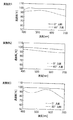
バックライトユニット12から出射したRGB各色の光はともに同一レベルであるとする(図7A)。バックライトユニット12から出射した光は、液晶パネル11を透過するまでの間に拡散板13、プリズムシート14、拡散シート15、偏光分離素子16、偏光板3a,3b、カラーフィルタ17等によって輝度(強度)が低下する。
また、これら各種光学シートあるいは液晶層1の屈折率異方性等を原因として、パネル正面方向に出射する光とパネル斜め方向に出射する光との間で発光スペクトルが異なる。バックライトにLED等の広色域光源が用いられている場合、パネル斜め方向に出射する可視光は、B及びGに比べてRの方が輝度が高い(図7B)。光学フィルタ4は、斜め方向から出射する可視光のうちR成分の透過率を選択的に抑えて、RGB各色の輝度の均一性を高める働きをする(図7C)。
この光学フィルタは、入射角0°で波長400〜650nmの可視光の透過率が70%以上であり、入射角60°で波長600nm以上の可視光の透過率が波長450〜550nmの可視光の平均透過率の約70%に設計されている。実験の結果、正面方向と斜め方向での色差は良好であり、斜め方向から見たときの画面の赤色化も見られなかった。
図9は本発明の第2の実施の形態による液晶表示装置用光学フィルムとしての光学フィルタ4’の構成例を示している。本実施の形態の光学フィルタ4’は、透過率90%以上の透明プラスチックフィルム(例えばPETフィルム)製の透明支持体5の両面に高屈折率材料層6と低屈折率材料層7を順にそれぞれ積層した誘電体多層膜で構成されている。
図11は、本発明の第3の実施の形態による液晶表示装置20を示している。なお、図において上述の第1の実施の形態と対応する部分については同一の符号を付し、その詳細な説明は省略する。
図12は、本発明の第4の実施の形態による液晶表示装置30を示している。なお、図において上述の第3の実施の形態と対応する部分については同一の符号を付し、その詳細な説明は省略する。
・顔料微粒子:TiO2微粒子 100重量部
(石原産業社製、平均粒径約20nm、屈折率2.48)
・結合剤:SO3Na基含有ウレタンアクリレート 9.2重量部
(数平均分子量:350、SO3Na濃度:1×10⁻¹mol/g)
・分散剤:ポリオキシエチレンリン酸エステル 7.5重量部
・有機溶媒:メチルイソブチルケトン(MIBK) 4800重量部
・紫外性(UV)硬化性樹脂:ジペンタエリスリトールヘキサアクリレートとジペンタエリスリトールペンタアクリレートとの混合物 22重量部
(日本化薬社製、商品名DPHA)
・結合剤:末端カルボキシル基をもつパーフルオロブテニルビニルエーテルの重合体 100重量部
・有機溶媒:含フッ素アルコール(C6F13C2H4OH)とパーフルオロブチルアミンとの混合溶媒(混合比95:5) 1666重量部
上述の塗料A,Bを用いて以下のようにして光学フィルムのサンプルを作製した。
実施例2〜6における各サンプルの屈折率材料層の膜厚、積層数、積層形態を表1にまとめて示す。実施例2では、低屈折率材料層のみを形成した(この場合、PET基材が高屈折率材料層(屈折率1.65程度)に相当)。実施例3〜5では、(2層目の)低屈折率材料層の上に更に高屈折率材料層および低屈折率材料層を形成した。

Claims (2)
- 液晶パネルと、
NTSC比90%以上の光源を有し、前記液晶パネルの背面側に配置されたバックライトユニットと、
第1の屈折率材料層と前記第1の屈折率材料層よりも低い屈折率を有する第2の屈折率材料層とが交互に複数積層された誘電体多層膜と、前記誘電体多層膜を支持する透明プラスチックフィルム製の透明支持体とを有し、前記液晶パネルの前面側に配置された光学フィルタとを具備し、
前記光学フィルタは、前記バックライトユニットから出射する波長600nm以上の可視光について、前記液晶パネルから正面方向に出射する場合よりも斜め方向に出射する場合の透過率を低下させ、前記バックライトユニットから出射する波長400〜450nmの可視光について、当該光学フィルタへ入射角0°で入射する場合よりも入射角10°以上30°以下で入射する場合の透過率の平均値を高める液晶表示装置。 - 請求項1に記載の液晶表示装置であって、
前記光学フィルタは、入射角60°で入射する可視光について、波長600nmから650nmの可視光の透過率の平均値が、波長600nm未満の可視光の透過率の平均値よりも低い液晶表示装置。
Priority Applications (7)
| Application Number | Priority Date | Filing Date | Title |
|---|---|---|---|
| JP2005289336A JP4760275B2 (ja) | 2005-05-23 | 2005-09-30 | 液晶表示装置 |
| TW095118296A TW200708860A (en) | 2005-05-23 | 2006-05-23 | Optical element, liquid crystal panel, and liquid crystal display device |
| CN200680000788XA CN101019049B (zh) | 2005-05-23 | 2006-05-23 | 光学元件、液晶显示面板、以及液晶显示器 |
| US11/659,914 US8223295B2 (en) | 2005-05-23 | 2006-05-23 | Optical element, liquid crystal panel, and liquid crystal display |
| KR1020077003107A KR101220479B1 (ko) | 2005-05-23 | 2006-05-23 | 광학 필터, 액정 패널 및 액정 표시 장치 |
| EP06746750A EP1884806A4 (en) | 2005-05-23 | 2006-05-23 | OPTICAL ELEMENT, LIQUID CRYSTAL PANEL, AND LIQUID CRYSTAL DISPLAY DEVICE |
| PCT/JP2006/310266 WO2006126549A1 (ja) | 2005-05-23 | 2006-05-23 | 光学素子、液晶パネル及び液晶表示装置 |
Applications Claiming Priority (3)
| Application Number | Priority Date | Filing Date | Title |
|---|---|---|---|
| JP2005149380 | 2005-05-23 | ||
| JP2005149380 | 2005-05-23 | ||
| JP2005289336A JP4760275B2 (ja) | 2005-05-23 | 2005-09-30 | 液晶表示装置 |
Publications (3)
| Publication Number | Publication Date |
|---|---|
| JP2007004104A JP2007004104A (ja) | 2007-01-11 |
| JP2007004104A5 JP2007004104A5 (ja) | 2007-03-01 |
| JP4760275B2 true JP4760275B2 (ja) | 2011-08-31 |
Family
ID=37451974
Family Applications (1)
| Application Number | Title | Priority Date | Filing Date |
|---|---|---|---|
| JP2005289336A Expired - Fee Related JP4760275B2 (ja) | 2005-05-23 | 2005-09-30 | 液晶表示装置 |
Country Status (7)
| Country | Link |
|---|---|
| US (1) | US8223295B2 (ja) |
| EP (1) | EP1884806A4 (ja) |
| JP (1) | JP4760275B2 (ja) |
| KR (1) | KR101220479B1 (ja) |
| CN (1) | CN101019049B (ja) |
| TW (1) | TW200708860A (ja) |
| WO (1) | WO2006126549A1 (ja) |
Families Citing this family (29)
| Publication number | Priority date | Publication date | Assignee | Title |
|---|---|---|---|---|
| TW200821703A (en) * | 2006-11-10 | 2008-05-16 | Delta Electronics Inc | Optical system and liquid crystal display apparatus thereof |
| KR100852273B1 (ko) * | 2007-04-13 | 2008-08-14 | 신홍우 | 백라이트 유니트와 이를 이용한 액정표시모듈 |
| US8208097B2 (en) * | 2007-08-08 | 2012-06-26 | Samsung Corning Precision Materials Co., Ltd. | Color compensation multi-layered member for display apparatus, optical filter for display apparatus having the same and display apparatus having the same |
| TWI363904B (en) * | 2008-01-16 | 2012-05-11 | Au Optronics Corp | Liquid crystal display device and back light unit thereof |
| JP4826599B2 (ja) * | 2008-04-10 | 2011-11-30 | ソニー株式会社 | 液晶表示装置、偏光板およびバックライト光源 |
| JP2010217660A (ja) * | 2009-03-18 | 2010-09-30 | Victor Co Of Japan Ltd | 光学ユニット、バックライト装置、液晶モジュール、及び液晶ディスプレイ |
| CN102449542A (zh) * | 2009-03-30 | 2012-05-09 | 住友化学株式会社 | 液晶显示装置 |
| KR20110132622A (ko) * | 2009-03-30 | 2011-12-08 | 스미또모 가가꾸 가부시끼가이샤 | 액정 표시 장치 |
| KR101766494B1 (ko) * | 2009-04-15 | 2017-08-08 | 쓰리엠 이노베이티브 프로퍼티즈 컴파니 | 광 결합을 방지하기 위한 광학 필름 |
| KR101713946B1 (ko) * | 2010-12-29 | 2017-03-08 | 엘지디스플레이 주식회사 | 액정표시장치 |
| TWI588540B (zh) * | 2012-05-09 | 2017-06-21 | 半導體能源研究所股份有限公司 | 顯示裝置和電子裝置 |
| KR102046152B1 (ko) | 2012-11-20 | 2019-11-19 | 삼성디스플레이 주식회사 | 편광판 및 이를 포함하는 액정 표시 장치 |
| US9568362B2 (en) * | 2012-12-19 | 2017-02-14 | Viavi Solutions Inc. | Spectroscopic assembly and method |
| CN103235356B (zh) * | 2013-04-16 | 2016-06-29 | 京东方科技集团股份有限公司 | 滤光片及其制备方法、彩膜基板和显示装置 |
| US9366784B2 (en) | 2013-05-07 | 2016-06-14 | Corning Incorporated | Low-color scratch-resistant articles with a multilayer optical film |
| US9359261B2 (en) * | 2013-05-07 | 2016-06-07 | Corning Incorporated | Low-color scratch-resistant articles with a multilayer optical film |
| US9110230B2 (en) | 2013-05-07 | 2015-08-18 | Corning Incorporated | Scratch-resistant articles with retained optical properties |
| US11267973B2 (en) | 2014-05-12 | 2022-03-08 | Corning Incorporated | Durable anti-reflective articles |
| JP6444631B2 (ja) * | 2014-06-30 | 2018-12-26 | 大和製罐株式会社 | 滑水・滑油性膜、その製造方法、及びそれにより被覆された表面を有する物品 |
| US9790593B2 (en) | 2014-08-01 | 2017-10-17 | Corning Incorporated | Scratch-resistant materials and articles including the same |
| KR20160017365A (ko) * | 2014-08-05 | 2016-02-16 | 삼성디스플레이 주식회사 | 액정표시장치 |
| WO2017048700A1 (en) | 2015-09-14 | 2017-03-23 | Corning Incorporated | High light transmission and scratch-resistant anti-reflective articles |
| US10600213B2 (en) * | 2016-02-27 | 2020-03-24 | Focal Sharp, Inc. | Method and apparatus for color-preserving spectrum reshape |
| WO2018155304A1 (ja) * | 2017-02-27 | 2018-08-30 | 富士フイルム株式会社 | 輝度均一化部材、バックライトユニットおよび液晶表示装置 |
| CN108156776B (zh) * | 2017-12-21 | 2020-12-04 | 北京小米移动软件有限公司 | 电子设备的壳体及其制备方法 |
| CN108051947B (zh) * | 2018-01-09 | 2024-04-12 | 河北工业大学 | 一种色域拓宽装置 |
| JP7228028B2 (ja) | 2018-08-17 | 2023-02-22 | コーニング インコーポレイテッド | 薄い耐久性の反射防止構造を有する無機酸化物物品 |
| KR20200133862A (ko) | 2019-05-20 | 2020-12-01 | 삼성디스플레이 주식회사 | 백라이트 유닛 및 이를 포함하는 표시 장치 |
| CN115220256A (zh) * | 2021-04-21 | 2022-10-21 | 胡崇铭 | 垂直排列型液晶显示模块 |
Family Cites Families (20)
| Publication number | Priority date | Publication date | Assignee | Title |
|---|---|---|---|---|
| DE3768824D1 (de) | 1986-01-21 | 1991-05-02 | Fuji Photo Film Co Ltd | Vorrichtung zum auslesen von strahlungsbildern. |
| JPH0711677B2 (ja) * | 1986-01-22 | 1995-02-08 | 富士写真フイルム株式会社 | 放射線画像情報読取装置 |
| JPH0434806A (ja) * | 1990-05-31 | 1992-02-05 | Toshiba Lighting & Technol Corp | 照明装置 |
| JPH0437806A (ja) * | 1990-06-04 | 1992-02-07 | Minolta Camera Co Ltd | 光量補正光学系 |
| JPH04232924A (ja) * | 1990-12-27 | 1992-08-21 | Semiconductor Energy Lab Co Ltd | 液晶電気光学装置 |
| JPH0815525A (ja) | 1994-04-27 | 1996-01-19 | Sony Corp | 偏光ビームスプリッタ及び液晶プロジェクタ装置 |
| JPH0815695A (ja) | 1994-06-29 | 1996-01-19 | Sony Corp | 液晶表示装置 |
| JP3974217B2 (ja) | 1997-04-02 | 2007-09-12 | シャープ株式会社 | 液晶表示パネルおよび液晶表示装置 |
| JPH1124066A (ja) | 1997-07-04 | 1999-01-29 | Sony Corp | 液晶表示装置 |
| JPH11212073A (ja) * | 1998-01-26 | 1999-08-06 | Hitachi Ltd | 液晶表示装置 |
| JP3580124B2 (ja) | 1998-03-05 | 2004-10-20 | 日東電工株式会社 | 光学素子、照明装置及び液晶表示装置 |
| JPH11271671A (ja) * | 1998-03-19 | 1999-10-08 | Minolta Co Ltd | 投影光学系 |
| JP3826709B2 (ja) * | 2000-12-22 | 2006-09-27 | 豊田合成株式会社 | 液晶表示装置 |
| EP1376162A4 (en) * | 2001-02-27 | 2008-11-26 | Seiko Epson Corp | MULTILAYER FILM FILTER AND METHOD FOR PRODUCING THE SAME, UV ELIMINATION FILTER, DUST-SEALED GLASS, DISPLAY PANEL, AND PROJECTION TYPE DISPLAY UNIT |
| JP2003066451A (ja) * | 2001-08-30 | 2003-03-05 | Matsushita Electric Ind Co Ltd | 液晶表示装置 |
| JP4195585B2 (ja) | 2002-07-02 | 2008-12-10 | アルパイン株式会社 | 車載用電子機器 |
| US7317499B2 (en) * | 2002-08-22 | 2008-01-08 | Nitto Denko Corporation | Multilayer plate and display panel with anisotropic crystal film and conducting protective layer |
| JP4506070B2 (ja) * | 2002-11-01 | 2010-07-21 | コニカミノルタホールディングス株式会社 | 防眩層の形成方法、防眩フィルムの製造方法及び防眩層形成用のインクジェット装置 |
| JP4342821B2 (ja) | 2003-04-03 | 2009-10-14 | 日東電工株式会社 | 光学素子、液晶セル、照明装置および液晶表示装置 |
| US20060066803A1 (en) * | 2004-09-30 | 2006-03-30 | Aylward Peter T | Substrate free flexible liquid crystal displays |
-
2005
- 2005-09-30 JP JP2005289336A patent/JP4760275B2/ja not_active Expired - Fee Related
-
2006
- 2006-05-23 EP EP06746750A patent/EP1884806A4/en not_active Withdrawn
- 2006-05-23 CN CN200680000788XA patent/CN101019049B/zh active Active
- 2006-05-23 KR KR1020077003107A patent/KR101220479B1/ko active IP Right Grant
- 2006-05-23 WO PCT/JP2006/310266 patent/WO2006126549A1/ja active Application Filing
- 2006-05-23 TW TW095118296A patent/TW200708860A/zh not_active IP Right Cessation
- 2006-05-23 US US11/659,914 patent/US8223295B2/en active Active
Also Published As
| Publication number | Publication date |
|---|---|
| EP1884806A4 (en) | 2009-07-29 |
| KR101220479B1 (ko) | 2013-01-10 |
| WO2006126549A1 (ja) | 2006-11-30 |
| CN101019049A (zh) | 2007-08-15 |
| EP1884806A1 (en) | 2008-02-06 |
| CN101019049B (zh) | 2012-05-02 |
| TWI354166B (ja) | 2011-12-11 |
| US8223295B2 (en) | 2012-07-17 |
| WO2006126549B1 (ja) | 2007-02-15 |
| JP2007004104A (ja) | 2007-01-11 |
| TW200708860A (en) | 2007-03-01 |
| KR20080009257A (ko) | 2008-01-28 |
| US20070247567A1 (en) | 2007-10-25 |
Similar Documents
| Publication | Publication Date | Title |
|---|---|---|
| JP4760275B2 (ja) | 液晶表示装置 | |
| JP2007004104A5 (ja) | ||
| US7630032B2 (en) | LCD with selective transmission filter having light transmittance of 80% or more at wavelength regions of 440+/−20nm; 525+/−25nm and 565+/−45nm, and 10% or less at 470 to 485nm and 575 to 595nm | |
| US5949506A (en) | LCD with diffuser having diffusing particles therein located between polarizers | |
| US8208097B2 (en) | Color compensation multi-layered member for display apparatus, optical filter for display apparatus having the same and display apparatus having the same | |
| JP2007316156A (ja) | 液晶パネル、液晶表示装置および光学素子 | |
| US20060164574A1 (en) | Liquid crystal display | |
| JP2010072653A (ja) | カラーシフト低減光学フィルター及びこれを具備するディスプレイ装置 | |
| US20140176859A1 (en) | Wide-color gamut film, display apparatus with the wide-color gamut film, and method for manufacturing the film | |
| JP3879661B2 (ja) | 液晶表示装置および電子機器 | |
| KR20090015318A (ko) | 디스플레이 장치용 색보상 필름, 이를 포함하는 디스플레이장치용 필터 및 디스플레이 장치 | |
| US8625056B2 (en) | Liquid crystal display | |
| US20070047111A1 (en) | Prism sheet and backlight unit employed in a liquid crystal display | |
| RU2499289C1 (ru) | Жидкокристаллическое устройство отображения | |
| JP3435113B2 (ja) | 液晶表示装置 | |
| JP3340073B2 (ja) | カラー液晶表示装置 | |
| CN113272728A (zh) | 滤色器lcd上的增强性量子点 | |
| JP2006184587A (ja) | 光散乱膜、およびこれを用いたカラーフィルタ、反射型液晶表示装置用電極基板、反射型液晶表示装置 | |
| JP2008070418A (ja) | 液晶表示装置 | |
| JP2023038443A (ja) | 表示装置 | |
| KR100846625B1 (ko) | 반투과형 액정표시장치 | |
| WO2007122853A1 (ja) | 液晶表示装置 | |
| JP2004151309A (ja) | 半透過型カラー液晶表示装置 | |
| JP2005208206A (ja) | 光散乱膜及びそれを用いた液晶表示装置 | |
| JP2014089317A (ja) | 表示装置及び照明装置 |
Legal Events
| Date | Code | Title | Description |
|---|---|---|---|
| A521 | Request for written amendment filed |
Free format text: JAPANESE INTERMEDIATE CODE: A523 Effective date: 20070115 |
|
| A621 | Written request for application examination |
Free format text: JAPANESE INTERMEDIATE CODE: A621 Effective date: 20070115 |
|
| RD03 | Notification of appointment of power of attorney |
Free format text: JAPANESE INTERMEDIATE CODE: A7423 Effective date: 20071028 |
|
| A131 | Notification of reasons for refusal |
Free format text: JAPANESE INTERMEDIATE CODE: A131 Effective date: 20100330 |
|
| A521 | Request for written amendment filed |
Free format text: JAPANESE INTERMEDIATE CODE: A523 Effective date: 20100524 |
|
| A131 | Notification of reasons for refusal |
Free format text: JAPANESE INTERMEDIATE CODE: A131 Effective date: 20110215 |
|
| A521 | Request for written amendment filed |
Free format text: JAPANESE INTERMEDIATE CODE: A523 Effective date: 20110411 |
|
| TRDD | Decision of grant or rejection written | ||
| A01 | Written decision to grant a patent or to grant a registration (utility model) |
Free format text: JAPANESE INTERMEDIATE CODE: A01 Effective date: 20110510 |
|
| A61 | First payment of annual fees (during grant procedure) |
Free format text: JAPANESE INTERMEDIATE CODE: A61 Effective date: 20110523 |
|
| FPAY | Renewal fee payment (event date is renewal date of database) |
Free format text: PAYMENT UNTIL: 20140617 Year of fee payment: 3 |
|
| R151 | Written notification of patent or utility model registration |
Ref document number: 4760275 Country of ref document: JP Free format text: JAPANESE INTERMEDIATE CODE: R151 |
|
| FPAY | Renewal fee payment (event date is renewal date of database) |
Free format text: PAYMENT UNTIL: 20140617 Year of fee payment: 3 |
|
| R250 | Receipt of annual fees |
Free format text: JAPANESE INTERMEDIATE CODE: R250 |
|
| R250 | Receipt of annual fees |
Free format text: JAPANESE INTERMEDIATE CODE: R250 |
|
| R250 | Receipt of annual fees |
Free format text: JAPANESE INTERMEDIATE CODE: R250 |
|
| R250 | Receipt of annual fees |
Free format text: JAPANESE INTERMEDIATE CODE: R250 |
|
| R250 | Receipt of annual fees |
Free format text: JAPANESE INTERMEDIATE CODE: R250 |
|
| R250 | Receipt of annual fees |
Free format text: JAPANESE INTERMEDIATE CODE: R250 |
|
| R250 | Receipt of annual fees |
Free format text: JAPANESE INTERMEDIATE CODE: R250 |
|
| R250 | Receipt of annual fees |
Free format text: JAPANESE INTERMEDIATE CODE: R250 |
|
| R250 | Receipt of annual fees |
Free format text: JAPANESE INTERMEDIATE CODE: R250 |
|
| LAPS | Cancellation because of no payment of annual fees |