JP4760275B2 - Liquid crystal display - Google Patents
Liquid crystal display Download PDFInfo
- Publication number
- JP4760275B2 JP4760275B2 JP2005289336A JP2005289336A JP4760275B2 JP 4760275 B2 JP4760275 B2 JP 4760275B2 JP 2005289336 A JP2005289336 A JP 2005289336A JP 2005289336 A JP2005289336 A JP 2005289336A JP 4760275 B2 JP4760275 B2 JP 4760275B2
- Authority
- JP
- Japan
- Prior art keywords
- liquid crystal
- transmittance
- light
- wavelength
- refractive index
- Prior art date
- Legal status (The legal status is an assumption and is not a legal conclusion. Google has not performed a legal analysis and makes no representation as to the accuracy of the status listed.)
- Expired - Fee Related
Links
- 239000004973 liquid crystal related substance Substances 0.000 title claims description 139
- 230000003287 optical effect Effects 0.000 claims description 86
- 238000002834 transmittance Methods 0.000 claims description 78
- 239000000463 material Substances 0.000 claims description 65
- 229920003023 plastic Polymers 0.000 claims description 4
- 239000002985 plastic film Substances 0.000 claims description 4
- 239000010410 layer Substances 0.000 description 78
- 239000010408 film Substances 0.000 description 61
- 230000010287 polarization Effects 0.000 description 28
- 239000012788 optical film Substances 0.000 description 26
- 239000000758 substrate Substances 0.000 description 26
- 239000011248 coating agent Substances 0.000 description 18
- 238000000576 coating method Methods 0.000 description 18
- 238000000926 separation method Methods 0.000 description 18
- 238000009792 diffusion process Methods 0.000 description 15
- 230000008859 change Effects 0.000 description 13
- 230000007423 decrease Effects 0.000 description 10
- 238000010586 diagram Methods 0.000 description 10
- 239000010419 fine particle Substances 0.000 description 7
- 230000005540 biological transmission Effects 0.000 description 6
- 238000004040 coloring Methods 0.000 description 6
- 230000000694 effects Effects 0.000 description 6
- 239000003973 paint Substances 0.000 description 6
- 229910010413 TiO 2 Inorganic materials 0.000 description 5
- 239000003086 colorant Substances 0.000 description 5
- 238000000295 emission spectrum Methods 0.000 description 5
- 238000002474 experimental method Methods 0.000 description 5
- 238000000034 method Methods 0.000 description 5
- 229920002799 BoPET Polymers 0.000 description 4
- 239000011230 binding agent Substances 0.000 description 4
- 238000013461 design Methods 0.000 description 4
- 230000005684 electric field Effects 0.000 description 4
- 239000003960 organic solvent Substances 0.000 description 4
- 239000011347 resin Substances 0.000 description 4
- 229920005989 resin Polymers 0.000 description 4
- 230000002238 attenuated effect Effects 0.000 description 3
- 239000006185 dispersion Substances 0.000 description 3
- 239000000203 mixture Substances 0.000 description 3
- 230000035699 permeability Effects 0.000 description 3
- YCKRFDGAMUMZLT-UHFFFAOYSA-N Fluorine atom Chemical compound [F] YCKRFDGAMUMZLT-UHFFFAOYSA-N 0.000 description 2
- NTIZESTWPVYFNL-UHFFFAOYSA-N Methyl isobutyl ketone Chemical compound CC(C)CC(C)=O NTIZESTWPVYFNL-UHFFFAOYSA-N 0.000 description 2
- UIHCLUNTQKBZGK-UHFFFAOYSA-N Methyl isobutyl ketone Natural products CCC(C)C(C)=O UIHCLUNTQKBZGK-UHFFFAOYSA-N 0.000 description 2
- MPIAGWXWVAHQBB-UHFFFAOYSA-N [3-prop-2-enoyloxy-2-[[3-prop-2-enoyloxy-2,2-bis(prop-2-enoyloxymethyl)propoxy]methyl]-2-(prop-2-enoyloxymethyl)propyl] prop-2-enoate Chemical compound C=CC(=O)OCC(COC(=O)C=C)(COC(=O)C=C)COCC(COC(=O)C=C)(COC(=O)C=C)COC(=O)C=C MPIAGWXWVAHQBB-UHFFFAOYSA-N 0.000 description 2
- 238000007598 dipping method Methods 0.000 description 2
- 239000002270 dispersing agent Substances 0.000 description 2
- 239000000284 extract Substances 0.000 description 2
- 229910052731 fluorine Inorganic materials 0.000 description 2
- 239000011737 fluorine Substances 0.000 description 2
- 238000005286 illumination Methods 0.000 description 2
- 238000009434 installation Methods 0.000 description 2
- 239000000049 pigment Substances 0.000 description 2
- 238000002360 preparation method Methods 0.000 description 2
- 230000003595 spectral effect Effects 0.000 description 2
- JWKJOADJHWZCLL-UHFFFAOYSA-N 1,2,3,4,5,5,6,6,6-nonafluoro-1-(1,2,3,4,5,5,6,6,6-nonafluorohexa-1,3-dienoxy)hexa-1,3-diene Chemical compound FC(OC(F)=C(F)C(F)=C(F)C(F)(F)C(F)(F)F)=C(F)C(F)=C(F)C(F)(F)C(F)(F)F JWKJOADJHWZCLL-UHFFFAOYSA-N 0.000 description 1
- FDSUVTROAWLVJA-UHFFFAOYSA-N 2-[[3-hydroxy-2,2-bis(hydroxymethyl)propoxy]methyl]-2-(hydroxymethyl)propane-1,3-diol;prop-2-enoic acid Chemical compound OC(=O)C=C.OC(=O)C=C.OC(=O)C=C.OC(=O)C=C.OC(=O)C=C.OCC(CO)(CO)COCC(CO)(CO)CO FDSUVTROAWLVJA-UHFFFAOYSA-N 0.000 description 1
- LFQSCWFLJHTTHZ-UHFFFAOYSA-N Ethanol Chemical compound CCO LFQSCWFLJHTTHZ-UHFFFAOYSA-N 0.000 description 1
- 239000004988 Nematic liquid crystal Substances 0.000 description 1
- 229910004298 SiO 2 Inorganic materials 0.000 description 1
- 230000009471 action Effects 0.000 description 1
- 230000003321 amplification Effects 0.000 description 1
- 230000008901 benefit Effects 0.000 description 1
- 125000003178 carboxy group Chemical group [H]OC(*)=O 0.000 description 1
- 210000002858 crystal cell Anatomy 0.000 description 1
- 238000003618 dip coating Methods 0.000 description 1
- 238000001035 drying Methods 0.000 description 1
- 150000002148 esters Chemical class 0.000 description 1
- UHESRSKEBRADOO-UHFFFAOYSA-N ethyl carbamate;prop-2-enoic acid Chemical compound OC(=O)C=C.CCOC(N)=O UHESRSKEBRADOO-UHFFFAOYSA-N 0.000 description 1
- 238000011156 evaluation Methods 0.000 description 1
- 230000001747 exhibiting effect Effects 0.000 description 1
- 239000011521 glass Substances 0.000 description 1
- 230000001678 irradiating effect Effects 0.000 description 1
- 238000010030 laminating Methods 0.000 description 1
- 238000003475 lamination Methods 0.000 description 1
- 238000005259 measurement Methods 0.000 description 1
- 239000012528 membrane Substances 0.000 description 1
- 239000012046 mixed solvent Substances 0.000 description 1
- 238000002156 mixing Methods 0.000 description 1
- 230000004048 modification Effects 0.000 description 1
- 238000012986 modification Methods 0.000 description 1
- AEDVWMXHRPMJAD-UHFFFAOYSA-N n,n,1,1,2,2,3,3,4,4,4-undecafluorobutan-1-amine Chemical compound FN(F)C(F)(F)C(F)(F)C(F)(F)C(F)(F)F AEDVWMXHRPMJAD-UHFFFAOYSA-N 0.000 description 1
- 238000003199 nucleic acid amplification method Methods 0.000 description 1
- 239000002245 particle Substances 0.000 description 1
- 229920001690 polydopamine Polymers 0.000 description 1
- 229920000139 polyethylene terephthalate Polymers 0.000 description 1
- 229920000642 polymer Polymers 0.000 description 1
- 229920006254 polymer film Polymers 0.000 description 1
- -1 polyoxyethylene phosphate Polymers 0.000 description 1
- 230000008569 process Effects 0.000 description 1
- 230000009467 reduction Effects 0.000 description 1
- 239000002356 single layer Substances 0.000 description 1
- 238000009751 slip forming Methods 0.000 description 1
- 238000004544 sputter deposition Methods 0.000 description 1
- 239000000126 substance Substances 0.000 description 1
- 230000001629 suppression Effects 0.000 description 1
- 239000010409 thin film Substances 0.000 description 1
- 230000009466 transformation Effects 0.000 description 1
- 238000001771 vacuum deposition Methods 0.000 description 1
Images


Classifications
-
- G—PHYSICS
- G02—OPTICS
- G02B—OPTICAL ELEMENTS, SYSTEMS OR APPARATUS
- G02B5/00—Optical elements other than lenses
- G02B5/20—Filters
- G02B5/28—Interference filters
- G02B5/285—Interference filters comprising deposited thin solid films
- G02B5/286—Interference filters comprising deposited thin solid films having four or fewer layers, e.g. for achieving a colour effect
-
- G—PHYSICS
- G02—OPTICS
- G02F—OPTICAL DEVICES OR ARRANGEMENTS FOR THE CONTROL OF LIGHT BY MODIFICATION OF THE OPTICAL PROPERTIES OF THE MEDIA OF THE ELEMENTS INVOLVED THEREIN; NON-LINEAR OPTICS; FREQUENCY-CHANGING OF LIGHT; OPTICAL LOGIC ELEMENTS; OPTICAL ANALOGUE/DIGITAL CONVERTERS
- G02F1/00—Devices or arrangements for the control of the intensity, colour, phase, polarisation or direction of light arriving from an independent light source, e.g. switching, gating or modulating; Non-linear optics
- G02F1/01—Devices or arrangements for the control of the intensity, colour, phase, polarisation or direction of light arriving from an independent light source, e.g. switching, gating or modulating; Non-linear optics for the control of the intensity, phase, polarisation or colour
- G02F1/13—Devices or arrangements for the control of the intensity, colour, phase, polarisation or direction of light arriving from an independent light source, e.g. switching, gating or modulating; Non-linear optics for the control of the intensity, phase, polarisation or colour based on liquid crystals, e.g. single liquid crystal display cells
- G02F1/133—Constructional arrangements; Operation of liquid crystal cells; Circuit arrangements
- G02F1/1333—Constructional arrangements; Manufacturing methods
- G02F1/1335—Structural association of cells with optical devices, e.g. polarisers or reflectors
- G02F1/133509—Filters, e.g. light shielding masks
- G02F1/133514—Colour filters
- G02F1/133521—Interference filters
-
- G—PHYSICS
- G02—OPTICS
- G02F—OPTICAL DEVICES OR ARRANGEMENTS FOR THE CONTROL OF LIGHT BY MODIFICATION OF THE OPTICAL PROPERTIES OF THE MEDIA OF THE ELEMENTS INVOLVED THEREIN; NON-LINEAR OPTICS; FREQUENCY-CHANGING OF LIGHT; OPTICAL LOGIC ELEMENTS; OPTICAL ANALOGUE/DIGITAL CONVERTERS
- G02F1/00—Devices or arrangements for the control of the intensity, colour, phase, polarisation or direction of light arriving from an independent light source, e.g. switching, gating or modulating; Non-linear optics
- G02F1/01—Devices or arrangements for the control of the intensity, colour, phase, polarisation or direction of light arriving from an independent light source, e.g. switching, gating or modulating; Non-linear optics for the control of the intensity, phase, polarisation or colour
- G02F1/13—Devices or arrangements for the control of the intensity, colour, phase, polarisation or direction of light arriving from an independent light source, e.g. switching, gating or modulating; Non-linear optics for the control of the intensity, phase, polarisation or colour based on liquid crystals, e.g. single liquid crystal display cells
- G02F1/133—Constructional arrangements; Operation of liquid crystal cells; Circuit arrangements
- G02F1/1333—Constructional arrangements; Manufacturing methods
- G02F1/1335—Structural association of cells with optical devices, e.g. polarisers or reflectors
- G02F1/1336—Illuminating devices
- G02F1/133602—Direct backlight
- G02F1/133603—Direct backlight with LEDs
-
- G—PHYSICS
- G02—OPTICS
- G02F—OPTICAL DEVICES OR ARRANGEMENTS FOR THE CONTROL OF LIGHT BY MODIFICATION OF THE OPTICAL PROPERTIES OF THE MEDIA OF THE ELEMENTS INVOLVED THEREIN; NON-LINEAR OPTICS; FREQUENCY-CHANGING OF LIGHT; OPTICAL LOGIC ELEMENTS; OPTICAL ANALOGUE/DIGITAL CONVERTERS
- G02F2203/00—Function characteristic
- G02F2203/05—Function characteristic wavelength dependent
- G02F2203/055—Function characteristic wavelength dependent wavelength filtering
Description
本発明は、斜めから見たときの画面の着色を抑制し視角特性の改善を図った液晶表示装置用光学フィルム、液晶パネル及び液晶表示装置に関する。 The present invention relates to an optical film for a liquid crystal display device , a liquid crystal panel, and a liquid crystal display device that suppresses coloring of a screen when viewed from an oblique direction and improves viewing angle characteristics.
液晶表示装置(LCD:Liquid Crystal Display)は、ブラウン管(CRT:Cathode Ray Tube)と比較して低消費電力かつ小型化、薄型化が可能であり、現在では携帯電話、デジタルカメラ、PDA(Personal Digital Assistants)等の小型機器から、大型サイズの液晶テレビに至るまで、様々なサイズのものが幅広く使用されている。 A liquid crystal display (LCD) is lower in power consumption, smaller and thinner than a cathode ray tube (CRT), and is now available in mobile phones, digital cameras, and PDAs (Personal Digital Display). Various sizes are widely used, from small devices such as Assistants) to large-sized LCD TVs.
液晶表示装置は透過型、反射型等に分類され、特に透過型液晶表示装置は、液晶層を一対の透明基板で挟んだ液晶パネルのほか、バックライトユニットを備えている。また、バックライトユニットからの光源光を液晶パネルの全面に効率良く照射するための拡散シートやプリズムシート等の機能性シートを液晶パネルとバックライト間に挿入したり、液晶層に入射する光に偏光性を与える偏光板やカラー画像表示のためのカラーフィルタ等を液晶パネルに配置する構成が一般的である。 Liquid crystal display devices are classified into a transmission type, a reflection type, and the like. In particular, the transmission type liquid crystal display device includes a backlight unit in addition to a liquid crystal panel in which a liquid crystal layer is sandwiched between a pair of transparent substrates. Also, a functional sheet such as a diffusion sheet or prism sheet for efficiently irradiating the entire surface of the liquid crystal panel with the light source light from the backlight unit is inserted between the liquid crystal panel and the backlight, or is incident on the light incident on the liquid crystal layer. Generally, a configuration in which a polarizing plate that imparts polarizing properties, a color filter for displaying color images, and the like are arranged on a liquid crystal panel is used.
一方、液晶表示装置の表示方式には、液晶層を構成する液晶分子の種類に応じて、TN(ねじれネマティック)、VA(垂直配列)、IPS(In-Plane Switching)等の種々の方式が知られている。これらの方式はいずれも、画素単位で液晶分子の配向状態を変え、液晶層に入射する光の偏光状態あるいは透過率を制御することで、液晶パネル前面に所望の画像を表示させている。 On the other hand, various display methods such as TN (twisted nematic), VA (vertical alignment), and IPS (In-Plane Switching) are known as display methods for liquid crystal display devices, depending on the type of liquid crystal molecules constituting the liquid crystal layer. It has been. In any of these methods, a desired image is displayed on the front surface of the liquid crystal panel by changing the alignment state of liquid crystal molecules in units of pixels and controlling the polarization state or transmittance of light incident on the liquid crystal layer.
ところが、液晶パネルを透過する光の偏光状態は液晶分子の配向角度に大きく依存するため、液晶パネルへ垂直に入射する光の偏光状態と斜め方向に入射する光の偏光状態とでは光の透過率に差が生じる。また、液晶層の屈折率異方性と厚さとの積で表されるリタデーションが波長分散性を有し、波長の大きさで光の透過率が変化する。その結果、液晶パネルを見る方向によって特定の波長領域の光が強度が変化することにより映像の色温度が変化し、また、表示コントラストや表示色が見る方向で異なる等、視角特性が悪くなるという問題を有している(下記特許文献1参照)。一般的には、見る方向が斜めになるに従い、青色系の強度は減少し、赤色系の強度が増加する場合が多く、その結果、映像の色温度が低下する傾向がある。
However, since the polarization state of the light transmitted through the liquid crystal panel greatly depends on the orientation angle of the liquid crystal molecules, the light transmittance is different between the polarization state of the light incident perpendicularly to the liquid crystal panel and the polarization state of the light incident obliquely. There will be a difference. In addition, the retardation represented by the product of the refractive index anisotropy and the thickness of the liquid crystal layer has wavelength dispersion, and the light transmittance changes depending on the wavelength. As a result, the color temperature of the image changes as the intensity of light in a specific wavelength region changes depending on the direction in which the liquid crystal panel is viewed, and the viewing angle characteristics deteriorate, such as the display contrast and display color differing in the viewing direction. There is a problem (see
このような視角特性に関わる問題を解消するために、従来の液晶表示装置においては、液晶パネルに位相差板や色補償板等の補償フィルムを配置し、液晶層の複屈折性を相殺することで、液晶パネルの視角特性の改善を図るようにしている(例えば下記特許文献2,3参照)。また、一定の偏光成分のみを抽出する偏光分離素子に、色補償機能を持たせたものもある(下記特許文献4参照)。
In order to eliminate such problems related to viewing angle characteristics, in a conventional liquid crystal display device, a compensation film such as a retardation plate or a color compensation plate is arranged on the liquid crystal panel to cancel the birefringence of the liquid crystal layer. Therefore, the viewing angle characteristics of the liquid crystal panel are improved (see, for example,
しかしながら、液晶パネルの視角特性は、液晶層の複屈折性だけが原因ではなく、液晶パネルに配置された偏光板やカラーフィルタの光学特性が液晶パネルの視角特性に強く影響している。また、液晶パネル以外の他の構成部品、例えば拡散シートやプリズムシート、偏光分離素子等の輝度向上フィルムの構成や組合せ方によっても視角特性に違いが生じる。 However, the viewing angle characteristics of the liquid crystal panel are not only due to the birefringence of the liquid crystal layer, but the optical characteristics of the polarizing plates and the color filters arranged in the liquid crystal panel strongly influence the viewing angle characteristics of the liquid crystal panel. Further, the viewing angle characteristics vary depending on the configuration and combination of the brightness enhancement films such as the diffusion sheet, the prism sheet, and the polarization separation element other than the liquid crystal panel.
従って、液晶層の複屈折性のみに着目して視野角補償をするには限界がある。また、液晶層以外の構成部品による影響をも含めた補償フィルムの光学設計は複雑性、困難性が増し、生産性も優れない。 Therefore, there is a limit to the viewing angle compensation by focusing only on the birefringence of the liquid crystal layer. In addition, the optical design of the compensation film including the influence of components other than the liquid crystal layer increases the complexity and difficulty, and the productivity is not excellent.
なお最近では、表示色の再現性をより高めるため、光源にRGB3原色の発光ダイオードを使用したLED(Light Emitting Diode)バックライトや、蛍光体の改善により広色域化されたCCFL(Cold Cathode Fluorescent Lamp)バックライトが、液晶表示装置に用いられ始めている。この場合、光源の赤色の発光スペクトルはより長波長側へシフトするため、液晶パネルを斜めから見たときの赤色化は顕著となる。 Recently, in order to further enhance the reproducibility of display colors, LED (Light Emitting Diode) backlights that use light emitting diodes of the RGB three primary colors as light sources, and CCFL (Cold Cathode Fluorescent) that has a wider color gamut by improving phosphors. Lamp) backlights are beginning to be used in liquid crystal display devices. In this case, since the red emission spectrum of the light source is shifted to the longer wavelength side, the red color becomes noticeable when the liquid crystal panel is viewed obliquely.
本発明は上述の問題に鑑みてなされ、液晶パネルを斜めから見たときの画面の色度変化を抑制することができる液晶表示装置用光学フィルム、液晶パネル及び液晶表示装置を提供することを課題とする。 The present invention has been made in view of the above problems, and it is an object of the present invention to provide an optical film for a liquid crystal display device, a liquid crystal panel, and a liquid crystal display device that can suppress a change in chromaticity of a screen when the liquid crystal panel is viewed from an oblique direction. And
以上の課題を解決するに当たり、本発明は、液晶パネルの光出射面から出射する所定波長領域の光について、光出射面から正面方向に出射する場合よりも斜め方向に出射する場合の透過率を変化させる液晶表示装置用光学フィルムを備えている。また、本発明は、液晶パネルと、NTSC比90%以上の光源を有し、前記液晶パネルの背面側に配置されたバックライトユニットと、第1の屈折率材料層と前記第1の屈折率材料層よりも低い屈折率を有する第2の屈折率材料層とが交互に複数積層された誘電体多層膜と、前記誘電体多層膜を支持する透明プラスチックフィルム製の透明支持体とを有し、前記液晶パネルの前面側に配置された光学フィルタとを具備し、前記光学フィルタは、前記バックライトユニットから出射する波長600nm以上の可視光について、前記液晶パネルから正面方向に出射する場合よりも斜め方向に出射する場合の透過率を低下させ、前記バックライトユニットから出射する波長400〜450nmの可視光について、当該光学フィルタへ入射角0°で入射する場合よりも入射角10°以上30°以下で入射する場合の透過率の平均値を高める液晶表示装置を備えている。さらに、本発明は、前記光学フィルタは、入射角60°で入射する可視光について、波長600nmから650nmの可視光の透過率の平均値が、波長600nm未満の可視光の透過率の平均値よりも低い液晶表示装置を備えている。
In solving the above-mentioned problems, the present invention provides the transmittance when light emitted in a predetermined wavelength region emitted from the light emission surface of the liquid crystal panel is emitted obliquely from the light emission surface when emitted in the front direction. An optical film for a liquid crystal display device to be changed is provided. The present invention also includes a liquid crystal panel, a backlight unit having a light source with an NTSC ratio of 90% or more, disposed on the back side of the liquid crystal panel, a first refractive index material layer, and the first refractive index. A dielectric multilayer film in which a plurality of second refractive index material layers having a refractive index lower than that of the material layer are alternately laminated; and a transparent support made of a transparent plastic film that supports the dielectric multilayer film. An optical filter disposed on the front side of the liquid crystal panel, and the optical filter emits visible light having a wavelength of 600 nm or more emitted from the backlight unit in a front direction from the liquid crystal panel. The transmittance in the case of emitting in an oblique direction is reduced, and visible light having a wavelength of 400 to 450 nm emitted from the backlight unit enters the optical filter at an incident angle of 0 °. And a liquid crystal display device to increase the average value of the transmittance in the case of incident: 30 °
この光学フィルムは、第1の屈折率材料と、この第1の屈折率材料と屈折率が異なる第2の屈折率材料とが積層された多層膜からなり、所定波長領域の光について、当該多層膜の法線方向に出射する場合よりも斜め方向に出射する場合の透過率が大きく変化するという特性を有している。 This optical film is composed of a multilayer film in which a first refractive index material and a second refractive index material having a refractive index different from that of the first refractive index material are laminated. It has a characteristic that the transmittance when emitting in an oblique direction is greatly changed compared to when emitting in the normal direction of the film.
例えば液晶パネルを斜めから見たときに画面全体が赤みを呈するような場合には、光出射面から斜め方向に出射する赤色波長領域(波長600nm以上)の光について選択的に透過率減衰機能を発揮させることで、表示色の視角依存性を解消することができる。またこれと同時に、あるいは別に、青色波長領域の一部(400〜450nm)の光について選択的に透過率増幅機能を発揮させても同様な効果が得られ、色温度の視角依存性を解消することができる。
For example, when the entire screen is reddish when the liquid crystal panel is viewed obliquely, a transmittance attenuation function is selectively applied to light in the red wavelength region (
また、正面方向に出射される光の透過率が高ければ、上記光学フィルムを用いることによるディスプレイの輝度の低下を抑制することができる。この透過率は、波長400nmから650nmにおける可視光の最小透過率が90%以上であり、かつ平均値が95%以上であることが望ましい。 Moreover, if the transmittance | permeability of the light radiate | emitted in a front direction is high, the fall of the brightness | luminance of a display by using the said optical film can be suppressed. As for this transmittance, it is desirable that the minimum visible light transmittance at a wavelength of 400 nm to 650 nm is 90% or more and the average value is 95% or more.
また、広(高)色域光源を採用した際に斜め方向から見たときの特定波長成分による画面の着色を効果的に抑制できるので、表示色の再現性を損なうことなく視角特性の改善を図ることができる。なお、ここでいう広色域光源とは、NTSC比90%以上の光源をいう。 In addition, when a wide (high) color gamut light source is used, coloring of the screen due to specific wavelength components when viewed from an oblique direction can be effectively suppressed, improving the viewing angle characteristics without impairing the reproducibility of display colors. Can be planned. The wide color gamut light source here refers to a light source having an NTSC ratio of 90% or more.
上記構成の光学フィルムを用いて液晶パネルあるいは液晶表示装置を構成することにより、従来用いられていた色補償フィルム等のように液晶層や偏光板等の複屈折性を考慮した面倒な色補償設計を必要とすることなく、斜め方向から見たときの特定色による画面の着色を抑え、所望の視角特性を容易に実現することができる。 By constructing a liquid crystal panel or a liquid crystal display device using the optical film having the above structure, it is a troublesome color compensation design considering the birefringence of a liquid crystal layer, a polarizing plate, etc. like a conventionally used color compensation film. Therefore, it is possible to suppress the coloring of the screen with a specific color when viewed from an oblique direction and easily realize a desired viewing angle characteristic.
本発明に係る光学フィルムは、液晶パネルの出射面側(前面あるいは正面側)および入射面側(背面側)を問わず、配置することができる。特に本発明の液晶パネルは、液晶層を挟んで対向する一対の透明基板のうち光出射面側に配置している。この構成により、要求される液晶パネルの画像品位に応じて最適な光学フィルムの設計が可能となる。 The optical film which concerns on this invention can be arrange | positioned regardless of the output surface side (front surface or front surface side) and incident surface side (back surface side) of a liquid crystal panel. In particular, the liquid crystal panel of the present invention is disposed on the light emitting surface side of a pair of transparent substrates facing each other with a liquid crystal layer interposed therebetween. With this configuration, an optimal optical film can be designed according to the required image quality of the liquid crystal panel.
本発明に係る光学フィルムを液晶パネルとバックライトユニットとの間に配置する構成例では、当該光学フィルムをバックライトユニットの光出射面に配置する構成を採用することができる。これにより、光源側から特定波長領域の光の強度を減衰させた状態で後段へ導くことができる。また、例えば一定の偏光成分のみを抽出する偏光分離素子や、拡散シート、プリズムシートその他の光学的機能素子と一体的に当該光学フィルムを構成してもよい。さらに、本発明に係る光学フィルムの設置個所は一カ所に限らず、例えば上記光学的機能素子を挟む位置に二カ所以上設置してもよい。 In the configuration example in which the optical film according to the present invention is disposed between the liquid crystal panel and the backlight unit, a configuration in which the optical film is disposed on the light exit surface of the backlight unit can be employed. Thereby, it is possible to guide the light from the light source side to the subsequent stage in a state where the intensity of light in the specific wavelength region is attenuated. Further, for example, the optical film may be integrally formed with a polarization separation element that extracts only a certain polarization component, a diffusion sheet, a prism sheet, or other optical functional elements. Furthermore, the installation location of the optical film according to the present invention is not limited to one location, and for example, two or more locations may be installed at positions sandwiching the optical functional element.
以上述べたように、本発明によれば、液晶パネルを斜めから見たときの画像の色度変化を抑制できるので、視角特性の改善を図ることができる。 As described above, according to the present invention, the change in chromaticity of an image when the liquid crystal panel is viewed from an oblique direction can be suppressed, and thus the viewing angle characteristics can be improved.
以下、本発明の各実施の形態について図面を参照して説明する。 Embodiments of the present invention will be described below with reference to the drawings.
(第1の実施の形態)
図1は本発明の第1の実施の形態による液晶表示装置10の一構成例を示す概略図である。図示する液晶表示装置10は、例えば大型液晶テレビ用に構成され、液晶パネル(液晶セル)11と、この液晶パネル11の背面側(図1において下方側)に配置されたバックライトユニット12とを有している。液晶パネル11とバックライトユニット12との間には、拡散板13、プリズムシート14、拡散シート15、偏光分離素子16等が適宜組み合わされて配置されている。
(First embodiment)
FIG. 1 is a schematic diagram showing a configuration example of the liquid
図2は液晶パネル11の拡大断面図である。液晶パネル11は、液晶層1を挟んで対向する一対の透明基板2a,2bと、これらの透明基板2a,2bの外面側に各々配置された一対の偏光板3a,3bと、光出射面側にある透明基板2aの上に偏光板3aを介して配置された光学フィルタ4とを備えている。なお必要に応じて、透明基板2a,2bと偏光板3a,3bとの間に位相差板等の光学補償フィルムを介在させてもよい。
FIG. 2 is an enlarged cross-sectional view of the
液晶層1の構成は特に限定されず、誘電異方性が正で電界印加時に分子長軸が電界方向と略平行になるネマティック型液晶材料や、誘電異方性が負で電界印加時に分子長軸が電界方向と略直交する垂直配向型液晶材料が用いられる。
The configuration of the
透明基板2a,2bにはガラス基板が用いられるが、ポリマーフィルム基板が用いられてもよい。透明基板2aの内面側にはカラーフィルタ17、透明電極膜18a及び配向膜19aが順に積層されている。また、透明基板2bの内面側には透明電極膜18b及び配向膜19bが順に積層されている。一対の透明電極膜18a,18bは、例えば、一方がデータ線、他方が走査線として、それぞれ互いに直交する複数本の線状に配列され、それぞれの交差領域に画素を形成している。
Although glass substrates are used for the
光学フィルタ4は、本発明に係る「液晶表示装置用光学フィルム」として構成され、透明基板2a及び偏光板3aを透過するバックライトユニット12からの特定波長領域の光について、液晶パネル11から正面方向に出射する場合よりも斜め方向に出射する場合の透過率を変化させる機能を有している。
The
図3は、光学フィルタ4の一構成例を示している。光学フィルタ4は、透過率90%以上の透明プラスチックフィルム(例えばPETフィルム)製の透明支持体5の上に高屈折率材料層6と低屈折率材料層7とを交互に複数積層した誘電体多層膜で構成されている。そして、光学フィルタ4は、波長600nm以上の赤色系の光について、上記誘電体多層膜の法線方向に出射する場合よりも斜め方向に出射する場合の透過率が低く、また、波長400〜450nmの青色系の光については、逆に透過率が高くなるという特性を有している。
FIG. 3 shows a configuration example of the
なお、高屈折率材料層6は本発明の「第1の屈折率材料」に相当し、低屈折率材料層7は本発明の「第2の屈折率材料」に相当する。また、これらの屈折率材料層6,7とは更に異なる屈折率を有する材料を積層してもよい。これら高屈折率材料層6及び低屈折率材料層7は、真空蒸着法やスパッタ法等のドライプロセスあるいはディップコート等のウェットプロセスによって作製することができる。そして、最下層の低屈折率材料層7の上に粘着層(図示略)を介して偏光板3aに貼り付けられる。
The high refractive
本実施の形態では、液晶パネル11から斜め方向に出射する光のうち、波長600nm以上の可視光について、その透過率を光学フィルタ4で低下させるようにしている。この光学フィルタ4の構成例として、高屈折率材料層6はTiO2 膜(屈折率2.4)、低屈折率材料層7はSiO2 膜(屈折率1.5)とされる。なお、高屈折率材料層6は、TiO2 膜の代わりにNb2O5膜、Ta2O5膜、ZrO2膜等としてもよい。
In the present embodiment, the transmittance of visible light having a wavelength of 600 nm or more out of the light emitted from the
ある透明基板上にそれと屈折率の異なる物質による薄膜を塗布すると、その膜厚に応じてある波長域に透過率ピークと透過率ボトムが現れる。これは光の干渉効果によるものである。透明基板の法線方向に対する光の入射角が0°から高角度側にシフトした場合、図4Aに示すように透過率ピークおよび透過率ボトムは短波長側にシフトする。また、この透過率ピーク間距離およびピーク幅は膜厚が薄くなるほど大きくなる。 When a thin film made of a material having a refractive index different from that of a transparent substrate is applied on a certain transparent substrate, a transmittance peak and a transmittance bottom appear in a certain wavelength region according to the film thickness. This is due to the interference effect of light. When the incident angle of light with respect to the normal direction of the transparent substrate is shifted from 0 ° to the high angle side, the transmittance peak and the transmittance bottom shift to the short wavelength side as shown in FIG. 4A. The transmittance peak-to-peak distance and peak width increase as the film thickness decreases.
本発明はこのことを利用し、図4Bに示すように透過率ピークを可視波長領域内に設定し、透過率ボトムが可視領域よりも長波長側に位置するように設定することで、入射角が大きくなるに従い可視領域の長波長側は反射率が増大していき、短波長側は減少する光学素子を作製するようにしている。即ち、長波長側の反射率の増大は映像の赤色化の軽減に寄与し、短波長側の反射率の減少は色温度変化の抑制に寄与する。従って、長波長側の反射率の増大と短波長側の減少が同時に起こるような特性が望ましいが、膜厚設計によってはこの片方の条件のみ満たせる場合もある。この場合は、長波長側の反射率の増大を優先させる方が望ましい。これは一般に人間の目が色温度の変化よりも赤色化の変化の方に敏感であるためである。さらに、屈折率が異なる複数の物質による多層膜を用いることで、入射角0°における透過率を透明基板そのものの透過率よりも高く設定することができる。 The present invention takes advantage of this, and by setting the transmittance peak in the visible wavelength region as shown in FIG. 4B and setting the transmittance bottom to be on the longer wavelength side than the visible region, the incident angle is set. As the value increases, the reflectance increases on the long wavelength side in the visible region, and the optical element decreases on the short wavelength side. That is, an increase in the reflectance on the long wavelength side contributes to the reduction of redness of the image, and a decrease in the reflectance on the short wavelength side contributes to the suppression of the color temperature change. Therefore, it is desirable that the reflectance increases on the long wavelength side and decreases on the short wavelength side simultaneously. However, depending on the film thickness design, only one of these conditions may be satisfied. In this case, it is desirable to give priority to an increase in reflectance on the long wavelength side. This is because the human eye is generally more sensitive to reddening changes than to color temperature changes. Furthermore, by using a multilayer film made of a plurality of substances having different refractive indexes, the transmittance at an incident angle of 0 ° can be set higher than the transmittance of the transparent substrate itself.
本実施の形態において、波長600nm以上の光および波長400〜450nmの光の入射角θと透過率との間の関係は、主として、屈折率材料層6,7の膜厚、積層数、各層の膜厚の組み合わせ方等によって調整することができる。本例では、透明支持体5に形成した1層目の高屈折率材料層6の膜厚を約85nm、2層目の低屈折率材料層7の膜厚を約165nm、3層目の高屈折率材料層6の膜厚を約80nm、4層目の低屈折率材料層7の膜厚を約75nmとしている。
In the present embodiment, the relationship between the incident angle θ and the transmittance of light having a wavelength of 600 nm or more and light having a wavelength of 400 to 450 nm is mainly based on the film thickness, the number of layers of the refractive index material layers 6 and 7, It can be adjusted depending on how the film thickness is combined. In this example, the film thickness of the first high refractive
以上のように構成される光学フィルタ4は、入射角θ(図3)が大きくなるにつれて波長600nm以上の光の透過率を小さくし、特に本実施の形態では、後述するように、入射角60°で入射する可視光について、波長600nmから650nmの可視光の透過率の平均値が、波長600nm未満の可視光の透過率の平均値よりも低くなるように構成されている。
The
バックライトユニット12は、液晶パネル11の背面側から照明光を照射する直下型バックライトユニットで構成され、複数のLED光源8と、LED光源8の背面側及び側面側を覆う反射板9で構成されている。LED光源8はRGB(赤、緑、青)の3原色の単色光源であってもよいし、白色光源であってもよい。なおバックライトユニット12は、直下型だけに限らず、エッジライト型としてもよい。
The
また、LED光源に代えて、広色域蛍光管(CCFL)等のNTSC比90%以上の光源を用いることができる。LEDや広色域CCFLをバックライト光源に用いることで、液晶パネル11に表示される画像の色再現性が向上し、より高精細、高画質の映像を表示できるようになる。
Further, instead of the LED light source, a light source having a NTSC ratio of 90% or more such as a wide color gamut fluorescent tube (CCFL) can be used. By using the LED or the wide color gamut CCFL as the backlight light source, the color reproducibility of the image displayed on the
ここで、NTSC比は、NTSC(National Television System Committee)規格で提案されているXY色度域に対する色再現範囲を面積比で表したものをいう。図5はCIE(国際照明委員会)標準表色系色度図である。あるディスプレイにおいてRGB単色の色度を測定し色度図上にプロットして得られる三角形の面積を、NTSC方式で規定されたRGBの色度点によって得られる三角形の面積で割った値が、NTSC比として用いられている。 Here, the NTSC ratio refers to a color reproduction range with respect to the XY chromaticity range proposed by the NTSC (National Television System Committee) standard expressed as an area ratio. FIG. 5 is a CIE (International Commission on Illumination) standard color system chromaticity diagram. The value obtained by dividing the area of a triangle obtained by measuring the chromaticity of a single RGB color on a display and plotting it on a chromaticity diagram by the area of the triangle obtained by the RGB chromaticity points defined in the NTSC system is NTSC. Used as a ratio.
一方、このような広色域光源は、従来の光源(NTSC比65〜75%)に比べて特に赤色系の発光スペクトルが長波長側にシフトしている。従って、従来の液晶パネルあるいは液晶表示装置においてこの種の広色域光源を用いると、パネルから斜め方向に出射する600nm以上の長波長領域の可視光がこれより短波長領域の可視光に比べて出射強度が大きくなる。その結果、視角依存性がより高まることになり、特にパネルを斜め方向から見たときに画面全体が赤色化する傾向にある。また、青色成分の出射強度は斜め方向にいくほど減少するため、赤色化に加えて、色温度も低下する傾向にある。
On the other hand, the light emission spectrum of such a wide color gamut light source is particularly shifted to the long wavelength side compared to the conventional light source (
図6は、従来の低NTSC比CCFL光源(NTSC比65〜75%)と、LED光源(NTSC比90%以上)の視角特性を比較する実験データである。縦軸は色差Δxy、横軸は液晶パネルの法線方向に対する視角φ(図2参照)をそれぞれ示している。色差Δxyは二方向間における画像の色調変化を意味し、下記の式で算出される。
Δxy=√{(x0−x1)2+(y0−y1)2}
ここで、x0,y0は正面方向(φ=0°)における色度座標、x1,y1は角度φにおける色度座標をそれぞれ示している。なお、実験にはELDIM社製視野角測定器「EZ−CONTRAST」を用いた。
FIG. 6 is experimental data comparing the viewing angle characteristics of a conventional low NTSC ratio CCFL light source (NTSC ratio 65-75%) and an LED light source (
Δxy = √ {(x0−x1) 2 + (y0−y1) 2 }
Here, x0 and y0 are chromaticity coordinates in the front direction (φ = 0 °), and x1 and y1 are chromaticity coordinates at an angle φ. In the experiment, a viewing angle measuring device “EZ-CONTRAST” manufactured by ELDIM was used.
図6の例から明らかなように、曲線2で示す従来の低NTSC比光源を備えた液晶表示装置に比べて、曲線1で示す広色域光源を備えた液晶表示装置は、視角に対する色差Δxyの変化量が大きくパネルに対する視角依存性が高い。
そして、このような特性を有する広色域光源を備えた液晶表示装置の液晶パネル前面に上記構成の光学フィルタ4を設けることで、曲線3で示したように、従来の光源に比べて視角φに対するΔxyの変化量を抑えられることが確認された。
なお、視角φ=80°における色差Δxyは、従来の低NTSC比光源で0.023、広色域光源で0.032、本発明の光学フィルタ4を備えた広色域光源で0.021であった。
As is clear from the example of FIG. 6, the liquid crystal display device having the wide color gamut light source shown by
Then, by providing the
Note that the color difference Δxy at the viewing angle φ = 80 ° is 0.023 for the conventional low NTSC light source, 0.032 for the wide color gamut light source, and 0.021 for the wide color gamut light source including the
以下、本実施の形態の作用について説明する。 Hereinafter, the operation of the present embodiment will be described.
図1を参照して、バックライトユニット12から出射したLED光源8の光は、拡散板13、プリズムシート14、拡散シート15及び偏光分離素子16を介して液晶パネル11へ入射される。
With reference to FIG. 1, the light from the LED
拡散板13は、入射したバックライト光を散乱出射させて、液晶パネル11の前面からバックライトユニット12の輝線を見えなくする働きをする。プリズムシート14は拡散板13で散乱された光源光を集光し、拡散シート15は集光された光源光を所定の角度範囲で拡散出射する。偏光分離素子16は、入射光に含まれる一定の直線偏光成分(例えばP波)を透過させ他の直線偏光成分(例えばS波)を反射する。これにより、一定の偏光光のみが液晶パネル11へ入射される。
The diffusing
偏光分離素子16から出射した偏光光は、その偏光方向と平行な透過軸を有する偏光板3bを介して液晶層1へ入射する。液晶層1を構成する液晶分子は、透明電極膜18a,18b(図2)間に挟まれた画素領域毎に電圧駆動されることで配向制御され、入射偏光光に旋光性を与える。その結果、カラーフィルタ17を通過し、液晶パネル前面側の偏光板3aを透過する光と透過しない光とが画素毎に制御され、液晶パネル11の前面にカラー画像を形成する。
The polarized light emitted from the
液晶パネル11の最前面に位置する光学フィルタ4は、画像を形成する光のうち、波長600nm以上の赤色系波長領域の可視光について、正面方向(図2においてφ=0)に出射する場合よりも斜め方向に出射する場合の透過率を低下させる機能を果たす。特に、当該可視光について、光学フィルタ4に対する入射角θ(図3)にほぼ比例した透過率の減衰作用が得られ、図5の曲線3で示したように視角φに対する色差Δxyの変化量を低く抑えることができる。
The
図7は、バックライト光及びパネル出射光の発光スペクトルを模式的に示している。
バックライトユニット12から出射したRGB各色の光はともに同一レベルであるとする(図7A)。バックライトユニット12から出射した光は、液晶パネル11を透過するまでの間に拡散板13、プリズムシート14、拡散シート15、偏光分離素子16、偏光板3a,3b、カラーフィルタ17等によって輝度(強度)が低下する。
また、これら各種光学シートあるいは液晶層1の屈折率異方性等を原因として、パネル正面方向に出射する光とパネル斜め方向に出射する光との間で発光スペクトルが異なる。バックライトにLED等の広色域光源が用いられている場合、パネル斜め方向に出射する可視光は、B及びGに比べてRの方が輝度が高い(図7B)。光学フィルタ4は、斜め方向から出射する可視光のうちR成分の透過率を選択的に抑えて、RGB各色の輝度の均一性を高める働きをする(図7C)。
FIG. 7 schematically shows emission spectra of the backlight light and the panel emission light.
It is assumed that the light of RGB colors emitted from the
Further, due to the refractive index anisotropy of these various optical sheets or the
従って本実施の形態によれば、光学フィルタ4により、出射角度に応じて波長600nm以上の長波長光の透過量を選択的に減じることができるので、斜め方向から見たときの画面全体の赤系色での着色を効果的に抑えることができる。また、光学フィルタ4によって光の出射角にほぼ比例した透過率減衰作用が得られるので、液晶パネル11を見る角度の違いによる色差を少なくでき、表示色や表示コントラスト等の視角特性を改善できる。
Therefore, according to the present embodiment, the
また、本実施の形態によれば、液晶層1を挟んで対向する一対の透明基板2a,2bのうち光出射面側に光学フィルタ4を配置しているので、液晶パネルに表示される画像品位に応じた光学フィルタ4の設計を容易に行うことが可能となる。
Further, according to the present embodiment, since the
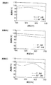
本発明者らは、図8A,Bに示す透過率特性を示す光学フィルタを最前面に貼り付けた液晶パネルの視角特性を確認した。図8Aは入射角0°における透過率と波長との関係を示しており、図8Bは入射角60°における透過率と波長との関係を示している。
この光学フィルタは、入射角0°で波長400〜650nmの可視光の透過率が70%以上であり、入射角60°で波長600nm以上の可視光の透過率が波長450〜550nmの可視光の平均透過率の約70%に設計されている。実験の結果、正面方向と斜め方向での色差は良好であり、斜め方向から見たときの画面の赤色化も見られなかった。
The present inventors confirmed the viewing angle characteristics of the liquid crystal panel in which the optical filter having the transmittance characteristics shown in FIGS. FIG. 8A shows the relationship between transmittance and wavelength at an incident angle of 0 °, and FIG. 8B shows the relationship between transmittance and wavelength at an incident angle of 60 °.
This optical filter has a visible light transmittance of 70% or more at an incident angle of 0 ° and a wavelength of 400 to 650 nm, and a visible light transmittance of a wavelength of 450 to 550 nm at an incident angle of 60 °. It is designed to be about 70% of the average transmittance. As a result of the experiment, the color difference between the front direction and the diagonal direction was good, and the screen was not red when viewed from the diagonal direction.
(第2の実施の形態)
図9は本発明の第2の実施の形態による液晶表示装置用光学フィルムとしての光学フィルタ4’の構成例を示している。本実施の形態の光学フィルタ4’は、透過率90%以上の透明プラスチックフィルム(例えばPETフィルム)製の透明支持体5の両面に高屈折率材料層6と低屈折率材料層7を順にそれぞれ積層した誘電体多層膜で構成されている。
(Second Embodiment)
FIG. 9 shows a configuration example of an
本実施の形態では、高屈折率材料層6はTiO2微粒子含有塗膜(屈折率1.94)で形成され、低屈折率材料層7はフッ素系樹脂膜(屈折率1.35)で形成されている。なお、高屈折率材料6は、Nb2O5やTa2O5、ZrO2等の微粒子を含有する塗膜で形成されてもよい。なお図9の構成例では、透明支持体5の各面に各々同一層数の多層膜を形成したが、各面において層数を異ならせてもよい。
In the present embodiment, the high refractive
上記構成の光学フィルタ4’において、波長600nm以上の光の入射角と透過率との間の関係は、屈折率材料層6,7の膜厚、積層数、各層の膜厚の組み合わせ方等によって調整することができる。本例では、透明支持体5に形成した1層目の高屈折率材料層6の膜厚を約128nm、2層目の低屈折率材料層7の膜厚を約93nmとしている。
In the
以上のように構成される光学フィルタ4’は、入射角が大きくなるにつれて波長600nm以上の可視光の透過率を小さくし、特に、入射角60°で入射する可視光について、波長600nmから650nmの可視光の透過率の平均値をこれよりも短波長側の可視光の透過率の平均値よりも低下させる機能を有する。
The
また、この光学フィルタ4’は、入射角0°で入射する可視光について、波長400nmから650nmにおける可視光の最小透過率が90%以上であり、かつ、透過率の平均値が95%以上の特性を有している。
The
本実施の形態の光学フィルタ4’によっても上述の第1の実施の形態と同様な効果を得ることができ、液晶パネルを斜め方向から見たときの画面全体の赤系色での着色を効果的に抑えることができる。また、正面方向に出射される光の透過率が極めて高いので、ディスプレイの輝度の低下を抑えることができる。
The
上記構成の光学フィルタ4’の光学特性を図10A,Bに示す。図10Aは入射角0°における透過率と波長との関係を示しており、図10Bは入射角60°における透過率と波長との関係を示している。この光学フィルタ4’は、入射角0°で波長400〜650nmの可視光の透過率が97%以上であり、入射角60°で波長600nm以上の可視光の透過率が波長450〜600nmの可視光の平均透過率よりも低く設定されている。このような光学特性を有する光学フィルタ4’を最前面に貼り付けた液晶パネルの視角特性を確認する実験を行った結果、正面方向と斜め方向での色差は良好であり、斜め方向から見たときの画面の赤色化も見られなかった。
The optical characteristics of the
(第3の実施の形態)
図11は、本発明の第3の実施の形態による液晶表示装置20を示している。なお、図において上述の第1の実施の形態と対応する部分については同一の符号を付し、その詳細な説明は省略する。
(Third embodiment)
FIG. 11 shows a liquid
本実施の形態において、液晶パネル21は、液晶層1を挟んで対向する一対の透明基板2a,2bと、これらの透明基板2a,2bの外面側に各々配置された偏光板3a,3bとを備えている。なお必要に応じて、透明基板2a,2bと偏光板3a,3bとの間に位相差板等の光学補償フィルムを介在させてもよい。
In the present embodiment, the
本発明に係る液晶表示装置用光学フィルムとしての光学フィルタ24は、バックライトユニット12と拡散板13との間に配置されている。この光学フィルタ24は、上述の第1,第2の実施の形態における光学フィルタ4,4’と同様な構成を有し、バックライトユニット12から出射した光のうち波長600nm以上の可視光について、液晶パネル21の正面方向に出射する場合よりも斜め方向に出射する場合の透過率を低下させる機能を有している。
The optical filter 24 as an optical film for a liquid crystal display device according to the present invention is disposed between the
本実施の形態では、光学フィルタ24をバックライトユニット12の光出射面に配置して、光源側から長波長領域の光の強度を選択的に減衰させた状態で後段の拡散板13、プリズムシート14、拡散シート15、偏光分離素子16及び液晶パネル21へ導くようにしている。これにより、液晶パネル21の前面から斜め方向に出射される長波長領域の光の強度を光学フィルタ24であらかじめ減じ、液晶パネル21を斜め方向から見たときの画面の赤色化を抑制している。
In the present embodiment, the optical filter 24 is disposed on the light exit surface of the
光学フィルタ24は、第1,第2の実施の形態で説明した光学フィルタ4,4’と同一の構成とすることも可能であるが、液晶パネル21に表示される画像特性に合わせて最適化することが好ましい。本発明者らは、光学フィルム24を構成する屈折率材料層の膜厚を変更して、入射角0°で波長600nm以上の可視光の透過率が、波長450〜550nmの可視光の平均透過率の90%となるフィルタを作製し、液晶パネル21の視角特性を確認する実験を行った。実験の結果、正面方向と斜め方向での色差は良好であり、斜め方向から見たときの画面の赤色化も見られなかった。
The optical filter 24 may have the same configuration as the
(第4の実施の形態)
図12は、本発明の第4の実施の形態による液晶表示装置30を示している。なお、図において上述の第3の実施の形態と対応する部分については同一の符号を付し、その詳細な説明は省略する。
(Fourth embodiment)
FIG. 12 shows a liquid
本実施の形態の液晶表示装置30においては、本発明に係る液晶表示装置用光学フィルムとしての光学フィルタ34が、液晶パネル21とバックライトユニット12との間に配置された偏光分離素子36一体的に設けられている。
In the liquid
偏光分離素子36は、図13に模式的に示すように、反射性偏光子37を複数積層して構成されており、バックライトユニット12から出射された光のうち、例えばP波偏光成分は透過させS波偏光成分は反射する光学的機能素子である。本実施の形態では、この偏光分離素子36の光出射面に光学フィルタ34を一体的に設けている。
As schematically shown in FIG. 13, the
光学フィルタ34は、上述の第1,第2の実施の形態における光学フィルタ4,4’と同様な構成を有し、偏光分離素子36から出射される光のうち、波長600nm以上の可視光について、液晶パネル21の正面方向に出射する場合よりも斜め方向に出射する場合の透過率を低下させる機能を有している。
The
以上のように構成される本実施の形態によっても、上述の各実施の形態と同様な効果を得ることができる。特に本実施の形態によれば、本発明に係る光学フィルタ34を偏光分離素子36等の光学的機能素子と一体的に設けているので、部品点数を増大することなく当該液晶表示装置を構成することができる。
Also according to the present embodiment configured as described above, the same effects as those of the above-described embodiments can be obtained. In particular, according to the present embodiment, since the
なお、偏光分離素子36は図13に示した構成のものに限らず、例えば、断面三角形状の溝が連続して形成された構造面を有する第1及び第2のプリズム基板が誘電体層を介してそれぞれの山部と谷部とが一致するように対向配置された構成のものを採用してもよい。また、光学フィルタ34に一体的に設けられる光学的機能素子は、偏光分離素子に限らず、プリズムシート14や拡散シート15等であってもよい。
The
以下、本発明の実施例について説明する。なお、以下の実施例は例示であり、本発明はこれらの実施例に限定されるものではない。 Examples of the present invention will be described below. In addition, the following Examples are illustrations and this invention is not limited to these Examples.
本発明に係る液晶表示装置用光学フィルムとしての光学フィルタの幾つかのサンプルを作製した。そして、光学フィルタを構成する屈折率材料層の膜厚、積層数、積層構造を変えて、入射角0°および60°における透過率と波長との関係を測定した。 Several samples of an optical filter as an optical film for a liquid crystal display device according to the present invention were prepared. Then, the relationship between the transmittance and wavelength at incident angles of 0 ° and 60 ° was measured by changing the film thickness, the number of layers, and the layered structure of the refractive index material layers constituting the optical filter.
サンプル作製に用いた高屈折率材料層は、TiO2微粒子を含有する塗膜とした。当該塗膜を形成する塗料Aの構成は以下の通りである。 The high refractive index material layer used for sample preparation was a coating film containing TiO 2 fine particles. The composition of the coating material A that forms the coating film is as follows.
(塗料A)
・顔料微粒子:TiO2微粒子 100重量部
(石原産業社製、平均粒径約20nm、屈折率2.48)
・結合剤:SO3Na基含有ウレタンアクリレート 9.2重量部
(数平均分子量:350、SO3Na濃度:1×10⁻¹mol/g)
・分散剤:ポリオキシエチレンリン酸エステル 7.5重量部
・有機溶媒:メチルイソブチルケトン(MIBK) 4800重量部
・紫外性(UV)硬化性樹脂:ジペンタエリスリトールヘキサアクリレートとジペンタエリスリトールペンタアクリレートとの混合物 22重量部
(日本化薬社製、商品名DPHA)
(Paint A)
Pigment fine particles: TiO 2
Binder: 9.2 parts by weight of SO 3 Na group-containing urethane acrylate (number average molecular weight: 350, SO 3 Na concentration: 1 × 10 −1 mol / g)
Dispersant: 7.5 parts by weight of polyoxyethylene phosphate ester Organic solvent: 4800 parts by weight of methyl isobutyl ketone (MIBK) Ultraviolet (UV) curable resin: dipentaerythritol hexaacrylate and dipentaerythritol pentaacrylate 22 parts by weight (Nippon Kayaku Co., Ltd., trade name DPHA)
上記顔料微粒子、分散剤、結合剤、有機溶媒を所定量混合し、ペイントシェーカーで分散処理を行い微粒子分散液を得た。次に、UV硬化性樹脂を添加し、撹拌機にて撹拌処理を行い、塗料Aとした。なお、当該塗料Aより成膜した光学膜について、フィルメトリックス(松下インターテクノ社製)を用いて膜の屈折率を測定したところ、可視領域で平均1.94であった。 A predetermined amount of the pigment fine particles, the dispersant, the binder, and the organic solvent were mixed, and dispersion treatment was performed with a paint shaker to obtain a fine particle dispersion. Next, a UV curable resin was added, and the mixture was stirred with a stirrer to obtain paint A. In addition, when the refractive index of the optical film formed from the coating material A was measured using Filmetrics (manufactured by Matsushita Intertechno Co., Ltd.), the average was 1.94 in the visible region.
一方、サンプル作製に用いた低屈折率材料層は、フッ素樹脂膜とした。当該樹脂膜を形成する塗料Bの構成は以下の通りである。 On the other hand, the low refractive index material layer used for sample preparation was a fluororesin film. The composition of the coating material B that forms the resin film is as follows.
(塗料B)
・結合剤:末端カルボキシル基をもつパーフルオロブテニルビニルエーテルの重合体 100重量部
・有機溶媒:含フッ素アルコール(C6F13C2H4OH)とパーフルオロブチルアミンとの混合溶媒(混合比95:5) 1666重量部
(Paint B)
Binder: terminated
上記結合剤と有機溶媒とを混合し、十分撹拌して塗料Bとした。なお、当該塗料Bより成膜した光学膜について、フィルメトリックス(松下インターテクノ社製)を用いて膜の屈折率を測定したところ、可視領域で平均1.34であった。 The binder and the organic solvent were mixed and sufficiently stirred to obtain paint B. In addition, about the optical film formed into a film from the said coating material B, when the refractive index of the film | membrane was measured using Filmetrics (made by Matsushita Intertechno Co., Ltd.), it was 1.34 on the average in the visible region.
(実施例1)
上述の塗料A,Bを用いて以下のようにして光学フィルムのサンプルを作製した。
Example 1
An optical film sample was prepared using the coating materials A and B as described below.
PETフィルム(厚み188μm、東レ社製、商品名U426)の主面に塗料Aをディッピング方式で塗布した。塗料Aの塗布量は基板の引き上げ速度を調整して行い、目標膜厚128nmとなる量とした。塗料Aの塗膜を80℃で乾燥後、UV硬化させ(1000mJ/cm2)、高屈折率材料層を形成した。 Coating A was applied by dipping on the main surface of a PET film (thickness: 188 μm, manufactured by Toray Industries, Inc., trade name: U426). The coating amount of the coating material A was adjusted by adjusting the pulling rate of the substrate, and was set to a target film thickness of 128 nm. The coating film of Paint A was dried at 80 ° C. and then UV cured (1000 mJ / cm 2) to form a high refractive index material layer.
次いで、作製した高屈折率材料層の上に塗料Bをディッピング方式で塗布した。塗料Bの塗布量は基板の引き上げ速度を調整して行い、目標膜厚93nmとなる量とした。塗料Bの塗膜を室温で乾燥後、90℃で熱硬化を行い、低屈折率材料層を形成した。以上のようにして、PETフィルムの両面に合計4層の膜を積層した。 Subsequently, the coating material B was apply | coated by the dipping method on the produced high refractive index material layer. The coating amount of the coating material B was adjusted by adjusting the pulling rate of the substrate, and was set to a target film thickness of 93 nm. The coating film of the coating material B was dried at room temperature and then thermally cured at 90 ° C. to form a low refractive index material layer. As described above, a total of four layers were laminated on both sides of the PET film.
得られたサンプルの評価として、分光反射率測定器により、入射角0°および60°における透過率を測定し、波長400〜600nmにおける透過率の平均値および最小透過率、波長600〜650nmにおける透過率の平均値を求めた。また、入射角が0°、10°、20°および30°における透過率を測定し、波長400〜450nmにおける透過率の平均値を求めた。
As an evaluation of the obtained sample, the transmittance at an incident angle of 0 ° and 60 ° was measured by a spectral reflectometer, and the average value and the minimum transmittance at a wavelength of 400 to 600 nm and the transmission at a wavelength of 600 to 650 nm were measured. The average value of the rate was obtained. Moreover, the transmittance | permeability in
(実施例2〜6)
実施例2〜6における各サンプルの屈折率材料層の膜厚、積層数、積層形態を表1にまとめて示す。実施例2では、低屈折率材料層のみを形成した(この場合、PET基材が高屈折率材料層(屈折率1.65程度)に相当)。実施例3〜5では、(2層目の)低屈折率材料層の上に更に高屈折率材料層および低屈折率材料層を形成した。
(Examples 2 to 6)
Table 1 summarizes the film thickness, the number of layers, and the lamination form of the refractive index material layers of the samples in Examples 2 to 6. In Example 2, only the low refractive index material layer was formed (in this case, the PET substrate corresponds to the high refractive index material layer (refractive index of about 1.65)). In Examples 3 to 5, a high refractive index material layer and a low refractive index material layer were further formed on the (second layer) low refractive index material layer.

各実施例によるサンプルの透過率測定結果を表2、表3、図14および図15に示す。各サンプルのいずれもが、入射角0°で入射する可視光について、波長400nmから650nmにおける可視光の最小透過率が90%以上であり、かつ透過率の平均値が95%以上であることがわかる。また、入射角60°で入射する可視光について、波長600nmから650nmの可視光の透過率の平均値が、波長400nmから600nmの可視光の透過率の平均値よりも低くすることができる。また同時に、0°入射時の波長400〜450nmの透過率平均値よりも10°、20°、30°入射時の透過率の平均値の方を高くすることができる。 Table 2, Table 3, FIG. 14 and FIG. 15 show the transmittance measurement results of the samples according to each example. In any sample, for visible light incident at an incident angle of 0 °, the minimum visible light transmittance at a wavelength of 400 nm to 650 nm is 90% or more, and the average value of the transmittance is 95% or more. Recognize. For visible light incident at an incident angle of 60 °, the average value of the transmittance of visible light with a wavelength of 600 nm to 650 nm can be made lower than the average value of the transmittance of visible light with a wavelength of 400 nm to 600 nm. At the same time, the average value of the transmittance at the time of incidence of 10 °, 20 °, and 30 ° can be made higher than the average value of the transmittance at a wavelength of 400 to 450 nm when incident at 0 °.
また、実施例5については、実際にLEDバックライトを用いた液晶テレビにおいて、液晶パネルとプリズムシートとの間に当該光学フィルムのサンプルを設置し、観察角度によるディスプレイの色度変化を分光放射輝度計(コニカミノルタ社製CA1000)により測定した。その結果を図16に示す。実施例5におけるフィルムを設置しない場合に比べ、設置した場合の観察角度の変化によるディスプレイの色度変化量Δxyが小さくなり、また、色度変化方向がyが高くなる方向、即ち赤みを消す方向にシフトしていることがわかる。即ち、本発明により色温度の変化と赤色化の両方を抑制できることがわかる。 In addition, in Example 5, in a liquid crystal television actually using an LED backlight, a sample of the optical film is placed between the liquid crystal panel and the prism sheet, and the change in chromaticity of the display according to the observation angle is measured as the spectral radiance. It measured with the meter (CA1000 by Konica Minolta). The result is shown in FIG. Compared with the case where the film is not installed in Example 5, the chromaticity change amount Δxy of the display due to the change in the observation angle when the film is installed is small, and the direction of chromaticity change is the direction in which y increases, that is, the direction in which the redness disappears. It turns out that it has shifted to. That is, it can be seen that the present invention can suppress both the change in color temperature and redness.
以上、本発明の各実施の形態について説明したが、勿論、本発明はこれらに限定されることなく、本発明の技術的思想に基づいて種々の変形が可能である。 As mentioned above, although each embodiment of this invention was described, of course, this invention is not limited to these, A various deformation | transformation is possible based on the technical idea of this invention.
例えば以上の各実施の形態では、波長600nm以上の可視光を対象とした透過率減衰作用を行わせるように光学フィルタを構成したが、これに限られない。例えば、広色域光源を用いていないバックライトユニットを備えた液晶表示装置においては、赤以外の黄色や橙色、緑色等の過剰な透過率をもつ出射光が問題となる場合がある。この場合、本発明によれば、これらの波長領域を対象とした光学フィルタの設計を行うことにより、画面を斜めから見たときの特定色による着色を抑制することができる。 For example, in each of the embodiments described above, the optical filter is configured to perform the transmittance attenuation function for visible light having a wavelength of 600 nm or more, but the present invention is not limited to this. For example, in a liquid crystal display device including a backlight unit that does not use a wide color gamut light source, emitted light having excessive transmittance such as yellow other than red, orange, or green may be a problem. In this case, according to the present invention, by designing the optical filter for these wavelength regions, coloring by a specific color when the screen is viewed from an oblique direction can be suppressed.
また、以上の第1の実施の形態において、液晶パネル11の最前面に位置する光学フィルタ4の前面側(図3において透明支持体5の上面側)に比較的低屈折率の誘電体層、あるいは高屈折率材料と低屈折率材料層の誘電多層膜を形成することにより、外光に対する反射防止機能を付加してもよい。
In the first embodiment described above, a dielectric layer having a relatively low refractive index is formed on the front side of the
更に、図17に示すように、光学フィルタ4の前面側に単層あるいは多層構造の誘電体膜(光学層)41を形成した光学素子40を構成し、光学フィルタ4を透過する特定波長領域(例えば波長600nm以上)の光を、誘電体膜41で反射した外光の特定波長成分(例えば波長600nm以上)との干渉作用で減衰させるようにしてもよい。この場合、誘電体層41は、光学フィルタ4を透過する特定波長領域の光の位相と逆位相となるような光学的設計がなされる。
Further, as shown in FIG. 17, an
更にまた、本発明に係る液晶表示装置用光学フィルムは、液晶パネルの前面側やバックライトユニットの光照射面に配置したり、偏光分離素子16と一体的に構成する例に限らず、拡散シートやプリズムシート等の光学シートの種類、構造、組合せ等に応じて、要求される画像品位が得られる最適な位置に当該光学素子を配置することができる。
Furthermore, the optical film for a liquid crystal display device according to the present invention is not limited to an example in which the optical film is disposed on the front side of the liquid crystal panel or the light irradiation surface of the backlight unit, or is configured integrally with the
1…液晶層、2a,2b…透明基板、3a,3b…偏光板、4,4’,24,34…光学フィルタ(液晶表示装置用光学フィルム)、6…高屈折率材料層、7…低屈折率材料層、8…光源、10、20,30…液晶表示装置、11,21…液晶パネル、12…バックライトユニット、13…拡散板、14…プリズムシート、15…拡散シート、16,36…偏光分離素子、17…カラーフィルタ、18a,18b…透明電極膜、19a,19b…配向膜、38a,38b…プリズム基板、40…光学素子、41…誘電体層(光学層)。
DESCRIPTION OF
Claims (2)
NTSC比90%以上の光源を有し、前記液晶パネルの背面側に配置されたバックライトユニットと、
第1の屈折率材料層と前記第1の屈折率材料層よりも低い屈折率を有する第2の屈折率材料層とが交互に複数積層された誘電体多層膜と、前記誘電体多層膜を支持する透明プラスチックフィルム製の透明支持体とを有し、前記液晶パネルの前面側に配置された光学フィルタとを具備し、
前記光学フィルタは、前記バックライトユニットから出射する波長600nm以上の可視光について、前記液晶パネルから正面方向に出射する場合よりも斜め方向に出射する場合の透過率を低下させ、前記バックライトユニットから出射する波長400〜450nmの可視光について、当該光学フィルタへ入射角0°で入射する場合よりも入射角10°以上30°以下で入射する場合の透過率の平均値を高める液晶表示装置。 LCD panel,
A backlight unit having a light source with an NTSC ratio of 90% or more and disposed on the back side of the liquid crystal panel;
A dielectric multilayer film in which a plurality of first refractive index material layers and a plurality of second refractive index material layers having a refractive index lower than that of the first refractive index material layer are alternately stacked; and A transparent support made of a transparent plastic film to support, an optical filter disposed on the front side of the liquid crystal panel,
The optical filter reduces the transmittance when the light emitted from the backlight unit has a wavelength of 600 nm or more and is emitted obliquely from the liquid crystal panel in the front direction, from the backlight unit. A liquid crystal display device that raises the average transmittance when incident visible light having a wavelength of 400 to 450 nm is incident on the optical filter at an incident angle of 10 ° or more and 30 ° or less than when incident on the optical filter at an incident angle of 0 ° .
前記光学フィルタは、入射角60°で入射する可視光について、波長600nmから650nmの可視光の透過率の平均値が、波長600nm未満の可視光の透過率の平均値よりも低い液晶表示装置。 The liquid crystal display device according to claim 1,
The optical filter is a liquid crystal display device in which an average value of transmittance of visible light having a wavelength of 600 nm to 650 nm is lower than an average value of transmittance of visible light having a wavelength of less than 600 nm with respect to visible light incident at an incident angle of 60 °.
Priority Applications (7)
| Application Number | Priority Date | Filing Date | Title |
|---|---|---|---|
| JP2005289336A JP4760275B2 (en) | 2005-05-23 | 2005-09-30 | Liquid crystal display |
| TW095118296A TW200708860A (en) | 2005-05-23 | 2006-05-23 | Optical element, liquid crystal panel, and liquid crystal display device |
| EP06746750A EP1884806A4 (en) | 2005-05-23 | 2006-05-23 | Optical element, liquid crystal panel, and liquid crystal display device |
| KR1020077003107A KR101220479B1 (en) | 2005-05-23 | 2006-05-23 | Optical element, liquid crystal panel, and liquid crystal display device |
| PCT/JP2006/310266 WO2006126549A1 (en) | 2005-05-23 | 2006-05-23 | Optical element, liquid crystal panel, and liquid crystal display device |
| US11/659,914 US8223295B2 (en) | 2005-05-23 | 2006-05-23 | Optical element, liquid crystal panel, and liquid crystal display |
| CN200680000788XA CN101019049B (en) | 2005-05-23 | 2006-05-23 | Optical element, liquid crystal panel, and liquid crystal display |
Applications Claiming Priority (3)
| Application Number | Priority Date | Filing Date | Title |
|---|---|---|---|
| JP2005149380 | 2005-05-23 | ||
| JP2005149380 | 2005-05-23 | ||
| JP2005289336A JP4760275B2 (en) | 2005-05-23 | 2005-09-30 | Liquid crystal display |
Publications (3)
| Publication Number | Publication Date |
|---|---|
| JP2007004104A JP2007004104A (en) | 2007-01-11 |
| JP2007004104A5 JP2007004104A5 (en) | 2007-03-01 |
| JP4760275B2 true JP4760275B2 (en) | 2011-08-31 |
Family
ID=37451974
Family Applications (1)
| Application Number | Title | Priority Date | Filing Date |
|---|---|---|---|
| JP2005289336A Expired - Fee Related JP4760275B2 (en) | 2005-05-23 | 2005-09-30 | Liquid crystal display |
Country Status (7)
| Country | Link |
|---|---|
| US (1) | US8223295B2 (en) |
| EP (1) | EP1884806A4 (en) |
| JP (1) | JP4760275B2 (en) |
| KR (1) | KR101220479B1 (en) |
| CN (1) | CN101019049B (en) |
| TW (1) | TW200708860A (en) |
| WO (1) | WO2006126549A1 (en) |
Families Citing this family (28)
| Publication number | Priority date | Publication date | Assignee | Title |
|---|---|---|---|---|
| TW200821703A (en) * | 2006-11-10 | 2008-05-16 | Delta Electronics Inc | Optical system and liquid crystal display apparatus thereof |
| KR100852273B1 (en) | 2007-04-13 | 2008-08-14 | 신홍우 | Back light unit and liquid crystal display module using the same |
| US8208097B2 (en) * | 2007-08-08 | 2012-06-26 | Samsung Corning Precision Materials Co., Ltd. | Color compensation multi-layered member for display apparatus, optical filter for display apparatus having the same and display apparatus having the same |
| TWI363904B (en) * | 2008-01-16 | 2012-05-11 | Au Optronics Corp | Liquid crystal display device and back light unit thereof |
| JP4826599B2 (en) * | 2008-04-10 | 2011-11-30 | ソニー株式会社 | Liquid crystal display, polarizing plate and backlight source |
| JP2010217660A (en) * | 2009-03-18 | 2010-09-30 | Victor Co Of Japan Ltd | Optical unit, backlight device, liquid crystal module and liquid crystal display |
| KR20110132622A (en) * | 2009-03-30 | 2011-12-08 | 스미또모 가가꾸 가부시끼가이샤 | Liquid crystal display device |
| CN102449542A (en) * | 2009-03-30 | 2012-05-09 | 住友化学株式会社 | Liquid crystal display device |
| KR101766494B1 (en) * | 2009-04-15 | 2017-08-08 | 쓰리엠 이노베이티브 프로퍼티즈 컴파니 | Optical film for preventing optical coupling |
| KR101713946B1 (en) * | 2010-12-29 | 2017-03-08 | 엘지디스플레이 주식회사 | Liquid crystal display device |
| TWI588540B (en) * | 2012-05-09 | 2017-06-21 | 半導體能源研究所股份有限公司 | Display device and electronic device |
| KR102046152B1 (en) | 2012-11-20 | 2019-11-19 | 삼성디스플레이 주식회사 | Polarizer and liquid crystal display using the same |
| US9568362B2 (en) * | 2012-12-19 | 2017-02-14 | Viavi Solutions Inc. | Spectroscopic assembly and method |
| CN103235356B (en) * | 2013-04-16 | 2016-06-29 | 京东方科技集团股份有限公司 | Optical filter and preparation method thereof, color membrane substrates and display device |
| US9110230B2 (en) | 2013-05-07 | 2015-08-18 | Corning Incorporated | Scratch-resistant articles with retained optical properties |
| US9359261B2 (en) * | 2013-05-07 | 2016-06-07 | Corning Incorporated | Low-color scratch-resistant articles with a multilayer optical film |
| US9366784B2 (en) | 2013-05-07 | 2016-06-14 | Corning Incorporated | Low-color scratch-resistant articles with a multilayer optical film |
| US11267973B2 (en) | 2014-05-12 | 2022-03-08 | Corning Incorporated | Durable anti-reflective articles |
| JP6444631B2 (en) * | 2014-06-30 | 2018-12-26 | 大和製罐株式会社 | Water-sliding / oil-sliding membrane, method for producing the same, and article having a surface covered thereby |
| US9790593B2 (en) | 2014-08-01 | 2017-10-17 | Corning Incorporated | Scratch-resistant materials and articles including the same |
| KR20160017365A (en) * | 2014-08-05 | 2016-02-16 | 삼성디스플레이 주식회사 | Liquid crystal display device |
| JP2018536177A (en) | 2015-09-14 | 2018-12-06 | コーニング インコーポレイテッド | High light transmittance and scratch resistant anti-reflective article |
| US10600213B2 (en) | 2016-02-27 | 2020-03-24 | Focal Sharp, Inc. | Method and apparatus for color-preserving spectrum reshape |
| WO2018155304A1 (en) | 2017-02-27 | 2018-08-30 | 富士フイルム株式会社 | Luminance equalizing member, backlight unit, and liquid crystal display device |
| CN108156776B (en) * | 2017-12-21 | 2020-12-04 | 北京小米移动软件有限公司 | Shell of electronic equipment and preparation method thereof |
| KR20230146673A (en) | 2018-08-17 | 2023-10-19 | 코닝 인코포레이티드 | Inorganic Oxide Articles with Thin, Durable Anti-Reflective Structures |
| KR20200133862A (en) | 2019-05-20 | 2020-12-01 | 삼성디스플레이 주식회사 | Backlight unit and Display device having the same |
| CN115220256A (en) * | 2021-04-21 | 2022-10-21 | 胡崇铭 | Vertical alignment type liquid crystal display module |
Family Cites Families (20)
| Publication number | Priority date | Publication date | Assignee | Title |
|---|---|---|---|---|
| DE3768824D1 (en) | 1986-01-21 | 1991-05-02 | Fuji Photo Film Co Ltd | DEVICE FOR READING RADIATION IMAGES. |
| JPH0711677B2 (en) * | 1986-01-22 | 1995-02-08 | 富士写真フイルム株式会社 | Radiation image information reader |
| JPH0434806A (en) * | 1990-05-31 | 1992-02-05 | Toshiba Lighting & Technol Corp | Lighting device |
| JPH0437806A (en) * | 1990-06-04 | 1992-02-07 | Minolta Camera Co Ltd | Light quantity correcting optical system |
| JPH04232924A (en) * | 1990-12-27 | 1992-08-21 | Semiconductor Energy Lab Co Ltd | Liquid crystal electro-optic device |
| JPH0815525A (en) | 1994-04-27 | 1996-01-19 | Sony Corp | Polarization beam splitter and liquid crystal projector |
| JPH0815695A (en) | 1994-06-29 | 1996-01-19 | Sony Corp | Liquid crystal display device |
| JP3974217B2 (en) | 1997-04-02 | 2007-09-12 | シャープ株式会社 | Liquid crystal display panel and liquid crystal display device |
| JPH1124066A (en) | 1997-07-04 | 1999-01-29 | Sony Corp | Liquid crystal display device |
| JPH11212073A (en) * | 1998-01-26 | 1999-08-06 | Hitachi Ltd | Liquid crystal display device |
| JP3580124B2 (en) | 1998-03-05 | 2004-10-20 | 日東電工株式会社 | Optical element, lighting device and liquid crystal display device |
| JPH11271671A (en) * | 1998-03-19 | 1999-10-08 | Minolta Co Ltd | Projection optical system |
| JP3826709B2 (en) * | 2000-12-22 | 2006-09-27 | 豊田合成株式会社 | Liquid crystal display |
| CN1216302C (en) * | 2001-02-27 | 2005-08-24 | 精工爱普生株式会社 | Multi-layer film cut filter and production method therefor, UV cut filter, dustproof glass, display panel and projection type display unit |
| JP2003066451A (en) * | 2001-08-30 | 2003-03-05 | Matsushita Electric Ind Co Ltd | Liquid crystal display |
| JP4195585B2 (en) | 2002-07-02 | 2008-12-10 | アルパイン株式会社 | Automotive electronics |
| US7317499B2 (en) * | 2002-08-22 | 2008-01-08 | Nitto Denko Corporation | Multilayer plate and display panel with anisotropic crystal film and conducting protective layer |
| JP4506070B2 (en) * | 2002-11-01 | 2010-07-21 | コニカミノルタホールディングス株式会社 | Method for forming antiglare layer, method for producing antiglare film, and ink jet device for forming antiglare layer |
| JP4342821B2 (en) | 2003-04-03 | 2009-10-14 | 日東電工株式会社 | Optical element, liquid crystal cell, illumination device, and liquid crystal display device |
| US20060066803A1 (en) * | 2004-09-30 | 2006-03-30 | Aylward Peter T | Substrate free flexible liquid crystal displays |
-
2005
- 2005-09-30 JP JP2005289336A patent/JP4760275B2/en not_active Expired - Fee Related
-
2006
- 2006-05-23 CN CN200680000788XA patent/CN101019049B/en active Active
- 2006-05-23 KR KR1020077003107A patent/KR101220479B1/en active IP Right Grant
- 2006-05-23 EP EP06746750A patent/EP1884806A4/en not_active Withdrawn
- 2006-05-23 US US11/659,914 patent/US8223295B2/en active Active
- 2006-05-23 TW TW095118296A patent/TW200708860A/en not_active IP Right Cessation
- 2006-05-23 WO PCT/JP2006/310266 patent/WO2006126549A1/en active Application Filing
Also Published As
| Publication number | Publication date |
|---|---|
| WO2006126549B1 (en) | 2007-02-15 |
| TWI354166B (en) | 2011-12-11 |
| WO2006126549A1 (en) | 2006-11-30 |
| KR101220479B1 (en) | 2013-01-10 |
| US8223295B2 (en) | 2012-07-17 |
| CN101019049B (en) | 2012-05-02 |
| US20070247567A1 (en) | 2007-10-25 |
| KR20080009257A (en) | 2008-01-28 |
| EP1884806A4 (en) | 2009-07-29 |
| JP2007004104A (en) | 2007-01-11 |
| CN101019049A (en) | 2007-08-15 |
| EP1884806A1 (en) | 2008-02-06 |
| TW200708860A (en) | 2007-03-01 |
Similar Documents
| Publication | Publication Date | Title |
|---|---|---|
| JP4760275B2 (en) | Liquid crystal display | |
| JP2007004104A5 (en) | ||
| US7630032B2 (en) | LCD with selective transmission filter having light transmittance of 80% or more at wavelength regions of 440+/−20nm; 525+/−25nm and 565+/−45nm, and 10% or less at 470 to 485nm and 575 to 595nm | |
| US5949506A (en) | LCD with diffuser having diffusing particles therein located between polarizers | |
| US8208097B2 (en) | Color compensation multi-layered member for display apparatus, optical filter for display apparatus having the same and display apparatus having the same | |
| JP2007316156A (en) | Liquid crystal panel, liquid crystal display apparatus and optical element | |
| US20060164574A1 (en) | Liquid crystal display | |
| JP2010072653A (en) | Color shift-reducing optical filter, and display device with the same | |
| US20140176859A1 (en) | Wide-color gamut film, display apparatus with the wide-color gamut film, and method for manufacturing the film | |
| JP3879661B2 (en) | Liquid crystal display device and electronic device | |
| KR20090015318A (en) | Color compensation film for display apparatus, filter for display apparatus having the same and display apparatus having the same | |
| US8625056B2 (en) | Liquid crystal display | |
| US20070047111A1 (en) | Prism sheet and backlight unit employed in a liquid crystal display | |
| RU2499289C1 (en) | Liquid crystal display device | |
| JP3435113B2 (en) | Liquid crystal display | |
| JP3340073B2 (en) | Color liquid crystal display | |
| CN113272728A (en) | Enhanced quantum dots on color filter LCD | |
| JP2006184587A (en) | Light scattering film, and color filter, electrode substrate for reflection type liquid crystal display apparatus, and reflection type liquid crystal display using film | |
| JP2008070418A (en) | Liquid crystal display device | |
| JP2023038443A (en) | Display device | |
| KR100846625B1 (en) | Transflective type liquid crystal display device | |
| WO2007122853A1 (en) | Liquid crystal display device | |
| JP2004151309A (en) | Transflective color liquid crystal display device | |
| JP2005208206A (en) | Light scattering film and liquid crystal display device using the same | |
| JP2014089317A (en) | Display device and luminaire |
Legal Events
| Date | Code | Title | Description |
|---|---|---|---|
| A521 | Request for written amendment filed |
Free format text: JAPANESE INTERMEDIATE CODE: A523 Effective date: 20070115 |
|
| A621 | Written request for application examination |
Free format text: JAPANESE INTERMEDIATE CODE: A621 Effective date: 20070115 |
|
| RD03 | Notification of appointment of power of attorney |
Free format text: JAPANESE INTERMEDIATE CODE: A7423 Effective date: 20071028 |
|
| A131 | Notification of reasons for refusal |
Free format text: JAPANESE INTERMEDIATE CODE: A131 Effective date: 20100330 |
|
| A521 | Request for written amendment filed |
Free format text: JAPANESE INTERMEDIATE CODE: A523 Effective date: 20100524 |
|
| A131 | Notification of reasons for refusal |
Free format text: JAPANESE INTERMEDIATE CODE: A131 Effective date: 20110215 |
|
| A521 | Request for written amendment filed |
Free format text: JAPANESE INTERMEDIATE CODE: A523 Effective date: 20110411 |
|
| TRDD | Decision of grant or rejection written | ||
| A01 | Written decision to grant a patent or to grant a registration (utility model) |
Free format text: JAPANESE INTERMEDIATE CODE: A01 Effective date: 20110510 |
|
| A61 | First payment of annual fees (during grant procedure) |
Free format text: JAPANESE INTERMEDIATE CODE: A61 Effective date: 20110523 |
|
| FPAY | Renewal fee payment (event date is renewal date of database) |
Free format text: PAYMENT UNTIL: 20140617 Year of fee payment: 3 |
|
| R151 | Written notification of patent or utility model registration |
Ref document number: 4760275 Country of ref document: JP Free format text: JAPANESE INTERMEDIATE CODE: R151 |
|
| FPAY | Renewal fee payment (event date is renewal date of database) |
Free format text: PAYMENT UNTIL: 20140617 Year of fee payment: 3 |
|
| R250 | Receipt of annual fees |
Free format text: JAPANESE INTERMEDIATE CODE: R250 |
|
| R250 | Receipt of annual fees |
Free format text: JAPANESE INTERMEDIATE CODE: R250 |
|
| R250 | Receipt of annual fees |
Free format text: JAPANESE INTERMEDIATE CODE: R250 |
|
| R250 | Receipt of annual fees |
Free format text: JAPANESE INTERMEDIATE CODE: R250 |
|
| R250 | Receipt of annual fees |
Free format text: JAPANESE INTERMEDIATE CODE: R250 |
|
| R250 | Receipt of annual fees |
Free format text: JAPANESE INTERMEDIATE CODE: R250 |
|
| R250 | Receipt of annual fees |
Free format text: JAPANESE INTERMEDIATE CODE: R250 |
|
| R250 | Receipt of annual fees |
Free format text: JAPANESE INTERMEDIATE CODE: R250 |
|
| R250 | Receipt of annual fees |
Free format text: JAPANESE INTERMEDIATE CODE: R250 |
|
| LAPS | Cancellation because of no payment of annual fees |