WO2013125610A1 - Dispositif d'antenne et dispositif de communication sans fil - Google Patents
Dispositif d'antenne et dispositif de communication sans fil Download PDFInfo
- Publication number
- WO2013125610A1 WO2013125610A1 PCT/JP2013/054256 JP2013054256W WO2013125610A1 WO 2013125610 A1 WO2013125610 A1 WO 2013125610A1 JP 2013054256 W JP2013054256 W JP 2013054256W WO 2013125610 A1 WO2013125610 A1 WO 2013125610A1
- Authority
- WO
- WIPO (PCT)
- Prior art keywords
- coil
- antenna
- coil antenna
- conductor
- conductors
- Prior art date
Links
Images


Classifications
-
- H—ELECTRICITY
- H01—ELECTRIC ELEMENTS
- H01Q—ANTENNAS, i.e. RADIO AERIALS
- H01Q7/00—Loop antennas with a substantially uniform current distribution around the loop and having a directional radiation pattern in a plane perpendicular to the plane of the loop
-
- H—ELECTRICITY
- H01—ELECTRIC ELEMENTS
- H01Q—ANTENNAS, i.e. RADIO AERIALS
- H01Q1/00—Details of, or arrangements associated with, antennas
- H01Q1/12—Supports; Mounting means
- H01Q1/22—Supports; Mounting means by structural association with other equipment or articles
- H01Q1/2208—Supports; Mounting means by structural association with other equipment or articles associated with components used in interrogation type services, i.e. in systems for information exchange between an interrogator/reader and a tag/transponder, e.g. in Radio Frequency Identification [RFID] systems
-
- H—ELECTRICITY
- H01—ELECTRIC ELEMENTS
- H01Q—ANTENNAS, i.e. RADIO AERIALS
- H01Q21/00—Antenna arrays or systems
- H01Q21/28—Combinations of substantially independent non-interacting antenna units or systems
-
- H—ELECTRICITY
- H01—ELECTRIC ELEMENTS
- H01L—SEMICONDUCTOR DEVICES NOT COVERED BY CLASS H10
- H01L2224/00—Indexing scheme for arrangements for connecting or disconnecting semiconductor or solid-state bodies and methods related thereto as covered by H01L24/00
- H01L2224/01—Means for bonding being attached to, or being formed on, the surface to be connected, e.g. chip-to-package, die-attach, "first-level" interconnects; Manufacturing methods related thereto
- H01L2224/10—Bump connectors; Manufacturing methods related thereto
- H01L2224/15—Structure, shape, material or disposition of the bump connectors after the connecting process
- H01L2224/16—Structure, shape, material or disposition of the bump connectors after the connecting process of an individual bump connector
- H01L2224/161—Disposition
- H01L2224/16151—Disposition the bump connector connecting between a semiconductor or solid-state body and an item not being a semiconductor or solid-state body, e.g. chip-to-substrate, chip-to-passive
- H01L2224/16221—Disposition the bump connector connecting between a semiconductor or solid-state body and an item not being a semiconductor or solid-state body, e.g. chip-to-substrate, chip-to-passive the body and the item being stacked
- H01L2224/16225—Disposition the bump connector connecting between a semiconductor or solid-state body and an item not being a semiconductor or solid-state body, e.g. chip-to-substrate, chip-to-passive the body and the item being stacked the item being non-metallic, e.g. insulating substrate with or without metallisation
-
- H—ELECTRICITY
- H01—ELECTRIC ELEMENTS
- H01L—SEMICONDUCTOR DEVICES NOT COVERED BY CLASS H10
- H01L2924/00—Indexing scheme for arrangements or methods for connecting or disconnecting semiconductor or solid-state bodies as covered by H01L24/00
- H01L2924/19—Details of hybrid assemblies other than the semiconductor or other solid state devices to be connected
- H01L2924/191—Disposition
- H01L2924/19101—Disposition of discrete passive components
- H01L2924/19105—Disposition of discrete passive components in a side-by-side arrangement on a common die mounting substrate
Definitions
- the present invention relates to an antenna device and a wireless communication device used for an RFID system including a non-contact IC card and an RF tag.
- an RFID system that communicates wirelessly between a reader / writer and an RFID tag and transmits information between the reader / writer and the RFID tag is widely used.
- the reader / writer and the RFID tag are each composed of an RFID IC chip for processing a radio signal and an antenna for transmitting / receiving a radio signal, and between the antenna of the RFID tag and the antenna of the reader / writer, Predetermined communication is performed via a magnetic field or an electromagnetic field.
- an RFID system has been introduced into a wireless communication terminal, and this wireless communication terminal may be used as a reader / writer or an RFID tag.
- this wireless communication terminal may be used as a reader / writer or an RFID tag.
- Patent Documents 1 and 2 disclose a structure in which a conductive member or a soft magnetic member is disposed between two antennas.
- a contactless automatic ticket gate system for example, a user holds an IC card over a reader / writer arranged in the ticket gate body, and data is transmitted and received between the reader / writer and the IC card. At this time, the antenna on the IC card side is held at various angles with respect to the antenna on the reader / writer side. However, depending on the angle, reading / writing of the IC card may not be possible.
- An object of the present invention is to provide an antenna device and a wireless communication device that solve the problem of upsizing when a plurality of antennas are provided in one device or apparatus.
- An antenna device of the present invention is an antenna device including a first coil antenna and a second coil antenna disposed in the vicinity of the first coil antenna,
- the first coil antenna is configured to include one coil conductor
- the second coil antenna is configured to include two coil conductors, and the two coil conductors are arranged and wound so that a generated induction magnetic field forms a closed magnetic circuit
- the winding axis of the coil conductor of the first coil antenna is substantially in the same direction as the winding axis of the two coil conductors of the second coil antenna
- the closed magnetic circuit substantially circulates inside the coil conductor of the first coil antenna, or substantially outside the coil conductor of the first coil antenna via the coil conductor of the first coil antenna. Orbiting, It is characterized by that.
- the degree of coupling between the first coil antenna and the second coil antenna is very small, and mutual interference between the first coil antenna and the second coil antenna can be suppressed.
- the antenna device can be miniaturized and the structure is not shielded by the conductive member or soft magnetic member, so that an antenna device with little loss and a large communication distance can be realized.
- the first coil antenna is an antenna used in the first communication system
- the second coil antenna is used in the second communication system.
- the first communication system and the second communication system are communication systems in the same frequency band. Thereby, two antennas having different directivities can be used in a communication system in the same frequency band.
- the first coil antenna and the second coil antenna are arranged such that a winding axis of a coil conductor of the first coil antenna includes a winding axis of the two coil conductors of the second coil antenna. It is preferable that they are arranged.
- the first coil antenna and the second coil antenna are not more coupled and independence can be enhanced.
- the winding axis of the two coil conductors of the second coil antenna and the winding axis of the coil conductor of the first coil antenna are the first coil antenna in plan view from the winding axis direction.
- the formation region of the second coil antenna and the formation region of the second coil antenna overlap at least partially.
- the first coil antenna and the second coil antenna are arranged adjacent to each other so that each coil surface is positioned on substantially the same plane, The first coil antenna and the second coil antenna are used in one communication system.
- the magnetic flux generated by the first coil antenna or the magnetic flux linked to the first coil antenna and the magnetic flux generated by the second coil antenna or the magnetic flux linked to the second coil antenna are substantially equal to each other.
- An orthogonal relationship is established. Further, although the first coil antenna and the second coil antenna are close to each other, they do not interfere with each other. Therefore, communication can be performed with the antenna device of the communication partner via an electromagnetic field with a very wide angular relationship.
- the formation area of the two coil conductors of the second coil antenna is in a positional relationship of sandwiching the coil conductor of the first coil antenna in a substantially plane.
- a feeding coil that is electromagnetically coupled to at least one of the first coil antenna or the second coil antenna is provided as necessary.
- an antenna device with high radiation efficiency can be obtained while using a small feeding coil. Further, since the feeding coil, the first coil antenna, and the second coil antenna can be arranged at positions suitable for each, assembly is facilitated. In addition, the power supply circuit can be protected from static electricity and surges caused by lightning.
- the wireless communication device of the present invention is a wireless communication device including an antenna device including a first coil antenna and a second coil antenna disposed in the vicinity of the first coil antenna,
- the first coil antenna is configured to include one coil conductor
- the second coil antenna is configured to include two coil conductors.
- an induced magnetic field forms a closed magnetic circuit.
- the winding axis of the coil conductor of the first coil antenna is oriented in substantially the same direction as the winding axis of the two coil conductors of the second coil antenna
- the closed magnetic circuit substantially circulates inside the coil conductor of the first coil antenna, or substantially outside the coil conductor of the first coil antenna via the coil conductor of the first coil antenna. It is characterized by orbiting.
- the antenna device corresponds to the first communication system and the second communication system, and has the longest communication distance required for the first communication system and the second communication system. It is preferable that the first coil antenna and the second coil antenna are assigned according to the length.
- This configuration can be applied to both a proximity communication system with a maximum communication distance of 10 cm and a proximity communication system with a maximum communication distance of 70 cm.
- the first coil antenna and the second coil antenna are arranged adjacent to each other so that the coil surfaces are positioned on substantially the same plane, The first coil antenna and the second coil antenna are used in one communication system.
- a common feeding circuit that feeds power to the first coil antenna and the second coil antenna;
- a switch that selectively switches a signal path between the first coil antenna, the second coil antenna, and the power feeding circuit.
- the directivity of the antenna by the first coil antenna and the directivity of the antenna by the second coil antenna can be selectively switched as necessary.
- an antenna device with high radiation efficiency can be obtained while using a small feeding coil. Further, since the feeding coil, the first coil antenna, and the second coil antenna can be arranged at positions suitable for each, assembly is facilitated. In addition, the power supply circuit can be protected from static electricity and surges caused by lightning.
- the first coil antenna does not substantially pick up the induction magnetic field of the second coil antenna
- the second coil antenna does not substantially pick up the induction magnetic field of the first coil antenna. That is, the degree of coupling between the first coil antenna and the second coil antenna is very small.
- the first coil antenna and the second coil antenna are disposed adjacent to each other, mutual interference between the coil antennas can be suppressed.
- a conductive member and a soft magnetic member are not necessarily required, the size can be reduced, and since the structure is not shielded by a conductive member or a soft magnetic member, an antenna device and a wireless communication device having a small loss and a large communication distance are configured. it can.
- FIG. 1A is an exploded perspective view of the antenna device 101
- FIG. 1B is an external perspective view of the antenna device 101
- 2A is a plan view of the antenna device 101
- FIG. 2B is a front view of the antenna device 101
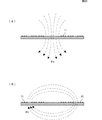
- FIG. 3 is a diagram illustrating the direction of current flowing through the coil conductor 11 of the first coil antenna 1 and the coil conductors 21 and 22 of the second coil antenna 2.
- FIG. 4 is a diagram showing magnetic fields induced by the coil conductors 11, 21, and 22 by magnetic lines of force.
- FIG. 5 is a diagram illustrating a configuration of a wireless communication device 201 such as a mobile phone terminal provided with the antenna device 101.
- 5A is a plan view of the lower housing (view of the inner bottom surface), and FIG.
- FIG. 5B is a cross-sectional view of the wireless communication apparatus 201.
- FIG. 6A is a plan view of the antenna device 102A of the second embodiment, and FIG. 6B is a front view of the antenna device 102A.
- FIG. 7A is a plan view of another antenna device 102B of the second embodiment, and FIG. 7B is a front view of the antenna device 102B.
- FIG. 8 is a plan view of still another antenna device 102C of the second embodiment.
- 9A is an exploded perspective view of the antenna device 103 according to the third embodiment
- FIG. 9B is a perspective view of the RFIC module 70 mounted on the antenna device 103
- FIG. 9C is a diagram of the RFIC module 70. It is sectional drawing.
- FIG. 10A is an exploded perspective view of only the coil conductor of the first coil antenna 1, and FIG. 10B is an equivalent circuit diagram of the first coil antenna.
- FIG. 11 is a cross-sectional view of a wireless communication apparatus 204 such as a mobile phone terminal according to the fourth embodiment.
- FIG. 12 is an exploded perspective view of the antenna device 105 according to the fifth embodiment.
- 13A is a perspective view of the second coil antenna of the antenna device 106 according to the sixth embodiment
- FIG. 13B is a plan view of the antenna device 106
- FIG. 13C is a front view of the antenna device 106.
- FIG. 14A is a plan view of the antenna device 107 according to the seventh embodiment.
- FIG. 14B is a front view of the antenna device 107.
- FIG. 14A is a plan view of the antenna device 107 according to the seventh embodiment.
- FIG. 14B is a front view of the antenna device 107.
- FIG. 14A is a plan view of the antenna device 107
- FIG. 15 is an external perspective view of the antenna device 108.
- FIG. 16A is a plan view of the antenna device 108
- FIG. 16B is a front view of the antenna device 108.
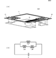
- FIGS. 17A and 17B are circuit diagrams illustrating two connection states of the power feeding circuit 30 to the antenna device 108.
- 18A and 18B are diagrams illustrating two connection states of the power feeding circuit 30 to the antenna device 108.
- FIG. FIG. 19A and FIG. 19B are diagrams showing a state of current flowing through each coil conductor of the antenna device 108.
- 20A and 20B are diagrams showing the state of the magnetic field induced by each coil conductor of the antenna device 108.
- FIG. 21B are diagrams showing the positional relationship between the antenna device 108 and the IC card (tag) during communication with the IC card (tag) that is the communication partner.
- FIG. 22A is a perspective view of the antenna device 109 according to the ninth embodiment.
- FIG. 22B is an equivalent circuit diagram of the antenna device 109.
- FIG. 23 is a diagram illustrating a state of a current flowing through each coil conductor of the antenna device 109
- FIG. 24 is a diagram illustrating a state of a magnetic field induced by each coil conductor of the antenna device 109.
- FIG. 24 is a diagram illustrating a state of a magnetic field induced by each coil conductor of the antenna device 109.
- FIG. 25C are diagrams illustrating the configuration of three antenna devices according to the tenth embodiment.
- FIG. 26A is a plan view of the antenna device 111 according to the eleventh embodiment, and FIG. 26B is a front sectional view.
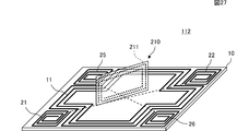
- FIG. 27 is an external perspective view of the antenna device 112 according to the twelfth embodiment.
- FIG. 28 is a diagram illustrating a connection example of the power feeding circuit 30 to the antenna device 112 illustrated in FIG.
- FIG. 29 is a diagram illustrating another connection example of the power feeding circuit 30 to the antenna device 112 illustrated in FIG.
- FIG. 30A is a perspective view of the booster antenna 113, and FIG. 30B is an equivalent circuit diagram of the booster antenna 113.
- FIG. 31 is a perspective view of an antenna device according to the thirteenth embodiment.
- FIG. 32 is an equivalent circuit diagram of the antenna device according to the thirteenth embodiment.
- FIG. 1A is an exploded perspective view of the antenna device 101
- FIG. 1B is an external perspective view of the antenna device 101.
- FIG. The antenna device 101 includes a first coil antenna 1 and a second coil antenna 2.
- the first coil antenna 1 is obtained by forming a rectangular spiral coil conductor 11 on a nonmagnetic insulating base material 10.
- the second coil antenna 2 is obtained by forming two coil conductors 21 and 22 on a nonmagnetic insulating base material 20.
- a first power feeding circuit 31 is connected to the coil conductor 11 of the first coil antenna 1, and a second power feeding circuit 32 is connected to the coil conductors 21 and 22 of the second coil antenna 2.
- the two coil conductors 21 and 22 are arranged and wound so that a magnetic field generated by energizing them is circulated in a coil opening of the coil conductor 11 of the first coil antenna 1 ( The closed magnetic circuit will be described later).
- FIG. 2A is a plan view of the antenna device 101
- FIG. 2B is a front view of the antenna device 101.
- the winding axes A21 and A22 of the two coil conductors 21 and 22 of the second coil antenna 2 and the winding axis A10 of the first coil antenna 1 are parallel to each other. That is, the winding axis directions coincide. In a plan view from the winding axis direction, the formation region of the first coil antenna 1 and the formation region of the second coil antenna 2 overlap.
- FIG. 3 is a diagram showing directions of currents flowing through the coil conductor 11 of the first coil antenna 1 and the coil conductors 21 and 22 of the second coil antenna 2.
- the base material is shown transparent.
- FIG. 4 is a diagram showing magnetic fields induced by the coil conductors 11, 21, 22 at that time by magnetic lines of force.
- the magnetic flux induced by the current flowing through the coil conductors 21 and 22 Draws a loop to form a closed magnetic circuit.
- the first coil antenna and the second coil antenna are arranged so that the winding axis of the coil conductor of the first coil antenna is in a plane including the winding axes of the two coil conductors of the second coil antenna.
- the first coil antenna and the second coil antenna are arranged so that the closed magnetic circuit of the second coil antenna circulates in one plane orthogonal to the coil opening surface of the first coil antenna.
- the magnetic field induced by the current flowing through the coil conductor 11 of the first coil antenna 1 is directed perpendicular to the coil opening surface of the coil conductor 11.
- the first coil antenna 1 and the second coil antenna 2 are arranged such that the winding axis of the coil conductor of the first coil antenna is in a plane including the winding axes of the two coil conductors of the second coil antenna.
- the magnetic flux ⁇ a and the magnetic flux ⁇ b are orthogonal to each other, and the first coil antenna 1 and the second coil antenna 2 are not coupled.
- the coil conductor 11 is coupled to the coil conductor 21, and the coil conductor 11 is also coupled to the coil conductor 22. Since the polarity of is opposite, it cancels out.
- the coil conductor 21 is disposed outside the formation area of the coil conductor 11, and the coil conductor 22 is disposed in the coil opening of the coil conductor 11 (inside the formation area of the coil conductor 11).
- the closed magnetic path of the second coil antenna 2 is not preferable because it is coupled to the first coil antenna 1.
- FIG. 5 is a diagram illustrating a configuration of a wireless communication device 201 such as a mobile phone terminal provided with the antenna device 101.
- 5A is a plan view of the lower housing (view of the inner bottom surface), and
- FIG. 5B is a cross-sectional view of the wireless communication apparatus 201.
- the second coil antenna 2 is attached to the first coil antenna 1 via a double-sided adhesive sheet or the like.
- the first coil antenna 1 is attached to the inner bottom surface of the lower housing 62.
- the lower housing 62 is a molded product of insulating resin.
- a printed wiring board 40 on which electronic components such as the RFIC chip 53 are mounted is housed in the internal space between the lower housing 62 and the upper housing 61.
- a liquid crystal display panel or the like is provided on the upper housing 61 side.
- a ground conductor 41 is formed on the printed wiring board 40.
- the printed wiring board 40 includes a power feeding circuit for the first coil antenna 1 and a power feeding circuit for the second coil antenna 2.
- the printed wiring board 40 is provided with a contact pin 51 that contacts the terminal 11T of the first coil antenna 1 and a contact pin 52 that contacts the terminals 21T and 22T of the second coil antenna 2.
- the first feeding circuit that feeds power to the first coil antenna 1 and the second feeding circuit that feeds power to the second coil antenna 2 are used in a communication system of the same frequency band such as 13.56 MHz. Moreover, the 1st coil antenna 1 and the 2nd coil antenna 2 are allocated according to the length of the communication longest distance requested
- the magnetic field (magnetic field line loop) by the 2nd coil antenna 2 has the characteristic which does not spread comparatively largely, it is used for a proximity type
- a wireless communication device such as a mobile phone terminal in which the antenna device 101 is provided on the inner surface of the housing can be configured.
- FIG. 6A is a plan view of the antenna device 102A of the second embodiment
- FIG. 6B is a front view of the antenna device 102A
- FIG. 7A is a plan view of another antenna device 102B of the second embodiment
- FIG. 7B is a front view of the antenna device 102B
- FIG. 8 is a plan view of still another antenna device 102C of the second embodiment.
- the difference between the first embodiment and the antenna device 101 shown in FIG. 2 is the positional relationship between the first coil antenna 1 and the second coil antenna 2.
- the winding axis of the two coil conductors 21 and 22 of the second coil antenna 2 and the winding axis of the first coil antenna 1 are such that their winding axis directions are Almost coincident (winding axes are parallel).
- the formation region of the first coil antenna 1 and the formation region of the second coil antenna 2 overlap.
- the dimension X ⁇ b> 2 e between the farthest ends of the counter electrode relationship in the formation area of the two coil conductors 21, 22 of the second coil antenna 2 is the dimension inside the coil opening of the coil conductor 11. Wider than X1i.
- the dimension X ⁇ b> 2 i between the nearest inner ends of the formation areas of the two coil conductors 21, 22 of the second coil antenna 2 is larger than the dimension X ⁇ b> 1 e outside the coil opening of the coil conductor 11. narrow. This relationship is the same for FIG. In other words, the coil conductors 21 and 22 partially overlap the coil conductor 11 in plan view.
- the closed magnetic circuit by the coil conductors 21 and 22 of the second coil antenna 2 substantially circulates inside the first coil antenna 1 (coil conductor 11) in the antenna device 102A shown in FIG.
- the first coil antenna 1 through the coil conductor 11 of the first coil antenna 1 substantially, that is, the magnetic field loop of the closed magnetic circuit partially overlaps the coil conductor in plan view. It goes around the outside of the coil conductor 11).
- the longitudinal direction of the first coil antenna 1 and the longitudinal direction of the second coil antenna 2 are not the same direction (parallel direction) as shown in FIGS. 2, 6, and 7, but may be orthogonal as shown in FIG. Good.
- the closed magnetic path by the coil conductors 21 and 22 of the second coil antenna 2 is not the coil conductor of the first coil antenna 1. 11 orthogonal to the coil axis.
- the closed magnetic circuit by the coil conductors 21 and 22 of the second coil antenna 2 substantially circulates inside or outside of the first coil antenna 1 (coil conductor 11). Therefore, the magnetic field generated by the first coil antenna 1 and the magnetic field generated by the second coil antenna 2 are orthogonal to each other, and the first coil antenna 1 and the second coil antenna 2 are not coupled.
- the coil conductor 11 is coupled to the coil conductor 21, and the coil conductor 11 is also coupled to the coil conductor 22. Is opposite, so it cancels out.
- FIG. 9A is an exploded perspective view of the antenna device 103 according to the third embodiment
- FIG. 9B is an external perspective view of the antenna device 103
- FIG. 9C is an RFIC mounted on the antenna device 103
- FIG. 9D is a cross-sectional view of the RFIC module 70.
- FIG. 10A is an exploded perspective view of only the coil conductor of the first coil antenna 1
- FIG. 10B is an equivalent circuit diagram of the first coil antenna.
- the coil conductor of the first coil antenna 1 is formed with an upper surface coil conductor 11A and a lower surface coil conductor 11B on the front and back of the base material 10.
- the winding direction of the upper surface coil conductor 11A and the winding direction of the lower surface coil conductor 11B are opposite (the same in the perspective direction), and the upper surface coil conductor 11A and the lower surface coil conductor 11B are arranged to face each other.
- the inductance by the upper surface coil conductor 11A is represented by L1
- the inductance by the lower surface coil conductor 11B is represented by L2
- the capacitance between the coil conductors is represented by capacitances C1 and C2
- an LC resonance circuit as shown in FIG.
- the resonance frequency of the LC resonance circuit is the carrier frequency of the communication system that communicates with the first coil antenna or a frequency in the vicinity thereof.
- the RFIC module 70 serving as a power feeding circuit includes a power feeding coil substrate 71 having a power feeding coil 72 formed therein and an RFIC chip 73.
- the RFIC chip 73 is mounted on the feeding coil substrate 71 via the conductive bonding material 74 and connected to the feeding coil 72.
- the feeding coil 72 is magnetically coupled to the coil conductors 11A and 11B by arranging (adhering) the RFIC module 70 to the corner of the coil conductor 11 of the first coil antenna 1.
- the RFIC chip 73 corresponds to a first power feeding circuit.
- the power feeding circuit may be magnetically coupled without being directly connected.
- an electrode facing the coil conductor of the first coil antenna may be provided on the feeding coil substrate 71 so as to be electric field coupled to both ends of the coil conductor.
- the winding axes of the coil conductors 21 and 22 of the second coil antenna 2 are both disposed in the opening of the first coil antenna 1.
- the closed magnetic circuit of the second coil antenna 2 substantially circulates within the opening of the first coil antenna 1, that is, inside the coil conductors 21 and 22 of the first coil antenna.
- the second coil antenna may be configured such that a closed magnetic circuit circulates within the opening of the first coil antenna 1.
- FIG. 11 is a cross-sectional view of a wireless communication apparatus 204 such as a mobile phone terminal according to the fourth embodiment.
- a card type device 80 is provided in the housing 60.
- the card type device 80 includes a base material 10, coil conductors 11 ⁇ / b> A and 11 ⁇ / b> B formed on both surfaces of the base material 10, and an RFIC module 70.
- the basic configuration of the card type device 80 is the same as that of the first coil antenna 1 shown in FIGS. 9 and 10 in the third embodiment.
- a printed wiring board 40 on which electronic components are mounted is accommodated in the housing 60.
- the printed wiring board 40 is formed with two coil conductors 21 and 22 for the second coil antenna.
- the printed wiring board 40 is mounted with an RFIC chip 53 that is a power feeding circuit for the second coil antenna.
- the positional relationship between the coil conductors 21 and 22 of the second coil antenna formed on the printed wiring board 40 and the coil conductors 11A and 11B of the first coil antenna is the same as that shown in FIG. 9 in the third embodiment. is there.
- the card-type device 80 may be configured by the first coil antenna and the RFIC module 70, and this may be provided in the casing of the wireless communication apparatus. Since the card-type device 80 can be electrically separated from the printed wiring board 40, electrical connection in the housing is not necessary. Also, the second coil antenna may be formed on a printed wiring board as shown in FIG.
- FIG. 12 is an exploded perspective view of the antenna device 105 according to the fifth embodiment. However, illustration of the base material is omitted.
- the feeding circuit 31 is connected to the coil conductor 11 of the first coil antenna 1
- the feeding circuit 32 is connected in series to the coil conductors 21 and 22 of the second coil antenna 2.
- the feeding circuit 32 is connected in parallel to the coil conductors 21 and 22 of the second coil antenna 2.
- the magnetic field induced by the coil conductor 21 and the magnetic field induced by the coil conductor 22 are connected to be opposite to the coil opening surface.
- the two coil conductors 21 and 22 are arranged and wound so that a magnetic field generated by energizing them forms a closed magnetic circuit. For this reason, the first coil antenna 1 and the second coil antenna 2 are not coupled to each other as in the case of the embodiments described so far.
- FIG. 13A is a perspective view of the second coil antenna of the antenna device 106 according to the sixth embodiment.
- FIG. 13B is a plan view of the antenna device 106.
- the support base material which forms each coil conductor is transparently illustrated.
- FIG. 13C is a front view of the antenna device 106.
- the coil conductors 21 and 22 of the second coil antenna 2 are formed on the base material 20, and the ferrite sheets 23 and 24 are inserted so as to obliquely penetrate the coil openings. ing.
- the base material 20 is formed with slit-like holes into which the ferrite sheets 23 and 24 are inserted.
- the coil conductors 21 and 22 are electrically connected in series, and both ends are formed as connection terminals 21T and 22T.
- the coil conductor 11 of the first coil antenna is the same as that shown in the embodiments so far.
- the magnetic flux ⁇ b induced by the current flowing through the coil conductors 21 and 22 of the second coil antenna 2 forms a loop (closed magnetic path) that passes through the two ferrite sheets 23 and 24 in series. To do. Further, the closed magnetic circuit by the coil conductors 21 and 22 of the second coil antenna 2 substantially circulates inside (inside the coil opening) of the first coil antenna 1 (coil conductor 11).
- the magnetic flux ⁇ a induced by the current flowing through the coil conductor 11 of the first coil antenna 1 is oriented in the direction perpendicular to the coil opening surface of the coil conductor 11. Therefore, the first coil antenna 1 and the second coil antenna 2 are not coupled.
- the magnetic flux ⁇ b can be greatly expanded in a necessary direction, and directivity and gain can be increased. Can be increased.
- FIG. 14A is a plan view of the antenna device 107 according to the seventh embodiment. However, the support base material which forms each coil conductor is transparently illustrated.
- FIG. 14B is a front view of the antenna device 107.
- the coil conductors 21 and 22 of the second coil antenna 2 are formed on the base material 20, and the ferrite sheets 23 and 24 are inserted so as to obliquely penetrate the coil openings. ing.
- the base material 20 is formed with slit-like holes into which the ferrite sheets 23 and 24 are inserted.
- the coil conductors 21 and 22 are electrically connected in series.
- the insertion direction of the ferrite sheets 23 and 24 is different from the example shown in FIG.
- the coil conductor 11 of the first coil antenna is the same as that shown in the embodiments so far.
- the magnetic flux ⁇ b induced by the current flowing through the coil conductors 21 and 22 of the second coil antenna 2 forms a loop (closed magnetic circuit) that passes through the two ferrite sheets 23 and 24 in series.
- the closed magnetic circuit by the coil conductors 21 and 22 of the second coil antenna 2 is substantially connected to the coil conductor 11 via the coil conductor 11 of the first coil antenna 1, that is, the magnetic field loop of the closed magnetic circuit is in a plan view. It goes around the outside of the first coil antenna 1 (coil conductor 11) so as to overlap.
- the magnetic flux ⁇ a induced by the current flowing through the coil conductor 11 of the first coil antenna 1 is oriented in the direction perpendicular to the coil opening surface of the coil conductor 11. Therefore, the first coil antenna 1 and the second coil antenna 2 are not coupled.
- the antenna device 107 can be accommodated in a limited thickness by arranging the first coil antenna 1 inside the position where the ferrite sheets 23 and 24 are exposed at the top in FIG.
- FIG. 15 is an external perspective view of the antenna device 108.
- FIG. 16A is a plan view of the antenna device 108, and
- FIG. 16B is a front view of the antenna device 108.
- the antenna device 108 includes a first coil antenna 1 and a second coil antenna 2.
- the first coil antenna 1 is obtained by forming a rectangular spiral coil conductor 11 on a nonmagnetic insulating base material 10.
- the second coil antenna 2 is obtained by forming two coil conductors 21 and 22 on a base material 10.
- the two coil conductors 21 and 22 of the second coil antenna have wiring and wiring formed on the surface opposite to the surface on which the two coil conductors 21 and 22 of the base material 10 are formed (dotted line portion in FIG. 15).
- the two coil conductors 21 and 22 are connected to each other by a via-hole conductor (not shown) that connects the coil conductors 21 and 22 to each other. It is arranged and wound so that the closed magnetic circuit circulates in the coil opening of the conductor 11.
- the winding axes A21 and A22 of the two coil conductors 21 and 22 of the second coil antenna 2 and the winding axis A10 of the coil conductor 11 of the first coil antenna 1 are mutually connected. Parallel. That is, the winding axis directions coincide.
- the winding axis of the coil conductor 11 of the first coil antenna 1 is a plane including the winding axes of the two coil conductors 21 and 22 of the second coil antenna 2 (a plane perpendicular to the plane of the substrate 10).
- the winding axis of the coil conductor 11 is in a plane including the winding axes of the coil conductors 21 and 22.
- the formation regions of the first coil antenna 1 and the second coil antenna 2 are in a positional relationship in which the formation region of the first coil antenna 1 is sandwiched between substantially the planes (in this example, the surface of the base material 10).
- FIGS. 17 and 18 are diagrams showing a connection state of the power feeding circuit 30 to the antenna device 108.
- the inductor L1 corresponds to the coil conductor 11 of the first coil antenna 1 and the inductors L2a and L2b correspond to the coil conductors 21 and 22 of the second coil antenna 2, respectively.
- a power feeding circuit 31 is connected to the antenna device via switches SW1 and SW2. In the state of FIGS. 17A and 18A, power is supplied to the first coil antenna 1, and in the state of FIGS. 17B and 18B, power is supplied to the second coil antenna 2.
- FIG. 19 is a diagram illustrating a state of a current flowing through each coil conductor of the antenna device 108
- FIG. 20 is a diagram illustrating a state of a magnetic field induced by each coil conductor of the antenna device 108.
- 19A and 20A show a state in which power is supplied to the coil conductor 11 of the first coil antenna 1
- FIGS. 19B and 20B show the coil conductor 21 of the second coil antenna 2.
- the magnetic flux induced by the current flowing through the coil conductors 21 and 22 of the second coil antenna 2 draws a loop so as to form a closed magnetic circuit.
- the winding axis of the coil conductor 11 of the first coil antenna 1 is in a plane including the winding axes of the two coil conductors 21 and 22 of the second coil antenna 2.
- FIG. 21 is a diagram showing a positional relationship between the antenna device 108 and the IC card (tag) at the time of communication with the IC card (tag) as a communication partner.
- FIG. 21A shows a communication state using the first coil antenna 1
- FIG. 21B shows a communication state using the second coil antenna 2.
- a coil antenna 211 is formed on the IC card (tag) 210.
- the IC card (tag) 210 in the state where the IC card (tag) 210 that is the communication partner and the antenna device 101 are parallel or substantially parallel, by using the first coil antenna 1, the IC card (tag) The coil antenna 211 of 210 can communicate by interlinking with the magnetic flux ⁇ a shown in FIG.
- the second coil antenna 2 in a state where the IC card (tag) 210 and the antenna device 108 are vertical or almost vertical, the second coil antenna 2 is used, so that the IC card (tag) 210 The coil antenna 211 can communicate with the magnetic flux ⁇ b shown in FIG.
- FIG. 22A is a perspective view of the antenna device 109 according to the ninth embodiment. However, illustration of the base material is omitted. In this example, the coil conductor 11 of the first coil antenna 1 and the coil conductors 21 and 22 of the second coil antenna 2 are connected in series.
- the coil conductor 11 of the first coil antenna 1 and the coil conductors 21 and 22 of the second coil antenna 2 are formed on the upper layer (upper surface), and on the lower layer (lower surface), A pattern that is electrically connected to each coil conductor is formed.
- the upper layer (upper surface) coil conductor and the lower layer (lower surface) pattern are connected via via conductors.
- FIG. 22B is an equivalent circuit diagram of the antenna device 109.
- the inductor L1 corresponds to the coil conductor 11 of the first coil antenna 1
- the inductors L2a and L2b correspond to the coil conductors 21 and 22 of the second coil antenna 2, respectively.
- the capacitor C1 is a capacitor composed of an upper layer (upper surface) electrode 91 and a lower layer (lower surface) electrode 92.
- the capacitor C2 is an external component such as a chip capacitor.
- the inductor L1 and the capacitor C1 constitute an LC parallel resonator, and the inductor (L2a, L2b) and the capacitor C2 constitute another LC parallel resonator.
- the resonance frequency of any resonator is equal to or close to the carrier frequency of the communication signal.
- FIG. 23 is a diagram illustrating a state of current flowing through each coil conductor of the antenna device 109
- FIG. 24 is a diagram illustrating a magnetic field induced by each coil conductor of the antenna device 109.
- FIG. 23 shows a state where power is supplied to the coil conductor 11 of the first coil antenna 1 and the coil conductors 21 and 22 of the second coil antenna 2.
- a magnetic field as shown by a magnetic flux ⁇ a in FIG. 24 is induced by a current flowing through the coil conductor 11 of the first coil antenna 1.
- a magnetic field as shown by a magnetic flux ⁇ b in FIG. 24 is induced by the current flowing through the coil conductors 21 and 22 of the second coil antenna 2. Therefore, as in the case of the first embodiment, the magnetic flux generated by the first coil antenna 1 or the magnetic flux interlinked with the first coil antenna 1 and the magnetic flux generated by the second coil antenna 2 or the second coil antenna 2.
- the magnetic flux interlinking with each other is substantially orthogonal.
- the power feeding circuit 30 may be connected in series to the first coil antenna 1 and the second coil antenna 2 so that power is fed simultaneously. Similarly, a power feeding circuit 30 may be connected in parallel to the first coil antenna 1 and the second coil antenna 2 so that power is fed simultaneously.
- FIG. 25 is a diagram illustrating a configuration of three antenna devices according to the tenth embodiment.
- 25A is a plan view of the antenna device 110A
- FIG. 25B is a plan view of the antenna device 110B
- FIG. 25C is a plan view of the antenna device 110C.
- the coil conductor 21 of the second coil antenna is formed at the center of one of the two long sides of the substrate 10
- the coil conductor 22 of the second coil antenna is formed at the center of the other.
- a coil conductor 11 of the first coil antenna is formed along the periphery of the base material 10 so as to bypass the two coil conductors 21 and 22.
- the two coil conductors 21 and 22 of the second coil antenna are formed on the surface opposite to the surface on which the two coil conductors 21 and 22 of the base material 10 are formed, as in the first embodiment. Are connected by a via-hole conductor connecting the wiring and the coil conductors 21 and 22.
- the coil conductor 21 of the second coil antenna is formed at the center of one of the two short sides of the substrate 10, and the coil conductor 22 of the second coil antenna is formed at the other center.
- the coil conductor 11 of the first coil antenna is formed along the periphery of the base material 10 so as to bypass the two coil conductors 21 and 22.
- FIG. 25B the coil conductor 21 of the second coil antenna is formed at the center of one of the two short sides of the substrate 10
- the coil conductor 22 of the second coil antenna is formed at the other center.
- the coil conductor 21 of the second coil antenna is located near the center of one of the two short sides of the substrate 10, and the coil conductor of the second coil antenna is located near the center of the other short side. 22 are formed.
- the coil conductor 11 of the first coil antenna is formed along the periphery of the base material 10 and so as to surround the two coil conductors 21 and 22.
- the area is limited as in the first and second embodiments.
- An antenna device can be configured. Further, by forming the coil conductor 11 of the first coil antenna and the coil conductors 21 and 22 of the second coil antenna on the common base material as described above, the thickness can be further reduced. Furthermore, handling at the time of manufacture and assembly is improved.
- FIG. 26A is a plan view of the antenna device 111 according to the eleventh embodiment
- FIG. 26B is a front sectional view.
- the coil conductor 11 of the first coil antenna and the coil conductors 21 and 22 of the second coil antenna are formed inside the base material 10. This is manufactured by, for example, a method for manufacturing a resin multilayer substrate.
- the two coil conductors 21 and 22 are arranged and wound so that a magnetic field generated by energizing them has a closed magnetic circuit orthogonal to the magnetic field induced by the coil conductor 11.
- the closed magnetic circuit formed by the coil conductors 21 and 22 of the second coil antenna 2 substantially overlaps the coil conductor 11 via the coil conductor 11 of the first coil antenna 1, that is, the loop of the magnetic field of the closed magnetic circuit partially overlaps in plan view.
- the outer circumference of the first coil antenna 1 (coil conductor 11) is circulated.
- the coil conductor 11 of the first coil antenna and the coil conductors 21 and 22 of the second coil antenna may be formed on different layers of the common base material.
- a thin and small planar antenna device can be configured.
- FIG. 27 is an external perspective view of the antenna device 112 according to the twelfth embodiment.
- the antenna device 112 includes a nonmagnetic insulating base 10 and a coil conductor formed on the base 10. That is, a cross-shaped and spiral coil conductor 11 and four spiral coil conductors 21, 22, 25, and 26 are formed on the base material 10.
- the coil conductor 11 constitutes a first coil antenna, and the coil conductors 21, 22, 25, and 26 constitute a second coil antenna.
- the coil conductors 21 and 22 connect the coil conductors 21 and 22 with wiring (broken lines in FIG. 27) formed on the surface of the base 10 opposite to the surface on which the two coil conductors 21 and 22 are formed. They are connected by via hole conductors (not shown).
- the coil conductors 25 and 26 are composed of wiring (dashed lines in FIG. 27) and coil conductors 25 and 26 formed on the surface of the base 10 opposite to the surface on which the two coil conductors 25 and 26 are formed. Are connected by via hole conductors (not shown).
- the two coil conductors 21 and 22 are arranged and wound so that a magnetic field generated by energizing them is circulated around the coil conductor 11 of the first coil antenna 1.
- the two coil conductors 25 and 26 are arranged and wound so that a magnetic field generated by energizing them is circulated around the coil conductor 11 of the first coil antenna 1.
- FIG. 27 shows an IC card (tag) 210 that is a communication partner.
- the coil antenna 211 of the IC card 210 is linked with the magnetic field generated by the coil conductors 25 and 26. Therefore, the IC card 210 is electromagnetically coupled to the power supply circuit connected to the coil conductors 25 and 26.
- FIG. 28 is a diagram illustrating a connection example of the power feeding circuit 30 to the antenna device 112 illustrated in FIG.
- the inductor L1 corresponds to the coil conductor 11
- the inductors L2a and L2b correspond to the coil conductors 21 and 22
- the inductors L3a and L3b correspond to the coil conductors 25 and 26, respectively.
- the power feeding circuit 31 is connected to the antenna device 112 via the switches SW1 and SW2. In this way, the coil conductor used by switching the switch may be selected.
- FIG. 29 is a diagram illustrating another connection example of the power feeding circuit 30 to the antenna device 112 illustrated in FIG.
- the inductor L1 corresponds to the coil conductor 11
- the inductors L2a and L2b correspond to the coil conductors 21 and 22
- the inductors L1m and L2m correspond to the coil conductors 25 and 26, respectively.
- the series circuit of the coil conductors 21 and 22 and the coil conductor 11 may be connected in parallel via the other coil conductors (25, 26).
- the coil conductors 25 and 26 may be connected in series to the series circuit of the coil conductors 21 and 22 and the coil conductor 11, respectively, so that the inductances of the two series circuits may be adjusted to be substantially equal.
- the inductances of the two series circuits may be adjusted to be substantially equal.
- all of the second coil antennas are arranged outside the first coil antenna (open magnetic circuit antennas), but they may all be arranged inside, or two sets. Of these closed magnetic paths, one set may be arranged on the inner side and the other set may be arranged on the outer side.
- the closed magnetic circuit antenna is arranged at the four corners of the open magnetic circuit antenna, but may be arranged at the center of the four sides of the open magnetic circuit antenna.
- FIG. 30A is a perspective view of the booster antenna 113
- FIG. 30B is an equivalent circuit diagram of the booster antenna 113.
- illustration of the base material is omitted.
- the inductor L1 corresponds to the coil conductor 11
- the inductors L2a and L2b correspond to the coil conductors 21 and 22, respectively.
- the capacitor C is a capacitor composed of an upper layer (upper surface) electrode 91 and a lower layer (lower surface) electrode 92.
- the coil conductor 11 of the first coil antenna and the coil conductors 21 and 22 of the second coil antenna are connected in parallel, and the capacitor C is further connected in parallel.
- This resonance frequency is set to a carrier frequency of the communication system or a frequency in the vicinity thereof.
- an inductor other than the coil conductor may be provided.
- FIG. 31 is a perspective view of the antenna device according to the thirteenth embodiment.
- the RFIC module 75 is mounted on the substrate 90, and the booster antenna 113 is disposed in parallel to the substrate 90 and in the vicinity of the RFIC module 75.
- the RFIC module 75 includes a feeding coil.
- the booster antenna 113 is attached to the inner surface of the housing.
- the direction and position of the coil winding axis of the power supply coil are determined so that the power supply coil of the RFIC module 75 is magnetically coupled to any or all of the coil conductors 11, 21, and 22.
- the feeding coil of the RFIC module 75 and the booster antenna 113 are electromagnetically coupled.
- FIG. 32 is an equivalent circuit diagram of the antenna device according to the thirteenth embodiment.
- the configuration of the booster antenna 113 is as shown in FIG.
- the RFIC module 75 includes an RFIC, a feeding coil, and a matching circuit.
- the inductor Lf corresponds to a feeding coil
- the capacitor Cf is a resonance frequency adjusting capacitor.
- the matching circuit is not shown.
- the feeding coil (inductor Lf) is shown coupled to the coil conductor 11 (inductor L1) of the first coil antenna, but coupled to one of the coil conductors 21 and 22 (inductors L2a and L2b). Also good. Since the coil conductors 21 and 22 are connected in parallel with the coil conductor 11, even in that case, the feeding coil and the booster antenna 113 are electromagnetically coupled.
- the coil conductors 21 and 22 and the coil conductor 11 are connected in parallel.
- the coil conductors 21 and 22 and the coil conductor 11 may be independent on the circuit.
- the winding axis of the coil conductor 11 of the first coil antenna 1 exists in the plane including the two winding axes of the coil conductors 21 and 22 of the second coil antenna 2, that is, 3
- the present invention is not limited to this.
- the winding axis of the coil conductor 11 of the first coil antenna 1 is directed substantially in the same direction as the winding axis of the two coil conductors 21 and 22 of the second coil antenna 2, and the first coil antenna 1 and the second coil antenna 2 so that the closed magnetic circuit of the second coil antenna substantially circulates outside the coil conductor of the first coil antenna, or circulates inside the coil conductor of the first coil antenna so that they are not coupled to each other. Good.
- the winding axis of the coil conductor 11 of the first coil antenna 1 is not within the plane including the two winding axes of the two coil conductors 21 and 22 of the second coil antenna 2, It is only necessary that the winding axis of the coil conductor 11 of the one-coil antenna 1 is substantially in the same direction as the winding axes of the two coil conductors 21 and 22 of the second coil antenna 2.
- the magnetic field loop generated by energizing the two coil conductors of the second coil antenna can be made substantially orthogonal to the coil axis of the coil conductor of the first coil antenna.
- an antenna device in which the two coil antennas do not interfere with each other even though the first coil antenna 1 and the second coil antenna 2 are close to each other. If the above three winding axes are in the same plane, a magnetic field loop generated by energizing the two coil conductors of the second coil antenna is caused with respect to the coil axis of the coil conductor of the first coil antenna. Thus, the crossing can be made more reliably.
- the coil conductor of the second coil antenna may be arranged via the coil conductor of the first coil antenna, that is, so that the magnetic field loop of the closed magnetic circuit partially overlaps the coil conductor 11 in plan view.
Abstract
Le dispositif d'antenne (101) est pourvu d'une première antenne à bobine et (1) d'une seconde antenne à bobine (2). La première antenne à bobine (1) est un conducteur de bobine (11) de forme spiralée rectangulaire formé sur un matériau de base (10) isolant et non magnétique. La seconde antenne à bobine (2) comprend deux conducteurs de bobine (21, 22) formés sur un matériau de base (20) isolant et non-magnétique. Les deux conducteurs de bobine (21, 22) sont positionnés et enroulés de sorte que la boucle de champ magnétique produite par le passage du courant à travers eux soit orthogonale à l'axe de bobine du conducteur de bobine (11). Le dispositif d'antenne et le dispositif de communication sans fil constitués de cette manière permettent ainsi de résoudre le problème lié à l'augmentation de la taille dans la fabrication d'une machine ou d'un dispositif unique à antennes multiples.
Priority Applications (2)
| Application Number | Priority Date | Filing Date | Title |
|---|---|---|---|
| JP2013550682A JP5464307B2 (ja) | 2012-02-24 | 2013-02-21 | アンテナ装置および無線通信装置 |
| US14/171,004 US9692128B2 (en) | 2012-02-24 | 2014-02-03 | Antenna device and wireless communication device |
Applications Claiming Priority (4)
| Application Number | Priority Date | Filing Date | Title |
|---|---|---|---|
| JP2012-038238 | 2012-02-24 | ||
| JP2012-038239 | 2012-02-24 | ||
| JP2012038238 | 2012-02-24 | ||
| JP2012038239 | 2012-02-24 |
Related Child Applications (1)
| Application Number | Title | Priority Date | Filing Date |
|---|---|---|---|
| US14/171,004 Continuation US9692128B2 (en) | 2012-02-24 | 2014-02-03 | Antenna device and wireless communication device |
Publications (1)
| Publication Number | Publication Date |
|---|---|
| WO2013125610A1 true WO2013125610A1 (fr) | 2013-08-29 |
Family
ID=49005790
Family Applications (1)
| Application Number | Title | Priority Date | Filing Date |
|---|---|---|---|
| PCT/JP2013/054256 WO2013125610A1 (fr) | 2012-02-24 | 2013-02-21 | Dispositif d'antenne et dispositif de communication sans fil |
Country Status (3)
| Country | Link |
|---|---|
| US (1) | US9692128B2 (fr) |
| JP (1) | JP5464307B2 (fr) |
| WO (1) | WO2013125610A1 (fr) |
Cited By (11)
| Publication number | Priority date | Publication date | Assignee | Title |
|---|---|---|---|---|
| CN103606002A (zh) * | 2013-11-30 | 2014-02-26 | 陈其晖 | 一种rfid电子标签及其天线 |
| CN105514591A (zh) * | 2016-02-19 | 2016-04-20 | 广东中元创新科技有限公司 | 电子线双频带天线 |
| JP2016076827A (ja) * | 2014-10-07 | 2016-05-12 | 日本電信電話株式会社 | 通信システム、通信方法、送信装置および受信装置 |
| JP2016540393A (ja) * | 2013-09-25 | 2016-12-22 | クゥアルコム・インコーポレイテッドQualcomm Incorporated | 面内磁界を使用する非接触データ通信、ならびに関連するシステムおよび方法 |
| WO2017209195A1 (fr) * | 2016-06-01 | 2017-12-07 | 戸田工業株式会社 | Dispositif antenne et étiquette ci l'utilisant |
| CN109804501A (zh) * | 2016-09-23 | 2019-05-24 | 阿莫技术有限公司 | 天线模块 |
| US10388450B2 (en) | 2015-05-28 | 2019-08-20 | Murata Manufacturing Co., Ltd. | Inductor module and electric power transmission system |
| JP2019525155A (ja) * | 2016-06-30 | 2019-09-05 | ローベルト ボツシユ ゲゼルシヤフト ミツト ベシユレンクテル ハフツングRobert Bosch Gmbh | コイル装置及び付属の測定装置 |
| JP2019169527A (ja) * | 2018-03-22 | 2019-10-03 | Tdk株式会社 | コイルユニット、ワイヤレス送電装置、ワイヤレス受電装置、及びワイヤレス電力伝送システム |
| JP2019220983A (ja) * | 2019-08-30 | 2019-12-26 | パナソニックIpマネジメント株式会社 | 水中通信装置及び水中通信システム |
| US10965381B2 (en) | 2018-03-28 | 2021-03-30 | Panasonic Intellectual Property Management Co., Ltd. | Underwater communication device and underwater communication system |
Families Citing this family (25)
| Publication number | Priority date | Publication date | Assignee | Title |
|---|---|---|---|---|
| US11476566B2 (en) * | 2009-03-09 | 2022-10-18 | Nucurrent, Inc. | Multi-layer-multi-turn structure for high efficiency wireless communication |
| WO2011118379A1 (fr) * | 2010-03-24 | 2011-09-29 | 株式会社村田製作所 | Système d'identification par radiofréquence |
| TWI613686B (zh) | 2012-03-23 | 2018-02-01 | Lg伊諾特股份有限公司 | 無線功率接收器之製造方法 |
| US9553476B2 (en) | 2012-03-23 | 2017-01-24 | Lg Innotek Co., Ltd. | Antenna assembly and method for manufacturing same |
| DE102013109221B4 (de) | 2013-08-26 | 2022-05-19 | Infineon Technologies Ag | Chip-Anordnung, Analysevorrichtung, Aufnahmebehälter, und Aufnahmebehältersystem |
| US9761945B2 (en) * | 2013-10-18 | 2017-09-12 | Taoglas Group Holdings Limited | Ultra-low profile monopole antenna for 2.4GHz band |
| KR102152074B1 (ko) * | 2014-07-22 | 2020-09-07 | 삼성전자주식회사 | 근거리 무선 통신 안테나 |
| CN104282991B (zh) * | 2014-09-25 | 2017-08-11 | 福建升腾资讯有限公司 | 一种pos机非接天线绕线方法 |
| JP6310383B2 (ja) * | 2014-12-18 | 2018-04-11 | アルプス電気株式会社 | 携帯機 |
| KR20160080669A (ko) * | 2014-12-30 | 2016-07-08 | 삼성전기주식회사 | 안테나 장치 |
| CN207517887U (zh) * | 2015-02-24 | 2018-06-19 | 株式会社村田制作所 | 天线装置以及rfid系统 |
| US10268945B1 (en) | 2015-06-30 | 2019-04-23 | Amazon Technologies, Inc. | RFID tags |
| EP3166181A1 (fr) * | 2015-11-05 | 2017-05-10 | Gemalto Sa | Procede de fabrication d'antenne radiofrequence sur un support et antenne ainsi obtenue |
| US10311355B1 (en) * | 2016-03-31 | 2019-06-04 | Amazon Technologies, Inc. | RFID tags |
| JP6251770B2 (ja) * | 2016-04-15 | 2017-12-20 | 株式会社エスケーエレクトロニクス | Rfidタグ |
| JP7114221B2 (ja) * | 2017-01-11 | 2022-08-08 | キヤノン株式会社 | 無線通信システム、通信装置及び通信方法 |
| US10511095B2 (en) * | 2017-03-24 | 2019-12-17 | Wits Co., Ltd. | Antenna module |
| KR101883109B1 (ko) * | 2017-07-20 | 2018-07-27 | 삼성전기주식회사 | 안테나 모듈 |
| FR3071988B1 (fr) * | 2017-10-03 | 2020-11-06 | Continental Automotive France | Dispositif de communication en champ proche |
| CN210576467U (zh) * | 2018-02-16 | 2020-05-19 | 株式会社村田制作所 | 天线装置以及电子设备 |
| FR3079972B1 (fr) * | 2018-04-09 | 2020-04-17 | Gaming Partners International | Dispositif de detection. |
| WO2020009539A1 (fr) | 2018-07-06 | 2020-01-09 | 주식회사 아모텍 | Module d'antenne combiné |
| TWI713250B (zh) * | 2019-10-05 | 2020-12-11 | 啓碁科技股份有限公司 | 通訊裝置和通訊方法 |
| KR102217291B1 (ko) * | 2019-10-31 | 2021-02-19 | 삼성전기주식회사 | 코일 부품 |
| CN110993626B (zh) * | 2019-12-20 | 2022-09-30 | 京东方科技集团股份有限公司 | 阵列基板、显示面板、显示装置和可穿戴设备 |
Citations (2)
| Publication number | Priority date | Publication date | Assignee | Title |
|---|---|---|---|---|
| JP2009171070A (ja) * | 2008-01-11 | 2009-07-30 | Sony Corp | アンテナモジュール、通信装置及び通信システム |
| JP2011101293A (ja) * | 2009-11-09 | 2011-05-19 | Murata Mfg Co Ltd | 複合アンテナ及び電子機器 |
Family Cites Families (577)
| Publication number | Priority date | Publication date | Assignee | Title |
|---|---|---|---|---|
| US3364564A (en) | 1965-06-28 | 1968-01-23 | Gregory Ind Inc | Method of producing welding studs dischargeable in end-to-end relationship |
| JPS5754964B2 (fr) | 1974-05-08 | 1982-11-20 | ||
| JPS6193701A (ja) | 1984-10-13 | 1986-05-12 | Toyota Motor Corp | 自動車用アンテナ装置 |
| JPS61284102A (ja) | 1985-06-11 | 1986-12-15 | Oki Electric Ind Co Ltd | 携帯形無線機のアンテナ |
| JPS62127140U (fr) | 1986-02-03 | 1987-08-12 | ||
| JPH01212035A (ja) | 1987-08-13 | 1989-08-25 | Secom Co Ltd | 電磁界ダイバ−シチ受信方式 |
| JPH03503467A (ja) | 1988-02-04 | 1991-08-01 | ユニスキャン リミティド | 磁界集中装置 |
| JPH0744114B2 (ja) | 1988-12-16 | 1995-05-15 | 株式会社村田製作所 | 積層チップコイル |
| JPH02164105A (ja) | 1988-12-19 | 1990-06-25 | Mitsubishi Electric Corp | スパイラルアンテナ |
| US5253969A (en) | 1989-03-10 | 1993-10-19 | Sms Schloemann-Siemag Aktiengesellschaft | Feeding system for strip material, particularly in treatment plants for metal strips |
| JPH03171385A (ja) | 1989-11-30 | 1991-07-24 | Sony Corp | 情報カード |
| JP2662742B2 (ja) | 1990-03-13 | 1997-10-15 | 株式会社村田製作所 | バンドパスフィルタ |
| JP2763664B2 (ja) | 1990-07-25 | 1998-06-11 | 日本碍子株式会社 | 分布定数回路用配線基板 |
| JPH04150011A (ja) | 1990-10-12 | 1992-05-22 | Tdk Corp | 複合電子部品 |
| JPH04167500A (ja) | 1990-10-30 | 1992-06-15 | Omron Corp | プリント基板管理システム |
| JP2539367Y2 (ja) | 1991-01-30 | 1997-06-25 | 株式会社村田製作所 | 積層型電子部品 |
| NL9100176A (nl) | 1991-02-01 | 1992-03-02 | Nedap Nv | Antenne met transformator voor contactloze informatieoverdracht vanuit integrated circuit-kaart. |
| JP2558330Y2 (ja) | 1991-02-06 | 1997-12-24 | オムロン株式会社 | 電磁結合型電子機器 |
| NL9100347A (nl) | 1991-02-26 | 1992-03-02 | Nedap Nv | Geintegreerde transformator voor een contactloze identificatiekaart. |
| JPH04321190A (ja) | 1991-04-22 | 1992-11-11 | Mitsubishi Electric Corp | 非接触型携帯記憶装置のアンテナ回路 |
| JPH0745933Y2 (ja) | 1991-06-07 | 1995-10-18 | 太陽誘電株式会社 | 積層セラミックインダクタンス素子 |
| DE69215283T2 (de) | 1991-07-08 | 1997-03-20 | Nippon Telegraph & Telephone | Ausfahrbares Antennensystem |
| JP2839782B2 (ja) | 1992-02-14 | 1998-12-16 | 三菱電機株式会社 | プリント化スロットアンテナ |
| JPH05327331A (ja) | 1992-05-15 | 1993-12-10 | Matsushita Electric Works Ltd | プリントアンテナ |
| JP3186235B2 (ja) | 1992-07-30 | 2001-07-11 | 株式会社村田製作所 | 共振器アンテナ |
| JPH0677729A (ja) | 1992-08-25 | 1994-03-18 | Mitsubishi Electric Corp | アンテナ一体化マイクロ波回路 |
| JP2592328Y2 (ja) | 1992-09-09 | 1999-03-17 | 神鋼電機株式会社 | アンテナ装置 |
| JPH06177635A (ja) | 1992-12-07 | 1994-06-24 | Mitsubishi Electric Corp | クロスダイポールアンテナ装置 |
| JPH06260949A (ja) | 1993-03-03 | 1994-09-16 | Seiko Instr Inc | 無線機器 |
| JPH07183836A (ja) | 1993-12-22 | 1995-07-21 | San'eisha Mfg Co Ltd | 配電線搬送通信用結合フィルタ装置 |
| US5491483A (en) | 1994-01-05 | 1996-02-13 | Texas Instruments Incorporated | Single loop transponder system and method |
| US6096431A (en) | 1994-07-25 | 2000-08-01 | Toppan Printing Co., Ltd. | Biodegradable cards |
| JP3427527B2 (ja) | 1994-12-26 | 2003-07-22 | 凸版印刷株式会社 | 生分解性積層体及び生分解性カード |
| JPH0844833A (ja) | 1994-08-03 | 1996-02-16 | Mitsubishi Denki Semiconductor Software Kk | 非接触icカード用リーダライタ及び非接触icカード用リーダライタシステム |
| JP2999374B2 (ja) | 1994-08-10 | 2000-01-17 | 太陽誘電株式会社 | 積層チップインダクタ |
| JP3141692B2 (ja) | 1994-08-11 | 2001-03-05 | 松下電器産業株式会社 | ミリ波用検波器 |
| DE4431754C1 (de) | 1994-09-06 | 1995-11-23 | Siemens Ag | Trägerelement |
| US5528222A (en) | 1994-09-09 | 1996-06-18 | International Business Machines Corporation | Radio frequency circuit and memory in thin flexible package |
| JPH0887580A (ja) | 1994-09-14 | 1996-04-02 | Omron Corp | データキャリア及びボールゲーム |
| JP3064840B2 (ja) | 1994-12-22 | 2000-07-12 | ソニー株式会社 | Icカード |
| JP2837829B2 (ja) | 1995-03-31 | 1998-12-16 | 松下電器産業株式会社 | 半導体装置の検査方法 |
| JPH08279027A (ja) | 1995-04-04 | 1996-10-22 | Toshiba Corp | 無線通信カード |
| US5955723A (en) | 1995-05-03 | 1999-09-21 | Siemens Aktiengesellschaft | Contactless chip card |
| DE19516227C2 (de) | 1995-05-03 | 2002-02-07 | Infineon Technologies Ag | Datenträgeranordnung, insbesondere Chipkarte |
| JPH08307126A (ja) | 1995-05-09 | 1996-11-22 | Kyocera Corp | アンテナの収納構造 |
| JP3637982B2 (ja) | 1995-06-27 | 2005-04-13 | 株式会社荏原電産 | インバータ駆動ポンプの制御システム |
| US5629241A (en) | 1995-07-07 | 1997-05-13 | Hughes Aircraft Company | Microwave/millimeter wave circuit structure with discrete flip-chip mounted elements, and method of fabricating the same |
| JP3150575B2 (ja) | 1995-07-18 | 2001-03-26 | 沖電気工業株式会社 | タグ装置及びその製造方法 |
| GB2305075A (en) | 1995-09-05 | 1997-03-26 | Ibm | Radio Frequency Tag for Electronic Apparatus |
| DE19534229A1 (de) | 1995-09-15 | 1997-03-20 | Licentia Gmbh | Transponderanordnung |
| JPH0993029A (ja) | 1995-09-21 | 1997-04-04 | Matsushita Electric Ind Co Ltd | アンテナ装置 |
| US6104611A (en) | 1995-10-05 | 2000-08-15 | Nortel Networks Corporation | Packaging system for thermally controlling the temperature of electronic equipment |
| JP3882218B2 (ja) | 1996-03-04 | 2007-02-14 | ソニー株式会社 | 光ディスク |
| JP3471160B2 (ja) | 1996-03-18 | 2003-11-25 | 株式会社東芝 | モノリシックアンテナ |
| JPH09270623A (ja) | 1996-03-29 | 1997-10-14 | Murata Mfg Co Ltd | アンテナ装置 |
| JPH09284038A (ja) | 1996-04-17 | 1997-10-31 | Nhk Spring Co Ltd | 非接触データキャリアのアンテナ装置 |
| JPH09294374A (ja) | 1996-04-26 | 1997-11-11 | Hitachi Ltd | 電源回路 |
| JP3427663B2 (ja) | 1996-06-18 | 2003-07-22 | 凸版印刷株式会社 | 非接触icカード |
| AUPO055296A0 (en) | 1996-06-19 | 1996-07-11 | Integrated Silicon Design Pty Ltd | Enhanced range transponder system |
| US6104311A (en) | 1996-08-26 | 2000-08-15 | Addison Technologies | Information storage and identification tag |
| JP3767030B2 (ja) | 1996-09-09 | 2006-04-19 | 三菱電機株式会社 | 折畳式無線通信装置 |
| EP0931295B1 (fr) | 1996-10-09 | 2001-12-12 | PAV Card GmbH | Procede et systeme de connexion pour produire une carte a puce |
| JPH10171954A (ja) | 1996-12-05 | 1998-06-26 | Hitachi Maxell Ltd | 非接触式icカード |
| JP3279205B2 (ja) | 1996-12-10 | 2002-04-30 | 株式会社村田製作所 | 表面実装型アンテナおよび通信機 |
| JPH10193849A (ja) | 1996-12-27 | 1998-07-28 | Rohm Co Ltd | 回路チップ搭載カードおよび回路チップモジュール |
| JPH10193851A (ja) | 1997-01-08 | 1998-07-28 | Denso Corp | 非接触カード |
| DE19703029A1 (de) | 1997-01-28 | 1998-07-30 | Amatech Gmbh & Co Kg | Übertragungsmodul für eine Transpondervorrichtung sowie Transpondervorrichtung und Verfahren zum Betrieb einer Transpondervorrichtung |
| JPH10242742A (ja) | 1997-02-26 | 1998-09-11 | Harada Ind Co Ltd | 送受信アンテナ |
| WO1998040930A1 (fr) | 1997-03-10 | 1998-09-17 | Precision Dynamics Corporation | Elements couples de maniere reactive dans des circuits sur substrats souples |
| JPH10293828A (ja) | 1997-04-18 | 1998-11-04 | Omron Corp | データキャリア、コイルモジュール、リーダライタ及び衣服データ取得方法 |
| JP3900593B2 (ja) | 1997-05-27 | 2007-04-04 | 凸版印刷株式会社 | Icカードおよびicモジュール |
| JPH11346114A (ja) | 1997-06-11 | 1999-12-14 | Matsushita Electric Ind Co Ltd | アンテナ装置 |
| JPH1125244A (ja) | 1997-06-27 | 1999-01-29 | Toshiba Chem Corp | 非接触データキャリアパッケージ |
| JP3621560B2 (ja) | 1997-07-24 | 2005-02-16 | 三菱電機株式会社 | 電磁誘導型データキャリアシステム |
| JPH1175329A (ja) | 1997-08-29 | 1999-03-16 | Hitachi Ltd | 非接触icカードシステム |
| JPH1185937A (ja) | 1997-09-02 | 1999-03-30 | Nippon Lsi Card Kk | 非接触式lsiカード及びその検査方法 |
| JPH1188241A (ja) | 1997-09-04 | 1999-03-30 | Nippon Steel Corp | データキャリアシステム |
| JPH11103209A (ja) | 1997-09-26 | 1999-04-13 | Fujitsu Ten Ltd | 電波受信装置 |
| JP3853930B2 (ja) | 1997-09-26 | 2006-12-06 | 株式会社マースエンジニアリング | 非接触データキャリアパッケージおよびその製造方法 |
| CN1179295C (zh) | 1997-11-14 | 2004-12-08 | 凸版印刷株式会社 | 复合ic模块及复合ic卡 |
| JPH11149536A (ja) | 1997-11-14 | 1999-06-02 | Toppan Printing Co Ltd | 複合icカード |
| JP3800766B2 (ja) | 1997-11-14 | 2006-07-26 | 凸版印刷株式会社 | 複合icモジュールおよび複合icカード |
| JP3800765B2 (ja) | 1997-11-14 | 2006-07-26 | 凸版印刷株式会社 | 複合icカード |
| JPH11175678A (ja) | 1997-12-09 | 1999-07-02 | Toppan Printing Co Ltd | Icモジュールとそのモジュールを搭載したicカード |
| JPH11220319A (ja) | 1998-01-30 | 1999-08-10 | Sharp Corp | アンテナ装置 |
| JPH11219420A (ja) | 1998-02-03 | 1999-08-10 | Tokin Corp | Icカードモジュール、icカード及びそれらの製造方法 |
| JP2001084463A (ja) | 1999-09-14 | 2001-03-30 | Miyake:Kk | 共振回路 |
| JPH11261325A (ja) | 1998-03-10 | 1999-09-24 | Shiro Sugimura | コイル素子と、その製造方法 |
| JP4260917B2 (ja) | 1998-03-31 | 2009-04-30 | 株式会社東芝 | ループアンテナ |
| EP0987789A4 (fr) | 1998-03-31 | 2004-09-22 | Matsushita Electric Ind Co Ltd | Antenne et televiseur numerique |
| US5936150A (en) | 1998-04-13 | 1999-08-10 | Rockwell Science Center, Llc | Thin film resonant chemical sensor with resonant acoustic isolator |
| KR20010013741A (ko) | 1998-04-14 | 2001-02-26 | 리버티 카톤 컴퍼니 텍사스 | 압축기와 그 밖의 물품을 위한 컨테이너 |
| JP4030651B2 (ja) | 1998-05-12 | 2008-01-09 | 三菱電機株式会社 | 携帯型電話機 |
| JPH11328352A (ja) | 1998-05-19 | 1999-11-30 | Tokin Corp | アンテナとicチップとの接続構造、及びicカード |
| US6107920A (en) | 1998-06-09 | 2000-08-22 | Motorola, Inc. | Radio frequency identification tag having an article integrated antenna |
| US6018299A (en) | 1998-06-09 | 2000-01-25 | Motorola, Inc. | Radio frequency identification tag having a printed antenna and method |
| JP2000021639A (ja) | 1998-07-02 | 2000-01-21 | Sharp Corp | インダクター、これを用いた共振回路、整合回路、アンテナ回路及び発振回路 |
| JP2000021128A (ja) | 1998-07-03 | 2000-01-21 | Nippon Steel Corp | 円盤状記憶媒体及びその収納ケース |
| JP2000022421A (ja) | 1998-07-03 | 2000-01-21 | Murata Mfg Co Ltd | チップアンテナ及びそれを搭載した無線機器 |
| AUPP473898A0 (en) | 1998-07-20 | 1998-08-13 | Integrated Silicon Design Pty Ltd | Metal screened electronic labelling system |
| JP2000311226A (ja) | 1998-07-28 | 2000-11-07 | Toshiba Corp | 無線icカード及びその製造方法並びに無線icカード読取り書込みシステム |
| EP0977145A3 (fr) | 1998-07-28 | 2002-11-06 | Kabushiki Kaisha Toshiba | Carte à puce radio |
| JP3956172B2 (ja) | 1998-07-31 | 2007-08-08 | 吉川アールエフシステム株式会社 | データキャリア及びデータキャリア用アンテナ |
| JP2000059260A (ja) | 1998-08-04 | 2000-02-25 | Sony Corp | 記憶装置 |
| AU762495B2 (en) | 1998-08-14 | 2003-06-26 | 3M Innovative Properties Company | Application for a radio frequency identification system |
| CA2338522C (fr) | 1998-08-14 | 2009-04-07 | 3M Innovative Properties Company | Applications pour des systemes d'identification de frequence radio |
| JP4411670B2 (ja) | 1998-09-08 | 2010-02-10 | 凸版印刷株式会社 | 非接触icカードの製造方法 |
| JP4508301B2 (ja) | 1998-09-16 | 2010-07-21 | 大日本印刷株式会社 | 非接触icカード |
| JP3632466B2 (ja) | 1998-10-23 | 2005-03-23 | 凸版印刷株式会社 | 非接触icカード用の検査装置および検査方法 |
| JP2000137785A (ja) | 1998-10-30 | 2000-05-16 | Sony Corp | 非接触型icカードの製造方法および非接触型icカード |
| US6837438B1 (en) | 1998-10-30 | 2005-01-04 | Hitachi Maxell, Ltd. | Non-contact information medium and communication system utilizing the same |
| JP3924962B2 (ja) | 1998-10-30 | 2007-06-06 | 株式会社デンソー | 皿状物品用idタグ |
| JP2000137779A (ja) | 1998-10-30 | 2000-05-16 | Hitachi Maxell Ltd | 非接触情報媒体とその製造方法 |
| JP2000148948A (ja) | 1998-11-05 | 2000-05-30 | Sony Corp | 非接触型icラベルおよびその製造方法 |
| JP2000172812A (ja) | 1998-12-08 | 2000-06-23 | Hitachi Maxell Ltd | 非接触情報媒体 |
| FR2787640B1 (fr) | 1998-12-22 | 2003-02-14 | Gemplus Card Int | Agencement d'une antenne dans un environnement metallique |
| JP3088404B2 (ja) | 1999-01-14 | 2000-09-18 | 埼玉日本電気株式会社 | 移動無線端末および内蔵アンテナ |
| JP2000222540A (ja) | 1999-02-03 | 2000-08-11 | Hitachi Maxell Ltd | 非接触型半導体タグ |
| JP2000228602A (ja) | 1999-02-08 | 2000-08-15 | Alps Electric Co Ltd | 共振線路 |
| JP2000243797A (ja) | 1999-02-18 | 2000-09-08 | Sanken Electric Co Ltd | 半導体ウエハ及びその切断法並びに半導体ウエハ組立体及びその切断法 |
| JP3967487B2 (ja) | 1999-02-23 | 2007-08-29 | 株式会社東芝 | Icカード |
| JP2000251049A (ja) | 1999-03-03 | 2000-09-14 | Konica Corp | カード及びその製造方法 |
| JP4106673B2 (ja) | 1999-03-05 | 2008-06-25 | 株式会社エフ・イー・シー | コイルユニットを使用するアンテナ装置、プリント回路基板 |
| JP4349597B2 (ja) | 1999-03-26 | 2009-10-21 | 大日本印刷株式会社 | Icチップの製造方法及びそれを内蔵したメモリー媒体の製造方法 |
| US6542050B1 (en) | 1999-03-30 | 2003-04-01 | Ngk Insulators, Ltd. | Transmitter-receiver |
| JP2000286634A (ja) | 1999-03-30 | 2000-10-13 | Ngk Insulators Ltd | アンテナ装置及びアンテナ装置の製造方法 |
| JP3751178B2 (ja) | 1999-03-30 | 2006-03-01 | 日本碍子株式会社 | 送受信機 |
| JP3067764B1 (ja) | 1999-03-31 | 2000-07-24 | 株式会社豊田自動織機製作所 | 移動体通信用結合器、移動体及び移動体の通信方法 |
| JP2000321984A (ja) | 1999-05-12 | 2000-11-24 | Hitachi Ltd | Rf−idタグ付きラベル |
| JP4286977B2 (ja) | 1999-07-02 | 2009-07-01 | 大日本印刷株式会社 | 非接触型icカードとそのアンテナ特性調整方法 |
| JP3557130B2 (ja) | 1999-07-14 | 2004-08-25 | 新光電気工業株式会社 | 半導体装置の製造方法 |
| JP2001043340A (ja) | 1999-07-29 | 2001-02-16 | Toppan Printing Co Ltd | 複合icカード |
| JP2001066990A (ja) | 1999-08-31 | 2001-03-16 | Sumitomo Bakelite Co Ltd | Icタグの保護フィルム及び保護方法 |
| US6259369B1 (en) | 1999-09-30 | 2001-07-10 | Moore North America, Inc. | Low cost long distance RFID reading |
| JP2001101369A (ja) | 1999-10-01 | 2001-04-13 | Matsushita Electric Ind Co Ltd | Rfタグ |
| JP3451373B2 (ja) | 1999-11-24 | 2003-09-29 | オムロン株式会社 | 電磁波読み取り可能なデータキャリアの製造方法 |
| JP4186149B2 (ja) | 1999-12-06 | 2008-11-26 | 株式会社エフ・イー・シー | Icカード用の補助アンテナ |
| JP2001188890A (ja) | 2000-01-05 | 2001-07-10 | Omron Corp | 非接触タグ |
| JP2001209767A (ja) | 2000-01-27 | 2001-08-03 | Hitachi Maxell Ltd | 非接触icモジュールを備えた被アクセス体 |
| US7334734B2 (en) | 2000-01-27 | 2008-02-26 | Hitachi Maxwell, Ltd. | Non-contact IC module |
| JP2001240046A (ja) | 2000-02-25 | 2001-09-04 | Toppan Forms Co Ltd | 容器及びその製造方法 |
| JP4514880B2 (ja) | 2000-02-28 | 2010-07-28 | 大日本印刷株式会社 | 書籍の配送、返品および在庫管理システム |
| JP2001257292A (ja) | 2000-03-10 | 2001-09-21 | Hitachi Maxell Ltd | 半導体装置 |
| JP2001256457A (ja) | 2000-03-13 | 2001-09-21 | Toshiba Corp | 半導体装置及びその製造方法、icカード通信システム |
| EP1269412A1 (fr) | 2000-03-28 | 2003-01-02 | Lucatron AG | Etiquette rfid dotee d'un element permettant de regler la frequence de resonance |
| JP4624537B2 (ja) | 2000-04-04 | 2011-02-02 | 大日本印刷株式会社 | 非接触式データキャリア装置、収納体 |
| JP4624536B2 (ja) | 2000-04-04 | 2011-02-02 | 大日本印刷株式会社 | 非接触式データキャリア装置 |
| JP2001291181A (ja) | 2000-04-07 | 2001-10-19 | Ricoh Elemex Corp | センサ装置及びセンサシステム |
| JP2001319380A (ja) | 2000-05-11 | 2001-11-16 | Mitsubishi Materials Corp | Rfid付光ディスク |
| JP2001331976A (ja) | 2000-05-17 | 2001-11-30 | Casio Comput Co Ltd | 光記録型記録媒体 |
| JP4223174B2 (ja) | 2000-05-19 | 2009-02-12 | Dxアンテナ株式会社 | フィルムアンテナ |
| JP2001339226A (ja) | 2000-05-26 | 2001-12-07 | Nec Saitama Ltd | アンテナ装置 |
| JP2001344574A (ja) | 2000-05-30 | 2001-12-14 | Mitsubishi Materials Corp | 質問器のアンテナ装置 |
| JP2001352176A (ja) | 2000-06-05 | 2001-12-21 | Fuji Xerox Co Ltd | 多層プリント配線基板および多層プリント配線基板製造方法 |
| AU2001275117A1 (en) | 2000-06-06 | 2001-12-17 | Battelle Memorial Institute | Remote communication system and method |
| JP2001358527A (ja) | 2000-06-12 | 2001-12-26 | Matsushita Electric Ind Co Ltd | アンテナ装置 |
| EP1477928B1 (fr) | 2000-06-23 | 2009-06-17 | Toyo Aluminium Kabushiki Kaisha | Bobine d'antenne pour carte à puce et méthode de fabrication |
| JP2002157564A (ja) | 2000-11-21 | 2002-05-31 | Toyo Aluminium Kk | Icカード用アンテナコイルとその製造方法 |
| CN1233104C (zh) | 2000-07-04 | 2005-12-21 | 克里蒂帕斯株式会社 | 无源型发射机应答器识别系统 |
| JP4138211B2 (ja) | 2000-07-06 | 2008-08-27 | 株式会社村田製作所 | 電子部品およびその製造方法、集合電子部品、電子部品の実装構造、ならびに電子装置 |
| JP2002024776A (ja) | 2000-07-07 | 2002-01-25 | Nippon Signal Co Ltd:The | Icカード用リーダライタ |
| JP2001076111A (ja) | 2000-07-12 | 2001-03-23 | Hitachi Kokusai Electric Inc | 共振回路 |
| JP2002032731A (ja) | 2000-07-14 | 2002-01-31 | Sony Corp | 非接触式情報交換カード |
| KR100758100B1 (ko) | 2000-07-19 | 2007-09-11 | 가부시키가이샤 하넥스 | Rfid태그 하우징구조물, rfid태그 설치구조물 및rfid태그 통신 방법 |
| RU2163739C1 (ru) | 2000-07-20 | 2001-02-27 | Криштопов Александр Владимирович | Антенна |
| JP2002042076A (ja) | 2000-07-21 | 2002-02-08 | Dainippon Printing Co Ltd | 非接触型データキャリア及び非接触型データキャリアを有する冊子 |
| JP2002042083A (ja) | 2000-07-27 | 2002-02-08 | Hitachi Maxell Ltd | 非接触通信式情報担体 |
| JP3075400U (ja) | 2000-08-03 | 2001-02-16 | 昌栄印刷株式会社 | 非接触型icカード |
| US6466007B1 (en) | 2000-08-14 | 2002-10-15 | Teradyne, Inc. | Test system for smart card and indentification devices and the like |
| JP2002063557A (ja) | 2000-08-21 | 2002-02-28 | Mitsubishi Materials Corp | Rfid用タグ |
| JP2002076750A (ja) | 2000-08-24 | 2002-03-15 | Murata Mfg Co Ltd | アンテナ装置およびそれを備えた無線機 |
| JP2002143826A (ja) | 2000-08-30 | 2002-05-21 | Denso Corp | 廃棄物のリサイクルシステムおよび不法投棄検出システム |
| JP3481575B2 (ja) | 2000-09-28 | 2003-12-22 | 寛児 川上 | アンテナ |
| JP4615695B2 (ja) | 2000-10-19 | 2011-01-19 | 三星エスディーエス株式会社 | Icカード用のicモジュールと、それを使用するicカード |
| US6634564B2 (en) | 2000-10-24 | 2003-10-21 | Dai Nippon Printing Co., Ltd. | Contact/noncontact type data carrier module |
| JP4628611B2 (ja) | 2000-10-27 | 2011-02-09 | 三菱マテリアル株式会社 | アンテナ |
| JP4432254B2 (ja) | 2000-11-20 | 2010-03-17 | 株式会社村田製作所 | 表面実装型アンテナ構造およびそれを備えた通信機 |
| JP2002185358A (ja) | 2000-11-24 | 2002-06-28 | Supersensor Pty Ltd | 容器にrfトランスポンダを装着する方法 |
| JP4641096B2 (ja) | 2000-12-07 | 2011-03-02 | 大日本印刷株式会社 | 非接触式データキャリア装置とブースターアンテナ部用配線部材 |
| JP2002183676A (ja) | 2000-12-08 | 2002-06-28 | Hitachi Ltd | 情報読み取り装置 |
| JP2002175920A (ja) | 2000-12-08 | 2002-06-21 | Murata Mfg Co Ltd | 高周波用フィルタ素子 |
| JP2002183690A (ja) | 2000-12-11 | 2002-06-28 | Hitachi Maxell Ltd | 非接触icタグ装置 |
| EP1350233A4 (fr) | 2000-12-15 | 2005-04-13 | Electrox Corp | Procede de fabrication de nouveaux dispositifs d'identification par frequence radio a bas prix |
| JP3788325B2 (ja) | 2000-12-19 | 2006-06-21 | 株式会社村田製作所 | 積層型コイル部品及びその製造方法 |
| TW531976B (en) | 2001-01-11 | 2003-05-11 | Hanex Co Ltd | Communication apparatus and installing structure, manufacturing method and communication method |
| JP3621655B2 (ja) | 2001-04-23 | 2005-02-16 | 株式会社ハネックス中央研究所 | Rfidタグ構造及びその製造方法 |
| KR20020061103A (ko) | 2001-01-12 | 2002-07-22 | 후루까와덴끼고오교 가부시끼가이샤 | 안테나 장치 및 이 안테나 장치가 부착된 단말기기 |
| JP2002280821A (ja) | 2001-01-12 | 2002-09-27 | Furukawa Electric Co Ltd:The | アンテナ装置および端末機器 |
| JP2002222398A (ja) | 2001-01-25 | 2002-08-09 | Jstm Kk | 非接触データキャリア |
| JP2002232221A (ja) | 2001-01-30 | 2002-08-16 | Alps Electric Co Ltd | 送受信ユニット |
| WO2002061675A1 (fr) | 2001-01-31 | 2002-08-08 | Hitachi, Ltd. | Moyen d'identification sans contact |
| JP4662400B2 (ja) | 2001-02-05 | 2011-03-30 | 大日本印刷株式会社 | コイルオンチップ型の半導体モジュール付き物品 |
| JP2002246828A (ja) | 2001-02-15 | 2002-08-30 | Mitsubishi Materials Corp | トランスポンダのアンテナ |
| JP4396046B2 (ja) | 2001-02-16 | 2010-01-13 | 株式会社デンソー | Idタグ用リーダライタ |
| ATE499725T1 (de) | 2001-03-02 | 2011-03-15 | Nxp Bv | Modul und elektronische vorrichtung |
| JP4712986B2 (ja) | 2001-03-06 | 2011-06-29 | 大日本印刷株式会社 | Rfidタグ付き液体容器 |
| JP2002290130A (ja) | 2001-03-28 | 2002-10-04 | Aiwa Co Ltd | 無線通信機器 |
| JP2002298109A (ja) | 2001-03-30 | 2002-10-11 | Toppan Forms Co Ltd | 非接触型icメディアおよびその製造方法 |
| JP3570386B2 (ja) | 2001-03-30 | 2004-09-29 | 松下電器産業株式会社 | 無線機能内蔵携帯用情報端末 |
| JP3772778B2 (ja) | 2001-03-30 | 2006-05-10 | 三菱マテリアル株式会社 | アンテナコイル及びそれを用いた識別タグ、リーダライタ装置、リーダ装置及びライタ装置 |
| JP2002308437A (ja) | 2001-04-16 | 2002-10-23 | Dainippon Printing Co Ltd | Rfidタグを用いた検査システム |
| JP2002319812A (ja) | 2001-04-20 | 2002-10-31 | Oji Paper Co Ltd | データキャリヤ貼着方法 |
| JP4700831B2 (ja) | 2001-04-23 | 2011-06-15 | 株式会社ハネックス | Rfidタグの通信距離拡大方法 |
| JP2002325013A (ja) | 2001-04-26 | 2002-11-08 | Mitsubishi Materials Corp | アンテナコイル |
| JP4265114B2 (ja) | 2001-04-26 | 2009-05-20 | 三菱マテリアル株式会社 | タグ用アンテナコイル |
| JP2005236339A (ja) | 2001-07-19 | 2005-09-02 | Oji Paper Co Ltd | Icチップ実装体 |
| FI112550B (fi) | 2001-05-31 | 2003-12-15 | Rafsec Oy | Älytarra ja älytarraraina |
| JP2002362613A (ja) | 2001-06-07 | 2002-12-18 | Toppan Printing Co Ltd | 非接触icが積層された積層包装材及びこれを用いた包装容器、並びに包装容器の開封検出方法 |
| JP2002366917A (ja) | 2001-06-07 | 2002-12-20 | Hitachi Ltd | アンテナを内蔵するicカード |
| JP4710174B2 (ja) | 2001-06-13 | 2011-06-29 | 株式会社村田製作所 | バランス型lcフィルタ |
| JP2002373029A (ja) | 2001-06-18 | 2002-12-26 | Hitachi Ltd | Icタグによるソフトウェアの不正コピーの防止方法 |
| JP4882167B2 (ja) | 2001-06-18 | 2012-02-22 | 大日本印刷株式会社 | 非接触icチップ付きカード一体型フォーム |
| JP4759854B2 (ja) | 2001-06-19 | 2011-08-31 | 株式会社寺岡精工 | Icタグの金属物への装着方法及びicタグ内蔵マーカー |
| JP2003087008A (ja) | 2001-07-02 | 2003-03-20 | Ngk Insulators Ltd | 積層型誘電体フィルタ |
| JP4058919B2 (ja) | 2001-07-03 | 2008-03-12 | 日立化成工業株式会社 | 非接触式icラベル、非接触式icカード、非接触式icラベルまたは非接触式icカード用icモジュール |
| JP2003026177A (ja) | 2001-07-12 | 2003-01-29 | Toppan Printing Co Ltd | 非接触方式icチップ付き包装体 |
| JP2003030612A (ja) | 2001-07-19 | 2003-01-31 | Oji Paper Co Ltd | Icチップ実装体 |
| JP4670195B2 (ja) | 2001-07-23 | 2011-04-13 | 凸版印刷株式会社 | 非接触式icカードを備えた携帯電話機用筐体 |
| US7274285B2 (en) | 2001-07-24 | 2007-09-25 | Hewlett-Packard Development Company, L.P. | System and method for improved object identification |
| DE60131270T2 (de) | 2001-07-26 | 2008-08-21 | Irdeto Access B.V. | Zeitvaliderungssystem |
| JP3629448B2 (ja) | 2001-07-27 | 2005-03-16 | Tdk株式会社 | アンテナ装置及びそれを備えた電子機器 |
| JP4731060B2 (ja) | 2001-07-31 | 2011-07-20 | トッパン・フォームズ株式会社 | Rf−idの検査方法およびその検査システム |
| JP2003058840A (ja) | 2001-08-14 | 2003-02-28 | Hirano Design Sekkei:Kk | Rfid搭載コンピュータ記録媒体利用の情報保護管理プログラム |
| JP2003069335A (ja) | 2001-08-28 | 2003-03-07 | Hitachi Kokusai Electric Inc | 補助アンテナ |
| JP2003067711A (ja) | 2001-08-29 | 2003-03-07 | Toppan Forms Co Ltd | Icチップ実装体あるいはアンテナ部を備えた物品 |
| JP2003078333A (ja) | 2001-08-30 | 2003-03-14 | Murata Mfg Co Ltd | 無線通信機 |
| JP2003078336A (ja) | 2001-08-30 | 2003-03-14 | Tokai Univ | 積層スパイラルアンテナ |
| JP4843885B2 (ja) | 2001-08-31 | 2011-12-21 | 凸版印刷株式会社 | Icメモリチップ付不正防止ラベル |
| JP4514374B2 (ja) | 2001-09-05 | 2010-07-28 | トッパン・フォームズ株式会社 | Rf−idの検査システム |
| JP4747467B2 (ja) | 2001-09-07 | 2011-08-17 | 大日本印刷株式会社 | 非接触icタグ |
| JP2003085520A (ja) | 2001-09-11 | 2003-03-20 | Oji Paper Co Ltd | Icカードの製造方法 |
| JP2003087044A (ja) | 2001-09-12 | 2003-03-20 | Mitsubishi Materials Corp | Rfid用アンテナ及び該アンテナを備えたrfidシステム |
| JP2003099184A (ja) | 2001-09-25 | 2003-04-04 | Sharp Corp | 情報処理システム、それに用いる情報処理装置および入力ペン |
| JP4698096B2 (ja) | 2001-09-25 | 2011-06-08 | トッパン・フォームズ株式会社 | Rf−idの検査システム |
| JP4845306B2 (ja) | 2001-09-25 | 2011-12-28 | トッパン・フォームズ株式会社 | Rf−idの検査システム |
| JP2003110344A (ja) | 2001-09-26 | 2003-04-11 | Hitachi Metals Ltd | 表面実装型アンテナおよびそれを搭載したアンテナ装置 |
| KR20040037127A (ko) | 2001-09-28 | 2004-05-04 | 미쓰비시 마테리알 가부시키가이샤 | 안테나 코일 및 그것을 이용한 rfid 용 태그,트랜스폰더용 안테나 |
| JP4196554B2 (ja) | 2001-09-28 | 2008-12-17 | 三菱マテリアル株式会社 | タグ用アンテナコイル及びそれを用いたrfid用タグ |
| JP2003132330A (ja) | 2001-10-25 | 2003-05-09 | Sato Corp | Rfidラベルプリンタ |
| JP2003134007A (ja) | 2001-10-30 | 2003-05-09 | Auto Network Gijutsu Kenkyusho:Kk | 車載機器間における信号送受信システム及び車載機器間における信号送受信方法 |
| JP3984458B2 (ja) | 2001-11-20 | 2007-10-03 | 大日本印刷株式会社 | Icタグ付き包装体の製造方法 |
| JP3908514B2 (ja) | 2001-11-20 | 2007-04-25 | 大日本印刷株式会社 | Icタグ付き包装体とicタグ付き包装体の製造方法 |
| US6812707B2 (en) | 2001-11-27 | 2004-11-02 | Mitsubishi Materials Corporation | Detection element for objects and detection device using the same |
| JP3894540B2 (ja) | 2001-11-30 | 2007-03-22 | トッパン・フォームズ株式会社 | 導電接続部を有するインターポーザ |
| JP2003188338A (ja) | 2001-12-13 | 2003-07-04 | Sony Corp | 回路基板装置及びその製造方法 |
| JP3700777B2 (ja) | 2001-12-17 | 2005-09-28 | 三菱マテリアル株式会社 | Rfid用タグの電極構造及び該電極を用いた共振周波数の調整方法 |
| JP2003188620A (ja) | 2001-12-19 | 2003-07-04 | Murata Mfg Co Ltd | モジュール一体型アンテナ |
| JP4028224B2 (ja) | 2001-12-20 | 2007-12-26 | 大日本印刷株式会社 | 非接触通信機能を有する紙製icカード用基材 |
| JP3895175B2 (ja) | 2001-12-28 | 2007-03-22 | Ntn株式会社 | 誘電性樹脂統合アンテナ |
| JP3896965B2 (ja) | 2002-01-17 | 2007-03-22 | 三菱マテリアル株式会社 | リーダ/ライタ用アンテナ及び該アンテナを備えたリーダ/ライタ |
| JP2003209421A (ja) | 2002-01-17 | 2003-07-25 | Dainippon Printing Co Ltd | 透明アンテナを有するrfidタグ、及びその製造方法 |
| JP3915092B2 (ja) | 2002-01-21 | 2007-05-16 | 株式会社エフ・イー・シー | Icカード用のブースタアンテナ |
| JP2003216919A (ja) | 2002-01-23 | 2003-07-31 | Toppan Forms Co Ltd | Rf−idメディア |
| JP2003233780A (ja) | 2002-02-06 | 2003-08-22 | Mitsubishi Electric Corp | データ通信装置 |
| JP3998992B2 (ja) | 2002-02-14 | 2007-10-31 | 大日本印刷株式会社 | ウェブに実装されたicチップへのアンテナパターン形成方法とicタグ付き包装体 |
| JP2003243918A (ja) | 2002-02-18 | 2003-08-29 | Dainippon Printing Co Ltd | 非接触icタグ用アンテナと非接触icタグ |
| JP2003249813A (ja) | 2002-02-25 | 2003-09-05 | Tecdia Kk | ループアンテナ付きrfid用タグ |
| US7119693B1 (en) | 2002-03-13 | 2006-10-10 | Celis Semiconductor Corp. | Integrated circuit with enhanced coupling |
| JP2003288560A (ja) | 2002-03-27 | 2003-10-10 | Toppan Forms Co Ltd | 帯電防止機能を有するインターポーザおよびインレットシート |
| US7129834B2 (en) | 2002-03-28 | 2006-10-31 | Kabushiki Kaisha Toshiba | String wireless sensor and its manufacturing method |
| JP2003309418A (ja) | 2002-04-17 | 2003-10-31 | Alps Electric Co Ltd | ダイポールアンテナ |
| JP2003308363A (ja) | 2002-04-18 | 2003-10-31 | Oki Electric Ind Co Ltd | 製品及び関連情報管理方法 |
| US7135974B2 (en) | 2002-04-22 | 2006-11-14 | Symbol Technologies, Inc. | Power source system for RF location/identification tags |
| JP2003317060A (ja) | 2002-04-22 | 2003-11-07 | Dainippon Printing Co Ltd | Icカード |
| JP2003317052A (ja) | 2002-04-24 | 2003-11-07 | Smart Card:Kk | Icタグシステム |
| JP3879098B2 (ja) | 2002-05-10 | 2007-02-07 | 株式会社エフ・イー・シー | Icカード用のブースタアンテナ |
| JP3979178B2 (ja) | 2002-05-14 | 2007-09-19 | 凸版印刷株式会社 | 非接触ic媒体用モジュール及び非接触ic媒体 |
| US6753814B2 (en) | 2002-06-27 | 2004-06-22 | Harris Corporation | Dipole arrangements using dielectric substrates of meta-materials |
| JP3863464B2 (ja) | 2002-07-05 | 2006-12-27 | 株式会社ヨコオ | フィルタ内蔵アンテナ |
| JP3803085B2 (ja) | 2002-08-08 | 2006-08-02 | 株式会社日立製作所 | 無線icタグ |
| JP4100993B2 (ja) | 2002-08-09 | 2008-06-11 | キヤノン株式会社 | 電子機器 |
| JP4107381B2 (ja) | 2002-08-23 | 2008-06-25 | 横浜ゴム株式会社 | 空気入りタイヤ |
| JP2004088218A (ja) | 2002-08-23 | 2004-03-18 | Tokai Univ | 平面アンテナ |
| JP4273724B2 (ja) | 2002-08-29 | 2009-06-03 | カシオ電子工業株式会社 | 消耗品不正使用防止システム |
| JP2004096566A (ja) | 2002-09-02 | 2004-03-25 | Toenec Corp | 誘導通信装置 |
| JP3925364B2 (ja) | 2002-09-03 | 2007-06-06 | 株式会社豊田中央研究所 | アンテナ及びダイバーシチ受信装置 |
| JP3645239B2 (ja) | 2002-09-06 | 2005-05-11 | シャープ株式会社 | ダイポールアンテナ、それを用いたタグ及び移動体識別システム |
| CN1809948B (zh) | 2002-09-20 | 2015-08-19 | 快捷半导体公司 | Rfid标签宽带宽的对数螺旋天线方法和系统 |
| JP3975918B2 (ja) | 2002-09-27 | 2007-09-12 | ソニー株式会社 | アンテナ装置 |
| JP2004126750A (ja) | 2002-09-30 | 2004-04-22 | Toppan Forms Co Ltd | 情報書込/読出装置、アンテナ及びrf−idメディア |
| JP2004121412A (ja) | 2002-09-30 | 2004-04-22 | Toppan Printing Co Ltd | 手術用ガーゼ及びその管理装置 |
| JP3958667B2 (ja) | 2002-10-16 | 2007-08-15 | 株式会社日立国際電気 | リーダライタ用ループアンテナ、及びそれを備えた物品管理棚及び図書管理システム |
| AU2003277438A1 (en) | 2002-10-17 | 2004-05-04 | Ambient Corporation | Filter for segmenting power lines for communications |
| JP4158483B2 (ja) | 2002-10-22 | 2008-10-01 | ソニー株式会社 | Icモジュール |
| JP3659956B2 (ja) | 2002-11-11 | 2005-06-15 | 松下電器産業株式会社 | 圧力測定装置および圧力測定システム |
| JP3789424B2 (ja) | 2002-11-20 | 2006-06-21 | 埼玉日本電気株式会社 | 携帯端末 |
| JP2004213582A (ja) | 2003-01-09 | 2004-07-29 | Mitsubishi Materials Corp | Rfidタグ及びリーダ/ライタ並びに該タグを備えたrfidシステム |
| JP2004234595A (ja) | 2003-02-03 | 2004-08-19 | Matsushita Electric Ind Co Ltd | 情報記録媒体読取装置 |
| US7250910B2 (en) | 2003-02-03 | 2007-07-31 | Matsushita Electric Industrial Co., Ltd. | Antenna apparatus utilizing minute loop antenna and radio communication apparatus using the same antenna apparatus |
| EP1445821A1 (fr) | 2003-02-06 | 2004-08-11 | Matsushita Electric Industrial Co., Ltd. | Appareil de communication radio portable muni d'un bras de support |
| US7225992B2 (en) | 2003-02-13 | 2007-06-05 | Avery Dennison Corporation | RFID device tester and method |
| JP2004253858A (ja) | 2003-02-18 | 2004-09-09 | Minerva:Kk | Icタグ用のブースタアンテナ装置 |
| JP2004280390A (ja) | 2003-03-14 | 2004-10-07 | Toppan Forms Co Ltd | Rf−idメディア及びrf−idメディアの製造方法 |
| JP4010263B2 (ja) | 2003-03-14 | 2007-11-21 | 富士電機ホールディングス株式会社 | アンテナ、及びデータ読取装置 |
| JP4034676B2 (ja) | 2003-03-20 | 2008-01-16 | 日立マクセル株式会社 | 非接触通信式情報担体 |
| JP4097139B2 (ja) | 2003-03-26 | 2008-06-11 | Necトーキン株式会社 | 無線タグ |
| JP2004297249A (ja) | 2003-03-26 | 2004-10-21 | Matsushita Electric Ind Co Ltd | 異相線間カプラーとその装着方法、及び、異相線間のカップリング方法 |
| JP2004297681A (ja) | 2003-03-28 | 2004-10-21 | Toppan Forms Co Ltd | 非接触型情報記録媒体 |
| JP2004304370A (ja) | 2003-03-28 | 2004-10-28 | Sony Corp | アンテナコイル及び通信機器 |
| JP4208631B2 (ja) | 2003-04-17 | 2009-01-14 | 日本ミクロン株式会社 | 半導体装置の製造方法 |
| JP2004326380A (ja) | 2003-04-24 | 2004-11-18 | Dainippon Printing Co Ltd | Rfidタグ |
| JP2004334268A (ja) | 2003-04-30 | 2004-11-25 | Dainippon Printing Co Ltd | 紙片icタグと紙片icタグ付き書籍・雑誌、紙片icタグ付き書籍 |
| JP2004336250A (ja) | 2003-05-02 | 2004-11-25 | Taiyo Yuden Co Ltd | アンテナ整合回路、アンテナ整合回路を有する移動体通信装置、アンテナ整合回路を有する誘電体アンテナ |
| JP4080944B2 (ja) | 2003-05-12 | 2008-04-23 | 株式会社ハネックス | データキャリアの設置構造 |
| JP2004343000A (ja) | 2003-05-19 | 2004-12-02 | Fujikura Ltd | 半導体モジュールとそれを備えた非接触icタグ及び半導体モジュールの製造方法 |
| JP2004362190A (ja) | 2003-06-04 | 2004-12-24 | Hitachi Ltd | 半導体装置 |
| JP4828088B2 (ja) | 2003-06-05 | 2011-11-30 | 凸版印刷株式会社 | Icタグ |
| JP2005005866A (ja) | 2003-06-10 | 2005-01-06 | Alps Electric Co Ltd | アンテナ一体型モジュール |
| JP3596774B1 (ja) | 2003-06-12 | 2004-12-02 | 松下電器産業株式会社 | 携帯無線機 |
| JP4210559B2 (ja) | 2003-06-23 | 2009-01-21 | 大日本印刷株式会社 | Icタグ付シートおよびその製造方法 |
| JP2005033461A (ja) | 2003-07-11 | 2005-02-03 | Mitsubishi Materials Corp | Rfidシステム及び該システムにおけるアンテナの構造 |
| JP2005050581A (ja) | 2003-07-30 | 2005-02-24 | Seiko Epson Corp | 電源コード、電源コード検査装置及び電源コード検査方法 |
| JP2005064799A (ja) | 2003-08-11 | 2005-03-10 | Toppan Printing Co Ltd | 携帯型情報端末機器用rfidアンテナ |
| WO2005017821A1 (fr) * | 2003-08-13 | 2005-02-24 | Murata Manufacturing Co., Ltd. | Unite de lecture/ecriture et dispositif de communication mobile |
| JP3982476B2 (ja) | 2003-10-01 | 2007-09-26 | ソニー株式会社 | 通信システム |
| JP4062233B2 (ja) | 2003-10-20 | 2008-03-19 | トヨタ自動車株式会社 | ループアンテナ装置 |
| JP4680489B2 (ja) | 2003-10-21 | 2011-05-11 | 三菱電機株式会社 | 情報記録読取システム |
| JP2005134942A (ja) | 2003-10-28 | 2005-05-26 | Mitsubishi Materials Corp | Rfidリーダ/ライタ及びアンテナの構造 |
| JP3570430B1 (ja) | 2003-10-29 | 2004-09-29 | オムロン株式会社 | ループコイルアンテナ |
| JP4402426B2 (ja) | 2003-10-30 | 2010-01-20 | 大日本印刷株式会社 | 温度変化感知検出システム |
| JP4343655B2 (ja) | 2003-11-12 | 2009-10-14 | 株式会社日立製作所 | アンテナ |
| JP4451125B2 (ja) | 2003-11-28 | 2010-04-14 | シャープ株式会社 | 小型アンテナ |
| JP4177241B2 (ja) | 2003-12-04 | 2008-11-05 | 株式会社日立情報制御ソリューションズ | 無線icタグ用アンテナ、無線icタグ及び無線icタグ付き容器 |
| JP2005165839A (ja) | 2003-12-04 | 2005-06-23 | Nippon Signal Co Ltd:The | リーダライタ、icタグ、物品管理装置、及び光ディスク装置 |
| US7494066B2 (en) | 2003-12-19 | 2009-02-24 | Semiconductor Energy Laboratory Co., Ltd. | Semiconductor device |
| JP4916658B2 (ja) | 2003-12-19 | 2012-04-18 | 株式会社半導体エネルギー研究所 | 半導体装置 |
| US6999028B2 (en) | 2003-12-23 | 2006-02-14 | 3M Innovative Properties Company | Ultra high frequency radio frequency identification tag |
| JP4326936B2 (ja) | 2003-12-24 | 2009-09-09 | シャープ株式会社 | 無線タグ |
| EP1548674A1 (fr) | 2003-12-25 | 2005-06-29 | Hitachi, Ltd. | Etiquette interrogeable par radio, procédé de production et appareil pour fabrication d'une telle étiquette |
| JP4089680B2 (ja) | 2003-12-25 | 2008-05-28 | 三菱マテリアル株式会社 | アンテナ装置 |
| ATE503287T1 (de) | 2003-12-25 | 2011-04-15 | Mitsubishi Materials Corp | Antennenvorrichtung und kommunikationsgerät |
| JP2005210676A (ja) | 2003-12-25 | 2005-08-04 | Hitachi Ltd | 無線用icタグ、無線用icタグの製造方法、及び、無線用icタグの製造装置 |
| JP2005190417A (ja) | 2003-12-26 | 2005-07-14 | Taketani Shoji:Kk | 固定物管理システム及びこのシステムに用いる個体識別子 |
| JP4218519B2 (ja) | 2003-12-26 | 2009-02-04 | 戸田工業株式会社 | 磁界アンテナ、それを用いて構成したワイヤレスシステムおよび通信システム |
| JP4174801B2 (ja) | 2004-01-15 | 2008-11-05 | 株式会社エフ・イー・シー | 識別タグのリーダライタ用アンテナ |
| FR2865329B1 (fr) | 2004-01-19 | 2006-04-21 | Pygmalyon | Dispositif recepteur-emetteur passif alimente par une onde electromagnetique |
| JP2005210223A (ja) | 2004-01-20 | 2005-08-04 | Tdk Corp | アンテナ装置 |
| AU2005208313A1 (en) | 2004-01-22 | 2005-08-11 | Mikoh Corporation | A modular radio frequency identification tagging method |
| JP4271591B2 (ja) | 2004-01-30 | 2009-06-03 | 双信電機株式会社 | アンテナ装置 |
| KR101270180B1 (ko) | 2004-01-30 | 2013-05-31 | 가부시키가이샤 한도오따이 에네루기 켄큐쇼 | 검사장치 및 검사방법과, 반도체장치 제작방법 |
| JP2005229474A (ja) | 2004-02-16 | 2005-08-25 | Olympus Corp | 情報端末装置 |
| JP4393228B2 (ja) | 2004-02-27 | 2010-01-06 | シャープ株式会社 | 小型アンテナ及びそれを備えた無線タグ |
| JP2005252853A (ja) | 2004-03-05 | 2005-09-15 | Fec Inc | Rf−id用アンテナ |
| JP2005277579A (ja) | 2004-03-23 | 2005-10-06 | Kyocera Corp | 高周波モジュールおよびそれを用いた通信機器 |
| KR20060135822A (ko) | 2004-03-24 | 2006-12-29 | 가부시끼가이샤 우찌다 요오꼬오 | 기록매체용 ic태그 부착 시트 및 기록매체 |
| JP2005275870A (ja) | 2004-03-25 | 2005-10-06 | Matsushita Electric Ind Co Ltd | 挿入型無線通信媒体装置および電子機器 |
| JP2005284352A (ja) | 2004-03-26 | 2005-10-13 | Toshiba Corp | 携帯可能電子装置 |
| JP2005284455A (ja) | 2004-03-29 | 2005-10-13 | Fujita Denki Seisakusho:Kk | Rfidシステム |
| JP4067510B2 (ja) | 2004-03-31 | 2008-03-26 | シャープ株式会社 | テレビジョン受信装置 |
| JP2005293537A (ja) | 2004-04-05 | 2005-10-20 | Fuji Xynetics Kk | Icタグ付き段ボ−ル |
| US8139759B2 (en) | 2004-04-16 | 2012-03-20 | Panasonic Corporation | Line state detecting apparatus and transmitting apparatus and receiving apparatus of balanced transmission system |
| JP2005311205A (ja) | 2004-04-23 | 2005-11-04 | Nec Corp | 半導体装置 |
| JP2005306696A (ja) | 2004-04-26 | 2005-11-04 | Matsushita Electric Ind Co Ltd | 磁性フェライトおよびそれを用いたコモンモードノイズフィルタ並びにチップトランス |
| JP2005340759A (ja) | 2004-04-27 | 2005-12-08 | Sony Corp | アンテナモジュール用磁芯部材、アンテナモジュールおよびこれを備えた携帯情報端末 |
| JP2005322119A (ja) | 2004-05-11 | 2005-11-17 | Ic Brains Co Ltd | Icタグ付き物品の不正持ち出し防止装置 |
| JP2005321305A (ja) | 2004-05-10 | 2005-11-17 | Murata Mfg Co Ltd | 電子部品測定治具 |
| JP3867085B2 (ja) | 2004-05-13 | 2007-01-10 | 東芝テック株式会社 | 無線通信装置、rfタグリーダ/ライタおよびプリンタ |
| JP4191088B2 (ja) | 2004-05-14 | 2008-12-03 | 株式会社デンソー | 電子装置 |
| JP2005333244A (ja) | 2004-05-18 | 2005-12-02 | Mitsubishi Electric Corp | 携帯電話機 |
| JP4551122B2 (ja) | 2004-05-26 | 2010-09-22 | 株式会社岩田レーベル | Rfidラベルの貼付装置 |
| JP4360276B2 (ja) | 2004-06-02 | 2009-11-11 | 船井電機株式会社 | 無線icタグを有する光ディスク及び光ディスク再生装置 |
| US7317396B2 (en) | 2004-05-26 | 2008-01-08 | Funai Electric Co., Ltd. | Optical disc having RFID tag, optical disc apparatus, and system for preventing unauthorized copying |
| JP2005345802A (ja) | 2004-06-03 | 2005-12-15 | Casio Comput Co Ltd | 撮像装置、この撮像装置に用いられる交換ユニット、交換ユニット使用制御方法及びプログラム |
| JP2005352858A (ja) | 2004-06-11 | 2005-12-22 | Hitachi Maxell Ltd | 通信式記録担体 |
| JP4348282B2 (ja) | 2004-06-11 | 2009-10-21 | 株式会社日立製作所 | 無線用icタグ、及び無線用icタグの製造方法 |
| JP4530140B2 (ja) | 2004-06-28 | 2010-08-25 | Tdk株式会社 | 軟磁性体及びそれを用いたアンテナ装置 |
| JP4359198B2 (ja) | 2004-06-30 | 2009-11-04 | 株式会社日立製作所 | Icタグ実装基板の製造方法 |
| JP4328682B2 (ja) | 2004-07-13 | 2009-09-09 | 富士通株式会社 | 光記録媒体用の無線タグアンテナ構造および無線タグアンテナ付き光記録媒体の収納ケース |
| JP2006033312A (ja) | 2004-07-15 | 2006-02-02 | Matsushita Electric Ind Co Ltd | アンテナ及びアンテナ取り付け方法 |
| JP2004362602A (ja) | 2004-07-26 | 2004-12-24 | Hitachi Ltd | Rfidタグ |
| JP2006039947A (ja) | 2004-07-27 | 2006-02-09 | Daido Steel Co Ltd | 複合磁性シート |
| JP2006039902A (ja) | 2004-07-27 | 2006-02-09 | Ntn Corp | Uhf帯無線icタグ |
| JP2006042059A (ja) | 2004-07-28 | 2006-02-09 | Tdk Corp | 無線通信装置及びそのインピ−ダンス調整方法 |
| JP2006042097A (ja) | 2004-07-29 | 2006-02-09 | Kyocera Corp | アンテナ配線基板 |
| JP2006050200A (ja) | 2004-08-04 | 2006-02-16 | Matsushita Electric Ind Co Ltd | リーダライタ |
| JP4653440B2 (ja) | 2004-08-13 | 2011-03-16 | 富士通株式会社 | Rfidタグおよびその製造方法 |
| JP4482403B2 (ja) | 2004-08-30 | 2010-06-16 | 日本発條株式会社 | 非接触情報媒体 |
| JP4186895B2 (ja) | 2004-09-01 | 2008-11-26 | 株式会社デンソーウェーブ | 非接触通信装置用コイルアンテナおよびその製造方法 |
| JP4125275B2 (ja) | 2004-09-02 | 2008-07-30 | 日本電信電話株式会社 | 非接触ic媒体制御システム |
| JP2005129019A (ja) | 2004-09-03 | 2005-05-19 | Sony Chem Corp | Icカード |
| JP2006080367A (ja) | 2004-09-10 | 2006-03-23 | Brother Ind Ltd | インダクタンス素子、無線タグ回路素子、タグテープロール、及びインダクタンス素子の製造方法 |
| US20060055531A1 (en) | 2004-09-14 | 2006-03-16 | Honeywell International, Inc. | Combined RF tag and SAW sensor |
| JP2006092630A (ja) | 2004-09-22 | 2006-04-06 | Sony Corp | 光ディスクおよびその製造方法 |
| JP4600742B2 (ja) | 2004-09-30 | 2010-12-15 | ブラザー工業株式会社 | 印字ヘッド及びタグラベル作成装置 |
| JP2006107296A (ja) | 2004-10-08 | 2006-04-20 | Dainippon Printing Co Ltd | 非接触icタグおよび非接触icタグ用アンテナ |
| GB2419779A (en) | 2004-10-29 | 2006-05-03 | Hewlett Packard Development Co | Document having conductive tracks for coupling to a memory tag and a reader |
| JP2008519347A (ja) | 2004-11-05 | 2008-06-05 | キネテイツク・リミテツド | 離調可能な無線周波数タグ |
| US20090140947A1 (en) | 2004-11-08 | 2009-06-04 | Misako Sasagawa | Antenna Device and Radio-Communication System Using the Same |
| JP4088797B2 (ja) | 2004-11-18 | 2008-05-21 | 日本電気株式会社 | Rfidタグ |
| JP2006148518A (ja) | 2004-11-19 | 2006-06-08 | Matsushita Electric Works Ltd | 非接触icカードの調整装置および調整方法 |
| JP2006151402A (ja) | 2004-11-25 | 2006-06-15 | Rengo Co Ltd | 無線タグを備えた段ボール箱 |
| US7545328B2 (en) | 2004-12-08 | 2009-06-09 | Electronics And Telecommunications Research Institute | Antenna using inductively coupled feeding method, RFID tag using the same and antenna impedance matching method thereof |
| JP4281683B2 (ja) | 2004-12-16 | 2009-06-17 | 株式会社デンソー | Icタグの取付構造 |
| JP4541246B2 (ja) | 2004-12-24 | 2010-09-08 | トッパン・フォームズ株式会社 | 非接触icモジュール |
| JP4942998B2 (ja) | 2004-12-24 | 2012-05-30 | 株式会社半導体エネルギー研究所 | 半導体装置及び半導体装置の作製方法 |
| US8716834B2 (en) | 2004-12-24 | 2014-05-06 | Semiconductor Energy Laboratory Co., Ltd. | Semiconductor device including antenna |
| JP4737505B2 (ja) | 2005-01-14 | 2011-08-03 | 日立化成工業株式会社 | Icタグインレット及びicタグインレットの製造方法 |
| US7714794B2 (en) | 2005-01-19 | 2010-05-11 | Behzad Tavassoli Hozouri | RFID antenna |
| JP4711692B2 (ja) | 2005-02-01 | 2011-06-29 | 富士通株式会社 | メアンダラインアンテナ |
| JP2006232292A (ja) | 2005-02-22 | 2006-09-07 | Nippon Sheet Glass Co Ltd | 電子タグ付き容器およびrfidシステム |
| JP2006237674A (ja) | 2005-02-22 | 2006-09-07 | Suncall Corp | パッチアンテナ及びrfidインレット |
| JP2006238282A (ja) | 2005-02-28 | 2006-09-07 | Matsushita Electric Ind Co Ltd | アンテナユニット、送受信装置、無線タグ読み取り装置、及び無線タグ読み取りシステム |
| JP4639857B2 (ja) | 2005-03-07 | 2011-02-23 | 富士ゼロックス株式会社 | Rfidタグが取り付けられた物品を収納する収納箱、その配置方法、通信方法、通信確認方法および包装構造。 |
| CA2599576C (fr) | 2005-03-10 | 2015-09-15 | Gen-Probe Incorporated | Systemes et procedes permettant d'effectuer des dosages afin de detecter ou de quantifier des analytes dans des echantillons |
| JP4330575B2 (ja) | 2005-03-17 | 2009-09-16 | 富士通株式会社 | タグアンテナ |
| JP4437965B2 (ja) | 2005-03-22 | 2010-03-24 | Necトーキン株式会社 | 無線タグ |
| JP2006270681A (ja) | 2005-03-25 | 2006-10-05 | Sony Corp | 携帯機器 |
| JP4087859B2 (ja) | 2005-03-25 | 2008-05-21 | 東芝テック株式会社 | 無線タグ |
| JP2006287659A (ja) | 2005-03-31 | 2006-10-19 | Tdk Corp | アンテナ装置 |
| EP1865574B1 (fr) | 2005-04-01 | 2015-06-17 | Fujitsu Frontech Limited | Etiquette rfid apposable sur du metal et element d etiquette rfid |
| JP4750450B2 (ja) | 2005-04-05 | 2011-08-17 | 富士通株式会社 | Rfidタグ |
| JP2006302219A (ja) | 2005-04-25 | 2006-11-02 | Fujita Denki Seisakusho:Kk | Rfidタグ通信範囲設定装置 |
| EP1878089A4 (fr) | 2005-04-26 | 2008-07-16 | Emw Antenna Co Ltd | Antenne à bande ultralarge ayant une caractéristique de bande étroite |
| JP4771115B2 (ja) | 2005-04-27 | 2011-09-14 | 日立化成工業株式会社 | Icタグ |
| JP4452865B2 (ja) | 2005-04-28 | 2010-04-21 | 智三 太田 | 無線icタグ装置及びrfidシステム |
| JP4529786B2 (ja) | 2005-04-28 | 2010-08-25 | 株式会社日立製作所 | 信号処理回路、及びこれを用いた非接触icカード並びにタグ |
| US8111143B2 (en) | 2005-04-29 | 2012-02-07 | Hewlett-Packard Development Company, L.P. | Assembly for monitoring an environment |
| JP4740645B2 (ja) | 2005-05-17 | 2011-08-03 | 富士通株式会社 | 半導体装置の製造方法 |
| US7688272B2 (en) | 2005-05-30 | 2010-03-30 | Semiconductor Energy Laboratory Co., Ltd. | Semiconductor device |
| JP2007013120A (ja) | 2005-05-30 | 2007-01-18 | Semiconductor Energy Lab Co Ltd | 半導体装置 |
| JP4255931B2 (ja) | 2005-06-01 | 2009-04-22 | 日本電信電話株式会社 | 非接触ic媒体及び制御装置 |
| JP2007007888A (ja) | 2005-06-28 | 2007-01-18 | Oji Paper Co Ltd | 非接触icチップ実装体装着ダンボールおよびその製造方法 |
| JP2007018067A (ja) | 2005-07-05 | 2007-01-25 | Kobayashi Kirokushi Co Ltd | Rfidタグ、及びrfidシステム |
| JP4286813B2 (ja) | 2005-07-08 | 2009-07-01 | 富士通株式会社 | アンテナ及びこれを搭載するrfid用タグ |
| JP2007028002A (ja) | 2005-07-13 | 2007-02-01 | Matsushita Electric Ind Co Ltd | リーダライタのアンテナ、及び通信システム |
| JP2007040702A (ja) | 2005-07-29 | 2007-02-15 | Oki Electric Ind Co Ltd | 半導体集積回路、無線タグ及びセンサ |
| CN101228663B (zh) | 2005-07-29 | 2011-01-12 | 富士通株式会社 | 射频标签和制造射频标签的方法 |
| JP4720348B2 (ja) | 2005-08-04 | 2011-07-13 | パナソニック株式会社 | Rf−idリーダーライター装置用アンテナ及びそれを用いたrf−idリーダーライター装置並びにrf−idシステム |
| JP4737716B2 (ja) | 2005-08-11 | 2011-08-03 | ブラザー工業株式会社 | 無線タグic回路保持体、タグテープロール、無線タグカートリッジ |
| JP4801951B2 (ja) | 2005-08-18 | 2011-10-26 | 富士通フロンテック株式会社 | Rfidタグ |
| JP2007065822A (ja) | 2005-08-30 | 2007-03-15 | Sofueru:Kk | 無線icタグ、中間icタグ体、中間icタグ体セットおよび無線icタグの製造方法 |
| JP2007068073A (ja) | 2005-09-02 | 2007-03-15 | Sony Corp | 情報処理装置 |
| DE102005042444B4 (de) | 2005-09-06 | 2007-10-11 | Ksw Microtec Ag | Anordnung für eine RFID - Transponder - Antenne |
| JP4725261B2 (ja) | 2005-09-12 | 2011-07-13 | オムロン株式会社 | Rfidタグの検査方法 |
| JP4384102B2 (ja) | 2005-09-13 | 2009-12-16 | 株式会社東芝 | 携帯無線機およびアンテナ装置 |
| JP2007096655A (ja) | 2005-09-28 | 2007-04-12 | Oji Paper Co Ltd | Rfidタグ用アンテナおよびrfidタグ |
| JP4075919B2 (ja) | 2005-09-29 | 2008-04-16 | オムロン株式会社 | アンテナユニットおよび非接触icタグ |
| JP4826195B2 (ja) | 2005-09-30 | 2011-11-30 | 大日本印刷株式会社 | Rfidタグ |
| JP2007116347A (ja) | 2005-10-19 | 2007-05-10 | Mitsubishi Materials Corp | タグアンテナ及び携帯無線機 |
| JP4774273B2 (ja) | 2005-10-31 | 2011-09-14 | 株式会社サトー | Rfidラベルおよびrfidラベルの貼付方法 |
| JP2007159083A (ja) | 2005-11-09 | 2007-06-21 | Alps Electric Co Ltd | アンテナ整合回路 |
| WO2007060792A1 (fr) | 2005-11-22 | 2007-05-31 | Murata Manufacturing Co., Ltd. | Antenne a cadre et appareil electronique portatif |
| JP4899446B2 (ja) | 2005-11-24 | 2012-03-21 | Tdk株式会社 | 複合電子部品及びその製造方法 |
| JP2007150642A (ja) | 2005-11-28 | 2007-06-14 | Hitachi Ulsi Systems Co Ltd | 無線タグ用質問器、無線タグ用アンテナ、無線タグシステムおよび無線タグ選別装置 |
| JP2007150868A (ja) | 2005-11-29 | 2007-06-14 | Renesas Technology Corp | 電子装置およびその製造方法 |
| WO2007063786A1 (fr) | 2005-11-29 | 2007-06-07 | Semiconductor Energy Laboratory Co., Ltd. | Antenne et son procede de fabrication, composant a semiconducteur incluant l'antenne et son procede de fabrication et systeme de radiocommunications |
| US7573388B2 (en) | 2005-12-08 | 2009-08-11 | The Kennedy Group, Inc. | RFID device with augmented grain |
| JP4560480B2 (ja) | 2005-12-13 | 2010-10-13 | Necトーキン株式会社 | 無線タグ |
| JP4815211B2 (ja) | 2005-12-22 | 2011-11-16 | 株式会社サトー | Rfidラベルおよびrfidラベルの貼付方法 |
| JP4848764B2 (ja) | 2005-12-26 | 2011-12-28 | 大日本印刷株式会社 | 非接触式データキャリア装置 |
| JP4696923B2 (ja) | 2006-01-19 | 2011-06-08 | 横河電機株式会社 | アンテナとそれを用いた無線タグ装置および無線タグ通信装置 |
| EP3244487A1 (fr) | 2006-01-19 | 2017-11-15 | Murata Manufacturing Co., Ltd. | Dispositif ci sans fil |
| JP4123306B2 (ja) | 2006-01-19 | 2008-07-23 | 株式会社村田製作所 | 無線icデバイス |
| US7519328B2 (en) | 2006-01-19 | 2009-04-14 | Murata Manufacturing Co., Ltd. | Wireless IC device and component for wireless IC device |
| WO2007086130A1 (fr) | 2006-01-27 | 2007-08-02 | Totoku Electric Co., Ltd. | Dispositif étiquette, dispositif émetteur/récepteur et système d’étiquette |
| US20100156750A1 (en) | 2006-02-19 | 2010-06-24 | Tatsuo Ishibashi | Feeding Structure of Housing With Antenna |
| CN101948025B (zh) | 2006-02-22 | 2012-05-30 | 东洋制罐株式会社 | 带rfid标签的金属盖及使用其的金属物品 |
| JP4524674B2 (ja) | 2006-02-23 | 2010-08-18 | ブラザー工業株式会社 | 無線タグ通信システムの質問器 |
| JP4026080B2 (ja) | 2006-02-24 | 2007-12-26 | オムロン株式会社 | アンテナ、およびrfidタグ |
| JP4755921B2 (ja) | 2006-02-24 | 2011-08-24 | 富士通株式会社 | Rfidタグ |
| JP5055478B2 (ja) | 2006-02-28 | 2012-10-24 | 凸版印刷株式会社 | Icタグ |
| WO2007099602A1 (fr) | 2006-02-28 | 2007-09-07 | Matsushita Electric Industrial Co., Ltd. | Appareil radio portable |
| JP3121577U (ja) | 2006-03-02 | 2006-05-18 | 株式会社スマート | 偏心磁性体コイルシステム |
| EP1993170A4 (fr) | 2006-03-06 | 2011-11-16 | Mitsubishi Electric Corp | Etiquette rfid, procede de fabrication d'etiquette rfid et procede de mise en place d'etiquette rfid |
| JP2007241789A (ja) | 2006-03-10 | 2007-09-20 | Ic Brains Co Ltd | 無線タグリーダ/ライタ、通信装置及び通信システム |
| JP3933191B1 (ja) | 2006-03-13 | 2007-06-20 | 株式会社村田製作所 | 携帯電子機器 |
| JP2007249620A (ja) | 2006-03-16 | 2007-09-27 | Nec Tokin Corp | 無線タグ |
| JP2007287128A (ja) | 2006-03-22 | 2007-11-01 | Orient Sokki Computer Kk | 非接触ic媒体 |
| JP4735368B2 (ja) | 2006-03-28 | 2011-07-27 | 富士通株式会社 | 平面アンテナ |
| JP4854362B2 (ja) | 2006-03-30 | 2012-01-18 | 富士通株式会社 | Rfidタグ及びその製造方法 |
| JP4927625B2 (ja) | 2006-03-31 | 2012-05-09 | ニッタ株式会社 | 磁気シールドシート、非接触icカード通信改善方法および非接触icカード収容容器 |
| JP2007279782A (ja) | 2006-04-03 | 2007-10-25 | Dainippon Printing Co Ltd | Icチップ破壊防止構造を有する非接触icタグと非接触icタグ連接体、非接触icタグ連接体の製造方法 |
| JP4998463B2 (ja) | 2006-04-10 | 2012-08-15 | 株式会社村田製作所 | 無線icデバイス |
| JP4572983B2 (ja) | 2006-04-14 | 2010-11-04 | 株式会社村田製作所 | 無線icデバイス |
| KR100968347B1 (ko) | 2006-04-14 | 2010-07-08 | 가부시키가이샤 무라타 세이사쿠쇼 | 안테나 |
| JP4853095B2 (ja) | 2006-04-24 | 2012-01-11 | 大日本印刷株式会社 | 非接触データキャリア、非接触データキャリア用配線基板 |
| JP2007295395A (ja) | 2006-04-26 | 2007-11-08 | Fujitsu Ltd | タグ用アンテナ及びそれを用いたタグ |
| JP4674638B2 (ja) | 2006-04-26 | 2011-04-20 | 株式会社村田製作所 | 電磁結合モジュール付き物品 |
| US9064198B2 (en) | 2006-04-26 | 2015-06-23 | Murata Manufacturing Co., Ltd. | Electromagnetic-coupling-module-attached article |
| EP2012388B1 (fr) | 2006-04-26 | 2011-12-28 | Murata Manufacturing Co. Ltd. | Article ayant une carte de circuit imprime d'alimentation |
| US20080068132A1 (en) | 2006-05-16 | 2008-03-20 | Georges Kayanakis | Contactless radiofrequency device featuring several antennas and related antenna selection circuit |
| US7589675B2 (en) | 2006-05-19 | 2009-09-15 | Industrial Technology Research Institute | Broadband antenna |
| JP2007324865A (ja) | 2006-05-31 | 2007-12-13 | Sony Chemical & Information Device Corp | アンテナ回路及びトランスポンダ |
| EP2023275B1 (fr) | 2006-06-01 | 2011-04-27 | Murata Manufacturing Co. Ltd. | Dispositif à circuits intégrés radiofréquence et ses composant composite |
| JP4281850B2 (ja) | 2006-06-30 | 2009-06-17 | 株式会社村田製作所 | 光ディスク |
| WO2008007606A1 (fr) | 2006-07-11 | 2008-01-17 | Murata Manufacturing Co., Ltd. | Dispositif à antenne et circuit résonnant |
| JP2008033716A (ja) | 2006-07-31 | 2008-02-14 | Sankyo Kk | コイン型rfidタグ |
| JP4169062B2 (ja) | 2006-08-03 | 2008-10-22 | 凸版印刷株式会社 | 無線タグ |
| KR100797172B1 (ko) | 2006-08-08 | 2008-01-23 | 삼성전자주식회사 | 정합회로가 일체로 형성된 루프 안테나 |
| JP4836899B2 (ja) | 2006-09-05 | 2011-12-14 | パナソニック株式会社 | 磁性体ストライプ状配列シート、rfid磁性シート、電磁遮蔽シートおよびそれらの製造方法 |
| US7981528B2 (en) | 2006-09-05 | 2011-07-19 | Panasonic Corporation | Magnetic sheet with stripe-arranged magnetic grains, RFID magnetic sheet, magnetic shielding sheet and method of manufacturing the same |
| JP4770655B2 (ja) | 2006-09-12 | 2011-09-14 | 株式会社村田製作所 | 無線icデバイス |
| JP2008079118A (ja) * | 2006-09-22 | 2008-04-03 | Alpha Corp | 車両用アンテナ装置 |
| US8120462B2 (en) | 2006-09-25 | 2012-02-21 | Sensomatic Electronics, LLC | Method and system for standing wave detection for radio frequency identification marker readers |
| JP2008083867A (ja) | 2006-09-26 | 2008-04-10 | Matsushita Electric Works Ltd | メモリカード用ソケット |
| JP2008092131A (ja) | 2006-09-29 | 2008-04-17 | Tdk Corp | アンテナ素子及び携帯情報端末 |
| JP2008098993A (ja) | 2006-10-12 | 2008-04-24 | Dx Antenna Co Ltd | アンテナ装置 |
| JP4913529B2 (ja) | 2006-10-13 | 2012-04-11 | トッパン・フォームズ株式会社 | Rfidメディア |
| JP2008107947A (ja) | 2006-10-24 | 2008-05-08 | Toppan Printing Co Ltd | Rfidタグ |
| JP2008118359A (ja) | 2006-11-02 | 2008-05-22 | Nec Corp | 携帯無線機 |
| US7605761B2 (en) | 2006-11-30 | 2009-10-20 | Semiconductor Energy Laboratory Co., Ltd. | Antenna and semiconductor device having the same |
| DE102006057369A1 (de) | 2006-12-04 | 2008-06-05 | Airbus Deutschland Gmbh | RFID-Etikett, sowie dessen Verwendung und ein damit gekennzeichnetes Objekt |
| JP2008167190A (ja) | 2006-12-28 | 2008-07-17 | Philtech Inc | 基体シート |
| WO2008081699A1 (fr) | 2006-12-28 | 2008-07-10 | Philtech Inc. | Plaque de base |
| JP2008182438A (ja) | 2007-01-24 | 2008-08-07 | Nec Tokin Corp | 無線タグ |
| US8063844B1 (en) * | 2007-01-29 | 2011-11-22 | Kutta Technologies, Inc. | Omnidirectional antenna system |
| JP2008207875A (ja) | 2007-01-30 | 2008-09-11 | Sony Corp | 光ディスクケース、光ディスクトレイ、カード部材、および製造方法 |
| US7886315B2 (en) | 2007-01-30 | 2011-02-08 | Sony Corporation | Optical disc case, optical disc tray, card member, and manufacturing method |
| JP2008197714A (ja) | 2007-02-08 | 2008-08-28 | Dainippon Printing Co Ltd | 非接触データキャリア装置及び非接触データキャリア用補助アンテナ |
| JP4872713B2 (ja) | 2007-02-27 | 2012-02-08 | 大日本印刷株式会社 | 非接触式データキャリア装置 |
| JP5061657B2 (ja) | 2007-03-05 | 2012-10-31 | 大日本印刷株式会社 | 非接触式データキャリア装置 |
| JP2008226099A (ja) | 2007-03-15 | 2008-09-25 | Dainippon Printing Co Ltd | 非接触式データキャリア装置 |
| JP4865614B2 (ja) | 2007-03-27 | 2012-02-01 | マグネックス・コーポレーション | 範囲が改良されたrfidチップとアンテナ |
| JP4867753B2 (ja) | 2007-03-30 | 2012-02-01 | Tdk株式会社 | アンテナ装置及びこれを用いた無線通信機器 |
| WO2008126458A1 (fr) | 2007-04-06 | 2008-10-23 | Murata Manufacturing Co., Ltd. | Dispositif à circuit intégré radio |
| WO2008133018A1 (fr) | 2007-04-13 | 2008-11-06 | Murata Manufacturing Co., Ltd. | Antenne de type à couplage de champ magnétique, module d'antenne de type à couplage de champ magnétique, dispositif d'antenne de type à couplage de champ magnétique et leurs procédés de fabrication |
| US7762472B2 (en) | 2007-07-04 | 2010-07-27 | Murata Manufacturing Co., Ltd | Wireless IC device |
| JP4525859B2 (ja) | 2007-05-10 | 2010-08-18 | 株式会社村田製作所 | 無線icデバイス |
| EP2148449B1 (fr) | 2007-05-11 | 2012-12-12 | Murata Manufacturing Co., Ltd. | Dispositif ic sans fil |
| JP4770792B2 (ja) | 2007-05-18 | 2011-09-14 | パナソニック電工株式会社 | アンテナ装置 |
| JP4867787B2 (ja) | 2007-05-22 | 2012-02-01 | Tdk株式会社 | アンテナ装置 |
| JP4885093B2 (ja) | 2007-06-11 | 2012-02-29 | 株式会社タムラ製作所 | ブースターアンテナコイル |
| EP3364501A1 (fr) | 2007-07-04 | 2018-08-22 | Murata Manufacturing Co., Ltd. | Dispositif ci sans fil et composant pour dispositif ci sans fil |
| JP2009017284A (ja) | 2007-07-05 | 2009-01-22 | Panasonic Corp | アンテナ装置 |
| CN104078767B (zh) | 2007-07-09 | 2015-12-09 | 株式会社村田制作所 | 无线ic器件 |
| WO2009011400A1 (fr) | 2007-07-17 | 2009-01-22 | Murata Manufacturing Co., Ltd. | Dispositif ci sans fil et appareil électronique |
| JP5167709B2 (ja) | 2007-07-17 | 2013-03-21 | 株式会社村田製作所 | 無線icデバイス、その検査システム及び該検査システムを用いた無線icデバイスの製造方法 |
| WO2009011423A1 (fr) | 2007-07-18 | 2009-01-22 | Murata Manufacturing Co., Ltd. | Dispositif ci sans fil |
| JP4867830B2 (ja) | 2007-07-18 | 2012-02-01 | 株式会社村田製作所 | 無線icデバイス |
| JP4561932B2 (ja) | 2007-07-18 | 2010-10-13 | 株式会社村田製作所 | 無線icデバイス |
| US20090021352A1 (en) | 2007-07-18 | 2009-01-22 | Murata Manufacturing Co., Ltd. | Radio frequency ic device and electronic apparatus |
| US7830311B2 (en) | 2007-07-18 | 2010-11-09 | Murata Manufacturing Co., Ltd. | Wireless IC device and electronic device |
| JP2009037413A (ja) | 2007-08-01 | 2009-02-19 | Murata Mfg Co Ltd | 無線icデバイス |
| JP4702336B2 (ja) | 2007-08-10 | 2011-06-15 | 株式会社デンソーウェーブ | 携帯型rfidタグ読取器 |
| JP4885092B2 (ja) | 2007-09-06 | 2012-02-29 | 株式会社タムラ製作所 | ブースターアンテナコイル |
| US8717244B2 (en) | 2007-10-11 | 2014-05-06 | 3M Innovative Properties Company | RFID tag with a modified dipole antenna |
| JP2009110144A (ja) | 2007-10-29 | 2009-05-21 | Oji Paper Co Ltd | コイン型rfidタグ |
| TW200919327A (en) | 2007-10-29 | 2009-05-01 | China Steel Corp | Three-dimensional wireless identification label adhered onto metal |
| JP2009111950A (ja) | 2007-11-01 | 2009-05-21 | Dainippon Printing Co Ltd | 非接触型icタグ及び非接触型icタグの製造方法 |
| JP5155642B2 (ja) | 2007-11-28 | 2013-03-06 | ルネサスエレクトロニクス株式会社 | Idタグ |
| JP2009135166A (ja) | 2007-11-29 | 2009-06-18 | Nikon Corp | 露光方法及び装置、露光ユニット、並びにデバイス製造方法 |
| KR101047189B1 (ko) | 2007-12-20 | 2011-07-06 | 가부시키가이샤 무라타 세이사쿠쇼 | 무선 ic 디바이스 |
| JP2009181246A (ja) | 2008-01-29 | 2009-08-13 | Toppan Forms Co Ltd | Rfid検査システム |
| JP2009182630A (ja) | 2008-01-30 | 2009-08-13 | Dainippon Printing Co Ltd | ブースタアンテナ基板、ブースタアンテナ基板シート及び非接触式データキャリア装置 |
| JP5267463B2 (ja) | 2008-03-03 | 2013-08-21 | 株式会社村田製作所 | 無線icデバイス及び無線通信システム |
| WO2009110382A1 (fr) | 2008-03-03 | 2009-09-11 | 株式会社村田製作所 | Antenne composite |
| JP4404166B2 (ja) | 2008-03-26 | 2010-01-27 | 株式会社村田製作所 | 無線icデバイス |
| WO2009128437A1 (fr) | 2008-04-14 | 2009-10-22 | 株式会社村田製作所 | Dispositif de circuit intégré radio, dispositif électronique et procédé d'ajustement de fréquence de résonance de dispositif de circuit intégré radio |
| JP2009260758A (ja) | 2008-04-18 | 2009-11-05 | Murata Mfg Co Ltd | 無線icデバイス |
| US8629650B2 (en) | 2008-05-13 | 2014-01-14 | Qualcomm Incorporated | Wireless power transfer using multiple transmit antennas |
| JP4927781B2 (ja) | 2008-05-15 | 2012-05-09 | 株式会社東海理化電機製作所 | 携帯機 |
| CN103729676B (zh) | 2008-05-21 | 2017-04-12 | 株式会社村田制作所 | 无线ic器件 |
| JP5078022B2 (ja) | 2008-05-22 | 2012-11-21 | Necトーキン株式会社 | 無線タグおよび無線タグの使用方法 |
| JP4557186B2 (ja) | 2008-06-25 | 2010-10-06 | 株式会社村田製作所 | 無線icデバイスとその製造方法 |
| JP2010015342A (ja) | 2008-07-03 | 2010-01-21 | Dainippon Printing Co Ltd | アンテナシート、インレットおよびicタグ |
| JP2010050844A (ja) | 2008-08-22 | 2010-03-04 | Sony Corp | ループアンテナ及び通信装置 |
| JP5319313B2 (ja) | 2008-08-29 | 2013-10-16 | 峰光電子株式会社 | ループアンテナ |
| JP4618459B2 (ja) | 2008-09-05 | 2011-01-26 | オムロン株式会社 | Rfidタグ、rfidタグセット及びrfidシステム |
| JP3148168U (ja) | 2008-10-21 | 2009-02-05 | 株式会社村田製作所 | 無線icデバイス |
| JP5195275B2 (ja) | 2008-10-22 | 2013-05-08 | 株式会社村田製作所 | 無線通信システム |
| JP4525869B2 (ja) | 2008-10-29 | 2010-08-18 | 株式会社村田製作所 | 無線icデバイス |
| CN103500873B (zh) | 2009-01-09 | 2016-08-31 | 株式会社村田制作所 | 无线ic器件及无线ic模块 |
| JP5287289B2 (ja) | 2009-01-26 | 2013-09-11 | 株式会社村田製作所 | アンテナ装置 |
| EP2408063B1 (fr) | 2009-03-13 | 2018-04-18 | Murata Manufacturing Co., Ltd. | Appareil d'antenne |
| JP5510450B2 (ja) | 2009-04-14 | 2014-06-04 | 株式会社村田製作所 | 無線icデバイス |
| JP5535752B2 (ja) | 2009-04-30 | 2014-07-02 | ニッタ株式会社 | 無線通信改善シート体、無線通信改善シート体付き無線タグおよび無線タグ通信システム |
| JP4883136B2 (ja) | 2009-05-15 | 2012-02-22 | 株式会社村田製作所 | コイルアンテナ |
| JP2011015395A (ja) | 2009-06-03 | 2011-01-20 | Nippon Information System:Kk | Rfidタグ付き布およびrfidタグ付き布管理システム |
| JP5304580B2 (ja) | 2009-10-02 | 2013-10-02 | 株式会社村田製作所 | 無線icデバイス |
| CN102473244B (zh) * | 2009-11-04 | 2014-10-08 | 株式会社村田制作所 | 无线ic标签、读写器及信息处理系统 |
| WO2011055701A1 (fr) * | 2009-11-04 | 2011-05-12 | 株式会社村田製作所 | Terminal de communication et système de traitement de l'information |
| JP2010051012A (ja) | 2009-11-06 | 2010-03-04 | Tdk Corp | アンテナ、及び無線icメモリ |
| US9088072B2 (en) | 2009-11-20 | 2015-07-21 | Hitachi Metals, Ltd. | Antenna |
| US20110136444A1 (en) * | 2009-12-09 | 2011-06-09 | Mark Rhodes | Transmit and receive antenna |
| JP5521686B2 (ja) | 2010-03-25 | 2014-06-18 | 株式会社村田製作所 | アンテナ装置及び無線通信デバイス |
| JP5558960B2 (ja) | 2010-07-30 | 2014-07-23 | トッパン・フォームズ株式会社 | Rf−idメディア検査装置 |
| JP4894960B2 (ja) | 2011-03-15 | 2012-03-14 | 株式会社村田製作所 | 電子機器 |
-
2013
- 2013-02-21 WO PCT/JP2013/054256 patent/WO2013125610A1/fr active Application Filing
- 2013-02-21 JP JP2013550682A patent/JP5464307B2/ja active Active
-
2014
- 2014-02-03 US US14/171,004 patent/US9692128B2/en active Active
Patent Citations (2)
| Publication number | Priority date | Publication date | Assignee | Title |
|---|---|---|---|---|
| JP2009171070A (ja) * | 2008-01-11 | 2009-07-30 | Sony Corp | アンテナモジュール、通信装置及び通信システム |
| JP2011101293A (ja) * | 2009-11-09 | 2011-05-19 | Murata Mfg Co Ltd | 複合アンテナ及び電子機器 |
Cited By (14)
| Publication number | Priority date | Publication date | Assignee | Title |
|---|---|---|---|---|
| JP2016540393A (ja) * | 2013-09-25 | 2016-12-22 | クゥアルコム・インコーポレイテッドQualcomm Incorporated | 面内磁界を使用する非接触データ通信、ならびに関連するシステムおよび方法 |
| CN103606002A (zh) * | 2013-11-30 | 2014-02-26 | 陈其晖 | 一种rfid电子标签及其天线 |
| JP2016076827A (ja) * | 2014-10-07 | 2016-05-12 | 日本電信電話株式会社 | 通信システム、通信方法、送信装置および受信装置 |
| US10388450B2 (en) | 2015-05-28 | 2019-08-20 | Murata Manufacturing Co., Ltd. | Inductor module and electric power transmission system |
| CN105514591A (zh) * | 2016-02-19 | 2016-04-20 | 广东中元创新科技有限公司 | 电子线双频带天线 |
| CN105514591B (zh) * | 2016-02-19 | 2018-05-08 | 广东中元创新科技有限公司 | 电子线双频带天线 |
| JPWO2017209195A1 (ja) * | 2016-06-01 | 2019-03-28 | 戸田工業株式会社 | アンテナ装置及びそれを用いたicタグ |
| WO2017209195A1 (fr) * | 2016-06-01 | 2017-12-07 | 戸田工業株式会社 | Dispositif antenne et étiquette ci l'utilisant |
| JP2019525155A (ja) * | 2016-06-30 | 2019-09-05 | ローベルト ボツシユ ゲゼルシヤフト ミツト ベシユレンクテル ハフツングRobert Bosch Gmbh | コイル装置及び付属の測定装置 |
| US11268832B2 (en) | 2016-06-30 | 2022-03-08 | Robert Bosch Gmbh | Coil assembly and corresponding measuring assembly |
| CN109804501A (zh) * | 2016-09-23 | 2019-05-24 | 阿莫技术有限公司 | 天线模块 |
| JP2019169527A (ja) * | 2018-03-22 | 2019-10-03 | Tdk株式会社 | コイルユニット、ワイヤレス送電装置、ワイヤレス受電装置、及びワイヤレス電力伝送システム |
| US10965381B2 (en) | 2018-03-28 | 2021-03-30 | Panasonic Intellectual Property Management Co., Ltd. | Underwater communication device and underwater communication system |
| JP2019220983A (ja) * | 2019-08-30 | 2019-12-26 | パナソニックIpマネジメント株式会社 | 水中通信装置及び水中通信システム |
Also Published As
| Publication number | Publication date |
|---|---|
| US20140145906A1 (en) | 2014-05-29 |
| JP5464307B2 (ja) | 2014-04-09 |
| JPWO2013125610A1 (ja) | 2015-07-30 |
| US9692128B2 (en) | 2017-06-27 |
Similar Documents
| Publication | Publication Date | Title |
|---|---|---|
| JP5464307B2 (ja) | アンテナ装置および無線通信装置 | |
| US9847578B2 (en) | Antenna device and communication terminal apparatus | |
| JP6197918B2 (ja) | アンテナ素子 | |
| JP5713134B2 (ja) | アンテナ装置および通信端末装置 | |
| JP6260729B2 (ja) | 給電素子 | |
| KR101374302B1 (ko) | 안테나 장치 및 통신단말장치 | |
| US10411325B2 (en) | Antenna device, antenna module, and communication terminal apparatus | |
| JP5549787B2 (ja) | アンテナ装置および通信端末装置 | |
| JP5418737B2 (ja) | アンテナ装置および無線デバイス | |
| US10181637B2 (en) | Antenna device and communication apparatus | |
| US20140035793A1 (en) | Antenna device and communication terminal apparatus | |
| US20120206239A1 (en) | Rfid system | |
| WO2013035820A1 (fr) | Dispositif d'antenne, étiquette rfid et article métallique comprenant dispositif d'antenne |
Legal Events
| Date | Code | Title | Description |
|---|---|---|---|
| 121 | Ep: the epo has been informed by wipo that ep was designated in this application |
Ref document number: 13752174 Country of ref document: EP Kind code of ref document: A1 |
|
| ENP | Entry into the national phase |
Ref document number: 2013550682 Country of ref document: JP Kind code of ref document: A |
|
| NENP | Non-entry into the national phase |
Ref country code: DE |
|
| 122 | Ep: pct application non-entry in european phase |
Ref document number: 13752174 Country of ref document: EP Kind code of ref document: A1 |