EP1686592A2 - Teil-Löschüberprüfung - Google Patents
Teil-Löschüberprüfung Download PDFInfo
- Publication number
- EP1686592A2 EP1686592A2 EP06100507A EP06100507A EP1686592A2 EP 1686592 A2 EP1686592 A2 EP 1686592A2 EP 06100507 A EP06100507 A EP 06100507A EP 06100507 A EP06100507 A EP 06100507A EP 1686592 A2 EP1686592 A2 EP 1686592A2
- Authority
- EP
- European Patent Office
- Prior art keywords
- erase
- cell
- ensemble
- subgroup
- level
- Prior art date
- Legal status (The legal status is an assumption and is not a legal conclusion. Google has not performed a legal analysis and makes no representation as to the accuracy of the status listed.)
- Withdrawn
Links
Images


Classifications
-
- G—PHYSICS
- G11—INFORMATION STORAGE
- G11C—STATIC STORES
- G11C16/00—Erasable programmable read-only memories
- G11C16/02—Erasable programmable read-only memories electrically programmable
- G11C16/06—Auxiliary circuits, e.g. for writing into memory
- G11C16/10—Programming or data input circuits
-
- G—PHYSICS
- G06—COMPUTING OR CALCULATING; COUNTING
- G06F—ELECTRIC DIGITAL DATA PROCESSING
- G06F12/00—Accessing, addressing or allocating within memory systems or architectures
- G06F12/14—Protection against unauthorised use of memory or access to memory
- G06F12/1408—Protection against unauthorised use of memory or access to memory by using cryptography
-
- G—PHYSICS
- G11—INFORMATION STORAGE
- G11C—STATIC STORES
- G11C11/00—Digital stores characterised by the use of particular electric or magnetic storage elements; Storage elements therefor
- G11C11/56—Digital stores characterised by the use of particular electric or magnetic storage elements; Storage elements therefor using storage elements with more than two stable states represented by steps, e.g. of voltage, current, phase, frequency
- G11C11/5621—Digital stores characterised by the use of particular electric or magnetic storage elements; Storage elements therefor using storage elements with more than two stable states represented by steps, e.g. of voltage, current, phase, frequency using charge storage in a floating gate
- G11C11/5628—Programming or writing circuits; Data input circuits
- G11C11/5635—Erasing circuits
-
- G—PHYSICS
- G11—INFORMATION STORAGE
- G11C—STATIC STORES
- G11C16/00—Erasable programmable read-only memories
- G11C16/02—Erasable programmable read-only memories electrically programmable
- G11C16/06—Auxiliary circuits, e.g. for writing into memory
- G11C16/10—Programming or data input circuits
- G11C16/14—Circuits for erasing electrically, e.g. erase voltage switching circuits
- G11C16/16—Circuits for erasing electrically, e.g. erase voltage switching circuits for erasing blocks, e.g. arrays, words, groups
-
- G—PHYSICS
- G11—INFORMATION STORAGE
- G11C—STATIC STORES
- G11C16/00—Erasable programmable read-only memories
- G11C16/02—Erasable programmable read-only memories electrically programmable
- G11C16/06—Auxiliary circuits, e.g. for writing into memory
- G11C16/26—Sensing or reading circuits; Data output circuits
-
- G—PHYSICS
- G11—INFORMATION STORAGE
- G11C—STATIC STORES
- G11C16/00—Erasable programmable read-only memories
- G11C16/02—Erasable programmable read-only memories electrically programmable
- G11C16/06—Auxiliary circuits, e.g. for writing into memory
- G11C16/34—Determination of programming status, e.g. threshold voltage, overprogramming or underprogramming, retention
- G11C16/3404—Convergence or correction of memory cell threshold voltages; Repair or recovery of overerased or overprogrammed cells
-
- G—PHYSICS
- G11—INFORMATION STORAGE
- G11C—STATIC STORES
- G11C16/00—Erasable programmable read-only memories
- G11C16/02—Erasable programmable read-only memories electrically programmable
- G11C16/06—Auxiliary circuits, e.g. for writing into memory
- G11C16/34—Determination of programming status, e.g. threshold voltage, overprogramming or underprogramming, retention
- G11C16/3436—Arrangements for verifying correct programming or erasure
- G11C16/344—Arrangements for verifying correct erasure or for detecting overerased cells
- G11C16/3445—Circuits or methods to verify correct erasure of nonvolatile memory cells
-
- G—PHYSICS
- G11—INFORMATION STORAGE
- G11C—STATIC STORES
- G11C16/00—Erasable programmable read-only memories
- G11C16/02—Erasable programmable read-only memories electrically programmable
- G11C16/06—Auxiliary circuits, e.g. for writing into memory
- G11C16/34—Determination of programming status, e.g. threshold voltage, overprogramming or underprogramming, retention
- G11C16/349—Arrangements for evaluating degradation, retention or wearout, e.g. by counting erase cycles
-
- G—PHYSICS
- G11—INFORMATION STORAGE
- G11C—STATIC STORES
- G11C16/00—Erasable programmable read-only memories
- G11C16/02—Erasable programmable read-only memories electrically programmable
- G11C16/04—Erasable programmable read-only memories electrically programmable using variable threshold transistors, e.g. FAMOS
- G11C16/0466—Erasable programmable read-only memories electrically programmable using variable threshold transistors, e.g. FAMOS comprising cells with charge storage in an insulating layer, e.g. metal-nitride-oxide-silicon [MNOS], silicon-oxide-nitride-oxide-silicon [SONOS]
- G11C16/0475—Erasable programmable read-only memories electrically programmable using variable threshold transistors, e.g. FAMOS comprising cells with charge storage in an insulating layer, e.g. metal-nitride-oxide-silicon [MNOS], silicon-oxide-nitride-oxide-silicon [SONOS] comprising two or more independent storage sites which store independent data
-
- G—PHYSICS
- G11—INFORMATION STORAGE
- G11C—STATIC STORES
- G11C2216/00—Indexing scheme relating to G11C16/00 and subgroups, for features not directly covered by these groups
- G11C2216/12—Reading and writing aspects of erasable programmable read-only memories
- G11C2216/18—Flash erasure of all the cells in an array, sector or block simultaneously
Definitions
- the present invention relates generally to operating memory cells of non-volatile memory (NVM) arrays, such as programming and erasing, and particularly to methods for reducing erase pulse and erase verity operations on such arrays.
- NVM non-volatile memory
- Modem day non-volatile memory products incorporate the ability to electrically program and erase the memory cells.
- the erase operation is preformed on a subset of cells and not individually cell-by-cell, as normally performed during the programming operation. This means that erasure conditions are applied to the subset until the last (slowest) cell finishes erasure, i.e. is verified as passing a predetermined level (erase verify).
- NROM non-oxide read-only memory
- Memory products incorporating tunneling enhanced hot hole injection during erasure require high biasing of the transistor junction to create the injected holes, through band-to-band tunneling, as may be seen in Fig. 1.
- Charge injection must be controlled to insure proper device operation, and accordingly, step and verify algorithms are typically implemented. In a typical algorithm, charge is injected at a certain bias following by a verify operation to ascertain whether the cell has reached its destination. If the destination has not been achieved, stronger charge injection is initiated via a higher bias and vice versa.
- this flow usually has to be performed on both sides of the memory cell separately, resulting in longer erase time and lower performance.
- Fig. 2 illustrates an example of a typical prior art erase curve of an NRQM cell before and after cycling. The graph shows the degradation of the erase operation, in which higher voltages are required to erase the cell after cycling.
- Fig. 3 illustrates another example of the detrimental effects cycling has on the erasure voltage.
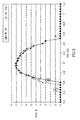
- Fig. 3 illustrates erase voltage and step count of a prior art NROM based memory product, as a function of the number of program/erase operations (cycle count) performed on the device.
- the drain voltage (Vppd) increases up to a certain voltage (e.g., 7.1 V, the maximum allowed value in the specific product shown in the graph), together with an increase of the number of pulses. After reaching the maximum allowed voltage, the voltage level becomes clamped.
- Another option uses large voltage strides between consecutive steps. However, this may result in poor control of the operation. Still another option uses multiple strides. Since charge injection is usually performed for many cells in parallel, the rationale of this option is that large strides can be incorporated until a first cell ensemble reaches a target, followed by smaller strides until the full population is done.
- Another option is that of a learning phase, in which a prior step level ascertained from a previous cell group or erase operation of the same group is implemented on the rest of the array in order to achieve fast convergence.
- Yet another option calls for dialing in the first pulse level during product sort. However, this does not insure a low pulse count over time.
- Another option uses multiple verify levels. This may achieve a faster convergence to the final pulse level, but requires a more intricate design and a longer verify time.
- Another option calls for alternating between the two sides of the cell in the pulse application / verification operations. This approach may result in a twofold improvement in erase performance, but may lead to reduced control.
- Another option uses increased erase parallelism through the reduction of the power consumption.
- erase verification is stopped if sufficient cells fail erasure. Erase verification then continues after applying an additional erase pulse, at the address of the first failure.
- all cells in the erase group must pass several erase verifications, including a penalty of associated word line switching overhead, before the erase operation is completed.
- the present invention seeks to provide methods for erasing bits of memory cells in memory arrays, and for reducing erase pulse and erase verify operations of such arrays.
- the invention is described in detail hereinbelow with reference to memory cells of NVM arrays, and particularly to single bit, dual bit, multi-bit and multi-level NROM cells, wherein erasing generally involves changing the threshold voltage level of a bit to a target threshold level.
- the invention is not limited to NROM arrays.
- the verification and switching time is reduced.
- the abovementioned time penalty of the prior art may be reduced. This may substantially improve product performance.
- a method for erasing memory cells in a memory array including applying an erase pulse to all bits of a cell ensemble of a memory cell array, and performing an erase verification operation only on a subgroup of the cell ensemble being erased to check if the memory cell threshold voltages (Vt) have been lowered to an erase verify (EV) voltage level, and if so, stopping the erase operation on the entire cell ensemble with or without checking the remaining subgroups of the cell ensemble.
- Vt memory cell threshold voltages
- EV erase verify
- the entire cell ensemble may be verified as being erased only after the subgroup has been verified as being erased.
- the subgroup may be verified as being erased to a level lower than the target EV level, in order to insure that the entire cell ensemble has been erased, even though not all the cells have been verified as such.
- the method may further include minimizing verification time overhead.
- performing the erase verification operation may be done after bunching the subgroup to a small number of word lines to further reduce switching overhead.
- a set margin may be increased between a read level and the erase verify level, or between a read level and the erase verify and program verify levels.
- the method may further include applying an erase pulse to a plurality of subgroups of the cell ensemble, but not performing erase verification operations on all of the subgroups.
- the method may further include insuring that a number of bits have passed a set level, and producing a high probability that the entire cell ensemble has been passed erase verification, even though only a subgroup of cells have been physically verified as passing erase verification.
- the method may further include applying extra erase pulses after erase verification has been completed.
- the subgroup of the cell ensemble which is erase verified may be alternated between all the subgroups including the cell ensemble, regularly, periodically or randomly from erase operation to erase operation.
- FIG. 4A is a schematic example of a cell ensemble 10 in a memory array partitioned to subdivisions 12 (by DQ's in this case), and a subgroup 14, containing cells from all subdivisions 12, which will be erased verified (instead of the entire ensemble), as described hereinbelow.
- the ensemble subdivisions 12 and subgroups 14 may take any form.
- Fig. 4B illustrates another example of partitioning cell ensemble 10 to subdivisions. In this example, cell ensemble 10 is subdivided into subdivisions 16 by word lines.
- FIG. 4C illustrates a method for erasing bits of memory cells in a non-volatile memory cell array, in accordance with an embodiment of the present invention.
- An erase pulse may be selected for erasing bits of the cells, comprising selecting ("dialing in") a negative gate voltage (Vg or Vcvpn-voltage from a charge pump) and a positive drain voltage (Vppd) (step 401). Typical non-limititig ranges of values may be Vg from -3V to -7V and Vppd from 3V to 7V over a duration of 100-1000 ⁇ sce.
- the erase pulse may then be applied to bits in a cell ensemble (step 402).
- an erase verification operation is not performed on the entire cell ensemble, but rather only on a subgroup of the cell ensemble being erased (step 403).
- the erase verification operation checks if the threshold voltages (Vt) of the memory cells have been lowered to an erase verify (EV) voltage level or not.
- This subgroup of the cell ensemble may typically include cells from all subdivisions of the memory cell ensemble, which are defined by the architecture implemented, such as physical array slices, which are connected to the different sense amplifiers (referred to as subdivisions DQ's).
- a new Vppd level may be set (dialed in) with a strong (i.e., large) increment (step 404). If any subdivision passed EV, then a new Vppd level may be set with a weak (i.e., relatively smaller) increment (step 405). Erase pulses may be applied to any subdivision of the cell ensemble until all the cells from the subdivision, which are included in the verified subgroup, are verified as erased (passed EV) (step 406). Once all cells in the subgroup are verified as erased, the erase operation is concluded, without checking other subgroups of the cell ensemble (step 407).
- the remaining subgroups may be checked to verify that they are indeed fully erased (step 408).
- the cells of the ensemble may receive an extra erase pulse (step 409) at a higher level than the last pulse used to reach full erasure for improving reliability, as taught, for example, in US Patent 6,700,818 aud US Patent Applications 20050117395 and 20050058005.
- this extra erase pulse is administered to groups of cells according to the subdivision of the cell ensemble - for example to the different DQ's, based on the erase pulse level that caused the cells in this DQ to pass EV (or those cells which were actually verified).
- the number of verify operations may be reduced and the erase operation may be completed faster. Furthermore, if the subgroup is restricted to a few word lines out of the total number of word lines comprising the erased cell ensemble, the switching time overhead (from 0V to the verification gate voltage and back) may also be substantially reduced.
- the subgroup of the cell ensemble which is erase verified may be alternated between all the subgroups including the cell ensemble, regularly, periodically or randomly from erase operation to erase operation.
- Fig. 5 illustrates threshold voltage distributions in subgroups of an NROM array as a function of the subgroup size.
- the example shown in the graph is nearly a uniform case, wherein all cell-to-cell variations are random in nature, and follow a Gaussian distribution.
- This permits cotrelating the erase speed of a subgroup (the conditions required to erase the slowest cell in the group) and the erase speed of the full ensemble. That is, this permits performing erase verify on just a subgroup of the cells without having to do EV on all of the cells.
- EV has not been performed on all of the cells, there is some sort of mismatch between the erase verify that worked for the subgroup as opposed to the rest of the cells, as is now explained.
- Fig. 6A illustrates the statistical distribution of threshold voltages of erased and programmed cells that have been erased and programmed with conventional techniques of the prior art.
- the erased cells may have a Gaussian distribution all of which are below the erase verify level (curve A).
- the programmed cells may have a Gaussian distribution all of which are greater than a program verify level (curve B).
- Fig. 6B illustrates the statistical distribution of threshold voltages of erased cells that have been erased in accordance with the present invention (curve C).
- curve C the statistical distribution of threshold voltages of erased cells that have been erased in accordance with the present invention
- an additional margin may be set in the product's operating window between the EV level and the read level.
- the program verify level may be shifted in order hot to reduce its margin to the read level.
- the extra pulse mechanism (as taught, for example, in US Patent 6,700,818 and US Patent Applications 20050117395 and 300500S8005; or other techniques mentioned in the background) may be set to a more aggressive value to insure all cells are below the erase verify level, i.e. fully erased.
- the subgroup may be bunched to a small number of word lines to further reduce the switching overhead.
- Fig. 8 illustrates threshold voltage distributions of two subgroups of programmed NROM cells from the same array, with an identical history. The distributions show a very high degree of overlap, yet the cells with the lowest threshold voltages, which determine the highest read reference levels that can correctly sense the data content of the cells, are 200mV apart (at 5.45V and 5.65V). Yet, if the level which causes at least eight bits to be sensed incorrectly (in this case programmed bits which are sensed as being erased) is utilized, two subgroups differ by only 50mV (5.65V vs. 5.7V).
Landscapes
- Engineering & Computer Science (AREA)
- Computer Security & Cryptography (AREA)
- Theoretical Computer Science (AREA)
- Physics & Mathematics (AREA)
- General Engineering & Computer Science (AREA)
- General Physics & Mathematics (AREA)
- Computer Hardware Design (AREA)
- Read Only Memory (AREA)
- Non-Volatile Memory (AREA)
- Semiconductor Memories (AREA)
Applications Claiming Priority (1)
| Application Number | Priority Date | Filing Date | Title |
|---|---|---|---|
| US64456905P | 2005-01-19 | 2005-01-19 |
Publications (2)
| Publication Number | Publication Date |
|---|---|
| EP1686592A2 true EP1686592A2 (de) | 2006-08-02 |
| EP1686592A3 EP1686592A3 (de) | 2007-04-25 |
Family
ID=36143177
Family Applications (3)
| Application Number | Title | Priority Date | Filing Date |
|---|---|---|---|
| EP06100507A Withdrawn EP1686592A3 (de) | 2005-01-19 | 2006-01-18 | Teil-Löschüberprüfung |
| EP06100524A Withdrawn EP1684307A1 (de) | 2005-01-19 | 2006-01-18 | Verfahren, Schaltung und System zum Löschen einer oder mehrerer nichtflüchtiger Speicherzellen |
| EP06100526A Withdrawn EP1684308A1 (de) | 2005-01-19 | 2006-01-18 | Verfahren zur Verhinderung von Feststrukturprogrammierung |
Family Applications After (2)
| Application Number | Title | Priority Date | Filing Date |
|---|---|---|---|
| EP06100524A Withdrawn EP1684307A1 (de) | 2005-01-19 | 2006-01-18 | Verfahren, Schaltung und System zum Löschen einer oder mehrerer nichtflüchtiger Speicherzellen |
| EP06100526A Withdrawn EP1684308A1 (de) | 2005-01-19 | 2006-01-18 | Verfahren zur Verhinderung von Feststrukturprogrammierung |
Country Status (4)
| Country | Link |
|---|---|
| US (3) | US7468926B2 (de) |
| EP (3) | EP1686592A3 (de) |
| JP (3) | JP2006228406A (de) |
| CN (3) | CN1838323A (de) |
Families Citing this family (69)
| Publication number | Priority date | Publication date | Assignee | Title |
|---|---|---|---|---|
| US20070103980A1 (en) * | 2005-11-10 | 2007-05-10 | Gert Koebernick | Method for operating a semiconductor memory device and semiconductor memory device |
| US7885112B2 (en) * | 2007-09-07 | 2011-02-08 | Sandisk Corporation | Nonvolatile memory and method for on-chip pseudo-randomization of data within a page and between pages |
| US7606966B2 (en) | 2006-09-08 | 2009-10-20 | Sandisk Corporation | Methods in a pseudo random and command driven bit compensation for the cycling effects in flash memory |
| US7734861B2 (en) * | 2006-09-08 | 2010-06-08 | Sandisk Corporation | Pseudo random and command driven bit compensation for the cycling effects in flash memory |
| EP2070090B1 (de) | 2006-09-08 | 2014-01-08 | SanDisk Technologies Inc. | Pseudozufalls- und befehlsgesteuerte bitkompensation für taktungseffekte in flash-speichern und entsprechende verfahren |
| US7619934B2 (en) * | 2006-12-20 | 2009-11-17 | Spansion Llc | Method and apparatus for adaptive memory cell overerase compensation |
| US8127200B2 (en) | 2006-12-24 | 2012-02-28 | Sandisk Il Ltd. | Flash memory device and system with randomizing for suppressing errors |
| KR101449673B1 (ko) | 2006-12-24 | 2014-10-13 | 샌디스크 아이엘 엘티디 | 에러 억제를 위해 랜더마이징하는 플래시 메모리 디바이스, 시스템 및 방법 |
| US8370561B2 (en) * | 2006-12-24 | 2013-02-05 | Sandisk Il Ltd. | Randomizing for suppressing errors in a flash memory |
| JP4498370B2 (ja) * | 2007-02-14 | 2010-07-07 | 株式会社東芝 | データ書き込み方法 |
| JP2008217857A (ja) | 2007-02-28 | 2008-09-18 | Toshiba Corp | メモリコントローラ及び半導体装置 |
| US8320191B2 (en) | 2007-08-30 | 2012-11-27 | Infineon Technologies Ag | Memory cell arrangement, method for controlling a memory cell, memory array and electronic device |
| US7945050B2 (en) * | 2007-09-28 | 2011-05-17 | Intel Corporation | Suppressing power supply noise using data scrambling in double data rate memory systems |
| US20090150595A1 (en) * | 2007-10-24 | 2009-06-11 | Avi Lavan | Balanced programming rate for memory cells |
| JP4554660B2 (ja) * | 2007-11-01 | 2010-09-29 | 株式会社コナミデジタルエンタテインメント | 記憶処理装置、情報提供サーバ、動作方法、ならびに、プログラム |
| US7843728B2 (en) * | 2007-11-20 | 2010-11-30 | Kabushiki Kaisha Toshiba | Nonvolatile semiconductor storage device |
| US7995392B2 (en) | 2007-12-13 | 2011-08-09 | Kabushiki Kaisha Toshiba | Semiconductor memory device capable of shortening erase time |
| JP2009163782A (ja) * | 2007-12-13 | 2009-07-23 | Toshiba Corp | 半導体記憶装置 |
| JP5019611B2 (ja) * | 2007-12-27 | 2012-09-05 | 株式会社東芝 | メモリシステム |
| US8301912B2 (en) * | 2007-12-31 | 2012-10-30 | Sandisk Technologies Inc. | System, method and memory device providing data scrambling compatible with on-chip copy operation |
| US7813169B2 (en) * | 2008-01-18 | 2010-10-12 | Qimonda Flash Gmbh | Integrated circuit and method to operate an integrated circuit |
| KR101378365B1 (ko) | 2008-03-12 | 2014-03-28 | 삼성전자주식회사 | 하이브리드 메모리 데이터 검출 장치 및 방법 |
| KR101517185B1 (ko) | 2008-04-15 | 2015-05-04 | 삼성전자주식회사 | 메모리 시스템 및 그것의 동작 방법 |
| US8154918B2 (en) * | 2008-06-30 | 2012-04-10 | Sandisk Il Ltd. | Method for page- and block based scrambling in non-volatile memory |
| US8230158B2 (en) | 2008-08-12 | 2012-07-24 | Micron Technology, Inc. | Memory devices and methods of storing data on a memory device |
| US8130552B2 (en) * | 2008-09-11 | 2012-03-06 | Sandisk Technologies Inc. | Multi-pass programming for memory with reduced data storage requirement |
| US8145855B2 (en) | 2008-09-12 | 2012-03-27 | Sandisk Technologies Inc. | Built in on-chip data scrambler for non-volatile memory |
| US8429330B2 (en) | 2008-09-12 | 2013-04-23 | Sandisk Technologies Inc. | Method for scrambling data in which scrambling data and scrambled data are stored in corresponding non-volatile memory locations |
| WO2010030701A1 (en) * | 2008-09-12 | 2010-03-18 | Sandisk Corporation | Built in on-chip data scrambler for non-volatile memory |
| JP5492679B2 (ja) * | 2009-06-30 | 2014-05-14 | パナソニック株式会社 | 記憶装置およびメモリコントローラ |
| US8874825B2 (en) * | 2009-06-30 | 2014-10-28 | Sandisk Technologies Inc. | Storage device and method using parameters based on physical memory block location |
| US8036044B2 (en) * | 2009-07-16 | 2011-10-11 | Sandisk Technologies Inc. | Dynamically adjustable erase and program levels for non-volatile memory |
| KR20110055178A (ko) * | 2009-11-19 | 2011-05-25 | 삼성전자주식회사 | 플래시 메모리 장치 및 그것을 포함한 메모리 시스템 |
| US8130551B2 (en) | 2010-03-31 | 2012-03-06 | Sandisk Technologies Inc. | Extra dummy erase pulses after shallow erase-verify to avoid sensing deep erased threshold voltage |
| KR20120002760A (ko) * | 2010-07-01 | 2012-01-09 | 삼성전자주식회사 | 낸드 플래쉬 메모리의 동작 신뢰성을 향상시키는 데이터 기록 방법 및 데이터 기록 장치 |
| KR101710089B1 (ko) * | 2010-08-26 | 2017-02-24 | 삼성전자주식회사 | 불휘발성 메모리 장치, 그것의 동작 방법, 그리고 그것을 포함하는 메모리 시스템 |
| US8953318B1 (en) * | 2010-09-13 | 2015-02-10 | The Board Of Trustees Of The University Of Alabama, For And On Behalf Of The University Of Alabama In Huntsville | Passive cooling systems and methods for electronics |
| US9009547B2 (en) | 2011-01-27 | 2015-04-14 | Apple Inc. | Advanced programming verification schemes for analog memory cells |
| US9293194B2 (en) | 2011-01-27 | 2016-03-22 | Apple Inc. | Programming and erasure schemes for analog memory cells |
| US8649200B2 (en) | 2011-01-27 | 2014-02-11 | Apple Inc. | Enhanced programming and erasure schemes for analog memory cells |
| KR20120096212A (ko) * | 2011-02-22 | 2012-08-30 | 삼성전자주식회사 | 비휘발성 메모리 장치, 메모리 컨트롤러, 및 이들의 동작 방법 |
| KR101686980B1 (ko) * | 2011-03-02 | 2016-12-16 | 샌디스크 테크놀로지스 엘엘씨 | 비휘발성 메모리 내의 데이터 저장 방법 |
| US8843693B2 (en) | 2011-05-17 | 2014-09-23 | SanDisk Technologies, Inc. | Non-volatile memory and method with improved data scrambling |
| JP6001093B2 (ja) * | 2012-01-24 | 2016-10-05 | アップル インコーポレイテッド | アナログメモリセルのプログラミング及び消去の方式 |
| WO2013112332A1 (en) * | 2012-01-24 | 2013-08-01 | Apple Inc. | Enhanced programming and erasure schemes for analog memory cells |
| US9454493B1 (en) * | 2012-05-04 | 2016-09-27 | Amazon Technologies, Inc. | Systems and methods for wiped storage devices |
| US9317217B1 (en) * | 2012-05-04 | 2016-04-19 | Amazon Technologies, Inc. | Wiping and verifying storage devices |
| KR20130127234A (ko) | 2012-05-14 | 2013-11-22 | 삼성전자주식회사 | 메모리의 구동 방법 |
| US8787088B2 (en) | 2012-06-29 | 2014-07-22 | Sandisk Technologies Inc. | Optimized erase operation for non-volatile memory with partially programmed block |
| US8971125B2 (en) * | 2012-07-02 | 2015-03-03 | Micron Technology, Inc. | Erase operations with erase-verify voltages based on where in the erase operations an erase cycle occurs |
| US9292428B2 (en) | 2012-09-05 | 2016-03-22 | Kabushiki Kaisha Toshiba | Memory system |
| KR101949987B1 (ko) * | 2012-12-18 | 2019-02-20 | 에스케이하이닉스 주식회사 | 데이터 저장 장치 및 그것의 동작 방법 |
| US9214240B2 (en) | 2013-03-04 | 2015-12-15 | Sandisk Technologies Inc. | Dynamic erase depth for improved endurance of non-volatile memory |
| KR102218735B1 (ko) | 2014-01-21 | 2021-02-23 | 삼성전자주식회사 | 불휘발성 메모리 장치를 포함하는 메모리 시스템 및 그것의 소거 방법 |
| CN104882166A (zh) * | 2014-02-27 | 2015-09-02 | 北京兆易创新科技股份有限公司 | Flash存储装置、擦除方法及编程方法 |
| US10409621B2 (en) | 2014-10-20 | 2019-09-10 | Taser International, Inc. | Systems and methods for distributed control |
| US9343171B1 (en) | 2015-02-09 | 2016-05-17 | Sandisk Technologies Inc. | Reduced erase-verify voltage for first-programmed word line in a memory device |
| US9236139B1 (en) | 2015-02-11 | 2016-01-12 | Sandisk Technologies Inc. | Reduced current program verify in non-volatile memory |
| US9343160B1 (en) | 2015-02-11 | 2016-05-17 | Sandisk Technologies Inc. | Erase verify in non-volatile memory |
| US10417122B2 (en) * | 2015-09-30 | 2019-09-17 | Seagate Technology Llc | Data randomization using memory block access counts |
| US10580506B2 (en) | 2017-12-07 | 2020-03-03 | Micron Technology, Inc. | Semiconductor memory device and erase method including changing erase pulse magnitude for a memory array |
| US10535412B2 (en) | 2018-02-09 | 2020-01-14 | Sandisk Technologies Llc | Single pulse verification of memory cells |
| CN110838329B (zh) * | 2018-08-17 | 2022-04-01 | 北京兆易创新科技股份有限公司 | 一种存储器的擦除方法和系统 |
| JP7163210B2 (ja) * | 2019-02-13 | 2022-10-31 | キオクシア株式会社 | 半導体記憶装置、メモリシステム及び不良検出方法 |
| JP2020149745A (ja) | 2019-03-13 | 2020-09-17 | キオクシア株式会社 | 半導体記憶装置 |
| US20210303715A1 (en) * | 2020-03-25 | 2021-09-30 | SK Hynix Inc. | Data scrambler for memory systems and method thereof |
| US12153801B2 (en) | 2022-07-26 | 2024-11-26 | Sandisk Technologies Llc | Non-volatile memory with optimized operation sequence |
| US12087373B2 (en) | 2022-07-26 | 2024-09-10 | Sandisk Technologies Llc | Non-volatile memory with optimized erase verify sequence |
| US20240419339A1 (en) * | 2023-06-14 | 2024-12-19 | Winbond Electronics Corp. | Erase method for non-volatile memory device and non-volatile memory device using the same |
Family Cites Families (640)
| Publication number | Priority date | Publication date | Assignee | Title |
|---|---|---|---|---|
| GB1297899A (de) | 1970-10-02 | 1972-11-29 | ||
| GB1392599A (en) | 1971-07-28 | 1975-04-30 | Mullard Ltd | Semiconductor memory elements |
| US3881180A (en) | 1971-11-30 | 1975-04-29 | Texas Instruments Inc | Non-volatile memory cell |
| US3895360A (en) | 1974-01-29 | 1975-07-15 | Westinghouse Electric Corp | Block oriented random access memory |
| US4016588A (en) | 1974-12-27 | 1977-04-05 | Nippon Electric Company, Ltd. | Non-volatile semiconductor memory device |
| US4017888A (en) | 1975-12-31 | 1977-04-12 | International Business Machines Corporation | Non-volatile metal nitride oxide semiconductor device |
| US4151021A (en) | 1977-01-26 | 1979-04-24 | Texas Instruments Incorporated | Method of making a high density floating gate electrically programmable ROM |
| US4145703A (en) | 1977-04-15 | 1979-03-20 | Supertex, Inc. | High power MOS device and fabrication method therefor |
| US4173766A (en) | 1977-09-16 | 1979-11-06 | Fairchild Camera And Instrument Corporation | Insulated gate field-effect transistor read-only memory cell |
| US4173791A (en) | 1977-09-16 | 1979-11-06 | Fairchild Camera And Instrument Corporation | Insulated gate field-effect transistor read-only memory array |
| JPS5453929U (de) | 1977-09-21 | 1979-04-14 | ||
| US4373248A (en) * | 1978-07-12 | 1983-02-15 | Texas Instruments Incorporated | Method of making high density semiconductor device such as floating gate electrically programmable ROM or the like |
| DE2832388C2 (de) * | 1978-07-24 | 1986-08-14 | Siemens Ag, 1000 Berlin Und 8000 Muenchen | Verfahren zum Herstellen von MNOS- und MOS-Transistoren in Silizium-Gate-Technologie auf einem Halbleitersubstrat |
| US4360900A (en) | 1978-11-27 | 1982-11-23 | Texas Instruments Incorporated | Non-volatile semiconductor memory elements |
| US4247861A (en) | 1979-03-09 | 1981-01-27 | Rca Corporation | High performance electrically alterable read-only memory (EAROM) |
| DE2923995C2 (de) | 1979-06-13 | 1985-11-07 | Siemens AG, 1000 Berlin und 8000 München | Verfahren zum Herstellen von integrierten MOS-Schaltungen mit MOS-Transistoren und MNOS-Speichertransistoren in Silizium-Gate-Technologie |
| JPS56501146A (de) | 1979-09-13 | 1981-08-13 | ||
| JPS5656677A (en) | 1979-10-13 | 1981-05-18 | Toshiba Corp | Semiconductor memory device |
| US4281397A (en) | 1979-10-29 | 1981-07-28 | Texas Instruments Incorporated | Virtual ground MOS EPROM or ROM matrix |
| DE2947350A1 (de) | 1979-11-23 | 1981-05-27 | Siemens AG, 1000 Berlin und 8000 München | Verfahren zum herstellen von mnos-speichertransistoren mit sehr kurzer kanallaenge in silizium-gate-technologie |
| JPS56120166A (en) | 1980-02-27 | 1981-09-21 | Hitachi Ltd | Semiconductor ic device and manufacture thereof |
| US4342102A (en) | 1980-06-18 | 1982-07-27 | Signetics Corporation | Semiconductor memory array |
| US4380057A (en) | 1980-10-27 | 1983-04-12 | International Business Machines Corporation | Electrically alterable double dense memory |
| US4521796A (en) | 1980-12-11 | 1985-06-04 | General Instrument Corporation | Memory implant profile for improved channel shielding in electrically alterable read only memory semiconductor device |
| EP0056195B1 (de) | 1980-12-25 | 1986-06-18 | Fujitsu Limited | Nichtflüchtiger Halbleiterspeicher |
| US4448400A (en) | 1981-07-13 | 1984-05-15 | Eliyahou Harari | Highly scalable dynamic RAM cell with self-signal amplification |
| US4404747A (en) | 1981-07-29 | 1983-09-20 | Schur, Inc. | Knife and sheath assembly |
| US4389705A (en) | 1981-08-21 | 1983-06-21 | Mostek Corporation | Semiconductor memory circuit with depletion data transfer transistor |
| US4388705A (en) | 1981-10-01 | 1983-06-14 | Mostek Corporation | Semiconductor memory circuit |
| US4435786A (en) | 1981-11-23 | 1984-03-06 | Fairchild Camera And Instrument Corporation | Self-refreshing memory cell |
| US4494016A (en) | 1982-07-26 | 1985-01-15 | Sperry Corporation | High performance MESFET transistor for VLSI implementation |
| US4527257A (en) | 1982-08-25 | 1985-07-02 | Westinghouse Electric Corp. | Common memory gate non-volatile transistor memory |
| JPS5949022A (ja) | 1982-09-13 | 1984-03-21 | Toshiba Corp | 多値論理回路 |
| US4613956A (en) | 1983-02-23 | 1986-09-23 | Texas Instruments Incorporated | Floating gate memory with improved dielectric |
| JPS59174080A (ja) * | 1983-03-24 | 1984-10-02 | Sony Corp | テレビジヨン信号受信装置 |
| US4769340A (en) | 1983-11-28 | 1988-09-06 | Exel Microelectronics, Inc. | Method for making electrically programmable memory device by doping the floating gate by implant |
| US4725984A (en) | 1984-02-21 | 1988-02-16 | Seeq Technology, Inc. | CMOS eprom sense amplifier |
| JPS60182174A (ja) | 1984-02-28 | 1985-09-17 | Nec Corp | 不揮発性半導体メモリ |
| GB2157489A (en) | 1984-03-23 | 1985-10-23 | Hitachi Ltd | A semiconductor integrated circuit memory device |
| JPS60201594A (ja) | 1984-03-23 | 1985-10-12 | Hitachi Micro Comput Eng Ltd | 半導体記憶装置 |
| JPS60200566A (ja) | 1984-03-26 | 1985-10-11 | Hitachi Ltd | 半導体集積回路装置 |
| US5352620A (en) | 1984-05-23 | 1994-10-04 | Hitachi, Ltd. | Method of making semiconductor device with memory cells and peripheral transistors |
| KR930007195B1 (ko) | 1984-05-23 | 1993-07-31 | 가부시끼가이샤 히다찌세이사꾸쇼 | 반도체 장치와 그 제조 방법 |
| US4908834A (en) * | 1984-10-12 | 1990-03-13 | Wiedemer John D | High security pay television system |
| US4907273A (en) * | 1984-10-12 | 1990-03-06 | Wiedemer John D | High security pay television system |
| US4665426A (en) | 1985-02-01 | 1987-05-12 | Advanced Micro Devices, Inc. | EPROM with ultraviolet radiation transparent silicon nitride passivation layer |
| DE3684351D1 (de) | 1985-04-18 | 1992-04-23 | Nec Corp | Programmierbarer festwertspeicher mit reduzierter programmierspeisespannung. |
| US4667217A (en) | 1985-04-19 | 1987-05-19 | Ncr Corporation | Two bit vertically/horizontally integrated memory cell |
| JPH0831789B2 (ja) | 1985-09-04 | 1996-03-27 | 沖電気工業株式会社 | 出力回路 |
| US4742491A (en) | 1985-09-26 | 1988-05-03 | Advanced Micro Devices, Inc. | Memory cell having hot-hole injection erase mode |
| US4760555A (en) | 1986-04-21 | 1988-07-26 | Texas Instruments Incorporated | Memory array with an array reorganizer |
| JPH0828431B2 (ja) | 1986-04-22 | 1996-03-21 | 日本電気株式会社 | 半導体記憶装置 |
| JPH0521758Y2 (de) | 1986-05-19 | 1993-06-03 | ||
| US4758869A (en) | 1986-08-29 | 1988-07-19 | Waferscale Integration, Inc. | Nonvolatile floating gate transistor structure |
| JPS63249375A (ja) | 1987-04-06 | 1988-10-17 | Oki Electric Ind Co Ltd | 半導体記憶装置のデ−タ消去方法 |
| US5168334A (en) | 1987-07-31 | 1992-12-01 | Texas Instruments, Incorporated | Non-volatile semiconductor memory |
| US4780424A (en) | 1987-09-28 | 1988-10-25 | Intel Corporation | Process for fabricating electrically alterable floating gate memory devices |
| US4870470A (en) | 1987-10-16 | 1989-09-26 | International Business Machines Corporation | Non-volatile memory cell having Si rich silicon nitride charge trapping layer |
| US4839705A (en) | 1987-12-16 | 1989-06-13 | Texas Instruments Incorporated | X-cell EEPROM array |
| JPH07120720B2 (ja) | 1987-12-17 | 1995-12-20 | 三菱電機株式会社 | 不揮発性半導体記憶装置 |
| US5159570A (en) | 1987-12-22 | 1992-10-27 | Texas Instruments Incorporated | Four memory state EEPROM |
| US4888735A (en) | 1987-12-30 | 1989-12-19 | Elite Semiconductor & Systems Int'l., Inc. | ROM cell and array configuration |
| US5677867A (en) | 1991-06-12 | 1997-10-14 | Hazani; Emanuel | Memory with isolatable expandable bit lines |
| US4857770A (en) | 1988-02-29 | 1989-08-15 | Advanced Micro Devices, Inc. | Output buffer arrangement for reducing chip noise without speed penalty |
| US5268870A (en) | 1988-06-08 | 1993-12-07 | Eliyahou Harari | Flash EEPROM system and intelligent programming and erasing methods therefor |
| US4941028A (en) | 1988-08-10 | 1990-07-10 | Actel Corporation | Structure for protecting thin dielectrics during processing |
| JPH0271493A (ja) | 1988-09-06 | 1990-03-12 | Mitsubishi Electric Corp | 半導体メモリ装置 |
| US5042009A (en) | 1988-12-09 | 1991-08-20 | Waferscale Integration, Inc. | Method for programming a floating gate memory device |
| US5293563A (en) | 1988-12-29 | 1994-03-08 | Sharp Kabushiki Kaisha | Multi-level memory cell with increased read-out margin |
| US5844842A (en) | 1989-02-06 | 1998-12-01 | Hitachi, Ltd. | Nonvolatile semiconductor memory device |
| US5120672A (en) | 1989-02-22 | 1992-06-09 | Texas Instruments Incorporated | Fabricating a single level merged EEPROM cell having an ONO memory stack substantially spaced from the source region |
| US5142495A (en) | 1989-03-10 | 1992-08-25 | Intel Corporation | Variable load for margin mode |
| DE3931596A1 (de) | 1989-03-25 | 1990-10-04 | Eurosil Electronic Gmbh | Spannungsvervielfacherschaltung |
| DE69024086T2 (de) | 1989-04-13 | 1996-06-20 | Sundisk Corp | EEprom-System mit Blocklöschung |
| US5172338B1 (en) | 1989-04-13 | 1997-07-08 | Sandisk Corp | Multi-state eeprom read and write circuits and techniques |
| US4961010A (en) | 1989-05-19 | 1990-10-02 | National Semiconductor Corporation | Output buffer for reducing switching induced noise |
| US5104819A (en) | 1989-08-07 | 1992-04-14 | Intel Corporation | Fabrication of interpoly dielctric for EPROM-related technologies |
| US5081675A (en) * | 1989-11-13 | 1992-01-14 | Kitti Kittirutsunetorn | System for protection of software in memory against unauthorized use |
| US5027321A (en) | 1989-11-21 | 1991-06-25 | Intel Corporation | Apparatus and method for improved reading/programming of virtual ground EPROM arrays |
| US4992391A (en) | 1989-11-29 | 1991-02-12 | Advanced Micro Devices, Inc. | Process for fabricating a control gate for a floating gate FET |
| KR100199258B1 (ko) | 1990-02-09 | 1999-06-15 | 가나이 쓰도무 | 반도체집적회로장치 |
| JP2733796B2 (ja) | 1990-02-13 | 1998-03-30 | セイコーインスツルメンツ株式会社 | スイッチ回路 |
| JP2697231B2 (ja) * | 1990-03-12 | 1998-01-14 | 松下電器産業株式会社 | Catvシステム |
| JP2672688B2 (ja) | 1990-04-02 | 1997-11-05 | 松下電子工業株式会社 | 不揮発性半導体記憶装置の駆動方法 |
| JPH043395A (ja) * | 1990-04-20 | 1992-01-08 | Mitsubishi Electric Corp | 不揮発性半導体記憶装置 |
| JPH04226071A (ja) | 1990-05-16 | 1992-08-14 | Ricoh Co Ltd | 半導体メモリ装置 |
| US5204835A (en) | 1990-06-13 | 1993-04-20 | Waferscale Integration Inc. | Eprom virtual ground array |
| EP0461904A3 (en) | 1990-06-14 | 1992-09-09 | Creative Integrated Systems, Inc. | An improved semiconductor read-only vlsi memory |
| US5075245A (en) | 1990-08-03 | 1991-12-24 | Intel Corporation | Method for improving erase characteristics of buried bit line flash EPROM devices without using sacrificial oxide growth and removal steps |
| US5091938B1 (en) * | 1990-08-06 | 1997-02-04 | Nippon Denki Home Electronics | Digital data cryptographic system |
| US5289406A (en) * | 1990-08-28 | 1994-02-22 | Mitsubishi Denki Kabushiki Kaisha | Read only memory for storing multi-data |
| US5117389A (en) | 1990-09-05 | 1992-05-26 | Macronix International Co., Ltd. | Flat-cell read-only-memory integrated circuit |
| KR920006991A (ko) | 1990-09-25 | 1992-04-28 | 김광호 | 반도체메모리 장치의 고전압발생회로 |
| US5081371A (en) | 1990-11-07 | 1992-01-14 | U.S. Philips Corp. | Integrated charge pump circuit with back bias voltage reduction |
| JP3002309B2 (ja) | 1990-11-13 | 2000-01-24 | ウエハスケール インテグレーション, インコーポレイテッド | 高速epromアレイ |
| JP2987193B2 (ja) | 1990-11-20 | 1999-12-06 | 富士通株式会社 | 半導体記憶装置 |
| US5086325A (en) * | 1990-11-21 | 1992-02-04 | Atmel Corporation | Narrow width EEPROM with single diffusion electrode formation |
| US5094968A (en) * | 1990-11-21 | 1992-03-10 | Atmel Corporation | Fabricating a narrow width EEPROM with single diffusion electrode formation |
| US5218569A (en) | 1991-02-08 | 1993-06-08 | Banks Gerald J | Electrically alterable non-volatile memory with n-bits per memory cell |
| JP2612969B2 (ja) | 1991-02-08 | 1997-05-21 | シャープ株式会社 | 半導体装置の製造方法 |
| US6002614A (en) | 1991-02-08 | 1999-12-14 | Btg International Inc. | Memory apparatus including programmable non-volatile multi-bit memory cell, and apparatus and method for demarcating memory states of the cell |
| US5270979A (en) * | 1991-03-15 | 1993-12-14 | Sundisk Corporation | Method for optimum erasing of EEPROM |
| JPH04291962A (ja) | 1991-03-20 | 1992-10-16 | Fujitsu Ltd | マスクromの製造方法とマスクrom |
| JPH04311900A (ja) | 1991-04-10 | 1992-11-04 | Sharp Corp | 半導体読み出し専用メモリ |
| JP2930440B2 (ja) | 1991-04-15 | 1999-08-03 | 沖電気工業株式会社 | 半導体集積回路 |
| US5424567A (en) | 1991-05-15 | 1995-06-13 | North American Philips Corporation | Protected programmable transistor with reduced parasitic capacitances and method of fabrication |
| US5142496A (en) | 1991-06-03 | 1992-08-25 | Advanced Micro Devices, Inc. | Method for measuring VT 's less than zero without applying negative voltages |
| US5245572A (en) | 1991-07-30 | 1993-09-14 | Intel Corporation | Floating gate nonvolatile memory with reading while writing capability |
| JP2965415B2 (ja) | 1991-08-27 | 1999-10-18 | 松下電器産業株式会社 | 半導体記憶装置 |
| DK0740854T3 (da) | 1991-08-29 | 2003-08-18 | Hyundai Electronics Ind | Automatisk justeret dual-bit split gate (DSG) flash EEPROM celle |
| KR960013022B1 (ko) | 1991-09-11 | 1996-09-25 | 가와사끼 세이데쯔 가부시끼가이샤 | 반도체 집적회로 |
| US5175120A (en) | 1991-10-11 | 1992-12-29 | Micron Technology, Inc. | Method of processing a semiconductor wafer to form an array of nonvolatile memory devices employing floating gate transistors and peripheral area having CMOS transistors |
| JPH05110114A (ja) | 1991-10-17 | 1993-04-30 | Rohm Co Ltd | 不揮発性半導体記憶素子 |
| US5355178A (en) * | 1991-10-24 | 1994-10-11 | Eastman Kodak Company | Mechanism for improving television display of still images using image motion-dependent filter |
| JP3358663B2 (ja) | 1991-10-25 | 2002-12-24 | ローム株式会社 | 半導体記憶装置およびその記憶情報読出方法 |
| US5428568A (en) * | 1991-10-30 | 1995-06-27 | Mitsubishi Denki Kabushiki Kaisha | Electrically erasable and programmable non-volatile memory device and a method of operating the same |
| US5338954A (en) | 1991-10-31 | 1994-08-16 | Rohm Co., Ltd. | Semiconductor memory device having an insulating film and a trap film joined in a channel region |
| US5357134A (en) | 1991-10-31 | 1994-10-18 | Rohm Co., Ltd. | Nonvolatile semiconductor device having charge trap film containing silicon crystal grains |
| JPH05129284A (ja) | 1991-11-06 | 1993-05-25 | Sony Corp | プラズマSiN成膜条件の設定方法及び半導体装置の製造方法 |
| US5260593A (en) | 1991-12-10 | 1993-11-09 | Micron Technology, Inc. | Semiconductor floating gate device having improved channel-floating gate interaction |
| KR960000619B1 (ko) | 1991-12-27 | 1996-01-10 | 후지쓰 가부시끼가이샤 | 일괄소거형의 불휘발성 반도체 기억장치 및 그의 구동제어회로 |
| JP2564067B2 (ja) | 1992-01-09 | 1996-12-18 | 株式会社東芝 | センス回路を有する読み出し出力回路 |
| US6222762B1 (en) * | 1992-01-14 | 2001-04-24 | Sandisk Corporation | Multi-state memory |
| US5293328A (en) * | 1992-01-15 | 1994-03-08 | National Semiconductor Corporation | Electrically reprogrammable EPROM cell with merged transistor and optiumum area |
| US5654568A (en) | 1992-01-17 | 1997-08-05 | Rohm Co., Ltd. | Semiconductor device including nonvolatile memories |
| JP2851962B2 (ja) | 1992-01-21 | 1999-01-27 | シャープ株式会社 | 半導体読み出し専用メモリ |
| EP0552531B1 (de) * | 1992-01-22 | 2000-08-16 | Macronix International Co., Ltd. | Nichtflüchtige Speicherzelle und Anordnungsarchitektur |
| US5324675A (en) | 1992-03-31 | 1994-06-28 | Kawasaki Steel Corporation | Method of producing semiconductor devices of a MONOS type |
| JPH05290584A (ja) * | 1992-04-08 | 1993-11-05 | Nec Corp | 半導体記憶装置 |
| US5557221A (en) | 1992-06-15 | 1996-09-17 | Fujitsu Limited | Semiconductor integrated circuit with input/output interface adapted for small-amplitude operation |
| US5657332A (en) | 1992-05-20 | 1997-08-12 | Sandisk Corporation | Soft errors handling in EEPROM devices |
| JP3472313B2 (ja) | 1992-05-25 | 2003-12-02 | ローム株式会社 | 不揮発性記憶装置 |
| JP2904645B2 (ja) | 1992-05-28 | 1999-06-14 | 株式会社東芝 | 不揮発性半導体メモリ |
| US5496753A (en) | 1992-05-29 | 1996-03-05 | Citizen Watch, Co., Ltd. | Method of fabricating a semiconductor nonvolatile storage device |
| JPH065823A (ja) | 1992-06-19 | 1994-01-14 | Toshiba Corp | 不揮発性半導体記憶装置及びその使用方法 |
| US5289412A (en) * | 1992-06-19 | 1994-02-22 | Intel Corporation | High-speed bias-stabilized current-mirror referencing circuit for non-volatile memories |
| EP0596198B1 (de) * | 1992-07-10 | 2000-03-29 | Sony Corporation | Flash-EPROM mit Löschprüfung und Architektur zum Adresszerhacken |
| US5315541A (en) | 1992-07-24 | 1994-05-24 | Sundisk Corporation | Segmented column memory array |
| GB9217743D0 (en) | 1992-08-19 | 1992-09-30 | Philips Electronics Uk Ltd | A semiconductor memory device |
| JP3036565B2 (ja) | 1992-08-28 | 2000-04-24 | 日本電気株式会社 | 不揮発性半導体記憶装置の製造方法 |
| US5450354A (en) | 1992-08-31 | 1995-09-12 | Nippon Steel Corporation | Non-volatile semiconductor memory device detachable deterioration of memory cells |
| US5450341A (en) | 1992-08-31 | 1995-09-12 | Nippon Steel Corporation | Non-volatile semiconductor memory device having memory cells, each for at least three different data writable thereinto selectively and a method of using the same |
| US5412601A (en) | 1992-08-31 | 1995-05-02 | Nippon Steel Corporation | Non-volatile semiconductor memory device capable of storing multi-value data in each memory cell |
| US5412238A (en) | 1992-09-08 | 1995-05-02 | National Semiconductor Corporation | Source-coupling, split-gate, virtual ground flash EEPROM array |
| US5428621A (en) | 1992-09-21 | 1995-06-27 | Sundisk Corporation | Latent defect handling in EEPROM devices |
| US5280420A (en) * | 1992-10-02 | 1994-01-18 | National Semiconductor Corporation | Charge pump which operates on a low voltage power supply |
| JP2825217B2 (ja) * | 1992-11-11 | 1998-11-18 | シャープ株式会社 | フラッシュメモリ |
| JPH06151833A (ja) | 1992-11-16 | 1994-05-31 | Mitsubishi Electric Corp | 半導体装置およびその製造方法 |
| US5579199A (en) | 1992-11-26 | 1996-11-26 | Sharp Kabushiki Kaisha | Non-volatile memory device and a method for producing the same |
| US5377153A (en) | 1992-11-30 | 1994-12-27 | Sgs-Thomson Microelectronics, Inc. | Virtual ground read only memory circuit |
| US5418743A (en) | 1992-12-07 | 1995-05-23 | Nippon Steel Corporation | Method of writing into non-volatile semiconductor memory |
| US5319593A (en) | 1992-12-21 | 1994-06-07 | National Semiconductor Corp. | Memory array with field oxide islands eliminated and method |
| JPH07114792A (ja) | 1993-10-19 | 1995-05-02 | Mitsubishi Electric Corp | 半導体記憶装置 |
| US5436481A (en) | 1993-01-21 | 1995-07-25 | Nippon Steel Corporation | MOS-type semiconductor device and method of making the same |
| WO1994018703A1 (en) | 1993-02-01 | 1994-08-18 | National Semiconductor Corporation | Ultra-high-density alternate metal virtual ground rom |
| JPH06232416A (ja) | 1993-02-03 | 1994-08-19 | Rohm Co Ltd | 半導体記憶装置およびその製法 |
| US5515173A (en) * | 1993-03-05 | 1996-05-07 | Gemstar Developement Corporation | System and method for automatically recording television programs in television systems with tuners external to video recorders |
| US5424978A (en) | 1993-03-15 | 1995-06-13 | Nippon Steel Corporation | Non-volatile semiconductor memory cell capable of storing more than two different data and method of using the same |
| US5393701A (en) | 1993-04-08 | 1995-02-28 | United Microelectronics Corporation | Layout design to eliminate process antenna effect |
| DE9305576U1 (de) | 1993-04-14 | 1993-07-08 | Holzrichter, Dieter, Dr.med., 2000 Hamburg | Datenaufzeichnungsgerät |
| JP3317459B2 (ja) | 1993-04-30 | 2002-08-26 | ローム株式会社 | 不揮発性記憶素子およびこれを利用した不揮発性記憶装置、この記憶装置の駆動方法、ならびにこの記憶素子の製造方法 |
| US5335198A (en) | 1993-05-06 | 1994-08-02 | Advanced Micro Devices, Inc. | Flash EEPROM array with high endurance |
| US5463586A (en) | 1993-05-28 | 1995-10-31 | Macronix International Co., Ltd. | Erase and program verification circuit for non-volatile memory |
| JP3156447B2 (ja) | 1993-06-17 | 2001-04-16 | 富士通株式会社 | 半導体集積回路 |
| EP0631369A1 (de) | 1993-06-21 | 1994-12-28 | STMicroelectronics S.r.l. | Spannungsvervielfacher mit hohem Ausgangsstrom und stabilisierter Ausgangsspannung |
| US5350710A (en) | 1993-06-24 | 1994-09-27 | United Microelectronics Corporation | Device for preventing antenna effect on circuit |
| US5400286A (en) * | 1993-08-17 | 1995-03-21 | Catalyst Semiconductor Corp. | Self-recovering erase scheme to enhance flash memory endurance |
| JP3463030B2 (ja) | 1993-08-27 | 2003-11-05 | 株式会社東芝 | 不揮発性半導体記憶装置 |
| US5563823A (en) | 1993-08-31 | 1996-10-08 | Macronix International Co., Ltd. | Fast FLASH EPROM programming and pre-programming circuit design |
| US5553030A (en) | 1993-09-10 | 1996-09-03 | Intel Corporation | Method and apparatus for controlling the output voltage provided by a charge pump circuit |
| US5477499A (en) | 1993-10-13 | 1995-12-19 | Advanced Micro Devices, Inc. | Memory architecture for a three volt flash EEPROM |
| US5828601A (en) | 1993-12-01 | 1998-10-27 | Advanced Micro Devices, Inc. | Programmed reference |
| JP3076185B2 (ja) | 1993-12-07 | 2000-08-14 | 日本電気株式会社 | 半導体メモリ装置及びその検査方法 |
| US5666516A (en) * | 1993-12-16 | 1997-09-09 | International Business Machines Corporation | Protected programmable memory cartridge having selective access circuitry |
| JPH07193151A (ja) | 1993-12-27 | 1995-07-28 | Toshiba Corp | 不揮発性半導体記憶装置及びその記憶方法 |
| US5440505A (en) | 1994-01-21 | 1995-08-08 | Intel Corporation | Method and circuitry for storing discrete amounts of charge in a single memory element |
| FR2715782B1 (fr) | 1994-01-31 | 1996-03-22 | Sgs Thomson Microelectronics | Bascule bistable non volatile programmable, à état initial prédéfini, notamment pour circuit de redondance de mémoire. |
| FR2715758B1 (fr) * | 1994-01-31 | 1996-03-22 | Sgs Thomson Microelectronics | Bascule bistable non volatile programmable par la source, notamment pour circuit de redondance de mémoire. |
| JP3397427B2 (ja) | 1994-02-02 | 2003-04-14 | 株式会社東芝 | 半導体記憶装置 |
| US6005423A (en) | 1994-02-10 | 1999-12-21 | Xilinx, Inc. | Low current power-on reset circuit |
| US5418176A (en) | 1994-02-17 | 1995-05-23 | United Microelectronics Corporation | Process for producing memory devices having narrow buried N+ lines |
| CN1057171C (zh) | 1994-03-03 | 2000-10-04 | 罗姆有限公司 | 低压晶体管闪速电可擦可编程只读存储器单元 |
| US5436478A (en) | 1994-03-16 | 1995-07-25 | National Semiconductor Corporation | Fast access AMG EPROM with segment select transistors which have an increased width |
| DE69424771T2 (de) | 1994-03-22 | 2000-10-26 | Stmicroelectronics S.R.L., Agrate Brianza | Anordnung zum Lesen einer Speicherzellenmatrix |
| US5467308A (en) | 1994-04-05 | 1995-11-14 | Motorola Inc. | Cross-point eeprom memory array |
| US5530803A (en) | 1994-04-14 | 1996-06-25 | Advanced Micro Devices, Inc. | Method and apparatus for programming memory devices |
| US5568085A (en) | 1994-05-16 | 1996-10-22 | Waferscale Integration Inc. | Unit for stabilizing voltage on a capacitive node |
| TW241394B (en) * | 1994-05-26 | 1995-02-21 | Aplus Integrated Circuits Inc | Flat-cell ROM and decoder |
| US5608679A (en) | 1994-06-02 | 1997-03-04 | Intel Corporation | Fast internal reference cell trimming for flash EEPROM memory |
| JP3725911B2 (ja) | 1994-06-02 | 2005-12-14 | 株式会社ルネサステクノロジ | 半導体装置 |
| US5523972A (en) | 1994-06-02 | 1996-06-04 | Intel Corporation | Method and apparatus for verifying the programming of multi-level flash EEPROM memory |
| EP0691729A3 (de) | 1994-06-30 | 1996-08-14 | Sgs Thomson Microelectronics | Ladungspumpenschaltung mit Rückkopplungssteuerung |
| EP0693781B1 (de) | 1994-07-13 | 2002-10-02 | United Microelectronics Corporation | Erdungsverfahren zur Eliminierung des Antenneneffekts während der Fabrikation |
| DE69413960T2 (de) * | 1994-07-18 | 1999-04-01 | Stmicroelectronics S.R.L., Agrate Brianza, Mailand/Milano | Nicht-flüchtiger EPROM und Flash-EEPROM-Speicher und Verfahren zu seiner Herstellung |
| JP3197168B2 (ja) | 1994-10-03 | 2001-08-13 | 松下電器産業株式会社 | 半導体記憶装置の駆動方法 |
| US5508968A (en) | 1994-08-12 | 1996-04-16 | International Business Machines Corporation | Dynamic random access memory persistent page implemented as processor register sets |
| US5822256A (en) | 1994-09-06 | 1998-10-13 | Intel Corporation | Method and circuitry for usage of partially functional nonvolatile memory |
| KR100372905B1 (ko) | 1994-09-13 | 2003-05-01 | 애질런트 테크놀로지스, 인크. | 산화물영역보호장치 |
| US5583808A (en) | 1994-09-16 | 1996-12-10 | National Semiconductor Corporation | EPROM array segmented for high performance and method for controlling same |
| JP3730272B2 (ja) | 1994-09-17 | 2005-12-21 | 株式会社東芝 | 不揮発性半導体記憶装置 |
| DE4434725C1 (de) | 1994-09-28 | 1996-05-30 | Siemens Ag | Festwert-Speicherzellenanordnung und Verfahren zu deren Herstellung |
| US5619052A (en) | 1994-09-29 | 1997-04-08 | Macronix International Co., Ltd. | Interpoly dielectric structure in EEPROM device |
| US5523251A (en) | 1994-10-05 | 1996-06-04 | United Microelectronics Corp. | Method for fabricating a self aligned mask ROM |
| US5612642A (en) | 1995-04-28 | 1997-03-18 | Altera Corporation | Power-on reset circuit with hysteresis |
| US5581252A (en) | 1994-10-13 | 1996-12-03 | Linear Technology Corporation | Analog-to-digital conversion using comparator coupled capacitor digital-to-analog converters |
| JPH08115597A (ja) * | 1994-10-17 | 1996-05-07 | Mitsubishi Electric Corp | 半導体ディスク装置 |
| JPH08124395A (ja) | 1994-10-25 | 1996-05-17 | Nkk Corp | メモリ装置 |
| US5694356A (en) | 1994-11-02 | 1997-12-02 | Invoice Technology, Inc. | High resolution analog storage EPROM and flash EPROM |
| WO1996015553A1 (en) | 1994-11-15 | 1996-05-23 | Advanced Micro Devices, Inc. | Transistor structure with specific gate and pad areas |
| US5537358A (en) | 1994-12-06 | 1996-07-16 | National Semiconductor Corporation | Flash memory having adaptive sensing and method |
| US5561714A (en) * | 1994-12-12 | 1996-10-01 | Tektronix, Inc. | Scrambling system for serial digital video |
| US5599727A (en) | 1994-12-15 | 1997-02-04 | Sharp Kabushiki Kaisha | Method for producing a floating gate memory device including implanting ions through an oxidized portion of the silicon film from which the floating gate is formed |
| JP4183290B2 (ja) * | 1994-12-27 | 2008-11-19 | マクロニクス インターナショナル カンパニイ リミテッド | ベリファイ機能を備えた不揮発性半導体装置 |
| US5661060A (en) | 1994-12-28 | 1997-08-26 | National Semiconductor Corporation | Method for forming field oxide regions |
| KR100478172B1 (ko) * | 1995-01-31 | 2005-03-23 | 가부시끼가이샤 히다치 세이사꾸쇼 | 반도체 메모리 장치 |
| US5534804A (en) | 1995-02-13 | 1996-07-09 | Advanced Micro Devices, Inc. | CMOS power-on reset circuit using hysteresis |
| CA2142644C (en) | 1995-02-16 | 1996-11-26 | Marc Etienne Bonneville | Standby power circuit arrangement |
| DE19505293A1 (de) | 1995-02-16 | 1996-08-22 | Siemens Ag | Mehrwertige Festwertspeicherzelle mit verbessertem Störabstand |
| US5801076A (en) | 1995-02-21 | 1998-09-01 | Advanced Micro Devices, Inc. | Method of making non-volatile memory device having a floating gate with enhanced charge retention |
| US5518942A (en) * | 1995-02-22 | 1996-05-21 | Alliance Semiconductor Corporation | Method of making flash EPROM cell having improved erase characteristics by using a tilt angle implant |
| US6353554B1 (en) | 1995-02-27 | 2002-03-05 | Btg International Inc. | Memory apparatus including programmable non-volatile multi-bit memory cell, and apparatus and method for demarcating memory states of the cell |
| US5666365A (en) | 1995-03-16 | 1997-09-09 | Bell Atlantic Network Services, Inc. | Simulcast transmission of digital programs to shared antenna receiving systems |
| US5617357A (en) | 1995-04-07 | 1997-04-01 | Advanced Micro Devices, Inc. | Flash EEPROM memory with improved discharge speed using substrate bias and method therefor |
| JP3511732B2 (ja) | 1995-04-27 | 2004-03-29 | ソニー株式会社 | 半導体不揮発性記憶装置 |
| JPH08306196A (ja) * | 1995-04-28 | 1996-11-22 | Toshiba Corp | 不揮発性半導体記憶装置 |
| DE69524572T2 (de) | 1995-04-28 | 2002-08-22 | Stmicroelectronics S.R.L., Agrate Brianza | Leseverstärkerschaltung für Halbleiterspeicheranordnungen |
| KR100187656B1 (ko) | 1995-05-16 | 1999-06-01 | 김주용 | 플래쉬 이이피롬 셀의 제조방법 및 그 프로그램 방법 |
| US5553018A (en) | 1995-06-07 | 1996-09-03 | Advanced Micro Devices, Inc. | Nonvolatile memory cell formed using self aligned source implant |
| JP3807744B2 (ja) | 1995-06-07 | 2006-08-09 | マクロニクス インターナショナル カンパニイ リミテッド | 可変プログラムパルス高及びパルス幅によるページモードフラッシュメモリ用自動プログラミングアルゴリズム |
| DE69528971D1 (de) | 1995-06-30 | 2003-01-09 | St Microelectronics Srl | Herstellungsverfahren eines Schaltkreises, der nichtflüchtige Speicherzellen und Randtransistoren von mindestens zwei unterschiedlichen Typen enthält, und entsprechender IC |
| JPH0917981A (ja) | 1995-07-03 | 1997-01-17 | Hitachi Ltd | 半導体記憶装置 |
| US6034896A (en) * | 1995-07-03 | 2000-03-07 | The University Of Toronto, Innovations Foundation | Method of fabricating a fast programmable flash E2 PROM cell |
| US5903031A (en) | 1995-07-04 | 1999-05-11 | Matsushita Electric Industrial Co., Ltd. | MIS device, method of manufacturing the same, and method of diagnosing the same |
| EP0753859B1 (de) | 1995-07-14 | 2000-01-26 | STMicroelectronics S.r.l. | Verfahren zur Einstellung der Schwellspannung einer Referenzspeicherzelle |
| JP3424427B2 (ja) | 1995-07-27 | 2003-07-07 | ソニー株式会社 | 不揮発性半導体メモリ装置 |
| US5751944A (en) * | 1995-07-28 | 1998-05-12 | Micron Quantum Devices, Inc. | Non-volatile memory system having automatic cycling test function |
| US5631606A (en) | 1995-08-01 | 1997-05-20 | Information Storage Devices, Inc. | Fully differential output CMOS power amplifier |
| US5721781A (en) | 1995-09-13 | 1998-02-24 | Microsoft Corporation | Authentication system and method for smart card transactions |
| US5835935A (en) | 1995-09-13 | 1998-11-10 | Lexar Media, Inc. | Method of and architecture for controlling system data with automatic wear leveling in a semiconductor non-volatile mass storage memory |
| US5604804A (en) | 1996-04-23 | 1997-02-18 | Micali; Silvio | Method for certifying public keys in a digital signature scheme |
| US5696929A (en) | 1995-10-03 | 1997-12-09 | Intel Corporation | Flash EEPROM main memory in a computer system |
| US5815435A (en) | 1995-10-10 | 1998-09-29 | Information Storage Devices, Inc. | Storage cell for analog recording and playback |
| US6163048A (en) | 1995-10-25 | 2000-12-19 | Cypress Semiconductor Corporation | Semiconductor non-volatile memory device having a NAND cell structure |
| US5644531A (en) | 1995-11-01 | 1997-07-01 | Advanced Micro Devices, Inc. | Program algorithm for low voltage single power supply flash memories |
| JPH09191111A (ja) | 1995-11-07 | 1997-07-22 | Semiconductor Energy Lab Co Ltd | 半導体装置およびその作製方法 |
| KR100253868B1 (ko) | 1995-11-13 | 2000-05-01 | 니시무로 타이죠 | 불휘발성 반도체기억장치 |
| JP2982670B2 (ja) | 1995-12-12 | 1999-11-29 | 日本電気株式会社 | 不揮発性半導体記憶装置および記憶方法 |
| US5677869A (en) | 1995-12-14 | 1997-10-14 | Intel Corporation | Programming flash memory using strict ordering of states |
| JP3251164B2 (ja) | 1995-12-14 | 2002-01-28 | シャープ株式会社 | 半導体装置及びその製造方法 |
| US5633603A (en) | 1995-12-26 | 1997-05-27 | Hyundai Electronics Industries Co., Ltd. | Data output buffer using pass transistors biased with a reference voltage and a precharged data input |
| KR100223747B1 (ko) * | 1995-12-28 | 1999-10-15 | 김영환 | 고속 저잡음 출력 버퍼 |
| US5748534A (en) | 1996-03-26 | 1998-05-05 | Invox Technology | Feedback loop for reading threshold voltage |
| US5920503A (en) | 1996-03-29 | 1999-07-06 | Aplus Flash Technology, Inc. | Flash memory with novel bitline decoder and sourceline latch |
| US5777923A (en) | 1996-06-17 | 1998-07-07 | Aplus Integrated Circuits, Inc. | Flash memory read/write controller |
| US5672959A (en) | 1996-04-12 | 1997-09-30 | Micro Linear Corporation | Low drop-out voltage regulator having high ripple rejection and low power consumption |
| EP0802569B1 (de) | 1996-04-15 | 2003-09-24 | STMicroelectronics S.r.l. | Mit einem EEPROM integrierter FLASH-EPROM |
| JP3200012B2 (ja) | 1996-04-19 | 2001-08-20 | 株式会社東芝 | 記憶システム |
| US5712815A (en) | 1996-04-22 | 1998-01-27 | Advanced Micro Devices, Inc. | Multiple bits per-cell flash EEPROM capable of concurrently programming and verifying memory cells and reference cells |
| US5706292A (en) | 1996-04-25 | 1998-01-06 | Micron Technology, Inc. | Layout for a semiconductor memory device having redundant elements |
| US5663907A (en) | 1996-04-25 | 1997-09-02 | Bright Microelectronics, Inc. | Switch driver circuit for providing small sector sizes for negative gate erase flash EEPROMS using a standard twin-well CMOS process |
| US5847441A (en) | 1996-05-10 | 1998-12-08 | Micron Technology, Inc. | Semiconductor junction antifuse circuit |
| US5715193A (en) | 1996-05-23 | 1998-02-03 | Micron Quantum Devices, Inc. | Flash memory system and method for monitoring the disturb effect on memory cell blocks due to high voltage conditions of other memory cell blocks |
| US5886927A (en) | 1996-06-11 | 1999-03-23 | Nkk Corporation | Nonvolatile memory device with verify function |
| JPH1011990A (ja) * | 1996-06-26 | 1998-01-16 | Nkk Corp | ベリファイ機能を有する不揮発性記憶装置 |
| US5683925A (en) | 1996-06-13 | 1997-11-04 | Waferscale Integration Inc. | Manufacturing method for ROM array with minimal band-to-band tunneling |
| DE69702256T2 (de) | 1996-06-24 | 2001-01-18 | Advanced Micro Devices, Inc. | Verfahren für einen merhfachen, bits pro zelle flash eeprom, speicher mit seitenprogrammierungsmodus und leseverfahren |
| US6156149A (en) | 1997-05-07 | 2000-12-05 | Applied Materials, Inc. | In situ deposition of a dielectric oxide layer and anti-reflective coating |
| JP2882370B2 (ja) * | 1996-06-28 | 1999-04-12 | 日本電気株式会社 | 半導体記憶装置 |
| KR100265574B1 (ko) | 1996-06-29 | 2000-09-15 | 김영환 | 반도체 메모리장치의 감지증폭기 |
| US5793079A (en) | 1996-07-22 | 1998-08-11 | Catalyst Semiconductor, Inc. | Single transistor non-volatile electrically alterable semiconductor memory device |
| US5768192A (en) | 1996-07-23 | 1998-06-16 | Saifun Semiconductors, Ltd. | Non-volatile semiconductor memory cell utilizing asymmetrical charge trapping |
| JP2917924B2 (ja) | 1996-07-30 | 1999-07-12 | 日本電気株式会社 | 不揮発性半導体記憶装置 |
| DE59704729D1 (de) | 1996-08-01 | 2001-10-31 | Infineon Technologies Ag | Verfahren zum betrieb einer speicherzellenanordnung |
| US6037627A (en) * | 1996-08-02 | 2000-03-14 | Seiko Instruments Inc. | MOS semiconductor device |
| US5787484A (en) * | 1996-08-08 | 1998-07-28 | Micron Technology, Inc. | System and method which compares data preread from memory cells to data to be written to the cells |
| US5717635A (en) * | 1996-08-27 | 1998-02-10 | International Business Machines Corporation | High density EEPROM for solid state file |
| JP3709246B2 (ja) | 1996-08-27 | 2005-10-26 | 株式会社日立製作所 | 半導体集積回路 |
| TW338165B (en) | 1996-09-09 | 1998-08-11 | Sony Co Ltd | Semiconductor nand type flash memory with incremental step pulse programming |
| US5760634A (en) | 1996-09-12 | 1998-06-02 | United Microelectronics Corporation | High speed, low noise output buffer |
| US5777919A (en) | 1996-09-13 | 1998-07-07 | Holtek Microelectronics, Inc. | Select gate enhanced high density read-only-memory device |
| FR2753579B1 (fr) | 1996-09-19 | 1998-10-30 | Sgs Thomson Microelectronics | Circuit electronique pourvu d'un dispositif de neutralisation |
| US5873113A (en) * | 1996-09-24 | 1999-02-16 | Altera Corporation | System and method for programming eprom cells using shorter duration pulse(s) in repeating the programming process of a particular cell |
| JP3930074B2 (ja) | 1996-09-30 | 2007-06-13 | 株式会社ルネサステクノロジ | 半導体集積回路及びデータ処理システム |
| US5812456A (en) | 1996-10-01 | 1998-09-22 | Microchip Technology Incorporated | Switched ground read for EPROM memory array |
| US5808506A (en) | 1996-10-01 | 1998-09-15 | Information Storage Devices, Inc. | MOS charge pump generation and regulation method and apparatus |
| DE69619112D1 (de) | 1996-10-11 | 2002-03-21 | St Microelectronics Srl | Verbesserte positive Ladungspumpe |
| US6078518A (en) | 1998-02-25 | 2000-06-20 | Micron Technology, Inc. | Apparatus and method for reading state of multistate non-volatile memory cells |
| US5764568A (en) | 1996-10-24 | 1998-06-09 | Micron Quantum Devices, Inc. | Method for performing analog over-program and under-program detection for a multistate memory cell |
| JPH10133754A (ja) | 1996-10-28 | 1998-05-22 | Fujitsu Ltd | レギュレータ回路及び半導体集積回路装置 |
| US5886561A (en) | 1996-11-18 | 1999-03-23 | Waferscale Integration, Inc. | Backup battery switch |
| US5774395A (en) | 1996-11-27 | 1998-06-30 | Advanced Micro Devices, Inc. | Electrically erasable reference cell for accurately determining threshold voltage of a non-volatile memory at a plurality of threshold voltage levels |
| US5717632A (en) | 1996-11-27 | 1998-02-10 | Advanced Micro Devices, Inc. | Apparatus and method for multiple-level storage in non-volatile memories |
| TW367503B (en) | 1996-11-29 | 1999-08-21 | Sanyo Electric Co | Non-volatile semiconductor device |
| TW318283B (en) * | 1996-12-09 | 1997-10-21 | United Microelectronics Corp | Multi-level read only memory structure and manufacturing method thereof |
| US6418506B1 (en) | 1996-12-31 | 2002-07-09 | Intel Corporation | Integrated circuit memory and method for transferring data using a volatile memory to buffer data for a nonvolatile memory array |
| US5837584A (en) | 1997-01-15 | 1998-11-17 | Macronix International Co., Ltd. | Virtual ground flash cell with asymmetrically placed source and drain and method of fabrication |
| DE69733603D1 (de) | 1997-01-23 | 2005-07-28 | St Microelectronics Srl | NMOS, negative Ladungspumpe |
| US6130574A (en) | 1997-01-24 | 2000-10-10 | Siemens Aktiengesellschaft | Circuit configuration for producing negative voltages, charge pump having at least two circuit configurations and method of operating a charge pump |
| TW347581B (en) | 1997-02-05 | 1998-12-11 | United Microelectronics Corp | Process for fabricating read-only memory cells |
| US5872848A (en) | 1997-02-18 | 1999-02-16 | Arcanvs | Method and apparatus for witnessed authentication of electronic documents |
| IT1289933B1 (it) | 1997-02-20 | 1998-10-19 | Sgs Thomson Microelectronics | Dispositivo di memoria con matrice di celle di memoria in triplo well e relativo procedimento di fabbricazione |
| JP3532725B2 (ja) | 1997-02-27 | 2004-05-31 | 株式会社東芝 | 半導体集積回路 |
| US6107862A (en) | 1997-02-28 | 2000-08-22 | Seiko Instruments Inc. | Charge pump circuit |
| US5870335A (en) * | 1997-03-06 | 1999-02-09 | Agate Semiconductor, Inc. | Precision programming of nonvolatile memory cells |
| US6028324A (en) | 1997-03-07 | 2000-02-22 | Taiwan Semiconductor Manufacturing Company | Test structures for monitoring gate oxide defect densities and the plasma antenna effect |
| JPH10261292A (ja) | 1997-03-18 | 1998-09-29 | Nec Corp | 不揮発性半導体記憶装置の消去方法 |
| US6190966B1 (en) | 1997-03-25 | 2001-02-20 | Vantis Corporation | Process for fabricating semiconductor memory device with high data retention including silicon nitride etch stop layer formed at high temperature with low hydrogen ion concentration |
| JP3920415B2 (ja) | 1997-03-31 | 2007-05-30 | 三洋電機株式会社 | 不揮発性半導体メモリ装置 |
| JP4253052B2 (ja) | 1997-04-08 | 2009-04-08 | 株式会社東芝 | 半導体装置 |
| US6252799B1 (en) | 1997-04-11 | 2001-06-26 | Programmable Silicon Solutions | Device with embedded flash and EEPROM memories |
| TW381325B (en) | 1997-04-15 | 2000-02-01 | United Microelectronics Corp | Three dimensional high density deep trench ROM and the manufacturing method thereof |
| US5880620A (en) * | 1997-04-22 | 1999-03-09 | Xilinx, Inc. | Pass gate circuit with body bias control |
| US6297096B1 (en) | 1997-06-11 | 2001-10-02 | Saifun Semiconductors Ltd. | NROM fabrication method |
| US5966603A (en) | 1997-06-11 | 1999-10-12 | Saifun Semiconductors Ltd. | NROM fabrication method with a periphery portion |
| US5805500A (en) | 1997-06-18 | 1998-09-08 | Sgs-Thomson Microelectronics S.R.L. | Circuit and method for generating a read reference signal for nonvolatile memory cells |
| JP3189740B2 (ja) | 1997-06-20 | 2001-07-16 | 日本電気株式会社 | 不揮発性半導体メモリのデータ修復方法 |
| US6335990B1 (en) | 1997-07-03 | 2002-01-01 | Cisco Technology, Inc. | System and method for spatial temporal-filtering for improving compressed digital video |
| JP3039458B2 (ja) | 1997-07-07 | 2000-05-08 | 日本電気株式会社 | 不揮発性半導体メモリ |
| JP3765163B2 (ja) | 1997-07-14 | 2006-04-12 | ソニー株式会社 | レベルシフト回路 |
| US6031263A (en) | 1997-07-29 | 2000-02-29 | Micron Technology, Inc. | DEAPROM and transistor with gallium nitride or gallium aluminum nitride gate |
| IL125604A (en) | 1997-07-30 | 2004-03-28 | Saifun Semiconductors Ltd | Non-volatile electrically erasable and programmble semiconductor memory cell utilizing asymmetrical charge |
| US6768165B1 (en) | 1997-08-01 | 2004-07-27 | Saifun Semiconductors Ltd. | Two bit non-volatile electrically erasable and programmable semiconductor memory cell utilizing asymmetrical charge trapping |
| US6000006A (en) | 1997-08-25 | 1999-12-07 | Bit Microsystems, Inc. | Unified re-map and cache-index table with dual write-counters for wear-leveling of non-volatile flash RAM mass storage |
| US6064251A (en) | 1997-08-27 | 2000-05-16 | Integrated Silicon Solution, Inc. | System and method for a low voltage charge pump with large output voltage range |
| JP3951443B2 (ja) | 1997-09-02 | 2007-08-01 | ソニー株式会社 | 不揮発性半導体記憶装置及びその書き込み方法 |
| US5926409A (en) | 1997-09-05 | 1999-07-20 | Information Storage Devices, Inc. | Method and apparatus for an adaptive ramp amplitude controller in nonvolatile memory application |
| US5825683A (en) | 1997-10-29 | 1998-10-20 | Utron Technology Inc. | Folded read-only memory |
| JP3322828B2 (ja) | 1997-10-31 | 2002-09-09 | シャープ株式会社 | 半導体記憶装置 |
| ATE260512T1 (de) | 1997-11-12 | 2004-03-15 | Deka Products Lp | Piezoelektrischer antrieb betriebsfähig in elektrolytischer flüssigkeit |
| US5940332A (en) | 1997-11-13 | 1999-08-17 | Stmicroelectronics, Inc. | Programmed memory with improved speed and power consumption |
| US5963412A (en) | 1997-11-13 | 1999-10-05 | Advanced Micro Devices, Inc. | Process induced charging damage control device |
| US5867429A (en) * | 1997-11-19 | 1999-02-02 | Sandisk Corporation | High density non-volatile flash memory without adverse effects of electric field coupling between adjacent floating gates |
| US6281545B1 (en) | 1997-11-20 | 2001-08-28 | Taiwan Semiconductor Manufacturing Company | Multi-level, split-gate, flash memory cell |
| IT1296486B1 (it) | 1997-11-21 | 1999-06-25 | Ses Thomson Microelectronics S | Regolatore di tensione per circuiti di memoria a singola tensione di alimentazione, in particolare per memorie di tipo flash. |
| JP3599541B2 (ja) | 1997-11-27 | 2004-12-08 | シャープ株式会社 | 不揮発性半導体記憶装置 |
| US6633496B2 (en) | 1997-12-12 | 2003-10-14 | Saifun Semiconductors Ltd. | Symmetric architecture for memory cells having widely spread metal bit lines |
| US5949728A (en) | 1997-12-12 | 1999-09-07 | Scenix Semiconductor, Inc. | High speed, noise immune, single ended sensing scheme for non-volatile memories |
| US6633499B1 (en) | 1997-12-12 | 2003-10-14 | Saifun Semiconductors Ltd. | Method for reducing voltage drops in symmetric array architectures |
| US5963465A (en) | 1997-12-12 | 1999-10-05 | Saifun Semiconductors, Ltd. | Symmetric segmented memory array architecture |
| DE69839959D1 (de) | 1997-12-19 | 2008-10-16 | Texas Instruments Inc | Vorspannungsstrommessschaltung für Mikrofon |
| US6020241A (en) | 1997-12-22 | 2000-02-01 | Taiwan Semiconductor Manufacturing Company | Post metal code engineering for a ROM |
| US6034433A (en) | 1997-12-23 | 2000-03-07 | Intel Corporation | Interconnect structure for protecting a transistor gate from charge damage |
| US6148435A (en) * | 1997-12-24 | 2000-11-14 | Cypress Semiconductor Corporation | Optimized programming/erase parameters for programmable devices |
| KR100327421B1 (ko) | 1997-12-31 | 2002-07-27 | 주식회사 하이닉스반도체 | 비휘발성 메모리 소자의 프로그램 시스템 및 그의 프로그램 방법 |
| US6195368B1 (en) * | 1998-01-14 | 2001-02-27 | Skystream Corporation | Re-timing of video program bearing streams transmitted by an asynchronous communication link |
| US6351474B1 (en) * | 1998-01-14 | 2002-02-26 | Skystream Networks Inc. | Network distributed remultiplexer for video program bearing transport streams |
| US6292490B1 (en) * | 1998-01-14 | 2001-09-18 | Skystream Corporation | Receipts and dispatch timing of transport packets in a video program bearing stream remultiplexer |
| US6306653B1 (en) | 1998-01-20 | 2001-10-23 | Codon Diagnostics, Llc | Detection and treatment of breast disease |
| US6195196B1 (en) * | 1998-03-13 | 2001-02-27 | Fuji Photo Film Co., Ltd. | Array-type exposing device and flat type display incorporating light modulator and driving method thereof |
| US5946258A (en) | 1998-03-16 | 1999-08-31 | Intel Corporation | Pump supply self regulation for flash memory cell pair reference circuit |
| US6064226A (en) | 1998-03-17 | 2000-05-16 | Vanguard International Semiconductor Corporation | Multiple input/output level interface input receiver |
| JP3580693B2 (ja) | 1998-03-19 | 2004-10-27 | シャープ株式会社 | チャージ・ポンプ回路 |
| KR100339024B1 (ko) | 1998-03-28 | 2002-09-18 | 주식회사 하이닉스반도체 | 플래쉬메모리장치의센스앰프회로 |
| US6243289B1 (en) | 1998-04-08 | 2001-06-05 | Micron Technology Inc. | Dual floating gate programmable read only memory cell structure and method for its fabrication and operation |
| JP3346274B2 (ja) | 1998-04-27 | 2002-11-18 | 日本電気株式会社 | 不揮発性半導体記憶装置 |
| FR2778012B1 (fr) | 1998-04-28 | 2001-09-28 | Sgs Thomson Microelectronics | Dispositif et procede de lecture de cellules de memoire eeprom |
| US6344959B1 (en) | 1998-05-01 | 2002-02-05 | Unitrode Corporation | Method for sensing the output voltage of a charge pump circuit without applying a load to the output stage |
| US6030871A (en) | 1998-05-05 | 2000-02-29 | Saifun Semiconductors Ltd. | Process for producing two bit ROM cell utilizing angled implant |
| US6188211B1 (en) | 1998-05-13 | 2001-02-13 | Texas Instruments Incorporated | Current-efficient low-drop-out voltage regulator with improved load regulation and frequency response |
| US6215148B1 (en) | 1998-05-20 | 2001-04-10 | Saifun Semiconductors Ltd. | NROM cell with improved programming, erasing and cycling |
| US6348711B1 (en) | 1998-05-20 | 2002-02-19 | Saifun Semiconductors Ltd. | NROM cell with self-aligned programming and erasure areas |
| JPH11354758A (ja) | 1998-06-08 | 1999-12-24 | Hitachi Ltd | 半導体記憶装置 |
| US6063666A (en) | 1998-06-16 | 2000-05-16 | Advanced Micro Devices, Inc. | RTCVD oxide and N2 O anneal for top oxide of ONO film |
| US6034403A (en) | 1998-06-25 | 2000-03-07 | Acer Semiconductor Manufacturing, Inc. | High density flat cell mask ROM |
| US6094095A (en) | 1998-06-29 | 2000-07-25 | Cypress Semiconductor Corp. | Efficient pump for generating voltages above and/or below operating voltages |
| US6308485B1 (en) | 1998-06-29 | 2001-10-30 | Stora Kopparbergs Bergslags Ab | Panel and method for mounting the same |
| TW379399B (en) | 1998-07-08 | 2000-01-11 | United Microelectronics Corp | Structure for monitoring antenna effect |
| JO2117B1 (en) * | 1998-07-15 | 2000-05-21 | كانال + تيكنولوجيز سوسيته انونيم | A method and device for the secure communication of information between a group of audio-visual devices that operate with numbers |
| JP3999900B2 (ja) | 1998-09-10 | 2007-10-31 | 株式会社東芝 | 不揮発性半導体メモリ |
| US6285246B1 (en) | 1998-09-15 | 2001-09-04 | California Micro Devices, Inc. | Low drop-out regulator capable of functioning in linear and saturated regions of output driver |
| DE69828966D1 (de) | 1998-09-15 | 2005-03-17 | St Microelectronics Srl | Verfahren zum Schutz des Inhalts nichtflüchtiger Speicherzellen |
| JP3456904B2 (ja) | 1998-09-16 | 2003-10-14 | 松下電器産業株式会社 | 突入電流抑制手段を備えた電源回路、およびこの電源回路を備えた集積回路 |
| US5991202A (en) | 1998-09-24 | 1999-11-23 | Advanced Micro Devices, Inc. | Method for reducing program disturb during self-boosting in a NAND flash memory |
| US6205059B1 (en) | 1998-10-05 | 2001-03-20 | Advanced Micro Devices | Method for erasing flash electrically erasable programmable read-only memory (EEPROM) |
| US6219290B1 (en) | 1998-10-14 | 2001-04-17 | Macronix International Co., Ltd. | Memory cell sense amplifier |
| US6044019A (en) | 1998-10-23 | 2000-03-28 | Sandisk Corporation | Non-volatile memory with improved sensing and method therefor |
| WO2000030116A1 (en) | 1998-11-17 | 2000-05-25 | Lexar Media, Inc. | Method and apparatus for memory control circuit |
| JP3554497B2 (ja) | 1998-12-08 | 2004-08-18 | シャープ株式会社 | チャージポンプ回路 |
| US6214666B1 (en) | 1998-12-18 | 2001-04-10 | Vantis Corporation | Method of forming a non-volatile memory device |
| US6282145B1 (en) | 1999-01-14 | 2001-08-28 | Silicon Storage Technology, Inc. | Array architecture and operating methods for digital multilevel nonvolatile memory integrated circuit system |
| US6215697B1 (en) | 1999-01-14 | 2001-04-10 | Macronix International Co., Ltd. | Multi-level memory cell device and method for self-converged programming |
| US6587315B1 (en) * | 1999-01-20 | 2003-07-01 | Alps Electric Co., Ltd. | Magnetoresistive-effect device with a magnetic coupling junction |
| US6128226A (en) | 1999-02-04 | 2000-10-03 | Saifun Semiconductors Ltd. | Method and apparatus for operating with a close to ground signal |
| US6108240A (en) | 1999-02-04 | 2000-08-22 | Tower Semiconductor Ltd. | Implementation of EEPROM using intermediate gate voltage to avoid disturb conditions |
| US6256231B1 (en) | 1999-02-04 | 2001-07-03 | Tower Semiconductor Ltd. | EEPROM array using 2-bit non-volatile memory cells and method of implementing same |
| US6233180B1 (en) | 1999-02-04 | 2001-05-15 | Saifun Semiconductors Ltd. | Device for determining the validity of word line conditions and for delaying data sensing operation |
| US6134156A (en) | 1999-02-04 | 2000-10-17 | Saifun Semiconductors Ltd. | Method for initiating a retrieval procedure in virtual ground arrays |
| US6157570A (en) | 1999-02-04 | 2000-12-05 | Tower Semiconductor Ltd. | Program/erase endurance of EEPROM memory cells |
| US6133095A (en) | 1999-02-04 | 2000-10-17 | Saifun Semiconductors Ltd. | Method for creating diffusion areas for sources and drains without an etch step |
| US6147904A (en) | 1999-02-04 | 2000-11-14 | Tower Semiconductor Ltd. | Redundancy method and structure for 2-bit non-volatile memory cells |
| US6346442B1 (en) | 1999-02-04 | 2002-02-12 | Tower Semiconductor Ltd. | Methods for fabricating a semiconductor chip having CMOS devices and a fieldless array |
| US6181597B1 (en) | 1999-02-04 | 2001-01-30 | Tower Semiconductor Ltd. | EEPROM array using 2-bit non-volatile memory cells with serial read operations |
| US6081456A (en) | 1999-02-04 | 2000-06-27 | Tower Semiconductor Ltd. | Bit line control circuit for a memory array using 2-bit non-volatile memory cells |
| US6075724A (en) | 1999-02-22 | 2000-06-13 | Vantis Corporation | Method for sorting semiconductor devices having a plurality of non-volatile memory cells |
| US6044022A (en) | 1999-02-26 | 2000-03-28 | Tower Semiconductor Ltd. | Programmable configuration for EEPROMS including 2-bit non-volatile memory cell arrays |
| US6208557B1 (en) | 1999-05-21 | 2001-03-27 | National Semiconductor Corporation | EPROM and flash memory cells with source-side injection and a gate dielectric that traps hot electrons during programming |
| US6084794A (en) | 1999-05-28 | 2000-07-04 | Winbond Electronics Corp. | High speed flat-cell mask ROM structure with select lines |
| US6154081A (en) | 1999-06-15 | 2000-11-28 | Delphi Technologies, Inc. | Load circuit having extended reverse voltage protection |
| US6337502B1 (en) | 1999-06-18 | 2002-01-08 | Saifun Semicinductors Ltd. | Method and circuit for minimizing the charging effect during manufacture of semiconductor devices |
| KR100328359B1 (ko) | 1999-06-22 | 2002-03-13 | 윤종용 | 기판 전압 바운싱을 최소화할 수 있는 플래시 메모리 장치 및그것의 프로그램 방법 |
| US6218695B1 (en) | 1999-06-28 | 2001-04-17 | Tower Semiconductor Ltd. | Area efficient column select circuitry for 2-bit non-volatile memory cells |
| US6108241A (en) | 1999-07-01 | 2000-08-22 | Micron Technology, Inc. | Leakage detection in flash memory cell |
| US6175519B1 (en) | 1999-07-22 | 2001-01-16 | Macronix International Co., Ltd. | Virtual ground EPROM structure |
| EP1071096B1 (de) | 1999-07-22 | 2003-09-24 | STMicroelectronics S.r.l. | Leseschaltung für einen nichtflüchtigen Speicher |
| US6469935B2 (en) | 1999-08-05 | 2002-10-22 | Halo Lsi Design & Device Technology, Inc. | Array architecture nonvolatile memory and its operation methods |
| JP2001051730A (ja) | 1999-08-05 | 2001-02-23 | Fujitsu Ltd | スイッチ回路及びシリーズレギュレータ |
| JP3912937B2 (ja) | 1999-08-10 | 2007-05-09 | スパンション インク | 非導電性のチャージトラップゲートを利用した多ビット不揮発性メモリ |
| US6122198A (en) | 1999-08-13 | 2000-09-19 | Advanced Micro Devices, Inc. | Bit by bit APDE verify for flash memory applications |
| US6353356B1 (en) | 1999-08-30 | 2002-03-05 | Micron Technology, Inc. | High voltage charge pump circuits |
| JP4091221B2 (ja) | 1999-09-10 | 2008-05-28 | 株式会社東芝 | 不揮発性半導体記憶装置 |
| JP3348432B2 (ja) | 1999-09-14 | 2002-11-20 | 日本電気株式会社 | 半導体装置および半導体記憶装置 |
| JP3438669B2 (ja) * | 1999-09-14 | 2003-08-18 | 日本電気株式会社 | 移動通信端末装置及びその制御方法並びにその制御プログラムを記録した記録媒体 |
| US6297974B1 (en) | 1999-09-27 | 2001-10-02 | Intel Corporation | Method and apparatus for reducing stress across capacitors used in integrated circuits |
| JP2001101870A (ja) * | 1999-09-30 | 2001-04-13 | Fujitsu Ltd | 半導体集積回路 |
| US6181605B1 (en) * | 1999-10-06 | 2001-01-30 | Advanced Micro Devices, Inc. | Global erase/program verification apparatus and method |
| JP3829161B2 (ja) | 1999-10-14 | 2006-10-04 | スパンション インク | 多ビット情報を記録する不揮発性メモリ回路 |
| US6147906A (en) | 1999-10-14 | 2000-11-14 | Advanced Micro Devices, Inc. | Method and system for saving overhead program time in a memory device |
| US6331950B1 (en) | 1999-10-19 | 2001-12-18 | Fujitsu Limited | Write protect input implementation for a simultaneous operation flash memory device |
| US6265268B1 (en) | 1999-10-25 | 2001-07-24 | Advanced Micro Devices, Inc. | High temperature oxide deposition process for fabricating an ONO floating-gate electrode in a two bit EEPROM device |
| US6297143B1 (en) | 1999-10-25 | 2001-10-02 | Advanced Micro Devices, Inc. | Process for forming a bit-line in a MONOS device |
| US6458677B1 (en) | 1999-10-25 | 2002-10-01 | Advanced Micro Devices, Inc. | Process for fabricating an ONO structure |
| US6175523B1 (en) * | 1999-10-25 | 2001-01-16 | Advanced Micro Devices, Inc | Precharging mechanism and method for NAND-based flash memory devices |
| US6429063B1 (en) | 1999-10-26 | 2002-08-06 | Saifun Semiconductors Ltd. | NROM cell with generally decoupled primary and secondary injection |
| IT1308856B1 (it) | 1999-10-29 | 2002-01-11 | St Microelectronics Srl | Circuito di lettura per una memoria non volatile. |
| US6436766B1 (en) | 1999-10-29 | 2002-08-20 | Advanced Micro Devices, Inc. | Process for fabricating high density memory cells using a polysilicon hard mask |
| US7039614B1 (en) * | 1999-11-09 | 2006-05-02 | Sony Corporation | Method for simulcrypting scrambled data to a plurality of conditional access devices |
| JP2001143487A (ja) | 1999-11-15 | 2001-05-25 | Nec Corp | 半導体記憶装置 |
| US6272047B1 (en) | 1999-12-17 | 2001-08-07 | Micron Technology, Inc. | Flash memory cell |
| WO2001046768A1 (en) | 1999-12-21 | 2001-06-28 | Koninklijke Philips Electronics N.V. | Voltage regulator provided with a current limiter |
| US6828638B2 (en) | 1999-12-22 | 2004-12-07 | Intel Corporation | Decoupling capacitors for thin gate oxides |
| JP4360736B2 (ja) | 2000-01-27 | 2009-11-11 | 株式会社ルネサステクノロジ | 不揮発性半導体記憶装置および不揮発性半導体記憶装置のデータ消去方法 |
| US6201737B1 (en) | 2000-01-28 | 2001-03-13 | Advanced Micro Devices, Inc. | Apparatus and method to characterize the threshold distribution in an NROM virtual ground array |
| US6222768B1 (en) | 2000-01-28 | 2001-04-24 | Advanced Micro Devices, Inc. | Auto adjusting window placement scheme for an NROM virtual ground array |
| US6185143B1 (en) * | 2000-02-04 | 2001-02-06 | Hewlett-Packard Company | Magnetic random access memory (MRAM) device including differential sense amplifiers |
| US6261904B1 (en) | 2000-02-10 | 2001-07-17 | Advanced Micro Devices, Inc. | Dual bit isolation scheme for flash devices |
| TW476179B (en) | 2000-02-11 | 2002-02-11 | Winbond Electronics Corp | Charge pump circuit applied in low supply voltage |
| US6410388B1 (en) | 2000-02-15 | 2002-06-25 | Advanced Micro Devices, Inc. | Process for optimizing pocket implant profile by RTA implant annealing for a non-volatile semiconductor device |
| US6266281B1 (en) | 2000-02-16 | 2001-07-24 | Advanced Micro Devices, Inc. | Method of erasing non-volatile memory cells |
| US6438031B1 (en) | 2000-02-16 | 2002-08-20 | Advanced Micro Devices, Inc. | Method of programming a non-volatile memory cell using a substrate bias |
| US6215702B1 (en) | 2000-02-16 | 2001-04-10 | Advanced Micro Devices, Inc. | Method of maintaining constant erasing speeds for non-volatile memory cells |
| US6343033B1 (en) * | 2000-02-25 | 2002-01-29 | Advanced Micro Devices, Inc. | Variable pulse width memory programming |
| US6205055B1 (en) | 2000-02-25 | 2001-03-20 | Advanced Micro Devices, Inc. | Dynamic memory cell programming voltage |
| US6349062B1 (en) | 2000-02-29 | 2002-02-19 | Advanced Micro Devices, Inc. | Selective erasure of a non-volatile memory cell of a flash memory device |
| US6366501B1 (en) | 2000-02-29 | 2002-04-02 | Advanced Micro Devices, Inc. | Selective erasure of a non-volatile memory cell of a flash memory device |
| US6205056B1 (en) | 2000-03-14 | 2001-03-20 | Advanced Micro Devices, Inc. | Automated reference cell trimming verify |
| US6240040B1 (en) | 2000-03-15 | 2001-05-29 | Advanced Micro Devices, Inc. | Multiple bank simultaneous operation for a flash memory |
| US6458656B1 (en) | 2000-03-16 | 2002-10-01 | Advanced Micro Devices, Inc. | Process for creating a flash memory cell using a photoresist flow operation |
| WO2001080238A1 (en) * | 2000-04-05 | 2001-10-25 | Infineon Technologies North America Corp. | Improved read/write channel |
| DE10017920A1 (de) | 2000-04-11 | 2001-10-25 | Infineon Technologies Ag | Ladungspumpenanordnung |
| JP2001297316A (ja) | 2000-04-14 | 2001-10-26 | Mitsubishi Electric Corp | メモリカード及びその制御方法 |
| US6396741B1 (en) | 2000-05-04 | 2002-05-28 | Saifun Semiconductors Ltd. | Programming of nonvolatile memory cells |
| US6928001B2 (en) | 2000-12-07 | 2005-08-09 | Saifun Semiconductors Ltd. | Programming and erasing methods for a non-volatile memory cell |
| US6490204B2 (en) | 2000-05-04 | 2002-12-03 | Saifun Semiconductors Ltd. | Programming and erasing methods for a reference cell of an NROM array |
| JP4002712B2 (ja) | 2000-05-15 | 2007-11-07 | スパンション エルエルシー | 不揮発性半導体記憶装置および不揮発性半導体記憶装置のデータ保持方法 |
| US6275414B1 (en) | 2000-05-16 | 2001-08-14 | Advanced Micro Devices, Inc. | Uniform bitline strapping of a non-volatile memory cell |
| US6593606B1 (en) | 2000-05-16 | 2003-07-15 | Advanced Micro Devices, Inc. | Staggered bitline strapping of a non-volatile memory cell |
| US6538270B1 (en) | 2000-05-16 | 2003-03-25 | Advanced Micro Devices, Inc. | Staggered bitline strapping of a non-volatile memory cell |
| US6417081B1 (en) | 2000-05-16 | 2002-07-09 | Advanced Micro Devices, Inc. | Process for reduction of capacitance of a bitline for a non-volatile memory cell |
| JP2001357686A (ja) | 2000-06-13 | 2001-12-26 | Mitsubishi Electric Corp | 不揮発性半導体記憶装置 |
| JP3653449B2 (ja) | 2000-06-15 | 2005-05-25 | シャープ株式会社 | 不揮発性半導体記憶装置 |
| US6618290B1 (en) | 2000-06-23 | 2003-09-09 | Advanced Micro Devices, Inc. | Method of programming a non-volatile memory cell using a baking process |
| US6292394B1 (en) * | 2000-06-29 | 2001-09-18 | Saifun Semiconductors Ltd. | Method for programming of a semiconductor memory cell |
| US6519182B1 (en) | 2000-07-10 | 2003-02-11 | Advanced Micro Devices, Inc. | Using hot carrier injection to control over-programming in a non-volatile memory cell having an oxide-nitride-oxide (ONO) structure |
| JP4707803B2 (ja) | 2000-07-10 | 2011-06-22 | エルピーダメモリ株式会社 | エラーレート判定方法と半導体集積回路装置 |
| TW503528B (en) | 2000-07-12 | 2002-09-21 | Koninkl Philips Electronics Nv | Semiconductor device |
| JP2002050705A (ja) | 2000-08-01 | 2002-02-15 | Fujitsu Ltd | 半導体記憶装置及びその製造方法 |
| KR100597060B1 (ko) | 2000-08-03 | 2006-07-06 | 후지쯔 가부시끼가이샤 | 비휘발성 반도체 기억 장치 및 데이터 판독 방법 |
| US6562683B1 (en) | 2000-08-31 | 2003-05-13 | Advanced Micro Devices, Inc. | Bit-line oxidation by removing ONO oxide prior to bit-line implant |
| US6246555B1 (en) | 2000-09-06 | 2001-06-12 | Prominenet Communications Inc. | Transient current and voltage protection of a voltage regulator |
| US6356469B1 (en) | 2000-09-14 | 2002-03-12 | Fairchild Semiconductor Corporation | Low voltage charge pump employing optimized clock amplitudes |
| US6356062B1 (en) | 2000-09-27 | 2002-03-12 | Intel Corporation | Degenerative load temperature correction for charge pumps |
| US6537881B1 (en) | 2000-10-16 | 2003-03-25 | Advanced Micro Devices, Inc. | Process for fabricating a non-volatile memory device |
| US6583479B1 (en) | 2000-10-16 | 2003-06-24 | Advanced Micro Devices, Inc. | Sidewall NROM and method of manufacture thereof for non-volatile memory cells |
| JP4051175B2 (ja) | 2000-11-17 | 2008-02-20 | スパンション エルエルシー | 不揮発性半導体メモリ装置および製造方法 |
| US6331951B1 (en) | 2000-11-21 | 2001-12-18 | Advanced Micro Devices, Inc. | Method and system for embedded chip erase verification |
| US6465306B1 (en) | 2000-11-28 | 2002-10-15 | Advanced Micro Devices, Inc. | Simultaneous formation of charge storage and bitline to wordline isolation |
| US6433624B1 (en) | 2000-11-30 | 2002-08-13 | Intel Corporation | Threshold voltage generation circuit |
| JP2002184190A (ja) | 2000-12-11 | 2002-06-28 | Toshiba Corp | 不揮発性半導体記憶装置 |
| KR100676722B1 (ko) | 2000-12-21 | 2007-02-01 | 후지쯔 가부시끼가이샤 | 비휘발성 반도체 기억 장치 및 데이터 소거 방법 |
| EP1217744B1 (de) | 2000-12-21 | 2004-03-24 | STMicroelectronics S.r.l. | Ausgangspuffer mit Konstantschaltstrom |
| TW490675B (en) | 2000-12-22 | 2002-06-11 | Macronix Int Co Ltd | Control method of multi-stated NROM |
| US6452438B1 (en) | 2000-12-28 | 2002-09-17 | Intel Corporation | Triple well no body effect negative charge pump |
| JP3846293B2 (ja) | 2000-12-28 | 2006-11-15 | 日本電気株式会社 | 帰還型増幅回路及び駆動回路 |
| JP2002216496A (ja) | 2001-01-16 | 2002-08-02 | Umc Japan | 半導体メモリ装置 |
| US6449190B1 (en) | 2001-01-17 | 2002-09-10 | Advanced Micro Devices, Inc. | Adaptive reference cells for a memory device |
| US6614692B2 (en) | 2001-01-18 | 2003-09-02 | Saifun Semiconductors Ltd. | EEPROM array and method for operation thereof |
| JP2002216488A (ja) | 2001-01-18 | 2002-08-02 | Iwate Toshiba Electronics Co Ltd | 半導体記憶装置 |
| US6563741B2 (en) * | 2001-01-30 | 2003-05-13 | Micron Technology, Inc. | Flash memory device and method of erasing |
| US6445030B1 (en) | 2001-01-30 | 2002-09-03 | Advanced Micro Devices, Inc. | Flash memory erase speed by fluorine implant or fluorination |
| US6567303B1 (en) | 2001-01-31 | 2003-05-20 | Advanced Micro Devices, Inc. | Charge injection |
| JP3930256B2 (ja) | 2001-02-07 | 2007-06-13 | スパンション エルエルシー | 半導体装置及びその製造方法 |
| US6898037B2 (en) * | 2001-02-20 | 2005-05-24 | Seagate Technology Llc | Optical equipment assemblies and techniques |
| US6348381B1 (en) * | 2001-02-21 | 2002-02-19 | Macronix International Co., Ltd. | Method for forming a nonvolatile memory with optimum bias condition |
| JP4467815B2 (ja) | 2001-02-26 | 2010-05-26 | 富士通マイクロエレクトロニクス株式会社 | 不揮発性半導体メモリの読み出し動作方法および不揮発性半導体メモリ |
| US6738289B2 (en) | 2001-02-26 | 2004-05-18 | Sandisk Corporation | Non-volatile memory with improved programming and method therefor |
| US6456533B1 (en) | 2001-02-28 | 2002-09-24 | Advanced Micro Devices, Inc. | Higher program VT and faster programming rates based on improved erase methods |
| US6442074B1 (en) | 2001-02-28 | 2002-08-27 | Advanced Micro Devices, Inc. | Tailored erase method using higher program VT and higher negative gate erase |
| US6307784B1 (en) | 2001-02-28 | 2001-10-23 | Advanced Micro Devices | Negative gate erase |
| DE10110150A1 (de) * | 2001-03-02 | 2002-09-19 | Infineon Technologies Ag | Verfahren zum Herstellen von metallischen Bitleitungen für Speicherzellenarrays, Verfahren zum Herstellen von Speicherzellenarrays und Speicherzellenarray |
| US6528390B2 (en) | 2001-03-02 | 2003-03-04 | Advanced Micro Devices, Inc. | Process for fabricating a non-volatile memory device |
| US6426898B1 (en) | 2001-03-05 | 2002-07-30 | Micron Technology, Inc. | Method of reducing trapped holes induced by erase operations in the tunnel oxide of flash memory cells |
| US6351415B1 (en) | 2001-03-28 | 2002-02-26 | Tower Semiconductor Ltd. | Symmetrical non-volatile memory array architecture without neighbor effect |
| JP2002299473A (ja) | 2001-03-29 | 2002-10-11 | Fujitsu Ltd | 半導体記憶装置及びその駆動方法 |
| US6584017B2 (en) | 2001-04-05 | 2003-06-24 | Saifun Semiconductors Ltd. | Method for programming a reference cell |
| US6448750B1 (en) | 2001-04-05 | 2002-09-10 | Saifun Semiconductor Ltd. | Voltage regulator for non-volatile memory with large power supply rejection ration and minimal current drain |
| US6665769B2 (en) | 2001-04-05 | 2003-12-16 | Saifun Semiconductors Ltd. | Method and apparatus for dynamically masking an N-bit memory array having individually programmable cells |
| US20020145465A1 (en) | 2001-04-05 | 2002-10-10 | Joseph Shor | Efficient charge pump apparatus and method for operating the same |
| US6535434B2 (en) | 2001-04-05 | 2003-03-18 | Saifun Semiconductors Ltd. | Architecture and scheme for a non-strobed read sequence |
| US6577514B2 (en) | 2001-04-05 | 2003-06-10 | Saifun Semiconductors Ltd. | Charge pump with constant boosted output voltage |
| US6677805B2 (en) | 2001-04-05 | 2004-01-13 | Saifun Semiconductors Ltd. | Charge pump stage with body effect minimization |
| US6493266B1 (en) | 2001-04-09 | 2002-12-10 | Advanced Micro Devices, Inc. | Soft program and soft program verify of the core cells in flash memory array |
| EP1249842B1 (de) | 2001-04-10 | 2009-08-26 | STMicroelectronics S.r.l. | Verfahren zur Programmierung nichtflüchtiger Speicherzellen mit Programmier- und Prüfalgorithmus unter Verwendung treppenförmiger Spannungsimpulse mit variablem Stufenabstand |
| JP2002319287A (ja) | 2001-04-20 | 2002-10-31 | Fujitsu Ltd | 不揮発性半導体メモリ |
| US6636440B2 (en) | 2001-04-25 | 2003-10-21 | Saifun Semiconductors Ltd. | Method for operation of an EEPROM array, including refresh thereof |
| US6455896B1 (en) | 2001-04-25 | 2002-09-24 | Macronix International Co., Ltd. | Protection circuit for a memory array |
| TW508590B (en) | 2001-05-09 | 2002-11-01 | Macronix Int Co Ltd | Operating method of flash memory with symmetrical dual channel |
| US6438037B1 (en) * | 2001-05-09 | 2002-08-20 | Advanced Micro Devices, Inc. | Threshold voltage compacting for non-volatile semiconductor memory designs |
| US6522585B2 (en) * | 2001-05-25 | 2003-02-18 | Sandisk Corporation | Dual-cell soft programming for virtual-ground memory arrays |
| DE60141200D1 (de) * | 2001-05-30 | 2010-03-18 | St Microelectronics Srl | Halbleiterspeichersystem |
| EP1265252A1 (de) | 2001-06-05 | 2002-12-11 | STMicroelectronics S.r.l. | Ein Verfahren zur sektorweisen Löschung und Löschverifikation für einen nichtflüchtigen Flash EEPROM-Speicher |
| JP2002367380A (ja) * | 2001-06-05 | 2002-12-20 | Sony Corp | 不揮発性半導体メモリ装置 |
| US6617179B1 (en) | 2001-06-05 | 2003-09-09 | Advanced Micro Devices, Inc. | Method and system for qualifying an ONO layer in a semiconductor device |
| US6449188B1 (en) | 2001-06-19 | 2002-09-10 | Advanced Micro Devices, Inc. | Low column leakage nor flash array-double cell implementation |
| US6662274B2 (en) | 2001-06-20 | 2003-12-09 | Intel Corporation | Method for using cache prefetch feature to improve garbage collection algorithm |
| US6574139B2 (en) | 2001-06-20 | 2003-06-03 | Fujitsu Limited | Method and device for reading dual bit memory cells using multiple reference cells with two side read |
| US6512701B1 (en) * | 2001-06-21 | 2003-01-28 | Advanced Micro Devices, Inc. | Erase method for dual bit virtual ground flash |
| DE10129958B4 (de) | 2001-06-21 | 2006-07-13 | Infineon Technologies Ag | Speicherzellenanordnung und Herstellungsverfahren |
| US6436768B1 (en) | 2001-06-27 | 2002-08-20 | Advanced Micro Devices, Inc. | Source drain implant during ONO formation for improved isolation of SONOS devices |
| KR100390959B1 (ko) | 2001-06-29 | 2003-07-12 | 주식회사 하이닉스반도체 | 센싱회로를 이용한 멀티레벨 플래시 메모리 프로그램/리드방법 |
| US6462387B1 (en) * | 2001-06-29 | 2002-10-08 | Chinatech Corporation | High density read only memory |
| JP4859294B2 (ja) | 2001-07-10 | 2012-01-25 | 富士通セミコンダクター株式会社 | 不揮発性半導体記憶装置 |
| US6456539B1 (en) | 2001-07-12 | 2002-09-24 | Silicon Storage Technology, Inc. | Method and apparatus for sensing a memory signal from a selected memory cell of a memory device |
| US6654296B2 (en) | 2001-07-23 | 2003-11-25 | Samsung Electronics Co., Ltd. | Devices, circuits and methods for dual voltage generation using single charge pump |
| US6643178B2 (en) | 2001-07-31 | 2003-11-04 | Fujitsu Limited | System for source side sensing |
| US6525969B1 (en) | 2001-08-10 | 2003-02-25 | Advanced Micro Devices, Inc. | Decoder apparatus and methods for pre-charging bit lines |
| US6614689B2 (en) * | 2001-08-13 | 2003-09-02 | Micron Technology, Inc. | Non-volatile memory having a control mini-array |
| US6981188B2 (en) * | 2001-08-16 | 2005-12-27 | Tower Semiconductor Ltd. | Non-volatile memory device with self test |
| US6469929B1 (en) | 2001-08-21 | 2002-10-22 | Tower Semiconductor Ltd. | Structure and method for high speed sensing of memory arrays |
| JP2003068086A (ja) * | 2001-08-28 | 2003-03-07 | Mitsubishi Electric Corp | 不揮発性半導体記憶装置 |
| US6549468B2 (en) * | 2001-08-30 | 2003-04-15 | Micron Technology, Inc. | Non-volatile memory with address descrambling |
| JP2003077282A (ja) | 2001-08-31 | 2003-03-14 | Fujitsu Ltd | 不揮発性半導体記憶装置 |
| ITRM20010556A1 (it) * | 2001-09-12 | 2003-03-12 | Micron Technology Inc | Decodificatore per decodificare i comandi di commutazione a modo di test di circuiti integrati. |
| US6456528B1 (en) | 2001-09-17 | 2002-09-24 | Sandisk Corporation | Selective operation of a multi-state non-volatile memory system in a binary mode |
| EP1293905A1 (de) * | 2001-09-17 | 2003-03-19 | STMicroelectronics S.r.l. | Pointer-Schaltung |
| US6440797B1 (en) * | 2001-09-28 | 2002-08-27 | Advanced Micro Devices, Inc. | Nitride barrier layer for protection of ONO structure from top oxide loss in a fabrication of SONOS flash memory |
| US6566194B1 (en) | 2001-10-01 | 2003-05-20 | Advanced Micro Devices, Inc. | Salicided gate for virtual ground arrays |
| US6645801B1 (en) | 2001-10-01 | 2003-11-11 | Advanced Micro Devices, Inc. | Salicided gate for virtual ground arrays |
| US6630384B1 (en) | 2001-10-05 | 2003-10-07 | Advanced Micro Devices, Inc. | Method of fabricating double densed core gates in sonos flash memory |
| US6510082B1 (en) | 2001-10-23 | 2003-01-21 | Advanced Micro Devices, Inc. | Drain side sensing scheme for virtual ground flash EPROM array with adjacent bit charge and hold |
| US6643181B2 (en) | 2001-10-24 | 2003-11-04 | Saifun Semiconductors Ltd. | Method for erasing a memory cell |
| US6791396B2 (en) | 2001-10-24 | 2004-09-14 | Saifun Semiconductors Ltd. | Stack element circuit |
| TW506123B (en) | 2001-10-24 | 2002-10-11 | Macronix Int Co Ltd | Multi-level NROM memory cell and its operating method |
| US6653190B1 (en) | 2001-12-15 | 2003-11-25 | Advanced Micro Devices, Inc. | Flash memory with controlled wordline width |
| US6535020B1 (en) | 2001-12-18 | 2003-03-18 | Sun Microsystems, Inc. | Output buffer with compensated slew rate and delay control |
| US6967872B2 (en) | 2001-12-18 | 2005-11-22 | Sandisk Corporation | Method and system for programming and inhibiting multi-level, non-volatile memory cells |
| US6885585B2 (en) | 2001-12-20 | 2005-04-26 | Saifun Semiconductors Ltd. | NROM NOR array |
| US6828199B2 (en) | 2001-12-20 | 2004-12-07 | Advanced Micro Devices, Ltd. | Monos device having buried metal silicide bit line |
| US6639271B1 (en) | 2001-12-20 | 2003-10-28 | Advanced Micro Devices, Inc. | Fully isolated dielectric memory cell structure for a dual bit nitride storage device and process for making same |
| US6583007B1 (en) | 2001-12-20 | 2003-06-24 | Saifun Semiconductors Ltd. | Reducing secondary injection effects |
| DE10164415A1 (de) | 2001-12-29 | 2003-07-17 | Philips Intellectual Property | Verfahren und Anordnung zur Programmierung und Verifizierung von EEPROM-Pages sowie ein entsprechendes Computerprogrammprodukt und ein entsprechendes computerlesbares Speichermedium |
| US6674138B1 (en) | 2001-12-31 | 2004-01-06 | Advanced Micro Devices, Inc. | Use of high-k dielectric materials in modified ONO structure for semiconductor devices |
| US6529412B1 (en) | 2002-01-16 | 2003-03-04 | Advanced Micro Devices, Inc. | Source side sensing scheme for virtual ground read of flash eprom array with adjacent bit precharge |
| DE10297641T5 (de) | 2002-01-16 | 2005-01-05 | Advanced Micro Devices, Inc., Sunnyvale | Ladungsinjektion |
| US20030134476A1 (en) | 2002-01-17 | 2003-07-17 | Yakov Roizin | Oxide-nitride-oxide structure |
| JP2003224213A (ja) | 2002-01-30 | 2003-08-08 | Mitsubishi Electric Corp | 不揮発性半導体記憶装置 |
| US6700818B2 (en) * | 2002-01-31 | 2004-03-02 | Saifun Semiconductors Ltd. | Method for operating a memory device |
| US6928527B2 (en) | 2002-01-31 | 2005-08-09 | Saifun Semiconductors Ltd. | Look ahead methods and apparatus |
| US7190620B2 (en) | 2002-01-31 | 2007-03-13 | Saifun Semiconductors Ltd. | Method for operating a memory device |
| US7062619B2 (en) | 2002-01-31 | 2006-06-13 | Saifun Semiconductor Ltd. | Mass storage device architecture and operation |
| US6975536B2 (en) | 2002-01-31 | 2005-12-13 | Saifun Semiconductors Ltd. | Mass storage array and methods for operation thereof |
| FR2835521B1 (fr) * | 2002-02-04 | 2004-04-09 | Inst Francais Du Petrole | Composition catalytique contenant un aluminoxane pour la dimerisation, la co-dimerisation et l'oligomerisation des olefines |
| JP4082913B2 (ja) | 2002-02-07 | 2008-04-30 | 株式会社ルネサステクノロジ | メモリシステム |
| US6731011B2 (en) | 2002-02-19 | 2004-05-04 | Matrix Semiconductor, Inc. | Memory module having interconnected and stacked integrated circuits |
| JP3796457B2 (ja) | 2002-02-28 | 2006-07-12 | 富士通株式会社 | 不揮発性半導体記憶装置 |
| JP4012150B2 (ja) * | 2002-02-28 | 2007-11-21 | 株式会社ルネサステクノロジ | 不揮発性半導体記憶装置 |
| JP3891863B2 (ja) * | 2002-03-07 | 2007-03-14 | 松下電器産業株式会社 | 半導体装置及び半導体装置の駆動方法 |
| US6639844B1 (en) | 2002-03-13 | 2003-10-28 | Advanced Micro Devices, Inc. | Overerase correction method |
| US6642573B1 (en) | 2002-03-13 | 2003-11-04 | Advanced Micro Devices, Inc. | Use of high-K dielectric material in modified ONO structure for semiconductor devices |
| US6706595B2 (en) * | 2002-03-14 | 2004-03-16 | Advanced Micro Devices, Inc. | Hard mask process for memory device without bitline shorts |
| US6587383B1 (en) * | 2002-03-19 | 2003-07-01 | Micron Technology, Inc. | Erase block architecture for non-volatile memory |
| TW527722B (en) | 2002-03-20 | 2003-04-11 | Macronix Int Co Ltd | Non-volatile memory device and fabrication method thereof |
| US6479348B1 (en) | 2002-03-27 | 2002-11-12 | Advanced Micro Devices, Inc. | Method of making memory wordline hard mask extension |
| US6617215B1 (en) | 2002-03-27 | 2003-09-09 | Advanced Micro Devices, Inc. | Memory wordline hard mask |
| US6690602B1 (en) | 2002-04-08 | 2004-02-10 | Advanced Micro Devices, Inc. | Algorithm dynamic reference programming |
| US6700815B2 (en) | 2002-04-08 | 2004-03-02 | Advanced Micro Devices, Inc. | Refresh scheme for dynamic page programming |
| US8673716B2 (en) | 2002-04-08 | 2014-03-18 | Spansion Llc | Memory manufacturing process with bitline isolation |
| US6901010B1 (en) | 2002-04-08 | 2005-05-31 | Advanced Micro Devices, Inc. | Erase method for a dual bit memory cell |
| US6799256B2 (en) | 2002-04-12 | 2004-09-28 | Advanced Micro Devices, Inc. | System and method for multi-bit flash reads using dual dynamic references |
| US6996692B2 (en) * | 2002-04-17 | 2006-02-07 | Matsushita Electric Industrial Co., Ltd. | Nonvolatile semiconductor memory device and method for providing security for the same |
| US6608526B1 (en) | 2002-04-17 | 2003-08-19 | National Semiconductor Corporation | CMOS assisted output stage |
| JP2003309192A (ja) | 2002-04-17 | 2003-10-31 | Fujitsu Ltd | 不揮発性半導体メモリおよびその製造方法 |
| US6642148B1 (en) | 2002-04-19 | 2003-11-04 | Advanced Micro Devices, Inc. | RELACS shrink method applied for single print resist mask for LDD or buried bitline implants using chemically amplified DUV type photoresist |
| US6670241B1 (en) | 2002-04-22 | 2003-12-30 | Advanced Micro Devices, Inc. | Semiconductor memory with deuterated materials |
| US6816423B2 (en) | 2002-04-29 | 2004-11-09 | Fujitsu Limited | System for control of pre-charge levels in a memory device |
| US6594181B1 (en) | 2002-05-10 | 2003-07-15 | Fujitsu Limited | System for reading a double-bit memory cell |
| JP2003332469A (ja) | 2002-05-10 | 2003-11-21 | Fujitsu Ltd | 不揮発性半導体記憶装置及びその製造方法 |
| US6804151B2 (en) | 2002-05-15 | 2004-10-12 | Fujitsu Limited | Nonvolatile semiconductor memory device of virtual-ground memory array with reliable data reading |
| US6653191B1 (en) | 2002-05-16 | 2003-11-25 | Advanced Micro Devices, Inc. | Memory manufacturing process using bitline rapid thermal anneal |
| KR100463954B1 (ko) | 2002-05-17 | 2004-12-30 | 주식회사 하이닉스반도체 | 플래시 메모리 장치 및 그 소거 방법 |
| JP3967193B2 (ja) | 2002-05-21 | 2007-08-29 | スパンション エルエルシー | 不揮発性半導体記憶装置及びその製造方法 |
| US20030218913A1 (en) | 2002-05-24 | 2003-11-27 | Le Binh Quang | Stepped pre-erase voltages for mirrorbit erase |
| JP4104133B2 (ja) | 2002-05-31 | 2008-06-18 | スパンション エルエルシー | 不揮発性半導体記憶装置及びその製造方法 |
| JP4028301B2 (ja) | 2002-06-11 | 2007-12-26 | 富士通株式会社 | 不揮発性半導体記憶装置及びその消去方法 |
| US6570211B1 (en) | 2002-06-26 | 2003-05-27 | Advanced Micro Devices, Inc. | 2Bit/cell architecture for floating gate flash memory product and associated method |
| US6917544B2 (en) | 2002-07-10 | 2005-07-12 | Saifun Semiconductors Ltd. | Multiple use memory chip |
| US7196369B2 (en) | 2002-07-15 | 2007-03-27 | Macronix International Co., Ltd. | Plasma damage protection circuit for a semiconductor device |
| JP4260434B2 (ja) | 2002-07-16 | 2009-04-30 | 富士通マイクロエレクトロニクス株式会社 | 不揮発性半導体メモリ及びその動作方法 |
| US6813189B2 (en) | 2002-07-16 | 2004-11-02 | Fujitsu Limited | System for using a dynamic reference in a double-bit cell memory |
| US6734063B2 (en) | 2002-07-22 | 2004-05-11 | Infineon Technologies Ag | Non-volatile memory cell and fabrication method |
| JP2004055099A (ja) | 2002-07-24 | 2004-02-19 | Renesas Technology Corp | 差動増幅回路およびそれを用いた半導体記憶装置 |
| JP2004079602A (ja) * | 2002-08-12 | 2004-03-11 | Fujitsu Ltd | トラップ層を有する不揮発性メモリ |
| US6765259B2 (en) | 2002-08-28 | 2004-07-20 | Tower Semiconductor Ltd. | Non-volatile memory transistor array implementing “H” shaped source/drain regions and method for fabricating same |
| US6992932B2 (en) * | 2002-10-29 | 2006-01-31 | Saifun Semiconductors Ltd | Method circuit and system for read error detection in a non-volatile memory array |
| US6859028B2 (en) | 2002-11-26 | 2005-02-22 | Sige Semiconductor Inc. | Design-for-test modes for a phase locked loop |
| JP4113423B2 (ja) | 2002-12-04 | 2008-07-09 | シャープ株式会社 | 半導体記憶装置及びリファレンスセルの補正方法 |
| US6731542B1 (en) | 2002-12-05 | 2004-05-04 | Advanced Micro Devices, Inc. | Circuit for accurate memory read operations |
| US7447667B2 (en) * | 2002-12-11 | 2008-11-04 | International Business Machines Corporation | Method and knowledge structures for reasoning about concepts, relations, and rules |
| US6885590B1 (en) | 2003-01-14 | 2005-04-26 | Advanced Micro Devices, Inc. | Memory device having A P+ gate and thin bottom oxide and method of erasing same |
| US6643177B1 (en) | 2003-01-21 | 2003-11-04 | Advanced Micro Devices, Inc. | Method for improving read margin in a flash memory device |
| US6806535B2 (en) | 2003-01-22 | 2004-10-19 | Macronix International Co., Ltd. | Non-volatile memory and fabricating method thereof |
| US6842383B2 (en) | 2003-01-30 | 2005-01-11 | Saifun Semiconductors Ltd. | Method and circuit for operating a memory cell using a single charge pump |
| US6967896B2 (en) | 2003-01-30 | 2005-11-22 | Saifun Semiconductors Ltd | Address scramble |
| US7178004B2 (en) | 2003-01-31 | 2007-02-13 | Yan Polansky | Memory array programming circuit and a method for using the circuit |
| US6803284B2 (en) | 2003-02-10 | 2004-10-12 | Macronix International Co., Ltd. | Method for manufacturing embedded non-volatile memory with two polysilicon layers |
| US6912160B2 (en) | 2003-03-11 | 2005-06-28 | Fujitsu Limited | Nonvolatile semiconductor memory device |
| WO2004111477A1 (ja) | 2003-06-12 | 2004-12-23 | Nsk Ltd. | 円筒ころ軸受 |
| US7471932B2 (en) * | 2003-08-11 | 2008-12-30 | Nortel Networks Limited | System and method for embedding OFDM in CDMA systems |
| KR101070209B1 (ko) | 2003-08-13 | 2011-10-06 | 퀄컴 인코포레이티드 | 더 높은 데이터 레이트를 위한 신호 인터페이스 |
| US6870772B1 (en) | 2003-09-12 | 2005-03-22 | Renesas Technology Corp. | Nonvolatile semiconductor memory device |
| US6954393B2 (en) | 2003-09-16 | 2005-10-11 | Saifun Semiconductors Ltd. | Reading array cell with matched reference cell |
| US6879277B1 (en) | 2003-10-09 | 2005-04-12 | Texas Instruments Incorporated | Differential pipelined analog to digital converter with successive approximation register subconverter stages |
| US6906357B1 (en) | 2003-10-10 | 2005-06-14 | National Semiconductor Corporation | Electrostatic discharge (ESD) protection structure with symmetrical positive and negative ESD protection |
| US6930928B2 (en) | 2003-10-10 | 2005-08-16 | Macronix International Co., Ltd. | Method of over-erase prevention in a non-volatile memory device and related structure |
| US6937523B2 (en) | 2003-10-27 | 2005-08-30 | Tower Semiconductor Ltd. | Neighbor effect cancellation in memory array architecture |
| KR100562636B1 (ko) | 2003-12-30 | 2006-03-20 | 주식회사 하이닉스반도체 | 반도체 메모리 소자의 파워업 회로 |
| EP2309695A1 (de) | 2004-03-10 | 2011-04-13 | Qualcomm Incorporated | Schnittstellenvorrichtung mit hoher Datenrate und Verfahren |
| US7755938B2 (en) | 2004-04-19 | 2010-07-13 | Saifun Semiconductors Ltd. | Method for reading a memory array with neighbor effect cancellation |
| US7447847B2 (en) * | 2004-07-19 | 2008-11-04 | Micron Technology, Inc. | Memory device trims |
| US20060084219A1 (en) | 2004-10-14 | 2006-04-20 | Saifun Semiconductors, Ltd. | Advanced NROM structure and method of fabrication |
| US7257025B2 (en) | 2004-12-09 | 2007-08-14 | Saifun Semiconductors Ltd | Method for reading non-volatile memory cells |
-
2006
- 2006-01-18 EP EP06100507A patent/EP1686592A3/de not_active Withdrawn
- 2006-01-18 CN CNA2006100059975A patent/CN1838323A/zh active Pending
- 2006-01-18 EP EP06100524A patent/EP1684307A1/de not_active Withdrawn
- 2006-01-18 CN CNA2006100059960A patent/CN1838328A/zh active Pending
- 2006-01-18 EP EP06100526A patent/EP1684308A1/de not_active Withdrawn
- 2006-01-19 US US11/335,321 patent/US7468926B2/en not_active Expired - Fee Related
- 2006-01-19 US US11/335,316 patent/US20060181934A1/en not_active Abandoned
- 2006-01-19 JP JP2006010811A patent/JP2006228406A/ja active Pending
- 2006-01-19 JP JP2006010819A patent/JP2006228407A/ja active Pending
- 2006-01-19 US US11/335,318 patent/US7369440B2/en not_active Expired - Lifetime
- 2006-01-19 JP JP2006010810A patent/JP2006228405A/ja active Pending
- 2006-01-19 CN CNA2006100054168A patent/CN1822233A/zh active Pending
Also Published As
| Publication number | Publication date |
|---|---|
| JP2006228405A (ja) | 2006-08-31 |
| CN1838323A (zh) | 2006-09-27 |
| CN1838328A (zh) | 2006-09-27 |
| CN1822233A (zh) | 2006-08-23 |
| US20060181934A1 (en) | 2006-08-17 |
| US7468926B2 (en) | 2008-12-23 |
| US7369440B2 (en) | 2008-05-06 |
| US20060158938A1 (en) | 2006-07-20 |
| JP2006228406A (ja) | 2006-08-31 |
| EP1686592A3 (de) | 2007-04-25 |
| EP1684307A1 (de) | 2006-07-26 |
| US20060158940A1 (en) | 2006-07-20 |
| EP1684308A1 (de) | 2006-07-26 |
| JP2006228407A (ja) | 2006-08-31 |
Similar Documents
| Publication | Publication Date | Title |
|---|---|---|
| US7468926B2 (en) | Partial erase verify | |
| US7042766B1 (en) | Method of programming a flash memory device using multilevel charge storage | |
| KR101695506B1 (ko) | 비-휘발성 메모리들 내에서의 상태 분포들의 확장을 줄이기 위한 소거 및 프로그래밍 기법들 | |
| EP2427885B1 (de) | Mehrstufige programmüberprüfung in einer speichervorrichtung | |
| JP4640660B2 (ja) | プログラミングに失敗したことが検出されたビットの数に応じて最適化された電圧レベルによってフラッシュメモリーにプログラムする方法。 | |
| US8179726B2 (en) | Method and apparatus for programming flash memory | |
| US7599225B2 (en) | Method of programming and erasing a non-volatile memory array | |
| US7564718B2 (en) | Method for programming a block of memory cells, non-volatile memory device and memory card device | |
| US8027200B2 (en) | Reduction of quick charge loss effect in a memory device | |
| JP2005506653A (ja) | メモリセルを消去するための方法 | |
| US20140269058A1 (en) | Non-volatile Memory Program Algorithm Device And Method | |
| US6654287B2 (en) | Method of re-programming an array of non-volatile memory cells, in particular of the nor architecture flash type, after an erase operation, and a corresponding memory device | |
| US8139421B2 (en) | Erase degradation reduction in non-volatile memory | |
| US20100226171A1 (en) | Method of programming nonvolatile memory device | |
| JPWO2002067267A1 (ja) | 多値不揮発性半導体記憶装置 | |
| US20040190341A1 (en) | Alternating application of pulses on two sides of a cell | |
| US7170796B1 (en) | Methods and systems for reducing the threshold voltage distribution following a memory cell erase | |
| JP2022040515A (ja) | フラッシュメモリおよびプログラミング方法 |
Legal Events
| Date | Code | Title | Description |
|---|---|---|---|
| PUAI | Public reference made under article 153(3) epc to a published international application that has entered the european phase |
Free format text: ORIGINAL CODE: 0009012 |
|
| AK | Designated contracting states |
Kind code of ref document: A2 Designated state(s): AT BE BG CH CY CZ DE DK EE ES FI FR GB GR HU IE IS IT LI LT LU LV MC NL PL PT RO SE SI SK TR |
|
| AX | Request for extension of the european patent |
Extension state: AL BA HR MK YU |
|
| PUAL | Search report despatched |
Free format text: ORIGINAL CODE: 0009013 |
|
| AK | Designated contracting states |
Kind code of ref document: A3 Designated state(s): AT BE BG CH CY CZ DE DK EE ES FI FR GB GR HU IE IS IT LI LT LU LV MC NL PL PT RO SE SI SK TR |
|
| AX | Request for extension of the european patent |
Extension state: AL BA HR MK YU |
|
| AKX | Designation fees paid | ||
| REG | Reference to a national code |
Ref country code: DE Ref legal event code: 8566 |
|
| STAA | Information on the status of an ep patent application or granted ep patent |
Free format text: STATUS: THE APPLICATION IS DEEMED TO BE WITHDRAWN |
|
| 18D | Application deemed to be withdrawn |
Effective date: 20071026 |