US8130552B2 - Multi-pass programming for memory with reduced data storage requirement - Google Patents
Multi-pass programming for memory with reduced data storage requirement Download PDFInfo
- Publication number
- US8130552B2 US8130552B2 US12/344,763 US34476308A US8130552B2 US 8130552 B2 US8130552 B2 US 8130552B2 US 34476308 A US34476308 A US 34476308A US 8130552 B2 US8130552 B2 US 8130552B2
- Authority
- US
- United States
- Prior art keywords
- programming
- volatile storage
- data
- storage element
- coarse
- Prior art date
- Legal status (The legal status is an assumption and is not a legal conclusion. Google has not performed a legal analysis and makes no representation as to the accuracy of the status listed.)
- Active, expires
Links
Images


Classifications
-
- G—PHYSICS
- G11—INFORMATION STORAGE
- G11C—STATIC STORES
- G11C16/00—Erasable programmable read-only memories
- G11C16/02—Erasable programmable read-only memories electrically programmable
- G11C16/06—Auxiliary circuits, e.g. for writing into memory
- G11C16/34—Determination of programming status, e.g. threshold voltage, overprogramming or underprogramming, retention
-
- G—PHYSICS
- G11—INFORMATION STORAGE
- G11C—STATIC STORES
- G11C11/00—Digital stores characterised by the use of particular electric or magnetic storage elements; Storage elements therefor
- G11C11/56—Digital stores characterised by the use of particular electric or magnetic storage elements; Storage elements therefor using storage elements with more than two stable states represented by steps, e.g. of voltage, current, phase, frequency
- G11C11/5621—Digital stores characterised by the use of particular electric or magnetic storage elements; Storage elements therefor using storage elements with more than two stable states represented by steps, e.g. of voltage, current, phase, frequency using charge storage in a floating gate
- G11C11/5628—Programming or writing circuits; Data input circuits
-
- G—PHYSICS
- G11—INFORMATION STORAGE
- G11C—STATIC STORES
- G11C16/00—Erasable programmable read-only memories
- G11C16/02—Erasable programmable read-only memories electrically programmable
- G11C16/06—Auxiliary circuits, e.g. for writing into memory
- G11C16/10—Programming or data input circuits
-
- G—PHYSICS
- G11—INFORMATION STORAGE
- G11C—STATIC STORES
- G11C16/00—Erasable programmable read-only memories
- G11C16/02—Erasable programmable read-only memories electrically programmable
- G11C16/06—Auxiliary circuits, e.g. for writing into memory
- G11C16/34—Determination of programming status, e.g. threshold voltage, overprogramming or underprogramming, retention
- G11C16/3418—Disturbance prevention or evaluation; Refreshing of disturbed memory data
-
- G—PHYSICS
- G11—INFORMATION STORAGE
- G11C—STATIC STORES
- G11C2211/00—Indexing scheme relating to digital stores characterized by the use of particular electric or magnetic storage elements; Storage elements therefor
- G11C2211/56—Indexing scheme relating to G11C11/56 and sub-groups for features not covered by these groups
- G11C2211/562—Multilevel memory programming aspects
- G11C2211/5621—Multilevel programming verification
Definitions
- the present invention relates to technology for non-volatile storage.
- Non-volatile semiconductor memory has become more popular for use in various electronic devices.
- non-volatile semiconductor memory is used in cellular telephones, digital cameras, personal digital assistants, mobile computing devices, non-mobile computing devices and other devices.
- Electrical Erasable Programmable Read Only Memory (EEPROM) and flash memory are among the most popular non-volatile semiconductor memories.
- Both EEPROM and flash memory utilize a floating gate that is positioned above and insulated from a channel region in a semiconductor substrate.
- the floating gate is positioned between the source and drain regions.
- a control gate is provided over and insulated from the floating gate.
- the threshold voltage of the transistor is controlled by the amount of charge that is retained on the floating gate. That is, the minimum amount of voltage that must be applied to the control gate before the transistor is turned on to permit conduction between its source and drain is controlled by the level of charge on the floating gate.
- Some EEPROM and flash memory devices have a floating gate that is used to store two ranges of charges and, therefore, the memory cell can be programmed/erased between two states (an erased state and a programmed state).
- Such a flash memory device is sometimes referred to as a binary flash memory device.
- a multi-state flash memory device is implemented by identifying multiple distinct allowed/valid programmed threshold voltage ranges separated by forbidden ranges. Each distinct threshold voltage range corresponds to a predetermined value for the set of data bits encoded in the memory device.
- Shifts in the apparent charge stored on a floating gate can occur because of the coupling of an electric field based on the charge stored in adjacent floating gates.
- One example of an adjacent floating gate to a target floating gate includes a floating gate that is connected to the same word line and connected to an adjacent bit line.
- the effect of the floating gate to floating gate coupling is of greater concern for multi-state devices because in multi-state devices the allowed threshold voltage ranges and the forbidden ranges are narrower than in binary devices. Therefore, the floating gate to floating gate coupling can result in memory cells being shifted from an allowed threshold voltage range to a forbidden range.
- the floating gate to floating gate coupling can occur between sets of adjacent memory cells that have been programmed at different times. For example, a first memory cell is programmed to add a level of charge to its floating gate that corresponds to one set of data. Subsequently, one or more adjacent memory cells are programmed to add a level of charge to their floating gates that correspond to a second set of data. After the one or more of the adjacent memory cells are programmed, the charge level read from the first memory cell appears to be different than programmed because of the effect of the charge on the adjacent memory cells being coupled to the first memory cell. The coupling from adjacent memory cells can shift the apparent charge level being read a sufficient amount to lead to an erroneous reading of the data stored.
- the floating gate to floating gate coupling can also occur between sets of adjacent memory cells that have been programmed concurrently.
- two adjacent multi-state memory cells may be programmed to different target levels such that a first memory cell is programmed to a state corresponding to a lower threshold voltage and a second memory cell is programmed to a state corresponding to a higher threshold voltage.
- the memory cell being programmed to the state corresponding to the lower threshold voltage is likely to reach that state and be locked out from further programming before the second memory cell reaches the state corresponding to the higher threshold voltage.
- After the second memory cell reaches the state corresponding to the higher threshold voltage it will couple to the first memory cell and cause the first memory cell to have a higher apparent threshold voltage than programmed.
- a programming technique is provided for reducing the effects of coupling between adjacent floating gates in a cost effective manner.
- a method for operating non-volatile storage includes: (a) programming a particular non-volatile storage element to raise its threshold voltage to a first level which is above a first verify level, (b) reading the particular non-volatile storage element after the programming to determine that the threshold voltage has been raised above the first verify level, and (c) responsive to the reading, further programming the particular non-volatile storage element to raise its threshold voltage from the first level to a second level which is above the second verify level.
- a method for operating non-volatile storage includes performing multi-pass programming operations on a set of non-volatile storage elements which is associated with a set of word lines.
- the multi-pass programming operations include at least two associated programming passes for each word line, and are performed in an order in which a particular word line, WLn, is subject to one programming pass, after which at least a first additional word line is subject to at least one programming pass, after which WLn is subject to another programming pass.
- the method further includes performing a read operation for WLn after WLn is subject to the one programming pass and before the first additional WL is subject to the one programming pass, and using results from the read operation to perform the associated additional pass of WLn.
- a method for operating non-volatile storage includes performing multi-pass programming operations on a set of non-volatile storage elements which is associated with a set of word lines.
- the multi-pass programming operations include at least two associated programming passes for each word line, and are performed in an order in which a particular word line, WLn, is subject to one programming pass, after which at least a first additional word line is subject to at least one programming pass which partially programs non-volatile storage elements associated with WLn.
- the method further includes performing a read operation and an associated error correction process for WLn after WLn is subject to the one programming.
- the method further includes using results from the read operation and the associated error correction process to perform another programming pass of WLn, thereby completing programming of the non-volatile storage elements associated with WLn.
- a non-volatile storage apparatus in another embodiment, includes a set of non-volatile storage elements, and one or more circuits in communication with the set of non-volatile storage elements.
- the one or more control circuits : (a) program a particular non-volatile storage element to raise its threshold voltage to a first level which is above a first verify level, (b) read the particular non-volatile storage element after the programming to determine that the threshold voltage has been raised above the first verify level, and (c) responsive to the reading, further program the particular non-volatile storage element to raise its threshold voltage from the first level to a second level which is above the second verify level.
- FIG. 1 a is a top view of a NAND string.
- FIG. 1 b is an equivalent circuit diagram of the NAND string.
- FIG. 1 c is a block diagram of an array of NAND flash storage elements.
- FIG. 2 depicts a cross-sectional view of a NAND string.
- FIG. 3 depicts a programming order for a set of storage elements and associated word lines in a two-pass programming technique.
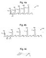
- FIG. 4 a depicts a first example pulse train applied to the control gates of storage elements during programming.
- FIG. 4 b depicts a second example pulse train applied to the control gates of storage elements during programming.
- FIG. 4 c depicts an example voltage waveform applied to the control gates of non-volatile storage elements during a read operation.
- FIG. 5 a depicts details of the two-pass programming technique of FIG. 3 , where data is read between programming passes.
- FIG. 5 b depicts details of a two-pass programming technique where data is not read between programming passes.
- FIG. 6 a depicts changes in threshold voltages after a first, coarse pass of the two-pass programming technique of FIG. 3 .
- FIG. 6 b depicts changes in threshold voltages after a second, fine pass of the two-pass programming technique of FIG. 3 .
- FIG. 7 a depicts an overview of a multi-pass programming process in which data is read between programming passes and subsequently accessed and error corrected.
- FIG. 7 b depicts a multi-pass programming process corresponding to the two-pass programming technique of FIG. 3 .
- FIG. 8 depicts a programming order for a set of storage elements and associated word lines in a three-pass programming technique.
- FIG. 9 depicts details of the three-pass programming technique of FIG. 8 , where data is read between programming passes.
- FIGS. 10 a - 10 c depict threshold voltage distributions for a three-pass programming technique associated with FIG. 8 .
- FIG. 11 depicts a multi-pass programming process corresponding to the three-pass programming technique of FIG. 8 .
- FIG. 12 a depicts an additional multi-pass programming process.
- FIGS. 12 b - 12 e depict threshold voltage distributions for a programming technique associated with FIG. 12 a.
- FIG. 13 is a block diagram of an array of NAND flash storage elements.
- FIG. 14 is a block diagram of a non-volatile memory system using single row/column decoders and read/write circuits.
- FIG. 15 is a block diagram depicting one embodiment of a read/write stack.
- FIG. 16 illustrates an example of an organization of a memory array into blocks for an all bit line memory architecture or for an even-odd memory architecture.
- a programming technique is provided for reducing the effects of coupling between adjacent floating gates in a cost effective manner.
- FIG. 1 a is a top view showing one NAND string.
- FIG. 1 b is an equivalent circuit thereof.
- the NAND string depicted in FIGS. 1 a and 1 b includes four transistors 100 , 102 , 104 and 106 in series and sandwiched between a first (drain side) select gate 120 and a second (source side) select gate 122 .
- Select gate 120 connects the NAND string to a bit line via bit line contact 126 .
- Select gate 122 connects the NAND string to source line 128 .
- Select gate 120 is controlled by applying the appropriate voltages to select line SGD.
- Select gate 122 is controlled by applying the appropriate voltages to select line SGS.
- Each of the transistors 100 , 102 , 104 and 106 has a control gate and a floating gate.
- transistor 100 has control gate 100 CG and floating gate 100 FG.
- Transistor 102 includes control gate 102 CG and a floating gate 102 FG.
- Transistor 104 includes control gate 104 CG and floating gate 104 FG.
- Transistor 106 includes a control gate 106 CG and a floating gate 106 FG.
- Control gate 100 CG is connected to word line WL 3
- control gate 102 CG is connected to word line WL 2
- control gate 104 CG is connected to word line WL 1
- control gate 106 CG is connected to word line WL 0 .
- FIGS. 1 a and 1 b show four memory cells in the NAND string, the use of four memory cells is only provided as an example.
- a NAND string can have fewer than four memory cells or more than four memory cells.
- some NAND strings will include eight memory cells, 16 memory cells, 32 memory cells, 64 memory cells, 128 memory cells, etc.
- the discussion herein is not limited to any particular number of memory cells in a NAND string.
- One embodiment uses NAND strings with 66 memory cells, where 64 memory cells are used to store data and two of the memory cells are referred to as dummy memory cells because they do not store data.
- a typical architecture for a flash memory system using a NAND structure will include several NAND strings.
- Each NAND string is connected to the common source line by its source select gate controlled by select line SGS and connected to its associated bit line by its drain select gate controlled by select line SGD.
- select line SGS Source select gate controlled by select line SGS
- select line SGD Drain select gate controlled by select line SGD
- Each bit line and the respective NAND string(s) that are connected to that bit line via a bit line contact comprise the columns of the array of memory cells.
- Bit lines are shared with multiple NAND strings.
- the bit line runs on top of the NAND strings in a direction perpendicular to the word lines and is connected to a sense amplifier.
- non-volatile memory devices are also manufactured from memory cells that use a dielectric layer for storing charge. Instead of the conductive floating gate elements described earlier, a dielectric layer is used. Such memory devices utilizing dielectric storage element have been described by Eitan et al., “NROM: A Novel Localized Trapping, 2-Bit Nonvolatile Memory Cell,” IEEE Electron Device Letters, vol. 21, no. 11, November 2000, pp. 543-545. An ONO dielectric layer extends across the channel between source and drain diffusions.
- U.S. Pat. Nos. 5,768,192 and 6,011,725 disclose a non-volatile memory cell having a trapping dielectric sandwiched between two silicon dioxide layers. Multi-state data storage is implemented by separately reading the binary states of the spatially separated charge storage regions within the dielectric. Non-volatile storage based on MONOS or TANOS types of structures or nanocrystals can also be used. Other types of non-volatile storage can also be used.
- FIG. 1 c is a circuit diagram depicting three NAND strings.
- a typical architecture for a flash memory system using a NAND structure will include several NAND strings.
- three NAND strings 320 , 340 and 360 are shown in a memory array having many more NAND strings.
- Each of the NAND strings includes two select gates and four storage elements. While four storage elements are illustrated for simplicity, modern NAND strings can have up to thirty-two or sixty-four storage elements, for instance.
- NAND string 320 includes select gates 322 and 327 , and storage elements 323 - 326
- NAND string 340 includes select gates 342 and 347 , and storage elements 343 - 346
- NAND string 360 includes select gates 362 and 367 , and storage elements 363 - 366 .
- Each NAND string is connected to the source line by its select gates (e.g., select gates 327 , 347 or 367 ).
- a selection line SGS is used to control the source side select gates.
- the various NAND strings 320 , 340 and 360 are connected to respective bit lines 321 , 341 and 361 , by select transistors in the select gates 322 , 342 , 362 , and so forth.
- select transistors are controlled by a drain select line SGD.
- the select lines do not necessarily need to be in common among the NAND strings; that is, different select lines can be provided for different NAND strings.
- WL 3 is connected to the control gates for storage elements 323 , 343 and 363 .
- WL 2 is connected to the control gates for storage elements 324 , 344 and 364 .
- WL 1 is connected to the control gates for storage elements 325 , 345 and 365 .
- WL 0 is connected to the control gates for storage elements 326 , 346 and 366 .
- each bit line and the respective NAND string comprise the columns of the array or set of storage elements.
- the word lines (WL 3 , WL 2 , WL 1 and WL 0 ) comprise the rows of the array or set. Each word line connects the control gates of each storage element in the row. Or, the control gates may be provided by the word lines themselves. For example, WL 2 provides the control gates for storage elements 324 , 344 and 364 . In practice, there can be thousands of storage elements on a word line.
- Each storage element can store data. For example, when storing one bit of digital data, the range of possible threshold voltages (V TH ) of the storage element is divided into two ranges which are assigned logical data “1” and “0.”
- V TH threshold voltages
- the V TH is negative after the storage element is erased, and defined as logic “1.”
- the V TH after a program operation is positive and defined as logic “0.”
- the storage element will turn on to indicate logic “1” is being stored.
- the V TH is positive and a read operation is attempted, the storage element will not turn on, which indicates that logic “0” is stored.
- a storage element can also store multiple levels of information, for example, multiple bits of digital data.
- the range of V TH is divided into the number of levels of data. For example, if four levels of information are stored, there will be four V TH ranges assigned to the data values “11”, “10”, “01”, and “00.” In one example of a NAND type memory, the V TH after an erase operation is negative and defined as “11”. Positive V TH values are used for the states of “10”, “01”, and “00.” The specific relationship between the data programmed into the storage element and the V TH ranges of the storage element depends upon the data encoding scheme adopted for the storage elements.
- a program voltage is applied to the control gate of the storage element, and the bit line associated with the storage element is grounded. Electrons from the channel are injected into the floating gate. When electrons accumulate in the floating gate, the floating gate becomes negatively charged and the VTH of the storage element is raised. To apply the program voltage to the control gate of the storage element being programmed, that program voltage is applied on the appropriate word line. As discussed above, one storage element in each of the NAND strings share the same word line. For example, when programming storage element 324 of FIG. 1 c , the program voltage will also be applied to the control gates of storage elements 344 and 364 .
- FIG. 2 depicts a cross-sectional view of a NAND string.
- the NAND string 200 includes a source-side select gate 206 , a drain-side select gate 224 , and eight storage elements 208 , 210 , 212 , 214 , 216 , 218 , 220 and 222 , formed on a substrate 290 .
- the components can be formed on a p-well region 292 which itself is formed in an n-well region 294 of the substrate.
- the n-well can in turn be formed in a p-substrate 296 .
- Supply lines 202 and 203 may communicate with the p-well region 292 and n-well region 294 , respectively.
- a source supply line 204 with a potential of V SOURCE is provided in addition to a bit line 226 with a potential of V BL .
- V SGS is applied to the select gate 206 and V SGD is applied to the select gate 224 .
- the source side of a word line or non-volatile storage element refers to the side which faces the source end of the NAND string, e.g., at source supply line 204
- the drain side of a word line or non-volatile storage element refers to the side which faces the drain end of the NAND string, e.g., at bit line 226 .
- Capacitive coupling includes bit line-to-bit line coupling and word line-to-word line coupling.
- the storage elements are programmed to an offset level below their final intended states in one, coarse pass. This offset level is for a partly programmed state that may be considered to be a coarse or “foggy” state. Subsequently, the storage elements are programmed the remainder of the way to their final intended states in another, fine pass. The final programmed state may be considered to be a “fine” state.
- multi-pass programming technique is discussed next.
- FIG. 3 depicts a programming order for a set of storage elements and associated word lines in a two-pass programming technique.
- a set of storage elements each represented by a square, is in communication with a set of word lines WL 0 to WL 4 and a set of bit lines BLi ⁇ 1 to BLi+1.
- the components depicted may be a subset of a much larger set of storage elements, word lines and bit lines.
- five word lines are provided, where WL 0 is a source side end word line and WL 4 is a drain side end word line.
- many more word lines are typically arranged in a block, such as 64 or 128 word lines.
- the illustration provided is used to depict aspects of one embodiment of the invention. Steps S 1 through S 15 denote steps which are performed sequentially.
- the programming order may be referred to as a word line out of sequence or zigzag sequence since the order involves jumping back and forth among the word lines.
- a coarse pass and a fine pass are provided for each word line.
- a first programming pass is performed for selected storage elements associated with WL 0 (this is step 1 or S 1 ).
- a read operation is performed for WL 0 (S 2 ).
- the read operation allows the condition of the storage elements on WL 0 to be ascertained before the storage elements are affected by coupling from subsequent programming of neighboring word line storage elements. Errors in the read data can be detected using an error correction code (ECC).
- ECC error correction code
- the ECC can be utilized to correct failure bits caused by coarse programming itself, or failure bits caused in the period after the coarse programming and before the coarse read. It is assumed that there are no failure bits caused by the temporal storage.
- a coarse programming pass occurs for WL 1 .
- This programming causes a shift in the threshold voltages of the storage elements of WL 0 due to coupling from WL 1 .
- a fine programming pass occurs for WL 0 .
- the read data indicates the data states to which each storage element of WL 0 is to be programmed in the fine programming pass.
- the read data can be deleted. This approach avoids the need to store program data for the fine programming during the coarse programming, for a given word line, as explained in further detail below. Additionally, threshold voltage distributions are tightened.
- a read operation is performed for WL 1
- coarse programming is performed for WL 2 , which causes a shift in the threshold voltages of the storage elements of WL 1 due to coupling.
- a fine programming pass occurs for WL 1 . This could cause a minor amount of coupling to the source side neighboring word line, WL 0 . However, this coupling is much less than that due to coarse programming and thus can be tolerated.
- the data which was previously read at S 5 is accessed and decoded using ECC decoding.
- the read data indicates the data states to which each storage element of WL 1 is to be programmed in the fine programming pass.
- the process proceeds accordingly for the other world lines so that, for a given word line, the storage elements are read after the coarse programming, before the word line is subject to coupling from coarse programming of a higher word line, and the read data is used for the fine programming.
- the last word line, WL 4 is programmed analogously except there is no higher word line programmed after the read of S 14 . Instead, fine programming occurs for WL 4 at S 15 .
- an additional, initial programming pass may be performed before the coarse and fine programming passes depicted such as discussed in connection with FIG. 8 .
- a given word line does not complete programming until the next higher word line has been partially programmed.
- the next higher word line is one programming pass behind. For example, when WL 0 has completed the fine programming, WL 1 has only completed the coarse programming.
- All bit line programming may be used in which the storage elements of all bit lines on a word line are programmed without regard to whether the storage elements are associated with an even or odd numbered bit line.
- other approaches are possible, including an approach in which the even bit lines are programmed, undergoing program and verify operations, followed by the odd bit lines being programmed, undergoing program and verify operations.
- the even and odd bit lines are both programmed together, receiving a program pulse, after which the even bit lines are verified, and after which the odd bit line are verified. A next program pulse is subsequently applied and the process proceeds accordingly.
- FIG. 4 a depicts a first example pulse train 400 applied to the control gates of storage elements during programming.
- the pulse train includes program pulses 402 , 404 , 406 , 408 , 410 . . . which step up in amplitude, in one possible approach, and a set of verify pulses between each program pulse, including example verify pulses 403 , which have amplitudes such as V VA-COARSE , V VB-COARSE and V VC-COARSE or V VA-FINE , V VB-FINE and V VC-FINE , discussed further below.
- the pulse amplitudes are V PGM1 , V PGM2 , and so forth.
- the pulses can be fixed in amplitude, or they can step up at a fixed or varying rate, for instance.
- m ⁇ 1 verify pulses are used when m data states are used.
- the same pulse train is used for each programming pass.
- the second programming pass may use a pulse train which starts at a higher initial V PGM than the first pass.
- the programming pulses have a voltage, V PGM1 , which starts at, e.g., 12 V and increases by increments, e.g., 0.5 V, for each successive programming pulse until a maximum of, e.g., 20-25 V is reached.
- V PGM1 a voltage
- the pulse train 400 may be used during all bit line programming, for instance, or during even-odd programming.
- storage elements of even-numbered bit lines are programmed and verified using repeated applications of the pulse train 400 , followed by storage elements of odd-numbered bit lines being programmed and verified using repeated applications of the pulse train 400 .
- the pulse train 460 includes program pulses 442 , 444 , 446 , 448 , 450 . . . which step up in amplitude, and two sets of verify pulses between each program pulse, including example sets 443 and 445 .
- the set of verify pulses 443 may be used to verify storage elements of even-numbered bit lines
- the set of verify pulses 445 may be used to verify storage elements of odd-numbered bit lines, in one possible approach.
- FIG. 4 c depicts an example voltage waveform applied to the control gates of non-volatile storage elements during a read operation.
- the voltage on a selected word line is coupled to the control gates of selected storage elements, and a sequence of read voltages V CGR-A , V CGR-B and V CGR-C is provided.
- a read operation is distinguished from a verify operation in that a verify operation typically uses only one comparison level while a read operation uses multiple comparison levels, for a multi-level storage element. Further, a verify operation involves ensuring that a threshold voltage of a storage elements exceeds a comparison level, while a read operation involves determining which voltage threshold interval and data state a storage element should be classified into. Generally, n ⁇ 1 read compare levels are used to distinguish among n states. As discussed below in connection with FIGS. 6 a and 6 b , different read voltages can be used depending on whether coarsely programmed data or finely programmed data is being read.
- FIG. 5 a depicts details of the two-pass programming technique of FIG. 3 , where data is read between programming passes.
- Steps S 1 through S 10 correspond to the like numbered steps of FIG. 3 .
- “E” denotes the erased state. Time proceeds to the right.
- the storage elements of all word lines are in the erased (E) state.
- coarse programming is performed for WL 0 (“coarse program”), after which storage elements of WL 0 are in a coarsely programmed state (“coarse”).
- Storage elements of WL 1 through WL 4 are in the E state.
- S 2 WL 0 is read, and the associated data is stored. For example, two bits of data can be stored for each storage element when there are four possible data states. Generally, N bits are stored when there are 2 N states.
- coarse programming is performed for WL 1 . Storage elements of WL 1 are in the coarse state, and storage elements of WL 2 through WL 4 are in the E state.
- the read data for WL 0 is accessed for use in fine programming of WL 0 .
- the read data indicates the data state to which each storage element of WL 0 is to be programmed during fine programming.
- the coarse threshold voltage distributions provide the program data for the fine distributions.
- the read data of WL 0 can be discarded after the fine programming as it is no longer need. Note that read data from only one word line need be stored at a time. This reduces the storage requirements for program data as well as operations needed for moving data around, thus allowing possible reductions in hardware costs, power consumption and the space used by the hardware on the memory chip.
- the reading, storing and subsequent accessing of data can be implemented as a sequence which is launched by a command input, and a storage location in the memory device can be provided to temporarily store the read data.
- the multi-pass programming will be transparent to the user. Additionally, the storage location in the memory device can be volatile since the command guarantees that the reading, storing and subsequent accessing of data is continuous.
- the techniques herein provide a coarse-fine program method which requires less capacity of data storage.
- the conventional coarse/fine programming method for 4-level storage elements requires storage such as 4-bit flip-flops (not necessarily flip-flops, any storage is acceptable) per bit line to keep program data.
- the 4-level cell of the technology described herein only requires storage such as 2-bit flip-flops (not necessarily flip-flops, any storage is acceptable) per bit line.
- WL 1 is read, and the associated data is stored.
- coarse programming is performed for WL 2 .
- a coarse distribution on WLn ⁇ 1 is read before coarse programming on WLn.
- the coarse distribution on WLn ⁇ 1 is only minimally disturbed by coupling from the fine programming on WLn ⁇ 2.
- storage elements of WL 0 are in the fine state
- storage elements of WL 1 are in the coarse state
- storage elements of WL 3 and WL 4 are in the E state.
- the read data for WL 1 is accessed for use in fine programming of WL 1 .
- the read data of WL 1 can be discarded after the fine programming.
- WL 2 is read, and the associated data is stored.
- FIG. 5 b depicts details of a two-pass programming technique where data is not read between programming passes, as a comparison to FIG. 5 a .
- Steps S 1 , S 3 , S 4 , S 6 , S 7 , S 9 and S 10 correspond to the like numbered steps in FIG. 5 a .
- program data from at least two word lines needs to be stored concurrently, somewhere in the memory device or storage system. For example, data of WL 0 is stored from when coarse programming is performed (S 1 ) until fine programming is performed for WL 0 (S 4 ). Data of WL 1 is stored from when coarse programming is performed (S 3 ) until fine programming is performed for WL 1 (S 7 ).
- Data of WL 2 is stored from when coarse programming is performed (S 6 ) until fine programming is performed for WL 2 (S 10 ), and so on.
- WL 0 and WL 1 are stored at the same time
- WL 1 and WL 2 are stored at the same time
- WL 2 and WL 3 are stored at the same time, and so forth.
- FIG. 6 a depicts changes in threshold voltages after a first, coarse pass of the two-pass programming technique of FIG. 3 .
- This programming technique is referred to as full sequence programming. This portion of the programming technique uses lower or coarse verify voltages.
- Coarse programming refers to the fact that storage elements are programmed toward their final intended state with a lesser degree of precision and at a faster rate (a greater ⁇ V TH /sec.) than fine programming. This faster programming can be achieved, e.g., by applying program pulses having a higher amplitude, or increasing at a faster rate.
- the storage elements are programmed to a verify level which is offset below the final, or fine, verify level.
- the coarse verify level is generally close to the fine verify level, but low enough to prevent the storage elements from overshooting too far past the fine verify level. That is, the cells are allowed to program beyond the fine verify level as depicted, although programming the cells too far past the fine verify level will result in a widening of the fine distribution.
- a first, coarse programming pass uses a first, coarse set of verify voltages V VA-COARSE , V VB-COARSE , and V VC-COARSE for states A, B and C, respectively.
- the coarse programming pass is alternatively referred to as a first pass of a multiple “pass write” (PW) programming process.
- PW pass write
- the transition in threshold voltage on WLn is relatively large, resulting in coupling to storage elements of an adjacent word line.
- the V TH distributions for WLn are shifted slightly higher as represented by the short dashed lines.
- the V TH distributions for WLn are shifted significantly higher as represented by the dotted lines. The coupling effect of coarse programming is thus stronger than that of fine programming.
- Coarse distributions on WLn after fine programming on WLn ⁇ 1 will have some read margin, e.g., the distributions do not overlap. Thus, reading the coarse distributions on WLn after fine programming on WLn ⁇ 1 (reading the distribution represented by the short dashed lines) will result in accurate results. In case ECC is used, a certain amount of overlap of the distributions can be allowed while the ECC can be used to correct fail bits.
- the optimal read levels for reading the coarse distribution should be somewhat lower than for the fine distribution.
- the read levels for the coarse distribution are V CGR-A (COARSE) , V CGR-B (COARSE) , and V CGR-C (COARSE) , as depicted in FIG.
- V CGR-A FINE
- V CGR-B FINE
- V CGR-C FINE
- Coarse distributions on WLn after coarse programming on WLn+1 may not have a good read margin, e.g., the distributions can overlap, as indicated.
- FIG. 6 b depicts changes in threshold voltages after a second, fine pass of the two-pass programming technique of FIG. 3 .
- the second, fine programming pass which follows the coarse pass of FIG. 6 a , uses a second, higher set of verify voltages V VA-FINE , V VB-FINE , and V VC-FINE for states A, B and C, respectively.
- each nth verify voltage in the second set of verify voltages is higher than each nth verify voltage in the first set of verify voltages by an increment, which can be the same or different for the different states. This is a second pass of the multiple “pass write” programming process.
- the storage elements Just after the second programming pass, which is the fine programming pass of WLn, the storage elements have V TH distributions which are represented by the dash-dot lines.
- the distributions of FIG. 6 a which were represented by dotted lines are repeated in FIG. 6 b for reference, with arrows indicating how the distributions are narrowed.
- the storage elements have been programmed to their final intended states.
- the V TH distributions for WLn are shifted slightly higher as represented by the solid lines.
- Fine programming refers to the fact that storage elements are programmed toward their final intended state with a higher degree of precision and at a slower rate (a smaller ⁇ V TH /sec.) than coarse programming. This slower programming can be achieved, e.g., by applying program pulses which have a lower amplitude or increase at a slower rate.
- FIG. 7 a depicts an overview of a multi-pass programming process in which data is read between programming passes and subsequently accessed and error corrected.
- the data which is to be programmed can be in a form which is ECC coded.
- an error correcting code which detects and corrects errors, or an error detecting code, which detects but does not correct errors, can be used.
- a multi-pass programming operation begins at step 700 .
- coarse programming is performed for a particular word line, e.g., WLn.
- programming is performed on another word line, e.g., WLn ⁇ 1, which does not couple strongly to the particular word line. For example, this programming could be fine programming on WLn ⁇ 1.
- the particular word line is read and the associated data is stored.
- programming is performed for another word line which does result in appreciable coupling to the particular word line.
- this programming could be coarse programming of WLn+1.
- the V TH of the storage elements of the particular word line is shifted due to the coupling.
- Step 712 includes accessing the stored data of WLn and performing an error correction process using the ECC. Fine programming is performed for the particular word line using the accessed data at step 714 , and the stored data for the particular word line is discarded at step 716 . For example, the data can be written over as it is no longer needed.
- FIG. 7 b depicts a multi-pass programming process corresponding to the two-pass programming technique of FIG. 3 .
- the programming operation begins at step 720 .
- a word line index is set to 0, which represents the first word line.
- the word lines are typically numbered sequentially starting at 0 at the source side of a set of word lines such as a NAND string.
- Step 730 includes coarse programming of WL 0
- step 735 includes reading WL 0 .
- Step 755 increments the index, e.g., to 1.
- step 740 includes coarse programming of WLi (e.g., WL 1 ), and step 745 includes accessing WLi ⁇ 1 (e.g., WL 0 ) coarse read data and performing fine programming of WLi ⁇ 1.
- step 750 includes reading WLi (e.g., WL 1 ) and storing the associated data.
- Step 755 increments the index again, e.g., to 2. If the index is not at the last word line at decision step 760 , the flow proceeds to step 740 , which includes coarse programming of WLi (e.g., WL 2 ), and step 745 includes accessing WLi ⁇ 1 (e.g., WL 1 ) coarse read data and performing fine programming of WLi ⁇ 1. Step 750 includes reading WLi (e.g., WL 2 ) and storing the associated data.
- step 740 includes coarse programming of WLi (e.g., WL 2 )
- step 745 includes accessing WLi ⁇ 1 (e.g., WL 1 ) coarse read data and performing fine programming of WLi ⁇ 1.
- Step 750 includes reading WLi (e.g., WL 2 ) and storing the associated data.
- the process proceeds accordingly until the index is at the last word line at decision step 760 .
- the programming is modified slightly due to the fact that there is no higher word line than the last word line.
- coarse programming of WLi e.g., WL 4
- the WLi e.g., WL 4
- coarse read data is accessed and fine programming is performed for WLi.
- the programming operation finally ends at step 775 . Note that this is one example programming sequence, as other programming sequences are possible.
- FIG. 8 depicts a programming order for a set of storage elements and associated word lines in a three-pass programming technique.
- a set of storage elements each represented by a square, is in communication with an example set of word lines WL 0 to WL 4 and an example set of bit lines BLi ⁇ 1 to BLi+1.
- the components depicted may be a subset of a much larger set of storage elements, word lines and bit lines. In this example, five word lines are provided, where WL 0 is a source side end word line and WL 4 is a drain side end word line.
- WL 0 is at the source end of a set of series-connected storage elements such as a NAND string
- WL 4 is at the drain end of the set of series-connected storage elements.
- the illustration provided is used to depict aspects of one embodiment of the invention. Steps S 1 through S 20 denote operations which occur sequentially.
- the three passes of the programming are a lower page pass, an upper page coarse pass (or a first upper page pass) and an upper page fine pass (or a second upper page pass), described further below.
- S 1 includes lower page programming of WL 0
- S 2 includes lower page programming of WL 1
- S 3 includes upper page coarse programming of WL 0
- S 4 includes lower page programming of WL 2
- S 5 includes reading WL 0 .
- S 6 includes upper page coarse programming of WL 1 , which causes coupling interference to WL 0 .
- S 7 include accessing the previously read data and performing upper page fine programming of WL 0 .
- S 8 includes lower page programming of WL 3 .
- S 9 includes reading WL 1 .
- S 10 includes upper page coarse programming of WL 2 , which causes coupling interference to WL 1 .
- S 11 includes accessing the previously read data and performing upper page fine programming of WL 1 . The process proceeds accordingly until the last word line is reached.
- a given word line does not complete programming until the next two higher word line have been partially programmed.
- the next higher word line is one programming pass behind, and the second higher word line is two programming passes behind. For example, when WL 0 has completed the upper page fine programming, WL 1 has only completed the upper page coarse programming and WL 2 has only completed the lower page programming.
- FIG. 9 depicts details of the three-pass programming technique of FIG. 8 , where data is read between programming passes. Steps S 1 through S 11 correspond to the like numbered steps of FIG. 8 . “E” denotes the erased state. Time proceeds to the right. Prior to S 1 , the storage elements of all word lines are in the erased state (E). At S 1 , lower page programming (“is performed for WL 0 , after which storage elements of WL 0 are in a lower page state (“lower page”). The lower page programming is also two-level programming when the storage elements are in one of two possible states.
- Storage elements of WL 1 through WL 4 are in the E state.
- lower page programming is performed for WL 1 , after which storage elements of WL 1 are in the lower page state.
- Storage elements of WL 0 are in a lower page state and WL 2 through WL 4 are in the E state.
- WL 0 undergoes upper page coarse programming (“coarse program”).
- Storage elements of WL 1 are in a lower page state and WL 2 through WL 4 are in the E state.
- lower page programming is performed for WL 2 , after which storage elements of WL 2 are in the lower page state.
- Storage elements of WL 0 are in a coarse state
- storage elements of WL 1 are in a lower page state and storage elements of WL 3 through WL 4 are in the E state.
- WL 0 is read and the associated data is stored.
- coarse programming occurs for WL 1 .
- Storage elements of WL 0 are in a coarse state, storage elements of WL 2 are in a lower page state and storage elements of WL 3 through WL 4 are in the E state.
- the WL 0 data is accessed and use for fine programming of WL 0 .
- the WL 0 data can then be discarded.
- lower page programming occurs for WL 3 .
- Storage elements of WL 0 are in a fine, upper page state, storage elements of WL 2 are in a coarse, upper page state and storage elements of WL 4 are in the E state.
- WL 1 is read and the associated data is stored.
- WL 1 undergoes fine programming and the read data of WL 1 can be discarded. Again, note that read data from only one word line need be stored at a time. This reduces storage requirements as well as operations needed for moving data around.
- a work area of the programming requires two bits of storage, and a temporal buffer for the subsequent operations requires four bits of storage, including two bits for WLn+1 data to be used for fine programming, and two bits for WLn data to be used for fine programming.
- the work area can be provided by data latches or flop flops, for example, while the temporal buffer can be provided by data latches, flop flops, a binary buffer or a binary memory. See FIGS. 14 and 15 for further details.
- the work area for programming requires two bits of storage
- the temporal buffer requires two bits of storage, including two bits for WLn data to be used for fine programming.
- a total of four bits storage space for each storage element is needed.
- the work area requires three bits of storage, and a temporal buffer for the subsequent operations requires two bits of storage, including two bits for WLn data to be used for fine programming.
- a total of five bits storage space for each storage element is needed.
- a savings of one bit per storage elements results with the programming technique discussed herein.
- a memory device can be designed with the reduced storage requirements in mind to save costs. Further, power consumption can be reduced.
- FIGS. 10 a - 10 c depict threshold voltage distributions for a three-pass programming technique associated with FIG. 8 .
- FIG. 10 a depicts changes in threshold voltages after a first, lower page programming pass, in which an intermediate verify voltage is used.
- the programming process occurs in three phases.
- An initial phase involves programming using an intermediate verify voltage, V VINT , for storage elements which are intended to be programmed to a final state of B or C. Storage elements which are intended to be programmed to a final state of A remain in the erased state.
- This initial phase may involve programming a lower page of data.
- the INT V TH distributions for WLn is represented by the long dashed line for the INT distribution.
- the INT V TH distribution is shifted slightly higher as represented by the short dashed line.
- the INT V TH distribution for WLn is shifted significantly higher as represented by the dotted line.
- FIG. 10 b depicts changes in threshold voltages after a second pass, which is a coarse upper page pass, in which lower verify voltages are used.
- a first “pass write” programming pass uses the first, lower set of verify voltages V VA-COARSE , V VB-COARSE , and V VC-COARSE for states A, B and C, respectively.
- Storage elements which are intended to be programmed to a final state A are programmed starting from state E, and storage elements which are intended to be programmed to a final state B or C are programmed starting from state INT.
- the dotted line of FIG. 10 a is repeated in FIG. 10 b for reference.
- the storage elements are programmed to a level which is offset lower than the final state.
- This programming phase may be a first, coarse pass of programming an upper page of data.
- the storage elements of WLn have V TH distributions which are represented by the dash-dot lines.
- V TH distributions for WLn are shifted slightly higher as represented by the dash-dot-dot lines.
- the V TH distributions for WLn are shifted significantly higher as represented by the dash-dash-dot lines.
- the read levels for the coarse upper page distribution are V CGR-A (COARSE) , V CGR-B (COARSE) , and V CGR-C (COARSE) .
- Example control gate read voltages V CGR-A (COARSE) , V CGR-B (COARSE) and V GCR-C (COARSE) for states A, B and C, respectively, are also depicted for reference.
- FIG. 10 c depicts changes in threshold voltages after a third, fine upper page pass, in which higher verify voltages are used.
- the transition from FIG. 10 b to FIG. 10 c is similar to the transition from FIG. 6 a to FIG. 6 b .
- a second “pass write” programming pass uses the second, higher set of verify voltages V VA-FINE , V VB-FINE , and V VC-FINE for states A, B and C, respectively.
- Storage elements which are intended to be programmed to a final state A, B or C are programmed starting from the respective lower offset states, represented by the dash-dash-dot lines which are repeated from FIG. 10 b .
- Example control gate read voltages V CGR-A (FINE) , V CGR-B (FINE) and V GCR-C (FINE) for states A, B and C, respectively, are also depicted for reference.
- This programming phase may be a second, fine pass of programming an upper page of data.
- the storage elements have V TH distributions which are represented by the dotted lines.
- the distribution of FIG. 10 b which was represented by a dash-dash-dot line is repeated in FIG. 10 c for reference, with arrows indicating how the distributions are narrowed.
- the V TH distributions for WLn are shifted slightly higher as represented by the solid lines.
- the non-volatile storage elements store two bits of data per storage element, using four data states. For example, assume that state E is the erased state and states A, B and C are the programmed states. State E stores data 11 . State A stores data 01 . State B stores data 10 . State C stores data 00 . This is an example of non-Gray coding because both bits change between adjacent states A and B. Other encodings of data to physical data states can also be used. Each storage element stores two pages of data. For reference purposes, these pages of data will be called upper page and lower page; however, they can be given other labels. With reference to state A, the upper page stores bit 0 and the lower page stores bit 1 . With reference to state B, the upper page stores bit 1 and the lower page stores bit 0 . With reference to state C, both pages store bit data 0 .
- the lower page is programmed. If the lower page is to remain data 1 , then the storage element state remains at state E. If the data is to be programmed to 0, then the threshold of voltage of the storage element is raised such that the storage element is programmed to state INT. In one embodiment, after a storage element is programmed from state E to state INT, its neighbor storage element (WLn+1) in the NAND string will then be programmed with respect to its lower page. For example, looking back at FIG. 1 b , after the lower page for storage element 106 is programmed, the lower page for storage element 104 would be programmed.
- the floating gate to floating gate coupling effect will raise the apparent V TH of storage element 106 if storage element 104 had a V TH raised from state E to state INT. This will have the effect of widening the V TH distribution for state INT. This apparent widening of the V TH distribution will be mostly remedied when programming the upper page.
- the storage element will remain in state E. If the storage element is in state E and its upper page data is to be programmed to 0, then the V TH of the storage element will be raised so that the storage element is in state A. If the storage element was in the INT threshold voltage distribution and the upper page data is to remain at 1, then the storage element will be programmed to final state B. If the storage element is the INT threshold voltage distribution and the upper page data is to become data 0 , then the V TH of the storage element will be raised so that the storage element is in state C.
- An example of an alternate state coding is to move from distribution INT to state C when the upper page data is a 1, and to move to state B when the upper page data is a 0.
- FIGS. 10 a - c provide an example with respect to four data states and two pages of data, the concepts taught can be applied to other implementations with any number of states and pages.
- FIG. 11 depicts a multi-pass programming process corresponding to the three-pass programming technique of FIG. 8 .
- the programming operation begins at step 1100 .
- a word line index is set to zero to represent the initial, source side word line.
- Step 1110 includes lower page programming of WL 0 .
- Step 1115 includes lower page programming of WL 1 .
- Step 1120 includes coarse, upper page programming of WL 0 .
- step 1125 includes lower page programming of WLi+1 (e.g., WL 2 )
- step 1130 includes reading WLi ⁇ 1 (e.g., WL 0 ) and storing the associated data
- step 1135 includes coarse programming of WLi (e.g., WL 1 ).
- Step 1140 includes accessing the WLi ⁇ 1 (e.g., WL 0 ) coarse read data and performing fine, upper page programming of WLi ⁇ 1.
- step 1125 includes lower page programming of WLi+1 (e.g., WL 3 )
- step 1130 includes reading WLi ⁇ 1 (e.g., WL 1 ) and storing the associated data
- step 1135 includes coarse programming of WLi (e.g., WL 2 ).
- Step 1140 includes accessing the WLi ⁇ 1 (e.g., WL 1 ) coarse read data and performing fine, upper page programming of WLi ⁇ 1.
- step 1155 includes reading WLi ⁇ 2 (e.g., WL 2 ), step 1160 includes coarse, upper page programming of WLi ⁇ 1 (e.g., WL 3 ), and step 1165 includes accessing WLi ⁇ 2 (e.g., WL 2 ) coarse read data and using it to perform fine programming of WLi ⁇ 2.
- Step 1170 includes reading WLi ⁇ 1 (e.g., WL 3 ), step 1175 includes coarse, upper page programming of WLi (e.g., WL 4 ), and step 1180 includes accessing WLi ⁇ 1 (e.g., WL 3 ) coarse read data and using it to perform fine programming of WLi ⁇ 1.
- Step 1185 includes reading WLi (e.g., WL 4 ), and step 1190 includes accessing WLi (e.g., WL 4 ) coarse read data and using it to perform fine programming of WLi.
- the programming operation ends at step 1195 .
- FIG. 12 a depicts an additional multi-pass programming process which is analogous to FIG. 8 except the upper page coarse programming is performed for the C state before the A and B states.
- S 3 , S 6 , S 10 , S 14 and S 17 denote steps for performing coarse programming of the upper page for state C storage elements, followed by coarse programming of the upper page for state A and B storage elements.
- S 7 , S 11 , S 15 , S 18 and S 20 denote steps for fine programming of the upper page for all states, e.g., A, B and C.
- FIGS. 12 b - 12 e depict threshold voltage distributions for a programming technique associated with FIG. 12 a.
- FIG. 12 b depicts changes in threshold voltages after lower page programming, in which an intermediate verify voltage is used.
- This option can also reduce the impact of disturbs and neighbor-cell interference effects. It mainly reduces bit line-to-bit line interference and program disturb.
- This programming technique is referred to as “C-first” or “highest state first,” where the C state represents the highest state in a four data state, multi-level implementation. The technique can be extended to eight, sixteen or other numbers of states. Such techniques involve programming all of the highest state cells to their intended state, using a coarse verify level, before coarse programming of lower state cells.
- the B and C state storage elements are programmed using V VINT as a verify level.
- the long dashed line depicts the INT V TH distribution for WLn just after the lower page programming of WLn
- the short dashed line depicts the INT V TH distribution for WLn after coarse upper page programming of WLn ⁇ 1
- the dotted line depicts the INT V TH distribution for WLn after lower page programming of WLn+1.
- FIG. 12 c depicts a V TH distribution just after coarse upper page programming of the C state storage elements, as represented by a dot-dash line.
- the dotted line of the INT state of FIG. 12 b is repeated for reference.
- a transition in V TH is depicted by an arrow for the C state storage elements.
- the V TH of the B state storage elements remains at INT.
- FIG. 12 d depicts coarse upper page programming of A and B storage elements in which lower verify voltages for A and B states are used.
- the A state storage elements are programmed from state E using the lower verify level V VA-COARSE and the B state storage elements are programmed from the INT state using the verify level V VB-COARSE .
- the dotted line of the INT state of FIG. 12 c is repeated in FIG. 12 d for reference.
- the C state storage elements are locked out from programming at this time, in one possible approach.
- the coarse upper page programming of A and B storage elements causes a shift in the V TH of the C state storage elements from the distribution represented by the dash-dot line to the distribution represented by the dash-dot-dot line.
- the dash-dot-dot lines depict the V TH distribution of WLn for states A, B and C just after the coarse upper page programming of state A and B storage elements of WLn. Further, the dash-dash-dot line depicts the V TH distribution of the storage elements of WLn after fine upper page programming of WLn ⁇ 1, where a small coupling shift is experienced, and the dashed line depicts the V TH distribution of the storage elements of WLn after coarse upper page programming of WLn+1, where a larger coupling shift is experience.
- FIG. 12 e depicts fine, upper page programming in which higher verify voltages for A, B and C states are used.
- the A, B and C state storage elements are programmed using the higher verify levels V VA-FINE , V VB-FINE and V VC-FINE , respectively.
- the storage elements have V TH distributions which are represented by the dotted lines.
- the distributions of FIG. 12 d which were represented by dashed lines are repeated in FIG. 12 e for reference, with arrows indicating how the distributions are narrowed.
- the V TH distributions for WLn are shifted slightly higher as represented by the solid lines.
- FIG. 13 illustrates an example of an array 1300 of NAND storage elements, such as those shown in FIGS. 1 a and 1 b .
- a bit line 1306 is coupled to the drain terminal 1326 of the drain select gate for the NAND string 1325 .
- a source line 1304 may connect all the source terminals 1328 of the source select gates of the NAND strings.
- the array of storage elements is divided into a large number of blocks of storage elements.
- the block is the unit of erase. That is, each block contains the minimum number of storage elements that are erased together.
- Each block is typically divided into a number of pages.
- a page is the smallest unit of programming.
- One or more pages of data are typically stored in one row of storage elements. For example, a row typically contains several interleaved pages or it may constitute one page. All storage elements of a page will be read or programmed together.
- a page can store user data from one or more sectors.
- a sector is a logical concept used by the host as a convenient unit of user data; it typically does not contain overhead data, which is confined to the controller.
- Overhead data may include an Error Correction Code (ECC) that has been calculated from the user data of the sector.
- ECC Error Correction Code
- a portion of the controller calculates the ECC when data is being programmed into the array, and also checks it when data is being read from the array.
- the ECCs and/or other overhead data are stored in different pages, or even different blocks, than the user data to which they pertain.
- a sector of user data is typically 512 bytes, corresponding to the size of a sector in magnetic disk drives. Overhead data is typically an additional 16-20 bytes.
- a large number of pages form a block, anywhere from 8 pages, for example, up to 32, 64, 128 or more pages.
- a row of NAND strings comprises a block.
- Memory storage elements are erased in one embodiment by raising the p-well to an erase voltage (e.g., 14-22 V) for a sufficient period of time and grounding the word lines of a selected block while the source and bit lines are floating. Erasing can be performed on the entire memory array, separate blocks, or another unit of storage elements.
- an erase voltage e.g. 14-22 V
- FIG. 14 is a block diagram of a non-volatile memory system using single row/column decoders and read/write circuits.
- the diagram illustrates a memory device 1396 having read/write circuits for reading and programming a page of storage elements in parallel, according to one embodiment of the present invention.
- Memory device 1396 may include one or more memory die 1398 .
- Memory die 1398 includes a two-dimensional array of storage elements 1300 , control circuitry 1310 , and read/write circuits 1365 . In some embodiments, the array of storage elements can be three dimensional.
- the memory array 1300 is addressable by word lines via a row decoder 1330 and by bit lines via a column decoder 1360 .
- the read/write circuits 1365 include multiple read/write (R/W) stacks 1305 which allow a page of storage elements to be read or programmed in parallel. Each read/write (R/W) stack 1305 is on-chip circuitry. Binary buffers 1302 are also associated with the memory array. Typically an off-chip controller 1350 is included in the same memory device 1396 (e.g., a removable storage card) as the one or more memory die 1398 . Commands and Data are transferred between the host and controller 1350 via lines 1320 and between the controller and the one or more memory die 1398 via lines 1318 .
- the control circuitry 1310 cooperates with the read/write circuits 1365 to perform memory operations on the memory array 1000 .
- the control circuitry 1310 includes a state machine 1312 , an on-chip address decoder 1314 and a power control module 1316 .
- the state machine 1312 provides chip-level control of memory operations.
- the on-chip address decoder 1314 provides an address interface between that used by the host or a memory controller to the hardware address used by the decoders 1330 and 1360 .
- the power control module 1316 controls the power and voltages supplied to the word lines and bit lines during memory operations.
- one or more of the components can be combined.
- one or more of the components (alone or in combination), other than memory array 1300 can be thought of as a managing or control circuit.
- one or more managing or control circuits may include any one of or a combination of control circuitry 1310 , state machine 1312 , decoders 1314 / 1360 , power control 1316 , R/W stacks 1305 , read/write circuits 1365 , controller 1350 , etc.
- access to the memory array 1300 by the various peripheral circuits is implemented in a symmetric fashion, on opposite sides of the array, so that the densities of access lines and circuitry on each side are reduced by half.
- the row decoder is split into two row decoders and the column decoder is split into two column decoders.
- the read/write circuits are split into read/write circuits connecting to bit lines from the bottom of the array 1300 and read/write circuits connecting to bit lines from the top of the array 1300 . In this way, the density of the read/write modules is essentially reduced by one half.
- the controller 1350 can include an ECC encoder/decoder 1352 and a buffer memory 1354 .
- the ECC encoder/decoder 1352 is used for encoding and decoding data of a word line which is programmed and read during a multi-pass programming process, as discussed previously, e.g., in connection with FIG. 7 a . Encoding, including ECC coding, is done before the data is coarse programmed.
- the ECC encoder/decoder 1352 can similarly be used for decoding raw data which is read from a word line, performing error correction and detection, and determining whether an error threshold has been exceeded.
- the buffer memory 1354 , binary buffers 1320 and data latches are typically temporary, volatile data storage locations.
- FIG. 15 is a block diagram depicting one embodiment of a read/write stack, also referred to as a sense block.
- a bank of partitioned R/W stacks may be provided to implement the read/write circuits 1365 of FIG. 14 , in one possible approach.
- An example individual R/W stack 1305 includes a stack of sense modules 1380 for sensing k respective bit lines, a common processor 1392 to process data and coordinate transferring data, data latches 1394 for each respective bit line, and an I/O interface module 1396 .
- the sense modules 1380 , common processor 1392 and data latches 1394 may communicate via a data bus 1393 . Further, the data latches 1394 may communicate with the I/O interface 1396 directly.
- a state machine 1312 ( FIG. 14 ) may communicate with the bus 1393 optionally via a stack bus controller. For further details, refer to U.S. 2006/0140007 and U.S. 2008/0065813, both incorporated herein by reference.
- Sense module 1380 comprises sense circuitry 1382 , e.g., a sense amplifier, which determines whether a conduction current in a connected bit line is above or below a predetermined threshold level.
- Sense module 1380 also includes a bit line latch 1384 that is used to set a voltage condition on the connected bit line. For example, a predetermined state latched in bit line latch 1384 will result in the connected bit line being pulled to a state designating program inhibit (e.g., V DD ).
- a state designating program inhibit e.g., V DD
- Common processor 1392 performs computations. For example, one of its functions is to determine the data stored in the sensed storage element and store the determined data in the set of data latches 1394 .
- the set of data latches 1394 is used to store data bits determined by processor 1392 during a read operation. It is also used to store data bits imported from the data bus 1320 during a program operation. The imported data bits represent write data meant to be programmed into the memory.
- I/O interface 1396 provides an interface between data latches 1394 and the data bus 1320 .
- state machine 1312 that controls the supply of different control gate voltages to the addressed storage element.
- the sense module 1380 may trip at one of these voltages and an output will be provided from sense module 1380 to processor 1392 via bus 1393 .
- processor 1392 determines the resultant memory state by consideration of the tripping event(s) of the sense module and the information about the applied control gate voltage from the state machine via input lines 1393 . It then computes a binary encoding for the memory state and stores the resultant data bits into data latches 1394 .
- bit line latch 1384 serves double duty, both as a latch for latching the output of the sense module 1380 and also as a bit line latch as described above.
- each processor 1392 will include an output line (not depicted) such that each of the output lines is wired-OR'd together.
- the output lines are inverted prior to being connected to the wired-OR line. This configuration enables a quick determination during the program verification process of when the programming process has completed because the state machine receiving the wired-OR can determine when all bits being programmed have reached the desired level. For example, when each bit has reached its desired level, a logic zero for that bit will be sent to the wired-OR line (or a data one is inverted). When all bits output a data 0 (or a data one inverted), then the state machine knows to terminate the programming process.
- the state machine needs to read the wired-OR line eight times, or logic is added to processor 1392 to accumulate the results of the associated bit lines such that the state machine need only read the wired-OR line one time. Similarly, by choosing the logic levels correctly, the global state machine can detect when the first bit changes its state and change the algorithms accordingly.
- the data to be programmed is stored in the set of data latches 1394 from the data bus 1320 .
- the program operation under the control of the state machine, comprises a series of programming voltage pulses applied to the control gates of the addressed storage elements. Each programming pulse is followed by a read back (verify) to determine if the storage element has been programmed to the desired memory state.
- Processor 1392 monitors the read back memory state relative to the desired memory state. When the two are in agreement, the processor 1392 sets the bit line latch 1384 so as to cause the bit line to be pulled to a state designating program inhibit. This inhibits the storage element coupled to the bit line from further programming even if programming pulses appear on its control gate. In other embodiments the processor initially loads the bit line latch 1384 and the sense circuitry sets it to an inhibit value during the verify process.
- Data latch stack 1394 contains a stack of data latches corresponding to the sense modules. In one embodiment, there are three data latches per sense module 1380 . In some implementations (but not required), the data latches are implemented as a shift register so that the parallel data stored therein is converted to serial data for data bus 1320 , and vice versa. In the preferred embodiment, all the data latches corresponding to the read/write block of m storage elements can be linked together to form a block shift register so that a block of data can be input or output by serial transfer. In particular, the bank of r read/write modules is adapted so that each of its set of data latches will shift data in to or out of the data bus in sequence as if they are part of a shift register for the entire read/write block.
- a number of the R/W stacks may be provided, where each is responsible for storing a respective portion of user data to respective storage elements of a selected word line.
- the R/W stacks may operate generally in parallel.
- FIG. 16 illustrates an example of an organization of a memory array into blocks for an all bit line memory architecture or for an odd-even memory architecture.
- Exemplary structures of memory array 1600 are described.
- a NAND flash EEPROM is described that is partitioned into 1,024 blocks.
- the data stored in each block can be simultaneously erased.
- the block is the minimum unit of storage elements that are simultaneously erased.
- ABL all bit line
- each NAND string includes sixty four data storage elements.
- the NAND strings can have more or less than 64 data storage elements.
- One terminal of the NAND string is connected to a corresponding bit line via a drain select gate (connected to select gate drain lines SGD), and another terminal is connected to c-source via a source select gate (connected to select gate source line SGS).
- bit lines are divided into even bit lines (BLe) and odd bit lines (BLo).
- BLe even bit lines
- BLo odd bit lines
- storage elements along a common word line and connected to the odd bit lines are programmed at one time, while storage elements along a common word line and connected to even bit lines are programmed at another time.
- Data can be programmed into different blocks and read from different blocks concurrently. In each block, in this example, there are 8,512 columns that are divided into even columns and odd columns.
- 4,256 storage elements are simultaneously selected.
- the storage elements selected have the same word line and the same kind of bit line (e.g., even or odd). Therefore, 532 bytes of data, which form a logical page, can be read or programmed simultaneously, and one block of the memory can store at least eight logical pages (four word lines, each with odd and even pages).
- one block stores sixteen logical pages. Other sized blocks and pages can also be used.
- storage elements can be erased by raising the p-well to an erase voltage (e.g., 20 V) and grounding the word lines of a selected block.
- the source and bit lines are floating. Erasing can be performed on the entire memory array, separate blocks, or another unit of the storage elements which is a portion of the memory device. Electrons are transferred from the floating gates of the storage elements to the p-well region so that the V TH of the storage elements becomes negative.
Landscapes
- Engineering & Computer Science (AREA)
- Computer Hardware Design (AREA)
- Read Only Memory (AREA)
Abstract
Description
Claims (11)
Priority Applications (7)
| Application Number | Priority Date | Filing Date | Title |
|---|---|---|---|
| US12/344,763 US8130552B2 (en) | 2008-09-11 | 2008-12-29 | Multi-pass programming for memory with reduced data storage requirement |
| EP09810897.0A EP2332147B1 (en) | 2008-09-11 | 2009-09-09 | Multi-pass programming for memory with reduced data storage requirement |
| KR1020117008326A KR101632367B1 (en) | 2008-09-11 | 2009-09-09 | Multi-pass programming for memory with reduced data storage requirement |
| PCT/US2009/056394 WO2010030692A2 (en) | 2008-09-11 | 2009-09-09 | Multi-pass programming for memory with reduced data storage requirement |
| CN200980135261.1A CN102150216B (en) | 2008-09-11 | 2009-09-09 | Multi-pass programming of memories with reduced data storage requirements |
| JP2011526944A JP5467107B2 (en) | 2008-09-11 | 2009-09-09 | Memory multi-pass programming with reduced data storage requirements |
| TW098130823A TW201017672A (en) | 2008-09-11 | 2009-09-11 | Multi-pass programming for memory with reduced data storage requirement |
Applications Claiming Priority (2)
| Application Number | Priority Date | Filing Date | Title |
|---|---|---|---|
| US9622108P | 2008-09-11 | 2008-09-11 | |
| US12/344,763 US8130552B2 (en) | 2008-09-11 | 2008-12-29 | Multi-pass programming for memory with reduced data storage requirement |
Publications (2)
| Publication Number | Publication Date |
|---|---|
| US20100061151A1 US20100061151A1 (en) | 2010-03-11 |
| US8130552B2 true US8130552B2 (en) | 2012-03-06 |
Family
ID=41799149
Family Applications (1)
| Application Number | Title | Priority Date | Filing Date |
|---|---|---|---|
| US12/344,763 Active 2030-02-15 US8130552B2 (en) | 2008-09-11 | 2008-12-29 | Multi-pass programming for memory with reduced data storage requirement |
Country Status (7)
| Country | Link |
|---|---|
| US (1) | US8130552B2 (en) |
| EP (1) | EP2332147B1 (en) |
| JP (1) | JP5467107B2 (en) |
| KR (1) | KR101632367B1 (en) |
| CN (1) | CN102150216B (en) |
| TW (1) | TW201017672A (en) |
| WO (1) | WO2010030692A2 (en) |
Cited By (7)
| Publication number | Priority date | Publication date | Assignee | Title |
|---|---|---|---|---|
| US9164893B2 (en) | 2012-09-18 | 2015-10-20 | Kabushiki Kaisha Toshiba | Nonvolatile semiconductor memory device |
| US9230664B2 (en) | 2014-06-06 | 2016-01-05 | Kabushiki Kaisha Toshiba | Nonvolatile memory and data writing method |
| US10614886B2 (en) | 2017-09-22 | 2020-04-07 | Samsung Electronics Co., Ltd. | Nonvolatile memory device and a method of programming the nonvolatile memory device |
| US10643721B2 (en) | 2018-06-21 | 2020-05-05 | Sandisk Technologies Llc | Interleaved program and verify in non-volatile memory |
| US11036582B2 (en) | 2019-09-27 | 2021-06-15 | Western Digital Technologies, Inc. | Uncorrectable error correction code (UECC) recovery time improvement |
| US11037628B2 (en) | 2018-12-12 | 2021-06-15 | Samsung Electronics Co., Ltd. | Methods of operating nonvolatile memory devices, methods of operating storage device and storage devices |
| US20240290390A1 (en) * | 2023-02-27 | 2024-08-29 | Western Digital Technologies, Inc. | Programming erase state as last program state during a programming cycle of a non-volatile memory structure |
Families Citing this family (188)
| Publication number | Priority date | Publication date | Assignee | Title |
|---|---|---|---|---|
| US8156403B2 (en) | 2006-05-12 | 2012-04-10 | Anobit Technologies Ltd. | Combined distortion estimation and error correction coding for memory devices |
| US8239735B2 (en) | 2006-05-12 | 2012-08-07 | Apple Inc. | Memory Device with adaptive capacity |
| CN103280239B (en) | 2006-05-12 | 2016-04-06 | 苹果公司 | Distortion estimation in memory device and elimination |
| US8060806B2 (en) | 2006-08-27 | 2011-11-15 | Anobit Technologies Ltd. | Estimation of non-linear distortion in memory devices |
| US7975192B2 (en) | 2006-10-30 | 2011-07-05 | Anobit Technologies Ltd. | Reading memory cells using multiple thresholds |
| US7821826B2 (en) * | 2006-10-30 | 2010-10-26 | Anobit Technologies, Ltd. | Memory cell readout using successive approximation |
| US7924648B2 (en) | 2006-11-28 | 2011-04-12 | Anobit Technologies Ltd. | Memory power and performance management |
| WO2008068747A2 (en) | 2006-12-03 | 2008-06-12 | Anobit Technologies Ltd. | Automatic defect management in memory devices |
| US7900102B2 (en) | 2006-12-17 | 2011-03-01 | Anobit Technologies Ltd. | High-speed programming of memory devices |
| US8151166B2 (en) | 2007-01-24 | 2012-04-03 | Anobit Technologies Ltd. | Reduction of back pattern dependency effects in memory devices |
| US7751240B2 (en) * | 2007-01-24 | 2010-07-06 | Anobit Technologies Ltd. | Memory device with negative thresholds |
| WO2008111058A2 (en) | 2007-03-12 | 2008-09-18 | Anobit Technologies Ltd. | Adaptive estimation of memory cell read thresholds |
| US8001320B2 (en) | 2007-04-22 | 2011-08-16 | Anobit Technologies Ltd. | Command interface for memory devices |
| US8234545B2 (en) | 2007-05-12 | 2012-07-31 | Apple Inc. | Data storage with incremental redundancy |
| US8429493B2 (en) | 2007-05-12 | 2013-04-23 | Apple Inc. | Memory device with internal signap processing unit |
| US7925936B1 (en) | 2007-07-13 | 2011-04-12 | Anobit Technologies Ltd. | Memory device with non-uniform programming levels |
| US8259497B2 (en) | 2007-08-06 | 2012-09-04 | Apple Inc. | Programming schemes for multi-level analog memory cells |
| US8174905B2 (en) * | 2007-09-19 | 2012-05-08 | Anobit Technologies Ltd. | Programming orders for reducing distortion in arrays of multi-level analog memory cells |
| US7773413B2 (en) * | 2007-10-08 | 2010-08-10 | Anobit Technologies Ltd. | Reliable data storage in analog memory cells in the presence of temperature variations |
| US8527819B2 (en) * | 2007-10-19 | 2013-09-03 | Apple Inc. | Data storage in analog memory cell arrays having erase failures |
| US8068360B2 (en) | 2007-10-19 | 2011-11-29 | Anobit Technologies Ltd. | Reading analog memory cells using built-in multi-threshold commands |
| US8000141B1 (en) | 2007-10-19 | 2011-08-16 | Anobit Technologies Ltd. | Compensation for voltage drifts in analog memory cells |
| KR101509836B1 (en) * | 2007-11-13 | 2015-04-06 | 애플 인크. | Optimized selection of memory units in multi-unit memory devices |
| US8225181B2 (en) | 2007-11-30 | 2012-07-17 | Apple Inc. | Efficient re-read operations from memory devices |
| US8209588B2 (en) | 2007-12-12 | 2012-06-26 | Anobit Technologies Ltd. | Efficient interference cancellation in analog memory cell arrays |
| US8456905B2 (en) | 2007-12-16 | 2013-06-04 | Apple Inc. | Efficient data storage in multi-plane memory devices |
| US8085586B2 (en) | 2007-12-27 | 2011-12-27 | Anobit Technologies Ltd. | Wear level estimation in analog memory cells |
| US7978516B2 (en) * | 2007-12-27 | 2011-07-12 | Pliant Technology, Inc. | Flash memory controller having reduced pinout |
| US8156398B2 (en) | 2008-02-05 | 2012-04-10 | Anobit Technologies Ltd. | Parameter estimation based on error correction code parity check equations |
| US7924587B2 (en) | 2008-02-21 | 2011-04-12 | Anobit Technologies Ltd. | Programming of analog memory cells using a single programming pulse per state transition |
| US7864573B2 (en) * | 2008-02-24 | 2011-01-04 | Anobit Technologies Ltd. | Programming analog memory cells for reduced variance after retention |
| US8230300B2 (en) | 2008-03-07 | 2012-07-24 | Apple Inc. | Efficient readout from analog memory cells using data compression |
| US8400858B2 (en) | 2008-03-18 | 2013-03-19 | Apple Inc. | Memory device with reduced sense time readout |
| US8059457B2 (en) | 2008-03-18 | 2011-11-15 | Anobit Technologies Ltd. | Memory device with multiple-accuracy read commands |
| US7924613B1 (en) | 2008-08-05 | 2011-04-12 | Anobit Technologies Ltd. | Data storage in analog memory cells with protection against programming interruption |
| US7995388B1 (en) | 2008-08-05 | 2011-08-09 | Anobit Technologies Ltd. | Data storage using modified voltages |
| US8949684B1 (en) | 2008-09-02 | 2015-02-03 | Apple Inc. | Segmented data storage |
| US8169825B1 (en) | 2008-09-02 | 2012-05-01 | Anobit Technologies Ltd. | Reliable data storage in analog memory cells subjected to long retention periods |
| US8482978B1 (en) | 2008-09-14 | 2013-07-09 | Apple Inc. | Estimation of memory cell read thresholds by sampling inside programming level distribution intervals |
| US8000135B1 (en) | 2008-09-14 | 2011-08-16 | Anobit Technologies Ltd. | Estimation of memory cell read thresholds by sampling inside programming level distribution intervals |
| US8239734B1 (en) | 2008-10-15 | 2012-08-07 | Apple Inc. | Efficient data storage in storage device arrays |
| US7839687B2 (en) * | 2008-10-16 | 2010-11-23 | Sandisk Corporation | Multi-pass programming for memory using word line coupling |
| US8261159B1 (en) | 2008-10-30 | 2012-09-04 | Apple, Inc. | Data scrambling schemes for memory devices |
| US8208304B2 (en) | 2008-11-16 | 2012-06-26 | Anobit Technologies Ltd. | Storage at M bits/cell density in N bits/cell analog memory cell devices, M>N |
| US8248831B2 (en) | 2008-12-31 | 2012-08-21 | Apple Inc. | Rejuvenation of analog memory cells |
| US8174857B1 (en) | 2008-12-31 | 2012-05-08 | Anobit Technologies Ltd. | Efficient readout schemes for analog memory cell devices using multiple read threshold sets |
| US8924661B1 (en) | 2009-01-18 | 2014-12-30 | Apple Inc. | Memory system including a controller and processors associated with memory devices |
| US8228701B2 (en) | 2009-03-01 | 2012-07-24 | Apple Inc. | Selective activation of programming schemes in analog memory cell arrays |
| US8832354B2 (en) * | 2009-03-25 | 2014-09-09 | Apple Inc. | Use of host system resources by memory controller |
| US8259506B1 (en) | 2009-03-25 | 2012-09-04 | Apple Inc. | Database of memory read thresholds |
| US8238157B1 (en) | 2009-04-12 | 2012-08-07 | Apple Inc. | Selective re-programming of analog memory cells |
| US8479080B1 (en) | 2009-07-12 | 2013-07-02 | Apple Inc. | Adaptive over-provisioning in memory systems |
| US8495465B1 (en) | 2009-10-15 | 2013-07-23 | Apple Inc. | Error correction coding over multiple memory pages |
| KR101636248B1 (en) * | 2009-12-10 | 2016-07-06 | 삼성전자주식회사 | Flash memory device, flash memory system, and method of programming the flash memory device |
| US8677054B1 (en) | 2009-12-16 | 2014-03-18 | Apple Inc. | Memory management schemes for non-volatile memory devices |
| US8694814B1 (en) | 2010-01-10 | 2014-04-08 | Apple Inc. | Reuse of host hibernation storage space by memory controller |
| US8572311B1 (en) | 2010-01-11 | 2013-10-29 | Apple Inc. | Redundant data storage in multi-die memory systems |
| JP2011181156A (en) * | 2010-03-03 | 2011-09-15 | Toshiba Corp | Semiconductor memory device |
| US8694853B1 (en) | 2010-05-04 | 2014-04-08 | Apple Inc. | Read commands for reading interfering memory cells |
| US8572423B1 (en) | 2010-06-22 | 2013-10-29 | Apple Inc. | Reducing peak current in memory systems |
| US8595591B1 (en) | 2010-07-11 | 2013-11-26 | Apple Inc. | Interference-aware assignment of programming levels in analog memory cells |
| US9104580B1 (en) | 2010-07-27 | 2015-08-11 | Apple Inc. | Cache memory for hybrid disk drives |
| US8645794B1 (en) | 2010-07-31 | 2014-02-04 | Apple Inc. | Data storage in analog memory cells using a non-integer number of bits per cell |
| US8856475B1 (en) | 2010-08-01 | 2014-10-07 | Apple Inc. | Efficient selection of memory blocks for compaction |
| US8694854B1 (en) | 2010-08-17 | 2014-04-08 | Apple Inc. | Read threshold setting based on soft readout statistics |
| US9021181B1 (en) | 2010-09-27 | 2015-04-28 | Apple Inc. | Memory management for unifying memory cell conditions by using maximum time intervals |
| US8472280B2 (en) | 2010-12-21 | 2013-06-25 | Sandisk Technologies Inc. | Alternate page by page programming scheme |
| US8910020B2 (en) | 2011-06-19 | 2014-12-09 | Sandisk Enterprise Ip Llc | Intelligent bit recovery for flash memory |
| US8909982B2 (en) | 2011-06-19 | 2014-12-09 | Sandisk Enterprise Ip Llc | System and method for detecting copyback programming problems |
| KR101792870B1 (en) * | 2011-06-21 | 2017-11-02 | 삼성전자주식회사 | Non-volatile memory device and read method thereof |
| US8432740B2 (en) | 2011-07-21 | 2013-04-30 | Sandisk Technologies Inc. | Program algorithm with staircase waveform decomposed into multiple passes |
| KR101903091B1 (en) | 2011-10-05 | 2018-10-02 | 삼성전자주식회사 | Memory system comprising a non-volatile memory device and operating method thereof |
| EP2768805B1 (en) | 2011-10-20 | 2020-03-25 | Oryzon Genomics, S.A. | (hetero)aryl cyclopropylamine compounds as lsd1 inhibitors |
| US9058289B2 (en) | 2011-11-07 | 2015-06-16 | Sandisk Enterprise Ip Llc | Soft information generation for memory systems |
| US9048876B2 (en) | 2011-11-18 | 2015-06-02 | Sandisk Enterprise Ip Llc | Systems, methods and devices for multi-tiered error correction |
| US8954822B2 (en) | 2011-11-18 | 2015-02-10 | Sandisk Enterprise Ip Llc | Data encoder and decoder using memory-specific parity-check matrix |
| US8924815B2 (en) | 2011-11-18 | 2014-12-30 | Sandisk Enterprise Ip Llc | Systems, methods and devices for decoding codewords having multiple parity segments |
| KR101893145B1 (en) | 2011-12-06 | 2018-10-05 | 삼성전자주식회사 | Memory systems and block copy methods thereof |
| US8867271B2 (en) * | 2012-05-30 | 2014-10-21 | Sandisk Technologies Inc. | Threshold voltage adjustment for a select gate transistor in a stacked non-volatile memory device |
| US8750045B2 (en) | 2012-07-27 | 2014-06-10 | Sandisk Technologies Inc. | Experience count dependent program algorithm for flash memory |
| US9699263B1 (en) | 2012-08-17 | 2017-07-04 | Sandisk Technologies Llc. | Automatic read and write acceleration of data accessed by virtual machines |
| US9501398B2 (en) | 2012-12-26 | 2016-11-22 | Sandisk Technologies Llc | Persistent storage device with NVRAM for staging writes |
| US9612948B2 (en) | 2012-12-27 | 2017-04-04 | Sandisk Technologies Llc | Reads and writes between a contiguous data block and noncontiguous sets of logical address blocks in a persistent storage device |
| US9239751B1 (en) | 2012-12-27 | 2016-01-19 | Sandisk Enterprise Ip Llc | Compressing data from multiple reads for error control management in memory systems |
| US9454420B1 (en) | 2012-12-31 | 2016-09-27 | Sandisk Technologies Llc | Method and system of reading threshold voltage equalization |
| US9003264B1 (en) | 2012-12-31 | 2015-04-07 | Sandisk Enterprise Ip Llc | Systems, methods, and devices for multi-dimensional flash RAID data protection |
| US9329928B2 (en) | 2013-02-20 | 2016-05-03 | Sandisk Enterprise IP LLC. | Bandwidth optimization in a non-volatile memory system |
| US9214965B2 (en) | 2013-02-20 | 2015-12-15 | Sandisk Enterprise Ip Llc | Method and system for improving data integrity in non-volatile storage |
| US9870830B1 (en) | 2013-03-14 | 2018-01-16 | Sandisk Technologies Llc | Optimal multilevel sensing for reading data from a storage medium |
| US9244763B1 (en) | 2013-03-15 | 2016-01-26 | Sandisk Enterprise Ip Llc | System and method for updating a reading threshold voltage based on symbol transition information |
| US9236886B1 (en) | 2013-03-15 | 2016-01-12 | Sandisk Enterprise Ip Llc | Universal and reconfigurable QC-LDPC encoder |
| US9009576B1 (en) | 2013-03-15 | 2015-04-14 | Sandisk Enterprise Ip Llc | Adaptive LLR based on syndrome weight |
| US9136877B1 (en) | 2013-03-15 | 2015-09-15 | Sandisk Enterprise Ip Llc | Syndrome layered decoding for LDPC codes |
| US9367246B2 (en) | 2013-03-15 | 2016-06-14 | Sandisk Technologies Inc. | Performance optimization of data transfer for soft information generation |
| US9092350B1 (en) | 2013-03-15 | 2015-07-28 | Sandisk Enterprise Ip Llc | Detection and handling of unbalanced errors in interleaved codewords |
| TWI497509B (en) * | 2013-04-01 | 2015-08-21 | Macronix Int Co Ltd | Non-volatile memory and its stylization |
| US9170941B2 (en) | 2013-04-05 | 2015-10-27 | Sandisk Enterprises IP LLC | Data hardening in a storage system |
| US10049037B2 (en) | 2013-04-05 | 2018-08-14 | Sandisk Enterprise Ip Llc | Data management in a storage system |
| US9159437B2 (en) | 2013-06-11 | 2015-10-13 | Sandisk Enterprise IP LLC. | Device and method for resolving an LM flag issue |
| US9524235B1 (en) | 2013-07-25 | 2016-12-20 | Sandisk Technologies Llc | Local hash value generation in non-volatile data storage systems |
| US9043517B1 (en) | 2013-07-25 | 2015-05-26 | Sandisk Enterprise Ip Llc | Multipass programming in buffers implemented in non-volatile data storage systems |
| US9384126B1 (en) | 2013-07-25 | 2016-07-05 | Sandisk Technologies Inc. | Methods and systems to avoid false negative results in bloom filters implemented in non-volatile data storage systems |
| US9639463B1 (en) | 2013-08-26 | 2017-05-02 | Sandisk Technologies Llc | Heuristic aware garbage collection scheme in storage systems |
| US9361221B1 (en) | 2013-08-26 | 2016-06-07 | Sandisk Technologies Inc. | Write amplification reduction through reliable writes during garbage collection |
| US9519577B2 (en) | 2013-09-03 | 2016-12-13 | Sandisk Technologies Llc | Method and system for migrating data between flash memory devices |
| US9442670B2 (en) | 2013-09-03 | 2016-09-13 | Sandisk Technologies Llc | Method and system for rebalancing data stored in flash memory devices |
| US9158349B2 (en) | 2013-10-04 | 2015-10-13 | Sandisk Enterprise Ip Llc | System and method for heat dissipation |
| US9323637B2 (en) | 2013-10-07 | 2016-04-26 | Sandisk Enterprise Ip Llc | Power sequencing and data hardening architecture |
| US9442662B2 (en) | 2013-10-18 | 2016-09-13 | Sandisk Technologies Llc | Device and method for managing die groups |
| US9298608B2 (en) | 2013-10-18 | 2016-03-29 | Sandisk Enterprise Ip Llc | Biasing for wear leveling in storage systems |
| KR102125559B1 (en) * | 2013-10-28 | 2020-06-22 | 삼성전자주식회사 | Method and apparatus for correcting cache profiling information at the multi pass simulator |
| US9436831B2 (en) | 2013-10-30 | 2016-09-06 | Sandisk Technologies Llc | Secure erase in a memory device |
| US9263156B2 (en) | 2013-11-07 | 2016-02-16 | Sandisk Enterprise Ip Llc | System and method for adjusting trip points within a storage device |
| US9244785B2 (en) | 2013-11-13 | 2016-01-26 | Sandisk Enterprise Ip Llc | Simulated power failure and data hardening |
| US9152555B2 (en) | 2013-11-15 | 2015-10-06 | Sandisk Enterprise IP LLC. | Data management with modular erase in a data storage system |
| US9703816B2 (en) | 2013-11-19 | 2017-07-11 | Sandisk Technologies Llc | Method and system for forward reference logging in a persistent datastore |
| US9520197B2 (en) | 2013-11-22 | 2016-12-13 | Sandisk Technologies Llc | Adaptive erase of a storage device |
| US9122636B2 (en) | 2013-11-27 | 2015-09-01 | Sandisk Enterprise Ip Llc | Hard power fail architecture |
| US9520162B2 (en) | 2013-11-27 | 2016-12-13 | Sandisk Technologies Llc | DIMM device controller supervisor |
| US9280429B2 (en) | 2013-11-27 | 2016-03-08 | Sandisk Enterprise Ip Llc | Power fail latching based on monitoring multiple power supply voltages in a storage device |
| US9250676B2 (en) | 2013-11-29 | 2016-02-02 | Sandisk Enterprise Ip Llc | Power failure architecture and verification |
| US9582058B2 (en) | 2013-11-29 | 2017-02-28 | Sandisk Technologies Llc | Power inrush management of storage devices |
| US9092370B2 (en) | 2013-12-03 | 2015-07-28 | Sandisk Enterprise Ip Llc | Power failure tolerant cryptographic erase |
| US9235245B2 (en) | 2013-12-04 | 2016-01-12 | Sandisk Enterprise Ip Llc | Startup performance and power isolation |
| US9129665B2 (en) | 2013-12-17 | 2015-09-08 | Sandisk Enterprise Ip Llc | Dynamic brownout adjustment in a storage device |
| US9549457B2 (en) | 2014-02-12 | 2017-01-17 | Sandisk Technologies Llc | System and method for redirecting airflow across an electronic assembly |
| US9497889B2 (en) | 2014-02-27 | 2016-11-15 | Sandisk Technologies Llc | Heat dissipation for substrate assemblies |
| US9703636B2 (en) | 2014-03-01 | 2017-07-11 | Sandisk Technologies Llc | Firmware reversion trigger and control |
| US9348377B2 (en) | 2014-03-14 | 2016-05-24 | Sandisk Enterprise Ip Llc | Thermal isolation techniques |
| US9519319B2 (en) | 2014-03-14 | 2016-12-13 | Sandisk Technologies Llc | Self-supporting thermal tube structure for electronic assemblies |
| US9485851B2 (en) | 2014-03-14 | 2016-11-01 | Sandisk Technologies Llc | Thermal tube assembly structures |
| US9390814B2 (en) | 2014-03-19 | 2016-07-12 | Sandisk Technologies Llc | Fault detection and prediction for data storage elements |
| US9454448B2 (en) | 2014-03-19 | 2016-09-27 | Sandisk Technologies Llc | Fault testing in storage devices |
| US9448876B2 (en) | 2014-03-19 | 2016-09-20 | Sandisk Technologies Llc | Fault detection and prediction in storage devices |
| US9626400B2 (en) | 2014-03-31 | 2017-04-18 | Sandisk Technologies Llc | Compaction of information in tiered data structure |
| US9390021B2 (en) | 2014-03-31 | 2016-07-12 | Sandisk Technologies Llc | Efficient cache utilization in a tiered data structure |
| US9626399B2 (en) | 2014-03-31 | 2017-04-18 | Sandisk Technologies Llc | Conditional updates for reducing frequency of data modification operations |
| US9697267B2 (en) | 2014-04-03 | 2017-07-04 | Sandisk Technologies Llc | Methods and systems for performing efficient snapshots in tiered data structures |
| US9645749B2 (en) | 2014-05-30 | 2017-05-09 | Sandisk Technologies Llc | Method and system for recharacterizing the storage density of a memory device or a portion thereof |
| US9070481B1 (en) | 2014-05-30 | 2015-06-30 | Sandisk Technologies Inc. | Internal current measurement for age measurements |
| US9093160B1 (en) | 2014-05-30 | 2015-07-28 | Sandisk Technologies Inc. | Methods and systems for staggered memory operations |
| US10114557B2 (en) | 2014-05-30 | 2018-10-30 | Sandisk Technologies Llc | Identification of hot regions to enhance performance and endurance of a non-volatile storage device |
| US10656840B2 (en) | 2014-05-30 | 2020-05-19 | Sandisk Technologies Llc | Real-time I/O pattern recognition to enhance performance and endurance of a storage device |
| US10162748B2 (en) | 2014-05-30 | 2018-12-25 | Sandisk Technologies Llc | Prioritizing garbage collection and block allocation based on I/O history for logical address regions |
| US10372613B2 (en) | 2014-05-30 | 2019-08-06 | Sandisk Technologies Llc | Using sub-region I/O history to cache repeatedly accessed sub-regions in a non-volatile storage device |
| US10146448B2 (en) | 2014-05-30 | 2018-12-04 | Sandisk Technologies Llc | Using history of I/O sequences to trigger cached read ahead in a non-volatile storage device |
| US8891303B1 (en) | 2014-05-30 | 2014-11-18 | Sandisk Technologies Inc. | Method and system for dynamic word line based configuration of a three-dimensional memory device |
| US9703491B2 (en) | 2014-05-30 | 2017-07-11 | Sandisk Technologies Llc | Using history of unaligned writes to cache data and avoid read-modify-writes in a non-volatile storage device |
| US10656842B2 (en) | 2014-05-30 | 2020-05-19 | Sandisk Technologies Llc | Using history of I/O sizes and I/O sequences to trigger coalesced writes in a non-volatile storage device |
| US9652381B2 (en) | 2014-06-19 | 2017-05-16 | Sandisk Technologies Llc | Sub-block garbage collection |
| US9971647B2 (en) * | 2014-07-31 | 2018-05-15 | Winbond Electronics Corporation | Apparatus and method for programming ECC-enabled NAND flash memory |
| US9443601B2 (en) | 2014-09-08 | 2016-09-13 | Sandisk Technologies Llc | Holdup capacitor energy harvesting |
| JP2016062624A (en) | 2014-09-17 | 2016-04-25 | 株式会社東芝 | Semiconductor memory device |
| US9460780B2 (en) * | 2015-01-20 | 2016-10-04 | Sandisk Technologies Llc | Initialization techniques for multi-level memory cells using multi-pass programming |
| US9576665B2 (en) | 2015-03-12 | 2017-02-21 | Kabushiki Kaisha Toshiba | Semiconductor memory device and memory system |
| US10019314B2 (en) | 2016-04-27 | 2018-07-10 | Silicon Motion Inc. | Flash memory apparatus and storage management method for flash memory |
| CN112463433B (en) * | 2016-04-27 | 2024-03-29 | 慧荣科技股份有限公司 | Method for accessing flash memory module, and related flash memory controller and memory device |
| CN111679787B (en) | 2016-04-27 | 2023-07-18 | 慧荣科技股份有限公司 | Flash memory device, flash memory controller, and flash memory storage management method |
| US10446244B1 (en) * | 2018-04-09 | 2019-10-15 | Sandisk Technologies Llc | Adjusting voltage on adjacent word line during verify of memory cells on selected word line in multi-pass programming |
| US11257552B2 (en) * | 2019-02-21 | 2022-02-22 | Macronix International Co., Ltd. | Programming a memory device |
| JP7302008B2 (en) | 2019-05-17 | 2023-07-03 | 長江存儲科技有限責任公司 | Data buffering operation of a three-dimensional memory device with static random access memory |
| JP7360478B2 (en) * | 2019-10-18 | 2023-10-12 | 長江存儲科技有限責任公司 | Memory device and method |
| US10984867B1 (en) | 2019-12-23 | 2021-04-20 | SanDiskTechnologies LLC | Direct look ahead mode for memory apparatus programmed with reverse order programming |
| US11282580B2 (en) * | 2020-05-29 | 2022-03-22 | Western Digital Technologies, Inc. | Data storage device with foggy-fine program sequence for reducing neighbor wordline interference |
| KR102873067B1 (en) | 2020-11-17 | 2025-10-16 | 삼성전자주식회사 | A memory device, a memory system and an operation method thereof |
| CN112599157B (en) * | 2020-12-17 | 2022-05-27 | 长江存储科技有限责任公司 | Three-dimensional memory and programming method thereof |
| US11430526B2 (en) * | 2020-12-18 | 2022-08-30 | Micron Technology, Inc. | Interleaved two-pass data programming techniques with reduced write amplification |
| US11456038B2 (en) | 2020-12-18 | 2022-09-27 | Micron Technology, Inc. | Simplified operations to read memory cells coarsely programmed via interleaved two-pass data programming techniques |
| US11335407B1 (en) | 2020-12-18 | 2022-05-17 | Micron Technology, Inc. | One-ladder read of memory cells coarsely programmed via interleaved two-pass data programming techniques |
| US11462265B2 (en) * | 2020-12-18 | 2022-10-04 | Micron Technology, Inc. | Reading memory cells coarsely programmed via interleaved two-pass data programming techniques |
| CN114765043A (en) * | 2021-01-15 | 2022-07-19 | 南京大学 | Programming method for reducing data retention errors of 3D NAND Flash |
| CN113228186B (en) * | 2021-03-29 | 2023-09-29 | 长江存储科技有限责任公司 | Negative gate stress in multi-pass programming operates machine memory devices |
| CN113994433B (en) * | 2021-03-29 | 2025-07-11 | 长江存储科技有限责任公司 | Negative gate stress operation in multi-pass programming machine memory devices |
| US11556416B2 (en) | 2021-05-05 | 2023-01-17 | Apple Inc. | Controlling memory readout reliability and throughput by adjusting distance between read thresholds |
| US11699494B2 (en) * | 2021-06-07 | 2023-07-11 | Sandisk Technologies Llc | Peak and average ICC reduction by tier-based sensing during program verify operations of non-volatile memory structures |
| CN113646843B (en) * | 2021-06-25 | 2023-12-15 | 长江存储科技有限责任公司 | Memory device and multi-pass programming operations |
| US12020747B2 (en) * | 2021-07-20 | 2024-06-25 | Macronix International Co., Ltd. | Non-volatile memory and programming method thereof |
| US11847342B2 (en) | 2021-07-28 | 2023-12-19 | Apple Inc. | Efficient transfer of hard data and confidence levels in reading a nonvolatile memory |
| CN116547759A (en) | 2021-12-02 | 2023-08-04 | 长江存储科技有限责任公司 | Memory device, memory system, and program operation method thereof |
| CN114400035A (en) * | 2021-12-02 | 2022-04-26 | 长江存储科技有限责任公司 | Programming method of memory, memory and storage system |
| CN114530180B (en) * | 2021-12-29 | 2026-04-21 | 长江存储科技有限责任公司 | Non-volatile storage devices and their programming operation methods, storage systems |
| KR20240006348A (en) * | 2022-07-06 | 2024-01-15 | 에스케이하이닉스 주식회사 | Memory device and operating method of the memory device |
| US20240062840A1 (en) * | 2022-08-16 | 2024-02-22 | Micron Technology, Inc. | Read verification cadence and timing in memory devices |
| US12176032B2 (en) | 2022-08-29 | 2024-12-24 | Sandisk Technologies Llc | Word line dependent pass voltage ramp rate to improve performance of NAND memory |
| US12046314B2 (en) | 2022-08-29 | 2024-07-23 | SanDisk Technologies, Inc. | NAND memory with different pass voltage ramp rates for binary and multi-state memory |
| US11875043B1 (en) * | 2022-08-29 | 2024-01-16 | Sandisk Technologies Llc | Loop dependent word line ramp start time for program verify of multi-level NAND memory |
| US12367937B2 (en) * | 2023-05-22 | 2025-07-22 | SanDisk Technologies, Inc. | Binary read-based fast algorithm for optimal read level acquisition |
| WO2025137977A1 (en) * | 2023-12-28 | 2025-07-03 | Yangtze Memory Technologies Co., Ltd. | Memory device and program operation thereof |
Citations (19)
| Publication number | Priority date | Publication date | Assignee | Title |
|---|---|---|---|---|
| US5768192A (en) | 1996-07-23 | 1998-06-16 | Saifun Semiconductors, Ltd. | Non-volatile semiconductor memory cell utilizing asymmetrical charge trapping |
| US6011725A (en) | 1997-08-01 | 2000-01-04 | Saifun Semiconductors, Ltd. | Two bit non-volatile electrically erasable and programmable semiconductor memory cell utilizing asymmetrical charge trapping |
| US7023736B2 (en) | 2002-09-24 | 2006-04-04 | Sandisk Corporation | Non-volatile memory and method with improved sensing |
| US7046568B2 (en) | 2002-09-24 | 2006-05-16 | Sandisk Corporation | Memory sensing circuit and method for low voltage operation |
| US7057939B2 (en) | 2004-04-23 | 2006-06-06 | Sandisk Corporation | Non-volatile memory and control with improved partial page program capability |
| US20060158938A1 (en) * | 2005-01-19 | 2006-07-20 | Saifun Semiconductors, Ltd. | Method, circuit and systems for erasing one or more non-volatile memory cells |
| US20060158947A1 (en) | 2002-09-24 | 2006-07-20 | Chan Siu L | Reference sense amplifier for non-volatile memory |
| US20060221692A1 (en) | 2005-04-05 | 2006-10-05 | Jian Chen | Compensating for coupling during read operations on non-volatile memory |
| US7170780B2 (en) * | 2004-07-20 | 2007-01-30 | Kabushiki Kaisha Toshiba | Semiconductor memory device and electric device with the same |
| US7224614B1 (en) | 2005-12-29 | 2007-05-29 | Sandisk Corporation | Methods for improved program-verify operations in non-volatile memories |
| US20070153594A1 (en) * | 2005-12-29 | 2007-07-05 | Jian Chen | Continued verification in non-volatile memory write operations |
| US20070280000A1 (en) * | 2004-11-12 | 2007-12-06 | Kabushiki Kaisha Toshiba | Method of writing data to a semiconductor memory device |
| US20080019193A1 (en) | 2006-07-20 | 2008-01-24 | Yan Li | Compensating for coupling based on sensing a neighbor using coupling |
| US20080019185A1 (en) | 2006-07-20 | 2008-01-24 | Yan Li | Compensating for coupling during programming |
| US20080137432A1 (en) | 2006-03-28 | 2008-06-12 | Shih-Chung Lee | Program Time Adjustment as Function of Program Voltage For Improved Programming Speed in Memory System |
| US20080198664A1 (en) | 2007-02-20 | 2008-08-21 | Nima Mokhlesi | Non-volatile storage apparatus with multiple pass write sequence |
| US20080253181A1 (en) | 2007-04-03 | 2008-10-16 | Kabushiki Kaisha Toshiba | Method for programming a semiconductor memory device |
| US7443729B2 (en) | 2006-07-20 | 2008-10-28 | Sandisk Corporation | System that compensates for coupling based on sensing a neighbor using coupling |
| US7454669B2 (en) | 1995-09-29 | 2008-11-18 | Kabushiki Kaisha Toshiba | Coding system and decoding system |
Family Cites Families (8)
| Publication number | Priority date | Publication date | Assignee | Title |
|---|---|---|---|---|
| JP3210259B2 (en) * | 1996-04-19 | 2001-09-17 | 株式会社東芝 | Semiconductor storage device and storage system |
| JP2001093288A (en) * | 1999-09-20 | 2001-04-06 | Toshiba Corp | Nonvolatile semiconductor memory device |
| JP3631463B2 (en) * | 2001-12-27 | 2005-03-23 | 株式会社東芝 | Nonvolatile semiconductor memory device |
| ITRM20020369A1 (en) | 2002-07-09 | 2004-01-09 | Micron Technology Inc | BURST ARCHITECTURE FOR DOUBLE BUS MEMORY. |
| US6859397B2 (en) | 2003-03-05 | 2005-02-22 | Sandisk Corporation | Source side self boosting technique for non-volatile memory |
| US7020017B2 (en) * | 2004-04-06 | 2006-03-28 | Sandisk Corporation | Variable programming of non-volatile memory |
| US20060140007A1 (en) | 2004-12-29 | 2006-06-29 | Raul-Adrian Cernea | Non-volatile memory and method with shared processing for an aggregate of read/write circuits |
| US7606966B2 (en) | 2006-09-08 | 2009-10-20 | Sandisk Corporation | Methods in a pseudo random and command driven bit compensation for the cycling effects in flash memory |
-
2008
- 2008-12-29 US US12/344,763 patent/US8130552B2/en active Active
-
2009
- 2009-09-09 JP JP2011526944A patent/JP5467107B2/en active Active
- 2009-09-09 EP EP09810897.0A patent/EP2332147B1/en not_active Not-in-force
- 2009-09-09 WO PCT/US2009/056394 patent/WO2010030692A2/en not_active Ceased
- 2009-09-09 KR KR1020117008326A patent/KR101632367B1/en active Active
- 2009-09-09 CN CN200980135261.1A patent/CN102150216B/en not_active Expired - Fee Related
- 2009-09-11 TW TW098130823A patent/TW201017672A/en unknown
Patent Citations (24)
| Publication number | Priority date | Publication date | Assignee | Title |
|---|---|---|---|---|
| US7454669B2 (en) | 1995-09-29 | 2008-11-18 | Kabushiki Kaisha Toshiba | Coding system and decoding system |
| US5768192A (en) | 1996-07-23 | 1998-06-16 | Saifun Semiconductors, Ltd. | Non-volatile semiconductor memory cell utilizing asymmetrical charge trapping |
| US6011725A (en) | 1997-08-01 | 2000-01-04 | Saifun Semiconductors, Ltd. | Two bit non-volatile electrically erasable and programmable semiconductor memory cell utilizing asymmetrical charge trapping |
| US20060158947A1 (en) | 2002-09-24 | 2006-07-20 | Chan Siu L | Reference sense amplifier for non-volatile memory |
| US7196931B2 (en) | 2002-09-24 | 2007-03-27 | Sandisk Corporation | Non-volatile memory and method with reduced source line bias errors |
| US7046568B2 (en) | 2002-09-24 | 2006-05-16 | Sandisk Corporation | Memory sensing circuit and method for low voltage operation |
| US7023736B2 (en) | 2002-09-24 | 2006-04-04 | Sandisk Corporation | Non-volatile memory and method with improved sensing |
| US7057939B2 (en) | 2004-04-23 | 2006-06-06 | Sandisk Corporation | Non-volatile memory and control with improved partial page program capability |
| US20080025099A1 (en) | 2004-04-23 | 2008-01-31 | Yan Li | Non-Volatile Memory And Control With Improved Partial Page Program Capability |
| US7170780B2 (en) * | 2004-07-20 | 2007-01-30 | Kabushiki Kaisha Toshiba | Semiconductor memory device and electric device with the same |
| US20070280000A1 (en) * | 2004-11-12 | 2007-12-06 | Kabushiki Kaisha Toshiba | Method of writing data to a semiconductor memory device |
| US20060158938A1 (en) * | 2005-01-19 | 2006-07-20 | Saifun Semiconductors, Ltd. | Method, circuit and systems for erasing one or more non-volatile memory cells |
| US20060221692A1 (en) | 2005-04-05 | 2006-10-05 | Jian Chen | Compensating for coupling during read operations on non-volatile memory |
| US20070230250A1 (en) | 2005-12-29 | 2007-10-04 | Chan Siu L | Methods for Improved Program-Verify Operations in Non-Volatile Memories |
| US7307887B2 (en) | 2005-12-29 | 2007-12-11 | Sandisk Corporation | Continued verification in non-volatile memory write operations |
| US20070153594A1 (en) * | 2005-12-29 | 2007-07-05 | Jian Chen | Continued verification in non-volatile memory write operations |
| US7224614B1 (en) | 2005-12-29 | 2007-05-29 | Sandisk Corporation | Methods for improved program-verify operations in non-volatile memories |
| US20080137432A1 (en) | 2006-03-28 | 2008-06-12 | Shih-Chung Lee | Program Time Adjustment as Function of Program Voltage For Improved Programming Speed in Memory System |
| US20080019193A1 (en) | 2006-07-20 | 2008-01-24 | Yan Li | Compensating for coupling based on sensing a neighbor using coupling |
| US20080019185A1 (en) | 2006-07-20 | 2008-01-24 | Yan Li | Compensating for coupling during programming |
| US7443729B2 (en) | 2006-07-20 | 2008-10-28 | Sandisk Corporation | System that compensates for coupling based on sensing a neighbor using coupling |
| US20090185416A1 (en) * | 2006-07-20 | 2009-07-23 | Yan Li | System that compensates for coupling based on sensing a neighbor using coupling |
| US20080198664A1 (en) | 2007-02-20 | 2008-08-21 | Nima Mokhlesi | Non-volatile storage apparatus with multiple pass write sequence |
| US20080253181A1 (en) | 2007-04-03 | 2008-10-16 | Kabushiki Kaisha Toshiba | Method for programming a semiconductor memory device |
Non-Patent Citations (3)
| Title |
|---|
| International Preliminary Report on Patentability dated Mar. 15, 2011, International Application No. PCT/US2009/056394 filed Sep. 9, 2009. |
| International Search Report & The Written Opinion of the International Searching Authority dated Apr. 15, 2010, International Application No. PCT/US2009/056394 filed Sep. 9, 2009. |
| Response to Office Action dated May 20, 2011, European Patent Application No. 09810897.0. |
Cited By (10)
| Publication number | Priority date | Publication date | Assignee | Title |
|---|---|---|---|---|
| US9164893B2 (en) | 2012-09-18 | 2015-10-20 | Kabushiki Kaisha Toshiba | Nonvolatile semiconductor memory device |
| US9230664B2 (en) | 2014-06-06 | 2016-01-05 | Kabushiki Kaisha Toshiba | Nonvolatile memory and data writing method |
| US10614886B2 (en) | 2017-09-22 | 2020-04-07 | Samsung Electronics Co., Ltd. | Nonvolatile memory device and a method of programming the nonvolatile memory device |
| US10796766B2 (en) | 2017-09-22 | 2020-10-06 | Samsung Electronics Co., Ltd. | Nonvolatile memory device and a method of programming the nonvolatile memory device |
| US10643721B2 (en) | 2018-06-21 | 2020-05-05 | Sandisk Technologies Llc | Interleaved program and verify in non-volatile memory |
| US10885994B2 (en) | 2018-06-21 | 2021-01-05 | Sandisk Technologies Llc | Interleaved program and verify in non-volatile memory |
| US11037628B2 (en) | 2018-12-12 | 2021-06-15 | Samsung Electronics Co., Ltd. | Methods of operating nonvolatile memory devices, methods of operating storage device and storage devices |
| US11610631B2 (en) | 2018-12-12 | 2023-03-21 | Samsung Electronics Co., Ltd. | Methods of operating nonvolatile memory devices, methods of operating storage device and storage devices |
| US11036582B2 (en) | 2019-09-27 | 2021-06-15 | Western Digital Technologies, Inc. | Uncorrectable error correction code (UECC) recovery time improvement |
| US20240290390A1 (en) * | 2023-02-27 | 2024-08-29 | Western Digital Technologies, Inc. | Programming erase state as last program state during a programming cycle of a non-volatile memory structure |
Also Published As
| Publication number | Publication date |
|---|---|
| CN102150216B (en) | 2014-03-12 |
| EP2332147B1 (en) | 2014-08-06 |
| KR20110056408A (en) | 2011-05-27 |
| WO2010030692A3 (en) | 2010-06-10 |
| WO2010030692A2 (en) | 2010-03-18 |
| KR101632367B1 (en) | 2016-06-21 |
| EP2332147A2 (en) | 2011-06-15 |
| JP2012502408A (en) | 2012-01-26 |
| US20100061151A1 (en) | 2010-03-11 |
| JP5467107B2 (en) | 2014-04-09 |
| CN102150216A (en) | 2011-08-10 |
| TW201017672A (en) | 2010-05-01 |
Similar Documents
| Publication | Publication Date | Title |
|---|---|---|
| US8130552B2 (en) | Multi-pass programming for memory with reduced data storage requirement | |
| US11688458B2 (en) | Semiconductor memory device and memory system | |
| US7839687B2 (en) | Multi-pass programming for memory using word line coupling | |
| US7839690B2 (en) | Adaptive erase and soft programming for memory | |
| US7688638B2 (en) | Faster programming of multi-level non-volatile storage through reduced verify operations | |
| US7916533B2 (en) | Forecasting program disturb in memory by detecting natural threshold voltage distribution | |
| US8051240B2 (en) | Compensating non-volatile storage using different pass voltages during program-verify and read | |
| US7898864B2 (en) | Read operation for memory with compensation for coupling based on write-erase cycles | |
| US7719902B2 (en) | Enhanced bit-line pre-charge scheme for increasing channel boosting in non-volatile storage | |
| US7876611B2 (en) | Compensating for coupling during read operations in non-volatile storage | |
| US8472266B2 (en) | Reducing neighbor read disturb | |
| US7468911B2 (en) | Non-volatile memory using multiple boosting modes for reduced program disturb | |
| US7440324B2 (en) | Apparatus with alternating read mode | |
| US7606079B2 (en) | Reducing power consumption during read operations in non-volatile storage | |
| US8839074B2 (en) | On chip data recovery for non-volatile storage | |
| US7440323B2 (en) | Reducing program disturb in non-volatile memory using multiple boosting modes | |
| US7623386B2 (en) | Reducing program disturb in non-volatile storage using early source-side boosting | |
| US9224494B2 (en) | Erase speed adjustment for endurance of non-volatile storage | |
| US20080266975A1 (en) | Non-volatile storage with reduced power consumption during read operations | |
| US20070297247A1 (en) | Method for programming non-volatile memory using variable amplitude programming pulses | |
| US7623387B2 (en) | Non-volatile storage with early source-side boosting for reducing program disturb | |
| US7495962B2 (en) | Alternating read mode |
Legal Events
| Date | Code | Title | Description |
|---|---|---|---|
| AS | Assignment |
Owner name: SANDISK CORPORATION,CALIFORNIA Free format text: ASSIGNMENT OF ASSIGNORS INTEREST;ASSIGNORS:MIWA, TORU;HEMINK, GERRIT JAN;REEL/FRAME:022038/0734 Effective date: 20081224 Owner name: SANDISK CORPORATION, CALIFORNIA Free format text: ASSIGNMENT OF ASSIGNORS INTEREST;ASSIGNORS:MIWA, TORU;HEMINK, GERRIT JAN;REEL/FRAME:022038/0734 Effective date: 20081224 |
|
| AS | Assignment |
Owner name: SANDISK TECHNOLOGIES INC., TEXAS Free format text: ASSIGNMENT OF ASSIGNORS INTEREST;ASSIGNOR:SANDISK CORPORATION;REEL/FRAME:026283/0902 Effective date: 20110404 |
|
| STCF | Information on status: patent grant |
Free format text: PATENTED CASE |
|
| FPAY | Fee payment |
Year of fee payment: 4 |
|
| AS | Assignment |
Owner name: SANDISK TECHNOLOGIES LLC, TEXAS Free format text: CHANGE OF NAME;ASSIGNOR:SANDISK TECHNOLOGIES INC;REEL/FRAME:038809/0600 Effective date: 20160516 |
|
| MAFP | Maintenance fee payment |
Free format text: PAYMENT OF MAINTENANCE FEE, 8TH YEAR, LARGE ENTITY (ORIGINAL EVENT CODE: M1552); ENTITY STATUS OF PATENT OWNER: LARGE ENTITY Year of fee payment: 8 |
|
| MAFP | Maintenance fee payment |
Free format text: PAYMENT OF MAINTENANCE FEE, 12TH YEAR, LARGE ENTITY (ORIGINAL EVENT CODE: M1553); ENTITY STATUS OF PATENT OWNER: LARGE ENTITY Year of fee payment: 12 |
|
| AS | Assignment |
Owner name: SANDISK TECHNOLOGIES, INC., CALIFORNIA Free format text: ASSIGNMENT OF ASSIGNORS INTEREST;ASSIGNOR:SANDISK TECHNOLOGIES LLC;REEL/FRAME:069796/0423 Effective date: 20241227 |
|
| AS | Assignment |
Owner name: SANDISK TECHNOLOGIES, INC., CALIFORNIA Free format text: PARTIAL RELEASE OF SECURITY INTERESTS;ASSIGNOR:JPMORGAN CHASE BANK, N.A., AS AGENT;REEL/FRAME:071382/0001 Effective date: 20250424 Owner name: JPMORGAN CHASE BANK, N.A., AS COLLATERAL AGENT, ILLINOIS Free format text: SECURITY AGREEMENT;ASSIGNOR:SANDISK TECHNOLOGIES, INC.;REEL/FRAME:071050/0001 Effective date: 20250424 |