JP3631463B2 - Nonvolatile semiconductor memory device - Google Patents
Nonvolatile semiconductor memory device Download PDFInfo
- Publication number
- JP3631463B2 JP3631463B2 JP2001397446A JP2001397446A JP3631463B2 JP 3631463 B2 JP3631463 B2 JP 3631463B2 JP 2001397446 A JP2001397446 A JP 2001397446A JP 2001397446 A JP2001397446 A JP 2001397446A JP 3631463 B2 JP3631463 B2 JP 3631463B2
- Authority
- JP
- Japan
- Prior art keywords
- write
- memory cell
- voltage
- writing
- data
- Prior art date
- Legal status (The legal status is an assumption and is not a legal conclusion. Google has not performed a legal analysis and makes no representation as to the accuracy of the status listed.)
- Expired - Lifetime
Links
Images


Classifications
-
- G—PHYSICS
- G11—INFORMATION STORAGE
- G11C—STATIC STORES
- G11C16/00—Erasable programmable read-only memories
- G11C16/02—Erasable programmable read-only memories electrically programmable
- G11C16/06—Auxiliary circuits, e.g. for writing into memory
-
- G—PHYSICS
- G11—INFORMATION STORAGE
- G11C—STATIC STORES
- G11C11/00—Digital stores characterised by the use of particular electric or magnetic storage elements; Storage elements therefor
- G11C11/56—Digital stores characterised by the use of particular electric or magnetic storage elements; Storage elements therefor using storage elements with more than two stable states represented by steps, e.g. of voltage, current, phase, frequency
- G11C11/5621—Digital stores characterised by the use of particular electric or magnetic storage elements; Storage elements therefor using storage elements with more than two stable states represented by steps, e.g. of voltage, current, phase, frequency using charge storage in a floating gate
- G11C11/5628—Programming or writing circuits; Data input circuits
-
- G—PHYSICS
- G11—INFORMATION STORAGE
- G11C—STATIC STORES
- G11C11/00—Digital stores characterised by the use of particular electric or magnetic storage elements; Storage elements therefor
- G11C11/56—Digital stores characterised by the use of particular electric or magnetic storage elements; Storage elements therefor using storage elements with more than two stable states represented by steps, e.g. of voltage, current, phase, frequency
- G11C11/5621—Digital stores characterised by the use of particular electric or magnetic storage elements; Storage elements therefor using storage elements with more than two stable states represented by steps, e.g. of voltage, current, phase, frequency using charge storage in a floating gate
- G11C11/5642—Sensing or reading circuits; Data output circuits
-
- G—PHYSICS
- G11—INFORMATION STORAGE
- G11C—STATIC STORES
- G11C16/00—Erasable programmable read-only memories
- G11C16/02—Erasable programmable read-only memories electrically programmable
- G11C16/04—Erasable programmable read-only memories electrically programmable using variable threshold transistors, e.g. FAMOS
- G11C16/0483—Erasable programmable read-only memories electrically programmable using variable threshold transistors, e.g. FAMOS comprising cells having several storage transistors connected in series
-
- G—PHYSICS
- G11—INFORMATION STORAGE
- G11C—STATIC STORES
- G11C16/00—Erasable programmable read-only memories
- G11C16/02—Erasable programmable read-only memories electrically programmable
- G11C16/06—Auxiliary circuits, e.g. for writing into memory
- G11C16/10—Programming or data input circuits
- G11C16/12—Programming voltage switching circuits
-
- G—PHYSICS
- G11—INFORMATION STORAGE
- G11C—STATIC STORES
- G11C16/00—Erasable programmable read-only memories
- G11C16/02—Erasable programmable read-only memories electrically programmable
- G11C16/06—Auxiliary circuits, e.g. for writing into memory
- G11C16/34—Determination of programming status, e.g. threshold voltage, overprogramming or underprogramming, retention
- G11C16/3418—Disturbance prevention or evaluation; Refreshing of disturbed memory data
- G11C16/3427—Circuits or methods to prevent or reduce disturbance of the state of a memory cell when neighbouring cells are read or written
-
- G—PHYSICS
- G11—INFORMATION STORAGE
- G11C—STATIC STORES
- G11C16/00—Erasable programmable read-only memories
- G11C16/02—Erasable programmable read-only memories electrically programmable
- G11C16/06—Auxiliary circuits, e.g. for writing into memory
- G11C16/34—Determination of programming status, e.g. threshold voltage, overprogramming or underprogramming, retention
- G11C16/3436—Arrangements for verifying correct programming or erasure
- G11C16/3454—Arrangements for verifying correct programming or for detecting overprogrammed cells
- G11C16/3459—Circuits or methods to verify correct programming of nonvolatile memory cells
-
- G—PHYSICS
- G11—INFORMATION STORAGE
- G11C—STATIC STORES
- G11C16/00—Erasable programmable read-only memories
- G11C16/02—Erasable programmable read-only memories electrically programmable
- G11C16/06—Auxiliary circuits, e.g. for writing into memory
- G11C16/34—Determination of programming status, e.g. threshold voltage, overprogramming or underprogramming, retention
- G11C16/3436—Arrangements for verifying correct programming or erasure
- G11C16/3468—Prevention of overerasure or overprogramming, e.g. by verifying whilst erasing or writing
- G11C16/3481—Circuits or methods to verify correct programming of nonvolatile memory cells whilst programming is in progress, e.g. by detecting onset or cessation of current flow in cells and using the detector output to terminate programming
-
- H—ELECTRICITY
- H10—SEMICONDUCTOR DEVICES; ELECTRIC SOLID-STATE DEVICES NOT OTHERWISE PROVIDED FOR
- H10B—ELECTRONIC MEMORY DEVICES
- H10B41/00—Electrically erasable-and-programmable ROM [EEPROM] devices comprising floating gates
- H10B41/30—Electrically erasable-and-programmable ROM [EEPROM] devices comprising floating gates characterised by the memory core region
- H10B41/35—Electrically erasable-and-programmable ROM [EEPROM] devices comprising floating gates characterised by the memory core region with a cell select transistor, e.g. NAND
-
- H—ELECTRICITY
- H10—SEMICONDUCTOR DEVICES; ELECTRIC SOLID-STATE DEVICES NOT OTHERWISE PROVIDED FOR
- H10B—ELECTRONIC MEMORY DEVICES
- H10B69/00—Erasable-and-programmable ROM [EPROM] devices not provided for in groups H10B41/00 - H10B63/00, e.g. ultraviolet erasable-and-programmable ROM [UVEPROM] devices
-
- G—PHYSICS
- G11—INFORMATION STORAGE
- G11C—STATIC STORES
- G11C2211/00—Indexing scheme relating to digital stores characterized by the use of particular electric or magnetic storage elements; Storage elements therefor
- G11C2211/56—Indexing scheme relating to G11C11/56 and sub-groups for features not covered by these groups
- G11C2211/562—Multilevel memory programming aspects
- G11C2211/5621—Multilevel programming verification
Description
【0001】
【発明の属する技術分野】
この発明は、電気的にデータの書替えが可能な不揮発性半導体記憶装置に係り、特に1つのメモリセルに対して2値以上の多値データを記憶する多値フラッシュメモリに関する。
【0002】
【従来の技術】
フラッシュメモリでは、消去、書き込みが行われることでメモリセルトランジスタの浮遊ゲートの蓄積電荷量を変え、これによりしきい値を変えてデータが記憶される。例えば、負のしきい値を“1”データ、正のしきい値を“0”データに対応させる。
【0003】
近年、ビット単価を下げるため、あるいは記憶容量を増やすために、1つのメモリセルに複数ビットのデータを記憶させる多値フラッシュメモリが開発されている。2ビットのデータを1つのメモリセルに記憶させるものでは、そのメモリセルは4つのしきい値帯をデータに応じて持つ。
【0004】
精度よくしきい値をメモリセルに持たせることで信頼性の高いデバイスが得られる。しきい値の制御を精度よく行うため、書き込み電圧Vpgmを一定の割合で高めながらデータ書き込みを行う方法が例えば、”Fast and Accurate Programming Method for Multi−level NAND EEPROMs, pp129−130, Digest of 1995 Symposium on VLSI Technology”で提案されている。
【0005】
この方法では、書き込み電圧Vpgmを、例えば、0.2V/10μsecの割合で高めながら書き込むことで、原理的に1つのしきい値分布幅を0.2Vに制御できる。通常、書き込み電圧Vpgmは複数の書き込みパルスに分割され、各パルスの電圧Vpgmを一定の割合でステップアップさせる。これにより同等の効果が得られる。各パルスのメモリセルへの印加後にしきい値を確認し、所定のベリファイレベルに達したら、書き込みを終了する。
【0006】
一方、加工寸法の微細化も進んでいる。このため、メモリセル間の距離が縮まり、多値フラッシュメモリにおいても、様々な問題を引き起こしている。すなわち、微細化が進むにつれて浮遊ゲート間の距離が縮まり、以下のような問題を引き起こしている。
【0007】
2つの隣り合うメモリセルAとBを考える。まず、2つとも同時に消去され、それぞれ−3Vのしきい値を持つとする。先にAのメモリセルにあるデータを書き込む。これによってそのしきい値が例えば0.5V〜1Vにされる。その後、Bのメモリセルに異なるデータを書き込む。Bのメモリセルのしきい値が例えば1.5V〜2Vにされると、浮遊ゲート間相互の容量結合により、Aのメモリセルの浮遊ゲートの電位が下がり、そのしきい値が上昇する。例えば、1V〜1.5Vへ上昇する。
【0008】
この例では、本来AとBのメモリセルのしきい値差(読み出しマージン)は最小で0.5Vであるはずであるが、浮遊ゲート間相互の容量結合により0Vに縮まる。つまり異なるデータを区別するためのしきい値差が縮まり、読み出しマージンが消滅する。
【0009】
図18を用いて、上記のように予めデータが書き込まれたメモリセルのしきい値が、他のメモリセルに対する書き込みの影響を受けて変化することを説明する。
【0010】
図18(a)は、消去後のあるメモリセルに対して書き込みが行われた後の浮遊ゲートFG1の電荷の様子を示している。書き込みが行われたメモリセルの浮遊ゲートFG1には電子が蓄積されている。図では電子を「−」の記号で示している。その後、その両側に位置する浮遊ゲートFG2、FG3を有する他のメモリセルに対して書き込みが行われると、図18(b)に示すように、始めに書き込まれたメモリセルの浮遊ゲートFG1に変化が起きる。隣接した浮遊ゲートFG2、FG3間の静電容量結合により、始めに書き込まれたメモリセルの電位が下がり、しきい値が図18(c)に示されるように上昇する。この結果、浮遊ゲートFG1を有するメモリセルのしきい値は広く分布する。なお、図18(a)、(b)中、WLは浮遊ゲートFG1、FG2、FG3を持つメモリセルに共通に設けられたワード線(制御ゲート)である。
【0011】
こういった問題に対して、しきい値分布幅を狭くする技術は今後非常に重要になっていく。
【0012】
このような問題を回避するために、書き込み電圧Vpgmのステップアップ量Dvpgmを減らすことが考えられる。例えば、ステップアップ量Dvpgmを0.5Vから0.1Vにすることで、しきい値分布幅が0.5Vから0.1Vとなり、読み出しマージンが0.4V増加する。
【0013】
しかしながら、ステップアップ量が1/5となることで書き込みパルスの数が5倍必要となり、書き込み時間が5倍となる問題が新たに生じる。
【0014】
【発明が解決しようとする課題】
このように従来では、読み出しマージンを確保して信頼性を高めようとすると書き込み時間が増加するという問題があった。
【0015】
この発明は上記のような事情を考慮してなされたものであり、その目的は、書き込み時間の増加を抑えつつ、しきい値分布幅を縮め、信頼性の高い不揮発性半導体記憶装置を提供することである。
【0016】
【課題を解決するための手段】
この発明の不揮発性半導体記憶装置は、電気的にデータの書き換えが可能な不揮発性半導体メモリセルと、前記メモリセルにデータを書き込む書き込み回路であり、前記メモリセルに書き込み電圧と書き込み制御電圧とを供給して前記メモリセルに書き込みを行い、前記メモリセルが第1の書き込み状態に達したら前記書き込み制御電圧の供給状態を変えて前記メモリセルに書き込みを行い、前記メモリセルが第2の書き込み状態に達したら前記書き込み制御電圧の供給状態をさらに変えて前記メモリセルの書き込みを禁止する書き込み回路とを具備したことを特徴とする。
【0017】
この発明の不揮発性半導体記憶装置は、電気的にデータの書き換えが可能な不揮発性半導体メモリセルと、前記メモリセルにデータを書き込む書き込み回路であり、前記メモリセルに書き込み電圧と第1の値を有する書き込み制御電圧とを供給して前記メモリセルに書き込みを行い、前記メモリセルが第1の書き込み状態に達したら前記書き込み制御電圧の値を前記第1の値とは異なる第2の値に変えて前記メモリセルに書き込みを行い、前記メモリセルが第2の書き込み状態に達したら前記書き込み制御電圧の値を前記第1及び第2の値とはそれぞれ異なる第3の値に変えて前記メモリセルの書き込みを禁止する書き込み回路とを具備したことを特徴とする。
【0018】
この発明の不揮発性半導体記憶装置は、電気的にデータの書き換えが可能な不揮発性半導体メモリセルと、前記メモリセルにデータを書き込む書き込み回路であり、前記メモリセルに書き込み電圧を供給した状態で第1の値を有する書き込み制御電圧を第1の期間だけ供給して前記メモリセルに書き込みを行い、前記メモリセルが第1の書き込み状態に達したら前記メモリセルに前記書き込み電圧を供給した状態で前記第1の値を有する書き込み制御電圧を前記第1の期間とは異なる第2の期間だけ供給して前記メモリセルに書き込みを行い、前記メモリセルが第2の書き込み状態に達したら前記書き込み制御電圧の値を前記第1の値とは異なる第2の値に変えて前記メモリセルの書き込みを禁止する書き込み回路とを具備したことを特徴とする。
【0019】
この発明の不揮発性半導体記憶装置は、それぞれ電気的にデータの書き換えが可能な複数の不揮発性半導体メモリセルと、前記複数のメモリセルに共通に接続されたワード線と、前記複数のメモリセルのそれぞれに接続された複数のビット線と、前記複数のメモリセルにデータを書き込む書き込み回路とを具備し、前記書き込み回路は、前記複数のビット線のそれぞれに対応して設けられ、第1及び第2の制御データを記憶するデータ記憶回路を有し、前記書き込み回路は、対応するメモリセルに書き込むべきデータに応じて前記データ記憶回路に第1の制御データを設定し、前記ワード線に書き込み電圧を供給すると共に前記第1の制御データとして書き込みが必要なデータが記憶されている前記データ記憶回路に対応するビット線に書き込み制御電圧を供給して対応するメモリセルに書き込みを行い、書き込みが行われている前記メモリセルのうち第1の書き込み状態に達したメモリセルに対応する前記データ記憶回路に前記第2の制御データとして第1の書き込み状態が終了したことを表すデータを設定した後、前記書き込み制御電圧の供給状態を変えて前記第1の書き込み状態に達した前記メモリセルに書き込みを行い、書き込みが行われているメモリセルのうち第2の書き込み状態に達したメモリセルに対応する前記データ記憶回路に第1の制御データとして第2の書き込み状態が終了したことを表すデータを設定した後、前記書き込み制御電圧の供給状態をさらに変えて前記第2の書き込み状態に達した前記メモリセルの書き込みを禁止することを特徴とする。
【0020】
この発明の不揮発性半導体記憶装置は、電気的にデータの書き換えが可能な不揮発性半導体メモリセルと、前記メモリセルにデータを書き込む書き込み回路であり、前記メモリセルにその値が順次増加する書き込み電圧と第1の実効電圧を有する書き込み制御電圧とを供給して前記メモリセルに書き込みを行い、前記メモリセルが第1の書き込み状態に達したら前記書き込み制御電圧を前記第1の実効電圧とは異なる第2の実効電圧に変えて前記メモリセルに供給して前記メモリセルに書き込みを行い、前記メモリセルが第2の書き込み状態に達したら前記メモリセルの書き込みを禁止する書き込み回路とを具備したことを特徴とする。
【0021】
この発明の不揮発性半導体記憶装置は、電気的にデータの書き換えが可能な不揮発性半導体メモリセルと、前記メモリセルにデータを書き込む書き込み回路であり、前記メモリセルに一定値ずつ値が順次増加するような書き込み電圧と第1の実効電圧を有する書き込み制御電圧とを供給して前記メモリセルに書き込みを行い、前記メモリセルが第1の書き込み状態に達したら前記書き込み制御電圧を前記第1の実効電圧とは異なる第2の実効電圧に変えて前記メモリセルに供給して前記メモリセルに書き込みを行い、前記メモリセルが第2の書き込み状態に達したら前記メモリセルの書き込みを禁止する書き込み回路とを具備し、前記第2の実効電圧と前記第1の実効電圧との差が、前記書き込み電圧の値を増加させる一定値よりも大きく設定されていることを特徴とする。
【0022】
【発明の実施の形態】
以下、図面を参照して本発明を実施の形態により説明する。
【0023】
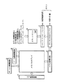
図1は、本発明の第1の実施の形態に係わる多値フラッシュメモリの全体の構成を示すブロック図である。
【0024】
メモリセルアレイ1内には複数のフラッシュメモリセル、複数のビット線及びワード線が設けられている。複数のフラッシュメモリセルはマトリクス状に配置されている。
【0025】
カラム制御回路2及びロウ制御回路3が、メモリセルアレイ1に隣接して設けられている。上記カラム制御回路2は、メモリセルアレイ1内のビット線を制御し、メモリセルのデータ消去、メモリセルへのデータ書き込み、さらには、メモリセルからのデータ読み出しを行う。
【0026】
上記ロウ制御回路3は、メモリセルアレイ1内のワード線を選択し、消去、書き込み、読み出しに必要な電圧を供給する。
【0027】
また、メモリセルアレイ1のソース線を制御するソース線制御回路4と、メモリセルアレイ1が形成されるp型ウェルを制御するPウェル制御回路5とが設けられている。
【0028】
データ入出力バッファ6は、外部I/O線を介してホストに接続されている。このデータ入出力バッファ6は、書き込みデータの受け取り、読み出しデータの出力、アドレスデータやコマンドデータの受け取りを行う。データ入出力バッファ6で受け取られた書き込みデータはカラム制御回路2に送られる。また、データ入出力バッファ6は、カラム制御回路2から読み出されたデータを受け取る。
【0029】
メモリセルアレイ1内のメモリセルの選択を行うために、外部からのアドレスデータがステートマシン8を介してカラム制御回路2及びロウ制御回路3に送られる。
【0030】
また、ホストからのコマンドデータがコマンド・インターフェイス7に送られる。コマンド・インターフェイス7は、ホストからの制御信号を受け、データ入出力バッファ6に入力されたデータが書き込みデータかコマンドデータかアドレスデータかを判断し、コマンドデータであれば受け取りコマンド信号としてステートマシン8に転送する。
【0031】
ステートマシン8は、フラッシュメモリ全体の管理を行うものであり、ホストからのコマンドを受け、読み出し、書き込み、消去の各動作及びデータの入出力管理を行う。なお、ステートマシン8内には各メモリセルに対するデータの書き込み回数をカウントするための書き込みカウンタPCが設けられている。
【0032】
図2(a)は、図1中のメモリセルアレイ1の内部構成を示すブロック図である。メモリセルアレイ1内の複数のメモリセルは複数のブロックBLOCK0〜BLOCK1023に分割されている。ブロックは消去の最小単位である。各ブロックBLOCKi(i=0〜1023内にはそれぞれ、図2(b)に示すように8512個のNAND型メモリユニットが設けられている。
【0033】
この例では、各NAND型メモリユニットには直列に接続された4個のメモリセルMが設けられており、その一端は選択ゲート線SGD iに共通に接続された選択ゲートS1を介してビット線BLeまたはBLoに接続され、他端は選択ゲート線SGS iに共通に接続された選択ゲートS2を介して共通ソース線C−sourceに接続されている。
【0034】
それぞれのメモリセルMは制御ゲート、浮遊ゲート、ソース及びドレインを有し、各4個のメモリセルMの制御ゲートはワード線WL0 i〜WL3 iのうち対応するものに共通に接続されている。
【0035】
0から数えて偶数番目のビット線BLeと奇数番目のビット線BLoに対し、互いに独立にデータの書き込みと読み出しが行われる。1本のワード線WLに制御ゲートが接続されている8512個のメモリセルのうち、偶数番目のビット線BLeに接続される4256個のメモリセルに対して同時にデータの書き込みと読み出しが行われる。
【0036】
各メモリセルがそれぞれ1ビットのデータを記憶する場合、4256個のメモリセルに記憶される4256ビットのデータがページという単位を構成する。1つのメモリセルが2ビットのデータを記憶する場合、4256個のメモリセルは2ページ分のデータを記憶する。奇数番目のビット線BLoに接続される4256個のメモリセルで別の2ページが構成され、同一ページ内のメモリセルに対して同時にデータの書き込みと読み出しが行われる。
【0037】
図3は、図1中のメモリセルアレイ1のカラム方向の素子構造を示す断面図である。p型基板10上にn型ウェル11が形成され、n型ウェル11内にp型ウェル1211が形成されている。各メモリセルMは、n型拡散層13で形成されたソース、ドレインと、ソース・ドレイン間のチャネル領域上にトンネル酸化膜を介して設けられた浮遊ゲートFGと、この浮遊ゲートFG上に絶縁膜を介して設けられワード線WLとなる制御ゲートCGとから構成されている。
【0038】
各選択ゲートS1、S2は、n型拡散層13で形成されたソース、ドレインと、積層された2重構造の選択ゲート線SGとからそれぞれ構成されている。ワード線WLと選択ゲート線SGは、共に図1中のロウ制御回路3に接続され、ロウ制御回路3からの出力信号によって制御される。
【0039】
4個のメモリセルMと選択ゲートS1、S2とからなるNAND型メモリユニットの一端は、コンタクトホールCB1を介して第1層のメタル配線層M0に接続される。このメタル配線層M0は、ヴイアホールV1を介して、ビット線BLとなる第2層のメタル配線層M1に接続されている。ビット線BLは図2中のカラム制御回路2に接続されている。
【0040】
NAND型メモリユニットの他端はコンタクトホールCB2を介して、共通ソース線C−sourceとなる第1層のメタル配線層M2に接続されている。共通ソース線C−sourceは図1中のソース線制御回路4に接続されている。
【0041】
n型ウェル11の表面にはn型拡散層14が、p型ウェル12の表面にはp型拡散層15がそれぞれ形成され、n型拡散層14及びp型拡散層15はコンタクトホールCB3、CB4を介して、ウェル線C−p−wellとなる第1層のメタル配線層M3に共に接続されている。ウェル線C−p−wellは図1中のPウェル制御回路5に接続されている。
【0042】
図4(a)、(b)は、メモリセルアレイ1のロウ方向の素子構造を示す断面図である。図4(a)、(b)に示すように、各メモリセルは素子分離STIによって互いに分離されている。
【0043】
図4(a)に示すように、各メモリセルでは、トンネル酸化膜16を介して浮遊ゲートFGがチャネル領域上に積層されている。浮遊ゲートFG上にはONO膜からなる絶縁膜17を介してワード線WLが積層されている。
【0044】
図4(b)に示すように、選択ゲート線SGは2重構造にされている。そして、メモリセルアレイ1の端あるいは一定数のビット線毎に上下の選択ゲート線SGが接続されている。
【0045】
図5は、図1中のカラム制御回路2の主要部の構成を抽出して示している。
【0046】
カラム制御回路2には、同一カラム番号の偶数番目のビット線BLeと奇数番目のビット線BLoからなる2本のビット線毎にデータ記憶回路20がそれぞれ設けられている。また、カラム制御回路2には、上記各データ記憶回路20に対応して、メモリセルにデータを書き込みかつメモリセルからデータを読み出すセンスアンプが設けられている。
【0047】
上記データ記憶回路20と偶数番目のビット線BLeとの間にはカラム選択用のnチャネルMOSトランジスタQn1が接続され、奇数番目のビット線BLoとの間にはカラム選択用のnチャネルMOSトランジスタQn2が接続されている。
【0048】
各データ記憶回路20に接続された偶数番目及び奇数番目のビット線BLe、BLoは、いずれか一方が選択されてデータ記憶回路20に接続され、データ書き込みあるいは読み出しのため制御される。すなわち、信号EVENBLがHレベル、信号ODDBLがLレベルのときは、MOSトランジスタQn1が導通して偶数番目のビット線BLeが選択され、このビット線BLeがデータ記憶回路20に接続される。信号EVENBLがLレベル、信号ODDBLがHレベルのときは、MOSトランジスタQn2が導通して奇数番目のビット線BLoが選択され、このビット線BLoがデータ記憶回路20に接続される。なお、上記信号EVENBLは偶数番目のビット線BLeに接続されている全てのカラム選択用のnチャネルMOSトランジスタに共通に供給され、信号ODDBLは奇数番目のビット線BLoに接続されている全てのカラム選択用のnチャネルMOSトランジスタに共通に供給される。なお、非選択のビット線BLについては、図示しない他の回路で制御される。
【0049】
上記各データ記憶回路20内には3つのバイナリデータ記憶部DS1、DS2、DS3が設けられている。データ記憶部DS1は内部のデータ入出力線(I/O線)を介してデータ入出力バッファ6と接続され、外部から入力された書き込みデータや外部へ出力する読み出しデータを記憶する。データ記憶部DS2は、書き込み後にメモリセルのしきい値を確認する(書き込みベリファイ)時の検出結果を記憶する。データ記憶部DS3は、メモリセルのデータを書き込みと読み出しの時に一時的に記憶する。
【0050】
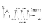
図6は、第1の実施の形態に係わる多値フラッシュメモリの多値データとメモリセルのしきい値との関係を示す図である。
【0051】
次に、図6を参照して、上記構成でなる多値フラッシュメモリの動作を説明する。なお、本例では、2ビット、つまり4値のデータを1つのメモリセルに記憶する場合を説明する。この2ビットのデータとしては“11”、“10”、“01”、“00”が全てである。この2つのビットは異なるロウアドレス(異なるページ)に属する。
【0052】
また、上記4値のデータはしきい値の違いとしてメモリセルに記憶され、図6に示すように、例えばしきい値が最も低い状態(例えばしきい値電圧が負の状態)をデータ“11”とし、メモリセルのしきい値が2番目に低い状態(例えばしきい値電圧が正の状態を)データ“10”とし、メモリセルのしきい値が3番目に低い状態(例えばしきい値電圧が正の状態を)データ“01”とし、メモリセルのしきい値が最も高い状態(例えばしきい値電圧が正の状態を)データ“00”とする。
【0053】
消去後、メモリセルのデータは“11”となっている。このメモリセルへの下位ページの書き込みデータが“0”であれば、書き込みにより“11”の状態から“10”に移る。“1”データ書き込みの場合は“11”のままである。
【0054】
次に、上位ページのデータが書き込まれる。もし書き込みデータが“1”であれば、“11”あるいは“10”の状態がそのまま維持される。もし書き込みデータが“0”であれば、“11”の状態は“01”に、“10”の状態は“00”にそれぞれ移される。
【0055】
書き込み動作中に、書き込みが行われたメモリセルからデータを読み出して、十分に書き込みが行われたか否かが検証されるいわゆる書き込みベリファイが行われる。
【0056】
センスアンプによる読出しデータは、しきい値が0V以下であれば“11”とみなされ、しきい値が0V以上1V以下なら“10”とみなされる。また、しきい値が1V以上2V以下なら“01”とみなされ、しきい値が2V以上なら“00”とみなされる。
【0057】
このように、1つのメモリセルに2ビットのデータを記憶させるために、4値のしきい値が用いられる。実際のデバイスでは、メモリセルの特性にばらつきが生じるため、そのしきい値もばらつく。このばらつきが大きいと、データの区別ができなくなり間違ったデータを読み出してしまう。
【0058】
本実施の形態の多値フラッシュメモリでは、図6中に破線で示すように、従来の多値フラッシュメモリで生じていたしきい値の大きなばらつきを実線のように抑えることができる。この点については後で説明する。
【0059】
表1は、第1の実施の形態に係る多値フラッシュメモリの消去、書き込み、読み出し、書き込みベリファイ時における各部の電圧値を一例を示している。なお、表1では、書き込みと読み出し時にワード線WL2と偶数番目のビット線BLeが選択された場合の例を示している。
【0060】
【表1】

消去は、p型ウェル12(ウェル線C−p−well)に20Vが、選択されたブロックの全ワード線WL0に0Vが供給される。これにより、ブロック内の全てのメモリセルMの浮遊ゲートFGから電子が放出されてしきい値が負となり、“11”状態になる。ここで非選択ブロックのワード線及びビット線BLなどは電位的にフローティング状態にされるが、p型ウェル12との容量結合により20V近くとなっている。
【0062】
書き込みは、第1段階、第2段階及び書き込み禁止の順で行われる。まず、選択されたワード線WL2に14V〜20Vの値を持つプログラム電圧(書き込み電圧)Vpgmが供給される。非選択のワード線のうち選択メモリセルよりもビット線側に配置されたメモリセルの各ワード線、例えばワード線WL3には、このワード線WL3が接続されたメモリセルが導通するような高い電圧、例えば10Vが供給される。他方、非選択のワード線のうち選択メモリセルよりもウェル線C−p−well側に配置されたメモリセルの各ワード線、例えばワード線WL1には、このワード線WL1が接続されたメモリセルが非導通となるような低い電圧、例えば0Vが供給される。また、選択されたビット線BLeには0Vの電圧が供給される。すると、ビット線BLeに供給された0Vの電圧が、選択されたメモリセルのドレインまで伝わり、かつ制御ゲートCGと浮遊ゲートFGとの間の容量結合によって浮遊ゲートFGの電位が上昇し、トンネル酸化膜(図4(a)中のトンネル酸化膜16)を介し、トンネル現象によって電子がドレインから浮遊ゲートFGに注入され、しきい値が高速に上昇する(第1段階書き込み)。書き込み時に、しきい値の上昇速度を抑えるには、ビット線BLeの電圧が0.4Vに上げられる(第2段階書き込み)。しきい値の上昇を禁止するにはビット線BLeを十分に高い電圧、例えば電源電圧Vdd(〜3V)にされる(書き込み禁止)。
【0063】
読み出しは、選択されたワード線WL2に異なる値の読み出し電圧(0V、1V、2V)が順次供給されることで行われる。非選択の残りのワード線には、非選択のメモリセルが導通するような値の電圧、例えば4.5Vが供給される。選択メモリセルのしきい値が読み出し電圧以下なら、ビット線BLeと共通ソース線C−sourceとの間が導通して電流が流れ、ビット線BLeの電位は比較的低いレベルLとなる。選択メモリセルのしきい値が読み出し電圧以上なら、ビット線BLeと共通ソース線C−sourceとの間は非導通となり、ビット線BLeの電位は比較的高いレベルHとなる。メモリセルが“10”状態のしきい値より高いか否かを検出するには、読み出し電圧が例えば0Vにされて読み出しが行われる(“10”読み出し)。メモリセルが“01”状態のしきい値より高いか否かを検出するには、読み出し電圧が例えば1Vにされて読み出しが行われる(“01”読み出し)。また、メモリセルが“00”状態のしきい値より高いか否かを検出するには、読み出し電圧が例えば2Vにされて読み出しが行われる(“00”読み出し)。
【0064】
“10”状態のメモリセルは、読み出し電圧0Vに対して0.4Vの読み出しマージンを持たせるため、しきい値が0.4V以上となるように書き込まれる。このため、“10”に書き込む場合、書き込みベリファイによりメモリセルのしきい値が0.4Vに達したと検出されたら、書き込みが禁止される。
【0065】
従来では、しきい値が0.4Vに達したか否かしか検出されないので、図6に示すように、しきい値は比較的幅広い分布を持つ。
【0066】
本実施の形態では、しきい値が目標のしきい値より若干低いレベルに達したか否かを検出して、しきい値の上昇速度が第2段階書き込みにより抑制される。このため、しきい値の分布幅は図6中の実線で示すように従来よりも狭めることができる。他の“01”、“00”状態に関しても同様である。
【0067】
書き込みベリファイは、選択されたワード線WL2に異なる値のベリファイ電圧、例えば、0.2V、0.4V、1.2V、1.4V、2.2V、2.4Vが順次供給されることで行われる。メモリセルのしきい値がベリファイ電圧以下なら、ビット線BLeと共通ソース線C−sourceとの間が導通して、ビット線BLeの電位は比較的低いレベルLとなる。メモリセルのしきい値がベリファイ電圧以上なら、ビット線BLeと共通ソース線C−sourceとの間は非導通となり、ビット線BLeの電位は比較的高いレベルHとなる。
【0068】
メモリセルの目標のしきい値が0.4Vの場合、その目標のしきい値よりも若干低いレベルのしきい値、本例では例えば0.2Vより高いか否かを検出するには、ベリファイ電圧が0.2Vにされて書き込みベリファイが行われる(“10”第1段階書き込みベリファイ)。メモリセルのしきい値が目標のしきい値0.4Vより高いか否かを検出するには、ベリファイ電圧が0.4Vにされて書き込みベリファイが行われる(“10”第2段階書き込みベリファイ)。
【0069】
メモリセルの目標のしきい値が1.4Vの場合、その目標のしきい値よりも若干低いレベルのしきい値、本例では例えば1.2Vより高いか否かを検出するには、ベリファイ電圧が1.2Vにされて書き込みベリファイが行われる(“01”第1段階書き込みベリファイ)。メモリセルのしきい値が目標のしきい値1.4Vより高いか否かを検出するには、ベリファイ電圧が1.4Vにされて書き込みベリファイが行われる(“01”第2段階書き込みベリファイ)。
【0070】
メモリセルの目標のしきい値が2.4Vの場合、その目標のしきい値よりも若干低いレベルのしきい値、本例では例えば2.2Vより高いか否かを検出するには、ベリファイ電圧が2.2Vにされて書き込みベリファイが行われる(“00”第1段階書き込みベリファイ)。メモリセルのしきい値が目標のしきい値2.4Vより高いか否かを検出するには、ベリファイ電圧が2.4Vにされて書き込みベリファイが行われる(“00”第2段階書き込みベリファイ)。
【0071】
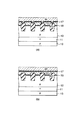
図7は、従来の書き込み方法としきい値の変化状態を示している。図中、白抜きの四角は書き込み易いメモリセルのしきい値及びこのメモリセルに供給される書き込み制御電圧(ビット線BLの電圧)を示し、黒の四角は書き込み難いメモリセルのしきい値及びこのメモリセルに供給される書き込み制御電圧(ビット線BLの電圧)を示している。この2つのメモリセルは同一ページのデータを記憶する。どちらも初期状態では消去されており、負のしきい値を持っているとする。
【0072】
書き込み電圧Vpgmは複数のパルスに分割されており、1パルス毎に例えば0.2Vづつ上昇する。すなわち、書き込み電圧Vpgmの1パルス当たりの増加分Dvpgmは0.2Vである。
【0073】
書き込み制御電圧であるビット線BLの電圧が0Vにされると、数パルス後に、しきい値は書き込み電圧Vpgmの電圧増加分と同じ0.2V/パルスの速度で上がっていく。各書き込みパルス印加後に書き込みベリファイが行われ、書き込みベリファイ電圧にしきい値が達したと検出されたメモリセルのビット線電圧がVddにされ、メモリセル毎に書き込みが禁止されていく。従って、しきい値は0.2Vの分布幅を持つ。
【0074】
図8は、第1の実施の形態に係わる多値フラッシュメモリにおけるデータの書き込み方法と、しきい値の変化状態を示している。図7の場合と同様に、白抜きの四角は書き込み易いメモリセルのしきい値及びこのメモリセルに供給される書き込み制御電圧(ビット線BLの電圧)を示し、黒の四角は書き込み難いメモリセルのしきい値及びこのメモリセルに供給される書き込み制御電圧(ビット線BLの電圧)を示している。この2つのメモリセルは同一ページのそれぞれのカラムのデータを記憶する。どちらも初期状態では消去されており、負のしきい値を持っている。
【0075】
書き込み電圧Vpgmは複数のパルスに分割されており、1パルス毎に例えば0.2Vづつ上昇する。すなわち、書き込み電圧Vpgmの1パルス当たりの増加分Dvpgmは0.2Vである。
【0076】
書き込み制御電圧であるビット線BLの電圧が0Vにされて第1段階書き込みが行われる。そして、第1段階書き込みにおいて、書き込み電圧Vpgmが数パルス分供給された後に、しきい値は書き込み電圧Vpgmの電圧増加分と同じ0.2V/パルスの速度で上がっていく。書き込みパルスを1回印加した後毎に第1段階書き込みベリファイあるいは第2段階書き込みベリファイが行われる。
【0077】
第1段階書き込みベリファイ電圧にしきい値が達したと検出されたメモリセルのビット線電圧は、その後、0.4Vにされ、メモリセル毎に第2段階書き込みに移る。第2段階書き込みベリファイ電圧にしきい値が達したと検出されたメモリセルのビット線電圧はVddにされ、メモリセル毎に書き込みが禁止されていく。
【0078】
第2段階書き込みになって、数パルスの間はしきい値の上昇率が第1段階書き込み時における0.2V/パルスよりも低く抑制される。すなわち、ビット線BLの電圧つまり書き込み制御電圧は、第1段階書き込み時では0Vであるが、第2段階書き込みになると0.4Vに増加する。このため、第2段階書き込みでは第1段階書き込みと比べてより書き込み難くなる。第2段階書き込み時におけるしきい値の上昇率は、例えばほぼ0V/パルスから0.05V/パルスの範囲の値に抑制される。すなわち、第2段階書き込み時では、しきい値は高々0.05Vの分布幅しか持たない。
【0079】
書き込みパルス幅を20μsec、書き込みベリファイに要する時間を5μsecとすると、従来では書き込み時間は(20μsec+5μsec)×18パルス=450μsecとなる。
【0080】
従来において、0.05Vのしきい値分布を実現させるためには、書き込み電圧Vpgmの電圧増加分Dvpgmを0.05V、つまり0.2Vの4分の1の値にする必要があるので、450μsec×4 =1800μsecとなる。
【0081】
一方、本実施の形態によれば、図8に示すように、0.2V/パルスの電圧増加分Dvpgmで0.05Vのしきい値分布幅が実現でき、その書き込み時間は、(20μsec+5μsec+5μsec)×20パルス=600μsecとなる。
【0082】
つまり、従来に比べて同じ0.05Vのしきい値分布を実現するために要する書き込み時間は3分の1に短縮される。
【0083】
第1段階書き込みベリファイ電圧を“10”第1段階書き込みベリファイ電圧とし、第2段階書き込みベリファイ電圧を“10”第2段階書き込みベリファイ電圧とすることで、“10”書き込みが行われる。
【0084】
図9は、本実施の形態における同一メモリセルへの上位ページデータの書き込み方法としきい値の変化状態を示している。図7、図8の場合と同様に、白抜きの四角は書き込み易いメモリセルのしきい値及びこのメモリセルに供給される書き込み制御電圧(ビット線BLの電圧)を示し、黒の四角は書き込み難いメモリセルのしきい値及びこのメモリセルに供給される書き込み制御電圧(ビット線BLの電圧)を示している。この2つのメモリセルは同一ページのそれぞれのカラムのデータを記憶する。
【0085】
白抜きの四角で示される書き込み易いメモリセルは、初期状態では消去されており負のしきい値を持っており、このメモリセルは“01”状態に書き込まれるとする。黒の四角で示されるメモリセルは、初期状態では“10”の状態に既に書き込まれており、このメモリセルは“00”状態に書き込まれるとする。
【0086】
書き込み電圧Vpgmは複数のパルスに分割されており、1パルス毎に例えば0.2Vづつ上昇する。すなわち、書き込み電圧Vpgmの1パルス当たりの増加分Dvpgmは0.2Vである。
【0087】
書き込み制御電圧であるビット線BLの電圧が0Vにされて第1段階書き込みが行われる。そして、数パルス後には、しきい値は書き込み電圧Vpgmの電圧増加分と同じ0.2V/パルスの速度で上がっていく。書き込みパルスが印加された後毎に“01”第1段階書き込みベリファイが行われる。目標のしきい値よりも若干低いしきい値に書き込まれた後は、書き込みパルスが印加された後毎に“01”第2段階書き込みベリファイが行われる。その後、“00”第1段階書き込みベリファイと“00”第2段階書き込みベリファイが行われる。
【0088】
白抜きの四角で示されるメモリセルのしきい値が“01”第1段階書き込みベリファイ電圧に達したと検出されたら、その後、ビット線電圧が0.4Vにされ、第2段階書き込みに移る。黒の四角で示されるメモリセルのしきい値が“00”第1段階書き込みベリファイ電圧に達したと検出されたら、その後、ビット線電圧が0.4Vにされ、第2段階書き込みに移る。
【0089】
また、白抜きの四角で示されるメモリセルのしきい値が“01”第2段階書き込みベリファイ電圧に達したと検出されたら、その後、ビット線電圧がVddにされ、書き込みが禁止される。さらに、黒の四角で示されるメモリセルのしきい値が“00”第2段階書き込みベリファイ電圧に達したと検出されたら、その後、ビット線電圧がVddにされ、書き込みが禁止される。
【0090】
データ“01”及び“00”の両方に関し、第2段階書き込みになってから、書き込み電圧の数パルスの間は、しきい値の増加分が例えばほぼ0V/パルスから0.05V/パルスの範囲の値に抑制されるため、しきい値は0.05Vの分布幅しか持たない。
【0091】
図10は、本実施の形態において、1つのメモリセルに下位ページのデータを書き込む際の各部の信号波形を示している。
【0092】
時間tp0からtp7までが書き込みステップであり、この期間にメモリセルに書き込みパルスが与えられる。時間tfv0からtfv6までが“10”第1段階書き込みベリファイ期間であり、時間tsv0からtsv6までが“10”第2段階書き込みベリファイ期間である。本例ではワード線WL2と偶数番目のビット線BLeが選択される場合を示している。
【0093】
書き込みステップで、書き込み制御電圧であるビット線BLeは、第1段階書き込みならば0Vに、第2段階書き込みならば0.4Vにそれぞれされ、書き込み禁止ならVdd(例えば2.5V)にされる。
【0094】
各書き込みベリファイ期間には、まずビット線BLeが例えば0.7Vに充電される。その後、選択ワード線WL2が各書き込みベリファイ電圧に達すると、もしメモリセルのしきい値が書き込みベリファイ電圧に達していればビット線BLeは0.7Vに維持される。メモリセルのしきい値が書き込みベリファイ電圧に達していなければ、ビット線BLeは0Vに向かって下がる。時間tfv4あるいはtsv4のタイミングでビット線BLeの電圧をセンスアンプで検出すれば、メモリセルのしきい値が書き込みベリファイ電圧に達しているか否か検出できる。メモリセルのしきい値が書き込みベリファイ電圧に達していれば検出結果はパスである。
【0095】
図11は、第1の実施の形態における、1つのメモリセルに対する下位ページのデータ書き込み時の制御アルゴリズムを示している。
【0096】
まず、ホストからのデータ入力コマンドを受け取り、ステートマシン8にデータ入力コマンドを設定する(S1)。ホストからのアドレスデータを受け取り、ステートマシン8に書き込みページを選択するためのアドレスを設定する(S2)。次に、1ページ分の書き込みデータを受け取り、それぞれの対応するデータ記憶部DS1に書き込みデータを設定する(S3)。ホストが発行した書き込みコマンドを受け取り、ステートマシン8に書き込みコマンドを設定する(S4)。書き込みコマンドが設定されて、S5からS16のステップが自動的に内部でステートマシン8によって起動される。
【0097】
各データ記憶部DS1のデータは対応するデータ記憶部DS2にコピーされる(S5)。その後、書き込み電圧Vpgmの初期値を12Vに設定し、また、書き込みカウンタPCを0に設定する(S6)。データ記憶部DS1のデータが“0”でかつデータ記憶部DS2のデータが“0”なら第1段階書き込みであるので、書き込み制御電圧であるビット線BLの電圧を0Vにする。データ記憶部DS1のデータが“0”かつデータ記憶部DS2のデータが“1”なら第2段階書き込みであるので、書き込み制御電圧であるビット線BLの電圧を0.4Vにする。データ記憶部DS1のデータが“1”かつデータ記憶部DS2のデータが“1”なら書き込み禁止であるので、書き込み制御電圧であるビット線BLの電圧をVddに設定する(S7)。
【0098】
設定された書き込み電圧Vpgmと書き込み制御電圧とを用いて1ページ分のメモリセルに対して書き込みパルスを与える書き込みステップを実行する(S8)。全てのデータ記憶部DS2のデータが“1”か否かを検出し、全て“1”なら第1段階ステータスをパスと判断し、そうでなければパスでないと判断する(S9)。後述するが、全てのデータ記憶部DS2のデータが“1”であれば、前段の書き込みステップ(S8)で第1段階書き込みされたメモリセルは無い。
【0099】
第1段階ステータスがパスでなければ、“10”第1段階書き込みベリファイが起動され(S10)、1ページ分のメモリセルのうち検出結果がパスとなったメモリセルに対応するデータ記憶部DS2のデータを“0”から“1”に変える。データ記憶部DS2のデータが“1”であるものは、その“1”状態を保持する。
【0100】
第1段階ステータスがパスの場合、あるいは“10”第1段階書き込みベリファイが終了すると、“10”第2段階書き込みベリファイが起動される(S11)。1ページ分のメモリセルのうち検出結果がパスとなったメモリセルに対応するデータ記憶部DS1のデータを“0”から“1”に変える。データ記憶部DS1のデータが“1”であるものは、その“1”状態を保持する。
【0101】
“10”第2段階書き込みベリファイ後、全てのデータ記憶部DS1のデータが“1”か否かを検出し、全て“1”なら第2段階ステータスをパスと判断し、そうでなければパスでないと判断する(S12)。第2段階ステータスがパスであれば、正常に書き込みが終了したとして、書きこみステータスをパスに設定して書き込み終了となる(S13)。
【0102】
第2段階ステータスがパスでなければ書き込みカウンタPCを調べ(S14)、その値が20以上であれば正常に書き込めなかったとして、書きこみステータスをフェイルに設定して書き込み終了となる(S15)。書き込みカウンタPCの値が20より少なければ、書き込みカウンタPCの値を1だけ増やし、さらに、書き込み電圧Vpgmの設定値を0.2V増やし(S16)、再度ステップS7を経て書き込みステップS8となる。なお、上記書き込み回数は20回に限定されるではなく、適宜変更してもよい。
【0103】
表2は、図11に示される書き込みアルゴリズムにおいて、データ記憶部DS1とDS2の“10”第1段階書き込みベリファイ前後のデータと、対応するメモリセルのしきい値(Vt)との関係を示している。
【0104】
【表2】
n番目の“10”第1段階書き込みベリファイ前のデータ記憶部DS1とDS2の取り得る値は0/0、0/1、1/1のいずれかである。0/0は、n−1番目の書き込みステップまでにメモリセルのしきい値が“10”第1段階書き込みベリファイ電圧にも達していないことを示している。0/1は、n−1番目の書き込みステップまでにメモリセルのしきい値が“10”第1段階書き込みベリファイ電圧には達したが、“10”第2段階書き込みベリファイ電圧には達していないことを示している。1/1は、n−1番目の書き込みステップまでにメモリセルのしきい値が“10”第2段階書き込みベリファイ電圧に達したことを示している。n−1番目の書き込みステップまでにメモリセルのしきい値が“10”第2段階書き込みベリファイ電圧には達したが、“10”第1段階書き込みベリファイ電圧には達していないということはあり得ないので、1/0という状態はこの実施の形態では存在しない。
【0106】
1番目の“10”第1段階書き込みベリファイ前のデータ記憶部DS1とDS2の取り得る値は0/0か1/1である。
【0107】
メモリセルのしきい値がn番目の書き込みステップで“10”第1段階書き込みベリファイ電圧である0.2Vに達していなければ、“10”第1段階書き込みベリファイでの検出結果はパスではないので、データ記憶部DS2のデータは変更されない。メモリセルのしきい値がn番目の書き込みステップで“10”第1段階書き込みベリファイ電圧である0.2Vに達していれば、“10”第1段階書き込みベリファイでの検出結果はパスなので、データ記憶部DS2のデータは“1”に変更される。既に“1”であるデータ記憶部DS2のデータはメモリセルのしきい値によらず変更されない。
【0108】
表3は、図11に示されるアルゴリズムにおいて、データ記憶部DS1とDS2の“10”第2段階書き込みベリファイ前後のデータと、対応するメモリセルのしきい値との関係を示している。
【0109】
【表3】
n番目の“10”第2段階書き込みベリファイ前のデータ記憶部DS1とDS2の取り得る値は0/0、0/1、1/1のいずれかである。0/0は、n番目の書き込みステップ後にメモリセルのしきい値が“10”第1段階書き込みベリファイ電圧にも達していないことを示している。0/1は、n番目の書き込みステップまでにメモリセルのしきい値が“10”第1段階書き込みベリファイ電圧には達したが、n−1番目の書き込みステップまではメモリセルのしきい値が“10”第2段階書き込みベリファイ電圧には達していないことを示している。1/1は、n−1番目の書き込みステップまでにメモリセルのしきい値が“10”第2段階書き込みベリファイ電圧に達したことを示している。
【0111】
n−1番目の書き込みステップまでにメモリセルのしきい値が“10”第2段階書き込みベリファイ電圧には達したが、n番目の書き込みステップまでにメモリセルのしきい値が“10”第1段階書き込みベリファイ電圧には達していないことはあり得ないので、1/0という状態はこの実施の形態では存在しない。
【0112】
メモリセルのしきい値が、n番目の書き込みステップで“10”第2段階書き込みベリファイ電圧である0.4Vに達していなければ、“10”第2段階書き込みベリファイでの検出結果はパスではないので、データ記憶部DS1のデータは変更されない。メモリセルのしきい値が、n番目の書き込みステップで“10”第2段階書き込みベリファイ電圧である0.4Vに達していれば、“10”第2段階書き込みベリファイでの検出結果はパスなので、データ記憶部DS1のデータは“1”に変更される。既に“1”であるデータ記憶部DS1のデータはメモリセルのしきい値によらず変更されない。0/0は、“10”第2段階書き込みベリファイによって変更されることはない。
【0113】
図12は、上記実施の形態における、メモリセルに対する上位ページのデータ書き込み時の制御アルゴリズムを示している。
【0114】
まず、ホストからのデータ入力コマンドを受け取りステートマシン8にデータ入力コマンドを設定する(S1)。ホストからのアドレスデータを受け取り、ステートマシン8に書き込みページを選択するためのアドレスを設定する(S2)。次に、1ページ分の書き込みデータを受け取り、それぞれのデータ記憶部DS1に対応する書き込みデータを設定する(S3)。ホストが発行した書き込みコマンドを受け取りステートマシン8に書き込みコマンドを設定する(S4)。書き込みコマンドが設定されて、S5〜S20のステップが自動的に内部でステートマシン8によって起動される。
【0115】
まず、“10”読み出しが起動され(S5)、パス(メモリセルのデータが“10”)の場合は、対応するデータ記憶部DS3に“0”を設定する。パスでなければ対応するデータ記憶部DS3に“1”を設定する。次に、各データ記憶部DS1のデータを対応するデータ記憶部DS2にコピーする(S6)。その後、書き込み電圧Vpgmの初期値を14Vに設定し、また、書き込みカウンタPCを0に設定する(S7)。データ記憶部DS1のデータが“0”かつデータ記憶部DS2のデータが“0”なら第1段階書き込みであるので、書き込み制御電圧であるビット線BLの電圧を0Vにし、データ記憶部DS1のデータが“0”かつデータ記憶部DS2のデータが“1”なら第2段階書き込みであるので、書き込み制御電圧であるビット線BLの電圧を0.4Vにし、データ記憶部DS1のデータが“1”かつデータ記憶部DS2のデータが“1”なら書き込み禁止であるので、書き込み制御電圧であるビット線BLの電圧をVddに設定する(S8)。この後は、設定された書き込み電圧Vpgmと書き込み制御電圧とを用いて1ページ分のメモリセルに対して書き込みパルスを与える書き込みステップとなる(S9)。
【0116】
データ記憶部DS3に“0”が記憶されている全てのデータ記憶回路20で、その全てのデータ記憶部DS2のデータが“1”か否かを検出し、全て“1”なら“00”第1段階ステータスをパスと判断し、そうでなければパスでないと判断する(S10)。後ほど説明するが、その全てのデータ記憶部DS2のデータが“1”であれば、前段の書き込みステップ(S9)で“00”第1段階書き込みされたメモリセルは無い。
【0117】
“00”第1段階ステータスがパスでなければ、“00”第1段階書き込みベリファイが起動され(S11)、1ページ分のメモリセルのうち検出結果がパスとなったメモリセルに対応しかつデータ記憶部DS3のデータが“0”であるデータ記憶回路20内のデータ記憶部DS2のデータを“0”から“1”に変える。データ記憶部DS2のデータが既に“1”であるものは、その“1”状態を保持する。
【0118】
“00”第1段階ステータスがパスの場合、あるいは“00”第1段階書き込みベリファイが終了すると、“00”第2段階書き込みベリファイが起動される(S12)。1ページ分のメモリセルのうち検出結果がパスとなったメモリセルに対応しかつデータ記憶部DS3のデータが“0”であるデータ記憶回路20中のデータ記憶部DS1のデータを“0”から“1”に変える。既にデータ記憶部DS1のデータが“1”であるものは、その“1”状態を保持する。
【0119】
次に、データ記憶部DS3に“1”を記憶している全てのデータ記憶回路20で、その全てのデータ記憶部DS2のデータが“1”か否かを検出し、全て“1”なら“01”第1段階ステータスをパスと判断し、そうでなければパスでないと判断する(S13)。後ほど説明するが、その全てのデータ記憶部DS2のデータが“1”であれば、前段の書き込みステップ(S9)で“01”第1段階書き込みされたメモリセルは無い。
【0120】
“01”第1段階ステータスがパスでなければ、“01”第1段階書き込みベリファイが起動され(S14)、1ページ分のメモリセルのうち検出結果がパスとなったメモリセルに対応しかつデータ記憶部DS3のデータが“1”であるデータ記憶回路20内のデータ記憶部DS2のデータを“0”から“1”に変える。既にデータ記憶部DS2のデータが“1”であるものは、その“1”状態を保持する。
【0121】
“01”第1段階ステータスがパスの場合、あるいは“01”第1段階書き込みベリファイが終了すると、“01”第2段階書き込みベリファイが起動される(S15)。1ページ分のメモリセルのうち検出結果がパスとなったメモリセルに対応しかつデータ記憶部DS3のデータが“1”であるデータ記憶回路20内のデータ記憶部DS1のデータを“0”から“1”に変える。既にデータ記憶部DS1のデータが“1”であるものは、その“1”状態を保持する。
【0122】
“01”第2段階書き込みベリファイ後、全てのデータ記憶部DS1のデータが“1”か否かを検出し、全て“1”なら第2段階ステータスをパスと判断し、そうでなければパスでないと判断する(S16)。第2段階ステータスがパスであれば、正常に書き込みが終了したとして、書きこみステータスをパスに設定して書き込み終了となる(S17)。第2段階ステータスがパスでなければ書き込みカウンタPCを調べ(S18)、その値が20以上であれば正常に書き込めなかったとして、書き込みステータスをフェイルに設定して書き込み終了となる(S19)。書き込みカウンタPCの値が20より少なければ、書き込みカウンタPCの値を1だけ増やし、さらに、書き込み電圧Vpgmの設定値を0.2V増加し(S20)、再度ステップS8を経て書き込みステップS9となる。この場合にも、上記書き込み回数は20回に限定されるではなく、適宜変更してもよい。
【0123】
表4は、図11に示されるアルゴリズムにおいて、データ記憶部DS1、DS2、DS3の“01”第1段階書き込みベリファイ前後のデータと、対応するメモリセルのしきい値(Vt)との関係を示している。
【0124】
【表4】
n番目の“01”第1段階書き込みベリファイ前のデータ記憶部DS1、DS2、DS3の取り得る値は、0/0/1、0/1/1、1/1/1、0/0/0、0/1/0、1/1/0のいずれかである。0/0/1は、n−1番目の書き込みステップまでにメモリセルのしきい値が“01”第1段階書き込みベリファイ電圧にも達していないことを示している。0/1/1は、n−1番目の書き込みステップまでにメモリセルのしきい値が“01”第1段階書き込みベリファイ電圧には達したが、“01”第2段階書き込みベリファイ電圧には達していないことを示している。1/1/1は、n−1番目の書き込みステップまでにメモリセルのしきい値が“01”第2段階書き込みベリファイ電圧に達したことを示している。n−1番目の書き込みステップまでにメモリセルのしきい値が“01”第2段階書き込みベリファイ電圧には達したが、“01”第1段階書き込みベリファイ電圧には達していないということはあり得ないので、1/0/1という状態はこの実施の形態では存在しない。
【0126】
メモリセルのしきい値が、n番目の書き込みステップで“01”第1段階書き込みベリファイ電圧である1.2Vに達していなければ、“01”第1段階書き込みベリファイでの検出結果はパスではないので、データ記憶部DS2のデータは変更されない。メモリセルのしきい値が、n番目の書き込みステップで“01”第1段階書き込みベリファイ電圧である1.2Vに達していれば“01”第1段階書き込みベリファイでの検出結果はパスなので、データ記憶部DS2のデータは“1”に変更される。既に“1”であるデータ記憶部DS2のデータはメモリセルのしきい値によらず変更されない。また、0/0/0、0/1/0、1/1/0は“01”第1段階書き込みベリファイ対象ではないので変更されない。
【0127】
表5は、図12に示されるアルゴリズムにおいて、データ記憶部DS1、DS2、DS3の“01”第2段階書き込みベリファイ前後のデータと、対応するメモリセルのしきい値(Vt)との関係を示している。
【0128】
【表5】
n番目の“01”第2段階書き込みベリファイ前のデータ記憶部DS1、DS2、DS3の取り得る値は、0/0/1、0/1/1、1/1/1、0/0/0、0/1/0、1/1/0のいずれかである。0/0/1は、n番目の書き込みステップ後にメモリセルのしきい値が“01”第1段階書き込みベリファイ電圧にも達していないことを示している。0/1/1は、n番目の書き込みステップまでにメモリセルのしきい値が“01”第1段階書き込みベリファイ電圧には達したが、n−1番目の書き込みステップまではメモリセルのしきい値が“01”第2段階書き込みベリファイ電圧には達していないことを示している。1/1/1は、n−1番目の書き込みステップまでにメモリセルのしきい値が“01”第2段階書き込みベリファイ電圧に達したことを示している。n−1番目の書き込みステップまでにメモリセルのしきい値が“01”第2段階書き込みベリファイ電圧には達したが、n番目の書き込みステップまでにメモリセルのしきい値が“01”第1段階書き込みベリファイ電圧には達していないということはあり得ないので、1/0/1という状態はこの実施の形態では存在しない。
【0130】
メモリセルのしきい値が、n番目の書き込みステップで“01”第2段階書き込みベリファイ電圧である1.4Vに達していなければ、“01”第2段階書き込みベリファイでの検出結果はパスではないので、データ記憶部DS1のデータは変更されない。メモリセルのしきい値が、n番目の書き込みステップで“01”第2段階書き込みベリファイ電圧である1.4Vに達していれば、“01”第2段階書き込みベリファイでの検出結果はパスなので、データ記憶部DS1のデータは“1”に変更される。既に“1”であるデータ記憶部DS1のデータはメモリセルのしきい値によらず変更されない。0/0/1は、“01”第2段階書き込みベリファイによって変更されることはない。また、0/0/0、0/1/0、1/1/0は“01”第2段階書き込みベリファイ対象ではないので変更されない。
【0131】
表6は、図12に示されるアルゴリズムにおいて、データ記憶部DS1、DS2、DS3の“00”第1段階書き込みベリファイ前後のデータと、対応するメモリセルのしきい値(Vt)との関係を示している。
【0132】
【表6】
n番目の“00”第1段階書き込みベリファイ前のデータ記憶部DS1、DS2、DS3の取り得る値は、0/0/1、0/1/1、1/1/1、0/0/0、0/1/0、1/1/0のいずれかである。0/0/0は、n−1番目の書き込みステップまでにメモリセルのしきい値が“00”第1段階書き込みベリファイ電圧にも達していないことを示している。0/1/0は、n−1番目の書き込みステップまでにメモリセルのしきい値が“00”第1段階書き込みベリファイ電圧には達したが、“00”第2段階書き込みベリファイ電圧には達していないことを示している。1/1/0は、n−1番目の書き込みステップまでにメモリセルのしきい値が“00”第2段階書き込みベリファイ電圧に達したことを示している。n−1番目の書き込みステップまでにメモリセルのしきい値が“00”第2段階書き込みベリファイ電圧には達したが、“00”第1段階書き込みベリファイ電圧には達していないということはあり得ないので、1/0/0という状態はこの実施の形態では存在しない。
【0134】
メモリセルのしきい値が、n番目の書き込みステップで“00”第1段階書き込みベリファイ電圧である2.2Vに達していなければ、“00”第1段階書き込みベリファイでの検出結果はパスではないので、データ記憶部DS2のデータは変更されない。メモリセルのしきい値が、n番目の書き込みステップで“00”第1段階書き込みベリファイ電圧である2.2Vに達していれば、“00”第1段階書き込みベリファイでの検出結果はパスなので、データ記憶部DS2のデータは“1”に変更される。既に“1”であるデータ記憶部DS2のデータはメモリセルのしきい値によらず変更されない。また、0/0/1、0/1/1、1/1/1は“01”第1段階書き込みベリファイ対象ではないので変更されない。
【0135】
表7は、図12に示されるアルゴリズムにおいて、データ記憶部DS1、DS2、DS3の“00”第2段階書き込みベリファイ前後のデータと、対応するメモリセルのしきい値(Vt)との関係を示している。
【0136】
【表7】
n番目の“00”第2段階書き込みベリファイ前のデータ記憶部DS1、DS2、DS3の取り得る値は、0/0/1、0/1/1、1/1/1、0/0/0、0/1/0、1/1/0のいずれかである。0/0/0は、n番目の書き込みステップ後にメモリセルのしきい値が“00”第1段階書き込みベリファイ電圧にも達していないことを示している。0/1/0は、n番目の書き込みステップまでにメモリセルのしきい値が“00”第1段階書き込みベリファイ電圧には達したが、n−1番目の書き込みステップまではメモリセルのしきい値が“00”第2段階書き込みベリファイ電圧には達していないことを示している。1/1/0は、n−1番目の書き込みステップまでにメモリセルのしきい値が“00”第2段階書き込みベリファイ電圧に達したことを示している。n−1番目の書き込みステップまでにメモリセルのしきい値が“00”第2段階書き込みベリファイ電圧には達したが、n番目の書き込みステップまでにメモリセルのしきい値が“00”第1段階書き込みベリファイ電圧には達していないということはあり得ないので、1/0/0という状態はこの実施の形態では存在しない。
【0138】
メモリセルのしきい値が、n番目の書き込みステップで“00”第2段階書き込みベリファイ電圧である2.4Vに達していなければ、“00”第2段階書き込みベリファイでの検出結果はパスではないので、データ記憶部DS1のデータは変更されない。メモリセルのしきい値が、n番目の書き込みステップで“00”第2段階書き込みベリファイ電圧である2.4Vに達していれば、“00”第2段階書き込みベリファイでの検出結果はパスなので、データ記憶部DS1のデータは“1”に変更される。既に“1”であるデータ記憶部DS1のデータはメモリセルのしきい値によらず変更されない。0/0/0は、“00”第2段階書き込みベリファイによって変更されることはない。また、0/0/1、0/1/1、1/1/1は、“00”第2段階書き込みベリファイ対象ではないので変更されない。
【0139】
図13は、ブロック内の書き込み順を制御するための制御アルゴリズムを示す。
【0140】
まず始めにワード線WL0を選択し、偶数番目のビット線に接続された複数のメモリセルで構成される1つのページに下位のデータを書き込む。その後、奇数番目のビット線に接続された複数のメモリセルで構成される1つのページに下位のデータを書き込む。3番目に、偶数番目のビット線に接続された複数のメモリセルで構成される1つのページに上位のデータを書き込んで、最後に奇数番目のビット線に接続された複数のメモリセルで構成される1つのページに上位のデータを書き込む。以下、同様に他のワード線WL1、WL2、WL3…についても上記同様の順番でデータを書き込んで行く。
【0141】
これにより、隣接するメモリセルの浮遊ゲート相互間の干渉を最小に抑えることができる。つまり、後で書き込まれるメモリセルは、その状態が“11”から“10”、“11”から“01”、あるいは“10”から“00”に遷移しても、“11”から“00”に遷移することは無い。“11”から“00”への遷移は隣接するメモリセルのしきい値を最も上昇させる。
【0142】
図14は、メモリセルの下位ページのデータの読み出しを行う際の制御アルゴリズムを示している。
【0143】
まず、ホストからの読み出しコマンドを受け取り、ステートマシン8に読み出しコマンドを設定する(S1)。ホストからのアドレスデータを受け取り、ステートマシン8に読み出しページを選択するためのアドレスを設定する(S2)。アドレスが設定されて、S3〜S5のステップが自動的に内部でステートマシン8によって起動される。
【0144】
まず始めに“01”読み出しが起動される(S3)。“01”読み出しの際にはワード線WLには1Vが供給される。メモリセルのしきい値が“01”データよりも低ければ、センスアンプによる読み出し結果は“1”となり、“01”データよりも高ければ読み出し結果は“0”となる。読み出した結果は対応するデータ記憶部DS3に記憶される。次に“10”読み出しが起動される(S4)。“10”読み出しの際にはワード線WLには0Vが供給される。メモリセルのしきい値が“10”データよりも低ければ、センスアンプによる読み出し結果は“1”となり、“10”データよりも高ければ読み出し結果は“0”となる。読み出した結果は対応するデータ記憶部DS2に記憶される。最後に“00”読み出しが起動される(S5)。“00”読み出しの際にはワード線WLには2Vが供給される。メモリセルのしきい値が“00”データよりも低ければ、センスアンプによる読み出し結果は“1”となり、“00”データよりも高ければ読み出し結果は“0”となる。“00”読み出しで得られた結果と、対応するデータ記憶部DS2とDS3のデータとから下位のページのデータが論理演算され、それが対応するデータ記憶部DS1に記憶される。そして、データ記憶部DS1に記憶されたデータが下位のページのデータとして外部に出力される。
【0145】
例えば、データ記憶部DS3に記憶されている“01”読み出しの結果が“1”でかつデータ記憶部DS2に記憶されている“10”読み出しの結果も“1”であれば、下位のページのデータの論理演算結果は“1”となる。データ記憶部DS3に記憶されている“01”読み出しの結果が“1”でかつデータ記憶部DS2に記憶されている“10”読み出しの結果が“0”であれば、下位のページのデータの論理演算結果は“0”となる。データ記憶部DS3に記憶されている“01”読み出しの結果が“0”でかつ“00”読み出し結果も“0”であれば、下位のページのデータの論理演算結果は“0”となる。データ記憶部DS3に記憶されている“01”読み出しの結果が“0”でかつ“00”読み出し結果が“1”であれば、下位のページのデータの論理演算結果は“1”となる。
【0146】
つまり、上記のような論理演算を行う演算回路は、DS3が“1”のときはDS2の値を下位のページのデータとしてデータ記憶部DS1に記憶し、かつDS3が“0”のときは“01”読み出しの結果の値を下位のページのデータとしてデータ記憶部DS1に記憶するように構成されていればよい。
【0147】
図15は、メモリセルの上位ページのデータの読み出しを行う際の制御アルゴリズムを示している。
【0148】
まず、ホストからの読み出しコマンドを受け取り、ステートマシン8に読み出しコマンドを設定する(S1)。ホストからのアドレスデータを受け取り、ステートマシン8に読み出しページを選択するためのアドレスを設定する(S2)。アドレスが設定されて、S3のステップが自動的に内部でステートマシン8によって起動される。
【0149】
ステップS3では“01”読み出しが起動される。読み出した結果は上位ページのデータであり、対応するデータ記憶部DS1に記憶される。すなわち、“01”読み出しの結果がそのまま上位のページのデータとなる。そして、データ記憶部DS1のデータが外部に出力される。
【0150】
以上のように、第1の実施の形態の多値フラッシュメモリによれば、書き込み時間の増加を抑えつつ、しきい値分布幅を縮めることができて信頼性の向上を図ることができる。
【0151】
次にこの発明の第2の実施の形態について説明する。
【0152】
図16(a)は、図10に示された信号波形図から書き込みステップの部分を抽出したものである。なお、ここでは例えばビット線BLeの電圧が0.4Vにされており、第2段階書き込みの場合が示されている。第1の実施の形態では、書き込みステップの際、ワード線WLに所定の書き込み電圧(図では例えば18.0V)が印加されている間中、書き込み制御電圧であるビット線BLの電圧を一定電圧、例えば0.4Vに保ったままで書き込みを行っている。
【0153】
これに対し、第2の実施の形態では、図16(b)に示すように、選択されたワード線WL2に書き込み電圧Vpgmが印加されている期間のうちの一定期間中(図中のTwr)のみ書き込み制御電圧であるビット線BLの電圧を0Vとし、その後、書き込みを禁止するようにVddとする。
【0154】
なお、ビット線BLの電圧を0Vにする上記一定期間Twrの長さは、第1段階書き込み時に比べ第2段階書き込み時の方が短くなるようにすることで、第1の実施の形態と同等に、第2段階書き込み時におけるしきい値の増加分を第1段階書き込み時のそれよりも抑制できる。
【0155】
すなわち、第2の実施の形態によれば、書き込み制御電圧の実効電圧を、書き込み制御電圧であるビット線BLの電圧を書き込みステップの期間中一定にする第1の実施の形態の場合と同等にすることができ、第1の実施の形態の場合と同様の効果が得られる。
【0156】
次にこの発明の第3の実施の形態について説明する。
【0157】
図17は、図10に示された信号波形図に対応する信号波形図を示している。
【0158】
図10に示されるように、第1の実施の形態では、第1段階書き込みベリファイが終了した後は、ビット線の電圧が充電後の電圧を維持している場合でもいったんビット線の電圧を0Vにリセットし、第2段階書き込みベリファイを行うためにビット線を再度充電するようにしている。
【0159】
これに対し、第3の実施の形態の場合には、以下のようにして書き込みベリファイを行う。
【0160】
第1段階書き込みベリファイ時には、まずビット線BLeが例えば0.7Vに充電される。その後、選択ワード線WL2が第1段階書き込みベリファイ電圧に達すると、もしメモリセルのしきい値が第1段階書き込みベリファイ電圧に達していれば、ビット線BLeは0.7Vは維持する。もしメモリセルのしきい値が第1段階書き込みベリファイ電圧に達していなければ、ビット線BLeは0Vに向かって下がる。図18中のtfv4のタイミングでビット線BLeの電圧を検出すれば、メモリセルのしきい値が第1段階書き込みベリファイ電圧に達しているか否か検出できる。メモリセルのしきい値が書き込みベリファイ電圧に達していれば検出結果はパスである。
【0161】
その後、タイミングtfv5あるいは同タイミングのtsv3で、選択ワード線WL2の電圧を第1段階書き込みベリファイ電圧から第2段階書き込みベリファイ電圧にスイッチする。例えば、図17に示すように選択ワード線WL2の電圧を0.2Vから0.4Vに上昇させる。もし、メモリセルのしきい値が第2段階書き込みベリファイ電圧に達していれば、ビット線BLeは0.7Vは維持する。メモリセルのしきい値が第2段階書き込みベリファイ電圧に達していなければ、ビット線BLeは0Vに向かって下がる。そして、tsv4のタイミングでビット線BLeの電圧を検出すれば、メモリセルのしきい値が第2段階書き込みベリファイ電圧に達しているか否か検出できる。メモリセルのしきい値が書き込みベリファイ電圧に達していれば検出結果はパスである。
【0162】
第3の実施の形態では、第1の実施の形態と同様の効果が得られる上に、第2段階書き込みベリファイ時のビット線の充電時間が省略でき、より高速に書き込みが行えるという効果がさらに得られる。なお、データ“01”やデータ“00”の第1あるいは第2段階書き込みベリファイの場合も書き込みベリファイ電圧の値を変えるだけで同様に実施できる。
【0163】
なお、上記各実施の形態では、1つのメモリセルに対し2ビットのデータ、つまりそれぞれ4値のデータを記憶させる場合について説明したが、これは1つのメモリセルに対し4値以上のデータを記憶させる場合にも容易に実施することができることはもちろんである。
【0164】
【発明の効果】
以上説明したようにこの発明によれば、書き込み時間の増加を抑えつつ、しきい値分布幅を縮めることができて、信頼性の高い不揮発性半導体記憶装置を提供することができる。
【図面の簡単な説明】
【図1】本発明の第1の実施の形態に係わるフラッシュメモリの全体の構成を示すブロック図。
【図2】図1中のメモリセルアレイの内部構成を示すブロック図及びメモリセルアレイ内に設けられるNAND型メモリユニットの回路図。
【図3】図1中のメモリセルアレイのカラム方向の素子構造を示す断面図。
【図4】図1中のメモリセルアレイのロウ方向の素子構造を示す断面図。
【図5】図1中のカラム制御回路の主要部の構成を抽出して示すブロック図。
【図6】第1の実施の形態に係わる多値フラッシュメモリの多値データとメモリセルのしきい値の関係を示す図。
【図7】従来の書き込み方法としきい値の変化状態を示す図。
【図8】第1の実施の形態に係わる多値フラッシュメモリにおけるデータの書き込み方法としきい値の変化状態を示す図。
【図9】第1の実施の形態における同一メモリセルへの上位ページデータの書き込み方法としきい値の変化状態を示す図。
【図10】第1の実施の形態において1つのメモリセルに下位ページのデータを書き込む際の各部の信号波形を示す図。
【図11】第1の実施の形態における1つのメモリセルに対する下位ページのデータ書き込み時の制御アルゴリズムを示す図。
【図12】第1の実施の形態におけるメモリセルに対する上位ページのデータ書き込み時の制御アルゴリズムを示す図。
【図13】第1の実施の形態においてブロック内の書き込み順を制御するための制御アルゴリズムを示す図。
【図14】第1の実施の形態においてメモリセルの下位ページのデータの読み出しを行う際の制御アルゴリズムを示す図。
【図15】第1の実施の形態においてメモリセルの上位ページのデータの読み出しを行う際の制御アルゴリズムを示す図。
【図16】第1及び第2の実施の形態による書き込みステップの信号波形図。
【図17】第3の実施の形態において1つのメモリセルデータを書き込む際の各部の信号波形を示す図。
【図18】従来の問題点を説明するための断面図及びしきい値の分布状態を示す図。
【符号の説明】
1…メモリセルアレイ、
2…カラム制御回路、
3…ロウ制御回路、
4…ソース線制御回路、
5…Pウェル制御回路、
6…データ入出力バッファ、
7…コマンド・インターフェイス、
8…ステートマシン、
10…p型半導体基板、
11…n型ウェル、
12…p型ウェル、
13…n型拡散層、
14…p型拡散層、
15…n型拡散層、
16…トンネル酸化膜、
17…ONO膜、
20…データ記憶回路。
BLOCK…メモリセルブロック、
BL…ビット線、
WL…ワード線、
SG…選択ゲート線、
C−source…共通ソース線、
M…メモリセル、
S1、S2…選択ゲート、
C−p−well…ウェル線、
STI…素子分離、
CG…制御ゲート、
FG…浮遊ゲート、
DS1、DS2、DS3…データ記憶部、
Qn1、Qn2…nチャネルMOSトランジスタ。[0001]
BACKGROUND OF THE INVENTION
The present invention relates to a nonvolatile semiconductor memory device in which data can be electrically rewritten, and more particularly, to a multi-value flash memory that stores multi-value data of two or more values in one memory cell.
[0002]
[Prior art]
In flash memory, erasing and writing are performed to change the amount of charge accumulated in the floating gate of the memory cell transistor, thereby changing the threshold value and storing data. For example, the negative threshold is associated with “1” data, and the positive threshold is associated with “0” data.
[0003]
In recent years, in order to reduce the bit unit price or increase the storage capacity, a multi-value flash memory in which a plurality of bits of data is stored in one memory cell has been developed. In the case of storing 2-bit data in one memory cell, the memory cell has four threshold bands according to the data.
[0004]
A highly reliable device can be obtained by providing a memory cell with a threshold value with high accuracy. In order to accurately control the threshold value, a method of writing data while increasing the write voltage Vpgm at a constant rate is, for example, “Fast and Accurate Programming Method for Multi-level NAND EEPROMs, pp129-130, Digest of 1995 Symp. on VLSI Technology ".
[0005]
In this method, one threshold distribution width can be theoretically controlled to 0.2 V by writing while increasing the write voltage Vpgm at a rate of 0.2 V / 10 μsec, for example. Normally, the write voltage Vpgm is divided into a plurality of write pulses, and the voltage Vpgm of each pulse is stepped up at a constant rate. Thereby, an equivalent effect can be obtained. The threshold value is confirmed after each pulse is applied to the memory cell, and when the predetermined verify level is reached, the writing is terminated.
[0006]
On the other hand, miniaturization of processing dimensions is also progressing. For this reason, the distance between the memory cells is reduced, and various problems are caused even in the multilevel flash memory. That is, as the miniaturization progresses, the distance between the floating gates is shortened, causing the following problems.
[0007]
Consider two adjacent memory cells A and B. First, assume that both are erased at the same time and each has a threshold of -3V. First, data in the memory cell A is written. As a result, the threshold value is set to 0.5 V to 1 V, for example. Thereafter, different data is written into the B memory cell. When the threshold value of the B memory cell is set to 1.5 V to 2 V, for example, the potential of the floating gate of the A memory cell is lowered and the threshold value is raised due to the capacitive coupling between the floating gates. For example, the voltage rises from 1V to 1.5V.
[0008]
In this example, the threshold difference (read margin) between the memory cells A and B should be 0.5 V at the minimum, but it is reduced to 0 V due to mutual capacitive coupling between the floating gates. That is, the threshold difference for distinguishing different data is reduced, and the read margin disappears.
[0009]
With reference to FIG. 18, it will be described that the threshold value of a memory cell in which data is previously written as described above changes under the influence of writing to another memory cell.
[0010]
FIG. 18A shows the state of charge in the floating gate FG1 after writing is performed on a memory cell after erasure. Electrons are accumulated in the floating gate FG1 of the memory cell to which data has been written. In the figure, electrons are indicated by a symbol “−”. Thereafter, when writing is performed on other memory cells having the floating gates FG2 and FG3 located on both sides thereof, as shown in FIG. 18B, the floating gate FG1 of the memory cell written first is changed. Happens. Due to the capacitive coupling between the adjacent floating gates FG2 and FG3, the potential of the memory cell written first decreases, and the threshold value increases as shown in FIG. As a result, the threshold values of the memory cells having the floating gate FG1 are widely distributed. In FIGS. 18A and 18B, WL is a word line (control gate) provided in common to memory cells having floating gates FG1, FG2, and FG3.
[0011]
In order to deal with such problems, a technique for narrowing the threshold distribution width will become very important in the future.
[0012]
In order to avoid such a problem, it is conceivable to reduce the step-up amount Dvpgm of the write voltage Vpgm. For example, when the step-up amount Dvpgm is changed from 0.5 V to 0.1 V, the threshold distribution width is changed from 0.5 V to 0.1 V, and the read margin is increased by 0.4 V.
[0013]
However, when the step-up amount is 1/5, the number of write pulses is required five times, and a new problem that the write time is five times arises.
[0014]
[Problems to be solved by the invention]
As described above, conventionally, there has been a problem that the write time increases when the reliability is improved by securing the read margin.
[0015]
The present invention has been made in consideration of the above-described circumstances, and an object of the present invention is to provide a highly reliable non-volatile semiconductor memory device with a reduced threshold distribution width while suppressing an increase in write time. That is.
[0016]
[Means for Solving the Problems]
A nonvolatile semiconductor memory device according to the present invention is a nonvolatile semiconductor memory cell in which data can be electrically rewritten, and a writing circuit for writing data into the memory cell. A writing voltage and a writing control voltage are applied to the memory cell. And writing to the memory cell. When the memory cell reaches the first write state, the supply state of the write control voltage is changed to write to the memory cell, and the memory cell is in the second write state. A write circuit for prohibiting writing to the memory cell by further changing the supply state of the write control voltage.
[0017]
The nonvolatile semiconductor memory device according to the present invention is a nonvolatile semiconductor memory cell in which data can be electrically rewritten, and a writing circuit for writing data into the memory cell, wherein a write voltage and a first value are applied to the memory cell. And writing to the memory cell, and when the memory cell reaches a first writing state, the value of the writing control voltage is changed to a second value different from the first value. Writing to the memory cell, and when the memory cell reaches a second write state, the value of the write control voltage is changed to a third value different from the first and second values, respectively. And a writing circuit for prohibiting the writing of.
[0018]
A nonvolatile semiconductor memory device according to the present invention is a nonvolatile semiconductor memory cell in which data can be electrically rewritten, and a writing circuit for writing data into the memory cell. The nonvolatile semiconductor memory device in the state where a writing voltage is supplied to the memory cell. A write control voltage having a value of 1 is supplied for a first period to write to the memory cell, and when the memory cell reaches a first write state, the write voltage is supplied to the memory cell. A write control voltage having a first value is supplied for a second period different from the first period to perform writing to the memory cell, and when the memory cell reaches a second write state, the write control voltage And a write circuit that changes the value of the memory cell to a second value different from the first value and prohibits the writing of the memory cell. That.
[0019]
The nonvolatile semiconductor memory device according to the present invention includes a plurality of nonvolatile semiconductor memory cells each capable of electrically rewriting data, a word line commonly connected to the plurality of memory cells, and a plurality of the memory cells. A plurality of bit lines connected to each of the plurality of bit lines; and a write circuit for writing data to the plurality of memory cells, wherein the write circuit is provided corresponding to each of the plurality of bit lines. 2, and the write circuit sets first control data in the data storage circuit in accordance with data to be written in the corresponding memory cell, and a write voltage is applied to the word line. Is written to the bit line corresponding to the data storage circuit in which data that needs to be written is stored as the first control data. Only the control voltage is supplied to perform writing to the corresponding memory cell, and the second control is applied to the data storage circuit corresponding to the memory cell that has reached the first writing state among the memory cells in which writing is performed. After setting the data indicating that the first write state is completed as data, the write state is changed by changing the supply state of the write control voltage and writing is performed to the memory cell that has reached the first write state. After the data indicating that the second write state is completed is set as the first control data in the data storage circuit corresponding to the memory cell that has reached the second write state among the memory cells that are present, the write control The voltage supply state is further changed to inhibit writing of the memory cell that has reached the second write state.
[0020]
A nonvolatile semiconductor memory device according to the present invention is a nonvolatile semiconductor memory cell in which data can be electrically rewritten, and a write circuit for writing data into the memory cell, and a write voltage whose value sequentially increases in the memory cell And a write control voltage having a first effective voltage are supplied to write to the memory cell, and when the memory cell reaches a first write state, the write control voltage is different from the first effective voltage. A write circuit for supplying to the memory cell by changing to a second effective voltage and writing to the memory cell, and prohibiting writing of the memory cell when the memory cell reaches a second write state; It is characterized by.
[0021]
The nonvolatile semiconductor memory device of the present invention is a nonvolatile semiconductor memory cell in which data can be electrically rewritten, and a writing circuit for writing data into the memory cell, and the value sequentially increases in the memory cell by a certain value. A write voltage and a write control voltage having a first effective voltage are supplied to write to the memory cell, and when the memory cell reaches a first write state, the write control voltage is set to the first effective voltage. A write circuit for changing to a second effective voltage different from the voltage and supplying the memory cell to write to the memory cell, and forbidding the memory cell when the memory cell reaches a second write state; And the difference between the second effective voltage and the first effective voltage is set to be larger than a fixed value that increases the value of the write voltage. Characterized in that it is.
[0022]
DETAILED DESCRIPTION OF THE INVENTION
The present invention will be described below with reference to the drawings.
[0023]
FIG. 1 is a block diagram showing the overall configuration of the multilevel flash memory according to the first embodiment of the present invention.
[0024]
A plurality of flash memory cells, a plurality of bit lines, and word lines are provided in the
[0025]
A
[0026]
The
[0027]
A source line control circuit 4 that controls the source lines of the
[0028]
The data input /
[0029]
In order to select a memory cell in the
[0030]
Also, command data from the host is sent to the
[0031]
The
[0032]
FIG. 2A is a block diagram showing an internal configuration of the
[0033]
In this example, each NAND type memory unit is provided with four memory cells M connected in series, one end of which is connected to a bit line via a selection gate S1 commonly connected to a selection gate line SGD i. The other end is connected to the common source line C-source via a selection gate S2 connected in common to the selection gate line SGS i.
[0034]
Each memory cell M has a control gate, a floating gate, a source, and a drain, and the control gates of each of the four memory cells M are commonly connected to the corresponding one of the word lines WL0 i to WL3 i.
[0035]
Data is written to and read from the even-numbered bit lines BLe and odd-numbered bit lines BLo counting from 0 independently of each other. Of 8512 memory cells whose control gates are connected to one word line WL, data write and read are simultaneously performed on 4256 memory cells connected to even-numbered bit lines BLe.
[0036]
When each memory cell stores 1-bit data, 4256-bit data stored in 4256 memory cells constitutes a unit called a page. When one memory cell stores 2-bit data, 4256 memory cells store two pages of data. Two other pages are composed of 4256 memory cells connected to the odd-numbered bit lines BLo, and data is written to and read from memory cells in the same page at the same time.
[0037]
FIG. 3 is a cross-sectional view showing an element structure in the column direction of the
[0038]
Each of the select gates S1 and S2 includes a source and a drain formed by the n-type diffusion layer 13 and a stacked select gate line SG having a double structure. Both the word line WL and the selection gate line SG are connected to the
[0039]
One end of a NAND memory unit composed of four memory cells M and select gates S1 and S2 is connected to the first metal wiring layer M0 through a contact hole CB1. The metal wiring layer M0 is connected to the second-layer metal wiring layer M1 serving as the bit line BL via the via hole V1. The bit line BL is connected to the
[0040]
The other end of the NAND type memory unit is connected to a first metal wiring layer M2 serving as a common source line C-source via a contact hole CB2. The common source line C-source is connected to the source line control circuit 4 in FIG.
[0041]
An n-
[0042]
4A and 4B are cross-sectional views showing the element structure of the
[0043]
As shown in FIG. 4A, in each memory cell, the floating gate FG is stacked on the channel region via the
[0044]
As shown in FIG. 4B, the selection gate line SG has a double structure. The upper and lower select gate lines SG are connected to the end of the
[0045]
FIG. 5 shows an extracted configuration of the main part of the
[0046]
The
[0047]
An n-channel MOS transistor Qn1 for column selection is connected between the
[0048]
One of the even-numbered and odd-numbered bit lines BLe and BLo connected to each
[0049]
Each
[0050]
FIG. 6 is a diagram showing the relationship between the multi-value data of the multi-value flash memory and the threshold value of the memory cell according to the first embodiment.
[0051]
Next, the operation of the multi-level flash memory having the above configuration will be described with reference to FIG. In this example, a case where 2-bit, that is, quaternary data is stored in one memory cell will be described. As the 2-bit data, “11”, “10”, “01”, “00” are all. These two bits belong to different row addresses (different pages).
[0052]
The four-value data is stored in the memory cell as a difference in threshold value. As shown in FIG. 6, for example, a state where the threshold value is the lowest (for example, a state where the threshold voltage is negative) ", The data cell having the second lowest threshold (for example, a positive threshold voltage) data" 10 ", and the memory cell having the third lowest threshold (for example, threshold) Data “01” is defined as a positive voltage state, and data “00” is defined as a state in which the threshold value of the memory cell is highest (for example, a threshold voltage is positive).
[0053]
After erasing, the data in the memory cell is “11”. If the write data of the lower page to this memory cell is “0”, the state is changed from “11” to “10” by writing. In the case of writing “1” data, it remains “11”.
[0054]
Next, the data of the upper page is written. If the write data is “1”, the state of “11” or “10” is maintained as it is. If the write data is “0”, the state of “11” is moved to “01”, and the state of “10” is moved to “00”.
[0055]
During the write operation, so-called write verify is performed in which data is read from the memory cell in which writing has been performed and whether or not the writing has been sufficiently performed is verified.
[0056]
Data read by the sense amplifier is regarded as “11” if the threshold value is 0 V or less, and is regarded as “10” if the threshold value is 0 V or more and 1 V or less. If the threshold value is 1 V or more and 2 V or less, it is regarded as “01”, and if the threshold value is 2 V or more, it is regarded as “00”.
[0057]
As described above, a quaternary threshold value is used to store 2-bit data in one memory cell. In an actual device, the memory cell characteristics vary, and the threshold value also varies. If this variation is large, the data cannot be distinguished and incorrect data is read out.
[0058]
In the multilevel flash memory according to the present embodiment, as indicated by a broken line in FIG. 6, a large variation in threshold value that has occurred in the conventional multilevel flash memory can be suppressed as indicated by a solid line. This point will be described later.
[0059]
Table 1 shows an example of voltage values of the respective units at the time of erasing, writing, reading, and writing verification of the multilevel flash memory according to the first embodiment. Table 1 shows an example in which the word line WL2 and the even-numbered bit line BLe are selected at the time of writing and reading.
[0060]
[Table 1]
In erasing, 20V is supplied to the p-type well 12 (well line Cp-well), and 0V is supplied to all the word lines WL0 of the selected block. As a result, electrons are emitted from the floating gates FG of all the memory cells M in the block, the threshold value becomes negative, and the state becomes “11”. Here, the word lines and the bit lines BL of the non-selected blocks are in a floating state in terms of potential, but are close to 20 V due to capacitive coupling with the p-
[0062]
Writing is performed in the order of the first stage, the second stage, and the write inhibition. First, a program voltage (write voltage) Vpgm having a value of 14V to 20V is supplied to the selected word line WL2. Among the non-selected word lines, each word line of the memory cell arranged on the bit line side of the selected memory cell, for example, the word line WL3 has a high voltage at which the memory cell to which the word line WL3 is connected becomes conductive. For example, 10V is supplied. On the other hand, among the non-selected word lines, each word line of the memory cells arranged on the well line Cp-well side with respect to the selected memory cell, for example, the word line WL1, is connected to the word line WL1. Is supplied with a low voltage such as 0V. A voltage of 0 V is supplied to the selected bit line BLe. Then, the voltage of 0V supplied to the bit line BLe is transmitted to the drain of the selected memory cell, and the potential of the floating gate FG rises due to capacitive coupling between the control gate CG and the floating gate FG, and tunnel oxidation occurs. Through the film (
[0063]
Reading is performed by sequentially supplying different read voltages (0V, 1V, 2V) to the selected word line WL2. The remaining non-selected word lines are supplied with a voltage value such as 4.5 V that makes the non-selected memory cells conductive. If the threshold value of the selected memory cell is equal to or lower than the read voltage, the bit line BLe and the common source line C-source are conducted and current flows, and the potential of the bit line BLe becomes a relatively low level L. If the threshold value of the selected memory cell is equal to or higher than the read voltage, the bit line BLe and the common source line C-source are non-conductive, and the potential of the bit line BLe becomes a relatively high level H. In order to detect whether or not the memory cell is higher than the threshold value of the “10” state, the read voltage is set to 0 V, for example (“10” read). In order to detect whether or not the memory cell is higher than the threshold value of the “01” state, the read voltage is set to, for example, 1 V (“01” read). Further, in order to detect whether or not the memory cell is higher than the threshold value of the “00” state, the read voltage is set to 2 V, for example, and read is performed (“00” read).
[0064]
The memory cell in the “10” state is written to have a threshold value of 0.4 V or more in order to have a read margin of 0.4 V with respect to the read voltage of 0 V. Therefore, when writing to “10”, if it is detected by the write verify that the threshold value of the memory cell has reached 0.4 V, the writing is prohibited.
[0065]
Conventionally, since it is only detected whether or not the threshold value has reached 0.4V, the threshold value has a relatively wide distribution as shown in FIG.
[0066]
In the present embodiment, it is detected whether or not the threshold value has reached a level slightly lower than the target threshold value, and the rising speed of the threshold value is suppressed by the second step writing. Therefore, the threshold distribution width can be made narrower than the conventional one as shown by the solid line in FIG. The same applies to the other “01” and “00” states.
[0067]
The write verify is performed by sequentially supplying different verify voltages such as 0.2 V, 0.4 V, 1.2 V, 1.4 V, 2.2 V, and 2.4 V to the selected word line WL2. Is called. If the threshold value of the memory cell is equal to or lower than the verify voltage, the bit line BLe and the common source line C-source are brought into conduction, and the potential of the bit line BLe becomes a relatively low level L. If the threshold value of the memory cell is equal to or higher than the verify voltage, the bit line BLe and the common source line C-source are not conducted, and the potential of the bit line BLe becomes a relatively high level H.
[0068]
In order to detect whether the target threshold value of the memory cell is 0.4V, a threshold value slightly lower than the target threshold value, in this example, for example, whether it is higher than 0.2V, verify is performed. The voltage is set to 0.2 V and the write verify is performed (“10” first-step write verify). In order to detect whether or not the threshold value of the memory cell is higher than the target threshold value 0.4V, the verify voltage is set to 0.4V and the write verify is performed (“10” second-step write verify). .
[0069]
In order to detect whether the target threshold value of the memory cell is 1.4 V, a threshold value slightly lower than the target threshold value, for example, whether it is higher than 1.2 V in this example, is verified. The voltage is set to 1.2 V, and write verification is performed (“01” first-step write verification). In order to detect whether or not the threshold value of the memory cell is higher than the target threshold value of 1.4 V, the verify voltage is set to 1.4 V and the write verify is performed (“01” second-step write verify). .
[0070]
In order to detect whether the target threshold value of the memory cell is 2.4 V, the threshold value is slightly lower than the target threshold value, for example, whether it is higher than 2.2 V in this example. The voltage is set to 2.2 V, and write verification is performed (“00” first-step write verification). In order to detect whether or not the threshold value of the memory cell is higher than the target threshold value 2.4V, the verify voltage is set to 2.4V and the write verify is performed (“00” second-step write verify). .
[0071]
FIG. 7 shows a conventional writing method and a change state of the threshold value. In the figure, open squares indicate the threshold value of the memory cell that is easy to write and the write control voltage (voltage of the bit line BL) supplied to the memory cell, and black squares indicate the threshold value of the memory cell that is difficult to write. A write control voltage (voltage of the bit line BL) supplied to the memory cell is shown. These two memory cells store the same page of data. Both are erased in the initial state and have a negative threshold.
[0072]
The write voltage Vpgm is divided into a plurality of pulses, and rises by 0.2 V, for example, for each pulse. That is, the increment Dvpgm per pulse of the write voltage Vpgm is 0.2V.
[0073]
When the voltage of the bit line BL, which is the write control voltage, is set to 0V, the threshold value increases at a speed of 0.2V / pulse, which is the same as the increase in the write voltage Vpgm, after several pulses. Write verify is performed after each write pulse is applied, the bit line voltage of the memory cell detected as having reached the threshold value for the write verify voltage is set to Vdd, and writing is inhibited for each memory cell. Therefore, the threshold value has a distribution width of 0.2V.
[0074]
FIG. 8 shows a data writing method and a change state of the threshold value in the multilevel flash memory according to the first embodiment. As in the case of FIG. 7, the white square indicates the threshold value of the memory cell that is easy to write and the write control voltage (voltage of the bit line BL) supplied to this memory cell, and the black square is the memory cell that is difficult to write. , And a write control voltage (voltage of the bit line BL) supplied to the memory cell. These two memory cells store data of respective columns of the same page. Both are erased in the initial state and have a negative threshold.
[0075]
The write voltage Vpgm is divided into a plurality of pulses, and rises by 0.2 V, for example, for each pulse. That is, the increment Dvpgm per pulse of the write voltage Vpgm is 0.2V.
[0076]
The voltage of the bit line BL, which is a write control voltage, is set to 0 V, and the first stage write is performed. In the first stage write, after the write voltage Vpgm is supplied for several pulses, the threshold value rises at the same speed of 0.2 V / pulse as the voltage increase of the write voltage Vpgm. The first-stage write verify or the second-stage write verify is performed every time the write pulse is applied once.
[0077]
The bit line voltage of the memory cell detected as having reached the threshold value for the first step write verify voltage is then set to 0.4 V, and the second step write is started for each memory cell. The bit line voltage of the memory cell that is detected as having reached the threshold value for the second stage write verify voltage is set to Vdd, and writing is inhibited for each memory cell.
[0078]
In the second stage writing, the threshold increase rate is suppressed to be lower than 0.2 V / pulse in the first stage writing for several pulses. That is, the voltage of the bit line BL, that is, the write control voltage is 0 V at the first stage write, but increases to 0.4 V at the second stage write. For this reason, in the second stage writing, it becomes more difficult to write than in the first stage writing. The increase rate of the threshold during the second stage writing is suppressed to a value in the range of, for example, approximately 0 V / pulse to 0.05 V / pulse. That is, at the time of the second stage writing, the threshold value has a distribution width of at most 0.05V.
[0079]
When the write pulse width is 20 μsec and the time required for write verification is 5 μsec, the write time is conventionally (20 μsec + 5 μsec) × 18 pulses = 450 μsec.
[0080]
Conventionally, in order to realize a threshold distribution of 0.05 V, the voltage increase Dvpgm of the write voltage Vpgm needs to be 0.05 V, that is, a value that is a quarter of 0.2 V, so 450 μsec. × 4 = 1800 μsec.
[0081]
On the other hand, according to the present embodiment, as shown in FIG. 8, a threshold distribution width of 0.05 V can be realized with a voltage increase Dvpgm of 0.2 V / pulse, and the writing time is (20 μsec + 5 μsec + 5 μsec) × 20 pulses = 600 μsec.
[0082]
That is, the writing time required to realize the same 0.05 V threshold distribution as compared with the conventional case is reduced to one third.
[0083]
By setting the first stage write verify voltage to “10” and the second stage write verify voltage to “10” and the second stage write verify voltage, “10” writing is performed.
[0084]
FIG. 9 shows a method of writing upper page data to the same memory cell and a change state of the threshold value in this embodiment. As in the case of FIG. 7 and FIG. 8, the white square indicates the threshold value of the memory cell that is easy to write and the write control voltage (voltage of the bit line BL) supplied to this memory cell, and the black square indicates the write. The threshold value of the difficult memory cell and the write control voltage (bit line BL voltage) supplied to the memory cell are shown. These two memory cells store data of respective columns of the same page.
[0085]
The easy-to-write memory cell indicated by the white square is erased in the initial state and has a negative threshold value, and is assumed to be written in the “01” state. The memory cell indicated by the black square is already written in the “10” state in the initial state, and this memory cell is written in the “00” state.
[0086]
The write voltage Vpgm is divided into a plurality of pulses, and rises by 0.2 V, for example, for each pulse. That is, the increment Dvpgm per pulse of the write voltage Vpgm is 0.2V.
[0087]
The voltage of the bit line BL, which is a write control voltage, is set to 0 V, and the first stage write is performed. After several pulses, the threshold value increases at a speed of 0.2 V / pulse, which is the same as the voltage increase of the write voltage Vpgm. Every time after the write pulse is applied, “01” first-step write verify is performed. After writing to a threshold value slightly lower than the target threshold value, “01” second stage write verification is performed every time a write pulse is applied. Thereafter, “00” first-step write verify and “00” second-step write verify are performed.
[0088]
If it is detected that the threshold value of the memory cell indicated by the white square has reached the “01” first-step write verify voltage, then the bit line voltage is set to 0.4 V, and the second-step write is started. If it is detected that the threshold value of the memory cell indicated by the black square has reached the “00” first-step write verify voltage, then the bit line voltage is set to 0.4 V, and the second-step write is started.
[0089]
If it is detected that the threshold value of the memory cell indicated by the white square has reached the “01” second-step write verify voltage, then the bit line voltage is set to Vdd, and writing is prohibited. Further, if it is detected that the threshold value of the memory cell indicated by the black square has reached the “00” second-step write verify voltage, then the bit line voltage is set to Vdd and writing is prohibited.
[0090]
With respect to both data “01” and “00”, the threshold value increases within a range of, for example, approximately 0 V / pulse to 0.05 V / pulse during several pulses of the write voltage after the second stage write. Therefore, the threshold value has only a distribution width of 0.05V.
[0091]
FIG. 10 shows signal waveforms at various parts when writing lower page data in one memory cell in the present embodiment.
[0092]
A write step is from time tp0 to tp7, and a write pulse is applied to the memory cell during this period. The period from time tfv0 to tfv6 is the “10” first stage write verify period, and the period from time tsv0 to tsv6 is the “10” second stage write verify period. In this example, the word line WL2 and the even-numbered bit line BLe are selected.
[0093]
In the write step, the bit line BLe, which is the write control voltage, is set to 0 V for the first stage write, 0.4 V for the second stage write, and Vdd (for example, 2.5 V) for the write inhibit.
[0094]
In each write verify period, first, the bit line BLe is charged to, for example, 0.7V. Thereafter, when the selected word line WL2 reaches each write verify voltage, the bit line BLe is maintained at 0.7V if the threshold voltage of the memory cell has reached the write verify voltage. If the threshold value of the memory cell does not reach the write verify voltage, the bit line BLe decreases toward 0V. If the voltage of the bit line BLe is detected by the sense amplifier at the timing of the time tfv4 or tsv4, it can be detected whether or not the threshold value of the memory cell has reached the write verify voltage. If the threshold value of the memory cell has reached the write verify voltage, the detection result is a pass.
[0095]
FIG. 11 shows a control algorithm at the time of writing data of a lower page for one memory cell in the first embodiment.
[0096]
First, a data input command from the host is received, and the data input command is set in the state machine 8 (S1). Address data from the host is received, and an address for selecting a write page is set in the state machine 8 (S2). Next, write data for one page is received, and write data is set in the corresponding data storage section DS1 (S3). A write command issued by the host is received, and the write command is set in the state machine 8 (S4). The write command is set, and the steps from S5 to S16 are automatically started by the
[0097]
The data in each data storage unit DS1 is copied to the corresponding data storage unit DS2 (S5). Thereafter, the initial value of the write voltage Vpgm is set to 12 V, and the write counter PC is set to 0 (S6). If the data in the data storage section DS1 is “0” and the data in the data storage section DS2 is “0”, the first stage write is performed, and therefore the voltage of the bit line BL that is the write control voltage is set to 0V. If the data in the data storage section DS1 is “0” and the data in the data storage section DS2 is “1”, the second stage writing is performed, and therefore the voltage of the bit line BL, which is a write control voltage, is set to 0.4V. If the data in the data storage unit DS1 is “1” and the data in the data storage unit DS2 is “1”, the write is prohibited, so the voltage of the bit line BL, which is a write control voltage, is set to Vdd (S7).
[0098]
Using the set write voltage Vpgm and the write control voltage, a write step for applying a write pulse to the memory cells for one page is executed (S8). It is detected whether or not the data in all the data storage units DS2 is “1”. If all the data is “1”, it is determined that the first stage status is “pass”, otherwise it is determined that the data is not a pass (S9). As will be described later, if the data in all the data storage units DS2 is “1”, there is no memory cell written in the first stage in the preceding write step (S8).
[0099]
If the first stage status is not “pass”, “10” first stage write verify is activated (S10). Among the memory cells for one page, the data storage section DS2 corresponding to the memory cell whose detection result is “pass”. Change the data from “0” to “1”. If the data in the data storage unit DS2 is “1”, the “1” state is held.
[0100]
When the first stage status is “pass” or when “10” first stage write verification is completed, “10” second stage write verification is started (S11). Of the memory cells for one page, the data in the data storage section DS1 corresponding to the memory cell whose detection result is a pass is changed from “0” to “1”. If the data in the data storage unit DS1 is “1”, the “1” state is retained.
[0101]
After “10” second-stage write verification, it is detected whether or not the data in all the data storage units DS1 is “1”. If all “1”, the second-stage status is determined to be “pass”; (S12). If the second stage status is “pass”, the write status is set to “pass” and the writing is ended (S13), assuming that the writing is normally completed.
[0102]
If the second stage status is not “pass”, the write counter PC is checked (S14). If the value is 20 or more, the write status is set to “fail” and the write is terminated (S15). If the value of the write counter PC is less than 20, the value of the write counter PC is increased by 1, and further, the set value of the write voltage Vpgm is increased by 0.2V (S16), and the process goes to step S8 again through step S7. The number of times of writing is not limited to 20, but may be changed as appropriate.
[0103]
Table 2 shows the relationship between the data before and after the “10” first stage write verification of the data storage units DS1 and DS2 and the threshold value (Vt) of the corresponding memory cell in the write algorithm shown in FIG. Yes.
[0104]
[Table 2]
The possible values of the data storage units DS1 and DS2 before the nth “10” first-stage write verify are 0/0, 0/1, or 1/1. 0/0 indicates that the threshold value of the memory cell has not reached the “10” first-step write verify voltage until the (n−1) th write step. In 0/1, the threshold value of the memory cell has reached the “10” first-step write verify voltage by the (n−1) th write step, but has not reached the “10” second-step write verify voltage. It is shown that. 1/1 indicates that the threshold value of the memory cell has reached the “10” second-step write verify voltage by the (n−1) th write step. It is possible that the threshold value of the memory cell has reached the “10” second stage write verify voltage by the (n−1) th write step, but has not reached the “10” first stage write verify voltage. Since there is no state, 1/0 does not exist in this embodiment.
[0106]
The possible values of the data storage units DS1 and DS2 before the first “10” first-step write verification are 0/0 or 1/1.
[0107]
If the threshold value of the memory cell does not reach “10” first-step write verify voltage 0.2V in the n-th write step, the detection result in “10” first-step write verify is not a pass. The data in the data storage unit DS2 is not changed. If the threshold value of the memory cell has reached “10” first-step write verify voltage 0.2V in the n-th write step, the detection result in “10” first-step write verify is a pass, so the data The data in the storage unit DS2 is changed to “1”. The data in the data storage unit DS2 that is already “1” is not changed regardless of the threshold value of the memory cell.
[0108]
Table 3 shows the relationship between the data before and after the “10” second-step write verification of the data storage units DS1 and DS2 and the threshold value of the corresponding memory cell in the algorithm shown in FIG.
[0109]
[Table 3]
The value that can be taken by the data storage units DS1 and DS2 before the nth “10” second-stage write verification is one of 0/0, 0/1, and 1/1. 0/0 indicates that the threshold value of the memory cell does not reach the “10” first-step write verify voltage after the nth write step. In the case of 0/1, the threshold value of the memory cell has reached the “10” first-step write verify voltage by the nth write step, but the threshold value of the memory cell has reached the n−1th write step. “10” indicates that the second stage write verify voltage has not been reached. 1/1 indicates that the threshold value of the memory cell has reached the “10” second-step write verify voltage by the (n−1) th write step.
[0111]
The threshold value of the memory cell has reached the “10” second-step write verify voltage by the (n−1) th write step, but the threshold value of the memory cell is “10” first by the nth write step. Since the step-write verify voltage cannot be reached, the state of 1/0 does not exist in this embodiment.
[0112]
If the threshold value of the memory cell does not reach "10" second stage write verify voltage 0.4V in the nth write step, the detection result in "10" second stage write verify is not a pass. Therefore, the data in the data storage unit DS1 is not changed. If the threshold value of the memory cell has reached “10” second stage write verify voltage 0.4V in the nth write step, the detection result in “10” second stage write verify is a pass. The data in the data storage unit DS1 is changed to “1”. Data in the data storage section DS1 that is already “1” is not changed regardless of the threshold value of the memory cell. 0/0 is not changed by “10” second-step write verify.
[0113]
FIG. 12 shows a control algorithm at the time of writing upper page data to the memory cell in the above embodiment.
[0114]
First, a data input command from the host is received and a data input command is set in the state machine 8 (S1). Address data from the host is received, and an address for selecting a write page is set in the state machine 8 (S2). Next, write data for one page is received, and write data corresponding to each data storage unit DS1 is set (S3). A write command issued by the host is received, and the write command is set in the state machine 8 (S4). A write command is set, and steps S5 to S20 are automatically activated internally by the
[0115]
First, “10” reading is activated (S5), and in the case of pass (memory cell data is “10”), “0” is set in the corresponding data storage unit DS3. If it is not a pass, “1” is set in the corresponding data storage unit DS3. Next, the data in each data storage unit DS1 is copied to the corresponding data storage unit DS2 (S6). Thereafter, the initial value of the write voltage Vpgm is set to 14 V, and the write counter PC is set to 0 (S7). If the data in the data storage unit DS1 is “0” and the data in the data storage unit DS2 is “0”, the first stage write is performed. Therefore, the voltage of the bit line BL that is the write control voltage is set to 0V, Is "0" and the data in the data storage section DS2 is "1", the second stage writing is performed. Therefore, the voltage of the bit line BL, which is the write control voltage, is set to 0.4 V, and the data in the data storage section DS1 is "1". If the data in the data storage section DS2 is “1”, writing is prohibited, and the voltage of the bit line BL, which is a writing control voltage, is set to Vdd (S8). Thereafter, a write step is performed in which a write pulse is given to the memory cells for one page using the set write voltage Vpgm and the write control voltage (S9).
[0116]
In all the
[0117]
If the "00" first stage status is not pass, "00" first stage write verify is activated (S11), corresponding to the memory cell whose detection result is a pass among the memory cells for one page and data Data in the data storage unit DS2 in the
[0118]
When “00” first stage status is “pass”, or when “00” first stage write verify is completed, “00” second stage write verify is started (S12). The data in the data storage unit DS1 in the
[0119]
Next, in all the
[0120]
If the "01" first stage status is not pass, "01" first stage write verify is activated (S14) and corresponds to the memory cell whose detection result is a pass among the memory cells for one page and data The data in the data storage unit DS2 in the
[0121]
When the “01” first stage status is “pass” or when the “01” first stage write verify is completed, the “01” second stage write verify is activated (S15). Among the memory cells for one page, the data stored in the data storage unit DS1 in the
[0122]
“01” After the second stage write verify, it is detected whether or not the data in all the data storage units DS1 is “1”. If all the data is “1”, the second stage status is determined to be “pass”; (S16). If the second stage status is “pass”, the write status is set to “pass” and the writing is completed (S17), assuming that the writing is normally completed. If the second stage status is not “pass”, the write counter PC is checked (S18). If the value is 20 or more, the write status is set to “fail” and the write is terminated (S19). If the value of the write counter PC is less than 20, the value of the write counter PC is increased by 1, and further, the set value of the write voltage Vpgm is increased by 0.2 V (S20), and the process goes to step S9 again through step S8. Also in this case, the number of times of writing is not limited to 20, but may be changed as appropriate.
[0123]
Table 4 shows the relationship between the data before and after “01” first-step write verification of the data storage units DS1, DS2, and DS3 and the threshold value (Vt) of the corresponding memory cell in the algorithm shown in FIG. ing.
[0124]
[Table 4]
Possible values of the data storage units DS1, DS2, and DS3 before the n-th “01” first-step write verification are 0/0/1, 0/1/1, 1/1/1, and 0/0/0. , 0/1/0 or 1/1/0. 0/0/1 indicates that the threshold value of the memory cell has not reached the “01” first-step write verify voltage until the (n−1) th write step. In 0/1/1, the threshold value of the memory cell has reached the “01” first stage write verify voltage by the (n−1) th write step, but has reached the “01” second stage write verify voltage. Indicates that it is not. 1/1/1 indicates that the threshold value of the memory cell has reached the “01” second-step write verify voltage by the (n−1) th write step. It is possible that the threshold value of the memory cell has reached the “01” second stage write verify voltage by the (n−1) th write step, but has not reached the “01” first stage write verify voltage. Therefore, the state of 1/0/1 does not exist in this embodiment.
[0126]
If the threshold value of the memory cell does not reach 1.2V which is the “01” first step write verify voltage in the nth write step, the detection result in the “01” first step write verify is not a pass. Therefore, the data in the data storage unit DS2 is not changed. If the threshold value of the memory cell reaches 1.2V which is the “01” first-step write verify voltage in the n-th write step, the detection result in the “01” first-step write verify is a pass, so the data The data in the storage unit DS2 is changed to “1”. The data in the data storage unit DS2 that is already “1” is not changed regardless of the threshold value of the memory cell. Also, 0/0/0, 0/1/0, and 1/1/0 are not changed because they are not “01” first stage write verify targets.
[0127]
Table 5 shows the relationship between the data before and after the “01” second-step write verification of the data storage units DS1, DS2, and DS3 and the threshold value (Vt) of the corresponding memory cell in the algorithm shown in FIG. ing.
[0128]
[Table 5]
Possible values of the data storage units DS1, DS2, and DS3 before the nth “01” second-stage write verify are 0/0/1, 0/1/1, 1/1/1, and 0/0/0. , 0/1/0 or 1/1/0. 0/0/1 indicates that the threshold value of the memory cell does not reach the “01” first-step write verify voltage after the nth write step. In 0/1/1, the threshold value of the memory cell reached the “01” first-step write verify voltage by the nth write step, but the threshold of the memory cell until the n−1th write step. The value "01" indicates that the second stage write verify voltage has not been reached. 1/1/1 indicates that the threshold value of the memory cell has reached the “01” second-step write verify voltage by the (n−1) th write step. The threshold value of the memory cell has reached the “01” second-step write verify voltage by the (n−1) th write step, but the threshold value of the memory cell is “01” first by the nth write step. Since it is impossible that the step write verify voltage has not been reached, the state of 1/0/1 does not exist in this embodiment.
[0130]
If the threshold value of the memory cell does not reach 1.4V which is the “01” second stage write verify voltage in the nth write step, the detection result in the “01” second stage write verify is not a pass. Therefore, the data in the data storage unit DS1 is not changed. If the threshold value of the memory cell reaches 1.4V which is the “01” second stage write verify voltage in the nth write step, the detection result in the “01” second stage write verify is a pass. The data in the data storage unit DS1 is changed to “1”. Data in the data storage section DS1 that is already “1” is not changed regardless of the threshold value of the memory cell. 0/0/1 is not changed by “01” second-step write verify. Also, 0/0/0, 0/1/0, and 1/1/0 are not changed because they are not “01” second stage write verify targets.
[0131]
Table 6 shows the relationship between the data before and after “00” first-step write verification of the data storage units DS1, DS2, and DS3 and the threshold value (Vt) of the corresponding memory cell in the algorithm shown in FIG. ing.
[0132]
[Table 6]
Possible values of the data storage units DS1, DS2, and DS3 before the n-th “00” first-step write verification are 0/0/1, 0/1/1, 1/1/1, and 0/0/0. , 0/1/0 or 1/1/0. 0/0/0 indicates that the threshold value of the memory cell has not reached the “00” first-step write verify voltage until the (n−1) th write step. In 0/1/0, the threshold value of the memory cell has reached the “00” first stage write verify voltage by the (n−1) th write step, but has reached the “00” second stage write verify voltage. Indicates that it is not. 1/1/0 indicates that the threshold value of the memory cell has reached the “00” second-step write verify voltage by the (n−1) th write step. It is possible that the threshold value of the memory cell has reached the “00” second stage write verify voltage by the (n−1) th write step, but has not reached “00” first stage write verify voltage. Therefore, the state of 1/0/0 does not exist in this embodiment.
[0134]
If the threshold value of the memory cell has not reached “00” first stage write verify voltage 2.2V in the nth write step, the detection result in “00” first stage write verify is not a pass. Therefore, the data in the data storage unit DS2 is not changed. If the threshold value of the memory cell has reached “00” first stage write verify voltage 2.2V in the nth write step, the detection result in “00” first stage write verify is a pass. The data in the data storage unit DS2 is changed to “1”. The data in the data storage unit DS2 that is already “1” is not changed regardless of the threshold value of the memory cell. Also, 0/0/1, 0/1/1, and 1/1/1 are not changed because they are not “01” first stage write verify targets.
[0135]
Table 7 shows the relationship between the data before and after “00” second-step write verification of the data storage units DS1, DS2, and DS3 and the threshold value (Vt) of the corresponding memory cell in the algorithm shown in FIG. ing.
[0136]
[Table 7]
Possible values of the data storage units DS1, DS2, and DS3 before the nth “00” second-stage write verify are 0/0/1, 0/1/1, 1/1/1, and 0/0/0. , 0/1/0 or 1/1/0. 0/0/0 indicates that the threshold value of the memory cell does not reach the “00” first-step write verify voltage after the nth write step. In 0/1/0, the threshold value of the memory cell reached the first-step write verify voltage by the nth write step, but the threshold of the memory cell reached the n-1st write step. The value “00” indicates that the second stage write verify voltage has not been reached. 1/1/0 indicates that the threshold value of the memory cell has reached the “00” second-step write verify voltage by the (n−1) th write step. The threshold value of the memory cell has reached the “00” second-step write verify voltage by the (n−1) th write step, but the threshold value of the memory cell has been “00” first by the nth write step. Since it is impossible that the step-write verify voltage has not been reached, the state of 1/0/0 does not exist in this embodiment.
[0138]
If the threshold value of the memory cell does not reach “00” second-step write verify voltage 2.4V in the n-th write step, the detection result in “00” second-step write verify is not a pass. Therefore, the data in the data storage unit DS1 is not changed. If the threshold value of the memory cell has reached “00” second stage write verify voltage 2.4V in the nth write step, the detection result in “00” second stage write verify is a pass. The data in the data storage unit DS1 is changed to “1”. Data in the data storage section DS1 that is already “1” is not changed regardless of the threshold value of the memory cell. 0/0/0 is not changed by “00” second-step write verify. Further, 0/0/1, 0/1/1, and 1/1/1 are not changed because “00” is not the second stage write verify target.
[0139]
FIG. 13 shows a control algorithm for controlling the order of writing within a block.
[0140]
First, the word line WL0 is selected, and lower data is written in one page composed of a plurality of memory cells connected to even-numbered bit lines. Thereafter, lower data is written in one page including a plurality of memory cells connected to odd-numbered bit lines. Third, upper data is written in one page composed of a plurality of memory cells connected to even-numbered bit lines, and finally composed of a plurality of memory cells connected to odd-numbered bit lines. The upper data is written in one page. Similarly, data is written in the same order as described above for the other word lines WL1, WL2, WL3.
[0141]
Thereby, interference between floating gates of adjacent memory cells can be minimized. In other words, a memory cell to be written later will change from “11” to “00” even if its state changes from “11” to “10”, “11” to “01”, or “10” to “00”. There is no transition to. The transition from “11” to “00” raises the threshold value of the adjacent memory cell most.
[0142]
FIG. 14 shows a control algorithm for reading data of the lower page of the memory cell.
[0143]
First, a read command is received from the host, and the read command is set in the state machine 8 (S1). Address data from the host is received, and an address for selecting a read page is set in the state machine 8 (S2). The address is set, and steps S3 to S5 are automatically started by the
[0144]
First, “01” reading is activated (S3). In reading “01”, 1V is supplied to the word line WL. If the threshold value of the memory cell is lower than “01” data, the read result by the sense amplifier is “1”, and if higher than “01” data, the read result is “0”. The read result is stored in the corresponding data storage unit DS3. Next, “10” reading is activated (S4). In reading “10”, 0 V is supplied to the word line WL. If the threshold value of the memory cell is lower than “10” data, the read result by the sense amplifier is “1”, and if higher than “10” data, the read result is “0”. The read result is stored in the corresponding data storage unit DS2. Finally, “00” reading is activated (S5). When reading “00”, 2V is supplied to the word line WL. If the threshold value of the memory cell is lower than “00” data, the read result by the sense amplifier is “1”, and if higher than “00” data, the read result is “0”. The lower page data is logically calculated from the result obtained by reading “00” and the data stored in the corresponding data storage units DS2 and DS3, and stored in the corresponding data storage unit DS1. Then, the data stored in the data storage unit DS1 is output to the outside as lower page data.
[0145]
For example, if the “01” read result stored in the data storage unit DS3 is “1” and the “10” read result stored in the data storage unit DS2 is also “1”, the lower page The logical operation result of the data is “1”. If the “01” read result stored in the data storage unit DS3 is “1” and the “10” read result stored in the data storage unit DS2 is “0”, the data of the lower page is stored. The logical operation result is “0”. If the “01” read result stored in the data storage unit DS3 is “0” and the “00” read result is also “0”, the logical operation result of the lower page data is “0”. If the “01” read result stored in the data storage section DS3 is “0” and the “00” read result is “1”, the logical operation result of the lower page data is “1”.
[0146]
That is, the arithmetic circuit that performs the logical operation as described above stores the value of DS2 in the data storage unit DS1 as lower page data when DS3 is “1”, and “3” when DS3 is “0”. It is only necessary to be configured to store the value of the 01 ”read result in the data storage unit DS1 as lower page data.
[0147]
FIG. 15 shows a control algorithm when reading the data of the upper page of the memory cell.
[0148]
First, a read command is received from the host, and the read command is set in the state machine 8 (S1). Address data from the host is received, and an address for selecting a read page is set in the state machine 8 (S2). The address is set and the step of S3 is automatically started by the
[0149]
In step S3, “01” reading is activated. The read result is the data of the upper page and is stored in the corresponding data storage unit DS1. That is, the result of reading “01” becomes the data of the upper page as it is. Then, the data in the data storage unit DS1 is output to the outside.
[0150]
As described above, according to the multilevel flash memory of the first embodiment, it is possible to reduce the threshold distribution width and to improve the reliability while suppressing the increase of the writing time.
[0151]
Next, a second embodiment of the present invention will be described.
[0152]
FIG. 16A shows a write step extracted from the signal waveform diagram shown in FIG. Here, for example, the voltage of the bit line BLe is set to 0.4 V, and the case of the second step writing is shown. In the first embodiment, during the write step, the voltage of the bit line BL, which is the write control voltage, is kept constant while a predetermined write voltage (for example, 18.0 V in the figure) is applied to the word line WL. For example, writing is performed while maintaining the voltage at 0.4V.
[0153]
On the other hand, in the second embodiment, as shown in FIG. 16B, during a certain period (Twr in the figure) of the period in which the write voltage Vpgm is applied to the selected word line WL2. Only the voltage of the bit line BL, which is a write control voltage, is set to 0 V, and then set to Vdd so as to inhibit writing.
[0154]
Note that the length of the predetermined period Twr in which the voltage of the bit line BL is set to 0 V is the same as that of the first embodiment by making the second stage writing shorter than the first stage writing. In addition, the increase in the threshold during the second stage writing can be suppressed more than that during the first stage writing.
[0155]
That is, according to the second embodiment, the effective voltage of the write control voltage is equal to that in the first embodiment in which the voltage of the bit line BL, which is the write control voltage, is constant during the write step. The same effect as in the first embodiment can be obtained.
[0156]
Next explained is the third embodiment of the invention.
[0157]
FIG. 17 shows a signal waveform diagram corresponding to the signal waveform diagram shown in FIG.
[0158]
As shown in FIG. 10, in the first embodiment, after the first stage write verify is completed, even if the voltage of the bit line maintains the voltage after charging, the voltage of the bit line is once set to 0V. And the bit line is recharged to perform the second stage write verify.
[0159]
On the other hand, in the case of the third embodiment, the write verify is performed as follows.
[0160]
In the first stage write verify, first, the bit line BLe is charged to, for example, 0.7V. Thereafter, when the selected word line WL2 reaches the first stage write verify voltage, if the threshold value of the memory cell has reached the first stage write verify voltage, the bit line BLe is maintained at 0.7V. If the threshold value of the memory cell does not reach the first stage write verify voltage, the bit line BLe decreases toward 0V. If the voltage of the bit line BLe is detected at the timing of tfv4 in FIG. 18, it can be detected whether or not the threshold value of the memory cell has reached the first stage write verify voltage. If the threshold value of the memory cell has reached the write verify voltage, the detection result is a pass.
[0161]
Thereafter, at timing tfv5 or tsv3 at the same timing, the voltage of the selected word line WL2 is switched from the first step write verify voltage to the second step write verify voltage. For example, as shown in FIG. 17, the voltage of the selected word line WL2 is increased from 0.2V to 0.4V. If the threshold voltage of the memory cell has reached the second stage write verify voltage, the bit line BLe is maintained at 0.7V. If the threshold voltage of the memory cell does not reach the second stage write verify voltage, the bit line BLe decreases toward 0V. If the voltage of the bit line BLe is detected at the timing of tsv4, it can be detected whether or not the threshold value of the memory cell has reached the second stage write verify voltage. If the threshold value of the memory cell has reached the write verify voltage, the detection result is a pass.
[0162]
In the third embodiment, the same effect as that of the first embodiment can be obtained, and the charging time of the bit line at the time of the second stage write verification can be omitted, so that the writing can be performed at a higher speed. can get. Note that the first or second stage write verification of data “01” or data “00” can be similarly performed only by changing the value of the write verification voltage.
[0163]
In each of the above-described embodiments, the case where 2-bit data, that is, quaternary data is stored in one memory cell has been described, but this is because data of four or more values is stored in one memory cell. Of course, it can be easily implemented.
[0164]
【The invention's effect】
As described above, according to the present invention, it is possible to reduce the threshold distribution width while suppressing an increase in writing time, and to provide a highly reliable nonvolatile semiconductor memory device.
[Brief description of the drawings]
FIG. 1 is a block diagram showing the overall configuration of a flash memory according to a first embodiment of the present invention.
2 is a block diagram showing an internal configuration of the memory cell array in FIG. 1 and a circuit diagram of a NAND type memory unit provided in the memory cell array.
3 is a cross-sectional view showing an element structure in a column direction of the memory cell array in FIG. 1;
4 is a cross-sectional view showing the element structure in the row direction of the memory cell array in FIG. 1;
5 is a block diagram showing an extracted configuration of a main part of the column control circuit in FIG. 1. FIG.
FIG. 6 is a view showing the relationship between multi-value data of the multi-value flash memory and the threshold value of the memory cell according to the first embodiment.
FIG. 7 is a diagram illustrating a conventional writing method and a change state of a threshold value.
FIG. 8 is a diagram showing a data writing method and a threshold value changing state in the multilevel flash memory according to the first embodiment;
FIG. 9 is a diagram showing a method of writing upper page data to the same memory cell and a change state of a threshold value in the first embodiment.
FIG. 10 is a diagram showing signal waveforms at various parts when lower page data is written in one memory cell in the first embodiment;
FIG. 11 is a diagram showing a control algorithm at the time of writing data of a lower page to one memory cell in the first embodiment.
FIG. 12 is a view showing a control algorithm at the time of writing upper page data to the memory cell in the first embodiment;
FIG. 13 is a diagram showing a control algorithm for controlling the write order within a block in the first embodiment.
FIG. 14 is a diagram showing a control algorithm when reading data of a lower page of a memory cell in the first embodiment.
FIG. 15 is a diagram showing a control algorithm when reading data of an upper page of a memory cell in the first embodiment.
FIG. 16 is a signal waveform diagram of a write step according to the first and second embodiments.
FIG. 17 is a diagram showing signal waveforms at various parts when writing one memory cell data in the third embodiment;
FIG. 18 is a cross-sectional view for explaining a conventional problem and a diagram showing a distribution state of threshold values.
[Explanation of symbols]
1 ... memory cell array,
2 ... Column control circuit,
3 ... Row control circuit,
4 ... Source line control circuit,
5 P-well control circuit,
6: Data input / output buffer,
7 ... Command interface,
8 ... State machine,
10: p-type semiconductor substrate,
11 ... n-type well,
12 ... p-type well,
13 ... n-type diffusion layer,
14 ... p-type diffusion layer,
15 ... n-type diffusion layer,
16 ... Tunnel oxide film,
17 ... ONO film,
20 Data storage circuit.
BLOCK: Memory cell block,
BL ... bit line,
WL ... word line,
SG ... selection gate line,
C-source: Common source line,
M ... memory cell,
S1, S2 ... selection gate,
Cp-well ... well line,
STI ... element isolation,
CG ... Control gate,
FG ... Floating gate,
DS1, DS2, DS3 ... data storage unit,
Qn1, Qn2,... N-channel MOS transistors.
Claims (31)
前記メモリセルにデータを書き込む書き込み回路であり、前記メモリセルに書き込み電圧と書き込み制御電圧とを供給して前記メモリセルに書き込みを行い、前記メモリセルが第1の書き込み状態に達したら前記書き込み制御電圧の供給状態を変えて前記メモリセルに書き込みを行い、前記メモリセルが第2の書き込み状態に達したら前記書き込み制御電圧の供給状態をさらに変えて前記メモリセルの書き込みを禁止する書き込み回路とを具備し、
書き込み回路は、前記メモリセルに継続して前記書き込み電圧が供給されている間は前記書き込み制御電圧の供給状態を変えないことを特徴とする不揮発性半導体記憶装置。A nonvolatile semiconductor memory cell capable of electrically rewriting data;
A write circuit for writing data to the memory cell, supplying a write voltage and a write control voltage to the memory cell to write to the memory cell, and the write control when the memory cell reaches a first write state; A write circuit that performs writing to the memory cell by changing a voltage supply state, and further changes the supply state of the write control voltage to prohibit writing to the memory cell when the memory cell reaches a second write state. Equipped,
The nonvolatile semiconductor memory device, wherein the write circuit does not change the supply state of the write control voltage while the write voltage is continuously supplied to the memory cell .
前記メモリセルにデータを書き込む書き込み回路であり、前記メモリセルに書き込み電圧と第1の値を有する書き込み制御電圧とを供給して前記メモリセルに書き込みを行い、前記メモリセルが第1の書き込み状態に達したら前記書き込み制御電圧の値を前記第1の値とは異なる第2の値に変えて前記メモリセルに書き込みを行い、前記メモリセルが第2の書き込み状態に達したら前記書き込み制御電圧の値を前記第1及び第2の値とはそれぞれ異なる第3の値に変えて前記メモリセルの書き込みを禁止する書き込み回路とを具備し、
前記書き込み回路は、前記メモリセルに継続して前記書き込み電圧が供給されている間は前記書き込み制御電圧の供給状態を変えないことを特徴とする不揮発性半導体記憶装置。A nonvolatile semiconductor memory cell capable of electrically rewriting data;
A write circuit for writing data to the memory cell, wherein a write voltage and a write control voltage having a first value are supplied to the memory cell to write to the memory cell, and the memory cell is in a first write state; The write control voltage is changed to a second value different from the first value to write to the memory cell, and when the memory cell reaches the second write state, the write control voltage A write circuit for changing the value to a third value different from the first and second values and prohibiting writing of the memory cell,
The nonvolatile semiconductor memory device , wherein the write circuit does not change a supply state of the write control voltage while the write voltage is continuously supplied to the memory cell .
前記メモリセルにデータを書き込む書き込み回路であり、前記メモリセルに書き込み電圧を供給した状態で第1の値を有する書き込み制御電圧を第1の期間だけ供給して前記メモリセルに書き込みを行い、前記メモリセルが第1の書き込み状態に達したら前記メモリセルに前記書き込み電圧を供給した状態で前記第1の値を有する書き込み制御電圧を前記第1の期間とは異なる第2の期間だけ供給して前記メモリセルに書き込みを行い、前記メモリセルが第2の書き込み状態に達したら前記書き込み制御電圧の値を前記第1の値よりも大きい第2の値に変えて前記メモリセルの書き込みを禁止する書き込み回路
とを具備したことを特徴とする不揮発性半導体記憶装置。A nonvolatile semiconductor memory cell capable of electrically rewriting data;
A write circuit for writing data to the memory cell, supplying a write control voltage having a first value for a first period in a state where a write voltage is supplied to the memory cell, and writing to the memory cell; When the memory cell reaches the first write state, the write control voltage having the first value is supplied for the second period different from the first period while the write voltage is supplied to the memory cell. Writing to the memory cell is performed, and when the memory cell reaches a second writing state, the value of the writing control voltage is changed to a second value larger than the first value to inhibit writing of the memory cell. A non-volatile semiconductor memory device comprising a writing circuit.
前記書き込み回路は前記書き込み電圧を前記不揮発性トランジスタの制御ゲートに供給し、前記書き込み制御電圧を前記不揮発性トランジスタのドレインに供給することを特徴とする請求項1、2、5のいずれか1項記載の不揮発性半導体記憶装置。The nonvolatile semiconductor memory cell is a nonvolatile transistor having a floating gate, a control gate, a source, and a drain;
6. The write circuit according to claim 1, wherein the write circuit supplies the write voltage to a control gate of the nonvolatile transistor and supplies the write control voltage to a drain of the nonvolatile transistor. The nonvolatile semiconductor memory device described.
前記複数のメモリセルに共通に接続された複数のワード線と、
前記複数のメモリセルのそれぞれに接続された複数のビット線と、
前記複数のメモリセルにデータを書き込む書き込み回路とを具備し、
前記書き込み回路は、前記複数のビット線のそれぞれに対応して設けられ、第1及び第2の制御データを記憶するデータ記憶回路を有し、
前記書き込み回路は、
対応するメモリセルに書き込むべきデータに応じて前記データ記憶回路に第1の制御データを設定し、
前記ワード線に書き込み電圧を供給すると共に前記第1の制御データとして書き込みが必要なデータが記憶されている前記データ記憶回路に対応するビット線に書き込み制御電圧を供給して対応するメモリセルに書き込みを行い、
書き込みが行われている前記メモリセルのうち第1の書き込み状態に達したメモリセルに対応する前記データ記憶回路に前記第2の制御データとして第1の書き込み状態が終了したことを表すデータを設定した後、前記書き込み制御電圧の供給状態を変えて前記第1の書き込み状態に達した前記メモリセルに書き込みを行い、
書き込みが行われているメモリセルのうち第2の書き込み状態に達したメモリセルに対応する前記データ記憶回路に第1の制御データとして第2の書き込み状態が終了したことを表すデータを設定した後、前記書き込み制御電圧の供給状態をさらに変えて前記第2の書き込み状態に達した前記メモリセルの書き込みを禁止し、前記メモリセルに継続して前記書き込み電圧が供給されている間は前記書き込み制御電圧の供給状態を変えないことを特徴とする不揮発性半導体記憶装置。A plurality of nonvolatile semiconductor memory cells each capable of electrically rewriting data;
A plurality of word lines commonly connected to the plurality of memory cells;
A plurality of bit lines connected to each of the plurality of memory cells;
A write circuit for writing data to the plurality of memory cells,
The write circuit is provided corresponding to each of the plurality of bit lines, and has a data storage circuit for storing first and second control data,
The writing circuit includes:
Setting first control data in the data storage circuit in accordance with data to be written to the corresponding memory cell;
A write voltage is supplied to the word line and a write control voltage is supplied to a bit line corresponding to the data storage circuit in which data that needs to be written is stored as the first control data to write to the corresponding memory cell And
Data indicating the end of the first write state is set as the second control data in the data storage circuit corresponding to the memory cell that has reached the first write state among the memory cells being written. Then, changing the supply state of the write control voltage to write to the memory cell that has reached the first write state,
After setting data indicating the end of the second write state as the first control data in the data storage circuit corresponding to the memory cell that has reached the second write state among the memory cells being written The write control voltage is further changed to prohibit the writing of the memory cell that has reached the second write state, and the write control is continued while the write voltage is continuously supplied to the memory cell. A nonvolatile semiconductor memory device characterized by not changing a supply state of voltage .
前記メモリセルにデータを書き込む書き込み回路であり、前記メモリセルにその値が順次増加する書き込み電圧と第1の実効電圧を有する書き込み制御電圧とを供給して前記メモリセルに書き込みを行い、前記メモリセルが第1の書き込み状態に達したら前記書き込み制御電圧を前記第1の実効電圧とは異なる第2の実効電圧に変えて前記メモリセルに供給して前記メモリセルに書き込みを行い、前記メモリセルが第2の書き込み状態に達したら前記メモリセルの書き込みを禁止する書き込み回路とを具備し、
書き込み回路は、前記メモリセルに継続して前記書き込み電圧が供給されている間は前記書き込み制御電圧の供給状態を変えないことを特徴とする不揮発性半導体記憶装置。A nonvolatile semiconductor memory cell capable of electrically rewriting data;
A write circuit for writing data into the memory cell, wherein the memory cell is supplied with a write voltage whose value sequentially increases and a write control voltage having a first effective voltage to write to the memory cell; When the cell reaches the first write state, the write control voltage is changed to a second effective voltage different from the first effective voltage and supplied to the memory cell to write to the memory cell, and the memory cell Comprises a write circuit that inhibits writing of the memory cell when the second write state is reached,
The nonvolatile semiconductor memory device, wherein the write circuit does not change the supply state of the write control voltage while the write voltage is continuously supplied to the memory cell .
前記メモリセルにデータを書き込む書き込み回路であり、前記メモリセルに一定値ずつ値が順次増加するような書き込み電圧と第1の実効電圧を有する書き込み制御電圧とを供給して前記メモリセルに書き込みを行い、前記メモリセルが第1の書き込み状態に達したら前記書き込み制御電圧を前記第1の実効電圧とは異なる第2の実効電圧に変えて前記メモリセルに供給して前記メモリセルに書き込みを行い、前記メモリセルが第2の書き込み状態に達したら前記メモリセルの書き込みを禁止する書き込み回路とを具備し、
前記第2の実効電圧と前記第1の実効電圧との差が、前記書き込み電圧の値を増加させる一定値よりも大きく設定されているとともに、前記書き込み回路は、前記メモリセルに継続して前記書き込み電圧が供給されている間は前記書き込み制御電圧の供給状態を変えないことを特徴とする不揮発性半導体記憶装置。A nonvolatile semiconductor memory cell capable of electrically rewriting data;
A writing circuit for writing data to the memory cell, and supplying the memory cell with a writing voltage such that a value sequentially increases by a constant value and a writing control voltage having a first effective voltage; When the memory cell reaches the first write state, the write control voltage is changed to a second effective voltage different from the first effective voltage and supplied to the memory cell to perform writing to the memory cell. A write circuit that inhibits writing of the memory cell when the memory cell reaches a second write state;
The difference between the second effective voltage and the first effective voltage is set to be larger than a constant value that increases the value of the write voltage, and the write circuit continues to the memory cell and continues to the memory cell. A nonvolatile semiconductor memory device, wherein a supply state of the write control voltage is not changed while a write voltage is supplied .
前記書き込み回路は前記書き込み電圧を前記不揮発性トランジスタの制御ゲートに供給し、前記書き込み制御電圧を前記不揮発性トランジスタのドレインに供給することを特徴とする請求項18または19記載の不揮発性半導体記憶装置。The nonvolatile semiconductor memory cell is a nonvolatile transistor having a floating gate, a control gate, a source, and a drain;
20. The nonvolatile semiconductor memory device according to claim 18, wherein the write circuit supplies the write voltage to a control gate of the nonvolatile transistor and supplies the write control voltage to a drain of the nonvolatile transistor. .
前記メモリセルにデータを書き込む書き込み回路であり、前記メモリセルに書き込み電圧と書き込み制御電圧とを供給して前記メモリセルに書き込みを行い前記メモリセルの書き込み状態を変化させ、前記書き込み制御電圧の供給状態を変えて前記書き込み状態の変化速度を緩和し、前記書き込み状態の変化速度が緩和されている間に前記メモリセルに対する書き込みを終了させる書き込み回路とを具備し、
前記書き込み回路は、前記メモリセルに継続して前記書き込み電圧が供給されている間は前記書き込み制御電圧の供給状態を変えないことを特徴とする不揮発性半導体記憶装置。An electrically rewritable nonvolatile semiconductor memory cell;
A write circuit for writing data to the memory cell, supplying a write voltage and a write control voltage to the memory cell, writing to the memory cell, changing a write state of the memory cell, and supplying the write control voltage A write circuit that changes the state to relieve the change rate of the write state, and finishes writing to the memory cell while the change rate of the write state is relieved,
The nonvolatile semiconductor memory device , wherein the write circuit does not change a supply state of the write control voltage while the write voltage is continuously supplied to the memory cell .
前記メモリセルにデータを書き込む書き込み回路であり、前記メモリセルに書き込み電圧と書き込み制御電圧とを供給して前記メモリセルに書き込みを行い前記メモリセルの書き込み状態を変化させ、前記書き込み制御電圧の供給状態を変えて前記書き込み状態の変化速度を緩和し、前記書き込み状態の変化速度が緩和されている間にさらに前記書き込み制御電圧の供給状態を変えて前記メモリセルに対する書き込みを終了させる書き込み回路とを具備し、
前記書き込み回路は、前記メモリセルに継続して前記書き込み電圧が供給されている間は前記書き込み制御電圧の供給状態を変えないことを特徴とする不揮発性半導体記憶装置。An electrically rewritable nonvolatile semiconductor memory cell;
A write circuit for writing data to the memory cell, supplying a write voltage and a write control voltage to the memory cell, writing to the memory cell, changing a write state of the memory cell, and supplying the write control voltage A write circuit that relaxes the write state change rate by changing the state, and further changes the supply state of the write control voltage while the write state change rate is relaxed to finish writing to the memory cell; Equipped,
The nonvolatile semiconductor memory device , wherein the write circuit does not change a supply state of the write control voltage while the write voltage is continuously supplied to the memory cell .
前記メモリセルのドレインに接続されたビット線とをさらに備え、A bit line connected to the drain of the memory cell,
前記書き込み回路は前記書き込み電圧を前記ワード線に供給し、前記書き込み制御電圧を前記ビット線に供給することを特徴とする請求項21あるいは22記載の不揮発性半導体記憶装置。23. The nonvolatile semiconductor memory device according to claim 21, wherein the write circuit supplies the write voltage to the word line and supplies the write control voltage to the bit line.
前記メモリセルに読み出し電圧を印加して前記メモリセルに記憶されているデータを読み出す読み出し回路と、
前記メモリセルにデータを書き込む書き込み回路であり、前記メモリセルに第1のベリファイ電圧を印加して前記メモリセルの書き込み状態が第1のレベルに達したかを検出し、前記メモリセルの書き込み状態が前記第1のレベルに達していなければ前記メモリセルに書き込み電圧と第1の実効電圧を有する書き込み制御電圧を印加して書き込みを行い、前記メモリセルの書き込み状態が前記第1のレベルに達していれば前記メモリセルに前記書き込み電圧と第2の実効電圧を有する書き込み制御電圧を印加して書き込みを行い、前記メモリセルに第2のベリファイ電圧を印加して前記メモリセルの書き込み状態が第2のレベルに達したかを検出し、前記メモリセルの書き込み状態が前記第2のレベルに達していれば前記メモリセルに前記書き込み電圧と第3の実効電圧を有する書き込み制御電圧を印加して書き込みを禁止する書き込み回路とを具備し、
前記書き込み回路は、前記メモリセルに継続して前記書き込み電圧が供給されている間は前記書き込み制御電圧の供給状態を変えないとともに、前記読み出し電圧と前記第2のベリファイ電圧との差が前記第1のベリファイ電圧と前記第2のベリファイ電圧との差よりも大きいことを特徴とする不揮発性半導体記憶装置。An electrically rewritable nonvolatile semiconductor memory cell;
A read circuit that applies a read voltage to the memory cell and reads data stored in the memory cell;
A write circuit for writing data to the memory cell, wherein a first verify voltage is applied to the memory cell to detect whether the write state of the memory cell has reached a first level, and the write state of the memory cell Is not reached the first level, writing is performed by applying a write control voltage having a write voltage and a first effective voltage to the memory cell, and the write state of the memory cell reaches the first level. If so, writing is performed by applying a write control voltage having the write voltage and the second effective voltage to the memory cell, and applying a second verify voltage to the memory cell to change the write state of the memory cell to the first state. 2 is detected, and if the write state of the memory cell has reached the second level, the write to the memory cell is performed. By applying a write control voltage having a write voltage and a third effective voltage; and a write circuit inhibits writing,
The write circuit does not change the supply state of the write control voltage while the write voltage is continuously supplied to the memory cell, and the difference between the read voltage and the second verify voltage is the first voltage. A non-volatile semiconductor memory device, wherein the difference is greater than a difference between one verify voltage and the second verify voltage.
前記メモリセルのドレインに接続されたビット線とをさらに備え、
前記書き込み回路は前記書き込み電圧を前記ワード線に供給し、前記書き込み制御電圧を前記ビット線に供給することを特徴とする請求項28記載の不揮発性半導体記憶装置。 A word line connected to the control gate of the memory cell;
A bit line connected to the drain of the memory cell;
29. The nonvolatile semiconductor memory device according to claim 28, wherein the write circuit supplies the write voltage to the word line and supplies the write control voltage to the bit line .
Priority Applications (25)
| Application Number | Priority Date | Filing Date | Title |
|---|---|---|---|
| JP2001397446A JP3631463B2 (en) | 2001-12-27 | 2001-12-27 | Nonvolatile semiconductor memory device |
| US10/051,372 US6643188B2 (en) | 2001-12-27 | 2002-01-22 | Non-volatile semiconductor memory device adapted to store a multi-valued data in a single memory cell |
| EP02001104.5A EP1324343B1 (en) | 2001-12-27 | 2002-01-23 | Non-volatile semiconductor memory device adapted to store a multi-valued data in a single memory cell |
| KR10-2002-0010414A KR100467410B1 (en) | 2001-12-27 | 2002-02-27 | Non-volatile semiconductor memory device adapted to store a multi-valued data in a single memory cell |
| TW091103610A TW544933B (en) | 2001-12-27 | 2002-02-27 | Non-volatile semiconductor memory device adapted to store a multi-valued data in a single memory cell |
| CNB021064520A CN100338775C (en) | 2001-12-27 | 2002-02-28 | Nonvolatile semiconductor memory for storage multiple-valued data in single storage unit |
| CNB2005101164137A CN100538903C (en) | 2001-12-27 | 2002-02-28 | Nonvolatile semiconductor memory |
| US10/656,139 US6990019B2 (en) | 2001-12-27 | 2003-09-08 | Nonvolatile semiconductor memory adapted to store a multi-valued data in a single memory cell |
| US10/675,946 US20040066680A1 (en) | 2001-12-27 | 2003-10-02 | Non-volatile semiconductor memory device adapted to store a multi-valued data in a single memory cell |
| US10/871,110 US7301806B2 (en) | 2001-12-27 | 2004-06-21 | Non-volatile semiconductor memory device adapted to store a multi-valued in a single memory cell |
| US11/049,535 US7088616B2 (en) | 2001-12-27 | 2005-02-03 | Nonvolatile semiconductor memory adapted to store a multi-valued data in a single memory cell |
| US11/417,185 US7286404B2 (en) | 2001-12-27 | 2006-05-04 | Non-volatile semiconductor memory adapted to store a multi-valued data in a single memory cell |
| US11/871,441 US7405970B2 (en) | 2001-12-27 | 2007-10-12 | Non-volatile semiconductor memory device adapted to store a multi-valued data in a single memory cell |
| US12/168,283 US7672168B2 (en) | 2001-12-27 | 2008-07-07 | Non-volatile semiconductor memory device adapted to store a multi-valued data in a single memory cell |
| US12/652,418 US7864591B2 (en) | 2001-12-27 | 2010-01-05 | Non-volatile semiconductor memory device adapted to store a multi-valued data in a single memory cell |
| US12/967,227 US8208311B2 (en) | 2001-12-27 | 2010-12-14 | Non-volatile semiconductor memory device adapted to store a multi-valued data in a single memory cell |
| US13/482,577 US8605511B2 (en) | 2001-01-27 | 2012-05-29 | Non-volatile semiconductor memory device adapted to store a multi-valued data in a single memory cell |
| US14/078,195 US8929135B2 (en) | 2001-12-27 | 2013-11-12 | Non-volatile semiconductor memory device adapted to store a multi-valued data in a single memory cell |
| US14/559,265 US9257189B2 (en) | 2001-12-27 | 2014-12-03 | Non-volatile semiconductor memory adapted to store a multi-valued data in a single memory cell |
| US14/983,802 US9508422B2 (en) | 2001-12-27 | 2015-12-30 | Non-volatile semiconductor memory adapted to store a multi-valued data in a single memory cell |
| US15/299,255 US9734899B2 (en) | 2001-12-27 | 2016-10-20 | Non-volatile semiconductor memory device adapted to store a multi-valued data in a single memory cell |
| US15/645,182 US9990987B2 (en) | 2001-12-27 | 2017-07-10 | Non-volatile semiconductor memory device adapted to store a multi-valued data in a single memory cell |
| US15/973,644 US10236058B2 (en) | 2001-12-27 | 2018-05-08 | Non-volatile semiconductor memory device adapted to store a multi-valued data in a single memory cell |
| US16/268,726 US10706919B2 (en) | 2001-12-27 | 2019-02-06 | Non-volatile semiconductor memory device adapted to store a multi-valued data in a single memory cell |
| US16/887,306 US11183235B2 (en) | 2001-12-27 | 2020-05-29 | Non-volatile semiconductor memory device adapted to store a multi-valued data in a single memory cell |
Applications Claiming Priority (1)
| Application Number | Priority Date | Filing Date | Title |
|---|---|---|---|
| JP2001397446A JP3631463B2 (en) | 2001-12-27 | 2001-12-27 | Nonvolatile semiconductor memory device |
Publications (3)
| Publication Number | Publication Date |
|---|---|
| JP2003196988A JP2003196988A (en) | 2003-07-11 |
| JP2003196988A5 JP2003196988A5 (en) | 2004-09-24 |
| JP3631463B2 true JP3631463B2 (en) | 2005-03-23 |
Family
ID=19189193
Family Applications (1)
| Application Number | Title | Priority Date | Filing Date |
|---|---|---|---|
| JP2001397446A Expired - Lifetime JP3631463B2 (en) | 2001-01-27 | 2001-12-27 | Nonvolatile semiconductor memory device |
Country Status (6)
| Country | Link |
|---|---|
| US (18) | US6643188B2 (en) |
| EP (1) | EP1324343B1 (en) |
| JP (1) | JP3631463B2 (en) |
| KR (1) | KR100467410B1 (en) |
| CN (2) | CN100338775C (en) |
| TW (1) | TW544933B (en) |
Cited By (1)
| Publication number | Priority date | Publication date | Assignee | Title |
|---|---|---|---|---|
| US10755786B2 (en) | 2018-09-18 | 2020-08-25 | Toshiba Memory Corporation | Semiconductor memory device including a plurality of strings each including a select transistor and a memory cell |
Families Citing this family (342)
| Publication number | Priority date | Publication date | Assignee | Title |
|---|---|---|---|---|
| US7366020B2 (en) * | 1999-07-28 | 2008-04-29 | Samsung Electronics Co., Ltd. | Flash memory device capable of preventing an overerase of flash memory cells and erase method thereof |
| US6914827B2 (en) * | 1999-07-28 | 2005-07-05 | Samsung Electronics Co., Ltd. | Flash memory device capable of preventing an over-erase of flash memory cells and erase method thereof |
| JP3631463B2 (en) | 2001-12-27 | 2005-03-23 | 株式会社東芝 | Nonvolatile semiconductor memory device |
| JP3977799B2 (en) | 2003-12-09 | 2007-09-19 | 株式会社東芝 | Nonvolatile semiconductor memory device |
| US7301806B2 (en) | 2001-12-27 | 2007-11-27 | Kabushiki Kaisha Toshiba | Non-volatile semiconductor memory device adapted to store a multi-valued in a single memory cell |
| JP4050555B2 (en) * | 2002-05-29 | 2008-02-20 | 株式会社東芝 | Nonvolatile semiconductor memory device and data writing method thereof |
| US6894931B2 (en) | 2002-06-20 | 2005-05-17 | Kabushiki Kaisha Toshiba | Nonvolatile semiconductor memory device |
| US7120068B2 (en) * | 2002-07-29 | 2006-10-10 | Micron Technology, Inc. | Column/row redundancy architecture using latches programmed from a look up table |
| JP4086583B2 (en) * | 2002-08-08 | 2008-05-14 | シャープ株式会社 | Nonvolatile semiconductor memory device and data write control method |
| US7234036B1 (en) * | 2002-10-28 | 2007-06-19 | Sandisk Corporation | Method and apparatus for resolving physical blocks associated with a common logical block |
| US7136304B2 (en) * | 2002-10-29 | 2006-11-14 | Saifun Semiconductor Ltd | Method, system and circuit for programming a non-volatile memory array |
| US6657891B1 (en) | 2002-11-29 | 2003-12-02 | Kabushiki Kaisha Toshiba | Semiconductor memory device for storing multivalued data |
| JP3935139B2 (en) | 2002-11-29 | 2007-06-20 | 株式会社東芝 | Semiconductor memory device |
| US7178004B2 (en) | 2003-01-31 | 2007-02-13 | Yan Polansky | Memory array programming circuit and a method for using the circuit |
| US7177199B2 (en) * | 2003-10-20 | 2007-02-13 | Sandisk Corporation | Behavior based programming of non-volatile memory |
| US7057931B2 (en) * | 2003-11-07 | 2006-06-06 | Sandisk Corporation | Flash memory programming using gate induced junction leakage current |
| US7099179B2 (en) * | 2003-12-22 | 2006-08-29 | Unity Semiconductor Corporation | Conductive memory array having page mode and burst mode write capability |
| US6888758B1 (en) * | 2004-01-21 | 2005-05-03 | Sandisk Corporation | Programming non-volatile memory |
| US7068539B2 (en) * | 2004-01-27 | 2006-06-27 | Sandisk Corporation | Charge packet metering for coarse/fine programming of non-volatile memory |
| US7139198B2 (en) * | 2004-01-27 | 2006-11-21 | Sandisk Corporation | Efficient verification for coarse/fine programming of non-volatile memory |
| US7002843B2 (en) * | 2004-01-27 | 2006-02-21 | Sandisk Corporation | Variable current sinking for coarse/fine programming of non-volatile memory |
| JP2008176924A (en) * | 2004-01-30 | 2008-07-31 | Toshiba Corp | Semiconductor storage |
| JP4170952B2 (en) | 2004-01-30 | 2008-10-22 | 株式会社東芝 | Semiconductor memory device |
| US7161833B2 (en) | 2004-02-06 | 2007-01-09 | Sandisk Corporation | Self-boosting system for flash memory cells |
| US7466590B2 (en) * | 2004-02-06 | 2008-12-16 | Sandisk Corporation | Self-boosting method for flash memory cells |
| US20050213393A1 (en) * | 2004-03-14 | 2005-09-29 | M-Systems Flash Disk Pioneers, Ltd. | States encoding in multi-bit flash cells for optimizing error rate |
| US7310347B2 (en) * | 2004-03-14 | 2007-12-18 | Sandisk, Il Ltd. | States encoding in multi-bit flash cells |
| JP4427361B2 (en) * | 2004-03-16 | 2010-03-03 | 株式会社東芝 | Nonvolatile semiconductor memory |
| US7020017B2 (en) | 2004-04-06 | 2006-03-28 | Sandisk Corporation | Variable programming of non-volatile memory |
| KR100847587B1 (en) | 2004-04-06 | 2008-07-22 | 샌디스크 코포레이션 | Variable programming of non-volatile memory |
| US7057939B2 (en) | 2004-04-23 | 2006-06-06 | Sandisk Corporation | Non-volatile memory and control with improved partial page program capability |
| US7313649B2 (en) * | 2004-04-28 | 2007-12-25 | Matsushita Electric Industrial Co., Ltd. | Flash memory and program verify method for flash memory |
| EP1751771B1 (en) * | 2004-05-05 | 2011-07-13 | SanDisk Corporation | Bitline governed approach for program control of non-volatile memory |
| US7020026B2 (en) * | 2004-05-05 | 2006-03-28 | Sandisk Corporation | Bitline governed approach for program control of non-volatile memory |
| US7023733B2 (en) * | 2004-05-05 | 2006-04-04 | Sandisk Corporation | Boosting to control programming of non-volatile memory |
| DE112004002851B4 (en) * | 2004-05-11 | 2023-05-25 | Spansion Llc (N.D.Ges.D. Staates Delaware) | Semiconductor device and programming method |
| US7307884B2 (en) | 2004-06-15 | 2007-12-11 | Sandisk Corporation | Concurrent programming of non-volatile memory |
| US8375146B2 (en) | 2004-08-09 | 2013-02-12 | SanDisk Technologies, Inc. | Ring bus structure and its use in flash memory systems |
| US7493457B2 (en) * | 2004-11-08 | 2009-02-17 | Sandisk Il. Ltd | States encoding in multi-bit flash cells for optimizing error rate |
| US7173859B2 (en) * | 2004-11-16 | 2007-02-06 | Sandisk Corporation | Faster programming of higher level states in multi-level cell flash memory |
| US7092290B2 (en) * | 2004-11-16 | 2006-08-15 | Sandisk Corporation | High speed programming system with reduced over programming |
| JP4690713B2 (en) * | 2004-12-08 | 2011-06-01 | 株式会社東芝 | Nonvolatile semiconductor memory device and driving method thereof |
| JP4786171B2 (en) | 2004-12-10 | 2011-10-05 | 株式会社東芝 | Semiconductor memory device |
| US7158421B2 (en) * | 2005-04-01 | 2007-01-02 | Sandisk Corporation | Use of data latches in multi-phase programming of non-volatile memories |
| US6980471B1 (en) | 2004-12-23 | 2005-12-27 | Sandisk Corporation | Substrate electron injection techniques for programming non-volatile charge storage memory cells |
| US7450433B2 (en) * | 2004-12-29 | 2008-11-11 | Sandisk Corporation | Word line compensation in non-volatile memory erase operations |
| US7308525B2 (en) * | 2005-01-10 | 2007-12-11 | Sandisk Il Ltd. | Method of managing a multi-bit cell flash memory with improved reliablility and performance |
| JP4764414B2 (en) * | 2005-02-03 | 2011-09-07 | 株式会社東芝 | Nonvolatile semiconductor memory device and operation method thereof |
| US20060184718A1 (en) | 2005-02-16 | 2006-08-17 | Sinclair Alan W | Direct file data programming and deletion in flash memories |
| US9104315B2 (en) | 2005-02-04 | 2015-08-11 | Sandisk Technologies Inc. | Systems and methods for a mass data storage system having a file-based interface to a host and a non-file-based interface to secondary storage |
| US20060184719A1 (en) * | 2005-02-16 | 2006-08-17 | Sinclair Alan W | Direct data file storage implementation techniques in flash memories |
| US7877539B2 (en) | 2005-02-16 | 2011-01-25 | Sandisk Corporation | Direct data file storage in flash memories |
| US7403428B2 (en) * | 2005-03-31 | 2008-07-22 | Sandisk Corporation | Systems for erasing non-volatile memory utilizing changing word line conditions to compensate for slower erasing memory cells |
| US7522457B2 (en) * | 2005-03-31 | 2009-04-21 | Sandisk Corporation | Systems for erase voltage manipulation in non-volatile memory for controlled shifts in threshold voltage |
| US7457166B2 (en) * | 2005-03-31 | 2008-11-25 | Sandisk Corporation | Erase voltage manipulation in non-volatile memory for controlled shifts in threshold voltage |
| US7196946B2 (en) * | 2005-04-05 | 2007-03-27 | Sandisk Corporation | Compensating for coupling in non-volatile storage |
| US7196928B2 (en) * | 2005-04-05 | 2007-03-27 | Sandisk Corporation | Compensating for coupling during read operations of non-volatile memory |
| US7187585B2 (en) * | 2005-04-05 | 2007-03-06 | Sandisk Corporation | Read operation for non-volatile storage that includes compensation for coupling |
| JP2006302345A (en) * | 2005-04-15 | 2006-11-02 | Sony Corp | Data processing device, data reproducing device, data processing method, and program |
| US7564713B2 (en) | 2005-04-28 | 2009-07-21 | Kabushiki Kaisha Toshiba | Semiconductor integrated circuit device wherein during data write a potential transferred to each bit line is changed in accordance with program order of program data |
| JP2006331618A (en) * | 2005-04-28 | 2006-12-07 | Toshiba Corp | Semiconductor integrated circuit device |
| KR100602320B1 (en) * | 2005-05-03 | 2006-07-18 | 주식회사 하이닉스반도체 | Non-volatile memory device having uniform programming speed |
| WO2006138413A1 (en) * | 2005-06-15 | 2006-12-28 | Micron Technology, Inc. | Selective slow programming convergence in a flash memory device |
| ITRM20050310A1 (en) * | 2005-06-15 | 2006-12-16 | Micron Technology Inc | SLOW CONVERGENCE IN SELECTIVE PROGRAMMING IN A FLASH MEMORY DEVICE. |
| US7958430B1 (en) * | 2005-06-20 | 2011-06-07 | Cypress Semiconductor Corporation | Flash memory device and method |
| JP4282636B2 (en) * | 2005-06-22 | 2009-06-24 | 株式会社東芝 | Nonvolatile semiconductor memory device and data writing method thereof |
| US7457910B2 (en) | 2005-06-29 | 2008-11-25 | Sandisk Corproation | Method and system for managing partitions in a storage device |
| JP4711178B2 (en) * | 2005-07-06 | 2011-06-29 | 昭栄化学工業株式会社 | Manufacturing method of laminated electronic component |
| US7656710B1 (en) | 2005-07-14 | 2010-02-02 | Sau Ching Wong | Adaptive operations for nonvolatile memories |
| DE602005012625D1 (en) * | 2005-07-22 | 2009-03-19 | Hynix Semiconductor Inc | A method of accessing a FLASH NAND nonvolatile multi-level memory device |
| US7669003B2 (en) * | 2005-08-03 | 2010-02-23 | Sandisk Corporation | Reprogrammable non-volatile memory systems with indexing of directly stored data files |
| US7558906B2 (en) | 2005-08-03 | 2009-07-07 | Sandisk Corporation | Methods of managing blocks in nonvolatile memory |
| US7627733B2 (en) | 2005-08-03 | 2009-12-01 | Sandisk Corporation | Method and system for dual mode access for storage devices |
| US7409489B2 (en) * | 2005-08-03 | 2008-08-05 | Sandisk Corporation | Scheduling of reclaim operations in non-volatile memory |
| US7552271B2 (en) | 2005-08-03 | 2009-06-23 | Sandisk Corporation | Nonvolatile memory with block management |
| US7949845B2 (en) * | 2005-08-03 | 2011-05-24 | Sandisk Corporation | Indexing of file data in reprogrammable non-volatile memories that directly store data files |
| US7480766B2 (en) | 2005-08-03 | 2009-01-20 | Sandisk Corporation | Interfacing systems operating through a logical address space and on a direct data file basis |
| US20070084375A1 (en) * | 2005-08-10 | 2007-04-19 | Smith Kyle S | High density cartridge and method for reloading |
| KR100729359B1 (en) | 2005-09-23 | 2007-06-15 | 삼성전자주식회사 | Nand flash memory device and program method thereof |
| JP2007102865A (en) * | 2005-09-30 | 2007-04-19 | Toshiba Corp | Semiconductor integrated circuit system |
| US7681109B2 (en) | 2005-10-13 | 2010-03-16 | Ramot At Tel Aviv University Ltd. | Method of error correction in MBC flash memory |
| US7529905B2 (en) * | 2005-10-13 | 2009-05-05 | Sandisk Corporation | Method of storing transformed units of data in a memory system having fixed sized storage blocks |
| US7814262B2 (en) | 2005-10-13 | 2010-10-12 | Sandisk Corporation | Memory system storing transformed units of data in fixed sized storage blocks |
| US7286406B2 (en) * | 2005-10-14 | 2007-10-23 | Sandisk Corporation | Method for controlled programming of non-volatile memory exhibiting bit line coupling |
| US7206235B1 (en) | 2005-10-14 | 2007-04-17 | Sandisk Corporation | Apparatus for controlled programming of non-volatile memory exhibiting bit line coupling |
| US7526715B2 (en) * | 2005-10-17 | 2009-04-28 | Ramot At Tel Aviv University Ltd. | Probabilistic error correction in multi-bit-per-cell flash memory |
| US7366022B2 (en) * | 2005-10-27 | 2008-04-29 | Sandisk Corporation | Apparatus for programming of multi-state non-volatile memory using smart verify |
| US7301817B2 (en) | 2005-10-27 | 2007-11-27 | Sandisk Corporation | Method for programming of multi-state non-volatile memory using smart verify |
| JP4836548B2 (en) * | 2005-11-11 | 2011-12-14 | 株式会社東芝 | Semiconductor integrated circuit device |
| US8683082B2 (en) * | 2005-11-14 | 2014-03-25 | Sandisk Technologies Inc. | Removable memory devices for displaying advertisement content on host systems using applications launched from removable memory devices |
| US8683081B2 (en) * | 2005-11-14 | 2014-03-25 | Sandisk Technologies Inc. | Methods for displaying advertisement content on host system using application launched from removable memory device |
| US7739078B2 (en) * | 2005-12-01 | 2010-06-15 | Sandisk Corporation | System for managing appliances |
| US7353073B2 (en) * | 2005-12-01 | 2008-04-01 | Sandisk Corporation | Method for managing appliances |
| US7262994B2 (en) * | 2005-12-06 | 2007-08-28 | Sandisk Corporation | System for reducing read disturb for non-volatile storage |
| US7349258B2 (en) * | 2005-12-06 | 2008-03-25 | Sandisk Corporation | Reducing read disturb for non-volatile storage |
| US7877540B2 (en) * | 2005-12-13 | 2011-01-25 | Sandisk Corporation | Logically-addressed file storage methods |
| US7355888B2 (en) * | 2005-12-19 | 2008-04-08 | Sandisk Corporation | Apparatus for programming non-volatile memory with reduced program disturb using modified pass voltages |
| US7355889B2 (en) * | 2005-12-19 | 2008-04-08 | Sandisk Corporation | Method for programming non-volatile memory with reduced program disturb using modified pass voltages |
| US20070143566A1 (en) * | 2005-12-21 | 2007-06-21 | Gorobets Sergey A | Non-volatile memories with data alignment in a directly mapped file storage system |
| US20070143378A1 (en) * | 2005-12-21 | 2007-06-21 | Gorobets Sergey A | Non-volatile memories with adaptive file handling in a directly mapped file storage system |
| US7747837B2 (en) | 2005-12-21 | 2010-06-29 | Sandisk Corporation | Method and system for accessing non-volatile storage devices |
| US20070156998A1 (en) * | 2005-12-21 | 2007-07-05 | Gorobets Sergey A | Methods for memory allocation in non-volatile memories with a directly mapped file storage system |
| US20070143111A1 (en) * | 2005-12-21 | 2007-06-21 | Conley Kevin M | Voice controlled portable memory storage device |
| US20070143561A1 (en) * | 2005-12-21 | 2007-06-21 | Gorobets Sergey A | Methods for adaptive file data handling in non-volatile memories with a directly mapped file storage system |
| US7917949B2 (en) * | 2005-12-21 | 2011-03-29 | Sandisk Corporation | Voice controlled portable memory storage device |
| US7769978B2 (en) | 2005-12-21 | 2010-08-03 | Sandisk Corporation | Method and system for accessing non-volatile storage devices |
| US20070143117A1 (en) * | 2005-12-21 | 2007-06-21 | Conley Kevin M | Voice controlled portable memory storage device |
| US7793068B2 (en) | 2005-12-21 | 2010-09-07 | Sandisk Corporation | Dual mode access for non-volatile storage devices |
| US8161289B2 (en) * | 2005-12-21 | 2012-04-17 | SanDisk Technologies, Inc. | Voice controlled portable memory storage device |
| US20070143567A1 (en) * | 2005-12-21 | 2007-06-21 | Gorobets Sergey A | Methods for data alignment in non-volatile memories with a directly mapped file storage system |
| US8484632B2 (en) * | 2005-12-22 | 2013-07-09 | Sandisk Technologies Inc. | System for program code execution with memory storage controller participation |
| US8479186B2 (en) * | 2005-12-22 | 2013-07-02 | Sandisk Technologies Inc. | Method for program code execution with memory storage controller participation |
| US7436703B2 (en) * | 2005-12-27 | 2008-10-14 | Sandisk Corporation | Active boosting to minimize capacitive coupling effect between adjacent gates of flash memory devices |
| US7362615B2 (en) * | 2005-12-27 | 2008-04-22 | Sandisk Corporation | Methods for active boosting to minimize capacitive coupling effect between adjacent gates of flash memory devices |
| US7352629B2 (en) * | 2005-12-29 | 2008-04-01 | Sandisk Corporation | Systems for continued verification in non-volatile memory write operations |
| US7307887B2 (en) * | 2005-12-29 | 2007-12-11 | Sandisk Corporation | Continued verification in non-volatile memory write operations |
| US7224614B1 (en) | 2005-12-29 | 2007-05-29 | Sandisk Corporation | Methods for improved program-verify operations in non-volatile memories |
| US7349260B2 (en) * | 2005-12-29 | 2008-03-25 | Sandisk Corporation | Alternate row-based reading and writing for non-volatile memory |
| US7310255B2 (en) * | 2005-12-29 | 2007-12-18 | Sandisk Corporation | Non-volatile memory with improved program-verify operations |
| US7443726B2 (en) * | 2005-12-29 | 2008-10-28 | Sandisk Corporation | Systems for alternate row-based reading and writing for non-volatile memory |
| US7808818B2 (en) | 2006-01-12 | 2010-10-05 | Saifun Semiconductors Ltd. | Secondary injection for NROM |
| JP4157563B2 (en) | 2006-01-31 | 2008-10-01 | 株式会社東芝 | Semiconductor integrated circuit device |
| US7680041B2 (en) * | 2006-01-31 | 2010-03-16 | Zensys A/S | Node repair in a mesh network |
| JP2007213664A (en) * | 2006-02-08 | 2007-08-23 | Nec Electronics Corp | Nonvolatile semiconductor memory device and writing method for the same |
| US7499319B2 (en) * | 2006-03-03 | 2009-03-03 | Sandisk Corporation | Read operation for non-volatile storage with compensation for coupling |
| US7436733B2 (en) * | 2006-03-03 | 2008-10-14 | Sandisk Corporation | System for performing read operation on non-volatile storage with compensation for coupling |
| US8848442B2 (en) * | 2006-03-06 | 2014-09-30 | Sandisk Il Ltd. | Multi-bit-per-cell flash memory device with non-bijective mapping |
| US7388781B2 (en) * | 2006-03-06 | 2008-06-17 | Sandisk Il Ltd. | Multi-bit-per-cell flash memory device with non-bijective mapping |
| US7397703B2 (en) * | 2006-03-21 | 2008-07-08 | Freescale Semiconductor, Inc. | Non-volatile memory with controlled program/erase |
| US7428165B2 (en) | 2006-03-30 | 2008-09-23 | Sandisk Corporation | Self-boosting method with suppression of high lateral electric fields |
| US7511995B2 (en) * | 2006-03-30 | 2009-03-31 | Sandisk Corporation | Self-boosting system with suppression of high lateral electric fields |
| US7426137B2 (en) | 2006-04-12 | 2008-09-16 | Sandisk Corporation | Apparatus for reducing the impact of program disturb during read |
| US7515463B2 (en) | 2006-04-12 | 2009-04-07 | Sandisk Corporation | Reducing the impact of program disturb during read |
| US7436713B2 (en) | 2006-04-12 | 2008-10-14 | Sandisk Corporation | Reducing the impact of program disturb |
| US7499326B2 (en) | 2006-04-12 | 2009-03-03 | Sandisk Corporation | Apparatus for reducing the impact of program disturb |
| US7516261B2 (en) * | 2006-04-21 | 2009-04-07 | Sandisk Corporation | Method for U3 adapter |
| US7447821B2 (en) * | 2006-04-21 | 2008-11-04 | Sandisk Corporation | U3 adapter |
| US7436709B2 (en) * | 2006-05-05 | 2008-10-14 | Sandisk Corporation | NAND flash memory with boosting |
| US7286408B1 (en) | 2006-05-05 | 2007-10-23 | Sandisk Corporation | Boosting methods for NAND flash memory |
| US7440331B2 (en) * | 2006-06-01 | 2008-10-21 | Sandisk Corporation | Verify operation for non-volatile storage using different voltages |
| US7457163B2 (en) * | 2006-06-01 | 2008-11-25 | Sandisk Corporation | System for verifying non-volatile storage using different voltages |
| US7310272B1 (en) * | 2006-06-02 | 2007-12-18 | Sandisk Corporation | System for performing data pattern sensitivity compensation using different voltage |
| US7450421B2 (en) * | 2006-06-02 | 2008-11-11 | Sandisk Corporation | Data pattern sensitivity compensation using different voltage |
| US7606084B2 (en) * | 2006-06-19 | 2009-10-20 | Sandisk Corporation | Programming differently sized margins and sensing with compensations at select states for improved read operations in non-volatile memory |
| US7492633B2 (en) | 2006-06-19 | 2009-02-17 | Sandisk Corporation | System for increasing programming speed for non-volatile memory by applying counter-transitioning waveforms to word lines |
| US7349261B2 (en) * | 2006-06-19 | 2008-03-25 | Sandisk Corporation | Method for increasing programming speed for non-volatile memory by applying counter-transitioning waveforms to word lines |
| US7352628B2 (en) * | 2006-06-19 | 2008-04-01 | Sandisk Corporation | Systems for programming differently sized margins and sensing with compensations at select states for improved read operations in a non-volatile memory |
| US7489549B2 (en) * | 2006-06-22 | 2009-02-10 | Sandisk Corporation | System for non-real time reprogramming of non-volatile memory to achieve tighter distribution of threshold voltages |
| US7486561B2 (en) | 2006-06-22 | 2009-02-03 | Sandisk Corporation | Method for non-real time reprogramming of non-volatile memory to achieve tighter distribution of threshold voltages |
| US7533328B2 (en) * | 2006-07-04 | 2009-05-12 | Sandisk Il, Ltd. | Method of error correction in a multi-bit-per-cell flash memory |
| US7885119B2 (en) | 2006-07-20 | 2011-02-08 | Sandisk Corporation | Compensating for coupling during programming |
| JP4940300B2 (en) * | 2006-07-20 | 2012-05-30 | サンディスク コーポレイション | Compensation for coupling during programming |
| US7506113B2 (en) * | 2006-07-20 | 2009-03-17 | Sandisk Corporation | Method for configuring compensation |
| US7522454B2 (en) * | 2006-07-20 | 2009-04-21 | Sandisk Corporation | Compensating for coupling based on sensing a neighbor using coupling |
| US7495953B2 (en) * | 2006-07-20 | 2009-02-24 | Sandisk Corporation | System for configuring compensation |
| US7443729B2 (en) * | 2006-07-20 | 2008-10-28 | Sandisk Corporation | System that compensates for coupling based on sensing a neighbor using coupling |
| US7400535B2 (en) * | 2006-07-20 | 2008-07-15 | Sandisk Corporation | System that compensates for coupling during programming |
| JP4886434B2 (en) * | 2006-09-04 | 2012-02-29 | 株式会社東芝 | Nonvolatile semiconductor memory device |
| JP4997882B2 (en) * | 2006-09-05 | 2012-08-08 | ソニー株式会社 | Nonvolatile semiconductor memory device and writing method thereof |
| US7440326B2 (en) | 2006-09-06 | 2008-10-21 | Sandisk Corporation | Programming non-volatile memory with improved boosting |
| US8184478B2 (en) * | 2006-09-27 | 2012-05-22 | Sandisk Technologies Inc. | Apparatus with reduced program disturb in non-volatile storage |
| US8189378B2 (en) * | 2006-09-27 | 2012-05-29 | Sandisk Technologies Inc. | Reducing program disturb in non-volatile storage |
| US7447076B2 (en) * | 2006-09-29 | 2008-11-04 | Sandisk Corporation | Systems for reverse reading in non-volatile memory with compensation for coupling |
| US7684247B2 (en) * | 2006-09-29 | 2010-03-23 | Sandisk Corporation | Reverse reading in non-volatile memory with compensation for coupling |
| KR100769776B1 (en) * | 2006-09-29 | 2007-10-24 | 주식회사 하이닉스반도체 | A method for programming a nand flash memory device |
| US7450426B2 (en) * | 2006-10-10 | 2008-11-11 | Sandisk Corporation | Systems utilizing variable program voltage increment values in non-volatile memory program operations |
| US7474561B2 (en) * | 2006-10-10 | 2009-01-06 | Sandisk Corporation | Variable program voltage increment values in non-volatile memory program operations |
| US7535766B2 (en) * | 2006-10-13 | 2009-05-19 | Sandisk Corporation | Systems for partitioned soft programming in non-volatile memory |
| US7499317B2 (en) * | 2006-10-13 | 2009-03-03 | Sandisk Corporation | System for partitioned erase and erase verification in a non-volatile memory to compensate for capacitive coupling |
| US7495954B2 (en) | 2006-10-13 | 2009-02-24 | Sandisk Corporation | Method for partitioned erase and erase verification to compensate for capacitive coupling effects in non-volatile memory |
| US7499338B2 (en) * | 2006-10-13 | 2009-03-03 | Sandisk Corporation | Partitioned soft programming in non-volatile memory |
| JP4818061B2 (en) * | 2006-10-13 | 2011-11-16 | 株式会社東芝 | Nonvolatile semiconductor memory |
| US7372748B2 (en) * | 2006-10-16 | 2008-05-13 | Sandisk Corporation | Voltage regulator in a non-volatile memory device |
| US7596031B2 (en) | 2006-10-30 | 2009-09-29 | Sandisk Corporation | Faster programming of highest multi-level state for non-volatile memory |
| JP2008117471A (en) | 2006-11-02 | 2008-05-22 | Toshiba Corp | Nonvolatile semiconductor storage device and nonvolatile memory system |
| US7904780B2 (en) * | 2006-11-03 | 2011-03-08 | Sandisk Corporation | Methods of modulating error correction coding |
| US8001441B2 (en) * | 2006-11-03 | 2011-08-16 | Sandisk Technologies Inc. | Nonvolatile memory with modulated error correction coding |
| US7739444B2 (en) | 2006-12-26 | 2010-06-15 | Sandisk Corporation | System using a direct data file system with a continuous logical address space interface |
| US8046522B2 (en) * | 2006-12-26 | 2011-10-25 | SanDisk Technologies, Inc. | Use of a direct data file system with a continuous logical address space interface and control of file address storage in logical blocks |
| US20080155175A1 (en) * | 2006-12-26 | 2008-06-26 | Sinclair Alan W | Host System That Manages a LBA Interface With Flash Memory |
| US7917686B2 (en) | 2006-12-26 | 2011-03-29 | Sandisk Corporation | Host system with direct data file interface configurability |
| US8209461B2 (en) | 2006-12-26 | 2012-06-26 | Sandisk Technologies Inc. | Configuration of host LBA interface with flash memory |
| US8166267B2 (en) * | 2006-12-26 | 2012-04-24 | Sandisk Technologies Inc. | Managing a LBA interface in a direct data file memory system |
| US7570520B2 (en) * | 2006-12-27 | 2009-08-04 | Sandisk Corporation | Non-volatile storage system with initial programming voltage based on trial |
| US7551482B2 (en) * | 2006-12-27 | 2009-06-23 | Sandisk Corporation | Method for programming with initial programming voltage based on trial |
| US7616506B2 (en) * | 2006-12-28 | 2009-11-10 | Sandisk Corporation | Systems for complete word line look ahead with efficient data latch assignment in non-volatile memory read operations |
| US7616505B2 (en) * | 2006-12-28 | 2009-11-10 | Sandisk Corporation | Complete word line look ahead with efficient data latch assignment in non-volatile memory read operations |
| KR100816155B1 (en) * | 2006-12-28 | 2008-03-21 | 주식회사 하이닉스반도체 | The non volatile memory device and multi level cell programming method thereof |
| US7616498B2 (en) * | 2006-12-29 | 2009-11-10 | Sandisk Corporation | Non-volatile storage system with resistance sensing and compensation |
| US7468918B2 (en) * | 2006-12-29 | 2008-12-23 | Sandisk Corporation | Systems for programming non-volatile memory with reduced program disturb by removing pre-charge dependency on word line data |
| US7518923B2 (en) * | 2006-12-29 | 2009-04-14 | Sandisk Corporation | Margined neighbor reading for non-volatile memory read operations including coupling compensation |
| US7606070B2 (en) * | 2006-12-29 | 2009-10-20 | Sandisk Corporation | Systems for margined neighbor reading for non-volatile memory read operations including coupling compensation |
| US7890723B2 (en) * | 2006-12-29 | 2011-02-15 | Sandisk Corporation | Method for code execution |
| US7590002B2 (en) * | 2006-12-29 | 2009-09-15 | Sandisk Corporation | Resistance sensing and compensation for non-volatile storage |
| US7890724B2 (en) * | 2006-12-29 | 2011-02-15 | Sandisk Corporation | System for code execution |
| US7463531B2 (en) * | 2006-12-29 | 2008-12-09 | Sandisk Corporation | Systems for programming non-volatile memory with reduced program disturb by using different pre-charge enable voltages |
| US7450430B2 (en) * | 2006-12-29 | 2008-11-11 | Sandisk Corporation | Programming non-volatile memory with reduced program disturb by using different pre-charge enable voltages |
| US7440324B2 (en) * | 2006-12-29 | 2008-10-21 | Sandisk Corporation | Apparatus with alternating read mode |
| US7495962B2 (en) * | 2006-12-29 | 2009-02-24 | Sandisk Corporation | Alternating read mode |
| US7433241B2 (en) * | 2006-12-29 | 2008-10-07 | Sandisk Corporation | Programming non-volatile memory with reduced program disturb by removing pre-charge dependency on word line data |
| US7590007B2 (en) | 2007-01-11 | 2009-09-15 | Kabushiki Kaisha Toshiba | Nonvolatile semiconductor memory device |
| US7535764B2 (en) * | 2007-03-21 | 2009-05-19 | Sandisk Corporation | Adjusting resistance of non-volatile memory using dummy memory cells |
| ITRM20070167A1 (en) * | 2007-03-27 | 2008-09-29 | Micron Technology Inc | NON-VOLATILE MULTILEVEL MEMORY CELL PROGRAMMING |
| US7729165B2 (en) * | 2007-03-29 | 2010-06-01 | Flashsilicon, Incorporation | Self-adaptive and self-calibrated multiple-level non-volatile memories |
| US7864584B2 (en) * | 2007-05-02 | 2011-01-04 | Micron Technology, Inc. | Expanded programming window for non-volatile multilevel memory cells |
| US7656709B2 (en) * | 2007-05-03 | 2010-02-02 | Micron Technology, Inc. | NAND step up voltage switching method |
| US7525870B2 (en) * | 2007-05-21 | 2009-04-28 | Sandisk Il, Ltd. | Methods for optimizing page selection in flash-memory devices |
| US9396103B2 (en) * | 2007-06-08 | 2016-07-19 | Sandisk Technologies Llc | Method and system for storage address re-mapping for a memory device |
| EP2165338B1 (en) * | 2007-07-03 | 2012-06-20 | SanDisk Technologies Inc. | Coarse/fine program verification in non-volatile memory using different reference levels for improved sensing |
| US7508715B2 (en) * | 2007-07-03 | 2009-03-24 | Sandisk Corporation | Coarse/fine program verification in non-volatile memory using different reference levels for improved sensing |
| US7599224B2 (en) * | 2007-07-03 | 2009-10-06 | Sandisk Corporation | Systems for coarse/fine program verification in non-volatile memory using different reference levels for improved sensing |
| US20090043831A1 (en) * | 2007-08-11 | 2009-02-12 | Mcm Portfolio Llc | Smart Solid State Drive And Method For Handling Critical Files |
| JP4444320B2 (en) | 2007-09-07 | 2010-03-31 | 株式会社東芝 | Nonvolatile semiconductor memory device |
| JP4510060B2 (en) * | 2007-09-14 | 2010-07-21 | 株式会社東芝 | Read / write control method for nonvolatile semiconductor memory device |
| US7978520B2 (en) | 2007-09-27 | 2011-07-12 | Sandisk Corporation | Compensation of non-volatile memory chip non-idealities by program pulse adjustment |
| US20090088876A1 (en) * | 2007-09-28 | 2009-04-02 | Conley Kevin M | Portable, digital media player and associated methods |
| US7688638B2 (en) * | 2007-12-07 | 2010-03-30 | Sandisk Corporation | Faster programming of multi-level non-volatile storage through reduced verify operations |
| US7916544B2 (en) * | 2008-01-25 | 2011-03-29 | Micron Technology, Inc. | Random telegraph signal noise reduction scheme for semiconductor memories |
| KR101448851B1 (en) | 2008-02-26 | 2014-10-13 | 삼성전자주식회사 | Programming method of Non-volatile memory device |
| JP4693859B2 (en) | 2008-03-21 | 2011-06-01 | 株式会社東芝 | Nonvolatile semiconductor memory device and control method thereof |
| US20090271562A1 (en) * | 2008-04-25 | 2009-10-29 | Sinclair Alan W | Method and system for storage address re-mapping for a multi-bank memory device |
| CA2629960C (en) * | 2008-04-28 | 2009-12-08 | Westport Power Inc. | Apparatus and method for improving the accuracy of measurements taken with a capacitance-type sensor |
| KR101378602B1 (en) * | 2008-05-13 | 2014-03-25 | 삼성전자주식회사 | Memory device and memory programming method |
| US7848144B2 (en) * | 2008-06-16 | 2010-12-07 | Sandisk Corporation | Reverse order page writing in flash memories |
| JP2010009733A (en) | 2008-06-30 | 2010-01-14 | Toshiba Corp | Nonvolatile semiconductor memory device |
| JP2010016062A (en) * | 2008-07-01 | 2010-01-21 | Toshiba Corp | Semiconductor device |
| US8130552B2 (en) * | 2008-09-11 | 2012-03-06 | Sandisk Technologies Inc. | Multi-pass programming for memory with reduced data storage requirement |
| DE102008057681B3 (en) * | 2008-11-17 | 2009-12-10 | Giesecke & Devrient Gmbh | Method for the secure storage of data in a memory of a portable data carrier |
| US8064252B2 (en) | 2008-11-21 | 2011-11-22 | Micron Technology, Inc. | Multi-pass programming in a memory device |
| JP5193830B2 (en) | 2008-12-03 | 2013-05-08 | 株式会社東芝 | Nonvolatile semiconductor memory |
| TWI397071B (en) * | 2008-12-31 | 2013-05-21 | A Data Technology Co Ltd | Memory storage device and control method thereof |
| JP2010211883A (en) | 2009-03-11 | 2010-09-24 | Toshiba Corp | Nonvolatile semiconductor memory device |
| JP2010218623A (en) | 2009-03-17 | 2010-09-30 | Toshiba Corp | Nonvolatile semiconductor storage device |
| JP5363154B2 (en) * | 2009-03-19 | 2013-12-11 | ラピスセミコンダクタ株式会社 | Semiconductor nonvolatile memory, semiconductor nonvolatile memory charge storage method, and charge storage program |
| US7983065B2 (en) | 2009-04-08 | 2011-07-19 | Sandisk 3D Llc | Three-dimensional array of re-programmable non-volatile memory elements having vertical bit lines |
| WO2010117914A1 (en) | 2009-04-08 | 2010-10-14 | Sandisk 3D Llc | Three-dimensional array of re-programmable non-volatile memory elements having vertical bit lines and a single-sided word line architecture |
| US8199576B2 (en) * | 2009-04-08 | 2012-06-12 | Sandisk 3D Llc | Three-dimensional array of re-programmable non-volatile memory elements having vertical bit lines and a double-global-bit-line architecture |
| US8351236B2 (en) * | 2009-04-08 | 2013-01-08 | Sandisk 3D Llc | Three-dimensional array of re-programmable non-volatile memory elements having vertical bit lines and a single-sided word line architecture |
| KR101528886B1 (en) | 2009-04-09 | 2015-06-16 | 삼성전자주식회사 | Programing method of nonvolatile memory device |
| JP2011008838A (en) | 2009-06-23 | 2011-01-13 | Toshiba Corp | Nonvolatile semiconductor memory device and writing method of the same |
| JP2011008857A (en) * | 2009-06-25 | 2011-01-13 | Toshiba Corp | Nonvolatile semiconductor memory device and writing method thereof |
| US8054691B2 (en) | 2009-06-26 | 2011-11-08 | Sandisk Technologies Inc. | Detecting the completion of programming for non-volatile storage |
| KR101626548B1 (en) | 2009-07-15 | 2016-06-01 | 삼성전자주식회사 | Nonvolatile memory device, memory system having the same, and programming method thereof |
| JP5284909B2 (en) * | 2009-08-26 | 2013-09-11 | 力晶科技股▲ふん▼有限公司 | NAND flash memory and erase method thereof |
| US8238166B2 (en) * | 2009-10-12 | 2012-08-07 | Macronix International Co., Ltd. | Methods of programming and reading single-level trapped-charge memory cells using second-bit threshold detection |
| US8089815B2 (en) | 2009-11-24 | 2012-01-03 | Sandisk Technologies Inc. | Programming memory with bit line floating to reduce channel-to-floating gate coupling |
| US7986573B2 (en) * | 2009-11-24 | 2011-07-26 | Sandisk Technologies Inc. | Programming memory with direct bit line driving to reduce channel-to-floating gate coupling |
| US8473669B2 (en) * | 2009-12-07 | 2013-06-25 | Sandisk Technologies Inc. | Method and system for concurrent background and foreground operations in a non-volatile memory array |
| JP2011150749A (en) | 2010-01-20 | 2011-08-04 | Toshiba Corp | Nonvolatile semiconductor memory device |
| KR20120137354A (en) | 2010-01-28 | 2012-12-20 | 샌디스크 아이엘 엘티디 | Sliding-window error correction |
| JP2011159351A (en) * | 2010-01-29 | 2011-08-18 | Toshiba Corp | Nonvolatile semiconductor memory device and nonvolatile memory system |
| WO2011114866A1 (en) | 2010-03-17 | 2011-09-22 | Semiconductor Energy Laboratory Co., Ltd. | Memory device and semiconductor device |
| JP2011198419A (en) * | 2010-03-19 | 2011-10-06 | Toshiba Corp | Nonvolatile semiconductor memory device and write method thereof |
| US8526237B2 (en) | 2010-06-08 | 2013-09-03 | Sandisk 3D Llc | Non-volatile memory having 3D array of read/write elements and read/write circuits and method thereof |
| US8547720B2 (en) | 2010-06-08 | 2013-10-01 | Sandisk 3D Llc | Non-volatile memory having 3D array of read/write elements with efficient decoding of vertical bit lines and word lines |
| JP2012014816A (en) | 2010-07-05 | 2012-01-19 | Toshiba Corp | Nonvolatile semiconductor storage device |
| US8274838B2 (en) * | 2010-07-19 | 2012-09-25 | Sandisk Technologies Inc. | Programming non-volatile memory with bit line voltage step up |
| US8452911B2 (en) | 2010-09-30 | 2013-05-28 | Sandisk Technologies Inc. | Synchronized maintenance operations in a multi-bank storage system |
| JP2012084207A (en) | 2010-10-13 | 2012-04-26 | Toshiba Corp | Nonvolatile semiconductor memory device |
| US8737138B2 (en) | 2010-11-18 | 2014-05-27 | Micron Technology, Inc. | Memory instruction including parameter to affect operating condition of memory |
| US9227456B2 (en) | 2010-12-14 | 2016-01-05 | Sandisk 3D Llc | Memories with cylindrical read/write stacks |
| EP2731110B1 (en) | 2010-12-14 | 2016-09-07 | SanDisk Technologies LLC | Architecture for three dimensional non-volatile storage with vertical bit lines |
| JP5075992B2 (en) * | 2011-02-02 | 2012-11-21 | 株式会社東芝 | Semiconductor memory device |
| CN103345936B (en) * | 2011-04-19 | 2016-08-03 | 黑龙江大学 | Arbitrarily K value and 8 is worth write circuit and the reading circuit of DRAM |
| JP2011204356A (en) * | 2011-07-19 | 2011-10-13 | Toshiba Corp | Nonvolatile semiconductor memory device |
| US8432740B2 (en) * | 2011-07-21 | 2013-04-30 | Sandisk Technologies Inc. | Program algorithm with staircase waveform decomposed into multiple passes |
| KR20130016619A (en) * | 2011-08-08 | 2013-02-18 | 삼성전자주식회사 | Program method of non-volatile memory device |
| US8743615B2 (en) | 2011-08-22 | 2014-06-03 | Sandisk Technologies Inc. | Read compensation for partially programmed blocks of non-volatile storage |
| JP2013045478A (en) | 2011-08-23 | 2013-03-04 | Toshiba Corp | Nonvolatile semiconductor memory device |
| JP5380506B2 (en) | 2011-09-22 | 2014-01-08 | 株式会社東芝 | Nonvolatile semiconductor memory device |
| JP5296175B2 (en) * | 2011-10-24 | 2013-09-25 | 株式会社東芝 | Semiconductor memory device |
| JP2013122799A (en) | 2011-12-09 | 2013-06-20 | Toshiba Corp | Nonvolatile semiconductor storage device |
| US8762627B2 (en) | 2011-12-21 | 2014-06-24 | Sandisk Technologies Inc. | Memory logical defragmentation during garbage collection |
| US8605507B2 (en) | 2012-01-12 | 2013-12-10 | Macronix International Co., Ltd. | Flash programming technology for improved margin and inhibiting disturbance |
| US8582381B2 (en) | 2012-02-23 | 2013-11-12 | SanDisk Technologies, Inc. | Temperature based compensation during verify operations for non-volatile storage |
| US9111620B2 (en) * | 2012-03-30 | 2015-08-18 | Micron Technology, Inc. | Memory having memory cell string and coupling components |
| US8923050B2 (en) | 2012-06-15 | 2014-12-30 | Sandisk 3D Llc | 3D memory with vertical bit lines and staircase word lines and vertical switches and methods thereof |
| US9281029B2 (en) | 2012-06-15 | 2016-03-08 | Sandisk 3D Llc | Non-volatile memory having 3D array architecture with bit line voltage control and methods thereof |
| US9053819B2 (en) | 2012-07-11 | 2015-06-09 | Sandisk Technologies Inc. | Programming method to tighten threshold voltage width with avoiding program disturb |
| US8873316B2 (en) | 2012-07-25 | 2014-10-28 | Freescale Semiconductor, Inc. | Methods and systems for adjusting NVM cell bias conditions based upon operating temperature to reduce performance degradation |
| US9142315B2 (en) | 2012-07-25 | 2015-09-22 | Freescale Semiconductor, Inc. | Methods and systems for adjusting NVM cell bias conditions for read/verify operations to compensate for performance degradation |
| US8902667B2 (en) * | 2012-07-25 | 2014-12-02 | Freescale Semiconductor, Inc. | Methods and systems for adjusting NVM cell bias conditions for program/erase operations to reduce performance degradation |
| US8830760B2 (en) | 2012-08-16 | 2014-09-09 | Kabushiki Kaisha Toshiba | Semiconductor storage device |
| US9734911B2 (en) | 2012-12-31 | 2017-08-15 | Sandisk Technologies Llc | Method and system for asynchronous die operations in a non-volatile memory |
| US8873284B2 (en) | 2012-12-31 | 2014-10-28 | Sandisk Technologies Inc. | Method and system for program scheduling in a multi-layer memory |
| US9223693B2 (en) | 2012-12-31 | 2015-12-29 | Sandisk Technologies Inc. | Memory system having an unequal number of memory die on different control channels |
| US9465731B2 (en) | 2012-12-31 | 2016-10-11 | Sandisk Technologies Llc | Multi-layer non-volatile memory system having multiple partitions in a layer |
| US9336133B2 (en) | 2012-12-31 | 2016-05-10 | Sandisk Technologies Inc. | Method and system for managing program cycles including maintenance programming operations in a multi-layer memory |
| US9348746B2 (en) | 2012-12-31 | 2016-05-24 | Sandisk Technologies | Method and system for managing block reclaim operations in a multi-layer memory |
| US9734050B2 (en) | 2012-12-31 | 2017-08-15 | Sandisk Technologies Llc | Method and system for managing background operations in a multi-layer memory |
| US8885416B2 (en) | 2013-01-30 | 2014-11-11 | Sandisk Technologies Inc. | Bit line current trip point modulation for reading nonvolatile storage elements |
| US9064547B2 (en) | 2013-03-05 | 2015-06-23 | Sandisk 3D Llc | 3D non-volatile memory having low-current cells and methods |
| US9743987B2 (en) | 2013-03-14 | 2017-08-29 | Board Of Regents Of The University Of Nebraska | Methods, systems, and devices relating to robotic surgical devices, end effectors, and controllers |
| JP2014186763A (en) | 2013-03-21 | 2014-10-02 | Toshiba Corp | Nonvolatile semiconductor memory device |
| JP2014225310A (en) * | 2013-05-16 | 2014-12-04 | 株式会社東芝 | Nonvolatile semiconductor memory device |
| US9183940B2 (en) | 2013-05-21 | 2015-11-10 | Aplus Flash Technology, Inc. | Low disturbance, power-consumption, and latency in NAND read and program-verify operations |
| US9123430B2 (en) | 2013-06-14 | 2015-09-01 | Sandisk 3D Llc | Differential current sense amplifier and method for non-volatile memory |
| US8933516B1 (en) | 2013-06-24 | 2015-01-13 | Sandisk 3D Llc | High capacity select switches for three-dimensional structures |
| WO2014210424A2 (en) | 2013-06-27 | 2014-12-31 | Aplus Flash Technology, Inc. | Novel nand array architecture for multiple simultaneous program and read |
| KR102125376B1 (en) * | 2013-07-01 | 2020-06-23 | 삼성전자주식회사 | Storage device and writing method thereof |
| US9230677B2 (en) | 2013-07-25 | 2016-01-05 | Aplus Flash Technology, Inc | NAND array hiarchical BL structures for multiple-WL and all-BL simultaneous erase, erase-verify, program, program-verify, and read operations |
| JP5669903B2 (en) * | 2013-09-05 | 2015-02-18 | ラピスセミコンダクタ株式会社 | Semiconductor nonvolatile memory, semiconductor nonvolatile memory charge storage method, and charge storage program |
| KR102137075B1 (en) * | 2013-09-10 | 2020-07-23 | 에스케이하이닉스 주식회사 | Semiconductor memory device and programming method thereof |
| KR102118979B1 (en) * | 2013-09-13 | 2020-06-05 | 삼성전자주식회사 | Non-volatile memory device and program method thereof |
| US9293205B2 (en) | 2013-09-14 | 2016-03-22 | Aplus Flash Technology, Inc | Multi-task concurrent/pipeline NAND operations on all planes |
| US9165683B2 (en) | 2013-09-23 | 2015-10-20 | Sandisk Technologies Inc. | Multi-word line erratic programming detection |
| US9105343B2 (en) | 2013-11-13 | 2015-08-11 | Avalanche Technology, Inc. | Multi-level cells and method for using the same |
| US8724380B1 (en) * | 2013-11-13 | 2014-05-13 | Avalanche Technology, Inc. | Method for reading and writing multi-level cells |
| WO2015100434A2 (en) | 2013-12-25 | 2015-07-02 | Aplus Flash Technology, Inc | A HYBRID NAND WITH ALL-BL m-PAGE OPERATION SCHEME |
| US9123392B1 (en) | 2014-03-28 | 2015-09-01 | Sandisk 3D Llc | Non-volatile 3D memory with cell-selectable word line decoding |
| US9767894B2 (en) | 2014-06-09 | 2017-09-19 | Micron Technology, Inc. | Programming memories with stepped programming pulses |
| US9514835B2 (en) | 2014-07-10 | 2016-12-06 | Sandisk Technologies Llc | Determination of word line to word line shorts between adjacent blocks |
| US9460809B2 (en) | 2014-07-10 | 2016-10-04 | Sandisk Technologies Llc | AC stress mode to screen out word line to word line shorts |
| US9443612B2 (en) | 2014-07-10 | 2016-09-13 | Sandisk Technologies Llc | Determination of bit line to low voltage signal shorts |
| US9484086B2 (en) | 2014-07-10 | 2016-11-01 | Sandisk Technologies Llc | Determination of word line to local source line shorts |
| WO2016014731A1 (en) | 2014-07-22 | 2016-01-28 | Aplus Flash Technology, Inc. | Yukai vsl-based vt-compensation for nand memory |
| US9202593B1 (en) | 2014-09-02 | 2015-12-01 | Sandisk Technologies Inc. | Techniques for detecting broken word lines in non-volatile memories |
| US9240249B1 (en) | 2014-09-02 | 2016-01-19 | Sandisk Technologies Inc. | AC stress methods to screen out bit line defects |
| US9449694B2 (en) * | 2014-09-04 | 2016-09-20 | Sandisk Technologies Llc | Non-volatile memory with multi-word line select for defect detection operations |
| US9875805B2 (en) | 2015-01-23 | 2018-01-23 | Sandisk Technologies Llc | Double lockout in non-volatile memory |
| US9570179B2 (en) | 2015-04-22 | 2017-02-14 | Sandisk Technologies Llc | Non-volatile memory with two phased programming |
| US9633719B2 (en) | 2015-05-29 | 2017-04-25 | Micron Technology, Inc. | Programming memory cells to be programmed to different levels to an intermediate level from a lowest level |
| JP2017054567A (en) * | 2015-09-10 | 2017-03-16 | 株式会社東芝 | Semiconductor storage device |
| US10157681B2 (en) | 2015-09-14 | 2018-12-18 | Sandisk Technologies Llc | Programming of nonvolatile memory with verify level dependent on memory state and programming loop count |
| US9711211B2 (en) | 2015-10-29 | 2017-07-18 | Sandisk Technologies Llc | Dynamic threshold voltage compaction for non-volatile memory |
| US9778855B2 (en) | 2015-10-30 | 2017-10-03 | Sandisk Technologies Llc | System and method for precision interleaving of data writes in a non-volatile memory |
| US10042553B2 (en) | 2015-10-30 | 2018-08-07 | Sandisk Technologies Llc | Method and system for programming a multi-layer non-volatile memory having a single fold data path |
| US10133490B2 (en) | 2015-10-30 | 2018-11-20 | Sandisk Technologies Llc | System and method for managing extended maintenance scheduling in a non-volatile memory |
| US10120613B2 (en) | 2015-10-30 | 2018-11-06 | Sandisk Technologies Llc | System and method for rescheduling host and maintenance operations in a non-volatile memory |
| US9530513B1 (en) * | 2015-11-25 | 2016-12-27 | Intel Corporation | Methods and apparatus to read memory cells based on clock pulse counts |
| KR102429456B1 (en) * | 2016-03-08 | 2022-08-05 | 에스케이하이닉스 주식회사 | Semiconductor memory device and operating method thereof |
| JP6502880B2 (en) | 2016-03-10 | 2019-04-17 | 東芝メモリ株式会社 | Semiconductor memory device |
| US10248499B2 (en) | 2016-06-24 | 2019-04-02 | Sandisk Technologies Llc | Non-volatile storage system using two pass programming with bit error control |
| WO2018112199A1 (en) | 2016-12-14 | 2018-06-21 | Virtual Incision Corporation | Releasable attachment device for coupling to medical devices and related systems and methods |
| US10217515B2 (en) | 2017-04-01 | 2019-02-26 | Intel Corporation | Programming memory devices |
| US10438636B2 (en) * | 2017-12-07 | 2019-10-08 | Advanced Micro Devices, Inc. | Capacitive structure for memory write assist |
| JP7065637B2 (en) * | 2018-02-22 | 2022-05-12 | ルネサスエレクトロニクス株式会社 | Semiconductor device |
| US10719248B2 (en) | 2018-04-20 | 2020-07-21 | Micron Technology, Inc. | Apparatuses and methods for counter update operations |
| JP2019200826A (en) | 2018-05-14 | 2019-11-21 | 東芝メモリ株式会社 | Semiconductor device |
| US10978145B2 (en) | 2019-08-14 | 2021-04-13 | Sandisk Technologies Llc | Programming to minimize cross-temperature threshold voltage widening |
| US11107535B2 (en) | 2019-09-10 | 2021-08-31 | Adesto Technologies Corporation | Memory device with adaptive noise and voltage suppression during read-while-write operations |
| WO2022061630A1 (en) | 2020-09-24 | 2022-03-31 | Yangtze Memory Technologies Co., Ltd. | Architecture and method for nand memory programming |
Family Cites Families (72)
| Publication number | Priority date | Publication date | Assignee | Title |
|---|---|---|---|---|
| EP0244394B1 (en) * | 1986-04-23 | 1992-06-17 | AVL Medical Instruments AG | Sensor element for determining the concentration of substances |
| FR2604554B1 (en) * | 1986-09-30 | 1988-11-10 | Eurotechnique Sa | SECURITY DEVICE FOR PROGRAMMING AN ELECTRICALLY PROGRAMMABLE NON-VOLATILE MEMORY |
| US5172338B1 (en) * | 1989-04-13 | 1997-07-08 | Sandisk Corp | Multi-state eeprom read and write circuits and techniques |
| US5602789A (en) * | 1991-03-12 | 1997-02-11 | Kabushiki Kaisha Toshiba | Electrically erasable and programmable non-volatile and multi-level memory systemn with write-verify controller |
| KR960002006B1 (en) * | 1991-03-12 | 1996-02-09 | 가부시끼가이샤 도시바 | Eeprom with write/verify controller using two reference levels |
| JPH0526199A (en) | 1991-07-19 | 1993-02-02 | Mitsubishi Electric Corp | Axial blower |
| JPH0574182A (en) * | 1991-09-10 | 1993-03-26 | Nec Corp | Nonvolatile semiconductor memory device |
| US5357462A (en) * | 1991-09-24 | 1994-10-18 | Kabushiki Kaisha Toshiba | Electrically erasable and programmable non-volatile semiconductor memory with automatic write-verify controller |
| US5361227A (en) | 1991-12-19 | 1994-11-01 | Kabushiki Kaisha Toshiba | Non-volatile semiconductor memory device and memory system using the same |
| JP2001266583A (en) * | 1991-12-19 | 2001-09-28 | Toshiba Corp | Non-volatile semiconductor memory |
| US5657332A (en) * | 1992-05-20 | 1997-08-12 | Sandisk Corporation | Soft errors handling in EEPROM devices |
| US5555204A (en) | 1993-06-29 | 1996-09-10 | Kabushiki Kaisha Toshiba | Non-volatile semiconductor memory device |
| JP2922116B2 (en) | 1993-09-02 | 1999-07-19 | 株式会社東芝 | Semiconductor storage device |
| JP3512833B2 (en) | 1993-09-17 | 2004-03-31 | 株式会社東芝 | Nonvolatile semiconductor memory device |
| KR0169267B1 (en) | 1993-09-21 | 1999-02-01 | 사토 후미오 | Nonvolatile semiconductor memory device |
| JP3476952B2 (en) * | 1994-03-15 | 2003-12-10 | 株式会社東芝 | Nonvolatile semiconductor memory device |
| KR100210985B1 (en) * | 1994-06-29 | 1999-07-15 | 니시무로 타이죠 | Nonvolatile semiconductor device |
| JP3199989B2 (en) | 1994-09-30 | 2001-08-20 | 株式会社東芝 | Nonvolatile semiconductor memory device and overwriting remedy method |
| US5694356A (en) | 1994-11-02 | 1997-12-02 | Invoice Technology, Inc. | High resolution analog storage EPROM and flash EPROM |
| US6005805A (en) * | 1994-12-27 | 1999-12-21 | Nkk Corporation | Nonvolatile semiconductor device with a verify function |
| US6353554B1 (en) * | 1995-02-27 | 2002-03-05 | Btg International Inc. | Memory apparatus including programmable non-volatile multi-bit memory cell, and apparatus and method for demarcating memory states of the cell |
| US5682346A (en) * | 1995-03-29 | 1997-10-28 | Kabushiki Kaisha Toshiba | Nonvolatile semiconductor memory device having suitable writing efficiency |
| JP3153730B2 (en) | 1995-05-16 | 2001-04-09 | 株式会社東芝 | Nonvolatile semiconductor memory device |
| JPH0945090A (en) * | 1995-07-31 | 1997-02-14 | Nkk Corp | Nonvolatile semiconductor storage device |
| US5572462A (en) * | 1995-08-02 | 1996-11-05 | Aplus Integrated Circuits, Inc. | Multistate prom and decompressor |
| US5576992A (en) * | 1995-08-30 | 1996-11-19 | Texas Instruments Incorporated | Extended-life method for soft-programming floating-gate memory cells |
| KR100253868B1 (en) * | 1995-11-13 | 2000-05-01 | 니시무로 타이죠 | Non-volatile semiconductor memory device |
| JP3392604B2 (en) | 1995-11-14 | 2003-03-31 | 株式会社東芝 | Nonvolatile semiconductor memory device |
| KR100199348B1 (en) * | 1995-12-23 | 1999-06-15 | 김영환 | Method of fabricating semiconductor device |
| KR100244864B1 (en) * | 1996-03-18 | 2000-03-02 | 니시무로 타이죠 | Non-volatile semiconductor memory |
| US5903495A (en) * | 1996-03-18 | 1999-05-11 | Kabushiki Kaisha Toshiba | Semiconductor device and memory system |
| JP3200012B2 (en) | 1996-04-19 | 2001-08-20 | 株式会社東芝 | Storage system |
| JP3740212B2 (en) * | 1996-05-01 | 2006-02-01 | 株式会社ルネサステクノロジ | Nonvolatile semiconductor memory device |
| JP3414587B2 (en) | 1996-06-06 | 2003-06-09 | 株式会社東芝 | Nonvolatile semiconductor memory device |
| US5754469A (en) * | 1996-06-14 | 1998-05-19 | Macronix International Co., Ltd. | Page mode floating gate memory device storing multiple bits per cell |
| US6134148A (en) * | 1997-09-30 | 2000-10-17 | Hitachi, Ltd. | Semiconductor integrated circuit and data processing system |
| US5818758A (en) * | 1996-12-31 | 1998-10-06 | Intel Corporation | Zero voltage drop negative switch for dual well processes |
| JPH10228786A (en) | 1997-02-17 | 1998-08-25 | Mitsubishi Electric Corp | Non-volatile semiconductor memory and its threshold value control method |
| KR100323554B1 (en) | 1997-05-14 | 2002-03-08 | 니시무로 타이죠 | Non-volatile semiconductor memory |
| JP3517081B2 (en) * | 1997-05-22 | 2004-04-05 | 株式会社東芝 | Multi-level nonvolatile semiconductor memory device |
| JPH1131391A (en) * | 1997-07-10 | 1999-02-02 | Sony Corp | Non-volatile semiconductor memory |
| US5959892A (en) * | 1997-08-26 | 1999-09-28 | Macronix International Co., Ltd. | Apparatus and method for programming virtual ground EPROM array cell without disturbing adjacent cells |
| JP3486079B2 (en) * | 1997-09-18 | 2004-01-13 | 株式会社東芝 | Semiconductor storage device |
| JP3572179B2 (en) * | 1997-10-07 | 2004-09-29 | シャープ株式会社 | Nonvolatile semiconductor memory device and writing method thereof |
| JP3906545B2 (en) | 1998-02-03 | 2007-04-18 | ソニー株式会社 | Nonvolatile semiconductor memory device |
| JP3344313B2 (en) * | 1998-03-25 | 2002-11-11 | 日本電気株式会社 | Nonvolatile semiconductor memory device |
| JP4306042B2 (en) * | 1998-09-16 | 2009-07-29 | ソニー株式会社 | NONVOLATILE SEMICONDUCTOR MEMORY DEVICE, NONVOLATILE SEMICONDUCTOR MEMORY DEVICE VERIFY METHOD AND READ METHOD |
| JP4154771B2 (en) * | 1998-11-10 | 2008-09-24 | ソニー株式会社 | Nonvolatile semiconductor memory device and data writing method thereof |
| JP2000163977A (en) | 1998-11-20 | 2000-06-16 | Sony Corp | Nonvolatile semiconductor storage device and its data writing method |
| JP3905990B2 (en) | 1998-12-25 | 2007-04-18 | 株式会社東芝 | Storage device and storage method thereof |
| JP3410036B2 (en) * | 1999-02-03 | 2003-05-26 | シャープ株式会社 | Method of writing information to nonvolatile semiconductor memory device |
| US6208506B1 (en) * | 1999-05-19 | 2001-03-27 | Gei-Jon Pao | Space saving CD-ROM/DVD drive mechanism used with electronic devices |
| JP2001093288A (en) | 1999-09-20 | 2001-04-06 | Toshiba Corp | Non-volatile semiconductor memory |
| KR100319559B1 (en) * | 1999-11-01 | 2002-01-05 | 윤종용 | Multi-state nonvolatile semiconductor memory device which is capable of regularly maintaining a margin between threshold voltage distributions |
| US6259627B1 (en) * | 2000-01-27 | 2001-07-10 | Multi Level Memory Technology | Read and write operations using constant row line voltage and variable column line load |
| JP3776307B2 (en) | 2000-04-26 | 2006-05-17 | 沖電気工業株式会社 | Nonvolatile memory analog voltage writing circuit |
| JP3942342B2 (en) * | 2000-06-30 | 2007-07-11 | 富士通株式会社 | Non-volatile memory for recording multi-value data |
| JP3922516B2 (en) * | 2000-09-28 | 2007-05-30 | 株式会社ルネサステクノロジ | Nonvolatile memory and writing method of nonvolatile memory |
| JP3631463B2 (en) | 2001-12-27 | 2005-03-23 | 株式会社東芝 | Nonvolatile semiconductor memory device |
| JP4282248B2 (en) | 2001-03-30 | 2009-06-17 | 株式会社東芝 | Semiconductor memory device |
| US6522580B2 (en) | 2001-06-27 | 2003-02-18 | Sandisk Corporation | Operating techniques for reducing effects of coupling between storage elements of a non-volatile memory operated in multiple data states |
| US6456528B1 (en) * | 2001-09-17 | 2002-09-24 | Sandisk Corporation | Selective operation of a multi-state non-volatile memory system in a binary mode |
| US7301806B2 (en) | 2001-12-27 | 2007-11-27 | Kabushiki Kaisha Toshiba | Non-volatile semiconductor memory device adapted to store a multi-valued in a single memory cell |
| JP3977799B2 (en) | 2003-12-09 | 2007-09-19 | 株式会社東芝 | Nonvolatile semiconductor memory device |
| JP4004811B2 (en) | 2002-02-06 | 2007-11-07 | 株式会社東芝 | Nonvolatile semiconductor memory device |
| JP2003242787A (en) | 2002-02-14 | 2003-08-29 | Mitsubishi Electric Corp | Nonvolatile semiconductor memory device |
| JP4086583B2 (en) | 2002-08-08 | 2008-05-14 | シャープ株式会社 | Nonvolatile semiconductor memory device and data write control method |
| JP4270832B2 (en) | 2002-09-26 | 2009-06-03 | 株式会社東芝 | Nonvolatile semiconductor memory |
| US6657891B1 (en) | 2002-11-29 | 2003-12-02 | Kabushiki Kaisha Toshiba | Semiconductor memory device for storing multivalued data |
| US6882567B1 (en) | 2002-12-06 | 2005-04-19 | Multi Level Memory Technology | Parallel programming of multiple-bit-per-cell memory cells on a continuous word line |
| JP4287222B2 (en) | 2003-09-03 | 2009-07-01 | 株式会社東芝 | Nonvolatile semiconductor memory device |
| JP4322686B2 (en) | 2004-01-07 | 2009-09-02 | 株式会社東芝 | Nonvolatile semiconductor memory device |
-
2001
- 2001-12-27 JP JP2001397446A patent/JP3631463B2/en not_active Expired - Lifetime
-
2002
- 2002-01-22 US US10/051,372 patent/US6643188B2/en not_active Expired - Lifetime
- 2002-01-23 EP EP02001104.5A patent/EP1324343B1/en not_active Expired - Lifetime
- 2002-02-27 KR KR10-2002-0010414A patent/KR100467410B1/en active IP Right Grant
- 2002-02-27 TW TW091103610A patent/TW544933B/en not_active IP Right Cessation
- 2002-02-28 CN CNB021064520A patent/CN100338775C/en not_active Expired - Lifetime
- 2002-02-28 CN CNB2005101164137A patent/CN100538903C/en not_active Expired - Lifetime
-
2003
- 2003-09-08 US US10/656,139 patent/US6990019B2/en not_active Expired - Lifetime
- 2003-10-02 US US10/675,946 patent/US20040066680A1/en not_active Abandoned
-
2005
- 2005-02-03 US US11/049,535 patent/US7088616B2/en not_active Expired - Lifetime
-
2006
- 2006-05-04 US US11/417,185 patent/US7286404B2/en not_active Expired - Lifetime
-
2007
- 2007-10-12 US US11/871,441 patent/US7405970B2/en not_active Expired - Lifetime
-
2008
- 2008-07-07 US US12/168,283 patent/US7672168B2/en not_active Expired - Lifetime
-
2010
- 2010-01-05 US US12/652,418 patent/US7864591B2/en not_active Expired - Fee Related
- 2010-12-14 US US12/967,227 patent/US8208311B2/en not_active Expired - Lifetime
-
2012
- 2012-05-29 US US13/482,577 patent/US8605511B2/en not_active Expired - Lifetime
-
2013
- 2013-11-12 US US14/078,195 patent/US8929135B2/en not_active Expired - Fee Related
-
2014
- 2014-12-03 US US14/559,265 patent/US9257189B2/en not_active Expired - Fee Related
-
2015
- 2015-12-30 US US14/983,802 patent/US9508422B2/en not_active Expired - Lifetime
-
2016
- 2016-10-20 US US15/299,255 patent/US9734899B2/en not_active Expired - Lifetime
-
2017
- 2017-07-10 US US15/645,182 patent/US9990987B2/en not_active Expired - Fee Related
-
2018
- 2018-05-08 US US15/973,644 patent/US10236058B2/en not_active Expired - Fee Related
-
2019
- 2019-02-06 US US16/268,726 patent/US10706919B2/en not_active Expired - Lifetime
-
2020
- 2020-05-29 US US16/887,306 patent/US11183235B2/en not_active Expired - Lifetime
Cited By (1)
| Publication number | Priority date | Publication date | Assignee | Title |
|---|---|---|---|---|
| US10755786B2 (en) | 2018-09-18 | 2020-08-25 | Toshiba Memory Corporation | Semiconductor memory device including a plurality of strings each including a select transistor and a memory cell |
Also Published As
Similar Documents
| Publication | Publication Date | Title |
|---|---|---|
| JP3631463B2 (en) | Nonvolatile semiconductor memory device | |
| US10720220B2 (en) | Sense amplifier having a sense transistor to which different voltages are applied during sensing and after sensing to correct a variation of the threshold voltage of the sense transistor | |
| JP3977799B2 (en) | Nonvolatile semiconductor memory device | |
| JP2007102865A (en) | Semiconductor integrated circuit system | |
| KR100765011B1 (en) | Semiconductor integrated circuit device |
Legal Events
| Date | Code | Title | Description |
|---|---|---|---|
| A977 | Report on retrieval |
Free format text: JAPANESE INTERMEDIATE CODE: A971007 Effective date: 20040525 |
|
| A131 | Notification of reasons for refusal |
Free format text: JAPANESE INTERMEDIATE CODE: A131 Effective date: 20040629 |
|
| A521 | Request for written amendment filed |
Free format text: JAPANESE INTERMEDIATE CODE: A523 Effective date: 20040929 |
|
| TRDD | Decision of grant or rejection written | ||
| A01 | Written decision to grant a patent or to grant a registration (utility model) |
Free format text: JAPANESE INTERMEDIATE CODE: A01 Effective date: 20041214 |
|
| A61 | First payment of annual fees (during grant procedure) |
Free format text: JAPANESE INTERMEDIATE CODE: A61 Effective date: 20041216 |
|
| R150 | Certificate of patent or registration of utility model |
Ref document number: 3631463 Country of ref document: JP Free format text: JAPANESE INTERMEDIATE CODE: R150 Free format text: JAPANESE INTERMEDIATE CODE: R150 |
|
| FPAY | Renewal fee payment (event date is renewal date of database) |
Free format text: PAYMENT UNTIL: 20071224 Year of fee payment: 3 |
|
| FPAY | Renewal fee payment (event date is renewal date of database) |
Free format text: PAYMENT UNTIL: 20081224 Year of fee payment: 4 |
|
| FPAY | Renewal fee payment (event date is renewal date of database) |
Free format text: PAYMENT UNTIL: 20091224 Year of fee payment: 5 |
|
| FPAY | Renewal fee payment (event date is renewal date of database) |
Free format text: PAYMENT UNTIL: 20091224 Year of fee payment: 5 |
|
| FPAY | Renewal fee payment (event date is renewal date of database) |
Free format text: PAYMENT UNTIL: 20101224 Year of fee payment: 6 |
|
| FPAY | Renewal fee payment (event date is renewal date of database) |
Free format text: PAYMENT UNTIL: 20111224 Year of fee payment: 7 |
|
| FPAY | Renewal fee payment (event date is renewal date of database) |
Free format text: PAYMENT UNTIL: 20121224 Year of fee payment: 8 |
|
| FPAY | Renewal fee payment (event date is renewal date of database) |
Free format text: PAYMENT UNTIL: 20121224 Year of fee payment: 8 |
|
| FPAY | Renewal fee payment (event date is renewal date of database) |
Free format text: PAYMENT UNTIL: 20131224 Year of fee payment: 9 |
|
| S111 | Request for change of ownership or part of ownership |
Free format text: JAPANESE INTERMEDIATE CODE: R313117 |
|
| S531 | Written request for registration of change of domicile |
Free format text: JAPANESE INTERMEDIATE CODE: R313531 |
|
| R350 | Written notification of registration of transfer |
Free format text: JAPANESE INTERMEDIATE CODE: R350 |
|
| S111 | Request for change of ownership or part of ownership |
Free format text: JAPANESE INTERMEDIATE CODE: R313115 |
|
| R350 | Written notification of registration of transfer |
Free format text: JAPANESE INTERMEDIATE CODE: R350 |
|
| EXPY | Cancellation because of completion of term |