JP3776307B2 - Nonvolatile memory analog voltage writing circuit - Google Patents
Nonvolatile memory analog voltage writing circuit Download PDFInfo
- Publication number
- JP3776307B2 JP3776307B2 JP2000364603A JP2000364603A JP3776307B2 JP 3776307 B2 JP3776307 B2 JP 3776307B2 JP 2000364603 A JP2000364603 A JP 2000364603A JP 2000364603 A JP2000364603 A JP 2000364603A JP 3776307 B2 JP3776307 B2 JP 3776307B2
- Authority
- JP
- Japan
- Prior art keywords
- memory cell
- write
- voltage
- circuit
- source
- Prior art date
- Legal status (The legal status is an assumption and is not a legal conclusion. Google has not performed a legal analysis and makes no representation as to the accuracy of the status listed.)
- Expired - Fee Related
Links
Images
Classifications
-
- G—PHYSICS
- G11—INFORMATION STORAGE
- G11C—STATIC STORES
- G11C11/00—Digital stores characterised by the use of particular electric or magnetic storage elements; Storage elements therefor
- G11C11/56—Digital stores characterised by the use of particular electric or magnetic storage elements; Storage elements therefor using storage elements with more than two stable states represented by steps, e.g. of voltage, current, phase, frequency
- G11C11/5621—Digital stores characterised by the use of particular electric or magnetic storage elements; Storage elements therefor using storage elements with more than two stable states represented by steps, e.g. of voltage, current, phase, frequency using charge storage in a floating gate
- G11C11/5628—Programming or writing circuits; Data input circuits
-
- G—PHYSICS
- G11—INFORMATION STORAGE
- G11C—STATIC STORES
- G11C16/00—Erasable programmable read-only memories
- G11C16/02—Erasable programmable read-only memories electrically programmable
- G11C16/06—Auxiliary circuits, e.g. for writing into memory
- G11C16/10—Programming or data input circuits
- G11C16/12—Programming voltage switching circuits
-
- G—PHYSICS
- G11—INFORMATION STORAGE
- G11C—STATIC STORES
- G11C27/00—Electric analogue stores, e.g. for storing instantaneous values
- G11C27/005—Electric analogue stores, e.g. for storing instantaneous values with non-volatile charge storage, e.g. on floating gate or MNOS
-
- G—PHYSICS
- G11—INFORMATION STORAGE
- G11C—STATIC STORES
- G11C16/00—Erasable programmable read-only memories
- G11C16/02—Erasable programmable read-only memories electrically programmable
- G11C16/06—Auxiliary circuits, e.g. for writing into memory
- G11C16/30—Power supply circuits
-
- G—PHYSICS
- G11—INFORMATION STORAGE
- G11C—STATIC STORES
- G11C19/00—Digital stores in which the information is moved stepwise, e.g. shift registers
-
- G—PHYSICS
- G11—INFORMATION STORAGE
- G11C—STATIC STORES
- G11C2211/00—Indexing scheme relating to digital stores characterized by the use of particular electric or magnetic storage elements; Storage elements therefor
- G11C2211/56—Indexing scheme relating to G11C11/56 and sub-groups for features not covered by these groups
- G11C2211/562—Multilevel memory programming aspects
- G11C2211/5621—Multilevel programming verification
-
- G—PHYSICS
- G11—INFORMATION STORAGE
- G11C—STATIC STORES
- G11C2211/00—Indexing scheme relating to digital stores characterized by the use of particular electric or magnetic storage elements; Storage elements therefor
- G11C2211/56—Indexing scheme relating to G11C11/56 and sub-groups for features not covered by these groups
- G11C2211/564—Miscellaneous aspects
- G11C2211/5644—Multilevel memory comprising counting devices
-
- G—PHYSICS
- G11—INFORMATION STORAGE
- G11C—STATIC STORES
- G11C2211/00—Indexing scheme relating to digital stores characterized by the use of particular electric or magnetic storage elements; Storage elements therefor
- G11C2211/56—Indexing scheme relating to G11C11/56 and sub-groups for features not covered by these groups
- G11C2211/564—Miscellaneous aspects
- G11C2211/5645—Multilevel memory with current-mirror arrangements
-
- G—PHYSICS
- G11—INFORMATION STORAGE
- G11C—STATIC STORES
- G11C7/00—Arrangements for writing information into, or reading information out from, a digital store
- G11C7/06—Sense amplifiers; Associated circuits, e.g. timing or triggering circuits
-
- G—PHYSICS
- G11—INFORMATION STORAGE
- G11C—STATIC STORES
- G11C8/00—Arrangements for selecting an address in a digital store
- G11C8/04—Arrangements for selecting an address in a digital store using a sequential addressing device, e.g. shift register, counter
Description
【0001】
【発明の属する技術分野】
本発明は電気的書き込み消去可能な不揮発性メモリにアナログ電圧を記憶させる技術に関するものであり,メモリセル間の書き込み特性ばらつきやエンデュランスによる書き込み特性劣化を補償して,書き込み特性ばらつきによるメモリセル間の書き込みアナログ電圧のばらつき減少とエンデュランス寿命回数を向上させる回路に関する。
【0002】
【従来の技術】
文献名,USP−5,638,320(date of Patent,Jun.10,1997)
上記文献において,不揮発性メモリにアナログ電荷量を記憶させる手法とその回路ブロック及び説明図が16page6行から18Page19行とSheet29of63のFIGURE12aからSheet40of63のFIGURE15hに記載されている。この文献での不揮発性メモリにアナログ電荷量を記憶させる方式は以下の通りである。
【0003】
不揮発性メモリセルのしきい値電圧は書き込み時間増加に伴い単位時間あたりのしきい値変化量が減少し飽和特性となり,その書き込み飽和しきい値電圧は書き込み時のコントロール電圧に比例する。書き込み時のコントロール電圧を書き込むアナログ電圧に比例させ短い書き込みを繰り返し(書き込み動作),その書き込み間にメモリセルのしきい値電圧を読み出して書き込むアナログ電圧と比較する(ベリファイ動作)。この書き込み/ベリファイ動作を繰り返し行い,読み出したメモリセルのしきい値電圧が書き込むアナログ電圧に達した時点で書き込み動作を終了させる。
【0004】
さらにこの文献では,書き込みアナログ電圧精度とアナログ書き込み時間短縮させる改善方法として,書き込み/ベリファイ繰り返し動作時の書き込み時コントロール電圧や書き込み/ベリファイ時間を一律とするのではなく変化させる方法(Sheet33of63のFIGURE15aからSheet40of63のFIGURE15h)が開示されている。
【0005】
【発明が解決しようとする課題】
しかしながら,上記文献で開示されている書き込み/ベリファイ繰り返し動作時の書き込み時コントロール電圧や書き込み/ベリファイ時間を一律とするのではなく変化させる方法(Sheet33of63のFIGURE15aからSheet40of63のFIGURE15h)は,書き込み開始初期時の書き込み時のコントロール電圧を本来の書き込みアナログ電圧の比例電圧よりも高く設定したり,書き込み開始初期時の書き込みパルス幅を短く設定して書き込み注入効率を高くするといった初期書き込みスピードを早くする方法によって,初期書き込みスピードが遅いセルやエンデュランス劣化し書き込みスピードが遅くなったセルでも所定時間内でアナログ電圧の書き込み動作を終了させ書き込みアナログ電圧精度を改善させようとするものであるが,この方法では初期書き込みスピードの早いセルが初期書き込み動作時で書き込むアナログ電圧に達してしまい書き込みアナログ電圧精度が荒くなるおそれがある。
【0006】
初期書き込みスピードの早いセルが初期書き込み動作時で書き込むアナログ電圧に達しないようにするには,初期書き込みスピードを下げるしかない。このようにこの文献で開示されている書き込みアナログ電圧精度とアナログ書き込み時間短縮させる改善方法は初期書き込みスピードの早いセルに対しての対策がされてなく,初期書き込みスピードの早いセルの制約によって書き込みアナログ電圧精度とアナログ書き込み時間短縮を十分に改善できないという問題があった。
【0007】
本発明は,従来の不揮発性メモリアナログ電圧書き込み回路が有する上記問題点に鑑みてなされたものであり,本発明の目的は,書き込み電圧の精度の向上及び書き込み時間の短縮を図ることの可能な,新規かつ改良された不揮発性メモリアナログ電圧書き込み回路を提供することである。
【0008】
【課題を解決するための手段】
上記課題を解決するため,請求項1によれば,電気的書き込み消去可能な不揮発性メモリにアナログ電圧を記憶させる回路において,入力されたアナログ電圧値からメモリセル書き込み時にメモリセルのコントロールゲートに印加する書き込み電圧(Vpp)を発生させる書き込み電圧発生回路(110)と,入力されたアナログ電圧値からメモリセルベリファイ時に,前記メモリセルのコントロールゲートに印加するベリファイ電圧(VVFY)を発生させるベリファイ電圧発生回路(120)と,メモリセル書き込み時にメモリセルのソースに印加するソース電圧(VSource)を発生させ,制御信号(S0〜S4)の入力によって反転増幅器の利得を変化させて出力ソース電圧を変化させるソース電圧発生回路(135)と,メモリセルベリファイ時にメモリセルドレイン電流のカレンミラー比電流を比較基準電流(Iref)と比較するマルチレベルセンスアンプ(140)と,所定の書き込み信号パルス数に信号を出力するカウンタ−デコーダ回路(150)と,前記マルチレベルセンスアンプ出力と前記カウンタ−デコーダ回路出力とを比較する比較回路(160)と,前記比較回路の比較結果により前記制御信号のレベルをシフトさせるアップダウンシフトレジスタ回路(170)と,を備えたことを特徴とする,不揮発性メモリアナログ電圧書き込み回路(100)が提供される。
【0009】
かかる構成によれば,書き込み時間に従って所定の順序(A0→A1→A2)でL→Hに変化するデコーダ回路出力と,メモリセルしきい値電圧上昇によって出力が所定の順序(SAOUT0→SAOUT1→SAOUT2)でL→Hに変化するマルチレベルセンスアンプ回路出力とを比較回路で比較し,その結果に応じてメモリセル書き込み時にメモリセルのソースに印加するソース電圧を変化させることができる。
【0010】
このため,書き込みスピードの遅いセルは書き込み時メモリセルのソース−コントロールゲート間電圧を増加させ,逆に書き込みスピードの早いセルは書き込み時メモリセルのソース−コントロールゲート間電圧を減少させる動作が可能であり,選択メモリセルの書き込み特性に合わせた書き込みメモリセルのソース−コントロールゲート間電圧条件を探しながらのメモリセル書き込み動作が可能である。
【0011】
また,請求項2によれば,電気的書き込み消去可能な不揮発性メモリにアナログ電圧を記憶させる回路において,入力されたアナログ電圧値からメモリセル書き込み時にメモリセルのコントロールゲートに印加する書き込み電圧(Vpp)を発生させる書き込み電圧発生回路(110)と,入力されたアナログ電圧値からメモリセルベリファイ時に,メモリセルのコントロールゲートに印加するベリファイ電圧(VVFY)を発生させるベリファイ電圧発生回路(120)と,メモリセル書き込み時にメモリセルのソースに印加するソース電圧(VSource)を発生させ,制御信号(S0〜S4)の入力によって反転増幅器の利得を変化させて出力ソース電圧を変化させるソース電圧発生回路(135)と,メモリセルベリファイ時にメモリセルドレイン電流を比較基準電流(Iref)のカレンミラー比電流と比較するマルチレベルセンスアンプ(140)と,所定の書き込み信号パルス数に信号を出力するカウンタ−デコーダ回路(150)と,前記マルチレベルセンスアンプ出力とカウンタ−デコーダ回路出力とを比較する比較回路(160)と,前記比較回路の比較結果により前記制御信号のレベルをシフトさせるアップダウンシフトレジスタ回路(170)と,を備えたことを特徴とする,不揮発性メモリアナログ電圧書き込み回路(200)が提供される。
【0012】
かかる構成によれば,書き込み時間に従って所定の順序(A0→A1→A2)の順でL→Hに変化するデコーダ回路出力と,メモリセルしきい値上昇によって出力が所定の順序(SAOUT0→SAOUT1→SAOUT2)でL→Hに変化するマルチレベルセンスアンプ回路出力とを比較回路で比較し,その結果に応じてメモリセル書き込み時にメモリセルのソースに印加するソース電圧を変化させることができる。
【0013】
このため,書き込みスピードの遅いセルは書き込み時メモリセルのソース−コントロールゲート間電圧を増加させ,逆に書き込みスピードの早いセルは書き込み時メモリセルのソース−コントロールゲート間電圧を減少させる動作が可能であり,選択メモリセルの書き込み特性に合わせた書き込みメモリセルのソース−コントロールゲート間電圧条件を探しながらのメモリセル書き込み動作が可能である。
【0014】
また,請求項3によれば,電気的書き込み消去可能な不揮発性メモリにアナログ電圧を記憶させる回路において,入力されたアナログ電圧値からメモリセル書き込み時にメモリセルのコントロールゲートに印加する書き込み電圧(Vpp)を発生させ,第1制御信号(S0〜S4)の入力によって,電荷分配コンデンサ(C1)のコンデンサ比増幅AMP負端子と対称電極の電圧を増加させることによってサンプルホールド後のレベルシフト出力書き込み電圧を変化させる書き込み電圧発生回路(210)と,入力されたアナログ電圧値からメモリセルベリファイ時に,メモリセルのコントロールゲートに印加するベリファイ電圧(VVFY)を発生させるベリファイ電圧発生回路(120)と,メモリセルベリファイ時にメモリセルのソースに印加するベリファイソース電圧(VVFYSource)を発生させ,第2制御信号(SX0〜SX4)の入力によって反転増幅器の利得を変化させて出力ベリファイソース電圧を変化させるソース電圧発生回路(235)と,メモリセルベリファイ時にメモリセルドレイン電流を比較基準電流(Iref)と比較するセンスアンプ(240)と,所定の書き込み信号パルス数に信号を出力するカウンタ−デコーダ回路と,前記センスアンプ出力(SAOUT0)より,第1制御信号(S0〜S4)のレベルをシフトさせるアップダウンシフトレジスタ回路(170)とを備えたことを特徴とする,不揮発性メモリアナログ電圧書き込み回路(300)が提供される。
【0015】
かかる構成によれば,書き込み時間に従って所定の順序(例えば,SX0→SX1→SX2→SX3→SX4)の順でL→Hに変化するデコーダ回路出力と,その出力(SX0〜SX4)によってベリファイソース電圧(VVFYSource)が変化降下するソース電圧発生回路の出力電圧を選択メモリセルのソースに印加して,ベリファイ時のメモリセルソース−コントロールゲート間電圧を増加させ,そのセンスアンプ出力結果に応じてメモリセル書き込み時書き込み電圧(Vpp)を変化させることができる。
【0016】
このため,書き込みスピードの遅いセルは書き込み電圧を増加させ,逆に書き込みスピードの早いセルは書き込み電圧を減少させる動作が可能であり,選択メモリセルの書き込み特性に合わせた書き込み電圧条件を探しながらのメモリセル書き込み動作が可能である。
【0017】
また,請求項4によれば,電気的書き込み消去可能な不揮発性メモリにアナログ電圧を記憶させる回路において,入力されたアナログ電圧値からメモリセル書き込み時にメモリセルのコントロールゲートに印加する書き込み電圧(Vpp)を発生させる書き込み電圧発生回路(110)と,入力されたアナログ電圧値からメモリセルベリファイ時に,メモリセルのコントロールゲートに印加するベリファイ電圧(VVFY)を発生させるベリファイ電圧発生回路(120)と,メモリセル書き込み時にメモリセルのソースに印加するソース電圧(VSource)を発生させ,第1制御信号(S0〜S4)の入力によって反転増幅器の利得を変化させて出力ソース電圧を変化させるソース電圧発生回路(135)と,メモリセルベリファイ時にメモリセルのソースに印加するベリファイソース電圧(VVFYSource)を発生させ,第2制御信号(SX0〜SX4)の入力によって反転増幅器の利得を変化させて出力ベリファイソース電圧を変化させるソース電圧発生回路(235)と,メモリセルベリファイ時にメモリセルドレイン電流を比較基準電流と比較するセンスアンプ(240)と,所定の書き込み信号パルス数に信号を出力するカウンタ−デコーダ回路(150)と,前記センスアンプ出力より前記第1制御信号のレベルをシフトさせるアップダウンシフトレジスタ回路(170)と,を備えたことを特徴とする,不揮発性メモリアナログ電圧書き込み回路(400)が提供される。
【0018】
かかる構成によれば,書き込みパルス数(書き込み時間)に従って所定の順序(SX0→SX1→SX2→SX3→SX4)でL→Hに変化するデコーダ回路出力とその出力(SX0〜SX4)によってベリファイソース電圧が変化降下するソース電圧発生回路の出力電圧を選択メモリセルのソースに印加してベリファイ時のメモリセルソース−コントロールゲート間電圧を増加させ,そのセンスアンプ出力結果に応じてメモリセル書き込み時にメモリセルのソースに印加するソース電圧を変化させることができる。
【0019】
このため,書き込みスピードの遅いセルは書き込み時メモリセルのソース−コントロールゲート間電圧を増加させ,逆に書き込みスピードの早いセルは書き込み時メモリセルのソース−コントロールゲート間電圧を減少させる動作が可能であり,選択メモリセルの書き込み特性に合わせた書き込みメモリセルのソース−コントロールゲート間電圧条件を探しながらのメモリセル書き込み動作が可能である。
【0020】
また,請求項5によれば,電気的書き込み消去可能な不揮発性メモリにアナログ電圧を記憶させる回路において,入力されたアナログ電圧値からメモリセル書き込み時にメモリセルのコントロールゲートに印加する書き込み電圧(Vpp)を発生させ,第1制御信号(S0〜S4)の入力によって,電荷分配コンデンサ(C1)のコンデンサ比増幅AMP負端子と対称電極の電圧を増加させることによってサンプルホールド後のレベルシフト出力書き込み電圧を変化させる書き込み電圧発生回路(210)と,入力されたアナログ電圧値からメモリセルベリファイ時に,メモリセルのコントロールゲートに印加するベリファイ電圧(VVFY)を発生させるベリファイ電圧発生回路(120)と,メモリセル書き込み時に書き込みメモリセルドレイン電圧(VW電圧)を発生させ,非反転増幅器の利得を変化させて書き込みメモリセルドレイン電圧を変化させる書き込みメモリセルドレイン電圧発生回路(VW電圧発生回路125)と,メモリセルベリファイ時にメモリセルドレイン電流のカレンミラー比電流を比較基準電流(Iref)と比較するマルチレベルセンスアンプ(140)と,所定の書き込み信号パルス数に信号を出力するカウンタ−デコーダ回路(150)と,前記マルチレベルセンスアンプ出力と前記カウンタ−デコーダ回路出力とを比較する比較回路(160)と,前記比較回路の比較結果により第1制御信号出力のレベルをシフトさせるアップダウンシフトレジスタ回路(170)と,を備えたことを特徴とする,不揮発性メモリアナログ電圧書き込み回路(500)が提供される。
【0021】
かかる構成によれば,書き込みパルス数(書き込み時間)に従って所定の順序(A0→A1→A2)でL→Hに変化するデコーダ回路出力とメモリセルしきい値Vt上昇によって出力が所定の順序(SAOUT0→SAOUT1→SAOUT2)でL→Hに変化するマルチレベルセンスアンプ回路出力とを比較回路で比較しその結果に応じてメモリセル書き込み電圧を変化させることができる。
【0022】
このため,書き込みスピードの遅いセルは書き込み電圧を増加させ,逆に書き込みスピードの早いセルは書き込み電圧を減少させる動作が可能であり,選択メモリセルの書き込み特性に合わせた書き込み電圧条件を探しながらのメモリセル書き込み動作が可能であり,極端に書き込みスピードの遅いセルに対しては書き込み時メモリセルの書き込みメモリセルドレイン電圧を増加させて書き込みスピードを上げることが可能である。
【0023】
また,請求項6によれば,電気的書き込み消去可能な不揮発性メモリにアナログ電圧を記憶させる回路において,入力されたアナログ電圧値からメモリセル書き込み時にメモリセルのコントロールゲートに印加する書き込み電圧(Vpp)を発生させ,制御信号(S0〜S4)の入力によって,電荷分配コンデンサ(C1)のコンデンサ比増幅AMP正端子電圧を増加させることによってサンプルホールド後のレベルシフト出力書き込み電圧を変化させる書き込み電圧発生回路(310)と,入力されたアナログ電圧値からメモリセルベリファイ時に,メモリセルのコントロールゲートに印加するベリファイ電圧(VVFY)を発生させるベリファイ電圧発生回路(120)と,メモリセル書き込み時に書き込みメモリセルドレイン電圧(VW電圧)を発生させ,非反転増幅器の利得を変化させて書き込みメモリセルドレイン電圧を変化させる書き込みメモリセルドレイン電圧発生回路(VW電圧発生回路125)と,メモリセルベリファイ時にメモリセルドレイン電流のカレンミラー比電流を比較基準電流と比較するマルチレベルセンスアンプ(140)と,所定の書き込み信号パルス数に信号を出力するカウンタ−デコーダ回路(150)と,前記マルチレベルセンスアンプ出力と前記カウンタ−デコーダ回路出力とを比較する比較回路(160)と,前記比較回路の比較結果により前記制御信号のレベルをシフトさせるアップダウンシフトレジスタ回路(170)と,を備えたことを特徴とする,不揮発性メモリアナログ電圧書き込み回路(600)が提供される。
【0024】
かかる構成によれば,書き込みパルス数(書き込み時間)に従って所定の順序(A0→A1→A2)でL→Hに変化するデコーダ回路出力とメモリセルしきい値Vt上昇によって出力が所定の順序(SAOUT0→SAOUT1→SAOUT2)でL→Hに変化するマルチレベルセンスアンプ回路出力とを比較回路で比較しその結果に応じてメモリセル書き込み電圧を変化させることができる。
【0025】
このため,書き込みスピードの遅いセルは書き込み時書き込み電圧を増加させ,逆に書き込みスピードの早いセルは書き込み時書き込み電圧を減少させる動作が可能であり,選択メモリセルの書き込み特性に合わせた書き込み条件を探しながらのメモリセル書き込み動作が可能であり,極端に書き込みスピードの遅いセルに対しては書き込み時メモリセルのドレイン印加VW電圧を増加させて書き込みスピードを上げることが可能である。
【0026】
また,請求項7によれば,電気的書き込み消去可能な不揮発性メモリにアナログ電圧を記憶させる回路において,入力されたアナログ電圧値からメモリセル書き込み時にメモリセルのコントロールゲートに印加する書き込み電圧(Vpp)を発生させ,制御信号の入力によって,電荷分配コンデンサ(C1)のコンデンサ比増幅AMP負端子と対称電極の電圧を増加させることによってサンプルホールド後のレベルシフト出力書き込み電圧を変化させる電圧発生回路(210)と,入力されたアナログ電圧値からメモリセルベリファイ時に,メモリセルのコントロールゲートに印加するベリファイ電圧(VVFY)を発生させるベリファイ電圧発生回路(120)と,メモリセル書き込み時に書き込みメモリセルドレイン電圧(VW電圧)を発生させ,非反転増幅器の利得を変化させて書き込みメモリセルドレイン電圧を変化させる書き込みメモリセルドレイン電圧発生回路(VW電圧発生回路125)と,メモリセルベリファイ時にメモリセルドレイン電流を比較基準電流(Iref)のカレンミラー比電流と比較するマルチレベルセンスアンプ(240)と,所定の書き込み信号パルス数に信号を出力するカウンタ−デコーダ回路(150)と,前記マルチレベルセンスアンプ出力と前記カウンタ−デコーダ回路出力とを比較する比較回路(160)と,前記比較回路の比較結果により前記制御信号のレベルをシフトさせるアップダウンシフトレジスタ回路(170)と,を備えたことを特徴とする,不揮発性メモリアナログ電圧書き込み回路(700)が提供される。
【0027】
かかる構成によれば,書き込みパルス数(書き込み時間)に従って所定の順序(A0→A1→A2)でL→Hに変化ずるデコーダ回路出力とメモリセルしきい値Vt上昇によって出力が所定の順序(SA0UT0→SA0UT1→SAOUT2)でL→Hに変化するマルチレベルセンスアンプ回路出力とを比較回路で比較しその結果に応じてメモリセル書き込み電圧を変化させることができる。
【0028】
このため,書き込みスピードの遅いセルは書き込み時書き込み電圧を増加させ,逆に書き込みスピードの早いセルは書き込み時書き込み電圧を減少させる動作が可能であり,選択メモリセルの書き込み特性に合わせた書き込み条件を探しながらのメモリセル書き込み動作が可能であり,極端に書き込みスピードの遅いセルに対しては書き込み時メモリセルのドレイン印加VW電圧を増加させて書き込みスピードを上げることが可能である。
【0029】
また,請求項8によれば,電気的書き込み消去可能な不揮発性メモリにアナログ電圧を記憶させる回路において,入力されたアナログ電圧値からメモリセル書き込み時にメモリセルのコントロールゲートに印加する書き込み電圧(Vpp)を発生させ,制御信号(S0〜S4)の入力によって,コンデンサ比増幅AMP正端子電圧を増加させることによってサンプルホールド後のレベルシフト出力書き込み電圧を変化させる書き込み電圧発生回路(310)と,入力されたアナログ電圧値からメモリセルベリファイ時に,メモリセルのコントロールゲートに印加するベリファイ電圧(VVFY)を発生させるベリファイ電圧発生回路(120)と,メモリセル書き込み時に書き込みメモリセルドレイン電圧(VW電圧)を発生させ,非反転増幅器の利得を変化させて書き込みメモリセルドレイン電圧を変化させる書き込みメモリセルドレイン電圧発生回路(VW電圧発生回路125)と,メモリセルベリファイ時にメモリセルドレイン電流を比較基準電流のカレンミラー比電流と比較するマルチレベルセンスアンプ(240)と,所定の書き込み信号パルス数に信号を出力するカウンタ−デコーダ回路(150)と,前記マルチレベルセンスアンプ出力と前記カウンタ−デコーダ回路出力とを比較する比較回路(160)と,前記比較回路の比較結果により前記制御信号のレベルをシフトさせるアップダウンシフトレジスタ回路(170)と,を備えたことを特徴とする,不揮発性メモリアナログ電圧書き込み回路(800)が提供される。
【0030】
かかる構成によれば,書き込みパルス数(書き込み時間)に従って所定の順序(A0→A1→A2)でL→Hに変化するデコーダ回路出力とメモリセルしきい値Vt上昇によって出力が所定の順序(SAOUT0→SAOUT1→SAOUT2)でL→Hに変化するマルチレベルセンスアンプ回路出力とを比較回路で比較しその結果に応じてメモリセル書き込み電圧を変化させることができる。
【0031】
このため,書き込みスピードの遅いセルは書き込み時書き込み電圧を増加させ,逆に書き込みスピードの早いセルは書き込み時書き込み電圧を減少させる動作が可能であり,選択メモリセルの書き込み特性に合わせた書き込み条件を探しながらのメモリセル書き込み動作が可能であり,極端に書き込みスピードの遅いセルに対しては書き込み時メモリセルのドレイン印加VW電圧を増加させて書き込みスピードを上げることが可能である。
【0032】
【発明の実施の形態】
以下に添付図面を参照しながら,本発明にかかる不揮発性メモリアナログ電圧書き込み回路(以下,単に「書き込み回路」という。)の好適な実施の形態について詳細に説明する。なお,添付図面は,図1〜図17に各実施の形態の回路図等を示し,図18〜図24に各実施の形態に共通のタイミング図等を示している。また,本明細書及び図面において,実質的に同一の機能構成を有する構成要素については,同一の符号を付することにより重複説明を省略する。また,ハイレベルの電位を「H」と表し,ローレベルの電位を「L」と表す。
【0033】
(第1の実施の形態)
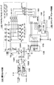
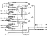
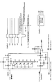
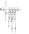
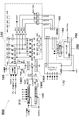
図1に,本発明の第1の実施の形態の回路図を示す。この書き込み回路100は,入力されたアナログ電圧値からメモリセル書き込み時にメモリセルのコントロールゲートに印加する書き込み電圧Vppを発生させる書き込み電圧発生回路110と,入力されたアナログ電圧値からメモリセルベリファイ時にメモリセルのコントロールゲートに印加するベリファイ電圧VVFYを発生させるベリファイ電圧発生回路120を備えている。
【0034】
さらに,この書き込み回路100は,書き込みメモリセルを選択するXデコーダ130X/Yデコーダ130Y/ソースデコーダ130Sと,メモリセル書き込み時に書き込み電圧VppをXデコーダ130Xに導通させるトランスファーゲートMP1と,メモリセルベリファイ時にベリファイ電圧VVFYをXデコーダ130Xに導通させるトランスファーゲートMP2と,メモリセル書き込み時に書き込みメモリセルドレイン電圧VWをYデコーダ130Yに導通させるトランスファーゲートMP3と,メモリセル書き込み時にソース電圧VSourceをソースデコーダ130Sに導通させるトランスファーゲートMN8と,メモリセルベリファイ時にGND電圧をソースデコーダ130Sに導通させるトランスファーゲートMN7と,メモリセル書き込み時にメモリセルのソースに印加するソース電圧VSourceを発生させるソース電圧発生回路135と,メモリセルベリファイ時にメモリセルのリードディスターブを防止するドレイン電圧をYデコーダ130Yに導通させるソースフォロファNMOSトランジスタMN1を備えている。
【0035】
さらに,この書き込み回路100は,メモリセルベリファイ時にメモリセルドレイン電流を比較基準電流Irefと比較するマルチレベルセンスアンプ140を構成するMP4〜MP8,MN2〜MN5,INV0〜INV3と,所定の書き込み信号パルス数に信号を出力するカウンタ−デコーダ回路150と,マルチレベルセンスアンプ140出力SAOUT0〜SAOUT2とカウンタ−デコーダ回路150出力A0,A1,A2とを比較する比較回路160と,その比較結果により出力S0〜S4をMSB/LSB双方向にシフトさせるアップダウンシフトレジスタ回路170を備えている。アップダウンシフトレジスタ回路170出力S0〜S4はソース電圧発生回路135に入力される。
この書き込み回路100は,以上のように構成されている。
【0036】
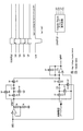
図2に書き込み電圧発生回路110の回路図を示す。この書き込み電圧発生回路110はサンプルホールドレベルシフト回路であり,そのシフト量(利得)は一定値である。
図3にベリファイ電圧発生回路120の回路図を示す。このベリファイ電圧発生回路120もサンプルホールドレベルシフト回路であるが,そのシフト量(利得)は一定値である。
図4にアップダウンシフトレジスタ回路170の回路図を示す。
図5に比較回路160の回路図を示す。
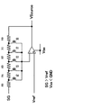
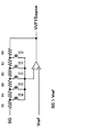
図6にソース電圧発生回路135の回路図を示す。このソース電圧発生回路135は反転増幅器で構成され,S0〜S4入力によって反転増幅器の利得を変化させて出力ソース電圧VSourceを変化できることを特徴とする。
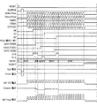
【0037】
図18に第1の実施の形態のタイミング図を示す。Xデコーダ130X/Yデコーダ130Y/ソースデコーダ130Sによって消去後の書き込み対象メモリセルが選択された後,まずリセットパルスRESETによってカウンタ回路152及びアップダウンシフトレジスタ回路170がリセットされる。アップダウンシフトレジスタ回路170のリセット状態はS2=Hである。
【0038】
信号SAMPLEで書き込み電圧発生回路110とベリファイ電圧発生回路120によって入力アナログ電圧がサンプルホールド及びレベルシフトされて書き込み電圧Vppとベリファイ電圧VVFYが発生する。その時の書き込み電圧Vpp及びベリファイ電圧VVFYと入力アナログ電圧値AINRECとの関係は以下式となる。
Vpp=C2/C3×(AINREC−SG)+(C1/C3+1)×VSFT
VVFY=C1/C2×(AINREC−SG)+VSFT
【0039】
書き込みパルス,イネーブル信号VppEN,VWEN,VVFYENのクロック信号がカウンタ回路152及びアップダウンシフトレジスタ回路170,MP1,MP2,MP3,MN7,MN8のそれぞれに与えられると書き込み/ベリファイ動作が開始される。
【0040】
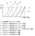
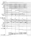
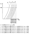
図19に第1の実施の形態の回路動作での書き込み時メモリセルVcg−Ids特性とSAOUT0〜SAOUT2出力関係を示す。書き込み/ベリファイ繰り返し動作によってメモリセルしきい値Vtが上昇するにつれてメモリセルのVcg−Ids特性は図19中の0→▲1▼→▲2▼→▲3▼→▲4▼へと変化して行く。第1の実施の形態では,メモリセルベリファイ時メモリセルドレイン電流をMP4〜MP8からなるカレンミラー回路で変化させて比較基準電流Irefと比較している。
【0041】
そしてMP4:MP5:MP6:MP7:MP8=1:1:1/m2:1/m1:1/m0(1>1/m2>1/m1>1/m0)としているので,メモリセルしきい値Vt上昇0→▲1▼→▲2▼→▲3▼→▲4▼変化に応じてINV0からINV3の順序でセンスアンプインバータがL→H反転し,マルチレベルセンスアンプ140出力もSAOUT0→SAOUT1→SAOUT2の順序でL→Hに変化する。メモリセルしきい値Vt上昇の速さはメモリセル特性と書き込み時ソース−コントロール間電圧によって決定される。
【0042】
書き込み開始時デコーダ回路155出力A0〜A2は全てLに設定されている。その後書き込み開始後の書き込みパルス数(書き込み時間)に従ってA0→A1→A2の順でL→Hに変化する。
【0043】
書き込み開始時は,
書き込み電圧Vpp(一定値),Vpp=C2/C3×(AINREC−SG)+(C1/C3+1)×VSFT
初期設定ソース電圧VSource,VSource=(R0+R1+R2)/(R3+R4+R5)×(SG−Vref)+Vref
であり,書き込み開始時は,
書き込み電圧Vpp(一定値)−初期設定ソース電圧VSource
=[C2/C3×(AINREC−SG)+(C1/C3+1)×VSFT.−[−(R0+R1+R2)/(R3+R4+R5)×(SG−Vref)+Vref
が,書き込み時選択メモリセルのソース−コントロールゲート間電圧となり,選択メモリセルが書き込まれメモリセルしきい値電圧Vtは上昇して行く。
【0044】
そして,ベリファイ時マルチレベルセンスアンプ140出力SAOUT0〜SAOUT2とデコーダ回路155出力A0〜A2を比較回路160で比較し,その結果にてアップダウンシフトレジスタ回路170出力を変化させ,ソース電圧VSourceを変化させている。
【0045】
もしA0がL→Hに変化する前にSAOUT0がL→Hに変化した場合は比較回路160の出力A<BがL→Hに変化してアップダウンシフトレジスタ回路170のS2=HがS1=Hにシフトし,
ソース電圧VSourceは,
VSource=−(R0+R1)/(R2+R3+R4+R5)×(SG−Vref)+Vref
に増加し書き込み時選択メモリセルのソース−コントロールゲート間電圧は低下する。
【0046】
これとは,逆にSAOUT0がL→Hに変化する前にA0がL→Hに変化した場合は比較回路160の出力A>BがL→Hに変化してアップダウンシフトレジスタ回路170のS2=HがS3=Hにシフトし,ソース電圧VSourceは,
VSource=−(R0+R1+R2+R3)/(R4+R5)×(SG−Vref)+Vref
に低下し,書き込み時選択メモリセルのソース−コントロールゲート間電圧は増加する。
【0047】
図18のタイミング図では後者のSAOUT0がL→Hに変化する前にA0がL→Hに変化した場合を記載している。
【0048】
以下同様にして,デコーダ回路155出力が書き込みパルス数(書き込み時間)に従ってA1→A2の順でL→Hに変化して行った場合も,ベリファイ時マルチレベルセンスアンプ140出力SAOUT0〜SAOUT2とデコーダ回路155出力A0〜A2を比較回路160で比較し,その結果にてアップダウンシフトレジスタ回路170出力を変化させ,ソース電圧VSourceを変化させる。
【0049】
デコーダ回路155出力A0〜A2のL→H変化書き込みパルス数(書き込み時間)とマルチレベルセンスアンプ140の力レンミラ−回路MP4:MP5:MP6:MP7:MP8=1:1:1/m2:1/m1:1/m0(1>1/m2>1/m1>1/m0)比係数を,メモリセルの書き込み時間−書き込みVt特性のその使用プロセスメモリセルのtypicalに合わせておけば,書き込みスピードの遅いセルは書き込み時メモリセルのソース−コントロールゲート間電圧を増加させて逆に書き込みスピードの早いセルは書き込み時メモリセルのソース−コントロールゲート間電圧を減少させる動作が可能であり選択メモリセルの書き込み特性に合わせた書き込み条件(書き込み時メモリセルのソース−コントロールゲート間電圧)を探しながらのメモリセル書き込み動作を継続する。
【0050】
そして,メモリセルドレイン電流が比較基準電流Iref以下になった時SAOUTがH出力されて選択メモリセルの書き込み動作を終了する。
【0051】
以上のように第1の実施の形態では,書き込みパルス数(書き込み時間)に従ってA0→A1→A2の順でL→Hに変化するデコーダ回路155出力とメモリセルしきい値Vt上昇によって出力がSAOUT0→SAOUT1→SAOUT2の順序でL→Hに変化するマルチレベルセンスアンプ140出力とを比較回路160で比較し,その結果に応じてメモリセル書き込みソース電圧VSourceを変化させるようにしたので,書き込みスピードの遅いセルは書き込み時メモリセルのソース−コントロールゲート間電圧を増加させ,逆に書き込みスピードの早いセルは書き込み時メモリセルのソース−コントロールゲート間電圧を減少させる動作が可能となり,選択メモリセルの書き込み特性に合わせた書き込み条件(書き込み時メモリセルのソース−コントロールゲート間電圧)を探しながらのメモリセル書き込み動作を行うことができる。
【0052】
従って,初期書き込みスピードが遅いセルやエンデュランス劣化し書き込みスピードが遅くなったセルでも所定時間内で書き込みアナログ電圧精度を下げることなく,アナログ書き込み動作を終了させることが可能である。さらには,初期書き込みスピードの早いセルでもメモリセル書き込みVt飽和での最終アナログ電圧書き込みが可能となり,アナログ電圧精度ばらつきを改善させることができる。
【0053】
また,第1の実施の形態では,ソース電圧発生回路135において出力ソース電圧VSourceがGNP以上となるように基準電圧Vref及び反転増幅AMPのGain抵抗R0〜R5値を設定することが可能である。書き込み選択メモリセルと同一ビットライン上の非選択消去状態メモリセルに過消去状態メモリセルが含まれている場合に過消去状態メモリセルのソース電圧VSourceをGND以上にすることができるので過消去状態メモリセルにおけるIdsリークを防止することが可能であり,書き込みドレイン電圧のVW電源の電流能力を書き込み選択メモリセルの書き込みIds以上にするなどの過消去メモリセル対策が不要になる。VW電源をLIS内部昇圧回路で発生させている場合は消費電流の増加を抑えることができる。
【0054】
また,逆にソース電圧発生回路135において出力ソース電圧VSourceがGND以下となるように基準電圧Vref及び反転増幅AMPのGain抵抗R0〜R5値を設定することも可能である。その場合は,書き込み時のメモリセルのコントロールゲートに印加する印加電圧である書き込み電圧Vpp(一定値)を低くすることができる。その場合,書き込み選択メモリセルと同一ワードライン上の非選択メモリセルのコントロールゲート印加電圧も低くなるのでゲートディスターブを低減することができる。
【0055】
以上のように第1の実施の形態では,使用プロセスのメモリセルの特徴に合わせて,過消去セルが生じやすいメモリセルに対してはソース電圧発生回路135出力ソース電圧VSourceをGND以上に設定して過消去セルのIdsリークを防止することが可能であり,またゲートディスターブが弱いメモリセルに対してはソース電圧発生回路135出力ソース電圧VSourceをGND以下に設定して書き込み電圧Vppを下げてゲートディスターブを防止することが可能である。
【0056】
(第2の実施の形態)
図7に,本発明の第2の実施の形態の回路図を示す。この書き込み回路200は,マルチレベルセンスアンプ140を構成するMP4〜MP8,MN2〜MN5,の能力比がMP4:MP5:MP6:MP7:MP8=1:1:1:1:1とMN6:MN2:MN3:MN4:MN5=1:1:m2:m1:m0(1<m2<m1<m0)となっていて,第1の実施の形態のMP4〜MP8,MN2〜MN5,の能力比と異なっている以外は,第1の実施の形態の書き込み回路100と同じである。
【0057】
図18に第2の実施の形態のタイミング図を示す。第2の実施の形態のタイミング図は第1の実施の形態と同じであり基本動作は同じである。異なっている点は,図19に示した第1の実施の形態の回路動作での書き込み時メモリセルVcg−Ids特性とSAOUT0〜SAOUT2出力関係が図20示す第3の実施の形態の回路動作での書き込み時メモリセルVcg−Ids特性とSAOUT0〜SAOUT2出力関係に変わることである。
【0058】
図20において,書き込み/ベリファイ繰り返し動作によってメモリセルしきい値Vtが上昇するにつれてメモリセルのVcg−Ids特性が図20中の0→▲1▼→▲2▼→▲3▼→▲4▼へと変化する点は同じであるが,第3の実施の形態では,メモリセルベリファイ時M職ドレイン電流との比較電流をMN2〜MP5からなるカレンミラー回路で比較基準電流Iref変化させて電流としている点である。
【0059】
MN6:MN2:MN3:MN4:MN5=1:1:m2:m1:m0(1<m2<m1<m0)としているので,メモリセルしきい値Vt上昇0→▲1▼→▲2▼→▲3▼→▲4▼変化に応じてINV0からINV3の順序でセンスアンプインバータがL→H反転し,マルチレベルセンスアンプ140出力もSAOUT0→SAOUT1→SAOUT2の順序でL→Hに変化する点とメモリセルしきい値Vt上昇の速さはメモリセル特性と書き込み時書き込み電圧Vppによって決定される点は同じである。
【0060】
第2の実施の形態も第1の実施の形態と同様に,書き込みパルス数(書き込み時間)に従ってA0→A1→A2の順でL→Hに変化するデコーダ回路155出力とメモリセルしきい値Vt上昇によって出力がSAOUT0→SAOUT1→SAOUT2の順序でL→Hに変化するマルチレベルセンスアンプ140出力とを比較回路160で比較しその結果に応じてメモリセル書き込みソース電圧VSourceを変化させるようにしたので,書き込みスピードの遅いセルは書き込み時メモリセルのソース−コントロールゲート間電圧を増加させ,逆に書き込みスピードの早いセルは書き込み時メモリセルのソース−コントロールゲート間電圧を減少させる動作が可能となり,選択メモリセルの書き込み特性に合わせた書き込み条件(書き込み時メモリセルのソース−コントロールゲート間電圧)を探しながらのメモリセル書き込み動作を行うことができる。
【0061】
従って,初期書き込みスピードが遅いセルやエンデュランス劣化し書き込みスピードが遅くなったセルでも所定時間内で書き込みアナログ電圧精度を下げることなく,アナログ書き込み動作を終了させることが可能である。さらには,初期書き込みスピードの早いセルでもメモリセル書き込みVt飽和での最終アナログ電圧書き込みが可能となり,アナログ電圧精度ばらつきを改善させることができる。
【0062】
また,ソース電圧発生回路135において出力ソース電圧VSourceがGND以上となるように,基準電圧Vref及び反転増幅AMPのGain抵抗R0〜R5値を設定することが可能である。
【0063】
書き込み選択メモリセルと同一ビットライン上の非選択消去状態メモリセルに過消去状態メモリセルが含まれている場合に過消去状態メモリセルのソース電圧VSourceをGND以上にすることができるので過消去状態メモリセルのIdsリークを防止することが可能であり,書き込みドレイン電圧のVW電源の電流能力を書き込み選択メモリセルの書き込みIds以上にするなどの過消去メモリセル対策が不要になる。VW電源をLIS内部昇圧回路で発生させている場合は消費電流の増加を抑えることができる。
【0064】
また,逆にソース電圧発生回路135において出力ソース電圧VSourceがGND以下となるように基準電圧Vref及び反転増幅AMPのGain抵抗R0〜R5値を設定することも可能である。その場合は,書き込み時にメモリセルのコントロールゲートに印加する印加電圧である書き込み電圧Vpp(一定値)を低くすることができる。その場合,書き込み選択メモリセルと同一ワードライン上の非選択メモリセルのコントロールゲート印加電圧も低くなるのでゲートディスターブを低減することができる。
【0065】
以上のように,使用プロセスのメモリセルの特徴に合わせて,過消去セルが生じやすいメモリセルに対してはソース電圧発生回路135出力ソース電圧VSourceをGND以上に設定して過消去セルのIdsリークを防止することが可能であり,またゲートディスターブが弱いメモリセルに対してはソース電圧発生回路135出力ソース電圧VSourceをGND以下に設定して書き込み電圧Vppを下げてゲートディスターブを防止することが可能である。
【0066】
さらに第2の実施の形態は,マルチレベルセンスアンプ140は比較基準Iref電流源側のNchMOSカレントミラー比をMN6:MN2:MN3:MN4:MN5=1:1:m2:m1:m0(1<m2<m1<m0)に変化させているため,書き込み途中INV0〜INV2でのメモリセルしきい値Vt確認は比較基準Iref電流より大きい比較基準電流Iref’で実施している。そのため,書き込み途中INV0〜INV2でのメモリセルしきい値Vt確認は比較基準電流Irefは,比較基準電流Irefで実施した場合よりも高速に行うことが可能となり,第2の実施の形態のセンスアンプは高速なマルチレベルセンスアンプ140となる。従って,第2の実施の形態ではベリファイ繰り返し動作のベリファイ期間で行う書き込みメモリセルしきい値Vt確認時間のセンスアンプ応答時間分を短縮することが可能になり,書き込みパルス周波数を高くする場合に効果的である。
【0067】
書き込み途中INV0〜INV2でのメモリセルしきい値Vt確認は比較基準電流Irefより大きい比較基準電流Iref’で実施しているので,カレントミラー回路のPchMOS(MP4〜MP8)は比較基準電流Iref’が大きいMN5に合わせる必要がある。従ってμp>μnのプロセスでこの第2の実施の形態回路を構成する場合はMP4のディメンジョンを大きくすること無くレイアウト面積を小さくできる優位点がある。
【0068】
(第3の実施の形態)
図8に,本発明の第3の実施の形態の回路図を示す。この書き込み回路300は,入力されたアナログ電圧値からメモリセル書き込み時にメモリセルのコントロールゲートに印加する書き込み電圧Vppを発生させる書き込み電圧発生回路210と,入力されたアナログ電圧値からメモリセルベリファイ時にメモリセルのコントロールゲートに印加するベリファイ電圧VVFYを発生させるベリファイ電圧発生回路120を備えている。
【0069】
さらに,この書き込み回路300は,書き込みメモリセルを選択するXデコーダ130X/Yデコーダ130Y/ソースデコーダ130Sと,メモリセル書き込み時に書き込み電圧VppをXデコーダ130Xに導通させるトランスファーゲートMP1と,メモリセルベリファイ時にベリファイ電圧VVFYをXデコーダ130Xに導通させるトランスファーゲートMP2と,メモリセル書き込み時に書き込みメモリセルドレイン電圧VWをYデコーダ130Yに導通させるトランスファーゲートMP3と,メモリセル書き込み時にGND電圧をソースデコーダ130Sに導通させるトランスファーゲートMN5と,メモリセルベリファイ時にベリファイソース電圧VVFYSourceをソースデコーダ130Sに導通させるトランスファーゲートMN4と,メモリセルベリファイ時にメモリセルのソースに印加するベリファイソース電圧VVFYSourceを発生させるソース電圧発生回路235と,メモリセルベリファイ時にメモリセルのリードディスターブを防止するドレイン電圧をYデコーダ130Yに導通させるソースフォロファNMOSトランジスタMN1を備えている。
【0070】
さらに,この書き込み回路300は,メモリセルベリファイ時にメモリセルドレイン電流を比較基準電流Irefと比較するセンスアンプ240を構成するMP4,MP5,MN2,MN3,INV0と,所定の書き込み信号パルス数到達時に信号を出力するカウンタ−デコーダ回路150と,センスアンプ出力SAOUT0より出力S0〜S4をMSB/LSB双方向にシフトさせるアップダウンシフトレジスタ回路170を備えている。アップダウンシフトレジスタ回路170出力S0〜S4は前記書き込み電圧発生回路110に入力される。またカウンタ−デコーダ回路150出力SX0〜SX4は前記書き込み電圧発生回路110に入力される。
この書き込み回路300は,以上のように構成されている。
【0071】
この書き込み回路300は,上記実施の形態のソース電圧発生回路135に代えて,ソース電圧発生回路235を備えたことを特徴としている。図9にソース電圧発生回路235の回路図を示す。このソース電圧発生回路235は反転増幅器で構成され,SX0〜SX4入力によって反転増幅器の利得を変化させて出力ベリファイソース電圧VVFYSourceを変化できることを特徴とする。
【0072】
また,この書き込み回路300は,上記実施の形態の書き込み電圧発生回路110に代えて,書き込み電圧発生回路210を備えたことを特徴としている。図10に書き込み電圧発生回路210の回路図を示す。この書き込み電圧発生回路210はサンプルホールドレベルシフト回路でありS0〜S4入力によってサンプルホールド後のレベルシフト出力書き込み電圧Vppを変化できることを特徴とする。
【0073】
ベリファイ電圧発生回路120及びアップダウンシフトレジスタ回路170は,第1,2の実施の形態の回路と同じである。
【0074】
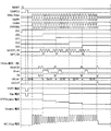
図21に第3の実施の形態のタイミング図を示す。Xデコーダ130X/Yデコーダ130Y/ソースデコーダ130Sによって消去後の書き込み対象メモリセルが選択された後,まずリセットパルスRESETによってカウンタ回路152及びアップダウンシフトレジスタ回路170がリセットされる。アップダウンシフトレジスタ回路170のリセット状態はS2=Hである。また,リセット時カウンタ−デコーダ回路150出力はSX0=Hである。
【0075】
次に信号SAMPLEで書き込み電圧発生回路210とベリファイ電圧発生回路120によって入力アナログ電圧がサンブルホールド及びレベルシフトされて書き込み電圧Vppとしベリファイ電圧VVFYが発生する。その時の初期設定書き込み電圧Vpp及びベリファイ電圧VVFYと入力アナログ電圧値AINRECとの関係は以下の式となる。
Vpp=C2/C3×(AINREC−SG)+(C1/C3+1)×VSFT+C1/C3×(R0+R1+R2+R3+R4+R5)/(R3+R4+R&)×VSFT
VVFY=C1/C2×(AINREC−SG)+VSFT
【0076】
書き込みパルス,イネーブル信号VppEN,VWEN,VVFYENのクロック信号がカウンタ回路152及びアップダウンシフトレジスタ回路170,MP1,MP2,MP3のそれぞれに与えられると書き込み/ベリファイ動作が開始される。
【0077】
図22に第3の実施の形態の回路動作でのベリファイ時メモリセルVcg−Ids特性とSAOUT出力関係を示す。書き込み/ベリファイ繰り返し動作によってメモリセルしきい値Vtが上昇するにつれてメモリセルのVcg−Ids特性は図22中の0→▲1▼→▲2▼→▲3▼→▲4▼と変化して行く。第3の実施の形態では,メモリセルベリファイ時のベリファイ電圧発生回路120発生ベリファイ電圧VVFY(メモリセルコントロールゲート印加電圧)は一定値であり,ソース電圧発生回路235で発生させるメモリセルソース電圧VVFYSourceはカウンタ−デコーダ回路150出力SX0〜SX4で変化し以下となる。
SX0=H時 ベリファイソース電圧VVFYSource,ベリファイソース0=−(R0)/(R1+R2+R3+R4+R5)×(SG−Vref)+Vref
SX1=H時 ベリファイソース電圧VVFYSource,ベリファイソース1=−(R0+R1)/(R2+R3+R4+R5)×(SG−Vref)+Vref
SX2=H時 ベリファイソース電圧VVFYSource,ベリファイソース2=−(R0+R1+R2)/(R3+R4+R5)×(SG−Vref)+Vref
SX3=H時 ベリファイソース電圧VVFYSource,ベリファイソース3=−(R0+R1+R2+R3)/(R4+R5)×(SG−Vref)+Vref
SX4=H時 ベリファイソース電圧VVFYSource,ベリファイソース4=−(R0+R1+R2+R3+R4)/R5×(SG−Vref)+Vref
【0078】
書き込み開始時デコーダ回路155出力SX0〜SX4はSX0出力のみHでSX1〜SX4はLに設定されている。その後書き込み開始後の書き込みパルス数(書き込み時間)に従ってカウンタ−デコーダ回路150出力SX0〜SX4はSX1→SX2→SX3→SX4の順でL→Hに変化する。SX1→SX2→SX3→SX4の順でのL→H変化に伴い,ベリファイソース電圧VVFYSourceもベリファイソース0→ベリファイソース1→ベリファイソース2→ベリファイソース3→ベリファイソース4の順で減少する。
【0079】
ベリファイ時のソース−コントロール間電圧(Vscg)は
Vscg=ベリファイ電圧VVFY(一定値)−ベリファイソース電圧VVFYSourceであるので,SX1→SX2→SX3→SX4の順でのL→H変化に伴い,Vscg(ソース−コントロール間電圧)電圧はVscg0→Vscg1→Vscg2→Vscg3→Vscg4の順で増加する。
従ってセンスアンプインバータがL→H反転するメモリセルしきい値VtもVscg0→Vscg1→Vscg2→Vscg3→Vscg4の順で上昇して行く。
【0080】
書き込み開始時は,初期設定書き込み電圧Vpp,
Vpp=C2/C3×(AINREC−SG)+(C1/C3+1)×VSFT+C1/C3×(R+R1+R2+R3+R4+R5)/(R3+R4+R5)×VSFT
で選択メモリセルが書き込まれメモリセルしきい値電圧Vtは上昇して行く。
【0081】
そしてベリファイ時は初期デコーダ回路155出力SX0=Hで設定されたソース電圧発生回路235で発生させるメモリセルソース電圧VVFYSourceから決まるVscg電圧がメモリセルのコントロールゲートに印加され,Ids電流が比較基準電流Iref以上になるとSAOUT0がL→Hに変化する。そのSAOUT0出力結果にてアップダウンシフトレジスタ回路170出力を変化させ,書き込み電圧Vppを変化させている。
【0082】
もしSX1がL→Hに変化する前にSAOUT0がL→Hに変化した場合は,アップダウンシフトレジスタ回路170のS2=HがS1=Hにシフトし,書き込み電圧Vppは,
Vpp=C2/C3×(AINREC−SG)+(C1/C3+1)×VSFT+C1/C3×(R0+R1+R2+R3+R4+R5)/(R4+R5)×VSFT
に増加する。図21のタイミング図では後者のSAOUT0がL→Hに変化する前にA0がL→Hに変化した場合を記載している。
【0083】
以下同様にして,デコーダ回路155出力が書き込みパルス数(書き込み時間)に従ってSX1→SX2→SX3→SX4の順でL→Hに変化して行った場合もSAOUT0出力結果でアップダウンシフトレジスタ回路170出力を変化させ,書き込み電圧Vppを変化させている。
【0084】
デコーダ回路155出力SX1〜SX4のL→H変化書き込みパルス数(書き込み時間)とソース電圧発生回路235で発生するメモリセルソース電圧VVFYSourceの下降係数を,メモリセルの書き込み時間−書き込みVt特性のその使用プロセスメモリセルのtypicalに合わせておけば,書き込みスピードの遅いセルの書き込み時は書き込み電圧Vppを減少させる動作が可能であり,選択メモリセルの書き込み特性に合わせた書き込み条件を探しながらのメモリセル書き込み動作を継続する。
【0085】
そして,メモリセルコントロールゲート印加電圧=最終書き込み目標Vscg電圧のメモリセルドレイン電流が比較基準電流Iref以下になった時SAOUTからHが出力されて選択メモリセルの書き込み動作を終了する。
【0086】
以上のように第3の実施の形態では,書き込みパルス数(書き込み時間)に従ってSX0→SX1→SX2→SX3→SX4の順でL→Hに変化するデコーダ回路155出力とその出力SX0〜SX4によってベリファイ時のメモリセルソース電圧VVFYSource電圧が変化降下するソース電圧発生回路235の出力電圧を選択メモリセルのソースに印加して,その時のセンスアンプ出力結果に応じてメモリセル書き込み電圧Vppを変化させるようにしたので,書き込みスピードの遅いセルは書き込み時書き込み電圧Vppを増加させ,逆に書き込みスピードの早いセルは書き込み時書き込み電圧Vppを減少させる動作が可能となり,選択メモリセルの書き込み特性に合わせた書き込み条件を探しながらのメモリセル書き込み動作を行うことができる。
【0087】
従って,初期書き込みスピードが遅いセルやエンデュランス劣化し書き込みスピードが遅くなったセルでも所定時間内で書き込みアナログ電圧精度を下げることなく,アナログ書き込み動作を終了させることが可能である。さらには,初期書き込みスピードの早いセルでもメモリセル書き込みVt飽和での最終アナログ電圧書き込みが可能となり,アナログ電圧精度ばらつきを改善させることができる。
【0088】
また,ソース電圧発生回路235において出力ソース電圧VSourceがGND以上となるように基準電圧Vref及び反転増幅AMPのGain抵抗R0〜R5値を設定することが可能である。
【0089】
書き込み選択メモリセルと同一ビットライン上の非選択消去状態メモリセルに過消去状態メモリセルが含まれている場合に,過消去状態メモリセルのソース電圧VSourceをGND以上にすることができるので過消去状態メモリセルのベリファイ時Idsリークを防止することが可能であり,過消去状態メモリセルのベリファイ時Idsリークが原因で生じるベリファイ比較基準電流Irefずれによる書き込みVtずれを防ぐことができる。
【0090】
さらには,S0〜S4入力によって書き込み電圧発生回路210でサンプルホールド後のレベルシフト出力書き込み電圧Vppを変化させる際,コンデンサ比増幅AMP正端子電圧は変化させずに,電荷分配コンデンサC1のコンデンサ比増幅AMP負端子と対称電極の電圧を変化させているので,S0〜S4変化時の書き込み電圧Vpp変化はコンデンサ比増幅AMP正端子電圧を変化させた場合と比べて早い応答が可能である。また,第3の実施の形態のセンスアンプ240はマルチレベルセンスアンプ140を用いず単純なカレントミラー回路と1つのインバータで構成されているため小さいレイアウト面積で実現できる。
【0091】
従って,第3の実施の形態では,書き込みメモリセルを選択するXデコーダ130X/Yデコーダ130Y/ソースデコーダ130Sと,メモリセル書き込み時に書き込みメモリセルドレイン電圧VWをYデコーダ130Yに導通させるトランスファーゲートMP3と,メモリセルベリファイ時にメモリセルのリードディスターブを防止するドレイン電圧をYデコーダ130Yに導通させるソースフォロファNMOSトランジスタMN1と,メモリセルベリファイ時にメモリセルドレイン電流を比較基準電流Irefと比較するセンスアンプ240を構成するMP4,MP5,MN2,MN3,INV0とからなる回路部を小単位に分割しても1チップ全体のレイアウト面積増加を最小限に抑えることができる。従って,メモリビットを小ビットメモリアレイに分割して1メモリアレイのワードライン/ビットライン数を少なくした場合の高速書き込みを実現する場合に効果的である。
【0092】
(第4の実施の形態)
図11に,本発明の第4の実施の形態の回路図を示す。この書き込み回路400は,入力されたアナログ電圧値からメモリセル書き込み時にメモリセルのコントロールゲートに印加する書き込み電圧Vppを発生させる書き込み電圧発生回路110と,入力されたアナログ電圧値からメモリセルベリファイ時にメモリセルのコントロールゲートに印加するベリファイ電圧VVFYを発生させるベリファイ電圧発生回路120を備えている。
【0093】
さらに,この書き込み回路400は,書き込みメモリセルを選択するXデコーダ130X位デコーダ/Yデコーダ130Y/ソースデコーダ130Sと,メモリセル書き込み時に書き込み電圧VppをXデコーダ130Xに導通させるトランスファーゲートMP1と,メモリセルベリファイ時にベリファイ電圧VVFYをXデコーダ130Xに導通させるトランスファーゲートMP2と,メモリセル書き込み時に書き込みメモリセルドレイン電圧VWをYデコーダ130Yに導通させるトランスファーゲートMP3と,メモリセル書き込み時にソース電圧VSourceをソースデコーダ130Sに導通させるトランスファーゲートMN5と,メモリセルベリファイ時にベリファイソース電圧VVFYSourceをソースデコーダ130Sに導通させるトランスファーゲートMN4と,メモリセル書き込み時にメモリセルのソースに印加するソース電圧VSourceを発生させるソース電圧発生回路135と,メモリセルベリファイ時にメモリセルのソースに印加するベリファイソース電圧VVFYSourceを発生させるソース電圧発生回路235と,メモリセルベリファイ時にメモリセルのリードディスターブを防止するドレイン電圧をYデコーダ130Yに導通させるソースフォロファNMOSトランジスタMN1を備えている。
【0094】
さらに,この書き込み回路400は,メモリセルベリファイ時にメモリセルドレイン電流を比較基準電流Irefと比較するセンスアンプ240を構成するMP4,MP5,MN2,MN3,INV0と,所定の書き込み信号パルス数到達時に信号を出力するカウンタ−デコーダ回路150と,センスアンプ出力SAOUT0より出力S0〜S4をMSB/LSB双方向にシフトさせるアップダウンシフトレジスタ回路170を備えている。アップダウンシフトレジスタ回路170出力S0〜S4は前記ソース電圧発生回路235に入力される。またカウンタ−デコーダ回路150出力SX0〜SX4は前記ソース電圧発生回路235に入力される。
この書き込み回路400は,以上のように構成されている。
【0095】
書き込み電圧発生回路110,ベリファイ電圧発生回路120,ソース電圧発生回路135及びアップダウンシフトレジスタ回路170は,第1,第2の実施の形態の回路と同じであり,ソース電圧発生回路235は第3の実施の形態の回路と同じである。
【0096】
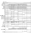
図23に第4の実施の形態のタイミング図を示す。Xデコーダ130X/Yデコーダ130Y/ソースデコーダ130Sによって消去後の書き込み対策メモリセルが選択された後,まずリセットパルスRESETによってカウンタ回路152及びアップダウンレジスタ回路がリセットされる。アップダウンシフトレジスタ回路170のリセット状態はS2=Hである。また,リセット時カウンタ−デコーダ回路150出力はSX0=Hである。
【0097】
次に信号SAMPLEで,書き込み電圧発生回路110とベリファイ電圧発生回路120によって入力アナログ電圧がサンプルホールド及びレベルシフトされて書き込み電圧Vppとベリファイ電圧VVFYが発生する。その時の書き込み電圧Vpp及びベリファイ電圧VVFYと入力アナログ電圧値AINRECとの関係は以下式となる。
Vpp=C2/C3×(AINREC−SG)+(C1/C3+1)×VSFT
VVFY=C1/C2×(AINREC−SG)+VSFT
【0098】
書き込みパルス,イネーブル信号VppEN,VWEN,VVFYENのクロック信号がカウンタ回路152及びアップダウンシフトレジスタ回路170,MP1,MP2,MP3,MN4,MN5のそれぞれに与えられると書き込み/ベリファイ動作が開始される。
【0099】
図22に第4の実施の形態の回路動作でのベリファイ時メモリセルVcg−Ids特性とSAOUT出力関係を示す。書き込み/ベリファイ繰り返し動作によってメモリセルしきい値Vtが上昇するにつれてメモリセルのVcg−Ids特性は図22中の0→▲1▼→▲2▼→▲3▼→▲4▼と変化して行く。第4の実施の形態では,メモリセルベリファイ時のベリファイ電圧発生回路120発生ベリファイ電圧VVFY(メモリセルコントロールゲート印加電圧)は一定値であり,ソース電圧発生回路235で発生させるメモリセルソース電圧VVFYSourceはカウンタ−デコーダ回路150出力SX0〜SX4で変化し以下となる。
SX0=H時 ベリファイソース電圧VVFYSource,ベリファイソース0=−(R0)/(R1+R2+R3+R4+R5)×(SG−Vref)+Vref
SX1=H時 ベリファイソース電圧VVFYSource,ベリファイソース1=−(R0+R1)/(R2+R3+R4+R5)×(SG−Vref)+Vref
SX2=H時 ベリファイソース電圧VVFYSource,ベリファイソース2=−(R0+R1+R2)/(R3+R4+R5)×(SG−Vref)+Vref
SX3=H時 ベリファイソース電圧VVFYSource,ベリファイソース3=−(R0+R1+R2+R3)/(R4+R5)×(SG−Vref)+Vref
SX4=H時 ベリファイソース電圧VVFYSource,ベリファイソース4=−(R0+R1+R2+R3+R4)/R5×(SG−Vref)+Vref
【0100】
書き込み開始時デコーダ回路155出力SX0〜SX4はSX0出力のみHでSX1〜SX4はLに設定されている。その後書き込み開始後の書き込みパルス数(書き込み時間)に従ってカウンタ−デコーダ回路150出力SX0〜SX4はSX1→SX2→SX3→SX4の順でL→Hに変化する。
【0101】
SX1→SX2→SX3→SX4の順でのL→H変化に伴い,ベリファイソース電圧VVFYSourceもベリファイソース0→ベリファイソース1→ベリファイソース2→ベリファイソース3→ベリファイソース4の順で減少する。
【0102】
ベリファイ時のVscg(ソース−コントロール間電圧)電圧はVscg=ベリファイ電圧VVFY(一定値)−ベリファイソース電圧VVFYSourceであるので,SX1→SX2→SX3→SX4の順でのL→H変化に伴い,Vscg(ソース−コントロール間電圧)電圧はVscg0→ Vscg1→Vscg2→Vscg3→Vscg4の順で増加する。
【0103】
従ってセンスアンプインバータがL→H反転するメモリセルしきい値VtもVscg0→Vscg1→Vscg2→Vscg3→Vscg4の順で上昇して行く。
【0104】
書き込み開始時は,
書き込み電圧Vpp(一定値),Vpp=C2/C3×(AINREC−SG)+(C1/C3+1)×VSFT
初期設定ソース電圧VSource,VSource=(R0+R1+R2)/(R3+R4+R5)×(SG−Vref)+Vref
であり,書き込み開始時は,
書き込み電圧Vpp(一定値)−初期設定ソース電圧VSource
=[C2/C3×(AINREC−SG)+(C1/C3+1)×VSFT]−[−(R0+R1+R2)/(R3+R4+R5)×(SG−Vref)+Vref]
が,書き込み時選択メモリセルのソース−コントロールゲート間電圧となり,選択メモリセルが書き込まれメモリセルしきい値電圧Vtは上昇して行く。
【0105】
そしてベリファイ時は初期デコーダ回路155出力SX0=Hで設定されたソース電圧発生回路235で発生させるメモリセルソース電圧VVFYSourceから決まるVscg電圧がメモリセルのコントロールゲートに印加され,Ids電流が比較基準電流Iref以上になるとSAOUT0がL→Hに変化する。そのSAOUT0出力結果にてアップダウンシフトレジスタ回路170出力を変化させ,ソース電圧VSourceを変化させている。
【0106】
もしSX1がL→Hに変化する前にSAOUT0がL→Hに変化した場合は,アップダウンシフトレジスタ回路170のS2=HがS1=Hにシフトし,
ソース電圧VSourceは,
VSource=−(R0+R1)/(R2+R3+R4+R5)×(SG−Vref)+Vref
に増加し書き込み時選択メモリセルのソース−コントロールゲート間電圧は低下する。
【0107】
これとは,逆にSAOUT0がL→Hに変化する前にSX1がL→Hに変化した場合は,アップダウンシフトレジスタ回路170のS2=HがS3=Hにシフトし,
ソース電圧VSourceは,
VSource=−(R0+R1+R2+R3)/(R4+R5)×(SG−Vref)+Vref
に低下し,書き込み時選択メモリセルのソース−コントロールゲート間電圧は増加する。図23のタイミング図では後者のSAOUT0がL→Hに変化する前にL→Hに変化した場合を記載している。
【0108】
以下同様にして,デコーダ回路155出力が書き込みパルス数(書き込み時間)に従ってSX1→SX2→SX3→SX4の順でL→Hに変化して行った場合もSAOUT0出力結果でアップダウンシフトレジスタ回路170出力を変化させ,ソース電圧VSourceを変化させている。
【0109】
デコーダ回路155出力SX1〜SX4のL→H変化書き込みパルス数(書き込み時間)とソース電圧発生回路235で発生するメモリセルソース電圧VVFYSourceの下降係数を,メモリセルの書き込み時間−書き込みVt特性のその使用プロセスメモリセルのtypicalに合わせておけば,書き込みスピードの遅いセルは書き込み時メモリセルのソース−コントロールゲート間電圧を増加させて逆に書き込みスピードの早いセルは書き込み時メモリセルのソース−コントロールゲート間電圧を減少させる動作が可能であり,選択メモリセルの書き込み特性に合わせた書き込み条件(書き込み時メモリセルのソース−コントロールゲート間電圧)を探しながらのメモリセル書き込み動作を継続する。
そして,メモリセルコントロールゲート印加電圧=最終書き込み目標Vscg電圧のメモリセルドレイン電流が比較基準電流Iref以下になった時SAOUTからHが出力されて選択メモリセルの書き込み動作を終了する。
【0110】
以上のように第4の実施の形態では,書き込みパルス数(書き込み時間)に従ってSX0→SX1→SX2→SX3→SX4の順でL→Hに変化するデコーダ回路155出力とその出力SX0〜SX4によってベリファイ時のメモリセルソース電圧VVFYSource電圧が変化降下するソース電圧発生回路235の出力電圧を選択メモリセルのソースに印加して,その時のセンスアンプ出力結果に応じてメモリセル書き込みソース電圧VSourceを変化させるようにしたので,書き込みスピードの遅いセルは書き込み時メモリセルのソース−コントロールゲート間電圧を増加させ,逆に書き込みスピードの早いセルは書き込み時メモリセルのソース−コントロールゲート間電圧を減少させる動作が可能となり,選択メモリセルの書き込み特性に合わせた書き込み条件(書き込み時メモリセルのソース−コントロールゲート間電圧)を探しながらのメモリセル書き込み動作を行うことができる。
【0111】
従って,初期書き込みスピードが遅いセルやエンデュランス劣化し書き込みスピードが遅くなったセルでも所定時間内で書き込みアナログ電圧精度を下げることなく,アナログ書き込み動作を終了させることが可能である。さらには,初期書き込みスピードの早いセルでもメモリセル書き込みVt飽和での最終アナログ電圧書き込みが可能となり,アナログ電圧精度ばらつきを改善させることができる。
【0112】
また,ソース電圧発生回路135において出力ソース電圧VSourceがGND以上となるように基準電圧Vref及び反転増幅AMPのGain抵抗R0〜R5値を設定することが可能であり,ソース電圧発生回路235において出力ベリファイソース電圧VVFYSourceがGND以上となるように基準電圧Vref及び反転増幅AMPのGain抵抗R0〜R5値を設定することが可能である。
【0113】
従って,書き込み選択メモリセルと同一ビットライン上の非選択消去状態メモリセルに過消去状態メモリセルが含まれている場合に,過消去状態メモリセルのソース電圧VSourceをGND以上にすることができるので過消去状態メモリセルのベリファイ時Idsリークを防止することが可能であり,過消去状態メモリセルのベリファイ時Idsリークが原因で生じるベリファイ比較基準電流Irefずれによる書き込みVtずれを防ぐことができる。
【0114】
一方,書き込み時においては過消去状態メモリセルのソース電圧VSourceをGND以上にすることができるので過消去状態メモリセルにおけるIdsリークを防止することが可能であり,書き込みドレイン電圧のVW電源の電流能力を書き込み選択メモリセルの書き込みIds以上にするなどの過消去メモリセル対策が不要になる。VW電源をLIS内部昇圧回路で発生させている場合は消費電流の増加を抑えることができる。以上のように第4の実施の形態では,過消去セルが生じやすいメモリセルに対して効果的な回路方式となる。
【0115】
さらには,S0〜S4入力によって書き込み電圧発生回路110でサンプルホールド後のレベルシフト出力書き込み電圧Vppを変化させる際,コンデンサ比増幅AMP正端子電圧は変化させずに,電荷分配コンデンサC1のコンデンサ比増幅AMP負端子と対称電極の電圧を変化させているので,S0〜S4変化時の書き込み電圧Vpp変化はコンデンサ比増幅AMP正端子電圧を変化させた場合と比べて早い応答が可能である。また,第4の実施の形態のセンスアンプ240はマルチレベルセンスアンプ140を用いず単純なカレントミラー回路と1つのインバータで構成されているため小さいレイアウト面積で実現できる。
【0116】
従って,第4の実施の形態では,書き込みメモリセルを選択するXデコーダ130X/Yデコーダ130Y/ソースデコーダ130Sと,メモリセル書き込み時に書き込みメモリセルドレイン電圧VWをYデコーダ130Yに導通させるトランスファーゲートMP3と,メモリセルベリファイ時にメモリセルのリードディスターブを防止するドレイン電圧をYデコーダ130Yに導通させるソースフォロファNMOSトランジスタMN1と,メモリセルベリファイ時にメモリセルドレイン電流を比較基準電流Irefと比較するセンスアンプ240を構成するMP4,MP5,MN2,MN3,INV0とからなる回路部を小単位に分割しても1チップ全体のレイアウト面積増加を最小限に抑えることができる。従って,メモリビットを小ビットメモリアレイに分割して1メモリアレイのワードライン/ビットライン数を少なくした場合の高速書き込みを実現する場合に効果的である。
【0117】
(第5の実施の形態)
図12に,本発明の第5の実施の形態の回路図を示す。この書き込み回路500は,入力されたアナログ電圧値からメモリセル書き込み時にメモリセルのコントロールゲートに印加する書き込み電圧Vppを発生させる書き込み電圧発生回路210と,入力されたアナログ電圧値からメモリセルベリファイ時にメモリセルのコントロールゲートに印加するベリファイ電圧VVFYを発生させるベリファイ電圧発生回路120を備えている。
【0118】
さらに,この書き込み回路500は,書き込みメモリセルを選択するXデコーダ130X/Yデコーダ130Y/ソースデコーダ130Sと,メモリセル書き込み時にベリファイ電圧VVFYをXデコーダ130Xに導通させるトランスファーゲートMP2と,メモリセル書き込み時に書き込みメモリセルドレイン電圧VWをYデコーダ130Yに導通させるトランスファーゲートMP3と,メモリセル書き込み時に書き込みメモリセルドレイン電圧VWを発生させるVW電圧発生回路125と,メモリセルベリファイ時にメモリセルのリードディスターブを防止するドレイン電圧をYデコーダ130Yに導通させるソースフォロファNMOSトランジスタMN1を備えている。
【0119】
さらに,この書き込み回路500は,メモリセルベリファイ時にメモリセルドレイン電流を比較基準電流Irefと比較するマルチレベルセンスアンプ140を構成するMP4〜MP8,MN2〜MN5,INV0〜INV3と,所定の書き込み信号パルス数に信号を出力するカウンタ−デコーダ回路150と,マルチレベルセンスアンプ140出力SAOUT0〜SAOUT2とカウンタ−デコーダ回路150出力A0,A1,A2とを比較する比較回路160と,その比較結果により出力S0〜S4をMSB/LSB双方向にシフトさせるアップダウンシフトレジスタ回路170を備えている。アップダウンシフトレジスタ回路170出力S0〜S4は前記書き込み電圧発生回路110に入力される。カウンタ−デコーダ回路150出力A3,A4及びSAOUTが前記VW電圧発生回路125に入力される。
この書き込み回路500は,以上のように構成されている。
【0120】
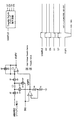
図13にVW電圧発生回路125の回路図を示す。このVW電圧発生回路125は非反転増幅器で構成され,A3,A4及びSAOUT入力によって非反転増幅器の利得を変化せて出力VW電圧を変化できることを特徴とする。
【0121】
書き込み電圧発生回路210は第3の実施の形態の回路と同じであり,ベリファイ電圧発生回路120,アップダウンシフトレジスタ回路170,比較回路160は,第1,2の実施の形態の回路と同じである。
【0122】
図24に第5の実施の形態のタイミング図を示す。Xデコーダ130X/Yデコーダ130Y/ソースデコーダ130Sによって消去後の書き込み対象メモリセルが選択された後,まずリセットパルスRESETによってカウンタ回路152及びアップダウンシフトレジスタ回路170がリセットされる。アップダウンシフトレジスタ回路170のリセット状態はS2=Hである。
【0123】
次に信号SAMPLEで書き込み電圧発生回路210とベリファイ電圧発生回路120によって入力アナログ電圧がサンプルホールド及びレベルシフトされて書き込み電圧Vppとベリファイ電圧VVFYが発生する。その時の書き込み電圧Vpp及びベリファイ電圧VVFYと入力アナログ電圧値AINRECとの関係は以下式となる。
Vpp=C2/C3×(AINREC−SG)+(C1/C3+1)×VSFT+C1/C3×(R+R1+R2+R3+R4+R5)/(R3+R4+R5)×VSFT
VVFY=C1/C2×(AINREC−SG)+VSFT
【0124】
書き込みパルス,イネーブル信号VppEN,VWEN,VVFYENのクロック信号がカウンタ回路152及びアップダウンシフトレジスタ回路170,MP1,MP2,MP3のそれぞれに与えられると書き込み/ベリファイ動作が開始される。
【0125】
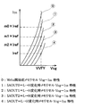
図19に第5の実施の形態の回路動作での書き込み時メモリセルVcg−Ids特性とSAOUT0〜SAOUT2出力関係を示す。書き込み/ベリファイ繰り返し動作によってメモリセルしきい値Vtが上昇するにつれてメモリセルのVcg−Ids特性は図19中の0→▲1▼→▲2▼→▲3▼→▲4▼へと変化して行く。第5の実施の形態では,メモリセルベリファイ時メモリセルドレイン電流をMP4〜MP8からなるカレンミラー回路で変化させて比較基準電流Irefと比較している。
【0126】
そしてMP4:MP5:MP6:MP7:MP8=1:1:1/m2:1/m1:1/m0(1>1/m2>1/m1>1/m0)としているので,メモリセルしきい値Vt上昇0→▲1▼→▲2▼→▲3▼→▲4▼変化に応じてINV0からINV3の順序でセンスアンプインバータがL→H反転し,マルチレベルセンスアンプ140出力もSAOUT0→SAOUT1→SAOUT2の順序でL→Hに変化する。メモリセルしきい値Vt上昇の速さはメモリセル特性と書き込み時書き込み電圧Vppによって決定される。
【0127】
書き込み開始時デコーダ回路155出力A0〜A4は全てLに設定されている。その後書き込み開始後の書き込みパルス数(書き込み時間)に従ってA0→A1→A2→A3→A4の順でL→Hに変化する。
書き込み開始時は,
初期設定書き込み電圧Vpp,
Vpp=C2/C3×(AINREC−SG)+(C1/C3+1)×VSFT+C1/C3×(R+R1+R2+R3+R4+R5)/(R3+R4+R5)×VSFT
初期設定VW電圧,
VW=(1+MP1_R/(MP2_R+MP3_R+MP4_R))×Vref
で選択メモリセルが書き込まれメモリセルしきい値電圧Vtは上昇して行く。マルチレベルセンスアンプ140出力SAOUT0〜SAOUT2とデコーダ回路155出力A0〜A2を比較回路160で比較し,その結果にてアップダウンシフトレジスタ回路170出力を変化させ,書き込み電圧Vppを変化させている。
【0128】
もしA0がL→Hに変化する前にSAOUT0がL→Hに変化した場合は比較回路160の出力A<BがL→Hに変化してアップダウンシフトレジスタ回路170のS2=HがS1=Hにシフトし,
書き込み電圧Vppは,
Vpp=C2/C3×(AINREC−SG)+(C1/C3+1)×VSFT+C1/C3×(R+R1+R2+R3+R4+R5)/(R2+R3+R4+R5)×VSFT
に低下する。
【0129】
これとは,逆にSAOUT0がL→Hに変化する前にA0がL→Hに変化した場合は比較回路160の出力A>BがL→Hに変化してアップダウンシフトレジスタ回路170のS2=HがS3=Hにシフトし,書き込み電圧Vppは,
Vpp=C2/C3×(AINREC−SG)+(C1/C3+1)×VSFT+C1/C3×(R+R1+R2+R3+R4+R5)/(R4+R5)×VSFT
に増加する。図24のタイミング図では後者のSAOUT0がL→Hに変化する前にA0がL→Hに変化した場合を記載している。
【0130】
以下同様にして,デコーダ回路155出力が書き込みパルス数(書き込み時間)に従ってA1→A2の順でL→Hに変化して行った場合もマルチレベルセンスアンプ140出力SAOUT0〜SAOUT2とデコーダ回路155出力A0〜A2を比較回路160で比較し,その結果にてアップダウンシフトレジスタ回路170出力を変化させ,書き込み電圧Vppを変化させる。
【0131】
デコーダ回路155出力A0〜A2のL→H変化書き込みパルス数(書き込み時間)とマルチレベルセンスアンプ140のカレンミラー回路MP4:MP5:MP6:MP7:MP8=1:1:1/m2:1/m1:1/m0(1>1/m2>1/m1>1/m0)比係数を,メモリセルの書き込み時間−書き込みVt特性のその使用プロセスメモリセルのtypicalに合わせておけば,書き込みスピードの遅いセルは書き込み時書き込み電圧Vppを増加させて逆に書き込みスピードの早いセルは書き込み時書き込み電圧Vppを減少させる動作が可能であり,選択メモリセルの書き込み特性に合わせた書き込み条件を探しながらのメモリセル書き込み動作を継続する。
【0132】
その後,デコーダ回路155出力A3がL→H変化にすると,VW電圧が増加して
VW=(1+(MP1_R+MP2_R)/(MP3_R+MP4_R))×Vref
となる。その後デコーダ回路155出力A4がL→H変化にするとVW電圧がさらに増加して
VW=(1+(MP1_R+MP2_R+MP3_R)/MP4_R)×Vref
となる。そして,メモリセルドレイン電流が比較基準電流Iref以上になった時SAOUTがH出力されて選択メモリセルの書き込み動作を終了する。
【0133】
以上のように第5の実施の形態では,書き込みパルス数(書き込み時間)に従ってA0→A1→A2の順でL→Hに変化するデコーダ回路155出力とメモリセルしきい値Vt上昇によって出力がSAOUT0→SAOUT1→SAOUT2の順序でL→Hに変化するマルチレベルセンスアンプ140出力とを比較回路160で比較しその結果に応じてメモリセル書き込み電圧Vppを変化させるようにしたので,書き込みスピードの遅いセルは書き込み時書き込み電圧Vppを増加させ,逆に書き込みスピードの早いセルは書き込み時書き込み電圧Vppを減少させる動作が可能となり,選択メモリセルの書き込み特性に合わせた書き込み条件を探しながらのメモリセル書き込み動作を行うことができる。
【0134】
従って,初期書き込みスピードが遅いセルやエンデュランス劣化し書き込みスピードが遅くなったセルでも所定時間内で書き込みアナログ電圧精度を下げることなく,アナログ書き込み動作を終了させることが可能である。さらには,初期書き込みスピードの早いセルでもメモリセル書き込みVt飽和での最終アナログ電圧書き込みが可能となり,アナログ電圧精度ばらつきを改善させることができる。
【0135】
さらに第5の実施の形態では,書き込みパルス数(書き込み時間)に従ってA3→A4の順でL→Hに変化するデコーダ回路155出力とSAOUT結果に応じてメモリセル書き込みVW電圧を増加させるようにしたので,選択メモリセルの書き込み特性に合わせた書き込み条件の範囲外の初期書き込みスピードが極端に遅いセルやエンデュランス劣化が著しく書き込みスピードが極端に遅くなったセルについては書き込みVW電圧を上げて書き込みスピードを早くして所定時間内にで書込がアナログ電圧精度を下げることなく,アナログ書き込み動作を終了させることが可能である。
【0136】
(第6の実施の形態)
図14に,本発明の第6の実施の形態の回路図を示す。この書き込み回路600は,書き込み電圧発生回路310が第5の実施の形態の書き込み電圧発生回路210と異なっている以外は,第5の実施の形態の書き込み回路500と同じである。
【0137】
図15に書き込み電圧発生回路310の回路図を示す。この書き込み電圧発生回路310は書き込み電圧発生回路210と同じ機能を有していて,サンプルホールドレベルシフト回路でありS0〜S4入力によってサンプルホールド後のレベルシフト出力書き込み電圧Vppを変化できることを特徴とする。
【0138】
図24に第6の実施の形態のタイミング図を示す。第6の実施の形態のタイミング図は第5の実施の形態と同じであり基本動作は同じである。異なっている点はへ信号SAMPLEで書き込み電圧発生回路310によって入力アナログ電圧がサンプルホールド及びレベルシフトされて発生される書き込み電圧Vppと入力アナログ電圧値AINRECとの関係が,
Vpp=C2/C3×(AINREC−SG)+(C1/C3+1)×(R0+R1+R2+R3+R4+R5)/(R3+R4+R5)×SG
式となることと,
デコーダ回路155出力A0がL→Hに変化する前にSAOUT0がL→Hに変化した場合に比較回路160の出力A<BがL→Hに変化してアップダウンシフトレジスタ回路170のS2=HがS1=Hにシフトした時の書き込み電圧Vppが,
Vpp=C2/C8×(AINREC−SG)+(C1/C3+1)×(R0+R1+R2+R3+R4+R5)/(R2+R3+R4+R5)×SGに,逆にSAOUT0がL→Hに変化する前にA0がL→Hに変化した場合に比較回路160の出力A>BがL→Hに変化してアップダウンシフトレジスタ回路170のS2=HがS3=Hにシフトした時の書き込み電圧Vppが,
Vpp=C2/C3×(AINREC−SG)+(C1/C3+1)×(R0+R1+R2+R3+R4+R5)/(R3+R4+R5)×SG
に変わることである。
【0139】
第6の実施の形態も第5の実施の形態と同様に,書き込みパルス数(書き込み時間)に従ってA0→A1→A2の順でL→Hに変化するデコーダ回路155出力とメモリセルしきい値Vt上昇によって出力がSAOUT0→SAOUT1→SAOUT2の順序でL→Hに変化するマルチレベルセンスアンプ140出力とを比較回路160で比較しその結果に応じてメモリセル書き込み電圧Vppを変化させるようにしたので,書き込みスピードの遅いセルは書き込み時書き込み電圧Vppを増加させ,逆に書き込みスピードの早いセルは書き込み時書き込み電圧Vppを減少させる動作が可能となり,選択メモリセルの書き込み特性に合わせた書き込み条件を探しながらのメモリセル書き込み動作を行うことができる。
【0140】
従って,初期書き込みスピードが遅いセルやエンデュランス劣化し書き込みスピードが遅くなったセルでも所定時間内で書き込みアナログ電圧精度を下げることなく,アナログ書き込み動作を終了させることが可能である。さらには,初期書き込みスピードの早いセルでも・メモリセル書き込みVt飽和での最終アナログ電圧書き込みが可能となり,アナログ電圧精度ばらつきを改善させることができる。
【0141】
さらに,書き込みパルス数(書き込み時間)に従ってA3→A4の順でL→Hに変化するデコーダ回路155出力とSAOUT結果に応じて,メモリセル書き込みVW電圧を増加させるようにしたので,選択メモリセルの書き込み特性に合わせた書き込み条件の範囲外の初期書き込みスピードが極端に遅いセルやエンデュランス劣化が著しく書き込みスピードが極端に遅くなったセルについては書き込みVW電圧を下げることなく,アナログ書き込み動作を終了させることが可能である。
【0142】
第6の実施の形態では,S0〜S4入力によって書き込み電圧発生回路310でサンブルホールド後のレベルシフト出力書き込み電圧Vppを変化させる際,コンデンサ比増幅AMPの正端子電圧を増加させているので,コンデンサ比増幅AMP正端子電圧は変化させずに電荷分配コンデンサC1のコンデンサ比増幅AMP負端子と対称電極の電圧を増加させた場合と比べて,少しの電圧変化で書き込み電圧Vppを大きく変化させることが可能である。
【0143】
従って,第6の実施の形態は初期書き込みスピードが極端に遅いセルやエンデュランス劣化が著しく書き込みスピードが極端に遅くなったセルに対して書き込みVW電圧を上げことと書き込み電圧Vppを大きく変化させることの対応が容易にできるので,エンデュランス劣化(特性変動)や初期特性ばらつきが大きく,それら特性変動及びばらつきを補償しなければならない場合に特に効果的である。
【0144】
(第7の実施の形態)
図16に,本発明の第7の実施の形態の回路図を示す。この書き込み回路700は.マルチレベルセンスアンプ240を構成するMP4〜MP8,MN2〜MN5の能力比がMP4:MP5:MP6:MP7:MP8=1:1:1:1:1とMN6:MN2:MN3:MN4:MN5=1:1:m2:m1:m0(1<m2<m1<m0)となっていて,第5の実施の形態のMP4〜MP8,MN2〜MN5,の能力比と異なっている以外は,第5の実施の形態回路と同じである。
【0145】
図24に第7の実施の形態のタイミング図を示す。第7の実施の形態のタイミング図は第5の実施の形態と同じであり基本動作は同じである。異なっている点は,図19に示した第1の実施の形態の回路動作での書き込み時メモリセルVcg−Ids特性とSAOUT0〜SAOUT2出力関係が図20示す第7の実施の形態の回路動作での書き込み時メモリセルVcg−Ids特性とSAOUT0〜SAOUT2出力関係に変わることである。
【0146】
図20において,書き込み/ベリファイ繰り返し動作によってメモリセルしきい値Vtが上昇するにつれてメモリセルのVcg−Ids特性が図20中の0→▲1▼→▲2▼→▲3▼→▲4▼へと変化する点は同じであるが,第7の実施の形態では,メモリセルベリファイ時メモリセルドレイン電流との比較電流をMN2〜MP5からなるカレンミラー回路で比較基準電流Iref変化させて電流としている点である。
【0147】
MN6:MN2:MN3:MN4:MN5=1:1:m2:m1:m0(1<m2<m1<m0)としているので,メモリセルしきい値Vt上昇0→▲1▼→▲2▼→▲3▼→▲4▼変化に応じてINV0からINV3の順序でセンスアンプインバータがL→H反転し,マルチレベルセンスアンプ140出力もSAOUT0→SAOUT1→SAOUT2の順序でL→Hに変化する点とメモリセルしきい値Vt上昇の速さはメモリセル特性と書き込み時書き込み電圧Vppによって決定される点は同じである。
【0148】
第7の実施の形態も第5の実施の形態と同様に,書き込みパルス数(書き込み時間)に従ってA0→A1→A2の順でL→Hに変化するデコーダ回路155出力とメモリセルしきい値Vt上昇によって出力がSAOUT0→SAOUT1→SAOUT2の順序でL→Hに変化するマルチレベルセンスアンプ240出力とを比較回路160で比較しその結果に応じてメモリセル書き込み電圧Vppを変化させるようにしたので,書き込みスピードの遅いセルは書き込み時書き込み電圧Vppを増加させ,逆に書き込みスピードの早いセルは書き込み時書き込み電圧Vppを減少させる動作が可能となり,選択メモリセルの書き込み特性に合わせた書き込み条件を探しながらのメモリセル書き込み動作を行うことができる。
【0149】
従って,初期書き込みスピードが遅いセルやエンデュランス劣化し書き込みスピードが遅くなったセルでも所定時間内で書き込みアナログ電圧精度を下げることなく,アナログ書き込み動作を終了させることが可能である。さらには初期書き込みスピードの早いセルでもメモリセル書き込みVt飽和での最終アナログ電圧書き込みが可能となり,アナログ電圧精度ばらつきを改善させることができる。
【0150】
さらに,書き込みパルス数(書き込み時間)に従ってA3→A4の順でL→Hに変化するデコーダ回路155出力とSAOUT結果に応じてメモリセル書き込みVW電圧を増加させるようにしたので,選択メモリセルの書き込み特性に合わせた書き込み条件の範囲外の初期書き込みスピードが極端に遅いセルやエンデュランス劣化が著しく書き込みスピードが極端に遅くなったセルについては書き込みVW電圧を上げて書き込みスピードを早くして所定時間内にで書き込みアナログ電圧精度を下げることなく,アナログ書き込み動作を終了させることが可能である。
【0151】
第7の実施の形態は,第5の実施の形態と同様に,S0〜S4入力によって書き込み電圧発生回路210でサンプルホールド後のレベルシフト出力書き込み電圧Vppを変化させる際,コンデンサ比増幅AMP正端子電圧は変化させずに,電荷分配コンデンサC1のコンデンサ比増幅AM正負端子と対称電極の電圧を増加させているので,S0〜S4変化時の書き込み電圧Vppを変化はコンデンサ比増幅AM円正端子電圧は変化させた場合と比べて早い応答が可能である。
【0152】
さらに第7の実施の形態は,マルチレベルセンスアンプ240は比較基準Iref電流源側のNchMOSカレントミラー比をMN6:MN2:MN3:MN4:MN5=1:1:m2:m1:m0(1<m2<m1<m0)に変化させているため,書き込み途中INV0〜INV2でのメモリセルしきい値Vt確認は比較基準電流Irefより大きい比較基準電流Iref’で実施している。そのため,書き込み途中INV0〜INV2でのメモリセルしきい値Vt確認は比較基準電流Irefは,比較基準電流Irefで実施した場合よりも高速に行うことが可能となり,第7の実施の形態のセンスアンプは高速なマルチレベルセンスアンプ140となる。
【0153】
従って,第7の実施の形態ではベリファイ繰り返し動作のベリファイ期間で行う書き込みメモリセルしきい値Vt確認時間のセンスアンプ応答時間分を短縮することが可能になり,書き込みパルス周波数を高くする場合に効果的である。
【0154】
書き込み途中INV0〜INV2でのメモリセルしきい値Vt確認は比較基準Irefより大きい比較基準電流Iref’で実施しているので,カレントミラー回路のPchMOS側(MP4〜MP8)は比較基準電流Irefが大きいMN5能力に合わせる必要がある。従って,μp>μnのプロセスでこの第7の実施の形態の回路を構成する場合はMP4のディメンジョンを大きくすること無くレイアウト面積を小さくできる優位点がある。
【0155】
(第8の実施の形態)
図17に,本発明の第8の実施の形態の回路図を示す。この書き込み回路800は,書き込み電圧発生回路310が第7の実施の形態の書き込み電圧発生回路210と異なっている以外は,第7の実施の形態の書き込み回路700と同じである。書き込み電圧発生回路310は,第6の実施の形態の書き込み電圧発生回路310と同じである。
【0156】
図24に第8の実施の形態のタイミング図を示す。第8の実施の形態のタイミング図は第7の実施の形態と同じであり基本動作は同じである。異なっている点は,信号SAMPLEで書き込み電圧発生回路310によって入力アナログ電圧がサンプルホールド及びレベルシフトされて発生される書き込み電圧Vppと入力アナログ電圧値AINRECとの関係が,
Vpp=C2/C3×(AINREC−SG)+(C1/C3+1)×(R0+R1+R2+R3+R4+R5)/(R3+R4+R5)×SG
式となることと,
デコーダ回路155出力A0がL→Hに変化する前にSAOUT0がL→Hに変化した場合に比較回路160の出力A<BがL→Hに変化してアップダウンシフトレジスタ回路170のS2=HがS1=Hにシフトした時の書き込み電圧Vppが,
Vpp=C2/C3×(AINREC−SG)+(C1/C3+1)×(R0+R1+R2+R3+R4+R5)/(R2+R3+R4+R5)×SGに,
逆にSAOUT0がL→Hに変化する前にA0がL→Hに変化した場合に比較回路160の出力A>BがL→Hに変化してアップダウンシフトレジスタ回路170のS2=HがS3=Hにシフトした時の書き込み電圧Vppが,
Vpp=C2/C3×(AINREC−SG)+(C1/C3+1)×(R0+R1+R2+R3+R4+R5)/(R3+R4+R5)×SG
に変わることである。
これらは,第6の実施の形態と同じである。
【0157】
第8の実施の形態も第5の実施の形態と同様に,書き込みパルス数(書き込み時間)に従ってA0→A1→A2の順でL→Hに変化するデコーダ回路155出力とメモリセルしきい値Vt上昇によって出力がSAOUT0→SAOUT1→SAOUT2の順序でL→Hに変化するマルチレベルセンスアンプ140出力とを比較回路160で比較しその結果に応じてメモリセル書き込み電圧Vppを変化させるようにしたので,書き込みスピードの遅いセルは書き込み時,書き込み電圧Vppを増加させ,逆に書き込みスピードの早いセルは書き込み時書き込み電圧Vppを減少させる動作が可能となり,選択メモリセルの書き込み特性に合わせた書き込み条件を探しながらのメモリセル書き込み動作を行うことができる。
【0158】
従って,初期書き込みスピードが遅いセルやエンデュランス劣化し書き込みスピードが遅くなったセルでも所定時間内で書き込みアナログ電圧精度を下げることなく,アナログ書き込み動作を終了させることが可能である。さらには,初期書き込みスピードの早いセルでもメモリセル書き込みVt飽和での最終アナログ電圧書き込みが可能となり,アナログ電圧精度ばらつきを改善させることができる。
【0159】
さらに,書き込みパルス数(書き込み時間)に従ってA3→A4の順でL→Hに変化するデコーダ回路155出力とSAOUT結果に応じてメモリセル書き込みVW電圧を増加させるようにしたので,選択メモリセルの書き込み特性に合わせた書き込み条件の範囲外の初期書き込みスピードが極端に遅いセルやエンデュランス劣化が著しく書き込みスピードが極端に遅くなったセルについては書き込みVW電圧を上げて書き込みスピードを早くして所定時間内にで書き込みアナログ電圧精度を下げることなく,アナログ書き込み動作を終了させることが可能である。
【0160】
第8の実施の形態では,第6の実施の形態と同様に,S0〜S4入力によって書き込み電圧発生回路310でサンプルホールド後の,レベルシフト出力書き込み電圧Vppを変化させる際,コンデンサ比増幅AMPの正端子電圧を増加させているので,コンデンサ比増幅,AMP正端子電圧は変化させずに電荷分配コンデンサC1のコンデンサ比増幅AMP負端子と対称電極の電圧を増加させた場合と比べて,少しの電圧変化で書き込み電圧Vppを大さく変化させることが可能である。
【0161】
また,第7の実施の形態と同様に.マルチレベルセンスァンプは比較基準電流Iref電源側のNchMOSカレントミラー比をMN6:MN2:MN3:MN4:MN5=1:1:m2:m1:m0(1<m2<m1<m0)に変化させているため書き込み途中INV0〜INV2でのメモリセルしきい値Vt確認は比較基準電流Irefより大きい比較基準電流Iref’で実施していることにより高速なマルチレベルセンスアンプ140となる利点とμp>μnのプロセスで実施する場合はMP4のディメンジョンを大きくすること無くレイアウト面積を小さくできる優位点をも兼ね備えている。
【0162】
従って,第8の実施の形態はμp>μnのプロセスにおいて,エンデュランス劣化が大きく,それを補償しなければならない場合に特に効果的である。
【0163】
以上,添付図面を参照しながら本発明にかかる不揮発性メモリアナログ電圧書き込み回路の好適な実施形態について説明したが,本発明はかかる例に限定されない。当業者であれば,特許請求の範囲に記載された技術的思想の範疇内において各種の変更例または修正例に想到し得ることは明らかであり,それらについても当然に本発明の技術的範囲に属するものと了解される。
【0164】
【発明の効果】
以上説明したように,本発明によれば,書き込みスピードの遅いセルは書き込み時メモリセルのソース−コントロールゲート間電圧を増加させ,逆に書き込みスピードの早いセルは書き込み時メモリセルのソース−コントロールゲート間電圧を減少させる動作が可能であり,選択メモリセルの書き込み特性に合わせた書き込みメモリセルのソース−コントロールゲート間電圧条件を探しながらのメモリセル書き込み動作が可能である。このため,書き込み電圧の精度の向上及び書き込み時間の短縮を図ることが可能である。
【図面の簡単な説明】
【図1】第1の実施の形態にかかる回路を示す説明図である。
【図2】書き込み電圧発生回路を示す説明図である。
【図3】ベリファイ電圧発生回路を示す説明図である。
【図4】アップダウンシフトレジスタ回路を示す説明図である。
【図5】比較回路を示す説明図である。
【図6】ソース電圧発生回路を示す説明図である。
【図7】第2の実施の形態にかかる回路を示す説明図である。
【図8】第3の実施の形態にかかる回路を示す説明図である。
【図9】ソース電圧発生回路を示す説明図である。
【図10】書き込み電圧発生回路を示す説明図である。
【図11】第4の実施の形態にかかる回路を示す説明図である。
【図12】第5の実施の形態にかかる回路を示す説明図である。
【図13】VW電圧発生回路を示す説明図である。
【図14】第6の実施の形態にかかる回路を示す説明図である。
【図15】書き込み電圧発生回路を示す説明図である。
【図16】第7の実施の形態にかかる回路を示す説明図である。
【図17】第8の実施の形態にかかる回路を示す説明図である。
【図18】第1,第2の実施の形態における動作タイミングを示す説明図である。
【図19】第1,第5,第6の実施の形態における書き込み時メモリセルVcg−Ids特性とSAOUT0〜SAOUT2,SAOUTの出力関係を示す説明図である。
【図20】第2,第7,第8の実施の形態における書き込み時メモリセルVcg−Ids特性とSAOUT0〜SAOUT2,SAOUTの出力関係を示す説明図である。
【図21】第3の実施の形態における動作タイミングを示す説明図である。
【図22】第3,第4の実施の形態における書き込み時メモリセルVcg−Ids特性とSAOUTの出力関係を示す説明図である。
【図23】第4の実施の形態における動作タイミングを示す説明図である。
【図24】第5〜第8の実施の形態における動作タイミングを示す説明図である。
【符号の説明】
100,・・・,800 (不揮発性メモリアナログ電圧)書き込み回路
110,210,310 書き込み電圧発生回路
120 ベリファイ電圧発生回路
125 VW電圧発生回路
130X Xデコーダ
130Y Yデコーダ
130S ソースデコーダ
135,235 ソース電圧発生回路
140 マルチレベルセンスアンプ
150 カウンタ−デコーダ回路
152 カウンタ回路
155 デコーダ回路
160 比較回路
170 アップダウンシフトレジスタ回路
240 センスアンプ[0001]
BACKGROUND OF THE INVENTION
The present invention relates to a technique for storing an analog voltage in an electrically erasable non-volatile memory, and compensates for a write characteristic variation between memory cells and a write characteristic deterioration due to endurance, and between memory cells due to a write characteristic variation. The present invention relates to a circuit for reducing variation in write analog voltage and improving the endurance life.
[0002]
[Prior art]
Literature name, USP-5,638,320 (date of Patent, Jun. 10, 1997)
In the above document, a method of storing an analog charge amount in a non-volatile memory, its circuit block, and an explanatory diagram are described in FIG. 16 line 6 to 18 Page 19 line and Sheet 29 of 63 FIGURE 12 a to Sheet 40 of 63 FIGURE 15 h. The method of storing the analog charge amount in the nonvolatile memory in this document is as follows.
[0003]
The threshold voltage of the non-volatile memory cell becomes saturated with a decrease in threshold change per unit time as the write time increases, and the write saturation threshold voltage is proportional to the control voltage at the time of writing. Short writing is repeated in proportion to the analog voltage to which the control voltage at the time of writing is written (write operation), and the threshold voltage of the memory cell is read and compared with the analog voltage to be written during the write (verify operation). This write / verify operation is repeated, and the write operation is terminated when the threshold voltage of the read memory cell reaches the analog voltage to be written.
[0004]
Further, in this document, as an improvement method for shortening the write analog voltage accuracy and the analog write time, a method of changing the write control voltage and the write / verify time during the write / verify repetitive operation instead of making them uniform (from FIGURE 15a of Sheet 33 of 63). FIG. 15h) of Sheet 40 of 63 is disclosed.
[0005]
[Problems to be solved by the invention]
However, the method of changing the write control voltage and the write / verify time during the write / verify repetitive operation disclosed in the above-mentioned document instead of making them uniform (FIGURE 15a of Sheet 33 of 63 to FIG. 15 h of Sheet 40 of 63) is the initial stage of writing start. By increasing the initial write speed by setting the control voltage at the time of writing higher than the proportional voltage of the original write analog voltage or by shortening the write pulse width at the beginning of writing to increase the write injection efficiency Even if the initial write speed is slow or the endurance deterioration causes the write speed to slow down, complete the analog voltage write operation within a specified time to improve the write analog voltage accuracy. Although it is an, in this way there is a risk that the write analog voltage accuracy early cell of initial write speed will reach the analog voltage written in during the initial write operation is rough.
[0006]
The only way to prevent a cell with a fast initial write speed from reaching the analog voltage written during the initial write operation is to reduce the initial write speed. As described above, the improvement method for reducing the write analog voltage accuracy and the analog write time disclosed in this document does not take measures against the cell having a high initial write speed, and the write analog voltage is limited by the restriction of the cell having the high initial write speed. There was a problem that voltage accuracy and analog writing time reduction could not be improved sufficiently.
[0007]
The present invention has been made in view of the above-mentioned problems of the conventional nonvolatile memory analog voltage writing circuit, and an object of the present invention is to improve the accuracy of the writing voltage and shorten the writing time. It is a novel and improved non-volatile memory analog voltage writing circuit.
[0008]
[Means for Solving the Problems]
In order to solve the above-described problem, according to
[0009]
According to such a configuration, the decoder circuit output that changes from L to H in a predetermined order (A0 → A1 → A2) according to the write time, and the output in a predetermined order (SAOUT0 → SAOUT1 → SAOUT2) due to the memory cell threshold voltage rise. The comparison circuit compares the output of the multi-level sense amplifier circuit that changes from L to H with the comparison circuit, and the source voltage applied to the source of the memory cell can be changed according to the result.
[0010]
Therefore, a cell with a slow write speed can increase the voltage between the source and control gates of the memory cell at the time of write, and a cell with a fast write speed can reduce the voltage between the source and control gate of the memory cell at the time of write. The memory cell write operation is possible while searching for the voltage condition between the source and control gates of the write memory cell in accordance with the write characteristics of the selected memory cell.
[0011]
According to a second aspect of the present invention, in a circuit for storing an analog voltage in an electrically writable / erasable non-volatile memory, a write voltage (Vpp) applied to the control gate of the memory cell when the memory cell is written from the input analog voltage value A write voltage generation circuit (110) for generating a verification voltage generation circuit (120) for generating a verification voltage (VVFY) to be applied to the control gate of the memory cell at the time of memory cell verification from the input analog voltage value; A source voltage generation circuit (135) that generates a source voltage (VSource) to be applied to the source of the memory cell at the time of writing to the memory cell and changes the output source voltage by changing the gain of the inverting amplifier by the input of the control signals (S0 to S4). ) And the memory cell verify A multilevel sense amplifier (140) for comparing the resell drain current with the current mirror ratio current of the comparison reference current (Iref), a counter-decoder circuit (150) for outputting a signal at a predetermined number of write signal pulses, and the multilevel A comparison circuit (160) for comparing the output of the sense amplifier and the output of the counter-decoder circuit; and an up / down shift register circuit (170) for shifting the level of the control signal according to the comparison result of the comparison circuit. A non-volatile memory analog voltage write circuit (200) is provided.
[0012]
According to such a configuration, the decoder circuit output that changes from L to H in a predetermined order (A0 → A1 → A2) according to the write time, and the output in a predetermined order (SAOUT0 → SAOUT1 → The output from the multi-level sense amplifier circuit that changes from L to H in SAOUT2) is compared by the comparison circuit, and the source voltage applied to the source of the memory cell can be changed according to the result.
[0013]
Therefore, a cell with a slow write speed can increase the voltage between the source and control gates of the memory cell at the time of write, and a cell with a fast write speed can reduce the voltage between the source and control gate of the memory cell at the time of write. The memory cell write operation is possible while searching for the voltage condition between the source and control gates of the write memory cell in accordance with the write characteristics of the selected memory cell.
[0014]
According to a third aspect of the present invention, in a circuit for storing an analog voltage in an electrically writable / erasable non-volatile memory, a write voltage (Vpp) applied to the control gate of the memory cell when the memory cell is written from the input analog voltage value Level shift output write voltage after sample and hold by increasing the voltage of the capacitor ratio amplification AMP negative terminal and the symmetric electrode of the charge distribution capacitor (C1) by the input of the first control signal (S0 to S4) A write voltage generation circuit (210) that changes the voltage, a verify voltage generation circuit (120) that generates a verify voltage (VVFY) to be applied to the control gate of the memory cell at the time of memory cell verification from the input analog voltage value, and a memory Memory cell source during cell verification A source voltage generation circuit (235) for generating a verification source voltage (VVFYSource) to be applied to the first and second output signals SX0 to SX4, and changing the output verification source voltage by changing the gain of the inverting amplifier. From the sense amplifier (240) that compares the memory cell drain current with the comparison reference current (Iref) at the time of cell verification, the counter-decoder circuit that outputs a signal at a predetermined number of write signal pulses, and the sense amplifier output (SAOUT0), A non-volatile memory analog voltage writing circuit (300) is provided, comprising an up / down shift register circuit (170) for shifting the level of the first control signal (S0 to S4).
[0015]
According to such a configuration, the decoder circuit output that changes from L to H in a predetermined order (for example, SX0 → SX1 → SX2 → SX3 → SX4) according to the write time, and the verify source voltage by the output (SX0 to SX4) (VVFYSource) is applied to the source of the selected memory cell with the output voltage of the source voltage generation circuit that changes and drops to increase the voltage between the memory cell source and the control gate at the time of verifying, and the memory cell according to the sense amplifier output result The write voltage (Vpp) at the time of writing can be changed.
[0016]
For this reason, a cell with a slow write speed can increase the write voltage, while a cell with a fast write speed can decrease the write voltage, while searching for a write voltage condition that matches the write characteristics of the selected memory cell. Memory cell write operation is possible.
[0017]
According to a fourth aspect of the present invention, in a circuit for storing an analog voltage in an electrically writable / erasable nonvolatile memory, a write voltage (Vpp) applied to the control gate of the memory cell when the memory cell is written from the input analog voltage value A write voltage generation circuit (110) for generating a verification voltage generation circuit (120) for generating a verification voltage (VVFY) to be applied to the control gate of the memory cell at the time of memory cell verification from the input analog voltage value; A source voltage generation circuit that generates a source voltage (VSource) to be applied to the source of a memory cell when writing to the memory cell, and changes the output source voltage by changing the gain of the inverting amplifier according to the input of the first control signal (S0 to S4). (135) and memory cell verify A source voltage generation circuit (235) that generates a verify source voltage (VVFYSource) to be applied to the source of the memory cell and changes the output verify source voltage by changing the gain of the inverting amplifier according to the input of the second control signals (SX0 to SX4). ), A sense amplifier (240) that compares the memory cell drain current with the comparison reference current at the time of memory cell verification, a counter-decoder circuit (150) that outputs a signal at a predetermined number of write signal pulses, and the sense amplifier output A non-volatile memory analog voltage writing circuit (400) is provided, comprising an up / down shift register circuit (170) for shifting the level of the first control signal.
[0018]
According to this configuration, the verify source voltage is determined by the decoder circuit output that changes from L to H in a predetermined order (SX0 → SX1 → SX2 → SX3 → SX4) and its output (SX0 to SX4) according to the number of write pulses (write time). Is applied to the source of the selected memory cell to increase the voltage between the memory cell source and the control gate at the time of verification, and the memory cell is written at the time of writing to the memory cell according to the sense amplifier output result. The source voltage applied to the source can be changed.
[0019]
Therefore, a cell with a slow write speed can increase the voltage between the source and control gates of the memory cell at the time of write, and a cell with a fast write speed can reduce the voltage between the source and control gate of the memory cell at the time of write. The memory cell write operation is possible while searching for the voltage condition between the source and control gates of the write memory cell in accordance with the write characteristics of the selected memory cell.
[0020]
According to a fifth aspect of the present invention, in a circuit for storing an analog voltage in an electrically writable / erasable non-volatile memory, a write voltage (Vpp) applied to a control gate of the memory cell at the time of memory cell write from the input analog voltage value Level shift output write voltage after sample and hold by increasing the voltage of the capacitor ratio amplification AMP negative terminal and the symmetric electrode of the charge distribution capacitor (C1) by the input of the first control signal (S0 to S4) A write voltage generation circuit (210) that changes the voltage, a verify voltage generation circuit (120) that generates a verify voltage (VVFY) to be applied to the control gate of the memory cell at the time of memory cell verification from the input analog voltage value, and a memory Write memory cell when writing cell A write memory cell drain voltage generation circuit (VW voltage generation circuit 125) that generates a rain voltage (VW voltage) and changes a gain of a non-inverting amplifier to change a write memory cell drain voltage, and a memory cell drain during memory cell verification A multilevel sense amplifier (140) for comparing the current current ratio of the current to a comparison reference current (Iref); a counter-decoder circuit (150) for outputting a signal at a predetermined number of write signal pulses; and the multilevel sense amplifier A comparison circuit (160) for comparing the output with the counter-decoder circuit output; and an up / down shift register circuit (170) for shifting the level of the first control signal output according to the comparison result of the comparison circuit. Nonvolatile memory analog voltage writing circuit 500) is provided.
[0021]
According to this configuration, the decoder circuit output changes from L to H in a predetermined order (A0 → A1 → A2) according to the number of write pulses (write time) and the output is in a predetermined order (SAOUT0) due to the rise in the memory cell threshold value Vt. The output from the multi-level sense amplifier circuit that changes from L → H in (SAOUT1 → SAOUT2) is compared by the comparison circuit, and the memory cell write voltage can be changed according to the result.
[0022]
For this reason, a cell with a slow write speed can increase the write voltage, while a cell with a fast write speed can decrease the write voltage, while searching for a write voltage condition that matches the write characteristics of the selected memory cell. A memory cell write operation is possible. For cells with extremely slow write speed, the write memory cell drain voltage of the memory cell at the time of write can be increased to increase the write speed.
[0023]
According to a sixth aspect of the present invention, in a circuit for storing an analog voltage in an electrically writable / erasable non-volatile memory, a write voltage (Vpp) applied to the control gate of the memory cell when the memory cell is written from the input analog voltage value ) Is generated, and a write voltage is generated to change the level shift output write voltage after the sample hold by increasing the capacitor ratio amplification AMP positive terminal voltage of the charge distribution capacitor (C1) by the input of the control signals (S0 to S4) A circuit (310), a verify voltage generation circuit (120) for generating a verify voltage (VVFY) to be applied to the control gate of the memory cell at the time of memory cell verification from the input analog voltage value, and a write memory cell at the time of memory cell writing Drain voltage (V Voltage) and a write memory cell drain voltage generation circuit (VW voltage generation circuit 125) that changes the write memory cell drain voltage by changing the gain of the non-inverting amplifier, and a current mirror drain of the memory cell drain current during memory cell verification A multilevel sense amplifier (140) for comparing a specific current with a comparison reference current; a counter-decoder circuit (150) for outputting a signal for a predetermined number of write signal pulses; the multilevel sense amplifier output; and the counter-decoder circuit A non-volatile memory analog comprising: a comparison circuit (160) for comparing the output; and an up / down shift register circuit (170) for shifting the level of the control signal according to a comparison result of the comparison circuit. A voltage writing circuit (600) is provided.
[0024]
According to this configuration, the decoder circuit output changes from L to H in a predetermined order (A0 → A1 → A2) according to the number of write pulses (write time) and the output is in a predetermined order (SAOUT0) due to the rise in the memory cell threshold value Vt. The output from the multi-level sense amplifier circuit that changes from L → H in (SAOUT1 → SAOUT2) is compared by the comparison circuit, and the memory cell write voltage can be changed according to the result.
[0025]
For this reason, a cell with a slow write speed can be operated to increase the write voltage during write, and a cell with a fast write speed can be decreased to reduce the write voltage during write. The memory cell write operation can be performed while searching. For a cell with extremely slow write speed, the write applied speed can be increased by increasing the drain applied VW voltage of the memory cell at the time of write.
[0026]
According to a seventh aspect of the present invention, in a circuit for storing an analog voltage in an electrically writable / erasable non-volatile memory, a write voltage (Vpp) applied to a control gate of the memory cell at the time of memory cell write from the input analog voltage value ), And a voltage generation circuit that changes the level shift output write voltage after the sample hold by increasing the voltage of the capacitor ratio amplification AMP negative terminal and the symmetrical electrode of the charge distribution capacitor (C1) by the input of the control signal ( 210), a verify voltage generation circuit (120) for generating a verify voltage (VVFY) to be applied to the control gate of the memory cell when verifying the memory cell from the input analog voltage value, and a write memory cell drain voltage when writing to the memory cell (VW voltage) And a write memory cell drain voltage generation circuit (VW voltage generation circuit 125) that changes the write memory cell drain voltage by changing the gain of the non-inverting amplifier, and a comparison reference current (Iref ), A counter-decoder circuit (150) for outputting a signal for a predetermined number of write signal pulses, the multi-level sense amplifier output, and the counter-decoder circuit. A non-volatile memory analog comprising: a comparison circuit (160) for comparing the output; and an up / down shift register circuit (170) for shifting the level of the control signal according to a comparison result of the comparison circuit. A voltage writing circuit (700) is provided.
[0027]
According to such a configuration, the decoder circuit output changes from L to H in a predetermined order (A0 → A1 → A2) according to the number of write pulses (write time), and the output is in a predetermined order (SA0UT0) due to the rise of the memory cell threshold value Vt. The output of the multi-level sense amplifier circuit that changes from L to H in (SA0UT1 → SAOUT2) is compared by the comparison circuit, and the memory cell write voltage can be changed according to the result.
[0028]
For this reason, a cell with a slow write speed can be operated to increase the write voltage during write, and a cell with a fast write speed can be decreased to reduce the write voltage during write. The memory cell write operation can be performed while searching. For a cell with extremely slow write speed, the write applied speed can be increased by increasing the drain applied VW voltage of the memory cell at the time of write.
[0029]
According to the eighth aspect of the present invention, in the circuit for storing an analog voltage in an electrically writable / erasable nonvolatile memory, the write voltage (Vpp) applied to the control gate of the memory cell when the memory cell is written from the input analog voltage value And a write voltage generation circuit (310) for changing the level shift output write voltage after the sample hold by increasing the capacitor ratio amplification AMP positive terminal voltage by the input of the control signal (S0 to S4), and an input A verify voltage generation circuit (120) for generating a verify voltage (VVFY) to be applied to the control gate of the memory cell at the time of memory cell verification from the analog voltage value, and a write memory cell drain voltage (VW voltage) at the time of memory cell writing Generated, non-inverted increase A write memory cell drain voltage generation circuit (VW voltage generation circuit 125) that changes the gain of the write circuit to change the write memory cell drain voltage, and compares the memory cell drain current with the current reference current of the comparison reference current when the memory cell is verified A multi-level sense amplifier (240), a counter-decoder circuit (150) for outputting a signal at a predetermined number of write signal pulses, and a comparison circuit for comparing the multi-level sense amplifier output with the counter-decoder circuit output ( 160) and an up / down shift register circuit (170) for shifting the level of the control signal according to the comparison result of the comparison circuit, a nonvolatile memory analog voltage writing circuit (800) is provided. Is done.
[0030]
According to this configuration, the decoder circuit output changes from L to H in a predetermined order (A0 → A1 → A2) according to the number of write pulses (write time) and the output is in a predetermined order (SAOUT0) due to the rise in the memory cell threshold value Vt. The output from the multi-level sense amplifier circuit that changes from L → H in (SAOUT1 → SAOUT2) is compared by the comparison circuit, and the memory cell write voltage can be changed according to the result.
[0031]
For this reason, a cell with a slow write speed can be operated to increase the write voltage during write, and a cell with a fast write speed can be decreased to reduce the write voltage during write. The memory cell write operation can be performed while searching. For a cell with extremely slow write speed, the write applied speed can be increased by increasing the drain applied VW voltage of the memory cell at the time of write.
[0032]
DETAILED DESCRIPTION OF THE INVENTION
Exemplary embodiments of a nonvolatile memory analog voltage writing circuit (hereinafter simply referred to as “writing circuit”) according to the present invention will be described below in detail with reference to the accompanying drawings. In the accompanying drawings, FIGS. 1 to 17 show circuit diagrams of the respective embodiments, and FIGS. 18 to 24 show timing diagrams and the like common to the respective embodiments. Further, in the present specification and the drawings, the same reference numerals are given to constituent elements having substantially the same functional configuration, and redundant description is omitted. Further, the high level potential is represented as “H”, and the low level potential is represented as “L”.
[0033]
(First embodiment)
FIG. 1 shows a circuit diagram of a first embodiment of the present invention. The write circuit 100 includes a write
[0034]
Further, the write circuit 100 includes an
[0035]
Further, the write circuit 100 includes MP4 to MP8, MN2 to MN5, INV0 to INV3 constituting a
The write circuit 100 is configured as described above.
[0036]
FIG. 2 shows a circuit diagram of the write
FIG. 3 is a circuit diagram of the verify
FIG. 4 shows a circuit diagram of the up / down
FIG. 5 shows a circuit diagram of the
FIG. 6 shows a circuit diagram of the source
[0037]
FIG. 18 shows a timing chart of the first embodiment. After the erase target memory cell is selected by the
[0038]
The input voltage is sampled and held and level-shifted by the
Vpp = C2 / C3 × (AINREC−SG) + (C1 / C3 + 1) × VSFT
VVFY = C1 / C2 × (AINREC−SG) + VSFT
[0039]
When the write pulse and the clock signals of the enable signals VppEN, VWEN, and VVFYEN are given to the
[0040]
FIG. 19 shows the memory cell Vcg-Ids characteristics and SAOUT0 to SAOUT2 output relationship during writing in the circuit operation of the first embodiment. As the memory cell threshold value Vt rises due to repeated write / verify operations, the Vcg-Ids characteristic of the memory cell changes from 0 → ▲ 1 ▼ → ▲ 2 ▼ → ▲ 3 ▼ → ▲ 4 ▼ in FIG. go. In the first embodiment, the memory cell drain current at the time of memory cell verification is changed by the current mirror circuit composed of MP4 to MP8 and compared with the comparison reference current Iref.
[0041]
Since MP4: MP5: MP6: MP7: MP8 = 1: 1/1 / m2: 1 / m1: 1 / m0 (1> 1 / m2> 1 / m1> 1 / m0), the memory cell threshold value is set. Vt rise 0 → ▲ 1 ▼ → ▲ 2 ▼ → ▲ 3 ▼ → ④4 In response to the change, the sense amplifier inverter inverts L → H in the order of INV0 to INV3, and the
[0042]
At the start of writing, outputs A0 to A2 of the
[0043]
At the start of writing,
Write voltage Vpp (constant value), Vpp = C2 / C3 × (AINREC−SG) + (C1 / C3 + 1) × VSFT
Initial setting source voltage VSource, VSource = (R0 + R1 + R2) / (R3 + R4 + R5) × (SG−Vref) + Vref
At the start of writing,
Write voltage Vpp (constant value) −initial setting source voltage VSource
= [C2 / C3 * (AINREC-SG) + (C1 / C3 + 1) * VSFT. − [− (R0 + R1 + R2) / (R3 + R4 + R5) × (SG−Vref) + Vref
However, the voltage becomes the source-control gate voltage of the selected memory cell at the time of writing, the selected memory cell is written, and the memory cell threshold voltage Vt rises.
[0044]
Then, the
[0045]
If SAOUT0 changes from L to H before A0 changes from L to H, the output A <B of the
The source voltage VSource is
VSource = − (R0 + R1) / (R2 + R3 + R4 + R5) × (SG−Vref) + Vref
The voltage between the source and the control gate of the selected memory cell is decreased during writing.
[0046]
Conversely, when A0 changes from L to H before SAOUT0 changes from L to H, the output A> B of the
VSource = − (R0 + R1 + R2 + R3) / (R4 + R5) × (SG−Vref) + Vref
The voltage between the source and control gate of the selected memory cell increases during writing.
[0047]
The timing diagram of FIG. 18 shows the case where A0 changes from L to H before the latter SAOUT0 changes from L to H.
[0048]
Similarly, when the output of the
[0049]
[0050]
Then, when the memory cell drain current becomes equal to or lower than the comparison reference current Iref, SAOUT is output H, and the write operation of the selected memory cell is completed.
[0051]
As described above, in the first embodiment, the output is SAOUT0 due to the output of the
[0052]
Therefore, it is possible to terminate the analog write operation without degrading the write analog voltage accuracy within a predetermined time even in a cell having a low initial write speed or a cell having a low write speed due to endurance degradation. Furthermore, the final analog voltage can be written with memory cell write Vt saturation even in a cell with a fast initial write speed, and variations in analog voltage accuracy can be improved.
[0053]
In the first embodiment, the source
[0054]
Conversely, in the source
[0055]
As described above, in the first embodiment, the source
[0056]
(Second Embodiment)
FIG. 7 shows a circuit diagram of the second embodiment of the present invention. In the
[0057]
FIG. 18 shows a timing chart of the second embodiment. The timing chart of the second embodiment is the same as that of the first embodiment, and the basic operation is the same. The difference lies in the circuit operation of the third embodiment shown in FIG. 20 in that the memory cell Vcg-Ids characteristics and SAOUT0 to SAOUT2 output relationship during writing in the circuit operation of the first embodiment shown in FIG. Is the memory cell Vcg-Ids characteristic and the SAOUT0 to SAOUT2 output relationship.
[0058]
In FIG. 20, the Vcg-Ids characteristic of the memory cell changes from 0 → (1) → (2) → (3) → (4) in FIG. 20 as the memory cell threshold value Vt rises by the repeated write / verify operation. In the third embodiment, the comparison current with the M drain current at the time of memory cell verification is changed to a current by changing the comparison reference current Iref with a current mirror circuit composed of MN2 to MP5. Is a point.
[0059]
Since MN6: MN2: MN3: MN4: MN5 = 1: 1: m2: m1: m0 (1 <m2 <m1 <m0), the memory cell threshold Vt increases 0 → ▲ 1 ▼ → ▲ 2 ▼ → ▲ In response to the change, the sense amplifier inverter is inverted from L to H in the order of INV0 to INV3, and the output of the
[0060]
Similarly to the first embodiment, in the second embodiment, the output of the
[0061]
Therefore, it is possible to terminate the analog write operation without degrading the write analog voltage accuracy within a predetermined time even in a cell having a low initial write speed or a cell having a low write speed due to endurance degradation. Furthermore, the final analog voltage can be written with memory cell write Vt saturation even in a cell with a fast initial write speed, and variations in analog voltage accuracy can be improved.
[0062]
In addition, the source
[0063]
When a non-selected erase state memory cell on the same bit line as the write selected memory cell includes an over erase state memory cell, the source voltage VSource of the over erase state memory cell can be made to be equal to or higher than GND. It is possible to prevent the Ids leak of the memory cell, and it is not necessary to take measures against overerased memory cells such as setting the current capability of the VW power supply of the write drain voltage to be equal to or higher than the write Ids of the write selected memory cell. When the VW power supply is generated by the LIS internal booster circuit, an increase in current consumption can be suppressed.
[0064]
Conversely, in the source
[0065]
As described above, the source
[0066]
Further, in the second embodiment, the
[0067]
Since the memory cell threshold value Vt is confirmed with the comparison reference current Iref ′ larger than the comparison reference current Iref during the writing INV0 to INV2, the comparison reference current Iref ′ is applied to the PchMOSs (MP4 to MP8) of the current mirror circuit. It is necessary to adjust to large MN5. Therefore, when the circuit of the second embodiment is configured by a process of μp> μn, there is an advantage that the layout area can be reduced without increasing the dimension of MP4.
[0068]
(Third embodiment)
FIG. 8 shows a circuit diagram of the third embodiment of the present invention. The
[0069]
Further, the
[0070]
Further, the
The
[0071]
The
[0072]
The
[0073]
The verify
[0074]
FIG. 21 shows a timing chart of the third embodiment. After the erase target memory cell is selected by the
[0075]
Next, the input voltage is sample-held and level-shifted by the write
Vpp = C2 / C3 × (AINREC−SG) + (C1 / C3 + 1) × VSFT + C1 / C3 × (R0 + R1 + R2 + R3 + R4 + R5) / (R3 + R4 + R &) × VSFT
VVFY = C1 / C2 × (AINREC−SG) + VSFT
[0076]
When the write pulse and the clock signals of the enable signals VppEN, VWEN, and VVFYEN are given to the
[0077]
FIG. 22 shows the memory cell Vcg-Ids characteristics and SAOUT output relationship during verification in the circuit operation of the third embodiment. As the memory cell threshold value Vt rises by repeated write / verify operation, the Vcg-Ids characteristic of the memory cell changes from 0 → ▲ 1 ▼ → ▲ 2 ▼ → ▲ 3 ▼ → ▲ 4 in FIG. . In the third embodiment, the verify
When SX0 = H, verify source voltage VVFYSource, verify
When SX1 = H, verify source voltage VVFYSource, verify
When SX2 = H, verify source voltage VVFYSource, verify
When SX3 = H, verify source voltage VVFYSource, verify
When SX4 = H, verify source voltage VVFYSource, verify
[0078]
At the start of writing,
[0079]
The source-control voltage (Vscg) during verification is
Since Vsgg = Verify voltage VVFY (constant value) −Verify source voltage VVFYSource, the Vsgg (source-control voltage) voltage is changed from Vsgg0 → Vscg1 to L → H in the order of SX1 → SX2 → SX3 → SX4. It increases in the order of Vsgg2 → Vsgg3 → Vsgg4.
Accordingly, the memory cell threshold value Vt at which the sense amplifier inverter is inverted from L to H also rises in the order of Vscg0 → Vsgg1 → Vsgg2 → Vsgg3 → Vsgg4.
[0080]
At the start of writing, the initial setting write voltage Vpp,
Vpp = C2 / C3 × (AINREC−SG) + (C1 / C3 + 1) × VSFT + C1 / C3 × (R + R1 + R2 + R3 + R4 + R5) / (R3 + R4 + R5) × VSFT
Thus, the selected memory cell is written and the memory cell threshold voltage Vt rises.
[0081]
During verification, a Vscg voltage determined by the memory cell source voltage VVFYSource generated by the source
[0082]
If SAOUT0 changes from L to H before SX1 changes from L to H, S2 = H of the up / down
Vpp = C2 / C3 × (AINREC−SG) + (C1 / C3 + 1) × VSFT + C1 / C3 × (R0 + R1 + R2 + R3 + R4 + R5) / (R4 + R5) × VSFT
To increase. In the timing chart of FIG. 21, the case where A0 changes from L to H before the latter SAOUT0 changes from L to H is shown.
[0083]
Similarly, when the output of the
[0084]
The number of L → H change write pulses (write time) of the outputs SX1 to SX4 of the
[0085]
When the memory cell drain current with the memory cell control gate applied voltage = the final write target Vscg voltage becomes equal to or lower than the comparison reference current Iref, H is output from SAOUT, and the write operation of the selected memory cell is completed.
[0086]
As described above, in the third embodiment, the verification is performed by the
[0087]
Therefore, it is possible to terminate the analog write operation without degrading the write analog voltage accuracy within a predetermined time even in a cell having a low initial write speed or a cell having a low write speed due to endurance degradation. Furthermore, the final analog voltage can be written with memory cell write Vt saturation even in a cell with a fast initial write speed, and variations in analog voltage accuracy can be improved.
[0088]
The source
[0089]
When the non-erased memory cell on the same bit line as the write selected memory cell includes an over-erased memory cell, the over-erased memory cell can be over-erased because the source voltage VSource can be set to GND or higher. It is possible to prevent the Ids leak at the time of verifying the state memory cell, and the write Vt shift due to the verify comparison reference current Iref shift caused by the Ids leak at the time of verifying the over-erased memory cell can be prevented.
[0090]
Further, when the level shift output write voltage Vpp after sample hold is changed by the write
[0091]
Therefore, in the third embodiment, the
[0092]
(Fourth embodiment)
FIG. 11 shows a circuit diagram of the fourth embodiment of the present invention. The
[0093]
Further, the
[0094]
Further, the
The
[0095]
The write
[0096]
FIG. 23 shows a timing chart of the fourth embodiment. After the erased write countermeasure memory cell is selected by the
[0097]
Next, in accordance with the signal SAMPLE, the input analog voltage is sampled and held and level-shifted by the write
Vpp = C2 / C3 × (AINREC−SG) + (C1 / C3 + 1) × VSFT
VVFY = C1 / C2 × (AINREC−SG) + VSFT
[0098]
When the write pulse and enable clock signals VppEN, VWEN, and VVFYEN are supplied to the
[0099]
FIG. 22 shows the memory cell Vcg-Ids characteristics and SAOUT output relationship during verification in the circuit operation of the fourth embodiment. As the memory cell threshold value Vt rises due to repeated write / verify operations, the Vcg-Ids characteristic of the memory cell changes from 0 → ▲ 1 ▼ → ▲ 2 ▼ → ▲ 3 ▼ → ▲ 4 ▼ in FIG. . In the fourth embodiment, the verify
When SX0 = H, verify source voltage VVFYSource, verify
When SX1 = H, verify source voltage VVFYSource, verify
When SX2 = H, verify source voltage VVFYSource, verify
When SX3 = H, verify source voltage VVFYSource, verify
When SX4 = H, verify source voltage VVFYSource, verify
[0100]
At the start of writing,
[0101]
As the L → H changes in the order of
[0102]
Since Vsgg (source-control voltage) voltage at the time of verification is Vsgg = verification voltage VVFY (constant value) −verification source voltage VVFYSource, Vscg changes with L → H in the order of SX1 → SX2 → SX3 → SX4. (Source-control voltage) The voltage increases in the order of Vsgg0 → Vsgg1 → Vsgg2 → Vsgg3 → Vsgg4.
[0103]
Accordingly, the memory cell threshold value Vt at which the sense amplifier inverter is inverted from L to H also rises in the order of Vscg0 → Vsgg1 → Vsgg2 → Vsgg3 → Vsgg4.
[0104]
At the start of writing,
Write voltage Vpp (constant value), Vpp = C2 / C3 × (AINREC−SG) + (C1 / C3 + 1) × VSFT
Initial setting source voltage VSource, VSource = (R0 + R1 + R2) / (R3 + R4 + R5) × (SG−Vref) + Vref
At the start of writing,
Write voltage Vpp (constant value) −initial setting source voltage VSource
= [C2 / C3 × (AINREC−SG) + (C1 / C3 + 1) × VSFT] − [− (R0 + R1 + R2) / (R3 + R4 + R5) × (SG−Vref) + Vref]
However, the voltage becomes the source-control gate voltage of the selected memory cell at the time of writing, the selected memory cell is written, and the memory cell threshold voltage Vt rises.
[0105]
During verification, a Vscg voltage determined by the memory cell source voltage VVFYSource generated by the source
[0106]
If SAOUT0 changes from L to H before SX1 changes from L to H, S2 = H of the up / down
The source voltage VSource is
VSource = − (R0 + R1) / (R2 + R3 + R4 + R5) × (SG−Vref) + Vref
The voltage between the source and the control gate of the selected memory cell is decreased during writing.
[0107]
Conversely, when SX1 changes from L to H before SAOUT0 changes from L to H, S2 = H of the up / down
The source voltage VSource is
VSource = − (R0 + R1 + R2 + R3) / (R4 + R5) × (SG−Vref) + Vref
The voltage between the source and control gate of the selected memory cell increases during writing. In the timing chart of FIG. 23, the case where the latter SAOUT0 changes from L to H before changing from L to H is described.
[0108]
Similarly, when the output of the
[0109]
The number of L → H change write pulses (write time) of the outputs SX1 to SX4 of the
When the memory cell drain current with the memory cell control gate applied voltage = the final write target Vscg voltage becomes equal to or lower than the comparison reference current Iref, H is output from SAOUT, and the write operation of the selected memory cell is completed.
[0110]
As described above, in the fourth embodiment, the verification is performed by the
[0111]
Therefore, it is possible to terminate the analog write operation without degrading the write analog voltage accuracy within a predetermined time even in a cell having a low initial write speed or a cell having a low write speed due to endurance degradation. Furthermore, the final analog voltage can be written with memory cell write Vt saturation even in a cell with a fast initial write speed, and variations in analog voltage accuracy can be improved.
[0112]
Further, the source
[0113]
Therefore, when the over-erased memory cell is included in the non-selected erased memory cell on the same bit line as the write selected memory cell, the source voltage VSource of the over-erased memory cell can be set to GND or higher. It is possible to prevent the Ids leak at the time of verifying the over-erased memory cell, and the write Vt shift due to the verify comparison reference current Iref shift caused by the Ids leak at the verify of the over-erased memory cell can be prevented.
[0114]
On the other hand, at the time of writing, the source voltage VSource of the overerased memory cell can be set to GND or higher, so that it is possible to prevent Ids leakage in the overerased memory cell, and the current capability of the VW power supply for the write drain voltage. Therefore, it is not necessary to take measures against over-erased memory cells such as setting the write Ids of the write selected memory cell to be higher than the write Ids. When the VW power supply is generated by the LIS internal booster circuit, an increase in current consumption can be suppressed. As described above, the fourth embodiment provides an effective circuit system for memory cells in which overerased cells are likely to occur.
[0115]
Further, when the level shift output write voltage Vpp after sample hold is changed by the write
[0116]
Therefore, in the fourth embodiment, the
[0117]
(Fifth embodiment)
FIG. 12 shows a circuit diagram of the fifth embodiment of the present invention. The
[0118]
Further, the
[0119]
Further, the
The
[0120]
FIG. 13 shows a circuit diagram of the VW
[0121]
The write
[0122]
FIG. 24 shows a timing chart of the fifth embodiment. After the erase target memory cell is selected by the
[0123]
Next, the input analog voltage is sampled and held and level-shifted by the write
Vpp = C2 / C3 × (AINREC−SG) + (C1 / C3 + 1) × VSFT + C1 / C3 × (R + R1 + R2 + R3 + R4 + R5) / (R3 + R4 + R5) × VSFT
VVFY = C1 / C2 × (AINREC−SG) + VSFT
[0124]
When the write pulse and the clock signals of the enable signals VppEN, VWEN, and VVFYEN are given to the
[0125]
FIG. 19 shows the memory cell Vcg-Ids characteristics and SAOUT0 to SAOUT2 output relationship during writing in the circuit operation of the fifth embodiment. As the memory cell threshold value Vt rises due to repeated write / verify operations, the Vcg-Ids characteristic of the memory cell changes from 0 → ▲ 1 ▼ → ▲ 2 ▼ → ▲ 3 ▼ → ▲ 4 ▼ in FIG. go. In the fifth embodiment, the memory cell drain current at the time of memory cell verification is changed by a current mirror circuit composed of MP4 to MP8 and compared with the comparison reference current Iref.
[0126]
Since MP4: MP5: MP6: MP7: MP8 = 1: 1/1 / m2: 1 / m1: 1 / m0 (1> 1 / m2> 1 / m1> 1 / m0), the memory cell threshold value is set. Vt rise 0 → ▲ 1 ▼ → ▲ 2 ▼ → ▲ 3 ▼ → ④4 In response to the change, the sense amplifier inverter inverts L → H in the order of INV0 to INV3, and the
[0127]
At the start of writing, outputs A0 to A4 of the
At the start of writing,
Initial setting write voltage Vpp,
Vpp = C2 / C3 × (AINREC−SG) + (C1 / C3 + 1) × VSFT + C1 / C3 × (R + R1 + R2 + R3 + R4 + R5) / (R3 + R4 + R5) × VSFT
Initial setting VW voltage,
VW = (1 + MP1_R / (MP2_R + MP3_R + MP4_R)) × Vref
Thus, the selected memory cell is written and the memory cell threshold voltage Vt rises. The
[0128]
If SAOUT0 changes from L to H before A0 changes from L to H, the output A <B of the
The write voltage Vpp is
Vpp = C2 / C3 × (AINREC−SG) + (C1 / C3 + 1) × VSFT + C1 / C3 × (R + R1 + R2 + R3 + R4 + R5) / (R2 + R3 + R4 + R5) × VSFT
To drop.
[0129]
Conversely, when A0 changes from L to H before SAOUT0 changes from L to H, the output A> B of the
Vpp = C2 / C3 × (AINREC−SG) + (C1 / C3 + 1) × VSFT + C1 / C3 × (R + R1 + R2 + R3 + R4 + R5) / (R4 + R5) × VSFT
To increase. The timing diagram of FIG. 24 shows a case where A0 changes from L to H before SAOUT0 changes from L to H.
[0130]
Similarly, when the output of the
[0131]
L → H change write pulse number (write time) of
[0132]
After that, when the
VW = (1+ (MP1_R + MP2_R) / (MP3_R + MP4_R)) × Vref
It becomes. Thereafter, when the output A4 of the
VW = (1+ (MP1_R + MP2_R + MP3_R) / MP4_R) × Vref
It becomes. Then, when the memory cell drain current becomes equal to or higher than the comparison reference current Iref, SAOUT is output H, and the write operation of the selected memory cell is completed.
[0133]
As described above, in the fifth embodiment, the output is SAOUT0 due to the output of the
[0134]
Therefore, it is possible to terminate the analog write operation without degrading the write analog voltage accuracy within a predetermined time even in a cell having a low initial write speed or a cell having a low write speed due to endurance degradation. Furthermore, the final analog voltage can be written with memory cell write Vt saturation even in a cell with a fast initial write speed, and variations in analog voltage accuracy can be improved.
[0135]
Further, in the fifth embodiment, the memory cell write VW voltage is increased according to the output of the
[0136]
(Sixth embodiment)
FIG. 14 shows a circuit diagram of the sixth embodiment of the present invention. The
[0137]
FIG. 15 shows a circuit diagram of the write
[0138]
FIG. 24 shows a timing chart of the sixth embodiment. The timing chart of the sixth embodiment is the same as that of the fifth embodiment, and the basic operation is the same. The difference is that the relationship between the input analog voltage value AINREC and the write voltage Vpp generated when the input analog voltage is sampled and held and level-shifted by the write
Vpp = C2 / C3 × (AINREC−SG) + (C1 / C3 + 1) × (R0 + R1 + R2 + R3 + R4 + R5) / (R3 + R4 + R5) × SG
Being an expression,
When SAOUT0 changes from L to H before the output A0 of the
Vpp = C2 / C8 * (AINREC-SG) + (C1 / C3 + 1) * (R0 + R1 + R2 + R3 + R4 + R5) / (R2 + R3 + R4 + R5) * SG, conversely, A0 changes from L to H before SAOUT0 changes from L to H When the output A> B of the
Vpp = C2 / C3 × (AINREC−SG) + (C1 / C3 + 1) × (R0 + R1 + R2 + R3 + R4 + R5) / (R3 + R4 + R5) × SG
It is to change to.
[0139]
In the sixth embodiment, as in the fifth embodiment, the output of the
[0140]
Therefore, it is possible to terminate the analog write operation without degrading the write analog voltage accuracy within a predetermined time even in a cell having a low initial write speed or a cell having a low write speed due to endurance degradation. Further, even in a cell having a high initial write speed, the final analog voltage can be written with the memory cell write Vt saturation, and the analog voltage accuracy variation can be improved.
[0141]
Furthermore, the memory cell write VW voltage is increased according to the output of the
[0142]
In the sixth embodiment, when the write
[0143]
Therefore, in the sixth embodiment, the write VW voltage is increased and the write voltage Vpp is greatly changed for a cell whose initial write speed is extremely slow or a cell whose endurance deterioration is remarkably slow. This is particularly effective when endurance deterioration (characteristic fluctuation) and initial characteristic variation are large and the characteristic fluctuation and variation must be compensated.
[0144]
(Seventh embodiment)
FIG. 16 shows a circuit diagram of the seventh embodiment of the present invention. The
[0145]
FIG. 24 shows a timing chart of the seventh embodiment. The timing chart of the seventh embodiment is the same as that of the fifth embodiment, and the basic operation is the same. The difference lies in the circuit operation of the seventh embodiment shown in FIG. 20 in that the memory cell Vcg-Ids characteristics and SAOUT0 to SAOUT2 output relationship during writing in the circuit operation of the first embodiment shown in FIG. Is the memory cell Vcg-Ids characteristic and the SAOUT0 to SAOUT2 output relationship.
[0146]
In FIG. 20, the Vcg-Ids characteristic of the memory cell changes from 0 → (1) → (2) → (3) → (4) in FIG. 20 as the memory cell threshold value Vt rises by the repeated write / verify operation. However, in the seventh embodiment, the comparison current with the memory cell drain current at the time of verifying the memory cell is changed to a current by changing the comparison reference current Iref with a current mirror circuit composed of MN2 to MP5. Is a point.
[0147]
Since MN6: MN2: MN3: MN4: MN5 = 1: 1: m2: m1: m0 (1 <m2 <m1 <m0), the memory cell threshold Vt increases 0 → ▲ 1 ▼ → ▲ 2 ▼ → ▲ In response to the change, the sense amplifier inverter is inverted from L to H in the order of INV0 to INV3, and the output of the
[0148]
In the seventh embodiment, similarly to the fifth embodiment, the output of the
[0149]
Therefore, it is possible to terminate the analog write operation without degrading the write analog voltage accuracy within a predetermined time even in a cell having a low initial write speed or a cell having a low write speed due to endurance degradation. Furthermore, the final analog voltage write can be performed with memory cell write Vt saturation even in a cell having a high initial write speed, and variations in analog voltage accuracy can be improved.
[0150]
Furthermore, the memory cell write VW voltage is increased in accordance with the output of the
[0151]
In the seventh embodiment, similarly to the fifth embodiment, when changing the level shift output write voltage Vpp after sample hold in the write
[0152]
Further, in the seventh embodiment, the
[0153]
Therefore, in the seventh embodiment, the sense amplifier response time of the write memory cell threshold value Vt confirmation time performed in the verify period of the verify repeat operation can be shortened, which is effective when the write pulse frequency is increased. Is.
[0154]
Since the memory cell threshold value Vt is confirmed in the middle of writing INV0 to INV2 with the comparison reference current Iref ′ larger than the comparison reference Iref, the comparison reference current Iref is large on the PchMOS side (MP4 to MP8) of the current mirror circuit. It is necessary to match the MN5 capability. Therefore, when the circuit of the seventh embodiment is formed by a process of μp> μn, there is an advantage that the layout area can be reduced without increasing the dimension of MP4.
[0155]
(Eighth embodiment)
FIG. 17 shows a circuit diagram of the eighth embodiment of the present invention. The
[0156]
FIG. 24 shows a timing chart of the eighth embodiment. The timing chart of the eighth embodiment is the same as that of the seventh embodiment, and the basic operation is the same. A difference is that the relationship between the input analog voltage value AINREC and the write voltage Vpp generated when the input analog voltage is sampled and held and level-shifted by the write
Vpp = C2 / C3 × (AINREC−SG) + (C1 / C3 + 1) × (R0 + R1 + R2 + R3 + R4 + R5) / (R3 + R4 + R5) × SG
Being an expression,
When SAOUT0 changes from L to H before the output A0 of the
Vpp = C2 / C3 × (AINREC−SG) + (C1 / C3 + 1) × (R0 + R1 + R2 + R3 + R4 + R5) / (R2 + R3 + R4 + R5) × SG,
Conversely, when A0 changes from L to H before SAOUT0 changes from L to H, the output A> B of the
Vpp = C2 / C3 × (AINREC−SG) + (C1 / C3 + 1) × (R0 + R1 + R2 + R3 + R4 + R5) / (R3 + R4 + R5) × SG
It is to change to.
These are the same as those in the sixth embodiment.
[0157]
In the eighth embodiment, as in the fifth embodiment, the
[0158]
Therefore, it is possible to terminate the analog write operation without degrading the write analog voltage accuracy within a predetermined time even in a cell having a low initial write speed or a cell having a low write speed due to endurance degradation. Furthermore, the final analog voltage can be written with memory cell write Vt saturation even in a cell with a fast initial write speed, and variations in analog voltage accuracy can be improved.
[0159]
Furthermore, the memory cell write VW voltage is increased in accordance with the output of the
[0160]
In the eighth embodiment, similarly to the sixth embodiment, when the level shift output write voltage Vpp after the sample hold in the write
[0161]
Also, as in the seventh embodiment. The multi-level sense amplifier changes the NchMOS current mirror ratio on the comparison reference current Iref power supply side to MN6: MN2: MN3: MN4: MN5 = 1: 1: m2: m1: m0 (1 <m2 <m1 <m0). Therefore, the confirmation of the memory cell threshold value Vt during the writing INV0 to INV2 is performed with the comparison reference current Iref ′ larger than the comparison reference current Iref, and the advantage that the high-level
[0162]
Therefore, the eighth embodiment is particularly effective when the endurance deterioration is large in the process of μp> μn and must be compensated for.
[0163]
The preferred embodiments of the nonvolatile memory analog voltage writing circuit according to the present invention have been described above with reference to the accompanying drawings, but the present invention is not limited to such examples. It will be obvious to those skilled in the art that various changes or modifications can be conceived within the scope of the technical idea described in the claims, and these are naturally within the technical scope of the present invention. It is understood that it belongs.
[0164]
【The invention's effect】
As described above, according to the present invention, a cell having a low write speed increases the voltage between the source and control gates of the memory cell at the time of writing, and conversely, a cell having a high write speed is the source-control gate of the memory cell at the time of writing. The operation of decreasing the inter-voltage is possible, and the memory cell writing operation can be performed while searching for the source-control gate voltage condition of the write memory cell in accordance with the write characteristics of the selected memory cell. Therefore, it is possible to improve the accuracy of the write voltage and shorten the write time.
[Brief description of the drawings]
FIG. 1 is an explanatory diagram illustrating a circuit according to a first embodiment;
FIG. 2 is an explanatory diagram showing a write voltage generation circuit.
FIG. 3 is an explanatory diagram showing a verify voltage generation circuit;
FIG. 4 is an explanatory diagram showing an up / down shift register circuit;
FIG. 5 is an explanatory diagram showing a comparison circuit;
FIG. 6 is an explanatory diagram showing a source voltage generation circuit.
FIG. 7 is an explanatory diagram illustrating a circuit according to a second embodiment;
FIG. 8 is an explanatory diagram illustrating a circuit according to a third embodiment;
FIG. 9 is an explanatory diagram showing a source voltage generation circuit.
FIG. 10 is an explanatory diagram showing a write voltage generation circuit.
FIG. 11 is an explanatory diagram illustrating a circuit according to a fourth embodiment;
FIG. 12 is an explanatory diagram illustrating a circuit according to a fifth embodiment.
FIG. 13 is an explanatory diagram showing a VW voltage generation circuit.
FIG. 14 is an explanatory diagram of a circuit according to a sixth embodiment.
FIG. 15 is an explanatory diagram showing a write voltage generation circuit.
FIG. 16 is an explanatory diagram illustrating a circuit according to a seventh embodiment;
FIG. 17 is an explanatory diagram illustrating a circuit according to an eighth embodiment;
FIG. 18 is an explanatory diagram showing operation timing in the first and second embodiments.
FIG. 19 is an explanatory diagram showing a write memory cell Vcg-Ids characteristic and an output relationship between SAOUT0 to SAOUT2 and SAOUT in the first, fifth, and sixth embodiments;
FIG. 20 is an explanatory diagram showing a write memory cell Vcg-Ids characteristic and an output relationship between SAOUT0 to SAOUT2 and SAOUT in the second, seventh, and eighth embodiments;
FIG. 21 is an explanatory diagram showing operation timing in the third embodiment.
FIG. 22 is an explanatory diagram showing a write memory cell Vcg-Ids characteristic and an output relationship of SAOUT in the third and fourth embodiments;
FIG. 23 is an explanatory diagram showing operation timing in the fourth embodiment.
FIG. 24 is an explanatory diagram showing operation timings in the fifth to eighth embodiments.
[Explanation of symbols]
100,..., 800 (nonvolatile memory analog voltage) writing circuit
110, 210, 310 Write voltage generation circuit
120 verify voltage generation circuit
125 VW voltage generator
130X X decoder
130Y Y decoder
130S source decoder
135,235 Source voltage generation circuit
140 Multi-level sense amplifier
150 counter-decoder circuit
152 Counter circuit
155 decoder circuit
160 Comparison circuit
170 Up-down shift register circuit
240 sense amplifier
Claims (8)
入力されたアナログ電圧値からメモリセル書き込み時にメモリセルのコントロールゲートに印加する書き込み電圧を発生させる書き込み電圧発生回路と,
入力されたアナログ電圧値からメモリセルベリファイ時に,メモリセルのコントロールゲートに印加するベリファイ電圧を発生させるベリファイ電圧発生回路と,
メモリセル書き込み時にメモリセルのソースに印加するソース電圧を発生させ,制御信号の入力によって反転増幅器の利得を変化させて出力ソース電圧を変化させるソース電圧発生回路と,
メモリセルベリファイ時にメモリセルドレイン電流のカレンミラー比電流を比較基準電流と比較した結果をデジタル値として出力するマルチレベルセンスアンプと,
所定の書き込み信号パルス数毎のカウント値を出力するカウンタ−デコーダ回路と,
前記マルチレベルセンスアンプ出力と前記カウンタ−デコーダ回路出力とを比較する比較回路と,
前記比較回路の比較結果により前記制御信号のレベルをシフトさせるアップダウンシフトレジスタ回路と,
を備えたことを特徴とする,不揮発性メモリアナログ電圧書き込み回路。In a circuit for storing an analog voltage in an electrically writable / erasable nonvolatile memory,
A write voltage generation circuit for generating a write voltage to be applied to the control gate of the memory cell when the memory cell is written from the input analog voltage value;
A verify voltage generation circuit for generating a verify voltage to be applied to the control gate of the memory cell at the time of memory cell verification from the input analog voltage value;
A source voltage generating circuit for generating a source voltage to be applied to the source of the memory cell when writing the memory cell, and changing an output source voltage by changing a gain of the inverting amplifier according to an input of a control signal;
A multi-level sense amplifier that outputs the result of comparing the current mirror drain current of the memory cell drain current with the comparison reference current as a digital value during memory cell verification;
A counter-decoder circuit for outputting a count value for each predetermined number of write signal pulses;
A comparison circuit for comparing the multi-level sense amplifier output and the counter-decoder circuit output;
An up-down shift register circuit for shifting the level of the control signal according to the comparison result of the comparison circuit;
A non-volatile memory analog voltage writing circuit.
入力されたアナログ電圧値からメモリセル書き込み時にメモリセルのコントロールゲートに印加する書き込み電圧を発生させる書き込み電圧発生回路と,
入力されたアナログ電圧値からメモリセルベリファイ時に,メモリセルのコントロールゲートに印加するベリファイ電圧を発生させるベリファイ電圧発生回路と,
メモリセル書き込み時にメモリセルのソースに印加するソース電圧を発生させ,制御信号の入力によって反転増幅器の利得を変化させて出力ソース電圧を変化させるソース電圧発生回路と,
メモリセルベリファイ時にメモリセルドレイン電流を比較基準電流のカレンミラー比電流と比較した結果をデジタル値として出力するマルチレベルセンスアンプと,
所定の書き込み信号パルス数毎のカウント値を出力するカウンタ−デコーダ回路と,
前記マルチレベルセンスアンプ出力とカウンタ−デコーダ回路出力とを比較する比較回路と,
前記比較回路の比較結果により前記制御信号のレベルをシフトさせるアップダウンシフトレジスタ回路と,
を備えたことを特徴とする,不揮発性メモリアナログ電圧書き込み回路。In a circuit for storing an analog voltage in an electrically writable / erasable nonvolatile memory,
A write voltage generation circuit for generating a write voltage to be applied to the control gate of the memory cell when the memory cell is written from the input analog voltage value;
A verify voltage generation circuit for generating a verify voltage to be applied to the control gate of the memory cell at the time of memory cell verification from the input analog voltage value;
A source voltage generating circuit for generating a source voltage to be applied to the source of the memory cell when writing the memory cell, and changing an output source voltage by changing a gain of the inverting amplifier according to an input of a control signal;
A multi-level sense amplifier that outputs the result of comparing the memory cell drain current with the current reference current of the comparison reference current as a digital value during memory cell verification;
A counter-decoder circuit for outputting a count value for each predetermined number of write signal pulses;
A comparison circuit for comparing the multi-level sense amplifier output with the counter-decoder circuit output;
An up-down shift register circuit for shifting the level of the control signal according to the comparison result of the comparison circuit;
A non-volatile memory analog voltage writing circuit.
入力されたアナログ電圧値からメモリセル書き込み時にメモリセルのコントロールゲートに印加する書き込み電圧を発生させ,第1制御信号の入力によって,電荷分配コンデンサのコンデンサ比増幅AMP負端子と対称電極の電圧を増加させることによってサンプルホールド後のレベルシフト出力書き込み電圧を変化させる書き込み電圧発生回路と,
入力されたアナログ電圧値からメモリセルベリファイ時に,メモリセルのコントロールゲートに印加するベリファイ電圧を発生させるベリファイ電圧発生回路と,
メモリセルベリファイ時にメモリセルのソースに印加するベリファイソース電圧を発生させ,第2制御信号の入力によって反転増幅器の利得を変化させて出力ベリファイソース電圧を変化させるソース電圧発生回路と,
メモリセルベリファイ時にメモリセルドレイン電流を比較基準電流と比較するセンスアンプと,
所定の書き込み信号パルス数毎に前記第2制御信号を出力するカウンタ−デコーダ回路と,
前記センスアンプ出力より,第1制御信号のレベルをシフトさせるアップダウンシフトレジスタ回路と
を備えたことを特徴とする,不揮発性メモリアナログ電圧書き込み回路。In a circuit for storing an analog voltage in an electrically writable / erasable nonvolatile memory,
A write voltage to be applied to the control gate of the memory cell is generated from the input analog voltage value, and the voltage of the capacitor ratio amplification AMP negative terminal and the symmetrical electrode of the charge distribution capacitor is increased by inputting the first control signal. A write voltage generating circuit for changing the level shift output write voltage after the sample and hold,
A verify voltage generation circuit for generating a verify voltage to be applied to the control gate of the memory cell at the time of memory cell verification from the input analog voltage value;
A source voltage generation circuit for generating a verify source voltage to be applied to the source of the memory cell at the time of verifying the memory cell, and changing an output verify source voltage by changing a gain of the inverting amplifier according to an input of the second control signal;
A sense amplifier for comparing the memory cell drain current with the comparison reference current during memory cell verification;
A counter-decoder circuit for outputting the second control signal every predetermined number of write signal pulses;
A nonvolatile memory analog voltage writing circuit, comprising: an up / down shift register circuit for shifting the level of the first control signal from the sense amplifier output.
入力されたアナログ電圧値からメモリセル書き込み時にメモリセルのコントロールゲートに印加する書き込み電圧を発生させる書き込み電圧発生回路と,
入力されたアナログ電圧値からメモリセルベリファイ時に,メモリセルのコントロールゲートに印加するベリファイ電圧を発生させるベリファイ電圧発生回路と,
メモリセル書き込み時にメモリセルのソースに印加するソース電圧を発生させ,第1制御信号の入力によって反転増幅器の利得を変化させて出力ソース電圧を変化させるソース電圧発生回路と,
メモリセルベリファイ時にメモリセルのソースに印加するベリファイソース電圧を発生させ,第2制御信号の入力によって反転増幅器の利得を変化させて出力ベリファイソース電圧を変化させるソース電圧発生回路と,
メモリセルベリファイ時にメモリセルドレイン電流を比較基準電流と比較するセンスアンプと,
所定の書き込み信号パルス数毎に前記第2制御信号を出力するカウンタ−デコーダ回路と,
前記センスアンプ出力より前記第1制御信号のレベルをシフトさせるアップダウンシフトレジスタ回路と,
を備えたことを特徴とする,不揮発性メモリアナログ電圧書き込み回路。In a circuit for storing an analog voltage in an electrically writable / erasable nonvolatile memory,
A write voltage generation circuit for generating a write voltage to be applied to the control gate of the memory cell when the memory cell is written from the input analog voltage value;
A verify voltage generation circuit for generating a verify voltage to be applied to the control gate of the memory cell at the time of memory cell verification from the input analog voltage value;
A source voltage generating circuit for generating a source voltage to be applied to the source of the memory cell at the time of writing to the memory cell, and changing the output source voltage by changing the gain of the inverting amplifier according to the input of the first control signal;
A source voltage generation circuit for generating a verify source voltage to be applied to the source of the memory cell at the time of verifying the memory cell, and changing an output verify source voltage by changing a gain of the inverting amplifier according to an input of the second control signal;
A sense amplifier for comparing the memory cell drain current with the comparison reference current during memory cell verification;
A counter-decoder circuit for outputting the second control signal every predetermined number of write signal pulses;
An up-down shift register circuit for shifting the level of the first control signal from the sense amplifier output;
A non-volatile memory analog voltage writing circuit.
Priority Applications (2)
| Application Number | Priority Date | Filing Date | Title |
|---|---|---|---|
| JP2000364603A JP3776307B2 (en) | 2000-04-26 | 2000-11-30 | Nonvolatile memory analog voltage writing circuit |
| US09/840,884 US6473338B2 (en) | 2000-04-26 | 2001-04-25 | Analog voltage supply circuit for a non-volatile memory |
Applications Claiming Priority (3)
| Application Number | Priority Date | Filing Date | Title |
|---|---|---|---|
| JP2000-131531 | 2000-04-26 | ||
| JP2000131531 | 2000-04-26 | ||
| JP2000364603A JP3776307B2 (en) | 2000-04-26 | 2000-11-30 | Nonvolatile memory analog voltage writing circuit |
Publications (2)
| Publication Number | Publication Date |
|---|---|
| JP2002015590A JP2002015590A (en) | 2002-01-18 |
| JP3776307B2 true JP3776307B2 (en) | 2006-05-17 |
Family
ID=26591296
Family Applications (1)
| Application Number | Title | Priority Date | Filing Date |
|---|---|---|---|
| JP2000364603A Expired - Fee Related JP3776307B2 (en) | 2000-04-26 | 2000-11-30 | Nonvolatile memory analog voltage writing circuit |
Country Status (2)
| Country | Link |
|---|---|
| US (1) | US6473338B2 (en) |
| JP (1) | JP3776307B2 (en) |
Families Citing this family (13)
| Publication number | Priority date | Publication date | Assignee | Title |
|---|---|---|---|---|
| JP3631463B2 (en) | 2001-12-27 | 2005-03-23 | 株式会社東芝 | Nonvolatile semiconductor memory device |
| JP3977799B2 (en) * | 2003-12-09 | 2007-09-19 | 株式会社東芝 | Nonvolatile semiconductor memory device |
| JP4068863B2 (en) * | 2002-03-08 | 2008-03-26 | 富士通株式会社 | Nonvolatile multilevel semiconductor memory |
| US6621745B1 (en) * | 2002-06-18 | 2003-09-16 | Atmel Corporation | Row decoder circuit for use in programming a memory device |
| ITMI20042071A1 (en) * | 2004-10-29 | 2005-01-29 | St Microelectronics Srl | METHOD OF PROGRAMMING OF MULTILEVEL MEMORIES AND RELATIVE CIRCUIT |
| JP4772363B2 (en) | 2005-04-12 | 2011-09-14 | 株式会社東芝 | Nonvolatile semiconductor memory device |
| US8194015B1 (en) * | 2007-02-26 | 2012-06-05 | Alta Analog, Inc. | Reduction of the effect of AVDD power supply variation on gamma reference voltages and the ability to compensate for manufacturing variations |
| US9024761B2 (en) * | 2009-03-17 | 2015-05-05 | Taiwan Semiconductor Manufacturing Company, Ltd. | System and method for persistent ID flag for RFID applications |
| KR101086858B1 (en) * | 2009-04-15 | 2011-11-25 | 주식회사 하이닉스반도체 | Non-volatile Semiconductor Memory Circuit For Generating Write Voltage |
| JP2011108307A (en) * | 2009-11-16 | 2011-06-02 | Renesas Electronics Corp | Nonvolatile semiconductor memory device |
| CN103328932B (en) * | 2011-02-28 | 2015-08-05 | 富士电机株式会社 | SIC (semiconductor integrated circuit) and semiconductor physical quantity sensor device |
| JP2013200910A (en) | 2012-03-23 | 2013-10-03 | Toshiba Corp | Semiconductor storage device and voltage output method of semiconductor storage device |
| US9342089B2 (en) * | 2014-04-25 | 2016-05-17 | Texas Instruments Deutschland Gmbh | Verification of bandgap reference startup |
Family Cites Families (5)
| Publication number | Priority date | Publication date | Assignee | Title |
|---|---|---|---|---|
| US5828601A (en) * | 1993-12-01 | 1998-10-27 | Advanced Micro Devices, Inc. | Programmed reference |
| JP3496285B2 (en) * | 1994-08-31 | 2004-02-09 | 富士通株式会社 | Flash memory |
| US5694356A (en) | 1994-11-02 | 1997-12-02 | Invoice Technology, Inc. | High resolution analog storage EPROM and flash EPROM |
| US5712815A (en) * | 1996-04-22 | 1998-01-27 | Advanced Micro Devices, Inc. | Multiple bits per-cell flash EEPROM capable of concurrently programming and verifying memory cells and reference cells |
| JP3920943B2 (en) * | 1996-05-10 | 2007-05-30 | 株式会社ルネサステクノロジ | Nonvolatile semiconductor memory device |
-
2000
- 2000-11-30 JP JP2000364603A patent/JP3776307B2/en not_active Expired - Fee Related
-
2001
- 2001-04-25 US US09/840,884 patent/US6473338B2/en not_active Expired - Fee Related
Also Published As
| Publication number | Publication date |
|---|---|
| JP2002015590A (en) | 2002-01-18 |
| US6473338B2 (en) | 2002-10-29 |
| US20010040825A1 (en) | 2001-11-15 |
Similar Documents
| Publication | Publication Date | Title |
|---|---|---|
| JP3737525B2 (en) | Semiconductor memory device | |
| JP4149637B2 (en) | Semiconductor device | |
| US8625355B2 (en) | Semiconductor memory device and method of operating the same | |
| KR100332001B1 (en) | Semiconductor nonvolatile memory device | |
| KR100697053B1 (en) | Non-volatile memory and method of non-volatile memory programming | |
| KR100221939B1 (en) | Semiconductor memory device and high-voltage switching circuit | |
| JP4702572B2 (en) | Low power multi-bit sense amplifier | |
| US7848140B2 (en) | Flash memory array system including a top gate memory cell | |
| US9123423B2 (en) | Programming operations in a memory device | |
| CN107045889B (en) | Semiconductor memory device, erasing method and programming method thereof | |
| US6449190B1 (en) | Adaptive reference cells for a memory device | |
| JP2002100192A (en) | Non-volatile semiconductor memory | |
| JP3583703B2 (en) | Semiconductor device | |
| US6655758B2 (en) | Method for storing data in a nonvolatile memory | |
| JP3776307B2 (en) | Nonvolatile memory analog voltage writing circuit | |
| JPH097383A (en) | Nonvolatile semiconductor memory device and its word-line driving method | |
| KR100286720B1 (en) | Non-volatile semiconductor memory | |
| JP2014157650A (en) | Semiconductor memory device | |
| JP2013127828A (en) | Semiconductor storage device | |
| CN113496755B (en) | Semiconductor memory device and read-out method | |
| JP2000163976A (en) | Nonvolatile semiconductor storage device and its verifying method | |
| CN107305786B (en) | Nonvolatile semiconductor memory device | |
| JP2006065945A (en) | Nonvolatile semiconductor storage device and semiconductor integrated circuit device | |
| JP3563702B2 (en) | Semiconductor storage device | |
| JP3541503B2 (en) | Semiconductor storage device |
Legal Events
| Date | Code | Title | Description |
|---|---|---|---|
| A131 | Notification of reasons for refusal |
Free format text: JAPANESE INTERMEDIATE CODE: A131 Effective date: 20050405 |
|
| A521 | Written amendment |
Free format text: JAPANESE INTERMEDIATE CODE: A523 Effective date: 20050606 |
|
| TRDD | Decision of grant or rejection written | ||
| A01 | Written decision to grant a patent or to grant a registration (utility model) |
Free format text: JAPANESE INTERMEDIATE CODE: A01 Effective date: 20060221 |
|
| A61 | First payment of annual fees (during grant procedure) |
Free format text: JAPANESE INTERMEDIATE CODE: A61 Effective date: 20060222 |
|
| R150 | Certificate of patent or registration of utility model |
Free format text: JAPANESE INTERMEDIATE CODE: R150 |
|
| FPAY | Renewal fee payment (event date is renewal date of database) |
Free format text: PAYMENT UNTIL: 20090303 Year of fee payment: 3 |
|
| FPAY | Renewal fee payment (event date is renewal date of database) |
Free format text: PAYMENT UNTIL: 20100303 Year of fee payment: 4 |
|
| S111 | Request for change of ownership or part of ownership |
Free format text: JAPANESE INTERMEDIATE CODE: R313111 |
|
| S531 | Written request for registration of change of domicile |
Free format text: JAPANESE INTERMEDIATE CODE: R313531 |
|
| FPAY | Renewal fee payment (event date is renewal date of database) |
Free format text: PAYMENT UNTIL: 20100303 Year of fee payment: 4 |
|
| R350 | Written notification of registration of transfer |
Free format text: JAPANESE INTERMEDIATE CODE: R350 |
|
| FPAY | Renewal fee payment (event date is renewal date of database) |
Free format text: PAYMENT UNTIL: 20110303 Year of fee payment: 5 |
|
| LAPS | Cancellation because of no payment of annual fees |