JP4149637B2 - Semiconductor device - Google Patents
Semiconductor device Download PDFInfo
- Publication number
- JP4149637B2 JP4149637B2 JP2000154983A JP2000154983A JP4149637B2 JP 4149637 B2 JP4149637 B2 JP 4149637B2 JP 2000154983 A JP2000154983 A JP 2000154983A JP 2000154983 A JP2000154983 A JP 2000154983A JP 4149637 B2 JP4149637 B2 JP 4149637B2
- Authority
- JP
- Japan
- Prior art keywords
- voltage
- circuit
- node
- output
- short
- Prior art date
- Legal status (The legal status is an assumption and is not a legal conclusion. Google has not performed a legal analysis and makes no representation as to the accuracy of the status listed.)
- Expired - Fee Related
Links
Images


Classifications
-
- G—PHYSICS
- G11—INFORMATION STORAGE
- G11C—STATIC STORES
- G11C5/00—Details of stores covered by group G11C11/00
- G11C5/14—Power supply arrangements, e.g. power down, chip selection or deselection, layout of wirings or power grids, or multiple supply levels
- G11C5/145—Applications of charge pumps; Boosted voltage circuits; Clamp circuits therefor
-
- G—PHYSICS
- G11—INFORMATION STORAGE
- G11C—STATIC STORES
- G11C16/00—Erasable programmable read-only memories
- G11C16/02—Erasable programmable read-only memories electrically programmable
- G11C16/06—Auxiliary circuits, e.g. for writing into memory
- G11C16/10—Programming or data input circuits
- G11C16/12—Programming voltage switching circuits
-
- G—PHYSICS
- G11—INFORMATION STORAGE
- G11C—STATIC STORES
- G11C16/00—Erasable programmable read-only memories
- G11C16/02—Erasable programmable read-only memories electrically programmable
- G11C16/06—Auxiliary circuits, e.g. for writing into memory
- G11C16/30—Power supply circuits
-
- G—PHYSICS
- G11—INFORMATION STORAGE
- G11C—STATIC STORES
- G11C5/00—Details of stores covered by group G11C11/00
- G11C5/14—Power supply arrangements, e.g. power down, chip selection or deselection, layout of wirings or power grids, or multiple supply levels
-
- G—PHYSICS
- G11—INFORMATION STORAGE
- G11C—STATIC STORES
- G11C5/00—Details of stores covered by group G11C11/00
- G11C5/14—Power supply arrangements, e.g. power down, chip selection or deselection, layout of wirings or power grids, or multiple supply levels
- G11C5/147—Voltage reference generators, voltage or current regulators; Internally lowered supply levels; Compensation for voltage drops
Description
【0001】
【発明の属する技術分野】
この発明は、電源電圧を昇圧する昇圧回路を備えた半導体装置に係り、特にメモリセルを有し、このメモリセルのデータ消去及び書込みの際に使用される高電圧を昇圧回路で得るようにした半導体記憶装置に関する。
【0002】
【従来の技術】
半導体記憶装置の1つにフラッシュメモリがある。図13はこのフラッシュメモリにおける1つのメモリセルの素子断面構造を示している。図において、P型半導体基板(P−substrate)71内にはN型ウエル領域(N−well)72が形成されている。さらにこのN型ウエル領域72内にはP型ウエル領域(P−well)73が形成されている。上記P型ウエル領域73内には、それぞれn+型領域からなるメモリセルのソース、ドレイン領域74、75が互いに離間して形成されている。そして、このソース、ドレイン領域74、75相互間のチャネル領域上には、図示しない絶縁膜を介してフローティングゲート(floating gate)76が形成され、さらにこのフローティングゲート76上には、図示しない絶縁膜を介してコントロールゲート(control gate)77が形成されている。
【0003】
また、上記P型半導体基板71にはp+型領域からなるコンタクト領域78が、N型ウエル領域72にはn+型領域からなるコンタクト領域79が、P型ウエル領域73にはp+型領域からなるコンタクト領域80がそれぞれ形成されている。
【0004】
動作時に、メモリセルのコントロールゲート77にはゲート電圧Vgが、ドレイン領域75にはドレイン電圧Vdが、ソース領域74にはソース電圧Vsがそれぞれ供給される。また、コンタクト領域79及び80にはソース電圧Vsと同じ電圧が、コンタクト領域78には0Vの接地電圧がそれぞれ供給される。
【0005】
上記メモリセルは、フローティングゲート76に蓄積される電子の量によってデータの“1”レベル、“0”レベルを記憶する。そして、記憶データのレベルに応じてコントロールゲート77からみたしきい値電圧が変わる。
【0006】
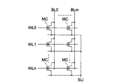
このようなメモリセルが複数設けられることによってメモリセルアレイが構成される。図14はNOR型フラッシュメモリのメモリセルアレイの回路例を示している。複数のメモリセルMCが行列状に配置されており、同一行に配置されたメモリセルMCのコントロールゲートは、複数のワード線WL0〜WLnのうち対応する1つのワード線に共通に接続されている。また、同一列に配置されたメモリセルMCのドレイン領域は、複数のビットBL0〜BLmのうち対応する1つのビット線に共通に接続されている。通常、メモリセルは複数のブロックに分割されており、同じブロック内のメモリセルMCのソース領域は複数のソース線SLiのうち対応するブロックのソース線に共通に接続されている。
【0007】
図15は、動作時に、メモリセルのコントロールゲートに供給されるゲート電圧と、メモリセルのドレインに流れるドレイン電流との関係を示している。ここでは、フローティングゲートに蓄積される電子の量が比較的多い状態、すなわちメモリセルのしきい値電圧Vtが高い状態を“0”データ(“0”データを記憶しているメモリセルを“0”cellと称する)とし、逆に比較的少ない状態、すなわちメモリセルのしきい値電圧Vtが低い状態を“1”データ(“1”データを記憶しているメモリセルを“1”cellと称する)としている。
【0008】
データの読み出し、書込み、消去時のバイアス条件を図16に示す。図16は、動作時にメモリセルに対して供給される先の電圧Vg、Vd、Vsの値の一例を示している。データの読み出し時には、Vg、Vd、Vsはそれぞれ5V、1V、0Vにされる。データの書込み時には、Vg、Vsはそれぞれ9V、0Vにされ、Vdは“0”データを書込むメモリセルについては5V、そうでないメモリセル(元の“1”データのままにされるメモリセル)については0Vにされる。さらに、消去時には、Vg、Vsはそれぞれ−7V、10Vにされ、Vdはフローティング状態にされる。
【0009】
データの読み出しは、ドレイン領域に所定の電圧(本例では1V)を供給した状態でコントロールゲートにゲート電圧Vread(本例では5V)を供給した時に、セル電流が流れる否かによって判定される。この判定は、図示しないセンスアンプにより、リファレンスセルに流れるリファレンス電流(Iref)との比較により行われる。
【0010】
消去は、P型ウエル領域73(図13に図示)を共有する複数のメモリセルで一括して行われる。この消去時には、ファウラ・ノルトハイム(F・N)トンネル現象によってフローティングゲート76からP型ウエル領域73に電子が流れ、消去対象のメモリセルは全て“1”cellにされる。
【0011】
書込みはメモリセル1個毎に行われる。“0”データを書込むメモリセルのビット線を5Vにバイアスして、チャネルホットエレクトロン現象で発生した高エネルギーの電子をフローティングゲート76に注入する。元の“1”データのままとしたい“1”cellのビット線は0Vにされる。これにより、非書込みのメモリセルでは、フローティングゲート76に対する電子の注入が起きず、しきい電圧Vtの変化は生じない。
【0012】
また、フラッシュメモリでは、書込み時及び消去時に、書込みや消去の程度を確認するために書込みベリファイ動作や消去ベリファイ動作が行われる。書込みベリファイ動作は、コントロールゲート の電圧を、読出し時の電圧Vread(本例では5V)に比べて高い電圧Vpv(例えば7V)に設定して“0”読み動作を行う。そして、書込み動作と書込みベリファイ動作とを交互に繰り返して実行し、書込み対象のメモリセルのデータが全て“0”になったら書込み動作が終了する。
【0013】
消去時の場合には、コントロールゲート77の電圧を、読出し時の電圧Vreadに比べて低い電圧Vev(例えば3.5V)に設定して“1”読み動作を行う。そして、消去動作と消去ベリファイ動作とを交互に繰り返して実行し、消去対象のメモリセルのデータが全て“1”になったら消去動作が終了する。これにより、セル電流Icellが十分に確保される。
【0014】
このようにメモリセルのコントロールゲートに供給される電圧は、動作モードに応じて、例えば9V、7V、5V、3.5Vというように様々の値に変化する。これらの電圧のうち9V、7V、5Vは、外部から供給される電源電圧よりも高い電圧である。
【0015】
ところで、従来では、上記のような9V、7V、5Vなど、外部から供給される電源電圧よりも高い種々の電圧を生成するために、電源電圧を昇圧する昇圧回路を必要な数だけ設けるようにしており、これら複数の昇圧回路の出力をスイッチによって適宜選択し、メモリセルのコントロールゲートに供給するようにしている。
【0016】
しかしながら、昇圧回路はキャパシタ等、チップ上で大きな面積を占める素子を必要とするために、複数の昇圧回路を設けるとチップ面積が大型化するという問題がある。さらに、昇圧回路における消費電流が比較的多いので、チップ全体の消費電流が多くなるという問題もある。
【0017】
【発明が解決しようとする課題】
上述したように、外部から供給される電源電圧よりも高い種々の電圧を必要とする従来の半導体装置では複数の昇圧回路を設けるようにしているために、集積化する際にチップ面積が大型化する、消費電流が多くなるという問題がある。
【0018】
この発明は上記のような事情を考慮してなされたものであり、その目的は、集積化する際にチップ面積が大きくならず、かつ消費電流も少ない半導体装置を提供することである。
【0019】
【課題を解決するための手段】
この発明の半導体装置は、電源電圧を昇圧して第1の電圧を出力する昇圧回路と、上記第1の電圧が供給され、この第1の電圧を用いて第1の電圧よりも値が低い少なくとも2つの電圧を出力ノードから時系列的に順次出力する第1の電圧出力回路と、上記第1の電圧のノードと上記第1の電圧出力回路の出力ノードとの間を短絡する短絡回路とを具備し、前記短絡回路は、前記昇圧回路で昇圧動作が開始されるのに伴って前記第1の電圧のノードと前記第1の電圧出力回路の出力ノードとの間の短絡を開始し、昇圧動作が開始されてから所定期間が経過した後に短絡状態を解除し、前記短絡回路が前記第1の電圧のノードと前記第1の電圧出力回路の出力ノードとの間の短絡を行っている期間は、前記第1の電圧出力回路は非活性化し、前記短絡回路が前記短絡状態を解除した後に、前記第1の電圧出力回路が活性化することを特徴とする。
この発明の半導体装置は、電源電圧を昇圧して第1の電圧を出力する昇圧回路と、上記第1の電圧が供給され、この第1の電圧を用いて第1の電圧よりも値が低い少なくとも2つの電圧を出力ノードから時系列的に順次出力する第1の電圧出力回路と、上記第1の電圧のノードと上記第1の電圧出力回路の出力ノードとの間を短絡する短絡回路とを具備し、前記短絡回路は、前記昇圧回路で昇圧動作が開始されるのに伴って前記第1の電圧のノードと前記第1の電圧出力回路の出力ノードとの間の短絡を開始し、昇圧動作が開始されて前記第1の電圧が所定値に達した後に短絡状態を解除し、前記短絡回路が前記第1の電圧のノードと前記第1の電圧出力回路の出力ノードとの間の短絡を行っている期間は、前記第1の電圧出力回路は非活性化し、前記短絡回路が前記短絡状態を解除した後に、前記第1の電圧出力回路が活性化することを特徴とする。
【0020】
この発明の半導体記憶装置は、データを記憶するデータ消去可能なメモリセルと、上記メモリセルのゲートに第1の電圧を供給し、ドレインに第2の電圧及び第3の電圧のいずれか一方を供給して、上記メモリセルのデータ書込みを行う書込み回路と、上記メモリセルが形成されている半導体領域に第4の電圧を供給して、上記メモリセルのデータ消去を行う消去回路と、電源電圧を昇圧して第5の電圧を出力する昇圧回路と、上記第5の電圧が供給され、この第5の電圧を用いて第5の電圧よりも値が低い上記第1の電圧を出力ノードから出力する第1の電圧出力回路と、前記第5の電圧のノードと前記第1の電圧出力回路の出力ノードとの間を短絡する短絡回路とを具備し、前記短絡回路は、前記昇圧回路で昇圧動作が開始されるのに伴って前記第5の電圧のノードと前記第1の電圧出力回路の出力ノードとの間の短絡を開始し、昇圧動作が開始されてから所定期間が経過した後に短絡状態を解除し、前記短絡回路が前記第5の電圧のノードと前記第1の電圧出力回路の出力ノードとの間の短絡を行っている期間は、前記第1の電圧出力回路は非活性化し、前記短絡回路が前記短絡状態を解除した後に、前記第1の電圧出力回路が活性化することを特徴とする。
【0021】
【発明の実施の形態】
以下、図面を参照してこの発明の実施の形態を詳細に説明する。
【0022】
図1は、この発明の第1の実施の形態による半導体装置の一部の回路構成を示すブロック図である。図1に示した回路は例えばフラッシュメモリに内蔵され、前記したように種々の動作モードの際にメモリセルのコントロールゲートに供給すべき種々の電圧を生成する電圧生成回路であり、昇圧回路(Vpp generator)11と、レギュレータ回路(regulator)12とから構成されている。
【0023】
昇圧回路11は、昇圧活性化信号VPPEが活性化されると動作し、外部から供給される電源電圧を昇圧して電源電圧よりも高い値を有する電圧Vppを出力する。この電圧Vppはレギュレータ回路12に供給される。
【0024】
レギュレータ回路12は、上記電圧Vppからそれよりも値が低い複数の電圧を電圧Vregとして時系列的に順次出力する。このレギュレータ回路12の動作は、レギュレータ活性化信号REGE、メモリセルが書込み動作の時に活性化される書込み時信号PROG、及びメモリセルが書込みベリファイ動作の時に活性化されるベリファイ時信号VRFYに応じて制御される。
【0025】
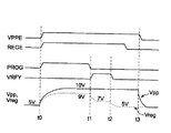
次に、図1の回路の動作の一例を図2のタイミングチャートを用いて説明する。なお、図2中の時刻t0以前では、電圧Vpp、Vregは共に、図示しない他の昇圧回路の出力電圧である5Vの読み出し電圧に設定されているとする。
【0026】
時刻t0に昇圧活性化信号VPPEが活性化されると、昇圧回路11が動作を開始し、外部から供給される電源電圧の昇圧が開始される。この後、電圧Vppは上昇する。昇圧回路11の動作が安定すると、この電圧Vppは規定値に達して安定する。電圧Vppの規定値は、メモリセルで消去を行う際にソース領域に供給されるソース電圧Vsと同じ電圧であり、例えば10Vである。このときの10Vの電圧Vppは、消去動作の際にソース領域に供給されるソース電圧Vsとして使用してもよい。
【0027】
一方、時刻t0にレギュレータ活性化信号REGEが活性化され、かつこれと同時に書込み時信号PROGが活性化される。これにより、レギュレータ回路12が動作し、電圧Vregが電圧Vppよりも低い値、例えば9Vに向かって上昇し、その後、9Vに達すると安定する。信号PROGが“H”レベルの期間に電圧Vregとして出力される9Vの電圧は、消去動作の際にメモリセルのコントロールゲートに供給される先のゲート電圧Vgとして使用される。
【0028】
次に、時刻t1に書込み時信号PROGが非活性化となり、ベリファイ時信号VRFYが活性化される。これにより、レギュレータ回路12の出力電圧Vregは、先の9Vからそれよりも低い7Vに低下し始め、その後、7Vに達すると安定する。そして、信号VRFYが“H”レベルの期間に電圧Vregとして出力される7Vの電圧は、書込みベリファイ動作の際にメモリセルのコントロールゲートに供給される先の電圧Vpvとして使用される。
【0029】
次に時刻t2にベリファイ時信号VRFYが非活性になると、レギュレータ回路12の出力電圧Vregは先の7Vから元の5Vに向かって低下し始める。また時刻t3に昇圧活性化信号VPPEが非活性化されると、昇圧回路11の動作が停止し、電圧Vppが元の5Vに向かって低下し始める。
【0030】
このように図1の回路では、メモリセルの種々の動作モードの際にメモリセルのコントロールゲートに供給するための値の異なる電圧を、昇圧回路11から出力される電圧Vppを用いて、レギュレータ回路12によって時系列的に順次生成するようにしたので、従来のように生成すべき電圧の数だけ昇圧回路を設ける必要がなくなる。これにより、集積化した際にチップに占める占有面積を小さくすることができ、また消費電流も少なくすることができる。
【0031】
図3は、図1中の昇圧回路11の具体的な回路構成を示している。この昇圧回路11は周知のものであり、発振器(oscillator)21、チャージポンプ回路(charge pump)22及び電圧検知回路(voltage detector)23によって構成されている。
【0032】
発振器21は、NANDゲートNA1及び2個のインバータIV1、IV2からなる負帰還回路を有し、電圧検知回路23から出力される発振活性化信号OSCEに応じてこの負帰還回路の動作が制御され、負帰還回路の動作時に所定の周波数で発振する。
【0033】
チャージポンプ回路22は、電源電圧Vccの供給ノードと電圧Vppの出力ノードとの間にソース・ドレイン間が直列に挿入された3個のIタイプ(intrinsic type:しきい値が0V近傍)のMOSトランジスタQI1〜QI3と、トランジスタQI1とQI2との直列接続ノードと上記発振器21内のインバータIV2の出力ノードとの間に接続されたキャパシタC1と、トランジスタQI2とQI3との直列接続ノードと上記発振器21内のインバータIV1の出力ノードとの間に接続されたキャパシタC2とから構成されている。
【0034】
そして、電源電圧Vccの供給ノードに最も近い位置に配置されているトランジスタQI1のゲートには電圧検知回路23から出力される発振活性化信号OSCEが供給され、他の2個のトランジスタQI2、QI3のゲートはそれぞれのソース、すなわちキャパシタC1またはC2の一端に接続されている。
【0035】
電圧検知回路23は、昇圧活性化信号VPPEが入力されるインバータIN3と、このインバータIN3の出力が入力されるインバータIN4と、PチャネルのMOSトランジスタQP1、QP2及びNチャネルのMOSトランジスタQN1、QN2からなり、上記インバータIN3、IN4の出力がNチャネルのMOSトランジスタQN1、QN2のゲートに入力されるレベルシフト回路24と、ゲートに上記レベルシフト回路24の出力が入力され、ソース・ドレイン間の一端が電圧Vppの出力ノードに接続されたPチャネルのMOSトランジスタQP3と、上記トランジスタQP3のソース・ドレイン間の他端と接地電圧の供給ノードとの間に直列接続された電圧分割用の2個の抵抗R1、R2と、上記抵抗R1、R2によって分割された分割電圧Vdivを基準電圧Vrefと比較して前記発振活性化信号OSCEを発生するコンパレータ25とから構成されている。
【0036】
このような構成の昇圧回路において、昇圧活性化信号VPPEが“H”レベルになると、電圧検知回路23内のインバータIV3の出力が“L”レベル、インバータIV4の出力が“H”レベルとなり、レベルシフト回路24の出力が“L”レベルになる。すると、PチャネルのMOSトランジスタQP3がオンし、電圧Vppが2個の抵抗R1、R2によって抵抗分割される。そして、この分割電圧Vdivがコンパレータ25により基準電圧Vrefと比較される。
【0037】
昇圧回路11の動作直後では電圧Vppの値が低いので、Vref>Vdivの関係となり、コンパレータ25の出力である発振活性化信号OSCEは“H”レベルになる。この発振活性化信号OSCEが“H”レベルのとき、発振器21は所定の周波数で発振する。また、信号OSCEが“H”レベルのときは、チャージポンプ回路22内のトランジスタQI1がオンし、かつチャージポンプ回路22内のトランジスタQI2、QI3のソースにはキャパシタC1、C2を介して発振器21における発振信号が供給されるので、Vppの出力ノードに対して正の電荷が順次転送され、これによりVppの電圧値が順次上昇していく。
【0038】
そして、電圧Vppが規定値以上に上昇すると、Vref<Vdivの関係となり、発振活性化信号OSCEが“L”レベルになり、これにより発振器21の発振動作が停止し、チャージポンプ回路22における電荷の転送動作も停止する。
【0039】
この状態で電圧Vppが規定値よりも低下すると、再び発振活性化信号OSCEは“H”レベルになり、発振動作が再開され、チャージポンプ回路22における電荷の転送動作も再開される。このような動作は、昇圧活性化信号VPPEが“H”レベルにされている期間中繰り返して行われ、これにより電圧Vppの出力ノードからは昇圧された電圧が出力される。
【0040】
図4は、図1中のレギュレータ回路12の具体的な回路構成を示している。このレギュレータ回路12は、レギュレータ活性化信号REGEによって活性化制御される2個のコンパレータ26、27と、ソースが電圧Vppの供給ノードに接続され、ゲートがドレインに接続されたPチャネルのMOSトランジスタQP4と、ソースが電圧Vppの供給ノードに接続され、ゲートが上記トランジスタQP4のゲートと共通接続され、ドレインが電圧Vregの出力ノードに接続されて上記トランジスタQP4と共にカレントミラー回路を構成するPチャネルのMOSトランジスタQP5と、ドレインが上記トランジスタQP4のドレインに接続され、ソースが接地電圧のノードに接続され、ゲートに上記コンパレータ26の出力が供給されるNチャネルのMOSトランジスタQN3と、ドレインが上記トランジスタQP5のドレインに接続され、ソースが接地電圧のノードに接続され、ゲートに上記コンパレータ27の出力が供給されるNチャネルのMOSトランジスタQN4と、電圧Vregの出力ノードと接地電圧のノードとの間に直列に挿入された電圧分割用の3個の抵抗R3、R4、R5と、上記3個の抵抗R3、R4、R5のうち接地電圧のノードに最も近い側に配置された抵抗R5と接地電圧のノードとの間にソース・ドレイン間が挿入され、ゲートにベリファイ時信号VRFYが供給されるNチャネルのMOSトランジスタQN5と、上記3個の抵抗R3、R4、R5のうち抵抗R4とR5の直列接続ノードと接地電圧のノードとの間にソース・ドレイン間が挿入され、ゲートに書込み時信号PROGが供給されるNチャネルのMOSトランジスタQN6とから構成されている。
【0041】
そして、上記一方のコンパレータ26の非反転入力端子(+)及び他方のコンパレータ27の反転入力端子(−)にはそれぞれ基準電圧Vrefが供給され、一方のコンパレータ26の反転入力端子(−)及び他方のコンパレータ27の非反転入力端子(+)には上記2個の抵抗R3、R4の直列接続ノードにおける分割電圧がそれぞれ供給される。上記両コンパレータ26、27は、レギュレータ活性化信号REGEが“H”レベルにされたときに動作し、それぞれの入力電圧を比較する。
【0042】
このような構成において、レギュレータ活性化信号REGEが“H”レベルにされ、書込み時信号PROGが“H”レベルにされている図2中の時刻t0〜t1の期間では、トランジスタQN6がオンし、電圧Vregが2個の抵抗R3、R4によって分割され、このときの分割電圧がコンパレータ26、27に入力される。
【0043】
ここで、レギュレータ活性化信号REGEが“H”レベルにされた直後では電圧Vregはほぼ0Vであり、この電圧を2個の抵抗R3、R4によって分割した分割電圧はVrefよりも低いので、一方のコンパレータ26の出力は“H”レベル、他方のコンパレータ27の出力は“L”レベルとなる。これにより、トランジスタQN3がオンし、トランジスタQN4がオフ状態となり,トランジスタQP4及びトランジスタQN3を介して、図中に示す電流I1が電圧Vppのノードから接地電圧のノードに向かって流れる。この電流I1が流れることにより、トランジスタQP5を介して、図中に示す電流I2が電圧Vpp(規定値が10V)のノードから電圧Vregのノードに向かって流れ、電圧Vregのノードが充電される。この結果、前記図2に示すように電圧Vregが上昇を開始する。そして、この電圧Vregが規定値である9Vを超えると、抵抗R3とR4の直列ノードにおける分割電圧の値が基準電圧Vrefよりも高くなり、一方のコンパレータ26の出力は“H”レベルから“L”レベルに反転し、逆に他方のコンパレータ27の出力は“L”レベルから“H”レベルに反転する。これにより、今度はトランジスタQN3がオフ状態、トランジスタQN4がオン状態となり、先の電流I1は流れなくなり、電圧VregのノードがトランジスタQN4を介して接地電圧のノードに向かって放電され、電圧Vregが低下を始める。
【0044】
このようにして、コンパレータ26、27により、抵抗R3とR4の直列ノードにおける分割電圧と基準電圧Vrefとが比較され、その比較結果に基づいてNチャネルのMOSトランジスタQN3、QN4がオン/オフ制御され、電圧Vregのノードが充放電されることによって電圧Vregが常に書込み時の規定値(9V)に一致するように制御される。
【0045】
次に、書込み時信号PROGが“L”レベルにされ、ベリファイ時信号VRFYが“H”レベルにされている図2中の時刻t1〜t2の期間では、トランジスタQN6がオフし、トランジスタQN5がオンするので、電圧Vregが3個の抵抗R3、R4、R5によって分割され、書込み時よりも抵抗分割比率が小さな分割電圧がコンパレータ26、27に入力される。この場合、電圧Vregが先の規定値である9Vよりも低い7Vに達した時に得られる上記分割電圧の値が、電圧Vregが9Vのときに得られる分割電圧の値と等しくなるように抵抗R3、R4、R5の各抵抗値が設定されている。
【0046】
従って、ベリファイ時には、コンパレータ26、27により、抵抗R3とR4の直列ノードにおける分割電圧と基準電圧Vrefとが比較され、その比較結果に基づいてNチャネルのMOSトランジスタQN3、QN4がオン/オフ制御され、電圧Vregのノードが充放電されることによって電圧Vregが常にベリファイ時の規定値(7V)に一致するように制御される。
【0047】
図5は、図4におけるコンパレータ26、27の具体的な回路構成を示している。電源電圧Vccの供給ノードにはPチャネルのMOSトランジスタQP6のソースが接続されている。このトランジスタQP6のドレインには2個のPチャネルのMOSトランジスタQP7、QP8の各ソースが接続されている。上記両トランジスタQP7、QP8のゲートは共通に接続され、さらにトランジスタQP8のドレインは上記ゲート共通接続ノードに接続されている。また、上記トランジスタQP7のドレインにはNチャネルのMOSトランジスタQN7のドレインが接続されている。このトランジスタQN7のゲートは前記反転入力端子(−)として使用される。上記トランジスタQP8のドレインにはNチャネルのMOSトランジスタQN8のドレインが接続されている。このトランジスタQN8のゲートは前記非反転入力端子(+)として使用される。上記両トランジスタQN7、QN8のソースは共通に接続され、このソース共通接続ノードと接地電圧のノードとの間には電流源28が接続されている。すなわち、トランジスタQP6、QP7、QP8、QN7、QN8及び電流源28は、カレントミラー負荷を有する差動増幅器を構成している。
【0048】
一方、レギュレータ活性化信号REGEはインバータ29に入力され、このインバータ29の出力は前記PチャネルのMOSトランジスタQP6のゲートに入力される。さらに、上記インバータ29の出力は、前記PチャネルのMOSトランジスタQP7とNチャネルのMOSトランジスタQN6のドレイン共通接続ノードである差動増幅器の出力ノードOUTにソースが接続され、接地電圧のノードにドレインが接続されたNチャネルのMOSトランジスタQN9のゲートに入力される。
【0049】
このような構成でなるコンパレータにおいて、レギュレータ活性化信号REGEが“L”レベルにされているときはインバータ29の出力が“H”レベルとなり、PチャネルのMOSトランジスタQP6がオフし、NチャネルのMOSトランジスタQN9がオンする。このとき、差動増幅器は動作せず、出力ノードOUTはトランジスタQN9を介して接地電圧のノードに接続されるので、出力ノードOUTの信号は、反転入力端子(−)と非反転入力端子(+)に入力される電圧にかかわらずに“L”レベルになる。
【0050】
レギュレータ活性化信号REGEが“H”レベルになると、インバータ29の出力が“L”レベルとなり、PチャネルのMOSトランジスタQP6がオンし、差動増幅器は動作状態となり、反転入力端子(−)と非反転入力端子(+)に入力される電圧が比較される。このとき、反転入力端子(−)に入力される電圧に対し非反転入力端子(+)に入力される電圧の方が高い場合、NチャネルのMOSトランジスタQN8がオンし、出力ノードOUTの信号は“H”レベルになる。上記とは逆に反転入力端子(−)に入力される電圧に対し非反転入力端子(+)に入力される電圧の方が低い場合、NチャネルのMOSトランジスタQN7がオンし、出力ノードOUTの信号は“L”レベルになる。
【0051】
ところで、図4に示すレギュレータ回路12では、書込み動作の開始直後にトランジスタQP4及びQN3を直列に介して接地電圧のノードに流れる電流I1の値が大きなものとなり、電圧Vppの立ち上がり、ひいては電圧Vregの立ち上がりが遅くなることがある。
【0052】
そこで、このように電圧Vpp、電圧Vregの立ち上がりの遅れが問題となるような場合には、図6に示す第2の実施の形態の電圧生成回路のように、電圧Vppのノードと電圧Vregのノードとの間に、両ノード間を短絡制御する短絡回路(Equalizer)13を接続すればよい。
【0053】
上記短絡回路13は、短絡制御信号EQLEによって動作が制御され、信号EQLEが活性化(“H”レベル)されているときに電圧Vppのノードと電圧Vregのノードとの間が短絡される。
【0054】
次に、図6の回路の動作の一例を図7のタイミングチャートを用いて説明する。なお、この場合にも、図7中の時刻t0以前では、電圧Vpp、Vregは共に、図示しない他の昇圧回路の出力電圧である5Vの読み出し電圧に設定されているとする。
【0055】
時刻t0に昇圧活性化信号VPPEが活性化されると、昇圧回路11が動作を開始し、電圧Vppが上昇を開始する。また、これと同時に短絡制御信号EQLEが活性化され、短絡回路13によって電圧Vppのノードと電圧Vregのノードとの間が短絡され、電圧Vregは電圧Vppと同様に上昇していく。
【0056】
次に、時刻t1に短絡制御信号EQLEが“L”レベルになると、短絡回路13による短絡状態が解除される。この後、昇圧回路11の出力電圧Vppは規定値に達して安定する。電圧Vppの規定値は、メモリセルで消去を行う際にソース領域に供給されるソース電圧Vsと同じ電圧であり、例えば10Vである。このときの10Vの電圧Vregは、消去動作の際にソース領域に供給されるソース電圧Vsとして使用してもよい。
【0057】
電圧Vregがある程度上昇した後の時刻t2にレギュレータ活性化信号REGEが活性化される。なお、書込み時信号PROGは昇圧活性化信号VPPEの活性化と同時に活性化されている。信号REGEが活性化されることにより、レギュレータ回路12が動作し、電圧Vregが電圧Vppよりも低い値、例えば9Vとなるように安定化される。
【0058】
次に、時刻t3に書込み時信号PROGが非活性化となり、ベリファイ時信号VRFYが活性化される。これにより、レギュレータ回路12の出力電圧Vregは9Vから7Vに低下し始め、その後、7Vに達すると安定する。
【0059】
次に時刻t4にベリファイ時信号VRFYが非活性になると、レギュレータ回路12の出力電圧Vregは7Vから5Vに向かって低下する。また時刻t5に昇圧活性化信号VPPEが非活性化されると、昇圧回路11の動作が停止し、電圧Vppが元の5Vに向かって低下する。
【0060】
図8は、図6中の短絡回路13の具体的な回路構成を示している。この短絡回路13は、短絡制御信号EQLEが入力されるインバータIV5と、このインバータIV5の出力が入力されるインバータIV6と、PチャネルのMOSトランジスタQP9、QP10及びNチャネルのMOSトランジスタQN10、QN11からなり、上記インバータIV5、IV6の出力がNチャネルのMOSトランジスタQN10、QN11のゲートに入力されるレベルシフト回路30と、ゲートに上記レベルシフト回路30の出力が入力され、ソースが電圧Vppの出力ノードに、ドレインが電圧Vregの出力ノードにそれぞれ接続されたPチャネルのMOSトランジスタQP11とから構成されている。
【0061】
図8の短絡回路13において、短絡制御信号EQLEが“H”レベルのとき、インバータIV5の出力は“H”レベル、インバータIV6の出力は“L”レベルとなり、トランジスタQN10がオフ、トランジスタQN11がオンして、レベルシフト回路30の出力が“L”レベルになる。これによりトランジスタQP11がオンして電圧Vppのノードと電圧Vregのノードとが短絡される。
【0062】
一方、短絡制御信号EQLEが“L”レベルのときは、インバータIV5の出力が“L”レベル、インバータIV6の出力が“H”レベルとなり、トランジスタQN10がオン、トランジスタQN11がオフして、レベルシフト回路30の出力か゜“H”レベル(Vpp)になる。これによりトランジスタQP11はオフし、電圧Vppのノードと電圧Vregのノードとの間の短絡状態が解除される。
【0063】
このように図6の回路でも、図1の場合と同様に、メモリセルの種々の動作モードの際に、メモリセルのコントロールゲートに供給するための値の異なる電圧を、昇圧回路11から出力される電圧Vppを用いてレギュレータ回路12で時系列的に順次生成するようにしたので、図1の場合と同様の効果が得られる他に次のような効果が得られる。
【0064】
すなわち、昇圧回路11における昇圧動作の開始直後ではレギュレータ回路12を動作させず、その代わりに短絡回路13を動作させて電圧Vppのノードと電圧Vregのノードとを短絡させるようにしている。このため、電圧Vppの立ち上がり時に接地電圧のノードに流れ出ていた大きな電流I1は流れず、電圧Vppの立ち上がり、ひいては電圧Vregの立ち上がりを早くすることができる。また、昇圧回路11における昇圧動作の開始直後に接地電圧のノードに流れ出ていた大きな電流は流れなくなるので、消費電流も図1の場合と比べて大幅に削減することができる。
【0065】
図9は、図1もしくは図6中のレギュレータ回路12の他の具体的回路構成を、レギュレータ活性化信号REGEや短絡制御信号EQLE等の制御信号を生成する制御信号生成回路などの回路と共に示している。
【0066】
図9に示すレギュレータ回路12が図4に示すものと異なる点は、コンパレータ27の活性化動作がレギュレータ活性化信号REGEではなく、後述する信号生成回路で生成される別の制御信号で制御される点である。
【0067】
31は、昇圧活性化信号VPPE、書込み時信号PROG及びベリファイ時信号VRFYなどから、レギュレータ活性化信号REGE、短絡制御信号EQLEなどを生成する制御信号生成回路である。この回路31は、基準電圧Vrefとレギュレータ回路12内の抵抗R2及びR3の直列接続ノードにおける分割電圧とを比較するコンパレータ32と、昇圧活性化信号VPPEが入力されるインバータ33と、それぞれ一方の入力端子にコンパレータ32及びインバータ33の出力が入力され、他方の入力端子と出力端子とが交差接続されてラッチ回路34を構成する2個のNORゲートNOR1、NOR2と、NORゲートNOR2の出力とインバータ33の出力とが入力されるNORゲートNOR3と、書込み時信号PROG及びベリファイ時信号VRFYが入力されるNORゲートNOR4と、NORゲートNOR4の出力が入力されるインバータ35とから構成されている。
【0068】
そして、上記NORゲートNOR2からの出力はレギュレータ活性化信号REGEとしてレギュレータ回路12内のコンパレータ26に入力され、NORゲートNOR3からの出力は短絡制御信号EQLEとして図8に示す短絡回路30に入力される。また、インバータ35からの出力は活性化信号としてレギュレータ回路12内のコンパレータ27に入力される。
【0069】
36は、昇圧回路11における昇圧動作の開始前及び昇圧動作の停止後に、電圧Vregのノード及び電圧Vppのノードを昇圧された電圧、例えば5Vに設定するための電圧設定回路である。この回路36は、制御信号生成回路31内のインバータ35の出力が入力されるインバータIV7と、PチャネルのMOSトランジスタQP12、QP13及びNチャネルのMOSトランジスタQN12、QN13からなり、上記インバータ34、IV7の出力がNチャネルのMOSトランジスタQN12、QN13のゲートに入力されるレベルシフト回路37と、ゲートに上記レベルシフト回路37の出力が入力され、ソースが5Vの電圧の供給ノードに、ドレインが電圧Vregの出力ノードにそれぞれ接続されたPチャネルのMOSトランジスタQP14と、ソースが5Vの電圧の供給ノードに、ドレインが電圧Vppのノードにそれぞれ接続されたPチャネルのMOSトランジスタQP15とから構成されている。
【0070】
次に、図9に示す回路の動作の一例を図10のタイミングチャートを用いて説明する。まず、時刻t0以前では書込み時信号PROG及びベリファイ時信号VRFYが共に“L”レベルになっているので、信号生成回路31内のNORゲートNOR4の出力は“H”レベル、このNORゲートNOR4の出力が入力されるインバータ35の出力は“L”レベルとなる。さらにインバータ35の出力が入力される電圧設定回路36内のインバータIV7の出力は“H”レベルとなる。このとき、電圧設定回路36内のレベルシフト回路37のNチャネルのMOSトランジスタQN12がオフ、QN13がオンとなり、レベルシフト回路37の出力は“L”レベルになる。これにより、このレベルシフト回路37の出力がゲートに入力される2個のPチャネルのMOSトランジスタQP14、QP15がオンし、電圧Vregのノード及び電圧Vppのノードに5Vの電圧が出力され、電圧Vreg及び電圧Vppが共に5Vに設定される。
【0071】
時刻t0に昇圧活性化信号VPPEが活性化(“H”レベル)されると、昇圧回路11が動作を開始し、電圧Vppが上昇を開始する。また、信号VPPEが“H”レベルになると、信号生成回路31内のインバータ33の出力が“L”レベルになる。ここで、予めラッチ回路34を構成するNORゲートNOR2の出力であるレギュレータ活性化信号REGEが“L”レベルになっているとすると、NORゲートNOR3の出力である短絡制御信号EQLEは“H”レベルになる。この信号EQLEを受けて、先に説明したように図8の短絡回路30内のトランジスタQP11がオンし、電圧Vppのノードと電圧Vregのノードとの間が短絡される。
【0072】
また、時刻t0に書込み時信号PROGが“H”レベルになると、信号生成回路31内のNORゲートNOR4の出力が“L”レベルに反転し、インバータ35の出力が“H”レベルに反転し、電圧設定回路36内のレベルシフト回路37のNチャネルのMOSトランジスタQN12がオン、QN13がオフとなり、レベルシフト回路37の出力が“H”レベルに反転する。これにより、このレベルシフト回路37の出力がゲートに入力される2個のPチャネルのMOSトランジスタQP14、QP15がオフし、電圧Vregのノード及び電圧Vppのノードが5Vの電圧のノードから切り離される。従って、電圧Vpp及びVregは昇圧回路11の出力によって順次上昇していく。
【0073】
一方、昇圧回路11の出力電圧Vppの上昇に伴ってレギュレータ回路12の出力電圧Vregが上昇し、時刻t1において電圧Vregが規定値(9V)に達し、先に述べたようにレギュレータ回路12内の2個の抵抗R3、R4による分割電圧が基準電圧Vrefを超えると、制御信号生成回路31内のコンパレータ32の出力が“H”レベルになり、これによりラッチ回路34内のNORゲートNOR2の出力であるレギュレータ活性化信号REGEが“L”レベルから“H”レベルに反転し、レギュレータ回路12内のコンパレータ26が活性化される。このとき、書込み時信号PROGは“H”レベルであり、信号生成回路31内のNORゲートNOR4の出力は“L”レベル、インバータ35の出力は“H”レベルなので、レギュレータ回路12内のコンパレータ27も活性化されている。従って、この後は、前述のように、この2個のコンパレータ26、27の出力によってNチャネルのMOSトランジスタQN3、QN4がオン、オフ制御されることにより、電圧Vregの安定化制御が行われる。
【0074】
また、レギュレータ活性化信号REGEが“H”レベルに反転すると、NORゲートNOR3の出力である短絡制御信号EQLEが“L”レベルになる。これにより、短絡回路13による短絡状態は解除される。
【0075】
次に、時刻t2に書込み時信号PROGが“L”レベルになり、ベリファイ時信号VRFYが“H”レベルになる。このとき信号生成回路31内のインバータ35の出力は“H”レベルのまま変化しないので、レギュレータ回路12内のコンパレータ27は活性状態のままとなる。また、このとき、レギュレータ回路12ではNチャネルのMOSトランジスタQN6に代わってNチャネルのMOSトランジスタQN5がオンし、前述したように電圧Vregの分割比率が変化する。この結果、前述したように電圧Vregは9Vから7Vに低下し、その後は7Vに安定するように制御される。
【0076】
次に、時刻t3に昇圧活性化信号VPPEが非活性(“L”レベル)にされる。これにより、昇圧回路11が昇圧動作を停止する。また信号VPPEが“L”レベルになると、信号生成回路31内のインバータ33の出力が“H”レベルになり、ラッチ回路34を構成するNORゲートNOR2の出力であるレギュレータ活性化信号REGEが“L”レベルになり、レギュレータ回路12の動作が停止する。さらに、昇圧活性化信号VPPEの非活性化と同時にベリファイ時信号VRFYが“L”レベルになる。このとき、書込み時信号PROGは既に“L”レベルになっているので、信号生成回路31内のNORゲートNOR4の出力は“H”レベル、インバータ35の出力は“L”レベルとなり、先に説明したように電圧設定回路36内の2個のPチャネルのMOSトランジスタQP14、QP15がオンし、電圧Vregのノード及び電圧Vppのノードに5Vの電圧が出力され、電圧Vreg及び電圧Vppが再び共に5Vに設定されるようになる。
【0077】
このように図9に示した回路では、昇圧活性化信号VPPEの立ち上がりに同期して短絡制御信号EQLEが立ち上がり、Vregが規定値である9Vに達した後に短絡制御信号EQLEが立ち下がり、かつレギュレータ活性化信号REGEが立ち上がるようにしている。この結果、短絡制御信号EQLEが立ち下がった後から次にレギュレータ活性化信号REGEが立ち上がるまでの間の時間を実質的になくすことができ、これにより図7のタイミングチャートの場合と比較して、不要に長くタイミングを確保する必要がなくなり、最適なタイミングで動作させることができる。
【0078】
図11はこの発明の第3の実施の形態による電圧生成回路を示している。図11の電圧生成回路には、図6に示すものと同様に昇圧回路11と、レギュレータ回路12と、短絡回路13とが設けられていると共に、さらにスイッチ回路(Switch)14が設けられている。
【0079】
上記スイッチ回路14には昇圧回路11から出力される電圧Vppが供給され、スイッチ回路14は消去時に消去選択信号ERSEiに応じて電圧Vppを、前記図15中に示されるソース線SLiに選択的に出力する。
【0080】
すなわち、この実施の形態による電圧生成回路では、昇圧回路11によって得られる10Vの電圧Vppを、メモリセルの消去時にソース線SLiに供給するためのソース電圧Vsとして使用するようにしたものである。なお、この場合、消去選択信号ERSEiの“H”レベルはVppである。
【0081】
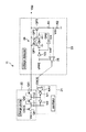
図12はこの発明をフラッシュメモリに適用した場合のメモリ全体の構成を示すブロック図である。アドレスバッファ(Address buffer)41は、外部アドレスを受け、読み出しまたは書込みまたは消去するメモリセルに対応した内部アドレスを出力する。I/Oバッファ(I/O buffer)42は、読み出し時にセンスアンプ(sense amp)43でセンスされるメモリセルのデータを外部に出力し、書込み時には外部から供給される書込みデータを書込み回路(Program circuit)44に入力する。書込み回路44はカラムゲート回路(column gates)45を介して、メモリセルアレイ(Memory Cell Array)46内の対応するビット線に書込み電圧を供給する。
【0082】
コマンドレジスタ(Command register)47は書込みや消去コマンドなど、外部から入力されるコマンドを保持し、コントローラ(Controller)48はコマンドレジスタ47で保持されているコマンドを受けて、メモリ内の各回路を制御するための制御信号を発生する。ロウデコーダ(Row decoder)49はアドレスバッファ41から出力される内部アドレスを受け、メモリセルアレイ46内の対応するワード線を選択する。カラムデコーダ(Column decoder)50はアドレスバッファ41から出力される内部アドレスを受け、カラムゲート回路45内のカラムゲートを内部アドレスに応じて選択駆動する。これにより、メモリセルアレイ46内の選択ビット線が、カラムゲート回路45を介してセンスアンプ43に接続される。
【0083】
チャージポンプ回路(Charge pumps)51は、外部電源電圧を昇圧して書込み用の5Vの電圧、消去用の10V(Vpp)及び−7Vの電圧を発生する。チャージポンプ回路51で発生された5Vの電圧は書込み回路44に供給される。チャージポンプ回路51で発生された−7Vの電圧はメモリセルアレイ46に供給される。
【0084】
また、チャージポンプ回路51で発生された10Vの電圧Vppはレギュレータ回路(Regulator)12に供給される。このレギュレータ回路12の機能については先に説明した通りなので、その説明は省略する。またチャージポンプ回路51とレギュレータ回路12との間には、先に説明した短絡回路(Equalizer)13が接続されている。この短絡回路(Equalizer)13の機能についても先に説明した通りなので、その説明は省略する。
【0085】
このような構成のフラッシュメモリでは、メモリセルの書込み時や読み出し時にワード線、つまりメモリセルのコントロールゲートに供給するための種々の電圧Vregを、レギュレータ回路12を用いて、1つのチャージポンプ回路で得られる電圧から時系列的に順次出力するために、いくつものチャージポンプ回路を設ける必要がなくなる。この結果、チップ全体の面積の大型化を防ぐことができる。しかも、チャージポンプ回路には比較的大きな電流が流れ、消費電流が多いために、チャージポンプ回路の数を減らすことによって全体の消費電流を削減することができる。なお、電圧Vregはロウデコーダ49を経由してメモリセルアレイ46内のワード線、つまりメモリセルのコントロールゲートに供給される。
【0086】
【発明の効果】
以上説明したようにこの発明によれば、昇圧回路の出力を用いて電圧出力回路から値が異なるいくつかの電圧を時系列的に順次出力するようにしたので、昇圧回路の数を減らすことができ、これによって集積化する際にチップ面積が大きくならず、かつ消費電流も少ない半導体装置を提供することができる。
【図面の簡単な説明】
【図1】この発明の第1の実施の形態に係る電圧生成回路のブロック図。
【図2】 図1の回路の動作の一例を示すタイミングチャート。
【図3】図1中の昇圧回路11の具体的な回路構成を示す図。
【図4】図1中のレギュレータ回路12の具体的な回路構成を示す図。
【図5】図4におけるコンパレータ26、27の具体的な回路構成を示す図。
【図6】第2の実施の形態に係る電圧生成回路のブロック図。
【図7】図6の回路の動作の一例を示すタイミングチャート。
【図8】図6中の短絡回路13の具体的な回路構成を示す図。
【図9】図1もしくは図6中のレギュレータ回路12の他の具体的回路構成を制御信号生成回路などの他の回路と共に示す回路図。
【図10】図9に示す回路の動作の一例を示すタイミングチャート。
【図11】この発明の第3の実施の形態による電圧生成回路のブロック図。
【図12】この発明をフラッシュメモリに適用した場合のメモリ全体の構成を示すブロック図。
【図13】フラッシュメモリにおける1つのメモリセルの素子断面構造を示す図。
【図14】NOR型フラッシュメモリのメモリセルアレイの回路例を示す図。
【図15】メモリセルのコントロールゲートに供給されるゲート電圧とメモリセルのドレインに流れるドレイン電流との関係を示す特性図。
【図16】動作時にメモリセルに対して供給される電圧Vg、Vd、Vsの値の一例を示す図。
【符号の説明】
11…昇圧回路(Vpp generator)、
12…レギュレータ回路(regulator)、
13…短絡回路(Equalizer)、
14…スイッチ回路(Switch)、
21…発振器(oscillator)、
22…チャージポンプ回路(charge pump)、
23…電圧検知回路(voltage detector)、
24…レベルシフト回路、
25、26、27、32…コンパレータ、
28…電流源、
29、33、35…インバータ、
30…レベルシフト回路、
31…制御信号生成回路、
34…ラッチ回路、
36…電圧設定回路、
37…レベルシフト回路、
41…アドレスバッファ(Address buffer)、
42…I/Oバッファ(I/O buffer)、
43…センスアンプ(sense amp)、
44…書込み回路(Program circuit)、
45…カラムゲート回路(column gates)、
46…メモリセルアレイ(Memory Cell Array)、
47…コマンドレジスタ(Command register)、
48…コントローラ(Controller)、
49…ロウデコーダ(Row decoder)、
50…カラムデコーダ(Column decoder)、
51…チャージポンプ回路(Charge pumps)、
IV1〜IV7…インバータ、
QI1〜QI3…IタイプのMOSトランジスタ、
C1、C2…キャパシタ、
QP1〜QP15…PチャネルのMOSトランジスタ、
QN1〜QN13…NチャネルのMOSトランジスタ、
R1〜R5…抵抗、
NOR1〜NOR4…NORゲート、
NA1…NANDゲート。[0001]
BACKGROUND OF THE INVENTION
The present invention relates to a semiconductor device including a booster circuit for boosting a power supply voltage, and particularly has a memory cell, and a high voltage used for erasing and writing data in the memory cell is obtained by the booster circuit. The present invention relates to a semiconductor memory device.
[0002]
[Prior art]
One type of semiconductor memory device is a flash memory. FIG. 13 shows an element cross-sectional structure of one memory cell in this flash memory. In the figure, an N-type well region (N-well) 72 is formed in a P-type semiconductor substrate (P-substrate) 71. Further, a P-type well region (P-well) 73 is formed in the N-
[0003]
The P
[0004]
In operation, the gate voltage Vg is supplied to the
[0005]
The memory cell stores “1” level and “0” level of data according to the amount of electrons accumulated in the
[0006]
A memory cell array is configured by providing a plurality of such memory cells. FIG. 14 shows a circuit example of a memory cell array of a NOR type flash memory. A plurality of memory cells MC are arranged in a matrix, and the control gates of the memory cells MC arranged in the same row are commonly connected to a corresponding one of the plurality of word lines WL0 to WLn. . The drain regions of the memory cells MC arranged in the same column are commonly connected to one corresponding bit line among the plurality of bits BL0 to BLm. Usually, the memory cell is divided into a plurality of blocks, and the source regions of the memory cells MC in the same block are commonly connected to the source lines of the corresponding blocks among the plurality of source lines SLi.
[0007]
FIG. 15 shows the relationship between the gate voltage supplied to the control gate of the memory cell and the drain current flowing through the drain of the memory cell during operation. Here, a state in which the amount of electrons accumulated in the floating gate is relatively large, that is, a state in which the threshold voltage Vt of the memory cell is high is designated as “0” data (a memory cell storing “0” data is designated as “0”). In contrast, a relatively small state, that is, a state where the threshold voltage Vt of the memory cell is low is referred to as “1” data (a memory cell storing “1” data is referred to as “1” cell). ).
[0008]
FIG. 16 shows bias conditions for reading, writing, and erasing data. FIG. 16 shows an example of the values of the voltages Vg, Vd, and Vs that are supplied to the memory cell during operation. When reading data, Vg, Vd, and Vs are set to 5V, 1V, and 0V, respectively. At the time of data writing, Vg and Vs are set to 9V and 0V, respectively, and Vd is 5V for a memory cell to which “0” data is written, and other memory cells (memory cells that are left with the original “1” data). Is set to 0V. Further, at the time of erasing, Vg and Vs are set to −7 V and 10 V, respectively, and Vd is brought into a floating state.
[0009]
Data reading is determined by whether or not a cell current flows when a gate voltage Vread (5 V in this example) is supplied to the control gate while a predetermined voltage (1 V in this example) is supplied to the drain region. This determination is performed by comparison with a reference current (Iref) flowing in the reference cell by a sense amplifier (not shown).
[0010]
Erasing is performed collectively by a plurality of memory cells sharing the P-type well region 73 (shown in FIG. 13). At the time of erasing, electrons flow from the
[0011]
Writing is performed for each memory cell. The bit line of the memory cell in which “0” data is written is biased to 5 V, and high energy electrons generated by the channel hot electron phenomenon are injected into the
[0012]
In the flash memory, a write verify operation and an erase verify operation are performed at the time of writing and erasing in order to confirm the degree of writing and erasing. In the write verify operation, the voltage of the control gate is set to a voltage Vpv (for example, 7 V) higher than the voltage Vread at the time of reading (5 V in this example), and a “0” read operation is performed. Then, the write operation and the write verify operation are alternately repeated, and the write operation is completed when all the data of the write target memory cell becomes “0”.
[0013]
In the case of erasing, the voltage of the
[0014]
As described above, the voltage supplied to the control gate of the memory cell changes to various values such as 9 V, 7 V, 5 V, and 3.5 V, for example, depending on the operation mode. Among these voltages, 9V, 7V, and 5V are higher than the power supply voltage supplied from the outside.
[0015]
By the way, conventionally, in order to generate various voltages higher than the power supply voltage supplied from the outside, such as 9V, 7V, and 5V as described above, a necessary number of boosting circuits for boosting the power supply voltage are provided. The outputs of the plurality of booster circuits are appropriately selected by a switch and supplied to the control gate of the memory cell.
[0016]
However, since the booster circuit requires an element occupying a large area on the chip, such as a capacitor, there is a problem that the chip area is increased when a plurality of booster circuits are provided. Further, since the current consumption in the booster circuit is relatively large, there is a problem that the current consumption of the entire chip increases.
[0017]
[Problems to be solved by the invention]
As described above, the conventional semiconductor device that requires various voltages higher than the power supply voltage supplied from the outside is provided with a plurality of booster circuits, so that the chip area increases when integrating. However, there is a problem that current consumption increases.
[0018]
The present invention has been made in consideration of the above-described circumstances, and an object of the present invention is to provide a semiconductor device that does not have a large chip area and consumes less current when integrated.
[0019]
[Means for Solving the Problems]
The semiconductor device of the present invention is supplied with the booster circuit that boosts the power supply voltage and outputs the first voltage, and the first voltage, and the value is lower than the first voltage using the first voltage. A first voltage output circuit that sequentially outputs at least two voltages from an output node in time series; a short circuit that short-circuits between the first voltage node and the output node of the first voltage output circuit; The short circuit starts a short circuit between the node of the first voltage and the output node of the first voltage output circuit as a boost operation is started in the boost circuit, The short-circuit state is released after a predetermined period has elapsed since the boosting operation is started, and the short-circuit circuit performs a short-circuit between the first voltage node and the output node of the first voltage output circuit. During the period, the first voltage output circuit is deactivated and After the short circuit has canceled the short-circuit state, the first voltage output circuit activation It is characterized by doing.
The semiconductor device of the present invention is supplied with the booster circuit that boosts the power supply voltage and outputs the first voltage, and the first voltage, and the value is lower than the first voltage using the first voltage. A first voltage output circuit that sequentially outputs at least two voltages from an output node in time series; a short circuit that short-circuits between the first voltage node and the output node of the first voltage output circuit; The short circuit starts a short circuit between the node of the first voltage and the output node of the first voltage output circuit as a boost operation is started in the boost circuit, After the boosting operation is started and the first voltage reaches a predetermined value, the short-circuit state is released, and the short-circuit is connected between the node of the first voltage and the output node of the first voltage output circuit. During the short-circuit period, the first voltage output circuit is inactive And, after the short circuit is released the short-circuit state, the first voltage output circuit activation It is characterized by doing.
[0020]
In the semiconductor memory device of the present invention, a data erasable memory cell for storing data, a first voltage is supplied to the gate of the memory cell, and one of the second voltage and the third voltage is supplied to the drain. A write circuit for writing data to the memory cell, an erasing circuit for erasing data of the memory cell by supplying a fourth voltage to the semiconductor region in which the memory cell is formed, and a power supply voltage And the fifth voltage is supplied, and the first voltage having a value lower than the fifth voltage is output from the output node by using the fifth voltage. A first voltage output circuit for outputting, and a short circuit for short-circuiting between the node of the fifth voltage and the output node of the first voltage output circuit, the short circuit being the boost circuit As the boost operation starts Starting a short circuit between the node of the fifth voltage and the output node of the first voltage output circuit, and releasing the short circuit state after a predetermined period has elapsed from the start of the boosting operation, Is in a short circuit between the node of the fifth voltage and the output node of the first voltage output circuit, the first voltage output circuit is deactivated, and the short circuit is in the short circuit state. After the first voltage output circuit is activation It is characterized by doing.
[0021]
DETAILED DESCRIPTION OF THE INVENTION
Hereinafter, embodiments of the present invention will be described in detail with reference to the drawings.
[0022]
FIG. 1 is a block diagram showing a partial circuit configuration of a semiconductor device according to the first embodiment of the present invention. The circuit shown in FIG. 1 is a voltage generation circuit that is built in, for example, a flash memory and generates various voltages to be supplied to the control gate of the memory cell in various operation modes as described above. generator) 11 and a regulator circuit (regulator) 12.
[0023]
Boost
[0024]
The
[0025]
Next, an example of the operation of the circuit of FIG. 1 will be described with reference to the timing chart of FIG. Before time t0 in FIG. 2, it is assumed that both voltages Vpp and Vreg are set to a read voltage of 5 V, which is an output voltage of another booster circuit (not shown).
[0026]
When the boost activation signal VPPE is activated at time t0, the
[0027]
On the other hand, the regulator activation signal REGE is activated at time t0, and at the same time, the write signal PROG is activated. Thereby, the
[0028]
Next, at time t1, the write time signal PROG is deactivated and the verify time signal VRFY is activated. As a result, the output voltage Vreg of the
[0029]
Next, when the verify time signal VRFY becomes inactive at time t2, the output voltage Vreg of the
[0030]
As described above, in the circuit of FIG. 1, the regulator circuit uses the voltage Vpp output from the
[0031]
FIG. 3 shows a specific circuit configuration of the
[0032]
The
[0033]
The
[0034]
The oscillation activation signal OSCE output from the
[0035]
The
[0036]
In the booster circuit having such a configuration, when the boost activation signal VPPE becomes “H” level, the output of the inverter IV3 in the
[0037]
Since the value of the voltage Vpp is low immediately after the operation of the
[0038]
When the voltage Vpp rises above the specified value, the relationship of Vref <Vdiv is established, and the oscillation activation signal OSCE becomes “L” level, whereby the oscillation operation of the
[0039]
In this state, when the voltage Vpp falls below the specified value, the oscillation activation signal OSCE again becomes “H” level, the oscillation operation is resumed, and the charge transfer operation in the
[0040]
FIG. 4 shows a specific circuit configuration of the
[0041]
The reference voltage Vref is supplied to the non-inverting input terminal (+) of the one
[0042]
In such a configuration, the transistor QN6 is turned on during the period from time t0 to t1 in FIG. 2 in which the regulator activation signal REGE is set to “H” level and the write signal PROG is set to “H” level. The voltage Vreg is divided by the two resistors R3 and R4, and the divided voltage at this time is input to the
[0043]
Here, immediately after the regulator activation signal REGE is set to the “H” level, the voltage Vreg is almost 0 V, and the divided voltage obtained by dividing the voltage by the two resistors R3 and R4 is lower than Vref. The output of the
[0044]
In this way, the
[0045]
Next, in the period from time t1 to time t2 in FIG. 2 in which the write signal PROG is set to “L” level and the verify signal VRFY is set to “H” level, the transistor QN6 is turned off and the transistor QN5 is turned on. Therefore, the voltage Vreg is divided by the three resistors R3, R4, and R5, and a divided voltage having a smaller resistance division ratio than that at the time of writing is input to the
[0046]
Therefore, at the time of verification, the
[0047]
FIG. 5 shows a specific circuit configuration of the
[0048]
On the other hand, the regulator activation signal REGE is input to the
[0049]
In the comparator having such a configuration, when the regulator activation signal REGE is set to “L” level, the output of the
[0050]
When the regulator activation signal REGE becomes “H” level, the output of the
[0051]
In the
[0052]
Therefore, when the delay of rising of the voltage Vpp and the voltage Vreg becomes a problem as described above, the node of the voltage Vpp and the voltage Vreg are changed as in the voltage generation circuit of the second embodiment shown in FIG. What is necessary is just to connect the short circuit (Equalizer) 13 which carries out short circuit control between both nodes between nodes.
[0053]
The operation of the
[0054]
Next, an example of the operation of the circuit of FIG. 6 will be described with reference to the timing chart of FIG. Also in this case, it is assumed that the voltages Vpp and Vreg are both set to a read voltage of 5 V, which is an output voltage of another booster circuit (not shown) before time t0 in FIG.
[0055]
When boost activation signal VPPE is activated at time t0,
[0056]
Next, when the short circuit control signal EQLE becomes “L” level at time t1, the short circuit state by the
[0057]
The regulator activation signal REGE is activated at time t2 after the voltage Vreg has increased to some extent. Note that the write signal PROG is activated simultaneously with the activation of the boost activation signal VPPE. When the signal REGE is activated, the
[0058]
Next, at time t3, the write signal PROG is deactivated and the verify signal VRFY is activated. As a result, the output voltage Vreg of the
[0059]
Next, when the verify time signal VRFY becomes inactive at time t4, the output voltage Vreg of the
[0060]
FIG. 8 shows a specific circuit configuration of the
[0061]
In the
[0062]
On the other hand, when the short-circuit control signal EQLE is at the “L” level, the output of the inverter IV5 is at the “L” level, the output of the inverter IV6 is at the “H” level, the transistor QN10 is turned on, the transistor QN11 is turned off, and the level shift The output of the
[0063]
Thus, in the circuit of FIG. 6 as well, in the various operation modes of the memory cell, voltages having different values to be supplied to the control gate of the memory cell are output from the
[0064]
That is, the
[0065]
FIG. 9 shows another specific circuit configuration of the
[0066]
The
[0067]
A control signal generation circuit 31 generates a regulator activation signal REGE, a short circuit control signal EQLE, and the like from the boost activation signal VPPE, the write signal PROG, the verify signal VRFY, and the like. This circuit 31 includes a
[0068]
The output from the NOR gate NOR2 is input to the
[0069]
[0070]
Next, an example of the operation of the circuit illustrated in FIG. 9 will be described with reference to the timing chart of FIG. First, since the write signal PROG and the verify signal VRFY are both at the “L” level before time t0, the output of the NOR gate NOR4 in the signal generation circuit 31 is at the “H” level, and the output of the NOR gate NOR4 The output of the
[0071]
When boost activation signal VPPE is activated ("H" level) at time t0,
[0072]
When the write signal PROG becomes “H” level at time t0, the output of the NOR gate NOR4 in the signal generation circuit 31 is inverted to “L” level, and the output of the
[0073]
On the other hand, the output voltage Vreg of the
[0074]
Further, when the regulator activation signal REGE is inverted to the “H” level, the short circuit control signal EQLE that is the output of the NOR gate NOR3 becomes the “L” level. Thereby, the short circuit state by the
[0075]
Next, at time t2, the write time signal PROG becomes “L” level, and the verify time signal VRFY becomes “H” level. At this time, since the output of the
[0076]
Next, boost activation signal VPPE is deactivated ("L" level) at time t3. Thereby, the
[0077]
As described above, in the circuit shown in FIG. 9, the short-circuit control signal EQLE rises in synchronization with the rise of the boost activation signal VPPE, the short-circuit control signal EQLE falls after Vreg reaches the specified value of 9V, and the regulator The activation signal REGE rises. As a result, it is possible to substantially eliminate the time from when the short-circuit control signal EQLE falls to the next rise of the regulator activation signal REGE, thereby comparing with the timing chart of FIG. It is not necessary to secure the timing unnecessarily long, and the operation can be performed at the optimum timing.
[0078]
FIG. 11 shows a voltage generation circuit according to the third embodiment of the present invention. The voltage generation circuit of FIG. 11 is provided with a
[0079]
The
[0080]
That is, in the voltage generation circuit according to this embodiment, the voltage Vpp of 10 V obtained by the
[0081]
FIG. 12 is a block diagram showing the configuration of the entire memory when the present invention is applied to a flash memory. An
[0082]
A
[0083]
A
[0084]
The 10 V voltage Vpp generated by the
[0085]
In the flash memory having such a configuration, various voltages Vreg to be supplied to the word lines, that is, the control gates of the memory cells at the time of writing or reading of the memory cells are supplied by a single charge pump circuit using the
[0086]
【The invention's effect】
As described above, according to the present invention, since the voltage output circuit sequentially outputs several voltages having different values from the voltage output circuit in time series, the number of boost circuits can be reduced. Thus, it is possible to provide a semiconductor device that does not increase the chip area and consumes less current when integrated.
[Brief description of the drawings]
FIG. 1 is a block diagram of a voltage generation circuit according to a first embodiment of the present invention.
FIG. 2 shows the operation of the circuit of FIG. of The timing chart which shows an example.
FIG. 3 is a diagram showing a specific circuit configuration of a
FIG. 4 is a diagram showing a specific circuit configuration of the
5 is a diagram showing a specific circuit configuration of
FIG. 6 is a block diagram of a voltage generation circuit according to a second embodiment.
7 is a timing chart showing an example of the operation of the circuit of FIG.
8 is a diagram showing a specific circuit configuration of a
9 is a circuit diagram showing another specific circuit configuration of the
10 is a timing chart illustrating an example of the operation of the circuit illustrated in FIG. 9;
FIG. 11 is a block diagram of a voltage generation circuit according to a third embodiment of the present invention.
FIG. 12 is a block diagram showing the configuration of the entire memory when the present invention is applied to a flash memory.
FIG. 13 shows an element cross-sectional structure of one memory cell in a flash memory.
FIG. 14 is a diagram showing a circuit example of a memory cell array of a NOR flash memory.
FIG. 15 is a characteristic diagram showing the relationship between the gate voltage supplied to the control gate of the memory cell and the drain current flowing through the drain of the memory cell.
FIG. 16 is a diagram illustrating an example of values of voltages Vg, Vd, and Vs supplied to a memory cell during operation.
[Explanation of symbols]
11: Booster circuit (Vpp generator),
12 ... Regulator circuit,
13 ... Short circuit (Equalizer),
14 ... Switch circuit (Switch),
21 ... oscillator,
22 ... charge pump circuit,
23 ... Voltage detector,
24. Level shift circuit,
25, 26, 27, 32 ... comparators,
28 ... current source,
29, 33, 35 ... inverter,
30 ... Level shift circuit,
31 ... Control signal generation circuit,
34 ... Latch circuit,
36 ... Voltage setting circuit,
37 ... Level shift circuit,
41 ... Address buffer,
42 ... I / O buffer
43 ... sense amp,
44 ... Program circuit,
45 ... column gates,
46: Memory cell array,
47: Command register,
48 ... Controller,
49. Row decoder,
50: Column decoder,
51 ... Charge pumps,
IV1-IV7 ... inverter,
QI1-QI3 ... I-type MOS transistors,
C1, C2 ... capacitors,
QP1 to QP15... P channel MOS transistors,
QN1 to QN13 ... N-channel MOS transistors,
R1-R5: resistance,
NOR1-NOR4 ... NOR gate,
NA1: NAND gate.
Claims (6)
上記第1の電圧が供給され、この第1の電圧を用いて第1の電圧よりも値が低い少なくとも2つの電圧を出力ノードから時系列的に順次出力する第1の電圧出力回路と、
上記第1の電圧のノードと上記第1の電圧出力回路の出力ノードとの間を短絡する短絡回路とを具備し、
前記短絡回路は、前記昇圧回路で昇圧動作が開始されるのに伴って前記第1の電圧のノードと前記第1の電圧出力回路の出力ノードとの間の短絡を開始し、昇圧動作が開始されてから所定期間が経過した後に短絡状態を解除し、
前記短絡回路が前記第1の電圧のノードと前記第1の電圧出力回路の出力ノードとの間の短絡を行っている期間は、前記第1の電圧出力回路は非活性化し、前記短絡回路が前記短絡状態を解除した後に、前記第1の電圧出力回路が活性化することを特徴とする半導体装置。A booster circuit for boosting a power supply voltage and outputting a first voltage;
A first voltage output circuit that is supplied with the first voltage and sequentially outputs at least two voltages having a value lower than the first voltage from the output node in time series using the first voltage;
A short circuit for short-circuiting between the node of the first voltage and the output node of the first voltage output circuit;
The short circuit starts a short circuit between the node of the first voltage and the output node of the first voltage output circuit as the boost operation is started in the boost circuit, and the boost operation starts. After a predetermined period of time has passed since the release,
During a period in which the short circuit is short-circuiting between the node of the first voltage and the output node of the first voltage output circuit, the first voltage output circuit is inactivated, and the short circuit is The semiconductor device is characterized in that the first voltage output circuit is activated after releasing the short-circuit state.
上記第1の電圧が供給され、この第1の電圧を用いて第1の電圧よりも値が低い少なくとも2つの電圧を出力ノードから時系列的に順次出力する第1の電圧出力回路と、
上記第1の電圧のノードと上記第1の電圧出力回路の出力ノードとの間を短絡する短絡回路とを具備し、
前記短絡回路は、前記昇圧回路で昇圧動作が開始されるのに伴って前記第1の電圧のノードと前記第1の電圧出力回路の出力ノードとの間の短絡を開始し、昇圧動作が開始されて前記第1の電圧が所定値に達した後に短絡状態を解除し、
前記短絡回路が前記第1の電圧のノードと前記第1の電圧出力回路の出力ノードとの間の短絡を行っている期間は、前記第1の電圧出力回路は非活性化し、前記短絡回路が前記短絡状態を解除した後に、前記第1の電圧出力回路が活性化することを特徴とする半導体装置。A booster circuit for boosting a power supply voltage and outputting a first voltage;
A first voltage output circuit that is supplied with the first voltage and sequentially outputs at least two voltages having a value lower than the first voltage from the output node in time series using the first voltage;
A short circuit for short-circuiting between the node of the first voltage and the output node of the first voltage output circuit;
The short circuit starts a short circuit between the node of the first voltage and the output node of the first voltage output circuit as the boost operation is started in the boost circuit, and the boost operation starts. The short circuit state is released after the first voltage reaches a predetermined value,
During a period in which the short circuit is short-circuiting between the node of the first voltage and the output node of the first voltage output circuit, the first voltage output circuit is inactivated, and the short circuit is The semiconductor device is characterized in that the first voltage output circuit is activated after releasing the short-circuit state.
上記メモリセルのゲートに第1の電圧を供給し、ドレインに第2の電圧及び第3の電圧のいずれか一方を供給して、上記メモリセルのデータ書込みを行う書込み回路と、
上記メモリセルが形成されている半導体領域に第4の電圧を供給して、上記メモリセルのデータ消去を行う消去回路と、
電源電圧を昇圧して第5の電圧を出力する昇圧回路と、
上記第5の電圧が供給され、この第5の電圧を用いて第5の電圧よりも値が低い上記第1の電圧を出力ノードから出力する第1の電圧出力回路と、
前記第5の電圧のノードと前記第1の電圧出力回路の出力ノードとの間を短絡する短絡回路とを具備し、
前記短絡回路は、前記昇圧回路で昇圧動作が開始されるのに伴って前記第5の電圧のノードと前記第1の電圧出力回路の出力ノードとの間の短絡を開始し、昇圧動作が開始されてから所定期間が経過した後に短絡状態を解除し、
前記短絡回路が前記第5の電圧のノードと前記第1の電圧出力回路の出力ノードとの間の短絡を行っている期間は、前記第1の電圧出力回路は非活性化し、前記短絡回路が前記短絡状態を解除した後に、前記第1の電圧出力回路が活性化することを特徴とする半導体記憶装置。A data erasable memory cell for storing data;
A write circuit for supplying data to the memory cell by supplying a first voltage to the gate of the memory cell and supplying a second voltage or a third voltage to the drain;
An erasing circuit for erasing data of the memory cell by supplying a fourth voltage to the semiconductor region in which the memory cell is formed;
A booster circuit that boosts the power supply voltage and outputs a fifth voltage;
A first voltage output circuit which is supplied with the fifth voltage and outputs the first voltage having a value lower than that of the fifth voltage from the output node using the fifth voltage;
A short circuit for short-circuiting between the node of the fifth voltage and the output node of the first voltage output circuit;
The short circuit starts a short circuit between the node of the fifth voltage and the output node of the first voltage output circuit as the boost operation is started in the boost circuit, and the boost operation starts. After a predetermined period of time has passed since the release,
During the period in which the short circuit is short-circuiting between the node of the fifth voltage and the output node of the first voltage output circuit, the first voltage output circuit is inactivated, and the short circuit is The semiconductor memory device, wherein the first voltage output circuit is activated after releasing the short circuit state.
上記メモリセルのゲートに第1の電圧を供給し、ドレインに第2の電圧及び第3の電圧のいずれか一方を供給して、上記メモリセルのデータ書込みを行う書込み回路と、
上記メモリセルが形成されている半導体領域に第4の電圧を供給して、上記メモリセルのデータ消去を行う消去回路と、
電源電圧を昇圧して第5の電圧を出力する昇圧回路と、
上記第5の電圧が供給され、この第5の電圧を用いて第5の電圧よりも値が低い上記第1の電圧を出力ノードから出力する第1の電圧出力回路と、
前記第5の電圧のノードと前記第1の電圧出力回路の出力ノードとの間を短絡する短絡回路とを具備し、
前記短絡回路は、前記昇圧回路で昇圧動作が開始されるのに伴って前記第5の電圧のノードと前記第1の電圧出力回路の出力ノードとの間の短絡を開始し、昇圧動作が開始されて前記第5の電圧が所定値に達した後に短絡状態を解除し、
前記短絡回路が前記第5の電圧のノードと前記第1の電圧出力回路の出力ノードとの間の短絡を行っている期間は、前記第1の電圧出力回路は非活性化し、前記短絡回路が前記短絡状態を解除した後に、前記第1の電圧出力回路が活性化することを特徴とする半導体記憶装置。A data erasable memory cell for storing data;
A write circuit for supplying data to the memory cell by supplying a first voltage to the gate of the memory cell and supplying a second voltage or a third voltage to the drain;
An erasing circuit for erasing data of the memory cell by supplying a fourth voltage to the semiconductor region in which the memory cell is formed;
A booster circuit that boosts the power supply voltage and outputs a fifth voltage;
A first voltage output circuit which is supplied with the fifth voltage and outputs the first voltage having a value lower than that of the fifth voltage from the output node using the fifth voltage;
A short circuit for short-circuiting between the node of the fifth voltage and the output node of the first voltage output circuit;
The short circuit starts a short circuit between the node of the fifth voltage and the output node of the first voltage output circuit as the boost operation is started in the boost circuit, and the boost operation starts. And the short circuit state is released after the fifth voltage reaches a predetermined value,
During the period in which the short circuit is short-circuiting between the node of the fifth voltage and the output node of the first voltage output circuit, the first voltage output circuit is inactivated, and the short circuit is The semiconductor memory device, wherein the first voltage output circuit is activated after releasing the short circuit state.
Priority Applications (8)
| Application Number | Priority Date | Filing Date | Title |
|---|---|---|---|
| JP2000154983A JP4149637B2 (en) | 2000-05-25 | 2000-05-25 | Semiconductor device |
| US09/864,181 US6487120B2 (en) | 2000-05-25 | 2001-05-25 | Boosted voltage generating circuit and semiconductor memory device having the same |
| EP01112062A EP1158524A1 (en) | 2000-05-25 | 2001-05-25 | Semiconductor memory device having a boosted voltage generating circuit |
| US10/265,727 US6605986B2 (en) | 2000-05-25 | 2002-10-08 | Boosted voltage generating circuit and semiconductor memory device having the same |
| US10/464,462 US6771547B2 (en) | 2000-05-25 | 2003-06-19 | Boosted voltage generating circuit and semiconductor memory device having the same |
| US10/866,131 US6996024B2 (en) | 2000-05-25 | 2004-06-14 | Boosted voltage generating circuit and semiconductor memory device having the same |
| US11/269,696 US7203120B2 (en) | 2000-05-25 | 2005-11-09 | Boosted voltage generating circuit and semiconductor memory device having the same |
| US11/269,697 US7180796B2 (en) | 2000-05-25 | 2005-11-09 | Boosted voltage generating circuit and semiconductor memory device having the same |
Applications Claiming Priority (1)
| Application Number | Priority Date | Filing Date | Title |
|---|---|---|---|
| JP2000154983A JP4149637B2 (en) | 2000-05-25 | 2000-05-25 | Semiconductor device |
Publications (3)
| Publication Number | Publication Date |
|---|---|
| JP2001338493A JP2001338493A (en) | 2001-12-07 |
| JP2001338493A5 JP2001338493A5 (en) | 2005-08-25 |
| JP4149637B2 true JP4149637B2 (en) | 2008-09-10 |
Family
ID=18659994
Family Applications (1)
| Application Number | Title | Priority Date | Filing Date |
|---|---|---|---|
| JP2000154983A Expired - Fee Related JP4149637B2 (en) | 2000-05-25 | 2000-05-25 | Semiconductor device |
Country Status (3)
| Country | Link |
|---|---|
| US (6) | US6487120B2 (en) |
| EP (1) | EP1158524A1 (en) |
| JP (1) | JP4149637B2 (en) |
Families Citing this family (71)
| Publication number | Priority date | Publication date | Assignee | Title |
|---|---|---|---|---|
| JP4149637B2 (en) * | 2000-05-25 | 2008-09-10 | 株式会社東芝 | Semiconductor device |
| DE10108980A1 (en) * | 2001-02-23 | 2002-09-12 | Koninkl Philips Electronics Nv | Arrangement for controlling display units with an adaptive start sequence |
| JP2003208794A (en) * | 2002-01-10 | 2003-07-25 | Seiko Epson Corp | Nonvolatile semiconductor memory device |
| US6876582B2 (en) * | 2002-05-24 | 2005-04-05 | Hynix Semiconductor, Inc. | Flash memory cell erase scheme using both source and channel regions |
| US6937517B2 (en) * | 2002-07-18 | 2005-08-30 | Micron Technology, Inc. | Clock regulation scheme for varying loads |
| JP2004063019A (en) * | 2002-07-30 | 2004-02-26 | Renesas Technology Corp | Internal voltage generating circuit |
| TWI241591B (en) * | 2002-08-09 | 2005-10-11 | Hitachi Ltd | Semiconductor device and memory card using the same |
| US6842380B2 (en) * | 2002-08-27 | 2005-01-11 | Micron Technology, Inc. | Method and apparatus for erasing memory |
| DE10248498A1 (en) * | 2002-10-17 | 2004-05-06 | Infineon Technologies Ag | Circuit arrangement for voltage regulation |
| DE60335147D1 (en) * | 2003-05-13 | 2011-01-05 | Fujitsu Semiconductor Ltd | INTEGRATED SEMICONDUCTOR ELEMENT |
| JP4318511B2 (en) * | 2003-08-26 | 2009-08-26 | 三洋電機株式会社 | Booster circuit |
| US7095653B2 (en) * | 2003-10-08 | 2006-08-22 | Micron Technology, Inc. | Common wordline flash array architecture |
| ITRM20030512A1 (en) * | 2003-11-05 | 2005-05-06 | St Microelectronics Srl | LOADING PUMP CIRCUIT WITH LOW-WEAKING TIME |
| KR100572323B1 (en) * | 2003-12-11 | 2006-04-19 | 삼성전자주식회사 | Multilevel High Voltage Generator |
| JP2005222580A (en) * | 2004-02-03 | 2005-08-18 | Renesas Technology Corp | Semiconductor memory device |
| JP4426361B2 (en) * | 2004-03-31 | 2010-03-03 | パナソニック株式会社 | Nonvolatile semiconductor memory device |
| KR100562654B1 (en) * | 2004-04-20 | 2006-03-20 | 주식회사 하이닉스반도체 | Bleq driving circuit and semiconductor memory device using it |
| JP2006031801A (en) * | 2004-07-14 | 2006-02-02 | Nec Electronics Corp | Electric potential switching circuit, flash memory having same, and electric potential switching method |
| US7038954B2 (en) * | 2004-08-30 | 2006-05-02 | Micron Technology, Inc. | Apparatus with equalizing voltage generation circuit and methods of use |
| US7154794B2 (en) * | 2004-10-08 | 2006-12-26 | Lexmark International, Inc. | Memory regulator system with test mode |
| FR2878986B1 (en) * | 2004-12-08 | 2007-04-27 | Atmel Corp | PRINCIPLE OF POWER CONTROL OF HIGH VOLTAGE OUTPUT IN INTEGRATED CIRCUIT DEVICES |
| JP4587804B2 (en) * | 2004-12-22 | 2010-11-24 | 株式会社リコー | Voltage regulator circuit |
| US7266018B2 (en) * | 2005-04-11 | 2007-09-04 | Intel Corporation | Reducing sneak currents in virtual ground memory arrays |
| KR100697284B1 (en) * | 2005-05-02 | 2007-03-20 | 삼성전자주식회사 | Flash memory device and programming method thereof |
| KR100680441B1 (en) * | 2005-06-07 | 2007-02-08 | 주식회사 하이닉스반도체 | VPP voltage generator for generating stable VPP voltage |
| JP4927356B2 (en) * | 2005-07-11 | 2012-05-09 | エルピーダメモリ株式会社 | Semiconductor device |
| WO2007043095A1 (en) * | 2005-09-30 | 2007-04-19 | Spansion Llc | Memory device and method of controlling memory device |
| KR100729353B1 (en) | 2005-11-22 | 2007-06-15 | 삼성전자주식회사 | Flash memory device with unified regulator/pump structure |
| US20070126494A1 (en) * | 2005-12-06 | 2007-06-07 | Sandisk Corporation | Charge pump having shunt diode for improved operating efficiency |
| US7372320B2 (en) * | 2005-12-16 | 2008-05-13 | Sandisk Corporation | Voltage regulation with active supplemental current for output stabilization |
| US20070139099A1 (en) * | 2005-12-16 | 2007-06-21 | Sandisk Corporation | Charge pump regulation control for improved power efficiency |
| JP4841282B2 (en) * | 2006-03-24 | 2011-12-21 | 富士通セミコンダクター株式会社 | Power supply device control circuit, power supply device, and control method therefor |
| US20070229149A1 (en) * | 2006-03-30 | 2007-10-04 | Sandisk Corporation | Voltage regulator having high voltage protection |
| US7606075B2 (en) * | 2006-04-19 | 2009-10-20 | Micron Technology, Inc. | Read operation for NAND memory |
| JP4843376B2 (en) * | 2006-05-17 | 2011-12-21 | 株式会社東芝 | Power circuit |
| KR100733953B1 (en) | 2006-06-15 | 2007-06-29 | 삼성전자주식회사 | Voltage regulator for flash memory device |
| US7626866B2 (en) * | 2006-07-28 | 2009-12-01 | Micron Technology, Inc. | NAND flash memory programming |
| US7554311B2 (en) * | 2006-07-31 | 2009-06-30 | Sandisk Corporation | Hybrid charge pump regulation |
| US7461106B2 (en) * | 2006-09-12 | 2008-12-02 | Motorola, Inc. | Apparatus and method for low complexity combinatorial coding of signals |
| US7368979B2 (en) | 2006-09-19 | 2008-05-06 | Sandisk Corporation | Implementation of output floating scheme for hv charge pumps |
| JP4956218B2 (en) * | 2007-02-15 | 2012-06-20 | 株式会社東芝 | Nonvolatile semiconductor memory device |
| JP5158076B2 (en) * | 2007-03-29 | 2013-03-06 | 富士通株式会社 | Semiconductor device and bias generation circuit |
| US7532516B2 (en) * | 2007-04-05 | 2009-05-12 | Sandisk Corporation | Non-volatile storage with current sensing of negative threshold voltages |
| JP2008269727A (en) * | 2007-04-24 | 2008-11-06 | Matsushita Electric Ind Co Ltd | Voltage booster circuit, semiconductor memory and drive method thereof |
| US8576096B2 (en) * | 2007-10-11 | 2013-11-05 | Motorola Mobility Llc | Apparatus and method for low complexity combinatorial coding of signals |
| US8209190B2 (en) * | 2007-10-25 | 2012-06-26 | Motorola Mobility, Inc. | Method and apparatus for generating an enhancement layer within an audio coding system |
| JP5367977B2 (en) * | 2007-12-12 | 2013-12-11 | セイコーインスツル株式会社 | Nonvolatile semiconductor memory device and writing method and reading method thereof |
| US7995392B2 (en) | 2007-12-13 | 2011-08-09 | Kabushiki Kaisha Toshiba | Semiconductor memory device capable of shortening erase time |
| US7916544B2 (en) | 2008-01-25 | 2011-03-29 | Micron Technology, Inc. | Random telegraph signal noise reduction scheme for semiconductor memories |
| US7839689B2 (en) * | 2008-01-31 | 2010-11-23 | Mosaid Technologies Incorporated | Power supplies in flash memory devices and systems |
| KR100894490B1 (en) * | 2008-03-03 | 2009-04-22 | 주식회사 하이닉스반도체 | Internal voltage generator of semiconductor memory device |
| US7889103B2 (en) * | 2008-03-13 | 2011-02-15 | Motorola Mobility, Inc. | Method and apparatus for low complexity combinatorial coding of signals |
| US20090234642A1 (en) * | 2008-03-13 | 2009-09-17 | Motorola, Inc. | Method and Apparatus for Low Complexity Combinatorial Coding of Signals |
| JP5011182B2 (en) * | 2008-03-24 | 2012-08-29 | ルネサスエレクトロニクス株式会社 | Charge pump circuit |
| US8639519B2 (en) * | 2008-04-09 | 2014-01-28 | Motorola Mobility Llc | Method and apparatus for selective signal coding based on core encoder performance |
| JP2010124590A (en) * | 2008-11-19 | 2010-06-03 | Seiko Instruments Inc | Booster circuit |
| US20100148840A1 (en) * | 2008-12-16 | 2010-06-17 | Siyou Weng | Pulse modulated charge pump circuit |
| US8219408B2 (en) * | 2008-12-29 | 2012-07-10 | Motorola Mobility, Inc. | Audio signal decoder and method for producing a scaled reconstructed audio signal |
| US8140342B2 (en) * | 2008-12-29 | 2012-03-20 | Motorola Mobility, Inc. | Selective scaling mask computation based on peak detection |
| US8200496B2 (en) * | 2008-12-29 | 2012-06-12 | Motorola Mobility, Inc. | Audio signal decoder and method for producing a scaled reconstructed audio signal |
| US8175888B2 (en) * | 2008-12-29 | 2012-05-08 | Motorola Mobility, Inc. | Enhanced layered gain factor balancing within a multiple-channel audio coding system |
| KR101005136B1 (en) * | 2009-05-29 | 2011-01-04 | 주식회사 하이닉스반도체 | Apparatus for generating high voltage |
| JP5259505B2 (en) * | 2009-06-26 | 2013-08-07 | 株式会社東芝 | Semiconductor memory device |
| IT1397283B1 (en) * | 2009-11-30 | 2013-01-04 | St Microelectronics Rousset | LOADING PUMP STAGE, METHOD OF CHECKING A STAGE WITH A LOADING PUMP AND MEMORY INCLUDING A STAGE WITH A LOADING PUMP. |
| US8423355B2 (en) * | 2010-03-05 | 2013-04-16 | Motorola Mobility Llc | Encoder for audio signal including generic audio and speech frames |
| US8428936B2 (en) * | 2010-03-05 | 2013-04-23 | Motorola Mobility Llc | Decoder for audio signal including generic audio and speech frames |
| US8456914B2 (en) * | 2011-03-07 | 2013-06-04 | Elpida Memory, Inc. | Memory device with multiple planes |
| JP5890207B2 (en) | 2012-03-13 | 2016-03-22 | ルネサスエレクトロニクス株式会社 | Semiconductor device |
| US9129600B2 (en) | 2012-09-26 | 2015-09-08 | Google Technology Holdings LLC | Method and apparatus for encoding an audio signal |
| US9190903B2 (en) | 2013-12-20 | 2015-11-17 | Infineon Technologies, Ag | System and method for a controlled feedback charge pump |
| CN106708153B (en) * | 2017-03-08 | 2019-03-12 | 长江存储科技有限责任公司 | A kind of high bandwidth low pressure difference linear voltage regulator |
Family Cites Families (42)
| Publication number | Priority date | Publication date | Assignee | Title |
|---|---|---|---|---|
| US5493572A (en) * | 1981-04-17 | 1996-02-20 | Hitachi, Ltd. | Semiconductor integrated circuit with voltage limiter having different output ranges for normal operation and performing of aging tests |
| CA2028414C (en) * | 1989-10-25 | 2000-02-08 | Owen H. Decker | Method for increasing fiber strength translation in composite pressure vessels using matrix resin formulations containing surface-active agents |
| US5519654A (en) * | 1990-09-17 | 1996-05-21 | Kabushiki Kaisha Toshiba | Semiconductor memory device with external capacitor to charge pump in an EEPROM circuit |
| US5357462A (en) * | 1991-09-24 | 1994-10-18 | Kabushiki Kaisha Toshiba | Electrically erasable and programmable non-volatile semiconductor memory with automatic write-verify controller |
| JPH05151789A (en) * | 1991-11-29 | 1993-06-18 | Nec Corp | Electrically writable and batch erasable nonvolatile semiconductor memory device |
| US5257232A (en) * | 1992-03-05 | 1993-10-26 | International Business Machines Corporation | Sensing circuit for semiconductor memory with limited bitline voltage swing |
| KR960000616B1 (en) * | 1993-01-13 | 1996-01-10 | 삼성전자주식회사 | Non-volatile semiconductor memory device |
| JP3373632B2 (en) * | 1993-03-31 | 2003-02-04 | 株式会社東芝 | Nonvolatile semiconductor memory device |
| JP2839819B2 (en) * | 1993-05-28 | 1998-12-16 | 株式会社東芝 | Nonvolatile semiconductor memory device |
| JP3292417B2 (en) * | 1994-02-15 | 2002-06-17 | 三菱電機株式会社 | Semiconductor device |
| US5483486A (en) * | 1994-10-19 | 1996-01-09 | Intel Corporation | Charge pump circuit for providing multiple output voltages for flash memory |
| US5726944A (en) * | 1996-02-05 | 1998-03-10 | Motorola, Inc. | Voltage regulator for regulating an output voltage from a charge pump and method therefor |
| JP3171129B2 (en) * | 1996-11-01 | 2001-05-28 | 株式会社デンソー | Driver circuit and constant current control circuit for occupant protection device having constant current control function |
| JP4007457B2 (en) * | 1996-06-20 | 2007-11-14 | エスティマイクロエレクトロニクス・ソチエタ・ア・レスポンサビリタ・リミタータ | Multi-level memory circuit with regulated read voltage |
| JP3519547B2 (en) * | 1996-06-24 | 2004-04-19 | 株式会社東芝 | Intermediate voltage generating circuit and nonvolatile semiconductor memory having the same |
| JP3207768B2 (en) * | 1996-09-30 | 2001-09-10 | 株式会社東芝 | Semiconductor device |
| JP3600396B2 (en) * | 1997-02-27 | 2004-12-15 | 株式会社東芝 | Semiconductor storage device |
| JPH10241385A (en) * | 1997-02-27 | 1998-09-11 | Toshiba Corp | Intermediate voltage generating circuit, and semiconductor integrated circuit device having the circuit |
| JP4094104B2 (en) * | 1997-02-27 | 2008-06-04 | 株式会社東芝 | Semiconductor integrated circuit device and memory device |
| TW404063B (en) | 1997-02-27 | 2000-09-01 | Toshiba Corp | Semiconductor integrated circuit apparatus and semiconductor memory apparatus |
| TW423162B (en) * | 1997-02-27 | 2001-02-21 | Toshiba Corp | Power voltage supplying circuit and semiconductor memory including the same |
| JPH10302468A (en) * | 1997-04-23 | 1998-11-13 | Toshiba Corp | Semiconductor memory |
| IT1296486B1 (en) * | 1997-11-21 | 1999-06-25 | Ses Thomson Microelectronics S | VOLTAGE REGULATOR FOR SINGLE POWER SUPPLY VOLTAGE MEMORY CIRCUITS, IN PARTICULAR FOR FLASH TYPE MEMORIES. |
| US6204721B1 (en) * | 1998-05-20 | 2001-03-20 | Programmable Microelectronics Corp. | Method and apparatus for switching a well potential in response to an output voltage |
| US6065986A (en) * | 1998-12-11 | 2000-05-23 | Mitsubishi Denki Kabushiki Kaisha | Socket for semiconductor device |
| JP3854025B2 (en) * | 1998-12-25 | 2006-12-06 | 株式会社東芝 | Nonvolatile semiconductor memory device |
| US6198677B1 (en) * | 1998-12-29 | 2001-03-06 | International Business Machines Corporation | Boosted sensing ground circuit |
| US6229385B1 (en) * | 1999-01-29 | 2001-05-08 | Linear Technology Corporation | Control feature for IC without using a dedicated pin |
| JP3713401B2 (en) * | 1999-03-18 | 2005-11-09 | 株式会社東芝 | Charge pump circuit |
| US6377502B1 (en) * | 1999-05-10 | 2002-04-23 | Kabushiki Kaisha Toshiba | Semiconductor device that enables simultaneous read and write/erase operation |
| JP3836279B2 (en) * | 1999-11-08 | 2006-10-25 | 株式会社東芝 | Semiconductor memory device and control method thereof |
| KR100332114B1 (en) * | 1999-12-27 | 2002-04-10 | 박종섭 | A circuit for creating bias level in a flash memory device |
| DE69935919D1 (en) * | 1999-12-30 | 2007-06-06 | St Microelectronics Srl | Voltage booster for non-volatile memory for operation in low-consumption standby mode |
| KR100362700B1 (en) * | 2000-02-03 | 2002-11-27 | 삼성전자 주식회사 | Voltage regulator circuit built in a semiconductor memory device |
| JP3872927B2 (en) * | 2000-03-22 | 2007-01-24 | 株式会社東芝 | Booster circuit |
| US6327194B1 (en) * | 2000-04-25 | 2001-12-04 | Advanced Micro Devices, Inc. | Precise reference wordline loading compensation for a high density flash memory device |
| JP4149637B2 (en) * | 2000-05-25 | 2008-09-10 | 株式会社東芝 | Semiconductor device |
| JP2002100192A (en) * | 2000-09-22 | 2002-04-05 | Toshiba Corp | Non-volatile semiconductor memory |
| IT1320666B1 (en) * | 2000-09-22 | 2003-12-10 | St Microelectronics Srl | CONTROL CIRCUIT OF A VARIABLE VOLTAGE REGULATOR OF A NON-VOLATILE MEMORY WITH HIERARCHICAL LINE DECODING. |
| US6275425B1 (en) * | 2000-11-16 | 2001-08-14 | Ramtron International Corporation | Ferroelectric voltage boost circuits |
| US6977850B2 (en) * | 2001-12-27 | 2005-12-20 | Kabushiki Kaisha Toshiba | Semiconductor device having switch circuit to supply voltage |
| EP1324345A1 (en) * | 2001-12-27 | 2003-07-02 | STMicroelectronics S.r.l. | Single supply voltage, nonvolatile memory device with cascoded column decoding |
-
2000
- 2000-05-25 JP JP2000154983A patent/JP4149637B2/en not_active Expired - Fee Related
-
2001
- 2001-05-25 EP EP01112062A patent/EP1158524A1/en not_active Withdrawn
- 2001-05-25 US US09/864,181 patent/US6487120B2/en not_active Expired - Fee Related
-
2002
- 2002-10-08 US US10/265,727 patent/US6605986B2/en not_active Expired - Fee Related
-
2003
- 2003-06-19 US US10/464,462 patent/US6771547B2/en not_active Expired - Fee Related
-
2004
- 2004-06-14 US US10/866,131 patent/US6996024B2/en not_active Expired - Fee Related
-
2005
- 2005-11-09 US US11/269,696 patent/US7203120B2/en not_active Expired - Fee Related
- 2005-11-09 US US11/269,697 patent/US7180796B2/en not_active Expired - Fee Related
Also Published As
| Publication number | Publication date |
|---|---|
| US6605986B2 (en) | 2003-08-12 |
| US20040240271A1 (en) | 2004-12-02 |
| US6996024B2 (en) | 2006-02-07 |
| US20030112056A1 (en) | 2003-06-19 |
| US20060055453A1 (en) | 2006-03-16 |
| US20060055452A1 (en) | 2006-03-16 |
| US7180796B2 (en) | 2007-02-20 |
| JP2001338493A (en) | 2001-12-07 |
| US20020003724A1 (en) | 2002-01-10 |
| US7203120B2 (en) | 2007-04-10 |
| US20030210089A1 (en) | 2003-11-13 |
| US6487120B2 (en) | 2002-11-26 |
| US6771547B2 (en) | 2004-08-03 |
| EP1158524A1 (en) | 2001-11-28 |
Similar Documents
| Publication | Publication Date | Title |
|---|---|---|
| JP4149637B2 (en) | Semiconductor device | |
| JP3583703B2 (en) | Semiconductor device | |
| US5768190A (en) | Electrically erasable and programmable non-volatile semiconductor memory with automatic write-verify controller | |
| JP4271168B2 (en) | Semiconductor memory device | |
| US7719891B2 (en) | Non-volatile memory device | |
| JP3496285B2 (en) | Flash memory | |
| JP2002258955A (en) | Semiconductor device | |
| KR100515533B1 (en) | Semiconductor device | |
| US9697904B2 (en) | Integrated circuit for mirroring and amplifying a sensing current and operation method thereof | |
| KR20200131747A (en) | Semiconductor memory device | |
| JP3836787B2 (en) | Semiconductor device | |
| JP3943790B2 (en) | Negative potential detection circuit and semiconductor memory device provided with the negative potential detection circuit | |
| JP3756067B2 (en) | Nonvolatile semiconductor memory device | |
| JP2000057791A (en) | Memory device changing boosting ratio | |
| JPWO2006001058A1 (en) | Semiconductor device and source voltage control method | |
| JP3176016B2 (en) | Nonvolatile semiconductor memory device | |
| TW202202973A (en) | Power down detection circuit and semiconductor memory device | |
| JPH1186573A (en) | Non-volatile semiconductor memory | |
| TW202113864A (en) | Semiconductor memory device |
Legal Events
| Date | Code | Title | Description |
|---|---|---|---|
| A521 | Request for written amendment filed |
Free format text: JAPANESE INTERMEDIATE CODE: A523 Effective date: 20050214 |
|
| A621 | Written request for application examination |
Free format text: JAPANESE INTERMEDIATE CODE: A621 Effective date: 20050214 |
|
| A131 | Notification of reasons for refusal |
Free format text: JAPANESE INTERMEDIATE CODE: A131 Effective date: 20070807 |
|
| A521 | Request for written amendment filed |
Free format text: JAPANESE INTERMEDIATE CODE: A523 Effective date: 20071005 |
|
| A131 | Notification of reasons for refusal |
Free format text: JAPANESE INTERMEDIATE CODE: A131 Effective date: 20080212 |
|
| A521 | Request for written amendment filed |
Free format text: JAPANESE INTERMEDIATE CODE: A523 Effective date: 20080307 |
|
| TRDD | Decision of grant or rejection written | ||
| A01 | Written decision to grant a patent or to grant a registration (utility model) |
Free format text: JAPANESE INTERMEDIATE CODE: A01 Effective date: 20080624 |
|
| A01 | Written decision to grant a patent or to grant a registration (utility model) |
Free format text: JAPANESE INTERMEDIATE CODE: A01 |
|
| A61 | First payment of annual fees (during grant procedure) |
Free format text: JAPANESE INTERMEDIATE CODE: A61 Effective date: 20080626 |
|
| FPAY | Renewal fee payment (event date is renewal date of database) |
Free format text: PAYMENT UNTIL: 20110704 Year of fee payment: 3 |
|
| R150 | Certificate of patent or registration of utility model |
Ref document number: 4149637 Country of ref document: JP Free format text: JAPANESE INTERMEDIATE CODE: R150 Free format text: JAPANESE INTERMEDIATE CODE: R150 |
|
| S111 | Request for change of ownership or part of ownership |
Free format text: JAPANESE INTERMEDIATE CODE: R313117 |
|
| FPAY | Renewal fee payment (event date is renewal date of database) |
Free format text: PAYMENT UNTIL: 20110704 Year of fee payment: 3 |
|
| R350 | Written notification of registration of transfer |
Free format text: JAPANESE INTERMEDIATE CODE: R350 |
|
| FPAY | Renewal fee payment (event date is renewal date of database) |
Free format text: PAYMENT UNTIL: 20120704 Year of fee payment: 4 |
|
| FPAY | Renewal fee payment (event date is renewal date of database) |
Free format text: PAYMENT UNTIL: 20130704 Year of fee payment: 5 |
|
| S111 | Request for change of ownership or part of ownership |
Free format text: JAPANESE INTERMEDIATE CODE: R313111 |
|
| R350 | Written notification of registration of transfer |
Free format text: JAPANESE INTERMEDIATE CODE: R350 |
|
| LAPS | Cancellation because of no payment of annual fees |