EP2688145A1 - Wireless ic device - Google Patents
Wireless ic device Download PDFInfo
- Publication number
- EP2688145A1 EP2688145A1 EP13742949.4A EP13742949A EP2688145A1 EP 2688145 A1 EP2688145 A1 EP 2688145A1 EP 13742949 A EP13742949 A EP 13742949A EP 2688145 A1 EP2688145 A1 EP 2688145A1
- Authority
- EP
- European Patent Office
- Prior art keywords
- wireless
- power supply
- supply circuit
- coil
- coil element
- Prior art date
- Legal status (The legal status is an assumption and is not a legal conclusion. Google has not performed a legal analysis and makes no representation as to the accuracy of the status listed.)
- Withdrawn
Links
Images


Classifications
-
- G—PHYSICS
- G06—COMPUTING; CALCULATING OR COUNTING
- G06K—GRAPHICAL DATA READING; PRESENTATION OF DATA; RECORD CARRIERS; HANDLING RECORD CARRIERS
- G06K19/00—Record carriers for use with machines and with at least a part designed to carry digital markings
- G06K19/06—Record carriers for use with machines and with at least a part designed to carry digital markings characterised by the kind of the digital marking, e.g. shape, nature, code
- G06K19/067—Record carriers with conductive marks, printed circuits or semiconductor circuit elements, e.g. credit or identity cards also with resonating or responding marks without active components
- G06K19/07—Record carriers with conductive marks, printed circuits or semiconductor circuit elements, e.g. credit or identity cards also with resonating or responding marks without active components with integrated circuit chips
- G06K19/077—Constructional details, e.g. mounting of circuits in the carrier
- G06K19/07749—Constructional details, e.g. mounting of circuits in the carrier the record carrier being capable of non-contact communication, e.g. constructional details of the antenna of a non-contact smart card
-
- G—PHYSICS
- G06—COMPUTING; CALCULATING OR COUNTING
- G06K—GRAPHICAL DATA READING; PRESENTATION OF DATA; RECORD CARRIERS; HANDLING RECORD CARRIERS
- G06K19/00—Record carriers for use with machines and with at least a part designed to carry digital markings
- G06K19/06—Record carriers for use with machines and with at least a part designed to carry digital markings characterised by the kind of the digital marking, e.g. shape, nature, code
- G06K19/067—Record carriers with conductive marks, printed circuits or semiconductor circuit elements, e.g. credit or identity cards also with resonating or responding marks without active components
- G06K19/07—Record carriers with conductive marks, printed circuits or semiconductor circuit elements, e.g. credit or identity cards also with resonating or responding marks without active components with integrated circuit chips
- G06K19/077—Constructional details, e.g. mounting of circuits in the carrier
-
- G—PHYSICS
- G06—COMPUTING; CALCULATING OR COUNTING
- G06K—GRAPHICAL DATA READING; PRESENTATION OF DATA; RECORD CARRIERS; HANDLING RECORD CARRIERS
- G06K19/00—Record carriers for use with machines and with at least a part designed to carry digital markings
- G06K19/06—Record carriers for use with machines and with at least a part designed to carry digital markings characterised by the kind of the digital marking, e.g. shape, nature, code
- G06K19/067—Record carriers with conductive marks, printed circuits or semiconductor circuit elements, e.g. credit or identity cards also with resonating or responding marks without active components
- G06K19/07—Record carriers with conductive marks, printed circuits or semiconductor circuit elements, e.g. credit or identity cards also with resonating or responding marks without active components with integrated circuit chips
- G06K19/0701—Record carriers with conductive marks, printed circuits or semiconductor circuit elements, e.g. credit or identity cards also with resonating or responding marks without active components with integrated circuit chips at least one of the integrated circuit chips comprising an arrangement for power management
-
- G—PHYSICS
- G06—COMPUTING; CALCULATING OR COUNTING
- G06K—GRAPHICAL DATA READING; PRESENTATION OF DATA; RECORD CARRIERS; HANDLING RECORD CARRIERS
- G06K19/00—Record carriers for use with machines and with at least a part designed to carry digital markings
- G06K19/06—Record carriers for use with machines and with at least a part designed to carry digital markings characterised by the kind of the digital marking, e.g. shape, nature, code
- G06K19/067—Record carriers with conductive marks, printed circuits or semiconductor circuit elements, e.g. credit or identity cards also with resonating or responding marks without active components
- G06K19/07—Record carriers with conductive marks, printed circuits or semiconductor circuit elements, e.g. credit or identity cards also with resonating or responding marks without active components with integrated circuit chips
- G06K19/077—Constructional details, e.g. mounting of circuits in the carrier
- G06K19/07749—Constructional details, e.g. mounting of circuits in the carrier the record carrier being capable of non-contact communication, e.g. constructional details of the antenna of a non-contact smart card
- G06K19/07766—Constructional details, e.g. mounting of circuits in the carrier the record carrier being capable of non-contact communication, e.g. constructional details of the antenna of a non-contact smart card comprising at least a second communication arrangement in addition to a first non-contact communication arrangement
- G06K19/07767—Constructional details, e.g. mounting of circuits in the carrier the record carrier being capable of non-contact communication, e.g. constructional details of the antenna of a non-contact smart card comprising at least a second communication arrangement in addition to a first non-contact communication arrangement the first and second communication means being two different antennas types, e.g. dipole and coil type, or two antennas of the same kind but operating at different frequencies
-
- G—PHYSICS
- G06—COMPUTING; CALCULATING OR COUNTING
- G06K—GRAPHICAL DATA READING; PRESENTATION OF DATA; RECORD CARRIERS; HANDLING RECORD CARRIERS
- G06K19/00—Record carriers for use with machines and with at least a part designed to carry digital markings
- G06K19/06—Record carriers for use with machines and with at least a part designed to carry digital markings characterised by the kind of the digital marking, e.g. shape, nature, code
- G06K19/067—Record carriers with conductive marks, printed circuits or semiconductor circuit elements, e.g. credit or identity cards also with resonating or responding marks without active components
- G06K19/07—Record carriers with conductive marks, printed circuits or semiconductor circuit elements, e.g. credit or identity cards also with resonating or responding marks without active components with integrated circuit chips
- G06K19/077—Constructional details, e.g. mounting of circuits in the carrier
- G06K19/07749—Constructional details, e.g. mounting of circuits in the carrier the record carrier being capable of non-contact communication, e.g. constructional details of the antenna of a non-contact smart card
- G06K19/07773—Antenna details
- G06K19/07777—Antenna details the antenna being of the inductive type
- G06K19/07779—Antenna details the antenna being of the inductive type the inductive antenna being a coil
- G06K19/07783—Antenna details the antenna being of the inductive type the inductive antenna being a coil the coil being planar
-
- G—PHYSICS
- G06—COMPUTING; CALCULATING OR COUNTING
- G06K—GRAPHICAL DATA READING; PRESENTATION OF DATA; RECORD CARRIERS; HANDLING RECORD CARRIERS
- G06K19/00—Record carriers for use with machines and with at least a part designed to carry digital markings
- G06K19/06—Record carriers for use with machines and with at least a part designed to carry digital markings characterised by the kind of the digital marking, e.g. shape, nature, code
- G06K19/067—Record carriers with conductive marks, printed circuits or semiconductor circuit elements, e.g. credit or identity cards also with resonating or responding marks without active components
- G06K19/07—Record carriers with conductive marks, printed circuits or semiconductor circuit elements, e.g. credit or identity cards also with resonating or responding marks without active components with integrated circuit chips
- G06K19/077—Constructional details, e.g. mounting of circuits in the carrier
- G06K19/07749—Constructional details, e.g. mounting of circuits in the carrier the record carrier being capable of non-contact communication, e.g. constructional details of the antenna of a non-contact smart card
- G06K19/07773—Antenna details
- G06K19/07786—Antenna details the antenna being of the HF type, such as a dipole
-
- H—ELECTRICITY
- H01—ELECTRIC ELEMENTS
- H01Q—ANTENNAS, i.e. RADIO AERIALS
- H01Q1/00—Details of, or arrangements associated with, antennas
- H01Q1/12—Supports; Mounting means
- H01Q1/22—Supports; Mounting means by structural association with other equipment or articles
- H01Q1/2208—Supports; Mounting means by structural association with other equipment or articles associated with components used in interrogation type services, i.e. in systems for information exchange between an interrogator/reader and a tag/transponder, e.g. in Radio Frequency Identification [RFID] systems
- H01Q1/2225—Supports; Mounting means by structural association with other equipment or articles associated with components used in interrogation type services, i.e. in systems for information exchange between an interrogator/reader and a tag/transponder, e.g. in Radio Frequency Identification [RFID] systems used in active tags, i.e. provided with its own power source or in passive tags, i.e. deriving power from RF signal
-
- H—ELECTRICITY
- H01—ELECTRIC ELEMENTS
- H01Q—ANTENNAS, i.e. RADIO AERIALS
- H01Q1/00—Details of, or arrangements associated with, antennas
- H01Q1/36—Structural form of radiating elements, e.g. cone, spiral, umbrella; Particular materials used therewith
-
- G—PHYSICS
- G06—COMPUTING; CALCULATING OR COUNTING
- G06Q—INFORMATION AND COMMUNICATION TECHNOLOGY [ICT] SPECIALLY ADAPTED FOR ADMINISTRATIVE, COMMERCIAL, FINANCIAL, MANAGERIAL OR SUPERVISORY PURPOSES; SYSTEMS OR METHODS SPECIALLY ADAPTED FOR ADMINISTRATIVE, COMMERCIAL, FINANCIAL, MANAGERIAL OR SUPERVISORY PURPOSES, NOT OTHERWISE PROVIDED FOR
- G06Q20/00—Payment architectures, schemes or protocols
- G06Q20/30—Payment architectures, schemes or protocols characterised by the use of specific devices or networks
- G06Q20/34—Payment architectures, schemes or protocols characterised by the use of specific devices or networks using cards, e.g. integrated circuit [IC] cards or magnetic cards
- G06Q20/341—Active cards, i.e. cards including their own processing means, e.g. including an IC or chip
Definitions
- the present invention relates to a wireless IC device, and particularly relates to a wireless IC device preferably for use in an RFID (Radio Frequency Identification) system.
- RFID Radio Frequency Identification
- an RFID system has been put into practical use as an article information management system, which includes: a reader/writer that generates an induction field; and an RFID tag (also referred to as a wireless IC device) that is attached to an article, and non-contact communication using the induction field is established between the reader/writer and the RFID tag to transmit predetermined information therebetween.
- the RFID tag is composed of a wireless IC chip that has stored predetermined information therein and processes a predetermined wireless signal; and an antenna that performs transmission/reception of high-frequency signals.
- the RFID tag is attached to various articles as management objects (or their packing materials) when used.
- a HF-band RFID system using the 13 MHz band and a UHF-band RFID system using the 900 MHz band are typically known.
- the communication distance is relatively long (the communication area is relatively wide), and it is possible to collectively perform reading/writing of a plurality of tags.
- the UHF-band RFID system is regarded as a promising system for article management.
- Patent Document 1 and 2 describe wireless IC devices in which a power supply circuit substrate is interposed between a wireless IC element (wireless IC chip) and an antenna element.
- the frequencies of transmission/reception signals are practically determined by a power supply circuit provided on the power supply circuit substrate.
- It is an object of the present invention provide a wireless IC device that allows a wide frequency band to be realized with a small-size power supply circuit substrate.
- a wireless IC device includes a wireless IC element, a power supply circuit substrate including a laminate defined by laminated base layers, the power supply circuit substrate including a power supply circuit connected to the wireless IC element, and a radiating element connected to the power supply circuit.
- the power supply circuit includes a first coil element connected in series with the wireless IC element, and a second coil element connected in parallel with the wireless IC element. The first coil element and the second coil element are wound and arranged such that winding axes of the first and second coil elements coincide or substantially coincide with each other and directions of magnetic fields generated in the respective first and second coil elements are opposite to each other.
- the wireless IC device since the first coil element and the second coil element are wound and arranged such that the winding axes of the first and second coil elements coincide or substantially coincide with each other and the directions of the magnetic fields generated in the respective first and second coil elements are opposite to each other, coupling between each coil element is excellent, a plurality of resonance points occurs, and transmission/reception of high-frequency signals is possible in a wide frequency band.
- the number of elements is small, the size of the power supply circuit substrate is reduced, and the size of the wireless IC device itself is also reduced.
- the wireless IC device 1A includes a base sheet 10 having flexibility and a rectangular or substantially rectangular shape, a radiating element 20 preferably including two radiating portions 21A and 21B and connection portions 22A and 22B thereof, provided on a surface of the base sheet 10, and a power-supply module 30 connected to the radiating element 20, and is configured as a so-called RFID tag.
- the base sheet 10 preferably has, for example, heat resistance or chemical resistance, and a thermoplastic resin material such as polyimide or PET may be used for the base sheet 10.
- the radiating element 20 preferably has flexibility as a metal film which is provided substantially on the entirety of the surface of the base sheet 10 and contains silver, copper, aluminum, or the like as a principal component.
- the radiating element 20 is divided into the two radiating portions 21A and 21B across a gap at a center portion thereof in a longitudinal direction, and the respective connection portions 22A and 22B are provided so as to face the gap across which the radiating portions 21A and 21B face each other.
- the power-supply module 30 is joined to the connection portions 22A and 22B preferably by a conductive joining material 39 such as solder so as to extend over the gap.
- the radiating element 20 serves as a dipole type radiating element. It should be noted that the radiating element 20 except for the connection portions 22A and 22B may be coated with a resist layer (e.g., a polyimide resin) which is not shown.
- a resist layer e.g., a polyimide resin
- the power-supply module 30 includes a power supply circuit substrate 31 and a wireless IC element (wireless IC chip 50).
- the wireless IC chip 50 preferably includes a memory circuit, a clock circuit, a logic circuit, etc. and is an integrated circuit element which processes an RF signal. As shown in Fig. 2 , the wireless IC chip 50 includes differential input/output electrodes 51A and 51B.
- the wireless IC chip 50 preferably includes a base defined by, for example, a semiconductor substrate such as silicon. It should be noted that the wireless IC element may be a bare chip IC or a package IC, for example.
- a later-described power supply circuit 33 is included in the power supply circuit substrate 31, and is electrically and directly connected (DC-connected) to end portions of the radiating element 20, namely, the connection portions 22A and 22B, which are power-supply portions, by the conductive joining material 39 such as solder, for example.
- the wireless IC chip 50 is mounted on the power supply circuit substrate 31 and is sealed by a resin material 55.
- the power supply circuit substrate 31 preferably includes a laminate 32 including a plurality of base layers (see Fig. 4 ) laminated on each other, and includes the power supply circuit 33 shown in Figs. 2 and 3 .
- the power supply circuit 33 includes a first coil element L1 connected in series with the wireless IC chip 50; and a second coil element L2 connected in parallel with the wireless IC chip 50.
- An end of the first coil element L1 is connected to an electrode 34A, and the electrode 34A is connected to the input/output electrode 51A of the wireless IC chip 50 via a conductive joining material 52 such as solder.
- Another end of the first coil element L1 is connected to an input/output electrode 35A via a capacitor element C1, and the input/output electrode 35A is connected to the connection portion 22A of the radiating portion 21A via the conductive joining material 39.
- An end of the second coil element L2 is connected to the other end of the first coil element L1 and the capacitor element C1. Another end of the second coil element L2 is connected to an electrode 34B, and the electrode 34B is joined to the input/output electrode 51B of the wireless IC chip 50 via the conductive joining material 52. Furthermore, the other end of the second coil element L2 is connected to an input/output electrode 35B via a capacitor element C2, and the input/output electrode 35B is connected to the connection portion 22B of the radiating portion 21B via the conductive joining material 39.
- the first coil element L1 is connected in series with a differential signal line
- the second coil element L2 is provided between differential signal lines.
- the first coil element L1 and the second coil element L2 are wound and arranged such that the winding axes of the respective coil elements L1 and L2 coincide or substantially coincide with each other and the directions of magnetic fields M1 and M2 generated in the respective coil elements L1 and L2 are opposite to each other.
- the coil elements L1 and L2 are arranged within the laminate 32 such that the winding axes thereof extend along the lamination direction of the laminate 32.
- the direction of the magnetic field M1 generated by a current a in the first coil element L1 and the direction of the magnetic field M2 generated by a current b in the second coil element L2 are opposed to each other.
- the first coil element L1 and the second coil element L2 are magnetically coupled to each other as indicated by a reference character M, and the capacitor elements C1 and C2 define a resonant circuit.
- the resonant circuit also serves as an impedance matching circuit for the wireless IC chip 50 and the radiating element 20.
- the first coil element L1 is a series inductance component on the wireless IC chip 50 side, and this inductance component mainly has a function to shift an impedance in the direction of an imaginary number axis on an impedance chart.
- the second coil element L2 is a series inductance component on the radiating element 20 side, is arranged so as to extend over the two connection portions 22A and 22B of the radiating element 20, and mainly has a function to shift an impedance on an imaginary number axis on an admittance chart.
- the two types of the coil elements are caused to have the respective functions as described above, it is possible to provide efficient impedance matching.
- the laminate 32 is preferably formed by laminating, pressure-bonding, and firing base layers 41a to 411 formed from a dielectric material or a magnetic material.
- the base layers constituting the laminate 32 are not limited to a ceramic material, and may be, for example, a thermosetting resin such as a liquid crystal polymer, or a resin such as a thermoplastic resin.
- the base layers 41a to 411 are laminated such that the base layer 41a becomes a lowermost layer and the base layer 411 becomes an uppermost layer.
- the input/output electrodes 35A and 35B are formed on a back surface of the base layer 41a, and via-hole conductors 61a and 61b are also formed therein.
- Capacitor electrodes 42A, 42B, 43A, 43B, 44A, and 44B are formed on front surfaces of the base layers 41b, 41c, and 41d, and via-hole conductors 62a, 62b, 63a, and 63b are also formed therein.
- the via-hole conductors 63a and 63b are formed in the base layer 41e.
- Conductor lines 45A to 45F are formed on front surfaces of the base layers 41f to 41k, and the via-hole conductors 63a to 63h are also formed therein.
- the input/output electrodes 34A and 34B and mounting electrodes 34C and 34D are formed on a front surface of the base layer 411, and the via-hole conductors 63g and 63h are also formed therein.
- the power supply circuit 33 is preferably formed by laminating the base layers 41a to 411 described above.
- the electrodes 35A and 35B are connected to the capacitor electrodes 42A and 42B via the via-hole conductors 61a and 61b, respectively.
- the capacitor electrodes 42A and 42B are connected to the capacitor electrodes 44A and 44B via the via-hole conductors 62a and 62b, respectively.
- the capacitor electrodes 44A and 44B are connected to an end and another end of the conductor line 45A via the via-hole conductors 63a and 63b, respectively.
- the capacitor electrodes 43A and 43B are connected to the end and the other end of the conductor line 45A via the via-hole conductors 63a and 63b, respectively.
- the end of the conductor line 45A is connected to an end of the conductor line 45B via the via-hole conductor 63a, and another end of the conductor line 45B is connected to an end of the conductor line 45C via the via-hole conductor 63d.
- the other end of the conductor line 45A is connected to an end of the conductor line 45F via the via-hole conductor 63c, and another end of the conductor line 45F is connected to the input/output electrode 34B via the via-hole conductor 63h.
- the conductor lines 45C, 45D, and 45E are connected to each other via the via-hole conductors 63e and 63f in a spiral manner. Another end of the conductor line 45E is connected to the input/output electrode 34A via the via-hole conductor 63g.
- the capacitor electrodes 42A, 43A, and 44A constitute the capacitor element C1
- the capacitor electrodes 42B, 43B, and 43C constitute the capacitor element C2.
- the conductor lines 45C, 45D, and 45E constitute the first coil element L1
- the conductor line 45A constitutes the second coil element L2.
- the wireless IC device 1A when a predetermined high-frequency signal is transmitted from the wireless IC chip 50 via the power supply circuit 33 to the radiating element 20, the high-frequency signal is radiated from the radiating element 20 to the outside without any change. Also, when the radiating element 20 receives a high-frequency wave from the outside, power is similarly supplied to the wireless IC chip 50 via the power supply circuit 33. Thus, the wireless IC chip 50 and a reader/writer, which is not shown, communicate with each other.
- the first coil element L1 and the second coil element L2 are wound and arranged such that the winding axes of the coil elements L1 and L2 coincide or substantially coincide with each other and the directions of the magnetic fields M1 and M2 generated in the respective coil elements L1 and L2 are opposite to each other.
- coupling between the coil elements L1 and L2 is excellent, a plurality of resonance points occurs, and transmission/reception of high-frequency signals is possible in a wide frequency band.
- the size of the power supply circuit substrate 31 is reduced, and the size of the wireless IC device 1A itself is also reduced.
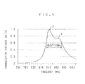
- the wireless IC device 1A using the power supply circuit substrate 31 its communication distance with respect to frequency is shown in Fig. 5 .
- the communication distance is shown as a ratio in which the longest distance is regarded as 1. The actual distance depends on the gain of the radiating element 20.
- a region in which impedance matching is provided between the radiating element 20 and the wireless IC chip 50 is made large, and two resonance points X and Y (see Fig. 5 ) occur.
- the first coil element L1 mainly serves as an inductance element for impedance matching
- the second coil element L2 mainly serves as an inductance element constituting the power supply circuit 33.
- the impedance of the imaginary part of the wireless IC chip 50 is high in the negative direction
- the impedance of the imaginary part of the radiating element 20 is high in the positive direction.
- the inductance value of the first coil element L1 is preferably greater than the inductance value of the second coil element L2.
- the ratio L1:L2 of the inductance values of the first and second coil elements L1 and L2 is preferably about 3:1 to about 4:1, for example.
- the two radiating portions 21A and 21B of the radiating element 20 preferably have a meander shape, and the other configuration is preferably the same or substantially the same as that of the first preferred embodiment.
- the advantageous effects of the wireless IC device 1B are the same as those of the first preferred embodiment.
- the communication distance of the wireless IC device 1B with respect to frequency shows substantially the same characteristics as in Fig. 5 , and the gain is increased since the radiating portions 21A and 21B preferably have a meander shape. Thus, the communication distance is slightly lengthened.
- impedance characteristics are shown in Fig. 7 .
- an A part is a characteristic at 860 MHz
- a B part is a characteristic at 960 MHz. Since a C part is ring-shaped, a region in which impedance matching is provided between the radiating element 20 and the wireless IC chip 50 is made large.
- the impedance (imaginary part) of the wireless IC chip 50 preferably is about -150 ⁇ to about -250 ⁇ , and the impedance (imaginary part) of the radiating element 20 preferably is about 50 to about 400 ⁇ , for example.
- wireless IC device is not limited to the preferred embodiments described above, and can be variously modified within the scope of the present invention.
- the materials, the shapes, and the sizes of the base sheet and the radiating element may be selected as appropriate according to the purpose.
- the shape of the radiating element is arbitrary, and may be a loop shape.
- the wireless IC device it is possible to use the wireless IC device not only as a tag attached to an article but also as a reader/writer, and it is also possible to use the wireless IC device in a wireless communication system other than an RFID system.
- the wireless IC chip may be mounted on another substrate, other than being mounted on the power supply circuit substrate.
- the radiating element may be configured using a ground conductor provided on a printed wiring board.
- the printed wiring board preferably is a body of the wireless IC device.
- the power supply circuit substrate may be formed by a so-called semiconductor process as a rewiring layer of the wireless IC chip, for example.
- the present invention are useful for a wireless IC device, and are particularly excellent in that it is possible to realize a wide frequency band with a small-size power supply circuit substrate.
Abstract
It is an object of the present invention to provide a wireless IC device that allows a wide frequency band to be realized with a small-size power supply circuit substrate.
A wireless IC device includes a wireless IC element (50), a power supply circuit substrate (31) including a laminate (32) of a plurality of base layers and a power supply circuit (33) connected to the wireless IC element (50), and a radiating element connected to the power supply circuit (33). The power supply circuit (33) includes a first coil element (L1) connected in series with the wireless IC element (50), and a second coil element (L2) connected in parallel with the wireless IC element (50). The first coil element (L1) and the second coil element (L2) are wound and arranged such that winding axes of the first and second coil elements (L1),(L2) coincide or substantially coincide with each other and directions of magnetic fields generated in the respective first and second coil elements (L1),(L2) are opposite to each other.
Description
- The present invention relates to a wireless IC device, and particularly relates to a wireless IC device preferably for use in an RFID (Radio Frequency Identification) system.
- In recent years, an RFID system has been put into practical use as an article information management system, which includes: a reader/writer that generates an induction field; and an RFID tag (also referred to as a wireless IC device) that is attached to an article, and non-contact communication using the induction field is established between the reader/writer and the RFID tag to transmit predetermined information therebetween. The RFID tag is composed of a wireless IC chip that has stored predetermined information therein and processes a predetermined wireless signal; and an antenna that performs transmission/reception of high-frequency signals. The RFID tag is attached to various articles as management objects (or their packing materials) when used.
- As RFID systems, a HF-band RFID system using the 13 MHz band and a UHF-band RFID system using the 900 MHz band are typically known. Particularly, with the UHF-band RFID system, the communication distance is relatively long (the communication area is relatively wide), and it is possible to collectively perform reading/writing of a plurality of tags. Thus, the UHF-band RFID system is regarded as a promising system for article management.
- As wireless IC devices for use in the UHF-band RFID system, for example,
Patent Document 1 and 2 describe wireless IC devices in which a power supply circuit substrate is interposed between a wireless IC element (wireless IC chip) and an antenna element. In these wireless IC devices, the frequencies of transmission/reception signals are practically determined by a power supply circuit provided on the power supply circuit substrate. Thus, it is possible to easily realize stable high-frequency characteristics without being greatly influenced by the size of the antenna element (radiating plate) and the surface area of its periphery. - However, in each wireless IC device described above, when it is attempted to expand its frequency band, the power supply circuit becomes complicated, some coil elements and capacitor elements have to be incorporated thereinto, and the necessity to ensure isolation between these elements occurs. Thus, there is a problem that the size of the power supply circuit substrate is increased.
-
- Patent Document 1: Japanese Patent Publication No.
4069958 - Patent Document 2: Japanese Patent Publication No.
4561932 - It is an object of the present invention provide a wireless IC device that allows a wide frequency band to be realized with a small-size power supply circuit substrate. Solution to the Problem
- A wireless IC device according to an aspect of the present invention includes a wireless IC element, a power supply circuit substrate including a laminate defined by laminated base layers, the power supply circuit substrate including a power supply circuit connected to the wireless IC element, and a radiating element connected to the power supply circuit. The power supply circuit includes a first coil element connected in series with the wireless IC element, and a second coil element connected in parallel with the wireless IC element. The first coil element and the second coil element are wound and arranged such that winding axes of the first and second coil elements coincide or substantially coincide with each other and directions of magnetic fields generated in the respective first and second coil elements are opposite to each other.
- In the wireless IC device, since the first coil element and the second coil element are wound and arranged such that the winding axes of the first and second coil elements coincide or substantially coincide with each other and the directions of the magnetic fields generated in the respective first and second coil elements are opposite to each other, coupling between each coil element is excellent, a plurality of resonance points occurs, and transmission/reception of high-frequency signals is possible in a wide frequency band. In addition, since the number of elements is small, the size of the power supply circuit substrate is reduced, and the size of the wireless IC device itself is also reduced.
- According to the present invention, it is possible to realize a wide frequency band with a small-size power supply circuit substrate.
-
-
Fig. 1A is a cross-sectional view of a wireless IC device according to a first preferred embodiment of the present invention.Fig. 1B is a plan view of the wireless IC device ofFig. 1A. Fig. 1C is a plan view of the wireless IC device in a state where a power-supply module is removed. -
Fig. 2 is a schematic diagram showing the internal configuration of a power supply circuit substrate constituting the wireless IC device. -
Fig. 3 is an equivalent circuit diagram of the wireless IC device. -
Fig. 4 is a plan view showing a lamination structure of the power supply circuit substrate in an exploded manner. -
Fig. 5 is a graph showing a communication distance of the wireless IC device with respect to frequency. -
Fig. 6A is a plan view of a wireless IC device according to a second preferred embodiment of the present invention.Fig. 6B is a plan view of the wireless IC device in a state where a power-supply module is removed. -
Fig. 7 is a Smith chart showing impedance characteristics of the wireless IC device according to the second preferred embodiment of the present invention. - Hereinafter, preferred embodiments of a wireless IC device according to the present invention will be described with reference to the accompanying drawings. It should be noted that in each drawing, common elements and portions are denoted by the same reference numerals, and the overlap description is omitted.
- A wireless IC device 1A according to a first preferred embodiment that is preferably used for communication in the UHF band. As shown in
Figs. 1A to 1C , the wireless IC device 1A includes abase sheet 10 having flexibility and a rectangular or substantially rectangular shape, aradiating element 20 preferably including two radiatingportions connection portions base sheet 10, and a power-supply module 30 connected to theradiating element 20, and is configured as a so-called RFID tag. - The
base sheet 10 preferably has, for example, heat resistance or chemical resistance, and a thermoplastic resin material such as polyimide or PET may be used for thebase sheet 10. Theradiating element 20 preferably has flexibility as a metal film which is provided substantially on the entirety of the surface of thebase sheet 10 and contains silver, copper, aluminum, or the like as a principal component. The radiatingelement 20 is divided into the two radiatingportions respective connection portions radiating portions supply module 30 is joined to theconnection portions material 39 such as solder so as to extend over the gap. In other words, theradiating element 20 serves as a dipole type radiating element. It should be noted that theradiating element 20 except for theconnection portions - The power-
supply module 30 includes a powersupply circuit substrate 31 and a wireless IC element (wireless IC chip 50). Thewireless IC chip 50 preferably includes a memory circuit, a clock circuit, a logic circuit, etc. and is an integrated circuit element which processes an RF signal. As shown inFig. 2 , thewireless IC chip 50 includes differential input/output electrodes wireless IC chip 50 preferably includes a base defined by, for example, a semiconductor substrate such as silicon. It should be noted that the wireless IC element may be a bare chip IC or a package IC, for example. - A later-described
power supply circuit 33 is included in the powersupply circuit substrate 31, and is electrically and directly connected (DC-connected) to end portions of theradiating element 20, namely, theconnection portions material 39 such as solder, for example. Specifically, in the power-supply module 30, thewireless IC chip 50 is mounted on the powersupply circuit substrate 31 and is sealed by aresin material 55. - The power
supply circuit substrate 31 preferably includes a laminate 32 including a plurality of base layers (seeFig. 4 ) laminated on each other, and includes thepower supply circuit 33 shown inFigs. 2 and 3 . Thepower supply circuit 33 includes a first coil element L1 connected in series with thewireless IC chip 50; and a second coil element L2 connected in parallel with thewireless IC chip 50. An end of the first coil element L1 is connected to anelectrode 34A, and theelectrode 34A is connected to the input/output electrode 51A of thewireless IC chip 50 via a conductive joiningmaterial 52 such as solder. Another end of the first coil element L1 is connected to an input/output electrode 35A via a capacitor element C1, and the input/output electrode 35A is connected to theconnection portion 22A of the radiatingportion 21A via the conductive joiningmaterial 39. - An end of the second coil element L2 is connected to the other end of the first coil element L1 and the capacitor element C1. Another end of the second coil element L2 is connected to an
electrode 34B, and theelectrode 34B is joined to the input/output electrode 51B of thewireless IC chip 50 via the conductive joiningmaterial 52. Furthermore, the other end of the second coil element L2 is connected to an input/output electrode 35B via a capacitor element C2, and the input/output electrode 35B is connected to theconnection portion 22B of the radiatingportion 21B via the conductive joiningmaterial 39. In other words, the first coil element L1 is connected in series with a differential signal line, and the second coil element L2 is provided between differential signal lines. - The first coil element L1 and the second coil element L2 are wound and arranged such that the winding axes of the respective coil elements L1 and L2 coincide or substantially coincide with each other and the directions of magnetic fields M1 and M2 generated in the respective coil elements L1 and L2 are opposite to each other. Specifically, the coil elements L1 and L2 are arranged within the laminate 32 such that the winding axes thereof extend along the lamination direction of the laminate 32. In other words, as shown in
Fig. 2 , the direction of the magnetic field M1 generated by a current a in the first coil element L1 and the direction of the magnetic field M2 generated by a current b in the second coil element L2 are opposed to each other. The first coil element L1 and the second coil element L2 are magnetically coupled to each other as indicated by a reference character M, and the capacitor elements C1 and C2 define a resonant circuit. The resonant circuit also serves as an impedance matching circuit for thewireless IC chip 50 and the radiatingelement 20. - The first coil element L1 is a series inductance component on the
wireless IC chip 50 side, and this inductance component mainly has a function to shift an impedance in the direction of an imaginary number axis on an impedance chart. Meanwhile, the second coil element L2 is a series inductance component on the radiatingelement 20 side, is arranged so as to extend over the twoconnection portions element 20, and mainly has a function to shift an impedance on an imaginary number axis on an admittance chart. As described above, since the two types of the coil elements are caused to have the respective functions as described above, it is possible to provide efficient impedance matching. - Here, the lamination structure of the power supply circuit substrate 31 (the laminate 32) will be described with reference to
Fig. 4 . The laminate 32 is preferably formed by laminating, pressure-bonding, and firingbase layers 41a to 411 formed from a dielectric material or a magnetic material. It should be noted that the base layers constituting the laminate 32 are not limited to a ceramic material, and may be, for example, a thermosetting resin such as a liquid crystal polymer, or a resin such as a thermoplastic resin. - The base layers 41a to 411 are laminated such that the
base layer 41a becomes a lowermost layer and thebase layer 411 becomes an uppermost layer. The input/output electrodes base layer 41a, and via-hole conductors 61a and 61b are also formed therein.Capacitor electrodes hole conductors hole conductors Conductor lines 45A to 45F are formed on front surfaces of thebase layers 41f to 41k, and the via-hole conductors 63a to 63h are also formed therein. The input/output electrodes electrodes 34C and 34D are formed on a front surface of thebase layer 411, and the via-hole conductors - The
power supply circuit 33 is preferably formed by laminating the base layers 41a to 411 described above. In other words, theelectrodes capacitor electrodes hole conductors 61a and 61b, respectively. Thecapacitor electrodes capacitor electrodes 44A and 44B via the via-hole conductors capacitor electrodes 44A and 44B are connected to an end and another end of theconductor line 45A via the via-hole conductors capacitor electrodes 43A and 43B are connected to the end and the other end of theconductor line 45A via the via-hole conductors - The end of the
conductor line 45A is connected to an end of theconductor line 45B via the via-hole conductor 63a, and another end of theconductor line 45B is connected to an end of the conductor line 45C via the via-hole conductor 63d. The other end of theconductor line 45A is connected to an end of theconductor line 45F via the via-hole conductor 63c, and another end of theconductor line 45F is connected to the input/output electrode 34B via the via-hole conductor 63h. The conductor lines 45C, 45D, and 45E are connected to each other via the via-hole conductors 63e and 63f in a spiral manner. Another end of theconductor line 45E is connected to the input/output electrode 34A via the via-hole conductor 63g. - With the connection mode described above, the
capacitor electrodes 42A, 43A, and 44A constitute the capacitor element C1, and thecapacitor electrodes conductor line 45A constitutes the second coil element L2. - In the wireless IC device 1A, when a predetermined high-frequency signal is transmitted from the
wireless IC chip 50 via thepower supply circuit 33 to the radiatingelement 20, the high-frequency signal is radiated from the radiatingelement 20 to the outside without any change. Also, when the radiatingelement 20 receives a high-frequency wave from the outside, power is similarly supplied to thewireless IC chip 50 via thepower supply circuit 33. Thus, thewireless IC chip 50 and a reader/writer, which is not shown, communicate with each other. - In the wireless IC device 1A, the first coil element L1 and the second coil element L2 are wound and arranged such that the winding axes of the coil elements L1 and L2 coincide or substantially coincide with each other and the directions of the magnetic fields M1 and M2 generated in the respective coil elements L1 and L2 are opposite to each other. Thus, coupling between the coil elements L1 and L2 is excellent, a plurality of resonance points occurs, and transmission/reception of high-frequency signals is possible in a wide frequency band. In addition, since the number of elements is small, the size of the power
supply circuit substrate 31 is reduced, and the size of the wireless IC device 1A itself is also reduced. - With regard to the wireless IC device 1A using the power
supply circuit substrate 31, its communication distance with respect to frequency is shown inFig. 5 . InFig. 5 , the communication distance is shown as a ratio in which the longest distance is regarded as 1. The actual distance depends on the gain of the radiatingelement 20. In addition, a region in which impedance matching is provided between the radiatingelement 20 and thewireless IC chip 50 is made large, and two resonance points X and Y (seeFig. 5 ) occur. - In the
power supply circuit 33, the first coil element L1 mainly serves as an inductance element for impedance matching, and the second coil element L2 mainly serves as an inductance element constituting thepower supply circuit 33. The impedance of the imaginary part of thewireless IC chip 50 is high in the negative direction, and the impedance of the imaginary part of the radiatingelement 20 is high in the positive direction. Thus, the inductance value of the first coil element L1 is preferably greater than the inductance value of the second coil element L2. In addition, the ratio L1:L2 of the inductance values of the first and second coil elements L1 and L2 is preferably about 3:1 to about 4:1, for example. - In a wireless IC device 1B according to a second preferred embodiment of the present invention, as shown in
Fig. 6 , the two radiatingportions element 20 preferably have a meander shape, and the other configuration is preferably the same or substantially the same as that of the first preferred embodiment. The advantageous effects of the wireless IC device 1B are the same as those of the first preferred embodiment. - The communication distance of the wireless IC device 1B with respect to frequency shows substantially the same characteristics as in
Fig. 5 , and the gain is increased since the radiatingportions Fig. 7 . InFig. 7 , an A part is a characteristic at 860 MHz, and a B part is a characteristic at 960 MHz. Since a C part is ring-shaped, a region in which impedance matching is provided between the radiatingelement 20 and thewireless IC chip 50 is made large. - The impedance (imaginary part) of the
wireless IC chip 50 preferably is about -150 Ω to about -250 Ω, and the impedance (imaginary part) of the radiatingelement 20 preferably is about 50 to about 400 Ω, for example. - It should be noted that the wireless IC device according to the present invention is not limited to the preferred embodiments described above, and can be variously modified within the scope of the present invention.
- In particular, the materials, the shapes, and the sizes of the base sheet and the radiating element may be selected as appropriate according to the purpose. In addition, the shape of the radiating element is arbitrary, and may be a loop shape.
- In addition, it is possible to use the wireless IC device not only as a tag attached to an article but also as a reader/writer, and it is also possible to use the wireless IC device in a wireless communication system other than an RFID system. Moreover, the wireless IC chip may be mounted on another substrate, other than being mounted on the power supply circuit substrate.
- Other than being provided exclusively, the radiating element may be configured using a ground conductor provided on a printed wiring board. In this case, the printed wiring board preferably is a body of the wireless IC device. In addition, the power supply circuit substrate may be formed by a so-called semiconductor process as a rewiring layer of the wireless IC chip, for example.
- As described above, the present invention are useful for a wireless IC device, and are particularly excellent in that it is possible to realize a wide frequency band with a small-size power supply circuit substrate.
-
- 1A and 1B: wireless IC bevide
- 20: radiating element
- 30: power-supply module
- 31: power supply circuit substrate
- 32: laminate
- 33: power supply circuit
- 41a to 411: base layer
- 50: wireless IC chip
- L1 and L2: coil element
- C1 and C2: Capacitor element
Claims (3)
- A wireless IC device comprising:a wireless IC element;a power supply circuit substrate including a laminate of a plurality of base layers, and a power supply circuit connected to the wireless IC element; anda radiating element connected to the power supply circuit; whereinthe power supply circuit includes a first coil element connected in series with the wireless IC element, and a second coil element connected in parallel with the wireless IC element; andthe first coil element and the second coil element are wound and arranged such that winding axes of the first and second coil elements coincide or substantially coincide with each other and directions of magnetic fields generated in the respective first and second coil elements are opposite to each other.
- The wireless IC device according to Claim 1, wherein the first coil element and the second coil element are arranged within the laminate such that the winding axis of each coil element extends along a lamination direction of the base layers.
- The wireless IC device according to any one of Claim 1 or Claim 2, wherein
the power supply circuit includes a first capacitor element and a second capacitor element which are connected between both end portions of the second coil element and the radiating element; and
the second coil element and the first and second capacitor elements constitute a resonant circuit.
Applications Claiming Priority (2)
| Application Number | Priority Date | Filing Date | Title |
|---|---|---|---|
| JP2012016067 | 2012-01-30 | ||
| PCT/JP2013/051254 WO2013115019A1 (en) | 2012-01-30 | 2013-01-23 | Wireless ic device |
Publications (1)
| Publication Number | Publication Date |
|---|---|
| EP2688145A1 true EP2688145A1 (en) | 2014-01-22 |
Family
ID=48905061
Family Applications (1)
| Application Number | Title | Priority Date | Filing Date |
|---|---|---|---|
| EP13742949.4A Withdrawn EP2688145A1 (en) | 2012-01-30 | 2013-01-23 | Wireless ic device |
Country Status (6)
| Country | Link |
|---|---|
| US (1) | US8720789B2 (en) |
| EP (1) | EP2688145A1 (en) |
| JP (1) | JP5354137B1 (en) |
| KR (1) | KR20130105938A (en) |
| CN (1) | CN103430382B (en) |
| WO (1) | WO2013115019A1 (en) |
Families Citing this family (3)
| Publication number | Priority date | Publication date | Assignee | Title |
|---|---|---|---|---|
| JP5370581B2 (en) * | 2010-03-24 | 2013-12-18 | 株式会社村田製作所 | RFID system |
| JP6357919B2 (en) * | 2014-06-30 | 2018-07-18 | 凸版印刷株式会社 | Communication medium |
| WO2016098387A1 (en) * | 2014-12-16 | 2016-06-23 | 株式会社 村田製作所 | Wireless communication device, and article for attaching same |
Family Cites Families (459)
| Publication number | Priority date | Publication date | Assignee | Title |
|---|---|---|---|---|
| US3364564A (en) | 1965-06-28 | 1968-01-23 | Gregory Ind Inc | Method of producing welding studs dischargeable in end-to-end relationship |
| JPS6193701A (en) | 1984-10-13 | 1986-05-12 | Toyota Motor Corp | Antenna system for automobile |
| US5253969A (en) | 1989-03-10 | 1993-10-19 | Sms Schloemann-Siemag Aktiengesellschaft | Feeding system for strip material, particularly in treatment plants for metal strips |
| JP2763664B2 (en) | 1990-07-25 | 1998-06-11 | 日本碍子株式会社 | Wiring board for distributed constant circuit |
| NL9100176A (en) | 1991-02-01 | 1992-03-02 | Nedap Nv | Antenna configuration for contactless identification label - forms part of tuned circuit of ID or credit card interrogated via inductive coupling |
| NL9100347A (en) | 1991-02-26 | 1992-03-02 | Nedap Nv | Integrated transformer circuit for ID or credit card - is interrogated via contactless inductive coupling using capacitor to form tuned circuit |
| JPH04321190A (en) | 1991-04-22 | 1992-11-11 | Mitsubishi Electric Corp | Antenna circuit and its production for non-contact type portable storage |
| DE69215283T2 (en) | 1991-07-08 | 1997-03-20 | Nippon Telegraph & Telephone | Extendable antenna system |
| JPH05128324A (en) * | 1991-11-07 | 1993-05-25 | Mitsubishi Electric Corp | Non-contact card, terminal machine for non-contact card, and non-contact transmission system |
| US5491483A (en) | 1994-01-05 | 1996-02-13 | Texas Instruments Incorporated | Single loop transponder system and method |
| US6096431A (en) | 1994-07-25 | 2000-08-01 | Toppan Printing Co., Ltd. | Biodegradable cards |
| JP3141692B2 (en) | 1994-08-11 | 2001-03-05 | 松下電器産業株式会社 | Millimeter wave detector |
| US5528222A (en) | 1994-09-09 | 1996-06-18 | International Business Machines Corporation | Radio frequency circuit and memory in thin flexible package |
| US5955723A (en) | 1995-05-03 | 1999-09-21 | Siemens Aktiengesellschaft | Contactless chip card |
| US5629241A (en) | 1995-07-07 | 1997-05-13 | Hughes Aircraft Company | Microwave/millimeter wave circuit structure with discrete flip-chip mounted elements, and method of fabricating the same |
| JP3150575B2 (en) | 1995-07-18 | 2001-03-26 | 沖電気工業株式会社 | Tag device and manufacturing method thereof |
| GB2305075A (en) | 1995-09-05 | 1997-03-26 | Ibm | Radio Frequency Tag for Electronic Apparatus |
| DE19534229A1 (en) | 1995-09-15 | 1997-03-20 | Licentia Gmbh | Transponder arrangement |
| AUPO055296A0 (en) | 1996-06-19 | 1996-07-11 | Integrated Silicon Design Pty Ltd | Enhanced range transponder system |
| US6104311A (en) | 1996-08-26 | 2000-08-15 | Addison Technologies | Information storage and identification tag |
| WO1998015916A1 (en) | 1996-10-09 | 1998-04-16 | Pav Card Gmbh | Method and connection arrangement for producing a smart card |
| JP3279205B2 (en) | 1996-12-10 | 2002-04-30 | 株式会社村田製作所 | Surface mount antenna and communication equipment |
| JPH10193849A (en) | 1996-12-27 | 1998-07-28 | Rohm Co Ltd | Circuit chip-mounted card and circuit chip module |
| DE19703029A1 (en) | 1997-01-28 | 1998-07-30 | Amatech Gmbh & Co Kg | Transmission module for a transponder device and transponder device and method for operating a transponder device |
| JP2001514777A (en) | 1997-03-10 | 2001-09-11 | プレシジョン ダイナミクス コーポレイション | Reactively connected elements of a circuit provided on a flexible substrate |
| WO1999026195A1 (en) * | 1997-11-14 | 1999-05-27 | Toppan Printing Co., Ltd. | Composite ic module and composite ic card |
| JP2001084463A (en) | 1999-09-14 | 2001-03-30 | Miyake:Kk | Resonance circuit |
| JPH11261325A (en) | 1998-03-10 | 1999-09-24 | Shiro Sugimura | Coil element and its manufacture |
| WO1999050932A1 (en) | 1998-03-31 | 1999-10-07 | Matsushita Electric Industrial Co., Ltd. | Antenna unit and digital television receiver |
| JP4260917B2 (en) | 1998-03-31 | 2009-04-30 | 株式会社東芝 | Loop antenna |
| US5936150A (en) | 1998-04-13 | 1999-08-10 | Rockwell Science Center, Llc | Thin film resonant chemical sensor with resonant acoustic isolator |
| AU8588698A (en) | 1998-04-14 | 1999-11-01 | Liberty Carton Company | Container for compressors and other goods |
| US6018299A (en) | 1998-06-09 | 2000-01-25 | Motorola, Inc. | Radio frequency identification tag having a printed antenna and method |
| US6107920A (en) | 1998-06-09 | 2000-08-22 | Motorola, Inc. | Radio frequency identification tag having an article integrated antenna |
| JP2000021639A (en) | 1998-07-02 | 2000-01-21 | Sharp Corp | Inductor, resonance circuit using the same, matching circuit, antenna circuit, and oscillation circuit |
| JP2000022421A (en) | 1998-07-03 | 2000-01-21 | Murata Mfg Co Ltd | Chip antenna and radio device mounted with it |
| AUPP473898A0 (en) | 1998-07-20 | 1998-08-13 | Integrated Silicon Design Pty Ltd | Metal screened electronic labelling system |
| EP0977145A3 (en) | 1998-07-28 | 2002-11-06 | Kabushiki Kaisha Toshiba | Radio IC card |
| JP2000311226A (en) | 1998-07-28 | 2000-11-07 | Toshiba Corp | Radio ic card and its production and read and write system of the same |
| JP3956172B2 (en) | 1998-07-31 | 2007-08-08 | 吉川アールエフシステム株式会社 | Data carrier and antenna for data carrier |
| JP2000059260A (en) | 1998-08-04 | 2000-02-25 | Sony Corp | Storage device |
| KR100699755B1 (en) | 1998-08-14 | 2007-03-27 | 쓰리엠 이노베이티브 프로퍼티즈 캄파니 | Radio frequency identification systems applications |
| ES2198938T3 (en) | 1998-08-14 | 2004-02-01 | 3M Innovative Properties Company | APPLICATION FOR A RADIO FREQUENCY IDENTIFICATION SYSTEM. |
| JP4411670B2 (en) | 1998-09-08 | 2010-02-10 | 凸版印刷株式会社 | Non-contact IC card manufacturing method |
| JP4508301B2 (en) | 1998-09-16 | 2010-07-21 | 大日本印刷株式会社 | Non-contact IC card |
| JP3632466B2 (en) | 1998-10-23 | 2005-03-23 | 凸版印刷株式会社 | Inspection device and inspection method for non-contact IC card |
| JP2000137785A (en) | 1998-10-30 | 2000-05-16 | Sony Corp | Manufacture of noncontact type ic card and noncontact type ic card |
| JP3924962B2 (en) | 1998-10-30 | 2007-06-06 | 株式会社デンソー | ID tag for dishes |
| JP2000137779A (en) | 1998-10-30 | 2000-05-16 | Hitachi Maxell Ltd | Non-contact information medium and production thereof |
| US6837438B1 (en) | 1998-10-30 | 2005-01-04 | Hitachi Maxell, Ltd. | Non-contact information medium and communication system utilizing the same |
| JP2000148948A (en) | 1998-11-05 | 2000-05-30 | Sony Corp | Non-contact ic label and its manufacture |
| JP2000172812A (en) | 1998-12-08 | 2000-06-23 | Hitachi Maxell Ltd | Noncontact information medium |
| FR2787640B1 (en) | 1998-12-22 | 2003-02-14 | Gemplus Card Int | ARRANGEMENT OF AN ANTENNA IN A METALLIC ENVIRONMENT |
| JP3088404B2 (en) | 1999-01-14 | 2000-09-18 | 埼玉日本電気株式会社 | Mobile radio terminal and built-in antenna |
| JP2000222540A (en) | 1999-02-03 | 2000-08-11 | Hitachi Maxell Ltd | Non-contact type semiconductor tag |
| JP2000228602A (en) | 1999-02-08 | 2000-08-15 | Alps Electric Co Ltd | Resonance line |
| JP2000243797A (en) | 1999-02-18 | 2000-09-08 | Sanken Electric Co Ltd | Semiconductor wafer, and cutting method thereof, and semiconductor wafer assembly and cutting method thereof |
| JP3967487B2 (en) | 1999-02-23 | 2007-08-29 | 株式会社東芝 | IC card |
| JP2000251049A (en) | 1999-03-03 | 2000-09-14 | Konica Corp | Card and production thereof |
| JP4106673B2 (en) | 1999-03-05 | 2008-06-25 | 株式会社エフ・イー・シー | Antenna device using coil unit, printed circuit board |
| JP4349597B2 (en) | 1999-03-26 | 2009-10-21 | 大日本印刷株式会社 | IC chip manufacturing method and memory medium manufacturing method incorporating the same |
| JP3751178B2 (en) | 1999-03-30 | 2006-03-01 | 日本碍子株式会社 | Transceiver |
| JP2000286634A (en) | 1999-03-30 | 2000-10-13 | Ngk Insulators Ltd | Antenna system and its manufacture |
| US6542050B1 (en) | 1999-03-30 | 2003-04-01 | Ngk Insulators, Ltd. | Transmitter-receiver |
| JP3067764B1 (en) | 1999-03-31 | 2000-07-24 | 株式会社豊田自動織機製作所 | Mobile communication coupler, mobile body, and mobile communication method |
| JP2000321984A (en) | 1999-05-12 | 2000-11-24 | Hitachi Ltd | Label with rf-id tag |
| JP3557130B2 (en) | 1999-07-14 | 2004-08-25 | 新光電気工業株式会社 | Method for manufacturing semiconductor device |
| JP2001043340A (en) | 1999-07-29 | 2001-02-16 | Toppan Printing Co Ltd | Composite ic card |
| US6259369B1 (en) | 1999-09-30 | 2001-07-10 | Moore North America, Inc. | Low cost long distance RFID reading |
| JP2001101369A (en) | 1999-10-01 | 2001-04-13 | Matsushita Electric Ind Co Ltd | Rf tag |
| JP3451373B2 (en) | 1999-11-24 | 2003-09-29 | オムロン株式会社 | Manufacturing method of data carrier capable of reading electromagnetic wave |
| JP4186149B2 (en) | 1999-12-06 | 2008-11-26 | 株式会社エフ・イー・シー | Auxiliary antenna for IC card |
| JP2001188890A (en) | 2000-01-05 | 2001-07-10 | Omron Corp | Non-contact tag |
| US7334734B2 (en) | 2000-01-27 | 2008-02-26 | Hitachi Maxwell, Ltd. | Non-contact IC module |
| JP2001209767A (en) | 2000-01-27 | 2001-08-03 | Hitachi Maxell Ltd | Object to be accessed provided with non-contact ic module |
| JP2001240046A (en) | 2000-02-25 | 2001-09-04 | Toppan Forms Co Ltd | Container and manufacturing method thereof |
| JP4514880B2 (en) | 2000-02-28 | 2010-07-28 | 大日本印刷株式会社 | Book delivery, returns and inventory management system |
| JP2001257292A (en) | 2000-03-10 | 2001-09-21 | Hitachi Maxell Ltd | Semiconductor device |
| JP2001256457A (en) | 2000-03-13 | 2001-09-21 | Toshiba Corp | Semiconductor device, its manufacture and ic card communication system |
| JP2003529163A (en) | 2000-03-28 | 2003-09-30 | ルカトロン アーゲー | RFID label having member for adjusting resonance frequency |
| JP4624536B2 (en) | 2000-04-04 | 2011-02-02 | 大日本印刷株式会社 | Non-contact data carrier device |
| JP4624537B2 (en) | 2000-04-04 | 2011-02-02 | 大日本印刷株式会社 | Non-contact data carrier device, storage |
| JP2001291181A (en) | 2000-04-07 | 2001-10-19 | Ricoh Elemex Corp | Sensor and sensor system |
| JP2001319380A (en) | 2000-05-11 | 2001-11-16 | Mitsubishi Materials Corp | Optical disk with rfid |
| JP2001331976A (en) | 2000-05-17 | 2001-11-30 | Casio Comput Co Ltd | Optical recording type recording medium |
| JP4223174B2 (en) | 2000-05-19 | 2009-02-12 | Dxアンテナ株式会社 | Film antenna |
| JP2001339226A (en) | 2000-05-26 | 2001-12-07 | Nec Saitama Ltd | Antenna system |
| JP2001344574A (en) | 2000-05-30 | 2001-12-14 | Mitsubishi Materials Corp | Antenna device for interrogator |
| JP2001352176A (en) | 2000-06-05 | 2001-12-21 | Fuji Xerox Co Ltd | Multilayer printed wiring board and manufacturing method of multilayer printed wiring board |
| WO2001095242A2 (en) | 2000-06-06 | 2001-12-13 | Battelle Memorial Institute | Remote communication system |
| JP2001358527A (en) | 2000-06-12 | 2001-12-26 | Matsushita Electric Ind Co Ltd | Antenna device |
| JP2002157564A (en) | 2000-11-21 | 2002-05-31 | Toyo Aluminium Kk | Antenna coil for ic card and its manufacturing method |
| EP1172760B1 (en) | 2000-06-23 | 2004-12-01 | Toyo Aluminium Kabushiki Kaisha | Antenna coil for IC card and manufacturing method thereof |
| WO2002003560A1 (en) | 2000-07-04 | 2002-01-10 | Credipass Co.,Ltd. | Passive transponder identification system and credit-card type transponder |
| JP4138211B2 (en) | 2000-07-06 | 2008-08-27 | 株式会社村田製作所 | Electronic component and manufacturing method thereof, collective electronic component, mounting structure of electronic component, and electronic apparatus |
| JP2002024776A (en) | 2000-07-07 | 2002-01-25 | Nippon Signal Co Ltd:The | Ic card reader/writer |
| EP1308883B1 (en) | 2000-07-19 | 2008-09-17 | Hanex Co. Ltd | Rfid tag housing structure, rfid tag installation structure and rfid tag communication method |
| RU2163739C1 (en) | 2000-07-20 | 2001-02-27 | Криштопов Александр Владимирович | Antenna |
| JP2002042076A (en) | 2000-07-21 | 2002-02-08 | Dainippon Printing Co Ltd | Non-contact data carrier and booklet therewith |
| JP2002042083A (en) | 2000-07-27 | 2002-02-08 | Hitachi Maxell Ltd | Non-contact communication type information carrier |
| JP3075400U (en) | 2000-08-03 | 2001-02-16 | 昌栄印刷株式会社 | Non-contact IC card |
| US6466007B1 (en) | 2000-08-14 | 2002-10-15 | Teradyne, Inc. | Test system for smart card and indentification devices and the like |
| JP2002063557A (en) | 2000-08-21 | 2002-02-28 | Mitsubishi Materials Corp | Tag for rfid |
| JP2002076750A (en) | 2000-08-24 | 2002-03-15 | Murata Mfg Co Ltd | Antenna device and radio equipment equipped with it |
| JP2002143826A (en) | 2000-08-30 | 2002-05-21 | Denso Corp | System for recycling waste and system for detecting unlawful dumping |
| JP3481575B2 (en) | 2000-09-28 | 2003-12-22 | 寛児 川上 | antenna |
| JP4615695B2 (en) | 2000-10-19 | 2011-01-19 | 三星エスディーエス株式会社 | IC module for IC card and IC card using it |
| US6634564B2 (en) | 2000-10-24 | 2003-10-21 | Dai Nippon Printing Co., Ltd. | Contact/noncontact type data carrier module |
| JP4628611B2 (en) | 2000-10-27 | 2011-02-09 | 三菱マテリアル株式会社 | antenna |
| JP4432254B2 (en) | 2000-11-20 | 2010-03-17 | 株式会社村田製作所 | Surface mount antenna structure and communication device including the same |
| JP2002185358A (en) | 2000-11-24 | 2002-06-28 | Supersensor Pty Ltd | Method for fitting rf transponder to container |
| JP4641096B2 (en) | 2000-12-07 | 2011-03-02 | 大日本印刷株式会社 | Non-contact data carrier device and wiring member for booster antenna |
| JP2002175920A (en) | 2000-12-08 | 2002-06-21 | Murata Mfg Co Ltd | High-frequency filter element |
| JP2002183676A (en) | 2000-12-08 | 2002-06-28 | Hitachi Ltd | Information reader |
| JP2002183690A (en) | 2000-12-11 | 2002-06-28 | Hitachi Maxell Ltd | Noncontact ic tag device |
| AU2002226093A1 (en) | 2000-12-15 | 2002-06-24 | Electrox Corp. | Process for the manufacture of novel, inexpensive radio frequency identificationdevices |
| JP3788325B2 (en) | 2000-12-19 | 2006-06-21 | 株式会社村田製作所 | Multilayer coil component and manufacturing method thereof |
| TW531976B (en) | 2001-01-11 | 2003-05-11 | Hanex Co Ltd | Communication apparatus and installing structure, manufacturing method and communication method |
| JP3621655B2 (en) | 2001-04-23 | 2005-02-16 | 株式会社ハネックス中央研究所 | RFID tag structure and manufacturing method thereof |
| KR20020061103A (en) | 2001-01-12 | 2002-07-22 | 후루까와덴끼고오교 가부시끼가이샤 | Antenna device and terminal with the antenna device |
| JP2002280821A (en) | 2001-01-12 | 2002-09-27 | Furukawa Electric Co Ltd:The | Antenna system and terminal equipment |
| JP2002222398A (en) | 2001-01-25 | 2002-08-09 | Jstm Kk | Non-contact data carrier |
| JP2002232221A (en) | 2001-01-30 | 2002-08-16 | Alps Electric Co Ltd | Transmission and reception unit |
| JPWO2002061675A1 (en) | 2001-01-31 | 2004-06-03 | 株式会社ルネサステクノロジ | Non-contact identification medium |
| JP4662400B2 (en) | 2001-02-05 | 2011-03-30 | 大日本印刷株式会社 | Articles with coil-on-chip semiconductor modules |
| JP2002246828A (en) | 2001-02-15 | 2002-08-30 | Mitsubishi Materials Corp | Antenna for transponder |
| DE60239262D1 (en) | 2001-03-02 | 2011-04-07 | Nxp Bv | MODULE AND ELECTRONIC DEVICE |
| JP4712986B2 (en) | 2001-03-06 | 2011-06-29 | 大日本印刷株式会社 | Liquid container with RFID tag |
| JP2002290130A (en) | 2001-03-28 | 2002-10-04 | Aiwa Co Ltd | Radio communication unit |
| JP2002298109A (en) | 2001-03-30 | 2002-10-11 | Toppan Forms Co Ltd | Contactless ic medium and manufacturing method thereof |
| JP3570386B2 (en) | 2001-03-30 | 2004-09-29 | 松下電器産業株式会社 | Portable information terminal with built-in wireless function |
| JP3772778B2 (en) | 2001-03-30 | 2006-05-10 | 三菱マテリアル株式会社 | Antenna coil, identification tag using the same, reader / writer device, reader device and writer device |
| JP2002308437A (en) | 2001-04-16 | 2002-10-23 | Dainippon Printing Co Ltd | Inspection system using rfid tag |
| JP2002319812A (en) | 2001-04-20 | 2002-10-31 | Oji Paper Co Ltd | Data carrier adhesion method |
| JP4700831B2 (en) | 2001-04-23 | 2011-06-15 | 株式会社ハネックス | RFID tag communication distance expansion method |
| JP2002325013A (en) | 2001-04-26 | 2002-11-08 | Mitsubishi Materials Corp | Antenna coil |
| JP2005236339A (en) | 2001-07-19 | 2005-09-02 | Oji Paper Co Ltd | Ic chip mounted body |
| FI112550B (en) | 2001-05-31 | 2003-12-15 | Rafsec Oy | Smart label and smart label path |
| JP2002362613A (en) | 2001-06-07 | 2002-12-18 | Toppan Printing Co Ltd | Laminated packaging material having non-contact ic, packaging container using laminated packaging material and method for detecting opened seal of packaging container |
| JP2002366917A (en) | 2001-06-07 | 2002-12-20 | Hitachi Ltd | Ic card incorporating antenna |
| JP4710174B2 (en) | 2001-06-13 | 2011-06-29 | 株式会社村田製作所 | Balanced LC filter |
| JP2002373029A (en) | 2001-06-18 | 2002-12-26 | Hitachi Ltd | Method for preventing illegal copy of software by using ic tag |
| JP4882167B2 (en) | 2001-06-18 | 2012-02-22 | 大日本印刷株式会社 | Card-integrated form with non-contact IC chip |
| JP4759854B2 (en) | 2001-06-19 | 2011-08-31 | 株式会社寺岡精工 | Mounting method of IC tag to metal object and IC tag built-in marker |
| JP2003087008A (en) | 2001-07-02 | 2003-03-20 | Ngk Insulators Ltd | Laminated type dielectric filter |
| JP4058919B2 (en) | 2001-07-03 | 2008-03-12 | 日立化成工業株式会社 | Non-contact IC label, non-contact IC card, non-contact IC label or IC module for non-contact IC card |
| JP2003026177A (en) | 2001-07-12 | 2003-01-29 | Toppan Printing Co Ltd | Packaging member with non-contact type ic chip |
| JP2003030612A (en) | 2001-07-19 | 2003-01-31 | Oji Paper Co Ltd | Ic chip mounting body |
| JP4670195B2 (en) | 2001-07-23 | 2011-04-13 | 凸版印刷株式会社 | Mobile phone case with non-contact IC card |
| US7274285B2 (en) | 2001-07-24 | 2007-09-25 | Hewlett-Packard Development Company, L.P. | System and method for improved object identification |
| ES2295105T3 (en) | 2001-07-26 | 2008-04-16 | Irdeto Access B.V. | SYSTEM FOR THE VALIDATION OF TIME TIME. |
| JP3629448B2 (en) | 2001-07-27 | 2005-03-16 | Tdk株式会社 | ANTENNA DEVICE AND ELECTRONIC DEVICE HAVING THE SAME |
| JP2003069335A (en) | 2001-08-28 | 2003-03-07 | Hitachi Kokusai Electric Inc | Auxiliary antenna |
| JP2003067711A (en) | 2001-08-29 | 2003-03-07 | Toppan Forms Co Ltd | Article provided with ic chip mounting body or antenna part |
| JP2003078336A (en) | 2001-08-30 | 2003-03-14 | Tokai Univ | Laminated spiral antenna |
| JP2003078333A (en) | 2001-08-30 | 2003-03-14 | Murata Mfg Co Ltd | Radio communication apparatus |
| JP4514374B2 (en) | 2001-09-05 | 2010-07-28 | トッパン・フォームズ株式会社 | RF-ID inspection system |
| JP4747467B2 (en) | 2001-09-07 | 2011-08-17 | 大日本印刷株式会社 | Non-contact IC tag |
| JP2003085520A (en) | 2001-09-11 | 2003-03-20 | Oji Paper Co Ltd | Manufacturing method for ic card |
| JP2003099184A (en) | 2001-09-25 | 2003-04-04 | Sharp Corp | Information system and information processor and input pen to be used for the same system |
| JP4845306B2 (en) | 2001-09-25 | 2011-12-28 | トッパン・フォームズ株式会社 | RF-ID inspection system |
| JP4698096B2 (en) | 2001-09-25 | 2011-06-08 | トッパン・フォームズ株式会社 | RF-ID inspection system |
| JP2003110344A (en) | 2001-09-26 | 2003-04-11 | Hitachi Metals Ltd | Surface-mounting type antenna and antenna device mounting the same |
| JP2003132330A (en) | 2001-10-25 | 2003-05-09 | Sato Corp | Rfid label printer |
| JP2003134007A (en) | 2001-10-30 | 2003-05-09 | Auto Network Gijutsu Kenkyusho:Kk | System and method for exchanging signal between on- vehicle equipment |
| JP3984458B2 (en) | 2001-11-20 | 2007-10-03 | 大日本印刷株式会社 | Manufacturing method of package with IC tag |
| JP3908514B2 (en) | 2001-11-20 | 2007-04-25 | 大日本印刷株式会社 | Package with IC tag and method of manufacturing package with IC tag |
| US6812707B2 (en) | 2001-11-27 | 2004-11-02 | Mitsubishi Materials Corporation | Detection element for objects and detection device using the same |
| JP3894540B2 (en) | 2001-11-30 | 2007-03-22 | トッパン・フォームズ株式会社 | Interposer with conductive connection |
| JP2003188338A (en) | 2001-12-13 | 2003-07-04 | Sony Corp | Circuit board and its manufacturing method |
| JP3700777B2 (en) | 2001-12-17 | 2005-09-28 | 三菱マテリアル株式会社 | Electrode structure of RFID tag and method for adjusting resonance frequency using the electrode |
| JP2003188620A (en) | 2001-12-19 | 2003-07-04 | Murata Mfg Co Ltd | Antenna integral with module |
| JP4028224B2 (en) | 2001-12-20 | 2007-12-26 | 大日本印刷株式会社 | Paper IC card substrate having non-contact communication function |
| JP3895175B2 (en) | 2001-12-28 | 2007-03-22 | Ntn株式会社 | Dielectric resin integrated antenna |
| JP2003209421A (en) | 2002-01-17 | 2003-07-25 | Dainippon Printing Co Ltd | Rfid tag having transparent antenna and production method therefor |
| JP3915092B2 (en) | 2002-01-21 | 2007-05-16 | 株式会社エフ・イー・シー | Booster antenna for IC card |
| JP2003216919A (en) | 2002-01-23 | 2003-07-31 | Toppan Forms Co Ltd | Rf-id media |
| JP2003233780A (en) | 2002-02-06 | 2003-08-22 | Mitsubishi Electric Corp | Data communication device |
| JP3998992B2 (en) | 2002-02-14 | 2007-10-31 | 大日本印刷株式会社 | Method for forming antenna pattern on IC chip mounted on web and package with IC tag |
| JP2003243918A (en) | 2002-02-18 | 2003-08-29 | Dainippon Printing Co Ltd | Antenna for non-contact ic tag, and non-contact ic tag |
| JP2003249813A (en) | 2002-02-25 | 2003-09-05 | Tecdia Kk | Tag for rfid with loop antenna |
| US7119693B1 (en) | 2002-03-13 | 2006-10-10 | Celis Semiconductor Corp. | Integrated circuit with enhanced coupling |
| JP2003288560A (en) | 2002-03-27 | 2003-10-10 | Toppan Forms Co Ltd | Interposer and inlet sheet with antistatic function |
| US7129834B2 (en) | 2002-03-28 | 2006-10-31 | Kabushiki Kaisha Toshiba | String wireless sensor and its manufacturing method |
| JP2003309418A (en) | 2002-04-17 | 2003-10-31 | Alps Electric Co Ltd | Dipole antenna |
| JP2003308363A (en) | 2002-04-18 | 2003-10-31 | Oki Electric Ind Co Ltd | Product and related information management method |
| JP2003317060A (en) | 2002-04-22 | 2003-11-07 | Dainippon Printing Co Ltd | Ic card |
| US7135974B2 (en) | 2002-04-22 | 2006-11-14 | Symbol Technologies, Inc. | Power source system for RF location/identification tags |
| JP2003317052A (en) | 2002-04-24 | 2003-11-07 | Smart Card:Kk | Ic tag system |
| JP3879098B2 (en) | 2002-05-10 | 2007-02-07 | 株式会社エフ・イー・シー | Booster antenna for IC card |
| JP3979178B2 (en) | 2002-05-14 | 2007-09-19 | 凸版印刷株式会社 | Non-contact IC medium module and non-contact IC medium |
| US6753814B2 (en) | 2002-06-27 | 2004-06-22 | Harris Corporation | Dipole arrangements using dielectric substrates of meta-materials |
| JP3863464B2 (en) | 2002-07-05 | 2006-12-27 | 株式会社ヨコオ | Filter built-in antenna |
| JP3803085B2 (en) | 2002-08-08 | 2006-08-02 | 株式会社日立製作所 | Wireless IC tag |
| JP4100993B2 (en) | 2002-08-09 | 2008-06-11 | キヤノン株式会社 | Electronics |
| JP4107381B2 (en) | 2002-08-23 | 2008-06-25 | 横浜ゴム株式会社 | Pneumatic tire |
| JP2004096566A (en) | 2002-09-02 | 2004-03-25 | Toenec Corp | Inductive communication equipment |
| JP3925364B2 (en) | 2002-09-03 | 2007-06-06 | 株式会社豊田中央研究所 | Antenna and diversity receiver |
| JP3645239B2 (en) | 2002-09-06 | 2005-05-11 | シャープ株式会社 | Dipole antenna, tag and moving object identification system using the same |
| AU2003272420A1 (en) | 2002-09-20 | 2004-04-08 | Fairchild Semiconductor Corporation | Rfid tag wide bandwidth logarithmic spiral antenna method and system |
| JP3975918B2 (en) | 2002-09-27 | 2007-09-12 | ソニー株式会社 | Antenna device |
| JP2004121412A (en) | 2002-09-30 | 2004-04-22 | Toppan Printing Co Ltd | Surgical gauze, and its management device |
| JP2004126750A (en) | 2002-09-30 | 2004-04-22 | Toppan Forms Co Ltd | Information write/read device, antenna and rf-id medium |
| JP3958667B2 (en) | 2002-10-16 | 2007-08-15 | 株式会社日立国際電気 | Loop antenna for reader / writer, and article management shelf and book management system provided with the loop antenna |
| EP1556947A4 (en) | 2002-10-17 | 2006-07-26 | Ambient Corp | Filter for segmenting power lines for communications |
| JP4158483B2 (en) | 2002-10-22 | 2008-10-01 | ソニー株式会社 | IC module |
| JP3659956B2 (en) | 2002-11-11 | 2005-06-15 | 松下電器産業株式会社 | Pressure measuring device and pressure measuring system |
| JP2004213582A (en) | 2003-01-09 | 2004-07-29 | Mitsubishi Materials Corp | Rfid tag, reader/writer and rfid system with tag |
| JP2004234595A (en) | 2003-02-03 | 2004-08-19 | Matsushita Electric Ind Co Ltd | Information recording medium reader |
| DE602004026549D1 (en) | 2003-02-03 | 2010-05-27 | Panasonic Corp | ANTENNA DEVICE AND THEREOF USING WIRELESS COMMUNICATION DEVICE |
| EP1445821A1 (en) | 2003-02-06 | 2004-08-11 | Matsushita Electric Industrial Co., Ltd. | Portable radio communication apparatus provided with a boom portion |
| US7225992B2 (en) | 2003-02-13 | 2007-06-05 | Avery Dennison Corporation | RFID device tester and method |
| JP2004253858A (en) | 2003-02-18 | 2004-09-09 | Minerva:Kk | Booster antenna device for ic tag |
| JP4010263B2 (en) | 2003-03-14 | 2007-11-21 | 富士電機ホールディングス株式会社 | Antenna and data reader |
| JP2004280390A (en) | 2003-03-14 | 2004-10-07 | Toppan Forms Co Ltd | Rf-id media and method for manufacturing the same |
| JP4034676B2 (en) | 2003-03-20 | 2008-01-16 | 日立マクセル株式会社 | Non-contact communication type information carrier |
| JP4097139B2 (en) | 2003-03-26 | 2008-06-11 | Necトーキン株式会社 | Wireless tag |
| JP2004297249A (en) | 2003-03-26 | 2004-10-21 | Matsushita Electric Ind Co Ltd | Coupler between different phase lines, mounting method therefor, and coupling method between different phase lines |
| JP2004304370A (en) | 2003-03-28 | 2004-10-28 | Sony Corp | Antenna coil and communication equipment |
| JP2004297681A (en) | 2003-03-28 | 2004-10-21 | Toppan Forms Co Ltd | Non-contact information recording medium |
| JP4208631B2 (en) | 2003-04-17 | 2009-01-14 | 日本ミクロン株式会社 | Manufacturing method of semiconductor device |
| JP2004326380A (en) | 2003-04-24 | 2004-11-18 | Dainippon Printing Co Ltd | Rfid tag |
| JP2004334268A (en) | 2003-04-30 | 2004-11-25 | Dainippon Printing Co Ltd | Paper slip ic tag, book/magazine with it, and book with it |
| JP2004336250A (en) | 2003-05-02 | 2004-11-25 | Taiyo Yuden Co Ltd | Antenna matching circuit, and mobile communication apparatus and dielectric antenna having the same |
| JP2004343000A (en) | 2003-05-19 | 2004-12-02 | Fujikura Ltd | Semiconductor module, non-contact integrated circuit tag having the semiconductor module, and method of manufacturing semiconductor module |
| JP2004362190A (en) | 2003-06-04 | 2004-12-24 | Hitachi Ltd | Semiconductor device |
| JP4828088B2 (en) | 2003-06-05 | 2011-11-30 | 凸版印刷株式会社 | IC tag |
| JP2005005866A (en) | 2003-06-10 | 2005-01-06 | Alps Electric Co Ltd | Antenna-integrated module |
| JP2005033461A (en) | 2003-07-11 | 2005-02-03 | Mitsubishi Materials Corp | Rfid system and structure of antenna therein |
| JP2005050581A (en) | 2003-07-30 | 2005-02-24 | Seiko Epson Corp | Power supply cord, power supply code inspection device, and power supply code inspection method |
| JP2005064799A (en) | 2003-08-11 | 2005-03-10 | Toppan Printing Co Ltd | Rfid antenna for portable information terminal unit |
| JP3982476B2 (en) | 2003-10-01 | 2007-09-26 | ソニー株式会社 | Communications system |
| JP4062233B2 (en) | 2003-10-20 | 2008-03-19 | トヨタ自動車株式会社 | Loop antenna device |
| JP4680489B2 (en) | 2003-10-21 | 2011-05-11 | 三菱電機株式会社 | Information record reading system |
| JP2005134942A (en) | 2003-10-28 | 2005-05-26 | Mitsubishi Materials Corp | Rfid reader/writer and structure of antenna |
| JP3570430B1 (en) | 2003-10-29 | 2004-09-29 | オムロン株式会社 | Loop coil antenna |
| JP4402426B2 (en) | 2003-10-30 | 2010-01-20 | 大日本印刷株式会社 | Temperature change detection system |
| JP4343655B2 (en) | 2003-11-12 | 2009-10-14 | 株式会社日立製作所 | antenna |
| JP4451125B2 (en) | 2003-11-28 | 2010-04-14 | シャープ株式会社 | Small antenna |
| JP4177241B2 (en) | 2003-12-04 | 2008-11-05 | 株式会社日立情報制御ソリューションズ | Wireless IC tag antenna, wireless IC tag, and container with wireless IC tag |
| JP2005165839A (en) | 2003-12-04 | 2005-06-23 | Nippon Signal Co Ltd:The | Reader/writer, ic tag, article control device, and optical disk device |
| US7494066B2 (en) | 2003-12-19 | 2009-02-24 | Semiconductor Energy Laboratory Co., Ltd. | Semiconductor device |
| JP4916658B2 (en) | 2003-12-19 | 2012-04-18 | 株式会社半導体エネルギー研究所 | Semiconductor device |
| US6999028B2 (en) | 2003-12-23 | 2006-02-14 | 3M Innovative Properties Company | Ultra high frequency radio frequency identification tag |
| JP4326936B2 (en) | 2003-12-24 | 2009-09-09 | シャープ株式会社 | Wireless tag |
| JP2005210676A (en) | 2003-12-25 | 2005-08-04 | Hitachi Ltd | Wireless ic tag, and method and apparatus for manufacturing the same |
| EP1548674A1 (en) | 2003-12-25 | 2005-06-29 | Hitachi, Ltd. | Radio IC tag, method and apparatus for manufacturing the same |
| JP4089680B2 (en) | 2003-12-25 | 2008-05-28 | 三菱マテリアル株式会社 | Antenna device |
| US7777677B2 (en) | 2003-12-25 | 2010-08-17 | Mitsubishi Material Corporation | Antenna device and communication apparatus |
| JP4218519B2 (en) | 2003-12-26 | 2009-02-04 | 戸田工業株式会社 | Magnetic field antenna, wireless system and communication system using the same |
| JP2005190417A (en) | 2003-12-26 | 2005-07-14 | Taketani Shoji:Kk | Fixed object management system and individual identifier for use therein |
| JP4174801B2 (en) | 2004-01-15 | 2008-11-05 | 株式会社エフ・イー・シー | Identification tag reader / writer antenna |
| FR2865329B1 (en) | 2004-01-19 | 2006-04-21 | Pygmalyon | PASSIVE RECEIVER-RECEIVER DEVICE POWERED BY AN ELECTROMAGNETIC WAVE |
| JP2005210223A (en) | 2004-01-20 | 2005-08-04 | Tdk Corp | Antenna device |
| WO2005073937A2 (en) | 2004-01-22 | 2005-08-11 | Mikoh Corporation | A modular radio frequency identification tagging method |
| KR101270180B1 (en) | 2004-01-30 | 2013-05-31 | 가부시키가이샤 한도오따이 에네루기 켄큐쇼 | An inspection apparatus, inspenction method, and method for manufacturing a semiconductor device |
| JP4271591B2 (en) | 2004-01-30 | 2009-06-03 | 双信電機株式会社 | Antenna device |
| JP2005229474A (en) | 2004-02-16 | 2005-08-25 | Olympus Corp | Information terminal device |
| JP4393228B2 (en) | 2004-02-27 | 2010-01-06 | シャープ株式会社 | Small antenna and wireless tag provided with the same |
| JP2005252853A (en) | 2004-03-05 | 2005-09-15 | Fec Inc | Antenna for rf-id |
| JP2005277579A (en) | 2004-03-23 | 2005-10-06 | Kyocera Corp | High frequency module and communication apparatus employing the same |
| JP4374346B2 (en) | 2004-03-24 | 2009-12-02 | 株式会社内田洋行 | IC tag affixing sheet for optical recording media |
| JP2005275870A (en) | 2004-03-25 | 2005-10-06 | Matsushita Electric Ind Co Ltd | Insertion type radio communication medium device and electronic equipment |
| JP2005284352A (en) | 2004-03-26 | 2005-10-13 | Toshiba Corp | Portable electronic equipment |
| JP2005284455A (en) | 2004-03-29 | 2005-10-13 | Fujita Denki Seisakusho:Kk | Rfid system |
| JP4067510B2 (en) | 2004-03-31 | 2008-03-26 | シャープ株式会社 | Television receiver |
| JP2005293537A (en) | 2004-04-05 | 2005-10-20 | Fuji Xynetics Kk | Cardboard with ic tag |
| US8139759B2 (en) | 2004-04-16 | 2012-03-20 | Panasonic Corporation | Line state detecting apparatus and transmitting apparatus and receiving apparatus of balanced transmission system |
| JP2005311205A (en) | 2004-04-23 | 2005-11-04 | Nec Corp | Semiconductor device |
| JP2005306696A (en) | 2004-04-26 | 2005-11-04 | Matsushita Electric Ind Co Ltd | Magnetic ferrite, and common mode noise filter and chip transformer using the same |
| JP2005340759A (en) | 2004-04-27 | 2005-12-08 | Sony Corp | Magnetic core member for antenna module, antenna module, and personal digital assistant equipped with this |
| JP2005322119A (en) | 2004-05-11 | 2005-11-17 | Ic Brains Co Ltd | Device for preventing illegal taking of article equipped with ic tag |
| JP2005321305A (en) | 2004-05-10 | 2005-11-17 | Murata Mfg Co Ltd | Electronic component measurement jig |
| JP3867085B2 (en) | 2004-05-13 | 2007-01-10 | 東芝テック株式会社 | Wireless communication device, RF tag reader / writer, and printer |
| JP4191088B2 (en) | 2004-05-14 | 2008-12-03 | 株式会社デンソー | Electronic equipment |
| JP2005333244A (en) | 2004-05-18 | 2005-12-02 | Mitsubishi Electric Corp | Mobile telephone set |
| US7317396B2 (en) | 2004-05-26 | 2008-01-08 | Funai Electric Co., Ltd. | Optical disc having RFID tag, optical disc apparatus, and system for preventing unauthorized copying |
| JP4360276B2 (en) | 2004-06-02 | 2009-11-11 | 船井電機株式会社 | Optical disc having wireless IC tag and optical disc reproducing apparatus |
| JP4551122B2 (en) | 2004-05-26 | 2010-09-22 | 株式会社岩田レーベル | RFID label affixing device |
| JP2005345802A (en) | 2004-06-03 | 2005-12-15 | Casio Comput Co Ltd | Imaging device, replacement unit used for the imaging device, and replacement unit use control method and program |
| JP4348282B2 (en) | 2004-06-11 | 2009-10-21 | 株式会社日立製作所 | Wireless IC tag and method of manufacturing wireless IC tag |
| JP2005352858A (en) | 2004-06-11 | 2005-12-22 | Hitachi Maxell Ltd | Communication type recording medium |
| JP4530140B2 (en) | 2004-06-28 | 2010-08-25 | Tdk株式会社 | Soft magnetic material and antenna device using the same |
| JP4359198B2 (en) | 2004-06-30 | 2009-11-04 | 株式会社日立製作所 | IC tag mounting substrate manufacturing method |
| JP4328682B2 (en) | 2004-07-13 | 2009-09-09 | 富士通株式会社 | Radio tag antenna structure for optical recording medium and optical recording medium housing case with radio tag antenna |
| JP2006033312A (en) | 2004-07-15 | 2006-02-02 | Matsushita Electric Ind Co Ltd | Antenna and antenna fitting method |
| JP2004362602A (en) | 2004-07-26 | 2004-12-24 | Hitachi Ltd | Rfid tag |
| JP2006039947A (en) | 2004-07-27 | 2006-02-09 | Daido Steel Co Ltd | Composite magnetic sheet |
| JP2006050200A (en) | 2004-08-04 | 2006-02-16 | Matsushita Electric Ind Co Ltd | Reader/writer |
| JP4653440B2 (en) | 2004-08-13 | 2011-03-16 | 富士通株式会社 | RFID tag and manufacturing method thereof |
| JP4186895B2 (en) | 2004-09-01 | 2008-11-26 | 株式会社デンソーウェーブ | Coil antenna for non-contact communication device and manufacturing method thereof |
| JP2005129019A (en) | 2004-09-03 | 2005-05-19 | Sony Chem Corp | Ic card |
| US20060055531A1 (en) | 2004-09-14 | 2006-03-16 | Honeywell International, Inc. | Combined RF tag and SAW sensor |
| JP4600742B2 (en) | 2004-09-30 | 2010-12-15 | ブラザー工業株式会社 | Print head and tag label producing apparatus |
| JP2006107296A (en) | 2004-10-08 | 2006-04-20 | Dainippon Printing Co Ltd | Non-contact ic tag and antenna for non-contact ic tag |
| GB2419779A (en) | 2004-10-29 | 2006-05-03 | Hewlett Packard Development Co | Document having conductive tracks for coupling to a memory tag and a reader |
| WO2006048663A1 (en) | 2004-11-05 | 2006-05-11 | Qinetiq Limited | Detunable rf tags |
| EP1713022A4 (en) | 2004-11-08 | 2008-02-20 | Matsushita Electric Ind Co Ltd | Antenna assembly and wireless communication system employing same |
| JP4088797B2 (en) | 2004-11-18 | 2008-05-21 | 日本電気株式会社 | RFID tag |
| JP2006148518A (en) | 2004-11-19 | 2006-06-08 | Matsushita Electric Works Ltd | Adjuster and adjusting method of non-contact ic card |
| JP2006151402A (en) | 2004-11-25 | 2006-06-15 | Rengo Co Ltd | Corrugated box with radio tag |
| US7545328B2 (en) | 2004-12-08 | 2009-06-09 | Electronics And Telecommunications Research Institute | Antenna using inductively coupled feeding method, RFID tag using the same and antenna impedance matching method thereof |
| JP4281683B2 (en) | 2004-12-16 | 2009-06-17 | 株式会社デンソー | IC tag mounting structure |
| WO2006068286A1 (en) | 2004-12-24 | 2006-06-29 | Semiconductor Energy Laboratory Co., Ltd. | Semiconductor device |
| JP4942998B2 (en) | 2004-12-24 | 2012-05-30 | 株式会社半導体エネルギー研究所 | Semiconductor device and manufacturing method of semiconductor device |
| JP4541246B2 (en) | 2004-12-24 | 2010-09-08 | トッパン・フォームズ株式会社 | Non-contact IC module |
| JP4737505B2 (en) | 2005-01-14 | 2011-08-03 | 日立化成工業株式会社 | IC tag inlet and manufacturing method of IC tag inlet |
| US7714794B2 (en) | 2005-01-19 | 2010-05-11 | Behzad Tavassoli Hozouri | RFID antenna |
| JP4711692B2 (en) | 2005-02-01 | 2011-06-29 | 富士通株式会社 | Meander line antenna |
| JP2006237674A (en) | 2005-02-22 | 2006-09-07 | Suncall Corp | Patch antenna and rfid inlet |
| JP2006232292A (en) | 2005-02-22 | 2006-09-07 | Nippon Sheet Glass Co Ltd | Container with electronic tag, and rfid system |
| JP2006238282A (en) | 2005-02-28 | 2006-09-07 | Matsushita Electric Ind Co Ltd | Antenna unit, transmitter/receiver, wireless tag reading apparatus, and wireless tag read system |
| JP4639857B2 (en) | 2005-03-07 | 2011-02-23 | 富士ゼロックス株式会社 | A storage box for storing articles to which RFID tags are attached, an arrangement method thereof, a communication method, a communication confirmation method, and a packaging structure. |
| US8008066B2 (en) | 2005-03-10 | 2011-08-30 | Gen-Probe Incorporated | System for performing multi-formatted assays |
| JP4330575B2 (en) | 2005-03-17 | 2009-09-16 | 富士通株式会社 | Tag antenna |
| JP4437965B2 (en) | 2005-03-22 | 2010-03-24 | Necトーキン株式会社 | Wireless tag |
| JP2006270681A (en) | 2005-03-25 | 2006-10-05 | Sony Corp | Portable equipment |
| JP4087859B2 (en) | 2005-03-25 | 2008-05-21 | 東芝テック株式会社 | Wireless tag |
| JP2006287659A (en) | 2005-03-31 | 2006-10-19 | Tdk Corp | Antenna device |
| CN101142711B (en) | 2005-04-01 | 2012-07-04 | 富士通株式会社 | RFID label suitable for metal and RFID label section of the same |
| JP4750450B2 (en) | 2005-04-05 | 2011-08-17 | 富士通株式会社 | RFID tag |
| JP2006302219A (en) | 2005-04-25 | 2006-11-02 | Fujita Denki Seisakusho:Kk | Rfid tag communication range setting device |
| US8115681B2 (en) | 2005-04-26 | 2012-02-14 | Emw Co., Ltd. | Ultra-wideband antenna having a band notch characteristic |
| JP4771115B2 (en) | 2005-04-27 | 2011-09-14 | 日立化成工業株式会社 | IC tag |
| JP4452865B2 (en) | 2005-04-28 | 2010-04-21 | 智三 太田 | Wireless IC tag device and RFID system |
| JP4529786B2 (en) | 2005-04-28 | 2010-08-25 | 株式会社日立製作所 | Signal processing circuit and non-contact IC card and tag using the same |
| US8111143B2 (en) | 2005-04-29 | 2012-02-07 | Hewlett-Packard Development Company, L.P. | Assembly for monitoring an environment |
| JP4740645B2 (en) | 2005-05-17 | 2011-08-03 | 富士通株式会社 | Manufacturing method of semiconductor device |
| JP2007013120A (en) | 2005-05-30 | 2007-01-18 | Semiconductor Energy Lab Co Ltd | Semiconductor device |
| US7688272B2 (en) | 2005-05-30 | 2010-03-30 | Semiconductor Energy Laboratory Co., Ltd. | Semiconductor device |
| JP4255931B2 (en) | 2005-06-01 | 2009-04-22 | 日本電信電話株式会社 | Non-contact IC medium and control device |
| JP2007007888A (en) | 2005-06-28 | 2007-01-18 | Oji Paper Co Ltd | Non-contact ic chip mount body mounting corrugated cardboard and its manufacturing method |
| JP4286813B2 (en) | 2005-07-08 | 2009-07-01 | 富士通株式会社 | Antenna and RFID tag equipped with the same |
| JP2007040702A (en) | 2005-07-29 | 2007-02-15 | Oki Electric Ind Co Ltd | Semiconductor ic, wireless ic tag and sensor |
| EP1912284B1 (en) | 2005-07-29 | 2012-04-11 | Fujitsu Ltd. | Rf tag and rf tag manufacturing method |
| JP4720348B2 (en) | 2005-08-04 | 2011-07-13 | パナソニック株式会社 | Antenna for RF-ID reader / writer device, RF-ID reader / writer device using the antenna, and RF-ID system |
| JP4737716B2 (en) | 2005-08-11 | 2011-08-03 | ブラザー工業株式会社 | RFID tag IC circuit holder, tag tape roll, RFID tag cartridge |
| JP4801951B2 (en) | 2005-08-18 | 2011-10-26 | 富士通フロンテック株式会社 | RFID tag |
| DE102005042444B4 (en) | 2005-09-06 | 2007-10-11 | Ksw Microtec Ag | Arrangement for an RFID transponder antenna |
| JP4384102B2 (en) | 2005-09-13 | 2009-12-16 | 株式会社東芝 | Portable radio device and antenna device |
| JP2007096655A (en) | 2005-09-28 | 2007-04-12 | Oji Paper Co Ltd | Antenna for rfid tag and rfid tag |
| JP4075919B2 (en) | 2005-09-29 | 2008-04-16 | オムロン株式会社 | Antenna unit and non-contact IC tag |
| JP4826195B2 (en) | 2005-09-30 | 2011-11-30 | 大日本印刷株式会社 | RFID tag |
| JP2007116347A (en) | 2005-10-19 | 2007-05-10 | Mitsubishi Materials Corp | Tag antenna and mobile radio equipment |
| JP4774273B2 (en) | 2005-10-31 | 2011-09-14 | 株式会社サトー | RFID label and RFID label attaching method |
| JP2007159083A (en) | 2005-11-09 | 2007-06-21 | Alps Electric Co Ltd | Antenna matching circuit |
| JP4899446B2 (en) | 2005-11-24 | 2012-03-21 | Tdk株式会社 | Composite electronic component and manufacturing method thereof |
| JP2007150642A (en) | 2005-11-28 | 2007-06-14 | Hitachi Ulsi Systems Co Ltd | Interrogator for wireless tag, antenna for wireless tag, wireless tag system, and wireless tag selector |
| JP2007150868A (en) | 2005-11-29 | 2007-06-14 | Renesas Technology Corp | Electronic equipment and method of manufacturing the same |
| US7573388B2 (en) | 2005-12-08 | 2009-08-11 | The Kennedy Group, Inc. | RFID device with augmented grain |
| JP4560480B2 (en) | 2005-12-13 | 2010-10-13 | Necトーキン株式会社 | Wireless tag |
| JP4815211B2 (en) | 2005-12-22 | 2011-11-16 | 株式会社サトー | RFID label and RFID label attaching method |
| JP4848764B2 (en) | 2005-12-26 | 2011-12-28 | 大日本印刷株式会社 | Non-contact data carrier device |
| WO2007083575A1 (en) | 2006-01-19 | 2007-07-26 | Murata Manufacturing Co., Ltd. | Radio ic device |
| US7519328B2 (en) | 2006-01-19 | 2009-04-14 | Murata Manufacturing Co., Ltd. | Wireless IC device and component for wireless IC device |
| CN105631509A (en) | 2006-01-19 | 2016-06-01 | 株式会社村田制作所 | Radio ic device and radio ic device part |
| US20090231106A1 (en) | 2006-01-27 | 2009-09-17 | Totoku Electric Co., Ltd. | Tag Apparatus,Transceiver Apparatus, and Tag System |
| KR101061648B1 (en) | 2006-02-19 | 2011-09-01 | 니폰샤신인사츠가부시키가이샤 | Feeding structure of the housing with antenna |
| KR101314036B1 (en) | 2006-02-22 | 2013-10-01 | 도요세이칸 그룹 홀딩스 가부시키가이샤 | Base material for rfid tag adapted to metallic material |
| JP4524674B2 (en) | 2006-02-23 | 2010-08-18 | ブラザー工業株式会社 | Interrogator for RFID tag communication system |
| JP4755921B2 (en) | 2006-02-24 | 2011-08-24 | 富士通株式会社 | RFID tag |
| JP4026080B2 (en) | 2006-02-24 | 2007-12-26 | オムロン株式会社 | Antenna and RFID tag |
| JP5055478B2 (en) | 2006-02-28 | 2012-10-24 | 凸版印刷株式会社 | IC tag |
| WO2007099602A1 (en) | 2006-02-28 | 2007-09-07 | Matsushita Electric Industrial Co., Ltd. | Portable radio apparatus |
| JP3121577U (en) | 2006-03-02 | 2006-05-18 | 株式会社スマート | Eccentric magnetic coil system |
| EP1993170A4 (en) | 2006-03-06 | 2011-11-16 | Mitsubishi Electric Corp | Rfid tag, method for manufacturing rfid tag and method for arranging rfid tag |
| JP2007241789A (en) | 2006-03-10 | 2007-09-20 | Ic Brains Co Ltd | Radio tag reader/writer, communication device and communication system |
| JP3933191B1 (en) | 2006-03-13 | 2007-06-20 | 株式会社村田製作所 | Portable electronic devices |
| JP2007249620A (en) | 2006-03-16 | 2007-09-27 | Nec Tokin Corp | Wireless tag |
| JP2007287128A (en) | 2006-03-22 | 2007-11-01 | Orient Sokki Computer Kk | Non-contact ic medium |
| JP4735368B2 (en) | 2006-03-28 | 2011-07-27 | 富士通株式会社 | Planar antenna |
| JP4854362B2 (en) | 2006-03-30 | 2012-01-18 | 富士通株式会社 | RFID tag and manufacturing method thereof |
| JP4927625B2 (en) | 2006-03-31 | 2012-05-09 | ニッタ株式会社 | Magnetic shield sheet, non-contact IC card communication improving method, and non-contact IC card container |
| JP2007279782A (en) | 2006-04-03 | 2007-10-25 | Dainippon Printing Co Ltd | Non-contact ic tag having ic chip breakdown prevention structure, connecting element of the non-contact ic tag, and manufacturing method of the non-contact ic tag connecting element |
| CN101416353B (en) | 2006-04-10 | 2013-04-10 | 株式会社村田制作所 | Wireless IC device |
| EP2009736B1 (en) | 2006-04-14 | 2016-01-13 | Murata Manufacturing Co. Ltd. | Wireless ic device |
| CN102780084B (en) | 2006-04-14 | 2016-03-02 | 株式会社村田制作所 | Antenna |
| JP4853095B2 (en) | 2006-04-24 | 2012-01-11 | 大日本印刷株式会社 | Non-contact data carrier, wiring board for non-contact data carrier |
| JP4803253B2 (en) | 2006-04-26 | 2011-10-26 | 株式会社村田製作所 | Article with power supply circuit board |
| ATE526648T1 (en) | 2006-04-26 | 2011-10-15 | Murata Manufacturing Co | ITEM WITH ELECTROMAGNETICALLY COUPLED MODULES |
| US9064198B2 (en) | 2006-04-26 | 2015-06-23 | Murata Manufacturing Co., Ltd. | Electromagnetic-coupling-module-attached article |
| JP2007295395A (en) | 2006-04-26 | 2007-11-08 | Fujitsu Ltd | Antenna for tag, and tag using the same |
| US20080068132A1 (en) | 2006-05-16 | 2008-03-20 | Georges Kayanakis | Contactless radiofrequency device featuring several antennas and related antenna selection circuit |
| US7589675B2 (en) | 2006-05-19 | 2009-09-15 | Industrial Technology Research Institute | Broadband antenna |
| JP2007324865A (en) | 2006-05-31 | 2007-12-13 | Sony Chemical & Information Device Corp | Antenna circuit, and transponder |
| ATE507538T1 (en) | 2006-06-01 | 2011-05-15 | Murata Manufacturing Co | HIGH FREQUENCY IC ARRANGEMENT AND COMPOSITE COMPONENT FOR A HIGH FREQUENCY IC ARRANGEMENT |
| JP4281850B2 (en) | 2006-06-30 | 2009-06-17 | 株式会社村田製作所 | optical disk |
| WO2008007606A1 (en) | 2006-07-11 | 2008-01-17 | Murata Manufacturing Co., Ltd. | Antenna and radio ic device |
| JP2008033716A (en) | 2006-07-31 | 2008-02-14 | Sankyo Kk | Coin type rfid tag |
| KR100797172B1 (en) | 2006-08-08 | 2008-01-23 | 삼성전자주식회사 | Loop-antenna having a matching circuit on it |
| JP4836899B2 (en) | 2006-09-05 | 2011-12-14 | パナソニック株式会社 | Magnetic striped array sheet, RFID magnetic sheet, electromagnetic shielding sheet, and manufacturing method thereof |
| US7981528B2 (en) | 2006-09-05 | 2011-07-19 | Panasonic Corporation | Magnetic sheet with stripe-arranged magnetic grains, RFID magnetic sheet, magnetic shielding sheet and method of manufacturing the same |
| US8120462B2 (en) | 2006-09-25 | 2012-02-21 | Sensomatic Electronics, LLC | Method and system for standing wave detection for radio frequency identification marker readers |
| JP2008083867A (en) | 2006-09-26 | 2008-04-10 | Matsushita Electric Works Ltd | Memory card socket |
| JP2008092131A (en) | 2006-09-29 | 2008-04-17 | Tdk Corp | Antenna element and mobile information terminal |
| JP2008098993A (en) | 2006-10-12 | 2008-04-24 | Dx Antenna Co Ltd | Antenna |
| JP4913529B2 (en) | 2006-10-13 | 2012-04-11 | トッパン・フォームズ株式会社 | RFID media |
| JP2008107947A (en) | 2006-10-24 | 2008-05-08 | Toppan Printing Co Ltd | Rfid tag |
| US7605761B2 (en) | 2006-11-30 | 2009-10-20 | Semiconductor Energy Laboratory Co., Ltd. | Antenna and semiconductor device having the same |
| DE102006057369A1 (en) | 2006-12-04 | 2008-06-05 | Airbus Deutschland Gmbh | Radio frequency identification tag for e.g. identifying metal container, has radio frequency identification scanning antenna with conductor loop that is aligned diagonally or perpendicularly to attachment surface |
| JP2008167190A (en) | 2006-12-28 | 2008-07-17 | Philtech Inc | Base body sheet |
| WO2008081699A1 (en) | 2006-12-28 | 2008-07-10 | Philtech Inc. | Base sheet |
| JP2008182438A (en) | 2007-01-24 | 2008-08-07 | Nec Tokin Corp | Radio tag |
| JP2008207875A (en) | 2007-01-30 | 2008-09-11 | Sony Corp | Optical disk case, optical disk tray, card member and manufacturing method |
| US7886315B2 (en) | 2007-01-30 | 2011-02-08 | Sony Corporation | Optical disc case, optical disc tray, card member, and manufacturing method |
| JP2008197714A (en) | 2007-02-08 | 2008-08-28 | Dainippon Printing Co Ltd | Non-contact data carrier device, and auxiliary antenna for non-contact data carrier |
| JP4872713B2 (en) | 2007-02-27 | 2012-02-08 | 大日本印刷株式会社 | Non-contact data carrier device |
| JP5061657B2 (en) | 2007-03-05 | 2012-10-31 | 大日本印刷株式会社 | Non-contact data carrier device |
| JP2008226099A (en) | 2007-03-15 | 2008-09-25 | Dainippon Printing Co Ltd | Noncontact data carrier device |
| JP4867753B2 (en) | 2007-03-30 | 2012-02-01 | Tdk株式会社 | ANTENNA DEVICE AND RADIO COMMUNICATION DEVICE USING THE SAME |
| EP2133827B1 (en) | 2007-04-06 | 2012-04-25 | Murata Manufacturing Co. Ltd. | Radio ic device |
| GB2461443B (en) | 2007-04-13 | 2012-06-06 | Murata Manufacturing Co | Magnetic field coupling antenna module arrangements including a magnetic core embedded in an insulating layer and their manufacturing methods. |
| DE112008000065B4 (en) | 2007-05-10 | 2011-07-07 | Murata Manufacturing Co., Ltd., Kyoto-fu | Wireless IC device |
| JP4666102B2 (en) | 2007-05-11 | 2011-04-06 | 株式会社村田製作所 | Wireless IC device |
| JP4770792B2 (en) | 2007-05-18 | 2011-09-14 | パナソニック電工株式会社 | Antenna device |
| JP4867787B2 (en) | 2007-05-22 | 2012-02-01 | Tdk株式会社 | Antenna device |
| JP4885093B2 (en) | 2007-06-11 | 2012-02-29 | 株式会社タムラ製作所 | Booster antenna coil |
| JP2009017284A (en) | 2007-07-05 | 2009-01-22 | Panasonic Corp | Antenna device |
| EP2166617B1 (en) | 2007-07-09 | 2015-09-30 | Murata Manufacturing Co. Ltd. | Wireless ic device |
| CN104540317B (en) * | 2007-07-17 | 2018-11-02 | 株式会社村田制作所 | printed wiring substrate |
| JP4867830B2 (en) | 2007-07-18 | 2012-02-01 | 株式会社村田製作所 | Wireless IC device |
| US20090021352A1 (en) | 2007-07-18 | 2009-01-22 | Murata Manufacturing Co., Ltd. | Radio frequency ic device and electronic apparatus |
| EP2166616B1 (en) | 2007-07-18 | 2013-11-27 | Murata Manufacturing Co. Ltd. | Wireless ic device |
| ATE556466T1 (en) * | 2007-07-18 | 2012-05-15 | Murata Manufacturing Co | WIRELESS IC DEVICE |
| US7830311B2 (en) | 2007-07-18 | 2010-11-09 | Murata Manufacturing Co., Ltd. | Wireless IC device and electronic device |
| JP2009037413A (en) | 2007-08-01 | 2009-02-19 | Murata Mfg Co Ltd | Radio ic device |
| JP4702336B2 (en) | 2007-08-10 | 2011-06-15 | 株式会社デンソーウェーブ | Portable RFID tag reader |
| JP4885092B2 (en) | 2007-09-06 | 2012-02-29 | 株式会社タムラ製作所 | Booster antenna coil |
| US8717244B2 (en) | 2007-10-11 | 2014-05-06 | 3M Innovative Properties Company | RFID tag with a modified dipole antenna |
| TW200919327A (en) | 2007-10-29 | 2009-05-01 | China Steel Corp | Three-dimensional wireless identification label adhered onto metal |
| JP2009110144A (en) | 2007-10-29 | 2009-05-21 | Oji Paper Co Ltd | Coin-shaped rfid tag |
| JP5155642B2 (en) | 2007-11-28 | 2013-03-06 | ルネサスエレクトロニクス株式会社 | ID tag |
| JP2009135166A (en) | 2007-11-29 | 2009-06-18 | Nikon Corp | Exposure method and exposure device, exposure unit, and device manufacturing method |
| ATE555518T1 (en) | 2007-12-20 | 2012-05-15 | Murata Manufacturing Co | IC RADIO DEVICE |
| JP2009181246A (en) | 2008-01-29 | 2009-08-13 | Toppan Forms Co Ltd | Rfid inspection system |
| JP2009182630A (en) | 2008-01-30 | 2009-08-13 | Dainippon Printing Co Ltd | Booster antenna board, booster antenna board sheet and non-contact type data carrier device |
| EP2251934B1 (en) | 2008-03-03 | 2018-05-02 | Murata Manufacturing Co. Ltd. | Wireless ic device and wireless communication system |
| JP4518211B2 (en) | 2008-03-03 | 2010-08-04 | 株式会社村田製作所 | Compound antenna |
| JP4404166B2 (en) | 2008-03-26 | 2010-01-27 | 株式会社村田製作所 | Wireless IC device |
| CN101953025A (en) | 2008-04-14 | 2011-01-19 | 株式会社村田制作所 | Radio IC device, electronic device, and method for adjusting resonance frequency of radio IC device |
| JP2009260758A (en) | 2008-04-18 | 2009-11-05 | Murata Mfg Co Ltd | Radio ic device |
| US8965461B2 (en) | 2008-05-13 | 2015-02-24 | Qualcomm Incorporated | Reverse link signaling via receive antenna impedance modulation |
| CN103729676B (en) | 2008-05-21 | 2017-04-12 | 株式会社村田制作所 | Wireless ic device |
| JP5078022B2 (en) | 2008-05-22 | 2012-11-21 | Necトーキン株式会社 | Wireless tag and method of using wireless tag |
| JP4557186B2 (en) | 2008-06-25 | 2010-10-06 | 株式会社村田製作所 | Wireless IC device and manufacturing method thereof |
| JP2010015342A (en) | 2008-07-03 | 2010-01-21 | Dainippon Printing Co Ltd | Antenna sheet, inlet, and ic tag |
| JP2010050844A (en) | 2008-08-22 | 2010-03-04 | Sony Corp | Loop antenna and communication device |
| JP5319313B2 (en) | 2008-08-29 | 2013-10-16 | 峰光電子株式会社 | Loop antenna |
| JP4618459B2 (en) | 2008-09-05 | 2011-01-26 | オムロン株式会社 | RFID tag, RFID tag set and RFID system |
| JP3148168U (en) | 2008-10-21 | 2009-02-05 | 株式会社村田製作所 | Wireless IC device |
| CN102197537B (en) | 2008-10-29 | 2014-06-18 | 株式会社村田制作所 | Wireless IC device |
| JP5041075B2 (en) | 2009-01-09 | 2012-10-03 | 株式会社村田製作所 | Wireless IC device and wireless IC module |
| EP3276746B1 (en) | 2009-03-13 | 2019-05-22 | Murata Manufacturing Co., Ltd. | Antenna apparatus |
| JP5510450B2 (en) | 2009-04-14 | 2014-06-04 | 株式会社村田製作所 | Wireless IC device |
| JP2011015395A (en) | 2009-06-03 | 2011-01-20 | Nippon Information System:Kk | Cloth with rfid tag, and system for managing cloth with rfid tag |
| JP5304580B2 (en) * | 2009-10-02 | 2013-10-02 | 株式会社村田製作所 | Wireless IC device |
| WO2011062274A1 (en) | 2009-11-20 | 2011-05-26 | 日立金属株式会社 | Antenna |
| JP5521686B2 (en) | 2010-03-25 | 2014-06-18 | 株式会社村田製作所 | Antenna apparatus and wireless communication device |
| JP5558960B2 (en) | 2010-07-30 | 2014-07-23 | トッパン・フォームズ株式会社 | RF-ID media inspection device |
-
2013
- 2013-01-23 JP JP2013526258A patent/JP5354137B1/en not_active Expired - Fee Related
- 2013-01-23 WO PCT/JP2013/051254 patent/WO2013115019A1/en active Application Filing
- 2013-01-23 CN CN201380000854.3A patent/CN103430382B/en not_active Expired - Fee Related
- 2013-01-23 EP EP13742949.4A patent/EP2688145A1/en not_active Withdrawn
- 2013-01-23 KR KR1020137023537A patent/KR20130105938A/en active IP Right Grant
- 2013-08-28 US US14/011,823 patent/US8720789B2/en active Active
Non-Patent Citations (1)
| Title |
|---|
| See references of WO2013115019A1 * |
Also Published As
| Publication number | Publication date |
|---|---|
| KR20130105938A (en) | 2013-09-26 |
| US20130341415A1 (en) | 2013-12-26 |
| US8720789B2 (en) | 2014-05-13 |
| JPWO2013115019A1 (en) | 2015-05-11 |
| CN103430382A (en) | 2013-12-04 |
| JP5354137B1 (en) | 2013-11-27 |
| CN103430382B (en) | 2015-07-15 |
| WO2013115019A1 (en) | 2013-08-08 |
Similar Documents
| Publication | Publication Date | Title |
|---|---|---|
| US9812764B2 (en) | Antenna device and wireless device | |
| US8544759B2 (en) | Wireless IC device, wireless IC module and method of manufacturing wireless IC module | |
| US8668151B2 (en) | Wireless IC device | |
| US8006910B2 (en) | Wireless IC device | |
| US10396429B2 (en) | Wireless communication device | |
| JP5780324B2 (en) | Wireless communication device | |
| WO2012117843A1 (en) | Wireless communication device | |
| JP2011193245A (en) | Antenna device, radio communication device and radio communication terminal | |
| EP2688145A1 (en) | Wireless ic device | |
| US9336475B2 (en) | Radio IC device and radio communication terminal |
Legal Events
| Date | Code | Title | Description |
|---|---|---|---|
| PUAI | Public reference made under article 153(3) epc to a published international application that has entered the european phase |
Free format text: ORIGINAL CODE: 0009012 |
|
| 17P | Request for examination filed |
Effective date: 20130903 |
|
| AK | Designated contracting states |
Kind code of ref document: A1 Designated state(s): AL AT BE BG CH CY CZ DE DK EE ES FI FR GB GR HR HU IE IS IT LI LT LU LV MC MK MT NL NO PL PT RO RS SE SI SK SM TR |
|
| STAA | Information on the status of an ep patent application or granted ep patent |
Free format text: STATUS: THE APPLICATION HAS BEEN WITHDRAWN |
|
| 18W | Application withdrawn |
Effective date: 20140728 |