JP4942998B2 - Semiconductor device and manufacturing method of semiconductor device - Google Patents
Semiconductor device and manufacturing method of semiconductor device Download PDFInfo
- Publication number
- JP4942998B2 JP4942998B2 JP2005370476A JP2005370476A JP4942998B2 JP 4942998 B2 JP4942998 B2 JP 4942998B2 JP 2005370476 A JP2005370476 A JP 2005370476A JP 2005370476 A JP2005370476 A JP 2005370476A JP 4942998 B2 JP4942998 B2 JP 4942998B2
- Authority
- JP
- Japan
- Prior art keywords
- power supply
- film
- layer
- wiring
- circuit
- Prior art date
- Legal status (The legal status is an assumption and is not a legal conclusion. Google has not performed a legal analysis and makes no representation as to the accuracy of the status listed.)
- Expired - Fee Related
Links
Images


Landscapes
- Design And Manufacture Of Integrated Circuits (AREA)
- Thin Film Transistor (AREA)
- Electroluminescent Light Sources (AREA)
- Semiconductor Integrated Circuits (AREA)
Description
本発明は、非接触で情報の送受信が可能である半導体装置に関する。 The present invention relates to a semiconductor device capable of transmitting and receiving information without contact.
近年、個々の対象物にID(個体識別番号)を与えることで、その対象物の履歴等の情報を明確にし、生産・管理等に役立てるといった個体認識技術が注目されている。その中でも、非接触でデータの送受信が可能な半導体装置の開発が進められている。このような半導体装置として、RFIDタグ(Radio Frequency Identification)(IDタグ、ICタグ、ICチップ、RFタグ(Radio Frequency)、無線タグ、電子タグ、無線チップともよばれる)等が企業内、市場等で導入され始めている。 2. Description of the Related Art In recent years, attention has been focused on an individual recognition technique in which an ID (individual identification number) is given to an individual object to clarify information such as a history of the object and to be useful for production and management. Among them, development of semiconductor devices capable of transmitting and receiving data without contact is underway. As such a semiconductor device, an RFID tag (Radio Frequency Identification) (ID tag, IC tag, IC chip, RF tag (Radio Frequency), wireless tag, electronic tag, also referred to as a wireless chip) is used in an enterprise, a market, or the like. It has begun to be introduced.
一般的に、現在実用化されているRFIDタグの多くは、例えば、図4(A)に示すように基板70上にトランジスタ等の素子から構成される回路を有する素子形成層72(IC(Integrated Circuit)チップとも呼ばれる)とアンテナ71とを有している。これらの、半導体装置は、電磁波を用いてリーダ/ライタとの間の通信を行うことができる。具体的には、リーダ/ライタから発せられる電磁波によりアンテナコイルを通る磁界が変化し、それによって生じる誘導起電力を用いて、素子形成層を動作させる。また、素子形成層から出力された信号を用いてアンテナに負荷変調を与えることで、リーダ/ライタに信号を送ることができる。
In general, most of RFID tags currently in practical use include, for example, an element formation layer 72 (IC (Integrated) having a circuit formed of elements such as transistors on a
ところで、素子形成層72においては、素子形成層に設けられた複数の機能回路に十分な電源の供給を行うために電源配線や接地配線等が複数の機能回路の周りを囲むように設けられている。具体的には、図4(B)に示すように、電源配線73や接地配線74等の配線が電源回路75および機能回路76、77等を囲むように配置され、環状となっている。
Meanwhile, in the
しかしながら、非接触で情報の送受信を行う半導体装置において、素子形成層72に設けられる配線等の形状によっては、電磁誘導を利用する場合に問題が生じる恐れがある。例えば、図4(B)に示すように電源配線や接地配線等の配線が環状である場合、電源配線や接地配線等に囲まれた領域で磁界が変化すると、これらの配線には磁界の変化を打ち消すように電流(渦電流)が発生する。具体的には、図5(A)に示すように、例えば、半導体装置にリーダ/ライタから電磁波が送られてきた場合(ここでは基板70の上方から下方に向かって磁界が生じた場合)、アンテナ71を介して素子形成層72に電源電圧を発生するが、その一方で、素子形成層72における環状の電源配線73や接地配線74にも、当該磁界の変化を打ち消すように電流78が発生し、基板の下方から上方に向かう磁界が発生する(図5(B))。
However, in a semiconductor device that transmits and receives information without contact, depending on the shape of the wiring or the like provided in the
その結果、リーダ/ライタから送られてくる電磁波が減少することによって通信距離が低減したり、配線等に生じる電流により素子形成層にジュール熱が発生し電磁エネルギーの一部が熱エネルギーとして消費され、素子形成層が発熱するといった問題等が生じる。特に、コイル状に設けられたアンテナと重なるように素子形成層が設けられている場合には、この問題はより顕著になる。 As a result, the electromagnetic wave sent from the reader / writer is reduced to reduce the communication distance, or Joule heat is generated in the element formation layer due to the current generated in the wiring, etc., and a part of the electromagnetic energy is consumed as thermal energy. There arises a problem that the element forming layer generates heat. In particular, this problem becomes more conspicuous when the element formation layer is provided so as to overlap the antenna provided in a coil shape.
上記の実情を鑑み、本発明は、リーダ/ライタから送られてくる電磁波の減少を防ぎ、また磁界の変化に伴う素子形成層の発熱を防止することが可能である半導体装置を提供することを目的とする。 In view of the above circumstances, the present invention provides a semiconductor device capable of preventing a decrease in electromagnetic waves transmitted from a reader / writer and preventing heat generation of an element formation layer due to a change in a magnetic field. Objective.
上記課題を解決するために、本発明では以下の手段を講ずる。 In order to solve the above problems, the present invention takes the following measures.
本発明の半導体装置は、基板上に設けられた素子形成層と、素子形成層に接続されたアンテナとを有し、素子形成層は電源配線および接地配線とを有し、電源配線および接地配線が非環状であることを特徴としている。なお、本発明における環状とは、円状だけではなく楕円状や四角形状等も含み、配線の端点同士が接続しているかまたは配線があるものを囲むように1周囲以上設けてある形状も含まれる。つまり、円状や四角形状の配線はもちろん、らせん状やコイル状に配置されている配線も含まれる。また、立体的(3次元)において上記形状をなしている場合も含まれる。そして、環状以外の形状を非環状という。 The semiconductor device of the present invention has an element formation layer provided on a substrate and an antenna connected to the element formation layer, the element formation layer has a power supply wiring and a ground wiring, and the power supply wiring and the ground wiring Is characterized by being non-annular. The ring in the present invention includes not only a circular shape but also an elliptical shape, a quadrangular shape, and the like, and also includes a shape in which one or more circumferences are provided so that the end points of the wiring are connected to each other or surround the wiring. It is. That is, the wiring arrange | positioned in spiral shape and coil shape is included as well as circular or square shape wiring. Moreover, the case where the said shape is comprised in three dimensions (three dimensions) is also included. A shape other than an annular shape is referred to as a non-annular shape.
また、本発明の半導体装置の他の構成として、基板上に設けられた素子形成層と、素子形成層に接続されたアンテナとを有し、素子形成層とアンテナとは少なくとも一部が重なるように設けられ、素子形成層は電源配線および接地配線とを有し、電源配線および接地配線は非環状であることを特徴としている。また、アンテナは、素子形成層の上方に設けてもよいし下方に設けてもよい。 As another structure of the semiconductor device of the present invention, the semiconductor device includes an element formation layer provided over the substrate and an antenna connected to the element formation layer, and the element formation layer and the antenna overlap at least partially. The element formation layer has power supply wiring and ground wiring, and the power supply wiring and ground wiring are non-annular. The antenna may be provided above or below the element formation layer.
また、上記構成において、本発明は電源配線や接地配線等の配線を、コの字型形状や櫛形形状や十字状等に設けることができる。 In the above configuration, the present invention can provide power supply wiring, ground wiring, and the like in a U shape, a comb shape, a cross shape, or the like.
また、本発明の半導体装置の他の構成として、基板上に設けられた半導体膜と、半導体膜上にゲート絶縁膜を介して設けられたゲート電極と、ゲート電極上に設けられた絶縁膜と、絶縁膜上に設けられ且つ半導体膜のソースまたはドレイン領域に接続されたソースまたはドレイン電極と、ソースまたはドレイン電極に電気的に接続された電源配線や接地配線等の配線と、配線に電気的に接続されたアンテナとを有し、配線は非環状であることを特徴としている。 As another structure of the semiconductor device of the present invention, a semiconductor film provided over a substrate, a gate electrode provided over the semiconductor film via a gate insulating film, and an insulating film provided over the gate electrode, A source or drain electrode provided on the insulating film and connected to a source or drain region of the semiconductor film, a power supply wiring or a ground wiring electrically connected to the source or drain electrode, and a wiring electrically And the wiring is non-annular.
また、本発明の半導体装置の他の構成として、基板上に設けられた半導体膜と、半導体膜上にゲート絶縁膜を介して設けられたゲート電極と、ゲート電極上に設けられた絶縁膜と、絶縁膜上に設けられ且つ半導体膜のソースまたはドレイン領域に接続されたソースまたはドレイン電極と、ソースまたはドレイン電極の上方に設けられ且つソースまたはドレイン電極と電気的に接続された電源配線や接地配線等の配線と、半導体膜と少なくとも一部が重なって配置され且つ配線に電気的に接続されたアンテナとを有し、配線は非環状であることを特徴としている。 As another structure of the semiconductor device of the present invention, a semiconductor film provided over a substrate, a gate electrode provided over the semiconductor film via a gate insulating film, and an insulating film provided over the gate electrode, A source or drain electrode provided on the insulating film and connected to a source or drain region of the semiconductor film, and a power supply wiring or ground provided above the source or drain electrode and electrically connected to the source or drain electrode The wiring includes a wiring and an antenna that is disposed at least partially overlapping with the semiconductor film and is electrically connected to the wiring. The wiring is non-annular.
電源配線や接地配線等の配線を非環状で設けることによって、磁界の変化に伴い電源配線や接地配線等の配線に発生する電流を抑制し、リーダ/ライタから送られてくる電磁波が減少することを防止することができる。また、磁界の変化に伴い電源配線や接地配線で発生する電流を抑制することによって、素子形成層の発熱を防止することができる。特にコイル状に設けられたアンテナと重なるように素子形成層が配置する場合に効果的となる。 By providing non-annular wiring such as power wiring and ground wiring, current generated in power wiring and ground wiring due to changes in the magnetic field is suppressed, and electromagnetic waves sent from the reader / writer are reduced. Can be prevented. In addition, heat generation of the element formation layer can be prevented by suppressing current generated in the power supply wiring and the ground wiring in accordance with the change of the magnetic field. This is particularly effective when the element formation layer is disposed so as to overlap the antenna provided in a coil shape.
本発明の実施の形態について、図面を用いて以下に説明する。但し、本発明は以下の説明に限定されず、本発明の趣旨及びその範囲から逸脱することなくその形態及び詳細を様々に変更し得ることは当業者であれば容易に理解される。従って、本発明は以下に示す実施の形態の記載内容に限定して解釈されるものではない。なお、以下に説明する本発明の構成において、同じものを指す符号は異なる図面間で共通して用いる場合がある。 Embodiments of the present invention will be described below with reference to the drawings. However, the present invention is not limited to the following description, and it is easily understood by those skilled in the art that modes and details can be variously changed without departing from the spirit and scope of the present invention. Therefore, the present invention should not be construed as being limited to the description of the embodiments below. Note that in the structures of the present invention described below, the same reference numerals may be used in common in different drawings.
(実施の形態1)
本発明の半導体装置の一構成例に関して図面を用いて以下に説明する。なお、図1(A)は半導体装置の上面図を表し、図1(B)は半導体装置における素子形成層の模式図を表している。
(Embodiment 1)
One structural example of the semiconductor device of the present invention will be described below with reference to the drawings. 1A is a top view of the semiconductor device, and FIG. 1B is a schematic view of an element formation layer in the semiconductor device.
図1(A)に示すように、本実施の形態で示す半導体装置は、基板20上に、素子形成層22とアンテナ21が設けられている。素子形成層22とアンテナ21はどのように配置してもよいが、半導体装置の小型化を考慮して素子形成層22とアンテナ21とが重なるように設けることが好ましい。また、アンテナ21をコイル状で設ける場合には、素子形成層22は、アンテナ21の端部と重なるように配置することが好ましい。これは、アンテナ21の中心に素子形成層22が配置されることによって、アンテナ21を通る電磁波が減少することを防ぐためである。
As shown in FIG. 1A, in the semiconductor device described in this embodiment, an
基板20は、バリウムホウケイ酸ガラスや、アルミノホウケイ酸ガラスなどのガラス基板、石英基板、セラミック基板等を用いることができる。また、ステンレス等の金属基板または半導体基板の表面に絶縁膜を形成したものを用いても良い。他にも、PET等のプラスチック等の可撓性を有する合成樹脂からなる基板を用いてもよい。
As the
素子形成層22は、少なくともトランジスタおよび配線とを有している。当該トランジスタにより、CPU(central processing unit)、記憶回路またはマイクロプロセッサ等のありとあらゆる集積回路を設けることができる。また、素子形成層22におけるトランジスタは、ガラス基板等に薄膜トランジスタ(TFT)を設けてもよいし、基板としてSi等の半導体基板やSOI基板等を用い当該基板をチャネル部として利用する電界効果トランジスタ(FET)を設けてもよいし、有機TFTで設けてもよい。
The
アンテナ21は、アルミニウム(Al)、チタン(Ti)、銀(Ag)、銅(Cu)から選択された元素、又はこれらの元素を主成分とする合金材料若しくは化合物材料等の導電物質で形成されている。また、アンテナ21は、素子形成層22と共に形成してもよいし、素子形成層22とは別個に形成し、後に素子形成層22に電気的に接続するように貼り合わせることによって設けてもよい。
The
次に、図1(B)を用いて半導体装置における素子形成層22のより具体的な構成を説明する。
Next, a more specific structure of the
素子形成層22は、アンテナ21と接続しており、電源配線23、接地配線24、電源回路25、機能回路26、27等を有している。アンテナ21の端部は、それぞれ電源回路25と接地配線24に接続されており、リーダ/ライタから発せられる電磁波によってアンテナ21を通る磁界が変化し、その変化により生じる誘導起電力により電源回路25に交流電圧が供給される。電源回路25は、アンテナから供給された交流電圧を整流して平滑化し電源電圧を生成する。また、電源配線23は電源回路25と接続しており、電源回路25から電源配線23に電源電圧が供給される。そして、機能回路26、27は、電源配線23および接地配線24に接続しており、そこから電源電圧が供給されることによって機能回路26、27が動作する。なお、機能回路としては、クロック発生回路、データ復調/変調回路、各種回路を制御する制御回路、記憶回路等が含まれる。
The
また、本実施の形態では、電源配線23および接地配線24を非環状とする。つまり、従来のように機能回路等を囲むように環状に設けていた電源配線や接地配線等(図4(B)参照)を環状にならないように設ける。例えば、図1(B)に示すように、電源配線23および接地配線24を機能回路等を一周させて囲うように設けるのではなく、コの字の形状に設けることによって非環状とすることができる。
In the present embodiment, the
なお、ここでいう環状とは、円状だけではなく楕円状や四角形状も含み、配線の端点同士が接続しているかまたは配線があるものを囲むように1周囲以上設けてある形状も含まれる。つまり、円状や四角形状の配線はもちろん、コイル状に配置されている場合も含む。また、立体的(3次元)において上記形状をなしている場合も含まれる。なお、ここでは、上記環状以外の形状を非環状と記す。 The term “annular” as used herein includes not only a circular shape but also an elliptical shape and a quadrangular shape, and includes a shape in which one or more circumferences are provided so that the end points of the wirings are connected to each other or surround the wirings. . That is, it includes not only a circular or quadrangular wiring but also a case where it is arranged in a coil shape. Moreover, the case where the said shape is comprised in three dimensions (three dimensions) is also included. Here, a shape other than the above-described ring shape is referred to as a non-ring shape.
このように、電源配線や接地配線等の配線を非環状とすることによって、磁界の変化による電源配線や接地配線等に生じる電流を抑制し、リーダ/ライタから送られてくる電磁波の減少を防止することができる。また、当該電流による素子形成層の発熱も防止することが可能となる。また、本実施の形態で示したように、コイル状に設けられたアンテナと素子形成層とを重ねて配置する場合(コイル状のアンテナの内側に素子形成層を設ける場合)には、素子形成層における電源配線や接地配線等を非環状とすることによって、リーダ/ライタから送られてくる電磁波の減少を防止することができる。 In this way, by making the wiring such as power supply wiring and ground wiring non-circular, the current generated in the power supply wiring and ground wiring due to the change of the magnetic field is suppressed, and the reduction of electromagnetic waves sent from the reader / writer is prevented. can do. In addition, heat generation of the element formation layer due to the current can be prevented. In addition, as shown in this embodiment mode, when an antenna provided in a coil shape and an element formation layer are arranged so as to overlap each other (when an element formation layer is provided inside a coiled antenna), element formation is performed. By making the power supply wiring, ground wiring, and the like in the layer non-annular, it is possible to prevent a reduction in electromagnetic waves sent from the reader / writer.
(実施の形態2)
本実施の形態では、上記実施の形態と異なる半導体装置の一構成例に関して図面を用いて説明する。
(Embodiment 2)
In this embodiment, a structural example of a semiconductor device different from that in the above embodiment will be described with reference to drawings.
上記実施の形態では、機能回路等を囲むように環状に設けられた電源配線や接地配線等の配線の一部分を切り取るようにコの字型にする例を示したが、これに限られず、外部からの磁界の変化に対して影響を受けにくい形状であれば、電源配線や接地配線等の配線をどのように配置してもよい。以下に、上記実施の形態で示した構造以外の具体例に関して図面に示す。 In the above embodiment, an example in which the U-shape is formed so as to cut off a part of the wiring such as the power supply wiring and the ground wiring provided in an annular shape so as to surround the functional circuit or the like is not limited to this. As long as the shape is not easily affected by the change in the magnetic field, the wiring such as the power supply wiring and the ground wiring may be arranged in any way. Hereinafter, specific examples other than the structure shown in the above embodiment mode are shown in the drawings.
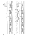
図2では、電源配線23や接地配線24が電源回路25や各機能回路26、27間を通るように設けられている。図2(A)では、電源配線23や接地配線24を環状にせずに交互に折れ曲がった形状で設けることにより電源回路25および各機能回路26、27を囲むように配置している。
In FIG. 2, the
また、図2(B)に示すように、電源配線23および接地配線24をそれぞれ櫛形に設け、左右から組み合わせることによって配線を設けることも可能である。このように、電源配線23や接地配線24等を櫛形に設けることによって、電源回路25や機能回路26、27の周囲に電源配線23や接地配線24を配置することができるため、電源回路25や機能回路26、27等に十分な電圧の供給を行うことができる。
In addition, as shown in FIG. 2B, the
このように電源配線23や接地配線24を非環状で配置することによって、磁界の変化による電源配線23や接地配線24等に生じる電流を防止することができる。
By arranging the
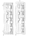
また、電源配線23や接地配線24等の配線は図2に示した構成に限られない。例えば、図3に示すように電源配線23と接地配線24の一方または両方(ここでは、接地配線24)を十字形状に設けてもよい。そして、十字形状に設けられた配線の周辺に電源回路25や機能回路26〜28を設けることができる。
Further, the wiring such as the
上記実施の形態に示した形状の他にも、例えば電源配線23や接地配線24等の配線を階段形等のジグザグ形状、V字型、まんじ(卍)等の形状とすることも可能である。このように、素子形成層22において、電源配線23や接地配線24等の配線を環状でない形状であればどのように設けてもよく、実施者が適宜選択して、十分に電源回路や機能回路等に電圧の供給を行えるようにすればよい。
In addition to the shape shown in the above embodiment, for example, the wiring such as the
以上のように、電源配線や接地配線等の配線を非環状とすることによって、磁界の変化による電源配線や接地配線等に生じる電流を抑制し、リーダ/ライタから送られてくる電磁波の減少を防止することができる。また、当該電流による素子形成層の発熱も防止することが可能となる。 As described above, by making the wiring such as the power supply wiring and the ground wiring non-circular, the current generated in the power supply wiring and the ground wiring due to the change of the magnetic field is suppressed, and the electromagnetic wave transmitted from the reader / writer is reduced. Can be prevented. In addition, heat generation of the element formation layer due to the current can be prevented.
なお、本実施の形態は上記実施の形態と自由に組み合わせて行うことができる。
(実施の形態3)
本実施の形態では、本発明の半導体装置の作製方法の一例について、図面を参照して説明する。具体的には、素子形成層におけるトランジスタとして薄膜トランジスタ(TFT)を用い、支持基板上にTFTを設けた後に支持基板からTFTを分離する剥離法により半導体装置を作製する例を示す。
Note that this embodiment mode can be freely combined with the above embodiment modes.
(Embodiment 3)
In this embodiment, an example of a method for manufacturing a semiconductor device of the present invention will be described with reference to drawings. Specifically, an example in which a thin film transistor (TFT) is used as a transistor in the element formation layer and a semiconductor device is manufactured by a separation method in which the TFT is separated from the support substrate after the TFT is provided over the support substrate.
まず、基板701の一表面に、剥離層702を形成する(図6(A))。基板701は、ガラス基板、石英基板、ステンレス基板等の金属基板の一表面に絶縁膜を形成したもの、本工程の処理温度に耐えうる耐熱性があるプラスチック基板等を用いるとよい。このような基板701であれば、その面積や形状に大きな制限はないため、基板701として、例えば、1辺が1メートル以上であって、矩形状のものを用いれば、生産性を格段に向上させることができる。このような利点は、円形のシリコン基板を用いる場合と比較すると、大きな優位点である。なお、本工程では、剥離層702は、基板701の全面に設けているが、必要に応じて、基板701の全面に剥離層を設けた後に、フォトリソグラフィ法により選択的に設けてもよい。また、基板701に接するように剥離層702を形成しているが、必要に応じて、基板701に接するように下地となる絶縁膜を形成し、当該絶縁膜に接するように剥離層702を形成してもよい。
First, the
剥離層702は、金属膜と当該金属酸化膜により形成されている。金属膜は、公知の手段(スパッタリング法やプラズマCVD法等)により、タングステン(W)、モリブデン(Mo)、チタン(Ti)、タンタル(Ta)、ニオブ(Nb)、ニッケル(Ni)、コバルト(Co)、ジルコニウム(Zr)、亜鉛(Zn)、ルテニウム(Ru)、ロジウム(Rh)、鉛(Pb)、オスミウム(Os)、イリジウム(Ir)から選択された元素または前記元素を主成分とする合金材料若しくは化合物材料からなる層を、単層又は積層して形成する。金属酸化膜は、金属膜に酸素雰囲気下でプラズマ処理を行うか、金属膜に酸素雰囲気下で熱処理を行うことによって金属膜の表面に形成する。なお、金属酸化膜の他にも金属酸化窒化物を用いてもよい。
The
金属膜が単層構造の場合、例えば、タングステン層、モリブデン層またはタングステンとモリブデンの混合物を含む層を形成する。そして、金属膜の表面に、タングステンの酸化物若しくは酸化窒化物を含む層、モリブデンの酸化物若しくは酸化窒化物を含む層またはタングステンとモリブデンの混合物の酸化物若しくは酸化窒化物を含む層を形成する。なお、タングステンとモリブデンの混合物とは、例えば、タングステンとモリブデンの合金に相当する。 In the case where the metal film has a single-layer structure, for example, a tungsten layer, a molybdenum layer, or a layer containing a mixture of tungsten and molybdenum is formed. Then, a layer containing tungsten oxide or oxynitride, a layer containing molybdenum oxide or oxynitride, or a layer containing oxide or oxynitride of a mixture of tungsten and molybdenum is formed on the surface of the metal film. . Note that the mixture of tungsten and molybdenum corresponds to, for example, an alloy of tungsten and molybdenum.
また、剥離層702として、基板701上に金属膜を形成した後に、酸素雰囲気下で上記金属膜の材料をターゲットとして、スパッタ法により金属酸化膜を形成してもよい。この場合、金属膜と金属酸化膜を別の金属元素を用いて形成することもできる。なお、基板701上に、直接金属酸化膜を形成しこれを剥離層702として用いてもよい。
Alternatively, after forming a metal film over the
次に、剥離層702を覆うように、下地となる絶縁膜703を形成する。絶縁膜703は、公知の手段(スパッタ法やプラズマCVD法等)により、珪素の酸化物または珪素の窒化物を含む膜を、単層又は積層で形成する。下地となる絶縁膜が2層構造の場合、例えば、1層目として窒化酸化珪素膜を形成し、2層目として酸化窒化珪素膜を形成するとよい。下地となる絶縁膜が3層構造の場合、1層目の絶縁膜として酸化珪素膜を形成し、2層目の絶縁膜として窒化酸化珪素膜を形成し、3層目の絶縁膜として酸化窒化珪素膜を形成するとよい。または、1層目の絶縁膜として酸化窒化珪素膜を形成し、2層目の絶縁膜として窒化酸化珪素膜を形成し、3層目の絶縁膜として酸化窒化珪素膜を形成するとよい。下地となる絶縁膜は、基板701からの不純物の侵入を防止するブロッキング膜として機能する。
Next, an insulating
次に、絶縁膜703上に、非晶質半導体膜704(例えば非晶質珪素を含む膜)を形成する。非晶質半導体膜704は、公知の手段(スパッタ法、LPCVD法、プラズマCVD法等)により、25〜200nm(好ましくは30〜150nm)の厚さで形成する。続いて、非晶質半導体膜704を公知の結晶化法(レーザ結晶化法、RTA又はファーネスアニール炉を用いる熱結晶化法、結晶化を助長する金属元素を用いる熱結晶化法、結晶化を助長する金属元素を用いる熱結晶化法とレーザ結晶化法を組み合わせた方法等)により結晶化して、結晶質半導体膜を形成する。その後、得られた結晶質半導体膜を所望の形状にエッチングして、結晶質半導体膜706〜710を形成する(図6(B))。なお、剥離層702、絶縁膜703および非晶質半導体膜704は、連続して形成することができる。
Next, an amorphous semiconductor film 704 (eg, a film containing amorphous silicon) is formed over the insulating
結晶質半導体膜706〜710の作製工程の一例を以下に簡単に説明すると、まず、プラズマCVD法を用いて、膜厚66nmの非晶質半導体膜を形成する。次に、結晶化を助長する金属元素であるニッケルを含む溶液を非晶質半導体膜上に保持させた後、非晶質半導体膜に脱水素化の処理(500℃、1時間)と、熱結晶化の処理(550℃、4時間)を行って結晶質半導体膜を形成する。その後、必要に応じてレーザ光を照射し、フォトリソグラフィ法を用いることによって結晶質半導体膜706〜710を形成する。
An example of a manufacturing process of the
レーザ結晶化法で結晶質半導体膜を形成する場合、連続発振またはパルス発振の気体レーザ又は固体レーザを用いる。気体レーザとしては、エキシマレーザ、YAGレーザ、YVO4レーザ、YLFレーザ、YAlO3レーザ、ガラスレーザ、ルビーレーザ、Ti:サファイアレーザ等を用いる。固体レーザとしては、Cr、Nd、Er、Ho、Ce、Co、Ti又はTmがドーピングされたYAG、YVO4、YLF、YAlO3などの結晶を使ったレーザを用いる。特に、連続発振のレーザの基本波、及び当該基本波の第2高調波から第4高調波のレーザを照射することで、大粒径の結晶を得ることができる。例えば、Nd:YVO4レーザ(基本波1064nm)の第2高調波(532nm)や第3高調波(355nm)を用いることができる。なお連続発振の基本波のレーザ光と連続発振の高調波のレーザ光とを照射するようにしてもよいし、連続発振の基本波のレーザ光とパルス発振の高調波のレーザ光とを照射するようにしてもよい。複数のレーザ光を照射することにより、エネルギーを補うことができる。またパルス発振型のレーザであって、半導体膜がレーザ光によって溶融してから固化するまでに、次のパルスのレーザ光を照射できるような発振周波数でレーザ光を発振させることで、走査方向に向かって連続的に成長した結晶粒を得ることができる。すなわち、パルス発振の周期が、半導体膜が溶融してから完全に固化するまでの時間よりも短くなるように、発振の周波数の下限を定めたパルス発振のレーザを使用することができる。このようなレーザとして、発振周波数が10MHz以上のパルス発振のレーザ光を用いてもよい。 In the case of forming a crystalline semiconductor film by a laser crystallization method, a continuous wave or pulsed gas laser or solid state laser is used. As the gas laser, excimer laser, YAG laser, YVO 4 laser, YLF laser, YAlO 3 laser, glass laser, ruby laser, Ti: sapphire laser, or the like is used. As the solid-state laser, a laser using a crystal such as YAG, YVO 4 , YLF, or YAlO 3 doped with Cr, Nd, Er, Ho, Ce, Co, Ti, or Tm is used. In particular, a crystal having a large grain size can be obtained by irradiating a fundamental wave of a continuous wave laser and a second to fourth harmonic laser of the fundamental wave. For example, a second harmonic (532 nm) or a third harmonic (355 nm) of an Nd: YVO 4 laser (fundamental wave 1064 nm) can be used. The continuous wave fundamental laser beam and the continuous wave harmonic laser beam may be irradiated, or the continuous wave fundamental laser beam and the pulsed harmonic laser beam may be irradiated. You may do it. By irradiating a plurality of laser beams, energy can be supplemented. Also, it is a pulse oscillation type laser that oscillates the laser light at an oscillation frequency that can be irradiated with the laser light of the next pulse after the semiconductor film is melted by the laser light and solidifies in the scanning direction. Crystal grains grown continuously can be obtained. That is, it is possible to use a pulsed laser in which the lower limit of the oscillation frequency is set so that the period of pulse oscillation is shorter than the time until the semiconductor film is completely solidified after being melted. As such a laser, a pulsed laser beam having an oscillation frequency of 10 MHz or more may be used.
また、結晶化を助長する金属元素を用いて非晶質半導体膜の結晶化を行うと、低温で短時間の結晶化が可能となるうえ、結晶の方向が揃うという利点がある一方、金属元素が結晶質半導体膜に残存するためにオフ電流が上昇し、特性が安定しないという欠点がある。そこで、結晶質半導体膜上に、ゲッタリングサイトとして機能する非晶質半導体膜を形成するとよい。ゲッタリングサイトとなる非晶質半導体膜には、リンやアルゴンの不純物元素を含有させる必要があるため、好適には、アルゴンを高濃度に含有させることが可能なスパッタ法で形成するとよい。その後、加熱処理(RTA法やファーネスアニール炉を用いた熱アニール等)を行って、非晶質半導体膜中に金属元素を拡散させ、続いて、当該金属元素を含む非晶質半導体膜を除去する。そうすると、結晶質半導体膜中の金属元素の含有量を低減又は除去することができる。 In addition, when an amorphous semiconductor film is crystallized using a metal element that promotes crystallization, it is possible to perform crystallization at a low temperature for a short time, and the crystal orientation is aligned. Remains in the crystalline semiconductor film, so that the off-current increases and the characteristics are not stable. Therefore, an amorphous semiconductor film functioning as a gettering site is preferably formed over the crystalline semiconductor film. Since the amorphous semiconductor film serving as a gettering site needs to contain an impurity element such as phosphorus or argon, it is preferably formed by a sputtering method which can contain argon at a high concentration. Then, heat treatment (RTA method or thermal annealing using a furnace annealing furnace) is performed to diffuse the metal element in the amorphous semiconductor film, and then the amorphous semiconductor film containing the metal element is removed. To do. Then, the content of the metal element in the crystalline semiconductor film can be reduced or removed.
次に、結晶質半導体膜706〜710を覆うゲート絶縁膜705を形成する。ゲート絶縁膜705は、公知の手段(プラズマCVD法やスパッタ法)により、珪素の酸化物又は珪素の窒化物を含む膜を、単層又は積層して形成する。具体的には、酸化珪素を含む膜、酸化窒化珪素を含む膜、窒化酸化珪素を含む膜を、単層又は積層して形成する。
Next, a
次に、ゲート絶縁膜705上に、第1の導電膜と第2の導電膜とを積層して形成する。第1の導電膜は、公知の手段(プラズマCVD法やスパッタリング法)により、20〜100nmの厚さで形成する。第2の導電膜は、公知の手段により、100〜400nmの厚さで形成する。第1の導電膜と第2の導電膜は、タンタル(Ta)、タングステン(W)、チタン(Ti)、モリブデン(Mo)、アルミニウム(Al)、銅(Cu)、クロム(Cr)、ニオブ(Nd)等から選択された元素又はこれらの元素を主成分とする合金材料若しくは化合物材料で形成する。または、リン等の不純物元素をドーピングした多結晶珪素に代表される半導体材料により形成する。第1の導電膜と第2の導電膜の組み合わせの例を挙げると、窒化タンタル膜とタングステン膜、窒化タングステン膜とタングステン膜、窒化モリブデン膜とモリブデン膜等が挙げられる。タングステンや窒化タンタルは、耐熱性が高いため、第1の導電膜と第2の導電膜を形成した後に、熱活性化を目的とした加熱処理を行うことができる。また、2層構造ではなく、3層構造の場合は、モリブデン膜とアルミニウム膜とモリブデン膜の積層構造を採用するとよい。
Next, a first conductive film and a second conductive film are stacked over the
次に、フォトリソグラフィ法を用いてレジストからなるマスクを形成し、ゲート電極とゲート線を形成するためのエッチング処理を行って、ゲート電極として機能する導電膜(ゲート電極とよぶことがある)716〜725を形成する。また、導電膜716〜725と同一の層に電源配線や接地配線等の配線を形成してもよい。この場合、導電膜716〜725と同時に同じ材料を用いて設けることができる。なお、電源配線や接地配線の配線は上記実施の形態で示したように非環状で設ける。
Next, a resist mask is formed using a photolithography method, etching treatment for forming a gate electrode and a gate line is performed, and a conductive film functioning as a gate electrode (also referred to as a gate electrode) 716 ~ 725 are formed. Further, wiring such as power supply wiring and ground wiring may be formed in the same layer as the
次に、フォトリソグラフィ法により、レジストからなるマスクを形成して、結晶質半導体膜706、708〜710に、イオンドープ法又はイオン注入法により、N型を付与する不純物元素を低濃度に添加して、N型不純物領域711、713〜715とチャネル形成領域780、782〜784を形成する。N型を付与する不純物元素は、15族に属する元素を用いれば良く、例えばリン(P)、砒素(As)を用いる。
Next, a resist mask is formed by photolithography, and an impurity element imparting N-type is added to the
次に、フォトリソグラフィ法によりレジストからなるマスクを形成して、結晶質半導体膜707に、P型を付与する不純物元素を添加して、P型不純物領域712とチャネル形成領域781を形成する。P型を付与する不純物元素は、例えばボロン(B)を用いる。
Next, a resist mask is formed by photolithography, and an impurity element imparting P-type conductivity is added to the
次に、ゲート絶縁膜705と導電膜716〜725を覆うように、絶縁膜を形成する。絶縁膜は、公知の手段(プラズマCVD法やスパッタ法)により、珪素、珪素の酸化物又は珪素の窒化物の無機材料を含む膜や、有機樹脂などの有機材料を含む膜を、単層又は積層して形成する。次に、絶縁膜を、垂直方向を主体とした異方性エッチングにより選択的にエッチングして、導電膜716〜725の側面に接する絶縁膜(サイドウォールともよばれる)739〜743を形成する(図6(C))。また、絶縁膜739〜743の作製と同時に、絶縁膜705がエッチングされた絶縁膜734〜738を形成する。絶縁膜739〜743は、後にLDD(Lightly Doped drain)領域を形成する際のドーピング用のマスクとして用いる。
Next, an insulating film is formed so as to cover the
次に、フォトリソグラフィ法により形成したレジストからなるマスクと、絶縁膜739〜743をマスクとして用いて、結晶質半導体膜706、708〜710にN型を付与する不純物元素を添加して、第1のN型不純物領域(LDD領域ともよぶ)727、729、731、733と、第2のN型不純物領域726、728、730、732とを形成する。第1のN型不純物領域727、729、731、733が含む不純物元素の濃度は、第2のN型不純物領域726、728、730、732の不純物元素の濃度よりも低い。上記工程を経て、N型の薄膜トランジスタ744、746〜748と、P型の薄膜トランジスタ745が完成する。
Next, an impurity element imparting n-type conductivity is added to the
なお、LDD領域を形成するためには、ゲート電極を2層以上の積層構造として、当該ゲート電極をテーパー状にエッチングしたりゲート電極に異方性エッチング等を行って、当該ゲート電極を構成する下層の導電膜をマスクとして用いる手法と、サイドウォールの絶縁膜をマスクとして用いる手法がある。前者の手法を採用して形成された薄膜トランジスタは、ゲート絶縁膜を介してLDD領域をゲート電極と重ねて配置させた構造となっているが、この構造は、ゲート電極をテーパー状にエッチングしたりゲート電極に異方性エッチングを行うために、LDD領域の幅を制御することが難しく、エッチング工程が良好に行われなければ、LDD領域を形成することが出来ない場合がある。一方、後者のサイドウォールの絶縁膜をマスクとして用いる手法は、前者の手法と比較すると、LDD領域の幅の制御が容易であり、また、LDD領域を確実に形成することができる。 Note that in order to form the LDD region, the gate electrode has a stacked structure of two or more layers, and the gate electrode is etched into a tapered shape or anisotropic etching or the like is performed on the gate electrode to configure the gate electrode. There are a method using a lower conductive film as a mask and a method using an insulating film on a sidewall as a mask. A thin film transistor formed by using the former method has a structure in which an LDD region is disposed so as to overlap a gate electrode with a gate insulating film interposed therebetween. In this structure, the gate electrode is etched in a tapered shape. Since anisotropic etching is performed on the gate electrode, it is difficult to control the width of the LDD region, and the LDD region may not be formed unless the etching process is performed well. On the other hand, the latter method using the sidewall insulating film as a mask makes it easier to control the width of the LDD region than the former method, and the LDD region can be formed reliably.
続いて、薄膜トランジスタ744〜748を覆うように、絶縁膜を単層又は積層して形成する(図7(A))。薄膜トランジスタ744〜748を覆う絶縁膜は、公知の手段(SOG法、液滴吐出法等)により、珪素の酸化物や珪素の窒化物等の無機材料、ポリイミド、ポリアミド、ベンゾシクロブテン、アクリル、エポキシ、シロキサン等の有機材料等により、単層又は積層で形成する。シロキサン系の材料とは、例えば、シリコン(Si)と酸素(O)との結合で骨格構造が構成される。置換基として、少なくとも水素を含む有機基(例えばアルキル基、芳香族炭化水素)が用いられる。置換基として、フルオロ基を用いてもよい。または置換基として、少なくとも水素を含む有機基と、フルオロ基とを用いてもよい。例えば、薄膜トランジスタ744〜748を覆う絶縁膜が3層構造の場合、1層目の絶縁膜749として酸化珪素を含む膜を形成し、2層目の絶縁膜750として樹脂を含む膜を形成し、3層目の絶縁膜751として窒化珪素を含む膜を形成するとよい。
Next, an insulating film is formed as a single layer or a stacked layer so as to cover the
なお、絶縁膜749〜751を形成する前、又は絶縁膜749〜751のうちの1つ又は複数の薄膜を形成した後に、半導体膜の結晶性の回復や半導体膜に添加された不純物元素の活性化、半導体膜の水素化を目的とした加熱処理を行うとよい。加熱処理には、熱アニール、レーザアニール法又はRTA法などを適用するとよい。
Note that before the insulating
次に、フォトリソグラフィ法により絶縁膜749〜751をエッチングして、N型不純物領域726、728、730、732、P型不純物領域785を露出させるコンタクトホールを形成する。続いて、コンタクトホールを充填するように、導電膜を形成し、当該導電膜をパターン加工して、ソースドレイン配線として機能する導電膜752〜761を形成する。また、この時、ソースドレイン配線として機能する導電膜752〜761と同一の層に電源配線や接地配線等の配線を形成してもよい。この場合、導電膜752〜761と同時に同じ材料を用いて設けることができる。なお、電源配線や接地配線の配線は上記実施の形態で示したように非環状で設ける。
Next, the insulating
導電膜752〜761は、公知の手段(プラズマCVD法やスパッタリング法)により、チタン(Ti)、アルミニウム(Al)、ネオジウム(Nd)から選択された元素、又はこれらの元素を主成分とする合金材料若しくは化合物材料で、単層又は積層で形成する。アルミニウムを主成分とする合金材料とは、例えば、アルミニウムを主成分としニッケルを含む材料、又は、アルミニウムを主成分とし、ニッケルと、炭素と珪素の一方又は両方とを含む合金材料に相当する。導電膜752〜761は、例えば、バリア膜とアルミニウムシリコン(Al−Si)膜とバリア膜の積層構造、バリア膜とアルミニウムシリコン(Al−Si)膜と窒化チタン膜とバリア膜の積層構造を採用するとよい。なお、バリア膜とは、チタン、チタンの窒化物、モリブデン、又はモリブデンの窒化物からなる薄膜に相当する。アルミニウムやアルミニウムシリコンは抵抗値が低く、安価であるため、導電膜752〜761を形成する材料として最適である。また、上層と下層のバリア層を設けると、アルミニウムやアルミニウムシリコンのヒロックの発生を防止することができる。また、還元性の高い元素であるチタンからなるバリア膜を形成すると、結晶質半導体膜上に薄い自然酸化膜ができていたとしても、この自然酸化膜を還元し、結晶質半導体膜と良好なコンタクトをとることができる。
The
次に、導電膜752〜761を覆うように、絶縁膜762を形成する(図7(B))。絶縁膜762は、公知の手段(SOG法、液滴吐出法等)を用いて、無機材料又は有機材料により、単層又は積層で形成する。また、絶縁膜762は、好適には、0.75μm〜3μmの厚さで形成する。
Next, an insulating
続いて、フォトリソグラフィ法により絶縁膜762をエッチングして、導電膜757、759、761を露出させるコンタクトホールを形成する。続いて、コンタクトホールを充填するように、導電膜を形成する。導電膜は、公知の手段(プラズマCVD法やスパッタリング法)を用いて、導電性材料により形成する。次に、導電膜をパターン加工して、導電膜763〜765を形成する。なお、導電膜763〜765は、記憶素子が含む一対の導電膜のうちの一方の導電膜となる。従って、好適には、導電膜763〜765は、チタン、又はチタンを主成分とする合金材料若しくは化合物材料により、単層又は積層で形成するとよい。チタンは、抵抗値が低いため、記憶素子のサイズの縮小につながり、高集積化を実現することができる。また、導電膜763〜765を形成するためのフォトリソグラフィ工程においては、下層の薄膜トランジスタ744〜748にダメージを与えないために、ウエットエッチング加工を行うとよく、エッチング剤にはフッ化水素(HF)又はアンモニア過水を用いるとよい。なお、導電膜763〜765と同一の層に電源配線や接地配線等を設けてもよい。この場合、導電膜763〜765と同時に同じ材料を用いて設けることができる。また、電源配線や接地配線は上記実施の形態で示したように非環状で設ける。
Subsequently, the insulating
次に、導電膜763〜765を覆うように、絶縁膜766を形成する。絶縁膜766は、公知の手段(SOG法、液滴吐出法等)を用いて、無機材料又は有機材料により、単層又は積層で形成する。また、絶縁膜766は、好適には、0.75μm〜3μmの厚さで形成する。続いて、フォトリソグラフィ法により、絶縁膜766をエッチングして、導電膜763〜765を露出させるコンタクトホール767〜769を形成する。
Next, an insulating
次に、導電膜765に接し、アンテナとして機能する導電膜786を形成する(図8(A))。導電膜786は、公知の手段(プラズマCVD法、スパッタリング法、印刷法、液滴吐出法)を用いて、導電性材料により形成する。好ましくは、導電膜786は、アルミニウム(Al)、チタン(Ti)、銀(Ag)、銅(Cu)から選択された元素、又はこれらの元素を主成分とする合金材料若しくは化合物材料で、単層又は積層で形成する。ここでは、導電膜786は、スクリーン印刷法により、銀を含むペーストを用いて形成し、その後、50〜350度の加熱処理を行って形成する。又は、スパッタリング法によりアルミニウム膜を形成し、当該アルミニウム膜をパターン加工することにより形成する。アルミニウム膜のパターン加工は、ウエットエッチング加工を用いるとよく、ウエットエッチング加工後は200〜300度の加熱処理を行うとよい。なお、導電膜786と同一の層に電源配線や接地配線等を設けてもよい。この場合、導電膜786と同時に同じ材料を用いて設けることができる。また、電源配線や接地配線は上記実施の形態で示したように非環状で設ける。
Next, a
次に、導電膜763、764に接するように有機化合物層787を形成する(図8(B))。有機化合物層787は、公知の手段(液滴吐出法や蒸着法等)により形成する。続いて、有機化合物層787に接するように、導電膜771を形成する。導電膜771は、公知の手段(スパッタリング法や蒸着法)により形成する。
Next, an
また、導電膜771の形成と同時に電源配線や接地配線等を設けてもよい。電源配線や接地配線は上記実施の形態で示したように非環状で設ける。このように、電源配線や接地配線等は、導電膜716〜725と同一の層、導電膜752〜761と同一の層、導電膜763〜765と同一の層、導電膜786と同一の層または導電膜771と同一の層等どこに設けてもよく実施者が適宜選択することができる。また、電源配線と接地配線をそれぞれ異なる層に設けることも可能である。さらに、素子形成層を多層に形成することによって、電源配線や接地配線を薄膜トランジスタの上方に設け、素子形成層の小型化を達成することができる。
Further, a power supply wiring, a ground wiring, or the like may be provided simultaneously with the formation of the
以上の工程を経て、導電膜763、有機化合物層787及び導電膜771の積層体からなる記憶素子部789と、導電膜764、有機化合物層787及び導電膜771の積層体からなる記憶素子部790が完成する。
Through the above steps, a
なお、上記の作製工程では、有機化合物層787の耐熱性が強くないため、アンテナとして機能する導電膜786を形成する工程の後に、有機化合物層787を形成する工程を行うことを特徴とする。また、アンテナとして機能する導電膜786は、導電膜716〜725と同一の層、導電膜752〜761と同一の層、導電膜763〜765と同一の層または導電膜771と同一の層に設けることも可能である。また、アンテナは、アンテナとして機能する導電膜786を直接形成せずに、別の基板に別途設けた導電膜と導電膜765とを導電性微粒子等を含む接着剤を用いて貼り合わせることによって設けることも可能である。この場合は、有機化合物層787を設けた後であってもアンテナを形成することができる。
Note that in the above manufacturing process, the heat resistance of the
なお、ここでは、記憶素子部789、790として、有機化合物材料を用いた例を示したが、これに限られない。例えば、結晶状態と非晶質状態の間で可逆的に変化する材料や第1の結晶状態と第2の結晶状態の間で可逆的に変化する材料等の相変化材料を用いることができる。また、非晶質状態から結晶状態にのみ変化する材料を用いることも可能である。
Note that here, an example in which an organic compound material is used as the
結晶状態と非晶質状態の間で可逆的に変化する材料とは、ゲルマニウム(Ge)、テルル(Te)、アンチモン(Sb)、硫黄(S)、酸化テルル(TeOx)、Sn(スズ)、金(Au)、ガリウム(Ga)、セレン(Se)、インジウム(In)、タリウム(Tl)、Co(コバルト)及び銀(Ag)から選択された複数を有する材料であり、例えば、Ge−Te−Sb−S、Te−TeO2−Ge−Sn、Te−Ge−Sn−Au、Ge−Te−Sn、Sn−Se−Te、Sb−Se−Te、Sb−Se、Ga−Se−Te、Ga−Se−Te−Ge、In−Se、In−Se−Tl−Co、Ge−Sb−Te、In−Se−Te、Ag−In−Sb−Te系材料が挙げられる。また、第1の結晶状態と第2の結晶状態の間で可逆的に変化する材料とは、銀(Ag)、亜鉛(Zn)、銅(Cu)、アルミニウム(Al)、ニッケル(Ni)、インジウム(In)、アンチモン(Sb)、セレン(Se)及びテルル(Te)から選択された複数を有する材料であり、例えば、Te−TeO2、Te−TeO2−Pd、Sb2Se3/Bi2Te3が挙げられる。この材料の場合、相変化は2つの異なる結晶状態の間で行われる。また、非晶質状態から結晶状態にのみ変化する材料とは、テルル(Te)、酸化テルル(TeOx)、アンチモン(Sb)、セレン(Se)及びビスマス(Bi)から選択された複数を有する材料であり、例えば、Ag−Zn、Cu−Al−Ni、In−Sb、In−Sb−Se、In−Sb−Teが挙げられる。 Materials that reversibly change between a crystalline state and an amorphous state include germanium (Ge), tellurium (Te), antimony (Sb), sulfur (S), tellurium oxide (TeOx), Sn (tin), A material having a plurality of materials selected from gold (Au), gallium (Ga), selenium (Se), indium (In), thallium (Tl), Co (cobalt), and silver (Ag), for example, Ge-Te -Sb-S, Te-TeO 2 -Ge-Sn, Te-Ge-Sn-Au, Ge-Te-Sn, Sn-Se-Te, Sb-Se-Te, Sb-Se, Ga-Se-Te, Ga-Se-Te-Ge, In-Se, In-Se-Tl-Co, Ge-Sb-Te, In-Se-Te, and Ag-In-Sb-Te-based materials can be given. The materials that reversibly change between the first crystal state and the second crystal state are silver (Ag), zinc (Zn), copper (Cu), aluminum (Al), nickel (Ni), A material having a plurality selected from indium (In), antimony (Sb), selenium (Se), and tellurium (Te), for example, Te—TeO 2 , Te—TeO 2 —Pd, Sb 2 Se 3 / Bi. 2 Te 3 is mentioned. In this material, the phase change takes place between two different crystalline states. The material changing only from the amorphous state to the crystalline state is a material having a plurality selected from tellurium (Te), tellurium oxide (TeOx), antimony (Sb), selenium (Se), and bismuth (Bi). Examples thereof include Ag—Zn, Cu—Al—Ni, In—Sb, In—Sb—Se, and In—Sb—Te.
次に、記憶素子部789、790、アンテナとして機能する導電膜786を覆うように、公知の手段(SOG法、液滴吐出法等)により、保護膜として機能する絶縁膜772を形成する。絶縁膜772は、DLC(ダイヤモンドライクカーボン)などの炭素を含む膜、窒化珪素を含む膜、窒化酸化珪素を含む膜、有機材料により形成し、好ましくはエポキシ樹脂により形成する。
Next, an insulating
次に、薄膜トランジスタ744〜748、記憶素子部789、790等を含む素子形成層791を基板701から剥離する。ここでは、レーザ光(例えばUV光)を照射することによって開口部773、774を形成後(図9(A))、物理的な力を用いて基板701から素子形成層791を剥離することができる。また、基板701から素子形成層791を剥離する前に、開口部773、774にエッチング剤を導入して、剥離層702を除去してもよい。エッチング剤は、フッ化ハロゲンまたはハロゲン間化合物を含む気体又は液体を使用する。例えば、フッ化ハロゲンを含む気体として三フッ化塩素(ClF3)を使用する。そうすると、素子形成層791は、基板701から剥離された状態となる。なお、剥離層702は、全て除去せず一部分を残存させてもよい。こうすることによって、エッチング剤の消費量を抑え剥離層702の除去に要する処理時間を短縮することが可能となる。
Next, the
また、素子形成層791が剥離された基板701は、コストの削減のために、再利用することが好ましい。また、絶縁膜772は、剥離層702を除去した後に、素子形成層791が飛散しないように形成したものである。素子形成層791は小さく薄く軽いために、剥離層702を除去した後は、基板701に密着していないために飛散しやすい。しかしながら、素子形成層791上に絶縁膜772を形成することで、素子形成層791に重みが付き、基板701からの飛散を防止することができる。また、素子形成層791単体では薄くて軽いが、絶縁膜772を形成することで、基板701から剥離した素子形成層791が応力等により巻かれた形状になることがなく、ある程度の強度を確保することができる。
The
次に、素子形成層791の一方の面を、第1のシート材775に接着させて基板701から完全に剥離する(図10(A))。剥離層702を全て除去せず一部を残した場合には、物理的手段を用いて基板701から素子形成層791を剥離する。続いて、素子形成層791の他方の面に、第2のシート材776を設け、その後加熱処理と加圧処理の一方または両方を行って、第2のシート材776を貼り合わせる。また、第2のシート材776を設けると同時または設けた後に第1のシート材775を剥離し、代わりに第3のシート材777を設ける。そして、加熱処理と加圧処理の一方または両方を行って、第3のシート材777を貼り合わせる。そうすると、第2のシート材776と第3のシート材777により封止された半導体装置が完成する(図10(B))。
Next, one surface of the
なお、第1のシート材775と第2のシート材776によって封止を行っても良いが、基板701から素子形成層791を剥離するためのシート材と素子形成層791を封止するためのシート材に異なるシート材を用いる場合には、上述したように、第2のシート材776と第3のシート材777で素子形成層791を封止する。これは、例えば、基板701から素子形成層791を剥離する際に、第1のシート材775が素子形成層791のみならず基板701への接着が懸念される場合等、粘着力が弱いシート材を利用したいときに有効となる。
Note that the
封止に用いる第2のシート材776、第3のシート材777として、ポリプロピレン、ポリエステル、ビニル、ポリフッ化ビニル、塩化ビニルなどからなるフィルム、繊維質な材料からなる紙、基材フィルム(ポリエステル、ポリアミド、無機蒸着フィルム、紙類等)と接着性合成樹脂フィルム(アクリル系合成樹脂、エポキシ系合成樹脂等)との積層フィルム等を利用することができる。また、フィルムは、熱圧着により、被処理体と加熱処理と加圧処理が行われるものであり、加熱処理と加圧処理を行う際には、フィルムの最表面に設けられた接着層か、又は最外層に設けられた層(接着層ではない)を加熱処理によって溶かし、加圧により接着する。また、第2のシート材776と第3のシート材777の表面には接着層が設けられていてもよいし、接着層が設けられていなくてもよい。接着層は、熱硬化樹脂、紫外線硬化樹脂、エポキシ樹脂系接着剤、樹脂添加剤等の接着剤を含む層に相当する。また、封止後に内部への水分等の侵入を防ぐために封止するシート材にシリカコートを行うことが好ましく、例えば、接着層とポリエステル等のフィルムとシリカコートを積層させたシート材を利用することができる。
As the
また、第2のシート材776、第3のシート材777として、静電気等を防止する帯電防止対策を施したフィルム(以下、帯電防止フィルムと記す)を用いることもできる。帯電防止フィルムとしては、帯電防止可能な材料を樹脂中に分散させたフィルム、及び帯電防止可能な材料が貼り付けられたフィルム等が挙げられる。帯電防止可能な材料が設けられたフィルムは、片面に帯電防止可能な材料を設けたフィルムであってもよいし、両面に帯電防止可能な材料を設けたフィルムであってもよい。さらに、片面に帯電防止可能な材料が設けられたフィルムは、帯電防止可能な材料が設けられた面をフィルムの内側になるように層に貼り付けてもよいし、フィルムの外側になるように貼り付けてもよい。なお、帯電防止可能な材料はフィルムの全面、あるいは一部に設けてあればよい。ここでの帯電防止可能な材料としては、金属、インジウムと錫の酸化物(ITO)、両性界面活性剤や陽イオン性界面活性剤や非イオン性界面活性剤等の界面活性剤用いることができる。また、他にも帯電防止材料として、側鎖にカルボキシル基および4級アンモニウム塩基をもつ架橋性共重合体高分子を含む樹脂材料等を用いることができる。これらの材料をフィルムに貼り付けたり、練り込んだり、塗布したりすることによって帯電防止フィルムとすることができる。帯電防止フィルムで封止を行うことによって、商品として取り扱う際に、外部からの静電気等によって半導体素子に悪影響が及ぶことを抑制することができる。
In addition, as the
なお、本実施の形態は、上記実施の形態と自由に組み合わせて行うことができる。 Note that this embodiment can be freely combined with the above embodiment.
(実施の形態4)
本実施の形態では、本発明の半導体装置を非接触でデータの送受信が可能であるRFIDタグとして利用した場合に関して図11を用いて説明する。
(Embodiment 4)
In this embodiment, the case where the semiconductor device of the present invention is used as an RFID tag capable of transmitting and receiving data without contact will be described with reference to FIGS.
RFIDタグ80は、非接触でデータを交信する機能を有し、電源回路81、クロック発生回路82、データ復調回路83、データ変調回路84、他の回路を制御する制御回路85、記憶回路86、アンテナ87とを有している(図11(A))。なお、記憶回路は1つに限定されず、複数であっても良く、SRAM、フラッシュメモリ、ROMまたはFeRAM等や上記実施の形態で示した有機化合物層を記憶素子部に用いたものを用いることができる。
The
リーダ/ライタ88から電磁波として送られてきた信号は、アンテナ87において電磁誘導により交流の電気信号に変換される。電源回路81では、交流の電気信号を用いて電源電圧を生成し、電源配線を用いて各回路へ電源電圧を供給する。クロック発生回路82は、アンテナ87から入力された交流信号を基に、各種クロック信号を生成し、制御回路85に供給する。データ復調回路83では、当該交流の電気信号を復調し、制御回路85に供給する。制御回路85では、入力された信号に従って各種演算処理を行う。より具体的には、制御回路85は、例えばデータ復調回路83によって復調された信号を解読する命令解析部や解読された信号をチェックするCRC(Cyclic Redundancy Check)回路、記憶回路86を制御するメモリコントローラ等を含んでいる。記憶回路86では、制御回路85において用いられるプログラムやデータ等が記憶されている他、演算処理時の作業エリアとしても用いることができる。そして、制御回路85からデータ変調回路84にデータが送られ、データ変調回路84から当該データに従ってアンテナ87に負荷変調を加えることができる。リーダ/ライタ88は、アンテナ87に加えられた負荷変調を電磁波で受け取ることにより、結果的にデータを読み取ることが可能となる
A signal sent as an electromagnetic wave from the reader /
また、上記回路の周辺に電源配線や接地配線等の配線が設けられており、電源配線や接地配線等の配線は上記実施の形態で示したように非環状で設けられている。なお、RFIDタグは上記構成に制約されず、例えば、電源電圧のリミッタ回路や暗号処理専用ハードウエアといった他の要素を追加した構成であってもよい。 In addition, wiring such as power wiring and ground wiring is provided around the circuit, and wiring such as power wiring and ground wiring is provided in a non-annular form as described in the above embodiment. Note that the RFID tag is not limited to the above-described configuration, and may be a configuration in which other elements such as a power supply voltage limiter circuit and cryptographic processing dedicated hardware are added.
また、RFIDタグは、各回路への電源電圧の供給を電源(バッテリ)を搭載せず電磁波により行うタイプとしてもよいし、電源(バッテリ)を搭載して電磁波と電源(バッテリ)により各回路に電源電圧を供給するタイプとしてもよい。 The RFID tag may be of a type in which power supply voltage is supplied to each circuit by electromagnetic waves without mounting a power supply (battery), or each circuit is mounted by electromagnetic waves and power supply (battery). The power supply voltage may be supplied.
本発明の半導体装置をRFIDタグ等に利用した場合、非接触で通信を行う点、複数読取りが可能である点、データの書き込みが可能である点、様々な形状に加工可能である点、選択する周波数によっては、指向性が広く、認識範囲が広い点等の利点を有する。RFIDタグは、非接触による無線通信で人や物の個々の情報を識別可能なICタグ、ラベル加工を施して目標物への貼り付けを可能としたラベル、イベントやアミューズメント向けのリストバンド等に適用することができる。また、RFIDタグを樹脂材料により成型加工してもよいし、無線通信を阻害する金属に直接固定してもよい。さらに、RFIDタグは、入退室管理システムや精算システムといった、システムの運用に活用することができる。 When the semiconductor device of the present invention is used for an RFID tag or the like, the point of performing contactless communication, the point that multiple reading is possible, the point that data can be written, the point that it can be processed into various shapes, and the selection Depending on the frequency to be used, there are advantages such as wide directivity and wide recognition range. RFID tags can be used for IC tags that can identify individual information about people and objects by wireless communication without contact, labels that can be attached to target objects by label processing, wristbands for events and amusements, etc. Can be applied. Further, the RFID tag may be molded using a resin material, or may be directly fixed to a metal that hinders wireless communication. Furthermore, the RFID tag can be used for system operation such as an entrance / exit management system and a payment system.
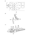
次に、半導体装置をRFIDタグとして実際に使用するときの一形態について説明する。表示部321を含む携帯端末の側面には、リーダ/ライタ320が設けられ、品物322の側面にはRFIDタグ323が設けられる(図11(B))。品物322が含むRFIDタグ323にリーダ/ライタ320をかざすと、表示部321に品物の原材料や原産地、生産工程ごとの検査結果や流通過程の履歴等、更に商品の説明等の商品に関する情報が表示される。また、商品326をベルトコンベアにより搬送する際に、リーダ/ライタ324と、商品326に設けられたRFIDタグ325を用いて、該商品326の検品を行うことができる(図11(C))。このように、システムにRFIDタグを活用することで、情報の取得を簡単に行うことができ、高機能化と高付加価値化を実現する。
Next, one mode when the semiconductor device is actually used as an RFID tag will be described. A reader /
なお、本実施の形態は、上記実施の形態と自由に組み合わせて行うことができる。 Note that this embodiment can be freely combined with the above embodiment.
(実施の形態5)
本発明の半導体装置の用途は広範にわたり、非接触で対象物の履歴等の情報を明確にし、生産・管理等に役立てる商品であればどのようなものにも適用することができる。例えば、紙幣、硬貨、有価証券類、証書類、無記名債券類、包装用容器類、書籍類、記録媒体、身の回り品、乗物類、食品類、衣類、保健用品類、生活用品類、薬品類及び電子機器等に設けて使用することができる。これらの例に関して図12を用いて説明する。
(Embodiment 5)
The application of the semiconductor device of the present invention is wide-ranging, and can be applied to any product that can be used for production and management by clarifying information such as the history of an object without contact. For example, banknotes, coins, securities, certificate documents, bearer bonds, packaging containers, books, recording media, personal belongings, vehicles, foods, clothing, health supplies, daily necessities, chemicals, etc. It can be provided and used in an electronic device or the like. These examples will be described with reference to FIG.
紙幣、硬貨とは、市場に流通する金銭であり、特定の地域で貨幣と同じように通用するもの(金券)、記念コイン等を含む。有価証券類とは、小切手、証券、約束手形等を指す(図12(A)参照)。証書類とは、運転免許証、住民票等を指す(図12(B)参照)。無記名債券類とは、切手、おこめ券、各種ギフト券等を指す(図12(C)参照)。包装用容器類とは、お弁当等の包装紙、ペットボトル等を指す(図12(D)参照)。書籍類とは、書物、本等を指す(図12(E)参照)。記録媒体とは、DVDソフト、ビデオテープ等を指す(図12(F)参照)。乗物類とは、自転車等の車両、船舶等を指す(図12(G)参照)。身の回り品とは、鞄、眼鏡等を指す(図12(H)参照)。食品類とは、食料品、飲料等を指す。衣類とは、衣服、履物等を指す。保健用品類とは、医療器具、健康器具等を指す。生活用品類とは、家具、照明器具等を指す。薬品類とは、医薬品、農薬等を指す。電子機器とは、液晶表示装置、EL表示装置、テレビジョン装置(テレビ受像機、薄型テレビ受像機)、携帯電話等を指す。 Banknotes and coins are money that circulates in the market, and include those that are used in the same way as money in a specific area (cash vouchers), commemorative coins, and the like. Securities refer to checks, securities, promissory notes, etc. (see FIG. 12A). The certificate refers to a driver's license, a resident's card, etc. (see FIG. 12B). Bearer bonds refer to stamps, gift cards, various gift certificates, and the like (see FIG. 12C). Packaging containers refer to wrapping paper for lunch boxes, plastic bottles, and the like (see FIG. 12D). Books refer to books, books, and the like (see FIG. 12E). The recording media refer to DVD software, video tapes, and the like (see FIG. 12F). The vehicles refer to vehicles such as bicycles, ships, and the like (see FIG. 12G). Personal belongings refer to bags, glasses, and the like (see FIG. 12H). Foods refer to food products, beverages, and the like. Clothing refers to clothing, footwear, and the like. Health supplies refer to medical equipment, health equipment, and the like. Livingware refers to furniture, lighting equipment, and the like. Chemicals refer to pharmaceuticals, agricultural chemicals, and the like. Electronic devices refer to liquid crystal display devices, EL display devices, television devices (TV receivers, flat-screen TV receivers), mobile phones, and the like.
紙幣、硬貨、有価証券類、証書類、無記名債券類等にRFIDタグを設けることにより、偽造を防止することができる。また、包装用容器類、書籍類、記録媒体等、身の回り品、食品類、生活用品類、電子機器等にRFIDタグを設けることにより、検品システムやレンタル店のシステムなどの効率化を図ることができる。乗物類、保健用品類、薬品類等にRFIDタグを設けることにより、偽造や盗難の防止、薬品類ならば、薬の服用の間違いを防止することができる。RFIDタグの設け方としては、物品の表面に貼ったり、物品に埋め込んだりして設ける。例えば、本ならば紙に埋め込んだり、有機樹脂からなるパッケージなら当該有機樹脂に埋め込んだりするとよい。また、後に光学的作用を加えて書き込み(追記)をする場合には、チップに設けられた記憶素子の部分に光が照射できるように透明な材料で形成しておくことが好ましい。さらに、一度書き込んだデータの書き換えが不可能である記憶素子を用いることによって、効果的に偽造を防止することが可能となる。また、ユーザーが商品を購入した後のプライバシー等の問題についても、RFIDタグに設けられた記憶素子のデータを消去するシステムを設けておくことによって解決することができる。 Forgery can be prevented by providing RFID tags on bills, coins, securities, certificates, bearer bonds, and the like. In addition, it is possible to improve the efficiency of inspection systems and rental store systems by providing RFID tags for personal items such as packaging containers, books, and recording media, foods, daily necessities, and electronic devices. it can. By providing RFID tags on vehicles, health supplies, medicines, etc., counterfeiting and theft can be prevented, and medicines can prevent mistakes in taking medicines. The RFID tag is provided by being attached to the surface of the article or embedded in the article. For example, a book may be embedded in paper, and a package made of an organic resin may be embedded in the organic resin. Further, when writing (additional writing) is performed by applying an optical action later, it is preferable to form the transparent element so that light can be applied to the portion of the memory element provided on the chip. Furthermore, forgery can be effectively prevented by using a memory element in which data once written cannot be rewritten. In addition, problems such as privacy after a user purchases a product can be solved by providing a system for erasing data in a storage element provided in the RFID tag.
このように、包装用容器類、記録媒体、身の回り品、食品類、衣類、生活用品類、電子機器等にRFIDタグを設けることにより、検品システムやレンタル店のシステムなどの効率化を図ることができる。また乗物類にRFIDタグを設けることにより、偽造や盗難を防止することができる。また、動物等の生き物に埋め込むことによって、個々の生き物の識別を容易に行うことができる。例えば、家畜等の生き物にセンサを備えたRFIDタグを埋め込むことによって、生まれた年や性別または種類等はもちろん現在の体温等の健康状態を容易に管理することが可能となる。 In this way, by providing RFID tags on packaging containers, recording media, personal items, foods, clothing, daily necessities, electronic devices, etc., it is possible to improve the efficiency of inspection systems and rental store systems. it can. In addition, forgery and theft can be prevented by providing an RFID tag in vehicles. Moreover, by embedding it in creatures such as animals, it is possible to easily identify individual creatures. For example, by embedding an RFID tag equipped with a sensor in a living creature such as livestock, it is possible to easily manage the current health condition such as the body temperature as well as the year of birth, gender or type.
以上のように、本発明の半導体装置はどのようなものにでも設けて使用することができる。なお、本実施の形態は、上記実施の形態と自由に組み合わせて行うことができる。 As described above, the semiconductor device of the present invention can be provided and used in any device. Note that this embodiment can be freely combined with the above embodiment.
20 基板
21 アンテナ
22 素子形成層
23 電源配線
24 接地配線
25 電源回路
26 機能回路
27 機能回路
28 機能回路
70 基板
71 アンテナ
72 素子形成層
73 電源配線
74 接地配線
75 電源回路
76 機能回路
77 機能回路
78 電流
701 基板
702 剥離層
703 絶縁膜
704 非晶質半導体膜
705 絶縁膜
706 結晶質半導体膜
707 結晶質半導体膜
708 結晶質半導体膜
709 結晶質半導体膜
710 結晶質半導体膜
711 N型不純物領域
712 P型不純物領域
713 N型不純物領域
714 N型不純物領域
715 N型不純物領域
716 導電膜
717 導電膜
718 導電膜
719 導電膜
720 導電膜
721 導電膜
722 導電膜
723 導電膜
724 導電膜
725 導電膜
726 N型不純物領域
727 N型不純物領域
728 N型不純物領域
729 N型不純物領域
730 N型不純物領域
731 N型不純物領域
732 N型不純物領域
733 N型不純物領域
734 絶縁膜
735 絶縁膜
736 絶縁膜
737 絶縁膜
738 絶縁膜
739 絶縁膜
740 絶縁膜
741 絶縁膜
742 絶縁膜
743 絶縁膜
744 薄膜トランジスタ
745 薄膜トランジスタ
746 薄膜トランジスタ
747 薄膜トランジスタ
748 薄膜トランジスタ
749 絶縁膜
750 絶縁膜
751 絶縁膜
752 導電膜
753 導電膜
754 導電膜
755 導電膜
756 導電膜
757 導電膜
758 導電膜
759 導電膜
760 導電膜
761 導電膜
762 絶縁膜
763 導電膜
764 導電膜
765 導電膜
766 絶縁膜
767 コンタクトホール
768 コンタクトホール
769 コンタクトホール
771 導電膜
772 絶縁膜
773 開口部
774 開口部
780 チャネル形成領域
781 チャネル形成領域
782 チャネル形成領域
783 チャネル形成領域
784 チャネル形成領域
785 P型不純物領域
786 導電膜
787 有機化合物層
789 記憶素子部
790 記憶素子部
791 素子形成層
775 第1のシート材
776 第2のシート材
777 第3のシート材
80 RFIDタグ
81 電源回路
82 クロック発生回路
83 データ復調回路
84 データ変調回路
85 制御回路
86 記憶回路
87 アンテナ
88 リーダ/ライタ
321 表示部
320 リーダ/ライタ
322 品物
323 RFIDタグ
326 商品
324 リーダ/ライタ
325 RFIDタグ
20 Substrate 21 Antenna 22 Element formation layer 23 Power supply wiring 24 Ground wiring 25 Power supply circuit 26 Functional circuit 27 Functional circuit 28 Functional circuit 70 Substrate 71 Antenna 72 Element formation layer 73 Power supply wiring 74 Ground wiring 75 Power supply circuit 76 Functional circuit 77 Functional circuit 78 Current 701 Substrate 702 Release layer 703 Insulating film 704 Amorphous semiconductor film 705 Insulating film 706 Crystalline semiconductor film 707 Crystalline semiconductor film 708 Crystalline semiconductor film 709 Crystalline semiconductor film 710 Crystalline semiconductor film 711 N-type impurity region 712 P N-type impurity region 714 N-type impurity region 715 N-type impurity region 715 N-type impurity region 716 conductive film 717 conductive film 718 conductive film 719 conductive film 720 conductive film 721 conductive film 722 conductive film 723 conductive film 724 conductive film 725 conductive film 726 N Type impurity region 727 N type impurity region 7 8 N-type impurity region 729 N-type impurity region 730 N-type impurity region 731 N-type impurity region 732 N-type impurity region 733 N-type impurity region 734 Insulating film 735 Insulating film 736 Insulating film 737 Insulating film 738 Insulating film 739 Insulating film 740 Insulating Film 741 insulating film 742 insulating film 743 insulating film 744 thin film transistor 745 thin film transistor 746 thin film transistor 747 thin film transistor 748 thin film transistor 749 insulating film 750 insulating film 751 insulating film 752 conductive film 753 conductive film 754 conductive film 755 conductive film 756 conductive film 757 conductive film 758 conductive film 759 conductive film 760 conductive film 761 conductive film 762 insulating film 763 conductive film 764 conductive film 765 conductive film 766 insulating film 767 contact hole 768 contact hole 769 contact hole 771 conductive Film 772 Insulating film 773 Opening 774 Opening 780 Channel formation region 781 Channel formation region 782 Channel formation region 783 Channel formation region 784 Channel formation region 785 P-type impurity region 786 Conductive film 787 Organic compound layer 789 Memory element portion 790 Memory element portion 791 Element formation layer 775 First sheet material 776 Second sheet material 777 Third sheet material 80 RFID tag 81 Power supply circuit 82 Clock generation circuit 83 Data demodulation circuit 84 Data modulation circuit 85 Control circuit 86 Storage circuit 87 Antenna 88 Reader / Writer 321 Display unit 320 Reader / Writer 322 Product 323 RFID tag 326 Product 324 Reader / Writer 325 RFID tag
Claims (7)
前記素子形成層と前記アンテナとは少なくとも一部が重なるように設けられ、
前記素子形成層は、複数のトランジスタを有し、
前記複数のトランジスタを用いて、電源回路及び機能回路を構成し、
前記電源回路と、前記機能回路との間で十字形状となるように、接地配線が設けられ、
前記電源回路と、前記機能回路とを囲んでコの字形状となるように、電源配線が設けられたことを特徴とする半導体装置。 An element forming layer provided on a substrate; and an antenna electrically connected to the element forming layer;
The element formation layer and the antenna are provided so that at least a part thereof overlaps,
The element formation layer has a plurality of transistors,
A power supply circuit and a functional circuit are configured using the plurality of transistors,
A ground wiring is provided so as to have a cross shape between the power supply circuit and the functional circuit,
A semiconductor device, wherein a power supply wiring is provided so as to surround the power supply circuit and the functional circuit so as to have a U shape.
前記素子形成層と前記アンテナとは少なくとも一部が重なるように設けられ、
前記素子形成層は、複数のトランジスタを有し、
前記複数のトランジスタのソース電極又はドレイン電極の一方と電気的に接続される導電膜とを有し、
前記複数のトランジスタを用いて、電源回路及び機能回路を構成し、
前記電源回路と、前記機能回路との間で十字形状となるように、接地配線が設けられ、
前記電源回路と、前記機能回路とを囲んでコの字形状となるように、電源配線が設けられ、
前記接地配線及び前記電源配線は、前記導電膜と同一層に設けられたことを特徴とする半導体装置。 An element forming layer provided on a substrate; and an antenna electrically connected to the element forming layer;
The element formation layer and the antenna are provided so that at least a part thereof overlaps,
The element formation layer has a plurality of transistors,
A conductive film electrically connected to one of a source electrode or a drain electrode of the plurality of transistors;
A power supply circuit and a functional circuit are configured using the plurality of transistors,
A ground wiring is provided so as to have a cross shape between the power supply circuit and the functional circuit,
Power supply wiring is provided so as to surround the power supply circuit and the functional circuit to have a U shape,
The semiconductor device, wherein the ground wiring and the power supply wiring are provided in the same layer as the conductive film.
前記素子形成層と前記アンテナとは少なくとも一部が重なるように設けられ、
前記素子形成層は、複数のトランジスタを有し、
前記複数のトランジスタのソース電極又はドレイン電極の一方と電気的に接続される導電膜とを有し、
前記複数のトランジスタを用いて、電源回路及び第1乃至第3の機能回路を構成し、
前記電源回路と前記第1の機能回路との間、前記電源回路と前記第2の機能回路との間、前記第1の機能回路と前記第3の機能回路との間、及び前記第2の機能回路と前記第3の機能回路との間で十字形状となるように、接地配線が設けられ、
前記電源回路と、前記第1の機能回路と、前記第3の機能回路と、前記第2の機能回路とを順に囲んでコの字形状となるように、電源配線が設けられ、
前記接地配線及び前記電源配線は、前記導電膜と同一層に設けられたことを特徴とする半導体装置。 An element forming layer provided on a substrate; and an antenna electrically connected to the element forming layer;
The element formation layer and the antenna are provided so that at least a part thereof overlaps,
The element formation layer has a plurality of transistors,
A conductive film electrically connected to one of a source electrode or a drain electrode of the plurality of transistors;
A power supply circuit and first to third functional circuits are configured using the plurality of transistors,
Between said power supply circuit wherein the first functional circuit, between said power supply circuit and the second functional circuit, between the front Symbol said first functional circuit the third functional circuit, and the second A ground wiring is provided so as to form a cross shape between the functional circuit and the third functional circuit ,
A power supply wiring is provided so as to surround the power supply circuit, the first functional circuit, the third functional circuit, and the second functional circuit in order to form a U shape,
The semiconductor device, wherein the ground wiring and the power supply wiring are provided in the same layer as the conductive film.
前記電源回路から前記電源配線に電源電圧が供給されるように、前記電源回路と前記電源配線とは電気的に接続していることを特徴とする半導体装置。 In any one of Claims 1 thru | or 3,
The semiconductor device, wherein the power supply circuit and the power supply wiring are electrically connected so that a power supply voltage is supplied from the power supply circuit to the power supply wiring.
前記素子形成層と前記アンテナとは少なくとも一部が重なるように設けられ、
前記素子形成層は、複数のトランジスタと、記憶素子部とを有し、
前記記憶素子部は、前記複数のトランジスタのソース電極又はドレイン電極の一方と電気的に接続される第1の導電膜と、
前記第1の導電膜上に形成された有機化合物層と、
前記有機化合物層上に形成された第2の導電膜とを有し、
前記複数のトランジスタを用いて、電源回路及び機能回路を構成し、
前記電源回路と、前記機能回路との間で十字形状となるように、接地配線が設けられ、
前記電源回路と、前記機能回路とを囲んでコの字形状となるように、電源配線が設けられた半導体装置の作製方法であって、
前記アンテナを形成した後に前記有機化合物層を形成することを特徴とする半導体装置の作製方法。 An element forming layer provided on a substrate; and an antenna electrically connected to the element forming layer;
The element formation layer and the antenna are provided so that at least a part thereof overlaps,
The element formation layer includes a plurality of transistors and a memory element portion ,
The memory element portion includes a first conductive film electrically connected to one of a source electrode and a drain electrode of the plurality of transistors;
An organic compound layer formed on the first conductive film;
A second conductive film formed on the organic compound layer,
A power supply circuit and a functional circuit are configured using the plurality of transistors,
A ground wiring is provided so as to have a cross shape between the power supply circuit and the functional circuit,
A method for manufacturing a semiconductor device provided with power supply wiring so as to surround the power supply circuit and the functional circuit so as to have a U shape,
A method for manufacturing a semiconductor device, wherein the organic compound layer is formed after the antenna is formed.
前記素子形成層と前記アンテナとは少なくとも一部が重なるように設けられ、
前記素子形成層は、複数のトランジスタと、記憶素子部とを有し、
前記記憶素子部は、前記複数のトランジスタのソース電極又はドレイン電極の一方と電気的に接続される第1の導電膜と、
前記第1の導電膜上に形成された有機化合物層と、
前記有機化合物層上に形成された第2の導電膜とを有し、
前記複数のトランジスタを用いて、電源回路及び機能回路を構成し、
前記電源回路と、前記機能回路との間で十字形状となるように、接地配線が設けられ、
前記電源回路と、前記機能回路とを囲んでコの字形状となるように、電源配線が設けられた半導体装置の作製方法であって、
前記接地配線及び前記電源配線は、前記第1の導電膜と同時に形成され、
前記アンテナを形成した後に前記有機化合物層を形成することを特徴とする半導体装置の作製方法。 An element forming layer provided on a substrate; and an antenna electrically connected to the element forming layer;
The element formation layer and the antenna are provided so that at least a part thereof overlaps,
The element formation layer includes a plurality of transistors and a memory element portion ,
The memory element portion includes a first conductive film electrically connected to one of a source electrode and a drain electrode of the plurality of transistors;
An organic compound layer formed on the first conductive film;
A second conductive film formed on the organic compound layer,
A power supply circuit and a functional circuit are configured using the plurality of transistors,
A ground wiring is provided so as to have a cross shape between the power supply circuit and the functional circuit,
A method for manufacturing a semiconductor device provided with power supply wiring so as to surround the power supply circuit and the functional circuit so as to have a U shape,
The ground wiring and the power supply wiring are formed simultaneously with the first conductive film,
A method for manufacturing a semiconductor device, wherein the organic compound layer is formed after the antenna is formed.
前記電源回路から前記電源配線に電源電圧が供給されるように、前記電源回路と前記電源配線とは電気的に接続していることを特徴とする半導体装置の作製方法。 In claim 5 or 6,
The method for manufacturing a semiconductor device, wherein the power supply circuit and the power supply wiring are electrically connected so that a power supply voltage is supplied from the power supply circuit to the power supply wiring.
Priority Applications (1)
| Application Number | Priority Date | Filing Date | Title |
|---|---|---|---|
| JP2005370476A JP4942998B2 (en) | 2004-12-24 | 2005-12-22 | Semiconductor device and manufacturing method of semiconductor device |
Applications Claiming Priority (3)
| Application Number | Priority Date | Filing Date | Title |
|---|---|---|---|
| JP2004374913 | 2004-12-24 | ||
| JP2004374913 | 2004-12-24 | ||
| JP2005370476A JP4942998B2 (en) | 2004-12-24 | 2005-12-22 | Semiconductor device and manufacturing method of semiconductor device |
Publications (3)
| Publication Number | Publication Date |
|---|---|
| JP2006203187A JP2006203187A (en) | 2006-08-03 |
| JP2006203187A5 JP2006203187A5 (en) | 2008-11-20 |
| JP4942998B2 true JP4942998B2 (en) | 2012-05-30 |
Family
ID=36960854
Family Applications (1)
| Application Number | Title | Priority Date | Filing Date |
|---|---|---|---|
| JP2005370476A Expired - Fee Related JP4942998B2 (en) | 2004-12-24 | 2005-12-22 | Semiconductor device and manufacturing method of semiconductor device |
Country Status (1)
| Country | Link |
|---|---|
| JP (1) | JP4942998B2 (en) |
Families Citing this family (87)
| Publication number | Priority date | Publication date | Assignee | Title |
|---|---|---|---|---|
| US7519328B2 (en) | 2006-01-19 | 2009-04-14 | Murata Manufacturing Co., Ltd. | Wireless IC device and component for wireless IC device |
| CN102780085A (en) | 2006-04-14 | 2012-11-14 | 株式会社村田制作所 | Antenna |
| US9064198B2 (en) | 2006-04-26 | 2015-06-23 | Murata Manufacturing Co., Ltd. | Electromagnetic-coupling-module-attached article |
| WO2008001561A1 (en) | 2006-06-30 | 2008-01-03 | Murata Manufacturing Co., Ltd. | Optical disc |
| JP4775442B2 (en) | 2006-09-26 | 2011-09-21 | 株式会社村田製作所 | Article with electromagnetic coupling module |
| EP1909384A3 (en) * | 2006-10-06 | 2015-11-25 | Semiconductor Energy Laboratory Co., Ltd. | Rectifier circuit with variable capacitor, semiconductor device using the circuit, and driving method therefor |
| JP4798223B2 (en) | 2006-10-27 | 2011-10-19 | 株式会社村田製作所 | Article with electromagnetic coupling module |
| JP5361176B2 (en) | 2006-12-13 | 2013-12-04 | 株式会社半導体エネルギー研究所 | Semiconductor device |
| WO2008090943A1 (en) | 2007-01-26 | 2008-07-31 | Murata Manufacturing Co., Ltd. | Container with electromagnetically coupling module |
| WO2008096576A1 (en) | 2007-02-06 | 2008-08-14 | Murata Manufacturing Co., Ltd. | Packing material provided with electromagnetically coupled module |
| WO2008126458A1 (en) | 2007-04-06 | 2008-10-23 | Murata Manufacturing Co., Ltd. | Radio ic device |
| JP4697332B2 (en) | 2007-04-09 | 2011-06-08 | 株式会社村田製作所 | Wireless IC device |
| US8235299B2 (en) | 2007-07-04 | 2012-08-07 | Murata Manufacturing Co., Ltd. | Wireless IC device and component for wireless IC device |
| EP2138962B1 (en) | 2007-04-26 | 2012-01-04 | Murata Manufacturing Co. Ltd. | Wireless ic device |
| JP4666101B2 (en) | 2007-04-27 | 2011-04-06 | 株式会社村田製作所 | Wireless IC device |
| KR101038132B1 (en) | 2007-04-27 | 2011-05-31 | 가부시키가이샤 무라타 세이사쿠쇼 | Wireless IC devices |
| WO2008142957A1 (en) | 2007-05-10 | 2008-11-27 | Murata Manufacturing Co., Ltd. | Wireless ic device |
| EP2148449B1 (en) | 2007-05-11 | 2012-12-12 | Murata Manufacturing Co., Ltd. | Wireless ic device |
| EP2077602B1 (en) | 2007-06-27 | 2012-02-08 | Murata Manufacturing Co. Ltd. | Wireless ic device |
| EP2166617B1 (en) | 2007-07-09 | 2015-09-30 | Murata Manufacturing Co. Ltd. | Wireless ic device |
| KR101037035B1 (en) | 2007-07-17 | 2011-05-25 | 가부시키가이샤 무라타 세이사쿠쇼 | Wireless IC Devices and Electronics |
| US20090021352A1 (en) | 2007-07-18 | 2009-01-22 | Murata Manufacturing Co., Ltd. | Radio frequency ic device and electronic apparatus |
| JP4434311B2 (en) | 2007-07-18 | 2010-03-17 | 株式会社村田製作所 | Wireless IC device and manufacturing method thereof |
| EP2680193B1 (en) | 2007-07-18 | 2015-11-18 | Murata Manufacturing Co., Ltd. | Apparatus comprising an RFID device |
| JP4462388B2 (en) | 2007-12-20 | 2010-05-12 | 株式会社村田製作所 | Wireless IC device |
| CN103401063B (en) | 2007-12-26 | 2018-03-02 | 株式会社村田制作所 | Antenna assembly and Wireless IC device |
| WO2009110382A1 (en) | 2008-03-03 | 2009-09-11 | 株式会社村田製作所 | Composite antenna |
| EP2251934B1 (en) | 2008-03-03 | 2018-05-02 | Murata Manufacturing Co. Ltd. | Wireless ic device and wireless communication system |
| EP2256861B1 (en) | 2008-03-26 | 2018-12-05 | Murata Manufacturing Co., Ltd. | Radio ic device |
| WO2009128437A1 (en) | 2008-04-14 | 2009-10-22 | 株式会社村田製作所 | Radio ic device, electronic device, and method for adjusting resonance frequency of radio ic device |
| EP2284949B1 (en) | 2008-05-21 | 2016-08-03 | Murata Manufacturing Co. Ltd. | Wireless ic device |
| WO2009142068A1 (en) | 2008-05-22 | 2009-11-26 | 株式会社村田製作所 | Wireless ic device and method for manufacturing the same |
| JP5218558B2 (en) | 2008-05-26 | 2013-06-26 | 株式会社村田製作所 | Wireless IC device system and authentication method for wireless IC device |
| EP3509162A1 (en) | 2008-05-28 | 2019-07-10 | Murata Manufacturing Co., Ltd. | Wireless ic device and component for a wireless ic device |
| JP4557186B2 (en) | 2008-06-25 | 2010-10-06 | 株式会社村田製作所 | Wireless IC device and manufacturing method thereof |
| JP4671001B2 (en) | 2008-07-04 | 2011-04-13 | 株式会社村田製作所 | Wireless IC device |
| WO2010021217A1 (en) | 2008-08-19 | 2010-02-25 | 株式会社村田製作所 | Wireless ic device and method for manufacturing same |
| WO2010047214A1 (en) | 2008-10-24 | 2010-04-29 | 株式会社村田製作所 | Radio ic device |
| DE112009002399B4 (en) | 2008-10-29 | 2022-08-18 | Murata Manufacturing Co., Ltd. | Radio IC device |
| WO2010055945A1 (en) | 2008-11-17 | 2010-05-20 | 株式会社村田製作所 | Antenna and wireless ic device |
| JP5041075B2 (en) | 2009-01-09 | 2012-10-03 | 株式会社村田製作所 | Wireless IC device and wireless IC module |
| WO2010082413A1 (en) | 2009-01-16 | 2010-07-22 | 株式会社村田製作所 | High frequency device and wireless ic device |
| CN102301528B (en) | 2009-01-30 | 2015-01-28 | 株式会社村田制作所 | Antenna and Wireless IC Devices |
| JP5510450B2 (en) | 2009-04-14 | 2014-06-04 | 株式会社村田製作所 | Wireless IC device |
| EP2424041B1 (en) | 2009-04-21 | 2018-11-21 | Murata Manufacturing Co., Ltd. | Antenna apparatus and resonant frequency setting method of same |
| CN102449846B (en) | 2009-06-03 | 2015-02-04 | 株式会社村田制作所 | Wireless IC device and production method thereof |
| WO2010146944A1 (en) | 2009-06-19 | 2010-12-23 | 株式会社村田製作所 | Wireless ic device and method for coupling power supply circuit and radiating plates |
| JP4788850B2 (en) | 2009-07-03 | 2011-10-05 | 株式会社村田製作所 | Antenna module |
| WO2011037234A1 (en) | 2009-09-28 | 2011-03-31 | 株式会社村田製作所 | Wireless ic device and method for detecting environmental conditions using same |
| WO2011040393A1 (en) | 2009-09-30 | 2011-04-07 | 株式会社村田製作所 | Circuit substrate and method of manufacture thereof |
| JP5304580B2 (en) | 2009-10-02 | 2013-10-02 | 株式会社村田製作所 | Wireless IC device |
| WO2011045970A1 (en) | 2009-10-16 | 2011-04-21 | 株式会社村田製作所 | Antenna and wireless ic device |
| JP5418600B2 (en) | 2009-10-27 | 2014-02-19 | 株式会社村田製作所 | Transceiver and RFID tag reader |
| WO2011055703A1 (en) | 2009-11-04 | 2011-05-12 | 株式会社村田製作所 | Communication terminal and information processing system |
| WO2011055702A1 (en) | 2009-11-04 | 2011-05-12 | 株式会社村田製作所 | Wireless ic tag, reader/writer, and information processing system |
| WO2011055701A1 (en) | 2009-11-04 | 2011-05-12 | 株式会社村田製作所 | Communication terminal and information processing system |
| CN104617374B (en) | 2009-11-20 | 2018-04-06 | 株式会社村田制作所 | Mobile communication terminal |
| GB2488450B (en) | 2009-12-24 | 2014-08-20 | Murata Manufacturing Co | Antenna and mobile terminal |
| CN102792520B (en) | 2010-03-03 | 2017-08-25 | 株式会社村田制作所 | Wireless communication module and Wireless Telecom Equipment |
| JP5403146B2 (en) | 2010-03-03 | 2014-01-29 | 株式会社村田製作所 | Wireless communication device and wireless communication terminal |
| CN102576940B (en) | 2010-03-12 | 2016-05-04 | 株式会社村田制作所 | Wireless communication devices and metal article processed |
| GB2491447B (en) | 2010-03-24 | 2014-10-22 | Murata Manufacturing Co | RFID system |
| JP5630499B2 (en) | 2010-03-31 | 2014-11-26 | 株式会社村田製作所 | Antenna apparatus and wireless communication device |
| JP5170156B2 (en) | 2010-05-14 | 2013-03-27 | 株式会社村田製作所 | Wireless IC device |
| JP5299351B2 (en) | 2010-05-14 | 2013-09-25 | 株式会社村田製作所 | Wireless IC device |
| JP5376060B2 (en) | 2010-07-08 | 2013-12-25 | 株式会社村田製作所 | Antenna and RFID device |
| CN104752813B (en) | 2010-07-28 | 2018-03-02 | 株式会社村田制作所 | Antenna assembly and communication terminal device |
| JP5423897B2 (en) | 2010-08-10 | 2014-02-19 | 株式会社村田製作所 | Printed wiring board and wireless communication system |
| JP5234071B2 (en) | 2010-09-03 | 2013-07-10 | 株式会社村田製作所 | RFIC module |
| JP5630506B2 (en) | 2010-09-30 | 2014-11-26 | 株式会社村田製作所 | Wireless IC device |
| JP5758909B2 (en) | 2010-10-12 | 2015-08-05 | 株式会社村田製作所 | Communication terminal device |
| CN102971909B (en) | 2010-10-21 | 2014-10-15 | 株式会社村田制作所 | Communication terminal device |
| CN105048058B (en) | 2011-01-05 | 2017-10-27 | 株式会社村田制作所 | Wireless communication devices |
| JP5304956B2 (en) | 2011-01-14 | 2013-10-02 | 株式会社村田製作所 | RFID chip package and RFID tag |
| CN103119786B (en) | 2011-02-28 | 2015-07-22 | 株式会社村田制作所 | Wireless communication device |
| JP5630566B2 (en) | 2011-03-08 | 2014-11-26 | 株式会社村田製作所 | Antenna device and communication terminal device |
| KR101317226B1 (en) | 2011-04-05 | 2013-10-15 | 가부시키가이샤 무라타 세이사쿠쇼 | Wireless communication device |
| WO2012141070A1 (en) | 2011-04-13 | 2012-10-18 | 株式会社村田製作所 | Wireless ic device and wireless communication terminal |
| JP5569648B2 (en) | 2011-05-16 | 2014-08-13 | 株式会社村田製作所 | Wireless IC device |
| EP3041087B1 (en) | 2011-07-14 | 2022-09-07 | Murata Manufacturing Co., Ltd. | Wireless communication device |
| JP5333707B2 (en) | 2011-07-15 | 2013-11-06 | 株式会社村田製作所 | Wireless communication device |
| CN203850432U (en) | 2011-07-19 | 2014-09-24 | 株式会社村田制作所 | Antenna device and communication terminal device |
| CN203553354U (en) | 2011-09-09 | 2014-04-16 | 株式会社村田制作所 | Antenna device and wireless device |
| JP5344108B1 (en) | 2011-12-01 | 2013-11-20 | 株式会社村田製作所 | Wireless IC device and manufacturing method thereof |
| JP5354137B1 (en) | 2012-01-30 | 2013-11-27 | 株式会社村田製作所 | Wireless IC device |
| JP5464307B2 (en) | 2012-02-24 | 2014-04-09 | 株式会社村田製作所 | ANTENNA DEVICE AND WIRELESS COMMUNICATION DEVICE |
| CN104487985B (en) | 2012-04-13 | 2020-06-26 | 株式会社村田制作所 | RFID tag inspection method and inspection device |
Family Cites Families (6)
| Publication number | Priority date | Publication date | Assignee | Title |
|---|---|---|---|---|
| JPH0793149B2 (en) * | 1989-06-09 | 1995-10-09 | 松下電器産業株式会社 | Solid state secondary battery and its manufacturing method |
| JPH0653449A (en) * | 1992-07-31 | 1994-02-25 | Nec Corp | Semiconductor device |
| JP2001284460A (en) * | 2000-04-03 | 2001-10-12 | Seiko Epson Corp | Semiconductor integrated circuit device |
| JP3377787B1 (en) * | 2000-06-21 | 2003-02-17 | 日立マクセル株式会社 | Semiconductor chip and semiconductor device using the same |
| JP2003109819A (en) * | 2001-09-28 | 2003-04-11 | Toshiba Corp | Semiconductor device having inductor |
| JP4566578B2 (en) * | 2003-02-24 | 2010-10-20 | 株式会社半導体エネルギー研究所 | Method for manufacturing thin film integrated circuit |
-
2005
- 2005-12-22 JP JP2005370476A patent/JP4942998B2/en not_active Expired - Fee Related
Also Published As
| Publication number | Publication date |
|---|---|
| JP2006203187A (en) | 2006-08-03 |
Similar Documents
| Publication | Publication Date | Title |
|---|---|---|
| JP4942998B2 (en) | Semiconductor device and manufacturing method of semiconductor device | |
| US8716834B2 (en) | Semiconductor device including antenna | |
| US8136735B2 (en) | ID label, ID card, and ID tag | |
| US9728631B2 (en) | Semiconductor device and method for manufacturing the same | |
| JP5604567B2 (en) | Semiconductor device | |
| JP5523593B2 (en) | Semiconductor device | |
| US8698220B2 (en) | Semiconductor device having concentration difference of impurity element in semiconductor films | |
| JP5322408B2 (en) | Semiconductor device and manufacturing method thereof | |
| CN101189625A (en) | Semiconductor device, manufacturing method thereof, and antenna manufacturing method | |
| JP2008252068A (en) | Semiconductor device and manufacturing method thereof | |
| JP4827618B2 (en) | Method for manufacturing antenna, method for manufacturing semiconductor device | |
| JP4912586B2 (en) | Method for manufacturing thin film integrated circuit device | |
| JP5100012B2 (en) | Semiconductor device and manufacturing method thereof | |
| JP5657069B2 (en) | Semiconductor device | |
| JP2008103706A (en) | Semiconductor device | |
| JP5089037B2 (en) | Method for manufacturing semiconductor device | |
| JP5027470B2 (en) | Storage device | |
| JP4974621B2 (en) | Semiconductor device and manufacturing method thereof | |
| JP4908936B2 (en) | Method for manufacturing semiconductor device | |
| JP5105918B2 (en) | Method for manufacturing semiconductor device |
Legal Events
| Date | Code | Title | Description |
|---|---|---|---|
| A521 | Request for written amendment filed |
Free format text: JAPANESE INTERMEDIATE CODE: A523 Effective date: 20081006 |
|
| A621 | Written request for application examination |
Free format text: JAPANESE INTERMEDIATE CODE: A621 Effective date: 20081006 |
|
| A131 | Notification of reasons for refusal |
Free format text: JAPANESE INTERMEDIATE CODE: A131 Effective date: 20111025 |
|
| A977 | Report on retrieval |
Free format text: JAPANESE INTERMEDIATE CODE: A971007 Effective date: 20111027 |
|
| A521 | Request for written amendment filed |
Free format text: JAPANESE INTERMEDIATE CODE: A523 Effective date: 20111205 |
|
| A131 | Notification of reasons for refusal |
Free format text: JAPANESE INTERMEDIATE CODE: A131 Effective date: 20120105 |
|
| A521 | Request for written amendment filed |
Free format text: JAPANESE INTERMEDIATE CODE: A523 Effective date: 20120207 |
|
| TRDD | Decision of grant or rejection written | ||
| A01 | Written decision to grant a patent or to grant a registration (utility model) |
Free format text: JAPANESE INTERMEDIATE CODE: A01 Effective date: 20120228 |
|
| A01 | Written decision to grant a patent or to grant a registration (utility model) |
Free format text: JAPANESE INTERMEDIATE CODE: A01 |
|
| A61 | First payment of annual fees (during grant procedure) |
Free format text: JAPANESE INTERMEDIATE CODE: A61 Effective date: 20120229 |
|
| R150 | Certificate of patent or registration of utility model |
Ref document number: 4942998 Country of ref document: JP Free format text: JAPANESE INTERMEDIATE CODE: R150 Free format text: JAPANESE INTERMEDIATE CODE: R150 |
|
| FPAY | Renewal fee payment (event date is renewal date of database) |
Free format text: PAYMENT UNTIL: 20150309 Year of fee payment: 3 |
|
| FPAY | Renewal fee payment (event date is renewal date of database) |
Free format text: PAYMENT UNTIL: 20150309 Year of fee payment: 3 |
|
| R250 | Receipt of annual fees |
Free format text: JAPANESE INTERMEDIATE CODE: R250 |
|
| R250 | Receipt of annual fees |
Free format text: JAPANESE INTERMEDIATE CODE: R250 |
|
| R250 | Receipt of annual fees |
Free format text: JAPANESE INTERMEDIATE CODE: R250 |
|
| R250 | Receipt of annual fees |
Free format text: JAPANESE INTERMEDIATE CODE: R250 |
|
| R250 | Receipt of annual fees |
Free format text: JAPANESE INTERMEDIATE CODE: R250 |
|
| R250 | Receipt of annual fees |
Free format text: JAPANESE INTERMEDIATE CODE: R250 |
|
| LAPS | Cancellation because of no payment of annual fees |