EP2166617A1 - Wireless ic device - Google Patents
Wireless ic device Download PDFInfo
- Publication number
- EP2166617A1 EP2166617A1 EP08777758A EP08777758A EP2166617A1 EP 2166617 A1 EP2166617 A1 EP 2166617A1 EP 08777758 A EP08777758 A EP 08777758A EP 08777758 A EP08777758 A EP 08777758A EP 2166617 A1 EP2166617 A1 EP 2166617A1
- Authority
- EP
- European Patent Office
- Prior art keywords
- wireless
- electrode
- loop
- loop electrode
- metal
- Prior art date
- Legal status (The legal status is an assumption and is not a legal conclusion. Google has not performed a legal analysis and makes no representation as to the accuracy of the status listed.)
- Granted
Links
Images






Classifications
-
- H—ELECTRICITY
- H01—ELECTRIC ELEMENTS
- H01Q—ANTENNAS, i.e. RADIO AERIALS
- H01Q1/00—Details of, or arrangements associated with, antennas
- H01Q1/12—Supports; Mounting means
- H01Q1/22—Supports; Mounting means by structural association with other equipment or articles
- H01Q1/2208—Supports; Mounting means by structural association with other equipment or articles associated with components used in interrogation type services, i.e. in systems for information exchange between an interrogator/reader and a tag/transponder, e.g. in Radio Frequency Identification [RFID] systems
- H01Q1/2225—Supports; Mounting means by structural association with other equipment or articles associated with components used in interrogation type services, i.e. in systems for information exchange between an interrogator/reader and a tag/transponder, e.g. in Radio Frequency Identification [RFID] systems used in active tags, i.e. provided with its own power source or in passive tags, i.e. deriving power from RF signal
-
- G—PHYSICS
- G06—COMPUTING OR CALCULATING; COUNTING
- G06K—GRAPHICAL DATA READING; PRESENTATION OF DATA; RECORD CARRIERS; HANDLING RECORD CARRIERS
- G06K19/00—Record carriers for use with machines and with at least a part designed to carry digital markings
- G06K19/06—Record carriers for use with machines and with at least a part designed to carry digital markings characterised by the kind of the digital marking, e.g. shape, nature, code
- G06K19/067—Record carriers with conductive marks, printed circuits or semiconductor circuit elements, e.g. credit or identity cards also with resonating or responding marks without active components
- G06K19/07—Record carriers with conductive marks, printed circuits or semiconductor circuit elements, e.g. credit or identity cards also with resonating or responding marks without active components with integrated circuit chips
-
- G—PHYSICS
- G06—COMPUTING OR CALCULATING; COUNTING
- G06K—GRAPHICAL DATA READING; PRESENTATION OF DATA; RECORD CARRIERS; HANDLING RECORD CARRIERS
- G06K19/00—Record carriers for use with machines and with at least a part designed to carry digital markings
- G06K19/04—Record carriers for use with machines and with at least a part designed to carry digital markings characterised by the shape
- G06K19/041—Constructional details
-
- G—PHYSICS
- G06—COMPUTING OR CALCULATING; COUNTING
- G06K—GRAPHICAL DATA READING; PRESENTATION OF DATA; RECORD CARRIERS; HANDLING RECORD CARRIERS
- G06K19/00—Record carriers for use with machines and with at least a part designed to carry digital markings
- G06K19/06—Record carriers for use with machines and with at least a part designed to carry digital markings characterised by the kind of the digital marking, e.g. shape, nature, code
- G06K19/067—Record carriers with conductive marks, printed circuits or semiconductor circuit elements, e.g. credit or identity cards also with resonating or responding marks without active components
- G06K19/07—Record carriers with conductive marks, printed circuits or semiconductor circuit elements, e.g. credit or identity cards also with resonating or responding marks without active components with integrated circuit chips
- G06K19/077—Constructional details, e.g. mounting of circuits in the carrier
- G06K19/07745—Mounting details of integrated circuit chips
-
- H—ELECTRICITY
- H01—ELECTRIC ELEMENTS
- H01Q—ANTENNAS, i.e. RADIO AERIALS
- H01Q23/00—Antennas with active circuits or circuit elements integrated within them or attached to them
-
- H—ELECTRICITY
- H01—ELECTRIC ELEMENTS
- H01Q—ANTENNAS, i.e. RADIO AERIALS
- H01Q7/00—Loop antennas with a substantially uniform current distribution around the loop and having a directional radiation pattern in a plane perpendicular to the plane of the loop
-
- H—ELECTRICITY
- H04—ELECTRIC COMMUNICATION TECHNIQUE
- H04B—TRANSMISSION
- H04B5/00—Near-field transmission systems, e.g. inductive or capacitive transmission systems
- H04B5/40—Near-field transmission systems, e.g. inductive or capacitive transmission systems characterised by components specially adapted for near-field transmission
- H04B5/48—Transceivers
Definitions
- the present invention relates to a wireless IC device for a radio frequency identification (RFID) system which allows noncontact data communication via electromagnetic waves.
- RFID radio frequency identification
- an RFID system allows noncontact communication between a reader/writer that generates an induction field and a wireless IC device that is attached to an article and stores predetermined information.
- Fig. 1 is an external perspective view illustrating an example of a metal article to which an IC tag label described in Patent Document 1 is attached.
- An IC tag label 102 has a rectangular thin film-like shape.
- the IC tag 102 has an IC chip 102a at the center thereof and a thin-film antenna 102b in an outer region thereof.
- the IC tag 102 is secured to the undersurface of a nonmetal plate 103.
- the nonmetal plate 103 is fit into the recessed portion 105a and secured.
- the head 101a has a notch 106.
- a magnetic field generated by the antenna 102b in the IC tag 102 can be formed into a loop that passes through the notch 106, the exterior of the metal article 101, and the nonmetal plate 103 and returns to the antenna 102b.
- a metal article with an IC tag is thus produced.
- an object of the present invention is to solve the problems described above, reduce cost of manufacturing a metal article, and provide a wireless IC device using the metal article as a radiator.
- a wireless IC device is configured as follows.
- the amount of coupling between the radiation electrode and the loop electrode according to the present invention is largest when the loop electrode is perpendicular to the radiation electrode. However, even if the loop plane of the loop electrode is inclined to the plane of the radiation electrode, the radiation electrode and the loop electrode are coupled to each other while the amount of coupling therebetween is smaller. Thus, it is possible to provide a high degree of flexibility in arranging the loop electrode relative to the radiation electrode.
- Fig. 2 is an external perspective view illustrating a wireless IC device according to a first embodiment of the present invention and a metal article provided with the wireless IC device.
- a metal article 60 is an article at least whose surface or near-surface layer is made of metal.
- a wireless-IC-device main part 6 is provided on a predetermined surface of the metal article 60.
- the component indicated by reference numeral 6 is not referred to as wireless IC device. This is because the wireless IC device is constituted not only by the component indicated by reference numeral 6, but also by a part of the metal surface of the metal article 60.
- Fig. 3 is an enlarged view of the wireless-IC-device main part.
- the wireless-IC-device main part 6 has an insulating substrate, which is provided with a loop electrode 7 and an electromagnetically coupled module 1 coupled to the loop electrode 7.
- the wireless-IC-device main part 6 is placed such that a loop plane of the loop electrode 7 is substantially perpendicular to the metal article 60.
- the wireless-IC-device main part 6 having the loop electrode 7 is bonded to the metal article 60 with an insulating adhesive or the like.
- Fig. 4 schematically illustrates an example of a distribution of electromagnetic fields generated on the metal article 60 when the loop electrode 7 acts as an auxiliary radiator for transmission.
- dashed lines indicate loops of magnetic fields H
- solid lines indicate loops of electric fields E.
- the loop electrode 7 acts as an auxiliary radiator for magnetic fields, causes the magnetic fields H to be generated parallel to the surface of the metal article 60, and induces the electric fields E in a direction substantially perpendicular to the surface of the metal article 60. Then, electric field loops induce magnetic field loops and thus, this chain of induction events expands the distribution of electromagnetic fields.
- the loop electrode 7 acts as an auxiliary radiator for transmission.
- a high gain is also obtained when the loop electrode 7 acts as an auxiliary radiator for reception.
- the electromagnetically coupled module 1 illustrated in Fig. 3 includes a wireless IC chip and a feed circuit board that are described below.
- the wireless IC chip and the feed circuit board may either be electrically connected to each other or electromagnetically coupled to each other.
- a capacitance is formed of a dielectric thin film or the like between electrodes of the wireless IC chip and the feed circuit board.
- the electrode of the feed circuit board is electromagnetically coupled to both ends of the loop electrode 7.
- the electromagnetically coupled module 1 may be replaced with a single wireless IC chip. In both cases, since the loop electrode 7 is galvanically isolated from the metal article 60, the wireless IC device is highly resistant to static electricity.
- the loop electrode 7 may be of any shape which allows coupling between input and output terminals of the electromagnetically coupled module 1.
- a recessed portion for accommodating an end of the feed circuit board may be formed on the surface of the metal article 60.
- the recessed portion may be internally provided with an insulating material, such as an insulating adhesive.
- the loop electrode 7 is directly bonded to the surface of the metal article 60.
- the loop electrode 7 may be bonded onto a metal foil sheet or metal plate, which may then be bonded to the metal article 60.
- Fig. 5(A) and Fig. 5(B) illustrate configurations of two wireless IC devices according to a second embodiment of the present invention.
- a matching circuit is placed between a mounting area of a high-frequency device and a loop electrode.
- the matching circuit allows the high-frequency device and the loop electrode to be directly electrically connected to each other.
- a metal article 70 is an article at least whose surface or near-surface layer is made of metal.
- a loop electrode 73 is positioned such that the loop plane thereof is substantially perpendicular to the metal article 70. This allows the metal article 70 to act as a radiator.
- a wireless-IC-device main part 69 is internally provided with a matching circuit 11 including a meander electrode, and metal ribbons 9a and 9b serving as a mounting area for mounting a high-frequency device (electromagnetically coupled module or wireless IC chip).
- the wireless IC chip can be directly mounted on the metal ribbons 9a and 9b. If the wireless IC chip is directly mounted on the loop electrode, the operating frequency of the wireless IC device is substantially determined by the loop electrode including the matching circuit 11.
- Fig. 5(B) illustrates a state in which the electromagnetically coupled module 1 is mounted on the metal ribbons 9a and 9b in the wireless-IC-device main part 69 illustrated in Fig. 5(A) .
- the configuration of the matching circuit 11, metal ribbons 9a and 9b serving as a mounting area of the electromagnetically coupled module, and loop electrode 73 is the same as that illustrated in Fig. 5(A) .
- the loop electrode 73 acts as an auxiliary radiator for magnetic fields and is coupled to the metal article 70.
- the metal article 70 acts as a radiator.
- the metal article 70 illustrated in Fig. 5(A) and Fig. 5(B) may be, for example, a solid electrode formed on a circuit board inside a mobile phone terminal.
- Fig. 6 is an external perspective view illustrating a wireless IC device according to a third embodiment of the present invention and a metal article provided with the wireless IC device.
- a metal article 61 is an article at least whose surface or near-surface layer is made of metal.
- the entire loop electrode is provided on the substrate of the wireless-IC-device main part 6.
- loop electrode segments 71 that constitute part of the loop electrode are provided on a substrate of a wireless-IC-device main part 66.
- a part of the metal article 61 serves also as a part of the loop electrode.
- Fig. 7 is an enlarged view of the wireless-IC-device main part 66 illustrated in Fig. 6 .
- the wireless-IC-device main part 66 has the substrate provided with the loop electrode segments 71 and 71 and the electromagnetically coupled module 1 coupled to the loop electrode segments 71 and 71.
- the configuration of the electromagnetically coupled module 1 is the same as that illustrated in Fig. 3 .
- the loop electrode segments 71 and 71 constitute part of the loop electrode.
- a part of the surface of the metal article 61 serves also as a part of the loop electrode.
- the loop electrode segments 71 and 71 and the surface of the metal article 61 constitute the loop electrode, as indicated by L in the drawing.
- the loop electrode constituted by the loop electrode segments 71 and 71 and the surface of the metal article 61 acts as an auxiliary radiator for magnetic fields and is coupled to the metal article 61.
- the surface of the metal article 61 acts as a radiator.
- Fig. 8 is an external view of a metal article provided with a wireless IC device according to a fourth embodiment of the present invention.
- a metal article 62 is, for example, a cylindrical metal can. Unlike the polyhedral metal articles illustrated as examples in Fig. 2 and Fig. 6 , the metal article 62 illustrated as an example in Fig. 8 has a cylindrical shape.
- a wireless-IC-device main part 67 is attached to the periphery of the metal article 62.
- Fig. 9 is an enlarged view of a mounting area of the wireless-IC-device main part 67 illustrated in Fig. 8 .
- the wireless-IC-device main part 67 includes loop electrode segments 72 and 72 and the electromagnetically coupled module 1 coupled to the loop electrode segments 72 and 72.
- the loop electrode segments 72 and 72 illustrated in Fig. 9 are made of metal plates.
- the configuration of the electromagnetically coupled module 1 is the same as that illustrated in Fig. 3 and Fig. 7 .
- the loop electrode constituted by the loop electrode segments 72 and 72 and the surface of the metal article 62 acts as an auxiliary radiator for magnetic fields and is coupled to the metal article 62.
- the surface of the metal article 62 acts as a radiator.
- the wireless IC device acts as a high-gain wireless IC device. For example, in a state where an antenna of a reader/writer is placed close to a stack of soft drink cans to which the present invention is applied, IDs for all the soft drink cans in the stack can be read.
- the conductive layer acts as a radiator.
- Fig. 10 is an external view of a metal article provided with a wireless IC device according to a fifth embodiment of the present invention.
- a metal article 63 is, for example, a cylindrical metal can.
- the electromagnetically coupled module 1 is positioned on the periphery of the metal article 62.
- metal ribbons 9 and 9 are provided in a part of the metal article 63, and the electromagnetically coupled module 1 is positioned on the metal ribbons 9 and 9.
- the electromagnetically coupled module 1 and the metal ribbons 9 and 9 may be covered with insulating material, such as plastic, or such material may be molded around the electromagnetically coupled module 1 and the metal ribbons 9 and 9.
- Fig. 11 is an enlarged view of a mounting area of the electromagnetically coupled module 1 illustrated in Fig. 10 .
- a part of the metal article 63 and the metal ribbons 9 and 9 provided in a part of the metal article 63 act as a loop electrode.
- the metal ribbons 9 and 9 and a part of the metal article 63 act as an auxiliary radiator for magnetic fields and are coupled to the metal article 63.
- the metal article 63 acts as a radiator.
- Fig. 12 is an external view of a metal article provided with a wireless IC device according to a sixth embodiment of the present invention.
- a metal article 64 is provided with a wireless-IC-device main part 68 on its surface.
- Fig. 13 is an enlarged view of the wireless-IC-device main part 68.
- the overall shape of the wireless-IC-device main part 68 is a so-called "tack index label" shape.
- An insulating sheet 65 internally has adhesive layers, between which the loop electrode 7 and the electromagnetically coupled module 1 are interposed.
- the configuration of the loop electrode 7 and electromagnetically coupled module 1 is the same as that illustrated in Fig. 3 .
- the wireless-IC-device main part 68 is mounted on the metal article 64 such that the loop electrode 7 is perpendicular to the surface of the metal article 64 illustrated in Fig. 12 .
- the loop electrode 7 acts as an auxiliary radiator for magnetic fields and is coupled to the metal article 64.
- the surface of the metal article 64 acts as a radiator.
- a loop along the metal article acts as the loop electrode 7.
- the metal article 64 may be configured to act both as a part of the loop electrode and a radiator.
- Fig. 14 is an external perspective view of the electromagnetically coupled module 1 for a wireless IC device according to a seventh embodiment of the present invention.
- the electromagnetically coupled module 1 is applicable to the wireless IC device of any of the other embodiments.
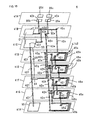
- the electromagnetically coupled module 1 includes a wireless IC chip 5 and a feed circuit board 4.
- the feed circuit board 4 not only provides an impedance match between the wireless IC chip 5 and a metal article acting as a radiator, but also acts as a resonant circuit.
- Fig. 15 is an exploded view illustrating an internal configuration of the feed circuit board 4.
- the feed circuit board 4 is a multilayer substrate formed by stacking a plurality of dielectric layers each having an electrode pattern.
- a dielectric layer 41A at the top has wireless-IC-chip mounting lands 35a to 35d.
- a dielectric layer 41B has a capacitor electrode 51 electrically connected to the wireless-IC-chip mounting land 35b.
- a dielectric layer 41C has a capacitor electrode 53.
- a capacitor C1 is formed between the capacitor electrode 51 and the capacitor electrode 53.
- Dielectric layers 41D to 41H each have inductor electrodes 45a and 45b.
- the inductor electrodes 45a and 45b on a plurality of different layers form inductors L1 and L2 that are double-spiral in overall shape and are strongly dielectrically coupled to each other.
- the dielectric layer 41F has a capacitor electrode 54 electrically connected to the inductor L1.
- the capacitor electrode 54 is interposed between the capacitor electrode 53 and a capacitor electrode 55, and forms the capacitor electrode 55. Electrodes of adjacent dielectric layers are electrically connected to each other through corresponding via holes 42a to 42i.
- Fig. 16 is an equivalent circuit diagram illustrating the feed circuit board 4 of Fig. 15 and the loop electrode.
- the capacitor C1 corresponds to a capacitance formed between the capacitor electrodes 51 and 53 illustrated in Fig. 15 ;
- the capacitor C2 corresponds to a capacitance formed between the capacitor electrodes 54 and 53 and the capacitor electrode 55 illustrated in Fig. 15 ;
- the inductors L1 and L2 correspond to the inductor electrodes 45a and 45b illustrated in Fig. 15 .
- the capacitor electrode 55 is parallel to and opposite an end of the loop electrode (i.e., the loop electrode 7 in the example of Fig. 3 ).
- the capacitor electrode 55 forms a capacitance between itself and this end of the loop electrode 7.
- the inductor electrodes L1 and L2 are electromagnetically coupled to the other end of the loop electrode 7.
- a resonance frequency is determined by a resonant circuit formed by the inductance elements L1 and L2 and their stray capacitance.
- the frequency of a signal emitted from a radiation electrode is substantially determined by the self-resonant frequency of the resonant circuit.
- the electromagnetically coupled module 1 formed by mounting the wireless IC chip 5 on the feed circuit board 4 receives, through the radiation electrode, high-frequency signals (e.g., in the UHF frequency band) emitted from a reader/writer (not shown), causes the resonant circuit in the feed circuit board 4 to resonate, and supplies received signals only in a predetermined frequency band to the wireless IC chip 5.
- the electromagnetically coupled module 1 extracts predetermined energy from the received signals, uses the extracted energy as a drive source to match information stored in the wireless IC chip 5 to a predetermined frequency in the resonant circuit, and transmits the information to the radiation electrode, from which the information is transmitted (transferred) to the reader/writer.
- providing a resonant circuit in the feed circuit board improves frequency selectivity and allows an operating frequency of the wireless IC device to be substantially determined by the self-resonant frequency. Accordingly, transmission and reception of energy of signals having a frequency used in the RFID system can be performed with a high degree of efficiency. At the same time, it is possible to set an optimum resonance frequency for the shape and size of the radiator, and thus to improve the radiation characteristics of the wireless IC device.
- Fig. 17 illustrates a configuration of an electromagnetically coupled module for a wireless IC device according to an eighth embodiment of the present invention.
- a loop electrode 30 is formed on an inner layer of a base 10.
- An insulating layer is disposed over two open ends 30a and 30b of the loop electrode 30, and an inductor electrode 20 and a capacitor electrode 25 are disposed over the insulating layer.
- the inductor electrode 20 has a spiral shape and its inner end is connected to the capacitor electrode 25 as described below.
- the wireless IC chip 5 is mounted on the ends of the inductor electrode 20 and capacitor electrode 25. Specifically, the wireless-IC-chip mounting land 35a is formed at the end of the inductor electrode 20, the wireless-IC-chip mounting land 35b is formed at the end of the capacitor electrode 25, and the wireless-IC-chip mounting lands 35c and 35d are formed additionally. Then, the wireless IC chip 5 is mounted on the wireless-IC-chip mounting lands 35a to 35d.
- Fig. 18 is a cross-sectional view taken along line II-II of Fig. 17 .
- a wire 21 connects the inductor electrode 20 and the capacitor electrode 25.
- the wireless IC chip 5 and the loop electrode 30 may be electrically connected through impedance matching units 8 and 8.
- the impedance matching units 8 and 8 may be separately produced using a ceramic multilayer substrate, a glass epoxy substrate, or the like and attached to the loop electrode 30 by a conductive adhesive. Thus, the impedance matching units 8 and 8 allow electrical connection between the wireless IC chip 5 and the loop electrode 30.
- Fig. 20 is an exploded perspective view illustrating a feed circuit board 40 in a wireless IC device according to a ninth embodiment of the present invention.
- Fig. 21 is an equivalent circuit diagram of Fig. 20 .
- the feed circuit board 40 is a multilayer substrate formed by stacking a plurality of dielectric layers each having an electrode pattern.
- the dielectric layer 41A at the top has the wireless-IC-chip mounting lands 35a to 35d.
- the dielectric layer 41B has the capacitor electrode 51 electrically connected to the wireless-IC-chip mounting land 35b.
- the dielectric layer 41C has the capacitor electrode 53.
- the capacitor C1 is formed between the capacitor electrode 51 and the capacitor electrode 53.
- the dielectric layers 41D to 41H each have the inductor electrodes 45a and 45b.
- the inductor electrodes 45a and 45b form the inductor L1 that is double-spiral in overall shape.
- the dielectric layer 41F has the capacitor electrode 54 electrically connected to the inductor L1.
- the capacitor electrode 54 is interposed between the capacitor electrodes 53 and 55 (56), and forms a capacitor.
- the dielectric layer 41H has the capacitor electrode 55 electrically connected to the capacitor electrode 53.
- Dielectric layers 41J to 41N each have inductor electrodes 46 and 47.
- the inductor electrodes 46 and 47 form the loop electrode L2 winding multiple times. Electrodes of adjacent dielectric layers are electrically connected to each other through corresponding via holes 42a to 42m.
- the feed circuit board 40 is obtained by adding a loop electrode to the feed circuit board 4 illustrated in Fig. 15 .
- the capacitor C1 corresponds to a capacitance formed between the capacitor electrodes 51 and 53 illustrated in Fig. 20 ; the capacitor C2 corresponds to a capacitance formed between the capacitor electrodes 54 and 53 and the capacitor electrode 55 illustrated in Fig. 20 ; inductors L1a and L1b correspond to the inductor electrodes 45a and 45b illustrated in Fig. 20 ; and the inductor L2 corresponds to the inductor electrodes 46 and 47 illustrated in Fig. 20 .
- Fig. 22 is an external perspective view of a notebook personal computer provided with a wireless IC device.
- Fig. 23 is a cross-sectional view illustrating a main part of a circuit board inside the notebook personal computer.
- Electronic components 17 and 18 and the wireless-IC-device main part 6 are mounted on a circuit board 15 inside the notebook personal computer in a direction substantially perpendicular to the circuit board 15.
- An electrode pattern 16 is formed on an upper surface of the circuit board 15. The electrode pattern 16 is coupled to the wireless-IC-device main part 6 and acts as a radiator.
- a wireless IC device may be formed on a metal panel on the back of a component (e.g., liquid crystal panel) inside the notebook personal computer illustrated in Fig. 22 . That is, the wireless IC device according to any of the first to tenth embodiments may be applied to cause the metal panel to act as a radiator.
- a component e.g., liquid crystal panel
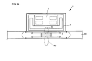
- Fig. 24 is a cross-sectional view illustrating a main part of a wireless IC device according to an eleventh embodiment of the present invention.
- the wireless-IC-device main part 6 is mounted on the surface (i.e., electromagnetic wave transmission/reception surface outside the metal article 60) for receiving signals from the reader/writer.
- the wireless-IC-device main part 6 is mounted on a surface opposite the surface for receiving signals from the reader/writer.
- the wireless-IC-device main part 6 has an insulating substrate, which is provided with the loop electrode 7 and the electromagnetically coupled module 1 coupled to the loop electrode 7.
- a signal (magnetic field Ho) from the reader/writer causes an eddy current J to flow across the conductor principal plane of the metal article 60.
- the eddy current J causes a magnetic field Hi to be generated in a direction perpendicular to the conductor principal plane of the metal article 60.
- the loop electrode 7 is coupled to the magnetic field Hi.
- the wireless-IC-device main part 6 functions as an RFID tag even for signals from the principal plane opposite the wireless-IC-device main part 6.
- An article on which the wireless-IC-device main part 6 is mounted is not limited to a metal article, but may be any article having a surface made of conductive material, such as carbon.
- the loop electrode 7 may either be in contact with or separated from the conductive surface of the article.
- Fig. 25(A) to Fig. 25(C) are cross-sectional views illustrating a main part of a wireless IC device according to a twelfth embodiment of the present invention.
- the wireless-IC-device main part 6 is mounted on the surface (i.e., outer surface) of the metal article 60.
- the wireless-IC-device main part 6 is mounted inside (i.e., on the inner surface) of the metal article 60.
- Fig. 25(A) illustrates metal cases (half cases) 81 and 82 having joining parts protruding inside the cases.
- Fig. 25(B) illustrates the metal cases (half cases) 81 and 82 having joining parts protruding outside the cases.
- Fig. 25(C) illustrates the metal cases (half cases) 81 and 82 having a hinge mechanism for maintaining conductivity at one end. In every case, corresponding joining parts are joined to each other with an electrical insulator (e.g., rubber packing) or an electrical resistor interposed therebetween.
- an electrical insulator e.g., rubber packing
- the wireless-IC-device main part 6 has an insulating substrate, which is provided with the loop electrode 7 and the electromagnetically coupled module 1 coupled to the loop electrode 7.
- a signal (magnetic field) from the reader/writer causes an eddy current to flow across the conductor principal plane of the metal cases 81 and 82.
- the eddy current causes a magnetic field to be generated in a direction perpendicular to the conductor principal plane of the metal cases 81 and 82.
- the magnetic field is coupled to the loop electrode 7. This allows the metal cases 81 and 82 to be used as metal articles having an internal RFID tag.
- the upper metal case 82 is galvanically isolated from the metal case 81 in which the wireless-IC-device main part 6 is provided. However, since a chain of electric field loops and magnetic field loops spreads along the conductor plane of the metal cases, the upper metal case 82 also acts as a radiator.
- the durability and environmental resistance of the wireless IC device are improved.
- the wireless-IC-device main part 6 illustrated in Fig. 25(A) to Fig. 25(C) is, for example, an RFID tag for a food product and the metal cases 81 and 82 correspond to a housing of a refrigerator or freezer.
- the wireless-IC-device main part 6 illustrated in Fig. 25(A) to Fig. 25(C) is, for example, an RFID tag for a food product and the metal cases 81 and 82 correspond to a housing of a refrigerator or freezer.
- the wireless-IC-device main part 6 illustrated in Fig. 25(A) to Fig. 25(C) is, for example, an RFID tag for an electronic component or circuit board and the metal cases 81 and 82 correspond to a housing of a personal computer or mobile phone terminal.
- the wireless-IC-device main part 6 illustrated in Fig. 25(A) to Fig. 25(C) is, for example, an RFID tag for an electronic component or circuit board and the metal cases 81 and 82 correspond to a housing of a personal computer or mobile phone terminal.
- Fig. 25(A) to Fig. 25(C) illustrate can-shaped metal cases as examples, the same also applies to tubular or cup-shaped conductive cases.
- the wireless-IC-device main part 6 inside a carbon shaft of a golf club, the golf club can be used as a golf club having an internal RFID tag that is externally readable and writable.
- Fig. 26 is a cross-sectional view illustrating a main part of a wireless IC device according to a thirteenth embodiment of the present invention.
- metal cases 83 and 84 that are surface-coated with electrical insulating material or electrical resistive material are used.
- the other configuration is the same as that illustrated in Fig. 25(A) to Fig. 25(C) .
- an interface between the upper and lower cases may be insulated or substantially insulated by the coating over the case surface.
- Fig. 27 is a cross-sectional view illustrating a main part of a wireless IC device according to a fourteenth embodiment of the present invention.
- protrusions 94 at joining parts between a lower metal case 85 and an upper metal case 86 create a clearance 95.
- the other configuration is the same as that illustrated in Fig. 25(A) to Fig. 25(C) .
- the metal article can be used as an article having an internal RFID tag, through action similar to that described above.
- Fig. 28 is a cross-sectional view illustrating a main part of a wireless IC device according to a fifteenth embodiment of the present invention.
- the wireless-IC-device main part 6 is mounted inside a metal tray 87 to form a metal tray having an RFID tag.
- the metal tray 87 is surface-coated with electrical insulating material or electrical resistive material.
- a plurality of metal trays are stacked on top of each other.
- the metal trays are galvanically isolated from each other by the coating of the electrical insulating material or electrical resistive material, and each wireless-IC-device main part 6 is surrounded by metal material.
- the reader/writer can communicate with an RFID tag in each metal tray.
- Fig. 29 is a cross-sectional view illustrating a main part of a wireless IC device according to a sixteenth embodiment of the present invention.
- the wireless-IC-device main part 6 is mounted inside a metal tray 88 to form a metal tray having an RFID tag.
- the metal tray 88 has a rim 96 of electrical insulating material or electrical resistive material at its edge.
- a plurality of metal trays are stacked on top of each other.
- the metal trays are galvanically isolated from each other by the electrical insulating material or electrical resistive material, and each wireless-IC-device main part 6 is surrounded by metal material.
- the reader/writer can individually communicate with an RFID tag in each metal tray.
- the wireless-IC-device main part 6 provided inside a case or housing tightly surrounded by conductive material can still be used as an RFID tag while the antenna gain may be slightly reduced.
- a loop electrode of rectangular shape is used in the embodiments described above.
- the loop electrode may be of any shape, such as circular, elliptical, or polygonal shape, depending on the article in which the electrode is contained. Additionally, the loop electrode may extend from the bottom to the side of a case. Even when the shape of the signal transmission/reception surface is thus modified, the wireless-IC-device main part 6 still functions as an RFID tag.
- a loop electrode is formed of a single-layer conductive pattern.
- the loop electrode may have a multilayer coil structure, instead of a single-layer loop structure.
- a loop electrode forms an open loop in the embodiments described above.
- the loop electrode may form a closed loop, as long as the loop electrode is configured to be magnetically coupled to an inductor in a feed circuit board. That is, an inductor pattern parallel to the loop plane of the loop electrode may be formed on the feed circuit board such that the inductor pattern is magnetically coupled to the loop electrode forming a closed loop.
- a wireless-IC-device main part having a loop electrode is in contact with a predetermined surface of a case.
- the wireless-IC-device main part may be spaced from the predetermined surface, or may be hung from the inner surface of the case (i.e., suspended in the air inside the case).
- a wireless-IC-device main part having a loop electrode is mounted on a principal surface of a case, the principal surface having a large area.
- the wireless-IC-device main part may be mounted on a side of the case.
Landscapes
- Engineering & Computer Science (AREA)
- Computer Hardware Design (AREA)
- Microelectronics & Electronic Packaging (AREA)
- Physics & Mathematics (AREA)
- General Physics & Mathematics (AREA)
- Theoretical Computer Science (AREA)
- Computer Networks & Wireless Communication (AREA)
- Signal Processing (AREA)
- Near-Field Transmission Systems (AREA)
- Details Of Aerials (AREA)
Abstract
Description
- The present invention relates to a wireless IC device for a radio frequency identification (RFID) system which allows noncontact data communication via electromagnetic waves.
- In recent years, RFID systems have been used as article management systems. For information transmission, an RFID system allows noncontact communication between a reader/writer that generates an induction field and a wireless IC device that is attached to an article and stores predetermined information.
-
Fig. 1 is an external perspective view illustrating an example of a metal article to which an IC tag label described inPatent Document 1 is attached. - An
IC tag label 102 has a rectangular thin film-like shape. TheIC tag 102 has anIC chip 102a at the center thereof and a thin-film antenna 102b in an outer region thereof. To accommodate theIC tag 102 in a floating state in arecessed portion 105a formed in ahead 101a of ametal article 101, theIC tag 102 is secured to the undersurface of anonmetal plate 103. Thenonmetal plate 103 is fit into therecessed portion 105a and secured. Thehead 101a has anotch 106. - With the configuration described above, a magnetic field generated by the
antenna 102b in theIC tag 102 can be formed into a loop that passes through thenotch 106, the exterior of themetal article 101, and thenonmetal plate 103 and returns to theantenna 102b. - A metal article with an IC tag is thus produced.
- Patent Document 1: Japanese Unexamined Patent Application Publication No.
2003-6599 - However, the IC tag and the metal article provided with the IC tag described in
Patent Document 1 have the following problems. -
- (1) Forming a complex structure, including the recessed portion and the notch, involves a long process and use of additional components. This leads to an increase in cost of manufacturing the metal article.
-
- (2) Producing the nonmetal plate for covering the recessed portion involves preparation of material different from that of the metal article, a long process, and use of additional material. This leads to an increase in cost of manufacturing a metal structure. Additionally, application distortion occurs at a portion where the nonmetal plate is secured to the metal article, due to a difference in thermal expansion coefficient. This may cause cracks or fractures.
-
- (3) Forming an antenna pattern is necessary to allow the IC tag to operate.
- Accordingly, an object of the present invention is to solve the problems described above, reduce cost of manufacturing a metal article, and provide a wireless IC device using the metal article as a radiator. Means for Solving the Problems
- To solve the problems described above, a wireless IC device according to the present invention is configured as follows.
- (1) A wireless IC device includes a high-frequency device being an electromagnetically coupled module or a wireless IC chip, the electromagnetically coupled module including the wireless IC chip and a feed circuit board coupled to an external circuit and electrically connected to or electromagnetically coupled to the wireless IC chip; a radiation electrode acting as a radiator; and a loop electrode coupled to the high-frequency device and the radiation electrode, and having a loop plane perpendicular or inclined to a plane of the radiation electrode.
-
- (2) The loop electrode may be electromagnetically coupled to the radiation electrode with an insulating layer interposed therebetween.
-
- (3) The loop electrode may be electrically directly connected to the radiation electrode, and a part of the radiation electrode may serve also as the loop electrode.
-
- (4) The wireless IC device may further include a matching circuit between a mounting area of the high-frequency device and the loop electrode, the matching circuit being configured to directly electrically connect the high-frequency device to the loop electrode.
-
- (5) The wireless IC device may further include a resonant circuit and/or a matching circuit in the feed circuit board.
-
- (6) A resonance frequency of the resonant circuit may be substantially equal to a frequency of a signal transmitted and received by the radiation electrode.
-
- (7) The high-frequency device or the loop electrode may be covered with plastic.
-
- (8) The high-frequency device and the loop electrode may be molded of plastic on the radiation electrode.
-
- (9) The radiation electrode may be a cylindrical metal article having a conductive layer.
-
- (10) The radiation electrode may be an electrode pattern formed on a circuit board inside electronic equipment.
-
- (11) The radiation electrode may be a metal plate provided in a component inside electronic equipment.
-
- (12) The loop electrode may be disposed on a surface opposite an electromagnetic wave transmission/reception surface outside the radiation electrode.
-
- (13) The loop electrode may be covered with the radiation electrode or a conductive surface including the radiation electrode.
-
- (1) Processing steps and components involved in forming, in a metal article, a notch, a recessed portion, a plate, etc., such as those illustrated in
Fig. 1 , are not necessary. Thus, there is substantially no cost increase associated with addition of the wireless IC device to the article. - Since all or part of the metal article can be used as a radiator, it is possible to improve radiation characteristics.
- Use of the electromagnetically coupled module allows design of impedance matching between the wireless IC chip and the radiation electrode within the feed circuit board. This increases the degree of design freedom.
- The amount of coupling between the radiation electrode and the loop electrode according to the present invention is largest when the loop electrode is perpendicular to the radiation electrode. However, even if the loop plane of the loop electrode is inclined to the plane of the radiation electrode, the radiation electrode and the loop electrode are coupled to each other while the amount of coupling therebetween is smaller. Thus, it is possible to provide a high degree of flexibility in arranging the loop electrode relative to the radiation electrode.
-
- (2) When the loop electrode is coupled to the high-frequency device and electromagnetically coupled to the radiation electrode with an insulating layer interposed therebetween, matching between the high-frequency device and the loop electrode is easily achieved. Additionally, since the loop electrode and the radiation electrode are galvanically isolated from each other, high resistance to static electricity is achieved.
-
- (3) When the loop electrode is coupled to the high-frequency device and electrically directly connected to the radiation electrode, and a part of the radiation electrode serves also as the loop electrode, matching between the high-frequency device and the loop electrode is easily achieved. Additionally, since the loop electrode is strongly coupled to the radiation electrode, it is possible to provide high gain.
-
- (4) When a matching circuit is provided between a mounting area for mounting the high-frequency device and the loop electrode, the matching circuit can be used as an inductor for impedance matching between the radiation electrode and the high-frequency device. Thus, flexible and easy design of impedance matching in the wireless IC device is achieved.
-
- (5) Providing a resonant circuit in the feed circuit board improves frequency selectivity and allows an operating frequency of the wireless IC device to be substantially determined by the self-resonant frequency. Accordingly, transmission and reception of energy of signals having a frequency used in the RFID system can be performed with a high degree of efficiency. Thus, radiation characteristics of the wireless IC device can be improved.
- Also, by providing a matching circuit in the feed circuit board, transmission and reception of energy of signals having a frequency used in the RFID system can be performed with a high degree of efficiency.
-
- (6) When a resonance frequency of the resonant circuit is made substantially equal to a frequency of a signal transmitted and received by the radiation electrode, transmission and reception of energy of signals having a frequency used in the RFID system can be performed with a high degree of efficiency. It is only necessary that the radiation electrode be simply coupled to the feed circuit board and have a size appropriate for necessary gain. The shape and material of the radiation electrode are not limited by the frequency used, and the radiation electrode can be used for any types of articles.
-
- (7) When the high-frequency device or the loop electrode is covered with plastic, the electromagnetically coupled module can be directly attached to a metal article. Thus, the degree of design freedom can be increased.
-
- (8) When the high-frequency device and the loop electrode are molded of plastic on the radiation electrode, the processing steps of covering the electromagnetically coupled module and bonding the electromagnetically coupled module to a metal article can be performed simultaneously. This makes it possible to reduce the number of processing steps and manufacturing cost.
-
- (9) When a metal article formed into a cylindrical shape and having a conductive layer is used as the radiation electrode, the metal article can be used as it is and substantially the entire metal article acts as a radiator. Therefore, even if a plurality of articles are stacked on top of each other, an ID for each article can be read.
-
- (10) When an electrode pattern formed on a circuit board inside electronic equipment is used as the radiation electrode, the circuit board inside the electronic equipment can be used as it is, and mounting of the high-frequency device becomes easy.
-
- (11) When a metal plate provided in a component, such as a liquid crystal display panel, inside electronic equipment is used as the radiation electrode, the component inside the electronic equipment can be used as it is. Thus, it is possible to prevent an increase in size and cost.
-
- (12) When the loop electrode is disposed on the surface opposite the electromagnetic wave transmission/reception surface outside the radiation electrode, that is, on the side opposite the surface on which the high-frequency device is provided, the wireless IC device can be disposed inside an article. Thus, the wireless IC device is protected by the radiation electrode and increases its durability.
-
- (13) When the loop electrode is covered with the radiation electrode or a conductive surface including the radiation electrode, the durability and environmental resistance of the wireless IC device are improved. Brief Description of Drawings
-
- [
Fig. 1] Fig. 1 illustrates a configuration of a wireless IC device described inPatent Document 1. - [
Fig. 2] Fig. 2 illustrates a configuration of a wireless IC device according to a first embodiment of the present invention and an article provided with the wireless IC device. - [
Fig. 3] Fig. 3 is an enlarged view of a main part of the wireless IC device illustrated inFig. 2 . - [
Fig. 4] Fig. 4 is a schematic view illustrating a distribution of electromagnetic fields near the wireless IC device on the surface of the metal article illustrated inFig. 2 . - [
Fig. 5] Fig. 5(A) and Fig. 5(B) each illustrate a configuration of a wireless IC device according to a second embodiment of the present invention. - [
Fig. 6] Fig. 6 illustrates a configuration of a wireless IC device according to a third embodiment of the present invention and an article provided with the wireless IC device. - [
Fig. 7] Fig. 7 is an enlarged view of a main part of the wireless IC device for the article illustrated inFig. 6 . - [
Fig. 8] Fig. 8 illustrates a configuration of a wireless IC device according to a fourth embodiment of the present invention and an article provided with the wireless IC device. - [
Fig. 9] Fig. 9 is an enlarged view of a main part of the wireless IC device illustrated inFig. 8 . - [
Fig. 10] Fig. 10 illustrates a configuration of a wireless IC device according to a fifth embodiment of the present invention and an article provided with the wireless IC device. - [
Fig. 11] Fig. 11 is an enlarged view of a main part of the wireless IC device illustrated inFig. 10 . - [
Fig. 12] Fig. 12 illustrates a configuration of a wireless IC device according to a sixth embodiment of the present invention and an article provided with the wireless IC device. - [
Fig. 13] Fig. 13 is an enlarged view of a main part of the wireless IC device for the article illustrated inFig. 12 . - [
Fig. 14] Fig. 14 is an external perspective view of an electromagnetically coupled module in a wireless IC device. - [
Fig. 15] Fig. 15 is an exploded view illustrating an internal configuration of a feed circuit board. - [
Fig. 16] Fig. 16 is an equivalent circuit diagram of the feed circuit board. - [
Fig. 17] Fig. 17 illustrates a configuration of an electromagnetically coupled module in a wireless IC device according to a seventh embodiment of the present invention. - [
Fig. 18] Fig. 18 is a cross-sectional view illustrating a main part of the electromagnetically coupled module illustrated inFig. 17 . - [
Fig. 19] Fig. 19 illustrates a configuration of an electromagnetically coupled module in a wireless IC device according to an eighth embodiment of the present invention. - [
Fig. 20] Fig. 20 is an exploded perspective view illustrating a feed circuit board in a wireless IC device according to a ninth embodiment of the present invention. - [
Fig. 21] Fig. 21 is an equivalent circuit diagram of a main part of the wireless IC device illustrated inFig. 20 . - [
Fig. 22] Fig. 22 illustrates a configuration of a wireless IC device according to a tenth embodiment of the present invention and an article provided with the wireless IC device. - [
Fig. 23] Fig. 23 is a cross-sectional view illustrating a main part of a circuit board in a notebook personal computer provided with the wireless IC device illustrated inFig. 22 . - [
Fig. 24] Fig. 24 is a cross-sectional view illustrating a main part of a wireless IC device according to an eleventh embodiment of the present invention. - [
Fig. 25] Fig. 25(A) to Fig. 25(C) are cross-sectional views each illustrating a main part of a wireless IC device according to a twelfth embodiment of the present invention. - [
Fig. 26] Fig. 26 is a cross-sectional view illustrating a main part of a wireless IC device according to a thirteenth embodiment of the present invention. - [
Fig. 27] Fig. 27 is a cross-sectional view illustrating a main part of a wireless IC device according to a fourteenth embodiment of the present invention. - [
Fig. 28] Fig. 28 is a cross-sectional view illustrating a main part of a wireless IC device according to a fifteenth embodiment of the present invention. - [
Fig. 29] Fig. 29 is a cross-sectional view illustrating a main part of a wireless IC device according to a sixteenth embodiment of the present invention. Reference Numerals -
- 1: electromagnetically coupled module
- 4: feed circuit board
- 5: IC chip
- 6: wireless-IC-device main part
- 7: loop electrode
- 8: impedance matching unit
- 9, 9a, 9b: metal ribbon
- 10: base
- 11: matching circuit
- 15: circuit board
- 16: electrode pattern
- 17, 18: electronic component
- 20: inductor electrode
- 21: molded plastic
- 25: capacitor electrode
- 30: loop electrode
- 35a to 35d: wireless-IC-chip mounting land
- 40: feed circuit board
- 41A to 41H: dielectric layer
- 42a: via hole
- 45a, 45b: inductor electrode
- 46, 47: inductor electrode
- 51: capacitor electrode
- 53 to 57: capacitor electrode
- 60 to 64, 70: metal article 65: insulating
sheet main part loop electrode segment 81 to 86:metal case 87, 88:metal tray 91, 92: packing - 93: hinge
- 94: protrusion
- 95: clearance
- 96: rim
- C1, C2: capacitor
- L1, L1a, L1b, L2: inductor
- E: electric field
- H: magnetic field
-
Fig. 2 is an external perspective view illustrating a wireless IC device according to a first embodiment of the present invention and a metal article provided with the wireless IC device. Ametal article 60 is an article at least whose surface or near-surface layer is made of metal. - A wireless-IC-device
main part 6 is provided on a predetermined surface of themetal article 60. The component indicated byreference numeral 6 is not referred to as wireless IC device. This is because the wireless IC device is constituted not only by the component indicated byreference numeral 6, but also by a part of the metal surface of themetal article 60. -
Fig. 3 is an enlarged view of the wireless-IC-device main part. The wireless-IC-devicemain part 6 has an insulating substrate, which is provided with aloop electrode 7 and an electromagnetically coupledmodule 1 coupled to theloop electrode 7. The wireless-IC-devicemain part 6 is placed such that a loop plane of theloop electrode 7 is substantially perpendicular to themetal article 60. - The wireless-IC-device
main part 6 having theloop electrode 7 is bonded to themetal article 60 with an insulating adhesive or the like. -
Fig. 4 schematically illustrates an example of a distribution of electromagnetic fields generated on themetal article 60 when theloop electrode 7 acts as an auxiliary radiator for transmission. In the drawing, dashed lines indicate loops of magnetic fields H, while solid lines indicate loops of electric fields E. Theloop electrode 7 acts as an auxiliary radiator for magnetic fields, causes the magnetic fields H to be generated parallel to the surface of themetal article 60, and induces the electric fields E in a direction substantially perpendicular to the surface of themetal article 60. Then, electric field loops induce magnetic field loops and thus, this chain of induction events expands the distribution of electromagnetic fields. - In the example described above, the
loop electrode 7 acts as an auxiliary radiator for transmission. A high gain is also obtained when theloop electrode 7 acts as an auxiliary radiator for reception. - The electromagnetically coupled
module 1 illustrated inFig. 3 includes a wireless IC chip and a feed circuit board that are described below. The wireless IC chip and the feed circuit board may either be electrically connected to each other or electromagnetically coupled to each other. For electromagnetic coupling, a capacitance is formed of a dielectric thin film or the like between electrodes of the wireless IC chip and the feed circuit board. By allowing the wireless IC chip and the feed circuit board to be coupled through the capacitance, it is possible to protect the wireless IC chip from static damage. - When the feed circuit board is used, the electrode of the feed circuit board is electromagnetically coupled to both ends of the
loop electrode 7. Alternatively, the electromagnetically coupledmodule 1 may be replaced with a single wireless IC chip. In both cases, since theloop electrode 7 is galvanically isolated from themetal article 60, the wireless IC device is highly resistant to static electricity. - The
loop electrode 7 may be of any shape which allows coupling between input and output terminals of the electromagnetically coupledmodule 1. - Electric fields on a surface of a metal article are perpendicular to the surface of the metal article. Therefore, if the loop plane of the
loop electrode 7 is inclined from the position perpendicular to the surface of themetal article 60, the strength of electric fields induced by magnetic fields of theloop electrode 7 is reduced, and thus the antenna gain is reduced. The gain increases as the loop plane of theloop electrode 7 approaches the position perpendicular to themetal article 60. However, even if the loop plane of theloop electrode 7 is inclined relative to the surface of themetal article 60, themetal article 60 still acts as a radiator. Therefore, the loop plane of theloop electrode 7 may be inclined as necessary. - To allow the
loop electrode 7 to be positioned substantially perpendicularly to themetal article 60, a recessed portion for accommodating an end of the feed circuit board may be formed on the surface of themetal article 60. In this case, the recessed portion may be internally provided with an insulating material, such as an insulating adhesive. - In the first embodiment, the
loop electrode 7 is directly bonded to the surface of themetal article 60. Alternatively, for example, theloop electrode 7 may be bonded onto a metal foil sheet or metal plate, which may then be bonded to themetal article 60. -
Fig. 5(A) and Fig. 5(B) illustrate configurations of two wireless IC devices according to a second embodiment of the present invention. In the second embodiment, a matching circuit is placed between a mounting area of a high-frequency device and a loop electrode. The matching circuit allows the high-frequency device and the loop electrode to be directly electrically connected to each other. - Referring to
Fig. 5(A) , ametal article 70 is an article at least whose surface or near-surface layer is made of metal. Aloop electrode 73 is positioned such that the loop plane thereof is substantially perpendicular to themetal article 70. This allows themetal article 70 to act as a radiator. - A wireless-IC-device
main part 69 is internally provided with amatching circuit 11 including a meander electrode, andmetal ribbons 9a and 9b serving as a mounting area for mounting a high-frequency device (electromagnetically coupled module or wireless IC chip). - By thus providing the
matching circuit 11, the wireless IC chip can be directly mounted on themetal ribbons 9a and 9b. If the wireless IC chip is directly mounted on the loop electrode, the operating frequency of the wireless IC device is substantially determined by the loop electrode including thematching circuit 11. -
Fig. 5(B) illustrates a state in which the electromagnetically coupledmodule 1 is mounted on themetal ribbons 9a and 9b in the wireless-IC-devicemain part 69 illustrated inFig. 5(A) . The configuration of the matchingcircuit 11,metal ribbons 9a and 9b serving as a mounting area of the electromagnetically coupled module, andloop electrode 73 is the same as that illustrated inFig. 5(A) . - With this configuration, the
loop electrode 73 acts as an auxiliary radiator for magnetic fields and is coupled to themetal article 70. Thus, through action similar to that illustrated inFig. 4 , themetal article 70 acts as a radiator. - The
metal article 70 illustrated inFig. 5(A) and Fig. 5(B) may be, for example, a solid electrode formed on a circuit board inside a mobile phone terminal. -
Fig. 6 is an external perspective view illustrating a wireless IC device according to a third embodiment of the present invention and a metal article provided with the wireless IC device. Ametal article 61 is an article at least whose surface or near-surface layer is made of metal. - In the example illustrated in
Fig. 3 , the entire loop electrode is provided on the substrate of the wireless-IC-devicemain part 6. In the example illustrated inFig. 6 ,loop electrode segments 71 that constitute part of the loop electrode are provided on a substrate of a wireless-IC-devicemain part 66. Then, a part of themetal article 61 serves also as a part of the loop electrode. -
Fig. 7 is an enlarged view of the wireless-IC-devicemain part 66 illustrated inFig. 6 . The wireless-IC-devicemain part 66 has the substrate provided with theloop electrode segments module 1 coupled to theloop electrode segments module 1 is the same as that illustrated inFig. 3 . Theloop electrode segments metal article 61 serves also as a part of the loop electrode. In other words, theloop electrode segments metal article 61 constitute the loop electrode, as indicated by L in the drawing. - With this configuration, the loop electrode constituted by the
loop electrode segments metal article 61 acts as an auxiliary radiator for magnetic fields and is coupled to themetal article 61. Thus, through action similar to that illustrated inFig. 4 , the surface of themetal article 61 acts as a radiator. -
Fig. 8 is an external view of a metal article provided with a wireless IC device according to a fourth embodiment of the present invention. Ametal article 62 is, for example, a cylindrical metal can. Unlike the polyhedral metal articles illustrated as examples inFig. 2 andFig. 6 , themetal article 62 illustrated as an example inFig. 8 has a cylindrical shape. A wireless-IC-devicemain part 67 is attached to the periphery of themetal article 62. -
Fig. 9 is an enlarged view of a mounting area of the wireless-IC-devicemain part 67 illustrated inFig. 8 . The wireless-IC-devicemain part 67 includesloop electrode segments module 1 coupled to theloop electrode segments loop electrode segments Fig. 7 , theloop electrode segments Fig. 9 are made of metal plates. The configuration of the electromagnetically coupledmodule 1 is the same as that illustrated inFig. 3 andFig. 7 . - With this configuration, the loop electrode constituted by the
loop electrode segments metal article 62 acts as an auxiliary radiator for magnetic fields and is coupled to themetal article 62. Thus, through action similar to that illustrated inFig. 4 , the surface of themetal article 62 acts as a radiator. - When many articles are stacked, the above-described chain of induction events that occurs between electric and magnetic fields also occur among the articles, as long as a conductive part of each of the article acts as a radiator. Therefore, even if (or rather, particularly if) many articles are stacked, the wireless IC device acts as a high-gain wireless IC device. For example, in a state where an antenna of a reader/writer is placed close to a stack of soft drink cans to which the present invention is applied, IDs for all the soft drink cans in the stack can be read.
- Even in the case of a paper container, if it includes a conductive layer of aluminum or the like, the conductive layer acts as a radiator.
-
Fig. 10 is an external view of a metal article provided with a wireless IC device according to a fifth embodiment of the present invention. Ametal article 63 is, for example, a cylindrical metal can. In the example illustrated inFig. 8 , the electromagnetically coupledmodule 1 is positioned on the periphery of themetal article 62. In the example illustrated inFig. 10 ,metal ribbons metal article 63, and the electromagnetically coupledmodule 1 is positioned on themetal ribbons module 1 and themetal ribbons module 1 and themetal ribbons -
Fig. 11 is an enlarged view of a mounting area of the electromagnetically coupledmodule 1 illustrated inFig. 10 . As indicated by L in the drawing, a part of themetal article 63 and themetal ribbons metal article 63 act as a loop electrode. - With this configuration, the
metal ribbons metal article 63 act as an auxiliary radiator for magnetic fields and are coupled to themetal article 63. Thus, through action similar to that illustrated inFig. 4 , themetal article 63 acts as a radiator. -
Fig. 12 is an external view of a metal article provided with a wireless IC device according to a sixth embodiment of the present invention. Ametal article 64 is provided with a wireless-IC-devicemain part 68 on its surface. -
Fig. 13 is an enlarged view of the wireless-IC-devicemain part 68. The overall shape of the wireless-IC-devicemain part 68 is a so-called "tack index label" shape. An insulatingsheet 65 internally has adhesive layers, between which theloop electrode 7 and the electromagnetically coupledmodule 1 are interposed. The configuration of theloop electrode 7 and electromagnetically coupledmodule 1 is the same as that illustrated inFig. 3 . - In a manner as if a tack index label is affixed, the wireless-IC-device
main part 68 is mounted on themetal article 64 such that theloop electrode 7 is perpendicular to the surface of themetal article 64 illustrated inFig. 12 . - With the configuration described above, the
loop electrode 7 acts as an auxiliary radiator for magnetic fields and is coupled to themetal article 64. Thus, through action similar to that illustrated inFig. 4 , the surface of themetal article 64 acts as a radiator. - Here, a loop along the metal article acts as the
loop electrode 7. Alternatively, as described in the foregoing embodiments, themetal article 64 may be configured to act both as a part of the loop electrode and a radiator. -
Fig. 14 is an external perspective view of the electromagnetically coupledmodule 1 for a wireless IC device according to a seventh embodiment of the present invention. The electromagnetically coupledmodule 1 is applicable to the wireless IC device of any of the other embodiments. The electromagnetically coupledmodule 1 includes awireless IC chip 5 and afeed circuit board 4. Thefeed circuit board 4 not only provides an impedance match between thewireless IC chip 5 and a metal article acting as a radiator, but also acts as a resonant circuit. -
Fig. 15 is an exploded view illustrating an internal configuration of thefeed circuit board 4. Thefeed circuit board 4 is a multilayer substrate formed by stacking a plurality of dielectric layers each having an electrode pattern. Adielectric layer 41A at the top has wireless-IC-chip mounting lands 35a to 35d. Adielectric layer 41B has acapacitor electrode 51 electrically connected to the wireless-IC-chip mounting land 35b. Adielectric layer 41C has acapacitor electrode 53. A capacitor C1 is formed between thecapacitor electrode 51 and thecapacitor electrode 53.Dielectric layers 41D to 41H each haveinductor electrodes 45a and 45b. Theinductor electrodes 45a and 45b on a plurality of different layers form inductors L1 and L2 that are double-spiral in overall shape and are strongly dielectrically coupled to each other. Thedielectric layer 41F has acapacitor electrode 54 electrically connected to the inductor L1. Thecapacitor electrode 54 is interposed between thecapacitor electrode 53 and acapacitor electrode 55, and forms thecapacitor electrode 55. Electrodes of adjacent dielectric layers are electrically connected to each other through corresponding viaholes 42a to 42i. -
Fig. 16 is an equivalent circuit diagram illustrating thefeed circuit board 4 ofFig. 15 and the loop electrode. Referring toFig. 16 , the capacitor C1 corresponds to a capacitance formed between thecapacitor electrodes Fig. 15 ; the capacitor C2 corresponds to a capacitance formed between thecapacitor electrodes capacitor electrode 55 illustrated inFig. 15 ; and the inductors L1 and L2 correspond to theinductor electrodes 45a and 45b illustrated inFig. 15 . - The
capacitor electrode 55 is parallel to and opposite an end of the loop electrode (i.e., theloop electrode 7 in the example ofFig. 3 ). Thecapacitor electrode 55 forms a capacitance between itself and this end of theloop electrode 7. The inductor electrodes L1 and L2 are electromagnetically coupled to the other end of theloop electrode 7. - In the
feed circuit board 4, a resonance frequency is determined by a resonant circuit formed by the inductance elements L1 and L2 and their stray capacitance. The frequency of a signal emitted from a radiation electrode is substantially determined by the self-resonant frequency of the resonant circuit. - The electromagnetically coupled
module 1 formed by mounting thewireless IC chip 5 on thefeed circuit board 4 receives, through the radiation electrode, high-frequency signals (e.g., in the UHF frequency band) emitted from a reader/writer (not shown), causes the resonant circuit in thefeed circuit board 4 to resonate, and supplies received signals only in a predetermined frequency band to thewireless IC chip 5. At the same time, the electromagnetically coupledmodule 1 extracts predetermined energy from the received signals, uses the extracted energy as a drive source to match information stored in thewireless IC chip 5 to a predetermined frequency in the resonant circuit, and transmits the information to the radiation electrode, from which the information is transmitted (transferred) to the reader/writer. - Thus, providing a resonant circuit in the feed circuit board improves frequency selectivity and allows an operating frequency of the wireless IC device to be substantially determined by the self-resonant frequency. Accordingly, transmission and reception of energy of signals having a frequency used in the RFID system can be performed with a high degree of efficiency. At the same time, it is possible to set an optimum resonance frequency for the shape and size of the radiator, and thus to improve the radiation characteristics of the wireless IC device.
-
Fig. 17 illustrates a configuration of an electromagnetically coupled module for a wireless IC device according to an eighth embodiment of the present invention. Referring toFig. 17 , aloop electrode 30 is formed on an inner layer of abase 10. An insulating layer is disposed over twoopen ends loop electrode 30, and aninductor electrode 20 and acapacitor electrode 25 are disposed over the insulating layer. Theinductor electrode 20 has a spiral shape and its inner end is connected to thecapacitor electrode 25 as described below. - As illustrated in an enlarged view in
Fig. 17 , thewireless IC chip 5 is mounted on the ends of theinductor electrode 20 andcapacitor electrode 25. Specifically, the wireless-IC-chip mounting land 35a is formed at the end of theinductor electrode 20, the wireless-IC-chip mounting land 35b is formed at the end of thecapacitor electrode 25, and the wireless-IC-chip mounting lands 35c and 35d are formed additionally. Then, thewireless IC chip 5 is mounted on the wireless-IC-chip mounting lands 35a to 35d. -
Fig. 18 is a cross-sectional view taken along line II-II ofFig. 17 . Referring toFig. 18 , awire 21 connects theinductor electrode 20 and thecapacitor electrode 25. - As illustrated in
Fig. 19 , as a modification of the eighth embodiment, thewireless IC chip 5 and theloop electrode 30 may be electrically connected throughimpedance matching units - The
impedance matching units loop electrode 30 by a conductive adhesive. Thus, theimpedance matching units wireless IC chip 5 and theloop electrode 30. -
Fig. 20 is an exploded perspective view illustrating afeed circuit board 40 in a wireless IC device according to a ninth embodiment of the present invention.Fig. 21 is an equivalent circuit diagram ofFig. 20 . - The
feed circuit board 40 is a multilayer substrate formed by stacking a plurality of dielectric layers each having an electrode pattern. Thedielectric layer 41A at the top has the wireless-IC-chip mounting lands 35a to 35d. Thedielectric layer 41B has thecapacitor electrode 51 electrically connected to the wireless-IC-chip mounting land 35b. Thedielectric layer 41C has thecapacitor electrode 53. The capacitor C1 is formed between thecapacitor electrode 51 and thecapacitor electrode 53. Thedielectric layers 41D to 41H each have theinductor electrodes 45a and 45b. Theinductor electrodes 45a and 45b form the inductor L1 that is double-spiral in overall shape. - The
dielectric layer 41F has thecapacitor electrode 54 electrically connected to the inductor L1. Thecapacitor electrode 54 is interposed between thecapacitor electrodes 53 and 55 (56), and forms a capacitor. Thedielectric layer 41H has thecapacitor electrode 55 electrically connected to thecapacitor electrode 53. -
Dielectric layers 41J to 41N each haveinductor electrodes inductor electrodes holes 42a to 42m. - That is, the
feed circuit board 40 is obtained by adding a loop electrode to thefeed circuit board 4 illustrated inFig. 15 . - Referring to
Fig. 21 , the capacitor C1 corresponds to a capacitance formed between thecapacitor electrodes Fig. 20 ; the capacitor C2 corresponds to a capacitance formed between thecapacitor electrodes capacitor electrode 55 illustrated inFig. 20 ; inductors L1a and L1b correspond to theinductor electrodes 45a and 45b illustrated inFig. 20 ; and the inductor L2 corresponds to theinductor electrodes Fig. 20 . -
Fig. 22 is an external perspective view of a notebook personal computer provided with a wireless IC device.Fig. 23 is a cross-sectional view illustrating a main part of a circuit board inside the notebook personal computer.Electronic components main part 6 are mounted on acircuit board 15 inside the notebook personal computer in a direction substantially perpendicular to thecircuit board 15. Anelectrode pattern 16 is formed on an upper surface of thecircuit board 15. Theelectrode pattern 16 is coupled to the wireless-IC-devicemain part 6 and acts as a radiator. - As another example, a wireless IC device may be formed on a metal panel on the back of a component (e.g., liquid crystal panel) inside the notebook personal computer illustrated in
Fig. 22 . That is, the wireless IC device according to any of the first to tenth embodiments may be applied to cause the metal panel to act as a radiator. - The same is applicable to any metal articles (e.g., a safe and a container) in addition to those described in the foregoing embodiments.
-
Fig. 24 is a cross-sectional view illustrating a main part of a wireless IC device according to an eleventh embodiment of the present invention.
In the example described in the first embodiment with reference toFig. 2 , the wireless-IC-devicemain part 6 is mounted on the surface (i.e., electromagnetic wave transmission/reception surface outside the metal article 60) for receiving signals from the reader/writer. In the eleventh embodiment, the wireless-IC-devicemain part 6 is mounted on a surface opposite the surface for receiving signals from the reader/writer. - As in the case of the first embodiment, the wireless-IC-device
main part 6 has an insulating substrate, which is provided with theloop electrode 7 and the electromagnetically coupledmodule 1 coupled to theloop electrode 7. - With this configuration, a signal (magnetic field Ho) from the reader/writer causes an eddy current J to flow across the conductor principal plane of the
metal article 60. The eddy current J causes a magnetic field Hi to be generated in a direction perpendicular to the conductor principal plane of themetal article 60. Then, theloop electrode 7 is coupled to the magnetic field Hi. Thus, the wireless-IC-devicemain part 6 functions as an RFID tag even for signals from the principal plane opposite the wireless-IC-devicemain part 6. - An article on which the wireless-IC-device
main part 6 is mounted is not limited to a metal article, but may be any article having a surface made of conductive material, such as carbon.
Theloop electrode 7 may either be in contact with or separated from the conductive surface of the article. -
Fig. 25(A) to Fig. 25(C) are cross-sectional views illustrating a main part of a wireless IC device according to a twelfth embodiment of the present invention.
In the example described in the first embodiment with reference toFig. 2 , the wireless-IC-devicemain part 6 is mounted on the surface (i.e., outer surface) of themetal article 60. However, in the twelfth embodiment, the wireless-IC-devicemain part 6 is mounted inside (i.e., on the inner surface) of themetal article 60. -
Fig. 25(A) illustrates metal cases (half cases) 81 and 82 having joining parts protruding inside the cases.Fig. 25(B) illustrates the metal cases (half cases) 81 and 82 having joining parts protruding outside the cases.Fig. 25(C) illustrates the metal cases (half cases) 81 and 82 having a hinge mechanism for maintaining conductivity at one end. In every case, corresponding joining parts are joined to each other with an electrical insulator (e.g., rubber packing) or an electrical resistor interposed therebetween. - As in the case of the first embodiment, the wireless-IC-device
main part 6 has an insulating substrate, which is provided with theloop electrode 7 and the electromagnetically coupledmodule 1 coupled to theloop electrode 7. - With this configuration, as in the case of the eleventh embodiment, a signal (magnetic field) from the reader/writer causes an eddy current to flow across the conductor principal plane of the
metal cases metal cases loop electrode 7. This allows themetal cases - In the examples illustrated in
Fig. 25(A) and Fig. 25(B) , theupper metal case 82 is galvanically isolated from themetal case 81 in which the wireless-IC-devicemain part 6 is provided. However, since a chain of electric field loops and magnetic field loops spreads along the conductor plane of the metal cases, theupper metal case 82 also acts as a radiator. - Thus, by providing the
wireless IC device 6 inside a case, the durability and environmental resistance of the wireless IC device are improved. - The same applies to the situation where the wireless-IC-device
main part 6 illustrated inFig. 25(A) to Fig. 25(C) is, for example, an RFID tag for a food product and themetal cases - The same also applies to the situation where the wireless-IC-device
main part 6 illustrated inFig. 25(A) to Fig. 25(C) is, for example, an RFID tag for an electronic component or circuit board and themetal cases - Although
Fig. 25(A) to Fig. 25(C) illustrate can-shaped metal cases as examples, the same also applies to tubular or cup-shaped conductive cases. For example, by providing the wireless-IC-devicemain part 6 inside a carbon shaft of a golf club, the golf club can be used as a golf club having an internal RFID tag that is externally readable and writable. -
Fig. 26 is a cross-sectional view illustrating a main part of a wireless IC device according to a thirteenth embodiment of the present invention.
In the example ofFig. 26 ,metal cases Fig. 25(A) to Fig. 25(C) . - Thus, an interface between the upper and lower cases may be insulated or substantially insulated by the coating over the case surface.
-
Fig. 27 is a cross-sectional view illustrating a main part of a wireless IC device according to a fourteenth embodiment of the present invention.
In the example ofFig. 27 ,protrusions 94 at joining parts between alower metal case 85 and anupper metal case 86 create aclearance 95. The other configuration is the same as that illustrated inFig. 25(A) to Fig. 25(C) . - Thus, even if there is a clearance in metal cases, the metal article can be used as an article having an internal RFID tag, through action similar to that described above.
-
Fig. 28 is a cross-sectional view illustrating a main part of a wireless IC device according to a fifteenth embodiment of the present invention.
In the example ofFig. 28 , the wireless-IC-devicemain part 6 is mounted inside ametal tray 87 to form a metal tray having an RFID tag. Themetal tray 87 is surface-coated with electrical insulating material or electrical resistive material. In the example ofFig. 28 , a plurality of metal trays are stacked on top of each other. - By stacking the metal trays as described above, the metal trays are galvanically isolated from each other by the coating of the electrical insulating material or electrical resistive material, and each wireless-IC-device
main part 6 is surrounded by metal material. However, as in the cases of the twelfth to fourteenth embodiments described above, the reader/writer can communicate with an RFID tag in each metal tray. -
Fig. 29 is a cross-sectional view illustrating a main part of a wireless IC device according to a sixteenth embodiment of the present invention.
In the example ofFig. 29 , the wireless-IC-devicemain part 6 is mounted inside ametal tray 88 to form a metal tray having an RFID tag. Themetal tray 88 has arim 96 of electrical insulating material or electrical resistive material at its edge. In the example ofFig. 29 , a plurality of metal trays are stacked on top of each other. - By stacking the metal trays as described above, the metal trays are galvanically isolated from each other by the electrical insulating material or electrical resistive material, and each wireless-IC-device
main part 6 is surrounded by metal material. However, as in the cases of the twelfth to fourteenth embodiments described above, the reader/writer can individually communicate with an RFID tag in each metal tray. - In the examples described with reference to
Fig. 25 to Fig. 29 , there are portions galvanically isolated by the electrical insulating or resistive material. However, the wireless-IC-devicemain part 6 provided inside a case or housing tightly surrounded by conductive material can still be used as an RFID tag while the antenna gain may be slightly reduced. - A loop electrode of rectangular shape is used in the embodiments described above. However, the loop electrode may be of any shape, such as circular, elliptical, or polygonal shape, depending on the article in which the electrode is contained. Additionally, the loop electrode may extend from the bottom to the side of a case. Even when the shape of the signal transmission/reception surface is thus modified, the wireless-IC-device
main part 6 still functions as an RFID tag. - Also, in the embodiments described above, a loop electrode is formed of a single-layer conductive pattern. However, the loop electrode may have a multilayer coil structure, instead of a single-layer loop structure.
- A loop electrode forms an open loop in the embodiments described above. However, the loop electrode may form a closed loop, as long as the loop electrode is configured to be magnetically coupled to an inductor in a feed circuit board. That is, an inductor pattern parallel to the loop plane of the loop electrode may be formed on the feed circuit board such that the inductor pattern is magnetically coupled to the loop electrode forming a closed loop.
- Also, in the embodiments described above, a wireless-IC-device main part having a loop electrode is in contact with a predetermined surface of a case. However, the wireless-IC-device main part may be spaced from the predetermined surface, or may be hung from the inner surface of the case (i.e., suspended in the air inside the case).
- Also, in the embodiments described above, a wireless-IC-device main part having a loop electrode is mounted on a principal surface of a case, the principal surface having a large area. However, the wireless-IC-device main part may be mounted on a side of the case.
Claims (13)
- A wireless IC device comprising:a high-frequency device being an electromagnetically coupled module or a wireless IC chip, the electromagnetically coupled module including the wireless IC chip and a feed circuit board coupled to an external circuit and electrically connected to or electromagnetically coupled to the wireless IC chip;a radiation electrode acting as a radiator; anda loop electrode coupled to the high-frequency device and the radiation electrode, and having a loop plane perpendicular or inclined to a plane of the radiation electrode.
- The wireless IC device according to claim 1, wherein the loop electrode is electromagnetically coupled to the radiation electrode with an insulating layer interposed therebetween.
- The wireless IC device according to claim 1, wherein the loop electrode is electrically directly connected to the radiation electrode, and a part of the radiation electrode serves also as the loop electrode.
- The wireless IC device according to any one of claims 1 to 3, further comprising a matching circuit between a mounting area of the high-frequency device and the loop electrode, the matching circuit being configured to directly electrically connect the high-frequency device to the loop electrode.
- The wireless IC device according to any one of claims 1 to 4, further comprising a resonant circuit and/or a matching circuit in the feed circuit board.
- The wireless IC device according to claim 5, wherein a resonance frequency of the resonant circuit is substantially equal to a frequency of a signal transmitted and received by the radiation electrode.
- The wireless IC device according to any one of claims 1 to 6, wherein the high-frequency device or the loop electrode is covered with plastic.
- The wireless IC device according to any one of claims 1 to 6, wherein the high-frequency device and the loop electrode are molded of plastic on the radiation electrode.
- The wireless IC device according to any one of claims 1 to 8, wherein the radiation electrode is a cylindrical metal article having a conductive layer.
- The wireless IC device according to any one of claims 1 to 8, wherein the radiation electrode is an electrode pattern formed on a circuit board inside electronic equipment.
- The wireless IC device according to any one of claims 1 to 8, wherein the radiation electrode is a metal plate provided in a component inside electronic equipment.
- The wireless IC device according to any one of claims 1 to 11, wherein the loop electrode is disposed on a surface opposite an electromagnetic wave transmission/reception surface outside the radiation electrode.
- The wireless IC device according to claim 12, wherein the loop electrode is covered with the radiation electrode or a conductive surface including the radiation electrode.
Applications Claiming Priority (4)
| Application Number | Priority Date | Filing Date | Title |
|---|---|---|---|
| JP2007179332 | 2007-07-09 | ||
| JP2007264603 | 2007-10-10 | ||
| JP2008105189 | 2008-04-14 | ||
| PCT/JP2008/061955 WO2009008296A1 (en) | 2007-07-09 | 2008-07-02 | Wireless ic device |
Publications (3)
| Publication Number | Publication Date |
|---|---|
| EP2166617A4 EP2166617A4 (en) | 2010-03-24 |
| EP2166617A1 true EP2166617A1 (en) | 2010-03-24 |
| EP2166617B1 EP2166617B1 (en) | 2015-09-30 |
Family
ID=40228474
Family Applications (1)
| Application Number | Title | Priority Date | Filing Date |
|---|---|---|---|
| EP08777758.7A Active EP2166617B1 (en) | 2007-07-09 | 2008-07-02 | Wireless ic device |
Country Status (6)
| Country | Link |
|---|---|
| US (2) | US8193939B2 (en) |
| EP (1) | EP2166617B1 (en) |
| JP (2) | JP4466795B2 (en) |
| KR (1) | KR101023582B1 (en) |
| CN (2) | CN101542831B (en) |
| WO (1) | WO2009008296A1 (en) |
Cited By (49)
| Publication number | Priority date | Publication date | Assignee | Title |
|---|---|---|---|---|
| EP2056400A4 (en) * | 2007-07-18 | 2010-11-10 | Murata Manufacturing Co | WIRELESS IC DEVICE AND ELECTRONIC DEVICE |
| US8336786B2 (en) | 2010-03-12 | 2012-12-25 | Murata Manufacturing Co., Ltd. | Wireless communication device and metal article |
| US8413907B2 (en) | 2007-07-17 | 2013-04-09 | Murata Manufacturing Co., Ltd. | Wireless IC device and electronic apparatus |
| US8424769B2 (en) | 2010-07-08 | 2013-04-23 | Murata Manufacturing Co., Ltd. | Antenna and RFID device |
| US8424762B2 (en) | 2007-04-14 | 2013-04-23 | Murata Manufacturing Co., Ltd. | Wireless IC device and component for wireless IC device |
| US8544759B2 (en) | 2009-01-09 | 2013-10-01 | Murata Manufacturing., Ltd. | Wireless IC device, wireless IC module and method of manufacturing wireless IC module |
| US8552870B2 (en) | 2007-07-09 | 2013-10-08 | Murata Manufacturing Co., Ltd. | Wireless IC device |
| US8590797B2 (en) | 2008-05-21 | 2013-11-26 | Murata Manufacturing Co., Ltd. | Wireless IC device |
| US8602310B2 (en) | 2010-03-03 | 2013-12-10 | Murata Manufacturing Co., Ltd. | Radio communication device and radio communication terminal |
| US8613395B2 (en) | 2011-02-28 | 2013-12-24 | Murata Manufacturing Co., Ltd. | Wireless communication device |
| US8676117B2 (en) | 2006-01-19 | 2014-03-18 | Murata Manufacturing Co., Ltd. | Wireless IC device and component for wireless IC device |
| US8690070B2 (en) | 2009-04-14 | 2014-04-08 | Murata Manufacturing Co., Ltd. | Wireless IC device component and wireless IC device |
| US8704716B2 (en) | 2009-11-20 | 2014-04-22 | Murata Manufacturing Co., Ltd. | Antenna device and mobile communication terminal |
| US8718727B2 (en) | 2009-12-24 | 2014-05-06 | Murata Manufacturing Co., Ltd. | Antenna having structure for multi-angled reception and mobile terminal including the antenna |
| US8720789B2 (en) | 2012-01-30 | 2014-05-13 | Murata Manufacturing Co., Ltd. | Wireless IC device |
| US8740093B2 (en) | 2011-04-13 | 2014-06-03 | Murata Manufacturing Co., Ltd. | Radio IC device and radio communication terminal |
| US8770489B2 (en) | 2011-07-15 | 2014-07-08 | Murata Manufacturing Co., Ltd. | Radio communication device |
| US8797148B2 (en) | 2008-03-03 | 2014-08-05 | Murata Manufacturing Co., Ltd. | Radio frequency IC device and radio communication system |
| US8797225B2 (en) | 2011-03-08 | 2014-08-05 | Murata Manufacturing Co., Ltd. | Antenna device and communication terminal apparatus |
| US8814056B2 (en) | 2011-07-19 | 2014-08-26 | Murata Manufacturing Co., Ltd. | Antenna device, RFID tag, and communication terminal apparatus |
| US8853549B2 (en) | 2009-09-30 | 2014-10-07 | Murata Manufacturing Co., Ltd. | Circuit substrate and method of manufacturing same |
| US8870077B2 (en) | 2008-08-19 | 2014-10-28 | Murata Manufacturing Co., Ltd. | Wireless IC device and method for manufacturing same |
| US8878739B2 (en) | 2011-07-14 | 2014-11-04 | Murata Manufacturing Co., Ltd. | Wireless communication device |
| US8905296B2 (en) | 2011-12-01 | 2014-12-09 | Murata Manufacturing Co., Ltd. | Wireless integrated circuit device and method of manufacturing the same |
| US8917211B2 (en) | 2008-11-17 | 2014-12-23 | Murata Manufacturing Co., Ltd. | Antenna and wireless IC device |
| US8937576B2 (en) | 2011-04-05 | 2015-01-20 | Murata Manufacturing Co., Ltd. | Wireless communication device |
| US8944335B2 (en) | 2010-09-30 | 2015-02-03 | Murata Manufacturing Co., Ltd. | Wireless IC device |
| US8976075B2 (en) | 2009-04-21 | 2015-03-10 | Murata Manufacturing Co., Ltd. | Antenna device and method of setting resonant frequency of antenna device |
| US8981906B2 (en) | 2010-08-10 | 2015-03-17 | Murata Manufacturing Co., Ltd. | Printed wiring board and wireless communication system |
| US8991713B2 (en) | 2011-01-14 | 2015-03-31 | Murata Manufacturing Co., Ltd. | RFID chip package and RFID tag |
| US9024725B2 (en) | 2009-11-04 | 2015-05-05 | Murata Manufacturing Co., Ltd. | Communication terminal and information processing system |
| US9024837B2 (en) | 2010-03-31 | 2015-05-05 | Murata Manufacturing Co., Ltd. | Antenna and wireless communication device |
| US9104950B2 (en) | 2009-01-30 | 2015-08-11 | Murata Manufacturing Co., Ltd. | Antenna and wireless IC device |
| US9117157B2 (en) | 2009-10-02 | 2015-08-25 | Murata Manufacturing Co., Ltd. | Wireless IC device and electromagnetic coupling module |
| US9165239B2 (en) | 2006-04-26 | 2015-10-20 | Murata Manufacturing Co., Ltd. | Electromagnetic-coupling-module-attached article |
| US9166291B2 (en) | 2010-10-12 | 2015-10-20 | Murata Manufacturing Co., Ltd. | Antenna device and communication terminal apparatus |
| US9236651B2 (en) | 2010-10-21 | 2016-01-12 | Murata Manufacturing Co., Ltd. | Communication terminal device |
| US9281873B2 (en) | 2008-05-26 | 2016-03-08 | Murata Manufacturing Co., Ltd. | Wireless IC device system and method of determining authenticity of wireless IC device |
| US9378452B2 (en) | 2011-05-16 | 2016-06-28 | Murata Manufacturing Co., Ltd. | Radio IC device |
| US9461363B2 (en) | 2009-11-04 | 2016-10-04 | Murata Manufacturing Co., Ltd. | Communication terminal and information processing system |
| US9460320B2 (en) | 2009-10-27 | 2016-10-04 | Murata Manufacturing Co., Ltd. | Transceiver and radio frequency identification tag reader |
| US9460376B2 (en) | 2007-07-18 | 2016-10-04 | Murata Manufacturing Co., Ltd. | Radio IC device |
| US9543642B2 (en) | 2011-09-09 | 2017-01-10 | Murata Manufacturing Co., Ltd. | Antenna device and wireless device |
| US9558384B2 (en) | 2010-07-28 | 2017-01-31 | Murata Manufacturing Co., Ltd. | Antenna apparatus and communication terminal instrument |
| US9692128B2 (en) | 2012-02-24 | 2017-06-27 | Murata Manufacturing Co., Ltd. | Antenna device and wireless communication device |
| US9727765B2 (en) | 2010-03-24 | 2017-08-08 | Murata Manufacturing Co., Ltd. | RFID system including a reader/writer and RFID tag |
| US9761923B2 (en) | 2011-01-05 | 2017-09-12 | Murata Manufacturing Co., Ltd. | Wireless communication device |
| US10013650B2 (en) | 2010-03-03 | 2018-07-03 | Murata Manufacturing Co., Ltd. | Wireless communication module and wireless communication device |
| US10235544B2 (en) | 2012-04-13 | 2019-03-19 | Murata Manufacturing Co., Ltd. | Inspection method and inspection device for RFID tag |
Families Citing this family (18)
| Publication number | Priority date | Publication date | Assignee | Title |
|---|---|---|---|---|
| JP5041077B2 (en) | 2009-01-16 | 2012-10-03 | 株式会社村田製作所 | High frequency device and wireless IC device |
| JP4796180B2 (en) * | 2009-02-23 | 2011-10-19 | 株式会社日立情報システムズ | RFID tag |
| WO2010140429A1 (en) * | 2009-06-03 | 2010-12-09 | 株式会社村田製作所 | Wireless ic device and production method thereof |
| TWI446269B (en) * | 2009-12-03 | 2014-07-21 | Ind Tech Res Inst | Wireless communication apparatus |
| JP5904356B2 (en) * | 2011-09-12 | 2016-04-13 | 日立化成株式会社 | RFID tag and automatic recognition system |
| JP5664823B2 (en) * | 2012-10-26 | 2015-02-04 | 株式会社村田製作所 | Communication terminal and program |
| US11354558B2 (en) | 2013-01-18 | 2022-06-07 | Amatech Group Limited | Contactless smartcards with coupling frames |
| WO2015058213A1 (en) * | 2013-10-19 | 2015-04-23 | Williams Armani | Phone and tablet case |
| JP6007448B2 (en) * | 2014-01-23 | 2016-10-12 | 株式会社村田製作所 | Article with wireless communication tag and wireless communication tag |
| CN106134000B (en) * | 2014-04-28 | 2019-04-02 | 株式会社村田制作所 | Wireless IC devices, clip-like RFID tags, and items with RFID tags attached |
| JP2015225579A (en) * | 2014-05-29 | 2015-12-14 | 株式会社村田製作所 | Wireless IC device, manufacturing method thereof, and article with wireless IC device |
| CN105875431B (en) * | 2016-04-19 | 2019-03-08 | 福州市佳璞电子商务有限公司 | RFID transceiver, small livestock and poultry gathering alarm system and alarm method based on RFID transceiver |
| CN209747734U (en) | 2016-11-15 | 2019-12-06 | 株式会社村田制作所 | UHF frequency band RFID label and article with same |
| US10373045B2 (en) | 2016-12-01 | 2019-08-06 | Avery Dennison Retail Information Services, Llc | Coupling of RFID straps to antennae using a combination of magnetic and electric fields |
| JP7075729B2 (en) * | 2017-06-28 | 2022-05-26 | 株式会社ユニバーサルエンターテインメント | Non-contact information medium and its manufacturing method |
| SG11202005744SA (en) * | 2017-12-20 | 2020-07-29 | Aichi Steel Corp | Magnetic marker and magnetic marker system |
| WO2021044930A1 (en) * | 2019-09-05 | 2021-03-11 | 株式会社村田製作所 | Metal medical device with wireless ic tag |
| US20240147555A1 (en) * | 2021-03-26 | 2024-05-02 | Sony Group Corporation | Communication system and communication method |
Family Cites Families (410)
| Publication number | Priority date | Publication date | Assignee | Title |
|---|---|---|---|---|
| US3364564A (en) | 1965-06-28 | 1968-01-23 | Gregory Ind Inc | Method of producing welding studs dischargeable in end-to-end relationship |
| JPS5754964B2 (en) | 1974-05-08 | 1982-11-20 | ||
| JPS6193701A (en) | 1984-10-13 | 1986-05-12 | Toyota Motor Corp | Antenna system for automobile |
| JPS62127140U (en) | 1986-02-03 | 1987-08-12 | ||
| US5253969A (en) | 1989-03-10 | 1993-10-19 | Sms Schloemann-Siemag Aktiengesellschaft | Feeding system for strip material, particularly in treatment plants for metal strips |
| JP2763664B2 (en) | 1990-07-25 | 1998-06-11 | 日本碍子株式会社 | Wiring board for distributed constant circuit |
| NL9100176A (en) | 1991-02-01 | 1992-03-02 | Nedap Nv | Antenna configuration for contactless identification label - forms part of tuned circuit of ID or credit card interrogated via inductive coupling |
| NL9100347A (en) | 1991-02-26 | 1992-03-02 | Nedap Nv | Integrated transformer circuit for ID or credit card - is interrogated via contactless inductive coupling using capacitor to form tuned circuit |
| JPH04321190A (en) | 1991-04-22 | 1992-11-11 | Mitsubishi Electric Corp | Antenna circuit and its production for non-contact type portable storage |
| DE69215283T2 (en) | 1991-07-08 | 1997-03-20 | Nippon Telegraph & Telephone | Extendable antenna system |
| JPH05327331A (en) | 1992-05-15 | 1993-12-10 | Matsushita Electric Works Ltd | Printed antenna |
| JP3186235B2 (en) | 1992-07-30 | 2001-07-11 | 株式会社村田製作所 | Resonator antenna |
| JPH0677729A (en) | 1992-08-25 | 1994-03-18 | Mitsubishi Electric Corp | Microwave circuit with integrated antenna |
| JPH06177635A (en) | 1992-12-07 | 1994-06-24 | Mitsubishi Electric Corp | Cross dipole antenna system |
| JPH07183836A (en) | 1993-12-22 | 1995-07-21 | San'eisha Mfg Co Ltd | Coupling filter device for distribution line carrier communication |
| US5491483A (en) | 1994-01-05 | 1996-02-13 | Texas Instruments Incorporated | Single loop transponder system and method |
| US6096431A (en) | 1994-07-25 | 2000-08-01 | Toppan Printing Co., Ltd. | Biodegradable cards |
| JP3141692B2 (en) | 1994-08-11 | 2001-03-05 | 松下電器産業株式会社 | Millimeter wave detector |
| DE4431754C1 (en) | 1994-09-06 | 1995-11-23 | Siemens Ag | Carrier element for ic module of chip card |
| US5528222A (en) | 1994-09-09 | 1996-06-18 | International Business Machines Corporation | Radio frequency circuit and memory in thin flexible package |
| JPH0887580A (en) | 1994-09-14 | 1996-04-02 | Omron Corp | Data carriers and ball games |
| JP2837829B2 (en) | 1995-03-31 | 1998-12-16 | 松下電器産業株式会社 | Inspection method for semiconductor device |
| JPH08279027A (en) | 1995-04-04 | 1996-10-22 | Toshiba Corp | Wireless communication card |
| US5955723A (en) | 1995-05-03 | 1999-09-21 | Siemens Aktiengesellschaft | Contactless chip card |
| JPH08307126A (en) | 1995-05-09 | 1996-11-22 | Kyocera Corp | Antenna storage structure |
| JP3637982B2 (en) | 1995-06-27 | 2005-04-13 | 株式会社荏原電産 | Inverter-driven pump control system |
| US5629241A (en) | 1995-07-07 | 1997-05-13 | Hughes Aircraft Company | Microwave/millimeter wave circuit structure with discrete flip-chip mounted elements, and method of fabricating the same |
| JP3150575B2 (en) | 1995-07-18 | 2001-03-26 | 沖電気工業株式会社 | Tag device and manufacturing method thereof |
| GB2305075A (en) | 1995-09-05 | 1997-03-26 | Ibm | Radio Frequency Tag for Electronic Apparatus |
| DE19534229A1 (en) * | 1995-09-15 | 1997-03-20 | Licentia Gmbh | Transponder arrangement |
| US6104611A (en) * | 1995-10-05 | 2000-08-15 | Nortel Networks Corporation | Packaging system for thermally controlling the temperature of electronic equipment |
| JP3882218B2 (en) | 1996-03-04 | 2007-02-14 | ソニー株式会社 | optical disk |
| JP3471160B2 (en) | 1996-03-18 | 2003-11-25 | 株式会社東芝 | Monolithic antenna |
| JPH09270623A (en) | 1996-03-29 | 1997-10-14 | Murata Mfg Co Ltd | Antenna system |
| AUPO055296A0 (en) | 1996-06-19 | 1996-07-11 | Integrated Silicon Design Pty Ltd | Enhanced range transponder system |
| US6104311A (en) | 1996-08-26 | 2000-08-15 | Addison Technologies | Information storage and identification tag |
| ATE210864T1 (en) | 1996-10-09 | 2001-12-15 | Pav Card Gmbh | METHOD AND CONNECTION ARRANGEMENT FOR PRODUCING A CHIP CARD |
| JPH10171954A (en) | 1996-12-05 | 1998-06-26 | Hitachi Maxell Ltd | Non-contact IC card |
| JP3279205B2 (en) | 1996-12-10 | 2002-04-30 | 株式会社村田製作所 | Surface mount antenna and communication equipment |
| JPH10193849A (en) | 1996-12-27 | 1998-07-28 | Rohm Co Ltd | Circuit chip mounted card and circuit chip module |
| DE19703029A1 (en) | 1997-01-28 | 1998-07-30 | Amatech Gmbh & Co Kg | Transmission module for a transponder device and transponder device and method for operating a transponder device |
| US6181287B1 (en) | 1997-03-10 | 2001-01-30 | Precision Dynamics Corporation | Reactively coupled elements in circuits on flexible substrates |
| JPH10293828A (en) | 1997-04-18 | 1998-11-04 | Omron Corp | Data carrier, coil module, reader / writer, and clothing data acquisition method |
| JP3800765B2 (en) | 1997-11-14 | 2006-07-26 | 凸版印刷株式会社 | Compound IC card |
| WO1999026195A1 (en) | 1997-11-14 | 1999-05-27 | Toppan Printing Co., Ltd. | Composite ic module and composite ic card |
| JP2001084463A (en) | 1999-09-14 | 2001-03-30 | Miyake:Kk | Resonance circuit |
| JPH11261325A (en) | 1998-03-10 | 1999-09-24 | Shiro Sugimura | Coil element and manufacturing method thereof |
| US6320509B1 (en) * | 1998-03-16 | 2001-11-20 | Intermec Ip Corp. | Radio frequency identification transponder having a high gain antenna configuration |
| EP0987789A4 (en) | 1998-03-31 | 2004-09-22 | Matsushita Electric Industrial Co Ltd | ANTENNA AND DIGITAL TELEVISION |
| JP4260917B2 (en) | 1998-03-31 | 2009-04-30 | 株式会社東芝 | Loop antenna |
| US5936150A (en) | 1998-04-13 | 1999-08-10 | Rockwell Science Center, Llc | Thin film resonant chemical sensor with resonant acoustic isolator |
| CN1267267A (en) | 1998-04-14 | 2000-09-20 | 德克萨斯黎伯迪纸板箱公司 | Container for compressors and other goods |
| US6107920A (en) | 1998-06-09 | 2000-08-22 | Motorola, Inc. | Radio frequency identification tag having an article integrated antenna |
| US6018299A (en) | 1998-06-09 | 2000-01-25 | Motorola, Inc. | Radio frequency identification tag having a printed antenna and method |
| JP2000021639A (en) | 1998-07-02 | 2000-01-21 | Sharp Corp | Inductor, resonance circuit, matching circuit, antenna circuit and oscillation circuit using the same |
| JP2000022421A (en) | 1998-07-03 | 2000-01-21 | Murata Mfg Co Ltd | Chip antenna and radio device mounted with it |
| AUPP473898A0 (en) | 1998-07-20 | 1998-08-13 | Integrated Silicon Design Pty Ltd | Metal screened electronic labelling system |
| EP0977145A3 (en) | 1998-07-28 | 2002-11-06 | Kabushiki Kaisha Toshiba | Radio IC card |
| JP2000311226A (en) | 1998-07-28 | 2000-11-07 | Toshiba Corp | Wireless IC card, manufacturing method thereof, and wireless IC card read / write system |
| JP2000059260A (en) | 1998-08-04 | 2000-02-25 | Sony Corp | Storage device |
| CN100492388C (en) | 1998-08-14 | 2009-05-27 | 3M创新有限公司 | Radio frequency identification system applications |
| DE69909301T2 (en) | 1998-08-14 | 2004-04-22 | 3M Innovative Properties Co., St. Paul | USE FOR A HIGH FREQUENCY IDENTIFICATION SYSTEM |
| JP4411670B2 (en) | 1998-09-08 | 2010-02-10 | 凸版印刷株式会社 | Non-contact IC card manufacturing method |
| JP4508301B2 (en) | 1998-09-16 | 2010-07-21 | 大日本印刷株式会社 | Non-contact IC card |
| JP3513033B2 (en) * | 1998-10-16 | 2004-03-31 | 三菱電機株式会社 | Multi-frequency antenna system |
| JP3632466B2 (en) | 1998-10-23 | 2005-03-23 | 凸版印刷株式会社 | Inspection device and inspection method for non-contact IC card |
| JP2000137779A (en) | 1998-10-30 | 2000-05-16 | Hitachi Maxell Ltd | Non-contact information medium and its manufacturing method |
| US6837438B1 (en) | 1998-10-30 | 2005-01-04 | Hitachi Maxell, Ltd. | Non-contact information medium and communication system utilizing the same |
| JP2000137785A (en) | 1998-10-30 | 2000-05-16 | Sony Corp | Method of manufacturing non-contact type IC card and non-contact type IC card |
| JP3924962B2 (en) | 1998-10-30 | 2007-06-06 | 株式会社デンソー | ID tag for dishes |
| JP2000148948A (en) | 1998-11-05 | 2000-05-30 | Sony Corp | Non-contact type IC label and manufacturing method thereof |
| JP2000172812A (en) | 1998-12-08 | 2000-06-23 | Hitachi Maxell Ltd | Noncontact information medium |
| FR2787640B1 (en) | 1998-12-22 | 2003-02-14 | Gemplus Card Int | ARRANGEMENT OF AN ANTENNA IN A METALLIC ENVIRONMENT |
| JP3088404B2 (en) | 1999-01-14 | 2000-09-18 | 埼玉日本電気株式会社 | Mobile radio terminal and built-in antenna |
| JP2000222540A (en) | 1999-02-03 | 2000-08-11 | Hitachi Maxell Ltd | Non-contact type semiconductor tag |
| JP2000228602A (en) | 1999-02-08 | 2000-08-15 | Alps Electric Co Ltd | Resonance line |
| JP2000243797A (en) | 1999-02-18 | 2000-09-08 | Sanken Electric Co Ltd | Semiconductor wafer, and cutting method thereof, and semiconductor wafer assembly and cutting method thereof |
| JP3967487B2 (en) | 1999-02-23 | 2007-08-29 | 株式会社東芝 | IC card |
| JP2000251049A (en) | 1999-03-03 | 2000-09-14 | Konica Corp | Card and production thereof |
| JP4106673B2 (en) | 1999-03-05 | 2008-06-25 | 株式会社エフ・イー・シー | Antenna device using coil unit, printed circuit board |
| JP4349597B2 (en) | 1999-03-26 | 2009-10-21 | 大日本印刷株式会社 | IC chip manufacturing method and memory medium manufacturing method incorporating the same |
| JP3751178B2 (en) | 1999-03-30 | 2006-03-01 | 日本碍子株式会社 | Transceiver |
| JP2000286634A (en) | 1999-03-30 | 2000-10-13 | Ngk Insulators Ltd | Antenna system and its manufacture |
| US6542050B1 (en) | 1999-03-30 | 2003-04-01 | Ngk Insulators, Ltd. | Transmitter-receiver |
| JP3067764B1 (en) | 1999-03-31 | 2000-07-24 | 株式会社豊田自動織機製作所 | Mobile communication coupler, mobile body, and mobile communication method |
| JP2000321984A (en) | 1999-05-12 | 2000-11-24 | Hitachi Ltd | Label with RF-ID tag |
| JP3557130B2 (en) | 1999-07-14 | 2004-08-25 | 新光電気工業株式会社 | Method for manufacturing semiconductor device |
| JP2001043340A (en) | 1999-07-29 | 2001-02-16 | Toppan Printing Co Ltd | Composite IC card |
| US6259369B1 (en) | 1999-09-30 | 2001-07-10 | Moore North America, Inc. | Low cost long distance RFID reading |
| JP2001101369A (en) | 1999-10-01 | 2001-04-13 | Matsushita Electric Ind Co Ltd | RF tag |
| JP3451373B2 (en) | 1999-11-24 | 2003-09-29 | オムロン株式会社 | Manufacturing method of data carrier capable of reading electromagnetic wave |
| JP4186149B2 (en) | 1999-12-06 | 2008-11-26 | 株式会社エフ・イー・シー | Auxiliary antenna for IC card |
| JP2001188890A (en) | 2000-01-05 | 2001-07-10 | Omron Corp | Non-contact tag |
| KR20000024634A (en) * | 2000-02-25 | 2000-05-06 | 신기영 | Ultra-thin wideband micro strip patch antennas |
| JP2001240046A (en) | 2000-02-25 | 2001-09-04 | Toppan Forms Co Ltd | Container and manufacturing method thereof |
| JP4514880B2 (en) | 2000-02-28 | 2010-07-28 | 大日本印刷株式会社 | Book delivery, returns and inventory management system |
| JP2001257292A (en) | 2000-03-10 | 2001-09-21 | Hitachi Maxell Ltd | Semiconductor device |
| JP2001256457A (en) | 2000-03-13 | 2001-09-21 | Toshiba Corp | Semiconductor device, manufacturing method thereof, and IC card communication system |
| US6796508B2 (en) | 2000-03-28 | 2004-09-28 | Lucatron Ag | Rfid-label with an element for regulating the resonance frequency |
| JP4624537B2 (en) * | 2000-04-04 | 2011-02-02 | 大日本印刷株式会社 | Non-contact data carrier device, storage |
| JP4624536B2 (en) | 2000-04-04 | 2011-02-02 | 大日本印刷株式会社 | Non-contact data carrier device |
| JP2001291181A (en) | 2000-04-07 | 2001-10-19 | Ricoh Elemex Corp | Sensor and sensor system |
| JP2001319380A (en) | 2000-05-11 | 2001-11-16 | Mitsubishi Materials Corp | Optical disk with RFID |
| JP2001331976A (en) | 2000-05-17 | 2001-11-30 | Casio Comput Co Ltd | Optical recording type recording medium |
| JP4223174B2 (en) | 2000-05-19 | 2009-02-12 | Dxアンテナ株式会社 | Film antenna |
| JP2001339226A (en) | 2000-05-26 | 2001-12-07 | Nec Saitama Ltd | Antenna system |
| JP2001344574A (en) | 2000-05-30 | 2001-12-14 | Mitsubishi Materials Corp | Interrogator antenna device |
| JP2001352176A (en) | 2000-06-05 | 2001-12-21 | Fuji Xerox Co Ltd | Multilayer printed wiring board and manufacturing method of multilayer printed wiring board |
| AU2001275117A1 (en) | 2000-06-06 | 2001-12-17 | Battelle Memorial Institute | Remote communication system and method |
| JP2001358527A (en) | 2000-06-12 | 2001-12-26 | Matsushita Electric Ind Co Ltd | Antenna device |
| JP2002157564A (en) | 2000-11-21 | 2002-05-31 | Toyo Aluminium Kk | Antenna coil for ic card and its manufacturing method |
| DE60139036D1 (en) | 2000-06-23 | 2009-07-30 | Toyo Aluminium Kk | Antenna coil for smart cards and manufacturing processes |
| US6894624B2 (en) | 2000-07-04 | 2005-05-17 | Credipass Co., Ltd. | Passive transponder identification and credit-card type transponder |
| JP4138211B2 (en) | 2000-07-06 | 2008-08-27 | 株式会社村田製作所 | Electronic component and manufacturing method thereof, collective electronic component, mounting structure of electronic component, and electronic apparatus |
| JP2002024776A (en) | 2000-07-07 | 2002-01-25 | Nippon Signal Co Ltd:The | Ic card reader/writer |
| KR100758100B1 (en) * | 2000-07-19 | 2007-09-11 | 가부시키가이샤 하넥스 | RDF tag housing structure, RDF tag installation structure and RDF tag communication method |
| RU2163739C1 (en) | 2000-07-20 | 2001-02-27 | Криштопов Александр Владимирович | Antenna |
| JP2002042076A (en) | 2000-07-21 | 2002-02-08 | Dainippon Printing Co Ltd | Non-contact data carrier and booklet having non-contact data carrier |
| JP3075400U (en) | 2000-08-03 | 2001-02-16 | 昌栄印刷株式会社 | Non-contact IC card |
| JP2002063557A (en) | 2000-08-21 | 2002-02-28 | Mitsubishi Materials Corp | Tag for rfid |
| JP2002076750A (en) | 2000-08-24 | 2002-03-15 | Murata Mfg Co Ltd | Antenna device and radio equipment equipped with it |
| JP3481575B2 (en) | 2000-09-28 | 2003-12-22 | 寛児 川上 | antenna |
| JP4615695B2 (en) | 2000-10-19 | 2011-01-19 | 三星エスディーエス株式会社 | IC module for IC card and IC card using it |
| US6634564B2 (en) | 2000-10-24 | 2003-10-21 | Dai Nippon Printing Co., Ltd. | Contact/noncontact type data carrier module |
| JP4628611B2 (en) | 2000-10-27 | 2011-02-09 | 三菱マテリアル株式会社 | antenna |
| JP4432254B2 (en) | 2000-11-20 | 2010-03-17 | 株式会社村田製作所 | Surface mount antenna structure and communication device including the same |
| JP2002185358A (en) | 2000-11-24 | 2002-06-28 | Supersensor Pty Ltd | Method for fitting rf transponder to container |
| JP4641096B2 (en) | 2000-12-07 | 2011-03-02 | 大日本印刷株式会社 | Non-contact data carrier device and wiring member for booster antenna |
| JP2002183676A (en) | 2000-12-08 | 2002-06-28 | Hitachi Ltd | Information reading device |
| JP2002183690A (en) | 2000-12-11 | 2002-06-28 | Hitachi Maxell Ltd | Non-contact IC tag device |
| US20060071084A1 (en) | 2000-12-15 | 2006-04-06 | Electrox Corporation | Process for manufacture of novel, inexpensive radio frequency identification devices |
| JP3788325B2 (en) | 2000-12-19 | 2006-06-21 | 株式会社村田製作所 | Multilayer coil component and manufacturing method thereof |
| TW531976B (en) | 2001-01-11 | 2003-05-11 | Hanex Co Ltd | Communication apparatus and installing structure, manufacturing method and communication method |
| JP3621655B2 (en) | 2001-04-23 | 2005-02-16 | 株式会社ハネックス中央研究所 | RFID tag structure and manufacturing method thereof |
| JP2002280821A (en) | 2001-01-12 | 2002-09-27 | Furukawa Electric Co Ltd:The | Antenna device and terminal equipment |
| KR20020061103A (en) | 2001-01-12 | 2002-07-22 | 후루까와덴끼고오교 가부시끼가이샤 | Antenna device and terminal with the antenna device |
| JP2002232221A (en) | 2001-01-30 | 2002-08-16 | Alps Electric Co Ltd | Transmission and reception unit |
| JPWO2002061675A1 (en) | 2001-01-31 | 2004-06-03 | 株式会社ルネサステクノロジ | Non-contact identification medium |
| JP4662400B2 (en) | 2001-02-05 | 2011-03-30 | 大日本印刷株式会社 | Articles with coil-on-chip semiconductor modules |
| JP2002246828A (en) | 2001-02-15 | 2002-08-30 | Mitsubishi Materials Corp | Transponder antenna |
| JP2004519916A (en) | 2001-03-02 | 2004-07-02 | コーニンクレッカ フィリップス エレクトロニクス エヌ ヴィ | Modules and electronic devices |
| JP4712986B2 (en) | 2001-03-06 | 2011-06-29 | 大日本印刷株式会社 | Liquid container with RFID tag |
| JP2002298109A (en) | 2001-03-30 | 2002-10-11 | Toppan Forms Co Ltd | Non-contact IC media and method of manufacturing the same |
| JP3772778B2 (en) | 2001-03-30 | 2006-05-10 | 三菱マテリアル株式会社 | Antenna coil, identification tag using the same, reader / writer device, reader device and writer device |
| JP3570386B2 (en) | 2001-03-30 | 2004-09-29 | 松下電器産業株式会社 | Portable information terminal with built-in wireless function |
| JP2002308437A (en) | 2001-04-16 | 2002-10-23 | Dainippon Printing Co Ltd | Inspection system using RFID tag |
| JP2002319812A (en) | 2001-04-20 | 2002-10-31 | Oji Paper Co Ltd | Data carrier attachment method |
| JP4700831B2 (en) | 2001-04-23 | 2011-06-15 | 株式会社ハネックス | RFID tag communication distance expansion method |
| JP2005236339A (en) | 2001-07-19 | 2005-09-02 | Oji Paper Co Ltd | IC chip assembly |
| FI112550B (en) | 2001-05-31 | 2003-12-15 | Rafsec Oy | Smart label and smart label path |
| JP2002362613A (en) | 2001-06-07 | 2002-12-18 | Toppan Printing Co Ltd | Laminated packaging material in which non-contact IC is laminated, packaging container using the same, and method for detecting opening of packaging container |
| JP2002366917A (en) | 2001-06-07 | 2002-12-20 | Hitachi Ltd | IC card with built-in antenna |
| JP4710174B2 (en) | 2001-06-13 | 2011-06-29 | 株式会社村田製作所 | Balanced LC filter |
| JP2002373029A (en) | 2001-06-18 | 2002-12-26 | Hitachi Ltd | How to prevent unauthorized copying of software using IC tags |
| JP4882167B2 (en) | 2001-06-18 | 2012-02-22 | 大日本印刷株式会社 | Card-integrated form with non-contact IC chip |
| JP4759854B2 (en) | 2001-06-19 | 2011-08-31 | 株式会社寺岡精工 | Mounting method of IC tag to metal object and IC tag built-in marker |
| JP2003087008A (en) | 2001-07-02 | 2003-03-20 | Ngk Insulators Ltd | Multilayer dielectric filter |
| JP4058919B2 (en) | 2001-07-03 | 2008-03-12 | 日立化成工業株式会社 | Non-contact IC label, non-contact IC card, non-contact IC label or IC module for non-contact IC card |
| JP2003026177A (en) | 2001-07-12 | 2003-01-29 | Toppan Printing Co Ltd | Non-contact package with IC chip |
| JP2003030612A (en) | 2001-07-19 | 2003-01-31 | Oji Paper Co Ltd | Ic chip mounting body |
| JP4670195B2 (en) | 2001-07-23 | 2011-04-13 | 凸版印刷株式会社 | Mobile phone case with non-contact IC card |
| ES2295105T3 (en) | 2001-07-26 | 2008-04-16 | Irdeto Access B.V. | SYSTEM FOR THE VALIDATION OF TIME TIME. |
| JP3629448B2 (en) * | 2001-07-27 | 2005-03-16 | Tdk株式会社 | ANTENNA DEVICE AND ELECTRONIC DEVICE HAVING THE SAME |
| US6407920B1 (en) * | 2001-07-30 | 2002-06-18 | Delta Electronics, Inc. | Heat-dissipating assembly and process for assembling the same |
| JP2003069335A (en) * | 2001-08-28 | 2003-03-07 | Hitachi Kokusai Electric Inc | Auxiliary antenna |
| JP2003067711A (en) | 2001-08-29 | 2003-03-07 | Toppan Forms Co Ltd | Articles with IC chip mounting or antenna part |
| JP2003078333A (en) | 2001-08-30 | 2003-03-14 | Murata Mfg Co Ltd | Radio communication apparatus |
| JP2003078336A (en) | 2001-08-30 | 2003-03-14 | Tokai Univ | Stacked spiral antenna |
| JP4514374B2 (en) | 2001-09-05 | 2010-07-28 | トッパン・フォームズ株式会社 | RF-ID inspection system |
| JP4747467B2 (en) | 2001-09-07 | 2011-08-17 | 大日本印刷株式会社 | Non-contact IC tag |
| JP2003085520A (en) | 2001-09-11 | 2003-03-20 | Oji Paper Co Ltd | IC card manufacturing method |
| JP4845306B2 (en) | 2001-09-25 | 2011-12-28 | トッパン・フォームズ株式会社 | RF-ID inspection system |
| JP4698096B2 (en) | 2001-09-25 | 2011-06-08 | トッパン・フォームズ株式会社 | RF-ID inspection system |
| JP2003099184A (en) | 2001-09-25 | 2003-04-04 | Sharp Corp | Information processing system, information processing device and input pen used therein |
| JP2003110344A (en) | 2001-09-26 | 2003-04-11 | Hitachi Metals Ltd | Surface-mounting type antenna and antenna device mounting the same |
| JP2003132330A (en) | 2001-10-25 | 2003-05-09 | Sato Corp | RFID label printer |
| JP2003134007A (en) | 2001-10-30 | 2003-05-09 | Auto Network Gijutsu Kenkyusho:Kk | Signal transmission / reception system between vehicle-mounted devices and signal transmission / reception method between vehicle-mounted devices |
| JP3984458B2 (en) | 2001-11-20 | 2007-10-03 | 大日本印刷株式会社 | Manufacturing method of package with IC tag |
| JP3908514B2 (en) | 2001-11-20 | 2007-04-25 | 大日本印刷株式会社 | Package with IC tag and method of manufacturing package with IC tag |
| US6812707B2 (en) * | 2001-11-27 | 2004-11-02 | Mitsubishi Materials Corporation | Detection element for objects and detection device using the same |
| JP3894540B2 (en) | 2001-11-30 | 2007-03-22 | トッパン・フォームズ株式会社 | Interposer with conductive connection |
| JP2003188338A (en) | 2001-12-13 | 2003-07-04 | Sony Corp | Circuit board device and method of manufacturing the same |
| JP3700777B2 (en) | 2001-12-17 | 2005-09-28 | 三菱マテリアル株式会社 | Electrode structure of RFID tag and method for adjusting resonance frequency using the electrode |
| JP2003188620A (en) | 2001-12-19 | 2003-07-04 | Murata Mfg Co Ltd | Module integrated antenna |
| JP4028224B2 (en) | 2001-12-20 | 2007-12-26 | 大日本印刷株式会社 | Paper IC card substrate having non-contact communication function |
| JP3895175B2 (en) | 2001-12-28 | 2007-03-22 | Ntn株式会社 | Dielectric resin integrated antenna |
| JP2003209421A (en) | 2002-01-17 | 2003-07-25 | Dainippon Printing Co Ltd | RFID tag having transparent antenna and method of manufacturing the same |
| JP3915092B2 (en) | 2002-01-21 | 2007-05-16 | 株式会社エフ・イー・シー | Booster antenna for IC card |
| JP2003216919A (en) * | 2002-01-23 | 2003-07-31 | Toppan Forms Co Ltd | RF-ID media |
| JP2003233780A (en) | 2002-02-06 | 2003-08-22 | Mitsubishi Electric Corp | Data communication device |
| JP3998992B2 (en) | 2002-02-14 | 2007-10-31 | 大日本印刷株式会社 | Method for forming antenna pattern on IC chip mounted on web and package with IC tag |
| JP2003243918A (en) | 2002-02-18 | 2003-08-29 | Dainippon Printing Co Ltd | Non-contact IC tag antenna and non-contact IC tag |
| JP2003249813A (en) * | 2002-02-25 | 2003-09-05 | Tecdia Kk | RFID tag with loop antenna |
| US7119693B1 (en) | 2002-03-13 | 2006-10-10 | Celis Semiconductor Corp. | Integrated circuit with enhanced coupling |
| JP2003288560A (en) | 2002-03-27 | 2003-10-10 | Toppan Forms Co Ltd | Interposer and inlet sheet having antistatic function |
| US7129834B2 (en) | 2002-03-28 | 2006-10-31 | Kabushiki Kaisha Toshiba | String wireless sensor and its manufacturing method |
| JP2003309418A (en) | 2002-04-17 | 2003-10-31 | Alps Electric Co Ltd | Dipole antenna |
| JP2003317060A (en) | 2002-04-22 | 2003-11-07 | Dainippon Printing Co Ltd | IC card |
| JP2003317052A (en) * | 2002-04-24 | 2003-11-07 | Smart Card:Kk | Ic tag system |
| JP3879098B2 (en) | 2002-05-10 | 2007-02-07 | 株式会社エフ・イー・シー | Booster antenna for IC card |
| JP3979178B2 (en) | 2002-05-14 | 2007-09-19 | 凸版印刷株式会社 | Non-contact IC medium module and non-contact IC medium |
| US6753814B2 (en) | 2002-06-27 | 2004-06-22 | Harris Corporation | Dipole arrangements using dielectric substrates of meta-materials |
| US7097758B2 (en) * | 2002-07-03 | 2006-08-29 | Exxonmobil Chemical Patents Inc. | Converting mist flow to annular flow in thermal cracking application |
| JP3863464B2 (en) | 2002-07-05 | 2006-12-27 | 株式会社ヨコオ | Filter built-in antenna |
| JP3803085B2 (en) | 2002-08-08 | 2006-08-02 | 株式会社日立製作所 | Wireless IC tag |
| JP4107381B2 (en) | 2002-08-23 | 2008-06-25 | 横浜ゴム株式会社 | Pneumatic tire |
| JP2004096566A (en) | 2002-09-02 | 2004-03-25 | Toenec Corp | Inductive communication equipment |
| JP3925364B2 (en) | 2002-09-03 | 2007-06-06 | 株式会社豊田中央研究所 | Antenna and diversity receiver |
| GB2393076A (en) * | 2002-09-12 | 2004-03-17 | Rf Tags Ltd | Radio frequency identification tag which has a ground plane not substantially larger than the area spanned by the patch antenna |
| KR101148268B1 (en) | 2002-09-20 | 2012-05-21 | 페어차일드 세미컨덕터 코포레이션 | Rfid tag wide bandwidth logarithmic spiral antenna method and system |
| JP2004126750A (en) | 2002-09-30 | 2004-04-22 | Toppan Forms Co Ltd | Information writing / reading device, antenna and RF-ID medium |
| JP3958667B2 (en) * | 2002-10-16 | 2007-08-15 | 株式会社日立国際電気 | Loop antenna for reader / writer, and article management shelf and book management system provided with the loop antenna |
| EP1552678A2 (en) | 2002-10-17 | 2005-07-13 | Ambient Corporation | Repeaters sharing a common medium for communications |
| JP3659956B2 (en) | 2002-11-11 | 2005-06-15 | 松下電器産業株式会社 | Pressure measuring device and pressure measuring system |
| JP2004213582A (en) | 2003-01-09 | 2004-07-29 | Mitsubishi Materials Corp | RFID tag and reader / writer and RFID system provided with the tag |
| JP2004234595A (en) | 2003-02-03 | 2004-08-19 | Matsushita Electric Ind Co Ltd | Information recording medium reader |
| EP1594188B1 (en) | 2003-02-03 | 2010-04-14 | Panasonic Corporation | Antenna device and wireless communication device using same |
| EP1445821A1 (en) | 2003-02-06 | 2004-08-11 | Matsushita Electric Industrial Co., Ltd. | Portable radio communication apparatus provided with a boom portion |
| US7225992B2 (en) | 2003-02-13 | 2007-06-05 | Avery Dennison Corporation | RFID device tester and method |
| JP2004253858A (en) | 2003-02-18 | 2004-09-09 | Minerva:Kk | Booster antenna device for ic tag |
| JP2004280390A (en) | 2003-03-14 | 2004-10-07 | Toppan Forms Co Ltd | RF-ID media and method for manufacturing RF-ID media |
| JP4010263B2 (en) | 2003-03-14 | 2007-11-21 | 富士電機ホールディングス株式会社 | Antenna and data reader |
| JP4034676B2 (en) | 2003-03-20 | 2008-01-16 | 日立マクセル株式会社 | Non-contact communication type information carrier |
| JP2004297249A (en) | 2003-03-26 | 2004-10-21 | Matsushita Electric Ind Co Ltd | Coupler between different phases and its mounting method, and coupling method between different phases |
| JP4097139B2 (en) | 2003-03-26 | 2008-06-11 | Necトーキン株式会社 | Wireless tag |
| JP2004297681A (en) * | 2003-03-28 | 2004-10-21 | Toppan Forms Co Ltd | Non-contact information recording medium |
| JP2004304370A (en) | 2003-03-28 | 2004-10-28 | Sony Corp | Antenna coil and communication equipment |
| JP2004312112A (en) * | 2003-04-02 | 2004-11-04 | Fuji Photo Film Co Ltd | External antenna |
| JP4208631B2 (en) | 2003-04-17 | 2009-01-14 | 日本ミクロン株式会社 | Manufacturing method of semiconductor device |
| JP2004326380A (en) | 2003-04-24 | 2004-11-18 | Dainippon Printing Co Ltd | RFID tag |
| JP2004334268A (en) | 2003-04-30 | 2004-11-25 | Dainippon Printing Co Ltd | Paper IC tags and books / magazines with paper IC tags, books with paper IC tags |
| JP2004336250A (en) | 2003-05-02 | 2004-11-25 | Taiyo Yuden Co Ltd | Antenna matching circuit, and mobile communication apparatus and dielectric antenna having the same |
| JP2004343000A (en) | 2003-05-19 | 2004-12-02 | Fujikura Ltd | Semiconductor module, non-contact IC tag having the same, and method of manufacturing semiconductor module |
| JP2004362190A (en) | 2003-06-04 | 2004-12-24 | Hitachi Ltd | Semiconductor device |
| JP4828088B2 (en) | 2003-06-05 | 2011-11-30 | 凸版印刷株式会社 | IC tag |
| JP2005005866A (en) | 2003-06-10 | 2005-01-06 | Alps Electric Co Ltd | Antenna-integrated module |
| JP2005033461A (en) | 2003-07-11 | 2005-02-03 | Mitsubishi Materials Corp | RFID system and antenna structure in the system |
| US7691009B2 (en) * | 2003-09-26 | 2010-04-06 | Radar Golf, Inc. | Apparatuses and methods relating to findable balls |
| JP3982476B2 (en) | 2003-10-01 | 2007-09-26 | ソニー株式会社 | Communications system |
| JP4062233B2 (en) * | 2003-10-20 | 2008-03-19 | トヨタ自動車株式会社 | Loop antenna device |
| JP4680489B2 (en) | 2003-10-21 | 2011-05-11 | 三菱電機株式会社 | Information record reading system |
| JP3570430B1 (en) | 2003-10-29 | 2004-09-29 | オムロン株式会社 | Loop coil antenna |
| JP4402426B2 (en) | 2003-10-30 | 2010-01-20 | 大日本印刷株式会社 | Temperature change detection system |
| JP4343655B2 (en) | 2003-11-12 | 2009-10-14 | 株式会社日立製作所 | antenna |
| EP1689029B1 (en) * | 2003-11-27 | 2016-10-05 | Hitachi Metals, Ltd. | Antenna and radio timepiece using the same, keyless entry system, and rf id system |
| JP4451125B2 (en) | 2003-11-28 | 2010-04-14 | シャープ株式会社 | Small antenna |
| JP2005165839A (en) | 2003-12-04 | 2005-06-23 | Nippon Signal Co Ltd:The | Reader/writer, ic tag, article control device, and optical disk device |
| JP4177241B2 (en) | 2003-12-04 | 2008-11-05 | 株式会社日立情報制御ソリューションズ | Wireless IC tag antenna, wireless IC tag, and container with wireless IC tag |
| US6999028B2 (en) | 2003-12-23 | 2006-02-14 | 3M Innovative Properties Company | Ultra high frequency radio frequency identification tag |
| JP4326936B2 (en) | 2003-12-24 | 2009-09-09 | シャープ株式会社 | Wireless tag |
| EP1548674A1 (en) | 2003-12-25 | 2005-06-29 | Hitachi, Ltd. | Radio IC tag, method and apparatus for manufacturing the same |
| EP1978595B1 (en) | 2003-12-25 | 2011-03-23 | Mitsubishi Materials Corporation | Antenna device and communication apparatus |
| JP4089680B2 (en) | 2003-12-25 | 2008-05-28 | 三菱マテリアル株式会社 | Antenna device |
| JP2005210676A (en) | 2003-12-25 | 2005-08-04 | Hitachi Ltd | Wireless IC tag, wireless IC tag manufacturing method, and wireless IC tag manufacturing apparatus |
| JP2005190417A (en) | 2003-12-26 | 2005-07-14 | Taketani Shoji:Kk | Fixed object management system and individual identifier for use therein |
| JP4218519B2 (en) | 2003-12-26 | 2009-02-04 | 戸田工業株式会社 | Magnetic field antenna, wireless system and communication system using the same |
| JP4174801B2 (en) | 2004-01-15 | 2008-11-05 | 株式会社エフ・イー・シー | Identification tag reader / writer antenna |
| JP2005210223A (en) | 2004-01-20 | 2005-08-04 | Tdk Corp | Antenna device |
| KR101107555B1 (en) | 2004-01-22 | 2012-01-31 | 미코 코포레이션 | A modular radio frequency identification tagging method |
| JP4271591B2 (en) | 2004-01-30 | 2009-06-03 | 双信電機株式会社 | Antenna device |
| KR101270180B1 (en) | 2004-01-30 | 2013-05-31 | 가부시키가이샤 한도오따이 에네루기 켄큐쇼 | An inspection apparatus, inspenction method, and method for manufacturing a semiconductor device |
| JP2005229474A (en) | 2004-02-16 | 2005-08-25 | Olympus Corp | Information terminal device |
| JP4393228B2 (en) | 2004-02-27 | 2010-01-06 | シャープ株式会社 | Small antenna and wireless tag provided with the same |
| JP2005252853A (en) | 2004-03-05 | 2005-09-15 | Fec Inc | RF-ID antenna |
| CN1926721A (en) | 2004-03-24 | 2007-03-07 | 株式会社内田洋行 | IC label adhesive sheet for recording media and recording media |
| JP2005275870A (en) | 2004-03-25 | 2005-10-06 | Matsushita Electric Ind Co Ltd | INSERTION TYPE WIRELESS COMMUNICATION MEDIUM DEVICE AND ELECTRONIC DEVICE |
| JP2005284352A (en) | 2004-03-26 | 2005-10-13 | Toshiba Corp | Portable electronic device |
| JP2005284455A (en) | 2004-03-29 | 2005-10-13 | Fujita Denki Seisakusho:Kk | RFID system |
| JP4067510B2 (en) | 2004-03-31 | 2008-03-26 | シャープ株式会社 | Television receiver |
| JP2005293537A (en) | 2004-04-05 | 2005-10-20 | Fuji Xynetics Kk | Cardboard with ic tag |
| US8139759B2 (en) | 2004-04-16 | 2012-03-20 | Panasonic Corporation | Line state detecting apparatus and transmitting apparatus and receiving apparatus of balanced transmission system |
| JP2005311205A (en) | 2004-04-23 | 2005-11-04 | Nec Corp | Semiconductor device |
| JP2005340759A (en) | 2004-04-27 | 2005-12-08 | Sony Corp | Magnetic core member for antenna module, antenna module, and portable information terminal including the same |
| JP2005322119A (en) | 2004-05-11 | 2005-11-17 | Ic Brains Co Ltd | Device for preventing illegal taking of article equipped with ic tag |
| JP2005321305A (en) | 2004-05-10 | 2005-11-17 | Murata Mfg Co Ltd | Electronic component measurement jig |
| JP4360276B2 (en) | 2004-06-02 | 2009-11-11 | 船井電機株式会社 | Optical disc having wireless IC tag and optical disc reproducing apparatus |
| JP4551122B2 (en) | 2004-05-26 | 2010-09-22 | 株式会社岩田レーベル | RFID label affixing device |
| US7317396B2 (en) | 2004-05-26 | 2008-01-08 | Funai Electric Co., Ltd. | Optical disc having RFID tag, optical disc apparatus, and system for preventing unauthorized copying |
| JP4367238B2 (en) * | 2004-05-31 | 2009-11-18 | 富士ゼロックス株式会社 | IC tag communication relay device and IC tag communication relay method |
| JP2005345802A (en) | 2004-06-03 | 2005-12-15 | Casio Comput Co Ltd | IMAGING DEVICE, EXCHANGE UNIT USED FOR THIS IMAGING DEVICE, EXCHANGE UNIT USE CONTROL METHOD, AND PROGRAM |
| JP2005352858A (en) | 2004-06-11 | 2005-12-22 | Hitachi Maxell Ltd | Communication record carrier |
| JP4348282B2 (en) * | 2004-06-11 | 2009-10-21 | 株式会社日立製作所 | Wireless IC tag and method of manufacturing wireless IC tag |
| JP4530140B2 (en) | 2004-06-28 | 2010-08-25 | Tdk株式会社 | Soft magnetic material and antenna device using the same |
| JP4359198B2 (en) | 2004-06-30 | 2009-11-04 | 株式会社日立製作所 | IC tag mounting substrate manufacturing method |
| JP4328682B2 (en) | 2004-07-13 | 2009-09-09 | 富士通株式会社 | Radio tag antenna structure for optical recording medium and optical recording medium housing case with radio tag antenna |
| JP2006033312A (en) | 2004-07-15 | 2006-02-02 | Matsushita Electric Ind Co Ltd | Antenna and antenna mounting method |
| JP2004362602A (en) | 2004-07-26 | 2004-12-24 | Hitachi Ltd | RFID tag |
| JP2006039947A (en) | 2004-07-27 | 2006-02-09 | Daido Steel Co Ltd | Composite magnetic sheet |
| JP4653440B2 (en) | 2004-08-13 | 2011-03-16 | 富士通株式会社 | RFID tag and manufacturing method thereof |
| JP4186895B2 (en) | 2004-09-01 | 2008-11-26 | 株式会社デンソーウェーブ | Coil antenna for non-contact communication device and manufacturing method thereof |
| JP2005129019A (en) | 2004-09-03 | 2005-05-19 | Sony Chem Corp | Ic card |
| US20060055531A1 (en) | 2004-09-14 | 2006-03-16 | Honeywell International, Inc. | Combined RF tag and SAW sensor |
| JP4600742B2 (en) | 2004-09-30 | 2010-12-15 | ブラザー工業株式会社 | Print head and tag label producing apparatus |
| JP2006107296A (en) | 2004-10-08 | 2006-04-20 | Dainippon Printing Co Ltd | Non-contact IC tag and antenna for non-contact IC tag |
| GB2419779A (en) | 2004-10-29 | 2006-05-03 | Hewlett Packard Development Co | Document having conductive tracks for coupling to a memory tag and a reader |
| JP2008519347A (en) | 2004-11-05 | 2008-06-05 | キネテイツク・リミテツド | Detunable radio frequency tag |
| JP3898206B2 (en) * | 2004-11-10 | 2007-03-28 | 東芝テック株式会社 | Wireless tag reader |
| JP4088797B2 (en) | 2004-11-18 | 2008-05-21 | 日本電気株式会社 | RFID tag |
| JP2006148518A (en) | 2004-11-19 | 2006-06-08 | Matsushita Electric Works Ltd | Adjuster and adjusting method of non-contact ic card |
| JP2006151402A (en) | 2004-11-25 | 2006-06-15 | Rengo Co Ltd | Corrugated box with radio tag |
| US7545328B2 (en) | 2004-12-08 | 2009-06-09 | Electronics And Telecommunications Research Institute | Antenna using inductively coupled feeding method, RFID tag using the same and antenna impedance matching method thereof |
| JP4281683B2 (en) | 2004-12-16 | 2009-06-17 | 株式会社デンソー | IC tag mounting structure |
| JP4942998B2 (en) | 2004-12-24 | 2012-05-30 | 株式会社半導体エネルギー研究所 | Semiconductor device and manufacturing method of semiconductor device |
| US8716834B2 (en) | 2004-12-24 | 2014-05-06 | Semiconductor Energy Laboratory Co., Ltd. | Semiconductor device including antenna |
| JP4541246B2 (en) | 2004-12-24 | 2010-09-08 | トッパン・フォームズ株式会社 | Non-contact IC module |
| JP4737505B2 (en) | 2005-01-14 | 2011-08-03 | 日立化成工業株式会社 | IC tag inlet and manufacturing method of IC tag inlet |
| JP4711692B2 (en) | 2005-02-01 | 2011-06-29 | 富士通株式会社 | Meander line antenna |
| JP2006232292A (en) | 2005-02-22 | 2006-09-07 | Nippon Sheet Glass Co Ltd | Container with RFID tag and RFID system |
| JP2006237674A (en) | 2005-02-22 | 2006-09-07 | Suncall Corp | Patch antenna and rfid inlet |
| JP4639857B2 (en) | 2005-03-07 | 2011-02-23 | 富士ゼロックス株式会社 | A storage box for storing articles to which RFID tags are attached, an arrangement method thereof, a communication method, a communication confirmation method, and a packaging structure. |
| US7964413B2 (en) | 2005-03-10 | 2011-06-21 | Gen-Probe Incorporated | Method for continuous mode processing of multiple reaction receptacles in a real-time amplification assay |
| JP4330575B2 (en) | 2005-03-17 | 2009-09-16 | 富士通株式会社 | Tag antenna |
| JP4437965B2 (en) | 2005-03-22 | 2010-03-24 | Necトーキン株式会社 | Wireless tag |
| JP4087859B2 (en) | 2005-03-25 | 2008-05-21 | 東芝テック株式会社 | Wireless tag |
| JP2006270681A (en) | 2005-03-25 | 2006-10-05 | Sony Corp | Portable device |
| JP2006287659A (en) | 2005-03-31 | 2006-10-19 | Tdk Corp | Antenna device |
| KR100973243B1 (en) | 2005-04-01 | 2010-07-30 | 후지쯔 가부시끼가이샤 | Metal-compatible RDF tag and its RDF tag |
| JP4750450B2 (en) | 2005-04-05 | 2011-08-17 | 富士通株式会社 | RFID tag |
| JP2006302219A (en) | 2005-04-25 | 2006-11-02 | Fujita Denki Seisakusho:Kk | RFID tag communication range setting device |
| WO2006115363A1 (en) | 2005-04-26 | 2006-11-02 | E.M.W. Antenna Co., Ltd. | Ultra-wideband antenna having a band notch characteristic |
| JP4771115B2 (en) | 2005-04-27 | 2011-09-14 | 日立化成工業株式会社 | IC tag |
| JP4529786B2 (en) | 2005-04-28 | 2010-08-25 | 株式会社日立製作所 | Signal processing circuit and non-contact IC card and tag using the same |
| JP4452865B2 (en) | 2005-04-28 | 2010-04-21 | 智三 太田 | Wireless IC tag device and RFID system |
| US8111143B2 (en) | 2005-04-29 | 2012-02-07 | Hewlett-Packard Development Company, L.P. | Assembly for monitoring an environment |
| JP4740645B2 (en) | 2005-05-17 | 2011-08-03 | 富士通株式会社 | Manufacturing method of semiconductor device |
| US7688272B2 (en) | 2005-05-30 | 2010-03-30 | Semiconductor Energy Laboratory Co., Ltd. | Semiconductor device |
| JP4255931B2 (en) | 2005-06-01 | 2009-04-22 | 日本電信電話株式会社 | Non-contact IC medium and control device |
| JP2007007888A (en) | 2005-06-28 | 2007-01-18 | Oji Paper Co Ltd | Non-contact IC chip mounting body mounted cardboard and manufacturing method thereof |
| JP4286813B2 (en) | 2005-07-08 | 2009-07-01 | 富士通株式会社 | Antenna and RFID tag equipped with the same |
| JP2007040702A (en) | 2005-07-29 | 2007-02-15 | Oki Electric Ind Co Ltd | Semiconductor ic, wireless ic tag and sensor |
| JP4720348B2 (en) | 2005-08-04 | 2011-07-13 | パナソニック株式会社 | Antenna for RF-ID reader / writer device, RF-ID reader / writer device using the antenna, and RF-ID system |
| JP4737716B2 (en) | 2005-08-11 | 2011-08-03 | ブラザー工業株式会社 | RFID tag IC circuit holder, tag tape roll, RFID tag cartridge |
| JP4801951B2 (en) | 2005-08-18 | 2011-10-26 | 富士通フロンテック株式会社 | RFID tag |
| WO2007025025A2 (en) * | 2005-08-25 | 2007-03-01 | Bae Systems Information And Electronics Systems Integration Inc. | Method and apparatus for coupling multiple microradios to an rfid tag antenna |
| DE102005042444B4 (en) | 2005-09-06 | 2007-10-11 | Ksw Microtec Ag | Arrangement for an RFID transponder antenna |
| JP4384102B2 (en) | 2005-09-13 | 2009-12-16 | 株式会社東芝 | Portable radio device and antenna device |
| JP4075919B2 (en) | 2005-09-29 | 2008-04-16 | オムロン株式会社 | Antenna unit and non-contact IC tag |
| JP4826195B2 (en) | 2005-09-30 | 2011-11-30 | 大日本印刷株式会社 | RFID tag |
| JP2007116347A (en) | 2005-10-19 | 2007-05-10 | Mitsubishi Materials Corp | Tag antenna and portable radio |
| JP4774273B2 (en) | 2005-10-31 | 2011-09-14 | 株式会社サトー | RFID label and RFID label attaching method |
| JP2007159083A (en) | 2005-11-09 | 2007-06-21 | Alps Electric Co Ltd | Antenna matching circuit |
| JP2007150642A (en) | 2005-11-28 | 2007-06-14 | Hitachi Ulsi Systems Co Ltd | Interrogator for wireless tag, antenna for wireless tag, wireless tag system, and wireless tag selector |
| JP2007150868A (en) | 2005-11-29 | 2007-06-14 | Renesas Technology Corp | Electronic device and manufacturing method thereof |
| US7573388B2 (en) | 2005-12-08 | 2009-08-11 | The Kennedy Group, Inc. | RFID device with augmented grain |
| JP4560480B2 (en) | 2005-12-13 | 2010-10-13 | Necトーキン株式会社 | Wireless tag |
| JP4815211B2 (en) | 2005-12-22 | 2011-11-16 | 株式会社サトー | RFID label and RFID label attaching method |
| JP4848764B2 (en) | 2005-12-26 | 2011-12-28 | 大日本印刷株式会社 | Non-contact data carrier device |
| US7519328B2 (en) | 2006-01-19 | 2009-04-14 | Murata Manufacturing Co., Ltd. | Wireless IC device and component for wireless IC device |
| WO2007083575A1 (en) | 2006-01-19 | 2007-07-26 | Murata Manufacturing Co., Ltd. | Radio ic device |
| KR101010834B1 (en) | 2006-01-19 | 2011-01-25 | 가부시키가이샤 무라타 세이사쿠쇼 | Wireless IC Devices and Components for Wireless IC Devices |
| US20090231106A1 (en) | 2006-01-27 | 2009-09-17 | Totoku Electric Co., Ltd. | Tag Apparatus,Transceiver Apparatus, and Tag System |
| JP5055261B2 (en) | 2006-02-19 | 2012-10-24 | 日本写真印刷株式会社 | Feeding structure of housing with antenna |
| CN101948025B (en) | 2006-02-22 | 2012-05-30 | 东洋制罐株式会社 | Metal cover with RFID tag and metal article |
| JP4026080B2 (en) | 2006-02-24 | 2007-12-26 | オムロン株式会社 | Antenna and RFID tag |
| JP5055478B2 (en) | 2006-02-28 | 2012-10-24 | 凸版印刷株式会社 | IC tag |
| KR20080098412A (en) | 2006-03-06 | 2008-11-07 | 미쓰비시덴키 가부시키가이샤 | RFID tag, manufacturing method of RFID tag and RFID tag installation method |
| JP3933191B1 (en) | 2006-03-13 | 2007-06-20 | 株式会社村田製作所 | Portable electronic devices |
| JP2007287128A (en) | 2006-03-22 | 2007-11-01 | Orient Sokki Computer Kk | Non-contact ic medium |
| JP4735368B2 (en) | 2006-03-28 | 2011-07-27 | 富士通株式会社 | Planar antenna |
| JP4854362B2 (en) | 2006-03-30 | 2012-01-18 | 富士通株式会社 | RFID tag and manufacturing method thereof |
| JP4927625B2 (en) | 2006-03-31 | 2012-05-09 | ニッタ株式会社 | Magnetic shield sheet, non-contact IC card communication improving method, and non-contact IC card container |
| WO2007122870A1 (en) | 2006-04-10 | 2007-11-01 | Murata Manufacturing Co., Ltd. | Wireless ic device |
| CN102780085A (en) | 2006-04-14 | 2012-11-14 | 株式会社村田制作所 | Antenna |
| WO2007119304A1 (en) | 2006-04-14 | 2007-10-25 | Murata Manufacturing Co., Ltd. | Wireless ic device |
| JP4803253B2 (en) | 2006-04-26 | 2011-10-26 | 株式会社村田製作所 | Article with power supply circuit board |
| US9064198B2 (en) | 2006-04-26 | 2015-06-23 | Murata Manufacturing Co., Ltd. | Electromagnetic-coupling-module-attached article |
| BRPI0702919B1 (en) | 2006-04-26 | 2019-05-07 | Murata Manufacturing Co., Ltd | ARTICLE WITH AN ELECTROMAGNETIC COUPLING MODULE |
| US7589675B2 (en) | 2006-05-19 | 2009-09-15 | Industrial Technology Research Institute | Broadband antenna |
| JP2007324865A (en) | 2006-05-31 | 2007-12-13 | Sony Chemical & Information Device Corp | Antenna circuit, and transponder |
| EP2023275B1 (en) | 2006-06-01 | 2011-04-27 | Murata Manufacturing Co. Ltd. | Radio frequency ic device and composite component for radio frequency ic device |
| US20080100454A1 (en) * | 2006-06-27 | 2008-05-01 | Visible Assets, Inc. | Cart-based visibility system |
| US7659857B2 (en) * | 2006-07-05 | 2010-02-09 | King Patrick F | System and method for providing a low and narrow-profile radio frequency identification (RFID) tag |
| JP4957724B2 (en) | 2006-07-11 | 2012-06-20 | 株式会社村田製作所 | Antenna and wireless IC device |
| JP2008033716A (en) | 2006-07-31 | 2008-02-14 | Sankyo Kk | Coin-type RFID tag |
| KR100797172B1 (en) | 2006-08-08 | 2008-01-23 | 삼성전자주식회사 | Loop antenna with integral matching circuit |
| JP4836899B2 (en) | 2006-09-05 | 2011-12-14 | パナソニック株式会社 | Magnetic striped array sheet, RFID magnetic sheet, electromagnetic shielding sheet, and manufacturing method thereof |
| US7981528B2 (en) | 2006-09-05 | 2011-07-19 | Panasonic Corporation | Magnetic sheet with stripe-arranged magnetic grains, RFID magnetic sheet, magnetic shielding sheet and method of manufacturing the same |
| JP2008083867A (en) | 2006-09-26 | 2008-04-10 | Matsushita Electric Works Ltd | Memory card socket |
| JP4913529B2 (en) | 2006-10-13 | 2012-04-11 | トッパン・フォームズ株式会社 | RFID media |
| JP2008107947A (en) | 2006-10-24 | 2008-05-08 | Toppan Printing Co Ltd | RFID tag |
| DE102006057369A1 (en) * | 2006-12-04 | 2008-06-05 | Airbus Deutschland Gmbh | Radio frequency identification tag for e.g. identifying metal container, has radio frequency identification scanning antenna with conductor loop that is aligned diagonally or perpendicularly to attachment surface |
| US8237622B2 (en) | 2006-12-28 | 2012-08-07 | Philtech Inc. | Base sheet |
| JP2008167190A (en) | 2006-12-28 | 2008-07-17 | Philtech Inc | Base body sheet |
| JP2008207875A (en) | 2007-01-30 | 2008-09-11 | Sony Corp | Optical disc case, optical disc tray, card member, and manufacturing method |
| US7886315B2 (en) | 2007-01-30 | 2011-02-08 | Sony Corporation | Optical disc case, optical disc tray, card member, and manufacturing method |
| JP2008197714A (en) | 2007-02-08 | 2008-08-28 | Dainippon Printing Co Ltd | Non-contact data carrier device and auxiliary antenna for non-contact data carrier |
| JP5061657B2 (en) | 2007-03-05 | 2012-10-31 | 大日本印刷株式会社 | Non-contact data carrier device |
| JP5024372B2 (en) | 2007-04-06 | 2012-09-12 | 株式会社村田製作所 | Wireless IC device |
| JP5170087B2 (en) | 2007-04-13 | 2013-03-27 | 株式会社村田製作所 | Portable electronic devices |
| DE112008000065B4 (en) | 2007-05-10 | 2011-07-07 | Murata Manufacturing Co., Ltd., Kyoto-fu | Wireless IC device |
| JP4666102B2 (en) | 2007-05-11 | 2011-04-06 | 株式会社村田製作所 | Wireless IC device |
| JP4770792B2 (en) | 2007-05-18 | 2011-09-14 | パナソニック電工株式会社 | Antenna device |
| JP2009017284A (en) | 2007-07-05 | 2009-01-22 | Panasonic Corp | Antenna device |
| WO2009008296A1 (en) | 2007-07-09 | 2009-01-15 | Murata Manufacturing Co., Ltd. | Wireless ic device |
| CN104540317B (en) | 2007-07-17 | 2018-11-02 | 株式会社村田制作所 | printed wiring board |
| US20090021352A1 (en) | 2007-07-18 | 2009-01-22 | Murata Manufacturing Co., Ltd. | Radio frequency ic device and electronic apparatus |
| JP5104865B2 (en) | 2007-07-18 | 2012-12-19 | 株式会社村田製作所 | Wireless IC device |
| US7830311B2 (en) | 2007-07-18 | 2010-11-09 | Murata Manufacturing Co., Ltd. | Wireless IC device and electronic device |
| EP2086052B1 (en) | 2007-07-18 | 2012-05-02 | Murata Manufacturing Co. Ltd. | Wireless ic device |
| JP2009110144A (en) | 2007-10-29 | 2009-05-21 | Oji Paper Co Ltd | Coin-type RFID tag |
| CN101595599B (en) | 2007-12-20 | 2013-05-01 | 株式会社村田制作所 | Radio IC device |
| JP2009182630A (en) | 2008-01-30 | 2009-08-13 | Dainippon Printing Co Ltd | Booster antenna substrate, booster antenna substrate sheet and non-contact type data carrier device |
| EP2251934B1 (en) | 2008-03-03 | 2018-05-02 | Murata Manufacturing Co. Ltd. | Wireless ic device and wireless communication system |
| JP4535209B2 (en) | 2008-04-14 | 2010-09-01 | 株式会社村田製作所 | Wireless IC device, electronic apparatus, and method for adjusting resonance frequency of wireless IC device |
| CN103295056B (en) | 2008-05-21 | 2016-12-28 | 株式会社村田制作所 | Wireless IC device |
| JP4557186B2 (en) | 2008-06-25 | 2010-10-06 | 株式会社村田製作所 | Wireless IC device and manufacturing method thereof |
| JP2010050844A (en) | 2008-08-22 | 2010-03-04 | Sony Corp | Loop antenna and communication device |
| JP5319313B2 (en) | 2008-08-29 | 2013-10-16 | 峰光電子株式会社 | Loop antenna |
| JP4618459B2 (en) | 2008-09-05 | 2011-01-26 | オムロン株式会社 | RFID tag, RFID tag set and RFID system |
| JP3148168U (en) | 2008-10-21 | 2009-02-05 | 株式会社村田製作所 | Wireless IC device |
-
2008
- 2008-07-02 WO PCT/JP2008/061955 patent/WO2009008296A1/en not_active Ceased
- 2008-07-02 EP EP08777758.7A patent/EP2166617B1/en active Active
- 2008-07-02 KR KR1020097004504A patent/KR101023582B1/en active Active
- 2008-07-02 JP JP2009522591A patent/JP4466795B2/en active Active
- 2008-07-02 CN CN200880000689.0A patent/CN101542831B/en active Active
- 2008-07-02 CN CN201410310158.9A patent/CN104078767B/en active Active
-
2009
- 2009-02-23 US US12/390,556 patent/US8193939B2/en active Active
- 2009-10-15 JP JP2009238219A patent/JP5136538B2/en active Active
-
2012
- 2012-05-14 US US13/470,486 patent/US8552870B2/en active Active
Cited By (61)
| Publication number | Priority date | Publication date | Assignee | Title |
|---|---|---|---|---|
| US8676117B2 (en) | 2006-01-19 | 2014-03-18 | Murata Manufacturing Co., Ltd. | Wireless IC device and component for wireless IC device |
| US8725071B2 (en) | 2006-01-19 | 2014-05-13 | Murata Manufacturing Co., Ltd. | Wireless IC device and component for wireless IC device |
| US9165239B2 (en) | 2006-04-26 | 2015-10-20 | Murata Manufacturing Co., Ltd. | Electromagnetic-coupling-module-attached article |
| US8424762B2 (en) | 2007-04-14 | 2013-04-23 | Murata Manufacturing Co., Ltd. | Wireless IC device and component for wireless IC device |
| US8662403B2 (en) | 2007-07-04 | 2014-03-04 | Murata Manufacturing Co., Ltd. | Wireless IC device and component for wireless IC device |
| US8552870B2 (en) | 2007-07-09 | 2013-10-08 | Murata Manufacturing Co., Ltd. | Wireless IC device |
| US8413907B2 (en) | 2007-07-17 | 2013-04-09 | Murata Manufacturing Co., Ltd. | Wireless IC device and electronic apparatus |
| EP2056400A4 (en) * | 2007-07-18 | 2010-11-10 | Murata Manufacturing Co | WIRELESS IC DEVICE AND ELECTRONIC DEVICE |
| US9460376B2 (en) | 2007-07-18 | 2016-10-04 | Murata Manufacturing Co., Ltd. | Radio IC device |
| US9830552B2 (en) | 2007-07-18 | 2017-11-28 | Murata Manufacturing Co., Ltd. | Radio IC device |
| EP2928015A1 (en) * | 2007-07-18 | 2015-10-07 | Murata Manufacturing Co., Ltd. | Radio frequency ic device and electronic apparatus |
| US8797148B2 (en) | 2008-03-03 | 2014-08-05 | Murata Manufacturing Co., Ltd. | Radio frequency IC device and radio communication system |
| US8590797B2 (en) | 2008-05-21 | 2013-11-26 | Murata Manufacturing Co., Ltd. | Wireless IC device |
| US8973841B2 (en) | 2008-05-21 | 2015-03-10 | Murata Manufacturing Co., Ltd. | Wireless IC device |
| US9022295B2 (en) | 2008-05-21 | 2015-05-05 | Murata Manufacturing Co., Ltd. | Wireless IC device |
| US9281873B2 (en) | 2008-05-26 | 2016-03-08 | Murata Manufacturing Co., Ltd. | Wireless IC device system and method of determining authenticity of wireless IC device |
| US8870077B2 (en) | 2008-08-19 | 2014-10-28 | Murata Manufacturing Co., Ltd. | Wireless IC device and method for manufacturing same |
| US8917211B2 (en) | 2008-11-17 | 2014-12-23 | Murata Manufacturing Co., Ltd. | Antenna and wireless IC device |
| US8544759B2 (en) | 2009-01-09 | 2013-10-01 | Murata Manufacturing., Ltd. | Wireless IC device, wireless IC module and method of manufacturing wireless IC module |
| US9104950B2 (en) | 2009-01-30 | 2015-08-11 | Murata Manufacturing Co., Ltd. | Antenna and wireless IC device |
| US8876010B2 (en) | 2009-04-14 | 2014-11-04 | Murata Manufacturing Co., Ltd | Wireless IC device component and wireless IC device |
| US8690070B2 (en) | 2009-04-14 | 2014-04-08 | Murata Manufacturing Co., Ltd. | Wireless IC device component and wireless IC device |
| US8976075B2 (en) | 2009-04-21 | 2015-03-10 | Murata Manufacturing Co., Ltd. | Antenna device and method of setting resonant frequency of antenna device |
| US9564678B2 (en) | 2009-04-21 | 2017-02-07 | Murata Manufacturing Co., Ltd. | Antenna device and method of setting resonant frequency of antenna device |
| US9203157B2 (en) | 2009-04-21 | 2015-12-01 | Murata Manufacturing Co., Ltd. | Antenna device and method of setting resonant frequency of antenna device |
| US8853549B2 (en) | 2009-09-30 | 2014-10-07 | Murata Manufacturing Co., Ltd. | Circuit substrate and method of manufacturing same |
| US9117157B2 (en) | 2009-10-02 | 2015-08-25 | Murata Manufacturing Co., Ltd. | Wireless IC device and electromagnetic coupling module |
| US9460320B2 (en) | 2009-10-27 | 2016-10-04 | Murata Manufacturing Co., Ltd. | Transceiver and radio frequency identification tag reader |
| US9461363B2 (en) | 2009-11-04 | 2016-10-04 | Murata Manufacturing Co., Ltd. | Communication terminal and information processing system |
| US9024725B2 (en) | 2009-11-04 | 2015-05-05 | Murata Manufacturing Co., Ltd. | Communication terminal and information processing system |
| US8704716B2 (en) | 2009-11-20 | 2014-04-22 | Murata Manufacturing Co., Ltd. | Antenna device and mobile communication terminal |
| US8718727B2 (en) | 2009-12-24 | 2014-05-06 | Murata Manufacturing Co., Ltd. | Antenna having structure for multi-angled reception and mobile terminal including the antenna |
| US10013650B2 (en) | 2010-03-03 | 2018-07-03 | Murata Manufacturing Co., Ltd. | Wireless communication module and wireless communication device |
| US8602310B2 (en) | 2010-03-03 | 2013-12-10 | Murata Manufacturing Co., Ltd. | Radio communication device and radio communication terminal |
| US8528829B2 (en) | 2010-03-12 | 2013-09-10 | Murata Manufacturing Co., Ltd. | Wireless communication device and metal article |
| US8336786B2 (en) | 2010-03-12 | 2012-12-25 | Murata Manufacturing Co., Ltd. | Wireless communication device and metal article |
| US9727765B2 (en) | 2010-03-24 | 2017-08-08 | Murata Manufacturing Co., Ltd. | RFID system including a reader/writer and RFID tag |
| US9024837B2 (en) | 2010-03-31 | 2015-05-05 | Murata Manufacturing Co., Ltd. | Antenna and wireless communication device |
| US8424769B2 (en) | 2010-07-08 | 2013-04-23 | Murata Manufacturing Co., Ltd. | Antenna and RFID device |
| US9558384B2 (en) | 2010-07-28 | 2017-01-31 | Murata Manufacturing Co., Ltd. | Antenna apparatus and communication terminal instrument |
| US8981906B2 (en) | 2010-08-10 | 2015-03-17 | Murata Manufacturing Co., Ltd. | Printed wiring board and wireless communication system |
| US8944335B2 (en) | 2010-09-30 | 2015-02-03 | Murata Manufacturing Co., Ltd. | Wireless IC device |
| US9166291B2 (en) | 2010-10-12 | 2015-10-20 | Murata Manufacturing Co., Ltd. | Antenna device and communication terminal apparatus |
| US9236651B2 (en) | 2010-10-21 | 2016-01-12 | Murata Manufacturing Co., Ltd. | Communication terminal device |
| US9761923B2 (en) | 2011-01-05 | 2017-09-12 | Murata Manufacturing Co., Ltd. | Wireless communication device |
| US8991713B2 (en) | 2011-01-14 | 2015-03-31 | Murata Manufacturing Co., Ltd. | RFID chip package and RFID tag |
| US8757502B2 (en) | 2011-02-28 | 2014-06-24 | Murata Manufacturing Co., Ltd. | Wireless communication device |
| US8613395B2 (en) | 2011-02-28 | 2013-12-24 | Murata Manufacturing Co., Ltd. | Wireless communication device |
| US8960561B2 (en) | 2011-02-28 | 2015-02-24 | Murata Manufacturing Co., Ltd. | Wireless communication device |
| US8797225B2 (en) | 2011-03-08 | 2014-08-05 | Murata Manufacturing Co., Ltd. | Antenna device and communication terminal apparatus |
| US8937576B2 (en) | 2011-04-05 | 2015-01-20 | Murata Manufacturing Co., Ltd. | Wireless communication device |
| US8740093B2 (en) | 2011-04-13 | 2014-06-03 | Murata Manufacturing Co., Ltd. | Radio IC device and radio communication terminal |
| US9378452B2 (en) | 2011-05-16 | 2016-06-28 | Murata Manufacturing Co., Ltd. | Radio IC device |
| US8878739B2 (en) | 2011-07-14 | 2014-11-04 | Murata Manufacturing Co., Ltd. | Wireless communication device |
| US8770489B2 (en) | 2011-07-15 | 2014-07-08 | Murata Manufacturing Co., Ltd. | Radio communication device |
| US8814056B2 (en) | 2011-07-19 | 2014-08-26 | Murata Manufacturing Co., Ltd. | Antenna device, RFID tag, and communication terminal apparatus |
| US9543642B2 (en) | 2011-09-09 | 2017-01-10 | Murata Manufacturing Co., Ltd. | Antenna device and wireless device |
| US8905296B2 (en) | 2011-12-01 | 2014-12-09 | Murata Manufacturing Co., Ltd. | Wireless integrated circuit device and method of manufacturing the same |
| US8720789B2 (en) | 2012-01-30 | 2014-05-13 | Murata Manufacturing Co., Ltd. | Wireless IC device |
| US9692128B2 (en) | 2012-02-24 | 2017-06-27 | Murata Manufacturing Co., Ltd. | Antenna device and wireless communication device |
| US10235544B2 (en) | 2012-04-13 | 2019-03-19 | Murata Manufacturing Co., Ltd. | Inspection method and inspection device for RFID tag |
Also Published As
| Publication number | Publication date |
|---|---|
| CN104078767A (en) | 2014-10-01 |
| KR20090058515A (en) | 2009-06-09 |
| CN101542831A (en) | 2009-09-23 |
| EP2166617A4 (en) | 2010-03-24 |
| KR101023582B1 (en) | 2011-03-21 |
| JPWO2009008296A1 (en) | 2010-09-09 |
| US20090146821A1 (en) | 2009-06-11 |
| JP5136538B2 (en) | 2013-02-06 |
| EP2166617B1 (en) | 2015-09-30 |
| US8552870B2 (en) | 2013-10-08 |
| WO2009008296A1 (en) | 2009-01-15 |
| US8193939B2 (en) | 2012-06-05 |
| CN104078767B (en) | 2015-12-09 |
| JP2010016886A (en) | 2010-01-21 |
| CN101542831B (en) | 2014-06-25 |
| JP4466795B2 (en) | 2010-05-26 |
| US20120223148A1 (en) | 2012-09-06 |
Similar Documents
| Publication | Publication Date | Title |
|---|---|---|
| EP2166617B1 (en) | Wireless ic device | |
| US7762472B2 (en) | Wireless IC device | |
| JP6414614B2 (en) | Article | |
| US8610636B2 (en) | Radio frequency IC device | |
| US8424762B2 (en) | Wireless IC device and component for wireless IC device | |
| US9378452B2 (en) | Radio IC device | |
| US20110121083A1 (en) | Device having an rfid transponder in an electrically conductive object and method for producing said device |
Legal Events
| Date | Code | Title | Description |
|---|---|---|---|
| PUAI | Public reference made under article 153(3) epc to a published international application that has entered the european phase |
Free format text: ORIGINAL CODE: 0009012 |
|
| 17P | Request for examination filed |
Effective date: 20090205 |
|
| A4 | Supplementary search report drawn up and despatched |
Effective date: 20090630 |
|
| AK | Designated contracting states |
Kind code of ref document: A1 Designated state(s): AT BE BG CH CY CZ DE DK EE ES FI FR GB GR HR HU IE IS IT LI LT LU LV MC MT NL NO PL PT RO SE SI SK TR |
|
| AX | Request for extension of the european patent |
Extension state: AL BA MK RS |
|
| DAX | Request for extension of the european patent (deleted) | ||
| 17Q | First examination report despatched |
Effective date: 20101123 |
|
| GRAP | Despatch of communication of intention to grant a patent |
Free format text: ORIGINAL CODE: EPIDOSNIGR1 |
|
| INTG | Intention to grant announced |
Effective date: 20150410 |
|
| GRAS | Grant fee paid |
Free format text: ORIGINAL CODE: EPIDOSNIGR3 |
|
| GRAA | (expected) grant |
Free format text: ORIGINAL CODE: 0009210 |
|
| AK | Designated contracting states |
Kind code of ref document: B1 Designated state(s): AT BE BG CH CY CZ DE DK EE ES FI FR GB GR HR HU IE IS IT LI LT LU LV MC MT NL NO PL PT RO SE SI SK TR |
|
| REG | Reference to a national code |
Ref country code: CH Ref legal event code: EP Ref country code: GB Ref legal event code: FG4D |
|
| REG | Reference to a national code |
Ref country code: AT Ref legal event code: REF Ref document number: 752924 Country of ref document: AT Kind code of ref document: T Effective date: 20151015 |
|
| REG | Reference to a national code |
Ref country code: IE Ref legal event code: FG4D |
|
| REG | Reference to a national code |
Ref country code: DE Ref legal event code: R096 Ref document number: 602008040424 Country of ref document: DE |
|
| PG25 | Lapsed in a contracting state [announced via postgrant information from national office to epo] |
Ref country code: FI Free format text: LAPSE BECAUSE OF FAILURE TO SUBMIT A TRANSLATION OF THE DESCRIPTION OR TO PAY THE FEE WITHIN THE PRESCRIBED TIME-LIMIT Effective date: 20150930 Ref country code: GR Free format text: LAPSE BECAUSE OF FAILURE TO SUBMIT A TRANSLATION OF THE DESCRIPTION OR TO PAY THE FEE WITHIN THE PRESCRIBED TIME-LIMIT Effective date: 20151231 Ref country code: NO Free format text: LAPSE BECAUSE OF FAILURE TO SUBMIT A TRANSLATION OF THE DESCRIPTION OR TO PAY THE FEE WITHIN THE PRESCRIBED TIME-LIMIT Effective date: 20151230 Ref country code: LV Free format text: LAPSE BECAUSE OF FAILURE TO SUBMIT A TRANSLATION OF THE DESCRIPTION OR TO PAY THE FEE WITHIN THE PRESCRIBED TIME-LIMIT Effective date: 20150930 Ref country code: LT Free format text: LAPSE BECAUSE OF FAILURE TO SUBMIT A TRANSLATION OF THE DESCRIPTION OR TO PAY THE FEE WITHIN THE PRESCRIBED TIME-LIMIT Effective date: 20150930 |
|
| REG | Reference to a national code |
Ref country code: NL Ref legal event code: MP Effective date: 20150930 |
|
| REG | Reference to a national code |
Ref country code: LT Ref legal event code: MG4D |
|
| REG | Reference to a national code |
Ref country code: AT Ref legal event code: MK05 Ref document number: 752924 Country of ref document: AT Kind code of ref document: T Effective date: 20150930 |
|
| PG25 | Lapsed in a contracting state [announced via postgrant information from national office to epo] |
Ref country code: HR Free format text: LAPSE BECAUSE OF FAILURE TO SUBMIT A TRANSLATION OF THE DESCRIPTION OR TO PAY THE FEE WITHIN THE PRESCRIBED TIME-LIMIT Effective date: 20150930 Ref country code: SE Free format text: LAPSE BECAUSE OF FAILURE TO SUBMIT A TRANSLATION OF THE DESCRIPTION OR TO PAY THE FEE WITHIN THE PRESCRIBED TIME-LIMIT Effective date: 20150930 |
|
| PG25 | Lapsed in a contracting state [announced via postgrant information from national office to epo] |
Ref country code: ES Free format text: LAPSE BECAUSE OF FAILURE TO SUBMIT A TRANSLATION OF THE DESCRIPTION OR TO PAY THE FEE WITHIN THE PRESCRIBED TIME-LIMIT Effective date: 20150930 Ref country code: EE Free format text: LAPSE BECAUSE OF FAILURE TO SUBMIT A TRANSLATION OF THE DESCRIPTION OR TO PAY THE FEE WITHIN THE PRESCRIBED TIME-LIMIT Effective date: 20150930 Ref country code: SK Free format text: LAPSE BECAUSE OF FAILURE TO SUBMIT A TRANSLATION OF THE DESCRIPTION OR TO PAY THE FEE WITHIN THE PRESCRIBED TIME-LIMIT Effective date: 20150930 Ref country code: IS Free format text: LAPSE BECAUSE OF FAILURE TO SUBMIT A TRANSLATION OF THE DESCRIPTION OR TO PAY THE FEE WITHIN THE PRESCRIBED TIME-LIMIT Effective date: 20160130 Ref country code: IT Free format text: LAPSE BECAUSE OF FAILURE TO SUBMIT A TRANSLATION OF THE DESCRIPTION OR TO PAY THE FEE WITHIN THE PRESCRIBED TIME-LIMIT Effective date: 20150930 Ref country code: NL Free format text: LAPSE BECAUSE OF FAILURE TO SUBMIT A TRANSLATION OF THE DESCRIPTION OR TO PAY THE FEE WITHIN THE PRESCRIBED TIME-LIMIT Effective date: 20150930 Ref country code: CZ Free format text: LAPSE BECAUSE OF FAILURE TO SUBMIT A TRANSLATION OF THE DESCRIPTION OR TO PAY THE FEE WITHIN THE PRESCRIBED TIME-LIMIT Effective date: 20150930 |
|
| PG25 | Lapsed in a contracting state [announced via postgrant information from national office to epo] |
Ref country code: PL Free format text: LAPSE BECAUSE OF FAILURE TO SUBMIT A TRANSLATION OF THE DESCRIPTION OR TO PAY THE FEE WITHIN THE PRESCRIBED TIME-LIMIT Effective date: 20150930 Ref country code: RO Free format text: LAPSE BECAUSE OF FAILURE TO SUBMIT A TRANSLATION OF THE DESCRIPTION OR TO PAY THE FEE WITHIN THE PRESCRIBED TIME-LIMIT Effective date: 20150930 Ref country code: AT Free format text: LAPSE BECAUSE OF FAILURE TO SUBMIT A TRANSLATION OF THE DESCRIPTION OR TO PAY THE FEE WITHIN THE PRESCRIBED TIME-LIMIT Effective date: 20150930 Ref country code: PT Free format text: LAPSE BECAUSE OF FAILURE TO SUBMIT A TRANSLATION OF THE DESCRIPTION OR TO PAY THE FEE WITHIN THE PRESCRIBED TIME-LIMIT Effective date: 20160201 |
|
| REG | Reference to a national code |
Ref country code: DE Ref legal event code: R097 Ref document number: 602008040424 Country of ref document: DE |
|
| REG | Reference to a national code |
Ref country code: FR Ref legal event code: PLFP Year of fee payment: 9 |
|
| PLBE | No opposition filed within time limit |
Free format text: ORIGINAL CODE: 0009261 |
|
| STAA | Information on the status of an ep patent application or granted ep patent |
Free format text: STATUS: NO OPPOSITION FILED WITHIN TIME LIMIT |
|
| PG25 | Lapsed in a contracting state [announced via postgrant information from national office to epo] |
Ref country code: DK Free format text: LAPSE BECAUSE OF FAILURE TO SUBMIT A TRANSLATION OF THE DESCRIPTION OR TO PAY THE FEE WITHIN THE PRESCRIBED TIME-LIMIT Effective date: 20150930 |
|
| 26N | No opposition filed |
Effective date: 20160701 |
|
| PG25 | Lapsed in a contracting state [announced via postgrant information from national office to epo] |
Ref country code: SI Free format text: LAPSE BECAUSE OF FAILURE TO SUBMIT A TRANSLATION OF THE DESCRIPTION OR TO PAY THE FEE WITHIN THE PRESCRIBED TIME-LIMIT Effective date: 20150930 |
|
| PG25 | Lapsed in a contracting state [announced via postgrant information from national office to epo] |
Ref country code: BE Free format text: LAPSE BECAUSE OF FAILURE TO SUBMIT A TRANSLATION OF THE DESCRIPTION OR TO PAY THE FEE WITHIN THE PRESCRIBED TIME-LIMIT Effective date: 20150930 |
|
| REG | Reference to a national code |
Ref country code: CH Ref legal event code: PL |
|
| GBPC | Gb: european patent ceased through non-payment of renewal fee |
Effective date: 20160702 |
|
| PG25 | Lapsed in a contracting state [announced via postgrant information from national office to epo] |
Ref country code: MC Free format text: LAPSE BECAUSE OF FAILURE TO SUBMIT A TRANSLATION OF THE DESCRIPTION OR TO PAY THE FEE WITHIN THE PRESCRIBED TIME-LIMIT Effective date: 20150930 |
|
| PG25 | Lapsed in a contracting state [announced via postgrant information from national office to epo] |
Ref country code: CH Free format text: LAPSE BECAUSE OF NON-PAYMENT OF DUE FEES Effective date: 20160731 Ref country code: LI Free format text: LAPSE BECAUSE OF NON-PAYMENT OF DUE FEES Effective date: 20160731 |
|
| REG | Reference to a national code |
Ref country code: IE Ref legal event code: MM4A |
|
| PG25 | Lapsed in a contracting state [announced via postgrant information from national office to epo] |
Ref country code: GB Free format text: LAPSE BECAUSE OF NON-PAYMENT OF DUE FEES Effective date: 20160702 |
|
| REG | Reference to a national code |
Ref country code: FR Ref legal event code: PLFP Year of fee payment: 10 |
|
| PG25 | Lapsed in a contracting state [announced via postgrant information from national office to epo] |
Ref country code: IE Free format text: LAPSE BECAUSE OF NON-PAYMENT OF DUE FEES Effective date: 20160702 |
|
| PG25 | Lapsed in a contracting state [announced via postgrant information from national office to epo] |
Ref country code: LU Free format text: LAPSE BECAUSE OF NON-PAYMENT OF DUE FEES Effective date: 20160702 |
|
| PG25 | Lapsed in a contracting state [announced via postgrant information from national office to epo] |
Ref country code: HU Free format text: LAPSE BECAUSE OF FAILURE TO SUBMIT A TRANSLATION OF THE DESCRIPTION OR TO PAY THE FEE WITHIN THE PRESCRIBED TIME-LIMIT; INVALID AB INITIO Effective date: 20080702 Ref country code: CY Free format text: LAPSE BECAUSE OF FAILURE TO SUBMIT A TRANSLATION OF THE DESCRIPTION OR TO PAY THE FEE WITHIN THE PRESCRIBED TIME-LIMIT Effective date: 20150930 |
|
| PG25 | Lapsed in a contracting state [announced via postgrant information from national office to epo] |
Ref country code: MT Free format text: LAPSE BECAUSE OF NON-PAYMENT OF DUE FEES Effective date: 20160731 Ref country code: TR Free format text: LAPSE BECAUSE OF FAILURE TO SUBMIT A TRANSLATION OF THE DESCRIPTION OR TO PAY THE FEE WITHIN THE PRESCRIBED TIME-LIMIT Effective date: 20150930 |
|
| REG | Reference to a national code |
Ref country code: FR Ref legal event code: PLFP Year of fee payment: 11 |
|
| PG25 | Lapsed in a contracting state [announced via postgrant information from national office to epo] |
Ref country code: BG Free format text: LAPSE BECAUSE OF FAILURE TO SUBMIT A TRANSLATION OF THE DESCRIPTION OR TO PAY THE FEE WITHIN THE PRESCRIBED TIME-LIMIT Effective date: 20150930 |
|
| PGFP | Annual fee paid to national office [announced via postgrant information from national office to epo] |
Ref country code: DE Payment date: 20250722 Year of fee payment: 18 |
|
| PGFP | Annual fee paid to national office [announced via postgrant information from national office to epo] |
Ref country code: FR Payment date: 20250724 Year of fee payment: 18 |