EP3118841B1 - Resin composition and display apparatus - Google Patents
Resin composition and display apparatus Download PDFInfo
- Publication number
- EP3118841B1 EP3118841B1 EP16001361.1A EP16001361A EP3118841B1 EP 3118841 B1 EP3118841 B1 EP 3118841B1 EP 16001361 A EP16001361 A EP 16001361A EP 3118841 B1 EP3118841 B1 EP 3118841B1
- Authority
- EP
- European Patent Office
- Prior art keywords
- image display
- resin composition
- display part
- display unit
- protective part
- Prior art date
- Legal status (The legal status is an assumption and is not a legal conclusion. Google has not performed a legal analysis and makes no representation as to the accuracy of the status listed.)
- Active
Links
Images
Classifications
-
- G—PHYSICS
- G02—OPTICS
- G02F—OPTICAL DEVICES OR ARRANGEMENTS FOR THE CONTROL OF LIGHT BY MODIFICATION OF THE OPTICAL PROPERTIES OF THE MEDIA OF THE ELEMENTS INVOLVED THEREIN; NON-LINEAR OPTICS; FREQUENCY-CHANGING OF LIGHT; OPTICAL LOGIC ELEMENTS; OPTICAL ANALOGUE/DIGITAL CONVERTERS
- G02F1/00—Devices or arrangements for the control of the intensity, colour, phase, polarisation or direction of light arriving from an independent light source, e.g. switching, gating or modulating; Non-linear optics
- G02F1/01—Devices or arrangements for the control of the intensity, colour, phase, polarisation or direction of light arriving from an independent light source, e.g. switching, gating or modulating; Non-linear optics for the control of the intensity, phase, polarisation or colour
- G02F1/13—Devices or arrangements for the control of the intensity, colour, phase, polarisation or direction of light arriving from an independent light source, e.g. switching, gating or modulating; Non-linear optics for the control of the intensity, phase, polarisation or colour based on liquid crystals, e.g. single liquid crystal display cells
- G02F1/133—Constructional arrangements; Operation of liquid crystal cells; Circuit arrangements
- G02F1/1333—Constructional arrangements; Manufacturing methods
- G02F1/133308—Support structures for LCD panels, e.g. frames or bezels
-
- G—PHYSICS
- G02—OPTICS
- G02F—OPTICAL DEVICES OR ARRANGEMENTS FOR THE CONTROL OF LIGHT BY MODIFICATION OF THE OPTICAL PROPERTIES OF THE MEDIA OF THE ELEMENTS INVOLVED THEREIN; NON-LINEAR OPTICS; FREQUENCY-CHANGING OF LIGHT; OPTICAL LOGIC ELEMENTS; OPTICAL ANALOGUE/DIGITAL CONVERTERS
- G02F1/00—Devices or arrangements for the control of the intensity, colour, phase, polarisation or direction of light arriving from an independent light source, e.g. switching, gating or modulating; Non-linear optics
- G02F1/01—Devices or arrangements for the control of the intensity, colour, phase, polarisation or direction of light arriving from an independent light source, e.g. switching, gating or modulating; Non-linear optics for the control of the intensity, phase, polarisation or colour
- G02F1/13—Devices or arrangements for the control of the intensity, colour, phase, polarisation or direction of light arriving from an independent light source, e.g. switching, gating or modulating; Non-linear optics for the control of the intensity, phase, polarisation or colour based on liquid crystals, e.g. single liquid crystal display cells
- G02F1/133—Constructional arrangements; Operation of liquid crystal cells; Circuit arrangements
- G02F1/1333—Constructional arrangements; Manufacturing methods
-
- C—CHEMISTRY; METALLURGY
- C08—ORGANIC MACROMOLECULAR COMPOUNDS; THEIR PREPARATION OR CHEMICAL WORKING-UP; COMPOSITIONS BASED THEREON
- C08F—MACROMOLECULAR COMPOUNDS OBTAINED BY REACTIONS ONLY INVOLVING CARBON-TO-CARBON UNSATURATED BONDS
- C08F290/00—Macromolecular compounds obtained by polymerising monomers on to polymers modified by introduction of aliphatic unsaturated end or side groups
- C08F290/02—Macromolecular compounds obtained by polymerising monomers on to polymers modified by introduction of aliphatic unsaturated end or side groups on to polymers modified by introduction of unsaturated end groups
- C08F290/06—Polymers provided for in subclass C08G
- C08F290/067—Polyurethanes; Polyureas
-
- C—CHEMISTRY; METALLURGY
- C08—ORGANIC MACROMOLECULAR COMPOUNDS; THEIR PREPARATION OR CHEMICAL WORKING-UP; COMPOSITIONS BASED THEREON
- C08L—COMPOSITIONS OF MACROMOLECULAR COMPOUNDS
- C08L33/00—Compositions of homopolymers or copolymers of compounds having one or more unsaturated aliphatic radicals, each having only one carbon-to-carbon double bond, and only one being terminated by only one carboxyl radical, or of salts, anhydrides, esters, amides, imides or nitriles thereof; Compositions of derivatives of such polymers
-
- C—CHEMISTRY; METALLURGY
- C08—ORGANIC MACROMOLECULAR COMPOUNDS; THEIR PREPARATION OR CHEMICAL WORKING-UP; COMPOSITIONS BASED THEREON
- C08L—COMPOSITIONS OF MACROMOLECULAR COMPOUNDS
- C08L9/00—Compositions of homopolymers or copolymers of conjugated diene hydrocarbons
-
- C—CHEMISTRY; METALLURGY
- C09—DYES; PAINTS; POLISHES; NATURAL RESINS; ADHESIVES; COMPOSITIONS NOT OTHERWISE PROVIDED FOR; APPLICATIONS OF MATERIALS NOT OTHERWISE PROVIDED FOR
- C09J—ADHESIVES; NON-MECHANICAL ASPECTS OF ADHESIVE PROCESSES IN GENERAL; ADHESIVE PROCESSES NOT PROVIDED FOR ELSEWHERE; USE OF MATERIALS AS ADHESIVES
- C09J109/00—Adhesives based on homopolymers or copolymers of conjugated diene hydrocarbons
-
- C—CHEMISTRY; METALLURGY
- C09—DYES; PAINTS; POLISHES; NATURAL RESINS; ADHESIVES; COMPOSITIONS NOT OTHERWISE PROVIDED FOR; APPLICATIONS OF MATERIALS NOT OTHERWISE PROVIDED FOR
- C09J—ADHESIVES; NON-MECHANICAL ASPECTS OF ADHESIVE PROCESSES IN GENERAL; ADHESIVE PROCESSES NOT PROVIDED FOR ELSEWHERE; USE OF MATERIALS AS ADHESIVES
- C09J133/00—Adhesives based on homopolymers or copolymers of compounds having one or more unsaturated aliphatic radicals, each having only one carbon-to-carbon double bond, and at least one being terminated by only one carboxyl radical, or of salts, anhydrides, esters, amides, imides, or nitriles thereof; Adhesives based on derivatives of such polymers
- C09J133/04—Homopolymers or copolymers of esters
- C09J133/06—Homopolymers or copolymers of esters of esters containing only carbon, hydrogen and oxygen, the oxygen atom being present only as part of the carboxyl radical
- C09J133/062—Copolymers with monomers not covered by C09J133/06
- C09J133/066—Copolymers with monomers not covered by C09J133/06 containing -OH groups
-
- C—CHEMISTRY; METALLURGY
- C09—DYES; PAINTS; POLISHES; NATURAL RESINS; ADHESIVES; COMPOSITIONS NOT OTHERWISE PROVIDED FOR; APPLICATIONS OF MATERIALS NOT OTHERWISE PROVIDED FOR
- C09J—ADHESIVES; NON-MECHANICAL ASPECTS OF ADHESIVE PROCESSES IN GENERAL; ADHESIVE PROCESSES NOT PROVIDED FOR ELSEWHERE; USE OF MATERIALS AS ADHESIVES
- C09J4/00—Adhesives based on organic non-macromolecular compounds having at least one polymerisable carbon-to-carbon unsaturated bond ; adhesives, based on monomers of macromolecular compounds of groups C09J183/00 - C09J183/16
- C09J4/06—Organic non-macromolecular compounds having at least one polymerisable carbon-to-carbon unsaturated bond in combination with a macromolecular compound other than an unsaturated polymer of groups C09J159/00 - C09J187/00
-
- G—PHYSICS
- G02—OPTICS
- G02F—OPTICAL DEVICES OR ARRANGEMENTS FOR THE CONTROL OF LIGHT BY MODIFICATION OF THE OPTICAL PROPERTIES OF THE MEDIA OF THE ELEMENTS INVOLVED THEREIN; NON-LINEAR OPTICS; FREQUENCY-CHANGING OF LIGHT; OPTICAL LOGIC ELEMENTS; OPTICAL ANALOGUE/DIGITAL CONVERTERS
- G02F1/00—Devices or arrangements for the control of the intensity, colour, phase, polarisation or direction of light arriving from an independent light source, e.g. switching, gating or modulating; Non-linear optics
- G02F1/01—Devices or arrangements for the control of the intensity, colour, phase, polarisation or direction of light arriving from an independent light source, e.g. switching, gating or modulating; Non-linear optics for the control of the intensity, phase, polarisation or colour
- G02F1/13—Devices or arrangements for the control of the intensity, colour, phase, polarisation or direction of light arriving from an independent light source, e.g. switching, gating or modulating; Non-linear optics for the control of the intensity, phase, polarisation or colour based on liquid crystals, e.g. single liquid crystal display cells
- G02F1/133—Constructional arrangements; Operation of liquid crystal cells; Circuit arrangements
- G02F1/1333—Constructional arrangements; Manufacturing methods
- G02F1/1335—Structural association of cells with optical devices, e.g. polarisers or reflectors
- G02F1/133528—Polarisers
-
- C—CHEMISTRY; METALLURGY
- C08—ORGANIC MACROMOLECULAR COMPOUNDS; THEIR PREPARATION OR CHEMICAL WORKING-UP; COMPOSITIONS BASED THEREON
- C08L—COMPOSITIONS OF MACROMOLECULAR COMPOUNDS
- C08L19/00—Compositions of rubbers not provided for in groups C08L7/00 - C08L17/00
- C08L19/006—Rubber characterised by functional groups, e.g. telechelic diene polymers
-
- C—CHEMISTRY; METALLURGY
- C08—ORGANIC MACROMOLECULAR COMPOUNDS; THEIR PREPARATION OR CHEMICAL WORKING-UP; COMPOSITIONS BASED THEREON
- C08L—COMPOSITIONS OF MACROMOLECULAR COMPOUNDS
- C08L2203/00—Applications
- C08L2203/20—Applications use in electrical or conductive gadgets
- C08L2203/206—Applications use in electrical or conductive gadgets use in coating or encapsulating of electronic parts
-
- C—CHEMISTRY; METALLURGY
- C08—ORGANIC MACROMOLECULAR COMPOUNDS; THEIR PREPARATION OR CHEMICAL WORKING-UP; COMPOSITIONS BASED THEREON
- C08L—COMPOSITIONS OF MACROMOLECULAR COMPOUNDS
- C08L2666/00—Composition of polymers characterized by a further compound in the blend, being organic macromolecular compounds, natural resins, waxes or and bituminous materials, non-macromolecular organic substances, inorganic substances or characterized by their function in the composition
- C08L2666/02—Organic macromolecular compounds, natural resins, waxes or and bituminous materials
-
- C—CHEMISTRY; METALLURGY
- C08—ORGANIC MACROMOLECULAR COMPOUNDS; THEIR PREPARATION OR CHEMICAL WORKING-UP; COMPOSITIONS BASED THEREON
- C08L—COMPOSITIONS OF MACROMOLECULAR COMPOUNDS
- C08L45/00—Compositions of homopolymers or copolymers of compounds having no unsaturated aliphatic radicals in side chain, and having one or more carbon-to-carbon double bonds in a carbocyclic or in a heterocyclic ring system; Compositions of derivatives of such polymers
-
- C—CHEMISTRY; METALLURGY
- C08—ORGANIC MACROMOLECULAR COMPOUNDS; THEIR PREPARATION OR CHEMICAL WORKING-UP; COMPOSITIONS BASED THEREON
- C08L—COMPOSITIONS OF MACROMOLECULAR COMPOUNDS
- C08L51/00—Compositions of graft polymers in which the grafted component is obtained by reactions only involving carbon-to-carbon unsaturated bonds; Compositions of derivatives of such polymers
- C08L51/04—Compositions of graft polymers in which the grafted component is obtained by reactions only involving carbon-to-carbon unsaturated bonds; Compositions of derivatives of such polymers grafted on to rubbers
-
- G—PHYSICS
- G02—OPTICS
- G02F—OPTICAL DEVICES OR ARRANGEMENTS FOR THE CONTROL OF LIGHT BY MODIFICATION OF THE OPTICAL PROPERTIES OF THE MEDIA OF THE ELEMENTS INVOLVED THEREIN; NON-LINEAR OPTICS; FREQUENCY-CHANGING OF LIGHT; OPTICAL LOGIC ELEMENTS; OPTICAL ANALOGUE/DIGITAL CONVERTERS
- G02F1/00—Devices or arrangements for the control of the intensity, colour, phase, polarisation or direction of light arriving from an independent light source, e.g. switching, gating or modulating; Non-linear optics
- G02F1/01—Devices or arrangements for the control of the intensity, colour, phase, polarisation or direction of light arriving from an independent light source, e.g. switching, gating or modulating; Non-linear optics for the control of the intensity, phase, polarisation or colour
- G02F1/13—Devices or arrangements for the control of the intensity, colour, phase, polarisation or direction of light arriving from an independent light source, e.g. switching, gating or modulating; Non-linear optics for the control of the intensity, phase, polarisation or colour based on liquid crystals, e.g. single liquid crystal display cells
- G02F1/133—Constructional arrangements; Operation of liquid crystal cells; Circuit arrangements
- G02F1/1333—Constructional arrangements; Manufacturing methods
- G02F1/133308—Support structures for LCD panels, e.g. frames or bezels
- G02F1/133331—Cover glasses
-
- G—PHYSICS
- G02—OPTICS
- G02F—OPTICAL DEVICES OR ARRANGEMENTS FOR THE CONTROL OF LIGHT BY MODIFICATION OF THE OPTICAL PROPERTIES OF THE MEDIA OF THE ELEMENTS INVOLVED THEREIN; NON-LINEAR OPTICS; FREQUENCY-CHANGING OF LIGHT; OPTICAL LOGIC ELEMENTS; OPTICAL ANALOGUE/DIGITAL CONVERTERS
- G02F2201/00—Constructional arrangements not provided for in groups G02F1/00 - G02F7/00
- G02F2201/50—Protective arrangements
- G02F2201/503—Arrangements improving the resistance to shock
-
- G—PHYSICS
- G02—OPTICS
- G02F—OPTICAL DEVICES OR ARRANGEMENTS FOR THE CONTROL OF LIGHT BY MODIFICATION OF THE OPTICAL PROPERTIES OF THE MEDIA OF THE ELEMENTS INVOLVED THEREIN; NON-LINEAR OPTICS; FREQUENCY-CHANGING OF LIGHT; OPTICAL LOGIC ELEMENTS; OPTICAL ANALOGUE/DIGITAL CONVERTERS
- G02F2202/00—Materials and properties
- G02F2202/02—Materials and properties organic material
- G02F2202/022—Materials and properties organic material polymeric
-
- G—PHYSICS
- G02—OPTICS
- G02F—OPTICAL DEVICES OR ARRANGEMENTS FOR THE CONTROL OF LIGHT BY MODIFICATION OF THE OPTICAL PROPERTIES OF THE MEDIA OF THE ELEMENTS INVOLVED THEREIN; NON-LINEAR OPTICS; FREQUENCY-CHANGING OF LIGHT; OPTICAL LOGIC ELEMENTS; OPTICAL ANALOGUE/DIGITAL CONVERTERS
- G02F2202/00—Materials and properties
- G02F2202/28—Adhesive materials or arrangements
-
- Y—GENERAL TAGGING OF NEW TECHNOLOGICAL DEVELOPMENTS; GENERAL TAGGING OF CROSS-SECTIONAL TECHNOLOGIES SPANNING OVER SEVERAL SECTIONS OF THE IPC; TECHNICAL SUBJECTS COVERED BY FORMER USPC CROSS-REFERENCE ART COLLECTIONS [XRACs] AND DIGESTS
- Y10—TECHNICAL SUBJECTS COVERED BY FORMER USPC
- Y10T—TECHNICAL SUBJECTS COVERED BY FORMER US CLASSIFICATION
- Y10T428/00—Stock material or miscellaneous articles
- Y10T428/24—Structurally defined web or sheet [e.g., overall dimension, etc.]
- Y10T428/24355—Continuous and nonuniform or irregular surface on layer or component [e.g., roofing, etc.]
-
- Y—GENERAL TAGGING OF NEW TECHNOLOGICAL DEVELOPMENTS; GENERAL TAGGING OF CROSS-SECTIONAL TECHNOLOGIES SPANNING OVER SEVERAL SECTIONS OF THE IPC; TECHNICAL SUBJECTS COVERED BY FORMER USPC CROSS-REFERENCE ART COLLECTIONS [XRACs] AND DIGESTS
- Y10—TECHNICAL SUBJECTS COVERED BY FORMER USPC
- Y10T—TECHNICAL SUBJECTS COVERED BY FORMER US CLASSIFICATION
- Y10T428/00—Stock material or miscellaneous articles
- Y10T428/31504—Composite [nonstructural laminate]
Definitions
- the present invention relates to an image display unit used, for example, in cellular phones.
- the invention relates to an image display unit that includes an image display part and a transparent protective part arranged on the image display part, with a cured resin arranged between the image display part and the protective part.
- the liquid crystal display unit 101 includes a liquid crystal display panel 102 and a transparent protective part 103 arranged on the liquid crystal display panel 102.
- the protective part 103 is made of, for example, glass or plastic.
- a spacer 104 is arranged between the liquid crystal display panel 102 and the protective part 103 to form a gap 105 between the liquid crystal display panel 102 and the protective part 103.
- the gap 105 between the liquid crystal display panel 102 and the protective part 103 scatters light, resulting in decreased contrast and luminance of the display unit.
- the presence of the gap 105 also makes it difficult to design thinner display units.
- Patent Document 1 Japanese Patent Application Laid-Open No. 2005-55641 JP 2006-011212 A describes a liquid crystal display.
- JP 2006-150755 A describes an impact absorbing laminated structure, a liquid crystal display, a plasma display an organic EL display, a field emission display or an impact absorbing laminated structure for an electronic paper, and a display.
- US 2003/0199601 A1 describes a light-curable resin composition having an antistatic property.
- the present invention has been devised in view of the above-described problems associated with prior art. Accordingly, it is an object of the present invention to provide a thin display unit that incorporates a high-luminance, high-contrast image display part that is free of image defects caused by the deformation of the display part.
- the present inventors drew attention to the fact that the internal stress that builds up within a resin as the resin cures can be approximated by the product of the storage modulus and the cure shrinkage of the cured resin, and found an ideal resin composition for filling the above-described gap between the display part and the protective part of a display unit, that is, a resin composition that shrinks little when cured and has a storage modulus in a suitable range. This finding ultimately led to the present invention.
- the present invention devised based on the above-described finding provides an image display unit as defined in claim 1.
- the cured resin layer has a transmittance of 90% or higher in the visible range and a storage modulus at 25°C of 1 ⁇ 10 7 Pa or less.
- the resin composition has a cure shrinkage of 5% or less and its cured resin has a transmittance of 90% or higher in the visible range when formed into a 100 ⁇ m thick layer.
- the cured resin also has a storage modulus at 25°C of 1 ⁇ 10 7 Pa or less.
- the image display part may be a liquid crystal display panel.
- the protective part may be formed of an acrylic resin.
- the resin composition used in the image display unit of the present invention generates minimum shrinkage stress when it is applied between the image display part and the protective part and cured, so that the effects of the stress on the image display part and the protective part can be minimized.
- the image display part and the protective part of the image display unit of the present invention are substantially free of distortion.
- the cured product of the resin composition used in the image display unit of the present invention namely the cured resin
- the cured product of the resin composition used in the image display unit of the present invention has a refractive index closer to that of the panels used to make the image display part and the protective part, than does the gap between the liquid crystal display panel and the protective part, light reflection is suppressed at the interface between the protective part and the cured resin or at the interface between the cured resin and the image display part.
- the image display unit of the present invention achieves high-luminance, high-contrast display of images without causing any image defects.
- the image display unit of the present invention can effectively prevent the disrupted orientation of liquid crystal materials and other image defects and can therefore achieve high-quality display of images especially when the image display part is a liquid crystal display panel.
- the presence of the cured resin between the image display part and the protective part reinforces the image display unit of the present invention, making it resistant to high impacts.
- the present invention can provide image display units that are thinner than any of the conventional image display units that have a gap between the image display part and the protective part.
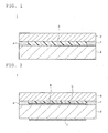
- Figs. 1 and 2 are cross-sectional views each showing one embodiment of display unit according to the present invention.
- a display unit 1 of the present embodiment includes a display part 2 that is connected to a drive circuit (not shown) and displays predetermined images, and a light-transmitting protective part 3 that is arranged in the vicinity of the display part 2 and faces the display part 2.
- the display part 2 is a liquid crystal display panel used in a liquid display apparatus.
- the liquid crystal display apparatus is not limited to a particular type, but can be applied to various systems. Examples of such liquid crystal display apparatuses include those for use in cellular phones, portable game machines and other electronic devices.
- polarizers 6, 7 are arranged on each side of the display part 2 as shown in Fig. 2 .
- the protective part 3 is formed of a planar member having substantially the same size as the display part 2.
- the protective part 3 is formed of plastic (such as an acrylic resin).
- the protective part 3 is spaced apart from the display part 2 by a spacer 4 arranged along the periphery of the display part 2.
- the thickness of the spacer is about in the range of from 0.05 mm to 1.5 mm and serves to keep the distance between the surfaces of the display part 2 and the protective part 3 at approximately 1 mm.
- the display unit 1 includes a cured resin layer 5 provided between the display part 2 and the protective part 3.
- the cured resin layer 5 has a transmittance of 90% or higher in the visible range and a storage modulus at 25°C of 1.0 ⁇ 10 7 Pa or less, and preferably from 1.0 ⁇ 10 3 to 1.0 ⁇ 10 6 Pa.
- the resin composition to make the cured resin layer 5 has a cure shrinkage of 5% or less, preferably 4.5% or less, and more preferably from 0 to 2%.
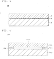
- the image display unit is configured without using the spacer 4 used in the above-described embodiments of the display unit 1 shown in Figs. 1 and 2 .
- the resin composition layer 5 and the protective part 3 are sequentially overlaid on the display part 2. Curing the resin composition completes an image display unit 1B as shown in Fig. 3 without providing the spacer.
- the distance between the display part 2 and the protective part 3 is typically in the range of from 50 ⁇ m to 200 ⁇ m.
- Such a configuration generally makes it possible to design thinner image display units.
- the resin composition to make the cured resin layer 5 is a photocurable resin composition in order to increase the productivity.
- the resin composition for use in the present invention preferably contains polyurethane acrylate and at least one acrylate monomer, such as isobornyl acrylate, dicyclopentenyloxyethyl methacrylate or 2-hydroxybutyl methacrylate; and a photopolymerization initiator, such as 1-hydroxycyclohexyl-phenyl-ketone, used together with a photopolymerization initiator that can cure in the visible range.
- acrylate monomer such as isobornyl acrylate, dicyclopentenyloxyethyl methacrylate or 2-hydroxybutyl methacrylate
- a photopolymerization initiator such as 1-hydroxycyclohexyl-phenyl-ketone
- the photopolymerization initiator for use in the present invention is preferably used together with a photopolymerization initiator that can cure in the visible range (such as SpeedCure TPO (trade name), Nihon Siber Hegner KK).
- the resin composition for use in the present invention is prepared such that the cured resin obtained by curing the resin composition by UV irradiation has a storage modulus (at 25°C) of 1 ⁇ 10 7 Pa or less, and preferably in the range of from 1 ⁇ 10 3 Pa to 1 ⁇ 10 6 Pa, has a refractive index preferably in the range of from 1.45 to 1.55, and more preferably in the range of from 1.51 to 1.52, and has a transmittance of 90% or higher in the visible range when formed into a 100 ⁇ m-thick layer.
- Different resin compositions containing the same major resin component but different auxiliary resin components and monomer components may be cured to have different storage moduli (at 25°C) that may, in some cases, exceed 1 x 10 7 Pa.
- Those resin compositions that are cured to have a storage modulus (at 25°C) of higher than 1 ⁇ 10 7 Pa are not included in the scope of the present invention.
- the resin composition of the present invention also has a cure shrinkage of 5% or less, more preferably of 4.5% or less, and still more preferably in the range of from 0 to 2%. In this manner, the internal stress that builds up within the cured resin upon curing of the resin composition can be reduced, and the distortion generated at the interface between the cured resin layer 5 and the display part 2 or the protective part 3 can be prevented.
- the resin composition between the display part 2 and the protective part 3 and then curing the resin composition, the amount of light scattered at the interface between the cured resin layer 5 and the display part 2 or the protective part 3 can be reduced. As a result, the luminance and the visibility of the displayed images can be improved.
- the magnitude of the internal stress that builds up within the cured resin upon curing of the resin composition can be evaluated by dropping the resin composition onto a flat surface and measuring the average surface roughness of the cured resin.
- the distortion generated at the interface between the display part 2 or the protective part 3 and the cured resin arranged in between would be negligible if, for example, a cured resin obtained by dropping 2 mg of the resin composition onto a glass plate and cured by UV irradiation to 90% or a higher cure ratio has an average surface roughness of 6 nm or less.
- this average surface roughness can be kept at 6 nm or less, and preferably in the range of 1 nm to 3 nm.
- the spacer 4 and a ridge are arranged on the display part 2 along its periphery.
- a predetermined amount of the above-described photocurable resin composition is then poured over the display member 2 in the area inside the spacer and the ridge.
- the protective part 3 is then placed on the display part 2 over the spacer 4 and the gap between the display part 2 and the protective part 3 is completely filled with the resin composition.
- the resin composition is irradiated with ultraviolet rays via the protective part 3 to cure the resin composition. This completes the desired display unit 1.
- the above-described photocurable resin composition is first applied onto the display part 2.
- the protective part 3 is then placed over the coating of the resin composition and the ultraviolet rays are irradiated onto the resin composition from the side of the protective part 3.
- the effects of the stress generated as the resin cures and shrinks on the display part 2 and the protective part 3 can be minimized, so that little or no distortion is generated in the display part 2 and the protective part 3. Since the display part 2 is not deformed during the production, it can display images at high luminance and high contrast without causing any image defects.
- the cured resin 5 that fills the gap between the display part 2 and the protective part 3 in the present embodiment reinforces the display unit 1 so that it can withstand high impacts. This makes it possible to design thinner display units 1.
- the present invention can provide a liquid crystal display apparatus that can effectively prevent disrupted orientation of liquid crystal materials and other image defects and can thus achieve high-quality display of images especially.
- the present invention is suitable for use in the above-described liquid crystal display apparatuses, the invention is also applicable to various other panel displays, such as organic EL apparatuses and plasma display apparatuses.
- Example 1 The following components were kneaded together in a kneader to make a resin composition of Example 1: 50 parts by weight of polyurethane acrylate, 30 parts by weight of isobornyl acrylate, 3 parts by weight of a photopolymerization initiator and 1 part by weight of a photopolymerization initiator for visible-range.
- Example 2 The following components were kneaded together in a kneader to make a resin composition of Example 2: 70 parts by weight of an ester formed from a maleic anhydride adduct of a polyisoprene polymer and 2-hydroxyethyl methacrylate, 30 parts by weight of dicyclopentenyloxyethyl methacrylate, 10 parts by weight of 2-hydroxybutyl methacrylate, 30 parts by weight of a hydrogenated terpene resin, 140 parts by weight of a butadiene polymer, 4 parts by weight of a photopolymerization initiator and 0.5 parts by weight of a visible-range photopolymerization initiator.
- Example 3 100 parts by weight of an ester formed from a maleic anhydride adduct of a polyisoprene polymer and 2-hydroxyethyl methacrylate, 30 parts by weight of dicyclopentenyloxyethyl methacrylate, 10 parts by weight of 2-hydroxybutyl methacrylate, 30 parts by weight of a hydrogenated terpene resin, 210 parts by weight of a butadiene polymer, 7 parts by weight of a photopolymerization initiator and 1.5 parts by weight of a visible-range photopolymerization initiator.
- Each of the resin compositions prepared in Examples 1 through 3 and Comparative Examples 1 through 3 was poured onto a 100 ⁇ m-thick white glass plate to a predetermined thickness.
- the plates were transported on a UV-conveyor to obtain cured resins having a predetermined thickness.
- the cured resins were used as samples.
- the light transmittance, elastic modulus, cure shrinkage and surface roughness of each sample were determined as described below.
- each sample (with 100 ⁇ m-thick cured resin) was analyzed for the transmittance in the visible range. It turned out that all of the samples had 90% or a higher transmittance.
- each sample (with 1mm-thick cured resin) was analyzed for the distortion (Ra: average surface roughness) in a predetermined area (2.93 mm ⁇ 2.20 mm) of the glass plate surface caused by the internal stress generated during UV curing.
- the average surface roughness Ra was from 1.5 nm to 5.5 nm in each of Examples 1 through 3, indicating that samples in these Examples were each distorted little.
- the resin composition of Example 1 was cured between a 50mm ⁇ 50mm ⁇ 0.5mm glass plate (display part) and a 50mm ⁇ 50mm ⁇ 0.5mm polycarbonate plate (protective part) to form a 0.1mm-thick layer between the two plates.
- the resulting panel served as the sample panel of this Reference Example. In this configuration, the spacer was omitted and the sample panel had a total thickness of 1.1 mm.
- the resin composition of Example 1 was first applied to the glass plate and the polycarbonate plate was placed over the coating of the resin composition. The resin composition was then cured by the irradiation of UV from the side of the polycarbonate plate.
- a sample panel having the conventional configuration as shown in Fig. 4 was prepared.
- the liquid crystal display panel (display part) 102 and the protective part 103 used were identical to those used to make the sample panel of the Reference Example.
- the display part and the protective part were assembled with 1.0mm thick spacers arranged in between to make the sample panel of Comparative Example having a 1.0mm air gap and a total thickness of 2.0 mm.
- Each of the sample panels of the Reference Example and Comparative Example was secured to a mount by the periphery using a predetermined jig.
- a panel breakage test was then performed by perpendicularly pressing a press member, 5 mm in diameter, against the surface of the protective part at a press speed of 1 mm/sec.
Landscapes
- Physics & Mathematics (AREA)
- Chemical & Material Sciences (AREA)
- Nonlinear Science (AREA)
- Organic Chemistry (AREA)
- Chemical Kinetics & Catalysis (AREA)
- Medicinal Chemistry (AREA)
- Polymers & Plastics (AREA)
- Health & Medical Sciences (AREA)
- Mathematical Physics (AREA)
- Crystallography & Structural Chemistry (AREA)
- Optics & Photonics (AREA)
- General Physics & Mathematics (AREA)
- Liquid Crystal (AREA)
- Devices For Indicating Variable Information By Combining Individual Elements (AREA)
- Inorganic Chemistry (AREA)
- Macromonomer-Based Addition Polymer (AREA)
- Polymerisation Methods In General (AREA)
- Graft Or Block Polymers (AREA)
- Compositions Of Macromolecular Compounds (AREA)
Priority Applications (2)
| Application Number | Priority Date | Filing Date | Title |
|---|---|---|---|
| EP24162999.7A EP4365256A3 (en) | 2006-07-14 | 2007-07-17 | Resin composition and display apparatus |
| EP20216920.7A EP3836128B8 (en) | 2006-07-14 | 2007-07-17 | Resin composition and display apparatus |
Applications Claiming Priority (5)
| Application Number | Priority Date | Filing Date | Title |
|---|---|---|---|
| JP2006193730 | 2006-07-14 | ||
| JP2007102251 | 2007-04-09 | ||
| PCT/JP2007/064120 WO2008007800A1 (en) | 2006-07-14 | 2007-07-17 | Resin composition and display apparatus |
| EP14002672.5A EP2824653B1 (en) | 2006-07-14 | 2007-07-17 | Resin composition and display apparatus |
| EP07790882.0A EP2051227B1 (en) | 2006-07-14 | 2007-07-17 | Resin composition and display apparatus |
Related Parent Applications (2)
| Application Number | Title | Priority Date | Filing Date |
|---|---|---|---|
| EP14002672.5A Division EP2824653B1 (en) | 2006-07-14 | 2007-07-17 | Resin composition and display apparatus |
| EP07790882.0A Division EP2051227B1 (en) | 2006-07-14 | 2007-07-17 | Resin composition and display apparatus |
Related Child Applications (2)
| Application Number | Title | Priority Date | Filing Date |
|---|---|---|---|
| EP20216920.7A Division EP3836128B8 (en) | 2006-07-14 | 2007-07-17 | Resin composition and display apparatus |
| EP24162999.7A Division EP4365256A3 (en) | 2006-07-14 | 2007-07-17 | Resin composition and display apparatus |
Publications (2)
| Publication Number | Publication Date |
|---|---|
| EP3118841A1 EP3118841A1 (en) | 2017-01-18 |
| EP3118841B1 true EP3118841B1 (en) | 2021-01-06 |
Family
ID=38923359
Family Applications (5)
| Application Number | Title | Priority Date | Filing Date |
|---|---|---|---|
| EP16001361.1A Active EP3118841B1 (en) | 2006-07-14 | 2007-07-17 | Resin composition and display apparatus |
| EP14002672.5A Active EP2824653B1 (en) | 2006-07-14 | 2007-07-17 | Resin composition and display apparatus |
| EP24162999.7A Pending EP4365256A3 (en) | 2006-07-14 | 2007-07-17 | Resin composition and display apparatus |
| EP20216920.7A Active EP3836128B8 (en) | 2006-07-14 | 2007-07-17 | Resin composition and display apparatus |
| EP07790882.0A Active EP2051227B1 (en) | 2006-07-14 | 2007-07-17 | Resin composition and display apparatus |
Family Applications After (4)
| Application Number | Title | Priority Date | Filing Date |
|---|---|---|---|
| EP14002672.5A Active EP2824653B1 (en) | 2006-07-14 | 2007-07-17 | Resin composition and display apparatus |
| EP24162999.7A Pending EP4365256A3 (en) | 2006-07-14 | 2007-07-17 | Resin composition and display apparatus |
| EP20216920.7A Active EP3836128B8 (en) | 2006-07-14 | 2007-07-17 | Resin composition and display apparatus |
| EP07790882.0A Active EP2051227B1 (en) | 2006-07-14 | 2007-07-17 | Resin composition and display apparatus |
Country Status (6)
| Country | Link |
|---|---|
| US (9) | US9423638B2 (enExample) |
| EP (5) | EP3118841B1 (enExample) |
| JP (7) | JP5343388B2 (enExample) |
| KR (1) | KR101379126B1 (enExample) |
| CN (3) | CN101490732B (enExample) |
| WO (1) | WO2008007800A1 (enExample) |
Families Citing this family (70)
| Publication number | Priority date | Publication date | Assignee | Title |
|---|---|---|---|---|
| EP3118841B1 (en) | 2006-07-14 | 2021-01-06 | Dexerials Corporation | Resin composition and display apparatus |
| EP2053087A4 (en) * | 2006-10-31 | 2010-12-01 | Hitachi Chemical Co Ltd | RESIN COMPOSITION FOR OPTICAL USE, RESIN MATERIAL FOR OPTICAL USE USING THE RESIN COMPOSITION, OPTICAL FILTER FOR IMAGE DISPLAY DEVICE, AND IMAGE DISPLAY DEVICE |
| JP2009186957A (ja) * | 2007-04-09 | 2009-08-20 | Sony Chemical & Information Device Corp | 樹脂組成物及び表示装置 |
| JP5401824B2 (ja) | 2007-04-09 | 2014-01-29 | デクセリアルズ株式会社 | 画像表示装置 |
| EP2144219A4 (en) | 2007-04-09 | 2010-07-07 | Sony Chem & Inf Device Corp | IMAGE DISPLAY DEVICE |
| JP5470735B2 (ja) | 2007-04-10 | 2014-04-16 | デクセリアルズ株式会社 | 画像表示装置の製造方法 |
| JP4711354B2 (ja) * | 2007-07-17 | 2011-06-29 | ソニーケミカル&インフォメーションデバイス株式会社 | 画像表示装置の製造方法 |
| KR20130122006A (ko) * | 2007-07-17 | 2013-11-06 | 데쿠세리아루즈 가부시키가이샤 | 화상 표시 장치 및 그 제조 방법 |
| JP5343391B2 (ja) * | 2007-07-17 | 2013-11-13 | デクセリアルズ株式会社 | 樹脂組成物及び画像表示装置 |
| JP5477417B2 (ja) * | 2007-07-17 | 2014-04-23 | デクセリアルズ株式会社 | 樹脂組成物及び画像表示装置 |
| KR100977704B1 (ko) * | 2007-12-21 | 2010-08-24 | 주성엔지니어링(주) | 표시소자 및 그 제조방법 |
| JP5125814B2 (ja) * | 2008-07-02 | 2013-01-23 | 日立化成工業株式会社 | 枠体及びそれを用いた液晶表示装置 |
| WO2010018651A1 (ja) * | 2008-08-13 | 2010-02-18 | 共同技研化学株式会社 | 表示装置の保護体及び該保護体の形成方法 |
| TWI485214B (zh) * | 2008-09-05 | 2015-05-21 | Kyoritsu Chemical Co Ltd | And a photohardenable resin composition for bonding an optical functional material |
| JP2010097070A (ja) * | 2008-10-17 | 2010-04-30 | Nitto Denko Corp | フラットパネルディスプレイ用透明粘着シート及びフラットパネルディスプレイ |
| WO2010044291A1 (ja) * | 2008-10-17 | 2010-04-22 | シャープ株式会社 | 表示装置及びその製造方法 |
| WO2010116569A1 (ja) * | 2009-04-07 | 2010-10-14 | シャープ株式会社 | 表示装置およびその製造方法 |
| KR101423848B1 (ko) * | 2009-09-04 | 2014-07-25 | 데쿠세리아루즈 가부시키가이샤 | 충전 장치 |
| WO2011043295A1 (ja) * | 2009-10-07 | 2011-04-14 | ソニーケミカル&インフォメーションデバイス株式会社 | 接着装置、板状接着体の製造方法 |
| KR101814831B1 (ko) | 2009-10-13 | 2018-01-04 | 데쿠세리아루즈 가부시키가이샤 | 표시 장치의 제조 방법 및 투명 수지 충전제 |
| US9182625B2 (en) | 2009-10-16 | 2015-11-10 | Dexerials Corporation | Display, manufacturing method therefor and transparent resin charging material |
| CN104809960B (zh) * | 2009-10-16 | 2018-03-30 | 迪睿合电子材料有限公司 | 显示装置及其制造方法、以及透明树脂填充剂 |
| DE102010010598A1 (de) | 2010-03-08 | 2011-09-08 | Delo Industrie Klebstoffe Gmbh & Co. Kgaa | Dual härtende Masse und deren Verwendung |
| WO2011148990A1 (ja) * | 2010-05-26 | 2011-12-01 | 旭硝子株式会社 | 粘着層付き透明面材、表示装置およびそれらの製造方法 |
| WO2011162125A1 (ja) | 2010-06-21 | 2011-12-29 | シャープ株式会社 | 前面板付表示パネル、表示装置及び樹脂組成物 |
| KR101211371B1 (ko) | 2010-09-16 | 2012-12-13 | 주식회사 토비스 | 곡면 디스플레이 패널 제조 방법 |
| JP5757292B2 (ja) * | 2010-12-08 | 2015-07-29 | 旭硝子株式会社 | 粘着層付き透明面材、表示装置およびそれらの製造方法 |
| JPWO2012081708A1 (ja) * | 2010-12-16 | 2014-05-22 | 日立化成株式会社 | 光硬化性樹脂組成物、画像表示用装置、その製造方法 |
| WO2012086404A1 (ja) | 2010-12-22 | 2012-06-28 | モメンティブ・パフォーマンス・マテリアルズ・ジャパン合同会社 | 熱硬化型ポリオルガノシロキサン組成物及びその使用 |
| WO2012086402A1 (ja) | 2010-12-22 | 2012-06-28 | モメンティブ・パフォーマンス・マテリアルズ・ジャパン合同会社 | 紫外線硬化型シリコーン樹脂組成物、及びそれを用いた画像表示装置 |
| CN103314402B (zh) | 2011-01-18 | 2016-01-06 | 夏普株式会社 | 带平面板的显示面板、带平面板的显示面板的制造方法 |
| JP5710302B2 (ja) | 2011-02-09 | 2015-04-30 | 株式会社ジャパンディスプレイ | 液晶表示装置 |
| JP2012172064A (ja) | 2011-02-22 | 2012-09-10 | Nitto Denko Corp | 紫外線硬化型光学樹脂接着剤組成物 |
| JPWO2012114608A1 (ja) * | 2011-02-25 | 2014-07-07 | ポリプラスチックス株式会社 | 成形品の製造方法及び成形品 |
| MY170060A (en) | 2011-10-21 | 2019-07-02 | Nippon Kayaku Kk | Method for producing optical member and use of ultraviolet ray cured resin composition for same |
| KR101996109B1 (ko) * | 2011-11-28 | 2019-07-04 | 쓰리엠 이노베이티브 프로퍼티즈 컴파니 | 고해상도 이미지를 제공하는 편광 빔 스플리터를 제조하는 방법 및 그러한 빔 스플리터를 이용하는 시스템 |
| US20140287167A1 (en) * | 2011-12-27 | 2014-09-25 | Showa Denko K.K. | Polymerizable composition, polymer, image-display device, and manufacturing method therefor |
| US20140069581A1 (en) * | 2012-01-25 | 2014-03-13 | Dexerials Corporation | Method of manufacturing image display device |
| TWI484013B (zh) * | 2012-03-12 | 2015-05-11 | Showa Denko Kk | A polymerizable composition, a polymer, an image display device, and a method for manufacturing the same |
| US20150050432A1 (en) * | 2012-03-28 | 2015-02-19 | Showa Denko K.K. | Polymerizable composition, polymerization product, adhesive sheet, method for manufacturing an image display device, and image display device |
| EP4184485B1 (en) * | 2012-05-09 | 2025-08-13 | Dexerials Corporation | Method of manufacturing image display apparatus |
| WO2013173976A1 (en) * | 2012-05-22 | 2013-11-28 | Henkel (China) Company Limited | Liquid optically clear photo-curable adhesive |
| WO2013187508A1 (ja) | 2012-06-15 | 2013-12-19 | 昭和電工株式会社 | 重合性組成物、重合物、光学用粘着シート、画像表示装置およびその製造方法 |
| JP6124916B2 (ja) | 2012-10-31 | 2017-05-10 | 昭和電工株式会社 | 重合性組成物、重合物、光学用粘着シート、画像表示装置およびその製造方法 |
| JP5370706B1 (ja) | 2012-12-14 | 2013-12-18 | デクセリアルズ株式会社 | 画像表示装置の製造方法 |
| WO2014092199A1 (ja) * | 2012-12-14 | 2014-06-19 | デクセリアルズ株式会社 | 画像表示装置の製造方法、樹脂用ディスペンサー |
| JP5994618B2 (ja) * | 2012-12-14 | 2016-09-21 | デクセリアルズ株式会社 | 光硬化性樹脂組成物及びそれを用いた画像表示装置の製造方法 |
| JP6331483B2 (ja) * | 2013-03-08 | 2018-05-30 | 株式会社スリーボンド | 光硬化性組成物 |
| JP6609093B2 (ja) | 2013-05-13 | 2019-11-20 | 日東電工株式会社 | ハードコートフィルム、偏光板及び画像表示装置 |
| JP2015025877A (ja) * | 2013-07-24 | 2015-02-05 | コニカミノルタ株式会社 | 光学フィルム、偏光板、及び液晶表示装置 |
| JP6226652B2 (ja) * | 2013-09-09 | 2017-11-08 | 昭和電工株式会社 | 画像表示装置の製造方法 |
| JP2014142648A (ja) * | 2014-02-27 | 2014-08-07 | Dexerials Corp | 表示装置及びその製造方法、並びに透明樹脂充填剤 |
| TWI646163B (zh) * | 2014-06-11 | 2019-01-01 | 日本化藥股份有限公司 | 觸控面板用紫外線硬化型樹脂組成物、使用其之貼合方法及物品 |
| WO2016069416A1 (en) | 2014-10-27 | 2016-05-06 | Ctech Adhesives Llc | Assembly processes using uv curable pressure sensitive adhesives (psa) or stageable psa systems |
| KR102506256B1 (ko) * | 2015-08-31 | 2023-03-07 | 삼성전자 주식회사 | 방수구조를 가지는 전자 장치 |
| KR20170028164A (ko) * | 2015-09-03 | 2017-03-13 | 엘지전자 주식회사 | 이동 단말기 |
| JP5994011B2 (ja) * | 2015-10-21 | 2016-09-21 | デクセリアルズ株式会社 | 表示装置の製造方法 |
| US9946104B2 (en) | 2015-12-28 | 2018-04-17 | Japan Display Inc. | Display device and method of manufacturing the same |
| KR102314685B1 (ko) | 2017-08-17 | 2021-10-20 | 모멘티브퍼포먼스머티리얼스코리아 주식회사 | 열경화형 실리콘계 수지 조성물 및 이를 이용하여 형성된 점착 필름 |
| WO2019130756A1 (ja) * | 2017-12-26 | 2019-07-04 | ソニー株式会社 | 表示装置 |
| KR102568774B1 (ko) | 2018-03-14 | 2023-08-21 | 모멘티브퍼포먼스머티리얼스코리아 주식회사 | 디스플레이 패널 및 이의 제조방법 |
| KR102458048B1 (ko) | 2018-07-12 | 2022-10-25 | 모멘티브퍼포먼스머티리얼스코리아 주식회사 | 점착 필름용 열경화형 실리콘계 수지 조성물 및 이를 이용하여 형성된 점착 필름 |
| KR102552820B1 (ko) | 2018-07-17 | 2023-07-07 | 모멘티브퍼포먼스머티리얼스코리아 주식회사 | 광학 투명 레진 및 이를 이용하여 형성된 전자 소자 |
| KR102552831B1 (ko) | 2018-07-17 | 2023-07-07 | 모멘티브퍼포먼스머티리얼스코리아 주식회사 | 광학 투명 레진 및 이를 이용하여 형성된 전자 소자 |
| CN110776870A (zh) * | 2019-09-25 | 2020-02-11 | 塔威新材料科技(上海)有限公司 | 光学塑料和玻璃粘接用uv胶及其制备方法 |
| TW202130739A (zh) | 2019-11-24 | 2021-08-16 | 美商陶氏有機矽公司 | 光可固化聚矽氧組成物及其固化產物 |
| EP4061875A4 (en) | 2019-11-24 | 2023-12-20 | Dow Toray Co., Ltd. | Photocurable silicone composition and cured product thereof |
| CN117751165A (zh) | 2021-07-19 | 2024-03-22 | 迈图高新材料公司 | 光学用途紫外线活性型液状硅酮组合物 |
| JP7310035B1 (ja) | 2021-12-17 | 2023-07-18 | モメンティブ パフォーマンス マテリアルズ インコーポレイテッド | 紫外線硬化性シリコーン組成物 |
| CN115197664B (zh) * | 2022-08-01 | 2023-06-02 | 业成科技(成都)有限公司 | 光学胶组合物、光学胶膜及制造光学胶膜之方法 |
Family Cites Families (215)
| Publication number | Priority date | Publication date | Assignee | Title |
|---|---|---|---|---|
| JPH079562B2 (ja) | 1983-10-07 | 1995-02-01 | カシオ計算機株式会社 | フィルム型液晶表示セルの実装方法 |
| US4679918A (en) | 1984-10-23 | 1987-07-14 | Ace Ronald S | Ophthalmic glass/plastic laminated lens having photochromic characteristics and assembly thereof |
| JPH01300246A (ja) * | 1988-05-28 | 1989-12-04 | Nippon Paint Co Ltd | フレキソ印刷用感光性樹脂組成物 |
| JPH02165188A (ja) | 1988-12-19 | 1990-06-26 | Mitsubishi Electric Corp | 表示素子 |
| US5126620A (en) | 1988-12-19 | 1992-06-30 | Mitsubishi Denki Kabushiki Kaisha | Display element |
| JPH03204616A (ja) | 1990-01-08 | 1991-09-06 | Hitachi Ltd | 液晶ディスプレイ |
| JPH0675701A (ja) | 1992-08-25 | 1994-03-18 | Nitto Denko Corp | 液晶表示装置の製造方法 |
| JPH0688963A (ja) | 1992-09-08 | 1994-03-29 | Rohm Co Ltd | 液晶表示パネル |
| JPH06299126A (ja) | 1993-02-19 | 1994-10-25 | Sekisui Chem Co Ltd | 感熱接着性フォーム、その製造方法、その複合体及びその加工方法 |
| JP3321718B2 (ja) | 1993-04-01 | 2002-09-09 | 鈴木総業株式会社 | 液晶表示装置における光錯乱防止構造の製造方法 |
| JPH0713173A (ja) | 1993-06-22 | 1995-01-17 | Three Bond Co Ltd | 液晶シール剤 |
| US5679722A (en) | 1993-07-15 | 1997-10-21 | Teijin Seiki Co., Ltd. | Resin composition for production of a three-dimensional object by curing |
| JP3287661B2 (ja) | 1993-08-30 | 2002-06-04 | 新日本製鐵株式会社 | 熱硬化性樹脂組成物及びその硬化物並びに画像形成材料 |
| JPH07114010A (ja) * | 1993-10-14 | 1995-05-02 | Matsushita Electric Ind Co Ltd | 液晶表示装置 |
| JP3327423B2 (ja) | 1993-10-21 | 2002-09-24 | 日本合成化学工業株式会社 | 偏光フイルムの製造法 |
| US5747152A (en) | 1993-12-02 | 1998-05-05 | Dai Nippon Printing Co., Ltd. | Transparent functional membrane containing functional ultrafine particles, transparent functional film, and process for producing the same |
| US5557436A (en) | 1994-05-12 | 1996-09-17 | Magnascreen Corporation | Thin seal liquid crystal display and method of making same |
| JPH08122759A (ja) | 1994-10-28 | 1996-05-17 | Sony Corp | 画像表示パネルおよびその製造方法 |
| JP3083715B2 (ja) | 1994-12-05 | 2000-09-04 | シャープ株式会社 | 液晶表示素子の製造方法 |
| JPH08211353A (ja) | 1995-02-01 | 1996-08-20 | Nippondenso Co Ltd | 画像表示装置 |
| JP3230038B2 (ja) | 1995-02-13 | 2001-11-19 | キヤノン株式会社 | 液晶表示装置 |
| CN1076378C (zh) | 1995-04-28 | 2001-12-19 | 日本化药株式会社 | 紫外线固化型粘合剂组合物 |
| JP3331277B2 (ja) | 1995-05-30 | 2002-10-07 | シャープ株式会社 | 液晶表示装置の製造方法および液晶表示装置 |
| JP3272921B2 (ja) | 1995-09-27 | 2002-04-08 | リンテック株式会社 | 粘着シート |
| JP3220403B2 (ja) | 1996-02-09 | 2001-10-22 | セイコーインスツルメンツ株式会社 | 表示装置の製造方法 |
| DE69721355T2 (de) * | 1996-02-09 | 2003-10-30 | Seiko Instr Inc | Anzeigeeinheit mit einem transparenten Berührungsschalter und einer Flüssigkristallanzeige, und Verfahren zur Herstellung |
| JP3445436B2 (ja) | 1996-03-21 | 2003-09-08 | 日東電工株式会社 | プラズマ表示装置 |
| DE69716332T2 (de) | 1996-04-15 | 2003-02-20 | Teijin Seiki Co. Ltd., Osaka | Verwendung einer photohärtbaren Harzzusammensetzung zur Herstellung eines Objektes mittels Stereolithographie |
| JPH09318932A (ja) | 1996-05-27 | 1997-12-12 | Nitto Denko Corp | 液晶表示装置 |
| JP4013085B2 (ja) * | 1996-09-03 | 2007-11-28 | 東洋紡績株式会社 | 積層フィルムの製造方法 |
| JP3842347B2 (ja) | 1996-09-09 | 2006-11-08 | セイコーインスツル株式会社 | 表示装置 |
| JPH1095967A (ja) | 1996-09-24 | 1998-04-14 | Olympus Optical Co Ltd | 接着剤組成物及び接着構造体 |
| JP3532051B2 (ja) * | 1996-12-13 | 2004-05-31 | シャープ株式会社 | 液晶パネルの固定方法及び固定用装置 |
| JPH10293314A (ja) | 1997-04-22 | 1998-11-04 | Toshiba Corp | 表示装置の製造方法および製造装置 |
| JP3799829B2 (ja) | 1997-09-11 | 2006-07-19 | セイコーエプソン株式会社 | 電気光学装置およびその製造方法並びに投射型表示装置 |
| JP4217842B2 (ja) | 1997-12-24 | 2009-02-04 | 株式会社ブリヂストン | タッチパネル一体型表示装置用接着剤組成物及び接着剤フィルム並びにタッチパネル一体型表示装置及びその製造方法 |
| DE69940916D1 (de) | 1998-02-18 | 2009-07-09 | Dsm Ip Assets Bv | Fotohärtbare flüssige Harzzusammensetzung |
| US5926248A (en) * | 1998-06-26 | 1999-07-20 | Bausch & Lomb, Incorporated | Sunglass lens laminate |
| JP3887708B2 (ja) | 1998-07-08 | 2007-02-28 | Jsr株式会社 | 光硬化性樹脂組成物 |
| JP2000073025A (ja) | 1998-08-26 | 2000-03-07 | Sony Chem Corp | 粘着テープ及びその製造方法 |
| JP2000143756A (ja) | 1998-09-03 | 2000-05-26 | Nitto Denko Corp | 芳香族ポリカルボジイミド及びそのシ―ト |
| JP2000111908A (ja) | 1998-10-05 | 2000-04-21 | Seiko Instruments Inc | 液晶装置 |
| US6461709B1 (en) | 1998-10-28 | 2002-10-08 | 3M Innovative Properties Company | Graffiti and/or environmental protective article having removable sheets, substrates protected therewith, and a method of use |
| JP2000219868A (ja) | 1998-11-16 | 2000-08-08 | Dainippon Ink & Chem Inc | 液晶パネルシ―ル用光硬化性樹脂組成物 |
| US6218446B1 (en) | 1999-01-11 | 2001-04-17 | Dymax Corporation | Radiation curable formulation for producing electrically conductive resinous material, method of use, and article produced |
| JP3462135B2 (ja) * | 1999-01-14 | 2003-11-05 | シャープ株式会社 | 二次元画像検出器およびアクティブマトリクス基板並びに表示装置 |
| KR100579633B1 (ko) | 1999-01-21 | 2006-05-12 | 도요 보세키 가부시키가이샤 | 광학용 이접착필름 및 그 롤 |
| JP2000258780A (ja) | 1999-03-05 | 2000-09-22 | Mitsubishi Electric Corp | 液晶表示装置およびその製造方法 |
| JP3697104B2 (ja) | 1999-03-30 | 2005-09-21 | セイコーエプソン株式会社 | 液晶装置及びこれを備えた投射型表示装置 |
| JP3881962B2 (ja) | 1999-03-30 | 2007-02-14 | セイコーエプソン株式会社 | 電気光学装置及びこれを備えた投射型表示装置 |
| US6414781B1 (en) | 1999-03-30 | 2002-07-02 | Seiko Epson Corporation | Electro-optical device and projection display device including the same |
| EP1047055A1 (en) | 1999-04-22 | 2000-10-25 | 3M Innovative Properties Company | Optical storage medium |
| JP2001026759A (ja) | 1999-04-28 | 2001-01-30 | Bridgestone Corp | 光学機能部材一体型表示装置用接着剤組成物、接着剤フィルム、接着剤フィルム積層体、光学機能部材一体型表示装置及びその製造方法 |
| JP2001026758A (ja) | 1999-04-28 | 2001-01-30 | Bridgestone Corp | 光学機能部材一体型表示装置用接着剤組成物、接着剤フィルム、接着剤フィルム積層体、光学機能部材一体型表示装置及びその製造方法 |
| EP1177182B1 (en) | 1999-05-10 | 2006-11-29 | Ciba SC Holding AG | Novel photoinitiators and their applications |
| JP4883433B2 (ja) | 1999-05-16 | 2012-02-22 | 株式会社ワイエス・メディカル | バルーンカテーテルおよびその製造方法並びにカテーテルチューブへのバルーンの装着方法 |
| JP2001222017A (ja) | 1999-05-24 | 2001-08-17 | Fujitsu Ltd | 液晶表示装置及びその製造方法 |
| KR100662534B1 (ko) | 1999-07-15 | 2006-12-28 | 가부시키가이샤 도모에가와 세이시쇼 | 분체 단층 피막 형성방법 |
| US6429235B1 (en) * | 1999-08-27 | 2002-08-06 | Cognis Corporation | Energy-curable composition for making a pressure sensitive adhesive |
| JP2001290005A (ja) | 1999-09-06 | 2001-10-19 | Seiko Epson Corp | カバーガラス |
| JP2001141907A (ja) | 1999-11-12 | 2001-05-25 | Seiko Epson Corp | マイクロレンズ基板の製造方法、マイクロレンズ基板、液晶パネル用対向基板、液晶パネルおよび投射型表示装置 |
| JP2000267118A (ja) | 2000-01-01 | 2000-09-29 | Matsushita Electric Ind Co Ltd | 液晶パネル |
| JP3560532B2 (ja) | 2000-05-02 | 2004-09-02 | 株式会社巴川製紙所 | ディスプレイ用帯電防止フィルム |
| AU2001257165A1 (en) | 2000-05-12 | 2001-11-26 | 3M Innovative Properties Company | Rigid substrate lamination process, system, and product |
| JP2002019013A (ja) | 2000-07-05 | 2002-01-22 | Lintec Corp | 金属板成形品の製造方法及びそれに用いる粘着シート |
| JP2002040208A (ja) * | 2000-07-28 | 2002-02-06 | Nissha Printing Co Ltd | 反射防止カバー部品とその製造方法 |
| JP2002052552A (ja) | 2000-08-11 | 2002-02-19 | Mitsubishi Chemicals Corp | 光硬化樹脂シートの製造方法 |
| JP2002092957A (ja) | 2000-09-19 | 2002-03-29 | Mitsui Chemicals Inc | 光記録媒体用表面保護層材料 |
| JP3607591B2 (ja) | 2000-10-04 | 2005-01-05 | Necアクセステクニカ株式会社 | 情報端末装置 |
| KR100387536B1 (ko) | 2000-10-18 | 2003-06-18 | 주식회사 루밴틱스 | 광학 접착제 수지 조성물 및 광학 접착제 수지의 제조방법 |
| US6798467B2 (en) | 2000-12-21 | 2004-09-28 | Asahi Rubber Inc. | Liquid crystal display device and a method for producing the same |
| JP4118027B2 (ja) | 2001-02-28 | 2008-07-16 | 株式会社日立製作所 | 液晶表示装置 |
| US7163739B2 (en) | 2001-03-15 | 2007-01-16 | Mitsui Chemicals, Inc. | Laminate and display apparatus using the same |
| JP2003215344A (ja) | 2001-03-29 | 2003-07-30 | Seiko Epson Corp | 偏光子、およびこの偏光子を用いた光学機器 |
| CN1266489C (zh) * | 2001-04-10 | 2006-07-26 | 富士胶片株式会社 | 防反射薄膜、起偏振片、图像显示装置、液晶显示器及表面保护板 |
| JP3733418B2 (ja) | 2001-04-16 | 2006-01-11 | シャープ株式会社 | 粘接着シート、積層シート及び液晶表示装置 |
| JP3710721B2 (ja) | 2001-04-25 | 2005-10-26 | 三井化学株式会社 | ディスプレイ用フィルタの製造方法 |
| JP2002341776A (ja) | 2001-05-16 | 2002-11-29 | Nitto Denko Corp | ガラス割れ防止用フィルム状フィルタとプラズマ表示装置 |
| JP2002341317A (ja) | 2001-05-17 | 2002-11-27 | Sanyo Electric Co Ltd | 液晶表示装置 |
| JP5415658B2 (ja) | 2001-05-28 | 2014-02-12 | 三菱樹脂株式会社 | 中間膜用粘着シート及び透明積層体 |
| JP5045865B2 (ja) | 2001-06-26 | 2012-10-10 | 株式会社ブリヂストン | 光学機能部材一体型表示装置用接着剤組成物及び光学機能部材一体型表示装置 |
| JP2003029644A (ja) | 2001-07-19 | 2003-01-31 | Mitsubishi Plastics Ind Ltd | 画像表示装置、画像表示装置用積層板及び画像表示装置のパネルに用いる透明粘着シート |
| CN1327293C (zh) | 2001-07-26 | 2007-07-18 | 西巴特殊化学品控股有限公司 | 光敏性树脂组合物 |
| JP2003096425A (ja) | 2001-09-21 | 2003-04-03 | Nippon Sheet Glass Co Ltd | 光学部品固定用接着剤組成物 |
| US7399574B2 (en) * | 2001-09-28 | 2008-07-15 | Dai Nippon Printing Co., Ltd. | Curable resin for photo-patterning, process for producing the same, curable resin composition, color filter, liquid crystal panel substrate, and liquid crystal panel |
| JP3860460B2 (ja) | 2001-11-15 | 2006-12-20 | 三菱樹脂株式会社 | フィルター一体型画像表示装置 |
| JP4134559B2 (ja) | 2002-01-15 | 2008-08-20 | 岩崎電気株式会社 | 表示板用ガラス基板のシール材の硬化装置 |
| JP2003216059A (ja) | 2002-01-24 | 2003-07-30 | Sharp Corp | 表示素子およびその製造方法 |
| JP2003295780A (ja) | 2002-03-29 | 2003-10-15 | Asahi Rubber:Kk | 電子機器の画像の視認性向上構造及びその構造を有する電子機器、当該構造に使用される透明部材 |
| KR100813953B1 (ko) * | 2002-04-22 | 2008-03-14 | 삼성전자주식회사 | 대전방지성을 갖는 광경화성 수지 조성물 |
| GB0212977D0 (en) | 2002-06-06 | 2002-07-17 | Vantico Ag | Actinic radiation curable compositions and their use |
| JP4211295B2 (ja) | 2002-06-11 | 2009-01-21 | 住友ベークライト株式会社 | バリア膜付き光学フィルムシートおよびこれを用いた表示素子 |
| JP2004077887A (ja) | 2002-06-18 | 2004-03-11 | Sony Corp | 表示装置および表示装置を有する電子機器 |
| JP2004061925A (ja) | 2002-07-30 | 2004-02-26 | Nippon Kayaku Co Ltd | 液晶シール剤およびそれを用いた液晶表示セル |
| JP3674610B2 (ja) * | 2002-08-05 | 2005-07-20 | セイコーエプソン株式会社 | 液晶装置、液晶装置の製造方法、電子機器 |
| JP2004117545A (ja) | 2002-09-24 | 2004-04-15 | Mitsui Chemicals Inc | ディスプレイ用フィルタの製造方法 |
| JP2004115757A (ja) | 2002-09-30 | 2004-04-15 | Jsr Corp | 液状硬化性樹脂組成物 |
| JP4208187B2 (ja) | 2002-10-28 | 2009-01-14 | 日東電工株式会社 | 粘着型光学フィルム、粘着型光学フィルムの製造方法および画像表示装置 |
| JP4251060B2 (ja) | 2002-11-06 | 2009-04-08 | 住友化学株式会社 | アクリル樹脂、該樹脂を含有する粘着剤、及び該粘着剤を積層してなる光学積層体 |
| JP2004212521A (ja) | 2002-12-27 | 2004-07-29 | Mitsubishi Plastics Ind Ltd | 液晶表示装置 |
| JP2004224855A (ja) | 2003-01-21 | 2004-08-12 | Matsushita Electric Ind Co Ltd | 接着方法 |
| JP4519409B2 (ja) | 2003-02-24 | 2010-08-04 | リンテック株式会社 | 粘着シートおよびその使用方法 |
| JP2004271935A (ja) | 2003-03-10 | 2004-09-30 | Nitto Denko Corp | 粘着剤付き光学フィルムと液晶表示装置 |
| US7208206B2 (en) | 2003-03-10 | 2007-04-24 | Nitto Denko Corporation | Glass crack prevention laminate and liquid crystal display device |
| JP2004272059A (ja) | 2003-03-11 | 2004-09-30 | Ge Toshiba Silicones Co Ltd | 液晶表示装置及びこれを備えた携帯型電子機器 |
| JP2004279946A (ja) | 2003-03-18 | 2004-10-07 | Sharp Corp | 2d/3d切替型液晶表示パネルおよび2d/3d切替型液晶表示装置 |
| US7537810B2 (en) | 2003-03-24 | 2009-05-26 | Dai Nippon Printing Co., Ltd. | Curable resin composition, photosensitive pattern-forming curable resin composition, color filter, substrate for liquid crystalline panel, and liquid crystalline panel |
| JP2004325788A (ja) | 2003-04-24 | 2004-11-18 | Sony Corp | 光学的検査方法及び光学的検査装置、並びに液晶表示装置の製造方法 |
| JP2004359769A (ja) | 2003-06-03 | 2004-12-24 | Sekisui Chem Co Ltd | 液晶パネル用光硬化性接着剤組成物、液晶パネルの接着方法、偏光板の貼付方法および液晶パネル素子 |
| TW200502304A (en) | 2003-06-13 | 2005-01-16 | Jsr Corp | Transparent sheet and process for producing the same |
| JP4572590B2 (ja) * | 2003-06-13 | 2010-11-04 | Jsr株式会社 | 透明シート及びその製造方法 |
| JP2005055641A (ja) | 2003-08-04 | 2005-03-03 | Yokogawa Electric Corp | 液晶表示装置 |
| TWI326059B (en) | 2003-08-22 | 2010-06-11 | Asahi Glass Co Ltd | Display device and method for fabricating the same |
| JP4815768B2 (ja) | 2003-08-22 | 2011-11-16 | 旭硝子株式会社 | 表示装置及び表示装置の製造方法 |
| JP4170861B2 (ja) | 2003-09-04 | 2008-10-22 | 電気化学工業株式会社 | 光硬化性樹脂組成物 |
| JP4583749B2 (ja) | 2003-11-26 | 2010-11-17 | 日東電工株式会社 | 感圧性接着シート |
| US20050126697A1 (en) | 2003-12-11 | 2005-06-16 | International Business Machines Corporation | Photochemically and thermally curable adhesive formulations |
| JP2005179481A (ja) * | 2003-12-18 | 2005-07-07 | Nitto Denko Corp | 積層シート及び液晶表示装置 |
| JP4485188B2 (ja) * | 2003-12-26 | 2010-06-16 | 日東電工株式会社 | 積層シート及び画像表示装置 |
| TWI303341B (en) | 2004-01-14 | 2008-11-21 | Hannstar Display Corp | Liquid crystal display panel and manufacturing method therof |
| JP3798003B2 (ja) | 2004-02-05 | 2006-07-19 | 沖電気工業株式会社 | ダイスボンド装置及びダイスボンド方法 |
| JP2005225127A (ja) | 2004-02-13 | 2005-08-25 | Mitsubishi Chem Mkv Co | 積層フィルム |
| KR100776561B1 (ko) | 2004-02-16 | 2007-11-15 | 미쓰비시 가가꾸 가부시키가이샤 | 경화성 수지 조성물, 컬러 필터 및 액정 표시 장치 |
| JP2005234129A (ja) | 2004-02-18 | 2005-09-02 | Sekisui Chem Co Ltd | 液晶表示素子用硬化性樹脂組成物、液晶表示素子用シール剤、上下導通材料、及び、液晶表示素子 |
| JP2005242099A (ja) | 2004-02-27 | 2005-09-08 | Nec Lcd Technologies Ltd | 液晶表示装置 |
| JP2005255706A (ja) * | 2004-03-09 | 2005-09-22 | Lintec Corp | 粘接着剤組成物、光ディスク製造用シートおよび光ディスク |
| JP2005283749A (ja) | 2004-03-29 | 2005-10-13 | Sony Corp | 光拡散フィルム及びその製造方法並びにスクリーン |
| JP2005314687A (ja) | 2004-03-31 | 2005-11-10 | Sekisui Chem Co Ltd | 光硬化性樹脂組成物、光カチオン重合開始剤、表示素子用接着剤及び表示素子 |
| JP2005315901A (ja) | 2004-03-31 | 2005-11-10 | Optrex Corp | 表示装置 |
| US20050249683A1 (en) | 2004-04-27 | 2005-11-10 | L Alloret Florence | Nail varnish composition comprising a polymer comprising units with a lower critical solution temperature |
| US7399376B2 (en) | 2004-05-04 | 2008-07-15 | Eastman Kodak Company | Polarizing plate laminated with an improved glue composition and a method of manufacturing the same |
| JP4370207B2 (ja) * | 2004-06-29 | 2009-11-25 | シャープ株式会社 | 液晶表示装置 |
| JP4527012B2 (ja) | 2004-07-12 | 2010-08-18 | 日東電工株式会社 | 粘着剤付き光学フィルムおよび画像表示装置 |
| WO2006011461A1 (ja) | 2004-07-27 | 2006-02-02 | Jsr Corporation | 衝撃吸収体、衝撃吸収積層構造体、液晶ディスプレイ用衝撃吸収積層構造体、プラズマディスプレイ用衝撃吸収積層構造体、有機エレクトロルミネセンスディスプレイ用衝撃吸収積層構造体及びディスプレイ装置 |
| JP2006047741A (ja) * | 2004-08-05 | 2006-02-16 | Konica Minolta Opto Inc | 偏光板、偏光板の製造方法及び表示装置 |
| JP2006053425A (ja) | 2004-08-13 | 2006-02-23 | Dainippon Ink & Chem Inc | 液晶パネルシール用光硬化性組成物及び液晶パネル |
| TWI380900B (zh) * | 2004-09-17 | 2013-01-01 | 住友化學股份有限公司 | 光學疊層體 |
| JP5207095B2 (ja) | 2004-09-30 | 2013-06-12 | 大日本印刷株式会社 | 光学積層体 |
| JP4527489B2 (ja) * | 2004-10-07 | 2010-08-18 | 大日本印刷株式会社 | カラーフィルター用熱硬化性樹脂組成物、カラーフィルター、液晶パネル、及びカラーフィルターの製造方法 |
| JP2006113435A (ja) | 2004-10-18 | 2006-04-27 | Citizen Watch Co Ltd | 光制御装置および液晶表示装置 |
| JP2006129678A (ja) | 2004-11-01 | 2006-05-18 | Sony Corp | 電源装置 |
| US20080102262A1 (en) | 2004-11-08 | 2008-05-01 | Mitsubishi Chemical Corporation | Radiation Curable Composition and Curing Product Thereof, and Laminate Including the Same |
| JP2006137795A (ja) * | 2004-11-10 | 2006-06-01 | Mitsubishi Chemicals Corp | 放射線硬化性組成物及びその硬化物、並びにその積層体 |
| US20060110549A1 (en) | 2004-11-22 | 2006-05-25 | Yongcai Wang | Cover sheet comprising tie layer for polarizer and method of manufacturing the same |
| JP4609051B2 (ja) * | 2004-11-29 | 2011-01-12 | Jsr株式会社 | 衝撃吸収積層構造体、lcd、プラズマディスプレイ、有機elディスプレイ、フィールドエミッションディスプレイ又は電子ペーパー用衝撃吸収積層構造体、及びディスプレイ装置 |
| JP2006159412A (ja) | 2004-12-02 | 2006-06-22 | Nippon Paint Co Ltd | 複合膜形成方法および複合膜 |
| JP2006193730A (ja) | 2004-12-15 | 2006-07-27 | Toray Ind Inc | ポリエステルフィルム |
| JP2006189715A (ja) | 2005-01-07 | 2006-07-20 | Pentax Corp | 表示パネル用保護カバー及びその用途 |
| WO2006075617A1 (ja) | 2005-01-11 | 2006-07-20 | Dai Nippon Printing Co., Ltd. | 拡散光学シート、偏向光学シート、および、透過型スクリーン |
| US8462301B2 (en) | 2005-01-19 | 2013-06-11 | Stephen Derby O'Donnell | High-strength optical bonding method using optical silicone as a bonding medium and pressure sensitive adhesive as an intermediate layer |
| JP4244933B2 (ja) * | 2005-01-19 | 2009-03-25 | セイコーエプソン株式会社 | 液晶表示装置 |
| KR101115856B1 (ko) | 2005-03-18 | 2012-03-13 | 덴끼 가가꾸 고교 가부시키가이샤 | 접착성 조성물 및 그것을 이용하는 부재의 가고정 방법 |
| JP2006267502A (ja) | 2005-03-23 | 2006-10-05 | Fuji Xerox Co Ltd | 光導波路モジュール |
| JP2006276105A (ja) | 2005-03-28 | 2006-10-12 | Toray Ind Inc | 平面ディスプレイ部材の製造方法 |
| JP2006277828A (ja) * | 2005-03-29 | 2006-10-12 | Tdk Corp | 光記録媒体 |
| JP2006282911A (ja) * | 2005-04-01 | 2006-10-19 | Three M Innovative Properties Co | 粘着剤組成物及び粘着テープ |
| JP2006292993A (ja) | 2005-04-11 | 2006-10-26 | Mitsubishi Electric Corp | 貼り合わせ装置 |
| TW200636032A (en) | 2005-04-13 | 2006-10-16 | Lg Chemical Ltd | Acrylic adhesive composition having excellent impact resistance, optical film using the adhesive composition, and liquid crystal display comprising the optical film |
| JP4801925B2 (ja) | 2005-04-15 | 2011-10-26 | 株式会社ブリヂストン | 光硬化性シール材用組成物及びそれを用いたシール層付き部材 |
| JP2006308866A (ja) | 2005-04-28 | 2006-11-09 | Nippon Shinku Kagaku Kenkyusho:Kk | 偏光変換素子およびそれを用いた液晶表示装置 |
| CN101213267A (zh) | 2005-05-10 | 2008-07-02 | 株式会社日本触媒 | 含有近红外线吸收剂的压敏粘合剂组合物 |
| KR20080026119A (ko) | 2005-05-30 | 2008-03-24 | 세키스이가가쿠 고교가부시키가이샤 | 칼럼 스페이서용 경화성 수지 조성물, 칼럼 스페이서 및액정 표시 소자 |
| US7829605B2 (en) | 2005-05-31 | 2010-11-09 | Denki Kagaku Kogyo Kabushiki Kaisha | Energy ray-curable resin composition and adhesive using same |
| US20060271771A1 (en) | 2005-05-31 | 2006-11-30 | Microsoft Corporation | Exception tagging |
| US7354288B2 (en) | 2005-06-03 | 2008-04-08 | Applied Materials, Inc. | Substrate support with clamping electrical connector |
| JP2006342222A (ja) | 2005-06-08 | 2006-12-21 | Mitsuyoshi Sato | 光硬化性樹脂組成物 |
| KR100784991B1 (ko) | 2005-06-10 | 2007-12-11 | 주식회사 엘지화학 | 아크릴계 점착제 조성물 |
| JP2006349736A (ja) | 2005-06-13 | 2006-12-28 | Dainippon Printing Co Ltd | 光学フィルターおよびその製造方法 |
| US9623631B2 (en) | 2005-06-22 | 2017-04-18 | Henkel IP & Holding GmbH | Radiation-curable laminating adhesives |
| JP2007004085A (ja) | 2005-06-27 | 2007-01-11 | Asahi Glass Co Ltd | 調光装置及びその製造方法 |
| JP2007010769A (ja) | 2005-06-28 | 2007-01-18 | Nippon Kayaku Co Ltd | 液晶シール剤及びそれを用いた液晶表示セル |
| JP4743493B2 (ja) | 2005-07-01 | 2011-08-10 | 日立化成工業株式会社 | 液晶ディスプレイ向け衝撃吸収用樹脂組成物及びそれを用いた液晶ディスプレイ用衝撃吸収材並びにこれらを用いた液晶ディスプレイ用光学フィルタ及び液晶ディスプレイ |
| JP5283146B2 (ja) | 2005-07-01 | 2013-09-04 | 株式会社ジャパンディスプレイ | 液晶表示装置 |
| JP2007023147A (ja) * | 2005-07-15 | 2007-02-01 | Toagosei Co Ltd | 光学材料用活性エネルギー線硬化型組成物 |
| CN101223198B (zh) | 2005-07-19 | 2011-12-28 | 东洋油墨制造株式会社 | 固化性组合物、固化膜及层叠体 |
| JP5011676B2 (ja) | 2005-08-12 | 2012-08-29 | 株式会社日立製作所 | 表示装置を備える機器 |
| JP4459880B2 (ja) | 2005-09-15 | 2010-04-28 | 電気化学工業株式会社 | エネルギー線硬化性樹脂組成物とそれを用いた接着剤 |
| JP2007086290A (ja) | 2005-09-21 | 2007-04-05 | Sanyo Epson Imaging Devices Corp | 電気光学装置、保護部材、電子機器 |
| JP4483833B2 (ja) * | 2005-09-22 | 2010-06-16 | エプソンイメージングデバイス株式会社 | 電気光学装置、電子機器、保護部材、保護部材の製造方法 |
| US20100294344A1 (en) | 2005-09-28 | 2010-11-25 | Sipix Chemical Inc. | Decoration film and decoration device |
| JP2007108592A (ja) * | 2005-10-17 | 2007-04-26 | Nitto Denko Corp | 液晶表示装置用積層体、及びそれを備えた液晶表示装置 |
| JP2007140220A (ja) | 2005-11-21 | 2007-06-07 | Hitachi Ltd | 表示装置 |
| KR101168469B1 (ko) | 2005-11-29 | 2012-07-26 | 세이코 인스트루 가부시키가이샤 | 표시 장치의 제조 방법, 및 접합 방법 |
| KR101253802B1 (ko) | 2005-12-05 | 2013-04-12 | 세이코 인스트루 가부시키가이샤 | 표시 기기 및 표시 기기의 제조 방법 |
| JP5098162B2 (ja) | 2005-12-05 | 2012-12-12 | 日立化成工業株式会社 | 粘着組成物層付き液晶ディスプレイ用光学機能フィルム及びそれを含む液晶ディスプレイ |
| JP2007163627A (ja) | 2005-12-12 | 2007-06-28 | Epson Imaging Devices Corp | 照明装置、電気光学装置及び電子機器 |
| US20070141244A1 (en) | 2005-12-19 | 2007-06-21 | Eastman Kodak Company | Method of making a polarizer plate |
| JP2007178758A (ja) | 2005-12-28 | 2007-07-12 | Seiko Instruments Inc | 表示装置 |
| JP2007186360A (ja) | 2006-01-11 | 2007-07-26 | Taiheiyo Cement Corp | セメント組成物 |
| US7463734B2 (en) * | 2006-02-03 | 2008-12-09 | Sony Ericsson Mobile Communications Ab | Display window cover assemblies and electronic devices and methods using the same |
| TWI447443B (zh) | 2006-02-28 | 2014-08-01 | Fujifilm Corp | 偏光板及液晶顯示器 |
| JP2007249038A (ja) | 2006-03-17 | 2007-09-27 | Toppan Printing Co Ltd | 光学素子と、それを用いた偏光板および液晶表示装置 |
| JP4321537B2 (ja) | 2006-03-23 | 2009-08-26 | エプソンイメージングデバイス株式会社 | 液晶装置及び液晶装置の製造方法 |
| JP4985049B2 (ja) | 2006-03-31 | 2012-07-25 | 大日本印刷株式会社 | 光学積層体 |
| JP4238880B2 (ja) | 2006-04-03 | 2009-03-18 | エプソンイメージングデバイス株式会社 | 照明装置及び液晶表示装置 |
| JP4227625B2 (ja) | 2006-04-14 | 2009-02-18 | セイコーインスツル株式会社 | 表示装置 |
| JP2007298667A (ja) | 2006-04-28 | 2007-11-15 | Hitachi Chem Co Ltd | 光学フィルタ |
| JP2007328221A (ja) | 2006-06-09 | 2007-12-20 | Nitto Denko Corp | 液晶パネル、及び液晶表示装置 |
| JP2008005027A (ja) | 2006-06-20 | 2008-01-10 | Morikawa Denki:Kk | ディスプレイ台 |
| KR101001405B1 (ko) | 2006-06-30 | 2010-12-14 | 엘지디스플레이 주식회사 | 액정표시장치 |
| EP3118841B1 (en) * | 2006-07-14 | 2021-01-06 | Dexerials Corporation | Resin composition and display apparatus |
| JP2008019402A (ja) | 2006-07-14 | 2008-01-31 | Jsr Corp | 硬化性樹脂組成物及び反射防止膜 |
| JP2008129159A (ja) | 2006-11-17 | 2008-06-05 | Hitachi Chem Co Ltd | 保護板付き画像表示装置の製造方法 |
| JP4978997B2 (ja) | 2006-12-25 | 2012-07-18 | 株式会社ジャパンディスプレイイースト | 表示装置の製造方法 |
| JP2007102251A (ja) | 2007-01-22 | 2007-04-19 | Kyocera Mita Corp | 画像形成装置及び感光体ドラムの清浄方法 |
| JP4542553B2 (ja) | 2007-01-22 | 2010-09-15 | 株式会社リコー | 画像形成装置 |
| JP5298605B2 (ja) | 2007-04-03 | 2013-09-25 | デクセリアルズ株式会社 | 画像表示装置の製造方法 |
| CN104536185B (zh) | 2007-04-03 | 2018-11-09 | 迪睿合电子材料有限公司 | 图像显示装置及其制造方法 |
| KR101445897B1 (ko) * | 2007-04-04 | 2014-09-29 | 데쿠세리아루즈 가부시키가이샤 | 화상 표시 장치의 제조 방법 |
| EP2144219A4 (en) | 2007-04-09 | 2010-07-07 | Sony Chem & Inf Device Corp | IMAGE DISPLAY DEVICE |
| JP5401824B2 (ja) | 2007-04-09 | 2014-01-29 | デクセリアルズ株式会社 | 画像表示装置 |
| JP2009186957A (ja) | 2007-04-09 | 2009-08-20 | Sony Chemical & Information Device Corp | 樹脂組成物及び表示装置 |
| JP2009075490A (ja) | 2007-09-25 | 2009-04-09 | Hitachi Ltd | 平面型表示装置 |
| JP5571879B2 (ja) | 2008-05-13 | 2014-08-13 | 株式会社豊田中央研究所 | 動力伝達装置 |
| KR101071138B1 (ko) | 2008-06-13 | 2011-10-10 | 엘지디스플레이 주식회사 | 액정표시장치 |
-
2007
- 2007-07-17 EP EP16001361.1A patent/EP3118841B1/en active Active
- 2007-07-17 CN CN2007800263306A patent/CN101490732B/zh active Active
- 2007-07-17 CN CN201310103458.5A patent/CN103289025B/zh active Active
- 2007-07-17 WO PCT/JP2007/064120 patent/WO2008007800A1/ja not_active Ceased
- 2007-07-17 EP EP14002672.5A patent/EP2824653B1/en active Active
- 2007-07-17 US US12/308,858 patent/US9423638B2/en active Active
- 2007-07-17 EP EP24162999.7A patent/EP4365256A3/en active Pending
- 2007-07-17 EP EP20216920.7A patent/EP3836128B8/en active Active
- 2007-07-17 EP EP07790882.0A patent/EP2051227B1/en active Active
- 2007-07-17 KR KR1020097000633A patent/KR101379126B1/ko active Active
- 2007-07-17 CN CN2011100864556A patent/CN102163394B/zh active Active
-
2008
- 2008-04-04 JP JP2008098342A patent/JP5343388B2/ja active Active
-
2012
- 2012-08-20 JP JP2012181768A patent/JP2013011897A/ja active Pending
-
2013
- 2013-04-22 JP JP2013089503A patent/JP2013190797A/ja active Pending
-
2014
- 2014-07-15 US US14/331,660 patent/US9599847B2/en active Active
-
2015
- 2015-05-22 JP JP2015104375A patent/JP2015187742A/ja active Pending
- 2015-05-22 JP JP2015104305A patent/JP2015163991A/ja active Pending
-
2016
- 2016-06-29 JP JP2016128495A patent/JP2016200826A/ja active Pending
- 2016-06-29 JP JP2016128496A patent/JP2016218455A/ja active Pending
-
2017
- 2017-01-25 US US15/415,386 patent/US9885900B2/en active Active
- 2017-12-28 US US15/857,018 patent/US10684498B2/en active Active
-
2020
- 2020-05-06 US US16/868,012 patent/US10989944B2/en active Active
- 2020-05-06 US US16/867,950 patent/US10989943B2/en active Active
-
2021
- 2021-03-12 US US17/199,913 patent/US11467438B2/en active Active
-
2022
- 2022-09-09 US US17/941,847 patent/US11982890B2/en active Active
-
2024
- 2024-04-08 US US18/629,671 patent/US12321056B2/en active Active
Non-Patent Citations (1)
| Title |
|---|
| None * |
Also Published As
Similar Documents
| Publication | Publication Date | Title |
|---|---|---|
| EP3118841B1 (en) | Resin composition and display apparatus | |
| EP2133856B1 (en) | Method for manufacturing image display | |
| TWI399288B (zh) | Resin composition and display device | |
| HK1189241A (en) | A resin composition and a display apparatus | |
| HK1137074B (en) | Resin composition and display apparatus |
Legal Events
| Date | Code | Title | Description |
|---|---|---|---|
| PUAI | Public reference made under article 153(3) epc to a published international application that has entered the european phase |
Free format text: ORIGINAL CODE: 0009012 |
|
| STAA | Information on the status of an ep patent application or granted ep patent |
Free format text: STATUS: THE APPLICATION HAS BEEN PUBLISHED |
|
| AC | Divisional application: reference to earlier application |
Ref document number: 2824653 Country of ref document: EP Kind code of ref document: P Ref document number: 2051227 Country of ref document: EP Kind code of ref document: P |
|
| AK | Designated contracting states |
Kind code of ref document: A1 Designated state(s): AT BE BG CH CY CZ DE DK EE ES FI FR GB GR HU IE IS IT LI LT LU LV MC MT NL PL PT RO SE SI SK TR |
|
| STAA | Information on the status of an ep patent application or granted ep patent |
Free format text: STATUS: REQUEST FOR EXAMINATION WAS MADE |
|
| 17P | Request for examination filed |
Effective date: 20170718 |
|
| RBV | Designated contracting states (corrected) |
Designated state(s): AT BE BG CH CY CZ DE DK EE ES FI FR GB GR HU IE IS IT LI LT LU LV MC MT NL PL PT RO SE SI SK TR |
|
| RIC1 | Information provided on ipc code assigned before grant |
Ipc: C09J 133/06 20060101ALI20180329BHEP Ipc: G02F 1/1335 20060101ALI20180329BHEP Ipc: C08F 2/44 20060101ALI20180329BHEP Ipc: C08L 33/04 20060101ALI20180329BHEP Ipc: C09J 109/00 20060101ALI20180329BHEP Ipc: G09F 9/00 20060101AFI20180329BHEP |
|
| STAA | Information on the status of an ep patent application or granted ep patent |
Free format text: STATUS: EXAMINATION IS IN PROGRESS |
|
| 17Q | First examination report despatched |
Effective date: 20180614 |
|
| GRAP | Despatch of communication of intention to grant a patent |
Free format text: ORIGINAL CODE: EPIDOSNIGR1 |
|
| STAA | Information on the status of an ep patent application or granted ep patent |
Free format text: STATUS: GRANT OF PATENT IS INTENDED |
|
| INTG | Intention to grant announced |
Effective date: 20200723 |
|
| GRAS | Grant fee paid |
Free format text: ORIGINAL CODE: EPIDOSNIGR3 |
|
| GRAA | (expected) grant |
Free format text: ORIGINAL CODE: 0009210 |
|
| STAA | Information on the status of an ep patent application or granted ep patent |
Free format text: STATUS: THE PATENT HAS BEEN GRANTED |
|
| AC | Divisional application: reference to earlier application |
Ref document number: 2051227 Country of ref document: EP Kind code of ref document: P Ref document number: 2824653 Country of ref document: EP Kind code of ref document: P |
|
| AK | Designated contracting states |
Kind code of ref document: B1 Designated state(s): AT BE BG CH CY CZ DE DK EE ES FI FR GB GR HU IE IS IT LI LT LU LV MC MT NL PL PT RO SE SI SK TR |
|
| REG | Reference to a national code |
Ref country code: GB Ref legal event code: FG4D |
|
| REG | Reference to a national code |
Ref country code: AT Ref legal event code: REF Ref document number: 1353203 Country of ref document: AT Kind code of ref document: T Effective date: 20210115 Ref country code: RO Ref legal event code: EPE Ref country code: CH Ref legal event code: EP |
|
| REG | Reference to a national code |
Ref country code: DE Ref legal event code: R096 Ref document number: 602007060894 Country of ref document: DE |
|
| REG | Reference to a national code |
Ref country code: IE Ref legal event code: FG4D |
|
| REG | Reference to a national code |
Ref country code: SK Ref legal event code: T3 Ref document number: E 36658 Country of ref document: SK |
|
| REG | Reference to a national code |
Ref country code: NL Ref legal event code: MP Effective date: 20210106 |
|
| REG | Reference to a national code |
Ref country code: AT Ref legal event code: MK05 Ref document number: 1353203 Country of ref document: AT Kind code of ref document: T Effective date: 20210106 |
|
| REG | Reference to a national code |
Ref country code: LT Ref legal event code: MG9D |
|
| PG25 | Lapsed in a contracting state [announced via postgrant information from national office to epo] |
Ref country code: BG Free format text: LAPSE BECAUSE OF FAILURE TO SUBMIT A TRANSLATION OF THE DESCRIPTION OR TO PAY THE FEE WITHIN THE PRESCRIBED TIME-LIMIT Effective date: 20210406 Ref country code: NL Free format text: LAPSE BECAUSE OF FAILURE TO SUBMIT A TRANSLATION OF THE DESCRIPTION OR TO PAY THE FEE WITHIN THE PRESCRIBED TIME-LIMIT Effective date: 20210106 Ref country code: FI Free format text: LAPSE BECAUSE OF FAILURE TO SUBMIT A TRANSLATION OF THE DESCRIPTION OR TO PAY THE FEE WITHIN THE PRESCRIBED TIME-LIMIT Effective date: 20210106 Ref country code: GR Free format text: LAPSE BECAUSE OF FAILURE TO SUBMIT A TRANSLATION OF THE DESCRIPTION OR TO PAY THE FEE WITHIN THE PRESCRIBED TIME-LIMIT Effective date: 20210407 Ref country code: LT Free format text: LAPSE BECAUSE OF FAILURE TO SUBMIT A TRANSLATION OF THE DESCRIPTION OR TO PAY THE FEE WITHIN THE PRESCRIBED TIME-LIMIT Effective date: 20210106 Ref country code: PT Free format text: LAPSE BECAUSE OF FAILURE TO SUBMIT A TRANSLATION OF THE DESCRIPTION OR TO PAY THE FEE WITHIN THE PRESCRIBED TIME-LIMIT Effective date: 20210506 |
|
| PG25 | Lapsed in a contracting state [announced via postgrant information from national office to epo] |
Ref country code: SE Free format text: LAPSE BECAUSE OF FAILURE TO SUBMIT A TRANSLATION OF THE DESCRIPTION OR TO PAY THE FEE WITHIN THE PRESCRIBED TIME-LIMIT Effective date: 20210106 Ref country code: AT Free format text: LAPSE BECAUSE OF FAILURE TO SUBMIT A TRANSLATION OF THE DESCRIPTION OR TO PAY THE FEE WITHIN THE PRESCRIBED TIME-LIMIT Effective date: 20210106 Ref country code: PL Free format text: LAPSE BECAUSE OF FAILURE TO SUBMIT A TRANSLATION OF THE DESCRIPTION OR TO PAY THE FEE WITHIN THE PRESCRIBED TIME-LIMIT Effective date: 20210106 Ref country code: LV Free format text: LAPSE BECAUSE OF FAILURE TO SUBMIT A TRANSLATION OF THE DESCRIPTION OR TO PAY THE FEE WITHIN THE PRESCRIBED TIME-LIMIT Effective date: 20210106 |
|
| PG25 | Lapsed in a contracting state [announced via postgrant information from national office to epo] |
Ref country code: IS Free format text: LAPSE BECAUSE OF FAILURE TO SUBMIT A TRANSLATION OF THE DESCRIPTION OR TO PAY THE FEE WITHIN THE PRESCRIBED TIME-LIMIT Effective date: 20210506 |
|
| REG | Reference to a national code |
Ref country code: DE Ref legal event code: R097 Ref document number: 602007060894 Country of ref document: DE |
|
| PG25 | Lapsed in a contracting state [announced via postgrant information from national office to epo] |
Ref country code: EE Free format text: LAPSE BECAUSE OF FAILURE TO SUBMIT A TRANSLATION OF THE DESCRIPTION OR TO PAY THE FEE WITHIN THE PRESCRIBED TIME-LIMIT Effective date: 20210106 |
|
| PLBE | No opposition filed within time limit |
Free format text: ORIGINAL CODE: 0009261 |
|
| STAA | Information on the status of an ep patent application or granted ep patent |
Free format text: STATUS: NO OPPOSITION FILED WITHIN TIME LIMIT |
|
| PG25 | Lapsed in a contracting state [announced via postgrant information from national office to epo] |
Ref country code: ES Free format text: LAPSE BECAUSE OF FAILURE TO SUBMIT A TRANSLATION OF THE DESCRIPTION OR TO PAY THE FEE WITHIN THE PRESCRIBED TIME-LIMIT Effective date: 20210106 Ref country code: DK Free format text: LAPSE BECAUSE OF FAILURE TO SUBMIT A TRANSLATION OF THE DESCRIPTION OR TO PAY THE FEE WITHIN THE PRESCRIBED TIME-LIMIT Effective date: 20210106 |
|
| 26N | No opposition filed |
Effective date: 20211007 |
|
| PG25 | Lapsed in a contracting state [announced via postgrant information from national office to epo] |
Ref country code: SI Free format text: LAPSE BECAUSE OF FAILURE TO SUBMIT A TRANSLATION OF THE DESCRIPTION OR TO PAY THE FEE WITHIN THE PRESCRIBED TIME-LIMIT Effective date: 20210106 |
|
| REG | Reference to a national code |
Ref country code: CH Ref legal event code: PL |
|
| GBPC | Gb: european patent ceased through non-payment of renewal fee |
Effective date: 20210717 |
|
| PG25 | Lapsed in a contracting state [announced via postgrant information from national office to epo] |
Ref country code: MC Free format text: LAPSE BECAUSE OF FAILURE TO SUBMIT A TRANSLATION OF THE DESCRIPTION OR TO PAY THE FEE WITHIN THE PRESCRIBED TIME-LIMIT Effective date: 20210106 |
|
| REG | Reference to a national code |
Ref country code: BE Ref legal event code: MM Effective date: 20210731 |
|
| PG25 | Lapsed in a contracting state [announced via postgrant information from national office to epo] |
Ref country code: LI Free format text: LAPSE BECAUSE OF NON-PAYMENT OF DUE FEES Effective date: 20210731 Ref country code: IT Free format text: LAPSE BECAUSE OF FAILURE TO SUBMIT A TRANSLATION OF THE DESCRIPTION OR TO PAY THE FEE WITHIN THE PRESCRIBED TIME-LIMIT Effective date: 20210106 Ref country code: GB Free format text: LAPSE BECAUSE OF NON-PAYMENT OF DUE FEES Effective date: 20210717 Ref country code: CH Free format text: LAPSE BECAUSE OF NON-PAYMENT OF DUE FEES Effective date: 20210731 |
|
| PG25 | Lapsed in a contracting state [announced via postgrant information from national office to epo] |
Ref country code: IS Free format text: LAPSE BECAUSE OF FAILURE TO SUBMIT A TRANSLATION OF THE DESCRIPTION OR TO PAY THE FEE WITHIN THE PRESCRIBED TIME-LIMIT Effective date: 20210506 Ref country code: LU Free format text: LAPSE BECAUSE OF NON-PAYMENT OF DUE FEES Effective date: 20210717 Ref country code: FR Free format text: LAPSE BECAUSE OF NON-PAYMENT OF DUE FEES Effective date: 20210731 |
|
| PG25 | Lapsed in a contracting state [announced via postgrant information from national office to epo] |
Ref country code: IE Free format text: LAPSE BECAUSE OF NON-PAYMENT OF DUE FEES Effective date: 20210717 Ref country code: BE Free format text: LAPSE BECAUSE OF NON-PAYMENT OF DUE FEES Effective date: 20210731 |
|
| PG25 | Lapsed in a contracting state [announced via postgrant information from national office to epo] |
Ref country code: HU Free format text: LAPSE BECAUSE OF FAILURE TO SUBMIT A TRANSLATION OF THE DESCRIPTION OR TO PAY THE FEE WITHIN THE PRESCRIBED TIME-LIMIT; INVALID AB INITIO Effective date: 20070717 Ref country code: CY Free format text: LAPSE BECAUSE OF FAILURE TO SUBMIT A TRANSLATION OF THE DESCRIPTION OR TO PAY THE FEE WITHIN THE PRESCRIBED TIME-LIMIT Effective date: 20210106 |
|
| PG25 | Lapsed in a contracting state [announced via postgrant information from national office to epo] |
Ref country code: MT Free format text: LAPSE BECAUSE OF FAILURE TO SUBMIT A TRANSLATION OF THE DESCRIPTION OR TO PAY THE FEE WITHIN THE PRESCRIBED TIME-LIMIT Effective date: 20210106 |
|
| PGFP | Annual fee paid to national office [announced via postgrant information from national office to epo] |
Ref country code: RO Payment date: 20250625 Year of fee payment: 19 |
|
| PGFP | Annual fee paid to national office [announced via postgrant information from national office to epo] |
Ref country code: SK Payment date: 20250612 Year of fee payment: 19 |
|
| PGFP | Annual fee paid to national office [announced via postgrant information from national office to epo] |
Ref country code: DE Payment date: 20250528 Year of fee payment: 19 |
|
| PGFP | Annual fee paid to national office [announced via postgrant information from national office to epo] |
Ref country code: CZ Payment date: 20250701 Year of fee payment: 19 |
|
| PG25 | Lapsed in a contracting state [announced via postgrant information from national office to epo] |
Ref country code: TR Free format text: LAPSE BECAUSE OF FAILURE TO SUBMIT A TRANSLATION OF THE DESCRIPTION OR TO PAY THE FEE WITHIN THE PRESCRIBED TIME-LIMIT Effective date: 20210106 |