US10312331B2 - Semiconductor device, and method of manufacturing semiconductor device - Google Patents
Semiconductor device, and method of manufacturing semiconductor device Download PDFInfo
- Publication number
- US10312331B2 US10312331B2 US15/169,740 US201615169740A US10312331B2 US 10312331 B2 US10312331 B2 US 10312331B2 US 201615169740 A US201615169740 A US 201615169740A US 10312331 B2 US10312331 B2 US 10312331B2
- Authority
- US
- United States
- Prior art keywords
- region
- semiconductor substrate
- peak
- carrier lifetime
- semiconductor device
- Prior art date
- Legal status (The legal status is an assumption and is not a legal conclusion. Google has not performed a legal analysis and makes no representation as to the accuracy of the status listed.)
- Active
Links
- 239000004065 semiconductor Substances 0.000 title claims abstract description 262
- 238000004519 manufacturing process Methods 0.000 title description 12
- 239000000758 substrate Substances 0.000 claims abstract description 180
- 238000009826 distribution Methods 0.000 claims abstract description 64
- 230000002441 reversible effect Effects 0.000 claims description 40
- 238000002347 injection Methods 0.000 claims description 31
- 239000007924 injection Substances 0.000 claims description 31
- 238000011084 recovery Methods 0.000 claims description 30
- 238000000137 annealing Methods 0.000 description 36
- 230000002123 temporal effect Effects 0.000 description 32
- 239000001307 helium Substances 0.000 description 20
- 229910052734 helium Inorganic materials 0.000 description 20
- 239000012535 impurity Substances 0.000 description 18
- 238000009413 insulation Methods 0.000 description 14
- 230000015572 biosynthetic process Effects 0.000 description 13
- SWQJXJOGLNCZEY-UHFFFAOYSA-N helium atom Chemical compound [He] SWQJXJOGLNCZEY-UHFFFAOYSA-N 0.000 description 12
- 238000000034 method Methods 0.000 description 10
- -1 hydrogen ions Chemical class 0.000 description 9
- 239000000969 carrier Substances 0.000 description 8
- 230000007423 decrease Effects 0.000 description 8
- 230000007547 defect Effects 0.000 description 8
- 239000013078 crystal Substances 0.000 description 7
- 150000002500 ions Chemical class 0.000 description 7
- 230000003247 decreasing effect Effects 0.000 description 6
- 230000008569 process Effects 0.000 description 6
- 239000001257 hydrogen Substances 0.000 description 5
- 229910052739 hydrogen Inorganic materials 0.000 description 5
- 230000000052 comparative effect Effects 0.000 description 4
- 238000000227 grinding Methods 0.000 description 4
- 125000004435 hydrogen atom Chemical class [H]* 0.000 description 4
- 230000001678 irradiating effect Effects 0.000 description 4
- OAICVXFJPJFONN-UHFFFAOYSA-N Phosphorus Chemical compound [P] OAICVXFJPJFONN-UHFFFAOYSA-N 0.000 description 2
- XUIMIQQOPSSXEZ-UHFFFAOYSA-N Silicon Chemical compound [Si] XUIMIQQOPSSXEZ-UHFFFAOYSA-N 0.000 description 2
- 230000004075 alteration Effects 0.000 description 2
- 125000004429 atom Chemical group 0.000 description 2
- 230000008859 change Effects 0.000 description 2
- 238000010586 diagram Methods 0.000 description 2
- 238000009792 diffusion process Methods 0.000 description 2
- 238000005224 laser annealing Methods 0.000 description 2
- 229910052698 phosphorus Inorganic materials 0.000 description 2
- 239000011574 phosphorus Substances 0.000 description 2
- 229910052710 silicon Inorganic materials 0.000 description 2
- 239000010703 silicon Substances 0.000 description 2
- 229910052581 Si3N4 Inorganic materials 0.000 description 1
- VYPSYNLAJGMNEJ-UHFFFAOYSA-N Silicium dioxide Chemical compound O=[Si]=O VYPSYNLAJGMNEJ-UHFFFAOYSA-N 0.000 description 1
- 230000001133 acceleration Effects 0.000 description 1
- 229910052782 aluminium Inorganic materials 0.000 description 1
- XAGFODPZIPBFFR-UHFFFAOYSA-N aluminium Chemical compound [Al] XAGFODPZIPBFFR-UHFFFAOYSA-N 0.000 description 1
- 238000004364 calculation method Methods 0.000 description 1
- 230000015556 catabolic process Effects 0.000 description 1
- 230000000694 effects Effects 0.000 description 1
- 239000011810 insulating material Substances 0.000 description 1
- 230000001788 irregular Effects 0.000 description 1
- 239000000463 material Substances 0.000 description 1
- 229910052751 metal Inorganic materials 0.000 description 1
- 239000002184 metal Substances 0.000 description 1
- 230000010355 oscillation Effects 0.000 description 1
- 238000002360 preparation method Methods 0.000 description 1
- 230000008439 repair process Effects 0.000 description 1
- HQVNEWCFYHHQES-UHFFFAOYSA-N silicon nitride Chemical compound N12[Si]34N5[Si]62N3[Si]51N64 HQVNEWCFYHHQES-UHFFFAOYSA-N 0.000 description 1
- 229910052814 silicon oxide Inorganic materials 0.000 description 1
- 238000004088 simulation Methods 0.000 description 1
Images


Classifications
-
- H—ELECTRICITY
- H01—ELECTRIC ELEMENTS
- H01L—SEMICONDUCTOR DEVICES NOT COVERED BY CLASS H10
- H01L29/00—Semiconductor devices specially adapted for rectifying, amplifying, oscillating or switching and having potential barriers; Capacitors or resistors having potential barriers, e.g. a PN-junction depletion layer or carrier concentration layer; Details of semiconductor bodies or of electrodes thereof ; Multistep manufacturing processes therefor
- H01L29/02—Semiconductor bodies ; Multistep manufacturing processes therefor
- H01L29/36—Semiconductor bodies ; Multistep manufacturing processes therefor characterised by the concentration or distribution of impurities in the bulk material
-
- H—ELECTRICITY
- H01—ELECTRIC ELEMENTS
- H01L—SEMICONDUCTOR DEVICES NOT COVERED BY CLASS H10
- H01L21/00—Processes or apparatus adapted for the manufacture or treatment of semiconductor or solid state devices or of parts thereof
- H01L21/02—Manufacture or treatment of semiconductor devices or of parts thereof
- H01L21/04—Manufacture or treatment of semiconductor devices or of parts thereof the devices having potential barriers, e.g. a PN junction, depletion layer or carrier concentration layer
- H01L21/18—Manufacture or treatment of semiconductor devices or of parts thereof the devices having potential barriers, e.g. a PN junction, depletion layer or carrier concentration layer the devices having semiconductor bodies comprising elements of Group IV of the Periodic Table or AIIIBV compounds with or without impurities, e.g. doping materials
- H01L21/22—Diffusion of impurity materials, e.g. doping materials, electrode materials, into or out of a semiconductor body, or between semiconductor regions; Interactions between two or more impurities; Redistribution of impurities
- H01L21/221—Diffusion of impurity materials, e.g. doping materials, electrode materials, into or out of a semiconductor body, or between semiconductor regions; Interactions between two or more impurities; Redistribution of impurities of killers
-
- H—ELECTRICITY
- H01—ELECTRIC ELEMENTS
- H01L—SEMICONDUCTOR DEVICES NOT COVERED BY CLASS H10
- H01L21/00—Processes or apparatus adapted for the manufacture or treatment of semiconductor or solid state devices or of parts thereof
- H01L21/02—Manufacture or treatment of semiconductor devices or of parts thereof
- H01L21/04—Manufacture or treatment of semiconductor devices or of parts thereof the devices having potential barriers, e.g. a PN junction, depletion layer or carrier concentration layer
- H01L21/18—Manufacture or treatment of semiconductor devices or of parts thereof the devices having potential barriers, e.g. a PN junction, depletion layer or carrier concentration layer the devices having semiconductor bodies comprising elements of Group IV of the Periodic Table or AIIIBV compounds with or without impurities, e.g. doping materials
- H01L21/26—Bombardment with radiation
- H01L21/263—Bombardment with radiation with high-energy radiation
- H01L21/265—Bombardment with radiation with high-energy radiation producing ion implantation
-
- H—ELECTRICITY
- H01—ELECTRIC ELEMENTS
- H01L—SEMICONDUCTOR DEVICES NOT COVERED BY CLASS H10
- H01L21/00—Processes or apparatus adapted for the manufacture or treatment of semiconductor or solid state devices or of parts thereof
- H01L21/02—Manufacture or treatment of semiconductor devices or of parts thereof
- H01L21/04—Manufacture or treatment of semiconductor devices or of parts thereof the devices having potential barriers, e.g. a PN junction, depletion layer or carrier concentration layer
- H01L21/18—Manufacture or treatment of semiconductor devices or of parts thereof the devices having potential barriers, e.g. a PN junction, depletion layer or carrier concentration layer the devices having semiconductor bodies comprising elements of Group IV of the Periodic Table or AIIIBV compounds with or without impurities, e.g. doping materials
- H01L21/30—Treatment of semiconductor bodies using processes or apparatus not provided for in groups H01L21/20 - H01L21/26
- H01L21/324—Thermal treatment for modifying the properties of semiconductor bodies, e.g. annealing, sintering
-
- H—ELECTRICITY
- H01—ELECTRIC ELEMENTS
- H01L—SEMICONDUCTOR DEVICES NOT COVERED BY CLASS H10
- H01L29/00—Semiconductor devices specially adapted for rectifying, amplifying, oscillating or switching and having potential barriers; Capacitors or resistors having potential barriers, e.g. a PN-junction depletion layer or carrier concentration layer; Details of semiconductor bodies or of electrodes thereof ; Multistep manufacturing processes therefor
- H01L29/02—Semiconductor bodies ; Multistep manufacturing processes therefor
- H01L29/06—Semiconductor bodies ; Multistep manufacturing processes therefor characterised by their shape; characterised by the shapes, relative sizes, or dispositions of the semiconductor regions ; characterised by the concentration or distribution of impurities within semiconductor regions
- H01L29/0603—Semiconductor bodies ; Multistep manufacturing processes therefor characterised by their shape; characterised by the shapes, relative sizes, or dispositions of the semiconductor regions ; characterised by the concentration or distribution of impurities within semiconductor regions characterised by particular constructional design considerations, e.g. for preventing surface leakage, for controlling electric field concentration or for internal isolations regions
- H01L29/0607—Semiconductor bodies ; Multistep manufacturing processes therefor characterised by their shape; characterised by the shapes, relative sizes, or dispositions of the semiconductor regions ; characterised by the concentration or distribution of impurities within semiconductor regions characterised by particular constructional design considerations, e.g. for preventing surface leakage, for controlling electric field concentration or for internal isolations regions for preventing surface leakage or controlling electric field concentration
- H01L29/0638—Semiconductor bodies ; Multistep manufacturing processes therefor characterised by their shape; characterised by the shapes, relative sizes, or dispositions of the semiconductor regions ; characterised by the concentration or distribution of impurities within semiconductor regions characterised by particular constructional design considerations, e.g. for preventing surface leakage, for controlling electric field concentration or for internal isolations regions for preventing surface leakage or controlling electric field concentration for preventing surface leakage due to surface inversion layer, e.g. with channel stopper
-
- H—ELECTRICITY
- H01—ELECTRIC ELEMENTS
- H01L—SEMICONDUCTOR DEVICES NOT COVERED BY CLASS H10
- H01L29/00—Semiconductor devices specially adapted for rectifying, amplifying, oscillating or switching and having potential barriers; Capacitors or resistors having potential barriers, e.g. a PN-junction depletion layer or carrier concentration layer; Details of semiconductor bodies or of electrodes thereof ; Multistep manufacturing processes therefor
- H01L29/02—Semiconductor bodies ; Multistep manufacturing processes therefor
- H01L29/30—Semiconductor bodies ; Multistep manufacturing processes therefor characterised by physical imperfections; having polished or roughened surface
- H01L29/32—Semiconductor bodies ; Multistep manufacturing processes therefor characterised by physical imperfections; having polished or roughened surface the imperfections being within the semiconductor body
-
- H—ELECTRICITY
- H01—ELECTRIC ELEMENTS
- H01L—SEMICONDUCTOR DEVICES NOT COVERED BY CLASS H10
- H01L29/00—Semiconductor devices specially adapted for rectifying, amplifying, oscillating or switching and having potential barriers; Capacitors or resistors having potential barriers, e.g. a PN-junction depletion layer or carrier concentration layer; Details of semiconductor bodies or of electrodes thereof ; Multistep manufacturing processes therefor
- H01L29/66—Types of semiconductor device ; Multistep manufacturing processes therefor
- H01L29/66007—Multistep manufacturing processes
- H01L29/66075—Multistep manufacturing processes of devices having semiconductor bodies comprising group 14 or group 13/15 materials
- H01L29/66083—Multistep manufacturing processes of devices having semiconductor bodies comprising group 14 or group 13/15 materials the devices being controllable only by variation of the electric current supplied or the electric potential applied, to one or more of the electrodes carrying the current to be rectified, amplified, oscillated or switched, e.g. two-terminal devices
- H01L29/6609—Diodes
- H01L29/66128—Planar diodes
-
- H—ELECTRICITY
- H01—ELECTRIC ELEMENTS
- H01L—SEMICONDUCTOR DEVICES NOT COVERED BY CLASS H10
- H01L29/00—Semiconductor devices specially adapted for rectifying, amplifying, oscillating or switching and having potential barriers; Capacitors or resistors having potential barriers, e.g. a PN-junction depletion layer or carrier concentration layer; Details of semiconductor bodies or of electrodes thereof ; Multistep manufacturing processes therefor
- H01L29/66—Types of semiconductor device ; Multistep manufacturing processes therefor
- H01L29/66007—Multistep manufacturing processes
- H01L29/66075—Multistep manufacturing processes of devices having semiconductor bodies comprising group 14 or group 13/15 materials
- H01L29/66227—Multistep manufacturing processes of devices having semiconductor bodies comprising group 14 or group 13/15 materials the devices being controllable only by the electric current supplied or the electric potential applied, to an electrode which does not carry the current to be rectified, amplified or switched, e.g. three-terminal devices
- H01L29/66234—Bipolar junction transistors [BJT]
- H01L29/66325—Bipolar junction transistors [BJT] controlled by field-effect, e.g. insulated gate bipolar transistors [IGBT]
- H01L29/66333—Vertical insulated gate bipolar transistors
- H01L29/66348—Vertical insulated gate bipolar transistors with a recessed gate
-
- H—ELECTRICITY
- H01—ELECTRIC ELEMENTS
- H01L—SEMICONDUCTOR DEVICES NOT COVERED BY CLASS H10
- H01L29/00—Semiconductor devices specially adapted for rectifying, amplifying, oscillating or switching and having potential barriers; Capacitors or resistors having potential barriers, e.g. a PN-junction depletion layer or carrier concentration layer; Details of semiconductor bodies or of electrodes thereof ; Multistep manufacturing processes therefor
- H01L29/66—Types of semiconductor device ; Multistep manufacturing processes therefor
- H01L29/68—Types of semiconductor device ; Multistep manufacturing processes therefor controllable by only the electric current supplied, or only the electric potential applied, to an electrode which does not carry the current to be rectified, amplified or switched
- H01L29/70—Bipolar devices
- H01L29/72—Transistor-type devices, i.e. able to continuously respond to applied control signals
- H01L29/739—Transistor-type devices, i.e. able to continuously respond to applied control signals controlled by field-effect, e.g. bipolar static induction transistors [BSIT]
- H01L29/7393—Insulated gate bipolar mode transistors, i.e. IGBT; IGT; COMFET
- H01L29/7395—Vertical transistors, e.g. vertical IGBT
- H01L29/7396—Vertical transistors, e.g. vertical IGBT with a non planar surface, e.g. with a non planar gate or with a trench or recess or pillar in the surface of the emitter, base or collector region for improving current density or short circuiting the emitter and base regions
- H01L29/7397—Vertical transistors, e.g. vertical IGBT with a non planar surface, e.g. with a non planar gate or with a trench or recess or pillar in the surface of the emitter, base or collector region for improving current density or short circuiting the emitter and base regions and a gate structure lying on a slanted or vertical surface or formed in a groove, e.g. trench gate IGBT
-
- H—ELECTRICITY
- H01—ELECTRIC ELEMENTS
- H01L—SEMICONDUCTOR DEVICES NOT COVERED BY CLASS H10
- H01L29/00—Semiconductor devices specially adapted for rectifying, amplifying, oscillating or switching and having potential barriers; Capacitors or resistors having potential barriers, e.g. a PN-junction depletion layer or carrier concentration layer; Details of semiconductor bodies or of electrodes thereof ; Multistep manufacturing processes therefor
- H01L29/66—Types of semiconductor device ; Multistep manufacturing processes therefor
- H01L29/86—Types of semiconductor device ; Multistep manufacturing processes therefor controllable only by variation of the electric current supplied, or only the electric potential applied, to one or more of the electrodes carrying the current to be rectified, amplified, oscillated or switched
- H01L29/861—Diodes
- H01L29/8611—Planar PN junction diodes
-
- H—ELECTRICITY
- H01—ELECTRIC ELEMENTS
- H01L—SEMICONDUCTOR DEVICES NOT COVERED BY CLASS H10
- H01L21/00—Processes or apparatus adapted for the manufacture or treatment of semiconductor or solid state devices or of parts thereof
- H01L21/02—Manufacture or treatment of semiconductor devices or of parts thereof
- H01L21/04—Manufacture or treatment of semiconductor devices or of parts thereof the devices having potential barriers, e.g. a PN junction, depletion layer or carrier concentration layer
- H01L21/18—Manufacture or treatment of semiconductor devices or of parts thereof the devices having potential barriers, e.g. a PN junction, depletion layer or carrier concentration layer the devices having semiconductor bodies comprising elements of Group IV of the Periodic Table or AIIIBV compounds with or without impurities, e.g. doping materials
- H01L21/26—Bombardment with radiation
- H01L21/263—Bombardment with radiation with high-energy radiation
- H01L21/265—Bombardment with radiation with high-energy radiation producing ion implantation
- H01L21/26506—Bombardment with radiation with high-energy radiation producing ion implantation in group IV semiconductors
-
- H—ELECTRICITY
- H01—ELECTRIC ELEMENTS
- H01L—SEMICONDUCTOR DEVICES NOT COVERED BY CLASS H10
- H01L27/00—Devices consisting of a plurality of semiconductor or other solid-state components formed in or on a common substrate
- H01L27/02—Devices consisting of a plurality of semiconductor or other solid-state components formed in or on a common substrate including semiconductor components specially adapted for rectifying, oscillating, amplifying or switching and having potential barriers; including integrated passive circuit elements having potential barriers
- H01L27/04—Devices consisting of a plurality of semiconductor or other solid-state components formed in or on a common substrate including semiconductor components specially adapted for rectifying, oscillating, amplifying or switching and having potential barriers; including integrated passive circuit elements having potential barriers the substrate being a semiconductor body
- H01L27/06—Devices consisting of a plurality of semiconductor or other solid-state components formed in or on a common substrate including semiconductor components specially adapted for rectifying, oscillating, amplifying or switching and having potential barriers; including integrated passive circuit elements having potential barriers the substrate being a semiconductor body including a plurality of individual components in a non-repetitive configuration
- H01L27/0611—Devices consisting of a plurality of semiconductor or other solid-state components formed in or on a common substrate including semiconductor components specially adapted for rectifying, oscillating, amplifying or switching and having potential barriers; including integrated passive circuit elements having potential barriers the substrate being a semiconductor body including a plurality of individual components in a non-repetitive configuration integrated circuits having a two-dimensional layout of components without a common active region
- H01L27/0641—Devices consisting of a plurality of semiconductor or other solid-state components formed in or on a common substrate including semiconductor components specially adapted for rectifying, oscillating, amplifying or switching and having potential barriers; including integrated passive circuit elements having potential barriers the substrate being a semiconductor body including a plurality of individual components in a non-repetitive configuration integrated circuits having a two-dimensional layout of components without a common active region without components of the field effect type
- H01L27/0647—Bipolar transistors in combination with diodes, or capacitors, or resistors, e.g. vertical bipolar transistor and bipolar lateral transistor and resistor
- H01L27/0652—Vertical bipolar transistor in combination with diodes, or capacitors, or resistors
- H01L27/0664—Vertical bipolar transistor in combination with diodes
-
- H—ELECTRICITY
- H01—ELECTRIC ELEMENTS
- H01L—SEMICONDUCTOR DEVICES NOT COVERED BY CLASS H10
- H01L29/00—Semiconductor devices specially adapted for rectifying, amplifying, oscillating or switching and having potential barriers; Capacitors or resistors having potential barriers, e.g. a PN-junction depletion layer or carrier concentration layer; Details of semiconductor bodies or of electrodes thereof ; Multistep manufacturing processes therefor
- H01L29/02—Semiconductor bodies ; Multistep manufacturing processes therefor
- H01L29/06—Semiconductor bodies ; Multistep manufacturing processes therefor characterised by their shape; characterised by the shapes, relative sizes, or dispositions of the semiconductor regions ; characterised by the concentration or distribution of impurities within semiconductor regions
- H01L29/0603—Semiconductor bodies ; Multistep manufacturing processes therefor characterised by their shape; characterised by the shapes, relative sizes, or dispositions of the semiconductor regions ; characterised by the concentration or distribution of impurities within semiconductor regions characterised by particular constructional design considerations, e.g. for preventing surface leakage, for controlling electric field concentration or for internal isolations regions
- H01L29/0607—Semiconductor bodies ; Multistep manufacturing processes therefor characterised by their shape; characterised by the shapes, relative sizes, or dispositions of the semiconductor regions ; characterised by the concentration or distribution of impurities within semiconductor regions characterised by particular constructional design considerations, e.g. for preventing surface leakage, for controlling electric field concentration or for internal isolations regions for preventing surface leakage or controlling electric field concentration
- H01L29/0611—Semiconductor bodies ; Multistep manufacturing processes therefor characterised by their shape; characterised by the shapes, relative sizes, or dispositions of the semiconductor regions ; characterised by the concentration or distribution of impurities within semiconductor regions characterised by particular constructional design considerations, e.g. for preventing surface leakage, for controlling electric field concentration or for internal isolations regions for preventing surface leakage or controlling electric field concentration for increasing or controlling the breakdown voltage of reverse biased devices
- H01L29/0615—Semiconductor bodies ; Multistep manufacturing processes therefor characterised by their shape; characterised by the shapes, relative sizes, or dispositions of the semiconductor regions ; characterised by the concentration or distribution of impurities within semiconductor regions characterised by particular constructional design considerations, e.g. for preventing surface leakage, for controlling electric field concentration or for internal isolations regions for preventing surface leakage or controlling electric field concentration for increasing or controlling the breakdown voltage of reverse biased devices by the doping profile or the shape or the arrangement of the PN junction, or with supplementary regions, e.g. junction termination extension [JTE]
- H01L29/0619—Semiconductor bodies ; Multistep manufacturing processes therefor characterised by their shape; characterised by the shapes, relative sizes, or dispositions of the semiconductor regions ; characterised by the concentration or distribution of impurities within semiconductor regions characterised by particular constructional design considerations, e.g. for preventing surface leakage, for controlling electric field concentration or for internal isolations regions for preventing surface leakage or controlling electric field concentration for increasing or controlling the breakdown voltage of reverse biased devices by the doping profile or the shape or the arrangement of the PN junction, or with supplementary regions, e.g. junction termination extension [JTE] with a supplementary region doped oppositely to or in rectifying contact with the semiconductor containing or contacting region, e.g. guard rings with PN or Schottky junction
Definitions
- the present invention relates to a semiconductor device and a method of manufacturing a semiconductor device.
- Patent Document 1 Japanese Patent Application Publication No. 2012-199577
- Patent Document 2 WO 2013/100155
- Patent Document 3 U.S. Pat. No. 6,482,681
- Patent Document 4 U.S. Pat. No. 6,707,111
- Patent Document 5 Japanese Patent Application Publication No. 2001-160559
- Patent Document 6 Japanese Patent Application Publication No. 2001-156299
- Patent Document 7 Japanese Patent Application Publication No. H7-193218
- Patent Document 8 United States Patent Application Publication No. 2008-1257
- Patent Document 9 United States Patent Application Publication No. 2008-54369
- Preferred characteristics of the above-mentioned semiconductor device include a low reverse recovery loss (that is, a low peak current Irp of a reverse recovery current and a low tail current of a reverse recovery current) and gentle reverse recovery (that is, a gentle rate of temporal change dV/dt of reverse recovery voltage). These characteristics are influenced by the carrier lifetime distribution in the direction vertical to the front surface of the semiconductor substrate.
- Methods of controlling a carrier lifetime include a technique of irradiating the inside of a semiconductor substrate with an electron ray. But when the carrier lifetime is controlled by electron ray irradiation, the carrier lifetime inside the semiconductor substrate becomes short uniformly. In this case, the tail current can be made small. But dV/dt and Irp tend to be large.
- a semiconductor device may comprise an n-type semiconductor substrate.
- the semiconductor device may comprise a p-type anode region.
- the anode region may be formed in the semiconductor substrate on its front surface side.
- the semiconductor device may comprise an n-type field stop region.
- the field stop region may be formed in the semiconductor substrate on its rear surface side with protons as a donor.
- the semiconductor device may comprise an n-type cathode region.
- the cathode region may be formed in the semiconductor substrate to be closer to its rear surface than the field stop region is.
- a concentration distribution of the donor in the field stop region in its depth direction may have a first peak, and a second peak that is closer to the rear surface of the semiconductor substrate than the first peak is, and has a concentration lower than that of the first peak.
- a carrier lifetime in at least a partial region between the anode region and the cathode region may be longer than carrier lifetimes in both the anode region and the cathode region.
- a carrier lifetime at a depth position at which the concentration distribution of the donor exhibits the first peak may be longer than the carrier lifetimes in both the anode region and the cathode region.
- the concentration distribution of the donor in the field stop region in its depth direction may have a plurality of peaks, and the first peak may be a peak closest to the front surface of the semiconductor substrate among the plurality of peaks.
- the region that has a carrier lifetime longer than that in the anode region may extend toward the front surface side of the semiconductor substrate past a position at which the concentration distribution of the donor exhibits the first peak.
- the first peak may be at a position corresponding to an end portion of a depletion layer, on the rear surface side of the semiconductor substrate, that expands from a boundary between the anode region and an n-type region of the semiconductor substrate when an inter-electrode voltage of a diode at the time of reverse recovery of the semiconductor device becomes a half value of an applied voltage.
- a local lifetime killer that shortens the carrier lifetime may be provided on the rear surface side of the semiconductor substrate.
- a region where the local lifetime killer is present is formed at a position that does not contact a depletion layer that expands from a boundary between the anode region and an n-type region of the semiconductor substrate when a rated reverse voltage of the semiconductor device is applied.
- An injection amount of the local lifetime killer is 1/300 or more of an injection amount of the protons that correspond to a peak of the concentration distribution of the donor closest to the rear surface of the semiconductor substrate.
- the injection amount of the local lifetime killer may be 1/150 or more, or 1/100 or more of the injection amount of protons.
- Irradiation of a lifetime killer that shortens the carrier lifetime of the entire semiconductor substrate may be performed.
- the lifetime killer used may be one that is capable of terminating, by protons, crystal defects formed by the lifetime killer.
- the carrier lifetime of the cathode region may be longer than the carrier lifetime of the anode region.
- a manufacturing method of manufacturing a semiconductor device having: an n-type semiconductor substrate; a p-type anode region formed in the semiconductor substrate on its front surface side; an n-type field stop region formed in the semiconductor substrate on its rear surface side with protons as a donor; and an n-type cathode region formed in the semiconductor substrate to be closer to its rear surface than the field stop region is may comprise: injecting protons from the rear surface side of the semiconductor substrate such that a concentration distribution of the donor in the field stop region in its depth direction has a first peak, and a second peak that is closer to the rear surface of the semiconductor substrate than the first peak is, and has a concentration lower than that of the first peak.
- the manufacturing method may comprise annealing the semiconductor substrate to diffuse the protons so that a carrier lifetime in at least a partial region between the anode region and the cathode region becomes longer than carrier lifetimes in both the anode region and the cathode region.
- the manufacturing method may further comprise irradiating the semiconductor substrate with a lifetime killer that shortens a carrier lifetime of the entire semiconductor substrate.
- the protons may be diffused in the annealing to recover the carrier lifetime in a region where the protons are diffused.
- the manufacturing method may further comprise, between the injecting and the irradiating, annealing the semiconductor substrate.
- a position of the first peak may be adjusted according to a withstand voltage class of the semiconductor device.
- the semiconductor substrate In the irradiating, the semiconductor substrate may be irradiated with an electron ray.
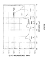
- FIG. 1 shows a figure illustrating the gist of a semiconductor device 100 according to an embodiment of the present invention.
- FIG. 2 shows a sectional schematic view of the semiconductor device 100 and a figure illustrating the carrier concentration distribution in an FS region 40 .
- FIG. 3 shows a schematic view illustrating a distribution example of the carrier lifetime of a semiconductor substrate 10 in its depth direction.
- FIG. 4 shows a figure illustrating one exemplary leakage current waveform of the semiconductor device 100 .
- FIG. 5 shows a figure illustrating one exemplary manufacturing direction of the semiconductor device 100 .
- FIG. 6 shows a figure illustrating one example of an FS region formation step S 340 and a lifetime control step S 350 .
- FIG. 7 shows a figure illustrating another example of the FS region formation step S 340 and the lifetime control step S 350 .
- FIG. 8 shows a figure in which a leakage current waveform of a semiconductor device 100 manufactured by performing proton annealing and a leakage current waveform of a semiconductor device 100 manufactured without performing proton annealing are compared with each other.
- FIG. 9 shows a figure illustrating another exemplary carrier lifetime distribution.
- FIG. 10 shows a figure illustrating one exemplary end portion position of a depletion layer when a reverse voltage is applied to the semiconductor device 100 .
- FIG. 11 shows a figure illustrating one exemplary relationship between the irradiation amount of helium as a local lifetime killer and forward voltage of the semiconductor device 100 .
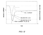
- FIG. 12 shows a figure illustrating exemplary temporal waveforms of anode-cathode voltage and anodic current at the time of reverse recovery.
- FIG. 13 shows a figure illustrating the relationship between forward voltage and dV/dt when the semiconductor substrate 10 is divided into seven regions in its depth direction, and the carrier lifetimes of the respective regions are varied.
- FIG. 14A shows the relationship between the carrier lifetime (forward voltage) of a region from the front surface to the depth of 1/7 of the semiconductor substrate 10 , and a temporal waveform of anode-cathode voltage V KA .
- FIG. 14B shows the relationship between the carrier lifetime (forward voltage) of a region from the front surface to the depth of 1/7 of the semiconductor substrate 10 , and a temporal waveform of anode current I A .
- FIG. 15A shows the relationship between the carrier lifetime (forward voltage) of a depth region from 1/7 to 2/7 and a temporal waveform of anode-cathode voltage V KA .
- FIG. 15B shows the relationship between the carrier lifetime (forward voltage) of a depth region from 1/7 to 2/7 from the front surface of the semiconductor substrate 10 , and a temporal waveform of anode current I A .
- FIG. 16A shows the relationship between the carrier lifetime (forward voltage) of a depth region from 2/7 to 3/7 and a temporal waveform of anode-cathode voltage V KA .
- FIG. 16B shows the relationship between the carrier lifetime (forward voltage) of a depth region from 2/7 to 3/7 from the front surface of the semiconductor substrate 10 , and a temporal waveform of anode current I A .
- FIG. 17A shows the relationship between the carrier lifetime (forward voltage) of a depth region from 3/7 to 4/7 and a temporal waveform of anode-cathode voltage V KA .
- FIG. 17B shows the relationship between the carrier lifetime (forward voltage) of a depth region from 3/7 to 4/7 from the front surface of the semiconductor substrate 10 , and a temporal waveform of anode current I A .
- FIG. 18A shows the relationship between the carrier lifetime (forward voltage) of a depth region from 4/7 to 5/7 and a temporal waveform of anode-cathode voltage V KA .
- FIG. 18B shows the relationship between the carrier lifetime (forward voltage) of a depth region from 4/7 to 5/7 from the front surface of the semiconductor substrate 10 , and a temporal waveform of anode current I A .
- FIG. 19A shows the relationship between the carrier lifetime (forward voltage) of a depth region from 5/7 to 6/7 and a temporal waveform of anode-cathode voltage V KA .
- FIG. 19B shows the relationship between the carrier lifetime (forward voltage) of a depth region from 5/7 to 6/7 from the front surface of the semiconductor substrate 10 , and a temporal waveform of anode current I A .
- FIG. 20A shows the relationship between the carrier lifetime (forward voltage) of a depth region from 6/7 to the rear surface of the semiconductor substrate 10 , and a temporal waveform of anode-cathode voltage V KA .
- FIG. 20B shows the relationship between the carrier lifetime (forward voltage) of a depth region from 6/7 to the rear surface of the semiconductor substrate 10 , and a temporal waveform of anode current I A .
- FIG. 21 shows a figure illustrating a configuration example of a semiconductor device 200 according to another embodiment.
- FIG. 22 shows a figure illustrating one exemplary method of manufacturing the semiconductor device 200 .
- FIG. 23 shows a figure illustrating another exemplary carrier concentration distribution in the FS region 40 .
- FIG. 24 shows a figure illustrating one exemplary impurity concentration distribution of the semiconductor substrate 10 in its depth direction, together with the helium distribution and hydrogen distribution.
- FIG. 1 shows a figure illustrating the gist of a semiconductor device 100 according to an embodiment of the present invention.
- FIG. 1 shows a schematic view of a section of the semiconductor device 100 .
- the semiconductor device 100 in the present example is used as a free wheeling diode (FWD) provided to be parallel with a high withstand voltage switch such as an IGBT, for example.
- the semiconductor device 100 of the present example comprises an n ⁇ -type semiconductor substrate 10 , an insulation film 22 , an anode electrode 24 and a cathode electrode 32 .
- a p + -type anode region 20 is formed in the semiconductor substrate 10 on its front surface side, and a field stop region (FS region 40 ) and an n + -type cathode region 30 are formed in the semiconductor substrate 10 on its rear surface side.
- the semiconductor substrate 10 is a silicon substrate, for example.
- the insulation film 22 is formed to cover the front surface of the semiconductor substrate 10 . However, the insulation film 22 has an opening through which the anode region 20 is exposed.
- the insulation film 22 is formed with an insulating material such as silicon oxide or silicon nitride, for example.
- the anode electrode 24 is formed on the anode region 20 exposed through the opening of the insulation film 22 .
- the anode electrode 24 is formed with metal such as aluminum, for example.
- the FS region 40 is an n-type region formed with protons (hydrogen ions) as the donor.
- the impurity concentration of the FS region (the donor concentration in the present example) is higher than the impurity concentration of the semiconductor substrate 10 .
- the cathode region 30 is formed in the semiconductor substrate 10 to be closer to its rear surface than the FS region 40 is.
- the cathode region 30 is an n + -type region formed with phosphorus or the like as the donor, for example.
- the impurity concentration of the cathode region 30 is higher than both the impurity concentration of the semiconductor substrate 10 and the impurity concentration of the FS region 40 .
- the cathode electrode 32 is formed on the rear surface of the semiconductor substrate 10 , and is connected with the cathode region 30 . With such a configuration, the semiconductor device 100 functions as a diode.
- FIG. 2 shows a sectional schematic view of the semiconductor device 100 and a figure illustrating the carrier concentration distribution in the FS region 40 .
- the insulation film 22 , the anode electrode 24 and the cathode electrode 32 are omitted.
- the horizontal axis indicates the depth position within the FS region 40 from its rear surface side end portion, and the vertical axis indicates the carrier concentration.
- the carrier concentration corresponds to the donor concentration of protons injected into the FS region 40 .
- the concentration distribution of the donor in the FS region 40 in its depth direction has a plurality of peaks.
- the peaks refer to maximum values, for example.
- a first peak, a second peak, a third peak and a fourth peak are present in the concentration distribution of the donor in the FS region 40 of the present example.
- the first peak is present at the deepest position in the FS region 40 as seen from the rear surface side (cathode side) of the semiconductor substrate 10 .
- locations whose distances from the rear surface side (cathode side) of the semiconductor substrate 10 are longer are referred to as “deeper positions”, and locations whose distances are shorter are referred to as “shallower positions.”
- the second peak is present at a position shallower than that of the first peak.
- the donor concentration of the second peak is lower than the donor concentration of the first peak.
- the third peak is present at a position shallower than that of the second peak.
- the donor concentration of the third peak is higher than both the donor concentration of the second peak and the donor concentration of the first peak.
- the donor concentration of the third peak may be lower than at least either one of the donor concentration of the second peak and the donor concentration of the first peak.
- the fourth peak is present at a position shallower than that of the third peak.
- the fourth peak is present at the shallowest position in the FS region 40 .
- the fourth peak may be provided at a position adjacent to or apart from the cathode region 30 .
- the plurality of peaks may be provided at regular intervals or irregular intervals in the FS region 40 in its depth direction.
- the donor concentration of the fourth peak is higher than the donor concentrations of all the other peaks.
- the concentration of a peak decreases as the distance, in the FS region 40 , from the rear surface side of the semiconductor substrate 10 increases, the concentration of the first peak at the deepest position becomes higher than the concentration of the second peak at the second deepest position.
- the concentration of the first peak higher than the concentration of the second peak, the distribution of the carrier lifetime of the semiconductor substrate 10 in its depth direction can be controlled appropriately.
- the carrier lifetime is controlled by irradiation with an electron ray or the like. Irradiation with an electron ray or the like dissociates the bonds between atoms of silicon crystal or the like forming the semiconductor substrate 10 , and crystal defects occur. Thereby, the carrier lifetime becomes short. Irradiation with an electron ray or the like makes the carrier lifetime short almost uniformly over the entire semiconductor substrate 10 .
- protons terminate atoms whose bonds have been dissociated to repair the above-mentioned crystal defects. That is, protons have a function of recovering a carrier lifetime. For this reason, the distribution of a carrier lifetime can be controlled by controlling the concentration distribution of protons to be injected into the semiconductor substrate 10 .
- FIG. 3 shows a schematic view illustrating a distribution example of the carrier lifetime of the semiconductor substrate 10 in its depth direction.
- the horizontal axis indicates positions in the depth direction of the semiconductor substrate 10
- the vertical axis indicates the carrier lifetimes.
- the distribution example shows in FIG. 3 is schematic, and the thickness of the semiconductor substrate 10 and the thickness of the FS region 40 do not match those in the example of FIG. 2 .
- the first peak of the FS region is positioned near the center of the anode region 20 and the cathode region 30 .
- the diffused protons hydrogen-terminate crystal defects to recover a carrier lifetime. Because in the present example, the concentration of protons injected to the deepest position of the FS region 40 is high, the carrier lifetime of an intermediate portion of the semiconductor substrate 10 becomes longer than those on the front surface and rear surface of the semiconductor substrate 10 as shown in FIG. 3 .
- the carrier lifetime in at least a partial region between the anode region 20 and the cathode region 30 is longer than the carrier lifetimes in both the anode region 20 and the cathode region 30 .
- the concentration distribution of protons injected is controlled to attain such a distribution of carrier lifetimes.
- the carrier lifetime at a depth position that exhibits the first peak shown in FIG. 2 becomes longer than the carrier lifetimes in both the anode region 20 and the cathode region 30 .
- the peak current Irp and the tail current of a reverse recovery current can be made small to decrease a reverse recovery loss, and the rate of temporal change dV/dt of reverse recovery voltage can be made small to realize gentle reverse recovery.
- the region that has a carrier lifetime longer than that in the anode region 20 extends toward the front surface side of the semiconductor substrate 10 past a position that is at the deepest portion in the FS region 40 and exhibits the first peak, as shown in FIG. 3 .
- the extension amount of the region is estimated to be approximately 30 to 40 ⁇ m from the position of the first peak as described below with reference to FIG. 4 .
- the depth position of the first peak is preferably determined considering the extension amount.
- FIG. 4 shows a figure illustrating one exemplary leakage current waveform of the semiconductor device 100 .
- the horizontal axis indicates the reverse voltage between the anode and the cathode, and the vertical axis indicates the leakage current.
- a leakage current waveform of a semiconductor device in which the FS region 40 is not formed is shown with a broken line.
- the semiconductor device 100 of the present example in which the FS region 40 is formed exhibits generally decreased leakage current as compared with the semiconductor device in which the FS region 40 is not formed.
- the semiconductor device 100 of the present example exhibits a steep inclination of leakage current increase relative to reverse voltages of up to approximately 200 to 300 V. With a further larger reverse voltage, the inclination of current decreases. The decrease in the inclination of current is deemed to be attributable to the fact that the depletion layer expanded by increase in voltage entered a region where the carrier lifetime was recovered by protons.
- Vbi is a built-in voltage
- N A is an accepter concentration
- N D is a donor concentration
- e is the dielectric constant of the semiconductor substrate 10
- q is an electric charge.
- FIG. 5 shows a figure illustrating one exemplary manufacturing direction of the semiconductor device 100 .
- a semiconductor substrate 12 is prepared.
- the semiconductor substrate 12 functions as the semiconductor substrate 10 by being ground at its rear surface at a grinding step S 320 described below. That is, the semiconductor substrate 12 is formed with a material which is the same as that of the semiconductor substrate 10 , and is thicker than the semiconductor substrate 10 .
- the substrate resistivities of the semiconductor substrate 12 and the semiconductor substrate 10 may be approximately 70 to 90 ⁇ cm.
- a front surface side forming step S 310 the element structure of the front surface side of the semiconductor substrate 12 is formed.
- the anode region 20 , the insulation film 22 and the anode electrode 24 are formed on the front surface of the semiconductor substrate 12 .
- a protection film to protect the element structure may be formed. The protection film may be removed after manufacturing the semiconductor device 100 . Because the structure of the front surface side is formed by using the thick semiconductor substrate 12 , the possibility of a crack or the like of the semiconductor substrate 12 occurring at the front surface side forming step S 310 can be lowered.
- the rear surface side of the semiconductor substrate 12 is ground to form the semiconductor substrate 10 .
- the thickness of the semiconductor substrate 10 after grinding is determined based on a rated voltage or the like of the semiconductor device 100 .
- the thickness of the semiconductor substrate 10 in the present example is approximately 100 to 130 ⁇ m.
- the cathode region 30 is formed on the rear surface of the semiconductor substrate 10 .
- n-type impurities such as phosphorus are ion-injected from the rear surface side of the semiconductor substrate 10 .
- laser annealing is performed on a region where the cathode region 30 should be formed to activate impurity ions and turn them into a donor. Thereby, the cathode region 30 is formed.
- protons are injected into a region where the FS region 40 should be formed.
- protons are injected into the FS region 40 so that the concentration distribution of protons in the FS region 40 in its depth direction has a plurality of peaks.
- the first peak closest to the front surface of the semiconductor substrate 10 may be higher than the second peak closer to the rear surface of the semiconductor substrate 10 than the first peak is.
- the FS region 40 is formed.
- the condition ranges of the acceleration voltage and injection amount of protons in the present example are as follows. Each value shown in the parentheses is a value to be one example. Thereby, the concentration distribution similar to that in the example of FIG. 2 is formed.
- Second peak 0.8 to 3 MeV (1 Mev), 1E12 to 1E13 cm ⁇ 2 (7E12 cm ⁇ 2 )
- the preferred ranges of respective peak concentrations of the FS region 40 and depths from the rear surface in the present example are as follows. Each value shown in the parentheses is a value to be one example. Also, because the second peak, the third peak and the fourth peak are formed in passage regions of protons for deeper peaks, the donor concentrations are raised due to the influence of protons in the passage regions having been turned into the donor. For this reason, for example, even if the injection amount of protons at the first peak, and the injection amount of protons at the third peak are the same, the donor concentration of the third peak is higher than that of the first peak. Because the donor concentrations of the passage regions of protons of the first and second peak are added thereto.
- Second peak 1E14 to 1E15 cm ⁇ 3 (5E14 cm ⁇ 3 ), 10 to 100 ⁇ m (15 ⁇ m)
- the position of the first peak may be determined according to the withstand voltage class of the semiconductor device 100 . As described above, protons are diffused by a certain distance toward the front surface side of the semiconductor substrate 10 . Because the size of a region on the front surface side of the semiconductor substrate 10 desired to be left as a region where protons are not diffused is determined according to the withstand voltage class of the semiconductor device 100 , the position of the first peak may be determined considering the distance by which protons are diffused.
- the position of the first peak in a 1700-V withstand voltage semiconductor device 100 for example, is deeper than the position of the first peak in a 1200-V withstand voltage semiconductor device 100 . Also, in a 600-V withstand voltage semiconductor device 100 , the first peak is provided at a position shallower than that in the 1200-V withstand voltage semiconductor device 100 .
- a lifetime control step S 350 the rear surface side of the semiconductor substrate 10 is irradiated with a lifetime killer.
- the rear surface side of the semiconductor substrate 10 is irradiated for example with an electron ray.
- the lifetime killer is not limited to an electron ray, one that enables recovery, by protons, of a carrier lifetime shortened by the lifetime killer is used.
- the semiconductor substrate 10 is annealed. Thereby, protons are diffused within the semiconductor substrate 10 , and the carrier lifetime of a partial region recovers, and the carrier lifetime distribution as shown in FIG. 3 is attained.
- the cathode electrode 32 is formed in the semiconductor substrate 10 on its rear surface side. After forming the cathode electrode 32 , a thermal process of the cathode electrode 32 may be performed. Thereby, the semiconductor device 100 can be manufactured.
- FIG. 6 shows a figure illustrating one example of the FS region formation step S 340 and the lifetime control step S 350 .
- the FS region formation step S 340 of the present example has a proton injection step S 342 and a proton annealing step S 344 .
- the lifetime control step S 350 has a lifetime killer irradiation step S 352 and a lifetime annealing step S 354 .
- the semiconductor substrate 10 is annealed.
- the annealing temperature is approximately 300 to 500° C., for example, and the annealing duration is approximately 0.5 to 10 hours, for example.
- the annealing temperature is approximately 300 to 500° C., for example, and the annealing duration is approximately 0.5 to 10 hours, for example.
- irradiation with an electron ray of 80 kGy is performed.
- the present example comprises the proton annealing step S 344 of annealing the semiconductor substrate 10 between the proton injection step S 342 and the lifetime killer irradiation step S 352 , and excess protons are expelled from the semiconductor substrate 10 at the proton annealing step S 344 , an appropriate amount of the protons is diffused by lifetime annealing. Thereby, the carrier lifetime in a region where protons are diffused recovers. For this reason, both decrease in the carrier lifetimes on the anode region 20 side and cathode region 30 side by lifetime killer irradiation, and recovery of the carrier lifetime in a region between the anode region 20 and the cathode region 30 by proton diffusion can be realized.
- FIG. 7 shows a figure illustrating another example of the FS region formation step S 340 and the lifetime control step S 350 .
- the FS region formation step S 340 does not have the proton annealing step S 344 .
- Other respects are the same as the example shown in FIG. 6 .
- FIG. 8 shows a figure in which a leakage current waveform of a semiconductor device 100 manufactured by performing proton annealing and a leakage current waveform of a semiconductor device 100 manufactured without performing proton annealing are compared with each other.
- FIG. 9 shows a figure illustrating another exemplary carrier lifetime distribution.
- the carrier lifetime in the cathode region 30 is reduced as compared with that in the distribution shown in FIG. 3 .
- a local lifetime killer to shorten the carrier lifetime is injected into the rear surface side of the semiconductor substrate 10 .
- the local lifetime killer in the present example is helium. Because the tail current can be made small by reducing the carrier lifetime on the cathode region 30 side as described below, a reverse recovery loss can be decreased.
- a region where the local lifetime killer is present is preferably formed at a depth position that does not contact a depletion layer that expands from the boundary between the anode region 20 and an n-type region of the semiconductor substrate 10 when a rated reverse voltage of the semiconductor device 100 is applied. Also, a region where the local lifetime killer is present may be formed at a depth position that does not contact a depletion layer that expands from the boundary between the anode region 20 and an n-type region of the semiconductor substrate 10 when a breakdown voltage of the semiconductor device 100 is applied.
- FIG. 10 shows a figure illustrating one exemplary end portion position of a depletion layer when a reverse voltage is applied to the semiconductor device 100 .
- FIG. 10 shows the dope concentration distribution of impurities together. Also, in FIG. 10 , distances, from the rear surface of the semiconductor substrate 10 , of depletion layer end portions when reverse voltages are 400 V, 600 V, 800 V, 1000 V, 1100 V and 1200 V are shown.
- the depletion layer expands from the front surface toward the rear surface of the semiconductor substrate 10 , and the depletion layer end reaches the position of 4 ⁇ m from the rear surface.
- the local lifetime killer is preferably neither injected nor diffused to positions deeper than 2.5 ⁇ m from the rear surface of the semiconductor substrate 10 , for example.
- the local lifetime killer injection position overlaps the fourth peak position of the proton injection. Crystal defects that have occurred due to helium irradiation are influenced by defect recovery due to protons in a similar manner to electron ray irradiation. For this reason, the local lifetime killer injection amount is preferably adjusted according to the proton injection amount in the region.
- FIG. 11 shows a figure illustrating one exemplary relationship between the irradiation amount of helium as a local lifetime killer and forward voltage of the semiconductor device 100 .
- the forward voltage in a case where irradiation with helium was not performed was approximately 1.5 to 1.6 V.
- the proton injection amount at the fourth peak is 3E14 cm ⁇ 2 .
- the local lifetime killer injection amount is preferably 1/300 or more of the proton injection amount.
- the local lifetime killer injection amount may be 1/150 or more, or 1/100 or more of the proton injection amount.
- the local lifetime killer injection amount is preferably 1 ⁇ 3 or less of the proton injection amount.
- FIG. 12 shows a figure illustrating exemplary temporal waveforms of anode-cathode voltage and anodic current at the time of reverse recovery.
- a reverse recovery loss can be decreased by making the peak current value Irp and the tail current shown in FIG. 12 small. Also, by making the inclination dV/dt of the anode-cathode voltage steep, reverse recovery can be made gentle.
- FIG. 13 shows a figure illustrating the relationship between forward voltage and dV/dt when the semiconductor substrate 10 is divided into seven regions in its depth direction, and the carrier lifetimes of the respective regions are varied.
- the relationship is calculated by device simulation. Generally, the shorter the carrier lifetime, the higher the forward voltage Vf.
- FIG. 14A shows the relationship between forward voltage Vf at the time when the carrier lifetime of a region from the front surface to the depth of 1/7 of the semiconductor substrate 10 is varied, and a temporal waveform of anode-cathode voltage V KA .
- FIG. 14B shows the relationship between forward voltage Vf at the time when the carrier lifetime of a region from the front surface to the depth of 1/7 of the semiconductor substrate 10 is varied, and a temporal waveform of anode current I A .
- FIG. 15A shows the relationship between forward voltage Vf at the time when the carrier lifetime of a depth region from 1/7 to 2/7 is varied, and a temporal waveform of anode-cathode voltage V KA .
- FIG. 15B shows the relationship between forward voltage Vf at the time when the carrier lifetime of a depth region from 1/7 to 2/7 from the front surface of the semiconductor substrate 10 is varied, and a temporal waveform of anode current I A .
- FIG. 16A shows the relationship between forward voltage Vf at the time when the carrier lifetime of a depth region from 2/7 to 3/7 is varied, and a temporal waveform of anode-cathode voltage V KA .
- FIG. 16B shows the relationship between forward voltage Vf at the time when the carrier lifetime of a depth region from 2/7 to 3/7 from the front surface of the semiconductor substrate 10 is varied, and a temporal waveform of anode current I A .
- FIG. 17A shows the relationship between forward voltage Vf at the time when the carrier lifetime of a depth region from 3/7 to 4/7 is varied, and a temporal waveform of anode-cathode voltage V KA .
- FIG. 17B shows the relationship between forward voltage Vf at the time when the carrier lifetime of a depth region from 3/7 to 4/7 from the front surface of the semiconductor substrate 10 is varied, and a temporal waveform of anode current I A .
- FIG. 18A shows the relationship between forward voltage Vf at the time when the carrier lifetime of a depth region from 4/7 to 5/7 is varied, and a temporal waveform of anode-cathode voltage V KA .
- FIG. 18B shows the relationship between forward voltage Vf at the time when the carrier lifetime of a depth region from 4/7 to 5/7 from the front surface of the semiconductor substrate 10 is varied, and a temporal waveform of anode current I A .
- FIG. 19A shows the relationship between forward voltage Vf at the time when the carrier lifetime of a depth region from 5/7 to 6/7 is varied, and a temporal waveform of anode-cathode voltage V KA .
- FIG. 19B shows the relationship between forward voltage Vf at the time when the carrier lifetime of a depth region from 5/7 to 6/7 from the front surface of the semiconductor substrate 10 is varied, and a temporal waveform of anode current I A .
- FIG. 20A shows the relationship between forward voltage Vf at the time when the carrier lifetime of a depth region from 6/7 to the rear surface of the semiconductor substrate 10 is varied, and a temporal waveform of anode-cathode voltage V KA .
- FIG. 20B shows the relationship between forward voltage Vf at the time when the carrier lifetime of a depth region from 6/7 to the rear surface of the semiconductor substrate 10 is varied, and a temporal waveform of anode current I A .
- the carrier lifetime is preferably short so as to reduce Irp.
- the carrier lifetime of this region is preferably long so as to realize gentle dV/dt.
- the carrier lifetime of this region may be shorter than that in the region from 3/7 to 5/7, and longer than that in the region from the front surface of the semiconductor substrate 10 to 3/7.
- the above-mentioned phenomenon can be understood also as follows.
- the depletion layer expands from the anode region 20 side. Carriers that have been present in the region of the depletion layer are expelled to become a reverse recovery current. Accordingly, if there is a lot of carriers on the front surface side of the semiconductor substrate 10 , it becomes more likely that the peak Irp of current to flow first becomes higher.
- the IGBT or the like draws a predetermined current from the semiconductor device 100 .
- the current can be supplied to the IGBT or the like even if the depletion layer expands slowly.
- the depletion layer expands fast in order to supply the current, and the inclination dV/dt of the reverse recovery voltage becomes steep. For this reason, when the number of carriers in a region in the middle of the semiconductor substrate 10 through which the depletion layer expands is large, the inclination of dV/dt of reverse recovery voltage becomes less steep.
- the first peak is preferably provided at a position corresponding to an end portion of the above-mentioned depletion layer on the rear surface side of the semiconductor substrate 10 when the inter-electrode voltage of the diode at the time of reverse recovery of the semiconductor device 100 becomes the half value of an applied voltage.
- an applied voltage at the time of reverse recovery is often set to be approximately the half of the withstand voltage of an element.
- a 1200-V withstand voltage element is reverse-recovered at an applied voltage of 600 V.
- the moment when dV/dt becomes the largest at the time of reverse recovery is when the anode-cathode voltage becomes the half of an applied voltage.
- the carrier lifetime is caused to recover by injecting protons to form the FS region 40 , and at the same time diffusing the protons. Because in the present example, the distribution of protons is like the one shown in FIG. 2 or the like, as shown in FIG. 3 or FIG. 9 , the distribution of the carrier lifetime having a peak in the middle of the semiconductor substrate 10 can be formed. Thanks to the distribution of the carrier lifetime, as explained with reference to FIG. 13 to FIG. 20A , the small peak current Irp, the small tail current and the gentle inclination dV/dt of reverse recovery voltage can be realized.
- FIG. 21 shows a figure illustrating a configuration example of a semiconductor device 200 according to another embodiment.
- the semiconductor device 200 of the present example is an RC-IGBT device in which an IGBT element 140 and a FWD element 150 connected in anti-parallel are formed integrally.
- the semiconductor device 200 comprises the semiconductor substrate 10 , an insulation film 122 , an emitter anode electrode 124 and a collector cathode electrode 132 .
- the semiconductor substrate 10 has p-type regions 120 formed on its front surface side. Also, the semiconductor substrate 10 has a plurality of trenches 104 formed to penetrate the p-type regions 120 from the front surface of the semiconductor substrate 10 . The leading end of each trench 104 on the rear surface side of the semiconductor substrate 10 protrudes past the end portions of the p-type regions 120 . Each trench 104 has a trench gate 102 formed to penetrate the p-type region 120 from the front surface of the semiconductor substrate 10 . Also, each trench gate 102 and each semiconductor layer are insulated by an insulation film 103 .
- n + -type regions 106 and p + -type region 108 are formed.
- the n + -type regions 106 are provided adjacent to the trenches 104 on the front surface of the p-type regions 120 .
- the p + -type regions 108 are provided being sandwiched by the n + -type regions 106 on the front surface of the p-type regions 120 .
- p-type regions 120 corresponding to the FWD element 150 function as the anode region 20 explained with reference to FIG. 1 to FIG. 20B .
- the n + -type regions 106 and the p + -type regions 108 may be formed also in the p-type regions 120 corresponding to the FWD element 150 .
- the emitter anode electrode 124 is connected to the respective p-type regions 120 .
- the emitter anode electrode 124 is connected to both the n + -type regions 106 and the p + -type regions 108 .
- the emitter anode electrode 124 is connected to the p-type regions 120 .
- the emitter anode electrode 124 and the trench gates 102 are insulated by the insulation film 122 .
- the respective trench gates 102 are connected to a gate electrode not shown in the figure. Due to a voltage being applied to the trench gates 102 , a channel in the vertical direction is formed in the p-type regions 120 between the n + -type regions 106 and the semiconductor substrate 10 .
- the semiconductor substrate 10 comprises the FS region 40 formed on its rear surface side.
- the FS region 40 has the structure and characteristics which are the same as those of the FS region 40 explained with reference to FIG. 1 to FIG. 20B .
- a p-type collector region 130 is formed, and in a region corresponding to the FWD element 150 , the n-type cathode region 30 is formed.
- the common collector cathode electrode 132 is formed on the rear surfaces of the collector region 130 and the cathode region 30 .
- FIG. 22 shows a figure illustrating one exemplary method of manufacturing the semiconductor device 200 .
- the semiconductor substrate 12 is prepared in a manner similar to that in the example of FIG. 5 .
- the element structure of the semiconductor substrate 12 on the front surface side thereof is formed.
- the p-type regions 120 , the trenches 104 , the n + -type regions 106 , the p + -type regions 108 , the n-type regions 110 and the insulation film 122 are formed on the front surface of the semiconductor substrate 12 .
- a front surface electrode formation step S 404 the emitter anode electrode 124 is formed.
- the rear surface grinding step S 406 the rear surface of the semiconductor substrate 12 is ground.
- a rear surface diffusion layer ion injection step S 408 p-type impurity ions and n-type impurity ions are injected, respectively, into regions of the rear surface of the semiconductor substrate 10 corresponding to the collector region 130 and the cathode region 30 .
- a rear surface laser annealing step S 410 the regions to which the p-type impurity ions and the n-type impurity ions are injected are laser-annealed to form the collector region 130 and the cathode region 30 .
- a front surface protection film formation step S 411 a protection film is formed on the front surface of the semiconductor substrate 10 .
- the FS region 40 is formed.
- the proton injection step S 412 and the proton annealing step S 414 are the same as the proton injection step S 342 and the proton annealing step S 344 in FIG. 6 .
- the FS region 40 having the concentration distribution of protons as the one shown in FIG. 2 is formed.
- a lifetime killer irradiation step S 416 and a lifetime annealing step S 418 the carrier lifetime is controlled.
- the lifetime killer irradiation step S 416 and the lifetime annealing step S 418 are the same as the lifetime killer irradiation step S 352 and the lifetime annealing step S 354 in FIG. 6 . Thereby, the carrier lifetime distribution as the one shown in FIG. 3 or FIG. 9 is realized.
- the collector cathode electrode 132 is formed. Thereby, the semiconductor device 200 is manufactured.
- FIG. 23 shows a figure illustrating another exemplary carrier concentration distribution in the FS region 40 .
- the horizontal axis indicates the depth position within the FS region 40 from its rear surface side end portion, and the vertical axis indicates the carrier concentration.
- the carrier concentration corresponds to the donor concentration of protons injected into the FS region 40 .
- the concentration distribution of the donor in the FS region 40 in its depth direction has a plurality of peaks.
- the first to third peaks excluding the fourth peak closest to the rear surface side end portion of the FS region 40 have higher carrier concentrations as the distances from the rear surface end portion increase. That is, the carrier concentration of the first peak is higher than the carrier concentrations of the second peak and the third peak, and the carrier concentration of the second peak is higher than the carrier concentration of the third peak.
- the FS region 40 prevents the depletion layer expanding from the boundary of the p + -type anode region 20 and the n ⁇ -type semiconductor substrate 10 from reaching the cathode region 30 .
- the depletion layer may expand, at most, to the peak closest to the rear surface end portion among the plurality of peaks.
- the concentrations of the first to third peak decrease gradually from the substrate front surface side toward the rear surface side. Also, the lowest peak concentration is higher than that in the example of FIG. 2 . For this reason, the inclination dV/dt of reverse recovery voltage can be made small.
- FIG. 24 shows a figure illustrating one exemplary impurity concentration distribution of the semiconductor substrate 10 in its depth direction, together with the helium distribution and hydrogen distribution.
- the p-type and n-type impurity concentrations are shown together.
- the p-type anode region 20 with a high concentration is formed from the front surface of the semiconductor substrate 10 to the depth of approximately several ⁇ m.
- An n ⁇ -type region as a drift region is formed from an end portion of the anode region 20 to the depth of approximately 55 ⁇ m, and the FS region 40 and the cathode region 30 are formed to the depths of approximately 55 ⁇ m and more.
- the impurity concentration of a comparative example 300 is indicated with a dotted line.
- the peak of impurity concentration closest to the front surface of the semiconductor substrate 10 is higher than the corresponding peak in the comparative example 300 .
- the front surface of the semiconductor substrate 10 is irradiated with helium ions in order to control the carrier lifetime on the front surface side of the semiconductor substrate 10 .
- the average range of helium ions is Rp
- the half-value width of the range distribution of helium ions is ⁇ Rp.
- the peak position of a range of helium ions with which the front surface of the semiconductor substrate 10 is irradiated (that is, the position of a depth Rp from the front surface of the semiconductor substrate 10 ) may be located within a range of 40 ⁇ m from the peak closest to the front surface of the semiconductor substrate 10 from among the peaks in the concentration distribution of the donor in the FS region 40 .
- the distance from a peak may be measured from a position at which a donor concentration becomes a half of a maximum value of the peak on the substrate front surface side from the maximum point of the peak.
- the half-value position Rp- ⁇ Rp of the range distribution of helium ions may be within the range of 40 ⁇ m from the peak of the concentration distribution of the donor in the FS region 40 . Thereby, a leakage current can be decreased more efficiently.
- the distribution position of helium ions is not limited to these ranges. Even if the peak position Rp of the range of helium ions is apart from the peak of the concentration distribution of the donor in the FS region 40 by 40 ⁇ m or more, a leakage current can be decreased to a certain degree, although hydrogen diffused from the peak becomes less.
Landscapes
- Engineering & Computer Science (AREA)
- Power Engineering (AREA)
- Microelectronics & Electronic Packaging (AREA)
- Physics & Mathematics (AREA)
- Computer Hardware Design (AREA)
- Condensed Matter Physics & Semiconductors (AREA)
- General Physics & Mathematics (AREA)
- Ceramic Engineering (AREA)
- Manufacturing & Machinery (AREA)
- High Energy & Nuclear Physics (AREA)
- Health & Medical Sciences (AREA)
- Toxicology (AREA)
- Metal-Oxide And Bipolar Metal-Oxide Semiconductor Integrated Circuits (AREA)
- Thyristors (AREA)
Priority Applications (3)
| Application Number | Priority Date | Filing Date | Title |
|---|---|---|---|
| US16/430,444 US10923570B2 (en) | 2014-10-03 | 2019-06-04 | Manufacturing method for controlling carrier lifetimes in semiconductor substrates that includes injection and annealing |
| US17/168,124 US11646350B2 (en) | 2014-10-03 | 2021-02-04 | Semiconductor device, and method of manufacturing semiconductor device |
| US18/310,554 US20230275129A1 (en) | 2014-10-03 | 2023-05-02 | Semiconductor device, and method of manufacturing semiconductor device |
Applications Claiming Priority (3)
| Application Number | Priority Date | Filing Date | Title |
|---|---|---|---|
| JP2014-204849 | 2014-10-03 | ||
| JP2014204849 | 2014-10-03 | ||
| PCT/JP2015/072933 WO2016051973A1 (ja) | 2014-10-03 | 2015-08-13 | 半導体装置および半導体装置の製造方法 |
Related Parent Applications (1)
| Application Number | Title | Priority Date | Filing Date |
|---|---|---|---|
| PCT/JP2015/072933 Continuation WO2016051973A1 (ja) | 2014-10-03 | 2015-08-13 | 半導体装置および半導体装置の製造方法 |
Related Child Applications (1)
| Application Number | Title | Priority Date | Filing Date |
|---|---|---|---|
| US16/430,444 Division US10923570B2 (en) | 2014-10-03 | 2019-06-04 | Manufacturing method for controlling carrier lifetimes in semiconductor substrates that includes injection and annealing |
Publications (2)
| Publication Number | Publication Date |
|---|---|
| US20160276446A1 US20160276446A1 (en) | 2016-09-22 |
| US10312331B2 true US10312331B2 (en) | 2019-06-04 |
Family
ID=55630019
Family Applications (4)
| Application Number | Title | Priority Date | Filing Date |
|---|---|---|---|
| US15/169,740 Active US10312331B2 (en) | 2014-10-03 | 2016-06-01 | Semiconductor device, and method of manufacturing semiconductor device |
| US16/430,444 Active 2035-10-21 US10923570B2 (en) | 2014-10-03 | 2019-06-04 | Manufacturing method for controlling carrier lifetimes in semiconductor substrates that includes injection and annealing |
| US17/168,124 Active US11646350B2 (en) | 2014-10-03 | 2021-02-04 | Semiconductor device, and method of manufacturing semiconductor device |
| US18/310,554 Pending US20230275129A1 (en) | 2014-10-03 | 2023-05-02 | Semiconductor device, and method of manufacturing semiconductor device |
Family Applications After (3)
| Application Number | Title | Priority Date | Filing Date |
|---|---|---|---|
| US16/430,444 Active 2035-10-21 US10923570B2 (en) | 2014-10-03 | 2019-06-04 | Manufacturing method for controlling carrier lifetimes in semiconductor substrates that includes injection and annealing |
| US17/168,124 Active US11646350B2 (en) | 2014-10-03 | 2021-02-04 | Semiconductor device, and method of manufacturing semiconductor device |
| US18/310,554 Pending US20230275129A1 (en) | 2014-10-03 | 2023-05-02 | Semiconductor device, and method of manufacturing semiconductor device |
Country Status (5)
| Country | Link |
|---|---|
| US (4) | US10312331B2 (ja) |
| JP (2) | JP6319453B2 (ja) |
| CN (1) | CN105814694B (ja) |
| DE (1) | DE112015000206T5 (ja) |
| WO (1) | WO2016051973A1 (ja) |
Families Citing this family (21)
| Publication number | Priority date | Publication date | Assignee | Title |
|---|---|---|---|---|
| WO2016051970A1 (ja) * | 2014-09-30 | 2016-04-07 | 富士電機株式会社 | 半導体装置および半導体装置の製造方法 |
| DE112015000206T5 (de) | 2014-10-03 | 2016-08-25 | Fuji Electric Co., Ltd. | Halbleitervorrichtung und Verfahren zum Herstellen einer Halbleitervorrichtung |
| DE112016000170T5 (de) | 2015-06-17 | 2017-08-03 | Fuji Electric Co., Ltd. | Halbleitervorrichtung und Verfahren zur Hestellung einer Halbleitervorrichtung |
| CN107851584B (zh) | 2016-02-23 | 2021-06-11 | 富士电机株式会社 | 半导体装置 |
| DE102016118012A1 (de) * | 2016-09-23 | 2018-03-29 | Infineon Technologies Ag | Halbleiterbauelement und Verfahren zum Bilden eines Halbleiterbauelements |
| WO2018135448A1 (ja) | 2017-01-17 | 2018-07-26 | 富士電機株式会社 | 半導体装置 |
| DE102017118975B4 (de) * | 2017-08-18 | 2023-07-27 | Infineon Technologies Ag | Halbleitervorrichtung mit einem cz-halbleiterkörper und verfahren zum herstellen einer halbleitervorrichtung mit einem cz-halbleiterkörper |
| DE112019000094T5 (de) | 2018-03-19 | 2020-09-24 | Fuji Electric Co., Ltd. | Halbleitervorrichtung und verfahren zum herstellen einerhalbleitervorrichtung |
| CN110660847B (zh) * | 2018-06-28 | 2022-04-12 | 上海先进半导体制造有限公司 | 双极型晶体管及其制造方法 |
| DE102018123439B4 (de) * | 2018-09-24 | 2020-04-23 | Infineon Technologies Ag | Leistungshalbleitertransistor, Verfahren zum Verarbeiten eines Leistungshalbleitertransistors und Verfahren zum Produzieren eines Leistungshalbleitertransistors |
| DE102018010379B4 (de) | 2018-09-24 | 2024-04-25 | Infineon Technologies Ag | Verfahren zum Herstellen eines Leistungshalbleitertransistors |
| DE112019001741T5 (de) | 2018-11-16 | 2020-12-17 | Fuji Electric Co., Ltd. | Halbleitervorrichtung und herstellungsverfahren |
| DE112019001738T5 (de) | 2018-11-16 | 2020-12-17 | Fuji Electric Co., Ltd. | Halbleitervorrichtung und herstellungsverfahren |
| JP7243744B2 (ja) * | 2019-01-18 | 2023-03-22 | 富士電機株式会社 | 半導体装置および半導体装置の製造方法 |
| US12080705B2 (en) * | 2019-07-12 | 2024-09-03 | Mitsubishi Electric Corporation | IGBT with anti-parallelly connected FWD on a common substrate |
| JP7222435B2 (ja) | 2019-10-11 | 2023-02-15 | 富士電機株式会社 | 半導体装置および半導体装置の製造方法 |
| JP7231066B2 (ja) * | 2020-01-17 | 2023-03-01 | 富士電機株式会社 | 半導体装置および半導体装置の製造方法 |
| JP7361634B2 (ja) * | 2020-03-02 | 2023-10-16 | 三菱電機株式会社 | 半導体装置及び半導体装置の製造方法 |
| WO2021177422A1 (ja) * | 2020-03-04 | 2021-09-10 | 富士電機株式会社 | 半導体装置、半導体装置の製造方法および半導体装置を備えた電力変換装置 |
| JP7456349B2 (ja) * | 2020-10-08 | 2024-03-27 | 三菱電機株式会社 | 半導体装置および半導体装置の製造方法 |
| WO2023176887A1 (ja) * | 2022-03-16 | 2023-09-21 | 富士電機株式会社 | 半導体装置および半導体装置の製造方法 |
Citations (41)
| Publication number | Priority date | Publication date | Assignee | Title |
|---|---|---|---|---|
| US5250446A (en) * | 1990-01-11 | 1993-10-05 | Kabushiki Kaisha Toshiba | Method of manufacturing a semiconductor device by forming at least three regions of different lifetimes of carriers at different depths |
| JPH07193218A (ja) | 1993-12-27 | 1995-07-28 | Hitachi Ltd | 荷電粒子注入方法及び結晶欠陥層を有する半導体装置 |
| JPH08102545A (ja) | 1994-09-30 | 1996-04-16 | Meidensha Corp | 半導体素子のライフタイム制御方法 |
| JPH09232332A (ja) | 1996-02-27 | 1997-09-05 | Fuji Electric Co Ltd | 半導体装置 |
| US5717244A (en) * | 1994-10-25 | 1998-02-10 | Mitsubishi Denki Kabushiki Kaisha | Semiconductor device having layers with varying lifetime characteristics |
| JPH10116998A (ja) | 1996-10-14 | 1998-05-06 | Toyota Motor Corp | 半導体装置およびその製造方法 |
| JP2000022174A (ja) | 1998-06-30 | 2000-01-21 | Toshiba Corp | 半導体装置の製造方法 |
| JP2000223720A (ja) | 1999-01-29 | 2000-08-11 | Meidensha Corp | 半導体素子およびライフタイム制御方法 |
| JP2001156299A (ja) | 1999-11-26 | 2001-06-08 | Fuji Electric Co Ltd | 半導体装置及びその製造方法 |
| JP2001160559A (ja) | 1999-12-01 | 2001-06-12 | Fuji Electric Co Ltd | 半導体装置の製造方法 |
| US6482681B1 (en) | 2000-05-05 | 2002-11-19 | International Rectifier Corporation | Hydrogen implant for buffer zone of punch-through non epi IGBT |
| US20050215042A1 (en) * | 2004-03-16 | 2005-09-29 | Infineon Technologies Ag | Metallization and its use in, in particular, an IGBT or a diode |
| US20060081923A1 (en) * | 2004-09-30 | 2006-04-20 | Infineon Technologies Ag | Semiconductor device and fabrication method suitable therefor |
| US20060138607A1 (en) * | 2002-02-20 | 2006-06-29 | Fuji Electric Co., Ltd. | Power semiconductor rectifier having broad buffer structure and method of manufacturing thereof |
| US20060286753A1 (en) * | 2005-06-08 | 2006-12-21 | Reiner Barthelmess | Method for Producing a Stop Zone in a Semiconductor Body and Semiconductor Component Having a Stop Zone |
| US20080001257A1 (en) * | 2006-06-30 | 2008-01-03 | Infineon Technologies Austria Ag | Semiconductor device with a field stop zone |
| US20080054369A1 (en) * | 2006-08-31 | 2008-03-06 | Infineon Technologies | Semiconductor device with a field stop zone and process of producing the same |
| JP2008211148A (ja) | 2007-02-28 | 2008-09-11 | Fuji Electric Device Technology Co Ltd | 半導体装置およびその製造方法 |
| US20090184340A1 (en) * | 2008-01-23 | 2009-07-23 | Fuji Electric Device Technology Co., Ltd. | Semiconductor device and method of producing the same |
| JP2010141170A (ja) | 2008-12-12 | 2010-06-24 | Denso Corp | 半導体装置の製造方法 |
| JP2012199577A (ja) | 2012-06-04 | 2012-10-18 | Fuji Electric Co Ltd | 半導体装置および半導体装置の製造方法 |
| US20130075783A1 (en) * | 2011-09-28 | 2013-03-28 | Toyota Jidosha Kabushiki Kaisha | Semiconductor device and method for manufacturing the same |
| US20130093065A1 (en) * | 2011-10-12 | 2013-04-18 | Mitsubishi Electric Corporation | Semiconductor device |
| US20130207223A1 (en) * | 2011-08-11 | 2013-08-15 | Peter Irsigler | Semiconductor device and method for producing a semiconductor device |
| WO2013141141A1 (ja) | 2012-03-19 | 2013-09-26 | 富士電機株式会社 | 半導体装置の製造方法 |
| WO2013141221A1 (ja) | 2012-03-19 | 2013-09-26 | 富士電機株式会社 | 半導体装置の製造方法 |
| US8766413B2 (en) * | 2009-11-02 | 2014-07-01 | Fuji Electric Co., Ltd. | Semiconductor device and method for manufacturing semiconductor device |
| US20140246755A1 (en) * | 2011-12-28 | 2014-09-04 | Fuji Electric Co., Ltd. | Semiconductor device and method for producing semiconductor device |
| US20140246750A1 (en) * | 2011-12-15 | 2014-09-04 | Fuji Electric Co., Ltd. | Semiconductor device and method for producing semiconductor device |
| US20140291723A1 (en) * | 2012-01-19 | 2014-10-02 | Fuji Electric Co., Ltd. | Semiconductor device and method for producing the same |
| US20140374793A1 (en) * | 2012-03-30 | 2014-12-25 | Fuji Electric Co., Ltd. | Manufacturing method for semiconductor device |
| US20150087116A1 (en) * | 2007-12-31 | 2015-03-26 | Madhur Bobde | Sawtooth electric field drift region structure for power semiconductor devices |
| US9035434B2 (en) * | 2009-06-04 | 2015-05-19 | Mitsubishi Electric Corporation | Semiconductor device having first and second portions with opposite conductivity type which contact an electrode |
| US9070737B2 (en) * | 2010-10-27 | 2015-06-30 | Fuji Electric Co., Ltd. | Semiconductor device with low-lifetime region |
| US9129851B2 (en) * | 2011-11-30 | 2015-09-08 | Denso Corporation | Semiconductor device |
| US9299801B1 (en) * | 2013-03-14 | 2016-03-29 | Mie Fujitsu Semiconductor Limited | Method for fabricating a transistor device with a tuned dopant profile |
| US9299698B2 (en) * | 2012-06-27 | 2016-03-29 | Mie Fujitsu Semiconductor Limited | Semiconductor structure with multiple transistors having various threshold voltages |
| US9356115B2 (en) * | 2012-03-19 | 2016-05-31 | Fuji Electric Co., Ltd. | Method of manufacturing a semiconductor device |
| US20170117384A1 (en) * | 2012-04-24 | 2017-04-27 | Fairchild Korea Semiconductor, Ltd. | Power device and fabricating method thereof |
| US9954086B2 (en) * | 2014-06-12 | 2018-04-24 | Fuji Electric Co., Ltd. | Semiconductor device having multiple field stop layers |
| US9954053B2 (en) * | 2014-09-17 | 2018-04-24 | Fuji Electric Co., Ltd. | Semiconductor device and method of manufacturing semiconductor device |
Family Cites Families (193)
| Publication number | Priority date | Publication date | Assignee | Title |
|---|---|---|---|---|
| US3645808A (en) * | 1967-07-31 | 1972-02-29 | Hitachi Ltd | Method for fabricating a semiconductor-integrated circuit |
| US4047976A (en) * | 1976-06-21 | 1977-09-13 | Motorola, Inc. | Method for manufacturing a high-speed semiconductor device |
| US4203780A (en) * | 1978-08-23 | 1980-05-20 | Sony Corporation | Fe Ion implantation into semiconductor substrate for reduced lifetime sensitivity to temperature |
| DE3037316C2 (de) * | 1979-10-03 | 1982-12-23 | Tokyo Shibaura Denki K.K., Kawasaki, Kanagawa | Verfahren zur Herstellung von Leistungsthyristoren |
| JPS59189679A (ja) * | 1983-04-13 | 1984-10-27 | Hitachi Ltd | ダイオ−ド |
| US4651189A (en) * | 1983-12-19 | 1987-03-17 | Hitachi, Ltd. | Semiconductor device provided with electrically floating control electrode |
| EP0178582A3 (en) * | 1984-10-15 | 1989-02-08 | Hitachi, Ltd. | Reverse blocking type semiconductor device |
| JPH07123166B2 (ja) * | 1986-11-17 | 1995-12-25 | 日産自動車株式会社 | 電導度変調形mosfet |
| US6100575A (en) * | 1987-08-19 | 2000-08-08 | Mitsubishi Denki Kabushiki Kaisha | Semiconductor switching device having different carrier lifetimes between a first portion serving as a main current path and the remaining portion of the device |
| US4855799A (en) * | 1987-12-22 | 1989-08-08 | Kabushiki Kaisha Toshiba | Power MOS FET with carrier lifetime killer |
| JPH07107935B2 (ja) * | 1988-02-04 | 1995-11-15 | 株式会社東芝 | 半導体装置 |
| KR930003555B1 (ko) * | 1988-12-16 | 1993-05-06 | 산켄 덴끼 가부시끼가이샤 | 반도체 장치의 제조방법 |
| US4925812A (en) * | 1989-09-21 | 1990-05-15 | International Rectifier Corporation | Platinum diffusion process |
| JP2504862B2 (ja) * | 1990-10-08 | 1996-06-05 | 三菱電機株式会社 | 半導体装置及びその製造方法 |
| US5608244A (en) * | 1992-04-28 | 1997-03-04 | Mitsubishi Denki Kabushiki Kaisha | Semiconductor diode with reduced recovery current |
| JPH06196723A (ja) * | 1992-04-28 | 1994-07-15 | Mitsubishi Electric Corp | 半導体装置及びその製造方法 |
| JP2743057B2 (ja) * | 1993-02-24 | 1998-04-22 | 三星電子株式会社 | 半導体装置 |
| US5342805A (en) * | 1993-07-01 | 1994-08-30 | G.I. Corporation | Method of growing a semiconductor material by epilaxy |
| EP0694960B1 (en) * | 1994-07-25 | 2002-07-03 | Consorzio per la Ricerca sulla Microelettronica nel Mezzogiorno - CoRiMMe | Process for the localized reduction of the lifetime of charge carriers |
| JP2883017B2 (ja) * | 1995-02-20 | 1999-04-19 | ローム株式会社 | 半導体装置およびその製法 |
| JP4167313B2 (ja) * | 1997-03-18 | 2008-10-15 | 株式会社東芝 | 高耐圧電力用半導体装置 |
| JP3287269B2 (ja) * | 1997-06-02 | 2002-06-04 | 富士電機株式会社 | ダイオードとその製造方法 |
| US6603189B2 (en) * | 1997-08-14 | 2003-08-05 | Mitsubishi Denki Kabushiki Kaisha | Semiconductor device with deliberately damaged layer having a shorter carrier lifetime therein |
| JP4156717B2 (ja) * | 1998-01-13 | 2008-09-24 | 三菱電機株式会社 | 半導体装置 |
| ATE263433T1 (de) * | 1998-07-17 | 2004-04-15 | Infineon Technologies Ag | Leistungshalbleiterbauelement für hohe sperrspannungen |
| JP4044735B2 (ja) * | 1998-10-26 | 2008-02-06 | インフィネオン テクノロジース アクチエンゲゼルシャフト | バイポーラ高電圧電力素子 |
| JP2000252477A (ja) * | 1999-03-02 | 2000-09-14 | Fuji Electric Co Ltd | 半導体装置 |
| DE10055446B4 (de) * | 1999-11-26 | 2012-08-23 | Fuji Electric Co., Ltd. | Halbleiterbauelement und Verfahren zu seiner Herstellung |
| JP4581179B2 (ja) * | 2000-04-26 | 2010-11-17 | 富士電機システムズ株式会社 | 絶縁ゲート型半導体装置 |
| US6599818B2 (en) * | 2000-10-10 | 2003-07-29 | Semiconductor Energy Laboratory Co., Ltd. | Semiconductor device manufacturing method, heat treatment apparatus, and heat treatment method |
| JP3906076B2 (ja) * | 2001-01-31 | 2007-04-18 | 株式会社東芝 | 半導体装置 |
| JP5061407B2 (ja) * | 2001-01-31 | 2012-10-31 | 富士電機株式会社 | 半導体装置およびその製造方法 |
| GB0102734D0 (en) * | 2001-02-03 | 2001-03-21 | Koninkl Philips Electronics Nv | Bipolar diode |
| DE10205323B4 (de) * | 2001-02-09 | 2011-03-24 | Fuji Electric Systems Co., Ltd. | Verfahren zur Herstellung eines Halbleiterbauelements |
| US20020137264A1 (en) * | 2001-03-23 | 2002-09-26 | Ming-Jer Kao | Method of fabrication thin wafer IGBT |
| DE10235198B4 (de) * | 2001-08-02 | 2011-08-11 | Fuji Electric Systems Co., Ltd. | Leistungs-Halbleitergleichrichter mit ringförmigen Gräben |
| DE102004017723B4 (de) * | 2003-04-10 | 2011-12-08 | Fuji Electric Co., Ltd | In Rückwärtsrichtung sperrendes Halbleiterbauteil und Verfahren zu seiner Herstellung |
| JP4765000B2 (ja) * | 2003-11-20 | 2011-09-07 | 富士電機株式会社 | 絶縁ゲート型半導体装置 |
| JP2005340528A (ja) * | 2004-05-27 | 2005-12-08 | Fuji Electric Device Technology Co Ltd | 半導体装置およびその製造方法 |
| JP4867140B2 (ja) * | 2004-07-01 | 2012-02-01 | 富士電機株式会社 | 半導体装置 |
| CA2563731A1 (en) * | 2005-03-04 | 2006-09-08 | Sumitomo Electric Industries, Ltd. | Vertical gallium nitride semiconductor device and epitaxial substrate |
| US7897452B2 (en) * | 2005-06-20 | 2011-03-01 | Fuji Electric Systems Co., Ltd. | Method of producing a semiconductor device with an aluminum or aluminum alloy rear electrode |
| JP5087828B2 (ja) * | 2005-08-26 | 2012-12-05 | 富士電機株式会社 | 半導体装置の製造方法 |
| JP2007103770A (ja) * | 2005-10-06 | 2007-04-19 | Sanken Electric Co Ltd | 絶縁ゲート型バイポーラトランジスタ |
| US7728409B2 (en) * | 2005-11-10 | 2010-06-01 | Fuji Electric Device Technology Co., Ltd. | Semiconductor device and method of manufacturing the same |
| WO2007055352A1 (ja) * | 2005-11-14 | 2007-05-18 | Fuji Electric Device Technology Co., Ltd. | 半導体装置およびその製造方法 |
| JP2007134625A (ja) * | 2005-11-14 | 2007-05-31 | Mitsubishi Electric Corp | 半導体装置およびその製造方法 |
| JP5984282B2 (ja) * | 2006-04-27 | 2016-09-06 | 富士電機株式会社 | 縦型トレンチ型絶縁ゲートmos半導体装置 |
| US8669554B2 (en) * | 2006-05-10 | 2014-03-11 | Ho-Yuan Yu | Fast recovery reduced p-n junction rectifier |
| US7880166B2 (en) * | 2006-05-10 | 2011-02-01 | Ho-Yuan Yu | Fast recovery reduced p-n junction rectifier |
| DE102006025958B3 (de) * | 2006-06-02 | 2007-10-11 | Infineon Technologies Ag | Sanft schaltendes Halbleiterbauelement mit hoher Robustheit und geringen Schaltverlusten |
| DE102006034786B4 (de) * | 2006-07-27 | 2011-01-20 | Siltronic Ag | Monokristalline Halbleiterscheibe mit defektreduzierten Bereichen und Verfahren zur Ausheilung GOI-relevanter Defekte in einer monokristallinen Halbleiterscheibe |
| JP2008085050A (ja) * | 2006-09-27 | 2008-04-10 | Renesas Technology Corp | 半導体装置の製造方法 |
| JP2008091705A (ja) * | 2006-10-03 | 2008-04-17 | Mitsubishi Electric Corp | 半導体装置及びその製造方法 |
| JP4292427B2 (ja) * | 2006-12-04 | 2009-07-08 | サンケン電気株式会社 | 絶縁ゲート型電界効果トランジスタ及びその製造方法 |
| US8008734B2 (en) * | 2007-01-11 | 2011-08-30 | Fuji Electric Co., Ltd. | Power semiconductor device |
| DE102007020039B4 (de) * | 2007-04-27 | 2011-07-14 | Infineon Technologies Austria Ag | Verfahren zur Herstellung einer vertikal inhomogenen Platin- oder Goldverteilung in einem Halbleitersubstrat und in einem Halbleiterbauelement, derart hergestelltes Halbleitersubstrat und Halbleiterbauelement |
| US7755130B2 (en) * | 2007-05-10 | 2010-07-13 | Qimonda Ag | Minority carrier sink for a memory cell array comprising nonvolatile semiconductor memory cells |
| GB0714866D0 (en) * | 2007-07-31 | 2007-09-12 | Univ Leeds | Biosensor |
| JP4930904B2 (ja) * | 2007-09-07 | 2012-05-16 | サンケン電気株式会社 | 電気回路のスイッチング装置 |
| JP5374883B2 (ja) * | 2008-02-08 | 2013-12-25 | 富士電機株式会社 | 半導体装置およびその製造方法 |
| WO2009122486A1 (ja) * | 2008-03-31 | 2009-10-08 | 三菱電機株式会社 | 半導体装置 |
| JP4788734B2 (ja) * | 2008-05-09 | 2011-10-05 | トヨタ自動車株式会社 | 半導体装置 |
| JP2010098189A (ja) * | 2008-10-17 | 2010-04-30 | Toshiba Corp | 半導体装置 |
| JP4905559B2 (ja) * | 2009-01-27 | 2012-03-28 | 株式会社デンソー | 半導体装置 |
| JP2010238835A (ja) * | 2009-03-31 | 2010-10-21 | Fuji Electric Systems Co Ltd | 複合半導体整流素子とそれを用いた電力変換装置 |
| JP5507118B2 (ja) * | 2009-05-20 | 2014-05-28 | 富士電機株式会社 | 半導体装置およびその製造方法 |
| JP5740820B2 (ja) * | 2010-03-02 | 2015-07-01 | 富士電機株式会社 | 半導体装置および半導体装置の製造方法 |
| JP5195816B2 (ja) * | 2010-05-17 | 2013-05-15 | 富士電機株式会社 | 半導体装置の製造方法 |
| JP5361808B2 (ja) * | 2010-06-23 | 2013-12-04 | 三菱電機株式会社 | 電力用半導体装置 |
| JP5865618B2 (ja) * | 2010-09-21 | 2016-02-17 | 株式会社東芝 | 半導体装置 |
| JP5606240B2 (ja) * | 2010-09-22 | 2014-10-15 | 三菱電機株式会社 | 半導体装置 |
| JP5641055B2 (ja) * | 2010-12-17 | 2014-12-17 | 富士電機株式会社 | 半導体装置およびその製造方法 |
| JP5655932B2 (ja) * | 2011-03-14 | 2015-01-21 | 富士電機株式会社 | 半導体装置 |
| JP2012204395A (ja) * | 2011-03-23 | 2012-10-22 | Toshiba Corp | 半導体装置およびその製造方法 |
| EP2695184B1 (en) * | 2011-04-06 | 2018-02-14 | Oxford University Innovation Limited | Processing a wafer for an electronic circuit |
| JP5633468B2 (ja) * | 2011-05-11 | 2014-12-03 | 三菱電機株式会社 | 半導体装置 |
| JP2012256628A (ja) * | 2011-06-07 | 2012-12-27 | Renesas Electronics Corp | Igbtおよびダイオード |
| DE112011105319B4 (de) * | 2011-06-09 | 2015-10-08 | Toyota Jidosha Kabushiki Kaisha | Halbleitervorrichtung und Verfahren zur Herstellung einer Halbleitervorrichtung |
| JP5937413B2 (ja) * | 2011-06-15 | 2016-06-22 | 株式会社デンソー | 半導体装置 |
| JP5348276B2 (ja) * | 2011-07-04 | 2013-11-20 | 株式会社デンソー | 半導体装置 |
| TWI463925B (zh) * | 2011-07-08 | 2014-12-01 | Unimicron Technology Corp | 封裝基板及其製法 |
| WO2013011548A1 (ja) * | 2011-07-15 | 2013-01-24 | 富士電機株式会社 | 半導体装置の製造方法 |
| JP5961357B2 (ja) * | 2011-09-09 | 2016-08-02 | 昭和電工株式会社 | SiCエピタキシャルウェハ及びその製造方法 |
| DE102011113549B4 (de) | 2011-09-15 | 2019-10-17 | Infineon Technologies Ag | Ein Halbleiterbauelement mit einer Feldstoppzone in einem Halbleiterkörper und ein Verfahren zur Herstellung einer Feldstoppzone in einem Halbleiterkörper |
| JP5754545B2 (ja) * | 2012-03-23 | 2015-07-29 | 富士電機株式会社 | 半導体装置および半導体装置の製造方法 |
| WO2013172059A1 (ja) * | 2012-05-15 | 2013-11-21 | 富士電機株式会社 | 半導体装置 |
| JP5696815B2 (ja) * | 2012-06-01 | 2015-04-08 | 富士電機株式会社 | 半導体装置 |
| WO2014006695A1 (ja) * | 2012-07-03 | 2014-01-09 | 新電元工業株式会社 | 半導体装置 |
| WO2014030450A1 (ja) * | 2012-08-22 | 2014-02-27 | 富士電機株式会社 | 半導体装置の製造方法 |
| DE112013002031T5 (de) * | 2012-08-22 | 2015-03-12 | Fuji Electric Co., Ltd. | Halbleitervorrichtung und Halbleitervorrichtungsherstellungsverfahren |
| US9490128B2 (en) * | 2012-08-27 | 2016-11-08 | Ultratech, Inc. | Non-melt thin-wafer laser thermal annealing methods |
| JP2014063980A (ja) * | 2012-08-30 | 2014-04-10 | Toshiba Corp | 半導体装置 |
| US8860040B2 (en) * | 2012-09-11 | 2014-10-14 | Dow Corning Corporation | High voltage power semiconductor devices on SiC |
| JP6111572B2 (ja) * | 2012-09-12 | 2017-04-12 | 富士電機株式会社 | 半導体装置および半導体装置の製造方法 |
| WO2014065080A1 (ja) * | 2012-10-23 | 2014-05-01 | 富士電機株式会社 | 半導体装置およびその製造方法 |
| JP2014086600A (ja) * | 2012-10-24 | 2014-05-12 | Fuji Electric Co Ltd | 半導体装置、半導体装置の製造方法および半導体装置の制御方法 |
| JP6263966B2 (ja) * | 2012-12-12 | 2018-01-24 | 富士電機株式会社 | 半導体装置 |
| JP6197294B2 (ja) * | 2013-01-16 | 2017-09-20 | 富士電機株式会社 | 半導体素子 |
| CN104620388A (zh) * | 2013-01-16 | 2015-05-13 | 富士电机株式会社 | 半导体元件 |
| US9627517B2 (en) | 2013-02-07 | 2017-04-18 | Infineon Technologies Ag | Bipolar semiconductor switch and a manufacturing method therefor |
| US8836090B1 (en) * | 2013-03-01 | 2014-09-16 | Ixys Corporation | Fast recovery switching diode with carrier storage area |
| JP6028852B2 (ja) * | 2013-03-25 | 2016-11-24 | 富士電機株式会社 | 半導体装置 |
| JP6117602B2 (ja) * | 2013-04-25 | 2017-04-19 | トヨタ自動車株式会社 | 半導体装置 |
| KR102206507B1 (ko) * | 2013-06-26 | 2021-01-22 | 후지 덴키 가부시키가이샤 | 반도체 장치 및 반도체 장치의 제조 방법 |
| JP6075458B2 (ja) * | 2013-09-18 | 2017-02-08 | 富士電機株式会社 | 半導体装置およびその製造方法 |
| JP6268948B2 (ja) * | 2013-11-07 | 2018-01-31 | 富士電機株式会社 | Mos型半導体装置の製造方法 |
| WO2015072210A1 (ja) * | 2013-11-13 | 2015-05-21 | 三菱電機株式会社 | 半導体装置の製造方法 |
| JP6311723B2 (ja) * | 2013-12-16 | 2018-04-18 | 富士電機株式会社 | 半導体装置および半導体装置の製造方法 |
| DE112015001055B4 (de) * | 2014-02-28 | 2020-11-26 | Mitsubishi Electric Corporation | Halbleitereinheit und Verfahren zur Herstellung einer Halbleitereinheit |
| JP6271309B2 (ja) * | 2014-03-19 | 2018-01-31 | 株式会社東芝 | 半導体基板の製造方法、半導体基板および半導体装置 |
| US9312135B2 (en) | 2014-03-19 | 2016-04-12 | Infineon Technologies Ag | Method of manufacturing semiconductor devices including generating and annealing radiation-induced crystal defects |
| US9887125B2 (en) | 2014-06-06 | 2018-02-06 | Infineon Technologies Ag | Method of manufacturing a semiconductor device comprising field stop zone |
| JP6271356B2 (ja) * | 2014-07-07 | 2018-01-31 | 株式会社東芝 | 半導体装置の製造方法 |
| KR101938755B1 (ko) * | 2014-07-10 | 2019-01-15 | 가부시키가이샤 사이콕스 | 반도체 기판 및 반도체 기판의 제조 방법 |
| JP6237902B2 (ja) * | 2014-07-17 | 2017-11-29 | 富士電機株式会社 | 半導体装置および半導体装置の製造方法 |
| JP2016063190A (ja) * | 2014-09-22 | 2016-04-25 | 住友電気工業株式会社 | 炭化珪素エピタキシャル基板の製造方法、炭化珪素エピタキシャル基板および炭化珪素半導体装置 |
| DE112015000206T5 (de) * | 2014-10-03 | 2016-08-25 | Fuji Electric Co., Ltd. | Halbleitervorrichtung und Verfahren zum Herstellen einer Halbleitervorrichtung |
| US9559171B2 (en) * | 2014-10-15 | 2017-01-31 | Fuji Electric Co., Ltd. | Semiconductor device |
| WO2016063683A1 (ja) * | 2014-10-24 | 2016-04-28 | 富士電機株式会社 | 半導体装置および半導体装置の製造方法 |
| JP6467882B2 (ja) * | 2014-11-13 | 2019-02-13 | 富士電機株式会社 | 半導体装置、および、半導体装置の製造方法 |
| DE102014116666B4 (de) | 2014-11-14 | 2022-04-21 | Infineon Technologies Ag | Ein Verfahren zum Bilden eines Halbleiterbauelements |
| JP6415946B2 (ja) * | 2014-11-26 | 2018-10-31 | 株式会社東芝 | 半導体装置の製造方法及び半導体装置 |
| US10083843B2 (en) * | 2014-12-17 | 2018-09-25 | Ultratech, Inc. | Laser annealing systems and methods with ultra-short dwell times |
| JP2016127177A (ja) * | 2015-01-06 | 2016-07-11 | 住友電気工業株式会社 | 炭化珪素基板、炭化珪素半導体装置および炭化珪素基板の製造方法 |
| WO2016120999A1 (ja) * | 2015-01-27 | 2016-08-04 | 三菱電機株式会社 | 半導体装置 |
| JP2016174032A (ja) * | 2015-03-16 | 2016-09-29 | 株式会社東芝 | 半導体装置及びその製造方法 |
| JP6272799B2 (ja) * | 2015-06-17 | 2018-01-31 | 富士電機株式会社 | 半導体装置および半導体装置の製造方法 |
| JP6334465B2 (ja) * | 2015-06-17 | 2018-05-30 | 富士電機株式会社 | 半導体装置 |
| US10026831B2 (en) * | 2015-08-18 | 2018-07-17 | Fuji Electric Co., Ltd. | Semiconductor device and method of manufacturing semiconductor device |
| WO2017047285A1 (ja) * | 2015-09-16 | 2017-03-23 | 富士電機株式会社 | 半導体装置および半導体装置の製造方法 |
| JP6597102B2 (ja) * | 2015-09-16 | 2019-10-30 | 富士電機株式会社 | 半導体装置 |
| JP6728638B2 (ja) * | 2015-11-10 | 2020-07-22 | 富士電機株式会社 | 半導体デバイスの製造方法 |
| DE112016001599B4 (de) * | 2015-11-16 | 2024-02-29 | Fuji Electric Co., Ltd. | Halbleitervorrichtung und Verfahren zum Herstellen einer Halbleitervorrichtung |
| JP6690198B2 (ja) * | 2015-11-16 | 2020-04-28 | 富士電機株式会社 | 炭化珪素半導体装置の製造方法 |
| DE112015007246T5 (de) * | 2015-12-28 | 2018-09-20 | Mitsubishi Electric Corporation | Halbleiterbauelement und verfahren zum herstellen eines halbleiterbauelements |
| US9899390B2 (en) * | 2016-02-08 | 2018-02-20 | Kilopass Technology, Inc. | Methods and systems for reducing electrical disturb effects between thyristor memory cells using heterostructured cathodes |
| CN107086217B (zh) * | 2016-02-16 | 2023-05-16 | 富士电机株式会社 | 半导体装置 |
| WO2017155122A1 (ja) * | 2016-03-10 | 2017-09-14 | 富士電機株式会社 | 半導体装置 |
| US9768285B1 (en) * | 2016-03-16 | 2017-09-19 | Semiconductor Components Industries, Llc | Semiconductor device and method of manufacture |
| US10276362B2 (en) * | 2016-04-29 | 2019-04-30 | Infineon Technologies Ag | Method for processing a semiconductor region and an electronic device |
| JP6787690B2 (ja) * | 2016-05-19 | 2020-11-18 | ローム株式会社 | 高速ダイオード及びその製造方法 |
| JP6703915B2 (ja) * | 2016-07-29 | 2020-06-03 | 富士電機株式会社 | 炭化珪素半導体基板、炭化珪素半導体基板の製造方法、半導体装置および半導体装置の製造方法 |
| CN108604602B (zh) * | 2016-08-12 | 2021-06-15 | 富士电机株式会社 | 半导体装置及半导体装置的制造方法 |
| JP6844163B2 (ja) * | 2016-09-14 | 2021-03-17 | 富士電機株式会社 | 炭化珪素半導体装置 |
| JP6704057B2 (ja) * | 2016-09-20 | 2020-06-03 | 富士電機株式会社 | 半導体装置および半導体装置の製造方法 |
| JP7114873B2 (ja) * | 2016-10-14 | 2022-08-09 | 富士電機株式会社 | 半導体装置 |
| JP6589817B2 (ja) * | 2016-10-26 | 2019-10-16 | 株式会社デンソー | 半導体装置 |
| JP6756376B2 (ja) * | 2016-11-16 | 2020-09-16 | 富士電機株式会社 | 半導体装置 |
| EP3324443B1 (en) * | 2016-11-17 | 2019-09-11 | Fuji Electric Co., Ltd. | Semiconductor device |
| JP6766885B2 (ja) * | 2016-12-08 | 2020-10-14 | 富士電機株式会社 | 半導体装置の製造方法 |
| US10867798B2 (en) * | 2016-12-08 | 2020-12-15 | Fuji Electric Co., Ltd. | Method of manufacturing semiconductor device |
| CN113506800A (zh) * | 2016-12-16 | 2021-10-15 | 富士电机株式会社 | 半导体装置 |
| US9818696B1 (en) * | 2016-12-26 | 2017-11-14 | Sanken Electric Co., Ltd. | Semiconductor device |
| JP6820738B2 (ja) * | 2016-12-27 | 2021-01-27 | 三菱電機株式会社 | 半導体装置、電力変換装置および半導体装置の製造方法 |
| JP6766889B2 (ja) * | 2017-01-17 | 2020-10-14 | 富士電機株式会社 | 半導体装置および半導体装置の製造方法 |
| JP6903931B2 (ja) * | 2017-02-13 | 2021-07-14 | 富士電機株式会社 | 半導体装置および半導体装置の製造方法 |
| EP3480855B1 (en) * | 2017-02-15 | 2023-09-20 | Fuji Electric Co., Ltd. | Semiconductor device |
| JP7325167B2 (ja) * | 2017-03-16 | 2023-08-14 | 富士電機株式会社 | 半導体装置の製造方法 |
| US10396189B2 (en) * | 2017-05-30 | 2019-08-27 | Fuji Electric Co., Ltd. | Semiconductor device |
| CN109891595B (zh) * | 2017-05-31 | 2022-05-24 | 富士电机株式会社 | 半导体装置 |
| JP6988175B2 (ja) * | 2017-06-09 | 2022-01-05 | 富士電機株式会社 | 炭化珪素半導体装置および炭化珪素半導体装置の製造方法 |
| JP6815285B2 (ja) * | 2017-06-26 | 2021-01-20 | 株式会社東芝 | 半導体装置 |
| US10170559B1 (en) * | 2017-06-29 | 2019-01-01 | Alpha And Omega Semiconductor (Cayman) Ltd. | Reverse conducting IGBT incorporating epitaxial layer field stop zone and fabrication method |
| CN110140199B (zh) * | 2017-07-14 | 2022-07-05 | 富士电机株式会社 | 半导体装置 |
| US10193000B1 (en) * | 2017-07-31 | 2019-01-29 | Ixys, Llc | Fast recovery inverse diode |
| US10319669B2 (en) * | 2017-08-31 | 2019-06-11 | Ixys, Llc | Packaged fast inverse diode component for PFC applications |
| US10424677B2 (en) * | 2017-08-31 | 2019-09-24 | Littelfuse, Inc. | Charge carrier extraction inverse diode |
| JP6777244B2 (ja) * | 2017-10-18 | 2020-10-28 | 富士電機株式会社 | 半導体装置 |
| CN110546767B (zh) * | 2017-11-15 | 2022-07-29 | 富士电机株式会社 | 半导体装置 |
| CN110574146B (zh) * | 2017-11-16 | 2024-02-13 | 富士电机株式会社 | 半导体装置 |
| JP7052322B2 (ja) * | 2017-11-28 | 2022-04-12 | 富士電機株式会社 | 炭化珪素半導体装置および炭化珪素半導体装置の製造方法 |
| JP6881599B2 (ja) * | 2017-12-06 | 2021-06-02 | 富士電機株式会社 | 半導体装置 |
| JP6863479B2 (ja) * | 2017-12-14 | 2021-04-21 | 富士電機株式会社 | 半導体装置およびその製造方法 |
| DE112018006404T5 (de) * | 2017-12-14 | 2020-09-03 | Fuji Electric Co., Ltd. | Halbleitervorrichtung |
| CN109979935A (zh) * | 2017-12-28 | 2019-07-05 | 富士电机株式会社 | 半导体装置及半导体装置的制造方法 |
| JP7106881B2 (ja) * | 2018-02-09 | 2022-07-27 | 株式会社デンソー | 炭化珪素基板および炭化珪素半導体装置 |
| CN111033751B (zh) * | 2018-02-14 | 2023-08-18 | 富士电机株式会社 | 半导体装置 |
| CN111052393B (zh) * | 2018-02-14 | 2023-11-14 | 富士电机株式会社 | 半导体装置 |
| JP7095303B2 (ja) * | 2018-02-14 | 2022-07-05 | 富士電機株式会社 | 半導体装置 |
| JP7091693B2 (ja) * | 2018-02-19 | 2022-06-28 | 富士電機株式会社 | 半導体装置 |
| JP7124339B2 (ja) * | 2018-02-28 | 2022-08-24 | 富士電機株式会社 | 半導体装置 |
| JP7102808B2 (ja) * | 2018-03-15 | 2022-07-20 | 富士電機株式会社 | 半導体装置 |
| JP6954449B2 (ja) * | 2018-03-15 | 2021-10-27 | 富士電機株式会社 | 半導体装置 |
| JP7187787B2 (ja) * | 2018-03-15 | 2022-12-13 | 富士電機株式会社 | 半導体装置 |
| JP7131003B2 (ja) * | 2018-03-16 | 2022-09-06 | 富士電機株式会社 | 半導体装置 |
| DE112019000094T5 (de) * | 2018-03-19 | 2020-09-24 | Fuji Electric Co., Ltd. | Halbleitervorrichtung und verfahren zum herstellen einerhalbleitervorrichtung |
| JP6958732B2 (ja) * | 2018-05-10 | 2021-11-02 | 富士電機株式会社 | 半導体装置の製造方法 |
| JP7181520B2 (ja) * | 2018-06-25 | 2022-12-01 | 国立研究開発法人産業技術総合研究所 | 炭化珪素半導体装置および炭化珪素半導体装置の製造方法 |
| JP6964566B2 (ja) * | 2018-08-17 | 2021-11-10 | 三菱電機株式会社 | 半導体装置およびその製造方法 |
| JP7230434B2 (ja) * | 2018-10-30 | 2023-03-01 | 富士電機株式会社 | 半導体装置の製造方法 |
| JP7268330B2 (ja) * | 2018-11-05 | 2023-05-08 | 富士電機株式会社 | 半導体装置および製造方法 |
| JP7263740B2 (ja) * | 2018-11-06 | 2023-04-25 | 富士電機株式会社 | 炭化珪素半導体装置および炭化珪素半導体装置の製造方法 |
-
2015
- 2015-08-13 DE DE112015000206.5T patent/DE112015000206T5/de active Pending
- 2015-08-13 CN CN201580002976.5A patent/CN105814694B/zh active Active
- 2015-08-13 WO PCT/JP2015/072933 patent/WO2016051973A1/ja active Application Filing
- 2015-08-13 JP JP2016551621A patent/JP6319453B2/ja active Active
-
2016
- 2016-06-01 US US15/169,740 patent/US10312331B2/en active Active
-
2018
- 2018-02-19 JP JP2018026650A patent/JP6508372B2/ja active Active
-
2019
- 2019-06-04 US US16/430,444 patent/US10923570B2/en active Active
-
2021
- 2021-02-04 US US17/168,124 patent/US11646350B2/en active Active
-
2023
- 2023-05-02 US US18/310,554 patent/US20230275129A1/en active Pending
Patent Citations (46)
| Publication number | Priority date | Publication date | Assignee | Title |
|---|---|---|---|---|
| US5250446A (en) * | 1990-01-11 | 1993-10-05 | Kabushiki Kaisha Toshiba | Method of manufacturing a semiconductor device by forming at least three regions of different lifetimes of carriers at different depths |
| JPH07193218A (ja) | 1993-12-27 | 1995-07-28 | Hitachi Ltd | 荷電粒子注入方法及び結晶欠陥層を有する半導体装置 |
| JPH08102545A (ja) | 1994-09-30 | 1996-04-16 | Meidensha Corp | 半導体素子のライフタイム制御方法 |
| US5717244A (en) * | 1994-10-25 | 1998-02-10 | Mitsubishi Denki Kabushiki Kaisha | Semiconductor device having layers with varying lifetime characteristics |
| JPH09232332A (ja) | 1996-02-27 | 1997-09-05 | Fuji Electric Co Ltd | 半導体装置 |
| JPH10116998A (ja) | 1996-10-14 | 1998-05-06 | Toyota Motor Corp | 半導体装置およびその製造方法 |
| JP2000022174A (ja) | 1998-06-30 | 2000-01-21 | Toshiba Corp | 半導体装置の製造方法 |
| JP2000223720A (ja) | 1999-01-29 | 2000-08-11 | Meidensha Corp | 半導体素子およびライフタイム制御方法 |
| JP2001156299A (ja) | 1999-11-26 | 2001-06-08 | Fuji Electric Co Ltd | 半導体装置及びその製造方法 |
| JP2001160559A (ja) | 1999-12-01 | 2001-06-12 | Fuji Electric Co Ltd | 半導体装置の製造方法 |
| US6482681B1 (en) | 2000-05-05 | 2002-11-19 | International Rectifier Corporation | Hydrogen implant for buffer zone of punch-through non epi IGBT |
| US6707111B2 (en) | 2000-05-05 | 2004-03-16 | International Rectifier Corporation | Hydrogen implant for buffer zone of punch-through non EPI IGBT |
| US20060138607A1 (en) * | 2002-02-20 | 2006-06-29 | Fuji Electric Co., Ltd. | Power semiconductor rectifier having broad buffer structure and method of manufacturing thereof |
| US20050215042A1 (en) * | 2004-03-16 | 2005-09-29 | Infineon Technologies Ag | Metallization and its use in, in particular, an IGBT or a diode |
| US20060081923A1 (en) * | 2004-09-30 | 2006-04-20 | Infineon Technologies Ag | Semiconductor device and fabrication method suitable therefor |
| US20060286753A1 (en) * | 2005-06-08 | 2006-12-21 | Reiner Barthelmess | Method for Producing a Stop Zone in a Semiconductor Body and Semiconductor Component Having a Stop Zone |
| US20080001257A1 (en) * | 2006-06-30 | 2008-01-03 | Infineon Technologies Austria Ag | Semiconductor device with a field stop zone |
| US20080054369A1 (en) * | 2006-08-31 | 2008-03-06 | Infineon Technologies | Semiconductor device with a field stop zone and process of producing the same |
| JP2008211148A (ja) | 2007-02-28 | 2008-09-11 | Fuji Electric Device Technology Co Ltd | 半導体装置およびその製造方法 |
| US20150087116A1 (en) * | 2007-12-31 | 2015-03-26 | Madhur Bobde | Sawtooth electric field drift region structure for power semiconductor devices |
| US20090184340A1 (en) * | 2008-01-23 | 2009-07-23 | Fuji Electric Device Technology Co., Ltd. | Semiconductor device and method of producing the same |
| JP2010141170A (ja) | 2008-12-12 | 2010-06-24 | Denso Corp | 半導体装置の製造方法 |
| US9035434B2 (en) * | 2009-06-04 | 2015-05-19 | Mitsubishi Electric Corporation | Semiconductor device having first and second portions with opposite conductivity type which contact an electrode |
| US8766413B2 (en) * | 2009-11-02 | 2014-07-01 | Fuji Electric Co., Ltd. | Semiconductor device and method for manufacturing semiconductor device |
| US9070737B2 (en) * | 2010-10-27 | 2015-06-30 | Fuji Electric Co., Ltd. | Semiconductor device with low-lifetime region |
| US20130207223A1 (en) * | 2011-08-11 | 2013-08-15 | Peter Irsigler | Semiconductor device and method for producing a semiconductor device |
| US20130075783A1 (en) * | 2011-09-28 | 2013-03-28 | Toyota Jidosha Kabushiki Kaisha | Semiconductor device and method for manufacturing the same |
| US20130093065A1 (en) * | 2011-10-12 | 2013-04-18 | Mitsubishi Electric Corporation | Semiconductor device |
| US9129851B2 (en) * | 2011-11-30 | 2015-09-08 | Denso Corporation | Semiconductor device |
| US20140246750A1 (en) * | 2011-12-15 | 2014-09-04 | Fuji Electric Co., Ltd. | Semiconductor device and method for producing semiconductor device |
| US20140246755A1 (en) * | 2011-12-28 | 2014-09-04 | Fuji Electric Co., Ltd. | Semiconductor device and method for producing semiconductor device |
| US20140291723A1 (en) * | 2012-01-19 | 2014-10-02 | Fuji Electric Co., Ltd. | Semiconductor device and method for producing the same |
| WO2013141141A1 (ja) | 2012-03-19 | 2013-09-26 | 富士電機株式会社 | 半導体装置の製造方法 |
| US9356115B2 (en) * | 2012-03-19 | 2016-05-31 | Fuji Electric Co., Ltd. | Method of manufacturing a semiconductor device |
| US20150050798A1 (en) * | 2012-03-19 | 2015-02-19 | Fuji Electric Co., Ltd. | Production method for a semiconductor device |
| WO2013141221A1 (ja) | 2012-03-19 | 2013-09-26 | 富士電機株式会社 | 半導体装置の製造方法 |
| US20140357026A1 (en) | 2012-03-19 | 2014-12-04 | Fuji Electric Co., Ltd. | Production method for semiconductor device |
| CN104040692A (zh) * | 2012-03-19 | 2014-09-10 | 富士电机株式会社 | 半导体装置的制造方法 |
| US20140374793A1 (en) * | 2012-03-30 | 2014-12-25 | Fuji Electric Co., Ltd. | Manufacturing method for semiconductor device |
| US20170117384A1 (en) * | 2012-04-24 | 2017-04-27 | Fairchild Korea Semiconductor, Ltd. | Power device and fabricating method thereof |
| US20190019879A1 (en) * | 2012-04-24 | 2019-01-17 | Semiconductor Components Industries, Llc | Power device with a field stop layer |
| JP2012199577A (ja) | 2012-06-04 | 2012-10-18 | Fuji Electric Co Ltd | 半導体装置および半導体装置の製造方法 |
| US9299698B2 (en) * | 2012-06-27 | 2016-03-29 | Mie Fujitsu Semiconductor Limited | Semiconductor structure with multiple transistors having various threshold voltages |
| US9299801B1 (en) * | 2013-03-14 | 2016-03-29 | Mie Fujitsu Semiconductor Limited | Method for fabricating a transistor device with a tuned dopant profile |
| US9954086B2 (en) * | 2014-06-12 | 2018-04-24 | Fuji Electric Co., Ltd. | Semiconductor device having multiple field stop layers |
| US9954053B2 (en) * | 2014-09-17 | 2018-04-24 | Fuji Electric Co., Ltd. | Semiconductor device and method of manufacturing semiconductor device |
Non-Patent Citations (4)
| Title |
|---|
| International Search Report for International Application No. PCT/JP2015/072933, issued by the Japan Patent Office dated Oct. 6, 2015. |
| Office Action issued for counterpart Chinese Application 201580002976.5, issued by the Chinese Intellectual Property Office dated May 10, 2018. |
| Office Action issued for counterpart Japanese Application 2016-551621, issued by the Japan Patent Office dated Dec. 26, 2017. |
| Office Action issued for counterpart Japanese Application No. 2018-026650, drafted by the Japan Patent Office dated Nov. 29, 2018. |
Also Published As
| Publication number | Publication date |
|---|---|
| JP6319453B2 (ja) | 2018-05-09 |
| WO2016051973A1 (ja) | 2016-04-07 |
| CN105814694A (zh) | 2016-07-27 |
| US20190288078A1 (en) | 2019-09-19 |
| US20230275129A1 (en) | 2023-08-31 |
| US11646350B2 (en) | 2023-05-09 |
| US20210159317A1 (en) | 2021-05-27 |
| US20160276446A1 (en) | 2016-09-22 |
| US10923570B2 (en) | 2021-02-16 |
| JPWO2016051973A1 (ja) | 2017-07-20 |
| JP6508372B2 (ja) | 2019-05-08 |
| DE112015000206T5 (de) | 2016-08-25 |
| JP2018125537A (ja) | 2018-08-09 |
| CN105814694B (zh) | 2019-03-08 |
Similar Documents
| Publication | Publication Date | Title |
|---|---|---|
| US11646350B2 (en) | Semiconductor device, and method of manufacturing semiconductor device | |
| US10651269B2 (en) | Semiconductor device and method for producing semiconductor device | |
| US10566440B2 (en) | Production method for semiconductor device | |
| CN109075213B (zh) | 半导体装置 | |
| CN106887385B (zh) | 半导体装置的制造方法 | |
| US7667297B2 (en) | Method for producing a stop zone in a semiconductor body and semiconductor component having a stop zone | |
| US10490646B2 (en) | Semiconductor device and semiconductor device manufacturing method | |
| US11152224B2 (en) | Semiconductor device with field stop layer and semiconductor device manufacturing method thereof | |
| JP2003318412A (ja) | 半導体装置およびその製造方法 | |
| US20200273970A1 (en) | Semiconductor device |
Legal Events
| Date | Code | Title | Description |
|---|---|---|---|
| AS | Assignment |
Owner name: FUJI ELECTRIC CO., LTD., JAPAN Free format text: ASSIGNMENT OF ASSIGNORS INTEREST;ASSIGNORS:WAKIMOTO, HIROKI;TAKISHITA, HIROSHI;YOSHIMURA, TAKASHI;AND OTHERS;SIGNING DATES FROM 20160516 TO 20160517;REEL/FRAME:038755/0689 |
|
| STPP | Information on status: patent application and granting procedure in general |
Free format text: NOTICE OF ALLOWANCE MAILED -- APPLICATION RECEIVED IN OFFICE OF PUBLICATIONS |
|
| STPP | Information on status: patent application and granting procedure in general |
Free format text: PUBLICATIONS -- ISSUE FEE PAYMENT VERIFIED |
|
| STCF | Information on status: patent grant |
Free format text: PATENTED CASE |
|
| MAFP | Maintenance fee payment |
Free format text: PAYMENT OF MAINTENANCE FEE, 4TH YEAR, LARGE ENTITY (ORIGINAL EVENT CODE: M1551); ENTITY STATUS OF PATENT OWNER: LARGE ENTITY Year of fee payment: 4 |