WO2017155122A1 - 半導体装置 - Google Patents
半導体装置 Download PDFInfo
- Publication number
- WO2017155122A1 WO2017155122A1 PCT/JP2017/009843 JP2017009843W WO2017155122A1 WO 2017155122 A1 WO2017155122 A1 WO 2017155122A1 JP 2017009843 W JP2017009843 W JP 2017009843W WO 2017155122 A1 WO2017155122 A1 WO 2017155122A1
- Authority
- WO
- WIPO (PCT)
- Prior art keywords
- region
- semiconductor device
- semiconductor substrate
- transistor
- diode
- Prior art date
Links
- 239000004065 semiconductor Substances 0.000 title claims abstract description 260
- 239000000758 substrate Substances 0.000 claims abstract description 141
- 238000003860 storage Methods 0.000 claims description 109
- 238000009825 accumulation Methods 0.000 claims description 91
- 239000011229 interlayer Substances 0.000 claims description 24
- 230000000149 penetrating effect Effects 0.000 claims description 4
- 238000000605 extraction Methods 0.000 abstract description 5
- 239000000969 carrier Substances 0.000 description 16
- 238000009792 diffusion process Methods 0.000 description 8
- 238000011084 recovery Methods 0.000 description 8
- 230000000694 effects Effects 0.000 description 7
- 230000007547 defect Effects 0.000 description 6
- 239000012535 impurity Substances 0.000 description 6
- 238000002347 injection Methods 0.000 description 6
- 239000007924 injection Substances 0.000 description 6
- 239000004020 conductor Substances 0.000 description 4
- 230000006378 damage Effects 0.000 description 4
- 239000000852 hydrogen donor Substances 0.000 description 4
- 229910021420 polycrystalline silicon Inorganic materials 0.000 description 4
- 229920005591 polysilicon Polymers 0.000 description 4
- XUIMIQQOPSSXEZ-UHFFFAOYSA-N Silicon Chemical compound [Si] XUIMIQQOPSSXEZ-UHFFFAOYSA-N 0.000 description 3
- 238000009826 distribution Methods 0.000 description 3
- 230000005684 electric field Effects 0.000 description 3
- 239000010410 layer Substances 0.000 description 3
- 239000000463 material Substances 0.000 description 3
- 229910052751 metal Inorganic materials 0.000 description 3
- 239000002184 metal Substances 0.000 description 3
- 229910052710 silicon Inorganic materials 0.000 description 3
- 239000010703 silicon Substances 0.000 description 3
- UFHFLCQGNIYNRP-UHFFFAOYSA-N Hydrogen Chemical compound [H][H] UFHFLCQGNIYNRP-UHFFFAOYSA-N 0.000 description 2
- 229910052782 aluminium Inorganic materials 0.000 description 2
- XAGFODPZIPBFFR-UHFFFAOYSA-N aluminium Chemical compound [Al] XAGFODPZIPBFFR-UHFFFAOYSA-N 0.000 description 2
- 230000015556 catabolic process Effects 0.000 description 2
- 230000000052 comparative effect Effects 0.000 description 2
- 230000020169 heat generation Effects 0.000 description 2
- 239000001257 hydrogen Substances 0.000 description 2
- 229910052739 hydrogen Inorganic materials 0.000 description 2
- WFKWXMTUELFFGS-UHFFFAOYSA-N tungsten Chemical compound [W] WFKWXMTUELFFGS-UHFFFAOYSA-N 0.000 description 2
- 229910052721 tungsten Inorganic materials 0.000 description 2
- 239000010937 tungsten Substances 0.000 description 2
- 229910002601 GaN Inorganic materials 0.000 description 1
- JMASRVWKEDWRBT-UHFFFAOYSA-N Gallium nitride Chemical compound [Ga]#N JMASRVWKEDWRBT-UHFFFAOYSA-N 0.000 description 1
- 229910000676 Si alloy Inorganic materials 0.000 description 1
- RTAQQCXQSZGOHL-UHFFFAOYSA-N Titanium Chemical compound [Ti] RTAQQCXQSZGOHL-UHFFFAOYSA-N 0.000 description 1
- 230000004075 alteration Effects 0.000 description 1
- CSDREXVUYHZDNP-UHFFFAOYSA-N alumanylidynesilicon Chemical compound [Al].[Si] CSDREXVUYHZDNP-UHFFFAOYSA-N 0.000 description 1
- 238000013459 approach Methods 0.000 description 1
- QVGXLLKOCUKJST-UHFFFAOYSA-N atomic oxygen Chemical compound [O] QVGXLLKOCUKJST-UHFFFAOYSA-N 0.000 description 1
- 230000004888 barrier function Effects 0.000 description 1
- 230000015572 biosynthetic process Effects 0.000 description 1
- 238000010586 diagram Methods 0.000 description 1
- 230000005484 gravity Effects 0.000 description 1
- 239000001307 helium Substances 0.000 description 1
- 229910052734 helium Inorganic materials 0.000 description 1
- SWQJXJOGLNCZEY-UHFFFAOYSA-N helium atom Chemical compound [He] SWQJXJOGLNCZEY-UHFFFAOYSA-N 0.000 description 1
- 230000005764 inhibitory process Effects 0.000 description 1
- 238000004519 manufacturing process Methods 0.000 description 1
- 238000012986 modification Methods 0.000 description 1
- 230000004048 modification Effects 0.000 description 1
- 150000004767 nitrides Chemical class 0.000 description 1
- 238000005121 nitriding Methods 0.000 description 1
- 230000001590 oxidative effect Effects 0.000 description 1
- 239000001301 oxygen Substances 0.000 description 1
- 229910052760 oxygen Inorganic materials 0.000 description 1
- 238000000059 patterning Methods 0.000 description 1
- 230000001737 promoting effect Effects 0.000 description 1
- 229920006395 saturated elastomer Polymers 0.000 description 1
- HBMJWWWQQXIZIP-UHFFFAOYSA-N silicon carbide Chemical compound [Si+]#[C-] HBMJWWWQQXIZIP-UHFFFAOYSA-N 0.000 description 1
- 229910010271 silicon carbide Inorganic materials 0.000 description 1
- 239000000243 solution Substances 0.000 description 1
- 239000002344 surface layer Substances 0.000 description 1
- 239000010936 titanium Substances 0.000 description 1
- 229910052719 titanium Inorganic materials 0.000 description 1
- 150000003609 titanium compounds Chemical class 0.000 description 1
Images


Classifications
-
- H—ELECTRICITY
- H01—ELECTRIC ELEMENTS
- H01L—SEMICONDUCTOR DEVICES NOT COVERED BY CLASS H10
- H01L27/00—Devices consisting of a plurality of semiconductor or other solid-state components formed in or on a common substrate
- H01L27/02—Devices consisting of a plurality of semiconductor or other solid-state components formed in or on a common substrate including semiconductor components specially adapted for rectifying, oscillating, amplifying or switching and having potential barriers; including integrated passive circuit elements having potential barriers
- H01L27/04—Devices consisting of a plurality of semiconductor or other solid-state components formed in or on a common substrate including semiconductor components specially adapted for rectifying, oscillating, amplifying or switching and having potential barriers; including integrated passive circuit elements having potential barriers the substrate being a semiconductor body
- H01L27/06—Devices consisting of a plurality of semiconductor or other solid-state components formed in or on a common substrate including semiconductor components specially adapted for rectifying, oscillating, amplifying or switching and having potential barriers; including integrated passive circuit elements having potential barriers the substrate being a semiconductor body including a plurality of individual components in a non-repetitive configuration
- H01L27/07—Devices consisting of a plurality of semiconductor or other solid-state components formed in or on a common substrate including semiconductor components specially adapted for rectifying, oscillating, amplifying or switching and having potential barriers; including integrated passive circuit elements having potential barriers the substrate being a semiconductor body including a plurality of individual components in a non-repetitive configuration the components having an active region in common
- H01L27/0705—Devices consisting of a plurality of semiconductor or other solid-state components formed in or on a common substrate including semiconductor components specially adapted for rectifying, oscillating, amplifying or switching and having potential barriers; including integrated passive circuit elements having potential barriers the substrate being a semiconductor body including a plurality of individual components in a non-repetitive configuration the components having an active region in common comprising components of the field effect type
- H01L27/0727—Devices consisting of a plurality of semiconductor or other solid-state components formed in or on a common substrate including semiconductor components specially adapted for rectifying, oscillating, amplifying or switching and having potential barriers; including integrated passive circuit elements having potential barriers the substrate being a semiconductor body including a plurality of individual components in a non-repetitive configuration the components having an active region in common comprising components of the field effect type in combination with diodes, or capacitors or resistors
-
- H—ELECTRICITY
- H01—ELECTRIC ELEMENTS
- H01L—SEMICONDUCTOR DEVICES NOT COVERED BY CLASS H10
- H01L27/00—Devices consisting of a plurality of semiconductor or other solid-state components formed in or on a common substrate
- H01L27/02—Devices consisting of a plurality of semiconductor or other solid-state components formed in or on a common substrate including semiconductor components specially adapted for rectifying, oscillating, amplifying or switching and having potential barriers; including integrated passive circuit elements having potential barriers
- H01L27/04—Devices consisting of a plurality of semiconductor or other solid-state components formed in or on a common substrate including semiconductor components specially adapted for rectifying, oscillating, amplifying or switching and having potential barriers; including integrated passive circuit elements having potential barriers the substrate being a semiconductor body
- H01L27/06—Devices consisting of a plurality of semiconductor or other solid-state components formed in or on a common substrate including semiconductor components specially adapted for rectifying, oscillating, amplifying or switching and having potential barriers; including integrated passive circuit elements having potential barriers the substrate being a semiconductor body including a plurality of individual components in a non-repetitive configuration
- H01L27/0611—Devices consisting of a plurality of semiconductor or other solid-state components formed in or on a common substrate including semiconductor components specially adapted for rectifying, oscillating, amplifying or switching and having potential barriers; including integrated passive circuit elements having potential barriers the substrate being a semiconductor body including a plurality of individual components in a non-repetitive configuration integrated circuits having a two-dimensional layout of components without a common active region
- H01L27/0617—Devices consisting of a plurality of semiconductor or other solid-state components formed in or on a common substrate including semiconductor components specially adapted for rectifying, oscillating, amplifying or switching and having potential barriers; including integrated passive circuit elements having potential barriers the substrate being a semiconductor body including a plurality of individual components in a non-repetitive configuration integrated circuits having a two-dimensional layout of components without a common active region comprising components of the field-effect type
- H01L27/0635—Devices consisting of a plurality of semiconductor or other solid-state components formed in or on a common substrate including semiconductor components specially adapted for rectifying, oscillating, amplifying or switching and having potential barriers; including integrated passive circuit elements having potential barriers the substrate being a semiconductor body including a plurality of individual components in a non-repetitive configuration integrated circuits having a two-dimensional layout of components without a common active region comprising components of the field-effect type in combination with bipolar transistors and diodes, or resistors, or capacitors
-
- H—ELECTRICITY
- H01—ELECTRIC ELEMENTS
- H01L—SEMICONDUCTOR DEVICES NOT COVERED BY CLASS H10
- H01L21/00—Processes or apparatus adapted for the manufacture or treatment of semiconductor or solid state devices or of parts thereof
- H01L21/70—Manufacture or treatment of devices consisting of a plurality of solid state components formed in or on a common substrate or of parts thereof; Manufacture of integrated circuit devices or of parts thereof
- H01L21/71—Manufacture of specific parts of devices defined in group H01L21/70
- H01L21/76—Making of isolation regions between components
- H01L21/765—Making of isolation regions between components by field effect
-
- H—ELECTRICITY
- H01—ELECTRIC ELEMENTS
- H01L—SEMICONDUCTOR DEVICES NOT COVERED BY CLASS H10
- H01L29/00—Semiconductor devices specially adapted for rectifying, amplifying, oscillating or switching and having potential barriers; Capacitors or resistors having potential barriers, e.g. a PN-junction depletion layer or carrier concentration layer; Details of semiconductor bodies or of electrodes thereof ; Multistep manufacturing processes therefor
- H01L29/02—Semiconductor bodies ; Multistep manufacturing processes therefor
- H01L29/06—Semiconductor bodies ; Multistep manufacturing processes therefor characterised by their shape; characterised by the shapes, relative sizes, or dispositions of the semiconductor regions ; characterised by the concentration or distribution of impurities within semiconductor regions
- H01L29/0684—Semiconductor bodies ; Multistep manufacturing processes therefor characterised by their shape; characterised by the shapes, relative sizes, or dispositions of the semiconductor regions ; characterised by the concentration or distribution of impurities within semiconductor regions characterised by the shape, relative sizes or dispositions of the semiconductor regions or junctions between the regions
- H01L29/0692—Surface layout
- H01L29/0696—Surface layout of cellular field-effect devices, e.g. multicellular DMOS transistors or IGBTs
-
- H—ELECTRICITY
- H01—ELECTRIC ELEMENTS
- H01L—SEMICONDUCTOR DEVICES NOT COVERED BY CLASS H10
- H01L29/00—Semiconductor devices specially adapted for rectifying, amplifying, oscillating or switching and having potential barriers; Capacitors or resistors having potential barriers, e.g. a PN-junction depletion layer or carrier concentration layer; Details of semiconductor bodies or of electrodes thereof ; Multistep manufacturing processes therefor
- H01L29/02—Semiconductor bodies ; Multistep manufacturing processes therefor
- H01L29/06—Semiconductor bodies ; Multistep manufacturing processes therefor characterised by their shape; characterised by the shapes, relative sizes, or dispositions of the semiconductor regions ; characterised by the concentration or distribution of impurities within semiconductor regions
- H01L29/08—Semiconductor bodies ; Multistep manufacturing processes therefor characterised by their shape; characterised by the shapes, relative sizes, or dispositions of the semiconductor regions ; characterised by the concentration or distribution of impurities within semiconductor regions with semiconductor regions connected to an electrode carrying current to be rectified, amplified or switched and such electrode being part of a semiconductor device which comprises three or more electrodes
- H01L29/083—Anode or cathode regions of thyristors or gated bipolar-mode devices
- H01L29/0834—Anode regions of thyristors or gated bipolar-mode devices, e.g. supplementary regions surrounding anode regions
-
- H—ELECTRICITY
- H01—ELECTRIC ELEMENTS
- H01L—SEMICONDUCTOR DEVICES NOT COVERED BY CLASS H10
- H01L29/00—Semiconductor devices specially adapted for rectifying, amplifying, oscillating or switching and having potential barriers; Capacitors or resistors having potential barriers, e.g. a PN-junction depletion layer or carrier concentration layer; Details of semiconductor bodies or of electrodes thereof ; Multistep manufacturing processes therefor
- H01L29/02—Semiconductor bodies ; Multistep manufacturing processes therefor
- H01L29/06—Semiconductor bodies ; Multistep manufacturing processes therefor characterised by their shape; characterised by the shapes, relative sizes, or dispositions of the semiconductor regions ; characterised by the concentration or distribution of impurities within semiconductor regions
- H01L29/10—Semiconductor bodies ; Multistep manufacturing processes therefor characterised by their shape; characterised by the shapes, relative sizes, or dispositions of the semiconductor regions ; characterised by the concentration or distribution of impurities within semiconductor regions with semiconductor regions connected to an electrode not carrying current to be rectified, amplified or switched and such electrode being part of a semiconductor device which comprises three or more electrodes
- H01L29/1095—Body region, i.e. base region, of DMOS transistors or IGBTs
-
- H—ELECTRICITY
- H01—ELECTRIC ELEMENTS
- H01L—SEMICONDUCTOR DEVICES NOT COVERED BY CLASS H10
- H01L29/00—Semiconductor devices specially adapted for rectifying, amplifying, oscillating or switching and having potential barriers; Capacitors or resistors having potential barriers, e.g. a PN-junction depletion layer or carrier concentration layer; Details of semiconductor bodies or of electrodes thereof ; Multistep manufacturing processes therefor
- H01L29/02—Semiconductor bodies ; Multistep manufacturing processes therefor
- H01L29/30—Semiconductor bodies ; Multistep manufacturing processes therefor characterised by physical imperfections; having polished or roughened surface
- H01L29/32—Semiconductor bodies ; Multistep manufacturing processes therefor characterised by physical imperfections; having polished or roughened surface the imperfections being within the semiconductor body
-
- H—ELECTRICITY
- H01—ELECTRIC ELEMENTS
- H01L—SEMICONDUCTOR DEVICES NOT COVERED BY CLASS H10
- H01L29/00—Semiconductor devices specially adapted for rectifying, amplifying, oscillating or switching and having potential barriers; Capacitors or resistors having potential barriers, e.g. a PN-junction depletion layer or carrier concentration layer; Details of semiconductor bodies or of electrodes thereof ; Multistep manufacturing processes therefor
- H01L29/02—Semiconductor bodies ; Multistep manufacturing processes therefor
- H01L29/36—Semiconductor bodies ; Multistep manufacturing processes therefor characterised by the concentration or distribution of impurities in the bulk material
-
- H—ELECTRICITY
- H01—ELECTRIC ELEMENTS
- H01L—SEMICONDUCTOR DEVICES NOT COVERED BY CLASS H10
- H01L29/00—Semiconductor devices specially adapted for rectifying, amplifying, oscillating or switching and having potential barriers; Capacitors or resistors having potential barriers, e.g. a PN-junction depletion layer or carrier concentration layer; Details of semiconductor bodies or of electrodes thereof ; Multistep manufacturing processes therefor
- H01L29/40—Electrodes ; Multistep manufacturing processes therefor
- H01L29/402—Field plates
- H01L29/404—Multiple field plate structures
-
- H—ELECTRICITY
- H01—ELECTRIC ELEMENTS
- H01L—SEMICONDUCTOR DEVICES NOT COVERED BY CLASS H10
- H01L29/00—Semiconductor devices specially adapted for rectifying, amplifying, oscillating or switching and having potential barriers; Capacitors or resistors having potential barriers, e.g. a PN-junction depletion layer or carrier concentration layer; Details of semiconductor bodies or of electrodes thereof ; Multistep manufacturing processes therefor
- H01L29/40—Electrodes ; Multistep manufacturing processes therefor
- H01L29/402—Field plates
- H01L29/405—Resistive arrangements, e.g. resistive or semi-insulating field plates
-
- H—ELECTRICITY
- H01—ELECTRIC ELEMENTS
- H01L—SEMICONDUCTOR DEVICES NOT COVERED BY CLASS H10
- H01L29/00—Semiconductor devices specially adapted for rectifying, amplifying, oscillating or switching and having potential barriers; Capacitors or resistors having potential barriers, e.g. a PN-junction depletion layer or carrier concentration layer; Details of semiconductor bodies or of electrodes thereof ; Multistep manufacturing processes therefor
- H01L29/40—Electrodes ; Multistep manufacturing processes therefor
- H01L29/402—Field plates
- H01L29/407—Recessed field plates, e.g. trench field plates, buried field plates
-
- H—ELECTRICITY
- H01—ELECTRIC ELEMENTS
- H01L—SEMICONDUCTOR DEVICES NOT COVERED BY CLASS H10
- H01L29/00—Semiconductor devices specially adapted for rectifying, amplifying, oscillating or switching and having potential barriers; Capacitors or resistors having potential barriers, e.g. a PN-junction depletion layer or carrier concentration layer; Details of semiconductor bodies or of electrodes thereof ; Multistep manufacturing processes therefor
- H01L29/40—Electrodes ; Multistep manufacturing processes therefor
- H01L29/41—Electrodes ; Multistep manufacturing processes therefor characterised by their shape, relative sizes or dispositions
- H01L29/423—Electrodes ; Multistep manufacturing processes therefor characterised by their shape, relative sizes or dispositions not carrying the current to be rectified, amplified or switched
- H01L29/42312—Gate electrodes for field effect devices
- H01L29/42316—Gate electrodes for field effect devices for field-effect transistors
- H01L29/4232—Gate electrodes for field effect devices for field-effect transistors with insulated gate
- H01L29/42372—Gate electrodes for field effect devices for field-effect transistors with insulated gate characterised by the conducting layer, e.g. the length, the sectional shape or the lay-out
- H01L29/4238—Gate electrodes for field effect devices for field-effect transistors with insulated gate characterised by the conducting layer, e.g. the length, the sectional shape or the lay-out characterised by the surface lay-out
-
- H—ELECTRICITY
- H01—ELECTRIC ELEMENTS
- H01L—SEMICONDUCTOR DEVICES NOT COVERED BY CLASS H10
- H01L29/00—Semiconductor devices specially adapted for rectifying, amplifying, oscillating or switching and having potential barriers; Capacitors or resistors having potential barriers, e.g. a PN-junction depletion layer or carrier concentration layer; Details of semiconductor bodies or of electrodes thereof ; Multistep manufacturing processes therefor
- H01L29/66—Types of semiconductor device ; Multistep manufacturing processes therefor
- H01L29/68—Types of semiconductor device ; Multistep manufacturing processes therefor controllable by only the electric current supplied, or only the electric potential applied, to an electrode which does not carry the current to be rectified, amplified or switched
- H01L29/70—Bipolar devices
- H01L29/72—Transistor-type devices, i.e. able to continuously respond to applied control signals
- H01L29/739—Transistor-type devices, i.e. able to continuously respond to applied control signals controlled by field-effect, e.g. bipolar static induction transistors [BSIT]
- H01L29/7393—Insulated gate bipolar mode transistors, i.e. IGBT; IGT; COMFET
- H01L29/7395—Vertical transistors, e.g. vertical IGBT
- H01L29/7396—Vertical transistors, e.g. vertical IGBT with a non planar surface, e.g. with a non planar gate or with a trench or recess or pillar in the surface of the emitter, base or collector region for improving current density or short circuiting the emitter and base regions
- H01L29/7397—Vertical transistors, e.g. vertical IGBT with a non planar surface, e.g. with a non planar gate or with a trench or recess or pillar in the surface of the emitter, base or collector region for improving current density or short circuiting the emitter and base regions and a gate structure lying on a slanted or vertical surface or formed in a groove, e.g. trench gate IGBT
-
- H—ELECTRICITY
- H01—ELECTRIC ELEMENTS
- H01L—SEMICONDUCTOR DEVICES NOT COVERED BY CLASS H10
- H01L29/00—Semiconductor devices specially adapted for rectifying, amplifying, oscillating or switching and having potential barriers; Capacitors or resistors having potential barriers, e.g. a PN-junction depletion layer or carrier concentration layer; Details of semiconductor bodies or of electrodes thereof ; Multistep manufacturing processes therefor
- H01L29/66—Types of semiconductor device ; Multistep manufacturing processes therefor
- H01L29/68—Types of semiconductor device ; Multistep manufacturing processes therefor controllable by only the electric current supplied, or only the electric potential applied, to an electrode which does not carry the current to be rectified, amplified or switched
- H01L29/76—Unipolar devices, e.g. field effect transistors
- H01L29/772—Field effect transistors
- H01L29/78—Field effect transistors with field effect produced by an insulated gate
-
- H—ELECTRICITY
- H01—ELECTRIC ELEMENTS
- H01L—SEMICONDUCTOR DEVICES NOT COVERED BY CLASS H10
- H01L29/00—Semiconductor devices specially adapted for rectifying, amplifying, oscillating or switching and having potential barriers; Capacitors or resistors having potential barriers, e.g. a PN-junction depletion layer or carrier concentration layer; Details of semiconductor bodies or of electrodes thereof ; Multistep manufacturing processes therefor
- H01L29/66—Types of semiconductor device ; Multistep manufacturing processes therefor
- H01L29/86—Types of semiconductor device ; Multistep manufacturing processes therefor controllable only by variation of the electric current supplied, or only the electric potential applied, to one or more of the electrodes carrying the current to be rectified, amplified, oscillated or switched
- H01L29/861—Diodes
- H01L29/8613—Mesa PN junction diodes
-
- H—ELECTRICITY
- H01—ELECTRIC ELEMENTS
- H01L—SEMICONDUCTOR DEVICES NOT COVERED BY CLASS H10
- H01L29/00—Semiconductor devices specially adapted for rectifying, amplifying, oscillating or switching and having potential barriers; Capacitors or resistors having potential barriers, e.g. a PN-junction depletion layer or carrier concentration layer; Details of semiconductor bodies or of electrodes thereof ; Multistep manufacturing processes therefor
- H01L29/66—Types of semiconductor device ; Multistep manufacturing processes therefor
- H01L29/86—Types of semiconductor device ; Multistep manufacturing processes therefor controllable only by variation of the electric current supplied, or only the electric potential applied, to one or more of the electrodes carrying the current to be rectified, amplified, oscillated or switched
- H01L29/861—Diodes
- H01L29/8611—Planar PN junction diodes
Definitions
- the present invention relates to a semiconductor device.
- a semiconductor device may comprise a semiconductor substrate.
- the semiconductor substrate may have a drift region of the first conductivity type.
- the semiconductor substrate may have a base region of the second conductivity type provided above the drift region.
- the semiconductor device may include a transistor portion formed on a semiconductor substrate.
- the semiconductor device may include a diode portion formed on the semiconductor substrate adjacent to the transistor portion.
- a plurality of trench portions may be formed in the transistor portion and the diode portion along the predetermined arrangement direction. In the transistor portion and the diode portion, a plurality of mesa portions may be formed between the respective trench portions.
- At least one boundary mesa portion at the boundary between the transistor portion and the diode portion among the plurality of mesa portions may have a contact region of the second conductivity type higher in concentration than the base region on the upper surface of the semiconductor substrate.
- the area of the contact area at the boundary mesa may be larger than the area of the contact area at the other mesa.
- an accumulation region having a concentration higher than that of the drift region may be provided between the base region and the drift region.
- a storage region may not be provided in at least one of the boundary mesas.
- the trench adjacent to the boundary mesa may be a dummy trench.
- at least one trench portion provided closer to the transistor portion than the trench portion adjacent to the boundary mesa portion may be a dummy trench portion.
- the accumulation area may have a first accumulation area formed at a predetermined depth position.
- the storage region may have a second storage region formed closer to the diode portion than the first storage region and shallower than the first storage region.
- the trench portion adjacent to the second accumulation region may be a dummy trench portion.
- the diode portion may have a lifetime killer on the upper surface side of the semiconductor substrate.
- the transistor portion may not have the lifetime killer on the upper surface side of the semiconductor substrate in the region where the first accumulation region is formed.
- the boundary mesa may have a lifetime killer on the top side of the semiconductor substrate.
- the mesa portion closer to the transistor portion than the boundary mesa portion may have an emitter region of the first conductivity type higher in concentration than the drift region and a contact region on the upper surface of the semiconductor substrate.
- the boundary mesa may not have an emitter region.
- At least a part of the mesa portion closer to the diode portion than the boundary mesa portion may have a base region on the upper surface of the semiconductor substrate.
- the distance from the boundary between the transistor portion and the diode portion to the mesa portion having the emitter region and the trench portion between the boundary mesa portion is Da, and the distance from the lower surface of the semiconductor substrate to the lower surface of the base region is Dt.
- 100 ⁇ m ⁇ Da + Dt ⁇ 150 ⁇ m may be satisfied.
- Each trench portion may be formed to extend in the extension direction different from the arrangement direction on the upper surface of the semiconductor substrate.
- the mesa portion closer to the transistor portion than the boundary mesa portion may have emitter regions and contact regions alternately along the extending direction on the upper surface of the semiconductor substrate.
- the storage region may be formed to the outside of the end of the outermost formed emitter region in the extending direction.
- the semiconductor device may further include an interlayer insulating film formed on the upper surface of the semiconductor substrate.
- the interlayer insulating film may have a contact hole for exposing the emitter region and the contact region. In the extending direction, the contact hole may be formed outside the end of the accumulation region.
- a semiconductor device may comprise a semiconductor substrate.
- the semiconductor substrate may have a drift region of the first conductivity type.
- the semiconductor substrate may have a base region of the second conductivity type provided above the drift region.
- the semiconductor device may be provided with a trench portion formed extending in a predetermined extending direction on the upper surface of the semiconductor substrate and penetrating the base region.
- an emitter region of a first conductivity type higher in concentration than the drift region and a concentration higher than the base region are alternately formed in the region adjacent to the trench portion on the upper surface of the semiconductor substrate along the extending direction.
- a contact region of the second conductivity type may include a storage region of the first conductivity type formed between the base region and the drift region and having a higher concentration than the drift region. The storage region may be formed to the outside of the end of the outermost formed emitter region in the extending direction.
- the semiconductor device may further include an interlayer insulating film formed on the upper surface of the semiconductor substrate.
- the interlayer insulating film may have a contact hole for exposing the emitter region and the contact region. In the extending direction, the contact hole may be formed outside the end of the accumulation region. The end of the accumulation region in the stretching direction may be formed at a position shallower toward the outside.
- the semiconductor device of the second aspect may further include a well region of a second conductivity type higher in concentration than the base region, formed outside the contact region on the upper surface of the semiconductor substrate.
- a base region may be formed between the contact region and the well region on the top surface of the semiconductor substrate. In the extension direction, the distance from the end of the emitter region to the end of the accumulation region may be shorter than the distance from the end of the accumulation region to the end of the contact hole.
- At least a partial area below the emitter area may have a carrier passage area in which the storage area is not formed.
- a carrier passage area may be provided in the entire area below the emitter area.
- the carrier passage region may be provided below the end of the contact region adjacent to the emitter region.
- the accumulation area may have a first accumulation area formed at a predetermined depth position.
- the storage region may have a second storage region formed closer to the emitter region than the first storage region and shallower than the first storage region. Both the first accumulation region and the second accumulation region may be formed below the contact region.
- the semiconductor device may further include an interlayer insulating film formed on the upper surface of the semiconductor substrate.
- the interlayer insulating film may have a contact hole for exposing the emitter region and the contact region. In the extending direction, the accumulation region may be formed outside the end of the contact hole.
- a semiconductor device may comprise a semiconductor substrate.
- the semiconductor substrate may have a drift region of the first conductivity type.
- the semiconductor substrate may have a base region of the second conductivity type provided above the drift region.
- the semiconductor device may be provided with a trench portion formed extending in a predetermined extending direction on the upper surface of the semiconductor substrate and penetrating the base region.
- the semiconductor device is formed on the upper surface of the semiconductor substrate in a region adjacent to the trench portion, and is alternately formed along the extending direction, and has a higher concentration than the emitter region and the base region of the first conductivity type higher than the drift region. And a contact region of a second conductivity type.
- the semiconductor device may include a storage region of the first conductivity type formed between the base region and the drift region and having a higher concentration than the drift region.
- the semiconductor device may include an interlayer insulating film formed on the upper surface of the semiconductor substrate.
- the interlayer insulating film may have a contact hole for exposing the emitter region and the contact region. In the extending direction, the contact hole may be formed outside the end of the accumulation region.
- the transistor unit and the diode unit in the semiconductor device of the first aspect may further include a collector region of the second conductivity type.
- the collector region may be provided at least below the outermost contact region provided in the extending direction different from the arranging direction.
- the transistor unit may further include a storage region of the first conductivity type.
- An accumulation region may be provided between the base region and the drift region.
- the accumulation region may be of the first conductivity type higher in concentration than the drift region.
- the inner end of the collector region of the diode portion may be located inside the outer end of the storage region of the transistor portion.
- the transistor portion in the semiconductor device of the first aspect may further include an emitter region of the first conductivity type.
- the emitter region may be of a first conductivity type that is more heavily doped than the drift region.
- the inner end of the collector region of the diode portion may be located inside the outer end of the emitter region provided outermost in the extending direction in the transistor portion.
- the semiconductor device in the semiconductor device of the second and third aspects may further include a transistor portion and a diode portion.
- the transistor portion may be formed on a semiconductor substrate.
- the diode portion may be formed on the semiconductor substrate adjacent to the transistor portion.
- the transistor portion and the diode portion may further include a collector region of the second conductivity type.
- the collector region may be provided at least below the outermost contact region in the extending direction.
- the inner end of the collector region of the diode portion may be located inside the outer end of the storage region of the transistor portion.
- the inner end of the collector region of the diode portion may be located inside the outer end of the emitter region provided outermost in the extending direction in the transistor portion.
- FIG. 2 is a top view showing an example of a semiconductor device 100.
- FIG. 2 is a view showing an example of a cross section aa ′ of the semiconductor device 100 shown in FIG. 1;
- FIG. 7 is a view showing another example of the aa ′ cross section of the semiconductor substrate 10;
- FIG. 5 is a view for explaining the size of a predetermined portion in the semiconductor substrate 10 shown in FIG. 2 or 3;
- FIG. 2 is a view showing an example of the bb ′ cross section of the semiconductor device 100 shown in FIG. 1;
- FIG. 6 is an enlarged view of the vicinity of an end 98 of the accumulation region 16 in the cross section shown in FIG. 5; It is a figure showing an example of semiconductor device 200 concerning a comparative example.
- FIG. 1 is a view showing an example of a cross section aa ′ of the semiconductor device 100 shown in FIG. 1
- FIG. 7 is a view showing another example of the aa ′ cross section of the semiconductor substrate 10
- FIG. 31 is a top view showing an example of a semiconductor device 300. It is a figure which shows an example of the cc 'cross section in FIG.
- FIG. 9 is a view showing an example of a dd 'cross section in FIG. 8; It is a figure which shows an example of the ee 'cross section in FIG. It is a figure which shows an example of the cross section of the mesa 94 in a surface parallel to a YZ surface. It is a figure which shows the other example of the cross section of the mesa 94 in a surface parallel to a YZ surface.
- FIG. 31 is a top view showing an example of a semiconductor device 400.
- FIG. 9 is a view showing an example of a dd 'cross section in FIG. 8; It is a figure which shows an example of the ee 'cross section in FIG. It is a figure which shows an example of the cross section of the mesa 94 in a surface parallel to a YZ surface
- FIG. 15 is a view showing an example of a cross section taken along line cc 'of the semiconductor device 400 shown in FIG. 14;
- FIG. 31 is a top view showing an example of a semiconductor device 500.
- FIG. 17 is a view showing an example of a cross section aa ′ of the semiconductor device 500 shown in FIG. 16;
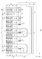
- FIG. 1 is a top view showing an example of a semiconductor device 100.
- the semiconductor device 100 of this example is a semiconductor chip having a transistor unit 70 including a transistor such as an IGBT (Insulated Gate Bipolar Transistor) and a diode unit 80 including a diode such as a FWD (Free Wheel Diode).
- the diode unit 80 is formed adjacent to the transistor unit 70 on the upper surface of the semiconductor substrate.
- the upper surface of the semiconductor substrate refers to one of two opposing main surfaces of the semiconductor substrate. In FIG. 1, the top surface of the chip around the chip end is shown, and the other regions are omitted.
- the diode portion 80 is projected when the cathode region is projected perpendicularly to the back surface of the semiconductor substrate with respect to the back surface region coinciding with the cathode region or the front surface side. It may be an area.
- the transistor portion 70 is a projection region when the collector region is projected perpendicularly to the back surface of the semiconductor substrate on the front surface side in the active region, and includes the emitter region 12 and the contact region 15.
- the unit structure of may be an area regularly arranged.
- FIG. 1 shows the active region of the semiconductor substrate in the semiconductor device 100
- the semiconductor device 100 may have an edge termination portion surrounding the active region.
- the active region indicates a region through which current flows when the semiconductor device 100 is controlled to be in an on state.
- the edge termination alleviates the concentration of the electric field on the upper surface side of the semiconductor substrate.
- the edge end has, for example, a guard ring, a field plate, a resurf, and a combination of these.
- the semiconductor device 100 of this example includes a gate trench portion 40, a dummy trench portion 30, a well region 17, an emitter region 12, a base region 14 and a contact region 15 formed inside the upper surface side of the semiconductor substrate.
- the semiconductor device 100 of this example includes the emitter electrode 52 and the gate electrode 50 provided above the upper surface of the semiconductor substrate. Emitter electrode 52 and gate electrode 50 are provided separately from each other.
- the gate trench portion 40 and the dummy trench portion 30 are an example of the trench portion.
- An interlayer insulating film is formed between the emitter electrode 52 and the gate electrode 50 and the upper surface of the semiconductor substrate, but is omitted in FIG.
- a contact hole 54, a contact hole 55 and a contact hole 56 are formed through the interlayer insulating film in the interlayer insulating film of this example.
- Emitter electrode 52 is in contact with emitter region 12, contact region 15 and base region 14 on the top surface of the semiconductor substrate through contact hole 54. Further, emitter electrode 52 is connected to the dummy conductive portion in dummy trench portion 30 through contact hole 56. Between the emitter electrode 52 and the dummy conductive portion, a connection portion 57 formed of a conductive material such as polysilicon doped with an impurity may be provided. The connection portion 57 is formed on the upper surface of the semiconductor substrate. An insulating film such as a thermal oxide film is formed between the connection portion 57 and the semiconductor substrate.
- Gate electrode 50 is in contact with gate interconnection 51 through contact hole 55.
- Gate interconnection 51 is formed of polysilicon or the like doped with an impurity. Gate interconnection 51 is connected to the gate conductive portion in gate trench portion 40 on the upper surface of the semiconductor substrate. That is, gate interconnection 51 is formed on the upper surface of the semiconductor substrate, between a portion of gate trench portion 40 and contact hole 55.
- Emitter electrode 52 and gate electrode 50 are formed of a material containing a metal.
- each electrode is formed of aluminum or aluminum-silicon alloy.
- Each electrode may have a barrier metal formed of titanium, a titanium compound, or the like below the region formed of aluminum or the like, and may have a plug formed of tungsten or the like in the contact hole.
- the one or more gate trench portions 40 and the one or more dummy trench portions 30 are arranged in the region of the transistor portion 70 at predetermined intervals along a predetermined arrangement direction.
- one or more gate trench portions 40 and one or more dummy trench portions 30 may be alternately formed along the arrangement direction. Further, the dummy trench portions 30 are arranged at predetermined intervals in the arrangement direction in the region of the diode portion 80.
- the dummy trench portion 30 is formed to extend in a predetermined extending direction on the upper surface of the semiconductor substrate.
- a part of the dummy trench portion 30 in the transistor portion 70 of the present example has a linear shape, and is formed extending in the extending direction perpendicular to the above-described arrangement direction.
- a part of the dummy trench portion 30 in the transistor portion 70 has a shape in which two straight lines are connected at the end portion by a curved portion.
- the X axis direction is taken as the arrangement direction of the trench portions.
- the Y-axis direction is taken as the extending direction of the trench portion.
- the X axis and the Y axis are axes orthogonal to each other in a plane parallel to the top surface of the semiconductor substrate.
- an axis orthogonal to the X axis and the Y axis is taken as a Z axis.
- the Z-axis direction may be referred to as the depth direction.
- a plurality of dummy trench sections 30 may be continuously arranged at the boundary with the diode section 80.
- the number of dummy trench portions 30 continuously arranged at the boundary with the diode portion 80 may be larger than the number of dummy trench portions 30 continuously arranged inside the transistor portion 70 separated from the diode portion 80 .
- a total of three dummy trench sections 30 of two connected at the end and one linear shape are continuously arranged. (The dummy trench portion 30 overlapping the boundary between the transistor portion 70 and the diode portion 80 is not counted).
- the gate trench portions 40 and the dummy trench portions 30 are alternately arranged one by one.
- the gate trench portion 40 has an opposing portion 41 and a projecting portion 43.
- the facing portion 41 is formed to extend in the above-described extending direction in a range facing the dummy trench portion 30 in the transistor portion 70. That is, the facing portion 41 is formed in parallel to the dummy trench portion 30.
- the protruding portion 43 is further extended from the facing portion 41 and is formed in a range not facing the dummy trench portion 30.
- two opposing portions 41 provided on both sides of the dummy trench portion 30 are connected by one projecting portion 43. At least a portion of the protrusion 43 may have a curvilinear shape.
- the gate conductive portion in the gate trench portion 40 and the gate wiring 51 are connected.
- the gate wire 51 may be connected to the gate conductive portion in a region farthest from the facing portion 41 of the protrusion 43.
- the projecting portion 43 in this example has a portion that extends in a direction orthogonal to the facing portion 41 in a region farthest from the facing portion 41.
- the gate wire 51 may be connected to the gate conductive portion at the corresponding portion of the protrusion 43.
- the dummy trench portion 30 in the diode portion 80 may have the same shape as the dummy trench portion 30 in the gate trench portion 40, and may have the same shape as the gate trench portion 40. However, dummy trench portion 30 in diode portion 80 has the same length as dummy trench portion 30 in transistor portion 70.
- Emitter electrode 52 is formed above gate trench portion 40, dummy trench portion 30, well region 17, emitter region 12, base region 14 and contact region 15.
- the well region 17 is formed in a predetermined range from the end of the active region on the side where the gate electrode 50 is provided.
- the diffusion depth of the well region 17 may be deeper than the depths of the gate trench portion 40 and the dummy trench portion 30.
- a partial region of gate trench portion 40 and dummy trench portion 30 on the side of gate electrode 50 is formed in well region 17. The bottom of the end in the extension direction of the dummy trench portion 30 may be covered by the well region 17.
- the projecting portion 43 of the gate trench portion 40 may be entirely formed in the well region 17.
- the semiconductor substrate has a first conductivity type, and the well region 17 has a second conductivity type different from the semiconductor substrate.
- the semiconductor substrate of this example is N ⁇ type, and the well region 17 is P + type.
- the first conductivity type is described as N-type, and the second conductivity type is described as P-type.
- the first and second conductivity types may be opposite conductivity types.
- the base region 14 is formed in the mesa portion 94 which is a region sandwiched by the respective trench portions. Furthermore, the mesa portion 94 is a region sandwiched by adjacent trench portions along the arrangement direction, from the deepest position on the bottom surface of the trench portion to the upper surface (that is, the front surface) of the semiconductor substrate Good.
- the base region 14 is a second conductivity type having a doping concentration lower than that of the well region 17.
- the base region 14 in this example is P-type.
- a contact region 15 of the second conductivity type having a doping concentration higher than that of the base region 14 is formed on the top surface of the base region 14 in the mesa portion 94.
- the contact region 15 in this example is P + type.
- the emitter region 12 of the first conductivity type having a doping concentration higher than that of the semiconductor substrate is selectively formed on a part of the upper surface of the contact region 15.
- the emitter region 12 in this example is N + type.
- Each of contact region 15 and emitter region 12 is formed from one adjacent trench portion to the other trench portion.
- the one or more contact regions 15 and the one or more emitter regions 12 of the transistor portion 70 are formed to be alternately exposed on the upper surface of the mesa portion 94 along the extension direction of the trench portion.
- the contact region 15 is formed in a region facing the at least one contact region 15 in the transistor unit 70.
- the contact region 15 is formed in the region facing the contact region 15 closest to the gate electrode 50 in the transistor unit 70, and the base is provided in the other region. Region 14 is formed.
- the contact hole 54 is formed above each of the contact region 15 and the emitter region 12.
- the contact hole 54 is not formed in the region corresponding to the base region 14 and the well region 17.
- the contact hole 54 is formed above the contact region 15 and the base region 14.
- the contact hole 54 in the present example is not formed in the base region 14 closest to the gate electrode 50 among the plurality of base regions 14 in the mesa portion 94 of the diode portion 80.
- the contact holes 54 of the transistor section 70 and the contact holes 54 of the diode section 80 have the same length in the extending direction of the respective trench sections.
- the contact region 15 is formed at the end in the extension direction of the contact hole 54, but the contact region 15 may be omitted.
- the contact region 15 may be formed on the surface of the base region 14 exposed by the contact hole.
- At least one boundary mesa portion 94-1 at the boundary between the transistor portion 70 and the diode portion 80 among the plurality of mesa portions 94 is a P + -type contact region having a concentration higher than that of the base region 14 on the upper surface of the semiconductor substrate.
- the area of the contact region 15 exposed to the upper surface of the semiconductor substrate in the boundary mesa portion 94-1 is larger than the area of the contact region 15 exposed to the upper surface of the semiconductor substrate in the other mesa portion 94.
- one mesa portion 94 on the transistor portion 70 side adjacent to the boundary between the transistor portion 70 and the diode portion 80 is the boundary mesa portion 94-1.
- boundary mesa portion 94-1 in addition to the region where contact region 15 is formed in another mesa portion 94 of transistor portion 70, the region where emitter region 12 is formed in another mesa portion 94 of transistor portion 70. Also, the contact region 15 is formed. That is, the boundary mesa 94-1 in this example does not have the emitter region 12 on the upper surface of the semiconductor substrate.
- the mesa portion 94 closer to the diode portion 80 than the boundary mesa portion 94-1 has the base region 14 on the upper surface of the semiconductor substrate.
- a region facing the contact region 15 in the boundary mesa portion 94-1 is also the base region 14.
- the base region 14 functions as an anode region of the diode.
- an accumulation region 16 is formed below the base region 14 in a partial region of the transistor section 70.
- a region in which the storage region 16 is formed is indicated by a dotted line.
- a cathode region 82 is formed below the base region 14 in a partial region of the diode unit 80.
- a region where the cathode region 82 is formed is indicated by a dotted line.
- the cathode region 82 may be at a position where the base region 14 exposed on the upper surface (that is, the front surface) of the semiconductor substrate is projected on the lower surface of the semiconductor substrate. That is, the cathode region 82 may be separated from the position where the contact region 15 formed at the end of the contact hole 54 in the trench extension direction is projected onto the lower surface (that is, the back surface) of the semiconductor substrate.
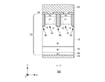
- FIG. 2 is a view showing an example of the aa ′ cross section of the semiconductor device 100 shown in FIG.
- the aa ′ cross section is a cross section parallel to the XZ plane and passing through the emitter region 12 of the transistor section 70.
- the mask 110 used at the time of manufacture of the semiconductor device 100 is shown collectively.
- the semiconductor device 100 of this example has the semiconductor substrate 10, the interlayer insulating film 26, the emitter electrode 52, and the collector electrode 24 in the cross section.
- Emitter electrode 52 is formed on the upper surface of semiconductor substrate 10 and interlayer insulating film 26.
- the collector electrode 24 is formed on the lower surface of the semiconductor substrate 10.
- the lower surface refers to the surface opposite to the upper surface.
- Emitter electrode 52 and collector electrode 24 are formed of a conductive material such as metal.
- the surface or end of the emitter electrode 52 side of each member such as a substrate, layer, or region is referred to as the upper surface or the upper end, and the surface or end of the collector electrode 24 is referred to as the lower surface or the lower end.
- a direction connecting the emitter electrode 52 and the collector electrode 24 is referred to as a depth direction.
- the semiconductor substrate 10 may be a silicon substrate, a silicon carbide substrate, or a nitride semiconductor substrate such as gallium nitride.
- a P ⁇ -type base region 14 is formed on the upper surface side of the semiconductor substrate 10.
- the N + -type emitter region 12, the P ⁇ -type base region 14 and the N + -type storage region 16 are sequentially arranged from the upper surface side of the semiconductor substrate 10 on the upper surface side of each mesa portion 94 of the transistor portion 70. It is formed.
- a P ⁇ -type base region 14 is formed on the upper surface side of each of the mesa portions 94 of the diode portion 80.
- the storage region 16 is not formed in each mesa portion 94 of the diode portion 80.
- an N ⁇ -type drift region 18 is formed on the lower surface of the accumulation region 16.
- the storage region 16 is formed in each mesa 94 of the transistor unit 70.
- the storage region 16 may be provided to cover the entire lower surface of the base region 14 in each mesa 94. However, in the mesa portion 94 in the vicinity of the boundary between the transistor portion 70 and the diode portion 80, the lower surface of the base region 14 is not covered by the accumulation region 16.
- the drift region 18 is formed on the lower surface of the base region 14.
- an N ⁇ -type buffer region 20 is formed on the lower surface of the drift region 18.
- the buffer region 20 is formed on the lower surface side of the drift region 18.
- the doping concentration of buffer region 20 is higher than the doping concentration of drift region 18.
- Buffer region 20 may function as a field stop layer that prevents the depletion layer extending from the lower surface side of base region 14 from reaching P + type collector region 22 and N + type cathode region 82.
- a P + type collector region 22 is formed on the lower surface of the buffer region 20.
- an N + -type cathode region 82 is formed on the lower surface of the buffer region 20.
- a plane parallel to the YZ plane passing through the boundary between the collector region 22 and the cathode region 82 is the boundary between the transistor portion 70 and the diode portion 80.
- the boundary between the collector region 22 and the cathode region 82 may be a position where the distribution of the net doping concentration of the impurity in the X-axis direction has a minimum value.
- One of the dummy trench portions 30 may be formed at the boundary between the transistor portion 70 and the diode portion 80. Further, the position of the dummy trench portion 30 closest to the position where the net doping concentration becomes the minimum value in the X axis may be taken as the boundary position of the transistor portion 70 and the diode portion 80.
- a collector electrode 24 is provided on the lower surface of the collector region 22 and the cathode region 82.
- One or more gate trench portions 40 and one or more dummy trench portions 30 are formed on the upper surface side of the semiconductor substrate 10. Each trench portion penetrates base region 14 from the upper surface of semiconductor substrate 10 to reach drift region 18. In the region where at least one of the emitter region 12, the contact region 15 and the storage region 16 is provided, each trench also penetrates these regions to reach the drift region 18.
- the gate trench portion 40 has a gate trench formed on the upper surface side of the semiconductor substrate 10, a gate insulating film 42, and a gate conductive portion 44.
- the gate insulating film 42 is formed to cover the inner wall of the gate trench.
- the gate insulating film 42 may be formed by oxidizing or nitriding the semiconductor on the inner wall of the gate trench.
- the gate conductive portion 44 is formed inside the gate insulating film 42 inside the gate trench. That is, the gate insulating film 42 insulates the gate conductive portion 44 and the semiconductor substrate 10.
- the gate conductive portion 44 is formed of a conductive material such as polysilicon.
- Gate conductive portion 44 includes a region facing at least adjacent base region 14 in the Z-axis direction. Gate trench portion 40 is covered with interlayer insulating film 26 on the upper surface of semiconductor substrate 10. In this example, as shown in FIG. 1, the gate conductive portion 44 in the projecting portion 43 is electrically connected to the gate electrode 50 through the gate wiring 51. When a predetermined voltage is applied to gate conductive portion 44, a channel is formed in the surface layer of the interface of base region 14 in contact with the gate trench.
- the dummy trench portion 30 may have the same structure as the gate trench portion 40 in the cross section.
- the dummy trench portion 30 has a dummy trench formed on the upper surface side of the semiconductor substrate 10, a dummy insulating film 32 and a dummy conductive portion 34.
- the dummy insulating film 32 is formed to cover the inner wall of the dummy trench.
- the dummy conductive portion 34 is formed inside the dummy trench and is formed inside the dummy insulating film 32.
- the dummy insulating film 32 insulates the dummy conductive portion 34 and the semiconductor substrate 10.
- the dummy conductive portion 34 may be formed of the same material as the gate conductive portion 44.
- the dummy conductive portion 34 is formed of a conductive material such as polysilicon.
- the dummy conductive portion 34 may have the same length as the gate conductive portion 44 in the depth direction.
- the dummy trench portion 30 is covered with the interlayer insulating film 26 on the upper surface of the semiconductor substrate 10.
- the dummy conductive portion 34 is electrically connected to the emitter electrode 52 through the contact hole 56.
- the emitter region 12 exposed on the upper surface of the semiconductor substrate 10 is not formed in the boundary mesa portion 94-1 at the boundary between the transistor portion 70 and the diode portion 80 among the plurality of mesa portions 94.
- a contact region 15 exposed on the top surface of 10 is formed. As shown in FIG. 1, it is preferable that the emitter region 12 exposed on the top surface of the semiconductor substrate 10 is not formed in the entire boundary mesa portion 94-1.
- the contact region 15 of the boundary mesa portion 94-1 is connected to the emitter electrode 52 through the contact hole 54.
- the mesa portion 94 at the boundary between the transistor portion 70 and the diode portion 80 refers to the mesa portion 94 overlapping the boundary in the X-axis.
- the mesa 94 adjacent to the boundary between the transistor unit 70 and the diode unit 80 refers to the mesa 94 adjacent to the trench.
- the mesa portion 94 on the transistor portion 70 side is the boundary mesa portion 94-1.
- a plurality of mesa portions 94 continuous in the arrangement direction may be the boundary mesa portion 94-1 adjacent to the boundary between the transistor portion 70 and the diode portion 80. Further, the mesa portion 94 adjacent to the boundary on the diode portion 80 side may be the boundary mesa portion 94-1.
- the boundary mesa portion 94-1 By providing the boundary mesa portion 94-1, holes can be efficiently extracted near the boundary between the transistor portion 70 and the diode portion 80 when the semiconductor device 100 is turned off. Thus, it is possible to efficiently reduce the tail current at turn-off and to reduce the loss at the off-state. In addition, the decrease in withstand voltage of the semiconductor device 100 can be suppressed. Further, it is possible to suppress the holes accumulated in the region of the transistor portion 70 from flowing to the region of the diode portion 80, and to reduce the influence on the diode portion 80.
- the storage region 16 is not provided in at least one of the boundary mesas 94-1.
- no storage region 16 is provided in all boundary mesas 94-1.
- holes can be drawn out at the boundary mesa 94-1 without being blocked by the accumulation region 16.
- the mask 110 is used in the step of implanting an impurity into a region corresponding to the storage region 16.
- the mask 110 is disposed to cover the diode portion 80 and the boundary mesa portion 94-1.
- the mask 110 may be formed by applying a resist or the like and patterning it into a predetermined shape.
- the storage area 16 is not formed in the area covered by the mask 110, and the storage area 16 is formed in the area not covered by the mask 110.
- the end of the mask 110 is preferably formed vertically at a position facing the end of the boundary mesa 94-1. However, if resist mask or the like occurs on the mask 110, the excess portion 112 may be formed beyond the position.
- the storage region 16 is not formed at a predetermined depth in the mesa portion 94 covered by the excess portion 112. For example, in the mesa portion 94 covered by the excess portion 112, the accumulation region 16 is not formed at all or formed shallower than a predetermined depth.
- the storage area 16 of this example includes a first storage area 16-1 and a second storage area 16-2.
- the first accumulation region 16-1 is formed at a predetermined depth position.
- the first accumulation region 16-1 is formed inside the transistor unit 70.
- the second accumulation region 16-2 is formed at a position closer to the diode unit 80 than the first accumulation region 16-1.
- the second accumulation region 16-2 is formed at a position shallower than the first accumulation region 16-1. That is, the second accumulation region 16-2 is formed on the upper surface side of the semiconductor substrate 10 than the first accumulation region 16-1.
- the second storage region 16-2 may be formed to be shallow as it approaches the diode unit 80.
- the first accumulation region 16-1 and the second accumulation region 16-2 may be formed continuously or may be formed discontinuously in the depth direction.
- the depth position of the storage region 16 changes, the length in the depth direction of the base region 14 in the mesa portion 94 changes. Therefore, when the gate trench portion 40 is provided adjacent to the mesa portion 94, the threshold voltage Vth of the mesa portion 94 fluctuates with respect to the threshold voltage Vth of the other mesa portions 94. Variations in threshold voltage will increase. In addition, the variation in saturation current also increases. In addition, the forward voltage of the diode unit 80 may be lower than a predetermined design value.
- the trench portion adjacent to the boundary mesa portion 94-1 is the dummy trench portion 30. Further, at least one trench portion provided adjacent to the transistor portion 70 side further than the trench portion adjacent to the boundary mesa portion 94-1 is the dummy trench portion 30. Thereby, variations in threshold voltage can be reduced. More preferably, all the trench portions adjacent to the mesa portion 94 provided with the second accumulation region 16-2 are the dummy trench portions 30. In addition, it is preferable that all the trench portions closer to the diode portion 80 than the mesa portion 94 provided with the second accumulation region 16-2 be the dummy trench portions 30. Thereby, variations in threshold voltage can be further reduced.
- the trench portion adjacent to the first storage region 16-1 is a gate trench portion. 40 may be sufficient.
- the trench portion adjacent to the second storage region 16-2 is preferably the dummy trench portion 30.
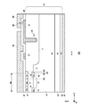
- FIG. 3 is a view showing another example of the aa ′ cross section of the semiconductor substrate 10.
- a lifetime killer 96 is further provided in addition to the configuration of the semiconductor substrate 10 shown in FIG. 2, a lifetime killer 96 is further provided. Further, in the semiconductor substrate 10 of FIG. 3, a plurality of boundary mesa portions 94-1 are formed. Other structures may be identical to the example shown in FIG.
- the lifetime killer 96 is provided on the upper surface side of the semiconductor substrate 10.
- the upper surface side of the semiconductor substrate 10 refers to the upper surface side of at least the middle of the drift region 18 in the depth direction.
- the lifetime killer 96 may be formed on the entire diode unit 80. Thereby, the carrier lifetime in the diode unit 80 can be adjusted, and for example, the diode unit 80 can be made to perform a soft recovery operation.
- the lifetime killer 96 may be any one that can locally adjust the carrier lifetime of the semiconductor substrate 10 in the depth direction. For example, the lifetime killer 96 is helium locally injected into the semiconductor substrate 10.
- the lifetime killer 96 of this example is also formed in the region adjacent to the diode unit 80 in the transistor unit 70. However, in the transistor section 70, the lifetime killer 96 is not formed below the area where the first accumulation area 16-1 is formed. Thereby, it is possible to prevent the IE effect by the accumulation area 16 from being offset by the lifetime killer 96.
- the lifetime killer 96 of this example is not formed below the mesa portion 94 in which the first accumulation region 16-1 is formed. Further, the lifetime killer 96 may not be formed below the at least one mesa portion 94 adjacent to the diode portion 80 with respect to the mesa portion 94 in which the first storage region 16-1 is formed. This makes it possible to reduce the influence of the lifetime killer 96 on the IE effect.
- a lifetime killer 96 may be formed below at least the one boundary mesa 94-1 on the side of the diode 80.
- the lifetime killer 96 is formed below all the boundary mesas 94-1. Thereby, the influence of the carriers in the transistor unit 70 on the diode unit 80 can be reduced.
- the lifetime killer 96 may be formed below the mesa portion 94 in which the second accumulation region 16-2 is formed.
- the area where the lifetime killer 96 is formed may end below the area where the second accumulation area 16-2 is formed.
- FIG. 4 is a diagram for explaining the size of a predetermined portion in the semiconductor substrate 10 shown in FIG. 2 or FIG.
- the distance from the boundary between the transistor unit 70 and the diode unit 80 in the X-axis direction to the dummy trench 30-2 between the mesa unit 94-2 having the emitter region 12 and the boundary mesa unit 94-1 is Da I assume.
- the position of dummy trench portion 30 indicates the center position of dummy trench portion 30 in the X-axis direction.
- the distance from the dummy trench portion 30-2 to the dummy trench portion 30-3 is Db.
- the dummy trench portion 30-3 refers to the dummy trench portion 30 closest to the transistor portion 70 among the dummy trench portions 30 continuously arranged on the transistor portion 70 side from the boundary between the transistor portion 70 and the diode portion 80.
- a distance from the lower surface of the semiconductor substrate 10 to the lower surface of the base region 14 in the Z-axis direction is Dt.
- the thickness of the mask 110 is Dc.
- the distance between the mesa portion 94-2 and the cathode region 82 can be secured. Therefore, it is possible to suppress the fluctuation of the forward voltage in diode portion 80 due to the formation of storage region 16 in mesa portion 94-2. Further, by setting Da + Dt ⁇ 150 ⁇ m, the size of the invalid region which does not function as a transistor can be limited in the transistor section 70. As an example, Dt may be about 70 ⁇ m.
- the length in the X-axis direction of the excess portion 112 of the mask 110 depends on the thickness Dc of the mask 110.
- Db> 1.2 Dc the trench portion adjacent to the region where the second storage region 16-2 is likely to be formed can be used as the dummy trench portion 30. Therefore, variations in threshold voltage and saturation current can be reduced.
- Db may be 6 ⁇ m or more.
- 2.0 Dc> Db may be satisfied, and 1.5 Dc> Db may be satisfied.
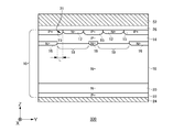
- FIG. 5 is a view showing an example of the bb ′ cross section of the semiconductor device 100 shown in FIG.
- the bb ′ cross section is a plane parallel to the YZ plane, and is a plane passing through the connecting portion 57 at the mesa portion 94 closer to the transistor portion 70 than the boundary mesa portion 94-1.
- the storage region 16 is formed in the mesa portion 94. Further, in FIG. 5, the positions of the contact holes 54 formed to face the cross section are indicated by dotted lines.
- the mesa portion 94 alternately has emitter regions 12 and contact regions 15 along the extending direction of the trench portion on the upper surface of the semiconductor substrate 10. Further, a storage region 16 is formed on the lower surface of the base region 14.
- the end position of the storage region 16 on the outermost side (that is, the gate electrode 50 side) in the Y-axis direction is P1.
- the outermost end position of the contact hole 54 in the Y-axis direction is P2.
- An end position of the emitter region 12 formed on the outermost side in the Y-axis direction on the side of the gate electrode 50 is P3.
- An end position of the contact region 15 formed on the outermost side in the Y-axis direction on the gate electrode 50 side is P4.
- the storage region 16 is preferably formed to the outside of the end of the emitter region 12 formed on the outermost side in the Y-axis direction. That is, it is preferable that the end position P1 of the storage region 16 be disposed outside the end position P3 of the emitter region 12. Thereby, the IE effect in the accumulation region 16 can be enhanced.
- the contact hole 54 is preferably formed to the outside of the accumulation region 16 in the Y-axis direction. That is, the end position P2 of the contact hole 54 is preferably disposed outside the end position P1 of the accumulation region 16. As a result, when the semiconductor device 100 is turned off, holes can be efficiently extracted from the outside of the storage region 16.
- the contact region 15 formed on the outermost side in the Y-axis direction be formed to the outside of the contact hole 54. That is, the end position P4 of the contact region 15 is preferably disposed outside the end position P2 of the contact hole 54. As a result, when the semiconductor device 100 is turned off, holes can be efficiently extracted from the outside of the storage region 16.
- the distance from the end position P3 of the emitter region 12 to the end position P1 of the storage region 16 is shorter than the distance from the end position P1 of the storage region 16 to the end position P4 of the contact region 15 Good.
- the storage region 16 can suppress inhibition of hole extraction.
- the concentration of the electric field at the end of the accumulation region 16 can be alleviated.
- the distance from the end position P3 to P1 is preferably shorter than the distance from the end position P1 of the accumulation region 16 to the end position P2 of the contact hole 54.
- the distance from the end position P3 of the emitter region 12 to the end position P1 of the accumulation region 16 is 12 ⁇ m or less. Further, the distance from the end position P1 of the accumulation region 16 to the end position P2 of the contact hole 54 is 20 ⁇ m or less. The distance from the end position P2 of the contact hole 54 to the end position P4 of the contact region 15 is 1 ⁇ m or less.
- the semiconductor device 100 including the diode unit 80 has been described with reference to FIGS. 1 to 4.
- the semiconductor device 100 shown in FIG. 5 may or may not include the diode unit 80. Even without the diode unit 80, the semiconductor device 100 can exhibit the above-described effects.
- a base region 14 is formed between the outermost contact region 15 and the well region 17 on the upper surface of the semiconductor substrate 10. That is, a region of relatively high resistance is arranged outside the contact region 15. Thereby, the carriers coming from the transistor unit 70 to the diode unit 80 can be reduced at the time of reverse recovery. Therefore, it is possible to suppress concentration of carriers on the end of the contact region 15 in the diode unit 80, and to suppress a decrease in withstand voltage of the diode unit 80.
- the length of the base region 14 between the contact region 15 and the well region 17 in the Y axis direction may be 10 ⁇ m or more and 50 ⁇ m or less.
- the end 98 of the accumulation region 16 may be formed shallower toward the outside in the Y-axis direction.
- the tip of storage region 16 in the Y-axis direction is formed at a position shallower than storage region 16 below emitter region 12.
- the tip of the accumulation region 16 may be formed at a position not in contact with the drift region 18.
- the tip of the accumulation area 16 may be provided at a position shallower than the middle of the base area 14 in the Z-axis direction.
- the storage region 16 in this example can be easily formed by using the mask 110 having the excess portion 112 described in FIG.
- the shape of the end 98 of the accumulation region 16 can be controlled by adjusting the shape of the excess portion 112 of the mask 110.
- the bake temperature of the mask 110, the bake time, the thickness of the mask 110, or the material may be adjusted.
- FIG. 7 is a view showing an example of the semiconductor device 200 according to the comparative example.
- the gate trench portion 40 is formed adjacent to the second storage region 16-2.
- variations in the threshold voltage Vth and the saturation current in the transistor portion 70 become large.
- the semiconductor device 100 since the dummy trench portion 30 is provided adjacent to the second storage region 16-2, variations in the threshold voltage Vth and the saturation current in the transistor portion 70 can be reduced.
- FIG. 8 is a top view showing an example of the semiconductor device 300. As shown in FIG. The semiconductor device 300 differs from the semiconductor device 100 of each aspect described in FIGS. 1 to 6 in the structure of the storage region 16. Other structures may be identical to those of the semiconductor device 100 of any aspect.
- the storage region 16 in the semiconductor device 300 is provided in at least a partial region below the contact region 15 and is not provided in at least a partial region below the emitter region 12.
- the storage region 16 in this example has a band shape extending along the X-axis direction.
- Band-shaped storage regions 16 are provided discretely along the Y-axis direction.
- each band-shaped storage region 16 is formed in a range overlapping the contact region 15 and not overlapping the emitter region 12.
- the width of the band-shaped storage region 16 in the Y-axis direction is smaller than the width of the contact region 15 in the Y-axis direction.
- FIG. 9 is a view showing an example of a cross section taken along line cc 'in FIG.
- the cc ′ cross section is a plane parallel to the XZ plane and passing through the emitter region 12. As described above, at least a part of the area below the emitter area 12 is provided with the carrier passage area 19 in which the storage area 16 is not formed.
- the carrier passage area 19 is an area where the mobility of holes is larger than that of the accumulation area 16.
- the carrier passage region 19 in this example refers to a region in the vicinity of the interface where the base region 14 remaining without the accumulation region 16 formed and the drift region 18 are in contact.
- the carrier passage region 19 may be provided over the entire width in the X-axis direction of the mesa portion 94.
- the carrier passage region 19 may include an N-type region having a lower doping concentration than the storage region 16 and a higher doping concentration than the drift region 18. In this case, the concentration of the N-type impurity in the carrier passage region 19 may be 1/10 or less or 1/100 or less of the concentration of the N-type impurity in the accumulation region 16.
- FIG. 10 is a view showing an example of the dd ′ cross section in FIG.
- the dd ′ cross section is a plane parallel to the XZ plane and passing through the contact region 15.
- the storage region 16 is formed in at least a partial region below the contact region 15.
- FIG. 11 is a view showing an example of a cross section along line e-e 'in FIG.
- the ee ′ cross section is a plane which is parallel to the YZ plane and passes through the connecting portion 57.
- the carrier passage region 19 is provided below the emitter region 12, and the storage region 16 is provided below the contact region 15.
- the carrier passage region 19 is provided in the entire region below the emitter region 12. That is, the width of the carrier passage region 19 in the Y-axis direction is equal to or greater than the width of the emitter region 12 in the Y-axis direction.
- the width of the carrier passage region 19 in the Y-axis direction may be larger than the width of the emitter region 12 in the Y-axis direction.
- the carrier passage region 19 is provided below the end of the contact region 15 in addition to the region below the emitter region 12.
- the end position of the storage region 16 on the outermost side (that is, the gate electrode 50 side) in the Y-axis direction is P1.
- the other end positions P2, P3 and P4 are the same as in the example of FIG.
- the storage region 16 in this example is formed to the outside of the end position P2 of the contact hole 54 in the Y-axis direction. That is, the end position P1 of the accumulation region 16 is disposed outside the end position P2 of the contact hole 54.
- the carrier passage region 19 is provided, even if the storage region 16 is formed to the outside of the contact hole 54, the decrease in withstand voltage can be suppressed. Further, by forming the accumulation region 16 to the outside of the contact hole 54, a constant carrier can be accumulated also in the end region.
- the end position P ⁇ b> 1 of the accumulation region 16 may be disposed inside the end position P ⁇ b> 4 of the contact region 15. Thereby, it is possible to suppress that the extraction of holes from the end region is inhibited by the accumulation region 16 at the turn-off time.
- FIG. 12 is a view showing an example of the cross section of the mesa portion 94 in a plane parallel to the YZ plane.
- the contact regions 15 and the emitter regions 12 are alternately arranged on the upper surface of the mesa portion 94 along the Y-axis direction.
- the carrier passage region 19 is also provided below the end 21 of the contact region 15 adjacent to the emitter region 12.
- the length L in the Y-axis direction of the portion where the carrier passage region 19 overlaps with one end 21 of the contact region 15 may be 10% or more, 20% or more of the width of the contact region 15 in the Y-axis direction. It may be The length L may be 30% or less of the width of the contact region 15 in the Y-axis direction.
- FIG. 13 is a view showing another example of the cross section of the mesa portion 94 in a plane parallel to the YZ plane.
- the storage area 16 of the present embodiment includes a first storage area 16-1 formed at a predetermined depth position and a second storage area 16-2 formed at a position shallower than the first storage area 16-1. And.
- the second accumulation region 16-2 is closer to the emitter region 12 than the first accumulation region 16-1 in the Y-axis direction. That is, the second accumulation region 16-2 is disposed between the first accumulation region 16-1 and the emitter region 12 in the Y-axis direction.
- the first accumulation region 16-1 is disposed between the base region 14 and the drift region 18.
- the second storage region 16-2 may be in contact with the contact region 15 or may be separated from the contact region 15. In addition, at least a part of the second storage region 16-2 may be formed in the contact region 15.
- the first accumulation region 16-1 and the second accumulation region 16-2 may be formed continuously or separated from each other.
- the shallow second storage region 16-2 may be formed below the excess portion 112.
- neither the first storage region 16-1 nor the second storage region 16-2 is formed below the contact region 15, and not below the emitter region 12. Therefore, even when the second storage region 16-2 is formed, the characteristics such as the threshold voltage of the semiconductor device 100 are not affected.
- the mask 110 is disposed such that the end of the mask 110 and the end of the contact region 15 overlap. Thereby, even if the excess portion 112 is generated in the mask 110, the second storage region 16-2 formed below the excess portion 112 can be arranged so as not to overlap with the emitter region 12.
- FIG. 14 is a top view showing an example of the semiconductor device 400.
- the outer end of the N + -type cathode region 82 is recessed in the positive Y-axis direction as compared with any of the semiconductor devices shown in FIGS. 1 to 13.
- the collector region 22 is not shown in FIG. 14, the transistor unit 70 and the diode unit 80 may have the collector region 22.
- the transistor portion 70 of this example has a collector region 22 on the entire surface on the lower surface side.
- the diode unit 80 of this example has the collector region 22 in a part of the lower surface side and the cathode region 82 in another part of the lower surface side. That is, on the lower surface side of the diode unit 80 of this example, the cathode region 82 is provided in the region where the collector region 22 is not provided.
- the inner end of the collector region 22 of the diode unit 80 may be located inside the outer end of the storage region 16 of the transistor unit 70, and the emitter provided at the outermost side in the Y axis direction in the transistor unit 70. It may be located inside the outer end of the region 12.
- the inner end of the collector region 22 of the diode unit 80 matches the outer end of the cathode region 82 of the diode unit 80.
- the length in the Y-axis direction from the inner end of the collector region 22 of the diode unit 80 to the outer end of the accumulation region 16 of the transistor unit 70 is referred to as L.
- the length L may be 200 ⁇ m.
- FIG. 15 is a view showing an example of a cross section along line cc 'of the semiconductor device 400 shown in FIG. FIG. 14 is a YZ cross section of the diode section 80.
- the dotted line in the vicinity of the contact region 15 indicates the position in the Y-axis direction of the outer end of the storage region 16 of the transistor section 70 in FIG.
- the boundary between the collector region 22 and the cathode region 82 is positioned in the positive Y-axis direction by the length L than the end portion outside the storage region 16 of the transistor section 70.
- the P + -type collector region 22 is expanded in the diode portion 80, holes can be easily injected from the collector region 22 to the drift region 18.
- holes can be easily injected from the collector region 22 to the drift region 18.
- the curved portion of the well region 17 shown in FIG. 15 is likely to generate an avalanche due to the concentration of the electric field, the avalanche can be suppressed by the hole injection from the back surface side.
- FIG. 16 is a top view showing an example of the semiconductor device 500. As shown in FIG. The semiconductor device 500 is provided with a boundary mesa portion 94-1 having a structure different from that of the semiconductor device 100 of each aspect described in FIGS. The other structure of the semiconductor device 500 may be the same as the semiconductor device 100 of any aspect.
- the boundary mesa portion 94-1 includes one or more boundary mesa portions 94-1A in which the area of the contact region 15 exposed to the upper surface of the semiconductor substrate on the side of the transistor portion 70 is larger than the exposed area of the base region 14. .
- the boundary mesa 94-1 may include a plurality of boundary mesas 94-1A. Further, in the boundary mesa portion 94-1, one area of the contact region 15 exposed to the upper surface of the semiconductor substrate on the side of the diode portion 80 is smaller than the exposed area of the base region 14 by one boundary mesa portion 94-1B.
- the boundary mesa 94-1 may include a plurality of boundary mesas 94-1B.
- the mesa portion 94 located closest to the diode portion 80 is adjacent to the boundary mesa portion 94-1A along the arrangement direction.
- the mesa portion 94 located closest to the transistor portion 70 is adjacent to the boundary mesa portion 94-1B in the arrangement direction.
- the boundary mesa portion 94-1A may be sandwiched by the dummy trench portion 30.
- the boundary mesa portion 94-1B may be sandwiched by the dummy trench portion 30.
- the distance from the end position P3 of the emitter region 12 to the end position P1 of the accumulation region 16 shown in FIG. 5 is Df. Further, the distance from the end position P1 of the accumulation region 16 to the end position P4 of the contact region 15 is taken as Dg.
- FIG. 17 is a view showing an example of the cross section aa ′ of the semiconductor device 500 shown in FIG.
- the aa ′ cross section is a cross section parallel to the XZ plane and passing through the emitter region 12 of the transistor section 70.
- the emitter electrode 52 and the collector electrode 24 are not shown.
- the boundary mesa portion 94-1A and the boundary mesa portion 94-1B have collector regions 22 on the lower surface (ie, the back surface) of the corresponding semiconductor substrate.
- the collector region 22 may extend from the transistor unit 70.
- FIG. 17 also shows distribution examples of the doping concentration (/ cm 3 ) and the defect concentration (/ cm 3 ) in the gg ′ cross section.
- the solid line in the concentration distribution indicates the doping concentration, and the dotted line indicates the defect concentration.
- boundary mesa portion 94-1A and boundary mesa portion 94-1B The distance to the dummy trench portion 30 between them is Dd.
- the distance between the dummy trench 30 between the boundary mesa 94-1A and the boundary mesa 94-1B and the boundary between the transistor 70 and the diode 80 is De.
- the position of dummy trench portion 30 indicates the center position of dummy trench portion 30 in the X-axis direction. Further, in the Z-axis direction, the distance from the lower surface of the semiconductor substrate 10 to the lower surface of the base region 14 is Dt.
- the distance Dd may be larger than the distance De.
- the minority carriers are holes in this example.
- the distance De may be larger than the distance Dd.
- the diode section 80 When the diode section 80 is in a conductive state, minority carriers are injected from both of the boundary mesa 94-1A and the boundary mesa 94-1B. In the boundary mesa portion 94-1A, the area ratio of the contact region 15 which is higher in concentration than the base region 14 is larger than that of the boundary mesa portion 94-1B. Therefore, when the diode unit 80 is in the conductive state, the concentration of minority carriers becomes high at the end of the boundary mesa unit 94-1 and the trench unit arrangement direction of the diode unit 80, and destruction at the time of reverse recovery may easily occur.
- the distance De By making the distance De larger than the distance Dd, the boundary mesa portion 94-1A and the cathode region 82 can be separated, and the increase in the concentration of minority carriers can be suppressed.
- the sum (Da + Dt) of the distance Da and the distance Dt may be greater than 100 ⁇ m and less than 150 ⁇ m.
- the sum of the distance Dd and the distance De, or the distance Da may be larger than the distance Df from the end position P3 of the emitter region 12 to the end position P1 of the accumulation region 16.
- the sum of the distance Dd and the distance De, or the distance Da may be larger than Dg, which is the distance from the end position P1 of the accumulation region 16 to the end position P4 of the contact region 15.
- the sum of the distance Dd and the distance De or the distance Da may be larger than the distance Dh from the bottom of the base region 14 of the boundary mesa 94-1 to the peak position of the defect concentration of the lifetime killer 96. Furthermore, the distance Dd or the distance De may be larger than the distance Dh from the bottom surface of the boundary mesa 94-1A or the base region 14 of the boundary mesa 94-1B to the peak position of the defect concentration of the lifetime killer 96 .
- the transistor section 70 is turned off, minority carriers can be effectively extracted.
- the sum of the distances Dd and De or the distance Da may be larger than the distance Di from the bottom of the base region 14 of the boundary mesa 94-1 to the position where the doping concentration is higher than the doping concentration of the semiconductor substrate. Furthermore, the sum of the distance Dd and the distance De, or the distance Da is from the bottom surface of the base region 14 of the boundary mesa 94-1 to the top surface of the semiconductor substrate among peak positions of a plurality of doping concentrations in the buffer region 20. It may be larger than the distance Dj to the peak position. As a result, when the transistor section 70 is turned off, minority carriers can be effectively extracted. In addition, it is possible to suppress the injection and accumulation of minority carriers in the boundary mesa portion 94-1 and the diode portion 80 at the time of conduction of the diode portion 80, and to prevent reverse recovery destruction.
- the region at the peak position of the doping concentration in the buffer region 20 may be a region including a hydrogen donor.
- the hydrogen donor may be formed by proton injection.
- the hydrogen donor may be a vacancy, a VOH complex defect due to oxygen and hydrogen.
- the doping concentration of the region F from the position where the doping concentration is higher than the doping concentration of the semiconductor substrate to the peak position of the uppermost surface of the semiconductor substrate among the peak positions of the doping concentration in the buffer region 20 is substantially flat.
- the region F may be a region including a hydrogen donor.
- the region F may be formed longer in the depth direction below the region where the lifetime killer 96 is formed, as compared to the region below the region where the lifetime killer 96 is not formed. When the lifetime killer 96 is irradiated from the lower surface of the semiconductor substrate, relatively many defects are formed in the region below the region where the lifetime killer 96 is formed, and hydrogen from the buffer region 20 is easily diffused.
- the sum of the distance Dd and the distance De, or the distance Da may be smaller than the distance Dt from the lower surface of the semiconductor substrate 10 to the lower surface of the base region 14.
- the distance Dd and the distance De, or the distance Da are larger than the distance Dt, the effect of preventing minority carrier extraction and reverse recovery breakdown at turn-off is saturated and a region (inactive region) not contributing to current conduction is As it increases, conduction loss and switching loss turn to increase.
- the distance Dd may be smaller than the distance Dt.
- the sum of the distance Dd and the distance De, or the distance Da, may be larger than the thermal diffusion length Lt of the semiconductor substrate.
- the thermal conductivity of the semiconductor substrate is ⁇
- the heat capacity per unit volume is C
- ⁇ 1.5 ⁇ 10 -5 (m 2 / s) about once a t the switching (for example, once the turn-off or reverse recovery)
- Lt is 7.7 ⁇ m.
- the sum of the distance Dd and the distance De or the distance Da may be, for example, larger than 7.7 ⁇ m.
- the distance Dd or the distance De may be larger than the thermal diffusion length Lt.
- the temperature of the diode unit 80 also increases.
- the heat generation of the diode unit 80 affects the transistor unit 70, the temperature of the transistor unit 70 also increases. Since the increase in temperature causes the concentration of minority carriers to increase, it is necessary to extract more carriers accordingly.
- the predetermined time t for heat diffusion may be the time required for one switching and may be 0.1 ⁇ s to 10 ⁇ s, for example 1 ⁇ s.
- the example which does not include the above-mentioned boundary mesa part 94-1B (for example, the semiconductor device 100 of FIGS. 1 to 6, the semiconductor device 300 of FIGS. 8 to 13, the semiconductor device 400 of FIGS. 14 to 15, or a combination thereof)
- the above relationship may be satisfied by setting the distance De of this example to zero.
Landscapes
- Engineering & Computer Science (AREA)
- Power Engineering (AREA)
- Microelectronics & Electronic Packaging (AREA)
- Physics & Mathematics (AREA)
- Condensed Matter Physics & Semiconductors (AREA)
- General Physics & Mathematics (AREA)
- Computer Hardware Design (AREA)
- Ceramic Engineering (AREA)
- Manufacturing & Machinery (AREA)
- Metal-Oxide And Bipolar Metal-Oxide Semiconductor Integrated Circuits (AREA)
- Electrodes Of Semiconductors (AREA)
Abstract
Description
特開2015-135954号公報
Claims (28)
- 第1導電型のドリフト領域および前記ドリフト領域の上方に設けられた第2導電型のベース領域を有する半導体基板と、
前記半導体基板に形成されたトランジスタ部と、
前記トランジスタ部と隣接して前記半導体基板に形成されたダイオード部と
を備え、
前記トランジスタ部および前記ダイオード部には、
それぞれ予め定められた配列方向に沿って配列された複数のトレンチ部と、
それぞれのトレンチ部の間に形成された複数のメサ部と
が形成され、
前記複数のメサ部のうち、前記トランジスタ部および前記ダイオード部との境界における少なくとも1つの境界メサ部は、前記半導体基板の上面において前記ベース領域よりも高濃度の第2導電型のコンタクト領域を有し、
前記境界メサ部における前記コンタクト領域の面積は、他のメサ部における前記コンタクト領域の面積よりも大きい、半導体装置。 - 前記境界メサ部のうち少なくとも一つは、前記トランジスタ部に設けられる
請求項1に記載の半導体装置。 - 前記トランジスタ部に形成された前記メサ部の少なくとも一つには、前記ベース領域および前記ドリフト領域の間に前記ドリフト領域よりも高濃度の第1導電型の蓄積領域が設けられ、
前記境界メサ部のうち少なくとも一つには、前記蓄積領域が設けられない
請求項1または2に記載の半導体装置。 - 前記複数のトレンチ部のうち、前記境界メサ部に隣接するトレンチ部は、ダミートレンチ部である
請求項3に記載の半導体装置。 - 前記複数のトレンチ部のうち、前記境界メサ部に隣接するトレンチ部よりも前記トランジスタ部側に隣接して設けられた少なくとも一つのトレンチ部も、ダミートレンチ部である
請求項4に記載の半導体装置。 - 前記蓄積領域は、
予め定められた深さ位置に形成された第1蓄積領域と、
前記第1蓄積領域よりも前記ダイオード部に近く、且つ、前記第1蓄積領域よりも浅い位置に形成された第2蓄積領域と
を有し、
前記第2蓄積領域に隣接するトレンチ部も、ダミートレンチ部である
請求項4または5に記載の半導体装置。 - 前記ダイオード部は、前記半導体基板の上面側にライフタイムキラーを有し、
前記トランジスタ部は、前記第1蓄積領域が形成された領域において、前記半導体基板の上面側に前記ライフタイムキラーを有さない
請求項6に記載の半導体装置。 - 前記境界メサ部は、前記半導体基板の上面側にライフタイムキラーを有する
請求項7に記載の半導体装置。 - 前記境界メサ部よりも前記トランジスタ部側の前記メサ部は、前記半導体基板の上面において、前記ドリフト領域よりも高濃度の第1導電型のエミッタ領域と、前記コンタクト領域とを有し、
前記境界メサ部は、前記エミッタ領域を有さない
請求項6から8のいずれか一項に記載の半導体装置。 - 前記境界メサ部よりも前記ダイオード部側の前記メサ部のうち少なくとも一部は、前記半導体基板の上面において前記ベース領域を有する
請求項6から9のいずれか一項に記載の半導体装置。 - 前記トランジスタ部と前記ダイオード部との境界から、前記エミッタ領域を有する前記メサ部と、前記境界メサ部との間の前記トレンチ部までの距離をDaとし、
前記半導体基板の下面から、前記ベース領域の下面までの距離をDtとした場合に、
100μm<Da+Dt<150μm
である、請求項9に記載の半導体装置。 - それぞれのトレンチ部は、前記半導体基板の上面において、前記配列方向とは異なる延伸方向に延伸して形成されており、
前記境界メサ部よりも前記トランジスタ部側の前記メサ部は、前記半導体基板の上面において、前記延伸方向に沿って前記エミッタ領域および前記コンタクト領域を交互に有し、
前記延伸方向において、最も外側に形成された前記エミッタ領域の端部よりも外側まで前記蓄積領域が形成されている
請求項9に記載の半導体装置。 - 前記半導体基板の上面に形成された層間絶縁膜を更に備え、
前記層間絶縁膜には、前記エミッタ領域および前記コンタクト領域を露出させるコンタクトホールが形成され、
前記延伸方向において、前記コンタクトホールは前記蓄積領域の端部よりも外側まで形成されている
請求項12に記載の半導体装置。 - 前記エミッタ領域の下方の少なくとも一部の領域において、前記蓄積領域が形成されていないキャリア通過領域を有する
請求項12に記載の半導体装置。 - 前記エミッタ領域の下方の領域全体に、前記キャリア通過領域が設けられている
請求項14に記載の半導体装置。 - 前記キャリア通過領域は、前記コンタクト領域のうち、前記エミッタ領域に隣接する端部の下方にも設けられている
請求項15に記載の半導体装置。 - 前記蓄積領域は、
予め定められた深さ位置に形成された第1蓄積領域と、
前記第1蓄積領域よりも前記エミッタ領域に近く、且つ、前記第1蓄積領域よりも浅い位置に形成された第2蓄積領域と
を有し、
前記第1蓄積領域および前記第2蓄積領域のいずれも、前記コンタクト領域の下方に形成されている
請求項14から16のいずれか一項に記載の半導体装置。 - 前記半導体基板の上面に形成された層間絶縁膜を更に備え、
前記層間絶縁膜には、前記エミッタ領域および前記コンタクト領域を露出させるコンタクトホールが形成され、
前記延伸方向において、前記蓄積領域は、前記コンタクトホールの端部よりも外側まで形成されている
請求項14から17のいずれか一項に記載の半導体装置。 - 第1導電型のドリフト領域および前記ドリフト領域の上方に設けられた第2導電型のベース領域を有する半導体基板と、
前記半導体基板の上面において、予め定められた延伸方向において延伸して形成され、前記ベース領域を貫通するトレンチ部と、
前記半導体基板の上面において前記トレンチ部と隣接する領域に、前記延伸方向に沿って交互に形成された、前記ドリフト領域よりも高濃度の前記第1導電型のエミッタ領域および前記ベース領域よりも高濃度の前記第2導電型のコンタクト領域と、
前記ベース領域および前記ドリフト領域の間に形成され、前記ドリフト領域よりも高濃度の前記第1導電型の蓄積領域と
を備え、
前記延伸方向において、最も外側に形成された前記エミッタ領域の端部よりも外側まで前記蓄積領域が形成されている半導体装置。 - 前記半導体基板の上面に形成された層間絶縁膜を更に備え、
前記層間絶縁膜には、前記エミッタ領域および前記コンタクト領域を露出させるコンタクトホールが形成され、
前記延伸方向において、前記コンタクトホールは前記蓄積領域の端部よりも外側まで形成されている
請求項19に記載の半導体装置。 - 前記延伸方向における前記蓄積領域の端部は、外側ほど浅い位置に形成されている
請求項19または20に記載の半導体装置。 - 前記半導体基板の上面において、前記コンタクト領域よりも外側に形成された、前記ベース領域よりも高濃度の前記第2導電型のウェル領域を更に備え、
前記半導体基板の上面において、前記コンタクト領域および前記ウェル領域の間に前記ベース領域が形成されている
請求項19から21のいずれか一項に記載の半導体装置。 - 前記延伸方向において、前記エミッタ領域の端部から前記蓄積領域の端部までの距離が、前記蓄積領域の端部から前記コンタクトホールの端部までの距離よりも短い
請求項20に記載の半導体装置。 - 第1導電型のドリフト領域および前記ドリフト領域の上方に設けられた第2導電型のベース領域を有する半導体基板と、
前記半導体基板の上面において、予め定められた延伸方向において延伸して形成され、前記ベース領域を貫通するトレンチ部と、
前記半導体基板の上面において前記トレンチ部と隣接する領域に、前記延伸方向に沿って交互に形成された、前記ドリフト領域よりも高濃度の前記第1導電型のエミッタ領域および前記ベース領域よりも高濃度の前記第2導電型のコンタクト領域と、
前記ベース領域および前記ドリフト領域の間に形成され、前記ドリフト領域よりも高濃度の前記第1導電型の蓄積領域と、
前記半導体基板の上面に形成された層間絶縁膜と
を備え、
前記層間絶縁膜には、前記エミッタ領域および前記コンタクト領域を露出させるコンタクトホールが形成され、
前記延伸方向において、前記コンタクトホールは前記蓄積領域の端部よりも外側まで形成されている半導体装置。 - 前記トランジスタ部および前記ダイオード部は、
前記配列方向とは異なる延伸方向の最も外側に設けられた前記コンタクト領域の下方に、少なくとも設けられた第2導電型のコレクタ領域
をさらに備え
前記トランジスタ部は、
前記ベース領域および前記ドリフト領域の間に設けられ、前記ドリフト領域よりも高濃度の前記第1導電型の蓄積領域
をさらに備え、
前記ダイオード部の前記コレクタ領域の内側の端部は、前記トランジスタ部の前記蓄積領域の外側の端部よりも内側に位置する
請求項1または2に記載の半導体装置。 - 前記トランジスタ部は、前記ドリフト領域よりも高濃度の第1導電型のエミッタ領域をさらに備え、
前記ダイオード部の前記コレクタ領域の内側の端部は、前記トランジスタ部において前記延伸方向の最も外側に設けられた前記エミッタ領域の外側の端部よりも内側に位置する
請求項25に記載の半導体装置。 - 前記半導体装置は、
前記半導体基板に形成されたトランジスタ部と、
前記トランジスタ部と隣接して前記半導体基板に形成されたダイオード部と
をさらに備え、
前記トランジスタ部および前記ダイオード部は、
前記延伸方向の最も外側に設けられた前記コンタクト領域の下方に、少なくとも設けられた第2導電型のコレクタ領域
をさらに有し、
前記ダイオード部の前記コレクタ領域の内側の端部は、前記トランジスタ部の前記蓄積領域の外側の端部よりも内側に位置する
請求項19から24のいずれか一項に記載の半導体装置。 - 前記ダイオード部の前記コレクタ領域の内側の端部は、前記トランジスタ部において前記延伸方向の最も外側に設けられた前記エミッタ領域の外側の端部よりも内側に位置する
請求項27に記載の半導体装置。
Priority Applications (7)
| Application Number | Priority Date | Filing Date | Title |
|---|---|---|---|
| DE112017000079.3T DE112017000079T5 (de) | 2016-03-10 | 2017-03-10 | Halbleitervorrichtung |
| CN201780002868.7A CN107924951B (zh) | 2016-03-10 | 2017-03-10 | 半导体装置 |
| JP2018504624A JP6604430B2 (ja) | 2016-03-10 | 2017-03-10 | 半導体装置 |
| US15/900,810 US10930647B2 (en) | 2016-03-10 | 2018-02-21 | Semiconductor device including trenches formed in transistor or diode portions |
| US17/172,090 US11430784B2 (en) | 2016-03-10 | 2021-02-10 | Semiconductor device |
| US17/887,504 US11735584B2 (en) | 2016-03-10 | 2022-08-14 | Semiconductor device |
| US18/353,907 US12080707B2 (en) | 2016-03-10 | 2023-07-18 | Semiconductor device |
Applications Claiming Priority (6)
| Application Number | Priority Date | Filing Date | Title |
|---|---|---|---|
| JP2016-047188 | 2016-03-10 | ||
| JP2016047188 | 2016-03-10 | ||
| JP2016201972 | 2016-10-13 | ||
| JP2016-201972 | 2016-10-13 | ||
| JP2017024925 | 2017-02-14 | ||
| JP2017-024925 | 2017-02-14 |
Related Child Applications (1)
| Application Number | Title | Priority Date | Filing Date |
|---|---|---|---|
| US15/900,810 Continuation US10930647B2 (en) | 2016-03-10 | 2018-02-21 | Semiconductor device including trenches formed in transistor or diode portions |
Publications (1)
| Publication Number | Publication Date |
|---|---|
| WO2017155122A1 true WO2017155122A1 (ja) | 2017-09-14 |
Family
ID=59790560
Family Applications (1)
| Application Number | Title | Priority Date | Filing Date |
|---|---|---|---|
| PCT/JP2017/009843 WO2017155122A1 (ja) | 2016-03-10 | 2017-03-10 | 半導体装置 |
Country Status (5)
| Country | Link |
|---|---|
| US (4) | US10930647B2 (ja) |
| JP (2) | JP6604430B2 (ja) |
| CN (1) | CN107924951B (ja) |
| DE (1) | DE112017000079T5 (ja) |
| WO (1) | WO2017155122A1 (ja) |
Cited By (15)
| Publication number | Priority date | Publication date | Assignee | Title |
|---|---|---|---|---|
| WO2018151227A1 (ja) * | 2017-02-15 | 2018-08-23 | 富士電機株式会社 | 半導体装置 |
| CN109755239A (zh) * | 2017-11-06 | 2019-05-14 | 富士电机株式会社 | 半导体装置 |
| WO2019097836A1 (ja) * | 2017-11-16 | 2019-05-23 | 富士電機株式会社 | 半導体装置 |
| CN109841616A (zh) * | 2017-11-28 | 2019-06-04 | 富士电机株式会社 | 碳化硅半导体装置及碳化硅半导体装置的制造方法 |
| WO2019111572A1 (ja) * | 2017-12-06 | 2019-06-13 | 富士電機株式会社 | 半導体装置 |
| WO2019159657A1 (ja) * | 2018-02-14 | 2019-08-22 | 富士電機株式会社 | 半導体装置 |
| WO2019159391A1 (ja) * | 2018-02-14 | 2019-08-22 | 富士電機株式会社 | 半導体装置 |
| US10622350B2 (en) | 2018-02-14 | 2020-04-14 | Fuji Electric Co., Ltd. | Semiconductor device |
| JP2020136543A (ja) * | 2019-02-21 | 2020-08-31 | 株式会社デンソー | 半導体装置 |
| JPWO2020036015A1 (ja) * | 2018-08-14 | 2021-02-15 | 富士電機株式会社 | 半導体装置および製造方法 |
| US11239234B2 (en) | 2017-12-14 | 2022-02-01 | Fuji Electric Co., Ltd. | Semiconductor device |
| US11424351B2 (en) | 2019-05-14 | 2022-08-23 | Fuji Electric Co., Ltd. | Semiconductor device and method of manufacturing semiconductor device |
| US11488951B2 (en) | 2019-02-27 | 2022-11-01 | Fuji Electric Co., Ltd. | Semiconductor device |
| JP7533641B2 (ja) | 2017-12-14 | 2024-08-14 | 富士電機株式会社 | 半導体装置 |
| JP7556416B2 (ja) | 2017-12-14 | 2024-09-26 | 富士電機株式会社 | 半導体装置 |
Families Citing this family (12)
| Publication number | Priority date | Publication date | Assignee | Title |
|---|---|---|---|---|
| DE112015000206T5 (de) | 2014-10-03 | 2016-08-25 | Fuji Electric Co., Ltd. | Halbleitervorrichtung und Verfahren zum Herstellen einer Halbleitervorrichtung |
| JP6634860B2 (ja) * | 2016-02-10 | 2020-01-22 | 株式会社デンソー | 半導体装置 |
| JP6804379B2 (ja) * | 2017-04-24 | 2020-12-23 | 三菱電機株式会社 | 半導体装置 |
| JP6935731B2 (ja) * | 2017-11-16 | 2021-09-15 | 株式会社デンソー | 半導体装置 |
| US11145717B2 (en) * | 2018-10-01 | 2021-10-12 | Pakal Technologies, Inc. | Cellular insulated gate power device with edge design to prevent failure near edge |
| JP7243744B2 (ja) * | 2019-01-18 | 2023-03-22 | 富士電機株式会社 | 半導体装置および半導体装置の製造方法 |
| JP7351086B2 (ja) * | 2019-03-05 | 2023-09-27 | 富士電機株式会社 | 絶縁ゲート型半導体装置及びその製造方法 |
| WO2021161668A1 (ja) * | 2020-02-12 | 2021-08-19 | 富士電機株式会社 | 半導体装置およびその製造方法 |
| US20230163172A1 (en) * | 2020-05-29 | 2023-05-25 | Mitsubishi Electric Corporation | Semiconductor device and power apparatus |
| JP7327672B2 (ja) * | 2020-07-03 | 2023-08-16 | 富士電機株式会社 | 半導体装置 |
| WO2022044542A1 (ja) | 2020-08-24 | 2022-03-03 | 富士電機株式会社 | 半導体装置および半導体装置の製造方法 |
| CN117637829B (zh) * | 2023-11-20 | 2024-07-12 | 海信家电集团股份有限公司 | 半导体装置 |
Citations (6)
| Publication number | Priority date | Publication date | Assignee | Title |
|---|---|---|---|---|
| JP2009272550A (ja) * | 2008-05-09 | 2009-11-19 | Toyota Motor Corp | 半導体装置 |
| JP2012043890A (ja) * | 2010-08-17 | 2012-03-01 | Denso Corp | 半導体装置 |
| WO2013030943A1 (ja) * | 2011-08-30 | 2013-03-07 | トヨタ自動車株式会社 | 半導体装置 |
| JP2013080796A (ja) * | 2011-10-03 | 2013-05-02 | Toyota Central R&D Labs Inc | 半導体装置 |
| JP2014103376A (ja) * | 2012-09-24 | 2014-06-05 | Toshiba Corp | 半導体装置 |
| WO2016030966A1 (ja) * | 2014-08-26 | 2016-03-03 | 三菱電機株式会社 | 半導体素子 |
Family Cites Families (39)
| Publication number | Priority date | Publication date | Assignee | Title |
|---|---|---|---|---|
| JP3850054B2 (ja) * | 1995-07-19 | 2006-11-29 | 三菱電機株式会社 | 半導体装置 |
| JP2007134625A (ja) * | 2005-11-14 | 2007-05-31 | Mitsubishi Electric Corp | 半導体装置およびその製造方法 |
| JP5089191B2 (ja) * | 2007-02-16 | 2012-12-05 | 三菱電機株式会社 | 半導体装置およびその製造方法 |
| JP5383009B2 (ja) * | 2007-07-17 | 2014-01-08 | 三菱電機株式会社 | 半導体装置の設計方法 |
| JP5167741B2 (ja) | 2007-09-21 | 2013-03-21 | 株式会社デンソー | 半導体装置 |
| US8089134B2 (en) * | 2008-02-06 | 2012-01-03 | Fuji Electric Sytems Co., Ltd. | Semiconductor device |
| JP4688901B2 (ja) * | 2008-05-13 | 2011-05-25 | 三菱電機株式会社 | 半導体装置 |
| JP5410133B2 (ja) | 2009-03-30 | 2014-02-05 | 富士電機株式会社 | 半導体装置およびその制御方法 |
| WO2011111500A1 (ja) * | 2010-03-09 | 2011-09-15 | 富士電機システムズ株式会社 | 半導体装置 |
| JP5831598B2 (ja) | 2010-12-08 | 2015-12-09 | 株式会社デンソー | 絶縁ゲート型半導体装置 |
| WO2012124784A1 (ja) * | 2011-03-16 | 2012-09-20 | 富士電機株式会社 | 半導体装置およびその製造方法 |
| DE112013001487T5 (de) * | 2012-03-16 | 2014-12-04 | Fuji Electric Co., Ltd. | Halbleitervorrichtung |
| CN104995737B (zh) * | 2013-02-13 | 2017-10-27 | 丰田自动车株式会社 | 半导体装置 |
| WO2014168171A1 (ja) * | 2013-04-11 | 2014-10-16 | 富士電機株式会社 | 半導体装置および半導体装置の製造方法 |
| JP6117602B2 (ja) * | 2013-04-25 | 2017-04-19 | トヨタ自動車株式会社 | 半導体装置 |
| JP2015008235A (ja) * | 2013-06-25 | 2015-01-15 | 富士電機株式会社 | 半導体装置の製造方法 |
| EP2966683B1 (en) * | 2013-10-04 | 2020-12-09 | Fuji Electric Co., Ltd. | Semiconductor device |
| JP6119577B2 (ja) | 2013-11-26 | 2017-04-26 | 三菱電機株式会社 | 半導体装置 |
| JP6421570B2 (ja) | 2013-12-20 | 2018-11-14 | 株式会社デンソー | 半導体装置 |
| JP6107767B2 (ja) * | 2013-12-27 | 2017-04-05 | トヨタ自動車株式会社 | 半導体装置とその製造方法 |
| JP2015153784A (ja) * | 2014-02-10 | 2015-08-24 | トヨタ自動車株式会社 | 半導体装置の製造方法及び半導体装置 |
| JP5918288B2 (ja) * | 2014-03-03 | 2016-05-18 | トヨタ自動車株式会社 | 半導体装置 |
| JP6158123B2 (ja) * | 2014-03-14 | 2017-07-05 | 株式会社東芝 | 半導体装置 |
| JP6277814B2 (ja) * | 2014-03-25 | 2018-02-14 | 株式会社デンソー | 半導体装置 |
| JP6459791B2 (ja) * | 2014-07-14 | 2019-01-30 | 株式会社デンソー | 半導体装置およびその製造方法 |
| US9559171B2 (en) * | 2014-10-15 | 2017-01-31 | Fuji Electric Co., Ltd. | Semiconductor device |
| WO2016063683A1 (ja) * | 2014-10-24 | 2016-04-28 | 富士電機株式会社 | 半導体装置および半導体装置の製造方法 |
| JP6354525B2 (ja) * | 2014-11-06 | 2018-07-11 | 株式会社デンソー | 炭化珪素半導体装置の製造方法 |
| JP6260515B2 (ja) | 2014-11-13 | 2018-01-17 | 三菱電機株式会社 | 半導体装置 |
| US10529839B2 (en) * | 2015-05-15 | 2020-01-07 | Fuji Electric Co., Ltd. | Semiconductor device |
| US10217738B2 (en) * | 2015-05-15 | 2019-02-26 | Smk Corporation | IGBT semiconductor device |
| DE112016000170T5 (de) * | 2015-06-17 | 2017-08-03 | Fuji Electric Co., Ltd. | Halbleitervorrichtung und Verfahren zur Hestellung einer Halbleitervorrichtung |
| US10332990B2 (en) * | 2015-07-15 | 2019-06-25 | Fuji Electric Co., Ltd. | Semiconductor device |
| JP6597102B2 (ja) * | 2015-09-16 | 2019-10-30 | 富士電機株式会社 | 半導体装置 |
| JP6531589B2 (ja) | 2015-09-17 | 2019-06-19 | 株式会社デンソー | 半導体装置 |
| JP6445952B2 (ja) * | 2015-10-19 | 2018-12-26 | 株式会社東芝 | 半導体装置 |
| US9825128B2 (en) * | 2015-10-20 | 2017-11-21 | Maxpower Semiconductor, Inc. | Vertical power transistor with thin bottom emitter layer and dopants implanted in trenches in shield area and termination rings |
| JP6693131B2 (ja) * | 2016-01-12 | 2020-05-13 | 富士電機株式会社 | 半導体装置 |
| WO2017141998A1 (ja) | 2016-02-15 | 2017-08-24 | 富士電機株式会社 | 半導体装置 |
-
2017
- 2017-03-10 WO PCT/JP2017/009843 patent/WO2017155122A1/ja active Application Filing
- 2017-03-10 JP JP2018504624A patent/JP6604430B2/ja active Active
- 2017-03-10 CN CN201780002868.7A patent/CN107924951B/zh active Active
- 2017-03-10 DE DE112017000079.3T patent/DE112017000079T5/de active Pending
-
2018
- 2018-02-21 US US15/900,810 patent/US10930647B2/en active Active
-
2019
- 2019-07-08 JP JP2019127251A patent/JP6791312B2/ja active Active
-
2021
- 2021-02-10 US US17/172,090 patent/US11430784B2/en active Active
-
2022
- 2022-08-14 US US17/887,504 patent/US11735584B2/en active Active
-
2023
- 2023-07-18 US US18/353,907 patent/US12080707B2/en active Active
Patent Citations (6)
| Publication number | Priority date | Publication date | Assignee | Title |
|---|---|---|---|---|
| JP2009272550A (ja) * | 2008-05-09 | 2009-11-19 | Toyota Motor Corp | 半導体装置 |
| JP2012043890A (ja) * | 2010-08-17 | 2012-03-01 | Denso Corp | 半導体装置 |
| WO2013030943A1 (ja) * | 2011-08-30 | 2013-03-07 | トヨタ自動車株式会社 | 半導体装置 |
| JP2013080796A (ja) * | 2011-10-03 | 2013-05-02 | Toyota Central R&D Labs Inc | 半導体装置 |
| JP2014103376A (ja) * | 2012-09-24 | 2014-06-05 | Toshiba Corp | 半導体装置 |
| WO2016030966A1 (ja) * | 2014-08-26 | 2016-03-03 | 三菱電機株式会社 | 半導体素子 |
Cited By (33)
| Publication number | Priority date | Publication date | Assignee | Title |
|---|---|---|---|---|
| US10770456B2 (en) | 2017-02-15 | 2020-09-08 | Fuji Electric Co., Ltd. | Semiconductor device |
| EP3480855A4 (en) * | 2017-02-15 | 2019-09-04 | Fuji Electric Co., Ltd. | SEMICONDUCTOR COMPONENT |
| WO2018151227A1 (ja) * | 2017-02-15 | 2018-08-23 | 富士電機株式会社 | 半導体装置 |
| CN109755239A (zh) * | 2017-11-06 | 2019-05-14 | 富士电机株式会社 | 半导体装置 |
| CN109755239B (zh) * | 2017-11-06 | 2023-10-03 | 富士电机株式会社 | 半导体装置 |
| WO2019097836A1 (ja) * | 2017-11-16 | 2019-05-23 | 富士電機株式会社 | 半導体装置 |
| US11631665B2 (en) | 2017-11-16 | 2023-04-18 | Fuji Electric Co., Ltd. | Semiconductor device |
| US11158631B2 (en) | 2017-11-16 | 2021-10-26 | Fuji Electric Co., Ltd. | Semiconductor device |
| CN109841616A (zh) * | 2017-11-28 | 2019-06-04 | 富士电机株式会社 | 碳化硅半导体装置及碳化硅半导体装置的制造方法 |
| CN109841616B (zh) * | 2017-11-28 | 2023-12-29 | 富士电机株式会社 | 碳化硅半导体装置及碳化硅半导体装置的制造方法 |
| CN110785852A (zh) * | 2017-12-06 | 2020-02-11 | 富士电机株式会社 | 半导体装置 |
| WO2019111572A1 (ja) * | 2017-12-06 | 2019-06-13 | 富士電機株式会社 | 半導体装置 |
| CN110785852B (zh) * | 2017-12-06 | 2023-10-24 | 富士电机株式会社 | 半导体装置 |
| US11139291B2 (en) | 2017-12-06 | 2021-10-05 | Fuji Electric Co., Ltd. | Semiconductor device |
| JPWO2019111572A1 (ja) * | 2017-12-06 | 2020-04-02 | 富士電機株式会社 | 半導体装置 |
| US11239234B2 (en) | 2017-12-14 | 2022-02-01 | Fuji Electric Co., Ltd. | Semiconductor device |
| JP7556416B2 (ja) | 2017-12-14 | 2024-09-26 | 富士電機株式会社 | 半導体装置 |
| JP7533641B2 (ja) | 2017-12-14 | 2024-08-14 | 富士電機株式会社 | 半導体装置 |
| US11810914B2 (en) | 2017-12-14 | 2023-11-07 | Fuji Electric Co., Ltd. | Semiconductor device |
| US11107910B2 (en) | 2018-02-14 | 2021-08-31 | Fuji Electric Co., Ltd. | Semiconductor device |
| US10622350B2 (en) | 2018-02-14 | 2020-04-14 | Fuji Electric Co., Ltd. | Semiconductor device |
| JPWO2019159391A1 (ja) * | 2018-02-14 | 2020-07-27 | 富士電機株式会社 | 半導体装置 |
| US11949005B2 (en) | 2018-02-14 | 2024-04-02 | Fuji Electric Co., Ltd. | Semiconductor device |
| US11380784B2 (en) | 2018-02-14 | 2022-07-05 | Fuji Electric Co., Ltd. | Semiconductor device |
| WO2019159391A1 (ja) * | 2018-02-14 | 2019-08-22 | 富士電機株式会社 | 半導体装置 |
| WO2019159657A1 (ja) * | 2018-02-14 | 2019-08-22 | 富士電機株式会社 | 半導体装置 |
| JPWO2019159657A1 (ja) * | 2018-02-14 | 2020-07-16 | 富士電機株式会社 | 半導体装置 |
| JPWO2020036015A1 (ja) * | 2018-08-14 | 2021-02-15 | 富士電機株式会社 | 半導体装置および製造方法 |
| JP7200739B2 (ja) | 2019-02-21 | 2023-01-10 | 株式会社デンソー | 半導体装置 |
| JP2020136543A (ja) * | 2019-02-21 | 2020-08-31 | 株式会社デンソー | 半導体装置 |
| US11810913B2 (en) | 2019-02-27 | 2023-11-07 | Fuji Electric Co., Ltd. | Semiconductor device |
| US11488951B2 (en) | 2019-02-27 | 2022-11-01 | Fuji Electric Co., Ltd. | Semiconductor device |
| US11424351B2 (en) | 2019-05-14 | 2022-08-23 | Fuji Electric Co., Ltd. | Semiconductor device and method of manufacturing semiconductor device |
Also Published As
| Publication number | Publication date |
|---|---|
| US12080707B2 (en) | 2024-09-03 |
| US20220392891A1 (en) | 2022-12-08 |
| US20230361111A1 (en) | 2023-11-09 |
| CN107924951A (zh) | 2018-04-17 |
| JP6604430B2 (ja) | 2019-11-13 |
| JPWO2017155122A1 (ja) | 2018-07-12 |
| US10930647B2 (en) | 2021-02-23 |
| JP6791312B2 (ja) | 2020-11-25 |
| DE112017000079T5 (de) | 2018-05-17 |
| US20210175231A1 (en) | 2021-06-10 |
| JP2019195093A (ja) | 2019-11-07 |
| US11430784B2 (en) | 2022-08-30 |
| CN107924951B (zh) | 2021-11-23 |
| US20180182754A1 (en) | 2018-06-28 |
| US11735584B2 (en) | 2023-08-22 |
Similar Documents
| Publication | Publication Date | Title |
|---|---|---|
| JP6791312B2 (ja) | 半導体装置 | |
| JP7428211B2 (ja) | 半導体装置 | |
| JP6780777B2 (ja) | 半導体装置 | |
| JP5787853B2 (ja) | 電力用半導体装置 | |
| JP6369173B2 (ja) | 縦型半導体装置およびその製造方法 | |
| US7723783B2 (en) | Semiconductor device | |
| US8232593B2 (en) | Power semiconductor device | |
| JP2023160970A (ja) | 半導体装置 | |
| US11195941B2 (en) | Semiconductor device | |
| JP6708269B2 (ja) | 半導体装置 | |
| JP6733829B2 (ja) | 半導体装置 | |
| JP2020177973A (ja) | 半導体装置 | |
| JP7414047B2 (ja) | 半導体装置 | |
| KR101397784B1 (ko) | 절연 게이트형 바이폴라 트랜지스터 | |
| JP2003101037A (ja) | 半導体素子 |
Legal Events
| Date | Code | Title | Description |
|---|---|---|---|
| ENP | Entry into the national phase |
Ref document number: 2018504624 Country of ref document: JP Kind code of ref document: A |
|
| WWE | Wipo information: entry into national phase |
Ref document number: 112017000079 Country of ref document: DE |
|
| 121 | Ep: the epo has been informed by wipo that ep was designated in this application |
Ref document number: 17763454 Country of ref document: EP Kind code of ref document: A1 |
|
| 122 | Ep: pct application non-entry in european phase |
Ref document number: 17763454 Country of ref document: EP Kind code of ref document: A1 |