EP2290118A2 - Appareil de dépôt de film mince et procédé de fabrication d'un appareil d'affichage luminescent organique selon le procédé - Google Patents
Appareil de dépôt de film mince et procédé de fabrication d'un appareil d'affichage luminescent organique selon le procédé Download PDFInfo
- Publication number
- EP2290118A2 EP2290118A2 EP10251514A EP10251514A EP2290118A2 EP 2290118 A2 EP2290118 A2 EP 2290118A2 EP 10251514 A EP10251514 A EP 10251514A EP 10251514 A EP10251514 A EP 10251514A EP 2290118 A2 EP2290118 A2 EP 2290118A2
- Authority
- EP
- European Patent Office
- Prior art keywords
- deposition
- thin film
- chamber
- substrate
- film deposition
- Prior art date
- Legal status (The legal status is an assumption and is not a legal conclusion. Google has not performed a legal analysis and makes no representation as to the accuracy of the status listed.)
- Granted
Links
Images


Classifications
-
- C—CHEMISTRY; METALLURGY
- C23—COATING METALLIC MATERIAL; COATING MATERIAL WITH METALLIC MATERIAL; CHEMICAL SURFACE TREATMENT; DIFFUSION TREATMENT OF METALLIC MATERIAL; COATING BY VACUUM EVAPORATION, BY SPUTTERING, BY ION IMPLANTATION OR BY CHEMICAL VAPOUR DEPOSITION, IN GENERAL; INHIBITING CORROSION OF METALLIC MATERIAL OR INCRUSTATION IN GENERAL
- C23C—COATING METALLIC MATERIAL; COATING MATERIAL WITH METALLIC MATERIAL; SURFACE TREATMENT OF METALLIC MATERIAL BY DIFFUSION INTO THE SURFACE, BY CHEMICAL CONVERSION OR SUBSTITUTION; COATING BY VACUUM EVAPORATION, BY SPUTTERING, BY ION IMPLANTATION OR BY CHEMICAL VAPOUR DEPOSITION, IN GENERAL
- C23C14/00—Coating by vacuum evaporation, by sputtering or by ion implantation of the coating forming material
- C23C14/04—Coating on selected surface areas, e.g. using masks
- C23C14/042—Coating on selected surface areas, e.g. using masks using masks
-
- C—CHEMISTRY; METALLURGY
- C23—COATING METALLIC MATERIAL; COATING MATERIAL WITH METALLIC MATERIAL; CHEMICAL SURFACE TREATMENT; DIFFUSION TREATMENT OF METALLIC MATERIAL; COATING BY VACUUM EVAPORATION, BY SPUTTERING, BY ION IMPLANTATION OR BY CHEMICAL VAPOUR DEPOSITION, IN GENERAL; INHIBITING CORROSION OF METALLIC MATERIAL OR INCRUSTATION IN GENERAL
- C23C—COATING METALLIC MATERIAL; COATING MATERIAL WITH METALLIC MATERIAL; SURFACE TREATMENT OF METALLIC MATERIAL BY DIFFUSION INTO THE SURFACE, BY CHEMICAL CONVERSION OR SUBSTITUTION; COATING BY VACUUM EVAPORATION, BY SPUTTERING, BY ION IMPLANTATION OR BY CHEMICAL VAPOUR DEPOSITION, IN GENERAL
- C23C14/00—Coating by vacuum evaporation, by sputtering or by ion implantation of the coating forming material
- C23C14/06—Coating by vacuum evaporation, by sputtering or by ion implantation of the coating forming material characterised by the coating material
- C23C14/12—Organic material
-
- C—CHEMISTRY; METALLURGY
- C23—COATING METALLIC MATERIAL; COATING MATERIAL WITH METALLIC MATERIAL; CHEMICAL SURFACE TREATMENT; DIFFUSION TREATMENT OF METALLIC MATERIAL; COATING BY VACUUM EVAPORATION, BY SPUTTERING, BY ION IMPLANTATION OR BY CHEMICAL VAPOUR DEPOSITION, IN GENERAL; INHIBITING CORROSION OF METALLIC MATERIAL OR INCRUSTATION IN GENERAL
- C23C—COATING METALLIC MATERIAL; COATING MATERIAL WITH METALLIC MATERIAL; SURFACE TREATMENT OF METALLIC MATERIAL BY DIFFUSION INTO THE SURFACE, BY CHEMICAL CONVERSION OR SUBSTITUTION; COATING BY VACUUM EVAPORATION, BY SPUTTERING, BY ION IMPLANTATION OR BY CHEMICAL VAPOUR DEPOSITION, IN GENERAL
- C23C14/00—Coating by vacuum evaporation, by sputtering or by ion implantation of the coating forming material
- C23C14/22—Coating by vacuum evaporation, by sputtering or by ion implantation of the coating forming material characterised by the process of coating
- C23C14/24—Vacuum evaporation
- C23C14/243—Crucibles for source material
-
- C—CHEMISTRY; METALLURGY
- C23—COATING METALLIC MATERIAL; COATING MATERIAL WITH METALLIC MATERIAL; CHEMICAL SURFACE TREATMENT; DIFFUSION TREATMENT OF METALLIC MATERIAL; COATING BY VACUUM EVAPORATION, BY SPUTTERING, BY ION IMPLANTATION OR BY CHEMICAL VAPOUR DEPOSITION, IN GENERAL; INHIBITING CORROSION OF METALLIC MATERIAL OR INCRUSTATION IN GENERAL
- C23C—COATING METALLIC MATERIAL; COATING MATERIAL WITH METALLIC MATERIAL; SURFACE TREATMENT OF METALLIC MATERIAL BY DIFFUSION INTO THE SURFACE, BY CHEMICAL CONVERSION OR SUBSTITUTION; COATING BY VACUUM EVAPORATION, BY SPUTTERING, BY ION IMPLANTATION OR BY CHEMICAL VAPOUR DEPOSITION, IN GENERAL
- C23C14/00—Coating by vacuum evaporation, by sputtering or by ion implantation of the coating forming material
- C23C14/22—Coating by vacuum evaporation, by sputtering or by ion implantation of the coating forming material characterised by the process of coating
- C23C14/24—Vacuum evaporation
- C23C14/246—Replenishment of source material
-
- C—CHEMISTRY; METALLURGY
- C23—COATING METALLIC MATERIAL; COATING MATERIAL WITH METALLIC MATERIAL; CHEMICAL SURFACE TREATMENT; DIFFUSION TREATMENT OF METALLIC MATERIAL; COATING BY VACUUM EVAPORATION, BY SPUTTERING, BY ION IMPLANTATION OR BY CHEMICAL VAPOUR DEPOSITION, IN GENERAL; INHIBITING CORROSION OF METALLIC MATERIAL OR INCRUSTATION IN GENERAL
- C23C—COATING METALLIC MATERIAL; COATING MATERIAL WITH METALLIC MATERIAL; SURFACE TREATMENT OF METALLIC MATERIAL BY DIFFUSION INTO THE SURFACE, BY CHEMICAL CONVERSION OR SUBSTITUTION; COATING BY VACUUM EVAPORATION, BY SPUTTERING, BY ION IMPLANTATION OR BY CHEMICAL VAPOUR DEPOSITION, IN GENERAL
- C23C14/00—Coating by vacuum evaporation, by sputtering or by ion implantation of the coating forming material
- C23C14/22—Coating by vacuum evaporation, by sputtering or by ion implantation of the coating forming material characterised by the process of coating
- C23C14/56—Apparatus specially adapted for continuous coating; Arrangements for maintaining the vacuum, e.g. vacuum locks
- C23C14/568—Transferring the substrates through a series of coating stations
-
- H—ELECTRICITY
- H10—SEMICONDUCTOR DEVICES; ELECTRIC SOLID-STATE DEVICES NOT OTHERWISE PROVIDED FOR
- H10H—INORGANIC LIGHT-EMITTING SEMICONDUCTOR DEVICES HAVING POTENTIAL BARRIERS
- H10H20/00—Individual inorganic light-emitting semiconductor devices having potential barriers, e.g. light-emitting diodes [LED]
- H10H20/01—Manufacture or treatment
-
- H—ELECTRICITY
- H10—SEMICONDUCTOR DEVICES; ELECTRIC SOLID-STATE DEVICES NOT OTHERWISE PROVIDED FOR
- H10K—ORGANIC ELECTRIC SOLID-STATE DEVICES
- H10K71/00—Manufacture or treatment specially adapted for the organic devices covered by this subclass
- H10K71/10—Deposition of organic active material
- H10K71/16—Deposition of organic active material using physical vapour deposition [PVD], e.g. vacuum deposition or sputtering
- H10K71/164—Deposition of organic active material using physical vapour deposition [PVD], e.g. vacuum deposition or sputtering using vacuum deposition
-
- H—ELECTRICITY
- H10—SEMICONDUCTOR DEVICES; ELECTRIC SOLID-STATE DEVICES NOT OTHERWISE PROVIDED FOR
- H10K—ORGANIC ELECTRIC SOLID-STATE DEVICES
- H10K71/00—Manufacture or treatment specially adapted for the organic devices covered by this subclass
- H10K71/10—Deposition of organic active material
- H10K71/16—Deposition of organic active material using physical vapour deposition [PVD], e.g. vacuum deposition or sputtering
- H10K71/166—Deposition of organic active material using physical vapour deposition [PVD], e.g. vacuum deposition or sputtering using selective deposition, e.g. using a mask
-
- H—ELECTRICITY
- H10—SEMICONDUCTOR DEVICES; ELECTRIC SOLID-STATE DEVICES NOT OTHERWISE PROVIDED FOR
- H10K—ORGANIC ELECTRIC SOLID-STATE DEVICES
- H10K71/00—Manufacture or treatment specially adapted for the organic devices covered by this subclass
- H10K71/20—Changing the shape of the active layer in the devices, e.g. patterning
- H10K71/231—Changing the shape of the active layer in the devices, e.g. patterning by etching of existing layers
-
- H—ELECTRICITY
- H10—SEMICONDUCTOR DEVICES; ELECTRIC SOLID-STATE DEVICES NOT OTHERWISE PROVIDED FOR
- H10K—ORGANIC ELECTRIC SOLID-STATE DEVICES
- H10K71/00—Manufacture or treatment specially adapted for the organic devices covered by this subclass
- H10K71/40—Thermal treatment, e.g. annealing in the presence of a solvent vapour
- H10K71/441—Thermal treatment, e.g. annealing in the presence of a solvent vapour in the presence of solvent vapors, e.g. solvent vapour annealing
-
- H10P72/0456—
-
- H10P72/0474—
-
- H10P72/0478—
-
- H10P72/72—
-
- H—ELECTRICITY
- H10—SEMICONDUCTOR DEVICES; ELECTRIC SOLID-STATE DEVICES NOT OTHERWISE PROVIDED FOR
- H10K—ORGANIC ELECTRIC SOLID-STATE DEVICES
- H10K59/00—Integrated devices, or assemblies of multiple devices, comprising at least one organic light-emitting element covered by group H10K50/00
- H10K59/30—Devices specially adapted for multicolour light emission
- H10K59/35—Devices specially adapted for multicolour light emission comprising red-green-blue [RGB] subpixels
Definitions
- An aspect of the present invention relates to a thin film deposition apparatus and a method of manufacturing an organic light-emitting display apparatus by using the same, and more particularly, to a thin film deposition apparatus that can be easily used to manufacture large substrates on a mass scale and that improves manufacturing yield, and a method of manufacturing an organic light-emitting display apparatus by using the thin film deposition apparatus.
- Organic light-emitting display apparatuses have a larger viewing angle, better contrast characteristics, and a faster response rate than other display apparatuses, and thus have drawn attention as next-generation display apparatuses.
- An organic light-emitting display apparatus includes intermediate layers, including an emission layer disposed between a first electrode and a second electrode that are arranged opposite to each other.
- the electrodes and the intermediate layers may be formed using a variety of methods, one of which is a deposition method.
- a fine metal mask (FMM) having the same pattern as a thin film to be formed is disposed in close contact with a substrate, and a thin film material is deposited over the FMM in order to form the thin film having the desired pattern.
- the FMM when the FMM is used, it is not easy to form an organic thin film pattern on a large substrate, such as a mother glass having a large size.
- the mask when the large-sized mask is used, the mask may be bent due to self-gravity, and the organic thin film pattern may be distorted due to the bent mask. This is not desirable for high definition patterning which is being increasingly used recently.
- An aspect of the present invention provides a thin film deposition apparatus that may be easily manufactured, that may be easily used to manufacture large-sized display apparatuses on a mass scale and that allows high-definition patterning, and a method of manufacturing an organic light-emitting display apparatus by using the thin film deposition apparatus.
- a thin film deposition apparatus including: a loading unit fixing a substrate that is a deposition target, onto an electrostatic chuck; a deposition unit including a chamber maintained in a vacuum state and a thin film deposition assembly disposed in the chamber, separated from the substrate by a predetermined distance, for depositing a thin film on the substrate fixed on the electrostatic chuck; an unloading unit separating the substrate on which a deposition process is completed, from the electrostatic chuck; a first circulation unit sequentially moving the electrostatic chuck on which the substrate is fixed, to the loading unit, the deposition unit, and the unloading unit; and a second circulation unit returning the electrostatic chuck separated from the substrate to the loading unit from the unloading unit, wherein the first circulation unit is disposed to pass through the chamber when passing through the deposition unit.
- a plurality of thin film deposition assemblies may be disposed in the chamber.
- the chamber may include a first chamber and a second chamber each including a plurality of thin film deposition assemblies, and the first chamber and the second chamber may be connected to each other.
- the first circulation unit or the second circulation unit may include a carrier that allows the electrostatic chuck to be moved.
- the carrier may include: a support installed to pass through the chamber and including a first support and a second support each extending along the first circulation unit or the second circulation unit; a moving bar disposed on the first support, to support edges of the electrostatic chuck; and a first driving unit interposed between the first support and the moving bar, to allow the moving bar to be moved along the first support.
- the thin film deposition assembly may include: a deposition source that discharges a deposition material; a deposition source nozzle unit that is disposed at a side of the deposition source and includes a plurality of deposition source nozzles arranged in a first direction; and a patterning slit sheet that is disposed opposite to the deposition source nozzle unit and includes a plurality of patterning slits arranged in a second direction perpendicular to the first direction, and wherein a deposition process is performed while the substrate is moved relative to the thin film deposition assembly in the first direction, and the deposition source, the deposition source nozzle unit, and the patterning slit sheet are integrally formed as one body.
- the deposition source and the deposition source nozzle unit, and the patterning slit sheet may be integrally connected as one body by a connection member that guides flow of the deposition material.
- connection member may seal a space between the deposition source and the deposition source nozzle unit, and the patterning slit sheet.
- the plurality of deposition source nozzles may be tilted at a predetermined angle.
- the plurality of deposition source nozzles may include deposition source nozzles arranged in two rows formed in the first direction, and the deposition source nozzles in the two rows are tilted to face each other.
- the plurality of deposition source nozzles may include deposition source nozzles arranged in two rows formed in the first direction, the deposition source nozzles of a row located at a first side of the patterning slit sheet are arranged to face a second side of the patterning slit sheet, and the deposition source nozzles of the other row located at the second side of the patterning slit sheet are arranged to face the first side of the patterning slit sheet.
- the thin film deposition assembly may include: a deposition source that discharges a deposition material; a deposition source nozzle unit that is disposed at a side of the deposition source and includes a plurality of deposition source nozzles arranged in a first direction; a patterning slit sheet that is disposed opposite to the deposition source nozzle unit and includes a plurality of patterning slits arranged in the first direction; and a barrier wall assembly that is disposed between the deposition source nozzle unit and the patterning slit sheet in the first direction, and includes a plurality of barrier walls that partition a space between the deposition source nozzle unit and the patterning slit sheet into a plurality of sub-deposition spaces, and wherein the thin film deposition assembly is disposed to be separated from the substrate, and the thin film deposition assembly or the substrate is moved relative to the other.
- each of the plurality of barrier walls may extend in a second direction that is substantially perpendicular to the first direction.
- the barrier wall assembly may include a first barrier wall assembly including a plurality of first barrier walls, and a second barrier wall assembly including a plurality of second barrier walls.
- each of the first barrier walls and each of the second barrier walls may extend in a second direction that is substantially perpendicular to the first direction.
- the first barrier walls may be arranged to respectively correspond to the second barrier walls.
- the deposition source and the barrier wall assembly may be separated from each other.
- the barrier wall assembly and the patterning slit sheet may be separated from each other.
- the patterning slit sheet may include a first mark
- the substrate may include a second mark
- the thin film deposition assembly may include a camera assembly for capturing a degree of alignment of the first mark and the second mark
- the camera assembly includes: a hood having an opening formed in one end of the hood; a camera installed in the hood; an optical system disposed between the camera and the opening; a protection window disposed between the optical system and the opening; and a heater disposed on the protection window.
- the patterning slit sheet may include a first mark
- the substrate may include a second mark
- the thin film deposition assembly may further include a camera assembly for capturing a degree of alignment of the first mark and the second mark, and a second driving unit for driving the thin film deposition assembly so as to align the first mark with the second mark by using information about the degree of alignment of the first mark and the second mark obtained by the camera assembly.
- the thin film deposition apparatus may further include: a source chamber which is connected to the chamber and in which the deposition source of the thin film deposition assembly is accommodated; a valve opening or closing a space between the chamber and the source chamber; and a shutter closing the space between the chamber and the source chamber when the deposition source is located at the chamber.
- the patterning slit sheet may further include a first mark
- the substrate may include a second mark
- the thin film deposition assembly may include a camera assembly for capturing a degree of alignment of the first mark and the second mark
- the camera assembly includes: a hood having an opening formed in one end of the hood; a camera installed in the hood; an optical system disposed between the camera and the opening; a protection window disposed between the optical system and the opening; and a heater disposed on the protection window.
- the patterning slit sheet may include a first mark
- the substrate may include a second mark
- the thin film deposition assembly may further include a camera assembly for capturing a degree of alignment of the first mark and the second mark, and a second driving unit for driving the thin film deposition assembly so as to align the first mark with the second mark by using information about the degree of alignment of the first mark and the second mark obtained by the camera assembly.
- the thin film deposition apparatus may further include: a source chamber which is connected to the chamber and in which the deposition source of the thin film deposition assembly is accommodated; a valve opening or closing a space between the chamber and the source chamber; and a shutter closing the space between the chamber and the source chamber when the deposition source is located at the chamber.
- a method of manufacturing an organic light-emitting display apparatus including: fixing a substrate that is a deposition target, on an electrostatic chuck; conveying the electrostatic chuck on which the substrate is fixed, into a chamber that is maintained in a vacuum state by using a first circulation unit installed to pass through the chamber; using a thin film deposition assembly disposed in the chamber and depositing an organic layer on the substrate by moving the substrate or the thin film deposition assembly relative to the other; removing the substrate on which the deposition process is completed, from the chamber by using the first circulation unit; separating the substrate on which the deposition process is completed, from the electrostatic chuck; and fixing the substrate on the electrostatic chuck separated from the substrate by using a second circulation unit installed outside the chamber.
- a plurality of thin film deposition assemblies may be disposed in the chamber so that a deposition process is continuously performed on the substrate by using each of the thin film deposition assemblies.
- a plurality of thin film deposition assemblies may be disposed in the chamber, and the chamber may include a first chamber and a second chamber connected to each other so that a deposition process is continuously performed on the substrate while the substrate is moved relative to the thin film deposition assembly in the first and second chambers.
- the thin film deposition assembly may include: a deposition source that discharges a deposition material; a deposition source nozzle unit that is disposed at a side of the deposition source and includes a plurality of deposition source nozzles arranged in a first direction; and a patterning slit sheet that is disposed opposite to the deposition source nozzle unit and includes a plurality of patterning slits arranged in a second direction that is perpendicular to the first direction, wherein the deposition source, the deposition source nozzle unit, and the patterning slit sheet are integrally formed as one body, and the thin film deposition assembly is disposed to be separated from the substrate so that a deposition process is performed on the substrate while the substrate is moved relative to the thin film deposition assembly in the first direction.
- the thin film deposition assembly may include: a deposition source that discharges a deposition material; a deposition source nozzle unit that is disposed at a side of the deposition source and includes a plurality of deposition source nozzles arranged in a first direction; a patterning slit sheet that is disposed opposite to the deposition source nozzle unit and includes a plurality of patterning slits arranged in the first direction; and a barrier wall assembly that is disposed between the deposition source nozzle unit and the patterning slit sheet in the first direction, and includes a plurality of barrier walls that partition a space between the deposition source nozzle unit and the patterning slit sheet into a plurality of sub-deposition spaces, and wherein the thin film deposition assembly is disposed to be separated from the substrate so that a deposition process is performed on the substrate while the thin film deposition assembly or the substrate is moved relative to the other.
- the patterning slit sheet may include a first mark
- the substrate may include a second mark
- the thin film deposition assembly may include a camera assembly for capturing a degree of alignment of the first mark and the second mark
- the camera assembly includes: a hood having an opening formed in one end of the hood; a camera installed in the hood; an optical system disposed between the camera and the opening; a protection window disposed between the optical system and the opening; and a heater disposed on the protection window, and wherein the degree of alignment of the first mark and the second mark is detected while the deposition process is performed.
- the patterning slit sheet may include a first mark
- the substrate may include a second mark
- the thin film deposition assembly may be driven while the deposition process is performed, so that the first mark and the second mark are aligned with each other.
- a thin film deposition apparatus may include: a source chamber which is connected to the chamber and in which the deposition source of the thin film deposition assembly is accommodated; a valve opening or closing a space between the chamber and the source chamber; and a shutter closing the space between the chamber and the source chamber when the deposition source is located at the chamber, and the method further including: conveying the deposition source to the source chamber after the deposition process on the substrate is completed; closing the space between the chamber and the source chamber by using the valve; and replacing the deposition source.
- the patterning slit sheet may include a first mark
- the substrate may include a second mark
- the thin film deposition assembly may include a camera assembly for capturing a degree of alignment of the first mark and the second mark
- the camera assembly includes: a hood having an opening formed in one end of the hood; a camera installed in the hood; an optical system disposed between the camera and the opening; a protection window disposed between the optical system and the opening; and a heater disposed on the protection window, and wherein the degree of alignment of the first mark and the second mark is detected while the deposition process is performed.
- the patterning slit sheet may include a first mark
- the substrate may include a second mark
- the thin film deposition assembly may be driven while the deposition process is performed, so that the first mark and the second mark are aligned with each other.
- a thin film deposition apparatus may include: a source chamber which is connected to the chamber and in which the deposition source of the thin film deposition assembly is accommodated; a valve opening or closing a space between the chamber and the source chamber; and a shutter closing the space between the chamber and the source chamber when the deposition source is located at the chamber, and the method further including: conveying the deposition source to the source chamber after the deposition process on the substrate is completed; closing the space between the chamber and the source chamber by using the valve; and replacing the deposition source.
- first element when a first element is described as being coupled to a second element, the first element may be not be only directly coupled to the second element but may also be indirectly coupled to the second element via a third element.
- first layer or film may be formed or disposed directly on the second layer or film or there may be intervening layers or films between the first layer or film and the second layer or film.
- formed on is used with the same meaning as “located on” or “disposed on” and is not meant to be limiting regarding any particular fabrication process.
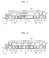
- FIG. 1 is a schematic view of a thin film deposition apparatus according to an embodiment of the present invention
- FIG. 2 illustrates a modified example of the thin film deposition apparatus of FIG. 1
- FIG. 3 is a schematic view of an electrostatic chuck 600, according to an embodiment of the present invention.
- the thin film deposition apparatus includes a loading unit 710, a deposition unit 730, an unloading unit 720, a first circulation unit 610, and a second circulation unit 620.
- the loading unit 710 may include a first rack 712, a transport robot 714, a transport chamber 716, and a first inversion chamber 718.
- the first inversion chamber 718 is disposed adjacent to the transport chamber 716, and a first inversion robot 719 located at the first inversion chamber 718 inverts the electrostatic chuck 600 to bar the electrostatic chuck 600 on the first circulation unit 610 of the deposition unit 730.
- the electrostatic chuck 600 includes an electrode 602 embedded in a main body 601 formed of dielectric material, wherein the electrode 602 is supplied with power. Such an electrostatic chuck may fix the substrates 500 on a surface of the main body 601 as a high voltage is applied to the electrode 602.
- the transport robot 714 places the substrates 500 on a top surface of the electrostatic chuck 600.
- the electrostatic chuck 600 is conveyed to the transport chamber 716.
- the first inversion robot 719 inverts the electrostatic chuck 600, the substrates 500 are directed downwards in the deposition unit 730.
- the unloading unit 720 is constituted to operate in an opposite manner to the loading unit 710 described above.
- the substrates 500 and the electrostatic chuck 600 that pass through the deposition unit 730 are inverted by a second inversion robot 729 in a second inversion chamber 728 and are conveyed to an ejection chamber 726, and an ejection robot 724 takes the substrates 500 and the electrostatic chuck 600 out of the ejection chamber 726 and then separates the substrates 500 from the electrostatic chuck 600 to place or stack the substrates 500 on a second rack 722.
- the electrostatic chuck 600 which is separated from the substrates 500 is returned to the loading unit 710 via the second circulation unit 620.
- the substrates 500 may be fixed on a bottom surface of the electrostatic chuck 600 from when the substrates 500 are initially fixed on the electrostatic chuck 600, and the electrostatic chuck 600 may be conveyed to the deposition unit 730.
- the first inversion chamber 718, the first inversion robot 719, the second inversion chamber 728, and the second inversion robot 729 are not necessary.
- the deposition unit 730 includes at least one deposition chamber.
- the deposition unit 730 may include a first chamber 731, and a plurality of thin film deposition assemblies 100, 200, 300, and 400 are disposed in the first chamber 731.
- four thin film deposition assemblies including a first thin film deposition assembly 100, a second thin film deposition assembly 200, a third thin film deposition assembly 300, and a fourth thin film deposition assembly 400 are installed in the first chamber 731.
- the number of thin film deposition assemblies to be installed in the first chamber 731 may vary according to a deposition material and a deposition condition.
- the first chamber 731 has an appropriate degree of vacuum maintained therein when deposition is performed.
- the deposition unit 730 includes the first chamber 731 and the second chamber 732 connected to each other, and the first and second thin film deposition assemblies 100 and 200 may be disposed in the first chamber 731, and the third and fourth thin film deposition assemblies 300 and 400 may be disposed in the second chamber 732.
- the number of chambers is not limited thereto and may be increased.
- the electrostatic chuck 600 on which the substrates 500 are disposed, is moved to at least the deposition unit 730 by the first circulation unit 610 and may be sequentially moved to the loading unit 710, the deposition unit 730, and the unloading unit 720.
- the electrostatic chuck 600 separated from the substrates 500 in the unloading unit 720 is returned to the loading unit 710 by the second circulation unit 620.
- the first circulation unit 610 is disposed to pass through the first chamber 731 when passing through the deposition unit 730, and the second circulation unit 620 allows the electrostatic chuck 600 to be conveyed to the loading unit 710.
- FIG. 4 is a cross-sectional view of the first circulation unit 610 of the thin film deposition apparatus of FIG. 1 .
- the first circulation unit 610 includes a first carrier 611 that allows the electrostatic chuck 600 on which the substrates 500 are disposed, to be moved.
- the first carrier 611 includes a first support 613, a second support 614, a moving bar 615, and a first driving unit 616.
- the first support 613 and the second support 614 are installed to pass through a chamber of the deposition unit 730, for example, in the embodiment of FIG. 1 , the first chamber 731, and in the embodiment of FIG. 2 , the first chamber 731 and the second chamber 732.
- the first support 613 is disposed vertically in the first chamber 731, and the second support 614 is horizontally disposed below the first support 613 in the first chamber 731. As illustrated in FIG. 4 , the first support 613 and the second support 614 are disposed perpendicular to each other forming a bent structure. However, aspects of the present invention are not limited thereto.
- the first support 613 may be disposed above the second support 614, and the second support 614 may be disposed below the first support 613.
- the moving bar 615 is movable along the first support 613. At least one end of the moving bar 615 is supported by the first support 613, and the other end of the moving bar 615 is formed to be supported by edges of the electrostatic chuck 600.
- the electrostatic chuck 600 may be fixedly supported on the moving bar 615 and may be moved along the first support 613 due to the moving bar 615. A portion of the moving bar 615 that supports the electrostatic chuck 600 may be bent toward a thin film deposition assembly 100 and may allow the substrates 500 to be close to the thin film deposition assembly 100.
- the first driving unit 616 is interposed between the moving bar 615 and the first support 613.
- the first driving unit 616 may include a roller 617 that may be rolled along the first support 613.
- the first driving unit 616 allows the moving bar 615 to be moved along the first support 613 and may provide a driving power or may transfer a driving power generated by an additional driving source to the moving bar 615.
- the first driving unit 616 may be any driving device that allows the moving bar 615 to be moved, as well as the roller 617.
- FIG. 5 is a cross-sectional view of the second circulation unit 620 of the thin film deposition apparatus of FIG. 1 .
- the second circulation unit 620 includes a second carrier 621 that allows the electrostatic chuck 600 that is separated from the substrates 500 to be moved.
- the second carrier 621 includes a third support 623, the moving bar 615, and the first driving unit 616.
- the third support 623 extends to the same length as an extended length of the first support 613 of the first carrier 611.
- the moving bar 615 on which the first driving unit 616 is disposed is supported by the third support 623, and the electrostatic chuck 600 that is separated from the substrates 500 is mounted on the moving bar 615. Structures of the moving bar 615 and the first driving unit 616 are as described above.
- FIG. 6 is a perspective view of the thin film deposition assembly 100 according to an embodiment of the present invention
- FIG. 7 is a schematic cross-sectional side view of the thin film deposition assembly 100 of FIG. 6 , according to an embodiment of the present invention
- FIG. 8 is a schematic plan view of the thin film deposition assembly 100 of FIG. 6 , according to an embodiment of the present invention.
- the thin film deposition assembly 100 includes a deposition source 110, a deposition source nozzle unit 120, and a patterning slit sheet 150.
- the first chamber 731 in order to deposit a deposition material 115 emitted from the deposition source 110 and discharged through the deposition source nozzle unit 120 and the patterning slit sheet 150, onto a substrate 500 in a desired pattern, the first chamber 731 should be maintained in a high-vacuum state as in a deposition method using a fine metal mask (FMM).
- the temperature of the patterning slit sheet 150 should be sufficiently lower than the temperature of the deposition source 110. In this regard, the temperature of the patterning slit sheet 150 may be about 100°C or less. The temperature of the patterning slit sheet 150 should be sufficiently low so as to reduce thermal expansion of the patterning slit sheet 150.
- the substrate 500 which constitutes a deposition target on which the deposition material 115 is to be deposited, is disposed in the first chamber 731.
- the substrate 500 may be a substrate for flat panel displays.
- a large substrate, such as a mother glass, for manufacturing a plurality of flat panel displays, may be used as the substrate 500.
- Other substrates may also be employed.
- Deposition may be performed while the substrate 500 or the thin film deposition assembly 100 is moved relative to the other.
- the size of the FMM has to be equal to the size of a substrate.
- the size of the FMM has to be increased as the substrate becomes larger.
- deposition may be performed while the thin film deposition assembly 100 or the substrate 500 is moved relative to the other.
- deposition may be continuously performed while the substrate 500, which is disposed to face the thin film deposition assembly 100, is moved in a Y-axis direction.
- deposition is performed in a scanning manner while the substrate 500 is moved in a direction of arrow A in FIG. 6 .
- the patterning slit sheet 150 may be significantly smaller than an FMM used in a conventional deposition method.
- deposition is continuously performed, i.e., in a scanning manner while the substrate 500 is moved in the Y-axis direction.
- lengths of the patterning slit sheet 150 in the X-axis and Y-axis directions may be significantly less than the lengths of the substrate 500 in the X-axis and Y-axis directions.
- the patterning slit sheet 150 may be formed to be significantly smaller than an FMM used in the conventional deposition method, it is relatively easy to manufacture the patterning slit sheet 150 used in the aspects of the present invention.
- the patterning slit sheet 150 which is smaller than an FMM used in the conventional deposition method, is more convenient in all processes, including etching and other subsequent processes, such as precise extension, welding, moving, and cleaning processes, compared to the conventional deposition method using the larger FMM. This is more advantageous for a relatively large display apparatus.
- the deposition source 110 that contains and heats the deposition material 115 is disposed in an opposite side of the first chamber 731 to the side in which the substrate 500 is disposed. While the deposition material 115 contained in the deposition source 110 is vaporized, the deposition material 115 is deposited on the substrate 500.
- the deposition source 110 includes a crucible 112 that is filled with the deposition material 115, and a cooling block 111 that includes a heater (not shown) that heats the crucible 112 to vaporize the deposition material 115, which is contained in the crucible 112, towards a side of the crucible 112, and in particular, towards the deposition source nozzle unit 120.
- the cooling block 111 prevents radiation of heat from the crucible 112 to outside, i.e., into the first chamber 731.
- the deposition source nozzle unit 120 is disposed at a side of the deposition source 110, and in particular, at the side of the deposition source 110 facing the substrate 500.
- the deposition source nozzle unit 120 includes a plurality of deposition source nozzles 121 arranged at equal intervals in the Y axis direction, i.e., a scanning direction of the substrate 500.
- the deposition material 110 that is vaporized in the deposition source 110 passes through the deposition source nozzle unit 120 towards the substrate 500.
- the deposition source nozzle unit 120 includes the plurality of deposition source nozzles 121 arranged in the Y-axis direction, that is, the scanning direction of the substrate 500, the size of a pattern formed of the deposition material 115 discharged through the patterning slits 151 of the patterning slit sheet 150 is affected by the size of each deposition source nozzle 121 (since there is only one line of deposition nozzles in the X-axis direction), and thus no shadow zone may be formed on the substrate 500.
- the plurality of deposition source nozzles 121 are arranged in the scanning direction of the substrate 500, even when there is a difference in flux between the deposition source nozzles 121, the difference may be compensated for and deposition uniformity may be maintained constant.
- the patterning slit sheet 150 and a frame 155 in which the patterning slit sheet 150 is bound are disposed between the deposition source 110 and the substrate 500.
- the frame 155 may be formed in a lattice shape, similar to a window frame.
- the patterning slit sheet 150 is bound inside the frame 155.
- the patterning slit sheet 150 includes a plurality of patterning slits 151 arranged in the X-axis direction.
- the deposition material 115 that is vaporized in the deposition source 110, passes through the deposition source nozzle unit 120 and the patterning slit sheet 150 towards the substrate 500.
- the patterning slit sheet 150 may be manufactured by etching, which is the same method as used in a conventional method of manufacturing an FMM, and in particular, a striped FMM.
- the total number of patterning slits 151 may be greater than the total number of deposition source nozzles 121.
- the deposition source 110 and the deposition source nozzle unit 120 coupled to the deposition source 110 may be disposed to be separated from the patterning slit sheet 150 by a predetermined distance.
- the deposition source 110 and the deposition source nozzle unit 120 coupled to the deposition source 110 may be connected to the patterning slit sheet 150 by a first connection member 135. That is, the deposition source 110, the deposition source nozzle unit 120, and the patterning slit sheet 150 may be integrally formed as one body by being connected to each other via the first connection member 135.
- the first connection member 135 guides the deposition material 121, which is discharged through the deposition source nozzles 121, to move in a substantially straight line through the thin film deposition assembly 100, and not to flow in the X-axis direction.
- the first connection members 135 are formed on left and right sides of the deposition source 110, the deposition source nozzle unit 120, and the patterning slit sheet 150 to guide the deposition material 915 not to flow in the X-axis direction; however, aspects of the present invention are not limited thereto. That is, the first connection member 135 may be formed as a sealed box to guide the flow of the deposition material 915 both in the X-axis and Y-axis directions.
- the thin film deposition assembly 100 performs deposition while being moved relative to the substrate 500.
- the patterning slit sheet 150 is separated from the substrate 500 by a predetermined distance.
- the FMM in close contact with a substrate in order to prevent formation of a shadow zone on the substrate.
- the contact may cause defects.
- the size of the mask has to be the same as the size of the substrate since the mask cannot be moved relative to the substrate.
- the size of the mask has to be increased as display apparatuses become larger.
- the patterning slit sheet 150 is disposed to be separated from the substrate 500 by a predetermined distance.
- a mask is formed to be smaller than a substrate, and deposition is performed while the mask is moved relative to the substrate.
- the mask can be easily manufactured.
- defects caused due to the contact between a substrate and an FMM, which occur in the conventional deposition method may be prevented.
- the manufacturing time may be reduced.
- the deposition source nozzle unit 120 is a deposition source opening unit. In this embodiment, the deposition source nozzle unit 120 has a plurality of deposition source nozzles. In other embodiments of the invention, the deposition source opening unit can have deposition source openings. The deposition source openings could have a variety of suitable shapes.
- the patterning slit sheet 150 is a patterning member. In this embodiment, the patterning slit sheet 150 has a plurality of patterning slits. In other embodiments of the invention, the patterning member can have patterning openings. The patterning openings could have a variety of suitable shapes.
- FIG. 9 is a perspective view of a thin film deposition assembly 100 according to another embodiment of the present invention.
- the thin film deposition assembly 100 includes a deposition source 110, a deposition source nozzle unit 120, and a patterning slit sheet 150.
- the deposition source 110 includes a crucible 112 that is filled with a deposition material 115, and a cooling block 111 that includes a heater (not shown) that heats the crucible 112 to vaporize the deposition material 115, so as to move the vaporized deposition material 115 to the deposition source nozzle unit 120.
- the cooling block 111 is contained in the crucible 112.
- the deposition source nozzle unit 120 which has a planar shape, is disposed at a side of the deposition source 110.
- the deposition source nozzle unit 120 includes a plurality of deposition source nozzles 121 arranged in the Y-axis direction.
- the patterning slit sheet 150 and a frame 155 are further disposed between the deposition source 110 and the substrate 500.
- the patterning slit sheet 150 includes a plurality of patterning slits 151 arranged in the X-axis direction.
- the deposition source 110 and the deposition source nozzle unit 120 may be connected to the patterning slit sheet 150 by a second connection member 133 (illustrated in FIG. 11 ).
- a plurality of deposition source nozzles 121 formed on the deposition source nozzle unit 120 are tilted at a predetermined angle, unlike the thin film deposition assembly 100 described with reference to FIG. 6 .
- the deposition source nozzles 121 may include deposition source nozzles 121 a and 121 b arranged in respective rows.
- the deposition source nozzles 121 a and 121 b may be arranged in respective rows to alternate in a zigzag pattern.
- the deposition source nozzles 121 a and 121 b may be tilted at a predetermined angle on an XZ plane.
- the deposition source nozzles 121 a and 121 b are arranged to be tilted at a predetermined angle to each other.
- the deposition source nozzles 121 a in a first row and the deposition source nozzles 121 b in a second row may be tilted to face each other. That is, the deposition source nozzles 121 a of the first row in a left part of the deposition source nozzle unit 121 may be tilted to face a right side portion of the patterning slit sheet 150, and the deposition source nozzles 121 b of the second row in a right part of the deposition source nozzle unit 121 may be tilted to face a left side portion of the patterning slit sheet 150.
- the deposition of the deposition material 115 may be adjusted to lessen a thickness variation between the center and the end portions of the substrate 500 and improve thickness uniformity of the deposition film. Moreover, utilization efficiency of the deposition material 115 may also be improved.
- FIG. 10 is a perspective view of a thin film deposition assembly according to another embodiment of the present invention.
- the thin film deposition apparatus includes a plurality of thin film deposition assemblies, each of which has the structure of the thin film deposition apparatus 100 illustrated in FIGS. 6 through 8 .
- the thin film deposition apparatus illustrated in FIG. 10 may include a multi-deposition source that simultaneously discharges deposition materials for forming a red (R) emission layer, a green (G) emission layer, and a blue (B) emission layer.
- the thin film deposition apparatus includes a first thin film deposition assembly 100, a second thin film deposition assembly 200, and a third thin film deposition assembly 300.
- Each of the first thin film deposition assembly 100, the second thin film deposition assembly 200, and the third thin film deposition assembly 300 has the same structure as the thin film deposition assembly 100 described with reference to FIGS. 6 through 8 , and thus a detailed description thereof will not be provided here.
- the deposition sources 110 of the first thin film deposition assembly 100, the second thin film deposition assembly 200 and the third thin film deposition assembly 300 may contain different deposition materials, respectively.
- the first thin film deposition assembly 100 may contain a deposition material for forming the R emission layer
- the second thin film deposition assembly 200 may contain a deposition material for forming the G emission layer
- the third thin film deposition assembly 300 may contain a deposition material for forming the B emission layer.
- the R emission layer, the G emission layer and the B emission layer may be formed at the same time with a single multi-deposition source.
- the time it takes to manufacture the organic light-emitting display apparatus is significantly reduced.
- the organic light-emitting display apparatus may be manufactured with a reduced number of chambers, so that equipment costs are also markedly reduced.
- a patterning slit sheet of the first thin film deposition assembly 100, a patterning slit sheet of the second thin film deposition assembly 200, a patterning slit sheet of the third thin film deposition assembly 300 may be arranged to be offset by a constant distance with respect to each other, in order for deposition regions corresponding to the patterning slit sheets not to overlap on the substrate 500.
- first thin film deposition assembly 100, the second thin film deposition assembly 200, and the third thin film deposition assembly 300 are used to deposit an R emission layer, a G emission layer and a B emission layer, respectively, patterning slits of the first thin film deposition assembly 100, patterning slits of the second thin film deposition assembly 200, and patterning slits of the second thin film deposition assembly 300 are arranged not to be aligned with each other, in order to form the R emission layer, the G emission layer and the B emission layer in different regions of the substrate 500.
- the deposition materials for forming the R emission layer, the G emission layer, and the B emission layer may have different deposition temperatures. Therefore, the temperatures of the deposition sources of the respective first, second, and third thin film deposition assemblies 100, 200, and 300 may be set to be different.
- a thin film deposition apparatus may include a plurality of thin film deposition assemblies, each of which contains a different deposition material.
- a thin film deposition apparatus may include five thin film deposition assemblies respectively containing materials for a R emission layer, a G emission layer, a B emission layer, an auxiliary layer (R') of the R emission layer, and an auxiliary layer (G') of the G emission layer.
- a plurality of thin layers may be formed at the same time with a plurality of thin film deposition assemblies, and thus manufacturing yield and deposition efficiency are improved.
- the overall manufacturing process is simplified, and the manufacturing costs are reduced.
- FIG. 11 is a perspective view of a thin film deposition assembly 100 according to another embodiment of the present invention
- FIG. 12 is a schematic cross-sectional side view of the thin film deposition assembly 100 of FIG. 11 , according to an embodiment of the present invention
- FIG. 13 is a schematic plan view of the thin film deposition assembly 100 of FIG. 11 , according to an embodiment of the present invention.
- the thin film deposition assembly 100 includes a deposition source 110, a deposition source nozzle unit 120, a barrier wall assembly 130, and patterning slits 151.
- all the components of the thin film deposition assembly 100 may be disposed within a chamber that has an appropriate degree of vacuum maintained therein.
- the chamber has an appropriate vacuum maintained therein in order to allow a deposition material to move in a substantially straight line through the thin film deposition assembly 100.
- the substrate 500 which constitutes a target on which a deposition material 115 is to be deposited, is conveyed into the chamber by using the electrostatic chuck 600.
- the substrate 500 may be a substrate for flat panel displays.
- a large substrate, such as a mother glass, for manufacturing a plurality of flat panel displays, may be used as the substrate 500.
- Deposition may be performed while the substrate 500 or the thin film deposition assembly 100 is moved relative to the other.
- the substrate 500 may be moved relative to the thin film deposition assembly 100 in a direction A.
- the patterning slit sheet 150 may be significantly smaller than a FMM used in the conventional deposition method.
- deposition is continuously performed, i.e., in a scanning manner while the substrate 500 is moved in the Y-axis direction.
- a width of the patterning slit sheet 150 in the X-axis direction is substantially the same as a width of the substrate 500 in the X-axis direction
- a length of the patterning slit sheet 150 in the Y-axis direction may be significantly less than a length of the substrate 500 in the Y-axis direction.
- deposition may be sufficiently performed on the entire surface of the substrate 500 in a scanning manner due to relative movement of the substrate 500 and the thin film deposition assembly 100.
- the patterning slit sheet 150 may be formed to be significantly smaller than an FMM used in the conventional deposition method, it is relatively easy to manufacture the patterning slit sheet 150 used in an aspect of the present invention.
- using the patterning slit sheet 150, which is smaller than an FMM used in the conventional deposition method is more convenient in all processes, including etching and subsequent other processes, such as precise extension, welding, moving, and cleaning processes, compared to the conventional deposition method using the larger FMM. This is more advantageous for a relatively large display apparatus.
- the deposition source 110 that contains and heats the deposition material 115 is disposed in an opposite side of the chamber to the side in which the substrate 500 is disposed.
- the deposition source 110 includes a crucible 112 that is filled with the deposition material 115, and a cooling block 111 that surrounds the crucible 112.
- the cooling block 111 prevents radiation of heat from the crucible 112 to outside, i.e., into the chamber.
- the cooling block 111 may include a heater (not shown) that heats the crucible 112.
- the deposition source nozzle unit 120 is disposed at a side of the deposition source 110, and in particular, at the side of the deposition source 110 facing the substrate 500.
- the deposition source nozzle unit 120 includes a plurality of deposition source nozzles 121 arranged in the X-axis direction.
- the deposition material 115 that is vaporized in the deposition source 110 passes through the plurality of deposition source nozzles 121 of the deposition source nozzle unit 120 towards the substrate 500.
- the barrier wall assembly 130 is disposed at a side of the deposition source nozzle unit 120.
- the barrier wall assembly 130 includes a plurality of barrier walls 131, and a barrier wall frame 132 that constitutes an outer wall of the barrier walls 131.
- the plurality of barrier walls 131 may be arranged parallel to each other at equal intervals in the X-axis direction.
- each of the barrier walls 131 may be formed to extend in an YZ plane in FIG. 11 , i.e., perpendicular to the X-axis direction.
- the plurality of barrier walls 131 arranged as described above partition the space between the deposition source nozzle unit 120 and the patterning slit sheet 150 into a plurality of sub-deposition spaces S (illustrated in FIG. 13 ).
- the deposition space is divided by the barrier walls 131 into the sub-deposition spaces S that respectively correspond to the deposition source nozzles 121 through which the deposition material 115 is discharged, as illustrated in FIG. 13 .
- the barrier walls 131 may be respectively disposed between adjacent deposition source nozzles 121.
- each of the deposition source nozzles 121 may be disposed between two adjacent barrier walls 131.
- the deposition source nozzles 121 may be respectively located at the midpoint between two adjacent barrier walls 131.
- aspects of the present invention are not limited thereto, and the deposition source nozzles 121 may be disposed otherwise.
- the plurality of deposition source nozzles 121 may be disposed between two adjacent barrier walls 131. Even in this case, the deposition source nozzles 121 may be respectively located at the midpoint between two adjacent barrier walls 131.
- the barrier walls 131 partition the space between the deposition source nozzle unit 120 and the patterning slit sheet 150 into the plurality of sub-deposition spaces S, the deposition material 115 discharged through each of the deposition source nozzles 121 is not mixed with the deposition material 115 discharged through the other deposition source nozzles 121, and passes through patterning slits 151 so as to be deposited on the substrate 500.
- the barrier walls 131 guide the deposition material 115, which is discharged through the deposition source nozzles 121, to move in a substantially straight line through the thin film deposition assembly 100, and not to flow in the Z-axis direction.
- the deposition material 115 is forced to move in a substantially straight line through the thin film deposition assembly 100 by installing the barrier walls 131, so that a smaller shadow zone may be formed on the substrate 500 compared to a case where no barrier walls are installed.
- the thin film deposition assembly 100 and the substrate 500 can be separated from each other by a predetermined distance. This will be described later in detail.
- the barrier wall frame 132 which forms upper and lower sides of the barrier walls 131, maintains the positions of the barrier walls 131, and guides the deposition material 115, which is discharged through the deposition source nozzles 121, to move in a substantially straight line through the thin film deposition assembly 100, and not to flow in the Y-axis direction.
- the deposition source nozzle unit 120 and the barrier wall assembly 130 may be separated from each other by a predetermined distance. Thus, heat dissipated from the deposition source 110 may be prevented from being conducted to the barrier wall assembly 130.
- aspects of the present invention are not limited thereto. In other words, when an appropriate insulation unit is disposed between the deposition source nozzle unit 120 and the barrier wall assembly 130, the deposition source nozzle unit 120 and the barrier wall assembly 130 may be combined with each other and may contact each other.
- the barrier wall assembly 130 may be constructed to be detachable from the thin film deposition assembly 100.
- the deposition space is enclosed by using the barrier wall assembly 130, so that the deposition material 115 that remains undeposited is mostly deposited within the barrier wall assembly 130.
- the barrier wall assembly 130 since the barrier wall assembly 130 is constructed to be detachable from the thin film deposition assembly 100, when a large amount of the deposition material 115 lies in the barrier wall assembly 130 after a long deposition process, the barrier wall assembly 130 may be detached from the thin film deposition assembly 100 and then placed in a separate deposition material recycling apparatus in order to recover the deposition material 115. Due to the structure of the thin film deposition assembly 100 according to the present embodiment, a reuse rate of the deposition material 115 is increased, so that the deposition efficiency is improved, and thus the manufacturing costs are reduced.
- the patterning slit sheet 150 and a frame 155 in which the patterning slit sheet 150 is bound are disposed between the deposition source 110 and the substrate 500.
- the frame 155 may be formed in a lattice shape, similar to a window frame.
- the patterning slit sheet 150 is bound inside the frame 155.
- the patterning slit sheet 150 includes a plurality of patterning slits 151 arranged in the X-axis direction.
- the patterning slit sheet 150 extends in the Y-axis direction.
- the patterning slit sheet 150 is formed of a metal sheet and is bound on the frame 155 in an extended state.
- the patterning slits 151 are formed as striped slits in the patterning slit sheet 150 manufactured by etching.
- the total number of patterning slits 151 may be greater than the total number of deposition source nozzles 121. In addition, there may be a greater number of patterning slits 151 than deposition source nozzles 121 disposed between two adjacent barrier walls 131. The number of the patterning slits 151 may correspond to the number of deposition patterns to be formed on the substrate 500.
- the barrier wall assembly 130 and the patterning slit sheet 150 may be formed to be separated from each other by a predetermined distance.
- the barrier wall assembly 130 and the patterning slit sheet 150 may be connected by a separate second connection member 133.
- the temperature of the barrier wall assembly 130 may increase to 100°C or higher due to the deposition source 110 whose temperature is high.
- the barrier wall assembly 130 and the patterning slit sheet 150 are separated from each other by a predetermined distance.
- the thin film deposition assembly 100 performs deposition while being moved relative to the substrate 500.
- the patterning slit sheet 150 is separated from the substrate 500 by a predetermined distance.
- the barrier walls 131 are arranged between the deposition source nozzle unit 120 and the patterning slit sheet 150 to force the deposition material 115 to move in a straight direction.
- a conventional deposition method using an FMM deposition is performed with the FMM in close contact with a substrate in order to prevent formation of a shadow zone on the substrate.
- defects such as scratched patterns that have been already formed over the substrate due to the contact between the substrate and the FMM, occur.
- the size of the mask has to be the same as the size of the substrate since the mask cannot be moved relative to the substrate.
- the size of the mask has to be increased as display apparatuses become larger.
- the patterning slit sheet 150 is disposed to be separated from the substrate 500 by a predetermined distance. This may be facilitated by installing the barrier walls 131 to reduce the size of the shadow zone formed on the substrate 500.
- a patterning slit sheet is formed to be smaller than a substrate according to an aspect of the present invention and then, the patterning slit sheet is moved relative to the substrate a large mask like in the conventional deposition method using the FMM does not need to be manufactured.
- the substrate and the patterning slit sheet are separated from each other by a predetermined distance, defects caused due to the contact between the substrate and the patterning slit sheet may be prevented.
- the manufacturing speed since it is unnecessary to use the patterning slit sheet in close contact with the substrate during a deposition process, the manufacturing speed may be improved.
- the deposition source 110 may be accommodated in a source chamber 113 connected to a first chamber 731 in which deposition is to be performed, as illustrated in FIGS. 14A and 14B .
- the separate source chamber 113 is connected to the first chamber 731 in which deposition is to be performed, and the space between the source chamber 113 and the first chamber 731 is opened or closed by a high-vacuum valve 118.
- the first chamber 731 In order to refill a deposition material in the deposition source 110 after a deposition process is completed, the first chamber 731 should be maintained under atmospheric pressure. However, when the first chamber 731 is maintained under atmospheric pressure to refill the deposition source 110, and then is maintained in a vacuum state so as to perform a new deposition process, this process takes a long time and production time increases.
- a stage 114 that supports the deposition source 110 is disposed in the source chamber 113, and the stage 114 is connected to bellows 116.
- the stage 114 is driven as the bellows 116 is driven.
- the deposition source 110 can be moved between the source chamber 113 and the first chamber 731.
- a shutter 117 is disposed around the deposition source 110, and when the deposition source 110 is raised into the first chamber 731, the shutter 117 blocks a connection opening to the source chamber 113 so as to prevent the source chamber 113 from being contaminated due to the deposition material, as illustrated in FIG. 14A .
- the deposition source 110 is lowered into the source chamber 113 when the shutter 117 is opened, and the source chamber 113 is closed by the high-vacuum valve 118 in an air-tight state with respect to the first chamber 731, as illustrated in FIG. 14B .
- the state of the source chamber 113 is changed to be under atmospheric pressure, and a separate door (not shown) disposed in the source chamber 113 is opened, so that the deposition source 110 may be taken out from the source chamber 113 to refill the deposition material in the deposition source 110.
- the deposition material may be easily filled in the deposition source 110 without exhausting the first chamber 173.
- the thin film deposition assembly 100 may be mounted on the second support 614, as illustrated in FIG. 4 .
- a second driving unit 618 is disposed on the second support 614, and the second driving unit 618 is connected to the frame 155 of the thin film deposition assembly 100 and finely adjusts the position of the thin film deposition assembly 100 so that the substrate 500 and the thin film deposition assembly 100 may be aligned with each other. Fine adjustment of the alignment may be performed in real-time while the deposition process is being performed.
- the thin film deposition assembly 100 may further include a camera assembly 170 for aligning the substrate 500 and the thin film deposition assembly 100 with each other, as illustrated in FIGS. 11 and 13 .
- the camera assembly 170 is used to align a first mark 159 formed on the frame 155 and a second mark 501 formed on the substrate 500 with each other in real-time.
- the camera assembly 170 may obtain a wide view area within a vacuum chamber in which the deposition process is performed, as illustrated in FIG. 10 .
- a camera 172 is disposed in a cylindrical hood 171, and an optical system 173 including a lens is disposed between the camera 172 and an opening 176 of the hood 171.
- a protection window 174 on which heating patterns 175 are formed, is disposed between the optical system 173 and the opening 176. While the deposition process is performed by using the heating patterns 175, an organic material is not deposited on the surface of the protection window 174. Thus, even when the deposition process is performed, the camera 172 can determine the alignment via the protection window 174 within the vacuum chamber.
- FIG. 16 is a schematic perspective view of a thin film deposition assembly 100 according to another embodiment of the present invention.
- the thin film deposition assembly 100 includes a deposition source 110, a deposition source nozzle unit 120, a first barrier wall assembly 130, a second barrier wall assembly 140, and a patterning slit sheet 150.
- all the components of the thin film deposition assembly 100 may be disposed within a chamber that has an appropriate degree of vacuum maintained therein.
- the chamber has an appropriate vacuum maintained therein in order to allow a deposition material to move in a substantially straight line through the thin film deposition assembly 100.
- the substrate 500 which constitutes a target on which a deposition material 115 is to be deposited, is disposed in the chamber.
- the deposition source 110 that contains and heats the deposition material 115 is disposed in an opposite side of the chamber to the side in which the substrate 500 is disposed.
- the first barrier wall assembly 130 is the same as the barrier wall assembly 130 described with reference to the embodiment of FIG. 11 and thus a detailed description thereof will not be provided here.
- the second barrier wall assembly 140 is disposed at a side of the first barrier wall assembly 130.
- the second barrier wall assembly 140 includes a plurality of second barrier walls 141, and a second barrier wall frame 142 that constitutes an outer wall of the second barrier walls 141.
- the plurality of second barrier walls 141 may be arranged parallel to each other at equal intervals in the X-axis direction.
- each of the second barrier walls 141 may be formed to extend in the YZ plane in FIG. 16 , i.e., perpendicular to the X-axis direction.
- the deposition space is divided by the first barrier walls 131 and the second barrier walls 141 into sub-deposition spaces that respectively correspond to the deposition source nozzles 121 through which the deposition material 115 is discharged.
- the second barrier walls 141 may be disposed to correspond respectively to the first barrier walls 131.
- the second barrier walls 141 may be respectively disposed to be parallel to and to be on the same plane as the first barrier walls 131.
- Each pair of the corresponding first and second barrier walls 131 and 141 may be located on the same plane.
- the first barrier walls 131 and the second barrier walls 141 are respectively illustrated as having the same thickness in the X-axis direction, aspects of the present invention are not limited thereto.
- the second barrier walls 141 which need to be accurately aligned with the patterning slit sheet 151, may be formed to be relatively thin, whereas the first barrier walls 131, which do not need to be precisely aligned with the patterning slit sheet 550, may be formed to be relatively thick. This makes it easier to manufacture the thin film deposition assembly 100.
- a plurality of thin film deposition assemblies 100 as described above may be continuously arranged in the first chamber 731, as illustrated in FIG. 1 .
- the first through fourth thin film deposition assemblies 100, 200, 300, and 400 may deposit different deposition materials.
- patterns of patterning slits of the first through fourth thin film deposition assemblies 100, 200, 300, and 400 are different from one another, so that a layer forming process including a process of depositing red, green, and blue pixels at one time may be performed.
- FIG. 17 is a cross-sectional view of an active matrix (AM) organic light-emitting display apparatus manufactured by using a thin film deposition apparatus, according to an embodiment of the present invention.
- AM active matrix
- the AM organic light-emitting display apparatus is disposed on a substrate 30.
- the substrate 30 may be formed of a transparent material, for example, glass, and may be also formed of plastic or metal.
- a thin film transistor (TFT) 40, a capacitor 50, and an organic light-emitting device 60 are formed on the insulating layer 31, as illustrated in FIG. 17 .
- a semiconductor active layer 41 is formed on an upper surface of the insulating layer 31 in a predetermined pattern.
- a gate insulating layer 32 is formed to cover the semiconductor active layer 41.
- the semiconductor active layer 41 may include a p-type or n-type semiconductor material.
- a gate electrode 42 of the TFT 40 is formed on an upper surface of the gate insulating layer 32 corresponding to the semiconductor active layer 41.
- An interlayer insulating layer 33 is formed to cover the gate electrode 42. After the interlayer insulating layer 33 is formed, the gate insulating layer 32 and the interlayer insulating layer 33 are etched by, for example, performing dry etching, to form a contact hole for exposing parts of the semiconductor active layer 41.
- a source/drain electrode 43 is formed on the interlayer insulating layer 33 to contact the semiconductor active layer 41 through the contact hole.
- a passivation layer 34 is formed to cover the source/drain electrode 43, and is etched to expose a part of the source/drain electrode 43.
- a separate insulating layer (not shown) may be further formed on the passivation layer 34 so as to planarize the passivation layer 34.
- the organic light-emitting device 60 displays predetermined image information by emitting red, green, or blue light as current flows.
- the organic light-emitting device 60 includes a first electrode 61 formed on the passivation layer 34.
- the first electrode 61 is electrically connected to the drain electrode 43 of the TFT 40.
- a pixel defining layer 35 is formed to cover the first electrode 61. After an opening 64 is formed in the pixel defining layer 35, an organic emission layer 63 is formed in a region defined by the opening 64. A second electrode 62 is formed on the organic emission layer 63.
- the pixel defining layer 35 which defines individual pixels, is formed of an organic material.
- the pixel defining layer 35 also planarizes the surface of a region of the substrate 30 where the first electrode 61 is formed, and in particular, the surface of the passivation layer 34.
- the first electrode 61 and the second electrode 62 are insulated from each other, and respectively apply voltages of opposite polarities to the organic emission layer 63 to induce light emission in the organic emission layer 63.
- the organic emission layer 63 may be formed of a low-molecular weight organic material or a polymer organic material.
- the organic emission layer 63 may have a single or multi-layer structure including at least one selected from the group consisting of a hole injection layer (HIL), a hole transport layer (HTL), an emission layer (EML), an electron transport layer (ETL), an electron injection layer (EIL), etc.
- HIL hole injection layer
- HTL hole transport layer
- EML emission layer
- ETL electron transport layer
- EIL electron injection layer
- available organic materials may include copper phthalocyanine (CuPc), N,N'-di(naphthalene-1-yl)-N,N'-diphenyl-benzidine (NPB), tris-8-hydroxyquinoline aluminum (Alq3), etc.
- CuPc copper phthalocyanine
- NPB N,N'-di(naphthalene-1-yl)-N,N'-diphenyl-benzidine
- Alq3
- the substrate 30 is conveyed into a chamber 731, as illustrated in FIG. 1 .
- a target organic material is deposited by the first through fourth thin film deposition assemblies 100, 200, 300, and 400.
- the second electrode 62 may be formed by performing the same deposition process as the deposition process required to form the first electrode 61.
- the first electrode 61 functions as an anode, and the second electrode 62 functions as a cathode.
- the first electrode 61 may function as a cathode, and the second electrode 62 may function as an anode.
- the first electrode 61 may be patterned to correspond to individual pixel regions, and the second electrode 62 may be formed to cover all the pixels.
- the first electrode 61 may be formed as a transparent electrode or a reflective electrode.
- a transparent electrode may be formed of at least one material selected from the group consisting of indium tin oxide (ITO), indium zinc oxide (IZO), zinc oxide (ZnO), and indium oxide (In 2 O 3 ).
- Such a reflective electrode may be formed by forming a reflective layer by using at least one material selected from the group consisting of silver (Ag), magnesium (Mg), aluminum (Al), platinum (Pt), palladium (Pd), gold (Au), nickel (Ni), neodymium (Nd), iridium (Ir), chromium (Cr), and a compound thereof and by forming a layer by using at least one material selected from the group consisting of ITO, IZO, ZnO, and In 2 O 3 on the reflective layer.
- the first electrode 61 may be formed by forming a layer by, for example, sputtering, and then patterning the layer by, for example, photolithography.
- the second electrode 62 may also be formed as a transparent electrode or a reflective electrode.
- the second electrode 62 functions as a cathode.
- a transparent electrode may be formed by depositing a metal having a low work function, such as lithium (Li), calcium (Ca), lithium fluoride/calcium (LiF/Ca), lithium fluoride/aluminum (LiF/Al), aluminum (Al), silver (Ag), magnesium (Mg), or a compound thereof on a surface of the organic emission layer 63 and forming an auxiliary electrode layer or a bus electrode line thereon from ITO, IZO, ZnO, In 2 O 3 , or the like.
- a metal having a low work function such as lithium (Li), calcium (Ca), lithium fluoride/calcium (LiF/Ca), lithium fluoride/aluminum (LiF/Al), aluminum (Al), silver (Ag), magnesium (Mg), or a compound thereof on a surface of the organic emission
- the reflective layer may be formed by depositing at least one material selected from the group consisting of Li, Ca, LiF/Ca, LiF/Al, Al, Ag, Mg, and a compound thereof on the entire surface of the organic emission layer 63.
- the second electrode 62 may be formed by using the same deposition method as used to form the organic emission layer 63 described above.
- the thin film deposition assemblies according to the embodiments of the present invention described above may be applied to form an organic layer or an inorganic layer of an organic TFT, and to form layers from various materials.
- the thin film deposition apparatus may be easily used to manufacture large substrates on a mass scale.
- the thin film deposition apparatus and the organic-light-emitting display apparatus may be easily manufactured, may improve manufacturing yield and deposition efficiency, and may allow deposition materials to be reused.
Landscapes
- Chemical & Material Sciences (AREA)
- Engineering & Computer Science (AREA)
- Chemical Kinetics & Catalysis (AREA)
- Materials Engineering (AREA)
- Mechanical Engineering (AREA)
- Metallurgy (AREA)
- Organic Chemistry (AREA)
- Manufacturing & Machinery (AREA)
- Electroluminescent Light Sources (AREA)
- Physical Vapour Deposition (AREA)
- Physics & Mathematics (AREA)
- Condensed Matter Physics & Semiconductors (AREA)
- General Physics & Mathematics (AREA)
- Computer Hardware Design (AREA)
- Microelectronics & Electronic Packaging (AREA)
- Power Engineering (AREA)
- Container, Conveyance, Adherence, Positioning, Of Wafer (AREA)
Applications Claiming Priority (2)
| Application Number | Priority Date | Filing Date | Title |
|---|---|---|---|
| KR20090079765 | 2009-08-27 | ||
| KR1020100011480A KR101174877B1 (ko) | 2009-08-27 | 2010-02-08 | 박막 증착 장치 및 이를 이용한 유기 발광 표시장치의 제조 방법 |
Publications (3)
| Publication Number | Publication Date |
|---|---|
| EP2290118A2 true EP2290118A2 (fr) | 2011-03-02 |
| EP2290118A3 EP2290118A3 (fr) | 2011-06-29 |
| EP2290118B1 EP2290118B1 (fr) | 2019-05-22 |
Family
ID=43221846
Family Applications (1)
| Application Number | Title | Priority Date | Filing Date |
|---|---|---|---|
| EP10251514.5A Active EP2290118B1 (fr) | 2009-08-27 | 2010-08-27 | Appareil de dépôt de film mince et procédé de fabrication d'un appareil d'affichage luminescent organique l'utilisant |
Country Status (4)
| Country | Link |
|---|---|
| US (2) | US9450140B2 (fr) |
| EP (1) | EP2290118B1 (fr) |
| JP (1) | JP5677785B2 (fr) |
| CN (1) | CN102005541B (fr) |
Cited By (3)
| Publication number | Priority date | Publication date | Assignee | Title |
|---|---|---|---|---|
| CN104178732A (zh) * | 2013-05-21 | 2014-12-03 | 三星显示有限公司 | 沉积源和有机层沉积设备 |
| EP2688121A3 (fr) * | 2012-07-16 | 2016-02-17 | Samsung Display Co., Ltd. | Appareil de dépôt de couche organique, procédé de fabrication d'un dispositif d'affichage électroluminescent organique à l'aide de celui-ci et dispositif d'affichage électroluminescent organique fabriqué par le procédé |
| CN112962081A (zh) * | 2021-02-01 | 2021-06-15 | 肇庆宏旺金属实业有限公司 | 一种钢板连续镀膜生产线及镀膜工艺 |
Families Citing this family (71)
| Publication number | Priority date | Publication date | Assignee | Title |
|---|---|---|---|---|
| TWI475124B (zh) | 2009-05-22 | 2015-03-01 | Samsung Display Co Ltd | 薄膜沉積設備 |
| TWI472639B (zh) | 2009-05-22 | 2015-02-11 | Samsung Display Co Ltd | 薄膜沉積設備 |
| US8882920B2 (en) * | 2009-06-05 | 2014-11-11 | Samsung Display Co., Ltd. | Thin film deposition apparatus |
| US8882921B2 (en) * | 2009-06-08 | 2014-11-11 | Samsung Display Co., Ltd. | Thin film deposition apparatus |
| KR101117719B1 (ko) * | 2009-06-24 | 2012-03-08 | 삼성모바일디스플레이주식회사 | 박막 증착 장치 |
| JP5328726B2 (ja) | 2009-08-25 | 2013-10-30 | 三星ディスプレイ株式會社 | 薄膜蒸着装置及びこれを利用した有機発光ディスプレイ装置の製造方法 |
| JP5677785B2 (ja) | 2009-08-27 | 2015-02-25 | 三星ディスプレイ株式會社Samsung Display Co.,Ltd. | 薄膜蒸着装置及びこれを利用した有機発光表示装置の製造方法 |
| US8696815B2 (en) | 2009-09-01 | 2014-04-15 | Samsung Display Co., Ltd. | Thin film deposition apparatus |
| US8876975B2 (en) * | 2009-10-19 | 2014-11-04 | Samsung Display Co., Ltd. | Thin film deposition apparatus |
| KR101146982B1 (ko) | 2009-11-20 | 2012-05-22 | 삼성모바일디스플레이주식회사 | 박막 증착 장치 및 유기 발광 디스플레이 장치 제조 방법 |
| KR101174874B1 (ko) * | 2010-01-06 | 2012-08-17 | 삼성디스플레이 주식회사 | 증착 소스, 박막 증착 장치 및 유기 발광 표시 장치 제조 방법 |
| KR101084184B1 (ko) | 2010-01-11 | 2011-11-17 | 삼성모바일디스플레이주식회사 | 박막 증착 장치 |
| KR101174875B1 (ko) | 2010-01-14 | 2012-08-17 | 삼성디스플레이 주식회사 | 박막 증착 장치, 이를 이용한 유기 발광 디스플레이 장치의 제조방법 및 이에 따라 제조된 유기 발광 디스플레이 장치 |
| KR101193186B1 (ko) * | 2010-02-01 | 2012-10-19 | 삼성디스플레이 주식회사 | 박막 증착 장치, 이를 이용한 유기 발광 디스플레이 장치의 제조방법 및 이에 따라 제조된 유기 발광 디스플레이 장치 |
| KR101156441B1 (ko) | 2010-03-11 | 2012-06-18 | 삼성모바일디스플레이주식회사 | 박막 증착 장치 |
| KR101202348B1 (ko) | 2010-04-06 | 2012-11-16 | 삼성디스플레이 주식회사 | 박막 증착 장치 및 이를 이용한 유기 발광 표시 장치의 제조 방법 |
| US8894458B2 (en) | 2010-04-28 | 2014-11-25 | Samsung Display Co., Ltd. | Thin film deposition apparatus, method of manufacturing organic light-emitting display device by using the apparatus, and organic light-emitting display device manufactured by using the method |
| KR101223723B1 (ko) | 2010-07-07 | 2013-01-18 | 삼성디스플레이 주식회사 | 박막 증착 장치, 이를 이용한 유기 발광 디스플레이 장치의 제조방법 및 이에 따라 제조된 유기 발광 디스플레이 장치 |
| KR101673017B1 (ko) | 2010-07-30 | 2016-11-07 | 삼성디스플레이 주식회사 | 박막 증착 장치 및 이를 이용한 유기 발광 표시장치의 제조 방법 |
| KR101678056B1 (ko) | 2010-09-16 | 2016-11-22 | 삼성디스플레이 주식회사 | 박막 증착 장치, 이를 이용한 유기 발광 디스플레이 장치의 제조방법 및 이에 따라 제조된 유기 발광 디스플레이 장치 |
| KR101738531B1 (ko) | 2010-10-22 | 2017-05-23 | 삼성디스플레이 주식회사 | 유기 발광 디스플레이 장치의 제조 방법 및 이에 따라 제조된 유기 발광 디스플레이 장치 |
| KR101723506B1 (ko) | 2010-10-22 | 2017-04-19 | 삼성디스플레이 주식회사 | 유기층 증착 장치 및 이를 이용한 유기 발광 디스플레이 장치의 제조 방법 |
| KR20120045865A (ko) | 2010-11-01 | 2012-05-09 | 삼성모바일디스플레이주식회사 | 유기층 증착 장치 |
| KR20120065789A (ko) | 2010-12-13 | 2012-06-21 | 삼성모바일디스플레이주식회사 | 유기층 증착 장치 |
| KR101760897B1 (ko) | 2011-01-12 | 2017-07-25 | 삼성디스플레이 주식회사 | 증착원 및 이를 구비하는 유기막 증착 장치 |
| KR101923174B1 (ko) * | 2011-05-11 | 2018-11-29 | 삼성디스플레이 주식회사 | 정전 척, 상기 정전 척을 포함하는 박막 증착 장치 및 이를 이용한 유기 발광 표시 장치의 제조 방법 |
| KR20120131548A (ko) * | 2011-05-25 | 2012-12-05 | 삼성디스플레이 주식회사 | 유기층 증착 장치 |
| KR101840654B1 (ko) | 2011-05-25 | 2018-03-22 | 삼성디스플레이 주식회사 | 유기층 증착 장치 및 이를 이용한 유기 발광 디스플레이 장치의 제조 방법 |
| KR101852517B1 (ko) | 2011-05-25 | 2018-04-27 | 삼성디스플레이 주식회사 | 유기층 증착 장치 및 이를 이용한 유기 발광 디스플레이 장치의 제조 방법 |
| KR101857249B1 (ko) | 2011-05-27 | 2018-05-14 | 삼성디스플레이 주식회사 | 패터닝 슬릿 시트 어셈블리, 유기막 증착 장치, 유기 발광 표시장치제조 방법 및 유기 발광 표시 장치 |
| KR20130004830A (ko) * | 2011-07-04 | 2013-01-14 | 삼성디스플레이 주식회사 | 유기층 증착 장치 및 이를 이용한 유기 발광 표시 장치의 제조 방법 |
| KR101826068B1 (ko) | 2011-07-04 | 2018-02-07 | 삼성디스플레이 주식회사 | 유기층 증착 장치 |
| KR20130015144A (ko) * | 2011-08-02 | 2013-02-13 | 삼성디스플레이 주식회사 | 증착원어셈블리, 유기층증착장치 및 이를 이용한 유기발광표시장치의 제조 방법 |
| CN102433540A (zh) * | 2011-08-30 | 2012-05-02 | 费绍栋 | 用于真空环境中直触式探测物料表面参数的窗式装置 |
| KR20130069037A (ko) * | 2011-12-16 | 2013-06-26 | 삼성디스플레이 주식회사 | 유기층 증착 장치, 이를 이용한 유기 발광 표시 장치의 제조 방법 및 유기 발광 표시 장치 |
| KR102015872B1 (ko) * | 2012-06-22 | 2019-10-22 | 삼성디스플레이 주식회사 | 유기층 증착 장치, 이를 이용한 유기 발광 디스플레이 장치의 제조 방법 및 이에 따라 제조된 유기 발광 디스플레이 장치 |
| US9461277B2 (en) | 2012-07-10 | 2016-10-04 | Samsung Display Co., Ltd. | Organic light emitting display apparatus |
| CN103545460B (zh) | 2012-07-10 | 2017-04-12 | 三星显示有限公司 | 有机发光显示装置、有机发光显示设备及其制造方法 |
| KR101959974B1 (ko) * | 2012-07-10 | 2019-07-16 | 삼성디스플레이 주식회사 | 유기층 증착 장치, 이를 이용한 유기 발광 디스플레이 장치의 제조 방법 및 이에 따라 제조된 유기 발광 디스플레이 장치 |
| KR101959975B1 (ko) * | 2012-07-10 | 2019-07-16 | 삼성디스플레이 주식회사 | 유기층 증착 장치, 이를 이용한 유기 발광 디스플레이 장치의 제조 방법 및 이에 따라 제조된 유기 발광 디스플레이 장치 |
| KR102013315B1 (ko) | 2012-07-10 | 2019-08-23 | 삼성디스플레이 주식회사 | 유기 발광 디스플레이 장치의 제조 방법 및 이에 따라 제조된 유기 발광 디스플레이 장치 |
| KR101632298B1 (ko) | 2012-07-16 | 2016-06-22 | 삼성디스플레이 주식회사 | 평판 표시장치 및 그 제조방법 |
| KR101938365B1 (ko) * | 2012-07-31 | 2019-04-12 | 삼성디스플레이 주식회사 | 증착 장치 및 이를 이용한 증착량 측정 방법 |
| KR101944918B1 (ko) | 2012-08-03 | 2019-02-08 | 삼성디스플레이 주식회사 | 유기층 증착 어셈블리, 유기층 증착 장치, 유기 발광 표시 장치 및 유기 발광 표시 장치 제조 방법 |
| KR101994838B1 (ko) | 2012-09-24 | 2019-10-01 | 삼성디스플레이 주식회사 | 유기층 증착 장치, 이를 이용한 유기 발광 디스플레이 장치의 제조 방법 및 이에 따라 제조된 유기 발광 디스플레이 장치 |
| KR20140050994A (ko) | 2012-10-22 | 2014-04-30 | 삼성디스플레이 주식회사 | 유기 발광 디스플레이 장치 및 그 제조 방법 |
| KR102009726B1 (ko) | 2012-11-08 | 2019-10-22 | 삼성디스플레이 주식회사 | 유기 발광 표시 장치 및 유기 발광 표시 장치 제조 방법 |
| KR102052069B1 (ko) * | 2012-11-09 | 2019-12-05 | 삼성디스플레이 주식회사 | 유기층 증착 장치, 이를 이용한 유기 발광 디스플레이 장치의 제조 방법 및 이에 따라 제조된 유기 발광 디스플레이 장치 |
| KR102006878B1 (ko) * | 2012-12-27 | 2019-08-05 | 삼성디스플레이 주식회사 | 기판 검사식각 복합장치 및 이를 구비하는 기판 처리장치 |
| KR102154706B1 (ko) * | 2013-03-20 | 2020-09-11 | 삼성디스플레이 주식회사 | 증착장치, 이를 이용한 유기발광 디스플레이 장치 제조 방법 및 유기발광 디스플레이 장치 |
| KR102050482B1 (ko) * | 2013-03-27 | 2019-12-02 | 삼성디스플레이 주식회사 | 증착장치, 이를 이용한 유기발광 디스플레이 장치 제조 방법 및 유기발광 디스플레이 장치 |
| KR102058515B1 (ko) * | 2013-04-18 | 2019-12-24 | 삼성디스플레이 주식회사 | 증착장치, 이를 이용한 유기발광 디스플레이 장치 제조 방법 및 유기발광 디스플레이 장치 |
| KR102081284B1 (ko) | 2013-04-18 | 2020-02-26 | 삼성디스플레이 주식회사 | 증착장치, 이를 이용한 유기발광 디스플레이 장치 제조 방법 및 유기발광 디스플레이 장치 |
| KR20140130972A (ko) * | 2013-05-02 | 2014-11-12 | 삼성디스플레이 주식회사 | 유기층 증착 장치 및 이를 이용한 유기 발광 디스플레이 장치의 제조 방법 |
| KR102096049B1 (ko) * | 2013-05-03 | 2020-04-02 | 삼성디스플레이 주식회사 | 증착장치, 이를 이용한 유기발광 디스플레이 장치 제조 방법 및 유기발광 디스플레이 장치 |
| KR102075528B1 (ko) | 2013-05-16 | 2020-03-03 | 삼성디스플레이 주식회사 | 증착장치, 유기발광 디스플레이 장치 제조방법 및 유기발광 디스플레이 장치 |
| KR102075527B1 (ko) | 2013-05-16 | 2020-02-11 | 삼성디스플레이 주식회사 | 유기층 증착 장치 및 이를 이용한 유기 발광 디스플레이 장치의 제조 방법 |
| KR102081282B1 (ko) * | 2013-05-27 | 2020-02-26 | 삼성디스플레이 주식회사 | 증착용 기판이동부, 이를 포함하는 증착장치, 이를 이용한 유기발광 디스플레이 장치 제조방법 및 유기발광 디스플레이 장치 |
| KR102107104B1 (ko) * | 2013-06-17 | 2020-05-07 | 삼성디스플레이 주식회사 | 유기층 증착 장치 및 이를 이용한 유기 발광 디스플레이 장치의 제조 방법 |
| KR102120895B1 (ko) * | 2013-08-09 | 2020-06-10 | 삼성디스플레이 주식회사 | 증착장치, 이를 이용한 유기발광 디스플레이 장치 제조 방법 및 유기발광 디스플레이 장치 |
| KR101673016B1 (ko) * | 2013-08-27 | 2016-11-07 | 삼성디스플레이 주식회사 | 박막봉지 제조장치 및 이를 이용한 표시 장치의 제조방법 |
| KR102162797B1 (ko) * | 2013-12-23 | 2020-10-08 | 삼성디스플레이 주식회사 | 유기 발광 디스플레이 장치의 제조 방법 |
| KR102217794B1 (ko) * | 2015-01-22 | 2021-02-19 | 삼성디스플레이 주식회사 | 위치 가변 마그넷 플레이트 |
| CN106956928B (zh) * | 2017-04-20 | 2019-11-01 | 东旭科技集团有限公司 | 输送装置和玻璃基板生产系统 |
| KR102180070B1 (ko) * | 2017-10-31 | 2020-11-17 | 엘지디스플레이 주식회사 | 초미세 패턴 증착장치, 이를 이용한 초미세 패턴 증착방법 그리고 초미세 패턴 증착방법에 의해 제작된 전계발광표시장치 |
| KR102171684B1 (ko) * | 2018-09-10 | 2020-10-29 | 주식회사 에스에프에이 | 디스플레이용 기판 증착 시스템 |
| KR102190638B1 (ko) * | 2018-09-10 | 2020-12-14 | 주식회사 에스에프에이 | 디스플레이용 기판 증착 시스템 |
| KR102700940B1 (ko) * | 2019-02-19 | 2024-09-02 | 삼성디스플레이 주식회사 | 표시 장치의 제조장치 및 표시 장치의 제조방법 |
| KR102152951B1 (ko) * | 2019-11-21 | 2020-09-08 | 삼성디스플레이 주식회사 | 증착장치 |
| KR102787867B1 (ko) * | 2020-07-03 | 2025-04-01 | 삼성디스플레이 주식회사 | 표시 장치의 제조 장치 및 표시 장치의 제조 방법 |
| KR102203106B1 (ko) * | 2020-09-01 | 2021-01-15 | 삼성디스플레이 주식회사 | 증착장치 |
Family Cites Families (501)
| Publication number | Priority date | Publication date | Assignee | Title |
|---|---|---|---|---|
| JPS6053745B2 (ja) * | 1981-07-31 | 1985-11-27 | アルバツク成膜株式会社 | 二元蒸着によつて不均質光学的薄膜を形成する方法 |
| JPS5959237U (ja) * | 1982-10-15 | 1984-04-18 | 鐘通工業株式会社 | 切換可能の永久磁石チヤツク |
| KR890002747B1 (ko) * | 1983-11-07 | 1989-07-26 | 가부시기가이샤 히다찌세이사꾸쇼 | 이온 빔에 의한 성막방법 및 그 장치 |
| JPH0669025B2 (ja) * | 1984-12-07 | 1994-08-31 | シャープ株式会社 | 半導体結晶成長装置 |
| JPH0682642B2 (ja) * | 1985-08-09 | 1994-10-19 | 株式会社日立製作所 | 表面処理装置 |
| US4792378A (en) * | 1987-12-15 | 1988-12-20 | Texas Instruments Incorporated | Gas dispersion disk for use in plasma enhanced chemical vapor deposition reactor |
| US4918517A (en) * | 1989-01-26 | 1990-04-17 | Westinghouse Electric Corp. | System and process for video monitoring a welding operation |
| JPH02247372A (ja) | 1989-03-17 | 1990-10-03 | Mitsubishi Electric Corp | 薄膜成膜方法 |
| JP2732539B2 (ja) * | 1989-10-06 | 1998-03-30 | 日本電気株式会社 | 真空成膜装置 |
| GB2248852A (en) * | 1990-10-16 | 1992-04-22 | Secr Defence | Vapour deposition |
| JP3125279B2 (ja) | 1991-02-25 | 2001-01-15 | 東海カーボン株式会社 | 真空蒸着用黒鉛ルツボ |
| JP2572861Y2 (ja) * | 1991-05-13 | 1998-05-25 | テイエチケー株式会社 | 直線運動用スライドユニット |
| JP2534431Y2 (ja) | 1991-08-30 | 1997-04-30 | 大日本スクリーン製造株式会社 | 基板搬送装置 |
| JP2797233B2 (ja) * | 1992-07-01 | 1998-09-17 | 富士通株式会社 | 薄膜成長装置 |
| EP0648698B1 (fr) | 1992-07-07 | 1998-01-07 | Ebara Corporation | Dispositif de transport en levitation magnetique |
| FR2695943B1 (fr) * | 1992-09-18 | 1994-10-14 | Alsthom Cge Alcatel | Procédé de dépôt en phase vapeur d'un film en verre fluoré sur un substrat. |
| JP3395801B2 (ja) | 1994-04-28 | 2003-04-14 | 株式会社ニコン | 反射屈折投影光学系、走査型投影露光装置、及び走査投影露光方法 |
| JP3401356B2 (ja) * | 1995-02-21 | 2003-04-28 | パイオニア株式会社 | 有機エレクトロルミネッセンスディスプレイパネルとその製造方法 |
| JPH1050478A (ja) | 1996-04-19 | 1998-02-20 | Toray Ind Inc | 有機電界発光素子およびその製造方法 |
| CH691680A5 (de) | 1996-10-15 | 2001-09-14 | Unaxis Deutschland Gmbh | Transportvorrichtung für Werkstücke in einer Vakuumanlage. |
| US6091195A (en) * | 1997-02-03 | 2000-07-18 | The Trustees Of Princeton University | Displays having mesa pixel configuration |
| US6274198B1 (en) * | 1997-02-24 | 2001-08-14 | Agere Systems Optoelectronics Guardian Corp. | Shadow mask deposition |
| JPH10270535A (ja) * | 1997-03-25 | 1998-10-09 | Nikon Corp | 移動ステージ装置、及び該ステージ装置を用いた回路デバイス製造方法 |
| KR100257219B1 (ko) | 1997-10-23 | 2000-05-15 | 박용관 | 가스배관용 폴리에틸렌 밸브의 개폐 안전 구동장치 및 그 방법 |
| JP3948082B2 (ja) | 1997-11-05 | 2007-07-25 | カシオ計算機株式会社 | 有機エレクトロルミネッセンス素子の製造方法 |
| US6337102B1 (en) | 1997-11-17 | 2002-01-08 | The Trustees Of Princeton University | Low pressure vapor phase deposition of organic thin films |
| US6099649A (en) * | 1997-12-23 | 2000-08-08 | Applied Materials, Inc. | Chemical vapor deposition hot-trap for unreacted precursor conversion and effluent removal |
| JP2000068054A (ja) | 1998-08-26 | 2000-03-03 | Hokuriku Electric Ind Co Ltd | El素子の製造方法 |
| KR20000019254A (ko) | 1998-09-08 | 2000-04-06 | 석창길 | 화학 기상 증착 장치의 박막 두께 균일도 개선을 위한 장치 |
| US6280821B1 (en) * | 1998-09-10 | 2001-08-28 | Ppg Industries Ohio, Inc. | Reusable mask and method for coating substrate |
| US6384529B2 (en) * | 1998-11-18 | 2002-05-07 | Eastman Kodak Company | Full color active matrix organic electroluminescent display panel having an integrated shadow mask |
| US6222198B1 (en) | 1998-11-20 | 2001-04-24 | Mems Optical Inc. | System and method for aligning pattern areas on opposing substrate surfaces |
| WO2000044506A1 (fr) * | 1999-01-26 | 2000-08-03 | Dbs Beschichtung Und Systeme-Technik Gmbh | Procede et installation pour appliquer un revetement a l'interieur de tuyaux |
| US6610150B1 (en) | 1999-04-02 | 2003-08-26 | Asml Us, Inc. | Semiconductor wafer processing system with vertically-stacked process chambers and single-axis dual-wafer transfer system |
| JP3734239B2 (ja) | 1999-04-02 | 2006-01-11 | キヤノン株式会社 | 有機膜真空蒸着用マスク再生方法及び装置 |
| JP4136185B2 (ja) | 1999-05-12 | 2008-08-20 | パイオニア株式会社 | 有機エレクトロルミネッセンス多色ディスプレイ及びその製造方法 |
| US6469439B2 (en) | 1999-06-15 | 2002-10-22 | Toray Industries, Inc. | Process for producing an organic electroluminescent device |
| WO2001005194A1 (fr) * | 1999-07-07 | 2001-01-18 | Sony Corporation | Procede et appareil de fabrication d'afficheur electroluminescent organique souple |
| JP2001028325A (ja) | 1999-07-13 | 2001-01-30 | Tdk Corp | チップ部品の搬送装置及び搬送方法並びに電極形成装置 |
| JP2001052862A (ja) | 1999-08-04 | 2001-02-23 | Hokuriku Electric Ind Co Ltd | 有機el素子の製造方法と装置 |
| JP4352522B2 (ja) * | 1999-09-01 | 2009-10-28 | ソニー株式会社 | 発光型平面表示素子 |
| JP4187367B2 (ja) | 1999-09-28 | 2008-11-26 | 三洋電機株式会社 | 有機発光素子、その製造装置およびその製造方法 |
| TW474114B (en) * | 1999-09-29 | 2002-01-21 | Junji Kido | Organic electroluminescent device, organic electroluminescent device assembly and method of controlling the emission spectrum in the device |
| KR100302159B1 (ko) | 1999-10-29 | 2001-09-22 | 최중호 | 향발생장치 및 방법 |
| AU3331700A (en) * | 1999-10-29 | 2001-05-08 | E. One Co., Ltd. | Scent diffusion apparatus and method thereof |
| KR20010039298A (ko) | 1999-10-29 | 2001-05-15 | 김영남 | 전계 방출 표시기 |
| KR100388903B1 (ko) * | 1999-12-10 | 2003-06-25 | 삼성에스디아이 주식회사 | 평면형 음극선관용 섀도우마스크 프레임 조립체 |
| JP2001185350A (ja) * | 1999-12-24 | 2001-07-06 | Sanyo Electric Co Ltd | 被着用マスク、その製造方法、エレクトロルミネッセンス表示装置及びその製造方法 |
| TW490714B (en) | 1999-12-27 | 2002-06-11 | Semiconductor Energy Lab | Film formation apparatus and method for forming a film |
| KR100653515B1 (ko) | 1999-12-30 | 2006-12-04 | 주식회사 팬택앤큐리텔 | 이동통신 시스템의 단말기 |
| JP3754859B2 (ja) * | 2000-02-16 | 2006-03-15 | キヤノン株式会社 | 画像表示装置の製造法 |
| US20030021886A1 (en) * | 2000-02-23 | 2003-01-30 | Baele Stephen James | Method of printing and printing machine |
| KR20010092914A (ko) | 2000-03-27 | 2001-10-27 | 윤종용 | 섀도우 링을 구비하는 정전척 |
| JP3802309B2 (ja) * | 2000-03-28 | 2006-07-26 | 株式会社アドテックエンジニアリング | 多層回路基板製造における位置合わせ装置及び露光装置 |
| JP4053209B2 (ja) * | 2000-05-01 | 2008-02-27 | 三星エスディアイ株式会社 | 有機elディスプレイの製造方法 |
| TW593622B (en) * | 2000-05-19 | 2004-06-21 | Eastman Kodak Co | Method of using predoped materials for making an organic light-emitting device |
| EP1167566B1 (fr) | 2000-06-22 | 2011-01-26 | Panasonic Electric Works Co., Ltd. | Appareil pour et méthode de dépôt par évaporation sous vide |
| KR20020000201A (ko) | 2000-06-23 | 2002-01-05 | 최승락 | 레이저와 기상을 이용한 엘씨디 세정 방법 |
| TW505942B (en) * | 2000-06-29 | 2002-10-11 | Matsushita Electric Industrial Co Ltd | Method and apparatus for forming pattern onto panel substrate |
| TW451601B (en) * | 2000-08-07 | 2001-08-21 | Ind Tech Res Inst | The fabrication method of full color organic electroluminescent device |
| JP2002099095A (ja) * | 2000-09-25 | 2002-04-05 | Orc Mfg Co Ltd | 自動両面露光装置およびその方法 |
| JP2002175878A (ja) * | 2000-09-28 | 2002-06-21 | Sanyo Electric Co Ltd | 層の形成方法及びカラー発光装置の製造方法 |
| TW594395B (en) * | 2000-09-29 | 2004-06-21 | Nippon Zeon Co | Photoresist composition for insulating film, insulating film for organic electroluminescent element, and process for producing the same |
| KR100726132B1 (ko) | 2000-10-31 | 2007-06-12 | 엘지.필립스 엘시디 주식회사 | 액정표시장치용 어레이기판과 그 제조방법 |
| US7078070B2 (en) | 2000-11-07 | 2006-07-18 | Helix Technology Inc. | Method for fabricating an organic light emitting diode |
| US6468496B2 (en) | 2000-12-21 | 2002-10-22 | Arco Chemical Technology, L.P. | Process for producing hydrogen peroxide |
| KR100625403B1 (ko) | 2000-12-22 | 2006-09-18 | 주식회사 하이닉스반도체 | 버추얼 채널 에스디램 |
| KR100698033B1 (ko) | 2000-12-29 | 2007-03-23 | 엘지.필립스 엘시디 주식회사 | 유기 전계발광소자 및 그 제조 방법 |
| US6558735B2 (en) * | 2001-04-20 | 2003-05-06 | Eastman Kodak Company | Reusable mass-sensor in manufacture of organic light-emitting devices |
| KR100405080B1 (ko) | 2001-05-11 | 2003-11-10 | 엘지.필립스 엘시디 주식회사 | 실리콘 결정화방법. |
| KR100463212B1 (ko) | 2001-05-19 | 2004-12-23 | 주식회사 아이엠티 | 건식 표면 클리닝 장치 |
| JP4704605B2 (ja) * | 2001-05-23 | 2011-06-15 | 淳二 城戸 | 連続蒸着装置、蒸着装置及び蒸着方法 |
| KR20020091457A (ko) | 2001-05-30 | 2002-12-06 | 주식회사 현대 디스플레이 테크놀로지 | 박막 트랜지스터 액정표시장치의 색특성 제어방법 |
| US20020197393A1 (en) * | 2001-06-08 | 2002-12-26 | Hideaki Kuwabara | Process of manufacturing luminescent device |
| JP2003003250A (ja) | 2001-06-22 | 2003-01-08 | Alps Electric Co Ltd | 真空蒸着重合装置及びこれを用いた有機被膜の形成方法 |
| KR100406059B1 (ko) | 2001-06-22 | 2003-11-17 | 미래산업 주식회사 | 트레이 피더용 트랜스퍼 |
| JP2003077662A (ja) | 2001-06-22 | 2003-03-14 | Junji Kido | 有機エレクトロルミネッセンス素子の製造方法および製造装置 |
| KR100732742B1 (ko) | 2001-06-27 | 2007-06-27 | 주식회사 하이닉스반도체 | 포커스 모니터링 방법 |
| US6483690B1 (en) * | 2001-06-28 | 2002-11-19 | Lam Research Corporation | Ceramic electrostatic chuck assembly and method of making |
| US6554969B1 (en) * | 2001-07-11 | 2003-04-29 | Advanced Micro Devices, Inc. | Acoustically enhanced deposition processes, and systems for performing same |
| KR100397635B1 (ko) | 2001-08-09 | 2003-09-13 | 박수관 | 유기 el 평판 디스플레이 제작공정중 증착용 마스크고정장치 및 고정방법 |
| JP3705237B2 (ja) | 2001-09-05 | 2005-10-12 | ソニー株式会社 | 有機電界発光素子を用いた表示装置の製造システムおよび製造方法 |
| KR200257218Y1 (ko) | 2001-09-07 | 2001-12-24 | 엘지.필립스 엘시디 주식회사 | 유기발광소자용 마스크장치 |
| KR100437768B1 (ko) * | 2001-09-13 | 2004-06-30 | 엘지전자 주식회사 | 박막증착장치 |
| US20090208754A1 (en) | 2001-09-28 | 2009-08-20 | Vitex Systems, Inc. | Method for edge sealing barrier films |
| KR100730111B1 (ko) | 2001-10-26 | 2007-06-19 | 삼성에스디아이 주식회사 | 유기 el 소자의 마스크용 프레임 |
| TW591202B (en) * | 2001-10-26 | 2004-06-11 | Hermosa Thin Film Co Ltd | Dynamic film thickness control device/method and ITS coating method |
| KR100430336B1 (ko) | 2001-11-16 | 2004-05-03 | 정광호 | 양산용 유기 전계 발광소자의 제작장치 |
| KR100450978B1 (ko) | 2001-11-26 | 2004-10-02 | 주성엔지니어링(주) | 정전척 |
| JP2003159786A (ja) | 2001-11-28 | 2003-06-03 | Seiko Epson Corp | 吐出方法およびその装置、電気光学装置、その製造方法およびその製造装置、カラーフィルタ、その製造方法およびその製造装置、ならびに基材を有するデバイス、その製造方法およびその製造装置 |
| US20030101937A1 (en) * | 2001-11-28 | 2003-06-05 | Eastman Kodak Company | Thermal physical vapor deposition source for making an organic light-emitting device |
| KR100490534B1 (ko) * | 2001-12-05 | 2005-05-17 | 삼성에스디아이 주식회사 | 유기 전자 발광 소자의 박막 증착용 마스크 프레임 조립체 |
| SG114589A1 (en) * | 2001-12-12 | 2005-09-28 | Semiconductor Energy Lab | Film formation apparatus and film formation method and cleaning method |
| TW200305773A (en) * | 2001-12-26 | 2003-11-01 | Pentax Corp | Projection Aligner |
| US20090169868A1 (en) | 2002-01-29 | 2009-07-02 | Vanderbilt University | Methods and apparatus for transferring a material onto a substrate using a resonant infrared pulsed laser |
| US6897164B2 (en) | 2002-02-14 | 2005-05-24 | 3M Innovative Properties Company | Aperture masks for circuit fabrication |
| US6919139B2 (en) * | 2002-02-14 | 2005-07-19 | E. I. Du Pont De Nemours And Company | Electroluminescent iridium compounds with phosphinoalkoxides and phenylpyridines or phenylpyrimidines and devices made with such compounds |
| US7006202B2 (en) | 2002-02-21 | 2006-02-28 | Lg.Philips Lcd Co., Ltd. | Mask holder for irradiating UV-rays |
| KR100595310B1 (ko) | 2002-02-22 | 2006-07-03 | 엘지.필립스 엘시디 주식회사 | 마스크 고정장치 및 그를 이용한 uv조사장치 |
| JP3481232B2 (ja) | 2002-03-05 | 2003-12-22 | 三洋電機株式会社 | 有機エレクトロルミネッセンスパネルの製造方法 |
| US20030168013A1 (en) * | 2002-03-08 | 2003-09-11 | Eastman Kodak Company | Elongated thermal physical vapor deposition source with plural apertures for making an organic light-emitting device |
| JP2003297562A (ja) | 2002-03-29 | 2003-10-17 | Sanyo Electric Co Ltd | 蒸着方法 |
| KR100501306B1 (ko) | 2002-04-01 | 2005-07-18 | (주) 휴네텍 | 도광판 제조방법 및 제조장치와 이를 위한 도광판 제조용입자분사장치 |
| KR100469252B1 (ko) | 2002-04-12 | 2005-02-02 | 엘지전자 주식회사 | 쉐도우 마스크 및 그를 이용한 풀칼라 유기 el 표시소자 |
| US6749906B2 (en) * | 2002-04-25 | 2004-06-15 | Eastman Kodak Company | Thermal physical vapor deposition apparatus with detachable vapor source(s) and method |
| JP4977811B2 (ja) | 2002-05-03 | 2012-07-18 | アメリカ合衆国 | デング熱1、2、3および4型又は抗原性キメラデング熱ウイルス1、2、3および4の3’−utrにおいて30ヌクレオチド欠失を共通に含有するデング熱四価ワクチン |
| US20030232563A1 (en) * | 2002-05-09 | 2003-12-18 | Isao Kamiyama | Method and apparatus for manufacturing organic electroluminescence device, and system and method for manufacturing display unit using organic electroluminescence devices |
| JP4030350B2 (ja) | 2002-05-28 | 2008-01-09 | 株式会社アルバック | 分割型静電吸着装置 |
| US20030221616A1 (en) | 2002-05-28 | 2003-12-04 | Micron Technology, Inc. | Magnetically-actuatable throttle valve |
| JP4292777B2 (ja) | 2002-06-17 | 2009-07-08 | ソニー株式会社 | 薄膜形成装置 |
| KR100908232B1 (ko) | 2002-06-03 | 2009-07-20 | 삼성모바일디스플레이주식회사 | 유기 전자 발광 소자의 박막 증착용 마스크 프레임 조립체 |
| CN100464440C (zh) * | 2002-06-03 | 2009-02-25 | 三星移动显示器株式会社 | 用于有机电致发光装置的薄层真空蒸发的掩模框组件 |
| US20030221620A1 (en) * | 2002-06-03 | 2003-12-04 | Semiconductor Energy Laboratory Co., Ltd. | Vapor deposition device |
| JP2004086136A (ja) | 2002-07-01 | 2004-03-18 | Seiko Epson Corp | 光トランシーバの製造方法及び調整装置 |
| MY164487A (en) | 2002-07-11 | 2017-12-29 | Molecular Imprints Inc | Step and repeat imprint lithography processes |
| JP2004043898A (ja) | 2002-07-12 | 2004-02-12 | Canon Electronics Inc | 蒸着用マスク、および有機エレクトロルミネセンス表示装置 |
| JP2004069414A (ja) * | 2002-08-05 | 2004-03-04 | Nec Corp | プラズマディスプレイパネルにおけるマスクと基板との間のギャップの測定方法 |
| KR100397196B1 (ko) | 2002-08-27 | 2003-09-13 | 에이엔 에스 주식회사 | 유기 반도체 장치의 유기물질 증착원 장치 및 그 방법 |
| JP2004103269A (ja) * | 2002-09-05 | 2004-04-02 | Sanyo Electric Co Ltd | 有機el表示装置の製造方法 |
| TWI252706B (en) * | 2002-09-05 | 2006-04-01 | Sanyo Electric Co | Manufacturing method of organic electroluminescent display device |
| JP2004103341A (ja) | 2002-09-09 | 2004-04-02 | Matsushita Electric Ind Co Ltd | 有機エレクトロルミネッセンス素子の製造方法 |
| KR101006938B1 (ko) * | 2002-09-20 | 2011-01-10 | 가부시키가이샤 한도오따이 에네루기 켄큐쇼 | 제조 시스템 및 발광장치 제작방법 |
| US6911671B2 (en) * | 2002-09-23 | 2005-06-28 | Eastman Kodak Company | Device for depositing patterned layers in OLED displays |
| US7067170B2 (en) | 2002-09-23 | 2006-06-27 | Eastman Kodak Company | Depositing layers in OLED devices using viscous flow |
| US20040086639A1 (en) * | 2002-09-24 | 2004-05-06 | Grantham Daniel Harrison | Patterned thin-film deposition using collimating heated mask asembly |
| JP4139186B2 (ja) | 2002-10-21 | 2008-08-27 | 東北パイオニア株式会社 | 真空蒸着装置 |
| JP2004143521A (ja) | 2002-10-24 | 2004-05-20 | Sony Corp | 薄膜形成装置 |
| KR100504477B1 (ko) | 2002-11-05 | 2005-08-03 | 엘지전자 주식회사 | 유기 el의 열 소스 장치 |
| KR100532657B1 (ko) | 2002-11-18 | 2005-12-02 | 주식회사 야스 | 다증발원을 이용한 동시증착에서 균일하게 혼합된 박막의증착을 위한 증발 영역조절장치 |
| JP4072422B2 (ja) | 2002-11-22 | 2008-04-09 | 三星エスディアイ株式会社 | 蒸着用マスク構造体とその製造方法、及びこれを用いた有機el素子の製造方法 |
| JP2004183044A (ja) * | 2002-12-03 | 2004-07-02 | Seiko Epson Corp | マスク蒸着方法及び装置、マスク及びマスクの製造方法、表示パネル製造装置、表示パネル並びに電子機器 |
| JP2004199919A (ja) | 2002-12-17 | 2004-07-15 | Tohoku Pioneer Corp | 有機el表示パネルの製造方法 |
| JP2004207142A (ja) | 2002-12-26 | 2004-07-22 | Seiko Epson Corp | 有機エレクトロルミネッセンス装置の製造方法、有機エレクトロルミネッセンス装置、電子機器 |
| KR100646160B1 (ko) * | 2002-12-31 | 2006-11-14 | 엘지.필립스 엘시디 주식회사 | 순차측면결정화를 위한 마스크 및 이를 이용한 실리콘결정화 방법 |
| JP4430010B2 (ja) | 2003-01-24 | 2010-03-10 | 株式会社半導体エネルギー研究所 | 発光装置 |
| US20040144321A1 (en) | 2003-01-28 | 2004-07-29 | Eastman Kodak Company | Method of designing a thermal physical vapor deposition system |
| US7211461B2 (en) | 2003-02-14 | 2007-05-01 | Semiconductor Energy Laboratory Co., Ltd. | Manufacturing apparatus |
| JP2004255058A (ja) | 2003-02-27 | 2004-09-16 | Techno Morioka Kk | 殺菌・滅菌装置及び殺菌・滅菌方法 |
| EP1458019A3 (fr) | 2003-03-13 | 2005-12-28 | VenTec Gesellschaft für Venturekapital und Unternehmensberatung | Porte-substrats mobiles électrostatiques et transportables |
| JP4230258B2 (ja) | 2003-03-19 | 2009-02-25 | 東北パイオニア株式会社 | 有機elパネル、有機elパネルの製造方法 |
| JP3966292B2 (ja) * | 2003-03-27 | 2007-08-29 | セイコーエプソン株式会社 | パターンの形成方法及びパターン形成装置、デバイスの製造方法、導電膜配線、電気光学装置、並びに電子機器 |
| KR100520305B1 (ko) | 2003-04-04 | 2005-10-13 | 한국전자통신연구원 | 레이저 변위 센서를 이용하여 마스크와 기판 사이의간격을 측정하는 간격 측정 장치 및 그 방법 |
| JP3915734B2 (ja) | 2003-05-12 | 2007-05-16 | ソニー株式会社 | 蒸着マスクおよびこれを用いた表示装置の製造方法、ならびに表示装置 |
| JP2004342455A (ja) | 2003-05-15 | 2004-12-02 | Tokki Corp | フラットパネルディスプレイ製造装置 |
| US7611587B2 (en) | 2003-05-16 | 2009-11-03 | Chow Peter P | Thin-film deposition evaporator |
| JP2004349101A (ja) * | 2003-05-22 | 2004-12-09 | Seiko Epson Corp | 膜形成方法、膜形成装置、有機エレクトロルミネッセンス装置の製造方法、有機エレクトロルミネッセンス装置 |
| JP2004355975A (ja) | 2003-05-29 | 2004-12-16 | Sony Corp | 表示装置の製造方法 |
| US6995035B2 (en) * | 2003-06-16 | 2006-02-07 | Eastman Kodak Company | Method of making a top-emitting OLED device having improved power distribution |
| KR100517255B1 (ko) | 2003-06-20 | 2005-09-27 | 주식회사 야스 | 유기 발광소자 박막 제작을 위한 선형 노즐 증발원 |
| US7410919B2 (en) | 2003-06-27 | 2008-08-12 | International Business Machines Corporation | Mask and substrate alignment for solder bump process |
| KR100724478B1 (ko) | 2003-06-30 | 2007-06-04 | 엘지.필립스 엘시디 주식회사 | 액정표시소자 제조방법 |
| JP4599871B2 (ja) | 2003-06-30 | 2010-12-15 | ブラザー工業株式会社 | 液滴噴射装置 |
| WO2005004229A1 (fr) * | 2003-07-08 | 2005-01-13 | Future Vision Inc. | Mandrin electrostatique pour etage de substrat, electrode utilisee avec le mandrin, et systeme de traitement a mandrin et electrode |
| JP4124046B2 (ja) | 2003-07-10 | 2008-07-23 | 株式会社大阪チタニウムテクノロジーズ | 金属酸化物被膜の成膜方法および蒸着装置 |
| US6837939B1 (en) * | 2003-07-22 | 2005-01-04 | Eastman Kodak Company | Thermal physical vapor deposition source using pellets of organic material for making OLED displays |
| JP2005044592A (ja) * | 2003-07-28 | 2005-02-17 | Toyota Industries Corp | 蒸着用マスク、この蒸着用マスクを用いた成膜方法及びこの蒸着用マスクを用いた成膜装置 |
| EP1505167B1 (fr) | 2003-08-04 | 2014-09-17 | LG Display Co., Ltd. | Source d'évaporation |
| KR100656845B1 (ko) | 2003-08-14 | 2006-12-13 | 엘지전자 주식회사 | 유기 전계 발광층 증착용 증착원 |
| KR100542997B1 (ko) | 2003-08-07 | 2006-01-20 | 삼성에스디아이 주식회사 | 평판표시장치 및 그의 제조방법 |
| KR20050028943A (ko) | 2003-09-17 | 2005-03-24 | 삼성전자주식회사 | 저압 화학기상증착 장치의 압력조절 시스템 |
| US7339139B2 (en) | 2003-10-03 | 2008-03-04 | Darly Custom Technology, Inc. | Multi-layered radiant thermal evaporator and method of use |
| KR100889764B1 (ko) | 2003-10-04 | 2009-03-20 | 삼성모바일디스플레이주식회사 | 유기 전자 발광 소자의 박막 증착용 마스크 프레임 조립체및, 그것을 이용한 박막 증착 방법 |
| US20050079418A1 (en) | 2003-10-14 | 2005-04-14 | 3M Innovative Properties Company | In-line deposition processes for thin film battery fabrication |
| JP4547599B2 (ja) | 2003-10-15 | 2010-09-22 | 奇美電子股▲ふん▼有限公司 | 画像表示装置 |
| KR20050039140A (ko) | 2003-10-24 | 2005-04-29 | 삼성전자주식회사 | 바라트론 센서 |
| CN1618716B (zh) | 2003-11-12 | 2011-03-16 | 周星工程股份有限公司 | 装载锁及使用其的装载锁腔室 |
| KR100520159B1 (ko) | 2003-11-12 | 2005-10-10 | 삼성전자주식회사 | 다중 안테나를 사용하는 직교주파수분할다중 시스템에서간섭신호 제거 장치 및 방법 |
| JP2005163099A (ja) | 2003-12-02 | 2005-06-23 | Seiko Epson Corp | マスク、マスクの製造方法、有機el装置の製造方法、有機el装置 |
| KR200342433Y1 (ko) | 2003-12-04 | 2004-02-21 | 현대엘씨디주식회사 | 고압 분사형 유기물 증착 도가니 |
| KR101061843B1 (ko) | 2003-12-19 | 2011-09-02 | 삼성전자주식회사 | 다결정용 마스크 및 이를 이용한 규소 결정화 방법 |
| JP2005206939A (ja) | 2003-12-26 | 2005-08-04 | Seiko Epson Corp | 薄膜形成方法、薄膜形成装置、有機エレクトロルミネッセンス装置の製造方法、有機エレクトロルミネッセンス装置、及び電子機器 |
| JP4475967B2 (ja) | 2004-01-29 | 2010-06-09 | 三菱重工業株式会社 | 真空蒸着機 |
| JP2005213616A (ja) | 2004-01-30 | 2005-08-11 | Pioneer Electronic Corp | 蒸着方法および装置ならびにプラズマディスプレイパネルの製造方法 |
| JP4441282B2 (ja) | 2004-02-02 | 2010-03-31 | 富士フイルム株式会社 | 蒸着マスク及び有機el表示デバイスの製造方法 |
| US20050166844A1 (en) | 2004-02-03 | 2005-08-04 | Nicholas Gralenski | High reflectivity atmospheric pressure furnace for preventing contamination of a work piece |
| JP2005235568A (ja) | 2004-02-19 | 2005-09-02 | Seiko Epson Corp | 蒸着装置及び有機el装置の製造方法 |
| KR100712096B1 (ko) | 2004-02-19 | 2007-04-27 | 삼성에스디아이 주식회사 | 유기전계 발광표시장치의 제조방법 |
| JP4366226B2 (ja) | 2004-03-30 | 2009-11-18 | 東北パイオニア株式会社 | 有機elパネルの製造方法、有機elパネルの成膜装置 |
| JP2005293968A (ja) | 2004-03-31 | 2005-10-20 | Sanyo Electric Co Ltd | 有機エレクトロルミネッセンス素子の製造方法 |
| JP2005296737A (ja) | 2004-04-07 | 2005-10-27 | Mikuni Corp | ビートプレート |
| US7273526B2 (en) | 2004-04-15 | 2007-09-25 | Asm Japan K.K. | Thin-film deposition apparatus |
| US20050244580A1 (en) | 2004-04-30 | 2005-11-03 | Eastman Kodak Company | Deposition apparatus for temperature sensitive materials |
| US7302990B2 (en) | 2004-05-06 | 2007-12-04 | General Electric Company | Method of forming concavities in the surface of a metal component, and related processes and articles |
| JP4455937B2 (ja) * | 2004-06-01 | 2010-04-21 | 東北パイオニア株式会社 | 成膜源、真空成膜装置、有機elパネルの製造方法 |
| JP4734508B2 (ja) | 2004-06-21 | 2011-07-27 | 京セラ株式会社 | Elディスプレイおよびその製造方法 |
| JP4545504B2 (ja) | 2004-07-15 | 2010-09-15 | 株式会社半導体エネルギー研究所 | 膜形成方法、発光装置の作製方法 |
| KR100696472B1 (ko) | 2004-07-15 | 2007-03-19 | 삼성에스디아이 주식회사 | 증착 마스크, 이를 이용한 유기 전계 발광 소자의 제조방법 |
| KR20060007211A (ko) * | 2004-07-19 | 2006-01-24 | 삼성전자주식회사 | 노광 시스템 |
| KR20060008602A (ko) | 2004-07-21 | 2006-01-27 | 엘지전자 주식회사 | 유기 전계 발광층 증착 방법 |
| JP4121514B2 (ja) | 2004-07-22 | 2008-07-23 | シャープ株式会社 | 有機発光素子、及び、それを備えた表示装置 |
| US7449831B2 (en) | 2004-08-02 | 2008-11-11 | Lg Display Co., Ltd. | OLEDs having inorganic material containing anode capping layer |
| US7273663B2 (en) | 2004-08-20 | 2007-09-25 | Eastman Kodak Company | White OLED having multiple white electroluminescence units |
| JP2006057173A (ja) | 2004-08-24 | 2006-03-02 | Tohoku Pioneer Corp | 成膜源、真空成膜装置、有機elパネルの製造方法 |
| KR100579406B1 (ko) | 2004-08-25 | 2006-05-12 | 삼성에스디아이 주식회사 | 수직 이동형 유기물 증착 장치 |
| KR100623696B1 (ko) | 2004-08-30 | 2006-09-19 | 삼성에스디아이 주식회사 | 고효율 유기 전계 발광 소자 및 그의 제조방법 |
| KR101070539B1 (ko) | 2004-09-08 | 2011-10-05 | 도레이 카부시키가이샤 | 증착 마스크 및 이를 사용한 유기 전계 발광 장치의 제조 방법 |
| EP1802177A4 (fr) * | 2004-09-08 | 2010-04-14 | Toray Industries | Dispositif electroluminescent organique et procede de fabrication de celui-ci |
| KR20060028115A (ko) | 2004-09-24 | 2006-03-29 | 삼성탈레스 주식회사 | 통신 단말기의 한글 입력 방법 |
| KR100719991B1 (ko) | 2004-09-30 | 2007-05-21 | 산요덴키가부시키가이샤 | 일렉트로루미네센스 소자 |
| KR101121417B1 (ko) | 2004-10-28 | 2012-03-15 | 주성엔지니어링(주) | 표시소자의 제조장치 |
| KR100669757B1 (ko) | 2004-11-12 | 2007-01-16 | 삼성에스디아이 주식회사 | 유기 전계 발광 소자 |
| TWI447840B (zh) * | 2004-11-15 | 2014-08-01 | 尼康股份有限公司 | 基板搬運裝置、基板搬運方法以及曝光裝置 |
| JP2008521165A (ja) | 2004-11-16 | 2008-06-19 | インターナショナル・ビジネス・マシーンズ・コーポレーション | 有機発光デバイス、それを製造するための方法、および複数の有機発光デバイスを備えるアレイ |
| US20060102078A1 (en) * | 2004-11-18 | 2006-05-18 | Intevac Inc. | Wafer fab |
| KR100708654B1 (ko) | 2004-11-18 | 2007-04-18 | 삼성에스디아이 주식회사 | 마스크 조립체 및 이를 이용한 마스크 프레임 조립체 |
| US8128753B2 (en) | 2004-11-19 | 2012-03-06 | Massachusetts Institute Of Technology | Method and apparatus for depositing LED organic film |
| KR20060056706A (ko) | 2004-11-22 | 2006-05-25 | 주식회사 하이닉스반도체 | 반도체 소자의 형성 방법 |
| US7748343B2 (en) | 2004-11-22 | 2010-07-06 | The Board Of Trustees Of The University Of Illinois | Electrohydrodynamic spraying system |
| KR100603403B1 (ko) | 2004-11-25 | 2006-07-20 | 삼성에스디아이 주식회사 | 마스크 프레임 조립체, 및 이를 이용한 유기 전계 발광소자의 제조방법 |
| KR100700013B1 (ko) | 2004-11-26 | 2007-03-26 | 삼성에스디아이 주식회사 | 유기전계발광소자 및 그의 제조 방법 |
| KR100708655B1 (ko) | 2004-11-27 | 2007-04-18 | 삼성에스디아이 주식회사 | 유기 전계 발광 소자 |
| KR20060060994A (ko) | 2004-12-01 | 2006-06-07 | 삼성에스디아이 주식회사 | 증착 소스 및 이를 구비한 증착 장치 |
| KR100700641B1 (ko) * | 2004-12-03 | 2007-03-27 | 삼성에스디아이 주식회사 | 레이저 조사 장치, 패터닝 방법 및 그를 이용한 레이저열전사 패터닝 방법과 이를 이용한 유기 전계 발광 소자의제조 방법 |
| KR20060065978A (ko) | 2004-12-11 | 2006-06-15 | 비오이 하이디스 테크놀로지 주식회사 | 슬릿 마스크 |
| JP4331707B2 (ja) | 2004-12-16 | 2009-09-16 | 三星モバイルディスプレイ株式會社 | 整列システム、垂直型トレイ移送装置及びこれを具備した蒸着装置 |
| WO2006067974A1 (fr) | 2004-12-20 | 2006-06-29 | Kyushu Institute Of Technology | Dispositif de transport sans contact par levitation magnetique supraconductrice |
| KR20060073367A (ko) | 2004-12-24 | 2006-06-28 | 엘지전자 주식회사 | 클리닝룸의 유기물 처리장치 |
| KR20060075887A (ko) | 2004-12-29 | 2006-07-04 | 매그나칩 반도체 유한회사 | 반도체 소자의 금속 배선 형성 방법 |
| KR101157322B1 (ko) | 2004-12-31 | 2012-06-15 | 엘지디스플레이 주식회사 | 스퍼터링장치의 반송유닛 |
| KR100796148B1 (ko) | 2005-01-05 | 2008-01-21 | 삼성에스디아이 주식회사 | 수직이동형 증착시스템 |
| KR100600357B1 (ko) | 2005-01-05 | 2006-07-18 | 삼성에스디아이 주식회사 | 증착시스템용 증착원의 구동축 밀폐장치 및 이를 구비한증착시스템 |
| KR100645719B1 (ko) | 2005-01-05 | 2006-11-14 | 삼성에스디아이 주식회사 | 물질증착용 증착원 및 이를 구비한 증착장치 |
| JP4384109B2 (ja) * | 2005-01-05 | 2009-12-16 | 三星モバイルディスプレイ株式會社 | 蒸着システム用蒸着源の駆動軸及びこれを具備した蒸着システム |
| US7538828B2 (en) | 2005-01-10 | 2009-05-26 | Advantech Global, Ltd | Shadow mask deposition system for and method of forming a high resolution active matrix liquid crystal display (LCD) and pixel structures formed therewith |
| KR101200693B1 (ko) | 2005-01-11 | 2012-11-12 | 김명희 | 대면적 유기박막 제작용 선형 다점 도가니 장치 |
| KR20060083510A (ko) | 2005-01-17 | 2006-07-21 | 삼성전자주식회사 | 결함성 부산물들을 제거하는 포토마스크 장비 |
| KR100703427B1 (ko) | 2005-04-15 | 2007-04-03 | 삼성에스디아이 주식회사 | 증발원 및 이를 채용한 증착장치 |
| KR100666574B1 (ko) | 2005-01-31 | 2007-01-09 | 삼성에스디아이 주식회사 | 증발원 |
| JP4440837B2 (ja) | 2005-01-31 | 2010-03-24 | 三星モバイルディスプレイ株式會社 | 蒸発源及びこれを採用した蒸着装置 |
| KR100661908B1 (ko) | 2005-02-07 | 2006-12-28 | 세메스 주식회사 | 기판 처리 장치 |
| US7918940B2 (en) * | 2005-02-07 | 2011-04-05 | Semes Co., Ltd. | Apparatus for processing substrate |
| KR100719314B1 (ko) | 2005-03-31 | 2007-05-17 | 세메스 주식회사 | 기판 이송 장치 및 기판 상에 유기 박막을 증착하는 장치 |
| KR20060092387A (ko) | 2005-02-17 | 2006-08-23 | 비오이 하이디스 테크놀로지 주식회사 | 멀티 슬릿 마스크 |
| KR20060098755A (ko) | 2005-03-07 | 2006-09-19 | 에스케이씨 주식회사 | 유기 발광 다이오드의 진공 증착 장치 및 방법 |
| CN101660126B (zh) * | 2005-03-18 | 2012-10-10 | 株式会社爱发科 | 成膜方法和成膜装置以及永磁铁和永磁铁的制造方法 |
| KR100687007B1 (ko) | 2005-03-22 | 2007-02-26 | 세메스 주식회사 | 유기전계 발광 소자 제조에 사용되는 유기 박박 증착 장치 |
| JP2006275433A (ja) | 2005-03-29 | 2006-10-12 | National Institute Of Advanced Industrial & Technology | 吸収式小型冷却及び冷凍装置 |
| KR100705316B1 (ko) | 2005-03-30 | 2007-04-09 | 엘지전자 주식회사 | 유기전계발광표시소자용 마스크의 클램핑 장치 및 방법 |
| KR100637714B1 (ko) | 2005-03-31 | 2006-10-25 | 세메스 주식회사 | 기판 처리 장치 |
| KR100773249B1 (ko) | 2005-04-18 | 2007-11-05 | 엘지전자 주식회사 | 유기 전계 발광층 형성용 마스크 |
| EP1717339A2 (fr) * | 2005-04-20 | 2006-11-02 | Applied Films GmbH & Co. KG | Appareil de depôt en continu |
| JP4701815B2 (ja) | 2005-04-26 | 2011-06-15 | 株式会社アルバック | 成膜装置 |
| JP2006330684A (ja) * | 2005-04-26 | 2006-12-07 | Kyocera Corp | マスク洗浄装置、マスク洗浄方法、蒸着膜の形成方法、elディスプレイの製造装置、及びelディスプレイの製造方法 |
| CN100481369C (zh) | 2005-04-28 | 2009-04-22 | 信越工程株式会社 | 静电夹盘装置 |
| KR20060114462A (ko) | 2005-04-29 | 2006-11-07 | 엘지전자 주식회사 | 유기전계발광표시소자용 마스크의 클램핑 장치 및 방법 |
| KR100810632B1 (ko) | 2005-04-29 | 2008-03-06 | 삼성에스디아이 주식회사 | 유기 전계 발광 표시 장치 |
| KR101219036B1 (ko) | 2005-05-02 | 2013-01-07 | 삼성디스플레이 주식회사 | 유기 발광 표시 장치 |
| JP2006318837A (ja) * | 2005-05-16 | 2006-11-24 | Hitachi Displays Ltd | 有機電界発光素子及び有機電界発光装置 |
| KR100700493B1 (ko) | 2005-05-24 | 2007-03-28 | 삼성에스디아이 주식회사 | 효율적인 필라멘트 배열 구조를 갖는 촉매 강화 화학 기상증착 장치 |
| KR100670344B1 (ko) | 2005-05-30 | 2007-01-16 | 삼성에스디아이 주식회사 | 기판과 마스크의 정렬 장치 및 정렬 방법 |
| KR100797787B1 (ko) | 2005-06-03 | 2008-01-24 | 주식회사 아이엠티 | 레이저를 이용한 건식세정시스템 |
| KR20060127743A (ko) | 2005-06-06 | 2006-12-13 | 스미토모덴키고교가부시키가이샤 | 질화물 반도체 기판과 그 제조 방법 |
| JP4591222B2 (ja) | 2005-06-09 | 2010-12-01 | セイコーエプソン株式会社 | 電気光学装置及び画像形成装置 |
| US7296673B2 (en) | 2005-06-10 | 2007-11-20 | Applied Materials, Inc. | Substrate conveyor system |
| KR101174154B1 (ko) * | 2005-06-13 | 2012-08-14 | 엘지디스플레이 주식회사 | 스퍼터링 장치 |
| US20070017445A1 (en) | 2005-07-19 | 2007-01-25 | Takako Takehara | Hybrid PVD-CVD system |
| DE502005001749D1 (de) | 2005-07-28 | 2007-11-29 | Applied Materials Gmbh & Co Kg | Bedampfervorrichtung |
| CN100451838C (zh) | 2005-07-29 | 2009-01-14 | 友达光电股份有限公司 | 对准系统及对准方法 |
| JP4959961B2 (ja) | 2005-07-29 | 2012-06-27 | 株式会社ジャパンディスプレイセントラル | 有機el素子の製造方法 |
| JP4873399B2 (ja) | 2005-08-08 | 2012-02-08 | 五鈴精工硝子株式会社 | 赤外線吸収能を有する屈折率分布型光学素子の製造方法 |
| JP4655812B2 (ja) | 2005-08-08 | 2011-03-23 | カシオ計算機株式会社 | 楽音発生装置、及びプログラム |
| WO2007023553A1 (fr) | 2005-08-25 | 2007-03-01 | Hitachi Zosen Corporation | Dispositif d'alignement pour déposition sous vide |
| US8070145B2 (en) * | 2005-08-26 | 2011-12-06 | Nikon Corporation | Holding unit, assembly system, sputtering unit, and processing method and processing unit |
| TWI414618B (zh) | 2005-08-26 | 2013-11-11 | 尼康股份有限公司 | A holding device, an assembling system, a sputtering device, and a processing method and a processing device |
| KR100729089B1 (ko) | 2005-08-26 | 2007-06-14 | 삼성에스디아이 주식회사 | 유기 발광표시장치 및 그 제조방법 |
| KR100711885B1 (ko) * | 2005-08-31 | 2007-04-25 | 삼성에스디아이 주식회사 | 유기 증착원 및 이의 가열원 제어방법 |
| JP4789551B2 (ja) | 2005-09-06 | 2011-10-12 | 株式会社半導体エネルギー研究所 | 有機el成膜装置 |
| US7531470B2 (en) * | 2005-09-27 | 2009-05-12 | Advantech Global, Ltd | Method and apparatus for electronic device manufacture using shadow masks |
| KR20070035796A (ko) | 2005-09-28 | 2007-04-02 | 엘지전자 주식회사 | 유기 전계발광 표시소자의 제조장치 |
| KR20070037848A (ko) | 2005-10-04 | 2007-04-09 | 삼성전자주식회사 | 유기 발광 표시 장치 |
| KR100697663B1 (ko) | 2005-10-27 | 2007-03-20 | 세메스 주식회사 | 유기물 증착 장치 |
| JP4767000B2 (ja) | 2005-11-28 | 2011-09-07 | 日立造船株式会社 | 真空蒸着装置 |
| KR101254335B1 (ko) | 2005-11-29 | 2013-04-12 | 황창훈 | 금속판 벨트 증발원을 이용한 선형 유기소자 양산장비 |
| KR100741142B1 (ko) | 2005-11-29 | 2007-07-23 | 주식회사 알파로보틱스 | 복수의 테이블을 가진 리니어 가이드 장치 |
| JP4666219B2 (ja) | 2005-12-02 | 2011-04-06 | セイコーエプソン株式会社 | コンテナ |
| KR100696547B1 (ko) | 2005-12-09 | 2007-03-19 | 삼성에스디아이 주식회사 | 증착 방법 |
| KR100696550B1 (ko) | 2005-12-09 | 2007-03-19 | 삼성에스디아이 주식회사 | 증착 장치 |
| KR100696554B1 (ko) | 2005-12-16 | 2007-03-19 | 삼성에스디아이 주식회사 | 증착 장치 |
| US20070137568A1 (en) | 2005-12-16 | 2007-06-21 | Schreiber Brian E | Reciprocating aperture mask system and method |
| US20070148337A1 (en) | 2005-12-22 | 2007-06-28 | Nichols Jonathan A | Flame-perforated aperture masks |
| KR100752321B1 (ko) | 2005-12-23 | 2007-08-29 | 주식회사 두산 | 백색 유기 전계 발광소자 |
| KR100729097B1 (ko) | 2005-12-28 | 2007-06-14 | 삼성에스디아이 주식회사 | 증발원 및 이를 이용한 박막 증착방법 |
| KR101340899B1 (ko) | 2006-01-06 | 2013-12-13 | 삼성디스플레이 주식회사 | 유기 발광 소자용 노즐장치 |
| US7645483B2 (en) | 2006-01-17 | 2010-01-12 | Eastman Kodak Company | Two-dimensional aperture array for vapor deposition |
| JP4692290B2 (ja) | 2006-01-11 | 2011-06-01 | セイコーエプソン株式会社 | マスクおよび成膜方法 |
| JP5064810B2 (ja) * | 2006-01-27 | 2012-10-31 | キヤノン株式会社 | 蒸着装置および蒸着方法 |
| US7576394B2 (en) | 2006-02-02 | 2009-08-18 | Kochi Industrial Promotion Center | Thin film transistor including low resistance conductive thin films and manufacturing method thereof |
| KR20070080635A (ko) | 2006-02-08 | 2007-08-13 | 주식회사 아바코 | 유기물증발 보트 |
| FR2897164B1 (fr) | 2006-02-09 | 2008-03-14 | Commissariat Energie Atomique | Realisation de cavites pouvant etre remplies par un materiau fluidique dans un compose microtechnologique optique |
| US20070190235A1 (en) | 2006-02-10 | 2007-08-16 | Semiconductor Energy Laboratory Co., Ltd. | Film forming apparatus, film forming method, and manufacturing method of light emitting element |
| KR100736218B1 (ko) | 2006-02-21 | 2007-07-06 | (주)얼라이드 테크 파인더즈 | 횡 방향의 다중 전극 구조를 가지는 평행 평판형 플라즈마소스 |
| JP2007227086A (ja) | 2006-02-22 | 2007-09-06 | Tokyo Electron Ltd | 成膜装置および発光素子の製造方法 |
| KR20070084973A (ko) | 2006-02-22 | 2007-08-27 | 삼성전기주식회사 | 고출력 반도체 레이저소자 |
| CN101589171A (zh) | 2006-03-03 | 2009-11-25 | 普拉萨德·盖德吉尔 | 用于大面积多层原子层化学气相处理薄膜的装置和方法 |
| US8691323B2 (en) | 2006-03-06 | 2014-04-08 | Nalco Company | Method and apparatus for monitoring and controlling the application of performance enhancing materials to creping cylinders |
| KR100994505B1 (ko) | 2006-03-06 | 2010-11-15 | 엘아이지에이디피 주식회사 | 바이폴라 전극 패턴이 형성된 정전 척 |
| JP2007242436A (ja) | 2006-03-09 | 2007-09-20 | Seiko Epson Corp | 有機エレクトロルミネッセンス装置の製造方法及び有機エレクトロルミネッセンス装置 |
| KR100768212B1 (ko) | 2006-03-28 | 2007-10-18 | 삼성에스디아이 주식회사 | 박막 증착 방법 및 유기 발광 표시장치의 제조방법 |
| JP2007291506A (ja) | 2006-03-31 | 2007-11-08 | Canon Inc | 成膜方法 |
| KR20070098122A (ko) | 2006-03-31 | 2007-10-05 | 삼성전자주식회사 | 반도체 제조설비 |
| JP4948021B2 (ja) | 2006-04-13 | 2012-06-06 | 株式会社アルバック | 触媒体化学気相成長装置 |
| KR20070105595A (ko) | 2006-04-27 | 2007-10-31 | 두산메카텍 주식회사 | 유기박막 증착장치 |
| TWI342721B (en) * | 2006-05-18 | 2011-05-21 | Au Optronics Corp | Shadow mask and evaporation device incorporating the same and method for manufacturing organic light emitting diode panel incoporating the same |
| KR20070112668A (ko) | 2006-05-22 | 2007-11-27 | 세메스 주식회사 | 유기발광소자 박막 제작을 위한 선형증발원 |
| US7835001B2 (en) * | 2006-05-24 | 2010-11-16 | Samsung Mobile Display Co., Ltd. | Method of aligning a substrate, mask to be aligned with the same, and flat panel display apparatus using the same |
| KR101264329B1 (ko) | 2006-07-18 | 2013-05-14 | 삼성디스플레이 주식회사 | 마스크 및 그를 이용한 기판 정렬 방법 |
| KR100770653B1 (ko) | 2006-05-25 | 2007-10-29 | 에이엔 에스 주식회사 | 박막형성용 증착장치 |
| KR101248004B1 (ko) | 2006-06-29 | 2013-03-27 | 엘지디스플레이 주식회사 | 유기전계 발광소자의 증착 스템과, 이를 이용한 유기전계발광소자의 제조방법 |
| KR100800125B1 (ko) | 2006-06-30 | 2008-01-31 | 세메스 주식회사 | 유기발광소자 증착장비의 소스셔터 및 기판 제어방법 |
| WO2008004792A1 (fr) | 2006-07-03 | 2008-01-10 | Yas Co., Ltd. | Évaporateur à ajutages multiples pour évaporation thermique sous vide |
| KR100980729B1 (ko) | 2006-07-03 | 2010-09-07 | 주식회사 야스 | 증착 공정용 다중 노즐 증발원 |
| JP2008019477A (ja) | 2006-07-13 | 2008-01-31 | Canon Inc | 真空蒸着装置 |
| US7910386B2 (en) | 2006-07-28 | 2011-03-22 | General Electric Company | Method of making organic light emitting devices |
| KR100723627B1 (ko) | 2006-08-01 | 2007-06-04 | 세메스 주식회사 | 유기 박막 증착 장치의 증발원 |
| KR100815265B1 (ko) | 2006-08-28 | 2008-03-19 | 주식회사 대우일렉트로닉스 | 마이크로 히터 및 도가니 제조 방법, 그리고 이들을 구비한유기물 진공 증착 장치 |
| US7322248B1 (en) | 2006-08-29 | 2008-01-29 | Eastman Kodak Company | Pressure gauge for organic materials |
| JP4971723B2 (ja) | 2006-08-29 | 2012-07-11 | キヤノン株式会社 | 有機発光表示装置の製造方法 |
| US20080241805A1 (en) | 2006-08-31 | 2008-10-02 | Q-Track Corporation | System and method for simulated dosimetry using a real time locating system |
| KR100787457B1 (ko) | 2006-08-31 | 2007-12-26 | 삼성에스디아이 주식회사 | 기판 정렬 장치 및 이를 포함하는 유기 발광 표시 장치용제조 장치 |
| US20080057183A1 (en) * | 2006-08-31 | 2008-03-06 | Spindler Jeffrey P | Method for lithium deposition in oled device |
| JP5063969B2 (ja) | 2006-09-29 | 2012-10-31 | 東京エレクトロン株式会社 | 蒸着装置、蒸着装置の制御装置、蒸着装置の制御方法および蒸着装置の使用方法 |
| KR100739309B1 (ko) | 2006-10-13 | 2007-07-12 | 삼성에스디아이 주식회사 | 박막 증착용 마스크 및 이를 이용한 유기 전계발광표시장치 |
| KR100823508B1 (ko) | 2006-10-19 | 2008-04-21 | 삼성에스디아이 주식회사 | 증발원 및 이를 구비한 증착 장치 |
| JP4809186B2 (ja) | 2006-10-26 | 2011-11-09 | 京セラ株式会社 | 有機elディスプレイおよびその製造方法 |
| KR100836471B1 (ko) | 2006-10-27 | 2008-06-09 | 삼성에스디아이 주식회사 | 마스크 및 이를 이용한 증착 장치 |
| KR100839380B1 (ko) | 2006-10-30 | 2008-06-19 | 삼성에스디아이 주식회사 | 유기 발광 표시 장치의 진공 증착 장치 |
| KR100823511B1 (ko) | 2006-11-10 | 2008-04-21 | 삼성에스디아이 주식회사 | 유기 발광 표시 장치 및 그 제조방법 |
| JP4768584B2 (ja) | 2006-11-16 | 2011-09-07 | 財団法人山形県産業技術振興機構 | 蒸発源およびこれを用いた真空蒸着装置 |
| KR20080045886A (ko) | 2006-11-21 | 2008-05-26 | 삼성전자주식회사 | 유기막 증착용 마스크 및 그 제조방법, 이를 포함하는유기전계 발광표시장치의 제조방법 |
| KR20080046761A (ko) | 2006-11-23 | 2008-05-28 | 엘지디스플레이 주식회사 | 기판이송장치 및 이를 구비하는 박막 형성 장치 |
| KR20080048653A (ko) | 2006-11-29 | 2008-06-03 | 엘지디스플레이 주식회사 | 마스크 장치 및 그를 이용한 평판 표시 장치의 제조방법 |
| US20080131587A1 (en) * | 2006-11-30 | 2008-06-05 | Boroson Michael L | Depositing organic material onto an oled substrate |
| US8092601B2 (en) | 2006-12-13 | 2012-01-10 | Ascentool, Inc. | System and process for fabricating photovoltaic cell |
| KR20080055124A (ko) | 2006-12-14 | 2008-06-19 | 엘지디스플레이 주식회사 | 증착 장치 |
| JP2008153543A (ja) | 2006-12-19 | 2008-07-03 | Shinko Electric Ind Co Ltd | 静電チャック |
| KR20080057080A (ko) * | 2006-12-19 | 2008-06-24 | 삼성전자주식회사 | 증착장치 및 증착방법 |
| JP2008156686A (ja) | 2006-12-22 | 2008-07-10 | Seiko Epson Corp | マスクおよびマスク蒸着装置 |
| KR20080060400A (ko) | 2006-12-27 | 2008-07-02 | 엘지디스플레이 주식회사 | 어레이 기판의 제조 방법 및 이를 이용한 유기 광 발생장치의 제조 방법 |
| KR20080061132A (ko) | 2006-12-28 | 2008-07-02 | 엘지디스플레이 주식회사 | 유기막 증착 장치 |
| KR20080061666A (ko) | 2006-12-28 | 2008-07-03 | 세메스 주식회사 | 유기 박막 증착 장치 |
| KR20080061774A (ko) | 2006-12-28 | 2008-07-03 | 엘지전자 주식회사 | 액정표시장치의 마스크를 정렬하는 장치 및 방법 |
| KR20080062212A (ko) | 2006-12-29 | 2008-07-03 | 세메스 주식회사 | 유기 박막 증착 장치 |
| KR100899279B1 (ko) | 2007-01-26 | 2009-05-27 | 창원대학교 산학협력단 | 상면 평판냉각기와 측면 열유도판을 결합한 리니어모터의 냉각장치 |
| JP2008196003A (ja) | 2007-02-13 | 2008-08-28 | Seiko Epson Corp | 蒸着用マスク、マスク蒸着法、および有機エレクトロルミネッセンス装置の製造方法 |
| KR101403328B1 (ko) | 2007-02-16 | 2014-06-05 | 엘아이지에이디피 주식회사 | 돌기 모양의 전극 패턴을 가지는 바이폴라 정전척 및 이를이용한 기판 처리 방법 |
| KR101394922B1 (ko) | 2007-03-30 | 2014-05-14 | 엘지디스플레이 주식회사 | 액정표시장치 |
| US8222061B2 (en) | 2007-03-30 | 2012-07-17 | The Penn State Research Foundation | Mist fabrication of quantum dot devices |
| KR100830318B1 (ko) | 2007-04-12 | 2008-05-16 | 삼성에스디아이 주식회사 | 발광표시장치 및 그의 제조방법 |
| JP2008274373A (ja) | 2007-05-02 | 2008-11-13 | Optnics Precision Co Ltd | 蒸着用マスク |
| JP2008285719A (ja) | 2007-05-17 | 2008-11-27 | Fujifilm Corp | 真空蒸着方法 |
| KR20080102898A (ko) | 2007-05-22 | 2008-11-26 | 삼성전자주식회사 | 백색-발광 유기 발광 소자, 이의 제조 방법 및 인-라인증착 시스템용 증착기 |
| KR101409524B1 (ko) | 2007-05-28 | 2014-06-20 | 엘지디스플레이 주식회사 | 기판 이송 장치 |
| JP2008300056A (ja) | 2007-05-29 | 2008-12-11 | Shinko Electric Co Ltd | マスクアライメント装置 |
| KR101288599B1 (ko) * | 2007-05-29 | 2013-07-22 | 엘지디스플레이 주식회사 | 기판 이송 장치 |
| US8142606B2 (en) | 2007-06-07 | 2012-03-27 | Applied Materials, Inc. | Apparatus for depositing a uniform silicon film and methods for manufacturing the same |
| KR20080109559A (ko) | 2007-06-13 | 2008-12-17 | 주식회사 하이닉스반도체 | 국부적 변형조명을 제공하는 마스크 및 제조 방법 |
| JP5277571B2 (ja) | 2007-06-18 | 2013-08-28 | セイコーエプソン株式会社 | ノズル基板の製造方法及び液滴吐出ヘッドの製造方法 |
| EP2162705A4 (fr) | 2007-06-19 | 2014-02-19 | 3M Innovative Properties Co | Systèmes et procédés pour fabriquer des échelles de déplacement |
| JP2009016385A (ja) | 2007-06-29 | 2009-01-22 | Canon Inc | ステージ装置、露光装置及びデバイス製造方法 |
| JP5081516B2 (ja) | 2007-07-12 | 2012-11-28 | 株式会社ジャパンディスプレイイースト | 蒸着方法および蒸着装置 |
| KR20090017910A (ko) | 2007-08-16 | 2009-02-19 | 엘지디스플레이 주식회사 | 쉐도우 마스크 및 이를 이용한 유기 전계발광소자의제조방법 |
| JP2009049223A (ja) | 2007-08-21 | 2009-03-05 | Seiko Epson Corp | 発光装置 |
| JP2009054512A (ja) * | 2007-08-29 | 2009-03-12 | Seiko Epson Corp | マスク |
| JP5282038B2 (ja) | 2007-09-10 | 2013-09-04 | 株式会社アルバック | 蒸着装置 |
| JP5201932B2 (ja) | 2007-09-10 | 2013-06-05 | 株式会社アルバック | 供給装置、及び有機蒸着装置 |
| JP2009076227A (ja) * | 2007-09-19 | 2009-04-09 | Seiko Epson Corp | マスクの製造方法及びマスク |
| KR20090038733A (ko) | 2007-10-16 | 2009-04-21 | 주식회사 실트론 | Soi 웨이퍼의 표면 거칠기 개선을 위한 열처리 방법 및이를 위한 열처리 장치 |
| KR100972636B1 (ko) | 2007-10-22 | 2010-07-27 | 네오뷰코오롱 주식회사 | 증착 마스크 유닛 |
| KR100790718B1 (ko) | 2007-11-05 | 2008-01-02 | 삼성전기주식회사 | 고출력 반도체 레이저소자 |
| JP5280667B2 (ja) | 2007-11-08 | 2013-09-04 | 株式会社ジャパンディスプレイ | 有機el表示装置の製造方法及び蒸着マスクのクリーニング方法 |
| KR100889872B1 (ko) | 2007-11-08 | 2009-03-24 | (주)와이티에스 | 디스플레이용 글라스 기판 얼라인 시스템의 얼라인 카메라진직도 자동 보정방법 |
| KR100928136B1 (ko) | 2007-11-09 | 2009-11-25 | 삼성모바일디스플레이주식회사 | 유기물 선형 증착 장치 |
| KR100908658B1 (ko) | 2007-11-20 | 2009-07-21 | 엘지디스플레이 주식회사 | 유기발광표시장치 |
| JP5046882B2 (ja) | 2007-11-21 | 2012-10-10 | 三菱重工業株式会社 | インライン式成膜装置 |
| KR100903624B1 (ko) | 2007-11-23 | 2009-06-18 | 삼성모바일디스플레이주식회사 | 평판 표시장치의 박막 증착용 마스크 조립체 |
| KR20090062088A (ko) * | 2007-12-12 | 2009-06-17 | 삼성전자주식회사 | 유기 발광 장치 및 이의 제조방법 |
| KR100979189B1 (ko) | 2007-12-20 | 2010-08-31 | 다이나믹솔라디자인 주식회사 | 연속 기판 처리 시스템 |
| US8298338B2 (en) | 2007-12-26 | 2012-10-30 | Samsung Electronics Co., Ltd. | Chemical vapor deposition apparatus |
| JP4725577B2 (ja) | 2007-12-28 | 2011-07-13 | カシオ計算機株式会社 | 表示装置の製造方法 |
| JP2009170200A (ja) | 2008-01-15 | 2009-07-30 | Sony Corp | 表示装置の製造方法 |
| KR20090079765A (ko) | 2008-01-17 | 2009-07-22 | 이태환 | 중력을 이용한 동력발생장치 |
| KR101415551B1 (ko) | 2008-01-25 | 2014-07-04 | (주)소슬 | 정전척, 이의 제조 방법 및 이를 포함하는 기판 처리 장치 |
| KR100964224B1 (ko) | 2008-02-28 | 2010-06-17 | 삼성모바일디스플레이주식회사 | 증착 장치 및 박막 형성 방법 |
| US20090218219A1 (en) * | 2008-02-29 | 2009-09-03 | Semiconductor Energy Laboratory Co., Ltd. | Manufacturing Apparatus |
| KR101352567B1 (ko) | 2008-03-04 | 2014-01-24 | 삼성테크윈 주식회사 | 리니어 이송 스테이지 장치 |
| KR100994114B1 (ko) | 2008-03-11 | 2010-11-12 | 삼성모바일디스플레이주식회사 | 박막 형성 방법 |
| KR20090107702A (ko) | 2008-04-10 | 2009-10-14 | 엘지디스플레이 주식회사 | 박막 증착방법 및 장비 |
| US7943202B2 (en) | 2008-05-07 | 2011-05-17 | Qualcomm Mems Technologies, Inc. | Apparatus and methods for providing a static interferometric display device |
| KR100953658B1 (ko) | 2008-06-05 | 2010-04-20 | 삼성모바일디스플레이주식회사 | 유기전계발광 표시장치 |
| CN101779241B (zh) | 2008-06-17 | 2012-08-29 | 佳能安内华股份有限公司 | 具有沉积遮蔽件的承载件 |
| KR20100000128A (ko) | 2008-06-24 | 2010-01-06 | 엘지디스플레이 주식회사 | 유기 발광 표시장치용 증착 마스크 유닛 |
| JP5368013B2 (ja) | 2008-06-24 | 2013-12-18 | 共同印刷株式会社 | フレキシブル有機elディスプレイの製造方法 |
| KR20100002381A (ko) | 2008-06-30 | 2010-01-07 | (주)드림젯코리아 | 흡착가열방식의 인쇄물거치대를 구비한 평판프린터 |
| KR20100026655A (ko) | 2008-09-01 | 2010-03-10 | 삼성모바일디스플레이주식회사 | 박막 증착용 마스크 및 이를 이용한 유기전계발광 소자의 제조방법 |
| KR100961110B1 (ko) | 2008-09-02 | 2010-06-07 | 삼성엘이디 주식회사 | 교류구동 발광장치 |
| US20100089443A1 (en) | 2008-09-24 | 2010-04-15 | Massachusetts Institute Of Technology | Photon processing with nanopatterned materials |
| KR101592013B1 (ko) | 2008-10-13 | 2016-02-05 | 삼성디스플레이 주식회사 | 유기 발광 표시 장치 및 그 제조 방법 |
| KR101487382B1 (ko) | 2008-10-22 | 2015-01-29 | 주식회사 원익아이피에스 | 인라인 반도체 제조시스템 |
| JP5157825B2 (ja) | 2008-10-29 | 2013-03-06 | ソニー株式会社 | 有機elディスプレイの製造方法 |
| KR101017654B1 (ko) | 2008-11-26 | 2011-02-25 | 세메스 주식회사 | 기판 척킹 부재, 이를 갖는 기판 처리 장치 및 이를 이용한기판 처리 방법 |
| JP5074368B2 (ja) | 2008-12-15 | 2012-11-14 | 株式会社日立ハイテクノロジーズ | 成膜装置 |
| KR101542398B1 (ko) * | 2008-12-19 | 2015-08-13 | 삼성디스플레이 주식회사 | 유기 발광 장치 및 그 제조 방법 |
| KR101117645B1 (ko) | 2009-02-05 | 2012-03-05 | 삼성모바일디스플레이주식회사 | 마스크 조립체 및 이를 이용한 평판표시장치용 증착 장치 |
| KR20100099806A (ko) | 2009-03-04 | 2010-09-15 | 삼성전자주식회사 | 홀로그래픽 노광 장치 |
| KR20110138259A (ko) | 2009-03-25 | 2011-12-26 | 비코 인스트루먼츠 인코포레이티드 | 고증기압재료의 증착 |
| JP5277059B2 (ja) * | 2009-04-16 | 2013-08-28 | 株式会社日立ハイテクノロジーズ | 成膜装置及び成膜システム |
| US8202671B2 (en) | 2009-04-28 | 2012-06-19 | Nikon Corporation | Protective apparatus, mask, mask forming apparatus, mask forming method, exposure apparatus, device fabricating method, and foreign matter detecting apparatus |
| KR101108151B1 (ko) | 2009-04-30 | 2012-01-31 | 삼성모바일디스플레이주식회사 | 증착 장치 |
| TWI475124B (zh) | 2009-05-22 | 2015-03-01 | Samsung Display Co Ltd | 薄膜沉積設備 |
| TWI472639B (zh) | 2009-05-22 | 2015-02-11 | Samsung Display Co Ltd | 薄膜沉積設備 |
| KR101074790B1 (ko) | 2009-05-22 | 2011-10-19 | 삼성모바일디스플레이주식회사 | 박막 증착 장치 |
| KR101067709B1 (ko) | 2009-05-28 | 2011-09-28 | 주식회사 태성기연 | 자기부상방식 판유리 이송장치 |
| KR20100130786A (ko) | 2009-06-04 | 2010-12-14 | 삼성모바일디스플레이주식회사 | 증착 장치 및 이를 이용한 유기 발광 소자의 제조방법 |
| US8882921B2 (en) | 2009-06-08 | 2014-11-11 | Samsung Display Co., Ltd. | Thin film deposition apparatus |
| KR101074792B1 (ko) | 2009-06-12 | 2011-10-19 | 삼성모바일디스플레이주식회사 | 박막 증착 장치 |
| TW201043729A (en) | 2009-06-15 | 2010-12-16 | Nat Univ Chung Cheng | Method and system of forming film by employing supercritical vapor deposition |
| KR101117719B1 (ko) | 2009-06-24 | 2012-03-08 | 삼성모바일디스플레이주식회사 | 박막 증착 장치 |
| KR101097311B1 (ko) | 2009-06-24 | 2011-12-21 | 삼성모바일디스플레이주식회사 | 유기 발광 디스플레이 장치 및 이를 제조하기 위한 유기막 증착 장치 |
| KR101117720B1 (ko) | 2009-06-25 | 2012-03-08 | 삼성모바일디스플레이주식회사 | 박막 증착 장치 및 이를 이용한 유기 발광 소자 제조 방법 |
| KR101169001B1 (ko) | 2009-07-10 | 2012-07-26 | 주식회사 엔씰텍 | 증착장치의 증착용 기판, 상기 증착용 기판을 사용한 성막 방법 및 유기전계발광표시장치의 제조방법 |
| US20110033621A1 (en) | 2009-08-10 | 2011-02-10 | Samsung Mobile Display Co., Ltd. | Thin film deposition apparatus including deposition blade |
| KR101127575B1 (ko) | 2009-08-10 | 2012-03-23 | 삼성모바일디스플레이주식회사 | 증착 가림막을 가지는 박막 증착 장치 |
| KR101127578B1 (ko) | 2009-08-24 | 2012-03-23 | 삼성모바일디스플레이주식회사 | 박막 증착 장치, 이를 이용한 유기 발광 디스플레이 장치의 제조방법 및 이에 따라 제조된 유기 발광 디스플레이 장치 |
| JP5676175B2 (ja) | 2009-08-24 | 2015-02-25 | 三星ディスプレイ株式會社Samsung Display Co.,Ltd. | 薄膜蒸着装置及びこれを利用した有機発光表示装置の製造方法 |
| JP5328726B2 (ja) | 2009-08-25 | 2013-10-30 | 三星ディスプレイ株式會社 | 薄膜蒸着装置及びこれを利用した有機発光ディスプレイ装置の製造方法 |
| US8486737B2 (en) | 2009-08-25 | 2013-07-16 | Samsung Display Co., Ltd. | Thin film deposition apparatus and method of manufacturing organic light-emitting display device by using the same |
| KR20110021090A (ko) | 2009-08-25 | 2011-03-04 | 엘지디스플레이 주식회사 | 유기전계 발광소자 제조 용 쉐도우 마스크 |
| JP5611718B2 (ja) | 2009-08-27 | 2014-10-22 | 三星ディスプレイ株式會社Samsung Display Co.,Ltd. | 薄膜蒸着装置及びこれを利用した有機発光表示装置の製造方法 |
| KR101174877B1 (ko) | 2009-08-27 | 2012-08-17 | 삼성디스플레이 주식회사 | 박막 증착 장치 및 이를 이용한 유기 발광 표시장치의 제조 방법 |
| JP5677785B2 (ja) | 2009-08-27 | 2015-02-25 | 三星ディスプレイ株式會社Samsung Display Co.,Ltd. | 薄膜蒸着装置及びこれを利用した有機発光表示装置の製造方法 |
| US8696815B2 (en) | 2009-09-01 | 2014-04-15 | Samsung Display Co., Ltd. | Thin film deposition apparatus |
| US20110052795A1 (en) | 2009-09-01 | 2011-03-03 | Samsung Mobile Display Co., Ltd. | Thin film deposition apparatus and method of manufacturing organic light-emitting display device by using the same |
| WO2011034011A1 (fr) | 2009-09-15 | 2011-03-24 | シャープ株式会社 | Procédé de déposition en phase vapeur et appareil de déposition en phase vapeur |
| KR20110032589A (ko) | 2009-09-23 | 2011-03-30 | 엘지디스플레이 주식회사 | 유기전계발광소자 |
| CN102024908A (zh) | 2009-09-23 | 2011-04-20 | 乐金显示有限公司 | 有机发光器件及其制造方法 |
| US8876975B2 (en) | 2009-10-19 | 2014-11-04 | Samsung Display Co., Ltd. | Thin film deposition apparatus |
| KR101146982B1 (ko) | 2009-11-20 | 2012-05-22 | 삼성모바일디스플레이주식회사 | 박막 증착 장치 및 유기 발광 디스플레이 장치 제조 방법 |
| KR101030030B1 (ko) | 2009-12-11 | 2011-04-20 | 삼성모바일디스플레이주식회사 | 마스크 조립체 |
| US20110262625A1 (en) | 2010-01-11 | 2011-10-27 | Hyun-Sook Park | Thin film deposition apparatus |
| KR101084184B1 (ko) | 2010-01-11 | 2011-11-17 | 삼성모바일디스플레이주식회사 | 박막 증착 장치 |
| KR101174875B1 (ko) | 2010-01-14 | 2012-08-17 | 삼성디스플레이 주식회사 | 박막 증착 장치, 이를 이용한 유기 발광 디스플레이 장치의 제조방법 및 이에 따라 제조된 유기 발광 디스플레이 장치 |
| KR101193186B1 (ko) | 2010-02-01 | 2012-10-19 | 삼성디스플레이 주식회사 | 박막 증착 장치, 이를 이용한 유기 발광 디스플레이 장치의 제조방법 및 이에 따라 제조된 유기 발광 디스플레이 장치 |
| US8691016B2 (en) | 2010-02-03 | 2014-04-08 | Sharp Kabushiki Kaisha | Deposition apparatus, and deposition method |
| JP4745447B2 (ja) | 2010-02-04 | 2011-08-10 | キヤノンアネルバ株式会社 | 基板搬送装置及び真空処理装置 |
| KR101174879B1 (ko) | 2010-03-09 | 2012-08-17 | 삼성디스플레이 주식회사 | 박막 증착용 마스크 프레임 조립체 및 그 조립방법 |
| KR101156441B1 (ko) | 2010-03-11 | 2012-06-18 | 삼성모바일디스플레이주식회사 | 박막 증착 장치 |
| KR100965416B1 (ko) | 2010-03-12 | 2010-06-24 | 엘아이지에이디피 주식회사 | 다중 전극 패턴을 가지는 정전척 |
| KR20110110525A (ko) * | 2010-04-01 | 2011-10-07 | 삼성전자주식회사 | 무선 전력 전송 장치 및 방법 |
| KR101801351B1 (ko) | 2010-04-28 | 2017-11-27 | 삼성디스플레이 주식회사 | 박막 증착 장치, 이를 이용한 유기 발광 표시 장치의 제조 방법 및 이를 이용하여 제조된 유기 발광 표시 장치 |
| US8894458B2 (en) | 2010-04-28 | 2014-11-25 | Samsung Display Co., Ltd. | Thin film deposition apparatus, method of manufacturing organic light-emitting display device by using the apparatus, and organic light-emitting display device manufactured by using the method |
| KR101779475B1 (ko) | 2010-06-22 | 2017-09-19 | 엘지디스플레이 주식회사 | 유기전계발광소자 및 이의 제조방법 |
| KR101223723B1 (ko) | 2010-07-07 | 2013-01-18 | 삼성디스플레이 주식회사 | 박막 증착 장치, 이를 이용한 유기 발광 디스플레이 장치의 제조방법 및 이에 따라 제조된 유기 발광 디스플레이 장치 |
| KR101146997B1 (ko) | 2010-07-12 | 2012-05-23 | 삼성모바일디스플레이주식회사 | 패터닝 슬릿 시트 인장 장치 |
| KR101146996B1 (ko) | 2010-07-12 | 2012-05-23 | 삼성모바일디스플레이주식회사 | 유기 발광 표시 장치의 제조 방법 |
| KR101182448B1 (ko) | 2010-07-12 | 2012-09-12 | 삼성디스플레이 주식회사 | 박막 증착 장치 및 이를 이용한 유기 발광 표시장치의 제조 방법 |
| KR101673017B1 (ko) | 2010-07-30 | 2016-11-07 | 삼성디스플레이 주식회사 | 박막 증착 장치 및 이를 이용한 유기 발광 표시장치의 제조 방법 |
| KR20120029166A (ko) | 2010-09-16 | 2012-03-26 | 삼성모바일디스플레이주식회사 | 박막 증착 장치, 이를 이용한 유기 발광 디스플레이 장치의 제조방법 및 이에 따라 제조된 유기 발광 디스플레이 장치 |
| KR101678056B1 (ko) | 2010-09-16 | 2016-11-22 | 삼성디스플레이 주식회사 | 박막 증착 장치, 이를 이용한 유기 발광 디스플레이 장치의 제조방법 및 이에 따라 제조된 유기 발광 디스플레이 장치 |
| KR20120029895A (ko) | 2010-09-17 | 2012-03-27 | 삼성모바일디스플레이주식회사 | 박막 증착 장치 및 이를 이용한 유기 발광 디스플레이 장치의 제조 방법 |
| US8022448B1 (en) | 2010-10-05 | 2011-09-20 | Skyworks Solutions, Inc. | Apparatus and methods for evaporation including test wafer holder |
| KR101723506B1 (ko) | 2010-10-22 | 2017-04-19 | 삼성디스플레이 주식회사 | 유기층 증착 장치 및 이를 이용한 유기 발광 디스플레이 장치의 제조 방법 |
| KR101738531B1 (ko) | 2010-10-22 | 2017-05-23 | 삼성디스플레이 주식회사 | 유기 발광 디스플레이 장치의 제조 방법 및 이에 따라 제조된 유기 발광 디스플레이 장치 |
| JP2012095448A (ja) | 2010-10-27 | 2012-05-17 | Canon Inc | 二次電池の充電回路および充電方式 |
| KR20120045865A (ko) | 2010-11-01 | 2012-05-09 | 삼성모바일디스플레이주식회사 | 유기층 증착 장치 |
| KR20120057290A (ko) | 2010-11-26 | 2012-06-05 | 삼성모바일디스플레이주식회사 | 박막 증착 장치 |
| KR20120060498A (ko) | 2010-12-02 | 2012-06-12 | 주식회사 케이씨텍 | 대면적 기판의 이송장치 |
| KR20120065789A (ko) | 2010-12-13 | 2012-06-21 | 삼성모바일디스플레이주식회사 | 유기층 증착 장치 |
| KR101223725B1 (ko) | 2011-01-10 | 2013-01-17 | 삼성디스플레이 주식회사 | 유기발광표시장치 및 그 제조방법 |
| KR101760897B1 (ko) | 2011-01-12 | 2017-07-25 | 삼성디스플레이 주식회사 | 증착원 및 이를 구비하는 유기막 증착 장치 |
| WO2012099012A1 (fr) | 2011-01-20 | 2012-07-26 | シャープ株式会社 | Creuset et appareil de dépôt |
| US8673077B2 (en) | 2011-03-10 | 2014-03-18 | Sharp Kabushiki Kaisha | Vapor deposition device, vapor deposition method, and organic EL display device |
| CN103415645B (zh) | 2011-03-14 | 2015-04-01 | 夏普株式会社 | 蒸镀颗粒射出装置和蒸镀装置以及蒸镀方法 |
| JP2012211352A (ja) | 2011-03-30 | 2012-11-01 | Hitachi High-Technologies Corp | 蒸発源並びに有機elデバイス製造装置及び有機elデバイス製造方法 |
| KR20120131543A (ko) | 2011-05-25 | 2012-12-05 | 삼성디스플레이 주식회사 | 유기층 증착 장치, 유기층 증착 장치용 프레임 시트 조립체 및 이를 이용한 유기 발광 디스플레이 장치의 제조 방법 |
| KR101840654B1 (ko) | 2011-05-25 | 2018-03-22 | 삼성디스플레이 주식회사 | 유기층 증착 장치 및 이를 이용한 유기 발광 디스플레이 장치의 제조 방법 |
| KR101857992B1 (ko) | 2011-05-25 | 2018-05-16 | 삼성디스플레이 주식회사 | 패터닝 슬릿 시트 어셈블리, 유기막 증착 장치, 유기 발광 표시 장치 제조 방법 및 유기 발광 표시 장치 |
| KR101852517B1 (ko) | 2011-05-25 | 2018-04-27 | 삼성디스플레이 주식회사 | 유기층 증착 장치 및 이를 이용한 유기 발광 디스플레이 장치의 제조 방법 |
| KR20120131548A (ko) | 2011-05-25 | 2012-12-05 | 삼성디스플레이 주식회사 | 유기층 증착 장치 |
| US8614144B2 (en) | 2011-06-10 | 2013-12-24 | Kabushiki Kaisha Toshiba | Method for fabrication of interconnect structure with improved alignment for semiconductor devices |
| KR101880721B1 (ko) | 2011-06-21 | 2018-07-23 | 삼성디스플레이 주식회사 | 박막 트랜지스터의 제조 방법, 상기 방법에 의해 제조된 박막 트랜지스터, 유기 발광 디스플레이 장치의 제조 방법, 및 상기 방법에 의해 제조된 유기 발광 디스플레이 장치 |
| KR101705823B1 (ko) | 2011-06-30 | 2017-02-13 | 삼성디스플레이 주식회사 | 유기 발광 소자 |
| KR20130004830A (ko) | 2011-07-04 | 2013-01-14 | 삼성디스플레이 주식회사 | 유기층 증착 장치 및 이를 이용한 유기 발광 표시 장치의 제조 방법 |
| KR101826068B1 (ko) | 2011-07-04 | 2018-02-07 | 삼성디스플레이 주식회사 | 유기층 증착 장치 |
| KR20130015144A (ko) | 2011-08-02 | 2013-02-13 | 삼성디스플레이 주식회사 | 증착원어셈블리, 유기층증착장치 및 이를 이용한 유기발광표시장치의 제조 방법 |
| KR20130069037A (ko) | 2011-12-16 | 2013-06-26 | 삼성디스플레이 주식회사 | 유기층 증착 장치, 이를 이용한 유기 발광 표시 장치의 제조 방법 및 유기 발광 표시 장치 |
| KR20130095063A (ko) | 2012-02-17 | 2013-08-27 | 삼성디스플레이 주식회사 | 유기층 증착 장치와, 이를 이용한 유기 발광 디스플레이 장치의 제조 방법 |
| KR101906358B1 (ko) | 2012-02-21 | 2018-10-11 | 삼성디스플레이 주식회사 | 증착 장치 및 이를 이용한 유기 발광 표시장치의 제조방법 |
| KR102015872B1 (ko) | 2012-06-22 | 2019-10-22 | 삼성디스플레이 주식회사 | 유기층 증착 장치, 이를 이용한 유기 발광 디스플레이 장치의 제조 방법 및 이에 따라 제조된 유기 발광 디스플레이 장치 |
| KR102013315B1 (ko) | 2012-07-10 | 2019-08-23 | 삼성디스플레이 주식회사 | 유기 발광 디스플레이 장치의 제조 방법 및 이에 따라 제조된 유기 발광 디스플레이 장치 |
| KR101959975B1 (ko) | 2012-07-10 | 2019-07-16 | 삼성디스플레이 주식회사 | 유기층 증착 장치, 이를 이용한 유기 발광 디스플레이 장치의 제조 방법 및 이에 따라 제조된 유기 발광 디스플레이 장치 |
| CN103545460B (zh) | 2012-07-10 | 2017-04-12 | 三星显示有限公司 | 有机发光显示装置、有机发光显示设备及其制造方法 |
| KR101959974B1 (ko) | 2012-07-10 | 2019-07-16 | 삼성디스플레이 주식회사 | 유기층 증착 장치, 이를 이용한 유기 발광 디스플레이 장치의 제조 방법 및 이에 따라 제조된 유기 발광 디스플레이 장치 |
| US9461277B2 (en) | 2012-07-10 | 2016-10-04 | Samsung Display Co., Ltd. | Organic light emitting display apparatus |
| KR20140010303A (ko) | 2012-07-16 | 2014-01-24 | 삼성디스플레이 주식회사 | 유기층 증착 장치, 이를 이용한 유기 발광 디스플레이 장치의 제조 방법 및 이에 따라 제조된 유기 발광 디스플레이 장치 |
| KR101944918B1 (ko) | 2012-08-03 | 2019-02-08 | 삼성디스플레이 주식회사 | 유기층 증착 어셈블리, 유기층 증착 장치, 유기 발광 표시 장치 및 유기 발광 표시 장치 제조 방법 |
| KR102013318B1 (ko) | 2012-09-20 | 2019-08-23 | 삼성디스플레이 주식회사 | 유기층 증착 장치, 이를 이용한 유기 발광 표시 장치의 제조 방법 및 유기 발광 표시 장치 |
| KR101971199B1 (ko) | 2012-09-21 | 2019-08-14 | 삼성디스플레이 주식회사 | 유기층 증착 장치, 유기 발광 표시 장치 및 유기 발광 표시 장치 제조 방법 |
| KR101994838B1 (ko) | 2012-09-24 | 2019-10-01 | 삼성디스플레이 주식회사 | 유기층 증착 장치, 이를 이용한 유기 발광 디스플레이 장치의 제조 방법 및 이에 따라 제조된 유기 발광 디스플레이 장치 |
| KR20140050994A (ko) | 2012-10-22 | 2014-04-30 | 삼성디스플레이 주식회사 | 유기 발광 디스플레이 장치 및 그 제조 방법 |
| KR102052069B1 (ko) | 2012-11-09 | 2019-12-05 | 삼성디스플레이 주식회사 | 유기층 증착 장치, 이를 이용한 유기 발광 디스플레이 장치의 제조 방법 및 이에 따라 제조된 유기 발광 디스플레이 장치 |
| KR20150052996A (ko) | 2013-11-07 | 2015-05-15 | 삼성디스플레이 주식회사 | 기판 이송 장치 및 이를 포함하는 박막 증착 장치 |
-
2010
- 2010-08-23 JP JP2010186365A patent/JP5677785B2/ja active Active
- 2010-08-27 US US12/869,830 patent/US9450140B2/en active Active
- 2010-08-27 CN CN2010102664066A patent/CN102005541B/zh active Active
- 2010-08-27 EP EP10251514.5A patent/EP2290118B1/fr active Active
-
2013
- 2013-07-16 US US13/943,221 patent/US20130298829A1/en not_active Abandoned
Non-Patent Citations (1)
| Title |
|---|
| None |
Cited By (5)
| Publication number | Priority date | Publication date | Assignee | Title |
|---|---|---|---|---|
| EP2688121A3 (fr) * | 2012-07-16 | 2016-02-17 | Samsung Display Co., Ltd. | Appareil de dépôt de couche organique, procédé de fabrication d'un dispositif d'affichage électroluminescent organique à l'aide de celui-ci et dispositif d'affichage électroluminescent organique fabriqué par le procédé |
| CN104178732A (zh) * | 2013-05-21 | 2014-12-03 | 三星显示有限公司 | 沉积源和有机层沉积设备 |
| TWI612161B (zh) * | 2013-05-21 | 2018-01-21 | 三星顯示器有限公司 | 沉積源及有機層沉積設備 |
| CN104178732B (zh) * | 2013-05-21 | 2018-01-30 | 三星显示有限公司 | 沉积源和有机层沉积设备 |
| CN112962081A (zh) * | 2021-02-01 | 2021-06-15 | 肇庆宏旺金属实业有限公司 | 一种钢板连续镀膜生产线及镀膜工艺 |
Also Published As
| Publication number | Publication date |
|---|---|
| JP2011049167A (ja) | 2011-03-10 |
| US20130298829A1 (en) | 2013-11-14 |
| CN102005541B (zh) | 2013-08-14 |
| US20110052791A1 (en) | 2011-03-03 |
| CN102005541A (zh) | 2011-04-06 |
| US9450140B2 (en) | 2016-09-20 |
| EP2290118B1 (fr) | 2019-05-22 |
| JP5677785B2 (ja) | 2015-02-25 |
| EP2290118A3 (fr) | 2011-06-29 |
Similar Documents
| Publication | Publication Date | Title |
|---|---|---|
| US9450140B2 (en) | Thin film deposition apparatus and method of manufacturing organic light-emitting display apparatus using the same | |
| TWI427681B (zh) | 薄膜沉積設備及使用其製造有機發光顯示設備之方法 | |
| US8486737B2 (en) | Thin film deposition apparatus and method of manufacturing organic light-emitting display device by using the same | |
| US9624580B2 (en) | Thin film deposition apparatus | |
| US8193011B2 (en) | Thin film deposition apparatus and method of manufacturing organic light-emitting display device by using the same | |
| US8951610B2 (en) | Organic layer deposition apparatus | |
| US8833294B2 (en) | Thin film deposition apparatus including patterning slit sheet and method of manufacturing organic light-emitting display device with the same | |
| US20120009328A1 (en) | Thin film deposition apparatus and method of manufacturing organic light-emitting display device by using the same | |
| US8852687B2 (en) | Organic layer deposition apparatus | |
| US9018647B2 (en) | Thin film deposition apparatus, method of manufacturing organic light-emitting display device by using the apparatus, and organic light-emitting display device manufactured by using the method | |
| US9249493B2 (en) | Organic layer deposition apparatus and method of manufacturing organic light-emitting display apparatus by using the same | |
| US8883259B2 (en) | Thin film deposition apparatus | |
| US8859325B2 (en) | Thin film deposition apparatus, method of manufacturing organic light-emitting display device by using the apparatus, and organic light-emitting display device manufactured by using the method | |
| US8882922B2 (en) | Organic layer deposition apparatus | |
| US20110053301A1 (en) | Thin film deposition apparatus and method of manufacturing organic light-emitting display device by using the same | |
| US20120299016A1 (en) | Organic layer deposition apparatus and method of manufacturing organic light emitting display device using the organic layer deposition apparatus | |
| US8709161B2 (en) | Thin film deposition apparatus and method of manufacturing organic light-emitting display device by using the same | |
| US20120009332A1 (en) | Method of manufacturing organic light-emitting display device | |
| US20150217319A1 (en) | Organic Layer Deposition Apparatus, Frame Sheet Assembly For The Organic Layer Deposition Apparatus, And Method Of Manufacturing Organic Light Emitting Display Device Using The Frame Sheet Assembly | |
| US20120097992A1 (en) | Method of Manufacturing Organic Light Emitting Display Apparatus, and Organic Light Emitting Display Apparatus Manufactured by Using the Method | |
| US20120068199A1 (en) | Thin film deposition apparatus, method of manufacturing organic light-emitting display device by using the thin film deposition apparatus, and organic light-emitting display device manufactured by using the method |
Legal Events
| Date | Code | Title | Description |
|---|---|---|---|
| PUAI | Public reference made under article 153(3) epc to a published international application that has entered the european phase |
Free format text: ORIGINAL CODE: 0009012 |
|
| AK | Designated contracting states |
Kind code of ref document: A2 Designated state(s): AL AT BE BG CH CY CZ DE DK EE ES FI FR GB GR HR HU IE IS IT LI LT LU LV MC MK MT NL NO PL PT RO SE SI SK SM TR |
|
| AX | Request for extension of the european patent |
Extension state: BA ME RS |
|
| PUAL | Search report despatched |
Free format text: ORIGINAL CODE: 0009013 |
|
| AK | Designated contracting states |
Kind code of ref document: A3 Designated state(s): AL AT BE BG CH CY CZ DE DK EE ES FI FR GB GR HR HU IE IS IT LI LT LU LV MC MK MT NL NO PL PT RO SE SI SK SM TR |
|
| AX | Request for extension of the european patent |
Extension state: BA ME RS |
|
| RIC1 | Information provided on ipc code assigned before grant |
Ipc: H01L 21/00 20060101ALI20110523BHEP Ipc: H01L 21/677 20060101ALI20110523BHEP Ipc: H01L 51/00 20060101ALI20110523BHEP Ipc: H01L 21/673 20060101ALI20110523BHEP Ipc: H01L 51/56 20060101ALI20110523BHEP Ipc: C23C 14/04 20060101AFI20101206BHEP Ipc: C23C 14/56 20060101ALI20110523BHEP Ipc: C23C 14/12 20060101ALI20110523BHEP Ipc: H01L 21/68 20060101ALI20110523BHEP Ipc: C23C 14/24 20060101ALI20110523BHEP Ipc: G03F 7/20 20060101ALI20110523BHEP |
|
| 17P | Request for examination filed |
Effective date: 20111229 |
|
| RAP1 | Party data changed (applicant data changed or rights of an application transferred) |
Owner name: SAMSUNG DISPLAY CO., LTD. |
|
| 17Q | First examination report despatched |
Effective date: 20150122 |
|
| RAP1 | Party data changed (applicant data changed or rights of an application transferred) |
Owner name: SAMSUNG DISPLAY CO., LTD. |
|
| GRAP | Despatch of communication of intention to grant a patent |
Free format text: ORIGINAL CODE: EPIDOSNIGR1 |
|
| STAA | Information on the status of an ep patent application or granted ep patent |
Free format text: STATUS: GRANT OF PATENT IS INTENDED |
|
| RIC1 | Information provided on ipc code assigned before grant |
Ipc: H01L 27/32 20060101ALN20181026BHEP Ipc: H01L 33/00 20100101ALI20181026BHEP Ipc: C23C 14/56 20060101ALI20181026BHEP Ipc: H01L 51/56 20060101ALI20181026BHEP Ipc: C23C 14/24 20060101ALI20181026BHEP Ipc: C23C 14/04 20060101AFI20181026BHEP Ipc: H01L 21/683 20060101ALI20181026BHEP Ipc: H01L 51/00 20060101ALI20181026BHEP Ipc: H01L 21/67 20060101ALI20181026BHEP Ipc: C23C 14/12 20060101ALI20181026BHEP |
|
| INTG | Intention to grant announced |
Effective date: 20181129 |
|
| GRAS | Grant fee paid |
Free format text: ORIGINAL CODE: EPIDOSNIGR3 |
|
| GRAA | (expected) grant |
Free format text: ORIGINAL CODE: 0009210 |
|
| STAA | Information on the status of an ep patent application or granted ep patent |
Free format text: STATUS: THE PATENT HAS BEEN GRANTED |
|
| AK | Designated contracting states |
Kind code of ref document: B1 Designated state(s): AL AT BE BG CH CY CZ DE DK EE ES FI FR GB GR HR HU IE IS IT LI LT LU LV MC MK MT NL NO PL PT RO SE SI SK SM TR |
|
| REG | Reference to a national code |
Ref country code: GB Ref legal event code: FG4D |
|
| REG | Reference to a national code |
Ref country code: CH Ref legal event code: EP |
|
| REG | Reference to a national code |
Ref country code: IE Ref legal event code: FG4D |
|
| REG | Reference to a national code |
Ref country code: DE Ref legal event code: R096 Ref document number: 602010059019 Country of ref document: DE |
|
| REG | Reference to a national code |
Ref country code: AT Ref legal event code: REF Ref document number: 1136198 Country of ref document: AT Kind code of ref document: T Effective date: 20190615 |
|
| REG | Reference to a national code |
Ref country code: NL Ref legal event code: MP Effective date: 20190522 |
|
| REG | Reference to a national code |
Ref country code: LT Ref legal event code: MG4D |
|
| PG25 | Lapsed in a contracting state [announced via postgrant information from national office to epo] |
Ref country code: HR Free format text: LAPSE BECAUSE OF FAILURE TO SUBMIT A TRANSLATION OF THE DESCRIPTION OR TO PAY THE FEE WITHIN THE PRESCRIBED TIME-LIMIT Effective date: 20190522 Ref country code: NO Free format text: LAPSE BECAUSE OF FAILURE TO SUBMIT A TRANSLATION OF THE DESCRIPTION OR TO PAY THE FEE WITHIN THE PRESCRIBED TIME-LIMIT Effective date: 20190822 Ref country code: PT Free format text: LAPSE BECAUSE OF FAILURE TO SUBMIT A TRANSLATION OF THE DESCRIPTION OR TO PAY THE FEE WITHIN THE PRESCRIBED TIME-LIMIT Effective date: 20190922 Ref country code: FI Free format text: LAPSE BECAUSE OF FAILURE TO SUBMIT A TRANSLATION OF THE DESCRIPTION OR TO PAY THE FEE WITHIN THE PRESCRIBED TIME-LIMIT Effective date: 20190522 Ref country code: SE Free format text: LAPSE BECAUSE OF FAILURE TO SUBMIT A TRANSLATION OF THE DESCRIPTION OR TO PAY THE FEE WITHIN THE PRESCRIBED TIME-LIMIT Effective date: 20190522 Ref country code: AL Free format text: LAPSE BECAUSE OF FAILURE TO SUBMIT A TRANSLATION OF THE DESCRIPTION OR TO PAY THE FEE WITHIN THE PRESCRIBED TIME-LIMIT Effective date: 20190522 Ref country code: ES Free format text: LAPSE BECAUSE OF FAILURE TO SUBMIT A TRANSLATION OF THE DESCRIPTION OR TO PAY THE FEE WITHIN THE PRESCRIBED TIME-LIMIT Effective date: 20190522 Ref country code: LT Free format text: LAPSE BECAUSE OF FAILURE TO SUBMIT A TRANSLATION OF THE DESCRIPTION OR TO PAY THE FEE WITHIN THE PRESCRIBED TIME-LIMIT Effective date: 20190522 Ref country code: NL Free format text: LAPSE BECAUSE OF FAILURE TO SUBMIT A TRANSLATION OF THE DESCRIPTION OR TO PAY THE FEE WITHIN THE PRESCRIBED TIME-LIMIT Effective date: 20190522 |
|
| PG25 | Lapsed in a contracting state [announced via postgrant information from national office to epo] |
Ref country code: GR Free format text: LAPSE BECAUSE OF FAILURE TO SUBMIT A TRANSLATION OF THE DESCRIPTION OR TO PAY THE FEE WITHIN THE PRESCRIBED TIME-LIMIT Effective date: 20190823 Ref country code: BG Free format text: LAPSE BECAUSE OF FAILURE TO SUBMIT A TRANSLATION OF THE DESCRIPTION OR TO PAY THE FEE WITHIN THE PRESCRIBED TIME-LIMIT Effective date: 20190822 Ref country code: LV Free format text: LAPSE BECAUSE OF FAILURE TO SUBMIT A TRANSLATION OF THE DESCRIPTION OR TO PAY THE FEE WITHIN THE PRESCRIBED TIME-LIMIT Effective date: 20190522 |
|
| REG | Reference to a national code |
Ref country code: AT Ref legal event code: MK05 Ref document number: 1136198 Country of ref document: AT Kind code of ref document: T Effective date: 20190522 |
|
| PG25 | Lapsed in a contracting state [announced via postgrant information from national office to epo] |
Ref country code: EE Free format text: LAPSE BECAUSE OF FAILURE TO SUBMIT A TRANSLATION OF THE DESCRIPTION OR TO PAY THE FEE WITHIN THE PRESCRIBED TIME-LIMIT Effective date: 20190522 Ref country code: AT Free format text: LAPSE BECAUSE OF FAILURE TO SUBMIT A TRANSLATION OF THE DESCRIPTION OR TO PAY THE FEE WITHIN THE PRESCRIBED TIME-LIMIT Effective date: 20190522 Ref country code: DK Free format text: LAPSE BECAUSE OF FAILURE TO SUBMIT A TRANSLATION OF THE DESCRIPTION OR TO PAY THE FEE WITHIN THE PRESCRIBED TIME-LIMIT Effective date: 20190522 Ref country code: CZ Free format text: LAPSE BECAUSE OF FAILURE TO SUBMIT A TRANSLATION OF THE DESCRIPTION OR TO PAY THE FEE WITHIN THE PRESCRIBED TIME-LIMIT Effective date: 20190522 Ref country code: RO Free format text: LAPSE BECAUSE OF FAILURE TO SUBMIT A TRANSLATION OF THE DESCRIPTION OR TO PAY THE FEE WITHIN THE PRESCRIBED TIME-LIMIT Effective date: 20190522 Ref country code: SK Free format text: LAPSE BECAUSE OF FAILURE TO SUBMIT A TRANSLATION OF THE DESCRIPTION OR TO PAY THE FEE WITHIN THE PRESCRIBED TIME-LIMIT Effective date: 20190522 |
|
| REG | Reference to a national code |
Ref country code: DE Ref legal event code: R097 Ref document number: 602010059019 Country of ref document: DE |
|
| PG25 | Lapsed in a contracting state [announced via postgrant information from national office to epo] |
Ref country code: SM Free format text: LAPSE BECAUSE OF FAILURE TO SUBMIT A TRANSLATION OF THE DESCRIPTION OR TO PAY THE FEE WITHIN THE PRESCRIBED TIME-LIMIT Effective date: 20190522 Ref country code: IT Free format text: LAPSE BECAUSE OF FAILURE TO SUBMIT A TRANSLATION OF THE DESCRIPTION OR TO PAY THE FEE WITHIN THE PRESCRIBED TIME-LIMIT Effective date: 20190522 |
|
| PLBE | No opposition filed within time limit |
Free format text: ORIGINAL CODE: 0009261 |
|
| STAA | Information on the status of an ep patent application or granted ep patent |
Free format text: STATUS: NO OPPOSITION FILED WITHIN TIME LIMIT |
|
| PG25 | Lapsed in a contracting state [announced via postgrant information from national office to epo] |
Ref country code: TR Free format text: LAPSE BECAUSE OF FAILURE TO SUBMIT A TRANSLATION OF THE DESCRIPTION OR TO PAY THE FEE WITHIN THE PRESCRIBED TIME-LIMIT Effective date: 20190522 |
|
| 26N | No opposition filed |
Effective date: 20200225 |
|
| PG25 | Lapsed in a contracting state [announced via postgrant information from national office to epo] |
Ref country code: PL Free format text: LAPSE BECAUSE OF FAILURE TO SUBMIT A TRANSLATION OF THE DESCRIPTION OR TO PAY THE FEE WITHIN THE PRESCRIBED TIME-LIMIT Effective date: 20190522 |
|
| PG25 | Lapsed in a contracting state [announced via postgrant information from national office to epo] |
Ref country code: LU Free format text: LAPSE BECAUSE OF NON-PAYMENT OF DUE FEES Effective date: 20190827 Ref country code: SI Free format text: LAPSE BECAUSE OF FAILURE TO SUBMIT A TRANSLATION OF THE DESCRIPTION OR TO PAY THE FEE WITHIN THE PRESCRIBED TIME-LIMIT Effective date: 20190522 Ref country code: MC Free format text: LAPSE BECAUSE OF FAILURE TO SUBMIT A TRANSLATION OF THE DESCRIPTION OR TO PAY THE FEE WITHIN THE PRESCRIBED TIME-LIMIT Effective date: 20190522 Ref country code: LI Free format text: LAPSE BECAUSE OF NON-PAYMENT OF DUE FEES Effective date: 20190831 Ref country code: CH Free format text: LAPSE BECAUSE OF NON-PAYMENT OF DUE FEES Effective date: 20190831 |
|
| REG | Reference to a national code |
Ref country code: BE Ref legal event code: MM Effective date: 20190831 |
|
| PG25 | Lapsed in a contracting state [announced via postgrant information from national office to epo] |
Ref country code: FR Free format text: LAPSE BECAUSE OF NON-PAYMENT OF DUE FEES Effective date: 20190831 Ref country code: IE Free format text: LAPSE BECAUSE OF NON-PAYMENT OF DUE FEES Effective date: 20190827 |
|
| PG25 | Lapsed in a contracting state [announced via postgrant information from national office to epo] |
Ref country code: BE Free format text: LAPSE BECAUSE OF NON-PAYMENT OF DUE FEES Effective date: 20190831 |
|
| PG25 | Lapsed in a contracting state [announced via postgrant information from national office to epo] |
Ref country code: CY Free format text: LAPSE BECAUSE OF FAILURE TO SUBMIT A TRANSLATION OF THE DESCRIPTION OR TO PAY THE FEE WITHIN THE PRESCRIBED TIME-LIMIT Effective date: 20190522 |
|
| PG25 | Lapsed in a contracting state [announced via postgrant information from national office to epo] |
Ref country code: IS Free format text: LAPSE BECAUSE OF FAILURE TO SUBMIT A TRANSLATION OF THE DESCRIPTION OR TO PAY THE FEE WITHIN THE PRESCRIBED TIME-LIMIT Effective date: 20190922 |
|
| PG25 | Lapsed in a contracting state [announced via postgrant information from national office to epo] |
Ref country code: MT Free format text: LAPSE BECAUSE OF FAILURE TO SUBMIT A TRANSLATION OF THE DESCRIPTION OR TO PAY THE FEE WITHIN THE PRESCRIBED TIME-LIMIT Effective date: 20190522 Ref country code: HU Free format text: LAPSE BECAUSE OF FAILURE TO SUBMIT A TRANSLATION OF THE DESCRIPTION OR TO PAY THE FEE WITHIN THE PRESCRIBED TIME-LIMIT; INVALID AB INITIO Effective date: 20100827 |
|
| PG25 | Lapsed in a contracting state [announced via postgrant information from national office to epo] |
Ref country code: MK Free format text: LAPSE BECAUSE OF FAILURE TO SUBMIT A TRANSLATION OF THE DESCRIPTION OR TO PAY THE FEE WITHIN THE PRESCRIBED TIME-LIMIT Effective date: 20190522 |
|
| P01 | Opt-out of the competence of the unified patent court (upc) registered |
Effective date: 20230515 |
|
| PGFP | Annual fee paid to national office [announced via postgrant information from national office to epo] |
Ref country code: DE Payment date: 20250721 Year of fee payment: 16 |
|
| PGFP | Annual fee paid to national office [announced via postgrant information from national office to epo] |
Ref country code: GB Payment date: 20250722 Year of fee payment: 16 |