WO2011132702A1 - 有機エレクトロニクス材料、重合開始剤及び熱重合開始剤、インク組成物、有機薄膜及びその製造方法、有機エレクトロニクス素子、有機エレクトロルミネセンス素子、照明装置、表示素子、並びに表示装置 - Google Patents
有機エレクトロニクス材料、重合開始剤及び熱重合開始剤、インク組成物、有機薄膜及びその製造方法、有機エレクトロニクス素子、有機エレクトロルミネセンス素子、照明装置、表示素子、並びに表示装置 Download PDFInfo
- Publication number
- WO2011132702A1 WO2011132702A1 PCT/JP2011/059711 JP2011059711W WO2011132702A1 WO 2011132702 A1 WO2011132702 A1 WO 2011132702A1 JP 2011059711 W JP2011059711 W JP 2011059711W WO 2011132702 A1 WO2011132702 A1 WO 2011132702A1
- Authority
- WO
- WIPO (PCT)
- Prior art keywords
- group
- organic
- electronic material
- organic electronic
- thin film
- Prior art date
- Legal status (The legal status is an assumption and is not a legal conclusion. Google has not performed a legal analysis and makes no representation as to the accuracy of the status listed.)
- Ceased
Links
- 0 CCCCCCCC(CC)(c(c(N)c(c(-c1c(c(N)c2N)N)c3*(**N*(c(c(N)c4[C@@](C)(CCC(C)CC)N)c(-c5c(c(N)c6N)N)c(N)c4N)c5c6N)c1c2N)N)c3N)N Chemical compound CCCCCCCC(CC)(c(c(N)c(c(-c1c(c(N)c2N)N)c3*(**N*(c(c(N)c4[C@@](C)(CCC(C)CC)N)c(-c5c(c(N)c6N)N)c(N)c4N)c5c6N)c1c2N)N)c3N)N 0.000 description 2
Images

Classifications
-
- C—CHEMISTRY; METALLURGY
- C09—DYES; PAINTS; POLISHES; NATURAL RESINS; ADHESIVES; COMPOSITIONS NOT OTHERWISE PROVIDED FOR; APPLICATIONS OF MATERIALS NOT OTHERWISE PROVIDED FOR
- C09K—MATERIALS FOR MISCELLANEOUS APPLICATIONS, NOT PROVIDED FOR ELSEWHERE
- C09K11/00—Luminescent materials, e.g. electroluminescent or chemiluminescent
- C09K11/06—Luminescent materials, e.g. electroluminescent or chemiluminescent containing organic luminescent materials
-
- H—ELECTRICITY
- H01—ELECTRIC ELEMENTS
- H01B—CABLES; CONDUCTORS; INSULATORS; SELECTION OF MATERIALS FOR THEIR CONDUCTIVE, INSULATING OR DIELECTRIC PROPERTIES
- H01B1/00—Conductors or conductive bodies characterised by the conductive materials; Selection of materials as conductors
- H01B1/06—Conductors or conductive bodies characterised by the conductive materials; Selection of materials as conductors mainly consisting of other non-metallic substances
- H01B1/12—Conductors or conductive bodies characterised by the conductive materials; Selection of materials as conductors mainly consisting of other non-metallic substances organic substances
- H01B1/122—Ionic conductors
-
- C—CHEMISTRY; METALLURGY
- C08—ORGANIC MACROMOLECULAR COMPOUNDS; THEIR PREPARATION OR CHEMICAL WORKING-UP; COMPOSITIONS BASED THEREON
- C08K—Use of inorganic or non-macromolecular organic substances as compounding ingredients
- C08K5/00—Use of organic ingredients
- C08K5/36—Sulfur-, selenium-, or tellurium-containing compounds
- C08K5/41—Compounds containing sulfur bound to oxygen
- C08K5/42—Sulfonic acids; Derivatives thereof
-
- C—CHEMISTRY; METALLURGY
- C08—ORGANIC MACROMOLECULAR COMPOUNDS; THEIR PREPARATION OR CHEMICAL WORKING-UP; COMPOSITIONS BASED THEREON
- C08K—Use of inorganic or non-macromolecular organic substances as compounding ingredients
- C08K5/00—Use of organic ingredients
- C08K5/36—Sulfur-, selenium-, or tellurium-containing compounds
- C08K5/43—Compounds containing sulfur bound to nitrogen
- C08K5/435—Sulfonamides
-
- C—CHEMISTRY; METALLURGY
- C08—ORGANIC MACROMOLECULAR COMPOUNDS; THEIR PREPARATION OR CHEMICAL WORKING-UP; COMPOSITIONS BASED THEREON
- C08L—COMPOSITIONS OF MACROMOLECULAR COMPOUNDS
- C08L65/00—Compositions of macromolecular compounds obtained by reactions forming a carbon-to-carbon link in the main chain; Compositions of derivatives of such polymers
-
- C—CHEMISTRY; METALLURGY
- C09—DYES; PAINTS; POLISHES; NATURAL RESINS; ADHESIVES; COMPOSITIONS NOT OTHERWISE PROVIDED FOR; APPLICATIONS OF MATERIALS NOT OTHERWISE PROVIDED FOR
- C09D—COATING COMPOSITIONS, e.g. PAINTS, VARNISHES OR LACQUERS; FILLING PASTES; CHEMICAL PAINT OR INK REMOVERS; INKS; CORRECTING FLUIDS; WOODSTAINS; PASTES OR SOLIDS FOR COLOURING OR PRINTING; USE OF MATERIALS THEREFOR
- C09D11/00—Inks
- C09D11/52—Electrically conductive inks
-
- H—ELECTRICITY
- H05—ELECTRIC TECHNIQUES NOT OTHERWISE PROVIDED FOR
- H05B—ELECTRIC HEATING; ELECTRIC LIGHT SOURCES NOT OTHERWISE PROVIDED FOR; CIRCUIT ARRANGEMENTS FOR ELECTRIC LIGHT SOURCES, IN GENERAL
- H05B33/00—Electroluminescent light sources
- H05B33/12—Light sources with substantially two-dimensional [2D] radiating surfaces
- H05B33/14—Light sources with substantially two-dimensional [2D] radiating surfaces characterised by the chemical or physical composition or the arrangement of the electroluminescent material, or by the simultaneous addition of the electroluminescent material in or onto the light source
-
- H—ELECTRICITY
- H10—SEMICONDUCTOR DEVICES; ELECTRIC SOLID-STATE DEVICES NOT OTHERWISE PROVIDED FOR
- H10K—ORGANIC ELECTRIC SOLID-STATE DEVICES
- H10K50/00—Organic light-emitting devices
-
- H—ELECTRICITY
- H10—SEMICONDUCTOR DEVICES; ELECTRIC SOLID-STATE DEVICES NOT OTHERWISE PROVIDED FOR
- H10K—ORGANIC ELECTRIC SOLID-STATE DEVICES
- H10K85/00—Organic materials used in the body or electrodes of devices covered by this subclass
- H10K85/10—Organic polymers or oligomers
- H10K85/111—Organic polymers or oligomers comprising aromatic, heteroaromatic, or aryl chains, e.g. polyaniline, polyphenylene or polyphenylene vinylene
- H10K85/115—Polyfluorene; Derivatives thereof
-
- H—ELECTRICITY
- H10—SEMICONDUCTOR DEVICES; ELECTRIC SOLID-STATE DEVICES NOT OTHERWISE PROVIDED FOR
- H10K—ORGANIC ELECTRIC SOLID-STATE DEVICES
- H10K85/00—Organic materials used in the body or electrodes of devices covered by this subclass
- H10K85/10—Organic polymers or oligomers
- H10K85/151—Copolymers
-
- C—CHEMISTRY; METALLURGY
- C08—ORGANIC MACROMOLECULAR COMPOUNDS; THEIR PREPARATION OR CHEMICAL WORKING-UP; COMPOSITIONS BASED THEREON
- C08G—MACROMOLECULAR COMPOUNDS OBTAINED OTHERWISE THAN BY REACTIONS ONLY INVOLVING UNSATURATED CARBON-TO-CARBON BONDS
- C08G2261/00—Macromolecular compounds obtained by reactions forming a carbon-to-carbon link in the main chain of the macromolecule
- C08G2261/10—Definition of the polymer structure
- C08G2261/14—Side-groups
- C08G2261/141—Side-chains having aliphatic units
- C08G2261/1412—Saturated aliphatic units
-
- C—CHEMISTRY; METALLURGY
- C08—ORGANIC MACROMOLECULAR COMPOUNDS; THEIR PREPARATION OR CHEMICAL WORKING-UP; COMPOSITIONS BASED THEREON
- C08G—MACROMOLECULAR COMPOUNDS OBTAINED OTHERWISE THAN BY REACTIONS ONLY INVOLVING UNSATURATED CARBON-TO-CARBON BONDS
- C08G2261/00—Macromolecular compounds obtained by reactions forming a carbon-to-carbon link in the main chain of the macromolecule
- C08G2261/10—Definition of the polymer structure
- C08G2261/16—End groups
- C08G2261/164—End groups comprising organic end groups
- C08G2261/1644—End groups comprising organic end groups comprising other functional groups, e.g. OH groups, NH groups, COOH groups or boronic acid
-
- C—CHEMISTRY; METALLURGY
- C08—ORGANIC MACROMOLECULAR COMPOUNDS; THEIR PREPARATION OR CHEMICAL WORKING-UP; COMPOSITIONS BASED THEREON
- C08G—MACROMOLECULAR COMPOUNDS OBTAINED OTHERWISE THAN BY REACTIONS ONLY INVOLVING UNSATURATED CARBON-TO-CARBON BONDS
- C08G2261/00—Macromolecular compounds obtained by reactions forming a carbon-to-carbon link in the main chain of the macromolecule
- C08G2261/30—Monomer units or repeat units incorporating structural elements in the main chain
- C08G2261/31—Monomer units or repeat units incorporating structural elements in the main chain incorporating aromatic structural elements in the main chain
- C08G2261/314—Condensed aromatic systems, e.g. perylene, anthracene or pyrene
- C08G2261/3142—Condensed aromatic systems, e.g. perylene, anthracene or pyrene fluorene-based, e.g. fluorene, indenofluorene, or spirobifluorene
-
- C—CHEMISTRY; METALLURGY
- C08—ORGANIC MACROMOLECULAR COMPOUNDS; THEIR PREPARATION OR CHEMICAL WORKING-UP; COMPOSITIONS BASED THEREON
- C08G—MACROMOLECULAR COMPOUNDS OBTAINED OTHERWISE THAN BY REACTIONS ONLY INVOLVING UNSATURATED CARBON-TO-CARBON BONDS
- C08G2261/00—Macromolecular compounds obtained by reactions forming a carbon-to-carbon link in the main chain of the macromolecule
- C08G2261/30—Monomer units or repeat units incorporating structural elements in the main chain
- C08G2261/31—Monomer units or repeat units incorporating structural elements in the main chain incorporating aromatic structural elements in the main chain
- C08G2261/316—Monomer units or repeat units incorporating structural elements in the main chain incorporating aromatic structural elements in the main chain bridged by heteroatoms, e.g. N, P, Si or B
- C08G2261/3162—Arylamines
-
- C—CHEMISTRY; METALLURGY
- C08—ORGANIC MACROMOLECULAR COMPOUNDS; THEIR PREPARATION OR CHEMICAL WORKING-UP; COMPOSITIONS BASED THEREON
- C08G—MACROMOLECULAR COMPOUNDS OBTAINED OTHERWISE THAN BY REACTIONS ONLY INVOLVING UNSATURATED CARBON-TO-CARBON BONDS
- C08G2261/00—Macromolecular compounds obtained by reactions forming a carbon-to-carbon link in the main chain of the macromolecule
- C08G2261/40—Polymerisation processes
- C08G2261/41—Organometallic coupling reactions
- C08G2261/411—Suzuki reactions
-
- C—CHEMISTRY; METALLURGY
- C08—ORGANIC MACROMOLECULAR COMPOUNDS; THEIR PREPARATION OR CHEMICAL WORKING-UP; COMPOSITIONS BASED THEREON
- C08G—MACROMOLECULAR COMPOUNDS OBTAINED OTHERWISE THAN BY REACTIONS ONLY INVOLVING UNSATURATED CARBON-TO-CARBON BONDS
- C08G2261/00—Macromolecular compounds obtained by reactions forming a carbon-to-carbon link in the main chain of the macromolecule
- C08G2261/50—Physical properties
- C08G2261/51—Charge transport
- C08G2261/512—Hole transport
-
- C—CHEMISTRY; METALLURGY
- C08—ORGANIC MACROMOLECULAR COMPOUNDS; THEIR PREPARATION OR CHEMICAL WORKING-UP; COMPOSITIONS BASED THEREON
- C08G—MACROMOLECULAR COMPOUNDS OBTAINED OTHERWISE THAN BY REACTIONS ONLY INVOLVING UNSATURATED CARBON-TO-CARBON BONDS
- C08G2261/00—Macromolecular compounds obtained by reactions forming a carbon-to-carbon link in the main chain of the macromolecule
- C08G2261/50—Physical properties
- C08G2261/52—Luminescence
- C08G2261/522—Luminescence fluorescent
- C08G2261/5222—Luminescence fluorescent electrofluorescent
-
- C—CHEMISTRY; METALLURGY
- C08—ORGANIC MACROMOLECULAR COMPOUNDS; THEIR PREPARATION OR CHEMICAL WORKING-UP; COMPOSITIONS BASED THEREON
- C08G—MACROMOLECULAR COMPOUNDS OBTAINED OTHERWISE THAN BY REACTIONS ONLY INVOLVING UNSATURATED CARBON-TO-CARBON BONDS
- C08G2261/00—Macromolecular compounds obtained by reactions forming a carbon-to-carbon link in the main chain of the macromolecule
- C08G2261/70—Post-treatment
- C08G2261/76—Post-treatment crosslinking
-
- C—CHEMISTRY; METALLURGY
- C08—ORGANIC MACROMOLECULAR COMPOUNDS; THEIR PREPARATION OR CHEMICAL WORKING-UP; COMPOSITIONS BASED THEREON
- C08G—MACROMOLECULAR COMPOUNDS OBTAINED OTHERWISE THAN BY REACTIONS ONLY INVOLVING UNSATURATED CARBON-TO-CARBON BONDS
- C08G2261/00—Macromolecular compounds obtained by reactions forming a carbon-to-carbon link in the main chain of the macromolecule
- C08G2261/90—Applications
- C08G2261/95—Use in organic luminescent diodes
-
- H—ELECTRICITY
- H10—SEMICONDUCTOR DEVICES; ELECTRIC SOLID-STATE DEVICES NOT OTHERWISE PROVIDED FOR
- H10K—ORGANIC ELECTRIC SOLID-STATE DEVICES
- H10K2101/00—Properties of the organic materials covered by group H10K85/00
- H10K2101/10—Triplet emission
-
- H—ELECTRICITY
- H10—SEMICONDUCTOR DEVICES; ELECTRIC SOLID-STATE DEVICES NOT OTHERWISE PROVIDED FOR
- H10K—ORGANIC ELECTRIC SOLID-STATE DEVICES
- H10K2102/00—Constructional details relating to the organic devices covered by this subclass
- H10K2102/10—Transparent electrodes, e.g. using graphene
- H10K2102/101—Transparent electrodes, e.g. using graphene comprising transparent conductive oxides [TCO]
- H10K2102/103—Transparent electrodes, e.g. using graphene comprising transparent conductive oxides [TCO] comprising indium oxides, e.g. ITO
-
- H—ELECTRICITY
- H10—SEMICONDUCTOR DEVICES; ELECTRIC SOLID-STATE DEVICES NOT OTHERWISE PROVIDED FOR
- H10K—ORGANIC ELECTRIC SOLID-STATE DEVICES
- H10K50/00—Organic light-emitting devices
- H10K50/10—OLEDs or polymer light-emitting diodes [PLED]
- H10K50/11—OLEDs or polymer light-emitting diodes [PLED] characterised by the electroluminescent [EL] layers
-
- H—ELECTRICITY
- H10—SEMICONDUCTOR DEVICES; ELECTRIC SOLID-STATE DEVICES NOT OTHERWISE PROVIDED FOR
- H10K—ORGANIC ELECTRIC SOLID-STATE DEVICES
- H10K50/00—Organic light-emitting devices
- H10K50/10—OLEDs or polymer light-emitting diodes [PLED]
- H10K50/11—OLEDs or polymer light-emitting diodes [PLED] characterised by the electroluminescent [EL] layers
- H10K50/125—OLEDs or polymer light-emitting diodes [PLED] characterised by the electroluminescent [EL] layers specially adapted for multicolour light emission, e.g. for emitting white light
-
- H—ELECTRICITY
- H10—SEMICONDUCTOR DEVICES; ELECTRIC SOLID-STATE DEVICES NOT OTHERWISE PROVIDED FOR
- H10K—ORGANIC ELECTRIC SOLID-STATE DEVICES
- H10K50/00—Organic light-emitting devices
- H10K50/10—OLEDs or polymer light-emitting diodes [PLED]
- H10K50/14—Carrier transporting layers
-
- H—ELECTRICITY
- H10—SEMICONDUCTOR DEVICES; ELECTRIC SOLID-STATE DEVICES NOT OTHERWISE PROVIDED FOR
- H10K—ORGANIC ELECTRIC SOLID-STATE DEVICES
- H10K85/00—Organic materials used in the body or electrodes of devices covered by this subclass
- H10K85/30—Coordination compounds
- H10K85/341—Transition metal complexes, e.g. Ru(II)polypyridine complexes
- H10K85/342—Transition metal complexes, e.g. Ru(II)polypyridine complexes comprising iridium
Definitions
- the present invention relates to an organic electronics material, a polymerization initiator and a thermal polymerization initiator, an ink composition, an organic thin film and a method for producing the same, an organic electronics element, an organic electroluminescence element (hereinafter sometimes referred to as an organic EL element), and illumination.
- the present invention relates to a device, a display element, and a display device.
- Organic electronics elements are elements that perform electrical operations using organic substances, and are expected to exhibit features such as energy saving, low cost, and flexibility, and are attracting attention as a technology that can replace conventional inorganic semiconductors based on silicon. ing.
- organic electronics elements include organic EL elements, organic photoelectric conversion elements, and organic transistors.
- organic EL elements are attracting attention as applications for large-area solid-state light sources as an alternative to incandescent lamps and gas-filled lamps, for example. It is also attracting attention as the most powerful self-luminous display that can replace the liquid crystal display (LCD) in the flat panel display (FPD) field, and its commercialization is progressing.
- LCD liquid crystal display
- FPD flat panel display
- TPAH tris (4-bromophenylaminium hexachloroantimonate)
- Patent Document 2 discloses that iron (III) chloride (FeCl 3 ) is mixed with a hole transporting compound as an electron accepting compound by a vacuum deposition method.
- Patent Document 3 tris (pentafluorophenyl) borane (PPB) as an electron-accepting compound is mixed with a hole-transporting polymer compound by a wet film formation method to form holes. Forming an injection layer is disclosed.
- Patent Document 4 discloses a composition comprising a specific aminium cation radical as a composition for a charge transport film.
- organic EL elements are roughly classified into two types, low molecular organic EL elements and polymer organic EL elements, depending on the materials used and the film forming method.
- High-molecular organic EL elements are composed of high-molecular materials, and can be used for simple film formation such as printing and ink-jet compared to low-molecular organic EL elements that require vacuum-based film formation. Therefore, it is an indispensable element for future large-screen organic EL displays.
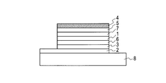
- FIG. 1 shows an example of a multilayered organic EL element.
- the layer responsible for light emission is described as the light emitting layer 1
- the layer in contact with the anode 2 is described as the hole injection layer 3
- the layer in contact with the cathode 4 is described as the electron injection layer 5.
- the layer in contact with the cathode 4 is described as the electron injection layer 5.
- a hole transport layer 6 when a different layer exists between the light emitting layer 1 and the hole injection layer 3, it is described as a hole transport layer 6, and when a different layer exists between the light emitting layer 1 and the electron injection layer 5, an electron transport is described. It is described as layer 7.
- 8 is a substrate.
- low molecular organic EL elements are formed by vapor deposition, multilayering can be easily achieved by performing vapor deposition while sequentially changing the compounds to be used.
- a polymer type organic EL element forms a film using a wet process such as printing or inkjet, there arises a problem that the lower layer dissolves when the upper layer is applied. For this reason, it is difficult to make a polymer organic EL element multi-layered as compared to a low molecular organic EL element, and it has not been possible to obtain an effect of improving luminous efficiency and life.
- Non-Patent Document 1 proposes a device having a three-layer structure using compounds having greatly different solubilities.
- Patent Document 5 discloses a three-layer element in which a layer called an interlayer is introduced on PEDOT: PSS.
- Non-Patent Documents 2 to 4 and Patent Document 6 in order to overcome such problems, the solubility of the compound is changed using a polymerization reaction of a siloxane compound, an oxetane group, a vinyl group, etc. A method of insolubilizing to is disclosed.
- Patent Literature 7, Patent Literature 8, and Patent Literature 9 disclose photoacid generators or initiators containing fluorine. However, these documents do not describe organic electronic materials using photoacid generators or initiators containing fluorine.
- Japanese Patent No. 3748491 Japanese Patent Laid-Open No. 11-251067 Japanese Patent No. 4023204 JP 2006-233162 A JP 2007-1119763 A International Publication No. 2008/010487 JP 2003-215791 A JP 2009-242391 A Japanese Patent No. 3985020
- the organic layers can be formed using a wet process that is easy to form even in large areas.
- the present invention can stably and easily form a thin film or easily form a multi-layered organic thin film layer to improve the productivity of organic electronics elements, particularly polymer type organic EL elements. It is an object of the present invention to provide an organic electronic material useful for making it, an ink composition containing the organic electronic material, the organic electronic material, and an organic thin film formed from the ink composition. Furthermore, an object of the present invention is to provide an organic electronics element, an organic EL element, an illuminating device, and a display element that have a lower driving voltage than that of the prior art and have a long light emission lifetime.
- the present inventors have found that an organic electronic material containing a charge transporting compound and an ionic compound, a polymerization initiator containing an ionic compound, an ink composition containing the organic electronic material, and the organic electronics
- an organic thin film formed using a material or the ink composition is useful for increasing the efficiency and extending the life of an organic EL device, and completed the present study. That is, the present invention is characterized by the following items (1) to (28).
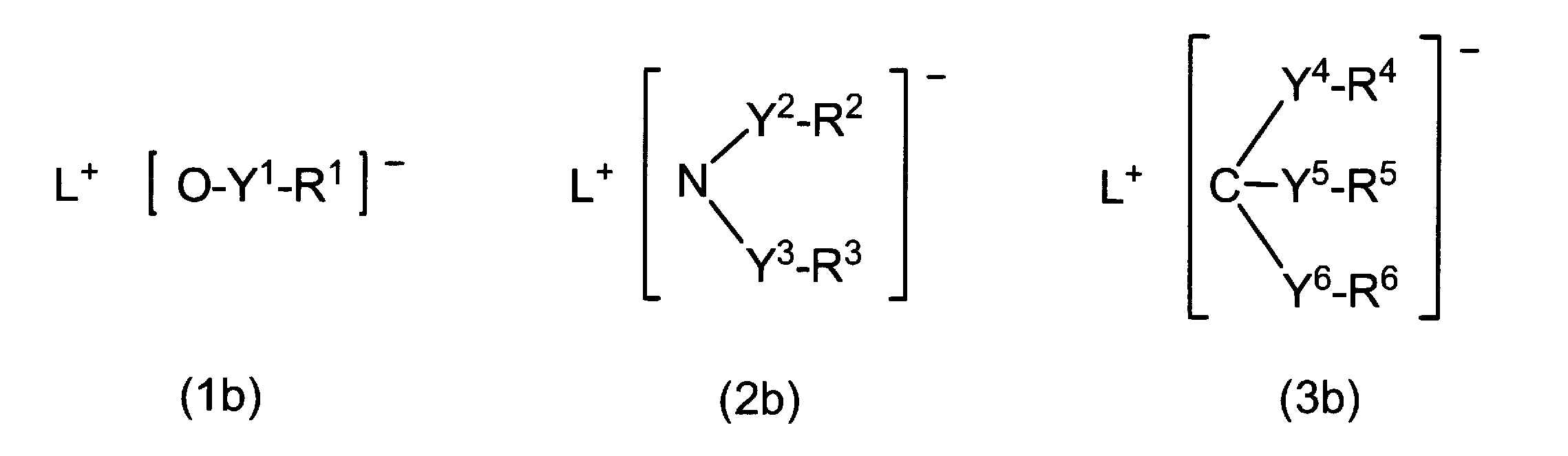
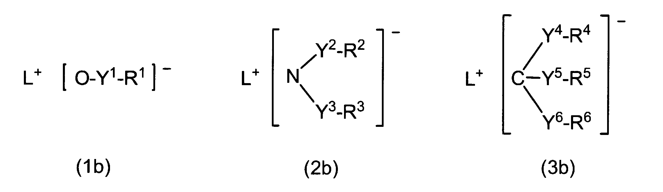
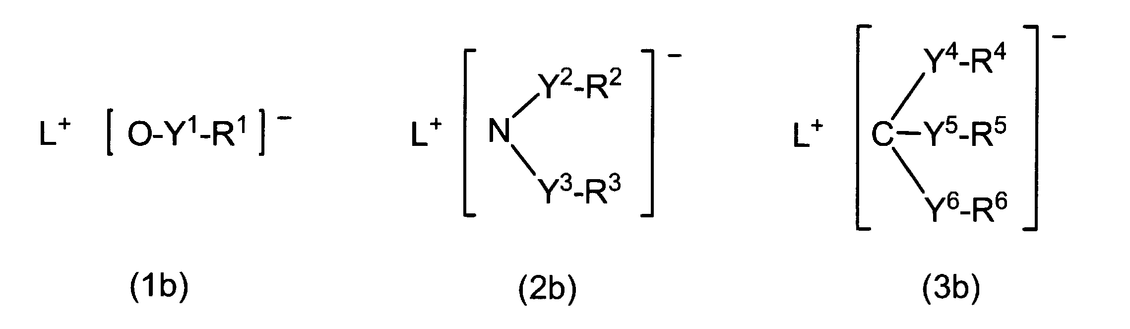
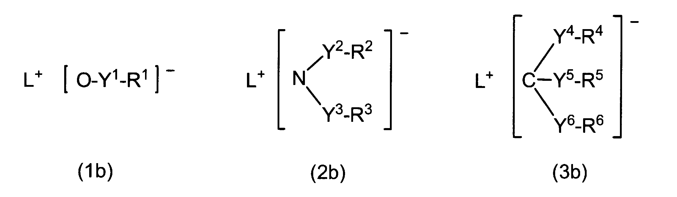
- Organic electronics materials are examples of the following general formulas (1b) to (3b):
- L + represents a monovalent cation.
- the ionic compound may be a linear, branched or cyclic perfluoroalkyl group, perfluoroalkylsulfonyl group, perfluoroalkyloxysulfonyl group, perfluoro group which may contain a heteroatom having 1 to 20 carbon atoms.
- R represents an arbitrary organic group (these structures may further have a substituent or a hetero atom).
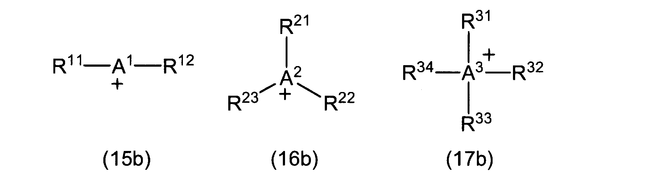
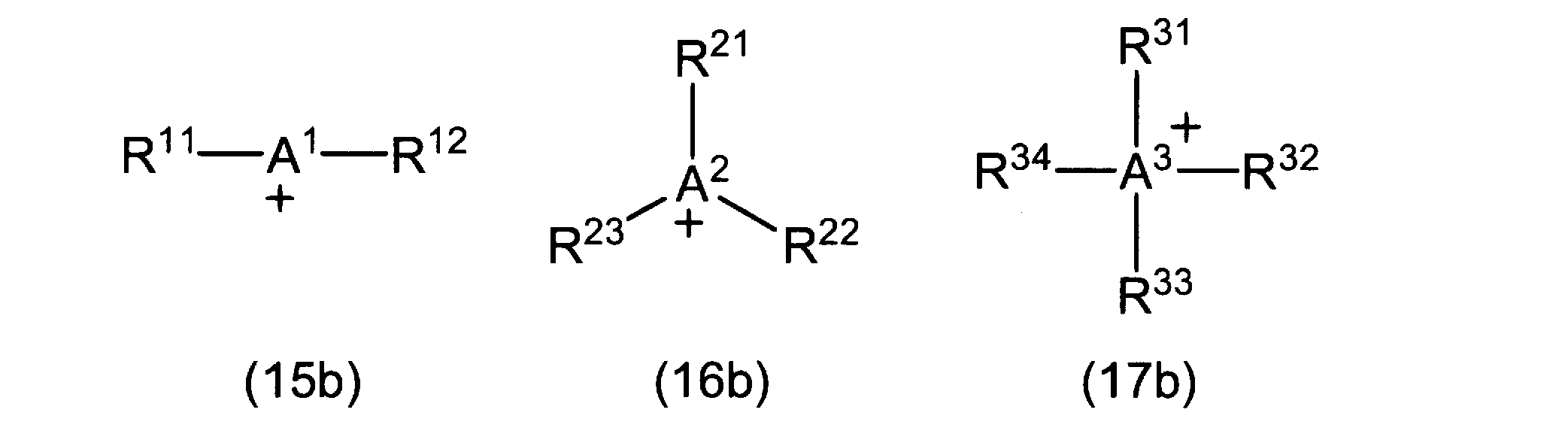
- R 11 to R 34 each independently represents an arbitrary organic group. Two or more adjacent groups of R 11 to R 34 may be linked to each other to form a ring.
- a 1 represents an element belonging to Group 17 or Group 14 of the long-period periodic table
- a 2 represents an element belonging to Group 16 or Group 14 of the long-period periodic table
- a 3 represents a long-period type (Represents elements belonging to Group 15 of the periodic table.)
- R 11 to R 34 in the general formulas (15b) to (17b) are each independently an alkyl group, an alkenyl group, an alkynyl group, an aromatic hydrocarbon group, or an aromatic heterocycle
- a 1 in the general formula (15b) is a bromine atom, iodine atom or carbon atom
- a 2 in the general formula (16b) is an oxygen atom, carbon atom, sulfur atom or selenium atom
- the general formula (17b the organic electronic material according to (5) or (6), wherein the a 3 is a nitrogen atom, phosphorus atom, arsenic atom or an antimony atom in).
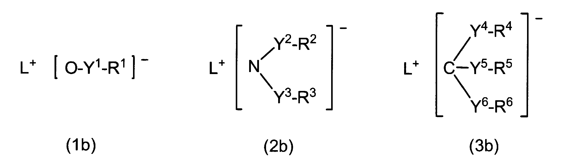
- a polymerization initiator comprising at least one ionic compound represented by the following general formulas (1b) to (3b):
- L + represents a monovalent cation.
- a thermal polymerization initiator comprising at least one ionic compound represented by the following general formulas (1b) to (3b).
- Y 1 to Y 6 are each independently a divalent linking group, and R 1 to R 6 are each independently an electron-withdrawing organic substituent (there are further substituents and heteroatoms in these structures) may have, also, R 1, R 2 and R 3, or R 4 ⁇ R 6 R 1 ⁇ R 6 may form a ring or polymeric bonded respectively.
- R 1, R 2 and R 3 may have, also, R 4 ⁇ R 6 R 1 ⁇ R 6 may form a ring or polymeric bonded respectively.
- a method for producing an organic thin film comprising a step of imparting solvent resistance to the organic thin film using the polymerization initiator according to (14).
- An ink composition comprising the organic electronic material according to any one of (1) to (12) and a solvent.
- a display device comprising the organic electroluminescent device according to any one of (21) to (25).
- An illumination device comprising the organic electroluminescent element as described in any one of (21) to (25).
- a display device comprising the illumination device according to (27) and a liquid crystal element as display means.
- a thin film can be formed stably and easily, and the solubility is changed by a polymerization reaction, so that an organic thin film layer can be easily formed in multiple layers. It is possible to provide an organic electronic material that is extremely useful for improving the productivity of the organic EL element. Furthermore, when the organic electronic material contains an ionic compound, it is possible to provide an organic electronic element and an organic EL element that have a lower driving voltage than conventional ones and have a long emission lifetime.
- Comparative Example 3 It is a schematic diagram which shows an example of the multilayered organic EL element.
- Comparative Example 3 it is a graph showing the relationship between applied voltage and current density when a voltage is applied using ITO as a positive electrode and Au as a cathode of a hole-only element.
- the organic electronic material of the present invention contains a charge transporting compound and an ionic compound, and at least one of the ionic compounds is one of the compounds represented by the following general formulas (1b) to (3b) It is characterized by.
- L + represents a monovalent cation.
- the “ionic compound” is a compound composed of a cation and an anion, and the anion contains an electron-withdrawing organic substituent (R 1 to R 6 in the above formula).
- examples thereof include halogen atoms such as fluorine atom, chlorine atom and bromine atom, alkylsulfonyl groups such as cyano group, thiocyano group, nitro group and mesyl group, arylsulfonyl groups such as tosyl group, formyl group and acetyl group
- An carbonyl group such as a benzoyl group is usually 1 or more and 12 or less, preferably 6 or less
- an alkoxy group such as an acyl group, methoxycarbonyl group or ethoxycarbonyl group is usually 2 or more and 10 or less, preferably 7 or less.
- Fragrance having usually 3 or more, preferably 4 or more and 25 or less, preferably 15 or less carbon atoms such as carbonyl group and pyridyloxycarbonyl group
- a group obtained by substituting a part or all of the hydrogen atoms of the group having a hydrogen atom with a halogen atom such as fluorine among the organic groups For example, a linear, branched or cyclic perfluoroalkyl group, perfluoroalkylsulfonyl group, perfluoroalkyloxysulfonyl group, perfluoroarylsulfonyl group, perfluoroaryl, which may contain a heteroatom having 1 to 20 carbon atoms
- An oxysulfonyl group, a perfluoroacyl group, a perfluoroalkoxycarbonyl group, a perfluoroacyloxy group, a perfluoroaryloxycarbonyl group, a perfluoroalkenyl group, and a perfluoroalkynyl group represented by the following structural formula group (1)
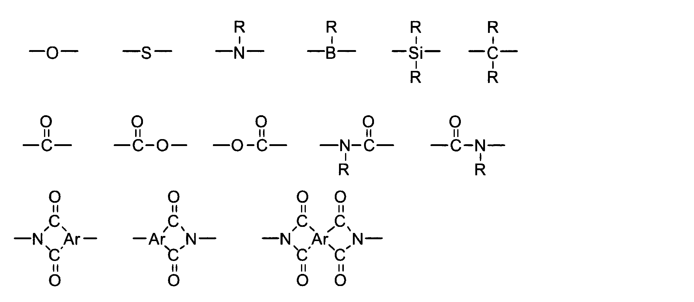
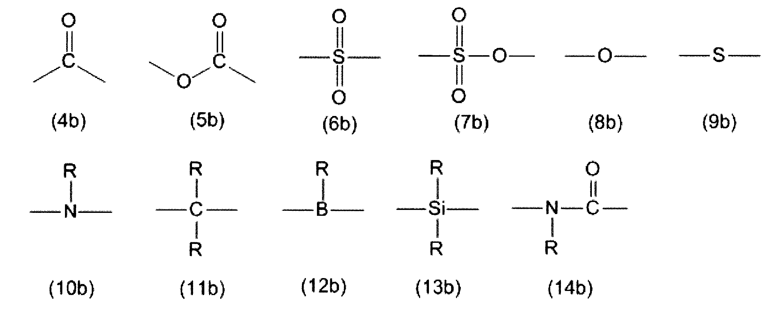
- Y 1 to Y 6 represent a divalent linking group, and are preferably any one of the following general formulas (4b) to (14b).
- R represents an arbitrary organic group (these structures may further have a substituent or a hetero atom).
- R in the general formulas (10b) to (14b) are each independently an alkyl group, an alkenyl group, an alkynyl group, an aromatic group, which may be substituted from the viewpoint of improving electron acceptability and solubility in a solvent. It is preferably a hydrocarbon group or an aromatic heterocyclic group, more preferably an organic group having an electron-withdrawing substituent among the substituents.
- the group of the structural formula group (1) is Can be mentioned.
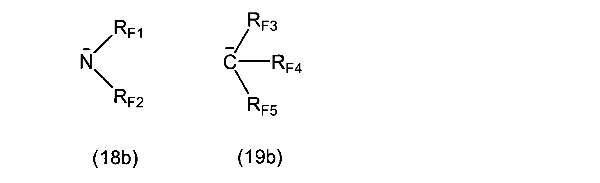
- the anion in the present invention preferably has a negative charge mainly on an oxygen atom, nitrogen atom, or carbon atom, and is not particularly limited, but more preferably has a negative charge on a nitrogen atom or carbon atom, most preferably. It is represented by the following general formulas (18b) and (19b).
- R F1 to R F5 are each independently an electron-withdrawing organic substituent (these structures may further have a substituent or a hetero atom, and R F1 to R F5 are bonded to each other). (It may be cyclic or polymer.) And is not particularly limited, and examples thereof include groups represented by the structural formula group (1).
- the cation of the ionic compound according to the present invention is a monovalent cation, and is not particularly limited, but is represented by the following general formulas (15b) to (17b). Any one of these is preferable.
- R 11 to R 34 each independently represents an arbitrary organic group. Two or more adjacent groups of R 11 to R 34 may be linked to each other to form a ring.
- a 1 represents an element belonging to Group 17 or Group 14 of the long-period periodic table
- a 2 represents an element belonging to Group 16 or Group 14 of the long-period periodic table
- a 3 represents a long-period type (Represents elements belonging to Group 15 of the periodic table.)
- R 11 to R 34 in the general formulas (15b) to (17b) are each independently an alkyl group, an alkenyl group, or an alkynyl group, which may be substituted from the viewpoints of stability of the compound and solubility in a solvent.
- An aromatic hydrocarbon group or an aromatic heterocyclic group is preferable.
- a 1 in the general formula (15b) is a bromine atom, iodine atom or carbon atom
- a 2 in the general formula (16b) is an oxygen atom or carbon atom.
- a sulfur atom or a selenium atom, and A 3 in the general formula (17b) is preferably a nitrogen atom, a phosphorus atom, an arsenic atom or an antimony atom. That is, the cation of the ionic compound in the present invention is more preferably iodonium, sulfonium, phosphonium, carbenium (trityl), anilinium, bismuthonium, ammonium, selenium, pyridinium, imidazolium, oxonium, quinolinium, pyrrolidinium, aminium, imonium, Such as tropylium.
- sulfonium triphenylsulfonium, tri-p-tolylsulfonium, tri-o-tolylsulfonium, tris (4-methoxyphenyl) sulfonium, 1-naphthyldiphenylsulfonium, 2-naphthyldiphenylsulfonium, tris (4-fluoro Phenyl) sulfonium, tri-1-naphthylsulfonium, tri-2-naphthylsulfonium, tris (4-hydroxyphenyl) sulfonium, 4- (phenylthio) phenyldiphenylsulfonium, 4- (p-tolylthio) phenyldi-p-tolylsulfonium, 4- (4-methoxyphenylthio) phenylbis (4-methoxyphenyl) sulfonium, 4- (pheny
- Examples of the iodonium ion include diphenyliodonium, di-p-tolyliodonium, bis (4-dodecylphenyl) iodonium, bis (4-methoxyphenyl) iodonium, (4-octyloxyphenyl) phenyliodonium, bis (4-decyloxyphenyl) ) Iodonium, 4- (2-hydroxytetradecyloxy) phenylphenyliodonium, 4-isopropylphenyl (p-tolyl) iodonium, isobutylphenyl (p-tolyl) iodonium, etc., which are listed in Macromolecules, 10, 1307 ( 1977), JP-A-6-184170, US Pat.
- Selenium ions include triphenyl selenium, tri-p-tolyl selenium, tri-o-tolyl selenium, tris (4-methoxyphenyl) selenium, 1-naphthyldiphenyl selenium, tris (4-fluorophenyl) selenium, tri-1 -Triaryl selenium such as naphthyl selenium, tri-2-naphthyl selenium, tris (4-hydroxyphenyl) selenium, 4- (phenylthio) phenyldiphenyl selenium, 4- (p-tolylthio) phenyldi-p-tolyl selenium; diphenylphena Diaryl selenium such as silselenium, diphenylbenzyl selenium, diphenylmethyl selenium; phenylmethylbenzyl selenium, 4-hydroxyphenylmethylbenzyl selenium, phenyl Monoaryl selenium such as
- ammonium ions include tetramethylammonium, ethyltrimethylammonium, diethyldimethylammonium, triethylmethylammonium, tetraethylammonium, trimethyl-n-propylammonium, trimethylisopropylammonium, trimethyl-n-butylammonium, trimethylisobutylammonium, trimethyl- tetraalkylammonium such as t-butylammonium, trimethyl-n-hexylammonium, dimethyldi-n-propylammonium, dimethyldiisopropylammonium, dimethyl-n-propylisopropylammonium, methyltri-n-propylammonium, methyltriisopropylammonium; N, N-dimethylpyrrolidinium, N-eth -Pyrrolidinium such as N-methylpyrrolidinium, N, N-d
- Examples of the phosphonium ion include tetraarylphosphonium such as tetraphenylphosphonium, tetra-p-tolylphosphonium, tetrakis (2-methoxyphenyl) phosphonium, tetrakis (3-methoxyphenyl) phosphonium, tetrakis (4-methoxyphenyl) phosphonium; Triarylphosphonium such as triphenylbenzylphosphonium, triphenylphenacylphosphonium, triphenylmethylphosphonium, triphenylbutylphosphonium; triethylbenzylphosphonium, tributylbenzylphosphonium, tetraethylphosphonium, tetrabutylphosphonium, tetrahexylphosphonium, triethylphenacylphosphonium, Tetraalkyls such as tributylphenacylphosphonium Phosphonium, and the
- oxonium ions examples include trimethyloxonium, triethyloxonium, tripropyloxonium, tributyloxonium, trihexyloxonium, triphenyloxonium, pyririnium, chromenilium, and xanthylium.
- Bismutonium ions are described in, for example, JP-A-2008-214330.
- tropylium ions examples include J.I. Polym. Sci. Part A; Polym. Chem. 42, 2166 (2004).
- the “charge transporting compound” refers to a compound having a charge transporting unit.
- the “charge transporting unit” in the present invention is an atomic group having the ability to transport holes or electrons, and the details thereof will be described below.
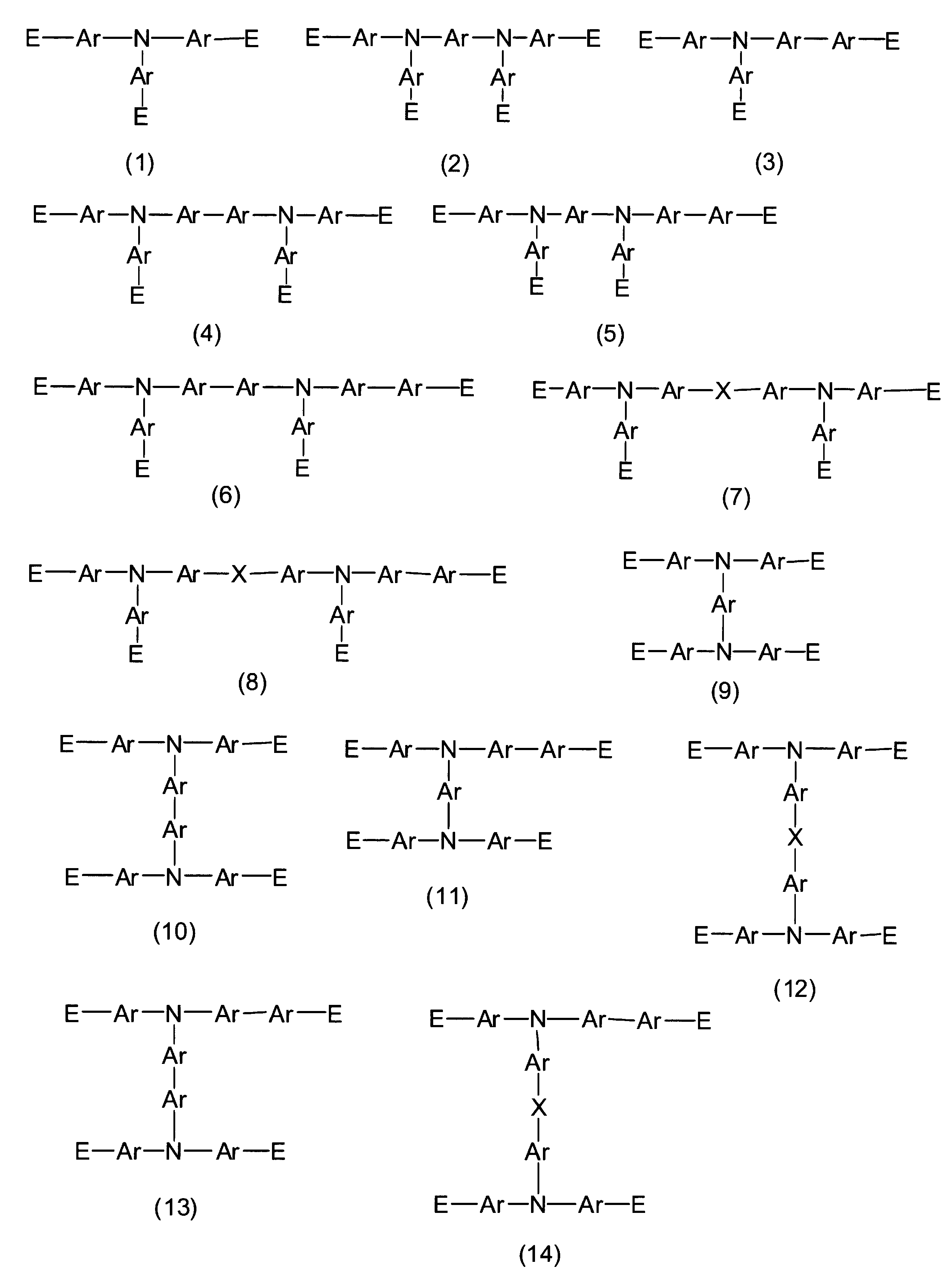
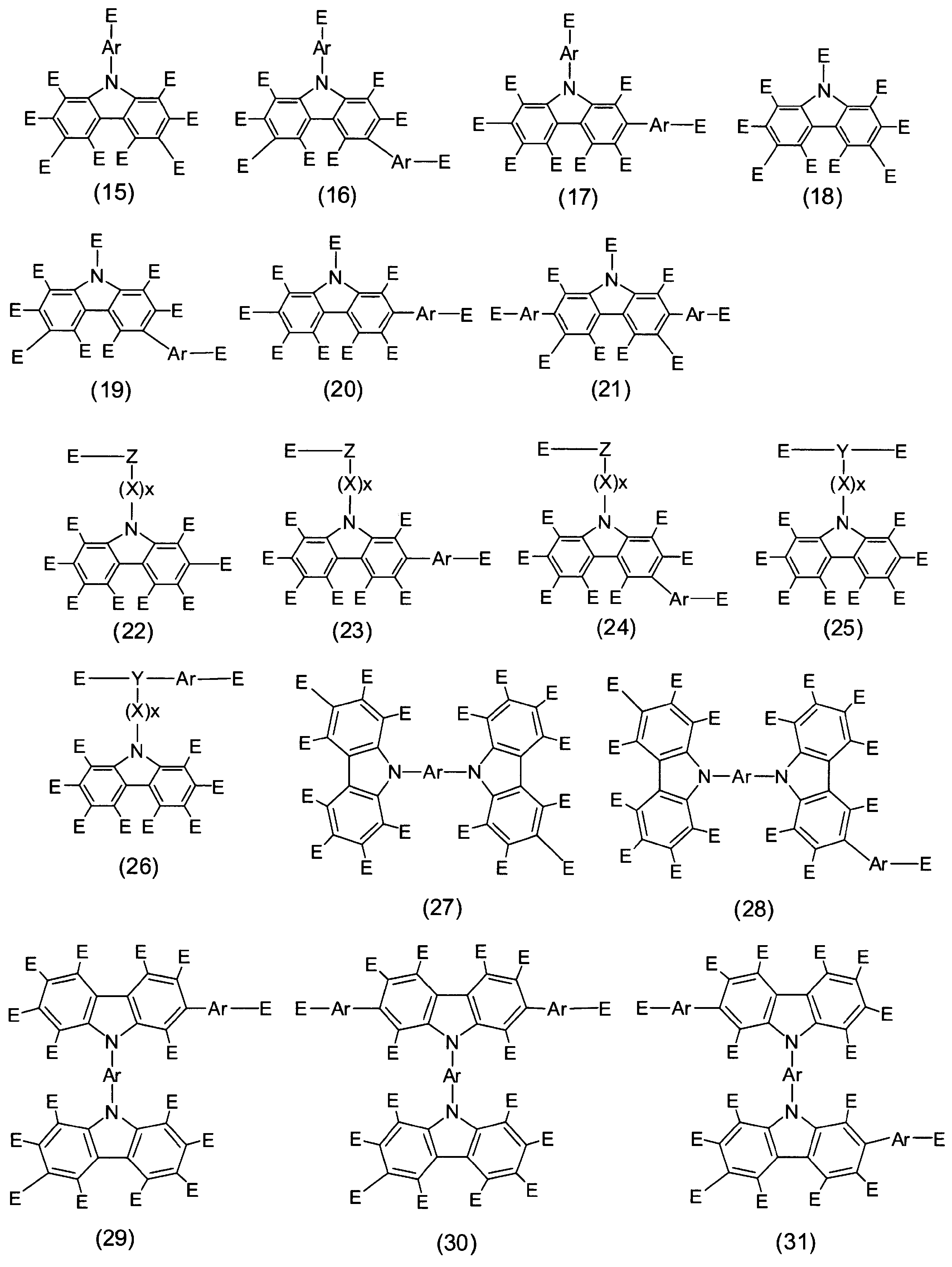
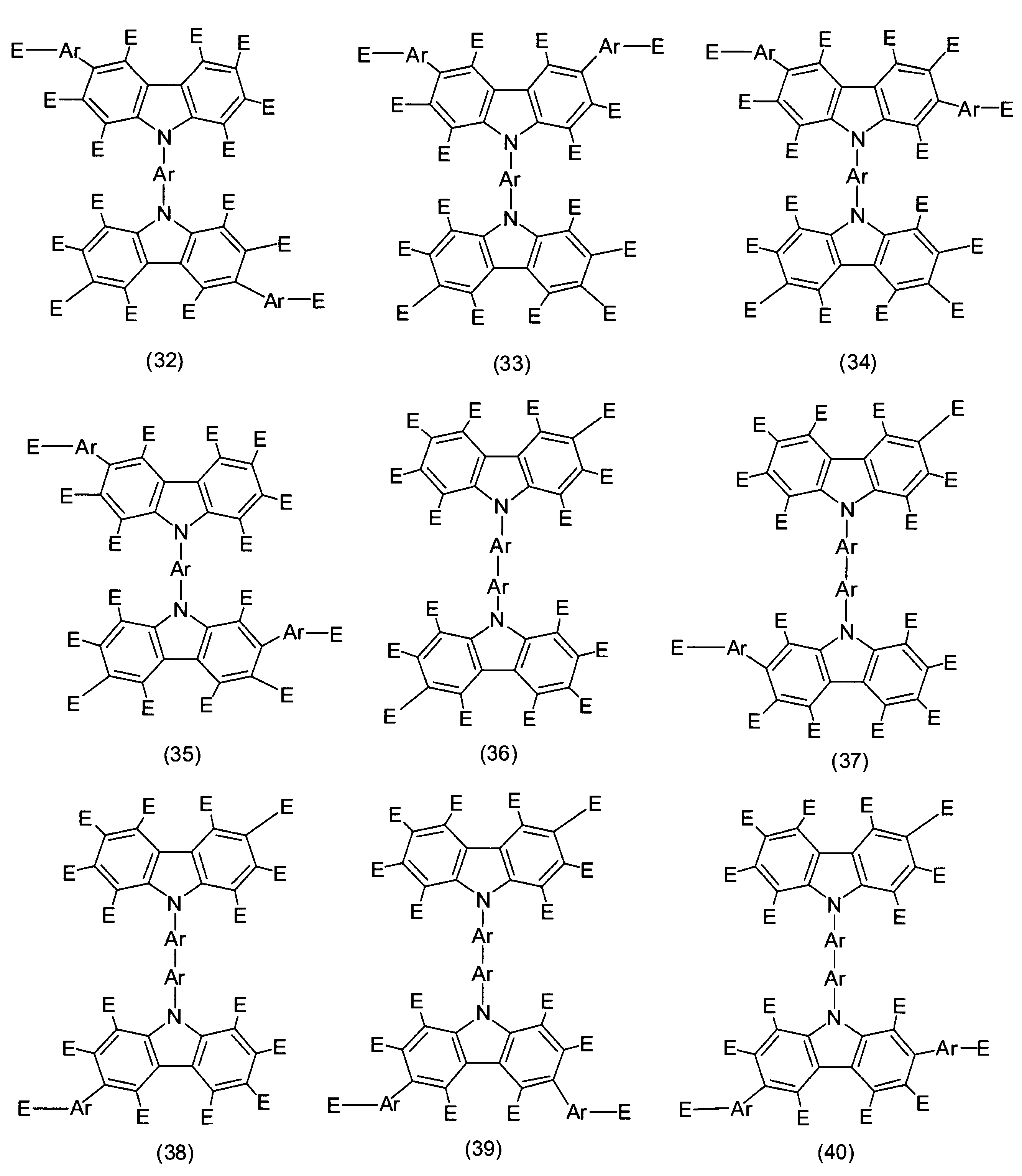
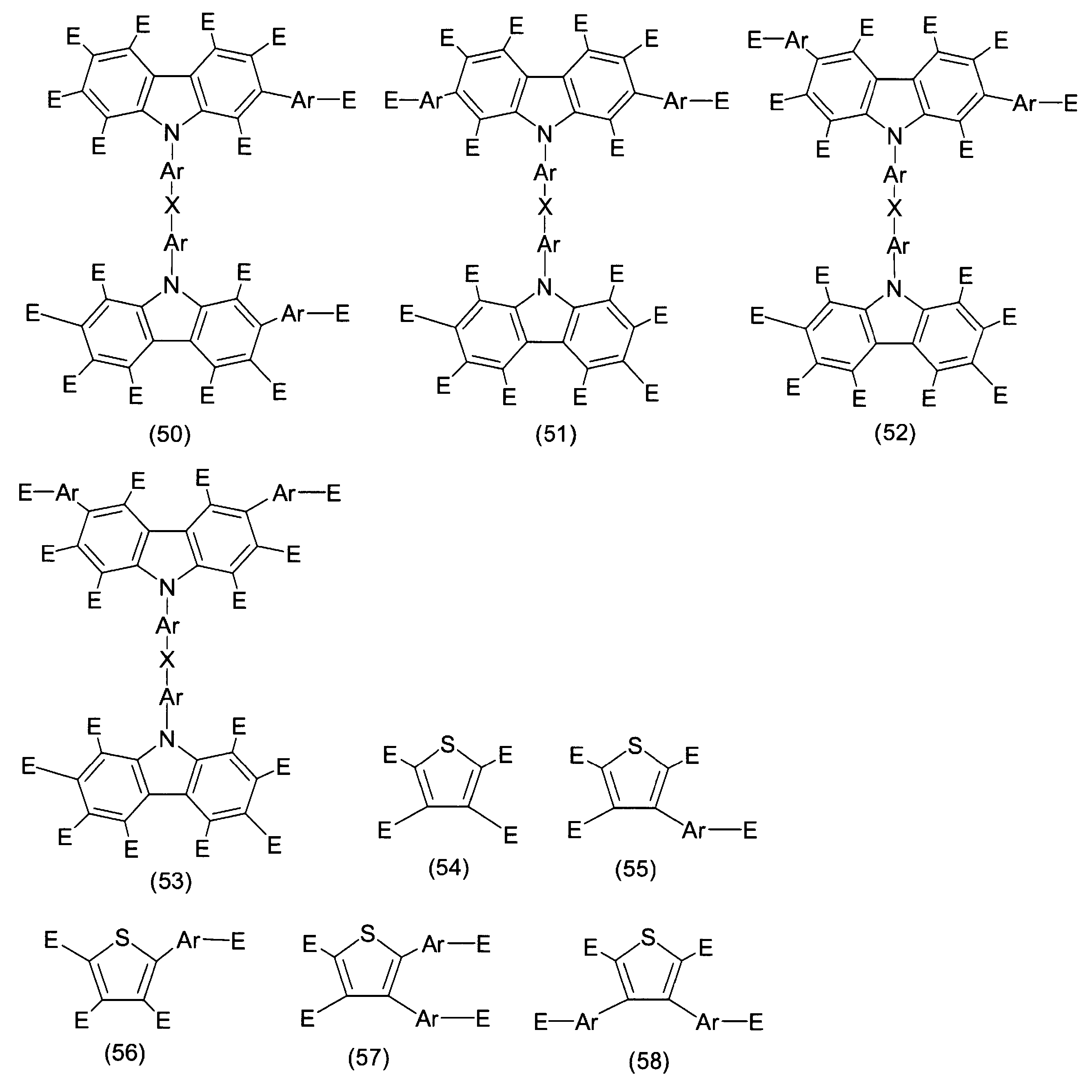
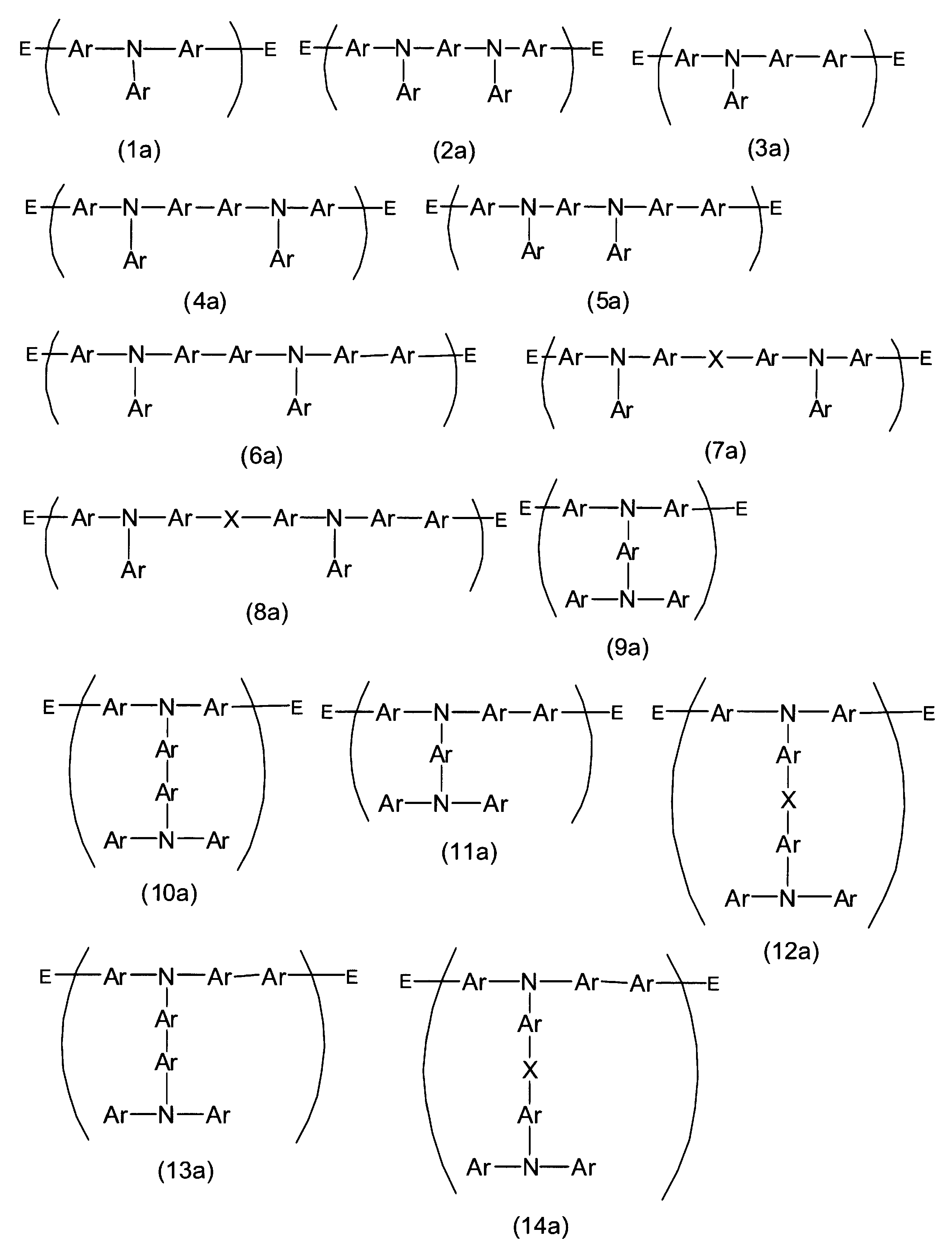
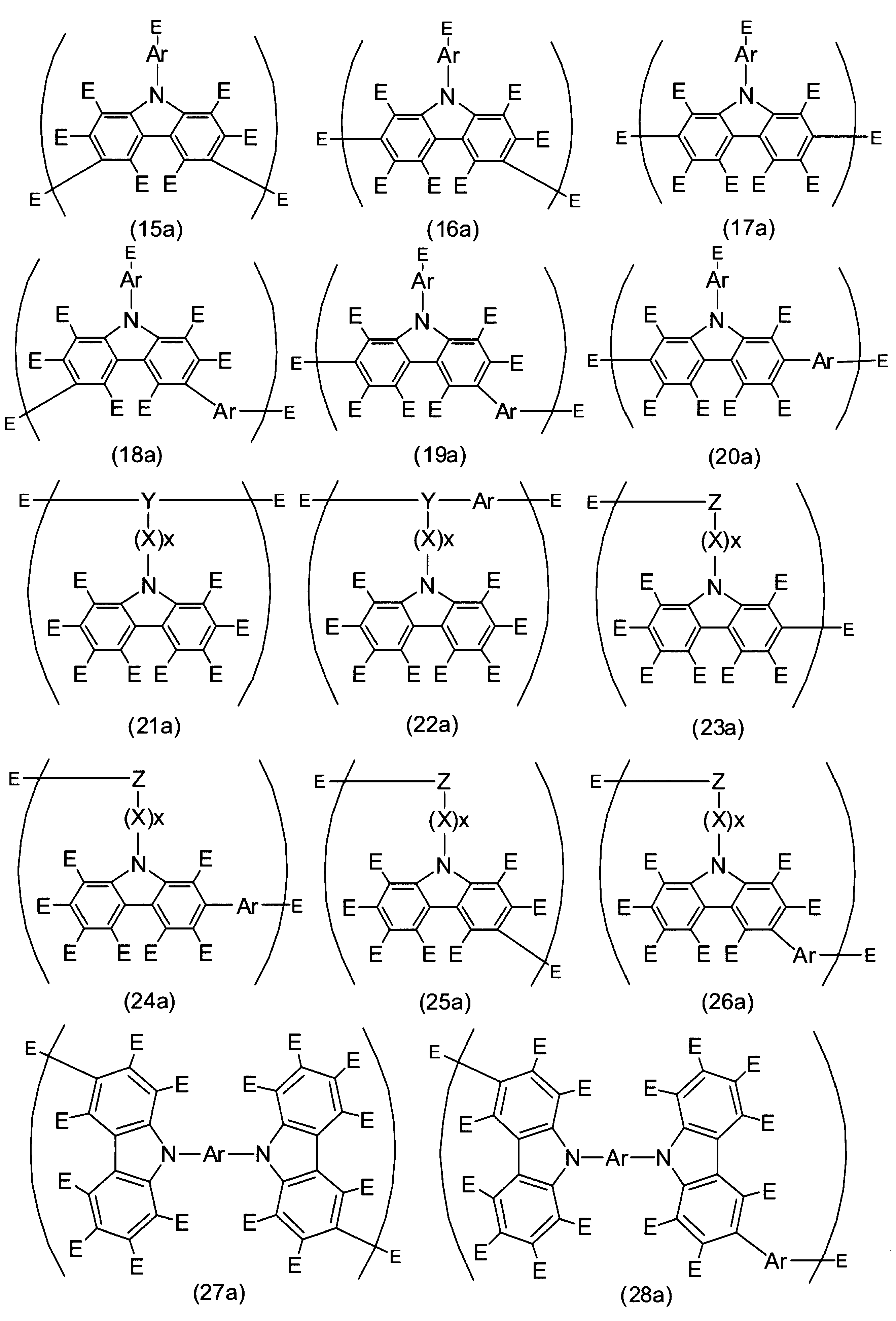
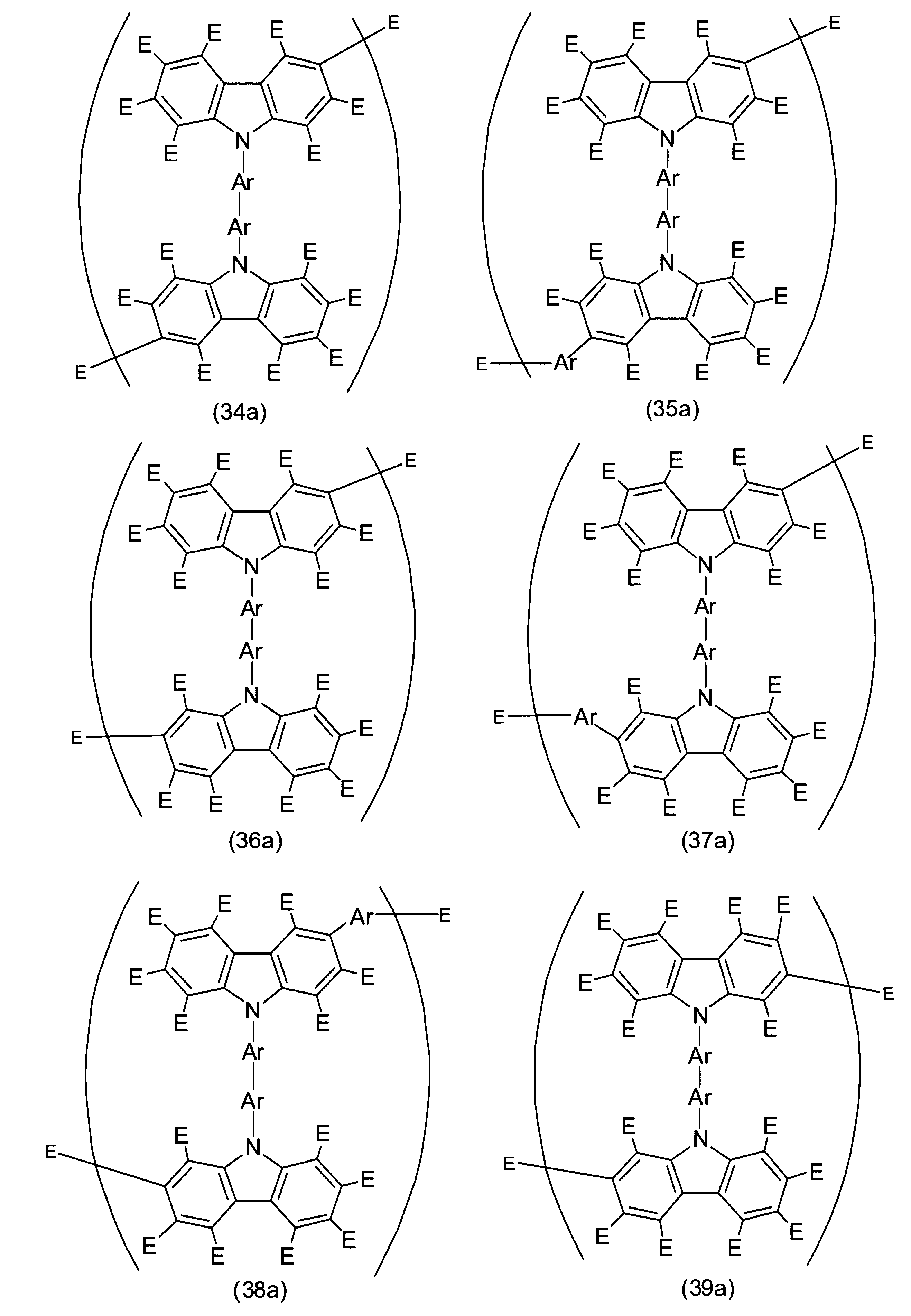
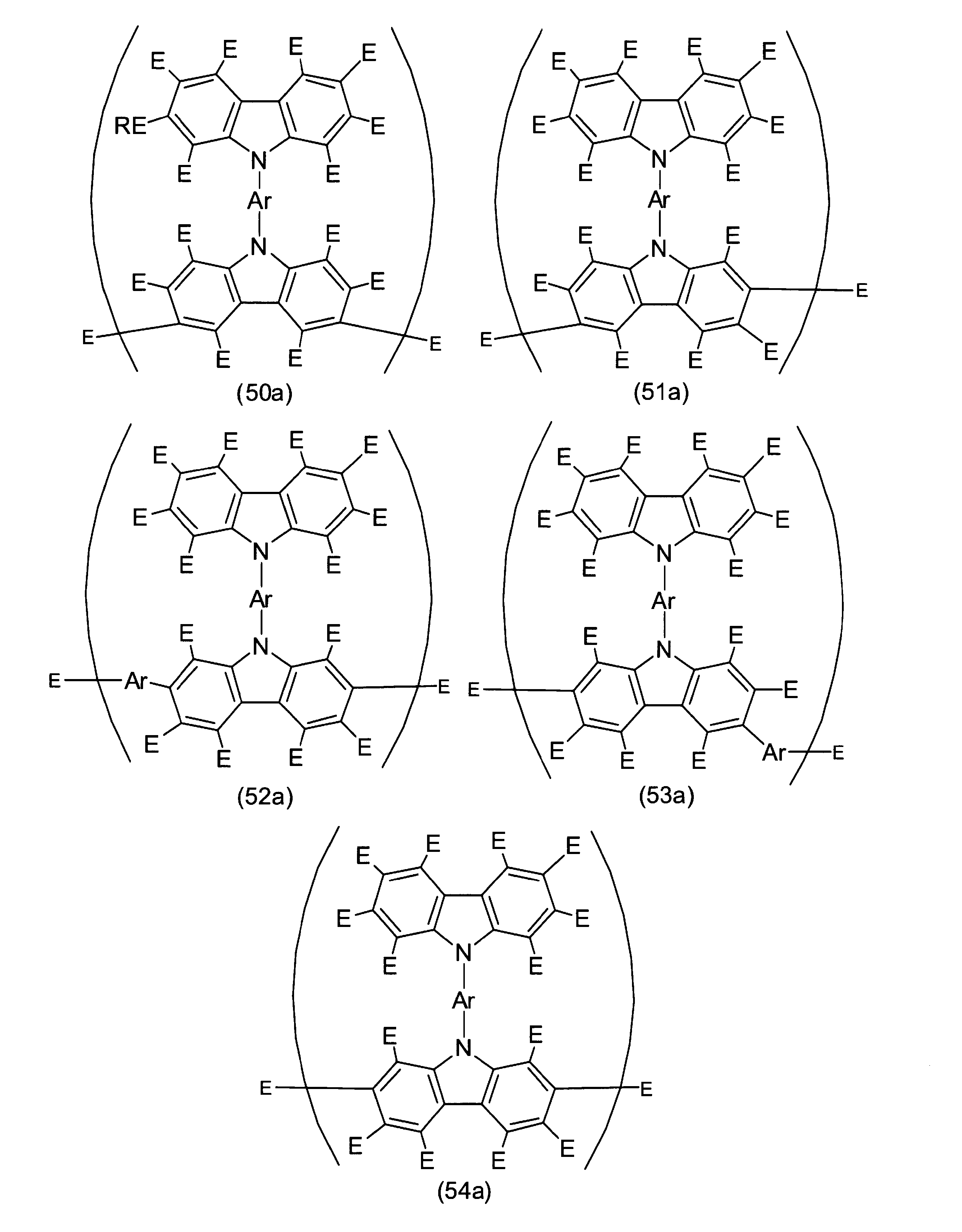
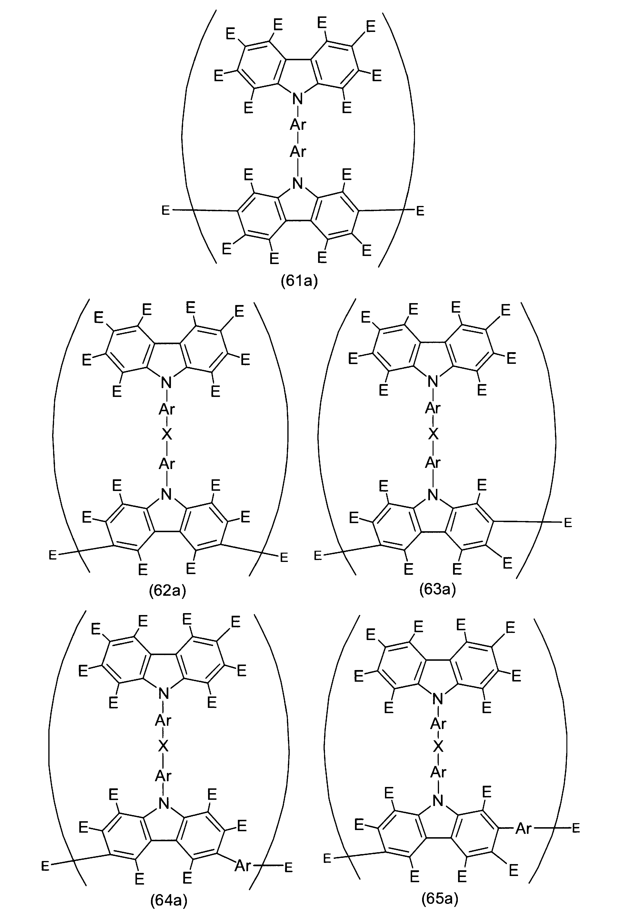
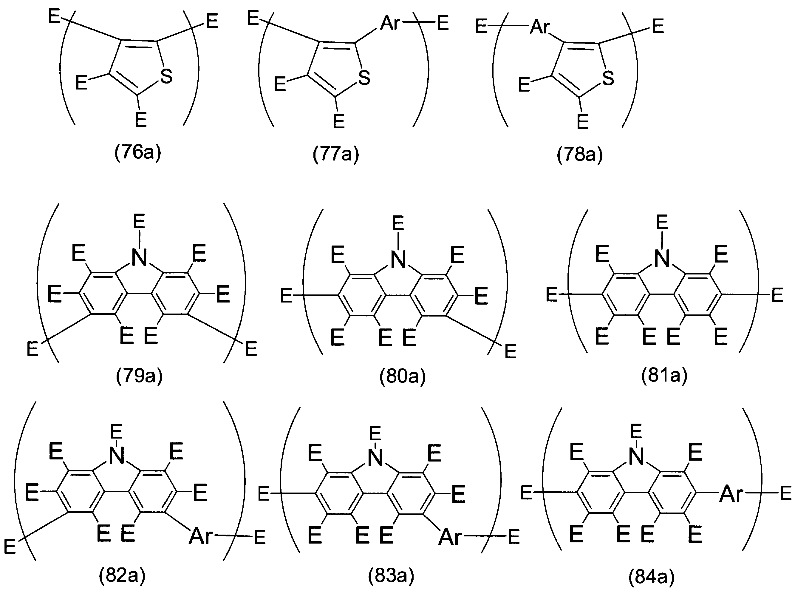
- the charge transporting unit is not particularly limited as long as it has an ability to transport holes or electrons, and is preferably an amine having an aromatic ring, carbazole, or thiophene. ) To (58).
- each E independently represents —R 1 , —OR 2 , —SR 3 , —OCOR 4 , —COOR 5 , —SiR 6 R 7 R 8, or general formulas (59) to (61)
- R 1 to R 11 represent a hydrogen atom, a linear, cyclic or branched alkyl group having 1 to 22 carbon atoms, or an aryl group or heteroaryl group having 2 to 30 carbon atoms, and a and b and c are 1
- the aryl group is an atomic group obtained by removing one hydrogen atom from an aromatic hydrocarbon, and may have a substituent, and the heteroaryl group has a heteroatom.
- An arylene group is an atomic group obtained by removing two hydrogen atoms from an aromatic hydrocarbon, and may have a substituent, such as phenylene, biphenyl-diyl, terphenyl -Diyl, naphthalene-diyl, anthracene-diyl, tetracene-diyl, fluorene-diyl, phenanthrene-diyl, etc.
- a heteroaryl group is an atomic group obtained by removing two hydrogen atoms from an aromatic compound having a heteroatom. And may have a substituent, such as pyridine-diyl, pyrazine-diyl, quinoline-diyl, isoquinoline-diyl, acridine-diyl, phenanthroline-diyl, furan-diyl, pyrrole-diyl, thiophene-diyl, Oxazole-diyl, oxadiazole-diyl, thiadi Zol-diyl, triazole-diyl, benzoxazole-diyl, benzooxadiazole-diyl, benzothiadiazole-diyl, benzotriazole-diyl, benzothiophene-diyl, etc.
- a substituent such as pyridine-diyl, pyrazin
- X and Z are each independently a divalent linkage.
- the group is not particularly limited, but is preferably a group obtained by removing one hydrogen atom from a group having one or more hydrogen atoms in the R or a group exemplified by the linking group group (A) described below, where x is Represents an integer of 0 to 2.
- Y represents the trivalent linking group, and represents a group obtained by removing two hydrogen atoms from a group having two or more hydrogen atoms in R.
- charge transporting compound in the present invention may be a commercially available one, or one synthesized by a method known to those skilled in the art, and is not particularly limited.
- the ionic compound in the present invention is preferably an onium salt from the viewpoint of improving charge transportability.
- the onium salt refers to a compound comprising a cation and a counter anion such as sulfonium ion, iodonium ion, selenium ion, ammonium ion, phosphonium ion, oxonium ion, bismuthium ion, and the like.
- anions include halogen ions such as F ⁇ , Cl ⁇ , Br ⁇ and I ⁇ ; OH ⁇ ; ClO 4 ⁇ ; FSO 3 ⁇ , ClSO 3 ⁇ , CH 3 SO 3 ⁇ , C 6 H 5 SO 3 ⁇ .
- CF 3 SO 3 - sulfonate ion such as; HSO 4 -, SO 4 2- sulfate ions such as; HCO 3 -, carbonate ions such as CO 3 2-; H 2 PO 4 -, HPO 4 2 -, phosphate ion such as PO 4 3-; PF 6 -, PF 5 OH - fluorophosphate ions such as; BF 4 -, B (C 6 F 5) 4 -, B (C 6 H 4 CF 3 ) borate ions such as 4 ⁇ ; AlCl 4 ⁇ ; BiF 6 ⁇ ; fluoroantimonate ions such as SbF 6 ⁇ and SbF 5 OH ⁇ ; fluoroarsenate ions such as AsF 6 ⁇ and AsF 5 OH ⁇ Etc.
- Examples of the cation are the same as the examples of formulas (8b) to (10b) described above.
- the charge transporting compound preferably contains at least one aromatic amine, carbazole or thiophene compound for highly efficient charge transporting.
- these charge transporting compounds are preferably polymers or oligomers from the viewpoints of solubility and film formability.
- the number average molecular weight is preferably 1,000 or more and 1,000,000 or less from the viewpoint of solubility in a solvent and film formability. More preferably, it is 2,000 or more and 900,000 or less, and further preferably 3,000 or more and 800,000 or less. If it is less than 1,000, the compound is easily crystallized, resulting in poor film-forming properties. On the other hand, if it is larger than 1,000,000, the solubility in a solvent is lowered, making it difficult to produce a coating solution or a coating ink.
- the polymer or oligomer preferably contains a repeating unit represented by the following general formulas (1a) to (84a).
- the polymer or oligomer preferably has one or more “polymerizable substituents” in order to change the solubility.
- the “polymerizable substituent” means a substituent capable of forming a bond between two or more molecules by causing a polymerization reaction, and details thereof will be described below.
- Examples of the polymerizable substituent include a group having a carbon-carbon multiple bond (for example, vinyl group, acetylene group, butenyl group, acrylic group, acrylate group, acrylamide group, methacryl group, methacrylate group, methacrylamide group, arene group).
- a group having a carbon-carbon multiple bond for example, vinyl group, acetylene group, butenyl group, acrylic group, acrylate group, acrylamide group, methacryl group, methacrylate group, methacrylamide group, arene group.
- combinations of groups capable of forming an ester bond or an amide bond can also be used. For example, a combination of an ester group and an amino group, an ester group and a hydroxyl group, or the like.
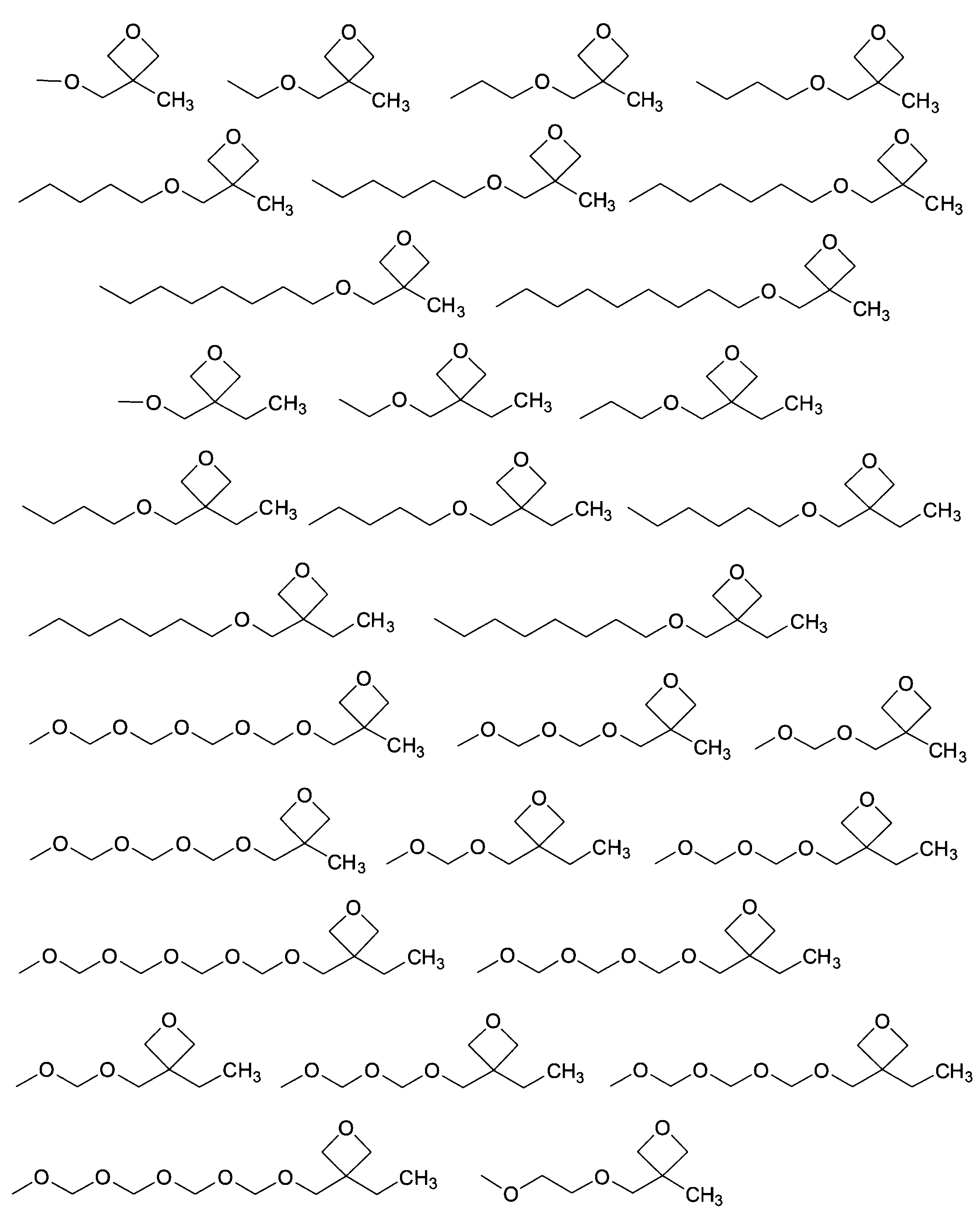
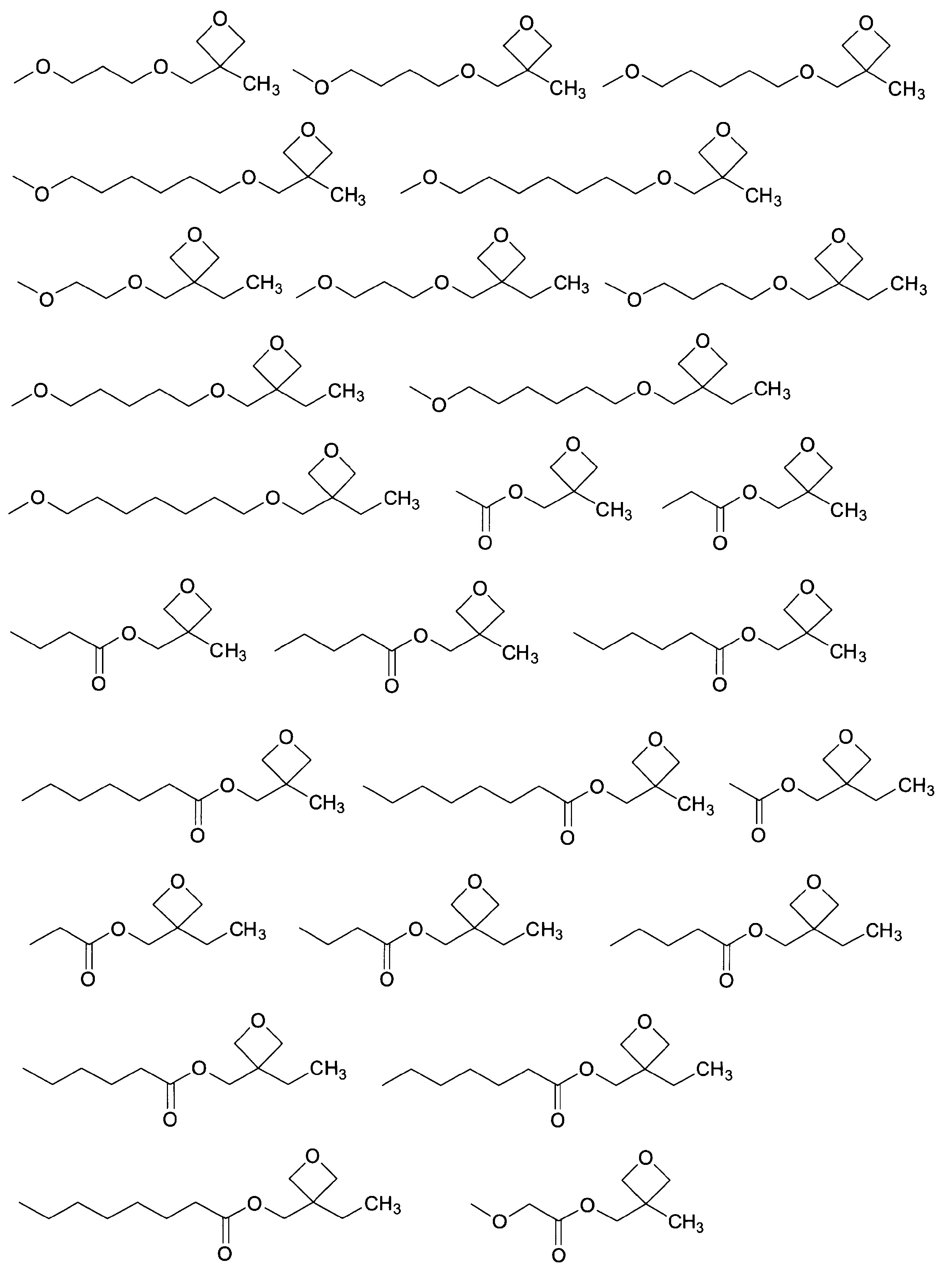
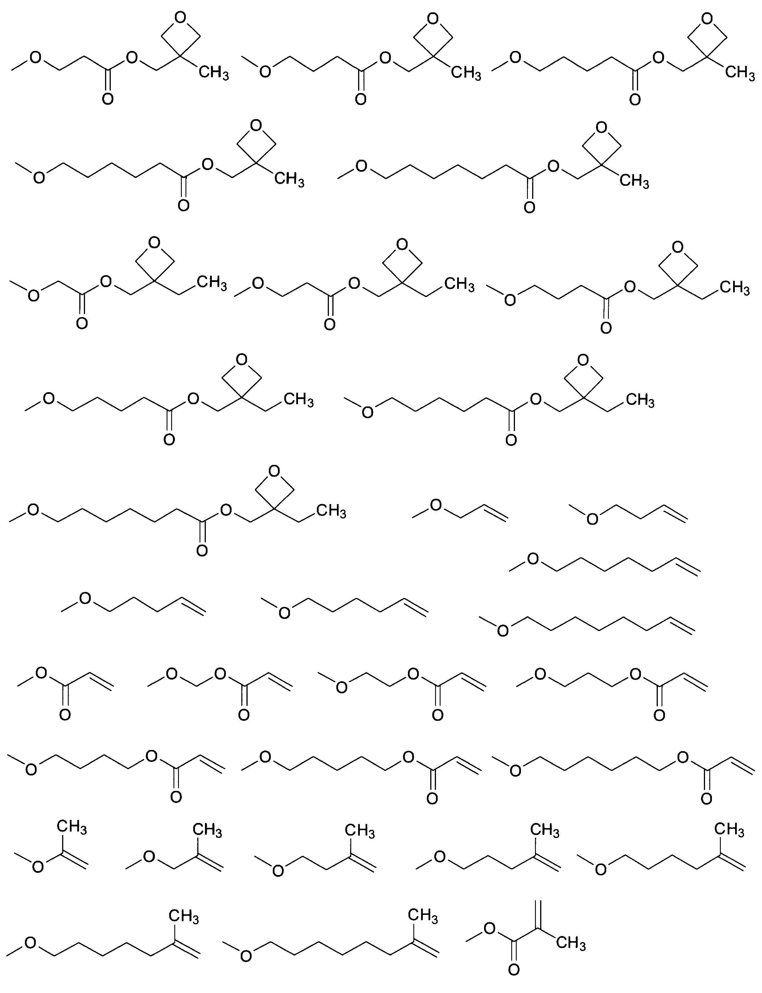
- an oxetane group, an epoxy group, a vinyl group, a vinyl ether group, an acrylate group, and a methacrylate group are particularly preferable from the viewpoint of reactivity, and an oxetane group is most preferable.
- the main chain of the polymer or oligomer and the polymerizable substituent are connected by an alkyl chain having 1 to 8 carbon atoms. preferable.
- the alkyl chain is more preferably a hydrophilic group such as ethylene glycol or diethylene glycol.
- the alkyl chain has an ether bond at the terminal part of the alkyl chain, that is, the connecting part with the polymerizable substituent, or the connecting part with the polymer or oligomer main chain. Specifically, they are represented by the substituent groups (A) to (C).
- the polymer or oligomer in the present invention has a structure represented by the following structural group (X) as the above arylene group or heteroarylene group in addition to the above repeating unit in order to adjust solubility, heat resistance, and electrical characteristics.
- X a copolymer having as a copolymer repeating unit.
- the copolymer may be a random, block or graft copolymer, or may be a polymer having an intermediate structure thereof, for example, a random copolymer having a block property.
- the polymer or oligomer used in the present invention may have branching in the main chain and may have three or more terminals.
- the ionic compound according to the present invention can be used alone as a polymerization initiator. That is, the polymerization initiator of the present invention is characterized by containing at least one ionic compound represented by the general formulas (1b) to (3b) according to the present invention described above.
- the trigger for initiating polymerization is not particularly limited as long as it exhibits the ability to polymerize a polymerizable substituent by application of heat, light, microwave, radiation, electron beam, etc. It is preferable that the polymerization is initiated by heating, and heating is most preferable. That is, the ionic compound according to the present invention can be used as a thermal polymerization initiator, and the thermal polymerization initiator according to the present invention is represented by the general formulas (1b) to (3b) according to the present invention described above. It contains at least one kind of ionic compound.
- the ionic compound according to the present invention can be used as a polymerization initiator that imparts solvent resistance to an organic thin film by a polymerization reaction.
- the method for producing an organic thin film of the present invention applies the action of this polymerization initiator to the method for producing an organic thin film. That is, the manufacturing method of the organic thin film of this invention is characterized by including the process of providing solvent resistance to an organic thin film using the polymerization initiator of the above-mentioned this invention.
- the conditions for using the polymerization initiator are 0.1 to 50 for the charge transporting compound.
- heating may be performed in a vacuum, in the air, or in a nitrogen atmosphere.
- the heating temperature and time are not particularly limited as long as the polymerization reaction can be sufficiently advanced.
- the temperature is preferably 300 ° C. or less, more preferably 200 ° C. or less, more preferably, since various substrates can be applied. Is 150 ° C. or lower.
- the time is preferably 2 hours or less, more preferably 1 hour or less, and even more preferably 30 minutes or less.
- the organic electronic material of the present invention preferably contains a polymerization initiator in order to utilize the difference in solubility due to the polymerization reaction.
- the polymerization initiator is not particularly limited as long as it exhibits the ability to polymerize a polymerizable substituent by application of heat, light, microwave, radiation, electron beam, and the like. Or it is preferable to start polymerization by heating.
- the ratio of the polymerization initiator in the charge transport film in the present invention is not particularly limited as long as the polymerization is sufficiently advanced, but is preferably 0.1% by mass to 50% by mass. When the amount is less than this, polymerization does not proceed efficiently, and the solubility cannot be changed sufficiently. On the other hand, when the amount is larger than this, a large amount of the polymerization initiator and / or decomposition product remains, and the effect of washing becomes low.
- the polymerization initiator of the present invention may contain a sensitizer for improving photosensitivity and / or heat sensitivity in addition to the above polymerization initiator.
- the polymerization initiator in the present invention is preferably the above ionic compound.
- the ink composition of the present invention is characterized by containing the above-described organic electronic material of the present invention and a solvent, and other additives such as polymerization inhibitors, stabilizers, thickeners, gelling agents. , Flame retardants, antioxidants, anti-reducing agents, oxidizing agents, reducing agents, surface modifiers, emulsifiers, antifoaming agents, dispersants, surfactants, and the like.
- the solvent examples include water, alcohols such as methanol, ethanol and isopropyl alcohol, alkanes such as pentane, hexane and octane, cyclic alkanes such as cyclohexane, aromatic solvents such as benzene, toluene, xylene, mesitylene, tetralin and diphenylmethane, ethylene Aliphatic ethers such as glycol dimethyl ether, ethylene glycol diethyl ether, propylene glycol-1-monomethyl ether acetate, 1,2-dimethoxybenzene, 1,3-dimethoxybenzene, anisole, phenetole, 2-methoxytoluene, 3-methoxytoluene , 4-methoxytoluene, 2,3-dimethylanisole, aromatic ethers such as 2,4-dimethylanisole, ethyl acetate, n-butyl acetate,
- Amide solvents others, dimethyl sulfoxide, tetrahydrofuran, acetone, chloroform, methylene chloride and the like can be mentioned, but preferably aromatic solvents, aliphatic esters, aromatic esters, aliphatic ethers, aromatic ethers can be used. .
- the content of the organic electronic material with respect to the solvent is preferably 0.1 to 30% by mass from the viewpoint of being applicable to various coating processes.
- the organic electronic element of the present invention includes an organic thin film formed from the organic electronic material and / or the ink composition.
- the organic electroluminescent element (organic EL element) of the present invention includes an organic thin film formed from the organic electronic material and / or the ink composition.
- Each element includes an excellent organic thin film formed using the organic electronic material of the present invention as the organic thin film, has a lower driving voltage than the conventional one, and has a long light emission lifetime.
- the EL element of the present invention will be described in detail below.
- the organic electronics element of the present invention is characterized by including an organic thin film made of an organic electronics material containing a charge transporting compound and an ionic compound.
- the organic EL device of the present invention is not particularly limited as long as it includes a light emitting layer, a polymerized layer, an anode, a cathode, and a substrate. Other elements such as a hole injection layer, an electron injection layer, a hole transport layer, and an electron transport layer are used. It may have a layer. Moreover, it is preferable to apply the organic thin film of this invention to a positive hole injection layer or a positive hole transport layer. Hereinafter, each layer will be described in detail.
- the material used for the light emitting layer may be a low molecular compound, a polymer or an oligomer, and a dendrimer or the like can also be used.
- low molecular weight compounds that utilize fluorescence include perylene, coumarin, rubrene, quinacudrine, dye laser dyes (eg, rhodamine, DCM1, etc.), aluminum complexes (eg, Tris (8-hydroxyquinolinato) aluminum (III) (Alq 3 )), Stilbene, and derivatives thereof.
- Polymers or oligomers that utilize fluorescence include polyfluorene, polyphenylene, polyphenylene vinylene (PPV), polyvinyl carbazole (PVK), fluorene-benzothiadiazole copolymer, fluorene-triphenylamine copolymer, and derivatives thereof And a mixture can be suitably used.
- phosphorescent organic EL devices have been actively developed in order to increase the efficiency of organic EL devices.
- the phosphorescent organic EL element not only singlet state energy but also triplet state energy can be used, and the internal quantum yield can be increased to 100% in principle.
- phosphorescence is emitted by doping a host material with a metal complex phosphorescent material containing a heavy metal such as platinum or iridium as a dopant that emits phosphorescence (MABaldo et al., Nature, vol. 395). , p. 151 (1998), MABaldo et al., Applied Physics Letters, vol.75, p.4 (1999), MABaldo et al., Nature, vol.403, p.750 (2000)). .
- a phosphorescent material for the light emitting layer from the viewpoint of high efficiency.
- a metal complex containing a central metal such as Ir or Pt can be preferably used.
- Ir complex for example, FIr (pic) that emits blue light [iridium (III) bis [(4,6-difluorophenyl) -pyridinate-N, C 2 ] picolinate], green light is emitted.
- Ir (ppy) 3 [Factris (2-phenylpyridine) iridium] (see MABaldo et al., Nature, vol. 403, p.
- Pt complex examples include 2,3,7,8,12,13,17, 18-octaethyl-21H, 23H-forminplatinum (PtOEP) that emits red light.
- PtOEP 23H-forminplatinum
- the phosphorescent material can be a small molecule or a dendrite species, such as an iridium nucleus dendrimer. Moreover, these derivatives can also be used conveniently.
- a host material is included in addition to the phosphorescent material.
- the host material may be a low molecular compound or a high molecular compound, and a dendrimer or the like can also be used.
- low molecular weight compound examples include CBP (4,4′-Bis (Carbazol-9-yl) -biphenyl), mCP (1,3-bis (9-carbazolyl) benzene), CDBP (4,4′-Bis).
- Carbazol-9-yl) -2,2′-dimethylbiphenyl and the like, for example, polyvinyl carbazole, polyphenylene, polyfluorene, etc. can be used as the polymer compound, and derivatives thereof can also be used.
- the light emitting layer may be formed by a vapor deposition method or a coating method.
- a solution containing a phosphorescent material and, if necessary, a host material is used, for example, an ink jet method, a casting method, a dipping method, a relief printing, an intaglio printing, an offset printing, a flat printing, a relief printing. It can be carried out by applying on a desired substrate by a known method such as a printing method such as reverse offset printing, screen printing or gravure printing, or spin coating method.
- the cathode material is preferably a metal or metal alloy such as Li, Ca, Mg, Al, In, Cs, Ba, Mg / Ag, LiF, and CsF.
- anode As the anode, a metal (for example, Au) or other material having metal conductivity, for example, an oxide (for example, ITO: indium oxide / tin oxide), a conductive polymer (for example, a polythiophene-polystyrene sulfonic acid mixture (for example, PEDOT: PSS)) can also be used.
- a metal for example, Au
- an oxide for example, ITO: indium oxide / tin oxide
- a conductive polymer for example, a polythiophene-polystyrene sulfonic acid mixture (for example, PEDOT: PSS)
- PEDOT polythiophene-polystyrene sulfonic acid mixture
- Examples of the electron transport layer and the electron injection layer include phenanthroline derivatives (for example, 2,9-dimethyl-4,7-diphenyl-1,10-phenanthroline (BCP)), bipyridine derivatives, nitro-substituted fluorene derivatives, diphenylquinone derivatives.
- phenanthroline derivatives for example, 2,9-dimethyl-4,7-diphenyl-1,10-phenanthroline (BCP)
- bipyridine derivatives for example, 2,9-dimethyl-4,7-diphenyl-1,10-phenanthroline (BCP)
- bipyridine derivatives for example, 2,9-dimethyl-4,7-diphenyl-1,10-phenanthroline (BCP)
- BCP 2,9-dimethyl-4,7-diphenyl-1,10-phenanthroline
- Thiopyran dioxide derivatives such as naphthaleneperylene, carbodiimide, fluorenylidenemethane derivatives, anthraquinodimethane and anthrone derivatives, oxadiazole derivatives (2- (4-Biphenylyl) -5- (4-tert-butylphenyl-1,3,4-oxadiazole) (PBD)), aluminum complexes (for example, Tris (8-hydroxyquinolinato) aluminum (III) (Alq 3 )) and the like.
- a thiadiazole derivative in which the oxygen atom of the oxadiazole ring is substituted with a sulfur atom, or a quinoxaline derivative having a quinoxaline ring known as an electron withdrawing group can be used.
- the kind of glass, plastic and the like is not particularly limited, and is not particularly limited as long as it is transparent, but glass, quartz, light transmissive A resin film or the like is preferably used. When a resin film is used, flexibility can be given to the organic EL element, which is particularly preferable.
- the resin film examples include polyethylene terephthalate (PET), polyethylene naphthalate (PEN), polyethersulfone (PES), polyetherimide, polyetheretherketone, polyphenylene sulfide, polyarylate, polyimide, polycarbonate (PC), and cellulose triacetate.
- PET polyethylene terephthalate
- PEN polyethylene naphthalate
- PES polyethersulfone
- CAP cellulose acetate propionate
- the resin film may be coated with an inorganic substance such as silicon oxide or silicon nitride in order to suppress permeation of water vapor or oxygen.
- the emission color in the organic EL device of the present invention is not particularly limited, but the white light-emitting device is preferable because it can be used for various lighting devices such as home lighting, interior lighting, clocks, and liquid crystal backlights.
- a plurality of light emitting colors can be simultaneously emitted and mixed using a plurality of light emitting materials.
- White luminescence is obtained.
- a combination of a plurality of emission colors is not particularly limited. However, a combination of three emission maximum wavelengths of blue, green, and red, a complementary color relationship such as blue and yellow, yellow green and orange is used. The thing containing two light emission maximum wavelengths is mentioned. The emission color can be controlled by adjusting the type and amount of the phosphorescent material.
- the display element of the present invention is characterized by including the above-described organic EL element of the present invention.
- a color display element can be obtained by using the organic EL element of the present invention as an element corresponding to each pixel of red, green, and blue (RGB).
- Image formation includes a simple matrix type in which individual organic EL elements arranged in a panel are directly driven by electrodes arranged in a matrix, and an active matrix type in which thin film transistors are arranged and driven in each element.
- the former is simple in structure but has a limit on the number of vertical pixels and is used for displaying characters.
- the latter is used for high-quality displays because the drive voltage is low and the current is small, and a bright high-definition image is obtained.
- the lighting device of the present invention is characterized by including the organic EL element of the present invention described above. Furthermore, the display device of the present invention is characterized by including a lighting device and a liquid crystal element as a display means.
- the illumination device of the present invention described above may be used as a backlight (white light source), and a display device using a liquid crystal element as a display unit, that is, a liquid crystal display device may be used.
- This configuration is a configuration in which only the backlight is replaced with the illumination device of the present invention in a known liquid crystal display device, and a known technique can be diverted to the liquid crystal element portion.
- the reaction solution was poured into a methanol / water mixed solvent (9: 1), and the precipitated polymer was filtered off. The reprecipitation was repeated twice to purify, and thus an oligomer A having a polymerizable substituent and a repeating unit having a hole transporting property was obtained.
- the number average molecular weight of the obtained oligomer A was 4652 in terms of polystyrene.
- Example 1 Ink containing the organic electronic material of the present invention by dissolving the oligomer A (4.5 mg) obtained above in toluene (465 ⁇ L), adding an ethyl acetate solution of the ionic compound G (ionic compound G 10 ⁇ g / 1 ⁇ L, 50 ⁇ L). A composition was prepared. The oligomer A and the ionic compound G did not remain undissolved, and a uniform solution was obtained.
- Example 1 An ink composition was prepared in the same manner except that the ionic compound G in Example 1 was replaced with tetraphenylphosphonium hexafluoroantimonate (manufactured by Alfa Easer). However, undissolved residue is generated and a uniform solution cannot be obtained, and it is not suitable as a coating ink.
- Example 1 shows that the organic electronic material of the present invention has a high solubility in a solvent and can prepare a uniform solution and ink composition.
- Example 2 ⁇ Preparation of solvent-resistant organic thin film>
- the oligomer A (4.5 mg) obtained above was dissolved in toluene (465 ⁇ L), and an ethyl acetate solution of the ionic compound C (ionic compound C 10 ⁇ g / 1 ⁇ L, 50 ⁇ L) was added to prepare an ink composition.
- This solution was spin-coated on a quartz glass plate at 3000 min ⁇ 1 and cured by heating at 180 ° C. for 10 minutes on a hot plate to form an organic thin film (film thickness: 60 nm).
- Example 3 A thin film was prepared in the same manner as in Example 2 except that the ionic compound C in Example 2 was changed to an ethyl acetate solution of the ionic compound D, and the residual film ratio was determined to be 99%.
- Example 4 A thin film was prepared in the same manner as in Example 2 except that the ionic compound C in Example 2 was changed to the ionic compound E, and the residual film ratio was found to be 91%.
- Example 5 A thin film was prepared in the same manner as in Example 2 except that the ionic compound C in Example 2 was changed to the ionic compound F, and the residual film ratio was determined to be 70%.
- Example 6 A thin film was produced in the same manner as in Example 2 except that the ionic compound C in Example 2 was changed to the ionic compound G, and the residual film ratio was found to be 86%.
- Example 7 A thin film was prepared in the same manner as in Example 2 except that the ionic compound C in Example 2 was changed to the ionic compound H, and the residual film ratio was determined to be 75%.
- Example 8 A thin film was prepared in the same manner as in Example 2 except that the ionic compound C in Example 2 was changed to the following ionic compound J, and the residual film ratio was determined to be 99%.
- Example 9 A thin film was prepared in the same manner as in Example 2 except that the ionic compound C in Example 2 was changed to the following ionic compound K, and the residual film ratio was 99%.
- Example 10 A thin film was produced in the same manner as in Example 2 except that the ionic compound C in Example 2 was changed to the following ionic compound L, and the residual film ratio was 94%.
- Example 11 A thin film was prepared in the same manner as in Example 2 except that the ionic compound C in Example 2 was changed to the following ionic compound M, and the residual film ratio was determined to be 80%.
- Example 2 A thin film was produced in the same manner as in Example 2 except that the ionic compound C in Example 2 was changed to diphenyliodonium hexafluorophosphate (manufactured by Aldrich), and the residual film ratio was determined to be 10%.
- Example 3 A thin film was produced in the same manner as in Example 2 except that the ionic compound C in Example 2 was changed to triphenylsulfonium tetrafluoroborate (manufactured by Tokyo Chemical Industry Co., Ltd.). there were.
- Example 4 A thin film was prepared in the same manner except that the ionic compound C in Example 2 was changed to tropylium hexafluorophosphate (manufactured by Tokyo Chemical Industry Co., Ltd.), and the residual film ratio was determined to be 13%.
- Table 1 shows the remaining film ratios of the above Examples and Comparative Examples.
- the organic electronic material of the present invention can exhibit sufficient solvent resistance upon curing. Moreover, it turns out that the ionic compound of this invention functions as a polymerization initiator which can be hardened at low temperature. Further, it can be seen that a laminated structure of organic thin films can be produced.
- Example 12 2000 ml of a mixed solution of oligomer A (20 mg) in toluene (525 ⁇ L) and ethyl acetate solution of ionic compound E (ionic compound E 10 ⁇ g / 1 ⁇ L, 222 ⁇ L) on a glass substrate patterned with ITO 1.6 mm wide. Spin coating at ⁇ 1 and heating on a hot plate at 180 ° C. for 10 minutes. Next, the obtained glass substrate was transferred into a vacuum evaporation machine, and gold (film thickness 30 nm) was evaporated.
- ionic compound E ionic compound E 10 ⁇ g / 1 ⁇ L, 222 ⁇ L
- the substrate After depositing gold, the substrate is moved into a dry nitrogen environment without opening to the atmosphere, and the sealing glass and ITO substrate in which 0.4 mm of counterbore is put into 0.7 mm non-alkali glass are used as a photocurable epoxy resin. Sealing was performed by bonding together to produce a hole-only element.
- Example 5 A hole-only device was produced in the same manner as in Example 12 except that the ionic compound E in Example 12 was not added. Subsequent experiments were performed in the atmosphere at room temperature (25 ° C.).
- FIG. 2 shows a graph of applied voltage-current density when voltage is applied using ITO as a positive electrode and Au as a cathode of these hole-only elements. From FIG. 2, it can be seen that the hole current of the device of Example 12 is significantly easier to flow than the device of Comparative Example 5.
- Example 13 A coating solution obtained by mixing the oligomer A (4.5 mg) obtained above, the ionic compound E (0.45 mg), and toluene (1.2 ml) on a glass substrate obtained by patterning ITO to a width of 1.6 mm, After spin coating at 3000 min ⁇ 1 , the film was cured by heating at 180 ° C. for 10 minutes on a hot plate to form a hole injection layer (40 nm).
- Example 6 A white organic EL element and a lighting device were produced in the same manner as in Example 13 except that the ionic compound was not added when forming the hole injection layer.
- Example 14 The oligomer A (10 mg) obtained above was dissolved in toluene (728 ⁇ L), and a coating solution was prepared by adding the ethyl acetate solution of the ionic compound C (ionic compound C 10 ⁇ g / 1 ⁇ L, 31 ⁇ L). On a glass substrate patterned with a width of 1.6 mm of ITO, the coating solution was spin-coated at 3000 min ⁇ 1 in a nitrogen atmosphere, and then heated and cured on a hot plate at 180 ° C. for 10 minutes to form a hole injection layer ( 60 nm).
- a coating solution was prepared by adding the ethyl acetate solution of the ionic compound C (ionic compound C 10 ⁇ g / 1 ⁇ L, 31 ⁇ L).
- the coating solution was spin-coated at 3000 min ⁇ 1 in a nitrogen atmosphere, and then heated and cured on a hot plate at 180 ° C. for 10 minutes to form a hole injection layer ( 60 nm).
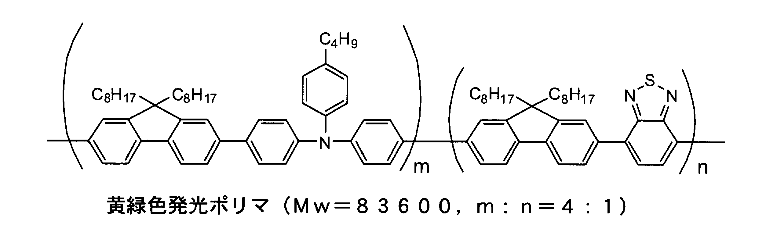
- a mixture of the following yellow-green light emitting polymer (10 mg) and toluene (566 ⁇ L) was spin-coated at 4000 min ⁇ 1 under a nitrogen atmosphere, and then dried at 80 ° C. for 5 minutes to form a light emitting layer (100 nm).
- the obtained ITO glass substrate was transferred into a vacuum vapor deposition machine, and Ba (3 nm) and Al (100 nm) were vapor-deposited in this order. After vapor deposition of Al, the substrate is moved into a dry nitrogen environment without opening to the atmosphere, and the sealing glass and ITO glass substrate in which 0.4 mm of counterbore is added to 0.7 mm non-alkali glass are used as a photocurable epoxy. Sealing was performed by bonding using a resin to produce an organic EL element.
- Example 13 and Comparative Example 6 and Example 14 and Comparative Example 7 By comparing the above-described Example 13 and Comparative Example 6, and Example 14 and Comparative Example 7, by applying the organic electronics material of the present invention, the charge transporting property is improved, and the organic EL element and the lighting device are reduced in voltage. It can also be seen that it can be driven with a long life.
Landscapes
- Chemical & Material Sciences (AREA)
- Organic Chemistry (AREA)
- Materials Engineering (AREA)
- Engineering & Computer Science (AREA)
- Polymers & Plastics (AREA)
- Health & Medical Sciences (AREA)
- Medicinal Chemistry (AREA)
- Chemical Kinetics & Catalysis (AREA)
- Physics & Mathematics (AREA)
- Spectroscopy & Molecular Physics (AREA)
- Wood Science & Technology (AREA)
- Life Sciences & Earth Sciences (AREA)
- Optics & Photonics (AREA)
- Electroluminescent Light Sources (AREA)
- Inks, Pencil-Leads, Or Crayons (AREA)
- Organic Low-Molecular-Weight Compounds And Preparation Thereof (AREA)
- Devices For Indicating Variable Information By Combining Individual Elements (AREA)
- Compositions Of Macromolecular Compounds (AREA)
- Polyoxymethylene Polymers And Polymers With Carbon-To-Carbon Bonds (AREA)
Abstract
Description
しかしながら、これら文献においてフッ素を含有した光酸発生剤あるいは開始剤を用いた有機エレクトロニクス材料に関する記載はない。
さらに、本発明は、従来よりも駆動電圧が低く、長い発光寿命を有する有機エレクトロニクス素子及び有機EL素子、照明装置、表示素子を提供することを目的とするものである。
すなわち、本発明は、下記(1)~(28)の事項をその特徴とするものである。
(1)電荷輸送性化合物とイオン性化合物とを含有し、該イオン性化合物の少なくとも一つが下記一般式(1b)~(3b)で表される化合物のいずれか1種であることを特徴とする有機エレクトロニクス材料。



さらには、該有機エレクトロニクス材料がイオン性化合物を含むことにより従来よりも駆動電圧が低く、長い発光寿命を有する有機エレクトロニクス素子及び有機EL素子を提供することができる。



化合物の安定性、合成及び精製のし易さから、前記一般式(15b)におけるA1が臭素原子、ヨウ素原子または炭素原子であり、前記一般式(16b)におけるA2が酸素原子、炭素原子、硫黄原子またはセレン原子であり、前記一般式(17b)におけるA3が窒素原子、リン原子、ヒ素原子またはアンチモン原子であることが好ましい。
すなわち、本発明におけるイオン性化合物のカチオンは、より好ましくは、ヨードニウム、スルホニウム、ホスホニウム、カルベニウム(トリチル)、アニリニウム、ビスムトニウム、アンモニウム、セレニウム、ピリジニウム、イミダゾリウム、オキソニウム、キノリニウム、ピロリジニウム、アミニウム、イモニウム、トロピリウムなどである。
ここで、本発明において「電荷輸送性ユニット」とは、正孔または電子を輸送する能力を有した原子団であり、以下、その詳細について述べる。




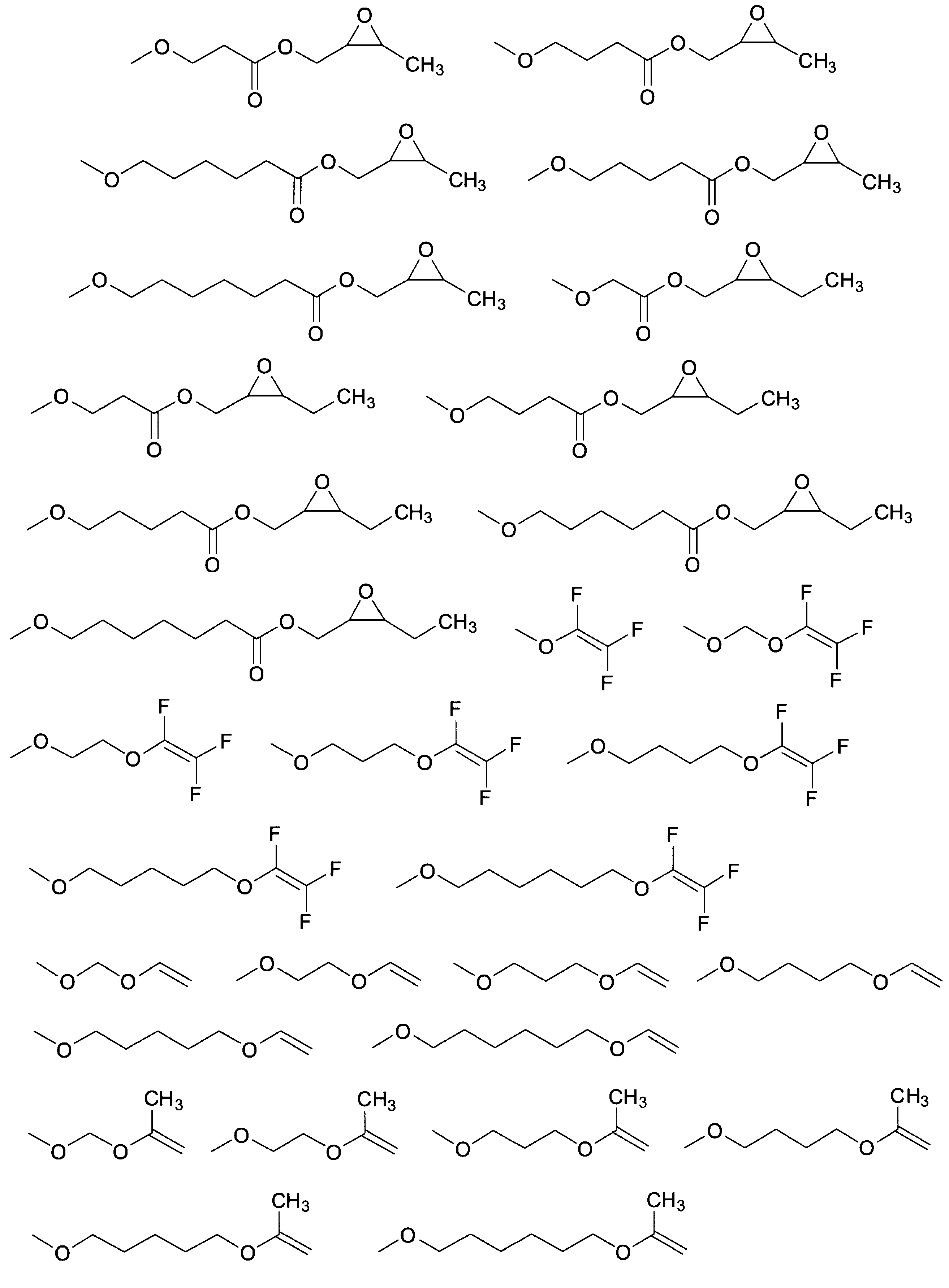


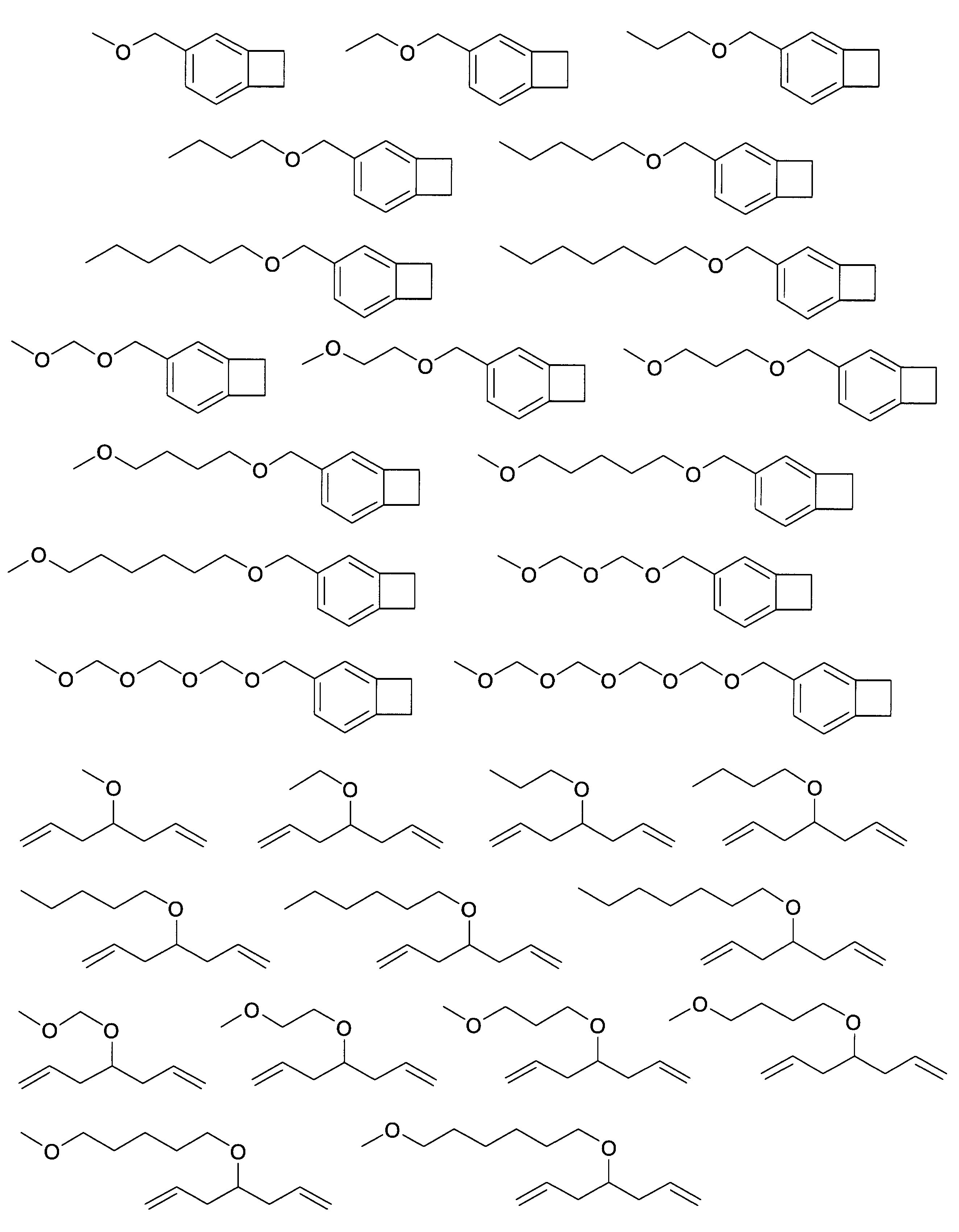
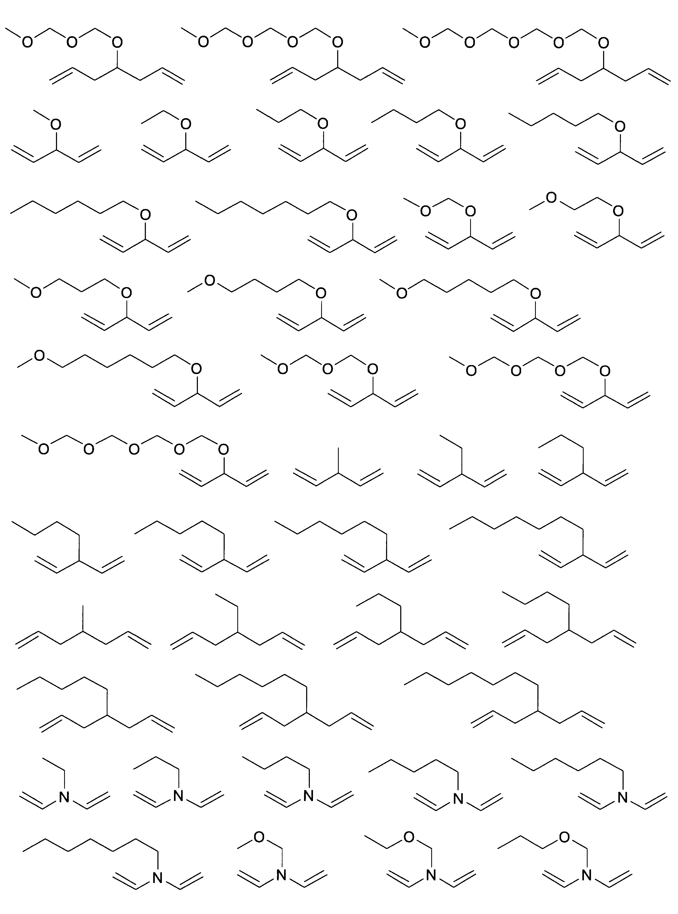

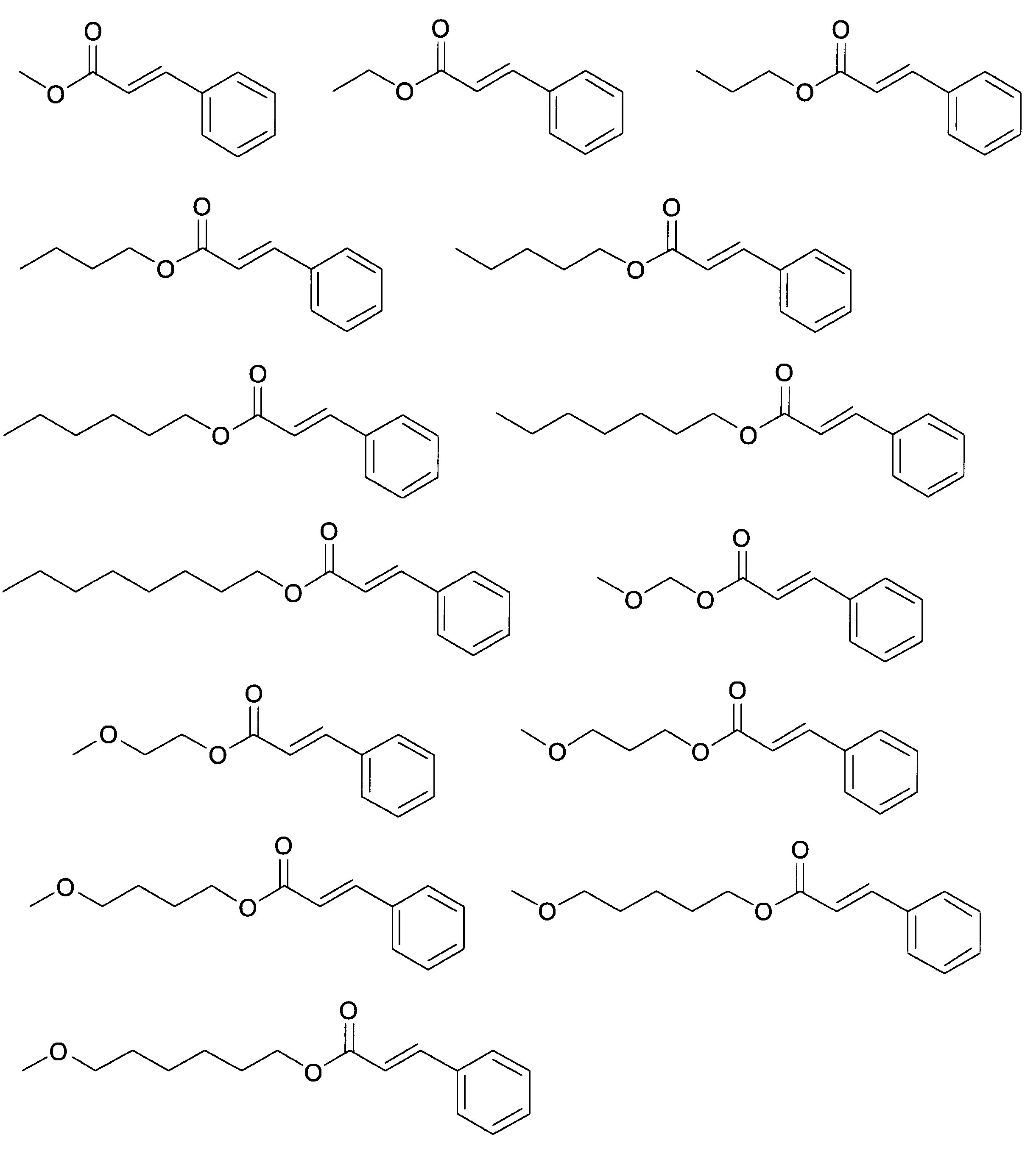
前記カチオンの例は、既述の式(8b)~(10b)の例示と同様である。
また、本発明において、これらの電荷輸送性化合物は溶解度、成膜性の観点からポリマー又はオリゴマーであることが好ましい。
また、前記電荷輸送性化合物がポリマー又はオリゴマーである場合、溶剤への溶解性、成膜性の観点から数平均分子量が、1,000以上1,000,000以下であることが好ましい。より好ましくは2,000以上900,000以下、さらに好ましくは3,000以上800,000以下である。1,000より小さいと化合物が結晶化しやすくなり、成膜性に劣ってしまう。また、1,000,000より大きいと溶剤への溶解度が低下し、塗布溶液や塗布インクを作製するのが困難になる。






この重合開始剤の作用を有機薄膜の製造方法に適用したのが本発明の有機薄膜の製造方法である。すなわち、本発明の有機薄膜の製造方法は、上述の本発明の重合開始剤を用いて有機薄膜に耐溶剤性を付与する工程を含むことを特徴としている。
本発明の有機薄膜の製造方法において、本発明の重合開始剤を用いて有機薄膜に耐溶剤性を付与するに際し、重合開始剤を用いる条件は、電荷輸送性化合物に対し、0.1~50質量%の重合開始剤を用いて薄膜を形成したのち、真空中、大気下あるいは窒素雰囲気下で加熱すればよい。加熱温度・時間は、重合反応を十分に進行させられればよく、特に制限はないが、温度については、種々の基板を適用できることから、好ましくは300℃以下、より好ましくは200℃以下、さらに好ましくは150℃以下である。時間は、生産性を上げる観点から、好ましくは2時間以下、より好ましくは1時間以下、さらに好ましくは30分以下である。
本発明のインク組成物において、溶媒に対する有機エレクトロニクス材料の含有量は、種々の塗布プロセスに適用できる観点から0.1~30質量%とすることが好ましい。
同様に、本発明の有機エレクトロルミネセンス素子(有機EL素子)は、上記有機エレクトロニクス材料および/または上記インク組成物から形成された有機薄膜を含む。
いずれの素子も、有機薄膜として、本発明の有機エレクトロニクス材料を用いて形成された優れた有機薄膜を含み、従来よりも駆動電圧が低く、長い発光寿命を有する。
以下に、本発明のEL素子について詳述する。
本発明の有機エレクトロニクス素子は、電荷輸送性化合物とイオン性化合物とを含む有機エレクトロニクス材料からなる有機薄膜を含むことをその特徴とするものである。本発明の有機EL素子は、発光層、重合層、陽極、陰極、基板を備えていれば特に限定されず、正孔注入層、電子注入層、正孔輸送層、電子輸送層などの他の層を有していてもよい。また、正孔注入層又は正孔輸送層に、本発明の有機薄膜を適用することが好ましい。
以下、各層について詳細に説明する。
発光層に用いる材料としては、低分子化合物であっても、ポリマーまたはオリゴマーであってもよく、デンドリマー等も使用可能である。蛍光発光を利用する低分子化合物としては、ペリレン、クマリン、ルブレン、キナクドリン、色素レーザー用色素(例えば、ローダミン、DCM1等)、アルミニウム錯体(例えば、Tris(8-hydroxyquinolinato)aluminum(III)(Alq3))、スチルベン、これらの誘導体があげられる。蛍光発光を利用するポリマーまたはオリゴマーとしては、ポリフルオレン、ポリフェニレン、ポリフェニレンビニレン(PPV)、ポリビニルカルバゾール(PVK)、フルオレンーベンゾチアジアゾール共重合体、フルオレン-トリフェニルアミン共重合体、及びこれらの誘導体や混合物が好適に利用できる。
燐光材料は、低分子又はデンドライド種、例えば、イリジウム核デンドリマーが使用され得る。またこれらの誘導体も好適に使用できる。
ホスト材料としては、低分子化合物であっても、高分子化合物であってもよく、デンドリマーなども使用できる。
塗布法により形成する場合、有機EL素子を安価に製造することができ、より好ましい。発光層を塗布法によって形成するには、燐光材料と、必要に応じてホスト材料を含む溶液を、例えば、インクジェット法、キャスト法、浸漬法、凸版印刷、凹版印刷、オフセット印刷、平板印刷、凸版反転オフセット印刷、スクリーン印刷、グラビア印刷等の印刷法、スピンコーティング法などの公知の方法で所望の基体上に塗布することで行うことができる。
陰極材料としては、例えば、Li、Ca、Mg、Al、In、Cs、Ba、Mg/Ag、LiF、CsF等の金属又は金属合金であることが好ましい。
陽極としては、金属(例えば、Au)又は金属導電率を有する他の材料、例えば、酸化物(例えば、ITO:酸化インジウム/酸化錫)、導電性高分子(例えば、ポリチオフェン-ポリスチレンスルホン酸混合物(PEDOT:PSS))を使用することもできる。
電子輸送層、電子注入層としては、例えば、フェナントロリン誘導体(例えば、2,9-dimethyl-4,7-diphenyl-1,10-phenanthroline(BCP))、ビピリジン誘導体、ニトロ置換フルオレン誘導体、ジフェニルキノン誘導体、チオピランジオキシド誘導体、ナフタレンペリレンなどの複素環テトラカルボン酸無水物、カルボジイミド、フレオレニリデンメタン誘導体、アントラキノジメタン及びアントロン誘導体、オキサジアゾール誘導体(2-(4-Biphenylyl)-5-(4-tert-butylphenyl-1,3,4-oxadiazole) (PBD))、アルミニウム錯体(例えば、Tris(8-hydroxyquinolinato)aluminum(III)(Alq3))などが挙げられる。さらに、上記オキサジアゾール誘導体において、オキサジアゾール環の酸素原子を硫黄原子に置換したチアジアゾール誘導体、電子吸引基として知られているキノキサリン環を有するキノキサリン誘導体も用いることができる。
本発明の有機EL素子に用いることができる基板として、ガラス、プラスチック等の種類は特に限定されることはなく、また、透明のものであれば特に制限は無いが、ガラス、石英、光透過性樹脂フィルム等が好ましく用いられる。樹脂フィルムを用いた場合には、有機EL素子にフレキシブル性を与えることが可能であり、特に好ましい。
本発明の有機EL素子における発光色は特に限定されるものではないが、白色発光素子は家庭用照明、車内照明、時計や液晶のバックライト等の各種照明器具に用いることができるため好ましい。
本発明の表示素子は、既述の本発明の有機EL素子を備えたことを特徴としている。
例えば、赤・緑・青(RGB)の各画素に対応する素子として、本発明の有機EL素子を用いることで、カラーの表示素子が得られる。
画像の形成には、マトリックス状に配置した電極でパネルに配列された個々の有機EL素子を直接駆動する単純マトリックス型と、各素子に薄膜トランジスタを配置して駆動するアクティブマトリックス型とがある。前者は、構造は単純ではあるが垂直画素数に限界があるため文字などの表示に用いる。後者は、駆動電圧は低く電流が少なくてすみ、明るい高精細画像が得られるので、高品位のディスプレイ用として用いられる。
(イオン性化合物合成例1)
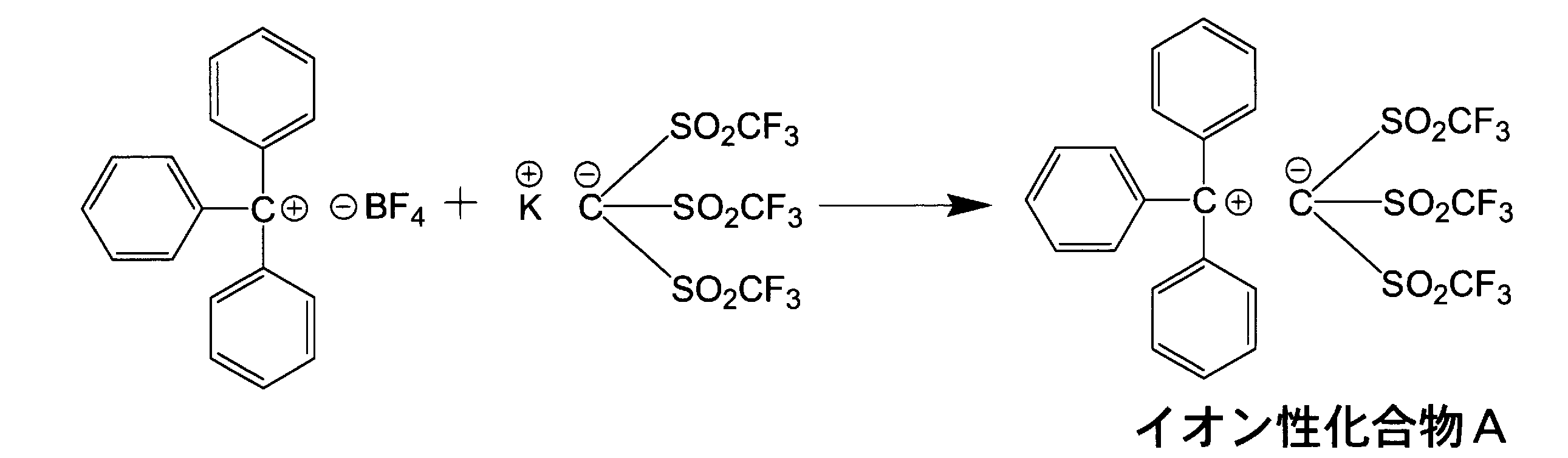
ナス型フラスコに、カリウム トリス(トリフルオロメタンスルホニル)メチド(1.01g,2.24mmol)を加え、酢酸エチル(20mL)に溶解した。ここに、トリチル テトラフルオロボレート(0.73g,2.21mmol)の酢酸エチル懸濁溶液(20mL)をゆっくりと滴下し、室温下で1時間攪拌した。有機層を水でよく洗浄した後、溶媒を留去して乾固させることで目的のイオン性化合物Aを黄色粉末として1.31g得た。収率90.5%。
本合成例の反応式を以下に示す。
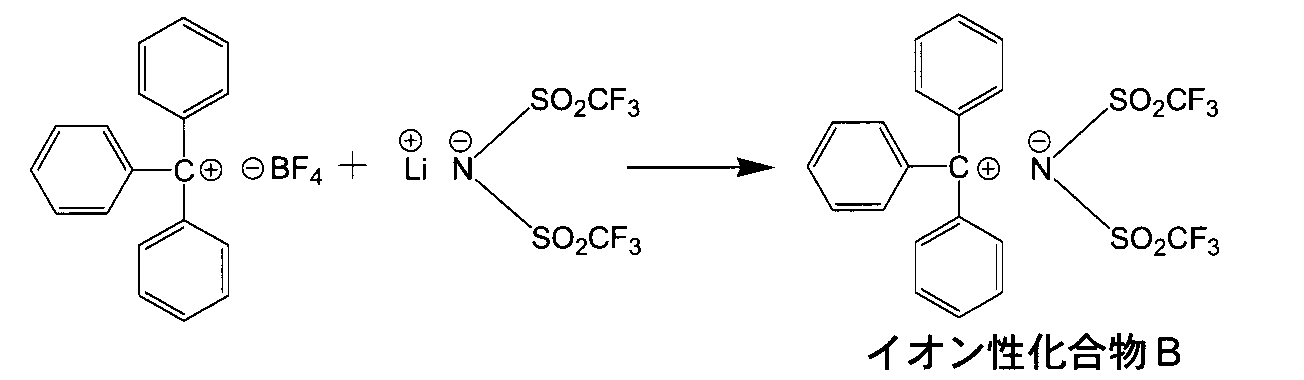
前記イオン性化合物合成例1のカリウム トリス(トリフルオロメタンスルホニル)メチドを、リチウム ビス(トリフルオロメタンスルホニル)イミドに代えた以外はイオン性化合物合成例1と同様にして合成を行った。目的のイオン性化合物Bを黄色粉末として得た。収率85.9%
本合成例の反応式を以下に示す。
ナス型フラスコに、カリウム トリス(トリフルオロメタンスルホニル)メチド(0.57g,1.34mmol)を加え、酢酸エチル(10mL)に溶解した。ここに、ジフェニルヨードニウムヘキサフルオロホスフェート(0.60g,1.33mmol)の酢酸エチル溶液(10mL)をゆっくりと滴下し、室温下で1時間攪拌した。有機層を水でよく洗浄したのち、溶媒を留去することで目的のイオン性化合物Cを白色粉末として0.90g得た。収率97.0%
本合成例の反応式を以下に示す。

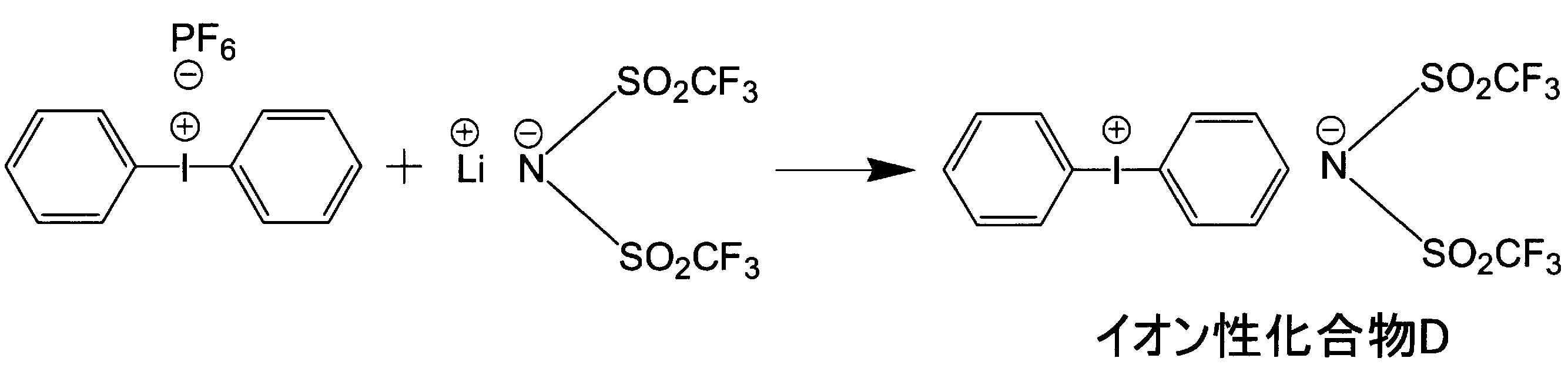
前記イオン性化合物合成例3のカリウム トリス(トリフルオロメタンスルホニル)メチドを、リチウム ビス(トリフルオロメタンスルホニル)イミドに変えた以外は同様にして合成を行った。目的のイオン性化合物Dを白色粉末として得た。収率89.8%
本合成例の反応式を以下に示す。
ナス型フラスコに、カリウム トリス(トリフルオロメタンスルホニル)メチド(0.76g,1.69mmol)を加え、酢酸エチル(10mL)に溶解した。ここに、トリフェニルスルホニウム テトラフルオロボラート(0.59g、1.69mmol)の酢酸エチル溶液(10mL)をゆっくりと滴下し、室温で1時間攪拌した。有機層を水でよく洗浄した後、溶媒を留去することで目的のイオン性化合物Eを白色粉末として1.04g得た。収率91.2%
本合成例の反応式を以下に示す。

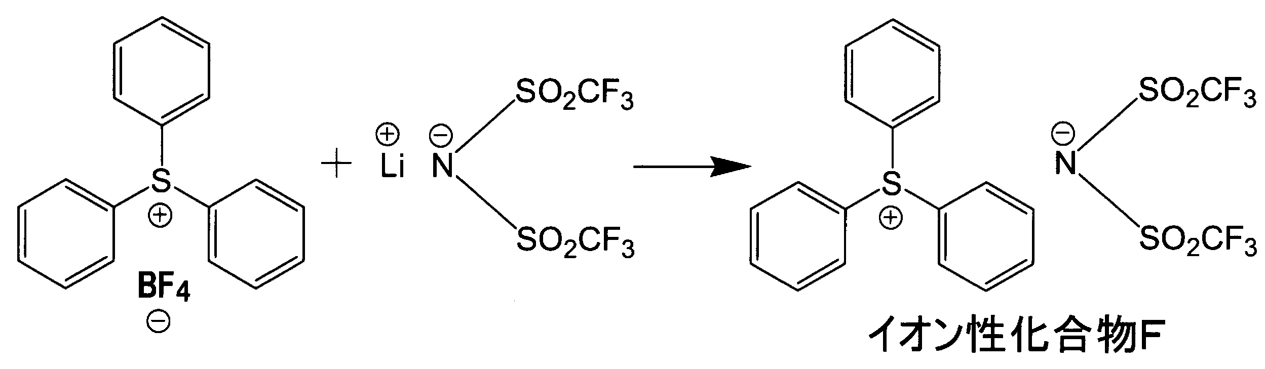
前記イオン性化合物合成例5のカリウム トリス(トリフルオロメタンスルホニル)メチドをリチウム ビス(トリフルオロメタンスルホニル)イミドに変えた以外は同様にして合成を行った。目的のイオン性化合物Fを白色粉末として得た。収率83.4%
本合成例の反応式を以下に示す。
ナス型フラスコに、カリウム トリス(トリフルオロメタンスルホニル)メチド(0.52g,1.14mmol)を加え、酢酸エチル(10mL)に溶解した。ここに、テトラフェニルホスホニウムブロミド(0.48g,1.14mmol)の酢酸エチル溶液(10mL)をゆっくりと滴下し、室温で1時間攪拌した。有機層を水でよく洗浄した後、溶媒を留去することで、目的のイオン性化合物Gを白色粉末として0.84g得た。収率98.2%
本合成例の反応式を以下に示す。

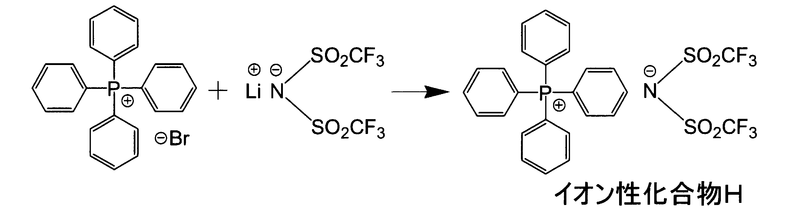
前記イオン性化合物合成例7のカリウム トリス(トリフルオロメタンスルホニル)メチドをリチウム ビス(トリフルオロメタンスルホニル)イミドに変えた以外は同様にして合成を行った。目的のイオン性化合物Hを白色粉末として得た。収率85.2%
本合成例の反応式を以下に示す。
ナス型フラスコに、カリウム トリス(トリフルオロメタンスルホニル)メチド(4.50g,10.0mmol)を加え、酢酸エチル(10mL)に溶解した。ここに、トリメチルフェニルアンモニウムクロリド(1.72g,10.0mmol)の酢酸エチル溶液(10mL)をゆっくりと滴下し、室温で1時間攪拌した。有機層を水でよく洗浄した後、溶媒を留去することで、目的のイオン性化合物Iを白色粉末として4.94g得た。収率90.2%
本合成例の反応式を以下に示す。
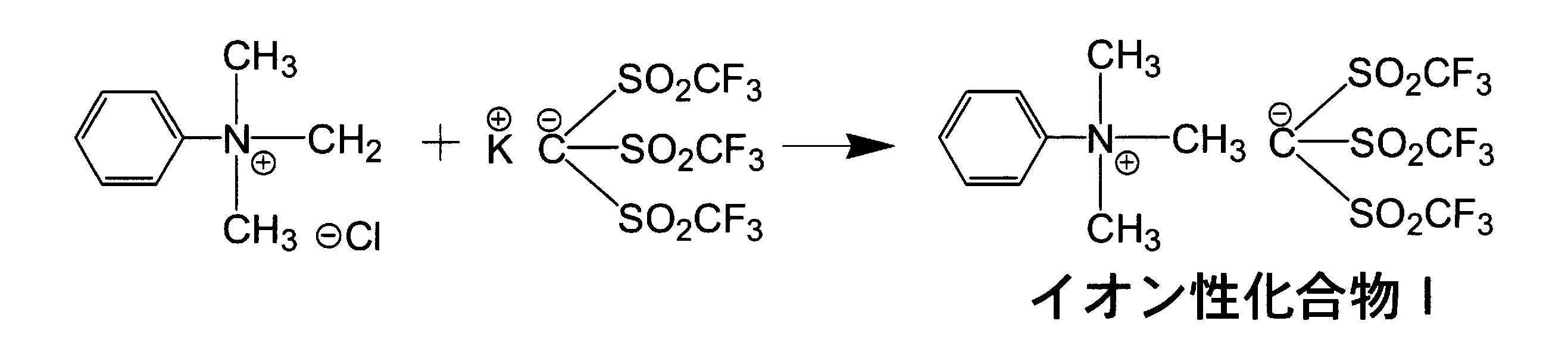
(モノマー合成例1)
丸底フラスコに、3-エチル-3-ヒドロキシメチルオキセタン(50mmol)、4-ブロモベンジルブロミド(50mmol)、n-ヘキサン(200mL)、テトラブチルアンモニウムブロミド(2.5mmol)及び50質量%水酸化ナトリウム水溶液(36g)を加え、窒素下、70℃で6時間加熱攪拌した。
本合成例の反応式を以下に示す。

(合成例1)
密閉可能なフッ素樹脂製容器に、2,7-ビス(4,4,5,5-テトラメチル-1,3,2-ジオキサボロラン-2-イル)-9,9-ジオクチルフルオレン(0.4mmol)、4,4’-ジブロモ-4’-n-ブチルトリフェニルアミン(0.32mmol)、重合可能な置換基を有するモノマーA(0.16mmol)、テトラキストリフェニルホスフィンパラジウム(0.008mmol)、2M炭酸カリウム水溶液(5.3ml)、Aliquat336(0.4mmol)及びアニソール(4ml)を入れ、窒素雰囲気下、密閉容器中、マイクロ波を照射して90℃、2時間加熱撹拌した。
本合成例の反応式を以下に示す。

[実施例1]
上記で得たオリゴマーA(4.5mg)をトルエン(465μL)に溶解し、前記イオン性化合物Gの酢酸エチル溶液(イオン性化合物G10μg/1μL、50μL)を加え本発明の有機エレクトロニクス材料を含むインク組成物を調製した。オリゴマーAおよびイオン性化合物Gが溶け残ることはなく、均一な溶液が得られた。
実施例1におけるイオン性化合物Gをテトラフェニルホスホニウム ヘキサフルオロアンチモネート(Alfa Easer製)に代えた以外は同様にしてインク組成物を調製した。しかしながら、溶け残りが発生して均一な溶液を得ることができず、塗布インクとして適するものではなかった。
[実施例2]
上記で得たオリゴマーA(4.5mg)をトルエン(465μL)に溶解し、前記イオン性化合物Cの酢酸エチル溶液(イオン性化合物C10μg/1μL、50μL)を加え、インク組成物を調製した。この溶液を用いて石英ガラス板上に3000min-1でスピンコートし、ホットプレート上で180℃ 10分間加熱して硬化させ、有機薄膜(膜厚:60nm)を形成した。この有機薄膜を石英ガラス板ごとトルエン中でリンスし、リンス前後の薄膜の吸光度の比より薄膜の残存率(残膜率)を求めたところ、残膜率は98%であった。
実施例2におけるイオン性化合物Cをイオン性化合物Dの酢酸エチル溶液に変えた以外は実施例2と同様にして薄膜を作製し、残膜率を求めたところ99%であった。
実施例2におけるイオン性化合物Cをイオン性化合物Eに変えた以外は実施例2と同様にして薄膜を作製し、残膜率を求めたところ91%であった。
実施例2におけるイオン性化合物Cをイオン性化合物Fに変えた以外は実施例2と同様にして薄膜を作製し、残膜率を求めたところ70%であった。
実施例2におけるイオン性化合物Cをイオン性化合物Gに変えた以外は実施例2と同様にして薄膜を作製し、残膜率を求めたところ86%であった。
実施例2におけるイオン性化合物Cをイオン性化合物Hに変えた以外は実施例2と同様にして薄膜を作製し、残膜率を求めたところ75%であった。
実施例2におけるイオン性化合物Cを下記イオン性化合物Jに変えた以外は実施例2と同様にして薄膜を作製し、残膜率を求めたところ99%であった。

実施例2におけるイオン性化合物Cを下記イオン性化合物Kに変えた以外は実施例2と同様にして薄膜を作製し、残膜率を求めたところ99%であった。

実施例2におけるイオン性化合物Cを下記イオン性化合物Lに変えた以外は実施例2と同様にして薄膜を作製し、残膜率を求めたところ94%であった。
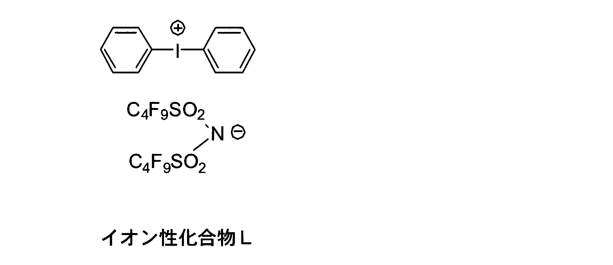
実施例2におけるイオン性化合物Cを下記イオン性化合物Mに変えた以外は実施例2と同様にして薄膜を作製し、残膜率を求めたところ80%であった。

実施例2におけるイオン性化合物Cをジフェニルヨードニウムヘキサフルオロホスフェート(Aldrich製)に変えた以外は実施例2と同様にして薄膜を作製し、残膜率を求めたところ、10%であった。
実施例2におけるイオン性化合物Cをトリフェニルスルホニウムテトラフルオロボラート(東京化成工業製)に変えた以外は実施例2と同様にして薄膜を作製し、残膜率を求めたところ、8%であった。
実施例2におけるイオン性化合物Cをトロピリウムヘキサフルオロホスファート(東京化成工業製)に変えた以外は同様にして薄膜を作製し、残膜率を求めたところ、13%であった。

[実施例12]
ITOを1.6mm幅にパターニングしたガラス基板上に、オリゴマーA(20mg)のトルエン(525μL)溶液と前記イオン性化合物Eの酢酸エチル溶液(イオン性化合物E10μg/1μL、222μL)の混合溶液を2000min-1でスピン塗布し、ホットプレート上で180℃、10分間加熱した。次に得られたガラス基板を真空蒸着機中に移し、金(膜厚30nm)を蒸着した。
実施例12におけるイオン性化合物Eを加えないこと以外は実施例12と同様にしてホールオンリー素子を作製した。以後の実験は大気中、室温(25℃)で行った。
[実施例13]
ITOを1.6mm幅にパターニングしたガラス基板上に、上記で得たオリゴマーA(4.5mg)、前記イオン性化合物E(0.45mg)、トルエン(1.2ml)を混合した塗布溶液を、3000min-1でスピンコートした後、ホットプレート上で180℃、10分間加熱して硬化させ、正孔注入層(40nm)を形成した。
正孔注入層の形成時に前記イオン性化合物を加えなかった以外、実施例13と同様にして白色有機EL素子および照明装置を作製した。
上記で得たオリゴマーA(10mg)をトルエン(728μL)に溶解し、前記イオン性化合物Cの酢酸エチル溶液(イオン性化合物C10μg/1μL、31μL)を加えた塗布溶液を調製した。ITOを1.6mm幅にパターニングしたガラス基板上に、窒素雰囲気下で塗布溶液を3000min-1でスピンコートした後、ホットプレート上で180℃、10分間加熱して硬化させ、正孔注入層(60nm)を形成した。
Alを蒸着後、大気開放することなく、乾燥窒素環境中に基板を移動し、0.7mmの無アルカリガラスに0.4mmのザグリを入れた封止ガラスとITOガラス基板を、光硬化性エポキシ樹脂を用いて貼り合わせることにより封止を行い、有機EL素子を作製した。
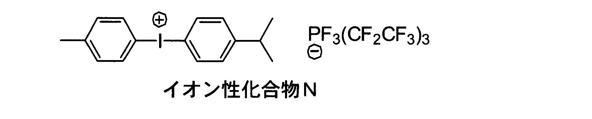
実施例14におけるイオン性化合物Cを下記イオン性化合物Nに変えた以外は同様にして有機EL素子を作製し、電圧を印加したところ、6.0Vで黄緑色発光が観測され、初期輝度1000cd/m2における発光寿命は、194時間であった。
2 陽極
3 正孔注入層
4 陰極
5 電子注入層
6 正孔輸送層
7 電子輸送層
8 基板
Claims (28)
- 電荷輸送性化合物とイオン性化合物とを含有し、該イオン性化合物の少なくとも一つが下記一般式(1b)~(3b)で表される化合物のいずれか1種であることを特徴とする有機エレクトロニクス材料。
- 前記イオン性化合物がハロゲン原子を有することを特徴とする請求項1に記載の有機エレクトロニクス材料。
- 前記イオン性化合物が、炭素数1~20のヘテロ原子を含んでもよい直鎖状、分岐状もしくは環状の、パーフルオロアルキル基、パーフルオロアルキルスルホニル基、パーフルオロアルキルオキシスルホニル基、パーフルオロアリールスルホニル基、パーフルオロアリールオキシスルホニル基、パーフルオロアシル基、パーフルオロアルコキシカルボニル基、パーフルオロアシルオキシ基、パーフルオロアリールオキシカルボニル基、パーフルオロアルケニル基、及びパーフルオロアルキニル基からなる群より選択される1種を有することを特徴とする請求項1又は2に記載の有機エレクトロニクス材料。
- 前記Y1~Y6が下記一般式(4b)~(14b)のいずれか1種であることを特徴とする請求項1~3のいずれか1項に記載の有機エレクトロニクス材料。
- 前記一般式(1b)~(3b)におけるL+が下記一般式(15b)~(17b)で表されるカチオンのうちのいずれか1種であることを特徴とする請求項1~4のいずれか1項に記載の有機エレクトロニクス材料。
- 一般式(15b)~(17b)におけるR11~R34が、各々独立に、置換されていてもよい、アルキル基、アルケニル基、アルキニル基、芳香族炭化水素基または芳香族複素環基であることを特徴とする請求項5に記載の有機エレクトロニクス材料。
- 一般式(15b)におけるA1が臭素原子、ヨウ素原子または炭素原子であり、一般式(16b)におけるA2が酸素原子、炭素原子、硫黄原子またはセレン原子であり、一般式(17b)におけるA3が窒素原子、リン原子、ヒ素原子またはアンチモン原子であることを特徴とする請求項5又は6に記載の有機エレクトロニクス材料。
- 前記電荷輸送性化合物が、芳香族アミン、カルバゾールまたはチオフェン化合物を少なくとも一つ含むことを特徴とする請求項1~7のいずれか1項に記載の有機エレクトロニクス材料。
- 前記芳香族アミン、カルバゾールまたはチオフェン化合物が、ポリマーまたはオリゴマーであることを特徴とする請求項8に記載の有機エレクトロニクス材料。
- 前記ポリマーまたはオリゴマーの数平均分子量が、1,000以上100,000以下である請求項9に記載の有機エレクトロニクス材料。
- 前記ポリマーまたはオリゴマーが一つ以上の重合可能な置換基を有することを特徴とする請求項9又は10に記載の有機エレクトロニクス材料。
- 前記重合可能な置換基がオキセタン基、エポキシ基、ビニル基、ビニルエーテル基、アクリレート基、メタクリレート基のいずれかであることを特徴とする請求項11に記載の有機エレクトロニクス材料。
- 前記イオン性化合物が重合開始剤として機能することを特徴とする請求項1~12のいずれか1項に記載の有機エレクトロニクス材料。
- 下記一般式(1b)~(3b)で表されるイオン性化合物の少なくとも1種を含むことを特徴とする重合開始剤。
- 下記一般式(1b)~(3b)で表されるイオン性化合物の少なくとも1種を含むことを特徴とする熱重合開始剤。
- 請求項14に記載の重合開始剤を用いて有機薄膜に耐溶剤性を付与する工程を含むことを特徴とする有機薄膜の製造方法。
- 請求項1~12のいずれか1項に記載の有機エレクトロニクス材料と溶媒とを含むインク組成物。
- 請求項1~12のいずれか1項に記載の有機エレクトロニクス材料を用いて形成された有機薄膜。
- 請求項17に記載のインク組成物を用いて形成された有機薄膜。
- 請求項18又は19に記載の有機薄膜を含むことを特徴とする有機エレクトロニクス素子。
- 請求項18又は19に記載の有機薄膜を含むことを特徴とする有機エレクトロルミネセンス素子。
- 前記有機薄膜が正孔注入層であることを特徴とする請求項21に記載の有機エレクトロルミネセンス素子。
- 前記有機薄膜が正孔輸送層であることを特徴とする請求項21に記載の有機エレクトロルミネセンス素子。
- 基板が、フレキシブル基板であることを特徴とする請求項21~23のいずれか1項に記載の有機エレクトロルミネセンス素子。
- 基板が、樹脂フィルムであることを特徴とする請求項21~23のいずれか1項に記載の有機エレクトロルミネセンス素子。
- 請求項21~25のいずれか1項に記載の有機エレクトロルミネセンス素子を備えた表示素子。
- 請求項21~25のいずれか1項に記載の有機エレクトロルミネセンス素子を備えた照明装置。
- 請求項27に記載の照明装置と、表示手段として液晶素子と、を備えた表示装置。
Priority Applications (8)
| Application Number | Priority Date | Filing Date | Title |
|---|---|---|---|
| EP11772035.9A EP2562839A4 (en) | 2010-04-22 | 2011-04-20 | ORGANIC ELECTRONIC MATERIAL, POLYMERIZATION INITIATOR AND THERMAL POLYMERIZATION INITIATOR, INK COMPOSITION, ORGANIC THIN FILM AND METHOD FOR PRODUCING THE SAME, ORGANIC ELECTRONIC ELEMENT, ORGANIC ELECTROLUMINESCENT ELEMENT, ILLUMINATION DEVICE, DISPLAY ELEMENT, AND DISPLAY DEVICE |
| KR1020127028465A KR101485470B1 (ko) | 2010-04-22 | 2011-04-20 | 유기 일렉트로닉스 재료, 중합 개시제 및 열중합 개시제, 잉크 조성물, 유기 박막 및 그 제조 방법, 유기 일렉트로닉스 소자, 유기 일렉트로 루미네센스 소자, 조명 장치, 표시 소자, 및 표시 장치 |
| KR1020147020698A KR20140108701A (ko) | 2010-04-22 | 2011-04-20 | 유기 일렉트로닉스 재료, 중합 개시제 및 열중합 개시제, 잉크 조성물, 유기 박막 및 그 제조 방법, 유기 일렉트로닉스 소자, 유기 일렉트로 루미네센스 소자, 조명 장치, 표시 소자, 및 표시 장치 |
| US13/642,522 US10566105B2 (en) | 2010-04-22 | 2011-04-20 | Method for producing charge transport film |
| KR1020147020699A KR101537654B1 (ko) | 2010-04-22 | 2011-04-20 | 유기 일렉트로닉스 재료, 중합 개시제 및 열중합 개시제, 잉크 조성물, 유기 박막 및 그 제조 방법, 유기 일렉트로닉스 소자, 유기 일렉트로 루미네센스 소자, 조명 장치, 표시 소자, 및 표시 장치 |
| CN201180020248.9A CN102859740B (zh) | 2010-04-22 | 2011-04-20 | 有机电子材料、聚合引发剂及热聚合引发剂、油墨组合物、有机薄膜及其制造方法、有机电子元件、有机电致发光元件、照明装置、显示元件以及显示装置 |
| JP2012511683A JP5696723B2 (ja) | 2010-04-22 | 2011-04-20 | 有機エレクトロニクス材料、重合開始剤及び熱重合開始剤、インク組成物、有機薄膜及びその製造方法、有機エレクトロニクス素子、有機エレクトロルミネセンス素子、照明装置、表示素子、並びに表示装置 |
| US16/726,220 US20200143954A1 (en) | 2010-04-22 | 2019-12-23 | Organic electronic material, polymerization initiator and thermal polymerization initiator, ink composition, organic thin film and production method for same, organic electronic element, organic electroluminescent element, lighting device, display element, and display device |
Applications Claiming Priority (2)
| Application Number | Priority Date | Filing Date | Title |
|---|---|---|---|
| JP2010-099035 | 2010-04-22 | ||
| JP2010099035 | 2010-04-22 |
Related Child Applications (2)
| Application Number | Title | Priority Date | Filing Date |
|---|---|---|---|
| US13/642,522 A-371-Of-International US10566105B2 (en) | 2010-04-22 | 2011-04-20 | Method for producing charge transport film |
| US16/726,220 Division US20200143954A1 (en) | 2010-04-22 | 2019-12-23 | Organic electronic material, polymerization initiator and thermal polymerization initiator, ink composition, organic thin film and production method for same, organic electronic element, organic electroluminescent element, lighting device, display element, and display device |
Publications (1)
| Publication Number | Publication Date |
|---|---|
| WO2011132702A1 true WO2011132702A1 (ja) | 2011-10-27 |
Family
ID=44834219
Family Applications (1)
| Application Number | Title | Priority Date | Filing Date |
|---|---|---|---|
| PCT/JP2011/059711 Ceased WO2011132702A1 (ja) | 2010-04-22 | 2011-04-20 | 有機エレクトロニクス材料、重合開始剤及び熱重合開始剤、インク組成物、有機薄膜及びその製造方法、有機エレクトロニクス素子、有機エレクトロルミネセンス素子、照明装置、表示素子、並びに表示装置 |
Country Status (7)
| Country | Link |
|---|---|
| US (2) | US10566105B2 (ja) |
| EP (1) | EP2562839A4 (ja) |
| JP (4) | JP5696723B2 (ja) |
| KR (3) | KR101537654B1 (ja) |
| CN (1) | CN102859740B (ja) |
| TW (1) | TWI454553B (ja) |
| WO (1) | WO2011132702A1 (ja) |
Cited By (16)
| Publication number | Priority date | Publication date | Assignee | Title |
|---|---|---|---|---|
| WO2013081031A1 (ja) | 2011-11-30 | 2013-06-06 | 日立化成株式会社 | 有機エレクトロニクス材料、インク組成物、及び有機エレクトロニクス素子 |
| WO2013081052A1 (ja) | 2011-11-30 | 2013-06-06 | 日立化成株式会社 | 有機エレクトロニクス材料、インク組成物、及び有機エレクトロニクス素子 |
| JP2013229429A (ja) * | 2012-04-25 | 2013-11-07 | Hitachi Chemical Co Ltd | 有機エレクトロニクス材料及びその製造方法、重合開始剤及び熱重合開始剤、インク組成物、有機薄膜及びその製造方法、有機エレクトロニクス素子、有機エレクトロルミネセンス素子、照明装置、表示素子、並びに表示装置 |
| JP2013229370A (ja) * | 2012-04-24 | 2013-11-07 | Hitachi Chemical Co Ltd | 色変化防止剤、該色変化防止剤を含むインク組成物、該インク組成物を用いて形成した有機薄膜、有機エレクトロニクス素子、有機エレクトロルミネセンス素子、表示素子、照明装置、及び表示装置 |
| JP2015012105A (ja) * | 2013-06-28 | 2015-01-19 | 日立化成株式会社 | 有機発光素子 |
| EP2894942A4 (en) * | 2012-09-04 | 2015-10-07 | Mitsubishi Chem Corp | ORGANIC ELECTROLUMINESCENZING DEVICE AND METHOD OF MANUFACTURING THEREOF |
| WO2015186688A1 (ja) * | 2014-06-05 | 2015-12-10 | 日産化学工業株式会社 | 電荷輸送性ワニス |
| JP2017125007A (ja) * | 2015-12-31 | 2017-07-20 | ローム アンド ハース エレクトロニック マテリアルズ エルエルシーRohm and Haas Electronic Materials LLC | 光酸発生剤 |
| WO2018070019A1 (ja) | 2016-10-13 | 2018-04-19 | 日立化成株式会社 | 有機エレクトロニクス材料、インク組成物、有機エレクトロニクス素子、及び有機エレクトロニクス素子の製造方法 |
| WO2018110610A1 (ja) * | 2016-12-14 | 2018-06-21 | 旭硝子株式会社 | 電荷輸送層、および有機光電子素子 |
| JP2018133454A (ja) * | 2017-02-15 | 2018-08-23 | 富士ゼロックス株式会社 | 有機電界発光素子用の組成物、電荷輸送性膜、及び有機電界発光素子 |
| WO2018186340A1 (ja) * | 2017-04-05 | 2018-10-11 | 日産化学株式会社 | 電荷輸送性ワニス |
| JP2019507491A (ja) * | 2015-12-24 | 2019-03-14 | ダウ グローバル テクノロジーズ エルエルシー | ポリマー層及びそれを含有する有機電子デバイス |
| WO2019124415A1 (ja) | 2017-12-20 | 2019-06-27 | 日産化学株式会社 | 電荷輸送性ワニス |
| JP2019519943A (ja) * | 2016-06-28 | 2019-07-11 | ダウ グローバル テクノロジーズ エルエルシー | 有機電荷輸送膜を作製するためのプロセス |
| JP2021027078A (ja) * | 2019-07-31 | 2021-02-22 | 株式会社リコー | 光電変換素子、電子機器、及び電源モジュール |
Families Citing this family (14)
| Publication number | Priority date | Publication date | Assignee | Title |
|---|---|---|---|---|
| KR101537654B1 (ko) | 2010-04-22 | 2015-07-17 | 히타치가세이가부시끼가이샤 | 유기 일렉트로닉스 재료, 중합 개시제 및 열중합 개시제, 잉크 조성물, 유기 박막 및 그 제조 방법, 유기 일렉트로닉스 소자, 유기 일렉트로 루미네센스 소자, 조명 장치, 표시 소자, 및 표시 장치 |
| CN104603953A (zh) * | 2012-03-23 | 2015-05-06 | 阿克伦大学 | 使用氧化锌纳米线作为电子传输层的宽带聚合物光检测器 |
| US10665786B2 (en) | 2013-03-08 | 2020-05-26 | Hitachi Chemical Company, Ltd. | Treatment liquid containing ionic compound, organic electronic element, and method for producing organic electronic element |
| CN106062985A (zh) | 2014-02-24 | 2016-10-26 | 株式会社理光 | 光电转换元件和太阳能电池 |
| WO2016026266A1 (en) * | 2014-08-21 | 2016-02-25 | Dow Global Technologies Llc | Polymeric charge transfer layer and organic electronic device containing the same |
| EP3133663B1 (en) * | 2015-08-18 | 2022-06-15 | Novaled GmbH | Metal amides for use as hole injection layer for an organic light-emitting diode (oled) |
| EP3133664A1 (en) * | 2015-08-18 | 2017-02-22 | Novaled GmbH | Triaryl amine thick layer doped with metal amides for use as hole injection layer for an organic light-emitting diode (oled) |
| EP4084109A1 (en) * | 2015-12-15 | 2022-11-02 | Merck Patent GmbH | Esters containing aromatic groups as solvents for organic electronic formulations |
| CN108431985B (zh) * | 2016-01-08 | 2020-06-23 | 日立化成株式会社 | 有机电子材料、有机电子元件及有机电致发光元件 |
| US11459462B2 (en) * | 2017-02-08 | 2022-10-04 | Showa Denko Materials Co., Ltd. | Charge-transport material and utilization thereof |
| JP2018181872A (ja) * | 2017-04-03 | 2018-11-15 | 日立化成株式会社 | 電荷輸送性材料、インク組成物、及び有機エレクトロニクス素子 |
| DE102018118278B4 (de) | 2018-07-27 | 2025-02-20 | Novaled Gmbh | Elektronische Vorrichtung, Anzeigevorrichtung, Verfahren zum Herstellen derselben und eine Verbindung |
| JP7133437B2 (ja) * | 2018-10-26 | 2022-09-08 | 住友化学株式会社 | 組成物、フィルム、積層構造体、発光装置及びディスプレイ |
| EP4064379B1 (en) * | 2021-03-24 | 2024-07-31 | Novaled GmbH | Organic electronic device, display device comprising the organic electronic device as well as compounds for use in organic electronic devices |
Citations (110)
| Publication number | Priority date | Publication date | Assignee | Title |
|---|---|---|---|---|
| JPS50151997A (ja) | 1974-05-02 | 1975-12-06 | ||
| JPS50151976A (ja) | 1974-05-02 | 1975-12-06 | ||
| US4069055A (en) | 1974-05-02 | 1978-01-17 | General Electric Company | Photocurable epoxy compositions containing group Va onium salts |
| JPS5322597A (en) | 1976-07-09 | 1978-03-02 | Gen Electric | Hardenable composite |
| US4231951A (en) | 1978-02-08 | 1980-11-04 | Minnesota Mining And Manufacturing Company | Complex salt photoinitiator |
| US4256828A (en) | 1975-09-02 | 1981-03-17 | Minnesota Mining And Manufacturing Company | Photocopolymerizable compositions based on epoxy and hydroxyl-containing organic materials |
| JPS56135519A (en) | 1980-02-29 | 1981-10-23 | Ciba Geigy Ag | Photo or thermopolymerizable composition |
| JPS57209931A (en) | 1981-06-04 | 1982-12-23 | Ciba Geigy Ag | Photopolymerizable mixture and photopolymerization |
| JPS5837003A (ja) | 1981-08-28 | 1983-03-04 | Asahi Denka Kogyo Kk | 熱硬化性組成物 |
| JPS5838350A (ja) | 1981-08-28 | 1983-03-05 | Toyota Motor Corp | 車輌用ク−ラコンプレツサの運転制御方法 |
| JPS60203628A (ja) | 1984-03-29 | 1985-10-15 | Toshiba Corp | 光重合性組成物 |
| JPS6429419A (en) | 1987-07-23 | 1989-01-31 | Wako Pure Chem Ind Ltd | Cationic photopolymerization initiator |
| JPS6445357A (en) | 1987-08-12 | 1989-02-17 | Wako Pure Chem Ind Ltd | Novel sulfonium salt |
| JPH021470A (ja) | 1988-03-03 | 1990-01-05 | Sanshin Chem Ind Co Ltd | スルホニウム化合物およびその製造方法 |
| JPH0243202A (ja) | 1988-04-15 | 1990-02-13 | Koei Chem Co Ltd | 重合触媒およびそれを含有する硬化性組成物 |
| JPH02178303A (ja) | 1988-12-29 | 1990-07-11 | Koei Chem Co Ltd | 光重合触媒およびそれを含有する硬化性組成物 |
| JPH02196812A (ja) | 1988-03-15 | 1990-08-03 | Sanshin Chem Ind Co Ltd | カチオン重合性組成物、重合触媒および重合方法 |
| JPH02268173A (ja) | 1989-04-08 | 1990-11-01 | Sanshin Chem Ind Co Ltd | ベンゾチアゾリウム化合物及びその製造方法 |
| JPH0317101A (ja) | 1989-06-14 | 1991-01-25 | Sanshin Chem Ind Co Ltd | カチオン重合触媒および重合性組成物、その重合方法 |
| JPH03237107A (ja) | 1990-02-14 | 1991-10-23 | Sanshin Chem Ind Co Ltd | カチオン重合開始剤および重合性組成物 |
| JPH0423204B2 (ja) | 1983-06-11 | 1992-04-21 | Shimadzu Corp | |
| JPH04308563A (ja) | 1991-04-03 | 1992-10-30 | Nippon Soda Co Ltd | 新規スルホニウム塩及び重合開始剤 |
| JPH04327574A (ja) | 1991-04-25 | 1992-11-17 | Nippon Soda Co Ltd | 新規ピリジニウム塩化合物および重合開始剤 |
| JPH05105692A (ja) | 1991-10-15 | 1993-04-27 | Hokko Chem Ind Co Ltd | 新規ベンジルホスホニウム塩および、それを含む熱硬化性樹脂組成物 |
| JPH05132461A (ja) | 1991-11-08 | 1993-05-28 | Nippon Soda Co Ltd | 新規ピリジニウム塩化合物及び重合開始剤 |
| JPH05140209A (ja) | 1991-11-15 | 1993-06-08 | Nippon Soda Co Ltd | 新規スルホニウム塩化合物及び重合開始剤 |
| JPH05140210A (ja) | 1991-11-15 | 1993-06-08 | Nippon Soda Co Ltd | 新規スルホニウム塩化合物及び重合開始剤 |
| JPH05222167A (ja) | 1991-06-19 | 1993-08-31 | Ciba Geigy Ag | より低い成形温度における新規な樹脂系 |
| JPH05222111A (ja) | 1992-02-10 | 1993-08-31 | Nippon Soda Co Ltd | ベンゾチアゾリウム塩化合物を含有する硬化性組成物 |
| JPH05222112A (ja) | 1992-02-10 | 1993-08-31 | Nippon Soda Co Ltd | ピリジニウム塩化合物を含有する硬化性組成物 |
| JPH05230189A (ja) | 1992-02-25 | 1993-09-07 | Nippon Soda Co Ltd | スルホニウム塩及び増感剤を含有する硬化性組成物 |
| JPH05239213A (ja) | 1992-02-29 | 1993-09-17 | Res Inst For Prod Dev | ポリ(アルキル−p−チオフェノキシフェニルスルホニウム塩)化合物 |
| JPH05255256A (ja) | 1992-03-13 | 1993-10-05 | Cosmo Sogo Kenkyusho:Kk | ピリジニウム塩および光硬化性組成物 |
| JPH05262813A (ja) | 1991-04-12 | 1993-10-12 | Nippon Soda Co Ltd | 硬化性組成物 |
| JPH06157624A (ja) | 1992-11-09 | 1994-06-07 | Ajinomoto Co Inc | ホスホニウム塩およびそれを含有する光硬化型カチオン重合性樹脂 |
| JPH06184170A (ja) | 1992-03-23 | 1994-07-05 | Rhone Poulenc Chim | カチオン重合開始剤である新規のオニウム硼酸塩又は有機金属錯体の硼酸塩 |
| JPH06228086A (ja) | 1993-02-02 | 1994-08-16 | Sanshin Chem Ind Co Ltd | モノマーおよびその重合体 |
| JPH06271532A (ja) | 1993-03-15 | 1994-09-27 | Nippon Soda Co Ltd | 新規スルホニウム塩化合物および重合開始剤 |
| JPH06345726A (ja) | 1993-06-15 | 1994-12-20 | Nippon Soda Co Ltd | 新規スルホニウム塩化合物および重合開始剤 |
| JPH0710914A (ja) | 1993-06-24 | 1995-01-13 | Nippon Kayaku Co Ltd | 光重合開始剤、これを含有するエネルギー線硬化性組成物及びその硬化物 |
| JPH0725922A (ja) | 1993-07-15 | 1995-01-27 | Nippon Kayaku Co Ltd | エネルギー線硬化性組成物及びその硬化物 |
| JPH0743854A (ja) | 1993-07-26 | 1995-02-14 | New Oji Paper Co Ltd | シート状光記録材料 |
| JPH0743901A (ja) | 1993-07-30 | 1995-02-14 | New Oji Paper Co Ltd | 光硬化性組成物およびそれを用いたシート状光記録材料 |
| JPH0761964A (ja) | 1993-06-18 | 1995-03-07 | Nippon Kayaku Co Ltd | 新規オニウム塩、光重合開始剤、これを含有するエネルギー線硬化性組成物及びその硬化物 |
| JPH0782283A (ja) | 1993-09-14 | 1995-03-28 | Hokko Chem Ind Co Ltd | ホスホニウム塩およびそれを含有するカチオン重合性組成物 |
| JPH07109303A (ja) | 1993-10-08 | 1995-04-25 | Nippon Soda Co Ltd | 硬化性組成物 |
| JPH07300505A (ja) | 1994-03-09 | 1995-11-14 | Nippon Soda Co Ltd | 新規スルホニウム塩化合物及び重合開始剤 |
| JPH07300504A (ja) | 1994-03-09 | 1995-11-14 | Nippon Soda Co Ltd | 新規スルホニウム塩化合物および重合開始剤およびそれらを含有する硬化性組成物 |
| JPH07324069A (ja) | 1994-03-29 | 1995-12-12 | Shin Etsu Chem Co Ltd | 新規スルホニウム塩及び化学増幅ポジ型レジスト材料 |
| JPH07333834A (ja) | 1994-06-10 | 1995-12-22 | Shin Etsu Chem Co Ltd | 化学増幅ポジ型レジスト材料 |
| JPH0827209A (ja) | 1994-07-20 | 1996-01-30 | Nippon Kayaku Co Ltd | 光重合開始剤、これを含有するエネルギー線硬化性組成物及びその硬化物 |
| JPH0827208A (ja) | 1994-07-15 | 1996-01-30 | Nippon Kayaku Co Ltd | エネルギー線硬化性組成物及びその硬化物 |
| JPH0827102A (ja) | 1994-07-14 | 1996-01-30 | Nec Corp | 橋かけ環式アルキル基を有するスルホニウム塩化合物、光酸発生剤、それを含有する感光性樹脂組成物、およびそれを用いたパターン形成方法 |
| JPH08157451A (ja) | 1994-12-05 | 1996-06-18 | Shin Etsu Chem Co Ltd | 新規スルホニウム塩及びその製造方法 |
| JPH08157510A (ja) | 1994-12-09 | 1996-06-18 | Nippon Kayaku Co Ltd | 光重合開始剤、これを含有するエネルギー線硬化性組成物及びその硬化物 |
| JPH08160606A (ja) | 1994-12-05 | 1996-06-21 | Shin Etsu Chem Co Ltd | 化学増幅ポジ型レジスト材料 |
| JPH08165290A (ja) | 1994-12-15 | 1996-06-25 | Nippon Kayaku Co Ltd | 光重合開始剤、これを含有するエネルギー線硬化性組成物及びその硬化物 |
| JP2519480B2 (ja) | 1987-10-09 | 1996-07-31 | 日本ペイント株式会社 | 新規ベンジルピリジニウム塩 |
| JPH08245566A (ja) | 1995-03-07 | 1996-09-24 | Shin Etsu Chem Co Ltd | 新規スルホニウム塩 |
| JPH08301991A (ja) | 1995-05-12 | 1996-11-19 | Nippon Kayaku Co Ltd | 光重合開始剤、これを含有するエネルギー線硬化性組成物及びその硬化物 |
| JPH08325259A (ja) | 1995-05-30 | 1996-12-10 | Shin Etsu Chem Co Ltd | スルホニウム塩及び化学増幅型ポジ型レジスト材料 |
| JPH08325225A (ja) | 1995-05-26 | 1996-12-10 | Nippon Soda Co Ltd | 新規スルホニウム塩化合物および重合開始剤およびそれらを含有する硬化性組成物 |
| JPH0912537A (ja) | 1995-06-29 | 1997-01-14 | Shin Etsu Chem Co Ltd | スルホニウム塩 |
| JPH09118663A (ja) | 1995-08-22 | 1997-05-06 | Nippon Soda Co Ltd | 新規スルホニウム塩化合物、重合開始剤、該化合物を含有する硬化性組成物および硬化方法 |
| JPH09143212A (ja) | 1995-11-27 | 1997-06-03 | Nippon Kayaku Co Ltd | 光重合開始剤、これを含有するエネルギー線硬化性組成物及びその硬化物 |
| JPH09202873A (ja) | 1996-01-29 | 1997-08-05 | Toyo Ink Mfg Co Ltd | 感エネルギー線酸発生剤、感エネルギー線酸発生剤組成物、硬化性組成物およびその硬化物 |
| JPH09221652A (ja) | 1996-02-19 | 1997-08-26 | Toyo Ink Mfg Co Ltd | 感エネルギー線酸発生剤、感エネルギー線酸発生剤組成物、硬化性組成物およびその硬化物 |
| JPH09268205A (ja) | 1996-03-29 | 1997-10-14 | Asahi Denka Kogyo Kk | 光学的立体造形用樹脂組成物および光学的立体造形法 |
| JPH09278935A (ja) | 1996-04-09 | 1997-10-28 | Asahi Denka Kogyo Kk | 光学的立体造形用樹脂組成物および光学的立体造形法 |
| JPH09278813A (ja) | 1996-04-12 | 1997-10-28 | Nippon Kayaku Co Ltd | 光重合開始剤、これを含有するエネルギー線硬化性組成物及びその硬化物 |
| JPH09328506A (ja) | 1996-06-10 | 1997-12-22 | Toyo Ink Mfg Co Ltd | 重合開始剤、重合開始剤組成物、重合性組成物およびその硬化物 |
| JPH09328507A (ja) | 1996-06-10 | 1997-12-22 | Toyo Ink Mfg Co Ltd | 重合開始剤、重合性組成物およびその硬化物 |
| JPH107680A (ja) | 1996-06-18 | 1998-01-13 | Nippon Kayaku Co Ltd | 光重合開始剤、これを含有するエネルギー線硬化性組成物及びその硬化物 |
| JPH10101718A (ja) | 1996-10-02 | 1998-04-21 | Nippon Kayaku Co Ltd | エネルギー線硬化性組成物及びその硬化物 |
| JPH10152495A (ja) | 1996-11-21 | 1998-06-09 | Nippon Kayaku Co Ltd | 光重合開始剤、これを含有するエネルギー線硬化性組成物及びその硬化物 |
| JPH10152469A (ja) | 1996-09-26 | 1998-06-09 | Nippon Soda Co Ltd | スルホニウム塩化合物、カチオン重合開始剤、及び硬化性組成物 |
| JPH10182825A (ja) | 1996-12-27 | 1998-07-07 | Kagaku Gijutsu Shinko Jigyodan | ポリ(アリーレンスルホニウム塩)化合物の製造法 |
| JPH10195117A (ja) | 1996-12-27 | 1998-07-28 | Nippon Soda Co Ltd | 光硬化性組成物および硬化方法 |
| JPH10204083A (ja) | 1997-01-20 | 1998-08-04 | Nippon Kayaku Co Ltd | 新規スルホニウム塩、光重合開始剤、エネルギー線硬化性組成物及びその硬化物 |
| JPH10226707A (ja) * | 1996-10-03 | 1998-08-25 | Alain Vallee | ポリイオン性ポリマー化合物、その製造方法及び光開始剤としての使用 |
| JPH10245378A (ja) | 1997-02-28 | 1998-09-14 | Nippon Kayaku Co Ltd | 新規スルホニウム塩、それからなる光重合開始剤及びエネルギー線硬化性組成物 |
| JPH10287643A (ja) | 1997-04-10 | 1998-10-27 | Nippon Kayaku Co Ltd | 新規オニウム塩、光重合開始剤、これを含有するエネルギー線硬化性組成物及びその硬化物 |
| JPH10330353A (ja) | 1997-05-27 | 1998-12-15 | Shin Etsu Chem Co Ltd | スルホニウム塩及びそれを含有する化学増幅ポジ型レジスト材料 |
| JPH10338688A (ja) | 1997-04-09 | 1998-12-22 | Nippon Steel Corp | 新規なスルホニウム塩及びこれを用いた感光性樹脂組成物 |
| JPH1121307A (ja) | 1997-06-30 | 1999-01-26 | Siemens Ag | 反応樹脂混合物とその使用方法 |
| JPH1135613A (ja) | 1997-06-30 | 1999-02-09 | Siemens Ag | カチオン重合開始剤 |
| JPH1180118A (ja) | 1997-09-05 | 1999-03-26 | Nippon Kayaku Co Ltd | 新規スルホニウム塩、カチオン重合性組成物及びその硬化物 |
| JPH11228534A (ja) | 1998-02-12 | 1999-08-24 | Sanwa Chemical:Kk | オキシカルボニルメチル基を有する新規なスルホニウム塩化合物 |
| JPH11251067A (ja) | 1998-03-02 | 1999-09-17 | Junji Kido | 有機エレクトロルミネッセント素子 |
| US6031014A (en) | 1998-12-08 | 2000-02-29 | Crivello; James V. | Initiator compositions and methods for their synthesis and use |
| JP2000119306A (ja) | 1998-03-20 | 2000-04-25 | Nippon Soda Co Ltd | ヨ―ドニウム塩化合物を含有する光硬化性組成物 |
| JP2000186071A (ja) | 1997-12-04 | 2000-07-04 | Asahi Denka Kogyo Kk | 新規な芳香族スルホニウム化合物、これからなる光酸発生剤およびこれを含む光重合性組成物、光造形用樹脂組成物ならびに光学的立体造形法 |
| US6093753A (en) | 1995-08-22 | 2000-07-25 | Nippon Soda Co., Ltd. | Sulfonium salt compounds, polymerization initiator, curable composition and curing method |
| JP2000510516A (ja) | 1997-04-11 | 2000-08-15 | ロディア シミ | 非毒性開始剤、開始剤を含む架橋性オルガノ官能基を含有する樹脂、及び安定な非毒性ポリマーを製造するためのそれらの使用 |
| JP2001139539A (ja) | 1999-09-21 | 2001-05-22 | Goldschmidt Ag | カチオン硬化用のウレタン基含有光開始剤 |
| JP2001288205A (ja) | 2000-04-03 | 2001-10-16 | Nippon Kayaku Co Ltd | 光カチオン重合開始剤及びそれを含有する光硬化性樹脂組成物 |
| JP2003215791A (ja) | 2002-01-18 | 2003-07-30 | Central Glass Co Ltd | 超強酸オニウム塩化合物および感放射線性樹脂組成物 |
| JP2003277353A (ja) | 2002-03-19 | 2003-10-02 | San Apro Kk | スルホニウム塩、カチオン重合開始剤、硬化性組成物、硬化方法および硬化物 |
| JP2003277352A (ja) | 2002-03-19 | 2003-10-02 | San Apro Kk | スルホニウム塩、カチオン重合開始剤、硬化性組成物、硬化方法および硬化物 |
| WO2003094578A1 (en) * | 2002-05-01 | 2003-11-13 | Nissan Chemical Industries,Ltd. | Organic electroluminescence device and material thereof |
| WO2005042621A1 (ja) * | 2003-10-30 | 2005-05-12 | Nissan Chemical Industries, Ltd. | 電荷輸送性化合物、電荷輸送性材料、電荷輸送性ワニス、電荷輸送性薄膜及び有機エレクトロルミネッセンス素子 |
| WO2005089024A1 (ja) * | 2004-03-11 | 2005-09-22 | Mitsubishi Chemical Corporation | 電荷輸送膜用組成物及びイオン化合物、それを用いた電荷輸送膜及び有機電界発光素子、並びに、有機電界発光素子の製造方法及び電荷輸送膜の製造方法 |
| JP3748491B2 (ja) | 1998-03-27 | 2006-02-22 | 出光興産株式会社 | 有機エレクトロルミネッセンス素子 |
| JP2006233162A (ja) | 2004-03-11 | 2006-09-07 | Mitsubishi Chemicals Corp | 電荷輸送膜用組成物及びイオン化合物、それを用いた電荷輸送膜及び有機電界発光素子、並びに、有機電界発光素子の製造方法及び電荷輸送膜の製造方法 |
| JP2007119763A (ja) | 2005-09-29 | 2007-05-17 | Sumitomo Chemical Co Ltd | 高分子材料及び高分子発光素子 |
| JP3985020B2 (ja) | 1995-03-06 | 2007-10-03 | スリーエム カンパニー | フルオロカーボンアニオンを有するエネルギー活性塩 |
| WO2008010487A1 (fr) | 2006-07-19 | 2008-01-24 | Hitachi Chemical Co., Ltd. | Matériau électronique organique, dispositif électronique organique et dispositif électroluminescent organique |
| WO2008099926A1 (ja) * | 2007-02-15 | 2008-08-21 | Mitsubishi Chemical Corporation | 有機電界発光素子及び有機デバイスの製造方法 |
| JP2008214330A (ja) | 2007-03-06 | 2008-09-18 | Tokyo Kasei Kogyo Kk | ビスムトニウム塩を用いたアルコールの選択的酸化方法 |
| JP2009242391A (ja) | 2008-03-13 | 2009-10-22 | Central Glass Co Ltd | 新規含フッ素カルバニオン構造を有する塩及びその誘導体、光酸発生剤並びにこれを用いたレジスト材料及びパターン形成方法 |
Family Cites Families (27)
| Publication number | Priority date | Publication date | Assignee | Title |
|---|---|---|---|---|
| JPS494653B1 (ja) * | 1970-10-27 | 1974-02-02 | ||
| US4250311A (en) * | 1974-05-02 | 1981-02-10 | General Electric Company | P, As, and Sb hexafluoride onium salts as photoinitiators |
| US4031036A (en) * | 1975-06-09 | 1977-06-21 | Minnesota Mining And Manufacturing Company | Use of bis(fluoroaliphaticsulfonyl) imides in cationic polymerization |
| US4983481A (en) * | 1989-01-03 | 1991-01-08 | Xerox Corporation | Electrostatographic imaging system |
| DE4325885A1 (de) * | 1993-08-02 | 1995-02-09 | Basf Ag | Elektrolumineszierende Anordnung |
| JPH11258802A (ja) * | 1998-03-16 | 1999-09-24 | Fuji Photo Film Co Ltd | ネガ型レジスト組成物 |
| JPH11282163A (ja) * | 1998-03-26 | 1999-10-15 | Fuji Photo Film Co Ltd | ポジ型感光性組成物 |
| JP4090180B2 (ja) * | 2000-03-16 | 2008-05-28 | 富士フイルム株式会社 | 平版印刷版原版 |
| JP2002139836A (ja) | 2000-11-02 | 2002-05-17 | Fuji Photo Film Co Ltd | ネガ型レジスト組成物 |
| JP2002202601A (ja) | 2000-12-28 | 2002-07-19 | Fuji Photo Film Co Ltd | 電子線又はx線用ネガ型レジスト組成物 |
| JP2002214768A (ja) | 2001-01-18 | 2002-07-31 | Fuji Photo Film Co Ltd | 感放射線性ポジ型レジスト組成物 |
| JP4023204B2 (ja) | 2001-05-02 | 2007-12-19 | 淳二 城戸 | 有機電界発光素子 |
| CN100486396C (zh) | 2004-03-11 | 2009-05-06 | 三菱化学株式会社 | 电荷输送膜用组合物和离子化合物、电荷输送膜和有机电致发光器件及其制造方法 |
| JP4701923B2 (ja) | 2005-08-26 | 2011-06-15 | トヨタ自動車株式会社 | イオン伝導材料およびその利用 |
| JP4907200B2 (ja) | 2006-03-09 | 2012-03-28 | 富士フイルム株式会社 | インク組成物、インクジェット記録方法、印刷物、平版印刷版の製造方法、及び、平版印刷版 |
| US7618683B2 (en) * | 2006-01-12 | 2009-11-17 | Fujifilm Corporation | Ink composition, inkjet recording method, printed material, process for producing lithographic printing plate, and lithographic printing plate |
| KR101348607B1 (ko) * | 2006-02-14 | 2014-01-07 | 주식회사 동진쎄미켐 | 포토레지스트 조성물 및 이를 이용한 박막 패터닝 방법과 이를 이용한 액정 표시 패널의 제조 방법 |
| JP2007241121A (ja) * | 2006-03-10 | 2007-09-20 | Lion Corp | 極端紫外線用レジスト組成物 |
| JP2007279271A (ja) * | 2006-04-05 | 2007-10-25 | Fujifilm Corp | 光学補償シート、光学補償シートを有する偏光板、および液晶表示装置 |
| US8575392B2 (en) * | 2006-07-18 | 2013-11-05 | Nissan Chemical Industries, Ltd. | Charge-transporting varnish |
| JP2008256754A (ja) | 2007-03-30 | 2008-10-23 | Fujifilm Corp | グラフトポリマーパターン形成方法、導電性パターン形成方法、及び有機el表示装置 |
| CN101828280B (zh) | 2007-10-18 | 2013-03-27 | 默克专利股份有限公司 | 导电配制剂 |
| JP5245978B2 (ja) | 2008-04-02 | 2013-07-24 | 日立化成株式会社 | 有機エレクトロニクス用材料 |
| KR101683026B1 (ko) | 2008-04-11 | 2016-12-07 | 닛산 가가쿠 고교 가부시키 가이샤 | 도핑된 공액 중합체, 소자, 및 소자의 제조 방법 |
| GB2460402A (en) | 2008-05-27 | 2009-12-02 | Polymertronics Ltd | UV curable material for coloured and white light OLED active layer fabrication |
| JP2010034496A (ja) | 2008-06-25 | 2010-02-12 | Hitachi Chem Co Ltd | 有機エレクトロルミネセンス素子、並びにこれを備えた表示素子、照明装置、及び表示装置 |
| KR101537654B1 (ko) * | 2010-04-22 | 2015-07-17 | 히타치가세이가부시끼가이샤 | 유기 일렉트로닉스 재료, 중합 개시제 및 열중합 개시제, 잉크 조성물, 유기 박막 및 그 제조 방법, 유기 일렉트로닉스 소자, 유기 일렉트로 루미네센스 소자, 조명 장치, 표시 소자, 및 표시 장치 |
-
2011
- 2011-04-20 KR KR1020147020699A patent/KR101537654B1/ko not_active Expired - Fee Related
- 2011-04-20 EP EP11772035.9A patent/EP2562839A4/en not_active Withdrawn
- 2011-04-20 KR KR1020127028465A patent/KR101485470B1/ko not_active Expired - Fee Related
- 2011-04-20 CN CN201180020248.9A patent/CN102859740B/zh not_active Expired - Fee Related
- 2011-04-20 WO PCT/JP2011/059711 patent/WO2011132702A1/ja not_active Ceased
- 2011-04-20 JP JP2012511683A patent/JP5696723B2/ja active Active
- 2011-04-20 US US13/642,522 patent/US10566105B2/en active Active
- 2011-04-20 KR KR1020147020698A patent/KR20140108701A/ko not_active Ceased
- 2011-04-22 TW TW100114106A patent/TWI454553B/zh not_active IP Right Cessation
-
2013
- 2013-12-25 JP JP2013266953A patent/JP6064892B2/ja active Active
-
2016
- 2016-09-20 JP JP2016182732A patent/JP6616267B2/ja active Active
-
2018
- 2018-07-26 JP JP2018140105A patent/JP6760336B2/ja active Active
-
2019
- 2019-12-23 US US16/726,220 patent/US20200143954A1/en not_active Abandoned
Patent Citations (113)
| Publication number | Priority date | Publication date | Assignee | Title |
|---|---|---|---|---|
| JPS50151997A (ja) | 1974-05-02 | 1975-12-06 | ||
| JPS50151976A (ja) | 1974-05-02 | 1975-12-06 | ||
| US4069055A (en) | 1974-05-02 | 1978-01-17 | General Electric Company | Photocurable epoxy compositions containing group Va onium salts |
| US4256828A (en) | 1975-09-02 | 1981-03-17 | Minnesota Mining And Manufacturing Company | Photocopolymerizable compositions based on epoxy and hydroxyl-containing organic materials |
| JPS5322597A (en) | 1976-07-09 | 1978-03-02 | Gen Electric | Hardenable composite |
| US4231951A (en) | 1978-02-08 | 1980-11-04 | Minnesota Mining And Manufacturing Company | Complex salt photoinitiator |
| JPS56135519A (en) | 1980-02-29 | 1981-10-23 | Ciba Geigy Ag | Photo or thermopolymerizable composition |
| US4351708A (en) | 1980-02-29 | 1982-09-28 | Ciba-Geigy Corporation | Photochemically or thermally polymerizable mixtures |
| JPS57209931A (en) | 1981-06-04 | 1982-12-23 | Ciba Geigy Ag | Photopolymerizable mixture and photopolymerization |
| JPS5837003A (ja) | 1981-08-28 | 1983-03-04 | Asahi Denka Kogyo Kk | 熱硬化性組成物 |
| JPS5838350A (ja) | 1981-08-28 | 1983-03-05 | Toyota Motor Corp | 車輌用ク−ラコンプレツサの運転制御方法 |
| JPH0423204B2 (ja) | 1983-06-11 | 1992-04-21 | Shimadzu Corp | |
| JPS60203628A (ja) | 1984-03-29 | 1985-10-15 | Toshiba Corp | 光重合性組成物 |
| JPS6429419A (en) | 1987-07-23 | 1989-01-31 | Wako Pure Chem Ind Ltd | Cationic photopolymerization initiator |
| JPS6445357A (en) | 1987-08-12 | 1989-02-17 | Wako Pure Chem Ind Ltd | Novel sulfonium salt |
| JP2519480B2 (ja) | 1987-10-09 | 1996-07-31 | 日本ペイント株式会社 | 新規ベンジルピリジニウム塩 |
| JPH021470A (ja) | 1988-03-03 | 1990-01-05 | Sanshin Chem Ind Co Ltd | スルホニウム化合物およびその製造方法 |
| JPH02196812A (ja) | 1988-03-15 | 1990-08-03 | Sanshin Chem Ind Co Ltd | カチオン重合性組成物、重合触媒および重合方法 |
| JPH0243202A (ja) | 1988-04-15 | 1990-02-13 | Koei Chem Co Ltd | 重合触媒およびそれを含有する硬化性組成物 |
| JPH02178303A (ja) | 1988-12-29 | 1990-07-11 | Koei Chem Co Ltd | 光重合触媒およびそれを含有する硬化性組成物 |
| JPH02268173A (ja) | 1989-04-08 | 1990-11-01 | Sanshin Chem Ind Co Ltd | ベンゾチアゾリウム化合物及びその製造方法 |
| JPH0317101A (ja) | 1989-06-14 | 1991-01-25 | Sanshin Chem Ind Co Ltd | カチオン重合触媒および重合性組成物、その重合方法 |
| JPH03237107A (ja) | 1990-02-14 | 1991-10-23 | Sanshin Chem Ind Co Ltd | カチオン重合開始剤および重合性組成物 |
| JPH04308563A (ja) | 1991-04-03 | 1992-10-30 | Nippon Soda Co Ltd | 新規スルホニウム塩及び重合開始剤 |
| JPH05262813A (ja) | 1991-04-12 | 1993-10-12 | Nippon Soda Co Ltd | 硬化性組成物 |
| JPH04327574A (ja) | 1991-04-25 | 1992-11-17 | Nippon Soda Co Ltd | 新規ピリジニウム塩化合物および重合開始剤 |
| JPH05222167A (ja) | 1991-06-19 | 1993-08-31 | Ciba Geigy Ag | より低い成形温度における新規な樹脂系 |
| JPH05105692A (ja) | 1991-10-15 | 1993-04-27 | Hokko Chem Ind Co Ltd | 新規ベンジルホスホニウム塩および、それを含む熱硬化性樹脂組成物 |
| JPH05132461A (ja) | 1991-11-08 | 1993-05-28 | Nippon Soda Co Ltd | 新規ピリジニウム塩化合物及び重合開始剤 |
| JPH05140210A (ja) | 1991-11-15 | 1993-06-08 | Nippon Soda Co Ltd | 新規スルホニウム塩化合物及び重合開始剤 |
| JPH05140209A (ja) | 1991-11-15 | 1993-06-08 | Nippon Soda Co Ltd | 新規スルホニウム塩化合物及び重合開始剤 |
| JPH05222112A (ja) | 1992-02-10 | 1993-08-31 | Nippon Soda Co Ltd | ピリジニウム塩化合物を含有する硬化性組成物 |
| JPH05222111A (ja) | 1992-02-10 | 1993-08-31 | Nippon Soda Co Ltd | ベンゾチアゾリウム塩化合物を含有する硬化性組成物 |
| JPH05230189A (ja) | 1992-02-25 | 1993-09-07 | Nippon Soda Co Ltd | スルホニウム塩及び増感剤を含有する硬化性組成物 |
| JPH05239213A (ja) | 1992-02-29 | 1993-09-17 | Res Inst For Prod Dev | ポリ(アルキル−p−チオフェノキシフェニルスルホニウム塩)化合物 |
| JPH05255256A (ja) | 1992-03-13 | 1993-10-05 | Cosmo Sogo Kenkyusho:Kk | ピリジニウム塩および光硬化性組成物 |
| JPH06184170A (ja) | 1992-03-23 | 1994-07-05 | Rhone Poulenc Chim | カチオン重合開始剤である新規のオニウム硼酸塩又は有機金属錯体の硼酸塩 |
| JPH06157624A (ja) | 1992-11-09 | 1994-06-07 | Ajinomoto Co Inc | ホスホニウム塩およびそれを含有する光硬化型カチオン重合性樹脂 |
| JPH06228086A (ja) | 1993-02-02 | 1994-08-16 | Sanshin Chem Ind Co Ltd | モノマーおよびその重合体 |
| JPH06271532A (ja) | 1993-03-15 | 1994-09-27 | Nippon Soda Co Ltd | 新規スルホニウム塩化合物および重合開始剤 |
| JPH06345726A (ja) | 1993-06-15 | 1994-12-20 | Nippon Soda Co Ltd | 新規スルホニウム塩化合物および重合開始剤 |
| JPH0761964A (ja) | 1993-06-18 | 1995-03-07 | Nippon Kayaku Co Ltd | 新規オニウム塩、光重合開始剤、これを含有するエネルギー線硬化性組成物及びその硬化物 |
| JPH0710914A (ja) | 1993-06-24 | 1995-01-13 | Nippon Kayaku Co Ltd | 光重合開始剤、これを含有するエネルギー線硬化性組成物及びその硬化物 |
| JPH0725922A (ja) | 1993-07-15 | 1995-01-27 | Nippon Kayaku Co Ltd | エネルギー線硬化性組成物及びその硬化物 |
| JPH0743854A (ja) | 1993-07-26 | 1995-02-14 | New Oji Paper Co Ltd | シート状光記録材料 |
| JPH0743901A (ja) | 1993-07-30 | 1995-02-14 | New Oji Paper Co Ltd | 光硬化性組成物およびそれを用いたシート状光記録材料 |
| JPH0782283A (ja) | 1993-09-14 | 1995-03-28 | Hokko Chem Ind Co Ltd | ホスホニウム塩およびそれを含有するカチオン重合性組成物 |
| JPH07109303A (ja) | 1993-10-08 | 1995-04-25 | Nippon Soda Co Ltd | 硬化性組成物 |
| JPH07300505A (ja) | 1994-03-09 | 1995-11-14 | Nippon Soda Co Ltd | 新規スルホニウム塩化合物及び重合開始剤 |
| JPH07300504A (ja) | 1994-03-09 | 1995-11-14 | Nippon Soda Co Ltd | 新規スルホニウム塩化合物および重合開始剤およびそれらを含有する硬化性組成物 |
| JPH07324069A (ja) | 1994-03-29 | 1995-12-12 | Shin Etsu Chem Co Ltd | 新規スルホニウム塩及び化学増幅ポジ型レジスト材料 |
| JPH07333834A (ja) | 1994-06-10 | 1995-12-22 | Shin Etsu Chem Co Ltd | 化学増幅ポジ型レジスト材料 |
| JPH0827102A (ja) | 1994-07-14 | 1996-01-30 | Nec Corp | 橋かけ環式アルキル基を有するスルホニウム塩化合物、光酸発生剤、それを含有する感光性樹脂組成物、およびそれを用いたパターン形成方法 |
| JPH0827208A (ja) | 1994-07-15 | 1996-01-30 | Nippon Kayaku Co Ltd | エネルギー線硬化性組成物及びその硬化物 |
| JPH0827209A (ja) | 1994-07-20 | 1996-01-30 | Nippon Kayaku Co Ltd | 光重合開始剤、これを含有するエネルギー線硬化性組成物及びその硬化物 |
| JPH08157451A (ja) | 1994-12-05 | 1996-06-18 | Shin Etsu Chem Co Ltd | 新規スルホニウム塩及びその製造方法 |
| JPH08160606A (ja) | 1994-12-05 | 1996-06-21 | Shin Etsu Chem Co Ltd | 化学増幅ポジ型レジスト材料 |
| JPH08157510A (ja) | 1994-12-09 | 1996-06-18 | Nippon Kayaku Co Ltd | 光重合開始剤、これを含有するエネルギー線硬化性組成物及びその硬化物 |
| JPH08165290A (ja) | 1994-12-15 | 1996-06-25 | Nippon Kayaku Co Ltd | 光重合開始剤、これを含有するエネルギー線硬化性組成物及びその硬化物 |
| JP3985020B2 (ja) | 1995-03-06 | 2007-10-03 | スリーエム カンパニー | フルオロカーボンアニオンを有するエネルギー活性塩 |
| JPH08245566A (ja) | 1995-03-07 | 1996-09-24 | Shin Etsu Chem Co Ltd | 新規スルホニウム塩 |
| JPH08301991A (ja) | 1995-05-12 | 1996-11-19 | Nippon Kayaku Co Ltd | 光重合開始剤、これを含有するエネルギー線硬化性組成物及びその硬化物 |
| JPH08325225A (ja) | 1995-05-26 | 1996-12-10 | Nippon Soda Co Ltd | 新規スルホニウム塩化合物および重合開始剤およびそれらを含有する硬化性組成物 |
| JPH08325259A (ja) | 1995-05-30 | 1996-12-10 | Shin Etsu Chem Co Ltd | スルホニウム塩及び化学増幅型ポジ型レジスト材料 |
| JPH0912537A (ja) | 1995-06-29 | 1997-01-14 | Shin Etsu Chem Co Ltd | スルホニウム塩 |
| JPH09118663A (ja) | 1995-08-22 | 1997-05-06 | Nippon Soda Co Ltd | 新規スルホニウム塩化合物、重合開始剤、該化合物を含有する硬化性組成物および硬化方法 |
| US6093753A (en) | 1995-08-22 | 2000-07-25 | Nippon Soda Co., Ltd. | Sulfonium salt compounds, polymerization initiator, curable composition and curing method |
| JPH09143212A (ja) | 1995-11-27 | 1997-06-03 | Nippon Kayaku Co Ltd | 光重合開始剤、これを含有するエネルギー線硬化性組成物及びその硬化物 |
| JPH09202873A (ja) | 1996-01-29 | 1997-08-05 | Toyo Ink Mfg Co Ltd | 感エネルギー線酸発生剤、感エネルギー線酸発生剤組成物、硬化性組成物およびその硬化物 |
| JPH09221652A (ja) | 1996-02-19 | 1997-08-26 | Toyo Ink Mfg Co Ltd | 感エネルギー線酸発生剤、感エネルギー線酸発生剤組成物、硬化性組成物およびその硬化物 |
| JPH09268205A (ja) | 1996-03-29 | 1997-10-14 | Asahi Denka Kogyo Kk | 光学的立体造形用樹脂組成物および光学的立体造形法 |
| JPH09278935A (ja) | 1996-04-09 | 1997-10-28 | Asahi Denka Kogyo Kk | 光学的立体造形用樹脂組成物および光学的立体造形法 |
| JPH09278813A (ja) | 1996-04-12 | 1997-10-28 | Nippon Kayaku Co Ltd | 光重合開始剤、これを含有するエネルギー線硬化性組成物及びその硬化物 |
| JPH09328507A (ja) | 1996-06-10 | 1997-12-22 | Toyo Ink Mfg Co Ltd | 重合開始剤、重合性組成物およびその硬化物 |
| JPH09328506A (ja) | 1996-06-10 | 1997-12-22 | Toyo Ink Mfg Co Ltd | 重合開始剤、重合開始剤組成物、重合性組成物およびその硬化物 |
| JPH107680A (ja) | 1996-06-18 | 1998-01-13 | Nippon Kayaku Co Ltd | 光重合開始剤、これを含有するエネルギー線硬化性組成物及びその硬化物 |
| JPH10152469A (ja) | 1996-09-26 | 1998-06-09 | Nippon Soda Co Ltd | スルホニウム塩化合物、カチオン重合開始剤、及び硬化性組成物 |
| JPH10101718A (ja) | 1996-10-02 | 1998-04-21 | Nippon Kayaku Co Ltd | エネルギー線硬化性組成物及びその硬化物 |
| JPH10226707A (ja) * | 1996-10-03 | 1998-08-25 | Alain Vallee | ポリイオン性ポリマー化合物、その製造方法及び光開始剤としての使用 |
| JPH10226658A (ja) * | 1996-10-03 | 1998-08-25 | Alain Vallee | フッ素化されたイオン性スルホニルイミド及びスルホニルメチリド、それらの製造方法並びに光開始剤としての使用 |
| JPH10152495A (ja) | 1996-11-21 | 1998-06-09 | Nippon Kayaku Co Ltd | 光重合開始剤、これを含有するエネルギー線硬化性組成物及びその硬化物 |
| JPH10182825A (ja) | 1996-12-27 | 1998-07-07 | Kagaku Gijutsu Shinko Jigyodan | ポリ(アリーレンスルホニウム塩)化合物の製造法 |
| JPH10195117A (ja) | 1996-12-27 | 1998-07-28 | Nippon Soda Co Ltd | 光硬化性組成物および硬化方法 |
| JPH10204083A (ja) | 1997-01-20 | 1998-08-04 | Nippon Kayaku Co Ltd | 新規スルホニウム塩、光重合開始剤、エネルギー線硬化性組成物及びその硬化物 |
| JPH10245378A (ja) | 1997-02-28 | 1998-09-14 | Nippon Kayaku Co Ltd | 新規スルホニウム塩、それからなる光重合開始剤及びエネルギー線硬化性組成物 |
| JPH10338688A (ja) | 1997-04-09 | 1998-12-22 | Nippon Steel Corp | 新規なスルホニウム塩及びこれを用いた感光性樹脂組成物 |
| JPH10287643A (ja) | 1997-04-10 | 1998-10-27 | Nippon Kayaku Co Ltd | 新規オニウム塩、光重合開始剤、これを含有するエネルギー線硬化性組成物及びその硬化物 |
| JP2000510516A (ja) | 1997-04-11 | 2000-08-15 | ロディア シミ | 非毒性開始剤、開始剤を含む架橋性オルガノ官能基を含有する樹脂、及び安定な非毒性ポリマーを製造するためのそれらの使用 |
| JPH10330353A (ja) | 1997-05-27 | 1998-12-15 | Shin Etsu Chem Co Ltd | スルホニウム塩及びそれを含有する化学増幅ポジ型レジスト材料 |
| JPH1121307A (ja) | 1997-06-30 | 1999-01-26 | Siemens Ag | 反応樹脂混合物とその使用方法 |
| JPH1135613A (ja) | 1997-06-30 | 1999-02-09 | Siemens Ag | カチオン重合開始剤 |
| JPH1180118A (ja) | 1997-09-05 | 1999-03-26 | Nippon Kayaku Co Ltd | 新規スルホニウム塩、カチオン重合性組成物及びその硬化物 |
| US6368769B1 (en) | 1997-12-04 | 2002-04-09 | Asahi Denki Kogyo Kabushiki Kaisha | Aromatic sulfonium compounds, photoacid generators comprising the same, photopolymerizable compositions containing the same, stereolithographic resin compositions, and stereolithographic process |
| JP2000186071A (ja) | 1997-12-04 | 2000-07-04 | Asahi Denka Kogyo Kk | 新規な芳香族スルホニウム化合物、これからなる光酸発生剤およびこれを含む光重合性組成物、光造形用樹脂組成物ならびに光学的立体造形法 |
| JPH11228534A (ja) | 1998-02-12 | 1999-08-24 | Sanwa Chemical:Kk | オキシカルボニルメチル基を有する新規なスルホニウム塩化合物 |
| JPH11251067A (ja) | 1998-03-02 | 1999-09-17 | Junji Kido | 有機エレクトロルミネッセント素子 |
| JP2000119306A (ja) | 1998-03-20 | 2000-04-25 | Nippon Soda Co Ltd | ヨ―ドニウム塩化合物を含有する光硬化性組成物 |
| JP3748491B2 (ja) | 1998-03-27 | 2006-02-22 | 出光興産株式会社 | 有機エレクトロルミネッセンス素子 |
| US6031014A (en) | 1998-12-08 | 2000-02-29 | Crivello; James V. | Initiator compositions and methods for their synthesis and use |
| JP2001139539A (ja) | 1999-09-21 | 2001-05-22 | Goldschmidt Ag | カチオン硬化用のウレタン基含有光開始剤 |
| JP2001288205A (ja) | 2000-04-03 | 2001-10-16 | Nippon Kayaku Co Ltd | 光カチオン重合開始剤及びそれを含有する光硬化性樹脂組成物 |
| JP2003215791A (ja) | 2002-01-18 | 2003-07-30 | Central Glass Co Ltd | 超強酸オニウム塩化合物および感放射線性樹脂組成物 |
| JP2003277353A (ja) | 2002-03-19 | 2003-10-02 | San Apro Kk | スルホニウム塩、カチオン重合開始剤、硬化性組成物、硬化方法および硬化物 |
| JP2003277352A (ja) | 2002-03-19 | 2003-10-02 | San Apro Kk | スルホニウム塩、カチオン重合開始剤、硬化性組成物、硬化方法および硬化物 |
| WO2003094578A1 (en) * | 2002-05-01 | 2003-11-13 | Nissan Chemical Industries,Ltd. | Organic electroluminescence device and material thereof |
| WO2005042621A1 (ja) * | 2003-10-30 | 2005-05-12 | Nissan Chemical Industries, Ltd. | 電荷輸送性化合物、電荷輸送性材料、電荷輸送性ワニス、電荷輸送性薄膜及び有機エレクトロルミネッセンス素子 |
| WO2005089024A1 (ja) * | 2004-03-11 | 2005-09-22 | Mitsubishi Chemical Corporation | 電荷輸送膜用組成物及びイオン化合物、それを用いた電荷輸送膜及び有機電界発光素子、並びに、有機電界発光素子の製造方法及び電荷輸送膜の製造方法 |
| JP2006233162A (ja) | 2004-03-11 | 2006-09-07 | Mitsubishi Chemicals Corp | 電荷輸送膜用組成物及びイオン化合物、それを用いた電荷輸送膜及び有機電界発光素子、並びに、有機電界発光素子の製造方法及び電荷輸送膜の製造方法 |
| JP2007119763A (ja) | 2005-09-29 | 2007-05-17 | Sumitomo Chemical Co Ltd | 高分子材料及び高分子発光素子 |
| WO2008010487A1 (fr) | 2006-07-19 | 2008-01-24 | Hitachi Chemical Co., Ltd. | Matériau électronique organique, dispositif électronique organique et dispositif électroluminescent organique |
| WO2008099926A1 (ja) * | 2007-02-15 | 2008-08-21 | Mitsubishi Chemical Corporation | 有機電界発光素子及び有機デバイスの製造方法 |
| JP2008214330A (ja) | 2007-03-06 | 2008-09-18 | Tokyo Kasei Kogyo Kk | ビスムトニウム塩を用いたアルコールの選択的酸化方法 |
| JP2009242391A (ja) | 2008-03-13 | 2009-10-22 | Central Glass Co Ltd | 新規含フッ素カルバニオン構造を有する塩及びその誘導体、光酸発生剤並びにこれを用いたレジスト材料及びパターン形成方法 |
Non-Patent Citations (11)
| Title |
|---|
| ADACHI ET AL., APPL. PHYS. LETT., vol. 78, no. 11, 2001, pages 1622 |
| E. BACHER; M.BAYERL; P. RUDATI; N. RECKFUSS; C. DAVID; K. MEERHOLZ; 0. NUYKEN, MACROMOLECULES, vol. 38, 2005, pages 1640 |
| H. YAN; P. LEE; N.R. ARMSTRONG; A. GRAHAM; G.A. EVEMENKO; P. DUTTA; T.J. MARKS, J. AM. CHEM. SOC., vol. 127, 2005, pages 3172 - 4183 |
| J. POLYM. SCI. PART A; POLYM. CHEM., vol. 42, 2004, pages 2166 |
| M.A. BALDO ET AL., APPLIED PHYSICS LETTERS, vol. 75, 1999, pages 4 |
| M.A. BALDO ET AL., NATURE, vol. 395, 1998, pages 151 |
| M.A. BALDO ET AL., NATURE, vol. 403, 2000, pages 750 |
| M.S. LIU; YH. NIU; J.W. KA; H.L. YIP; F. HUANG; J. LUO; T.D. WONG; A.K.Y. JEN, MACROMOLECULES, vol. 41, 2008, pages 9570 |
| MACROMOLECULES, vol. 10, 1977, pages 1307 |
| See also references of EP2562839A4 |
| Y GOTO; T. HAYASHIDA; M. NOTO, IDW '04 PROCEEDINGS OF THE 11TH INTERNATIONAL DISPLAY WORKSHOP, 2004, pages 1343 - 1346 |
Cited By (42)
| Publication number | Priority date | Publication date | Assignee | Title |
|---|---|---|---|---|
| KR101722302B1 (ko) * | 2011-11-30 | 2017-03-31 | 히타치가세이가부시끼가이샤 | 유기 일렉트로닉스 재료, 잉크 조성물 및 유기 일렉트로닉스 소자 |
| US9337429B2 (en) | 2011-11-30 | 2016-05-10 | Hitachi Chemical Company, Ltd. | Organic electronic material, ink composition, and organic electronic element |
| US9985210B2 (en) | 2011-11-30 | 2018-05-29 | Hitachi Chemical Company, Ltd | Organic electronic material, ink composition, and organic electronic element |
| US9748488B2 (en) | 2011-11-30 | 2017-08-29 | Hitachi Chemical Company, Ltd. | Organic electronic material, ink composition, and organic electronic element |
| CN103959498A (zh) * | 2011-11-30 | 2014-07-30 | 日立化成株式会社 | 有机电子材料、油墨组合物以及有机电子元件 |
| KR20140106617A (ko) * | 2011-11-30 | 2014-09-03 | 히타치가세이가부시끼가이샤 | 유기 일렉트로닉스 재료, 잉크 조성물 및 유기 일렉트로닉스 소자 |
| KR20160037242A (ko) * | 2011-11-30 | 2016-04-05 | 히타치가세이가부시끼가이샤 | 유기 일렉트로닉스 재료, 잉크 조성물 및 유기 일렉트로닉스 소자 |
| JPWO2013081052A1 (ja) * | 2011-11-30 | 2015-04-27 | 日立化成株式会社 | 有機エレクトロニクス材料、インク組成物、及び有機エレクトロニクス素子 |
| JPWO2013081031A1 (ja) * | 2011-11-30 | 2015-04-27 | 日立化成株式会社 | 有機エレクトロニクス材料、インク組成物、及び有機エレクトロニクス素子 |
| WO2013081031A1 (ja) | 2011-11-30 | 2013-06-06 | 日立化成株式会社 | 有機エレクトロニクス材料、インク組成物、及び有機エレクトロニクス素子 |
| WO2013081052A1 (ja) | 2011-11-30 | 2013-06-06 | 日立化成株式会社 | 有機エレクトロニクス材料、インク組成物、及び有機エレクトロニクス素子 |
| KR101716100B1 (ko) * | 2011-11-30 | 2017-03-13 | 히타치가세이가부시끼가이샤 | 유기 일렉트로닉스 재료, 잉크 조성물 및 유기 일렉트로닉스 소자 |
| CN103959498B (zh) * | 2011-11-30 | 2017-03-08 | 日立化成株式会社 | 有机电子材料、油墨组合物以及有机电子元件 |
| KR20160126100A (ko) * | 2011-11-30 | 2016-11-01 | 히타치가세이가부시끼가이샤 | 유기 일렉트로닉스 재료, 잉크 조성물 및 유기 일렉트로닉스 소자 |
| US9496509B2 (en) | 2011-11-30 | 2016-11-15 | Hitachi Chemical Company, Ltd. | Organic electronic material, ink composition, and organic electronic element |
| KR101695139B1 (ko) | 2011-11-30 | 2017-01-10 | 히타치가세이가부시끼가이샤 | 유기 일렉트로닉스 재료, 잉크 조성물 및 유기 일렉트로닉스 소자 |
| JP2013229370A (ja) * | 2012-04-24 | 2013-11-07 | Hitachi Chemical Co Ltd | 色変化防止剤、該色変化防止剤を含むインク組成物、該インク組成物を用いて形成した有機薄膜、有機エレクトロニクス素子、有機エレクトロルミネセンス素子、表示素子、照明装置、及び表示装置 |
| JP2013229429A (ja) * | 2012-04-25 | 2013-11-07 | Hitachi Chemical Co Ltd | 有機エレクトロニクス材料及びその製造方法、重合開始剤及び熱重合開始剤、インク組成物、有機薄膜及びその製造方法、有機エレクトロニクス素子、有機エレクトロルミネセンス素子、照明装置、表示素子、並びに表示装置 |
| EP2894942A4 (en) * | 2012-09-04 | 2015-10-07 | Mitsubishi Chem Corp | ORGANIC ELECTROLUMINESCENZING DEVICE AND METHOD OF MANUFACTURING THEREOF |
| JP2015012105A (ja) * | 2013-06-28 | 2015-01-19 | 日立化成株式会社 | 有機発光素子 |
| WO2015186688A1 (ja) * | 2014-06-05 | 2015-12-10 | 日産化学工業株式会社 | 電荷輸送性ワニス |
| JPWO2015186688A1 (ja) * | 2014-06-05 | 2017-04-20 | 日産化学工業株式会社 | 電荷輸送性ワニス |
| US11018303B2 (en) | 2014-06-05 | 2021-05-25 | Nissan Chemical Industries, Ltd. | Charge-transporting varnish |
| JP2019507491A (ja) * | 2015-12-24 | 2019-03-14 | ダウ グローバル テクノロジーズ エルエルシー | ポリマー層及びそれを含有する有機電子デバイス |
| JP2017125007A (ja) * | 2015-12-31 | 2017-07-20 | ローム アンド ハース エレクトロニック マテリアルズ エルエルシーRohm and Haas Electronic Materials LLC | 光酸発生剤 |
| JP2019519943A (ja) * | 2016-06-28 | 2019-07-11 | ダウ グローバル テクノロジーズ エルエルシー | 有機電荷輸送膜を作製するためのプロセス |
| WO2018070019A1 (ja) | 2016-10-13 | 2018-04-19 | 日立化成株式会社 | 有機エレクトロニクス材料、インク組成物、有機エレクトロニクス素子、及び有機エレクトロニクス素子の製造方法 |
| US10608183B2 (en) | 2016-12-14 | 2020-03-31 | AGC Inc. | Charge transport layer and organic photoelectronic element |
| JP7032739B2 (ja) | 2016-12-14 | 2022-03-09 | Agc株式会社 | 電荷輸送層、および有機光電子素子 |
| KR102425602B1 (ko) | 2016-12-14 | 2022-07-26 | 에이지씨 가부시키가이샤 | 전하 수송층 및 유기 광전자 소자 |
| KR20190092416A (ko) * | 2016-12-14 | 2019-08-07 | 에이지씨 가부시키가이샤 | 전하 수송층 및 유기 광전자 소자 |
| JPWO2018110610A1 (ja) * | 2016-12-14 | 2019-10-24 | Agc株式会社 | 電荷輸送層、および有機光電子素子 |
| WO2018110610A1 (ja) * | 2016-12-14 | 2018-06-21 | 旭硝子株式会社 | 電荷輸送層、および有機光電子素子 |
| JP2018133454A (ja) * | 2017-02-15 | 2018-08-23 | 富士ゼロックス株式会社 | 有機電界発光素子用の組成物、電荷輸送性膜、及び有機電界発光素子 |
| KR20190137128A (ko) * | 2017-04-05 | 2019-12-10 | 닛산 가가쿠 가부시키가이샤 | 전하 수송성 바니시 |
| CN110476265A (zh) * | 2017-04-05 | 2019-11-19 | 日产化学株式会社 | 电荷传输性清漆 |
| JPWO2018186340A1 (ja) * | 2017-04-05 | 2020-02-13 | 日産化学株式会社 | 電荷輸送性ワニス |
| WO2018186340A1 (ja) * | 2017-04-05 | 2018-10-11 | 日産化学株式会社 | 電荷輸送性ワニス |
| JP7163907B2 (ja) | 2017-04-05 | 2022-11-01 | 日産化学株式会社 | 電荷輸送性ワニス |
| KR102579661B1 (ko) | 2017-04-05 | 2023-09-18 | 닛산 가가쿠 가부시키가이샤 | 전하 수송성 바니시 |
| WO2019124415A1 (ja) | 2017-12-20 | 2019-06-27 | 日産化学株式会社 | 電荷輸送性ワニス |
| JP2021027078A (ja) * | 2019-07-31 | 2021-02-22 | 株式会社リコー | 光電変換素子、電子機器、及び電源モジュール |
Also Published As
| Publication number | Publication date |
|---|---|
| JP2014112689A (ja) | 2014-06-19 |
| KR101485470B1 (ko) | 2015-01-22 |
| JP5696723B2 (ja) | 2015-04-08 |
| CN102859740B (zh) | 2016-06-15 |
| JPWO2011132702A1 (ja) | 2013-07-18 |
| JP2017038067A (ja) | 2017-02-16 |
| TWI454553B (zh) | 2014-10-01 |
| JP2019024088A (ja) | 2019-02-14 |
| CN102859740A (zh) | 2013-01-02 |
| TW201141991A (en) | 2011-12-01 |
| KR20140109450A (ko) | 2014-09-15 |
| EP2562839A4 (en) | 2015-07-22 |
| JP6616267B2 (ja) | 2019-12-04 |
| US20200143954A1 (en) | 2020-05-07 |
| EP2562839A1 (en) | 2013-02-27 |
| KR20130007640A (ko) | 2013-01-18 |
| KR101537654B1 (ko) | 2015-07-17 |
| US20130037753A1 (en) | 2013-02-14 |
| US10566105B2 (en) | 2020-02-18 |
| KR20140108701A (ko) | 2014-09-12 |
| JP6760336B2 (ja) | 2020-09-23 |
| JP6064892B2 (ja) | 2017-01-25 |
Similar Documents
| Publication | Publication Date | Title |
|---|---|---|
| JP6616267B2 (ja) | 有機エレクトロニクス材料、重合開始剤及び熱重合開始剤、インク組成物、有機薄膜及びその製造方法、有機エレクトロニクス素子、有機エレクトロルミネセンス素子、照明装置、表示素子、並びに表示装置 | |
| TWI498350B (zh) | 有機電子用材料、有機電子元件、有機電激發光元件、及使用其之顯示元件、照明裝置、顯示裝置 | |
| WO2013081052A1 (ja) | 有機エレクトロニクス材料、インク組成物、及び有機エレクトロニクス素子 | |
| JP5994213B2 (ja) | 電子受容性化合物及びその製造方法、該化合物を含む重合開始剤、有機エレクトロニクス材料、これらを用いた有機薄膜、有機エレクトロニクス素子、有機エレクトロルミネセンス素子、表示素子、照明装置、並びに表示装置 | |
| JP5446705B2 (ja) | 有機薄膜の製造方法、有機薄膜、有機エレクトロニクス素子、有機エレクトロルミネセンス素子、照明装置および表示素子 | |
| JP5678552B2 (ja) | 重合開始剤及び有機エレクトロニクス材料、これらを用いた有機薄膜及びその製造方法、インク組成物、有機エレクトロニクス素子、有機エレクトロルミネセンス素子、照明装置、表示素子、並びに表示装置 | |
| WO2014136900A1 (ja) | イオン性化合物を含有する処理液、有機エレクトロニクス素子、及び有機エレクトロニクス素子の製造方法 | |
| JP6089389B2 (ja) | 電子受容性化合物及びその製造方法、該化合物を含む重合開始剤、有機エレクトロニクス材料及びこれらを用いた有機薄膜、有機エレクトロニクス素子、有機エレクトロルミネセンス素子、表示素子、照明装置、並びに表示装置 | |
| JP6155611B2 (ja) | 有機エレクトロニクス素子及びその製造方法 | |
| WO2020090294A1 (ja) | イオン性化合物、有機エレクトロニクス材料、インク組成物、及び有機エレクトロニクス素子 | |
| JP6222268B2 (ja) | 電子受容性化合物及びその製造方法、該化合物を含む重合開始剤、有機エレクトロニクス材料、これらを用いた有機薄膜、有機エレクトロニクス素子、有機エレクトロルミネセンス素子、表示素子、照明装置、並びに表示装置 | |
| JP2010118653A (ja) | 有機エレクトロニクス用材料、この材料を用いた有機エレクトロニクス素子及び有機エレクトロルミネセンス素子、並びに表示装置、照明装置、表示素子 | |
| JP5879795B2 (ja) | 有機エレクトロニクス材料、インク組成物、有機薄膜及びその製造方法、有機エレクトロニクス素子、有機エレクトロルミネセンス素子、表示素子、照明装置、並びに表示装置 | |
| JP5982990B2 (ja) | 有機エレクトロニクス材料及びその製造方法、重合開始剤及び熱重合開始剤、インク組成物、有機薄膜及びその製造方法、有機エレクトロニクス素子、有機エレクトロルミネセンス素子、照明装置、表示素子、並びに表示装置 | |
| JP6094058B2 (ja) | 有機エレクトロニクス材料、インク組成物、有機エレクトロニクス素子、有機エレクトロルミネセンス素子、及び光電変換素子 | |
| WO2018070019A1 (ja) | 有機エレクトロニクス材料、インク組成物、有機エレクトロニクス素子、及び有機エレクトロニクス素子の製造方法 | |
| JP5834391B2 (ja) | 有機エレクトロルミネセンス素子、表示素子、照明装置、及び表示装置 |
Legal Events
| Date | Code | Title | Description |
|---|---|---|---|
| WWE | Wipo information: entry into national phase |
Ref document number: 201180020248.9 Country of ref document: CN |
|
| 121 | Ep: the epo has been informed by wipo that ep was designated in this application |
Ref document number: 11772035 Country of ref document: EP Kind code of ref document: A1 |
|
| WWE | Wipo information: entry into national phase |
Ref document number: 2012511683 Country of ref document: JP |
|
| WWE | Wipo information: entry into national phase |
Ref document number: 13642522 Country of ref document: US |
|
| NENP | Non-entry into the national phase |
Ref country code: DE |
|
| WWE | Wipo information: entry into national phase |
Ref document number: 2011772035 Country of ref document: EP |
|
| ENP | Entry into the national phase |
Ref document number: 20127028465 Country of ref document: KR Kind code of ref document: A |