EP3598509B1 - Method of manufacturing a plurality of light emitting devices and resulting light emitting device - Google Patents
Method of manufacturing a plurality of light emitting devices and resulting light emitting device Download PDFInfo
- Publication number
- EP3598509B1 EP3598509B1 EP19189739.6A EP19189739A EP3598509B1 EP 3598509 B1 EP3598509 B1 EP 3598509B1 EP 19189739 A EP19189739 A EP 19189739A EP 3598509 B1 EP3598509 B1 EP 3598509B1
- Authority
- EP
- European Patent Office
- Prior art keywords
- lead
- resin
- outer side
- light emitting
- resin part
- Prior art date
- Legal status (The legal status is an assumption and is not a legal conclusion. Google has not performed a legal analysis and makes no representation as to the accuracy of the status listed.)
- Active
Links
Images


Classifications
-
- H—ELECTRICITY
- H10—SEMICONDUCTOR DEVICES; ELECTRIC SOLID-STATE DEVICES NOT OTHERWISE PROVIDED FOR
- H10H—INORGANIC LIGHT-EMITTING SEMICONDUCTOR DEVICES HAVING POTENTIAL BARRIERS
- H10H20/00—Individual inorganic light-emitting semiconductor devices having potential barriers, e.g. light-emitting diodes [LED]
- H10H20/80—Constructional details
- H10H20/85—Packages
-
- B—PERFORMING OPERATIONS; TRANSPORTING
- B29—WORKING OF PLASTICS; WORKING OF SUBSTANCES IN A PLASTIC STATE IN GENERAL
- B29C—SHAPING OR JOINING OF PLASTICS; SHAPING OF MATERIAL IN A PLASTIC STATE, NOT OTHERWISE PROVIDED FOR; AFTER-TREATMENT OF THE SHAPED PRODUCTS, e.g. REPAIRING
- B29C45/00—Injection moulding, i.e. forcing the required volume of moulding material through a nozzle into a closed mould; Apparatus therefor
- B29C45/0053—Injection moulding, i.e. forcing the required volume of moulding material through a nozzle into a closed mould; Apparatus therefor combined with a final operation, e.g. shaping
- B29C45/0055—Shaping
-
- B—PERFORMING OPERATIONS; TRANSPORTING
- B29—WORKING OF PLASTICS; WORKING OF SUBSTANCES IN A PLASTIC STATE IN GENERAL
- B29C—SHAPING OR JOINING OF PLASTICS; SHAPING OF MATERIAL IN A PLASTIC STATE, NOT OTHERWISE PROVIDED FOR; AFTER-TREATMENT OF THE SHAPED PRODUCTS, e.g. REPAIRING
- B29C45/00—Injection moulding, i.e. forcing the required volume of moulding material through a nozzle into a closed mould; Apparatus therefor
- B29C45/14—Injection moulding, i.e. forcing the required volume of moulding material through a nozzle into a closed mould; Apparatus therefor incorporating preformed parts or layers, e.g. injection moulding around inserts or for coating articles
- B29C45/14639—Injection moulding, i.e. forcing the required volume of moulding material through a nozzle into a closed mould; Apparatus therefor incorporating preformed parts or layers, e.g. injection moulding around inserts or for coating articles for obtaining an insulating effect, e.g. for electrical components
- B29C45/14655—Injection moulding, i.e. forcing the required volume of moulding material through a nozzle into a closed mould; Apparatus therefor incorporating preformed parts or layers, e.g. injection moulding around inserts or for coating articles for obtaining an insulating effect, e.g. for electrical components connected to or mounted on a carrier, e.g. lead frame
-
- H—ELECTRICITY
- H10—SEMICONDUCTOR DEVICES; ELECTRIC SOLID-STATE DEVICES NOT OTHERWISE PROVIDED FOR
- H10H—INORGANIC LIGHT-EMITTING SEMICONDUCTOR DEVICES HAVING POTENTIAL BARRIERS
- H10H20/00—Individual inorganic light-emitting semiconductor devices having potential barriers, e.g. light-emitting diodes [LED]
- H10H20/01—Manufacture or treatment
-
- H—ELECTRICITY
- H10—SEMICONDUCTOR DEVICES; ELECTRIC SOLID-STATE DEVICES NOT OTHERWISE PROVIDED FOR
- H10H—INORGANIC LIGHT-EMITTING SEMICONDUCTOR DEVICES HAVING POTENTIAL BARRIERS
- H10H20/00—Individual inorganic light-emitting semiconductor devices having potential barriers, e.g. light-emitting diodes [LED]
- H10H20/80—Constructional details
- H10H20/85—Packages
- H10H20/8506—Containers
-
- H—ELECTRICITY
- H10—SEMICONDUCTOR DEVICES; ELECTRIC SOLID-STATE DEVICES NOT OTHERWISE PROVIDED FOR
- H10H—INORGANIC LIGHT-EMITTING SEMICONDUCTOR DEVICES HAVING POTENTIAL BARRIERS
- H10H20/00—Individual inorganic light-emitting semiconductor devices having potential barriers, e.g. light-emitting diodes [LED]
- H10H20/80—Constructional details
- H10H20/85—Packages
- H10H20/851—Wavelength conversion means
- H10H20/8511—Wavelength conversion means characterised by their material, e.g. binder
- H10H20/8512—Wavelength conversion materials
- H10H20/8513—Wavelength conversion materials having two or more wavelength conversion materials
-
- H—ELECTRICITY
- H10—SEMICONDUCTOR DEVICES; ELECTRIC SOLID-STATE DEVICES NOT OTHERWISE PROVIDED FOR
- H10H—INORGANIC LIGHT-EMITTING SEMICONDUCTOR DEVICES HAVING POTENTIAL BARRIERS
- H10H20/00—Individual inorganic light-emitting semiconductor devices having potential barriers, e.g. light-emitting diodes [LED]
- H10H20/80—Constructional details
- H10H20/85—Packages
- H10H20/852—Encapsulations
- H10H20/853—Encapsulations characterised by their shape
-
- H—ELECTRICITY
- H10—SEMICONDUCTOR DEVICES; ELECTRIC SOLID-STATE DEVICES NOT OTHERWISE PROVIDED FOR
- H10H—INORGANIC LIGHT-EMITTING SEMICONDUCTOR DEVICES HAVING POTENTIAL BARRIERS
- H10H20/00—Individual inorganic light-emitting semiconductor devices having potential barriers, e.g. light-emitting diodes [LED]
- H10H20/80—Constructional details
- H10H20/85—Packages
- H10H20/852—Encapsulations
- H10H20/854—Encapsulations characterised by their material, e.g. epoxy or silicone resins
-
- H—ELECTRICITY
- H10—SEMICONDUCTOR DEVICES; ELECTRIC SOLID-STATE DEVICES NOT OTHERWISE PROVIDED FOR
- H10H—INORGANIC LIGHT-EMITTING SEMICONDUCTOR DEVICES HAVING POTENTIAL BARRIERS
- H10H20/00—Individual inorganic light-emitting semiconductor devices having potential barriers, e.g. light-emitting diodes [LED]
- H10H20/80—Constructional details
- H10H20/85—Packages
- H10H20/855—Optical field-shaping means, e.g. lenses
- H10H20/856—Reflecting means
-
- H—ELECTRICITY
- H10—SEMICONDUCTOR DEVICES; ELECTRIC SOLID-STATE DEVICES NOT OTHERWISE PROVIDED FOR
- H10H—INORGANIC LIGHT-EMITTING SEMICONDUCTOR DEVICES HAVING POTENTIAL BARRIERS
- H10H20/00—Individual inorganic light-emitting semiconductor devices having potential barriers, e.g. light-emitting diodes [LED]
- H10H20/80—Constructional details
- H10H20/85—Packages
- H10H20/857—Interconnections, e.g. lead-frames, bond wires or solder balls
-
- H—ELECTRICITY
- H10—SEMICONDUCTOR DEVICES; ELECTRIC SOLID-STATE DEVICES NOT OTHERWISE PROVIDED FOR
- H10H—INORGANIC LIGHT-EMITTING SEMICONDUCTOR DEVICES HAVING POTENTIAL BARRIERS
- H10H20/00—Individual inorganic light-emitting semiconductor devices having potential barriers, e.g. light-emitting diodes [LED]
- H10H20/80—Constructional details
- H10H20/85—Packages
- H10H20/858—Means for heat extraction or cooling
- H10H20/8581—Means for heat extraction or cooling characterised by their material
-
- H—ELECTRICITY
- H10—SEMICONDUCTOR DEVICES; ELECTRIC SOLID-STATE DEVICES NOT OTHERWISE PROVIDED FOR
- H10W—GENERIC PACKAGES, INTERCONNECTIONS, CONNECTORS OR OTHER CONSTRUCTIONAL DETAILS OF DEVICES COVERED BY CLASS H10
- H10W72/00—Interconnections or connectors in packages
- H10W72/01—Manufacture or treatment
- H10W72/0198—Manufacture or treatment batch processes
-
- B—PERFORMING OPERATIONS; TRANSPORTING
- B29—WORKING OF PLASTICS; WORKING OF SUBSTANCES IN A PLASTIC STATE IN GENERAL
- B29C—SHAPING OR JOINING OF PLASTICS; SHAPING OF MATERIAL IN A PLASTIC STATE, NOT OTHERWISE PROVIDED FOR; AFTER-TREATMENT OF THE SHAPED PRODUCTS, e.g. REPAIRING
- B29C2793/00—Shaping techniques involving a cutting or machining operation
- B29C2793/009—Shaping techniques involving a cutting or machining operation after shaping
-
- H—ELECTRICITY
- H10—SEMICONDUCTOR DEVICES; ELECTRIC SOLID-STATE DEVICES NOT OTHERWISE PROVIDED FOR
- H10H—INORGANIC LIGHT-EMITTING SEMICONDUCTOR DEVICES HAVING POTENTIAL BARRIERS
- H10H20/00—Individual inorganic light-emitting semiconductor devices having potential barriers, e.g. light-emitting diodes [LED]
- H10H20/01—Manufacture or treatment
- H10H20/036—Manufacture or treatment of packages
- H10H20/0362—Manufacture or treatment of packages of encapsulations
-
- H—ELECTRICITY
- H10—SEMICONDUCTOR DEVICES; ELECTRIC SOLID-STATE DEVICES NOT OTHERWISE PROVIDED FOR
- H10H—INORGANIC LIGHT-EMITTING SEMICONDUCTOR DEVICES HAVING POTENTIAL BARRIERS
- H10H20/00—Individual inorganic light-emitting semiconductor devices having potential barriers, e.g. light-emitting diodes [LED]
- H10H20/01—Manufacture or treatment
- H10H20/036—Manufacture or treatment of packages
- H10H20/0364—Manufacture or treatment of packages of interconnections
-
- H—ELECTRICITY
- H10—SEMICONDUCTOR DEVICES; ELECTRIC SOLID-STATE DEVICES NOT OTHERWISE PROVIDED FOR
- H10W—GENERIC PACKAGES, INTERCONNECTIONS, CONNECTORS OR OTHER CONSTRUCTIONAL DETAILS OF DEVICES COVERED BY CLASS H10
- H10W74/00—Encapsulations, e.g. protective coatings
-
- H—ELECTRICITY
- H10—SEMICONDUCTOR DEVICES; ELECTRIC SOLID-STATE DEVICES NOT OTHERWISE PROVIDED FOR
- H10W—GENERIC PACKAGES, INTERCONNECTIONS, CONNECTORS OR OTHER CONSTRUCTIONAL DETAILS OF DEVICES COVERED BY CLASS H10
- H10W90/00—Package configurations
- H10W90/701—Package configurations characterised by the relative positions of pads or connectors relative to package parts
- H10W90/751—Package configurations characterised by the relative positions of pads or connectors relative to package parts of bond wires
- H10W90/756—Package configurations characterised by the relative positions of pads or connectors relative to package parts of bond wires between a chip and a stacked lead frame, conducting package substrate or heat sink
Definitions
- the present invention is earnestly studied and as a result is finally completed.
- the light emitting device and manufacturing method therefor according to the present invention can provide a light emitting device which provides high adhesion between a lead frame and a resin-molded body. Further, it is possible to provide multiple light emitting devices in a short time and greatly improve production efficiency. Furthermore, it is possible to reduce runners which are discarded, and provide light emitting devices at low cost.
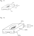
- FIG. 1 is a perspective view illustrating a light emitting device according to the first embodiment.
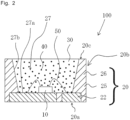
- FIG. 2 is a sectional view illustrating a light emitting device according to the first embodiment.
- FIG. 2 is a sectional view taken along line II-II illustrated in FIG. 1 .
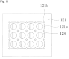
- FIG. 3 is a plan view illustrating a lead frame used in the first embodiment.
- a light emitting device 100 provides an optical reflectivity equal to or greater than 70% at the wavelength between 350 nm and 800 nm after thermal curing, and has a resin package 20 in which a resin part 25 and leads 22 are formed in the substantially same plane in outer side surfaces 20b.
- Plating processing is applied to at least one surface of the bottom surface (an outer bottom surface 20a of the resin package 20) and the upper surface (an inner bottom surface 27a of a concave part 27) of the leads 22.
- plating processing is not applied to the side surfaces of the leads 22 (the outer side surfaces 20b of the resin package 20).
- the resin part 25 occupies a large area in the outer side surfaces 20b of the resin package 20, and leads 22 are exposed from corner parts.
- Parts from which the leads 22 are exposed have the half or less length than the entire surrounding length of the outer side surfaces 20b of the resin package 20.
- notch parts 21a are provided in a lead frame 21 and the lead frame 21 is cut along the notch parts 21a and, therefore, the cut part of the lead frame 21 is a part which is exposed from the resin package 20.
- a light emitting element is preferably used in which a semiconductor such as GaAlN, ZnS, SnSe, SiC, GaP, GaAlAs, AlN, InN, AlInGaP, InGaN, GaN or AlInGaN is formed on a substrate as a light emitting layer, the semiconductor is not limited to these.
- the light emitting element which provides a light emission peak wavelength between 360 nm and 520 nm is preferable, and a light emitting element which provides a light emission peak wavelength between 350 nm and 800 nm can be used. More preferably, the light emitting element 10 has the light emission peak wavelength in the short wavelength region of visible light between 420 nm and 480 nm.
- the resin package has and is made by integrally molding a resin part formed with a thermosetting resin and the leads.
- the resin package provides an optical reflectivity equal to or more than 70% at 350 nm to 800 nm
- the resin package more preferably provides an optical reflectivity equal to or more than 80% at 420 nm to 520 nm.
- the resin package preferably has a high reflectivity in a light emitting area of a light emitting element and a light emitting area of a fluorescent material.
- the resin package has an outer bottom surface, outer side surfaces and an outer upper surface.
- the leads are exposed from the outer side surfaces of the resin package.
- the resin part and leads are formed in the substantially same plane. This substantially same plane means that the resin part and leads are formed in the same cutting step.
- the outer shape of the resin package is not limited to a generally rectangular parallelepiped, and may have a generally cube, generally hexagonal shape or other polygonal shapes. Further, the resin package seen from the outer upper surface side can also adopt a generally triangular shape, generally square shape, generally pentagonal shape or generally hexagonal shape.
- the resin package forms a concave part having an inner bottom surface and an inner side surface.
- the leads are arranged in the inner bottom surface of the concave part.
- the concave part seen form the outer upper surface side can adopt various shapes such as a generally circular shape, generally oval shape, generally square shape, generally polygonal shape or combination of these.
- the concave part preferably has a shape expanding in the opening direction, the concave part may have a cylindrical shape.
- the concave part may be provided with a smooth inclination, the concave part may be formed in a shape which has a minute concavity and convexity in its surface and diffuses light.
- thermosetting resin As the material of the resin part and resin-molded body, a triazine derivative epoxy resin, which is a thermosetting resin is preferably used. Further, the thermosetting resin can contain an acid anhydride, antioxidant, demolding member, light reflecting member, inorganic filler, curing catalyst, light stabilizer, and lubricant.
- the light reflecting member uses titanium dioxide and is filled with 10 to 60% by weight of titanium dioxide.
- the resin package is not limited to the above mode, and is preferably made of at least one selected from the group consisting of an epoxy resin, modified epoxy resin, silicone resin, modified silicone resin, acrylate resin, and urethane resin of a thermosetting resin.
- an epoxy resin, modified epoxy resin, silicone resin or modified silicone resin is preferable.
- a solid epoxy resin composition 100 parts by weight of a clear and colorless mixture in which the epoxy resin consisting of triglycidylisocyanuratem, bisphenol hydride A glycidyl ether and so on, and an acid anhydride consisting of hexahydrophthalic anhydride, 3-methylhexahydrophthalic anhydride, 4-methylhexahydrophthalic anhydride and so on equivalent to the epoxy resin, have been dissolved and mixed, which has been added with: 0.5 parts by weight of DBU (1,8-Diazabicyclo(5,4,0) undecene-7) as a curing accelerator; 1 parts by weight of ethylene glycol as a promoter; 10 parts by weight of a titanium oxide pigment; and 50 parts by weight of a glass fiber, and which has entered the B stage by being heated and partially cured and reacted.
- DBU 1,8-Diazabicyclo(5,4,0) undecene-7
- the lead frame is formed by, for example, punching or etching a metal plate of a flat plate shape.
- a concavity and convexity are formed in a sectional shape of the etched lead frame, so that it is possible to improve adhesion between the lead frame and resin-molded body.
- punching differences in level or concave-convex shapes are formed to improve adhesion between a lead frame and resin-molded body, the effect of improving adhesion is little because the differences in level or concave-convex shapes are small.
- etching can form concave-convex shapes in the entire sectional (etched part) part of the lead frame, so that it is possible to increase a bonding area between the lead frame and resin-molded body and mold a resin package of better adhesion.
- the lead frame is formed using an electrical good conductor such as iron, phosphor bronze or a copper alloy. Further, to increase the reflectivity with respect to light from the light emitting element, metal plating using silver, aluminum, copper, gold or the like can be applied to the lead frame. Although metal plating is preferably is applied to the lead frame before the lead frame is sandwiched by the upper mold and lower mold, that is, for example, after the notch parts are provided or etching processing is performed, metal plating can also be applied to the lead frame before the lead frame is integrally molded with the thermosetting resin.
- an electrical good conductor such as iron, phosphor bronze or a copper alloy.
- a fluorescent material may be a material which absorbs light from the light emitting element, and converts the wavelengths into light of a different wavelength.
- the fluorescent material is preferably selected from, for example, at least any one of a nitride phosphor, oxynitride phosphor or sialon phosphor mainly activated by a lanthanoid element such as Eu or Ce, alkaline-earth halogen apatite phosphor, alkaline-earth metal boric acid halogen phosphor, alkaline-earth metal aluminate phosphor, alkaline-earth silicate, alkaline-earth sulfide, alkaline-earth thiogallate, alkaline-earth silicon nitride or germanate mainly activated by a lanthanoid element such as Eu or a transition metal such as Mn, rare-earth aluminate or rare-earth silicon nitride mainly activated by a lanthanoi
- the nitride phosphor mainly activated by a lanthanoid element such as Eu or Ce includes, for example, M 2 Si 5 N 8 :Eu or MAlSiN 3 :Eu (where M is at least one or more selected from Sr, Ca, Ba, Mg and Zn). Further, the nitride phosphor also includes MSi 7 N 10 :Eu, M 1.8 Si 5 O 0.2 N 8 :Eu or M 0.9 Si 7 O 0.1 N 10 :Eu in addition to M 2 Si 5 N 8 :Eu (where M is at least one or more selected from Sr, Ca, Ba, Mg and Zn).
- the oxynitride phosphor mainly activated by a lanthanoid element such as Eu or Ce includes, for example, MSi 2 O 2 N 2 :Eu (where M is at least one or more selected from Sr, Ca, Ba, Mg and Zn).
- the alkaline-earth halogen apatite phosphor mainly activated by a lanthanoid element such as Eu or a transition metal such as Mn includes, for example, M 5 (PO 4 ) 3 X:R (M is at least one or more selected from Sr, Ca, Ba, Mg and Zn, X is at least one or more selected from F, Cl, Br and I, and R is at least one or more selected from Eu, Mn, Eu and Mn).
- the alkaline-earth metal boric acid halogen phosphor includes, for example, M 2 B 5 O 9 X:R (M is at least one or more selected from Sr, Ca, Ba, Mg and Zn, X is at least one or more selected from F, Cl, Br and I, and R is at least one or more selected from Eu, Mn, Eu and Mn).
- these phosphors can realize blue, green, yellow and red and, in addition, tinges such as turquoise, greenish yellow and orange which are intermediate colors of blue, green, yellow and red.
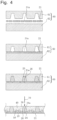
- the method for manufacturing a light emitting device includes the steps of sandwiching the lead frame 21 provided with the notch parts 21a by means of an upper mold 61 and a lower mold 62, transfer-molding a thermosetting resin 23 containing the light reflecting material 26, in a mold 60 sandwiched by the upper mold 61 and the lower mold 62 to form a resin-molded body 24 in the lead frame 21, and cutting the resin-molded body 24 and lead frame 21 along the notch parts 21a.
- the upper mold 61 has a main body part of a flat plate which forms an upper part of the upper mold, an outer wall part which is formed in a frame shape from end parts of the main body, a plurality of projecting parts which project from the main body part, and an inlet which penetrates part of the outer wall part in the horizontal direction.
- the projecting parts contact the lead frame 21 upon transfer-molding, and can form an exposed part from which part of the lead frame 21 is exposed from the resin-molded body 24 by preventing the thermosetting resin 23 from flowing in the contacting parts.
- the projecting parts project downward from the main body part, and are formed by being surrounded by the outer wall.
- the parts of the projecting parts contacting the lead frame 21 are formed flat.
- the projecting parts are preferably formed in one direction at equal intervals, and the projecting parts are preferably formed at equal intervals in a direction 90 degrees from the one direction of each projecting part.
- a pin insertion hole which penetrates the main body part is formed in the upper part of the upper mold 61.
- the pin insertion hole is used for insertion of the pin when the resin-molded body 24 is demolded from the upper mold 61.
- the lead frame 21 provided with the notch parts 21a is sandwiched by the upper mold 61 and lower mold 62.
- space is provided in the mold 60.
- thermosetting resin 23 containing the light reflecting material 26 is transfer-molded in the mold sandwiched by the upper mold 61 and lower mold 62, and the thermosetting resin 23 containing the light reflecting material 26 is injected through the inlet to the space provided in the mold 60 which forms the resin-molded body 24 on the lead frame 21 and is applied a predetermined temperature and pressure to transfer-mold.
- the lead frame 21 near the notch parts 21a are sandwiched by the upper mold 61 and lower mold 62, so that, when the thermosetting resin 23 is transfer-molded, it is possible to prevent flip-flop of the lead frame 21 and reduce burrs in the inner bottom surface 27a of the concave part 27.
- the pin is inserted in the pin inserting part to remove the resin-molded body 24 from the upper mold 61.
- the resin-molded body 24 is temporarily cured by being applied a predetermined temperature in the mold 60, then is removed from the mold 60 and is finally cured by being applied a higher temperature than temporary curing.
- the light emitting element 10 is placed on the lead frame 21 of the inner bottom surface 27a of the concave part 27 formed in the resin-molded body 24 to electrically connect with the lead frame 21 through the wires 50.
- the resin-molded body 24 can be placed after the resin-molded body 24 is removed from the mold 60, or the light emitting element 10 may be placed on the resin package 20 obtained by cutting and singulating the resin-molded body 24. Further, the light emitting elements may be faced down and mounted without using the wires.
- the sealing member 30 containing the fluorescent material 40 is filled and cured in the concave part 27.
- FIG. 9 is a perspective view illustrating the light emitting device according to the third embodiment.
- FIG. 10 is a plan view illustrating a lead frame used in the third embodiment. Description of some configurations employing the substantially same configuration as the light emitting device according to the first embodiment will be omitted where necessary.
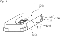
- the light emitting device 100 has the light emitting element 10, and the resin package 20 in which the resin part 25 containing the light reflecting material 26 and the leads 22 are integrally molded.
- the light emitting element 10 is a nitride semiconductor light emitting element which emits blue light with the light emission peak wavelength at 450 nm.
- the resin package 20 has a generally rectangular parallelepiped shape having a mortar-shaped concave part 27.
- the size of the resin package 20 is 35 mm long, 35 mm wide and 0.8 mm high, and a substantially diameter on the outer upper surface 20c side of the concave part 27 is 2.9 mm, a substantially diameter of the inner bottom surface 27a is 2.6 mm and the depth is 0.6 mm.
- the thickness of the lead 22 is 0.2 mm.
Landscapes
- Engineering & Computer Science (AREA)
- Manufacturing & Machinery (AREA)
- Mechanical Engineering (AREA)
- Led Device Packages (AREA)
- Microelectronics & Electronic Packaging (AREA)
- Lead Frames For Integrated Circuits (AREA)
- Physics & Mathematics (AREA)
- Geometry (AREA)
Priority Applications (1)
| Application Number | Priority Date | Filing Date | Title |
|---|---|---|---|
| EP24184101.4A EP4427906A3 (en) | 2008-09-03 | 2009-08-27 | Method of manufacturing a plurality of light emitting devices and resulting light emitting device |
Applications Claiming Priority (4)
| Application Number | Priority Date | Filing Date | Title |
|---|---|---|---|
| JP2008225408A JP5217800B2 (ja) | 2008-09-03 | 2008-09-03 | 発光装置、樹脂パッケージ、樹脂成形体並びにこれらの製造方法 |
| EP17182766.0A EP3267494B1 (en) | 2008-09-03 | 2009-08-27 | Light emitting device and method for manufacturing a plurality of light emitting devices |
| EP09811246.9A EP2325901B1 (en) | 2008-09-03 | 2009-08-27 | Method for manufacturing a resin package |
| PCT/JP2009/004170 WO2010026716A1 (ja) | 2008-09-03 | 2009-08-27 | 発光装置、樹脂パッケージ、樹脂成形体並びにこれらの製造方法 |
Related Parent Applications (3)
| Application Number | Title | Priority Date | Filing Date |
|---|---|---|---|
| EP09811246.9A Division EP2325901B1 (en) | 2008-09-03 | 2009-08-27 | Method for manufacturing a resin package |
| EP17182766.0A Division EP3267494B1 (en) | 2008-09-03 | 2009-08-27 | Light emitting device and method for manufacturing a plurality of light emitting devices |
| EP17182766.0A Division-Into EP3267494B1 (en) | 2008-09-03 | 2009-08-27 | Light emitting device and method for manufacturing a plurality of light emitting devices |
Related Child Applications (1)
| Application Number | Title | Priority Date | Filing Date |
|---|---|---|---|
| EP24184101.4A Division EP4427906A3 (en) | 2008-09-03 | 2009-08-27 | Method of manufacturing a plurality of light emitting devices and resulting light emitting device |
Publications (2)
| Publication Number | Publication Date |
|---|---|
| EP3598509A1 EP3598509A1 (en) | 2020-01-22 |
| EP3598509B1 true EP3598509B1 (en) | 2024-07-10 |
Family
ID=41796902
Family Applications (4)
| Application Number | Title | Priority Date | Filing Date |
|---|---|---|---|
| EP19189739.6A Active EP3598509B1 (en) | 2008-09-03 | 2009-08-27 | Method of manufacturing a plurality of light emitting devices and resulting light emitting device |
| EP17182766.0A Active EP3267494B1 (en) | 2008-09-03 | 2009-08-27 | Light emitting device and method for manufacturing a plurality of light emitting devices |
| EP24184101.4A Withdrawn EP4427906A3 (en) | 2008-09-03 | 2009-08-27 | Method of manufacturing a plurality of light emitting devices and resulting light emitting device |
| EP09811246.9A Active EP2325901B1 (en) | 2008-09-03 | 2009-08-27 | Method for manufacturing a resin package |
Family Applications After (3)
| Application Number | Title | Priority Date | Filing Date |
|---|---|---|---|
| EP17182766.0A Active EP3267494B1 (en) | 2008-09-03 | 2009-08-27 | Light emitting device and method for manufacturing a plurality of light emitting devices |
| EP24184101.4A Withdrawn EP4427906A3 (en) | 2008-09-03 | 2009-08-27 | Method of manufacturing a plurality of light emitting devices and resulting light emitting device |
| EP09811246.9A Active EP2325901B1 (en) | 2008-09-03 | 2009-08-27 | Method for manufacturing a resin package |
Country Status (9)
| Country | Link |
|---|---|
| US (11) | US8530250B2 (enExample) |
| EP (4) | EP3598509B1 (enExample) |
| JP (1) | JP5217800B2 (enExample) |
| KR (10) | KR101763086B1 (enExample) |
| CN (4) | CN105576091B (enExample) |
| BR (1) | BRPI0918071B1 (enExample) |
| DE (1) | DE202009019173U1 (enExample) |
| TW (7) | TW202504036A (enExample) |
| WO (1) | WO2010026716A1 (enExample) |
Families Citing this family (137)
| Publication number | Priority date | Publication date | Assignee | Title |
|---|---|---|---|---|
| JP5217800B2 (ja) | 2008-09-03 | 2013-06-19 | 日亜化学工業株式会社 | 発光装置、樹脂パッケージ、樹脂成形体並びにこれらの製造方法 |
| DE102009032253B4 (de) | 2009-07-08 | 2022-11-17 | OSRAM Opto Semiconductors Gesellschaft mit beschränkter Haftung | Elektronisches Bauteil |
| KR101186648B1 (ko) * | 2009-12-21 | 2012-09-28 | 서울반도체 주식회사 | Led 패키지 및 그의 제조 방법 |
| WO2011122665A1 (ja) | 2010-03-30 | 2011-10-06 | 大日本印刷株式会社 | Led用リードフレームまたは基板、半導体装置、およびled用リードフレームまたは基板の製造方法 |
| WO2011125753A1 (ja) | 2010-04-02 | 2011-10-13 | 株式会社カネカ | 硬化性樹脂組成物、硬化性樹脂組成物タブレット、成形体、半導体のパッケージ、半導体部品及び発光ダイオード |
| DE102010029368B4 (de) | 2010-05-27 | 2026-02-19 | OSRAM Opto Semiconductors Gesellschaft mit beschränkter Haftung | Elektronische Anordnung |
| JP5721969B2 (ja) * | 2010-06-11 | 2015-05-20 | 日東電工株式会社 | 光半導体装置のリフレクタ用エポキシ樹脂組成物およびそれを用いて得られる光半導体装置用リードフレーム、ならびに光半導体装置 |
| JP5871174B2 (ja) * | 2010-07-16 | 2016-03-01 | 大日本印刷株式会社 | Led用リードフレームまたは基板、半導体装置、およびled用リードフレームまたは基板の製造方法 |
| EP2613369B1 (en) * | 2010-09-03 | 2020-04-08 | Nichia Corporation | Light emitting device and method for manufacturing same |
| US9018653B2 (en) | 2010-09-03 | 2015-04-28 | Nichia Corporation | Light emitting device, circuit board, packaging array for light emitting device, and method for manufacturing packaging array for light emitting device |
| US9461207B2 (en) * | 2010-09-03 | 2016-10-04 | Nichia Corporation | Light emitting device, and package array for light emitting device |
| JP2012069885A (ja) * | 2010-09-27 | 2012-04-05 | Sanken Electric Co Ltd | 発光ダイオードの製造方法、発光ダイオード |
| US8691890B2 (en) * | 2010-10-22 | 2014-04-08 | Panasonic Corporation | Unsaturated polyester resin composition for use in LED reflector, and LED reflector and LED luminaire using said composition |
| US8933548B2 (en) | 2010-11-02 | 2015-01-13 | Dai Nippon Printing Co., Ltd. | Lead frame for mounting LED elements, lead frame with resin, method for manufacturing semiconductor devices, and lead frame for mounting semiconductor elements |
| EP2639841B1 (en) | 2010-11-11 | 2019-07-24 | Nichia Corporation | Light-emitting device, and method for manufacturing circuit board |
| JP5733743B2 (ja) * | 2010-12-15 | 2015-06-10 | 日東電工株式会社 | 光半導体装置 |
| JP2014038876A (ja) * | 2010-12-15 | 2014-02-27 | Panasonic Corp | 半導体発光装置 |
| JP5743184B2 (ja) * | 2011-01-12 | 2015-07-01 | 大日本印刷株式会社 | 半導体装置およびその製造方法ならびに照明装置 |
| TW201250964A (en) * | 2011-01-27 | 2012-12-16 | Dainippon Printing Co Ltd | Resin-attached lead frame, method for manufacturing same, and lead frame |
| JP5823416B2 (ja) * | 2011-02-09 | 2015-11-25 | 株式会社東芝 | 白色光源およびそれを用いた白色光源システム |
| CN103460416B (zh) | 2011-02-10 | 2016-11-09 | 日亚化学工业株式会社 | 发光装置、发光装置的制造方法及封装阵列 |
| JP5834467B2 (ja) * | 2011-04-27 | 2015-12-24 | 日亜化学工業株式会社 | 発光装置 |
| DE102011075032A1 (de) * | 2011-04-29 | 2012-10-31 | Osram Ag | Leuchtvorrichtung und Verfahren zum Herstellen einer Leuchtvorrichtung |
| KR101092015B1 (ko) * | 2011-05-03 | 2011-12-08 | 주식회사 네패스신소재 | 열경화형 광반사용 수지 조성물, 이의 제조 방법, 이로부터 제조된 광반도체 소자 탑재용 반사판, 및 이를 포함하는 광반도체 장치 |
| JP2014517110A (ja) * | 2011-05-18 | 2014-07-17 | 株式會社ネペスエーエムシー | 熱硬化型光反射用樹脂組成物及びその製造方法、熱硬化型光反射用樹脂組成物によって製造された光半導体素子搭載用反射板及びそれを含む光半導体装置 |
| CN102800783A (zh) * | 2011-05-25 | 2012-11-28 | 宏齐科技股份有限公司 | 具有对称反射框架的发光二极管封装结构及其制作方法 |
| JP5753446B2 (ja) * | 2011-06-17 | 2015-07-22 | 株式会社東芝 | 半導体発光装置の製造方法 |
| US8878215B2 (en) * | 2011-06-22 | 2014-11-04 | Lg Innotek Co., Ltd. | Light emitting device module |
| JP5527286B2 (ja) * | 2011-06-29 | 2014-06-18 | 豊田合成株式会社 | 発光装置 |
| JP2013038254A (ja) * | 2011-08-09 | 2013-02-21 | Fusheng Industrial Co Ltd | 発光ダイオードの熱硬化性樹脂フレームの製造方法 |
| JP5893868B2 (ja) | 2011-08-12 | 2016-03-23 | シャープ株式会社 | 発光装置 |
| JP2013041950A (ja) | 2011-08-12 | 2013-02-28 | Sharp Corp | 発光装置 |
| TWI426628B (zh) * | 2011-08-30 | 2014-02-11 | 復盛精密工業股份有限公司 | 發光二極體的支架結構及其製作方法(一) |
| JP5505735B2 (ja) * | 2011-09-22 | 2014-05-28 | 復盛精密工業股▲ふん▼有限公司 | 発光ダイオードの支持フレーム構造およびその製作方法(二) |
| US8796052B2 (en) * | 2012-02-24 | 2014-08-05 | Intersil Americas LLC | Optoelectronic apparatuses with post-molded reflector cups and methods for manufacturing the same |
| CN103325889A (zh) * | 2012-03-19 | 2013-09-25 | 展晶科技(深圳)有限公司 | 发光二极管封装方法 |
| TWI488341B (zh) * | 2012-04-11 | 2015-06-11 | 光寶電子(廣州)有限公司 | 連板料片、發光二極體封裝品及發光二極體燈條 |
| CN103367344B (zh) * | 2012-04-11 | 2016-04-27 | 光宝电子(广州)有限公司 | 连板料片、发光二极管封装品及发光二极管灯条 |
| TWI447961B (zh) * | 2012-04-16 | 2014-08-01 | 隆達電子股份有限公司 | 發光二極體封裝體 |
| CN103378226A (zh) | 2012-04-25 | 2013-10-30 | 展晶科技(深圳)有限公司 | 发光二极管的制造方法 |
| CN103378265A (zh) * | 2012-04-28 | 2013-10-30 | 展晶科技(深圳)有限公司 | 发光模组载板的制造方法 |
| JP2013239540A (ja) * | 2012-05-14 | 2013-11-28 | Shin Etsu Chem Co Ltd | 光半導体装置用基板とその製造方法、及び光半導体装置とその製造方法 |
| TWI497779B (zh) * | 2012-07-11 | 2015-08-21 | 復盛精密工業股份有限公司 | 發光二極體的支架結構製作方法(三) |
| KR20140020446A (ko) * | 2012-08-08 | 2014-02-19 | 삼성디스플레이 주식회사 | 백라이트 어셈블리 및 이를 갖는 표시 장치 |
| JP2014060343A (ja) * | 2012-09-19 | 2014-04-03 | Sanken Electric Co Ltd | 発光ダイオードの製造方法、発光ダイオード |
| DE102012109139A1 (de) * | 2012-09-27 | 2014-03-27 | Osram Opto Semiconductors Gmbh | Gehäuse für ein optoelektronisches Bauelement, Elektronische Baugruppe, Verfahren zum Herstellen von Gehäusen und Verfahren zum Herstellen elektronischer Baugruppen |
| NL2010379C2 (nl) * | 2013-03-01 | 2014-09-03 | Besi Netherlands B V | Mal, drager met te omhullen elektronische componenten, drager met omhulde elektronische componenten, gesepareerd omhulde elektronisch component en werkwijze voor het omhullen van elektronische componenten. |
| JP6131664B2 (ja) | 2013-03-25 | 2017-05-24 | 日亜化学工業株式会社 | 発光装置の製造方法および発光装置 |
| DE102013206963A1 (de) | 2013-04-17 | 2014-11-06 | Osram Opto Semiconductors Gmbh | Optoelektronisches Bauelement und Verfahren zu seiner Herstellung |
| JP2014216622A (ja) * | 2013-04-30 | 2014-11-17 | 日亜化学工業株式会社 | 発光装置の製造方法 |
| TW201517323A (zh) | 2013-08-27 | 2015-05-01 | Glo公司 | 模製發光二極體封裝及其製造方法 |
| US9142745B2 (en) | 2013-08-27 | 2015-09-22 | Glo Ab | Packaged LED device with castellations |
| US8999737B2 (en) | 2013-08-27 | 2015-04-07 | Glo Ab | Method of making molded LED package |
| CN104681690A (zh) * | 2013-12-03 | 2015-06-03 | 复盛精密工业股份有限公司 | 侧向型发光二极管的支架结构 |
| JP6237174B2 (ja) | 2013-12-05 | 2017-11-29 | 日亜化学工業株式会社 | 発光装置 |
| DE102013225552A1 (de) * | 2013-12-11 | 2015-06-11 | Osram Opto Semiconductors Gmbh | Optoelektronisches Bauelement |
| JP6847661B2 (ja) * | 2014-01-08 | 2021-03-24 | ルミレッズ ホールディング ベーフェー | 発光デバイス及びその形成方法 |
| JP6392654B2 (ja) * | 2014-02-04 | 2018-09-19 | エイブリック株式会社 | 光センサ装置 |
| DE102014103942B4 (de) * | 2014-03-21 | 2024-05-02 | OSRAM Opto Semiconductors Gesellschaft mit beschränkter Haftung | Verfahren zur Herstellung eines Gehäuses für ein elektronisches Bauelement und eines elektronischen Bauelements, Gehäuse für ein elektronisches Bauelement und elektronisches Bauelement |
| JP6410083B2 (ja) * | 2014-07-31 | 2018-10-24 | シーシーエス株式会社 | Led実装用基板、led |
| KR20160028014A (ko) | 2014-09-02 | 2016-03-11 | 삼성전자주식회사 | 반도체 소자 패키지 제조방법 |
| JP6477328B2 (ja) * | 2014-09-29 | 2019-03-06 | 日亜化学工業株式会社 | パッケージの製造方法及び発光装置の製造方法、並びにパッケージ及び発光装置 |
| US9640743B2 (en) | 2014-09-29 | 2017-05-02 | Nichia Corporation | Method for manufacturing package, method for manufacturing light emitting device, package and light emitting device |
| DE102014116133B4 (de) | 2014-11-05 | 2023-03-09 | OSRAM Opto Semiconductors Gesellschaft mit beschränkter Haftung | Optoelektronisches Bauelement, Verfahren zum Herstellen eines optoelektronischen Bauelements und Verfahren zum Herstellen einer optoelektronischen Anordnung |
| JP6458471B2 (ja) * | 2014-12-04 | 2019-01-30 | 株式会社カネカ | 発光素子実装用リードフレーム、これを用いた発光素子実装用樹脂成型体及び表面実装型発光装置 |
| JP6428245B2 (ja) * | 2014-12-19 | 2018-11-28 | 日亜化学工業株式会社 | 発光装置 |
| JP2015159324A (ja) * | 2015-04-30 | 2015-09-03 | 大日本印刷株式会社 | リフレクタ付きled用リードフレーム及びそれを用いた半導体装置の製造方法 |
| JP2015149509A (ja) * | 2015-05-11 | 2015-08-20 | 大日本印刷株式会社 | 半導体装置およびその製造方法ならびに照明装置 |
| WO2016188566A1 (en) * | 2015-05-26 | 2016-12-01 | Osram Opto Semiconductors Gmbh | Optoelectronic package device and method for producing the same |
| JP2015195389A (ja) * | 2015-06-17 | 2015-11-05 | 大日本印刷株式会社 | 半導体装置およびその製造方法 |
| JP2017027991A (ja) * | 2015-07-16 | 2017-02-02 | 大日本印刷株式会社 | 樹脂付きリードフレーム、樹脂付きリードフレームの多面付け体、光半導体装置、光半導体装置の多面付け体、樹脂付きリードフレーム用金型 |
| JP6135721B2 (ja) * | 2015-08-10 | 2017-05-31 | 大日本印刷株式会社 | 樹脂付リードフレームおよびその製造方法、ならびに半導体装置およびその製造方法 |
| TWI587548B (zh) * | 2015-09-07 | 2017-06-11 | 隆達電子股份有限公司 | 發光二極體封裝件 |
| DE102015115824A1 (de) * | 2015-09-18 | 2017-03-23 | Osram Opto Semiconductors Gmbh | Optoelektronisches Bauelement |
| US10366948B2 (en) * | 2016-03-17 | 2019-07-30 | Rohm Co., Ltd. | Semiconductor device and method for manufacturing the same |
| US10808103B2 (en) * | 2016-05-31 | 2020-10-20 | Mitsubishi Gas Chemical Company, Inc. | Resin composition, laminate including the resin composition, semiconductor wafer with resin composition layer, substrate for mounting semiconductor with resin composition layer, and semiconductor device including the semiconductor wafer with resin composition layer |
| JP6724634B2 (ja) * | 2016-07-28 | 2020-07-15 | 日亜化学工業株式会社 | 発光装置の製造方法 |
| JP6837314B2 (ja) * | 2016-11-01 | 2021-03-03 | 旭化成エレクトロニクス株式会社 | 半導体装置 |
| WO2018108676A1 (en) | 2016-12-13 | 2018-06-21 | Lumileds Holding B.V. | Arrangement of leds on a leadframe |
| TWI629431B (zh) * | 2017-02-17 | 2018-07-11 | 隆達電子股份有限公司 | 框架、應用其的發光裝置以及應用其的發光裝置的製作方法 |
| US9991194B1 (en) * | 2017-04-18 | 2018-06-05 | Ubotic Company Limited | Sensor package and method of manufacture |
| CN106935694A (zh) * | 2017-04-20 | 2017-07-07 | 江苏稳润光电科技有限公司 | 一种csp led封装方法 |
| CN106887505B (zh) * | 2017-04-24 | 2019-07-16 | 芜湖聚飞光电科技有限公司 | 一种单面发光芯片级led的制作方法 |
| US10153416B1 (en) | 2017-05-23 | 2018-12-11 | Radiant Choice Limited | Package body and light emitting device using same |
| US10270020B2 (en) | 2017-06-20 | 2019-04-23 | Lextar Electronics Corporation | LED package structure |
| JP7248379B2 (ja) * | 2017-07-24 | 2023-03-29 | 日亜化学工業株式会社 | 発光装置及びその製造方法 |
| US10892211B2 (en) * | 2017-08-09 | 2021-01-12 | Semtech Corporation | Side-solderable leadless package |
| JP6909976B2 (ja) * | 2017-09-07 | 2021-07-28 | 日亜化学工業株式会社 | 発光装置 |
| JP6637003B2 (ja) * | 2017-09-08 | 2020-01-29 | サンコール株式会社 | バスバーアッセンブリ |
| JP6879172B2 (ja) * | 2017-11-10 | 2021-06-02 | 日亜化学工業株式会社 | 発光装置 |
| DE102017128457A1 (de) | 2017-11-30 | 2019-06-06 | Osram Opto Semiconductors Gmbh | Herstellung optoelektronischer bauelemente |
| US10862015B2 (en) | 2018-03-08 | 2020-12-08 | Samsung Electronics., Ltd. | Semiconductor light emitting device package |
| JP6879262B2 (ja) | 2018-05-08 | 2021-06-02 | 日亜化学工業株式会社 | 発光装置 |
| CN110233199A (zh) * | 2018-08-31 | 2019-09-13 | 深圳市聚飞光电股份有限公司 | Led支架及其制作方法、led发光器件、发光装置 |
| US11056615B2 (en) * | 2018-09-28 | 2021-07-06 | Nichia Corporation | Method for manufacturing light emitting module with concave surface light guide plate |
| CN112586098B (zh) * | 2018-09-28 | 2021-09-21 | 三井金属矿业株式会社 | 多层布线板的制造方法 |
| US11056624B2 (en) * | 2018-10-31 | 2021-07-06 | Nichia Corporation | Method of manufacturing package and method of manufacturing light-emitting device |
| JP6717361B2 (ja) * | 2018-11-27 | 2020-07-01 | 日亜化学工業株式会社 | 発光装置及びその製造方法 |
| US10971650B2 (en) | 2019-07-29 | 2021-04-06 | Lextar Electronics Corporation | Light emitting device |
| US11152540B2 (en) | 2019-07-29 | 2021-10-19 | Lextar Electronics Corporation | Light emitting diode structure and method of manufacturing thereof |
| CN112445024B (zh) * | 2019-09-03 | 2024-03-22 | 纬联电子科技(中山)有限公司 | 显示器及其背光模块与灯源支架 |
| JP7339517B2 (ja) * | 2019-09-12 | 2023-09-06 | 日亜化学工業株式会社 | 発光装置の製造方法および発光装置 |
| US11038088B2 (en) | 2019-10-14 | 2021-06-15 | Lextar Electronics Corporation | Light emitting diode package |
| JP7348521B2 (ja) | 2019-12-24 | 2023-09-21 | 日亜化学工業株式会社 | 発光装置 |
| EP3848981A1 (en) * | 2020-01-10 | 2021-07-14 | Lumileds Holding B.V. | Led module, mold and method for manufacturing the same |
| JP7396057B2 (ja) * | 2020-01-14 | 2023-12-12 | オムロン株式会社 | スイッチの製造方法及び光学ユニットの製造方法 |
| DE102020107409B4 (de) * | 2020-03-18 | 2023-11-02 | OSRAM Opto Semiconductors Gesellschaft mit beschränkter Haftung | Gehäuse für ein optoelektronisches halbleiterbauelement und optoelektronisches halbleiterbauelement |
| JP7260793B2 (ja) | 2020-03-27 | 2023-04-19 | 日亜化学工業株式会社 | 発光装置 |
| US11677050B2 (en) | 2020-05-29 | 2023-06-13 | Nichia Corporation | Light emitting device emitting light bright in both scotopic vision and photipic vision |
| US20210399041A1 (en) * | 2020-06-18 | 2021-12-23 | Seoul Semiconductor Co., Ltd. | Light emitting module having a plurality of unit pixels, method of fabricating the same, and displaying apparatus having the same |
| TWI838548B (zh) * | 2020-06-24 | 2024-04-11 | 方略電子股份有限公司 | 發光裝置 |
| WO2022027470A1 (zh) * | 2020-08-06 | 2022-02-10 | 深圳市汇顶科技股份有限公司 | 一种芯片及芯片封装方法、电子设备 |
| CN112248359A (zh) * | 2020-09-28 | 2021-01-22 | 徐君东 | 一种定向反光膜的制作工艺 |
| CN112838153A (zh) * | 2021-02-02 | 2021-05-25 | 东莞市华彩威科技有限公司 | 一种led灯串、制造方法以及用于该led灯串中的led器件 |
| TWI765569B (zh) * | 2021-02-08 | 2022-05-21 | 健策精密工業股份有限公司 | 導線架結構及其製造方法 |
| CN114914351A (zh) * | 2021-02-08 | 2022-08-16 | 健策精密工业股份有限公司 | 导线架结构及其制造方法 |
| JP7502650B2 (ja) | 2021-04-26 | 2024-06-19 | 日亜化学工業株式会社 | 発光装置、灯具及び街路灯 |
| WO2022230223A1 (ja) | 2021-04-26 | 2022-11-03 | 日亜化学工業株式会社 | 発光装置、灯具及び街路灯 |
| JP7534642B2 (ja) | 2021-04-26 | 2024-08-15 | 日亜化学工業株式会社 | 発光装置、灯具及び街路灯 |
| JP7780072B2 (ja) | 2021-05-26 | 2025-12-04 | 日亜化学工業株式会社 | 酸化物蛍光体、発光装置及び酸化物蛍光体の製造方法 |
| JP7492142B2 (ja) | 2021-07-01 | 2024-05-29 | 日亜化学工業株式会社 | 発光装置、灯具及び照明器具 |
| JP7492143B2 (ja) | 2021-07-02 | 2024-05-29 | 日亜化学工業株式会社 | 発光装置、灯具及び街路灯 |
| JP7752009B2 (ja) | 2021-09-24 | 2025-10-09 | スタンレー電気株式会社 | 発光装置及び発光装置の製造方法 |
| JP2023072239A (ja) | 2021-11-12 | 2023-05-24 | スタンレー電気株式会社 | 発光装置及びリードフレーム |
| JP7835973B2 (ja) | 2021-11-30 | 2026-03-26 | 日亜化学工業株式会社 | 酸化物蛍光体及び発光装置 |
| JP2023082632A (ja) | 2021-12-02 | 2023-06-14 | スタンレー電気株式会社 | 半導体発光装置 |
| US20230335691A1 (en) * | 2021-12-26 | 2023-10-19 | Seoul Viosys Co., Ltd. | Light emitting module and display apparatus having the same |
| US20260071734A1 (en) | 2022-03-31 | 2026-03-12 | Nichia Corporation | Light emitting device and illumination device |
| JP7825503B2 (ja) * | 2022-04-26 | 2026-03-06 | 株式会社小糸製作所 | 照明装置 |
| JP2024001800A (ja) | 2022-06-22 | 2024-01-10 | スタンレー電気株式会社 | 発光装置 |
| JP7705833B2 (ja) * | 2022-08-23 | 2025-07-10 | Towa株式会社 | 半導体部品の製造方法及び半導体部品の製造装置 |
| EP4339509B1 (en) | 2022-09-15 | 2025-03-19 | Nichia Corporation | Vehicle light-emitting device and vehicle lighting device |
| JP2024054731A (ja) | 2022-10-05 | 2024-04-17 | スタンレー電気株式会社 | 半導体発光装置 |
| DE102023104437A1 (de) * | 2023-02-23 | 2024-08-29 | Ams-Osram International Gmbh | Elektronisches Bauelement und Verfahren zum Montieren eines elektronischen Bauelements |
| JP2025005175A (ja) | 2023-06-27 | 2025-01-16 | 日亜化学工業株式会社 | 酸化物蛍光体、及びそれを用いた発光装置 |
| CN120555047A (zh) | 2024-02-27 | 2025-08-29 | 日亚化学工业株式会社 | 氧化物荧光体、发光装置及氧化物荧光体的制造方法 |
| JP2026044359A (ja) | 2024-08-30 | 2026-03-12 | 日亜化学工業株式会社 | 酸化物蛍光体及び発光装置 |
Family Cites Families (168)
| Publication number | Priority date | Publication date | Assignee | Title |
|---|---|---|---|---|
| JPS5469068A (en) | 1977-11-14 | 1979-06-02 | Hitachi Ltd | Semiconductor device and its manufacture |
| JPS60262476A (ja) | 1984-06-08 | 1985-12-25 | Matsushita Electric Ind Co Ltd | 発光素子 |
| JP3088193B2 (ja) | 1992-06-05 | 2000-09-18 | 三菱電機株式会社 | Loc構造を有する半導体装置の製造方法並びにこれに使用するリードフレーム |
| KR0128251Y1 (ko) | 1992-08-21 | 1998-10-15 | 문정환 | 리드 노출형 반도체 조립장치 |
| US5302849A (en) | 1993-03-01 | 1994-04-12 | Motorola, Inc. | Plastic and grid array semiconductor device and method for making the same |
| SG68542A1 (en) * | 1993-06-04 | 1999-11-16 | Seiko Epson Corp | Semiconductor device and manufacturing method thereof |
| JPH0799345A (ja) | 1993-09-28 | 1995-04-11 | Nichia Chem Ind Ltd | 発光ダイオード |
| JPH0837252A (ja) | 1994-07-22 | 1996-02-06 | Nec Corp | 半導体装置 |
| KR100244853B1 (ko) | 1996-12-31 | 2000-02-15 | 구자홍 | 가변형 광원과 그를 이용한 이종 광디스크용광픽업 장치 |
| US6274890B1 (en) * | 1997-01-15 | 2001-08-14 | Kabushiki Kaisha Toshiba | Semiconductor light emitting device and its manufacturing method |
| US6107676A (en) | 1997-03-21 | 2000-08-22 | Rohm Co., Ltd. | Leadframe and a method of manufacturing a semiconductor device by use of it |
| WO1999000852A1 (fr) | 1997-06-27 | 1999-01-07 | Iwasaki Electric Co., Ltd. | Diode electroluminescente de type reflechissante |
| JP3165078B2 (ja) | 1997-07-24 | 2001-05-14 | 協和化成株式会社 | 表面実装部品の製造方法 |
| JP3472450B2 (ja) | 1997-09-04 | 2003-12-02 | シャープ株式会社 | 発光装置 |
| JPH11145523A (ja) | 1997-11-05 | 1999-05-28 | Matsushita Electron Corp | 半導体発光装置 |
| JP3877402B2 (ja) | 1997-11-28 | 2007-02-07 | 三洋電機株式会社 | 半導体装置の製造方法 |
| JP3831504B2 (ja) | 1997-12-25 | 2006-10-11 | 三洋電機株式会社 | リードフレーム |
| JP3877410B2 (ja) * | 1997-12-26 | 2007-02-07 | 三洋電機株式会社 | 半導体装置の製造方法 |
| JPH11214754A (ja) * | 1998-01-28 | 1999-08-06 | Rohm Co Ltd | 半導体発光装置 |
| JPH11220170A (ja) * | 1998-01-29 | 1999-08-10 | Rohm Co Ltd | 発光ダイオード素子 |
| US6184544B1 (en) * | 1998-01-29 | 2001-02-06 | Rohm Co., Ltd. | Semiconductor light emitting device with light reflective current diffusion layer |
| US6252254B1 (en) | 1998-02-06 | 2001-06-26 | General Electric Company | Light emitting device with phosphor composition |
| JP4065051B2 (ja) * | 1998-04-17 | 2008-03-19 | スタンレー電気株式会社 | 表面実装ledとその製造方法 |
| US6498099B1 (en) | 1998-06-10 | 2002-12-24 | Asat Ltd. | Leadless plastic chip carrier with etch back pad singulation |
| JP2000156435A (ja) | 1998-06-22 | 2000-06-06 | Fujitsu Ltd | 半導体装置及びその製造方法 |
| US7332375B1 (en) | 1998-06-24 | 2008-02-19 | Amkor Technology, Inc. | Method of making an integrated circuit package |
| US6143981A (en) | 1998-06-24 | 2000-11-07 | Amkor Technology, Inc. | Plastic integrated circuit package and method and leadframe for making the package |
| US6429583B1 (en) * | 1998-11-30 | 2002-08-06 | General Electric Company | Light emitting device with ba2mgsi2o7:eu2+, ba2sio4:eu2+, or (srxcay ba1-x-y)(a1zga1-z)2sr:eu2+phosphors |
| JP3667125B2 (ja) | 1998-12-07 | 2005-07-06 | 日亜化学工業株式会社 | 光半導体装置とその製造方法 |
| JP3217322B2 (ja) * | 1999-02-18 | 2001-10-09 | 日亜化学工業株式会社 | チップ部品型発光素子 |
| JP3795248B2 (ja) | 1999-03-19 | 2006-07-12 | ローム株式会社 | チップ型発光装置 |
| WO2000079605A1 (fr) | 1999-06-23 | 2000-12-28 | Citizen Electronics Co., Ltd. | Diode électroluminescente |
| JP4390317B2 (ja) | 1999-07-02 | 2009-12-24 | 株式会社ルネサステクノロジ | 樹脂封止型半導体パッケージ |
| JP4183859B2 (ja) | 1999-09-02 | 2008-11-19 | 株式会社アドバンテスト | 半導体基板試験装置 |
| JP2001077235A (ja) | 1999-09-06 | 2001-03-23 | Mitsui High Tec Inc | 半導体素子搭載用基板 |
| US6320251B1 (en) | 2000-01-18 | 2001-11-20 | Amkor Technology, Inc. | Stackable package for an integrated circuit |
| JP3420153B2 (ja) | 2000-01-24 | 2003-06-23 | Necエレクトロニクス株式会社 | 半導体装置及びその製造方法 |
| JP3429246B2 (ja) | 2000-03-21 | 2003-07-22 | 株式会社三井ハイテック | リードフレームパターン及びこれを用いた半導体装置の製造方法 |
| JP2001326295A (ja) | 2000-05-15 | 2001-11-22 | Rohm Co Ltd | 半導体装置および半導体装置製造用フレーム |
| TW511401B (en) * | 2000-09-04 | 2002-11-21 | Sanyo Electric Co | Method for manufacturing circuit device |
| JP4523138B2 (ja) * | 2000-10-06 | 2010-08-11 | ローム株式会社 | 半導体装置およびそれに用いるリードフレーム |
| KR100371567B1 (ko) | 2000-12-08 | 2003-02-07 | 삼성테크윈 주식회사 | Ag 선도금을 이용한 반도체 패키지용 리드프레임 |
| US6424024B1 (en) | 2001-01-23 | 2002-07-23 | Siliconware Precision Industries Co., Ltd. | Leadframe of quad flat non-leaded package |
| US6627482B2 (en) * | 2001-02-09 | 2003-09-30 | Harvatek Corporation | Mass production technique for surface mount optical device with a focusing cup |
| JP4505849B2 (ja) * | 2001-03-28 | 2010-07-21 | 住友電気工業株式会社 | 光通信モジュールの製造方法 |
| JP2002314143A (ja) * | 2001-04-09 | 2002-10-25 | Toshiba Corp | 発光装置 |
| JP2002314138A (ja) | 2001-04-09 | 2002-10-25 | Toshiba Corp | 発光装置 |
| DE10117889A1 (de) | 2001-04-10 | 2002-10-24 | Osram Opto Semiconductors Gmbh | Leiterrahmen und Gehäuse für ein strahlungsemittierendes Bauelement, strahlungsemittierendes Bauelement sowie Verfahren zu dessen Herstellung |
| JP4034073B2 (ja) | 2001-05-11 | 2008-01-16 | 株式会社ルネサステクノロジ | 半導体装置の製造方法 |
| JP3844196B2 (ja) | 2001-06-12 | 2006-11-08 | シチズン電子株式会社 | 発光ダイオードの製造方法 |
| JP2003023134A (ja) | 2001-07-09 | 2003-01-24 | Hitachi Ltd | 半導体装置およびその製造方法 |
| JP4672201B2 (ja) | 2001-07-26 | 2011-04-20 | ローム株式会社 | 半導体装置の製造方法 |
| US6624007B2 (en) | 2001-07-26 | 2003-09-23 | Rohm Co., Ltd. | Method of making leadframe by mechanical processing |
| JP2003110145A (ja) | 2001-09-27 | 2003-04-11 | Harvatek Corp | 発光ダイオード用の翼形表面実装パッケージ |
| CA2358379A1 (en) | 2001-10-05 | 2003-04-05 | Elysium Broadband Inc. | Method and device for preventing signal loss in unterminated bridge taps |
| DE10153259A1 (de) | 2001-10-31 | 2003-05-22 | Osram Opto Semiconductors Gmbh | Optoelektronisches Bauelement |
| JP2003152296A (ja) | 2001-11-15 | 2003-05-23 | Shin Kobe Electric Mach Co Ltd | Led搭載プリント配線板 |
| JP4009097B2 (ja) | 2001-12-07 | 2007-11-14 | 日立電線株式会社 | 発光装置及びその製造方法、ならびに発光装置の製造に用いるリードフレーム |
| JP3939554B2 (ja) | 2002-01-15 | 2007-07-04 | シャープ株式会社 | 半導体用リードフレーム |
| JP2003218398A (ja) | 2002-01-18 | 2003-07-31 | Citizen Electronics Co Ltd | 表面実装型発光ダイオード及びその製造方法 |
| JP2003304000A (ja) | 2002-04-08 | 2003-10-24 | Citizen Electronics Co Ltd | 発光ダイオード用パッケージの製造方法 |
| US7799611B2 (en) | 2002-04-29 | 2010-09-21 | Unisem (Mauritius) Holdings Limited | Partially patterned lead frames and methods of making and using the same in semiconductor packaging |
| TW546799B (en) | 2002-06-26 | 2003-08-11 | Lingsen Precision Ind Ltd | Packaged formation method of LED and product structure |
| DE10237084A1 (de) * | 2002-08-05 | 2004-02-19 | Osram Opto Semiconductors Gmbh | Verfahren zum Herstellen eines elektrischen Leiterrahmens und Verfahren zum Herstellen eines oberflächenmontierbaren Halbleiterbauelements |
| CN100533723C (zh) * | 2002-08-05 | 2009-08-26 | 奥斯兰姆奥普托半导体有限责任公司 | 电引线架的制造方法,表面安装的半导体器件的制造方法和引线架带 |
| JP4059293B2 (ja) | 2002-09-05 | 2008-03-12 | 日亜化学工業株式会社 | 発光装置 |
| TWI292961B (en) | 2002-09-05 | 2008-01-21 | Nichia Corp | Semiconductor device and an optical device using the semiconductor device |
| US6879040B2 (en) | 2002-09-18 | 2005-04-12 | Agilent Technologies, Inc. | Surface mountable electronic device |
| JP4280050B2 (ja) | 2002-10-07 | 2009-06-17 | シチズン電子株式会社 | 白色発光装置 |
| JP3666594B2 (ja) | 2002-10-17 | 2005-06-29 | ローム株式会社 | パッケージ型電子部品におけるリード端子の切断方法 |
| US7692206B2 (en) | 2002-12-06 | 2010-04-06 | Cree, Inc. | Composite leadframe LED package and method of making the same |
| FR2849158B1 (fr) * | 2002-12-20 | 2005-12-09 | Valeo Vision | Module d'eclairage pour projecteur de vehicule |
| JP3910171B2 (ja) | 2003-02-18 | 2007-04-25 | シャープ株式会社 | 半導体発光装置、その製造方法および電子撮像装置 |
| JP2006313943A (ja) * | 2003-02-18 | 2006-11-16 | Sharp Corp | 半導体発光装置、その製造方法および電子撮像装置 |
| JP4341951B2 (ja) | 2003-05-07 | 2009-10-14 | シチズン電子株式会社 | 発光ダイオード及びそのパッケージ構造 |
| US20050133808A1 (en) | 2003-09-11 | 2005-06-23 | Kyocera Corporation | Package for housing light-emitting element, light-emitting apparatus and illumination apparatus |
| US7157744B2 (en) * | 2003-10-29 | 2007-01-02 | M/A-Com, Inc. | Surface mount package for a high power light emitting diode |
| JP4792726B2 (ja) * | 2003-10-30 | 2011-10-12 | 日亜化学工業株式会社 | 半導体素子用支持体の製造方法 |
| US7183588B2 (en) * | 2004-01-08 | 2007-02-27 | Avago Technologies Ecbu Ip (Singapore) Pte. Ltd. | Light emission device |
| US7288797B2 (en) * | 2004-01-20 | 2007-10-30 | Nichia Corporation | Semiconductor light emitting element |
| JP3877732B2 (ja) * | 2004-02-26 | 2007-02-07 | 松下電器産業株式会社 | リードフレームおよびそれを用いた半導体装置およびその半導体装置の製造方法 |
| US20050211991A1 (en) | 2004-03-26 | 2005-09-29 | Kyocera Corporation | Light-emitting apparatus and illuminating apparatus |
| JP2005306952A (ja) | 2004-04-20 | 2005-11-04 | Japan Epoxy Resin Kk | 発光素子封止材用エポキシ樹脂組成物 |
| JP4635471B2 (ja) | 2004-04-22 | 2011-02-23 | ソニー株式会社 | 半導体装置及びその製造方法、半導体装置の実装構造並びにリードフレーム |
| JP2005317661A (ja) | 2004-04-27 | 2005-11-10 | Sharp Corp | 半導体発光装置およびその製造方法 |
| JP2005322804A (ja) | 2004-05-10 | 2005-11-17 | Nitto Denko Corp | 光半導体装置 |
| US7456499B2 (en) | 2004-06-04 | 2008-11-25 | Cree, Inc. | Power light emitting die package with reflecting lens and the method of making the same |
| JP4359195B2 (ja) | 2004-06-11 | 2009-11-04 | 株式会社東芝 | 半導体発光装置及びその製造方法並びに半導体発光ユニット |
| JP2006049442A (ja) | 2004-08-02 | 2006-02-16 | Sharp Corp | 半導体発光装置およびその製造方法 |
| JP4593201B2 (ja) | 2004-08-20 | 2010-12-08 | 日立化成工業株式会社 | チップ部品型発光装置及びそのための配線基板 |
| KR200373718Y1 (ko) | 2004-09-20 | 2005-01-21 | 주식회사 티씨오 | 정전기 방전 충격에 대한 보호 기능이 내장된 고휘도발광다이오드 |
| KR100880757B1 (ko) | 2004-09-22 | 2009-02-02 | 가부시끼가이샤 도시바 | 발광 장치와 그것을 이용한 백 라이트 및 액정 표시 장치 |
| US8816369B2 (en) * | 2004-10-29 | 2014-08-26 | Led Engin, Inc. | LED packages with mushroom shaped lenses and methods of manufacturing LED light-emitting devices |
| JP5060707B2 (ja) | 2004-11-10 | 2012-10-31 | 日立化成工業株式会社 | 光反射用熱硬化性樹脂組成物 |
| JP4329678B2 (ja) | 2004-11-11 | 2009-09-09 | 株式会社デンソー | 半導体装置に用いるリードフレームの製造方法 |
| JP4608294B2 (ja) | 2004-11-30 | 2011-01-12 | 日亜化学工業株式会社 | 樹脂成形体及び表面実装型発光装置並びにそれらの製造方法 |
| KR100638721B1 (ko) | 2005-01-28 | 2006-10-30 | 삼성전기주식회사 | 수지 흐름 개선용 리드 프레임 구조를 갖는 측면형발광다이오드 패키지 |
| JP4651008B2 (ja) * | 2005-02-01 | 2011-03-16 | シチズン電子株式会社 | 発光ダイオード |
| JP2006278427A (ja) | 2005-03-28 | 2006-10-12 | Matsushita Electric Works Ltd | 光結合素子およびそれに用いるリードフレームならびに光結合素子の製造方法 |
| JP4857594B2 (ja) | 2005-04-26 | 2012-01-18 | 大日本印刷株式会社 | 回路部材、及び回路部材の製造方法 |
| JP2006324410A (ja) | 2005-05-18 | 2006-11-30 | Showa Denko Kk | 発光ダイオード封止材用樹脂組成物 |
| JP3952084B2 (ja) * | 2005-05-24 | 2007-08-01 | 株式会社村田製作所 | インサートモールド品の製造方法および製造装置 |
| KR100593945B1 (ko) | 2005-05-30 | 2006-06-30 | 삼성전기주식회사 | 고출력 led 패키지 및 그 제조방법 |
| KR100638868B1 (ko) | 2005-06-20 | 2006-10-27 | 삼성전기주식회사 | 금속 반사 층을 형성한 엘이디 패키지 및 그 제조 방법 |
| JP2007005722A (ja) | 2005-06-27 | 2007-01-11 | Toshiba Corp | 光半導体素子用外囲器およびそれを用いた光半導体装置 |
| JP5392805B2 (ja) | 2005-06-28 | 2014-01-22 | 東レ・ダウコーニング株式会社 | 硬化性オルガノポリシロキサン樹脂組成物および光学部材 |
| JP4739842B2 (ja) | 2005-07-25 | 2011-08-03 | スタンレー電気株式会社 | 表面実装型led |
| EP2768031B1 (en) | 2005-08-04 | 2021-02-17 | Nichia Corporation | Light-emitting device |
| JP4857709B2 (ja) * | 2005-10-25 | 2012-01-18 | 日亜化学工業株式会社 | 発光装置 |
| TWI271835B (en) | 2005-11-07 | 2007-01-21 | High Power Lighting Corp | Packaging structure of high power LED chip and method of manufacturing the same |
| JP2007134376A (ja) | 2005-11-08 | 2007-05-31 | Akita Denshi Systems:Kk | 発光ダイオード装置及びその製造方法 |
| KR100637476B1 (ko) | 2005-11-09 | 2006-10-23 | 알티전자 주식회사 | 측면발광 다이오드 및 그 제조방법 |
| US7943431B2 (en) * | 2005-12-02 | 2011-05-17 | Unisem (Mauritius) Holdings Limited | Leadless semiconductor package and method of manufacture |
| US20070126020A1 (en) | 2005-12-03 | 2007-06-07 | Cheng Lin | High-power LED chip packaging structure and fabrication method thereof |
| WO2007077909A1 (ja) * | 2005-12-28 | 2007-07-12 | Renesas Technology Corp. | 半導体装置の製造方法 |
| JP5232369B2 (ja) * | 2006-02-03 | 2013-07-10 | 日立化成株式会社 | 光半導体素子搭載用パッケージ基板の製造方法およびこれを用いた光半導体装置の製造方法 |
| JP2007297601A (ja) | 2006-04-06 | 2007-11-15 | Hitachi Chem Co Ltd | 光反射用熱硬化性樹脂組成物、これを用いた光半導体素子搭載用基板とその製造方法および光半導体装置 |
| KR100735325B1 (ko) | 2006-04-17 | 2007-07-04 | 삼성전기주식회사 | 발광다이오드 패키지 및 그 제조방법 |
| JP4952233B2 (ja) * | 2006-04-19 | 2012-06-13 | 日亜化学工業株式会社 | 半導体装置 |
| KR100775574B1 (ko) | 2006-04-20 | 2007-11-15 | 알티전자 주식회사 | 고효율 발광 다이오드 패키지 |
| JP2007294506A (ja) | 2006-04-21 | 2007-11-08 | Matsushita Electric Ind Co Ltd | 放熱基板とその製造方法及び、これを用いた発光モジュール及び表示装置 |
| JP4830768B2 (ja) | 2006-05-10 | 2011-12-07 | 日亜化学工業株式会社 | 半導体発光装置及び半導体発光装置の製造方法 |
| WO2007135707A1 (ja) * | 2006-05-18 | 2007-11-29 | Nichia Corporation | 樹脂成形体及び表面実装型発光装置並びにそれらの製造方法 |
| KR20140146210A (ko) | 2006-06-02 | 2014-12-24 | 히타치가세이가부시끼가이샤 | 광반도체소자 탑재용 패키지 및 이것을 이용한 광반도체장치 |
| US8044418B2 (en) | 2006-07-13 | 2011-10-25 | Cree, Inc. | Leadframe-based packages for solid state light emitting devices |
| JP5233186B2 (ja) | 2006-07-25 | 2013-07-10 | 日立化成株式会社 | 熱硬化性光反射用樹脂組成物、これを用いた光半導体素子搭載用基板とその製造方法および光半導体装置 |
| US8092735B2 (en) * | 2006-08-17 | 2012-01-10 | 3M Innovative Properties Company | Method of making a light emitting device having a molded encapsulant |
| US7763478B2 (en) * | 2006-08-21 | 2010-07-27 | Cree, Inc. | Methods of forming semiconductor light emitting device packages by liquid injection molding |
| KR100773350B1 (ko) | 2006-08-29 | 2007-11-05 | 삼성전자주식회사 | 설비의 이상패턴 규명을 위한 기준정보형성방법 및 이를이용한 반도체 제조설비의 모니터링 방법 |
| US7485480B2 (en) | 2006-09-21 | 2009-02-03 | Harvatek Corporation | Method of manufacturing high power light-emitting device package and structure thereof |
| JP5298468B2 (ja) * | 2006-09-26 | 2013-09-25 | 日立化成株式会社 | 熱硬化性光反射用樹脂組成物、これを用いた光半導体素子搭載用基板とその製造方法および光半導体装置 |
| JP5564162B2 (ja) * | 2006-09-29 | 2014-07-30 | フューチャー ライト リミテッド ライアビリティ カンパニー | 発光ダイオード装置 |
| TWI311824B (en) * | 2006-10-02 | 2009-07-01 | Ind Tech Res Inst | Light emitting diode package structure |
| US8088635B2 (en) | 2006-10-17 | 2012-01-03 | C.I. Kasei Company, Limited | Vertical geometry light emitting diode package aggregate and production method of light emitting device using the same |
| JP2008108958A (ja) | 2006-10-26 | 2008-05-08 | C I Kasei Co Ltd | 発光装置および発光装置の製造方法 |
| JP2008103460A (ja) | 2006-10-18 | 2008-05-01 | Sony Corp | 半導体パッケージ及びその製造方法 |
| KR20090088365A (ko) | 2006-11-08 | 2009-08-19 | 씨. 아이. 카세이 가부시기가이샤 | 발광장치와 그 제조방법 |
| JP5023781B2 (ja) | 2006-11-13 | 2012-09-12 | 日亜化学工業株式会社 | 発光装置 |
| CN102408541B (zh) * | 2006-11-15 | 2016-10-05 | 日立化成株式会社 | 光反射用热固化性树脂组合物、及使用了所述树脂组合物的光半导体元件搭载用基板及光半导体装置 |
| JP2008130735A (ja) | 2006-11-20 | 2008-06-05 | C I Kasei Co Ltd | 発光装置の製造方法 |
| JP4961978B2 (ja) | 2006-11-30 | 2012-06-27 | 日亜化学工業株式会社 | 発光装置およびその製造方法 |
| US7679099B2 (en) | 2006-12-04 | 2010-03-16 | Avago Technologies Ecbu Ip (Singapore) Pte. Ltd. | Low thermal resistance high power LED |
| JPWO2008078791A1 (ja) | 2006-12-27 | 2010-04-30 | 昭和電工株式会社 | 発光装置の製造方法 |
| CN101507004B (zh) * | 2006-12-28 | 2011-04-20 | 日亚化学工业株式会社 | 发光装置、封装体、发光装置的制造方法、封装体的制造方法以及封装体制造用模具 |
| JP5168152B2 (ja) * | 2006-12-28 | 2013-03-21 | 日亜化学工業株式会社 | 発光装置 |
| JP5380774B2 (ja) | 2006-12-28 | 2014-01-08 | 日亜化学工業株式会社 | 表面実装型側面発光装置及びその製造方法 |
| JP4872683B2 (ja) | 2007-01-29 | 2012-02-08 | 株式会社デンソー | モールドパッケージの製造方法 |
| JP2008187045A (ja) | 2007-01-30 | 2008-08-14 | Matsushita Electric Ind Co Ltd | 半導体装置用リードフレームとその製造方法、半導体装置 |
| JP5470680B2 (ja) * | 2007-02-06 | 2014-04-16 | 日亜化学工業株式会社 | 発光装置及びその製造方法並びに成形体 |
| JP2008189827A (ja) * | 2007-02-06 | 2008-08-21 | Shin Etsu Chem Co Ltd | 熱硬化性エポキシ樹脂組成物及び半導体装置 |
| JP5608955B2 (ja) | 2007-02-06 | 2014-10-22 | 日亜化学工業株式会社 | 発光装置及びその製造方法並びに発光装置用成形体 |
| US20080255283A1 (en) * | 2007-02-06 | 2008-10-16 | Takayuki Aoki | Thermosetting epoxy resin composition and semiconductor device |
| JP4205135B2 (ja) | 2007-03-13 | 2009-01-07 | シャープ株式会社 | 半導体発光装置、半導体発光装置用多連リードフレーム |
| JP2008262939A (ja) * | 2007-04-10 | 2008-10-30 | Matsushita Electric Ind Co Ltd | リードフレームおよび封止金型および封止方法 |
| TW200843130A (en) * | 2007-04-17 | 2008-11-01 | Wen Lin | Package structure of a surface-mount high-power light emitting diode chip and method of making the same |
| JP2007329502A (ja) | 2007-08-16 | 2007-12-20 | Toshiba Corp | 発光装置 |
| JP4522442B2 (ja) * | 2007-08-20 | 2010-08-11 | 三菱鉛筆株式会社 | 衝撃緩和装置付きノック式筆記具 |
| US7968899B2 (en) * | 2007-08-27 | 2011-06-28 | Avago Technologies Ecbu Ip (Singapore) Pte. Ltd. | LED light source having improved resistance to thermal cycling |
| US8716848B2 (en) | 2008-03-24 | 2014-05-06 | SemiLEDs Optoelectronics Co., Ltd. | LED device with conductive wings and tabs |
| JP3142406U (ja) * | 2008-03-31 | 2008-06-12 | サンケン電気株式会社 | 半導体発光装置及び半導体発光ユニット |
| KR100869376B1 (ko) | 2008-05-20 | 2008-11-19 | 주식회사 정진넥스텍 | 발광다이오드 칩 실장용 리드 프레임 어셈블리와 그의 제조방법 |
| JP2010021259A (ja) | 2008-07-09 | 2010-01-28 | Toshiba Corp | 光半導体装置 |
| JP5217800B2 (ja) * | 2008-09-03 | 2013-06-19 | 日亜化学工業株式会社 | 発光装置、樹脂パッケージ、樹脂成形体並びにこれらの製造方法 |
| US8829685B2 (en) * | 2009-03-31 | 2014-09-09 | Semiconductor Components Industries, Llc | Circuit device having funnel shaped lead and method for manufacturing the same |
| US20120037939A1 (en) * | 2009-04-13 | 2012-02-16 | Youji Urano | Light emitting diode |
| JP5383611B2 (ja) * | 2010-01-29 | 2014-01-08 | 株式会社東芝 | Ledパッケージ |
| JP2013145908A (ja) | 2013-03-06 | 2013-07-25 | Nichia Chem Ind Ltd | 発光装置、樹脂パッケージ、樹脂成形体並びにこれらの製造方法 |
| JP5527450B2 (ja) | 2013-03-06 | 2014-06-18 | 日亜化学工業株式会社 | 発光装置、樹脂パッケージ、樹脂成形体並びにこれらの製造方法 |
-
2008
- 2008-09-03 JP JP2008225408A patent/JP5217800B2/ja active Active
-
2009
- 2009-08-24 TW TW113132889A patent/TW202504036A/zh unknown
- 2009-08-24 TW TW109108764A patent/TWI725777B/zh active
- 2009-08-24 TW TW098128401A patent/TWI525848B/zh active
- 2009-08-24 TW TW106112359A patent/TWI635629B/zh active
- 2009-08-24 TW TW110111023A patent/TWI850544B/zh active
- 2009-08-24 TW TW107119884A patent/TWI726214B/zh active
- 2009-08-24 TW TW104140582A patent/TWI596806B/zh active
- 2009-08-27 KR KR1020167009743A patent/KR101763086B1/ko active Active
- 2009-08-27 KR KR1020187029629A patent/KR102011235B1/ko active Active
- 2009-08-27 CN CN201610048316.7A patent/CN105576091B/zh active Active
- 2009-08-27 KR KR1020227018361A patent/KR102512557B1/ko active Active
- 2009-08-27 KR KR1020117007597A patent/KR101614975B1/ko active Active
- 2009-08-27 KR KR1020217026637A patent/KR102405355B1/ko active Active
- 2009-08-27 WO PCT/JP2009/004170 patent/WO2010026716A1/ja not_active Ceased
- 2009-08-27 BR BRPI0918071-0A patent/BRPI0918071B1/pt active IP Right Grant
- 2009-08-27 EP EP19189739.6A patent/EP3598509B1/en active Active
- 2009-08-27 KR KR1020177008341A patent/KR101909896B1/ko active Active
- 2009-08-27 EP EP17182766.0A patent/EP3267494B1/en active Active
- 2009-08-27 CN CN200980134526.6A patent/CN102144306B/zh active Active
- 2009-08-27 DE DE202009019173.7U patent/DE202009019173U1/de not_active Expired - Lifetime
- 2009-08-27 CN CN201610048719.1A patent/CN105576109B/zh active Active
- 2009-08-27 KR KR1020237009267A patent/KR102677856B1/ko active Active
- 2009-08-27 EP EP24184101.4A patent/EP4427906A3/en not_active Withdrawn
- 2009-08-27 US US12/737,940 patent/US8530250B2/en active Active
- 2009-08-27 KR KR1020207030577A patent/KR102294486B1/ko active Active
- 2009-08-27 KR KR1020197023217A patent/KR102129936B1/ko active Active
- 2009-08-27 KR KR1020207018684A patent/KR102171595B1/ko active Active
- 2009-08-27 CN CN201610048537.4A patent/CN105563728B/zh active Active
- 2009-08-27 EP EP09811246.9A patent/EP2325901B1/en active Active
-
2013
- 2013-08-16 US US13/969,182 patent/US9287476B2/en active Active
-
2015
- 2015-10-30 US US14/928,550 patent/US9537071B2/en active Active
- 2015-10-30 US US14/928,570 patent/US9490411B2/en active Active
-
2016
- 2016-11-23 US US15/360,316 patent/US10115870B2/en active Active
-
2018
- 2018-06-13 US US16/007,954 patent/US10573788B2/en active Active
- 2018-10-02 US US16/150,259 patent/US10700241B2/en active Active
- 2018-10-02 US US16/150,255 patent/US10573789B2/en active Active
-
2020
- 2020-05-26 US US16/883,714 patent/US11094854B2/en active Active
-
2021
- 2021-07-09 US US17/371,943 patent/US12211959B2/en active Active
-
2024
- 2024-12-24 US US19/000,967 patent/US20250133878A1/en active Pending
Also Published As
Similar Documents
| Publication | Publication Date | Title |
|---|---|---|
| US12211959B2 (en) | Light emitting device, resin package, resin-molded body, and methods for manufacturing light emitting device, resin package and resin-molded body | |
| JP2020127026A (ja) | 発光装置の製造方法及び発光装置 | |
| JP6056934B2 (ja) | 発光装置、樹脂パッケージ、樹脂成形体並びにこれらの製造方法 | |
| JP2023088987A (ja) | 発光装置の製造方法及び発光装置 | |
| JP5527450B2 (ja) | 発光装置、樹脂パッケージ、樹脂成形体並びにこれらの製造方法 | |
| JP6797861B2 (ja) | 発光装置の製造方法及び発光装置 | |
| JP6164355B2 (ja) | 発光装置、樹脂パッケージ、樹脂成形体並びにこれらの製造方法 | |
| JP7252503B2 (ja) | 発光装置の製造方法及び発光装置 | |
| JP5825390B2 (ja) | 発光装置、樹脂パッケージ、樹脂成形体並びにこれらの製造方法 | |
| JP2013145908A (ja) | 発光装置、樹脂パッケージ、樹脂成形体並びにこれらの製造方法 | |
| JP6489162B2 (ja) | 樹脂成形体付リードフレーム及びこれの製造方法並びにこれらに用いるリードフレーム |
Legal Events
| Date | Code | Title | Description |
|---|---|---|---|
| PUAI | Public reference made under article 153(3) epc to a published international application that has entered the european phase |
Free format text: ORIGINAL CODE: 0009012 |
|
| STAA | Information on the status of an ep patent application or granted ep patent |
Free format text: STATUS: THE APPLICATION HAS BEEN PUBLISHED |
|
| AC | Divisional application: reference to earlier application |
Ref document number: 2325901 Country of ref document: EP Kind code of ref document: P Ref document number: 3267494 Country of ref document: EP Kind code of ref document: P |
|
| AK | Designated contracting states |
Kind code of ref document: A1 Designated state(s): AT BE BG CH CY CZ DE DK EE ES FI FR GB GR HR HU IE IS IT LI LT LU LV MC MK MT NL NO PL PT RO SE SI SK SM TR |
|
| STAA | Information on the status of an ep patent application or granted ep patent |
Free format text: STATUS: REQUEST FOR EXAMINATION WAS MADE |
|
| 17P | Request for examination filed |
Effective date: 20200722 |
|
| RBV | Designated contracting states (corrected) |
Designated state(s): AT BE BG CH CY CZ DE DK EE ES FI FR GB GR HR HU IE IS IT LI LT LU LV MC MK MT NL NO PL PT RO SE SI SK SM TR |
|
| STAA | Information on the status of an ep patent application or granted ep patent |
Free format text: STATUS: EXAMINATION IS IN PROGRESS |
|
| 17Q | First examination report despatched |
Effective date: 20211116 |
|
| P01 | Opt-out of the competence of the unified patent court (upc) registered |
Effective date: 20230522 |
|
| GRAP | Despatch of communication of intention to grant a patent |
Free format text: ORIGINAL CODE: EPIDOSNIGR1 |
|
| STAA | Information on the status of an ep patent application or granted ep patent |
Free format text: STATUS: GRANT OF PATENT IS INTENDED |
|
| RIC1 | Information provided on ipc code assigned before grant |
Ipc: B29C 45/00 20060101ALN20240205BHEP Ipc: H01L 33/60 20100101ALN20240205BHEP Ipc: B29C 45/14 20060101ALI20240205BHEP Ipc: H01L 23/48 20060101ALI20240205BHEP Ipc: H01L 33/64 20100101ALI20240205BHEP Ipc: H01L 33/62 20100101ALI20240205BHEP Ipc: H01L 33/48 20100101ALI20240205BHEP Ipc: H01L 33/00 20100101AFI20240205BHEP |
|
| INTG | Intention to grant announced |
Effective date: 20240220 |
|
| GRAS | Grant fee paid |
Free format text: ORIGINAL CODE: EPIDOSNIGR3 |
|
| GRAA | (expected) grant |
Free format text: ORIGINAL CODE: 0009210 |
|
| STAA | Information on the status of an ep patent application or granted ep patent |
Free format text: STATUS: THE PATENT HAS BEEN GRANTED |
|
| AC | Divisional application: reference to earlier application |
Ref document number: 2325901 Country of ref document: EP Kind code of ref document: P Ref document number: 3267494 Country of ref document: EP Kind code of ref document: P |
|
| AK | Designated contracting states |
Kind code of ref document: B1 Designated state(s): AT BE BG CH CY CZ DE DK EE ES FI FR GB GR HR HU IE IS IT LI LT LU LV MC MK MT NL NO PL PT RO SE SI SK SM TR |
|
| REG | Reference to a national code |
Ref country code: CH Ref legal event code: EP |
|
| REG | Reference to a national code |
Ref country code: DE Ref legal event code: R096 Ref document number: 602009065305 Country of ref document: DE |
|
| REG | Reference to a national code |
Ref country code: LT Ref legal event code: MG9D |
|
| REG | Reference to a national code |
Ref country code: NL Ref legal event code: MP Effective date: 20240710 |
|
| REG | Reference to a national code |
Ref country code: DE Ref legal event code: R079 Ref document number: 602009065305 Country of ref document: DE Free format text: PREVIOUS MAIN CLASS: H01L0033000000 Ipc: H10H0020000000 |
|
| PG25 | Lapsed in a contracting state [announced via postgrant information from national office to epo] |
Ref country code: PT Free format text: LAPSE BECAUSE OF FAILURE TO SUBMIT A TRANSLATION OF THE DESCRIPTION OR TO PAY THE FEE WITHIN THE PRESCRIBED TIME-LIMIT Effective date: 20241111 |
|
| REG | Reference to a national code |
Ref country code: AT Ref legal event code: MK05 Ref document number: 1702831 Country of ref document: AT Kind code of ref document: T Effective date: 20240710 |
|
| PG25 | Lapsed in a contracting state [announced via postgrant information from national office to epo] |
Ref country code: NL Free format text: LAPSE BECAUSE OF FAILURE TO SUBMIT A TRANSLATION OF THE DESCRIPTION OR TO PAY THE FEE WITHIN THE PRESCRIBED TIME-LIMIT Effective date: 20240710 |
|
| PG25 | Lapsed in a contracting state [announced via postgrant information from national office to epo] |
Ref country code: PT Free format text: LAPSE BECAUSE OF FAILURE TO SUBMIT A TRANSLATION OF THE DESCRIPTION OR TO PAY THE FEE WITHIN THE PRESCRIBED TIME-LIMIT Effective date: 20241111 Ref country code: NL Free format text: LAPSE BECAUSE OF FAILURE TO SUBMIT A TRANSLATION OF THE DESCRIPTION OR TO PAY THE FEE WITHIN THE PRESCRIBED TIME-LIMIT Effective date: 20240710 |
|
| PG25 | Lapsed in a contracting state [announced via postgrant information from national office to epo] |
Ref country code: NO Free format text: LAPSE BECAUSE OF FAILURE TO SUBMIT A TRANSLATION OF THE DESCRIPTION OR TO PAY THE FEE WITHIN THE PRESCRIBED TIME-LIMIT Effective date: 20241010 |
|
| PG25 | Lapsed in a contracting state [announced via postgrant information from national office to epo] |
Ref country code: GR Free format text: LAPSE BECAUSE OF FAILURE TO SUBMIT A TRANSLATION OF THE DESCRIPTION OR TO PAY THE FEE WITHIN THE PRESCRIBED TIME-LIMIT Effective date: 20241011 Ref country code: FI Free format text: LAPSE BECAUSE OF FAILURE TO SUBMIT A TRANSLATION OF THE DESCRIPTION OR TO PAY THE FEE WITHIN THE PRESCRIBED TIME-LIMIT Effective date: 20240710 Ref country code: PL Free format text: LAPSE BECAUSE OF FAILURE TO SUBMIT A TRANSLATION OF THE DESCRIPTION OR TO PAY THE FEE WITHIN THE PRESCRIBED TIME-LIMIT Effective date: 20240710 |
|
| PG25 | Lapsed in a contracting state [announced via postgrant information from national office to epo] |
Ref country code: BG Free format text: LAPSE BECAUSE OF FAILURE TO SUBMIT A TRANSLATION OF THE DESCRIPTION OR TO PAY THE FEE WITHIN THE PRESCRIBED TIME-LIMIT Effective date: 20240710 |
|
| PG25 | Lapsed in a contracting state [announced via postgrant information from national office to epo] |
Ref country code: LV Free format text: LAPSE BECAUSE OF FAILURE TO SUBMIT A TRANSLATION OF THE DESCRIPTION OR TO PAY THE FEE WITHIN THE PRESCRIBED TIME-LIMIT Effective date: 20240710 |
|
| PG25 | Lapsed in a contracting state [announced via postgrant information from national office to epo] |
Ref country code: IS Free format text: LAPSE BECAUSE OF FAILURE TO SUBMIT A TRANSLATION OF THE DESCRIPTION OR TO PAY THE FEE WITHIN THE PRESCRIBED TIME-LIMIT Effective date: 20241110 Ref country code: AT Free format text: LAPSE BECAUSE OF FAILURE TO SUBMIT A TRANSLATION OF THE DESCRIPTION OR TO PAY THE FEE WITHIN THE PRESCRIBED TIME-LIMIT Effective date: 20240710 |
|
| PG25 | Lapsed in a contracting state [announced via postgrant information from national office to epo] |
Ref country code: HR Free format text: LAPSE BECAUSE OF FAILURE TO SUBMIT A TRANSLATION OF THE DESCRIPTION OR TO PAY THE FEE WITHIN THE PRESCRIBED TIME-LIMIT Effective date: 20240710 |
|
| PG25 | Lapsed in a contracting state [announced via postgrant information from national office to epo] |
Ref country code: ES Free format text: LAPSE BECAUSE OF FAILURE TO SUBMIT A TRANSLATION OF THE DESCRIPTION OR TO PAY THE FEE WITHIN THE PRESCRIBED TIME-LIMIT Effective date: 20240710 |
|
| PG25 | Lapsed in a contracting state [announced via postgrant information from national office to epo] |
Ref country code: PL Free format text: LAPSE BECAUSE OF FAILURE TO SUBMIT A TRANSLATION OF THE DESCRIPTION OR TO PAY THE FEE WITHIN THE PRESCRIBED TIME-LIMIT Effective date: 20240710 Ref country code: NO Free format text: LAPSE BECAUSE OF FAILURE TO SUBMIT A TRANSLATION OF THE DESCRIPTION OR TO PAY THE FEE WITHIN THE PRESCRIBED TIME-LIMIT Effective date: 20241010 Ref country code: LV Free format text: LAPSE BECAUSE OF FAILURE TO SUBMIT A TRANSLATION OF THE DESCRIPTION OR TO PAY THE FEE WITHIN THE PRESCRIBED TIME-LIMIT Effective date: 20240710 Ref country code: IS Free format text: LAPSE BECAUSE OF FAILURE TO SUBMIT A TRANSLATION OF THE DESCRIPTION OR TO PAY THE FEE WITHIN THE PRESCRIBED TIME-LIMIT Effective date: 20241110 Ref country code: HR Free format text: LAPSE BECAUSE OF FAILURE TO SUBMIT A TRANSLATION OF THE DESCRIPTION OR TO PAY THE FEE WITHIN THE PRESCRIBED TIME-LIMIT Effective date: 20240710 Ref country code: GR Free format text: LAPSE BECAUSE OF FAILURE TO SUBMIT A TRANSLATION OF THE DESCRIPTION OR TO PAY THE FEE WITHIN THE PRESCRIBED TIME-LIMIT Effective date: 20241011 Ref country code: FI Free format text: LAPSE BECAUSE OF FAILURE TO SUBMIT A TRANSLATION OF THE DESCRIPTION OR TO PAY THE FEE WITHIN THE PRESCRIBED TIME-LIMIT Effective date: 20240710 Ref country code: ES Free format text: LAPSE BECAUSE OF FAILURE TO SUBMIT A TRANSLATION OF THE DESCRIPTION OR TO PAY THE FEE WITHIN THE PRESCRIBED TIME-LIMIT Effective date: 20240710 Ref country code: BG Free format text: LAPSE BECAUSE OF FAILURE TO SUBMIT A TRANSLATION OF THE DESCRIPTION OR TO PAY THE FEE WITHIN THE PRESCRIBED TIME-LIMIT Effective date: 20240710 Ref country code: AT Free format text: LAPSE BECAUSE OF FAILURE TO SUBMIT A TRANSLATION OF THE DESCRIPTION OR TO PAY THE FEE WITHIN THE PRESCRIBED TIME-LIMIT Effective date: 20240710 |
|
| REG | Reference to a national code |
Ref country code: CH Ref legal event code: PL |
|
| REG | Reference to a national code |
Ref country code: DE Ref legal event code: R097 Ref document number: 602009065305 Country of ref document: DE |
|
| PG25 | Lapsed in a contracting state [announced via postgrant information from national office to epo] |
Ref country code: DK Free format text: LAPSE BECAUSE OF FAILURE TO SUBMIT A TRANSLATION OF THE DESCRIPTION OR TO PAY THE FEE WITHIN THE PRESCRIBED TIME-LIMIT Effective date: 20240710 Ref country code: SM Free format text: LAPSE BECAUSE OF FAILURE TO SUBMIT A TRANSLATION OF THE DESCRIPTION OR TO PAY THE FEE WITHIN THE PRESCRIBED TIME-LIMIT Effective date: 20240710 Ref country code: RO Free format text: LAPSE BECAUSE OF FAILURE TO SUBMIT A TRANSLATION OF THE DESCRIPTION OR TO PAY THE FEE WITHIN THE PRESCRIBED TIME-LIMIT Effective date: 20240710 |
|
| PG25 | Lapsed in a contracting state [announced via postgrant information from national office to epo] |
Ref country code: LU Free format text: LAPSE BECAUSE OF NON-PAYMENT OF DUE FEES Effective date: 20240827 |
|
| PG25 | Lapsed in a contracting state [announced via postgrant information from national office to epo] |
Ref country code: MC Free format text: LAPSE BECAUSE OF FAILURE TO SUBMIT A TRANSLATION OF THE DESCRIPTION OR TO PAY THE FEE WITHIN THE PRESCRIBED TIME-LIMIT Effective date: 20240710 Ref country code: CH Free format text: LAPSE BECAUSE OF NON-PAYMENT OF DUE FEES Effective date: 20240831 Ref country code: EE Free format text: LAPSE BECAUSE OF FAILURE TO SUBMIT A TRANSLATION OF THE DESCRIPTION OR TO PAY THE FEE WITHIN THE PRESCRIBED TIME-LIMIT Effective date: 20240710 |
|
| PG25 | Lapsed in a contracting state [announced via postgrant information from national office to epo] |
Ref country code: CZ Free format text: LAPSE BECAUSE OF FAILURE TO SUBMIT A TRANSLATION OF THE DESCRIPTION OR TO PAY THE FEE WITHIN THE PRESCRIBED TIME-LIMIT Effective date: 20240710 |
|
| PG25 | Lapsed in a contracting state [announced via postgrant information from national office to epo] |
Ref country code: IT Free format text: LAPSE BECAUSE OF FAILURE TO SUBMIT A TRANSLATION OF THE DESCRIPTION OR TO PAY THE FEE WITHIN THE PRESCRIBED TIME-LIMIT Effective date: 20240710 Ref country code: SK Free format text: LAPSE BECAUSE OF FAILURE TO SUBMIT A TRANSLATION OF THE DESCRIPTION OR TO PAY THE FEE WITHIN THE PRESCRIBED TIME-LIMIT Effective date: 20240710 |
|
| PLBE | No opposition filed within time limit |
Free format text: ORIGINAL CODE: 0009261 |
|
| STAA | Information on the status of an ep patent application or granted ep patent |
Free format text: STATUS: NO OPPOSITION FILED WITHIN TIME LIMIT |
|
| 26N | No opposition filed |
Effective date: 20250411 |
|
| REG | Reference to a national code |
Ref country code: BE Ref legal event code: MM Effective date: 20240831 |
|
| PG25 | Lapsed in a contracting state [announced via postgrant information from national office to epo] |
Ref country code: BE Free format text: LAPSE BECAUSE OF NON-PAYMENT OF DUE FEES Effective date: 20240831 |
|
| PG25 | Lapsed in a contracting state [announced via postgrant information from national office to epo] |
Ref country code: FR Free format text: LAPSE BECAUSE OF NON-PAYMENT OF DUE FEES Effective date: 20240910 |
|
| PG25 | Lapsed in a contracting state [announced via postgrant information from national office to epo] |
Ref country code: IE Free format text: LAPSE BECAUSE OF NON-PAYMENT OF DUE FEES Effective date: 20240827 |
|
| PG25 | Lapsed in a contracting state [announced via postgrant information from national office to epo] |
Ref country code: SE Free format text: LAPSE BECAUSE OF FAILURE TO SUBMIT A TRANSLATION OF THE DESCRIPTION OR TO PAY THE FEE WITHIN THE PRESCRIBED TIME-LIMIT Effective date: 20240710 |
|
| PGFP | Annual fee paid to national office [announced via postgrant information from national office to epo] |
Ref country code: DE Payment date: 20250702 Year of fee payment: 17 |
|
| PGFP | Annual fee paid to national office [announced via postgrant information from national office to epo] |
Ref country code: GB Payment date: 20250703 Year of fee payment: 17 |
|
| PG25 | Lapsed in a contracting state [announced via postgrant information from national office to epo] |
Ref country code: CY Free format text: LAPSE BECAUSE OF FAILURE TO SUBMIT A TRANSLATION OF THE DESCRIPTION OR TO PAY THE FEE WITHIN THE PRESCRIBED TIME-LIMIT; INVALID AB INITIO Effective date: 20090827 |
|
| PG25 | Lapsed in a contracting state [announced via postgrant information from national office to epo] |
Ref country code: HU Free format text: LAPSE BECAUSE OF FAILURE TO SUBMIT A TRANSLATION OF THE DESCRIPTION OR TO PAY THE FEE WITHIN THE PRESCRIBED TIME-LIMIT; INVALID AB INITIO Effective date: 20090827 |