JP5675170B2 - 半導体装置の作製方法 - Google Patents
半導体装置の作製方法 Download PDFInfo
- Publication number
- JP5675170B2 JP5675170B2 JP2010117995A JP2010117995A JP5675170B2 JP 5675170 B2 JP5675170 B2 JP 5675170B2 JP 2010117995 A JP2010117995 A JP 2010117995A JP 2010117995 A JP2010117995 A JP 2010117995A JP 5675170 B2 JP5675170 B2 JP 5675170B2
- Authority
- JP
- Japan
- Prior art keywords
- film
- thin film
- film transistor
- layer
- electrode
- Prior art date
- Legal status (The legal status is an assumption and is not a legal conclusion. Google has not performed a legal analysis and makes no representation as to the accuracy of the status listed.)
- Expired - Fee Related
Links
- 239000004065 semiconductor Substances 0.000 title claims description 306
- 238000000034 method Methods 0.000 title claims description 83
- 238000004519 manufacturing process Methods 0.000 title claims description 30
- 239000000758 substrate Substances 0.000 claims description 117
- IJGRMHOSHXDMSA-UHFFFAOYSA-N Atomic nitrogen Chemical compound N#N IJGRMHOSHXDMSA-UHFFFAOYSA-N 0.000 claims description 66
- XUIMIQQOPSSXEZ-UHFFFAOYSA-N Silicon Chemical compound [Si] XUIMIQQOPSSXEZ-UHFFFAOYSA-N 0.000 claims description 48
- 229910052710 silicon Inorganic materials 0.000 claims description 48
- 239000010703 silicon Substances 0.000 claims description 48
- 239000012298 atmosphere Substances 0.000 claims description 40
- QVGXLLKOCUKJST-UHFFFAOYSA-N atomic oxygen Chemical compound [O] QVGXLLKOCUKJST-UHFFFAOYSA-N 0.000 claims description 34
- 239000001301 oxygen Substances 0.000 claims description 34
- 229910052760 oxygen Inorganic materials 0.000 claims description 34
- 229910052757 nitrogen Inorganic materials 0.000 claims description 33
- 238000005530 etching Methods 0.000 claims description 29
- 230000001681 protective effect Effects 0.000 claims description 26
- 239000010408 film Substances 0.000 description 452
- 239000010410 layer Substances 0.000 description 286
- 239000010409 thin film Substances 0.000 description 227
- 238000004544 sputter deposition Methods 0.000 description 47
- VYPSYNLAJGMNEJ-UHFFFAOYSA-N Silicium dioxide Chemical compound O=[Si]=O VYPSYNLAJGMNEJ-UHFFFAOYSA-N 0.000 description 43
- 229910052814 silicon oxide Inorganic materials 0.000 description 43
- 239000004973 liquid crystal related substance Substances 0.000 description 42
- 230000015572 biosynthetic process Effects 0.000 description 39
- 239000001257 hydrogen Substances 0.000 description 39
- 229910052739 hydrogen Inorganic materials 0.000 description 39
- 238000010438 heat treatment Methods 0.000 description 37
- 229910052751 metal Inorganic materials 0.000 description 35
- 239000000463 material Substances 0.000 description 34
- 239000002184 metal Substances 0.000 description 34
- XLOMVQKBTHCTTD-UHFFFAOYSA-N Zinc monoxide Chemical compound [Zn]=O XLOMVQKBTHCTTD-UHFFFAOYSA-N 0.000 description 31
- 229910052782 aluminium Inorganic materials 0.000 description 31
- XAGFODPZIPBFFR-UHFFFAOYSA-N aluminium Chemical compound [Al] XAGFODPZIPBFFR-UHFFFAOYSA-N 0.000 description 30
- 230000006870 function Effects 0.000 description 29
- 239000007789 gas Substances 0.000 description 28
- 150000002431 hydrogen Chemical class 0.000 description 27
- 229910052581 Si3N4 Inorganic materials 0.000 description 26
- RTAQQCXQSZGOHL-UHFFFAOYSA-N Titanium Chemical compound [Ti] RTAQQCXQSZGOHL-UHFFFAOYSA-N 0.000 description 26
- HQVNEWCFYHHQES-UHFFFAOYSA-N silicon nitride Chemical compound N12[Si]34N5[Si]62N3[Si]51N64 HQVNEWCFYHHQES-UHFFFAOYSA-N 0.000 description 26
- 229910052719 titanium Inorganic materials 0.000 description 26
- 239000010936 titanium Substances 0.000 description 26
- 239000012212 insulator Substances 0.000 description 21
- 238000009792 diffusion process Methods 0.000 description 19
- 239000000123 paper Substances 0.000 description 19
- 238000005401 electroluminescence Methods 0.000 description 18
- 238000005259 measurement Methods 0.000 description 17
- 229930195733 hydrocarbon Natural products 0.000 description 16
- 150000002430 hydrocarbons Chemical class 0.000 description 16
- 239000011701 zinc Substances 0.000 description 16
- 239000011787 zinc oxide Substances 0.000 description 16
- -1 moisture Chemical class 0.000 description 14
- 239000004215 Carbon black (E152) Substances 0.000 description 13
- XLYOFNOQVPJJNP-UHFFFAOYSA-N water Substances O XLYOFNOQVPJJNP-UHFFFAOYSA-N 0.000 description 13
- UFHFLCQGNIYNRP-UHFFFAOYSA-N Hydrogen Chemical compound [H][H] UFHFLCQGNIYNRP-UHFFFAOYSA-N 0.000 description 12
- 229910007541 Zn O Inorganic materials 0.000 description 12
- 238000004891 communication Methods 0.000 description 12
- 239000013078 crystal Substances 0.000 description 12
- 239000012071 phase Substances 0.000 description 12
- 230000008569 process Effects 0.000 description 12
- 229920005989 resin Polymers 0.000 description 11
- 239000011347 resin Substances 0.000 description 11
- 239000013077 target material Substances 0.000 description 11
- 238000001312 dry etching Methods 0.000 description 10
- 239000011261 inert gas Substances 0.000 description 10
- 239000011159 matrix material Substances 0.000 description 10
- 238000001552 radio frequency sputter deposition Methods 0.000 description 10
- 239000011521 glass Substances 0.000 description 9
- 229910003437 indium oxide Inorganic materials 0.000 description 9
- PJXISJQVUVHSOJ-UHFFFAOYSA-N indium(iii) oxide Chemical compound [O-2].[O-2].[O-2].[In+3].[In+3] PJXISJQVUVHSOJ-UHFFFAOYSA-N 0.000 description 9
- 238000001755 magnetron sputter deposition Methods 0.000 description 9
- 239000000565 sealant Substances 0.000 description 9
- 238000000137 annealing Methods 0.000 description 8
- 238000000151 deposition Methods 0.000 description 8
- 239000002356 single layer Substances 0.000 description 8
- 239000004020 conductor Substances 0.000 description 7
- 229910052733 gallium Inorganic materials 0.000 description 7
- 229910052738 indium Inorganic materials 0.000 description 7
- 239000000203 mixture Substances 0.000 description 7
- 239000012299 nitrogen atmosphere Substances 0.000 description 7
- 239000002245 particle Substances 0.000 description 7
- 230000000704 physical effect Effects 0.000 description 7
- 229920003023 plastic Polymers 0.000 description 7
- 239000004033 plastic Substances 0.000 description 7
- 229910052725 zinc Inorganic materials 0.000 description 7
- ZOKXTWBITQBERF-UHFFFAOYSA-N Molybdenum Chemical compound [Mo] ZOKXTWBITQBERF-UHFFFAOYSA-N 0.000 description 6
- GWEVSGVZZGPLCZ-UHFFFAOYSA-N Titan oxide Chemical compound O=[Ti]=O GWEVSGVZZGPLCZ-UHFFFAOYSA-N 0.000 description 6
- 230000000694 effects Effects 0.000 description 6
- 238000011156 evaluation Methods 0.000 description 6
- 239000000945 filler Substances 0.000 description 6
- 239000012535 impurity Substances 0.000 description 6
- AMGQUBHHOARCQH-UHFFFAOYSA-N indium;oxotin Chemical compound [In].[Sn]=O AMGQUBHHOARCQH-UHFFFAOYSA-N 0.000 description 6
- 239000003094 microcapsule Substances 0.000 description 6
- 229910052750 molybdenum Inorganic materials 0.000 description 6
- 239000011733 molybdenum Substances 0.000 description 6
- QGLKJKCYBOYXKC-UHFFFAOYSA-N nonaoxidotritungsten Chemical compound O=[W]1(=O)O[W](=O)(=O)O[W](=O)(=O)O1 QGLKJKCYBOYXKC-UHFFFAOYSA-N 0.000 description 6
- 239000011734 sodium Substances 0.000 description 6
- OGIDPMRJRNCKJF-UHFFFAOYSA-N titanium oxide Inorganic materials [Ti]=O OGIDPMRJRNCKJF-UHFFFAOYSA-N 0.000 description 6
- 229910001930 tungsten oxide Inorganic materials 0.000 description 6
- KZBUYRJDOAKODT-UHFFFAOYSA-N Chlorine Chemical compound ClCl KZBUYRJDOAKODT-UHFFFAOYSA-N 0.000 description 5
- 230000005355 Hall effect Effects 0.000 description 5
- DGAQECJNVWCQMB-PUAWFVPOSA-M Ilexoside XXIX Chemical compound C[C@@H]1CC[C@@]2(CC[C@@]3(C(=CC[C@H]4[C@]3(CC[C@@H]5[C@@]4(CC[C@@H](C5(C)C)OS(=O)(=O)[O-])C)C)[C@@H]2[C@]1(C)O)C)C(=O)O[C@H]6[C@@H]([C@H]([C@@H]([C@H](O6)CO)O)O)O.[Na+] DGAQECJNVWCQMB-PUAWFVPOSA-M 0.000 description 5
- 238000004380 ashing Methods 0.000 description 5
- 238000004140 cleaning Methods 0.000 description 5
- 230000008021 deposition Effects 0.000 description 5
- 238000003795 desorption Methods 0.000 description 5
- 238000003780 insertion Methods 0.000 description 5
- 230000037431 insertion Effects 0.000 description 5
- 229910044991 metal oxide Inorganic materials 0.000 description 5
- 150000004706 metal oxides Chemical class 0.000 description 5
- 238000000059 patterning Methods 0.000 description 5
- 229910052708 sodium Inorganic materials 0.000 description 5
- 239000012798 spherical particle Substances 0.000 description 5
- GYHNNYVSQQEPJS-UHFFFAOYSA-N Gallium Chemical compound [Ga] GYHNNYVSQQEPJS-UHFFFAOYSA-N 0.000 description 4
- HCHKCACWOHOZIP-UHFFFAOYSA-N Zinc Chemical compound [Zn] HCHKCACWOHOZIP-UHFFFAOYSA-N 0.000 description 4
- 229910052786 argon Inorganic materials 0.000 description 4
- 239000002585 base Substances 0.000 description 4
- 239000003990 capacitor Substances 0.000 description 4
- 238000005229 chemical vapour deposition Methods 0.000 description 4
- 229920001940 conductive polymer Polymers 0.000 description 4
- 238000001816 cooling Methods 0.000 description 4
- 230000006866 deterioration Effects 0.000 description 4
- 238000010586 diagram Methods 0.000 description 4
- KPUWHANPEXNPJT-UHFFFAOYSA-N disiloxane Chemical class [SiH3]O[SiH3] KPUWHANPEXNPJT-UHFFFAOYSA-N 0.000 description 4
- 230000005684 electric field Effects 0.000 description 4
- APFVFJFRJDLVQX-UHFFFAOYSA-N indium atom Chemical compound [In] APFVFJFRJDLVQX-UHFFFAOYSA-N 0.000 description 4
- 150000002500 ions Chemical class 0.000 description 4
- 230000007246 mechanism Effects 0.000 description 4
- 238000000206 photolithography Methods 0.000 description 4
- 230000008707 rearrangement Effects 0.000 description 4
- 239000000126 substance Substances 0.000 description 4
- 238000003466 welding Methods 0.000 description 4
- YVTHLONGBIQYBO-UHFFFAOYSA-N zinc indium(3+) oxygen(2-) Chemical compound [O--].[Zn++].[In+3] YVTHLONGBIQYBO-UHFFFAOYSA-N 0.000 description 4
- RYGMFSIKBFXOCR-UHFFFAOYSA-N Copper Chemical compound [Cu] RYGMFSIKBFXOCR-UHFFFAOYSA-N 0.000 description 3
- 229910004298 SiO 2 Inorganic materials 0.000 description 3
- NIXOWILDQLNWCW-UHFFFAOYSA-N acrylic acid group Chemical group C(C=C)(=O)O NIXOWILDQLNWCW-UHFFFAOYSA-N 0.000 description 3
- 239000000956 alloy Substances 0.000 description 3
- 238000004458 analytical method Methods 0.000 description 3
- 125000004429 atom Chemical group 0.000 description 3
- 239000000460 chlorine Substances 0.000 description 3
- 229910052802 copper Inorganic materials 0.000 description 3
- 239000010949 copper Substances 0.000 description 3
- 230000005669 field effect Effects 0.000 description 3
- 239000010419 fine particle Substances 0.000 description 3
- 229910052736 halogen Inorganic materials 0.000 description 3
- 239000007788 liquid Substances 0.000 description 3
- 239000003921 oil Substances 0.000 description 3
- 150000002894 organic compounds Chemical class 0.000 description 3
- 238000005192 partition Methods 0.000 description 3
- 229920006267 polyester film Polymers 0.000 description 3
- 229920002620 polyvinyl fluoride Polymers 0.000 description 3
- 239000003566 sealing material Substances 0.000 description 3
- 239000007787 solid Substances 0.000 description 3
- UWCWUCKPEYNDNV-LBPRGKRZSA-N 2,6-dimethyl-n-[[(2s)-pyrrolidin-2-yl]methyl]aniline Chemical compound CC1=CC=CC(C)=C1NC[C@H]1NCCC1 UWCWUCKPEYNDNV-LBPRGKRZSA-N 0.000 description 2
- 229910000838 Al alloy Inorganic materials 0.000 description 2
- XKRFYHLGVUSROY-UHFFFAOYSA-N Argon Chemical compound [Ar] XKRFYHLGVUSROY-UHFFFAOYSA-N 0.000 description 2
- CURLTUGMZLYLDI-UHFFFAOYSA-N Carbon dioxide Chemical compound O=C=O CURLTUGMZLYLDI-UHFFFAOYSA-N 0.000 description 2
- ZAMOUSCENKQFHK-UHFFFAOYSA-N Chlorine atom Chemical compound [Cl] ZAMOUSCENKQFHK-UHFFFAOYSA-N 0.000 description 2
- PXGOKWXKJXAPGV-UHFFFAOYSA-N Fluorine Chemical compound FF PXGOKWXKJXAPGV-UHFFFAOYSA-N 0.000 description 2
- 229910005191 Ga 2 O 3 Inorganic materials 0.000 description 2
- 229910052779 Neodymium Inorganic materials 0.000 description 2
- GQPLMRYTRLFLPF-UHFFFAOYSA-N Nitrous Oxide Chemical compound [O-][N+]#N GQPLMRYTRLFLPF-UHFFFAOYSA-N 0.000 description 2
- OAICVXFJPJFONN-UHFFFAOYSA-N Phosphorus Chemical compound [P] OAICVXFJPJFONN-UHFFFAOYSA-N 0.000 description 2
- 239000004642 Polyimide Substances 0.000 description 2
- ATJFFYVFTNAWJD-UHFFFAOYSA-N Tin Chemical compound [Sn] ATJFFYVFTNAWJD-UHFFFAOYSA-N 0.000 description 2
- 230000001133 acceleration Effects 0.000 description 2
- 229910045601 alloy Inorganic materials 0.000 description 2
- 238000005280 amorphization Methods 0.000 description 2
- DQXBYHZEEUGOBF-UHFFFAOYSA-N but-3-enoic acid;ethene Chemical compound C=C.OC(=O)CC=C DQXBYHZEEUGOBF-UHFFFAOYSA-N 0.000 description 2
- CXKCTMHTOKXKQT-UHFFFAOYSA-N cadmium oxide Inorganic materials [Cd]=O CXKCTMHTOKXKQT-UHFFFAOYSA-N 0.000 description 2
- CFEAAQFZALKQPA-UHFFFAOYSA-N cadmium(2+);oxygen(2-) Chemical compound [O-2].[Cd+2] CFEAAQFZALKQPA-UHFFFAOYSA-N 0.000 description 2
- 230000001413 cellular effect Effects 0.000 description 2
- 239000000919 ceramic Substances 0.000 description 2
- 230000008859 change Effects 0.000 description 2
- 229910052801 chlorine Inorganic materials 0.000 description 2
- 239000011651 chromium Substances 0.000 description 2
- 150000001875 compounds Chemical class 0.000 description 2
- 239000000470 constituent Substances 0.000 description 2
- 239000000356 contaminant Substances 0.000 description 2
- PMHQVHHXPFUNSP-UHFFFAOYSA-M copper(1+);methylsulfanylmethane;bromide Chemical compound Br[Cu].CSC PMHQVHHXPFUNSP-UHFFFAOYSA-M 0.000 description 2
- 238000006356 dehydrogenation reaction Methods 0.000 description 2
- 238000007599 discharging Methods 0.000 description 2
- 230000009977 dual effect Effects 0.000 description 2
- 238000010894 electron beam technology Methods 0.000 description 2
- 239000005038 ethylene vinyl acetate Substances 0.000 description 2
- 230000005281 excited state Effects 0.000 description 2
- 230000001747 exhibiting effect Effects 0.000 description 2
- 239000000284 extract Substances 0.000 description 2
- 239000005262 ferroelectric liquid crystals (FLCs) Substances 0.000 description 2
- 239000011152 fibreglass Substances 0.000 description 2
- 239000011737 fluorine Substances 0.000 description 2
- 229910052731 fluorine Inorganic materials 0.000 description 2
- 125000001153 fluoro group Chemical group F* 0.000 description 2
- 150000002367 halogens Chemical class 0.000 description 2
- 238000002347 injection Methods 0.000 description 2
- 239000007924 injection Substances 0.000 description 2
- 239000007769 metal material Substances 0.000 description 2
- 238000002156 mixing Methods 0.000 description 2
- QEFYFXOXNSNQGX-UHFFFAOYSA-N neodymium atom Chemical compound [Nd] QEFYFXOXNSNQGX-UHFFFAOYSA-N 0.000 description 2
- 230000003287 optical effect Effects 0.000 description 2
- 125000000962 organic group Chemical group 0.000 description 2
- 239000011368 organic material Substances 0.000 description 2
- 229910052698 phosphorus Inorganic materials 0.000 description 2
- 239000011574 phosphorus Substances 0.000 description 2
- 239000000049 pigment Substances 0.000 description 2
- 229920001200 poly(ethylene-vinyl acetate) Polymers 0.000 description 2
- 229920002037 poly(vinyl butyral) polymer Polymers 0.000 description 2
- 229920001721 polyimide Polymers 0.000 description 2
- 229920000915 polyvinyl chloride Polymers 0.000 description 2
- 239000004800 polyvinyl chloride Substances 0.000 description 2
- 238000004549 pulsed laser deposition Methods 0.000 description 2
- 230000004044 response Effects 0.000 description 2
- 238000005245 sintering Methods 0.000 description 2
- 238000009751 slip forming Methods 0.000 description 2
- 239000000243 solution Substances 0.000 description 2
- 125000006850 spacer group Chemical group 0.000 description 2
- 238000003786 synthesis reaction Methods 0.000 description 2
- 229910052718 tin Inorganic materials 0.000 description 2
- XOLBLPGZBRYERU-UHFFFAOYSA-N tin dioxide Chemical compound O=[Sn]=O XOLBLPGZBRYERU-UHFFFAOYSA-N 0.000 description 2
- 229910001887 tin oxide Inorganic materials 0.000 description 2
- 230000007704 transition Effects 0.000 description 2
- WFKWXMTUELFFGS-UHFFFAOYSA-N tungsten Chemical compound [W] WFKWXMTUELFFGS-UHFFFAOYSA-N 0.000 description 2
- 229910052721 tungsten Inorganic materials 0.000 description 2
- 239000010937 tungsten Substances 0.000 description 2
- 210000003462 vein Anatomy 0.000 description 2
- ZCYVEMRRCGMTRW-UHFFFAOYSA-N 7553-56-2 Chemical compound [I] ZCYVEMRRCGMTRW-UHFFFAOYSA-N 0.000 description 1
- 239000004925 Acrylic resin Substances 0.000 description 1
- 229920000178 Acrylic resin Polymers 0.000 description 1
- 229910018072 Al 2 O 3 Inorganic materials 0.000 description 1
- 229910017073 AlLi Inorganic materials 0.000 description 1
- ZOXJGFHDIHLPTG-UHFFFAOYSA-N Boron Chemical compound [B] ZOXJGFHDIHLPTG-UHFFFAOYSA-N 0.000 description 1
- WKBOTKDWSSQWDR-UHFFFAOYSA-N Bromine atom Chemical compound [Br] WKBOTKDWSSQWDR-UHFFFAOYSA-N 0.000 description 1
- OKTJSMMVPCPJKN-UHFFFAOYSA-N Carbon Chemical compound [C] OKTJSMMVPCPJKN-UHFFFAOYSA-N 0.000 description 1
- 239000004986 Cholesteric liquid crystals (ChLC) Substances 0.000 description 1
- VYZAMTAEIAYCRO-UHFFFAOYSA-N Chromium Chemical compound [Cr] VYZAMTAEIAYCRO-UHFFFAOYSA-N 0.000 description 1
- 239000004593 Epoxy Substances 0.000 description 1
- 206010052128 Glare Diseases 0.000 description 1
- WHXSMMKQMYFTQS-UHFFFAOYSA-N Lithium Chemical compound [Li] WHXSMMKQMYFTQS-UHFFFAOYSA-N 0.000 description 1
- 206010052143 Ocular discomfort Diseases 0.000 description 1
- 238000006124 Pilkington process Methods 0.000 description 1
- 239000004952 Polyamide Substances 0.000 description 1
- ZLMJMSJWJFRBEC-UHFFFAOYSA-N Potassium Chemical compound [K] ZLMJMSJWJFRBEC-UHFFFAOYSA-N 0.000 description 1
- BLRPTPMANUNPDV-UHFFFAOYSA-N Silane Chemical compound [SiH4] BLRPTPMANUNPDV-UHFFFAOYSA-N 0.000 description 1
- BQCADISMDOOEFD-UHFFFAOYSA-N Silver Chemical compound [Ag] BQCADISMDOOEFD-UHFFFAOYSA-N 0.000 description 1
- 229910002808 Si–O–Si Inorganic materials 0.000 description 1
- 229910020923 Sn-O Inorganic materials 0.000 description 1
- 238000002441 X-ray diffraction Methods 0.000 description 1
- GDFCWFBWQUEQIJ-UHFFFAOYSA-N [B].[P] Chemical compound [B].[P] GDFCWFBWQUEQIJ-UHFFFAOYSA-N 0.000 description 1
- 230000009471 action Effects 0.000 description 1
- 229910052783 alkali metal Inorganic materials 0.000 description 1
- 150000001340 alkali metals Chemical class 0.000 description 1
- 125000000217 alkyl group Chemical group 0.000 description 1
- 239000005407 aluminoborosilicate glass Substances 0.000 description 1
- 239000005354 aluminosilicate glass Substances 0.000 description 1
- 229910021417 amorphous silicon Inorganic materials 0.000 description 1
- 229910052787 antimony Inorganic materials 0.000 description 1
- WATWJIUSRGPENY-UHFFFAOYSA-N antimony atom Chemical compound [Sb] WATWJIUSRGPENY-UHFFFAOYSA-N 0.000 description 1
- 229910052785 arsenic Inorganic materials 0.000 description 1
- RQNWIZPPADIBDY-UHFFFAOYSA-N arsenic atom Chemical compound [As] RQNWIZPPADIBDY-UHFFFAOYSA-N 0.000 description 1
- 125000003118 aryl group Chemical group 0.000 description 1
- 229910052788 barium Inorganic materials 0.000 description 1
- DSAJWYNOEDNPEQ-UHFFFAOYSA-N barium atom Chemical compound [Ba] DSAJWYNOEDNPEQ-UHFFFAOYSA-N 0.000 description 1
- 230000004888 barrier function Effects 0.000 description 1
- 230000008901 benefit Effects 0.000 description 1
- UMIVXZPTRXBADB-UHFFFAOYSA-N benzocyclobutene Chemical compound C1=CC=C2CCC2=C1 UMIVXZPTRXBADB-UHFFFAOYSA-N 0.000 description 1
- 230000002457 bidirectional effect Effects 0.000 description 1
- 239000011230 binding agent Substances 0.000 description 1
- 229910052797 bismuth Inorganic materials 0.000 description 1
- JCXGWMGPZLAOME-UHFFFAOYSA-N bismuth atom Chemical compound [Bi] JCXGWMGPZLAOME-UHFFFAOYSA-N 0.000 description 1
- 239000011011 black crystal Substances 0.000 description 1
- 229910052796 boron Inorganic materials 0.000 description 1
- 229910052795 boron group element Inorganic materials 0.000 description 1
- 239000005380 borophosphosilicate glass Substances 0.000 description 1
- 239000005388 borosilicate glass Substances 0.000 description 1
- GDTBXPJZTBHREO-UHFFFAOYSA-N bromine Substances BrBr GDTBXPJZTBHREO-UHFFFAOYSA-N 0.000 description 1
- 229910052794 bromium Inorganic materials 0.000 description 1
- 229910052792 caesium Inorganic materials 0.000 description 1
- TVFDJXOCXUVLDH-UHFFFAOYSA-N caesium atom Chemical compound [Cs] TVFDJXOCXUVLDH-UHFFFAOYSA-N 0.000 description 1
- 239000011575 calcium Substances 0.000 description 1
- 229910052791 calcium Inorganic materials 0.000 description 1
- BRPQOXSCLDDYGP-UHFFFAOYSA-N calcium oxide Chemical compound [O-2].[Ca+2] BRPQOXSCLDDYGP-UHFFFAOYSA-N 0.000 description 1
- ODINCKMPIJJUCX-UHFFFAOYSA-N calcium oxide Inorganic materials [Ca]=O ODINCKMPIJJUCX-UHFFFAOYSA-N 0.000 description 1
- 239000000292 calcium oxide Substances 0.000 description 1
- 229910052799 carbon Inorganic materials 0.000 description 1
- 239000001569 carbon dioxide Substances 0.000 description 1
- 229910002092 carbon dioxide Inorganic materials 0.000 description 1
- 229910052800 carbon group element Inorganic materials 0.000 description 1
- 239000000969 carrier Substances 0.000 description 1
- 230000003098 cholesteric effect Effects 0.000 description 1
- 229910052804 chromium Inorganic materials 0.000 description 1
- 238000004040 coloring Methods 0.000 description 1
- 239000002131 composite material Substances 0.000 description 1
- 239000002826 coolant Substances 0.000 description 1
- 239000000110 cooling liquid Substances 0.000 description 1
- 229920001577 copolymer Polymers 0.000 description 1
- 238000002425 crystallisation Methods 0.000 description 1
- 230000008025 crystallization Effects 0.000 description 1
- 238000007872 degassing Methods 0.000 description 1
- 238000013461 design Methods 0.000 description 1
- 238000001514 detection method Methods 0.000 description 1
- AJNVQOSZGJRYEI-UHFFFAOYSA-N digallium;oxygen(2-) Chemical compound [O-2].[O-2].[O-2].[Ga+3].[Ga+3] AJNVQOSZGJRYEI-UHFFFAOYSA-N 0.000 description 1
- 238000006073 displacement reaction Methods 0.000 description 1
- 239000007772 electrode material Substances 0.000 description 1
- 238000000313 electron-beam-induced deposition Methods 0.000 description 1
- 239000003822 epoxy resin Substances 0.000 description 1
- 239000004744 fabric Substances 0.000 description 1
- 230000002349 favourable effect Effects 0.000 description 1
- 238000007667 floating Methods 0.000 description 1
- 239000011888 foil Substances 0.000 description 1
- 229910001195 gallium oxide Inorganic materials 0.000 description 1
- 229910052732 germanium Inorganic materials 0.000 description 1
- GNPVGFCGXDBREM-UHFFFAOYSA-N germanium atom Chemical compound [Ge] GNPVGFCGXDBREM-UHFFFAOYSA-N 0.000 description 1
- PCHJSUWPFVWCPO-UHFFFAOYSA-N gold Chemical compound [Au] PCHJSUWPFVWCPO-UHFFFAOYSA-N 0.000 description 1
- 229910052737 gold Inorganic materials 0.000 description 1
- 239000010931 gold Substances 0.000 description 1
- 230000005283 ground state Effects 0.000 description 1
- 230000005525 hole transport Effects 0.000 description 1
- 150000002484 inorganic compounds Chemical class 0.000 description 1
- 229910010272 inorganic material Inorganic materials 0.000 description 1
- 229910052740 iodine Inorganic materials 0.000 description 1
- 239000011630 iodine Substances 0.000 description 1
- 230000001678 irradiating effect Effects 0.000 description 1
- 229910052744 lithium Inorganic materials 0.000 description 1
- 239000011777 magnesium Substances 0.000 description 1
- CPLXHLVBOLITMK-UHFFFAOYSA-N magnesium oxide Inorganic materials [Mg]=O CPLXHLVBOLITMK-UHFFFAOYSA-N 0.000 description 1
- 239000000395 magnesium oxide Substances 0.000 description 1
- AXZKOIWUVFPNLO-UHFFFAOYSA-N magnesium;oxygen(2-) Chemical compound [O-2].[Mg+2] AXZKOIWUVFPNLO-UHFFFAOYSA-N 0.000 description 1
- PNHVEGMHOXTHMW-UHFFFAOYSA-N magnesium;zinc;oxygen(2-) Chemical compound [O-2].[O-2].[Mg+2].[Zn+2] PNHVEGMHOXTHMW-UHFFFAOYSA-N 0.000 description 1
- 239000000696 magnetic material Substances 0.000 description 1
- 230000005389 magnetism Effects 0.000 description 1
- 230000008018 melting Effects 0.000 description 1
- 238000002844 melting Methods 0.000 description 1
- 229910021645 metal ion Inorganic materials 0.000 description 1
- 238000012986 modification Methods 0.000 description 1
- 230000004048 modification Effects 0.000 description 1
- 229910000476 molybdenum oxide Inorganic materials 0.000 description 1
- 150000004767 nitrides Chemical class 0.000 description 1
- 229960001730 nitrous oxide Drugs 0.000 description 1
- 235000013842 nitrous oxide Nutrition 0.000 description 1
- 238000007645 offset printing Methods 0.000 description 1
- 239000012788 optical film Substances 0.000 description 1
- AHLBNYSZXLDEJQ-FWEHEUNISA-N orlistat Chemical compound CCCCCCCCCCC[C@H](OC(=O)[C@H](CC(C)C)NC=O)C[C@@H]1OC(=O)[C@H]1CCCCCC AHLBNYSZXLDEJQ-FWEHEUNISA-N 0.000 description 1
- 238000007500 overflow downdraw method Methods 0.000 description 1
- TWNQGVIAIRXVLR-UHFFFAOYSA-N oxo(oxoalumanyloxy)alumane Chemical compound O=[Al]O[Al]=O TWNQGVIAIRXVLR-UHFFFAOYSA-N 0.000 description 1
- PQQKPALAQIIWST-UHFFFAOYSA-N oxomolybdenum Chemical compound [Mo]=O PQQKPALAQIIWST-UHFFFAOYSA-N 0.000 description 1
- 230000035515 penetration Effects 0.000 description 1
- 238000005268 plasma chemical vapour deposition Methods 0.000 description 1
- 229910052696 pnictogen Inorganic materials 0.000 description 1
- 229920002647 polyamide Polymers 0.000 description 1
- 229920000767 polyaniline Polymers 0.000 description 1
- 229920000647 polyepoxide Polymers 0.000 description 1
- 229920000128 polypyrrole Polymers 0.000 description 1
- 229920001296 polysiloxane Polymers 0.000 description 1
- 229920000123 polythiophene Polymers 0.000 description 1
- 229910052700 potassium Inorganic materials 0.000 description 1
- 239000011591 potassium Substances 0.000 description 1
- 230000002265 prevention Effects 0.000 description 1
- 238000012545 processing Methods 0.000 description 1
- 230000001737 promoting effect Effects 0.000 description 1
- 238000000746 purification Methods 0.000 description 1
- 230000005855 radiation Effects 0.000 description 1
- 239000012495 reaction gas Substances 0.000 description 1
- 230000006798 recombination Effects 0.000 description 1
- 238000005215 recombination Methods 0.000 description 1
- 229910052701 rubidium Inorganic materials 0.000 description 1
- IGLNJRXAVVLDKE-UHFFFAOYSA-N rubidium atom Chemical compound [Rb] IGLNJRXAVVLDKE-UHFFFAOYSA-N 0.000 description 1
- 229910052706 scandium Inorganic materials 0.000 description 1
- SIXSYDAISGFNSX-UHFFFAOYSA-N scandium atom Chemical compound [Sc] SIXSYDAISGFNSX-UHFFFAOYSA-N 0.000 description 1
- 238000007650 screen-printing Methods 0.000 description 1
- 229910000077 silane Inorganic materials 0.000 description 1
- 229920002050 silicone resin Polymers 0.000 description 1
- 229910052709 silver Inorganic materials 0.000 description 1
- 239000004332 silver Substances 0.000 description 1
- 239000002904 solvent Substances 0.000 description 1
- 238000004528 spin coating Methods 0.000 description 1
- 238000005507 spraying Methods 0.000 description 1
- 238000005477 sputtering target Methods 0.000 description 1
- 239000010935 stainless steel Substances 0.000 description 1
- 229910001220 stainless steel Inorganic materials 0.000 description 1
- 239000007858 starting material Substances 0.000 description 1
- 125000001424 substituent group Chemical group 0.000 description 1
- 229910052715 tantalum Inorganic materials 0.000 description 1
- GUVRBAGPIYLISA-UHFFFAOYSA-N tantalum atom Chemical compound [Ta] GUVRBAGPIYLISA-UHFFFAOYSA-N 0.000 description 1
- 229910052716 thallium Inorganic materials 0.000 description 1
- BKVIYDNLLOSFOA-UHFFFAOYSA-N thallium Chemical compound [Tl] BKVIYDNLLOSFOA-UHFFFAOYSA-N 0.000 description 1
- 229920001187 thermosetting polymer Polymers 0.000 description 1
- 238000002834 transmittance Methods 0.000 description 1
- 238000001771 vacuum deposition Methods 0.000 description 1
- 239000012808 vapor phase Substances 0.000 description 1
- 238000009834 vaporization Methods 0.000 description 1
- 230000008016 vaporization Effects 0.000 description 1
- UMJICYDOGPFMOB-UHFFFAOYSA-N zinc;cadmium(2+);oxygen(2-) Chemical compound [O-2].[O-2].[Zn+2].[Cd+2] UMJICYDOGPFMOB-UHFFFAOYSA-N 0.000 description 1
Images


Classifications
-
- H—ELECTRICITY
- H01—ELECTRIC ELEMENTS
- H01L—SEMICONDUCTOR DEVICES NOT COVERED BY CLASS H10
- H01L29/00—Semiconductor devices adapted for rectifying, amplifying, oscillating or switching, or capacitors or resistors with at least one potential-jump barrier or surface barrier, e.g. PN junction depletion layer or carrier concentration layer; Details of semiconductor bodies or of electrodes thereof ; Multistep manufacturing processes therefor
- H01L29/40—Electrodes ; Multistep manufacturing processes therefor
- H01L29/43—Electrodes ; Multistep manufacturing processes therefor characterised by the materials of which they are formed
- H01L29/49—Metal-insulator-semiconductor electrodes, e.g. gates of MOSFET
- H01L29/4908—Metal-insulator-semiconductor electrodes, e.g. gates of MOSFET for thin film semiconductor, e.g. gate of TFT
-
- H—ELECTRICITY
- H01—ELECTRIC ELEMENTS
- H01L—SEMICONDUCTOR DEVICES NOT COVERED BY CLASS H10
- H01L27/00—Devices consisting of a plurality of semiconductor or other solid-state components formed in or on a common substrate
- H01L27/02—Devices consisting of a plurality of semiconductor or other solid-state components formed in or on a common substrate including semiconductor components specially adapted for rectifying, oscillating, amplifying or switching and having at least one potential-jump barrier or surface barrier; including integrated passive circuit elements with at least one potential-jump barrier or surface barrier
- H01L27/12—Devices consisting of a plurality of semiconductor or other solid-state components formed in or on a common substrate including semiconductor components specially adapted for rectifying, oscillating, amplifying or switching and having at least one potential-jump barrier or surface barrier; including integrated passive circuit elements with at least one potential-jump barrier or surface barrier the substrate being other than a semiconductor body, e.g. an insulating body
- H01L27/1214—Devices consisting of a plurality of semiconductor or other solid-state components formed in or on a common substrate including semiconductor components specially adapted for rectifying, oscillating, amplifying or switching and having at least one potential-jump barrier or surface barrier; including integrated passive circuit elements with at least one potential-jump barrier or surface barrier the substrate being other than a semiconductor body, e.g. an insulating body comprising a plurality of TFTs formed on a non-semiconducting substrate, e.g. driving circuits for AMLCDs
- H01L27/124—Devices consisting of a plurality of semiconductor or other solid-state components formed in or on a common substrate including semiconductor components specially adapted for rectifying, oscillating, amplifying or switching and having at least one potential-jump barrier or surface barrier; including integrated passive circuit elements with at least one potential-jump barrier or surface barrier the substrate being other than a semiconductor body, e.g. an insulating body comprising a plurality of TFTs formed on a non-semiconducting substrate, e.g. driving circuits for AMLCDs with a particular composition, shape or layout of the wiring layers specially adapted to the circuit arrangement, e.g. scanning lines in LCD pixel circuits
-
- H—ELECTRICITY
- H01—ELECTRIC ELEMENTS
- H01L—SEMICONDUCTOR DEVICES NOT COVERED BY CLASS H10
- H01L27/00—Devices consisting of a plurality of semiconductor or other solid-state components formed in or on a common substrate
- H01L27/02—Devices consisting of a plurality of semiconductor or other solid-state components formed in or on a common substrate including semiconductor components specially adapted for rectifying, oscillating, amplifying or switching and having at least one potential-jump barrier or surface barrier; including integrated passive circuit elements with at least one potential-jump barrier or surface barrier
- H01L27/12—Devices consisting of a plurality of semiconductor or other solid-state components formed in or on a common substrate including semiconductor components specially adapted for rectifying, oscillating, amplifying or switching and having at least one potential-jump barrier or surface barrier; including integrated passive circuit elements with at least one potential-jump barrier or surface barrier the substrate being other than a semiconductor body, e.g. an insulating body
- H01L27/1214—Devices consisting of a plurality of semiconductor or other solid-state components formed in or on a common substrate including semiconductor components specially adapted for rectifying, oscillating, amplifying or switching and having at least one potential-jump barrier or surface barrier; including integrated passive circuit elements with at least one potential-jump barrier or surface barrier the substrate being other than a semiconductor body, e.g. an insulating body comprising a plurality of TFTs formed on a non-semiconducting substrate, e.g. driving circuits for AMLCDs
- H01L27/1248—Devices consisting of a plurality of semiconductor or other solid-state components formed in or on a common substrate including semiconductor components specially adapted for rectifying, oscillating, amplifying or switching and having at least one potential-jump barrier or surface barrier; including integrated passive circuit elements with at least one potential-jump barrier or surface barrier the substrate being other than a semiconductor body, e.g. an insulating body comprising a plurality of TFTs formed on a non-semiconducting substrate, e.g. driving circuits for AMLCDs with a particular composition or shape of the interlayer dielectric specially adapted to the circuit arrangement
-
- H—ELECTRICITY
- H01—ELECTRIC ELEMENTS
- H01L—SEMICONDUCTOR DEVICES NOT COVERED BY CLASS H10
- H01L29/00—Semiconductor devices adapted for rectifying, amplifying, oscillating or switching, or capacitors or resistors with at least one potential-jump barrier or surface barrier, e.g. PN junction depletion layer or carrier concentration layer; Details of semiconductor bodies or of electrodes thereof ; Multistep manufacturing processes therefor
- H01L29/02—Semiconductor bodies ; Multistep manufacturing processes therefor
- H01L29/12—Semiconductor bodies ; Multistep manufacturing processes therefor characterised by the materials of which they are formed
- H01L29/24—Semiconductor bodies ; Multistep manufacturing processes therefor characterised by the materials of which they are formed including, apart from doping materials or other impurities, only semiconductor materials not provided for in groups H01L29/16, H01L29/18, H01L29/20, H01L29/22
- H01L29/247—Amorphous materials
-
- H—ELECTRICITY
- H01—ELECTRIC ELEMENTS
- H01L—SEMICONDUCTOR DEVICES NOT COVERED BY CLASS H10
- H01L29/00—Semiconductor devices adapted for rectifying, amplifying, oscillating or switching, or capacitors or resistors with at least one potential-jump barrier or surface barrier, e.g. PN junction depletion layer or carrier concentration layer; Details of semiconductor bodies or of electrodes thereof ; Multistep manufacturing processes therefor
- H01L29/40—Electrodes ; Multistep manufacturing processes therefor
- H01L29/43—Electrodes ; Multistep manufacturing processes therefor characterised by the materials of which they are formed
- H01L29/45—Ohmic electrodes
-
- H—ELECTRICITY
- H01—ELECTRIC ELEMENTS
- H01L—SEMICONDUCTOR DEVICES NOT COVERED BY CLASS H10
- H01L29/00—Semiconductor devices adapted for rectifying, amplifying, oscillating or switching, or capacitors or resistors with at least one potential-jump barrier or surface barrier, e.g. PN junction depletion layer or carrier concentration layer; Details of semiconductor bodies or of electrodes thereof ; Multistep manufacturing processes therefor
- H01L29/40—Electrodes ; Multistep manufacturing processes therefor
- H01L29/43—Electrodes ; Multistep manufacturing processes therefor characterised by the materials of which they are formed
- H01L29/49—Metal-insulator-semiconductor electrodes, e.g. gates of MOSFET
- H01L29/51—Insulating materials associated therewith
- H01L29/511—Insulating materials associated therewith with a compositional variation, e.g. multilayer structures
- H01L29/513—Insulating materials associated therewith with a compositional variation, e.g. multilayer structures the variation being perpendicular to the channel plane
-
- H—ELECTRICITY
- H01—ELECTRIC ELEMENTS
- H01L—SEMICONDUCTOR DEVICES NOT COVERED BY CLASS H10
- H01L29/00—Semiconductor devices adapted for rectifying, amplifying, oscillating or switching, or capacitors or resistors with at least one potential-jump barrier or surface barrier, e.g. PN junction depletion layer or carrier concentration layer; Details of semiconductor bodies or of electrodes thereof ; Multistep manufacturing processes therefor
- H01L29/66—Types of semiconductor device ; Multistep manufacturing processes therefor
- H01L29/66007—Multistep manufacturing processes
- H01L29/66075—Multistep manufacturing processes of devices having semiconductor bodies comprising group 14 or group 13/15 materials
- H01L29/66227—Multistep manufacturing processes of devices having semiconductor bodies comprising group 14 or group 13/15 materials the devices being controllable only by the electric current supplied or the electric potential applied, to an electrode which does not carry the current to be rectified, amplified or switched, e.g. three-terminal devices
- H01L29/66409—Unipolar field-effect transistors
- H01L29/66477—Unipolar field-effect transistors with an insulated gate, i.e. MISFET
- H01L29/66742—Thin film unipolar transistors
-
- H—ELECTRICITY
- H01—ELECTRIC ELEMENTS
- H01L—SEMICONDUCTOR DEVICES NOT COVERED BY CLASS H10
- H01L29/00—Semiconductor devices adapted for rectifying, amplifying, oscillating or switching, or capacitors or resistors with at least one potential-jump barrier or surface barrier, e.g. PN junction depletion layer or carrier concentration layer; Details of semiconductor bodies or of electrodes thereof ; Multistep manufacturing processes therefor
- H01L29/66—Types of semiconductor device ; Multistep manufacturing processes therefor
- H01L29/68—Types of semiconductor device ; Multistep manufacturing processes therefor controllable by only the electric current supplied, or only the electric potential applied, to an electrode which does not carry the current to be rectified, amplified or switched
- H01L29/76—Unipolar devices, e.g. field effect transistors
- H01L29/772—Field effect transistors
- H01L29/78—Field effect transistors with field effect produced by an insulated gate
- H01L29/786—Thin film transistors, i.e. transistors with a channel being at least partly a thin film
- H01L29/78606—Thin film transistors, i.e. transistors with a channel being at least partly a thin film with supplementary region or layer in the thin film or in the insulated bulk substrate supporting it for controlling or increasing the safety of the device
- H01L29/78609—Thin film transistors, i.e. transistors with a channel being at least partly a thin film with supplementary region or layer in the thin film or in the insulated bulk substrate supporting it for controlling or increasing the safety of the device for preventing leakage current
-
- H—ELECTRICITY
- H01—ELECTRIC ELEMENTS
- H01L—SEMICONDUCTOR DEVICES NOT COVERED BY CLASS H10
- H01L29/00—Semiconductor devices adapted for rectifying, amplifying, oscillating or switching, or capacitors or resistors with at least one potential-jump barrier or surface barrier, e.g. PN junction depletion layer or carrier concentration layer; Details of semiconductor bodies or of electrodes thereof ; Multistep manufacturing processes therefor
- H01L29/66—Types of semiconductor device ; Multistep manufacturing processes therefor
- H01L29/68—Types of semiconductor device ; Multistep manufacturing processes therefor controllable by only the electric current supplied, or only the electric potential applied, to an electrode which does not carry the current to be rectified, amplified or switched
- H01L29/76—Unipolar devices, e.g. field effect transistors
- H01L29/772—Field effect transistors
- H01L29/78—Field effect transistors with field effect produced by an insulated gate
- H01L29/786—Thin film transistors, i.e. transistors with a channel being at least partly a thin film
- H01L29/7869—Thin film transistors, i.e. transistors with a channel being at least partly a thin film having a semiconductor body comprising an oxide semiconductor material, e.g. zinc oxide, copper aluminium oxide, cadmium stannate
- H01L29/78693—Thin film transistors, i.e. transistors with a channel being at least partly a thin film having a semiconductor body comprising an oxide semiconductor material, e.g. zinc oxide, copper aluminium oxide, cadmium stannate the semiconducting oxide being amorphous
-
- H—ELECTRICITY
- H01—ELECTRIC ELEMENTS
- H01L—SEMICONDUCTOR DEVICES NOT COVERED BY CLASS H10
- H01L29/00—Semiconductor devices adapted for rectifying, amplifying, oscillating or switching, or capacitors or resistors with at least one potential-jump barrier or surface barrier, e.g. PN junction depletion layer or carrier concentration layer; Details of semiconductor bodies or of electrodes thereof ; Multistep manufacturing processes therefor
- H01L29/66—Types of semiconductor device ; Multistep manufacturing processes therefor
- H01L29/68—Types of semiconductor device ; Multistep manufacturing processes therefor controllable by only the electric current supplied, or only the electric potential applied, to an electrode which does not carry the current to be rectified, amplified or switched
- H01L29/76—Unipolar devices, e.g. field effect transistors
- H01L29/772—Field effect transistors
- H01L29/78—Field effect transistors with field effect produced by an insulated gate
- H01L29/786—Thin film transistors, i.e. transistors with a channel being at least partly a thin film
- H01L29/78696—Thin film transistors, i.e. transistors with a channel being at least partly a thin film characterised by the structure of the channel, e.g. multichannel, transverse or longitudinal shape, length or width, doping structure, or the overlap or alignment between the channel and the gate, the source or the drain, or the contacting structure of the channel
-
- H—ELECTRICITY
- H01—ELECTRIC ELEMENTS
- H01L—SEMICONDUCTOR DEVICES NOT COVERED BY CLASS H10
- H01L27/00—Devices consisting of a plurality of semiconductor or other solid-state components formed in or on a common substrate
- H01L27/02—Devices consisting of a plurality of semiconductor or other solid-state components formed in or on a common substrate including semiconductor components specially adapted for rectifying, oscillating, amplifying or switching and having at least one potential-jump barrier or surface barrier; including integrated passive circuit elements with at least one potential-jump barrier or surface barrier
- H01L27/12—Devices consisting of a plurality of semiconductor or other solid-state components formed in or on a common substrate including semiconductor components specially adapted for rectifying, oscillating, amplifying or switching and having at least one potential-jump barrier or surface barrier; including integrated passive circuit elements with at least one potential-jump barrier or surface barrier the substrate being other than a semiconductor body, e.g. an insulating body
- H01L27/1214—Devices consisting of a plurality of semiconductor or other solid-state components formed in or on a common substrate including semiconductor components specially adapted for rectifying, oscillating, amplifying or switching and having at least one potential-jump barrier or surface barrier; including integrated passive circuit elements with at least one potential-jump barrier or surface barrier the substrate being other than a semiconductor body, e.g. an insulating body comprising a plurality of TFTs formed on a non-semiconducting substrate, e.g. driving circuits for AMLCDs
- H01L27/1222—Devices consisting of a plurality of semiconductor or other solid-state components formed in or on a common substrate including semiconductor components specially adapted for rectifying, oscillating, amplifying or switching and having at least one potential-jump barrier or surface barrier; including integrated passive circuit elements with at least one potential-jump barrier or surface barrier the substrate being other than a semiconductor body, e.g. an insulating body comprising a plurality of TFTs formed on a non-semiconducting substrate, e.g. driving circuits for AMLCDs with a particular composition, shape or crystalline structure of the active layer
- H01L27/1225—Devices consisting of a plurality of semiconductor or other solid-state components formed in or on a common substrate including semiconductor components specially adapted for rectifying, oscillating, amplifying or switching and having at least one potential-jump barrier or surface barrier; including integrated passive circuit elements with at least one potential-jump barrier or surface barrier the substrate being other than a semiconductor body, e.g. an insulating body comprising a plurality of TFTs formed on a non-semiconducting substrate, e.g. driving circuits for AMLCDs with a particular composition, shape or crystalline structure of the active layer with semiconductor materials not belonging to the group IV of the periodic table, e.g. InGaZnO
Description
本実施の形態では、薄膜トランジスタ及びその作製工程について、図1を用いて説明する。
本実施の形態では、薄膜トランジスタ及びその作製工程について、図2を用いて説明する。なお、実施の形態1と同一部分または同様な機能を有する部分、及び工程の繰り返し説明は省略する。
本実施の形態では、薄膜トランジスタ及びその作製工程について、図3を用いて説明する。なお、実施の形態1と同一部分または同様な機能を有する部分、及び工程の繰り返し説明は省略する。
本実施の形態では、薄膜トランジスタ及びその作製工程について、図4を用いて説明する。なお、実施の形態1と同一部分または同様な機能を有する部分、及び工程の繰り返し説明は省略する。
本実施の形態では、薄膜トランジスタ及びその作製工程について、図24を用いて説明する。なお、実施の形態1と同一部分または同様な機能を有する部分、及び工程の繰り返し説明は省略する。
本実施の形態では、半導体装置の一形態である表示装置において、同一基板上に少なくとも駆動回路の一部と、画素部に配置する薄膜トランジスタを作製する例について以下に説明する。
実施の形態1乃至実施の形態5に示す薄膜トランジスタを作製し、該薄膜トランジスタを画素部、さらには駆動回路に用いて表示機能を有する半導体装置(表示装置ともいう)を作製することができる。また、実施の形態1乃至実施の形態5に示す薄膜トランジスタを駆動回路の一部または全体を、画素部と同じ基板上に一体形成し、システムオンパネルを形成することができる。
(実施の形態8)
本実施の形態では、実施の形態1乃至実施の形態5に示す薄膜トランジスタを適用した半導体装置の一形態として発光表示装置の例を示す。表示装置の有する表示素子としては、ここではエレクトロルミネッセンスを利用する発光素子を用いて示す。エレクトロルミネッセンスを利用する発光素子は、発光材料が有機化合物であるか、無機化合物であるかによって区別され、一般的に、前者は有機EL素子、後者は無機EL素子と呼ばれている。
実施の形態1乃至実施の形態5に示す薄膜トランジスタを適用した半導体装置は、電子ペーパーとして適用することができる。電子ペーパーは、情報を表示するものであればあらゆる分野の電子機器に用いることが可能である。例えば、電子ペーパーを用いて、電子書籍(電子ブック)、ポスター、電車などの乗り物の車内広告、クレジットカード等の各種カードにおける表示等に適用することができる。電子機器の一例を図17、図18に示す。
実施の形態1乃至実施の形態5に示す薄膜トランジスタを用いた半導体装置は、さまざまな電子機器(遊技機も含む)に適用することができる。電子機器としては、例えば、テレビジョン装置(テレビ、またはテレビジョン受信機ともいう)、コンピュータ用などのモニタ、デジタルカメラ、デジタルビデオカメラ、デジタルフォトフレーム、携帯電話機(携帯電話、携帯電話装置ともいう)、携帯型ゲーム機、携帯情報端末、音響再生装置、パチンコ機などの大型ゲーム機などが挙げられる。
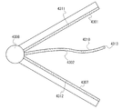
本実施の形態では、実施の形態1乃至実施の形態5に示す薄膜トランジスタを適用した半導体装置の一形態として、電子書籍の例を示す。本実施の形態では、図22(A)、(B)及び図23を用いて、第1の表示パネル4311と第2の表示パネル4312の間に、両面表示型の第3の表示パネル4313を搭載した例について説明する。図22(A)は、電子書籍を見開きにした状態であり、図22(B)は電子書籍を閉じた状態である。また、図23は電子書籍の横方向の断面図である。
101 ゲート電極
102 絶縁膜
103 半導体膜
104 絶縁膜
105 IGZO半導体層
106 絶縁物
107 コンタクトホール(開口)
108 ソース電極
109 ドレイン電極
200 基板
201 ゲート電極
202 絶縁膜
203 半導体膜
204 絶縁膜
205 半導体層
206 絶縁物
208 ソース電極
209 ドレイン電極
210 絶縁膜
211 金属多層膜
212 半導体膜
213 ソース側バッファー層
214 ドレイン側バッファー層
300 基板
301 ゲート電極
302 絶縁膜
303 半導体膜
304 絶縁膜
305 半導体層
306 絶縁物
308 ソース電極
309 ドレイン電極
310 絶縁膜
311 金属多層膜
400 基板
401 ゲート電極
402 絶縁膜
403 半導体膜
405 IGZO半導体層
408 ソース電極
409 ドレイン電極
410 絶縁膜
412 半導体膜
413 ソース側バッファー層
414 ドレイン側バッファー層
500 基板
501 絶縁膜
502 酸化物半導体膜
503 電極
510 物性評価用試料
581 薄膜トランジスタ
585 絶縁層
587 電極層
588 電極層
589 球形粒子
594 キャビティ
595 充填材
596 基板
597 基板
601 測定結果
602 測定結果
603 測定結果
604 ピーク
700 基板
701 ゲート電極
702 絶縁膜
703 半導体膜
705 IGZO半導体層
708 ソース電極
709 ドレイン電極
710 絶縁膜
1000 携帯電話機
1001 筐体
1002 表示部
1003 操作ボタン
1004 外部接続ポート
1005 スピーカ
1006 マイク
2600 TFT基板
2601 対向基板
2602 シール材
2603 画素部
2604 表示素子
2605 着色層
2606 偏光板
2607 偏光板
2608 配線回路部
2609 フレキシブル配線基板
2610 冷陰極管
2611 反射板
2612 回路基板
2613 拡散板
2631 ポスター
2632 車内広告
2700 電子書籍
2701 筐体
2703 筐体
2705 表示部
2707 表示部
2711 軸部
2721 電源スイッチ
2723 操作キー
2725 スピーカ
4001 基板
4002 画素部
4003 信号線駆動回路
4004 走査線駆動回路
4005 シール材
4006 基板
4008 液晶層
4010 薄膜トランジスタ
4011 薄膜トランジスタ
4013 液晶素子
4015 接続端子電極
4016 端子電極
4018 FPC
4019 異方性導電膜
4020 絶縁層
4021 絶縁層
4030 画素電極層
4031 対向電極層
4032 絶縁層
4301 表示部
4302 表示部
4304 操作部
4307 表示部
4308 部
4309 表示ボタン
4310 表示部
4311 表示パネル
4312 表示パネル
4313 表示パネル
4323 信号線駆動回路
4501 基板
4502 画素部
4505 シール材
4506 基板
4507 充填材
4509 薄膜トランジスタ
4510 薄膜トランジスタ
4511 発光素子
4512 電界発光層
4513 電極層
4515 接続端子電極
4516 端子電極
4517 電極層
4519 異方性導電膜
4520 隔壁
5300 基板
5301 画素部
5302 走査線駆動回路
5303 信号線駆動回路
5400 基板
5401 画素部
5402 走査線駆動回路
5403 信号線駆動回路
5404 走査線駆動回路
5501 配線
5502 配線
5503 配線
5504 配線
5505 配線
5506 配線
5543 ノード
5544 ノード
5571 薄膜トランジスタ
5572 薄膜トランジスタ
5573 薄膜トランジスタ
5574 薄膜トランジスタ
5575 薄膜トランジスタ
5576 薄膜トランジスタ
5577 薄膜トランジスタ
5578 薄膜トランジスタ
5601 ドライバIC
5602 スイッチ群
5611 配線
5612 配線
5613 配線
5621 配線
5701 フリップフロップ
5711 配線
5712 配線
5713 配線
5714 配線
5715 配線
5716 配線
5717 配線
5721 信号
5821 信号
590a 黒色領域
590b 白色領域
6400 画素
6401 スイッチング用トランジスタ
6402 駆動用トランジスタ
6403 容量素子
6404 発光素子
6405 信号線
6406 走査線
6407 電源線
6408 共通電極
7001 TFT
7002 発光素子
7003 陰極
7004 発光層
7005 陽極
7011 駆動用TFT
7012 発光素子
7013 陰極
7014 発光層
7015 陽極
7016 遮蔽膜
7017 導電膜
7021 駆動用TFT
7022 発光素子
7023 陰極
7024 発光層
7025 陽極
7027 導電膜
9400 通信装置
9401 筐体
9402 走査ボタン
9403 外部入力端子
9404 マイク
9405 スピーカ
9406 発光部
9410 表示装置
9411 筐体
9412 表示部
9413 操作ボタン
9600 テレビジョン装置
9601 筐体
9603 表示部
9605 スタンド
9607 表示部
9609 操作キー
9610 リモコン操作機
9700 デジタルフォトフレーム
9701 筐体
9703 表示部
9881 筐体
9882 表示部
9883 表示部
9884 スピーカ部
9885 操作キー
9886 記録媒体挿入部
9887 接続端子
9888 センサ
9889 マイクロフォン
9890 LEDランプ
9891 筐体
9893 連結部
9900 スロットマシン
9901 筐体
9903 表示部
4321a 走査線駆動回路
4322a 走査線駆動回路
4503a 信号線駆動回路
4504a 走査線駆動回路
4518a FPC
5603a 薄膜トランジスタ
5603b 薄膜トランジスタ
5603c 薄膜トランジスタ
5703a タイミング
5703b タイミング
5703c タイミング
5803a タイミング
5803b タイミング
5803c タイミング
Claims (1)
- 絶縁表面を有する基板の上方にゲート電極を形成し、
前記ゲート電極の上方に、窒素を3原子%以上30原子%以下含む第1の酸化窒化珪素膜を形成し、
前記第1の酸化窒化珪素膜の上方に、酸素を50%以上100%以下含む雰囲気中で酸化物半導体層を形成し、
前記酸化物半導体層の上方に、窒素を3原子%以上30原子%以下含む第2の酸化窒化珪素膜を形成し、
前記第2の酸化窒化珪素膜を選択的にエッチングして保護膜を形成し、
前記保護膜をマスクとして前記酸化物半導体層を選択的にエッチングして島状の半導体層を形成し、
前記保護膜を選択的にエッチングして開口を形成し、
前記保護膜の上方に、前記島状の半導体層と電気的に接続する導電層を形成することを特徴とする半導体装置の作製方法。
Priority Applications (1)
| Application Number | Priority Date | Filing Date | Title |
|---|---|---|---|
| JP2010117995A JP5675170B2 (ja) | 2009-05-29 | 2010-05-24 | 半導体装置の作製方法 |
Applications Claiming Priority (3)
| Application Number | Priority Date | Filing Date | Title |
|---|---|---|---|
| JP2009131616 | 2009-05-29 | ||
| JP2009131616 | 2009-05-29 | ||
| JP2010117995A JP5675170B2 (ja) | 2009-05-29 | 2010-05-24 | 半導体装置の作製方法 |
Related Child Applications (1)
| Application Number | Title | Priority Date | Filing Date |
|---|---|---|---|
| JP2014260267A Division JP5886936B2 (ja) | 2009-05-29 | 2014-12-24 | 半導体装置の作製方法 |
Publications (3)
| Publication Number | Publication Date |
|---|---|
| JP2011009719A JP2011009719A (ja) | 2011-01-13 |
| JP2011009719A5 JP2011009719A5 (ja) | 2013-07-04 |
| JP5675170B2 true JP5675170B2 (ja) | 2015-02-25 |
Family
ID=42261890
Family Applications (8)
| Application Number | Title | Priority Date | Filing Date |
|---|---|---|---|
| JP2010117995A Expired - Fee Related JP5675170B2 (ja) | 2009-05-29 | 2010-05-24 | 半導体装置の作製方法 |
| JP2014260267A Expired - Fee Related JP5886936B2 (ja) | 2009-05-29 | 2014-12-24 | 半導体装置の作製方法 |
| JP2016024581A Active JP6212143B2 (ja) | 2009-05-29 | 2016-02-12 | 半導体装置 |
| JP2017176833A Withdrawn JP2017224860A (ja) | 2009-05-29 | 2017-09-14 | 半導体装置 |
| JP2019035679A Withdrawn JP2019083345A (ja) | 2009-05-29 | 2019-02-28 | 半導体装置 |
| JP2019154483A Withdrawn JP2020065048A (ja) | 2009-05-29 | 2019-08-27 | 半導体装置 |
| JP2021103460A Active JP7154348B2 (ja) | 2009-05-29 | 2021-06-22 | 表示装置 |
| JP2022160132A Pending JP2023002589A (ja) | 2009-05-29 | 2022-10-04 | 半導体装置 |
Family Applications After (7)
| Application Number | Title | Priority Date | Filing Date |
|---|---|---|---|
| JP2014260267A Expired - Fee Related JP5886936B2 (ja) | 2009-05-29 | 2014-12-24 | 半導体装置の作製方法 |
| JP2016024581A Active JP6212143B2 (ja) | 2009-05-29 | 2016-02-12 | 半導体装置 |
| JP2017176833A Withdrawn JP2017224860A (ja) | 2009-05-29 | 2017-09-14 | 半導体装置 |
| JP2019035679A Withdrawn JP2019083345A (ja) | 2009-05-29 | 2019-02-28 | 半導体装置 |
| JP2019154483A Withdrawn JP2020065048A (ja) | 2009-05-29 | 2019-08-27 | 半導体装置 |
| JP2021103460A Active JP7154348B2 (ja) | 2009-05-29 | 2021-06-22 | 表示装置 |
| JP2022160132A Pending JP2023002589A (ja) | 2009-05-29 | 2022-10-04 | 半導体装置 |
Country Status (6)
| Country | Link |
|---|---|
| US (2) | US8872171B2 (ja) |
| EP (1) | EP2256814B1 (ja) |
| JP (8) | JP5675170B2 (ja) |
| KR (8) | KR20100129201A (ja) |
| CN (3) | CN107221562B (ja) |
| TW (9) | TWI697128B (ja) |
Families Citing this family (98)
| Publication number | Priority date | Publication date | Assignee | Title |
|---|---|---|---|---|
| EP2256814B1 (en) * | 2009-05-29 | 2019-01-16 | Semiconductor Energy Laboratory Co, Ltd. | Oxide semiconductor device and method for manufacturing the same |
| WO2011001879A1 (en) | 2009-06-30 | 2011-01-06 | Semiconductor Energy Laboratory Co., Ltd. | Method for manufacturing semiconductor device |
| WO2011007682A1 (en) | 2009-07-17 | 2011-01-20 | Semiconductor Energy Laboratory Co., Ltd. | Method of manufacturing semiconductor device |
| CN102473734B (zh) | 2009-07-31 | 2015-08-12 | 株式会社半导体能源研究所 | 半导体装置及其制造方法 |
| KR20120094013A (ko) | 2009-11-13 | 2012-08-23 | 가부시키가이샤 한도오따이 에네루기 켄큐쇼 | 스퍼터링 타겟 및 그 제조방법, 및 트랜지스터 |
| WO2011070929A1 (en) | 2009-12-11 | 2011-06-16 | Semiconductor Energy Laboratory Co., Ltd. | Semiconductor device and electronic device |
| KR20130009978A (ko) | 2010-02-26 | 2013-01-24 | 가부시키가이샤 한도오따이 에네루기 켄큐쇼 | 반도체 소자의 제조 방법 및 성막 장치 |
| WO2011118741A1 (en) | 2010-03-26 | 2011-09-29 | Semiconductor Energy Laboratory Co., Ltd. | Method for manufacturing semiconductor device |
| KR102112065B1 (ko) | 2010-03-26 | 2020-06-04 | 가부시키가이샤 한도오따이 에네루기 켄큐쇼 | 반도체 장치 |
| WO2011135987A1 (en) | 2010-04-28 | 2011-11-03 | Semiconductor Energy Laboratory Co., Ltd. | Method for manufacturing semiconductor device |
| US8895375B2 (en) | 2010-06-01 | 2014-11-25 | Semiconductor Energy Laboratory Co., Ltd. | Field effect transistor and method for manufacturing the same |
| KR102354354B1 (ko) * | 2010-07-02 | 2022-01-20 | 가부시키가이샤 한도오따이 에네루기 켄큐쇼 | 반도체 장치 및 그 제작 방법 |
| WO2012029612A1 (en) * | 2010-09-03 | 2012-03-08 | Semiconductor Energy Laboratory Co., Ltd. | Sputtering target and method for manufacturing semiconductor device |
| JP5782695B2 (ja) * | 2010-09-29 | 2015-09-24 | 凸版印刷株式会社 | 薄膜トランジスタ、薄膜トランジスタを備える画像表示装置、薄膜トランジスタの製造方法、画像表示装置の製造方法 |
| JP5275523B2 (ja) * | 2010-11-04 | 2013-08-28 | シャープ株式会社 | 表示装置、ならびに半導体装置および表示装置の製造方法 |
| US8894825B2 (en) | 2010-12-17 | 2014-11-25 | Semiconductor Energy Laboratory Co., Ltd. | Sputtering target, method for manufacturing the same, manufacturing semiconductor device |
| KR101770969B1 (ko) * | 2011-01-21 | 2017-08-25 | 삼성디스플레이 주식회사 | 터치 센싱 기판 및 이의 제조 방법 |
| KR101899880B1 (ko) * | 2011-02-17 | 2018-09-18 | 가부시키가이샤 한도오따이 에네루기 켄큐쇼 | 프로그래머블 lsi |
| WO2012117926A1 (ja) * | 2011-03-01 | 2012-09-07 | シャープ株式会社 | スパッタリングターゲット、その製造方法、および薄膜トランジスタの製造方法 |
| US20140110249A1 (en) * | 2011-03-04 | 2014-04-24 | Sharp Kabushiki Kaisha | Sputtering target, method for manufacturing same, and method for manufacturing thin film transistor |
| KR101333404B1 (ko) * | 2011-03-11 | 2013-11-28 | 샤프 가부시키가이샤 | 박막 트랜지스터 및 그 제조 방법, 및 표시 장치 |
| US8760903B2 (en) * | 2011-03-11 | 2014-06-24 | Semiconductor Energy Laboratory Co., Ltd. | Storage circuit |
| JP2012204548A (ja) * | 2011-03-24 | 2012-10-22 | Sony Corp | 表示装置およびその製造方法 |
| JP5857432B2 (ja) * | 2011-04-11 | 2016-02-10 | 大日本印刷株式会社 | 薄膜トランジスタの製造方法 |
| JP5883699B2 (ja) * | 2011-04-13 | 2016-03-15 | 株式会社半導体エネルギー研究所 | プログラマブルlsi |
| CN103477441B (zh) * | 2011-04-18 | 2016-05-18 | 夏普株式会社 | 薄膜晶体管、显示面板和薄膜晶体管的制造方法 |
| TWI573277B (zh) | 2011-05-05 | 2017-03-01 | 半導體能源研究所股份有限公司 | 半導體裝置及其製造方法 |
| US9762246B2 (en) * | 2011-05-20 | 2017-09-12 | Semiconductor Energy Laboratory Co., Ltd. | Semiconductor device with a storage circuit having an oxide semiconductor |
| JP5731904B2 (ja) * | 2011-05-25 | 2015-06-10 | ルネサスエレクトロニクス株式会社 | 半導体装置及び半導体装置の製造方法 |
| KR102432070B1 (ko) | 2011-06-08 | 2022-08-11 | 가부시키가이샤 한도오따이 에네루기 켄큐쇼 | 스퍼터링 타겟, 스퍼터링 타겟의 제조 방법 및 박막의 형성 방법 |
| KR101425064B1 (ko) | 2011-06-09 | 2014-08-01 | 엘지디스플레이 주식회사 | 산화물 박막 트랜지스터 및 그 제조방법 |
| CN102629609A (zh) * | 2011-07-22 | 2012-08-08 | 京东方科技集团股份有限公司 | 阵列基板及其制作方法、液晶面板、显示装置 |
| KR101506303B1 (ko) * | 2011-09-29 | 2015-03-26 | 가부시키가이샤 한도오따이 에네루기 켄큐쇼 | 반도체 장치, 및 반도체 장치의 제작 방법 |
| CN107068766B (zh) * | 2011-09-29 | 2020-12-29 | 株式会社半导体能源研究所 | 半导体装置 |
| KR101913207B1 (ko) | 2011-10-12 | 2018-11-01 | 삼성디스플레이 주식회사 | 박막 트랜지스터, 및 박막 트랜지스터 표시판과 이들을 제조하는 방법 |
| WO2013054823A1 (en) * | 2011-10-14 | 2013-04-18 | Semiconductor Energy Laboratory Co., Ltd. | Semiconductor device and manufacturing method thereof |
| WO2013065600A1 (ja) * | 2011-11-02 | 2013-05-10 | シャープ株式会社 | 薄膜トランジスタ、その製造方法、および表示装置 |
| JP6076038B2 (ja) * | 2011-11-11 | 2017-02-08 | 株式会社半導体エネルギー研究所 | 表示装置の作製方法 |
| CN103329275A (zh) * | 2011-11-17 | 2013-09-25 | 松下电器产业株式会社 | 薄膜半导体器件及其制造方法 |
| TWI489560B (zh) * | 2011-11-24 | 2015-06-21 | Au Optronics Corp | 畫素結構及其製作方法 |
| TWI669760B (zh) * | 2011-11-30 | 2019-08-21 | 日商半導體能源研究所股份有限公司 | 半導體裝置的製造方法 |
| JP6081162B2 (ja) * | 2011-11-30 | 2017-02-15 | 株式会社半導体エネルギー研究所 | 駆動回路及び該駆動回路を具備する表示装置 |
| TWI497689B (zh) * | 2011-12-02 | 2015-08-21 | Ind Tech Res Inst | 半導體元件及其製造方法 |
| TWI584383B (zh) | 2011-12-27 | 2017-05-21 | 半導體能源研究所股份有限公司 | 半導體裝置及其製造方法 |
| CN102651401B (zh) * | 2011-12-31 | 2015-03-18 | 京东方科技集团股份有限公司 | 一种薄膜晶体管、阵列基板及其制造方法和显示器件 |
| US9419146B2 (en) | 2012-01-26 | 2016-08-16 | Semiconductor Energy Laboratory Co., Ltd. | Semiconductor device and method for manufacturing the same |
| TWI642193B (zh) * | 2012-01-26 | 2018-11-21 | 半導體能源研究所股份有限公司 | 半導體裝置及半導體裝置的製造方法 |
| CN102629591B (zh) | 2012-02-28 | 2015-10-21 | 京东方科技集团股份有限公司 | 一种阵列基板的制造方法及阵列基板、显示器 |
| CN102569417A (zh) * | 2012-03-02 | 2012-07-11 | 福州华映视讯有限公司 | 薄膜晶体管及其制作方法 |
| JP6059566B2 (ja) | 2012-04-13 | 2017-01-11 | 株式会社半導体エネルギー研究所 | 半導体装置の作製方法 |
| JP6143423B2 (ja) * | 2012-04-16 | 2017-06-07 | 株式会社半導体エネルギー研究所 | 半導体装置の製造方法 |
| WO2013168687A1 (en) * | 2012-05-10 | 2013-11-14 | Semiconductor Energy Laboratory Co., Ltd. | Semiconductor device |
| US8995607B2 (en) | 2012-05-31 | 2015-03-31 | Semiconductor Energy Laboratory Co., Ltd. | Pulse signal output circuit and shift register |
| JP2014027263A (ja) * | 2012-06-15 | 2014-02-06 | Semiconductor Energy Lab Co Ltd | 半導体装置およびその作製方法 |
| JP2014041874A (ja) * | 2012-08-21 | 2014-03-06 | Sony Corp | 半導体装置およびその製造方法、並びに電子機器 |
| CN102916051B (zh) | 2012-10-11 | 2015-09-02 | 京东方科技集团股份有限公司 | 一种薄膜晶体管及其制作方法、阵列基板和显示装置 |
| CN102891106A (zh) * | 2012-10-19 | 2013-01-23 | 深圳市华星光电技术有限公司 | 薄膜晶体管阵列制作方法 |
| US20140110714A1 (en) * | 2012-10-22 | 2014-04-24 | Applied Materials, Inc. | High mobility compound semiconductor material using multiple anions |
| TWI691084B (zh) | 2012-10-24 | 2020-04-11 | 日商半導體能源研究所股份有限公司 | 半導體裝置及其製造方法 |
| CN102891108B (zh) * | 2012-10-24 | 2015-12-02 | 京东方科技集团股份有限公司 | 一种阵列基板的制造方法 |
| CN103915508B (zh) * | 2013-01-17 | 2017-05-17 | 上海天马微电子有限公司 | 一种底栅结构的氧化物薄膜晶体管及其制作方法 |
| JP6151070B2 (ja) * | 2013-04-11 | 2017-06-21 | 株式会社ジャパンディスプレイ | 薄膜トランジスタ及びそれを用いた表示装置 |
| TWI620324B (zh) * | 2013-04-12 | 2018-04-01 | 半導體能源研究所股份有限公司 | 半導體裝置 |
| US10304859B2 (en) * | 2013-04-12 | 2019-05-28 | Semiconductor Energy Laboratory Co., Ltd. | Semiconductor device having an oxide film on an oxide semiconductor film |
| CN105474372B (zh) * | 2013-08-09 | 2018-08-03 | 国立大学法人北陆先端科学技术大学院大学 | 氧化物半导体层及其制造方法、以及氧化物半导体的前驱体、氧化物半导体层、半导体元件及电子装置 |
| KR102244553B1 (ko) * | 2013-08-23 | 2021-04-23 | 가부시키가이샤 한도오따이 에네루기 켄큐쇼 | 용량 소자 및 반도체 장치 |
| JP6483402B2 (ja) | 2013-11-01 | 2019-03-13 | 株式会社半導体エネルギー研究所 | 記憶装置、及び記憶装置を有する電子機器 |
| US9601634B2 (en) | 2013-12-02 | 2017-03-21 | Semiconductor Energy Laboratory Co., Ltd. | Semiconductor device |
| TW201523738A (zh) | 2013-12-06 | 2015-06-16 | Chunghwa Picture Tubes Ltd | 薄膜電晶體基板及其製造方法 |
| JP6537264B2 (ja) | 2013-12-12 | 2019-07-03 | 株式会社半導体エネルギー研究所 | 半導体装置 |
| CN103681487A (zh) * | 2013-12-13 | 2014-03-26 | 华映视讯(吴江)有限公司 | 薄膜晶体管基板及其制造方法 |
| CN104752517A (zh) * | 2013-12-31 | 2015-07-01 | 昆山工研院新型平板显示技术中心有限公司 | 一种薄膜晶体管及其制备方法和应用 |
| CN104051541B (zh) * | 2014-06-06 | 2017-02-15 | 昆山工研院新型平板显示技术中心有限公司 | 薄膜晶体管及其制作方法 |
| CN104037090B (zh) * | 2014-06-19 | 2016-10-19 | 深圳市华星光电技术有限公司 | 氧化物薄膜晶体管结构制作方法及氧化物薄膜晶体管结构 |
| JP6400425B2 (ja) * | 2014-10-15 | 2018-10-03 | 東京エレクトロン株式会社 | 多層膜をエッチングする方法 |
| JP6584157B2 (ja) * | 2015-06-08 | 2019-10-02 | 三菱電機株式会社 | 薄膜トランジスタ、薄膜トランジスタ基板、液晶表示装置及び薄膜トランジスタの製造方法 |
| WO2017010342A1 (ja) * | 2015-07-10 | 2017-01-19 | シャープ株式会社 | 酸化物半導体膜のエッチング方法および半導体装置の製造方法 |
| US10061346B2 (en) * | 2015-10-22 | 2018-08-28 | Dell Products L.P. | Folded continuous multielement touch display |
| JP6495808B2 (ja) * | 2015-11-17 | 2019-04-03 | 株式会社東芝 | 酸化物半導体及び半導体装置 |
| CN105355647B (zh) * | 2015-11-26 | 2018-05-25 | 上海天马有机发光显示技术有限公司 | 一种封装结构、显示装置及其制作方法 |
| JP6904907B2 (ja) * | 2015-12-28 | 2021-07-21 | 株式会社半導体エネルギー研究所 | 酸化物及び半導体装置の作製方法 |
| CN105576038A (zh) * | 2016-01-12 | 2016-05-11 | 京东方科技集团股份有限公司 | 薄膜晶体管及其制作方法、显示基板和显示装置 |
| WO2017130776A1 (ja) * | 2016-01-27 | 2017-08-03 | シャープ株式会社 | 半導体装置およびその製造方法 |
| CN105632896B (zh) * | 2016-01-28 | 2018-06-15 | 深圳市华星光电技术有限公司 | 制造薄膜晶体管的方法 |
| JP6689108B2 (ja) | 2016-03-22 | 2020-04-28 | 三菱電機株式会社 | 薄膜トランジスタ基板およびその製造方法 |
| JP6827270B2 (ja) * | 2016-03-28 | 2021-02-10 | 株式会社ジャパンディスプレイ | 半導体装置の作製方法 |
| CN106648277B (zh) * | 2016-11-11 | 2019-05-03 | 京东方科技集团股份有限公司 | 电子装置及其制造方法和操作方法、电子复写系统 |
| CN107204375B (zh) * | 2017-05-19 | 2019-11-26 | 深圳市华星光电技术有限公司 | 薄膜晶体管及其制作方法 |
| CN107293493A (zh) * | 2017-06-06 | 2017-10-24 | 武汉华星光电技术有限公司 | 铟镓锌氧化物薄膜晶体管的制作方法 |
| CN107316875A (zh) * | 2017-08-15 | 2017-11-03 | 深圳市华星光电半导体显示技术有限公司 | 阵列基板的制作方法、阵列基板及液晶面板 |
| CN107644880B (zh) | 2017-10-19 | 2020-04-14 | 京东方科技集团股份有限公司 | 氧化物薄膜晶体管显示基板及其制作方法、显示装置 |
| CN107577375A (zh) * | 2017-10-24 | 2018-01-12 | 业成科技(成都)有限公司 | 触摸屏及其制造方法 |
| TW201919130A (zh) * | 2017-11-13 | 2019-05-16 | 友達光電股份有限公司 | 畫素結構、半導體結構的製造方法及半導體元件的製造方法 |
| CN108183132A (zh) * | 2017-12-27 | 2018-06-19 | 深圳市华星光电半导体显示技术有限公司 | 一种igzo薄膜晶体管制备方法 |
| CN109390414B (zh) * | 2018-11-14 | 2022-04-15 | 成都中电熊猫显示科技有限公司 | 一种薄膜晶体管、阵列基板以及显示面板 |
| CN110794898B (zh) * | 2019-11-19 | 2020-06-30 | 上海椒陵光学科技有限公司 | 一种能适应不同光照强度的夜视仪 |
| JP7418230B2 (ja) * | 2020-02-03 | 2024-01-19 | 東京エレクトロン株式会社 | プラズマ処理方法及びプラズマ処理装置 |
| CN111341849B (zh) * | 2020-03-05 | 2022-04-12 | 合肥京东方光电科技有限公司 | 显示基板及其制备方法、显示面板 |
Family Cites Families (227)
| Publication number | Priority date | Publication date | Assignee | Title |
|---|---|---|---|---|
| US4244040A (en) | 1978-10-10 | 1981-01-06 | Robert Fondiller | Miniature electronic device construction |
| JPS60198861A (ja) | 1984-03-23 | 1985-10-08 | Fujitsu Ltd | 薄膜トランジスタ |
| JPH0244256B2 (ja) | 1987-01-28 | 1990-10-03 | Kagaku Gijutsucho Mukizaishitsu Kenkyushocho | Ingazn2o5deshimesarerurotsuhoshokeinosojokozoojusurukagobutsuoyobisonoseizoho |
| JPH0244260B2 (ja) | 1987-02-24 | 1990-10-03 | Kagaku Gijutsucho Mukizaishitsu Kenkyushocho | Ingazn5o8deshimesarerurotsuhoshokeinosojokozoojusurukagobutsuoyobisonoseizoho |
| JPS63210023A (ja) | 1987-02-24 | 1988-08-31 | Natl Inst For Res In Inorg Mater | InGaZn↓4O↓7で示される六方晶系の層状構造を有する化合物およびその製造法 |
| JPH0244258B2 (ja) | 1987-02-24 | 1990-10-03 | Kagaku Gijutsucho Mukizaishitsu Kenkyushocho | Ingazn3o6deshimesarerurotsuhoshokeinosojokozoojusurukagobutsuoyobisonoseizoho |
| JPH0244262B2 (ja) | 1987-02-27 | 1990-10-03 | Kagaku Gijutsucho Mukizaishitsu Kenkyushocho | Ingazn6o9deshimesarerurotsuhoshokeinosojokozoojusurukagobutsuoyobisonoseizoho |
| JPH0244263B2 (ja) | 1987-04-22 | 1990-10-03 | Kagaku Gijutsucho Mukizaishitsu Kenkyushocho | Ingazn7o10deshimesarerurotsuhoshokeinosojokozoojusurukagobutsuoyobisonoseizoho |
| JPH04280637A (ja) * | 1991-03-08 | 1992-10-06 | Nippondenso Co Ltd | 薄膜トランジスタの製造方法 |
| JPH05251705A (ja) | 1992-03-04 | 1993-09-28 | Fuji Xerox Co Ltd | 薄膜トランジスタ |
| US5508532A (en) * | 1994-06-16 | 1996-04-16 | Semiconductor Energy Laboratory Co., Ltd. | Semiconductor device with braded silicon nitride |
| US5444673A (en) | 1994-07-12 | 1995-08-22 | Mathurin; Trevor S. | Audio controlled and activated wristwatch memory aid device |
| JP3422096B2 (ja) | 1994-09-22 | 2003-06-30 | ソニー株式会社 | 薄膜半導体装置の製造方法 |
| JP3479375B2 (ja) | 1995-03-27 | 2003-12-15 | 科学技術振興事業団 | 亜酸化銅等の金属酸化物半導体による薄膜トランジスタとpn接合を形成した金属酸化物半導体装置およびそれらの製造方法 |
| EP0820644B1 (en) | 1995-08-03 | 2005-08-24 | Koninklijke Philips Electronics N.V. | Semiconductor device provided with transparent switching element |
| JP3625598B2 (ja) | 1995-12-30 | 2005-03-02 | 三星電子株式会社 | 液晶表示装置の製造方法 |
| JP2652368B2 (ja) | 1996-04-05 | 1997-09-10 | 株式会社半導体エネルギー研究所 | 絶縁ゲイト型半導体装置の作製方法 |
| JPH1140814A (ja) | 1997-07-18 | 1999-02-12 | Furontetsuku:Kk | 薄膜トランジスタ基板と液晶表示装置および薄膜トランジスタ基板の製造方法 |
| JPH11109406A (ja) * | 1997-09-30 | 1999-04-23 | Sanyo Electric Co Ltd | 表示装置とその製造方法 |
| JPH11111994A (ja) | 1997-10-03 | 1999-04-23 | Sanyo Electric Co Ltd | 薄膜トランジスタ及び薄膜トランジスタの製造方法 |
| JP4017240B2 (ja) | 1998-03-30 | 2007-12-05 | 三洋電機株式会社 | 薄膜トランジスタの製造方法 |
| JP4170454B2 (ja) | 1998-07-24 | 2008-10-22 | Hoya株式会社 | 透明導電性酸化物薄膜を有する物品及びその製造方法 |
| JP4094179B2 (ja) | 1998-08-21 | 2008-06-04 | 株式会社半導体エネルギー研究所 | 半導体装置の作製方法 |
| US6246070B1 (en) | 1998-08-21 | 2001-06-12 | Semiconductor Energy Laboratory Co., Ltd. | Semiconductor device provided with semiconductor circuit made of semiconductor element and method of fabricating the same |
| JP2000150861A (ja) | 1998-11-16 | 2000-05-30 | Tdk Corp | 酸化物薄膜 |
| JP3276930B2 (ja) | 1998-11-17 | 2002-04-22 | 科学技術振興事業団 | トランジスタ及び半導体装置 |
| KR100539871B1 (ko) | 1998-12-26 | 2006-04-21 | 삼성전자주식회사 | 텔레비전 휴대폰의 수신 메세지 표시 방법 |
| US6888522B1 (en) | 1999-03-31 | 2005-05-03 | Minolta Co., Ltd. | Information display apparatus |
| JP2000357586A (ja) | 1999-06-15 | 2000-12-26 | Sharp Corp | 薄膜el素子の製造方法および薄膜el素子 |
| TW460731B (en) | 1999-09-03 | 2001-10-21 | Ind Tech Res Inst | Electrode structure and production method of wide viewing angle LCD |
| JP2001284592A (ja) * | 2000-03-29 | 2001-10-12 | Sony Corp | 薄膜半導体装置及びその駆動方法 |
| JP2001311965A (ja) | 2000-04-28 | 2001-11-09 | Nec Corp | アクティブマトリクス基板及びその製造方法 |
| WO2002016679A1 (fr) | 2000-08-18 | 2002-02-28 | Tohoku Techno Arch Co., Ltd. | Matiere semi-conductrice polycristalline |
| JP4089858B2 (ja) | 2000-09-01 | 2008-05-28 | 国立大学法人東北大学 | 半導体デバイス |
| JP2002162646A (ja) | 2000-09-14 | 2002-06-07 | Sony Corp | 反射型液晶表示装置 |
| KR20020038482A (ko) | 2000-11-15 | 2002-05-23 | 모리시타 요이찌 | 박막 트랜지스터 어레이, 그 제조방법 및 그것을 이용한표시패널 |
| US6717181B2 (en) * | 2001-02-22 | 2004-04-06 | Semiconductor Energy Laboratory Co., Ltd. | Luminescent device having thin film transistor |
| JP2002252353A (ja) * | 2001-02-26 | 2002-09-06 | Hitachi Ltd | 薄膜トランジスタおよびアクティブマトリクス型液晶表示装置 |
| JP3997731B2 (ja) | 2001-03-19 | 2007-10-24 | 富士ゼロックス株式会社 | 基材上に結晶性半導体薄膜を形成する方法 |
| JP2002289859A (ja) | 2001-03-23 | 2002-10-04 | Minolta Co Ltd | 薄膜トランジスタ |
| JP3512766B2 (ja) | 2001-08-09 | 2004-03-31 | 株式会社半導体エネルギー研究所 | 薄膜トランジスタ及び液晶表示装置 |
| JP4090716B2 (ja) | 2001-09-10 | 2008-05-28 | 雅司 川崎 | 薄膜トランジスタおよびマトリクス表示装置 |
| JP3925839B2 (ja) | 2001-09-10 | 2007-06-06 | シャープ株式会社 | 半導体記憶装置およびその試験方法 |
| EP1443130B1 (en) | 2001-11-05 | 2011-09-28 | Japan Science and Technology Agency | Natural superlattice homologous single crystal thin film, method for preparation thereof, and device using said single crystal thin film |
| JP4164562B2 (ja) | 2002-09-11 | 2008-10-15 | 独立行政法人科学技術振興機構 | ホモロガス薄膜を活性層として用いる透明薄膜電界効果型トランジスタ |
| JP4083486B2 (ja) | 2002-02-21 | 2008-04-30 | 独立行政法人科学技術振興機構 | LnCuO(S,Se,Te)単結晶薄膜の製造方法 |
| JP2003264148A (ja) | 2002-03-07 | 2003-09-19 | Nec Corp | 薄膜製造方法、半導体デバイス製造方法、非晶質半導体薄膜、絶縁体薄膜、及び半導体装置 |
| JP2003273133A (ja) | 2002-03-15 | 2003-09-26 | Sanyo Electric Co Ltd | 酸化物半導体層およびその形成方法ならびに半導体装置 |
| US7049190B2 (en) | 2002-03-15 | 2006-05-23 | Sanyo Electric Co., Ltd. | Method for forming ZnO film, method for forming ZnO semiconductor layer, method for fabricating semiconductor device, and semiconductor device |
| JP3933591B2 (ja) | 2002-03-26 | 2007-06-20 | 淳二 城戸 | 有機エレクトロルミネッセント素子 |
| US7339187B2 (en) | 2002-05-21 | 2008-03-04 | State Of Oregon Acting By And Through The Oregon State Board Of Higher Education On Behalf Of Oregon State University | Transistor structures |
| JP2004022625A (ja) | 2002-06-13 | 2004-01-22 | Murata Mfg Co Ltd | 半導体デバイス及び該半導体デバイスの製造方法 |
| US7105868B2 (en) | 2002-06-24 | 2006-09-12 | Cermet, Inc. | High-electron mobility transistor with zinc oxide |
| US7067843B2 (en) | 2002-10-11 | 2006-06-27 | E. I. Du Pont De Nemours And Company | Transparent oxide semiconductor thin film transistors |
| JP4166105B2 (ja) | 2003-03-06 | 2008-10-15 | シャープ株式会社 | 半導体装置およびその製造方法 |
| JP2004273732A (ja) | 2003-03-07 | 2004-09-30 | Sharp Corp | アクティブマトリクス基板およびその製造方法 |
| JP2004292873A (ja) | 2003-03-26 | 2004-10-21 | Sumitomo Heavy Ind Ltd | 酸化亜鉛膜の製造方法 |
| JP4108633B2 (ja) | 2003-06-20 | 2008-06-25 | シャープ株式会社 | 薄膜トランジスタおよびその製造方法ならびに電子デバイス |
| CN1577796A (zh) * | 2003-07-10 | 2005-02-09 | 精工爱普生株式会社 | 电子器件的制造方法和半导体器件的制造方法 |
| US7262463B2 (en) | 2003-07-25 | 2007-08-28 | Hewlett-Packard Development Company, L.P. | Transistor including a deposited channel region having a doped portion |
| US7453426B2 (en) | 2004-01-14 | 2008-11-18 | Semiconductor Energy Laboratory Co., Ltd. | Display device and electronic apparatus |
| JP4667051B2 (ja) * | 2004-01-29 | 2011-04-06 | 株式会社半導体エネルギー研究所 | 半導体装置の作製方法 |
| US20050170643A1 (en) * | 2004-01-29 | 2005-08-04 | Semiconductor Energy Laboratory Co., Ltd. | Forming method of contact hole, and manufacturing method of semiconductor device, liquid crystal display device and EL display device |
| KR101000451B1 (ko) * | 2004-02-05 | 2010-12-13 | 삼성전자주식회사 | Tft lcd 기판의 알루미늄 배선 형성방법과 이에의한 tft lcd 기판 |
| JP3915810B2 (ja) * | 2004-02-26 | 2007-05-16 | セイコーエプソン株式会社 | 有機エレクトロルミネッセンス装置、その製造方法、及び電子機器 |
| US7381579B2 (en) * | 2004-02-26 | 2008-06-03 | Samsung Sdi Co., Ltd. | Donor sheet, method of manufacturing the same, method of manufacturing TFT using the donor sheet, and method of manufacturing flat panel display device using the donor sheet |
| EP2246894B2 (en) | 2004-03-12 | 2018-10-10 | Japan Science and Technology Agency | Method for fabricating a thin film transistor having an amorphous oxide as a channel layer |
| US7282782B2 (en) | 2004-03-12 | 2007-10-16 | Hewlett-Packard Development Company, L.P. | Combined binary oxide semiconductor device |
| US7297977B2 (en) | 2004-03-12 | 2007-11-20 | Hewlett-Packard Development Company, L.P. | Semiconductor device |
| US7145174B2 (en) | 2004-03-12 | 2006-12-05 | Hewlett-Packard Development Company, Lp. | Semiconductor device |
| US7642038B2 (en) | 2004-03-24 | 2010-01-05 | Semiconductor Energy Laboratory Co., Ltd. | Method for forming pattern, thin film transistor, display device, method for manufacturing thereof, and television apparatus |
| KR100635065B1 (ko) * | 2004-05-17 | 2006-10-16 | 삼성에스디아이 주식회사 | 유기 전계 발광 표시 장치 및 그 제조방법 |
| US7629633B2 (en) * | 2004-05-20 | 2009-12-08 | Isaac Wing Tak Chan | Vertical thin film transistor with short-channel effect suppression |
| US7211825B2 (en) | 2004-06-14 | 2007-05-01 | Yi-Chi Shih | Indium oxide-based thin film transistors and circuits |
| WO2006006369A1 (ja) | 2004-07-12 | 2006-01-19 | Pioneer Corporation | 半導体装置 |
| KR100721555B1 (ko) | 2004-08-13 | 2007-05-23 | 삼성에스디아이 주식회사 | 박막트랜지스터 및 그 제조 방법 |
| JP2006100760A (ja) | 2004-09-02 | 2006-04-13 | Casio Comput Co Ltd | 薄膜トランジスタおよびその製造方法 |
| US7285501B2 (en) | 2004-09-17 | 2007-10-23 | Hewlett-Packard Development Company, L.P. | Method of forming a solution processed device |
| US7382421B2 (en) | 2004-10-12 | 2008-06-03 | Hewlett-Packard Development Company, L.P. | Thin film transistor with a passivation layer |
| US7298084B2 (en) | 2004-11-02 | 2007-11-20 | 3M Innovative Properties Company | Methods and displays utilizing integrated zinc oxide row and column drivers in conjunction with organic light emitting diodes |
| US7863611B2 (en) | 2004-11-10 | 2011-01-04 | Canon Kabushiki Kaisha | Integrated circuits utilizing amorphous oxides |
| US7791072B2 (en) | 2004-11-10 | 2010-09-07 | Canon Kabushiki Kaisha | Display |
| US7829444B2 (en) | 2004-11-10 | 2010-11-09 | Canon Kabushiki Kaisha | Field effect transistor manufacturing method |
| US7868326B2 (en) | 2004-11-10 | 2011-01-11 | Canon Kabushiki Kaisha | Field effect transistor |
| RU2402106C2 (ru) | 2004-11-10 | 2010-10-20 | Кэнон Кабусики Кайся | Аморфный оксид и полевой транзистор с его использованием |
| US7453065B2 (en) | 2004-11-10 | 2008-11-18 | Canon Kabushiki Kaisha | Sensor and image pickup device |
| KR20070085879A (ko) | 2004-11-10 | 2007-08-27 | 캐논 가부시끼가이샤 | 발광 장치 |
| US7579224B2 (en) * | 2005-01-21 | 2009-08-25 | Semiconductor Energy Laboratory Co., Ltd. | Method for manufacturing a thin film semiconductor device |
| TWI412138B (zh) | 2005-01-28 | 2013-10-11 | Semiconductor Energy Lab | 半導體裝置,電子裝置,和半導體裝置的製造方法 |
| TWI445178B (zh) | 2005-01-28 | 2014-07-11 | Semiconductor Energy Lab | 半導體裝置,電子裝置,和半導體裝置的製造方法 |
| US7858451B2 (en) | 2005-02-03 | 2010-12-28 | Semiconductor Energy Laboratory Co., Ltd. | Electronic device, semiconductor device and manufacturing method thereof |
| US7948171B2 (en) | 2005-02-18 | 2011-05-24 | Semiconductor Energy Laboratory Co., Ltd. | Light emitting device |
| US20060197092A1 (en) | 2005-03-03 | 2006-09-07 | Randy Hoffman | System and method for forming conductive material on a substrate |
| US8681077B2 (en) | 2005-03-18 | 2014-03-25 | Semiconductor Energy Laboratory Co., Ltd. | Semiconductor device, and display device, driving method and electronic apparatus thereof |
| WO2006105077A2 (en) | 2005-03-28 | 2006-10-05 | Massachusetts Institute Of Technology | Low voltage thin film transistor with high-k dielectric material |
| US7645478B2 (en) | 2005-03-31 | 2010-01-12 | 3M Innovative Properties Company | Methods of making displays |
| US8300031B2 (en) | 2005-04-20 | 2012-10-30 | Semiconductor Energy Laboratory Co., Ltd. | Semiconductor device comprising transistor having gate and drain connected through a current-voltage conversion element |
| JP2006344849A (ja) | 2005-06-10 | 2006-12-21 | Casio Comput Co Ltd | 薄膜トランジスタ |
| US7691666B2 (en) | 2005-06-16 | 2010-04-06 | Eastman Kodak Company | Methods of making thin film transistors comprising zinc-oxide-based semiconductor materials and transistors made thereby |
| US7402506B2 (en) | 2005-06-16 | 2008-07-22 | Eastman Kodak Company | Methods of making thin film transistors comprising zinc-oxide-based semiconductor materials and transistors made thereby |
| US7507618B2 (en) | 2005-06-27 | 2009-03-24 | 3M Innovative Properties Company | Method for making electronic devices using metal oxide nanoparticles |
| KR100711890B1 (ko) | 2005-07-28 | 2007-04-25 | 삼성에스디아이 주식회사 | 유기 발광표시장치 및 그의 제조방법 |
| JP2007059128A (ja) | 2005-08-23 | 2007-03-08 | Canon Inc | 有機el表示装置およびその製造方法 |
| JP4870404B2 (ja) * | 2005-09-02 | 2012-02-08 | 財団法人高知県産業振興センター | 薄膜トランジスタの製法 |
| JP4870403B2 (ja) | 2005-09-02 | 2012-02-08 | 財団法人高知県産業振興センター | 薄膜トランジスタの製法 |
| TWI345313B (en) * | 2005-09-05 | 2011-07-11 | Au Optronics Corp | Thin film transistor and method of manufacturing the same |
| JP4850457B2 (ja) | 2005-09-06 | 2012-01-11 | キヤノン株式会社 | 薄膜トランジスタ及び薄膜ダイオード |
| JP5116225B2 (ja) | 2005-09-06 | 2013-01-09 | キヤノン株式会社 | 酸化物半導体デバイスの製造方法 |
| JP4280736B2 (ja) | 2005-09-06 | 2009-06-17 | キヤノン株式会社 | 半導体素子 |
| JP2007073705A (ja) | 2005-09-06 | 2007-03-22 | Canon Inc | 酸化物半導体チャネル薄膜トランジスタおよびその製造方法 |
| JP4560502B2 (ja) | 2005-09-06 | 2010-10-13 | キヤノン株式会社 | 電界効果型トランジスタ |
| KR100786498B1 (ko) | 2005-09-27 | 2007-12-17 | 삼성에스디아이 주식회사 | 투명박막 트랜지스터 및 그 제조방법 |
| EP1998375A3 (en) | 2005-09-29 | 2012-01-18 | Semiconductor Energy Laboratory Co, Ltd. | Semiconductor device having oxide semiconductor layer and manufacturing method |
| JP5064747B2 (ja) | 2005-09-29 | 2012-10-31 | 株式会社半導体エネルギー研究所 | 半導体装置、電気泳動表示装置、表示モジュール、電子機器、及び半導体装置の作製方法 |
| JP5078246B2 (ja) | 2005-09-29 | 2012-11-21 | 株式会社半導体エネルギー研究所 | 半導体装置、及び半導体装置の作製方法 |
| KR101197053B1 (ko) * | 2005-09-30 | 2012-11-06 | 삼성디스플레이 주식회사 | 유기 박막 트랜지스터 표시판 및 그 제조 방법 |
| JP5427340B2 (ja) * | 2005-10-14 | 2014-02-26 | 株式会社半導体エネルギー研究所 | 半導体装置 |
| JP5037808B2 (ja) | 2005-10-20 | 2012-10-03 | キヤノン株式会社 | アモルファス酸化物を用いた電界効果型トランジスタ、及び該トランジスタを用いた表示装置 |
| KR20090115222A (ko) | 2005-11-15 | 2009-11-04 | 가부시키가이샤 한도오따이 에네루기 켄큐쇼 | 반도체장치 제조방법 |
| JP5099740B2 (ja) * | 2005-12-19 | 2012-12-19 | 財団法人高知県産業振興センター | 薄膜トランジスタ |
| JP5244295B2 (ja) * | 2005-12-21 | 2013-07-24 | 出光興産株式会社 | Tft基板及びtft基板の製造方法 |
| TWI292281B (en) | 2005-12-29 | 2008-01-01 | Ind Tech Res Inst | Pixel structure of active organic light emitting diode and method of fabricating the same |
| US7867636B2 (en) | 2006-01-11 | 2011-01-11 | Murata Manufacturing Co., Ltd. | Transparent conductive film and method for manufacturing the same |
| JP4977478B2 (ja) | 2006-01-21 | 2012-07-18 | 三星電子株式会社 | ZnOフィルム及びこれを用いたTFTの製造方法 |
| JP2007258675A (ja) | 2006-02-21 | 2007-10-04 | Idemitsu Kosan Co Ltd | Tft基板及び反射型tft基板並びにそれらの製造方法 |
| CN101416320B (zh) | 2006-01-31 | 2011-08-31 | 出光兴产株式会社 | Tft基板及反射型tft基板以及其制造方法 |
| US7576394B2 (en) | 2006-02-02 | 2009-08-18 | Kochi Industrial Promotion Center | Thin film transistor including low resistance conductive thin films and manufacturing method thereof |
| JP2007212699A (ja) | 2006-02-09 | 2007-08-23 | Idemitsu Kosan Co Ltd | 反射型tft基板及び反射型tft基板の製造方法 |
| US7977169B2 (en) | 2006-02-15 | 2011-07-12 | Kochi Industrial Promotion Center | Semiconductor device including active layer made of zinc oxide with controlled orientations and manufacturing method thereof |
| KR101293567B1 (ko) * | 2006-02-21 | 2013-08-06 | 삼성디스플레이 주식회사 | 표시장치의 제조방법 |
| JP2007250982A (ja) | 2006-03-17 | 2007-09-27 | Canon Inc | 酸化物半導体を用いた薄膜トランジスタ及び表示装置 |
| KR20070101595A (ko) | 2006-04-11 | 2007-10-17 | 삼성전자주식회사 | ZnO TFT |
| US20070252928A1 (en) | 2006-04-28 | 2007-11-01 | Toppan Printing Co., Ltd. | Structure, transmission type liquid crystal display, reflection type display and manufacturing method thereof |
| JP5135709B2 (ja) | 2006-04-28 | 2013-02-06 | 凸版印刷株式会社 | 薄膜トランジスタ及びその製造方法 |
| WO2007142167A1 (en) * | 2006-06-02 | 2007-12-13 | Kochi Industrial Promotion Center | Semiconductor device including an oxide semiconductor thin film layer of zinc oxide and manufacturing method thereof |
| JP5028033B2 (ja) | 2006-06-13 | 2012-09-19 | キヤノン株式会社 | 酸化物半導体膜のドライエッチング方法 |
| US8974918B2 (en) | 2006-07-04 | 2015-03-10 | Semiconductor Energy Laboratory Co., Ltd. | Display device and electronic device |
| JP5228298B2 (ja) * | 2006-08-04 | 2013-07-03 | カシオ計算機株式会社 | 半導体薄膜の加工方法及び半導体装置の製造方法 |
| JP4609797B2 (ja) | 2006-08-09 | 2011-01-12 | Nec液晶テクノロジー株式会社 | 薄膜デバイス及びその製造方法 |
| JP4999400B2 (ja) | 2006-08-09 | 2012-08-15 | キヤノン株式会社 | 酸化物半導体膜のドライエッチング方法 |
| US7651896B2 (en) | 2006-08-30 | 2010-01-26 | Semiconductor Energy Laboratory Co., Ltd. | Method for manufacturing semiconductor device |
| JP5216276B2 (ja) * | 2006-08-30 | 2013-06-19 | 株式会社半導体エネルギー研究所 | 半導体装置の作製方法 |
| US7636135B2 (en) * | 2006-09-11 | 2009-12-22 | Beijing Boe Optoelectronics Technology Co., Ltd | TFT-LCD array substrate and method for manufacturing the same |
| JP4332545B2 (ja) | 2006-09-15 | 2009-09-16 | キヤノン株式会社 | 電界効果型トランジスタ及びその製造方法 |
| JP5164357B2 (ja) | 2006-09-27 | 2013-03-21 | キヤノン株式会社 | 半導体装置及び半導体装置の製造方法 |
| JP4274219B2 (ja) | 2006-09-27 | 2009-06-03 | セイコーエプソン株式会社 | 電子デバイス、有機エレクトロルミネッセンス装置、有機薄膜半導体装置 |
| TWI514347B (zh) | 2006-09-29 | 2015-12-21 | Semiconductor Energy Lab | 顯示裝置和電子裝置 |
| JP5468196B2 (ja) | 2006-09-29 | 2014-04-09 | 株式会社半導体エネルギー研究所 | 半導体装置、表示装置及び液晶表示装置 |
| US7989361B2 (en) * | 2006-09-30 | 2011-08-02 | Samsung Electronics Co., Ltd. | Composition for dielectric thin film, metal oxide dielectric thin film using the same and preparation method thereof |
| US7622371B2 (en) | 2006-10-10 | 2009-11-24 | Hewlett-Packard Development Company, L.P. | Fused nanocrystal thin film semiconductor and method |
| JP5099739B2 (ja) | 2006-10-12 | 2012-12-19 | 財団法人高知県産業振興センター | 薄膜トランジスタ及びその製法 |
| KR100829570B1 (ko) * | 2006-10-20 | 2008-05-14 | 삼성전자주식회사 | 크로스 포인트 메모리용 박막 트랜지스터 및 그 제조 방법 |
| JP2008124215A (ja) | 2006-11-10 | 2008-05-29 | Kochi Prefecture Sangyo Shinko Center | 薄膜半導体装置及びその製造方法 |
| US7772021B2 (en) | 2006-11-29 | 2010-08-10 | Samsung Electronics Co., Ltd. | Flat panel displays comprising a thin-film transistor having a semiconductive oxide in its channel and methods of fabricating the same for use in flat panel displays |
| JP2008140684A (ja) | 2006-12-04 | 2008-06-19 | Toppan Printing Co Ltd | カラーelディスプレイおよびその製造方法 |
| JP5305630B2 (ja) * | 2006-12-05 | 2013-10-02 | キヤノン株式会社 | ボトムゲート型薄膜トランジスタの製造方法及び表示装置の製造方法 |
| KR101303578B1 (ko) | 2007-01-05 | 2013-09-09 | 삼성전자주식회사 | 박막 식각 방법 |
| US8207063B2 (en) | 2007-01-26 | 2012-06-26 | Eastman Kodak Company | Process for atomic layer deposition |
| KR101410926B1 (ko) * | 2007-02-16 | 2014-06-24 | 삼성전자주식회사 | 박막 트랜지스터 및 그 제조방법 |
| JP5196870B2 (ja) | 2007-05-23 | 2013-05-15 | キヤノン株式会社 | 酸化物半導体を用いた電子素子及びその製造方法 |
| KR100759086B1 (ko) | 2007-02-23 | 2007-09-19 | 실리콘 디스플레이 (주) | 국부 산화를 이용한 박막 트랜지스터 제조 방법 및 투명박막 트랜지스터 |
| KR100858088B1 (ko) * | 2007-02-28 | 2008-09-10 | 삼성전자주식회사 | 박막 트랜지스터 및 그 제조 방법 |
| KR100851215B1 (ko) | 2007-03-14 | 2008-08-07 | 삼성에스디아이 주식회사 | 박막 트랜지스터 및 이를 이용한 유기 전계 발광표시장치 |
| JP4727684B2 (ja) | 2007-03-27 | 2011-07-20 | 富士フイルム株式会社 | 薄膜電界効果型トランジスタおよびそれを用いた表示装置 |
| JP5197058B2 (ja) | 2007-04-09 | 2013-05-15 | キヤノン株式会社 | 発光装置とその作製方法 |
| WO2008126879A1 (en) | 2007-04-09 | 2008-10-23 | Canon Kabushiki Kaisha | Light-emitting apparatus and production method thereof |
| US7795613B2 (en) | 2007-04-17 | 2010-09-14 | Toppan Printing Co., Ltd. | Structure with transistor |
| KR101325053B1 (ko) * | 2007-04-18 | 2013-11-05 | 삼성디스플레이 주식회사 | 박막 트랜지스터 기판 및 이의 제조 방법 |
| KR20080094300A (ko) | 2007-04-19 | 2008-10-23 | 삼성전자주식회사 | 박막 트랜지스터 및 그 제조 방법과 박막 트랜지스터를포함하는 평판 디스플레이 |
| KR101334181B1 (ko) | 2007-04-20 | 2013-11-28 | 삼성전자주식회사 | 선택적으로 결정화된 채널층을 갖는 박막 트랜지스터 및 그제조 방법 |
| CN101663762B (zh) | 2007-04-25 | 2011-09-21 | 佳能株式会社 | 氧氮化物半导体 |
| US20080266448A1 (en) | 2007-04-30 | 2008-10-30 | Gary Mark Reiner | Wearable personal video/audio device method and system |
| KR100858617B1 (ko) * | 2007-05-10 | 2008-09-17 | 삼성에스디아이 주식회사 | 박막 트랜지스터 및 이를 이용한 유기 전계 발광표시장치 |
| JP5215589B2 (ja) | 2007-05-11 | 2013-06-19 | キヤノン株式会社 | 絶縁ゲート型トランジスタ及び表示装置 |
| JP5294651B2 (ja) | 2007-05-18 | 2013-09-18 | キヤノン株式会社 | インバータの作製方法及びインバータ |
| KR100873081B1 (ko) | 2007-05-29 | 2008-12-09 | 삼성모바일디스플레이주식회사 | 박막 트랜지스터, 그의 제조 방법 및 박막 트랜지스터를구비하는 평판 표시 장치 |
| KR101345376B1 (ko) * | 2007-05-29 | 2013-12-24 | 삼성전자주식회사 | ZnO 계 박막 트랜지스터 및 그 제조방법 |
| US8193045B2 (en) | 2007-05-31 | 2012-06-05 | Canon Kabushiki Kaisha | Manufacturing method of thin film transistor using oxide semiconductor |
| JP5364293B2 (ja) | 2007-06-01 | 2013-12-11 | 株式会社半導体エネルギー研究所 | 表示装置の作製方法およびプラズマcvd装置 |
| KR101294232B1 (ko) * | 2007-06-08 | 2013-08-07 | 엘지디스플레이 주식회사 | 프린지 필드 스위칭 모드 액정표시장치용 어레이 기판 및이의 제조 방법 |
| US8354674B2 (en) | 2007-06-29 | 2013-01-15 | Semiconductor Energy Laboratory Co., Ltd. | Semiconductor device wherein a property of a first semiconductor layer is different from a property of a second semiconductor layer |
| JP2009016469A (ja) * | 2007-07-03 | 2009-01-22 | Mitsubishi Electric Corp | 半導体装置およびその製造方法 |
| KR100889688B1 (ko) * | 2007-07-16 | 2009-03-19 | 삼성모바일디스플레이주식회사 | 반도체 활성층 제조 방법, 그를 이용한 박막 트랜지스터의제조 방법 및 반도체 활성층을 구비하는 박막 트랜지스터 |
| JP5435907B2 (ja) | 2007-08-17 | 2014-03-05 | 株式会社半導体エネルギー研究所 | 表示装置の作製方法 |
| JP5393058B2 (ja) | 2007-09-05 | 2014-01-22 | キヤノン株式会社 | 電界効果型トランジスタ |
| WO2009034953A1 (ja) | 2007-09-10 | 2009-03-19 | Idemitsu Kosan Co., Ltd. | 薄膜トランジスタ |
| JP2009070861A (ja) | 2007-09-11 | 2009-04-02 | Hitachi Displays Ltd | 表示装置 |
| JP5354999B2 (ja) | 2007-09-26 | 2013-11-27 | キヤノン株式会社 | 電界効果型トランジスタの製造方法 |
| US20090090915A1 (en) | 2007-10-05 | 2009-04-09 | Semiconductor Energy Laboratory Co., Ltd. | Thin film transistor, display device having thin film transistor, and method for manufacturing the same |
| WO2009052326A2 (en) | 2007-10-19 | 2009-04-23 | Qualcomm Mems Technologies, Inc. | Display with integrated photovoltaics |
| US8058549B2 (en) | 2007-10-19 | 2011-11-15 | Qualcomm Mems Technologies, Inc. | Photovoltaic devices with integrated color interferometric film stacks |
| JP5142943B2 (ja) | 2007-11-05 | 2013-02-13 | キヤノン株式会社 | 放射線検出装置の製造方法、放射線検出装置及び放射線撮像システム |
| JP5489445B2 (ja) | 2007-11-15 | 2014-05-14 | 富士フイルム株式会社 | 薄膜電界効果型トランジスタおよびそれを用いた表示装置 |
| JP5489446B2 (ja) | 2007-11-15 | 2014-05-14 | 富士フイルム株式会社 | 薄膜電界効果型トランジスタおよびそれを用いた表示装置 |
| US20090141004A1 (en) | 2007-12-03 | 2009-06-04 | Semiconductor Energy Laboratory Co., Ltd. | Display device and method for manufacturing the same |
| JP5213422B2 (ja) | 2007-12-04 | 2013-06-19 | キヤノン株式会社 | 絶縁層を有する酸化物半導体素子およびそれを用いた表示装置 |
| US8202365B2 (en) | 2007-12-17 | 2012-06-19 | Fujifilm Corporation | Process for producing oriented inorganic crystalline film, and semiconductor device using the oriented inorganic crystalline film |
| KR101425131B1 (ko) | 2008-01-15 | 2014-07-31 | 삼성디스플레이 주식회사 | 표시 기판 및 이를 포함하는 표시 장치 |
| JP5264197B2 (ja) * | 2008-01-23 | 2013-08-14 | キヤノン株式会社 | 薄膜トランジスタ |
| KR101015338B1 (ko) * | 2008-03-13 | 2011-02-16 | 삼성모바일디스플레이주식회사 | 박막 트랜지스터의 제조방법 |
| JP4555358B2 (ja) | 2008-03-24 | 2010-09-29 | 富士フイルム株式会社 | 薄膜電界効果型トランジスタおよび表示装置 |
| KR101490112B1 (ko) | 2008-03-28 | 2015-02-05 | 삼성전자주식회사 | 인버터 및 그를 포함하는 논리회로 |
| KR20090124527A (ko) | 2008-05-30 | 2009-12-03 | 삼성모바일디스플레이주식회사 | 박막 트랜지스터, 그의 제조 방법 및 박막 트랜지스터를구비하는 평판 표시 장치 |
| KR100963027B1 (ko) | 2008-06-30 | 2010-06-10 | 삼성모바일디스플레이주식회사 | 박막 트랜지스터, 그의 제조 방법 및 박막 트랜지스터를구비하는 평판 표시 장치 |
| KR100963026B1 (ko) | 2008-06-30 | 2010-06-10 | 삼성모바일디스플레이주식회사 | 박막 트랜지스터, 그의 제조 방법 및 박막 트랜지스터를구비하는 평판 표시 장치 |
| TWI475282B (zh) | 2008-07-10 | 2015-03-01 | Semiconductor Energy Lab | 液晶顯示裝置和其製造方法 |
| KR101588576B1 (ko) | 2008-07-10 | 2016-01-26 | 가부시키가이샤 한도오따이 에네루기 켄큐쇼 | 발광 장치 및 전자 기기 |
| JP2010040552A (ja) | 2008-07-31 | 2010-02-18 | Idemitsu Kosan Co Ltd | 薄膜トランジスタ及びその製造方法 |
| TWI476921B (zh) | 2008-07-31 | 2015-03-11 | Semiconductor Energy Lab | 半導體裝置及其製造方法 |
| TWI500159B (zh) | 2008-07-31 | 2015-09-11 | Semiconductor Energy Lab | 半導體裝置和其製造方法 |
| TWI450399B (zh) | 2008-07-31 | 2014-08-21 | Semiconductor Energy Lab | 半導體裝置及其製造方法 |
| TWI500160B (zh) | 2008-08-08 | 2015-09-11 | Semiconductor Energy Lab | 半導體裝置及其製造方法 |
| JP5345456B2 (ja) | 2008-08-14 | 2013-11-20 | 富士フイルム株式会社 | 薄膜電界効果型トランジスタ |
| US8129718B2 (en) | 2008-08-28 | 2012-03-06 | Canon Kabushiki Kaisha | Amorphous oxide semiconductor and thin film transistor using the same |
| US9082857B2 (en) | 2008-09-01 | 2015-07-14 | Semiconductor Energy Laboratory Co., Ltd. | Semiconductor device comprising an oxide semiconductor layer |
| JP4623179B2 (ja) | 2008-09-18 | 2011-02-02 | ソニー株式会社 | 薄膜トランジスタおよびその製造方法 |
| KR102413263B1 (ko) | 2008-09-19 | 2022-06-27 | 가부시키가이샤 한도오따이 에네루기 켄큐쇼 | 반도체장치 |
| JP5451280B2 (ja) | 2008-10-09 | 2014-03-26 | キヤノン株式会社 | ウルツ鉱型結晶成長用基板およびその製造方法ならびに半導体装置 |
| JP5442234B2 (ja) | 2008-10-24 | 2014-03-12 | 株式会社半導体エネルギー研究所 | 半導体装置及び表示装置 |
| TWI475616B (zh) | 2008-12-26 | 2015-03-01 | Semiconductor Energy Lab | 半導體裝置及其製造方法 |
| EP2256814B1 (en) * | 2009-05-29 | 2019-01-16 | Semiconductor Energy Laboratory Co, Ltd. | Oxide semiconductor device and method for manufacturing the same |
| WO2011013523A1 (en) | 2009-07-31 | 2011-02-03 | Semiconductor Energy Laboratory Co., Ltd. | Semiconductor device and method for manufacturing the same |
| CN102473735B (zh) | 2009-07-31 | 2015-08-12 | 株式会社半导体能源研究所 | 半导体装置及其制造方法 |
| CN102473734B (zh) | 2009-07-31 | 2015-08-12 | 株式会社半导体能源研究所 | 半导体装置及其制造方法 |
| WO2011013502A1 (en) | 2009-07-31 | 2011-02-03 | Semiconductor Energy Laboratory Co., Ltd. | Semiconductor device and manufacturing method thereof |
| KR102386147B1 (ko) | 2009-07-31 | 2022-04-14 | 가부시키가이샤 한도오따이 에네루기 켄큐쇼 | 반도체 디바이스 및 그 형성 방법 |
| KR101812683B1 (ko) | 2009-10-21 | 2017-12-27 | 가부시키가이샤 한도오따이 에네루기 켄큐쇼 | 반도체 장치 제작방법 |
-
2010
- 2010-05-03 EP EP10161738.9A patent/EP2256814B1/en active Active
- 2010-05-11 TW TW108115337A patent/TWI697128B/zh active
- 2010-05-11 TW TW110128481A patent/TW202213798A/zh unknown
- 2010-05-11 TW TW107127480A patent/TWI666778B/zh active
- 2010-05-11 TW TW109118928A patent/TWI737338B/zh active
- 2010-05-11 TW TW103140462A patent/TWI604616B/zh active
- 2010-05-11 TW TW099114955A patent/TWI573278B/zh active
- 2010-05-11 TW TW106128144A patent/TWI640100B/zh active
- 2010-05-11 TW TW105139251A patent/TWI605600B/zh active
- 2010-05-11 TW TW105137653A patent/TWI604618B/zh active
- 2010-05-24 US US12/785,664 patent/US8872171B2/en active Active
- 2010-05-24 JP JP2010117995A patent/JP5675170B2/ja not_active Expired - Fee Related
- 2010-05-27 KR KR1020100049495A patent/KR20100129201A/ko active Application Filing
- 2010-05-28 CN CN201710118915.6A patent/CN107221562B/zh active Active
- 2010-05-28 CN CN201010200480.8A patent/CN101901839B/zh active Active
- 2010-05-28 CN CN201710118912.2A patent/CN106887458B/zh active Active
-
2014
- 2014-09-25 US US14/496,368 patent/US9947797B2/en active Active
- 2014-10-08 KR KR1020140136127A patent/KR101680847B1/ko active IP Right Grant
- 2014-12-24 JP JP2014260267A patent/JP5886936B2/ja not_active Expired - Fee Related
-
2016
- 2016-02-12 JP JP2016024581A patent/JP6212143B2/ja active Active
-
2017
- 2017-09-14 JP JP2017176833A patent/JP2017224860A/ja not_active Withdrawn
- 2017-11-13 KR KR1020170150871A patent/KR20170126845A/ko active Application Filing
-
2018
- 2018-09-12 KR KR1020180108749A patent/KR102017085B1/ko active IP Right Grant
-
2019
- 2019-02-28 JP JP2019035679A patent/JP2019083345A/ja not_active Withdrawn
- 2019-08-26 KR KR1020190104427A patent/KR102150573B1/ko active IP Right Grant
- 2019-08-27 JP JP2019154483A patent/JP2020065048A/ja not_active Withdrawn
-
2020
- 2020-08-25 KR KR1020200107183A patent/KR102346526B1/ko active IP Right Grant
-
2021
- 2021-06-22 JP JP2021103460A patent/JP7154348B2/ja active Active
- 2021-12-28 KR KR1020210189428A patent/KR102591918B1/ko active IP Right Grant
-
2022
- 2022-10-04 JP JP2022160132A patent/JP2023002589A/ja active Pending
-
2023
- 2023-10-17 KR KR1020230138260A patent/KR20230149779A/ko active Application Filing
Also Published As
Similar Documents
| Publication | Publication Date | Title |
|---|---|---|
| JP7154348B2 (ja) | 表示装置 |
Legal Events
| Date | Code | Title | Description |
|---|---|---|---|
| A521 | Request for written amendment filed |
Free format text: JAPANESE INTERMEDIATE CODE: A523 Effective date: 20130521 |
|
| A621 | Written request for application examination |
Free format text: JAPANESE INTERMEDIATE CODE: A621 Effective date: 20130521 |
|
| A977 | Report on retrieval |
Free format text: JAPANESE INTERMEDIATE CODE: A971007 Effective date: 20140428 |
|
| A131 | Notification of reasons for refusal |
Free format text: JAPANESE INTERMEDIATE CODE: A131 Effective date: 20140507 |
|
| A521 | Request for written amendment filed |
Free format text: JAPANESE INTERMEDIATE CODE: A523 Effective date: 20140512 |
|
| A131 | Notification of reasons for refusal |
Free format text: JAPANESE INTERMEDIATE CODE: A131 Effective date: 20140708 |
|
| A521 | Request for written amendment filed |
Free format text: JAPANESE INTERMEDIATE CODE: A523 Effective date: 20140902 |
|
| TRDD | Decision of grant or rejection written | ||
| A01 | Written decision to grant a patent or to grant a registration (utility model) |
Free format text: JAPANESE INTERMEDIATE CODE: A01 Effective date: 20141125 |
|
| A61 | First payment of annual fees (during grant procedure) |
Free format text: JAPANESE INTERMEDIATE CODE: A61 Effective date: 20141224 |
|
| R150 | Certificate of patent or registration of utility model |
Ref document number: 5675170 Country of ref document: JP Free format text: JAPANESE INTERMEDIATE CODE: R150 |
|
| R250 | Receipt of annual fees |
Free format text: JAPANESE INTERMEDIATE CODE: R250 |
|
| R250 | Receipt of annual fees |
Free format text: JAPANESE INTERMEDIATE CODE: R250 |
|
| R250 | Receipt of annual fees |
Free format text: JAPANESE INTERMEDIATE CODE: R250 |
|
| R250 | Receipt of annual fees |
Free format text: JAPANESE INTERMEDIATE CODE: R250 |
|
| LAPS | Cancellation because of no payment of annual fees |