WO2012117926A1 - スパッタリングターゲット、その製造方法、および薄膜トランジスタの製造方法 - Google Patents
スパッタリングターゲット、その製造方法、および薄膜トランジスタの製造方法 Download PDFInfo
- Publication number
- WO2012117926A1 WO2012117926A1 PCT/JP2012/054370 JP2012054370W WO2012117926A1 WO 2012117926 A1 WO2012117926 A1 WO 2012117926A1 JP 2012054370 W JP2012054370 W JP 2012054370W WO 2012117926 A1 WO2012117926 A1 WO 2012117926A1
- Authority
- WO
- WIPO (PCT)
- Prior art keywords
- target
- groove
- target material
- sputtering target
- sputtering
- Prior art date
Links
- 238000005477 sputtering target Methods 0.000 title claims abstract description 143
- 238000004519 manufacturing process Methods 0.000 title claims description 29
- 239000010409 thin film Substances 0.000 title claims description 14
- 239000013077 target material Substances 0.000 claims abstract description 284
- 239000000463 material Substances 0.000 claims abstract description 68
- 229910052738 indium Inorganic materials 0.000 claims abstract description 9
- 229910052802 copper Inorganic materials 0.000 claims abstract description 7
- 239000004065 semiconductor Substances 0.000 claims description 49
- 238000000034 method Methods 0.000 claims description 33
- 238000004544 sputter deposition Methods 0.000 claims description 13
- 239000010949 copper Substances 0.000 claims description 11
- 229910052733 gallium Inorganic materials 0.000 claims description 8
- 229910052725 zinc Inorganic materials 0.000 claims description 7
- 239000011701 zinc Substances 0.000 claims description 7
- 239000011135 tin Substances 0.000 claims description 6
- GYHNNYVSQQEPJS-UHFFFAOYSA-N Gallium Chemical compound [Ga] GYHNNYVSQQEPJS-UHFFFAOYSA-N 0.000 claims description 5
- ATJFFYVFTNAWJD-UHFFFAOYSA-N Tin Chemical compound [Sn] ATJFFYVFTNAWJD-UHFFFAOYSA-N 0.000 claims description 5
- 229910052782 aluminium Inorganic materials 0.000 claims description 5
- APFVFJFRJDLVQX-UHFFFAOYSA-N indium atom Chemical compound [In] APFVFJFRJDLVQX-UHFFFAOYSA-N 0.000 claims description 5
- 229910052760 oxygen Inorganic materials 0.000 claims description 5
- 229910052718 tin Inorganic materials 0.000 claims description 5
- HCHKCACWOHOZIP-UHFFFAOYSA-N Zinc Chemical compound [Zn] HCHKCACWOHOZIP-UHFFFAOYSA-N 0.000 claims description 4
- 239000011575 calcium Substances 0.000 claims description 4
- OYPRJOBELJOOCE-UHFFFAOYSA-N Calcium Chemical compound [Ca] OYPRJOBELJOOCE-UHFFFAOYSA-N 0.000 claims description 3
- RYGMFSIKBFXOCR-UHFFFAOYSA-N Copper Chemical compound [Cu] RYGMFSIKBFXOCR-UHFFFAOYSA-N 0.000 claims description 3
- XUIMIQQOPSSXEZ-UHFFFAOYSA-N Silicon Chemical compound [Si] XUIMIQQOPSSXEZ-UHFFFAOYSA-N 0.000 claims description 3
- XAGFODPZIPBFFR-UHFFFAOYSA-N aluminium Chemical compound [Al] XAGFODPZIPBFFR-UHFFFAOYSA-N 0.000 claims description 3
- QVGXLLKOCUKJST-UHFFFAOYSA-N atomic oxygen Chemical compound [O] QVGXLLKOCUKJST-UHFFFAOYSA-N 0.000 claims description 3
- 229910052791 calcium Inorganic materials 0.000 claims description 3
- 229910052732 germanium Inorganic materials 0.000 claims description 3
- GNPVGFCGXDBREM-UHFFFAOYSA-N germanium atom Chemical compound [Ge] GNPVGFCGXDBREM-UHFFFAOYSA-N 0.000 claims description 3
- 239000001301 oxygen Substances 0.000 claims description 3
- 229910052710 silicon Inorganic materials 0.000 claims description 3
- 239000010703 silicon Substances 0.000 claims description 3
- 230000015572 biosynthetic process Effects 0.000 abstract description 4
- 239000010408 film Substances 0.000 description 86
- 230000004048 modification Effects 0.000 description 49
- 238000012986 modification Methods 0.000 description 49
- 238000005530 etching Methods 0.000 description 37
- 230000005684 electric field Effects 0.000 description 29
- 239000000758 substrate Substances 0.000 description 21
- 238000001755 magnetron sputter deposition Methods 0.000 description 16
- 239000010936 titanium Substances 0.000 description 9
- 239000004973 liquid crystal related substance Substances 0.000 description 8
- 229910004298 SiO 2 Inorganic materials 0.000 description 6
- 239000003990 capacitor Substances 0.000 description 6
- 230000000694 effects Effects 0.000 description 6
- 238000010586 diagram Methods 0.000 description 5
- 238000002474 experimental method Methods 0.000 description 4
- 239000007789 gas Substances 0.000 description 4
- 238000000206 photolithography Methods 0.000 description 4
- 239000011651 chromium Substances 0.000 description 3
- 238000005336 cracking Methods 0.000 description 3
- 230000006866 deterioration Effects 0.000 description 3
- 239000012535 impurity Substances 0.000 description 3
- 239000011159 matrix material Substances 0.000 description 3
- 238000005268 plasma chemical vapour deposition Methods 0.000 description 3
- 230000001681 protective effect Effects 0.000 description 3
- 229910052719 titanium Inorganic materials 0.000 description 3
- XKRFYHLGVUSROY-UHFFFAOYSA-N Argon Chemical compound [Ar] XKRFYHLGVUSROY-UHFFFAOYSA-N 0.000 description 2
- 230000002159 abnormal effect Effects 0.000 description 2
- 230000005856 abnormality Effects 0.000 description 2
- 239000000956 alloy Substances 0.000 description 2
- 229910045601 alloy Inorganic materials 0.000 description 2
- GPBUGPUPKAGMDK-UHFFFAOYSA-N azanylidynemolybdenum Chemical compound [Mo]#N GPBUGPUPKAGMDK-UHFFFAOYSA-N 0.000 description 2
- 239000012141 concentrate Substances 0.000 description 2
- 238000001816 cooling Methods 0.000 description 2
- 238000001312 dry etching Methods 0.000 description 2
- 230000002349 favourable effect Effects 0.000 description 2
- 239000011521 glass Substances 0.000 description 2
- 150000002500 ions Chemical class 0.000 description 2
- 238000003754 machining Methods 0.000 description 2
- 229910052751 metal Inorganic materials 0.000 description 2
- 239000002184 metal Substances 0.000 description 2
- 229910052750 molybdenum Inorganic materials 0.000 description 2
- 229910052721 tungsten Inorganic materials 0.000 description 2
- 238000001039 wet etching Methods 0.000 description 2
- VYZAMTAEIAYCRO-UHFFFAOYSA-N Chromium Chemical compound [Cr] VYZAMTAEIAYCRO-UHFFFAOYSA-N 0.000 description 1
- ZOKXTWBITQBERF-UHFFFAOYSA-N Molybdenum Chemical compound [Mo] ZOKXTWBITQBERF-UHFFFAOYSA-N 0.000 description 1
- 229910052581 Si3N4 Inorganic materials 0.000 description 1
- VYPSYNLAJGMNEJ-UHFFFAOYSA-N Silicium dioxide Chemical compound O=[Si]=O VYPSYNLAJGMNEJ-UHFFFAOYSA-N 0.000 description 1
- RTAQQCXQSZGOHL-UHFFFAOYSA-N Titanium Chemical compound [Ti] RTAQQCXQSZGOHL-UHFFFAOYSA-N 0.000 description 1
- NRTOMJZYCJJWKI-UHFFFAOYSA-N Titanium nitride Chemical compound [Ti]#N NRTOMJZYCJJWKI-UHFFFAOYSA-N 0.000 description 1
- 229910052786 argon Inorganic materials 0.000 description 1
- 229910052804 chromium Inorganic materials 0.000 description 1
- 239000004020 conductor Substances 0.000 description 1
- 239000000470 constituent Substances 0.000 description 1
- 238000005304 joining Methods 0.000 description 1
- 238000005259 measurement Methods 0.000 description 1
- 239000012528 membrane Substances 0.000 description 1
- 239000011733 molybdenum Substances 0.000 description 1
- 230000035699 permeability Effects 0.000 description 1
- 238000003825 pressing Methods 0.000 description 1
- HQVNEWCFYHHQES-UHFFFAOYSA-N silicon nitride Chemical compound N12[Si]34N5[Si]62N3[Si]51N64 HQVNEWCFYHHQES-UHFFFAOYSA-N 0.000 description 1
- 229910052814 silicon oxide Inorganic materials 0.000 description 1
- JBQYATWDVHIOAR-UHFFFAOYSA-N tellanylidenegermanium Chemical compound [Te]=[Ge] JBQYATWDVHIOAR-UHFFFAOYSA-N 0.000 description 1
- 238000002834 transmittance Methods 0.000 description 1
- WFKWXMTUELFFGS-UHFFFAOYSA-N tungsten Chemical compound [W] WFKWXMTUELFFGS-UHFFFAOYSA-N 0.000 description 1
- 239000010937 tungsten Substances 0.000 description 1
Images


Classifications
-
- H—ELECTRICITY
- H01—ELECTRIC ELEMENTS
- H01L—SEMICONDUCTOR DEVICES NOT COVERED BY CLASS H10
- H01L21/00—Processes or apparatus adapted for the manufacture or treatment of semiconductor or solid state devices or of parts thereof
- H01L21/02—Manufacture or treatment of semiconductor devices or of parts thereof
- H01L21/02104—Forming layers
- H01L21/02365—Forming inorganic semiconducting materials on a substrate
-
- C—CHEMISTRY; METALLURGY
- C23—COATING METALLIC MATERIAL; COATING MATERIAL WITH METALLIC MATERIAL; CHEMICAL SURFACE TREATMENT; DIFFUSION TREATMENT OF METALLIC MATERIAL; COATING BY VACUUM EVAPORATION, BY SPUTTERING, BY ION IMPLANTATION OR BY CHEMICAL VAPOUR DEPOSITION, IN GENERAL; INHIBITING CORROSION OF METALLIC MATERIAL OR INCRUSTATION IN GENERAL
- C23C—COATING METALLIC MATERIAL; COATING MATERIAL WITH METALLIC MATERIAL; SURFACE TREATMENT OF METALLIC MATERIAL BY DIFFUSION INTO THE SURFACE, BY CHEMICAL CONVERSION OR SUBSTITUTION; COATING BY VACUUM EVAPORATION, BY SPUTTERING, BY ION IMPLANTATION OR BY CHEMICAL VAPOUR DEPOSITION, IN GENERAL
- C23C14/00—Coating by vacuum evaporation, by sputtering or by ion implantation of the coating forming material
- C23C14/22—Coating by vacuum evaporation, by sputtering or by ion implantation of the coating forming material characterised by the process of coating
- C23C14/34—Sputtering
- C23C14/3407—Cathode assembly for sputtering apparatus, e.g. Target
-
- H—ELECTRICITY
- H01—ELECTRIC ELEMENTS
- H01J—ELECTRIC DISCHARGE TUBES OR DISCHARGE LAMPS
- H01J37/00—Discharge tubes with provision for introducing objects or material to be exposed to the discharge, e.g. for the purpose of examination or processing thereof
- H01J37/32—Gas-filled discharge tubes
- H01J37/34—Gas-filled discharge tubes operating with cathodic sputtering
- H01J37/3411—Constructional aspects of the reactor
- H01J37/3414—Targets
- H01J37/3417—Arrangements
-
- H—ELECTRICITY
- H01—ELECTRIC ELEMENTS
- H01J—ELECTRIC DISCHARGE TUBES OR DISCHARGE LAMPS
- H01J37/00—Discharge tubes with provision for introducing objects or material to be exposed to the discharge, e.g. for the purpose of examination or processing thereof
- H01J37/32—Gas-filled discharge tubes
- H01J37/34—Gas-filled discharge tubes operating with cathodic sputtering
- H01J37/3411—Constructional aspects of the reactor
- H01J37/3414—Targets
- H01J37/3426—Material
- H01J37/3429—Plural materials
-
- H—ELECTRICITY
- H01—ELECTRIC ELEMENTS
- H01L—SEMICONDUCTOR DEVICES NOT COVERED BY CLASS H10
- H01L21/00—Processes or apparatus adapted for the manufacture or treatment of semiconductor or solid state devices or of parts thereof
- H01L21/02—Manufacture or treatment of semiconductor devices or of parts thereof
- H01L21/04—Manufacture or treatment of semiconductor devices or of parts thereof the devices having potential barriers, e.g. a PN junction, depletion layer or carrier concentration layer
- H01L21/34—Manufacture or treatment of semiconductor devices or of parts thereof the devices having potential barriers, e.g. a PN junction, depletion layer or carrier concentration layer the devices having semiconductor bodies not provided for in groups H01L21/0405, H01L21/0445, H01L21/06, H01L21/16 and H01L21/18 with or without impurities, e.g. doping materials
-
- H—ELECTRICITY
- H01—ELECTRIC ELEMENTS
- H01L—SEMICONDUCTOR DEVICES NOT COVERED BY CLASS H10
- H01L29/00—Semiconductor devices specially adapted for rectifying, amplifying, oscillating or switching and having potential barriers; Capacitors or resistors having potential barriers, e.g. a PN-junction depletion layer or carrier concentration layer; Details of semiconductor bodies or of electrodes thereof ; Multistep manufacturing processes therefor
- H01L29/66—Types of semiconductor device ; Multistep manufacturing processes therefor
- H01L29/68—Types of semiconductor device ; Multistep manufacturing processes therefor controllable by only the electric current supplied, or only the electric potential applied, to an electrode which does not carry the current to be rectified, amplified or switched
- H01L29/76—Unipolar devices, e.g. field effect transistors
- H01L29/772—Field effect transistors
- H01L29/78—Field effect transistors with field effect produced by an insulated gate
- H01L29/786—Thin film transistors, i.e. transistors with a channel being at least partly a thin film
- H01L29/7869—Thin film transistors, i.e. transistors with a channel being at least partly a thin film having a semiconductor body comprising an oxide semiconductor material, e.g. zinc oxide, copper aluminium oxide, cadmium stannate
-
- H—ELECTRICITY
- H01—ELECTRIC ELEMENTS
- H01L—SEMICONDUCTOR DEVICES NOT COVERED BY CLASS H10
- H01L21/00—Processes or apparatus adapted for the manufacture or treatment of semiconductor or solid state devices or of parts thereof
- H01L21/02—Manufacture or treatment of semiconductor devices or of parts thereof
- H01L21/02104—Forming layers
- H01L21/02365—Forming inorganic semiconducting materials on a substrate
- H01L21/02518—Deposited layers
- H01L21/02521—Materials
- H01L21/02551—Group 12/16 materials
- H01L21/02554—Oxides
-
- H—ELECTRICITY
- H01—ELECTRIC ELEMENTS
- H01L—SEMICONDUCTOR DEVICES NOT COVERED BY CLASS H10
- H01L21/00—Processes or apparatus adapted for the manufacture or treatment of semiconductor or solid state devices or of parts thereof
- H01L21/02—Manufacture or treatment of semiconductor devices or of parts thereof
- H01L21/02104—Forming layers
- H01L21/02365—Forming inorganic semiconducting materials on a substrate
- H01L21/02518—Deposited layers
- H01L21/02521—Materials
- H01L21/02565—Oxide semiconducting materials not being Group 12/16 materials, e.g. ternary compounds
-
- H—ELECTRICITY
- H01—ELECTRIC ELEMENTS
- H01L—SEMICONDUCTOR DEVICES NOT COVERED BY CLASS H10
- H01L21/00—Processes or apparatus adapted for the manufacture or treatment of semiconductor or solid state devices or of parts thereof
- H01L21/02—Manufacture or treatment of semiconductor devices or of parts thereof
- H01L21/02104—Forming layers
- H01L21/02365—Forming inorganic semiconducting materials on a substrate
- H01L21/02612—Formation types
- H01L21/02617—Deposition types
- H01L21/02631—Physical deposition at reduced pressure, e.g. MBE, sputtering, evaporation
-
- Y—GENERAL TAGGING OF NEW TECHNOLOGICAL DEVELOPMENTS; GENERAL TAGGING OF CROSS-SECTIONAL TECHNOLOGIES SPANNING OVER SEVERAL SECTIONS OF THE IPC; TECHNICAL SUBJECTS COVERED BY FORMER USPC CROSS-REFERENCE ART COLLECTIONS [XRACs] AND DIGESTS
- Y10—TECHNICAL SUBJECTS COVERED BY FORMER USPC
- Y10T—TECHNICAL SUBJECTS COVERED BY FORMER US CLASSIFICATION
- Y10T156/00—Adhesive bonding and miscellaneous chemical manufacture
- Y10T156/10—Methods of surface bonding and/or assembly therefor
- Y10T156/1052—Methods of surface bonding and/or assembly therefor with cutting, punching, tearing or severing
- Y10T156/1082—Partial cutting bonded sandwich [e.g., grooving or incising]
Definitions
- the present invention relates to a sputtering target, a method for manufacturing the same, and a method for manufacturing a thin film transistor, and more particularly, to a split sputtering target including a plurality of target materials, a method for manufacturing the same, and a method for manufacturing a thin film transistor using the sputtering target.
- IGZO InGaZnO x
- a sputtering method is known as one method for forming such an oxide semiconductor film.
- a sputtering target used in this sputtering method generally includes a target material made of a thin film material to be formed and a support material made of a material having excellent conductivity and thermal conductivity, such as copper (Cu), from In or the like. It becomes the structure joined via the bonding material which becomes.
- magnetron sputtering which is one of the sputtering methods
- sputtering is performed by placing a magnet on the back surface of a sputtering target.
- film formation can be performed at high speed. Therefore, the magnetron sputtering method is widely used for forming an oxide semiconductor film.
- a slight gap is generally provided at the joint between adjacent target materials in order to prevent cracking of the target material.
- Films having different film qualities are formed at positions corresponding to the seam of the target material and at positions other than the position corresponding to the seam. That is, conventionally, there has been a problem that characteristics of TFTs formed at positions corresponding to the joints are deteriorated as compared with characteristics of TFTs formed at positions other than the positions corresponding to the joints.
- Patent Document 1 discloses a sputtering target in which a protective material made of either a material that is difficult to be sputtered or the same material as the target material is provided at the joint between the target materials. According to such a configuration, it is possible to prevent the support material from being sputtered at the joint and mixed into the thin film.
- Patent Document 2 discloses a sputtering target in which a number of corners are provided on the surface of a target material. According to such a configuration, sputtering can be speeded up.
- Patent Document 3 discloses a sputtering target in which grooves are provided on both sides of a region where the target material is easily eroded. According to such a configuration, the utilization efficiency of the target material can be increased.
- Patent Documents 1 to 3 cannot prevent film quality change caused by electric field concentration at the joint 15.
- an object of the present invention is to provide a sputtering target capable of obtaining a film having good characteristics.
- Another object of the present invention is to provide a method for producing a sputtering target capable of obtaining a film having good characteristics.
- Another object of the present invention is to provide a method for manufacturing a thin film transistor using a sputtering target capable of obtaining a semiconductor film with good characteristics.
- a first aspect of the present invention is a sputtering target, A plurality of target materials made of the same material, and A support material for supporting the plurality of target materials; A bonding material for bonding the plurality of target materials and the support material; A groove for dividing the surface into two or more regions is provided on at least one surface of the target materials adjacent to each other.
- Each target material is made of a semiconductor.
- the semiconductor is an oxide semiconductor.
- the oxide semiconductor contains indium, gallium, zinc, and oxygen as main components.
- the oxide semiconductor includes at least one of indium, gallium, zinc, copper, silicon, tin, aluminum, calcium, germanium, and lead.
- the groove is provided in parallel with a joint between target materials adjacent to each other.
- a seventh aspect of the present invention is the sixth aspect of the present invention,
- the groove is provided in the vicinity of the seam.
- At least one groove is provided on each of the one surface and the other surface of the target materials adjacent to each other.
- a ninth aspect of the present invention is the eighth aspect of the present invention, Corresponding to the joint, a plurality of the grooves are provided on each of the one surface and the other surface of the target materials adjacent to each other.
- One groove is provided on one of the surfaces of the target materials adjacent to each other corresponding to the joint.
- An eleventh aspect of the present invention is the second aspect of the present invention,
- the depth of the groove is 1 ⁇ 2 or more of the thickness of the target material provided with the groove, and is less than the thickness of the target material provided with the groove.
- a twelfth aspect of the present invention is the second aspect of the present invention, A corner portion of each target material corresponding to the groove and the joint is chamfered.
- the support material is formed in a flat plate shape
- Each target material is formed in a flat plate shape.
- a fourteenth aspect of the present invention is the second aspect of the present invention,
- the support material is formed in a cylindrical shape or a columnar shape,
- Each target material is formed in a cylindrical shape.
- a fifteenth aspect of the present invention is a method of manufacturing a thin film transistor, A step of forming a channel layer by sputtering a sputtering target according to any one of the second aspect of the present invention to the fourteenth aspect of the present invention is provided.
- a sixteenth aspect of the present invention includes a plurality of target materials made of the same material, a support material that supports the plurality of target materials, and a bonding material that joins the plurality of target materials and the support material.
- a method for producing a sputtering target comprising: A step of forming a groove for dividing the surface into two or more regions is provided on at least one surface of the target materials adjacent to each other.
- the groove along one side is provided on at least one surface of the target materials adjacent to each other.
- a semiconductor film having good characteristics can be obtained.
- an oxide semiconductor film with good characteristics can be obtained.
- an IGZO semiconductor film having good characteristics can be obtained.
- IGZO-based oxide semiconductor film having good characteristics can be obtained.
- the same effect as the second aspect of the present invention can be achieved by providing the groove along the seam.
- a groove is provided in the vicinity of the seam. Thereby, the electric field concentration at the joint can be further relaxed. Therefore, a semiconductor film with better characteristics can be obtained.
- At least one groove is provided on one surface and the other surface of the target material adjacent to each other forming the seam.
- a plurality of grooves are provided on one surface and the other surface of the target material adjacent to each other forming the seam with respect to the seam.
- one groove is provided on the surface of any one of the target materials adjacent to each other forming the seam.
- a groove having a depth of 1/2 or more of the thickness of the target material and less than the thickness of the target material is provided on the surface of the target material. This prolongs the lifetime of the groove. Therefore, even if the sputtering of the target material proceeds, it is possible to prevent deterioration of the characteristics of the formed semiconductor film.
- the corner of the target material corresponding to the groove and the seam is chamfered.
- the electric field concentration at the joint is further relaxed, and the electric field concentration at the groove is also reduced. Therefore, a semiconductor film with better characteristics can be obtained.
- the same effect as in the second aspect of the present invention can be achieved.
- the same effect as in the second aspect of the present invention can be achieved.
- a thin film transistor in which a channel layer with good characteristics is formed can be obtained.
- the sixteenth aspect of the present invention it is possible to manufacture a sputtering target capable of obtaining a film with good characteristics.
- FIG. 2 is a cross-sectional view taken along the line A-A ′ of the sputtering target shown in FIG. 1. It is the figure which expanded a part of sectional drawing concerning FIG. It is a figure which shows the other example of the said 1st Embodiment.
- FIGS. 4A to 4C are diagrams showing a method for manufacturing a sputtering target according to the first embodiment.
- FIGS. 5A to 5C are enlarged views of parts of FIGS. 5A to 5C, respectively.
- FIGS. 4A to 4D are cross-sectional views for explaining a manufacturing process of the TFT in the first embodiment.
- (A) is sectional drawing for demonstrating the manufacturing process of TFT in the said 1st Embodiment.
- It is a figure which shows a part of active matrix substrate in which TFT shown in FIG. 7 was provided as pixel TFT.
- It is a figure which shows the characteristic of TFT which formed the channel layer using the sputtering target which concerns on the said 1st Embodiment.
- FIG. 13 is a cross-sectional view taken along line B-B ′ of the sputtering target shown in FIG. 12. It is sectional drawing of the sputtering target which concerns on the 2nd modification of the said 1st Embodiment. It is the figure which expanded a part of sectional drawing concerning FIG. It is a top view of the sputtering target which concerns on the 3rd modification of the said 1st Embodiment. It is the figure which expanded a part of sectional drawing of the sputtering target which concerns on the 4th modification of the said 1st Embodiment.
- FIG. 1 It is a top view of the sputtering target which concerns on the 5th modification of the said 1st Embodiment. It is a top view which shows the other aspect of the 5th modification of the said 1st Embodiment. It is a top view of the sputtering target which concerns on the 6th modification of the said 1st Embodiment. It is a top view which shows the other aspect of the 6th modification of the said 1st Embodiment. It is a top view which shows the other aspect of the 6th modification of the said 1st Embodiment. It is a perspective view of the sputtering target which concerns on the 2nd Embodiment of this invention.
- FIG. 1 It is a top view of the sputtering target which concerns on the 5th modification of the said 1st Embodiment. It is a top view which shows the other aspect of the 5th modification of the said 1st Embodiment. It is a top view of the sputtering target
- FIG. 24 is a cross-sectional view of the sputtering target according to FIG. 23 taken along the line C-C ′. It is the figure which expanded a part of sectional drawing concerning FIG. (A), (B) is a figure which shows the manufacturing method of the sputtering target which concerns on the said 2nd Embodiment. (A), (B) is a figure which shows the manufacturing method of the sputtering target which concerns on the said 2nd Embodiment. It is a top view of the conventional sputtering target.
- FIG. 29 is a cross-sectional view taken along the line D-D ′ of the sputtering target shown in FIG. 28. It is the figure which expanded a part of sectional drawing concerning FIG.
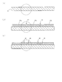
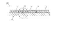
- FIG. 28 is a plan view showing a configuration of a conventional sputtering target 190.
- 29 is a cross-sectional view taken along line DD ′ of sputtering target 190 shown in FIG.
- FIG. 30 is an enlarged view of a part (a part surrounded by a broken line) of the sectional view according to FIG.
- the sputtering target 190 is a split type sputtering target composed of a plurality of flat target materials 10, a backing plate 20, and a bonding material 30.
- 28 and 29 show an example in which three target materials 10 are arranged side by side in the horizontal direction.
- Each target material 10 is made of a thin film material to be formed.
- Each target material 10 in this basic study is made of IGZO, which is an oxide semiconductor containing In, Ga, Zn, and O as main components.
- the backing plate 20 is made of Cu or the like.
- the bonding material 30 is made of In or the like.
- the plurality of target materials 10 and the backing plate 20 are joined via a bonding material 30.
- a slight gap is provided in the joint 15 between the target materials 10 adjacent to each other.
- the surface of the backing plate 20 is exposed at the joint 15 as shown in FIG.
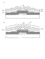
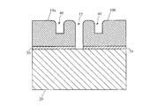
- FIG. 31 is a cross-sectional view showing a configuration of a TFT 290 in which a channel layer is formed using the conventional sputtering target 190 described above.
- the TFT 290 is a bottom gate type TFT having an etching stopper structure.
- a gate electrode 220 is formed on an insulating substrate 210 made of glass or the like.
- the gate electrode 220 is a stacked film in which a titanium (Ti) film with a thickness of 30 nm, an aluminum (Al) film with a thickness of 200 nm, and a Ti film with a thickness of 100 nm are sequentially formed.
- a gate insulating film 230 is formed on the gate electrode 220 so as to cover the gate electrode 220.
- the gate insulating film 230 is a laminated film in which a silicon nitride (SiN x ) film having a thickness of 325 nm and a silicon oxide (SiO 2 ) film having a thickness of 50 nm are sequentially formed.
- a channel layer 240 made of IGZO is formed on the gate insulating film 230. A method for forming the channel layer 240 will be described later.
- Etching stopper layers 250a, 250b, and 250c made of SiO 2 with a film thickness of 150 nm are respectively formed on the upper left portion, the upper right portion, and the upper central portion of the channel layer 240 in FIG.
- a source electrode 260a is formed so as to cover the etching stopper layer 250a, the channel layer 240 whose surface is exposed between the etching stopper layers 250a and 250c, and the left end portion of the etching stopper layer 250c.
- a drain electrode 260b is formed so as to cover the etching stopper layer 250b, the channel layer 240 whose surface is exposed between the etching stopper layers 250b and 250c, and the right end of the etching stopper layer 250c.
- a contact hole is formed between the etching stopper layers 250a and 250c, and the source electrode 260a and the channel layer 240 are connected by this contact hole.
- the source electrode 260a and the drain electrode 260b are stacked films in which a Ti film with a thickness of 30 nm and an Al film with a thickness of 200 nm are sequentially formed.
- a single metal film such as Ti, Al, Cu, molybdenum (Mo), tungsten (W), or chromium (Cr) or titanium nitride may be used as the source electrode 260a and the drain electrode 260b.
- An alloy film such as (TiN) or molybdenum nitride (MoN) may be used, or a laminated film of these may be used.
- a protective film 270 made of SiO 2 having a thickness of 200 nm is formed so as to cover the entire insulating substrate 210 on which the source electrode 260a and the drain electrode 260b are formed.
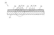
- the channel layer 240 is formed by magnetron sputtering.
- the magnetron sputtering method include a DC (Direct Current) magnetron sputtering method, an RF (Radio Frequency) magnetron sputtering method, and the like. Either the DC magnetron sputtering method or the RF magnetron sputtering method may be used to form the semiconductor film made of IGZO, but the following description will be made assuming that the DC magnetron sputtering method is used.
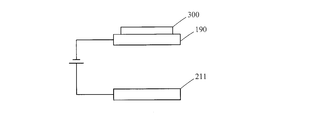
- a magnet 300 is disposed on the back surface (the surface on the backing plate 20 side) of the sputtering target 190, and the sputtering target 190 and the substrate 211 between which the magnet 300 is disposed on the back surface.
- a DC voltage is applied between them.
- the substrate 211 is an insulating substrate 210 having a gate electrode 220 and a gate insulating film 230 stacked on the surface.
- Argon (Ar) gas or the like is used as the sputtering gas. Note that a plurality of magnets 300 are usually used, but in FIG. 32, one is shown for convenience of illustration.
- the inventor of the present application conducted a characteristic measurement experiment of the TFT 290 in which the channel layer 240 was formed using the conventional sputtering target 190.
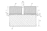
- the thickness T1 of each target material 10 shown in FIG. 30 is 6.0 mm
- the thickness T2 of the backing plate 20 is 10.0 mm
- the thickness T3 of the bonding material 30 is 0.3 mm.
- the width W1 of the joint 15 is 0.3 mm.
- the TFT 290 has a channel length of 8 ⁇ m and a channel width of 20 ⁇ m.
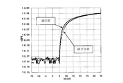
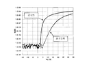
- FIG. 33 is a diagram showing the Id-Vg characteristics of the TFT 290 in which the channel layer 240 is formed using the conventional sputtering target 190 described above.
- Id represents the drain current
- Vg represents the gate voltage.
- the characteristics of the TFT 290 formed at a position other than the position corresponding to the seam 15 of the target material 10 are indicated by solid lines, and the position corresponding to the seam 15 of the target material 10 (hereinafter referred to as “seam portion”).
- the rise of the Id-Vg characteristic of the TFT 290 formed in the joint portion is worse than that of the TFT 290 formed in the normal portion.
- the backing plate 20 exposed at the joint 15 of the target material 10 and the bonding material 30 oozing out from the joint 15 are sputtered as impurities and these are mixed as impurities into the semiconductor film.
- the mobility of the TFT 290 formed at the joint portion is lowered, the threshold voltage is increased, and the like.
- the inventor of the present application has sputtered impurities as the backing plate 20 exposed at the joint 15 of the target material 10 and the bonding material 30 that has oozed out into the joint 15 in order to deteriorate the characteristics of the TFT 290 formed at the joint. I found out that there is a cause.
- an electric field concentrates on a corner of a conductor. That is, in the sputtering target 190, the electric field concentrates on the joint 15 of the target material 10. Since the concentrated electric field causes abnormal discharge (also referred to as “arcing”) at the joint 15, the film quality of the semiconductor film formed on the seam portion is different from the film quality of the semiconductor film formed on the normal portion. . That is, due to the influence of this abnormal discharge, the characteristics of the semiconductor film formed on the joint are deteriorated. As a result, in the TFT 290 formed in the joint portion, mobility is lowered, threshold voltage is increased, and the like.
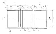
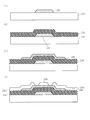
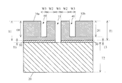
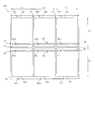
- FIG. 1 is a plan view showing a configuration of a sputtering target 100 according to the present embodiment.
- FIG. 2 is a cross-sectional view taken along line AA ′ of the sputtering target 100 shown in FIG.
- FIG. 3 is an enlarged view of a part (a portion surrounded by a broken line) of the sectional view according to FIG.
- the sputtering target 100 includes three flat target materials 10a to 10c (hereinafter referred to as “target material 10” when not distinguished from each other) made of the same material, and a flat support material.
- target material 10 This is a split type sputtering target 100 constituted by a backing plate 20 and a bonding material 30.
- the target material 10a located on the left side in FIG. 1, FIG. 10a ", the target material 10b located in the center may be referred to as" center target material 10b ", and the target material 10c located on the right side may be referred to as" right target material 10c ".
- the horizontal direction and the vertical direction in the referenced drawings are simply referred to as “horizontal direction” and “vertical direction”, respectively.
- the sputtering target 100 according to this embodiment is provided with grooves 40 on the surface of each target material 10. 1 and 2 show an example in which three target materials 10 are arranged side by side in the horizontal direction, the number of target materials 10 of the present embodiment is not limited to this.
- each target material 10 and the backing plate 20 are joined via a bonding material 30.
- a slight gap (width W1) is provided in the joint 15 between the target materials 10 adjacent to each other.
- the width W1 of the joint 15 is sufficiently smaller than the length L1 of the upper and lower sides of the target material 10 in FIG.
- the seam 15 is formed perpendicular to the surface of the backing plate 20, but is not limited thereto.
- the seam 15 may be formed in a staircase shape, an oblique shape, or the like.
- the surface of the backing plate 20 is exposed at the joint 15, but the present invention is not limited to this.
- the surface of the backing plate 20 may be covered at the joint 15 with an insulating tape, which will be described later, used when each target material 10 and the backing plate 20 are joined.
- the surface of the backing plate 20 may be covered with the bonding material 30 at the joint 15.
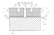
- the groove 40 is provided from the upper side to the lower side in FIG. 1 of the target material 10 in parallel with both sides (left side and right side) of the target material 10 in FIG. More specifically, the groove 40 having the same length as the length L2 on both sides of the target material 10 and a depth D1 is parallel to the seam 15 and in the vicinity of the seam 15 (a distance W2 away from the seam 15). ).
- the distance W2 from the joint 15 to the groove 40 is sufficiently smaller than the length L1 of the upper and lower sides of the target material 10.
- the depth D1 of the groove 40 is smaller than the thickness T1 of the target material 10.
- the width W1 of the joint 15 and the width W3 of the groove 40 are preferably substantially the same, but the present invention is not limited to this.
- one groove 40 is provided corresponding to one seam 15 on each of one surface and the other surface of the target material 10 adjacent to each other forming the seam 15. That is, the groove 40 divides the surface of the left target material 10a into regions Ra1 and Ra2, the surface of the central target material 10b into regions Rb1, Rb2, and Rb3, and the surface of the right target material 10c into regions Rc1 and Rc2. Has been. More specifically, one groove 40 is provided in the vicinity of the left side of the seam 15 on the surface of the left target material 10a corresponding to the seam 15 formed by the left target material 10a and the central target material 10b. One groove 40 is provided near the right side of the joint 15 on the surface of the target material 10b.
- one groove 40 is provided near the left side of the joint 15 on the surface of the central target material 10b, and the right target material 10c.
- One groove 40 is provided in the vicinity of the right side of the seam 15 on the surface.
- each target material 10 is IGZO, which is an oxide semiconductor containing In, Ga, Zn, and O as main components. Not limited to this, the material of each target material 10 is at least one of In, Ga, Zn, Cu, silicon (Si), tin (Sn), Al, calcium (Ca), germanium (Ge), and lead (Pb). An oxide semiconductor including one (so-called “IGZO-based oxide semiconductor”) may be used. Each target material 10 may be a semiconductor other than an oxide (for example, Si).
- the material of the backing plate 20 is not particularly limited, and is, for example, Cu or the like having excellent conductivity and thermal conductivity.
- the material of the bonding material 30 is not particularly limited, and is, for example, In.
- FIGS. 5A to 5C are cross-sectional views taken along line AA ′ of the sputtering target 100 shown in FIG. 1 for explaining the method for manufacturing the sputtering target 100 according to this embodiment.
- FIGS. 6A to 6C are enlarged views of parts of FIGS. 5A to 5C, respectively.
- the bonding material 30 is solidified by cooling the bonding material 30. Thereby, the three target materials 10 and the backing plate 20 are joined via the bonding material 30 (FIGS. 5B and 6B). At this time, a seam 15 having a width W1 is formed.
- the width W1 can be accurately set by pasting the target materials 10 together using an insulating tape as described above.
- a groove 40 having a length L2 and a depth D1 is formed on the surface of each target material 10 at a position parallel to the seam 15 and at a distance W2 from the seam 15 (FIG. 5C ), FIG. 6 (C)).
- the surface of the left target material 10a is divided into regions Ra1 and Ra2
- the surface of the central target material 10b is divided into regions Rb1, Rb2, and Rb3
- the surface of the right target material 10c is divided into regions Rc1 and Rc2.
- the groove 40 may be formed not only by grinding with a disk grinder or the like, but also by lathe machining with a lathe or the like, or fusing with a laser or the like. Further, grooves 40 are formed on the surface of each target material 10 before the three target materials 10 and the backing plate 20 are joined, and thereafter, the three target materials 10 formed with the grooves 40 and the backing plate 20 are joined. May be.
- the sputtering target 100 according to this embodiment is manufactured by the above method.
- FIG. 7 is a cross-sectional view showing a configuration of a TFT 200 in which a channel layer is formed using the sputtering target 100 according to this embodiment. Since the configuration of the TFT 200 in this embodiment is the same as the configuration of the TFT 290 in the basic study, the description thereof is omitted.
- FIG. 9A, and FIG. 9B are cross-sectional views for explaining the manufacturing process of the TFT 200 in the present embodiment. Note that in FIGS. 8A to 8D, FIG. 9A, and FIG. 9B, the resist pattern is not shown for convenience.
- a resist pattern is formed on the center upper portion of the laminated film by photolithography.
- the stacked film is etched using the resist pattern as a mask, thereby forming the gate electrode 220 (FIG. 8A).
- a dry etching method is used for the etching.
- a 325 nm-thickness SiN x film and a 50 nm-thickness SiO 2 film are sequentially stacked on the insulating substrate 210 on which the gate electrode 220 is formed by plasma CVD.
- the gate insulating film 230 is formed (FIG. 8B).
- an IGZO semiconductor film is formed on the gate insulating film 230.
- either the DC magnetron sputtering method or the RF magnetron sputtering method may be used for forming the IGZO semiconductor film.
- the magnet 300 is disposed on the back surface (the surface on the backing plate 20 side) of the sputtering target 100 according to the present embodiment, and between the sputtering target 100 and the substrate 211.
- a DC voltage is applied to.
- the substrate 211 is an insulating substrate 210 having a gate electrode 220 and a gate insulating film 230 stacked on the surface. Ar gas or the like is used as the sputtering gas.
- a resist pattern is formed on the upper center of the IGZO semiconductor film by photolithography.
- the channel layer 240 is formed by etching the IGZO semiconductor film using the resist pattern as a mask (FIG. 8C).
- a wet etching method is used for the etching.
- an etching stopper layer made of a 150 nm-thickness SiO 2 film is formed by plasma CVD on the insulating substrate 210 on which the channel layer 240 is formed.
- a resist pattern is formed on the upper left portion, upper right portion, and upper central portion of the etching stopper layer in FIG. 8D by photolithography.
- etching stopper layers 250a, 250b, and 250c are formed on the upper left portion, the upper right portion, and the upper central portion of the channel layer 240, respectively (FIG. 8D).
- contact holes are formed between the etching stopper layers 250a and 250c and between the etching stopper layers 250b and 250c, respectively.
- a dry etching method is used for the etching.
- a laminated film in which a Ti film having a thickness of 30 nm and an Al film having a thickness of 200 nm are sequentially formed so as to cover the entire insulating substrate 210 is formed.
- a single metal film such as Ti, Al, Cu, Mo, W, or Cr, or an alloy film such as TiN or MoN may be formed. May be formed.
- the etching stopper layer 250a, the channel layer 240 whose surface is exposed between the etching stopper layers 250a and 250c, and the left end portion of the etching stopper layer 250c are opposed to each other by photolithography.
- a resist pattern is formed at a position opposite the etching stopper layer 250b, the channel layer 240 whose surface is exposed between the etching stopper layers 250b and 250c, and the right end of the etching stopper layer 250c. Thereafter, the laminated film is etched using the resist pattern as a mask. As a result, the source electrode 260a is formed so as to cover the etching stopper layer 250a, the channel layer 240 whose surface is exposed between the etching stopper layers 250a and 250c, and the left end portion of the etching stopper layer 250c.
- the drain electrode 260b is formed so as to cover the etching stopper layer 250b, the channel layer 240 whose surface is exposed between the etching stopper layers 250b and 250c, and the right end of the etching stopper layer 250c (FIG. 9A). )). At this time, since the surface of the channel layer 240 is covered with the etching stopper layer 250c, the surface of the channel layer 240 is not etched.
- a wet etching method is used for the etching.
- a protective film 270 made of SiO 2 having a thickness of 200 nm is formed by plasma CVD so as to cover the entire insulating substrate 210 (FIG. 9B).
- the TFT 200 in this embodiment can be manufactured.
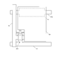
- FIG. 10 is a diagram showing a part of an active matrix substrate of a liquid crystal display device in which a TFT 200 in which a channel layer 240 is formed using the sputtering target 100 according to the present embodiment is provided as a pixel TFT.
- This active matrix substrate includes a plurality of source lines SL and a plurality of gate lines GL arranged in a lattice pattern on the insulating substrate 210 so as to intersect with each other, and each intersection of the plurality of source lines SL and the plurality of gate lines GL.
- the TFT 200, the pixel electrode Ec, and the auxiliary capacitance electrode Ec provided in correspondence with each other, and the auxiliary capacitance line CSL arranged along each gate line GL.
- the auxiliary capacitance line CSL is connected to the auxiliary capacitance electrode Ec.
- Liquid crystal is filled between the pixel electrode Ep and a common electrode (not shown) facing the pixel electrode Ep.
- a liquid crystal capacitor is formed by the pixel electrode Ep and the common electrode, and an auxiliary capacitor is formed by the pixel electrode Ep and the auxiliary capacitor line CSL.
- the TFT 200 is provided corresponding to the intersection of the source line SL and the gate line GL that intersect each other.
- the source electrode 260a of the TFT 200 is connected to the source line SL
- the gate electrode 220 is connected to the gate line GL
- the drain electrode 260b is connected to the pixel electrode Ep.
- the drain electrode 260b and the pixel electrode Ep are connected to each other via a contact hole (not shown).
- a plurality of source signals are respectively applied to the plurality of source lines SL, and a plurality of gate signals are respectively applied to the plurality of gate lines GL, whereby the pixel electrode is displayed on the basis of the potential applied to the common electrode.
- a voltage corresponding to the pixel value of the pixel to be supplied is applied via the TFT 200, and is held in the pixel capacitor composed of the liquid crystal capacitor and the auxiliary capacitor. Thereby, a voltage corresponding to the potential difference between each pixel electrode and the common electrode is applied to the liquid crystal layer.
- An image is displayed by controlling the light transmittance of the liquid crystal layer by this applied voltage.
- the inventor of the present application conducted a characteristic experiment of the TFT 200 in which the channel layer 240 was formed using the sputtering target 100 according to the present embodiment.
- the thickness T1 of each target material 10 shown in FIG. 3 is 6.0 mm
- the thickness T2 of the backing plate 20 is 10.0 mm
- the thickness T3 of the bonding material 30 is 0.3 mm.
- the depth D1 of the groove 40 is 3.0 mm
- the width W1 of the joint 15 is 0.3 mm
- the distance W2 from the joint 15 to the groove 40 is 10.0 mm
- the width W3 of the groove 40 is 0.3 mm.
- the TFT 200 has a channel length of 8 ⁇ m and a channel width of 20 ⁇ m.
- FIG. 11 is a diagram showing Id-Vg characteristics of the TFT 200 in which the channel layer 240 is formed using the sputtering target 100 according to the present embodiment.
- Id represents the drain current
- Vg represents the gate voltage.
- the characteristics of the TFT 200 formed in the normal portion are indicated by a solid line, and the characteristics of the TFT 200 formed in the joint portion are indicated by a broken line.
- the TFT 290 in which the channel layer 240 is formed using the conventional sputtering target 190 has a worse Id-Vg characteristic when formed at the seam portion than when formed at the normal portion. There was a problem.
- the Id-Vg characteristic when formed in the normal part is almost equal to the Id-Vg characteristic when formed in the normal part. Become.
- a groove 40 having a structure similar to the joint 15 is provided along the joint 15 of the target material 10.
- the concentration of the electric field generated in the joint 15 is dispersed in the groove 40. Therefore, the degree of electric field concentration generated in each of the groove 40 and the joint 15 of the sputtering target 100 according to the present embodiment, compared to the degree of electric field concentration generated only in the joint 15 of the conventional sputtering target 190 in which the groove 40 is not provided. Is reduced.
- the degree of electric field concentration is high enough to be observed as a TFT characteristic abnormality, whereas in the sputtering target 100 according to the present embodiment, the electric field concentration is not observed as a TFT characteristic abnormality.
- the degree is low.
- the characteristics when formed in the joint portion and the characteristics when formed in the normal portion are substantially equal.
- the groove 40 along the joint 15 is provided on the surface of the target material 10. Thereby, the electric field concentration at the joint 15 is alleviated. Therefore, a semiconductor film with good characteristics can be obtained.
- the groove 40 is provided in the vicinity of the joint 15 and on both sides. Thereby, the electric field concentration at the joint 15 can be further relaxed.
- FIG. 12 is a plan view showing the configuration of the sputtering target 100 according to the first modification of the present embodiment.
- FIG. 13 is a cross-sectional view taken along the line BB ′ of the sputtering target 100 shown in FIG.
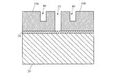
- one groove 40 is provided corresponding to one joint 15 only in one of the target materials 10 adjacent to each other forming the joint 15.
- a groove 40 having a length L2 is provided at each of the positions apart from each other. That is, the surface of the central target material 10b is divided into regions Rb1 and Rb2 by the grooves 40. On the other hand, the groove
- the distance W2 from the joint 15 to the groove 40 is sufficiently smaller than the length L1 of the upper and lower sides of the target material 10. Further, the depth D1 of the groove 40 is smaller than the thickness T1 of the target material 10.
- the number of grooves 40 is reduced as compared with the case where the grooves 40 are provided on both sides of the joint 15, the cost for forming the grooves 40 can be reduced. Further, the strength of the target material 10 can be sufficiently maintained.
- this modification is not limited to the configuration in which the two grooves 40 are provided on the surface of the central target material 10b.
- a groove 40 is provided on the surface of the left target material 10a at a distance W2 from the joint 15 formed on the right side of the left target material 10a, and the right target material is formed on the surface of the right target material 10c.
- the groove 40 may be provided at a position separated from the joint 15 formed on the left side of 10c by a distance W2.
- FIG. 14 is a cross-sectional view showing a configuration of a sputtering target 100 according to a second modification of the present embodiment. Moreover, it is the figure which expanded a part (part enclosed with the broken line) of sectional drawing concerning FIG.
- the groove 40 disappears.
- the electric field concentration at the joint 15 is not relaxed, and the characteristics of the TFT 200 formed at the joint are deteriorated as in the conventional case.
- the depth D1 of the groove 40 is further increased as compared with the sputtering target 100 according to the present embodiment described above. More specifically, a groove 40 having a depth D1 of 5.0 mm is provided in the target material 10 having a thickness T1 of 6.0 mm. Other parameters are the same as those of the sputtering target 100 according to the above-described embodiment.
- the life of the groove 40 can be extended by forming the groove 40 deeply in advance. Thereby, even if the sputtering of the target material 10 proceeds, it is possible to prevent the deterioration of the characteristics of the TFT 200 formed at the joint portion.
- FIG. 16 is a plan view showing a configuration of a sputtering target 100 according to a third modification of the present embodiment.
- a length L2 and a depth corresponding to one seam 15 are respectively provided on one surface and the other surface of the target material 10 adjacent to each other forming the seam 15.
- Three grooves 40 of length D1 are provided.
- the surface of the left target material 10a is in the regions Ra1, Ra2, Ra3 and Ra4
- the surface of the central target material 10b is in the regions Rb1, Rb2, Rb3, Rb4 and Rb5
- the surface of the right target material 10c is The region is divided into Rc1, Rc2, Rc3, and Rc4.
- a groove 40 having a length L2 and a depth D1 is formed in the vicinity of the left side of the joint 15 on the surface of the left target material 10a.
- three grooves 40 having a length L2 and a depth D1 are provided in the vicinity of the right side of the joint 15 on the surface of the central target material 10b.
- three grooves 40 are provided near the left side of the joint 15 on the surface of the central target material 10b, and the right target material 10c.
- Three grooves 40 are provided in the vicinity of the right side of the seam 15 on the surface.
- the number of grooves 40 that disperse the electric field concentration generated in the joint 15 increases. Therefore, the degree of electric field concentration generated in each of the joint 15 and the groove 40 is further reduced as compared with the conventional case. As a result, the characteristics of the TFT 200 formed in the seam portion are closer to the characteristics of the TFT 200 formed in the normal portion.
- three grooves 40 are provided in the vicinity of the left side and the right side of each joint 15, but the number of grooves 40 is not limited to this.
- two grooves 40 may be provided in the vicinity of the left side and the right side of each joint 15.
- four or more grooves 40 may be provided in the vicinity of the left side and the right side of each joint 15.
- FIG. 17 is an enlarged view of a part of a cross-sectional view of the sputtering target 100 according to the fourth modification of the present embodiment.
- the corner portions of the target material 10 corresponding to the joints 15 and the grooves 40 are chamfered.
- Each of the left target material 10a and the central target material 10b is chamfered at the corners of the left target material 10a and the central target material 10b.
- the electric field concentration at the joint 15 is further reduced, and the electric field concentration at the groove 40 is also reduced. Therefore, a semiconductor film with better characteristics can be obtained.
- FIG. 18 is a plan view showing the configuration of the sputtering target 100 according to the fifth modification of the present embodiment.
- a groove 40 having a length L2 and a depth D1 parallel to the joint 15 is provided in the center of each target material 10 in the lateral direction. That is, the groove 40 divides the surface of the left target material 10a into regions Ra1 and Ra2, the surface of the central target material 10b into regions Rb1 and Rb2, and the surface of the right target material 10c into regions Rc1 and Rc2. Yes. More specifically, one groove 40 is provided in each of the lateral center of the surface of the left target material 10a, the lateral center of the surface of the central target material 10b, and the lateral center of the right target material 10c.
- the electric field concentration at the joint 15 can be reduced more than before.
- the electric field concentration at the seam 15 is also achieved by providing a groove 40 having a length L1 and a depth D1 perpendicular to the seam 15 at the longitudinal center of the surface of each target material 10. It can be relaxed more than before.
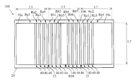
- FIG. 20 is a plan view showing a configuration of a sputtering target 100 according to a sixth modification of the present embodiment.
- a sputtering target 100 according to the present modification includes six flat target materials 10a to 10f (hereinafter referred to as “target material 10” when they are not distinguished from each other) made of the same material (IGZO).
- target material 10 located on the upper left side in FIG. 20, FIG. 22 and FIG. 10b "
- the target material 10c located on the upper right side is” upper right side target material 10c "
- the target material 10d located on the lower left side is” left lower side target material 10d "
- the target material 10e is located on the lower center side.
- FIG. 20 shows an example in which three target materials 10 are arranged in the horizontal direction and two in the vertical direction.
- the number of target materials 10 in the present modification is not limited to this. Absent.
- the seam 15 extending in the vertical direction not only the seam 15 between the target materials 10 adjacent to each other in the horizontal direction (hereinafter referred to as “the seam 15 extending in the vertical direction”) but also the target materials adjacent to each other in the vertical direction.
- There are ten seams 15 hereinafter referred to as “laterally extending seams 15”).
- each of the one surface and the other surface of the target material 10 adjacent to each other forming the longitudinally extending seam 15 is provided.
- One groove 40 having a length L2 and a depth D1 is provided in parallel with the seam 15 extending in the longitudinal direction. That is, due to the groove 40, the surface of the upper left target material 10a is in the regions Ra1 and Ra2, the surface of the central upper target material 10b is in the regions Rb1, Rb2, and Rb3, and the surface of the upper right target material 10c is in the regions Rc1 and Rc2.
- the surface of the lower left target material 10d is in the regions Rd1 and Rd2
- the surface of the central lower target material 10e is in the regions Re1, Re2, and Re3
- the surface of the lower right target material 10f is in the regions Rf1 and Rf2. It is divided into
- one groove 40 is provided in the vicinity of the left side of the seam 15 on the surface of the upper left target material 10a corresponding to the seam 15 formed by the upper left target material 10a and the central upper target material 10b. At the same time, one groove 40 is provided in the vicinity of the right side of the joint 15 on the surface of the center upper target material 10b. Further, in correspondence with the joint 15 formed by the center upper target material 10b and the upper right target material 10c, one groove 40 is provided in the vicinity of the left side of the joint 15 on the surface of the center upper target material 10b. One groove 40 is provided in the vicinity of the right side of the joint 15 on the surface of the side target material 10c.
- one groove 40 is provided in the vicinity of the left side of the seam 15 on the surface of the lower left target material 10d corresponding to the seam 15 formed by the lower left target material 10d and the central lower target material 10e.
- One groove 40 is provided in the vicinity of the right side of the joint 15 on the surface of the center lower target material 10e.
- one groove 40 is provided near the left side of the joint 15 on the surface of the center lower target material 10e corresponding to the joint 15 formed by the center lower target material 10e and the right lower target material 10f.
- one groove 40 is provided in the vicinity of the right side of the joint 15 on the surface of the lower right target material 10f.
- a groove 40 having a length L1 and a depth D1 may be provided in parallel with the seam 15 extending in the lateral direction.
- the surface of the upper left target material 10a is in the regions Ra1 and Ra2
- the surface of the central upper target material 10b is in the regions Rb1 and Rb2
- the surface of the upper right target material 10c is in the regions Rc1 and Rc2.
- the surface of the lower left target material 10d is divided into regions Rd1 and Rd2
- the surface of the center lower target material 10e is divided into regions Re1 and Re2
- the surface of the lower right target material 10f is divided into regions Rf1 and Rf2.
- one groove 40 is provided near the upper side of the seam 15 on the surface of the upper left target material 10a corresponding to the seam 15 formed by the upper left target material 10a and the lower left target material 10d. At the same time, one groove 40 is provided near the lower side of the joint 15 on the surface of the lower left target material 10d. Further, in correspondence with the joint 15 formed by the central upper target material 10b and the central lower target material 10e, one groove 40 is provided near the upper side of the joint 15 on the surface of the central upper target material 10b. One groove 40 is provided near the lower side of the seam 15 on the surface of the center lower target material 10e.
- one groove 40 is provided near the upper side of the seam 15 on the surface of the upper right target material 10c corresponding to the seam 15 formed by the upper right target material 10c and the lower right target material 10f.
- One groove 40 is provided near the lower side of the seam 15 on the surface of the lower right target material 10f.
- a groove 40 having a length L2 and a depth D1 is provided in parallel to the seam 15 extending in the longitudinal direction and in the vicinity of the seam 15 extending in the longitudinal direction, and parallel to the seam 15 extending in the lateral direction.
- a groove 40 having a length L1 and a depth D1 may be provided in the vicinity of the seam 15 extending in the lateral direction.
- the surface of the upper left target material 10a is in the regions Ra1, Ra2, Ra3, and Ra4, and the surface of the central upper target material 10b is in the regions Rb1, Rb2, Rb3, Rb4, Rb5, and Rb6.
- the surface of the upper right target material 10c is in the regions Rc1, Rc2, Rc3, and Rc4, the surface of the lower left target material 10d is in the regions Rd1, Rd2, Rd3, and Rd4, and the surface of the central lower target material 10e is in the region Re1.
- the surface of the lower right target material 10f is divided into regions Rf1, Rf2, Rf3, and Rf4 in Re2, Re3, Re4, Re5, and Re6.
- the electric field concentration generated at the joint 15 can be reduced in a sputtering target suitable for use in a large display panel. Note that according to the configuration shown in FIG. 22, the electric field concentration generated in the joint 15 can be further reduced as compared with the configuration shown in FIG. 20 or 21.
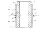
- FIG. 23 is a perspective view showing the configuration of the sputtering target 100 according to this embodiment.
- 24 is a cross-sectional view taken along the line CC ′ of the sputtering target 100 shown in FIG.
- FIG. 25 is an enlarged view of a part (a portion surrounded by a broken line) of the sectional view according to FIG.
- the sputtering target 100 is a split type sputtering target composed of two cylindrical target materials 10 a and 10 b made of the same material (IGZO), a backing tube 22, and a bonding material 30. is there.
- the target material 10a located on the upper side in FIG. 23 or FIG.
- each target material 10 may be called “upper target material 10a”, and the target material 10b located on the lower side may be called “lower target material 10b”.
- the outer diameter and inner diameter of each target material 10 are respectively larger than the outer diameter and inner diameter of the backing plate 20.
- 23 and 24 show an example in which two target materials 10 are arranged in the vertical direction, the present invention is not limited to this.
- the number of target materials 10 of this embodiment is not limited to this.
- the width W1 of the joint 15 in this embodiment is sufficiently smaller than the height (length in the vertical direction) L3 of the target material 10 in FIG.
- the seam 15 is formed perpendicular to the surface of the backing tube 22, but is not limited to this.
- the seam 15 may be formed in a staircase shape or an oblique shape.
- the groove 40 is provided along the circumferential direction of the cylindrical target material 10. More specifically, a groove 40 having the same length as the circumference of the target material 10 and a depth D1 is provided in parallel to the seam 15 and in the vicinity of the seam 15 (position away from the seam 15 by a distance W2). ing.
- the distance W2 from the joint 15 to the groove 40 is sufficiently smaller than the height L3 of the target material 10.
- one groove 40 is provided corresponding to one seam 15 on each of one surface and the other surface of the target material 10 adjacent to each other forming the seam 15. That is, the groove 40 divides the surface of the upper target material 10a into regions Ra1 and Ra2, and the surface of the lower target material 10b into regions Rb1 and Rb2. More specifically, one groove 40 is provided near the upper side of the seam 15 on the surface of the upper target material 10a corresponding to the seam 15 formed by the upper target material 10a and the lower target material 10b. One groove 40 is provided near the lower side of the joint 15 on the surface of the lower target material 10b.
- the target materials 10a and 10b on the cylinder made of IGZO are fitted into the cylindrical backing tube 22 made of Cu or the like (FIG. 26A) (FIG. 26B).
- a tape for example, an insulating tape.
- a molten bonding material 30 made of In or the like is injected between the two target materials 10 and the backing tube 22.
- the insulating tape is peeled off, and the bonding material 30 at the joint 15 is scraped out. Note that the insulating tape may not be peeled off.
- the bonding material 30 is solidified by cooling the bonding material 30. Thereby, the two target materials 10 and the backing tube 22 are joined via the bonding material 30 (FIG. 27A). At this time, a seam 15 having a width W1 is formed.
- the width W1 can be accurately set by sticking the target materials 10a and 10b to each other using an insulating tape as described above.
- a groove 40 having a depth D1 is formed on the surface of each target material 10 on the surface of each target material 10 at a position parallel to the seam 15 and at a distance W2 from the seam 15 ( FIG. 27 (B)).
- the surface of the upper target material 10a is divided into regions Ra1 and Ra2
- the surface of the lower target material 10b is divided into regions Rb1 and Rb2.
- the backing tube 22 is fixed to a predetermined support base, the disc grinder is fixed so that the groove 40 is not displaced, and the backing tube 22 and the target material 10 joined together by the bonding material 30 are rotated.
- the groove 40 can be formed uniformly.
- the groove 40 may be formed not only by grinding with a disk grinder or the like, but also by lathe machining with a lathe or the like, or fusing with a laser or the like. In addition, grooves 40 are formed on the surface of each target material 10 before joining each target material 10 and backing tube 22, and then each target material 10 formed with grooves 40 and backing tube 22 are joined. Good.
- the sputtering target 100 according to this embodiment is manufactured by the above method.
- the sputtering target 100 according to the present invention can be used not only for forming a semiconductor film but also for forming a conductive film or the like.
- a bottom gate type TFT having an etching stopper structure is taken as an example, but the present invention is not limited to this.
- a TFT having a channel etch structure or a top gate type may be used.
- a configuration in which the groove 40 is provided at the center of the target material 10 can be employed.
- a cylindrical support member (backing tube 22) is used, but a columnar support member may be used instead.
- the sputtering target which can obtain a semiconductor film with a favorable characteristic can be provided.
- membrane with a favorable characteristic can be provided.
- the present invention can be applied to a sputtering target used for forming a semiconductor film or the like.
Landscapes
- Engineering & Computer Science (AREA)
- Physics & Mathematics (AREA)
- Chemical & Material Sciences (AREA)
- Power Engineering (AREA)
- Microelectronics & Electronic Packaging (AREA)
- Condensed Matter Physics & Semiconductors (AREA)
- Computer Hardware Design (AREA)
- General Physics & Mathematics (AREA)
- Plasma & Fusion (AREA)
- Analytical Chemistry (AREA)
- Manufacturing & Machinery (AREA)
- Chemical Kinetics & Catalysis (AREA)
- Ceramic Engineering (AREA)
- Organic Chemistry (AREA)
- Metallurgy (AREA)
- Mechanical Engineering (AREA)
- Materials Engineering (AREA)
- Thin Film Transistor (AREA)
- Physical Deposition Of Substances That Are Components Of Semiconductor Devices (AREA)
- Physical Vapour Deposition (AREA)
Abstract
Description
互いに同じ材料からなる複数のターゲット材と、
前記複数のターゲット材を支持する支持材と、
前記複数のターゲット材と前記支持材とを接合するボンディング材とを備え、
互いに隣接するターゲット材の少なくとも一方の表面に、当該表面を2以上の領域に分割する溝が設けられていることを特徴とする。
各ターゲット材が半導体からなることを特徴とする。
前記半導体が酸化物半導体であることを特徴とする。
前記酸化物半導体が、インジウム、ガリウム、亜鉛、および酸素を主成分とすることを特徴とする。
前記酸化物半導体が、インジウム、ガリウム、亜鉛、銅、珪素、錫、アルミニウム、カルシウム、ゲルマニウム、および鉛のうち少なくとも1つを含むことを特徴とする。
前記溝が、互いに隣接するターゲット材同士の継ぎ目と平行に設けられていることを特徴とする。
前記溝が、前記継ぎ目の近傍に設けられていることを特徴とする。
前記継ぎ目に対応して、前記互いに隣接するターゲット材の一方の表面と他方の表面とのそれぞれに前記溝が少なくとも1つ設けられていることを特徴とする。
前記継ぎ目に対応して、前記互いに隣接するターゲット材の一方の表面と他方の表面とのそれぞれに前記溝が複数設けられていることを特徴とする。
前記継ぎ目に対応して、前記互いに隣接するターゲット材のいずれか一方の表面に前記溝が1つ設けられていることを特徴とする。
前記溝の深さが、当該溝が設けられたターゲット材の厚さの1/2以上であって、当該溝が設けられたターゲット材の厚さ未満であることを特徴とする。
各ターゲット材の、前記溝および前記継ぎ目に対応した角部が面取りされていることを特徴とする。
前記支持材が平板状に形成され、
各ターゲット材が平板状に形成されていることを特徴とする。
前記支持材が円筒状または円柱状に形成され、
各ターゲット材が円筒状に形成されていることを特徴とする。
本発明の第2の局面から本発明の第14の局面までのいずれかに係るスパッタリングターゲットをスパッタすることによりチャネル層を形成する工程を備えることを特徴とする。
互いに隣接するターゲット材の少なくとも一方の表面に、当該表面を2以上の領域に分割する溝を形成する工程を備えることを特徴とする。
本発明の実施形態について説明する前に、上記課題を解決すべく本願発明者によりなされた基礎検討について説明する。
従来のスパッタリングターゲットの構成について、図28~図30を参照しながら説明する。図28は、従来のスパッタリングターゲット190の構成を示す平面図である。図29は、図28に示すスパッタリングターゲット190のD-D’線断面図である。図30は、図29に係る断面図の一部(破線で囲んだ部分)を拡大した図である。
図31は、上記従来のスパッタリングターゲット190を用いてチャネル層を形成したTFT290の構成を示す断面図である。図31に示すように、TFT290は、エッチングストッパ構造のボトムゲート型TFTである。
上記チャネル層240は、マグネトロンスパッタリング法により形成される。マグネトロンスパッタリング法としては、DC(Direct Current)マグネトロンスパッタリング法、RF(Radio Frequency)マグネトロンスパッタリング法等が挙げられる。IGZOからなる半導体膜の成膜にはDCマグネトロンスパッタリング法またはRFマグネトロンスパッタリング方のどちらを用いてもよいが、以下では、DCマグネトロンスパッタリング法を用いるものとして説明する。
本願発明者は、上記従来のスパッタリングターゲット190を用いてチャネル層240を形成したTFT290の特性測定実験を行った。この実験に用いたスパッタリングターゲット190では、図30に示す各ターゲット材10の厚さT1を6.0mm、バッキングプレート20の厚さT2を10.0mm、ボンディング材30の厚さT3を0.3mm、継ぎ目15の幅W1を0.3mmとしている。また、TFT290のチャネル長を8μm、チャネル幅を20μmとしている。
<1.1 スパッタリングターゲットの構成>
本発明の第1の実施形態に係るスパッタリングターゲットの構成について、図1~図3を参照しながら説明する。図1は、本実施形態に係るスパッタリングターゲット100の構成を示す平面図である。図2は、図1に示すスパッタリングターゲット100のA-A’線断面図である。図3は、図2に係る断面図の一部(破線で囲んだ部分)を拡大した図である。
本実施形態に係るスパッタリングターゲット100の製造方法について、図5(A)~図5(C)および図6(A)~図6(C)を参照しながら説明する。図5(A)~図5(C)は、本実施形態に係るスパッタリングターゲット100の製造方法を説明するための、図1に示すスパッタリングターゲット100のA-A’線断面図である。図6(A)~図6(C)は、図5(A)~図5(C)の一部をそれぞれ拡大した図である。
図7は、本実施形態に係るスパッタリングターゲット100を用いてチャネル層を形成したTFT200の構成を示す断面図である。本実施形態におけるTFT200の構成は上記基礎検討におけるTFT290の構成と同様であるため、その説明を省略する。
本願発明者は、本実施形態に係るスパッタリングターゲット100を用いてチャネル層240を形成したTFT200の特性実験を行った。この実験に用いたスパッタリングターゲット100では、図3に示す各ターゲット材10の厚さT1を6.0mm、バッキングプレート20の厚さT2を10.0mm、ボンディング材30の厚さT3を0.3mm、溝40の深さD1を3.0mm、継ぎ目15の幅W1を0.3mm、継ぎ目15から溝40までの距離W2を10.0mm、溝40の幅W3を0.3mmとしている。また、TFT200のチャネル長を8μm、チャネル幅を20μmとしている。
本実施形態によれば、ターゲット材10の表面に、継ぎ目15に沿った溝40が設けられる。これにより、継ぎ目15での電界集中が緩和される。したがって、特性の良好な半導体膜を得ることができる。
図12は、本実施形態の第1の変形例に係るスパッタリングターゲット100の構成を示す平面図である。また、図13は、図12に示すスパッタリングターゲット100のB-B’線断面図である。本変形例に係るスパッタリングターゲット100では、1つ継ぎ目15に対応して、この継ぎ目15を形成している互いに隣接するターゲット材10のいずれか一方にのみ溝40が1つ設けられている。本変形例に係るスパッタリングターゲット100では、中央ターゲット材10bの表面において、この中央ターゲット材10bの左側に形成された継ぎ目15から距離W2だけ離れた位置、および右側に形成された継ぎ目15から距離W2だけ離れた位置のそれぞれに長さL2の溝40が設けられている。すなわち、中央ターゲット材10bの表面が溝40により領域Rb1とRb2とに分割されている。一方、左側ターゲット材10aおよび右側のターゲット材10cの表面には溝40が設けられていない。
図14は、本実施形態の第2の変形例に係るスパッタリングターゲット100の構成を示す断面図である。また、図15に係る断面図の一部(破線で囲んだ部分)を拡大した図である。
図16は、本実施形態の第3の変形例に係るスパッタリングターゲット100の構成を示す平面図である。本変形例に係るスパッタリングターゲット100では、1つの継ぎ目15に対応して、この継ぎ目15を形成している互いに隣接するターゲット材10の一方の表面と他方の表面とのそれぞれに長さL2、深さD1の溝40が3つ設けられている。すなわち、溝40により、左側ターゲット材10aの表面が領域Ra1とRa2とRa3とRa4とに、中央ターゲット材10bの表面が領域Rb1とRb2とRb3とRb4とRb5に、右側ターゲット材10cの表面が領域Rc1とRc2とRc3とRc4とに分割されている。
図17は、本実施形態の第4の変形例に係るスパッタリングターゲット100の断面図の一部を拡大した図である。本変形例に係るスパッタリングターゲット100では、ターゲット材10の、継ぎ目15および溝40に対応した角部に面取りが施されている。例えば、図17に示すように、左側ターゲット材10aの表面に設けられた溝40に存在するこの左側ターゲット材10aの角部と、左側ターゲット材10aと中央ターゲット材10bとによって形成された継ぎ目15に存在する左側ターゲット材10aおよび中央ターゲット材10bそれぞれの角部と、中央ターゲット材10bの表面に設けられた溝40に存在するこの中央ターゲット材10bの角部とが面取りされている。
図18は、本実施形態の第5の変形例に係るスパッタリングターゲット100の構成を示す平面図である。本変形例に係るスパッタリングターゲット100では、各ターゲット材10の横方向中央に、継ぎ目15と平行な、長さL2、深さD1の溝40が設けられている。すなわち、溝40により、左側ターゲット材10aの表面が領域Ra1とRa2とに、中央ターゲット材10bの表面が領域Rb1とRb2とに、右側ターゲット材10cの表面が領域Rc1とRc2とに分割されている。より詳細には、左側ターゲット材10aの表面の横方向中央、中央ターゲット材10bの表面の横方向中央、および右側ターゲット材10cの横方向中央のそれぞれに溝40が1つ設けられている。
図20は、本実施形態の第6の変形例に係るスパッタリングターゲット100の構成を示す平面図である。本変形例に係るスパッタリングターゲット100は、互いに同じ材料(IGZO)からなる6つの平板状のターゲット材10a~10f(以下、これらを区別しない場合に「ターゲット材10」という)を備えている。以下、本変形例では、図20、後述の図22、図23における左上側に位置するターゲット材10aを「左上側ターゲット材10a」と、中央上側に位置するターゲット材10bを「中央上側ターゲット材10b」と、右上側に位置するターゲット材10cを「右上側ターゲット材10c」と、左下側に位置するターゲット材10dを「左下側ターゲット材10d」と、中央下側に位置するターゲット材10eを「中央下側ターゲット材10e」と、右下側に位置するターゲット材10fを「右下側ターゲット材10f」と呼ぶことがある。なお、図20では、ターゲット材10が横方向に3つ、縦方向に2つ並べて配置されている例を示しているが、本変形例のターゲット材10の数はこれに限定されるものではない。
<2.1 スパッタリングターゲットの構成>
本発明の第2の実施形態に係るスパッタリングターゲットの構成について、図23~図25を参照しながら説明する。なお、本実施形態の構成要素のうち、上記第1の実施形態に係るスパッタリングターゲット100と同一の要素については、同一の参照符号を付して説明を省略する。図23は、本実施形態に係るスパッタリングターゲット100の構成を示す斜視図である。図24は、図23に示すスパッタリングターゲット100のC-C’線断面図である。図25は、図24に係る断面図の一部(破線で囲んだ部分)を拡大した図である。
本実施形態に係るスパッタリングターゲット100の製造方法について、図26(A)、図26(B)、図27(A)、および図27(B)を参照しながら説明する。
本実施形態によれば、円筒型のターゲット材10を用いた場合に、上記第1の実施形態と同様の効果を奏することができる。
本発明に係るスパッタリングターゲット100は、半導体膜の成膜のみならず、導電膜等の成膜にも用いることができる。
15…継ぎ目
20…バッキングプレート(支持材)
22…バッキングチューブ(支持材)
30…ボンディング材
40…溝
100、190…スパッタリングターゲット
200、290…TFT(薄膜トランジスタ)
240…チャネル層
Ra1~Ra4、Rb1~Rb6、Rc1~Rc4、Rd1~Rd4、Re1~Re6、Rf1~Rf4…領域
Claims (16)
- 互いに同じ材料からなる複数のターゲット材と、
前記複数のターゲット材を支持する支持材と、
前記複数のターゲット材と前記支持材とを接合するボンディング材とを備え、
互いに隣接するターゲット材の少なくとも一方の表面に、当該表面を2以上の領域に分割する溝が設けられていることを特徴とする、スパッタリングターゲット。 - 各ターゲット材が半導体からなることを特徴とする、請求項1に記載のスパッタリングターゲット。
- 前記半導体が酸化物半導体であることを特徴とする、請求項2に記載のスパッタリングターゲット。
- 前記酸化物半導体が、インジウム、ガリウム、亜鉛、および酸素を主成分とすることを特徴とする、請求項3に記載のスパッタリングターゲット。
- 前記酸化物半導体が、インジウム、ガリウム、亜鉛、銅、珪素、錫、アルミニウム、カルシウム、ゲルマニウム、および鉛のうち少なくとも1つを含むことを特徴とする、請求項3に記載のスパッタリングターゲット。
- 前記溝が、互いに隣接するターゲット材同士の継ぎ目と平行に設けられていることを特徴とする、請求項2に記載のスパッタリングターゲット。
- 前記溝が、前記継ぎ目の近傍に設けられていることを特徴とする、請求項6に記載のスパッタリングターゲット。
- 前記継ぎ目に対応して、前記互いに隣接するターゲット材の一方の表面と他方の表面とのそれぞれに前記溝が少なくとも1つ設けられていることを特徴とする、請求項7に記載のスパッタリングターゲット。
- 前記継ぎ目に対応して、前記互いに隣接するターゲット材の一方の表面と他方の表面とのそれぞれに前記溝が複数設けられていることを特徴とする、請求項8に記載のスパッタリングターゲット。
- 前記継ぎ目に対応して、前記互いに隣接するターゲット材のいずれか一方の表面に前記溝が1つ設けられていることを特徴とする、請求項7に記載のスパッタリングターゲット。
- 前記溝の深さが、当該溝が設けられたターゲット材の厚さの1/2以上であって、当該溝が設けられたターゲット材の厚さ未満であることを特徴とする、請求項2に記載のスパッタリングターゲット。
- 各ターゲット材の、前記溝および前記継ぎ目に対応した角部が面取りされていることを特徴とする、請求項2に記載のスパッタリングターゲット。
- 前記支持材が平板状に形成され、
各ターゲット材が平板状に形成されていることを特徴とする、請求項2に記載のスパッタリングターゲット。 - 前記支持材が円筒状または円柱状に形成され、
各ターゲット材が円筒状に形成されていることを特徴とする、請求項2に記載のスパッタリングターゲット。 - 薄膜トランジスタの製造方法であって、
請求項2から14までのいずれかに記載のスパッタリングターゲットをスパッタすることによりチャネル層を形成する工程を備えることを特徴とする、薄膜トランジスタの製造方法。 - 互いに同じ材料からなる複数のターゲット材と、前記複数のターゲット材を支持する支持材と、前記複数のターゲット材と前記支持材とを接合するボンディング材とを備えるスパッタリングターゲットの製造方法であって、
互いに隣接するターゲット材の少なくとも一方の表面に、当該表面を2以上の領域に分割する溝を形成する工程を備えることを特徴とする、スパッタリングターゲットの製造方法。
Priority Applications (4)
| Application Number | Priority Date | Filing Date | Title |
|---|---|---|---|
| JP2013502262A JP5377796B2 (ja) | 2011-03-01 | 2012-02-23 | スパッタリングターゲット、その製造方法、および薄膜トランジスタの製造方法 |
| US14/001,986 US20140021038A1 (en) | 2011-03-01 | 2012-02-23 | Sputtering target, method for manufacturing the same, and method for manufacturing thin film transistor |
| KR1020137025353A KR20140015407A (ko) | 2011-03-01 | 2012-02-23 | 스퍼터링 타깃, 그 제조 방법 및 박막 트랜지스터의 제조 방법 |
| CN201280010763.3A CN103403216B (zh) | 2011-03-01 | 2012-02-23 | 溅射靶、其制造方法和薄膜晶体管的制造方法 |
Applications Claiming Priority (2)
| Application Number | Priority Date | Filing Date | Title |
|---|---|---|---|
| JP2011-044085 | 2011-03-01 | ||
| JP2011044085 | 2011-03-01 |
Publications (1)
| Publication Number | Publication Date |
|---|---|
| WO2012117926A1 true WO2012117926A1 (ja) | 2012-09-07 |
Family
ID=46757863
Family Applications (1)
| Application Number | Title | Priority Date | Filing Date |
|---|---|---|---|
| PCT/JP2012/054370 WO2012117926A1 (ja) | 2011-03-01 | 2012-02-23 | スパッタリングターゲット、その製造方法、および薄膜トランジスタの製造方法 |
Country Status (6)
| Country | Link |
|---|---|
| US (1) | US20140021038A1 (ja) |
| JP (1) | JP5377796B2 (ja) |
| KR (1) | KR20140015407A (ja) |
| CN (1) | CN103403216B (ja) |
| TW (1) | TW201245483A (ja) |
| WO (1) | WO2012117926A1 (ja) |
Cited By (1)
| Publication number | Priority date | Publication date | Assignee | Title |
|---|---|---|---|---|
| JP2015004116A (ja) * | 2013-06-24 | 2015-01-08 | 株式会社アルバック | ターゲットアセンブリ及びその製造方法 |
Families Citing this family (5)
| Publication number | Priority date | Publication date | Assignee | Title |
|---|---|---|---|---|
| US9853053B2 (en) | 2012-09-10 | 2017-12-26 | 3B Technologies, Inc. | Three dimension integrated circuits employing thin film transistors |
| CN107112049A (zh) | 2014-12-23 | 2017-08-29 | 3B技术公司 | 采用薄膜晶体管的三维集成电路 |
| CN105154836A (zh) * | 2015-09-18 | 2015-12-16 | 有研亿金新材料有限公司 | 一种高性能铁磁性溅射靶材 |
| US10388738B2 (en) * | 2016-04-01 | 2019-08-20 | Semiconductor Energy Laboratory Co., Ltd. | Composite oxide semiconductor and method for manufacturing the same |
| CN112111718A (zh) * | 2020-09-10 | 2020-12-22 | 深圳市华星光电半导体显示技术有限公司 | 一种靶材装置及其制备方法、应用 |
Citations (6)
| Publication number | Priority date | Publication date | Assignee | Title |
|---|---|---|---|---|
| JPS61117274A (ja) * | 1984-11-14 | 1986-06-04 | Hitachi Ltd | スパツタリング用タ−ゲツト |
| JPH1161395A (ja) * | 1997-08-08 | 1999-03-05 | Tosoh Corp | Itoスパッタリングターゲット |
| JP2000345326A (ja) * | 1999-06-01 | 2000-12-12 | Tosoh Corp | 分割itoスパッタリングターゲット |
| JP2003055763A (ja) * | 2001-08-17 | 2003-02-26 | Tosoh Corp | スパッタリングターゲット |
| JP2009127125A (ja) * | 2007-11-28 | 2009-06-11 | Mitsui Mining & Smelting Co Ltd | スパッタリングターゲット材およびこれから得られるスパッタリングターゲット |
| JP2011009719A (ja) * | 2009-05-29 | 2011-01-13 | Semiconductor Energy Lab Co Ltd | 半導体装置及びその作製方法 |
Family Cites Families (9)
| Publication number | Priority date | Publication date | Assignee | Title |
|---|---|---|---|---|
| JPH02118068A (ja) * | 1988-10-27 | 1990-05-02 | Matsushita Electron Corp | スパッタリング装置 |
| JPH0566060U (ja) * | 1992-02-05 | 1993-08-31 | 株式会社大阪真空機器製作所 | スパッタ装置のターゲット取付け構造 |
| US6093293A (en) * | 1997-12-17 | 2000-07-25 | Balzers Hochvakuum Ag | Magnetron sputtering source |
| US6071389A (en) * | 1998-08-21 | 2000-06-06 | Tosoh Smd, Inc. | Diffusion bonded sputter target assembly and method of making |
| JP4007010B2 (ja) * | 2002-02-04 | 2007-11-14 | ヤマハ株式会社 | スパッタリングターゲット |
| US20050178653A1 (en) * | 2004-02-17 | 2005-08-18 | Charles Fisher | Method for elimination of sputtering into the backing plate of a target/backing plate assembly |
| ATE377098T1 (de) * | 2005-08-02 | 2007-11-15 | Applied Materials Gmbh & Co Kg | Rohrkathode für die verwendung bei einem sputterprozess |
| CN102212787B (zh) * | 2006-12-13 | 2016-01-20 | 出光兴产株式会社 | 溅射靶及氧化物半导体膜 |
| CN201012933Y (zh) * | 2007-01-23 | 2008-01-30 | 上海贺利氏工业技术材料有限公司 | 一种磁控溅射镀膜用铝罩 |
-
2012
- 2012-02-23 KR KR1020137025353A patent/KR20140015407A/ko not_active Application Discontinuation
- 2012-02-23 WO PCT/JP2012/054370 patent/WO2012117926A1/ja active Application Filing
- 2012-02-23 US US14/001,986 patent/US20140021038A1/en not_active Abandoned
- 2012-02-23 JP JP2013502262A patent/JP5377796B2/ja active Active
- 2012-02-23 CN CN201280010763.3A patent/CN103403216B/zh not_active Expired - Fee Related
- 2012-03-01 TW TW101106817A patent/TW201245483A/zh unknown
Patent Citations (6)
| Publication number | Priority date | Publication date | Assignee | Title |
|---|---|---|---|---|
| JPS61117274A (ja) * | 1984-11-14 | 1986-06-04 | Hitachi Ltd | スパツタリング用タ−ゲツト |
| JPH1161395A (ja) * | 1997-08-08 | 1999-03-05 | Tosoh Corp | Itoスパッタリングターゲット |
| JP2000345326A (ja) * | 1999-06-01 | 2000-12-12 | Tosoh Corp | 分割itoスパッタリングターゲット |
| JP2003055763A (ja) * | 2001-08-17 | 2003-02-26 | Tosoh Corp | スパッタリングターゲット |
| JP2009127125A (ja) * | 2007-11-28 | 2009-06-11 | Mitsui Mining & Smelting Co Ltd | スパッタリングターゲット材およびこれから得られるスパッタリングターゲット |
| JP2011009719A (ja) * | 2009-05-29 | 2011-01-13 | Semiconductor Energy Lab Co Ltd | 半導体装置及びその作製方法 |
Cited By (1)
| Publication number | Priority date | Publication date | Assignee | Title |
|---|---|---|---|---|
| JP2015004116A (ja) * | 2013-06-24 | 2015-01-08 | 株式会社アルバック | ターゲットアセンブリ及びその製造方法 |
Also Published As
| Publication number | Publication date |
|---|---|
| KR20140015407A (ko) | 2014-02-06 |
| CN103403216A (zh) | 2013-11-20 |
| TW201245483A (en) | 2012-11-16 |
| US20140021038A1 (en) | 2014-01-23 |
| CN103403216B (zh) | 2015-09-09 |
| JPWO2012117926A1 (ja) | 2014-07-07 |
| JP5377796B2 (ja) | 2013-12-25 |
Similar Documents
| Publication | Publication Date | Title |
|---|---|---|
| JP5377796B2 (ja) | スパッタリングターゲット、その製造方法、および薄膜トランジスタの製造方法 | |
| WO2012121028A1 (ja) | スパッタリングターゲット、その製造方法、および薄膜トランジスタの製造方法 | |
| KR102070558B1 (ko) | 발광 장치 | |
| KR101502676B1 (ko) | 어레이 기판, 그 제조방법 및 디스플레이 장치 | |
| US8093076B2 (en) | Organic light emitting apparatus and method of producing the same | |
| US8058645B2 (en) | Thin film transistor, display device, including the same, and associated methods | |
| US8987074B2 (en) | Oxide semiconductor thin film transistor, manufacturing method, and display device thereof | |
| JP2011028210A (ja) | 平板表示装置及びその製造方法 | |
| WO2020224095A1 (zh) | 阵列基板及制备方法、显示装置 | |
| WO2020187073A1 (zh) | 阵列基板及其制造方法和显示面板 | |
| WO2018221327A1 (ja) | Tft基板およびtft基板を備えた走査アンテナ | |
| WO2022016679A1 (zh) | 一种阵列基板及其制备方法 | |
| WO2012036079A1 (ja) | 半導体装置の製造方法 | |
| JP2017139445A (ja) | 半導体装置および半導体装置の製造方法 | |
| TWI528074B (zh) | 顯示面板 | |
| WO2011148424A1 (ja) | 表示装置用薄膜半導体装置、表示装置及び表示装置用薄膜半導体装置の製造方法 | |
| KR102311938B1 (ko) | 유기전계발광 표시장치 및 그 제조 방법 | |
| JP2023543645A (ja) | 基板及び表示パネル | |
| WO2021027053A1 (zh) | 一种tft阵列基板及其显示面板 | |
| WO2016155178A1 (zh) | 薄膜晶体管及其制作方法、阵列基板、显示装置 | |
| WO2020253004A1 (zh) | 阵列基板和显示面板 | |
| WO2021077477A1 (zh) | 一种阵列基板及其制备方法 | |
| WO2022257183A1 (zh) | 半导体器件及其制备方法 | |
| TW201427027A (zh) | 薄膜電晶體 | |
| JP2010140934A (ja) | 薄膜トランジスタの製造方法 |
Legal Events
| Date | Code | Title | Description |
|---|---|---|---|
| 121 | Ep: the epo has been informed by wipo that ep was designated in this application |
Ref document number: 12751960 Country of ref document: EP Kind code of ref document: A1 |
|
| ENP | Entry into the national phase |
Ref document number: 2013502262 Country of ref document: JP Kind code of ref document: A |
|
| NENP | Non-entry into the national phase |
Ref country code: DE |
|
| ENP | Entry into the national phase |
Ref document number: 20137025353 Country of ref document: KR Kind code of ref document: A |
|
| WWE | Wipo information: entry into national phase |
Ref document number: 14001986 Country of ref document: US |
|
| 122 | Ep: pct application non-entry in european phase |
Ref document number: 12751960 Country of ref document: EP Kind code of ref document: A1 |