EP3285361B1 - Terminal charging system, charging method, and power adapter - Google Patents
Terminal charging system, charging method, and power adapter Download PDFInfo
- Publication number
- EP3285361B1 EP3285361B1 EP17746716.4A EP17746716A EP3285361B1 EP 3285361 B1 EP3285361 B1 EP 3285361B1 EP 17746716 A EP17746716 A EP 17746716A EP 3285361 B1 EP3285361 B1 EP 3285361B1
- Authority
- EP
- European Patent Office
- Prior art keywords
- charging
- voltage
- current
- power adapter
- circuit
- Prior art date
- Legal status (The legal status is an assumption and is not a legal conclusion. Google has not performed a legal analysis and makes no representation as to the accuracy of the status listed.)
- Not-in-force
Links
Images


Classifications
-
- H—ELECTRICITY
- H02—GENERATION; CONVERSION OR DISTRIBUTION OF ELECTRIC POWER
- H02J—CIRCUIT ARRANGEMENTS OR SYSTEMS FOR SUPPLYING OR DISTRIBUTING ELECTRIC POWER; SYSTEMS FOR STORING ELECTRIC ENERGY
- H02J7/00—Circuit arrangements for charging or depolarising batteries or for supplying loads from batteries
- H02J7/02—Circuit arrangements for charging or depolarising batteries or for supplying loads from batteries for charging batteries from AC mains by converters
-
- G—PHYSICS
- G01—MEASURING; TESTING
- G01R—MEASURING ELECTRIC VARIABLES; MEASURING MAGNETIC VARIABLES
- G01R31/00—Arrangements for testing electric properties; Arrangements for locating electric faults; Arrangements for electrical testing characterised by what is being tested not provided for elsewhere
- G01R31/36—Arrangements for testing, measuring or monitoring the electrical condition of accumulators or electric batteries, e.g. capacity or state of charge [SoC]
- G01R31/382—Arrangements for monitoring battery or accumulator variables, e.g. SoC
- G01R31/3842—Arrangements for monitoring battery or accumulator variables, e.g. SoC combining voltage and current measurements
-
- H—ELECTRICITY
- H01—ELECTRIC ELEMENTS
- H01M—PROCESSES OR MEANS, e.g. BATTERIES, FOR THE DIRECT CONVERSION OF CHEMICAL ENERGY INTO ELECTRICAL ENERGY
- H01M10/00—Secondary cells; Manufacture thereof
- H01M10/05—Accumulators with non-aqueous electrolyte
- H01M10/052—Li-accumulators
- H01M10/0525—Rocking-chair batteries, i.e. batteries with lithium insertion or intercalation in both electrodes; Lithium-ion batteries
-
- H—ELECTRICITY
- H01—ELECTRIC ELEMENTS
- H01M—PROCESSES OR MEANS, e.g. BATTERIES, FOR THE DIRECT CONVERSION OF CHEMICAL ENERGY INTO ELECTRICAL ENERGY
- H01M10/00—Secondary cells; Manufacture thereof
- H01M10/42—Methods or arrangements for servicing or maintenance of secondary cells or secondary half-cells
- H01M10/425—Structural combination with electronic components, e.g. electronic circuits integrated to the outside of the casing
- H01M10/4257—Smart batteries, e.g. electronic circuits inside the housing of the cells or batteries
-
- H—ELECTRICITY
- H01—ELECTRIC ELEMENTS
- H01M—PROCESSES OR MEANS, e.g. BATTERIES, FOR THE DIRECT CONVERSION OF CHEMICAL ENERGY INTO ELECTRICAL ENERGY
- H01M10/00—Secondary cells; Manufacture thereof
- H01M10/42—Methods or arrangements for servicing or maintenance of secondary cells or secondary half-cells
- H01M10/44—Methods for charging or discharging
-
- H—ELECTRICITY
- H02—GENERATION; CONVERSION OR DISTRIBUTION OF ELECTRIC POWER
- H02J—CIRCUIT ARRANGEMENTS OR SYSTEMS FOR SUPPLYING OR DISTRIBUTING ELECTRIC POWER; SYSTEMS FOR STORING ELECTRIC ENERGY
- H02J7/00—Circuit arrangements for charging or depolarising batteries or for supplying loads from batteries
- H02J7/00032—Circuit arrangements for charging or depolarising batteries or for supplying loads from batteries characterised by data exchange
- H02J7/00034—Charger exchanging data with an electronic device, i.e. telephone, whose internal battery is under charge
-
- H—ELECTRICITY
- H02—GENERATION; CONVERSION OR DISTRIBUTION OF ELECTRIC POWER
- H02J—CIRCUIT ARRANGEMENTS OR SYSTEMS FOR SUPPLYING OR DISTRIBUTING ELECTRIC POWER; SYSTEMS FOR STORING ELECTRIC ENERGY
- H02J7/00—Circuit arrangements for charging or depolarising batteries or for supplying loads from batteries
- H02J7/00032—Circuit arrangements for charging or depolarising batteries or for supplying loads from batteries characterised by data exchange
- H02J7/00036—Charger exchanging data with battery
-
- H—ELECTRICITY
- H02—GENERATION; CONVERSION OR DISTRIBUTION OF ELECTRIC POWER
- H02J—CIRCUIT ARRANGEMENTS OR SYSTEMS FOR SUPPLYING OR DISTRIBUTING ELECTRIC POWER; SYSTEMS FOR STORING ELECTRIC ENERGY
- H02J7/00—Circuit arrangements for charging or depolarising batteries or for supplying loads from batteries
- H02J7/00032—Circuit arrangements for charging or depolarising batteries or for supplying loads from batteries characterised by data exchange
- H02J7/00038—Circuit arrangements for charging or depolarising batteries or for supplying loads from batteries characterised by data exchange using passive battery identification means, e.g. resistors or capacitors
- H02J7/00043—Circuit arrangements for charging or depolarising batteries or for supplying loads from batteries characterised by data exchange using passive battery identification means, e.g. resistors or capacitors using switches, contacts or markings, e.g. optical, magnetic or barcode
-
- H—ELECTRICITY
- H02—GENERATION; CONVERSION OR DISTRIBUTION OF ELECTRIC POWER
- H02J—CIRCUIT ARRANGEMENTS OR SYSTEMS FOR SUPPLYING OR DISTRIBUTING ELECTRIC POWER; SYSTEMS FOR STORING ELECTRIC ENERGY
- H02J7/00—Circuit arrangements for charging or depolarising batteries or for supplying loads from batteries
- H02J7/0013—Circuit arrangements for charging or depolarising batteries or for supplying loads from batteries acting upon several batteries simultaneously or sequentially
- H02J7/0025—Sequential battery discharge in systems with a plurality of batteries
-
- H—ELECTRICITY
- H02—GENERATION; CONVERSION OR DISTRIBUTION OF ELECTRIC POWER
- H02J—CIRCUIT ARRANGEMENTS OR SYSTEMS FOR SUPPLYING OR DISTRIBUTING ELECTRIC POWER; SYSTEMS FOR STORING ELECTRIC ENERGY
- H02J7/00—Circuit arrangements for charging or depolarising batteries or for supplying loads from batteries
- H02J7/0029—Circuit arrangements for charging or depolarising batteries or for supplying loads from batteries with safety or protection devices or circuits
- H02J7/00304—Overcurrent protection
-
- H—ELECTRICITY
- H02—GENERATION; CONVERSION OR DISTRIBUTION OF ELECTRIC POWER
- H02J—CIRCUIT ARRANGEMENTS OR SYSTEMS FOR SUPPLYING OR DISTRIBUTING ELECTRIC POWER; SYSTEMS FOR STORING ELECTRIC ENERGY
- H02J7/00—Circuit arrangements for charging or depolarising batteries or for supplying loads from batteries
- H02J7/0029—Circuit arrangements for charging or depolarising batteries or for supplying loads from batteries with safety or protection devices or circuits
- H02J7/0031—Circuit arrangements for charging or depolarising batteries or for supplying loads from batteries with safety or protection devices or circuits using battery or load disconnect circuits
-
- H—ELECTRICITY
- H02—GENERATION; CONVERSION OR DISTRIBUTION OF ELECTRIC POWER
- H02J—CIRCUIT ARRANGEMENTS OR SYSTEMS FOR SUPPLYING OR DISTRIBUTING ELECTRIC POWER; SYSTEMS FOR STORING ELECTRIC ENERGY
- H02J7/00—Circuit arrangements for charging or depolarising batteries or for supplying loads from batteries
- H02J7/0042—Circuit arrangements for charging or depolarising batteries or for supplying loads from batteries characterised by the mechanical construction
-
- H—ELECTRICITY
- H02—GENERATION; CONVERSION OR DISTRIBUTION OF ELECTRIC POWER
- H02J—CIRCUIT ARRANGEMENTS OR SYSTEMS FOR SUPPLYING OR DISTRIBUTING ELECTRIC POWER; SYSTEMS FOR STORING ELECTRIC ENERGY
- H02J7/00—Circuit arrangements for charging or depolarising batteries or for supplying loads from batteries
- H02J7/0047—Circuit arrangements for charging or depolarising batteries or for supplying loads from batteries with monitoring or indicating devices or circuits
- H02J7/0048—Detection of remaining charge capacity or state of charge [SOC]
- H02J7/0049—Detection of fully charged condition
-
- H—ELECTRICITY
- H02—GENERATION; CONVERSION OR DISTRIBUTION OF ELECTRIC POWER
- H02J—CIRCUIT ARRANGEMENTS OR SYSTEMS FOR SUPPLYING OR DISTRIBUTING ELECTRIC POWER; SYSTEMS FOR STORING ELECTRIC ENERGY
- H02J7/00—Circuit arrangements for charging or depolarising batteries or for supplying loads from batteries
- H02J7/007—Regulation of charging or discharging current or voltage
- H02J7/0071—Regulation of charging or discharging current or voltage with a programmable schedule
-
- H—ELECTRICITY
- H02—GENERATION; CONVERSION OR DISTRIBUTION OF ELECTRIC POWER
- H02J—CIRCUIT ARRANGEMENTS OR SYSTEMS FOR SUPPLYING OR DISTRIBUTING ELECTRIC POWER; SYSTEMS FOR STORING ELECTRIC ENERGY
- H02J7/00—Circuit arrangements for charging or depolarising batteries or for supplying loads from batteries
- H02J7/007—Regulation of charging or discharging current or voltage
- H02J7/00711—Regulation of charging or discharging current or voltage with introduction of pulses during the charging process
-
- H—ELECTRICITY
- H02—GENERATION; CONVERSION OR DISTRIBUTION OF ELECTRIC POWER
- H02J—CIRCUIT ARRANGEMENTS OR SYSTEMS FOR SUPPLYING OR DISTRIBUTING ELECTRIC POWER; SYSTEMS FOR STORING ELECTRIC ENERGY
- H02J7/00—Circuit arrangements for charging or depolarising batteries or for supplying loads from batteries
- H02J7/007—Regulation of charging or discharging current or voltage
- H02J7/00712—Regulation of charging or discharging current or voltage the cycle being controlled or terminated in response to electric parameters
- H02J7/00714—Regulation of charging or discharging current or voltage the cycle being controlled or terminated in response to electric parameters in response to battery charging or discharging current
-
- H—ELECTRICITY
- H02—GENERATION; CONVERSION OR DISTRIBUTION OF ELECTRIC POWER
- H02J—CIRCUIT ARRANGEMENTS OR SYSTEMS FOR SUPPLYING OR DISTRIBUTING ELECTRIC POWER; SYSTEMS FOR STORING ELECTRIC ENERGY
- H02J7/00—Circuit arrangements for charging or depolarising batteries or for supplying loads from batteries
- H02J7/007—Regulation of charging or discharging current or voltage
- H02J7/00712—Regulation of charging or discharging current or voltage the cycle being controlled or terminated in response to electric parameters
- H02J7/007182—Regulation of charging or discharging current or voltage the cycle being controlled or terminated in response to electric parameters in response to battery voltage
-
- H—ELECTRICITY
- H02—GENERATION; CONVERSION OR DISTRIBUTION OF ELECTRIC POWER
- H02J—CIRCUIT ARRANGEMENTS OR SYSTEMS FOR SUPPLYING OR DISTRIBUTING ELECTRIC POWER; SYSTEMS FOR STORING ELECTRIC ENERGY
- H02J7/00—Circuit arrangements for charging or depolarising batteries or for supplying loads from batteries
- H02J7/007—Regulation of charging or discharging current or voltage
- H02J7/007188—Regulation of charging or discharging current or voltage the charge cycle being controlled or terminated in response to non-electric parameters
- H02J7/007192—Regulation of charging or discharging current or voltage the charge cycle being controlled or terminated in response to non-electric parameters in response to temperature
-
- H—ELECTRICITY
- H02—GENERATION; CONVERSION OR DISTRIBUTION OF ELECTRIC POWER
- H02J—CIRCUIT ARRANGEMENTS OR SYSTEMS FOR SUPPLYING OR DISTRIBUTING ELECTRIC POWER; SYSTEMS FOR STORING ELECTRIC ENERGY
- H02J7/00—Circuit arrangements for charging or depolarising batteries or for supplying loads from batteries
- H02J7/02—Circuit arrangements for charging or depolarising batteries or for supplying loads from batteries for charging batteries from AC mains by converters
- H02J7/04—Regulation of charging current or voltage
- H02J7/06—Regulation of charging current or voltage using discharge tubes or semiconductor devices
-
- H—ELECTRICITY
- H02—GENERATION; CONVERSION OR DISTRIBUTION OF ELECTRIC POWER
- H02J—CIRCUIT ARRANGEMENTS OR SYSTEMS FOR SUPPLYING OR DISTRIBUTING ELECTRIC POWER; SYSTEMS FOR STORING ELECTRIC ENERGY
- H02J7/00—Circuit arrangements for charging or depolarising batteries or for supplying loads from batteries
- H02J7/14—Circuit arrangements for charging or depolarising batteries or for supplying loads from batteries for charging batteries from dynamo-electric generators driven at varying speed, e.g. on vehicle
- H02J7/16—Regulation of the charging current or voltage by variation of field
- H02J7/24—Regulation of the charging current or voltage by variation of field using discharge tubes or semiconductor devices
- H02J7/2434—Regulation of the charging current or voltage by variation of field using discharge tubes or semiconductor devices with pulse modulation
-
- H—ELECTRICITY
- H02—GENERATION; CONVERSION OR DISTRIBUTION OF ELECTRIC POWER
- H02M—APPARATUS FOR CONVERSION BETWEEN AC AND AC, BETWEEN AC AND DC, OR BETWEEN DC AND DC, AND FOR USE WITH MAINS OR SIMILAR POWER SUPPLY SYSTEMS; CONVERSION OF DC OR AC INPUT POWER INTO SURGE OUTPUT POWER; CONTROL OR REGULATION THEREOF
- H02M1/00—Details of apparatus for conversion
- H02M1/0003—Details of control, feedback or regulation circuits
- H02M1/0009—Devices or circuits for detecting current in a converter
-
- H—ELECTRICITY
- H02—GENERATION; CONVERSION OR DISTRIBUTION OF ELECTRIC POWER
- H02M—APPARATUS FOR CONVERSION BETWEEN AC AND AC, BETWEEN AC AND DC, OR BETWEEN DC AND DC, AND FOR USE WITH MAINS OR SIMILAR POWER SUPPLY SYSTEMS; CONVERSION OF DC OR AC INPUT POWER INTO SURGE OUTPUT POWER; CONTROL OR REGULATION THEREOF
- H02M1/00—Details of apparatus for conversion
- H02M1/08—Circuits specially adapted for the generation of control voltages for semiconductor devices incorporated in static converters
-
- H—ELECTRICITY
- H02—GENERATION; CONVERSION OR DISTRIBUTION OF ELECTRIC POWER
- H02M—APPARATUS FOR CONVERSION BETWEEN AC AND AC, BETWEEN AC AND DC, OR BETWEEN DC AND DC, AND FOR USE WITH MAINS OR SIMILAR POWER SUPPLY SYSTEMS; CONVERSION OF DC OR AC INPUT POWER INTO SURGE OUTPUT POWER; CONTROL OR REGULATION THEREOF
- H02M1/00—Details of apparatus for conversion
- H02M1/44—Circuits or arrangements for compensating for electromagnetic interference in converters or inverters
-
- H—ELECTRICITY
- H02—GENERATION; CONVERSION OR DISTRIBUTION OF ELECTRIC POWER
- H02M—APPARATUS FOR CONVERSION BETWEEN AC AND AC, BETWEEN AC AND DC, OR BETWEEN DC AND DC, AND FOR USE WITH MAINS OR SIMILAR POWER SUPPLY SYSTEMS; CONVERSION OF DC OR AC INPUT POWER INTO SURGE OUTPUT POWER; CONTROL OR REGULATION THEREOF
- H02M3/00—Conversion of DC power input into DC power output
- H02M3/22—Conversion of DC power input into DC power output with intermediate conversion into AC
- H02M3/24—Conversion of DC power input into DC power output with intermediate conversion into AC by static converters
- H02M3/28—Conversion of DC power input into DC power output with intermediate conversion into AC by static converters using discharge tubes with control electrode or semiconductor devices with control electrode to produce the intermediate AC
- H02M3/325—Conversion of DC power input into DC power output with intermediate conversion into AC by static converters using discharge tubes with control electrode or semiconductor devices with control electrode to produce the intermediate AC using devices of a triode or a transistor type requiring continuous application of a control signal
- H02M3/335—Conversion of DC power input into DC power output with intermediate conversion into AC by static converters using discharge tubes with control electrode or semiconductor devices with control electrode to produce the intermediate AC using devices of a triode or a transistor type requiring continuous application of a control signal using semiconductor devices only
- H02M3/33507—Conversion of DC power input into DC power output with intermediate conversion into AC by static converters using discharge tubes with control electrode or semiconductor devices with control electrode to produce the intermediate AC using devices of a triode or a transistor type requiring continuous application of a control signal using semiconductor devices only with automatic control of the output voltage or current, e.g. flyback converters
- H02M3/33523—Conversion of DC power input into DC power output with intermediate conversion into AC by static converters using discharge tubes with control electrode or semiconductor devices with control electrode to produce the intermediate AC using devices of a triode or a transistor type requiring continuous application of a control signal using semiconductor devices only with automatic control of the output voltage or current, e.g. flyback converters with galvanic isolation between input and output of both the power stage and the feedback loop
-
- H—ELECTRICITY
- H02—GENERATION; CONVERSION OR DISTRIBUTION OF ELECTRIC POWER
- H02M—APPARATUS FOR CONVERSION BETWEEN AC AND AC, BETWEEN AC AND DC, OR BETWEEN DC AND DC, AND FOR USE WITH MAINS OR SIMILAR POWER SUPPLY SYSTEMS; CONVERSION OF DC OR AC INPUT POWER INTO SURGE OUTPUT POWER; CONTROL OR REGULATION THEREOF
- H02M3/00—Conversion of DC power input into DC power output
- H02M3/22—Conversion of DC power input into DC power output with intermediate conversion into AC
- H02M3/24—Conversion of DC power input into DC power output with intermediate conversion into AC by static converters
- H02M3/28—Conversion of DC power input into DC power output with intermediate conversion into AC by static converters using discharge tubes with control electrode or semiconductor devices with control electrode to produce the intermediate AC
- H02M3/325—Conversion of DC power input into DC power output with intermediate conversion into AC by static converters using discharge tubes with control electrode or semiconductor devices with control electrode to produce the intermediate AC using devices of a triode or a transistor type requiring continuous application of a control signal
- H02M3/335—Conversion of DC power input into DC power output with intermediate conversion into AC by static converters using discharge tubes with control electrode or semiconductor devices with control electrode to produce the intermediate AC using devices of a triode or a transistor type requiring continuous application of a control signal using semiconductor devices only
- H02M3/33569—Conversion of DC power input into DC power output with intermediate conversion into AC by static converters using discharge tubes with control electrode or semiconductor devices with control electrode to produce the intermediate AC using devices of a triode or a transistor type requiring continuous application of a control signal using semiconductor devices only having several active switching elements
- H02M3/33576—Conversion of DC power input into DC power output with intermediate conversion into AC by static converters using discharge tubes with control electrode or semiconductor devices with control electrode to produce the intermediate AC using devices of a triode or a transistor type requiring continuous application of a control signal using semiconductor devices only having several active switching elements having at least one active switching element at the secondary side of an isolation transformer
- H02M3/33592—Conversion of DC power input into DC power output with intermediate conversion into AC by static converters using discharge tubes with control electrode or semiconductor devices with control electrode to produce the intermediate AC using devices of a triode or a transistor type requiring continuous application of a control signal using semiconductor devices only having several active switching elements having at least one active switching element at the secondary side of an isolation transformer having a synchronous rectifier circuit or a synchronous freewheeling circuit at the secondary side of an isolation transformer
-
- H—ELECTRICITY
- H02—GENERATION; CONVERSION OR DISTRIBUTION OF ELECTRIC POWER
- H02M—APPARATUS FOR CONVERSION BETWEEN AC AND AC, BETWEEN AC AND DC, OR BETWEEN DC AND DC, AND FOR USE WITH MAINS OR SIMILAR POWER SUPPLY SYSTEMS; CONVERSION OF DC OR AC INPUT POWER INTO SURGE OUTPUT POWER; CONTROL OR REGULATION THEREOF
- H02M5/00—Conversion of AC power input into AC power output, e.g. for change of voltage, for change of frequency, for change of number of phases
- H02M5/02—Conversion of AC power input into AC power output, e.g. for change of voltage, for change of frequency, for change of number of phases without intermediate conversion into DC
- H02M5/04—Conversion of AC power input into AC power output, e.g. for change of voltage, for change of frequency, for change of number of phases without intermediate conversion into DC by static converters
-
- H—ELECTRICITY
- H02—GENERATION; CONVERSION OR DISTRIBUTION OF ELECTRIC POWER
- H02M—APPARATUS FOR CONVERSION BETWEEN AC AND AC, BETWEEN AC AND DC, OR BETWEEN DC AND DC, AND FOR USE WITH MAINS OR SIMILAR POWER SUPPLY SYSTEMS; CONVERSION OF DC OR AC INPUT POWER INTO SURGE OUTPUT POWER; CONTROL OR REGULATION THEREOF
- H02M7/00—Conversion of AC power input into DC power output; Conversion of DC power input into AC power output
- H02M7/02—Conversion of AC power input into DC power output without possibility of reversal
- H02M7/04—Conversion of AC power input into DC power output without possibility of reversal by static converters
- H02M7/06—Conversion of AC power input into DC power output without possibility of reversal by static converters using discharge tubes without control electrode or semiconductor devices without control electrode
-
- H—ELECTRICITY
- H02—GENERATION; CONVERSION OR DISTRIBUTION OF ELECTRIC POWER
- H02M—APPARATUS FOR CONVERSION BETWEEN AC AND AC, BETWEEN AC AND DC, OR BETWEEN DC AND DC, AND FOR USE WITH MAINS OR SIMILAR POWER SUPPLY SYSTEMS; CONVERSION OF DC OR AC INPUT POWER INTO SURGE OUTPUT POWER; CONTROL OR REGULATION THEREOF
- H02M7/00—Conversion of AC power input into DC power output; Conversion of DC power input into AC power output
- H02M7/02—Conversion of AC power input into DC power output without possibility of reversal
- H02M7/04—Conversion of AC power input into DC power output without possibility of reversal by static converters
- H02M7/12—Conversion of AC power input into DC power output without possibility of reversal by static converters using discharge tubes with control electrode or semiconductor devices with control electrode
- H02M7/21—Conversion of AC power input into DC power output without possibility of reversal by static converters using discharge tubes with control electrode or semiconductor devices with control electrode using devices of a triode or transistor type requiring continuous application of a control signal
- H02M7/217—Conversion of AC power input into DC power output without possibility of reversal by static converters using discharge tubes with control electrode or semiconductor devices with control electrode using devices of a triode or transistor type requiring continuous application of a control signal using semiconductor devices only
-
- H—ELECTRICITY
- H01—ELECTRIC ELEMENTS
- H01M—PROCESSES OR MEANS, e.g. BATTERIES, FOR THE DIRECT CONVERSION OF CHEMICAL ENERGY INTO ELECTRICAL ENERGY
- H01M10/00—Secondary cells; Manufacture thereof
- H01M10/42—Methods or arrangements for servicing or maintenance of secondary cells or secondary half-cells
- H01M10/425—Structural combination with electronic components, e.g. electronic circuits integrated to the outside of the casing
- H01M2010/4271—Battery management systems including electronic circuits, e.g. control of current or voltage to keep battery in healthy state, cell balancing
-
- H—ELECTRICITY
- H02—GENERATION; CONVERSION OR DISTRIBUTION OF ELECTRIC POWER
- H02J—CIRCUIT ARRANGEMENTS OR SYSTEMS FOR SUPPLYING OR DISTRIBUTING ELECTRIC POWER; SYSTEMS FOR STORING ELECTRIC ENERGY
- H02J2207/00—Indexing scheme relating to details of circuit arrangements for charging or depolarising batteries or for supplying loads from batteries
- H02J2207/10—Control circuit supply, e.g. means for supplying power to the control circuit
-
- H—ELECTRICITY
- H02—GENERATION; CONVERSION OR DISTRIBUTION OF ELECTRIC POWER
- H02J—CIRCUIT ARRANGEMENTS OR SYSTEMS FOR SUPPLYING OR DISTRIBUTING ELECTRIC POWER; SYSTEMS FOR STORING ELECTRIC ENERGY
- H02J2207/00—Indexing scheme relating to details of circuit arrangements for charging or depolarising batteries or for supplying loads from batteries
- H02J2207/20—Charging or discharging characterised by the power electronics converter
-
- Y—GENERAL TAGGING OF NEW TECHNOLOGICAL DEVELOPMENTS; GENERAL TAGGING OF CROSS-SECTIONAL TECHNOLOGIES SPANNING OVER SEVERAL SECTIONS OF THE IPC; TECHNICAL SUBJECTS COVERED BY FORMER USPC CROSS-REFERENCE ART COLLECTIONS [XRACs] AND DIGESTS
- Y02—TECHNOLOGIES OR APPLICATIONS FOR MITIGATION OR ADAPTATION AGAINST CLIMATE CHANGE
- Y02E—REDUCTION OF GREENHOUSE GAS [GHG] EMISSIONS, RELATED TO ENERGY GENERATION, TRANSMISSION OR DISTRIBUTION
- Y02E60/00—Enabling technologies; Technologies with a potential or indirect contribution to GHG emissions mitigation
- Y02E60/10—Energy storage using batteries
Definitions
- the present disclosure relates to a device technology, more particularly, to a charging system for a device, a charging method for the device, and a power adapter.
- mobile devices such as a smart phone
- the mobile devices consume a great amount of power so that they need to be charged frequently.
- a power adapter generally includes a primary rectifier circuit, a primary filter circuit, a transformer, a secondary rectifier circuit, a secondary filter circuit, and a control circuit, etc.
- the power adapter converts input 220V alternating current (AC) power into a stable low-voltage direct current (DC) power (such as 5V) suitable for the mobile device, so as to provide power to a power management device and a battery of the mobile device, thus charging the mobile device.
- AC alternating current
- DC direct current
- the power of the power adapters increases, for example, when the power is upgraded from 5W to a higher power, such as 10W, 15W, 25W etc., more electronic components that can sustain a higher power and realize a higher control of accuracy are needed for complementing each other. This causes size of the power adapters to increase as well as manufacturing difficulty of the adapters to also increase.
- the battery charging circuit comprises an AC to DC converter, a charging control switch, and a charger controller.
- the AC to DC converter provides a charging power to a battery pack.
- Document CN 201 904 769, 20 July 2011 relates to a quick switching device for separating a loading switching from a sampling signal switching.
- Document CN 105 098 900 A, 25 November 2015 relates to a mobile terminal, a direct charging power adapter and a charging method.
- Document EP 2 887 492 A2, 24 June 2015 relates to a method for charging a battery comprising detecting a connection between an electronic device and a battery, transmitting to the battery charger a first request for at least one of a first voltage level and a first current level, receiving from the battery charger a signal and charging a battery of the electronic device with the signal.
- the battery tends to polarize and the resistance tends to become larger when the power adapter charges the battery of the mobile device; the battery temperature thus rises to reduce the service life of the battery. As a result, the reliability and safety of the battery are affected.
- one objective of the present disclosure is to provide a charging system for a device.
- voltage in a pulsating waveform outputted by a power adapter is directly applied to a battery of the device, thereby miniaturizing the power adapter, lowering the cost of the power adapter, and increasing the lifetime of the battery.
- two current sampling modes are alternatively switched to sample the current, which ensures the sensing function with the compatibility between sensing precision and dynamic range and expands the scope of the applications.
- Another objective of the present disclosure is to provide a power adapter. Still another objective of the present disclosure is to provide a charging method for a device.
- the charging system for a device includes a power adapter.
- the power adapter includes a first rectifying circuit configured to rectify an alternating current to voltage in a first pulsating waveform, a switch circuit configured to modulate the voltage in the first pulsating waveform according to a control signal, a transformer configured to output voltage in a second pulsating waveform according to the modulated voltage in the first pulsating waveform, a second rectifying circuit configured to rectify the voltage in the second pulsating waveform to voltage in a third pulsating waveform, a first charging interface coupled to the second rectifying circuit, a first current sampling circuit configured to sample current outputted by the second rectifying circuit to obtain a current sampling value, the first current sampling circuit selectively operable in a first current sampling mode and a second current sampling mode, a switch circuit configured to control the first current sampling circuit to switch between the first current sampling mode and the second current sampling
- the control circuit is configured to output the control signal to the switch circuit, configured to control the switch circuit to control the first current sampling circuit operating in the first current sampling mode or the second current sampling mode based on a charging mode, and configured to regulate a duty cycle of the control signal according to the current sampling value so that the voltage in the third pulsating waveform satisfies a requirement of charging.
- the device includes a battery and a second charging interface coupled to the battery, wherein the voltage in the third pulsating waveform is applied to the battery when the second charging interface couples to the first charging interface.
- the charging system for the device controls the power adapter to output the voltage in the third pulsating waveform, and directly applies the voltage in the third pulsating waveform output from the power adapter to the battery in the device, so that the fast charging of the battery directly by the output voltage/current that is pulsating can be achieved.
- a magnitude of the output voltage/current that is pulsating changes periodically.
- the lithium precipitation phenomenon of the lithium battery can be reduced.
- the service life of the battery can be improved.
- the probability of arcing and the force of the contact at the charging interface can further be reduced to improve the life of the charging interface.
- the power adapter outputs the voltage in the pulsating waveform, there is no necessity to dispose electrolytic capacitors in the power supply adapter. Not only can the power adapter be simplified and miniaturized, but the cost can also be greatly reduced. Additionally, two current sampling modes are alternatively switched to sample the current, which ensures the sensing function with the compatibility between sensing precision and dynamic range and expands the scope of the applications.
- the power adapter includes a first rectifying circuit configured to rectify an alternating current to voltage in a first pulsating waveform, a switch circuit configured to modulate the voltage in the first pulsating waveform according to a control signal, a transformer configured to output voltage in a second pulsating waveform according to the modulated voltage in the first pulsating waveform, a second rectifying circuit configured to rectify the voltage in the second pulsating waveform to voltage in a third pulsating waveform, a first charging interface coupled to the second rectifying circuit, a first current sampling circuit configured to sample current outputted by the second rectifying circuit to obtain a current sampling value, the first current sampling circuit selectively operable in a first current sampling mode and a second current sampling mode, a switch circuit configured to control the first current sampling circuit to switch between the first current sampling mode and the second current sampling mode, and a control circuit coupled to the first current sampling circuit, the switch
- the control circuit is configured to output the control signal to the switch circuit, configured to control the switch circuit to control the first current sampling circuit operating in the first current sampling mode or the second current sampling mode based on a charging mode, and configured to regulate a duty cycle of the control signal according to the current sampling value so that the voltage in the third pulsating waveform satisfies a requirement of charging.
- the first charging interface is configured to apply the voltage in the third pulsating waveform to a battery of a device through a second charging interface of the device when the second charging interface of the device couples to the first charging interface.
- the battery is coupled to the second charging interface.
- the power adapter outputs the voltage in the third pulsating waveform through the first charging interface, and directly applies the voltage in the third pulsating waveform output from the power adapter to the battery through the second charging interface in the device, so that the fast charging of the battery directly by the output voltage/current that is pulsating can be achieved.
- a magnitude of the output voltage/current that is pulsating changes periodically.
- the lithium precipitation phenomenon of the lithium battery can be reduced.
- the service life of the battery can be improved.
- the probability of arcing and the force of the contact at the charging interface can further be reduced to improve the life of the charging interface.
- the power adapter outputs the voltage in the pulsating waveform, there is no necessity to dispose electrolytic capacitors in the power supply adapter. Not only can the power adapter simplified and miniaturized, but the cost can also be greatly reduced. Additionally, two current sampling modes are alternatively switched to sample the current, which ensures the sensing function with the compatibility between sensing precision and dynamic range and expands the scope of the applications.
- the charging method for the device includes the following acts.
- An alternating current is rectified to output voltage in a first pulsating waveform when a first charging interface of a power adapter couples a second charging interface of the device.
- the voltage in the first pulsating waveform is modulated by controlling a switch circuit.
- the modulated voltage in the first pulsating waveform is converted into voltage in a second pulsating waveform by a transformer.
- the voltage in the second pulsating waveform is rectified to output voltage in a third pulsating waveform.
- the voltage in the third pulsating waveform is applied to a battery of the device through the second charging interface.
- the first current sampling circuit is selectively operable in a first current sampling mode and a second current sampling mode.
- the first current sampling circuit is controlled to operate in the first current sampling mode or the second current sampling mode according to a charging mode, and regulating a duty cycle of the control signal according to the current sampling value so that the voltage in the third pulsating waveform satisfies a requirement of charging.
- the voltage in the third pulsating waveform is outputted by controlling the power adapter, and the voltage in the third pulsating waveform output from the power adapter is directly applied to the battery of the device, so that the fast charging of the battery directly by the output voltage/current that is pulsating can be achieved.
- a magnitude of the output voltage/current that is pulsating changes periodically.
- the lithium precipitation phenomenon of the lithium battery can be reduced.
- the service life of the battery can be improved.
- the probability of arcing and the force of the contact at the charging interface can further be reduced to improve the life of the charging interface.
- the power adapter outputs the voltage in the pulsating waveform, there is no necessity to dispose electrolytic capacitors in the power supply adapter. Not only can the power adapter simplified and miniaturized, but the cost can also be greatly reduced. Additionally, two current sampling modes are alternatively switched to sample the current, which ensures the sensing function with the compatibility between sensing precision and dynamic range and expands the scope of the applications.
- the associated adapter constantly maintains an output voltage when the associated adapter operates in a constant voltage mode, such as 5V, 9V, 12V, or 20V, etc.
- Voltage output from the associated adapter is not suitable to be directly applied to two terminals of a battery, rather, the voltage output from the associated adapter needs to be first converted through a converter circuit in a chargeable device (such as a terminal) so as to obtain an expected charging voltage and/or a charging current by a battery in the chargeable device (such as a terminal).
- the converter circuit is configured to convert the voltage output from the associated adapter so as to satisfy the expected requirement of the charging voltage and/or the charging current by the battery.
- the converter circuit may refer to a charging management module, such as a charging IC in the device, which is configured to manage the charging voltage and/or the charging circuit of the battery during the charging process of the battery.
- the converter circuit has a function of a voltage feedback module and/or a function of a current feedback module to manage the charging voltage and/or the charging circuit of the battery.
- the charging process of the battery may include at least one of a trickle charging stage, a constant current charging stage, and a constant voltage charging stage.
- the converter circuit can utilize a current feedback loop so that a current entering into the battery satisfies a magnitude of the charging current expected by the battery (such as a first charging current) in the trickle charging stage.
- the converter circuit can utilize the current feedback loop so that the current entering into the battery satisfies magnitude of the charging current expected by the battery (such as a second charging current, the second charging current may be greater than the first charging current) in the constant current charging stage.
- the converter circuit can utilize a voltage feedback loop so that voltage applied to the two terminals of the battery satisfies a magnitude of the charging voltage expected by the battery in the constant voltage charging stage.
- the converter circuit when the voltage output from the associated adapter is greater than the charging voltage expected by the battery, the converter circuit can be configured to step down the voltage output from the associated adapter so that the charging voltage obtained after buck conversion satisfies the charging voltage expected by the battery. As another example, when the voltage output from the associated adapter is less than the charging voltage expected by the battery, the converter circuit can be configured to boost the voltage output from the associated adapter so that the charging voltage obtained after the boost conversion satisfies the charging voltage expected by the battery.
- a constant 5V voltage output from the associated adapter is taken as an example.
- the converter circuit (such as a buck circuit) can step down the voltage output from the associated adapter so that the charging voltage obtained after bucking satisfies the charging voltage expected by the battery.
- the constant voltage of 5V output from the associated adapter is taken as an example.
- the converter circuit (such as a boost circuit) can boost the voltage output from the associated adapter so that the charging voltage obtained after boosting satisfies the charging voltage expected by the battery.
- the converter circuit is limited by low conversion efficiency of the circuit, electrical energy that is not converted, is dissipated in a form of heat.
- This heat will accumulate inside the chargeable device (such as the terminal), where a design space and a heat dissipation space of the chargeable device (such as the terminal) are both limited (for example, a physical size of a mobile terminal used by a user becomes increasingly thin and light, and a great number of electronic components are closely arranged inside the mobile terminal to enhance performance of the mobile terminal).
- a design space and a heat dissipation space of the chargeable device such as the terminal
- it create increased difficulty of designing the converter circuit, but also it is very difficult to dissipate heat accumulated inside the chargeable device (such as the terminal) in a timely manner, thus causing the chargeable device (such as the terminal) to become abnormal.
- heat accumulated by the converter circuit is likely to cause thermal interference with electronic components near the converter circuit so that the electronic components work abnormally; and/or, for example, the heat accumulated on the converter circuit is likely to shorten service lives of the converter circuit and the electronic components nearby; and/or, for example, the heat accumulated on the converter circuit is likely to cause thermal interference with the battery so that the battery charges and discharges abnormally; and/or, for example, the heat accumulated on the converter circuit is likely to raise temperature of the chargeable device (such as the terminal) so that the user experience is affected when the user charges; and/or, for example, the heat accumulated on the converter circuit is likely to cause a short circuit of the converter circuit itself so that the battery charges abnormally when the voltage output from the associated adapter is directly applied to the two terminals of a battery. Under the circumstances that the battery is over charged for a long time, the battery can even explode, which in turn causes a certain security concern.
- a power adapter can acquire battery state information.
- the battery state information at least includes a current battery level information and/or voltage information.
- the power adapter adjusts an output voltage of the power adapter itself based on the acquired battery state information to satisfy a charging voltage and/or a charging current expected by the battery. Voltage outputted by the power adapter after adjustment can be directly applied to two terminals of the battery to charge the battery.
- an output of the power adapter may be voltage in a pulsating waveform.
- the power adapter has functions of a voltage feedback module and a current feedback module, to achieve the management of the charging voltage and/or the charging circuit of the battery.
- the power adapter adjusting the output voltage of the power adapter itself based on the acquired battery state information may refer to the power adapter can acquire the battery state information in a real-time manner and adjust the voltage output from the power adapter itself based on real-time state information of the battery acquired every time, to satisfy the charging voltage and/or the charging current expected by the battery.
- the power adapter adjusting the output voltage of the power adapter itself based on the battery state information acquired in a real-time manner may refer to the power adapter can acquire current state information of the battery at different times during a charging process as the charging voltage of the battery continues to rise during the charging process, and adjust the output voltage of the power adapter itself based on the current state information of the battery in a real-time manner to satisfy the charging voltage and/or the charging current expected by the battery.
- the voltage output from the power adapter after adjustment can be directly applied to the two terminals of the battery to charge the battery.
- the charging process of the battery may include at least one of a trickle charging stage, a constant current charging stage, and a constant voltage charging stage.
- the power adapter can output a first charging current to charge the battery so as to satisfy the charging current expected by the battery (in some embodiments, the first charging current may be current in a pulsating waveform).
- the power adapter can utilize a current feedback loop so that a current output from the power adapter and enters into the battery satisfies the charging current expected by the battery (for example, a second charging current, the second charging current may similarly be a current in a pulsating waveform, the second charging current may be greater than the first charging current, a peak value of the current in the pulsating waveform of the constant current charging stage may be greater than a peak value of the current in the pulsating waveform of the trickle charging stage, and a constant current of the constant current charging stage may refer to the peak value or an average value of the current in the pulsating waveform basically remaining unchanged).
- a current output from the power adapter and enters into the battery satisfies the charging current expected by the battery
- the second charging current may similarly be a current in a pulsating waveform
- the second charging current may be greater than the first charging current
- a peak value of the current in the pulsating waveform of the constant current charging stage may
- the power adapter can utilize a voltage feedback loop so that voltage (that is, the voltage in the pulsating waveform) outputted from the power adapter to a piece of chargeable device (such as a terminal) in the constant voltage charging stage is maintained constantly.
- the power adapter according to the embodiment of the present disclosure can be mainly configured to control the constant current charging stage of the battery in the chargeable device (such as the terminal).
- functions of controlling the trickle charging stage and the constant voltage charging stage of the battery in the chargeable device (such as the terminal) may be cooperatively achieved by the power adapter according to the embodiment of the present disclosure and an additional charging chip in the chargeable device (such as the terminal).
- charging power received by the battery in the trickle charging stage and the constant voltage charging stage is less, the efficiency conversion loss and heat accumulation of the charging chip in the chargeable device (such as the terminal) are thus acceptable.
- the constant current charging stage or the constant current stage may refer to the charging mode that controls an output current of the associated adapter and does not require that the output current of the power adapter to be maintained completely unchanged, for example, may refer to that the peak value or the average value of the current in the pulsating waveform output from the associated adapter basically remains unchanged or basically remains unchanged within a period of time.
- the power adapter in the constant current charging stage usually uses a multi-stage constant current charging method to charge.
- the multi-stage constant current charging may have N constant current stages (N is a positive integer not less than 2).
- the multi-stage constant current charging uses a predetermined charging current to start a first charging stage.
- the N constant current stages of the multi-stage constant current charging are sequentially executed from the first stage to the (N-1)th stage. After a previous constant current stage is changed to a next constant current stage in the constant current stages, the peak value or the average value of the current in the pulsating waveform can become smaller. When a battery voltage reaches a threshold voltage value for terminating charging, the previous constant current stage will change to the next constant current stage in the constant current stages.
- the current conversion process between two adjacent constant current stages may be gradual, or may be a stepped jump.
- the term "device” as used in the embodiments of the present disclosure may include, but is not limited to, a device configured to be connected via a wired connection (for example, via a public switched telephone network (PSTN), a digital subscriber line (DSL), a digital cable, a direct cable connection, and/or another data connection/network) and/or a device configured to receive/send a communication signal via a wireless interface (such as a cellular network, a wireless local area network (WLAN), a digital television network such as a DVB-H network, a satellite network, an AM-FM broadcast transmitter, and/or another communication terminal).
- PSTN public switched telephone network
- DSL digital subscriber line
- a digital cable a direct cable connection
- another data connection/network a device configured to receive/send a communication signal via a wireless interface (such as a cellular network, a wireless local area network (WLAN), a digital television network such as a DVB-H network, a satellite network, an AM-FM
- a terminal configured to communicate via a wireless interface may be referred to as a "wireless communication terminal", a “wireless terminal”, and/or a “mobile terminal”.
- mobile terminal include, but are not limited to, a satellite or cell phone; a personal communication system (PCS) terminal that can combine a cellular radiotelephone, data processing, facsimile, and data communications capabilities; may include a radiotelephone, a pager, an Internet/Intranet access, a Web browser, an electronic organizer, a calendar, and/or a personal digital assistant (PDA) equipped with a global positioning System (GPS) receiver; and a common laptop and/or palm type receiver or some other electronic devices including a transmitter-receiver radiotelephone.
- PCS personal communication system
- PDA personal digital assistant
- GPS global positioning System
- the charging current when the voltage in the pulsating waveform output from the power adapter is directly applied to the battery of the device so as to charge the battery, the charging current is characterized by a pulsating wave, such as a clipped sine wave, and it is understood that the charging current charges the battery in an intermittent manner.
- a period of the charging current changes depending on an input AC power, such as a frequency of an AC grid.
- a frequency corresponding to the period of the charging current is an integer multiple or a reciprocal of the frequency of the AC grid.
- the charging current charges the battery in an intermittent manner.
- a current waveform corresponding to the charging current may be composed of one pulse or one group of pulses synchronized with the grid.
- a description of a charging system for a device and a power adapter and a charging method for a device according to the embodiment of the present disclosure is provided as follows with reference to the figures.
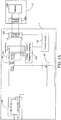
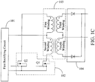
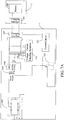
- a charging system for a device includes a power adapter 1 and a device 2.
- the power adapter 1 includes a first rectifying circuit 101, a switch circuit 102, a transformer 103, a second rectifying circuit 104, a first charging interface 105, a first current sampling circuit 1061, a switch circuit 115 and a control circuit 107.
- the first rectifying circuit 101 rectifies an input AC power (mains, such as AC220V) to output voltage in a first pulsation waveform, such as a voltage in a clipped pulsating waveform.
- the first rectifying circuit 101 may be a full bridge rectifier circuit constituted by four diodes.
- the switch circuit 102 is configured to modulate the voltage in the first pulsating waveform based on a control signal.
- the switch circuit 102 may be constituted by a metal-oxide-semiconductor (MOS) transistor, and perform a peak clipping modulation to the voltage in the clipped pulsating waveform through performing a pulse width modulation (PWM) control to the transistor.
- MOS metal-oxide-semiconductor
- PWM pulse width modulation
- the transformer 103 is configured to output voltage in a second pulsating form based on the voltage in the first pulsating form thus modulated.
- the second rectifying circuit 104 is configured to rectify the voltage in the second pulsating waveform to output voltage in a third pulsating form.
- the second rectifying circuit 104 may be constituted by a diode or a MOS transistor, which can achieve secondary synchronous rectification so that the third pulsating waveform is synchronized with the modulated first pulsating waveform.
- the third pulsating waveform being synchronized with the modulated first pulsating waveform refers to that a phase of the third pulsating waveform and a phase of the modulated first pulsating waveform are consistent, and a change trend of an amplitude of the third pulsating waveform and a change trend of an amplitude of the modulated first pulsating waveform are consistent.
- the first charging interface 105 and the second rectifying circuit 104 are connected.
- the first current sampling circuit 1061 is configured to sample current outputted by the second rectifying circuit 104 to obtain a current sampling value.
- the first current sampling circuit 1061 is selectively operable in a first current sampling mode and a second current sampling mode.
- the switch circuit 115 is configured to control the first current sampling circuit 1061 to switch between the first current sampling mode and the second current sampling mode.
- the control circuit 107 is coupled to the first current sampling circuit 1061, the switch circuit 115, and the switch circuit 102.
- the control circuit 107 is configured to output the control signal to the switch circuit 102 to control the switch circuit 115 to control the first current sampling circuit 1061 operating in the first current sampling mode or the second current sampling mode based on a charging mode, and configured to regulate a duty cycle of the control signal according to the current sampling value so that the voltage in the third pulsating waveform satisfies a requirement of charging.
- the device 2 includes a second charging interface 201 and a battery 202.
- the second charging interface 201 is connected to the battery 202.
- the second charging interface 201 applies the voltage in the third pulsating waveform to the battery 202 to achieve to charging of the battery 202.
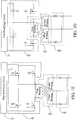
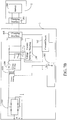
- the power adapter 1 may adopt a flyback switching power supply.
- the transformer 103 includes a primary winding and a secondary winding. One terminal of the primary winding is connected to a first output terminal of the first rectifying circuit 101. A second output terminal of the first rectifying circuit 101 is grounded. Another terminal of the primary winding is connected to the switch circuit 102 (for example, the switch circuit 102 is the MOS transistor, so the another terminal of the primary winding is connected to a drain of the MOS transistor).
- the transformer 103 is configured to output the voltage in the second pulsating waveform based on the modulated voltage in the first pulsating waveform.
- the transformer 103 is a high-frequency transformer, which may have an operating frequency of 50KHz to 2MHz.
- the modulated voltage in the first pulsating waveform is coupled to a secondary side by the high-frequency transformer and is output by the secondary winding.
- using the high-frequency transformer can take advantage of the feature of smaller size of the high-frequency transformer as compared with a low-frequency transformer (a low-frequency transformer is also called a power frequency transformer, which is mainly used for the mains frequency, such as 50Hz or 60Hz AC)), thus achieving the miniaturization of the power adapter 1.
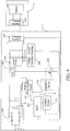
- the power adapter 1 may adopt a forward switching power supply.
- the transformer 103 includes a first winding, a second winding, and a third winding.
- a dotted terminal of the first winding is connected to a second output terminal of the first rectifying circuit 101 through a backward diode.
- a non-dotted terminal of the first winding is first connected to a dotted terminal of the second winding and then they are connected to a first output terminal of the first rectifying circuit 101.
- a non-dotted terminal of the second winding is connected to the switch circuit 102.
- the third winding and the second rectifying circuit 104 are connected.
- the backward diode has the effect of reverse clipping.
- An induced electromotive force generated by the first winding can limit an amplitude of a counter electromotive force through the backward diode, and energy caused by amplitude limitation is returned to an output of the first rectifying circuit 101 to charge the output of the first rectifying circuit 101.
- a magnetic field generated by a current passing the first winding can demagnetize a core of the transformer so that a magnetic field strength in a transformer core is restored to an initial state.
- the transformer 103 is configured to output the voltage in the second pulsating waveform based on the modulated voltage in the first pulsating waveform.
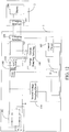
- the power adapter may adopt a push-pull switching power supply.
- the transformer 103 includes a first winding, a second winding, a third winding, and a fourth winding.
- a dotted terminal of the first winding is connected to the switch circuit 102.
- a non-dotted terminal of the first winding is first connected to a dotted terminal of the second winding and then they are connected to a first output terminal of the first rectifying circuit 101.
- a non-dotted terminal of the second wining is connected to the switch circuit 102.
- a non-dotted terminal of the third winding is connected to a dotted terminal of the fourth winding.
- the transformer 103 is configured to output the voltage in the second pulsating waveform based on the modulated voltage in the first pulsating waveform.
- the switch circuit 102 includes a first MOS transistor Q1 and a second MOS transistor Q2.
- the transformer 103 includes the first winding, the second winding, the third winding, and the fourth winding.
- the dotted terminal of the first winding is connected to a drain of the first MOS transistor Q1 in the switch circuit 102.
- the non-dotted terminal of the first winding is connected to the dotted terminal of the second winding, and a node between the non-dotted terminal of the first winding and the dotted terminal of the second winding is connected to the first output terminal of the first rectifying circuit 101.
- the non-dotted terminal of the second wining is connected to a drain of the second MOS transistor Q2 in the switch circuit 102.
- a source of the first MOS transistor Q1 is first connected to a source of the second MOS transistor Q2 and then they are connected to a second output terminal of the first rectifying circuit 101.
- a dotted terminal of the third winding is connected to a first input terminal of the second rectifying circuit 104.
- the non-dotted terminal of the third winding is connected to the dotted terminal of the fourth winding, and a node between the non-dotted terminal of the third winding and the dotted terminal of the fourth winding is grounded.
- a non-dotted terminal of the fourth winding is connected to a second input terminal of the second rectifying circuit 104.
- the first input terminal of the second rectifying circuit 104 is connected to the dotted terminal of the third winding.
- the second input terminal of the second rectifying circuit 104 is connected to the non-dotted terminal of the fourth winding.
- the second rectifying circuit 104 is configured rectify the voltage in the second pulsating waveform to output the voltage in the third pulsating waveform.
- the second rectifying circuit 104 may include two diodes. An anode of one diode is connected to the dotted terminal of the third winding. An anode of the other diode is connected to the non-dotted terminal of the fourth winding. Cathodes of the two diodes are connected together.
- the power adapter 1 may adopt a half-bridge switching power supply.
- the switch circuit 102 includes a first MOS transistor Q1, a second MOS transistor Q2, a first capacitor C1, and a second capacitor C2.
- the first capacitor C1 and the second capacitor C2 are first connected in series and then they are connected in parallel with output terminals of the first rectifying circuit 101.
- the first MOS transistor Q1 and the second MOS transistor Q2 are first connected in series and then they are connected in parallel with the output terminals of the first rectifying circuit 101.
- the transformer 103 includes a first winding, a second winding, and a third winding.
- a dotted terminal of the first winding is connected to a node between the first capacitor C1 and the second capacitor C2 connected in series.
- a non-dotted terminal of the first winding is connected to a node between the first MOS transistor Q1 and the second MOS transistor Q2 connected in series.
- a dotted end of the second winding is connected to a first input terminal of the second rectifying circuit 104.
- a non-dotted terminal of the second winding is first connected to a dotted terminal of the third winding and then they are grounded.
- a non-dotted terminal of the third winding is connected to a second input terminal of the second rectifying circuit 104.
- the transformer 103 is configured to output the voltage in the second pulsating waveform based on the modulated voltage in the first pulsating waveform.
- the power adapter 1 may adopt a full-bridge switching power supply.
- the switch circuit 102 includes a first MOS transistor Q1, a second MOS transistor Q2, a third MOS transistor Q3, and a fourth MOS transistor Q4.
- the third MOS transistor Q3 and the fourth MOS transistor Q4 are first connected in series and then they are connected in parallel with output terminals of the first rectifying circuit 101.
- the first MOS transistor Q1 and the second MOS transistor Q2 are first connected in series and then they are connected in parallel with the output terminals of the first rectifying circuit 101.
- the transformer 103 includes a first winding, a second winding, and a third winding.
- a dotted terminal of the first winding is connected to a node between third MOS transistor Q3 and the fourth MOS transistor Q4 connected in series.
- a non-dotted terminal of the first winding is connected to a node between first MOS transistor Q1 and the second MOS transistor Q2 connected in series.
- a dotted terminal of the second winding is connected to a first input terminal of the second rectifying circuit 104.
- a non-dotted terminal of the second winding is first connected to a dotted terminal of the third winding and then they are grounded.
- a non-dotted terminal of the third winding is connected to a second input terminal of the second rectifying circuit 104.
- the transformer 103 is configured to output the voltage in the second pulsating waveform based on the modulated voltage in the first pulsating waveform.
- the power adapter 1 can use any of the flyback switching power supply, the forward switching power supply, the push pull switching power supply, the half-bridge switching power supply, and the full-bridge switching power supply to output the voltage in the pulsating waveform according to embodiments of the present disclosure.
- the second rectifying circuit 104 is connected to the secondary winding of the transformer 103.
- the second rectifying circuit 104 is configured to rectify the voltage in the second pulsating waveform to output the voltage in a third pulsating form.
- the second rectifying circuit 104 may be constituted by the diode to achieve secondary synchronous rectification so that the third pulsating waveform is synchronized with the modulated first pulsating waveform.
- the third pulsating waveform being synchronized with the modulated first pulsating waveform refers to that the phase of the third pulsating waveform and the phase of the modulated first pulsating waveform are consistent, and the change trend of the amplitude of the third pulsating waveform and the change trend of the amplitude of the modulated first pulsating waveform are consistent.
- the first charging interface 105 and the second rectifying circuit 104 are connected.
- the sampling circuit 106 includes a first current sampling circuit 1061 and a first voltage sampling circuit 1062. The sampling circuit 106 is configured to sample the voltage and/or the current output from the second rectifying circuit 104 to obtain the voltage sampling value and/or the current sampling value.
- the control circuit 107 is connected to the sampling circuit 106 and the switch circuit 102.
- the control circuit 107 outputs the control signal to the switch circuit 102, and modulates the duty cycle of the control signal based on the voltage sampling value and/or the current sampling value so that the voltage in the third pulsating waveform output from the second rectifying circuit 104 satisfies the charging requirement.
- the device 2 includes the second charging interface 201 and the battery 202.
- the second charging interface 201 is connected to the battery 202.
- the second charging interface 201 applies the voltage in the third pulsating waveform to the battery 202 to achieve to charging of the battery 202.
- the voltage in the third pulsating waveform satisfying the charging requirement refers to that the voltage and a current in the third pulsating waveform satisfy the charging voltage and the charging current when the battery is charged. That is, the control circuit 107 modulates the duty cycle of the control signal, such as a PWM signal, based on voltage and/or a current output from the power adapter thus sampled to adjust an output of the second rectifying circuit 104 in a real-time manner.
- a closed-loop regulation control is thus realized so that the voltage in the third pulsation waveform satisfies the charging requirement of the device 2 to ensure that the battery 202 is safely and reliably charged.
- a charging voltage waveform output to the battery 202 being regulated through the duty cycle of the PWM signal is shown in FIG. 3 .
- a charging current waveform output to the battery 202 being regulated through the duty cycle of the PWM signal is shown in FIG. 4 .
- a regulating instruction can be generated based on the voltage sampling value, or the current sampling value, or the voltage sampling value and the current sampling value.
- the voltage in the first pulsation waveform that is, the voltage in the clipped pulsating waveform, which is rectified is directly modulated by performing PWM peak clipping through controlling the switch circuit 102, and delivered to the high-frequency transformer to be coupled from the primary side to the secondary side through the high-frequency transformer, and then be recovered as the voltage/a current in the clipped pulsating waveform through synchronous rectification to be directly delivered to the battery so as to achieve the fast charging of the battery.
- An amplitude of the voltage in the clipped pulsating waveform can be regulated through modulating the duty cycle of the PWM signal. As a result, the output of the power adapter satisfies the charging requirement of the battery.
- the power adapter according to the embodiment of the present disclosure removes the electrolytic capacitors on the primary side and the secondary side. Through using the voltage in the clipped pulsating waveform to directly charge the battery, the size of the power adapter can be reduced to miniaturize the power adapter and significantly reduce the cost.
- control circuit 107 may be a micro controller unit (MCU). That is, the control circuit 107 may be a microprocessor integrated with a switch-driven control function, a synchronous rectification function, and a voltage and current regulation control function.
- MCU micro controller unit
- control circuit 107 is further configured to modulate a frequency of the control signal based on the voltage sampling value and/or the current sampling value.
- the PWM signal output to the switch circuit 102 can thus be controlled to be continuously output for a period of time and then be stopped. After the output has been stopped for a predetermined time, the output of the PWM is turned on again. In this manner, the voltage applied to the battery is intermittent and the battery is intermittently charged. As a result, the security worry caused by serious heating when the battery is continuously charged can be avoided to improve the reliability and safety of battery charging.
- the polarization tends to be intensified during the charging process owing the decline of the conductive abilities of the ions and electrons of the lithium battery itself.
- the continuous charging method will make this polarization become even more obvious, and at the same time increase the possibility of lithium precipitation, thus affecting the safe performance of the battery.
- the continuous charging will result in continuous accumulation of heat caused by charging, the interior temperature of the battery also continuously rises. When the temperature exceeds a certain limit value, the battery performance will be limited and at the same time the security worry is increased.
- the power adapter through modulating the frequency of the control signal, the power adapter outputs in an intermittent manner.
- This situation is equivalent to that the stationary process of the battery is introduced during the battery charging process, which can alleviate the possible lithium precipitation phenomenon caused by polarization in continuous charging and reduce the effect caused by continuous accumulation of heat. The temperature is thus decreased to ensure the reliability and safety of the battery charging.
- the control signal output to the switch circuit 102 may be shown in FIG. 5 .
- the PWM signal is first continuously output for a period of time and then is stopped for a period of time, and then is continuously output for a period of time.
- the control signal output to the switch circuit 102 is intermittent and the frequency is adjustable.
- the control circuit 107 is connected to the first charging interface 105.
- the control circuit 107 is further configured to communicate with the device 2 through the first charging interface 105 to acquire state information of the device 2.
- the control circuit 107 is further configured to modulate the duty cycle of the control signal, such as the PWM signal, based on the state information of the device 2, and/or the voltage sampling value and/or the current sampling value.
- the state information of the device 2 may include a battery level, a battery temperature, the battery voltage, interface information of the device, or path impedance information of the device, etc.
- the first charging interface 105 includes power lines and data lines.
- the power lines are configured to charge the battery.
- the data lines are configured to communicate with the device 2.
- the control circuit 107 can acquire the state information of the device 2 so as to negotiate a charging mode and the charging parameters (such as the charging current, the charging voltage) with the device 2 and control the charging process.
- the charging mode supported by the power adapter and/or the device may include a second charging mode and a first charging mode.
- a charge rate of the first charging mode is greater than a charge rate of the second charging mode (for example, a charging current of the first charging mode is greater than a charging current of the second charging mode).
- the second charging mode can be understood as the charging mode in which the rated output voltage is 5V and the rated output current is less than or equal to 2.5A.
- D+ and D- in the data lines in an output port of the power adapter may be short circuited.
- the first charging mode according to the embodiment of the present disclosure is different.
- the power adapter can communicate with the device by utilizing D + and D- in the data lines to achieve data exchange, that is, the power adapter and the device can send a fast charging instruction to each other.
- the power adapter sends a fast charging inquiry instruction to the device.
- the power adapter acquires the state information of the device based on a reply instruction of the device after receiving a fast charging reply instruction of the device to enable the first charging mode.
- the charging current can be greater than 2.5A, for example, can be up to 4.5A or even greater.
- the second charging mode according to the embodiment of the present disclosure is not limited.
- the charging mode having the slower charge rate can be understood as the second charging mode.
- the charging power corresponding to the first charging mode can be greater than or equal to 15W.
- the control circuit 107 communicates with the device 2 through the first charging interface 105 to determine the charging mode.
- the charging mode includes the first charging mode and the second charging mode.
- the power adapter and the device are connected through a universal serial bus (USB) interface.
- the USB interface may be a normal USB interface, a micro USB interface, or other type USB interfaces.
- Data lines in the USB interface are the data lines in the first charging interface and are configured to provide a bidirectional communication between the power adapter and the device.
- the data lines may be a D+ line and/or a D- line in the USB interface, and the bidirectional communication can refer to the information exchange between the power adapter and the device.
- the power adapter performs the bidirectional communication with the device through the data lines in the USB interface to determine that the device is charged by the first charging mode.
- the power adapter may only be connected to the device and does not charge the device, or may charge the device by the second charging mode, or may use a small current to charge the device.
- the embodiment of the present disclosure is not limited in this regard.
- the power adapter adjusts the charging current to a charging current corresponding to the first charging mode so as to charge the device. After determining to use the first charging mode to charge the device, the power adapter can directly adjust the charging current to the charging current corresponding to the first charging mode, or can negotiate with the device to determine the charging current of the first charging mode. For example, the charging current corresponding to the first charging mode is determined based on a current power level of the battery in the device.
- the power adapter does not blindly increase the output current to perform fast charging. Rather, the power adapter needs to perform the bidirectional communication with the device so as to negotiate whether the first charging mode can be used or not. As compared with the prior art, the safety of fast charging process is increased.
- the control circuit when the control circuit performs the bidirectional communication with device through the data lines in the first charging interface to determine that the device is charged by the first charging mode, the control circuit sends a first instruction to the device.
- the first instruction is configured to inquire of the device whether to enable the first charging mode or not.
- the control circuit receives a reply instruction responsive to the first instruction from the device.
- the reply instruction responsive to the first instruction is configured to indicate that the device agrees to enable the first charging mode.
- the power adapter charges the device under the second charging mode, and the control circuit sends the first instruction to the device after determining that a charging time of the second charging mode is longer than a predetermined threshold value.
- the power adapter After the power adapter determines that the charging time of the second charging mode is longer than the predetermined threshold value, the power adapter can assume that the device has identified itself as a power adapter and can enable a fast charging inquiry communication.
- the power adapter determines to use a charging current greater than or equal to a predetermined threshold current value to charge for a predetermined time, the power adapter sends the first instruction to the device.
- control circuit is further configured to control the power adapter through controlling the switch circuit so as to adjust the charging current to the charging current corresponding to the first charging mode.
- control circuit performs the bidirectional communication with the device through the data lines in the first charging interface before the power adapter uses the charging current corresponding to the first charging mode to charge the device so as to determine a charging voltage corresponding to the first charging mode and control the power adapter to adjust the charging voltage to the charging voltage corresponding to the first charging mode.
- the control circuit when the control circuit performs the bidirectional communication with the device through the data lines in the first charging interface to determine the charging voltage corresponding to the first charging mode, the control circuit sends a second instruction to the device.
- the second instruction is configured to inquire whether or not a current output voltage of the power adapter is suitable as a charging voltage of the first charging mode.
- the control circuit receives a reply instruction responsive to the second instruction sent by the device.
- the reply instruction responsive to the second instruction is configured to indicate that the current output voltage of the power adapter is suitable, excessively high, or excessively low.
- the control circuit determines the charging voltage of the first charging mode based on the reply instruction responsive to the second instruction.
- control circuit before the control circuit controls the power adapter to adjust the charging current to the charging current corresponding to the first charging mode, the control circuit further performs the bidirectional communication with the device through the data lines in the first charging interface to determine the charging current corresponding to the first charging mode.
- the control circuit when the control circuit performs the bidirectional communication with the device through the data lines in the first charging interface to determine the charging current corresponding to the first charging mode, the control circuit sends a third instruction to the device.
- the third instruction is configured to inquire about a maximum charging current currently supported by the device.
- the control circuit receives a reply instruction responsive to the third instruction sent by the device.
- the reply instruction responsive to the third instruction is configured to indicate the maximum charging current currently supported by the device.
- the control circuit determines a charging current of the first charging mode based on the reply instruction responsive to the third instruction.
- the power adapter can directly determine the maximum charging current as the charging current of the fast charge mode, or set the charging current as a current value that is less than the maximum charging current.
- control circuit further performs the bidirectional communication with the device through the data lines in the first charging interface to continuously adjust the charging current output to the battery from the power adapter through controlling the switch circuit.
- the power adapter can continuously inquire about current state information of the device, for example, inquire about the battery voltage, the battery power level, etc., so as to continuously adjust the charging current output to the battery from the power adapter.
- the control circuit when the control circuit performs the bidirectional communication with the device through the data lines in the first charging interface to continuously adjust the charging current output to the battery from the power adapter through controlling the switch circuit, the control circuit sends a fourth instruction to the device.
- the fourth instruction is configured to inquire about a current voltage of the battery in the device.
- the control circuit receives a reply instruction responsive to the fourth instruction sent by the device.
- the reply instruction responsive to the fourth instruction is configured to indicate the current voltage of the battery in the device.
- the control circuit adjusts the charging current output to the battery from the power adapter through controlling the switch circuit based on the current voltage of the battery.
- control circuit adjusts the charging current output to the battery from the power adapter to a charging current value corresponding to the current voltage of the battery through controlling the switch circuit based on the current voltage of the battery and a predetermined relationship between a battery voltage value and a charging current value.
- the power adapter can store the relationship between the battery voltage value and the charging current value in advance.
- the power adapter can perform the bidirectional communication with the device through the data lines in the first charging interface to obtain the relationship between the battery voltage value and the charging current value stored in the device from a device side.
- the control circuit further performs the bidirectional communication with the device through the data lines in the first charging interface to determine whether there is a bad contact between the first charging interface and the second charging interface or not. When it is determined that there is a bad contact between the first charging interface and the second charging interface, the control circuit controls the power adapter to exit the quick charging mode.
- the control circuit before determining whether there is a bad contact between the first charging interface and the second charging interface or not, is further configured to receive information for indicating a path impedance of the device from the device.
- the control circuit sends the fourth instruction to the device.
- the fourth instruction is configured to inquire about voltage of the battery in the device.
- the control circuit receives the reply instruction responsive to the fourth instruction sent by the device.
- the reply instruction responsive to the fourth instruction is configured to indicate the voltage of the battery in the device.
- the control circuit determines a path impedance from the power adapter to the battery based on the output voltage of the power adapter and the voltage of the battery.
- the control circuit determines whether there is a bad contact between the first charging interface and the second charging interface or not based on the path impedance from the power adapter to the battery, the path impedance of the device, and a path impedance of the charging lines between the power adapter and the device.
- the device can record the path impedance of the device in advance. For example, since devices of a same model have a same structure, path impedances of the devices are set as a same value in default setting. Similarly, the power adapter can record the path impedance of the charging lines in advance. When the power adapter obtains voltage across two terminals of the battery of the device, a path impedance of an overall path can be determined based on a voltage drop between the power adapter and the two terminals of the battery and a path current.
- the path impedance of the overall path is greater than a sum of the path impedance of the device and the path impedance of the charging lines, or the path impedance of the overall path minus a sum of the path impedance of the device and the path impedance of the charging lines is greater than a threshold impedance value, it is determined that there is a bad contact between the first charging interface and the second charging interface.
- control circuit before the power adapter exits the quick charging mode, the control circuit further sends a fifth instruction to the device.
- the fifth instruction is configured to indicate that there is a bad contact between the first charging interface and the second charging interface.
- the power adapter After the power adapter sends the fifth instruction, the power adapter can exit the first charging mode or reset.
- the fast charging process according to the embodiment of the present disclosure is described in detail from the viewpoint of the power adapter, and the fast charging process according to the embodiment of the present disclosure is provided from the viewpoint of the device as follows.
- the device 2 further includes a charging control switch 203 and a controller 204.
- the charging control switch 203 such as a switch circuit constituted by electronic switch elements, is connected between the second charging interface 201 and the battery 202.
- the charging control switch 203 is configured to enable or end a charging process of the battery 202 under a control of the controller 204, so that the charging process of the battery 202 can be controlled from the device side to ensure the safety and reliability of the charging of the battery 202.
- the device 2 further includes a communication circuit 205.
- the communication circuit 205 is configured to establish a bidirectional communication between the controller 204 and the control circuit 107 through the second charging interface 201 and the first charging interface 105. That is, the device 2 and the power adapter 1 can perform the bidirectional communication through the data lines in the USB interface.
- the device 2 supports the second charging mode and the first charging mode. A charging current of the first charging mode is greater than a charging current of the second charging mode.
- the communication circuit 205 and the control circuit 107 perform a bidirectional communication to allow the power adapter 1 to determine using the first charging mode to charge the device 2, so that the control circuit 107 controls the power adapter 1 to output the charging current corresponding to the first charging mode to charge the battery 202 in the device 2.
- the power adapter 1 does not blindly increase the output current to perform fast charging. Rather, the power adapter 1 needs to perform the bidirectional communication with the device 2 so as to negotiate whether the first charging mode can be used or not. As compared with the prior art, the safety of fast charging process is improved.
- the controller receives a first instruction sent by the control circuit through the communication circuit.
- the first instruction is configured to inquire of the device whether to enable the first charging mode or not.
- the controller sends a reply instruction responsive to the first instruction to the control circuit through the communication circuit.
- the reply instruction responsive to the first instruction is configured to indicate that the device agrees to enable the first charging mode.
- the power adapter charges the battery in the device through the second charging mode.
- the control circuit determines that a charging time of the second charging mode is longer than a predetermined threshold value, the control circuit sends the first instruction to the communication circuit in the device.
- the controller receives the first instruction sent by the control circuit through the communication circuit.
- the controller before the power adapter outputs the charging current corresponding to the first charging mode to charge the battery in the device, performs the bidirectional communication with the control circuit through the communication circuit to allow the power adapter to determine the charging voltage corresponding to the first charging mode.
- the controller receives a second instruction sent by the control circuit.
- the second instruction is configured to inquire whether or not a current output voltage of the power adapter is suitable as the charging voltage of the first charging mode.
- the controller sends a reply instruction responsive to the second instruction to the control circuit.
- the reply instruction responsive to the second instruction is configured to indicate that the current output voltage of the power adapter is suitable, excessively high, or excessively low.
- the controller performs the bidirectional communication with the control circuit to allow the power adapter to determine the charging current corresponding to the first charging mode.
- the controller receives a third instruction sent by the control circuit.
- the third instruction is configured to inquire about a maximum charging current currently supported by the device.
- the controller sends a reply instruction responsive to the third instruction to the control circuit.
- the reply instruction responsive to the third instruction is configured to indicate the maximum charging current currently supported by the battery in the device to allow the power adapter to determine the charging current corresponding to the first charging mode based on the maximum charging current.
- the controller performs the bidirectional communication with the control circuit to allow the power adapter to continuously adjust the charging current output to the battery from the power adapter.
- the controller receives a fourth instruction sent by the control circuit.
- the fourth instruction is configured to inquire about a current voltage of the battery in the device.
- the controller sends a reply instruction responsive to the fourth instruction to the control circuit.
- the reply instruction responsive to the fourth instruction is configured to indicate the current voltage of the battery in the device to allow the power adapter to continuously adjust the charging current output to the battery from the power adapter based on the current voltage of the battery.
- the controller performs the bidirectional communication with the control circuit through the communication circuit to allow the power adapter to determine whether there is a bad contact between the first charging interface and the second charging interface or not.
- the controller receives the fourth instruction sent by the control circuit.
- the fourth instruction is configured to inquire about the current voltage of the battery in the device.
- the controller sends the reply instruction responsive to the fourth instruction to the control circuit.
- the reply instruction responsive to the fourth instruction is configured to indicate the current voltage of the battery in the device to allow the control circuit to determine whether there is a bad contact between the first charging interface and the second charging interface or not based on the output voltage of the power adapter and the current voltage of the battery.
- the controller receives a fifth instruction sent by the control circuit.
- the fifth instruction is configured to indicate that there is a bad contact between the first charging interface and the second charging interface.
- the power adapter can perform a fast charging communication process with the device. Through one or more handshake negotiations, the fast charging of the battery is achieved.
- a detailed description of the fast charging communication process and various stages of the fast charging process according to the embodiment of the present disclosure is provided as follows with reference to FIG. 6 . It should be understood that the communication steps or operations shown in FIG. 6 are merely examples, and the embodiment of the present disclosure may further perform other operations or variations of the various operations in FIG. 6 . In addition, the various stages in FIG. 6 may be performed in an order different from that presented in FIG. 6 , and it may not be necessary to perform all the operations in FIG. 6 . It is noted that the curve in FIG. 6 is a change trend of a peak value or an average value of a charging current, rather than an actual charging current curve.
- the fast charging process may include five stages.
- the device can detect a type of the power supply device through data lines D+, D-.
- a current absorbed by the device may be greater than a predetermined threshold current value (for example, may be 1A) .
- the power adapter detects that an output current of the power adapter has been greater than or equal to I2 for a predetermined time (for example, may be a continuous T1 duration)
- the power adapter regards that the device has completed the type identification of the power supply device.
- the power adapter turns on a handshake communication between the power adapter and the device.
- the power adapter sends an instruction 1 (corresponding to the first instruction as described above) to inquire of the device whether to enable the first charging mode or not (or called flash charging).
- the output current of the power adapter is detected again.
- the output current of the power adapter is still greater than or equal to I2 within a predetermined continuous time (for example, may be the continuous T1 duration)
- a request is sent again to inquire of the device whether to enable the first charging mode or not. The above steps of stage 1 are repeated until the device responds to agree to enable the first charging mode, or the output current of the power adapter no longer satisfies the condition of being greater than or equal to I2.
- the fast charging process is turned on after the device agrees to enable the first charging mode.
- the fast charging communication process enters a stage 2.
- Voltage in a clipped pulsating waveform output from the power adapter may include plural levels.
- the power adapter sends an instruction 2 (corresponding to the second instruction as described above) to the device to inquire of the device whether or not an output voltage of the power adapter matches a current voltage of the battery (or whether or not suitable, that is, whether or not suitable as a charging voltage of the first charging mode), that is, whether or not satisfy the charging requirement.
- the device responds that the output voltage of the power adapter is excessively high or excessively low or matching. If the power adapter receives a feedback of the device that the output voltage of the power adapter is excessively high or excessively low, the control circuit adjusts the output voltage of the power adapter by one level through adjusting a duty cycle of a PWM signal, and sends the instruction 2 to the device again to re-inquire whether the output voltage of the power adapter matches or not.
- stage 2 The above steps of stage 2 are repeated until the device responds to the power adapter that the output voltage of the power adapter is at a matching level, and the fast charging process enters a stage 3.
- the power adapter After the power adapter receives the feedback replied by the device that the output voltage of the power adapter is matching, the power adapter sends an instruction 3 (corresponding to the third instruction as described above) to the device to inquire of the device a maximum charging current currently supported by the device. The device responds to the power adapter with the maximum charging current currently supported by the device, and the fast charging process enters a stage 4.
- an instruction 3 corresponding to the third instruction as described above
- the power adapter can dispose an output current reference value of the power adapter.
- the control circuit 107 adjusts the duty cycle of the PWM signal based the output current reference value so that the output current of the power adapter satisfies the requirement of the charging current of the device, that is, enters the constant current stage.
- the constant current stage refers to that a peak value or an average value of the output current of the power adapter basically remains unchanged (that is, a change amplitude of the peak value or the average value of the output current is very small, for example, changes within 5% of the peak value or the average value of the output current).
- a peak value of a current in a third pulsating waveform remains constant in every period.
- the power adapter When entering the constant current stage, the power adapter sends an instruction 4 (corresponding to the fourth instruction as described above) at every interval of time to inquire of the device a current voltage.
- the device can feed back the current voltage of the battery of the device to the power adapter.
- the power adapter can determine whether a USB contact, that is, a contact between a first charging interface and a second charging interface is good or not and whether it is necessary to reduce a current charging current value of the device or not based on a feedback of the current voltage of the battery of the device replied by the device.
- the power adapter determines that the USB contact is bad, the power adapter sends an instruction 5 (corresponding to the fifth instruction as described above) and then resets to enter stage 1.
- data corresponding to the instruction 1 can attach data (or information) of a path impedance of the device.
- Path impedance data of the device may be used for determining whether the USB contact is good or not in stage 5.
- time from where the device agrees to enable the first charging mode to where the power adapter adjusts the voltage to an appropriate value in stage 2 can be controlled within a certain range. If the time exceeds a predetermined range, the device can determine that a request is abnormal and resets quickly.
- the device can give a feedback that the output voltage of the power adapter is suitable /matching to the power adapter when the output voltage of the power adapter is adjusted to ⁇ V ( ⁇ V is about 200 to 500 mV) higher than the current voltage of the battery in stage 2.
- ⁇ V is about 200 to 500 mV
- the control circuit 107 adjusts the duty cycle of the PWM signal based on a voltage sampling value to adjust the output voltage of the power adapter.
- a speed of adjusting a magnitude of the output current of the power adapter can be controlled within a certain range in stage 4, so as to avoid an abnormal interruption caused by excessively fast adjustment speed.
- a change amplitude of the magnitude of the output current of the power adapter can be controlled within 5% in stage 5. That is, the constant current stage is identified.
- the power adapter monitors a charging circuit impedance in a real-time manner in stage 5. That is, an overall charging circuit impedance is monitored through measuring the output voltage of the power adapter and the current charging current, and reading a battery voltage of the device. When it is detected that the charging circuit impedance is greater than a path impedance of the device plus an impedance of fast charging data lines, the USB contact is regarded as bad to perform a fast charging reset.
- a communication time interval between the power adapter and the device can be controlled within a certain range to avoid the fast charging reset.
- a stop of the first charging mode (or the fast charging process) can be classified into a recoverable stop and an unrecoverable stop.
- the fast charging is stopped and a reset is performed to enter stage 1.
- the device does not agree to enable the first charging mode.
- the fast charging communication process does not enter stage 2.
- the fast charging process that has been stopped can be an unrecoverable stop.
- the fast charging is stopped and the reset is performed to enter stage 1.
- the device agrees to enable the first charging mode to restore the fast charging process.
- the fast charging process that has been stopped can be a recoverable stop.
- the fast charging is stopped and the reset is performed to enter stage 1.
- the device does not agree to enable the first charging mode.
- the device agrees to enable the first charging mode to restore the fast charging process.
- the fast charging process that has been stopped can be a recoverable stop.
- a handshake communication between the device and the power adapter may be initiated by the device after the device is connected to the power adapter. That is, the device sends the instruction 1 to inquire of the power adapter whether to enable the first charging mode (or called flash charging) or not.
- the device receives a replay instruction of the power adapter indicating that the power adapter agrees to enable the first charging mode, the fast charging process is enabled.
- a constant voltage charging stage may be further included after stage 5. That is, in stage 5, the device can feed back the current voltage of the battery of the device to the power adapter. As voltage of the battery of the device rises continuously, the charging is changed to the constant voltage charging stage when the current voltage of the battery of the device reaches a threshold constant voltage charging voltage value.
- the control circuit 107 adjusts the duty cycle of the PWM signal based on a voltage reference value (that is, the threshold constant voltage charging voltage value) so that the output voltage of the power adapter satisfies the requirement of the charging voltage of the device, that is, the voltage is basically maintained constantly without change.
- the constant voltage charging stage the charging current gradually decreases. When the current drops to a certain threshold value, the charging is stopped. At this time, the battery is identified as being fully charged.
- the constant voltage charging refers to that a peak voltage of the third pulsating waveform is basically maintained constantly.
- obtaining the output voltage of the power adapter refers to obtaining the peak voltage or an average voltage value of the third pulsating waveform.
- Obtaining the output current of the power adapter refers to obtaining a peak current or an average current value of the third pulsating waveform.
- the power adapter 1 further includes: a controllable switch 108 and a filter circuit 109 connected in series.
- the serially connected controllable switch 108 and filter circuit 109 are connected to a first output terminal of the second rectifying circuit 104.
- the control circuit 107 is further configured to control the controllable switch 108 to close when a charging mode is determined to be the second charging mode, and control the controllable switch 108 to open when the charging mode is determined to be a first charging mode.
- one or more small capacitors are further connected in parallel at an output terminal of the second rectifying circuit 104. Not only can the noise be reduced, but the occurrence of surge phenomenon is also reduced.
- the output terminal of the second rectifying circuit 104 may further be connected to an LC filter circuit or a ⁇ filter circuit to filter the ripple interference. As shown in FIG. 7B , the output terminal of the second rectifying circuit 104 is connected to the LC filter circuit. It is noted that capacitors in the LC filter circuit or the ⁇ filter circuit are all small capacitors, which take a very small area.
- the filter circuit 109 includes a filter capacitor.
- the filter capacitor can support 5V standard charging, that is, correspond to the second charging mode.
- the controllable switch 108 may be constituted by a semiconductor switch device, such as a MOS transistor.
- the control circuit 107 controls the controllable switch 108 to close.
- the filter circuit 109 is connected to the circuit so that an output of the second rectifying circuit can be filtered. In this manner, the power adapter can be better compatible with the DC charging technology. That is, a DC power is applied to the battery of the device to achieve DC charging of the battery.
- a filter circuit including an electrolytic capacitor and an ordinary capacitor connected in parallel would support a small capacitor required by 5V standard charging (such as a solid state capacitor). Since the electrolytic capacitor occupies a larger volume, the electrolytic capacitor in the power adapter can be removed to retain a capacitor having a smaller capacitance so as to reduce the size of the power adapter.
- a branch where the small capacitor is located can be controlled to conduct. The current is thus filtered to achieve a stable low-power output so that the DC charging of the battery is performed.
- the branch where the small capacitor is located can be controlled to disconnect. The output of the second rectifying circuit 104 is not filtered. Voltage/current in a pulsating waveform is directly output to be applied to the battery, thus achieving fast charging of the battery.
- the first current sampling circuit 1061 can individually sample two currents flowing through two current sensing resistors, i.e. a first resistor R1 and a second resistor R2 as illustrated in Fig. 2B , in another embodiment of the present disclosure.
- the mode switch unit 115 is configured to switch the first current sampling circuit 1061 to operate in a first current sampling mode or a second current sampling mode.
- the control circuit 107 is configured to control the switch circuit 115 to control the first current sampling circuit 1061 operable in the first current sampling mode, when the control circuit 107 performs a bidirectional communication with the device through the data line of the first charging interface to determine that the device is charged by the first charging mode.
- the control circuit 107 is further configured to control the switch circuit 115 to control the first current sampling circuit 1061 operable in the second current sampling mode, when the control circuit 107 performs a bidirectional communication with the device through the data line of the first charging interface to determine that the device is charged by the second charging mode.
- the first current sampling circuit 1061 includes a first resistor R1, a second resistor R2, and a current sensor 10611 in another embodiment of the present disclosure.
- a first end of the first resistor R1 is coupled to an output end of the second rectifying circuit 104.
- a first end of the second resistor R2 is coupled to the output end of the second rectifying circuit 104.
- a third resistor R3 is coupled between the first end of the second resistor R2 and the first end of the first resistor R1.
- a fourth resistor R4 is coupled between a second end of the second resistor R2 and a second end of the first resistor R1.
- a resistance of the second resistor R2 is greater than a resistance of the first resistor R1, that is the second resistor R2 is a large resistor while the first resistor R1 is a small resistor.
- the current sensor 10611 is configured to sample the current outputted by the second rectifying circuit 104 according to voltage across the first resistor R1 or voltage across the second resistor R2.
- the current sensor 10611 can include an operational amplifier.
- the first current sampling circuit 1061 further includes a fifth resistor R5, a sixth resistor R6, a first filter capacitor C11, and a second filter capacitor C12.
- a first end of the fifth resistor R5 is coupled to the second end of the second resistor R2, and a second end of the fifth resistor R5 is coupled to the current sensor 10611.
- a first end of the sixth resistor R6 is coupled to the second end of the second resistor R2, and a second end of the sixth resistor R6 is coupled to the current sensor 10611.
- a first end of the first filter capacitor C11 is coupled to the second end of the fifth resistor R5 and the current sensor 10611.
- a second end of the first filter capacitor C11 is grounded.
- a first end of the second filter capacitor C12 is coupled to the second end of the sixth resistor R6 and the current sensor 10611, and a second end of the second filter capacitor C12 is grounded.
- the first current sampling circuit 1061 can detect current through the first resistor R1 (a small resistor) and the second resistor R2 (a large resistor) individually so the first current sampling circuit 1061 can be selectively operable in two current sampling modes.
- the switch circuit 115 includes a first switch SW1 and a second switch SW2, as Fig. 2B illustrates.
- a first end of the first switch SW1 is coupled to the second end of the first resistor R1, and a control end of the first switch SW1 is coupled to the control circuit 107.
- a first end of the second switch SW2 is coupled to the second end of the second resistor R2, a control end of the second switch SW2 is coupled to the control circuit 107, and a second end of the second switch SW2 is coupled to a second end of the first switch SW1.
- Both of the first switch SW1 and the second resistor R2 may be Metal oxide semiconductor (MOS) transistors.
- MOS Metal oxide semiconductor
- the first current sampling circuit 1061 when the control circuit 107 performs a bidirectional communication with the device through the data line of the first charging interface to determine that the device is charged by the first charging mode, i.e. a fast charging with high current, the first current sampling circuit 1061 is operable in the first current sampling mode that current flowing through the small resistor R1 is sensed, as the first switch SW1 turns on and the second switch SW2 turns off.
- the control circuit 107 performs a bidirectional communication with the device through the data line of the first charging interface to determine that the device is charged by the second charging mode, i.e. a standard charging with low current
- the first current sampling circuit 1061 is operable in the second current sampling mode that current flowing through the large resistor R2 is sensed, as the first switch SW1 turns off and the second switch SW2 turns on.
- control circuit 107 is further configured to obtain a charging current and/or a charging voltage corresponding to the first charging mode based on state information of the device when the charging mode is determined to be the first charging mode, and modulate a duty cycle of a PWM signal based on the charging current and/or the charging voltage corresponding to the first charging mode.
- the control circuit 107 obtains the charging current and/or the charging voltage corresponding to the first charging mode based on acquired state information of the device, such as a battery voltage, a battery level, a battery temperature, operating parameters of the device, and power consumption information of an application running on the device, etc., then modulates the duty cycle of a control signal based on the obtained charging current and/or charging voltage.
- an output of the power adapter satisfies the charging requirement to achieve the fast charging of the battery.
- the state information of the device includes the battery temperature. Additionally, when the battery temperature is higher than a first predetermined threshold temperature or lower than a second predetermined threshold temperature, the first charging mode is switched to the second charging mode if the current charging mode is the first charging mode.
- the first predetermined threshold temperature is higher the second predetermined threshold temperature. In other words, when the battery temperature is excessively low (for example, the battery temperature lower than the second predetermined threshold temperature) or excessively high (for example, the battery temperature higher than the first predetermined threshold temperature), neither is suitable for fast charging. Therefore, the first charging mode needs to be switched to the second charging mode.
- the first predetermined threshold temperature and the second predetermined threshold temperature may be set or written to a memory of the control circuit (such as an MCU of the power adapter) depending on practical situations.
- the control circuit 107 is further configured to control the switch circuit 102 to turn off when the battery temperature is higher than a high temperature protection threshold that is predetermined. That is, the control circuit 107 needs to adopt a high temperature protection strategy to control the switch circuit 102 to turn off when the battery temperature exceeds the high temperature protection threshold, so that the power adapter stops charging the battery.
- the high temperature protection of battery is thus achieved to improve charging safety.
- the high temperature protection threshold may be different from the first predetermined threshold temperature, or may be the same as the first predetermined threshold temperature. In at least one embodiment, the high temperature protection threshold is higher than the first predetermined threshold temperature.
- a controller is further configured to acquired the battery temperature, and control a charging control switch to turn off when the battery temperature is higher than the high temperature protection threshold that is predetermined. That is, the charging control switch is turned off through a device side to turn off the charging process of the battery so as to ensure charging safety.
- control circuit is further configured to acquire a temperature of the first charging interface, and control the switch circuit to turn off when the temperature of the first charging interface is higher than a predetermined protection temperature. That is, the control circuit 107 also needs to execute the high temperature protection strategy to control the switch circuit 102 to turn off when the temperature of the first charging interface exceeds a certain temperature, so that the power adapter stops charging the battery. The high temperature protection of charging interface is thus achieved to improve the charging safety.
- the controller acquires the temperature of the first charging interface through performing a bidirectional communication with the control circuit, and controls the charging control switch (see FIG. 13 and FIG. 14 ) to turn off when the temperature of the first charging interface is higher than the predetermined protection temperature. That is, the charging control switch is turned off through the device side to turn off the charging process of the battery so as to ensure charging safety.
- the power adapter 1 further includes a drive circuit 110, such as a MOSFET driver, as shown in FIG. 8 .
- the drive circuit 110 is connected between the switch circuit 102 and the control circuit 107.
- the drive circuit 110 is configured to drive the switch circuit 102 to turn on or turn off based on a control signal.
- the drive circuit 110 may be integrated in the control circuit 107 according to other embodiments of the present disclosure.
- the power adapter 1 further includes an isolation circuit 111.
- the isolation circuit 111 is connected between the drive circuit 110 and the control circuit 107 to achieve signal isolation between a primary side and a secondary side of the power adapter 1 (or signal isolation between a primary winding and a secondary winding of the transformer 103).
- the isolation circuit 111 may use an optocoupler isolation, or may use some other isolation.
- the control circuit 107 can be disposed on the secondary side of the power adapter 1 (or a secondary winding side of the transformer 103) to facilitate the control circuit 107 to communicate with the device 2. As a result, the space design of the power adapter 1 becomes simpler and easier.
- both the control circuit 107 and the drive circuit 110 can be disposed on the primary side.
- the isolation circuit 111 can be disposed between the control circuit 107 and the sampling circuit 106 to achieve the signal isolation between the primary side and the secondary side of the power adapter 1.
- the isolation circuit 111 needs to be disposed when the control circuit 107 is disposed on the secondary side.
- the isolation circuit 111 may be integrated in the control circuit 107.
- the isolation circuit when a signal is transmitted from the primary side to the secondary side or from the secondary side to the primary side, the isolation circuit usually needs to be disposed to perform signal isolation.
- the power adapter 1 further includes an auxiliary winding and a power supply circuit 112.
- the auxiliary winding generates voltage in a fourth pulsating waveform based on the voltage in the first pulsating waveform that is modulated.
- the power supply circuit 112 is connected to the auxiliary winding.
- the power supply circuit 112 (for example, including a filter regulator module, a voltage conversion module, etc.) is configured to convert the voltage in the fourth pulsating waveform to output DC power so as to supply power to the drive circuit 110 and/or the control circuit 107.
- the power supply circuit 112 may be constituted by elements, such as a small filter capacitor, a voltage regulator chip, etc., to process and convert the voltage in the fourth pulsating waveform, thus outputting a low voltage DC power, such as 3.3V, or 5V, etc.
- a power supply of the drive circuit 110 can be obtained through converting the voltage in the fourth pulsating waveform by the power supply circuit 112.
- a power supply of the control circuit 107 can be obtained through converting the voltage in the fourth pulsating waveform by the power supply circuit 112.
- the power supply circuit 112 provides a two-way DC output to respectively supply power to the drive circuit 110 and the control circuit 107.
- the isolation circuit 111 e.g. an optocoupler, is disposed between the control circuit 107 and the sampling circuit 106 to achieve the signal isolation between the primary side and the secondary side of the power adapter 1.
- the power supply circuit 112 When the control circuit 107 is disposed on the primary side and is integrated with the drive circuit 110, the power supply circuit 112 only supplies power to the control circuit 107.
- the control circuit 107 When the control circuit 107 is disposed on the secondary side and the drive circuit 110 is disposed on the primary side, the power supply circuit 112 only supplies power to the drive circuit 110.
- the power of the control circuit 107 is supplied by the secondary side, for example, a power supply circuit is used to convert the voltage in the third pulsating waveform output from the second rectifying circuit 104 to a DC power so as to supply power to the control circuit 107.
- output terminals of the first rectifying circuit 101 are further connected in parallel with a plurality of small capacitors to have a filtering effect. Or, the output terminals of the first rectifying circuit 101 are connected to an LC filter circuit.
- the power adapter 1 further includes a first voltage detection circuit 113 as shown in FIG. 10 .
- the first voltage detection circuit 113 is connected to the auxiliary winding and the control circuit 107.
- the first voltage detection circuit 113 is configured to detect the voltage in the fourth pulsating waveform to generate a voltage detection value.
- the control circuit 107 is further configured to modulate a duty cycle of a control signal based on the voltage detection value.
- control circuit 107 can reflect voltage output from the second rectifying circuit 104 based on voltage output from the auxiliary winding detected by the voltage detection circuit 113, and then modulate the duty cycle of the control signal based on the voltage detection value, so that the output of the second rectifying circuit 104 matches the charging requirement of the battery.
- the sampling circuit 106 includes a first current sampling circuit 1061 and a first voltage sampling circuit 1062 as shown in FIG. 11 .
- the first current sampling circuit 1061 is configured to sample a current output from the second rectifying circuit 104 to obtain a current sampling value.
- the voltage sampling circuit 1062 is configured to sample voltage output from the second rectifying circuit 104 to obtain voltage sampling value.
- the first current sampling circuit 1061 can sample voltage across a resistor (current sensing resistor) connected to the first output terminal of the second rectifying circuit 104 to achieve the sampling of the current output from the second rectifying circuit 104.
- the first voltage sampling circuit 1062 can sample voltage between the first output terminal and a second output terminal of the second rectifying circuit 104 to achieve the sampling of the voltage output from the second rectifying circuit 104.
- the first voltage sampling circuit 1062 includes a peak voltage sampling and retaining circuit, a zero-crossing sampling circuit, a discharge circuit, and an analog/digital (AD) sampling circuit as shown in FIG. 11 .
- the peak voltage sampling and retaining circuit is configured to sample and retain a peak voltage of the voltage in the third pulsating waveform.
- the zero-crossing sampling circuit is configured to sample zero-crossing points of the voltage in the third pulsating waveform.
- the discharge circuit is configured to discharge the peak voltage sampling and retaining circuit at the zero-crossing points.
- the AD sampling circuit is configured to sample the peak voltage in the peak voltage sampling and retaining circuit so as to obtain the voltage sampling value.
- the voltage sampling value can be ensured to be synchronized with the voltage in the first pulsating waveform, that is, the phases are synchronous and the amplitude change trends are consistent.
- the power adapter 1 further includes a second voltage sampling circuit 114 as shown in FIG. 12 .
- the second voltage sampling circuit 114 is configured to sample the voltage in the first pulsating waveform.
- the second voltage sampling circuit 114 is connected to the control circuit 107.
- the control circuit 107 controls the switch circuit 102 to turn on for a first predetermined time so as to discharge a surge voltage, a spike voltage, etc. in the first pulsating waveform.
- the second voltage sampling circuit 114 may be connected to a first output terminal and a second output terminal of the first rectifying circuit 101 to achieve the sampling of the voltage in the first pulsating waveform.
- the control circuit 107 makes a judgment on the voltage value sampled by the second voltage sampling circuit 114. If the voltage value sampled by the second voltage sampling circuit 114 is greater than the first predetermined voltage value, the power adapter 1 is interfered with by a electrical spark so the surge voltage appears. At This time, the surge voltage needs to be discharged to ensure the safety and reliability of charging.
- the control circuit 107 controls the switch circuit 102 to turn on for a period of time to form a discharge path. The surge voltage caused by the electrical spark is discharged to prevent interference caused by the electrical spark when the power adapter charges the device. As a result, the safety and reliability of charging the device is effectively improved.
- the first predetermined voltage value may be set depending on practical situations.
- the control circuit 107 is further configured to control the switch circuit 102 to turn off when a voltage value sampled by the sampling circuit 106 is greater than a second predetermined voltage value. That is, the control circuit 107 further makes a judgment on a magnitude of the voltage value sampled by the sampling circuit 106. If the voltage value sampled by the sampling circuit 106 is greater than a second predetermined voltage value, voltage output from the power adapter 1 is excessively high. At this time, the control circuit 107 controls the switch circuit 102 to turn off so that the power adapter 1 stops charging the battery 202 of the device 2. In other words, the control circuit 107 achieves the overvoltage protection of the power adapter 1 through controlling the switch circuit 102 to turn off so as to ensure safe charging.
- the controller 204 performs the bidirectional communication with the control circuit 107 to acquire the voltage value sampled by the sampling circuit 106 (see FIG. 13 and FIG. 14 ), and controls the charging control switch 203 to turn off when the voltage value sampled by the sampling circuit 106 is greater than the second predetermined voltage value. That is, the charging control switch 203 is turned off through a side of the device 2 so as to turn off the charging process of the battery 202. The charging safety is ensured.
- control circuit 107 is further configured to control the switch circuit 102 to turn off when a current value sampled by the sampling circuit 106 is greater than a predetermined current value. That is, the control circuit 107 further makes a judgment on a magnitude of the current value sampled by the sampling circuit 106. If the current value sampled by the sampling circuit 106 is greater than the predetermined current value, a current output from the power adapter 1 is excessively high. At this time, the control circuit 107 controls the switch circuit 102 to turn off so that the power adapter 1 stops charging the device 2. In other words, the control circuit 107 achieves the overcurrent protection of the power adapter 1 through controlling the switch circuit 102 to turn off so as to ensure safe charging.
- the controller 204 performs the bidirectional communication with the control circuit 107 to acquire the current value sampled by the sampling circuit 106 (see FIG. 13 and FIG. 14 ), and controls the charging control switch 203 to turn off when the current value sampled by the sampling circuit 106 is greater than the predetermined current value. That is, the charging control switch 203 is turned off through the side of the device 2 so as to turn off the charging process of the battery 202. The charging safety is ensured.
- Both the second predetermined voltage value and the predetermined current value may be set or written to a memory of the control circuit (for example, in the control circuit 107 of the power adapter 1, such as a micro controller unit (MCU)) depending on practical situations.
- a memory of the control circuit for example, in the control circuit 107 of the power adapter 1, such as a micro controller unit (MCU)
- the device may be a mobile device, such as a cellphone, a mobile power supply, such as a charging bank, a multimedia player, a notebook computer, or a wearable device, etc.
- a mobile device such as a cellphone, a mobile power supply, such as a charging bank, a multimedia player, a notebook computer, or a wearable device, etc.
- the charging system for the device controls the power adapter to output the voltage in the third pulsating waveform, and directly applies the voltage in the third pulsating waveform output from the power adapter to the battery in the device, so that the fast charging of the battery directly by the output voltage/current that is pulsating can be achieved.
- a magnitude of the output voltage/current that is pulsating changes periodically.
- the lithium precipitation phenomenon of the lithium battery can be reduced.
- the service life of the battery can be improved.
- the probability of arcing and the force of the contact at the charging interface can further be reduced to improve the life of the charging interface.
- the power adapter outputs the voltage in the pulsating waveform, there is no necessity to dispose electrolytic capacitors in the power supply adapter. Not only can the power adapter simplified and miniaturized, but the cost can also be greatly reduced. Additionally, two current sampling modes are alternatively switched to sample the current, which ensures the sensing function with the compatibility between sensing precision and dynamic range and expands the scope of the applications.
- the present disclosure also provides a power adapter.
- the power adapter includes a first rectifying circuit configured to rectify an alternating current to voltage in a first pulsating waveform, a switch circuit configured to modulate the voltage in the first pulsating waveform according to a control signal, a transformer configured to output voltage in a second pulsating waveform according to the modulated voltage in the first pulsating waveform, a second rectifying circuit configured to rectify the voltage in the second pulsating waveform to voltage in a third pulsating waveform, a first charging interface coupled to the second rectifying circuit, a first current sampling circuit configured to sample current outputted by the second rectifying circuit to obtain a current sampling value, the first current sampling circuit selectively operable in a first current sampling mode and a second current sampling mode, a switch circuit configured to control the first current sampling circuit to switch between the first current sampling mode and the second current sampling mode, and a control circuit coupled to the first current sampling circuit, the switch circuit, and the switch circuit.
- the control circuit is configured to output the control signal to the switch circuit, configured to control the switch circuit to control the first current sampling circuit operating in the first current sampling mode or the second current sampling mode based on a charging mode, and configured to regulate a duty cycle of the control signal according to the current sampling value so that the voltage in the third pulsating waveform satisfies a requirement of charging.
- the first charging interface is configured to apply the voltage in the third pulsating waveform to a battery of a device through a second charging interface of the device when the second charging interface of the device couples to the first charging interface.
- the battery is coupled to the second charging interface.
- the power adapter outputs the voltage in the third pulsating waveform through the first charging interface, and directly applies the voltage in the third pulsating waveform output from the power adapter to the battery through the second charging interface in the device, so that the fast charging of the battery directly by the output voltage/current that is pulsating can be achieved.
- a magnitude of the output voltage/current that is pulsating changes periodically.
- the lithium precipitation phenomenon of the lithium battery can be reduced.
- the service life of the battery can be improved.
- the probability of arcing and the force of the contact at the charging interface can further be reduced to improve the life of the charging interface.
- the power adapter outputs the voltage in the pulsating waveform, there is no necessity to dispose electrolytic capacitors in the power supply adapter. Not only can the power adapter simplified and miniaturized, but the cost can also be greatly reduced. Additionally, two current sampling modes are alternatively switched to sample the current, which ensures the sensing function with the compatibility between sensing precision and dynamic range and expands the scope of the applications.
- FIG. 15 illustrates a flowchart of a charging method for a device according to one embodiment of the present disclosure. As shown in FIG. 15 , the charging method for the device can begin at block S1.
- an AC power input to a power adapter is rectified for the first time to output voltage in a first pulsating waveform when a first charging interface of the power adapter is connected to a second charging interface of a device.
- a first rectifying circuit in the power adapter is used to rectify AC mains of an input AC power (that is, mains, such as 220V, 50Hz or 60Hz) and output voltage in a clipped pulsating waveform of the voltage in the first pulsating waveform (such as 100Hz or 120Hz).
- a switch circuit is controlled to modulate the voltage in the first pulsating waveform, and voltage in a second pulsating waveform is output through transformation of a transformer.
- the switch circuit may be constituted by a MOS transistor.
- a peak clipping modulation is performed to the voltage in the clipped pulsating waveform through performing a PWM control to the MOS transistor. Then, the voltage in the first pulsating waveform thus modulated is coupled to a secondary side by the transformer, and the voltage in the second pulsating waveform is output by a secondary winding.
- a high-frequency transformer may be adopted to perform transformation.
- a size of the transformer can be very small, thus being able to achieve a high-power and small-sized design of the power adapter.
- the voltage in the second pulsating waveform is rectified for the second time to output voltage in a third pulsating waveform.
- the voltage in the third pulsating waveform can be applied to a battery of the device through the second charging interface to achieve the charging of the battery of the device.
- the voltage in the second pulsating waveform is rectified for the second time through a second rectifying circuit.
- the second rectifying circuit may be constituted by a diode or a MOS transistor to achieve secondary synchronous rectification so that the modulated first pulsating waveform is synchronized with the third pulsating waveform.
- the first current sampling circuit is selectively operable in a first current sampling mode and a second current sampling mode.
- the first current sampling circuit is controlled to operate in the first current sampling mode or the second current sampling mode according to a charging mode, while a duty cycle of the control signal applied to the switch circuit is modulated based on the current sampling value so that the voltage in the third pulsating waveform satisfies the charging requirement.
- a frequency of the control signal is regulated according to the current sampling value.
- voltage and/or current being rectified twice can be sampled to obtain a voltage sampling value and/or a current sampling value.
- a duty cycle of the control signal applied to the switch circuit can be modulated based on the voltage sampling value and/or the current sampling value so that the voltage in the third pulsating waveform satisfies the charging requirement.
- the voltage in the third pulsating waveform satisfying the charging requirement refers to that the voltage and a current in the third pulsating waveform satisfy a charging voltage and a charging current when the battery is charged. That is, the duty cycle of the control signal, such as a PWM signal, can be modulated based on voltage and/or current output from the power adapter thus sampled to adjust an output of the power adapter in a real-time manner. A closed-loop regulation control is thus realized so that the voltage in the third pulsation waveform satisfies the charging requirement of the device to ensure that the battery is safely and reliably charged.
- the charging voltage waveform output to the battery being regulated through the duty cycle of the PWM signal is shown in FIG. 3 .
- the charging current waveform output to the battery being regulated through the duty cycle of the PWM signal is shown in FIG. 4 .
- the voltage in the first pulsation waveform that is, the voltage in the clipped pulsating waveform, which is rectified by a full bridge is directly modulated by performing PWM peak clipping through controlling the switch circuit, and delivered to the high-frequency transformer to be coupled from a primary side to the secondary side through the high-frequency transformer, and then be recovered as the voltage/current in the clipped pulsating waveform through synchronous rectification to be directly delivered to the battery of the device so as to achieve the fast charging of the battery.
- An amplitude of the voltage in the clipped pulsating waveform can be regulated through adjusting the duty cycle of the PWM signal.
- the output of the power adapter satisfies the charging requirement of the battery. It can be seen that the electrolytic capacitors on the primary side and the secondary side in the power adapter can be removed. Through using the voltage in the clipped pulsating waveform to directly charge the battery, the size of the power adapter can be reduced to miniaturize the power adapter and significantly reduce the cost.
- the first current sampling circuit is controlled to operate in the first current sampling mode, when a bidirectional communication between the device and the power adapter via the first charging interface is established to determine that the device is charged by the first charging mode.
- the first current sampling circuit is controlled to operate in the second current sampling mode, when the bidirectional communication between the device and the power adapter via the first charging interface is established to determine that the device is charged by the second charging mode.
- a frequency of the control signal is modulated based on the voltage sampling value and/or the current sampling value.
- the PWM signal output to the switch circuit can thus be controlled to be continuously output for a period of time and then be stopped. After the output has been stopped for a predetermined time, the output of the PWM is turned on again. In this manner, the voltage applied to the battery is intermittent and the battery is intermittently charged. As a result, the security worry caused by serious heating when the battery is continuously charged can be avoided to improve the reliability and safety of battery charging.
- the control signal output to the switch circuit may be shown in FIG. 5 .
- the charging method for the device further includes: state information of the device is acquired through a communication between the first charging interface and the device so as to modulate the duty cycle of the control signal based on the state information of the device, and/or the voltage sampling value and/or the current sampling value.
- the power adapter and the device can send a communication inquiry instruction to each other, and establish a communication connection between the power adapter and the device after receiving a reply instruction correspondingly.
- the state information of the device can be acquired so that the power adapter negotiates a charging mode and charging parameters (such as the charging current, the charging voltage) with the device and controls the charging process.
- voltage in a fourth pulsating waveform is generated through transformation of the transformer, and the voltage in the fourth pulsating waveform is detected to generate a voltage detection value so as to modulate the duty cycle of the control signal based on the voltage detection value.
- an auxiliary winding may be further disposed in the transformer.
- the auxiliary winding can generate the voltage in the fourth pulsating waveform based on the modulated first pulsating waveform.
- an output voltage of the power adapter can be reflected through detecting the voltage in the fourth pulsating waveform so as to modulate the duty cycle of the control signal based on the voltage detection value.
- the output of the power adapter matches the charging requirement of the battery.
- sampling the voltage that has been rectified twice to obtain the voltage sampling value includes: a peak voltage of the voltage that has been rectified twice is sampled and retained and zero-crossing points of the voltage that has been rectified twice are sampled; a peak voltage sampling and retaining circuit that samples and retains the peak voltage is discharged at the zero-crossing points; the peak voltage in the peak voltage sampling and retaining circuit is sampled to obtained the voltage sampling value.
- accurate sampling of the voltage output from the power adapter can be achieved.
- the voltage sampling value can be ensured to be synchronized with the voltage in the first pulsating waveform, that is, the phases the amplitude change trends are consistent.
- the charging method for the device further includes: the voltage in the first pulsating waveform is sampled and the switch circuit is controlled to turned on for a first predetermined time to discharge a surge voltage in the first pulsating waveform when a voltage value thus sampled is greater than a first predetermined voltage value.
- the power adapter is interfered with by a electrical spark so the surge voltage appears if the sampled voltage value is greater than the first predetermined voltage value.
- the surge voltage needs to be discharged to ensure the safety and reliability of charging.
- the switch circuit needs to be controlled to turn on for a period of time to form a discharge path.
- the surge voltage caused by the electrical spark is discharged to prevent interference caused by the electrical spark when the power adapter charges the device. As a result, the safety and reliability of charging the device is effectively improved.
- the first predetermined voltage value may be set depending on practical situations.
- the charging mode is further determined through a communication between the first charging interface and the device, and a charging current and/or a charging voltage corresponding to a first charging mode is obtained based on the state information of the device when the charging mode is determined to be the first charging mode.
- the duty cycle of the control signal is thus modulated based on the charging current and/or the charging voltage corresponding to the first charging mode.
- the charging mode includes the first charging mode and a second charging mode.
- the charging current and/or the charging voltage corresponding to the first charging mode can be obtained based on acquired state information of the device, such as a battery voltage, a battery level, a battery temperature, operating parameters of the device, and power consumption information of an application running on the device, etc. Then, the duty cycle of the control signal is modulated based on the obtained charging current and/or charging voltage. As a result, the output of the power adapter satisfies the charging requirement to achieve the fast charging of the battery.
- the state information of the device includes the battery temperature.
- the first charging mode is switched to the second charging mode if the current charging mode is the first charging mode.
- the first predetermined threshold temperature is higher the second predetermined threshold temperature.
- the first predetermined threshold temperature and the second predetermined threshold temperature may be set depending on practical situations.
- the switch circuit is controlled to turn off when the battery temperature is higher than a high temperature protection threshold that is predetermined. That is, a high temperature protection strategy needs to be adopted to control the switch circuit to turn off when the battery temperature exceeds the high temperature protection threshold, so that the power adapter stops charging the battery.
- the high temperature protection of battery is thus achieved to improve charging safety.
- the high temperature protection threshold may be different from the first predetermined threshold temperature, or may be the same as the first predetermined threshold temperature. In at least one embodiment, the high temperature protection threshold is higher than the first predetermined threshold temperature.
- the device further acquires the battery temperature, and controls the battery by stopping the charging when the battery temperature is higher than the high temperature protection threshold that is predetermined. That is, a charging control switch can be turned off through a device side to end the charging process of the battery so as to ensure charging safety.
- the charging method for the device further includes: a temperature of the first charging interface is acquired, and the switch circuit is controlled to turned off when the temperature of the first charging interface is higher than a predetermined protection temperature. That is, the control circuit also needs to execute the high temperature protection strategy to control the switch circuit to turn off when the temperature of the first charging interface exceeds a certain temperature, so that the power adapter stops charging the battery. The high temperature protection of charging interface is thus achieved to improve the charging safety.
- the device acquires the temperature of the first charging interface by performing a bidirectional communication with the power adapter through the second charging interface, and controls the battery by stopping the charging when the temperature of the first charging interface is higher than the predetermined protection temperature. That is, the charging control switch can be turned off through the device side to end the charging process of the battery so as to ensure charging safety.
- the switch circuit is controlled to turn off when the voltage sampling value is greater than a second predetermined voltage value. That is, during the process that the power adapter charges the device, a judgment is further made on a magnitude of the voltage sampling value. If the voltage sampling value is greater than the second predetermined voltage value, the voltage output from the power adapter is excessively high. At this time, the switch circuit is controlled to turn off so that the power adapter stops charging the device. In other words, the overvoltage protection of the power adapter is achieved through controlling the switch circuit to turn off so as to ensure safe charging.
- the device acquires the voltage sampling value by performing the bidirectional communication with the power adapter through the second charging interface, and controls the battery by stopping the charging when the voltage sampling value is greater than the second predetermined voltage value. That is, the charging control switch can be turned off through the device side so as to end the charging process of the battery. The charging safety is ensured.
- the switch circuit is controlled to turn off when the current sampling value is greater than a predetermined current value. That is, during the process that the power adapter charges the device, a judgment is further made on a magnitude of the current sampling value. If the current sampling value is greater than the predetermined current value, the current output from the power adapter is excessively high. At this time, the switch circuit is controlled to turn off so that the power adapter stops charging the device. In other words, the overcurrent protection of the power adapter is achieved through controlling the switch circuit to turn off so as to ensure safe charging.
- the device acquires the current sampling value by performing the bidirectional communication with the power adapter through the second charging interface, and controls the battery by stopping the charging when the current sampling value is greater than the predetermined current value. That is, the charging control switch can be turned off through the device side so as to end the charging process of the battery. The charging safety is ensured.
- Both the second predetermined voltage value and the predetermined current value may be set depending on practical situations.
- the state information of the device comprises a battery level, a battery temperature, voltage/current of the device, interface information of the device, or path impedance information of the device.
- the power adapter and the device are connected through a universal serial bus (USB) interface.
- the USB interface may be a normal USB interface, or may be a micro USB interface.
- Data lines in the USB interface are the data lines in the first charging interface and are configured to provide a bidirectional communication between the power adapter and the device.
- the data lines may be a D+ line and/or a D- line in the USB interface, and the bidirectional communication can refer to the information exchange between the power adapter and the device.
- the power adapter performs the bidirectional communication with the device through the data lines in the USB interface to determine that the device is charged by the first charging mode.
- a first instruction configured to inquire of the device whether to enable the first charging mode or not, is sent to the device by the power adapter, and a reply instruction responsive to the first instruction from the device, configured to indicate that the device agrees to enable the first charging mode, is received by the power adapter.
- the power adapter before sending the first instruction to the device, the power adapter charges the device through the second charging mode, the first instruction is sent to the device if a charging time of the second charging mode is longer than a predetermined threshold value.
- the power adapter determines that the device has identified the power adapter and can enable fast charging inquiry.
- a charging voltage corresponding to the first charging mode is determined through the bidirectional communication between the device and the power adapter via the first charging interface.
- the power adapter is controlled to adjust a charging voltage to the charging voltage corresponding to the first charging mode.
- the determining a charging voltage corresponding to the first charging mode through the bidirectional communication between the device and the power adapter via the first charging interface includes: a second instruction that is configured to inquire whether or not a current output voltage of the power adapter is suitable as a charging voltage of the first charging mode is sent to the device by the power adapter, and a reply instruction responsive to the second instruction sent by the device is received by the power adapter.
- the reply instruction responsive to the second instruction is configured to indicate that the current output voltage of the power adapter is suitable, excessively high, or excessively low. Then the charging voltage of the first charging mode is determined by the power adapter based on the reply instruction responsive to the second instruction.
- the charging current corresponding to the first charging mode is determined through the bidirectional communication between the device and the power adapter via the first charging interface.
- the determining the charging current corresponding to the first charging mode through the bidirectional communication between the device and the power adapter via the first charging interface includes: a third instruction to the device is sent by the power adapter, a reply instruction responsive to the third instruction sent by the device is received by the power adapter, and a charging current of the first charging mode is determined based on the reply instruction responsive to the third instruction.
- the third instruction is configured to inquire about a maximum charging current currently supported by the device.
- the reply instruction responsive to the third instruction configured to indicate the maximum charging current currently supported by the device.
- the power adapter can set the maximum charging current as the charging current of the first charging mode, or any charging current less than maximum charging current as the charging current of the first charging mode.
- the charging current output to the battery from the power adapter is continuously adjusted by controlling the switch circuit through the bidirectional communication between the device and the power adapter via the first charging interface.
- the power adapter can continuously inquiry the current state information of the device, such as battery voltage or power volume of the battery, so as to continuously adjust the charging current.
- the continuously adjusting the charging current output to the battery from the power adapter through controlling the switch circuit through the bidirectional communication between the device and the power adapter via the first charging interface includes: a fourth instruction to the device is sent by the power adapter, a reply instruction responsive to the fourth instruction sent from the device is received by the power adapter, and the charging current is adjusted through controlling the switch circuit based on the current voltage of the battery.
- the fourth instruction is configured to inquire about a current voltage of the battery in the device.
- the reply instruction responsive to the fourth instruction configured to indicate the current voltage of the battery in the device.
- the adjusting the charging current through controlling the switch circuit based on the current voltage of the battery includes: the charging current output to the battery from the power adapter is adjusted to a charging current value corresponding to the current voltage of the battery through controlling the switch circuit based on the current voltage of the battery and a predetermined relationship between a battery voltage value and a charging current value.
- the power adapter can store a relationship between the battery voltage and charging current.
- the power adapter uses the first charging mode to charge the device, it is determined that whether there is a bad contact between the first charging interface and a second charging interface or not, through the bidirectional communication between the device and the power adapter via the first charging interface.
- the power adapter is controlled to exit the first charging mode when it is determined that there is a bad contact between the first charging interface and the second charging interface.
- an information indicative of a path impedance of the device from the device is received before determining whether there is a bad contact between the first charging interface and the second charging interface or not.
- the receiving information indicative of a path impedance of the device from the device includes: a fourth instruction to the device is sent by the power adapter, a reply instruction responsive to the fourth instruction sent by the device is received by the power adapter, a path impedance from the power adapter to the battery is determined based on an output voltage of the power adapter and the voltage of the battery, and it is determined whether there is a bad contact between the first charging interface and the second charging interface or not based on the path impedance from the power adapter to the battery, the path impedance of the device, and a path impedance of charging lines between the power adapter and the device.
- the fourth instruction is configured to inquire about voltage of the battery in the device.
- the reply instruction responsive to the fourth instruction is configured to indicate the voltage of the battery in the device.
- a fifth instruction is sent to the device.
- the fifth instruction is configured to indicate that there is a bad contact between the first charging interface and the second charging interface.
- the power adapter After sending the fifth instruction, the power adapter can exit rapidly and reset.
- fast charging process in the above paragraphs is in view of the power adapter.
- the following describes the fast charging process in view of the device.
- the device supports the second charging mode and the first charging mode.
- a charging current of the first charging mode is greater than a charging current of the second charging mode.
- the power adapter determines that the first charging mode is used to charge the device, through the bidirectional communication between the second charging interface of the device and the adapter.
- the power adapter outputs the charging current corresponding to the first charging mode to charge the battery in the device.
- determining that the first charging mode is used to charge the device includes: the device receives a first instruction sent from the power adapter, the first instruction configured to inquire of the device whether to enable the first charging mode or not; the device sends a reply instruction responsive to the first instruction to the power adapter, the reply instruction responsive to the first instruction configured to indicate that the device agrees to enable the first charging mode.
- the power adapter before receiving the first instruction sent from the power adapter, charges the device through the second charging mode.
- the device receives the first instruction sent from the power adapter if a charging time of the second charging mode is longer than a predetermined threshold value.
- the charging voltage corresponding to the first charging mode is determined through the bidirectional communication between the power adapter and the second charging interface of the device.
- determining the charging voltage corresponding to the first charging mode through the bidirectional communication between the power adapter and the second charging interface of the device includes: the device receives a second instruction sent by the power adapter, the second instruction configured to inquire whether or not a current output voltage of the power adapter is suitable as a charging voltage of the first charging mode; the device sends a reply instruction responsive to the second instruction to the power adapter, the reply instruction responsive to the second instruction configured to indicate that the current output voltage of the power adapter is suitable, excessively high, or excessively low.
- the power adapter determines the charging current corresponding to the first charging mode through the bidirectional communication between the power adapter and the second charging interface of the device.
- the power adapter determines the charging current corresponding to the first charging mode through the bidirectional communication between the power adapter and the second charging interface of the device, includes: the device receives a third instruction sent by the power adapter, the third instruction configured to inquire about a maximum charging current currently supported by the device; the device sends a reply instruction responsive to the third instruction to the power adapter, the reply instruction responsive to the third instruction configured to indicate the maximum charging current currently supported by the device to allow the power adapter to determine the charging current corresponding to the first charging mode based on the maximum charging current.
- the power adapter continuously adjusts the charging current output to the battery from the power adapter through the bidirectional communication between the device and the power adapter via the first charging interface.
- continuously adjusting the charging current output to the battery from the power adapter through the bidirectional communication between the device and the power adapter via the first charging interface includes: the device receives a fourth instruction sent by the power adapter, the fourth instruction configured to inquire about a current voltage of the battery in the device; the device sends a reply instruction responsive to the fourth instruction to the power adapter, the reply instruction responsive to the fourth instruction configured to indicate the current voltage of the battery in the device to allow the power adapter to continuously adjust the charging current output to the battery from the power adapter based on the current voltage of the battery.
- the power adapter determines whether there is a bad contact between the first charging interface and the second charging interface or not through the bidirectional communication between the second charging interface and the power adapter.
- determining whether there is a bad contact between the first charging interface and the second charging interface or not through the bidirectional communication between the second charging interface and the power adapter includes: the device receives a fourth instruction sent by the power adapter, the fourth instruction configured to inquire about a current voltage of the battery in the device; the device sends a reply instruction responsive to the fourth instruction to the control circuit, the reply instruction responsive to the fourth instruction configured to indicate the current voltage of the battery in the device to allow the power adapter to determine whether there is a bad contact between the first charging interface and the second charging interface or not based on the output voltage of the power adapter and the current voltage of the battery.
- the device receives a fifth instruction sent by the power adapter.
- the fifth instruction is configured to indicate that there is a bad contact between the first charging interface and the second charging interface.
- the power adapter can perform a fast charging communication process with the device. Through one or more handshake negotiations, the fast charging of the battery is achieved.
- a detailed description of the fast charging communication process and various stages of the fast charging process according to the embodiment of the present disclosure is provided as follows with reference to FIG. 6 . It should be understood that the communication steps or operations shown in FIG. 6 are merely examples, and the embodiment of the present disclosure may further perform other operations or variations of the various operations in FIG. 6 . In addition, the various stages in FIG. 6 may be performed in an order different from that presented in FIG. 6 , and it may not be necessary to perform all the operations in FIG. 6 .
- the charging method for the device controls the power adapter to output the voltage in the third pulsating waveform that satisfies the charging requirement, and directly applies the voltage in the third pulsating waveform output from the power adapter to the battery in the device, so that the fast charging of the battery directly by the output voltage/current that is pulsating can be achieved.
- a magnitude of the output voltage/current that is pulsating changes periodically.
- the lithium precipitation phenomenon of the lithium battery can be reduced.
- the service life of the battery can be improved.
- the probability of arcing and the force of the contact at the charging interface can further be reduced to improve the life of the charging interface.
- the power adapter outputs the voltage in the pulsating waveform, there is no necessity to dispose electrolytic capacitors in the power adapter. Not only can the power adapter be simplified and miniaturized, but the cost can also be greatly reduced. Additionally, two current sampling modes are alternatively switched to sample the current, which ensures the sensing function with the compatibility between sensing precision and dynamic range and expands the scope of the applications.
- spatially relative terms such as “center”, “longitudinal”, “lateral”, “length”, “width”, “above”, “below”, “front”, “back”, “left”, “right”, “horizontal”, “vertical”, “top”, “bottom”, “inner”, “outer” clockwise” “counterclockwise”, “axial”, “radial”, “circumferential”, and the like, may be used herein for ease of description to describe one element or feature's relationship to another element(s) or feature(s) as illustrated in the figures. It will be understood that the spatially relative terms are intended to encompass different orientations of the device in use or operation in addition to the orientation depicted in the figures. The spatially relative terms are not limited to specific orientations depicted in the figures.
- first”, “second” are for illustrative purposes only and are not to be construed as indicating or imposing a relative importance or implicitly indicating the number of technical features indicated. Thus, a feature that limited by “first”, “second” may expressly or implicitly include at least one of the features.
- the meaning of “plural” is two or more, unless otherwise specifically defined.
- first characteristic and second characteristic may include a direct touch between the first and second characteristics.
- the first and second characteristics are not directly touched; instead, the first and second characteristics are touched via other characteristics between the first and second characteristics.
- first characteristic arranged on/above/over the second characteristic implies that the first characteristic arranged right above/obliquely above or merely means that the level of the first characteristic is higher than the level of the second characteristic.
- the first characteristic arranged under/below/beneath the second characteristic implies that the first characteristic arranged right under/obliquely under or merely means that the level of the first characteristic is lower than the level of the second characteristic.
- the revealed system, device and method may be implemented in other ways.
- the abovementioned embodiments of the device are merely schematic.
- the division of the circuits is merely a division based on logical functions; it may be different when they are put into practice.
- a plurality of circuits or components may be combined or integrated into another system, or some features may be ignored or not be performed.
- the displayed or discussed coupling, direct coupling or communication can be done through some interfaces, devices, or indirect coupling or communication between circuits; they may be electrical, mechanical, or in other forms.
- circuits described as separated parts may or may not be physically separated.
- a part that appeared as a circuit may or may not be a physical circuit, i.e. it can locate in one place, or it can be distributed to multiple network circuits. Part of or all of the circuits can be selected based on actual needs to achieve the object of the solutions of the present embodiments.
- each of the functional circuits in the embodiments of the present disclosure may be integrated in one processing circuit, or may be independent circuits physically separated, or may integrate with another one or more circuits and appear as a single circuit.
- the function is realized as a software functional unit and used or sold as a standalone product, it may be stored in a computer-readable storage medium. Based on such understanding, the technical solutions of the present disclosure per se, or its contribution to the related art, or the technical solution may be realized in a software product.
- the computer software product is stored in a storage medium, including several commands that enable a computer device (may be a personal computer, a server, or network device) to perform all or part of the steps of the methods of the various embodiments of the present disclosure.
- the storage medium includes U-disk, removable hard disk, read-only memory (ROM), random access memory (RAM), magnetic disk or compact disc (CD) and other medium that can store program codes.
Landscapes
- Engineering & Computer Science (AREA)
- Power Engineering (AREA)
- Chemical & Material Sciences (AREA)
- Manufacturing & Machinery (AREA)
- Chemical Kinetics & Catalysis (AREA)
- Electrochemistry (AREA)
- General Chemical & Material Sciences (AREA)
- Physics & Mathematics (AREA)
- Microelectronics & Electronic Packaging (AREA)
- General Physics & Mathematics (AREA)
- Materials Engineering (AREA)
- Electromagnetism (AREA)
- Charge And Discharge Circuits For Batteries Or The Like (AREA)
- Secondary Cells (AREA)
- Dc-Dc Converters (AREA)
- Direct Current Feeding And Distribution (AREA)
- Theoretical Computer Science (AREA)
- Rectifiers (AREA)
- Emergency Protection Circuit Devices (AREA)
- Protection Of Static Devices (AREA)
Applications Claiming Priority (3)
| Application Number | Priority Date | Filing Date | Title |
|---|---|---|---|
| PCT/CN2016/073679 WO2017133001A1 (zh) | 2016-02-05 | 2016-02-05 | 充电方法、适配器和移动终端 |
| CN201610600612 | 2016-07-26 | ||
| PCT/CN2017/070541 WO2017133396A1 (zh) | 2016-02-05 | 2017-01-07 | 用于终端的充电系统、充电方法以及电源适配器 |
Publications (3)
| Publication Number | Publication Date |
|---|---|
| EP3285361A1 EP3285361A1 (en) | 2018-02-21 |
| EP3285361A4 EP3285361A4 (en) | 2018-06-06 |
| EP3285361B1 true EP3285361B1 (en) | 2020-10-28 |
Family
ID=59499282
Family Applications (20)
| Application Number | Title | Priority Date | Filing Date |
|---|---|---|---|
| EP17746723.0A Active EP3282549B1 (en) | 2016-02-05 | 2017-01-07 | Adapter and charging control method |
| EP17746712.3A Active EP3282547B1 (en) | 2016-02-05 | 2017-01-07 | Terminal charging system, charging method, and power adapter |
| EP17746711.5A Not-in-force EP3282569B1 (en) | 2016-02-05 | 2017-01-07 | Charging system, protection method during charging, and power adapter |
| EP17746716.4A Not-in-force EP3285361B1 (en) | 2016-02-05 | 2017-01-07 | Terminal charging system, charging method, and power adapter |
| EP17746708.1A Active EP3273571B1 (en) | 2016-02-05 | 2017-01-07 | Adaptor and charging control method |
| EP17746700.8A Active EP3282550B1 (en) | 2016-02-05 | 2017-01-07 | Adapter and charging control method |
| EP17746707.3A Active EP3249779B1 (en) | 2016-02-05 | 2017-01-07 | Adaptor and charge control method |
| EP17746722.2A Not-in-force EP3291410B1 (en) | 2016-02-05 | 2017-01-07 | Adapter and charging control method |
| EP17755705.5A Not-in-force EP3285362B1 (en) | 2016-02-05 | 2017-01-07 | Charging system and charging method for terminal, and power adapter and switch power source |
| EP17746703.2A Active EP3285364B1 (en) | 2016-02-05 | 2017-01-07 | Adapter and charge control method |
| EP17746705.7A Not-in-force EP3319202B1 (en) | 2016-02-05 | 2017-01-07 | Adapter and charging control method |
| EP17746706.5A Active EP3285360B1 (en) | 2016-02-05 | 2017-01-07 | Adapter and charging control method |
| EP17746702.4A Active EP3285363B1 (en) | 2016-02-05 | 2017-01-07 | Adapter and charging control method |
| EP17746701.6A Active EP3249777B1 (en) | 2016-02-05 | 2017-01-07 | Adapter and charging control method |
| EP17746704.0A Active EP3282551B1 (en) | 2016-02-05 | 2017-01-07 | Adapter and charging control method |
| EP17746699.2A Not-in-force EP3413429B1 (en) | 2016-02-05 | 2017-01-07 | Adapter and charging control method |
| EP17746714.9A Not-in-force EP3282548B1 (en) | 2016-02-05 | 2017-01-07 | Terminal charging system, charging method, and terminal |
| EP17746709.9A Not-in-force EP3407460B1 (en) | 2016-02-05 | 2017-01-07 | Terminal charging system, charging method, and power adapter |
| EP17746729.7A Not-in-force EP3249778B1 (en) | 2016-02-05 | 2017-01-10 | Charging system, charging method, and power adapter for terminal |
| EP17746730.5A Not-in-force EP3273570B1 (en) | 2016-02-05 | 2017-01-10 | Charging system, charging method, and power adapter for terminal |
Family Applications Before (3)
| Application Number | Title | Priority Date | Filing Date |
|---|---|---|---|
| EP17746723.0A Active EP3282549B1 (en) | 2016-02-05 | 2017-01-07 | Adapter and charging control method |
| EP17746712.3A Active EP3282547B1 (en) | 2016-02-05 | 2017-01-07 | Terminal charging system, charging method, and power adapter |
| EP17746711.5A Not-in-force EP3282569B1 (en) | 2016-02-05 | 2017-01-07 | Charging system, protection method during charging, and power adapter |
Family Applications After (16)
| Application Number | Title | Priority Date | Filing Date |
|---|---|---|---|
| EP17746708.1A Active EP3273571B1 (en) | 2016-02-05 | 2017-01-07 | Adaptor and charging control method |
| EP17746700.8A Active EP3282550B1 (en) | 2016-02-05 | 2017-01-07 | Adapter and charging control method |
| EP17746707.3A Active EP3249779B1 (en) | 2016-02-05 | 2017-01-07 | Adaptor and charge control method |
| EP17746722.2A Not-in-force EP3291410B1 (en) | 2016-02-05 | 2017-01-07 | Adapter and charging control method |
| EP17755705.5A Not-in-force EP3285362B1 (en) | 2016-02-05 | 2017-01-07 | Charging system and charging method for terminal, and power adapter and switch power source |
| EP17746703.2A Active EP3285364B1 (en) | 2016-02-05 | 2017-01-07 | Adapter and charge control method |
| EP17746705.7A Not-in-force EP3319202B1 (en) | 2016-02-05 | 2017-01-07 | Adapter and charging control method |
| EP17746706.5A Active EP3285360B1 (en) | 2016-02-05 | 2017-01-07 | Adapter and charging control method |
| EP17746702.4A Active EP3285363B1 (en) | 2016-02-05 | 2017-01-07 | Adapter and charging control method |
| EP17746701.6A Active EP3249777B1 (en) | 2016-02-05 | 2017-01-07 | Adapter and charging control method |
| EP17746704.0A Active EP3282551B1 (en) | 2016-02-05 | 2017-01-07 | Adapter and charging control method |
| EP17746699.2A Not-in-force EP3413429B1 (en) | 2016-02-05 | 2017-01-07 | Adapter and charging control method |
| EP17746714.9A Not-in-force EP3282548B1 (en) | 2016-02-05 | 2017-01-07 | Terminal charging system, charging method, and terminal |
| EP17746709.9A Not-in-force EP3407460B1 (en) | 2016-02-05 | 2017-01-07 | Terminal charging system, charging method, and power adapter |
| EP17746729.7A Not-in-force EP3249778B1 (en) | 2016-02-05 | 2017-01-10 | Charging system, charging method, and power adapter for terminal |
| EP17746730.5A Not-in-force EP3273570B1 (en) | 2016-02-05 | 2017-01-10 | Charging system, charging method, and power adapter for terminal |
Country Status (16)
| Country | Link |
|---|---|
| US (23) | US10644530B2 (enExample) |
| EP (20) | EP3282549B1 (enExample) |
| JP (26) | JP6458200B2 (enExample) |
| KR (21) | KR102138091B1 (enExample) |
| CN (5) | CN108141058B (enExample) |
| AU (7) | AU2017215242B2 (enExample) |
| DK (1) | DK3249777T3 (enExample) |
| ES (4) | ES2746231T3 (enExample) |
| IL (2) | IL258469B (enExample) |
| MY (3) | MY183550A (enExample) |
| PH (1) | PH12018501667A1 (enExample) |
| PT (1) | PT3249777T (enExample) |
| SG (4) | SG11201708528PA (enExample) |
| TW (13) | TWI663810B (enExample) |
| WO (30) | WO2017133394A1 (enExample) |
| ZA (5) | ZA201707146B (enExample) |
Families Citing this family (135)
| Publication number | Priority date | Publication date | Assignee | Title |
|---|---|---|---|---|
| EP3866301A1 (en) * | 2014-01-28 | 2021-08-18 | Guangdong Oppo Mobile Telecommunications Corp., Ltd. | Power adapter and terminal |
| JP2017525323A (ja) * | 2015-06-30 | 2017-08-31 | エスゼット ディージェイアイ テクノロジー カンパニー リミテッドSz Dji Technology Co.,Ltd | 充電制御回路、充電装置、充電システムおよび充電制御方法 |
| AU2015401874B2 (en) * | 2015-09-22 | 2018-09-06 | Guang Dong Oppo Mobile Telecommunications Corp., Ltd. | Charge control method and device, and electronic device |
| US10565657B2 (en) | 2015-10-02 | 2020-02-18 | Engie Storage Services Na Llc | Methods and apparatuses for risk assessment and insuring intermittent electrical systems |
| US10248146B2 (en) * | 2015-10-14 | 2019-04-02 | Honeywell International Inc. | System for dynamic control with interactive visualization to optimize energy consumption |
| ES2896245T3 (es) * | 2016-01-05 | 2022-02-24 | Guangdong Oppo Mobile Telecommunications Corp Ltd | Método de carga rápida, terminal móvil y adaptador de corriente |
| EP3282549B1 (en) | 2016-02-05 | 2020-02-26 | Guangdong Oppo Mobile Telecommunications Corp., Ltd. | Adapter and charging control method |
| AU2016291545B2 (en) * | 2016-02-05 | 2018-12-13 | Guang Dong Oppo Mobile Telecommunications Corp., Ltd. | Charge method, adapter and mobile terminal |
| KR102023617B1 (ko) * | 2016-03-22 | 2019-09-20 | 삼성전자주식회사 | 이식형 의료장치에 전력을 공급하는 방법 및 이를 이용하는 전력공급시스템 |
| CN108923390B (zh) | 2016-03-29 | 2020-01-07 | 昂宝电子(上海)有限公司 | 用于led照明的过电压保护的系统和方法 |
| CN107231013B (zh) * | 2016-05-24 | 2019-01-15 | 华为技术有限公司 | 一种充电的方法、终端、充电器和系统 |
| EP3447893B1 (en) * | 2016-06-02 | 2021-11-10 | Murata Manufacturing Co., Ltd. | Battery module voltage control device, battery module and power supply system |
| JP6358304B2 (ja) * | 2016-09-30 | 2018-07-18 | 株式会社オートネットワーク技術研究所 | 車両用電源装置 |
| JP2018087879A (ja) * | 2016-11-28 | 2018-06-07 | キヤノン株式会社 | 画像形成装置 |
| TWI612750B (zh) * | 2017-03-22 | 2018-01-21 | 華碩電腦股份有限公司 | 電子裝置及其充電方法 |
| EP3609036B1 (en) | 2017-04-07 | 2023-02-15 | Guangdong Oppo Mobile Telecommunications Corp., Ltd. | Device to be charged, wireless charging apparatus, wireless charging method and system |
| EP3462564A4 (en) * | 2017-04-07 | 2019-05-08 | Guangdong Oppo Mobile Telecommunications Corp., Ltd. | WIRELESS LOADING SYSTEM, DEVICE AND METHOD AND DEVICE TO BE LOADED |
| WO2018195776A1 (zh) | 2017-04-25 | 2018-11-01 | Oppo广东移动通信有限公司 | 电源提供设备和充电控制方法 |
| US10978882B2 (en) * | 2017-05-16 | 2021-04-13 | Dong Guan Juxing Power Co., Ltd. | Constant-current charging circuit, energy storage power source and constant-current charging method |
| US10999652B2 (en) * | 2017-05-24 | 2021-05-04 | Engie Storage Services Na Llc | Energy-based curtailment systems and methods |
| CN110720166B (zh) * | 2017-06-12 | 2023-07-18 | 加拿大电池能源公司 | 通过多级电压转换为电池充电 |
| WO2018230187A1 (ja) * | 2017-06-14 | 2018-12-20 | 日立オートモティブシステムズ株式会社 | 電池監視装置 |
| CN109148985A (zh) * | 2017-06-15 | 2019-01-04 | 苏州宝时得电动工具有限公司 | 一种电池包充电方法及装置 |
| US10658841B2 (en) | 2017-07-14 | 2020-05-19 | Engie Storage Services Na Llc | Clustered power generator architecture |
| NZ760515A (en) * | 2017-07-24 | 2022-02-25 | Koki Holdings Co Ltd | Battery pack and electrical device using battery pack |
| CN109819686B (zh) * | 2017-09-22 | 2024-02-23 | Oppo广东移动通信有限公司 | 电源提供电路、电源提供设备以及控制方法 |
| EP3557746B1 (en) * | 2017-09-22 | 2021-04-21 | Guangdong Oppo Mobile Telecommunications Corp., Ltd. | Power supply circuit, power supply device, and control method |
| EP3657660B1 (en) * | 2017-09-22 | 2021-07-07 | Guangdong Oppo Mobile Telecommunications Corp., Ltd. | Power supply circuit, power supply device, and control method |
| KR102282301B1 (ko) | 2017-09-22 | 2021-07-27 | 광동 오포 모바일 텔레커뮤니케이션즈 코포레이션 리미티드 | 전원 공급 회로, 전원 공급 기기 및 제어 방법(power supply circuit, power supply device and control method) |
| KR102299830B1 (ko) | 2017-09-22 | 2021-09-08 | 광동 오포 모바일 텔레커뮤니케이션즈 코포레이션 리미티드 | 전원 공급 회로, 전원 공급 기기 및 제어 방법 |
| CN109599905B (zh) * | 2017-09-30 | 2020-11-06 | 比亚迪股份有限公司 | 充电电流调节方法和装置 |
| US10379921B1 (en) * | 2017-11-14 | 2019-08-13 | Juniper Networks, Inc. | Fault detection and power recovery and redundancy in a power over ethernet system |
| US11476697B2 (en) * | 2017-11-29 | 2022-10-18 | Mahle Electric Drives Japan Corporation | Battery-charging device |
| CN110119177B (zh) * | 2018-02-07 | 2020-08-28 | 珠海市一微半导体有限公司 | 一种低压制造工艺的集成电路及其电源电路 |
| TWI663514B (zh) * | 2018-04-27 | 2019-06-21 | 宏碁股份有限公司 | 電子裝置及其溫度控制方法 |
| JP6942883B2 (ja) * | 2018-05-15 | 2021-09-29 | オッポ広東移動通信有限公司Guangdong Oppo Mobile Telecommunications Corp., Ltd. | 充電対象機器、無線充電方法及びシステム |
| RU2730547C1 (ru) | 2018-05-31 | 2020-08-24 | Гуандун Оппо Мобайл Телекоммьюникейшнс Корп., Лтд. | Способ зарядки и зарядное устройство |
| WO2019237331A1 (zh) * | 2018-06-15 | 2019-12-19 | Oppo广东移动通信有限公司 | 待充电设备的适配器老化检测方法和装置 |
| CN111433619B (zh) * | 2018-06-15 | 2023-02-28 | Oppo广东移动通信有限公司 | 待充电设备的适配器老化检测方法和装置 |
| CN110838739B (zh) * | 2018-08-17 | 2023-03-14 | 群光电能科技(苏州)有限公司 | 充电装置及其操作方法 |
| CN110879316B (zh) * | 2018-09-05 | 2022-03-22 | Oppo(重庆)智能科技有限公司 | 终端充电电流检测方法、系统及存储介质 |
| CN110383665A (zh) * | 2018-09-11 | 2019-10-25 | Oppo广东移动通信有限公司 | 电源提供装置和充电控制方法 |
| KR102403478B1 (ko) * | 2018-10-12 | 2022-05-30 | 광동 오포 모바일 텔레커뮤니케이션즈 코포레이션 리미티드 | 충전 방법, 단말 및 컴퓨터 저장 매체 |
| CN110574219B (zh) * | 2018-10-12 | 2023-01-24 | Oppo广东移动通信有限公司 | 一种充电方法、终端及计算机存储介质 |
| KR102316486B1 (ko) * | 2018-11-27 | 2021-10-22 | 주식회사 엘지화학 | 시동용 배터리의 구동 시스템 및 이를 이용한 외부 시스템 오프 상태 인식 방법 |
| DE102018220674A1 (de) * | 2018-11-30 | 2020-06-04 | Robert Bosch Gmbh | Energieversorgungsvorrichtung |
| KR102219370B1 (ko) * | 2018-12-20 | 2021-02-23 | 현대트랜시스 주식회사 | 차량 내 통신 시스템 및 이를 이용한 통신 방법 |
| CN109888864B (zh) * | 2019-02-25 | 2021-03-23 | 宁德时代新能源科技股份有限公司 | 电池管理系统 |
| TWI703330B (zh) * | 2019-03-15 | 2020-09-01 | 德禮實業有限公司 | 可控制開關的零點檢測電路 |
| CN109831262B (zh) * | 2019-03-28 | 2021-04-16 | 黄小花 | 一种智能化低温储粮系统信号校准电路 |
| TWI704744B (zh) * | 2019-03-29 | 2020-09-11 | 威達高科股份有限公司 | 使用移動機器人電池的電源橋接裝置 |
| NO345214B1 (no) * | 2019-04-04 | 2020-11-09 | Hark Tech As | Effekttilpasningskrets og fremgangsmåte for å tilpasse effektuttaket fra en strømmåler |
| EP3959943A1 (en) * | 2019-04-22 | 2022-03-02 | Savant Systems, Inc. | Intelligent lighting control system multi-way schemes for switch bases |
| TWI691158B (zh) * | 2019-04-24 | 2020-04-11 | 奇源科技有限公司 | 交流充電及供電電路 |
| TWI688197B (zh) * | 2019-04-30 | 2020-03-11 | 宏碁股份有限公司 | 電源轉換裝置 |
| TWI692192B (zh) * | 2019-05-29 | 2020-04-21 | 宏碁股份有限公司 | 可設計關機點之電源供應電路 |
| WO2020237863A1 (zh) * | 2019-05-31 | 2020-12-03 | 广东美的制冷设备有限公司 | 运行控制方法、装置、电路、家电设备和计算机存储介质 |
| JP7482354B2 (ja) * | 2019-06-07 | 2024-05-14 | パナソニックIpマネジメント株式会社 | 車載電源システム |
| WO2020255702A1 (ja) * | 2019-06-21 | 2020-12-24 | 富士電機株式会社 | 集積回路、電源回路 |
| CN110308322B (zh) * | 2019-06-29 | 2021-07-23 | 杭州涂鸦信息技术有限公司 | 一种计算电源适配器电量的方法 |
| TWI704753B (zh) * | 2019-07-05 | 2020-09-11 | 宏碁股份有限公司 | 電源轉換裝置 |
| CN112311024A (zh) * | 2019-07-25 | 2021-02-02 | Oppo广东移动通信有限公司 | 待充电设备、无线充电方法及系统 |
| TWI695564B (zh) * | 2019-09-03 | 2020-06-01 | 飛宏科技股份有限公司 | 電池充電器之常溫降流及高溫脈衝充電方法 |
| CN110635544A (zh) * | 2019-09-16 | 2019-12-31 | 深圳第三代半导体研究院 | 一种汽车车载充电系统 |
| CN110635546B (zh) * | 2019-09-18 | 2021-11-30 | 华为数字能源技术有限公司 | 一种无线充电的电子设备、方法及系统 |
| CN110488086A (zh) * | 2019-09-20 | 2019-11-22 | 成都沃特塞恩电子技术有限公司 | 窄脉冲的功率测量方法及系统 |
| CN110729790B (zh) * | 2019-10-28 | 2023-03-21 | Oppo广东移动通信有限公司 | 充电方法、装置、计算机设备与存储介质 |
| CN110690751B (zh) * | 2019-11-17 | 2021-10-01 | 鲨湾科技(上海)有限公司 | 一种充电底座及充电系统 |
| EP4075631A4 (en) | 2019-12-13 | 2023-01-04 | Guangdong Oppo Mobile Telecommunications Corp., Ltd. | ADAPTER AND CHARGING METHOD |
| US11498446B2 (en) * | 2020-01-06 | 2022-11-15 | Ford Global Technologies, Llc | Plug-in charge current management for battery model-based online learning |
| US11145257B2 (en) * | 2020-02-02 | 2021-10-12 | Novatek Microelectronics Corp. | Display device driving method and related driver circuit |
| CN113364072A (zh) * | 2020-03-06 | 2021-09-07 | 华为技术有限公司 | 一种充电方法、设备和系统 |
| CN111327020B (zh) * | 2020-03-10 | 2020-12-25 | 珠海格力电器股份有限公司 | 电源保护电路和电源 |
| CN113394979B (zh) | 2020-03-12 | 2023-11-17 | Oppo广东移动通信有限公司 | 电源提供装置及充电控制方法 |
| CN113394989B (zh) * | 2020-03-12 | 2023-08-08 | Oppo广东移动通信有限公司 | 电源转换装置及充电控制方法 |
| CN113495195A (zh) * | 2020-03-20 | 2021-10-12 | 富泰华工业(深圳)有限公司 | 电子设备及其诊断方法 |
| CN111293757A (zh) * | 2020-03-24 | 2020-06-16 | 上海广为美线电源电器有限公司 | 全自动控制的充电设备 |
| JP7682163B2 (ja) * | 2020-03-30 | 2025-05-23 | パナソニックエナジー株式会社 | 電源装置 |
| CN111413624B (zh) * | 2020-04-13 | 2021-04-09 | 清华大学 | 燃料电池使用寿命和剩余寿命的倒数预测方法及装置 |
| KR102397594B1 (ko) * | 2020-05-08 | 2022-05-16 | 주식회사 마루온 | 전류제어방식 배터리 방전장치 |
| US20230216312A1 (en) * | 2020-05-18 | 2023-07-06 | Omron Corporation | Safety system for a mobile robot charging station |
| WO2021237135A1 (en) * | 2020-05-21 | 2021-11-25 | Iontra LLC | Systems and methods for impedance measurement of a battery cell |
| TWI730802B (zh) * | 2020-06-05 | 2021-06-11 | 安沛科技股份有限公司 | 充電裝置的控制系統及其方法 |
| CN111682629A (zh) * | 2020-06-22 | 2020-09-18 | 深圳市富兰瓦时技术有限公司 | 一种储能装置补电系统和方法 |
| CN111917152B (zh) * | 2020-07-07 | 2021-03-23 | 珠海智融科技有限公司 | 提高电源效率的方法、终端、存储介质及充电装置 |
| TWI767280B (zh) * | 2020-07-24 | 2022-06-11 | 台達電子工業股份有限公司 | 電源供電系統之降低線損方法及具有降低線損之電源供電系統 |
| CN113991762B (zh) * | 2020-07-27 | 2025-09-23 | 华为技术有限公司 | 充电装置、电子设备、充电系统及充电方法 |
| KR20220017260A (ko) | 2020-08-04 | 2022-02-11 | 삼성전자주식회사 | 직접 충전 방식에 기반하여 배터리를 충전하는 전자 장치 및 그의 동작 방법 |
| CN114391206B (zh) * | 2020-08-17 | 2024-03-01 | 华为数字能源技术有限公司 | 一种充电电路、终端设备、适配器、充电系统及方法 |
| TWI740615B (zh) * | 2020-08-19 | 2021-09-21 | 僑威科技股份有限公司 | 行動電子裝置之快充式充電裝置 |
| CN112019060A (zh) * | 2020-08-28 | 2020-12-01 | 东莞市大忠电子有限公司 | 一种车载交直流快充电源适配器电路 |
| CN114274792A (zh) * | 2020-10-01 | 2022-04-05 | 郑州创狼信息技术有限公司 | 直流供电系统及其电池模组充电系统 |
| CN112319296B (zh) * | 2020-10-13 | 2022-08-30 | 武汉蔚来能源有限公司 | 充电保护方法、系统及充电电池 |
| TWI741850B (zh) * | 2020-10-22 | 2021-10-01 | 僑威科技股份有限公司 | 電源轉換系統 |
| TWI729966B (zh) * | 2020-12-11 | 2021-06-01 | 四零四科技股份有限公司 | 電源管理系統 |
| TWI767452B (zh) * | 2020-12-16 | 2022-06-11 | 廣達電腦股份有限公司 | 電子裝置 |
| TWI741920B (zh) | 2020-12-23 | 2021-10-01 | 大陸商艾科微電子(深圳)有限公司 | 供電電路及電源供應器 |
| CN112731984B (zh) * | 2020-12-23 | 2022-02-22 | 恒大新能源汽车投资控股集团有限公司 | 动力电池温度调节方法、存储介质和系统 |
| KR102858145B1 (ko) * | 2021-02-03 | 2025-09-11 | 삼성전자주식회사 | 전력 공급 방법 및 이를 지원하는 전자 장치 |
| CN115145349B (zh) | 2021-03-30 | 2024-06-04 | 台达电子工业股份有限公司 | 供电系统及方法 |
| US12255481B2 (en) * | 2021-04-26 | 2025-03-18 | Cirrus Logic Inc. | Pulsed current battery management system |
| CN113193770B (zh) * | 2021-05-08 | 2022-12-13 | Oppo广东移动通信有限公司 | 电源装置、电源适配器以及电源装置控制方法 |
| CN113252949B (zh) * | 2021-05-13 | 2021-11-05 | 北京芯格诺微电子有限公司 | 带有片内实时校准的高精度电流采样电路 |
| JP7060896B1 (ja) | 2021-05-24 | 2022-04-27 | 東洋システム株式会社 | バッテリ充放電試験装置及びバッテリ放電電力制御方法 |
| US11791648B2 (en) * | 2021-05-28 | 2023-10-17 | Deltran Operations Usa, Inc. | Automated battery charging |
| JP7201264B2 (ja) * | 2021-06-04 | 2023-01-10 | 東洋システム株式会社 | バッテリー試験装置及びバッテリー充電試験方法 |
| KR102434036B1 (ko) * | 2021-06-17 | 2022-08-19 | 삼성전자주식회사 | 보조 전원 장치의 수명을 위한 충전 전압 제어 방법 및 이를 수행하는 스토리지 장치 |
| US12199582B2 (en) * | 2021-06-19 | 2025-01-14 | Maxim Integrated Products, Inc. | Digital communication systems and associated methods |
| CN113671251B (zh) * | 2021-06-30 | 2024-07-19 | 北京航天发射技术研究所 | 一种输入电形式辨识方法、装置和电子设备 |
| US12244160B2 (en) * | 2021-07-11 | 2025-03-04 | Harman International Industries, Incorporated | System and method for delivering power to a portable device |
| CN113640565B (zh) * | 2021-07-26 | 2025-03-25 | 台达电子企业管理(上海)有限公司 | 电流检测电路、电流检测方法及转换器 |
| KR20230036900A (ko) * | 2021-09-08 | 2023-03-15 | 삼성전자주식회사 | 전자 장치 및 이의 동작 방법 |
| US12300944B2 (en) * | 2021-09-24 | 2025-05-13 | Apple Inc. | Protection circuits for untethered cables |
| TWI784788B (zh) * | 2021-11-10 | 2022-11-21 | 技嘉科技股份有限公司 | 供電調控電路、充電裝置與其供電模式調整方法 |
| JP2023098367A (ja) * | 2021-12-28 | 2023-07-10 | 株式会社マキタ | 充電器 |
| TWI792917B (zh) * | 2022-02-11 | 2023-02-11 | 全漢企業股份有限公司 | 充電裝置及其安全功能控制電路與方法 |
| TWI817432B (zh) * | 2022-04-07 | 2023-10-01 | 宏碁股份有限公司 | 能改善電弧現象之電源傳輸系統 |
| KR102530292B1 (ko) * | 2022-05-04 | 2023-05-10 | (주)케이엔씨 | 충전 장치 |
| US20250343425A1 (en) * | 2022-06-02 | 2025-11-06 | Wybotics Co., Ltd. | Charging method for underwater cleaning machine, and charging structure thereof, and underwater cleaning machine |
| CN115051573A (zh) * | 2022-06-09 | 2022-09-13 | 昂宝电子(上海)有限公司 | 开关电源和用在开关电源中的方法 |
| CN117293938A (zh) * | 2022-06-17 | 2023-12-26 | 上海韦尔半导体股份有限公司 | 电力供给系统 |
| KR102598301B1 (ko) * | 2022-08-19 | 2023-11-03 | (주)케이엔씨 | 충전 장치 |
| CN115220387B (zh) * | 2022-09-15 | 2022-11-29 | 成都市易冲半导体有限公司 | 一种宽范围高精度线性充电电流控制方法 |
| CN115655015B (zh) * | 2022-09-30 | 2025-08-01 | 四川航天川南火工技术有限公司 | 一种低功耗集成化无线起爆器及起爆方法 |
| TWI853338B (zh) * | 2022-11-08 | 2024-08-21 | 台達電子工業股份有限公司 | 用於超級電容的充電電路、充電方法與電力系統 |
| US20240161969A1 (en) * | 2022-11-14 | 2024-05-16 | Delta Electronics, Inc. | Planar magnetic component |
| JP7718395B2 (ja) * | 2022-11-24 | 2025-08-05 | トヨタ自動車株式会社 | ソーラー充電システム |
| CN115776160A (zh) * | 2022-12-09 | 2023-03-10 | 昂宝电子(上海)有限公司 | 用于快充充电器的校准输出电流的方法和装置 |
| CN115986880B (zh) * | 2023-01-06 | 2024-05-10 | 铁塔能源有限公司 | 一种充电方法及充电电路 |
| US20240291308A1 (en) * | 2023-02-23 | 2024-08-29 | The Noco Company | Systems and Methods for Adaptive USB Charging |
| CN116826892B (zh) * | 2023-05-26 | 2024-06-21 | 荣耀终端有限公司 | 充电方法、充电装置、电子设备及可读存储介质 |
| CN116742762B (zh) * | 2023-08-14 | 2024-04-26 | 陕西拓普索尔电子科技有限责任公司 | 充电方法、装置和设备 |
| TWI877757B (zh) * | 2023-08-31 | 2025-03-21 | 大陸商美律電子(深圳)有限公司 | 音訊裝置及其控制方法 |
| TWI873879B (zh) * | 2023-09-27 | 2025-02-21 | 力林科技股份有限公司 | 用於電源轉換器的同步整流裝置 |
| TWI880526B (zh) * | 2023-12-15 | 2025-04-11 | 技嘉科技股份有限公司 | 電源供應器 |
Family Cites Families (440)
| Publication number | Priority date | Publication date | Assignee | Title |
|---|---|---|---|---|
| US1897394A (en) * | 1930-11-17 | 1933-02-14 | United States Gypsum Co | Gypsum calciner |
| JPS502047B1 (enExample) * | 1970-03-18 | 1975-01-23 | ||
| JPS502047A (enExample) | 1973-05-08 | 1975-01-10 | ||
| US3974660A (en) | 1974-07-01 | 1976-08-17 | Tecumseh Products Company | Power supply for refrigeration units |
| CA1025940A (en) | 1975-07-25 | 1978-02-07 | Serge Casagrande | Battery charger |
| JPS5441434A (en) * | 1977-09-06 | 1979-04-02 | Matsushita Electric Works Ltd | Method of charging battery |
| US4354148A (en) | 1979-04-18 | 1982-10-12 | Sanyo Electric Co., Ltd. | Apparatus for charging rechargeable battery |
| JPS5822304B2 (ja) | 1979-12-06 | 1983-05-07 | 東芝機械株式会社 | 両頭平面研削盤におけるワ−ク送り込み装置 |
| JPS58105743U (ja) * | 1982-01-14 | 1983-07-19 | 三洋電機株式会社 | 電池の充電装置 |
| DE3303223A1 (de) | 1983-02-01 | 1984-08-09 | Silcon Elektronik As | Stromversorgungsvorrichtung |
| US6075340A (en) | 1985-11-12 | 2000-06-13 | Intermec Ip Corp. | Battery pack having memory |
| JPS61244267A (ja) | 1985-04-18 | 1986-10-30 | Nec Corp | 電源回路 |
| JPS6289431A (ja) | 1985-10-15 | 1987-04-23 | 株式会社マキタ | 急速充電式電池の充電回路 |
| JPS63184073A (ja) | 1986-07-23 | 1988-07-29 | Shimadzu Corp | ピ−ク値検出回路 |
| JPS63187321A (ja) * | 1987-01-30 | 1988-08-02 | Hitachi Ltd | 座標読取装置 |
| US5614802A (en) | 1987-02-13 | 1997-03-25 | Nilssen; Ole K. | Frequency, voltage and waveshape converter for a three phase induction motor |
| US4763045A (en) | 1987-05-04 | 1988-08-09 | Bang H. Mo | Spark ignitor generated by capacitor discharge synchronized with alternate current power frequency |
| JPH0191626A (ja) * | 1987-10-02 | 1989-04-11 | Sony Corp | 電池充電装置 |
| JPH0186475U (enExample) | 1987-11-25 | 1989-06-08 | ||
| JPH01170330A (ja) | 1987-12-25 | 1989-07-05 | Nec Corp | 充電装置 |
| JPH01197998A (ja) * | 1988-02-03 | 1989-08-09 | Hitachi Medical Corp | インバータ式x線装置 |
| US5270635A (en) * | 1989-04-11 | 1993-12-14 | Solid State Chargers, Inc. | Universal battery charger |
| JPH0326194A (ja) | 1989-06-23 | 1991-02-04 | Matsushita Electric Ind Co Ltd | Isdn交換装置 |
| JPH03189569A (ja) * | 1989-12-20 | 1991-08-19 | Toshiba Corp | 電圧測定装置 |
| JP3019353B2 (ja) * | 1990-02-27 | 2000-03-13 | ソニー株式会社 | 充電装置 |
| JP2646824B2 (ja) * | 1990-09-28 | 1997-08-27 | 富士通株式会社 | 電源装置 |
| JPH0476133U (enExample) * | 1990-11-09 | 1992-07-02 | ||
| JPH0739341Y2 (ja) * | 1991-03-26 | 1995-09-06 | 太陽誘電株式会社 | 定電流回路 |
| US5382893A (en) | 1991-05-16 | 1995-01-17 | Compaq Computer Corporation | Maximum power regulated battery charger |
| JPH0513108A (ja) | 1991-07-01 | 1993-01-22 | Yoshimura Denki Kk | 二次電池 |
| JP3187454B2 (ja) * | 1991-07-05 | 2001-07-11 | 松下電工株式会社 | 充電回路 |
| JPH0549182A (ja) * | 1991-08-08 | 1993-02-26 | Sharp Corp | 組電池の充電装置 |
| JPH05103430A (ja) * | 1991-10-07 | 1993-04-23 | Murata Mfg Co Ltd | バツテリ充電回路 |
| JPH05137271A (ja) * | 1991-11-08 | 1993-06-01 | Nec Corp | 電池充電方法 |
| US5214369A (en) | 1991-12-30 | 1993-05-25 | The Charles Machine Works, Inc. | Universal battery charger |
| JPH0646535A (ja) | 1992-05-22 | 1994-02-18 | Tamura Seisakusho Co Ltd | 充電器 |
| US5442274A (en) * | 1992-08-27 | 1995-08-15 | Sanyo Electric Company, Ltd. | Rechargeable battery charging method |
| JP2601974B2 (ja) * | 1992-09-16 | 1997-04-23 | インターナショナル・ビジネス・マシーンズ・コーポレイション | 電子機器用電源装置及び電子機器システム |
| US5614805A (en) | 1992-11-19 | 1997-03-25 | Tokin Corporation | Method and apparatus for charging a secondary battery by supplying pulsed current as charging current |
| JPH06165407A (ja) | 1992-11-24 | 1994-06-10 | Toyonori Akiba | スイッチングコンバータ式充電器 |
| JPH06351170A (ja) * | 1993-06-02 | 1994-12-22 | Fujitsu Ltd | 充電電流検出回路 |
| JP3226396B2 (ja) | 1993-09-24 | 2001-11-05 | オリジン電気株式会社 | 直流電源装置 |
| US5463304A (en) * | 1993-11-22 | 1995-10-31 | Winters; Thomas L. | Life extending circuit for storage batteries |
| JPH07177672A (ja) | 1993-12-20 | 1995-07-14 | Sony Corp | 2次電池の充電装置 |
| JP3605733B2 (ja) | 1994-01-25 | 2004-12-22 | 株式会社エイ・ティーバッテリー | 充電方法 |
| US5561596A (en) | 1994-02-22 | 1996-10-01 | International Business Machines Corporation | AC line stabilization circuitry for high power factor loads |
| GB9408056D0 (en) | 1994-04-22 | 1994-06-15 | Switched Reluctance Drives Ltd | A control circuit for an inductive load |
| JPH0865904A (ja) | 1994-06-06 | 1996-03-08 | Nippondenso Co Ltd | 電気自動車用充電装置 |
| JP3291402B2 (ja) * | 1994-10-20 | 2002-06-10 | 三洋電機株式会社 | 二次電池の充電方法 |
| JPH08182215A (ja) | 1994-12-26 | 1996-07-12 | Shin Kobe Electric Mach Co Ltd | 二次電池の充電方法及び充電装置 |
| JP3208270B2 (ja) * | 1995-01-30 | 2001-09-10 | 三洋電機株式会社 | 二次電池の充電方法 |
| JPH08223907A (ja) | 1995-02-06 | 1996-08-30 | Internatl Business Mach Corp <Ibm> | 電源装置及び電源供給方法 |
| DE19504320C1 (de) | 1995-02-10 | 1996-07-25 | Starck H C Gmbh Co Kg | Verfahren zur Herstellung von Kobaltmetall-haltigem Kobalt(II)-Oxid sowie dessen Verwendung |
| JP3660398B2 (ja) * | 1995-06-28 | 2005-06-15 | ヤマハ発動機株式会社 | 2次電池の充電方法 |
| JP3469681B2 (ja) * | 1995-08-22 | 2003-11-25 | 三洋電機株式会社 | コンデンサーを内蔵するパック電池 |
| FR2738416B1 (fr) * | 1995-08-31 | 1997-09-26 | Lacme | Dispositif electrique de charge et/ou d'assistance au demarrage pour vehicule automobile |
| JP3620118B2 (ja) * | 1995-10-24 | 2005-02-16 | 松下電器産業株式会社 | 定電流・定電圧充電装置 |
| KR0151495B1 (ko) * | 1995-12-02 | 1998-12-15 | 김광호 | 배터리 충전 모드 제어 회로 |
| US5648895A (en) * | 1995-12-19 | 1997-07-15 | Sysgration Ltd. | Flyback and charging circuitry for an uninterruptible power supply system |
| JPH09233725A (ja) | 1996-02-20 | 1997-09-05 | Brother Ind Ltd | 急速充電回路 |
| JP3508384B2 (ja) * | 1996-04-05 | 2004-03-22 | ソニー株式会社 | バッテリ充電装置及び方法、並びにバッテリパック |
| WO1997044878A1 (en) * | 1996-05-21 | 1997-11-27 | Matsushita Electric Industrial Co., Ltd. | Pulse charging method and a charger |
| JPH10136573A (ja) * | 1996-10-28 | 1998-05-22 | Sanyo Electric Co Ltd | 電動車両の充電システム |
| JP2000511040A (ja) | 1997-03-12 | 2000-08-22 | コーニンクレッカ フィリップス エレクトロニクス エヌ ヴィ | 変換器、電源及びバッテリー充電器 |
| JP3038652B2 (ja) | 1997-05-28 | 2000-05-08 | 日本電気株式会社 | 無停電電源装置 |
| US6025695A (en) | 1997-07-09 | 2000-02-15 | Friel; Daniel D. | Battery operating system |
| JPH11143591A (ja) * | 1997-11-11 | 1999-05-28 | Matsushita Electric Ind Co Ltd | 電源装置 |
| JP3216595B2 (ja) * | 1997-11-13 | 2001-10-09 | ソニー株式会社 | 二次電池の充電装置 |
| WO1999026330A2 (en) * | 1997-11-17 | 1999-05-27 | Lifestyle Technologies | Universal power supply |
| US6184660B1 (en) * | 1998-03-26 | 2001-02-06 | Micro International, Ltd. | High-side current-sensing smart battery charger |
| JPH11332238A (ja) * | 1998-05-19 | 1999-11-30 | Sanyo Electric Co Ltd | 電源装置 |
| US6198645B1 (en) * | 1998-07-02 | 2001-03-06 | National Semiconductor Corporation | Buck and boost switched capacitor gain stage with optional shared rest state |
| CN1079603C (zh) | 1998-08-20 | 2002-02-20 | 苏永贵 | 组合脉冲充电方法 |
| US6137265A (en) | 1999-01-11 | 2000-10-24 | Dell Usa, L.P. | Adaptive fast charging of lithium-ion batteries |
| KR20010006576A (ko) | 1999-01-18 | 2001-01-26 | 가나이 쓰도무 | 전력축적수단의 충방전장치 및 그것을 사용한전력축적수단의 제조방법 |
| JP2000275282A (ja) * | 1999-03-26 | 2000-10-06 | Mitsubishi Electric Corp | ワンチップ極値検出装置 |
| US6100664A (en) | 1999-03-31 | 2000-08-08 | Motorola Inc. | Sub-miniature high efficiency battery charger exploiting leakage inductance of wall transformer power supply, and method therefor |
| US6127804A (en) | 1999-09-10 | 2000-10-03 | Oglesbee; John Wendell | Lithium ion charging means and method using ionic relaxation control |
| US6577072B2 (en) * | 1999-12-14 | 2003-06-10 | Takion Co., Ltd. | Power supply and LED lamp device |
| JP2001178013A (ja) * | 1999-12-20 | 2001-06-29 | Casio Comput Co Ltd | 充電回路及びその充電制御方法 |
| US6229287B1 (en) | 2000-01-24 | 2001-05-08 | Michael T. Ferris | Battery charger |
| US6456511B1 (en) | 2000-02-17 | 2002-09-24 | Tyco Electronics Corporation | Start-up circuit for flyback converter having secondary pulse width modulation |
| JP2001286070A (ja) | 2000-03-31 | 2001-10-12 | Sony Corp | 充電装置および充電制御方法 |
| US6459237B1 (en) * | 2000-06-13 | 2002-10-01 | Hewlett-Packard Company | Battery charger apparatus and method |
| CN1168210C (zh) | 2000-06-27 | 2004-09-22 | 百利通电子(上海)有限公司 | 红外线感应照明灯电子开关 |
| JP3486603B2 (ja) | 2000-07-06 | 2004-01-13 | Tdk株式会社 | 電源装置 |
| JP3428955B2 (ja) * | 2000-08-25 | 2003-07-22 | オーツー・マイクロ・インターナショナル・リミテッド | バッファバッテリィ電力供給システム |
| JP3574394B2 (ja) | 2000-10-02 | 2004-10-06 | シャープ株式会社 | スイッチング電源装置 |
| US6563235B1 (en) * | 2000-10-03 | 2003-05-13 | National Semiconductor Corporation | Switched capacitor array circuit for use in DC-DC converter and method |
| BR0114779A (pt) | 2000-10-20 | 2003-07-01 | Ray O Vac Corp | Processo e aparelho para ajuste de carga de pilhas eletroquìmicas |
| JP2002218749A (ja) * | 2001-01-19 | 2002-08-02 | Sony Corp | スイッチング電源装置 |
| JP4167811B2 (ja) | 2001-03-05 | 2008-10-22 | Tdk株式会社 | スイッチング電源装置 |
| JP3714882B2 (ja) | 2001-03-16 | 2005-11-09 | シャープ株式会社 | 携帯型通信端末充電システム |
| US6414465B1 (en) | 2001-06-22 | 2002-07-02 | France/Scott Fetzer Company | Method and apparatus for charging a lead acid battery |
| JP2003028901A (ja) * | 2001-07-11 | 2003-01-29 | Fujitsu Ten Ltd | マルチソースmosを用いた電流検出回路 |
| US7012405B2 (en) | 2001-09-14 | 2006-03-14 | Ricoh Company, Ltd. | Charging circuit for secondary battery |
| JP2003111386A (ja) * | 2001-09-26 | 2003-04-11 | Sanyo Electric Co Ltd | Dc−dcコンバータの制御方法 |
| JP2003116232A (ja) * | 2001-10-04 | 2003-04-18 | Matsushita Electric Ind Co Ltd | 電源装置 |
| WO2003041255A1 (en) * | 2001-11-02 | 2003-05-15 | Aker Wade Power Technologies Llc | Fast charger for high capacity batteries |
| US6664765B2 (en) * | 2002-01-30 | 2003-12-16 | Denso Corporation | Lithium-ion battery charger power limitation method |
| JP2005530468A (ja) | 2002-06-14 | 2005-10-06 | コーニンクレッカ フィリップス エレクトロニクス エヌ ヴィ | 蓄電池のための充電器 |
| JP3557198B2 (ja) | 2002-06-17 | 2004-08-25 | 株式会社東芝 | スイッチング電源回路及び電子機器 |
| SI21248B (sl) | 2002-06-20 | 2008-12-31 | Mikro + Polo Druĺ˝Ba Za Inĺ˝Eniring, Proizvodnjo In Trgovino D.O.O. | Postopek in naprava za hitro polnjenje baterije |
| JP3753112B2 (ja) | 2002-08-20 | 2006-03-08 | 株式会社村田製作所 | スイッチング電源装置およびそれを用いた電子装置 |
| JP3905005B2 (ja) | 2002-09-18 | 2007-04-18 | 富士通株式会社 | 携帯型機器及び半導体集積回路装置 |
| AU2003286569A1 (en) * | 2002-10-21 | 2004-05-13 | Advanced Power Technology, Inc. | Ac-dc power converter having high input power factor and low harmonic distortion |
| US6917188B2 (en) | 2002-11-14 | 2005-07-12 | Fyre Storm, Inc. | Power converter circuitry and method |
| JP2004172963A (ja) | 2002-11-20 | 2004-06-17 | Uniden Corp | コードレス電話機 |
| US7176654B2 (en) | 2002-11-22 | 2007-02-13 | Milwaukee Electric Tool Corporation | Method and system of charging multi-cell lithium-based batteries |
| US6844705B2 (en) | 2002-12-09 | 2005-01-18 | Intersil Americas Inc. | Li-ion/Li-polymer battery charger configured to be DC-powered from multiple types of wall adapters |
| US6914415B2 (en) * | 2003-02-14 | 2005-07-05 | Motorola, Inc. | Battery adaptor to facilitate reconditioning in a smart charger |
| JP2004260911A (ja) * | 2003-02-25 | 2004-09-16 | Canon Inc | Acアダプタ |
| US7135836B2 (en) | 2003-03-28 | 2006-11-14 | Power Designers, Llc | Modular and reconfigurable rapid battery charger |
| US6862194B2 (en) * | 2003-06-18 | 2005-03-01 | System General Corp. | Flyback power converter having a constant voltage and a constant current output under primary-side PWM control |
| GB2403609A (en) | 2003-07-01 | 2005-01-05 | Univ Leicester | Pulse charging an electrochemical device |
| JP3905867B2 (ja) | 2003-07-17 | 2007-04-18 | 東芝テック株式会社 | 充電式電気掃除機 |
| JP4124041B2 (ja) | 2003-07-18 | 2008-07-23 | 日立工機株式会社 | 充電機能付き直流電源装置 |
| US7528579B2 (en) | 2003-10-23 | 2009-05-05 | Schumacher Electric Corporation | System and method for charging batteries |
| JP2005151740A (ja) | 2003-11-18 | 2005-06-09 | Sanyo Electric Co Ltd | 充電器 |
| US6909617B1 (en) | 2004-01-22 | 2005-06-21 | La Marche Manufacturing Co. | Zero-voltage-switched, full-bridge, phase-shifted DC-DC converter with improved light/no-load operation |
| CN1564421A (zh) | 2004-03-17 | 2005-01-12 | 毛锦铭 | 锂电池充电器 |
| US7755330B2 (en) * | 2004-03-31 | 2010-07-13 | Texas Instruments Incorporated | Methods and systems for controlling an AC adapter and battery charger in a closed loop configuration |
| US20050253557A1 (en) | 2004-05-14 | 2005-11-17 | Grand Power Sources Inc. | Electric charging system |
| TWI298970B (en) * | 2004-07-29 | 2008-07-11 | Sanyo Electric Co | Voltage reduction type dc-dc converter |
| JP2006121797A (ja) * | 2004-10-20 | 2006-05-11 | Matsushita Electric Ind Co Ltd | 充電器 |
| TWI251395B (en) | 2004-11-12 | 2006-03-11 | Niko Semiconductor Co Ltd | Pulse width modulation apparatus by using output voltage feedback delay circuit to automatically change the output frequency |
| JP2006158073A (ja) * | 2004-11-29 | 2006-06-15 | Fuji Electric Holdings Co Ltd | キャパシタの充放電方法および電力変換装置 |
| US7723964B2 (en) | 2004-12-15 | 2010-05-25 | Fujitsu General Limited | Power supply device |
| US20060164044A1 (en) * | 2005-01-25 | 2006-07-27 | Keat Cheong S | Digital pulse controlled capacitor charging circuit |
| SG124315A1 (en) * | 2005-01-31 | 2006-08-30 | Stl Corp | Battery pack |
| CN1828467A (zh) | 2005-03-03 | 2006-09-06 | 华邦电子股份有限公司 | 可调稳压电源装置 |
| TWI278162B (en) * | 2005-05-24 | 2007-04-01 | Compal Electronics Inc | Power management device and method for an electronic device |
| CN1881738B (zh) | 2005-06-17 | 2011-06-22 | 鸿富锦精密工业(深圳)有限公司 | 充电模式控制电路及方法 |
| CN100438261C (zh) * | 2005-07-14 | 2008-11-26 | 栢怡国际股份有限公司 | 交替回路式充电装置 |
| JP4544092B2 (ja) | 2005-08-12 | 2010-09-15 | パナソニック電工株式会社 | 電気カミソリシステム |
| US20070138971A1 (en) * | 2005-08-15 | 2007-06-21 | Liang Chen | AC-to-DC voltage converter as power supply for lamp |
| US20070040516A1 (en) * | 2005-08-15 | 2007-02-22 | Liang Chen | AC to DC power supply with PFC for lamp |
| US7595619B2 (en) * | 2005-08-23 | 2009-09-29 | Texas Instruments Incorporated | Feed-forward circuit for adjustable output voltage controller circuits |
| TW200723660A (en) | 2005-09-30 | 2007-06-16 | Sony Corp | Switching power supply circuit |
| KR20070079783A (ko) | 2006-02-03 | 2007-08-08 | 엘지전자 주식회사 | 배터리의 충전제어 장치 및 방법 |
| US10099308B2 (en) | 2006-02-09 | 2018-10-16 | Illinois Tool Works Inc. | Method and apparatus for welding with battery power |
| JP2007252116A (ja) * | 2006-03-16 | 2007-09-27 | Matsushita Electric Ind Co Ltd | パルス充電装置 |
| TWI312603B (en) | 2006-03-17 | 2009-07-21 | Innolux Display Corp | Battery charging circuit |
| JP4193857B2 (ja) | 2006-03-23 | 2008-12-10 | ソニー株式会社 | リチウムイオン2次電池の充電装置及び充電方法 |
| JP4495105B2 (ja) * | 2006-03-28 | 2010-06-30 | 富士通株式会社 | 無停電電源装置 |
| JP4431119B2 (ja) * | 2006-03-28 | 2010-03-10 | パナソニック株式会社 | 充電器 |
| US20100201308A1 (en) * | 2006-06-29 | 2010-08-12 | Nokia Corporation | Device and method for battery charging |
| KR101259642B1 (ko) * | 2006-08-01 | 2013-04-30 | 엘지전자 주식회사 | 충전장치, 충전장치를 구비한 휴대용기기 및 그를 이용한충전방법 |
| US20080149320A1 (en) | 2006-10-19 | 2008-06-26 | Sony Ericsson Mobile Communications Ab | Electronic device with dual function outer surface |
| JP2008136278A (ja) * | 2006-11-27 | 2008-06-12 | Matsushita Electric Works Ltd | 充電器 |
| DE102006057523B4 (de) | 2006-12-06 | 2008-08-07 | Siemens Ag | Regelverfahren für eine Volumenstromregelung |
| US7750604B2 (en) * | 2007-02-16 | 2010-07-06 | O2Micro, Inc. | Circuits and methods for battery charging |
| CN101051701B (zh) | 2007-03-01 | 2010-08-11 | 华为技术有限公司 | 一种蓄电池脉冲快速充电方法及充电系统 |
| CN201017967Y (zh) | 2007-03-05 | 2008-02-06 | 南京德朔实业有限公司 | 一种带有自充功能的锂电系统 |
| US7973515B2 (en) * | 2007-03-07 | 2011-07-05 | O2Micro, Inc | Power management systems with controllable adapter output |
| US20080218127A1 (en) | 2007-03-07 | 2008-09-11 | O2Micro Inc. | Battery management systems with controllable adapter output |
| JP4379480B2 (ja) | 2007-03-09 | 2009-12-09 | ソニー株式会社 | 充電器および充電方法 |
| CN101022179A (zh) | 2007-03-15 | 2007-08-22 | 淮阴工学院 | 蓄电池快速充电方法 |
| JP2008236878A (ja) | 2007-03-19 | 2008-10-02 | Hitachi Koki Co Ltd | 充電装置 |
| FR2914123B1 (fr) | 2007-03-20 | 2009-12-04 | Advanced Electromagnetic Syste | Chargeur rapide universel pour tout element electrolytique, piles alcalines et accumulateurs rechargeables |
| US8018204B2 (en) * | 2007-03-26 | 2011-09-13 | The Gillette Company | Compact ultra fast battery charger |
| CN101291079B (zh) | 2007-04-18 | 2010-10-13 | 深圳市盈基实业有限公司 | 自适应电池充电电路 |
| JP2009017648A (ja) * | 2007-07-03 | 2009-01-22 | Canon Inc | 充電装置 |
| US8040699B2 (en) * | 2007-07-09 | 2011-10-18 | Active-Semi, Inc. | Secondary side constant voltage and constant current controller |
| US8193778B2 (en) * | 2007-07-13 | 2012-06-05 | Sanyo Electric Co., Ltd. | Method of charging a battery array |
| JP4479760B2 (ja) * | 2007-07-25 | 2010-06-09 | ソニー株式会社 | 充電装置および充電方法 |
| JP4380747B2 (ja) * | 2007-07-25 | 2009-12-09 | ソニー株式会社 | 充電装置 |
| US7663352B2 (en) | 2007-08-27 | 2010-02-16 | System General Corp. | Control circuit for measuring and regulating output current of CCM power converter |
| JP5162187B2 (ja) | 2007-08-31 | 2013-03-13 | 京セラ株式会社 | 携帯端末および起動方法 |
| US9071073B2 (en) | 2007-10-04 | 2015-06-30 | The Gillette Company | Household device continuous battery charger utilizing a constant voltage regulator |
| US7755916B2 (en) | 2007-10-11 | 2010-07-13 | Solarbridge Technologies, Inc. | Methods for minimizing double-frequency ripple power in single-phase power conditioners |
| CN101202462A (zh) * | 2007-11-02 | 2008-06-18 | 南开大学 | 多功能随身电源 |
| US7969043B2 (en) * | 2007-11-05 | 2011-06-28 | O2 Micro, Inc. | Power management systems with multiple power sources |
| CN101431250A (zh) | 2007-11-06 | 2009-05-13 | 上海辰蕊微电子科技有限公司 | 用于电池充电器的充电管理控制电路及其控制方法 |
| US20110280047A1 (en) * | 2007-11-29 | 2011-11-17 | Eng Electronic Co., Ltd. | Switching power adaptor circuit |
| KR100998304B1 (ko) | 2008-01-23 | 2010-12-03 | 삼성에스디아이 주식회사 | 배터리 팩 및 이의 충전 방법 |
| US7855520B2 (en) | 2008-03-19 | 2010-12-21 | Niko Semiconductor Co., Ltd. | Light-emitting diode driving circuit and secondary side controller for controlling the same |
| JP5551342B2 (ja) * | 2008-03-26 | 2014-07-16 | 富士重工業株式会社 | 充電装置 |
| JP2009247101A (ja) * | 2008-03-31 | 2009-10-22 | Tdk Corp | 充電装置 |
| US8320143B2 (en) | 2008-04-15 | 2012-11-27 | Powermat Technologies, Ltd. | Bridge synchronous rectifier |
| CN101312297B (zh) * | 2008-05-16 | 2010-12-08 | 浙江华源电气有限公司 | 蓄电池脉冲充电电源装置 |
| JP2010011563A (ja) | 2008-06-25 | 2010-01-14 | Mitsumi Electric Co Ltd | 直流電源装置 |
| JP2010010499A (ja) | 2008-06-30 | 2010-01-14 | New Japan Radio Co Ltd | 半導体装置の製造方法 |
| JP5301897B2 (ja) | 2008-07-03 | 2013-09-25 | セミコンダクター・コンポーネンツ・インダストリーズ・リミテッド・ライアビリティ・カンパニー | 充電装置 |
| CN101621209A (zh) * | 2008-07-03 | 2010-01-06 | 深圳富泰宏精密工业有限公司 | 充电装置及其充电方法 |
| JP5098912B2 (ja) * | 2008-07-11 | 2012-12-12 | ソニー株式会社 | バッテリパックおよび充電制御システム |
| JP5138490B2 (ja) | 2008-07-17 | 2013-02-06 | ルネサスエレクトロニクス株式会社 | サンプル・ホールド回路及びデジタルアナログ変換回路 |
| CN101651356A (zh) | 2008-08-11 | 2010-02-17 | 鸿富锦精密工业(深圳)有限公司 | 电源适配器及其充电方法 |
| US20100060081A1 (en) | 2008-09-04 | 2010-03-11 | Allsop, Inc. | System and Method for Providing Power to Portable Electronic Devices |
| CN101714647B (zh) * | 2008-10-08 | 2012-11-28 | 株式会社牧田 | 电动工具用蓄电池匣以及电动工具 |
| JP5313635B2 (ja) * | 2008-11-10 | 2013-10-09 | 株式会社マキタ | 電動工具用充電システム、電動工具用バッテリパック、及び電動工具用充電器 |
| JP4766095B2 (ja) * | 2008-10-09 | 2011-09-07 | ソニー株式会社 | 充電装置 |
| JP5431842B2 (ja) * | 2008-10-21 | 2014-03-05 | セイコーインスツル株式会社 | バッテリ状態監視回路及びバッテリ装置 |
| US8488342B2 (en) | 2008-10-21 | 2013-07-16 | On-Bright Electronics (Shanghai) Co., Ltd. | Systems and methods for constant voltage mode and constant current mode in flyback power converters with primary-side sensing and regulation |
| TWI414126B (zh) | 2009-01-23 | 2013-11-01 | Asustek Comp Inc | 充電裝置 |
| JP5451094B2 (ja) | 2009-02-02 | 2014-03-26 | スパンション エルエルシー | 充電回路、充電装置、電子機器及び充電方法 |
| US8169806B2 (en) * | 2009-02-12 | 2012-05-01 | Apple Inc. | Power converter system with pulsed power transfer |
| JP5600881B2 (ja) * | 2009-03-06 | 2014-10-08 | セイコーエプソン株式会社 | Dc−dcコンバータ回路、電気光学装置及び電子機器 |
| US8143862B2 (en) | 2009-03-12 | 2012-03-27 | 02Micro Inc. | Circuits and methods for battery charging |
| US8159091B2 (en) * | 2009-04-01 | 2012-04-17 | Chimei Innolux Corporation | Switch circuit of DC/DC converter configured to conduct various modes for charging/discharging |
| JP2010251104A (ja) * | 2009-04-15 | 2010-11-04 | Sanyo Electric Co Ltd | パック電池 |
| JP2010263734A (ja) | 2009-05-11 | 2010-11-18 | Funai Electric Co Ltd | 安全保護回路並びにそれを備えた電源装置及び電気機器 |
| JP2010263735A (ja) | 2009-05-11 | 2010-11-18 | Toshiba Corp | 情報処理装置及びバッテリ充電制御方法 |
| JP2010288360A (ja) * | 2009-06-11 | 2010-12-24 | Mitsubishi Electric Corp | 電力変換装置 |
| JP2010288403A (ja) * | 2009-06-12 | 2010-12-24 | Nissan Motor Co Ltd | 組電池充電制御装置 |
| JP5593849B2 (ja) * | 2009-06-12 | 2014-09-24 | 日産自動車株式会社 | 組電池の監視装置 |
| CN101572496B (zh) | 2009-06-15 | 2012-07-11 | 哈尔滨工程大学 | 基于单片机控制的程控开关电源 |
| CN101706558B (zh) * | 2009-07-20 | 2013-07-03 | 深圳市普禄科智能检测设备有限公司 | 一种直流电源及蓄电池在线监测系统 |
| CN101986502A (zh) | 2009-07-28 | 2011-03-16 | 深圳富泰宏精密工业有限公司 | 手机电池充电电路 |
| US8787040B2 (en) | 2009-07-29 | 2014-07-22 | Delta Electronics, Inc. | Voltage-regulating circuit with input voltage detecting circuit and parallel voltage-regulating circuit system using the same |
| CN102013705A (zh) * | 2009-09-08 | 2011-04-13 | 和硕联合科技股份有限公司 | 具省电功能的供电系统及供电方法 |
| US8148942B2 (en) | 2009-11-05 | 2012-04-03 | O2Micro International Limited | Charging systems with cell balancing functions |
| US20120262950A1 (en) | 2009-11-25 | 2012-10-18 | Rohm Co., Ltd. | Power supply adaptor |
| US20110140673A1 (en) | 2009-12-10 | 2011-06-16 | Texas Insturments Incorporated | Pulse width modulated battery charging |
| JP5454781B2 (ja) | 2010-01-15 | 2014-03-26 | 株式会社ダイフク | 鉛蓄電池の充電装置 |
| JP2011151891A (ja) * | 2010-01-19 | 2011-08-04 | Sony Corp | 二次電池の充電方法および充電装置 |
| US9087656B1 (en) * | 2010-02-08 | 2015-07-21 | VI Chip, Inc. | Power supply system with power factor correction and efficient low power operation |
| US8553439B2 (en) | 2010-02-09 | 2013-10-08 | Power Integrations, Inc. | Method and apparatus for determining zero-crossing of an AC input voltage to a power supply |
| US8310845B2 (en) * | 2010-02-10 | 2012-11-13 | Power Integrations, Inc. | Power supply circuit with a control terminal for different functional modes of operation |
| JP4848038B2 (ja) | 2010-02-26 | 2011-12-28 | 幸男 高橋 | 充電器及び充電装置 |
| CN101867295B (zh) | 2010-03-16 | 2014-07-16 | 成都芯源系统有限公司 | 一种电路及控制方法 |
| CN101944853B (zh) * | 2010-03-19 | 2013-06-19 | 郁百超 | 绿色功率变换器 |
| JP2011205839A (ja) * | 2010-03-26 | 2011-10-13 | Hitachi Koki Co Ltd | 充電器及び電池パック |
| JP5412355B2 (ja) | 2010-03-31 | 2014-02-12 | 株式会社日立製作所 | バッテリ充電装置、バッテリ充電回路及び半導体集積回路装置 |
| JP5486986B2 (ja) | 2010-03-31 | 2014-05-07 | 新電元工業株式会社 | バッテリ充電装置、バッテリ充電回路及び半導体集積回路装置 |
| JP5693870B2 (ja) | 2010-04-13 | 2015-04-01 | ミネベア株式会社 | スイッチング電源回路 |
| TWM391795U (en) | 2010-06-18 | 2010-11-01 | Digilion Inc | Power supply adapter |
| CN101924471B (zh) * | 2010-08-31 | 2013-05-01 | 深圳市明微电子股份有限公司 | 恒定输出电流的方法及装置 |
| CN201904769U (zh) * | 2010-09-01 | 2011-07-20 | 文祚明 | 取样电路档位快速切换装置 |
| CN101938154B (zh) | 2010-09-09 | 2013-11-06 | 中兴通讯股份有限公司 | 一种终端充电方法、装置及系统 |
| JP5817096B2 (ja) * | 2010-09-22 | 2015-11-18 | 日産自動車株式会社 | 電力供給装置及び電力供給方法 |
| JP5226753B2 (ja) | 2010-10-04 | 2013-07-03 | レノボ・シンガポール・プライベート・リミテッド | 充電システムおよび充電方法 |
| US20120086393A1 (en) | 2010-10-08 | 2012-04-12 | Richard Landry Gray | Device and Method for an Intermittent Load |
| JP5685885B2 (ja) | 2010-10-21 | 2015-03-18 | 株式会社デンソー | 車両用電池パック |
| US9252463B2 (en) | 2010-10-21 | 2016-02-02 | Chervon (Hk) Limited | Battery charging system having multiple charging modes |
| US9153999B2 (en) * | 2010-10-22 | 2015-10-06 | Qualcomm, Incorporated | Circuits and methods for automatic power source detection |
| JP5369082B2 (ja) * | 2010-12-06 | 2013-12-18 | パナソニック株式会社 | 充電器、アダプタ及び充電システム |
| CN102055344B (zh) | 2010-12-22 | 2013-03-06 | 上海明石光电科技有限公司 | 开关电源 |
| JP5664223B2 (ja) | 2010-12-27 | 2015-02-04 | ソニー株式会社 | 充電装置 |
| US8971074B2 (en) | 2011-01-05 | 2015-03-03 | General Electric Company | Bias supply, a power supply and a method of using bias supply voltage levels to signal information across an isolation barrier |
| CN102364848B (zh) | 2011-02-01 | 2013-04-03 | 杭州士兰微电子股份有限公司 | 一种原边控制的恒流开关电源控制器及方法 |
| CN102364990B (zh) * | 2011-02-01 | 2012-10-10 | 杭州士兰微电子股份有限公司 | 一种原边控制led恒流驱动开关电源控制器及其方法 |
| JP2012165546A (ja) * | 2011-02-07 | 2012-08-30 | Konica Minolta Medical & Graphic Inc | 充電システム、電子機器および充電装置 |
| US8351302B2 (en) * | 2011-02-09 | 2013-01-08 | Jeremy Laurence Fischer | Power supply for clock |
| JP2012200781A (ja) | 2011-03-28 | 2012-10-22 | Nippon Avionics Co Ltd | 静電蓄勢式溶接電源の充電制御方法および静電蓄勢式溶接電源 |
| US20120249054A1 (en) * | 2011-03-29 | 2012-10-04 | Paul King | Universal charging board assembly and method for providing power to devices connected thereof |
| JP5403288B2 (ja) * | 2011-03-30 | 2014-01-29 | 株式会社エクォス・リサーチ | 電力伝送システム |
| JP2012217276A (ja) | 2011-03-31 | 2012-11-08 | Sanyo Electric Co Ltd | 電源装置及びこれを備える車両 |
| JP5617748B2 (ja) * | 2011-04-08 | 2014-11-05 | 株式会社デンソー | 充電装置 |
| JP2012223077A (ja) * | 2011-04-14 | 2012-11-12 | Kyocera Corp | 充電システム |
| CN202019221U (zh) | 2011-04-18 | 2011-10-26 | 成都秦川科技发展有限公司 | 电动汽车pwm整流及变压变流脉冲充电系统 |
| US8836287B2 (en) * | 2011-05-03 | 2014-09-16 | Apple Inc. | Time-domain multiplexing of power and data |
| CN102769383B (zh) * | 2011-05-05 | 2015-02-04 | 广州昂宝电子有限公司 | 用于利用初级侧感测和调整进行恒流控制的系统和方法 |
| CN202059194U (zh) | 2011-05-17 | 2011-11-30 | 杭州电子科技大学 | 智能通用型液晶显示充电器 |
| CN202026118U (zh) | 2011-05-17 | 2011-11-02 | 李秉哲 | 防止蓄电池过量充电的充电装置 |
| JP5097289B1 (ja) | 2011-05-27 | 2012-12-12 | シャープ株式会社 | 電気自動車充電用の充電器及び充電装置 |
| JP2012249410A (ja) | 2011-05-27 | 2012-12-13 | Sharp Corp | 電気自動車充電用の充電器及び充電装置 |
| KR101813011B1 (ko) * | 2011-05-27 | 2017-12-28 | 삼성전자주식회사 | 무선 전력 및 데이터 전송 시스템 |
| CN102820682B (zh) | 2011-06-09 | 2016-01-20 | 中兴通讯股份有限公司 | 一种通过usb接口通信并为外部设备充电的装置及方法 |
| DE102011077716A1 (de) * | 2011-06-17 | 2012-12-20 | Robert Bosch Gmbh | Ladevorrichtung und Verfahren zum Laden eines elektrischen Energiespeichers |
| US9263968B2 (en) | 2011-06-22 | 2016-02-16 | Eetrex, Inc. | Bidirectional inverter-charger |
| CN102364856B (zh) | 2011-06-30 | 2013-10-16 | 成都芯源系统有限公司 | 开关电源及其空载控制电路和控制方法 |
| US8788852B2 (en) * | 2011-07-01 | 2014-07-22 | Intel Corporation | System and method for providing power through a reverse local data transfer connection |
| US20140151079A1 (en) | 2011-07-24 | 2014-06-05 | Makita Corporation | Power tool system and adapter therefor |
| JP5887081B2 (ja) | 2011-07-26 | 2016-03-16 | ローム株式会社 | Ac/dcコンバータおよびそれを用いたac電源アダプタおよび電子機器 |
| JP2013031303A (ja) | 2011-07-28 | 2013-02-07 | Sanyo Electric Co Ltd | 電池パックの無接点充電方法及び電池パック |
| US9746525B2 (en) * | 2011-09-08 | 2017-08-29 | Hitachi Automotive Systems, Ltd. | Battery system monitoring device |
| JP5780894B2 (ja) * | 2011-09-16 | 2015-09-16 | 株式会社半導体エネルギー研究所 | 非接触給電システム |
| JP5773435B2 (ja) | 2011-10-25 | 2015-09-02 | ニチコン株式会社 | 充電装置 |
| US8699243B2 (en) * | 2011-10-28 | 2014-04-15 | Apple Inc. | Power converter system with synchronous rectifier output stage and reduced no-load power consumption |
| US9805890B2 (en) * | 2011-11-07 | 2017-10-31 | Cooper Technologies Company | Electronic device state detection for zero power charger control, systems and methods |
| CN102427260A (zh) | 2011-12-02 | 2012-04-25 | 苏州冠硕新能源有限公司 | 充电管理系统及采用该充电管理系统的充电器 |
| CN103167663A (zh) * | 2011-12-09 | 2013-06-19 | 鸿富锦精密工业(深圳)有限公司 | Led控制电路 |
| US20130147543A1 (en) * | 2011-12-12 | 2013-06-13 | Futurewei Technologies, Inc. | Apparatus and Method for Fractional Charge Pumps |
| JP2013135510A (ja) | 2011-12-26 | 2013-07-08 | Sanyo Electric Co Ltd | 充電電流の決定方法及びパック電池 |
| CN105703429B (zh) * | 2011-12-28 | 2018-09-11 | 中兴通讯股份有限公司 | 一种充电方法、移动终端、充电设备及系统 |
| EP2805409B1 (en) * | 2012-01-19 | 2019-04-24 | Koninklijke Philips N.V. | Power supply device |
| KR101629997B1 (ko) * | 2012-01-30 | 2016-06-13 | 엘에스산전 주식회사 | 전기자동차 충전기를 위한 dc-링크 캐패시터 방전 장치 |
| WO2013114497A1 (ja) | 2012-02-01 | 2013-08-08 | パナソニック株式会社 | 電源供給制御システムの制御装置 |
| JP5800919B2 (ja) | 2012-02-08 | 2015-10-28 | 三菱電機株式会社 | 電力変換装置 |
| CN102545360A (zh) | 2012-02-09 | 2012-07-04 | 刘德军 | 电动车蓄电池智能充电器 |
| CN103001272A (zh) * | 2012-02-15 | 2013-03-27 | 西安胜唐电源有限公司 | 具有电度计量和电池管理的充电站 |
| IL218213A0 (en) * | 2012-02-20 | 2012-07-31 | Better Place GmbH | Charging management method and system |
| KR20130098521A (ko) * | 2012-02-28 | 2013-09-05 | 삼성전자주식회사 | 무선 전력공급장치 및 그 제어 방법 |
| US9287731B2 (en) * | 2012-02-29 | 2016-03-15 | Fairchild Semiconductor Corporation | Battery charging system including current observer circuitry to avoid battery voltage overshoot based on battery current draw |
| FR2987946B1 (fr) | 2012-03-09 | 2014-03-07 | Valeo Sys Controle Moteur Sas | Procede de decharge d'au moins un condensateur d'un circuit electrique |
| JP5773920B2 (ja) | 2012-03-19 | 2015-09-02 | ルネサスエレクトロニクス株式会社 | 充電装置 |
| JP5822304B2 (ja) | 2012-03-26 | 2015-11-24 | ニチコン株式会社 | 充電装置 |
| US9450452B2 (en) | 2012-04-03 | 2016-09-20 | Micorsoft Technology Licensing, LLC | Transformer coupled current capping power supply topology |
| CN102629773B (zh) | 2012-04-12 | 2014-04-30 | 杭州创美实业有限公司 | 智能脉冲温控充电器 |
| CN103376346B (zh) * | 2012-04-26 | 2015-12-02 | 比亚迪股份有限公司 | 一种低边电流检测系统 |
| AT512887B1 (de) | 2012-04-27 | 2014-03-15 | Siemens Ag | Ausgangsstufe eines Ladegerätes |
| US9118185B2 (en) * | 2012-05-14 | 2015-08-25 | Qualcomm Incorporated | Systems and methods for high power factor charging |
| CN119495308A (zh) | 2012-05-18 | 2025-02-21 | 杜比实验室特许公司 | 用于维持与参数音频编码器相关联的可逆动态范围控制信息的系统 |
| CN202616850U (zh) | 2012-06-01 | 2012-12-19 | 宋新林 | 蓄电池充电机 |
| CN102723880A (zh) | 2012-06-13 | 2012-10-10 | 广州金升阳科技有限公司 | 一种交流变直流电路 |
| CN202651863U (zh) * | 2012-06-28 | 2013-01-02 | 华为终端有限公司 | 充电器及充电系统 |
| JP6122257B2 (ja) | 2012-07-04 | 2017-04-26 | ローム株式会社 | Dc/dcコンバータおよびその制御回路、それを用いた電源装置、電源アダプタおよび電子機器 |
| CN103580506B (zh) * | 2012-07-19 | 2016-09-07 | 比亚迪股份有限公司 | 开关电源及电源控制芯片 |
| US8933662B2 (en) | 2012-07-26 | 2015-01-13 | Daifuku Co., Ltd. | Charging apparatus for lead storage battery |
| CN102801340B (zh) * | 2012-08-20 | 2014-07-02 | 浙江大学 | 一种ac-dc变换器的控制方法及其控制器 |
| JP6008365B2 (ja) * | 2012-09-05 | 2016-10-19 | 新電元工業株式会社 | 充電装置 |
| CN102916595B (zh) | 2012-10-25 | 2015-02-18 | 深圳市明微电子股份有限公司 | 一种开关电源及其多阈值开关电路 |
| TWI498704B (zh) * | 2012-11-06 | 2015-09-01 | 泰達電子公司 | 可動態調整輸出電壓之電源轉換器及其適用之供電系統 |
| WO2014077978A1 (en) * | 2012-11-14 | 2014-05-22 | Apple Inc. | High voltage charging for a portable device |
| CN102957193B (zh) | 2012-11-19 | 2015-12-23 | 中兴通讯股份有限公司 | 一种充电管理方法、装置和系统 |
| US9209676B2 (en) * | 2012-12-07 | 2015-12-08 | Motorola Solutions, Inc. | Method and apparatus for charging batteries having different voltage ranges with a single conversion charger |
| JP6092604B2 (ja) * | 2012-12-10 | 2017-03-08 | ローム株式会社 | Dc/dcコンバータおよびその制御回路、それを用いた電源装置、電源アダプタおよび電子機器 |
| CN103036437B (zh) | 2012-12-11 | 2015-03-11 | 航天科工深圳(集团)有限公司 | 一种配网终端电源装置 |
| KR101489226B1 (ko) * | 2012-12-21 | 2015-02-06 | 주식회사 만도 | 전기 자동차용 통합형 완속 충전기, 충전기능을 갖는 전기 자동차, 완속 충전기를 포함하는 전기 자동차용 충전기의 제어 시스템 및 제어 방법 |
| CN203104000U (zh) | 2012-12-24 | 2013-07-31 | 华联电电子(深圳)有限公司 | 便携式充电器 |
| US20140184189A1 (en) * | 2013-01-02 | 2014-07-03 | Loai Galal Bahgat Salem | Inductively assisted switched capacitor dc-dc converter |
| US9921627B2 (en) | 2013-01-08 | 2018-03-20 | Semiconductor Components Industries, Llc | Control circuit for programmable power supply |
| JP6101493B2 (ja) * | 2013-01-15 | 2017-03-22 | ローム株式会社 | 電力供給装置、acアダプタ、電子機器および電力供給システム |
| US9425634B2 (en) | 2013-01-17 | 2016-08-23 | Tamura Corporation | Charging apparatus for secondary battery |
| JP5997063B2 (ja) | 2013-01-17 | 2016-09-21 | 株式会社タムラ製作所 | 二次電池の充電装置 |
| CN103066666B (zh) * | 2013-01-22 | 2015-08-26 | 矽力杰半导体技术(杭州)有限公司 | 一种升压型电池充电管理系统及其控制方法 |
| JP6081207B2 (ja) * | 2013-01-29 | 2017-02-15 | 三洋電機株式会社 | 無接点給電システム、受電機器、給電台、無接点給電方法 |
| JP2014161146A (ja) * | 2013-02-19 | 2014-09-04 | Denso Corp | スイッチング電源装置 |
| US20140239882A1 (en) | 2013-02-26 | 2014-08-28 | System General Corporation | Apparatus for charging battery through programmable power adapter |
| US20140253051A1 (en) * | 2013-03-07 | 2014-09-11 | Apple Inc. | Charging a battery in a portable electronic device |
| US9318963B2 (en) | 2013-03-13 | 2016-04-19 | Dialog Semiconductor Inc. | Switching power converter with secondary to primary messaging |
| CN103178595B (zh) | 2013-03-14 | 2015-06-24 | 广东欧珀移动通信有限公司 | 手机适配器 |
| CN203135543U (zh) | 2013-03-14 | 2013-08-14 | 广东欧珀移动通信有限公司 | 手机适配器 |
| US9559538B1 (en) * | 2013-03-15 | 2017-01-31 | Maxim Integrated Products, Inc. | Switch mode battery charger with improved battery charging time |
| KR20140120699A (ko) * | 2013-04-04 | 2014-10-14 | 삼성전자주식회사 | 충전을 위한 전자 장치 제어 방법 및 이를 지원하는 전자 장치와 충전 장치 |
| JP6030018B2 (ja) * | 2013-04-16 | 2016-11-24 | 株式会社マキタ | 充電システム |
| TWI479294B (zh) | 2013-04-18 | 2015-04-01 | Asustek Comp Inc | 電源適配器 |
| US9231481B2 (en) | 2013-04-26 | 2016-01-05 | Motorola Solutions, Inc. | Power converter apparatus |
| CN203368317U (zh) | 2013-04-28 | 2013-12-25 | 矽恩微电子(厦门)有限公司 | 无需环路补偿的高pfc恒流控制装置及电压变换器 |
| JP2014220876A (ja) | 2013-05-02 | 2014-11-20 | 株式会社ブリッジ・マーケット | 電子トランス |
| JP6279229B2 (ja) * | 2013-05-07 | 2018-02-14 | 東芝Itコントロールシステム株式会社 | 充放電制御装置 |
| DE102013105119B4 (de) | 2013-05-17 | 2016-03-03 | H-Tech Ag | Verfahren und Vorrichtung zum Laden von wiederaufladbaren Zellen |
| WO2014194811A1 (en) * | 2013-06-03 | 2014-12-11 | Mediatek Inc. | Method, device, and adaptor for dynamically adjusting charging current of adaptor to achieve thermal protection and fast charging |
| US9553519B2 (en) * | 2013-06-04 | 2017-01-24 | Intel Corporation | Small form factor voltage adapters and devices, platforms, and techniques for managing power boosts |
| JP2015006068A (ja) | 2013-06-21 | 2015-01-08 | 三洋電機株式会社 | 無接点給電方法 |
| US9419455B2 (en) * | 2013-09-06 | 2016-08-16 | Broadcom Corporation | Multimode battery charger |
| JP5895912B2 (ja) | 2013-09-11 | 2016-03-30 | トヨタ自動車株式会社 | 車載バッテリの充電システム及び車載バッテリの充電方法 |
| KR101502230B1 (ko) * | 2013-09-17 | 2015-03-12 | 삼성에스디아이 주식회사 | 배터리 충전 방법 및 배터리 충전 시스템 |
| CN203537225U (zh) * | 2013-09-18 | 2014-04-09 | 江门市三通科技实业有限公司 | 一种具有抗浪涌功能的新型恒流开关电源 |
| JP2015065736A (ja) | 2013-09-24 | 2015-04-09 | 日立工機株式会社 | 充電装置 |
| KR101854218B1 (ko) * | 2013-10-22 | 2018-05-03 | 삼성에스디아이 주식회사 | 배터리 팩, 배터리 팩을 포함하는 에너지 저장 시스템, 배터리 팩의 충전 방법 |
| JP5519853B1 (ja) * | 2013-11-11 | 2014-06-11 | パナソニック株式会社 | 電子機器および電子機器システム |
| KR20150054464A (ko) * | 2013-11-12 | 2015-05-20 | 삼성에스디아이 주식회사 | 배터리 충전 방법 및 배터리 충전 시스템 |
| TWI506937B (zh) | 2013-12-03 | 2015-11-01 | Grenergy Opto Inc | 可提供負載補償之電源控制器以及相關之控制方法 |
| JP6225679B2 (ja) | 2013-12-09 | 2017-11-08 | 横浜ゴム株式会社 | タイヤビードフィラー用ゴム組成物およびそれを用いた空気入りタイヤ |
| CN203645386U (zh) | 2013-12-10 | 2014-06-11 | 中兴通讯股份有限公司 | 充电适配器及移动终端 |
| KR102215085B1 (ko) | 2013-12-23 | 2021-02-15 | 삼성전자주식회사 | 충전 기기 및 그 동작 방법 |
| JP2015144554A (ja) * | 2013-12-24 | 2015-08-06 | パナソニックIpマネジメント株式会社 | 電力変換装置 |
| CN103698594A (zh) * | 2013-12-31 | 2014-04-02 | 广东易事特电源股份有限公司 | 一种检测范围可调节的电流检测电路及方法 |
| KR101938220B1 (ko) * | 2014-01-27 | 2019-01-14 | 엘에스산전 주식회사 | 아날로그 전류 출력모듈 |
| CN106487065B (zh) | 2014-01-28 | 2019-02-05 | Oppo广东移动通信有限公司 | 快速充电方法和系统 |
| CN203747485U (zh) | 2014-01-28 | 2014-07-30 | 广东欧珀移动通信有限公司 | 电子设备充电装置及其电源适配器 |
| CN104810873B (zh) | 2014-01-28 | 2018-03-16 | 广东欧珀移动通信有限公司 | 电子设备充电控制装置及方法 |
| CN106532884B (zh) * | 2014-01-28 | 2019-07-19 | Oppo广东移动通信有限公司 | 电池充电装置及方法 |
| CN106329688B (zh) * | 2014-01-28 | 2019-09-27 | Oppo广东移动通信有限公司 | 电子设备及其电源适配器 |
| EP3101770B1 (en) | 2014-01-28 | 2019-05-15 | Guangdong Oppo Mobile Telecommunications Corp., Ltd | Power adapter and terminal |
| CN103746434B (zh) | 2014-01-28 | 2016-04-06 | 广东欧珀移动通信有限公司 | 充电方法和系统 |
| CN103762702B (zh) | 2014-01-28 | 2015-12-16 | 广东欧珀移动通信有限公司 | 电子设备充电装置及其电源适配器 |
| CN103762691B (zh) | 2014-01-28 | 2015-12-23 | 广东欧珀移动通信有限公司 | 电池充电装置及电池充电保护控制方法 |
| EP3866301A1 (en) | 2014-01-28 | 2021-08-18 | Guangdong Oppo Mobile Telecommunications Corp., Ltd. | Power adapter and terminal |
| CN203747452U (zh) * | 2014-01-28 | 2014-07-30 | 广东欧珀移动通信有限公司 | 电池充电装置 |
| CN203747451U (zh) * | 2014-01-28 | 2014-07-30 | 广东欧珀移动通信有限公司 | 电池充电装置 |
| US9641014B2 (en) * | 2014-02-12 | 2017-05-02 | Qualcomm Incorporated | Circuits and methods for controlling skin temperature of an electronic device |
| CN103856060A (zh) | 2014-02-13 | 2014-06-11 | 苏州市职业大学 | 一种最大输出电流可调的反激式开关电源 |
| US20150244187A1 (en) * | 2014-02-26 | 2015-08-27 | Kabushiki Kaisha Toshiba | Electronic device |
| JP2015162967A (ja) | 2014-02-27 | 2015-09-07 | 日立マクセル株式会社 | エネルギー管理システム、及びプログラム |
| TWI536706B (zh) | 2014-03-11 | 2016-06-01 | 登騰電子股份有限公司 | 智慧型電源轉接器及其供電控制方法 |
| US9562951B2 (en) | 2014-03-11 | 2017-02-07 | Venable Corporation | Digital Frequency response analysis system and method useful for power supplies |
| TWM481439U (zh) | 2014-03-14 | 2014-07-01 | San-Shan Hong | 交換式電源供應器及其保護裝置 |
| CN106233604A (zh) | 2014-03-14 | 2016-12-14 | 阿沃吉有限公司 | 谐振变换器中的自适应同步开关 |
| US20150280576A1 (en) | 2014-03-26 | 2015-10-01 | Infineon Technologies Austria Ag | System and Method for a Switched Mode Power Supply |
| EP2928038A1 (en) * | 2014-03-31 | 2015-10-07 | ABB Technology AG | Inductive power transfer system and method for operating an inductive power transfer system |
| US9711983B2 (en) | 2014-04-09 | 2017-07-18 | Blackberry Limited | Device, system and method for charging a battery |
| DE112015001844B4 (de) * | 2014-04-16 | 2024-09-19 | Mitsubishi Electric Corporation | Ladevorrichtung für Elektrofahrzeuge |
| US9158325B1 (en) | 2014-04-22 | 2015-10-13 | Infineon Technologies Ag | Cable quality detection and power consumer devices |
| CN203827185U (zh) | 2014-05-07 | 2014-09-10 | 昂宝电子(上海)有限公司 | 兼容多种通信指令和支持多级升降压的开关电源电路 |
| CN203981764U (zh) | 2014-05-09 | 2014-12-03 | 中节能六合天融环保科技有限公司 | 高速脉冲峰值甄别采样电路 |
| CN203872379U (zh) | 2014-05-28 | 2014-10-08 | 佛山市顺德区美的电热电器制造有限公司 | 电磁加热电路和电磁加热器具 |
| TW201547175A (zh) | 2014-06-06 | 2015-12-16 | Wei-Chih Huang | 降低待機功耗之交流/直流轉換器 |
| US9742217B2 (en) * | 2014-06-13 | 2017-08-22 | Nissan Motor Co., Ltd. | Charge control apparatus and charge control method |
| TWI539731B (zh) | 2014-06-19 | 2016-06-21 | 立錡科技股份有限公司 | 電壓轉換控制器、電壓轉換電路以及電壓轉換控制方法 |
| CN104022634B (zh) | 2014-06-30 | 2016-06-29 | 中国电子科技集团公司第四十三研究所 | 一种储能电容式高、低压浪涌抑制电路及其抑制方法 |
| CN204190621U (zh) | 2014-07-09 | 2015-03-04 | 昂宝电子(上海)有限公司 | 一种开关电源电路 |
| WO2016013451A1 (ja) | 2014-07-22 | 2016-01-28 | ローム株式会社 | 充電回路およびそれを利用した電子機器、充電器 |
| KR102271730B1 (ko) | 2014-07-31 | 2021-07-02 | 삼성전자주식회사 | 충전 제어 방법 및 이를 지원하는 전자 장치 |
| KR101592751B1 (ko) | 2014-08-13 | 2016-02-05 | 현대자동차주식회사 | 완속충전 초기 오버 슈트 방지 장치 및 방법 |
| US9634502B2 (en) | 2014-08-20 | 2017-04-25 | Qualcomm Incorporated | Fast battery charging through digital feedback |
| CN105472827B (zh) | 2014-08-22 | 2018-11-09 | 比亚迪股份有限公司 | Led驱动控制电路及其控制芯片 |
| CN104393628B (zh) * | 2014-08-29 | 2017-02-01 | 展讯通信(上海)有限公司 | Usb充电器、移动终端和充电控制方法 |
| DE102015011718A1 (de) | 2014-09-10 | 2016-03-10 | Infineon Technologies Ag | Gleichrichtervorrichtung und Anordnung von Gleichrichtern |
| JP6400407B2 (ja) | 2014-09-18 | 2018-10-03 | Ntn株式会社 | 充電装置 |
| US9784777B2 (en) * | 2014-09-24 | 2017-10-10 | Qualcomm Incorporated | Methods and systems for measuring power in wireless power systems |
| US9929568B2 (en) | 2014-09-26 | 2018-03-27 | Integrated Device Technology, Inc. | Methods and apparatuses for power control during backscatter modulation in wireless power receivers |
| TWI640145B (zh) * | 2014-10-13 | 2018-11-01 | 力智電子股份有限公司 | 轉接器、可攜式電子裝置與其充電控制方法 |
| CN105576306A (zh) * | 2014-10-17 | 2016-05-11 | 东莞新能源科技有限公司 | 电池快速充电方法 |
| CN204118838U (zh) * | 2014-10-20 | 2015-01-21 | 广州市江科电子有限公司 | 一种三段式加脉冲智能电动车充电器 |
| CN104362842A (zh) | 2014-10-20 | 2015-02-18 | 矽力杰半导体技术(杭州)有限公司 | 开关电源及适用于开关电源的浪涌保护电路、方法 |
| PT3220506T (pt) * | 2014-11-11 | 2020-05-06 | Guangdong Oppo Mobile Telecommunications Corp Ltd | Método de comunicação, adaptador de alimentação e terminal |
| US9577452B2 (en) | 2014-12-05 | 2017-02-21 | Htc Corporation | Portable electronic device and charging method therefor |
| US10250053B2 (en) | 2014-12-16 | 2019-04-02 | Virginia Tech Intellectual Properties, Inc. | Optimal battery current waveform for bidirectional PHEV battery charger |
| CN104506055B (zh) | 2014-12-26 | 2018-07-06 | 东莞市时瑞电池有限公司 | 自适应电压输出电源电路及电源装置 |
| CN104467139B (zh) | 2014-12-31 | 2017-10-24 | 展讯通信(上海)有限公司 | 充电方法、装置及充电器 |
| CN104917222B (zh) | 2015-01-05 | 2018-08-10 | 惠州市英盟科技有限公司 | 电动车车载数码充电器 |
| US10193380B2 (en) | 2015-01-13 | 2019-01-29 | Inertech Ip Llc | Power sources and systems utilizing a common ultra-capacitor and battery hybrid energy storage system for both uninterruptible power supply and generator start-up functions |
| CN105991018B (zh) * | 2015-01-27 | 2018-08-21 | 意瑞半导体(上海)有限公司 | 功率因数校正电路、乘法器及电压前馈电路 |
| TWI573365B (zh) * | 2015-02-04 | 2017-03-01 | 通嘉科技股份有限公司 | 應用於交流電源的保護電路及其相關保護方法 |
| CN106104964A (zh) | 2015-02-10 | 2016-11-09 | 存点有限公司 | 用于对能量存储装置进行充电的高功率充电装置 |
| CN104600813B (zh) | 2015-02-11 | 2017-12-19 | 南京矽力杰半导体技术有限公司 | 自适应输入电流限制的充电器及其控制方法 |
| CN104767260B (zh) | 2015-03-30 | 2017-04-05 | 华为技术有限公司 | 充电器、终端设备和充电系统 |
| US9525333B1 (en) | 2015-06-05 | 2016-12-20 | Power Integrations Limited | BJT driver with dynamic adjustment of storage time versus input line voltage variations |
| CN104917267B (zh) | 2015-06-05 | 2017-09-05 | 凤冠电机(深圳)有限公司 | 兼容mtk及qc2.0充电方案的二合一充电电路 |
| CN104917271A (zh) | 2015-06-19 | 2015-09-16 | 李�昊 | 一种适配器 |
| DE102015212403B4 (de) | 2015-07-02 | 2021-03-25 | Dialog Semiconductor (Uk) Limited | Batterieladesystem mit regelungsschleife |
| CN104993562B (zh) * | 2015-08-05 | 2017-12-05 | 青岛海信移动通信技术股份有限公司 | 可直充电源适配器 |
| CN104993182B (zh) * | 2015-08-05 | 2018-01-09 | 青岛海信移动通信技术股份有限公司 | 一种移动终端、可直充电源适配器及充电方法 |
| CN105098900B (zh) | 2015-08-05 | 2018-05-29 | 青岛海信移动通信技术股份有限公司 | 移动终端、可直充电源适配器及充电方法 |
| CN104967199B (zh) | 2015-08-05 | 2018-07-10 | 青岛海信移动通信技术股份有限公司 | 快速充电方法及移动终端 |
| CN104967201B (zh) | 2015-08-05 | 2018-10-02 | 青岛海信移动通信技术股份有限公司 | 快速充电方法、移动终端及可直充电源适配器 |
| CN105098945B (zh) * | 2015-08-05 | 2018-01-09 | 青岛海信移动通信技术股份有限公司 | 一种可直充电源适配器 |
| TWI579678B (zh) | 2015-08-13 | 2017-04-21 | 華碩電腦股份有限公司 | 電源適配器與其控制方法 |
| CN204858705U (zh) | 2015-08-13 | 2015-12-09 | 深圳市龙威盛电子科技有限公司 | 手机充电器 |
| CN105048613B (zh) | 2015-09-02 | 2018-10-16 | 泉州市海通电子设备有限公司 | 一种电动车智能充电器 |
| TWI536409B (zh) * | 2015-09-11 | 2016-06-01 | 萬國半導體(開曼)股份有限公司 | 脈衝變壓器 |
| CN105226759A (zh) * | 2015-10-28 | 2016-01-06 | 北京新能源汽车股份有限公司 | 电池管理系统的同步采样方法和采样系统 |
| CN105305551B (zh) * | 2015-11-11 | 2018-11-30 | 南京矽力杰半导体技术有限公司 | 充电电源及其控制方法 |
| US9559521B1 (en) | 2015-12-09 | 2017-01-31 | King Electric Vehicles Inc. | Renewable energy system with integrated home power |
| US20170187200A1 (en) | 2015-12-28 | 2017-06-29 | Dialog Semiconductor (Uk) Limited | Charger Communication by Load Modulation |
| TWM523138U (zh) * | 2015-12-29 | 2016-06-01 | 律源興業股份有限公司 | 切換式電源供應器及使用其之電源供應設備 |
| US10536024B2 (en) * | 2016-01-19 | 2020-01-14 | Texas Instruments Incorporated | Battery charging system |
| AU2016291545B2 (en) | 2016-02-05 | 2018-12-13 | Guang Dong Oppo Mobile Telecommunications Corp., Ltd. | Charge method, adapter and mobile terminal |
| EP3282549B1 (en) | 2016-02-05 | 2020-02-26 | Guangdong Oppo Mobile Telecommunications Corp., Ltd. | Adapter and charging control method |
| JP2017163779A (ja) | 2016-03-11 | 2017-09-14 | ローム株式会社 | 給電装置、1次側コントローラ、acアダプタ、電子機器、短絡検出方法 |
| US20170293335A1 (en) | 2016-04-08 | 2017-10-12 | Robert A. Dunstan | Adjustable power delivery apparatus for universal serial bus (usb) type-c |
| CN106028327A (zh) | 2016-05-19 | 2016-10-12 | 徐美琴 | 一种通过认证服务器实现热点安全的方法 |
| EP3723231B1 (en) | 2016-07-26 | 2021-10-06 | Guangdong Oppo Mobile Telecommunications Corp., Ltd. | Charging system, charging method, and power adapter |
| EP3496256B1 (en) | 2016-07-26 | 2022-02-16 | Guangdong Oppo Mobile Telecommunications Corp., Ltd. | Charging system, charging method, and power adapter |
| CN106297726B (zh) * | 2016-09-08 | 2018-10-23 | 京东方科技集团股份有限公司 | 采样保持电路、放电控制方法和显示装置 |
| US10476394B2 (en) * | 2016-12-28 | 2019-11-12 | Texas Instruments Incorporated | Dynamic learning of voltage source capabilities |
| US20180214971A1 (en) | 2017-02-02 | 2018-08-02 | Illinois Tool Works Inc. | Methods and apparatus for a multi-mode welding-type power supply |
-
2017
- 2017-01-07 EP EP17746723.0A patent/EP3282549B1/en active Active
- 2017-01-07 KR KR1020177031705A patent/KR102138091B1/ko not_active Expired - Fee Related
- 2017-01-07 WO PCT/CN2017/070539 patent/WO2017133394A1/zh not_active Ceased
- 2017-01-07 CN CN201780002632.3A patent/CN108141058B/zh active Active
- 2017-01-07 CN CN201780001264.0A patent/CN107735922B/zh active Active
- 2017-01-07 EP EP17746712.3A patent/EP3282547B1/en active Active
- 2017-01-07 JP JP2018508173A patent/JP6458200B2/ja not_active Expired - Fee Related
- 2017-01-07 DK DK17746701.6T patent/DK3249777T3/da active
- 2017-01-07 US US16/063,268 patent/US10644530B2/en active Active
- 2017-01-07 WO PCT/CN2017/070540 patent/WO2017133395A1/zh not_active Ceased
- 2017-01-07 US US15/576,236 patent/US10651677B2/en active Active
- 2017-01-07 EP EP17746711.5A patent/EP3282569B1/en not_active Not-in-force
- 2017-01-07 KR KR1020177037496A patent/KR102134066B1/ko not_active Expired - Fee Related
- 2017-01-07 JP JP2018512567A patent/JP6503138B2/ja not_active Expired - Fee Related
- 2017-01-07 WO PCT/CN2017/070551 patent/WO2017133404A1/zh not_active Ceased
- 2017-01-07 WO PCT/CN2017/070520 patent/WO2017133382A1/zh not_active Ceased
- 2017-01-07 SG SG11201708528PA patent/SG11201708528PA/en unknown
- 2017-01-07 JP JP2017568136A patent/JP6495485B2/ja not_active Expired - Fee Related
- 2017-01-07 EP EP17746716.4A patent/EP3285361B1/en not_active Not-in-force
- 2017-01-07 JP JP2017568074A patent/JP6386199B2/ja not_active Expired - Fee Related
- 2017-01-07 WO PCT/CN2017/070537 patent/WO2017133392A1/zh not_active Ceased
- 2017-01-07 WO PCT/CN2017/070536 patent/WO2017133391A1/zh not_active Ceased
- 2017-01-07 WO PCT/CN2017/070544 patent/WO2017133398A1/zh not_active Ceased
- 2017-01-07 KR KR1020187007677A patent/KR102204603B1/ko not_active Expired - Fee Related
- 2017-01-07 EP EP17746708.1A patent/EP3273571B1/en active Active
- 2017-01-07 AU AU2017215242A patent/AU2017215242B2/en not_active Ceased
- 2017-01-07 EP EP17746700.8A patent/EP3282550B1/en active Active
- 2017-01-07 EP EP17746707.3A patent/EP3249779B1/en active Active
- 2017-01-07 US US15/561,713 patent/US10581264B2/en not_active Expired - Fee Related
- 2017-01-07 JP JP2018508703A patent/JP6810738B2/ja not_active Expired - Fee Related
- 2017-01-07 PT PT17746701T patent/PT3249777T/pt unknown
- 2017-01-07 EP EP17746722.2A patent/EP3291410B1/en not_active Not-in-force
- 2017-01-07 ES ES17746701T patent/ES2746231T3/es active Active
- 2017-01-07 WO PCT/CN2017/070538 patent/WO2017133393A1/zh not_active Ceased
- 2017-01-07 JP JP2017557443A patent/JP6420499B2/ja not_active Expired - Fee Related
- 2017-01-07 WO PCT/CN2017/070516 patent/WO2017133379A1/zh not_active Ceased
- 2017-01-07 MY MYPI2017001495A patent/MY183550A/en unknown
- 2017-01-07 EP EP17755705.5A patent/EP3285362B1/en not_active Not-in-force
- 2017-01-07 CN CN201780001158.2A patent/CN107836066B/zh active Active
- 2017-01-07 JP JP2017557134A patent/JP6378454B2/ja not_active Expired - Fee Related
- 2017-01-07 EP EP17746703.2A patent/EP3285364B1/en active Active
- 2017-01-07 US US15/739,618 patent/US10644529B2/en active Active
- 2017-01-07 WO PCT/CN2017/070530 patent/WO2017133389A1/zh not_active Ceased
- 2017-01-07 WO PCT/CN2017/070519 patent/WO2017133381A1/zh not_active Ceased
- 2017-01-07 WO PCT/CN2017/070527 patent/WO2017133387A1/zh not_active Ceased
- 2017-01-07 AU AU2017215247A patent/AU2017215247B2/en not_active Ceased
- 2017-01-07 EP EP17746705.7A patent/EP3319202B1/en not_active Not-in-force
- 2017-01-07 EP EP17746706.5A patent/EP3285360B1/en active Active
- 2017-01-07 WO PCT/CN2017/070541 patent/WO2017133396A1/zh not_active Ceased
- 2017-01-07 JP JP2017557434A patent/JP6420498B2/ja not_active Expired - Fee Related
- 2017-01-07 EP EP17746702.4A patent/EP3285363B1/en active Active
- 2017-01-07 JP JP2017564896A patent/JP6546295B2/ja not_active Expired - Fee Related
- 2017-01-07 WO PCT/CN2017/070546 patent/WO2017133400A2/zh not_active Ceased
- 2017-01-07 US US15/573,853 patent/US10348119B2/en active Active
- 2017-01-07 KR KR1020177031582A patent/KR102178666B1/ko not_active Expired - Fee Related
- 2017-01-07 JP JP2017564836A patent/JP6623237B2/ja not_active Expired - Fee Related
- 2017-01-07 JP JP2017560302A patent/JP6670852B2/ja not_active Expired - Fee Related
- 2017-01-07 KR KR1020177031773A patent/KR102189990B1/ko not_active Expired - Fee Related
- 2017-01-07 KR KR1020177032891A patent/KR102183491B1/ko not_active Expired - Fee Related
- 2017-01-07 SG SG11201806170UA patent/SG11201806170UA/en unknown
- 2017-01-07 JP JP2018504669A patent/JP6589046B6/ja not_active Expired - Fee Related
- 2017-01-07 SG SG11201806219QA patent/SG11201806219QA/en unknown
- 2017-01-07 US US15/562,011 patent/US10985595B2/en active Active
- 2017-01-07 EP EP17746701.6A patent/EP3249777B1/en active Active
- 2017-01-07 AU AU2017215236A patent/AU2017215236B2/en not_active Ceased
- 2017-01-07 AU AU2017215235A patent/AU2017215235B2/en not_active Ceased
- 2017-01-07 KR KR1020187021404A patent/KR102193332B1/ko not_active Expired - Fee Related
- 2017-01-07 US US15/573,035 patent/US10320225B2/en active Active
- 2017-01-07 WO PCT/CN2017/070526 patent/WO2017133386A2/zh not_active Ceased
- 2017-01-07 WO PCT/CN2017/070545 patent/WO2017133399A1/zh not_active Ceased
- 2017-01-07 US US15/564,026 patent/US10291060B2/en active Active
- 2017-01-07 KR KR1020187001286A patent/KR102196455B1/ko not_active Expired - Fee Related
- 2017-01-07 JP JP2018500630A patent/JP6495535B2/ja not_active Expired - Fee Related
- 2017-01-07 WO PCT/CN2017/070548 patent/WO2017133402A2/zh not_active Ceased
- 2017-01-07 WO PCT/CN2017/070521 patent/WO2017133383A1/zh not_active Ceased
- 2017-01-07 WO PCT/CN2017/070528 patent/WO2017133388A1/zh not_active Ceased
- 2017-01-07 KR KR1020177037879A patent/KR102157342B1/ko not_active Expired - Fee Related
- 2017-01-07 US US15/575,788 patent/US10566829B2/en not_active Expired - Fee Related
- 2017-01-07 US US15/561,880 patent/US10566827B2/en not_active Expired - Fee Related
- 2017-01-07 US US15/561,297 patent/US10541553B2/en active Active
- 2017-01-07 KR KR1020187003186A patent/KR102183635B1/ko not_active Expired - Fee Related
- 2017-01-07 WO PCT/CN2017/070523 patent/WO2017133384A2/zh not_active Ceased
- 2017-01-07 WO PCT/CN2017/070517 patent/WO2017133380A1/zh not_active Ceased
- 2017-01-07 KR KR1020187004498A patent/KR102227157B1/ko not_active Expired - Fee Related
- 2017-01-07 WO PCT/CN2017/070542 patent/WO2017143876A1/zh not_active Ceased
- 2017-01-07 KR KR1020187006346A patent/KR102301104B1/ko not_active Expired - Fee Related
- 2017-01-07 KR KR1020187006356A patent/KR102301103B1/ko not_active Expired - Fee Related
- 2017-01-07 CN CN201720022432.1U patent/CN206490598U/zh not_active Expired - Fee Related
- 2017-01-07 WO PCT/CN2017/070535 patent/WO2017133390A1/zh not_active Ceased
- 2017-01-07 KR KR1020177037882A patent/KR102157343B1/ko not_active Expired - Fee Related
- 2017-01-07 US US15/570,802 patent/US10491030B2/en active Active
- 2017-01-07 CN CN201780003822.7A patent/CN108450037B/zh not_active Expired - Fee Related
- 2017-01-07 JP JP2017568217A patent/JP6393001B2/ja not_active Expired - Fee Related
- 2017-01-07 JP JP2017557133A patent/JP6421253B2/ja not_active Expired - Fee Related
- 2017-01-07 EP EP17746704.0A patent/EP3282551B1/en active Active
- 2017-01-07 JP JP2018508172A patent/JP6483325B2/ja not_active Expired - Fee Related
- 2017-01-07 AU AU2017215241A patent/AU2017215241B2/en not_active Ceased
- 2017-01-07 US US15/560,911 patent/US10411494B2/en active Active
- 2017-01-07 WO PCT/CN2017/070552 patent/WO2017133405A1/zh not_active Ceased
- 2017-01-07 WO PCT/CN2017/070549 patent/WO2017133403A2/zh not_active Ceased
- 2017-01-07 MY MYPI2018702449A patent/MY190877A/en unknown
- 2017-01-07 KR KR1020177031620A patent/KR102157331B1/ko not_active Expired - Fee Related
- 2017-01-07 EP EP17746699.2A patent/EP3413429B1/en not_active Not-in-force
- 2017-01-07 KR KR1020177036990A patent/KR102157329B1/ko not_active Expired - Fee Related
- 2017-01-07 JP JP2018539393A patent/JP6728372B2/ja not_active Expired - Fee Related
- 2017-01-07 US US15/573,913 patent/US10381860B2/en active Active
- 2017-01-07 ES ES17746699T patent/ES2857570T3/es active Active
- 2017-01-07 US US15/570,519 patent/US10566828B2/en active Active
- 2017-01-07 EP EP17746714.9A patent/EP3282548B1/en not_active Not-in-force
- 2017-01-07 WO PCT/CN2017/070524 patent/WO2017133385A2/zh not_active Ceased
- 2017-01-07 KR KR1020177031772A patent/KR102191090B1/ko not_active Expired - Fee Related
- 2017-01-07 ES ES17746708T patent/ES2788707T3/es active Active
- 2017-01-07 US US15/573,445 patent/US10389164B2/en active Active
- 2017-01-07 EP EP17746709.9A patent/EP3407460B1/en not_active Not-in-force
- 2017-01-07 KR KR1020177035929A patent/KR102138109B1/ko not_active Expired - Fee Related
- 2017-01-07 WO PCT/CN2017/070543 patent/WO2017133397A2/zh not_active Ceased
- 2017-01-07 WO PCT/CN2017/070547 patent/WO2017133401A1/zh not_active Ceased
- 2017-01-07 ES ES17746704T patent/ES2744852T3/es active Active
- 2017-01-10 EP EP17746729.7A patent/EP3249778B1/en not_active Not-in-force
- 2017-01-10 KR KR1020177033644A patent/KR102183637B1/ko not_active Expired - Fee Related
- 2017-01-10 US US15/563,594 patent/US10910866B2/en active Active
- 2017-01-10 AU AU2017215264A patent/AU2017215264B2/en not_active Ceased
- 2017-01-10 SG SG11201801422UA patent/SG11201801422UA/en unknown
- 2017-01-10 IL IL258469A patent/IL258469B/en unknown
- 2017-01-10 EP EP17746730.5A patent/EP3273570B1/en not_active Not-in-force
- 2017-01-10 MY MYPI2018700316A patent/MY188691A/en unknown
- 2017-01-10 JP JP2017560298A patent/JP6738834B2/ja not_active Expired - Fee Related
- 2017-01-10 AU AU2017215263A patent/AU2017215263B2/en not_active Ceased
- 2017-01-10 JP JP2018513611A patent/JP6559888B2/ja not_active Expired - Fee Related
- 2017-01-10 KR KR1020187006369A patent/KR102204865B1/ko not_active Expired - Fee Related
- 2017-01-10 WO PCT/CN2017/070728 patent/WO2017133410A1/zh not_active Ceased
- 2017-01-10 WO PCT/CN2017/070724 patent/WO2017133409A1/zh not_active Ceased
- 2017-01-26 TW TW106103382A patent/TWI663810B/zh not_active IP Right Cessation
- 2017-01-26 TW TW106103243A patent/TWI610509B/zh not_active IP Right Cessation
- 2017-01-26 TW TW106103370A patent/TWI663805B/zh not_active IP Right Cessation
- 2017-01-26 TW TW106103252A patent/TWI651915B/zh not_active IP Right Cessation
- 2017-01-26 TW TW106103242A patent/TWI625917B/zh not_active IP Right Cessation
- 2017-01-26 TW TW106103390A patent/TWI617113B/zh not_active IP Right Cessation
- 2017-01-26 TW TW106103251A patent/TWI651914B/zh not_active IP Right Cessation
- 2017-01-26 TW TW106103241A patent/TWI625916B/zh not_active IP Right Cessation
- 2017-01-26 TW TW106103384A patent/TWI656709B/zh not_active IP Right Cessation
- 2017-01-26 TW TW106103373A patent/TWI661640B/zh not_active IP Right Cessation
- 2017-01-26 TW TW106137238A patent/TWI666849B/zh not_active IP Right Cessation
- 2017-01-26 TW TW106103385A patent/TWI656710B/zh not_active IP Right Cessation
- 2017-01-26 TW TW106103369A patent/TWI655821B/zh not_active IP Right Cessation
- 2017-07-18 JP JP2018549330A patent/JP6705010B2/ja not_active Expired - Fee Related
- 2017-07-18 KR KR1020187034034A patent/KR102176549B1/ko not_active Expired - Fee Related
- 2017-09-20 US US15/710,612 patent/US10461568B2/en active Active
- 2017-10-20 ZA ZA2017/07146A patent/ZA201707146B/en unknown
- 2017-10-30 ZA ZA2017/07368A patent/ZA201707368B/en unknown
- 2017-11-08 US US15/807,511 patent/US11539230B2/en active Active
- 2017-11-11 IL IL255584A patent/IL255584B2/en unknown
- 2017-11-14 US US15/811,770 patent/US10819134B2/en active Active
- 2017-11-22 ZA ZA2017/07933A patent/ZA201707933B/en unknown
-
2018
- 2018-02-12 ZA ZA2018/00935A patent/ZA201800935B/en unknown
- 2018-02-19 ZA ZA2018/01132A patent/ZA201801132B/en unknown
- 2018-07-26 JP JP2018140376A patent/JP6692390B2/ja active Active
- 2018-08-06 PH PH12018501667A patent/PH12018501667A1/en unknown
- 2018-08-23 JP JP2018156093A patent/JP6712294B2/ja not_active Expired - Fee Related
-
2019
- 2019-01-31 JP JP2019015865A patent/JP6761061B2/ja not_active Expired - Fee Related
- 2019-02-26 JP JP2019032208A patent/JP6948356B2/ja not_active Expired - Fee Related
- 2019-05-24 JP JP2019097976A patent/JP6918862B2/ja not_active Expired - Fee Related
- 2019-06-10 JP JP2019108071A patent/JP6976993B2/ja active Active
- 2019-06-24 US US16/450,785 patent/US10637276B2/en active Active
- 2019-07-03 US US16/502,177 patent/US10608462B2/en not_active Expired - Fee Related
- 2019-09-06 US US16/562,690 patent/US10714963B2/en not_active Expired - Fee Related
Non-Patent Citations (1)
| Title |
|---|
| None * |
Also Published As
Similar Documents
| Publication | Publication Date | Title |
|---|---|---|
| EP3285361B1 (en) | Terminal charging system, charging method, and power adapter | |
| CN108307667B (zh) | 充电系统、充电方法以及电源适配器 | |
| CN109219913B (zh) | 充电系统、充电方法以及电源适配器 | |
| HK1260233A1 (en) | Terminal charging system, charging method, and power adapter | |
| HK1261750B (en) | Charging system, charging method and power adapter | |
| HK1261750A1 (en) | Charging system, charging method and power adapter |
Legal Events
| Date | Code | Title | Description |
|---|---|---|---|
| STAA | Information on the status of an ep patent application or granted ep patent |
Free format text: STATUS: THE INTERNATIONAL PUBLICATION HAS BEEN MADE |
|
| PUAI | Public reference made under article 153(3) epc to a published international application that has entered the european phase |
Free format text: ORIGINAL CODE: 0009012 |
|
| STAA | Information on the status of an ep patent application or granted ep patent |
Free format text: STATUS: REQUEST FOR EXAMINATION WAS MADE |
|
| 17P | Request for examination filed |
Effective date: 20171114 |
|
| AK | Designated contracting states |
Kind code of ref document: A1 Designated state(s): AL AT BE BG CH CY CZ DE DK EE ES FI FR GB GR HR HU IE IS IT LI LT LU LV MC MK MT NL NO PL PT RO RS SE SI SK SM TR |
|
| AX | Request for extension of the european patent |
Extension state: BA ME |
|
| A4 | Supplementary search report drawn up and despatched |
Effective date: 20180508 |
|
| RIC1 | Information provided on ipc code assigned before grant |
Ipc: H02J 7/04 20060101ALI20180427BHEP Ipc: H02J 7/00 20060101ALI20180427BHEP Ipc: H02J 7/02 20160101AFI20180427BHEP Ipc: H02M 3/335 20060101ALI20180427BHEP |
|
| STAA | Information on the status of an ep patent application or granted ep patent |
Free format text: STATUS: EXAMINATION IS IN PROGRESS |
|
| 17Q | First examination report despatched |
Effective date: 20181221 |
|
| DAV | Request for validation of the european patent (deleted) | ||
| DAX | Request for extension of the european patent (deleted) | ||
| RAP1 | Party data changed (applicant data changed or rights of an application transferred) |
Owner name: GUANGDONG OPPO MOBILE TELECOMMUNICATIONS CORP., LT |
|
| GRAP | Despatch of communication of intention to grant a patent |
Free format text: ORIGINAL CODE: EPIDOSNIGR1 |
|
| STAA | Information on the status of an ep patent application or granted ep patent |
Free format text: STATUS: GRANT OF PATENT IS INTENDED |
|
| INTG | Intention to grant announced |
Effective date: 20200417 |
|
| GRAJ | Information related to disapproval of communication of intention to grant by the applicant or resumption of examination proceedings by the epo deleted |
Free format text: ORIGINAL CODE: EPIDOSDIGR1 |
|
| STAA | Information on the status of an ep patent application or granted ep patent |
Free format text: STATUS: EXAMINATION IS IN PROGRESS |
|
| INTC | Intention to grant announced (deleted) | ||
| GRAR | Information related to intention to grant a patent recorded |
Free format text: ORIGINAL CODE: EPIDOSNIGR71 |
|
| GRAS | Grant fee paid |
Free format text: ORIGINAL CODE: EPIDOSNIGR3 |
|
| STAA | Information on the status of an ep patent application or granted ep patent |
Free format text: STATUS: GRANT OF PATENT IS INTENDED |
|
| GRAA | (expected) grant |
Free format text: ORIGINAL CODE: 0009210 |
|
| STAA | Information on the status of an ep patent application or granted ep patent |
Free format text: STATUS: THE PATENT HAS BEEN GRANTED |
|
| INTG | Intention to grant announced |
Effective date: 20200917 |
|
| AK | Designated contracting states |
Kind code of ref document: B1 Designated state(s): AL AT BE BG CH CY CZ DE DK EE ES FI FR GB GR HR HU IE IS IT LI LT LU LV MC MK MT NL NO PL PT RO RS SE SI SK SM TR |
|
| REG | Reference to a national code |
Ref country code: GB Ref legal event code: FG4D |
|
| REG | Reference to a national code |
Ref country code: CH Ref legal event code: EP |
|
| REG | Reference to a national code |
Ref country code: AT Ref legal event code: REF Ref document number: 1329207 Country of ref document: AT Kind code of ref document: T Effective date: 20201115 |
|
| REG | Reference to a national code |
Ref country code: DE Ref legal event code: R096 Ref document number: 602017026382 Country of ref document: DE |
|
| REG | Reference to a national code |
Ref country code: IE Ref legal event code: FG4D |
|
| REG | Reference to a national code |
Ref country code: AT Ref legal event code: MK05 Ref document number: 1329207 Country of ref document: AT Kind code of ref document: T Effective date: 20201028 |
|
| REG | Reference to a national code |
Ref country code: NL Ref legal event code: MP Effective date: 20201028 |
|
| PG25 | Lapsed in a contracting state [announced via postgrant information from national office to epo] |
Ref country code: GR Free format text: LAPSE BECAUSE OF FAILURE TO SUBMIT A TRANSLATION OF THE DESCRIPTION OR TO PAY THE FEE WITHIN THE PRESCRIBED TIME-LIMIT Effective date: 20210129 Ref country code: FI Free format text: LAPSE BECAUSE OF FAILURE TO SUBMIT A TRANSLATION OF THE DESCRIPTION OR TO PAY THE FEE WITHIN THE PRESCRIBED TIME-LIMIT Effective date: 20201028 Ref country code: NO Free format text: LAPSE BECAUSE OF FAILURE TO SUBMIT A TRANSLATION OF THE DESCRIPTION OR TO PAY THE FEE WITHIN THE PRESCRIBED TIME-LIMIT Effective date: 20210128 Ref country code: NL Free format text: LAPSE BECAUSE OF FAILURE TO SUBMIT A TRANSLATION OF THE DESCRIPTION OR TO PAY THE FEE WITHIN THE PRESCRIBED TIME-LIMIT Effective date: 20201028 Ref country code: PT Free format text: LAPSE BECAUSE OF FAILURE TO SUBMIT A TRANSLATION OF THE DESCRIPTION OR TO PAY THE FEE WITHIN THE PRESCRIBED TIME-LIMIT Effective date: 20210301 Ref country code: RS Free format text: LAPSE BECAUSE OF FAILURE TO SUBMIT A TRANSLATION OF THE DESCRIPTION OR TO PAY THE FEE WITHIN THE PRESCRIBED TIME-LIMIT Effective date: 20201028 |
|
| REG | Reference to a national code |
Ref country code: LT Ref legal event code: MG4D |
|
| PG25 | Lapsed in a contracting state [announced via postgrant information from national office to epo] |
Ref country code: BG Free format text: LAPSE BECAUSE OF FAILURE TO SUBMIT A TRANSLATION OF THE DESCRIPTION OR TO PAY THE FEE WITHIN THE PRESCRIBED TIME-LIMIT Effective date: 20210128 Ref country code: PL Free format text: LAPSE BECAUSE OF FAILURE TO SUBMIT A TRANSLATION OF THE DESCRIPTION OR TO PAY THE FEE WITHIN THE PRESCRIBED TIME-LIMIT Effective date: 20201028 Ref country code: LV Free format text: LAPSE BECAUSE OF FAILURE TO SUBMIT A TRANSLATION OF THE DESCRIPTION OR TO PAY THE FEE WITHIN THE PRESCRIBED TIME-LIMIT Effective date: 20201028 Ref country code: IS Free format text: LAPSE BECAUSE OF FAILURE TO SUBMIT A TRANSLATION OF THE DESCRIPTION OR TO PAY THE FEE WITHIN THE PRESCRIBED TIME-LIMIT Effective date: 20210228 Ref country code: SE Free format text: LAPSE BECAUSE OF FAILURE TO SUBMIT A TRANSLATION OF THE DESCRIPTION OR TO PAY THE FEE WITHIN THE PRESCRIBED TIME-LIMIT Effective date: 20201028 Ref country code: AT Free format text: LAPSE BECAUSE OF FAILURE TO SUBMIT A TRANSLATION OF THE DESCRIPTION OR TO PAY THE FEE WITHIN THE PRESCRIBED TIME-LIMIT Effective date: 20201028 Ref country code: ES Free format text: LAPSE BECAUSE OF FAILURE TO SUBMIT A TRANSLATION OF THE DESCRIPTION OR TO PAY THE FEE WITHIN THE PRESCRIBED TIME-LIMIT Effective date: 20201028 |
|
| PG25 | Lapsed in a contracting state [announced via postgrant information from national office to epo] |
Ref country code: HR Free format text: LAPSE BECAUSE OF FAILURE TO SUBMIT A TRANSLATION OF THE DESCRIPTION OR TO PAY THE FEE WITHIN THE PRESCRIBED TIME-LIMIT Effective date: 20201028 |
|
| REG | Reference to a national code |
Ref country code: DE Ref legal event code: R097 Ref document number: 602017026382 Country of ref document: DE |
|
| PG25 | Lapsed in a contracting state [announced via postgrant information from national office to epo] |
Ref country code: SM Free format text: LAPSE BECAUSE OF FAILURE TO SUBMIT A TRANSLATION OF THE DESCRIPTION OR TO PAY THE FEE WITHIN THE PRESCRIBED TIME-LIMIT Effective date: 20201028 Ref country code: LT Free format text: LAPSE BECAUSE OF FAILURE TO SUBMIT A TRANSLATION OF THE DESCRIPTION OR TO PAY THE FEE WITHIN THE PRESCRIBED TIME-LIMIT Effective date: 20201028 Ref country code: CZ Free format text: LAPSE BECAUSE OF FAILURE TO SUBMIT A TRANSLATION OF THE DESCRIPTION OR TO PAY THE FEE WITHIN THE PRESCRIBED TIME-LIMIT Effective date: 20201028 Ref country code: EE Free format text: LAPSE BECAUSE OF FAILURE TO SUBMIT A TRANSLATION OF THE DESCRIPTION OR TO PAY THE FEE WITHIN THE PRESCRIBED TIME-LIMIT Effective date: 20201028 Ref country code: SK Free format text: LAPSE BECAUSE OF FAILURE TO SUBMIT A TRANSLATION OF THE DESCRIPTION OR TO PAY THE FEE WITHIN THE PRESCRIBED TIME-LIMIT Effective date: 20201028 Ref country code: RO Free format text: LAPSE BECAUSE OF FAILURE TO SUBMIT A TRANSLATION OF THE DESCRIPTION OR TO PAY THE FEE WITHIN THE PRESCRIBED TIME-LIMIT Effective date: 20201028 |
|
| PG25 | Lapsed in a contracting state [announced via postgrant information from national office to epo] |
Ref country code: DK Free format text: LAPSE BECAUSE OF FAILURE TO SUBMIT A TRANSLATION OF THE DESCRIPTION OR TO PAY THE FEE WITHIN THE PRESCRIBED TIME-LIMIT Effective date: 20201028 Ref country code: MC Free format text: LAPSE BECAUSE OF FAILURE TO SUBMIT A TRANSLATION OF THE DESCRIPTION OR TO PAY THE FEE WITHIN THE PRESCRIBED TIME-LIMIT Effective date: 20201028 |
|
| REG | Reference to a national code |
Ref country code: CH Ref legal event code: PL |
|
| PLBE | No opposition filed within time limit |
Free format text: ORIGINAL CODE: 0009261 |
|
| STAA | Information on the status of an ep patent application or granted ep patent |
Free format text: STATUS: NO OPPOSITION FILED WITHIN TIME LIMIT |
|
| PG25 | Lapsed in a contracting state [announced via postgrant information from national office to epo] |
Ref country code: LU Free format text: LAPSE BECAUSE OF NON-PAYMENT OF DUE FEES Effective date: 20210107 |
|
| 26N | No opposition filed |
Effective date: 20210729 |
|
| REG | Reference to a national code |
Ref country code: BE Ref legal event code: MM Effective date: 20210131 |
|
| PG25 | Lapsed in a contracting state [announced via postgrant information from national office to epo] |
Ref country code: IT Free format text: LAPSE BECAUSE OF FAILURE TO SUBMIT A TRANSLATION OF THE DESCRIPTION OR TO PAY THE FEE WITHIN THE PRESCRIBED TIME-LIMIT Effective date: 20201028 Ref country code: AL Free format text: LAPSE BECAUSE OF FAILURE TO SUBMIT A TRANSLATION OF THE DESCRIPTION OR TO PAY THE FEE WITHIN THE PRESCRIBED TIME-LIMIT Effective date: 20201028 |
|
| PG25 | Lapsed in a contracting state [announced via postgrant information from national office to epo] |
Ref country code: LI Free format text: LAPSE BECAUSE OF NON-PAYMENT OF DUE FEES Effective date: 20210131 Ref country code: CH Free format text: LAPSE BECAUSE OF NON-PAYMENT OF DUE FEES Effective date: 20210131 Ref country code: SI Free format text: LAPSE BECAUSE OF FAILURE TO SUBMIT A TRANSLATION OF THE DESCRIPTION OR TO PAY THE FEE WITHIN THE PRESCRIBED TIME-LIMIT Effective date: 20201028 |
|
| PG25 | Lapsed in a contracting state [announced via postgrant information from national office to epo] |
Ref country code: IE Free format text: LAPSE BECAUSE OF NON-PAYMENT OF DUE FEES Effective date: 20210107 |
|
| PG25 | Lapsed in a contracting state [announced via postgrant information from national office to epo] |
Ref country code: IS Free format text: LAPSE BECAUSE OF FAILURE TO SUBMIT A TRANSLATION OF THE DESCRIPTION OR TO PAY THE FEE WITHIN THE PRESCRIBED TIME-LIMIT Effective date: 20210228 |
|
| PG25 | Lapsed in a contracting state [announced via postgrant information from national office to epo] |
Ref country code: BE Free format text: LAPSE BECAUSE OF NON-PAYMENT OF DUE FEES Effective date: 20210131 |
|
| PGFP | Annual fee paid to national office [announced via postgrant information from national office to epo] |
Ref country code: GB Payment date: 20221222 Year of fee payment: 7 Ref country code: FR Payment date: 20221223 Year of fee payment: 7 |
|
| PGFP | Annual fee paid to national office [announced via postgrant information from national office to epo] |
Ref country code: DE Payment date: 20221222 Year of fee payment: 7 |
|
| P01 | Opt-out of the competence of the unified patent court (upc) registered |
Effective date: 20230412 |
|
| PG25 | Lapsed in a contracting state [announced via postgrant information from national office to epo] |
Ref country code: CY Free format text: LAPSE BECAUSE OF FAILURE TO SUBMIT A TRANSLATION OF THE DESCRIPTION OR TO PAY THE FEE WITHIN THE PRESCRIBED TIME-LIMIT Effective date: 20201028 |
|
| PG25 | Lapsed in a contracting state [announced via postgrant information from national office to epo] |
Ref country code: HU Free format text: LAPSE BECAUSE OF FAILURE TO SUBMIT A TRANSLATION OF THE DESCRIPTION OR TO PAY THE FEE WITHIN THE PRESCRIBED TIME-LIMIT; INVALID AB INITIO Effective date: 20170107 |
|
| PG25 | Lapsed in a contracting state [announced via postgrant information from national office to epo] |
Ref country code: MK Free format text: LAPSE BECAUSE OF FAILURE TO SUBMIT A TRANSLATION OF THE DESCRIPTION OR TO PAY THE FEE WITHIN THE PRESCRIBED TIME-LIMIT Effective date: 20201028 |
|
| REG | Reference to a national code |
Ref country code: DE Ref legal event code: R119 Ref document number: 602017026382 Country of ref document: DE |
|
| GBPC | Gb: european patent ceased through non-payment of renewal fee |
Effective date: 20240107 |
|
| PG25 | Lapsed in a contracting state [announced via postgrant information from national office to epo] |
Ref country code: MT Free format text: LAPSE BECAUSE OF FAILURE TO SUBMIT A TRANSLATION OF THE DESCRIPTION OR TO PAY THE FEE WITHIN THE PRESCRIBED TIME-LIMIT Effective date: 20201028 |
|
| PG25 | Lapsed in a contracting state [announced via postgrant information from national office to epo] |
Ref country code: DE Free format text: LAPSE BECAUSE OF NON-PAYMENT OF DUE FEES Effective date: 20240801 |
|
| PG25 | Lapsed in a contracting state [announced via postgrant information from national office to epo] |
Ref country code: GB Free format text: LAPSE BECAUSE OF NON-PAYMENT OF DUE FEES Effective date: 20240107 |
|
| PG25 | Lapsed in a contracting state [announced via postgrant information from national office to epo] |
Ref country code: FR Free format text: LAPSE BECAUSE OF NON-PAYMENT OF DUE FEES Effective date: 20240131 |
|
| PG25 | Lapsed in a contracting state [announced via postgrant information from national office to epo] |
Ref country code: GB Free format text: LAPSE BECAUSE OF NON-PAYMENT OF DUE FEES Effective date: 20240107 Ref country code: FR Free format text: LAPSE BECAUSE OF NON-PAYMENT OF DUE FEES Effective date: 20240131 Ref country code: DE Free format text: LAPSE BECAUSE OF NON-PAYMENT OF DUE FEES Effective date: 20240801 |
|
| PG25 | Lapsed in a contracting state [announced via postgrant information from national office to epo] |
Ref country code: TR Free format text: LAPSE BECAUSE OF FAILURE TO SUBMIT A TRANSLATION OF THE DESCRIPTION OR TO PAY THE FEE WITHIN THE PRESCRIBED TIME-LIMIT Effective date: 20201028 |