US9921627B2 - Control circuit for programmable power supply - Google Patents
Control circuit for programmable power supply Download PDFInfo
- Publication number
- US9921627B2 US9921627B2 US14/148,955 US201414148955A US9921627B2 US 9921627 B2 US9921627 B2 US 9921627B2 US 201414148955 A US201414148955 A US 201414148955A US 9921627 B2 US9921627 B2 US 9921627B2
- Authority
- US
- United States
- Prior art keywords
- signal
- voltage
- circuit
- current
- coupled
- Prior art date
- Legal status (The legal status is an assumption and is not a legal conclusion. Google has not performed a legal analysis and makes no representation as to the accuracy of the status listed.)
- Active, expires
Links
Images


Classifications
-
- G—PHYSICS
- G06—COMPUTING; CALCULATING OR COUNTING
- G06F—ELECTRIC DIGITAL DATA PROCESSING
- G06F1/00—Details not covered by groups G06F3/00 - G06F13/00 and G06F21/00
- G06F1/26—Power supply means, e.g. regulation thereof
-
- G—PHYSICS
- G05—CONTROLLING; REGULATING
- G05B—CONTROL OR REGULATING SYSTEMS IN GENERAL; FUNCTIONAL ELEMENTS OF SUCH SYSTEMS; MONITORING OR TESTING ARRANGEMENTS FOR SUCH SYSTEMS OR ELEMENTS
- G05B19/00—Programme-control systems
- G05B19/02—Programme-control systems electric
- G05B19/04—Programme control other than numerical control, i.e. in sequence controllers or logic controllers
-
- H—ELECTRICITY
- H02—GENERATION; CONVERSION OR DISTRIBUTION OF ELECTRIC POWER
- H02M—APPARATUS FOR CONVERSION BETWEEN AC AND AC, BETWEEN AC AND DC, OR BETWEEN DC AND DC, AND FOR USE WITH MAINS OR SIMILAR POWER SUPPLY SYSTEMS; CONVERSION OF DC OR AC INPUT POWER INTO SURGE OUTPUT POWER; CONTROL OR REGULATION THEREOF
- H02M3/00—Conversion of dc power input into dc power output
- H02M3/22—Conversion of dc power input into dc power output with intermediate conversion into ac
- H02M3/24—Conversion of dc power input into dc power output with intermediate conversion into ac by static converters
- H02M3/28—Conversion of dc power input into dc power output with intermediate conversion into ac by static converters using discharge tubes with control electrode or semiconductor devices with control electrode to produce the intermediate ac
- H02M3/325—Conversion of dc power input into dc power output with intermediate conversion into ac by static converters using discharge tubes with control electrode or semiconductor devices with control electrode to produce the intermediate ac using devices of a triode or a transistor type requiring continuous application of a control signal
- H02M3/335—Conversion of dc power input into dc power output with intermediate conversion into ac by static converters using discharge tubes with control electrode or semiconductor devices with control electrode to produce the intermediate ac using devices of a triode or a transistor type requiring continuous application of a control signal using semiconductor devices only
- H02M3/33507—Conversion of dc power input into dc power output with intermediate conversion into ac by static converters using discharge tubes with control electrode or semiconductor devices with control electrode to produce the intermediate ac using devices of a triode or a transistor type requiring continuous application of a control signal using semiconductor devices only with automatic control of the output voltage or current, e.g. flyback converters
- H02M3/33523—Conversion of dc power input into dc power output with intermediate conversion into ac by static converters using discharge tubes with control electrode or semiconductor devices with control electrode to produce the intermediate ac using devices of a triode or a transistor type requiring continuous application of a control signal using semiconductor devices only with automatic control of the output voltage or current, e.g. flyback converters with galvanic isolation between input and output of both the power stage and the feedback loop
Definitions
- the present invention relates to a programmable power supply, and more specifically relates to a control circuit for the programmable power supply.
- a programmable power supply provides a wide range of the output voltage and the output current, such as 5V ⁇ 20V and 0.5 A ⁇ 5 A.
- the objective of the present invention is to solve this problem and achieve good performance for the programmable power supply.
- the objective of the present invention is to provide a control circuit for controlling a programmable power supply, and it achieves good performance for the programmable power supply.
- a control circuit for a programmable power supply comprises a reference generation circuit, a feedback circuit, a switching controller, and a micro-controller.
- the reference generation circuit is coupled to generate a voltage-reference signal and a current-reference signal for regulating an output voltage and an output current of the power supply.
- the feedback circuit is coupled to detect the output voltage and the output current for generating a feedback signal in accordance with the voltage-reference signal and the current-reference signal.
- the switching controller generates a switching signal coupled to switch a transformer for generating the output voltage and the output current in accordance with the feedback signal.
- the micro-controller is coupled to control the reference generation circuit.
- the micro-controller, the reference generation circuit, and the feedback circuit are equipped in the secondary side of the transformer.
- the switching controller is equipped in the primary side of the transformer.
- FIG. 1 is a circuit diagram of an embodiment of a programmable power supply according to the present invention.
- FIG. 2 is a circuit diagram of an embodiment of the controller according to the present invention.
- FIG. 3 is a block diagram of an embodiment of the feedback circuit according to the present invention.
- FIG. 4 is a circuit diagram of an embodiment of the error-amplifier circuit according to the present invention.
- FIG. 5 is a circuit diagram of an embodiment of the protection circuit according to the present invention.
- FIG. 6 is a reference circuit schematic of the watch-dog timer according to the present invention.
- FIG. 7 is a circuit diagram of an embodiment of the switching controller according to the present invention.
- FIG. 8 is a reference circuit schematic of the PWM circuit according to the present invention.
- FIG. 9 is a circuit diagram of an embodiment of the programmable circuit according to the present invention.
- FIG. 10 is a circuit diagram of an embodiment of the pulse-position modulation circuit according to the present invention.
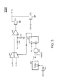
- FIG. 1 is a circuit diagram of an embodiment of a programmable power supply according to the present invention.
- a current-sense device such as a resistor 35 , generates a current-sense signal V CS in accordance with an output current I O of the programmable power supply.
- the current-sense signal V CS is correlated to the output current I O .
- a controller 100 is coupled to receive an output voltage V O and the current-sense signal V CS to detect the output voltage V O and the output current I O for developing the feedback loop.
- the controller 100 generates a feedback signal FB coupled to a switching controller (PSR) 300 through a first signal-transfer device, such as an opto-coupler 50 , for regulating the output voltage V O and the output current I O .
- PSR switching controller
- a capacitor 70 coupled to the controller 100 is used for a voltage-loop compensation.
- a capacitor 75 coupled to the controller 100 is applied to compensate a current-loop for the regulation of the output current I O .
- the controller 100 further generates a control signal S X coupled to control the switching controller 300 through a second signal-transfer device, such as an opto-coupler 60 .
- the control signal S X is used for programming of the switching controller 300 and the protections.
- a resistor 51 is coupled to the opto-coupler 50 and receives the output voltage V O from an output terminal of the programmable power supply. The resistor 51 is utilized to bias the operating current of the opto-coupler 50 .
- a resistor 61 is coupled to the opto-coupler 60 and receives the output voltage V O from the output terminal of the programmable power supply.
- the resistor 61 is applied to limit the current of the opto-coupler 60 .
- the controller 100 includes a communication interface COMM, (e.g. USB-PD, IEEE UPAMD 1823, one-wire communication, etc.) for the communication with the external devices.
- COMM communication interface
- the opto-coupler 50 will generate a feedback signal V B coupled to the switching controller 300 in accordance with the feedback signal FB.
- the opto-coupler 60 will generate a control signal S Y coupled to the switching controller 300 in response to the control signal S X .
- the switching controller 300 generates a switching signal S W for switching a primary-side winding N P of a transformer 10 and generating the output voltage V O and the output current I O at the secondary side of the transformer 10 through a secondary-side winding N S , a rectifier 30 , and an output capacitor 40 .
- a capacitor 45 and the resistor 35 are coupled to the output terminal of the programmable power supply.
- a first terminal of the primary-side winding N P receives an input voltage V IN .
- a transistor 20 is coupled to a second terminal of the primary-side winding N P to switch the transformer 10 in response to the switching signal S W .
- An auxiliary winding N A of the transformer 10 produces a reflected signal V S coupled to the switching controller 300 via a voltage divider developed by resistors 15 and 16 .
- the reflected signal V S is correlated to the output voltage V O .
- a resistor 25 is coupled between the transistor 20 and a ground to sense a switching current I P of the transformer 10 for generating a current signal CS coupled to the switching controller 300 .
- the switching controller 300 generates the switching signal S W in accordance with the feedback signal V B , the control signal S Y , the reflected signal V S , and the current signal CS.
- the controller 100 is equipped in the secondary side of the transformer 10 .
- the switching controller 300 is equipped in the primary side of the transformer 10 .
- FIG. 2 is a circuit diagram of an embodiment of the controller 100 according to the present invention.
- An embedded micro-controller (MCU) 80 has a memory 85 including a program memory and a data memory.
- the micro-controller 80 generates a watch-dog signal WG, a control signal CNT, and a control-bus signal N B .
- the control-bus signal N B is a bi-direction signal (input or output).
- the micro-controller 80 includes the communication interface COMM to communicate with the host and/or the I/O devices.
- the control-bus signal N B is coupled to control a multiplexer (MUX) 96 , an analog-to-digital converter (ADC) 95 , and digital-to-analog converters (DAC) 91 , 92 , 93 .
- the digital-to-analog converters 91 , 92 , and 93 are controlled by the micro-controller 80 through the control-bus signal N B and registers (REG) 81 , 82 , 83 .
- the registers 81 , 82 , and 83 have reference values.
- the control-bus signal N B is utilized to set the reference values.
- the current-sense signal V CS is coupled to generate a current signal V I through a feedback circuit 200 .
- the current signal V I is connected to the multiplexer 96 .
- the current signal V I is correlated to the output current I O shown in FIG. 1 .
- Resistors 86 and 87 develop a voltage divider to generate a feedback signal V FB in accordance with the output voltage V O .
- the feedback signal V FB is coupled to the multiplexer 96 and the feedback circuit 200 .
- the output terminal of the multiplexer 96 is connected to the input terminal of the analog-to-digital converter 95 .
- the output terminal of the multiplexer 96 outputs the current signal V I or the feedback signal V FB to the analog-to-digital converter 95 in response to the control-bus signal N B . That is, the analog-to-digital converter 95 is coupled to detect the output voltage V O and the output current I O .
- the output terminal of the analog-to-digital converter 95 is coupled to the micro-controller 80 . Therefore, via the control-bus signal N B , the micro-controller 80 can read the information of the output current I O and the output voltage V O from the analog-to-digital converter 95 .
- the micro-controller 80 controls the outputs of the digital-to-analog converters 91 , 92 , and 93 .
- the first digital-to-analog converter 91 generates a voltage-reference signal V RV in response to the reference value of the register 81 for controlling the output voltage V O .
- the second digital-to-analog converter 92 generates a current-reference signal V RI in response to the reference value of the register 82 for controlling the output current I O .
- the third digital-to-analog converter 93 generates an over-voltage reference threshold V OV in response to the reference value of the register 83 for the over-voltage protection.
- the digital-to-analog converters 91 , 92 , and 93 are operated as a reference generation circuit to generate the voltage-reference signal V RV , the current-reference signal V RI , and the over-voltage reference threshold V OV .
- the micro-controller 80 will control the over-voltage reference threshold V OV in accordance with the level of the output voltage V O .
- the registers 81 , 82 , and 83 will be reset to provide an initial value in response to the power-on of the power supply.
- the initial value of the first register 81 will be utilized to produce a minimum value of the voltage-reference signal V RV that is used to generate a 5V output voltage V O .
- the initial value of the second register 82 will be utilized to produce a minimum value of the current-reference signal V RI that is used to generate a 0.5 A output current I O .
- the voltage-reference signal V RV , the current-reference signal V RI , and the over-voltage reference threshold V OV will be reset to the initial value in response to the power-on of the power supply.
- the feedback circuit 200 generates a voltage-feedback signal COMV, a current-feedback signal COMI, the feedback signal FB, and the control signal S X in response to the voltage-reference signal V RV , the current-reference signal V RI , the over-voltage reference threshold V OV , the output voltage V O , the feedback signal V FB , the current-sense signal V CS , the watch-dog signal WG, the control signal CNT, and the control-bus signal N B .
- the feedback circuit 200 is coupled to detect the output voltage V O and the output current I O for generating the feedback signal FB in accordance with the feedback signal V FB , the current-sense signal V CS , the voltage-reference signal V RV , and the current-reference signal V RI .
- the feedback signal FB is transferred from the feedback circuit 200 to the switching controller 300 by the opto-coupler 50 (as shown in FIG. 1 ).
- FIG. 3 is a block diagram of an embodiment of the feedback circuit 200 according to the present invention. It includes an error-amplifier circuit (AMP) 210 and a protection circuit (PROTECTION) 250 .
- the error-amplifier circuit 210 generates the voltage-feedback signal COMV, the current-feedback signal COMI, the feedback signal FB, and the current signal V I in accordance with the voltage-reference signal V RV , the current-reference signal V RI , the current-sense signal V CS , and the feedback signal V FB .
- the protection circuit 250 generates the control signal S X in response to the over-voltage reference threshold V OV , the output voltage V O , the watch-dog signal WG, the control signal CNT, and the control-bus signal N B .
- FIG. 4 is a circuit diagram of an embodiment of the error-amplifier circuit 210 according to the present invention. It includes resistors 211 , 212 , and a capacitor 215 coupled to receive the current-sense signal V CS and filter the noise. A first terminal of the resistor 211 is coupled to receive the current-sense signal V CS . A first terminal of the resistor 212 is coupled to the ground. The capacitor 215 is coupled between second terminals of the resistors 211 and 212 . The capacitor 215 is further connected between a positive input terminal of an operational amplifier 220 and the second terminal of the resistor 211 . Resistors 218 and 219 determine the gain of the operational amplifier 220 .
- the resistor 218 is coupled between the second terminal of the resistor 211 and a negative input terminal of the operational amplifier 220 .
- the resistor 219 is coupled between the negative input terminal and an output terminal of the operational amplifier 220 .
- the operational amplifier 220 generates the current signal V I by amplifying the current-sense signal V CS .
- An error amplifier 230 generates the current-feedback signal COMI in accordance with the current signal V I and the current-reference signal V RI .
- the current signal V I is coupled to a negative input terminal of the error amplifier 230 .
- the current-reference signal V RI is supplied with a positive input terminal of the error amplifier 230 .
- An output terminal of the error amplifier 230 outputs the current-feedback signal COMI. Therefore, the error amplifier 230 generates the current-feedback signal COMI in accordance with the output current I O (as shown in FIG. 1 ) and the current-reference signal V RI .
- the current-feedback signal COMI is connected to the capacitor 75 (as shown in FIG. 1 ) for the loop-compensation.
- An error amplifier 240 generates the voltage-feedback signal COMV in accordance with the feedback signal V FB and the voltage-reference signal V RV .
- the feedback signal V FB is coupled to a negative input terminal of the error amplifier 240 .
- the voltage-reference signal V RV is supplied with a positive input terminal of the error amplifier 240 .
- An output terminal of the error amplifier 240 outputs the voltage-feedback signal COMV. Therefore, the error amplifier 240 generates the voltage-feedback signal COMV in accordance with the output voltage V O (as shown in FIG. 1 ) and the voltage-reference signal V RV .
- the voltage-feedback signal COMV is connected to the capacitor 70 (as shown in FIG. 1 ) for the loop-compensation.
- the voltage-feedback signal COMV is further connected to a positive input terminal of a buffer (OD) 245 to generate the feedback signal FB.
- a negative input terminal of the buffer 245 is coupled to an output terminal of the buffer 245 .
- the current-feedback signal COMI is further connected to a positive input terminal of a buffer 235 .
- a negative input terminal of the buffer 235 is coupled to an output terminal of the buffer 235 .
- the output terminal of the buffer 245 is parallel connected to the output terminal of the buffer 235 .
- the buffer 235 and the buffer 245 have the open-drain output, thus they can be wire-OR connected.
- FIG. 5 is a circuit diagram of an embodiment of the protection circuit 250 according to the present invention.
- the watch-dog signal WG is coupled to clear a watch-dog timer (TIMER) 280 via an inverter 251 .
- the watch-dog timer 280 will generate an expired signal T OUT (logic-low level) if the watch-dog signal WG is not generated (logic-low level) in time periodically.
- the expired signal T OUT can be regarded as a time-out signal.
- the expired signal T OUT and a power-on reset signal PWRST are coupled to a reset input terminal R of a RS flip-flop 253 via an AND gate 252 to reset the RS flip-flop 253 .
- the RS flip-flop 253 is set by the micro-controller 80 (as shown in FIG. 2 ) through the control-bus signal N B .
- the control-bus signal N B is coupled to a set input terminal S of the RS flip-flop 253 .
- the over-voltage reference threshold V OV and a threshold V T are coupled to a multiplexer (MUX) 260 .
- the multiplexer 260 outputs the over-voltage reference threshold V OV or the threshold V T as an over-voltage threshold for the over-voltage protection. Therefore, the multiplexer 260 is associated with the third register 83 and the third digital-to-analog converter 93 (as shown in FIG. 2 ) as a threshold generation circuit for generating the over-voltage threshold.
- the over-voltage reference threshold V OV or the threshold V T is coupled to a comparator 265 via the multiplexer 260 .
- the multiplexer 260 is controlled by an output terminal Q of the RS flip-flop 253 .
- the over-voltage reference threshold V OV When the RS flip-flop 253 is set, the over-voltage reference threshold V OV will be outputted to a negative input terminal of the comparator 265 . If the RS flip-flop 253 is reset, the threshold V T will be outputted to the negative input terminal of the comparator 265 for the over-voltage protection.
- the output voltage V O is coupled to a positive input terminal of the comparator 265 through a voltage divider developed by resistors 256 and 257 .
- the threshold V T is a minimum threshold for the over-voltage protection.
- the over-voltage threshold of the over-voltage protection is programmable by the micro-controller 80 through programming the level of the over-voltage reference threshold V OV .
- This over-voltage threshold will be reset as a minimum value (the threshold V T ) if the watch-dog signal WG is not generated in time periodically.
- the over-voltage threshold will be programmed to 14V for a 12V output voltage V O
- the over-voltage threshold will be programmed to 6V for a 5V output voltage V O .
- the over-voltage threshold will be reset to 6V even the output voltage V O is set as 12V, which will protect the power supply from abnormal operation when the micro-controller 80 is operated incorrectly. Further, the over-voltage threshold also will be reset as the minimum value in response to the power-on of the power supply.
- An output signal of the comparator 265 is coupled to a gate of a transistor 271 .
- the output signal of the comparator 265 drives the transistor 271 for generating the control signal S X (logic-low level).
- a source of the transistor 271 is coupled to the ground.
- a drain of the transistor 271 outputs the control signal S X .
- the comparator 265 is utilized to compare the output voltage V O with the over-voltage threshold for the over-voltage protection.
- the comparator 265 is associated with the transistor 271 as an over-voltage protection circuit to generate the control signal S X .
- the control signal S X serves as an over-voltage signal. As shown in FIG. 1 , the control signal S X is sent to the switching controller 300 through the opto-coupler 60 to disable the switching signal S W for the over-voltage protection.
- the control signal CNT from the micro-controller 80 also drives a transistor 272 to generate the control signal S X .
- the control signal CNT is coupled to a gate of the transistor 272 .
- a source of the transistor 272 is coupled to the ground.
- a drain of the transistor 272 outputs the control signal S X .
- the outputs of the transistors 271 and 272 are parallel connected.
- the control signal S X is used for the protection of the power supply and the control of the micro-controller 80 .
- FIG. 6 is a reference circuit schematic of the watch-dog timer 280 according to the present invention.
- the watch-dog timer 280 comprises an inverter 281 , a transistor 282 , a constant current source 283 , a capacitor 285 , and a comparator 290 .
- a first terminal of the constant current source 283 is coupled to a supply voltage V CC .
- a second terminal of the constant current source 283 is coupled to a drain of the transistor 282 and a first terminal of the capacitor 285 .
- a source of the transistor 282 and a second terminal of the capacitor 285 are coupled to the ground.
- An input signal CLR of the watch-dog timer 280 is coupled to a gate of the transistor 282 through the inverter 281 to control the transistor 282 .
- the input signal CLR is the inversed watch-dog signal /WG generated from the inverter 251 shown in FIG. 5 .
- a negative input terminal of the comparator 290 is coupled to the first terminal of the capacitor 285 .
- a positive input terminal of the comparator 290 is coupled to receive a threshold V TH1 .
- the comparator 290 compares the voltage of the capacitor 285 with the threshold V TH1 for generating the expired signal T OUT .
- the constant current source 283 is utilized to charge the capacitor 285 .
- the input signal CLR of the watch-dog timer 280 is coupled to discharge the capacitor 285 via the inverter 281 and the transistor 282 . If the capacitor 285 is not discharged by the input signal CLR timely, then the comparator 290 will generate the expired signal T OUT when the voltage of the capacitor 285 is charged and higher than the threshold V TH1 . At this time, the level of the expired signal T OUT is the logic-low level.
- FIG. 7 is a circuit diagram of an embodiment of the switching controller 300 according to the present invention. It includes a voltage detection circuit (V-DET) 310 to generate a voltage-loop signal V EA and a discharge time signal T DS in response to the reflected signal V S .
- V-DET voltage detection circuit
- the voltage-loop signal V EA is correlated to the output voltage V O shown in FIG. 1 .
- the discharge time signal T DS is correlated to the demagnetizing time of the transformer 10 shown in FIG. 1 . Therefore, the switching controller 300 is coupled to detect the output voltage V O by detecting the reflected signal V S of the transformer 10 .
- a current detection circuit (I-DET) 320 generates a current-loop signal T EA in response to the current signal CS and the discharge time signal T DS .
- the voltage detection circuit 310 and the current detection circuit 320 are related to the technology of the primary side regulation (PSR) of the power converter.
- PSR primary side regulation
- the detail of the skill of the primary side regulation can be found in the prior arts of “Control circuit for controlling output current at the primary side of a power converter”, U.S. Pat. No. 6,977,824; “Close-loop PWM controller for primary-side controlled power converters”, U.S. Pat. No. 7,016,204; and “Primary-side controlled switching regulator”, U.S. Pat. No. 7,352,595; etc.
- the voltage-loop signal V EA is coupled to a positive input terminal of a comparator 315 .
- a reference signal REF_V is supplied with a negative input terminal of the comparator 315 .
- the voltage-loop signal V EA is coupled to the comparator 315 for generating an over-voltage signal OV when the voltage-loop signal V EA is higher than the reference signal REF_V.
- the current-loop signal I EA is coupled to a negative input terminal of an amplifier 325 .
- a reference signal REF_I is supplied with a positive input terminal of the amplifier 325 .
- the current-loop signal I EA associated with the reference signal REF_I generates a current feedback signal I FB for generating the switching signal S W . Therefore, the switching controller 300 generates the switching signal S W in accordance with the reference signal REF_I.
- a programmable circuit 400 is coupled to generate the reference signals REF_V, REF_I, and a protection signal PRT in response to the control signal S Y and the power-on reset signal PWRST.
- the reference signal REF_V is operated as an over-voltage threshold signal for the over-voltage protection. This over-voltage protection is developed by the detection of the reflected signal V S .
- the reference signal REF_I is operated as a current limit threshold signal for limiting the output current I O (as shown in FIG. 1 ) of the power supply. Because the control signal S Y represents the control signal S X from the micro-controller 80 (as shown in FIG. 2 ), the reference signals REF_V and REF_I are controlled by the control signal S X for the over-voltage protection of the output voltage V O and the current limit of the output current I O .
- the protection signal PRT and the over-voltage signal OV are coupled to generate an off signal OFF via an OR gate 331 .
- a resistor 335 is utilized to pull high the feedback signal V B .
- the feedback signal V B is coupled to generate a secondary feedback signal V A through a level-shift circuit.
- the level-shift circuit comprises a transistor 336 , and resistors 335 , 337 , 338 .
- a drain of the transistor 336 is coupled to a supply voltage V DD .
- a first terminal of the resistor 335 is coupled to the supply voltage V DD and the drain of the transistor 336 .
- a second terminal of the resistor 335 is coupled to a gate of the transistor 336 and the feedback signal V B .
- the gate of the transistor 336 is further coupled to receive the feedback signal V B .
- a source of the transistor 336 is coupled to a first terminal of the resistor 337 .
- the resistor 338 is coupled between a second terminal of the resistor 337 and the ground.
- the secondary feedback signal V A is generated at the joint of the resistors 337 and 338 .
- the secondary feedback signal V A is correlated to the feedback signal V B .
- a PWM circuit (PWM) 350 generates the switching signal S W in response to the secondary feedback signal V A , the current feedback signal I FB , the off signal OFF, and the power-on reset signal PWRST.
- FIG. 8 is a reference circuit schematic of the PWM circuit 350 according to the present invention.
- An oscillator (OSC) 360 generates a clock signal PLS and a ramp signal RMP.
- the clock signal PLS is coupled to a clock input terminal CK of a flip-flop 375 .
- An output terminal Q of the flip-flop 375 outputs the switching signal S W .
- the off signal OFF is coupled to an input terminal D of the flip-flop 375 via an inverter 351 .
- the ramp signal RMP is coupled to negative input terminals of comparators 365 and 367 .
- the current feedback signal I FB is coupled to a positive input terminal of the comparator 365 to compare with the ramp signal RMP.
- the secondary feedback signal V A is coupled to a positive input terminal of the comparator 367 to compare with the ramp signal RMP.
- Output terminals of the comparators 365 and 367 are coupled to input terminals of an AND gate 370 .
- the off signal OFF is further coupled to the input terminal of the AND gate 370 though the inverter 351 .
- the power-on reset signal PWRST is also coupled to the input terminal of the AND gate 370 .
- An output terminal of the AND gate 370 is coupled to a reset input terminal R of the flip-flop 375 .
- the clock signal PLS periodically enables the switching signal S W via the flip-flop 375 .
- the switching signal S W will be disabled once the ramp signal RMP is higher than the current feedback signal I FB in the comparator 365 or the secondary feedback signal V A in the comparator 367 .
- the off signal OFF is also coupled to disable the switching signal S W through the inverter 351 and the AND gate 370 .
- the power-on reset signal PWRST is also coupled to disable the switching signal S W through the AND gate 370 .
- FIG. 9 is a circuit diagram of an embodiment of the programmable circuit 400 according to the present invention.
- a current source 410 is connected to pull high the control signal S Y .
- the current source 410 is coupled from the supply voltage V CC to a negative input terminal of a comparator 415 .
- the control signal S Y is also coupled to the negative input terminal of the comparator 415 .
- the comparator 415 will generate a pulse signal S CNT once the control signal S Y is lower than a threshold V T1 supplied with a positive input terminal of the comparator 415 .
- a pulse-position modulation circuit (PPM) 500 generates a demodulated signal S M and a synchronous signal S YNC in response to the pulse signal S CNT .
- the pulse signal S CNT indicates the control signal S X of the controller 100 (as shown in FIG. 2 ).
- the demodulated signal S M and the synchronous signal S YNC are coupled to a digital-decoder (DECODER) 450 to generate a digital data N M .
- the digital data N M is stored into a register (REG) 460 and a register (REG) 465 .
- the register 460 is coupled to output the digital data N M to a digital-to-analog converter (DAC) 470 for generating a voltage-adjust signal V J .
- DAC digital-to-analog converter
- An add circuit 480 generates the reference signal REF_V by adding a reference signal V RF and the voltage-adjust signal V J .
- the register 465 is coupled to output the digital data N M to a digital-to-analog converter (DAC) 475 for generating a current-adjust signal I J .
- An add circuit 485 generates the reference signal REF_I by adding a reference signal I RF and the current-adjust signal I J .
- the digital data N M is utilized to generate the voltage-adjust signal V J and the current-adjust signal I J for generating the reference signals REF_V and REF_I.
- the reference signal REF_V and the reference signal REF_I are programmable by the micro-controller 80 of the controller 100 .
- the reflected signal V S of the transformer 10 (as shown in FIG. 1 ) is used for the over-voltage protection in the primary side of the transformer 10 .
- the threshold (reference signal REF_V) of this over-voltage protection (for output voltage V O ) is programmable by the controller 100 in the secondary side of the transformer 10 .
- the current limit (reference signal REF_I) of the output current I O (as shown in FIG. 1 ) can be programmed by the controller 100 in the secondary side of the transformer 10 .
- the pulse signal S CNT is further coupled to a timer (TIMER_L) 420 for detecting the pulse width of the pulse signal S CNT . That is, the timer 420 is used to detect the logic-low period of the control signal S X shown in FIG. 1 .
- the protection signal PRT will be generated by the timer 420 via an inverter 421 if the pulse width of the pulse signal S CNT is over a period T OV .
- the circuit of the timer 420 can be the same as the circuit of the watch-dog timer 280 shown in FIG. 6 .
- the current of the constant current source 283 , the capacitance of the capacitor 285 , and the value of the threshold V TH1 determine the period T OV .
- This protection signal PRT is coupled to the OR gate 331 (as shown in FIG. 7 ) to generate the off signal OFF for disabling the switching signal S W . Because the control signal S X (the pulse signal S CNT ) shown in FIG. 5 will be generated greater than the period T OV when the over-voltage of the output voltage V O is detected by the controller 100 in the secondary side of the transformer 10 (as shown in FIG. 1 ), the switching signal S W will be disabled by the switching controller 300 once the over-voltage of the output voltage V O is detected.
- Another timer (TIMER_H) 425 is coupled to receive the pulse signal S CNT through an inverter 427 .
- An output terminal of the timer 425 is coupled to an AND gate 426 .
- the timer 425 will generate a reset signal PRST via the AND gate 426 once the pulse signal S CNT is not generated over a specific period T OT .
- the circuit of the timer 425 can be the same as the circuit of the watch-dog timer 280 shown in FIG. 6 .
- the current of the constant current source 283 , the capacitance of the capacitor 285 , and the value of the threshold V TH1 determine the period T OT .
- the power-on reset signal PWRST is also coupled to the AND gate 426 to generate the reset signal PRST through the AND gate 426 .
- the reset signal PRST is coupled to clear the registers 460 and 465 for resetting the value of the voltage-adjust signal V J and the current-adjust signal I J to the zero.
- the reference signal REF_V will be set to a minimum value (reference signal V RF ), that is the initial value, for the over-voltage protection once the control signal S X is not generated in time by the controller 100 or the power supply is powered on.
- the reference signal REF_I will be set to a minimum value (reference signal I RF ), that is the initial value, for limiting the output current I O once the control signal S X is not generated in time by the controller 100 or the power supply is powered on. Therefore, if the micro-controller 80 is not operated properly, then the threshold (reference signal REF_V) for the over-voltage protection and the threshold (reference signal REF_I) for the output current limit will be reset to the minimum value for the protection.
- control signal S X generated by the controller 100 is used for,
- FIG. 10 is a circuit diagram of an embodiment of the pulse-position modulation circuit 500 according to the present invention. It operates as a de-modulator for an input signal with the pulse-position modulation, such as the control signals S X , S Y , and the pulse signal S CNT .
- a current source 512 is coupled from the supply voltage V CC to a first terminal of a capacitor 520 to charge the capacitor 520 .
- a second terminal of the capacitor 520 is coupled to the ground.
- a resistor 511 is coupled between the first terminal of the capacitor 520 and a drain of a transistor 510 .
- a source of the transistor 510 is coupled to the ground.
- the pulse signal S CNT is coupled to a gate of the transistor 510 to drive the transistor 510 .
- the pulse signal S CNT is coupled to discharge the capacitor 520 through the transistor 510 and the resistor 511 .
- a slope signal SLP is thus generated at the capacitor 520 .
- a positive input terminal of a comparator 530 is coupled to the first terminal of the capacitor 520 .
- a threshold V T2 is supplied with a negative input terminal of the comparator 530 .
- the comparator 530 will generate a data signal S D as a logic-high level once the slope signal SLP is higher than the threshold V T2 .
- the data signal S D is coupled to an input terminal D of a flip-flop 570 .
- the pulse signal S CNT is further coupled to a clock input terminal CK of the flip-flop 570 .
- the data signal S D will be latched into the flip-flop 570 in response to the pulse signal S CNT for generating the demodulated signal S M at an output terminal Q of the flip-flop 570 .
- the power-on reset signal PWRST is coupled to a reset input terminal R of the flip-flop 570 to reset the flip-flop 570 .
- the pulse signal S CNT is further coupled to generate the synchronous signal S YNC through a pulse generation circuit 580 .
- the demodulated signal S M is generated in accordance with the pulse position of the control signal S X .
Abstract
Description
Claims (20)
Priority Applications (3)
| Application Number | Priority Date | Filing Date | Title |
|---|---|---|---|
| US14/148,955 US9921627B2 (en) | 2013-01-08 | 2014-01-07 | Control circuit for programmable power supply |
| US15/891,035 US10401929B2 (en) | 2013-01-08 | 2018-02-07 | Control circuit for programmable power supply |
| US16/521,043 US10969845B2 (en) | 2013-01-08 | 2019-07-24 | Control circuit for programmable power supply |
Applications Claiming Priority (2)
| Application Number | Priority Date | Filing Date | Title |
|---|---|---|---|
| US201361749972P | 2013-01-08 | 2013-01-08 | |
| US14/148,955 US9921627B2 (en) | 2013-01-08 | 2014-01-07 | Control circuit for programmable power supply |
Related Child Applications (1)
| Application Number | Title | Priority Date | Filing Date |
|---|---|---|---|
| US15/891,035 Continuation US10401929B2 (en) | 2013-01-08 | 2018-02-07 | Control circuit for programmable power supply |
Publications (2)
| Publication Number | Publication Date |
|---|---|
| US20140195065A1 US20140195065A1 (en) | 2014-07-10 |
| US9921627B2 true US9921627B2 (en) | 2018-03-20 |
Family
ID=50530032
Family Applications (3)
| Application Number | Title | Priority Date | Filing Date |
|---|---|---|---|
| US14/148,955 Active 2036-07-12 US9921627B2 (en) | 2013-01-08 | 2014-01-07 | Control circuit for programmable power supply |
| US15/891,035 Active US10401929B2 (en) | 2013-01-08 | 2018-02-07 | Control circuit for programmable power supply |
| US16/521,043 Active 2034-03-31 US10969845B2 (en) | 2013-01-08 | 2019-07-24 | Control circuit for programmable power supply |
Family Applications After (2)
| Application Number | Title | Priority Date | Filing Date |
|---|---|---|---|
| US15/891,035 Active US10401929B2 (en) | 2013-01-08 | 2018-02-07 | Control circuit for programmable power supply |
| US16/521,043 Active 2034-03-31 US10969845B2 (en) | 2013-01-08 | 2019-07-24 | Control circuit for programmable power supply |
Country Status (3)
| Country | Link |
|---|---|
| US (3) | US9921627B2 (en) |
| CN (1) | CN103762849B (en) |
| TW (1) | TWI513162B (en) |
Families Citing this family (16)
| Publication number | Priority date | Publication date | Assignee | Title |
|---|---|---|---|---|
| US9887564B2 (en) | 2014-02-13 | 2018-02-06 | Infineon Technologies Austria Ag | Switched mode power supply circuit |
| US10396571B2 (en) * | 2015-02-17 | 2019-08-27 | Fairchild Semiconductor Corporation | Adaptive overvoltage protection for adaptive power adapters |
| TWI579678B (en) * | 2015-08-13 | 2017-04-21 | 華碩電腦股份有限公司 | Power adapter and control method thereof |
| US10566827B2 (en) | 2016-02-05 | 2020-02-18 | Guangdong Oppo Mobile Telecommunications Corp., Ltd. | Adapter and charging control method |
| CN105656162B (en) * | 2016-03-17 | 2018-06-08 | 深圳市乐得瑞科技有限公司 | Quick charging system and method based on USB PD agreements |
| US9608616B1 (en) * | 2016-05-27 | 2017-03-28 | Taiwan Semiconductor Manufacturing Company, Ltd. | Power clamp circuits and methods |
| WO2018041687A1 (en) * | 2016-08-29 | 2018-03-08 | Philips Lighting Holding B.V. | Control of isolated auxiliary power supply and dali supply for sensor-ready led drivers |
| EP3504936B1 (en) | 2016-08-29 | 2020-10-21 | Signify Holding B.V. | Control of isolated auxiliary power supply and dali supply for sensor-ready led drivers |
| US10228742B2 (en) * | 2017-05-18 | 2019-03-12 | Cypress Semiconductor Corporation | USB power control analog subsystem architecture |
| US10222402B2 (en) | 2017-05-18 | 2019-03-05 | Cypress Semiconductor Corporation | Current sensing in a USB power control analog subsystem |
| US10228746B1 (en) * | 2017-12-05 | 2019-03-12 | Western Digital Technologies, Inc. | Dynamic distributed power control circuits |
| CN111324160B (en) * | 2018-12-14 | 2021-07-09 | 致茂电子(苏州)有限公司 | Power supply and compensation method thereof |
| CN112748675A (en) * | 2019-10-16 | 2021-05-04 | 重庆禾瑞佳森物联网科技有限责任公司 | Singlechip system compatible with multiple slave machines |
| EP3890445A1 (en) * | 2020-03-31 | 2021-10-06 | Tridonic GmbH & Co. KG | Primary side switched converter for providing a voltage supply to an led load |
| US11711023B2 (en) * | 2021-05-14 | 2023-07-25 | Queen's University At Kingston | Methods and circuits for sensing isolated power converter output voltage across the isolation barrier |
| FR3129004A1 (en) * | 2021-11-05 | 2023-05-12 | Stmicroelectronics (Grenoble 2) Sas | Power circuit |
Citations (27)
| Publication number | Priority date | Publication date | Assignee | Title |
|---|---|---|---|---|
| US5973945A (en) * | 1998-07-01 | 1999-10-26 | Power Integrations, Inc. | Coupled inductor power supply with reflected feedback regulation circuitry |
| US6023178A (en) * | 1997-04-09 | 2000-02-08 | Yokogawa Electric Corporation | Pulse width control IC circuit and switching power supply unit |
| US6301135B1 (en) * | 1999-03-01 | 2001-10-09 | Texas Instruments Incorporated | Isolated switching-mode power supply control circuit having secondary-side controller and supervisory primary-side controller |
| US6304462B1 (en) * | 1999-09-24 | 2001-10-16 | Power Integrations, Inc. | Method and apparatus providing a multi-function terminal for a power supply controller |
| US20030042437A1 (en) * | 2001-09-04 | 2003-03-06 | Worley Eugene Robert | Switching power supply circuit using a silicon based LED for feedback |
| JP2005237067A (en) | 2004-02-18 | 2005-09-02 | Mitsuhiro Kusakawa | Switching power supply device |
| US6977824B1 (en) | 2004-08-09 | 2005-12-20 | System General Corp. | Control circuit for controlling output current at the primary side of a power converter |
| US7016204B2 (en) | 2004-08-12 | 2006-03-21 | System General Corp. | Close-loop PWM controller for primary-side controlled power converters |
| CN1783681A (en) | 2004-12-01 | 2006-06-07 | 崇贸科技股份有限公司 | Suitching type controller |
| CN1862935A (en) | 2005-05-09 | 2006-11-15 | 崇贸科技股份有限公司 | Output power compensating method and switching controller |
| US20070228834A1 (en) * | 2006-03-28 | 2007-10-04 | Fujitsu Limited | Uninterruptible power supply apparatus |
| US7352595B2 (en) | 2005-11-08 | 2008-04-01 | System General Corp. | Primary-side controlled switching regulator |
| CN101232237A (en) | 2007-01-26 | 2008-07-30 | 艾默生网络能源系统有限公司 | Multi-output power supply |
| US20080266907A1 (en) * | 2007-04-25 | 2008-10-30 | Jin-Tae Kim | Switch controller, switch control method, converter using the same, and driving method thereof |
| TWM354791U (en) | 2008-11-14 | 2009-04-11 | jin-cheng Gao | Automatic output voltage adjusting circuit of power supply |
| US20090129128A1 (en) * | 2006-03-26 | 2009-05-21 | Fujitsu Limited | Uninterruptible power supply apparatus |
| TWM364897U (en) | 2009-04-10 | 2009-09-11 | Top Victory Invest Ltd | Power supply |
| US20090251062A1 (en) * | 2008-04-08 | 2009-10-08 | Rohm Co., Ltd. | Inverter |
| TWM394507U (en) | 2010-02-08 | 2010-12-11 | Tech United Corp C | Secondary side power source control switch |
| US20120153866A1 (en) * | 2010-12-20 | 2012-06-21 | O2Micro, Inc. | Dc/dc converter with multiple outputs |
| WO2012085836A2 (en) | 2010-12-21 | 2012-06-28 | Koninklijke Philips Electronics N.V. | Method and apparatus to limit current overshoot and undershoot in light driver |
| TW201233030A (en) | 2010-12-20 | 2012-08-01 | O2Micro Inc | DC/DC converter, powering system, and method for controlling transformer |
| US20120314459A1 (en) * | 2011-06-08 | 2012-12-13 | Park In-Ki | Feedback circuit and power supply device including the same |
| US20130020964A1 (en) * | 2009-10-07 | 2013-01-24 | Lutron Electronics Co., Inc | Power converter for a configurable light-emitting diode driver |
| US20130114175A1 (en) * | 2011-11-07 | 2013-05-09 | Samsung Electronics Co., Ltd. | Switching mode power supply including surge protection circuit and image forming apparatus including the same |
| US20130119956A1 (en) * | 2011-11-11 | 2013-05-16 | Samsung Electro-Mechanics Co., Ltd. | Control ic having auto recovery circuit, auto recovery circuit of control ic, power converter system and method for auto recovering control ic |
| US8587280B2 (en) * | 2008-06-19 | 2013-11-19 | Power Integrations, Inc. | Power factor correction converter control offset |
Family Cites Families (7)
| Publication number | Priority date | Publication date | Assignee | Title |
|---|---|---|---|---|
| JP3578124B2 (en) * | 2001-08-31 | 2004-10-20 | ソニー株式会社 | Switching power supply |
| US7394209B2 (en) * | 2004-02-11 | 2008-07-01 | 02 Micro International Limited | Liquid crystal display system with lamp feedback |
| KR101029428B1 (en) * | 2004-06-30 | 2011-04-14 | 엘지디스플레이 주식회사 | Apparatus for driving lamp of liquid crystal display device |
| GB0610422D0 (en) * | 2006-05-26 | 2006-07-05 | Cambridge Semiconductor Ltd | Forward power converters |
| CN101232337B (en) | 2008-02-26 | 2010-06-02 | 泰宇电子(上海)有限公司 | Method for realizing switching office function |
| US8374004B2 (en) * | 2009-08-14 | 2013-02-12 | Marvell World Trade Ltd. | Isolated AC-DC converter with master controller on secondary side and slave controller on primary side |
| JP5911242B2 (en) * | 2011-09-09 | 2016-04-27 | キヤノン株式会社 | Power supply device and image forming apparatus |
-
2014
- 2014-01-07 US US14/148,955 patent/US9921627B2/en active Active
- 2014-01-08 CN CN201410008958.5A patent/CN103762849B/en active Active
- 2014-01-08 TW TW103100725A patent/TWI513162B/en active
-
2018
- 2018-02-07 US US15/891,035 patent/US10401929B2/en active Active
-
2019
- 2019-07-24 US US16/521,043 patent/US10969845B2/en active Active
Patent Citations (51)
| Publication number | Priority date | Publication date | Assignee | Title |
|---|---|---|---|---|
| US6023178A (en) * | 1997-04-09 | 2000-02-08 | Yokogawa Electric Corporation | Pulse width control IC circuit and switching power supply unit |
| US5973945A (en) * | 1998-07-01 | 1999-10-26 | Power Integrations, Inc. | Coupled inductor power supply with reflected feedback regulation circuitry |
| US6301135B1 (en) * | 1999-03-01 | 2001-10-09 | Texas Instruments Incorporated | Isolated switching-mode power supply control circuit having secondary-side controller and supervisory primary-side controller |
| US20110085360A1 (en) * | 1999-09-24 | 2011-04-14 | Power Integrations, Inc. | Method and apparatus providing a multi-function terminal for a power supply controller |
| US7253997B2 (en) * | 1999-09-24 | 2007-08-07 | Power Integrations, Inc. | Method and apparatus providing a multi-function terminal for a power supply controller |
| US6351398B1 (en) * | 1999-09-24 | 2002-02-26 | Power Integrations, Inc. | Method and apparatus providing a multi-function terminal for a power supply controller |
| US6356464B1 (en) * | 1999-09-24 | 2002-03-12 | Power Integrations, Inc. | Method and apparatus providing a multi-function terminal for a power supply controller |
| US6366481B1 (en) * | 1999-09-24 | 2002-04-02 | Power Integrations, Inc. | Method and apparatus providing a multi-function terminal for a power supply controller |
| US6462971B1 (en) * | 1999-09-24 | 2002-10-08 | Power Integrations, Inc. | Method and apparatus providing a multi-function terminal for a power supply controller |
| US20020172055A1 (en) * | 1999-09-24 | 2002-11-21 | Balu Balakrishnan | Method and apparatus providing a multi-function terminal for a power supply controller |
| US20090310389A1 (en) * | 1999-09-24 | 2009-12-17 | Power Integrations, Inc. | Method and apparatus providing a multi-function terminal for a power supply controller |
| US6538908B2 (en) * | 1999-09-24 | 2003-03-25 | Power Integrations, Inc. | Method and apparatus providing a multi-function terminal for a power supply controller |
| US20030107359A1 (en) * | 1999-09-24 | 2003-06-12 | Balu Balakrishnan | Method and apparatus providing a multi-function terminal for a power supply controller |
| US6643153B2 (en) * | 1999-09-24 | 2003-11-04 | Power Integrations, Inc. | Method and apparatus providing a multi-function terminal for a power supply controller |
| US20040071001A1 (en) * | 1999-09-24 | 2004-04-15 | Balakrishnan Balu Y. | Method and apparatus providing a multi-function terminal for a power supply controller |
| US6914793B2 (en) * | 1999-09-24 | 2005-07-05 | Power Integrations, Inc. | Method and apparatus providing a multi-function terminal for a power supply controller |
| US20050152164A1 (en) * | 1999-09-24 | 2005-07-14 | Balu Balakrishnan | Method and apparatus providing a multi-function terminal for a power supply controller |
| US8482938B2 (en) * | 1999-09-24 | 2013-07-09 | Power Integrations, Inc. | Method and apparatus providing a multi-function terminal for a power supply controller |
| US6304462B1 (en) * | 1999-09-24 | 2001-10-16 | Power Integrations, Inc. | Method and apparatus providing a multi-function terminal for a power supply controller |
| US7876587B2 (en) * | 1999-09-24 | 2011-01-25 | Power Integrations, Inc, | Method and apparatus providing a multi-function terminal for a power supply controller |
| US6313976B1 (en) * | 1999-09-24 | 2001-11-06 | Power Integrations, Inc. | Method and apparatus providing a multi-function terminal for a power supply controller |
| US20080186747A1 (en) * | 1999-09-24 | 2008-08-07 | Balu Balakrishnan | Method and apparatus providing a multi-function terminal for a power supply controller |
| US7596005B2 (en) * | 1999-09-24 | 2009-09-29 | Power Integrations, Inc. | Method and apparatus providing a multi-function terminal for a power supply controller |
| US20030042437A1 (en) * | 2001-09-04 | 2003-03-06 | Worley Eugene Robert | Switching power supply circuit using a silicon based LED for feedback |
| JP2005237067A (en) | 2004-02-18 | 2005-09-02 | Mitsuhiro Kusakawa | Switching power supply device |
| US6977824B1 (en) | 2004-08-09 | 2005-12-20 | System General Corp. | Control circuit for controlling output current at the primary side of a power converter |
| US7016204B2 (en) | 2004-08-12 | 2006-03-21 | System General Corp. | Close-loop PWM controller for primary-side controlled power converters |
| CN1783681A (en) | 2004-12-01 | 2006-06-07 | 崇贸科技股份有限公司 | Suitching type controller |
| CN1862935A (en) | 2005-05-09 | 2006-11-15 | 崇贸科技股份有限公司 | Output power compensating method and switching controller |
| US7352595B2 (en) | 2005-11-08 | 2008-04-01 | System General Corp. | Primary-side controlled switching regulator |
| US20090129128A1 (en) * | 2006-03-26 | 2009-05-21 | Fujitsu Limited | Uninterruptible power supply apparatus |
| US8084886B2 (en) * | 2006-03-28 | 2011-12-27 | Fujitsu Limited | Uninterruptible power supply apparatus |
| US20070228834A1 (en) * | 2006-03-28 | 2007-10-04 | Fujitsu Limited | Uninterruptible power supply apparatus |
| CN101232237A (en) | 2007-01-26 | 2008-07-30 | 艾默生网络能源系统有限公司 | Multi-output power supply |
| US8670252B2 (en) * | 2007-04-25 | 2014-03-11 | Fairchild Korea Semiconductor, Ltd. | Switch controller, switch control method, converter using the same, and driving method thereof |
| US20080266907A1 (en) * | 2007-04-25 | 2008-10-30 | Jin-Tae Kim | Switch controller, switch control method, converter using the same, and driving method thereof |
| US8169802B2 (en) * | 2007-04-25 | 2012-05-01 | Fairchild Korea Semiconductor, Ltd. | Switch controller of a converter with a soft start signal generator comprising a plurality of current sources |
| US20120188802A1 (en) * | 2007-04-25 | 2012-07-26 | Jin-Tae Kim | Switch Controller, Switch Control Method, Converter Using the Same, and Driving Method Thereof |
| US20090251062A1 (en) * | 2008-04-08 | 2009-10-08 | Rohm Co., Ltd. | Inverter |
| US8587280B2 (en) * | 2008-06-19 | 2013-11-19 | Power Integrations, Inc. | Power factor correction converter control offset |
| TWM354791U (en) | 2008-11-14 | 2009-04-11 | jin-cheng Gao | Automatic output voltage adjusting circuit of power supply |
| TWM364897U (en) | 2009-04-10 | 2009-09-11 | Top Victory Invest Ltd | Power supply |
| US20130020964A1 (en) * | 2009-10-07 | 2013-01-24 | Lutron Electronics Co., Inc | Power converter for a configurable light-emitting diode driver |
| TWM394507U (en) | 2010-02-08 | 2010-12-11 | Tech United Corp C | Secondary side power source control switch |
| TW201233030A (en) | 2010-12-20 | 2012-08-01 | O2Micro Inc | DC/DC converter, powering system, and method for controlling transformer |
| US20120153866A1 (en) * | 2010-12-20 | 2012-06-21 | O2Micro, Inc. | Dc/dc converter with multiple outputs |
| WO2012085836A2 (en) | 2010-12-21 | 2012-06-28 | Koninklijke Philips Electronics N.V. | Method and apparatus to limit current overshoot and undershoot in light driver |
| US20120314459A1 (en) * | 2011-06-08 | 2012-12-13 | Park In-Ki | Feedback circuit and power supply device including the same |
| US9001533B2 (en) * | 2011-06-08 | 2015-04-07 | Fairchild Korea Semiconductor Ltd. | Feedback circuit and power supply device including the same |
| US20130114175A1 (en) * | 2011-11-07 | 2013-05-09 | Samsung Electronics Co., Ltd. | Switching mode power supply including surge protection circuit and image forming apparatus including the same |
| US20130119956A1 (en) * | 2011-11-11 | 2013-05-16 | Samsung Electro-Mechanics Co., Ltd. | Control ic having auto recovery circuit, auto recovery circuit of control ic, power converter system and method for auto recovering control ic |
Also Published As
| Publication number | Publication date |
|---|---|
| US20190346898A1 (en) | 2019-11-14 |
| US10401929B2 (en) | 2019-09-03 |
| US10969845B2 (en) | 2021-04-06 |
| US20140195065A1 (en) | 2014-07-10 |
| CN103762849B (en) | 2016-08-17 |
| CN103762849A (en) | 2014-04-30 |
| US20180164861A1 (en) | 2018-06-14 |
| TWI513162B (en) | 2015-12-11 |
| TW201429143A (en) | 2014-07-16 |
Similar Documents
| Publication | Publication Date | Title |
|---|---|---|
| US10969845B2 (en) | Control circuit for programmable power supply | |
| US9236806B2 (en) | Method and apparatus for controlling programmable power converter with low standby power loss | |
| US9343982B2 (en) | Primary-side controlled programmable power converter | |
| US20140192565A1 (en) | Circuit with synchronous rectifier for controlling programmable power converter | |
| US20140239882A1 (en) | Apparatus for charging battery through programmable power adapter | |
| US9654013B2 (en) | Control circuit, control method and primary-controlled flyback converter using the same | |
| US20160241150A1 (en) | Alternating valley switching for power converter | |
| US9337737B2 (en) | Control circuit with fast dynamic response for power converters | |
| US20080130324A1 (en) | Switch mode power supply and driving method thereof | |
| KR101126766B1 (en) | Switching mode power supply and method for protection operation thereof | |
| US20070285953A1 (en) | Quasi-resonant converter and controlling method thereof | |
| US7301786B2 (en) | Quasi resonant type switching power supply apparatus with overcurrent limiting | |
| US9343917B2 (en) | Control circuit for charging battery through programmable power supplier | |
| US9407142B2 (en) | Method and apparatus for controlling programmable power converter | |
| US9270184B2 (en) | Control circuit and terminal for cable compensation and wake-up of primary-side regulated power converter | |
| KR20080008037A (en) | Switching mode power supply and the driving method thereof | |
| US9954451B2 (en) | Programmable frequency decrease circuit for a programmable power supply | |
| US20120170321A1 (en) | Feedback circuit with remote on/off control for power supply | |
| TW201528675A (en) | Circuit with synchronous rectifier for controlling programmable power converter and method therefore | |
| US9762144B2 (en) | Switching control circuit with signal process to accommodate the synchronous rectifier of power converters | |
| US20140362608A1 (en) | Method for programmable primary-side-regulated power converter | |
| KR20080054132A (en) | Power factor correction circuit | |
| CN104135156A (en) | Circuit and method for controlling programmable power converter |
Legal Events
| Date | Code | Title | Description |
|---|---|---|---|
| AS | Assignment |
Owner name: SYSTEM GENERAL CORP., TAIWAN Free format text: ASSIGNMENT OF ASSIGNORS INTEREST;ASSIGNOR:YANG, TA-YUNG;REEL/FRAME:031904/0682 Effective date: 20140107 |
|
| AS | Assignment |
Owner name: FAIRCHILD (TAIWAN) CORPORATION, TAIWAN Free format text: CHANGE OF NAME;ASSIGNOR:SYSTEM GENERAL CORP.;REEL/FRAME:038599/0022 Effective date: 20140620 |
|
| AS | Assignment |
Owner name: SEMICONDUCTOR COMPONENTS INDUSTRIES, LLC, ARIZONA Free format text: ASSIGNMENT OF ASSIGNORS INTEREST;ASSIGNOR:FAIRCHILD (TAIWAN) CORPORATION (FORMERLY SYSTEM GENERAL CORPORATION);REEL/FRAME:042328/0318 Effective date: 20161221 |
|
| STCF | Information on status: patent grant |
Free format text: PATENTED CASE |
|
| AS | Assignment |
Owner name: DEUTSCHE BANK AG NEW YORK BRANCH, AS COLLATERAL AGENT, NEW YORK Free format text: PATENT SECURITY AGREEMENT;ASSIGNOR:SEMICONDUCTOR COMPONENTS INDUSTRIES, LLC;REEL/FRAME:046410/0933 Effective date: 20170210 Owner name: DEUTSCHE BANK AG NEW YORK BRANCH, AS COLLATERAL AG Free format text: PATENT SECURITY AGREEMENT;ASSIGNOR:SEMICONDUCTOR COMPONENTS INDUSTRIES, LLC;REEL/FRAME:046410/0933 Effective date: 20170210 |
|
| MAFP | Maintenance fee payment |
Free format text: PAYMENT OF MAINTENANCE FEE, 4TH YEAR, LARGE ENTITY (ORIGINAL EVENT CODE: M1551); ENTITY STATUS OF PATENT OWNER: LARGE ENTITY Year of fee payment: 4 |
|
| AS | Assignment |
Owner name: FAIRCHILD SEMICONDUCTOR CORPORATION, ARIZONA Free format text: RELEASE OF SECURITY INTEREST IN PATENTS RECORDED AT RECORDED AT REEL 046410, FRAME 0933;ASSIGNOR:DEUTSCHE BANK AG NEW YORK BRANCH, AS COLLATERAL AGENT;REEL/FRAME:064072/0001 Effective date: 20230622 Owner name: SEMICONDUCTOR COMPONENTS INDUSTRIES, LLC, ARIZONA Free format text: RELEASE OF SECURITY INTEREST IN PATENTS RECORDED AT RECORDED AT REEL 046410, FRAME 0933;ASSIGNOR:DEUTSCHE BANK AG NEW YORK BRANCH, AS COLLATERAL AGENT;REEL/FRAME:064072/0001 Effective date: 20230622 |