EP2293352B1 - Halbleiter-Lichtemissionsbauelement mit einem unebenen Substrat - Google Patents
Halbleiter-Lichtemissionsbauelement mit einem unebenen Substrat Download PDFInfo
- Publication number
- EP2293352B1 EP2293352B1 EP10190784.8A EP10190784A EP2293352B1 EP 2293352 B1 EP2293352 B1 EP 2293352B1 EP 10190784 A EP10190784 A EP 10190784A EP 2293352 B1 EP2293352 B1 EP 2293352B1
- Authority
- EP
- European Patent Office
- Prior art keywords
- substrate
- light emitting
- electrode
- light
- semiconductor layer
- Prior art date
- Legal status (The legal status is an assumption and is not a legal conclusion. Google has not performed a legal analysis and makes no representation as to the accuracy of the status listed.)
- Expired - Lifetime
Links
Images








Classifications
-
- H—ELECTRICITY
- H10—SEMICONDUCTOR DEVICES; ELECTRIC SOLID-STATE DEVICES NOT OTHERWISE PROVIDED FOR
- H10H—INORGANIC LIGHT-EMITTING SEMICONDUCTOR DEVICES HAVING POTENTIAL BARRIERS
- H10H20/00—Individual inorganic light-emitting semiconductor devices having potential barriers, e.g. light-emitting diodes [LED]
- H10H20/80—Constructional details
- H10H20/81—Bodies
- H10H20/817—Bodies characterised by the crystal structures or orientations, e.g. polycrystalline, amorphous or porous
-
- H—ELECTRICITY
- H10—SEMICONDUCTOR DEVICES; ELECTRIC SOLID-STATE DEVICES NOT OTHERWISE PROVIDED FOR
- H10H—INORGANIC LIGHT-EMITTING SEMICONDUCTOR DEVICES HAVING POTENTIAL BARRIERS
- H10H20/00—Individual inorganic light-emitting semiconductor devices having potential barriers, e.g. light-emitting diodes [LED]
- H10H20/01—Manufacture or treatment
- H10H20/011—Manufacture or treatment of bodies, e.g. forming semiconductor layers
- H10H20/013—Manufacture or treatment of bodies, e.g. forming semiconductor layers having light-emitting regions comprising only Group III-V materials
- H10H20/0133—Manufacture or treatment of bodies, e.g. forming semiconductor layers having light-emitting regions comprising only Group III-V materials with a substrate not being Group III-V materials
- H10H20/01335—Manufacture or treatment of bodies, e.g. forming semiconductor layers having light-emitting regions comprising only Group III-V materials with a substrate not being Group III-V materials the light-emitting regions comprising nitride materials
-
- H—ELECTRICITY
- H10—SEMICONDUCTOR DEVICES; ELECTRIC SOLID-STATE DEVICES NOT OTHERWISE PROVIDED FOR
- H10H—INORGANIC LIGHT-EMITTING SEMICONDUCTOR DEVICES HAVING POTENTIAL BARRIERS
- H10H20/00—Individual inorganic light-emitting semiconductor devices having potential barriers, e.g. light-emitting diodes [LED]
- H10H20/80—Constructional details
- H10H20/81—Bodies
- H10H20/819—Bodies characterised by their shape, e.g. curved or truncated substrates
-
- H—ELECTRICITY
- H10—SEMICONDUCTOR DEVICES; ELECTRIC SOLID-STATE DEVICES NOT OTHERWISE PROVIDED FOR
- H10H—INORGANIC LIGHT-EMITTING SEMICONDUCTOR DEVICES HAVING POTENTIAL BARRIERS
- H10H20/00—Individual inorganic light-emitting semiconductor devices having potential barriers, e.g. light-emitting diodes [LED]
- H10H20/80—Constructional details
- H10H20/81—Bodies
- H10H20/819—Bodies characterised by their shape, e.g. curved or truncated substrates
- H10H20/82—Roughened surfaces, e.g. at the interface between epitaxial layers
-
- H—ELECTRICITY
- H10—SEMICONDUCTOR DEVICES; ELECTRIC SOLID-STATE DEVICES NOT OTHERWISE PROVIDED FOR
- H10H—INORGANIC LIGHT-EMITTING SEMICONDUCTOR DEVICES HAVING POTENTIAL BARRIERS
- H10H20/00—Individual inorganic light-emitting semiconductor devices having potential barriers, e.g. light-emitting diodes [LED]
- H10H20/80—Constructional details
- H10H20/81—Bodies
- H10H20/822—Materials of the light-emitting regions
-
- H—ELECTRICITY
- H10—SEMICONDUCTOR DEVICES; ELECTRIC SOLID-STATE DEVICES NOT OTHERWISE PROVIDED FOR
- H10H—INORGANIC LIGHT-EMITTING SEMICONDUCTOR DEVICES HAVING POTENTIAL BARRIERS
- H10H20/00—Individual inorganic light-emitting semiconductor devices having potential barriers, e.g. light-emitting diodes [LED]
- H10H20/80—Constructional details
- H10H20/81—Bodies
- H10H20/822—Materials of the light-emitting regions
- H10H20/824—Materials of the light-emitting regions comprising only Group III-V materials, e.g. GaP
- H10H20/825—Materials of the light-emitting regions comprising only Group III-V materials, e.g. GaP containing nitrogen, e.g. GaN
-
- H—ELECTRICITY
- H10—SEMICONDUCTOR DEVICES; ELECTRIC SOLID-STATE DEVICES NOT OTHERWISE PROVIDED FOR
- H10H—INORGANIC LIGHT-EMITTING SEMICONDUCTOR DEVICES HAVING POTENTIAL BARRIERS
- H10H20/00—Individual inorganic light-emitting semiconductor devices having potential barriers, e.g. light-emitting diodes [LED]
- H10H20/80—Constructional details
- H10H20/83—Electrodes
- H10H20/831—Electrodes characterised by their shape
-
- H—ELECTRICITY
- H10—SEMICONDUCTOR DEVICES; ELECTRIC SOLID-STATE DEVICES NOT OTHERWISE PROVIDED FOR
- H10P—GENERIC PROCESSES OR APPARATUS FOR THE MANUFACTURE OR TREATMENT OF DEVICES COVERED BY CLASS H10
- H10P14/00—Formation of materials, e.g. in the shape of layers or pillars
- H10P14/20—Formation of materials, e.g. in the shape of layers or pillars of semiconductor materials
- H10P14/27—Formation of materials, e.g. in the shape of layers or pillars of semiconductor materials using selective deposition, e.g. simultaneous growth of monocrystalline and non-monocrystalline semiconductor materials
- H10P14/276—Lateral overgrowth
-
- H—ELECTRICITY
- H10—SEMICONDUCTOR DEVICES; ELECTRIC SOLID-STATE DEVICES NOT OTHERWISE PROVIDED FOR
- H10P—GENERIC PROCESSES OR APPARATUS FOR THE MANUFACTURE OR TREATMENT OF DEVICES COVERED BY CLASS H10
- H10P14/00—Formation of materials, e.g. in the shape of layers or pillars
- H10P14/20—Formation of materials, e.g. in the shape of layers or pillars of semiconductor materials
- H10P14/29—Formation of materials, e.g. in the shape of layers or pillars of semiconductor materials characterised by the substrates
- H10P14/2901—Materials
- H10P14/2902—Materials being Group IVA materials
- H10P14/2904—Silicon carbide
-
- H—ELECTRICITY
- H10—SEMICONDUCTOR DEVICES; ELECTRIC SOLID-STATE DEVICES NOT OTHERWISE PROVIDED FOR
- H10P—GENERIC PROCESSES OR APPARATUS FOR THE MANUFACTURE OR TREATMENT OF DEVICES COVERED BY CLASS H10
- H10P14/00—Formation of materials, e.g. in the shape of layers or pillars
- H10P14/20—Formation of materials, e.g. in the shape of layers or pillars of semiconductor materials
- H10P14/34—Deposited materials, e.g. layers
- H10P14/3402—Deposited materials, e.g. layers characterised by the chemical composition
- H10P14/3414—Deposited materials, e.g. layers characterised by the chemical composition being group IIIA-VIA materials
- H10P14/3416—Nitrides
-
- H—ELECTRICITY
- H10—SEMICONDUCTOR DEVICES; ELECTRIC SOLID-STATE DEVICES NOT OTHERWISE PROVIDED FOR
- H10H—INORGANIC LIGHT-EMITTING SEMICONDUCTOR DEVICES HAVING POTENTIAL BARRIERS
- H10H20/00—Individual inorganic light-emitting semiconductor devices having potential barriers, e.g. light-emitting diodes [LED]
- H10H20/80—Constructional details
- H10H20/81—Bodies
- H10H20/819—Bodies characterised by their shape, e.g. curved or truncated substrates
- H10H20/821—Bodies characterised by their shape, e.g. curved or truncated substrates of the light-emitting regions, e.g. non-planar junctions
-
- H—ELECTRICITY
- H10—SEMICONDUCTOR DEVICES; ELECTRIC SOLID-STATE DEVICES NOT OTHERWISE PROVIDED FOR
- H10H—INORGANIC LIGHT-EMITTING SEMICONDUCTOR DEVICES HAVING POTENTIAL BARRIERS
- H10H20/00—Individual inorganic light-emitting semiconductor devices having potential barriers, e.g. light-emitting diodes [LED]
- H10H20/80—Constructional details
- H10H20/872—Periodic patterns for optical field-shaping, e.g. photonic bandgap structures
-
- Y—GENERAL TAGGING OF NEW TECHNOLOGICAL DEVELOPMENTS; GENERAL TAGGING OF CROSS-SECTIONAL TECHNOLOGIES SPANNING OVER SEVERAL SECTIONS OF THE IPC; TECHNICAL SUBJECTS COVERED BY FORMER USPC CROSS-REFERENCE ART COLLECTIONS [XRACs] AND DIGESTS
- Y10—TECHNICAL SUBJECTS COVERED BY FORMER USPC
- Y10T—TECHNICAL SUBJECTS COVERED BY FORMER US CLASSIFICATION
- Y10T428/00—Stock material or miscellaneous articles
- Y10T428/24—Structurally defined web or sheet [e.g., overall dimension, etc.]
- Y10T428/24355—Continuous and nonuniform or irregular surface on layer or component [e.g., roofing, etc.]
-
- Y—GENERAL TAGGING OF NEW TECHNOLOGICAL DEVELOPMENTS; GENERAL TAGGING OF CROSS-SECTIONAL TECHNOLOGIES SPANNING OVER SEVERAL SECTIONS OF THE IPC; TECHNICAL SUBJECTS COVERED BY FORMER USPC CROSS-REFERENCE ART COLLECTIONS [XRACs] AND DIGESTS
- Y10—TECHNICAL SUBJECTS COVERED BY FORMER USPC
- Y10T—TECHNICAL SUBJECTS COVERED BY FORMER US CLASSIFICATION
- Y10T428/00—Stock material or miscellaneous articles
- Y10T428/24—Structurally defined web or sheet [e.g., overall dimension, etc.]
- Y10T428/24479—Structurally defined web or sheet [e.g., overall dimension, etc.] including variation in thickness
Definitions
- a substrate, an n-side nitride semiconductor layer, a light emitting region (active layer) and a p-side nitride semiconductor layer are layered, in this order, wherein the film thickness of the p-side nitride semiconductor layer is less than that of the n-side nitride semiconductor layer.
- the electrode formed on the surface of the semiconductor layer is an electrode having an opening, as described above, because the effect of recesses and/or protruding portions on the surface of substrate is much higher with an electrode having an opening.
- the brightness of edges of recesses and/or protruding portions is higher than other portions. Therefore, by forming the openings above the edges of the recesses and/or protrusions, the output power is considerably increased.
- Second, light that has reached to upper areas through scattering or diffraction has a low intensity.
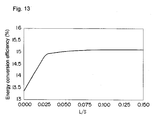
- the open electrode is an electrode having a plurality of openings that penetrate to the surface of the p-type semiconductor layer and that are surrounded by the electrode and it is preferable for L/S ⁇ 0.024 ⁇ m/ ⁇ m 2 to be fulfilled wherein the area of a portion surrounded by the outermost peripheral portion (total area of the electrode including the openings) is S and the total sum of the length of the inner periphery of the openings is L.
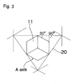
- a sapphire substrate of which a C plane (0001) is used as the main surface, having the orientation flat in an A plane (11-20) is used as the substrate.
- a process of the substrate and layering of an n-type semiconductor layer to a p-type semiconductor layer are carried out in the same manner as in first example.
- the LED gained in such a manner has properties wherein the vicinity of the periphery of the p electrode emits light that is more intense than that from other portions and in addition, a material having a high reflectance of the wavelength of the emitted light is used for the electrode so as to reduce the light component absorbed by the electrode, and therefore, the light emission output is increased in comparison with first and second embodiments.
- the light emission output is 13.2 mW according to a lamp measurement.
- a buffer layer which is made to grow at a low temperature, of AL x Ga 1-x N (0 ⁇ x ⁇ 1), of 100 ⁇ , is layered as an n-type semiconductor layer on sapphire substrate 10 wherein the repeating pattern of protruding portions 20 is formed and undoped GaN of 3 ⁇ m, Si doped GaN of 4 ⁇ m and undoped GaN of 3000 ⁇ are layered and then, six well layers and seven barrier layers, having respective film thickness of 60 ⁇ and 250 ⁇ , wherein well layers are undoped InGaN and barrier layers are Si doped GaN, are alternately layered as an active layer of a multi quantum well that becomes the light emitting region.
- the barrier layer that is finally layered may be of undoped GaN.
- Vf and power (wavelength 460nm) at 20 mA of the devices are as follows: Table 2 V f (V) power (mW) Relative power (i) triangle 3.54 10.08 1.14 (ii) diamond 3.55 10.01 1.13 (iii) hexagon 3.51 10.30 1.16 (iv) flat 3.48 8.85 1
Landscapes
- Led Devices (AREA)
- Electroluminescent Light Sources (AREA)
Claims (13)
- Halbleiter-Leuchtdrode umfassend:ein Substrat (10),eine Mehrzahl von Halbleiterschichten (11, 12, 13), welche auf dem Substrat (10) gebildet sind, und welche aus Materialien hergestellt sind, die sich von dem des Substrats (10) unterscheiden, undeine Ohmsche Elektrode (34), welche auf der Oberfläche der obersten Schicht der Halbleiterschichten (11, 12, 13) derart gebildet ist, dass Licht, welches in den Halbleiterschichten (11, 12, 13) erzeugt wird, von der Ohmsche Elektrode (34) oder von dem Substrat (10) emittiert wird,wobei hervorstehende Abschnitte (20) zum Streuen oder Beugen von Licht, welches in den Halbleiterschichten (11, 12, 13) erzeugt wird, in einem Wiederholungsmuster in der Oberfläche des Substrats (10) derart gebildet sind, dass der hervorstehende Abschnitt (20) in Kontakt mit zumindest einer der Halbleiterschichten (11, 12, 13) steht, undwobei die Seitenfläche des hervorstehenden Abschnitts (20) relativ zu der Richtung geneigt ist, in der die Halbleiterschichten (11, 12, 13) geschichtet sind,wobei der hervorstehende Abschnitt (20) keine Teilseite aufweist, die parallel zu einer A-Achse der Halblefterschichten (11, 12, 13) verläuft.
- Halbleiter-Leuchtdiode nach Anspruch 1, wobei das Substrat (10) ein Saphirsubstrat ist und wobei der hervorstehende Abschnitt (20) in einem Querschnitt des Saphirsubstrats (10) ein Trapez ist.
- Halbleiter-Leuchtdiode nach Anspruch 1, wobei das Substrat (10) ein Saphirsubstrat ist und wobei der hervorstehende Abschnitt (20) in einem Querschnitt des Saphirsubstrats (10) ein Trapez mit zumindest einem abgerundeten Rand ist.
- Halbleiter-Leuchtdiode nach einem der Ansprüche 1 bis 3, wobei die Ohmsche Elektrode (34) fast die gesamte Oberfläche der obersten Schicht der Halbleiterschichten (11, 12, 13) überdeckt.
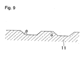
- Halbleiter-Leuchtdiode nach einem der Ansprüche 1 bis 4, wobei der Kegelwinkel der Seitenfläche der Vertiefung oder des hervorstehenden Abschnitts (20) nicht weniger als 90 Grad und nicht mehr als 160 Grad beträgt.
- Halbleiter-Leuchtdiode nach einem der Ansprüche 1 bis 6, wobei der hervorstehende Abschnitt (20) eine Teilseite aufweist, die rechtwinklig zu einer A-Achse der Halbleiterschichten (11, 12, 13) verläuft.
- Halbleiter-Leuchtdiode nach einem der Ansprüche 1 bis 6, wobei die Halbleiterschichten (11, 12, 13) aus III-V-Gruppenelement-baslerten Halbleitern hergestellt sind.
- Halbleiter-Leuchtdiode nach einem der Ansprüche 1 bis 7, wobei die Halbleiterschichten (11, 12, 13) aus GaN-basierten Halbleitern hergestellt sind.
- Halbleiter-Leuchtdiode nach einem der Ansprüche 1 bis 8, wobei das Substrat (10) ein C-Ebenen-(0001)-Saphirsubstrat (10) ist.
- Halbleiter-Leuchtdiode nach einem der Ansprüche 1 bis 9, wobei die Form des hervorstehenden Abschnitts (20) ein Polygon ist, welches ausgewählt ist aus der Gruppe enthaltend ein Dreieck, ein Parallelogramm und ein Hexagon.
- Halbleiter-Leuchtdiode nach einem der Ansprüche 1 bis 10, wobei die Höhe des hervorstehenden Abschnitts (20) nicht weniger als 50 Å und nicht mehr als die Dicke der Halbleiterschichten (11, 12, 13) beträgt, die auf dem Substrat (10) gewachsen sind.
- Halbleiter-Leuchtdiode nach einem der Ansprüche 1 bis 11, wobei die Seitenlänge des hervorstehenden Abschnitts (20) nicht weniger als λ/4 beträgt, wobei die Wellenlänge von emittiertem Licht in dem Halbleiter ist.
- Halbleiter-Leuchtdiode nach einem der Ansprüche 1 bis 12, wobei die Länge der Teilseite der hervorstehenden Abschnitte (20) nicht weniger als λ/4 und nicht mehr als 20 µm beträgt, wobei die Wellenlänge von emittiertem Licht in dem Halbleiter λ ist.
Applications Claiming Priority (5)
| Application Number | Priority Date | Filing Date | Title |
|---|---|---|---|
| JP2001223114 | 2001-07-24 | ||
| JP2002041737 | 2002-02-19 | ||
| JP2002213490A JP4055503B2 (ja) | 2001-07-24 | 2002-07-23 | 半導体発光素子 |
| EP02751652A EP1416543B1 (de) | 2001-07-24 | 2002-07-24 | Halbleiter-lichtemissionsbauelement mit einem unebenen substrat |
| PCT/JP2002/007460 WO2003010831A1 (fr) | 2001-07-24 | 2002-07-24 | Dispositif electroluminescent a semi-conducteur presentant un substrat irregulier |
Related Parent Applications (2)
| Application Number | Title | Priority Date | Filing Date |
|---|---|---|---|
| EP02751652A Division EP1416543B1 (de) | 2001-07-24 | 2002-07-24 | Halbleiter-lichtemissionsbauelement mit einem unebenen substrat |
| EP02751652.5 Division | 2002-07-24 |
Publications (3)
| Publication Number | Publication Date |
|---|---|
| EP2293352A1 EP2293352A1 (de) | 2011-03-09 |
| EP2293352B1 true EP2293352B1 (de) | 2014-06-04 |
| EP2293352B2 EP2293352B2 (de) | 2021-05-05 |
Family
ID=27347215
Family Applications (8)
| Application Number | Title | Priority Date | Filing Date |
|---|---|---|---|
| EP10189616.5A Expired - Lifetime EP2299504B1 (de) | 2001-07-24 | 2002-07-24 | Halbleiter-Lichtemissionsbauelement mit einem unebenen Substrat |
| EP10171092.9A Expired - Lifetime EP2259339B1 (de) | 2001-07-24 | 2002-07-24 | Licht emittierendes Halbleiterbauelement mit einem unebenen Substrat |
| EP02751652A Expired - Lifetime EP1416543B1 (de) | 2001-07-24 | 2002-07-24 | Halbleiter-lichtemissionsbauelement mit einem unebenen substrat |
| EP19211858.6A Withdrawn EP3654391A1 (de) | 2001-07-24 | 2002-07-24 | Licht emittierendes halbleiterbauelement mit einem unebenen substrat |
| EP17158639.9A Expired - Lifetime EP3211677B1 (de) | 2001-07-24 | 2002-07-24 | Licht emittierendes halbleiterbauelement mit einem unebenen substrat |
| EP10171100.0A Expired - Lifetime EP2256832B1 (de) | 2001-07-24 | 2002-07-24 | Licht emittierendes Halbleiterbauelement mit einem unebenen Substrat |
| EP10171097.8A Expired - Lifetime EP2256831B1 (de) | 2001-07-24 | 2002-07-24 | Licht emittierendes Halbleiterbauelement mit einem unebenen Substrat |
| EP10190784.8A Expired - Lifetime EP2293352B2 (de) | 2001-07-24 | 2002-07-24 | Halbleiter-Lichtemissionsbauelement mit einem unebenen Substrat |
Family Applications Before (7)
| Application Number | Title | Priority Date | Filing Date |
|---|---|---|---|
| EP10189616.5A Expired - Lifetime EP2299504B1 (de) | 2001-07-24 | 2002-07-24 | Halbleiter-Lichtemissionsbauelement mit einem unebenen Substrat |
| EP10171092.9A Expired - Lifetime EP2259339B1 (de) | 2001-07-24 | 2002-07-24 | Licht emittierendes Halbleiterbauelement mit einem unebenen Substrat |
| EP02751652A Expired - Lifetime EP1416543B1 (de) | 2001-07-24 | 2002-07-24 | Halbleiter-lichtemissionsbauelement mit einem unebenen substrat |
| EP19211858.6A Withdrawn EP3654391A1 (de) | 2001-07-24 | 2002-07-24 | Licht emittierendes halbleiterbauelement mit einem unebenen substrat |
| EP17158639.9A Expired - Lifetime EP3211677B1 (de) | 2001-07-24 | 2002-07-24 | Licht emittierendes halbleiterbauelement mit einem unebenen substrat |
| EP10171100.0A Expired - Lifetime EP2256832B1 (de) | 2001-07-24 | 2002-07-24 | Licht emittierendes Halbleiterbauelement mit einem unebenen Substrat |
| EP10171097.8A Expired - Lifetime EP2256831B1 (de) | 2001-07-24 | 2002-07-24 | Licht emittierendes Halbleiterbauelement mit einem unebenen Substrat |
Country Status (9)
| Country | Link |
|---|---|
| US (15) | US6870191B2 (de) |
| EP (8) | EP2299504B1 (de) |
| JP (1) | JP4055503B2 (de) |
| KR (4) | KR101211203B1 (de) |
| CN (1) | CN1315200C (de) |
| DK (1) | DK2256832T3 (de) |
| MY (1) | MY145322A (de) |
| TW (1) | TW561632B (de) |
| WO (1) | WO2003010831A1 (de) |
Families Citing this family (332)
| Publication number | Priority date | Publication date | Assignee | Title |
|---|---|---|---|---|
| US8829546B2 (en) * | 1999-11-19 | 2014-09-09 | Cree, Inc. | Rare earth doped layer or substrate for light conversion |
| JP4024994B2 (ja) * | 2000-06-30 | 2007-12-19 | 株式会社東芝 | 半導体発光素子 |
| US7211833B2 (en) | 2001-07-23 | 2007-05-01 | Cree, Inc. | Light emitting diodes including barrier layers/sublayers |
| JP4055503B2 (ja) * | 2001-07-24 | 2008-03-05 | 日亜化学工業株式会社 | 半導体発光素子 |
| US6846846B2 (en) * | 2001-10-23 | 2005-01-25 | The Trustees Of Columbia University In The City Of New York | Gentle-acting skin disinfectants |
| US8809867B2 (en) | 2002-04-15 | 2014-08-19 | The Regents Of The University Of California | Dislocation reduction in non-polar III-nitride thin films |
| US20030198837A1 (en) * | 2002-04-15 | 2003-10-23 | Craven Michael D. | Non-polar a-plane gallium nitride thin films grown by metalorganic chemical vapor deposition |
| JP4201079B2 (ja) * | 2002-12-20 | 2008-12-24 | 昭和電工株式会社 | 発光素子、その製造方法およびledランプ |
| US7102175B2 (en) * | 2003-04-15 | 2006-09-05 | Matsushita Electric Industrial Co., Ltd. | Semiconductor light-emitting device and method for fabricating the same |
| US6921924B2 (en) * | 2003-06-18 | 2005-07-26 | United Epitaxy Company, Ltd | Semiconductor light-emitting device |
| WO2005015648A1 (en) * | 2003-08-12 | 2005-02-17 | Epivalley Co., Ltd. | Method of forming grating on substrate and iii-nitride semiconductor light emitting device using the substrate |
| EP1667241B1 (de) * | 2003-08-19 | 2016-12-07 | Nichia Corporation | Halbleiter-leuchtdiode und verfahren zu deren herstellung |
| US6972438B2 (en) * | 2003-09-30 | 2005-12-06 | Cree, Inc. | Light emitting diode with porous SiC substrate and method for fabricating |
| KR100714639B1 (ko) * | 2003-10-21 | 2007-05-07 | 삼성전기주식회사 | 발광 소자 |
| WO2005043633A1 (ja) * | 2003-11-04 | 2005-05-12 | Pioneer Corporation | 半導体発光素子及びその製造方法 |
| US7704763B2 (en) | 2003-12-09 | 2010-04-27 | The Regents Of The University Of California | Highly efficient group-III nitride based light emitting diodes via fabrication of structures on an N-face surface |
| KR100576854B1 (ko) * | 2003-12-20 | 2006-05-10 | 삼성전기주식회사 | 질화물 반도체 제조 방법과 이를 이용한 질화물 반도체 |
| JP2005223165A (ja) * | 2004-02-06 | 2005-08-18 | Sanyo Electric Co Ltd | 窒化物系発光素子 |
| JP2005259891A (ja) * | 2004-03-10 | 2005-09-22 | Toyoda Gosei Co Ltd | 発光装置 |
| US7615798B2 (en) | 2004-03-29 | 2009-11-10 | Nichia Corporation | Semiconductor light emitting device having an electrode made of a conductive oxide |
| JP4977957B2 (ja) * | 2004-03-29 | 2012-07-18 | 日亜化学工業株式会社 | 半導体発光素子 |
| KR100568297B1 (ko) * | 2004-03-30 | 2006-04-05 | 삼성전기주식회사 | 질화물 반도체 발광 소자 및 그 제조 방법 |
| CN101587932B (zh) * | 2004-03-31 | 2011-06-01 | 日亚化学工业株式会社 | 氮化物半导体发光元件 |
| US8035113B2 (en) * | 2004-04-15 | 2011-10-11 | The Trustees Of Boston University | Optical devices featuring textured semiconductor layers |
| WO2005104236A2 (en) * | 2004-04-15 | 2005-11-03 | Trustees Of Boston University | Optical devices featuring textured semiconductor layers |
| US8227820B2 (en) * | 2005-02-09 | 2012-07-24 | The Regents Of The University Of California | Semiconductor light-emitting device |
| US8860051B2 (en) * | 2006-11-15 | 2014-10-14 | The Regents Of The University Of California | Textured phosphor conversion layer light emitting diode |
| US7345298B2 (en) * | 2005-02-28 | 2008-03-18 | The Regents Of The University Of California | Horizontal emitting, vertical emitting, beam shaped, distributed feedback (DFB) lasers by growth over a patterned substrate |
| US8294166B2 (en) | 2006-12-11 | 2012-10-23 | The Regents Of The University Of California | Transparent light emitting diodes |
| US7161188B2 (en) * | 2004-06-28 | 2007-01-09 | Matsushita Electric Industrial Co., Ltd. | Semiconductor light emitting element, semiconductor light emitting device, and method for fabricating semiconductor light emitting element |
| KR100619441B1 (ko) * | 2004-06-30 | 2006-09-08 | 서울옵토디바이스주식회사 | 기판제거가 용이한 질화갈륨 성장 방법 |
| US7795623B2 (en) | 2004-06-30 | 2010-09-14 | Cree, Inc. | Light emitting devices having current reducing structures and methods of forming light emitting devices having current reducing structures |
| US7557380B2 (en) | 2004-07-27 | 2009-07-07 | Cree, Inc. | Light emitting devices having a reflective bond pad and methods of fabricating light emitting devices having reflective bond pads |
| JP4386185B2 (ja) * | 2004-07-28 | 2009-12-16 | サンケン電気株式会社 | 窒化物半導体装置 |
| WO2006025277A1 (ja) * | 2004-08-31 | 2006-03-09 | Meijo University | 半導体発光素子製造方法および半導体発光素子 |
| GB2417825B (en) * | 2004-09-04 | 2006-11-22 | Arima Optoelectronics Corp | Light emitting diode with diffraction lattice |
| US7223998B2 (en) * | 2004-09-10 | 2007-05-29 | The Regents Of The University Of California | White, single or multi-color light emitting diodes by recycling guided modes |
| US8174037B2 (en) | 2004-09-22 | 2012-05-08 | Cree, Inc. | High efficiency group III nitride LED with lenticular surface |
| US7737459B2 (en) | 2004-09-22 | 2010-06-15 | Cree, Inc. | High output group III nitride light emitting diodes |
| US7633097B2 (en) * | 2004-09-23 | 2009-12-15 | Philips Lumileds Lighting Company, Llc | Growth of III-nitride light emitting devices on textured substrates |
| KR100819502B1 (ko) | 2004-10-06 | 2008-04-04 | 주식회사 이츠웰 | 자립형 질화물계 반도체 기판 및 그 제조방법. |
| KR100601138B1 (ko) * | 2004-10-06 | 2006-07-19 | 에피밸리 주식회사 | Ⅲ-질화물 반도체 발광소자 및 그 제조 방법 |
| KR100664988B1 (ko) | 2004-11-04 | 2007-01-09 | 삼성전기주식회사 | 광추출효율이 향상된 반도체 발광소자 |
| KR100644052B1 (ko) * | 2004-11-08 | 2006-11-10 | 엘지전자 주식회사 | 고 광적출 효율 발광 다이오드 및 그의 제조 방법 |
| JP4721691B2 (ja) * | 2004-11-26 | 2011-07-13 | 京セラ株式会社 | 発光素子およびその発光素子を用いた照明装置 |
| EP1821378A4 (de) * | 2004-12-08 | 2009-12-09 | Sumitomo Electric Industries | Halbleiterlasereinrichtung und verfahren zu ihrer herstellung |
| FI118196B (fi) * | 2005-07-01 | 2007-08-15 | Optogan Oy | Puolijohderakenne ja puolijohderakenteen valmistusmenetelmä |
| US7335920B2 (en) | 2005-01-24 | 2008-02-26 | Cree, Inc. | LED with current confinement structure and surface roughening |
| CN100431182C (zh) * | 2005-01-28 | 2008-11-05 | 晶元光电股份有限公司 | 发光组件 |
| JP5255745B2 (ja) * | 2005-01-31 | 2013-08-07 | 三菱化学株式会社 | 窒化物半導体発光素子 |
| US20060204865A1 (en) * | 2005-03-08 | 2006-09-14 | Luminus Devices, Inc. | Patterned light-emitting devices |
| KR100669142B1 (ko) * | 2005-04-20 | 2007-01-15 | (주)더리즈 | 발광 소자와 이의 제조 방법 |
| JP5082278B2 (ja) | 2005-05-16 | 2012-11-28 | ソニー株式会社 | 発光ダイオードの製造方法、集積型発光ダイオードの製造方法および窒化物系iii−v族化合物半導体の成長方法 |
| JP2006324324A (ja) * | 2005-05-17 | 2006-11-30 | Sumitomo Electric Ind Ltd | 発光装置、発光装置の製造方法および窒化物半導体基板 |
| JP2006324587A (ja) * | 2005-05-20 | 2006-11-30 | Toshiba Corp | 半導体発光素子 |
| KR20060131327A (ko) * | 2005-06-16 | 2006-12-20 | 엘지전자 주식회사 | 발광 다이오드의 제조 방법 |
| US20100015739A1 (en) * | 2005-06-25 | 2010-01-21 | Epiplus Co., Ltd. | Semiconductor light emitting device having improved luminance and manufacturing method thereof |
| WO2007001141A1 (en) * | 2005-06-25 | 2007-01-04 | Epiplus Co., Ltd. | Semiconductor light emitting device having improved luminance and method thereof |
| JP2007019318A (ja) * | 2005-07-08 | 2007-01-25 | Sumitomo Chemical Co Ltd | 半導体発光素子、半導体発光素子用基板の製造方法及び半導体発光素子の製造方法 |
| KR100682877B1 (ko) * | 2005-07-12 | 2007-02-15 | 삼성전기주식회사 | 발광다이오드 및 그 제조방법 |
| KR20070012930A (ko) * | 2005-07-25 | 2007-01-30 | 엘지이노텍 주식회사 | 반도체 발광소자 및 그 제조방법 |
| KR101154744B1 (ko) * | 2005-08-01 | 2012-06-08 | 엘지이노텍 주식회사 | 질화물 발광 소자 및 그 제조 방법 |
| JP4997621B2 (ja) * | 2005-09-05 | 2012-08-08 | パナソニック株式会社 | 半導体発光素子およびそれを用いた照明装置 |
| US7173289B1 (en) | 2005-09-08 | 2007-02-06 | Formosa Epitaxy Incorporation | Light emitting diode structure having photonic crystals |
| CN1992359B (zh) * | 2005-09-22 | 2012-12-12 | 索尼株式会社 | 发光二极管及其制造方法 |
| US8405106B2 (en) * | 2006-10-17 | 2013-03-26 | Epistar Corporation | Light-emitting device |
| US9530940B2 (en) | 2005-10-19 | 2016-12-27 | Epistar Corporation | Light-emitting device with high light extraction |
| CN101506937A (zh) * | 2005-10-31 | 2009-08-12 | 波士顿大学理事会 | 特征为织构的半导体层的光学器件 |
| US7598531B2 (en) * | 2005-11-18 | 2009-10-06 | Luminus Devices, Inc. | Electronic device contact structures |
| KR100714123B1 (ko) * | 2005-12-08 | 2007-05-02 | 한국전자통신연구원 | 실리콘 발광소자 |
| JP4986445B2 (ja) * | 2005-12-13 | 2012-07-25 | 昭和電工株式会社 | 窒化ガリウム系化合物半導体発光素子 |
| KR20070063731A (ko) * | 2005-12-15 | 2007-06-20 | 엘지전자 주식회사 | 나노 패턴이 형성된 기판의 제조방법 및 그 기판을 이용한발광소자 |
| US7772604B2 (en) | 2006-01-05 | 2010-08-10 | Illumitex | Separate optical device for directing light from an LED |
| US20100084679A1 (en) * | 2006-01-06 | 2010-04-08 | Epistar Corporation | Light-emitting device |
| US20080128734A1 (en) * | 2006-01-06 | 2008-06-05 | Epistar Corporation | Light-emitting device |
| KR100659373B1 (ko) * | 2006-02-09 | 2006-12-19 | 서울옵토디바이스주식회사 | 패터닝된 발광다이오드용 기판 및 그것을 채택하는 발광다이오드 |
| TWI288491B (en) * | 2006-03-02 | 2007-10-11 | Nat Univ Chung Hsing | High extraction efficiency of solid-state light emitting device |
| JP4888857B2 (ja) * | 2006-03-20 | 2012-02-29 | 国立大学法人徳島大学 | Iii族窒化物半導体薄膜およびiii族窒化物半導体発光素子 |
| WO2007111432A1 (en) * | 2006-03-28 | 2007-10-04 | Seoul Opto Device Co., Ltd. | Light emitting device having zener diode therein and method of fabricating the same |
| JP2007300069A (ja) * | 2006-04-04 | 2007-11-15 | Toyoda Gosei Co Ltd | 発光素子、この発光素子を用いた発光装置及びこの発光素子の製造方法 |
| DE102006017573A1 (de) * | 2006-04-13 | 2007-10-18 | Osram Opto Semiconductors Gmbh | Optoelektronischer Halbleiterkörper und Verfahren zu dessen Herstellung |
| KR100828873B1 (ko) * | 2006-04-25 | 2008-05-09 | 엘지이노텍 주식회사 | 질화물 반도체 발광소자 및 그 제조방법 |
| JP4854566B2 (ja) * | 2006-06-15 | 2012-01-18 | シャープ株式会社 | 窒化物半導体発光素子の製造方法および窒化物半導体発光素子 |
| TWI304278B (en) | 2006-06-16 | 2008-12-11 | Ind Tech Res Inst | Semiconductor emitting device substrate and method of fabricating the same |
| US20070295951A1 (en) * | 2006-06-26 | 2007-12-27 | Jen-Inn Chyi | Light-emitting diode incorporating an array of light extracting spots |
| JP2008034754A (ja) * | 2006-07-31 | 2008-02-14 | Dowa Holdings Co Ltd | 発光素子 |
| SG140473A1 (en) * | 2006-08-16 | 2008-03-28 | Tinggi Tech Private Ltd | Improvements in external light efficiency of light emitting diodes |
| TWI366284B (en) * | 2006-08-21 | 2012-06-11 | Ind Tech Res Inst | Light-emitting device |
| JP4984119B2 (ja) * | 2006-08-28 | 2012-07-25 | スタンレー電気株式会社 | 窒化物半導体結晶ないしそれを用いた発光素子及びその製造方法 |
| DE102006043400A1 (de) * | 2006-09-15 | 2008-03-27 | Osram Opto Semiconductors Gmbh | Optoelektronischer Halbleiterchip |
| US20090275266A1 (en) * | 2006-10-02 | 2009-11-05 | Illumitex, Inc. | Optical device polishing |
| WO2008042351A2 (en) | 2006-10-02 | 2008-04-10 | Illumitex, Inc. | Led system and method |
| CN101606246B (zh) | 2006-10-05 | 2012-07-04 | 三菱化学株式会社 | 使用GaN LED芯片的发光器件 |
| CN100464437C (zh) * | 2006-10-13 | 2009-02-25 | 杭州士兰明芯科技有限公司 | 一种提高芯片轴向出光亮度的方法 |
| US8110838B2 (en) * | 2006-12-08 | 2012-02-07 | Luminus Devices, Inc. | Spatial localization of light-generating portions in LEDs |
| JP5082752B2 (ja) | 2006-12-21 | 2012-11-28 | 日亜化学工業株式会社 | 半導体発光素子用基板の製造方法及びそれを用いた半導体発光素子 |
| KR101337616B1 (ko) * | 2006-12-28 | 2013-12-06 | 서울바이오시스 주식회사 | 다수의 절연층이 적층된 산란 중심을 구비하는 발광 소자제조방법 및 그 발광 소자 |
| KR100878979B1 (ko) * | 2007-01-18 | 2009-01-14 | 광주과학기술원 | 광결정 구조를 가지는 발광 다이오드 |
| KR101321356B1 (ko) | 2007-01-24 | 2013-10-22 | 엘지이노텍 주식회사 | 질화물 반도체 발광소자 |
| KR101283261B1 (ko) * | 2007-05-21 | 2013-07-11 | 엘지이노텍 주식회사 | 발광 소자 및 그 제조방법 |
| US7646025B1 (en) * | 2007-05-31 | 2010-01-12 | Chien-Min Sung | Diamond LED devices and associated methods |
| US8309967B2 (en) * | 2007-05-31 | 2012-11-13 | Chien-Min Sung | Diamond LED devices and associated methods |
| TWI354382B (en) * | 2007-06-01 | 2011-12-11 | Huga Optotech Inc | Semiconductor substrate with electromagnetic-wave- |
| US20090032799A1 (en) | 2007-06-12 | 2009-02-05 | Siphoton, Inc | Light emitting device |
| TWI372472B (en) * | 2007-07-06 | 2012-09-11 | Huga Optotech Inc | Semiconductor light-emitting device with low defect density and method of fabricating the same |
| CN101355123B (zh) * | 2007-07-23 | 2010-12-01 | 广镓光电股份有限公司 | 具有低缺陷密度的半导体发光组件及其制造方法 |
| US20090026471A1 (en) * | 2007-07-27 | 2009-01-29 | Noeton Optoelectronics Corp. | Light-scattering structure, light emitting device comprising the same and method of forming the same |
| JP2009038377A (ja) * | 2007-07-31 | 2009-02-19 | Epivalley Co Ltd | Iii族窒化物半導体発光素子 |
| EP3065186B1 (de) | 2007-08-03 | 2020-01-01 | Nichia Corporation | Verfahren zur herstellung eines lichtemittierenden galliumnitrid-verbindungshalbleiter-bauelements |
| JP2009049044A (ja) * | 2007-08-13 | 2009-03-05 | Sumitomo Electric Ind Ltd | 半導体レーザを作製する方法 |
| WO2009023722A1 (en) * | 2007-08-14 | 2009-02-19 | Nitek, Inc. | Micro-pixel ultraviolet light emitting diode |
| DE102008021403A1 (de) * | 2007-09-28 | 2009-04-02 | Osram Opto Semiconductors Gmbh | Optoelektronischer Halbleiterkörper und Verfahren zu dessen Herstellung |
| KR101438808B1 (ko) * | 2007-10-08 | 2014-09-05 | 엘지이노텍 주식회사 | 반도체 발광소자 및 그 제조방법 |
| JP5228442B2 (ja) * | 2007-10-29 | 2013-07-03 | 三菱化学株式会社 | 集積型発光源およびその製造方法 |
| TWI370558B (en) | 2007-11-07 | 2012-08-11 | Ind Tech Res Inst | Light emitting diode and process for fabricating the same |
| TWI381547B (zh) * | 2007-11-14 | 2013-01-01 | 榮創能源科技股份有限公司 | 三族氮化合物半導體發光二極體及其製造方法 |
| JP5219745B2 (ja) * | 2007-11-14 | 2013-06-26 | キヤノン株式会社 | 発光装置 |
| CN101452980B (zh) * | 2007-11-30 | 2012-03-21 | 展晶科技(深圳)有限公司 | 三族氮化合物半导体发光二极管的制造方法 |
| USD607420S1 (en) * | 2007-12-05 | 2010-01-05 | Citizen Electronics Co., Ltd. | Light-emitting diode for illuminating an object |
| US7985979B2 (en) * | 2007-12-19 | 2011-07-26 | Koninklijke Philips Electronics, N.V. | Semiconductor light emitting device with light extraction structures |
| DE102008024517A1 (de) * | 2007-12-27 | 2009-07-02 | Osram Opto Semiconductors Gmbh | Strahlungsemittierender Körper und Verfahren zur Herstellung eines strahlungsemittierenden Körpers |
| US8415682B2 (en) * | 2007-12-28 | 2013-04-09 | Rohm Co., Ltd. | Light emitting semiconductor device having an improved outward luminosity efficiency and fabrication method for the light emitting semiconductor device |
| US7901963B2 (en) * | 2008-01-22 | 2011-03-08 | Tekcore Co., Ltd. | Surface roughening method for light emitting diode substrate |
| KR100956456B1 (ko) * | 2008-01-31 | 2010-05-06 | 주식회사 에피밸리 | 3족 질화물 반도체 발광소자 |
| JP2011512037A (ja) * | 2008-02-08 | 2011-04-14 | イルミテックス, インコーポレイテッド | エミッタ層成形のためのシステムおよび方法 |
| JP5532930B2 (ja) | 2008-02-15 | 2014-06-25 | 三菱化学株式会社 | エピタキシャル成長用基板、GaN系半導体膜の製造方法、GaN系半導体膜、GaN系半導体発光素子の製造方法およびGaN系半導体発光素子 |
| US8592800B2 (en) * | 2008-03-07 | 2013-11-26 | Trustees Of Boston University | Optical devices featuring nonpolar textured semiconductor layers |
| KR101019134B1 (ko) * | 2008-03-25 | 2011-03-03 | 우리엘에스티 주식회사 | 발광소자 및 이의 제조방법 |
| US7977663B2 (en) * | 2008-03-26 | 2011-07-12 | Lattice Power (Jiangxi) Corporation | Semiconductor light-emitting device with a highly reflective ohmic-electrode |
| US7868340B2 (en) * | 2008-05-30 | 2011-01-11 | Bridgelux, Inc. | Method and apparatus for generating white light from solid state light emitting devices |
| US20110108800A1 (en) * | 2008-06-24 | 2011-05-12 | Pan Shaoher X | Silicon based solid state lighting |
| WO2010011201A1 (en) * | 2008-07-21 | 2010-01-28 | Pan Shaoher X | Light emitting device |
| TWI424587B (zh) * | 2008-06-30 | 2014-01-21 | Luxtaltek Corp | Light emitting diodes with nanoscale surface structure and embossing molds forming nanometer scale surface structures |
| KR101533296B1 (ko) | 2008-07-08 | 2015-07-02 | 삼성전자주식회사 | 패턴 형성 기판을 구비한 질화물 반도체 발광소자 및 그제조방법 |
| TW201003980A (en) * | 2008-07-14 | 2010-01-16 | Huga Optotech Inc | Substrate for making light emitting element and light emitting element using the same |
| DE102008035784A1 (de) * | 2008-07-31 | 2010-02-11 | Osram Opto Semiconductors Gmbh | Optoelektronischer Halbleiterchip und Verfahren zu dessen Herstellung |
| US8633501B2 (en) | 2008-08-12 | 2014-01-21 | Epistar Corporation | Light-emitting device having a patterned surface |
| JP2008277871A (ja) * | 2008-08-22 | 2008-11-13 | Showa Denko Kk | Ledランプ |
| US7825427B2 (en) * | 2008-09-12 | 2010-11-02 | Bridgelux, Inc. | Method and apparatus for generating phosphor film with textured surface |
| TWI422006B (zh) * | 2008-10-07 | 2014-01-01 | 璨圓光電股份有限公司 | An alternating current emitting device and a manufacturing method thereof |
| KR101009651B1 (ko) * | 2008-10-15 | 2011-01-19 | 박은현 | 3족 질화물 반도체 발광소자 |
| TWI401729B (zh) * | 2008-10-16 | 2013-07-11 | 榮創能源科技股份有限公司 | 阻斷半導體差排缺陷之方法 |
| JP2010103424A (ja) * | 2008-10-27 | 2010-05-06 | Showa Denko Kk | 半導体発光素子の製造方法 |
| TWI527260B (zh) | 2008-11-19 | 2016-03-21 | 廣鎵光電股份有限公司 | 發光元件結構及其半導體晶圓結構 |
| CN101749569A (zh) * | 2008-12-02 | 2010-06-23 | 鸿富锦精密工业(深圳)有限公司 | 发光模块 |
| TW201034256A (en) * | 2008-12-11 | 2010-09-16 | Illumitex Inc | Systems and methods for packaging light-emitting diode devices |
| KR101521259B1 (ko) * | 2008-12-23 | 2015-05-18 | 삼성전자주식회사 | 질화물 반도체 발광소자 및 그 제조방법 |
| KR101363022B1 (ko) * | 2008-12-23 | 2014-02-14 | 삼성디스플레이 주식회사 | 유기 발광 표시 장치 |
| US8680581B2 (en) * | 2008-12-26 | 2014-03-25 | Toyoda Gosei Co., Ltd. | Method for producing group III nitride semiconductor and template substrate |
| JP5311408B2 (ja) * | 2008-12-26 | 2013-10-09 | シャープ株式会社 | 窒化物半導体発光素子 |
| KR101141269B1 (ko) | 2008-12-26 | 2012-05-04 | 한국광기술원 | 발광 다이오드 및 이의 제조 방법 |
| WO2010077247A1 (en) * | 2008-12-31 | 2010-07-08 | Hewlett-Packard Development Company, L.P. | Electrically and/or thermally actuated device |
| TWI470823B (zh) * | 2009-02-11 | 2015-01-21 | Epistar Corp | 發光元件及其製造方法 |
| KR101134732B1 (ko) * | 2009-02-17 | 2012-04-19 | 엘지이노텍 주식회사 | 반도체 발광소자 및 그 제조방법 |
| JP5354622B2 (ja) * | 2009-02-18 | 2013-11-27 | 独立行政法人産業技術総合研究所 | 半導体発光ダイオード |
| WO2010101348A1 (ko) * | 2009-03-05 | 2010-09-10 | 우리엘에스티 주식회사 | 3족 질화물 반도체 발광소자 및 그 제조방법 |
| US8247886B1 (en) | 2009-03-09 | 2012-08-21 | Soraa, Inc. | Polarization direction of optical devices using selected spatial configurations |
| USD619975S1 (en) | 2009-04-08 | 2010-07-20 | Nichia Corporation | Light emitting diode module |
| DE102009019161A1 (de) | 2009-04-28 | 2010-11-04 | Osram Opto Semiconductors Gmbh | Leuchtdiode und Verfahren zur Herstellung einer Leuchtdiode |
| CN101877377B (zh) * | 2009-04-30 | 2011-12-14 | 比亚迪股份有限公司 | 一种分立发光二极管的外延片及其制造方法 |
| KR101055266B1 (ko) * | 2009-05-07 | 2011-08-09 | (주)더리즈 | 반도체 소자용 기판 및 이를 이용한 반도체 소자 |
| US20100308300A1 (en) * | 2009-06-08 | 2010-12-09 | Siphoton, Inc. | Integrated circuit light emission device, module and fabrication process |
| TWI488334B (zh) * | 2009-07-01 | 2015-06-11 | 晶元光電股份有限公司 | 發光元件及其製造方法 |
| US8878210B2 (en) | 2009-07-01 | 2014-11-04 | Epistar Corporation | Light-emitting device |
| US8227736B2 (en) * | 2009-07-02 | 2012-07-24 | Visera Technologies Company Limited | Image sensor device with silicon microstructures and fabrication method thereof |
| US8585253B2 (en) | 2009-08-20 | 2013-11-19 | Illumitex, Inc. | System and method for color mixing lens array |
| US8449128B2 (en) * | 2009-08-20 | 2013-05-28 | Illumitex, Inc. | System and method for a lens and phosphor layer |
| CN104600167B (zh) | 2009-09-07 | 2017-12-12 | 崇高种子公司 | 半导体发光元件 |
| US9583678B2 (en) | 2009-09-18 | 2017-02-28 | Soraa, Inc. | High-performance LED fabrication |
| JP2011082248A (ja) * | 2009-10-05 | 2011-04-21 | Showa Denko Kk | 半導体発光素子及びその製造方法、並びにランプ |
| USD615052S1 (en) * | 2009-10-27 | 2010-05-04 | Citizen Electronics Co. Ltd. | Light-emitting diode |
| JP5526712B2 (ja) | 2009-11-05 | 2014-06-18 | 豊田合成株式会社 | 半導体発光素子 |
| CN102074620B (zh) * | 2009-11-25 | 2012-07-25 | 广镓光电股份有限公司 | 半导体发光元件 |
| US8044422B2 (en) * | 2009-11-25 | 2011-10-25 | Huga Optotech Inc. | Semiconductor light emitting devices with a substrate having a plurality of bumps |
| US8525221B2 (en) * | 2009-11-25 | 2013-09-03 | Toshiba Techno Center, Inc. | LED with improved injection efficiency |
| JP2011119519A (ja) * | 2009-12-04 | 2011-06-16 | Showa Denko Kk | 半導体発光素子及び半導体発光装置 |
| JP2011129718A (ja) * | 2009-12-17 | 2011-06-30 | Showa Denko Kk | 基板、テンプレート基板、半導体発光素子、半導体発光素子の製造方法、半導体発光素子を用いた照明装置および電子機器 |
| JP5443286B2 (ja) * | 2009-12-24 | 2014-03-19 | スタンレー電気株式会社 | フェイスアップ型光半導体装置 |
| JP2011146589A (ja) | 2010-01-15 | 2011-07-28 | Stanley Electric Co Ltd | 半導体発光素子及びその製造方法 |
| US8722441B2 (en) | 2010-01-21 | 2014-05-13 | Siphoton Inc. | Manufacturing process for solid state lighting device on a conductive substrate |
| US8283676B2 (en) * | 2010-01-21 | 2012-10-09 | Siphoton Inc. | Manufacturing process for solid state lighting device on a conductive substrate |
| US8674383B2 (en) * | 2010-01-21 | 2014-03-18 | Siphoton Inc. | Solid state lighting device on a conductive substrate |
| US20110182056A1 (en) * | 2010-06-23 | 2011-07-28 | Soraa, Inc. | Quantum Dot Wavelength Conversion for Optical Devices Using Nonpolar or Semipolar Gallium Containing Materials |
| US10147850B1 (en) | 2010-02-03 | 2018-12-04 | Soraa, Inc. | System and method for providing color light sources in proximity to predetermined wavelength conversion structures |
| KR100976819B1 (ko) | 2010-02-10 | 2010-08-20 | (주)더리즈 | 반도체 기판 및 이를 이용한 발광소자 |
| WO2011101918A1 (ja) * | 2010-02-22 | 2011-08-25 | パナソニック株式会社 | 発光装置とその製造方法 |
| KR101660733B1 (ko) * | 2010-02-24 | 2016-09-28 | 엘지전자 주식회사 | 질화물 반도체 소자 및 그 제조방법 |
| KR101752408B1 (ko) | 2010-02-24 | 2017-06-29 | 엘지전자 주식회사 | 질화물 반도체 소자 및 그의 벽개면 형성 방법 |
| KR101660735B1 (ko) * | 2010-02-24 | 2016-09-28 | 엘지전자 주식회사 | 질화물 반도체 박막 성장 방법 |
| KR101660732B1 (ko) * | 2010-02-24 | 2016-09-28 | 엘지전자 주식회사 | 질화물 반도체 소자 및 그 제조방법 |
| US8258531B2 (en) * | 2010-03-26 | 2012-09-04 | Huga Optotech Inc. | Semiconductor devices |
| US8378367B2 (en) * | 2010-04-16 | 2013-02-19 | Invenlux Limited | Light-emitting devices with vertical light-extraction mechanism and method for fabricating the same |
| DE102010020789B4 (de) * | 2010-05-18 | 2021-05-20 | OSRAM Opto Semiconductors Gesellschaft mit beschränkter Haftung | Optoelektronischer Halbleiterchip und Verfahren zu dessen Herstellung |
| US8293551B2 (en) * | 2010-06-18 | 2012-10-23 | Soraa, Inc. | Gallium and nitrogen containing triangular or diamond-shaped configuration for optical devices |
| US9450143B2 (en) * | 2010-06-18 | 2016-09-20 | Soraa, Inc. | Gallium and nitrogen containing triangular or diamond-shaped configuration for optical devices |
| JP5475569B2 (ja) * | 2010-06-18 | 2014-04-16 | 株式会社東芝 | 窒化物半導体素子 |
| JP5150684B2 (ja) | 2010-07-13 | 2013-02-20 | 株式会社東芝 | 半導体発光素子および半導体発光素子の製造方法 |
| US9389408B2 (en) | 2010-07-23 | 2016-07-12 | Zeta Instruments, Inc. | 3D microscope and methods of measuring patterned substrates |
| US8723160B2 (en) | 2010-07-28 | 2014-05-13 | SemiLEDs Optoelectronics Co., Ltd. | Light emitting diode (LED) die having peripheral electrode frame and method of fabrication |
| US8283652B2 (en) | 2010-07-28 | 2012-10-09 | SemiLEDs Optoelectronics Co., Ltd. | Vertical light emitting diode (VLED) die having electrode frame and method of fabrication |
| EP2624283B1 (de) | 2010-08-06 | 2021-07-07 | Nichia Corporation | Saphirsubstrat und lichtemittierendes halbleiterelement damit |
| JP5292374B2 (ja) | 2010-09-06 | 2013-09-18 | 株式会社東芝 | 半導体発光素子及びその製造方法 |
| JP2012064811A (ja) * | 2010-09-16 | 2012-03-29 | Toshiba Corp | 半導体素子の製造方法 |
| KR20120029767A (ko) * | 2010-09-17 | 2012-03-27 | 엘지디스플레이 주식회사 | 반도체 발광소자 제조 방법 |
| JP5307100B2 (ja) * | 2010-09-24 | 2013-10-02 | 日本電信電話株式会社 | 半導体発光素子 |
| TW201214802A (en) * | 2010-09-27 | 2012-04-01 | Nat Univ Chung Hsing | Patterned substrate and LED formed using the same |
| CN102130254B (zh) * | 2010-09-29 | 2015-03-11 | 映瑞光电科技(上海)有限公司 | 发光装置及其制造方法 |
| JP5246235B2 (ja) * | 2010-09-30 | 2013-07-24 | 豊田合成株式会社 | Iii族窒化物半導体発光素子の製造方法 |
| US8765509B2 (en) | 2010-09-30 | 2014-07-01 | Toyoda Gosei Co., Ltd. | Method for producing group III nitride semiconductor light-emitting device |
| JP5246236B2 (ja) * | 2010-09-30 | 2013-07-24 | 豊田合成株式会社 | Iii族窒化物半導体発光素子の製造方法 |
| JP2012114204A (ja) * | 2010-11-24 | 2012-06-14 | Toyoda Gosei Co Ltd | Iii族窒化物半導体発光素子およびその製造方法 |
| JP5573632B2 (ja) * | 2010-11-25 | 2014-08-20 | 豊田合成株式会社 | Iii族窒化物半導体発光素子 |
| US8796053B2 (en) * | 2010-12-21 | 2014-08-05 | Ultratech, Inc. | Photolithographic LED fabrication using phase-shift mask |
| JPWO2012093601A1 (ja) * | 2011-01-07 | 2014-06-09 | 三菱化学株式会社 | エピタキシャル成長用基板およびGaN系LEDデバイス |
| CN103003964A (zh) * | 2011-01-21 | 2013-03-27 | 松下电器产业株式会社 | 氮化镓类化合物半导体发光元件和具有该发光元件的光源 |
| US8786053B2 (en) | 2011-01-24 | 2014-07-22 | Soraa, Inc. | Gallium-nitride-on-handle substrate materials and devices and method of manufacture |
| CN102623600A (zh) * | 2011-01-31 | 2012-08-01 | 隆达电子股份有限公司 | 半导体发光结构 |
| US8624292B2 (en) | 2011-02-14 | 2014-01-07 | Siphoton Inc. | Non-polar semiconductor light emission devices |
| JP5822190B2 (ja) * | 2011-03-10 | 2015-11-24 | 国立大学法人山口大学 | 多波長発光素子及びその製造方法 |
| US9601657B2 (en) * | 2011-03-17 | 2017-03-21 | Epistar Corporation | Light-emitting device |
| US9269870B2 (en) | 2011-03-17 | 2016-02-23 | Epistar Corporation | Light-emitting device with intermediate layer |
| TW201240145A (en) * | 2011-03-21 | 2012-10-01 | Walsin Lihwa Corp | Light emitting diode and method of manufacturing the same |
| JP2012216753A (ja) | 2011-03-30 | 2012-11-08 | Toyoda Gosei Co Ltd | Iii族窒化物半導体発光素子 |
| EP2509120A1 (de) * | 2011-04-05 | 2012-10-10 | Imec | Halbleiterbauelement und -verfahren |
| US8409892B2 (en) | 2011-04-14 | 2013-04-02 | Opto Tech Corporation | Method of selective photo-enhanced wet oxidation for nitride layer regrowth on substrates |
| US8481353B2 (en) | 2011-04-14 | 2013-07-09 | Opto Tech Corporation | Method of separating nitride films from the growth substrates by selective photo-enhanced wet oxidation |
| TWI470829B (zh) * | 2011-04-27 | 2015-01-21 | Sino American Silicon Prod Inc | 磊晶基板的製作方法、發光二極體,及其製作方法 |
| KR101259999B1 (ko) * | 2011-04-28 | 2013-05-06 | 서울옵토디바이스주식회사 | 반도체 기판 및 그 제조방법 |
| JP5875249B2 (ja) * | 2011-04-28 | 2016-03-02 | ソウル バイオシス カンパニー リミテッドSeoul Viosys Co.,Ltd. | 半導体基板、半導体装置及びその製造方法 |
| KR20120124702A (ko) * | 2011-05-04 | 2012-11-14 | 성균관대학교산학협력단 | 발광층 영역이 증가된 발광 다이오드 및 이의 제조방법 |
| JP4989773B1 (ja) * | 2011-05-16 | 2012-08-01 | 株式会社東芝 | 半導体発光素子 |
| TWI508325B (zh) * | 2011-05-23 | 2015-11-11 | Lextar Electronics Corp | 基材表面圖案化方法及其半導體發光元件 |
| TWI464910B (zh) | 2011-05-23 | 2014-12-11 | Lextar Electronics Corp | 半導體發光結構 |
| JP5726640B2 (ja) | 2011-05-27 | 2015-06-03 | 株式会社東芝 | 窒化物半導体素子及び窒化物半導体層成長用基板 |
| CN102820386B (zh) * | 2011-06-11 | 2017-01-25 | 昆山中辰矽晶有限公司 | 磊晶基板的制造方法、发光二极体及其制造方法 |
| KR101973608B1 (ko) * | 2011-06-30 | 2019-04-29 | 엘지이노텍 주식회사 | 발광소자 |
| KR101936967B1 (ko) | 2011-08-10 | 2019-01-09 | 엔지케이 인슐레이터 엘티디 | 13족 원소 질화물막 및 그 적층체 |
| WO2013021804A1 (ja) | 2011-08-10 | 2013-02-14 | 日本碍子株式会社 | 13族元素窒化物膜の剥離方法 |
| TWI447952B (zh) * | 2011-08-22 | 2014-08-01 | Lextar Electronics Corp | 發光二極體裝置的製造方法及發光半導體結構 |
| US8686431B2 (en) | 2011-08-22 | 2014-04-01 | Soraa, Inc. | Gallium and nitrogen containing trilateral configuration for optical devices |
| US9646827B1 (en) | 2011-08-23 | 2017-05-09 | Soraa, Inc. | Method for smoothing surface of a substrate containing gallium and nitrogen |
| RU2565328C1 (ru) | 2011-08-31 | 2015-10-20 | Асахи Касеи И-Матириалс Корпорейшн | Подложка для оптической системы и полупроводниковое светоизлучающее устройство |
| US10032956B2 (en) | 2011-09-06 | 2018-07-24 | Sensor Electronic Technology, Inc. | Patterned substrate design for layer growth |
| JP6429626B2 (ja) * | 2011-09-06 | 2018-11-28 | センサー エレクトロニック テクノロジー インコーポレイテッド | 層成長のためのパターンを有する基板の設計 |
| KR20130035658A (ko) * | 2011-09-30 | 2013-04-09 | 서울옵토디바이스주식회사 | 발광 다이오드 소자용 기판 제조 방법 |
| CN103035786B (zh) * | 2011-10-07 | 2015-07-01 | 清华大学 | 发光二极管的制备方法 |
| JP5142236B1 (ja) * | 2011-11-15 | 2013-02-13 | エルシード株式会社 | エッチング方法 |
| JP5622708B2 (ja) * | 2011-11-29 | 2014-11-12 | 株式会社沖データ | 半導体発光装置、画像形成装置および画像表示装置 |
| CN103137798B (zh) * | 2011-12-03 | 2015-09-30 | 清华大学 | 发光二极管的制备方法 |
| US8648328B2 (en) * | 2011-12-27 | 2014-02-11 | Sharp Laboratories Of America, Inc. | Light emitting diode (LED) using three-dimensional gallium nitride (GaN) pillar structures with planar surfaces |
| JP5673581B2 (ja) * | 2012-02-24 | 2015-02-18 | 豊田合成株式会社 | Iii族窒化物半導体発光素子の製造方法、iii族窒化物半導体発光素子、ランプ、並びに、レチクル |
| JP6024533B2 (ja) | 2012-03-28 | 2016-11-16 | 日亜化学工業株式会社 | サファイア基板及びその製造方法並びに窒化物半導体発光素子 |
| JP5811009B2 (ja) | 2012-03-30 | 2015-11-11 | 豊田合成株式会社 | Iii族窒化物半導体の製造方法及びiii族窒化物半導体 |
| EP2835836B1 (de) | 2012-04-02 | 2019-06-19 | Asahi Kasei Kabushiki Kaisha | Optisches substrat, lichtemittierendes halbleiterelement und verfahren zur herstellung des lichtemittierenden halbleiterelements |
| JPWO2013176291A1 (ja) * | 2012-05-23 | 2016-01-14 | 日本碍子株式会社 | 複合基板、発光素子および複合基板の製造方法 |
| US20130321433A1 (en) * | 2012-05-31 | 2013-12-05 | Qualcomm Mems Technologies, Inc. | Frontlight device with integrated electrical wiring |
| USD700585S1 (en) * | 2012-06-15 | 2014-03-04 | Toyoda Gosei Co., Ltd. | Light emitting diode |
| US9029890B2 (en) | 2012-07-12 | 2015-05-12 | Epistar Corporation | Light-emitting device having patterned substrate and method of manufacturing thereof |
| WO2014030670A1 (ja) | 2012-08-21 | 2014-02-27 | 王子ホールディングス株式会社 | 半導体発光素子用基板及び半導体発光素子、並びにこれらの製造方法 |
| JP2014056879A (ja) | 2012-09-11 | 2014-03-27 | Rohm Co Ltd | 半導体発光素子 |
| CN104781941A (zh) | 2012-10-12 | 2015-07-15 | 旭化成电子材料株式会社 | 光学基板、半导体发光元件及其制造方法 |
| US9978904B2 (en) | 2012-10-16 | 2018-05-22 | Soraa, Inc. | Indium gallium nitride light emitting devices |
| US9660140B2 (en) * | 2012-11-02 | 2017-05-23 | Riken | Ultraviolet light emitting diode and method for producing same |
| JP5296255B1 (ja) | 2012-11-21 | 2013-09-25 | 株式会社東芝 | 窒化物半導体素子、窒化物半導体ウェーハ及び窒化物半導体層の形成方法 |
| TWI540768B (zh) * | 2012-12-21 | 2016-07-01 | 鴻海精密工業股份有限公司 | 發光晶片組合及其製造方法 |
| CN103887295A (zh) * | 2012-12-22 | 2014-06-25 | 鸿富锦精密工业(深圳)有限公司 | 发光芯片组合及其制造方法 |
| US20150340557A1 (en) * | 2013-01-08 | 2015-11-26 | Koninklijke Philips N.V. | Shaped led for enhanced light extraction efficiency |
| KR102100440B1 (ko) * | 2013-02-05 | 2020-04-14 | 삼성디스플레이 주식회사 | 플렉서블 터치 스크린 패널 |
| US9178109B2 (en) | 2013-02-17 | 2015-11-03 | Tien Yang Wang | Semiconductor light-emitting device and method of manufacturing the same |
| US10014442B2 (en) * | 2013-04-22 | 2018-07-03 | Korea Polytechnic University Industry Academic Cooperation Foundation | Method for manufacturing vertical type light emitting diode, vertical type light emitting diode, method for manufacturing ultraviolet ray light emitting diode, and ultraviolet ray light emitting diode |
| JP6020357B2 (ja) | 2013-05-31 | 2016-11-02 | 豊田合成株式会社 | Iii族窒化物半導体の製造方法及びiii族窒化物半導体 |
| JP5935031B2 (ja) | 2013-06-10 | 2016-06-15 | 旭化成株式会社 | 半導体発光装置 |
| US8994033B2 (en) | 2013-07-09 | 2015-03-31 | Soraa, Inc. | Contacts for an n-type gallium and nitrogen substrate for optical devices |
| JP2015072751A (ja) * | 2013-10-01 | 2015-04-16 | 株式会社ジャパンディスプレイ | 有機el表示装置 |
| US9419189B1 (en) | 2013-11-04 | 2016-08-16 | Soraa, Inc. | Small LED source with high brightness and high efficiency |
| JP6183189B2 (ja) * | 2013-12-02 | 2017-08-23 | 日亜化学工業株式会社 | 発光素子の製造方法 |
| JP5828993B1 (ja) | 2013-12-18 | 2015-12-09 | 日本碍子株式会社 | 複合基板および機能素子 |
| CN103887157B (zh) * | 2014-03-12 | 2021-08-27 | 京东方科技集团股份有限公司 | 光学掩膜板和激光剥离装置 |
| KR20160138419A (ko) * | 2014-03-26 | 2016-12-05 | 제이엑스 에네루기 가부시키가이샤 | 에피택셜 성장용 기판 및 이것을 사용한 발광 소자 |
| JP6248786B2 (ja) * | 2014-04-25 | 2017-12-20 | 日亜化学工業株式会社 | 窒化物半導体素子およびその製造方法 |
| CN105094395A (zh) * | 2014-05-04 | 2015-11-25 | 宸鸿科技(厦门)有限公司 | 触控装置 |
| US9490119B2 (en) | 2014-05-21 | 2016-11-08 | Palo Alto Research Center Incorporated | Fabrication of thin-film devices using selective area epitaxy |
| TWI640104B (zh) * | 2014-05-30 | 2018-11-01 | 日商日亞化學工業股份有限公司 | 氮化物半導體元件及其製造方法 |
| JP6550926B2 (ja) | 2014-05-30 | 2019-07-31 | 日亜化学工業株式会社 | 窒化物半導体素子およびその製造方法 |
| JP6211999B2 (ja) * | 2014-06-25 | 2017-10-11 | 株式会社東芝 | 窒化物半導体層、窒化物半導体装置及び窒化物半導体層の製造方法 |
| CN107418173A (zh) | 2014-06-27 | 2017-12-01 | 赛史品威奥(唐山)结构复合材料有限公司 | 包括表面改性的微球体的低密度模塑料 |
| US11997768B2 (en) | 2014-09-28 | 2024-05-28 | Zhejiang Super Lighting Electric Appliance Co., Ltd | LED filament and LED light bulb |
| US12007077B2 (en) | 2014-09-28 | 2024-06-11 | Zhejiang Super Lighting Electric Appliance Co., Ltd. | LED filament and LED light bulb |
| US11543083B2 (en) | 2014-09-28 | 2023-01-03 | Zhejiang Super Lighting Electric Appliance Co., Ltd | LED filament and LED light bulb |
| US11085591B2 (en) | 2014-09-28 | 2021-08-10 | Zhejiang Super Lighting Electric Appliance Co., Ltd | LED light bulb with curved filament |
| US11686436B2 (en) | 2014-09-28 | 2023-06-27 | Zhejiang Super Lighting Electric Appliance Co., Ltd | LED filament and light bulb using LED filament |
| US11525547B2 (en) | 2014-09-28 | 2022-12-13 | Zhejiang Super Lighting Electric Appliance Co., Ltd | LED light bulb with curved filament |
| US11421827B2 (en) | 2015-06-19 | 2022-08-23 | Zhejiang Super Lighting Electric Appliance Co., Ltd | LED filament and LED light bulb |
| US11073248B2 (en) | 2014-09-28 | 2021-07-27 | Zhejiang Super Lighting Electric Appliance Co., Ltd. | LED bulb lamp |
| GB201418810D0 (en) | 2014-10-22 | 2014-12-03 | Infiniled Ltd | Display |
| GB201418772D0 (en) * | 2014-10-22 | 2014-12-03 | Infiniled Ltd | Display |
| US9755110B1 (en) | 2016-07-27 | 2017-09-05 | Sharp Laboratories Of America, Inc. | Substrate with topological features for steering fluidic assembly LED disks |
| US9985190B2 (en) | 2016-05-18 | 2018-05-29 | eLux Inc. | Formation and structure of post enhanced diodes for orientation control |
| US10249599B2 (en) | 2016-06-29 | 2019-04-02 | eLux, Inc. | Laminated printed color conversion phosphor sheets |
| US9892944B2 (en) | 2016-06-23 | 2018-02-13 | Sharp Kabushiki Kaisha | Diodes offering asymmetric stability during fluidic assembly |
| US9917226B1 (en) | 2016-09-15 | 2018-03-13 | Sharp Kabushiki Kaisha | Substrate features for enhanced fluidic assembly of electronic devices |
| JP6375890B2 (ja) * | 2014-11-18 | 2018-08-22 | 日亜化学工業株式会社 | 窒化物半導体素子及びその製造方法 |
| JP6135751B2 (ja) * | 2015-02-18 | 2017-05-31 | 日亜化学工業株式会社 | 発光素子 |
| US9773946B2 (en) | 2015-02-18 | 2017-09-26 | Nichia Corporation | Light-emitting element comprising a partitioned sapphire substrate |
| KR102306671B1 (ko) * | 2015-06-16 | 2021-09-29 | 삼성전자주식회사 | 발광 소자 패키지 |
| KR101693002B1 (ko) * | 2015-06-22 | 2017-01-04 | 주식회사 엘지에스 | 홀 가공을 통한 수직형 발광 다이오드의 제조방법 |
| EP3163634A4 (de) * | 2015-07-17 | 2018-01-17 | Scivax Corporation | Lichtemittierende vorrichtung |
| US9812322B2 (en) * | 2015-08-26 | 2017-11-07 | Epileds Technologies, Inc. | Sapphire substrate with patterned structure |
| JP6822417B2 (ja) * | 2016-01-22 | 2021-01-27 | 王子ホールディングス株式会社 | 半導体発光素子用基板、および、半導体発光素子用基板の製造方法 |
| US9779935B1 (en) * | 2016-04-05 | 2017-10-03 | Infineon Technologies Austria Ag | Semiconductor substrate with stress relief regions |
| US9954089B2 (en) | 2016-06-20 | 2018-04-24 | Infineon Technologies Americas Corp. | Low dislocation density III-nitride semiconductor component |
| US9627437B1 (en) | 2016-06-30 | 2017-04-18 | Sharp Laboratories Of America, Inc. | Patterned phosphors in through hole via (THV) glass |
| US20180053662A1 (en) * | 2016-08-17 | 2018-02-22 | Globalfoundries Inc. | Texturing of silicon surface with direct-self assembly patterning |
| US10243097B2 (en) | 2016-09-09 | 2019-03-26 | eLux Inc. | Fluidic assembly using tunable suspension flow |
| US9837390B1 (en) | 2016-11-07 | 2017-12-05 | Corning Incorporated | Systems and methods for creating fluidic assembly structures on a substrate |
| JP6772820B2 (ja) * | 2016-12-22 | 2020-10-21 | 日亜化学工業株式会社 | 再生基板の製造方法及び発光素子の製造方法 |
| US10937928B2 (en) | 2017-11-09 | 2021-03-02 | Asahi Kasei Kabushiki Kaisha | Nitride semiconductor element, nitride semiconductor light emitting element, ultraviolet light emitting element |
| US20190189850A1 (en) * | 2017-12-19 | 2019-06-20 | Epistar Corporation | Light-emitting device |
| US10707308B2 (en) | 2017-12-24 | 2020-07-07 | HangZhou HaiCun Information Technology Co., Ltd. | Hetero-epitaxial output device array |
| US11037911B2 (en) * | 2017-12-27 | 2021-06-15 | Nichia Corporation | Light emitting device |
| US10982048B2 (en) | 2018-04-17 | 2021-04-20 | Jiaxing Super Lighting Electric Appliance Co., Ltd | Organosilicon-modified polyimide resin composition and use thereof |
| JP7428564B2 (ja) * | 2020-03-25 | 2024-02-06 | 日機装株式会社 | 半導体発光素子 |
| TWI883156B (zh) * | 2020-04-14 | 2025-05-11 | 學校法人關西學院 | 半導體基板的製造方法、半導體基板以及朝成長層的差排導入的抑制方法 |
| US11592166B2 (en) | 2020-05-12 | 2023-02-28 | Feit Electric Company, Inc. | Light emitting device having improved illumination and manufacturing flexibility |
| US11876042B2 (en) | 2020-08-03 | 2024-01-16 | Feit Electric Company, Inc. | Omnidirectional flexible light emitting device |
| KR102849292B1 (ko) | 2020-09-15 | 2025-08-22 | 삼성전자주식회사 | 반도체 발광소자 및 이를 구비한 발광소자 패키지 |
| JP7216295B2 (ja) | 2020-09-28 | 2023-02-01 | 日亜化学工業株式会社 | 発光素子 |
| US20240222938A1 (en) * | 2021-05-05 | 2024-07-04 | Nilt Switzerland Gmbh | Manufacturing of surface emitting lasers including an integrated metastructure |
| KR102712118B1 (ko) * | 2021-11-26 | 2024-09-30 | 웨이브로드 주식회사 | 비발광 3족 질화물 반도체 적층체를 제조하는 방법 |
| CN113745242B (zh) | 2021-07-30 | 2022-07-01 | 惠科股份有限公司 | 阵列基板、显示面板、显示装置及阵列基板的制作方法 |
| CN114583020B (zh) * | 2022-02-24 | 2026-03-03 | 江苏第三代半导体研究院有限公司 | 一种光电器件外延结构的制备方法、外延结构及光电器件 |
| US20240355918A1 (en) * | 2023-04-21 | 2024-10-24 | Woflspeed, Inc. | Heteroepitaxial semiconductor devices with enhanced thermal dissipation |
Family Cites Families (129)
| Publication number | Priority date | Publication date | Assignee | Title |
|---|---|---|---|---|
| US655845A (en) * | 1900-03-30 | 1900-08-14 | Augustus G Winter | Method of fireproofing cellulose. |
| US4163953A (en) | 1977-07-07 | 1979-08-07 | Northern Telecom Limited | Double heterostructure laser for direct coupling to an optical fiber |
| DE2755433C2 (de) | 1977-12-13 | 1986-09-25 | Telefunken electronic GmbH, 7100 Heilbronn | Strahlungsemittierende Halbleiterdiode |
| US4476620A (en) * | 1979-10-19 | 1984-10-16 | Matsushita Electric Industrial Co., Ltd. | Method of making a gallium nitride light-emitting diode |
| JPS60960B2 (ja) | 1979-12-17 | 1985-01-11 | 松下電器産業株式会社 | 窒化ガリウム発光素子アレイの製造方法 |
| JPS5896781A (ja) | 1981-12-03 | 1983-06-08 | Matsushita Electric Ind Co Ltd | 半導体発光装置の製造方法 |
| JPS6276686A (ja) | 1985-09-30 | 1987-04-08 | Toshiba Corp | 発光素子 |
| KR880014692A (ko) | 1987-05-30 | 1988-12-24 | 강진구 | 반사경이 부착된 반도체 발광장치 |
| US4774435A (en) | 1987-12-22 | 1988-09-27 | Gte Laboratories Incorporated | Thin film electroluminescent device |
| US4881237A (en) | 1988-08-26 | 1989-11-14 | Massachusetts Institute Of Technology | Hybrid two-dimensional surface-emitting laser arrays |
| JP2889618B2 (ja) * | 1988-12-28 | 1999-05-10 | 株式会社リコー | アレイ型半導体発光装置 |
| JPH0459967A (ja) | 1990-06-29 | 1992-02-26 | Toshiba Corp | レーザ表面改質方法 |
| JP2765256B2 (ja) * | 1991-04-10 | 1998-06-11 | 日立電線株式会社 | 発光ダイオード |
| JPH0559861A (ja) | 1991-08-30 | 1993-03-09 | Taamo:Kk | 止 具 |
| JPH0590634A (ja) | 1991-09-25 | 1993-04-09 | Olympus Optical Co Ltd | 発光ダイオ−ド |
| JP3152969B2 (ja) | 1991-10-01 | 2001-04-03 | 京セラ株式会社 | 単結晶サファイアの接合体およびその製造方法 |
| US5309001A (en) | 1991-11-25 | 1994-05-03 | Sharp Kabushiki Kaisha | Light-emitting diode having a surface electrode of a tree-like form |
| JP2834922B2 (ja) | 1991-11-25 | 1998-12-14 | シャープ株式会社 | 発光ダイオード |
| JPH05183193A (ja) | 1991-12-27 | 1993-07-23 | Nikko Kyodo Co Ltd | 光半導体装置用基板へのレンズ加工方法 |
| JP2522952Y2 (ja) | 1992-01-13 | 1997-01-22 | 日亜化学工業株式会社 | 窒化ガリウム系化合物半導体素子 |
| JPH05335622A (ja) | 1992-05-27 | 1993-12-17 | Asahi Chem Ind Co Ltd | 半導体発光装置 |
| JPH0783136B2 (ja) | 1993-02-10 | 1995-09-06 | 日亜化学工業株式会社 | 窒化ガリウム系化合物半導体発光素子 |
| JP2836687B2 (ja) | 1993-04-03 | 1998-12-14 | 日亜化学工業株式会社 | 窒化ガリウム系化合物半導体発光素子 |
| JP2937692B2 (ja) | 1993-05-27 | 1999-08-23 | シャープ株式会社 | 半導体発光素子およびその製造方法 |
| TW253999B (de) * | 1993-06-30 | 1995-08-11 | Hitachi Cable | |
| JPH07254732A (ja) | 1994-03-15 | 1995-10-03 | Toshiba Corp | 半導体発光装置 |
| JPH0832110A (ja) * | 1994-07-19 | 1996-02-02 | Oki Electric Ind Co Ltd | 端面発光型led、端面発光型発光素子の製造方法、端面発光型発光素子の発光特性測定方法 |
| GB2309334B (en) | 1994-12-20 | 1997-11-19 | Ultra Silicon Techn Uk Ltd | Guiding light within electroluminescent devices |
| US5814839A (en) | 1995-02-16 | 1998-09-29 | Sharp Kabushiki Kaisha | Semiconductor light-emitting device having a current adjusting layer and a uneven shape light emitting region, and method for producing same |
| JP3240097B2 (ja) | 1995-02-16 | 2001-12-17 | シャープ株式会社 | 半導体発光素子 |
| JPH08236870A (ja) * | 1995-02-24 | 1996-09-13 | Nippon Steel Corp | 半導体レーザ装置及びその製造方法 |
| DE19629920B4 (de) | 1995-08-10 | 2006-02-02 | LumiLeds Lighting, U.S., LLC, San Jose | Licht-emittierende Diode mit einem nicht-absorbierenden verteilten Braggreflektor |
| US5779924A (en) | 1996-03-22 | 1998-07-14 | Hewlett-Packard Company | Ordered interface texturing for a light emitting device |
| JP3713100B2 (ja) | 1996-05-23 | 2005-11-02 | ローム株式会社 | 半導体発光素子の製法 |
| US5905275A (en) | 1996-06-17 | 1999-05-18 | Kabushiki Kaisha Toshiba | Gallium nitride compound semiconductor light-emitting device |
| US5734225A (en) | 1996-07-10 | 1998-03-31 | International Business Machines Corporation | Encapsulation of organic light emitting devices using siloxane or siloxane derivatives |
| TW383508B (en) * | 1996-07-29 | 2000-03-01 | Nichia Kagaku Kogyo Kk | Light emitting device and display |
| JP2970545B2 (ja) | 1996-07-30 | 1999-11-02 | 日本電気株式会社 | モノリシックレンズの製造方法 |
| US6107644A (en) | 1997-01-24 | 2000-08-22 | Rohm Co., Ltd. | Semiconductor light emitting device |
| JP3787206B2 (ja) | 1997-01-24 | 2006-06-21 | ローム株式会社 | 半導体発光素子 |
| JPH10209496A (ja) * | 1997-01-24 | 1998-08-07 | Rohm Co Ltd | 半導体発光素子 |
| JP3934320B2 (ja) * | 1997-03-13 | 2007-06-20 | 日本電気株式会社 | GaN系半導体素子とその製造方法 |
| US6348096B1 (en) | 1997-03-13 | 2002-02-19 | Nec Corporation | Method for manufacturing group III-V compound semiconductors |
| JP3863962B2 (ja) * | 1997-03-25 | 2006-12-27 | シャープ株式会社 | 窒化物系iii−v族化合物半導体発光素子とその製造方法 |
| US6091083A (en) * | 1997-06-02 | 2000-07-18 | Sharp Kabushiki Kaisha | Gallium nitride type compound semiconductor light-emitting device having buffer layer with non-flat surface |
| JP3462370B2 (ja) * | 1997-07-17 | 2003-11-05 | 三菱電線工業株式会社 | GaN系結晶成長用基板およびその用途 |
| GB2329238A (en) | 1997-09-12 | 1999-03-17 | Hassan Paddy Abdel Salam | LED light source |
| FR2769924B1 (fr) | 1997-10-20 | 2000-03-10 | Centre Nat Rech Scient | Procede de realisation d'une couche epitaxiale de nitrure de gallium, couche epitaxiale de nitrure de gallium et composant optoelectronique muni d'une telle couche |
| US7118929B2 (en) | 2000-07-07 | 2006-10-10 | Lumilog | Process for producing an epitaxial layer of gallium nitride |
| US7560296B2 (en) | 2000-07-07 | 2009-07-14 | Lumilog | Process for producing an epitalixal layer of galium nitride |
| US6346771B1 (en) | 1997-11-19 | 2002-02-12 | Unisplay S.A. | High power led lamp |
| US6633120B2 (en) | 1998-11-19 | 2003-10-14 | Unisplay S.A. | LED lamps |
| GB2381381B (en) | 1997-11-19 | 2003-06-11 | Unisplay Sa | LED lamp |
| JP3805883B2 (ja) * | 1997-12-26 | 2006-08-09 | 東芝電子エンジニアリング株式会社 | 窒化ガリウム系半導体ウエハおよび窒化ガリウム系半導体素子、ならびにそれらの製造方法 |
| DE19804372A1 (de) * | 1998-02-04 | 1999-08-05 | Michael W Dr Dr Dahm | Verfahren zur quantitativen Bestimmung von Tumorzellen in einer Körperflüssigkeit und dazu geeignete Testkits |
| US6091085A (en) * | 1998-02-19 | 2000-07-18 | Agilent Technologies, Inc. | GaN LEDs with improved output coupling efficiency |
| JPH11238687A (ja) * | 1998-02-20 | 1999-08-31 | Ricoh Co Ltd | 半導体基板および半導体発光素子 |
| JP3545197B2 (ja) | 1998-03-23 | 2004-07-21 | 三洋電機株式会社 | 半導体素子およびその製造方法 |
| US6163557A (en) | 1998-05-21 | 2000-12-19 | Xerox Corporation | Fabrication of group III-V nitrides on mesas |
| TW417315B (en) * | 1998-06-18 | 2001-01-01 | Sumitomo Electric Industries | GaN single crystal substrate and its manufacture method of the same |
| JP4352473B2 (ja) * | 1998-06-26 | 2009-10-28 | ソニー株式会社 | 半導体装置の製造方法 |
| US6335546B1 (en) | 1998-07-31 | 2002-01-01 | Sharp Kabushiki Kaisha | Nitride semiconductor structure, method for producing a nitride semiconductor structure, and light emitting device |
| JP3987660B2 (ja) * | 1998-07-31 | 2007-10-10 | シャープ株式会社 | 窒化物半導体構造とその製法および発光素子 |
| US5959316A (en) * | 1998-09-01 | 1999-09-28 | Hewlett-Packard Company | Multiple encapsulation of phosphor-LED devices |
| TW451535B (en) * | 1998-09-04 | 2001-08-21 | Sony Corp | Semiconductor device and package, and fabrication method thereof |
| US6291839B1 (en) * | 1998-09-11 | 2001-09-18 | Lulileds Lighting, U.S. Llc | Light emitting device having a finely-patterned reflective contact |
| JP3201475B2 (ja) | 1998-09-14 | 2001-08-20 | 松下電器産業株式会社 | 半導体装置およびその製造方法 |
| CN1127671C (zh) | 1998-10-07 | 2003-11-12 | 时至准钟表股份有限公司 | 液晶显示装置和具有该装置的电子钟表 |
| JP3592553B2 (ja) * | 1998-10-15 | 2004-11-24 | 株式会社東芝 | 窒化ガリウム系半導体装置 |
| US7113929B1 (en) * | 1998-10-23 | 2006-09-26 | Coinstar, Inc. | System for voucher or token verification |
| JP2000216431A (ja) * | 1998-11-19 | 2000-08-04 | Sanyo Electric Co Ltd | 発光素子 |
| US6307218B1 (en) | 1998-11-20 | 2001-10-23 | Lumileds Lighting, U.S., Llc | Electrode structures for light emitting devices |
| JP2000164555A (ja) | 1998-11-30 | 2000-06-16 | Ebara Corp | 基板乾燥装置及び方法 |
| JP2000174339A (ja) | 1998-12-04 | 2000-06-23 | Mitsubishi Cable Ind Ltd | GaN系半導体発光素子およびGaN系半導体受光素子 |
| JP2000216497A (ja) * | 1999-01-22 | 2000-08-04 | Sanyo Electric Co Ltd | 半導体素子およびその製造方法 |
| JP4097343B2 (ja) | 1999-01-26 | 2008-06-11 | 日亜化学工業株式会社 | 窒化物半導体レーザ素子の製造方法 |
| JP3471685B2 (ja) * | 1999-03-17 | 2003-12-02 | 三菱電線工業株式会社 | 半導体基材及びその製造方法 |
| US6940098B1 (en) | 1999-03-17 | 2005-09-06 | Mitsubishi Cable Industries, Ltd. | Semiconductor base and its manufacturing method, and semiconductor crystal manufacturing method |
| JP4288743B2 (ja) * | 1999-03-24 | 2009-07-01 | 日亜化学工業株式会社 | 窒化物半導体の成長方法 |
| JP2000282047A (ja) | 1999-03-31 | 2000-10-10 | Kawasaki Steel Corp | コークス乾式冷却設備の冷却室内圧力制御方法 |
| JP2000332300A (ja) | 1999-05-14 | 2000-11-30 | Unisplay Sa | Ledランプ |
| US6133589A (en) | 1999-06-08 | 2000-10-17 | Lumileds Lighting, U.S., Llc | AlGaInN-based LED having thick epitaxial layer for improved light extraction |
| JP3973799B2 (ja) * | 1999-07-06 | 2007-09-12 | 松下電器産業株式会社 | 窒化ガリウム系化合物半導体発光素子 |
| JP2001068067A (ja) | 1999-08-27 | 2001-03-16 | Hybec Corp | 管形赤外線電球における角形セラミックベース |
| JP3696003B2 (ja) * | 1999-09-22 | 2005-09-14 | 三洋電機株式会社 | 窒化物系半導体層の形成方法 |
| JP3427047B2 (ja) * | 1999-09-24 | 2003-07-14 | 三洋電機株式会社 | 窒化物系半導体素子、窒化物系半導体の形成方法および窒化物系半導体素子の製造方法 |
| JP4145437B2 (ja) * | 1999-09-28 | 2008-09-03 | 住友電気工業株式会社 | 単結晶GaNの結晶成長方法及び単結晶GaN基板の製造方法と単結晶GaN基板 |
| DE19947030A1 (de) * | 1999-09-30 | 2001-04-19 | Osram Opto Semiconductors Gmbh | Oberflächenstrukturierte Lichtemissionsdiode mit verbesserter Stromeinkopplung |
| JP4754057B2 (ja) * | 1999-10-06 | 2011-08-24 | パナソニック株式会社 | 半導体装置および半導体基板ならびにそれらの製造方法 |
| US6821805B1 (en) | 1999-10-06 | 2004-11-23 | Matsushita Electric Industrial Co., Ltd. | Semiconductor device, semiconductor substrate, and manufacture method |
| EP1104031B1 (de) * | 1999-11-15 | 2012-04-11 | Panasonic Corporation | Nitrid-Halbleiterlaserdiode und deren Herstellungsverfahren |
| JP3455512B2 (ja) * | 1999-11-17 | 2003-10-14 | 日本碍子株式会社 | エピタキシャル成長用基板およびその製造方法 |
| JP4547746B2 (ja) * | 1999-12-01 | 2010-09-22 | ソニー株式会社 | 窒化物系iii−v族化合物の結晶製造方法 |
| US6410942B1 (en) | 1999-12-03 | 2002-06-25 | Cree Lighting Company | Enhanced light extraction through the use of micro-LED arrays |
| CN1292493C (zh) * | 1999-12-03 | 2006-12-27 | 美商克立股份有限公司 | 藉由内部及外部光学组件之使用而加强发光二极管中的光放出 |
| US6514782B1 (en) * | 1999-12-22 | 2003-02-04 | Lumileds Lighting, U.S., Llc | Method of making a III-nitride light-emitting device with increased light generating capability |
| US6573537B1 (en) | 1999-12-22 | 2003-06-03 | Lumileds Lighting, U.S., Llc | Highly reflective ohmic contacts to III-nitride flip-chip LEDs |
| US6479320B1 (en) * | 2000-02-02 | 2002-11-12 | Raytheon Company | Vacuum package fabrication of microelectromechanical system devices with integrated circuit components |
| JP2001223114A (ja) | 2000-02-08 | 2001-08-17 | Funai Electric Co Ltd | ノイズ除去ユニット |
| US6566231B2 (en) | 2000-02-24 | 2003-05-20 | Matsushita Electric Industrial Co., Ltd. | Method of manufacturing high performance semiconductor device with reduced lattice defects in the active region |
| JP4026294B2 (ja) | 2000-03-07 | 2007-12-26 | 豊田合成株式会社 | Iii族窒化物系化合物半導体素子の製造方法 |
| JP3384782B2 (ja) * | 2000-03-16 | 2003-03-10 | 三洋電機株式会社 | 窒化物系半導体素子およびその製造方法 |
| US6387717B1 (en) | 2000-04-26 | 2002-05-14 | Micron Technology, Inc. | Field emission tips and methods for fabricating the same |
| US6469320B2 (en) * | 2000-05-25 | 2002-10-22 | Rohm, Co., Ltd. | Semiconductor light emitting device |
| KR100382481B1 (ko) * | 2000-06-09 | 2003-05-01 | 엘지전자 주식회사 | 백색 발광 다이오드 소자 및 그 제조 방법 |
| JP2002041737A (ja) | 2000-07-31 | 2002-02-08 | Nec Corp | スケジュール情報システム |
| US6586819B2 (en) * | 2000-08-14 | 2003-07-01 | Nippon Telegraph And Telephone Corporation | Sapphire substrate, semiconductor device, electronic component, and crystal growing method |
| JP3556916B2 (ja) † | 2000-09-18 | 2004-08-25 | 三菱電線工業株式会社 | 半導体基材の製造方法 |
| JP2002151796A (ja) | 2000-11-13 | 2002-05-24 | Sharp Corp | 窒化物半導体発光素子とこれを含む装置 |
| JP2002164571A (ja) * | 2000-11-22 | 2002-06-07 | Otts:Kk | 窒化ガリウム系化合物半導体およびその製造方法 |
| US6635901B2 (en) * | 2000-12-15 | 2003-10-21 | Nobuhiko Sawaki | Semiconductor device including an InGaAIN layer |
| JP2002213490A (ja) * | 2001-01-15 | 2002-07-31 | Exedy Corp | クラッチのアクチュエータ |
| US6864158B2 (en) * | 2001-01-29 | 2005-03-08 | Matsushita Electric Industrial Co., Ltd. | Method of manufacturing nitride semiconductor substrate |
| US6791119B2 (en) | 2001-02-01 | 2004-09-14 | Cree, Inc. | Light emitting diodes including modifications for light extraction |
| JP3679720B2 (ja) | 2001-02-27 | 2005-08-03 | 三洋電機株式会社 | 窒化物系半導体素子および窒化物系半導体の形成方法 |
| US6445007B1 (en) * | 2001-03-19 | 2002-09-03 | Uni Light Technology Inc. | Light emitting diodes with spreading and improving light emitting area |
| EP1378949A4 (de) | 2001-03-21 | 2006-03-22 | Mitsubishi Cable Ind Ltd | Lichtemittierendes halbleiterbauelement |
| JP3595277B2 (ja) * | 2001-03-21 | 2004-12-02 | 三菱電線工業株式会社 | GaN系半導体発光ダイオード |
| WO2002103813A1 (fr) | 2001-06-15 | 2002-12-27 | Nichia Corporation | Element emetteur de lumiere a semi-conducteur au nitrure, et dispositif emetteur de lumiere utilisant cet element |
| CN101834245B (zh) * | 2001-06-15 | 2013-05-22 | 克里公司 | 在SiC衬底上形成的GaN基LED |
| JP4055503B2 (ja) | 2001-07-24 | 2008-03-05 | 日亜化学工業株式会社 | 半導体発光素子 |
| JP2003197961A (ja) | 2001-12-27 | 2003-07-11 | Toyoda Gosei Co Ltd | Iii族窒化物系化合物半導体発光素子 |
| JP4223797B2 (ja) | 2002-12-19 | 2009-02-12 | 株式会社東芝 | 窒化物系半導体発光素子およびその製造方法 |
| EP1667241B1 (de) | 2003-08-19 | 2016-12-07 | Nichia Corporation | Halbleiter-leuchtdiode und verfahren zu deren herstellung |
| TWI253050B (en) | 2004-07-14 | 2006-04-11 | Au Optronics Corp | Method of multiple-frame scanning for a display |
| EP1791416A1 (de) * | 2004-08-18 | 2007-06-06 | ISO Groep B.V. | Vorrichtung und verfahren zum abmontieren von regaleinheiten |
| JP5183193B2 (ja) | 2007-12-28 | 2013-04-17 | 株式会社三共 | 遊技機 |
| JP5145119B2 (ja) | 2008-05-26 | 2013-02-13 | Hoya株式会社 | 内視鏡光源装置 |
| JP5335622B2 (ja) | 2009-08-31 | 2013-11-06 | レノボ・シンガポール・プライベート・リミテッド | 設定情報データベースを管理するコンピュータ・プログラム |
-
2002
- 2002-07-23 JP JP2002213490A patent/JP4055503B2/ja not_active Expired - Lifetime
- 2002-07-24 EP EP10189616.5A patent/EP2299504B1/de not_active Expired - Lifetime
- 2002-07-24 KR KR1020117028310A patent/KR101211203B1/ko not_active Expired - Lifetime
- 2002-07-24 KR KR1020107002157A patent/KR101032258B1/ko not_active Expired - Fee Related
- 2002-07-24 US US10/201,600 patent/US6870191B2/en not_active Expired - Lifetime
- 2002-07-24 EP EP10171092.9A patent/EP2259339B1/de not_active Expired - Lifetime
- 2002-07-24 EP EP02751652A patent/EP1416543B1/de not_active Expired - Lifetime
- 2002-07-24 EP EP19211858.6A patent/EP3654391A1/de not_active Withdrawn
- 2002-07-24 EP EP17158639.9A patent/EP3211677B1/de not_active Expired - Lifetime
- 2002-07-24 EP EP10171100.0A patent/EP2256832B1/de not_active Expired - Lifetime
- 2002-07-24 KR KR1020047000976A patent/KR100952552B1/ko not_active Expired - Fee Related
- 2002-07-24 MY MYPI20022795A patent/MY145322A/en unknown
- 2002-07-24 EP EP10171097.8A patent/EP2256831B1/de not_active Expired - Lifetime
- 2002-07-24 WO PCT/JP2002/007460 patent/WO2003010831A1/ja not_active Ceased
- 2002-07-24 TW TW091116475A patent/TW561632B/zh not_active IP Right Cessation
- 2002-07-24 DK DK10171100.0T patent/DK2256832T3/en active
- 2002-07-24 EP EP10190784.8A patent/EP2293352B2/de not_active Expired - Lifetime
- 2002-07-24 KR KR1020077017029A patent/KR101171135B1/ko not_active Expired - Lifetime
- 2002-07-24 CN CNB028142691A patent/CN1315200C/zh not_active Expired - Lifetime
-
2004
- 2004-07-23 US US10/897,163 patent/US7804101B2/en not_active Expired - Fee Related
-
2008
- 2008-01-30 US US12/022,769 patent/US7635875B2/en not_active Expired - Fee Related
- 2008-01-30 US US12/022,794 patent/US7745245B2/en not_active Expired - Fee Related
-
2010
- 2010-06-30 US US12/827,486 patent/US8299486B2/en not_active Expired - Fee Related
- 2010-06-30 US US12/827,677 patent/US8344403B2/en not_active Expired - Fee Related
- 2010-06-30 US US12/827,665 patent/US8148744B2/en not_active Expired - Fee Related
- 2010-06-30 US US12/827,634 patent/US8227280B2/en not_active Expired - Fee Related
- 2010-06-30 US US12/827,646 patent/US8344402B2/en not_active Expired - Fee Related
-
2012
- 2012-12-28 US US13/730,354 patent/US8796721B2/en not_active Expired - Fee Related
-
2014
- 2014-06-26 US US14/316,485 patent/US9368681B2/en not_active Expired - Fee Related
-
2016
- 2016-06-07 US US15/175,281 patent/US9865773B2/en not_active Expired - Fee Related
-
2017
- 2017-12-08 US US15/836,429 patent/US10396242B2/en not_active Expired - Fee Related
-
2019
- 2019-07-01 US US16/458,664 patent/US10593833B2/en not_active Expired - Fee Related
-
2020
- 2020-02-06 US US16/783,496 patent/US20200176631A1/en not_active Abandoned
Also Published As
Similar Documents
| Publication | Publication Date | Title |
|---|---|---|
| US10593833B2 (en) | Semiconductor light emitting device |
Legal Events
| Date | Code | Title | Description |
|---|---|---|---|
| PUAI | Public reference made under article 153(3) epc to a published international application that has entered the european phase |
Free format text: ORIGINAL CODE: 0009012 |
|
| AC | Divisional application: reference to earlier application |
Ref document number: 1416543 Country of ref document: EP Kind code of ref document: P |
|
| AK | Designated contracting states |
Kind code of ref document: A1 Designated state(s): AT BE BG CH CY CZ DE DK EE ES FI FR GB GR IE IT LI LU MC NL PT SE SK TR |
|
| 17P | Request for examination filed |
Effective date: 20110830 |
|
| RIC1 | Information provided on ipc code assigned before grant |
Ipc: H01L 33/22 20100101ALI20131031BHEP Ipc: H01L 33/00 20100101AFI20131031BHEP Ipc: H01L 33/24 20100101ALN20131031BHEP Ipc: H01L 33/26 20100101ALI20131031BHEP Ipc: H01L 33/20 20100101ALI20131031BHEP |
|
| GRAP | Despatch of communication of intention to grant a patent |
Free format text: ORIGINAL CODE: EPIDOSNIGR1 |
|
| RIC1 | Information provided on ipc code assigned before grant |
Ipc: H01L 33/22 20100101ALI20131121BHEP Ipc: H01L 33/20 20100101ALI20131121BHEP Ipc: H01L 33/26 20100101ALI20131121BHEP Ipc: H01L 33/00 20100101AFI20131121BHEP Ipc: H01L 33/24 20100101ALN20131121BHEP |
|
| INTG | Intention to grant announced |
Effective date: 20131217 |
|
| GRAS | Grant fee paid |
Free format text: ORIGINAL CODE: EPIDOSNIGR3 |
|
| GRAA | (expected) grant |
Free format text: ORIGINAL CODE: 0009210 |
|
| AC | Divisional application: reference to earlier application |
Ref document number: 1416543 Country of ref document: EP Kind code of ref document: P |
|
| AK | Designated contracting states |
Kind code of ref document: B1 Designated state(s): AT BE BG CH CY CZ DE DK EE ES FI FR GB GR IE IT LI LU MC NL PT SE SK TR |
|
| REG | Reference to a national code |
Ref country code: GB Ref legal event code: FG4D |
|
| REG | Reference to a national code |
Ref country code: CH Ref legal event code: EP |
|
| REG | Reference to a national code |
Ref country code: AT Ref legal event code: REF Ref document number: 671517 Country of ref document: AT Kind code of ref document: T Effective date: 20140615 |
|
| REG | Reference to a national code |
Ref country code: IE Ref legal event code: FG4D |
|
| REG | Reference to a national code |
Ref country code: DE Ref legal event code: R096 Ref document number: 60246331 Country of ref document: DE Effective date: 20140717 |
|
| REG | Reference to a national code |
Ref country code: NL Ref legal event code: T3 |
|
| REG | Reference to a national code |
Ref country code: AT Ref legal event code: MK05 Ref document number: 671517 Country of ref document: AT Kind code of ref document: T Effective date: 20140604 |
|
| PG25 | Lapsed in a contracting state [announced via postgrant information from national office to epo] |
Ref country code: FI Free format text: LAPSE BECAUSE OF FAILURE TO SUBMIT A TRANSLATION OF THE DESCRIPTION OR TO PAY THE FEE WITHIN THE PRESCRIBED TIME-LIMIT Effective date: 20140604 Ref country code: GR Free format text: LAPSE BECAUSE OF FAILURE TO SUBMIT A TRANSLATION OF THE DESCRIPTION OR TO PAY THE FEE WITHIN THE PRESCRIBED TIME-LIMIT Effective date: 20140905 Ref country code: CY Free format text: LAPSE BECAUSE OF FAILURE TO SUBMIT A TRANSLATION OF THE DESCRIPTION OR TO PAY THE FEE WITHIN THE PRESCRIBED TIME-LIMIT Effective date: 20140604 |
|
| PG25 | Lapsed in a contracting state [announced via postgrant information from national office to epo] |
Ref country code: AT Free format text: LAPSE BECAUSE OF FAILURE TO SUBMIT A TRANSLATION OF THE DESCRIPTION OR TO PAY THE FEE WITHIN THE PRESCRIBED TIME-LIMIT Effective date: 20140604 Ref country code: SE Free format text: LAPSE BECAUSE OF FAILURE TO SUBMIT A TRANSLATION OF THE DESCRIPTION OR TO PAY THE FEE WITHIN THE PRESCRIBED TIME-LIMIT Effective date: 20140604 |
|
| PG25 | Lapsed in a contracting state [announced via postgrant information from national office to epo] |
Ref country code: EE Free format text: LAPSE BECAUSE OF FAILURE TO SUBMIT A TRANSLATION OF THE DESCRIPTION OR TO PAY THE FEE WITHIN THE PRESCRIBED TIME-LIMIT Effective date: 20140604 Ref country code: ES Free format text: LAPSE BECAUSE OF FAILURE TO SUBMIT A TRANSLATION OF THE DESCRIPTION OR TO PAY THE FEE WITHIN THE PRESCRIBED TIME-LIMIT Effective date: 20140604 Ref country code: SK Free format text: LAPSE BECAUSE OF FAILURE TO SUBMIT A TRANSLATION OF THE DESCRIPTION OR TO PAY THE FEE WITHIN THE PRESCRIBED TIME-LIMIT Effective date: 20140604 Ref country code: PT Free format text: LAPSE BECAUSE OF FAILURE TO SUBMIT A TRANSLATION OF THE DESCRIPTION OR TO PAY THE FEE WITHIN THE PRESCRIBED TIME-LIMIT Effective date: 20141006 Ref country code: CZ Free format text: LAPSE BECAUSE OF FAILURE TO SUBMIT A TRANSLATION OF THE DESCRIPTION OR TO PAY THE FEE WITHIN THE PRESCRIBED TIME-LIMIT Effective date: 20140604 |
|
| REG | Reference to a national code |
Ref country code: CH Ref legal event code: PL |
|
| REG | Reference to a national code |
Ref country code: DE Ref legal event code: R026 Ref document number: 60246331 Country of ref document: DE |
|
| PLBI | Opposition filed |
Free format text: ORIGINAL CODE: 0009260 |
|
| PG25 | Lapsed in a contracting state [announced via postgrant information from national office to epo] |
Ref country code: MC Free format text: LAPSE BECAUSE OF FAILURE TO SUBMIT A TRANSLATION OF THE DESCRIPTION OR TO PAY THE FEE WITHIN THE PRESCRIBED TIME-LIMIT Effective date: 20140604 |
|
| 26 | Opposition filed |
Opponent name: ENGEL, CHRISTOPH K. Effective date: 20150303 |
|
| PLAX | Notice of opposition and request to file observation + time limit sent |
Free format text: ORIGINAL CODE: EPIDOSNOBS2 |
|
| REG | Reference to a national code |
Ref country code: IE Ref legal event code: MM4A |
|
| PG25 | Lapsed in a contracting state [announced via postgrant information from national office to epo] |
Ref country code: DK Free format text: LAPSE BECAUSE OF FAILURE TO SUBMIT A TRANSLATION OF THE DESCRIPTION OR TO PAY THE FEE WITHIN THE PRESCRIBED TIME-LIMIT Effective date: 20140604 Ref country code: LI Free format text: LAPSE BECAUSE OF NON-PAYMENT OF DUE FEES Effective date: 20140731 Ref country code: CH Free format text: LAPSE BECAUSE OF NON-PAYMENT OF DUE FEES Effective date: 20140731 Ref country code: IT Free format text: LAPSE BECAUSE OF FAILURE TO SUBMIT A TRANSLATION OF THE DESCRIPTION OR TO PAY THE FEE WITHIN THE PRESCRIBED TIME-LIMIT Effective date: 20140604 |
|
| REG | Reference to a national code |
Ref country code: DE Ref legal event code: R026 Ref document number: 60246331 Country of ref document: DE Effective date: 20150303 |
|
| PLAF | Information modified related to communication of a notice of opposition and request to file observations + time limit |
Free format text: ORIGINAL CODE: EPIDOSCOBS2 |
|
| PG25 | Lapsed in a contracting state [announced via postgrant information from national office to epo] |
Ref country code: BE Free format text: LAPSE BECAUSE OF FAILURE TO SUBMIT A TRANSLATION OF THE DESCRIPTION OR TO PAY THE FEE WITHIN THE PRESCRIBED TIME-LIMIT Effective date: 20140604 |
|
| PG25 | Lapsed in a contracting state [announced via postgrant information from national office to epo] |
Ref country code: IE Free format text: LAPSE BECAUSE OF NON-PAYMENT OF DUE FEES Effective date: 20140724 |
|
| PLBB | Reply of patent proprietor to notice(s) of opposition received |
Free format text: ORIGINAL CODE: EPIDOSNOBS3 |
|
| PG25 | Lapsed in a contracting state [announced via postgrant information from national office to epo] |
Ref country code: BG Free format text: LAPSE BECAUSE OF FAILURE TO SUBMIT A TRANSLATION OF THE DESCRIPTION OR TO PAY THE FEE WITHIN THE PRESCRIBED TIME-LIMIT Effective date: 20140604 |
|
| REG | Reference to a national code |
Ref country code: FR Ref legal event code: PLFP Year of fee payment: 15 |
|
| PG25 | Lapsed in a contracting state [announced via postgrant information from national office to epo] |
Ref country code: TR Free format text: LAPSE BECAUSE OF FAILURE TO SUBMIT A TRANSLATION OF THE DESCRIPTION OR TO PAY THE FEE WITHIN THE PRESCRIBED TIME-LIMIT Effective date: 20140604 Ref country code: LU Free format text: LAPSE BECAUSE OF NON-PAYMENT OF DUE FEES Effective date: 20140724 |
|
| RDAF | Communication despatched that patent is revoked |
Free format text: ORIGINAL CODE: EPIDOSNREV1 |
|
| APBM | Appeal reference recorded |
Free format text: ORIGINAL CODE: EPIDOSNREFNO |
|
| APBP | Date of receipt of notice of appeal recorded |
Free format text: ORIGINAL CODE: EPIDOSNNOA2O |
|
| APAH | Appeal reference modified |
Free format text: ORIGINAL CODE: EPIDOSCREFNO |
|
| APBQ | Date of receipt of statement of grounds of appeal recorded |
Free format text: ORIGINAL CODE: EPIDOSNNOA3O |
|
| REG | Reference to a national code |
Ref country code: FR Ref legal event code: PLFP Year of fee payment: 16 |
|
| REG | Reference to a national code |
Ref country code: FR Ref legal event code: PLFP Year of fee payment: 17 |
|
| APBU | Appeal procedure closed |
Free format text: ORIGINAL CODE: EPIDOSNNOA9O |
|
| PUAH | Patent maintained in amended form |
Free format text: ORIGINAL CODE: 0009272 |
|
| STAA | Information on the status of an ep patent application or granted ep patent |
Free format text: STATUS: PATENT MAINTAINED AS AMENDED |
|
| 27A | Patent maintained in amended form |
Effective date: 20210505 |
|
| AK | Designated contracting states |
Kind code of ref document: B2 Designated state(s): AT BE BG CH CY CZ DE DK EE ES FI FR GB GR IE IT LI LU MC NL PT SE SK TR |
|
| REG | Reference to a national code |
Ref country code: DE Ref legal event code: R102 Ref document number: 60246331 Country of ref document: DE |
|
| REG | Reference to a national code |
Ref country code: NL Ref legal event code: FP |
|
| PGFP | Annual fee paid to national office [announced via postgrant information from national office to epo] |
Ref country code: FR Payment date: 20210611 Year of fee payment: 20 Ref country code: NL Payment date: 20210615 Year of fee payment: 20 |
|
| PGFP | Annual fee paid to national office [announced via postgrant information from national office to epo] |
Ref country code: GB Payment date: 20210630 Year of fee payment: 20 |
|
| PGFP | Annual fee paid to national office [announced via postgrant information from national office to epo] |
Ref country code: DE Payment date: 20210629 Year of fee payment: 20 |
|
| REG | Reference to a national code |
Ref country code: DE Ref legal event code: R071 Ref document number: 60246331 Country of ref document: DE |
|
| REG | Reference to a national code |
Ref country code: NL Ref legal event code: MK Effective date: 20220723 |
|
| REG | Reference to a national code |
Ref country code: GB Ref legal event code: PE20 Expiry date: 20220723 |
|
| PG25 | Lapsed in a contracting state [announced via postgrant information from national office to epo] |
Ref country code: GB Free format text: LAPSE BECAUSE OF EXPIRATION OF PROTECTION Effective date: 20220723 |