JP2012114204A - Iii族窒化物半導体発光素子およびその製造方法 - Google Patents
Iii族窒化物半導体発光素子およびその製造方法 Download PDFInfo
- Publication number
- JP2012114204A JP2012114204A JP2010261166A JP2010261166A JP2012114204A JP 2012114204 A JP2012114204 A JP 2012114204A JP 2010261166 A JP2010261166 A JP 2010261166A JP 2010261166 A JP2010261166 A JP 2010261166A JP 2012114204 A JP2012114204 A JP 2012114204A
- Authority
- JP
- Japan
- Prior art keywords
- shape
- nitride semiconductor
- iii nitride
- sapphire substrate
- semiconductor light
- Prior art date
- Legal status (The legal status is an assumption and is not a legal conclusion. Google has not performed a legal analysis and makes no representation as to the accuracy of the status listed.)
- Pending
Links
Images


Classifications
-
- H—ELECTRICITY
- H01—ELECTRIC ELEMENTS
- H01L—SEMICONDUCTOR DEVICES NOT COVERED BY CLASS H10
- H01L33/00—Semiconductor devices with at least one potential-jump barrier or surface barrier specially adapted for light emission; Processes or apparatus specially adapted for the manufacture or treatment thereof or of parts thereof; Details thereof
- H01L33/02—Semiconductor devices with at least one potential-jump barrier or surface barrier specially adapted for light emission; Processes or apparatus specially adapted for the manufacture or treatment thereof or of parts thereof; Details thereof characterised by the semiconductor bodies
- H01L33/20—Semiconductor devices with at least one potential-jump barrier or surface barrier specially adapted for light emission; Processes or apparatus specially adapted for the manufacture or treatment thereof or of parts thereof; Details thereof characterised by the semiconductor bodies with a particular shape, e.g. curved or truncated substrate
- H01L33/22—Roughened surfaces, e.g. at the interface between epitaxial layers
-
- H—ELECTRICITY
- H01—ELECTRIC ELEMENTS
- H01L—SEMICONDUCTOR DEVICES NOT COVERED BY CLASS H10
- H01L33/00—Semiconductor devices with at least one potential-jump barrier or surface barrier specially adapted for light emission; Processes or apparatus specially adapted for the manufacture or treatment thereof or of parts thereof; Details thereof
- H01L33/005—Processes
- H01L33/0062—Processes for devices with an active region comprising only III-V compounds
- H01L33/0066—Processes for devices with an active region comprising only III-V compounds with a substrate not being a III-V compound
- H01L33/007—Processes for devices with an active region comprising only III-V compounds with a substrate not being a III-V compound comprising nitride compounds
Abstract
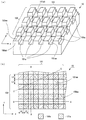
【解決手段】実施例1のIII 族窒化物半導体発光素子は、凹凸形状が形成されたサファイア基板10と、サファイア基板10の凹凸形状側表面上に、バッファ層を介して順に積層された、III 族窒化物半導体からなるn型層、発光層、p型層と、を有している。凹凸形状は、サファイア基板10表面上にx軸方向をストライプ方向とする第1のストライプ形状100が形成され、その上にx軸方向と直交するy軸方向をストライプ方向とする第2のストライプ形状101が重ねて形成された形状である。このような凹凸形状とすることで、従来のIII 族窒化物半導体発光素子よりも光取り出し効率を向上させることができる。
【選択図】図2
Description
第1の溝100aの幅L1、間隔L2は2μm、深さD1は0.7μm、側面100aaの角度θ1は80°とし、第2の溝101aの幅L3、間隔L4は1.5μm、深さD2は0.7μm、側面101aaの角度θ2は80°とした場合について、軸上の光出力を測定したところ、比較例1の1.19倍の光出力であった。
第1の溝100aの幅L1、間隔L2は1.5μm、深さD1は0.7μm、側面100aaの角度θ1は80°とし、第2の溝101aの幅L3、間隔L4は1.5μm、深さD2は0.7μm、側面101aaの角度θ2は80°とした場合について、軸上の光出力を測定したところ、比較例1の1.17倍の光出力であった。
第1の溝100aの幅L1、間隔L2は2μm、深さD1は1.4μm、側面100aaの角度θ1は60°とし、第2の溝101aの幅L3、間隔L4は1.5μm、深さD2は0.7μm、側面101aaの角度θ2は80°とした場合について、軸上の光出力を測定したところ、比較例1の1.29倍の光出力であった。
第1の溝100aの幅L1、間隔L2は1.5μm、深さD1は1.4μm、側面100aaの角度θ1は60°とし、第2の溝101aの幅L3、間隔L4は1.5μm、深さD2は0.7μm、側面101aaの角度θ2は80°とした場合について、軸上の光出力を測定したところ、比較例1の1.29倍の光出力であった。
第1の溝100aの幅L1、間隔L2は2μm、深さD1は0.7μm、側面100aaの角度θ1は80°とし、第2の溝101aの幅L3、間隔L4は1.5μm、深さD2は1.4μm、側面101aaの角度θ2は60°とした場合について、軸上の光出力を測定したところ、比較例1の1.34倍の光出力であった。
第1の溝100aの幅L1、間隔L2は1.5μm、深さD1は0.7μm、側面100aaの角度θ1は80°とし、第2の溝101aの幅L3、間隔L4は1.5μm、深さD2は1.4μm、側面101aaの角度θ2は60°とした場合について、軸上の光出力を測定したところ、比較例1の1.28倍の光出力であった。
11:n型層
12:発光層
13:p型層
14:n電極
15:透明電極
16:p電極
100:第1のストライプ形状
100a:第1の溝
101:第2のストライプ形状
101a:第2の溝
Claims (5)
- サファイア基板上にIII 族窒化物半導体からなる積層構造が形成されたIII 族窒化物半導体発光素子において、
前記サファイア基板は、前記積層構造側の表面に凹凸形状を有し、
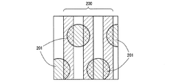
前記凹凸形状は、サファイア基板の主面に垂直な任意の方向での断面において1段以上の段差があり、サファイア基板の主面に垂直な特定の方向での断面において2段以上の段差を有する、
ことを特徴とするIII 族窒化物半導体発光素子。 - 前記凹凸形状は、
前記サファイア基板の前記積層構造側の表面に、第1方向に平行にストライプ状に配列された複数の第1の溝によって形成された第1のストライプ形状と、
前記第1のストライプ形状の上に重ねて形成され、第1方向とは異なる第2方向に平行にストライプ状に配列された複数の第2の溝によって形成された第2のストライプ形状と、
を有する形状であることを特徴とする請求項1に記載のIII 族窒化物半導体発光素子。 - 前記第1方向と、前記第2方向は直交する、ことを特徴とする請求項2に記載のIII 族窒化物半導体発光素子。
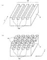
- 前記凹凸形状は、
前記サファイア基板の前記積層構造側の表面に、所定方向に平行にストライプ状に配列された複数の溝によって形成されたストライプ形状と、
前記ストライプ形状の上に重ねて形成され、格子状に配列されたドット状の凸部ないし凹部によって形成されたドット形状と、
を有する形状であることを特徴とする請求項1に記載のIII 族窒化物半導体発光素子。 - 前記凹凸形状は、
前記サファイア基板の前記積層構造側の表面に、格子状に配列されたドット状の凸部ないし凹部によって形成されたドット形状と、
前記ドット形状の上に重ねて形成され、所定方向に平行にストライプ状に配列された複数の溝によって形成されたストライプ形状と、
を有する形状であることを特徴とする請求項1に記載のIII 族窒化物半導体発光素子。
Priority Applications (4)
| Application Number | Priority Date | Filing Date | Title |
|---|---|---|---|
| JP2010261166A JP2012114204A (ja) | 2010-11-24 | 2010-11-24 | Iii族窒化物半導体発光素子およびその製造方法 |
| TW100140784A TW201234653A (en) | 2010-11-24 | 2011-11-08 | Group III nitride semiconductor light-emitting device |
| US13/302,983 US20120126241A1 (en) | 2010-11-24 | 2011-11-22 | Group iii nitride semiconductor light-emitting device and production method therefor |
| CN2011103736282A CN102479899A (zh) | 2010-11-24 | 2011-11-22 | 第iii族氮化物半导体发光器件及其制造方法 |
Applications Claiming Priority (1)
| Application Number | Priority Date | Filing Date | Title |
|---|---|---|---|
| JP2010261166A JP2012114204A (ja) | 2010-11-24 | 2010-11-24 | Iii族窒化物半導体発光素子およびその製造方法 |
Publications (2)
| Publication Number | Publication Date |
|---|---|
| JP2012114204A true JP2012114204A (ja) | 2012-06-14 |
| JP2012114204A5 JP2012114204A5 (ja) | 2013-04-18 |
Family
ID=46063496
Family Applications (1)
| Application Number | Title | Priority Date | Filing Date |
|---|---|---|---|
| JP2010261166A Pending JP2012114204A (ja) | 2010-11-24 | 2010-11-24 | Iii族窒化物半導体発光素子およびその製造方法 |
Country Status (4)
| Country | Link |
|---|---|
| US (1) | US20120126241A1 (ja) |
| JP (1) | JP2012114204A (ja) |
| CN (1) | CN102479899A (ja) |
| TW (1) | TW201234653A (ja) |
Cited By (5)
| Publication number | Priority date | Publication date | Assignee | Title |
|---|---|---|---|---|
| JP2014234324A (ja) * | 2013-05-31 | 2014-12-15 | 豊田合成株式会社 | Iii族窒化物半導体の製造方法及びiii族窒化物半導体 |
| EP2950356A1 (en) | 2014-05-30 | 2015-12-02 | Nichia Corporation | Nitride semiconductor element and method for manufacturing the same |
| EP3059766A1 (en) | 2015-02-18 | 2016-08-24 | Nichia Corporation | Light-emitting element |
| US9806232B2 (en) | 2014-05-30 | 2017-10-31 | Nichia Corporation | Nitride semiconductor element and method for manufacturing the same |
| US9837494B2 (en) | 2012-03-30 | 2017-12-05 | Toyoda Gosei Co., Ltd. | Production method for group III nitride semiconductor and group III nitride semiconductor |
Families Citing this family (7)
| Publication number | Priority date | Publication date | Assignee | Title |
|---|---|---|---|---|
| JP5573632B2 (ja) * | 2010-11-25 | 2014-08-20 | 豊田合成株式会社 | Iii族窒化物半導体発光素子 |
| WO2014122565A1 (en) * | 2013-02-11 | 2014-08-14 | Koninklijke Philips N.V. | A light emitting device and method for manufacturing a light emitting device |
| TWI597863B (zh) * | 2013-10-22 | 2017-09-01 | 晶元光電股份有限公司 | 發光元件及其製造方法 |
| CN105720153A (zh) * | 2016-04-11 | 2016-06-29 | 厦门乾照光电股份有限公司 | 一种提高背光源亮度的衬底 |
| JP6798452B2 (ja) * | 2017-08-23 | 2020-12-09 | 豊田合成株式会社 | Iii族窒化物半導体発光素子の製造方法 |
| JP6783990B2 (ja) * | 2017-09-07 | 2020-11-11 | 豊田合成株式会社 | Iii族窒化物半導体素子の製造方法および基板の製造方法 |
| CN113517379A (zh) * | 2021-06-30 | 2021-10-19 | 福建晶安光电有限公司 | 一种图形化衬底及其制备方法、led芯片 |
Citations (1)
| Publication number | Priority date | Publication date | Assignee | Title |
|---|---|---|---|---|
| JP2009526397A (ja) * | 2006-02-09 | 2009-07-16 | ソウル オプト デバイス カンパニー リミテッド | パターニングされた発光ダイオード用基板及びそれを採用する発光ダイオード |
Family Cites Families (5)
| Publication number | Priority date | Publication date | Assignee | Title |
|---|---|---|---|---|
| US6580098B1 (en) * | 1999-07-27 | 2003-06-17 | Toyoda Gosei Co., Ltd. | Method for manufacturing gallium nitride compound semiconductor |
| JP4055503B2 (ja) * | 2001-07-24 | 2008-03-05 | 日亜化学工業株式会社 | 半導体発光素子 |
| EP1667241B1 (en) * | 2003-08-19 | 2016-12-07 | Nichia Corporation | Semiconductor light emitting diode and method of manufacturing the same |
| KR101262226B1 (ko) * | 2006-10-31 | 2013-05-15 | 삼성전자주식회사 | 반도체 발광 소자의 제조방법 |
| JP5353113B2 (ja) * | 2008-01-29 | 2013-11-27 | 豊田合成株式会社 | Iii族窒化物系化合物半導体の製造方法 |
-
2010
- 2010-11-24 JP JP2010261166A patent/JP2012114204A/ja active Pending
-
2011
- 2011-11-08 TW TW100140784A patent/TW201234653A/zh unknown
- 2011-11-22 US US13/302,983 patent/US20120126241A1/en not_active Abandoned
- 2011-11-22 CN CN2011103736282A patent/CN102479899A/zh active Pending
Patent Citations (1)
| Publication number | Priority date | Publication date | Assignee | Title |
|---|---|---|---|---|
| JP2009526397A (ja) * | 2006-02-09 | 2009-07-16 | ソウル オプト デバイス カンパニー リミテッド | パターニングされた発光ダイオード用基板及びそれを採用する発光ダイオード |
Cited By (11)
| Publication number | Priority date | Publication date | Assignee | Title |
|---|---|---|---|---|
| US9837494B2 (en) | 2012-03-30 | 2017-12-05 | Toyoda Gosei Co., Ltd. | Production method for group III nitride semiconductor and group III nitride semiconductor |
| JP2014234324A (ja) * | 2013-05-31 | 2014-12-15 | 豊田合成株式会社 | Iii族窒化物半導体の製造方法及びiii族窒化物半導体 |
| US9209021B2 (en) | 2013-05-31 | 2015-12-08 | Toyoda Gosei Co., Ltd. | Method for producing Group III nitride semiconductor and Group III nitride semiconductor |
| EP2950356A1 (en) | 2014-05-30 | 2015-12-02 | Nichia Corporation | Nitride semiconductor element and method for manufacturing the same |
| US9806232B2 (en) | 2014-05-30 | 2017-10-31 | Nichia Corporation | Nitride semiconductor element and method for manufacturing the same |
| RU2663684C2 (ru) * | 2014-05-30 | 2018-08-08 | Нития Корпорейшн | Нитридный полупроводниковый элемент и способ его производства |
| US10263152B2 (en) | 2014-05-30 | 2019-04-16 | Nichia Corporation | Nitride semiconductor element and method for manufacturing the same |
| EP3059766A1 (en) | 2015-02-18 | 2016-08-24 | Nichia Corporation | Light-emitting element |
| US9773946B2 (en) | 2015-02-18 | 2017-09-26 | Nichia Corporation | Light-emitting element comprising a partitioned sapphire substrate |
| EP3327798A1 (en) | 2015-02-18 | 2018-05-30 | Nichia Corporation | Light-emitting element |
| US10461222B2 (en) | 2015-02-18 | 2019-10-29 | Nichia Corporation | Light-emitting element comprising sapphire substrate with convex portions |
Also Published As
| Publication number | Publication date |
|---|---|
| CN102479899A (zh) | 2012-05-30 |
| TW201234653A (en) | 2012-08-16 |
| US20120126241A1 (en) | 2012-05-24 |
Similar Documents
| Publication | Publication Date | Title |
|---|---|---|
| JP2012114204A (ja) | Iii族窒化物半導体発光素子およびその製造方法 | |
| JP2012114204A5 (ja) | ||
| US8367445B2 (en) | Group III nitride semiconductor light-emitting device | |
| JP5206923B2 (ja) | 半導体発光素子 | |
| US9831385B2 (en) | Semiconductor light-emitting devices | |
| JP5997373B2 (ja) | 窒化物半導体発光素子 | |
| US20100133567A1 (en) | Semiconductor light emitting device and method of manufacturing the same | |
| US8299479B2 (en) | Light-emitting devices with textured active layer | |
| KR101305876B1 (ko) | 반도체 발광소자 및 그 제조방법 | |
| US8653502B2 (en) | Group III nitride semiconductor light-emitting device | |
| JP5533791B2 (ja) | Iii族窒化物半導体発光素子の製造方法 | |
| US8378380B2 (en) | Nitride semiconductor light-emitting device and method for manufacturing the same | |
| JP6579038B2 (ja) | 半導体発光素子の製造方法 | |
| KR101862407B1 (ko) | 질화물계 반도체 발광소자 및 그 제조방법 | |
| JP5434872B2 (ja) | Iii族窒化物半導体発光素子の製造方法 | |
| JP5246236B2 (ja) | Iii族窒化物半導体発光素子の製造方法 | |
| KR20120045538A (ko) | 발광 소자 및 그 제조방법 | |
| KR20090026688A (ko) | 반도체 발광소자 및 그 제조방법 | |
| JP5246235B2 (ja) | Iii族窒化物半導体発光素子の製造方法 | |
| KR100631977B1 (ko) | 3족 질화물 발광 소자 및 그 제조 방법 | |
| JP2007251168A (ja) | 発光素子及びその製造方法 | |
| KR101316402B1 (ko) | 질화물 반도체 발광소자 및 그 제조 방법 | |
| KR101754426B1 (ko) | 질화물계 발광소자 및 그 제조방법 | |
| JP2016012648A (ja) | GaN系発光素子用基板 | |
| KR20130006971A (ko) | 발광 소자 및 그 제조방법 |
Legal Events
| Date | Code | Title | Description |
|---|---|---|---|
| A621 | Written request for application examination |
Free format text: JAPANESE INTERMEDIATE CODE: A621 Effective date: 20130125 |
|
| A521 | Request for written amendment filed |
Free format text: JAPANESE INTERMEDIATE CODE: A523 Effective date: 20130304 |
|
| A977 | Report on retrieval |
Free format text: JAPANESE INTERMEDIATE CODE: A971007 Effective date: 20130813 |
|
| A131 | Notification of reasons for refusal |
Free format text: JAPANESE INTERMEDIATE CODE: A131 Effective date: 20130903 |
|
| A521 | Request for written amendment filed |
Free format text: JAPANESE INTERMEDIATE CODE: A523 Effective date: 20131002 |
|
| A02 | Decision of refusal |
Free format text: JAPANESE INTERMEDIATE CODE: A02 Effective date: 20140603 |