EP1848026B1 - Diode électroluminescente avec une structure verticale - Google Patents
Diode électroluminescente avec une structure verticale Download PDFInfo
- Publication number
- EP1848026B1 EP1848026B1 EP07013949.8A EP07013949A EP1848026B1 EP 1848026 B1 EP1848026 B1 EP 1848026B1 EP 07013949 A EP07013949 A EP 07013949A EP 1848026 B1 EP1848026 B1 EP 1848026B1
- Authority
- EP
- European Patent Office
- Prior art keywords
- layer
- light
- emitting device
- semiconductor structure
- type electrode
- Prior art date
- Legal status (The legal status is an assumption and is not a legal conclusion. Google has not performed a legal analysis and makes no representation as to the accuracy of the status listed.)
- Expired - Lifetime
Links
- 238000002161 passivation Methods 0.000 claims abstract description 31
- 239000004065 semiconductor Substances 0.000 claims description 67
- 229910052751 metal Inorganic materials 0.000 claims description 59
- 239000002184 metal Substances 0.000 claims description 59
- 239000000463 material Substances 0.000 claims description 17
- 229910052737 gold Inorganic materials 0.000 claims description 15
- 229910052804 chromium Inorganic materials 0.000 claims description 9
- 229910052763 palladium Inorganic materials 0.000 claims description 9
- 229910052759 nickel Inorganic materials 0.000 claims description 8
- 229910052697 platinum Inorganic materials 0.000 claims description 6
- VYPSYNLAJGMNEJ-UHFFFAOYSA-N Silicium dioxide Chemical compound O=[Si]=O VYPSYNLAJGMNEJ-UHFFFAOYSA-N 0.000 claims description 5
- NRTOMJZYCJJWKI-UHFFFAOYSA-N Titanium nitride Chemical compound [Ti]#N NRTOMJZYCJJWKI-UHFFFAOYSA-N 0.000 claims description 5
- 229910052802 copper Inorganic materials 0.000 claims description 5
- 229910052721 tungsten Inorganic materials 0.000 claims description 5
- 239000011248 coating agent Substances 0.000 claims description 4
- 238000000576 coating method Methods 0.000 claims description 4
- AMGQUBHHOARCQH-UHFFFAOYSA-N indium;oxotin Chemical compound [In].[Sn]=O AMGQUBHHOARCQH-UHFFFAOYSA-N 0.000 claims description 3
- 229910052581 Si3N4 Inorganic materials 0.000 claims description 2
- 229910052681 coesite Inorganic materials 0.000 claims description 2
- 229910052906 cristobalite Inorganic materials 0.000 claims description 2
- 229910052710 silicon Inorganic materials 0.000 claims description 2
- 239000010703 silicon Substances 0.000 claims description 2
- 239000000377 silicon dioxide Substances 0.000 claims description 2
- 229910052682 stishovite Inorganic materials 0.000 claims description 2
- 239000010936 titanium Substances 0.000 claims description 2
- 229910052905 tridymite Inorganic materials 0.000 claims description 2
- FYYHWMGAXLPEAU-UHFFFAOYSA-N Magnesium Chemical compound [Mg] FYYHWMGAXLPEAU-UHFFFAOYSA-N 0.000 claims 1
- 229910052782 aluminium Inorganic materials 0.000 claims 1
- 229910052749 magnesium Inorganic materials 0.000 claims 1
- 239000011777 magnesium Substances 0.000 claims 1
- 239000000758 substrate Substances 0.000 abstract description 67
- 229910002601 GaN Inorganic materials 0.000 description 90
- JMASRVWKEDWRBT-UHFFFAOYSA-N Gallium nitride Chemical compound [Ga]#N JMASRVWKEDWRBT-UHFFFAOYSA-N 0.000 description 76
- 229910052594 sapphire Inorganic materials 0.000 description 48
- 239000010980 sapphire Substances 0.000 description 48
- 238000000034 method Methods 0.000 description 24
- 238000004519 manufacturing process Methods 0.000 description 17
- 235000012431 wafers Nutrition 0.000 description 12
- 238000001020 plasma etching Methods 0.000 description 10
- 230000009286 beneficial effect Effects 0.000 description 5
- 238000007772 electroless plating Methods 0.000 description 5
- 238000009713 electroplating Methods 0.000 description 5
- 238000005530 etching Methods 0.000 description 5
- 230000012010 growth Effects 0.000 description 5
- 238000009616 inductively coupled plasma Methods 0.000 description 5
- 238000000926 separation method Methods 0.000 description 5
- 238000004544 sputter deposition Methods 0.000 description 5
- 238000011161 development Methods 0.000 description 4
- -1 for example Substances 0.000 description 4
- 238000012986 modification Methods 0.000 description 4
- 230000004048 modification Effects 0.000 description 4
- 238000005498 polishing Methods 0.000 description 4
- 238000012545 processing Methods 0.000 description 4
- 230000008901 benefit Effects 0.000 description 3
- 230000015572 biosynthetic process Effects 0.000 description 3
- MVPPADPHJFYWMZ-UHFFFAOYSA-N chlorobenzene Chemical compound ClC1=CC=CC=C1 MVPPADPHJFYWMZ-UHFFFAOYSA-N 0.000 description 3
- 239000010408 film Substances 0.000 description 3
- 239000007789 gas Substances 0.000 description 3
- 150000002500 ions Chemical class 0.000 description 3
- 230000003287 optical effect Effects 0.000 description 3
- 229910015844 BCl3 Inorganic materials 0.000 description 2
- 238000011982 device technology Methods 0.000 description 2
- 238000010438 heat treatment Methods 0.000 description 2
- 230000001939 inductive effect Effects 0.000 description 2
- 239000000203 mixture Substances 0.000 description 2
- 238000001451 molecular beam epitaxy Methods 0.000 description 2
- 230000007935 neutral effect Effects 0.000 description 2
- FAQYAMRNWDIXMY-UHFFFAOYSA-N trichloroborane Chemical compound ClB(Cl)Cl FAQYAMRNWDIXMY-UHFFFAOYSA-N 0.000 description 2
- XUIMIQQOPSSXEZ-UHFFFAOYSA-N Silicon Chemical compound [Si] XUIMIQQOPSSXEZ-UHFFFAOYSA-N 0.000 description 1
- PNEYBMLMFCGWSK-UHFFFAOYSA-N aluminium oxide Inorganic materials [O-2].[O-2].[O-2].[Al+3].[Al+3] PNEYBMLMFCGWSK-UHFFFAOYSA-N 0.000 description 1
- 238000000137 annealing Methods 0.000 description 1
- 238000005229 chemical vapour deposition Methods 0.000 description 1
- 238000004140 cleaning Methods 0.000 description 1
- 229910052593 corundum Inorganic materials 0.000 description 1
- 239000010432 diamond Substances 0.000 description 1
- 229910003460 diamond Inorganic materials 0.000 description 1
- 238000007598 dipping method Methods 0.000 description 1
- 239000002019 doping agent Substances 0.000 description 1
- 238000010292 electrical insulation Methods 0.000 description 1
- 230000005611 electricity Effects 0.000 description 1
- 239000007772 electrode material Substances 0.000 description 1
- 230000005672 electromagnetic field Effects 0.000 description 1
- 238000010894 electron beam technology Methods 0.000 description 1
- 229910052733 gallium Inorganic materials 0.000 description 1
- 238000000227 grinding Methods 0.000 description 1
- 230000017525 heat dissipation Effects 0.000 description 1
- 229910052738 indium Inorganic materials 0.000 description 1
- APFVFJFRJDLVQX-UHFFFAOYSA-N indium atom Chemical compound [In] APFVFJFRJDLVQX-UHFFFAOYSA-N 0.000 description 1
- 238000009413 insulation Methods 0.000 description 1
- 239000012212 insulator Substances 0.000 description 1
- 238000001459 lithography Methods 0.000 description 1
- 230000008018 melting Effects 0.000 description 1
- 238000002844 melting Methods 0.000 description 1
- 229910044991 metal oxide Inorganic materials 0.000 description 1
- 150000004706 metal oxides Chemical class 0.000 description 1
- 230000005693 optoelectronics Effects 0.000 description 1
- TWNQGVIAIRXVLR-UHFFFAOYSA-N oxo(oxoalumanyloxy)alumane Chemical compound O=[Al]O[Al]=O TWNQGVIAIRXVLR-UHFFFAOYSA-N 0.000 description 1
- 239000002245 particle Substances 0.000 description 1
- 239000010453 quartz Substances 0.000 description 1
- 230000005855 radiation Effects 0.000 description 1
- 238000005389 semiconductor device fabrication Methods 0.000 description 1
- 238000003892 spreading Methods 0.000 description 1
- 230000003068 static effect Effects 0.000 description 1
- 230000002459 sustained effect Effects 0.000 description 1
- 239000010409 thin film Substances 0.000 description 1
- 238000000927 vapour-phase epitaxy Methods 0.000 description 1
- 238000001039 wet etching Methods 0.000 description 1
- 229910001845 yogo sapphire Inorganic materials 0.000 description 1
Images


Classifications
-
- H—ELECTRICITY
- H01—ELECTRIC ELEMENTS
- H01L—SEMICONDUCTOR DEVICES NOT COVERED BY CLASS H10
- H01L33/00—Semiconductor devices having potential barriers specially adapted for light emission; Processes or apparatus specially adapted for the manufacture or treatment thereof or of parts thereof; Details thereof
- H01L33/02—Semiconductor devices having potential barriers specially adapted for light emission; Processes or apparatus specially adapted for the manufacture or treatment thereof or of parts thereof; Details thereof characterised by the semiconductor bodies
- H01L33/12—Semiconductor devices having potential barriers specially adapted for light emission; Processes or apparatus specially adapted for the manufacture or treatment thereof or of parts thereof; Details thereof characterised by the semiconductor bodies with a stress relaxation structure, e.g. buffer layer
-
- H—ELECTRICITY
- H01—ELECTRIC ELEMENTS
- H01C—RESISTORS
- H01C7/00—Non-adjustable resistors formed as one or more layers or coatings; Non-adjustable resistors made from powdered conducting material or powdered semi-conducting material with or without insulating material
- H01C7/006—Thin film resistors
-
- H—ELECTRICITY
- H01—ELECTRIC ELEMENTS
- H01C—RESISTORS
- H01C7/00—Non-adjustable resistors formed as one or more layers or coatings; Non-adjustable resistors made from powdered conducting material or powdered semi-conducting material with or without insulating material
- H01C7/008—Thermistors
-
- H—ELECTRICITY
- H01—ELECTRIC ELEMENTS
- H01L—SEMICONDUCTOR DEVICES NOT COVERED BY CLASS H10
- H01L27/00—Devices consisting of a plurality of semiconductor or other solid-state components formed in or on a common substrate
- H01L27/02—Devices consisting of a plurality of semiconductor or other solid-state components formed in or on a common substrate including semiconductor components specially adapted for rectifying, oscillating, amplifying or switching and having potential barriers; including integrated passive circuit elements having potential barriers
- H01L27/04—Devices consisting of a plurality of semiconductor or other solid-state components formed in or on a common substrate including semiconductor components specially adapted for rectifying, oscillating, amplifying or switching and having potential barriers; including integrated passive circuit elements having potential barriers the substrate being a semiconductor body
- H01L27/08—Devices consisting of a plurality of semiconductor or other solid-state components formed in or on a common substrate including semiconductor components specially adapted for rectifying, oscillating, amplifying or switching and having potential barriers; including integrated passive circuit elements having potential barriers the substrate being a semiconductor body including only semiconductor components of a single kind
- H01L27/0802—Resistors only
-
- H—ELECTRICITY
- H01—ELECTRIC ELEMENTS
- H01L—SEMICONDUCTOR DEVICES NOT COVERED BY CLASS H10
- H01L28/00—Passive two-terminal components without a potential-jump or surface barrier for integrated circuits; Details thereof; Multistep manufacturing processes therefor
- H01L28/20—Resistors
-
- H—ELECTRICITY
- H01—ELECTRIC ELEMENTS
- H01L—SEMICONDUCTOR DEVICES NOT COVERED BY CLASS H10
- H01L33/00—Semiconductor devices having potential barriers specially adapted for light emission; Processes or apparatus specially adapted for the manufacture or treatment thereof or of parts thereof; Details thereof
- H01L33/0004—Devices characterised by their operation
- H01L33/002—Devices characterised by their operation having heterojunctions or graded gap
- H01L33/0025—Devices characterised by their operation having heterojunctions or graded gap comprising only AIIIBV compounds
-
- H—ELECTRICITY
- H01—ELECTRIC ELEMENTS
- H01L—SEMICONDUCTOR DEVICES NOT COVERED BY CLASS H10
- H01L33/00—Semiconductor devices having potential barriers specially adapted for light emission; Processes or apparatus specially adapted for the manufacture or treatment thereof or of parts thereof; Details thereof
- H01L33/005—Processes
- H01L33/0062—Processes for devices with an active region comprising only III-V compounds
- H01L33/0066—Processes for devices with an active region comprising only III-V compounds with a substrate not being a III-V compound
- H01L33/007—Processes for devices with an active region comprising only III-V compounds with a substrate not being a III-V compound comprising nitride compounds
-
- H—ELECTRICITY
- H01—ELECTRIC ELEMENTS
- H01L—SEMICONDUCTOR DEVICES NOT COVERED BY CLASS H10
- H01L33/00—Semiconductor devices having potential barriers specially adapted for light emission; Processes or apparatus specially adapted for the manufacture or treatment thereof or of parts thereof; Details thereof
- H01L33/005—Processes
- H01L33/0093—Wafer bonding; Removal of the growth substrate
-
- H—ELECTRICITY
- H01—ELECTRIC ELEMENTS
- H01L—SEMICONDUCTOR DEVICES NOT COVERED BY CLASS H10
- H01L33/00—Semiconductor devices having potential barriers specially adapted for light emission; Processes or apparatus specially adapted for the manufacture or treatment thereof or of parts thereof; Details thereof
- H01L33/005—Processes
- H01L33/0095—Post-treatment of devices, e.g. annealing, recrystallisation or short-circuit elimination
-
- H—ELECTRICITY
- H01—ELECTRIC ELEMENTS
- H01L—SEMICONDUCTOR DEVICES NOT COVERED BY CLASS H10
- H01L33/00—Semiconductor devices having potential barriers specially adapted for light emission; Processes or apparatus specially adapted for the manufacture or treatment thereof or of parts thereof; Details thereof
- H01L33/02—Semiconductor devices having potential barriers specially adapted for light emission; Processes or apparatus specially adapted for the manufacture or treatment thereof or of parts thereof; Details thereof characterised by the semiconductor bodies
- H01L33/04—Semiconductor devices having potential barriers specially adapted for light emission; Processes or apparatus specially adapted for the manufacture or treatment thereof or of parts thereof; Details thereof characterised by the semiconductor bodies with a quantum effect structure or superlattice, e.g. tunnel junction
- H01L33/06—Semiconductor devices having potential barriers specially adapted for light emission; Processes or apparatus specially adapted for the manufacture or treatment thereof or of parts thereof; Details thereof characterised by the semiconductor bodies with a quantum effect structure or superlattice, e.g. tunnel junction within the light emitting region, e.g. quantum confinement structure or tunnel barrier
-
- H—ELECTRICITY
- H01—ELECTRIC ELEMENTS
- H01L—SEMICONDUCTOR DEVICES NOT COVERED BY CLASS H10
- H01L33/00—Semiconductor devices having potential barriers specially adapted for light emission; Processes or apparatus specially adapted for the manufacture or treatment thereof or of parts thereof; Details thereof
- H01L33/02—Semiconductor devices having potential barriers specially adapted for light emission; Processes or apparatus specially adapted for the manufacture or treatment thereof or of parts thereof; Details thereof characterised by the semiconductor bodies
- H01L33/26—Materials of the light emitting region
- H01L33/30—Materials of the light emitting region containing only elements of Group III and Group V of the Periodic Table
- H01L33/32—Materials of the light emitting region containing only elements of Group III and Group V of the Periodic Table containing nitrogen
-
- H—ELECTRICITY
- H01—ELECTRIC ELEMENTS
- H01L—SEMICONDUCTOR DEVICES NOT COVERED BY CLASS H10
- H01L33/00—Semiconductor devices having potential barriers specially adapted for light emission; Processes or apparatus specially adapted for the manufacture or treatment thereof or of parts thereof; Details thereof
- H01L33/36—Semiconductor devices having potential barriers specially adapted for light emission; Processes or apparatus specially adapted for the manufacture or treatment thereof or of parts thereof; Details thereof characterised by the electrodes
- H01L33/38—Semiconductor devices having potential barriers specially adapted for light emission; Processes or apparatus specially adapted for the manufacture or treatment thereof or of parts thereof; Details thereof characterised by the electrodes with a particular shape
-
- H—ELECTRICITY
- H01—ELECTRIC ELEMENTS
- H01L—SEMICONDUCTOR DEVICES NOT COVERED BY CLASS H10
- H01L33/00—Semiconductor devices having potential barriers specially adapted for light emission; Processes or apparatus specially adapted for the manufacture or treatment thereof or of parts thereof; Details thereof
- H01L33/36—Semiconductor devices having potential barriers specially adapted for light emission; Processes or apparatus specially adapted for the manufacture or treatment thereof or of parts thereof; Details thereof characterised by the electrodes
- H01L33/40—Materials therefor
-
- H—ELECTRICITY
- H01—ELECTRIC ELEMENTS
- H01L—SEMICONDUCTOR DEVICES NOT COVERED BY CLASS H10
- H01L33/00—Semiconductor devices having potential barriers specially adapted for light emission; Processes or apparatus specially adapted for the manufacture or treatment thereof or of parts thereof; Details thereof
- H01L33/44—Semiconductor devices having potential barriers specially adapted for light emission; Processes or apparatus specially adapted for the manufacture or treatment thereof or of parts thereof; Details thereof characterised by the coatings, e.g. passivation layer or anti-reflective coating
-
- H—ELECTRICITY
- H01—ELECTRIC ELEMENTS
- H01L—SEMICONDUCTOR DEVICES NOT COVERED BY CLASS H10
- H01L33/00—Semiconductor devices having potential barriers specially adapted for light emission; Processes or apparatus specially adapted for the manufacture or treatment thereof or of parts thereof; Details thereof
- H01L33/48—Semiconductor devices having potential barriers specially adapted for light emission; Processes or apparatus specially adapted for the manufacture or treatment thereof or of parts thereof; Details thereof characterised by the semiconductor body packages
- H01L33/62—Arrangements for conducting electric current to or from the semiconductor body, e.g. lead-frames, wire-bonds or solder balls
-
- Y—GENERAL TAGGING OF NEW TECHNOLOGICAL DEVELOPMENTS; GENERAL TAGGING OF CROSS-SECTIONAL TECHNOLOGIES SPANNING OVER SEVERAL SECTIONS OF THE IPC; TECHNICAL SUBJECTS COVERED BY FORMER USPC CROSS-REFERENCE ART COLLECTIONS [XRACs] AND DIGESTS
- Y10—TECHNICAL SUBJECTS COVERED BY FORMER USPC
- Y10S—TECHNICAL SUBJECTS COVERED BY FORMER USPC CROSS-REFERENCE ART COLLECTIONS [XRACs] AND DIGESTS
- Y10S438/00—Semiconductor device manufacturing: process
- Y10S438/958—Passivation layer
-
- Y—GENERAL TAGGING OF NEW TECHNOLOGICAL DEVELOPMENTS; GENERAL TAGGING OF CROSS-SECTIONAL TECHNOLOGIES SPANNING OVER SEVERAL SECTIONS OF THE IPC; TECHNICAL SUBJECTS COVERED BY FORMER USPC CROSS-REFERENCE ART COLLECTIONS [XRACs] AND DIGESTS
- Y10—TECHNICAL SUBJECTS COVERED BY FORMER USPC
- Y10S—TECHNICAL SUBJECTS COVERED BY FORMER USPC CROSS-REFERENCE ART COLLECTIONS [XRACs] AND DIGESTS
- Y10S438/00—Semiconductor device manufacturing: process
- Y10S438/977—Thinning or removal of substrate
Definitions
- the present invention relates to semiconductor device fabrication. More particularly, the present invention relates to a method of fabricating Vertical devices using a metal support layer.
- LEDa Light emitting diodes
- the color (wavelength) of the light that is emitted by an LED depends on the semiconductor material that is used to fabricate the LED. This is because the wavelength of the emitted light depends on the semiconductor material's band-gap, which represents the energy diffecence between the material's valence band and conduction band electrons.
- Gallium-Nitride has gained much attention from LED researthers.
- GaN can be combined with indium to produce InGaN/GaN semiconductor layers that emit green, blue, and white light.
- This wavelength control ability enables an LED semiconductor designer to tailor material characteristics to achieve beneficial device characteristics. For example, GaN enables an LED semiconductor designer to produce blue LEDs, which are beneficial in optical recordings, and white LEDs, which can replace incandescent lamps.
- GaN-based LEDs Because of the foregoing and other advantageous, the market for GaN-based LEDs is rapidly growing. Accordingly, GaN-based opto-electronic device technology has rapidly evolved since their commercial introduction in 1994. Because the efficiency of GaN light emitting diodes has surpassed that of incandescent lighting, and is now comparable with that of fluorescent lighting, the market for GaN based LEDs is expected to continue its rapid growth.
- GaN devices are too expensive for many applications.
- One reason for this is the high cost of manufacturing GaN-based devices, which in turn is related to the difficulties of growing GaN epitaxial layers and of subsequently dicing out completed GaN-based devices.
- GaN-based devices are typically fabricated on sapphire substrates. This is because sapphire wafers are commercially available in dimensions that are suitable for mass-producing GaN-based devices, because sapphire supports relatively high-quality GaN epitaxial layer growths, and because of the extensive temperature handling capability of sapphire.
- Fabricating semiconductor devices on sapphire is typically performed by growing an n-GaN epitaxial layer on a sapphire substrate using metal oxide chemical vapor deposition (MOCVD) or molecular beam epitaxy (MBE). Then, a plurality of individual devices, such as GaN LEDs, is fabricated on the epitaxial layer using normal semiconductor processing techniques. After the individual devices are fabricated they must be diced out (separated) of the sapphire substrate.
- MOCVD metal oxide chemical vapor deposition
- MBE molecular beam epitaxy
- sapphire substrates are difficult to dice. Indeed, dicing typically requires that the sapphire substrate be thinned to about 100 microns by mechanical grinding, lapping, and/or polishing.
- the LED device topologies that are available when using sapphire substrates (or other insulating substrates) are, in practice, limited to lateral and vertical topologies.
- the metallic electrical contacts that are used to inject electrical current into the LED are both located on upper surfaces (or on the same side of the substrate).
- the sapphire (insulating) substrate is removed, and the other contact is located on a lower surface.
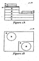
- Figures 1A and 1B illustrate a typical lateral GaN-based LED 20 that is fabricated on a sapphire substrate 22.
- an n-GaN buffer layer 24 is formed on the substrate 22.
- a relatively thick n-GaN layer 26 is formed on the buffer layer 24.
- An active layer 28 having multiple quantum wells of aluminum-indium-gallium-nitride (AlInGaN) or of InGaN/GaN is then formed on the n-type GaN layer 26.
- a p-GaN layer 30 is then formed on the active layer 26.
- a transparent conductive layer 32 is then formed on the p-GaN layer 30.
- the transparent conductive layer 32 may be made of any suitable material, such as Ru/Au; Ni/Au or indium-tin-oxide (ITO).
- a p-type electrode 34 is then formed on one side of the transparent conductive layer 32. Suitable p-type electrode materials include Ni/Au, Pd/Au, Pd/Ni and Pt.
- a pad 36 is then formed on the p-type electrode 34. Beneficially, the pad 36 is Au.
- the transparent conductive layer 32, the p-GaN layer 30, the active layer 28 and part of the n-GaN layer 26 are etched to form a step. Because of the difficulty of wet etching GaN, a dry etch is usually used. This etching requires additional lithography and stripping processes. Furthermore, plasma damage to the GaN step surface is often sustained during the dry-etch process.
- the LED 20 is completed by forming an n-electrode pad 38 (usually Au) and a pad 40 on the step.
- Figure 1B illustrates a top down view of the LED 20.
- lateral GaN-based LEDs have a significant draw back in that having both metal contacts (36 and 40) on the same side of the LED significantly reduces the surface area available for light emission.
- the metal contacts 36 and 40 are physically close together.
- the pads 36 are often Au.
- the Au often spreads. Au spreading can bring the electrical contacts even closer together.
- Such closely spaced electrodes 34 are highly susceptible to ESD damage.
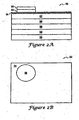
- Figures 2A and 2B illustrate a vertical GaN-based LED 50 that was formed on a sapphire substrate that was subsequently removed.
- the LED 50 includes a GaN buffer layer 54 having an n-metal contact 56 on a bottom side, and a relatively thick n-GaN layer 58 on the other.
- the n-metal contact 56 is beneficially formed from a high reflectively layer that is overlaid by a high conductivity metal, including, for example, Au.
- An active layer 60 having multiple quantum wells is formed on the n-type GaN layer 58, and a p-GaN layer 62 is formed on the active layer 60.
- a transparent conductive layer 64 is then formed on the p-GaN layer 62, and a p-type electrode 66 is formed on the transparent conductive layer 64.
- a pad 68 is formed on the p-type electrode 66.
- the materials for the various layers are similar to those used in the lateral LED 20.
- the vertical GaN-based LED 50 as the advantage that etching a step is not required.
- the sapphire substrate (not shown) has to be removed. Such removal can be difficult particularly if device yields are of concern.
- sapphire substrate removal using laser lift off is known.
- vertical GaN-based LEDs have the advantage that only one metal contact (68) blocks light.
- lateral GaN-based LEDs must have a larger surface area, which lowers device yields.
- the reflecting layer of the n-type contact 56 of vertical GaN-based LEDs reflect light that is otherwise absorbed in lateral GaN-based LEDs.
- the lateral topology is more vulnerable to static electricity, primarily because the two electrodes (36 and 40) are so close together. Additionally, as the lateral topology is fabricated on an insulating substrate, and as the vertical topology can be attached to a heat sink, the lateral topology has relatively poor thermal dissipation. Thus, in many respects the vertical topology is operationally superior to the lateral topology.
- GaN-based LEDs fabricated with a lateral topology. This is primarily because of the difficulties of removing the insulating substrate and of handling the GaN wafer structure without a supporting substrate. Despite these problems, removal of an insulation (growth) substrate and subsequent wafer bonding of the resulting GaN-based wafer on a Si substrate using Pd/In metal layers has been demonstrated for very small area wafers, approx. 1 cm by 1 cm. But, substrate removal and subsequent wafer bonding of large area wafers remains very difficult due to inhomogeneous bonding between the GaN wafer and the 2 nd (substitutional) substrate. This is mainly due to wafer bowing during and after laser lift off.
- a new method of fabricating vertical topology devices would be beneficial.
- a method that provides for mechanical stability of semiconductor wafer layers, that enables vertical topology electrical contact formation, and that improves heat dissipation would be highly useful, particularly with devices subject to high electrical currents, such as laser diodes or high-power LEDs.
- such a method would enable forming multiple semiconductor layers on an insulating substrate, the adding of a top support metal layer that provides for top electrical contacts and for structural stability, and the removal of the insulating substrate.
- US-A-5 874 747 discloses a GaN-based light-emitting device, comprising an electrically and thermally conductive SiC substrate, a doped compositionally graded (Al,Ga)N conductive buffer layer on the SiC substrate, a semiconductor structure comprising an n-type GaN layer, a GaN active layer, and a p-type GaN layer, wherein the conductive buffer layer is located between the conductive support layer and the semiconductor structure, a passivation layer disposed on the semiconductor structure, and a heavily doped p-type GaN contact layer on an upper surface of the semiconductor structure, wherein the passivation layer partially covers the upper surface of the p-type contact layer, and the passivation layer covers a side surface of the semiconductor structure, such that the passivation layer covering the side surface of the semiconductor structure extends to the upper surface of the p-type contact layer, and wherein a p-type contact is arranged on a portion of the p-type contact layer.
- WO-A-01/82384 discloses a radiation-emitting GaN-based semiconductor element whose semiconductor body is formed by a stark of different GaN semiconductor layers.
- the semiconductor body has a first main surface and a second main surface.
- the radiation that is produced is coupled out through the first main surface while a reflector is configured on the second main surface.
- an intermediate layer is first applied to a substrate and a plurality of GaN layers which form the semiconductor body of the component are then applied to said intermediate layer.
- the substrate and the intermediate layer are then removed and a reflector is formed on a main surface of the semiconductor body.
- the metal layer supports the semiconductor layers to prevent warping and/or other damage and provides for electrical contacts.
- the metal layer includes a metal, such as Cu, Cr, Ni, Au, Ag, Mo, Pt, Pd, W, or Al, or a metal containing material such as titanium nitride.
- Forming of the metal layer can be performed in numerous ways, for example, by electroplating, by electro-less plating, by CVD, or by sputtering. Subsequently, bottom electrical contacts can be added to the semiconductor layers and then individual semiconductor devices can be diced from the resulting structure.
- a method of fabricating vertical topology GaN-based devices on an insulating substrate by the use of a metal support film and by the subsequent removal of the insulating substrate is further provided.
- semiconductor layers for the GaN-based devices are formed on an insulating (sapphire) substrate using normal semiconductor fabrication techniques.
- trenches that define the boundaries of the individual devices are formed through the semiconductor layers. Those trenches may also be formed into the insulating substrate.
- Trench forming is beneficially performed using inductive coupled plasma reactive ion etching (ICPRIE).
- ICPRIE inductive coupled plasma reactive ion etching
- the trenches are then filled with an easily removed layer (such as a photo-resist).
- a metal support structure is then formed on the semiconductor layers.
- the metal support structure includes a metal, such as Cu, Cr, Ni, Au, Ag, Mo, Pt, Pd, W, or Al, or a metal-containing material such as titanium nitride.
- a metal such as Cu, Cr, Ni, Au, Ag, Mo, Pt, Pd, W, or Al
- a metal-containing material such as titanium nitride.
- Forming of the metal support structure can be performed in numerous ways, for example, by electroplating, by electro-less plating, by CVD, or by sputtering.
- the insulating substrate is then removed, beneficially using a laser-lift off process. Electrical contacts, a passivation layer, and metallic pads are then added to the individual devices, and the individual devices are then diced out.
- a method of fabricating vertical topology GaN-based LEDs on sapphire substrates According to that method, semiconductor layers for the vertical topology GaN-based LEDs are formed on a sapphire substrate using normal semiconductor fabrication techniques. Then, trenches that define the boundaries of the individual vertical topology GaN-based LEDs are formed through the semiconductor layers. Those trenches may also be formed into the sapphire substrate. Trench forming is beneficially performed using inductive coupled plasma reactive ion etching (ICPRIE). Beneficially, the trenches are fabricated using ICPRIE. The trenches are then beneficially filled with an easily removed layer (such as a photo-resist). A metal support structure is then formed on the semiconductor layers.
- ICPRIE inductive coupled plasma reactive ion etching
- the metal support structure includes a metal, such as Cu, Cr, Ni, Au, Ag, Mo, Pt, Pd, W, or Al, or a metal-containing material such as titanium nitride.
- a metal such as Cu, Cr, Ni, Au, Ag, Mo, Pt, Pd, W, or Al
- a metal-containing material such as titanium nitride.
- Forming of the metal layer can be performed in numerous ways, for example, by electroplating, by electro-less plating, by CVD, or by sputtering.
- the sapphire substrate is then removed, beneficially using a laser-lift off process. Electrical contacts, a passivation layer, and metallic pads are then added to the individual LEDs, and the individual LEDs are then diced out.
- Figure 1A illustrates a sectional view of a typical lateral topology GaN-based LED
- Figure 1B shows a top down view of the GaN-based LED illustrated in Figure 1A ;
- Figure 2A illustrates a sectional view of a typical vertical topology GaN-based LED
- Figure 2B shows a top down view of the GaN-based LED illustrated in Figure 2A ;
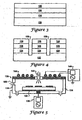
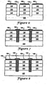
- FIGS. 3-15 illustrate steps of forming a light emitting diode that are in accord with the principles of the present invention.
- the principles of the present invention provide for methods of fabricating semiconductor devices, such as GaN-based vertical topology LEDs, on insulating substrates, such as sapphire substrates, using metal support films. While those principles are illustrated in a detailed description of a method of fabricating vertical topology GaN-based LEDs on a sapphire substrate, those principles are broader than that illustrated method. Therefore, the principles of the present invention are to be limited only by the appended claims.
- FIGS 3-15 illustrate a method of manufacturing vertical topology GaN-based light emitting diodes (LEDs) on sapphire substrates.
- Sapphire substrates are readily available in suitable sizes, are thermally, chemically, and mechanically stable, are relatively inexpensive, and support the growth of good quality GaN epitaxial layers. It should be understood that those figures are not to scale.
- the GaN-based LED layer structure includes an n-CaN buffer layer 124, an InGaN/GaN active layer 126 (beneficially having the proper composition to emit blue light) on the buffer layer 124, and a p-GaN contact layer 128 on the active layer 126.
- the buffer layer 124 beneficially includes both a 2 ⁇ m undoped GaN layer formed directly on the substrate, and a 1 ⁇ m thick, n-type, silicon doped, GaN layer.
- the p-GaN contact layer 128 is beneficially about 0.05 ⁇ m thick and is doped with Mg.
- the GaN-based LED layer structure is beneficially less than about 5 microns thick.
- Various standard epitaxial growth techniques such as vapor phase epitaxy, MOCVD, and MBE, together with suitable dopants and other materials, can be used to produce the GaN-based LED layer structure.
- trenches 130 are formed through the vertical topology GaN-based LED layer structure. Those trenches 130 may extend into the sapphire substrate 122.
- the trenches 130 define the individual LED semiconductor structures that will be produced. Each individual LED semiconductor structure is beneficially a square about 200 microns wide.
- the trenches 130 are beneficially narrower than about 10 microns (preferably close to 1 micron) and extend deeper than about 5 microns into the sapphire substrate 122.
- the trenches 130 assist a subsequent chip separation process.
- the trenches 130 are beneficially formed in the structure of Figure 3 using reactive ion etching, preferably inductively coupled plasma reactive ion etching (ICP RIE).
- ICP RIE inductively coupled plasma reactive ion etching
- Forming trenches using ICP RIE has two main steps: forming scribe lines and etching. Scribe lines are formed on the structure of Figure 3 using a photo-resist pattern in which areas of the sapphire substrate 122 where the trenches 130 are to be formed are exposed. The exposed areas are the scribe lines, while all other areas are covered by photo-resist.
- the photo-resist pattern is beneficially fabricated from a relatively hard photo-resist material that withstands intense plasma.
- the photo-resist could be AZ 9260, while the developer used to develop the photo-resist to form the scribe lines could be AZ MIF 500.
- the photo-resist is beneficially spin coated to a thickness of about 10 microns.
- the photo-resist thickness should be about the same as the thickness of the vertical topology GaN-based LED layer structure plus the etch depth into the sapphire substrate 122. This helps ensure that the photo-resist mask remains intact during etching. Because it is difficult to form a thick photo-resist coating in one step, the photo-resist can be applied in two coats, each about 5 microns thick. The first photo-resist coat is spin coated on and then soft baked, for example, at 90°F (32.2°C) for about 15 minutes.
- the second photo-resist coat is applied in a similar manner, but is soft baked, for example, at 110°F (43.3°C) for about 8 minutes.
- the photo-resist coating is then patterned to form the scribe lines. This is beneficially performed using lithographic techniques and development. Development takes a relatively long time because of the thickness of the photo-resist coating.
- the photo-resist pattern is hard baked, for example, at about 80°F (26.7°C) for about 30 minutes.
- the hard baked photo-resist is beneficially dipped in a MCB (Metal Chlorobenzene) treatment for about 3.5 minutes. Such dipping further hardens the photo-resist.
- MCB Metal Chlorobenzene
- the structure of Figure 3 is etched.
- the ICP RIE etch process is performed by placing the structure of Figure 3 on a bottom electrode 132 in a RIE chamber 134 having an insulating window 136 (beneficially a 1 cm-thick quartz window).
- the bottom electrode 132 is connected to a bias voltage supply 138 that biases the structure of Figure 3 to enable etching.
- the bias voltage supply 138 beneficially supplies 13.56 MHz RF power and a DC-bias voltage.
- the distance from the insulating window 136 to the bottom electrode 132 is beneficially about 6.5cm.
- a 2.5-turn or so spiral Cu coil 144 is located above the insulating window 136. Radio frequency (RF) power at 13.56 MHz is applied to the coil 144 from an RF source 146. It should be noted that magnetic fields are produced at right angles to the insulating window 136 by the RF power.
- RF radio frequency
- thin p-contacts 150 are formed on the individual LED semiconductor structures of the GaN-based LED layer structure.
- Those contacts 150 are beneficially comprised of Pt/Au, Pd/Au, Ru/Au, Ni/Au, Cr/Au, or of indium tin oxide (ITO)/Au and are less then 10nm.
- Such contacts can be formed using a vacuum evaporator (electron beam, thermal, sputter), followed by thermal annealing at an intermediate temperature (approximately 300-700°C).
- the trenches 130 are filled with an easily removed material (beneficially a photo-resist) to form posts 154.
- a metal support layer 156 approximately 50 ⁇ m is formed over the posts 154 and over the p-contacts 150.
- the posts 154 prevent the metal that forms the metal support layer 156 from entering into the trenches.
- the metal support layer 156 is beneficially comprised of a metal having good electrical and thermal conductivity and that is easily formed, such as by electroplating, by electro-less plating, by CVD, or by sputtering. Before electroplating or electro-less plating, it is beneficial to coat the surface with a suitable metal, such as by sputtering.
- the metal support layer 156 can be Cu, Cr, Ni, Au, Ag, Mo, Pt, Pd, W, or Al.
- the metal support layer 156 can be comprised of a metal-containing material such as titanium nitride.
- the sapphire substrate 122 is then removed from the remainder of the structure using light 158 from an eximer laser (having a wavelength less than 350 nanometers), while the sapphire substrate is biased away from the remainder of the structure (such as by use of vacuum chucks).
- the laser beam 158 passes through the sapphire substrate 122, causing localized heating at the junction of the sapphire substrate 122 and the n-GaN buffer layer 124. That heat decomposes the GaN at the interface of the sapphire substrate, which, together with the bias, causes the sapphire substrate 122 to separate, reference Figure 10 . It is beneficial to hold the other side of the structure with a vacuum chuck during laser lift off This enable easy application of a separation bias.
- the posts 154 are then removed, leaving the trenches 130 behind.
- Figure 11 the structure of Figure 10 is inverted. Then, the side opposite the metal support layer 156 is cleaned with HCl to remove Ga droplets (laser beam 158 heating separates GaN into Ga+N). After cleaning, ICP RIE polishing (using Cl 2 an/or Cl 2 +BCl 3 ) is performed to smooth the exposed surface (which is rough due to the separation of the sapphire substrate). Polishing produces an atomically flat surface of pure n-GaN on the n-GaN buffer layer 124.
- n-type ohmic contacts 160 are formed on the n-GaN buffer layer 124 using normal semiconductor-processing techniques. Beneficially, the n-type ohmic contacts 160 are comprised of Ti/Al-related materials.
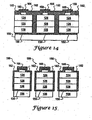
- a passivation layer 162 is formed on the n-type ohmic contacts 160 and in the trenches 130. Electrical insulation comprised of SiO 2 or Si 3 N 4 are suitable passivation layer materials. Additionally, as shown, the passivation layer 162 is patterned to expose top surface portions of the n-type ohmic contacts 160.
- metal pads 164 are formed on the n-type ohmic contacts 160. As shown in Figure 14 , the metal pads 164 extend over portions of the passivation layer 162.
- the metal pads 164 are beneficially comprised of Cr and Au.
- dicing is beneficially accomplished using photolithographic techniques to etch through the metal support layer 156 to the bottom of the passivation layer 162 (at the bottom of the trenches 130) and by removal of the passivation layer 162.
- sawing can be used. In practice, it is probably better to perform sawing at less than about 0°C. The result is a plurality of vertical topology CyaN LEDs 199 on conductive substrates.
- trenches 130 before laser lift off of the sapphire substrate 122.
- the sapphire substrate 122 could be removed first, and then trenches 130 can be formed.
Landscapes
- Engineering & Computer Science (AREA)
- Microelectronics & Electronic Packaging (AREA)
- Power Engineering (AREA)
- Computer Hardware Design (AREA)
- Manufacturing & Machinery (AREA)
- Physics & Mathematics (AREA)
- Electromagnetism (AREA)
- Condensed Matter Physics & Semiconductors (AREA)
- General Physics & Mathematics (AREA)
- Led Devices (AREA)
- Drying Of Semiconductors (AREA)
Claims (28)
- Dispositif électroluminescent, comprenant:une couche de support électriquement conductrice (156) comprenant un matériau métallique ou contenant du métal ;une électrode (150) sur la couche de support électriquement conductrice (156) ;une structure à semi-conducteur ayant une première surface, une seconde surface à l'opposé de la première surface et une surface latérale, la structure à semi-conducteur comprend une couche à base de GaN de type p (128) sur l'électrode de type p, une couche active (126) sur la couche à base de GaN de type p, et une couche à base de GaN de type n (124) sur la couche active, l'électrode de type p étant disposée entre la couche de support électriquement conductrice et la première surface de la structure à semi-conducteur ;une couche de passivation (162) sur la structure à semi-conducteur ; etune électrode de type n (160) sur une partie de la seconde surface de la structure à semi-conducteur ;dans lequel la couche de passivation couvre en partie la seconde surface de la structure à semi-conducteur de façon que la couche de passivation soit au contact de la couche à base de GaN de type n présentant la seconde surface, dans lequel la couche de passivation couvre la surface latérale de la structure à semi-conducteur, et dans lequel la couche de passivation couvrant la surface latérale de la structure à semi-conducteur s'étend jusqu'à la seconde surface de la structure à semi-conducteur, la couche de passivation étant au contact de l'électrode de type n, la couche de passivation couvrant un côté de l'électrode de type n,dans lequel un plot métallique (164) est disposé sur l'électrode de type n.
- Dispositif électroluminescent selon la revendication 1, dans lequel la couche de passivation comprend deux portions qui s'étendent respectivement sur des parties latérales de l'électrode de type p.
- Dispositif électroluminescent selon la revendication 2, dans lequel les parties latérales de l'électrode de type p sont disposées entre les deux portions.
- Dispositif électroluminescent selon la revendication 1, dans lequel la couche de passivation (162) comprend du SiO2 ou du Si3N4.
- Dispositif électroluminescent selon la revendication 1, dans lequel la couche à base de GaN de type p et la couche à base de GaN de type n sont dopées au silicium ou au magnésium.
- Dispositif électroluminescent selon la revendication 1, dans lequel la couche de support électriquement conductrice comprend au moins un élément parmi Cu, Cr, Ni, Au, Ag, Mo, Pt, Pd, W, Al et nitrure de titane.
- Dispositif électroluminescent selon la revendication 1, dans lequel la couche à base de GaN de type n est plus épaisse que la couche à base de GaN de type P.
- Dispositif électroluminescent selon la revendication 1, dans lequel la couche active comprend de l'InGaN/GaN.
- Dispositif électroluminescent selon la revendication 1, dans lequel la couche de passivation est disposée partiellement sur l'électrode de type n.
- Dispositif électroluminescent selon la revendication 1, dans lequel l'électrode de type n comprend un matériau de type Ti/Al.
- Dispositif électroluminescent selon la revendication 1, dans lequel le plot métallique comprend Cr et Au.
- Dispositif électroluminescent selon la revendication 1, comprenant en outre une couche de métal entre l'électrode de type pet la couche de support électriquement conductrice.
- Dispositif électroluminescent selon la revendication 12, dans lequel la couche de métal est un revêtement de métal.
- Dispositif électroluminescent selon la revendication 12, dans lequel la couche de métal est configurée de manière à faciliter la croissance de la couche de support électriquement conductrice sur la couche de métal.
- Dispositif électroluminescent selon la revendication 12, dans lequel une surface de la couche de métal est située au-dessus de la couche de support électriquement conductrice.
- Dispositif électroluminescent selon la revendication 12, dans lequel la couche de métal est en contact avec la couche de support électriquement conductrice.
- Diode selon la revendication 1, dans laquelle une aire de la couche de passivation couvrant la seconde surface de la structure à semi-conducteur est plus grande qu'une aire de la couche de passivation couvrant la surface de la structure à semi-conducteur.
- Dispositif électroluminescent selon la revendication 1, dans lequel l'électrode de type p de l'oxyde de étain et d'indium/Au.
- Dispositif électroluminescent selon la revendication 1, dans lequel l'épaisseur de la structure à semi-conducteur est inférieure à 5 microns.
- Dispositif électroluminescent selon la revendication 1, dans lequel la couche de passivation est disposée en partie entre la structure à semi-conducteur et la couche de support électriquement conductrice.
- Dispositif électroluminescent selon la revendication 1, dans lequel la couche de passivation est disposée sur toute la portion de la seconde surface de la structure à semi-conducteur qui n'est pas couverte par l'électrode de type n.
- Dispositif électroluminescent selon la revendication 1, dans lequel l'électrode de type p comprend un élément parmi Pt/Au, Pd/Au, Ru/Au, Ni/Au, Cr/Au, et ITO/Au.
- Dispositif électroluminescent selon la revendication 1, dans lequel l'électrode de type p est d'épaisseur inférieure à 10 nm.
- Dispositif électroluminescent selon la revendication 1, dans lequel la couche de passivation adjacente à la couche à base de GaN de type n s'étend sur une surface supérieure de la couche de support électriquement conductrice.
- Dispositif électroluminescent selon la revendication 1, dans lequel la couche de passivation adjacente à la couche à base de GaN de type p est en outre située au-dessus de la couche de support électriquement conductrice.
- Dispositif électroluminescent selon la revendication 1, dans lequel l'électrode de type n est au contact de la seconde surface de la structure à semi-conducteur.
- Dispositif électroluminescent selon la revendication 1, dans lequel l'électrode de type p est au contact de la structure à semi-conducteur, et dans lequel l'aire de contact entre l'électrode de type p et la structure à semi-conducteur est supérieure à l'aire de contact entre la couche de passivation et la seconde surface de la structure à semi-conducteur.
- Dispositif électroluminescent selon la revendication 1, dans lequel l'électrode de type p a une première surface faisant face à la structure à semi-conducteur et l'électrode de type n a une seconde surface faisant face à la structure à semi-conducteur, et dans lequel l'aire de première surface est supérieure à l'aire de la seconde surface.
Priority Applications (6)
| Application Number | Priority Date | Filing Date | Title |
|---|---|---|---|
| EP10183473.7A EP2261949B1 (fr) | 2002-04-09 | 2003-03-31 | Diode électroluminescente avec une structure verticale |
| EP10183510.6A EP2261951B1 (fr) | 2002-04-09 | 2003-03-31 | Procédé de fabrication d'une diode électroluminescente avec une structure verticale |
| EP14194349.8A EP2860753B1 (fr) | 2002-04-09 | 2003-03-31 | Diodes électroluminescentes à structure verticale |
| EP10183495.0A EP2261950B1 (fr) | 2002-04-09 | 2003-03-31 | Diode électroluminescente avec une structure verticale et son procédé de fabrication |
| EP14194356.3A EP2863444B1 (fr) | 2002-04-09 | 2003-03-31 | DEL à structure verticale |
| EP14194354.8A EP2860779B1 (fr) | 2002-04-09 | 2003-03-31 | Dispositif électroluminescent à structure verticale |
Applications Claiming Priority (2)
| Application Number | Priority Date | Filing Date | Title |
|---|---|---|---|
| US10/118,316 US20030189215A1 (en) | 2002-04-09 | 2002-04-09 | Method of fabricating vertical structure leds |
| EP03731009A EP1502286B1 (fr) | 2002-04-09 | 2003-03-31 | Procede de fabrication de del a structure verticale |
Related Parent Applications (1)
| Application Number | Title | Priority Date | Filing Date |
|---|---|---|---|
| EP03731009A Division EP1502286B1 (fr) | 2002-04-09 | 2003-03-31 | Procede de fabrication de del a structure verticale |
Related Child Applications (11)
| Application Number | Title | Priority Date | Filing Date |
|---|---|---|---|
| EP10183473.7A Division EP2261949B1 (fr) | 2002-04-09 | 2003-03-31 | Diode électroluminescente avec une structure verticale |
| EP10183473.7A Division-Into EP2261949B1 (fr) | 2002-04-09 | 2003-03-31 | Diode électroluminescente avec une structure verticale |
| EP14194349.8A Division EP2860753B1 (fr) | 2002-04-09 | 2003-03-31 | Diodes électroluminescentes à structure verticale |
| EP14194349.8A Division-Into EP2860753B1 (fr) | 2002-04-09 | 2003-03-31 | Diodes électroluminescentes à structure verticale |
| EP10183495.0A Division EP2261950B1 (fr) | 2002-04-09 | 2003-03-31 | Diode électroluminescente avec une structure verticale et son procédé de fabrication |
| EP10183495.0A Division-Into EP2261950B1 (fr) | 2002-04-09 | 2003-03-31 | Diode électroluminescente avec une structure verticale et son procédé de fabrication |
| EP14194356.3A Division EP2863444B1 (fr) | 2002-04-09 | 2003-03-31 | DEL à structure verticale |
| EP14194356.3A Division-Into EP2863444B1 (fr) | 2002-04-09 | 2003-03-31 | DEL à structure verticale |
| EP10183510.6A Division-Into EP2261951B1 (fr) | 2002-04-09 | 2003-03-31 | Procédé de fabrication d'une diode électroluminescente avec une structure verticale |
| EP14194354.8A Division EP2860779B1 (fr) | 2002-04-09 | 2003-03-31 | Dispositif électroluminescent à structure verticale |
| EP14194354.8A Division-Into EP2860779B1 (fr) | 2002-04-09 | 2003-03-31 | Dispositif électroluminescent à structure verticale |
Publications (2)
| Publication Number | Publication Date |
|---|---|
| EP1848026A1 EP1848026A1 (fr) | 2007-10-24 |
| EP1848026B1 true EP1848026B1 (fr) | 2014-12-31 |
Family
ID=28674400
Family Applications (8)
| Application Number | Title | Priority Date | Filing Date |
|---|---|---|---|
| EP10183473.7A Expired - Lifetime EP2261949B1 (fr) | 2002-04-09 | 2003-03-31 | Diode électroluminescente avec une structure verticale |
| EP10183495.0A Expired - Lifetime EP2261950B1 (fr) | 2002-04-09 | 2003-03-31 | Diode électroluminescente avec une structure verticale et son procédé de fabrication |
| EP14194349.8A Expired - Lifetime EP2860753B1 (fr) | 2002-04-09 | 2003-03-31 | Diodes électroluminescentes à structure verticale |
| EP14194356.3A Expired - Lifetime EP2863444B1 (fr) | 2002-04-09 | 2003-03-31 | DEL à structure verticale |
| EP03731009A Expired - Lifetime EP1502286B1 (fr) | 2002-04-09 | 2003-03-31 | Procede de fabrication de del a structure verticale |
| EP14194354.8A Expired - Lifetime EP2860779B1 (fr) | 2002-04-09 | 2003-03-31 | Dispositif électroluminescent à structure verticale |
| EP10183510.6A Expired - Lifetime EP2261951B1 (fr) | 2002-04-09 | 2003-03-31 | Procédé de fabrication d'une diode électroluminescente avec une structure verticale |
| EP07013949.8A Expired - Lifetime EP1848026B1 (fr) | 2002-04-09 | 2003-03-31 | Diode électroluminescente avec une structure verticale |
Family Applications Before (7)
| Application Number | Title | Priority Date | Filing Date |
|---|---|---|---|
| EP10183473.7A Expired - Lifetime EP2261949B1 (fr) | 2002-04-09 | 2003-03-31 | Diode électroluminescente avec une structure verticale |
| EP10183495.0A Expired - Lifetime EP2261950B1 (fr) | 2002-04-09 | 2003-03-31 | Diode électroluminescente avec une structure verticale et son procédé de fabrication |
| EP14194349.8A Expired - Lifetime EP2860753B1 (fr) | 2002-04-09 | 2003-03-31 | Diodes électroluminescentes à structure verticale |
| EP14194356.3A Expired - Lifetime EP2863444B1 (fr) | 2002-04-09 | 2003-03-31 | DEL à structure verticale |
| EP03731009A Expired - Lifetime EP1502286B1 (fr) | 2002-04-09 | 2003-03-31 | Procede de fabrication de del a structure verticale |
| EP14194354.8A Expired - Lifetime EP2860779B1 (fr) | 2002-04-09 | 2003-03-31 | Dispositif électroluminescent à structure verticale |
| EP10183510.6A Expired - Lifetime EP2261951B1 (fr) | 2002-04-09 | 2003-03-31 | Procédé de fabrication d'une diode électroluminescente avec une structure verticale |
Country Status (8)
| Country | Link |
|---|---|
| US (19) | US20030189215A1 (fr) |
| EP (8) | EP2261949B1 (fr) |
| JP (5) | JP5325365B2 (fr) |
| KR (1) | KR100921457B1 (fr) |
| AT (1) | ATE412972T1 (fr) |
| AU (1) | AU2003241280A1 (fr) |
| DE (3) | DE20321881U1 (fr) |
| WO (1) | WO2003088318A2 (fr) |
Families Citing this family (287)
| Publication number | Priority date | Publication date | Assignee | Title |
|---|---|---|---|---|
| US7067849B2 (en) | 2001-07-17 | 2006-06-27 | Lg Electronics Inc. | Diode having high brightness and method thereof |
| WO2003034508A1 (fr) * | 2001-10-12 | 2003-04-24 | Nichia Corporation | Dispositif d'emission de lumiere et procede de fabrication de celui-ci |
| US6949395B2 (en) | 2001-10-22 | 2005-09-27 | Oriol, Inc. | Method of making diode having reflective layer |
| US7148520B2 (en) | 2001-10-26 | 2006-12-12 | Lg Electronics Inc. | Diode having vertical structure and method of manufacturing the same |
| US8294172B2 (en) * | 2002-04-09 | 2012-10-23 | Lg Electronics Inc. | Method of fabricating vertical devices using a metal support film |
| US20030189215A1 (en) | 2002-04-09 | 2003-10-09 | Jong-Lam Lee | Method of fabricating vertical structure leds |
| US20040140474A1 (en) * | 2002-06-25 | 2004-07-22 | Matsushita Electric Industrial Co., Ltd. | Semiconductor light-emitting device, method for fabricating the same and method for bonding the same |
| US6841802B2 (en) | 2002-06-26 | 2005-01-11 | Oriol, Inc. | Thin film light emitting diode |
| KR101030068B1 (ko) | 2002-07-08 | 2011-04-19 | 니치아 카가쿠 고교 가부시키가이샤 | 질화물 반도체 소자의 제조방법 및 질화물 반도체 소자 |
| DE10245631B4 (de) * | 2002-09-30 | 2022-01-20 | OSRAM Opto Semiconductors Gesellschaft mit beschränkter Haftung | Halbleiterbauelement |
| US20050082575A1 (en) * | 2002-10-29 | 2005-04-21 | Lung-Chien Chen | Structure and manufacturing method for GaN light emitting diodes |
| US7244628B2 (en) * | 2003-05-22 | 2007-07-17 | Matsushita Electric Industrial Co., Ltd. | Method for fabricating semiconductor devices |
| CN100483612C (zh) * | 2003-06-04 | 2009-04-29 | 刘明哲 | 用于制造垂直结构的复合半导体器件的方法 |
| DE10326507A1 (de) * | 2003-06-12 | 2005-01-13 | Infineon Technologies Ag | Verfahren zur Herstellung eines bruchfesten scheibenförmigen Gegenstands sowie zugehörige Halbleiterschaltungsanordung |
| US8999736B2 (en) * | 2003-07-04 | 2015-04-07 | Epistar Corporation | Optoelectronic system |
| US7915085B2 (en) | 2003-09-18 | 2011-03-29 | Cree, Inc. | Molded chip fabrication method |
| TWI228272B (en) * | 2003-09-19 | 2005-02-21 | Tinggi Technologies Pte Ltd | Fabrication of semiconductor devices |
| CN100452328C (zh) * | 2003-09-19 | 2009-01-14 | 霆激技术有限公司 | 半导体器件上导电金属层的制作 |
| TWM255514U (en) * | 2003-10-16 | 2005-01-11 | Arima Optoelectronics Corp | Structure improvement of Gallium Indium Nitride light-emitting diode |
| KR100576854B1 (ko) * | 2003-12-20 | 2006-05-10 | 삼성전기주식회사 | 질화물 반도체 제조 방법과 이를 이용한 질화물 반도체 |
| KR100576856B1 (ko) * | 2003-12-23 | 2006-05-10 | 삼성전기주식회사 | 질화물 반도체 발광소자 및 제조방법 |
| US6969626B2 (en) * | 2004-02-05 | 2005-11-29 | Advanced Epitaxy Technology | Method for forming LED by a substrate removal process |
| JP2005223165A (ja) | 2004-02-06 | 2005-08-18 | Sanyo Electric Co Ltd | 窒化物系発光素子 |
| EP1730790B1 (fr) * | 2004-03-15 | 2011-11-09 | Tinggi Technologies Private Limited | Fabrication de dispositifs a semiconducteur |
| US7122398B1 (en) * | 2004-03-25 | 2006-10-17 | Nanosolar, Inc. | Manufacturing of optoelectronic devices |
| JP2005298554A (ja) * | 2004-04-07 | 2005-10-27 | Sumitomo Electric Ind Ltd | 膜厚方向に弾性回復性を有する延伸ポリテトラフルオロエチレン多孔質膜、その製造方法、及び該多孔質膜の使用 |
| EP1756875A4 (fr) * | 2004-04-07 | 2010-12-29 | Tinggi Technologies Private Ltd | Fabrication d'une couche retrofeflechissante sur des diodes electroluminescentes a semiconducteur |
| WO2005104780A2 (fr) | 2004-04-28 | 2005-11-10 | Verticle, Inc | Dispositifs semi-conducteurs a structure verticale |
| KR100595884B1 (ko) * | 2004-05-18 | 2006-07-03 | 엘지전자 주식회사 | 질화물 반도체 소자 제조 방법 |
| TWI433343B (zh) * | 2004-06-22 | 2014-04-01 | Verticle Inc | 具有改良光輸出的垂直構造半導體裝置 |
| WO2006004337A1 (fr) * | 2004-06-30 | 2006-01-12 | Seoul Opto-Device Co., Ltd. | Element electroluminescent a pluralite de cellules liees, son procede de fabrication, et dispositif electroluminescent utilisant un tel element |
| TWM261838U (en) * | 2004-09-16 | 2005-04-11 | Super Nova Optoelectronics Cor | Structure for GaN based LED with high light extraction efficiency |
| US20060076574A1 (en) * | 2004-10-12 | 2006-04-13 | Liang-Wen Wu | Gallium-nitride based light-emitting diodes structure with high reverse withstanding voltage and anti-ESD capability |
| CN100561758C (zh) * | 2004-10-22 | 2009-11-18 | 首尔Opto仪器股份有限公司 | 氮化镓化合物半导体发光元件及其制造方法 |
| KR100667508B1 (ko) * | 2004-11-08 | 2007-01-10 | 엘지전자 주식회사 | 발광 소자 및 그의 제조방법 |
| TWI389334B (zh) * | 2004-11-15 | 2013-03-11 | Verticle Inc | 製造及分離半導體裝置之方法 |
| US20060124941A1 (en) * | 2004-12-13 | 2006-06-15 | Lee Jae S | Thin gallium nitride light emitting diode device |
| US20060154393A1 (en) * | 2005-01-11 | 2006-07-13 | Doan Trung T | Systems and methods for removing operating heat from a light emitting diode |
| US8871547B2 (en) | 2005-01-11 | 2014-10-28 | SemiLEDs Optoelectronics Co., Ltd. | Method for fabricating vertical light emitting diode (VLED) structure using a laser pulse to remove a carrier substrate |
| US8802465B2 (en) | 2005-01-11 | 2014-08-12 | SemiLEDs Optoelectronics Co., Ltd. | Method for handling a semiconductor wafer assembly |
| US8318519B2 (en) * | 2005-01-11 | 2012-11-27 | SemiLEDs Optoelectronics Co., Ltd. | Method for handling a semiconductor wafer assembly |
| US7432119B2 (en) * | 2005-01-11 | 2008-10-07 | Semileds Corporation | Light emitting diode with conducting metal substrate |
| US7186580B2 (en) | 2005-01-11 | 2007-03-06 | Semileds Corporation | Light emitting diodes (LEDs) with improved light extraction by roughening |
| EP1681712A1 (fr) * | 2005-01-13 | 2006-07-19 | S.O.I. Tec Silicon on Insulator Technologies S.A. | Méthode de formation de substrats pour applications optoélectroniques. |
| CN100352116C (zh) * | 2005-01-18 | 2007-11-28 | 北京大学 | 自然解理腔面的GaN基激光二极管的制备方法 |
| TWI308396B (en) * | 2005-01-21 | 2009-04-01 | Epistar Corp | Light emitting diode and fabricating method thereof |
| KR101165257B1 (ko) * | 2005-01-26 | 2012-07-19 | 서울옵토디바이스주식회사 | 발광 소자 및 이의 제조 방법 |
| US7932111B2 (en) * | 2005-02-23 | 2011-04-26 | Cree, Inc. | Substrate removal process for high light extraction LEDs |
| JP4818732B2 (ja) * | 2005-03-18 | 2011-11-16 | シャープ株式会社 | 窒化物半導体素子の製造方法 |
| KR100638732B1 (ko) * | 2005-04-15 | 2006-10-30 | 삼성전기주식회사 | 수직구조 질화물 반도체 발광소자의 제조방법 |
| JP4707450B2 (ja) * | 2005-05-18 | 2011-06-22 | イーストマン コダック カンパニー | 画像処理装置及びホワイトバランス調整装置 |
| KR101128612B1 (ko) * | 2005-05-24 | 2012-03-26 | 엘지이노텍 주식회사 | 발광 소자 및 그의 제조 방법 |
| US7625778B2 (en) * | 2005-06-08 | 2009-12-01 | Chunghwa Picture Tubes, Ltd. | Method of manufacturing a substrate-free flip chip light emitting diode |
| US8168000B2 (en) * | 2005-06-15 | 2012-05-01 | International Rectifier Corporation | III-nitride semiconductor device fabrication |
| KR20060131327A (ko) * | 2005-06-16 | 2006-12-20 | 엘지전자 주식회사 | 발광 다이오드의 제조 방법 |
| KR100599012B1 (ko) * | 2005-06-29 | 2006-07-12 | 서울옵토디바이스주식회사 | 열전도성 기판을 갖는 발광 다이오드 및 그것을 제조하는방법 |
| KR100849788B1 (ko) * | 2005-06-30 | 2008-07-31 | 삼성전기주식회사 | 수직형 반도체 발광 소자의 제조 방법 |
| KR100658303B1 (ko) * | 2005-07-04 | 2006-12-14 | 엘지전자 주식회사 | 메탈지지층을 포함하는 수직형 구조의 발광 다이오드 |
| KR100606551B1 (ko) | 2005-07-05 | 2006-08-01 | 엘지전자 주식회사 | 발광소자 제조방법 |
| KR100691186B1 (ko) * | 2005-07-12 | 2007-03-09 | 삼성전기주식회사 | 수직구조 발광 다이오드의 제조 방법 |
| KR100617873B1 (ko) * | 2005-07-15 | 2006-08-28 | 엘지전자 주식회사 | 수직형 발광 다이오드 및 그 제조방법 |
| KR100682271B1 (ko) * | 2005-07-29 | 2007-02-15 | 엘지전자 주식회사 | 수직형 발광소자 제조방법 |
| KR100691111B1 (ko) * | 2005-08-09 | 2007-03-09 | 엘지전자 주식회사 | 수직형 발광 다이오드 및 그 제조방법 |
| KR100975711B1 (ko) * | 2005-09-13 | 2010-08-12 | 쇼와 덴코 가부시키가이샤 | 질화물 반도체 발광 장치 및 그 제조 방법 |
| JP4799974B2 (ja) * | 2005-09-16 | 2011-10-26 | 昭和電工株式会社 | 窒化物系半導体発光素子及びその製造方法 |
| JP2007081312A (ja) * | 2005-09-16 | 2007-03-29 | Showa Denko Kk | 窒化物系半導体発光素子の製造方法 |
| JP4799975B2 (ja) * | 2005-09-16 | 2011-10-26 | 昭和電工株式会社 | 窒化物系半導体発光素子及びその製造方法 |
| US7939351B2 (en) * | 2005-09-16 | 2011-05-10 | Showa Denko K.K. | Production method for nitride semiconductor light emitting device |
| KR100691363B1 (ko) * | 2005-09-23 | 2007-03-12 | 삼성전기주식회사 | 수직구조 발광 다이오드의 제조 방법 |
| SG130975A1 (en) * | 2005-09-29 | 2007-04-26 | Tinggi Tech Private Ltd | Fabrication of semiconductor devices for light emission |
| DE102005061346A1 (de) * | 2005-09-30 | 2007-04-05 | Osram Opto Semiconductors Gmbh | Optoelektronischer Halbleiterchip |
| DE102005053274A1 (de) * | 2005-09-30 | 2007-04-12 | Osram Opto Semiconductors Gmbh | Verfahren zum Herstellen einer Mehrzahl von Halbleiterchips und Halbleiterbauelement |
| KR100714589B1 (ko) * | 2005-10-05 | 2007-05-07 | 삼성전기주식회사 | 수직구조 발광 다이오드의 제조 방법 |
| KR100657735B1 (ko) * | 2005-10-11 | 2006-12-14 | 엘지전자 주식회사 | 수직형 발광소자 제조방법 |
| US8614449B1 (en) * | 2005-10-11 | 2013-12-24 | SemiLEDs Optoelectronics Co., Ltd. | Protection for the epitaxial structure of metal devices |
| US8778780B1 (en) * | 2005-10-13 | 2014-07-15 | SemiLEDs Optoelectronics Co., Ltd. | Method for defining semiconductor devices |
| SG131803A1 (en) | 2005-10-19 | 2007-05-28 | Tinggi Tech Private Ltd | Fabrication of transistors |
| KR100752348B1 (ko) * | 2005-10-20 | 2007-08-27 | (주) 비앤피 사이언스 | 수직 구조 발광 다이오드 제조 방법 |
| MY148126A (en) * | 2005-10-21 | 2013-02-28 | Taylor Biomass Energy Llc | Process and system for gasification with in-situ tar removal |
| US20070093037A1 (en) * | 2005-10-26 | 2007-04-26 | Velox Semicondutor Corporation | Vertical structure semiconductor devices and method of fabricating the same |
| CN100474642C (zh) * | 2005-10-27 | 2009-04-01 | 晶能光电(江西)有限公司 | 含有金属铬基板的铟镓铝氮半导体发光元件及其制造方法 |
| US7829909B2 (en) * | 2005-11-15 | 2010-11-09 | Verticle, Inc. | Light emitting diodes and fabrication methods thereof |
| JP2007158111A (ja) * | 2005-12-06 | 2007-06-21 | Toyoda Gosei Co Ltd | 半導体デバイスの製造方法 |
| SG133432A1 (en) * | 2005-12-20 | 2007-07-30 | Tinggi Tech Private Ltd | Localized annealing during semiconductor device fabrication |
| KR100764420B1 (ko) * | 2005-12-23 | 2007-10-05 | 삼성전기주식회사 | 슬림형 엘이디 패키지 |
| JP2007207981A (ja) * | 2006-02-01 | 2007-08-16 | Rohm Co Ltd | 窒化物半導体発光素子の製造方法 |
| KR100735488B1 (ko) * | 2006-02-03 | 2007-07-04 | 삼성전기주식회사 | 질화갈륨계 발광다이오드 소자의 제조방법 |
| KR100714637B1 (ko) * | 2006-02-09 | 2007-05-07 | 삼성전기주식회사 | 수직구조 발광 다이오드의 제조방법 |
| KR101125339B1 (ko) | 2006-02-14 | 2012-03-27 | 엘지이노텍 주식회사 | 질화물계 반도체 발광소자 및 그 제조 방법 |
| US7928462B2 (en) | 2006-02-16 | 2011-04-19 | Lg Electronics Inc. | Light emitting device having vertical structure, package thereof and method for manufacturing the same |
| US8124957B2 (en) | 2006-02-22 | 2012-02-28 | Cree, Inc. | Low resistance tunnel junctions in wide band gap materials and method of making same |
| US7737451B2 (en) * | 2006-02-23 | 2010-06-15 | Cree, Inc. | High efficiency LED with tunnel junction layer |
| JP2007258338A (ja) * | 2006-03-22 | 2007-10-04 | Rohm Co Ltd | 半導体発光素子 |
| KR100774196B1 (ko) * | 2006-03-14 | 2007-11-08 | 엘지전자 주식회사 | 수직형 발광 소자 제조방법 |
| US7696523B2 (en) | 2006-03-14 | 2010-04-13 | Lg Electronics Inc. | Light emitting device having vertical structure and method for manufacturing the same |
| US8420505B2 (en) * | 2006-03-25 | 2013-04-16 | International Rectifier Corporation | Process for manufacture of thin wafer |
| JP5232971B2 (ja) * | 2006-04-28 | 2013-07-10 | 豊田合成株式会社 | 窒化物系半導体発光素子の製造方法 |
| DE102006033502A1 (de) | 2006-05-03 | 2007-11-15 | Osram Opto Semiconductors Gmbh | Strahlungsemittierender Halbleiterkörper mit Trägersubstrat und Verfahren zur Herstellung eines solchen |
| KR100736623B1 (ko) * | 2006-05-08 | 2007-07-09 | 엘지전자 주식회사 | 수직형 발광 소자 및 그 제조방법 |
| KR100735496B1 (ko) * | 2006-05-10 | 2007-07-04 | 삼성전기주식회사 | 수직구조 질화갈륨계 led 소자의 제조방법 |
| WO2007148866A1 (fr) * | 2006-06-23 | 2007-12-27 | Lg Electronics Inc. | Diode électroluminescente ayant une topologie verticale et son procédé de fabrication |
| SG140473A1 (en) | 2006-08-16 | 2008-03-28 | Tinggi Tech Private Ltd | Improvements in external light efficiency of light emitting diodes |
| US20080054291A1 (en) * | 2006-08-31 | 2008-03-06 | Samsung Electronics Co., Ltd. | Vertical semiconductor light-emitting device and method of manufacturing the same |
| SG140512A1 (en) * | 2006-09-04 | 2008-03-28 | Tinggi Tech Private Ltd | Electrical current distribution in light emitting devices |
| KR101239850B1 (ko) * | 2006-09-26 | 2013-03-06 | 서울옵토디바이스주식회사 | 수직형 발광 다이오드 및 그 제조방법 |
| KR100786802B1 (ko) * | 2006-09-26 | 2007-12-18 | 한국광기술원 | 보호막을 구비한 수직형 반도체 발광소자 및 제조방법 |
| US8921204B2 (en) * | 2006-10-11 | 2014-12-30 | SemiLEDs Optoelectronics Co., Ltd. | Method for fabricating semiconductor dice by separating a substrate from semiconductor structures using multiple laser pulses |
| US20080087875A1 (en) * | 2006-10-11 | 2008-04-17 | Feng-Hsu Fan | Protection for the epitaxial structure of metal devices |
| US20080089829A1 (en) * | 2006-10-13 | 2008-04-17 | Rensselaer Polytechnic Institute | In-situ back-contact formation and site-selective assembly of highly aligned carbon nanotubes |
| KR101252558B1 (ko) * | 2006-11-06 | 2013-04-08 | 엘지이노텍 주식회사 | 수직형 발광 소자의 제조방법 |
| KR100867541B1 (ko) | 2006-11-14 | 2008-11-06 | 삼성전기주식회사 | 수직형 발광 소자의 제조 방법 |
| JP4910664B2 (ja) * | 2006-11-30 | 2012-04-04 | 豊田合成株式会社 | Iii−v族半導体素子の製造方法 |
| US7781241B2 (en) | 2006-11-30 | 2010-08-24 | Toyoda Gosei Co., Ltd. | Group III-V semiconductor device and method for producing the same |
| TWI410164B (zh) * | 2007-02-12 | 2013-09-21 | Nat Univ Chung Hsing | 固態發光元件之光條的製作方法 |
| US20080217634A1 (en) * | 2007-03-06 | 2008-09-11 | Wen-Huang Liu | Vertical light-emitting diode structure with omni-directional reflector |
| JP4290745B2 (ja) | 2007-03-16 | 2009-07-08 | 豊田合成株式会社 | Iii−v族半導体素子の製造方法 |
| KR100888966B1 (ko) * | 2007-03-20 | 2009-03-17 | 엘지전자 주식회사 | 수직형 발광 소자의 제조방법 |
| KR100871742B1 (ko) * | 2007-05-25 | 2008-12-05 | 김구영 | 발광다이오드의 다중 제어 장치 |
| KR100858322B1 (ko) * | 2007-05-30 | 2008-09-11 | (주)웨이브스퀘어 | 수직구조를 갖는 질화갈륨계 led소자의 제조방법 |
| US8309967B2 (en) * | 2007-05-31 | 2012-11-13 | Chien-Min Sung | Diamond LED devices and associated methods |
| US7646025B1 (en) * | 2007-05-31 | 2010-01-12 | Chien-Min Sung | Diamond LED devices and associated methods |
| US9082892B2 (en) * | 2007-06-11 | 2015-07-14 | Manulius IP, Inc. | GaN Based LED having reduced thickness and method for making the same |
| TWI411124B (zh) * | 2007-07-10 | 2013-10-01 | Delta Electronics Inc | 發光二極體裝置及其製造方法 |
| KR101289230B1 (ko) * | 2007-07-23 | 2013-07-29 | 엘지이노텍 주식회사 | 발광 소자 및 그 제조방법 |
| CN101842736A (zh) * | 2007-08-08 | 2010-09-22 | 新加坡科技研究局 | 电光设备及其制备方法 |
| US8187900B2 (en) * | 2007-08-10 | 2012-05-29 | Hong Kong Applied Science and Technology Research Institute Company Limited | Optimization of polishing stop design |
| DE102007043902A1 (de) * | 2007-09-14 | 2009-03-19 | Osram Opto Semiconductors Gmbh | Verfahren zum Vereinzeln metallisierter Halbleiterbauelemente |
| WO2009057241A1 (fr) * | 2007-11-01 | 2009-05-07 | Panasonic Corporation | Elément semi-conducteur émettant de la lumière et dispositif semi-conducteur émettant de la lumière l'utilisant |
| KR100975659B1 (ko) * | 2007-12-18 | 2010-08-17 | 포항공과대학교 산학협력단 | 발광 소자 및 그 제조 방법 |
| WO2009078574A1 (fr) * | 2007-12-18 | 2009-06-25 | Seoul Opto Device Co., Ltd. | Dispositif émetteur de lumière et son procédé de fabrication |
| CN100505351C (zh) * | 2007-12-24 | 2009-06-24 | 厦门市三安光电科技有限公司 | 一种应用合成分隔法激光剥离GaN基发光器件的制造方法 |
| WO2009084857A2 (fr) * | 2007-12-28 | 2009-07-09 | Seoul Opto Device Co., Ltd. | Diode électroluminescente et son procédé de fabrication |
| KR20090072980A (ko) | 2007-12-28 | 2009-07-02 | 서울옵토디바이스주식회사 | 발광 다이오드 및 그 제조방법 |
| KR20090077425A (ko) * | 2008-01-11 | 2009-07-15 | 엘지이노텍 주식회사 | 질화물계 발광 소자 및 그 제조방법 |
| KR101510377B1 (ko) * | 2008-01-21 | 2015-04-06 | 엘지이노텍 주식회사 | 질화물 반도체 및 수직형 발광 소자의 제조방법 |
| JP5353113B2 (ja) * | 2008-01-29 | 2013-11-27 | 豊田合成株式会社 | Iii族窒化物系化合物半導体の製造方法 |
| JP5288852B2 (ja) * | 2008-03-21 | 2013-09-11 | スタンレー電気株式会社 | 半導体素子の製造方法 |
| TWI447783B (zh) * | 2008-04-28 | 2014-08-01 | Advanced Optoelectronic Tech | 三族氮化合物半導體發光元件之製造方法及其結構 |
| JP5236070B2 (ja) * | 2008-05-13 | 2013-07-17 | シーメンス アクチエンゲゼルシヤフト | Ledアレイ |
| KR101428719B1 (ko) * | 2008-05-22 | 2014-08-12 | 삼성전자 주식회사 | 발광 소자 및 발광 장치의 제조 방법, 상기 방법을이용하여 제조한 발광 소자 및 발광 장치 |
| US7754511B2 (en) * | 2008-07-08 | 2010-07-13 | High Power Opto. Inc. | Laser lift-off method |
| KR100962898B1 (ko) | 2008-11-14 | 2010-06-10 | 엘지이노텍 주식회사 | 반도체 발광소자 및 그 제조방법 |
| JP5237763B2 (ja) * | 2008-11-10 | 2013-07-17 | スタンレー電気株式会社 | 半導体素子の製造方法 |
| US8211781B2 (en) * | 2008-11-10 | 2012-07-03 | Stanley Electric Co., Ltd. | Semiconductor manufacturing method |
| TWI389347B (zh) * | 2008-11-13 | 2013-03-11 | Epistar Corp | 光電元件及其製作方法 |
| USRE48774E1 (en) | 2008-11-14 | 2021-10-12 | Suzhou Lekin Semiconductor Co., Ltd. | Semiconductor light emitting device |
| KR101525076B1 (ko) * | 2008-12-15 | 2015-06-03 | 삼성전자 주식회사 | 발광 소자의 제조 방법 |
| JP5293591B2 (ja) * | 2008-12-26 | 2013-09-18 | 豊田合成株式会社 | Iii族窒化物半導体の製造方法、およびテンプレート基板 |
| US8680581B2 (en) * | 2008-12-26 | 2014-03-25 | Toyoda Gosei Co., Ltd. | Method for producing group III nitride semiconductor and template substrate |
| JP5293592B2 (ja) * | 2008-12-26 | 2013-09-18 | 豊田合成株式会社 | Iii族窒化物半導体の製造方法およびテンプレート基板 |
| KR101533817B1 (ko) * | 2008-12-31 | 2015-07-09 | 서울바이오시스 주식회사 | 복수개의 비극성 발광셀들을 갖는 발광 소자 및 그것을 제조하는 방법 |
| KR100934636B1 (ko) * | 2009-02-27 | 2009-12-31 | 한빔 주식회사 | 발광다이오드 소자의 제조방법 및 그의 제조 중간체 |
| KR101541512B1 (ko) * | 2009-03-31 | 2015-08-03 | 삼성전자 주식회사 | 발광 장치 |
| TWI480962B (zh) * | 2009-04-09 | 2015-04-11 | Lextar Electronics Corp | 發光二極體封裝以及發光二極體晶圓級封裝製程 |
| TWI485879B (zh) * | 2009-04-09 | 2015-05-21 | Lextar Electronics Corp | 發光二極體晶片及其製造方法 |
| KR100986544B1 (ko) * | 2009-06-10 | 2010-10-07 | 엘지이노텍 주식회사 | 반도체 발광소자 및 그 제조방법 |
| US8110419B2 (en) * | 2009-08-20 | 2012-02-07 | Integrated Photovoltaic, Inc. | Process of manufacturing photovoltaic device |
| KR101113692B1 (ko) * | 2009-09-17 | 2012-02-27 | 한국과학기술원 | 태양전지 제조방법 및 이에 의하여 제조된 태양전지 |
| JP5526712B2 (ja) * | 2009-11-05 | 2014-06-18 | 豊田合成株式会社 | 半導体発光素子 |
| JP5422341B2 (ja) * | 2009-11-10 | 2014-02-19 | スタンレー電気株式会社 | 半導体発光素子およびその製造方法 |
| WO2011069242A1 (fr) * | 2009-12-09 | 2011-06-16 | Cooledge Lighting Inc. | Appareil permettant le transfert de dés de semi-conducteurs et procédé de fabrication dudit appareil |
| US8071401B2 (en) * | 2009-12-10 | 2011-12-06 | Walsin Lihwa Corporation | Method of forming vertical structure light emitting diode with heat exhaustion structure |
| US20110151588A1 (en) * | 2009-12-17 | 2011-06-23 | Cooledge Lighting, Inc. | Method and magnetic transfer stamp for transferring semiconductor dice using magnetic transfer printing techniques |
| US8334152B2 (en) * | 2009-12-18 | 2012-12-18 | Cooledge Lighting, Inc. | Method of manufacturing transferable elements incorporating radiation enabled lift off for allowing transfer from host substrate |
| JP5423390B2 (ja) * | 2009-12-26 | 2014-02-19 | 豊田合成株式会社 | Iii族窒化物系化合物半導体素子及びその製造方法 |
| KR101081135B1 (ko) | 2010-03-15 | 2011-11-07 | 엘지이노텍 주식회사 | 발광 소자, 발광 소자 제조방법 및 발광 소자 패키지 |
| JP2011198854A (ja) * | 2010-03-17 | 2011-10-06 | Fujifilm Corp | 光電変換膜積層型固体撮像素子及び撮像装置 |
| JP2011198853A (ja) * | 2010-03-17 | 2011-10-06 | Fujifilm Corp | マイクロレンズ非搭載の光電変換膜積層型固体撮像素子及びその製造方法並びに撮像装置 |
| JP2011233783A (ja) * | 2010-04-28 | 2011-11-17 | Mitsubishi Heavy Ind Ltd | 半導体発光素子、半導体発光素子の保護膜及びその作製方法 |
| KR101330250B1 (ko) | 2010-05-14 | 2013-11-15 | 서울바이오시스 주식회사 | 발광 소자 |
| US20120032212A1 (en) * | 2010-08-06 | 2012-02-09 | Taiwan Semiconductor Manufacturing Company, Ltd. | Method of light emitting diode sidewall passivation |
| US9287452B2 (en) | 2010-08-09 | 2016-03-15 | Micron Technology, Inc. | Solid state lighting devices with dielectric insulation and methods of manufacturing |
| KR101782081B1 (ko) | 2010-08-30 | 2017-09-26 | 엘지이노텍 주식회사 | 발광 소자 |
| CN102456778B (zh) * | 2010-10-26 | 2014-11-05 | 展晶科技(深圳)有限公司 | 发光二极管芯片制造方法 |
| TWI458129B (zh) | 2010-12-21 | 2014-10-21 | Lextar Electronics Corp | 發光二極體晶片結構及其製造方法 |
| US9166126B2 (en) | 2011-01-31 | 2015-10-20 | Cree, Inc. | Conformally coated light emitting devices and methods for providing the same |
| CN103814447B (zh) * | 2011-05-12 | 2016-04-20 | Bbsa有限公司 | 垂直型第iii族氮化物半导体led芯片及其制造方法 |
| US8436386B2 (en) * | 2011-06-03 | 2013-05-07 | Micron Technology, Inc. | Solid state lighting devices having side reflectivity and associated methods of manufacture |
| US8865565B2 (en) * | 2011-08-02 | 2014-10-21 | Kabushiki Kaisha Toshiba | LED having a low defect N-type layer that has grown on a silicon substrate |
| US8333860B1 (en) | 2011-11-18 | 2012-12-18 | LuxVue Technology Corporation | Method of transferring a micro device |
| US8426227B1 (en) | 2011-11-18 | 2013-04-23 | LuxVue Technology Corporation | Method of forming a micro light emitting diode array |
| US8349116B1 (en) | 2011-11-18 | 2013-01-08 | LuxVue Technology Corporation | Micro device transfer head heater assembly and method of transferring a micro device |
| US8518204B2 (en) | 2011-11-18 | 2013-08-27 | LuxVue Technology Corporation | Method of fabricating and transferring a micro device and an array of micro devices utilizing an intermediate electrically conductive bonding layer |
| US8573469B2 (en) | 2011-11-18 | 2013-11-05 | LuxVue Technology Corporation | Method of forming a micro LED structure and array of micro LED structures with an electrically insulating layer |
| KR20130083721A (ko) | 2012-01-13 | 2013-07-23 | 삼성전자주식회사 | 레이저 어블레이션을 이용한 관통 실리콘 비아 형성방법 |
| KR101334205B1 (ko) * | 2012-02-07 | 2013-11-29 | 순천대학교 산학협력단 | 멀티 칩 반도체 레이저 다이오드 및 그 제조방법 |
| US9773750B2 (en) | 2012-02-09 | 2017-09-26 | Apple Inc. | Method of transferring and bonding an array of micro devices |
| KR101221642B1 (ko) | 2012-02-28 | 2013-02-05 | 서울옵토디바이스주식회사 | 발광 소자 및 이의 제조 방법 |
| US8952413B2 (en) | 2012-03-08 | 2015-02-10 | Micron Technology, Inc. | Etched trenches in bond materials for die singulation, and associated systems and methods |
| JP5914060B2 (ja) * | 2012-03-09 | 2016-05-11 | 三菱電機株式会社 | 炭化珪素半導体装置の製造方法 |
| US9847445B2 (en) * | 2012-04-05 | 2017-12-19 | Koninklijke Philips N.V. | LED thin-film device partial singulation prior to substrate thinning or removal |
| CN102623592A (zh) * | 2012-04-13 | 2012-08-01 | 杭州士兰明芯科技有限公司 | 一种垂直led芯片及其相应的制作方法 |
| US9548332B2 (en) | 2012-04-27 | 2017-01-17 | Apple Inc. | Method of forming a micro LED device with self-aligned metallization stack |
| US9105492B2 (en) | 2012-05-08 | 2015-08-11 | LuxVue Technology Corporation | Compliant micro device transfer head |
| US8415771B1 (en) | 2012-05-25 | 2013-04-09 | LuxVue Technology Corporation | Micro device transfer head with silicon electrode |
| US9034754B2 (en) | 2012-05-25 | 2015-05-19 | LuxVue Technology Corporation | Method of forming a micro device transfer head with silicon electrode |
| US9450152B2 (en) | 2012-05-29 | 2016-09-20 | Micron Technology, Inc. | Solid state transducer dies having reflective features over contacts and associated systems and methods |
| FR2992466A1 (fr) | 2012-06-22 | 2013-12-27 | Soitec Silicon On Insulator | Procede de realisation de contact pour led et structure resultante |
| US8383506B1 (en) | 2012-07-06 | 2013-02-26 | LuxVue Technology Corporation | Method of forming a compliant monopolar micro device transfer head with silicon electrode |
| US8569115B1 (en) | 2012-07-06 | 2013-10-29 | LuxVue Technology Corporation | Method of forming a compliant bipolar micro device transfer head with silicon electrodes |
| US8415768B1 (en) | 2012-07-06 | 2013-04-09 | LuxVue Technology Corporation | Compliant monopolar micro device transfer head with silicon electrode |
| US8415767B1 (en) | 2012-07-06 | 2013-04-09 | LuxVue Technology Corporation | Compliant bipolar micro device transfer head with silicon electrodes |
| US8933433B2 (en) | 2012-07-30 | 2015-01-13 | LuxVue Technology Corporation | Method and structure for receiving a micro device |
| DE102012107409B4 (de) | 2012-08-13 | 2022-06-15 | OSRAM Opto Semiconductors Gesellschaft mit beschränkter Haftung | Verfahren zur Herstellung eines Halbleiter-Laserelements |
| US8791530B2 (en) | 2012-09-06 | 2014-07-29 | LuxVue Technology Corporation | Compliant micro device transfer head with integrated electrode leads |
| US9162880B2 (en) | 2012-09-07 | 2015-10-20 | LuxVue Technology Corporation | Mass transfer tool |
| US8835940B2 (en) | 2012-09-24 | 2014-09-16 | LuxVue Technology Corporation | Micro device stabilization post |
| US8941215B2 (en) | 2012-09-24 | 2015-01-27 | LuxVue Technology Corporation | Micro device stabilization post |
| US9558721B2 (en) | 2012-10-15 | 2017-01-31 | Apple Inc. | Content-based adaptive refresh schemes for low-power displays |
| US9159700B2 (en) | 2012-12-10 | 2015-10-13 | LuxVue Technology Corporation | Active matrix emissive micro LED display |
| US9236815B2 (en) | 2012-12-10 | 2016-01-12 | LuxVue Technology Corporation | Compliant micro device transfer head array with metal electrodes |
| US9255001B2 (en) | 2012-12-10 | 2016-02-09 | LuxVue Technology Corporation | Micro device transfer head array with metal electrodes |
| US9029880B2 (en) | 2012-12-10 | 2015-05-12 | LuxVue Technology Corporation | Active matrix display panel with ground tie lines |
| US9178123B2 (en) | 2012-12-10 | 2015-11-03 | LuxVue Technology Corporation | Light emitting device reflective bank structure |
| US9105714B2 (en) | 2012-12-11 | 2015-08-11 | LuxVue Technology Corporation | Stabilization structure including sacrificial release layer and staging bollards |
| US9166114B2 (en) | 2012-12-11 | 2015-10-20 | LuxVue Technology Corporation | Stabilization structure including sacrificial release layer and staging cavity |
| US9314930B2 (en) | 2012-12-14 | 2016-04-19 | LuxVue Technology Corporation | Micro pick up array with integrated pivot mount |
| US9391042B2 (en) | 2012-12-14 | 2016-07-12 | Apple Inc. | Micro device transfer system with pivot mount |
| US9153171B2 (en) | 2012-12-17 | 2015-10-06 | LuxVue Technology Corporation | Smart pixel lighting and display microcontroller |
| CN103943741A (zh) * | 2013-01-17 | 2014-07-23 | 易美芯光(北京)科技有限公司 | 一种基于激光剥离的半导体发光器件的制备方法 |
| US9308649B2 (en) | 2013-02-25 | 2016-04-12 | LuxVue Techonology Corporation | Mass transfer tool manipulator assembly |
| US9095980B2 (en) | 2013-02-25 | 2015-08-04 | LuxVue Technology Corporation | Micro pick up array mount with integrated displacement sensor |
| US8791474B1 (en) | 2013-03-15 | 2014-07-29 | LuxVue Technology Corporation | Light emitting diode display with redundancy scheme |
| US9252375B2 (en) | 2013-03-15 | 2016-02-02 | LuxVue Technology Corporation | Method of fabricating a light emitting diode display with integrated defect detection test |
| US9217541B2 (en) | 2013-05-14 | 2015-12-22 | LuxVue Technology Corporation | Stabilization structure including shear release posts |
| US9484504B2 (en) | 2013-05-14 | 2016-11-01 | Apple Inc. | Micro LED with wavelength conversion layer |
| US9136161B2 (en) | 2013-06-04 | 2015-09-15 | LuxVue Technology Corporation | Micro pick up array with compliant contact |
| US20160329173A1 (en) | 2013-06-12 | 2016-11-10 | Rohinni, LLC | Keyboard backlighting with deposited light-generating sources |
| US8987765B2 (en) | 2013-06-17 | 2015-03-24 | LuxVue Technology Corporation | Reflective bank structure and method for integrating a light emitting device |
| US9111464B2 (en) | 2013-06-18 | 2015-08-18 | LuxVue Technology Corporation | LED display with wavelength conversion layer |
| US8928021B1 (en) | 2013-06-18 | 2015-01-06 | LuxVue Technology Corporation | LED light pipe |
| US9035279B2 (en) | 2013-07-08 | 2015-05-19 | LuxVue Technology Corporation | Micro device with stabilization post |
| US9296111B2 (en) | 2013-07-22 | 2016-03-29 | LuxVue Technology Corporation | Micro pick up array alignment encoder |
| US9548247B2 (en) * | 2013-07-22 | 2017-01-17 | Infineon Technologies Austria Ag | Methods for producing semiconductor devices |
| US9087764B2 (en) | 2013-07-26 | 2015-07-21 | LuxVue Technology Corporation | Adhesive wafer bonding with controlled thickness variation |
| US9153548B2 (en) | 2013-09-16 | 2015-10-06 | Lux Vue Technology Corporation | Adhesive wafer bonding with sacrificial spacers for controlled thickness variation |
| EP3050089A4 (fr) * | 2013-09-27 | 2017-05-03 | Intel Corporation | Dispositifs à semi-conducteurs non plans comportant des substrats souples multicouches |
| CN103606617B (zh) * | 2013-11-08 | 2016-06-29 | 溧阳市江大技术转移中心有限公司 | 具有透明电极的倒装发光二极管 |
| CN103594593B (zh) * | 2013-11-08 | 2016-04-06 | 溧阳市江大技术转移中心有限公司 | 具有粗化透明电极的倒装发光二极管的制造方法 |
| US10121822B2 (en) | 2013-12-02 | 2018-11-06 | Nanyang Technological University | Light-emitting device and method of forming the same |
| CN104701447A (zh) * | 2013-12-04 | 2015-06-10 | 旭明光电股份有限公司 | 金属装置的磊晶结构 |
| US9367094B2 (en) | 2013-12-17 | 2016-06-14 | Apple Inc. | Display module and system applications |
| US9768345B2 (en) | 2013-12-20 | 2017-09-19 | Apple Inc. | LED with current injection confinement trench |
| KR101539591B1 (ko) * | 2013-12-23 | 2015-07-28 | 광주과학기술원 | 레이저 차단층을 이용한 발광 다이오드의 전사방법 |
| US9583466B2 (en) | 2013-12-27 | 2017-02-28 | Apple Inc. | Etch removal of current distribution layer for LED current confinement |
| US9450147B2 (en) | 2013-12-27 | 2016-09-20 | Apple Inc. | LED with internally confined current injection area |
| US9542638B2 (en) | 2014-02-18 | 2017-01-10 | Apple Inc. | RFID tag and micro chip integration design |
| US9583533B2 (en) | 2014-03-13 | 2017-02-28 | Apple Inc. | LED device with embedded nanowire LEDs |
| EP3127143A4 (fr) * | 2014-03-31 | 2017-11-29 | Nanyang Technological University | Procédés de recyclage de substrats et de substrats porteurs de charge |
| US9522468B2 (en) | 2014-05-08 | 2016-12-20 | Apple Inc. | Mass transfer tool manipulator assembly with remote center of compliance |
| US9318475B2 (en) | 2014-05-15 | 2016-04-19 | LuxVue Technology Corporation | Flexible display and method of formation with sacrificial release layer |
| US9741286B2 (en) | 2014-06-03 | 2017-08-22 | Apple Inc. | Interactive display panel with emitting and sensing diodes |
| US9624100B2 (en) | 2014-06-12 | 2017-04-18 | Apple Inc. | Micro pick up array pivot mount with integrated strain sensing elements |
| US9425151B2 (en) | 2014-06-17 | 2016-08-23 | Apple Inc. | Compliant electrostatic transfer head with spring support layer |
| US9570002B2 (en) | 2014-06-17 | 2017-02-14 | Apple Inc. | Interactive display panel with IR diodes |
| JP6312552B2 (ja) * | 2014-08-07 | 2018-04-18 | シャープ株式会社 | 半導体発光素子の製造方法および半導体発光素子 |
| US9705432B2 (en) | 2014-09-30 | 2017-07-11 | Apple Inc. | Micro pick up array pivot mount design for strain amplification |
| US9828244B2 (en) | 2014-09-30 | 2017-11-28 | Apple Inc. | Compliant electrostatic transfer head with defined cavity |
| US10516084B2 (en) | 2014-10-31 | 2019-12-24 | eLux, Inc. | Encapsulated fluid assembly emissive elements |
| US9478583B2 (en) | 2014-12-08 | 2016-10-25 | Apple Inc. | Wearable display having an array of LEDs on a conformable silicon substrate |
| KR102038443B1 (ko) * | 2015-03-26 | 2019-10-30 | 엘지이노텍 주식회사 | 발광 소자 및 발광 소자 패키지 |
| US9793252B2 (en) | 2015-03-30 | 2017-10-17 | Emagin Corporation | Method of integrating inorganic light emitting diode with oxide thin film transistor for display applications |
| KR102406606B1 (ko) | 2015-10-08 | 2022-06-09 | 삼성디스플레이 주식회사 | 유기 발광 소자, 이를 포함하는 유기 발광 표시 장치, 및 이의 제조 방법 |
| US9997391B2 (en) * | 2015-10-19 | 2018-06-12 | QROMIS, Inc. | Lift off process for chip scale package solid state devices on engineered substrate |
| JP6959697B2 (ja) | 2016-01-15 | 2021-11-05 | ロヒンニ リミテッド ライアビリティ カンパニー | 装置上のカバーを介してバックライトで照らす装置及び方法 |
| US10644210B2 (en) * | 2016-04-01 | 2020-05-05 | Nichia Corporation | Method of manufacturing light emitting element mounting base member, method of manufacturing light emitting device using the light emitting element mounting base member, light emitting element mounting base member, and light emitting device using the light emitting element mounting base member |
| TWI646680B (zh) * | 2017-01-10 | 2019-01-01 | 英屬開曼群島商錼創科技股份有限公司 | 微型發光二極體晶片以及顯示面板 |
| DE102017108385A1 (de) | 2017-04-20 | 2018-10-25 | Osram Opto Semiconductors Gmbh | Laserbarren und Halbleiterlaser sowie Verfahren zur Herstellung von Laserbarren und Halbleiterlasern |
| CN107046085B (zh) * | 2017-04-28 | 2019-09-10 | 华灿光电(浙江)有限公司 | 一种垂直结构发光二极管芯片的制作方法 |
| CN107910405B (zh) * | 2017-09-27 | 2019-08-23 | 华灿光电(浙江)有限公司 | 一种发光二极管芯片的制作方法 |
| US10586829B2 (en) * | 2018-01-23 | 2020-03-10 | Light Share, LLC | Full-color monolithic micro-LED pixels |
| US11469138B2 (en) * | 2018-05-04 | 2022-10-11 | Taiwan Semiconductor Manufacturing Company, Ltd. | Via for coupling attached component upper electrode to substrate |
| US10652963B2 (en) | 2018-05-24 | 2020-05-12 | Lumiode, Inc. | LED display structures and fabrication of same |
| CN110544734B (zh) * | 2018-05-29 | 2020-12-11 | 山东浪潮华光光电子股份有限公司 | 一种提高led管芯亮度的无损裂片方法 |
| US11342479B2 (en) * | 2018-09-11 | 2022-05-24 | Facebook Technologies, Llc | Reducing bowing of materials before wafer-to-wafer bonding for LED manufacturing |
| EP3870565A1 (fr) | 2018-10-24 | 2021-09-01 | Novartis AG | Composés et compositions pour traiter des états associés à l'activité des nlrp |
| JP7195700B2 (ja) * | 2018-11-12 | 2022-12-26 | 株式会社ディスコ | リフトオフ方法 |
| KR102030323B1 (ko) * | 2018-11-23 | 2019-10-10 | 엘지디스플레이 주식회사 | 표시 장치 및 표시 장치의 제조 방법 |
| EP3899920A4 (fr) | 2018-12-21 | 2022-09-28 | Lumiode, Inc. | Adressage destiné à des dispositifs d'affichage émissifs |
| US11637219B2 (en) * | 2019-04-12 | 2023-04-25 | Google Llc | Monolithic integration of different light emitting structures on a same substrate |
| US11605756B2 (en) | 2019-08-21 | 2023-03-14 | Purdue Research Foundation | Light emitting device and method of making the same |
| TWI740212B (zh) * | 2019-09-19 | 2021-09-21 | 國立陽明交通大學 | 微型發光二極體晶片的製作方法 |
| KR20210064856A (ko) * | 2019-11-26 | 2021-06-03 | 삼성전자주식회사 | Led 소자 및 그 제조방법과, led 소자를 포함하는 디스플레이 장치 |
| US11817535B2 (en) | 2020-04-21 | 2023-11-14 | Raysolve Optoelectronics (Suzhou) Company Limited | Light emitting diode structure and method for manufacturing the same |
| CN112054104B (zh) * | 2020-07-30 | 2021-10-08 | 华灿光电(浙江)有限公司 | 发光二极管芯片及其制备方法 |
| KR20220055526A (ko) | 2020-10-26 | 2022-05-04 | 삼성디스플레이 주식회사 | 반도체 구조물을 포함하는 적층 구조물 및 이의 제조 방법 |
| WO2022217648A1 (fr) * | 2021-04-13 | 2022-10-20 | Raysolve Optoelectronics (Suzhou) Co. Ltd. | Structure de diode électroluminescente et son procédé de fabrication |
Family Cites Families (137)
| Publication number | Priority date | Publication date | Assignee | Title |
|---|---|---|---|---|
| NL6706735A (fr) * | 1967-05-13 | 1968-11-14 | ||
| FR2328286A1 (fr) * | 1975-10-14 | 1977-05-13 | Thomson Csf | Procede de fabrication de dispositifs a semiconducteurs, presentant une tres faible resistance thermique, et dispositifs obtenus par ledit procede |
| US4210878A (en) * | 1976-01-20 | 1980-07-01 | Nippon Electric Co., Ltd. | Semiconductor laser element having a unitary film on a laser crystal and a heat sink thereof |
| US4406052A (en) * | 1981-11-12 | 1983-09-27 | Gte Laboratories Incorporated | Non-epitaxial static induction transistor processing |
| JP2953468B2 (ja) * | 1989-06-21 | 1999-09-27 | 三菱化学株式会社 | 化合物半導体装置及びその表面処理加工方法 |
| US4966862A (en) | 1989-08-28 | 1990-10-30 | Cree Research, Inc. | Method of production of light emitting diodes |
| US5034068A (en) * | 1990-02-23 | 1991-07-23 | Spectrolab, Inc. | Photovoltaic cell having structurally supporting open conductive back electrode structure, and method of fabricating the cell |
| US5210051A (en) | 1990-03-27 | 1993-05-11 | Cree Research, Inc. | High efficiency light emitting diodes from bipolar gallium nitride |
| JPH0429374A (ja) * | 1990-05-24 | 1992-01-31 | Omron Corp | 面出射型半導体発光素子およびその作製方法 |
| JPH05304315A (ja) | 1992-04-27 | 1993-11-16 | Matsushita Electron Corp | 発光素子 |
| US5281526A (en) * | 1992-10-20 | 1994-01-25 | Solvay Enzymes, Inc. | Method of purification of amylase by precipitation with a metal halide and 4-hydroxybenzic acid or a derivative thereof |
| KR100286699B1 (ko) * | 1993-01-28 | 2001-04-16 | 오가와 에이지 | 질화갈륨계 3-5족 화합물 반도체 발광디바이스 및 그 제조방법 |
| DE4305296C3 (de) * | 1993-02-20 | 1999-07-15 | Vishay Semiconductor Gmbh | Verfahren zum Herstellen einer strahlungsemittierenden Diode |
| US5376580A (en) * | 1993-03-19 | 1994-12-27 | Hewlett-Packard Company | Wafer bonding of light emitting diode layers |
| JP3236401B2 (ja) * | 1993-04-16 | 2001-12-10 | 株式会社リコー | 光プリンター光源 |
| JP3410166B2 (ja) * | 1993-08-27 | 2003-05-26 | 松下電器産業株式会社 | 赤色発光ダイオード素子 |
| JPH07202265A (ja) | 1993-12-27 | 1995-08-04 | Toyoda Gosei Co Ltd | Iii族窒化物半導体の製造方法 |
| US5656832A (en) * | 1994-03-09 | 1997-08-12 | Kabushiki Kaisha Toshiba | Semiconductor heterojunction device with ALN buffer layer of 3nm-10nm average film thickness |
| BE1008384A3 (nl) * | 1994-05-24 | 1996-04-02 | Koninkl Philips Electronics Nv | Werkwijze voor het vervaardigen van halfgeleiderinrichtingen met halfgeleiderelementen gevormd in een op een dragerplak aangebrachte laag halfgeleidermateriaal. |
| JP3717196B2 (ja) | 1994-07-19 | 2005-11-16 | 豊田合成株式会社 | 発光素子 |
| US5707745A (en) * | 1994-12-13 | 1998-01-13 | The Trustees Of Princeton University | Multicolor organic light emitting devices |
| US5712504A (en) | 1995-02-02 | 1998-01-27 | Sumitomo Electric Industries, Ltd. | Pin type light-receiving device, opto electronic conversion circuit, and opto-electronic conversion module |
| US5661074A (en) * | 1995-02-03 | 1997-08-26 | Advanced Technology Materials, Inc. | High brightness electroluminescent device emitting in the green to ultraviolet spectrum and method of making the same |
| US5739554A (en) * | 1995-05-08 | 1998-04-14 | Cree Research, Inc. | Double heterojunction light emitting diode with gallium nitride active layer |
| JP3259811B2 (ja) * | 1995-06-15 | 2002-02-25 | 日亜化学工業株式会社 | 窒化物半導体素子の製造方法及び窒化物半導体素子 |
| JP2940477B2 (ja) | 1995-08-11 | 1999-08-25 | 株式会社デンソー | 誘電体薄膜と透明導電膜との積層膜および誘電体薄膜を用いた薄膜el素子 |
| JP2783210B2 (ja) | 1995-09-04 | 1998-08-06 | 日本電気株式会社 | 面発光型ダイオード |
| DE69622277T2 (de) | 1995-09-18 | 2003-03-27 | Hitachi, Ltd. | Halbleitermaterial, verfahren zur herstellung des halbleitermaterials und eine halbleitervorrichtung |
| US5784747A (en) * | 1995-11-01 | 1998-07-28 | The Procter & Gamble Company | Cleansing puff |
| KR100267839B1 (ko) * | 1995-11-06 | 2000-10-16 | 오가와 에이지 | 질화물 반도체 장치 |
| JP3409958B2 (ja) * | 1995-12-15 | 2003-05-26 | 株式会社東芝 | 半導体発光素子 |
| US5874747A (en) * | 1996-02-05 | 1999-02-23 | Advanced Technology Materials, Inc. | High brightness electroluminescent device emitting in the green to ultraviolet spectrum and method of making the same |
| JP2806423B2 (ja) | 1996-03-08 | 1998-09-30 | 日本電気株式会社 | 面発光型半導体素子 |
| JP3209096B2 (ja) * | 1996-05-21 | 2001-09-17 | 豊田合成株式会社 | 3族窒化物化合物半導体発光素子 |
| JP3292044B2 (ja) | 1996-05-31 | 2002-06-17 | 豊田合成株式会社 | p伝導形3族窒化物半導体の電極パッド及びそれを有した素子及び素子の製造方法 |
| DE19638667C2 (de) * | 1996-09-20 | 2001-05-17 | Osram Opto Semiconductors Gmbh | Mischfarbiges Licht abstrahlendes Halbleiterbauelement mit Lumineszenzkonversionselement |
| JP4018177B2 (ja) * | 1996-09-06 | 2007-12-05 | 株式会社東芝 | 窒化ガリウム系化合物半導体発光素子 |
| WO1998019375A1 (fr) * | 1996-10-30 | 1998-05-07 | Hitachi, Ltd. | Machine de traitement optique de l'information et dispositif a semi-conducteur emetteur de lumiere afferent |
| JPH10150220A (ja) | 1996-11-15 | 1998-06-02 | Toyoda Gosei Co Ltd | 半導体発光素子 |
| CA2223167C (fr) | 1996-12-04 | 2004-04-27 | Hitachi, Ltd. | Element organique electroluminescent et methode pour sa fabrication |
| EP1017113B1 (fr) * | 1997-01-09 | 2012-08-22 | Nichia Corporation | Dispositif a semi-conducteur au nitrure |
| JPH10247747A (ja) * | 1997-03-05 | 1998-09-14 | Toshiba Corp | 半導体発光素子およびその製造方法 |
| DE19714582A1 (de) | 1997-04-09 | 1998-10-15 | Bayer Ag | Verfahren zur Herstellung stark basischer Anionenaustauscher mit Ethylenoxid |
| US6107647A (en) * | 1997-05-15 | 2000-08-22 | Rohm Co. Ltd. | Semiconductor AlGaInP light emitting device |
| US6784463B2 (en) * | 1997-06-03 | 2004-08-31 | Lumileds Lighting U.S., Llc | III-Phospide and III-Arsenide flip chip light-emitting devices |
| US6121552A (en) * | 1997-06-13 | 2000-09-19 | The Regents Of The University Of Caliofornia | Microfabricated high aspect ratio device with an electrical isolation trench |
| JP3914615B2 (ja) * | 1997-08-19 | 2007-05-16 | 住友電気工業株式会社 | 半導体発光素子及びその製造方法 |
| JPH1168158A (ja) | 1997-08-20 | 1999-03-09 | Sanyo Electric Co Ltd | 窒化ガリウム系化合物半導体装置 |
| JP3718329B2 (ja) * | 1997-08-29 | 2005-11-24 | 株式会社東芝 | GaN系化合物半導体発光素子 |
| US6340824B1 (en) | 1997-09-01 | 2002-01-22 | Kabushiki Kaisha Toshiba | Semiconductor light emitting device including a fluorescent material |
| JP3116085B2 (ja) * | 1997-09-16 | 2000-12-11 | 東京農工大学長 | 半導体素子形成法 |
| TW393785B (en) * | 1997-09-19 | 2000-06-11 | Siemens Ag | Method to produce many semiconductor-bodies |
| US5972781A (en) * | 1997-09-30 | 1999-10-26 | Siemens Aktiengesellschaft | Method for producing semiconductor chips |
| US6335217B1 (en) * | 1997-10-10 | 2002-01-01 | Toyoda Gosei Co., Ltd. | GaN type semiconductor device fabrication |
| JP3517867B2 (ja) * | 1997-10-10 | 2004-04-12 | 豊田合成株式会社 | GaN系の半導体素子 |
| JP3255281B2 (ja) * | 1997-11-14 | 2002-02-12 | 日亜化学工業株式会社 | 窒化物半導体素子 |
| US6479839B2 (en) * | 1997-11-18 | 2002-11-12 | Technologies & Devices International, Inc. | III-V compounds semiconductor device with an AlxByInzGa1-x-y-zN non continuous quantum dot layer |
| JP3643225B2 (ja) * | 1997-12-03 | 2005-04-27 | ローム株式会社 | 光半導体チップ |
| UA66370C2 (en) | 1997-12-16 | 2004-05-17 | Lilly Co Eli | Arylpiperazines having activity to setotonin 1 receptors |
| US6172383B1 (en) | 1997-12-31 | 2001-01-09 | Siliconix Incorporated | Power MOSFET having voltage-clamped gate |
| US6041515A (en) | 1998-01-12 | 2000-03-28 | Life Technologies, Inc. | Apparatus for drying solutions containing macromolecules |
| US6071795A (en) | 1998-01-23 | 2000-06-06 | The Regents Of The University Of California | Separation of thin films from transparent substrates by selective optical processing |
| JPH11238913A (ja) * | 1998-02-20 | 1999-08-31 | Namiki Precision Jewel Co Ltd | 半導体発光デバイスチップ |
| US6078064A (en) * | 1998-05-04 | 2000-06-20 | Epistar Co. | Indium gallium nitride light emitting diode |
| US6936859B1 (en) | 1998-05-13 | 2005-08-30 | Toyoda Gosei Co., Ltd. | Light-emitting semiconductor device using group III nitride compound |
| JPH11330552A (ja) | 1998-05-18 | 1999-11-30 | Nichia Chem Ind Ltd | 窒化物半導体発光素子及び発光装置 |
| US6218207B1 (en) * | 1998-05-29 | 2001-04-17 | Mitsushita Electronics Corporation | Method for growing nitride semiconductor crystals, nitride semiconductor device, and method for fabricating the same |
| JP3287458B2 (ja) * | 1998-06-24 | 2002-06-04 | 日本電気株式会社 | 超高速・低電圧駆動アバランシェ増倍型半導体受光素子 |
| JP4352473B2 (ja) | 1998-06-26 | 2009-10-28 | ソニー株式会社 | 半導体装置の製造方法 |
| DE19829197C2 (de) * | 1998-06-30 | 2002-06-20 | Siemens Ag | Strahlungsaussendendes und/oder -empfangendes Bauelement |
| JP3316479B2 (ja) * | 1998-07-29 | 2002-08-19 | 三洋電機株式会社 | 半導体素子、半導体発光素子および半導体素子の製造方法 |
| US6319742B1 (en) | 1998-07-29 | 2001-11-20 | Sanyo Electric Co., Ltd. | Method of forming nitride based semiconductor layer |
| JP2000049114A (ja) * | 1998-07-30 | 2000-02-18 | Sony Corp | 電極およびその形成方法ならびに半導体装置およびその製造方法 |
| JP2000077713A (ja) | 1998-08-27 | 2000-03-14 | Sanyo Electric Co Ltd | 半導体発光素子 |
| JP3525061B2 (ja) * | 1998-09-25 | 2004-05-10 | 株式会社東芝 | 半導体発光素子の製造方法 |
| US6744800B1 (en) * | 1998-12-30 | 2004-06-01 | Xerox Corporation | Method and structure for nitride based laser diode arrays on an insulating substrate |
| US6320206B1 (en) * | 1999-02-05 | 2001-11-20 | Lumileds Lighting, U.S., Llc | Light emitting devices having wafer bonded aluminum gallium indium nitride structures and mirror stacks |
| US20010042866A1 (en) * | 1999-02-05 | 2001-11-22 | Carrie Carter Coman | Inxalygazn optical emitters fabricated via substrate removal |
| EP1076388B1 (fr) | 1999-02-26 | 2009-03-11 | The Furukawa Electric Co., Ltd. | Laser à semiconducteur |
| EP1168539B1 (fr) | 1999-03-04 | 2009-12-16 | Nichia Corporation | Element de laser semiconducteur au nitrure |
| US6426512B1 (en) * | 1999-03-05 | 2002-07-30 | Toyoda Gosei Co., Ltd. | Group III nitride compound semiconductor device |
| JP3881473B2 (ja) * | 1999-04-30 | 2007-02-14 | ローム株式会社 | 半導体発光素子の製法 |
| JP2000323797A (ja) * | 1999-05-10 | 2000-11-24 | Pioneer Electronic Corp | 窒化物半導体レーザ及びその製造方法 |
| US6258699B1 (en) * | 1999-05-10 | 2001-07-10 | Visual Photonics Epitaxy Co., Ltd. | Light emitting diode with a permanent subtrate of transparent glass or quartz and the method for manufacturing the same |
| GB9912583D0 (en) * | 1999-05-28 | 1999-07-28 | Arima Optoelectronics Corp | A light emitting diode having a two well system with asymmetric tunneling |
| US6133589A (en) | 1999-06-08 | 2000-10-17 | Lumileds Lighting, U.S., Llc | AlGaInN-based LED having thick epitaxial layer for improved light extraction |
| US6803603B1 (en) * | 1999-06-23 | 2004-10-12 | Kabushiki Kaisha Toshiba | Semiconductor light-emitting element |
| JP2001053336A (ja) | 1999-08-05 | 2001-02-23 | Toyoda Gosei Co Ltd | Iii族窒化物系化合物半導体発光素子 |
| JP3609661B2 (ja) | 1999-08-19 | 2005-01-12 | 株式会社東芝 | 半導体発光素子 |
| US6678463B1 (en) * | 2000-08-02 | 2004-01-13 | Opentv | System and method for incorporating previously broadcast content into program recording |
| JP2001144321A (ja) * | 1999-11-04 | 2001-05-25 | Shurai Kagi Kofun Yugenkoshi | 発光素子及びその製造方法 |
| US6410942B1 (en) | 1999-12-03 | 2002-06-25 | Cree Lighting Company | Enhanced light extraction through the use of micro-LED arrays |
| JP2001177145A (ja) | 1999-12-21 | 2001-06-29 | Toshiba Electronic Engineering Corp | 半導体発光素子およびその製造方法 |
| JP3893874B2 (ja) * | 1999-12-21 | 2007-03-14 | 日亜化学工業株式会社 | 窒化物半導体発光素子の製造方法 |
| US6992334B1 (en) * | 1999-12-22 | 2006-01-31 | Lumileds Lighting U.S., Llc | Multi-layer highly reflective ohmic contacts for semiconductor devices |
| JP4432180B2 (ja) * | 1999-12-24 | 2010-03-17 | 豊田合成株式会社 | Iii族窒化物系化合物半導体の製造方法、iii族窒化物系化合物半導体素子及びiii族窒化物系化合物半導体 |
| JP2001267242A (ja) * | 2000-03-14 | 2001-09-28 | Toyoda Gosei Co Ltd | Iii族窒化物系化合物半導体及びその製造方法 |
| JP4060511B2 (ja) | 2000-03-28 | 2008-03-12 | パイオニア株式会社 | 窒化物半導体素子の分離方法 |
| JP3795298B2 (ja) | 2000-03-31 | 2006-07-12 | 豊田合成株式会社 | Iii族窒化物系化合物半導体発光素子の製造方法 |
| DE10051465A1 (de) * | 2000-10-17 | 2002-05-02 | Osram Opto Semiconductors Gmbh | Verfahren zur Herstellung eines Halbleiterbauelements auf GaN-Basis |
| CN1292494C (zh) * | 2000-04-26 | 2006-12-27 | 奥斯兰姆奥普托半导体有限责任公司 | 发光半导体元件及其制造方法 |
| US6326294B1 (en) * | 2000-04-27 | 2001-12-04 | Kwangju Institute Of Science And Technology | Method of fabricating an ohmic metal electrode for use in nitride compound semiconductor devices |
| JP4050444B2 (ja) | 2000-05-30 | 2008-02-20 | 信越半導体株式会社 | 発光素子及びその製造方法 |
| JP4902040B2 (ja) | 2000-06-21 | 2012-03-21 | 日亜化学工業株式会社 | 窒化物半導体素子 |
| JP4024994B2 (ja) * | 2000-06-30 | 2007-12-19 | 株式会社東芝 | 半導体発光素子 |
| JP4816990B2 (ja) | 2000-08-21 | 2011-11-16 | ソニー株式会社 | 発光素子および半導体素子ならびにそれらの製造方法 |
| JP3694224B2 (ja) * | 2000-08-22 | 2005-09-14 | 山洋電気株式会社 | 防水構造を備えた遠心ファン |
| US6562648B1 (en) | 2000-08-23 | 2003-05-13 | Xerox Corporation | Structure and method for separation and transfer of semiconductor thin films onto dissimilar substrate materials |
| US6864628B2 (en) | 2000-08-28 | 2005-03-08 | Semiconductor Energy Laboratory Co., Ltd. | Light emitting device comprising light-emitting layer having triplet compound and light-emitting layer having singlet compound |
| US6858882B2 (en) * | 2000-09-08 | 2005-02-22 | Sharp Kabushiki Kaisha | Nitride semiconductor light-emitting device and optical device including the same |
| DE10044500A1 (de) * | 2000-09-08 | 2002-04-04 | Highlink Technology Corp Chupe | Licht emittierendes Verbindungshalbleiter-Bauteil und Verfahren zur Herstellung desselben |
| US6924594B2 (en) | 2000-10-03 | 2005-08-02 | Semiconductor Energy Laboratory Co., Ltd. | Light emitting device |
| US6936488B2 (en) | 2000-10-23 | 2005-08-30 | General Electric Company | Homoepitaxial gallium-nitride-based light emitting device and method for producing |
| JP4091261B2 (ja) * | 2000-10-31 | 2008-05-28 | 株式会社東芝 | 半導体発光素子及びその製造方法 |
| JP3889933B2 (ja) | 2001-03-02 | 2007-03-07 | シャープ株式会社 | 半導体発光装置 |
| US6555405B2 (en) * | 2001-03-22 | 2003-04-29 | Uni Light Technology, Inc. | Method for forming a semiconductor device having a metal substrate |
| US6765232B2 (en) * | 2001-03-27 | 2004-07-20 | Ricoh Company, Ltd. | Semiconductor light-emitting device, surface-emission laser diode, and production apparatus thereof, production method, optical module and optical telecommunication system |
| US6746889B1 (en) * | 2001-03-27 | 2004-06-08 | Emcore Corporation | Optoelectronic device with improved light extraction |
| JP4101468B2 (ja) * | 2001-04-09 | 2008-06-18 | 豊田合成株式会社 | 発光装置の製造方法 |
| US6510195B1 (en) * | 2001-07-18 | 2003-01-21 | Koninklijke Philips Electronics, N.V. | Solid state x-radiation detector modules and mosaics thereof, and an imaging method and apparatus employing the same |
| US7148520B2 (en) * | 2001-10-26 | 2006-12-12 | Lg Electronics Inc. | Diode having vertical structure and method of manufacturing the same |
| KR100456617B1 (ko) | 2002-01-02 | 2004-11-10 | 주식회사 언어과학 | 축소형 키 어레이를 이용한 중국어 한어 병음 입력 시스템및 입력 방법 |
| CA2466141C (fr) * | 2002-01-28 | 2012-12-04 | Nichia Corporation | Dispositif a semi-conducteur a base de nitrure comprenant un substrat de support, et son procede de realisation |
| US6869820B2 (en) * | 2002-01-30 | 2005-03-22 | United Epitaxy Co., Ltd. | High efficiency light emitting diode and method of making the same |
| US20030189215A1 (en) * | 2002-04-09 | 2003-10-09 | Jong-Lam Lee | Method of fabricating vertical structure leds |
| US6744196B1 (en) * | 2002-12-11 | 2004-06-01 | Oriol, Inc. | Thin film LED |
| US7074631B2 (en) * | 2003-04-15 | 2006-07-11 | Luminus Devices, Inc. | Light emitting device methods |
| US20040259279A1 (en) * | 2003-04-15 | 2004-12-23 | Erchak Alexei A. | Light emitting device methods |
| KR100483049B1 (ko) * | 2003-06-03 | 2005-04-15 | 삼성전기주식회사 | 수직구조 질화갈륨계 발광다이오드의 제조방법 |
| US20060175681A1 (en) * | 2005-02-08 | 2006-08-10 | Jing Li | Method to grow III-nitride materials using no buffer layer |
| JP2007005591A (ja) * | 2005-06-24 | 2007-01-11 | Toshiba Corp | 半導体発光素子 |
| JP4895587B2 (ja) * | 2005-11-29 | 2012-03-14 | ローム株式会社 | 窒化物半導体発光素子 |
| US8187900B2 (en) | 2007-08-10 | 2012-05-29 | Hong Kong Applied Science and Technology Research Institute Company Limited | Optimization of polishing stop design |
| US8653542B2 (en) | 2011-01-13 | 2014-02-18 | Tsmc Solid State Lighting Ltd. | Micro-interconnects for light-emitting diodes |
| US9368939B2 (en) | 2013-10-18 | 2016-06-14 | Soraa Laser Diode, Inc. | Manufacturable laser diode formed on C-plane gallium and nitrogen material |
| US9583466B2 (en) | 2013-12-27 | 2017-02-28 | Apple Inc. | Etch removal of current distribution layer for LED current confinement |
| US9601659B2 (en) | 2015-01-06 | 2017-03-21 | Apple Inc. | LED structures for reduced non-radiative sidewall recombination |
-
2002
- 2002-04-09 US US10/118,316 patent/US20030189215A1/en not_active Abandoned
-
2003
- 2003-03-31 AT AT03731009T patent/ATE412972T1/de not_active IP Right Cessation
- 2003-03-31 DE DE20321881U patent/DE20321881U1/de not_active Expired - Lifetime
- 2003-03-31 KR KR1020047016177A patent/KR100921457B1/ko active IP Right Grant
- 2003-03-31 EP EP10183473.7A patent/EP2261949B1/fr not_active Expired - Lifetime
- 2003-03-31 DE DE60324413T patent/DE60324413D1/de not_active Expired - Lifetime
- 2003-03-31 WO PCT/US2003/009501 patent/WO2003088318A2/fr active Application Filing
- 2003-03-31 EP EP10183495.0A patent/EP2261950B1/fr not_active Expired - Lifetime
- 2003-03-31 EP EP14194349.8A patent/EP2860753B1/fr not_active Expired - Lifetime
- 2003-03-31 JP JP2003585153A patent/JP5325365B2/ja not_active Expired - Fee Related
- 2003-03-31 EP EP14194356.3A patent/EP2863444B1/fr not_active Expired - Lifetime
- 2003-03-31 DE DE20321880U patent/DE20321880U1/de not_active Expired - Lifetime
- 2003-03-31 EP EP03731009A patent/EP1502286B1/fr not_active Expired - Lifetime
- 2003-03-31 EP EP14194354.8A patent/EP2860779B1/fr not_active Expired - Lifetime
- 2003-03-31 EP EP10183510.6A patent/EP2261951B1/fr not_active Expired - Lifetime
- 2003-03-31 AU AU2003241280A patent/AU2003241280A1/en not_active Abandoned
- 2003-03-31 EP EP07013949.8A patent/EP1848026B1/fr not_active Expired - Lifetime
-
2004
- 2004-12-03 US US11/002,413 patent/US7569865B2/en not_active Expired - Lifetime
-
2005
- 2005-01-07 US US11/030,323 patent/US7588952B2/en not_active Expired - Lifetime
- 2005-09-23 US US11/232,957 patent/US7563629B2/en not_active Expired - Lifetime
- 2005-09-23 US US11/232,956 patent/US7250638B2/en not_active Expired - Lifetime
-
2007
- 2007-08-30 US US11/896,307 patent/US7462881B2/en not_active Expired - Lifetime
- 2007-09-05 US US11/896,772 patent/US7576368B2/en not_active Expired - Lifetime
-
2009
- 2009-07-21 US US12/458,703 patent/US7816705B2/en not_active Expired - Fee Related
-
2010
- 2010-06-09 US US12/797,335 patent/US7928465B2/en not_active Expired - Fee Related
-
2011
- 2011-03-14 US US13/047,371 patent/US8384120B2/en not_active Expired - Lifetime
-
2013
- 2013-01-25 US US13/750,376 patent/US8809898B2/en not_active Expired - Lifetime
- 2013-04-03 JP JP2013077709A patent/JP2013175748A/ja active Pending
- 2013-12-05 US US14/098,185 patent/US8896017B2/en not_active Expired - Fee Related
-
2014
- 2014-09-25 US US14/496,076 patent/US9224907B2/en not_active Expired - Fee Related
-
2015
- 2015-04-02 JP JP2015076060A patent/JP6546432B2/ja not_active Expired - Lifetime
- 2015-11-24 US US14/950,773 patent/US9472727B2/en not_active Expired - Lifetime
-
2016
- 2016-09-09 US US15/261,172 patent/US9882084B2/en not_active Expired - Lifetime
- 2016-10-24 JP JP2016208006A patent/JP6268259B2/ja not_active Expired - Fee Related
-
2017
- 2017-12-04 US US15/831,084 patent/US10243101B2/en not_active Expired - Fee Related
-
2018
- 2018-09-10 JP JP2018168460A patent/JP6547047B2/ja not_active Expired - Lifetime
-
2019
- 2019-02-05 US US16/268,161 patent/US10461217B2/en not_active Expired - Fee Related
- 2019-04-17 US US16/387,312 patent/US10453993B1/en not_active Expired - Fee Related
- 2019-09-11 US US16/567,875 patent/US10600933B2/en not_active Expired - Fee Related
Also Published As
Similar Documents
| Publication | Publication Date | Title |
|---|---|---|
| US10600933B2 (en) | Vertical structure LEDs |
Legal Events
| Date | Code | Title | Description |
|---|---|---|---|
| PUAI | Public reference made under article 153(3) epc to a published international application that has entered the european phase |
Free format text: ORIGINAL CODE: 0009012 |
|
| 17P | Request for examination filed |
Effective date: 20070727 |
|
| AC | Divisional application: reference to earlier application |
Ref document number: 1502286 Country of ref document: EP Kind code of ref document: P |
|
| AK | Designated contracting states |
Kind code of ref document: A1 Designated state(s): AT BE BG CH CY CZ DE DK EE ES FI FR GB GR HU IE IT LI LU MC NL PT RO SE SI SK TR |
|
| RIN1 | Information on inventor provided before grant (corrected) |
Inventor name: JEONG, IN-KWON Inventor name: LEE, JONG-LAM Inventor name: YOO, MYUNG, CHEOL |
|
| 17Q | First examination report despatched |
Effective date: 20080410 |
|
| AKX | Designation fees paid |
Designated state(s): AT BE BG CH CY CZ DE DK EE ES FI FR GB GR HU IE IT LI LU MC NL PT RO SE SI SK TR |
|
| GRAP | Despatch of communication of intention to grant a patent |
Free format text: ORIGINAL CODE: EPIDOSNIGR1 |
|
| RIC1 | Information provided on ipc code assigned before grant |
Ipc: H01L 33/44 20100101ALN20130605BHEP Ipc: H01L 33/32 20100101ALN20130605BHEP Ipc: H01L 27/08 20060101ALN20130605BHEP Ipc: H01L 33/00 20100101ALN20130605BHEP Ipc: H01L 49/02 20060101ALN20130605BHEP Ipc: H01L 21/00 20060101AFI20130605BHEP Ipc: H01C 7/00 20060101ALN20130605BHEP Ipc: H01L 33/38 20100101ALN20130605BHEP |
|
| RIC1 | Information provided on ipc code assigned before grant |
Ipc: H01L 33/00 20100101ALN20130611BHEP Ipc: H01L 49/02 20060101ALN20130611BHEP Ipc: H01C 7/00 20060101ALN20130611BHEP Ipc: H01L 27/08 20060101ALN20130611BHEP Ipc: H01L 21/00 20060101AFI20130611BHEP |
|
| INTG | Intention to grant announced |
Effective date: 20130703 |
|
| GRAP | Despatch of communication of intention to grant a patent |
Free format text: ORIGINAL CODE: EPIDOSNIGR1 |
|
| RIC1 | Information provided on ipc code assigned before grant |
Ipc: H01C 7/00 20060101ALN20130905BHEP Ipc: H01L 33/00 20100101ALN20130905BHEP Ipc: H01L 49/02 20060101ALN20130905BHEP Ipc: H01L 21/00 20060101AFI20130905BHEP Ipc: H01L 27/08 20060101ALN20130905BHEP |
|
| RIC1 | Information provided on ipc code assigned before grant |
Ipc: H01C 7/00 20060101ALN20130909BHEP Ipc: H01L 33/00 20100101ALN20130909BHEP Ipc: H01L 21/00 20060101AFI20130909BHEP Ipc: H01L 49/02 20060101ALN20130909BHEP Ipc: H01L 27/08 20060101ALN20130909BHEP |
|
| INTG | Intention to grant announced |
Effective date: 20130924 |
|
| RAP1 | Party data changed (applicant data changed or rights of an application transferred) |
Owner name: LG INNOTEK CO., LTD. |
|
| GRAJ | Information related to disapproval of communication of intention to grant by the applicant or resumption of examination proceedings by the epo deleted |
Free format text: ORIGINAL CODE: EPIDOSDIGR1 |
|
| GRAP | Despatch of communication of intention to grant a patent |
Free format text: ORIGINAL CODE: EPIDOSNIGR1 |
|
| RIC1 | Information provided on ipc code assigned before grant |
Ipc: H01L 21/00 20060101AFI20140220BHEP Ipc: H01C 7/00 20060101ALN20140220BHEP Ipc: H01L 33/00 20100101ALN20140220BHEP Ipc: H01L 27/08 20060101ALN20140220BHEP Ipc: H01L 49/02 20060101ALN20140220BHEP |
|
| INTG | Intention to grant announced |
Effective date: 20140312 |
|
| GRAP | Despatch of communication of intention to grant a patent |
Free format text: ORIGINAL CODE: EPIDOSNIGR1 |
|
| RIC1 | Information provided on ipc code assigned before grant |
Ipc: H01C 7/00 20060101ALN20140702BHEP Ipc: H01L 27/08 20060101ALN20140702BHEP Ipc: H01L 49/02 20060101ALN20140702BHEP Ipc: H01L 21/00 20060101AFI20140702BHEP Ipc: H01L 33/00 20100101ALN20140702BHEP |
|
| INTG | Intention to grant announced |
Effective date: 20140715 |
|
| RAP1 | Party data changed (applicant data changed or rights of an application transferred) |
Owner name: LG INNOTEK CO., LTD. |
|
| GRAS | Grant fee paid |
Free format text: ORIGINAL CODE: EPIDOSNIGR3 |
|
| GRAA | (expected) grant |
Free format text: ORIGINAL CODE: 0009210 |
|
| AC | Divisional application: reference to earlier application |
Ref document number: 1502286 Country of ref document: EP Kind code of ref document: P |
|
| AK | Designated contracting states |
Kind code of ref document: B1 Designated state(s): AT BE BG CH CY CZ DE DK EE ES FI FR GB GR HU IE IT LI LU MC NL PT RO SE SI SK TR |
|
| REG | Reference to a national code |
Ref country code: CH Ref legal event code: EP Ref country code: GB Ref legal event code: FG4D |
|
| REG | Reference to a national code |
Ref country code: IE Ref legal event code: FG4D |
|
| RIN2 | Information on inventor provided after grant (corrected) |
Inventor name: LEE, JONG-LAM Inventor name: JEONG, IN-KWON Inventor name: YOO, MYUNG, CHEOL |
|
| REG | Reference to a national code |
Ref country code: AT Ref legal event code: REF Ref document number: 704839 Country of ref document: AT Kind code of ref document: T Effective date: 20150215 |
|
| RIN2 | Information on inventor provided after grant (corrected) |
Inventor name: LEE, JONG-LAM Inventor name: YOO, MYUNG CHEOL Inventor name: JEONG, IN-KWON |
|
| REG | Reference to a national code |
Ref country code: DE Ref legal event code: R096 Ref document number: 60347181 Country of ref document: DE Effective date: 20150219 |
|
| REG | Reference to a national code |
Ref country code: FR Ref legal event code: PLFP Year of fee payment: 13 |
|
| REG | Reference to a national code |
Ref country code: NL Ref legal event code: T3 |
|
| PG25 | Lapsed in a contracting state [announced via postgrant information from national office to epo] |
Ref country code: FI Free format text: LAPSE BECAUSE OF FAILURE TO SUBMIT A TRANSLATION OF THE DESCRIPTION OR TO PAY THE FEE WITHIN THE PRESCRIBED TIME-LIMIT Effective date: 20141231 |
|
| PG25 | Lapsed in a contracting state [announced via postgrant information from national office to epo] |
Ref country code: GR Free format text: LAPSE BECAUSE OF FAILURE TO SUBMIT A TRANSLATION OF THE DESCRIPTION OR TO PAY THE FEE WITHIN THE PRESCRIBED TIME-LIMIT Effective date: 20150401 Ref country code: SE Free format text: LAPSE BECAUSE OF FAILURE TO SUBMIT A TRANSLATION OF THE DESCRIPTION OR TO PAY THE FEE WITHIN THE PRESCRIBED TIME-LIMIT Effective date: 20141231 |
|
| REG | Reference to a national code |
Ref country code: AT Ref legal event code: MK05 Ref document number: 704839 Country of ref document: AT Kind code of ref document: T Effective date: 20141231 |
|
| PG25 | Lapsed in a contracting state [announced via postgrant information from national office to epo] |
Ref country code: RO Free format text: LAPSE BECAUSE OF FAILURE TO SUBMIT A TRANSLATION OF THE DESCRIPTION OR TO PAY THE FEE WITHIN THE PRESCRIBED TIME-LIMIT Effective date: 20141231 Ref country code: ES Free format text: LAPSE BECAUSE OF FAILURE TO SUBMIT A TRANSLATION OF THE DESCRIPTION OR TO PAY THE FEE WITHIN THE PRESCRIBED TIME-LIMIT Effective date: 20141231 Ref country code: CZ Free format text: LAPSE BECAUSE OF FAILURE TO SUBMIT A TRANSLATION OF THE DESCRIPTION OR TO PAY THE FEE WITHIN THE PRESCRIBED TIME-LIMIT Effective date: 20141231 Ref country code: SK Free format text: LAPSE BECAUSE OF FAILURE TO SUBMIT A TRANSLATION OF THE DESCRIPTION OR TO PAY THE FEE WITHIN THE PRESCRIBED TIME-LIMIT Effective date: 20141231 |
|
| PG25 | Lapsed in a contracting state [announced via postgrant information from national office to epo] |
Ref country code: AT Free format text: LAPSE BECAUSE OF FAILURE TO SUBMIT A TRANSLATION OF THE DESCRIPTION OR TO PAY THE FEE WITHIN THE PRESCRIBED TIME-LIMIT Effective date: 20141231 |
|
| REG | Reference to a national code |
Ref country code: DE Ref legal event code: R097 Ref document number: 60347181 Country of ref document: DE |
|
| PG25 | Lapsed in a contracting state [announced via postgrant information from national office to epo] |
Ref country code: DK Free format text: LAPSE BECAUSE OF FAILURE TO SUBMIT A TRANSLATION OF THE DESCRIPTION OR TO PAY THE FEE WITHIN THE PRESCRIBED TIME-LIMIT Effective date: 20141231 Ref country code: MC Free format text: LAPSE BECAUSE OF FAILURE TO SUBMIT A TRANSLATION OF THE DESCRIPTION OR TO PAY THE FEE WITHIN THE PRESCRIBED TIME-LIMIT Effective date: 20141231 Ref country code: LU Free format text: LAPSE BECAUSE OF FAILURE TO SUBMIT A TRANSLATION OF THE DESCRIPTION OR TO PAY THE FEE WITHIN THE PRESCRIBED TIME-LIMIT Effective date: 20150331 Ref country code: EE Free format text: LAPSE BECAUSE OF FAILURE TO SUBMIT A TRANSLATION OF THE DESCRIPTION OR TO PAY THE FEE WITHIN THE PRESCRIBED TIME-LIMIT Effective date: 20141231 |
|
| REG | Reference to a national code |
Ref country code: CH Ref legal event code: PL |
|
| PLBE | No opposition filed within time limit |
Free format text: ORIGINAL CODE: 0009261 |
|
| STAA | Information on the status of an ep patent application or granted ep patent |
Free format text: STATUS: NO OPPOSITION FILED WITHIN TIME LIMIT |
|
| 26N | No opposition filed |
Effective date: 20151001 |
|
| REG | Reference to a national code |
Ref country code: IE Ref legal event code: MM4A |
|
| PG25 | Lapsed in a contracting state [announced via postgrant information from national office to epo] |
Ref country code: LI Free format text: LAPSE BECAUSE OF NON-PAYMENT OF DUE FEES Effective date: 20150331 Ref country code: CH Free format text: LAPSE BECAUSE OF NON-PAYMENT OF DUE FEES Effective date: 20150331 Ref country code: IE Free format text: LAPSE BECAUSE OF NON-PAYMENT OF DUE FEES Effective date: 20150331 |
|
| REG | Reference to a national code |
Ref country code: FR Ref legal event code: PLFP Year of fee payment: 14 |
|
| PG25 | Lapsed in a contracting state [announced via postgrant information from national office to epo] |
Ref country code: SI Free format text: LAPSE BECAUSE OF FAILURE TO SUBMIT A TRANSLATION OF THE DESCRIPTION OR TO PAY THE FEE WITHIN THE PRESCRIBED TIME-LIMIT Effective date: 20141231 |
|
| PG25 | Lapsed in a contracting state [announced via postgrant information from national office to epo] |
Ref country code: BE Free format text: LAPSE BECAUSE OF FAILURE TO SUBMIT A TRANSLATION OF THE DESCRIPTION OR TO PAY THE FEE WITHIN THE PRESCRIBED TIME-LIMIT Effective date: 20141231 |
|
| REG | Reference to a national code |
Ref country code: FR Ref legal event code: PLFP Year of fee payment: 15 |
|
| PG25 | Lapsed in a contracting state [announced via postgrant information from national office to epo] |
Ref country code: HU Free format text: LAPSE BECAUSE OF FAILURE TO SUBMIT A TRANSLATION OF THE DESCRIPTION OR TO PAY THE FEE WITHIN THE PRESCRIBED TIME-LIMIT; INVALID AB INITIO Effective date: 20030331 Ref country code: BG Free format text: LAPSE BECAUSE OF FAILURE TO SUBMIT A TRANSLATION OF THE DESCRIPTION OR TO PAY THE FEE WITHIN THE PRESCRIBED TIME-LIMIT Effective date: 20141231 |
|
| PG25 | Lapsed in a contracting state [announced via postgrant information from national office to epo] |
Ref country code: CY Free format text: LAPSE BECAUSE OF FAILURE TO SUBMIT A TRANSLATION OF THE DESCRIPTION OR TO PAY THE FEE WITHIN THE PRESCRIBED TIME-LIMIT Effective date: 20141231 |
|
| PG25 | Lapsed in a contracting state [announced via postgrant information from national office to epo] |
Ref country code: PT Free format text: LAPSE BECAUSE OF FAILURE TO SUBMIT A TRANSLATION OF THE DESCRIPTION OR TO PAY THE FEE WITHIN THE PRESCRIBED TIME-LIMIT Effective date: 20150501 |
|
| PG25 | Lapsed in a contracting state [announced via postgrant information from national office to epo] |
Ref country code: TR Free format text: LAPSE BECAUSE OF FAILURE TO SUBMIT A TRANSLATION OF THE DESCRIPTION OR TO PAY THE FEE WITHIN THE PRESCRIBED TIME-LIMIT Effective date: 20141231 |
|
| REG | Reference to a national code |
Ref country code: FR Ref legal event code: PLFP Year of fee payment: 16 |
|
| REG | Reference to a national code |
Ref country code: GB Ref legal event code: 732E Free format text: REGISTERED BETWEEN 20210722 AND 20210728 Ref country code: NL Ref legal event code: PD Owner name: SUZHOU LEKIN SEMICONDUCTOR CO., LTD.; CN Free format text: DETAILS ASSIGNMENT: CHANGE OF OWNER(S), ASSIGNMENT; FORMER OWNER NAME: LG INNOTEK CO., LTD. Effective date: 20210719 |
|
| REG | Reference to a national code |
Ref country code: DE Ref legal event code: R081 Ref document number: 60347181 Country of ref document: DE Owner name: SUZHOU LEKIN SEMICONDUCTOR CO. LTD., TAICANG, CN Free format text: FORMER OWNER: LG INNOTEK CO., LTD., SEOUL, KR |
|
| PGFP | Annual fee paid to national office [announced via postgrant information from national office to epo] |
Ref country code: GB Payment date: 20220210 Year of fee payment: 20 Ref country code: DE Payment date: 20220203 Year of fee payment: 20 |
|
| PGFP | Annual fee paid to national office [announced via postgrant information from national office to epo] |
Ref country code: NL Payment date: 20220215 Year of fee payment: 20 Ref country code: IT Payment date: 20220210 Year of fee payment: 20 Ref country code: FR Payment date: 20220209 Year of fee payment: 20 |
|
| REG | Reference to a national code |
Ref country code: DE Ref legal event code: R071 Ref document number: 60347181 Country of ref document: DE |
|
| REG | Reference to a national code |
Ref country code: NL Ref legal event code: MK Effective date: 20230330 |
|
| REG | Reference to a national code |
Ref country code: GB Ref legal event code: PE20 Expiry date: 20230330 |
|
| PG25 | Lapsed in a contracting state [announced via postgrant information from national office to epo] |
Ref country code: GB Free format text: LAPSE BECAUSE OF EXPIRATION OF PROTECTION Effective date: 20230330 |