EP2494596B1 - Semiconductor device - Google Patents
Semiconductor device Download PDFInfo
- Publication number
- EP2494596B1 EP2494596B1 EP10826530.7A EP10826530A EP2494596B1 EP 2494596 B1 EP2494596 B1 EP 2494596B1 EP 10826530 A EP10826530 A EP 10826530A EP 2494596 B1 EP2494596 B1 EP 2494596B1
- Authority
- EP
- European Patent Office
- Prior art keywords
- transistor
- oxide semiconductor
- insulating layer
- potential
- electrode
- Prior art date
- Legal status (The legal status is an assumption and is not a legal conclusion. Google has not performed a legal analysis and makes no representation as to the accuracy of the status listed.)
- Active
Links
- 239000004065 semiconductor Substances 0.000 title claims description 497
- 239000010410 layer Substances 0.000 claims description 477
- 239000011229 interlayer Substances 0.000 claims description 66
- 239000000758 substrate Substances 0.000 claims description 59
- 239000000463 material Substances 0.000 claims description 54
- 239000003990 capacitor Substances 0.000 claims description 43
- 239000001257 hydrogen Substances 0.000 claims description 38
- 229910052739 hydrogen Inorganic materials 0.000 claims description 38
- 230000015572 biosynthetic process Effects 0.000 claims description 37
- UFHFLCQGNIYNRP-UHFFFAOYSA-N Hydrogen Chemical compound [H][H] UFHFLCQGNIYNRP-UHFFFAOYSA-N 0.000 claims description 31
- 230000001681 protective effect Effects 0.000 claims description 28
- 229910052710 silicon Inorganic materials 0.000 claims description 22
- 239000010703 silicon Substances 0.000 claims description 22
- 238000000034 method Methods 0.000 description 89
- 238000010438 heat treatment Methods 0.000 description 48
- 239000012535 impurity Substances 0.000 description 46
- 238000005530 etching Methods 0.000 description 33
- 230000002829 reductive effect Effects 0.000 description 32
- 239000007789 gas Substances 0.000 description 31
- 239000010936 titanium Substances 0.000 description 29
- RTAQQCXQSZGOHL-UHFFFAOYSA-N Titanium Chemical compound [Ti] RTAQQCXQSZGOHL-UHFFFAOYSA-N 0.000 description 28
- 229910052719 titanium Inorganic materials 0.000 description 28
- 238000004519 manufacturing process Methods 0.000 description 26
- QVGXLLKOCUKJST-UHFFFAOYSA-N atomic oxygen Chemical compound [O] QVGXLLKOCUKJST-UHFFFAOYSA-N 0.000 description 24
- 230000006870 function Effects 0.000 description 24
- 239000001301 oxygen Substances 0.000 description 24
- 229910052760 oxygen Inorganic materials 0.000 description 24
- XUIMIQQOPSSXEZ-UHFFFAOYSA-N Silicon Chemical compound [Si] XUIMIQQOPSSXEZ-UHFFFAOYSA-N 0.000 description 21
- 238000010586 diagram Methods 0.000 description 21
- 238000005259 measurement Methods 0.000 description 21
- XKRFYHLGVUSROY-UHFFFAOYSA-N Argon Chemical compound [Ar] XKRFYHLGVUSROY-UHFFFAOYSA-N 0.000 description 20
- 238000004544 sputter deposition Methods 0.000 description 19
- 229910052581 Si3N4 Inorganic materials 0.000 description 18
- 150000002736 metal compounds Chemical group 0.000 description 18
- HQVNEWCFYHHQES-UHFFFAOYSA-N silicon nitride Chemical compound N12[Si]34N5[Si]62N3[Si]51N64 HQVNEWCFYHHQES-UHFFFAOYSA-N 0.000 description 18
- 239000012298 atmosphere Substances 0.000 description 16
- 238000005229 chemical vapour deposition Methods 0.000 description 15
- 229910052751 metal Inorganic materials 0.000 description 15
- 239000002184 metal Substances 0.000 description 15
- 238000005240 physical vapour deposition Methods 0.000 description 15
- XLYOFNOQVPJJNP-UHFFFAOYSA-N water Substances O XLYOFNOQVPJJNP-UHFFFAOYSA-N 0.000 description 15
- 229910001868 water Inorganic materials 0.000 description 15
- 239000004020 conductor Substances 0.000 description 14
- 229910007541 Zn O Inorganic materials 0.000 description 13
- 229910010271 silicon carbide Inorganic materials 0.000 description 13
- 238000000151 deposition Methods 0.000 description 12
- VYPSYNLAJGMNEJ-UHFFFAOYSA-N silicon dioxide Inorganic materials O=[Si]=O VYPSYNLAJGMNEJ-UHFFFAOYSA-N 0.000 description 12
- WFKWXMTUELFFGS-UHFFFAOYSA-N tungsten Chemical compound [W] WFKWXMTUELFFGS-UHFFFAOYSA-N 0.000 description 12
- 229910052721 tungsten Inorganic materials 0.000 description 12
- 239000010937 tungsten Substances 0.000 description 12
- NRTOMJZYCJJWKI-UHFFFAOYSA-N Titanium nitride Chemical compound [Ti]#N NRTOMJZYCJJWKI-UHFFFAOYSA-N 0.000 description 11
- 229910052782 aluminium Inorganic materials 0.000 description 11
- XAGFODPZIPBFFR-UHFFFAOYSA-N aluminium Chemical compound [Al] XAGFODPZIPBFFR-UHFFFAOYSA-N 0.000 description 11
- 229910052786 argon Inorganic materials 0.000 description 11
- 230000004888 barrier function Effects 0.000 description 11
- 230000006866 deterioration Effects 0.000 description 11
- 238000001312 dry etching Methods 0.000 description 11
- IJGRMHOSHXDMSA-UHFFFAOYSA-N Atomic nitrogen Chemical compound N#N IJGRMHOSHXDMSA-UHFFFAOYSA-N 0.000 description 10
- 230000001413 cellular effect Effects 0.000 description 10
- 230000010354 integration Effects 0.000 description 9
- 230000008569 process Effects 0.000 description 9
- HBMJWWWQQXIZIP-UHFFFAOYSA-N silicon carbide Chemical compound [Si+]#[C-] HBMJWWWQQXIZIP-UHFFFAOYSA-N 0.000 description 9
- 229910052814 silicon oxide Inorganic materials 0.000 description 9
- RYGMFSIKBFXOCR-UHFFFAOYSA-N Copper Chemical compound [Cu] RYGMFSIKBFXOCR-UHFFFAOYSA-N 0.000 description 8
- XLOMVQKBTHCTTD-UHFFFAOYSA-N Zinc monoxide Chemical compound [Zn]=O XLOMVQKBTHCTTD-UHFFFAOYSA-N 0.000 description 8
- 150000001875 compounds Chemical class 0.000 description 8
- 229910052802 copper Inorganic materials 0.000 description 8
- 239000010949 copper Substances 0.000 description 8
- 230000009467 reduction Effects 0.000 description 8
- 229910000449 hafnium oxide Inorganic materials 0.000 description 7
- WIHZLLGSGQNAGK-UHFFFAOYSA-N hafnium(4+);oxygen(2-) Chemical compound [O-2].[O-2].[Hf+4] WIHZLLGSGQNAGK-UHFFFAOYSA-N 0.000 description 7
- 150000002431 hydrogen Chemical class 0.000 description 7
- 238000005268 plasma chemical vapour deposition Methods 0.000 description 7
- 229910052715 tantalum Inorganic materials 0.000 description 7
- GUVRBAGPIYLISA-UHFFFAOYSA-N tantalum atom Chemical compound [Ta] GUVRBAGPIYLISA-UHFFFAOYSA-N 0.000 description 7
- 238000001039 wet etching Methods 0.000 description 7
- 230000008021 deposition Effects 0.000 description 6
- 230000005684 electric field Effects 0.000 description 6
- 238000002955 isolation Methods 0.000 description 6
- 239000011787 zinc oxide Substances 0.000 description 6
- VYZAMTAEIAYCRO-UHFFFAOYSA-N Chromium Chemical compound [Cr] VYZAMTAEIAYCRO-UHFFFAOYSA-N 0.000 description 5
- ZOKXTWBITQBERF-UHFFFAOYSA-N Molybdenum Chemical compound [Mo] ZOKXTWBITQBERF-UHFFFAOYSA-N 0.000 description 5
- OAICVXFJPJFONN-UHFFFAOYSA-N Phosphorus Chemical compound [P] OAICVXFJPJFONN-UHFFFAOYSA-N 0.000 description 5
- 229910052804 chromium Inorganic materials 0.000 description 5
- 239000011651 chromium Substances 0.000 description 5
- 238000004891 communication Methods 0.000 description 5
- 230000000694 effects Effects 0.000 description 5
- 238000011156 evaluation Methods 0.000 description 5
- 230000002349 favourable effect Effects 0.000 description 5
- 229910052734 helium Inorganic materials 0.000 description 5
- 239000011261 inert gas Substances 0.000 description 5
- 239000007769 metal material Substances 0.000 description 5
- 229910052750 molybdenum Inorganic materials 0.000 description 5
- 239000011733 molybdenum Substances 0.000 description 5
- 229910052757 nitrogen Inorganic materials 0.000 description 5
- TWNQGVIAIRXVLR-UHFFFAOYSA-N oxo(oxoalumanyloxy)alumane Chemical compound O=[Al]O[Al]=O TWNQGVIAIRXVLR-UHFFFAOYSA-N 0.000 description 5
- BPUBBGLMJRNUCC-UHFFFAOYSA-N oxygen(2-);tantalum(5+) Chemical compound [O-2].[O-2].[O-2].[O-2].[O-2].[Ta+5].[Ta+5] BPUBBGLMJRNUCC-UHFFFAOYSA-N 0.000 description 5
- 229910052698 phosphorus Inorganic materials 0.000 description 5
- 239000011574 phosphorus Substances 0.000 description 5
- 238000009832 plasma treatment Methods 0.000 description 5
- 238000005498 polishing Methods 0.000 description 5
- 239000011241 protective layer Substances 0.000 description 5
- 239000002356 single layer Substances 0.000 description 5
- 238000003860 storage Methods 0.000 description 5
- 229910001936 tantalum oxide Inorganic materials 0.000 description 5
- 208000005156 Dehydration Diseases 0.000 description 4
- 229910052779 Neodymium Inorganic materials 0.000 description 4
- 229910052785 arsenic Inorganic materials 0.000 description 4
- RQNWIZPPADIBDY-UHFFFAOYSA-N arsenic atom Chemical compound [As] RQNWIZPPADIBDY-UHFFFAOYSA-N 0.000 description 4
- 125000004429 atom Chemical group 0.000 description 4
- 230000008901 benefit Effects 0.000 description 4
- 239000013078 crystal Substances 0.000 description 4
- 230000018044 dehydration Effects 0.000 description 4
- 238000006297 dehydration reaction Methods 0.000 description 4
- 238000006356 dehydrogenation reaction Methods 0.000 description 4
- 229910052733 gallium Inorganic materials 0.000 description 4
- 239000001307 helium Substances 0.000 description 4
- SWQJXJOGLNCZEY-UHFFFAOYSA-N helium atom Chemical compound [He] SWQJXJOGLNCZEY-UHFFFAOYSA-N 0.000 description 4
- 125000004435 hydrogen atom Chemical group [H]* 0.000 description 4
- 238000002347 injection Methods 0.000 description 4
- 239000007924 injection Substances 0.000 description 4
- 239000011810 insulating material Substances 0.000 description 4
- 229910021421 monocrystalline silicon Inorganic materials 0.000 description 4
- QEFYFXOXNSNQGX-UHFFFAOYSA-N neodymium atom Chemical compound [Nd] QEFYFXOXNSNQGX-UHFFFAOYSA-N 0.000 description 4
- 238000004151 rapid thermal annealing Methods 0.000 description 4
- 229910052706 scandium Inorganic materials 0.000 description 4
- SIXSYDAISGFNSX-UHFFFAOYSA-N scandium atom Chemical compound [Sc] SIXSYDAISGFNSX-UHFFFAOYSA-N 0.000 description 4
- VZGDMQKNWNREIO-UHFFFAOYSA-N tetrachloromethane Chemical compound ClC(Cl)(Cl)Cl VZGDMQKNWNREIO-UHFFFAOYSA-N 0.000 description 4
- 230000005641 tunneling Effects 0.000 description 4
- QTBSBXVTEAMEQO-UHFFFAOYSA-N Acetic acid Chemical compound CC(O)=O QTBSBXVTEAMEQO-UHFFFAOYSA-N 0.000 description 3
- ZOXJGFHDIHLPTG-UHFFFAOYSA-N Boron Chemical compound [B] ZOXJGFHDIHLPTG-UHFFFAOYSA-N 0.000 description 3
- ZAMOUSCENKQFHK-UHFFFAOYSA-N Chlorine atom Chemical compound [Cl] ZAMOUSCENKQFHK-UHFFFAOYSA-N 0.000 description 3
- XPDWGBQVDMORPB-UHFFFAOYSA-N Fluoroform Chemical compound FC(F)F XPDWGBQVDMORPB-UHFFFAOYSA-N 0.000 description 3
- MWUXSHHQAYIFBG-UHFFFAOYSA-N Nitric oxide Chemical compound O=[N] MWUXSHHQAYIFBG-UHFFFAOYSA-N 0.000 description 3
- 229910045601 alloy Inorganic materials 0.000 description 3
- 239000000956 alloy Substances 0.000 description 3
- 229910052796 boron Inorganic materials 0.000 description 3
- 239000000460 chlorine Substances 0.000 description 3
- 229910052801 chlorine Inorganic materials 0.000 description 3
- 230000003247 decreasing effect Effects 0.000 description 3
- 238000009792 diffusion process Methods 0.000 description 3
- QZQVBEXLDFYHSR-UHFFFAOYSA-N gallium(III) oxide Inorganic materials O=[Ga]O[Ga]=O QZQVBEXLDFYHSR-UHFFFAOYSA-N 0.000 description 3
- 125000002887 hydroxy group Chemical group [H]O* 0.000 description 3
- 229910052738 indium Inorganic materials 0.000 description 3
- PJXISJQVUVHSOJ-UHFFFAOYSA-N indium(III) oxide Inorganic materials [O-2].[O-2].[O-2].[In+3].[In+3] PJXISJQVUVHSOJ-UHFFFAOYSA-N 0.000 description 3
- 150000002500 ions Chemical class 0.000 description 3
- 239000011159 matrix material Substances 0.000 description 3
- 239000000203 mixture Substances 0.000 description 3
- 230000004048 modification Effects 0.000 description 3
- 238000012986 modification Methods 0.000 description 3
- 239000012299 nitrogen atmosphere Substances 0.000 description 3
- 238000007747 plating Methods 0.000 description 3
- 229910021420 polycrystalline silicon Inorganic materials 0.000 description 3
- 238000012545 processing Methods 0.000 description 3
- 230000009291 secondary effect Effects 0.000 description 3
- 239000000126 substance Substances 0.000 description 3
- 239000011701 zinc Substances 0.000 description 3
- QGZKDVFQNNGYKY-UHFFFAOYSA-N Ammonia Chemical compound N QGZKDVFQNNGYKY-UHFFFAOYSA-N 0.000 description 2
- YCKRFDGAMUMZLT-UHFFFAOYSA-N Fluorine atom Chemical compound [F] YCKRFDGAMUMZLT-UHFFFAOYSA-N 0.000 description 2
- 108010083687 Ion Pumps Proteins 0.000 description 2
- PXHVJJICTQNCMI-UHFFFAOYSA-N Nickel Chemical compound [Ni] PXHVJJICTQNCMI-UHFFFAOYSA-N 0.000 description 2
- NBIIXXVUZAFLBC-UHFFFAOYSA-N Phosphoric acid Chemical compound OP(O)(O)=O NBIIXXVUZAFLBC-UHFFFAOYSA-N 0.000 description 2
- BLRPTPMANUNPDV-UHFFFAOYSA-N Silane Chemical compound [SiH4] BLRPTPMANUNPDV-UHFFFAOYSA-N 0.000 description 2
- 239000012300 argon atmosphere Substances 0.000 description 2
- 229910052799 carbon Inorganic materials 0.000 description 2
- 239000000969 carrier Substances 0.000 description 2
- 238000006243 chemical reaction Methods 0.000 description 2
- 238000002425 crystallisation Methods 0.000 description 2
- 230000008025 crystallization Effects 0.000 description 2
- 230000007547 defect Effects 0.000 description 2
- 238000001514 detection method Methods 0.000 description 2
- 239000000428 dust Substances 0.000 description 2
- 230000008030 elimination Effects 0.000 description 2
- 238000003379 elimination reaction Methods 0.000 description 2
- 238000011049 filling Methods 0.000 description 2
- 229910052731 fluorine Inorganic materials 0.000 description 2
- 239000011737 fluorine Substances 0.000 description 2
- 239000011521 glass Substances 0.000 description 2
- 150000004678 hydrides Chemical class 0.000 description 2
- 238000009616 inductively coupled plasma Methods 0.000 description 2
- 230000007246 mechanism Effects 0.000 description 2
- 239000013081 microcrystal Substances 0.000 description 2
- 229910052754 neon Inorganic materials 0.000 description 2
- GKAOGPIIYCISHV-UHFFFAOYSA-N neon atom Chemical compound [Ne] GKAOGPIIYCISHV-UHFFFAOYSA-N 0.000 description 2
- 150000004767 nitrides Chemical class 0.000 description 2
- 230000003071 parasitic effect Effects 0.000 description 2
- 238000000059 patterning Methods 0.000 description 2
- 238000000206 photolithography Methods 0.000 description 2
- 238000001020 plasma etching Methods 0.000 description 2
- BASFCYQUMIYNBI-UHFFFAOYSA-N platinum Chemical compound [Pt] BASFCYQUMIYNBI-UHFFFAOYSA-N 0.000 description 2
- 238000005036 potential barrier Methods 0.000 description 2
- 230000005855 radiation Effects 0.000 description 2
- 230000000717 retained effect Effects 0.000 description 2
- 230000002441 reversible effect Effects 0.000 description 2
- 238000004528 spin coating Methods 0.000 description 2
- 238000005477 sputtering target Methods 0.000 description 2
- 238000000859 sublimation Methods 0.000 description 2
- 230000008022 sublimation Effects 0.000 description 2
- 230000000153 supplemental effect Effects 0.000 description 2
- TXEYQDLBPFQVAA-UHFFFAOYSA-N tetrafluoromethane Chemical compound FC(F)(F)F TXEYQDLBPFQVAA-UHFFFAOYSA-N 0.000 description 2
- 229910052725 zinc Inorganic materials 0.000 description 2
- ZSLUVFAKFWKJRC-IGMARMGPSA-N 232Th Chemical compound [232Th] ZSLUVFAKFWKJRC-IGMARMGPSA-N 0.000 description 1
- 239000004925 Acrylic resin Substances 0.000 description 1
- 229920000178 Acrylic resin Polymers 0.000 description 1
- OKTJSMMVPCPJKN-UHFFFAOYSA-N Carbon Chemical compound [C] OKTJSMMVPCPJKN-UHFFFAOYSA-N 0.000 description 1
- KZBUYRJDOAKODT-UHFFFAOYSA-N Chlorine Chemical compound ClCl KZBUYRJDOAKODT-UHFFFAOYSA-N 0.000 description 1
- MYMOFIZGZYHOMD-UHFFFAOYSA-N Dioxygen Chemical compound O=O MYMOFIZGZYHOMD-UHFFFAOYSA-N 0.000 description 1
- GYHNNYVSQQEPJS-UHFFFAOYSA-N Gallium Chemical compound [Ga] GYHNNYVSQQEPJS-UHFFFAOYSA-N 0.000 description 1
- CPELXLSAUQHCOX-UHFFFAOYSA-N Hydrogen bromide Chemical compound Br CPELXLSAUQHCOX-UHFFFAOYSA-N 0.000 description 1
- DGAQECJNVWCQMB-PUAWFVPOSA-M Ilexoside XXIX Chemical compound C[C@@H]1CC[C@@]2(CC[C@@]3(C(=CC[C@H]4[C@]3(CC[C@@H]5[C@@]4(CC[C@@H](C5(C)C)OS(=O)(=O)[O-])C)C)[C@@H]2[C@]1(C)O)C)C(=O)O[C@H]6[C@@H]([C@H]([C@@H]([C@H](O6)CO)O)O)O.[Na+] DGAQECJNVWCQMB-PUAWFVPOSA-M 0.000 description 1
- FYYHWMGAXLPEAU-UHFFFAOYSA-N Magnesium Chemical compound [Mg] FYYHWMGAXLPEAU-UHFFFAOYSA-N 0.000 description 1
- GRYLNZFGIOXLOG-UHFFFAOYSA-N Nitric acid Chemical compound O[N+]([O-])=O GRYLNZFGIOXLOG-UHFFFAOYSA-N 0.000 description 1
- GQPLMRYTRLFLPF-UHFFFAOYSA-N Nitrous Oxide Chemical compound [O-][N+]#N GQPLMRYTRLFLPF-UHFFFAOYSA-N 0.000 description 1
- 239000004642 Polyimide Substances 0.000 description 1
- 229910000577 Silicon-germanium Inorganic materials 0.000 description 1
- 229910020923 Sn-O Inorganic materials 0.000 description 1
- 229910052776 Thorium Inorganic materials 0.000 description 1
- QCWXUUIWCKQGHC-UHFFFAOYSA-N Zirconium Chemical compound [Zr] QCWXUUIWCKQGHC-UHFFFAOYSA-N 0.000 description 1
- LEVVHYCKPQWKOP-UHFFFAOYSA-N [Si].[Ge] Chemical compound [Si].[Ge] LEVVHYCKPQWKOP-UHFFFAOYSA-N 0.000 description 1
- 230000002411 adverse Effects 0.000 description 1
- 229910000147 aluminium phosphate Inorganic materials 0.000 description 1
- 229910021529 ammonia Inorganic materials 0.000 description 1
- 238000004380 ashing Methods 0.000 description 1
- 229910052790 beryllium Inorganic materials 0.000 description 1
- ATBAMAFKBVZNFJ-UHFFFAOYSA-N beryllium atom Chemical compound [Be] ATBAMAFKBVZNFJ-UHFFFAOYSA-N 0.000 description 1
- 238000005513 bias potential Methods 0.000 description 1
- 150000001721 carbon Chemical group 0.000 description 1
- 230000008859 change Effects 0.000 description 1
- 229910017052 cobalt Inorganic materials 0.000 description 1
- 239000010941 cobalt Substances 0.000 description 1
- GUTLYIVDDKVIGB-UHFFFAOYSA-N cobalt atom Chemical compound [Co] GUTLYIVDDKVIGB-UHFFFAOYSA-N 0.000 description 1
- 229910052681 coesite Inorganic materials 0.000 description 1
- 229910052906 cristobalite Inorganic materials 0.000 description 1
- 229910021419 crystalline silicon Inorganic materials 0.000 description 1
- 230000007812 deficiency Effects 0.000 description 1
- 230000001419 dependent effect Effects 0.000 description 1
- 229910001882 dioxygen Inorganic materials 0.000 description 1
- 238000009826 distribution Methods 0.000 description 1
- 238000001704 evaporation Methods 0.000 description 1
- 239000000284 extract Substances 0.000 description 1
- 230000005669 field effect Effects 0.000 description 1
- 230000009477 glass transition Effects 0.000 description 1
- 229910052736 halogen Inorganic materials 0.000 description 1
- 150000002367 halogens Chemical class 0.000 description 1
- 230000002401 inhibitory effect Effects 0.000 description 1
- 238000003780 insertion Methods 0.000 description 1
- 230000037431 insertion Effects 0.000 description 1
- 239000012212 insulator Substances 0.000 description 1
- 229910052743 krypton Inorganic materials 0.000 description 1
- 229910052749 magnesium Inorganic materials 0.000 description 1
- 239000011777 magnesium Substances 0.000 description 1
- 239000000696 magnetic material Substances 0.000 description 1
- WPBNNNQJVZRUHP-UHFFFAOYSA-L manganese(2+);methyl n-[[2-(methoxycarbonylcarbamothioylamino)phenyl]carbamothioyl]carbamate;n-[2-(sulfidocarbothioylamino)ethyl]carbamodithioate Chemical compound [Mn+2].[S-]C(=S)NCCNC([S-])=S.COC(=O)NC(=S)NC1=CC=CC=C1NC(=S)NC(=O)OC WPBNNNQJVZRUHP-UHFFFAOYSA-L 0.000 description 1
- QSHDDOUJBYECFT-UHFFFAOYSA-N mercury Chemical compound [Hg] QSHDDOUJBYECFT-UHFFFAOYSA-N 0.000 description 1
- 229910052753 mercury Inorganic materials 0.000 description 1
- 229910001507 metal halide Inorganic materials 0.000 description 1
- 150000005309 metal halides Chemical class 0.000 description 1
- 229910044991 metal oxide Inorganic materials 0.000 description 1
- 150000004706 metal oxides Chemical class 0.000 description 1
- 239000011259 mixed solution Substances 0.000 description 1
- 229910052759 nickel Inorganic materials 0.000 description 1
- 229910017604 nitric acid Inorganic materials 0.000 description 1
- GVGCUCJTUSOZKP-UHFFFAOYSA-N nitrogen trifluoride Chemical compound FN(F)F GVGCUCJTUSOZKP-UHFFFAOYSA-N 0.000 description 1
- 230000003287 optical effect Effects 0.000 description 1
- 230000003647 oxidation Effects 0.000 description 1
- 238000007254 oxidation reaction Methods 0.000 description 1
- 239000002245 particle Substances 0.000 description 1
- 230000002093 peripheral effect Effects 0.000 description 1
- 229910052697 platinum Inorganic materials 0.000 description 1
- 229920001721 polyimide Polymers 0.000 description 1
- 239000000843 powder Substances 0.000 description 1
- 238000000746 purification Methods 0.000 description 1
- 239000010453 quartz Substances 0.000 description 1
- 238000011160 research Methods 0.000 description 1
- 230000000630 rising effect Effects 0.000 description 1
- 229910052594 sapphire Inorganic materials 0.000 description 1
- 239000010980 sapphire Substances 0.000 description 1
- 238000001004 secondary ion mass spectrometry Methods 0.000 description 1
- 229910000077 silane Inorganic materials 0.000 description 1
- 239000000377 silicon dioxide Substances 0.000 description 1
- FDNAPBUWERUEDA-UHFFFAOYSA-N silicon tetrachloride Chemical compound Cl[Si](Cl)(Cl)Cl FDNAPBUWERUEDA-UHFFFAOYSA-N 0.000 description 1
- 239000011734 sodium Substances 0.000 description 1
- 229910052708 sodium Inorganic materials 0.000 description 1
- 239000000243 solution Substances 0.000 description 1
- 230000003068 static effect Effects 0.000 description 1
- 229910052682 stishovite Inorganic materials 0.000 description 1
- SFZCNBIFKDRMGX-UHFFFAOYSA-N sulfur hexafluoride Chemical compound FS(F)(F)(F)(F)F SFZCNBIFKDRMGX-UHFFFAOYSA-N 0.000 description 1
- 238000010408 sweeping Methods 0.000 description 1
- 238000012546 transfer Methods 0.000 description 1
- FAQYAMRNWDIXMY-UHFFFAOYSA-N trichloroborane Chemical compound ClB(Cl)Cl FAQYAMRNWDIXMY-UHFFFAOYSA-N 0.000 description 1
- 229910052905 tridymite Inorganic materials 0.000 description 1
- 238000001771 vacuum deposition Methods 0.000 description 1
- 229910052720 vanadium Inorganic materials 0.000 description 1
- 229910052724 xenon Inorganic materials 0.000 description 1
- FHNFHKCVQCLJFQ-UHFFFAOYSA-N xenon atom Chemical compound [Xe] FHNFHKCVQCLJFQ-UHFFFAOYSA-N 0.000 description 1
- 229910052726 zirconium Inorganic materials 0.000 description 1
Images


Classifications
-
- H—ELECTRICITY
- H01—ELECTRIC ELEMENTS
- H01L—SEMICONDUCTOR DEVICES NOT COVERED BY CLASS H10
- H01L27/00—Devices consisting of a plurality of semiconductor or other solid-state components formed in or on a common substrate
- H01L27/02—Devices consisting of a plurality of semiconductor or other solid-state components formed in or on a common substrate including semiconductor components specially adapted for rectifying, oscillating, amplifying or switching and having at least one potential-jump barrier or surface barrier; including integrated passive circuit elements with at least one potential-jump barrier or surface barrier
- H01L27/04—Devices consisting of a plurality of semiconductor or other solid-state components formed in or on a common substrate including semiconductor components specially adapted for rectifying, oscillating, amplifying or switching and having at least one potential-jump barrier or surface barrier; including integrated passive circuit elements with at least one potential-jump barrier or surface barrier the substrate being a semiconductor body
- H01L27/10—Devices consisting of a plurality of semiconductor or other solid-state components formed in or on a common substrate including semiconductor components specially adapted for rectifying, oscillating, amplifying or switching and having at least one potential-jump barrier or surface barrier; including integrated passive circuit elements with at least one potential-jump barrier or surface barrier the substrate being a semiconductor body including a plurality of individual components in a repetitive configuration
- H01L27/105—Devices consisting of a plurality of semiconductor or other solid-state components formed in or on a common substrate including semiconductor components specially adapted for rectifying, oscillating, amplifying or switching and having at least one potential-jump barrier or surface barrier; including integrated passive circuit elements with at least one potential-jump barrier or surface barrier the substrate being a semiconductor body including a plurality of individual components in a repetitive configuration including field-effect components
-
- G—PHYSICS
- G11—INFORMATION STORAGE
- G11C—STATIC STORES
- G11C11/00—Digital stores characterised by the use of particular electric or magnetic storage elements; Storage elements therefor
- G11C11/21—Digital stores characterised by the use of particular electric or magnetic storage elements; Storage elements therefor using electric elements
- G11C11/34—Digital stores characterised by the use of particular electric or magnetic storage elements; Storage elements therefor using electric elements using semiconductor devices
- G11C11/40—Digital stores characterised by the use of particular electric or magnetic storage elements; Storage elements therefor using electric elements using semiconductor devices using transistors
- G11C11/401—Digital stores characterised by the use of particular electric or magnetic storage elements; Storage elements therefor using electric elements using semiconductor devices using transistors forming cells needing refreshing or charge regeneration, i.e. dynamic cells
- G11C11/403—Digital stores characterised by the use of particular electric or magnetic storage elements; Storage elements therefor using electric elements using semiconductor devices using transistors forming cells needing refreshing or charge regeneration, i.e. dynamic cells with charge regeneration common to a multiplicity of memory cells, i.e. external refresh
- G11C11/405—Digital stores characterised by the use of particular electric or magnetic storage elements; Storage elements therefor using electric elements using semiconductor devices using transistors forming cells needing refreshing or charge regeneration, i.e. dynamic cells with charge regeneration common to a multiplicity of memory cells, i.e. external refresh with three charge-transfer gates, e.g. MOS transistors, per cell
-
- G—PHYSICS
- G11—INFORMATION STORAGE
- G11C—STATIC STORES
- G11C16/00—Erasable programmable read-only memories
- G11C16/02—Erasable programmable read-only memories electrically programmable
- G11C16/04—Erasable programmable read-only memories electrically programmable using variable threshold transistors, e.g. FAMOS
- G11C16/0408—Erasable programmable read-only memories electrically programmable using variable threshold transistors, e.g. FAMOS comprising cells containing floating gate transistors
- G11C16/0433—Erasable programmable read-only memories electrically programmable using variable threshold transistors, e.g. FAMOS comprising cells containing floating gate transistors comprising cells containing a single floating gate transistor and one or more separate select transistors
-
- H—ELECTRICITY
- H01—ELECTRIC ELEMENTS
- H01L—SEMICONDUCTOR DEVICES NOT COVERED BY CLASS H10
- H01L21/00—Processes or apparatus adapted for the manufacture or treatment of semiconductor or solid state devices or of parts thereof
- H01L21/02—Manufacture or treatment of semiconductor devices or of parts thereof
- H01L21/02104—Forming layers
- H01L21/02365—Forming inorganic semiconducting materials on a substrate
- H01L21/02656—Special treatments
- H01L21/02664—Aftertreatments
-
- H—ELECTRICITY
- H01—ELECTRIC ELEMENTS
- H01L—SEMICONDUCTOR DEVICES NOT COVERED BY CLASS H10
- H01L21/00—Processes or apparatus adapted for the manufacture or treatment of semiconductor or solid state devices or of parts thereof
- H01L21/02—Manufacture or treatment of semiconductor devices or of parts thereof
- H01L21/04—Manufacture or treatment of semiconductor devices or of parts thereof the devices having at least one potential-jump barrier or surface barrier, e.g. PN junction, depletion layer or carrier concentration layer
- H01L21/34—Manufacture or treatment of semiconductor devices or of parts thereof the devices having at least one potential-jump barrier or surface barrier, e.g. PN junction, depletion layer or carrier concentration layer the devices having semiconductor bodies not provided for in groups H01L21/0405, H01L21/0445, H01L21/06, H01L21/16 and H01L21/18 with or without impurities, e.g. doping materials
- H01L21/46—Treatment of semiconductor bodies using processes or apparatus not provided for in groups H01L21/428
-
- H—ELECTRICITY
- H01—ELECTRIC ELEMENTS
- H01L—SEMICONDUCTOR DEVICES NOT COVERED BY CLASS H10
- H01L21/00—Processes or apparatus adapted for the manufacture or treatment of semiconductor or solid state devices or of parts thereof
- H01L21/70—Manufacture or treatment of devices consisting of a plurality of solid state components formed in or on a common substrate or of parts thereof; Manufacture of integrated circuit devices or of parts thereof
- H01L21/77—Manufacture or treatment of devices consisting of a plurality of solid state components or integrated circuits formed in, or on, a common substrate
- H01L21/78—Manufacture or treatment of devices consisting of a plurality of solid state components or integrated circuits formed in, or on, a common substrate with subsequent division of the substrate into plural individual devices
- H01L21/82—Manufacture or treatment of devices consisting of a plurality of solid state components or integrated circuits formed in, or on, a common substrate with subsequent division of the substrate into plural individual devices to produce devices, e.g. integrated circuits, each consisting of a plurality of components
- H01L21/8258—Manufacture or treatment of devices consisting of a plurality of solid state components or integrated circuits formed in, or on, a common substrate with subsequent division of the substrate into plural individual devices to produce devices, e.g. integrated circuits, each consisting of a plurality of components the substrate being a semiconductor, using a combination of technologies covered by H01L21/8206, H01L21/8213, H01L21/822, H01L21/8252, H01L21/8254 or H01L21/8256
-
- H—ELECTRICITY
- H01—ELECTRIC ELEMENTS
- H01L—SEMICONDUCTOR DEVICES NOT COVERED BY CLASS H10
- H01L27/00—Devices consisting of a plurality of semiconductor or other solid-state components formed in or on a common substrate
- H01L27/02—Devices consisting of a plurality of semiconductor or other solid-state components formed in or on a common substrate including semiconductor components specially adapted for rectifying, oscillating, amplifying or switching and having at least one potential-jump barrier or surface barrier; including integrated passive circuit elements with at least one potential-jump barrier or surface barrier
- H01L27/12—Devices consisting of a plurality of semiconductor or other solid-state components formed in or on a common substrate including semiconductor components specially adapted for rectifying, oscillating, amplifying or switching and having at least one potential-jump barrier or surface barrier; including integrated passive circuit elements with at least one potential-jump barrier or surface barrier the substrate being other than a semiconductor body, e.g. an insulating body
- H01L27/1214—Devices consisting of a plurality of semiconductor or other solid-state components formed in or on a common substrate including semiconductor components specially adapted for rectifying, oscillating, amplifying or switching and having at least one potential-jump barrier or surface barrier; including integrated passive circuit elements with at least one potential-jump barrier or surface barrier the substrate being other than a semiconductor body, e.g. an insulating body comprising a plurality of TFTs formed on a non-semiconducting substrate, e.g. driving circuits for AMLCDs
- H01L27/1222—Devices consisting of a plurality of semiconductor or other solid-state components formed in or on a common substrate including semiconductor components specially adapted for rectifying, oscillating, amplifying or switching and having at least one potential-jump barrier or surface barrier; including integrated passive circuit elements with at least one potential-jump barrier or surface barrier the substrate being other than a semiconductor body, e.g. an insulating body comprising a plurality of TFTs formed on a non-semiconducting substrate, e.g. driving circuits for AMLCDs with a particular composition, shape or crystalline structure of the active layer
- H01L27/1225—Devices consisting of a plurality of semiconductor or other solid-state components formed in or on a common substrate including semiconductor components specially adapted for rectifying, oscillating, amplifying or switching and having at least one potential-jump barrier or surface barrier; including integrated passive circuit elements with at least one potential-jump barrier or surface barrier the substrate being other than a semiconductor body, e.g. an insulating body comprising a plurality of TFTs formed on a non-semiconducting substrate, e.g. driving circuits for AMLCDs with a particular composition, shape or crystalline structure of the active layer with semiconductor materials not belonging to the group IV of the periodic table, e.g. InGaZnO
-
- H—ELECTRICITY
- H01—ELECTRIC ELEMENTS
- H01L—SEMICONDUCTOR DEVICES NOT COVERED BY CLASS H10
- H01L29/00—Semiconductor devices adapted for rectifying, amplifying, oscillating or switching, or capacitors or resistors with at least one potential-jump barrier or surface barrier, e.g. PN junction depletion layer or carrier concentration layer; Details of semiconductor bodies or of electrodes thereof ; Multistep manufacturing processes therefor
- H01L29/02—Semiconductor bodies ; Multistep manufacturing processes therefor
- H01L29/06—Semiconductor bodies ; Multistep manufacturing processes therefor characterised by their shape; characterised by the shapes, relative sizes, or dispositions of the semiconductor regions ; characterised by the concentration or distribution of impurities within semiconductor regions
-
- H—ELECTRICITY
- H01—ELECTRIC ELEMENTS
- H01L—SEMICONDUCTOR DEVICES NOT COVERED BY CLASS H10
- H01L29/00—Semiconductor devices adapted for rectifying, amplifying, oscillating or switching, or capacitors or resistors with at least one potential-jump barrier or surface barrier, e.g. PN junction depletion layer or carrier concentration layer; Details of semiconductor bodies or of electrodes thereof ; Multistep manufacturing processes therefor
- H01L29/66—Types of semiconductor device ; Multistep manufacturing processes therefor
- H01L29/68—Types of semiconductor device ; Multistep manufacturing processes therefor controllable by only the electric current supplied, or only the electric potential applied, to an electrode which does not carry the current to be rectified, amplified or switched
- H01L29/76—Unipolar devices, e.g. field effect transistors
- H01L29/772—Field effect transistors
- H01L29/78—Field effect transistors with field effect produced by an insulated gate
- H01L29/786—Thin film transistors, i.e. transistors with a channel being at least partly a thin film
- H01L29/7869—Thin film transistors, i.e. transistors with a channel being at least partly a thin film having a semiconductor body comprising an oxide semiconductor material, e.g. zinc oxide, copper aluminium oxide, cadmium stannate
- H01L29/78693—Thin film transistors, i.e. transistors with a channel being at least partly a thin film having a semiconductor body comprising an oxide semiconductor material, e.g. zinc oxide, copper aluminium oxide, cadmium stannate the semiconducting oxide being amorphous
-
- H—ELECTRICITY
- H10—SEMICONDUCTOR DEVICES; ELECTRIC SOLID-STATE DEVICES NOT OTHERWISE PROVIDED FOR
- H10B—ELECTRONIC MEMORY DEVICES
- H10B41/00—Electrically erasable-and-programmable ROM [EEPROM] devices comprising floating gates
- H10B41/10—Electrically erasable-and-programmable ROM [EEPROM] devices comprising floating gates characterised by the top-view layout
-
- H—ELECTRICITY
- H10—SEMICONDUCTOR DEVICES; ELECTRIC SOLID-STATE DEVICES NOT OTHERWISE PROVIDED FOR
- H10B—ELECTRONIC MEMORY DEVICES
- H10B41/00—Electrically erasable-and-programmable ROM [EEPROM] devices comprising floating gates
- H10B41/20—Electrically erasable-and-programmable ROM [EEPROM] devices comprising floating gates characterised by three-dimensional arrangements, e.g. with cells on different height levels
-
- H—ELECTRICITY
- H10—SEMICONDUCTOR DEVICES; ELECTRIC SOLID-STATE DEVICES NOT OTHERWISE PROVIDED FOR
- H10B—ELECTRONIC MEMORY DEVICES
- H10B41/00—Electrically erasable-and-programmable ROM [EEPROM] devices comprising floating gates
- H10B41/30—Electrically erasable-and-programmable ROM [EEPROM] devices comprising floating gates characterised by the memory core region
- H10B41/35—Electrically erasable-and-programmable ROM [EEPROM] devices comprising floating gates characterised by the memory core region with a cell select transistor, e.g. NAND
-
- H—ELECTRICITY
- H10—SEMICONDUCTOR DEVICES; ELECTRIC SOLID-STATE DEVICES NOT OTHERWISE PROVIDED FOR
- H10B—ELECTRONIC MEMORY DEVICES
- H10B41/00—Electrically erasable-and-programmable ROM [EEPROM] devices comprising floating gates
- H10B41/70—Electrically erasable-and-programmable ROM [EEPROM] devices comprising floating gates the floating gate being an electrode shared by two or more components
-
- H—ELECTRICITY
- H01—ELECTRIC ELEMENTS
- H01L—SEMICONDUCTOR DEVICES NOT COVERED BY CLASS H10
- H01L27/00—Devices consisting of a plurality of semiconductor or other solid-state components formed in or on a common substrate
- H01L27/02—Devices consisting of a plurality of semiconductor or other solid-state components formed in or on a common substrate including semiconductor components specially adapted for rectifying, oscillating, amplifying or switching and having at least one potential-jump barrier or surface barrier; including integrated passive circuit elements with at least one potential-jump barrier or surface barrier
- H01L27/0203—Particular design considerations for integrated circuits
- H01L27/0207—Geometrical layout of the components, e.g. computer aided design; custom LSI, semi-custom LSI, standard cell technique
-
- H—ELECTRICITY
- H01—ELECTRIC ELEMENTS
- H01L—SEMICONDUCTOR DEVICES NOT COVERED BY CLASS H10
- H01L28/00—Passive two-terminal components without a potential-jump or surface barrier for integrated circuits; Details thereof; Multistep manufacturing processes therefor
- H01L28/40—Capacitors
- H01L28/60—Electrodes
-
- H—ELECTRICITY
- H01—ELECTRIC ELEMENTS
- H01L—SEMICONDUCTOR DEVICES NOT COVERED BY CLASS H10
- H01L29/00—Semiconductor devices adapted for rectifying, amplifying, oscillating or switching, or capacitors or resistors with at least one potential-jump barrier or surface barrier, e.g. PN junction depletion layer or carrier concentration layer; Details of semiconductor bodies or of electrodes thereof ; Multistep manufacturing processes therefor
- H01L29/66—Types of semiconductor device ; Multistep manufacturing processes therefor
- H01L29/68—Types of semiconductor device ; Multistep manufacturing processes therefor controllable by only the electric current supplied, or only the electric potential applied, to an electrode which does not carry the current to be rectified, amplified or switched
- H01L29/76—Unipolar devices, e.g. field effect transistors
- H01L29/772—Field effect transistors
- H01L29/78—Field effect transistors with field effect produced by an insulated gate
- H01L29/7833—Field effect transistors with field effect produced by an insulated gate with lightly doped drain or source extension, e.g. LDD MOSFET's; DDD MOSFET's
-
- Y—GENERAL TAGGING OF NEW TECHNOLOGICAL DEVELOPMENTS; GENERAL TAGGING OF CROSS-SECTIONAL TECHNOLOGIES SPANNING OVER SEVERAL SECTIONS OF THE IPC; TECHNICAL SUBJECTS COVERED BY FORMER USPC CROSS-REFERENCE ART COLLECTIONS [XRACs] AND DIGESTS
- Y02—TECHNOLOGIES OR APPLICATIONS FOR MITIGATION OR ADAPTATION AGAINST CLIMATE CHANGE
- Y02D—CLIMATE CHANGE MITIGATION TECHNOLOGIES IN INFORMATION AND COMMUNICATION TECHNOLOGIES [ICT], I.E. INFORMATION AND COMMUNICATION TECHNOLOGIES AIMING AT THE REDUCTION OF THEIR OWN ENERGY USE
- Y02D10/00—Energy efficient computing, e.g. low power processors, power management or thermal management
Definitions
- the invention disclosed herein relates to a semiconductor device using a semiconductor element.
- SRAM static random access memory
- An SRAM retains stored data by using a circuit such as a flip-flop and thus does not need refresh operation. This means that an SRAM has an advantage over a DRAM. However, cost per storage capacity is increased because a circuit such as a flip-flop is used. Moreover, as in a DRAM, stored data in an SRAM is lost when power supply stops.
- Patent Document 1 Japanese Published Patent Application No. S57-105889
- the article by Tomoyuki Ishii et al, A Poly-Silicon TFT With a Sub-5-nm Thick Channel for Low-Power Gain Cell Memory in Mobile Applications, IEEE Transactions on Electron Devices, 2004.11, Vol. 51, No. 11, p. 1805 - 1810 discloses a gain-cell DRAM comprising a write transistor and a read transistor where charge is stored in the gate capacitor of the read transistor.
- the term such as “over” or “below” does not necessarily mean that a component is placed “directly on” or “directly under” another component.
- the expression “a first gate electrode over a gate insulating layer” does not exclude the case where a component is placed between the gate insulating layer and the gate electrode.
- the terms such as “over” and “below” are only used for convenience of description and can include the case where the positional relation of components is reversed, unless otherwise specified.
- electrode does not limit a function of a component.
- an “electrode” is sometimes used as part of a “line”, and vice versa.
- electrode or “line” can include the case where a plurality of “electrodes” or “lines” are formed in an integrated manner.
- Source and drain Functions of a "source” and a “drain” are sometimes replaced with each other when a transistor of opposite polarity is used or when the direction of current flowing is changed in circuit operation, for example. Therefore, the terms “source” and “drain” can be replaced with each other in this specification and the like.
- FIG. 1 illustrates an example of a circuit configuration of a semiconductor device.
- the semiconductor device includes a transistor 160 formed using a material other than an oxide semiconductor (e.g., silicon), and a transistor 162 formed using an oxide semiconductor. Note that the semiconductor device illustrated in FIG. 1 is called a memory cell in some cases in the following description.
- an oxide semiconductor e.g., silicon
- the potential of the second line and a predetermined potential are compared with each other in a state where data is held, whereby the data can be read out.
- data is not lost when data is read unlike in a conventional DRAM; thus, rewriting of data is not necessary in every reading operation.
- the frequency of data writing can be significantly reduced as compared to a DRAM, which enables a sufficient reduction in power consumption.
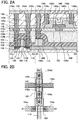
- the substrate 100 including a semiconductor material is prepared (see FIG. 3A ).
- a single crystal semiconductor substrate or a polycrystalline semiconductor substrate made of silicon, silicon carbide, or the like; a compound semiconductor substrate made of silicon germanium or the like; an SOI substrate; or the like can be used.
- an example of using a single crystal silicon substrate as the substrate 100 including a semiconductor material is described.
- an insulating layer is formed so as to cover the semiconductor region 104, and the insulating layer in a region overlapping with the semiconductor region 104 is selectively removed, so that element isolation insulating layers 106 are formed (see FIG 3B ).
- the insulating layer is formed using silicon oxide, silicon nitride, silicon nitride oxide, or the like. As a method for removing the insulating layer, any of etching treatment and polishing treatment such as CMP can be employed. Note that the protective layer 102 is removed after the formation of the semiconductor region 104 or after the formation of the element isolation insulating layers 106.
- an insulating layer is formed so as to cover the gate electrode 110, the impurity regions 114, the sidewall insulating layers 118, and the like.
- phosphorus (P), arsenic (As), or the like is added to regions where the insulating layer is in contact with the impurity regions 114, so that the high-concentration impurity regions 120 are formed (see FIG. 3E ).
- the insulating layer is removed, and a metal layer 122 is formed so as to cover the gate electrode 110, the sidewall insulating layers 118, the high-concentration impurity regions 120, and the like (see FIG. 3E ).
- the metal compound regions 124 that are in contact with the high-concentration impurity regions 120 are formed (see FIG. 3F ). Note that when the gate electrode 110 is formed using polycrystalline silicon or the like, a metal compound region is also formed in a region of the gate electrode 110 in contact with the metal layer 122.
- the interlayer insulating layer 126 and the interlayer insulating layer 128 are formed so as to cover the components formed in the above steps (see FIG. 3G ).
- the interlayer insulating layers 126 and 128 can be formed using a material including an inorganic insulating material such as silicon oxide, silicon nitride oxide, silicon nitride, hafnium oxide, aluminum oxide, or tantalum oxide.
- the interlayer insulating layers 126 and 128 can be formed using an organic insulating material such as a polyimide or an acrylic resin.
- the source/drain electrodes 130a and 130b can be formed in such a manner, for example, that a conductive layer is formed in a region including the openings by a PVD method, a CVD method, or the like and then part of the conductive layer is removed by etching, CMP, or the like.
- the process is preferably performed so that the surfaces are planarized.
- a thin titanium film or a thin titanium nitride film is formed in a region including the openings and then a tungsten film is formed so as to be embedded in the openings, excess tungsten, titanium, titanium nitride, or the like can be removed and the planarity of the surface can be improved by subsequent CMP.
- the surface including the source/drain electrodes 130a and 130b is planarized in such a manner, so that an electrode, a wiring, an insulating layer, a semiconductor layer, and the like can be favorably formed in later steps.
- a method for example, in which a thin titanium film is formed in a region including the openings by a PVD method and a thin titanium nitride film is formed by a CVD method, and then, a tungsten film is formed so as to be embedded in the openings.
- the titanium film formed by a PVD method has a function of reducing an oxide film formed on the surface of lower electrodes (here, the source/drain electrodes 130a and 130b, the electrode 130c, and the like) to decrease the contact resistance with the lower electrodes.
- the titanium nitride film formed after the formation of the titanium film has a barrier function of preventing diffusion of the conductive material.
- a copper film may be formed by a plating method after the formation of the barrier film of titanium, titanium nitride, or the like.
- the surfaces of the insulating layer 132, the electrodes 136a, 136b, and 136c, and the gate electrode 136d are planarized in such a manner, whereby an electrode, a wiring, an insulating layer, a semiconductor layer, and the like can be favorably formed in later steps.
- an oxide semiconductor that becomes intrinsic or substantially intrinsic by removal of impurities (a highly purified oxide semiconductor) is quite susceptible to the interface level and the interface charge; therefore, when such an oxide semiconductor is used for an oxide semiconductor layer, the interface with the gate insulating layer is important. In other words, the gate insulating layer 138 that is to be in contact with a highly purified oxide semiconductor layer needs to have high quality.
- Impurities included in the oxide semiconductor, particularly hydrogen and water, are reduced to a minimum and interface characteristics between the oxide semiconductor and the gate insulating layer are made favorable as described above, whereby a transistor that is stable against stresses such as high electric field and high temperature can be obtained.
- an oxide semiconductor deposition target containing zinc oxide as its main component can be used, for example.
- a cryopump for example, a cryopump, an ion pump, or a titanium sublimation pump can be used.
- An evacuation unit may be a turbo pump provided with a cold trap.
- a compound containing a carbon atom for example, a hydrogen atom, a compound containing a hydrogen atom such as water (H 2 O), and the like are removed, whereby the impurity concentration of the oxide semiconductor layer formed in the deposition chamber can be reduced.
- etching conditions e.g., the amount of electric power applied to a coiled electrode, the amount of electric power applied to an electrode on the substrate side, and the electrode temperature on the substrate side
- etching conditions e.g., the amount of electric power applied to a coiled electrode, the amount of electric power applied to an electrode on the substrate side, and the electrode temperature on the substrate side
- the source/drain electrode 142a and the source/drain electrode 142b are formed in contact with the oxide semiconductor layer 140 (see FIG. 4F ).
- the source/drain electrodes 142a and 142b can be formed in such a manner that a conductive layer is formed so as to cover the oxide semiconductor layer 140 and then is selectively etched.
- a sputtering gas used for forming the protective insulating layer 144 it is preferable to use a high-purity gas from which an impurity such as hydrogen, water, a compound having a hydroxyl group, or a hydride is removed so that the concentration of the impurity is reduced to several ppm (preferably several ppb).
- an impurity such as hydrogen, water, a compound having a hydroxyl group, or a hydride
- heat treatment may be performed at 100 °C to 200 °C for one hour to 30 hours in the air.
- This heat treatment may be performed at a fixed heating temperature; alternatively, the following change in the heating temperature may be conducted plural times repeatedly: the heating temperature is increased from room temperature to a temperature of 100 °C to 200 °C and then decreased to room temperature.
- This heat treatment may be performed under a reduced pressure before the protective insulating layer is formed.
- the heat treatment time can be shortened under the reduced pressure.
- This heat treatment under a reduced pressure may be performed instead of the second heat treatment or may be performed before or after the second heat treatment, for example.
- the conductive layer 148 can be formed by a film formation method such as a PVD method or a CVD method.
- the conductive layer 148 can be formed using a conductive material such as molybdenum, titanium, chromium, tantalum, tungsten, aluminum, copper, neodymium, or scandium or an alloy or a compound (e.g., a nitride) of any of these materials, for example.
- a highly purified oxide semiconductor is formed by removing water or hydrogen that can be a cause of the formation of localized levels. This is based on the idea that the localized levels in an energy gap are sufficiently reduced.
- Such a highly purified oxide semiconductor enables fabrication of remarkably excellent industrial products.
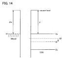
- FIG. 11 the conduction mechanism of a transistor including an oxide semiconductor will be described with reference to FIG. 11 , FIG. 12A and 12B , FIGS. 13A and 13B , and FIG. 14 .
- the following description is based on the assumption of an ideal situation for simplification.
- FIG 14 illustrates the relation between the vacuum level, the work function of metal ( ⁇ M), and the electron affinity of an oxide semiconductor ( ⁇ ).
- the insulating layer 152 is provided over the interlayer insulating layer 146.
- the electrodes 154a, 154b, 154c, and 154d are provided so as to be embedded in the insulating layer 152.
- the electrode 154a is in contact with the electrode 150a.
- the electrode 154b is in contact with the electrode 150b.
- the electrode 154c is in contact with the electrode 150c and the electrode 150d.
- the electrode 154d is in contact with the electrode 150e.
- FIG. 8A A large difference between the structure in FIG. 8A and the structure in FIG. 8B is that the source/drain electrodes 142a and 142b are in contact with either the bottom surface or the top surface of the oxide semiconductor layer 140. Moreover, these differences result in other electrodes, an insulating layer, and the like being arranged in a different manner. The details of each component are the same as those of FIGS. 2A and 2B , and the like.
- a component can be omitted from the structure in FIGS. 2A and 2B or the like in some cases. Also in such cases, a secondary effect such as simplification of a manufacturing process can be obtained.
- transistor 160 there is no particular limitation on the transistor 160.
- a transistor with high switching rate such as a transistor formed using single crystal silicon.
- the potential of the fifth line is set to a potential V 0 intermediate between V th_H and V th_L , whereby charge given to the gate electrode of the transistor 160 can be determined.
- V 0 intermediate between V th_H and V th_L
- charge given to the gate electrode of the transistor 160 can be determined.
- the transistor 160 is turned on.
- the transistor 160 since the potential of the fifth line is set to V 0 (> V th_L , the transistor 160 remains in an off state. Therefore, , the stored data can be read by the potential of the second line.
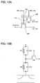
- the components such as transistors in the semiconductor device in FIG. 15A can be regarded as being composed of a resistor and a capacitor as shown in FIG. 15B r. That is, in FIG. 15B , the transistor 160 and the capacitor 164 are each regarded as including a resistor and a capacitor.
- R1 and C1 denote the resistance value and the capacitance value of the capacitor 164, respectively.
- the resistance value R1 corresponds to the resistance value which depends on an insulating layer included in the capacitor 164.
- R2 and C2 denote the resistance value and the capacitance value of the transistor 160, respectively.
- the resistance value R2 corresponds to the resistance value which depends on a gate insulating layer at the time when the transistor 160 is on.
- the capacitance value C2 corresponds to the capacitance value of so-called gate capacitance (capacitance formed between the gate electrode and the source electrode or the drain electrode and capacitance formed between the gate electrode and the channel formation region).
- C1 ⁇ C2 be satisfied. If C1 is large, variation in potential of the fifth line can be suppressed when the potential of the floating gate portion FG is controlled by the fifth line (e.g., at the time of reading).
- a gate electrode of the transistor 160, one of a source electrode and a drain electrode of the transistor 162, and one of electrodes of the capacitor 164 are electrically connected to one another.
- the first signal line S1 and the other of the source electrode and the drain electrode of the transistor 162 are electrically connected to each other, and the second signal line S2 and a gate electrode of the transistor 162 are electrically connected to each other.
- the word line WL and the other of the electrodes of the capacitor 164 are electrically connected to each other.
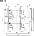
- the semiconductor device in FIG. 17B includes a plurality of source lines SL, a plurality of bit lines BL, a plurality of first signal lines S1, a plurality of second signal lines S2, a plurality of word lines WL, and a plurality of the memory cells 400.
- a gate electrode of the transistor 160, one of a source electrode and a drain electrode of the transistor 162, and one of electrodes of the capacitor 164 are electrically connected to one another.
- the source line SL and a source electrode of the transistor 160 are electrically connected to each other.
- the bit line BL and a drain electrode of the transistor 160 are electrically connected to each other.
- the amount of data which can be stored in each of the memory cells 400 is one bit in the above description, the structure of the memory device of this embodiment is not limited to this.
- the amount of data which is stored in each of the memory cells 400 may be increased by preparing three or more potentials to be supplied to the gate electrode of the transistor 160. For example, in the case where the number of potentials to be supplied to the gate electrode of the transistor 160 is four, data of two bits can be stored in each of the memory cells.
- FIG. 18C illustrates a latch sense amplifier which is an example of sense amplifier circuits.
- the latch sense amplifier has input/output terminals V1 and V2 and input terminals of control signals Sp and Sn.
- the control signals Sp and Sn are set to a signal High and a signal Low, respectively, and a power supply potential (Vdd) is interrupted.
- respective potentials V1in and V2in for comparison are supplied to V1 and V2, respectively.
- the control signals Sp and Sn are set to a signal Low and a signal High, respectively, and a power supply potential (Vdd) is supplied.
- each of the memory cells 1100 includes the first transistor 160, the second transistor 162, and the capacitor 164.
- a gate electrode of the first transistor160, one of a source electrode and a drain electrode of the second transistor 162, and one of electrodes of the capacitor 164 are connected to one another.
- the source line SL and a source electrode of the first transistor 160 are connected to each other.
- the bit line BL and a drain electrode of the first transistor 160 are connected to each other.
- the first signal line S1 and the other of the source electrode and the drain electrode of the second transistor 162 are connected to each other.
- the second signal line S2 and a gate electrode of the second transistor 162 are connected to each other.
- the word line WL and the other of the electrodes of the capacitor 164 are connected to each other.
- transistors are n-channel transistors here, it is needless to say that p-channel transistors can be used. Since the technical nature of the disclosed invention is to use an oxide semiconductor in the transistor 262 so that data can be stored, it is not necessary to limit a specific structure of a semiconductor device to the structure described here.
- the semiconductor device in FIGS. 22A and 22B is also different from the semiconductor device of the foregoing embodiment in an interlayer insulating layer provided in the transistor 260. That is, the semiconductor device in FIGS. 22A and 22B includes a hydrogen-containing interlayer insulating layer 225 which is in contact with a metal compound region 224 of the transistor 260. By providing the hydrogen-containing interlayer insulating layer 225 so as to be in contact with the metal compound region 224, hydrogen can be supplied to the transistor 260 to improve characteristics of the transistor 260.
- the interlayer insulating layer 225 for example, a silicon nitride layer containing hydrogen, which is formed by a plasma CVD method, is given.
- the source/drain electrodes 130a and 130b in Embodiment 1 are not formed through the manufacturing process of the transistor 260 in this embodiment, and even the structure in which the source/drain electrodes 130a and 130b are not formed is called the transistor 260 for convenience.
- the interlayer insulating layer 252 is desirably formed so as to have a planarized surface. This is because an electrode, a line, or the like can be favorably formed over the interlayer insulating layer 252 even in the case where the semiconductor device is reduced in size, for example.
- the interlayer insulating layer 252 can be planarized using a method such as CMP (chemical mechanical polishing).
- the source/drain electrode 254 can be formed in such a manner, for example, that a conductive layer is formed in a region including the opening by a PVD method, a CVD method, or the like and then part of the conductive layer is removed by etching, CMP, or the like.
- a method for example, in which a thin titanium film is formed in a region including the opening by a PVD method and a thin titanium nitride film is formed by a CVD method, and then, a tungsten film is formed so as to be embedded in the opening.
- FIG. 10B is a personal digital assistant (PDA) which includes the semiconductor device according to any of the previous embodiments, and is provided with a housing 311, a display portion 313, an external interface 315, operation buttons 314, and the like. Additionally, there is a stylus 312 as an operation accessory.
- PDA personal digital assistant
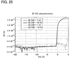
- FIG. 25 shows the results obtained by measurement of the off current of a transistor with a channel width W of 1 m.
- the horizontal axis shows a gate voltage VG and the vertical axis shows a drain current ID.
- the off current of the transistor was found to be smaller than or equal to 1 ⁇ 10 -13 A which is the detection limit.
- the off current of the transistor (per unit channel width (1 ⁇ m)) is smaller than or equal to 1 aA/ ⁇ m (1 ⁇ 10 -18 A/ ⁇ m).
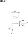
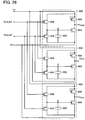
- a potential Vext_b2 for controlling an on state and an off state of the transistor 804 is supplied to the gate terminal of the transistor 804.
- a potential Vext_b1 for controlling an on state and an off state of the transistor 808 is supplied to the gate terminal of the transistor 808.
- a potential Vout is output from the output terminal.
- the potential Vext_b1 for turning on the transistor 808 is input to the gate terminal of the transistor 808 so that the transistor 808 is turned off.
- the potential V1 is set to low.
- the transistor 804 is off.
- the potential V2 is the same potential as V1.
- the initial period is completed. In a state where the initial period is completed, a potential difference is generated between the node A and one of the source terminal and the drain terminal of the transistor 804, and also, a potential difference is generated between the node A and the other of the source terminal and the drain terminal of the transistor 808. Therefore, charge flows slightly through the transistor 804 and the transistor 808. In other words, an off current is generated.
- the potential Vext_b2 is set to a potential (high potential) at which the transistor 804 is turned on.
- the potential of the node A comes to be V2, that is, a low potential (VSS).
- the potential Vext_b2 is set to a potential (low potential) at which the transistor 804 is turned off, whereby the transistor 804 is turned off.
- the potential Vext_b1 is set to a potential (high potential) at which the transistor 808 is turned on.
- the potential of the node A comes to be V1, that is, a high potential (VDD).
- the potential Vext_b1 is set to a potential at which the transistor 808 is turned off. Accordingly, the node A is brought into a floating state and the initial period is completed.
- the potential V1 was basically set to VSS and set to VDD only in a period of 100 msec every 10 to 300 seconds, and Vout was measured. Further, ⁇ t used when the current I flowing through an element was about 30,000 seconds.
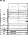
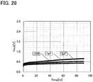
- FIG. 28 shows the relation between the output potential Vout and elapsed time Time in the current measurement. According to FIG 28 , the potential varies as time advances.
- FIG. 29 shows the off current at room temperature (25 °C) calculated based on the above current measurement. Note that FIG. 29 shows the relation between a source-drain voltage V and an off current I. According to FIG. 29 , an off current was about 40 zA/ ⁇ m, where the source-drain voltage is 4 V. When the source-drain voltage was 3.1 V, the off current was smaller than or equal to 10 zA/ ⁇ m. Note that 1 zA is equivalent to 10 -21 A.
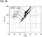
- FIG. 30 shows the off current in an environment at a temperature of 85 °C, which was calculated based on the above current measurement.
- FIG. 30 shows the relation between a source-drain voltage V and an off current I in a circumstance at 85 °C. According to FIG. 30 , the off current was about 100 zA/ ⁇ m when the source-drain voltage was 3.1 V.
- FIG. 31 shows the examination results of the memory window width at the time after writing was performed 1 ⁇ 10 9 times. Note that in FIG. 31 , the horizontal axis shows a Vcg (V) and the vertical axis shows Id (A). According to FIG. 31 , the memory window width was not changed after data was written 1 ⁇ 10 9 times, which means that at least during the period after data is written 1 ⁇ 10 9 times, the semiconductor device does not deteriorate.
Applications Claiming Priority (3)
| Application Number | Priority Date | Filing Date | Title |
|---|---|---|---|
| JP2009249330 | 2009-10-29 | ||
| JP2010012619 | 2010-01-22 | ||
| PCT/JP2010/068103 WO2011052396A1 (en) | 2009-10-29 | 2010-10-07 | Semiconductor device |
Publications (3)
| Publication Number | Publication Date |
|---|---|
| EP2494596A1 EP2494596A1 (en) | 2012-09-05 |
| EP2494596A4 EP2494596A4 (en) | 2016-05-11 |
| EP2494596B1 true EP2494596B1 (en) | 2020-01-15 |
Family
ID=43921822
Family Applications (1)
| Application Number | Title | Priority Date | Filing Date |
|---|---|---|---|
| EP10826530.7A Active EP2494596B1 (en) | 2009-10-29 | 2010-10-07 | Semiconductor device |
Country Status (9)
| Country | Link |
|---|---|
| US (7) | US10490553B2 (ko) |
| EP (1) | EP2494596B1 (ko) |
| JP (16) | JP5802005B2 (ko) |
| KR (16) | KR102369024B1 (ko) |
| CN (4) | CN102598246B (ko) |
| MY (1) | MY159871A (ko) |
| SG (4) | SG10201406869QA (ko) |
| TW (7) | TWI529916B (ko) |
| WO (1) | WO2011052396A1 (ko) |
Families Citing this family (258)
| Publication number | Priority date | Publication date | Assignee | Title |
|---|---|---|---|---|
| US8911653B2 (en) | 2009-05-21 | 2014-12-16 | Semiconductor Energy Laboratory Co., Ltd. | Method for manufacturing light-emitting device |
| JP5730529B2 (ja) | 2009-10-21 | 2015-06-10 | 株式会社半導体エネルギー研究所 | 半導体装置 |
| SG10201406934WA (en) | 2009-10-29 | 2014-11-27 | Semiconductor Energy Lab | Semiconductor device |
| KR102369024B1 (ko) | 2009-10-29 | 2022-02-28 | 가부시키가이샤 한도오따이 에네루기 켄큐쇼 | 반도체 장치 |
| KR101788521B1 (ko) | 2009-10-30 | 2017-10-19 | 가부시키가이샤 한도오따이 에네루기 켄큐쇼 | 반도체 장치 |
| WO2011052366A1 (en) | 2009-10-30 | 2011-05-05 | Semiconductor Energy Laboratory Co., Ltd. | Voltage regulator circuit |
| JP5521495B2 (ja) * | 2009-11-04 | 2014-06-11 | セイコーエプソン株式会社 | 半導体装置用基板、半導体装置及び電子機器 |
| KR101861980B1 (ko) | 2009-11-06 | 2018-05-28 | 가부시키가이샤 한도오따이 에네루기 켄큐쇼 | 반도체 장치 |
| KR101790365B1 (ko) | 2009-11-20 | 2017-10-25 | 가부시키가이샤 한도오따이 에네루기 켄큐쇼 | 반도체 장치 |
| MY166309A (en) | 2009-11-20 | 2018-06-25 | Semiconductor Energy Lab | Nonvolatile latch circuit and logic circuit, and semiconductor device using the same |
| KR102451852B1 (ko) | 2009-11-20 | 2022-10-11 | 가부시키가이샤 한도오따이 에네루기 켄큐쇼 | 반도체 장치 |
| WO2011065183A1 (en) | 2009-11-24 | 2011-06-03 | Semiconductor Energy Laboratory Co., Ltd. | Semiconductor device including memory cell |
| KR101720072B1 (ko) * | 2009-12-11 | 2017-03-27 | 가부시키가이샤 한도오따이 에네루기 켄큐쇼 | 불휘발성 래치 회로와 논리 회로, 및 이를 사용한 반도체 장치 |
| WO2011074392A1 (en) | 2009-12-18 | 2011-06-23 | Semiconductor Energy Laboratory Co., Ltd. | Semiconductor device |
| KR102275522B1 (ko) * | 2009-12-18 | 2021-07-08 | 가부시키가이샤 한도오따이 에네루기 켄큐쇼 | 액정 표시 장치 및 전자 기기 |
| EP2517245B1 (en) | 2009-12-25 | 2019-07-24 | Semiconductor Energy Laboratory Co. Ltd. | Semiconductor device |
| CN102804360B (zh) | 2009-12-25 | 2014-12-17 | 株式会社半导体能源研究所 | 半导体装置 |
| KR101842413B1 (ko) * | 2009-12-28 | 2018-03-26 | 가부시키가이샤 한도오따이 에네루기 켄큐쇼 | 반도체 장치 |
| EP2519969A4 (en) * | 2009-12-28 | 2016-07-06 | Semiconductor Energy Lab | SEMICONDUCTOR COMPONENT |
| WO2011086846A1 (en) | 2010-01-15 | 2011-07-21 | Semiconductor Energy Laboratory Co., Ltd. | Semiconductor device |
| WO2011086847A1 (en) * | 2010-01-15 | 2011-07-21 | Semiconductor Energy Laboratory Co., Ltd. | Semiconductor device |
| US8780629B2 (en) | 2010-01-15 | 2014-07-15 | Semiconductor Energy Laboratory Co., Ltd. | Semiconductor device and driving method thereof |
| US8415731B2 (en) | 2010-01-20 | 2013-04-09 | Semiconductor Energy Laboratory Co., Ltd. | Semiconductor storage device with integrated capacitor and having transistor overlapping sections |
| KR101883629B1 (ko) | 2010-01-20 | 2018-07-30 | 가부시키가이샤 한도오따이 에네루기 켄큐쇼 | 반도체 장치 |
| KR101855060B1 (ko) | 2010-01-22 | 2018-05-09 | 가부시키가이샤 한도오따이 에네루기 켄큐쇼 | 반도체 메모리 장치 및 그 구동 방법 |
| CN102742001B (zh) | 2010-02-05 | 2017-03-22 | 株式会社半导体能源研究所 | 半导体装置 |
| WO2011096277A1 (en) | 2010-02-05 | 2011-08-11 | Semiconductor Energy Laboratory Co., Ltd. | Semiconductor device and method of driving semiconductor device |
| KR101921618B1 (ko) * | 2010-02-05 | 2018-11-26 | 가부시키가이샤 한도오따이 에네루기 켄큐쇼 | 반도체 장치 및 반도체 장치의 구동 방법 |
| CN102725842B (zh) | 2010-02-05 | 2014-12-03 | 株式会社半导体能源研究所 | 半导体器件 |
| WO2011105310A1 (en) | 2010-02-26 | 2011-09-01 | Semiconductor Energy Laboratory Co., Ltd. | Semiconductor device |
| WO2011111503A1 (en) | 2010-03-08 | 2011-09-15 | Semiconductor Energy Laboratory Co., Ltd. | Semiconductor device and method for manufacturing semiconductor device |
| KR20190018049A (ko) * | 2010-03-08 | 2019-02-20 | 가부시키가이샤 한도오따이 에네루기 켄큐쇼 | 반도체 장치 및 반도체 장치를 제작하는 방법 |
| WO2011114866A1 (en) * | 2010-03-17 | 2011-09-22 | Semiconductor Energy Laboratory Co., Ltd. | Memory device and semiconductor device |
| KR20130032304A (ko) | 2010-04-02 | 2013-04-01 | 가부시키가이샤 한도오따이 에네루기 켄큐쇼 | 반도체 장치 |
| WO2011125432A1 (en) | 2010-04-07 | 2011-10-13 | Semiconductor Energy Laboratory Co., Ltd. | Semiconductor memory device |
| US8207025B2 (en) | 2010-04-09 | 2012-06-26 | Semiconductor Energy Laboratory Co., Ltd. | Manufacturing method of semiconductor device |
| TWI511236B (zh) * | 2010-05-14 | 2015-12-01 | Semiconductor Energy Lab | 半導體裝置 |
| US8664658B2 (en) | 2010-05-14 | 2014-03-04 | Semiconductor Energy Laboratory Co., Ltd. | Semiconductor device |
| US8416622B2 (en) | 2010-05-20 | 2013-04-09 | Semiconductor Energy Laboratory Co., Ltd. | Driving method of a semiconductor device with an inverted period having a negative potential applied to a gate of an oxide semiconductor transistor |
| WO2011145468A1 (en) | 2010-05-21 | 2011-11-24 | Semiconductor Energy Laboratory Co., Ltd. | Memory device and semiconductor device |
| US8779433B2 (en) | 2010-06-04 | 2014-07-15 | Semiconductor Energy Laboratory Co., Ltd. | Semiconductor device |
| KR101894897B1 (ko) | 2010-06-04 | 2018-09-04 | 가부시키가이샤 한도오따이 에네루기 켄큐쇼 | 반도체 장치 |
| US9437454B2 (en) | 2010-06-29 | 2016-09-06 | Semiconductor Energy Laboratory Co., Ltd. | Wiring board, semiconductor device, and manufacturing methods thereof |
| WO2012002186A1 (en) | 2010-07-02 | 2012-01-05 | Semiconductor Energy Laboratory Co., Ltd. | Semiconductor device |
| KR101859361B1 (ko) | 2010-07-16 | 2018-05-21 | 가부시키가이샤 한도오따이 에네루기 켄큐쇼 | 반도체 장치 |
| WO2012008304A1 (en) | 2010-07-16 | 2012-01-19 | Semiconductor Energy Laboratory Co., Ltd. | Semiconductor device |
| WO2012014790A1 (en) | 2010-07-27 | 2012-02-02 | Semiconductor Energy Laboratory Co., Ltd. | Semiconductor device |
| JP5739257B2 (ja) | 2010-08-05 | 2015-06-24 | 株式会社半導体エネルギー研究所 | 半導体装置の作製方法 |
| TWI688047B (zh) | 2010-08-06 | 2020-03-11 | 半導體能源研究所股份有限公司 | 半導體裝置 |
| US8792284B2 (en) | 2010-08-06 | 2014-07-29 | Semiconductor Energy Laboratory Co., Ltd. | Oxide semiconductor memory device |
| US8582348B2 (en) | 2010-08-06 | 2013-11-12 | Semiconductor Energy Laboratory Co., Ltd. | Semiconductor device and method for driving semiconductor device |
| TWI555128B (zh) | 2010-08-06 | 2016-10-21 | 半導體能源研究所股份有限公司 | 半導體裝置及半導體裝置的驅動方法 |
| US8422272B2 (en) | 2010-08-06 | 2013-04-16 | Semiconductor Energy Laboratory Co., Ltd. | Semiconductor device and driving method thereof |
| US8508276B2 (en) | 2010-08-25 | 2013-08-13 | Semiconductor Energy Laboratory Co., Ltd. | Semiconductor device including latch circuit |
| JP5727892B2 (ja) | 2010-08-26 | 2015-06-03 | 株式会社半導体エネルギー研究所 | 半導体装置 |
| US8339837B2 (en) | 2010-08-26 | 2012-12-25 | Semiconductor Energy Laboratory Co., Ltd. | Driving method of semiconductor device |
| JP5674594B2 (ja) | 2010-08-27 | 2015-02-25 | 株式会社半導体エネルギー研究所 | 半導体装置及び半導体装置の駆動方法 |
| KR101851817B1 (ko) | 2010-09-03 | 2018-04-24 | 가부시키가이샤 한도오따이 에네루기 켄큐쇼 | 반도체 장치 및 그 구동 방법 |
| US8520426B2 (en) | 2010-09-08 | 2013-08-27 | Semiconductor Energy Laboratory Co., Ltd. | Method for driving semiconductor device |
| US8922236B2 (en) | 2010-09-10 | 2014-12-30 | Semiconductor Energy Laboratory Co., Ltd. | Semiconductor memory device and method for inspecting the same |
| JP2012079399A (ja) | 2010-09-10 | 2012-04-19 | Semiconductor Energy Lab Co Ltd | 半導体装置 |
| TWI543166B (zh) | 2010-09-13 | 2016-07-21 | 半導體能源研究所股份有限公司 | 半導體裝置 |
| JP2012256821A (ja) | 2010-09-13 | 2012-12-27 | Semiconductor Energy Lab Co Ltd | 記憶装置 |
| TWI539453B (zh) | 2010-09-14 | 2016-06-21 | 半導體能源研究所股份有限公司 | 記憶體裝置和半導體裝置 |
| US8767443B2 (en) | 2010-09-22 | 2014-07-01 | Semiconductor Energy Laboratory Co., Ltd. | Semiconductor memory device and method for inspecting the same |
| US8569754B2 (en) | 2010-11-05 | 2013-10-29 | Semiconductor Energy Laboratory Co., Ltd. | Semiconductor device and manufacturing method thereof |
| JP5908263B2 (ja) | 2010-12-03 | 2016-04-26 | 株式会社半導体エネルギー研究所 | Dc−dcコンバータ |
| US8686415B2 (en) | 2010-12-17 | 2014-04-01 | Semiconductor Energy Laboratory Co., Ltd. | Semiconductor device |
| JP5973165B2 (ja) | 2010-12-28 | 2016-08-23 | 株式会社半導体エネルギー研究所 | 半導体装置 |
| US9048142B2 (en) | 2010-12-28 | 2015-06-02 | Semiconductor Energy Laboratory Co., Ltd. | Semiconductor device |
| TWI525614B (zh) | 2011-01-05 | 2016-03-11 | 半導體能源研究所股份有限公司 | 儲存元件、儲存裝置、及信號處理電路 |
| US8421071B2 (en) | 2011-01-13 | 2013-04-16 | Semiconductor Energy Laboratory Co., Ltd. | Memory device |
| TWI619230B (zh) | 2011-01-14 | 2018-03-21 | 半導體能源研究所股份有限公司 | 半導體記憶裝置 |
| TWI520273B (zh) | 2011-02-02 | 2016-02-01 | 半導體能源研究所股份有限公司 | 半導體儲存裝置 |
| JP5839474B2 (ja) | 2011-03-24 | 2016-01-06 | 株式会社半導体エネルギー研究所 | 信号処理回路 |
| TWI567735B (zh) | 2011-03-31 | 2017-01-21 | 半導體能源研究所股份有限公司 | 記憶體電路,記憶體單元,及訊號處理電路 |
| US8878174B2 (en) | 2011-04-15 | 2014-11-04 | Semiconductor Energy Laboratory Co., Ltd. | Semiconductor element, memory circuit, integrated circuit, and driving method of the integrated circuit |
| US8941958B2 (en) * | 2011-04-22 | 2015-01-27 | Semiconductor Energy Laboratory Co., Ltd. | Semiconductor device |
| US8681533B2 (en) | 2011-04-28 | 2014-03-25 | Semiconductor Energy Laboratory Co., Ltd. | Memory circuit, signal processing circuit, and electronic device |
| TWI568181B (zh) | 2011-05-06 | 2017-01-21 | 半導體能源研究所股份有限公司 | 邏輯電路及半導體裝置 |
| US9443844B2 (en) | 2011-05-10 | 2016-09-13 | Semiconductor Energy Laboratory Co., Ltd. | Gain cell semiconductor memory device and driving method thereof |
| US9048788B2 (en) | 2011-05-13 | 2015-06-02 | Semiconductor Energy Laboratory Co., Ltd. | Semiconductor device comprising a photoelectric conversion portion |
| WO2012157472A1 (en) | 2011-05-13 | 2012-11-22 | Semiconductor Energy Laboratory Co., Ltd. | Semiconductor device |
| US9397222B2 (en) * | 2011-05-13 | 2016-07-19 | Semiconductor Energy Laboratory Co., Ltd. | Display device and electronic device |
| US8564331B2 (en) | 2011-05-13 | 2013-10-22 | Semiconductor Energy Laboratory Co., Ltd. | Semiconductor device |
| TWI570891B (zh) * | 2011-05-17 | 2017-02-11 | 半導體能源研究所股份有限公司 | 半導體裝置 |
| US9673823B2 (en) | 2011-05-18 | 2017-06-06 | Semiconductor Energy Laboratory Co., Ltd. | Semiconductor device and method of driving semiconductor device |
| US8709889B2 (en) | 2011-05-19 | 2014-04-29 | Semiconductor Energy Laboratory Co., Ltd. | Semiconductor memory device and manufacturing method thereof |
| KR102081792B1 (ko) | 2011-05-19 | 2020-02-26 | 가부시키가이샤 한도오따이 에네루기 켄큐쇼 | 연산회로 및 연산회로의 구동방법 |
| JP6013682B2 (ja) | 2011-05-20 | 2016-10-25 | 株式会社半導体エネルギー研究所 | 半導体装置の駆動方法 |
| JP5886496B2 (ja) * | 2011-05-20 | 2016-03-16 | 株式会社半導体エネルギー研究所 | 半導体装置 |
| CN102789808B (zh) * | 2011-05-20 | 2018-03-06 | 株式会社半导体能源研究所 | 存储器装置和用于驱动存储器装置的方法 |
| US9762246B2 (en) | 2011-05-20 | 2017-09-12 | Semiconductor Energy Laboratory Co., Ltd. | Semiconductor device with a storage circuit having an oxide semiconductor |
| TWI616873B (zh) * | 2011-05-20 | 2018-03-01 | 半導體能源研究所股份有限公司 | 儲存裝置及信號處理電路 |
| JP5936908B2 (ja) * | 2011-05-20 | 2016-06-22 | 株式会社半導体エネルギー研究所 | パリティビット出力回路およびパリティチェック回路 |
| TWI573136B (zh) * | 2011-05-20 | 2017-03-01 | 半導體能源研究所股份有限公司 | 儲存裝置及信號處理電路 |
| TWI570730B (zh) * | 2011-05-20 | 2017-02-11 | 半導體能源研究所股份有限公司 | 半導體裝置 |
| TWI559683B (zh) * | 2011-05-20 | 2016-11-21 | 半導體能源研究所股份有限公司 | 半導體積體電路 |
| WO2012161059A1 (en) | 2011-05-20 | 2012-11-29 | Semiconductor Energy Laboratory Co., Ltd. | Semiconductor device and method for driving the same |
| JP6091083B2 (ja) * | 2011-05-20 | 2017-03-08 | 株式会社半導体エネルギー研究所 | 記憶装置 |
| JP5947099B2 (ja) * | 2011-05-20 | 2016-07-06 | 株式会社半導体エネルギー研究所 | 半導体装置 |
| US9171840B2 (en) * | 2011-05-26 | 2015-10-27 | Semiconductor Energy Laboratory Co., Ltd. | Semiconductor device and manufacturing method thereof |
| US8610482B2 (en) * | 2011-05-27 | 2013-12-17 | Semiconductor Energy Laboratory Co., Ltd. | Trimming circuit and method for driving trimming circuit |
| JP6231735B2 (ja) | 2011-06-01 | 2017-11-15 | 株式会社半導体エネルギー研究所 | 半導体装置 |
| JP5890251B2 (ja) | 2011-06-08 | 2016-03-22 | 株式会社半導体エネルギー研究所 | 通信方法 |
| JP6012263B2 (ja) | 2011-06-09 | 2016-10-25 | 株式会社半導体エネルギー研究所 | 半導体記憶装置 |
| WO2012169142A1 (en) | 2011-06-09 | 2012-12-13 | Semiconductor Energy Laboratory Co., Ltd. | Cache memory and method for driving the same |
| US8891285B2 (en) | 2011-06-10 | 2014-11-18 | Semiconductor Energy Laboratory Co., Ltd. | Semiconductor memory device |
| US8958263B2 (en) | 2011-06-10 | 2015-02-17 | Semiconductor Energy Laboratory Co., Ltd. | Semiconductor device |
| JP6005401B2 (ja) * | 2011-06-10 | 2016-10-12 | 株式会社半導体エネルギー研究所 | 半導体装置の作製方法 |
| US9166055B2 (en) * | 2011-06-17 | 2015-10-20 | Semiconductor Energy Laboratory Co., Ltd. | Semiconductor device and method for manufacturing the same |
| US9001564B2 (en) | 2011-06-29 | 2015-04-07 | Semiconductor Energy Laboratory Co., Ltd. | Semiconductor device and a method for driving the same |
| JP6013685B2 (ja) * | 2011-07-22 | 2016-10-25 | 株式会社半導体エネルギー研究所 | 半導体装置 |
| WO2013039126A1 (en) | 2011-09-16 | 2013-03-21 | Semiconductor Energy Laboratory Co., Ltd. | Semiconductor device |
| WO2013042562A1 (en) | 2011-09-22 | 2013-03-28 | Semiconductor Energy Laboratory Co., Ltd. | Semiconductor device |
| US9287405B2 (en) | 2011-10-13 | 2016-03-15 | Semiconductor Energy Laboratory Co., Ltd. | Semiconductor device comprising oxide semiconductor |
| TWI591611B (zh) | 2011-11-30 | 2017-07-11 | 半導體能源研究所股份有限公司 | 半導體顯示裝置 |
| KR20140101817A (ko) * | 2011-12-02 | 2014-08-20 | 가부시키가이샤 한도오따이 에네루기 켄큐쇼 | 반도체 장치 및 그 제작 방법 |
| US9076505B2 (en) | 2011-12-09 | 2015-07-07 | Semiconductor Energy Laboratory Co., Ltd. | Memory device |
| JP6053490B2 (ja) | 2011-12-23 | 2016-12-27 | 株式会社半導体エネルギー研究所 | 半導体装置の作製方法 |
| US9040981B2 (en) | 2012-01-20 | 2015-05-26 | Semiconductor Energy Laboratory Co., Ltd. | Semiconductor device |
| US9099560B2 (en) | 2012-01-20 | 2015-08-04 | Semiconductor Energy Laboratory Co., Ltd. | Semiconductor device and manufacturing method thereof |
| JP6091905B2 (ja) * | 2012-01-26 | 2017-03-08 | 株式会社半導体エネルギー研究所 | 半導体装置 |
| JP6063757B2 (ja) * | 2012-02-03 | 2017-01-18 | 株式会社半導体エネルギー研究所 | トランジスタ及び半導体装置 |
| US9196741B2 (en) | 2012-02-03 | 2015-11-24 | Semiconductor Energy Laboratory Co., Ltd. | Semiconductor device |
| US8916424B2 (en) * | 2012-02-07 | 2014-12-23 | Semiconductor Energy Laboratory Co., Ltd. | Method for manufacturing semiconductor device |
| JP5981157B2 (ja) | 2012-02-09 | 2016-08-31 | 株式会社半導体エネルギー研究所 | 半導体装置 |
| US9312257B2 (en) | 2012-02-29 | 2016-04-12 | Semiconductor Energy Laboratory Co., Ltd. | Semiconductor device |
| JP6046514B2 (ja) | 2012-03-01 | 2016-12-14 | 株式会社半導体エネルギー研究所 | 半導体装置 |
| US8754693B2 (en) | 2012-03-05 | 2014-06-17 | Semiconductor Energy Laboratory Co., Ltd. | Latch circuit and semiconductor device |
| JP6100559B2 (ja) | 2012-03-05 | 2017-03-22 | 株式会社半導体エネルギー研究所 | 半導体記憶装置 |
| US9058892B2 (en) | 2012-03-14 | 2015-06-16 | Semiconductor Energy Laboratory Co., Ltd. | Semiconductor device and shift register |
| US9324449B2 (en) | 2012-03-28 | 2016-04-26 | Semiconductor Energy Laboratory Co., Ltd. | Driver circuit, signal processing unit having the driver circuit, method for manufacturing the signal processing unit, and display device |
| US9349849B2 (en) | 2012-03-28 | 2016-05-24 | Semiconductor Energy Laboratory Co., Ltd. | Semiconductor device and electronic device including the semiconductor device |
| US9208849B2 (en) | 2012-04-12 | 2015-12-08 | Semiconductor Energy Laboratory Co., Ltd. | Semiconductor device and method for driving semiconductor device, and electronic device |
| KR102254731B1 (ko) | 2012-04-13 | 2021-05-20 | 가부시키가이샤 한도오따이 에네루기 켄큐쇼 | 반도체 장치 |
| US9285848B2 (en) | 2012-04-27 | 2016-03-15 | Semiconductor Energy Laboratory Co., Ltd. | Power reception control device, power reception device, power transmission and reception system, and electronic device |
| SG10201608665WA (en) | 2012-05-02 | 2016-12-29 | Semiconductor Energy Lab Co Ltd | Programmable logic device |
| JP6250955B2 (ja) | 2012-05-25 | 2017-12-20 | 株式会社半導体エネルギー研究所 | 半導体装置の駆動方法 |
| WO2013179593A1 (ja) * | 2012-05-29 | 2013-12-05 | パナソニック株式会社 | 半導体記憶装置および半導体記憶装置を搭載した半導体装置 |
| US9135182B2 (en) | 2012-06-01 | 2015-09-15 | Semiconductor Energy Laboratory Co., Ltd. | Central processing unit and driving method thereof |
| KR20150023547A (ko) * | 2012-06-01 | 2015-03-05 | 가부시키가이샤 한도오따이 에네루기 켄큐쇼 | 반도체 디바이스 및 경보 장치 |
| JP6108960B2 (ja) | 2012-06-01 | 2017-04-05 | 株式会社半導体エネルギー研究所 | 半導体装置、処理装置 |
| US8873308B2 (en) | 2012-06-29 | 2014-10-28 | Semiconductor Energy Laboratory Co., Ltd. | Signal processing circuit |
| KR102107591B1 (ko) | 2012-07-18 | 2020-05-07 | 가부시키가이샤 한도오따이 에네루기 켄큐쇼 | 기억 소자 및 프로그래머블 로직 디바이스 |
| JP2014057296A (ja) * | 2012-08-10 | 2014-03-27 | Semiconductor Energy Lab Co Ltd | 半導体装置の駆動方法 |
| WO2014025002A1 (en) * | 2012-08-10 | 2014-02-13 | Semiconductor Energy Laboratory Co., Ltd. | Semiconductor device and method for fabricating the same |
| US9129894B2 (en) * | 2012-09-17 | 2015-09-08 | Intermolecular, Inc. | Embedded nonvolatile memory elements having resistive switching characteristics |
| KR102102589B1 (ko) | 2012-10-17 | 2020-04-22 | 가부시키가이샤 한도오따이 에네루기 켄큐쇼 | 프로그램 가능한 논리 장치 |
| JP6204145B2 (ja) * | 2012-10-23 | 2017-09-27 | 株式会社半導体エネルギー研究所 | 半導体装置 |
| WO2014065343A1 (en) | 2012-10-24 | 2014-05-01 | Semiconductor Energy Laboratory Co., Ltd. | Semiconductor device |
| TWI605593B (zh) | 2012-11-15 | 2017-11-11 | 半導體能源研究所股份有限公司 | 半導體裝置 |
| JP6220641B2 (ja) | 2012-11-15 | 2017-10-25 | 株式会社半導体エネルギー研究所 | 半導体装置 |
| JP6254834B2 (ja) | 2012-12-06 | 2017-12-27 | 株式会社半導体エネルギー研究所 | 半導体装置 |
| US9614258B2 (en) | 2012-12-28 | 2017-04-04 | Semiconductor Energy Laboratory Co., Ltd. | Power storage device and power storage system |
| JP2014195243A (ja) | 2013-02-28 | 2014-10-09 | Semiconductor Energy Lab Co Ltd | 半導体装置 |
| JP2014195241A (ja) | 2013-02-28 | 2014-10-09 | Semiconductor Energy Lab Co Ltd | 半導体装置 |
| US9612795B2 (en) | 2013-03-14 | 2017-04-04 | Semiconductor Energy Laboratory Co., Ltd. | Data processing device, data processing method, and computer program |
| JP6333028B2 (ja) | 2013-04-19 | 2018-05-30 | 株式会社半導体エネルギー研究所 | 記憶装置及び半導体装置 |
| JP6396671B2 (ja) | 2013-04-26 | 2018-09-26 | 株式会社半導体エネルギー研究所 | 半導体装置 |
| TWI644434B (zh) | 2013-04-29 | 2018-12-11 | 日商半導體能源研究所股份有限公司 | 半導體裝置及其製造方法 |
| TWI631711B (zh) | 2013-05-01 | 2018-08-01 | 半導體能源研究所股份有限公司 | 半導體裝置 |
| TWI641112B (zh) | 2013-06-13 | 2018-11-11 | 半導體能源研究所股份有限公司 | 半導體裝置 |
| US9515094B2 (en) | 2013-06-26 | 2016-12-06 | Semiconductor Energy Laboratory Co., Ltd. | Storage device and semiconductor device |
| US9343288B2 (en) | 2013-07-31 | 2016-05-17 | Semiconductor Energy Laboratory Co., Ltd. | Semiconductor device |
| JP6410496B2 (ja) | 2013-07-31 | 2018-10-24 | 株式会社半導体エネルギー研究所 | マルチゲート構造のトランジスタ |
| JP6345023B2 (ja) | 2013-08-07 | 2018-06-20 | 株式会社半導体エネルギー研究所 | 半導体装置およびその作製方法 |
| JP6329843B2 (ja) | 2013-08-19 | 2018-05-23 | 株式会社半導体エネルギー研究所 | 半導体装置 |
| US9590109B2 (en) | 2013-08-30 | 2017-03-07 | Semiconductor Energy Laboratory Co., Ltd. | Semiconductor device and method for manufacturing the same |
| JP2015084418A (ja) | 2013-09-23 | 2015-04-30 | 株式会社半導体エネルギー研究所 | 半導体装置 |
| JP6570817B2 (ja) | 2013-09-23 | 2019-09-04 | 株式会社半導体エネルギー研究所 | 半導体装置 |
| WO2015046025A1 (en) | 2013-09-26 | 2015-04-02 | Semiconductor Energy Laboratory Co., Ltd. | Switch circuit, semiconductor device, and system |
| US9406348B2 (en) | 2013-12-26 | 2016-08-02 | Semiconductor Energy Laboratory Co., Ltd. | Memory cell including transistor and capacitor |
| SG11201604650SA (en) | 2013-12-26 | 2016-07-28 | Semiconductor Energy Lab | Semiconductor device |
| US9349418B2 (en) | 2013-12-27 | 2016-05-24 | Semiconductor Energy Laboratory Co., Ltd. | Semiconductor device and method for driving the same |
| US9318618B2 (en) | 2013-12-27 | 2016-04-19 | Semiconductor Energy Laboratory Co., Ltd. | Semiconductor device |
| WO2015114476A1 (en) | 2014-01-28 | 2015-08-06 | Semiconductor Energy Laboratory Co., Ltd. | Semiconductor device |
| JP2015141726A (ja) | 2014-01-28 | 2015-08-03 | 株式会社東芝 | 半導体記憶装置 |
| US9214508B2 (en) | 2014-02-24 | 2015-12-15 | Lg Display Co., Ltd. | Thin film transistor substrate with intermediate insulating layer and display using the same |
| US10074576B2 (en) | 2014-02-28 | 2018-09-11 | Semiconductor Energy Laboratory Co., Ltd. | Semiconductor memory device |
| US9397637B2 (en) | 2014-03-06 | 2016-07-19 | Semiconductor Energy Laboratory Co., Ltd. | Voltage controlled oscillator, semiconductor device, and electronic device |
| KR20160132405A (ko) | 2014-03-12 | 2016-11-18 | 가부시키가이샤 한도오따이 에네루기 켄큐쇼 | 반도체 장치 |
| JP6677449B2 (ja) | 2014-03-13 | 2020-04-08 | 株式会社半導体エネルギー研究所 | 半導体装置の駆動方法 |
| JP6541376B2 (ja) | 2014-03-13 | 2019-07-10 | 株式会社半導体エネルギー研究所 | プログラマブルロジックデバイスの動作方法 |
| US9299848B2 (en) | 2014-03-14 | 2016-03-29 | Semiconductor Energy Laboratory Co., Ltd. | Semiconductor device, RF tag, and electronic device |
| SG11201606647PA (en) * | 2014-03-14 | 2016-09-29 | Semiconductor Energy Lab Co Ltd | Circuit system |
| JP2015188071A (ja) | 2014-03-14 | 2015-10-29 | 株式会社半導体エネルギー研究所 | 半導体装置 |
| US9842842B2 (en) | 2014-03-19 | 2017-12-12 | Semiconductor Energy Laboratory Co., Ltd. | Semiconductor memory device and semiconductor device and electronic device having the same |
| JP6635670B2 (ja) | 2014-04-11 | 2020-01-29 | 株式会社半導体エネルギー研究所 | 半導体装置 |
| DE112015001878B4 (de) | 2014-04-18 | 2021-09-09 | Semiconductor Energy Laboratory Co., Ltd. | Halbleitervorrichtung und elektronisches Gerät |
| TWI643457B (zh) | 2014-04-25 | 2018-12-01 | 日商半導體能源研究所股份有限公司 | 半導體裝置 |
| KR102330412B1 (ko) | 2014-04-25 | 2021-11-25 | 가부시키가이샤 한도오따이 에네루기 켄큐쇼 | 반도체 장치, 전자 부품, 및 전자 기기 |
| KR102210964B1 (ko) * | 2014-05-13 | 2021-02-03 | 삼성전자주식회사 | 스토리지 장치, 스토리지 장치의 동작 방법, 그리고 스토리지 장치를 액세스하는 액세스 방법 |
| JP6580863B2 (ja) | 2014-05-22 | 2019-09-25 | 株式会社半導体エネルギー研究所 | 半導体装置、健康管理システム |
| US10020403B2 (en) | 2014-05-27 | 2018-07-10 | Semiconductor Energy Laboratory Co., Ltd. | Semiconductor device |
| JP6525722B2 (ja) | 2014-05-29 | 2019-06-05 | 株式会社半導体エネルギー研究所 | 記憶装置、電子部品、及び電子機器 |
| JP6538426B2 (ja) | 2014-05-30 | 2019-07-03 | 株式会社半導体エネルギー研究所 | 半導体装置及び電子機器 |
| US9831238B2 (en) | 2014-05-30 | 2017-11-28 | Semiconductor Energy Laboratory Co., Ltd. | Semiconductor device including insulating film having opening portion and conductive film in the opening portion |
| KR20170013240A (ko) | 2014-05-30 | 2017-02-06 | 가부시키가이샤 한도오따이 에네루기 켄큐쇼 | 반도체 장치 및 이를 제조하기 위한 방법 |
| WO2015182000A1 (en) | 2014-05-30 | 2015-12-03 | Semiconductor Energy Laboratory Co., Ltd. | Semiconductor device, manufacturing method thereof, and electronic device |
| US9401364B2 (en) | 2014-09-19 | 2016-07-26 | Semiconductor Energy Laboratory Co., Ltd. | Semiconductor device, electronic component, and electronic device |
| KR102524983B1 (ko) | 2014-11-28 | 2023-04-21 | 가부시키가이샤 한도오따이 에네루기 켄큐쇼 | 반도체 장치, 모듈, 및 전자 기기 |
| JP6667267B2 (ja) * | 2014-12-08 | 2020-03-18 | 株式会社半導体エネルギー研究所 | 半導体装置 |
| JP6833315B2 (ja) | 2014-12-10 | 2021-02-24 | 株式会社半導体エネルギー研究所 | 半導体装置、及び電子機器 |
| US9773832B2 (en) | 2014-12-10 | 2017-09-26 | Semiconductor Energy Laboratory Co., Ltd. | Semiconductor device and electronic device |
| JP6689062B2 (ja) | 2014-12-10 | 2020-04-28 | 株式会社半導体エネルギー研究所 | 半導体装置 |
| US9583177B2 (en) | 2014-12-10 | 2017-02-28 | Semiconductor Energy Laboratory Co., Ltd. | Memory device and semiconductor device including memory device |
| US10522693B2 (en) | 2015-01-16 | 2019-12-31 | Semiconductor Energy Laboratory Co., Ltd. | Memory device and electronic device |
| TWI792065B (zh) | 2015-01-30 | 2023-02-11 | 日商半導體能源研究所股份有限公司 | 成像裝置及電子裝置 |
| JP6717604B2 (ja) | 2015-02-09 | 2020-07-01 | 株式会社半導体エネルギー研究所 | 半導体装置、中央処理装置及び電子機器 |
| JP6739185B2 (ja) | 2015-02-26 | 2020-08-12 | 株式会社半導体エネルギー研究所 | ストレージシステム、およびストレージ制御回路 |
| JP6554533B2 (ja) | 2015-03-02 | 2019-07-31 | 株式会社半導体エネルギー研究所 | 環境センサ |
| JP6801969B2 (ja) * | 2015-03-03 | 2020-12-16 | 株式会社半導体エネルギー研究所 | 半導体装置、表示装置、および電子機器 |
| US9716852B2 (en) | 2015-04-03 | 2017-07-25 | Semiconductor Energy Laboratory Co., Ltd. | Broadcast system |
| US10389961B2 (en) | 2015-04-09 | 2019-08-20 | Semiconductor Energy Laboratory Co., Ltd. | Imaging device and electronic device |
| US9848146B2 (en) | 2015-04-23 | 2017-12-19 | Semiconductor Energy Laboratory Co., Ltd. | Imaging device and electronic device |
| JP2016225613A (ja) | 2015-05-26 | 2016-12-28 | 株式会社半導体エネルギー研究所 | 半導体装置及び半導体装置の駆動方法 |
| JP2017063420A (ja) | 2015-09-25 | 2017-03-30 | 株式会社半導体エネルギー研究所 | 半導体装置 |
| US9773787B2 (en) | 2015-11-03 | 2017-09-26 | Semiconductor Energy Laboratory Co., Ltd. | Semiconductor device, memory device, electronic device, or method for driving the semiconductor device |
| CN108352837A (zh) | 2015-11-13 | 2018-07-31 | 株式会社半导体能源研究所 | 半导体装置、电子构件及电子设备 |
| DE102015119771A1 (de) | 2015-11-16 | 2017-05-18 | Infineon Technologies Ag | Halbleitervorrichtung mit einem ersten Transistor und einem zweiten Transistor |
| KR20170061602A (ko) | 2015-11-26 | 2017-06-05 | 가부시키가이샤 한도오따이 에네루기 켄큐쇼 | 반도체 장치 및 전자 기기 |
| CN108886021B (zh) | 2016-02-12 | 2023-07-25 | 株式会社半导体能源研究所 | 半导体装置及其制造方法 |
| JP6917168B2 (ja) | 2016-04-01 | 2021-08-11 | 株式会社半導体エネルギー研究所 | 半導体装置 |
| US10008502B2 (en) | 2016-05-04 | 2018-06-26 | Semiconductor Energy Laboratory Co., Ltd. | Memory device |
| US9991266B2 (en) * | 2016-06-13 | 2018-06-05 | United Microelectronics Corp. | Semiconductor memory device and semiconductor memory array comprising the same |
| US10490116B2 (en) | 2016-07-06 | 2019-11-26 | Semiconductor Energy Laboratory Co., Ltd. | Semiconductor device, memory device, and display system |
| US10586495B2 (en) | 2016-07-22 | 2020-03-10 | Semiconductor Energy Laboratory Co., Ltd. | Display device and electronic device |
| KR102458660B1 (ko) | 2016-08-03 | 2022-10-26 | 가부시키가이샤 한도오따이 에네루기 켄큐쇼 | 표시 장치 및 전자 기기 |
| TWI619173B (zh) * | 2016-08-09 | 2018-03-21 | 元太科技工業股份有限公司 | 電晶體及其製造方法 |
| CN107706242B (zh) | 2016-08-09 | 2021-03-12 | 元太科技工业股份有限公司 | 晶体管及其制造方法 |
| US10147722B2 (en) | 2016-08-12 | 2018-12-04 | Renesas Electronics America Inc. | Isolated circuit formed during back end of line process |
| WO2018033834A1 (en) | 2016-08-19 | 2018-02-22 | Semiconductor Energy Laboratory Co., Ltd. | Method for controlling power supply in semiconductor device |
| TWI729030B (zh) | 2016-08-29 | 2021-06-01 | 日商半導體能源研究所股份有限公司 | 顯示裝置及控制程式 |
| CN109643713A (zh) * | 2016-09-05 | 2019-04-16 | 夏普株式会社 | 半导体装置 |
| KR102421299B1 (ko) | 2016-09-12 | 2022-07-18 | 가부시키가이샤 한도오따이 에네루기 켄큐쇼 | 기억 장치, 이의 구동 방법, 반도체 장치, 전자 부품, 및 전자 기기 |
| WO2018069787A1 (en) | 2016-10-14 | 2018-04-19 | Semiconductor Energy Laboratory Co., Ltd. | Semiconductor device, broadcasting system, and electronic device |
| WO2018073708A1 (en) | 2016-10-20 | 2018-04-26 | Semiconductor Energy Laboratory Co., Ltd. | Storage device, driving method thereof, semiconductor device, electronic component, and electronic device |
| JP2017103479A (ja) * | 2017-02-08 | 2017-06-08 | 株式会社半導体エネルギー研究所 | 記憶装置及びその作製方法 |
| US10658395B2 (en) | 2017-03-24 | 2020-05-19 | Semiconductor Energy Laboratory Co., Ltd. | Semiconductor device |
| US11114470B2 (en) | 2017-06-02 | 2021-09-07 | Semiconductor Energy Laboratory Co., Ltd. | Semiconductor device, electronic component, and electronic device |
| WO2018224911A1 (ja) | 2017-06-08 | 2018-12-13 | 株式会社半導体エネルギー研究所 | 半導体装置及び半導体装置の駆動方法 |
| US10593693B2 (en) | 2017-06-16 | 2020-03-17 | Semiconductor Energy Laboratory Co., Ltd. | Semiconductor device and method for manufacturing semiconductor device |
| CN117276353A (zh) | 2017-06-27 | 2023-12-22 | 株式会社半导体能源研究所 | 半导体装置、半导体晶片、存储装置及电子设备 |
| US10665604B2 (en) | 2017-07-21 | 2020-05-26 | Semiconductor Energy Laboratory Co., Ltd. | Semiconductor device, semiconductor wafer, memory device, and electronic device |
| US11139298B2 (en) | 2017-09-06 | 2021-10-05 | Semiconductor Energy Laboratory Co., Ltd. | Electronic device |
| US11296085B2 (en) | 2017-09-15 | 2022-04-05 | Semiconductor Energy Laboratory Co., Ltd. | Semiconductor device |
| EP3688813A4 (en) * | 2017-09-28 | 2021-06-23 | INTEL Corporation | MONOLITHIC INTEGRATION OF A THIN FILM TRANSISTOR ON A COMPLEMENTARY TRANSISTOR |
| US20190378794A1 (en) * | 2018-06-06 | 2019-12-12 | Intel Corporation | Bandgap reference diode using thin film transistors |
| JP7074583B2 (ja) * | 2018-06-26 | 2022-05-24 | キオクシア株式会社 | 半導体記憶装置 |
| WO2020000318A1 (en) * | 2018-06-28 | 2020-01-02 | Yangtze Memory Technologies Co., Ltd. | Three-dimensional memory device having shielding layer and method for forming the same |
| KR20200039867A (ko) * | 2018-10-05 | 2020-04-17 | 삼성디스플레이 주식회사 | 유기 발광 표시 장치 |
| JP7306865B2 (ja) | 2019-04-19 | 2023-07-11 | 日立Astemo株式会社 | 演算装置 |
| KR20210009000A (ko) * | 2019-07-16 | 2021-01-26 | 삼성전자주식회사 | 반도체 장치 |
| KR20210095015A (ko) * | 2020-01-21 | 2021-07-30 | 삼성전자주식회사 | 스몰 스윙 데이터 신호를 전송하는 메모리 장치 및 이의 동작 방법 |
| US11309014B2 (en) | 2020-01-21 | 2022-04-19 | Samsung Electronics Co., Ltd. | Memory device transmitting small swing data signal and operation method thereof |
| US11183242B1 (en) * | 2020-05-18 | 2021-11-23 | Micron Technology, Inc. | Preventing parasitic current during program operations in memory |
| CN116209260A (zh) * | 2022-11-01 | 2023-06-02 | 北京超弦存储器研究院 | 一种存储器、电子设备 |
Family Cites Families (224)
| Publication number | Priority date | Publication date | Assignee | Title |
|---|---|---|---|---|
| JPS4716085Y1 (ko) | 1968-05-17 | 1972-06-07 | ||
| JPS5135243A (en) * | 1974-09-20 | 1976-03-25 | Fujitsu Ltd | Mos memori |
| JPS6012799B2 (ja) * | 1977-05-14 | 1985-04-03 | 松下電器産業株式会社 | テ−ピング装置 |
| JPS6034199B2 (ja) | 1980-12-20 | 1985-08-07 | 株式会社東芝 | 半導体記憶装置 |
| EP0053878B1 (en) * | 1980-12-08 | 1985-08-14 | Kabushiki Kaisha Toshiba | Semiconductor memory device |
| JPS60198861A (ja) | 1984-03-23 | 1985-10-08 | Fujitsu Ltd | 薄膜トランジスタ |
| JPH0612799B2 (ja) * | 1986-03-03 | 1994-02-16 | 三菱電機株式会社 | 積層型半導体装置およびその製造方法 |
| JPH0244256B2 (ja) | 1987-01-28 | 1990-10-03 | Kagaku Gijutsucho Mukizaishitsu Kenkyushocho | Ingazn2o5deshimesarerurotsuhoshokeinosojokozoojusurukagobutsuoyobisonoseizoho |
| JPH0244260B2 (ja) | 1987-02-24 | 1990-10-03 | Kagaku Gijutsucho Mukizaishitsu Kenkyushocho | Ingazn5o8deshimesarerurotsuhoshokeinosojokozoojusurukagobutsuoyobisonoseizoho |
| JPS63210023A (ja) | 1987-02-24 | 1988-08-31 | Natl Inst For Res In Inorg Mater | InGaZn↓4O↓7で示される六方晶系の層状構造を有する化合物およびその製造法 |
| JPH0244258B2 (ja) | 1987-02-24 | 1990-10-03 | Kagaku Gijutsucho Mukizaishitsu Kenkyushocho | Ingazn3o6deshimesarerurotsuhoshokeinosojokozoojusurukagobutsuoyobisonoseizoho |
| JPH0244262B2 (ja) | 1987-02-27 | 1990-10-03 | Kagaku Gijutsucho Mukizaishitsu Kenkyushocho | Ingazn6o9deshimesarerurotsuhoshokeinosojokozoojusurukagobutsuoyobisonoseizoho |
| JPH0244263B2 (ja) | 1987-04-22 | 1990-10-03 | Kagaku Gijutsucho Mukizaishitsu Kenkyushocho | Ingazn7o10deshimesarerurotsuhoshokeinosojokozoojusurukagobutsuoyobisonoseizoho |
| JPS63268184A (ja) * | 1987-04-24 | 1988-11-04 | Sony Corp | 半導体メモリ装置 |
| JPH0254572A (ja) * | 1988-08-18 | 1990-02-23 | Matsushita Electric Ind Co Ltd | 半導体記憶装置 |
| US5366922A (en) | 1989-12-06 | 1994-11-22 | Seiko Instruments Inc. | Method for producing CMOS transistor |
| EP0469215B1 (en) * | 1990-07-31 | 1995-11-22 | International Business Machines Corporation | Method of forming stacked tungsten gate PFET devices and structures resulting therefrom |
| US5930608A (en) * | 1992-02-21 | 1999-07-27 | Semiconductor Energy Laboratory Co., Ltd. | Method of fabricating a thin film transistor in which the channel region of the transistor consists of two portions of differing crystallinity |
| JP2775040B2 (ja) * | 1991-10-29 | 1998-07-09 | 株式会社 半導体エネルギー研究所 | 電気光学表示装置およびその駆動方法 |
| JPH05251705A (ja) | 1992-03-04 | 1993-09-28 | Fuji Xerox Co Ltd | 薄膜トランジスタ |
| JPH05282881A (ja) * | 1992-03-31 | 1993-10-29 | Toshiba Corp | 半導体記憶装置 |
| JP3311070B2 (ja) * | 1993-03-15 | 2002-08-05 | 株式会社東芝 | 半導体装置 |
| JP2007189235A (ja) * | 1993-07-26 | 2007-07-26 | Seiko Epson Corp | 薄膜半導体装置及び表示システム |
| EP0923138B1 (en) | 1993-07-26 | 2002-10-30 | Seiko Epson Corporation | Thin -film semiconductor device, its manufacture and display sytem |
| JP3126630B2 (ja) * | 1994-06-20 | 2001-01-22 | キヤノン株式会社 | ディスプレイ |
| JP3479375B2 (ja) | 1995-03-27 | 2003-12-15 | 科学技術振興事業団 | 亜酸化銅等の金属酸化物半導体による薄膜トランジスタとpn接合を形成した金属酸化物半導体装置およびそれらの製造方法 |
| EP0820644B1 (en) | 1995-08-03 | 2005-08-24 | Koninklijke Philips Electronics N.V. | Semiconductor device provided with transparent switching element |
| JP3625598B2 (ja) | 1995-12-30 | 2005-03-02 | 三星電子株式会社 | 液晶表示装置の製造方法 |
| JP4103968B2 (ja) * | 1996-09-18 | 2008-06-18 | 株式会社半導体エネルギー研究所 | 絶縁ゲイト型半導体装置 |
| KR100234700B1 (ko) | 1996-11-27 | 1999-12-15 | 김영환 | 반도체 소자의 제조방법 |
| US5796650A (en) | 1997-05-19 | 1998-08-18 | Lsi Logic Corporation | Memory circuit including write control unit wherein subthreshold leakage may be reduced |
| JPH11126491A (ja) | 1997-08-20 | 1999-05-11 | Fujitsu Ltd | 半導体記憶装置 |
| US6271542B1 (en) | 1997-12-08 | 2001-08-07 | International Business Machines Corporation | Merged logic and memory combining thin film and bulk Si transistors |
| JPH11233789A (ja) | 1998-02-12 | 1999-08-27 | Semiconductor Energy Lab Co Ltd | 半導体装置 |
| JP4170454B2 (ja) | 1998-07-24 | 2008-10-22 | Hoya株式会社 | 透明導電性酸化物薄膜を有する物品及びその製造方法 |
| JP2000150861A (ja) | 1998-11-16 | 2000-05-30 | Tdk Corp | 酸化物薄膜 |
| JP3276930B2 (ja) | 1998-11-17 | 2002-04-22 | 科学技術振興事業団 | トランジスタ及び半導体装置 |
| JP3410976B2 (ja) | 1998-12-08 | 2003-05-26 | インターナショナル・ビジネス・マシーンズ・コーポレーション | 薄膜及びバルク・シリコン・トランジスタを組み合わせる併合化論理及びメモリ集積回路チップとその形成方法 |
| JP3174852B2 (ja) | 1999-03-05 | 2001-06-11 | 東京大学長 | しきい値電圧を制御しうるmosトランジスタを有する回路及びしきい値電圧制御方法 |
| JP2001093988A (ja) * | 1999-07-22 | 2001-04-06 | Sony Corp | 半導体記憶装置 |
| JP4654471B2 (ja) * | 1999-07-29 | 2011-03-23 | ソニー株式会社 | 半導体装置 |
| TW460731B (en) | 1999-09-03 | 2001-10-21 | Ind Tech Res Inst | Electrode structure and production method of wide viewing angle LCD |
| JP3735855B2 (ja) | 2000-02-17 | 2006-01-18 | 日本電気株式会社 | 半導体集積回路装置およびその駆動方法 |
| US6774397B2 (en) | 2000-05-12 | 2004-08-10 | Semiconductor Energy Laboratory Co., Ltd. | Semiconductor device |
| US6266269B1 (en) | 2000-06-07 | 2001-07-24 | Xilinx, Inc. | Three terminal non-volatile memory element |
| US6628551B2 (en) | 2000-07-14 | 2003-09-30 | Infineon Technologies Aktiengesellschaft | Reducing leakage current in memory cells |
| JP4089858B2 (ja) | 2000-09-01 | 2008-05-28 | 国立大学法人東北大学 | 半導体デバイス |
| JP3749101B2 (ja) * | 2000-09-14 | 2006-02-22 | 株式会社ルネサステクノロジ | 半導体装置 |
| KR20020038482A (ko) | 2000-11-15 | 2002-05-23 | 모리시타 요이찌 | 박막 트랜지스터 어레이, 그 제조방법 및 그것을 이용한표시패널 |
| JP2002216482A (ja) * | 2000-11-17 | 2002-08-02 | Toshiba Corp | 半導体メモリ集積回路 |
| US6625057B2 (en) | 2000-11-17 | 2003-09-23 | Kabushiki Kaisha Toshiba | Magnetoresistive memory device |
| US6396745B1 (en) * | 2001-02-15 | 2002-05-28 | United Microelectronics Corp. | Vertical two-transistor flash memory |
| JP3997731B2 (ja) | 2001-03-19 | 2007-10-24 | 富士ゼロックス株式会社 | 基材上に結晶性半導体薄膜を形成する方法 |
| JP2002289859A (ja) | 2001-03-23 | 2002-10-04 | Minolta Co Ltd | 薄膜トランジスタ |
| JP5051949B2 (ja) | 2001-05-31 | 2012-10-17 | 株式会社半導体エネルギー研究所 | 半導体装置の作製方法 |
| JP2002368226A (ja) | 2001-06-11 | 2002-12-20 | Sharp Corp | 半導体装置、半導体記憶装置及びその製造方法、並びに携帯情報機器 |
| JP3925839B2 (ja) | 2001-09-10 | 2007-06-06 | シャープ株式会社 | 半導体記憶装置およびその試験方法 |
| JP4090716B2 (ja) | 2001-09-10 | 2008-05-28 | 雅司 川崎 | 薄膜トランジスタおよびマトリクス表示装置 |
| JP2003101407A (ja) | 2001-09-21 | 2003-04-04 | Sharp Corp | 半導体集積回路 |
| JP4164562B2 (ja) | 2002-09-11 | 2008-10-15 | 独立行政法人科学技術振興機構 | ホモロガス薄膜を活性層として用いる透明薄膜電界効果型トランジスタ |
| WO2003040441A1 (en) | 2001-11-05 | 2003-05-15 | Japan Science And Technology Agency | Natural superlattice homologous single crystal thin film, method for preparation thereof, and device using said single crystal thin film |
| JP2002319682A (ja) | 2002-01-04 | 2002-10-31 | Japan Science & Technology Corp | トランジスタ及び半導体装置 |
| JP4262433B2 (ja) * | 2002-02-20 | 2009-05-13 | 株式会社日立製作所 | 半導体装置の製造方法 |
| JP4083486B2 (ja) | 2002-02-21 | 2008-04-30 | 独立行政法人科学技術振興機構 | LnCuO(S,Se,Te)単結晶薄膜の製造方法 |
| US7049190B2 (en) | 2002-03-15 | 2006-05-23 | Sanyo Electric Co., Ltd. | Method for forming ZnO film, method for forming ZnO semiconductor layer, method for fabricating semiconductor device, and semiconductor device |
| JP3933591B2 (ja) | 2002-03-26 | 2007-06-20 | 淳二 城戸 | 有機エレクトロルミネッセント素子 |
| US7339187B2 (en) * | 2002-05-21 | 2008-03-04 | State Of Oregon Acting By And Through The Oregon State Board Of Higher Education On Behalf Of Oregon State University | Transistor structures |
| US6787835B2 (en) * | 2002-06-11 | 2004-09-07 | Hitachi, Ltd. | Semiconductor memories |
| JP2004022625A (ja) | 2002-06-13 | 2004-01-22 | Murata Mfg Co Ltd | 半導体デバイス及び該半導体デバイスの製造方法 |
| US7105868B2 (en) | 2002-06-24 | 2006-09-12 | Cermet, Inc. | High-electron mobility transistor with zinc oxide |
| JP2004103855A (ja) | 2002-09-10 | 2004-04-02 | Canon Inc | 基板及びその製造方法 |
| US6882010B2 (en) | 2002-10-03 | 2005-04-19 | Micron Technology, Inc. | High performance three-dimensional TFT-based CMOS inverters, and computer systems utilizing such novel CMOS inverters |
| US7067843B2 (en) | 2002-10-11 | 2006-06-27 | E. I. Du Pont De Nemours And Company | Transparent oxide semiconductor thin film transistors |
| JP4166105B2 (ja) | 2003-03-06 | 2008-10-15 | シャープ株式会社 | 半導体装置およびその製造方法 |
| JP2004273732A (ja) | 2003-03-07 | 2004-09-30 | Sharp Corp | アクティブマトリクス基板およびその製造方法 |
| JP4108633B2 (ja) | 2003-06-20 | 2008-06-25 | シャープ株式会社 | 薄膜トランジスタおよびその製造方法ならびに電子デバイス |
| US7262463B2 (en) | 2003-07-25 | 2007-08-28 | Hewlett-Packard Development Company, L.P. | Transistor including a deposited channel region having a doped portion |
| KR100615085B1 (ko) * | 2004-01-12 | 2006-08-22 | 삼성전자주식회사 | 노드 콘택 구조체들, 이를 채택하는 반도체소자들, 이를채택하는 에스램 셀들 및 이를 제조하는 방법들 |
| US7297977B2 (en) | 2004-03-12 | 2007-11-20 | Hewlett-Packard Development Company, L.P. | Semiconductor device |
| US7282782B2 (en) | 2004-03-12 | 2007-10-16 | Hewlett-Packard Development Company, L.P. | Combined binary oxide semiconductor device |
| US7145174B2 (en) | 2004-03-12 | 2006-12-05 | Hewlett-Packard Development Company, Lp. | Semiconductor device |
| KR20070116888A (ko) | 2004-03-12 | 2007-12-11 | 도꾸리쯔교세이호징 가가꾸 기쥬쯔 신꼬 기꼬 | 아몰퍼스 산화물 및 박막 트랜지스터 |
| US7211825B2 (en) | 2004-06-14 | 2007-05-01 | Yi-Chi Shih | Indium oxide-based thin film transistors and circuits |
| JP2006100760A (ja) | 2004-09-02 | 2006-04-13 | Casio Comput Co Ltd | 薄膜トランジスタおよびその製造方法 |
| US7285501B2 (en) | 2004-09-17 | 2007-10-23 | Hewlett-Packard Development Company, L.P. | Method of forming a solution processed device |
| US7382421B2 (en) * | 2004-10-12 | 2008-06-03 | Hewlett-Packard Development Company, L.P. | Thin film transistor with a passivation layer |
| US7298084B2 (en) | 2004-11-02 | 2007-11-20 | 3M Innovative Properties Company | Methods and displays utilizing integrated zinc oxide row and column drivers in conjunction with organic light emitting diodes |
| BRPI0517568B8 (pt) | 2004-11-10 | 2022-03-03 | Canon Kk | Transistor de efeito de campo |
| EP1815530B1 (en) | 2004-11-10 | 2021-02-17 | Canon Kabushiki Kaisha | Field effect transistor employing an amorphous oxide |
| US7791072B2 (en) | 2004-11-10 | 2010-09-07 | Canon Kabushiki Kaisha | Display |
| US7829444B2 (en) | 2004-11-10 | 2010-11-09 | Canon Kabushiki Kaisha | Field effect transistor manufacturing method |
| JP5118811B2 (ja) | 2004-11-10 | 2013-01-16 | キヤノン株式会社 | 発光装置及び表示装置 |
| JP5053537B2 (ja) | 2004-11-10 | 2012-10-17 | キヤノン株式会社 | 非晶質酸化物を利用した半導体デバイス |
| US7863611B2 (en) * | 2004-11-10 | 2011-01-04 | Canon Kabushiki Kaisha | Integrated circuits utilizing amorphous oxides |
| US7453065B2 (en) | 2004-11-10 | 2008-11-18 | Canon Kabushiki Kaisha | Sensor and image pickup device |
| US7579224B2 (en) | 2005-01-21 | 2009-08-25 | Semiconductor Energy Laboratory Co., Ltd. | Method for manufacturing a thin film semiconductor device |
| US7608531B2 (en) | 2005-01-28 | 2009-10-27 | Semiconductor Energy Laboratory Co., Ltd. | Semiconductor device, electronic device, and method of manufacturing semiconductor device |
| TWI412138B (zh) * | 2005-01-28 | 2013-10-11 | Semiconductor Energy Lab | 半導體裝置,電子裝置,和半導體裝置的製造方法 |
| US7858451B2 (en) | 2005-02-03 | 2010-12-28 | Semiconductor Energy Laboratory Co., Ltd. | Electronic device, semiconductor device and manufacturing method thereof |
| US7948171B2 (en) | 2005-02-18 | 2011-05-24 | Semiconductor Energy Laboratory Co., Ltd. | Light emitting device |
| US20060197092A1 (en) | 2005-03-03 | 2006-09-07 | Randy Hoffman | System and method for forming conductive material on a substrate |
| KR100704784B1 (ko) | 2005-03-07 | 2007-04-10 | 삼성전자주식회사 | 적층된 반도체 장치 및 그 제조방법 |
| US8681077B2 (en) | 2005-03-18 | 2014-03-25 | Semiconductor Energy Laboratory Co., Ltd. | Semiconductor device, and display device, driving method and electronic apparatus thereof |
| WO2006105077A2 (en) | 2005-03-28 | 2006-10-05 | Massachusetts Institute Of Technology | Low voltage thin film transistor with high-k dielectric material |
| US7645478B2 (en) | 2005-03-31 | 2010-01-12 | 3M Innovative Properties Company | Methods of making displays |
| JP4849817B2 (ja) * | 2005-04-08 | 2012-01-11 | ルネサスエレクトロニクス株式会社 | 半導体記憶装置 |
| US8300031B2 (en) | 2005-04-20 | 2012-10-30 | Semiconductor Energy Laboratory Co., Ltd. | Semiconductor device comprising transistor having gate and drain connected through a current-voltage conversion element |
| US7483013B2 (en) | 2005-05-20 | 2009-01-27 | Semiconductor Energy Laboratory Co., Ltd. | Semiconductor circuit, display device, and electronic appliance therewith |
| JP5057696B2 (ja) | 2005-05-20 | 2012-10-24 | 株式会社半導体エネルギー研究所 | 半導体回路及び表示装置 |
| JP2006344849A (ja) | 2005-06-10 | 2006-12-21 | Casio Comput Co Ltd | 薄膜トランジスタ |
| US7691666B2 (en) | 2005-06-16 | 2010-04-06 | Eastman Kodak Company | Methods of making thin film transistors comprising zinc-oxide-based semiconductor materials and transistors made thereby |
| US7402506B2 (en) | 2005-06-16 | 2008-07-22 | Eastman Kodak Company | Methods of making thin film transistors comprising zinc-oxide-based semiconductor materials and transistors made thereby |
| US7507618B2 (en) | 2005-06-27 | 2009-03-24 | 3M Innovative Properties Company | Method for making electronic devices using metal oxide nanoparticles |
| KR100711890B1 (ko) | 2005-07-28 | 2007-04-25 | 삼성에스디아이 주식회사 | 유기 발광표시장치 및 그의 제조방법 |
| JP2007059128A (ja) | 2005-08-23 | 2007-03-08 | Canon Inc | 有機el表示装置およびその製造方法 |
| JP5116225B2 (ja) | 2005-09-06 | 2013-01-09 | キヤノン株式会社 | 酸化物半導体デバイスの製造方法 |
| JP2007073705A (ja) | 2005-09-06 | 2007-03-22 | Canon Inc | 酸化物半導体チャネル薄膜トランジスタおよびその製造方法 |
| JP4850457B2 (ja) | 2005-09-06 | 2012-01-11 | キヤノン株式会社 | 薄膜トランジスタ及び薄膜ダイオード |
| JP4560502B2 (ja) * | 2005-09-06 | 2010-10-13 | キヤノン株式会社 | 電界効果型トランジスタ |
| JP4280736B2 (ja) | 2005-09-06 | 2009-06-17 | キヤノン株式会社 | 半導体素子 |
| JP4753373B2 (ja) * | 2005-09-16 | 2011-08-24 | 株式会社半導体エネルギー研究所 | 表示装置及び表示装置の駆動方法 |
| JP2007081335A (ja) * | 2005-09-16 | 2007-03-29 | Renesas Technology Corp | 半導体装置 |
| JP5006598B2 (ja) | 2005-09-16 | 2012-08-22 | キヤノン株式会社 | 電界効果型トランジスタ |
| EP1998375A3 (en) * | 2005-09-29 | 2012-01-18 | Semiconductor Energy Laboratory Co, Ltd. | Semiconductor device having oxide semiconductor layer and manufacturing method |
| JP5037808B2 (ja) | 2005-10-20 | 2012-10-03 | キヤノン株式会社 | アモルファス酸化物を用いた電界効果型トランジスタ、及び該トランジスタを用いた表示装置 |
| JP2007122758A (ja) * | 2005-10-24 | 2007-05-17 | Sony Corp | 半導体メモリ装置およびその読み出し方法 |
| KR101358954B1 (ko) | 2005-11-15 | 2014-02-06 | 가부시키가이샤 한도오따이 에네루기 켄큐쇼 | 다이오드 및 액티브 매트릭스 표시장치 |
| TWI292281B (en) | 2005-12-29 | 2008-01-01 | Ind Tech Res Inst | Pixel structure of active organic light emitting diode and method of fabricating the same |
| US7867636B2 (en) | 2006-01-11 | 2011-01-11 | Murata Manufacturing Co., Ltd. | Transparent conductive film and method for manufacturing the same |
| JP4977478B2 (ja) | 2006-01-21 | 2012-07-18 | 三星電子株式会社 | ZnOフィルム及びこれを用いたTFTの製造方法 |
| US7576394B2 (en) | 2006-02-02 | 2009-08-18 | Kochi Industrial Promotion Center | Thin film transistor including low resistance conductive thin films and manufacturing method thereof |
| KR100714401B1 (ko) | 2006-02-08 | 2007-05-04 | 삼성전자주식회사 | 적층된 트랜지스터를 구비하는 반도체 장치 및 그 형성방법 |
| US7977169B2 (en) | 2006-02-15 | 2011-07-12 | Kochi Industrial Promotion Center | Semiconductor device including active layer made of zinc oxide with controlled orientations and manufacturing method thereof |
| KR20070101595A (ko) | 2006-04-11 | 2007-10-17 | 삼성전자주식회사 | ZnO TFT |
| US20070252928A1 (en) | 2006-04-28 | 2007-11-01 | Toppan Printing Co., Ltd. | Structure, transmission type liquid crystal display, reflection type display and manufacturing method thereof |
| EP2025004A1 (en) | 2006-06-02 | 2009-02-18 | Kochi Industrial Promotion Center | Semiconductor device including an oxide semiconductor thin film layer of zinc oxide and manufacturing method thereof |
| JP5028033B2 (ja) | 2006-06-13 | 2012-09-19 | キヤノン株式会社 | 酸化物半導体膜のドライエッチング方法 |
| JP5168824B2 (ja) | 2006-06-23 | 2013-03-27 | ソニー株式会社 | 負性抵抗素子の製造方法、単電子トンネル素子の製造方法、光センサの製造方法および機能素子の製造方法 |
| JP4609797B2 (ja) | 2006-08-09 | 2011-01-12 | Nec液晶テクノロジー株式会社 | 薄膜デバイス及びその製造方法 |
| JP4999400B2 (ja) | 2006-08-09 | 2012-08-15 | キヤノン株式会社 | 酸化物半導体膜のドライエッチング方法 |
| US7663165B2 (en) * | 2006-08-31 | 2010-02-16 | Aptina Imaging Corporation | Transparent-channel thin-film transistor-based pixels for high-performance image sensors |
| JP4332545B2 (ja) | 2006-09-15 | 2009-09-16 | キヤノン株式会社 | 電界効果型トランジスタ及びその製造方法 |
| JP4274219B2 (ja) | 2006-09-27 | 2009-06-03 | セイコーエプソン株式会社 | 電子デバイス、有機エレクトロルミネッセンス装置、有機薄膜半導体装置 |
| JP5164357B2 (ja) | 2006-09-27 | 2013-03-21 | キヤノン株式会社 | 半導体装置及び半導体装置の製造方法 |
| US7622371B2 (en) | 2006-10-10 | 2009-11-24 | Hewlett-Packard Development Company, L.P. | Fused nanocrystal thin film semiconductor and method |
| JP5072545B2 (ja) * | 2006-11-16 | 2012-11-14 | 株式会社半導体エネルギー研究所 | 半導体装置、半導体装置のデータ書き込み方法、及び半導体装置のデータ読み出し方法 |
| US7772021B2 (en) | 2006-11-29 | 2010-08-10 | Samsung Electronics Co., Ltd. | Flat panel displays comprising a thin-film transistor having a semiconductive oxide in its channel and methods of fabricating the same for use in flat panel displays |
| JP2008140684A (ja) | 2006-12-04 | 2008-06-19 | Toppan Printing Co Ltd | カラーelディスプレイおよびその製造方法 |
| JP5105842B2 (ja) * | 2006-12-05 | 2012-12-26 | キヤノン株式会社 | 酸化物半導体を用いた表示装置及びその製造方法 |
| KR101146574B1 (ko) | 2006-12-05 | 2012-05-16 | 캐논 가부시끼가이샤 | 산화물 반도체를 이용한 박막 트랜지스터의 제조방법 및 표시장치 |
| WO2008069255A1 (en) | 2006-12-05 | 2008-06-12 | Canon Kabushiki Kaisha | Method for manufacturing thin film transistor using oxide semiconductor and display apparatus |
| JP5305630B2 (ja) | 2006-12-05 | 2013-10-02 | キヤノン株式会社 | ボトムゲート型薄膜トランジスタの製造方法及び表示装置の製造方法 |
| KR20080052107A (ko) | 2006-12-07 | 2008-06-11 | 엘지전자 주식회사 | 산화물 반도체층을 구비한 박막 트랜지스터 |
| US8217435B2 (en) * | 2006-12-22 | 2012-07-10 | Intel Corporation | Floating body memory cell having gates favoring different conductivity type regions |
| KR101303578B1 (ko) | 2007-01-05 | 2013-09-09 | 삼성전자주식회사 | 박막 식각 방법 |
| US8207063B2 (en) | 2007-01-26 | 2012-06-26 | Eastman Kodak Company | Process for atomic layer deposition |
| KR100851215B1 (ko) | 2007-03-14 | 2008-08-07 | 삼성에스디아이 주식회사 | 박막 트랜지스터 및 이를 이용한 유기 전계 발광표시장치 |
| US7795613B2 (en) | 2007-04-17 | 2010-09-14 | Toppan Printing Co., Ltd. | Structure with transistor |
| KR101325053B1 (ko) | 2007-04-18 | 2013-11-05 | 삼성디스플레이 주식회사 | 박막 트랜지스터 기판 및 이의 제조 방법 |
| KR20080094300A (ko) | 2007-04-19 | 2008-10-23 | 삼성전자주식회사 | 박막 트랜지스터 및 그 제조 방법과 박막 트랜지스터를포함하는 평판 디스플레이 |
| KR101334181B1 (ko) | 2007-04-20 | 2013-11-28 | 삼성전자주식회사 | 선택적으로 결정화된 채널층을 갖는 박막 트랜지스터 및 그제조 방법 |
| WO2008133345A1 (en) | 2007-04-25 | 2008-11-06 | Canon Kabushiki Kaisha | Oxynitride semiconductor |
| JP5043499B2 (ja) * | 2007-05-02 | 2012-10-10 | 財団法人高知県産業振興センター | 電子素子及び電子素子の製造方法 |
| KR101345376B1 (ko) | 2007-05-29 | 2013-12-24 | 삼성전자주식회사 | ZnO 계 박막 트랜지스터 및 그 제조방법 |
| US20080296567A1 (en) * | 2007-06-04 | 2008-12-04 | Irving Lyn M | Method of making thin film transistors comprising zinc-oxide-based semiconductor materials |
| US8354674B2 (en) * | 2007-06-29 | 2013-01-15 | Semiconductor Energy Laboratory Co., Ltd. | Semiconductor device wherein a property of a first semiconductor layer is different from a property of a second semiconductor layer |
| US8232598B2 (en) | 2007-09-20 | 2012-07-31 | Semiconductor Energy Laboratory Co., Ltd. | Display device and method for manufacturing the same |
| US7982250B2 (en) * | 2007-09-21 | 2011-07-19 | Semiconductor Energy Laboratory Co., Ltd. | Semiconductor device |
| US8044464B2 (en) | 2007-09-21 | 2011-10-25 | Semiconductor Energy Laboratory Co., Ltd. | Semiconductor device |
| JP5354999B2 (ja) | 2007-09-26 | 2013-11-27 | キヤノン株式会社 | 電界効果型トランジスタの製造方法 |
| KR20090040158A (ko) * | 2007-10-19 | 2009-04-23 | 삼성전자주식회사 | 투명한 트랜지스터를 구비한 시모스 이미지 센서 |
| JP2009134274A (ja) | 2007-10-30 | 2009-06-18 | Semiconductor Energy Lab Co Ltd | 液晶表示装置の作製方法 |
| KR101452204B1 (ko) | 2007-11-05 | 2014-10-21 | 가부시키가이샤 한도오따이 에네루기 켄큐쇼 | 박막 트랜지스터 및 상기 박막 트랜지스터를 구비하는 표시 장치 |
| TW200921226A (en) * | 2007-11-06 | 2009-05-16 | Wintek Corp | Panel structure and manufacture method thereof |
| US20110052490A1 (en) | 2007-11-29 | 2011-03-03 | Plur0Med, Inc | Endoscopic mucosal resectioning using purified inverse thermosensitive polymers |
| JP5366517B2 (ja) * | 2007-12-03 | 2013-12-11 | 株式会社半導体エネルギー研究所 | 半導体装置の作製方法 |
| JP5430846B2 (ja) * | 2007-12-03 | 2014-03-05 | 株式会社半導体エネルギー研究所 | 半導体装置の作製方法 |
| JP5213422B2 (ja) | 2007-12-04 | 2013-06-19 | キヤノン株式会社 | 絶縁層を有する酸化物半導体素子およびそれを用いた表示装置 |
| KR100927421B1 (ko) * | 2007-12-17 | 2009-11-19 | 삼성전기주식회사 | 구형 표면을 갖는 태양전지 및 그 제조방법 |
| JP5215158B2 (ja) * | 2007-12-17 | 2013-06-19 | 富士フイルム株式会社 | 無機結晶性配向膜及びその製造方法、半導体デバイス |
| JP5213458B2 (ja) | 2008-01-08 | 2013-06-19 | キヤノン株式会社 | アモルファス酸化物及び電界効果型トランジスタ |
| WO2009093625A1 (ja) * | 2008-01-23 | 2009-07-30 | Idemitsu Kosan Co., Ltd. | 電界効果型トランジスタ及びその製造方法、それを用いた表示装置、並びに半導体装置 |
| JP2009206508A (ja) * | 2008-01-31 | 2009-09-10 | Canon Inc | 薄膜トランジスタ及び表示装置 |
| JP5121478B2 (ja) | 2008-01-31 | 2013-01-16 | 株式会社ジャパンディスプレイウェスト | 光センサー素子、撮像装置、電子機器、およびメモリー素子 |
| KR101512818B1 (ko) | 2008-02-01 | 2015-05-20 | 삼성전자주식회사 | 산화물 반도체 트랜지스터 및 그 제조방법 |
| EP2086013B1 (en) | 2008-02-01 | 2018-05-23 | Samsung Electronics Co., Ltd. | Oxide semiconductor transistor |
| US8586979B2 (en) | 2008-02-01 | 2013-11-19 | Samsung Electronics Co., Ltd. | Oxide semiconductor transistor and method of manufacturing the same |
| JP5052370B2 (ja) * | 2008-02-25 | 2012-10-17 | パナソニック株式会社 | 薄膜トランジスタアレイ基板の製造方法及び閾値補正方法 |
| JP5305696B2 (ja) * | 2008-03-06 | 2013-10-02 | キヤノン株式会社 | 半導体素子の処理方法 |
| JP4555358B2 (ja) * | 2008-03-24 | 2010-09-29 | 富士フイルム株式会社 | 薄膜電界効果型トランジスタおよび表示装置 |
| KR100941850B1 (ko) * | 2008-04-03 | 2010-02-11 | 삼성모바일디스플레이주식회사 | 박막 트랜지스터, 그의 제조 방법 및 박막 트랜지스터를구비하는 평판 표시 장치 |
| JP5305731B2 (ja) | 2008-05-12 | 2013-10-02 | キヤノン株式会社 | 半導体素子の閾値電圧の制御方法 |
| KR100963026B1 (ko) | 2008-06-30 | 2010-06-10 | 삼성모바일디스플레이주식회사 | 박막 트랜지스터, 그의 제조 방법 및 박막 트랜지스터를구비하는 평판 표시 장치 |
| KR100963027B1 (ko) * | 2008-06-30 | 2010-06-10 | 삼성모바일디스플레이주식회사 | 박막 트랜지스터, 그의 제조 방법 및 박막 트랜지스터를구비하는 평판 표시 장치 |
| JP5345456B2 (ja) * | 2008-08-14 | 2013-11-20 | 富士フイルム株式会社 | 薄膜電界効果型トランジスタ |
| JP4623179B2 (ja) | 2008-09-18 | 2011-02-02 | ソニー株式会社 | 薄膜トランジスタおよびその製造方法 |
| US8187919B2 (en) * | 2008-10-08 | 2012-05-29 | Lg Display Co. Ltd. | Oxide thin film transistor and method of fabricating the same |
| JP5451280B2 (ja) | 2008-10-09 | 2014-03-26 | キヤノン株式会社 | ウルツ鉱型結晶成長用基板およびその製造方法ならびに半導体装置 |
| KR101515468B1 (ko) | 2008-12-12 | 2015-05-06 | 삼성전자주식회사 | 표시장치 및 그 동작방법 |
| JP5781720B2 (ja) * | 2008-12-15 | 2015-09-24 | ルネサスエレクトロニクス株式会社 | 半導体装置及び半導体装置の製造方法 |
| JP5606682B2 (ja) | 2009-01-29 | 2014-10-15 | 富士フイルム株式会社 | 薄膜トランジスタ、多結晶酸化物半導体薄膜の製造方法、及び薄膜トランジスタの製造方法 |
| JP4415062B1 (ja) * | 2009-06-22 | 2010-02-17 | 富士フイルム株式会社 | 薄膜トランジスタ及び薄膜トランジスタの製造方法 |
| JP4571221B1 (ja) | 2009-06-22 | 2010-10-27 | 富士フイルム株式会社 | Igzo系酸化物材料及びigzo系酸化物材料の製造方法 |
| KR101996773B1 (ko) | 2009-10-21 | 2019-07-04 | 가부시키가이샤 한도오따이 에네루기 켄큐쇼 | 반도체 장치 |
| KR101490726B1 (ko) | 2009-10-21 | 2015-02-09 | 가부시키가이샤 한도오따이 에네루기 켄큐쇼 | 반도체 장치 |
| KR102369024B1 (ko) | 2009-10-29 | 2022-02-28 | 가부시키가이샤 한도오따이 에네루기 켄큐쇼 | 반도체 장치 |
| SG10201406934WA (en) | 2009-10-29 | 2014-11-27 | Semiconductor Energy Lab | Semiconductor device |
| CN102598249B (zh) | 2009-10-30 | 2014-11-05 | 株式会社半导体能源研究所 | 半导体装置 |
| KR101788521B1 (ko) | 2009-10-30 | 2017-10-19 | 가부시키가이샤 한도오따이 에네루기 켄큐쇼 | 반도체 장치 |
| KR101824854B1 (ko) | 2009-11-06 | 2018-02-01 | 가부시키가이샤 한도오따이 에네루기 켄큐쇼 | 반도체 장치 |
| KR101861980B1 (ko) | 2009-11-06 | 2018-05-28 | 가부시키가이샤 한도오따이 에네루기 켄큐쇼 | 반도체 장치 |
| WO2011058913A1 (en) * | 2009-11-13 | 2011-05-19 | Semiconductor Energy Laboratory Co., Ltd. | Semiconductor device and manufacturing method thereof |
| KR102451852B1 (ko) * | 2009-11-20 | 2022-10-11 | 가부시키가이샤 한도오따이 에네루기 켄큐쇼 | 반도체 장치 |
| WO2011065183A1 (en) | 2009-11-24 | 2011-06-03 | Semiconductor Energy Laboratory Co., Ltd. | Semiconductor device including memory cell |
| KR101911382B1 (ko) * | 2009-11-27 | 2018-10-24 | 가부시키가이샤 한도오따이 에네루기 켄큐쇼 | 반도체 장치 |
| CN102804360B (zh) * | 2009-12-25 | 2014-12-17 | 株式会社半导体能源研究所 | 半导体装置 |
| EP2517245B1 (en) * | 2009-12-25 | 2019-07-24 | Semiconductor Energy Laboratory Co. Ltd. | Semiconductor device |
| KR101842413B1 (ko) * | 2009-12-28 | 2018-03-26 | 가부시키가이샤 한도오따이 에네루기 켄큐쇼 | 반도체 장치 |
| EP2519969A4 (en) * | 2009-12-28 | 2016-07-06 | Semiconductor Energy Lab | SEMICONDUCTOR COMPONENT |
| JP2011138934A (ja) * | 2009-12-28 | 2011-07-14 | Sony Corp | 薄膜トランジスタ、表示装置および電子機器 |
| JP2011187506A (ja) * | 2010-03-04 | 2011-09-22 | Sony Corp | 薄膜トランジスタおよびその製造方法、並びに表示装置 |
| JP2012160679A (ja) | 2011-02-03 | 2012-08-23 | Sony Corp | 薄膜トランジスタ、表示装置および電子機器 |
| JP6012799B2 (ja) * | 2015-03-16 | 2016-10-25 | 本田技研工業株式会社 | 車両のホーン取付構造 |
| JP6848729B2 (ja) | 2017-07-05 | 2021-03-24 | 株式会社リコー | 情報処理装置、情報処理システム及び情報処理プログラム |
-
2010
- 2010-10-07 KR KR1020217035182A patent/KR102369024B1/ko active IP Right Grant
- 2010-10-07 CN CN201080049673.6A patent/CN102598246B/zh active Active
- 2010-10-07 KR KR1020227036408A patent/KR20220153647A/ko not_active Application Discontinuation
- 2010-10-07 KR KR1020247009695A patent/KR20240042253A/ko unknown
- 2010-10-07 SG SG10201406869QA patent/SG10201406869QA/en unknown
- 2010-10-07 KR KR1020237029899A patent/KR20230130172A/ko not_active Application Discontinuation
- 2010-10-07 KR KR1020147011674A patent/KR20140061553A/ko active Search and Examination
- 2010-10-07 SG SG10201503877UA patent/SG10201503877UA/en unknown
- 2010-10-07 MY MYPI2012700117A patent/MY159871A/en unknown
- 2010-10-07 CN CN202110087551.6A patent/CN112768455A/zh active Pending
- 2010-10-07 WO PCT/JP2010/068103 patent/WO2011052396A1/en active Application Filing
- 2010-10-07 KR KR1020207004538A patent/KR102281043B1/ko active IP Right Grant
- 2010-10-07 CN CN201610082458.5A patent/CN105762152B/zh not_active Expired - Fee Related
- 2010-10-07 KR KR1020217022519A patent/KR102321812B1/ko active IP Right Grant
- 2010-10-07 KR KR1020127013714A patent/KR101939712B1/ko active Application Filing
- 2010-10-07 KR KR1020127014969A patent/KR101403629B1/ko active IP Right Grant
- 2010-10-07 EP EP10826530.7A patent/EP2494596B1/en active Active
- 2010-10-07 KR KR1020227022400A patent/KR102458764B1/ko active IP Right Grant
- 2010-10-07 KR KR1020197031686A patent/KR102213595B1/ko active IP Right Grant
- 2010-10-07 KR KR1020247009694A patent/KR20240042252A/ko unknown
- 2010-10-07 KR KR1020177009832A patent/KR20170044209A/ko not_active Application Discontinuation
- 2010-10-07 KR KR1020197000763A patent/KR20190006091A/ko not_active Application Discontinuation
- 2010-10-07 KR KR1020237029902A patent/KR20230130771A/ko not_active Application Discontinuation
- 2010-10-07 KR KR1020227006153A patent/KR102416955B1/ko active IP Right Grant
- 2010-10-07 CN CN201610081971.2A patent/CN105914209A/zh active Pending
- 2010-10-07 SG SG2012017588A patent/SG179111A1/en unknown
- 2010-10-07 SG SG10201910510UA patent/SG10201910510UA/en unknown
- 2010-10-21 JP JP2010236650A patent/JP5802005B2/ja not_active Expired - Fee Related
- 2010-10-27 TW TW099136692A patent/TWI529916B/zh active
- 2010-10-27 TW TW110121022A patent/TWI784562B/zh active
- 2010-10-27 TW TW111139302A patent/TWI823627B/zh active
- 2010-10-27 US US12/913,464 patent/US10490553B2/en active Active
- 2010-10-27 TW TW108142733A patent/TWI732356B/zh active
- 2010-10-27 TW TW106114990A patent/TWI654740B/zh not_active IP Right Cessation
- 2010-10-27 TW TW107133997A patent/TWI688077B/zh active
- 2010-10-27 TW TW104140138A patent/TWI610420B/zh not_active IP Right Cessation
-
2013
- 2013-04-19 JP JP2013088040A patent/JP5619209B2/ja active Active
-
2015
- 2015-08-28 JP JP2015168823A patent/JP2016026384A/ja not_active Withdrawn
-
2017
- 2017-09-29 JP JP2017190486A patent/JP6457607B2/ja active Active
-
2018
- 2018-12-20 JP JP2018237886A patent/JP2019080069A/ja not_active Withdrawn
-
2019
- 2019-11-22 US US16/691,730 patent/US20200091154A1/en active Granted
-
2020
- 2020-05-13 JP JP2020084271A patent/JP6826685B2/ja active Active
-
2021
- 2021-01-15 JP JP2021004651A patent/JP6968303B2/ja active Active
- 2021-09-21 JP JP2021153338A patent/JP6998491B2/ja active Active
- 2021-10-26 JP JP2021174412A patent/JP7236518B2/ja active Active
-
2022
- 2022-03-29 JP JP2022053511A patent/JP2022091895A/ja not_active Withdrawn
-
2023
- 2023-08-16 US US18/234,410 patent/US20230395602A1/en active Pending
- 2023-08-16 US US18/234,414 patent/US20230395603A1/en active Pending
- 2023-09-29 JP JP2023168993A patent/JP2023171873A/ja active Pending
- 2023-10-06 JP JP2023174472A patent/JP2023175961A/ja active Pending
- 2023-12-07 JP JP2023206578A patent/JP2024023577A/ja active Pending
- 2023-12-07 JP JP2023206577A patent/JP2024023576A/ja active Pending
- 2023-12-07 JP JP2023206576A patent/JP2024023575A/ja active Pending
- 2023-12-07 JP JP2023206581A patent/JP2024023578A/ja active Pending
- 2023-12-13 US US18/538,192 patent/US20240120341A1/en active Pending
- 2023-12-13 US US18/537,929 patent/US20240120339A1/en active Pending
- 2023-12-13 US US18/538,161 patent/US20240120340A1/en active Pending
Non-Patent Citations (1)
| Title |
|---|
| None * |
Also Published As
Similar Documents
| Publication | Publication Date | Title |
|---|---|---|
| US20240120341A1 (en) | Semiconductor device | |
| EP2494599B1 (en) | Semiconductor device | |
| KR101791279B1 (ko) | 반도체 장치 | |
| WO2011086847A1 (en) | Semiconductor device | |
| WO2011080998A1 (en) | Semiconductor device | |
| WO2011065258A1 (en) | Semiconductor device | |
| WO2011096277A1 (en) | Semiconductor device and method of driving semiconductor device | |
| US20240136358A1 (en) | Semiconductor device | |
| TW202407969A (zh) | 半導體裝置 | |
| TW202407970A (zh) | 半導體裝置 | |
| KR20240042556A (ko) | 반도체 장치 | |
| KR20240042555A (ko) | 반도체 장치 |
Legal Events
| Date | Code | Title | Description |
|---|---|---|---|
| PUAI | Public reference made under article 153(3) epc to a published international application that has entered the european phase |
Free format text: ORIGINAL CODE: 0009012 |
|
| 17P | Request for examination filed |
Effective date: 20120524 |
|
| AK | Designated contracting states |
Kind code of ref document: A1 Designated state(s): AL AT BE BG CH CY CZ DE DK EE ES FI FR GB GR HR HU IE IS IT LI LT LU LV MC MK MT NL NO PL PT RO RS SE SI SK SM TR |
|
| DAX | Request for extension of the european patent (deleted) | ||
| RA4 | Supplementary search report drawn up and despatched (corrected) |
Effective date: 20160411 |
|
| RIC1 | Information provided on ipc code assigned before grant |
Ipc: G11C 16/04 20060101ALI20160405BHEP Ipc: H01L 27/088 20060101ALI20160405BHEP Ipc: H01L 49/02 20060101ALI20160405BHEP Ipc: H01L 27/115 20060101ALI20160405BHEP Ipc: H01L 21/8258 20060101ALI20160405BHEP Ipc: H01L 29/78 20060101ALI20160405BHEP Ipc: H01L 27/12 20060101ALI20160405BHEP Ipc: H01L 27/02 20060101ALI20160405BHEP Ipc: G11C 11/405 20060101ALI20160405BHEP Ipc: H01L 29/786 20060101ALI20160405BHEP Ipc: H01L 27/105 20060101ALI20160405BHEP Ipc: H01L 21/8234 20060101AFI20160405BHEP |
|
| STAA | Information on the status of an ep patent application or granted ep patent |
Free format text: STATUS: EXAMINATION IS IN PROGRESS |
|
| 17Q | First examination report despatched |
Effective date: 20180316 |
|
| GRAP | Despatch of communication of intention to grant a patent |
Free format text: ORIGINAL CODE: EPIDOSNIGR1 |
|
| STAA | Information on the status of an ep patent application or granted ep patent |
Free format text: STATUS: GRANT OF PATENT IS INTENDED |
|
| RIC1 | Information provided on ipc code assigned before grant |
Ipc: H01L 21/8234 20060101AFI20190828BHEP Ipc: H01L 49/02 20060101ALI20190828BHEP Ipc: H01L 27/11524 20170101ALI20190828BHEP Ipc: G11C 11/405 20060101ALI20190828BHEP Ipc: H01L 27/088 20060101ALI20190828BHEP Ipc: H01L 27/1156 20170101ALI20190828BHEP Ipc: H01L 27/11519 20170101ALI20190828BHEP Ipc: H01L 27/11551 20170101ALI20190828BHEP Ipc: H01L 27/115 20170101ALI20190828BHEP Ipc: G11C 16/04 20060101ALI20190828BHEP Ipc: H01L 27/11521 20170101ALI20190828BHEP Ipc: H01L 27/02 20060101ALI20190828BHEP Ipc: H01L 27/105 20060101ALI20190828BHEP Ipc: H01L 29/786 20060101ALI20190828BHEP Ipc: H01L 27/12 20060101ALI20190828BHEP Ipc: H01L 29/78 20060101ALI20190828BHEP Ipc: H01L 21/8258 20060101ALI20190828BHEP |
|
| INTG | Intention to grant announced |
Effective date: 20190913 |
|
| GRAS | Grant fee paid |
Free format text: ORIGINAL CODE: EPIDOSNIGR3 |
|
| GRAA | (expected) grant |
Free format text: ORIGINAL CODE: 0009210 |
|
| STAA | Information on the status of an ep patent application or granted ep patent |
Free format text: STATUS: THE PATENT HAS BEEN GRANTED |
|
| AK | Designated contracting states |
Kind code of ref document: B1 Designated state(s): AL AT BE BG CH CY CZ DE DK EE ES FI FR GB GR HR HU IE IS IT LI LT LU LV MC MK MT NL NO PL PT RO RS SE SI SK SM TR |
|
| REG | Reference to a national code |
Ref country code: CH Ref legal event code: EP Ref country code: GB Ref legal event code: FG4D |
|
| REG | Reference to a national code |
Ref country code: IE Ref legal event code: FG4D |
|
| REG | Reference to a national code |
Ref country code: DE Ref legal event code: R096 Ref document number: 602010062843 Country of ref document: DE |
|
| REG | Reference to a national code |
Ref country code: AT Ref legal event code: REF Ref document number: 1225901 Country of ref document: AT Kind code of ref document: T Effective date: 20200215 |
|
| REG | Reference to a national code |
Ref country code: NL Ref legal event code: FP |
|
| REG | Reference to a national code |
Ref country code: LT Ref legal event code: MG4D |
|
| PG25 | Lapsed in a contracting state [announced via postgrant information from national office to epo] |
Ref country code: RS Free format text: LAPSE BECAUSE OF FAILURE TO SUBMIT A TRANSLATION OF THE DESCRIPTION OR TO PAY THE FEE WITHIN THE PRESCRIBED TIME-LIMIT Effective date: 20200115 Ref country code: NO Free format text: LAPSE BECAUSE OF FAILURE TO SUBMIT A TRANSLATION OF THE DESCRIPTION OR TO PAY THE FEE WITHIN THE PRESCRIBED TIME-LIMIT Effective date: 20200415 Ref country code: FI Free format text: LAPSE BECAUSE OF FAILURE TO SUBMIT A TRANSLATION OF THE DESCRIPTION OR TO PAY THE FEE WITHIN THE PRESCRIBED TIME-LIMIT Effective date: 20200115 Ref country code: PT Free format text: LAPSE BECAUSE OF FAILURE TO SUBMIT A TRANSLATION OF THE DESCRIPTION OR TO PAY THE FEE WITHIN THE PRESCRIBED TIME-LIMIT Effective date: 20200607 |
|
| PG25 | Lapsed in a contracting state [announced via postgrant information from national office to epo] |
Ref country code: LV Free format text: LAPSE BECAUSE OF FAILURE TO SUBMIT A TRANSLATION OF THE DESCRIPTION OR TO PAY THE FEE WITHIN THE PRESCRIBED TIME-LIMIT Effective date: 20200115 Ref country code: SE Free format text: LAPSE BECAUSE OF FAILURE TO SUBMIT A TRANSLATION OF THE DESCRIPTION OR TO PAY THE FEE WITHIN THE PRESCRIBED TIME-LIMIT Effective date: 20200115 Ref country code: HR Free format text: LAPSE BECAUSE OF FAILURE TO SUBMIT A TRANSLATION OF THE DESCRIPTION OR TO PAY THE FEE WITHIN THE PRESCRIBED TIME-LIMIT Effective date: 20200115 Ref country code: IS Free format text: LAPSE BECAUSE OF FAILURE TO SUBMIT A TRANSLATION OF THE DESCRIPTION OR TO PAY THE FEE WITHIN THE PRESCRIBED TIME-LIMIT Effective date: 20200515 Ref country code: BG Free format text: LAPSE BECAUSE OF FAILURE TO SUBMIT A TRANSLATION OF THE DESCRIPTION OR TO PAY THE FEE WITHIN THE PRESCRIBED TIME-LIMIT Effective date: 20200415 Ref country code: GR Free format text: LAPSE BECAUSE OF FAILURE TO SUBMIT A TRANSLATION OF THE DESCRIPTION OR TO PAY THE FEE WITHIN THE PRESCRIBED TIME-LIMIT Effective date: 20200416 |
|
| REG | Reference to a national code |
Ref country code: FR Ref legal event code: PLFP Year of fee payment: 11 |
|
| REG | Reference to a national code |
Ref country code: DE Ref legal event code: R097 Ref document number: 602010062843 Country of ref document: DE |
|
| PG25 | Lapsed in a contracting state [announced via postgrant information from national office to epo] |
Ref country code: SK Free format text: LAPSE BECAUSE OF FAILURE TO SUBMIT A TRANSLATION OF THE DESCRIPTION OR TO PAY THE FEE WITHIN THE PRESCRIBED TIME-LIMIT Effective date: 20200115 Ref country code: RO Free format text: LAPSE BECAUSE OF FAILURE TO SUBMIT A TRANSLATION OF THE DESCRIPTION OR TO PAY THE FEE WITHIN THE PRESCRIBED TIME-LIMIT Effective date: 20200115 Ref country code: CZ Free format text: LAPSE BECAUSE OF FAILURE TO SUBMIT A TRANSLATION OF THE DESCRIPTION OR TO PAY THE FEE WITHIN THE PRESCRIBED TIME-LIMIT Effective date: 20200115 Ref country code: LT Free format text: LAPSE BECAUSE OF FAILURE TO SUBMIT A TRANSLATION OF THE DESCRIPTION OR TO PAY THE FEE WITHIN THE PRESCRIBED TIME-LIMIT Effective date: 20200115 Ref country code: ES Free format text: LAPSE BECAUSE OF FAILURE TO SUBMIT A TRANSLATION OF THE DESCRIPTION OR TO PAY THE FEE WITHIN THE PRESCRIBED TIME-LIMIT Effective date: 20200115 Ref country code: DK Free format text: LAPSE BECAUSE OF FAILURE TO SUBMIT A TRANSLATION OF THE DESCRIPTION OR TO PAY THE FEE WITHIN THE PRESCRIBED TIME-LIMIT Effective date: 20200115 Ref country code: SM Free format text: LAPSE BECAUSE OF FAILURE TO SUBMIT A TRANSLATION OF THE DESCRIPTION OR TO PAY THE FEE WITHIN THE PRESCRIBED TIME-LIMIT Effective date: 20200115 Ref country code: EE Free format text: LAPSE BECAUSE OF FAILURE TO SUBMIT A TRANSLATION OF THE DESCRIPTION OR TO PAY THE FEE WITHIN THE PRESCRIBED TIME-LIMIT Effective date: 20200115 |
|
| PGFP | Annual fee paid to national office [announced via postgrant information from national office to epo] |
Ref country code: GB Payment date: 20200930 Year of fee payment: 11 Ref country code: FR Payment date: 20200914 Year of fee payment: 11 |
|
| REG | Reference to a national code |
Ref country code: AT Ref legal event code: MK05 Ref document number: 1225901 Country of ref document: AT Kind code of ref document: T Effective date: 20200115 |
|
| PLBE | No opposition filed within time limit |
Free format text: ORIGINAL CODE: 0009261 |
|
| STAA | Information on the status of an ep patent application or granted ep patent |
Free format text: STATUS: NO OPPOSITION FILED WITHIN TIME LIMIT |
|
| 26N | No opposition filed |
Effective date: 20201016 |
|
| PG25 | Lapsed in a contracting state [announced via postgrant information from national office to epo] |
Ref country code: IT Free format text: LAPSE BECAUSE OF FAILURE TO SUBMIT A TRANSLATION OF THE DESCRIPTION OR TO PAY THE FEE WITHIN THE PRESCRIBED TIME-LIMIT Effective date: 20200115 Ref country code: AT Free format text: LAPSE BECAUSE OF FAILURE TO SUBMIT A TRANSLATION OF THE DESCRIPTION OR TO PAY THE FEE WITHIN THE PRESCRIBED TIME-LIMIT Effective date: 20200115 |
|
| PG25 | Lapsed in a contracting state [announced via postgrant information from national office to epo] |
Ref country code: SI Free format text: LAPSE BECAUSE OF FAILURE TO SUBMIT A TRANSLATION OF THE DESCRIPTION OR TO PAY THE FEE WITHIN THE PRESCRIBED TIME-LIMIT Effective date: 20200115 Ref country code: PL Free format text: LAPSE BECAUSE OF FAILURE TO SUBMIT A TRANSLATION OF THE DESCRIPTION OR TO PAY THE FEE WITHIN THE PRESCRIBED TIME-LIMIT Effective date: 20200115 |
|
| REG | Reference to a national code |
Ref country code: CH Ref legal event code: PL |
|
| PG25 | Lapsed in a contracting state [announced via postgrant information from national office to epo] |
Ref country code: LU Free format text: LAPSE BECAUSE OF NON-PAYMENT OF DUE FEES Effective date: 20201007 Ref country code: MC Free format text: LAPSE BECAUSE OF FAILURE TO SUBMIT A TRANSLATION OF THE DESCRIPTION OR TO PAY THE FEE WITHIN THE PRESCRIBED TIME-LIMIT Effective date: 20200115 |
|
| PG25 | Lapsed in a contracting state [announced via postgrant information from national office to epo] |
Ref country code: LI Free format text: LAPSE BECAUSE OF NON-PAYMENT OF DUE FEES Effective date: 20201031 Ref country code: CH Free format text: LAPSE BECAUSE OF NON-PAYMENT OF DUE FEES Effective date: 20201031 |
|
| PG25 | Lapsed in a contracting state [announced via postgrant information from national office to epo] |
Ref country code: IE Free format text: LAPSE BECAUSE OF NON-PAYMENT OF DUE FEES Effective date: 20201007 |
|
| PG25 | Lapsed in a contracting state [announced via postgrant information from national office to epo] |
Ref country code: TR Free format text: LAPSE BECAUSE OF FAILURE TO SUBMIT A TRANSLATION OF THE DESCRIPTION OR TO PAY THE FEE WITHIN THE PRESCRIBED TIME-LIMIT Effective date: 20200115 Ref country code: MT Free format text: LAPSE BECAUSE OF FAILURE TO SUBMIT A TRANSLATION OF THE DESCRIPTION OR TO PAY THE FEE WITHIN THE PRESCRIBED TIME-LIMIT Effective date: 20200115 Ref country code: CY Free format text: LAPSE BECAUSE OF FAILURE TO SUBMIT A TRANSLATION OF THE DESCRIPTION OR TO PAY THE FEE WITHIN THE PRESCRIBED TIME-LIMIT Effective date: 20200115 |
|
| GBPC | Gb: european patent ceased through non-payment of renewal fee |
Effective date: 20211007 |
|
| PG25 | Lapsed in a contracting state [announced via postgrant information from national office to epo] |
Ref country code: MK Free format text: LAPSE BECAUSE OF FAILURE TO SUBMIT A TRANSLATION OF THE DESCRIPTION OR TO PAY THE FEE WITHIN THE PRESCRIBED TIME-LIMIT Effective date: 20200115 Ref country code: AL Free format text: LAPSE BECAUSE OF FAILURE TO SUBMIT A TRANSLATION OF THE DESCRIPTION OR TO PAY THE FEE WITHIN THE PRESCRIBED TIME-LIMIT Effective date: 20200115 |
|
| PG25 | Lapsed in a contracting state [announced via postgrant information from national office to epo] |
Ref country code: GB Free format text: LAPSE BECAUSE OF NON-PAYMENT OF DUE FEES Effective date: 20211007 |
|
| PG25 | Lapsed in a contracting state [announced via postgrant information from national office to epo] |
Ref country code: FR Free format text: LAPSE BECAUSE OF NON-PAYMENT OF DUE FEES Effective date: 20211031 |
|
| P01 | Opt-out of the competence of the unified patent court (upc) registered |
Effective date: 20230529 |
|
| PGFP | Annual fee paid to national office [announced via postgrant information from national office to epo] |
Ref country code: NL Payment date: 20230915 Year of fee payment: 14 |
|
| PGFP | Annual fee paid to national office [announced via postgrant information from national office to epo] |
Ref country code: BE Payment date: 20230918 Year of fee payment: 14 |
|
| PGFP | Annual fee paid to national office [announced via postgrant information from national office to epo] |
Ref country code: DE Payment date: 20230830 Year of fee payment: 14 |