EP1884997B1 - Photoelectric conversion device and image pickup system - Google Patents
Photoelectric conversion device and image pickup system Download PDFInfo
- Publication number
- EP1884997B1 EP1884997B1 EP07111532A EP07111532A EP1884997B1 EP 1884997 B1 EP1884997 B1 EP 1884997B1 EP 07111532 A EP07111532 A EP 07111532A EP 07111532 A EP07111532 A EP 07111532A EP 1884997 B1 EP1884997 B1 EP 1884997B1
- Authority
- EP
- European Patent Office
- Prior art keywords
- region
- photoelectric conversion
- mos transistor
- conversion device
- peripheral circuit
- Prior art date
- Legal status (The legal status is an assumption and is not a legal conclusion. Google has not performed a legal analysis and makes no representation as to the accuracy of the status listed.)
- Not-in-force
Links
- 238000006243 chemical reaction Methods 0.000 title claims abstract description 176
- 239000004065 semiconductor Substances 0.000 claims abstract description 73
- 230000002093 peripheral effect Effects 0.000 claims abstract description 63
- 239000012535 impurity Substances 0.000 claims abstract description 38
- 238000000034 method Methods 0.000 claims abstract description 19
- 125000006850 spacer group Chemical group 0.000 claims abstract description 18
- 239000000758 substrate Substances 0.000 claims abstract description 12
- 229910052581 Si3N4 Inorganic materials 0.000 claims description 24
- HQVNEWCFYHHQES-UHFFFAOYSA-N silicon nitride Chemical compound N12[Si]34N5[Si]62N3[Si]51N64 HQVNEWCFYHHQES-UHFFFAOYSA-N 0.000 claims description 24
- 239000004020 conductor Substances 0.000 claims description 23
- 230000008569 process Effects 0.000 claims description 8
- 230000004044 response Effects 0.000 claims description 7
- UFHFLCQGNIYNRP-UHFFFAOYSA-N Hydrogen Chemical compound [H][H] UFHFLCQGNIYNRP-UHFFFAOYSA-N 0.000 claims description 4
- 229910052739 hydrogen Inorganic materials 0.000 claims description 4
- 239000001257 hydrogen Substances 0.000 claims description 4
- 230000003287 optical effect Effects 0.000 claims description 2
- 238000009792 diffusion process Methods 0.000 abstract description 22
- 238000005530 etching Methods 0.000 abstract description 7
- 150000002500 ions Chemical class 0.000 abstract description 3
- VYPSYNLAJGMNEJ-UHFFFAOYSA-N Silicium dioxide Chemical compound O=[Si]=O VYPSYNLAJGMNEJ-UHFFFAOYSA-N 0.000 description 20
- 229910052814 silicon oxide Inorganic materials 0.000 description 20
- 239000010410 layer Substances 0.000 description 14
- 230000005684 electric field Effects 0.000 description 13
- 230000000694 effects Effects 0.000 description 12
- 239000000969 carrier Substances 0.000 description 11
- 238000005468 ion implantation Methods 0.000 description 9
- 238000004519 manufacturing process Methods 0.000 description 9
- 238000002955 isolation Methods 0.000 description 6
- 230000015572 biosynthetic process Effects 0.000 description 5
- 230000015556 catabolic process Effects 0.000 description 5
- 230000007547 defect Effects 0.000 description 5
- 238000006731 degradation reaction Methods 0.000 description 5
- XUIMIQQOPSSXEZ-UHFFFAOYSA-N Silicon Chemical compound [Si] XUIMIQQOPSSXEZ-UHFFFAOYSA-N 0.000 description 4
- 238000010586 diagram Methods 0.000 description 4
- 238000001312 dry etching Methods 0.000 description 4
- 238000003384 imaging method Methods 0.000 description 4
- 230000009467 reduction Effects 0.000 description 4
- 230000002040 relaxant effect Effects 0.000 description 4
- 229910052710 silicon Inorganic materials 0.000 description 4
- 239000010703 silicon Substances 0.000 description 4
- 230000003068 static effect Effects 0.000 description 4
- 230000000875 corresponding effect Effects 0.000 description 3
- 230000006870 function Effects 0.000 description 3
- 239000002184 metal Substances 0.000 description 3
- 239000005380 borophosphosilicate glass Substances 0.000 description 2
- 230000008859 change Effects 0.000 description 2
- 230000000593 degrading effect Effects 0.000 description 2
- 238000010438 heat treatment Methods 0.000 description 2
- 230000003647 oxidation Effects 0.000 description 2
- 238000007254 oxidation reaction Methods 0.000 description 2
- 230000003071 parasitic effect Effects 0.000 description 2
- 229910021420 polycrystalline silicon Inorganic materials 0.000 description 2
- 229920005591 polysilicon Polymers 0.000 description 2
- 229910021332 silicide Inorganic materials 0.000 description 2
- FVBUAEGBCNSCDD-UHFFFAOYSA-N silicide(4-) Chemical compound [Si-4] FVBUAEGBCNSCDD-UHFFFAOYSA-N 0.000 description 2
- 230000003667 anti-reflective effect Effects 0.000 description 1
- 238000005229 chemical vapour deposition Methods 0.000 description 1
- 239000000356 contaminant Substances 0.000 description 1
- 238000011109 contamination Methods 0.000 description 1
- 230000002596 correlated effect Effects 0.000 description 1
- 238000000151 deposition Methods 0.000 description 1
- 230000008021 deposition Effects 0.000 description 1
- 238000009413 insulation Methods 0.000 description 1
- 239000011229 interlayer Substances 0.000 description 1
- 230000007246 mechanism Effects 0.000 description 1
- 238000012986 modification Methods 0.000 description 1
- 230000004048 modification Effects 0.000 description 1
- 238000000623 plasma-assisted chemical vapour deposition Methods 0.000 description 1
- 238000005070 sampling Methods 0.000 description 1
- 230000035945 sensitivity Effects 0.000 description 1
- 239000007787 solid Substances 0.000 description 1
- 239000002344 surface layer Substances 0.000 description 1
Images


Classifications
-
- H—ELECTRICITY
- H10—SEMICONDUCTOR DEVICES; ELECTRIC SOLID-STATE DEVICES NOT OTHERWISE PROVIDED FOR
- H10F—INORGANIC SEMICONDUCTOR DEVICES SENSITIVE TO INFRARED RADIATION, LIGHT, ELECTROMAGNETIC RADIATION OF SHORTER WAVELENGTH OR CORPUSCULAR RADIATION
- H10F39/00—Integrated devices, or assemblies of multiple devices, comprising at least one element covered by group H10F30/00, e.g. radiation detectors comprising photodiode arrays
- H10F39/80—Constructional details of image sensors
- H10F39/803—Pixels having integrated switching, control, storage or amplification elements
- H10F39/8037—Pixels having integrated switching, control, storage or amplification elements the integrated elements comprising a transistor
- H10F39/80377—Pixels having integrated switching, control, storage or amplification elements the integrated elements comprising a transistor characterised by the channel of the transistor, e.g. channel having a doping gradient
-
- H—ELECTRICITY
- H10—SEMICONDUCTOR DEVICES; ELECTRIC SOLID-STATE DEVICES NOT OTHERWISE PROVIDED FOR
- H10F—INORGANIC SEMICONDUCTOR DEVICES SENSITIVE TO INFRARED RADIATION, LIGHT, ELECTROMAGNETIC RADIATION OF SHORTER WAVELENGTH OR CORPUSCULAR RADIATION
- H10F39/00—Integrated devices, or assemblies of multiple devices, comprising at least one element covered by group H10F30/00, e.g. radiation detectors comprising photodiode arrays
- H10F39/011—Manufacture or treatment of image sensors covered by group H10F39/12
- H10F39/014—Manufacture or treatment of image sensors covered by group H10F39/12 of CMOS image sensors
-
- H—ELECTRICITY
- H10—SEMICONDUCTOR DEVICES; ELECTRIC SOLID-STATE DEVICES NOT OTHERWISE PROVIDED FOR
- H10F—INORGANIC SEMICONDUCTOR DEVICES SENSITIVE TO INFRARED RADIATION, LIGHT, ELECTROMAGNETIC RADIATION OF SHORTER WAVELENGTH OR CORPUSCULAR RADIATION
- H10F39/00—Integrated devices, or assemblies of multiple devices, comprising at least one element covered by group H10F30/00, e.g. radiation detectors comprising photodiode arrays
- H10F39/80—Constructional details of image sensors
- H10F39/803—Pixels having integrated switching, control, storage or amplification elements
- H10F39/8037—Pixels having integrated switching, control, storage or amplification elements the integrated elements comprising a transistor
Definitions
- the present invention relates to a photoelectric conversion device.
- the present invention relates to a MOS photoelectric conversion device including a MOS transistor.
- Document US 2005/067640 A1 describes a CMOS imaging device on the one hand which is capable of performing charge transfer and a manufacturing method of this device on the other hand.
- This imaging device includes a photodiode and floating diffusion region formed to be spaced from each other on a surface layer of a pixel region of a silicon (semiconductor) substrate, and a transfer gate having one of a concave and convex portions toward the floating diffusion region, the transfer gate being formed above the silicon substrate between the photodiode and the floating diffusion region by interposing a gate insulating film therebetween.
- Document JP 2006 049921 A describes a solid state imaging device and a method of manufacturing this device.
- demands for photoelectric conversion devices as image pickup devices for use in two-dimensional image input apparatuses, such as digital still cameras and camcorders, and for use in one-dimensional image readers, such as facsimiles and scanners have been rapidly increasing.
- Charge-coupled devices CCDs
- MOS photoelectric conversion devices are used as photoelectric conversion devices.
- noise generated in photoelectric conversion regions In photoelectric conversion devices, it is necessary to reduce noise generated in photoelectric conversion regions.
- An example of such noise is noise caused by hot carriers generated in MOS transistors disposed in photoelectric conversion regions.
- the term "hot carrier” refers to a carrier generated by subjecting a p-n junction constituted by a drain region and a channel end to a strong electric field generated by applying a voltage to a gate of a MOS transistor.
- noise generated by hot carriers in particular, may lead to a problem.
- Patent Document 1 Japanese Patent Laid-Open No. 11-284167 (Patent Document 1) and Japanese Patent Laid-Open No. 2000-012822 (Patent Document 2) each disclose a MOS transistor that has a lightly doped drain (LDD) structure and that is disposed in a photoelectric conversion region.
- LDD lightly doped drain
- Patent Document 2 discloses a process for producing a structure including a MOS transistor that has the LDD structure and that is disposed in a photoelectric conversion region. The process will be briefly described with reference to Fig. 2 of Patent Document 2.
- a light-receiving portion and a detecting portion described below serve as a source and a drain, respectively, of a transfer transistor.
- a region to be formed into a light-receiving portion is subjected to ion implantation.
- ion implantation is performed.
- a silicon nitride film functioning as an anti-reflection film for the light-receiving portion is formed so as to cover the light-receiving portion, a gate electrode, and the detecting portion.
- the silicon nitride film is patterned on the gate electrode to form a side wall on the drain side of the gate electrode.
- a heavily doped semiconductor region is formed with the side wall as a mask to form a photoelectric conversion device.
- photoelectric conversion devices have been required to have higher pixel densities and larger numbers of pixels while photoelectric conversion properties, such as sensitivity and a dynamic range, have been maintained or improved. Reducing the driving voltage of a photoelectric conversion region and miniaturizing a region other than the photo-receiving portion while a reduction in the area of the photo-receiving portion is inhibited are effective in fabricating such photoelectric conversion devices.
- the miniaturization of the MOS transistor for reading a signal in response to a signal charge of a photoelectric conversion element disposed in the photoelectric conversion region may degrade the reliability of transistor properties.
- the width of a side spacer is equal to that of a peripheral circuit region.
- the anti-reflection film in the photoelectric conversion region is subjected to etching.
- Etching causes damage (mainly plasma damage) to the photoelectric conversion region. This increases a dark current flowing through a photodiode.
- the present invention provides a photoelectric conversion device having improved properties without an increase in the number of production steps.
- a photoelectric conversion device includes a photoelectric conversion region having a plurality of photoelectric conversion elements and a first MOS transistor configured to read a signal in response to an electric charge of each photoelectric conversion element; and a peripheral circuit region having a second MOS transistor configured to drive the first MOS transistor and/or amplify the signal read from the photoelectric conversion region, the photoelectric conversion region and the peripheral circuit region being located on the same semiconductor substrate, wherein said first MOS transistor includes a drain having a first region that is in direct contact with a conductor and a second region that is located between said first region and a channel of said first MOS transistor, said second MOS transistor includes a drain having a first region that is in direct contact with a conductor and a second region that is located between said first region and a channel of said second MOS transistor, and said second region of said second MOS transistor includes a first subregion adjacent to said channel and a second subregion located between said first subregion and the first region, and where
- the present invention in its first aspect provides a photoelectric conversion device as specified in claims 1 to 6.
- the present invention in its second aspect provides an image pickup system as specified in claim 7.
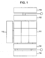
- Fig. 1 is a schematic plan view of a photoelectric conversion device according to the present invention.
- Figs. 2A and 2B are plan views and cross-sectional views of a MOS transistor according to the present invention.
- Fig. 3 is a circuit diagram of a photoelectric conversion device according to the present invention.
- Fig. 4 is a schematic cross-sectional view of a photoelectric conversion device according to a first embodiment of the present invention.
- Figs. 5A to 5E illustrate a procedure for fabricating a photoelectric conversion device according to a second embodiment.
- Fig. 6 is a schematic cross-sectional view of a photoelectric conversion device according to a third embodiment.
- Fig. 7 is a schematic cross-sectional view of a photoelectric conversion device according to a fourth embodiment.
- Fig. 8 is a schematic cross-sectional view of a photoelectric conversion device according to a fifth embodiment.
- Fig. 9 is a schematic cross-sectional view of a photoelectric conversion device for explaining the present invention.
- Fig. 10 is a block diagram illustrating an image pickup system including a photoelectric conversion device.
- a "photoelectric conversion region” refers to a region including a plurality of photoelectric conversion elements and a MOS transistor configured to read a signal in response to a charge of each photoelectric conversion element.
- a plurality of MOS transistors per photoelectric conversion element may be formed so as to amplify a signal.
- a "peripheral circuit region” refers to a region including a circuit configured to drive the MOS transistor disposed in the photoelectric conversion region and a circuit configured to amplify a signal fed from the photoelectric conversion region.
- Fig. 1 is a layout plan view of a photoelectric conversion device.
- Reference numeral 111 represents the photoelectric conversion region.
- a region in which the photoelectric conversion elements are arranged may also be referred to as a "pixel region".
- the pixel is the minimum unit of one photoelectric conversion element and a group of elements configured to read a signal from the photoelectric conversion element and then send the signal to an output line.
- the group of elements includes a transfer element such as a transfer MOS transistor, an amplifying element such as an amplifying MOS transistor, and a reset element such as a reset MOS transistor, described below.
- the elements may be shared between adjacent photoelectric conversion elements.
- the pixel is defined as the minimum unit of a group of elements configured to read a signal from the photoelectric conversion element.
- a signal-processing circuit 112 amplifies a signal read from the photoelectric conversion region.
- the signal-processing circuit 112 is not limited to the amplifying circuit but may be a circuit that removes pixel noise by correlated double sampling (CDS).
- the signal-processing circuit 112 may be a circuit that simply converts signals read in parallel from a plurality of columns into serial signals.
- a vertical shift register 113 drives the MOS transistor located in the photoelectric conversion region.
- a horizontal shift resister 114 drives a MOS transistor of the signal-processing circuit.
- the signal-processing circuit 112 to the horizontal shift resister 114 may be included in the peripheral circuit region.
- an A/D converter may be included in the peripheral circuit region.
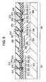
- Fig. 9 is a schematic cross-sectional view of a photoelectric conversion device including a photoelectric conversion region 101 and a peripheral circuit region 102.
- a MOS transistor 909 reads a signal fed from a photoelectric conversion element.
- a MOS transistor 910 is located in the peripheral circuit region.
- the source and the drain of each of the MOS transistor 909 located in the photoelectric conversion region and the MOS transistor 910 located in the peripheral circuit region have the same LDD structure. That is, the LDD structure has a heavily doped semiconductor region 911, a lightly doped semiconductor region 914 located under a side spacer 913, and a heavily doped semiconductor region 916 located under a contact hole 915.
- an excessively low impurity concentration in the electric-field-relaxation layer or an excessively large width of the electric-field-relaxation layer of the LDD structure increases the parasitic resistance (series resistance) of the transistor, thus significantly degrading the driving ability and static characteristics.
- the electric-field-relaxation layer having a relatively small width needs to be formed.
- the electric-field-relaxation layer having a larger width can be formed.
- the drains in the photoelectric conversion region and the peripheral circuit region have the same structure. Thus, only either one property or the other can be satisfied.
- both properties can be satisfied because the structure of a drain in a photoelectric conversion region is different from that of a drain in a peripheral circuit region.
- a lightly doped region of the drain in the photoelectric conversion region is located so as to have an area larger than the area of a lightly doped region of the drain in the peripheral circuit region.
- a portion extending from a gate end to a region (first region) where the drain is in direct contact with a conductor has the actual effect of relaxing an electric field applied to the MOS transistor.
- a large effect of relaxing an electric field can be obtained.
- the same effect is also obtained by reducing an impurity concentration in the drain of a MOS transistor located in the photoelectric conversion region compared with an impurity concentration in the drain of a MOS transistor located in the peripheral circuit region.
- the drain of the MOS transistor (first MOS transistor) located in the photoelectric conversion region has a first region that is in direct contact with a conductor and a second region that is closer to a channel of the MOS transistor than the first region.
- the drain is electrically connected to a plug, which is a conductor.
- the drain includes a first region that is in direct contact with the plug and a second region that is closer to a channel than the first region.
- the second region includes a first subregion adjacent to the channel and a second subregion located between the first region and the first subregion. An impurity concentration in the second region is lower than an impurity concentration in the second subregion.
- Fig. 2A shows a plan view and a cross-sectional view taken along line A-A' of a MOS transistor located in the peripheral circuit region.
- Fig. 2B shows a plan view and a cross-sectional view taken along line B-B' of a MOS transistor located in the photoelectric conversion region.
- Gate electrodes 2001, sources 2002, and connecting regions (first region) 2003 for connection with conductors are shown.
- a lightly doped semiconductor region (first subregion) 2004 is located adjacent to a gate.
- a region (second subregion) 2005 is located between the first region and the first subregion and has an impurity concentration higher than the first subregion.
- a lightly doped semiconductor region (second region) 2006 is located between the channel and the first region and has a low impurity concentration.
- An impurity concentration in the second region is lower than an impurity concentration in the second subregion.
- This structure can reduce hot carriers generated in the MOS transistor located in the photoelectric conversion region.
- the electric-field-relaxation layer having a relatively small width can be formed in the MOS transistor for which the driving ability and circuit characteristics are important.
- the absence of a step of forming a side wall can reduce noise caused by etching in the step.
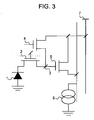
- Fig. 3 is an exemplary equivalent circuit diagram of a pixel of a photoelectric conversion device according to the present invention.
- the photoelectric conversion region includes a photoelectric conversion element 1, a transfer MOS transistor 2, a reset MOS transistor 4, and an amplifying MOS transistor 5.
- the pixel is selected by a voltage applied to the drain of the reset MOS transistor.
- the photoelectric conversion element is a photodiode that converts incident light into a charge by photoelectric conversion.
- the transfer MOS transistor functions as a transfer element that transfers the charge from the photoelectric conversion element to an input portion of the amplifying element.
- the amplifying MOS transistor transmits a change in electric potential in response to the charge generated in the photoelectric conversion element to a signal line.
- a target object with an electric potential to be changed may be a node in a floating state during transfer of the charge from the photoelectric conversion element.
- a floating diffusion region (FD) is used.
- the floating diffusion region is connected to the gate of the amplifying MOS transistor.
- the amplifying MOS transistor transmits a signal in response to the change in electric potential in the floating diffusion region to the signal line.
- the charge is amplified by source-follower operation and is then transmitted.
- the MOS transistor 5 is defined as an amplifying element.
- a power supply 7, the amplifying MOS transistor 5, the signal line, and a constant current source 6 constitute a source-follower circuit.
- the selective operation is performed on the basis of a drain voltage of the reset MOS transistor.
- a selective MOS transistor may be provided in order to perform selection.
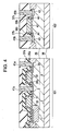
- Fig. 4 is a schematic cross-sectional view of a photoelectric conversion device according to this embodiment.
- a reset MOS transistor is exemplified as a MOS transistor located in a photoelectric conversion region.
- Fig. 4 shows a photoelectric conversion region 101 and a peripheral circuit region 102.
- a cross-sectional structure of a photoelectric conversion element, a transfer MOS transistor, and a reset MOS transistor is shown in the photoelectric conversion region 101.
- a MOS transistor in the peripheral circuit region 102 constitutes any of the above-described circuits.
- the photoelectric conversion region 101 shown in Fig. 4 includes a gate electrode 31 of the transfer MOS transistor and a gate electrode 32 of the reset MOS transistor.
- Reference numeral 33 represents a semiconductor region 33 of a first conductivity type, the semiconductor region constituting the photoelectric conversion element. The same conductivity type as a charge treated as a signal is used. When a charge is an electron, the semiconductor region is an n-type semiconductor region.
- a floating diffusion region 3 is formed of a semiconductor region of the first conductivity type.
- Reference numeral 34 represents a semiconductor region of the first conductivity type. A reference voltage for reset or pixel selection is applied to the semiconductor region 34.
- the semiconductor region 34 functions as the drain of the reset MOS transistor.
- a silicon nitride film 36a is covered with a silicon oxide film 37a.
- a combination of the silicon nitride film 36a and the silicon oxide film 37a can constitute an anti-reflection film that reduces the reflection of incident light from surfaces of the photoelectric conversion elements.
- the entire region is covered with an insulating film constituted by the silicon nitride film 36a and the silicon oxide film 37a, except for the bottoms of contact holes in the photoelectric conversion region 101.
- Contact holes 41a are filled with a conductor such as a contact plug.
- the insulating film is not limited to the combination of the silicon nitride film and the silicon oxide film.
- the source of the transfer MOS transistor also serves as the semiconductor region 33 constituting the photoelectric conversion element.
- the drain of the transfer MOS transistor, the drain of the reset MOS transistor, and the floating diffusion region are formed of a common semiconductor region.
- the floating diffusion region 3 is connected to the gate electrode of the amplifying MOS transistor through an electrode (not shown).
- the semiconductor region 34 is connected to a reference voltage line for reset (not shown) through an electrode.
- the peripheral circuit region 102 shown in Fig. 4 includes a gate electrode 42 of the MOS transistor and a heavily doped semiconductor region 43 of the first conductivity type, the heavily doped semiconductor region 43 serving as a source or a drain.
- Reference numeral 44 represents a lightly doped semiconductor region of the first conductivity type, the lightly doped semiconductor region 44 constituting the LDD structure and having an impurity concentration lower than that in the heavily doped semiconductor region 43.
- Side spacers are formed of silicon nitride films 36b and silicon oxide films 37b.
- the cost of manufacturing can be reduced.
- the silicon nitride film 36a and the silicon oxide film 37a in the photoelectric conversion region may be used as masks when the heavily doped semiconductor region 43 in the peripheral circuit region 102 is formed by ion implantation.
- the silicon nitride film 36a and the silicon oxide film 37a also serve as photomasks for forming lightly doped semiconductor regions 3, 34, and 44, the cost of manufacturing can be reduced.
- the source and the drain are each constituted by a lightly doped semiconductor region and each has a single-drain structure.
- the degradation of transistor properties caused by hot carriers can be effectively suppressed, compared with the LDD structure including the heavily doped semiconductor regions in the source and drain. In particular, this effect becomes pronounced as the MOS transistor is miniaturized.
- the degradation of transistor properties caused by hot carriers depends strongly on a gate length and a supply voltage. A smaller gate length and a higher supply voltage result in a significant degradation of transistor properties.
- the MOS transistor having the single drain structure in the photoelectric conversion region according to this embodiment can suppress the degradation of the properties even when the MOS transistor is a miniaturized MOS transistor having a small gate length.
- portions that are in contact with the bottoms of the contact plugs need to have an impurity concentration capable of ensuring electrical connection with metal leads.
- Such a target impurity concentration can be achieved by impurity-ion implantation from openings of contact holes.
- the MOS transistor has the heavily doped semiconductor regions and has the source and the drain each having the LDD structure, a high driving ability and resistance to hot carriers can be obtained.
- an operating speed in the peripheral circuit region needs to be higher than that in the photoelectric conversion region.
- the MOS transistor have the high driving ability. Therefore, it is important that the structure of the electric-field-relaxation region of the MOS transistor located in the photoelectric conversion region be different from that in the peripheral circuit region, as in the embodiment.
- the silicon nitride film 36a in the photoelectric conversion region 101 may be used as an etch stop when a contact is opened by anisotropic dry etching.
- a contact is opened by anisotropic dry etching.
- the contact is not in contact with the element isolation region or well 39 on a side face.
- a leakage current between the well 39 and the lightly doped semiconductor regions 3 and 34 can be suppressed, thereby reducing the distance between the contact and the element isolation region to miniaturize the element.
- the silicon nitride films 36a and 36b may contain a large number of hydrogen molecules. In this case, after the formation of the films, the films are subjected to heat treatment at 350°C or higher to diffuse hydrogen into a semiconductor substrate, thereby terminating dangling bonds.
- the silicon nitride film may be formed by plasma-enhanced chemical vapor deposition (CVD).
- a region including the anti-reflection film and the oxide film covering the anti-reflection film may be partially left in the peripheral circuit region. Furthermore, a side spacer formed of the anti-reflection film and the oxide film covering the anti-reflection film is formed. Then a MOS transistor having a source and a drain each constituted by a heavily doped semiconductor region and each having the LDD structure may be formed at part of the photoelectric conversion region.
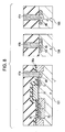
- FIGs. 5A to 5E illustrate a procedure for fabricating a photoelectric conversion device.
- a well (not shown) of a first conductivity type (n-type) and the well 39 of a second conductivity type (p-type) are formed in a semiconductor substrate 38 composed of silicon or the like.
- An element isolation region 41 is formed by shallow trench isolation (STI), selective oxidation, or the like.
- STI shallow trench isolation
- the photoelectric conversion region 101 is shown adjacent to the peripheral circuit region 102.
- the semiconductor region 33 of a photodiode constituting a photoelectric conversion element is formed by introduction of an n-type impurity. Then a p-type surface region 35 is formed by introduction of a p-type impurity in such a manner that the photodiode has a buried structure.
- n-type impurity is introduced by ion implantation with the gate electrodes as masks.
- the lightly doped semiconductor regions 3, 34, and 44 partially constituting sources and/or drains located on a surface adjacent to the gate electrode are formed in a self-aligned manner.
- a thin silicon oxide film 30b is formed on a surface of the semiconductor substrate except element isolation regions and the gate electrodes.
- the thin silicon oxide film 30b may be formed by leaving a gate oxide film on the surface of the semiconductor substrate when the polysilicon gate electrodes are formed by anisotropic dry etching.
- the thin silicon oxide film 30b may be formed by thermal oxidation or deposition before a silicon nitride film 36 is deposited.
- the silicon nitride film 36 is formed, and then a silicon oxide film 37 is formed thereon.
- the silicon nitride film 36 and the silicon oxide film 37 are formed so as to cover the photoelectric conversion region 101 and the peripheral circuit region 102, thereby protecting the photoelectric conversion region.
- a resist 50 is formed on the photoelectric conversion region.
- the silicon nitride film 36 and the silicon oxide film 37 are subjected to etch back.
- side spacers constituted by the silicon nitride films 36b and the silicon oxide films 37b are formed on side walls of the gate electrode 42 in the peripheral circuit region 102.
- an n-type impurity is introduced by ion implantation with the gate electrode and the side spacers as a mask in the peripheral circuit region 102.
- the heavily doped semiconductor regions 43 each constituting a self-aligned source or drain are formed adjacent to the side spacers.
- the silicon nitride film 36 and the silicon oxide film 37 remaining on the entire surface serve as a mask during ion implantation. In this case, the cost of manufacturing can be reduced. Thereby, the structure shown in Fig. 5D is made.
- an insulating film 40 composed of borophosphosilicate glass (BPSG) and functioning as an interlayer insulating film is formed so as to cover the entirety of the peripheral circuit region.
- Contact holes 41a and 41b are formed by anisotropic dry etching with the silicon nitride film 36a as an etch stop in the photoelectric conversion region. In this way, the contact holes in the photoelectric conversion region 101 are formed in such a manner that bottoms of the contact holes are in contact with the semiconductor substrate in a self-aligned manner. Then the contact holes 41a and 41b are filled with a conductor to form electrodes. Thereby, the structure shown in Fig. 5E is made.
- BPSG borophosphosilicate glass
- heat treatment can be performed at 350°C or higher.
- n-type MOS transistors have been described above.
- p-type MOS transistors may be similarly formed if the conductivity type is changed.
- the sources and the drains of the MOS transistors located in the photoelectric conversion region each have the single-drain structure including the lightly doped semiconductor region.
- the MOS transistor located in the peripheral circuit region has the LDD structure.
- the lightly doped semiconductor region located in the photoelectric conversion region may be simultaneously formed in the step of forming the lightly doped region of the MOS transistor having the LDD structure in the peripheral circuit region.
- the photoelectric conversion device produced by the process can suppress the degradation of properties of the MOS transistor located in the photoelectric conversion region caused by hot carriers and can achieve the high driving ability of the MOS transistor located in the peripheral circuit region.
- Each of the contact holes is in contact with only the surface of the semiconductor substrate when the anti-reflection film is used as an etch stop. Thus, the leakage current between the well and the source and drain of the MOS transistor can be suppressed.
- the insulating film is used as the etch stop for the anti-reflection film and the contact holes in the photoelectric conversion region and is used as the sidewall spacers of the MOS transistor in the peripheral circuit region. In this case, the cost of manufacturing can be reduced.
- the insulating film is formed of a silicon nitride film containing a large number of hydrogen molecules, the number of traps at the transistor interface and the interface between silicon and the silicon oxide film on the photodiode can be more effectively reduced.
- an amplifying MOS transistor will be described as a MOS transistor located in the photoelectric conversion region. This structure may be combined with the structure of the reset MOS transistor described in each of the first and second embodiments.
- Fig. 6 shows a cross-sectional structure in a photoelectric conversion region and a peripheral circuit region of a photoelectric conversion device. Elements equivalent to those in the first and second embodiments are designated using the same reference numerals, and redundant description is not repeated.
- An optical anti-reflection film 66 is disposed on a photoelectric conversion element and reduces the interfacial reflection on the surface of a photodiode.
- the anti-reflection film 66 may have a stacked structure including a silicon nitride layer and a silicon oxide layer.
- the floating diffusion region 3 that receives a charge from the photoelectric conversion element includes a lightly doped semiconductor region 301 and a heavily doped semiconductor region 302 for connection to a conductor.
- the floating diffusion region 3 and the source and drain of the MOS transistor 5 are each constituted by the lightly doped semiconductor region 301 of a first conductivity type and the heavily doped semiconductor region 302 of the first conductivity type, the heavily doped semiconductor region 302 being in direct contact with the conductor.
- Side spacers 68 in the peripheral circuit region are each formed of the same film as the anti-reflection film 66.
- Lightly doped semiconductor regions of the first conductivity type are formed in a self-aligned manner with a gate electrode and are also located under the side spacers 68.
- the heavily doped semiconductor regions 43 of the first conductivity type are formed in a self-aligned manner with the side spacers 68 and thus are not formed under the side spacers 68 or the anti-reflection film 66.
- the anti-reflection film 66 is not subjected to etching in the photoelectric conversion region, thus reducing noise caused by damage from etching. Furthermore, after the formation of the anti-reflection film 66, no step of exposing the semiconductor surface is performed, thus preventing contamination with a metal element or the like. As a result, the rate of occurrence of a point defect in dark conditions can be reduced.
- the electric-field-relaxation layer will be described in more detail below.
- An excessively low impurity concentration in the electric-field-relaxation layer or an excessively large width of the electric-field-relaxation layer of the LDD structure increases the parasitic resistance (series resistance) of the transistor, thus significantly degrading the driving ability and static characteristics.
- the electric-field-relaxation layer having a relatively small width needs to be formed.
- the electric-field-relaxation layer having a larger width can be formed.
- the MOS transistor located in the photoelectric conversion region can have an impurity concentration lower than that of the MOS transistor located in the peripheral circuit region and can have the lower-impurity-concentration region having a large width.
- the structure shown in this embodiment has the effect of reducing pixel defects and random noise caused by a leakage current flowing through the floating diffusion region 3.
- the floating diffusion region 3 is formed of the lightly doped electric-field-relaxation region (lightly doped semiconductor region 301 of the first conductivity type) and thus has a significant effect of relaxing an electric field at a region other than the gate end. That is, the floating diffusion region 3 can relax an electric field applied to a junction with a semiconductor region 104 of a second conductivity type and a junction with a channel stop region under a separating portion, thereby reducing the leakage current flowing through the floating diffusion region 3 and random noise during readout.
- the occurrence of a pixel causing the sudden occurrence of a large leakage current flowing through the floating diffusion region 3 correlates with an electric field applied to the floating diffusion region 3. Therefore, point defects can also be reduced according to this embodiment.
- the MOS transistor located in the peripheral circuit region having the same conductivity type as the MOS transistor located in the photoelectric conversion region has been described.
- CMOS transistor may be used in the peripheral circuit region.
- a MOS transistor having a conductivity type opposite the conductivity type of the MOS transistor located in the photoelectric conversion region may have the same structure.
- the structure according to this embodiment has profound effects on an n-type MOS transistor which easily generates hot carriers.
- an n-type MOS transistor is located in the photoelectric conversion region, and when the n-type MOS transistor located in the photoelectric conversion region and the n-type MOS transistor located in the peripheral circuit region each have the structure according to this embodiment, particularly significant effects can be obtained.
- the structure according to this embodiment is effective from the viewpoint of the processability of such a minute pixel.
- the anti-reflection film 66 is used.
- the effects, such as electric-field relaxation and the reduction of point defects, of this embodiment can be exerted.
- Fig. 7 shows a cross-sectional structure of a photoelectric conversion device according to this embodiment. Elements equivalent to those in the first to third embodiments are designated using the same reference numerals, and redundant description is not repeated.
- the heavily doped semiconductor region 43 of a first conductivity type is not located in the photoelectric conversion region.
- a mask pattern for forming the heavily doped semiconductor region 43 of the first conductivity type is formed in such a manner that the photoelectric conversion region is covered with a resist. The use of the mask pattern produces the structure shown in Fig. 7 .
- a lightly doped electric-field-relaxation layer (lightly doped semiconductor region 301 of a first conductivity type) having a lower impurity concentration or having a larger width can be designed, thereby improving the effect of relaxing an electric field. This can suppress the generation of hot carriers, thus improving reliability and withstanding voltage.
- the electric-field-relaxation layer having a relatively small width can be formed.
- a region of a drain which is in direct contact with a conductor will be described.
- conductors such as contact plugs that electrically connect leads with sources and drains of MOS transistors need to have low resistance and ohmic characteristics.
- a process of forming a silicide or a self-aligned silicide (salicide) is intentionally not applied, in some cases.
- methods for forming ohmic contact between drains and conductors are important for photoelectric conversion devices in particular.
- Fig. 8 shows a cross-sectional view of a photoelectric conversion device according to this embodiment. Elements equivalent to those in the first to fourth embodiments are designated using the same reference numerals, and redundant description is not repeated.
- Reference numeral 101 represents a portion where a MOS transistor (n-type) located in a photoelectric conversion region is connected to a conductor.
- Reference numeral 104 represents a portion where the source or drain of an n-type MOS transistor located in a peripheral circuit region is connected to a conductor.
- Reference numeral 105 represents a portion where the source or drain of a p-type MOS transistor located in the peripheral circuit region is connected to a conductor.
- the floating diffusion region 3 includes an n-type heavily doped semiconductor region 45 that is in direct contact with the conductor. Also in the portion 104, the source or drain includes an n-type heavily doped semiconductor region 45. In the portion 105, the source or drain includes a p-type heavily doped semiconductor region 46.
- the photoelectric conversion device is formed by the same procedure as in the second embodiment until the structure shown in Fig. 5D is formed.
- An impurity concentration d1 in the lightly doped semiconductor region may be set in the range of about 1E17/cm 3 to 5E18/cm 3 .
- contact holes each corresponding to the source or the drain to be connected to a conductor are formed by anisotropic dry etching.
- an n-type impurity, such as PH 3 is introduced using a photomask into the bottom of the contact hole communicating with the floating diffusion region 3 located in the photoelectric conversion region and the bottom of the hole communicating with the semiconductor region 43 located in the peripheral circuit region 104.
- the dose can be set in such a manner that an impurity concentration d2 in the region in direct contact with the conductor is in the range of 5E18/cm 3 to 5E19/cm 3 .
- the n-type impurity may be introduced into the entire surface without the photomask.
- a p-type impurity such as B is introduced using a photomask into the bottom of the contact hole communicating with the p-type heavily doped semiconductor region in the peripheral circuit region 105, thereby forming a heavily doped semiconductor region.
- the p-type semiconductor region may be formed by ion implantation with the above-described n-type impurity.
- conditions for implanting the p-type impurity ions need to be set in such a manner that the resulting semiconductor region covers the entirety of the n-type heavily doped semiconductor region located in the peripheral circuit region 104.
- the dose can also be set in such a manner that an impurity concentration d3 in the region in direct contact with the conductor is in the range of 5E18/cm 3 to 5E19/cm 3 .
- the procedure according to this embodiment may be applied to the first to fourth embodiments.
- the procedure may be applied to various MOS transistors located in the photoelectric conversion region.
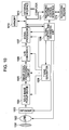
- Fig. 10 shows an exemplary block diagram when a photoelectric conversion device of the present invention is applied to a camera.
- a shutter 1001 is disposed before an imaging lens 1002 and controls exposure.
- An aperture 1003 controls the amount of light according to need, and then light is focused on a photoelectric conversion device 1004.
- a signal supplied from the photoelectric conversion device 1004 is processed by a signal-processing circuit 1005.
- An A/D converter 1006 converts the resulting analog signal to a digital signal.
- the output digital signal is subjected to arithmetic processing by a signal processor 1007.
- the processed digital signal is stored in a memory 1010 or is transmitted to an external apparatus through an external interface 1013.
- the photoelectric conversion device 1004, the image signal-processing circuit 1005, the A/D converter 1006, and the signal processor 1007 are controlled by a timing generator.
- the entire system is controlled by a global control and arithmetic unit 1009.
- the output digital signal is recorded through a recording-medium control interface 1011 that is controlled by the global control and arithmetic unit.
- a photoelectric conversion device includes a photoelectric conversion region (101) having a plurality of photoelectric conversion elements (1) and a first MOS transistor for reading a signal in response to an electric charge of each photoelectric conversion element (1); and a peripheral circuit region (102) having a second MOS transistor for driving the first MOS transistor and/or amplifying the signal read from the photoelectric conversion region (101), the photoelectric conversion region (101) and the peripheral circuit region (102) being located on the same semiconductor substrate, wherein an impurity concentration in a drain of the first MOS transistor is lower than an impurity concentration in a drain of the second MOS transistor.
Landscapes
- Solid State Image Pick-Up Elements (AREA)
- Transforming Light Signals Into Electric Signals (AREA)
- Light Receiving Elements (AREA)
Priority Applications (1)
| Application Number | Priority Date | Filing Date | Title |
|---|---|---|---|
| EP11195884.9A EP2437301B1 (en) | 2006-08-02 | 2007-07-02 | Photoelectric conversion device and a method for producing photoelectric conversion device |
Applications Claiming Priority (1)
| Application Number | Priority Date | Filing Date | Title |
|---|---|---|---|
| JP2006210531A JP5110820B2 (ja) | 2006-08-02 | 2006-08-02 | 光電変換装置、光電変換装置の製造方法及び撮像システム |
Related Child Applications (1)
| Application Number | Title | Priority Date | Filing Date |
|---|---|---|---|
| EP11195884.9 Division-Into | 2011-12-28 |
Publications (2)
| Publication Number | Publication Date |
|---|---|
| EP1884997A1 EP1884997A1 (en) | 2008-02-06 |
| EP1884997B1 true EP1884997B1 (en) | 2012-02-15 |
Family
ID=38473905
Family Applications (2)
| Application Number | Title | Priority Date | Filing Date |
|---|---|---|---|
| EP11195884.9A Not-in-force EP2437301B1 (en) | 2006-08-02 | 2007-07-02 | Photoelectric conversion device and a method for producing photoelectric conversion device |
| EP07111532A Not-in-force EP1884997B1 (en) | 2006-08-02 | 2007-07-02 | Photoelectric conversion device and image pickup system |
Family Applications Before (1)
| Application Number | Title | Priority Date | Filing Date |
|---|---|---|---|
| EP11195884.9A Not-in-force EP2437301B1 (en) | 2006-08-02 | 2007-07-02 | Photoelectric conversion device and a method for producing photoelectric conversion device |
Country Status (5)
| Country | Link |
|---|---|
| US (4) | US7920192B2 (enExample) |
| EP (2) | EP2437301B1 (enExample) |
| JP (1) | JP5110820B2 (enExample) |
| CN (2) | CN101609813B (enExample) |
| AT (1) | ATE545956T1 (enExample) |
Families Citing this family (110)
| Publication number | Priority date | Publication date | Assignee | Title |
|---|---|---|---|---|
| JPH11274454A (ja) | 1998-03-19 | 1999-10-08 | Canon Inc | 固体撮像装置及びその形成方法 |
| US8013409B2 (en) | 2005-09-27 | 2011-09-06 | Canon Kabushiki Kaisha | Photoelectric conversion device and fabrication method therefor |
| EP1788797B1 (en) * | 2005-11-18 | 2013-06-26 | Canon Kabushiki Kaisha | Solid-state image pickup device |
| JP4818018B2 (ja) * | 2006-08-01 | 2011-11-16 | キヤノン株式会社 | 光電変換装置及びそれを用いた撮像システム |
| JP5132102B2 (ja) * | 2006-08-01 | 2013-01-30 | キヤノン株式会社 | 光電変換装置および光電変換装置を用いた撮像システム |
| JP4185949B2 (ja) * | 2006-08-08 | 2008-11-26 | キヤノン株式会社 | 光電変換装置及び撮像装置 |
| JP4194633B2 (ja) * | 2006-08-08 | 2008-12-10 | キヤノン株式会社 | 撮像装置及び撮像システム |
| JP5110831B2 (ja) * | 2006-08-31 | 2012-12-26 | キヤノン株式会社 | 光電変換装置及び撮像システム |
| JP5159120B2 (ja) * | 2007-02-23 | 2013-03-06 | キヤノン株式会社 | 光電変換装置およびその製造方法 |
| JP4350768B2 (ja) | 2007-04-16 | 2009-10-21 | キヤノン株式会社 | 光電変換装置及び撮像装置 |
| JP2009021809A (ja) * | 2007-07-11 | 2009-01-29 | Canon Inc | 撮像装置の駆動方法、撮像装置、及び撮像システム |
| JP5305623B2 (ja) * | 2007-07-20 | 2013-10-02 | キヤノン株式会社 | 光電変換装置及び光電変換装置を用いた撮像システム |
| JP2009135349A (ja) * | 2007-12-03 | 2009-06-18 | Panasonic Corp | Mos型固体撮像装置およびその製造方法 |
| JP5366396B2 (ja) * | 2007-12-28 | 2013-12-11 | キヤノン株式会社 | 光電変換装置の製造方法、半導体装置の製造方法、光電変換装置、及び撮像システム |
| JP4685120B2 (ja) * | 2008-02-13 | 2011-05-18 | キヤノン株式会社 | 光電変換装置及び撮像システム |
| JP5153378B2 (ja) | 2008-02-15 | 2013-02-27 | キヤノン株式会社 | 固体撮像装置及びその駆動方法 |
| JP5111157B2 (ja) | 2008-02-27 | 2012-12-26 | キヤノン株式会社 | 光電変換装置及び光電変換装置を用いた撮像システム |
| JP5371463B2 (ja) | 2008-02-28 | 2013-12-18 | キヤノン株式会社 | 撮像装置、撮像システム、および、撮像装置の制御方法 |
| JP5314914B2 (ja) * | 2008-04-04 | 2013-10-16 | キヤノン株式会社 | 光電変換装置、撮像システム、設計方法、及び光電変換装置の製造方法 |
| JP5335271B2 (ja) * | 2008-04-09 | 2013-11-06 | キヤノン株式会社 | 光電変換装置及びそれを用いた撮像システム |
| JP5188275B2 (ja) | 2008-06-06 | 2013-04-24 | キヤノン株式会社 | 固体撮像装置、その駆動方法及び撮像システム |
| US8129764B2 (en) * | 2008-06-11 | 2012-03-06 | Aptina Imaging Corporation | Imager devices having differing gate stack sidewall spacers, method for forming such imager devices, and systems including such imager devices |
| JP5446281B2 (ja) * | 2008-08-01 | 2014-03-19 | ソニー株式会社 | 固体撮像装置、その製造方法および撮像装置 |
| US9041841B2 (en) | 2008-10-10 | 2015-05-26 | Taiwan Semiconductor Manufacturing Company, Ltd. | Image sensor having enhanced backside illumination quantum efficiency |
| JP5241454B2 (ja) * | 2008-12-01 | 2013-07-17 | キヤノン株式会社 | 固体撮像装置及びそれを用いた撮像システム |
| JP2010161236A (ja) | 2009-01-08 | 2010-07-22 | Canon Inc | 光電変換装置の製造方法 |
| JP5406537B2 (ja) * | 2009-01-13 | 2014-02-05 | キヤノン株式会社 | 光電変換装置、撮像システム、及び光電変換装置の製造方法 |
| JP2010177391A (ja) * | 2009-01-29 | 2010-08-12 | Sony Corp | 固体撮像装置、電子機器、固体撮像装置の製造方法 |
| JP2010206174A (ja) | 2009-02-06 | 2010-09-16 | Canon Inc | 光電変換装置およびその製造方法ならびにカメラ |
| JP2010206172A (ja) | 2009-02-06 | 2010-09-16 | Canon Inc | 撮像装置およびカメラ |
| JP2010206178A (ja) | 2009-02-06 | 2010-09-16 | Canon Inc | 光電変換装置、及び光電変換装置の製造方法 |
| JP2010206181A (ja) * | 2009-02-06 | 2010-09-16 | Canon Inc | 光電変換装置及び撮像システム |
| JP5538922B2 (ja) * | 2009-02-06 | 2014-07-02 | キヤノン株式会社 | 固体撮像装置の製造方法 |
| JP2010206173A (ja) * | 2009-02-06 | 2010-09-16 | Canon Inc | 光電変換装置およびカメラ |
| JP2010199154A (ja) * | 2009-02-23 | 2010-09-09 | Canon Inc | 固体撮像素子 |
| JP2010212365A (ja) * | 2009-03-09 | 2010-09-24 | Sony Corp | 固体撮像装置、および、その製造方法、電子機器 |
| JP2011004390A (ja) | 2009-05-18 | 2011-01-06 | Canon Inc | 撮像装置、撮像システム、及び撮像装置の駆動方法 |
| JP5500876B2 (ja) * | 2009-06-08 | 2014-05-21 | キヤノン株式会社 | 光電変換装置の製造方法 |
| JP5517503B2 (ja) | 2009-06-24 | 2014-06-11 | キヤノン株式会社 | 固体撮像装置 |
| JP5558916B2 (ja) | 2009-06-26 | 2014-07-23 | キヤノン株式会社 | 光電変換装置の製造方法 |
| JP5563257B2 (ja) * | 2009-08-28 | 2014-07-30 | キヤノン株式会社 | 光電変換装置、撮像システム、及び光電変換装置の製造方法 |
| JP5564874B2 (ja) * | 2009-09-25 | 2014-08-06 | ソニー株式会社 | 固体撮像装置、及び電子機器 |
| JP2011155168A (ja) * | 2010-01-28 | 2011-08-11 | Sony Corp | 半導体素子及びその製造方法、並びに固体撮像装置 |
| JP2011238652A (ja) * | 2010-05-06 | 2011-11-24 | Renesas Electronics Corp | 半導体装置およびその製造方法 |
| JP5717357B2 (ja) * | 2010-05-18 | 2015-05-13 | キヤノン株式会社 | 光電変換装置およびカメラ |
| JP5704848B2 (ja) * | 2010-06-30 | 2015-04-22 | キヤノン株式会社 | 固体撮像装置およびカメラ |
| JP5960961B2 (ja) | 2010-11-16 | 2016-08-02 | キヤノン株式会社 | 固体撮像素子及び撮像システム |
| JP5885721B2 (ja) * | 2011-02-09 | 2016-03-15 | キヤノン株式会社 | 固体撮像装置の製造方法 |
| JP2012182426A (ja) | 2011-02-09 | 2012-09-20 | Canon Inc | 固体撮像装置、固体撮像装置を用いた撮像システム及び固体撮像装置の製造方法 |
| JP5812692B2 (ja) * | 2011-05-27 | 2015-11-17 | キヤノン株式会社 | 固体撮像装置の製造方法 |
| JP5762199B2 (ja) | 2011-07-28 | 2015-08-12 | キヤノン株式会社 | 固体撮像装置 |
| JP5901186B2 (ja) | 2011-09-05 | 2016-04-06 | キヤノン株式会社 | 固体撮像装置及びその駆動方法 |
| JP5858695B2 (ja) | 2011-09-08 | 2016-02-10 | キヤノン株式会社 | 固体撮像装置及び固体撮像装置の駆動方法 |
| JP5801665B2 (ja) | 2011-09-15 | 2015-10-28 | キヤノン株式会社 | 固体撮像装置、a/d変換器およびその制御方法 |
| JP5806566B2 (ja) | 2011-09-15 | 2015-11-10 | キヤノン株式会社 | A/d変換器および固体撮像装置 |
| JP5864990B2 (ja) | 2011-10-03 | 2016-02-17 | キヤノン株式会社 | 固体撮像装置およびカメラ |
| JP2013093553A (ja) | 2011-10-04 | 2013-05-16 | Canon Inc | 光電変換装置及びその製造方法、並びに光電変換システム |
| JP5484422B2 (ja) | 2011-10-07 | 2014-05-07 | キヤノン株式会社 | 固体撮像装置 |
| JP5930651B2 (ja) | 2011-10-07 | 2016-06-08 | キヤノン株式会社 | 固体撮像装置 |
| JP5930650B2 (ja) | 2011-10-07 | 2016-06-08 | キヤノン株式会社 | 半導体装置の製造方法 |
| JP5901212B2 (ja) | 2011-10-07 | 2016-04-06 | キヤノン株式会社 | 光電変換システム |
| WO2014002362A1 (ja) * | 2012-06-26 | 2014-01-03 | パナソニック株式会社 | 固体撮像装置及びその製造方法 |
| JP6167406B2 (ja) * | 2012-06-28 | 2017-07-26 | パナソニックIpマネジメント株式会社 | 固体撮像装置及びその製造方法 |
| JP2014086515A (ja) * | 2012-10-22 | 2014-05-12 | Canon Inc | 撮像装置、その製造方法及びカメラ |
| US9659991B2 (en) | 2012-10-22 | 2017-05-23 | Canon Kabushiki Kaisha | Image capturing apparatus, manufacturing method thereof, and camera |
| JP6122649B2 (ja) * | 2013-02-13 | 2017-04-26 | セイコーNpc株式会社 | 浅い接合を有する紫外線受光素子 |
| JP2014199898A (ja) * | 2013-03-11 | 2014-10-23 | ソニー株式会社 | 固体撮像素子および製造方法、並びに、電子機器 |
| CN105378927B (zh) * | 2013-06-14 | 2019-05-28 | 瑞萨电子株式会社 | 摄像装置的制造方法以及摄像装置 |
| JP6159184B2 (ja) * | 2013-07-25 | 2017-07-05 | キヤノン株式会社 | 光電変換装置及び撮像システム |
| JP5886806B2 (ja) | 2013-09-17 | 2016-03-16 | キヤノン株式会社 | 固体撮像装置 |
| JP6305030B2 (ja) * | 2013-11-22 | 2018-04-04 | キヤノン株式会社 | 光電変換装置の製造方法 |
| JP6282109B2 (ja) | 2013-12-26 | 2018-02-21 | キヤノン株式会社 | 撮像装置の製造方法および撮像装置 |
| US9473719B2 (en) * | 2013-12-30 | 2016-10-18 | Taiwan Semiconductor Manufacturing Company, Ltd. | Protection layer in CMOS image sensor array region |
| JP6245997B2 (ja) | 2014-01-16 | 2017-12-13 | キヤノン株式会社 | 固体撮像装置及び撮像システム |
| JP6057931B2 (ja) | 2014-02-10 | 2017-01-11 | キヤノン株式会社 | 光電変換装置及びそれを用いた撮像システム |
| JP6274567B2 (ja) | 2014-03-14 | 2018-02-07 | キヤノン株式会社 | 固体撮像装置及び撮像システム |
| US9608033B2 (en) * | 2014-05-12 | 2017-03-28 | Canon Kabushiki Kaisha | Solid-state image sensor, method of manufacturing the same, and camera |
| JP6529221B2 (ja) * | 2014-05-14 | 2019-06-12 | キヤノン株式会社 | 光電変換装置及びその製造方法 |
| JP6325904B2 (ja) | 2014-06-02 | 2018-05-16 | キヤノン株式会社 | 固体撮像装置の製造方法、固体撮像装置、および、カメラ |
| JP2016001709A (ja) | 2014-06-12 | 2016-01-07 | キヤノン株式会社 | 固体撮像装置の製造方法 |
| JP6362093B2 (ja) | 2014-06-13 | 2018-07-25 | キヤノン株式会社 | 固体撮像装置の製造方法及び固体撮像装置 |
| CN104134676A (zh) * | 2014-07-23 | 2014-11-05 | 中国航天科技集团公司第九研究院第七七一研究所 | 基于辐射环境应用的快速电荷转移像素结构 |
| JP2016046420A (ja) * | 2014-08-25 | 2016-04-04 | ルネサスエレクトロニクス株式会社 | 半導体装置およびその製造方法 |
| JP2016082306A (ja) | 2014-10-10 | 2016-05-16 | キヤノン株式会社 | 撮像装置、撮像システム及び撮像装置の駆動方法 |
| JP6700655B2 (ja) * | 2014-10-30 | 2020-05-27 | キヤノン株式会社 | 光電変換装置および光電変換装置の製造方法 |
| JP6039773B2 (ja) * | 2015-09-17 | 2016-12-07 | キヤノン株式会社 | 固体撮像装置の製造方法 |
| JP2017120973A (ja) * | 2015-12-28 | 2017-07-06 | ルネサスエレクトロニクス株式会社 | 撮像素子 |
| EP3425900B1 (en) * | 2016-02-29 | 2023-08-30 | Sony Group Corporation | Solid-state imaging element |
| CN107845649A (zh) * | 2016-09-20 | 2018-03-27 | 松下知识产权经营株式会社 | 摄像装置及其制造方法 |
| JP6436953B2 (ja) | 2016-09-30 | 2018-12-12 | キヤノン株式会社 | 固体撮像装置及びその駆動方法、並びに撮像システム |
| US10306191B2 (en) * | 2016-11-29 | 2019-05-28 | Cista System Corp. | System and method for high dynamic range image sensing |
| KR102574236B1 (ko) * | 2016-12-07 | 2023-09-05 | 에스케이하이닉스 주식회사 | 서로 다른 사이즈의 포토다이오드들을 갖는 이미지 센서 |
| JP6552478B2 (ja) | 2016-12-28 | 2019-07-31 | キヤノン株式会社 | 固体撮像装置 |
| US10652531B2 (en) | 2017-01-25 | 2020-05-12 | Canon Kabushiki Kaisha | Solid-state imaging device, imaging system, and movable object |
| JP2017130693A (ja) * | 2017-04-13 | 2017-07-27 | ルネサスエレクトロニクス株式会社 | 撮像装置およびその製造方法 |
| JP7084700B2 (ja) | 2017-06-16 | 2022-06-15 | キヤノン株式会社 | 光電変換装置およびスキャナ |
| JP6598830B2 (ja) | 2017-08-31 | 2019-10-30 | キヤノン株式会社 | 光電変換装置の製造方法 |
| JP6704893B2 (ja) | 2017-11-30 | 2020-06-03 | キヤノン株式会社 | 固体撮像装置、撮像システム、および固体撮像装置の駆動方法 |
| JP7361452B2 (ja) * | 2018-02-19 | 2023-10-16 | キヤノン株式会社 | 撮像装置およびカメラ |
| JP7154795B2 (ja) | 2018-03-29 | 2022-10-18 | キヤノン株式会社 | 撮像装置、撮像システム、および移動体 |
| CN110880520B (zh) * | 2018-09-06 | 2024-11-29 | 松下知识产权经营株式会社 | 摄像装置 |
| JP7117974B2 (ja) * | 2018-10-30 | 2022-08-15 | キヤノン株式会社 | 表示装置および電子機器 |
| JP7292860B2 (ja) | 2018-11-22 | 2023-06-19 | キヤノン株式会社 | 光電変換装置 |
| US11425365B2 (en) | 2018-12-14 | 2022-08-23 | Canon Kabushiki Kaisha | Photoelectric conversion device, method of manufacturing photoelectric conversion device, and method of manufacturing semiconductor device |
| TWI692861B (zh) | 2019-03-14 | 2020-05-01 | 晶相光電股份有限公司 | 影像感測器及其製造方法 |
| JP7303682B2 (ja) | 2019-07-19 | 2023-07-05 | キヤノン株式会社 | 光電変換装置及び撮像システム |
| JP7374639B2 (ja) | 2019-07-19 | 2023-11-07 | キヤノン株式会社 | 光電変換装置及び撮像システム |
| CN113130516A (zh) * | 2020-01-15 | 2021-07-16 | 联华电子股份有限公司 | 半导体影像感测元件及其制作方法 |
| JP7504623B2 (ja) | 2020-02-28 | 2024-06-24 | キヤノン株式会社 | 撮像装置および撮像システム |
| CN116093121A (zh) * | 2021-11-08 | 2023-05-09 | 联华电子股份有限公司 | N沟道金属氧化物半导体结构及其制作方法 |
Family Cites Families (64)
| Publication number | Priority date | Publication date | Assignee | Title |
|---|---|---|---|---|
| US5880036A (en) * | 1992-06-15 | 1999-03-09 | Micron Technology, Inc. | Method for enhancing oxide to nitride selectivity through the use of independent heat control |
| JP3246046B2 (ja) | 1993-03-23 | 2002-01-15 | ソニー株式会社 | 高融点金属膜の堆積方法 |
| JP3239911B2 (ja) * | 1993-06-18 | 2001-12-17 | ソニー株式会社 | 固体撮像素子の製造方法 |
| JPH07202160A (ja) | 1993-12-27 | 1995-08-04 | Sony Corp | 固体撮像装置及びその製造方法、並びに半導体装置 |
| JP2959504B2 (ja) * | 1997-01-10 | 1999-10-06 | 日本電気株式会社 | 固体撮像装置の製造方法 |
| US6169317B1 (en) | 1998-02-13 | 2001-01-02 | Canon Kabushiki Kaisha | Photoelectric conversion device and image sensor |
| US6169318B1 (en) * | 1998-02-23 | 2001-01-02 | Polaroid Corporation | CMOS imager with improved sensitivity |
| JP3523057B2 (ja) | 1998-03-31 | 2004-04-26 | 株式会社東芝 | 固体撮像装置 |
| JP3103064B2 (ja) | 1998-04-23 | 2000-10-23 | 松下電子工業株式会社 | 固体撮像装置およびその製造方法 |
| US6144071A (en) * | 1998-09-03 | 2000-11-07 | Advanced Micro Devices, Inc. | Ultrathin silicon nitride containing sidewall spacers for improved transistor performance |
| US6218719B1 (en) | 1998-09-18 | 2001-04-17 | Capella Microsystems, Inc. | Photodetector and device employing the photodetector for converting an optical signal into an electrical signal |
| US6180532B1 (en) * | 1998-12-15 | 2001-01-30 | United Microelectronics Corp. | Method for forming a borderless contact hole |
| US6713234B2 (en) | 1999-02-18 | 2004-03-30 | Micron Technology, Inc. | Fabrication of semiconductor devices using anti-reflective coatings |
| JP3624140B2 (ja) * | 1999-08-05 | 2005-03-02 | キヤノン株式会社 | 光電変換装置およびその製造方法、デジタルスチルカメラ又はデジタルビデオカメラ |
| JP3782297B2 (ja) * | 2000-03-28 | 2006-06-07 | 株式会社東芝 | 固体撮像装置及びその製造方法 |
| JP4398917B2 (ja) | 2000-03-28 | 2010-01-13 | 株式会社東芝 | 固体撮像装置及びその製造方法 |
| US6630721B1 (en) * | 2000-05-16 | 2003-10-07 | Advanced Micro Devices, Inc. | Polysilicon sidewall with silicide formation to produce high performance MOSFETS |
| US6611037B1 (en) * | 2000-08-28 | 2003-08-26 | Micron Technology, Inc. | Multi-trench region for accumulation of photo-generated charge in a CMOS imager |
| JP2003031787A (ja) | 2001-07-17 | 2003-01-31 | Canon Inc | 固体撮像素子及びその駆動方法 |
| US6973265B2 (en) | 2001-09-27 | 2005-12-06 | Canon Kabushiki Kaisha | Solid state image pick-up device and image pick-up apparatus using such device |
| DE10150040A1 (de) | 2001-10-10 | 2003-04-17 | Merck Patent Gmbh | Kombinierte Ätz- und Dotiermedien |
| JP4115152B2 (ja) * | 2002-04-08 | 2008-07-09 | キヤノン株式会社 | 撮像装置 |
| JP4541666B2 (ja) * | 2002-06-20 | 2010-09-08 | 三星電子株式会社 | イメージセンサ及びその製造方法 |
| US7405757B2 (en) * | 2002-07-23 | 2008-07-29 | Fujitsu Limited | Image sensor and image sensor module |
| JP3795846B2 (ja) * | 2002-08-29 | 2006-07-12 | 富士通株式会社 | 半導体装置 |
| JP2004095895A (ja) | 2002-08-30 | 2004-03-25 | Sony Corp | 固体撮像素子の製造方法 |
| KR100508086B1 (ko) * | 2002-09-11 | 2005-08-17 | 삼성전자주식회사 | 씨모스 이미지 센서 및 그 제조방법 |
| JP3988189B2 (ja) | 2002-11-20 | 2007-10-10 | ソニー株式会社 | 固体撮像装置 |
| US6974715B2 (en) * | 2002-12-27 | 2005-12-13 | Hynix Semiconductor Inc. | Method for manufacturing CMOS image sensor using spacer etching barrier film |
| JP3840214B2 (ja) | 2003-01-06 | 2006-11-01 | キヤノン株式会社 | 光電変換装置及び光電変換装置の製造方法及び同光電変換装置を用いたカメラ |
| JP2004228425A (ja) | 2003-01-24 | 2004-08-12 | Renesas Technology Corp | Cmosイメージセンサの製造方法 |
| KR100587635B1 (ko) * | 2003-06-10 | 2006-06-07 | 주식회사 하이닉스반도체 | 반도체소자의 제조 방법 |
| US7250647B2 (en) * | 2003-07-03 | 2007-07-31 | Micron Technology, Inc. | Asymmetrical transistor for imager device |
| US7060554B2 (en) * | 2003-07-11 | 2006-06-13 | Advanced Micro Devices, Inc. | PECVD silicon-rich oxide layer for reduced UV charging |
| US7496776B2 (en) * | 2003-08-21 | 2009-02-24 | International Business Machines Corporation | Power throttling method and apparatus |
| US6908839B2 (en) * | 2003-09-17 | 2005-06-21 | Micron Technology, Inc. | Method of producing an imaging device |
| JP4578792B2 (ja) * | 2003-09-26 | 2010-11-10 | 富士通セミコンダクター株式会社 | 固体撮像装置 |
| JP3729826B2 (ja) * | 2004-01-09 | 2005-12-21 | 松下電器産業株式会社 | 固体撮像装置の製造方法 |
| JP4230406B2 (ja) * | 2004-04-27 | 2009-02-25 | 富士通マイクロエレクトロニクス株式会社 | 固体撮像装置 |
| KR100672713B1 (ko) * | 2004-06-09 | 2007-01-22 | 동부일렉트로닉스 주식회사 | 씨모스 이미지 센서의 제조방법 |
| KR100606934B1 (ko) * | 2004-07-05 | 2006-08-01 | 동부일렉트로닉스 주식회사 | 씨모스 이미지 센서의 제조 방법 |
| JP4530747B2 (ja) | 2004-07-16 | 2010-08-25 | 富士通セミコンダクター株式会社 | 固体撮像装置及びその製造方法 |
| JP4916101B2 (ja) | 2004-09-01 | 2012-04-11 | キヤノン株式会社 | 光電変換装置、固体撮像装置及び固体撮像システム |
| JP2006073736A (ja) | 2004-09-01 | 2006-03-16 | Canon Inc | 光電変換装置、固体撮像装置及び固体撮像システム |
| JP2006073885A (ja) | 2004-09-03 | 2006-03-16 | Canon Inc | 固体撮像装置、その製造方法、およびデジタルカメラ |
| JP4459099B2 (ja) | 2005-03-18 | 2010-04-28 | キヤノン株式会社 | 固体撮像装置及びカメラ |
| JP4794877B2 (ja) | 2005-03-18 | 2011-10-19 | キヤノン株式会社 | 固体撮像装置及びカメラ |
| JP4459098B2 (ja) | 2005-03-18 | 2010-04-28 | キヤノン株式会社 | 固体撮像装置及びカメラ |
| JP4695902B2 (ja) | 2005-03-18 | 2011-06-08 | キヤノン株式会社 | 固体撮像装置の製造方法 |
| JP4677258B2 (ja) | 2005-03-18 | 2011-04-27 | キヤノン株式会社 | 固体撮像装置及びカメラ |
| JP4804027B2 (ja) | 2005-04-21 | 2011-10-26 | キヤノン株式会社 | 焦点検出用固体撮像装置 |
| JP2006319158A (ja) * | 2005-05-13 | 2006-11-24 | Seiko Epson Corp | 固体撮像装置 |
| KR100653716B1 (ko) * | 2005-07-19 | 2006-12-05 | 삼성전자주식회사 | 이미지 센서 및 그 제조 방법 |
| US7633106B2 (en) * | 2005-11-09 | 2009-12-15 | International Business Machines Corporation | Light shield for CMOS imager |
| US20070108546A1 (en) | 2005-11-15 | 2007-05-17 | Canon Kabushiki Kaisha | Photoelectric converter and imaging system including the same |
| EP1788797B1 (en) | 2005-11-18 | 2013-06-26 | Canon Kabushiki Kaisha | Solid-state image pickup device |
| JP5132102B2 (ja) | 2006-08-01 | 2013-01-30 | キヤノン株式会社 | 光電変換装置および光電変換装置を用いた撮像システム |
| JP4956084B2 (ja) | 2006-08-01 | 2012-06-20 | キヤノン株式会社 | 光電変換装置及びそれを用いた撮像システム |
| JP4818018B2 (ja) | 2006-08-01 | 2011-11-16 | キヤノン株式会社 | 光電変換装置及びそれを用いた撮像システム |
| JP4194633B2 (ja) | 2006-08-08 | 2008-12-10 | キヤノン株式会社 | 撮像装置及び撮像システム |
| JP4315457B2 (ja) | 2006-08-31 | 2009-08-19 | キヤノン株式会社 | 光電変換装置及び撮像システム |
| JP5305622B2 (ja) | 2006-08-31 | 2013-10-02 | キヤノン株式会社 | 光電変換装置の製造方法 |
| JP5110831B2 (ja) | 2006-08-31 | 2012-12-26 | キヤノン株式会社 | 光電変換装置及び撮像システム |
| JP4979375B2 (ja) | 2006-12-28 | 2012-07-18 | キヤノン株式会社 | 固体撮像装置及び撮像システム |
-
2006
- 2006-08-02 JP JP2006210531A patent/JP5110820B2/ja not_active Expired - Fee Related
-
2007
- 2007-07-02 AT AT07111532T patent/ATE545956T1/de active
- 2007-07-02 EP EP11195884.9A patent/EP2437301B1/en not_active Not-in-force
- 2007-07-02 EP EP07111532A patent/EP1884997B1/en not_active Not-in-force
- 2007-07-06 US US11/774,270 patent/US7920192B2/en active Active
- 2007-08-02 CN CN2009101518731A patent/CN101609813B/zh not_active Expired - Fee Related
- 2007-08-02 CN CN2007101437523A patent/CN101118919B/zh not_active Expired - Fee Related
-
2010
- 2010-09-14 US US12/881,582 patent/US20110003426A1/en not_active Abandoned
-
2011
- 2011-03-04 US US13/040,607 patent/US8411187B2/en not_active Expired - Fee Related
-
2015
- 2015-07-22 US US14/805,561 patent/US9825077B2/en active Active
Also Published As
| Publication number | Publication date |
|---|---|
| CN101609813B (zh) | 2012-01-04 |
| CN101118919B (zh) | 2010-06-02 |
| EP2437301A1 (en) | 2012-04-04 |
| CN101118919A (zh) | 2008-02-06 |
| US7920192B2 (en) | 2011-04-05 |
| US20110003426A1 (en) | 2011-01-06 |
| EP2437301B1 (en) | 2014-01-01 |
| JP2008041726A (ja) | 2008-02-21 |
| ATE545956T1 (de) | 2012-03-15 |
| US20080029793A1 (en) | 2008-02-07 |
| CN101609813A (zh) | 2009-12-23 |
| JP5110820B2 (ja) | 2012-12-26 |
| EP1884997A1 (en) | 2008-02-06 |
| US8411187B2 (en) | 2013-04-02 |
| US20150325610A1 (en) | 2015-11-12 |
| US9825077B2 (en) | 2017-11-21 |
| US20110157447A1 (en) | 2011-06-30 |
Similar Documents
| Publication | Publication Date | Title |
|---|---|---|
| EP1884997B1 (en) | Photoelectric conversion device and image pickup system | |
| US7592578B2 (en) | Photoelectric-conversion apparatus and image-pickup system | |
| US8952433B2 (en) | Solid-state image sensor, method of manufacturing the same, and imaging system | |
| US7675100B2 (en) | CMOS image sensor and method for fabricating the same | |
| US9893114B2 (en) | Method of producing image pick-up apparatus and image pick-up apparatus | |
| JP5361110B2 (ja) | 非平面トランジスタを有する固体イメージセンサ素子及びその製造方法 | |
| US7592196B2 (en) | Method for fabricating a CMOS image sensor | |
| US9331121B2 (en) | Method of manufacturing photoelectric conversion apparatus including pixel well contact | |
| KR20090003854A (ko) | 이미지 센서 및 그 제조 방법 | |
| US20140346578A1 (en) | Solid-state image sensor, method of manufacturing the same, and image capturing system | |
| JP2016092203A (ja) | 固体撮像装置および固体撮像装置の製造方法 | |
| JP4994747B2 (ja) | 光電変換装置及び撮像システム | |
| JP5355740B2 (ja) | 光電変換装置の製造方法 | |
| JP2012146989A (ja) | 光電変換装置及び撮像システム | |
| JP2016178345A (ja) | 固体撮像素子、固体撮像素子の製造方法及び撮像システム | |
| KR20070069594A (ko) | 이미지 센서의 형성 방법 |
Legal Events
| Date | Code | Title | Description |
|---|---|---|---|
| PUAI | Public reference made under article 153(3) epc to a published international application that has entered the european phase |
Free format text: ORIGINAL CODE: 0009012 |
|
| AK | Designated contracting states |
Kind code of ref document: A1 Designated state(s): AT BE BG CH CY CZ DE DK EE ES FI FR GB GR HU IE IS IT LI LT LU LV MC MT NL PL PT RO SE SI SK TR |
|
| AX | Request for extension of the european patent |
Extension state: AL BA HR MK YU |
|
| 17P | Request for examination filed |
Effective date: 20080806 |
|
| AKX | Designation fees paid |
Designated state(s): AT BE BG CH CY CZ DE DK EE ES FI FR GB GR HU IE IS IT LI LT LU LV MC MT NL PL PT RO SE SI SK TR |
|
| GRAP | Despatch of communication of intention to grant a patent |
Free format text: ORIGINAL CODE: EPIDOSNIGR1 |
|
| RTI1 | Title (correction) |
Free format text: PHOTOELECTRIC CONVERSION DEVICE AND IMAGE PICKUP SYSTEM |
|
| GRAS | Grant fee paid |
Free format text: ORIGINAL CODE: EPIDOSNIGR3 |
|
| GRAA | (expected) grant |
Free format text: ORIGINAL CODE: 0009210 |
|
| AK | Designated contracting states |
Kind code of ref document: B1 Designated state(s): AT BE BG CH CY CZ DE DK EE ES FI FR GB GR HU IE IS IT LI LT LU LV MC MT NL PL PT RO SE SI SK TR |
|
| REG | Reference to a national code |
Ref country code: GB Ref legal event code: FG4D Ref country code: CH Ref legal event code: EP |
|
| REG | Reference to a national code |
Ref country code: IE Ref legal event code: FG4D |
|
| REG | Reference to a national code |
Ref country code: AT Ref legal event code: REF Ref document number: 545956 Country of ref document: AT Kind code of ref document: T Effective date: 20120315 |
|
| REG | Reference to a national code |
Ref country code: DE Ref legal event code: R096 Ref document number: 602007020677 Country of ref document: DE Effective date: 20120412 |
|
| REG | Reference to a national code |
Ref country code: NL Ref legal event code: VDEP Effective date: 20120215 |
|
| LTIE | Lt: invalidation of european patent or patent extension |
Effective date: 20120215 |
|
| PG25 | Lapsed in a contracting state [announced via postgrant information from national office to epo] |
Ref country code: IS Free format text: LAPSE BECAUSE OF FAILURE TO SUBMIT A TRANSLATION OF THE DESCRIPTION OR TO PAY THE FEE WITHIN THE PRESCRIBED TIME-LIMIT Effective date: 20120615 Ref country code: NL Free format text: LAPSE BECAUSE OF FAILURE TO SUBMIT A TRANSLATION OF THE DESCRIPTION OR TO PAY THE FEE WITHIN THE PRESCRIBED TIME-LIMIT Effective date: 20120215 Ref country code: LT Free format text: LAPSE BECAUSE OF FAILURE TO SUBMIT A TRANSLATION OF THE DESCRIPTION OR TO PAY THE FEE WITHIN THE PRESCRIBED TIME-LIMIT Effective date: 20120215 |
|
| PG25 | Lapsed in a contracting state [announced via postgrant information from national office to epo] |
Ref country code: GR Free format text: LAPSE BECAUSE OF FAILURE TO SUBMIT A TRANSLATION OF THE DESCRIPTION OR TO PAY THE FEE WITHIN THE PRESCRIBED TIME-LIMIT Effective date: 20120516 Ref country code: LV Free format text: LAPSE BECAUSE OF FAILURE TO SUBMIT A TRANSLATION OF THE DESCRIPTION OR TO PAY THE FEE WITHIN THE PRESCRIBED TIME-LIMIT Effective date: 20120215 Ref country code: PT Free format text: LAPSE BECAUSE OF FAILURE TO SUBMIT A TRANSLATION OF THE DESCRIPTION OR TO PAY THE FEE WITHIN THE PRESCRIBED TIME-LIMIT Effective date: 20120615 Ref country code: BE Free format text: LAPSE BECAUSE OF FAILURE TO SUBMIT A TRANSLATION OF THE DESCRIPTION OR TO PAY THE FEE WITHIN THE PRESCRIBED TIME-LIMIT Effective date: 20120215 Ref country code: FI Free format text: LAPSE BECAUSE OF FAILURE TO SUBMIT A TRANSLATION OF THE DESCRIPTION OR TO PAY THE FEE WITHIN THE PRESCRIBED TIME-LIMIT Effective date: 20120215 Ref country code: PL Free format text: LAPSE BECAUSE OF FAILURE TO SUBMIT A TRANSLATION OF THE DESCRIPTION OR TO PAY THE FEE WITHIN THE PRESCRIBED TIME-LIMIT Effective date: 20120215 |
|
| REG | Reference to a national code |
Ref country code: AT Ref legal event code: MK05 Ref document number: 545956 Country of ref document: AT Kind code of ref document: T Effective date: 20120215 |
|
| PG25 | Lapsed in a contracting state [announced via postgrant information from national office to epo] |
Ref country code: CY Free format text: LAPSE BECAUSE OF FAILURE TO SUBMIT A TRANSLATION OF THE DESCRIPTION OR TO PAY THE FEE WITHIN THE PRESCRIBED TIME-LIMIT Effective date: 20120215 |
|
| PG25 | Lapsed in a contracting state [announced via postgrant information from national office to epo] |
Ref country code: DK Free format text: LAPSE BECAUSE OF FAILURE TO SUBMIT A TRANSLATION OF THE DESCRIPTION OR TO PAY THE FEE WITHIN THE PRESCRIBED TIME-LIMIT Effective date: 20120215 Ref country code: RO Free format text: LAPSE BECAUSE OF FAILURE TO SUBMIT A TRANSLATION OF THE DESCRIPTION OR TO PAY THE FEE WITHIN THE PRESCRIBED TIME-LIMIT Effective date: 20120215 Ref country code: EE Free format text: LAPSE BECAUSE OF FAILURE TO SUBMIT A TRANSLATION OF THE DESCRIPTION OR TO PAY THE FEE WITHIN THE PRESCRIBED TIME-LIMIT Effective date: 20120215 Ref country code: CZ Free format text: LAPSE BECAUSE OF FAILURE TO SUBMIT A TRANSLATION OF THE DESCRIPTION OR TO PAY THE FEE WITHIN THE PRESCRIBED TIME-LIMIT Effective date: 20120215 Ref country code: SE Free format text: LAPSE BECAUSE OF FAILURE TO SUBMIT A TRANSLATION OF THE DESCRIPTION OR TO PAY THE FEE WITHIN THE PRESCRIBED TIME-LIMIT Effective date: 20120215 Ref country code: SI Free format text: LAPSE BECAUSE OF FAILURE TO SUBMIT A TRANSLATION OF THE DESCRIPTION OR TO PAY THE FEE WITHIN THE PRESCRIBED TIME-LIMIT Effective date: 20120215 |
|
| PG25 | Lapsed in a contracting state [announced via postgrant information from national office to epo] |
Ref country code: SK Free format text: LAPSE BECAUSE OF FAILURE TO SUBMIT A TRANSLATION OF THE DESCRIPTION OR TO PAY THE FEE WITHIN THE PRESCRIBED TIME-LIMIT Effective date: 20120215 Ref country code: IT Free format text: LAPSE BECAUSE OF FAILURE TO SUBMIT A TRANSLATION OF THE DESCRIPTION OR TO PAY THE FEE WITHIN THE PRESCRIBED TIME-LIMIT Effective date: 20120215 |
|
| PLBE | No opposition filed within time limit |
Free format text: ORIGINAL CODE: 0009261 |
|
| STAA | Information on the status of an ep patent application or granted ep patent |
Free format text: STATUS: NO OPPOSITION FILED WITHIN TIME LIMIT |
|
| 26N | No opposition filed |
Effective date: 20121116 |
|
| PG25 | Lapsed in a contracting state [announced via postgrant information from national office to epo] |
Ref country code: AT Free format text: LAPSE BECAUSE OF FAILURE TO SUBMIT A TRANSLATION OF THE DESCRIPTION OR TO PAY THE FEE WITHIN THE PRESCRIBED TIME-LIMIT Effective date: 20120215 |
|
| PG25 | Lapsed in a contracting state [announced via postgrant information from national office to epo] |
Ref country code: MC Free format text: LAPSE BECAUSE OF NON-PAYMENT OF DUE FEES Effective date: 20120731 |
|
| REG | Reference to a national code |
Ref country code: CH Ref legal event code: PL |
|
| REG | Reference to a national code |
Ref country code: DE Ref legal event code: R097 Ref document number: 602007020677 Country of ref document: DE Effective date: 20121116 |
|
| PG25 | Lapsed in a contracting state [announced via postgrant information from national office to epo] |
Ref country code: CH Free format text: LAPSE BECAUSE OF NON-PAYMENT OF DUE FEES Effective date: 20120731 Ref country code: LI Free format text: LAPSE BECAUSE OF NON-PAYMENT OF DUE FEES Effective date: 20120731 Ref country code: ES Free format text: LAPSE BECAUSE OF FAILURE TO SUBMIT A TRANSLATION OF THE DESCRIPTION OR TO PAY THE FEE WITHIN THE PRESCRIBED TIME-LIMIT Effective date: 20120526 |
|
| REG | Reference to a national code |
Ref country code: IE Ref legal event code: MM4A |
|
| PG25 | Lapsed in a contracting state [announced via postgrant information from national office to epo] |
Ref country code: BG Free format text: LAPSE BECAUSE OF FAILURE TO SUBMIT A TRANSLATION OF THE DESCRIPTION OR TO PAY THE FEE WITHIN THE PRESCRIBED TIME-LIMIT Effective date: 20120515 Ref country code: IE Free format text: LAPSE BECAUSE OF NON-PAYMENT OF DUE FEES Effective date: 20120702 Ref country code: MT Free format text: LAPSE BECAUSE OF FAILURE TO SUBMIT A TRANSLATION OF THE DESCRIPTION OR TO PAY THE FEE WITHIN THE PRESCRIBED TIME-LIMIT Effective date: 20120215 |
|
| PG25 | Lapsed in a contracting state [announced via postgrant information from national office to epo] |
Ref country code: TR Free format text: LAPSE BECAUSE OF FAILURE TO SUBMIT A TRANSLATION OF THE DESCRIPTION OR TO PAY THE FEE WITHIN THE PRESCRIBED TIME-LIMIT Effective date: 20120215 |
|
| PG25 | Lapsed in a contracting state [announced via postgrant information from national office to epo] |
Ref country code: LU Free format text: LAPSE BECAUSE OF NON-PAYMENT OF DUE FEES Effective date: 20120702 |
|
| PG25 | Lapsed in a contracting state [announced via postgrant information from national office to epo] |
Ref country code: HU Free format text: LAPSE BECAUSE OF FAILURE TO SUBMIT A TRANSLATION OF THE DESCRIPTION OR TO PAY THE FEE WITHIN THE PRESCRIBED TIME-LIMIT Effective date: 20070702 |
|
| REG | Reference to a national code |
Ref country code: FR Ref legal event code: PLFP Year of fee payment: 10 |
|
| PGFP | Annual fee paid to national office [announced via postgrant information from national office to epo] |
Ref country code: GB Payment date: 20160727 Year of fee payment: 10 |
|
| PGFP | Annual fee paid to national office [announced via postgrant information from national office to epo] |
Ref country code: FR Payment date: 20160726 Year of fee payment: 10 |
|
| GBPC | Gb: european patent ceased through non-payment of renewal fee |
Effective date: 20170702 |
|
| REG | Reference to a national code |
Ref country code: FR Ref legal event code: ST Effective date: 20180330 |
|
| PG25 | Lapsed in a contracting state [announced via postgrant information from national office to epo] |
Ref country code: GB Free format text: LAPSE BECAUSE OF NON-PAYMENT OF DUE FEES Effective date: 20170702 |
|
| PG25 | Lapsed in a contracting state [announced via postgrant information from national office to epo] |
Ref country code: FR Free format text: LAPSE BECAUSE OF NON-PAYMENT OF DUE FEES Effective date: 20170731 |
|
| PGFP | Annual fee paid to national office [announced via postgrant information from national office to epo] |
Ref country code: DE Payment date: 20220621 Year of fee payment: 16 |
|
| REG | Reference to a national code |
Ref country code: DE Ref legal event code: R119 Ref document number: 602007020677 Country of ref document: DE |
|
| PG25 | Lapsed in a contracting state [announced via postgrant information from national office to epo] |
Ref country code: DE Free format text: LAPSE BECAUSE OF NON-PAYMENT OF DUE FEES Effective date: 20240201 |