JP2010206181A - 光電変換装置及び撮像システム - Google Patents
光電変換装置及び撮像システム Download PDFInfo
- Publication number
- JP2010206181A JP2010206181A JP2010011375A JP2010011375A JP2010206181A JP 2010206181 A JP2010206181 A JP 2010206181A JP 2010011375 A JP2010011375 A JP 2010011375A JP 2010011375 A JP2010011375 A JP 2010011375A JP 2010206181 A JP2010206181 A JP 2010206181A
- Authority
- JP
- Japan
- Prior art keywords
- photoelectric conversion
- semiconductor region
- region
- type
- impurity
- Prior art date
- Legal status (The legal status is an assumption and is not a legal conclusion. Google has not performed a legal analysis and makes no representation as to the accuracy of the status listed.)
- Pending
Links
- 238000006243 chemical reaction Methods 0.000 title claims abstract description 108
- 238000003384 imaging method Methods 0.000 title claims description 28
- 239000004065 semiconductor Substances 0.000 claims abstract description 176
- 239000012535 impurity Substances 0.000 claims abstract description 98
- 239000000758 substrate Substances 0.000 claims abstract description 48
- 229910052785 arsenic Inorganic materials 0.000 claims abstract description 26
- RQNWIZPPADIBDY-UHFFFAOYSA-N arsenic atom Chemical compound [As] RQNWIZPPADIBDY-UHFFFAOYSA-N 0.000 claims abstract description 26
- 238000009825 accumulation Methods 0.000 claims abstract description 14
- 238000012545 processing Methods 0.000 claims description 26
- 238000003860 storage Methods 0.000 claims description 24
- 238000002955 isolation Methods 0.000 claims description 18
- 230000003287 optical effect Effects 0.000 claims description 11
- 238000000034 method Methods 0.000 claims description 9
- 238000005036 potential barrier Methods 0.000 claims description 7
- 230000008569 process Effects 0.000 claims description 7
- OAICVXFJPJFONN-UHFFFAOYSA-N Phosphorus Chemical compound [P] OAICVXFJPJFONN-UHFFFAOYSA-N 0.000 claims description 3
- 229910052698 phosphorus Inorganic materials 0.000 claims description 3
- 239000011574 phosphorus Substances 0.000 claims description 3
- 238000009792 diffusion process Methods 0.000 description 20
- 230000035945 sensitivity Effects 0.000 description 17
- 238000012546 transfer Methods 0.000 description 14
- 229910052796 boron Inorganic materials 0.000 description 12
- ZOXJGFHDIHLPTG-UHFFFAOYSA-N Boron Chemical compound [B] ZOXJGFHDIHLPTG-UHFFFAOYSA-N 0.000 description 10
- 230000000052 comparative effect Effects 0.000 description 9
- 238000002513 implantation Methods 0.000 description 9
- 230000001133 acceleration Effects 0.000 description 8
- 238000005468 ion implantation Methods 0.000 description 7
- 238000000926 separation method Methods 0.000 description 7
- 238000010438 heat treatment Methods 0.000 description 6
- 238000004519 manufacturing process Methods 0.000 description 6
- 238000004088 simulation Methods 0.000 description 6
- 238000010586 diagram Methods 0.000 description 5
- 230000006870 function Effects 0.000 description 5
- HAYXDMNJJFVXCI-UHFFFAOYSA-N arsenic(5+) Chemical compound [As+5] HAYXDMNJJFVXCI-UHFFFAOYSA-N 0.000 description 4
- 239000000969 carrier Substances 0.000 description 4
- 239000012212 insulator Substances 0.000 description 4
- 239000000203 mixture Substances 0.000 description 4
- 230000000694 effects Effects 0.000 description 3
- 230000005684 electric field Effects 0.000 description 3
- 238000000059 patterning Methods 0.000 description 3
- 230000015572 biosynthetic process Effects 0.000 description 2
- -1 boron ions Chemical class 0.000 description 2
- 238000004364 calculation method Methods 0.000 description 2
- 150000002500 ions Chemical class 0.000 description 2
- 229910052710 silicon Inorganic materials 0.000 description 2
- 239000010703 silicon Substances 0.000 description 2
- VYPSYNLAJGMNEJ-UHFFFAOYSA-N Silicium dioxide Chemical compound O=[Si]=O VYPSYNLAJGMNEJ-UHFFFAOYSA-N 0.000 description 1
- 230000003321 amplification Effects 0.000 description 1
- 230000005540 biological transmission Effects 0.000 description 1
- 230000008859 change Effects 0.000 description 1
- 239000002800 charge carrier Substances 0.000 description 1
- 238000012937 correction Methods 0.000 description 1
- 238000009826 distribution Methods 0.000 description 1
- 230000006872 improvement Effects 0.000 description 1
- 238000002347 injection Methods 0.000 description 1
- 239000007924 injection Substances 0.000 description 1
- 230000007246 mechanism Effects 0.000 description 1
- 230000004048 modification Effects 0.000 description 1
- 238000012986 modification Methods 0.000 description 1
- 238000003199 nucleic acid amplification method Methods 0.000 description 1
- 230000003647 oxidation Effects 0.000 description 1
- 238000007254 oxidation reaction Methods 0.000 description 1
- 230000009467 reduction Effects 0.000 description 1
- 229910052814 silicon oxide Inorganic materials 0.000 description 1
- 230000003595 spectral effect Effects 0.000 description 1
- 230000007480 spreading Effects 0.000 description 1
- 238000003892 spreading Methods 0.000 description 1
Images


Classifications
-
- H—ELECTRICITY
- H01—ELECTRIC ELEMENTS
- H01L—SEMICONDUCTOR DEVICES NOT COVERED BY CLASS H10
- H01L27/00—Devices consisting of a plurality of semiconductor or other solid-state components formed in or on a common substrate
- H01L27/14—Devices consisting of a plurality of semiconductor or other solid-state components formed in or on a common substrate including semiconductor components sensitive to infrared radiation, light, electromagnetic radiation of shorter wavelength or corpuscular radiation and specially adapted either for the conversion of the energy of such radiation into electrical energy or for the control of electrical energy by such radiation
- H01L27/144—Devices controlled by radiation
- H01L27/146—Imager structures
- H01L27/14601—Structural or functional details thereof
- H01L27/1464—Back illuminated imager structures
-
- H—ELECTRICITY
- H01—ELECTRIC ELEMENTS
- H01L—SEMICONDUCTOR DEVICES NOT COVERED BY CLASS H10
- H01L27/00—Devices consisting of a plurality of semiconductor or other solid-state components formed in or on a common substrate
- H01L27/14—Devices consisting of a plurality of semiconductor or other solid-state components formed in or on a common substrate including semiconductor components sensitive to infrared radiation, light, electromagnetic radiation of shorter wavelength or corpuscular radiation and specially adapted either for the conversion of the energy of such radiation into electrical energy or for the control of electrical energy by such radiation
- H01L27/144—Devices controlled by radiation
- H01L27/146—Imager structures
- H01L27/14601—Structural or functional details thereof
- H01L27/14603—Special geometry or disposition of pixel-elements, address-lines or gate-electrodes
-
- H—ELECTRICITY
- H01—ELECTRIC ELEMENTS
- H01L—SEMICONDUCTOR DEVICES NOT COVERED BY CLASS H10
- H01L27/00—Devices consisting of a plurality of semiconductor or other solid-state components formed in or on a common substrate
- H01L27/14—Devices consisting of a plurality of semiconductor or other solid-state components formed in or on a common substrate including semiconductor components sensitive to infrared radiation, light, electromagnetic radiation of shorter wavelength or corpuscular radiation and specially adapted either for the conversion of the energy of such radiation into electrical energy or for the control of electrical energy by such radiation
- H01L27/144—Devices controlled by radiation
- H01L27/146—Imager structures
- H01L27/14601—Structural or functional details thereof
- H01L27/1463—Pixel isolation structures
-
- H—ELECTRICITY
- H01—ELECTRIC ELEMENTS
- H01L—SEMICONDUCTOR DEVICES NOT COVERED BY CLASS H10
- H01L27/00—Devices consisting of a plurality of semiconductor or other solid-state components formed in or on a common substrate
- H01L27/14—Devices consisting of a plurality of semiconductor or other solid-state components formed in or on a common substrate including semiconductor components sensitive to infrared radiation, light, electromagnetic radiation of shorter wavelength or corpuscular radiation and specially adapted either for the conversion of the energy of such radiation into electrical energy or for the control of electrical energy by such radiation
- H01L27/144—Devices controlled by radiation
- H01L27/146—Imager structures
- H01L27/14643—Photodiode arrays; MOS imagers
- H01L27/14654—Blooming suppression
- H01L27/14656—Overflow drain structures
-
- H—ELECTRICITY
- H01—ELECTRIC ELEMENTS
- H01L—SEMICONDUCTOR DEVICES NOT COVERED BY CLASS H10
- H01L27/00—Devices consisting of a plurality of semiconductor or other solid-state components formed in or on a common substrate
- H01L27/14—Devices consisting of a plurality of semiconductor or other solid-state components formed in or on a common substrate including semiconductor components sensitive to infrared radiation, light, electromagnetic radiation of shorter wavelength or corpuscular radiation and specially adapted either for the conversion of the energy of such radiation into electrical energy or for the control of electrical energy by such radiation
- H01L27/144—Devices controlled by radiation
- H01L27/146—Imager structures
- H01L27/14665—Imagers using a photoconductor layer
- H01L27/14672—Blooming suppression
- H01L27/14674—Overflow drain structures
-
- H—ELECTRICITY
- H01—ELECTRIC ELEMENTS
- H01L—SEMICONDUCTOR DEVICES NOT COVERED BY CLASS H10
- H01L27/00—Devices consisting of a plurality of semiconductor or other solid-state components formed in or on a common substrate
- H01L27/14—Devices consisting of a plurality of semiconductor or other solid-state components formed in or on a common substrate including semiconductor components sensitive to infrared radiation, light, electromagnetic radiation of shorter wavelength or corpuscular radiation and specially adapted either for the conversion of the energy of such radiation into electrical energy or for the control of electrical energy by such radiation
- H01L27/144—Devices controlled by radiation
- H01L27/146—Imager structures
- H01L27/14683—Processes or apparatus peculiar to the manufacture or treatment of these devices or parts thereof
- H01L27/14689—MOS based technologies
-
- H—ELECTRICITY
- H01—ELECTRIC ELEMENTS
- H01L—SEMICONDUCTOR DEVICES NOT COVERED BY CLASS H10
- H01L31/00—Semiconductor devices sensitive to infrared radiation, light, electromagnetic radiation of shorter wavelength or corpuscular radiation and specially adapted either for the conversion of the energy of such radiation into electrical energy or for the control of electrical energy by such radiation; Processes or apparatus specially adapted for the manufacture or treatment thereof or of parts thereof; Details thereof
- H01L31/04—Semiconductor devices sensitive to infrared radiation, light, electromagnetic radiation of shorter wavelength or corpuscular radiation and specially adapted either for the conversion of the energy of such radiation into electrical energy or for the control of electrical energy by such radiation; Processes or apparatus specially adapted for the manufacture or treatment thereof or of parts thereof; Details thereof adapted as photovoltaic [PV] conversion devices
- H01L31/06—Semiconductor devices sensitive to infrared radiation, light, electromagnetic radiation of shorter wavelength or corpuscular radiation and specially adapted either for the conversion of the energy of such radiation into electrical energy or for the control of electrical energy by such radiation; Processes or apparatus specially adapted for the manufacture or treatment thereof or of parts thereof; Details thereof adapted as photovoltaic [PV] conversion devices characterised by at least one potential-jump barrier or surface barrier
- H01L31/062—Semiconductor devices sensitive to infrared radiation, light, electromagnetic radiation of shorter wavelength or corpuscular radiation and specially adapted either for the conversion of the energy of such radiation into electrical energy or for the control of electrical energy by such radiation; Processes or apparatus specially adapted for the manufacture or treatment thereof or of parts thereof; Details thereof adapted as photovoltaic [PV] conversion devices characterised by at least one potential-jump barrier or surface barrier the potential barriers being only of the metal-insulator-semiconductor type
Abstract
【解決手段】光電変換装置は、半導体基板に配された複数の光電変換部を有し、前記光電変換部は、第1の不純物を含むP型の電荷蓄積領域と、前記P型の電荷蓄積領域とフォトダイオードを構成するN型のウエル部とを備える。前記ウエル部は、砒素を第1の濃度で含むN型の第1の半導体領域と、前記第1の半導体領域の下に配され、砒素を前記第1の濃度より低い第2の濃度で含むN型の第2の半導体領域と、前記第2の半導体領域の下に配され、第2の不純物を前記第1の濃度よりも高い第3の濃度で含むN型の第3の半導体領域とを含む。
【選択図】図3
Description
ところで、光電変換装置には、画素の微細化と画素の感度向上とが要求されている。仮に、特開2005−197674号公報に記載された光電変換装置において、画素の大きさを微細化すると、それに伴って、隣接するフォトダイオードの距離も近くなると考えられる。
特開2005-197674号公報には、ボロンを深い領域より順次に注入することにより、複数の不純物領域4A〜4Dを形成し、その後、950℃以下の熱処理が行われることが記載されている。この複数の不純物領域4A〜4Dを形成した後に熱処理を行った場合、950℃以下の熱処理であってもボロンが拡散する傾向にあるので、複数の不純物領域4A〜4Dのそれぞれにおける不純物濃度のピークが容易に低減する。これにより、基板深さ方向に沿ったポテンシャルの勾配がなだらかになってしまい、電子が発生した画素のフォトダイオードに導かれずに、拡散のメカニズムに基づき隣接画素に到達してしまう可能性がある。この現象は、画素ごとに異なる分光透過特性を有するカラーセンサでは、ある色の光が異なる色に反応する画素に混入する、混色、という問題となって現れる。また、モノクロセンサにおいてはMTFの低下となって現れる。そのような問題は、とくに隣接するフォトダイオード(光電変換部)間の距離が近くなった場合に目立つようになる。
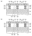
テンシャル高さPH2a,PH2d参照)が高く維持される。最も深い位置に配された半導体領域102dの不純物濃度が最も高く、最も表面側の半導体領域102aの不純物濃度が次に高く、半導体領域102b、102cの不純物濃度は最も低い。また半導体領域102b、102cはひとつの領域で構成することもできる。このような、不純物濃度関係とすることにより、縦方向の電界を維持し、光電変換部で発生した信号電荷であるホールを電荷蓄積領域に効率良く導くことが可能となる。更に、電荷蓄積領域107からの空乏層の広がりを抑えることが可能となり、信号読み出し時の駆動電圧の振幅を小さくすることが可能となる。
PH2a>PH1a,PH2d>PH1d・・・数式1
である。
PH3d>PH1d・・・数式2
である。この条件「実施例」によっても、条件「比較例」に比べて、信号電荷のキャリアが複数の半導体領域102a〜102dを通過して隣接する光電変換部に到達しにくい。したがって、条件「実施例」によれば、条件「比較例」に比べて、隣接する光電変換部間の距離が近くなった場合における混色を抑制することができる。
図9に本発明の別の実施形態に係る光電変換装置の断面構成を示す。図3に示された構成と同一の機能を有する部分には、同一の符号を付し、詳細な説明は省略する。
図11に本発明のまた別の実施形態に係る光電変換装置の断面構成を示す。図9に示された構成と同一の機能を有する部分には、同一の符号を付し、詳細な説明は省略する。
Claims (9)
- 半導体基板に配された複数の光電変換部を有し、
前記光電変換部は、
第1の不純物を含むP型の電荷蓄積領域と、
前記P型の電荷蓄積領域とともにフォトダイオードを構成するN型のウエル部と、
を備え、
前記ウエル部は、
砒素を第1の濃度で含むN型の第1の半導体領域と、
前記第1の半導体領域の下に配され、砒素を前記第1の濃度より低い第2の濃度で含むN型の第2の半導体領域と、
前記第2の半導体領域の下に配され、第2の不純物を前記第1の濃度よりも高い第3の濃度で含むN型の第3の半導体領域と、
を含むことを特徴とする光電変換装置。 - 前記第2の不純物は、リンを主成分としていることを特徴とする請求項1に記載の光電変換装置。
- 前記複数の光電変換部のP型の電荷蓄積領域どうしを分離するように、前記半導体基板の表面に垂直な方向における素子分離部と前記ウエル部との間にそれぞれ配された複数のポテンシャル障壁をさらに備えたことを特徴とする請求項1に記載の光電変換装置。
- 前記ポテンシャル障壁は、
前記素子分離部の下に配されたN型の第4の半導体領域と、
前記第4の半導体領域の下に配されたN型の第5の半導体領域と、
を含むことを特徴とする請求項3に記載の光電変換装置。 - 前記第4の半導体領域は、前記第2の不純物を前記第2の濃度より高い第4の濃度で含み、
前記第5の半導体領域は、前記第2の不純物を前記第2の濃度より高い第5の濃度で含むことを特徴とする請求項4に記載の光電変換装置。 - 前記光電変換部は、
前記P型の電荷蓄積領域の上に配され、前記第2の不純物を前記第4の濃度より高い第6の濃度で含むN型の表面領域と、
前記P型の電荷蓄積領域の下に配され、前記第1の不純物を前記電荷蓄積領域より低い濃度で含むP型の電荷収集領域と、をさらに含み、
前記第4の半導体領域は、前記素子分離部の少なくとも底面を覆い且つ、前記表面領域まで延びていることを特徴とする請求項5に記載の光電変換装置。 - 入射される光の方向が前記第1半導体領域から前記第2半導体領域へ向かう方向にとなるように、前記半導体基板の表面側から光が入射される
ことを特徴とする請求項1に記載の光電変換装置。 - 入射される光の方向が前記第2半導体領域から前記第1半導体領域へ向かう方向となるように、前記半導体基板の裏面側から光が入射される
ことを特徴とする請求項1に記載の光電変換装置。 - 請求項1に記載の光電変換装置と、
前記光電変換装置の撮像面へ像を形成する光学系と、
前記光電変換装置から出力された信号を処理して画像データを生成する信号処理部と、を備えたことを特徴とする撮像システム。
Priority Applications (4)
| Application Number | Priority Date | Filing Date | Title |
|---|---|---|---|
| JP2010011375A JP2010206181A (ja) | 2009-02-06 | 2010-01-21 | 光電変換装置及び撮像システム |
| PCT/JP2010/051308 WO2010090148A1 (en) | 2009-02-06 | 2010-01-26 | Photoelectric conversion apparatus and imaging system |
| CN2010800062328A CN102301475B (zh) | 2009-02-06 | 2010-01-26 | 光电转换装置和成像系统 |
| US13/131,442 US8779544B2 (en) | 2009-02-06 | 2010-01-26 | Photoelectric conversion apparatus and imaging system having revision with multiple impurity densities |
Applications Claiming Priority (2)
| Application Number | Priority Date | Filing Date | Title |
|---|---|---|---|
| JP2009026700 | 2009-02-06 | ||
| JP2010011375A JP2010206181A (ja) | 2009-02-06 | 2010-01-21 | 光電変換装置及び撮像システム |
Publications (2)
| Publication Number | Publication Date |
|---|---|
| JP2010206181A true JP2010206181A (ja) | 2010-09-16 |
| JP2010206181A5 JP2010206181A5 (ja) | 2013-02-21 |
Family
ID=42077427
Family Applications (1)
| Application Number | Title | Priority Date | Filing Date |
|---|---|---|---|
| JP2010011375A Pending JP2010206181A (ja) | 2009-02-06 | 2010-01-21 | 光電変換装置及び撮像システム |
Country Status (4)
| Country | Link |
|---|---|
| US (1) | US8779544B2 (ja) |
| JP (1) | JP2010206181A (ja) |
| CN (1) | CN102301475B (ja) |
| WO (1) | WO2010090148A1 (ja) |
Cited By (6)
| Publication number | Priority date | Publication date | Assignee | Title |
|---|---|---|---|---|
| US20090250778A1 (en) * | 2008-04-04 | 2009-10-08 | Canon Kabushiki Kaisha | Photoelectric conversion device, imaging system, photoelectric conversion device designing method, and photoelectric conversion device manufacturing method |
| JP2012164943A (ja) * | 2011-02-09 | 2012-08-30 | Canon Inc | 固体撮像装置 |
| JP2014116472A (ja) * | 2012-12-10 | 2014-06-26 | Canon Inc | 固体撮像装置およびその製造方法 |
| JP2015076453A (ja) * | 2013-10-07 | 2015-04-20 | キヤノン株式会社 | 固体撮像装置、その製造方法及び撮像システム |
| JP2016143870A (ja) * | 2015-02-05 | 2016-08-08 | キヤノン株式会社 | 固体撮像装置 |
| JP2018037672A (ja) * | 2017-10-18 | 2018-03-08 | キヤノン株式会社 | 固体撮像装置およびカメラ |
Families Citing this family (30)
| Publication number | Priority date | Publication date | Assignee | Title |
|---|---|---|---|---|
| JP2010206178A (ja) | 2009-02-06 | 2010-09-16 | Canon Inc | 光電変換装置、及び光電変換装置の製造方法 |
| JP5751766B2 (ja) * | 2010-07-07 | 2015-07-22 | キヤノン株式会社 | 固体撮像装置および撮像システム |
| JP5885401B2 (ja) | 2010-07-07 | 2016-03-15 | キヤノン株式会社 | 固体撮像装置および撮像システム |
| JP5697371B2 (ja) | 2010-07-07 | 2015-04-08 | キヤノン株式会社 | 固体撮像装置および撮像システム |
| JP5656484B2 (ja) | 2010-07-07 | 2015-01-21 | キヤノン株式会社 | 固体撮像装置および撮像システム |
| JP5645513B2 (ja) | 2010-07-07 | 2014-12-24 | キヤノン株式会社 | 固体撮像装置及び撮像システム |
| JP5643555B2 (ja) | 2010-07-07 | 2014-12-17 | キヤノン株式会社 | 固体撮像装置及び撮像システム |
| CN103620783B (zh) * | 2011-06-23 | 2016-08-17 | 松下电器产业株式会社 | 固体摄像装置 |
| JP5864990B2 (ja) | 2011-10-03 | 2016-02-17 | キヤノン株式会社 | 固体撮像装置およびカメラ |
| JP5743837B2 (ja) * | 2011-10-07 | 2015-07-01 | キヤノン株式会社 | 光電変換装置、撮像装置および撮像システム |
| JP2013084785A (ja) | 2011-10-11 | 2013-05-09 | Sony Corp | 固体撮像装置、撮像装置 |
| JP6124502B2 (ja) | 2012-02-29 | 2017-05-10 | キヤノン株式会社 | 固体撮像装置およびその製造方法 |
| JP6023437B2 (ja) | 2012-02-29 | 2016-11-09 | キヤノン株式会社 | 固体撮像装置及びカメラ |
| JP6016434B2 (ja) | 2012-04-23 | 2016-10-26 | キヤノン株式会社 | 固体撮像装置、その製造方法、及びカメラ |
| JP6274729B2 (ja) | 2013-02-04 | 2018-02-07 | キヤノン株式会社 | 固体撮像装置およびカメラ |
| JP2014199898A (ja) * | 2013-03-11 | 2014-10-23 | ソニー株式会社 | 固体撮像素子および製造方法、並びに、電子機器 |
| JP2014225536A (ja) | 2013-05-15 | 2014-12-04 | キヤノン株式会社 | 固体撮像装置及びカメラ |
| JP6305028B2 (ja) * | 2013-11-22 | 2018-04-04 | キヤノン株式会社 | 光電変換装置の製造方法および光電変換装置 |
| JP6274567B2 (ja) | 2014-03-14 | 2018-02-07 | キヤノン株式会社 | 固体撮像装置及び撮像システム |
| JP6595750B2 (ja) | 2014-03-14 | 2019-10-23 | キヤノン株式会社 | 固体撮像装置及び撮像システム |
| JP2016082306A (ja) | 2014-10-10 | 2016-05-16 | キヤノン株式会社 | 撮像装置、撮像システム及び撮像装置の駆動方法 |
| JPWO2016151982A1 (ja) * | 2015-03-26 | 2018-01-25 | パナソニックIpマネジメント株式会社 | 固体撮像素子およびこれを備えた撮像装置 |
| JP2016187018A (ja) * | 2015-03-27 | 2016-10-27 | キヤノン株式会社 | 光電変換装置およびカメラ |
| JP6541523B2 (ja) | 2015-09-11 | 2019-07-10 | キヤノン株式会社 | 撮像装置、撮像システム、および、撮像装置の制御方法 |
| US10205894B2 (en) | 2015-09-11 | 2019-02-12 | Canon Kabushiki Kaisha | Imaging device and imaging system |
| JP6570384B2 (ja) | 2015-09-11 | 2019-09-04 | キヤノン株式会社 | 撮像装置及び撮像システム |
| JP7084700B2 (ja) | 2017-06-16 | 2022-06-15 | キヤノン株式会社 | 光電変換装置およびスキャナ |
| JP2019102494A (ja) * | 2017-11-28 | 2019-06-24 | キヤノン株式会社 | 光電変換装置およびその製造方法、機器 |
| US11425365B2 (en) | 2018-12-14 | 2022-08-23 | Canon Kabushiki Kaisha | Photoelectric conversion device, method of manufacturing photoelectric conversion device, and method of manufacturing semiconductor device |
| JP7362285B2 (ja) | 2019-03-29 | 2023-10-17 | キヤノン株式会社 | 光電変換装置、光電変換システム、および移動体 |
Citations (2)
| Publication number | Priority date | Publication date | Assignee | Title |
|---|---|---|---|---|
| JP2004193547A (ja) * | 2002-06-27 | 2004-07-08 | Canon Inc | 固体撮像装置及び固体撮像装置を用いたカメラシステム |
| EP1542286A2 (en) * | 2003-12-12 | 2005-06-15 | Canon Kabushiki Kaisha | Photoelectric conversion device, method of manufacturing photoelectric conversion device, and image pickup system |
Family Cites Families (44)
| Publication number | Priority date | Publication date | Assignee | Title |
|---|---|---|---|---|
| JPH11126893A (ja) | 1997-10-23 | 1999-05-11 | Nikon Corp | 固体撮像素子とその製造方法 |
| JP4604296B2 (ja) | 1999-02-09 | 2011-01-05 | ソニー株式会社 | 固体撮像装置及びその製造方法 |
| JP2001257339A (ja) | 2000-01-06 | 2001-09-21 | Texas Instr Japan Ltd | 固体撮像装置およびその製造方法 |
| JP2002203954A (ja) | 2000-10-31 | 2002-07-19 | Sharp Corp | 回路内蔵受光素子 |
| JP2003031787A (ja) | 2001-07-17 | 2003-01-31 | Canon Inc | 固体撮像素子及びその駆動方法 |
| JP4269033B2 (ja) | 2002-03-05 | 2009-05-27 | シャープ株式会社 | 受光素子及びその製造方法、並びに、回路内蔵型受光素子及びその製造方法 |
| CN100435343C (zh) | 2002-06-27 | 2008-11-19 | 佳能株式会社 | 固体摄象装置和用固体摄象装置的摄象机系统 |
| JP3796227B2 (ja) | 2003-03-24 | 2006-07-12 | 三洋電機株式会社 | 電荷結合素子の製造方法 |
| JP2005072236A (ja) | 2003-08-25 | 2005-03-17 | Renesas Technology Corp | 半導体装置および半導体装置の製造方法 |
| JP2005136269A (ja) | 2003-10-31 | 2005-05-26 | Sharp Corp | 半導体装置およびその製造方法 |
| JP4612818B2 (ja) * | 2004-08-31 | 2011-01-12 | キヤノン株式会社 | 固体撮像素子、固体撮像装置及び撮像システム |
| JP4174468B2 (ja) | 2003-12-12 | 2008-10-29 | キヤノン株式会社 | 光電変換装置及び撮像システム |
| JP5224633B2 (ja) | 2004-03-30 | 2013-07-03 | キヤノン株式会社 | 半導体装置の製造方法 |
| JP4525144B2 (ja) * | 2004-04-02 | 2010-08-18 | ソニー株式会社 | 固体撮像素子及びその製造方法 |
| WO2005109512A1 (en) | 2004-05-06 | 2005-11-17 | Canon Kabushiki Kaisha | Photoelectric conversion device and manufacturing method thereof |
| US7605415B2 (en) * | 2004-06-07 | 2009-10-20 | Canon Kabushiki Kaisha | Image pickup device comprising photoelectric conversation unit, floating diffusion region and guard ring |
| JP5230058B2 (ja) * | 2004-06-07 | 2013-07-10 | キヤノン株式会社 | 固体撮像装置およびカメラ |
| JP4507769B2 (ja) | 2004-08-31 | 2010-07-21 | ソニー株式会社 | 固体撮像素子、カメラモジュール及び電子機器モジュール |
| JP2006073736A (ja) | 2004-09-01 | 2006-03-16 | Canon Inc | 光電変換装置、固体撮像装置及び固体撮像システム |
| JP4916101B2 (ja) | 2004-09-01 | 2012-04-11 | キヤノン株式会社 | 光電変換装置、固体撮像装置及び固体撮像システム |
| JP4680552B2 (ja) | 2004-09-02 | 2011-05-11 | 富士フイルム株式会社 | 固体撮像素子の製造方法 |
| JP2006108485A (ja) | 2004-10-07 | 2006-04-20 | Sanyo Electric Co Ltd | 固体撮像装置 |
| KR100672664B1 (ko) | 2004-12-29 | 2007-01-24 | 동부일렉트로닉스 주식회사 | 버티컬 씨모스 이미지 센서의 제조방법 |
| JP4919370B2 (ja) | 2005-03-31 | 2012-04-18 | ルネサスエレクトロニクス株式会社 | 半導体受光装置及び半導体受光装置の製造方法 |
| DE102006025408B4 (de) | 2006-05-31 | 2011-05-05 | Globalfoundries Inc. | Verfahren zur Steigerung des Transistorsleitungsvermögens durch Dotierstoffaktivierung nach der Silizidierung |
| JP5110820B2 (ja) | 2006-08-02 | 2012-12-26 | キヤノン株式会社 | 光電変換装置、光電変換装置の製造方法及び撮像システム |
| KR100781544B1 (ko) | 2006-08-08 | 2007-12-03 | 삼성전자주식회사 | 이미지 센서의 제조 방법 |
| JP5110831B2 (ja) | 2006-08-31 | 2012-12-26 | キヤノン株式会社 | 光電変換装置及び撮像システム |
| JP5023808B2 (ja) | 2007-05-24 | 2012-09-12 | ソニー株式会社 | 固体撮像装置およびカメラ |
| TWI479887B (zh) | 2007-05-24 | 2015-04-01 | Sony Corp | 背向照明固態成像裝置及照相機 |
| JP5157259B2 (ja) * | 2007-05-29 | 2013-03-06 | ソニー株式会社 | 固体撮像素子及び撮像装置 |
| JP2009026700A (ja) | 2007-07-23 | 2009-02-05 | Sumitomo Electric Ind Ltd | 導電性ペーストおよびそれを用いた多層プリント配線板 |
| JP2009038309A (ja) | 2007-08-03 | 2009-02-19 | Sharp Corp | 固体撮像素子およびその製造方法、電子情報機器 |
| JP5335271B2 (ja) | 2008-04-09 | 2013-11-06 | キヤノン株式会社 | 光電変換装置及びそれを用いた撮像システム |
| JP5213501B2 (ja) | 2008-04-09 | 2013-06-19 | キヤノン株式会社 | 固体撮像装置 |
| JP4759590B2 (ja) | 2008-05-09 | 2011-08-31 | キヤノン株式会社 | 光電変換装置及びそれを用いた撮像システム |
| JP2009278241A (ja) | 2008-05-13 | 2009-11-26 | Canon Inc | 固体撮像装置の駆動方法および固体撮像装置 |
| JP4863307B2 (ja) | 2008-06-30 | 2012-01-25 | Kddi株式会社 | アンダーサンプリングを用いた受信機、プログラム及び方法 |
| JP2010161236A (ja) | 2009-01-08 | 2010-07-22 | Canon Inc | 光電変換装置の製造方法 |
| JP5538922B2 (ja) | 2009-02-06 | 2014-07-02 | キヤノン株式会社 | 固体撮像装置の製造方法 |
| JP2010206178A (ja) | 2009-02-06 | 2010-09-16 | Canon Inc | 光電変換装置、及び光電変換装置の製造方法 |
| JP5451098B2 (ja) | 2009-02-06 | 2014-03-26 | キヤノン株式会社 | 半導体装置の製造方法 |
| JP2010199154A (ja) | 2009-02-23 | 2010-09-09 | Canon Inc | 固体撮像素子 |
| JP5623068B2 (ja) | 2009-12-07 | 2014-11-12 | キヤノン株式会社 | 固体撮像装置の製造方法 |
-
2010
- 2010-01-21 JP JP2010011375A patent/JP2010206181A/ja active Pending
- 2010-01-26 CN CN2010800062328A patent/CN102301475B/zh not_active Expired - Fee Related
- 2010-01-26 US US13/131,442 patent/US8779544B2/en not_active Expired - Fee Related
- 2010-01-26 WO PCT/JP2010/051308 patent/WO2010090148A1/en active Application Filing
Patent Citations (2)
| Publication number | Priority date | Publication date | Assignee | Title |
|---|---|---|---|---|
| JP2004193547A (ja) * | 2002-06-27 | 2004-07-08 | Canon Inc | 固体撮像装置及び固体撮像装置を用いたカメラシステム |
| EP1542286A2 (en) * | 2003-12-12 | 2005-06-15 | Canon Kabushiki Kaisha | Photoelectric conversion device, method of manufacturing photoelectric conversion device, and image pickup system |
Cited By (8)
| Publication number | Priority date | Publication date | Assignee | Title |
|---|---|---|---|---|
| US20090250778A1 (en) * | 2008-04-04 | 2009-10-08 | Canon Kabushiki Kaisha | Photoelectric conversion device, imaging system, photoelectric conversion device designing method, and photoelectric conversion device manufacturing method |
| US8274122B2 (en) * | 2008-04-04 | 2012-09-25 | Canon Kabushiki Kaisha | Photoelectric conversion device, imaging system, photoelectric conversion device designing method, and photoelectric conversion device manufacturing method |
| JP2012164943A (ja) * | 2011-02-09 | 2012-08-30 | Canon Inc | 固体撮像装置 |
| US8952428B2 (en) | 2011-02-09 | 2015-02-10 | Canon Kabushiki Kaisha | Element isolation structure of a solid-state pickup device |
| JP2014116472A (ja) * | 2012-12-10 | 2014-06-26 | Canon Inc | 固体撮像装置およびその製造方法 |
| JP2015076453A (ja) * | 2013-10-07 | 2015-04-20 | キヤノン株式会社 | 固体撮像装置、その製造方法及び撮像システム |
| JP2016143870A (ja) * | 2015-02-05 | 2016-08-08 | キヤノン株式会社 | 固体撮像装置 |
| JP2018037672A (ja) * | 2017-10-18 | 2018-03-08 | キヤノン株式会社 | 固体撮像装置およびカメラ |
Also Published As
| Publication number | Publication date |
|---|---|
| US20110234868A1 (en) | 2011-09-29 |
| CN102301475A (zh) | 2011-12-28 |
| WO2010090148A1 (en) | 2010-08-12 |
| US8779544B2 (en) | 2014-07-15 |
| CN102301475B (zh) | 2013-11-06 |
Similar Documents
| Publication | Publication Date | Title |
|---|---|---|
| JP2010206181A (ja) | 光電変換装置及び撮像システム | |
| US7592579B2 (en) | Photoelectric conversion device manufacturing method, semiconductor device manufacturing method, photoelectric conversion device, and image sensing system | |
| US9076704B2 (en) | Photoelectric conversion apparatus and manufacturing method for a photoelectric conversion apparatus | |
| JP3840203B2 (ja) | 固体撮像装置及び固体撮像装置を用いたカメラシステム | |
| US8785991B2 (en) | Solid state imaging device, method for producing the same, and electronic apparatus | |
| JP2011114302A (ja) | 半導体素子の製造方法及び半導体素子、並びに固体撮像素子及び固体撮像装置 | |
| JP2013045879A (ja) | 半導体装置、半導体装置の製造方法、固体撮像装置、固体撮像装置の製造方法、電子機器 | |
| JP5508356B2 (ja) | 固体撮像装置およびその駆動方法、固体撮像装置の製造方法、並びに電子情報機器 | |
| JP4859542B2 (ja) | Mos型固体撮像装置及びmos型固体撮像装置の製造方法 | |
| TWI451564B (zh) | 具有二磊晶層之影像感測器及其製造方法 | |
| JP2005268814A (ja) | 固体撮像装置及び固体撮像装置を用いたカメラシステム | |
| JP2006073804A (ja) | 固体撮像素子とその製造方法 | |
| JP4435063B2 (ja) | 固体撮像装置及び固体撮像装置を用いたカメラシステム | |
| JP2009111118A (ja) | 裏面照射型固体撮像素子およびその製造方法 | |
| KR101583904B1 (ko) | 고체 촬상 장치, 고체 촬상 장치의 제조 방법 및 카메라 모듈 | |
| JP2005191362A (ja) | 固体撮像装置 | |
| JP5241759B2 (ja) | 固体撮像装置 | |
| JP4779781B2 (ja) | 固体撮像装置とその製造方法 | |
| JP2010027750A (ja) | 固体撮像装置 | |
| JP2007234874A (ja) | 固体撮像装置の製造方法 | |
| JP2015173180A (ja) | 固体撮像装置およびその製造方法 |
Legal Events
| Date | Code | Title | Description |
|---|---|---|---|
| A521 | Request for written amendment filed |
Free format text: JAPANESE INTERMEDIATE CODE: A523 Effective date: 20130107 |
|
| A621 | Written request for application examination |
Free format text: JAPANESE INTERMEDIATE CODE: A621 Effective date: 20130107 |
|
| A131 | Notification of reasons for refusal |
Free format text: JAPANESE INTERMEDIATE CODE: A131 Effective date: 20140214 |
|
| A521 | Request for written amendment filed |
Free format text: JAPANESE INTERMEDIATE CODE: A523 Effective date: 20140327 |
|
| A02 | Decision of refusal |
Free format text: JAPANESE INTERMEDIATE CODE: A02 Effective date: 20141010 |