JP2010199154A - 固体撮像素子 - Google Patents
固体撮像素子 Download PDFInfo
- Publication number
- JP2010199154A JP2010199154A JP2009039755A JP2009039755A JP2010199154A JP 2010199154 A JP2010199154 A JP 2010199154A JP 2009039755 A JP2009039755 A JP 2009039755A JP 2009039755 A JP2009039755 A JP 2009039755A JP 2010199154 A JP2010199154 A JP 2010199154A
- Authority
- JP
- Japan
- Prior art keywords
- region
- electrode
- floating diffusion
- solid
- state imaging
- Prior art date
- Legal status (The legal status is an assumption and is not a legal conclusion. Google has not performed a legal analysis and makes no representation as to the accuracy of the status listed.)
- Pending
Links
- 238000003384 imaging method Methods 0.000 title claims abstract description 31
- 238000009792 diffusion process Methods 0.000 claims abstract description 30
- 239000000758 substrate Substances 0.000 claims abstract description 24
- 239000004065 semiconductor Substances 0.000 claims abstract description 23
- 238000009825 accumulation Methods 0.000 claims description 27
- 238000006243 chemical reaction Methods 0.000 claims description 8
- 239000012535 impurity Substances 0.000 claims description 8
- 239000010408 film Substances 0.000 description 12
- 230000035945 sensitivity Effects 0.000 description 11
- 230000000694 effects Effects 0.000 description 8
- 238000002955 isolation Methods 0.000 description 8
- 238000000034 method Methods 0.000 description 6
- 229910021420 polycrystalline silicon Inorganic materials 0.000 description 5
- 229920005591 polysilicon Polymers 0.000 description 5
- 238000010586 diagram Methods 0.000 description 4
- 238000005468 ion implantation Methods 0.000 description 4
- 230000003287 optical effect Effects 0.000 description 3
- VYPSYNLAJGMNEJ-UHFFFAOYSA-N Silicium dioxide Chemical compound O=[Si]=O VYPSYNLAJGMNEJ-UHFFFAOYSA-N 0.000 description 2
- 230000000875 corresponding effect Effects 0.000 description 2
- 238000005516 engineering process Methods 0.000 description 2
- 230000006870 function Effects 0.000 description 2
- 238000005286 illumination Methods 0.000 description 2
- 229910052814 silicon oxide Inorganic materials 0.000 description 2
- 230000003595 spectral effect Effects 0.000 description 2
- XUIMIQQOPSSXEZ-UHFFFAOYSA-N Silicon Chemical compound [Si] XUIMIQQOPSSXEZ-UHFFFAOYSA-N 0.000 description 1
- 239000000969 carrier Substances 0.000 description 1
- 230000001276 controlling effect Effects 0.000 description 1
- 230000002596 correlated effect Effects 0.000 description 1
- 230000007423 decrease Effects 0.000 description 1
- 238000002474 experimental method Methods 0.000 description 1
- 239000000284 extract Substances 0.000 description 1
- 238000002513 implantation Methods 0.000 description 1
- 150000002500 ions Chemical class 0.000 description 1
- 230000002093 peripheral effect Effects 0.000 description 1
- 238000005070 sampling Methods 0.000 description 1
- 238000000926 separation method Methods 0.000 description 1
- 229910052710 silicon Inorganic materials 0.000 description 1
- 239000010703 silicon Substances 0.000 description 1
- 239000010409 thin film Substances 0.000 description 1
- 238000002834 transmittance Methods 0.000 description 1
Images


Classifications
-
- H—ELECTRICITY
- H01—ELECTRIC ELEMENTS
- H01L—SEMICONDUCTOR DEVICES NOT COVERED BY CLASS H10
- H01L27/00—Devices consisting of a plurality of semiconductor or other solid-state components formed in or on a common substrate
- H01L27/14—Devices consisting of a plurality of semiconductor or other solid-state components formed in or on a common substrate including semiconductor components sensitive to infrared radiation, light, electromagnetic radiation of shorter wavelength or corpuscular radiation and specially adapted either for the conversion of the energy of such radiation into electrical energy or for the control of electrical energy by such radiation
- H01L27/144—Devices controlled by radiation
- H01L27/146—Imager structures
- H01L27/14643—Photodiode arrays; MOS imagers
-
- H—ELECTRICITY
- H01—ELECTRIC ELEMENTS
- H01L—SEMICONDUCTOR DEVICES NOT COVERED BY CLASS H10
- H01L27/00—Devices consisting of a plurality of semiconductor or other solid-state components formed in or on a common substrate
- H01L27/14—Devices consisting of a plurality of semiconductor or other solid-state components formed in or on a common substrate including semiconductor components sensitive to infrared radiation, light, electromagnetic radiation of shorter wavelength or corpuscular radiation and specially adapted either for the conversion of the energy of such radiation into electrical energy or for the control of electrical energy by such radiation
- H01L27/144—Devices controlled by radiation
- H01L27/146—Imager structures
- H01L27/14601—Structural or functional details thereof
- H01L27/14603—Special geometry or disposition of pixel-elements, address-lines or gate-electrodes
Abstract
【解決手段】半導体基板上に形成され、電荷を蓄積する第1の導電型の電荷蓄積領域(104)と、電荷蓄積領域の少なくとも一部を覆って半導体基板の表面に形成された第2の導電型の第1の表面領域(105)と、電荷を蓄積する第1の導電型のフローティングディフュージョン領域(103)と、電荷蓄積領域の全面を覆い、半導体基板上にゲート絶縁膜を介して、電荷蓄積領域に蓄積された電荷をフローティングディフュージョン領域に転送する電極(102)とを有し、電極は光が透過可能な膜厚であり、電極の下は、フローティングディフュージョン領域から離れ第1の表面領域を有する部分と、フローティングディフュージョン領域に近く第1の表面領域を有しない部分とを有する。
【選択図】図2
Description
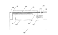
図1は本発明の第1の実施形態による固体撮像素子の上面図、図2は図1の固体撮像素子のa−a’断面図である。図1中の101は活性領域を示している。活性領域101と境界を同じくし活性領域101を取り囲む領域はシリコン酸化膜がシリコン基板に埋め込まれた素子分離領域を形成している。図2中101’はこの素子分離領域に該当する。102は電極であり、103はFD領域である。104は蓄積領域であり、光電変換により発生した電荷を蓄積する。109は半導体基板である。109は、例えば蓄積領域104と同じ導電型で蓄積領域104より低濃度の基板を使用するが、蓄積領域104と反対導電型で低濃度の基板を使用しても良い。更に、蓄積領域104と同じ低濃度基板に反対導電型のウエルを形成した基板でもよい。蓄積領域104は光電変換部(フォトダイオード)としての機能も有する。105は表面領域であり、蓄積領域104とは異なる導電型の半導体領域である。表面領域105の存在により蓄積領域104がゲート絶縁膜110との界面に接することを防ぎ、埋め込みフォトダイオード構造を実現することが可能である。106及び107はいずれもコンタクトホールであり、106はFD領域103を、107は電極102を、配線層(図示せず)と電気的に接続している。108はフィールドストップ領域であり、蓄積領域104とFD領域103との間における電荷のポテンシャル分離の役割を果たす。
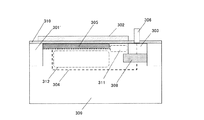
図3は本発明の第2の実施形態による固体撮像素子の上面図であり、図4は図3の固体撮像素子のb−b’断面図である。各部品番号301から312は、それぞれ第1の実施形態における101から112と同じ部分を示す。また、画素の等価回路、駆動タイミングは第1の実施形態と同等のものを選択可能である。本実施形態の特徴は、電極302が活性領域301をオーバーラップして配置されている点である。本実施形態の構造においても第1の実施形態と同様に埋め込みフォトダイオード構造を実現することが可能であり、暗電流の抑制が可能である。さらに本実施形態では、電極302がSTIエッジ部に乗っており、STIエッジ部のポテンシャルを制御することが可能である。このことにより、ストレスの大きいSTIエッジ部付近におけるマイノリティキャリア濃度を制御でき、暗電流値を低減することが可能となる。
図7は、本発明の第3の実施形態による固体撮像素子のa−a’断面図である。各部品番号901から912は、それぞれ第1の実施形態における101から112と同じ部分を示す。また、画素の等価回路、駆動タイミングは第1の実施形態と同等のものを選択可能である。本実施形態の特徴は、第1の表面領域905に加え、第2の表面領域905'が形成されている点である。
101'、301'、501'、601'、901' 素子分離領域
102、302、502、602、703、902 電極
103、303、503、603、903 FD領域
104、304、504、604、701、904 蓄積領域
105、305、505、605、702、905 表面領域
905’ 第2の表面領域
106、107、306、307、506、507、606、607、906 コンタクトホール
108、308、508、608、908 フィールドストップ領域
109、309、509、609、909 半導体基板
110、310、510、610、910 ゲート絶縁膜
111、311、511、611、911 FD領域に近い側の電極下活性領域
112、312、512、612、912 FD領域に遠い側の電極下活性領域
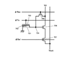
704 FD領域
705 リセットトランジスタ
706 ソースフォロワトランジスタ
707 選択トランジスタ
Claims (4)
- 半導体基板上に形成され、電荷を蓄積する第1の導電型の電荷蓄積領域と、
前記電荷蓄積領域の少なくとも一部を覆って前記半導体基板の表面に形成された第2の導電型の第1の表面領域と、
電荷を蓄積する第1の導電型のフローティングディフュージョン領域と、
前記電荷蓄積領域の全面を覆い、前記半導体基板上にゲート絶縁膜を介して、前記電荷蓄積領域に蓄積された電荷を前記フローティングディフュージョン領域に転送する電極とを有し、
前記電極は光が透過可能な膜厚であり、
前記電極の下は、前記フローティングディフュージョン領域から離れ前記第1の表面領域を有する部分と、前記フローティングディフュージョン領域に近く前記第1の表面領域を有しない部分とを有することを特徴とする固体撮像素子。 - 前記電極の下において、前記フローティングディフュージョン領域に近く前記第1の表面領域を有しない部分は、前記フローティングディフュージョン領域から離れ前記第1の表面領域を有する部分に比べて不純物濃度が薄いか、又は前記電荷蓄積領域と同じ導電型であることを特徴とする請求項1記載の固体撮像素子。
- 前記電荷蓄積領域に蓄積された電荷を前記フローティングディフュージョン領域に転送する期間中に、前記電極には前記電荷を前記半導体基板の表面側に引き寄せる電位を与えることを特徴とする請求項1又は2記載の固体撮像素子。
- 前記電荷蓄積領域は、光電変換により生成された電荷を蓄積することを特徴とする請求項1〜3のいずれか1項に記載の固体撮像素子。
Priority Applications (2)
| Application Number | Priority Date | Filing Date | Title |
|---|---|---|---|
| JP2009039755A JP2010199154A (ja) | 2009-02-23 | 2009-02-23 | 固体撮像素子 |
| US12/697,408 US20100214464A1 (en) | 2009-02-23 | 2010-02-01 | Solid-state imaging apparatus |
Applications Claiming Priority (1)
| Application Number | Priority Date | Filing Date | Title |
|---|---|---|---|
| JP2009039755A JP2010199154A (ja) | 2009-02-23 | 2009-02-23 | 固体撮像素子 |
Publications (2)
| Publication Number | Publication Date |
|---|---|
| JP2010199154A true JP2010199154A (ja) | 2010-09-09 |
| JP2010199154A5 JP2010199154A5 (ja) | 2012-03-08 |
Family
ID=42630655
Family Applications (1)
| Application Number | Title | Priority Date | Filing Date |
|---|---|---|---|
| JP2009039755A Pending JP2010199154A (ja) | 2009-02-23 | 2009-02-23 | 固体撮像素子 |
Country Status (2)
| Country | Link |
|---|---|
| US (1) | US20100214464A1 (ja) |
| JP (1) | JP2010199154A (ja) |
Families Citing this family (7)
| Publication number | Priority date | Publication date | Assignee | Title |
|---|---|---|---|---|
| JP2010206178A (ja) | 2009-02-06 | 2010-09-16 | Canon Inc | 光電変換装置、及び光電変換装置の製造方法 |
| JP2010206181A (ja) * | 2009-02-06 | 2010-09-16 | Canon Inc | 光電変換装置及び撮像システム |
| JP5538922B2 (ja) * | 2009-02-06 | 2014-07-02 | キヤノン株式会社 | 固体撮像装置の製造方法 |
| JP6016434B2 (ja) | 2012-04-23 | 2016-10-26 | キヤノン株式会社 | 固体撮像装置、その製造方法、及びカメラ |
| JP2016082306A (ja) | 2014-10-10 | 2016-05-16 | キヤノン株式会社 | 撮像装置、撮像システム及び撮像装置の駆動方法 |
| US11425365B2 (en) | 2018-12-14 | 2022-08-23 | Canon Kabushiki Kaisha | Photoelectric conversion device, method of manufacturing photoelectric conversion device, and method of manufacturing semiconductor device |
| US11922175B2 (en) | 2022-07-29 | 2024-03-05 | Arista Networks, Inc. | Unplanned reboot expedited recovery for network devices |
Citations (5)
| Publication number | Priority date | Publication date | Assignee | Title |
|---|---|---|---|---|
| JP2003115580A (ja) * | 2001-10-04 | 2003-04-18 | Sony Corp | 固体撮像素子およびその製造方法 |
| JP2004134685A (ja) * | 2002-10-15 | 2004-04-30 | Toshiba Corp | 固体撮像装置及びその製造方法 |
| JP2005268814A (ja) * | 2002-06-27 | 2005-09-29 | Canon Inc | 固体撮像装置及び固体撮像装置を用いたカメラシステム |
| JP2006310835A (ja) * | 2005-04-28 | 2006-11-09 | Samsung Electronics Co Ltd | Cmosイメージセンサー及びその製造方法 |
| JP2008124463A (ja) * | 2006-11-08 | 2008-05-29 | Samsung Electronics Co Ltd | Cmosイメージセンサーのピクセル構造及び該回路 |
Family Cites Families (14)
| Publication number | Priority date | Publication date | Assignee | Title |
|---|---|---|---|---|
| JP2003031787A (ja) * | 2001-07-17 | 2003-01-31 | Canon Inc | 固体撮像素子及びその駆動方法 |
| US7078745B2 (en) * | 2003-03-05 | 2006-07-18 | Micron Technology, Inc. | CMOS imager with enhanced transfer of charge and low voltage operation |
| US7095075B2 (en) * | 2003-07-01 | 2006-08-22 | Micron Technology, Inc. | Apparatus and method for split transistor memory having improved endurance |
| JP2005142470A (ja) * | 2003-11-10 | 2005-06-02 | Seiko Instruments Inc | 光電変換装置及びイメージセンサーic |
| JP2006073736A (ja) * | 2004-09-01 | 2006-03-16 | Canon Inc | 光電変換装置、固体撮像装置及び固体撮像システム |
| JP4916101B2 (ja) * | 2004-09-01 | 2012-04-11 | キヤノン株式会社 | 光電変換装置、固体撮像装置及び固体撮像システム |
| JP2006073885A (ja) * | 2004-09-03 | 2006-03-16 | Canon Inc | 固体撮像装置、その製造方法、およびデジタルカメラ |
| JP5132102B2 (ja) * | 2006-08-01 | 2013-01-30 | キヤノン株式会社 | 光電変換装置および光電変換装置を用いた撮像システム |
| JP5110820B2 (ja) * | 2006-08-02 | 2012-12-26 | キヤノン株式会社 | 光電変換装置、光電変換装置の製造方法及び撮像システム |
| JP4350768B2 (ja) * | 2007-04-16 | 2009-10-21 | キヤノン株式会社 | 光電変換装置及び撮像装置 |
| JP2009021809A (ja) * | 2007-07-11 | 2009-01-29 | Canon Inc | 撮像装置の駆動方法、撮像装置、及び撮像システム |
| JP5153378B2 (ja) * | 2008-02-15 | 2013-02-27 | キヤノン株式会社 | 固体撮像装置及びその駆動方法 |
| JP5335271B2 (ja) * | 2008-04-09 | 2013-11-06 | キヤノン株式会社 | 光電変換装置及びそれを用いた撮像システム |
| JP5188275B2 (ja) * | 2008-06-06 | 2013-04-24 | キヤノン株式会社 | 固体撮像装置、その駆動方法及び撮像システム |
-
2009
- 2009-02-23 JP JP2009039755A patent/JP2010199154A/ja active Pending
-
2010
- 2010-02-01 US US12/697,408 patent/US20100214464A1/en not_active Abandoned
Patent Citations (5)
| Publication number | Priority date | Publication date | Assignee | Title |
|---|---|---|---|---|
| JP2003115580A (ja) * | 2001-10-04 | 2003-04-18 | Sony Corp | 固体撮像素子およびその製造方法 |
| JP2005268814A (ja) * | 2002-06-27 | 2005-09-29 | Canon Inc | 固体撮像装置及び固体撮像装置を用いたカメラシステム |
| JP2004134685A (ja) * | 2002-10-15 | 2004-04-30 | Toshiba Corp | 固体撮像装置及びその製造方法 |
| JP2006310835A (ja) * | 2005-04-28 | 2006-11-09 | Samsung Electronics Co Ltd | Cmosイメージセンサー及びその製造方法 |
| JP2008124463A (ja) * | 2006-11-08 | 2008-05-29 | Samsung Electronics Co Ltd | Cmosイメージセンサーのピクセル構造及び該回路 |
Also Published As
| Publication number | Publication date |
|---|---|
| US20100214464A1 (en) | 2010-08-26 |
Similar Documents
| Publication | Publication Date | Title |
|---|---|---|
| US9985064B2 (en) | Solid-state imaging device and method of manufacturing the same, and imaging apparatus | |
| US8792035B2 (en) | Solid-state imaging device and manufacturing method thereof, driving method of solid-state imaging device, and electronic equipment | |
| JP2023118774A (ja) | 光検出素子 | |
| KR101683307B1 (ko) | 고체 촬상 장치, 고체 촬상 장치의 제조 방법, 및 전자 기기 | |
| TWI497702B (zh) | Solid state camera device | |
| US8716719B2 (en) | Solid-state imaging device, method of manufacturing solid-state imaging device, and electronic apparatus | |
| JP5651976B2 (ja) | 固体撮像素子およびその製造方法、並びに電子機器 | |
| US20190088704A1 (en) | Image sensors | |
| US9985066B2 (en) | Solid-state imaging device, method for manufacturing same, and electronic device | |
| JP4585964B2 (ja) | 固体撮像装置 | |
| KR102609646B1 (ko) | 촬상 소자, 전자 기기 | |
| WO2014141900A1 (ja) | 固体撮像素子およびその製造方法、並びに電子機器 | |
| KR102290502B1 (ko) | 이미지 센서 및 이의 제조 방법 | |
| JP6186205B2 (ja) | 撮像素子および撮像装置 | |
| JP2015065270A (ja) | 固体撮像装置およびその製造方法、並びに電子機器 | |
| JP2015053411A (ja) | 固体撮像素子、固体撮像素子の製造方法、および電子機器 | |
| JP2012199489A (ja) | 固体撮像装置、固体撮像装置の製造方法、及び電子機器 | |
| JP2009065098A (ja) | 裏面照射型固体撮像素子及びその製造方法 | |
| KR20150002593A (ko) | 고체 촬상 장치 및 전자 기기 | |
| JP2010199154A (ja) | 固体撮像素子 | |
| US7259361B2 (en) | Producing method for solid-state image pickup device including formation of a carrier accumulating region | |
| JP2012164892A (ja) | 固体撮像装置 | |
| US8618623B2 (en) | Solid-state image pickup device and method for manufacturing same, and image pickup apparatus | |
| US9741758B2 (en) | Methods of forming image sensors including deposited negative fixed charge layers on photoelectric conversion regions | |
| TWI525801B (zh) | 具有經摻雜之傳輸閘極的影像感測器 |
Legal Events
| Date | Code | Title | Description |
|---|---|---|---|
| A521 | Request for written amendment filed |
Free format text: JAPANESE INTERMEDIATE CODE: A523 Effective date: 20120124 |
|
| A621 | Written request for application examination |
Free format text: JAPANESE INTERMEDIATE CODE: A621 Effective date: 20120124 |
|
| A977 | Report on retrieval |
Free format text: JAPANESE INTERMEDIATE CODE: A971007 Effective date: 20130522 |
|
| A131 | Notification of reasons for refusal |
Free format text: JAPANESE INTERMEDIATE CODE: A131 Effective date: 20130528 |
|
| A521 | Request for written amendment filed |
Free format text: JAPANESE INTERMEDIATE CODE: A523 Effective date: 20130724 |
|
| A131 | Notification of reasons for refusal |
Free format text: JAPANESE INTERMEDIATE CODE: A131 Effective date: 20131203 |
|
| A02 | Decision of refusal |
Free format text: JAPANESE INTERMEDIATE CODE: A02 Effective date: 20140401 |