JP2010199154A - Solid-state imaging element - Google Patents
Solid-state imaging element Download PDFInfo
- Publication number
- JP2010199154A JP2010199154A JP2009039755A JP2009039755A JP2010199154A JP 2010199154 A JP2010199154 A JP 2010199154A JP 2009039755 A JP2009039755 A JP 2009039755A JP 2009039755 A JP2009039755 A JP 2009039755A JP 2010199154 A JP2010199154 A JP 2010199154A
- Authority
- JP
- Japan
- Prior art keywords
- region
- electrode
- floating diffusion
- solid
- state imaging
- Prior art date
- Legal status (The legal status is an assumption and is not a legal conclusion. Google has not performed a legal analysis and makes no representation as to the accuracy of the status listed.)
- Pending
Links
- 238000003384 imaging method Methods 0.000 title claims abstract description 31
- 238000009792 diffusion process Methods 0.000 claims abstract description 30
- 239000000758 substrate Substances 0.000 claims abstract description 24
- 239000004065 semiconductor Substances 0.000 claims abstract description 23
- 238000009825 accumulation Methods 0.000 claims description 27
- 238000006243 chemical reaction Methods 0.000 claims description 8
- 239000012535 impurity Substances 0.000 claims description 8
- 239000010408 film Substances 0.000 description 12
- 230000035945 sensitivity Effects 0.000 description 11
- 230000000694 effects Effects 0.000 description 8
- 238000002955 isolation Methods 0.000 description 8
- 238000000034 method Methods 0.000 description 6
- 229910021420 polycrystalline silicon Inorganic materials 0.000 description 5
- 229920005591 polysilicon Polymers 0.000 description 5
- 238000010586 diagram Methods 0.000 description 4
- 238000005468 ion implantation Methods 0.000 description 4
- 230000003287 optical effect Effects 0.000 description 3
- VYPSYNLAJGMNEJ-UHFFFAOYSA-N Silicium dioxide Chemical compound O=[Si]=O VYPSYNLAJGMNEJ-UHFFFAOYSA-N 0.000 description 2
- 230000000875 corresponding effect Effects 0.000 description 2
- 238000005516 engineering process Methods 0.000 description 2
- 230000006870 function Effects 0.000 description 2
- 238000005286 illumination Methods 0.000 description 2
- 229910052814 silicon oxide Inorganic materials 0.000 description 2
- 230000003595 spectral effect Effects 0.000 description 2
- XUIMIQQOPSSXEZ-UHFFFAOYSA-N Silicon Chemical compound [Si] XUIMIQQOPSSXEZ-UHFFFAOYSA-N 0.000 description 1
- 239000000969 carrier Substances 0.000 description 1
- 230000001276 controlling effect Effects 0.000 description 1
- 230000002596 correlated effect Effects 0.000 description 1
- 230000007423 decrease Effects 0.000 description 1
- 238000002474 experimental method Methods 0.000 description 1
- 239000000284 extract Substances 0.000 description 1
- 238000002513 implantation Methods 0.000 description 1
- 150000002500 ions Chemical class 0.000 description 1
- 230000002093 peripheral effect Effects 0.000 description 1
- 238000005070 sampling Methods 0.000 description 1
- 238000000926 separation method Methods 0.000 description 1
- 229910052710 silicon Inorganic materials 0.000 description 1
- 239000010703 silicon Substances 0.000 description 1
- 239000010409 thin film Substances 0.000 description 1
- 238000002834 transmittance Methods 0.000 description 1
Images


Classifications
-
- H—ELECTRICITY
- H01—ELECTRIC ELEMENTS
- H01L—SEMICONDUCTOR DEVICES NOT COVERED BY CLASS H10
- H01L27/00—Devices consisting of a plurality of semiconductor or other solid-state components formed in or on a common substrate
- H01L27/14—Devices consisting of a plurality of semiconductor or other solid-state components formed in or on a common substrate including semiconductor components sensitive to infrared radiation, light, electromagnetic radiation of shorter wavelength or corpuscular radiation and specially adapted either for the conversion of the energy of such radiation into electrical energy or for the control of electrical energy by such radiation
- H01L27/144—Devices controlled by radiation
- H01L27/146—Imager structures
- H01L27/14643—Photodiode arrays; MOS imagers
-
- H—ELECTRICITY
- H01—ELECTRIC ELEMENTS
- H01L—SEMICONDUCTOR DEVICES NOT COVERED BY CLASS H10
- H01L27/00—Devices consisting of a plurality of semiconductor or other solid-state components formed in or on a common substrate
- H01L27/14—Devices consisting of a plurality of semiconductor or other solid-state components formed in or on a common substrate including semiconductor components sensitive to infrared radiation, light, electromagnetic radiation of shorter wavelength or corpuscular radiation and specially adapted either for the conversion of the energy of such radiation into electrical energy or for the control of electrical energy by such radiation
- H01L27/144—Devices controlled by radiation
- H01L27/146—Imager structures
- H01L27/14601—Structural or functional details thereof
- H01L27/14603—Special geometry or disposition of pixel-elements, address-lines or gate-electrodes
Abstract
Description
本発明は、デジタルカメラ、カムコーダー等に用いられる固体撮像素子に関する。 The present invention relates to a solid-state imaging device used for a digital camera, a camcorder, and the like.
近年、固体撮像素子の進歩により、より高画質で安価なデジタルカメラが普及している。特に画素内に能動素子を持ち、周辺回路をオンチップ化できるCMOSセンサの性能向上はめざましく、CCDセンサを置き換えるに至っている。 In recent years, digital cameras with higher image quality and lower prices have become widespread due to the progress of solid-state imaging devices. In particular, the performance of a CMOS sensor having an active element in a pixel and having a peripheral circuit on-chip is remarkably improved, and the CCD sensor has been replaced.
CMOSセンサの画質の向上に貢献した技術として、埋め込みフォトダイオード構造、完全転送型フォトダイオードとCDS(Correlated Double Sampling)技術があげられる。 Technologies that contributed to improving the image quality of CMOS sensors include embedded photodiode structures, complete transfer photodiodes, and CDS (Correlated Double Sampling) technologies.
完全転送型フォトダイオードとは、リセット時及び読み出し時に、転送ゲート電極に高い電位を与えて転送ゲートをオン状態にし、フォトダイオード内のキャリアをすべてフローティングディフュージョン領域(以下、FD領域という)に転送する。そして、これにより、フォトダイオードを電荷が空の状態にリセットするものである。 In the complete transfer type photodiode, at the time of resetting and reading, a high potential is applied to the transfer gate electrode to turn on the transfer gate, and all carriers in the photodiode are transferred to the floating diffusion region (hereinafter referred to as FD region). . As a result, the photodiode is reset to an empty state.
CDS技術とは、読み出しの前後におけるFD領域の電位をサンプルホールドし、その差分を算出することでFD領域のリセットノイズを除去し、正規の光信号に相当する信号成分を取り出す技術である。一方、CDS技術ではフォトダイオード内のリセットノイズを除去することができないが、完全転送型フォトダイオードを用いることにより、フォトダイオード内のリセットノイズの発生を抑制することが可能となる。 The CDS technique is a technique that samples and holds the potential of the FD region before and after reading, calculates the difference, removes reset noise in the FD region, and extracts a signal component corresponding to a regular optical signal. On the other hand, although the reset noise in the photodiode cannot be removed by the CDS technique, the occurrence of reset noise in the photodiode can be suppressed by using a complete transfer type photodiode.
完全転送型フォトダイオードでは、リセットした際にフォトダイオード内には電荷が残存しなくなるため、リセット毎のランダム性が発生しないためである。完全転送を行うCMOSセンサの画素レイアウトの一例は特許文献1の図2に記載されている。 This is because in the complete transfer type photodiode, no charge remains in the photodiode when reset, and randomness does not occur at each reset. An example of a pixel layout of a CMOS sensor that performs complete transfer is described in FIG.
特許文献1中の図2中では、光電変換素子(フォトダイオード)の電荷を転送する転送トランジスタ(転送ゲート)がポリゲート(ポリシリコン)で形成されており、光電変換素子の外周の1辺に接して配置されている。 In FIG. 2 of Patent Document 1, a transfer transistor (transfer gate) for transferring charges of a photoelectric conversion element (photodiode) is formed of a polygate (polysilicon), and is in contact with one side of the outer periphery of the photoelectric conversion element. Are arranged.
近年では、高精細化や小形化を実現するために画素サイズは縮小化の一途を辿っている。画素サイズの縮小に伴いフォトダイオード面積の確保がより大きな課題となっている。 In recent years, the pixel size has been steadily reduced in order to realize high definition and miniaturization. As the pixel size is reduced, securing a photodiode area has become a larger issue.
フォトダイオード面積が小さくなることで飽和電荷が十分に得られず、センサのダイナミックレンジが小さくなるという問題がある。さらに、フォトダイオードの面積の縮小は感度の低下という問題を引き起こす。 When the photodiode area is reduced, sufficient saturation charges cannot be obtained, and the dynamic range of the sensor is reduced. Furthermore, the reduction in the area of the photodiode causes a problem of reduction in sensitivity.
この問題に対しては、1つの提案が特許文献2にてなされている。この特許文献2ではフォトダイオード上の全面にわたりゲート電極を配置し、ゲート電極を透過した光により発生した光電荷をゲート電極の制御により収集するという技術を提案している。 One proposal has been made in Patent Document 2 for this problem. This patent document 2 proposes a technique in which a gate electrode is arranged over the entire surface of a photodiode, and photocharges generated by light transmitted through the gate electrode are collected by controlling the gate electrode.
しかしながら、特許文献2による構造においては、光電荷の蓄積動作中においては、ゲート電極に高い電位を与え、ゲート電極の下に光電荷を蓄積することが述べられている。すなわち、特許文献1によるフォトダイオードは、ゲート酸化膜に接する半導体表面部に光電荷を蓄積している。このような蓄積構造では、フォトダイオードを埋め込みタイプにて形成することができないため、酸化膜界面における暗電流の発生を抑制することができない。 However, in the structure according to Patent Document 2, it is described that a high potential is applied to the gate electrode and the photocharge is stored under the gate electrode during the operation of storing the photocharge. That is, the photodiode according to Patent Document 1 accumulates photocharge on the semiconductor surface portion in contact with the gate oxide film. In such a storage structure, since the photodiode cannot be formed in a buried type, it is not possible to suppress the generation of dark current at the oxide film interface.
本発明の目的は、暗電流が少なくかつ、CDS動作によるリセットノイズ除去が行え、低照度の撮影環境においても高いS/N比での撮影が可能な固体撮像素子を提供することである。 An object of the present invention is to provide a solid-state imaging device that has a low dark current, can perform reset noise removal by a CDS operation, and can perform shooting with a high S / N ratio even in a low-illumination shooting environment.
本発明の固体撮像素子は、半導体基板上に形成され、電荷を蓄積する第1の導電型の電荷蓄積領域と、前記電荷蓄積領域の少なくとも一部を覆って前記半導体基板の表面に形成された第2の導電型の第1の表面領域と、電荷を蓄積する第1の導電型のフローティングディフュージョン領域と、前記電荷蓄積領域の全面を覆い、前記半導体基板上にゲート絶縁膜を介して、前記電荷蓄積領域に蓄積された電荷を前記フローティングディフュージョン領域に転送する電極とを有し、前記電極は光が透過可能な膜厚であり、前記電極の下は、前記フローティングディフュージョン領域から離れ前記第1の表面領域を有する部分と、前記フローティングディフュージョン領域に近く前記第1の表面領域を有しない部分とを有することを特徴とする。 The solid-state imaging device of the present invention is formed on the surface of the semiconductor substrate so as to cover at least a part of the first conductivity type charge storage region that accumulates charges and is formed on the semiconductor substrate. Covering the entire surface of the first conductivity type first surface region of the second conductivity type, the first conductivity type floating diffusion region for accumulating charges, and the charge accumulation region, the gate insulating film on the semiconductor substrate, An electrode for transferring the charge accumulated in the charge accumulation region to the floating diffusion region, and the electrode has a thickness that allows light to pass therethrough, and the first electrode is separated from the floating diffusion region under the first electrode. And a portion not having the first surface region near the floating diffusion region.
画素サイズの微細化を行った場合においても十分な感度及び飽和を確保することができ、また完全転送型で、埋め込み型のフォトダイオードを実現することができる。そのため、小型、高精細な固体撮像素子において低ノイズ、高感度、広いダイナミックレンジの撮像が可能となる。 Even when the pixel size is miniaturized, sufficient sensitivity and saturation can be ensured, and a complete transfer type and buried type photodiode can be realized. Therefore, it is possible to perform imaging with low noise, high sensitivity, and a wide dynamic range in a small, high-definition solid-state imaging device.
(第1の実施形態)
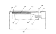
図1は本発明の第1の実施形態による固体撮像素子の上面図、図2は図1の固体撮像素子のa−a’断面図である。図1中の101は活性領域を示している。活性領域101と境界を同じくし活性領域101を取り囲む領域はシリコン酸化膜がシリコン基板に埋め込まれた素子分離領域を形成している。図2中101’はこの素子分離領域に該当する。102は電極であり、103はFD領域である。104は蓄積領域であり、光電変換により発生した電荷を蓄積する。109は半導体基板である。109は、例えば蓄積領域104と同じ導電型で蓄積領域104より低濃度の基板を使用するが、蓄積領域104と反対導電型で低濃度の基板を使用しても良い。更に、蓄積領域104と同じ低濃度基板に反対導電型のウエルを形成した基板でもよい。蓄積領域104は光電変換部(フォトダイオード)としての機能も有する。105は表面領域であり、蓄積領域104とは異なる導電型の半導体領域である。表面領域105の存在により蓄積領域104がゲート絶縁膜110との界面に接することを防ぎ、埋め込みフォトダイオード構造を実現することが可能である。106及び107はいずれもコンタクトホールであり、106はFD領域103を、107は電極102を、配線層(図示せず)と電気的に接続している。108はフィールドストップ領域であり、蓄積領域104とFD領域103との間における電荷のポテンシャル分離の役割を果たす。
(First embodiment)
FIG. 1 is a top view of a solid-state image sensor according to the first embodiment of the present invention, and FIG. 2 is a cross-sectional view of the solid-state image sensor of FIG. In FIG. 1,
素子分離領域101'は例えばSTI(shallow trench isolation)にて形成することが可能である。電極102は例えば薄膜ポリシリコンを用いることが可能である。ポリシリコンの膜厚は、センサで受光する波長の光に対して十分な透過率が確保できる程度の薄さであればよい。FD領域103は例えば、電極102を形成後、セルフアラインのイオン注入にて形成することが可能である。イオンの種類としては、Ph又はAsを用いることによりn型の不純物拡散層を形成することができる。蓄積領域104及び表面領域105は例えば、電極102の形成前にレジストパターンを用いてイオン注入し、形成することが可能である。蓄積領域104はPh又はAsによりn型の不純物拡散層にて形成することが可能であり、表面領域105はB又はBF2の注入によりP型の不純物拡散層にて形成することが可能である。フィールドストップ領域108は、例えば、電極102を形成後、もしくは電極102をパターニングしたレジストが残った状態で、セルフアラインのイオン注入にて形成することも可能である。このイオン注入はB又はBF2により行うことが可能であり、P型の不純物拡散層にて形成することが可能である。ゲート絶縁膜110は例えばシリコン酸化膜を用いることも可能である。
The
本実施形態おいては、蓄積領域104は素子分離領域101'に対してオフセットを持っている。このことにより素子分離領域101'との界面により発生する暗電流を抑制することが可能である。また、本実施形態において、電極102は図1において、蓄積領域104を覆うように形成されている。
In the present embodiment, the
本実施形態では、蓄積領域104の電荷をFD領域103に転送する機能を有する転送ゲートと蓄積領域104そのものを覆う電極102は一体となっている。
In the present embodiment, the transfer gate having a function of transferring the charge in the
背景技術で述べた特許文献1及び特許文献2では言及されていないが、本発明者の検討によれば、小さなフォトダイオードにマイクロレンズ等で光を集光する場合には次のような問題も発生する。 Although not mentioned in Patent Document 1 and Patent Document 2 described in the background art, according to the study of the present inventor, the following problem occurs when light is collected by a microlens or the like on a small photodiode. appear.
画素に垂直に入射した光は、マイクロレンズ等の効果によりフォトダイオードの中心付近に集光する。ところが、撮像領域の端部においては画素に入射する光は垂直から若干の傾きをもって入射され、その場合にはマイクロレンズの集光位置はフォトダイオードの中心からずれた場所になる。特許文献1では、左方向から角度をもって入射した場合は転送トランジスタのポリシリコンゲートに集光領域がかかり、右方向から角度をもって入射した場合は素子分離領域に集光領域がかかる。ポリシリコンゲートは短波長の光の吸収率が高く、長波長の光の吸収率が低いため、半導体領域に到達する光の量の波長依存は入射する角度により異なる。また、本発明者の実験によると、半導体領域に入射した光は、光電変換領域に入射しなかった場合でも、確率的に光電変換領域に光電荷が流れ込む。 Light incident perpendicularly to the pixel is collected near the center of the photodiode by the effect of a microlens or the like. However, at the end of the imaging region, light incident on the pixel is incident with a slight inclination from the vertical, and in this case, the condensing position of the microlens is shifted from the center of the photodiode. In Patent Document 1, a condensing region is applied to the polysilicon gate of the transfer transistor when entering from the left direction with an angle, and a condensing region is applied to the element isolation region when entering with an angle from the right direction. Since the polysilicon gate has a high absorptance for short-wavelength light and a low absorptance for long-wavelength light, the wavelength dependence of the amount of light reaching the semiconductor region differs depending on the incident angle. Further, according to an experiment by the present inventor, even when light incident on the semiconductor region does not enter the photoelectric conversion region, photocharge flows into the photoelectric conversion region stochastically.
結果として、フォトダイオードの光電荷の発生率の波長依存、すなわち分光感度特性が入射角度により異なる結果となる。このことは画面内での色の均一性を悪化させる要因となる。 As a result, the wavelength dependence of the photocharge generation rate of the photodiode, that is, the spectral sensitivity characteristic varies depending on the incident angle. This is a factor that deteriorates the uniformity of color in the screen.
一方、本実施形態においては転送ゲートと蓄積領域を覆う電極102が一体となっており、蓄積領域全面を包含しているため、入射角度による分光感度の変化を抑制することができる。故に、本実施形態による固体撮像素子においては、撮像領域内の色の均一性が改善される。
On the other hand, in this embodiment, the transfer gate and the
さらに加えて、本実施形態では次の効果もある。斜めに光が入射される光学的な要因として、対物レンズのF値が挙げられる。撮影時において、よりたくさんの光を取り込むためには絞りを開放に近づけ、F値を小さくし撮影を行う。F値が小さくなると、ひとつのマイクロレンズに入射する光は、垂直入射のみならず、さまざまな角度から入射する光の総和となる。すなわち、F値を変えることにより入射する光の角度が変わることになる。上述の課題と同様の原理にて、F値によって画像の色みが変わってしまうという課題も生じる。本実施形態の固体撮像素子においては、この課題も軽減する効果を得ることができる。 In addition, the present embodiment has the following effects. As an optical factor in which light is incident obliquely, the F value of the objective lens can be cited. At the time of shooting, in order to capture more light, the aperture is set close to the full aperture, and shooting is performed with a smaller F value. When the F value decreases, the light incident on one microlens becomes the sum of the light incident from various angles as well as normal incidence. That is, changing the F value changes the angle of incident light. On the same principle as the above-described problem, there also arises a problem that the color of the image changes depending on the F value. In the solid-state imaging device of the present embodiment, an effect of reducing this problem can be obtained.
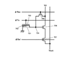
図5は本実施形態による画素の等価回路図であり、図6は本実施形態による画素の駆動タイミング図である。半導体基板上には、複数の画素が設けられる。本実施形態による固体撮像素子の駆動方法について、図5及び図6を用いて説明する。701は蓄積領域であり、702は表面領域、703は電極、704はFD領域、705はリセットトランジスタ、706はソースフォロワトランジスタであり、707は選択トランジスタである。蓄積の開始前に、信号φRes及びφTxによりリセットトランジスタ705及び転送ゲート703をオンすることによりフォダイオード(蓄積領域)701を空にリセットする。蓄積の終了及びCDS動作は以下の駆動により行う。信号φSelにて選択トランジスタ707をオンし、読み出す行を選択した後、信号φResにてリセットトランジスタ705をオンし、FD領域704をリセットする。そして、そのときのVout電位を信号φTnにて読み出し、回路部のメモリ(図示せず)にサンプルホールドする。この時の信号がノイズ信号となる。次に、信号φTxにて転送ゲート703をオンし、蓄積領域701内の光電荷をFD部704に転送した後、Vout電位を信号φTsにて読み出し回路部のメモリ(図示せず)にサンプルホールドする。この時の信号が画素信号となる。メモリに蓄えられた画素信号とノイズ信号の差分を算出することで、光電荷に相当する画素信号を読み出すことができる。
FIG. 5 is an equivalent circuit diagram of the pixel according to the present embodiment, and FIG. 6 is a drive timing diagram of the pixel according to the present embodiment. A plurality of pixels are provided on the semiconductor substrate. A method for driving the solid-state imaging device according to the present embodiment will be described with reference to FIGS. 5 and 6. 701 is a storage region, 702 is a surface region, 703 is an electrode, 704 is an FD region, 705 is a reset transistor, 706 is a source follower transistor, and 707 is a selection transistor. Before starting the accumulation, the photodiode (accumulation region) 701 is reset to empty by turning on the
本実施形態の固体撮像素子の電荷の転送方法について説明する。なお、ここで扱う光電荷とは電子である。背景技術で述べた特許文献2の駆動との大きな違いは、ゲート電極(本実施形態では電極703)に印加する電位にある。特許文献2では蓄積中には光電荷をゲート絶縁膜界面に集めるための高い電位を与え、転送時には低い電位を与えているのに対して、本実施形態においては逆に蓄積中には低い電位を与えることで、ゲート絶縁膜界面付近に光電荷を溜めない。このことにより暗電流値を著しく低減する効果がある。本実施形態においては、光電荷の転送は電極703に高い電位を与えることで行う。
A charge transfer method of the solid-state imaging device of the present embodiment will be described. Note that the photocharge handled here is an electron. A major difference from the driving of Patent Document 2 described in the background art is the potential applied to the gate electrode (the
本実施形態にて光電荷の完全転送が可能となるメカニズムを図1及び図2を参照して説明する。表面領域105はFD領域103と接する側には形成せず、FD領域103と離れた側に形成する。電極下活性領域111は、電極102の下の活性領域111である。FD領域103に近い側の電極下活性領域111は、電極102の電位によるポテンシャルの変調の影響を敏感に受ける。一方、表面領域105は半導体基板109と同じ導電型であり、半導体基板109と同電位に固定されるため、FD領域103に遠い側の電極下活性領域112は電極102の電位によるポテンシャルの変調の影響を受けにくい。よって、電極102に高い電位を与えた際には、光電荷はFD領域103に遠い側の電極下活性領域112からFD領域103に近い側の電極下活性領域111に移動する。さらにFD領域103に高いリセット電位が与えられているので、光電荷はFD領域103に転送される。
A mechanism that enables complete transfer of photocharge in this embodiment will be described with reference to FIGS. The
以上、本実施形態においては、小さな画素を形成した場合にもフォトダイオードの面積を確保することができ、感度、飽和が改善される。また、埋め込みフォトダイオード構造を実現できるため、暗電流が小さく、ノイズの少ない固体撮像素子の提供が可能となる。さらに、対物レンズを用いて撮像領域に結像した際にも、画面内の色の不均一性が抑制される。 As described above, in this embodiment, even when a small pixel is formed, the area of the photodiode can be ensured, and sensitivity and saturation are improved. In addition, since a buried photodiode structure can be realized, it is possible to provide a solid-state imaging device with low dark current and low noise. Furthermore, color nonuniformity in the screen is also suppressed when an image is formed on the imaging region using the objective lens.
(第2の実施形態)
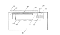
図3は本発明の第2の実施形態による固体撮像素子の上面図であり、図4は図3の固体撮像素子のb−b’断面図である。各部品番号301から312は、それぞれ第1の実施形態における101から112と同じ部分を示す。また、画素の等価回路、駆動タイミングは第1の実施形態と同等のものを選択可能である。本実施形態の特徴は、電極302が活性領域301をオーバーラップして配置されている点である。本実施形態の構造においても第1の実施形態と同様に埋め込みフォトダイオード構造を実現することが可能であり、暗電流の抑制が可能である。さらに本実施形態では、電極302がSTIエッジ部に乗っており、STIエッジ部のポテンシャルを制御することが可能である。このことにより、ストレスの大きいSTIエッジ部付近におけるマイノリティキャリア濃度を制御でき、暗電流値を低減することが可能となる。
(Second Embodiment)
FIG. 3 is a top view of a solid-state image sensor according to the second embodiment of the present invention, and FIG. 4 is a cross-sectional view taken along the line bb ′ of the solid-state image sensor of FIG. Each
加えて、本実施形態では以下の効果も得られる。本実施形態では電極302の面積をより大きくレイアウトすることが可能となり、感度、隣接画素へのクロストークの改善がはかれる。電極302の端部においては、入射光が側面において反射する現象や、回折する現象が確認されている。本実施形態では電極302の端部を第1の実施形態に比べ蓄積領域304の中心から、より遠くに配することが可能である。よって本実施形態では電極302端部の光学的な影響を抑制することができ、隣接画素へのクロストークを低減できる。効果は解像度を高めるのみならず、カラーフィルタを搭載した単板式カラー撮像素子においては色再現性を向上する結果となる。
In addition, the following effects can also be obtained in the present embodiment. In this embodiment, the
(第3の実施形態)
図7は、本発明の第3の実施形態による固体撮像素子のa−a’断面図である。各部品番号901から912は、それぞれ第1の実施形態における101から112と同じ部分を示す。また、画素の等価回路、駆動タイミングは第1の実施形態と同等のものを選択可能である。本実施形態の特徴は、第1の表面領域905に加え、第2の表面領域905'が形成されている点である。
(Third embodiment)
FIG. 7 is an aa ′ sectional view of a solid-state imaging device according to the third embodiment of the present invention. Each
第2の表面領域905'は、第1の表面領域905より不純物濃度が薄くなっているか、あるいは深さが浅くなっている。電極902に高い電位を印加した際、第2の表面領域905'を空乏化させるか、あるいは反転層を形成可能にすることにより、第1の実施形態と同様に光電荷をFD領域903に転送することが可能である。
The
本実施形態では第1の実施形態で得られた効果に加えて、フォトダイオードの埋め込み構造をより実現しやすく、蓄積中における暗電流を低減することが可能である。すなわち、第2の表面領域905'の埋め込み性が高いため、905'近傍での暗電流発生をより効果的に抑制することが可能となる。
In this embodiment, in addition to the effects obtained in the first embodiment, it is easier to realize a photodiode embedding structure, and dark current during accumulation can be reduced. That is, since the embedding property of the
上記第1〜3の実施形態においては、蓄積する光電荷は電子であったが、光電荷として正孔を蓄積することも可能である。この場合、各不純物拡散領域の極性を反転することにより形成が可能である。また、駆動パルスについては電位の高低を逆転することで正孔の完全転送が可能となる。この場合にも、本発明の第1〜第3の実施形態で得られた効果を得ることが可能である。 In the first to third embodiments, the photocharge to be accumulated is an electron, but it is also possible to accumulate holes as the photocharge. In this case, it can be formed by reversing the polarity of each impurity diffusion region. Further, with respect to the driving pulse, the hole can be completely transferred by reversing the potential level. Also in this case, it is possible to obtain the effects obtained in the first to third embodiments of the present invention.
第1〜第3の実施形態による固体撮像素子によれば、画素サイズの微細化を行った場合においても十分な感度及び飽和を確保することができ、また完全転送型で、埋め込み型のフォトダイオードを実現することができる。すなわち、表面にゲート電極を配するフォトダイオード、埋め込みフォトダイオード構造、及び完全転送型フォトダイオードのすべてを満たす画素構造を実現することができる。これにより、小型、高精細な固体撮像素子において低ノイズ、高感度、広いダイナミックレンジの撮像が可能となる。 According to the solid-state imaging device according to the first to third embodiments, sufficient sensitivity and saturation can be ensured even when the pixel size is miniaturized, and it is a complete transfer type and embedded type photodiode. Can be realized. That is, it is possible to realize a pixel structure that satisfies all of the photodiode having the gate electrode on the surface, the embedded photodiode structure, and the complete transfer type photodiode. Thereby, it is possible to perform imaging with low noise, high sensitivity, and a wide dynamic range in a small and high-definition solid-state imaging device.
第1〜第3の実施形態の固体撮像素子は、半導体基板109等上に形成され、電荷を蓄積する第1の導電型の電荷蓄積領域104等を有する。第2の導電型の第1の表面領域105等は、電荷蓄積領域104等の少なくとも一部を覆って半導体基板109等の表面に形成される。第1の導電型のフローティングディフュージョン領域103等は、電荷を蓄積するための領域である。電極102等は、電荷蓄積領域104等の全面を覆い、半導体基板109等上にゲート絶縁膜110等を介して、電荷蓄積領域104等に蓄積された電荷をフローティングディフュージョン領域103等に転送する。
The solid-state imaging devices of the first to third embodiments are formed on a
電極102等は光が透過可能な膜厚である。電極102等の下は、フローティングディフュージョン領域103等から離れ第1の表面領域105等を有する部分と、フローティングディフュージョン領域103等に近く第1の表面領域105等を有しない部分とを有する。
The
また、電荷蓄積領域104等に蓄積された電荷をフローティングディフュージョン領域103等に転送する期間中に、電極102等には前記電荷を半導体基板109等の表面側に引き寄せる電位を与える。また、電荷蓄積領域104等は、光電変換により生成された電荷を蓄積する。
Further, during the period in which the charge accumulated in the
第1及び第2の実施形態では、電極102の下において、フローティングディフュージョン領域103等に近く第1の表面領域105等を有しない部分(電極下活性領域111等)は、電荷蓄積領域104等と同じ導電型である。
In the first and second embodiments, a portion under the
また、第3の実施形態では、フローティングディフュージョン領域903に近く第1の表面領域905を有しない部分は、第2の表面領域905’である。電極902の下において、フローティングディフュージョン領域903に近く第1の表面領域905を有しない部分(第2の表面領域905’)は、フローティングディフュージョン領域903から離れ第1の表面領域905を有する部分に比べて不純物濃度が薄い。
In the third embodiment, the portion near the floating
第1〜第3の実施形態の固体撮像素子は、暗電流が少なくかつ、CDS動作によるリセットノイズ除去が行え、低照度の撮影環境においても高いS/N比での撮影が可能である。また、画素サイズの微細化を行った場合においても十分な感度及び飽和を確保することができ、また完全転送型で、埋め込み型のフォトダイオードを実現することができる。そのため、小型、高精細な固体撮像素子において低ノイズ、高感度、広いダイナミックレンジの撮像が可能となる。 The solid-state imaging devices of the first to third embodiments have a small dark current, can perform reset noise removal by the CDS operation, and can perform shooting with a high S / N ratio even in a low-illumination shooting environment. Further, sufficient sensitivity and saturation can be ensured even when the pixel size is reduced, and a complete transfer type and embedded type photodiode can be realized. Therefore, it is possible to perform imaging with low noise, high sensitivity, and a wide dynamic range in a small, high-definition solid-state imaging device.
なお、上記実施形態は、何れも本発明を実施するにあたっての具体化の例を示したものに過ぎず、これらによって本発明の技術的範囲が限定的に解釈されてはならないものである。すなわち、本発明はその技術思想、又はその主要な特徴から逸脱することなく、様々な形で実施することができる。 The above-described embodiments are merely examples of implementation in carrying out the present invention, and the technical scope of the present invention should not be construed in a limited manner. That is, the present invention can be implemented in various forms without departing from the technical idea or the main features thereof.
101、301、501、601 活性領域
101'、301'、501'、601'、901' 素子分離領域
102、302、502、602、703、902 電極
103、303、503、603、903 FD領域
104、304、504、604、701、904 蓄積領域
105、305、505、605、702、905 表面領域
905’ 第2の表面領域
106、107、306、307、506、507、606、607、906 コンタクトホール
108、308、508、608、908 フィールドストップ領域
109、309、509、609、909 半導体基板
110、310、510、610、910 ゲート絶縁膜
111、311、511、611、911 FD領域に近い側の電極下活性領域
112、312、512、612、912 FD領域に遠い側の電極下活性領域
704 FD領域
705 リセットトランジスタ
706 ソースフォロワトランジスタ
707 選択トランジスタ
101, 301, 501, 601
Claims (4)
前記電荷蓄積領域の少なくとも一部を覆って前記半導体基板の表面に形成された第2の導電型の第1の表面領域と、
電荷を蓄積する第1の導電型のフローティングディフュージョン領域と、
前記電荷蓄積領域の全面を覆い、前記半導体基板上にゲート絶縁膜を介して、前記電荷蓄積領域に蓄積された電荷を前記フローティングディフュージョン領域に転送する電極とを有し、
前記電極は光が透過可能な膜厚であり、
前記電極の下は、前記フローティングディフュージョン領域から離れ前記第1の表面領域を有する部分と、前記フローティングディフュージョン領域に近く前記第1の表面領域を有しない部分とを有することを特徴とする固体撮像素子。 A charge storage region of a first conductivity type formed on the semiconductor substrate and storing charge;
A first surface region of a second conductivity type formed on the surface of the semiconductor substrate so as to cover at least a part of the charge storage region;
A floating diffusion region of a first conductivity type for accumulating charge;
An electrode that covers the entire surface of the charge storage region and transfers charges stored in the charge storage region to the floating diffusion region via a gate insulating film on the semiconductor substrate;
The electrode has a film thickness that allows light to pass through,
A solid-state imaging device having a portion under the electrode and having the first surface region away from the floating diffusion region and a portion not having the first surface region near the floating diffusion region .
Priority Applications (2)
| Application Number | Priority Date | Filing Date | Title |
|---|---|---|---|
| JP2009039755A JP2010199154A (en) | 2009-02-23 | 2009-02-23 | Solid-state imaging element |
| US12/697,408 US20100214464A1 (en) | 2009-02-23 | 2010-02-01 | Solid-state imaging apparatus |
Applications Claiming Priority (1)
| Application Number | Priority Date | Filing Date | Title |
|---|---|---|---|
| JP2009039755A JP2010199154A (en) | 2009-02-23 | 2009-02-23 | Solid-state imaging element |
Publications (2)
| Publication Number | Publication Date |
|---|---|
| JP2010199154A true JP2010199154A (en) | 2010-09-09 |
| JP2010199154A5 JP2010199154A5 (en) | 2012-03-08 |
Family
ID=42630655
Family Applications (1)
| Application Number | Title | Priority Date | Filing Date |
|---|---|---|---|
| JP2009039755A Pending JP2010199154A (en) | 2009-02-23 | 2009-02-23 | Solid-state imaging element |
Country Status (2)
| Country | Link |
|---|---|
| US (1) | US20100214464A1 (en) |
| JP (1) | JP2010199154A (en) |
Families Citing this family (7)
| Publication number | Priority date | Publication date | Assignee | Title |
|---|---|---|---|---|
| JP2010206178A (en) | 2009-02-06 | 2010-09-16 | Canon Inc | Photoelectric conversion apparatus, and method of manufacturing photoelectric conversion apparatus |
| JP5538922B2 (en) * | 2009-02-06 | 2014-07-02 | キヤノン株式会社 | Method for manufacturing solid-state imaging device |
| JP2010206181A (en) * | 2009-02-06 | 2010-09-16 | Canon Inc | Photoelectric conversion apparatus and imaging system |
| JP6016434B2 (en) | 2012-04-23 | 2016-10-26 | キヤノン株式会社 | Solid-state imaging device, manufacturing method thereof, and camera |
| JP2016082306A (en) | 2014-10-10 | 2016-05-16 | キヤノン株式会社 | Imaging device, imaging system and driving method for imaging device |
| US11425365B2 (en) | 2018-12-14 | 2022-08-23 | Canon Kabushiki Kaisha | Photoelectric conversion device, method of manufacturing photoelectric conversion device, and method of manufacturing semiconductor device |
| US11922175B2 (en) | 2022-07-29 | 2024-03-05 | Arista Networks, Inc. | Unplanned reboot expedited recovery for network devices |
Citations (5)
| Publication number | Priority date | Publication date | Assignee | Title |
|---|---|---|---|---|
| JP2003115580A (en) * | 2001-10-04 | 2003-04-18 | Sony Corp | Solid state image sensor and its manufacturing method |
| JP2004134685A (en) * | 2002-10-15 | 2004-04-30 | Toshiba Corp | Solid state imaging device and its fabricating method |
| JP2005268814A (en) * | 2002-06-27 | 2005-09-29 | Canon Inc | Solid state imaging device and camera system using the same |
| JP2006310835A (en) * | 2005-04-28 | 2006-11-09 | Samsung Electronics Co Ltd | Cmos image sensor and manufacturing method therefor |
| JP2008124463A (en) * | 2006-11-08 | 2008-05-29 | Samsung Electronics Co Ltd | Pixel structure and circuit of cmos image sensor |
Family Cites Families (14)
| Publication number | Priority date | Publication date | Assignee | Title |
|---|---|---|---|---|
| JP2003031787A (en) * | 2001-07-17 | 2003-01-31 | Canon Inc | Solid state image sensor and its driving method |
| US7078745B2 (en) * | 2003-03-05 | 2006-07-18 | Micron Technology, Inc. | CMOS imager with enhanced transfer of charge and low voltage operation |
| US7095075B2 (en) * | 2003-07-01 | 2006-08-22 | Micron Technology, Inc. | Apparatus and method for split transistor memory having improved endurance |
| JP2005142470A (en) * | 2003-11-10 | 2005-06-02 | Seiko Instruments Inc | Photoelectric converter and image sensor ic |
| JP4916101B2 (en) * | 2004-09-01 | 2012-04-11 | キヤノン株式会社 | Photoelectric conversion device, solid-state imaging device, and solid-state imaging system |
| JP2006073736A (en) * | 2004-09-01 | 2006-03-16 | Canon Inc | Photoelectric converter, solid state imaging device and system |
| JP2006073885A (en) * | 2004-09-03 | 2006-03-16 | Canon Inc | Solid state imaging device, its manufacturing device, and digital camera |
| JP5132102B2 (en) * | 2006-08-01 | 2013-01-30 | キヤノン株式会社 | Photoelectric conversion device and imaging system using photoelectric conversion device |
| JP5110820B2 (en) * | 2006-08-02 | 2012-12-26 | キヤノン株式会社 | Photoelectric conversion device, photoelectric conversion device manufacturing method, and imaging system |
| JP4350768B2 (en) * | 2007-04-16 | 2009-10-21 | キヤノン株式会社 | Photoelectric conversion device and imaging device |
| JP2009021809A (en) * | 2007-07-11 | 2009-01-29 | Canon Inc | Driving method of imaging device, imaging device, and imaging system |
| JP5153378B2 (en) * | 2008-02-15 | 2013-02-27 | キヤノン株式会社 | Solid-state imaging device and driving method thereof |
| JP5335271B2 (en) * | 2008-04-09 | 2013-11-06 | キヤノン株式会社 | Photoelectric conversion device and imaging system using the same |
| JP5188275B2 (en) * | 2008-06-06 | 2013-04-24 | キヤノン株式会社 | Solid-state imaging device, driving method thereof, and imaging system |
-
2009
- 2009-02-23 JP JP2009039755A patent/JP2010199154A/en active Pending
-
2010
- 2010-02-01 US US12/697,408 patent/US20100214464A1/en not_active Abandoned
Patent Citations (5)
| Publication number | Priority date | Publication date | Assignee | Title |
|---|---|---|---|---|
| JP2003115580A (en) * | 2001-10-04 | 2003-04-18 | Sony Corp | Solid state image sensor and its manufacturing method |
| JP2005268814A (en) * | 2002-06-27 | 2005-09-29 | Canon Inc | Solid state imaging device and camera system using the same |
| JP2004134685A (en) * | 2002-10-15 | 2004-04-30 | Toshiba Corp | Solid state imaging device and its fabricating method |
| JP2006310835A (en) * | 2005-04-28 | 2006-11-09 | Samsung Electronics Co Ltd | Cmos image sensor and manufacturing method therefor |
| JP2008124463A (en) * | 2006-11-08 | 2008-05-29 | Samsung Electronics Co Ltd | Pixel structure and circuit of cmos image sensor |
Also Published As
| Publication number | Publication date |
|---|---|
| US20100214464A1 (en) | 2010-08-26 |
Similar Documents
| Publication | Publication Date | Title |
|---|---|---|
| US9985064B2 (en) | Solid-state imaging device and method of manufacturing the same, and imaging apparatus | |
| US8792035B2 (en) | Solid-state imaging device and manufacturing method thereof, driving method of solid-state imaging device, and electronic equipment | |
| JP2023118774A (en) | Photodetector | |
| KR101683307B1 (en) | Solid-state imaging device, method of manufacturing solid-state imaging device, and electronic apparatus | |
| TWI497702B (en) | Solid state camera device | |
| US8716719B2 (en) | Solid-state imaging device, method of manufacturing solid-state imaging device, and electronic apparatus | |
| JP5651976B2 (en) | Solid-state imaging device, manufacturing method thereof, and electronic device | |
| US20190088704A1 (en) | Image sensors | |
| US9985066B2 (en) | Solid-state imaging device, method for manufacturing same, and electronic device | |
| JP4585964B2 (en) | Solid-state imaging device | |
| KR102609646B1 (en) | Imaging element and electronic device | |
| WO2014141900A1 (en) | Solid-state image-pickup element, method for producing same, and electronic equipment | |
| KR102290502B1 (en) | Image sensor and method of fabricating the same | |
| JP6186205B2 (en) | Imaging device and imaging apparatus | |
| JP2015065270A (en) | Solid state image pickup device and manufacturing method of the same, and electronic apparatus | |
| JP2015053411A (en) | Solid-state imaging device, method for manufacturing solid-state imaging device, and electronic equipment | |
| JP2012199489A (en) | Solid state image pickup device, solid state image pickup device manufacturing method and electronic apparatus | |
| KR20150002593A (en) | Solid-state imaging device and electronic device | |
| JP2009065098A (en) | Backside irradiation type solid-state imaging device and method of manufacturing the same | |
| JP2010199154A (en) | Solid-state imaging element | |
| US7259361B2 (en) | Producing method for solid-state image pickup device including formation of a carrier accumulating region | |
| JP2012164892A (en) | Solid-state image sensor | |
| US8618623B2 (en) | Solid-state image pickup device and method for manufacturing same, and image pickup apparatus | |
| US9741758B2 (en) | Methods of forming image sensors including deposited negative fixed charge layers on photoelectric conversion regions | |
| TWI525801B (en) | Image sensor with doped transfer gate |
Legal Events
| Date | Code | Title | Description |
|---|---|---|---|
| A521 | Request for written amendment filed |
Free format text: JAPANESE INTERMEDIATE CODE: A523 Effective date: 20120124 |
|
| A621 | Written request for application examination |
Free format text: JAPANESE INTERMEDIATE CODE: A621 Effective date: 20120124 |
|
| A977 | Report on retrieval |
Free format text: JAPANESE INTERMEDIATE CODE: A971007 Effective date: 20130522 |
|
| A131 | Notification of reasons for refusal |
Free format text: JAPANESE INTERMEDIATE CODE: A131 Effective date: 20130528 |
|
| A521 | Request for written amendment filed |
Free format text: JAPANESE INTERMEDIATE CODE: A523 Effective date: 20130724 |
|
| A131 | Notification of reasons for refusal |
Free format text: JAPANESE INTERMEDIATE CODE: A131 Effective date: 20131203 |
|
| A02 | Decision of refusal |
Free format text: JAPANESE INTERMEDIATE CODE: A02 Effective date: 20140401 |