WO2014141900A1 - Solid-state image-pickup element, method for producing same, and electronic equipment - Google Patents
Solid-state image-pickup element, method for producing same, and electronic equipment Download PDFInfo
- Publication number
- WO2014141900A1 WO2014141900A1 PCT/JP2014/055008 JP2014055008W WO2014141900A1 WO 2014141900 A1 WO2014141900 A1 WO 2014141900A1 JP 2014055008 W JP2014055008 W JP 2014055008W WO 2014141900 A1 WO2014141900 A1 WO 2014141900A1
- Authority
- WO
- WIPO (PCT)
- Prior art keywords
- gate electrode
- photoelectric conversion
- transfer transistor
- semiconductor substrate
- transistor
- Prior art date
Links
- 238000004519 manufacturing process Methods 0.000 title claims abstract description 42
- 238000012546 transfer Methods 0.000 claims abstract description 235
- 239000004065 semiconductor Substances 0.000 claims abstract description 182
- 239000000758 substrate Substances 0.000 claims abstract description 170
- 238000006243 chemical reaction Methods 0.000 claims abstract description 168
- 239000012535 impurity Substances 0.000 claims abstract description 94
- 238000000034 method Methods 0.000 claims abstract description 33
- 238000003384 imaging method Methods 0.000 claims description 95
- 230000015572 biosynthetic process Effects 0.000 claims description 15
- 238000002955 isolation Methods 0.000 claims description 14
- 238000009792 diffusion process Methods 0.000 claims description 9
- 239000000463 material Substances 0.000 claims description 8
- 239000012212 insulator Substances 0.000 claims description 6
- 230000031700 light absorption Effects 0.000 claims description 6
- 238000005516 engineering process Methods 0.000 description 26
- 239000010410 layer Substances 0.000 description 25
- 230000003321 amplification Effects 0.000 description 12
- 230000006870 function Effects 0.000 description 12
- 238000003199 nucleic acid amplification method Methods 0.000 description 12
- VYPSYNLAJGMNEJ-UHFFFAOYSA-N Silicium dioxide Chemical compound O=[Si]=O VYPSYNLAJGMNEJ-UHFFFAOYSA-N 0.000 description 10
- 230000000875 corresponding effect Effects 0.000 description 10
- 229910021420 polycrystalline silicon Inorganic materials 0.000 description 10
- 229920005591 polysilicon Polymers 0.000 description 10
- 229910052814 silicon oxide Inorganic materials 0.000 description 10
- 238000001312 dry etching Methods 0.000 description 6
- 238000012986 modification Methods 0.000 description 6
- 230000004048 modification Effects 0.000 description 6
- XUIMIQQOPSSXEZ-UHFFFAOYSA-N Silicon Chemical compound [Si] XUIMIQQOPSSXEZ-UHFFFAOYSA-N 0.000 description 5
- 150000002500 ions Chemical class 0.000 description 5
- 238000012545 processing Methods 0.000 description 5
- 229910052710 silicon Inorganic materials 0.000 description 5
- 239000010703 silicon Substances 0.000 description 5
- 238000003860 storage Methods 0.000 description 5
- ZOXJGFHDIHLPTG-UHFFFAOYSA-N Boron Chemical compound [B] ZOXJGFHDIHLPTG-UHFFFAOYSA-N 0.000 description 4
- 229910052796 boron Inorganic materials 0.000 description 4
- 238000010586 diagram Methods 0.000 description 4
- 238000007599 discharging Methods 0.000 description 4
- 238000009826 distribution Methods 0.000 description 4
- 230000003287 optical effect Effects 0.000 description 4
- 238000000926 separation method Methods 0.000 description 4
- 238000009825 accumulation Methods 0.000 description 3
- 150000001875 compounds Chemical class 0.000 description 3
- 230000007274 generation of a signal involved in cell-cell signaling Effects 0.000 description 3
- 238000005468 ion implantation Methods 0.000 description 3
- 229910052782 aluminium Inorganic materials 0.000 description 2
- XAGFODPZIPBFFR-UHFFFAOYSA-N aluminium Chemical compound [Al] XAGFODPZIPBFFR-UHFFFAOYSA-N 0.000 description 2
- DVRDHUBQLOKMHZ-UHFFFAOYSA-N chalcopyrite Chemical group [S-2].[S-2].[Fe+2].[Cu+2] DVRDHUBQLOKMHZ-UHFFFAOYSA-N 0.000 description 2
- ZYGHJZDHTFUPRJ-UHFFFAOYSA-N coumarin Chemical compound C1=CC=C2OC(=O)C=CC2=C1 ZYGHJZDHTFUPRJ-UHFFFAOYSA-N 0.000 description 2
- 239000013078 crystal Substances 0.000 description 2
- 238000000151 deposition Methods 0.000 description 2
- 238000001514 detection method Methods 0.000 description 2
- 230000000694 effects Effects 0.000 description 2
- 230000005684 electric field Effects 0.000 description 2
- 238000005401 electroluminescence Methods 0.000 description 2
- 239000011229 interlayer Substances 0.000 description 2
- 229910052751 metal Inorganic materials 0.000 description 2
- 239000002184 metal Substances 0.000 description 2
- 239000011368 organic material Substances 0.000 description 2
- 230000003647 oxidation Effects 0.000 description 2
- 238000007254 oxidation reaction Methods 0.000 description 2
- 230000002093 peripheral effect Effects 0.000 description 2
- 238000005036 potential barrier Methods 0.000 description 2
- 229910052711 selenium Inorganic materials 0.000 description 2
- 239000011669 selenium Substances 0.000 description 2
- WFKWXMTUELFFGS-UHFFFAOYSA-N tungsten Chemical compound [W] WFKWXMTUELFFGS-UHFFFAOYSA-N 0.000 description 2
- 229910052721 tungsten Inorganic materials 0.000 description 2
- 239000010937 tungsten Substances 0.000 description 2
- 230000003139 buffering effect Effects 0.000 description 1
- 230000000295 complement effect Effects 0.000 description 1
- 230000001276 controlling effect Effects 0.000 description 1
- 238000012937 correction Methods 0.000 description 1
- 230000002596 correlated effect Effects 0.000 description 1
- 229960000956 coumarin Drugs 0.000 description 1
- 235000001671 coumarin Nutrition 0.000 description 1
- 238000006073 displacement reaction Methods 0.000 description 1
- 239000004973 liquid crystal related substance Substances 0.000 description 1
- 239000011159 matrix material Substances 0.000 description 1
- 229960000901 mepacrine Drugs 0.000 description 1
- 229910044991 metal oxide Inorganic materials 0.000 description 1
- 150000004706 metal oxides Chemical class 0.000 description 1
- 238000002156 mixing Methods 0.000 description 1
- 238000000059 patterning Methods 0.000 description 1
- 238000000206 photolithography Methods 0.000 description 1
- 229920002120 photoresistant polymer Polymers 0.000 description 1
- GPKJTRJOBQGKQK-UHFFFAOYSA-N quinacrine Chemical compound C1=C(OC)C=C2C(NC(C)CCCN(CC)CC)=C(C=CC(Cl)=C3)C3=NC2=C1 GPKJTRJOBQGKQK-UHFFFAOYSA-N 0.000 description 1
- 238000005070 sampling Methods 0.000 description 1
Images


Classifications
-
- H—ELECTRICITY
- H01—ELECTRIC ELEMENTS
- H01L—SEMICONDUCTOR DEVICES NOT COVERED BY CLASS H10
- H01L27/00—Devices consisting of a plurality of semiconductor or other solid-state components formed in or on a common substrate
- H01L27/14—Devices consisting of a plurality of semiconductor or other solid-state components formed in or on a common substrate including semiconductor components sensitive to infrared radiation, light, electromagnetic radiation of shorter wavelength or corpuscular radiation and specially adapted either for the conversion of the energy of such radiation into electrical energy or for the control of electrical energy by such radiation
- H01L27/144—Devices controlled by radiation
- H01L27/146—Imager structures
- H01L27/14601—Structural or functional details thereof
- H01L27/14609—Pixel-elements with integrated switching, control, storage or amplification elements
- H01L27/14612—Pixel-elements with integrated switching, control, storage or amplification elements involving a transistor
- H01L27/14614—Pixel-elements with integrated switching, control, storage or amplification elements involving a transistor having a special gate structure
-
- H—ELECTRICITY
- H01—ELECTRIC ELEMENTS
- H01L—SEMICONDUCTOR DEVICES NOT COVERED BY CLASS H10
- H01L27/00—Devices consisting of a plurality of semiconductor or other solid-state components formed in or on a common substrate
- H01L27/14—Devices consisting of a plurality of semiconductor or other solid-state components formed in or on a common substrate including semiconductor components sensitive to infrared radiation, light, electromagnetic radiation of shorter wavelength or corpuscular radiation and specially adapted either for the conversion of the energy of such radiation into electrical energy or for the control of electrical energy by such radiation
- H01L27/144—Devices controlled by radiation
- H01L27/146—Imager structures
- H01L27/14601—Structural or functional details thereof
- H01L27/14603—Special geometry or disposition of pixel-elements, address-lines or gate-electrodes
-
- H—ELECTRICITY
- H01—ELECTRIC ELEMENTS
- H01L—SEMICONDUCTOR DEVICES NOT COVERED BY CLASS H10
- H01L27/00—Devices consisting of a plurality of semiconductor or other solid-state components formed in or on a common substrate
- H01L27/14—Devices consisting of a plurality of semiconductor or other solid-state components formed in or on a common substrate including semiconductor components sensitive to infrared radiation, light, electromagnetic radiation of shorter wavelength or corpuscular radiation and specially adapted either for the conversion of the energy of such radiation into electrical energy or for the control of electrical energy by such radiation
- H01L27/144—Devices controlled by radiation
- H01L27/146—Imager structures
- H01L27/14601—Structural or functional details thereof
- H01L27/14638—Structures specially adapted for transferring the charges across the imager perpendicular to the imaging plane
-
- H—ELECTRICITY
- H01—ELECTRIC ELEMENTS
- H01L—SEMICONDUCTOR DEVICES NOT COVERED BY CLASS H10
- H01L27/00—Devices consisting of a plurality of semiconductor or other solid-state components formed in or on a common substrate
- H01L27/14—Devices consisting of a plurality of semiconductor or other solid-state components formed in or on a common substrate including semiconductor components sensitive to infrared radiation, light, electromagnetic radiation of shorter wavelength or corpuscular radiation and specially adapted either for the conversion of the energy of such radiation into electrical energy or for the control of electrical energy by such radiation
- H01L27/144—Devices controlled by radiation
- H01L27/146—Imager structures
- H01L27/14601—Structural or functional details thereof
- H01L27/1464—Back illuminated imager structures
-
- H—ELECTRICITY
- H01—ELECTRIC ELEMENTS
- H01L—SEMICONDUCTOR DEVICES NOT COVERED BY CLASS H10
- H01L27/00—Devices consisting of a plurality of semiconductor or other solid-state components formed in or on a common substrate
- H01L27/14—Devices consisting of a plurality of semiconductor or other solid-state components formed in or on a common substrate including semiconductor components sensitive to infrared radiation, light, electromagnetic radiation of shorter wavelength or corpuscular radiation and specially adapted either for the conversion of the energy of such radiation into electrical energy or for the control of electrical energy by such radiation
- H01L27/144—Devices controlled by radiation
- H01L27/146—Imager structures
- H01L27/14601—Structural or functional details thereof
- H01L27/14641—Electronic components shared by two or more pixel-elements, e.g. one amplifier shared by two pixel elements
-
- H—ELECTRICITY
- H01—ELECTRIC ELEMENTS
- H01L—SEMICONDUCTOR DEVICES NOT COVERED BY CLASS H10
- H01L27/00—Devices consisting of a plurality of semiconductor or other solid-state components formed in or on a common substrate
- H01L27/14—Devices consisting of a plurality of semiconductor or other solid-state components formed in or on a common substrate including semiconductor components sensitive to infrared radiation, light, electromagnetic radiation of shorter wavelength or corpuscular radiation and specially adapted either for the conversion of the energy of such radiation into electrical energy or for the control of electrical energy by such radiation
- H01L27/144—Devices controlled by radiation
- H01L27/146—Imager structures
- H01L27/14643—Photodiode arrays; MOS imagers
- H01L27/14645—Colour imagers
- H01L27/14647—Multicolour imagers having a stacked pixel-element structure, e.g. npn, npnpn or MQW elements
-
- H—ELECTRICITY
- H01—ELECTRIC ELEMENTS
- H01L—SEMICONDUCTOR DEVICES NOT COVERED BY CLASS H10
- H01L27/00—Devices consisting of a plurality of semiconductor or other solid-state components formed in or on a common substrate
- H01L27/14—Devices consisting of a plurality of semiconductor or other solid-state components formed in or on a common substrate including semiconductor components sensitive to infrared radiation, light, electromagnetic radiation of shorter wavelength or corpuscular radiation and specially adapted either for the conversion of the energy of such radiation into electrical energy or for the control of electrical energy by such radiation
- H01L27/144—Devices controlled by radiation
- H01L27/146—Imager structures
- H01L27/14683—Processes or apparatus peculiar to the manufacture or treatment of these devices or parts thereof
- H01L27/14689—MOS based technologies
-
- H—ELECTRICITY
- H04—ELECTRIC COMMUNICATION TECHNIQUE
- H04N—PICTORIAL COMMUNICATION, e.g. TELEVISION
- H04N25/00—Circuitry of solid-state image sensors [SSIS]; Control thereof
- H04N25/60—Noise processing, e.g. detecting, correcting, reducing or removing noise
- H04N25/63—Noise processing, e.g. detecting, correcting, reducing or removing noise applied to dark current
-
- H—ELECTRICITY
- H04—ELECTRIC COMMUNICATION TECHNIQUE
- H04N—PICTORIAL COMMUNICATION, e.g. TELEVISION
- H04N25/00—Circuitry of solid-state image sensors [SSIS]; Control thereof
- H04N25/70—SSIS architectures; Circuits associated therewith
- H04N25/76—Addressed sensors, e.g. MOS or CMOS sensors
-
- H—ELECTRICITY
- H01—ELECTRIC ELEMENTS
- H01L—SEMICONDUCTOR DEVICES NOT COVERED BY CLASS H10
- H01L27/00—Devices consisting of a plurality of semiconductor or other solid-state components formed in or on a common substrate
- H01L27/14—Devices consisting of a plurality of semiconductor or other solid-state components formed in or on a common substrate including semiconductor components sensitive to infrared radiation, light, electromagnetic radiation of shorter wavelength or corpuscular radiation and specially adapted either for the conversion of the energy of such radiation into electrical energy or for the control of electrical energy by such radiation
- H01L27/144—Devices controlled by radiation
- H01L27/146—Imager structures
- H01L27/14601—Structural or functional details thereof
- H01L27/1462—Coatings
- H01L27/14621—Colour filter arrangements
-
- H—ELECTRICITY
- H01—ELECTRIC ELEMENTS
- H01L—SEMICONDUCTOR DEVICES NOT COVERED BY CLASS H10
- H01L27/00—Devices consisting of a plurality of semiconductor or other solid-state components formed in or on a common substrate
- H01L27/14—Devices consisting of a plurality of semiconductor or other solid-state components formed in or on a common substrate including semiconductor components sensitive to infrared radiation, light, electromagnetic radiation of shorter wavelength or corpuscular radiation and specially adapted either for the conversion of the energy of such radiation into electrical energy or for the control of electrical energy by such radiation
- H01L27/144—Devices controlled by radiation
- H01L27/146—Imager structures
- H01L27/14601—Structural or functional details thereof
- H01L27/14625—Optical elements or arrangements associated with the device
- H01L27/14627—Microlenses
Definitions
- the present technology relates to a solid-state imaging device, a method for manufacturing the same, and an electronic device, and in particular, a solid-state imaging device that can withstand a misalignment during manufacturing and realize a solid-state imaging device with high photoelectric conversion efficiency. Further, the present invention relates to an electronic device.
- a photodiode (PD: Photo diode) using a semiconductor pn junction is known as a photoelectric conversion device that converts received light into an electrical signal. It has been. Elements using photodiodes are mounted on many electronic devices such as digital cameras, video cameras, surveillance cameras, copying machines, and facsimiles.
- CMOS Complementary Metal Oxide Semiconductor
- the charge accumulated in the photodiode is read out for each pixel, every row, etc., so there is a time lag in the accumulation of photocharge, and when the subject is moving, Distortion occurs.
- a global shutter function for performing exposure simultaneously on all pixels is required.
- the charge storage unit needs to be shielded from light in order to prevent photoelectric conversion during the period in which the stored charges are sequentially read out, resulting in noise. Therefore, the area of the photodiode occupying the entire pixel region is reduced by this light shielding region. In addition, since the charge storage portion and the pixel circuit portion are formed on the surface side of the semiconductor substrate, there is a problem that the aperture ratio of the photodiode is poor.
- Patent Document 4 the back light irradiation type is used while using the electrical global shutter system so that the amount of light incident on the photodiode is not reduced by the light shielding film.
- a light-shielding film that also serves as a photoelectric conversion film is formed on the back surface side so that light does not enter the charge storage portion and noise is prevented.
- Patent Documents 5 and 6 report techniques for maximizing the area of the photodiode by making light incident from the back side of the semiconductor substrate and embedding the photodiode in the semiconductor.
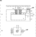
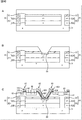
- FIG. 1 shows a pixel structure of a CMOS type solid-state imaging device described in Patent Document 5.
- the pixel 1 of the CMOS type solid-state imaging device shown in FIG. 1 is formed by embedding a photodiode 3 in a substrate of a p-type semiconductor substrate 2.
- the photodiode 3 has a high impurity concentration p-type semiconductor region (p + region) 11 formed on the front surface side of the semiconductor substrate 2 and a height direction formed in the depth direction toward the back surface side of the semiconductor substrate 2 in contact therewith.
- the n-type semiconductor region 12 includes a concentration impurity region (n + n region) 12A and a low impurity concentration region (n region) 12B.
- a gate electrode 5 of a transfer transistor for transferring charges to the n + region 4 as a floating diffusion region (FD) is formed in the depth direction from the substrate surface to the photodiode 3. Embedded.
- the outer periphery of the gate electrode 5 is covered with a gate insulating film 6 made of, for example, a silicon oxide film.
- a pixel isolation region 8 a gate electrode 9 of a reset transistor, and the like are formed on the surface side of the semiconductor substrate 2.
- the p + region 11 of the photodiode 3 is formed to maximize the charge capacity that can be stored in the photodiode 3, and the p-type semiconductor region having a lower impurity concentration than the p + p region 11 is located in the vicinity of the gate electrode 5. (P-region) 13 is formed.
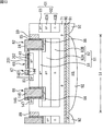
- FIG. 2 shows a pixel structure disclosed in Patent Document 6 that is resistant to misalignment between the p + ⁇ region 11 having a high impurity concentration of the photodiode 3 and the gate electrode 5.
- FIG. 2A shows a cross-sectional view of the pixel 1
- FIG. 2B shows a plan view of the pixel 1.
- the gate electrode 5 is formed in a square shape when viewed in the depth direction, and an n + region 4 as a floating diffusion region (FD) is formed inside the gate electrode 5. Is formed. As a result, the charge accumulated in the photodiode 3 flows inside the square-shaped gate electrode 5, so that it is resistant to misalignment between the high impurity concentration p + region 11 of the photodiode 3 and the gate electrode 5.
- FD floating diffusion region
- the present technology has been made in view of such a situation, and is intended to realize a solid-state imaging device that is resistant to misalignment during manufacturing and has high photoelectric conversion efficiency.
- a solid-state imaging device includes a photoelectric conversion unit that is embedded in a semiconductor substrate, an impurity region that holds charges generated by the photoelectric conversion unit, and the charges that are the impurities.
- a transfer transistor that transfers to the region, and the gate electrode of the transfer transistor is formed in a depth direction from the surface of the semiconductor substrate on which the impurity region is formed toward the photoelectric conversion portion in the semiconductor substrate The channel portion of the transfer transistor is surrounded by the gate electrode in two or more directions other than the direction of the impurity region when viewed from the depth direction.
- a method for manufacturing a solid-state imaging device in which a photoelectric conversion unit is embedded in a semiconductor substrate, and a gate electrode of a transfer transistor that transfers charges generated by the photoelectric conversion unit is used as the semiconductor. Forming in the depth direction from the surface of the substrate toward the photoelectric conversion portion in the semiconductor substrate, and forming an impurity region for holding the charge transferred by the transfer transistor on the surface of the semiconductor substrate; In addition, the channel portion of the transfer transistor is surrounded by the gate electrode in two or more directions other than the direction of the impurity region when viewed from the depth direction.
- An electronic apparatus includes a photoelectric conversion unit that is embedded and formed in a semiconductor substrate, an impurity region that holds charges generated by the photoelectric conversion unit, and the charge that is stored in the impurity region.
- the transfer transistor has a gate electrode formed in a depth direction from the surface of the semiconductor substrate on which the impurity region is formed toward the photoelectric conversion portion in the semiconductor substrate.
- the channel portion of the transfer transistor includes a solid-state imaging device that is surrounded by the gate electrode in two or more directions other than the direction of the impurity region when viewed from the depth direction.
- a photoelectric conversion unit is embedded in a semiconductor substrate, and a gate electrode of a transfer transistor that transfers charges generated by the photoelectric conversion unit is formed from the surface of the semiconductor substrate.
- An impurity region is formed in the depth direction toward the photoelectric conversion portion in the semiconductor substrate and holds the charge transferred by the transfer transistor on the surface of the semiconductor substrate. Further, when viewed from the depth direction, the channel portion of the transfer transistor is surrounded by the gate electrode in two or more directions other than the direction of the impurity region.
- a solid-state imaging device includes a photoelectric conversion unit that is embedded in a semiconductor substrate, a memory unit that holds charges generated by the photoelectric conversion unit, and the charge that is stored in the memory.
- the semiconductor substrate is close in parallel to the depth direction of the semiconductor substrate through an impurity region having an impurity concentration higher than that of the semiconductor substrate or an insulating film.
- a method for manufacturing a solid-state imaging device includes: forming a photoelectric conversion unit embedded in a semiconductor substrate; transferring a charge generated by the photoelectric conversion unit to a memory unit;
- the gate electrode of the discharge transistor that discharges unnecessary charges generated in the photoelectric conversion unit is formed in parallel in the depth direction from the surface of the semiconductor substrate toward the photoelectric conversion unit in the semiconductor substrate, Forming an impurity region or an insulating film having an impurity concentration higher than that of a channel portion serving as a current path between the gate electrode of the transfer transistor and the gate electrode of the discharge transistor;
- An electronic apparatus includes a photoelectric conversion unit that is embedded in a semiconductor substrate, a memory unit that holds charges generated by the photoelectric conversion unit, and the charge that is stored in the memory unit. And a discharge transistor for discharging unnecessary charges generated in the photoelectric conversion unit, and the gate electrode of the transfer transistor and the gate electrode of the discharge transistor are impurities in a channel portion serving as a current path.
- a solid-state imaging device is provided that is close to the semiconductor substrate in parallel with the depth direction of the semiconductor substrate via an impurity region having a higher concentration or an insulating film.
- the photoelectric conversion unit is formed by being embedded in a semiconductor substrate, the gate electrode of the transfer transistor that transfers the charge generated by the photoelectric conversion unit to the memory unit, and the photoelectric conversion unit
- a gate electrode of a discharge transistor that discharges unnecessary charges generated in step S1 is formed in parallel in a depth direction from the surface of the semiconductor substrate toward the photoelectric conversion unit, and the gate electrode of the transfer transistor and the discharge transistor
- An impurity region or an insulating film having a concentration higher than that of the channel portion serving as a current path is formed between the gate electrode and the gate electrode.
- a solid-state imaging device includes a photoelectric conversion unit that is embedded in a semiconductor substrate, a memory unit that holds charges generated by the photoelectric conversion unit, and the charge that is stored in the memory. And a discharge transistor for discharging unnecessary charges generated in the photoelectric conversion unit, and an end of the transfer transistor on the photoelectric conversion unit side of the gate electrode of the transfer transistor and the gate electrode of the discharge transistor Is arranged at a close position in the photoelectric conversion portion formation surface, and is formed so that the gate electrode of the transfer transistor and the gate electrode of the discharge transistor are gradually separated from each other as the depth from the surface of the semiconductor substrate becomes shallower. Has been.
- a solid-state imaging device manufacturing method includes a gate electrode of a transfer transistor that is formed by embedding a photoelectric conversion unit in a semiconductor substrate, and transfers charges generated by the photoelectric conversion unit to a memory unit.
- the end portions on the photoelectric conversion unit side of the gate electrode of the transfer transistor and the gate electrode of the discharge transistor are arranged at close positions in the photoelectric conversion unit formation surface, and the depth from the surface of the semiconductor substrate becomes shallow. Accordingly, the gate electrode of the transfer transistor and the gate electrode of the discharge transistor are formed so as to be gradually separated from each other.
- An electronic apparatus includes a photoelectric conversion unit that is embedded in a semiconductor substrate, a memory unit that holds charges generated by the photoelectric conversion unit, and the charge that is stored in the memory unit. And a transfer transistor that discharges unnecessary charges generated in the photoelectric conversion unit, and an end of the transfer transistor on the photoelectric conversion unit side of the gate electrode of the transfer transistor and the gate electrode of the discharge transistor The gate electrode of the transfer transistor and the gate electrode of the discharge transistor are gradually separated from each other as the depth from the surface of the semiconductor substrate becomes shallower.
- a solid-state imaging device is provided.
- a photoelectric conversion unit is formed embedded in a semiconductor substrate, and a gate electrode of a transfer transistor that transfers charges generated by the photoelectric conversion unit to a memory unit; and the photoelectric conversion unit
- a gate electrode of a discharge transistor that discharges unnecessary charges generated in step 1 is formed in a depth direction from the surface of the semiconductor substrate toward the photoelectric conversion unit. Further, end portions of the gate electrode of the transfer transistor and the gate electrode of the discharge transistor on the photoelectric conversion unit side are arranged at close positions in the photoelectric conversion unit formation surface, and the depth from the surface of the semiconductor substrate is shallow. Accordingly, the gate electrode of the transfer transistor and the gate electrode of the discharge transistor are formed so as to be gradually separated from each other.
- the solid-state imaging device and the electronic device may be independent devices or modules incorporated in other devices.
- FIG. 1 It is a figure which shows the conventional pixel structure of a CMOS type solid-state image sensor. It is a figure which shows the conventional pixel structure of a CMOS type solid-state image sensor. It is a block diagram which shows the structural example of the solid-state image sensor to which this technique is applied. It is a figure which shows the equivalent circuit of the 1st structure of a pixel. It is sectional drawing which shows the structure of the pixel of a 1st structure. It is a top view which shows the structure of the pixel of a 1st structure. It is a figure which shows the modification of a gate electrode shape. It is a figure which shows the equivalent circuit of the 2nd structure of a pixel.
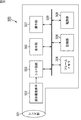
- FIG. 3 is a block diagram illustrating an example of the overall configuration of a solid-state imaging device to which the present technology is applied.
- 3 includes a timing control unit 42, a vertical scanning circuit 43, a pixel array unit 44, a constant current source circuit unit 45, a reference signal generation unit 46, a column AD conversion unit 47, a horizontal scanning circuit 48, and a horizontal output. It is composed of a line 49 and an output circuit 50.
- the timing control unit 42 supplies a clock signal and a timing signal necessary for a predetermined operation to the vertical scanning circuit 43 and the horizontal scanning circuit 48 based on a master clock having a predetermined frequency. For example, the timing control unit 42 supplies timing signals for the shutter operation and readout operation of the pixel 51 to the vertical scanning circuit 43 and the horizontal scanning circuit 48. Although not shown, the timing control unit 42 also supplies a clock signal and timing signal necessary for a predetermined operation to the reference signal generation unit 46, the column AD conversion unit 47, and the like.
- the vertical scanning circuit 43 sequentially supplies a signal for controlling the output of the pixel signal to each pixel 51 arranged in the vertical direction of the pixel array unit 44 at a predetermined timing.
- a plurality of pixels 51 are arranged in a two-dimensional array (matrix) in the pixel array unit 44.
- the plurality of pixels 51 arranged in a two-dimensional array are connected to the vertical scanning circuit 43 in units of rows by horizontal signal lines 52.
- the plurality of pixels 51 arranged in the same row in the pixel array unit 44 are connected to the vertical scanning circuit 43 by the same single horizontal signal line 52.
- the horizontal signal line 52 is shown as one wiring, but is not limited to one.
- the plurality of pixels 51 arranged in a two-dimensional array are connected to the horizontal scanning circuit 48 in units of columns by vertical signal lines 53.
- the plurality of pixels 51 arranged in the same column in the pixel array unit 44 are connected to the horizontal scanning circuit 48 by the same single vertical signal line 53.
- Each pixel 51 in the pixel array unit 44 outputs, to the vertical signal line 53, a pixel signal corresponding to the charge accumulated therein in accordance with a signal supplied from the vertical scanning circuit 43 via the horizontal signal line 52.
- the detailed configuration of the pixel 51 will be described later with reference to FIG.
- the constant current source circuit unit 45 has a plurality of load MOSs 54, and one load MOS 54 is connected to one vertical signal line 53.
- the load MOS 54 has a gate applied with a bias voltage and a source grounded, and forms a source follower circuit with a transistor in the pixel 51 connected via the vertical signal line 53.
- the reference signal generation unit 46 includes a DAC (Digital-to-Analog-Converter) 46a, generates a ramp (RAMP) waveform reference signal in accordance with the clock signal from the timing control unit 42, and generates a column signal. This is supplied to the AD conversion unit 47.
- DAC Digital-to-Analog-Converter
- the column AD converter 47 has a plurality of ADCs (Analog-Digital Converters) 25, one for each column of the pixel array unit 44. Accordingly, a plurality of pixels 51, a single load MOS 54 and an ADC 55 are connected to one vertical signal line 53.
- ADCs Analog-Digital Converters
- the ADC 55 performs a CDS (Correlated Double Sampling) process on the pixel signal supplied from the pixel 51 in the same column via the vertical signal line 53, and further performs an AD conversion process.
- CDS Correlated Double Sampling
- Each ADC 55 temporarily stores the pixel data after AD conversion and outputs it to the horizontal output line 49 under the control of the horizontal scanning circuit 48.
- the horizontal scanning circuit 48 sequentially outputs the pixel data stored in the plurality of ADCs 55 to the horizontal output line 49 at a predetermined timing.
- the horizontal output line 49 is connected to an output circuit (amplifier circuit) 50, and pixel data after AD conversion output from each ADC 55 is output from the output circuit 50 via the horizontal output line 49 to the outside of the solid-state imaging device 1. Is output.
- the output circuit 50 may perform only buffering, or may perform various digital signal processing such as black level adjustment and column variation correction.
- the solid-state imaging device 41 configured as described above is a CMOS image sensor called a column AD system in which ADCs 55 that perform CDS processing and AD conversion processing are arranged for each vertical column.
- FIG. 4 shows an equivalent circuit of the first configuration of the pixel 51.
- the pixel 51 includes a photodiode 61 as a photoelectric conversion element, a transfer transistor 62, an FD (floating diffusion region) 63, a reset transistor 64, an amplification transistor 65, and a selection transistor 66.
- the photodiode 61 is a photoelectric conversion unit that generates and accumulates charges (signal charges) corresponding to the amount of received light.
- the photodiode 61 has an anode terminal grounded and a cathode terminal connected to the FD 63 via the transfer transistor 62.
- the transfer transistor 62 When the transfer transistor 62 is turned on by the transfer signal TX, the charge generated by the photodiode 61 is read and transferred to the FD 63.
- the FD 63 holds the electric charge read from the photodiode 61.
- the reset transistor 64 is turned on by the reset signal RST, the charge stored in the FD 63 is discharged to the constant voltage source VDD, thereby resetting the potential of the FD 63.
- the amplification transistor 65 outputs a pixel signal corresponding to the potential of the FD 63. That is, the amplification transistor 65 constitutes a load MOS 54 as a constant current source and a source follower circuit, and a pixel signal indicating a level corresponding to the charge accumulated in the FD 63 is sent from the amplification transistor 65 to the ADC 55 via the selection transistor 66. Is output.
- the selection transistor 66 is turned on when the pixel 51 is selected by the selection signal SEL, and outputs the pixel signal of the pixel 51 to the ADC 55 via the vertical signal line 53.
- the transfer signal TX, the reset signal RST, and the selection signal SEL are supplied from the vertical scanning circuit 43 via the horizontal signal line 52 (FIG. 3).
- FIG. 5 is a cross-sectional view showing the structure of the pixel 51 having the first configuration shown in FIG.
- the pixel 51 is formed by embedding a photodiode 61 in a substrate of a first conductivity type, for example, a p-type semiconductor substrate 71.
- the photodiode 61 includes a high impurity concentration p-type semiconductor region (p + region) 81 formed on the surface side of the semiconductor substrate 71 and a second conductivity type, for example, an n-type semiconductor region (n-type semiconductor region). 82.
- the n-type semiconductor region 82 has a high impurity concentration n-type semiconductor region (n + region) 82A in contact with the p + region 81 and a low impurity concentration formed in the depth direction toward the back side of the semiconductor substrate 71.
- An n-type semiconductor region (n region) 82B is an n-type semiconductor region (n region) 82B.
- n + region 83 as an FD 63 is formed on the surface side of the semiconductor substrate 71, and a gate electrode 84 of the transfer transistor 62 for transferring charges to the n + region 83 is formed from the substrate surface to the semiconductor substrate.
- the photodiode 61 in 71 is embedded in the depth direction.
- the gate electrode 84 of the transfer transistor 62 made of polysilicon is buried to the same depth as the pn junction surface of the p + region 81 and the n + region 82A of the photodiode 61.
- the gate electrode 84 of the transfer transistor 62 may be embedded to a position deeper than the pn junction surface, or may be positioned slightly shallower than the pn junction surface depending on the concentration of the impurity region.
- the outer periphery of the gate electrode 84 in the substrate of the transfer transistor 62 is covered with a gate insulating film 85 made of, for example, a silicon oxide film.
- a gate insulating film 85 made of, for example, a silicon oxide film.
- a p-type semiconductor region (p ⁇ region) 86 having a lower impurity concentration than the p + region 81 is formed via a gate insulating film 85.
- n + region 87 as one source / drain region of the reset transistor 64 is formed on the surface side of the semiconductor substrate 71, and the n + region 83 as the FD 63 also serves as the other source / drain region of the reset transistor 64. To do.
- the reset transistor 64 is interposed between the n + region 87 as one source / drain region of the reset transistor 64 and the n + region 83 as the other source / drain region via a gate insulating film 85.
- the gate electrode 88 is formed.
- n + region 83 as the FD 63 is connected to the gate electrode of the amplification transistor 65 via an upper connection wiring (not shown), and the n + region 87 as one source / drain region of the reset transistor 64 is illustrated in FIG. It is connected to a constant voltage source VDD via an upper connection wiring (not shown).
- an isolation region 89 for isolating each pixel 51 of the pixel array unit 44 is formed by an insulator such as silicon oxide. Is formed.
- a planarizing film 90 is formed on the back surface side of the semiconductor substrate 71, and a color filter 91 and an on-chip lens (OCL) 92 are sequentially formed on the planarizing film 90 (downward in the drawing).
- OCL on-chip lens
- the pixel 51 having the above cross-sectional configuration has a back-illuminated structure in which light is incident from the back side of the semiconductor substrate 71 in the downward direction of the drawing.
- FIG. 6A is a plan view of the surface of the semiconductor substrate 71 on which the transistors of the pixel 51 having the first configuration are formed, as viewed from above.
- the transfer transistor 62 and the reset transistor 64 are formed so as to share the n + region 83 as one of the source / drain regions.
- the amplification transistor 65 and the selection transistor 66 are formed so as to share the n + region 103 as one of the source / drain regions.
- the amplification transistor 65 includes a gate electrode 102 and n + regions 101 and n + regions 103 disposed on both sides thereof, and the selection transistor 66 is disposed on the gate electrode 104 and both sides thereof.
- the n + region 103 and the n + region 105 are formed.
- FIG. 6B, FIG. 6C, and FIG. 6D respectively show the vicinity of the transfer transistor 62 of the pixel 51 along the lines XX ′, YY ′, and ZZ ′ of FIG. It is sectional drawing cut
- the transfer transistor 62 serves to connect the photodiode 61 embedded in the semiconductor substrate 71 and the n + region 83 as the FD 63 formed on the substrate surface.
- the gate electrode 84 of the transfer transistor 62 is formed in a U-shape so as to surround three directions at the cut surface of the Z-Z ′ line shown in FIG.
- the outer periphery of the U-shaped gate electrode 84 is covered with a gate insulating film 85.
- a high impurity concentration p-type semiconductor region (p + (region) 121 is formed on the upper and lower sides of the gate electrode 84 through the gate insulating film 85, and on the right side of the gate electrode 84 in the drawing.
- an isolation region 89 using an insulator such as silicon oxide is formed.
- all three directions on the upper side, the lower side, and the right side of the gate electrode 84 through the gate insulating film 85 may be the p + region 121 or the isolation region 89.
- an n + region 83 as the FD 63 is formed in the opening direction of the U-shaped gate electrode 84.
- a predetermined control voltage is applied to the gate electrode 84 of the transfer transistor 62, a channel portion serving as a current path is formed inside the U-shape of the gate electrode 84 formed in the depth direction.
- the concentration (p) of the impurity region serving as the channel portion is formed to be thinner than the impurity concentration outside the gate electrode 84 (p + of the p + region 121).
- FIG. 6B is a cross-sectional view further above the substrate surface on which the n + region 83 as the FD 63 is formed. As shown in FIG. 6B, on the upper side of the substrate surface, the gate electrode 84 is formed so as to cover the channel portion inside the U-shape.
- the gate electrode 84 may be formed on the upper side of the substrate surface in the same U-shape as in the substrate.
- the gate electrode 84 of the transfer transistor 62 is formed in a U shape in the depth direction when viewed from the depth direction, a channel portion serving as a current path is formed in the gate insulating film 85 from three directions. Therefore, the controllability of the electric field is increased, and the charge can be transferred smoothly.
- the impurity concentration of the p + region 81 can be increased, and by increasing the pn junction capacitance value of the photodiode 61, It is possible to increase the amount of saturation charge.
- FIG. 7A to FIG. 7C show modified examples of the shape of the gate electrode 84 of the transfer transistor 62.
- FIG. 7A to FIG. 7C are cross-sectional views taken along the line YY ′ of FIG. 5 as in FIG. 6C.
- the width in one direction where the U-shaped gate electrode 84 is opened is further narrower than the shape shown in FIG. 6C.
- the potential controllability of the channel portion can be further improved, and the effect of forming the potential barrier by the p + region 81 of the photodiode 61 can be further weakened. Therefore, stable charge transfer is possible.
- the gate electrode 84 of the transfer transistor 62 is not U-shaped so as to surround the three directions, and the separation region 89 side is opened together with the n + region 83 side which is the FD 63, so that the plate shape Are formed in a two-letter shape arranged in parallel.
- the potential controllability of the channel part is slightly weaker than that of the U-shape, but the shape of the gate electrode 84 becomes simple, so that the manufacturability is improved.
- the gate electrode 84 of FIG. 7C has two plate-like intervals similar to those of B of FIG. 7 so that the n + region 83 side which is the FD 63 is wide and the separation region 89 side is narrow. It is arranged in a letter shape. Also in this case, since the isolation region 89 side is closed by the gate electrode 84 and the n + region 83 side is open, the controllability of the electric field is increased, and charge transfer can be performed smoothly.
- the planar shape when the gate electrode 84 of the transfer transistor 62 is viewed from the depth direction is limited to the U-shape shown in FIG. 6 or the shapes shown in FIGS. 7A to 7C. Instead, it is sufficient that the n + region 83 side which is the FD 63 is opened at least so that the potential controllability in the other three directions is higher than that of the opening side.
- the channel portion as shown in B may be covered.
- FIG. 8 shows an equivalent circuit of the second configuration of the pixel 51.
- a pixel 51 shown in FIG. 8 shows a configuration of a pixel that realizes an electronic global shutter function.
- portions corresponding to those in FIG. 4 are denoted by the same reference numerals, and description thereof is omitted as appropriate.
- the second configuration pixel 51 transfers another charge transfer transistor 67 between the transfer transistor 62 and the FD 63 and the FD 63. It further includes a memory unit (MEM) 68 that temporarily holds charges before.
- MEM memory unit
- the transfer transistor 62 is referred to as a first transfer transistor 62
- the transfer transistor 67 is referred to as a second transfer transistor 67.
- a discharge transistor 69 for discharging unnecessary charges is newly connected to the photodiode 61.
- a high level discharge signal OFG is supplied to the discharge transistor 69, whereby the discharge transistor 69 is turned on, and the charge accumulated in the photodiode 61 is discharged to the constant voltage source VDD. 61 is reset.
- the first transfer transistor 62 When a predetermined exposure time determined in advance elapses, the first transfer transistor 62 is turned on by the first transfer signal TX1 in all the pixels of the pixel array unit 44, and the charges accumulated in the photodiode 61 are transferred to the memory unit. 68.
- the charges held in the memory unit 68 of each pixel 51 are sequentially read out to the ADC 55 for each row.
- the read operation is the same as in the first configuration described above.
- the second transfer transistor 67 of the pixel 51 in the read row is turned on by the second transfer signal TX2, and the charge held in the memory unit 68 is transferred to the FD 63. Transferred.
- the selection transistor 66 is turned on by the selection signal SEL, a signal indicating a level corresponding to the charge accumulated in the FD 63 is output from the amplification transistor 65 to the ADC 55 via the selection transistor 66.
- FIG. 9 is a cross-sectional view showing the structure of the pixel 51 having the second configuration shown in FIG.
- the gate electrode 84 of the first transfer transistor 62 and the n + region 83 as one source / drain region of the second transfer transistor 67 are formed on the substrate surface of the p-type semiconductor substrate 71.
- a memory unit 68 is formed between the two.
- the memory unit 68 is formed of an n-type semiconductor region (n + (region) 141 having a high impurity concentration for accumulating charges, and a p-type layer 142 for suppressing dark current is formed on the upper surface thereof.
- the gate electrode 143 of the second transfer transistor 67 is formed on the substrate surface via the gate insulating film 144 on the opposite side of the memory unit 68 from the side where the first transfer transistor 62 is disposed.
- an n + region 83 as an FD 63 is formed.
- the gate electrode of the discharge transistor 69 is provided in the other region above the photodiode 61 where the gate electrode 84 of the first transfer transistor 62, the memory portion 68, the second transfer transistor 67, the n + region 83 to be the FD 63, etc. are not formed.
- the gate electrode of the discharge transistor 69 is provided in the other region above the photodiode 61 where the gate electrode 84 of the first transfer transistor 62, the memory portion 68, the second transfer transistor 67, the n + region 83 to be the FD 63, etc. are not formed.
- the gate electrode of the discharge transistor 69 is provided in the other region above the photodiode 61 where the gate electrode 84 of the first transfer transistor 62, the memory portion 68, the second transfer transistor 67, the n + region 83 to be the FD 63, etc.
- the gate electrode of the discharge transistor 69 is provided in the other region above the photodiode 61 where the gate electrode 84 of the first transfer transistor
- the outer periphery of the gate electrode 145 in the substrate of the discharge transistor 69 is covered with a gate insulating film 146 made of, for example, a silicon oxide film.
- a gate insulating film 146 made of, for example, a silicon oxide film.
- a p-type semiconductor region (p ⁇ region) 86 having a lower impurity concentration than the p + region 81 is formed via a gate insulating film 146.
- n + region 147 as one source / drain region of the discharge transistor 69 is formed on the surface of the semiconductor substrate 71 on the left side of the gate electrode 145 of the discharge transistor 69 in the drawing.
- an isolation region 148 is formed on the opposite side of the gate electrode 145 of the drain transistor 69 from the n + region 147 side by an insulator such as silicon oxide.
- the shape of the gate electrode 145 of the discharge transistor 69 viewed in the depth direction is a U-shape, similar to the shape of the gate electrode 84 of the first transfer transistor 62 shown by B in FIG. 6 to D in FIG. Yes. Further, the peripheral portion in the planar direction of the gate electrode 145 of the discharge transistor 69 is also formed by the p + region 121 and the isolation region 148, similarly to the gate electrode 84 of the first transfer transistor 62.
- FIG. 10 is a plan view of the substrate surface on which the transistors of the pixel 51 having the second configuration are formed as seen from above.
- a first transfer transistor 62, a memory unit 68, a second transfer transistor 67, and an n + region 83 as an FD 63 are arranged side by side.
- a gate electrode 145 of the discharge transistor 69, an n + region 147 that is one of the source / drain regions, and an isolation region 148 are disposed.
- a selection transistor 66, an amplification transistor 65, and a reset transistor 64 are arranged side by side while sharing one source / drain region with another adjacent transistor. More specifically, the selection transistor 66 includes a gate electrode 162 and n + regions 161 and n + regions 163 disposed on both sides thereof, and the amplification transistor 65 is disposed on the gate electrode 164 and both sides thereof.
- the reset transistor 64 includes a gate electrode 166 and n + regions 165 and n + regions 167 disposed on both sides thereof.
- FIG. 11 is a cross-sectional view showing a third configuration of the pixel 51.
- the pixel structure of the pixel 51 of the third configuration shown in FIG. 11 is shielded against a predetermined region of the layer where the planarizing film 90 is formed. The difference is that the film 181 is formed. Further, the isolation region 148 between the gate electrode 145 of the discharge transistor 69 and the n + region 83 as the FD 63 is omitted.
- FIG. 12 is a plan view of the pixel 51 having the third configuration shown in the same manner as FIG.
- a light shielding film 181 is disposed so as to cover the memory unit 68 and the first transfer transistor 62 as shown in FIG. As a result, light incident on the memory unit 68 can be blocked, and mixing of noise during charge accumulation can be suppressed.
- FIG. 13 is a cross-sectional view showing a fourth configuration of the pixel 51.
- the pixel structure of the pixel 51 with the fourth configuration shown in FIG. 13 is formed above the n + region 141 that functions as the memory unit 68 as compared with the pixel structure with the second configuration shown in FIG.
- the p-type layer 142 is omitted, and a gate electrode 201 made of polysilicon or the like is formed through the gate insulating film 202 instead. Further, the isolation region 148 between the gate electrode 145 of the discharge transistor 69 and the n + region 83 as the FD 63 is omitted.
- the light shielding film 181 is not formed in the layer where the planarization film 90 is formed, but the light shielding film 181 may be disposed in the same manner as in FIG.
- FIG. 14 is a plan view of the pixel 51 having the fourth configuration shown in the same manner as FIG.
- the gate electrode 201 is disposed on the upper portion of the memory unit 68 as shown in FIG.
- a dark potential generated in the memory unit 68 can be reduced by applying a negative potential to the gate electrode 201.
- FIG. 15 is a cross-sectional view showing a fifth configuration of the pixel 51.
- the pixel structure of the pixel 51 of the fifth configuration shown in FIG. 15 is different from the pixel structure of the fourth configuration shown in FIG. 13 in that the gate electrode 84 of the first transfer transistor 62 in FIG.
- the difference is that a gate electrode 201 for applying a negative potential is integrated. That is, the gate electrode 221 of the first transfer transistor 62 of the pixel 51 of the fifth configuration is formed up to the top of the memory unit 68 and also functions as a gate electrode for applying a negative potential to the memory unit 68. Similarly, the gate insulating film 222 below the gate electrode 221 is formed so that the gate insulating film 85 and the gate insulating film 202 in FIG. 13 are integrated. Thereby, the control wiring for applying a negative potential to the gate electrode 201 in FIG. 13 can be omitted.
- a light shielding film 181 that shields the memory portion 68 may be disposed in the layer where the planarizing film 90 is formed.
- FIG. 16 is a plan view of the pixel 51 having the fifth configuration shown in the same manner as FIG.
- the gate electrode 221 of the transfer transistor 62 is disposed up to the upper part of the memory unit 68 as shown in FIG.
- a dark potential generated in the memory unit 68 can be reduced by applying a negative potential to the gate electrode 221.
- FIG. 17 is a cross-sectional view illustrating a sixth configuration of the pixel 51.
- the n region 82B in FIG. 11 is omitted and the back surface of the substrate from the n + region 82A is compared with the pixel structure having the third configuration shown in FIG.
- a photoelectric conversion film 241 is newly formed in the direction. Further, the photoelectric conversion films 241 of each pixel 51 are separated by a high impurity concentration p-type semiconductor region (p + region) 242.
- a compound semiconductor having a chalcopyrite structure or an organic material can be used as the photoelectric conversion film 241.
- the compound semiconductor having a chalcopyrite structure include CuInSe 2 , a copper-aluminum-gallium-indium-sulfur-selenium mixed crystal, and a copper-aluminum-gallium-indium-sulfur-selenium mixed crystal.
- a compound semiconductor layer made of a group III or group IV may be formed.
- an organic material you may use materials, such as a quinacrine and a coumarin type, for example.
- the material described above is an example of a material that can be used for the photoelectric conversion film 241 until it gets tired, and is not limited to this as long as it has a light absorption coefficient larger than that of the semiconductor substrate 71 (silicon).
- the photoelectric conversion film 241 having a light absorption coefficient larger than that of the semiconductor substrate 71 also functions as a light shielding film that shields visible light.
- the high impurity concentration n-type semiconductor region (n + n region) 82A accumulates the charge obtained by photoelectric conversion of the photoelectric conversion film 241.
- FIG. 18 shows a plan view of the pixel 51 of the sixth configuration, which is the same as the plan view shown in FIG. 12 except that the light shielding film 181 is not disposed.
- a photodiode 61 composed of a p + -type region 81 and an n-type semiconductor region 82 is formed on a p-type semiconductor substrate 71.
- the n-type semiconductor region 82 includes an n + region 82A on the p + region 81 side and an n region 82B on the back side of the semiconductor substrate 71.
- the p-type semiconductor substrate 71 is used.
- an n-type semiconductor substrate is used to form a p-type well region (P-Well) on the n-type semiconductor substrate.
- a photodiode 61 may be formed in the well region.
- the isolation region 89 is formed of an insulator such as silicon oxide.
- the gate electrodes of the first transfer transistor 62, the second transfer transistor 67, and the discharge transistor 69 are formed on the substrate surface.
- the p-type layer above the photodiode 61 in the region where the first transfer transistor 62 and the discharge transistor 69 are formed is etched away by a dry etching method. Then, P-type ions such as boron are implanted into a portion that becomes the bottom surface of the removed region, and a p ⁇ region 86 is formed. Further, a gate insulating film 85 and a gate insulating film 146 made of a silicon oxide film or the like are formed on the inner wall of the etched away region, and then polysilicon is embedded so that the gate electrode 84 and the discharge of the first transfer transistor 62 are discharged. A gate electrode 145 of the transistor 69 is formed.
- the gate electrode 143 of the second transfer transistor 67 and the like are formed at the same time.
- each transistor such as the n + region 147 of the drain transistor 69, the n + region 83 as the FD 63, and the n + region as the memory unit 68 141 and a p-type layer 142 on the upper surface thereof are formed on the surface of the semiconductor substrate 71.
- connection wiring layer 303 in which a plurality of interlayer films 301 and metal wirings 302 made of tungsten, aluminum, or the like are formed is formed on the surface side of the semiconductor substrate 71.
- the back surface side of the semiconductor substrate 71 is changed until the depth to the photodiode 61 becomes about 1 ⁇ m to 5 ⁇ m. Polished and thinned.
- a light shielding film 181, a planarizing film 90, a color filter 91, and an on-chip lens (OCL) 92 are sequentially formed on the back surface side of the thinned semiconductor substrate 71.
- the pixel 51 having the third configuration can be created.
- a p-type silicon layer is formed by epitaxial growth.
- the p-type layer in the region where the first transfer transistor 62 and the discharge transistor 69 are formed is etched away by a dry etching method.
- the p-type layer of the semiconductor substrate 71 has a pn junction surface of the photodiode 61 in a U-shape with the channel portion 321 of the first transfer transistor 62 left. Etched until.
- the drain transistor 69 is etched up to the pn junction surface of the photodiode 61 in a U shape with the channel portion 322 left.
- a P-type ion such as boron is implanted into the region etched into a U-shape corresponding to the first transfer transistor 62 and the discharge transistor 69, A p-region 86 is formed. At this time, a region other than the portion where ion implantation is performed is prevented from being ion implanted using a photoresist.
- the surface of the channel portion 321 of the first transfer transistor 62 and the surface of the channel portion 322 of the discharge transistor 69 are gate-insulated using a thermal oxidation method or a deposition method.
- polysilicon is further formed which becomes the gate electrode 84 of the first transfer transistor 62 and the gate electrode 145 of the discharge transistor 69.
- the polysilicon other than the portion surrounding the channel portion 321 of the first transfer transistor 62 and the channel portion 322 of the discharge transistor 69 is removed by dry etching, so that the first The gate electrode 84 of the 1 transfer transistor 62 and the gate electrode 145 of the discharge transistor 69 are completed.
- the gate electrode 84 of the first transfer transistor 62 and the gate electrode 145 of the discharge transistor 69, which are embedded gate electrodes, can be formed.
- the other manufacturing method of the pixel 51 is the same as the method described with reference to FIGS.
- the gate electrode 84 of the first transfer transistor 62 is formed in a U shape having an opening on the side of the n + region 83 that is the FD 63 and is embedded in the depth direction.
- the transfer transistor needs to be disposed at a place where the energy is lowest with respect to the carrier. Therefore, in the case where the pixel 51 has the discharge transistor 69 as a transfer transistor for reading out charges from the photodiode 61 in addition to the first transfer transistor 62, each of the first transfer transistor 62 and the discharge transistor 69 serves as a carrier. On the other hand, where the energy is the lowest, in the configuration of the photodiode 61 described above, the photodiode 61 needs to be disposed at the highest potential.
- FIG. 24 is a cross-sectional view illustrating a seventh configuration of the pixel 51 having a structure focusing on carrier energy.
- the arrangement and shape of the gate electrodes of the first transfer transistor 62 and the discharge transistor 69 are different from those described above.
- the gate electrode 341 of the first transfer transistor 62 is embedded in a rod shape to the same depth as the pn junction surface of the photodiode 61 via the gate insulating film 342. Further, the gate electrode 343 of the discharge transistor 69 is also embedded in a rod shape to the same depth as the pn junction surface of the photodiode 61 through the gate insulating film 344. The gate electrode 341 of the first transfer transistor 62 and the gate electrode 343 of the discharge transistor 69 are disposed close to the center of the photodiode 61.
- the gate electrode 341 of the first transfer transistor 62 and the gate electrode 343 of the discharge transistor 69 are arranged close to each other in the center of the photodiode 61.
- the memory portion 68 that is the charge transfer destination of the first transfer transistor 62 is formed on the left side of the first transfer transistor 62 in the figure, while the n + region 147 that is the charge transfer destination of the discharge transistor 69 is discharged. It is formed on the right side of the transistor 69.
- An impurity region (p region) serving as a channel portion is provided between the gate electrode 341 of the first transfer transistor 62 and the gate electrode 343 of the discharge transistor 69 so as not to exchange charges between the two transistors.
- a p-type semiconductor region (p + p region) 345 having a higher impurity concentration is formed.
- FIG. 25A is a plan view of the substrate surface on which the transistors of the pixel 51 having the seventh configuration are formed as seen from above.
- the gate electrode 341 of the first transfer transistor 62 and the gate electrode 343 of the discharge transistor 69 are the most in the plane where the photodiode 61 is formed, with the p + region 345 interposed therebetween. It is arranged at a close position.
- the gate electrode 143 of the second transfer transistor 67 and the gate electrode 143 of the second transfer transistor 67 are on the opposite side of the first transfer transistor 62 from the gate electrode 341 side.
- An n + region 83 is disposed as a source / drain region.
- the light shielding film 181 shields the memory portion 68 (n + region 141 thereof) and the n + region 83 serving as one source / drain region of the second transfer transistor 67.
- a selection transistor 66, an amplification transistor 65, and a reset transistor 64 are arranged side by side while sharing one source / drain region with another adjacent transistor. More specifically, the selection transistor 66 includes a gate electrode 162 and n + regions 161 and n + regions 163 disposed on both sides thereof, and the amplification transistor 65 is disposed on the gate electrode 164 and both sides thereof.
- the reset transistor 64 includes a gate electrode 166 and n + regions 165 and n + regions 167 disposed on both sides thereof.
- FIG. 25B, FIG. 25C, and FIG. 25D respectively show the vicinity of the first transfer transistor 62 and the discharge transistor 69 of the pixel 51 along the lines XX ′, YY ′ in FIG.
- FIG. 3 is a cross-sectional view taken along the line Z-Z ′.
- the shape of the gate electrode viewed in the depth direction is a U-shape
- the gate electrode 341 of the first transfer transistor 62 is configured as shown in FIG.
- the rectangular shape is embedded in the depth direction.
- the gate electrode 343 of the discharge transistor 69 is formed in a rectangular shape and embedded in the depth direction.
- a high impurity concentration p-type semiconductor region (p + p region) 362 is interposed via a gate insulating film 342. Is formed.
- a high impurity concentration p-type semiconductor region (p + p region) 362 is also formed on the upper and lower sides of the gate electrode 343 of the drain transistor 69 via the gate insulating film 344.
- the gate electrode 341 of the first transfer transistor 62 and the gate electrode 343 of the discharge transistor 69 embedded in the rod shape have the lowest carrier energy in the planar region where the photodiode 61 is formed.
- the portion (where the electric potential is the highest in this embodiment) is arranged in close proximity to each other.
- the charge is efficiently transferred both when the charge is transferred to the n + region 141 of the memory unit 68 by the first transfer transistor 62 and when the charge is transferred to the n + region 147 by the discharge transistor 69. be able to.
- a high impurity concentration p-type semiconductor region (p + region) 345 is formed between the gate electrode 341 of the first transfer transistor 62 and the gate electrode 343 of the discharge transistor 69. It had been.
- the isolation region 361 made of an insulating film such as a silicon oxide film is divided into the gate electrode 341 of the first transfer transistor 62 and the gate electrode 343 of the discharge transistor 69. You may form between.
- FIG. 27 shows a modification of the shape of the gate electrode 341 of the first transfer transistor 62 and the gate electrode 343 of the discharge transistor 69.
- FIG. 27A is a cross-sectional view of the vicinity of the first transfer transistor 62 and the discharge transistor 69 of the pixel 51, and B in FIG. 27 to D in FIG. 27 are XX ′ lines and Y in FIG. FIG. 6 is a cross-sectional view taken along line -Y 'and line Z-Z'.
- the shape of the gate electrode shown in FIG. 27 in the planar direction is formed in a U-shape as in the first to seventh configurations described above.
- the gate electrode 341 of the first transfer transistor 62 is formed in a U shape with an opening on the left side of the n + region 141 side in the drawing as a transfer destination.
- the gate electrode 343 of the discharge transistor 69 is formed in a U shape having an opening on the n + region 147 side on the right side in the drawing, which is a transfer destination.
- the shapes of the gate electrode 341 of the first transfer transistor 62 and the gate electrode 343 of the discharge transistor 69 are not limited to the U-shape, and various shapes shown in FIG. 7 can be employed. That is, the gate electrode 341 of the first transfer transistor 62 and the gate electrode 343 of the discharge transistor 69 are open in one direction on the charge transfer destination storage unit side, and the potential controllability in the other three directions is open. More shapes can be employed.
- FIG. 28 is a cross-sectional view showing an eighth configuration of the pixel 51.
- FIG. 29 is a plan view showing an eighth configuration of the pixel 51.
- the p-type layer 142 formed on the upper part of the n + region 141 functioning as the memory unit 68 is added to the seventh configuration shown in FIGS. Instead, a gate electrode 201 made of polysilicon or the like is formed via a gate insulating film 202 instead.
- a dark potential generated in the memory unit 68 can be reduced by applying a negative potential to the gate electrode 201.
- FIG. 30 is a cross-sectional view showing a ninth configuration of the pixel 51.
- FIG. 31 is a plan view showing a ninth configuration of the pixel 51.
- the pixel structure of the pixel 51 of the ninth configuration shown in FIGS. 30 and 31 is the gate electrode of the first transfer transistor 62 in FIG. 341 and the gate electrode 201 for applying a negative potential to the memory portion 68 are integrated. That is, the gate electrode 381 of the first transfer transistor 62 of the pixel 51 of the ninth configuration is formed up to the upper portion of the memory unit 68 and also functions as a gate electrode for applying a negative potential to the memory unit 68. Similarly, the gate insulating film 382 disposed under the gate electrode 381 is formed so that the gate insulating film 342 and the gate insulating film 202 in FIG. 28 are integrated. Accordingly, the control wiring for applying a negative potential to the gate electrode 201 in FIG. 30 can be omitted.
- FIG. 32 is a cross-sectional view showing a tenth configuration of the pixel 51.
- FIG. 33 is a plan view showing a tenth configuration of the pixel 51.
- the pixel structure of the pixel 51 having the tenth configuration shown in FIGS. 32 and 33 is compared with the pixel structure having the seventh configuration shown in FIGS. 24 and 25, and the gate electrode 401 and the drain of the first transfer transistor 62 are discharged.
- the difference is that the gate electrode 403 of the transistor 69 has a V-shaped gate structure. More specifically, the gate electrode 401 of the first transfer transistor 62 and the gate electrode 403 of the discharge transistor 69 are arranged at the same location at the bottom near the photodiode 61, but the depth from the surface of the semiconductor substrate 71 becomes shallow. It is formed diagonally so as to gradually move away.
- the gate insulating film 402 disposed below the gate electrode 401 of the first transfer transistor 62 and the gate insulating film 404 disposed below the gate electrode 403 of the discharge transistor 69 are also formed obliquely.
- a high impurity concentration p-type semiconductor region (p + region) 86 is provided on the upper and lower sides. Is formed.
- this pixel structure as can be seen from the plan view of FIG. 33, it is possible to secure a wide film formation region of the gate electrode 401 and the gate insulating film 402 when viewed from above, and the hole formed vertically Since it is not necessary to form the gate insulating film 402 on the side surface (side wall) and bury the polysilicon (gate electrode 401), the manufacture of the pixel 51 is facilitated.
- FIG. 34 is a cross-sectional view showing an eleventh configuration of the pixel 51.
- the gate electrode 411 of the first transfer transistor 62 is formed up to the upper portion of the memory unit 68 as compared with the tenth configuration shown in FIG. Also, it functions as a gate electrode for applying a negative potential to the memory portion 68.
- the gate insulating film 412 disposed under the gate electrode 411 is also formed up to the upper portion of the memory unit 68. Thereby, when the memory unit 68 is accumulating charges, a dark potential generated in the memory unit 68 can be reduced by applying a negative potential to the gate electrode 411.
- FIG. 35 is a cross-sectional view showing a twelfth configuration of the pixel 51.
- a pixel 51 having a twelfth configuration illustrated in FIG. 35 is obtained by changing the configuration of the pixel 51 illustrated in FIG. 24 to a configuration using the photoelectric conversion film 241.
- a photoelectric conversion film 241 is newly formed on the back side of the substrate, similarly to the sixth configuration shown in FIG. The region 82B is omitted. Further, since the photoelectric conversion film 241 also functions as a light shielding film, the light shielding film 181 is also omitted in the pixel 51 having the twelfth configuration shown in FIG. Further, the photoelectric conversion films 241 of each pixel 51 are separated by a p + region 242.
- FIG. 36 is a cross-sectional view showing a thirteenth configuration of the pixel 51.
- a pixel 51 having a thirteenth configuration illustrated in FIG. 36 is obtained by changing the configuration of the pixel 51 illustrated in FIG. 32 to a configuration using the photoelectric conversion film 241.
- the photoelectric conversion film 241 is newly formed on the back side of the substrate, and the n region 82B in FIG. 32 is omitted. Since the photoelectric conversion film 241 also functions as a light shielding film, the light shielding film 181 is also omitted in the pixel 51 having the thirteenth configuration shown in FIG. Further, the photoelectric conversion films 241 of each pixel 51 are separated by a p + region 242.
- a photodiode 61 composed of a p + -type region 81 and an n-type semiconductor region 82 is formed on a p-type semiconductor substrate 71.
- the n-type semiconductor region 82 includes an n + region 82A on the p + region 81 side and an n region 82B on the back side of the semiconductor substrate 71.
- the p-type semiconductor substrate 71 is used.
- an n-type semiconductor substrate is used to form a p-type well region (P-Well) on the n-type semiconductor substrate.
- a photodiode 61 may be formed in the well region.
- a p-type silicon layer of about 0.5 to 1.5 ⁇ m is formed on the photodiode 61 by epitaxial growth.
- the gate electrodes of the first transfer transistor 62, the second transfer transistor 67, and the discharge transistor 69 are formed on the substrate surface.
- the p-type layer above the photodiode 61 in the region where the first transfer transistor 62 and the discharge transistor 69 are formed is etched away by a dry etching method. Then, P-type ions such as boron are implanted into a portion that becomes the bottom surface of the removed region, and a p ⁇ region 86 is formed. Further, gate insulating films 342 and 344 made of a silicon oxide film or the like are formed on the inner wall of the etched area, and then polysilicon is buried, whereby the gate electrode 341 of the first transfer transistor 62 and the discharge transistor 69 are filled. Gate electrodes 343 are formed in parallel.
- the gate electrode 143 of the second transfer transistor 67 and the like are formed at the same time.
- Transistor source / drain regions and the like are formed on the surface of the semiconductor substrate 71. Further, an n + ridge region 141 as the memory unit 68 and a p-type layer 142 on the upper surface thereof are also formed.
- connection wiring layer 303 in which a plurality of interlayer films 301 and metal wirings 302 made of tungsten, aluminum, or the like are formed is formed on the surface side of the semiconductor substrate 71.
- the back surface side of the semiconductor substrate 71 remains until the depth to the photodiode 61 becomes about 1 ⁇ m to 5 ⁇ m. Polished and thinned.
- a light shielding film 181, a planarizing film 90, a color filter 91, and an on-chip lens (OCL) 92 are sequentially formed on the back surface side of the thinned semiconductor substrate 71.
- the pixel 51 having the seventh configuration can be created.
- a photodiode 61 composed of a p + type region 81 and an n-type semiconductor region 82 is formed on a p-type semiconductor substrate 71
- 0.5 to 0.5 is formed by epitaxial growth.
- a p-type silicon layer of about 1.5 ⁇ m is formed on the photodiode 61.
- the p-type layer above the photodiode 61 in the region where the first transfer transistor 62 and the discharge transistor 69 are formed is etched into a V shape by dry etching. To be removed. Then, P-type ions such as boron are implanted into a portion that becomes the bottom surface of the removed region, and a p ⁇ region 86 is formed.
- a gate electrode 401 of one transfer transistor 62 and a gate electrode 403 of the discharge transistor 69 are formed.
- the gate electrode 401 of the first transfer transistor 62 and the gate electrode 403 of the discharge transistor 69 are formed by forming polysilicon as a material, patterning the gate electrode shape using photolithography, and performing dry etching. Can be created.
- transistors such as the gate electrode 143 of the second transfer transistor 67 and the like in which polysilicon is formed only on the surface of the semiconductor substrate 71 are formed at the same time.
- each transistor such as the n + region 147 of the discharge transistor 69, the n + region 141 as the memory unit 68, and the p-type layer 142 on the upper surface thereof are also formed on the surface of the semiconductor substrate 71. It is formed.
- the subsequent manufacturing method is the same as the method described with reference to FIGS.
- the gate electrode 341 (or 401) of the first transfer transistor 62 and the gate electrode 343 (or 403) of the discharge transistor 69 have the lowest carrier energy of the photodiode 61. Placed in the part. As a result, the charge accumulated in the photodiode 61 can be efficiently transferred to either the memory unit 68 or the n + region 147.
- the portion where the carrier energy of the photodiode 61 is lowest corresponds to the portion where the potential is highest in the structure of the solid-state imaging device in which the above-described electrons are signal charges. In the structure of the solid-state imaging device, this corresponds to the portion where the potential is lowest.
- the center portion of the photodiode 61 becomes a portion where the carrier energy is the lowest, so that position
- the gate electrode 341 (or 401) of the first transfer transistor 62 and the gate electrode 343 (or 403) of the discharge transistor 69 are disposed.
- the gate electrode 341 (or 401) of the first transfer transistor 62 and the gate electrode 343 (or 403) of the discharge transistor 69 can be arranged at desired positions.
- the first conductivity type is p-type
- the second conductivity type is n-type
- electrons are signal charges
- the first conductivity type can be an n-type
- the second conductivity type can be a p-type
- each of the semiconductor regions described above can be composed of semiconductor regions of opposite conductivity types.
- the present technology is not limited to application to a solid-state imaging device. That is, the present technology is applied to an image capturing unit (photoelectric conversion unit) such as an imaging device such as a digital still camera or a video camera, a portable terminal device having an imaging function, or a copying machine using a solid-state imaging device as an image reading unit.
- the present invention can be applied to all electronic devices using a solid-state image sensor.
- the solid-state imaging device may be in a form formed as a single chip, or may be in a modular form having an imaging function in which an imaging unit and a signal processing unit or an optical system are packaged together.
- FIG. 41 is a block diagram illustrating a configuration example of an imaging apparatus as an electronic apparatus to which the present technology is applied.
- An imaging apparatus 500 in FIG. 41 includes an optical unit 501 including a lens group, a solid-state imaging device (imaging device) 502 that employs each configuration of the pixel 51 described above, and a DSP (Digital Signal Processor) that is a camera signal processing circuit.
- a circuit 503 is provided.
- the imaging apparatus 500 also includes a frame memory 504, a display unit 505, a recording unit 506, an operation unit 507, and a power supply unit 508.
- the DSP circuit 503, the frame memory 504, the display unit 505, the recording unit 506, the operation unit 507, and the power supply unit 508 are connected to each other via a bus line 509.
- the optical unit 501 captures incident light (image light) from a subject and forms an image on the imaging surface of the solid-state imaging device 502.
- the solid-state imaging device 502 converts the amount of incident light imaged on the imaging surface by the optical unit 501 into an electrical signal in units of pixels and outputs the electrical signal.
- the solid-state image sensor 502 the solid-state image sensor 41 of FIG. 3 can be used.
- the display unit 505 includes a panel type display device such as a liquid crystal panel or an organic EL (Electro Luminescence) panel, and displays a moving image or a still image captured by the solid-state image sensor 502.
- the recording unit 506 records a moving image or a still image captured by the solid-state image sensor 502 on a recording medium such as a hard disk or a semiconductor memory.
- the operation unit 507 issues operation commands for various functions of the imaging apparatus 500 under the operation of the user.
- the power supply unit 508 appropriately supplies various power sources serving as operation power sources for the DSP circuit 503, the frame memory 504, the display unit 505, the recording unit 506, and the operation unit 507 to these supply targets.
- the present technology is not limited to application to a solid-state imaging device that senses the distribution of the amount of incident light of visible light and captures it as an image.
- solid-state imaging devices physical quantity distribution detection devices
- fingerprint detection sensors that detect the distribution of other physical quantities such as pressure and capacitance and capture images as images.
- Embodiments of the present technology are not limited to the above-described embodiments, and various modifications may be made without departing from the gist of the present technology, such as appropriately combining a part of each configuration of the above-described pixels as necessary. Is possible.
- this technique can also take the following structures.
- the gate electrode of the transfer transistor is formed in the depth direction from the surface of the semiconductor substrate where the impurity region is formed toward the photoelectric conversion portion in the semiconductor substrate, A channel portion of the transfer transistor is surrounded by the gate electrode in two or more directions other than the direction of the impurity region when viewed from the depth direction.
- the photoelectric conversion unit is a photodiode
- the solid-state imaging device according to (1) wherein a gate electrode of the transfer transistor is formed to a position that is the same as or deeper than the pn junction surface of the photodiode.
- an isolation region made of an insulator is formed in a region opposite to the impurity region as viewed from the gate electrode.
- the impurity region is a memory unit that temporarily holds the charge before transferring the charge to a floating diffusion region,
- a gate electrode of a transfer transistor that transfers charges generated by the photoelectric conversion unit is formed in a depth direction from the surface of the semiconductor substrate toward the photoelectric conversion unit in the semiconductor substrate, Forming an impurity region for holding the charge transferred by the transfer transistor on a surface of the semiconductor substrate;
- a photoelectric conversion part embedded and formed in a semiconductor substrate An impurity region for holding charges generated in the photoelectric conversion unit; A transfer transistor for transferring the charge to the impurity region, The gate electrode of the transfer transistor is formed in the depth direction from the surface of the semiconductor substrate where the impurity region is formed toward the photoelectric conversion portion in the semiconductor substrate,
- An electronic apparatus comprising: a solid-state imaging device in which a channel portion of the transfer transistor is surrounded by the gate electrode in two or more directions other than the direction of the impurity region when viewed from the depth direction.
- a photoelectric conversion part embedded and formed in a semiconductor substrate A memory unit for holding charges generated by the photoelectric conversion unit; A transfer transistor for transferring the charge to the memory unit; A discharge transistor that discharges unnecessary charges generated by the photoelectric conversion unit, and
- the gate electrode of the transfer transistor and the gate electrode of the discharge transistor are close to each other in parallel with the depth direction of the semiconductor substrate via an impurity region or an insulating film that is higher than the impurity concentration of the channel portion serving as a current path.
- a solid-state image sensor A solid-state image sensor.
- the photoelectric conversion unit is a photodiode
- (11) The solid-state imaging device according to (10), wherein gate electrodes of the transfer transistor and the discharge transistor are connected to a portion of the photodiode formation surface where the carrier energy is lowest.
- a method for manufacturing a solid-state imaging device comprising: forming an impurity region or an insulating film that is higher in impurity concentration than a channel portion serving as a current path between a gate electrode of the transfer transistor and a gate electrode of the discharge transistor.
- a photoelectric conversion part embedded and formed in a semiconductor substrate A memory unit for holding charges generated by the photoelectric conversion unit; A transfer transistor for transferring the charge to the memory unit; A discharge transistor that discharges unnecessary charges generated by the photoelectric conversion unit, and
- the gate electrode of the transfer transistor and the gate electrode of the discharge transistor are close to each other in parallel with the depth direction of the semiconductor substrate via an impurity region or an insulating film that is higher than the impurity concentration of the channel portion serving as a current path.
- An electronic device including a solid-state imaging device.
- a photoelectric conversion part embedded and formed in a semiconductor substrate A memory unit for holding charges generated by the photoelectric conversion unit; A transfer transistor for transferring the charge to the memory unit; A discharge transistor that discharges unnecessary charges generated by the photoelectric conversion unit, and The ends of the gate electrode of the transfer transistor and the gate electrode of the discharge transistor on the photoelectric conversion unit side are arranged at close positions in the photoelectric conversion unit formation surface, A solid-state imaging device, wherein the gate electrode of the transfer transistor and the gate electrode of the discharge transistor are gradually separated from each other as the depth from the surface of the semiconductor substrate becomes shallower.
- the photoelectric conversion unit is a photodiode
- the solid-state imaging device according to (15) wherein gate electrodes of the transfer transistor and the discharge transistor are formed to a position that is the same as or deeper than the pn junction surface of the photodiode.
- a photoelectric conversion film formed of a material having a light absorption coefficient larger than that of the semiconductor substrate is disposed on a back surface side of the semiconductor substrate.
- a photoelectric conversion part embedded and formed in a semiconductor substrate A memory unit for holding charges generated by the photoelectric conversion unit; A transfer transistor for transferring the charge to the memory unit; A discharge transistor that discharges unnecessary charges generated by the photoelectric conversion unit, and The ends of the gate electrode of the transfer transistor and the gate electrode of the discharge transistor on the photoelectric conversion unit side are arranged at close positions in the photoelectric conversion unit formation surface,
- An electronic apparatus comprising: a solid-state imaging device formed so that a gate electrode of the transfer transistor and a gate electrode of the discharge transistor are gradually separated from each other as the depth from the surface of the semiconductor substrate becomes shallower.
Abstract
The present technique pertains to a solid-state image-pickup element that is resistant to misalignment during a manufacturing process and that has a high conversion efficiency regarding photoelectric conversion, to a producing method that makes it possible to achieve the solid-state image-pickup element, and to electronic equipment.
The solid-state image-pickup element includes: a photoelectric conversion part that is formed in a state of being embedded in a semiconductor substrate; an impurity area that holds charges generated by the photoelectric conversion part; and a transfer transistor that transfers charges to the impurity area. A gate electrode of the transfer transistor is formed so as to extend in the depth direction, from a surface of the semiconductor substrate where the impurity area is formed toward the photoelectric conversion part in the semiconductor substrate. A channel part of the transfer transistor is surrounded by gate electrodes in two or more directions other than the direction of the impurity area, as viewed in the depth direction. The present technique can be applied to, for example, a back surface irradiation-type solid-state image-pickup element and the like.
Description
本技術は、固体撮像素子およびその製造方法、並びに電子機器に関し、特に、製造途中の合わせずれにも強く、光電変換の変換効率がよい固体撮像素子を実現することができるようにする固体撮像素子およびその製造方法、並びに電子機器に関する。
The present technology relates to a solid-state imaging device, a method for manufacturing the same, and an electronic device, and in particular, a solid-state imaging device that can withstand a misalignment during manufacturing and realize a solid-state imaging device with high photoelectric conversion efficiency. Further, the present invention relates to an electronic device.
半導体(Si)を用いた固体撮像素子(イメージセンサ)において、受光した光を電気的な信号に変換する光電変換素子としては、半導体のpn接合を利用したフォトダイオード(PD:Photo diode)が知られている。フォトダイオードを利用した素子は、デジタルカメラ、ビデオカメラ、監視用カメラ、複写機、ファクシミリなど多くの電子機器に搭載されている。
In a solid-state imaging device (image sensor) using a semiconductor (Si), a photodiode (PD: Photo diode) using a semiconductor pn junction is known as a photoelectric conversion device that converts received light into an electrical signal. It has been. Elements using photodiodes are mounted on many electronic devices such as digital cameras, video cameras, surveillance cameras, copying machines, and facsimiles.
近年、固体撮像素子として、周辺回路も含めてCMOS(Complementary Metal Oxide Semiconductor)プロセスで製造される、いわゆるCMOS型固体撮像素子が多く用いられている。
In recent years, a so-called CMOS solid-state image sensor manufactured by a CMOS (Complementary Metal Oxide Semiconductor) process including peripheral circuits is often used as a solid-state image sensor.
このCMOS型固体撮像素子においては、画素毎、行毎などでフォトダイオードに蓄積された電荷を読み出すため、光電荷を蓄積する時間にずれが生じ、被写体が動いているときなどは撮影した被写体に歪みが生ずる。この被写体の歪みを防止するためには、すべての画素において同時に露光を行うグローバルシャッタ機能が必要となる。
In this CMOS-type solid-state imaging device, the charge accumulated in the photodiode is read out for each pixel, every row, etc., so there is a time lag in the accumulation of photocharge, and when the subject is moving, Distortion occurs. In order to prevent the subject from being distorted, a global shutter function for performing exposure simultaneously on all pixels is required.
グローバルシャッタを実現する手段としては、機械的なシャッタを設けるメカニカルシャッタ方式がある。この方式は、固体撮像素子に入射される光を機械的なシャッタでON/OFFすることで、全画素において同時に露光を行うことを可能とする方式である。フォトダイオードに蓄積された電荷は、従来のCMOS型固体撮像素子と同様に順次読みだされる。
As a means for realizing a global shutter, there is a mechanical shutter system in which a mechanical shutter is provided. In this method, light incident on the solid-state imaging device is turned on / off with a mechanical shutter, thereby enabling exposure to be performed simultaneously on all pixels. The charges accumulated in the photodiode are sequentially read out as in the conventional CMOS type solid-state imaging device.
しかしながら、メカニカルシャッタ方式では、機械的なシャッタが必要であるため、小型化を行うことが難しく、また機械駆動を行っているためシャッタ速度にも限界がある。
However, since the mechanical shutter system requires a mechanical shutter, it is difficult to reduce the size, and the shutter speed is limited because it is mechanically driven.
そこで、メカニカルシャッタ方式の欠点を補うため、電気的なグローバルシャッタ方式が報告されている(例えば、特許文献1乃至3)。電気的なグローバルシャッタ方式では、フォトダイオードに蓄積された電荷を、電荷蓄積部に全画素同時に一旦転送し、電荷蓄積部に蓄積されている電荷を、行毎の順次走査を行って読み出すことが可能である。
Therefore, an electrical global shutter system has been reported to compensate for the drawbacks of the mechanical shutter system (for example, Patent Documents 1 to 3). In the electrical global shutter system, the charges accumulated in the photodiode are transferred to all the pixels simultaneously at the same time, and the charges accumulated in the charge accumulation portion are read out by sequentially scanning each row. Is possible.
ここで、電荷蓄積部は、蓄積電荷を順次読み出す期間に光電変換が行われてノイズとなることを防止するため、遮光されている必要がある。従って、全画素領域に占めるフォトダイオードの面積が、この遮光領域によって小さくなる。また、半導体基板の表面側に電荷蓄積部、画素回路部を作成しているため、フォトダイオードの開口率が悪いという問題がある。
Here, the charge storage unit needs to be shielded from light in order to prevent photoelectric conversion during the period in which the stored charges are sequentially read out, resulting in noise. Therefore, the area of the photodiode occupying the entire pixel region is reduced by this light shielding region. In addition, since the charge storage portion and the pixel circuit portion are formed on the surface side of the semiconductor substrate, there is a problem that the aperture ratio of the photodiode is poor.
このような欠点を補うため、例えば、特許文献4では、電気的なグローバルシャッタ方式を用いつつ、裏面照射型とすることで、フォトダイオードに入射される光量が遮光膜によって低下しないようにしたものが提案されている。また、特許文献4では、裏面側に光電変換膜を兼ねた遮光膜を形成することで、電荷蓄積部に光が入射しないようにして、ノイズの発生を防止している。
In order to make up for such drawbacks, for example, in Patent Document 4, the back light irradiation type is used while using the electrical global shutter system so that the amount of light incident on the photodiode is not reduced by the light shielding film. Has been proposed. Further, in Patent Document 4, a light-shielding film that also serves as a photoelectric conversion film is formed on the back surface side so that light does not enter the charge storage portion and noise is prevented.
しかしながら、特許文献4に開示の技術では、フォトダイオードを半導体基板の裏面側上層面(表面)に作成しているため、フォトダイオードの面積を確保しにくい。
However, in the technique disclosed in Patent Document 4, since the photodiode is formed on the upper layer surface (front surface) of the semiconductor substrate, it is difficult to secure the area of the photodiode.
そこで、例えば、特許文献5、6では、半導体基板の裏面側から光を入射し、かつフォトダイオードを半導体中に埋め込むことで、フォトダイオードの面積を最大化する技術が報告されている。
Therefore, for example, Patent Documents 5 and 6 report techniques for maximizing the area of the photodiode by making light incident from the back side of the semiconductor substrate and embedding the photodiode in the semiconductor.
図1は、特許文献5に記載のCMOS型固体撮像素子の画素構造を示している。
FIG. 1 shows a pixel structure of a CMOS type solid-state imaging device described in Patent Document 5.
図1に示されるCMOS型固体撮像素子の画素1は、p型の半導体基板2の基板中に、フォトダイオード3が埋め込まれて形成されている。フォトダイオード3は、半導体基板2の表面側に形成した高不純物濃度のp型半導体領域(p+ 領域)11と、これに接して半導体基板2の裏面側に向かう深さ方向に形成された高濃度不純物領域(n+ 領域)12A及び低不純物濃度領域(n領域)12Bからなるn型半導体領域12とにより構成される。
The pixel 1 of the CMOS type solid-state imaging device shown in FIG. 1 is formed by embedding a photodiode 3 in a substrate of a p-type semiconductor substrate 2. The photodiode 3 has a high impurity concentration p-type semiconductor region (p + region) 11 formed on the front surface side of the semiconductor substrate 2 and a height direction formed in the depth direction toward the back surface side of the semiconductor substrate 2 in contact therewith. The n-type semiconductor region 12 includes a concentration impurity region (n + n region) 12A and a low impurity concentration region (n region) 12B.
そして、半導体基板2の表面側には、フローティング拡散領域(FD)としてのn+領域4に電荷を転送するための転送トランジスタのゲート電極5が、基板表面からフォトダイオード3まで、深さ方向に埋め込まれている。ゲート電極5の外側周辺は、例えば、シリコン酸化膜などによるゲート絶縁膜6で覆われている。
On the surface side of the semiconductor substrate 2, a gate electrode 5 of a transfer transistor for transferring charges to the n + region 4 as a floating diffusion region (FD) is formed in the depth direction from the substrate surface to the photodiode 3. Embedded. The outer periphery of the gate electrode 5 is covered with a gate insulating film 6 made of, for example, a silicon oxide film.
半導体基板2の表面側には、その他、画素分離領域8、リセットトランジスタのゲート電極9などが形成されている。
In addition, a pixel isolation region 8, a gate electrode 9 of a reset transistor, and the like are formed on the surface side of the semiconductor substrate 2.
フォトダイオード3のp+ 領域11は、フォトダイオード3において蓄積できる電荷容量を最大化するために形成されており、ゲート電極5の近傍は、p+ 領域11よりも低不純物濃度のp型半導体領域(p-領域)13が形成される。
The p + region 11 of the photodiode 3 is formed to maximize the charge capacity that can be stored in the photodiode 3, and the p-type semiconductor region having a lower impurity concentration than the p + p region 11 is located in the vicinity of the gate electrode 5. (P-region) 13 is formed.
このような画素構造においては、フォトダイオード3に蓄積された電荷は、ゲート電極5の周囲を流れていくため、高不純物濃度のp+ 領域11がゲート電極5に近づきすぎると、そこでポテンシャルのバリアが生じ、電荷転送に支障をきたす。従って、この画素構造は、フォトダイオード3の高不純物濃度のp+ 領域11とゲート電極5の合わせずれに弱いため、高不純物濃度のp+ 領域11の濃度を薄くするか、p+ 領域11をゲート電極5から十分に離す必要がある。しかし、そのようにするとフォトダイオード3の飽和電荷量が小さくなってしまう。
In such a pixel structure, since the charge accumulated in the photodiode 3 flows around the gate electrode 5, if the high impurity concentration p + region 11 is too close to the gate electrode 5, there is a potential barrier there. This causes trouble in charge transfer. Therefore, this pixel structure is vulnerable to misalignment between the high impurity concentration p + region 11 of the photodiode 3 and the gate electrode 5, so that the concentration of the high impurity concentration p + region 11 is reduced or the p + region 11 is formed. It is necessary to sufficiently separate from the gate electrode 5. However, when doing so, the saturation charge amount of the photodiode 3 becomes small.
そこで、図2は、フォトダイオード3の高不純物濃度のp+ 領域11とゲート電極5の合わせずれに強くなるようにした、特許文献6に開示の画素構造を示している。
Therefore, FIG. 2 shows a pixel structure disclosed in Patent Document 6 that is resistant to misalignment between the p + 濃度 region 11 having a high impurity concentration of the photodiode 3 and the gate electrode 5.
図2のAは、画素1の断面図を示し、図2のBは、画素1の平面図を示している。
2A shows a cross-sectional view of the pixel 1, and FIG. 2B shows a plan view of the pixel 1.
この画素構造では、図2のBに示されるように、深さ方向に見て、ゲート電極5がロの字形状に形成され、その内側に、フローティング拡散領域(FD)としてのn+領域4が形成されている。これにより、フォトダイオード3に蓄積された電荷は、ロの字形状のゲート電極5の内側を流れるため、フォトダイオード3の高不純物濃度のp+ 領域11とゲート電極5の合わせずれに強くなる。
In this pixel structure, as shown in FIG. 2B, the gate electrode 5 is formed in a square shape when viewed in the depth direction, and an n + region 4 as a floating diffusion region (FD) is formed inside the gate electrode 5. Is formed. As a result, the charge accumulated in the photodiode 3 flows inside the square-shaped gate electrode 5, so that it is resistant to misalignment between the high impurity concentration p + region 11 of the photodiode 3 and the gate electrode 5.
しかしながら、フローティング拡散領域(FD)としてのn+領域4がゲート電極5に囲まれているため、フローティング拡散領域とゲート電極5間の容量が大きくなり、フローティング拡散領域に蓄積された電荷を出力電圧に変換する変換効率が悪くなるという問題がある。
However, since the n + region 4 as the floating diffusion region (FD) is surrounded by the gate electrode 5, the capacitance between the floating diffusion region and the gate electrode 5 increases, and the charge accumulated in the floating diffusion region is output to the output voltage. There is a problem that the conversion efficiency of conversion to becomes worse.
本技術は、このような状況に鑑みてなされたものであり、製造途中の合わせずれにも強く、光電変換の変換効率がよい固体撮像素子を実現することができるようにするものである。
The present technology has been made in view of such a situation, and is intended to realize a solid-state imaging device that is resistant to misalignment during manufacturing and has high photoelectric conversion efficiency.
本技術の第1の側面の固体撮像素子は、半導体基板中に埋め込まれて形成されている光電変換部と、前記光電変換部で生成された電荷を保持する不純物領域と、前記電荷を前記不純物領域に転送する転送トランジスタとを備え、前記転送トランジスタのゲート電極は、前記不純物領域が形成されている前記半導体基板の表面から、前記半導体基板中の前記光電変換部に向かって深さ方向に形成されており、前記転送トランジスタのチャネル部は、前記深さ方向から見たとき、前記不純物領域の方向以外の2方向以上を、前記ゲート電極で囲まれている。
A solid-state imaging device according to a first aspect of the present technology includes a photoelectric conversion unit that is embedded in a semiconductor substrate, an impurity region that holds charges generated by the photoelectric conversion unit, and the charges that are the impurities. A transfer transistor that transfers to the region, and the gate electrode of the transfer transistor is formed in a depth direction from the surface of the semiconductor substrate on which the impurity region is formed toward the photoelectric conversion portion in the semiconductor substrate The channel portion of the transfer transistor is surrounded by the gate electrode in two or more directions other than the direction of the impurity region when viewed from the depth direction.
本技術の第1の側面の固体撮像素子の製造方法は、光電変換部を半導体基板中に埋め込んで形成し、前記光電変換部で生成された電荷を転送する転送トランジスタのゲート電極を、前記半導体基板の表面から、前記半導体基板中の前記光電変換部に向かって深さ方向に形成し、前記半導体基板の表面に、前記転送トランジスタにより転送された前記電荷を保持する不純物領域を形成するステップを含み、前記転送トランジスタのチャネル部は、前記深さ方向から見たとき、前記不純物領域の方向以外の2方向以上を、前記ゲート電極で囲まれている。
According to a first aspect of the present technology, there is provided a method for manufacturing a solid-state imaging device, in which a photoelectric conversion unit is embedded in a semiconductor substrate, and a gate electrode of a transfer transistor that transfers charges generated by the photoelectric conversion unit is used as the semiconductor. Forming in the depth direction from the surface of the substrate toward the photoelectric conversion portion in the semiconductor substrate, and forming an impurity region for holding the charge transferred by the transfer transistor on the surface of the semiconductor substrate; In addition, the channel portion of the transfer transistor is surrounded by the gate electrode in two or more directions other than the direction of the impurity region when viewed from the depth direction.
本技術の第1の側面の電子機器は、半導体基板中に埋め込まれて形成されている光電変換部と、前記光電変換部で生成された電荷を保持する不純物領域と、前記電荷を前記不純物領域に転送する転送トランジスタとを備え、前記転送トランジスタのゲート電極は、前記不純物領域が形成されている前記半導体基板の表面から、前記半導体基板中の前記光電変換部に向かって深さ方向に形成されており、前記転送トランジスタのチャネル部は、前記深さ方向から見たとき、前記不純物領域の方向以外の2方向以上を、前記ゲート電極で囲まれている固体撮像素子を備える。
An electronic apparatus according to a first aspect of the present technology includes a photoelectric conversion unit that is embedded and formed in a semiconductor substrate, an impurity region that holds charges generated by the photoelectric conversion unit, and the charge that is stored in the impurity region. The transfer transistor has a gate electrode formed in a depth direction from the surface of the semiconductor substrate on which the impurity region is formed toward the photoelectric conversion portion in the semiconductor substrate. The channel portion of the transfer transistor includes a solid-state imaging device that is surrounded by the gate electrode in two or more directions other than the direction of the impurity region when viewed from the depth direction.
本技術の第1の側面においては、光電変換部が半導体基板中に埋め込まれて形成され、前記光電変換部で生成された電荷を転送する転送トランジスタのゲート電極が、前記半導体基板の表面から、前記半導体基板中の前記光電変換部に向かって深さ方向に形成され、前記半導体基板の表面に、前記転送トランジスタにより転送された前記電荷を保持する不純物領域が形成される。また、前記転送トランジスタのチャネル部は、前記深さ方向から見たとき、前記不純物領域の方向以外の2方向以上を、前記ゲート電極で囲まれている。
In the first aspect of the present technology, a photoelectric conversion unit is embedded in a semiconductor substrate, and a gate electrode of a transfer transistor that transfers charges generated by the photoelectric conversion unit is formed from the surface of the semiconductor substrate. An impurity region is formed in the depth direction toward the photoelectric conversion portion in the semiconductor substrate and holds the charge transferred by the transfer transistor on the surface of the semiconductor substrate. Further, when viewed from the depth direction, the channel portion of the transfer transistor is surrounded by the gate electrode in two or more directions other than the direction of the impurity region.
本技術の第2の側面の固体撮像素子は、半導体基板中に埋め込まれて形成されている光電変換部と、前記光電変換部で生成された電荷を保持するメモリ部と、前記電荷を前記メモリ部に転送する転送トランジスタと、前記光電変換部で生成された不要な電荷を排出する排出トランジスタとを備え、前記転送トランジスタのゲート電極と前記排出トランジスタのゲート電極は、電流経路となるチャネル部の不純物濃度よりも濃い不純物領域かまたは絶縁膜を介して、前記半導体基板の深さ方向に平行に近接されている。
A solid-state imaging device according to a second aspect of the present technology includes a photoelectric conversion unit that is embedded in a semiconductor substrate, a memory unit that holds charges generated by the photoelectric conversion unit, and the charge that is stored in the memory. A transfer transistor for transferring to the portion, and a discharge transistor for discharging unnecessary charges generated by the photoelectric conversion portion, wherein the gate electrode of the transfer transistor and the gate electrode of the discharge transistor are of a channel portion serving as a current path The semiconductor substrate is close in parallel to the depth direction of the semiconductor substrate through an impurity region having an impurity concentration higher than that of the semiconductor substrate or an insulating film.
本技術の第2の側面の固体撮像素子の製造方法は、光電変換部を半導体基板中に埋め込んで形成し、前記光電変換部で生成された電荷をメモリ部に転送する転送トランジスタのゲート電極と、前記光電変換部で生成された不要な電荷を排出する排出トランジスタのゲート電極を、前記半導体基板の表面から、前記半導体基板中の前記光電変換部に向かって深さ方向に平行に形成し、前記転送トランジスタのゲート電極と前記排出トランジスタのゲート電極との間に、電流経路となるチャネル部の不純物濃度よりも濃い不純物領域かまたは絶縁膜を形成するステップを含む。
A method for manufacturing a solid-state imaging device according to a second aspect of the present technology includes: forming a photoelectric conversion unit embedded in a semiconductor substrate; transferring a charge generated by the photoelectric conversion unit to a memory unit; The gate electrode of the discharge transistor that discharges unnecessary charges generated in the photoelectric conversion unit is formed in parallel in the depth direction from the surface of the semiconductor substrate toward the photoelectric conversion unit in the semiconductor substrate, Forming an impurity region or an insulating film having an impurity concentration higher than that of a channel portion serving as a current path between the gate electrode of the transfer transistor and the gate electrode of the discharge transistor;
本技術の第2の側面の電子機器は、半導体基板中に埋め込まれて形成されている光電変換部と、前記光電変換部で生成された電荷を保持するメモリ部と、前記電荷を前記メモリ部に転送する転送トランジスタと、前記光電変換部で生成された不要な電荷を排出する排出トランジスタとを備え、前記転送トランジスタのゲート電極と前記排出トランジスタのゲート電極は、電流経路となるチャネル部の不純物濃度よりも濃い不純物領域かまたは絶縁膜を介して、前記半導体基板の深さ方向に平行に近接されている固体撮像素子を備える。
An electronic apparatus according to a second aspect of the present technology includes a photoelectric conversion unit that is embedded in a semiconductor substrate, a memory unit that holds charges generated by the photoelectric conversion unit, and the charge that is stored in the memory unit. And a discharge transistor for discharging unnecessary charges generated in the photoelectric conversion unit, and the gate electrode of the transfer transistor and the gate electrode of the discharge transistor are impurities in a channel portion serving as a current path A solid-state imaging device is provided that is close to the semiconductor substrate in parallel with the depth direction of the semiconductor substrate via an impurity region having a higher concentration or an insulating film.
本技術の第2の側面においては、光電変換部が半導体基板中に埋め込まれて形成され、前記光電変換部で生成された電荷をメモリ部に転送する転送トランジスタのゲート電極と、前記光電変換部で生成された不要な電荷を排出する排出トランジスタのゲート電極が、前記半導体基板の表面から、前記光電変換部に向かって深さ方向に平行に形成され、前記転送トランジスタのゲート電極と前記排出トランジスタのゲート電極との間に、電流経路となるチャネル部の不純物濃度よりも濃い不純物領域かまたは絶縁膜が形成される。
In the second aspect of the present technology, the photoelectric conversion unit is formed by being embedded in a semiconductor substrate, the gate electrode of the transfer transistor that transfers the charge generated by the photoelectric conversion unit to the memory unit, and the photoelectric conversion unit A gate electrode of a discharge transistor that discharges unnecessary charges generated in step S1 is formed in parallel in a depth direction from the surface of the semiconductor substrate toward the photoelectric conversion unit, and the gate electrode of the transfer transistor and the discharge transistor An impurity region or an insulating film having a concentration higher than that of the channel portion serving as a current path is formed between the gate electrode and the gate electrode.
本技術の第3の側面の固体撮像素子は、半導体基板中に埋め込まれて形成されている光電変換部と、前記光電変換部で生成された電荷を保持するメモリ部と、前記電荷を前記メモリ部に転送する転送トランジスタと、前記光電変換部で生成された不要な電荷を排出する排出トランジスタとを備え、前記転送トランジスタのゲート電極と前記排出トランジスタのゲート電極の前記光電変換部側の端部は、前記光電変換部形成面内の近接位置に配置され、前記半導体基板表面からの深さが浅くなるに従って、前記転送トランジスタのゲート電極と前記排出トランジスタのゲート電極どうしが徐々に離れるように形成されている。
A solid-state imaging device according to a third aspect of the present technology includes a photoelectric conversion unit that is embedded in a semiconductor substrate, a memory unit that holds charges generated by the photoelectric conversion unit, and the charge that is stored in the memory. And a discharge transistor for discharging unnecessary charges generated in the photoelectric conversion unit, and an end of the transfer transistor on the photoelectric conversion unit side of the gate electrode of the transfer transistor and the gate electrode of the discharge transistor Is arranged at a close position in the photoelectric conversion portion formation surface, and is formed so that the gate electrode of the transfer transistor and the gate electrode of the discharge transistor are gradually separated from each other as the depth from the surface of the semiconductor substrate becomes shallower. Has been.
本技術の第3の側面の固体撮像素子の製造方法は、光電変換部を半導体基板中に埋め込んで形成し、前記光電変換部で生成された電荷をメモリ部に転送する転送トランジスタのゲート電極と、前記光電変換部で生成された不要な電荷を排出する排出トランジスタのゲート電極を、前記半導体基板の表面から、前記半導体基板中の前記光電変換部に向かって深さ方向に形成するステップを含み、前記転送トランジスタのゲート電極と前記排出トランジスタのゲート電極の前記光電変換部側の端部は、前記光電変換部形成面内の近接位置に配置され、前記半導体基板表面からの深さが浅くなるに従って、前記転送トランジスタのゲート電極と前記排出トランジスタのゲート電極どうしが徐々に離れるように形成されている。
A solid-state imaging device manufacturing method according to a third aspect of the present technology includes a gate electrode of a transfer transistor that is formed by embedding a photoelectric conversion unit in a semiconductor substrate, and transfers charges generated by the photoelectric conversion unit to a memory unit. Forming a gate electrode of a discharge transistor that discharges unnecessary charges generated in the photoelectric conversion unit in a depth direction from the surface of the semiconductor substrate toward the photoelectric conversion unit in the semiconductor substrate. The end portions on the photoelectric conversion unit side of the gate electrode of the transfer transistor and the gate electrode of the discharge transistor are arranged at close positions in the photoelectric conversion unit formation surface, and the depth from the surface of the semiconductor substrate becomes shallow. Accordingly, the gate electrode of the transfer transistor and the gate electrode of the discharge transistor are formed so as to be gradually separated from each other.
本技術の第3の側面の電子機器は、半導体基板中に埋め込まれて形成されている光電変換部と、前記光電変換部で生成された電荷を保持するメモリ部と、前記電荷を前記メモリ部に転送する転送トランジスタと、前記光電変換部で生成された不要な電荷を排出する排出トランジスタとを備え、前記転送トランジスタのゲート電極と前記排出トランジスタのゲート電極の前記光電変換部側の端部は、前記光電変換部形成面内の近接位置に配置され、前記半導体基板表面からの深さが浅くなるに従って、前記転送トランジスタのゲート電極と前記排出トランジスタのゲート電極どうしが徐々に離れるように形成されている固体撮像素子を備える。
An electronic apparatus according to a third aspect of the present technology includes a photoelectric conversion unit that is embedded in a semiconductor substrate, a memory unit that holds charges generated by the photoelectric conversion unit, and the charge that is stored in the memory unit. And a transfer transistor that discharges unnecessary charges generated in the photoelectric conversion unit, and an end of the transfer transistor on the photoelectric conversion unit side of the gate electrode of the transfer transistor and the gate electrode of the discharge transistor The gate electrode of the transfer transistor and the gate electrode of the discharge transistor are gradually separated from each other as the depth from the surface of the semiconductor substrate becomes shallower. A solid-state imaging device.
本技術の第3の側面においては、光電変換部が半導体基板中に埋め込まれて形成され、前記光電変換部で生成された電荷をメモリ部に転送する転送トランジスタのゲート電極と、前記光電変換部で生成された不要な電荷を排出する排出トランジスタのゲート電極が、前記半導体基板の表面から、前記光電変換部に向かって深さ方向に形成される。また、前記転送トランジスタのゲート電極と前記排出トランジスタのゲート電極の前記光電変換部側の端部は、前記光電変換部形成面内の近接位置に配置され、前記半導体基板表面からの深さが浅くなるに従って、前記転送トランジスタのゲート電極と前記排出トランジスタのゲート電極どうしが徐々に離れるように形成されている。
In the third aspect of the present technology, a photoelectric conversion unit is formed embedded in a semiconductor substrate, and a gate electrode of a transfer transistor that transfers charges generated by the photoelectric conversion unit to a memory unit; and the photoelectric conversion unit A gate electrode of a discharge transistor that discharges unnecessary charges generated in step 1 is formed in a depth direction from the surface of the semiconductor substrate toward the photoelectric conversion unit. Further, end portions of the gate electrode of the transfer transistor and the gate electrode of the discharge transistor on the photoelectric conversion unit side are arranged at close positions in the photoelectric conversion unit formation surface, and the depth from the surface of the semiconductor substrate is shallow. Accordingly, the gate electrode of the transfer transistor and the gate electrode of the discharge transistor are formed so as to be gradually separated from each other.
固体撮像素子及び電子機器は、独立した装置であっても良いし、他の装置に組み込まれるモジュールであっても良い。
The solid-state imaging device and the electronic device may be independent devices or modules incorporated in other devices.
本技術の第1乃至第3の側面によれば、製造途中の合わせずれにも強く、光電変換の変換効率がよい固体撮像素子を実現することができる。
According to the first to third aspects of the present technology, it is possible to realize a solid-state imaging device that is resistant to misalignment during manufacturing and has high photoelectric conversion efficiency.
以下、本技術を実施するための形態(以下、実施の形態という)について説明する。なお、説明は以下の順序で行う。
1.本技術を適用した固体撮像素子の全体構成例
2.固体撮像素子の画素の第1乃至第6の構成
3.第3の構成の画素の製造方法
4.固体撮像素子の画素の第7乃至第13の構成
5.第7の構成の画素の製造方法
6.第10の構成の画素の製造方法
7.本技術を適用した電子機器の構成例 Hereinafter, modes for carrying out the present technology (hereinafter referred to as embodiments) will be described. The description will be given in the following order.
1. 1. Overall configuration example of solid-state imaging device to which the present technology is applied 2. First to sixth configurations of pixels of the solid-state imaging device 3. Manufacturing method of pixel of third configuration 4. Seventh to thirteenth configurations of pixels of the solid-state imaging device 5. Manufacturing method of pixel of seventh configuration 6. Manufacturing method of pixel of tenth configuration Configuration example of electronic equipment to which this technology is applied
1.本技術を適用した固体撮像素子の全体構成例
2.固体撮像素子の画素の第1乃至第6の構成
3.第3の構成の画素の製造方法
4.固体撮像素子の画素の第7乃至第13の構成
5.第7の構成の画素の製造方法
6.第10の構成の画素の製造方法
7.本技術を適用した電子機器の構成例 Hereinafter, modes for carrying out the present technology (hereinafter referred to as embodiments) will be described. The description will be given in the following order.
1. 1. Overall configuration example of solid-state imaging device to which the present technology is applied 2. First to sixth configurations of pixels of the solid-
<固体撮像素子の全体構成例>
図3は、本技術を適用した固体撮像素子の全体構成例を示すブロック図である。 <Example of overall configuration of solid-state imaging device>
FIG. 3 is a block diagram illustrating an example of the overall configuration of a solid-state imaging device to which the present technology is applied.
図3は、本技術を適用した固体撮像素子の全体構成例を示すブロック図である。 <Example of overall configuration of solid-state imaging device>
FIG. 3 is a block diagram illustrating an example of the overall configuration of a solid-state imaging device to which the present technology is applied.
図3の固体撮像素子41は、タイミング制御部42、垂直走査回路43、画素アレイ部44、定電流源回路部45、参照信号生成部46、カラムAD変換部47、水平走査回路48、水平出力線49、および出力回路50から構成される。
3 includes a timing control unit 42, a vertical scanning circuit 43, a pixel array unit 44, a constant current source circuit unit 45, a reference signal generation unit 46, a column AD conversion unit 47, a horizontal scanning circuit 48, and a horizontal output. It is composed of a line 49 and an output circuit 50.
タイミング制御部42は、所定の周波数のマスタクロックに基づいて、所定の動作に必要なクロック信号やタイミング信号を垂直走査回路43および水平走査回路48に供給する。例えば、タイミング制御部42は、画素51のシャッタ動作や読み出し動作のタイミング信号を垂直走査回路43および水平走査回路48に供給する。また、図示は省略されているが、タイミング制御部42は、所定の動作に必要なクロック信号やタイミング信号を、参照信号生成部46、カラムAD変換部47などにも供給する。
The timing control unit 42 supplies a clock signal and a timing signal necessary for a predetermined operation to the vertical scanning circuit 43 and the horizontal scanning circuit 48 based on a master clock having a predetermined frequency. For example, the timing control unit 42 supplies timing signals for the shutter operation and readout operation of the pixel 51 to the vertical scanning circuit 43 and the horizontal scanning circuit 48. Although not shown, the timing control unit 42 also supplies a clock signal and timing signal necessary for a predetermined operation to the reference signal generation unit 46, the column AD conversion unit 47, and the like.
垂直走査回路43は、画素アレイ部44の垂直方向に並ぶ各画素51に、順次、所定のタイミングで、画素信号の出力を制御する信号を供給する。
The vertical scanning circuit 43 sequentially supplies a signal for controlling the output of the pixel signal to each pixel 51 arranged in the vertical direction of the pixel array unit 44 at a predetermined timing.
画素アレイ部44には、複数の画素51が2次元アレイ状(行列状)に配置されている。
A plurality of pixels 51 are arranged in a two-dimensional array (matrix) in the pixel array unit 44.
2次元アレイ状に配置されている複数の画素51は、水平信号線52により、行単位で垂直走査回路43と接続されている。換言すれば、画素アレイ部44内の同一行に配置されている複数の画素51は、同じ一本の水平信号線52で、垂直走査回路43と接続されている。なお、図3では、水平信号線52について1本の配線として示しているが、1本に限られるものではない。
The plurality of pixels 51 arranged in a two-dimensional array are connected to the vertical scanning circuit 43 in units of rows by horizontal signal lines 52. In other words, the plurality of pixels 51 arranged in the same row in the pixel array unit 44 are connected to the vertical scanning circuit 43 by the same single horizontal signal line 52. In FIG. 3, the horizontal signal line 52 is shown as one wiring, but is not limited to one.
また、2次元アレイ状に配置されている複数の画素51は、垂直信号線53により、列単位で水平走査回路48と接続されている。換言すれば、画素アレイ部44内の同一列に配置されている複数の画素51は、同じ一本の垂直信号線53で、水平走査回路48と接続されている。
Further, the plurality of pixels 51 arranged in a two-dimensional array are connected to the horizontal scanning circuit 48 in units of columns by vertical signal lines 53. In other words, the plurality of pixels 51 arranged in the same column in the pixel array unit 44 are connected to the horizontal scanning circuit 48 by the same single vertical signal line 53.
画素アレイ部44内の各画素51は、水平信号線52を介して垂直走査回路43から供給される信号に従って、内部に蓄積された電荷に応じた画素信号を、垂直信号線53に出力する。画素51の詳細な構成については、図4等を参照して後述する。
Each pixel 51 in the pixel array unit 44 outputs, to the vertical signal line 53, a pixel signal corresponding to the charge accumulated therein in accordance with a signal supplied from the vertical scanning circuit 43 via the horizontal signal line 52. The detailed configuration of the pixel 51 will be described later with reference to FIG.
定電流源回路部45は複数の負荷MOS54を有し、一本の垂直信号線53に一つの負荷MOS54が接続されている。負荷MOS54は、ゲートにバイアス電圧が印加され、ソースが接地されており、垂直信号線53を介して接続される画素51内のトランジスタとソースフォロワ回路を構成する。
The constant current source circuit unit 45 has a plurality of load MOSs 54, and one load MOS 54 is connected to one vertical signal line 53. The load MOS 54 has a gate applied with a bias voltage and a source grounded, and forms a source follower circuit with a transistor in the pixel 51 connected via the vertical signal line 53.
参照信号生成部46は、DAC(Digital to Analog Converter)46aを有して構成されており、タイミング制御部42からのクロック信号に応じて、ランプ(RAMP)波形の基準信号を生成して、カラムAD変換部47に供給する。
The reference signal generation unit 46 includes a DAC (Digital-to-Analog-Converter) 46a, generates a ramp (RAMP) waveform reference signal in accordance with the clock signal from the timing control unit 42, and generates a column signal. This is supplied to the AD conversion unit 47.
カラムAD変換部47には、画素アレイ部44の列ごとに一つとなる複数のADC(Analog-Digital Converter)25を有している。したがって、一本の垂直信号線53には、複数の画素51と、一個の負荷MOS54及びADC55が接続されている。
The column AD converter 47 has a plurality of ADCs (Analog-Digital Converters) 25, one for each column of the pixel array unit 44. Accordingly, a plurality of pixels 51, a single load MOS 54 and an ADC 55 are connected to one vertical signal line 53.
ADC55は、同列の画素51から垂直信号線53を介して供給される画素信号を、CDS(Correlated Double Sampling;相関2重サンプリング)処理し、さらにAD変換処理する。
The ADC 55 performs a CDS (Correlated Double Sampling) process on the pixel signal supplied from the pixel 51 in the same column via the vertical signal line 53, and further performs an AD conversion process.
ADC55それぞれは、AD変換後の画素データを一時的に記憶し、水平走査回路48の制御に従って、水平出力線49に出力する。
Each ADC 55 temporarily stores the pixel data after AD conversion and outputs it to the horizontal output line 49 under the control of the horizontal scanning circuit 48.
水平走査回路48は、複数のADC55に記憶されている画素データを、順次、所定のタイミングで水平出力線49に出力させる。
The horizontal scanning circuit 48 sequentially outputs the pixel data stored in the plurality of ADCs 55 to the horizontal output line 49 at a predetermined timing.
水平出力線49は出力回路(アンプ回路)50と接続されており、各ADC55から出力されたAD変換後の画素データは、水平出力線49を介して出力回路50から、固体撮像素子1の外部へ出力される。出力回路50は、例えば、バファリングだけする場合もあるし、黒レベル調整、列ばらつき補正などの各種のデジタル信号処理が行われる場合もある。
The horizontal output line 49 is connected to an output circuit (amplifier circuit) 50, and pixel data after AD conversion output from each ADC 55 is output from the output circuit 50 via the horizontal output line 49 to the outside of the solid-state imaging device 1. Is output. For example, the output circuit 50 may perform only buffering, or may perform various digital signal processing such as black level adjustment and column variation correction.
以上のように構成される固体撮像素子41は、CDS処理とAD変換処理を行うADC55が垂直列ごとに配置されたカラムAD方式と呼ばれるCMOSイメージセンサである。
The solid-state imaging device 41 configured as described above is a CMOS image sensor called a column AD system in which ADCs 55 that perform CDS processing and AD conversion processing are arranged for each vertical column.
<画素51の第1の構成>
図4は、画素51の第1の構成の等価回路を示している。 <First Configuration ofPixel 51>
FIG. 4 shows an equivalent circuit of the first configuration of thepixel 51.
図4は、画素51の第1の構成の等価回路を示している。 <First Configuration of
FIG. 4 shows an equivalent circuit of the first configuration of the
画素51は、光電変換素子としてのフォトダイオード61、転送トランジスタ62、FD(フローティング拡散領域)63、リセットトランジスタ64、増幅トランジスタ65、及び選択トランジスタ66を有する。
The pixel 51 includes a photodiode 61 as a photoelectric conversion element, a transfer transistor 62, an FD (floating diffusion region) 63, a reset transistor 64, an amplification transistor 65, and a selection transistor 66.
フォトダイオード61は、受光量に応じた電荷(信号電荷)を生成し、蓄積する光電変換部である。フォトダイオード61は、アノード端子が接地されているとともに、カソード端子が転送トランジスタ62を介して、FD63に接続されている。
The photodiode 61 is a photoelectric conversion unit that generates and accumulates charges (signal charges) corresponding to the amount of received light. The photodiode 61 has an anode terminal grounded and a cathode terminal connected to the FD 63 via the transfer transistor 62.
転送トランジスタ62は、転送信号TXによりオンされたとき、フォトダイオード61で生成された電荷を読み出し、FD63に転送する。
When the transfer transistor 62 is turned on by the transfer signal TX, the charge generated by the photodiode 61 is read and transferred to the FD 63.
FD63は、フォトダイオード61から読み出された電荷を保持する。リセットトランジスタ64は、リセット信号RSTによりオンされたとき、FD63に蓄積されている電荷が定電圧源VDDに排出されることで、FD63の電位をリセットする。
The FD 63 holds the electric charge read from the photodiode 61. When the reset transistor 64 is turned on by the reset signal RST, the charge stored in the FD 63 is discharged to the constant voltage source VDD, thereby resetting the potential of the FD 63.
増幅トランジスタ65は、FD63の電位に応じた画素信号を出力する。すなわち、増幅トランジスタ65は定電流源としての負荷MOS54とソースフォロワ回路を構成し、FD63に蓄積されている電荷に応じたレベルを示す画素信号が、増幅トランジスタ65から選択トランジスタ66を介してADC55に出力される。
The amplification transistor 65 outputs a pixel signal corresponding to the potential of the FD 63. That is, the amplification transistor 65 constitutes a load MOS 54 as a constant current source and a source follower circuit, and a pixel signal indicating a level corresponding to the charge accumulated in the FD 63 is sent from the amplification transistor 65 to the ADC 55 via the selection transistor 66. Is output.
選択トランジスタ66は、選択信号SELにより画素51が選択されたときオンされ、画素51の画素信号を、垂直信号線53を介してADC55に出力する。転送信号TX、リセット信号RST、および選択信号SELは、水平信号線52(図3)を介して垂直走査回路43から供給される。
The selection transistor 66 is turned on when the pixel 51 is selected by the selection signal SEL, and outputs the pixel signal of the pixel 51 to the ADC 55 via the vertical signal line 53. The transfer signal TX, the reset signal RST, and the selection signal SEL are supplied from the vertical scanning circuit 43 via the horizontal signal line 52 (FIG. 3).
<第1の構成の画素51の断面図>
図5は、図4に示した第1の構成の画素51の構造を示す断面図である。 <Cross Section ofPixel 51 of First Configuration>
FIG. 5 is a cross-sectional view showing the structure of thepixel 51 having the first configuration shown in FIG.
図5は、図4に示した第1の構成の画素51の構造を示す断面図である。 <Cross Section of
FIG. 5 is a cross-sectional view showing the structure of the
画素51は、第1導電型、例えば、p型の半導体基板71の基板中に、フォトダイオード61が埋め込まれて形成されている。フォトダイオード61は、半導体基板71の表面側に形成した高不純物濃度のp型半導体領域(p+ 領域)81と、第2導電型である、例えば、n型の半導体領域(n型半導体領域)82とにより構成される。n型半導体領域82は、p+ 領域81と接する高不純物濃度のn型半導体領域(n+ 領域)82Aと、それより半導体基板71の裏面側に向かう深さ方向に形成された低不純物濃度のn型半導体領域(n領域)82Bとにより構成される。
The pixel 51 is formed by embedding a photodiode 61 in a substrate of a first conductivity type, for example, a p-type semiconductor substrate 71. The photodiode 61 includes a high impurity concentration p-type semiconductor region (p + region) 81 formed on the surface side of the semiconductor substrate 71 and a second conductivity type, for example, an n-type semiconductor region (n-type semiconductor region). 82. The n-type semiconductor region 82 has a high impurity concentration n-type semiconductor region (n + region) 82A in contact with the p + region 81 and a low impurity concentration formed in the depth direction toward the back side of the semiconductor substrate 71. An n-type semiconductor region (n region) 82B.
そして、半導体基板71の表面側には、FD63としてのn+領域83が形成されるとともに、n+領域83に電荷を転送するための転送トランジスタ62のゲート電極84が、基板表面から、半導体基板71中のフォトダイオード61まで深さ方向に埋め込まれている。例えばポリシリコンで形成される転送トランジスタ62のゲート電極84は、フォトダイオード61のp+ 領域81とn+ 領域82Aのpn接合面と同じ深さまで埋め込まれている。なお、転送トランジスタ62のゲート電極84は、pn接合面よりも深い位置まで埋め込まれていてもよいし、不純物領域の濃度によっては、pn接合面よりも少し浅めの位置とすることもできる。
An n + region 83 as an FD 63 is formed on the surface side of the semiconductor substrate 71, and a gate electrode 84 of the transfer transistor 62 for transferring charges to the n + region 83 is formed from the substrate surface to the semiconductor substrate. The photodiode 61 in 71 is embedded in the depth direction. For example, the gate electrode 84 of the transfer transistor 62 made of polysilicon is buried to the same depth as the pn junction surface of the p + region 81 and the n + region 82A of the photodiode 61. Note that the gate electrode 84 of the transfer transistor 62 may be embedded to a position deeper than the pn junction surface, or may be positioned slightly shallower than the pn junction surface depending on the concentration of the impurity region.
転送トランジスタ62の基板中のゲート電極84の外周は、例えば、シリコン酸化膜などによるゲート絶縁膜85で覆われている。転送トランジスタ62のゲート電極84下部には、ゲート絶縁膜85を介して、p+ 領域81よりも低不純物濃度のp型半導体領域(p-領域)86が形成されている。
The outer periphery of the gate electrode 84 in the substrate of the transfer transistor 62 is covered with a gate insulating film 85 made of, for example, a silicon oxide film. Under the gate electrode 84 of the transfer transistor 62, a p-type semiconductor region (p− region) 86 having a lower impurity concentration than the p + region 81 is formed via a gate insulating film 85.
半導体基板71の表面側には、リセットトランジスタ64の一方のソース・ドレイン領域としてのn+領域87が形成され、FD63としてのn+領域83が、リセットトランジスタ64の他方のソース・ドレイン領域も兼用する。そして、リセットトランジスタ64の一方のソース・ドレイン領域としてのn+領域87と、他方のソース・ドレイン領域としてのn+領域83との間の上部に、ゲート絶縁膜85を介して、リセットトランジスタ64のゲート電極88が形成される。
An n + region 87 as one source / drain region of the reset transistor 64 is formed on the surface side of the semiconductor substrate 71, and the n + region 83 as the FD 63 also serves as the other source / drain region of the reset transistor 64. To do. The reset transistor 64 is interposed between the n + region 87 as one source / drain region of the reset transistor 64 and the n + region 83 as the other source / drain region via a gate insulating film 85. The gate electrode 88 is formed.
FD63としてのn+領域83は、図示せぬ上部の接続配線を介して増幅トランジスタ65のゲート電極と接続されており、リセットトランジスタ64の一方のソース・ドレイン領域としてのn+領域87は、図示せぬ上部の接続配線を介して定電圧源VDDに接続されている。
The n + region 83 as the FD 63 is connected to the gate electrode of the amplification transistor 65 via an upper connection wiring (not shown), and the n + region 87 as one source / drain region of the reset transistor 64 is illustrated in FIG. It is connected to a constant voltage source VDD via an upper connection wiring (not shown).
転送トランジスタ62のゲート電極84からみてn+領域83側と反対側である図面右側には、画素アレイ部44の各画素51を分離するための分離領域89が、例えば酸化シリコンなどの絶縁物により形成されている。
On the right side of the drawing, which is opposite to the n + region 83 side when viewed from the gate electrode 84 of the transfer transistor 62, an isolation region 89 for isolating each pixel 51 of the pixel array unit 44 is formed by an insulator such as silicon oxide. Is formed.
半導体基板71の裏面側には、平坦化膜90が形成され、平坦化膜90の上(図面下方向)に、カラーフィルタ91、オンチップレンズ(OCL)92が、順に形成される。
A planarizing film 90 is formed on the back surface side of the semiconductor substrate 71, and a color filter 91 and an on-chip lens (OCL) 92 are sequentially formed on the planarizing film 90 (downward in the drawing).
以上の断面構成を有する画素51は、図面下方向である半導体基板71の裏面側から光が入射される裏面照射型の構造となっている。
The pixel 51 having the above cross-sectional configuration has a back-illuminated structure in which light is incident from the back side of the semiconductor substrate 71 in the downward direction of the drawing.
<第1の構成の画素51の平面図>
図6のAは、第1の構成の画素51の各トランジスタが形成されている半導体基板71表面を上からみた平面図である。 <Plan view of thepixel 51 of the first configuration>
FIG. 6A is a plan view of the surface of thesemiconductor substrate 71 on which the transistors of the pixel 51 having the first configuration are formed, as viewed from above.
図6のAは、第1の構成の画素51の各トランジスタが形成されている半導体基板71表面を上からみた平面図である。 <Plan view of the
FIG. 6A is a plan view of the surface of the
図6のAに示されるように、転送トランジスタ62とリセットトランジスタ64は、それぞれの一方のソース・ドレイン領域としてのn+領域83を共有する形で形成されている。
As shown in FIG. 6A, the transfer transistor 62 and the reset transistor 64 are formed so as to share the n + region 83 as one of the source / drain regions.
また、画素51の転送トランジスタ62及びリセットトランジスタ64とは異なる他の領域において、増幅トランジスタ65と選択トランジスタ66が、それぞれの一方のソース・ドレイン領域としてのn+領域103を共有する形で形成されている。より具体的には、増幅トランジスタ65は、ゲート電極102と、その両側に配置されたn+領域101及びn+領域103で構成され、選択トランジスタ66は、ゲート電極104と、その両側に配置されたn+領域103及びn+領域105で構成されている。
Further, in another region different from the transfer transistor 62 and the reset transistor 64 of the pixel 51, the amplification transistor 65 and the selection transistor 66 are formed so as to share the n + region 103 as one of the source / drain regions. ing. More specifically, the amplification transistor 65 includes a gate electrode 102 and n + regions 101 and n + regions 103 disposed on both sides thereof, and the selection transistor 66 is disposed on the gate electrode 104 and both sides thereof. The n + region 103 and the n + region 105 are formed.
また、図6のB、図6のC、および図6のDは、それぞれ、画素51の転送トランジスタ62近傍を、図5のX-X’線、Y-Y’線、およびZ-Z’線で切断した断面図である。
6B, FIG. 6C, and FIG. 6D respectively show the vicinity of the transfer transistor 62 of the pixel 51 along the lines XX ′, YY ′, and ZZ ′ of FIG. It is sectional drawing cut | disconnected by the line.
転送トランジスタ62は、半導体基板71中に埋め込まれたフォトダイオード61と、基板表面に形成されたFD63としてのn+領域83とを接続する役割を果たしている。
The transfer transistor 62 serves to connect the photodiode 61 embedded in the semiconductor substrate 71 and the n + region 83 as the FD 63 formed on the substrate surface.
図6のDに示されるZ-Z’線の切断面では、転送トランジスタ62のゲート電極84が、3方向を囲むようにコの字形状に形成されている。コの字形状のゲート電極84の外周はゲート絶縁膜85で覆われている。
6D, the gate electrode 84 of the transfer transistor 62 is formed in a U-shape so as to surround three directions at the cut surface of the Z-Z ′ line shown in FIG. The outer periphery of the U-shaped gate electrode 84 is covered with a gate insulating film 85.
ゲート絶縁膜85を介して、ゲート電極84の図面上側と下側には、高不純物濃度のp型半導体領域(p+ 領域)121が形成されており、また、ゲート電極84の図面右側には、例えば酸化シリコンなどの絶縁物を用いた分離領域89が形成されている。
A high impurity concentration p-type semiconductor region (p + (region) 121 is formed on the upper and lower sides of the gate electrode 84 through the gate insulating film 85, and on the right side of the gate electrode 84 in the drawing. For example, an isolation region 89 using an insulator such as silicon oxide is formed.
なお、ゲート絶縁膜85を介したゲート電極84の図面上側、下側、及び右側の3方向全てを、p+ 領域121としてもよいし、あるいは、分離領域89とすることもできる。
Note that all three directions on the upper side, the lower side, and the right side of the gate electrode 84 through the gate insulating film 85 may be the p + region 121 or the isolation region 89.
図6のCに示されるY-Y’線の切断面をみると、コの字形状のゲート電極84の開口方向に、FD63としてのn+領域83が形成されていることがわかる。転送トランジスタ62のゲート電極84に対して所定の制御電圧が印加されると、深さ方向に形成されたゲート電極84のコの字形状の内部に、電流経路となるチャネル部が形成される。チャネル部となる不純物領域の濃度(p)は、ゲート電極84の外側の不純物濃度(p+ 領域121のp+)よりも薄く形成されている。
6A and 6B, it can be seen that an n + region 83 as the FD 63 is formed in the opening direction of the U-shaped gate electrode 84. When a predetermined control voltage is applied to the gate electrode 84 of the transfer transistor 62, a channel portion serving as a current path is formed inside the U-shape of the gate electrode 84 formed in the depth direction. The concentration (p) of the impurity region serving as the channel portion is formed to be thinner than the impurity concentration outside the gate electrode 84 (p + of the p + region 121).
図6のBは、FD63としてのn+領域83が形成されている基板表面よりさらに上側の断面図である。図6のBに示されるように、基板表面より上側は、ゲート電極84が、コの字形状内部のチャネル部も覆うような形で形成されている。
6B is a cross-sectional view further above the substrate surface on which the n + region 83 as the FD 63 is formed. As shown in FIG. 6B, on the upper side of the substrate surface, the gate electrode 84 is formed so as to cover the channel portion inside the U-shape.
なお、図6のEに示されるように、基板表面より上側においても、基板内部と同様に、コの字形状のまま、ゲート電極84を形成してもよい。
Note that, as shown in FIG. 6E, the gate electrode 84 may be formed on the upper side of the substrate surface in the same U-shape as in the substrate.
以上のように、転送トランジスタ62のゲート電極84が、深さ方向からみて、コの字形状で深さ方向に形成されることにより、電流経路となるチャネル部が、3方向からゲート絶縁膜85を介してゲート電極84に接することになるため、電界の制御性が増し、電荷の転送をスムーズに行うことができる。
As described above, when the gate electrode 84 of the transfer transistor 62 is formed in a U shape in the depth direction when viewed from the depth direction, a channel portion serving as a current path is formed in the gate insulating film 85 from three directions. Therefore, the controllability of the electric field is increased, and the charge can be transferred smoothly.
特に、フォトダイオード61の上部に形成されているp+ 領域81を、図5に示したように、ゲート電極84の近傍まで形成した場合でも、コの字形状のゲート電極84による変調効果により、光電変換した電荷を、FD63であるn+領域83まで効率良く運ぶことができる。
In particular, even when the p + region 81 formed on the upper portion of the photodiode 61 is formed up to the vicinity of the gate electrode 84 as shown in FIG. 5, due to the modulation effect by the U-shaped gate electrode 84, The photoelectrically converted charge can be efficiently carried to the n + region 83 which is the FD63.
したがって、仮に、固体撮像素子41の製造過程において、フォトダイオード61の上部に形成されるp+ 領域81とゲート電極84との合わせずれが発生したとしても、ロバストに転送することができる。
Therefore, even if a misalignment between the p + region 81 formed on the upper portion of the photodiode 61 and the gate electrode 84 occurs in the manufacturing process of the solid-state imaging device 41, it can be robustly transferred.
また、p+ 領域81とゲート電極84との合わせずれを心配する必要がないので、p+ 領域81の不純物濃度を濃くすることができ、フォトダイオード61のpn接合容量値を大きくすることで、飽和電荷量を増加することが可能である。
Further, since there is no need to worry about misalignment between the p + region 81 and the gate electrode 84, the impurity concentration of the p + region 81 can be increased, and by increasing the pn junction capacitance value of the photodiode 61, It is possible to increase the amount of saturation charge.
<ゲート電極形状の変形例>
図7のA乃至図7のCは、転送トランジスタ62のゲート電極84の形状の変形例を示している。なお、図7のA乃至図7のCは、いずれも、図6のCと同様、図5のY-Y’線で切断した場合の断面図である。 <Modification of gate electrode shape>
7A to 7C show modified examples of the shape of thegate electrode 84 of the transfer transistor 62. FIG. 7A to FIG. 7C are cross-sectional views taken along the line YY ′ of FIG. 5 as in FIG. 6C.
図7のA乃至図7のCは、転送トランジスタ62のゲート電極84の形状の変形例を示している。なお、図7のA乃至図7のCは、いずれも、図6のCと同様、図5のY-Y’線で切断した場合の断面図である。 <Modification of gate electrode shape>
7A to 7C show modified examples of the shape of the
図7のAでは、コの字形状のゲート電極84の開口している一方向の幅が、図6のCに示した形状よりも更に狭められている。このように、ゲート電極84の開口幅を狭くすることで、チャネル部のポテンシャル制御性を更に向上させることができ、フォトダイオード61のp+ 領域81によるポテンシャルバリア形成の効果をさらに弱めることができるので、電荷の安定な転送が可能となる。
7A, the width in one direction where the U-shaped gate electrode 84 is opened is further narrower than the shape shown in FIG. 6C. Thus, by narrowing the opening width of the gate electrode 84, the potential controllability of the channel portion can be further improved, and the effect of forming the potential barrier by the p + region 81 of the photodiode 61 can be further weakened. Therefore, stable charge transfer is possible.
また、図7のBでは、転送トランジスタ62のゲート電極84が、3方向を囲むようなコの字形状ではなく、FD63であるn+領域83側とともに、分離領域89側も開口させ、板状に2本平行に配置させた二の字形状に形成されている。この場合、チャネル部のポテンシャル制御性は、コの字形状と比較すると若干弱くなるが、ゲート電極84の形状がシンプルとなるため、製造容易性が向上する。
Further, in FIG. 7B, the gate electrode 84 of the transfer transistor 62 is not U-shaped so as to surround the three directions, and the separation region 89 side is opened together with the n + region 83 side which is the FD 63, so that the plate shape Are formed in a two-letter shape arranged in parallel. In this case, the potential controllability of the channel part is slightly weaker than that of the U-shape, but the shape of the gate electrode 84 becomes simple, so that the manufacturability is improved.
図7のCのゲート電極84は、図7のBと同様の2本の板状の間隔が、FD63であるn+領域83側を広く、分離領域89側を狭く形成されることで、ハの字形状に配置されている。この場合も、分離領域89側がゲート電極84で閉じられており、n+領域83側が開口しているので、電界の制御性が増し、電荷の転送をスムーズに行うことができる。
The gate electrode 84 of FIG. 7C has two plate-like intervals similar to those of B of FIG. 7 so that the n + region 83 side which is the FD 63 is wide and the separation region 89 side is narrow. It is arranged in a letter shape. Also in this case, since the isolation region 89 side is closed by the gate electrode 84 and the n + region 83 side is open, the controllability of the electric field is increased, and charge transfer can be performed smoothly.
なお、転送トランジスタ62のゲート電極84を深さ方向から見たときの平面形状は、図6に示したコの字形状や、図7のA乃至図7のCに示した形状に限られるものではなく、FD63であるn+領域83側を少なくとも開口して、他の3方向のポテンシャル制御性が開口側よりも増すような形状であればよい。
The planar shape when the gate electrode 84 of the transfer transistor 62 is viewed from the depth direction is limited to the U-shape shown in FIG. 6 or the shapes shown in FIGS. 7A to 7C. Instead, it is sufficient that the n + region 83 side which is the FD 63 is opened at least so that the potential controllability in the other three directions is higher than that of the opening side.
また、図5のX-X’線の断面に相当する基板表面よりさらに上側については、図7のA乃至図7のCに示した基板内の形状と同じにしてもよいし、図6のBに示したようなチャネル部も覆う形状にしてもよい。
5 may be the same as the shape in the substrate shown in FIG. 7A to FIG. 7C on the upper side of the substrate surface corresponding to the cross section taken along line XX ′ of FIG. The channel portion as shown in B may be covered.
<画素51の第2の構成>
図8は、画素51の第2の構成の等価回路を示している。 <Second Configuration ofPixel 51>
FIG. 8 shows an equivalent circuit of the second configuration of thepixel 51.
図8は、画素51の第2の構成の等価回路を示している。 <Second Configuration of
FIG. 8 shows an equivalent circuit of the second configuration of the
図8に示される画素51は、電子式のグローバルシャッタ機能を実現する画素の構成を示している。なお、図8において、図4と対応する部分については同一の符号を付してあり、その説明は適宜省略する。
A pixel 51 shown in FIG. 8 shows a configuration of a pixel that realizes an electronic global shutter function. In FIG. 8, portions corresponding to those in FIG. 4 are denoted by the same reference numerals, and description thereof is omitted as appropriate.
第2の構成の画素51は、上述した第1の構成の画素51と比較すると、転送トランジスタ62とFD63との間に、電荷を転送するもう一つの転送トランジスタ67と、FD63に電荷を転送する前に一時的に電荷を保持するメモリ部(MEM)68をさらに備える。以下では、転送トランジスタ62を第1転送トランジスタ62と称し、転送トランジスタ67を第2転送トランジスタ67と称する。
Compared with the first configuration pixel 51 described above, the second configuration pixel 51 transfers another charge transfer transistor 67 between the transfer transistor 62 and the FD 63 and the FD 63. It further includes a memory unit (MEM) 68 that temporarily holds charges before. Hereinafter, the transfer transistor 62 is referred to as a first transfer transistor 62, and the transfer transistor 67 is referred to as a second transfer transistor 67.
また、第2の構成の画素51では、フォトダイオード61に、不要な電荷を排出するための排出トランジスタ69が新たに接続されている。
In the pixel 51 having the second configuration, a discharge transistor 69 for discharging unnecessary charges is newly connected to the photodiode 61.
図8の画素51の動作について簡単に説明する。
The operation of the pixel 51 in FIG. 8 will be briefly described.
まず、露光開始前に、Highレベルの排出信号OFGが排出トランジスタ69に供給されることにより排出トランジスタ69がオンされ、フォトダイオード61に蓄積されている電荷が定電圧源VDDに排出され、フォトダイオード61がリセットされる。
First, before the exposure is started, a high level discharge signal OFG is supplied to the discharge transistor 69, whereby the discharge transistor 69 is turned on, and the charge accumulated in the photodiode 61 is discharged to the constant voltage source VDD. 61 is reset.
フォトダイオード61のリセット後、排出トランジスタ69が、Lowレベルの排出信号OFGによりオフされると、全画素で露光が開始される。
After the reset of the photodiode 61, when the discharge transistor 69 is turned off by the low level discharge signal OFG, exposure is started in all pixels.
予め定められた所定の露光時間が経過すると、画素アレイ部44の全画素において、第1の転送信号TX1により第1転送トランジスタ62がオンされ、フォトダイオード61に蓄積されていた電荷が、メモリ部68に転送される。
When a predetermined exposure time determined in advance elapses, the first transfer transistor 62 is turned on by the first transfer signal TX1 in all the pixels of the pixel array unit 44, and the charges accumulated in the photodiode 61 are transferred to the memory unit. 68.
第1転送トランジスタ62がオフされた後、各画素51のメモリ部68に保持されている電荷が、行単位に、順次、ADC55に読み出される。読み出し動作は、上述した第1の構成と同様であり、読出し行の画素51の第2転送トランジスタ67が第2の転送信号TX2によりオンされ、メモリ部68に保持されている電荷が、FD63に転送される。そして、選択トランジスタ66が選択信号SELによりオンされことで、FD63に蓄積されている電荷に応じたレベルを示す信号が、増幅トランジスタ65から選択トランジスタ66を介してADC55に出力される。
After the first transfer transistor 62 is turned off, the charges held in the memory unit 68 of each pixel 51 are sequentially read out to the ADC 55 for each row. The read operation is the same as in the first configuration described above. The second transfer transistor 67 of the pixel 51 in the read row is turned on by the second transfer signal TX2, and the charge held in the memory unit 68 is transferred to the FD 63. Transferred. When the selection transistor 66 is turned on by the selection signal SEL, a signal indicating a level corresponding to the charge accumulated in the FD 63 is output from the amplification transistor 65 to the ADC 55 via the selection transistor 66.
<第2の構成の画素51の断面図>
図9は、図8に示した第2の構成の画素51の構造を示す断面図である。 <Cross-sectional view ofsecond configuration pixel 51>
FIG. 9 is a cross-sectional view showing the structure of thepixel 51 having the second configuration shown in FIG.
図9は、図8に示した第2の構成の画素51の構造を示す断面図である。 <Cross-sectional view of
FIG. 9 is a cross-sectional view showing the structure of the
図9以降の各図においても、上述した図と対応する部分については同一の符号を付してあり、その説明は適宜省略する。
9 and the subsequent drawings, the same reference numerals are given to the portions corresponding to the above-described drawings, and the description thereof will be omitted as appropriate.
図9の画素51の断面図では、p型の半導体基板71の基板表面において、第1転送トランジスタ62のゲート電極84と、第2転送トランジスタ67の一方のソース・ドレイン領域としてのn+領域83との間に、メモリ部68が形成されている。
9, the gate electrode 84 of the first transfer transistor 62 and the n + region 83 as one source / drain region of the second transfer transistor 67 are formed on the substrate surface of the p-type semiconductor substrate 71. A memory unit 68 is formed between the two.
メモリ部68は、電荷を蓄積する高不純物濃度のn型半導体領域(n+ 領域)141で形成され、その上面には、暗電流を抑制するためのp型層142が形成されている。
The memory unit 68 is formed of an n-type semiconductor region (n + (region) 141 having a high impurity concentration for accumulating charges, and a p-type layer 142 for suppressing dark current is formed on the upper surface thereof.
また、メモリ部68の第1転送トランジスタ62が配置された側の反対側には、第2転送トランジスタ67のゲート電極143が、ゲート絶縁膜144を介して、基板表面上に形成されている。
The gate electrode 143 of the second transfer transistor 67 is formed on the substrate surface via the gate insulating film 144 on the opposite side of the memory unit 68 from the side where the first transfer transistor 62 is disposed.
第2転送トランジスタ67のメモリ部68とは反対の側には、FD63としてのn+領域83が形成されている。
On the opposite side of the second transfer transistor 67 from the memory unit 68, an n + region 83 as an FD 63 is formed.
第1転送トランジスタ62のゲート電極84、メモリ部68、第2転送トランジスタ67、FD63となるn+領域83などが形成されていないフォトダイオード61上側の他の領域には、排出トランジスタ69のゲート電極145が、第1転送トランジスタ62のゲート電極84同様に、フォトダイオード61のpn接合面と同じ深さまで埋め込まれている。
In the other region above the photodiode 61 where the gate electrode 84 of the first transfer transistor 62, the memory portion 68, the second transfer transistor 67, the n + region 83 to be the FD 63, etc. are not formed, the gate electrode of the discharge transistor 69 is provided. Similarly to the gate electrode 84 of the first transfer transistor 62, 145 is embedded to the same depth as the pn junction surface of the photodiode 61.
排出トランジスタ69の基板中のゲート電極145の外周は、例えば、シリコン酸化膜などによるゲート絶縁膜146で覆われている。排出トランジスタ69のゲート電極145下部には、ゲート絶縁膜146を介して、p+ 領域81よりも低不純物濃度のp型半導体領域(p-領域)86が形成されている。
The outer periphery of the gate electrode 145 in the substrate of the discharge transistor 69 is covered with a gate insulating film 146 made of, for example, a silicon oxide film. Under the gate electrode 145 of the discharge transistor 69, a p-type semiconductor region (p− region) 86 having a lower impurity concentration than the p + region 81 is formed via a gate insulating film 146.
排出トランジスタ69のゲート電極145の図中左側の半導体基板71表面には、排出トランジスタ69の一方のソース・ドレイン領域としてのn+領域147が形成されている。また、排出トランジスタ69のゲート電極145のn+領域147側とは反対の側には、例えば酸化シリコンなどの絶縁物により、分離領域148が形成されている。
The n + region 147 as one source / drain region of the discharge transistor 69 is formed on the surface of the semiconductor substrate 71 on the left side of the gate electrode 145 of the discharge transistor 69 in the drawing. In addition, an isolation region 148 is formed on the opposite side of the gate electrode 145 of the drain transistor 69 from the n + region 147 side by an insulator such as silicon oxide.
排出トランジスタ69のゲート電極145を深さ方向にみた形状は、図6のB乃至図6のDで示した第1転送トランジスタ62のゲート電極84の形状と同様に、コの字形状となっている。また、排出トランジスタ69のゲート電極145の平面方向の周辺部についても、第1転送トランジスタ62のゲート電極84と同様に、p+ 領域121や分離領域148で形成されている。
The shape of the gate electrode 145 of the discharge transistor 69 viewed in the depth direction is a U-shape, similar to the shape of the gate electrode 84 of the first transfer transistor 62 shown by B in FIG. 6 to D in FIG. Yes. Further, the peripheral portion in the planar direction of the gate electrode 145 of the discharge transistor 69 is also formed by the p + region 121 and the isolation region 148, similarly to the gate electrode 84 of the first transfer transistor 62.
<第2の構成の画素51の平面図>
図10は、第2の構成の画素51の各トランジスタが形成されている基板表面を上からみた平面図である。 <Plan view of thepixel 51 of the second configuration>
FIG. 10 is a plan view of the substrate surface on which the transistors of thepixel 51 having the second configuration are formed as seen from above.
図10は、第2の構成の画素51の各トランジスタが形成されている基板表面を上からみた平面図である。 <Plan view of the
FIG. 10 is a plan view of the substrate surface on which the transistors of the
図10に示されるように、画素51の所定の領域には、第1転送トランジスタ62、メモリ部68、第2転送トランジスタ67、FD63としてのn+領域83が並んで配置されている。
As shown in FIG. 10, in a predetermined region of the pixel 51, a first transfer transistor 62, a memory unit 68, a second transfer transistor 67, and an n + region 83 as an FD 63 are arranged side by side.
また画素51の他の領域には、排出トランジスタ69のゲート電極145と、そのソース・ドレイン領域の一方であるn+領域147、及び分離領域148が配置されている。
In the other region of the pixel 51, a gate electrode 145 of the discharge transistor 69, an n + region 147 that is one of the source / drain regions, and an isolation region 148 are disposed.
さらに画素51の他の領域には、選択トランジスタ66、増幅トランジスタ65、およびリセットトランジスタ64が、隣接する他のトランジスタと一方のソース・ドレイン領域を共有しながら並んで配置されている。より具体的には、選択トランジスタ66は、ゲート電極162と、その両側に配置されたn+領域161及びn+領域163で構成され、増幅トランジスタ65は、ゲート電極164と、その両側に配置されたn+領域163及びn+領域165で構成され、リセットトランジスタ64は、ゲート電極166と、その両側に配置されたn+領域165及びn+領域167で構成されている。
Further, in the other region of the pixel 51, a selection transistor 66, an amplification transistor 65, and a reset transistor 64 are arranged side by side while sharing one source / drain region with another adjacent transistor. More specifically, the selection transistor 66 includes a gate electrode 162 and n + regions 161 and n + regions 163 disposed on both sides thereof, and the amplification transistor 65 is disposed on the gate electrode 164 and both sides thereof. The reset transistor 64 includes a gate electrode 166 and n + regions 165 and n + regions 167 disposed on both sides thereof.
<画素51の第3の構成>
図11は、画素51の第3の構成を示す断面図である。 <Third Configuration ofPixel 51>
FIG. 11 is a cross-sectional view showing a third configuration of thepixel 51.
図11は、画素51の第3の構成を示す断面図である。 <Third Configuration of
FIG. 11 is a cross-sectional view showing a third configuration of the
図11に示される第3の構成の画素51の画素構造は、図9に示した第2の構成の画素構造と比較すると、平坦化膜90が形成されている層の所定の領域に、遮光膜181が形成されている点が異なる。また、排出トランジスタ69のゲート電極145と、FD63としてのn+領域83との間の分離領域148が省略されている。
Compared with the pixel structure of the second configuration shown in FIG. 9, the pixel structure of the pixel 51 of the third configuration shown in FIG. 11 is shielded against a predetermined region of the layer where the planarizing film 90 is formed. The difference is that the film 181 is formed. Further, the isolation region 148 between the gate electrode 145 of the discharge transistor 69 and the n + region 83 as the FD 63 is omitted.
図12は、図10と同様に示した、第3の構成の画素51の平面図である。
FIG. 12 is a plan view of the pixel 51 having the third configuration shown in the same manner as FIG.
第3の構成の画素51を平面方向で見ると、図12に示されるように、メモリ部68や第1転送トランジスタ62を覆う形で遮光膜181が配置されている。これにより、メモリ部68に入射される光を遮ることができ、電荷蓄積中のノイズの混入を抑制することができる。
When the pixel 51 having the third configuration is viewed in a planar direction, a light shielding film 181 is disposed so as to cover the memory unit 68 and the first transfer transistor 62 as shown in FIG. As a result, light incident on the memory unit 68 can be blocked, and mixing of noise during charge accumulation can be suppressed.
<画素51の第4の構成>
図13は、画素51の第4の構成を示す断面図である。 <Fourth Configuration ofPixel 51>
FIG. 13 is a cross-sectional view showing a fourth configuration of thepixel 51.
図13は、画素51の第4の構成を示す断面図である。 <Fourth Configuration of
FIG. 13 is a cross-sectional view showing a fourth configuration of the
図13に示される第4の構成の画素51の画素構造は、図9に示した第2の構成の画素構造と比較すると、メモリ部68として機能するn+ 領域141の上部に形成されていたp型層142が省略されており、その代わりに、ポリシリコン等によるゲート電極201がゲート絶縁膜202を介して形成されている。また、排出トランジスタ69のゲート電極145と、FD63としてのn+領域83との間の分離領域148が省略されている。
The pixel structure of the pixel 51 with the fourth configuration shown in FIG. 13 is formed above the n + region 141 that functions as the memory unit 68 as compared with the pixel structure with the second configuration shown in FIG. The p-type layer 142 is omitted, and a gate electrode 201 made of polysilicon or the like is formed through the gate insulating film 202 instead. Further, the isolation region 148 between the gate electrode 145 of the discharge transistor 69 and the n + region 83 as the FD 63 is omitted.
なお、図13に示した画素構造では、平坦化膜90が形成されている層に、遮光膜181が形成されていないが、図11と同様に遮光膜181を配置してもよい。
In the pixel structure shown in FIG. 13, the light shielding film 181 is not formed in the layer where the planarization film 90 is formed, but the light shielding film 181 may be disposed in the same manner as in FIG.
図14は、図10と同様に示した、第4の構成の画素51の平面図である。
FIG. 14 is a plan view of the pixel 51 having the fourth configuration shown in the same manner as FIG.
第4の構成の画素51を平面方向で見ると、図14に示されるように、メモリ部68の上部にゲート電極201が配置されている。
When the pixel 51 of the fourth configuration is viewed in the planar direction, the gate electrode 201 is disposed on the upper portion of the memory unit 68 as shown in FIG.
メモリ部68が電荷蓄積中である場合、ゲート電極201に負の電位が印加されることで、メモリ部68に発生する暗電流を低減することができる。
When the memory unit 68 is accumulating charges, a dark potential generated in the memory unit 68 can be reduced by applying a negative potential to the gate electrode 201.
<画素51の第5の構成>
図15は、画素51の第5の構成を示す断面図である。 <Fifth Configuration ofPixel 51>
FIG. 15 is a cross-sectional view showing a fifth configuration of thepixel 51.
図15は、画素51の第5の構成を示す断面図である。 <Fifth Configuration of
FIG. 15 is a cross-sectional view showing a fifth configuration of the
図15に示される第5の構成の画素51の画素構造は、図13に示した第4の構成の画素構造と比較すると、図13における第1転送トランジスタ62のゲート電極84と、メモリ部68に負電位を印加するためのゲート電極201が一体化されている点が異なる。すなわち、第5の構成の画素51の第1転送トランジスタ62のゲート電極221は、メモリ部68の上部にまで形成され、メモリ部68に負電位を印加するためのゲート電極としても機能する。また、ゲート電極221下部のゲート絶縁膜222も同様に、図13におけるゲート絶縁膜85とゲート絶縁膜202とを一体化したように形成されている。これにより、図13においてゲート電極201に負電位を印加するための制御配線を省略することができる。
The pixel structure of the pixel 51 of the fifth configuration shown in FIG. 15 is different from the pixel structure of the fourth configuration shown in FIG. 13 in that the gate electrode 84 of the first transfer transistor 62 in FIG. The difference is that a gate electrode 201 for applying a negative potential is integrated. That is, the gate electrode 221 of the first transfer transistor 62 of the pixel 51 of the fifth configuration is formed up to the top of the memory unit 68 and also functions as a gate electrode for applying a negative potential to the memory unit 68. Similarly, the gate insulating film 222 below the gate electrode 221 is formed so that the gate insulating film 85 and the gate insulating film 202 in FIG. 13 are integrated. Thereby, the control wiring for applying a negative potential to the gate electrode 201 in FIG. 13 can be omitted.
なお、図15に示した画素構造においても、図11と同様に、平坦化膜90が形成されている層に、メモリ部68を遮光する遮光膜181を配置してもよい。
In the pixel structure shown in FIG. 15 as well, similarly to FIG. 11, a light shielding film 181 that shields the memory portion 68 may be disposed in the layer where the planarizing film 90 is formed.
図16は、図14と同様に示した、第5の構成の画素51の平面図である。
FIG. 16 is a plan view of the pixel 51 having the fifth configuration shown in the same manner as FIG.
第5の構成の画素51を平面方向で見ると、図16に示されるように、転送トランジスタ62のゲート電極221が、メモリ部68の上部にまで配置されている。
When the pixel 51 of the fifth configuration is viewed in the planar direction, the gate electrode 221 of the transfer transistor 62 is disposed up to the upper part of the memory unit 68 as shown in FIG.
これにより、メモリ部68が電荷蓄積中である場合、ゲート電極221に負の電位が印加されることで、メモリ部68に発生する暗電流を低減することができる。
Thus, when the memory unit 68 is accumulating charges, a dark potential generated in the memory unit 68 can be reduced by applying a negative potential to the gate electrode 221.
<画素51の第6の構成>
図17は、画素51の第6の構成を示す断面図である。 <Sixth Configuration ofPixel 51>
FIG. 17 is a cross-sectional view illustrating a sixth configuration of thepixel 51.
図17は、画素51の第6の構成を示す断面図である。 <Sixth Configuration of
FIG. 17 is a cross-sectional view illustrating a sixth configuration of the
図17に示される第6の構成の画素51の画素構造は、図11に示した第3の構成の画素構造と比較すると、図11におけるn領域82Bが省略され、n+ 領域82Aから基板裏面方向に、光電変換膜241が新たに形成されている。また、各画素51の光電変換膜241どうしは、高不純物濃度のp型半導体領域(p+ 領域)242で分離されている。
In the pixel structure of the pixel 51 having the sixth configuration shown in FIG. 17, the n region 82B in FIG. 11 is omitted and the back surface of the substrate from the n + region 82A is compared with the pixel structure having the third configuration shown in FIG. A photoelectric conversion film 241 is newly formed in the direction. Further, the photoelectric conversion films 241 of each pixel 51 are separated by a high impurity concentration p-type semiconductor region (p + region) 242.
光電変換膜241としては、カルコパイライト構造の化合物半導体、または、有機材料を用いることができる。カルコパイライト構造の化合物半導体としては、例えば、CuInSe2、銅-アルミニウム―ガリウム―インジウム-硫黄-セレン系の混晶からなるもの、銅-アルミニウム-ガリウム-インジウム-硫黄-セレン系の混晶からなるものなどがある。また、III族、IV族からなる化合物半導体層を形成しても良い。また、有機材料としては、例えば、キナクドリン系、クマリン系などの材料を用いても良い。上述した材料は、飽くまで光電変換膜241に用いることができる材料の一例を示したものであり、半導体基板71(シリコン)より光吸収係数の大きなものであれば、これに限られない。半導体基板71より光吸収係数が大きい光電変換膜241は、可視光線を遮光する遮光膜としても機能する。
As the photoelectric conversion film 241, a compound semiconductor having a chalcopyrite structure or an organic material can be used. Examples of the compound semiconductor having a chalcopyrite structure include CuInSe 2 , a copper-aluminum-gallium-indium-sulfur-selenium mixed crystal, and a copper-aluminum-gallium-indium-sulfur-selenium mixed crystal. There are things. Further, a compound semiconductor layer made of a group III or group IV may be formed. Moreover, as an organic material, you may use materials, such as a quinacrine and a coumarin type, for example. The material described above is an example of a material that can be used for the photoelectric conversion film 241 until it gets tired, and is not limited to this as long as it has a light absorption coefficient larger than that of the semiconductor substrate 71 (silicon). The photoelectric conversion film 241 having a light absorption coefficient larger than that of the semiconductor substrate 71 also functions as a light shielding film that shields visible light.
高不純物濃度のn型半導体領域(n+ 領域)82Aは、光電変換膜241の光電変換により得られた電荷を蓄積する。
The high impurity concentration n-type semiconductor region (n + n region) 82A accumulates the charge obtained by photoelectric conversion of the photoelectric conversion film 241.
図18は、第6の構成の画素51の平面図を示しており、遮光膜181が配置されていない点を除いて、図12に示した平面図と同様である。
FIG. 18 shows a plan view of the pixel 51 of the sixth configuration, which is the same as the plan view shown in FIG. 12 except that the light shielding film 181 is not disposed.
<第3の構成の画素51の製造方法>
次に、図19乃至図21を参照して、図11に示した第3の構成の画素51の製造方法について説明する。 <Method forManufacturing Pixel 51 of Third Configuration>
Next, a method for manufacturing thepixel 51 having the third configuration shown in FIG. 11 will be described with reference to FIGS.
次に、図19乃至図21を参照して、図11に示した第3の構成の画素51の製造方法について説明する。 <Method for
Next, a method for manufacturing the
初めに、図19のAに示されるように、p型の半導体基板71に、p+ 領域81とn型半導体領域82とからなるフォトダイオード61が形成される。n型半導体領域82は、p+ 領域81側のn+ 領域82Aと、それより半導体基板71の裏面側のn領域82Bとで構成される。
First, as shown in FIG. 19A, a photodiode 61 composed of a p + -type region 81 and an n-type semiconductor region 82 is formed on a p-type semiconductor substrate 71. The n-type semiconductor region 82 includes an n + region 82A on the p + region 81 side and an n region 82B on the back side of the semiconductor substrate 71.
なお、本実施の形態では、p型の半導体基板71を用いているが、n型の半導体基板を用いて、n型の半導体基板にp型のウェル領域(P-Well)を形成し、そのウェル領域内に、フォトダイオード61を形成するようにしてもよい。
In this embodiment, the p-type semiconductor substrate 71 is used. However, an n-type semiconductor substrate is used to form a p-type well region (P-Well) on the n-type semiconductor substrate. A photodiode 61 may be formed in the well region.
次に、図19のBに示されるように、フォトダイオード61上に、0.5乃至1.5μm程度のp型のシリコン層をエピタキシャル成長により形成した後、各画素51の境界となる所定の位置に、分離領域89が、酸化シリコンなどの絶縁物により形成される。
Next, as shown in FIG. 19B, after a p-type silicon layer of about 0.5 to 1.5 μm is formed on the photodiode 61 by epitaxial growth, a predetermined position serving as a boundary between the pixels 51 is formed. In addition, the isolation region 89 is formed of an insulator such as silicon oxide.
次に、図19のCに示されるように、第1転送トランジスタ62、第2転送トランジスタ67、及び排出トランジスタ69の各ゲート電極が基板表面に形成される。
Next, as shown in FIG. 19C, the gate electrodes of the first transfer transistor 62, the second transfer transistor 67, and the discharge transistor 69 are formed on the substrate surface.
具体的には、第1転送トランジスタ62及び排出トランジスタ69が形成される領域の、フォトダイオード61より上側のp型層が、ドライエッチング法によりエッチングされて除去される。そして、その除去された領域の底面となる部分に、例えばボロンなどのP型となるイオンが注入され、p-領域86が形成される。さらに、エッチング除去された領域の内壁に、シリコン酸化膜などによるゲート絶縁膜85及びゲート絶縁膜146が形成された後、ポリシリコンが埋め込まれることにより、第1転送トランジスタ62のゲート電極84及び排出トランジスタ69のゲート電極145が形成される。
Specifically, the p-type layer above the photodiode 61 in the region where the first transfer transistor 62 and the discharge transistor 69 are formed is etched away by a dry etching method. Then, P-type ions such as boron are implanted into a portion that becomes the bottom surface of the removed region, and a p − region 86 is formed. Further, a gate insulating film 85 and a gate insulating film 146 made of a silicon oxide film or the like are formed on the inner wall of the etched away region, and then polysilicon is embedded so that the gate electrode 84 and the discharge of the first transfer transistor 62 are discharged. A gate electrode 145 of the transistor 69 is formed.
また、第2転送トランジスタ67のゲート電極143なども同時に形成される。
Also, the gate electrode 143 of the second transfer transistor 67 and the like are formed at the same time.
その後、図19のDに示されるように、例えば、排出トランジスタ69のn+領域147などの各トランジスタのソース・ドレイン領域、FD63としてのn+領域83、並びに、メモリ部68としてのn+ 領域141およびその上面のp型層142が、半導体基板71の表面に形成される。
Thereafter, as shown in FIG. 19D, for example, the source / drain regions of each transistor such as the n + region 147 of the drain transistor 69, the n + region 83 as the FD 63, and the n + region as the memory unit 68 141 and a p-type layer 142 on the upper surface thereof are formed on the surface of the semiconductor substrate 71.
続いて、図20のAに示されるように、層間膜301と、タングステンやアルミニウムなどによる金属配線302とが複数形成された接続配線層303が、半導体基板71の表面側に形成される。
Subsequently, as shown in FIG. 20A, a connection wiring layer 303 in which a plurality of interlayer films 301 and metal wirings 302 made of tungsten, aluminum, or the like are formed is formed on the surface side of the semiconductor substrate 71.
そして、図20のBに示されるように、接続配線層303上部に支持基板304が貼り付けられた後、フォトダイオード61までの深さが1μm乃至5μm程度になるまで、半導体基板71の裏面側が研磨され、薄膜化される。
Then, as shown in FIG. 20B, after the support substrate 304 is pasted on the connection wiring layer 303, the back surface side of the semiconductor substrate 71 is changed until the depth to the photodiode 61 becomes about 1 μm to 5 μm. Polished and thinned.
その後、図21に示されるように、薄膜化された半導体基板71の裏面側に、遮光膜181、平坦化膜90、カラーフィルタ91、オンチップレンズ(OCL)92が、順に形成される。
Thereafter, as shown in FIG. 21, a light shielding film 181, a planarizing film 90, a color filter 91, and an on-chip lens (OCL) 92 are sequentially formed on the back surface side of the thinned semiconductor substrate 71.
以上の各工程により、第3の構成の画素51を作成することができる。
Through the above steps, the pixel 51 having the third configuration can be created.
<第3の構成の画素51のその他の製造方法>
図22および図23を参照して、画素51のうち、埋め込み型のゲート電極である、第1転送トランジスタ62のゲート電極84と、排出トランジスタ69のゲート電極145のその他の製造方法について説明する。 <Other Manufacturing Method ofPixel 51 of Third Configuration>
With reference to FIGS. 22 and 23, another method for manufacturing thegate electrode 84 of the first transfer transistor 62 and the gate electrode 145 of the discharge transistor 69, which are embedded gate electrodes in the pixel 51, will be described.
図22および図23を参照して、画素51のうち、埋め込み型のゲート電極である、第1転送トランジスタ62のゲート電極84と、排出トランジスタ69のゲート電極145のその他の製造方法について説明する。 <Other Manufacturing Method of
With reference to FIGS. 22 and 23, another method for manufacturing the
初めは、上述した製造方法と同様に、図22のAに示されるように、フォトダイオード61を、p型の半導体基板71に形成した後、エピタキシャル成長により、p型のシリコン層を形成する。
First, as shown in FIG. 22A, after the photodiode 61 is formed on the p-type semiconductor substrate 71 as in the manufacturing method described above, a p-type silicon layer is formed by epitaxial growth.
次に、図22のBに示されるように、第1転送トランジスタ62及び排出トランジスタ69が形成される領域のp型層が、ドライエッチング法によりエッチングされて除去される。このとき、図22のCの平面図に示されるように、第1転送トランジスタ62のチャネル部分321を残したコの字形状で、半導体基板71のp型層が、フォトダイオード61のpn接合面までエッチングされる。排出トランジスタ69についても同様に、チャネル部分322を残したコの字形状で、フォトダイオード61のpn接合面までエッチングされる。
Next, as shown in FIG. 22B, the p-type layer in the region where the first transfer transistor 62 and the discharge transistor 69 are formed is etched away by a dry etching method. At this time, as shown in the plan view of FIG. 22C, the p-type layer of the semiconductor substrate 71 has a pn junction surface of the photodiode 61 in a U-shape with the channel portion 321 of the first transfer transistor 62 left. Etched until. Similarly, the drain transistor 69 is etched up to the pn junction surface of the photodiode 61 in a U shape with the channel portion 322 left.
続いて、図23のAに示されるように、第1転送トランジスタ62及び排出トランジスタ69相当部分のコの字形状にエッチングした領域に対して、例えばボロンなどのP型となるイオンが注入され、p-領域86が形成される。このとき、イオン注入を行う部分以外の領域については、フォトレジストを用いてイオン注入されないようにする。
Subsequently, as shown in FIG. 23A, a P-type ion such as boron is implanted into the region etched into a U-shape corresponding to the first transfer transistor 62 and the discharge transistor 69, A p-region 86 is formed. At this time, a region other than the portion where ion implantation is performed is prevented from being ion implanted using a photoresist.
次に、図23のBに示されるように、第1転送トランジスタ62のチャネル部分321の表面、及び、排出トランジスタ69のチャネル部分322の表面に、熱酸化法または堆積法を用いて、ゲート絶縁膜85及びゲート絶縁膜146を形成した後、さらに、第1転送トランジスタ62のゲート電極84及び排出トランジスタ69のゲート電極145となるポリシリコンが形成される。
Next, as shown in FIG. 23B, the surface of the channel portion 321 of the first transfer transistor 62 and the surface of the channel portion 322 of the discharge transistor 69 are gate-insulated using a thermal oxidation method or a deposition method. After the formation of the film 85 and the gate insulating film 146, polysilicon is further formed which becomes the gate electrode 84 of the first transfer transistor 62 and the gate electrode 145 of the discharge transistor 69.
図23のCの平面図に示されるように、第1転送トランジスタ62のチャネル部分321、及び、排出トランジスタ69のチャネル部分322を囲う部分以外のポリシリコンについてはドライエッチングにより除去することで、第1転送トランジスタ62のゲート電極84及び排出トランジスタ69のゲート電極145が完成する。
As shown in the plan view of FIG. 23C, the polysilicon other than the portion surrounding the channel portion 321 of the first transfer transistor 62 and the channel portion 322 of the discharge transistor 69 is removed by dry etching, so that the first The gate electrode 84 of the 1 transfer transistor 62 and the gate electrode 145 of the discharge transistor 69 are completed.
以上のようにして、埋め込み型のゲート電極である、第1転送トランジスタ62のゲート電極84と、排出トランジスタ69のゲート電極145を作成することができる。画素51のその他の製造方法は、図19乃至図21を参照して説明した方法と同様である。
As described above, the gate electrode 84 of the first transfer transistor 62 and the gate electrode 145 of the discharge transistor 69, which are embedded gate electrodes, can be formed. The other manufacturing method of the pixel 51 is the same as the method described with reference to FIGS.
上述した固体撮像素子41では、画素51の第1乃至第6の構成いずれにおいても、電荷転送先の蓄積部側の一方向を開口して、他の3方向のポテンシャル制御性が開口側よりも増すような形状が採用されている。例えば、第1転送トランジスタ62のゲート電極84が、FD63であるn+領域83側を開口したコの字形状を形成し、深さ方向に埋め込まれていた。これにより、製造途中の合わせずれにも強く、光電変換の変換効率がよい固体撮像素子を実現することができる。
In the solid-state imaging device 41 described above, in any of the first to sixth configurations of the pixel 51, one direction of the charge transfer destination storage unit side is opened, and the potential controllability in the other three directions is higher than that of the opening side. Increasing shapes are adopted. For example, the gate electrode 84 of the first transfer transistor 62 is formed in a U shape having an opening on the side of the n + region 83 that is the FD 63 and is embedded in the depth direction. Thereby, it is possible to realize a solid-state imaging device that is resistant to misalignment during manufacturing and has high photoelectric conversion efficiency.
<固体撮像素子の他の問題>
ところで、フォトダイオード61に蓄積されている電荷の転送ルートが2系統存在するような画素の構造である場合、次のような問題が懸念される。 <Other problems of solid-state image sensor>
By the way, in the case of a pixel structure in which there are two systems of transfer routes of charges accumulated in thephotodiode 61, the following problems are concerned.
ところで、フォトダイオード61に蓄積されている電荷の転送ルートが2系統存在するような画素の構造である場合、次のような問題が懸念される。 <Other problems of solid-state image sensor>
By the way, in the case of a pixel structure in which there are two systems of transfer routes of charges accumulated in the
一般に、キャリアに対してエネルギーが最も低いところに、転送トランジスタは配置される必要がある。したがって、画素51が、第1転送トランジスタ62の他に、フォトダイオード61から電荷を読み出す転送トランジスタとして、排出トランジスタ69も有する場合には、第1転送トランジスタ62と排出トランジスタ69のそれぞれが、キャリアに対してエネルギーが最も低いところ、上述したフォトダイオード61の構成では、電位が最も高くなるところに、配置される必要がある。
Generally, the transfer transistor needs to be disposed at a place where the energy is lowest with respect to the carrier. Therefore, in the case where the pixel 51 has the discharge transistor 69 as a transfer transistor for reading out charges from the photodiode 61 in addition to the first transfer transistor 62, each of the first transfer transistor 62 and the discharge transistor 69 serves as a carrier. On the other hand, where the energy is the lowest, in the configuration of the photodiode 61 described above, the photodiode 61 needs to be disposed at the highest potential.
<第7の構成の画素51の断面図>
そこで、図24は、キャリアエネルギーに着目した構造である画素51の第7の構成を示す断面図である。 <Cross Sectional View ofPixel 51 of Seventh Configuration>
FIG. 24 is a cross-sectional view illustrating a seventh configuration of thepixel 51 having a structure focusing on carrier energy.
そこで、図24は、キャリアエネルギーに着目した構造である画素51の第7の構成を示す断面図である。 <Cross Sectional View of
FIG. 24 is a cross-sectional view illustrating a seventh configuration of the
図24以降の図面においても、上述した構成と対応する部分については同一の符号を付してあり、その説明は適宜省略する。
24 and the subsequent drawings, the same reference numerals are given to the portions corresponding to the above-described configuration, and the description thereof will be omitted as appropriate.
図24の画素51では、第1転送トランジスタ62と排出トランジスタ69のゲート電極の配置および形状が、上述した構成と異なる。
24, the arrangement and shape of the gate electrodes of the first transfer transistor 62 and the discharge transistor 69 are different from those described above.
より具体的には、第1転送トランジスタ62のゲート電極341は、ゲート絶縁膜342を介してフォトダイオード61のpn接合面と同じ深さまで、棒状に埋め込まれている。また、排出トランジスタ69のゲート電極343も、ゲート絶縁膜344を介してフォトダイオード61のpn接合面と同じ深さまで、棒状に埋め込まれている。そして、第1転送トランジスタ62のゲート電極341と排出トランジスタ69のゲート電極343は、フォトダイオード61の中央部に近接配置されている。
More specifically, the gate electrode 341 of the first transfer transistor 62 is embedded in a rod shape to the same depth as the pn junction surface of the photodiode 61 via the gate insulating film 342. Further, the gate electrode 343 of the discharge transistor 69 is also embedded in a rod shape to the same depth as the pn junction surface of the photodiode 61 through the gate insulating film 344. The gate electrode 341 of the first transfer transistor 62 and the gate electrode 343 of the discharge transistor 69 are disposed close to the center of the photodiode 61.
フォトダイオード61を形成する工程において、イオン注入を、フォトダイオード61の平面方向の作成領域に対して均一に行った場合、キャリアエネルギーが最も低くなる部分は、フォトダイオード61の中央部のpn接合付近となる。そのため、図24に示される第7の構成では、第1転送トランジスタ62のゲート電極341と、排出トランジスタ69のゲート電極343が近接されて、フォトダイオード61の中央部に配置されている。
In the step of forming the photodiode 61, when ion implantation is uniformly performed on the creation region in the planar direction of the photodiode 61, the portion with the lowest carrier energy is near the pn junction at the center of the photodiode 61. It becomes. Therefore, in the seventh configuration shown in FIG. 24, the gate electrode 341 of the first transfer transistor 62 and the gate electrode 343 of the discharge transistor 69 are arranged close to each other in the center of the photodiode 61.
そして、第1転送トランジスタ62の電荷転送先であるメモリ部68は、図中、第1転送トランジスタ62の左側に形成され、一方、排出トランジスタ69の電荷転送先であるn+領域147は、排出トランジスタ69の右側に形成されている。
The memory portion 68 that is the charge transfer destination of the first transfer transistor 62 is formed on the left side of the first transfer transistor 62 in the figure, while the n + region 147 that is the charge transfer destination of the discharge transistor 69 is discharged. It is formed on the right side of the transistor 69.
第1転送トランジスタ62のゲート電極341と、排出トランジスタ69のゲート電極343との間には、2つのトランジスタ間で電荷のやり取りをすることがないように、チャネル部となる不純物領域(p領域)よりも高不純物濃度のp型半導体領域(p+ 領域)345が形成されている。
An impurity region (p region) serving as a channel portion is provided between the gate electrode 341 of the first transfer transistor 62 and the gate electrode 343 of the discharge transistor 69 so as not to exchange charges between the two transistors. A p-type semiconductor region (p + p region) 345 having a higher impurity concentration is formed.
<第7の構成の画素51の平面図>
図25のAは、第7の構成の画素51の各トランジスタが形成されている基板表面を上からみた平面図である。 <Plan view of thepixel 51 of the seventh configuration>
FIG. 25A is a plan view of the substrate surface on which the transistors of thepixel 51 having the seventh configuration are formed as seen from above.
図25のAは、第7の構成の画素51の各トランジスタが形成されている基板表面を上からみた平面図である。 <Plan view of the
FIG. 25A is a plan view of the substrate surface on which the transistors of the
図25のAに示されるように、第1転送トランジスタ62のゲート電極341と、排出トランジスタ69のゲート電極343は、フォトダイオード61が形成されている面内で、p+ 領域345を挟んで最も近い位置に配置されている。
As shown in FIG. 25A, the gate electrode 341 of the first transfer transistor 62 and the gate electrode 343 of the discharge transistor 69 are the most in the plane where the photodiode 61 is formed, with the p + region 345 interposed therebetween. It is arranged at a close position.
p型層142の下側にあるメモリ部68(のn+ 領域141)からみて、第1転送トランジスタ62のゲート電極341側とは反対の側には、第2転送トランジスタ67のゲート電極143とソース・ドレイン領域としてのn+領域83が配置されている。メモリ部68(のn+ 領域141)と、第2転送トランジスタ67の一方のソース・ドレイン領域としてのn+領域83は、遮光膜181によって遮光されている。
When viewed from the memory portion 68 (n + region 141 thereof) below the p-type layer 142, the gate electrode 143 of the second transfer transistor 67 and the gate electrode 143 of the second transfer transistor 67 are on the opposite side of the first transfer transistor 62 from the gate electrode 341 side. An n + region 83 is disposed as a source / drain region. The light shielding film 181 shields the memory portion 68 (n + region 141 thereof) and the n + region 83 serving as one source / drain region of the second transfer transistor 67.
画素51の他の領域には、選択トランジスタ66、増幅トランジスタ65、およびリセットトランジスタ64が、隣接する他のトランジスタと一方のソース・ドレイン領域を共有しながら並んで配置されている。より具体的には、選択トランジスタ66は、ゲート電極162と、その両側に配置されたn+領域161及びn+領域163で構成され、増幅トランジスタ65は、ゲート電極164と、その両側に配置されたn+領域163及びn+領域165で構成され、リセットトランジスタ64は、ゲート電極166と、その両側に配置されたn+領域165及びn+領域167で構成されている。
In the other region of the pixel 51, a selection transistor 66, an amplification transistor 65, and a reset transistor 64 are arranged side by side while sharing one source / drain region with another adjacent transistor. More specifically, the selection transistor 66 includes a gate electrode 162 and n + regions 161 and n + regions 163 disposed on both sides thereof, and the amplification transistor 65 is disposed on the gate electrode 164 and both sides thereof. The reset transistor 64 includes a gate electrode 166 and n + regions 165 and n + regions 167 disposed on both sides thereof.
図25のB、図25のC、および図25のDは、それぞれ、画素51の第1転送トランジスタ62と排出トランジスタ69の近傍を、図24のX-X’線、Y-Y’線、およびZ-Z’線で切断した断面図である。
25B, FIG. 25C, and FIG. 25D respectively show the vicinity of the first transfer transistor 62 and the discharge transistor 69 of the pixel 51 along the lines XX ′, YY ′ in FIG. FIG. 3 is a cross-sectional view taken along the line Z-Z ′.
上述した第1乃至第6の構成では、深さ方向に見たゲート電極の形状がコの字形状とされていたのに対して、第1転送トランジスタ62のゲート電極341は、図25のB、図25のC、および図25のDの断面図から分かるように、矩形の形状で深さ方向に埋め込まれて形成されている。排出トランジスタ69のゲート電極343も同様に、矩形の形状で深さ方向に埋め込まれて形成されている。
In the first to sixth configurations described above, the shape of the gate electrode viewed in the depth direction is a U-shape, whereas the gate electrode 341 of the first transfer transistor 62 is configured as shown in FIG. As can be seen from the cross-sectional views of FIG. 25C and FIG. 25D, the rectangular shape is embedded in the depth direction. Similarly, the gate electrode 343 of the discharge transistor 69 is formed in a rectangular shape and embedded in the depth direction.
図25のCに示されるように、第1転送トランジスタ62のゲート電極341の図面上側と下側には、ゲート絶縁膜342を介して、高不純物濃度のp型半導体領域(p+ 領域)362が形成されている。また、排出トランジスタ69のゲート電極343の図面上側と下側にも、ゲート絶縁膜344を介して、高不純物濃度のp型半導体領域(p+ 領域)362が形成されている。
As shown in FIG. 25C, on the upper and lower sides of the gate electrode 341 of the first transfer transistor 62, a high impurity concentration p-type semiconductor region (p + p region) 362 is interposed via a gate insulating film 342. Is formed. A high impurity concentration p-type semiconductor region (p + p region) 362 is also formed on the upper and lower sides of the gate electrode 343 of the drain transistor 69 via the gate insulating film 344.
以上のように第7の構成では、棒状に埋め込んだ第1転送トランジスタ62のゲート電極341と排出トランジスタ69のゲート電極343が、フォトダイオード61が形成された平面領域内のキャリアエネルギーが最も低くなる部分(本実施例では電位が最も高いところ)に、平行に近接されて配置される。
As described above, in the seventh configuration, the gate electrode 341 of the first transfer transistor 62 and the gate electrode 343 of the discharge transistor 69 embedded in the rod shape have the lowest carrier energy in the planar region where the photodiode 61 is formed. The portion (where the electric potential is the highest in this embodiment) is arranged in close proximity to each other.
これにより、電荷を、第1転送トランジスタ62によって、メモリ部68のn+ 領域141へ転送する場合も、排出トランジスタ69によって、n+領域147へ転送する場合も、効率的に、電荷を転送することができる。
As a result, the charge is efficiently transferred both when the charge is transferred to the n + region 141 of the memory unit 68 by the first transfer transistor 62 and when the charge is transferred to the n + region 147 by the discharge transistor 69. be able to.
なお、図24に示した構成では、第1転送トランジスタ62のゲート電極341と、排出トランジスタ69のゲート電極343との間には、高不純物濃度のp型半導体領域(p+ 領域)345が形成されていた。
In the configuration shown in FIG. 24, a high impurity concentration p-type semiconductor region (p + region) 345 is formed between the gate electrode 341 of the first transfer transistor 62 and the gate electrode 343 of the discharge transistor 69. It had been.
しかし、図26に示されるように、p+ 領域345に代えて、シリコン酸化膜などの絶縁膜からなる分離領域361を、第1転送トランジスタ62のゲート電極341と、排出トランジスタ69のゲート電極343との間に形成してもよい。
However, as shown in FIG. 26, in place of the p + region 345, the isolation region 361 made of an insulating film such as a silicon oxide film is divided into the gate electrode 341 of the first transfer transistor 62 and the gate electrode 343 of the discharge transistor 69. You may form between.
<ゲート電極形状の変形例>
図27は、第1転送トランジスタ62のゲート電極341と、排出トランジスタ69のゲート電極343の形状の変形例を示している。 <Modification of gate electrode shape>
FIG. 27 shows a modification of the shape of thegate electrode 341 of the first transfer transistor 62 and the gate electrode 343 of the discharge transistor 69.
図27は、第1転送トランジスタ62のゲート電極341と、排出トランジスタ69のゲート電極343の形状の変形例を示している。 <Modification of gate electrode shape>
FIG. 27 shows a modification of the shape of the
なお、図27のAは、画素51の第1転送トランジスタ62と排出トランジスタ69付近の断面図であり、図27のB乃至図27のDは、図27のAのX-X’線、Y-Y’線、およびZ-Z’線で切断した断面図である。
27A is a cross-sectional view of the vicinity of the first transfer transistor 62 and the discharge transistor 69 of the pixel 51, and B in FIG. 27 to D in FIG. 27 are XX ′ lines and Y in FIG. FIG. 6 is a cross-sectional view taken along line -Y 'and line Z-Z'.
図27に示されるゲート電極の平面方向の形状は、上述した第1乃至第7の構成と同様、コの字形状に形成されている。
The shape of the gate electrode shown in FIG. 27 in the planar direction is formed in a U-shape as in the first to seventh configurations described above.
すなわち、第1転送トランジスタ62のゲート電極341は、転送先である図中左側のn+ 領域141側を開口させたコの字形状に形成されている。排出トランジスタ69のゲート電極343は、転送先である図中右側のn+領域147側を開口させたコの字形状に形成されている。
That is, the gate electrode 341 of the first transfer transistor 62 is formed in a U shape with an opening on the left side of the n + region 141 side in the drawing as a transfer destination. The gate electrode 343 of the discharge transistor 69 is formed in a U shape having an opening on the n + region 147 side on the right side in the drawing, which is a transfer destination.
このような構成を採用することにより、メモリ部68のn+ 領域141へ転送する場合も、n+領域147へ転送する場合も、効率的に電荷を転送することができるとともに、製造途中の合わせずれにも強く、光電変換の変換効率がよい固体撮像素子を実現することができる。
By adopting such a configuration, it is possible to transfer charges efficiently both in the case of transferring to the n + region 141 and in the case of transferring to the n + region 147 of the memory unit 68, and in the middle of manufacturing. It is possible to realize a solid-state imaging device that is resistant to displacement and has high photoelectric conversion efficiency.
なお、第1転送トランジスタ62のゲート電極341と、排出トランジスタ69のゲート電極343の形状は、コの字形状に限らず、図7に示した各種の形状を採用することができる。すなわち、第1転送トランジスタ62のゲート電極341と、排出トランジスタ69のゲート電極343の形状は、電荷転送先の蓄積部側の一方向を開口して、他の3方向のポテンシャル制御性が開口側よりも増すような形状を採用することができる。
Note that the shapes of the gate electrode 341 of the first transfer transistor 62 and the gate electrode 343 of the discharge transistor 69 are not limited to the U-shape, and various shapes shown in FIG. 7 can be employed. That is, the gate electrode 341 of the first transfer transistor 62 and the gate electrode 343 of the discharge transistor 69 are open in one direction on the charge transfer destination storage unit side, and the potential controllability in the other three directions is open. More shapes can be employed.
<画素51の第8の構成>
図28は、画素51の第8の構成を示す断面図である。また、図29は、画素51の第8の構成を示す平面図である。 <Eighth Configuration ofPixel 51>
FIG. 28 is a cross-sectional view showing an eighth configuration of thepixel 51. FIG. 29 is a plan view showing an eighth configuration of the pixel 51.
図28は、画素51の第8の構成を示す断面図である。また、図29は、画素51の第8の構成を示す平面図である。 <Eighth Configuration of
FIG. 28 is a cross-sectional view showing an eighth configuration of the
画素51の第8の構成では、図24及び図25に示した第7の構成に、図13と同様、メモリ部68として機能するn+ 領域141の上部に形成されていたp型層142が省略され、その代わりに、ポリシリコン等によるゲート電極201がゲート絶縁膜202を介して形成されている。
In the eighth configuration of the pixel 51, the p-type layer 142 formed on the upper part of the n + region 141 functioning as the memory unit 68 is added to the seventh configuration shown in FIGS. Instead, a gate electrode 201 made of polysilicon or the like is formed via a gate insulating film 202 instead.
メモリ部68が電荷蓄積中である場合、ゲート電極201に負の電位が印加されることで、メモリ部68に発生する暗電流を低減することができる。
When the memory unit 68 is accumulating charges, a dark potential generated in the memory unit 68 can be reduced by applying a negative potential to the gate electrode 201.
<画素51の第9の構成>
図30は、画素51の第9の構成を示す断面図である。また、図31は、画素51の第9の構成を示す平面図である。 <Ninth Configuration ofPixel 51>
FIG. 30 is a cross-sectional view showing a ninth configuration of thepixel 51. FIG. 31 is a plan view showing a ninth configuration of the pixel 51.
図30は、画素51の第9の構成を示す断面図である。また、図31は、画素51の第9の構成を示す平面図である。 <Ninth Configuration of
FIG. 30 is a cross-sectional view showing a ninth configuration of the
図30及び図31に示される第9の構成の画素51の画素構造は、図28及び図29に示した第8の構成の画素構造と比較すると、図28における第1転送トランジスタ62のゲート電極341と、メモリ部68に負電位を印加するためのゲート電極201が一体化されている点が異なる。すなわち、第9の構成の画素51の第1転送トランジスタ62のゲート電極381は、メモリ部68の上部にまで形成され、メモリ部68に負電位を印加するためのゲート電極としても機能する。また、ゲート電極381下部に配置されたゲート絶縁膜382も同様に、図28におけるゲート絶縁膜342とゲート絶縁膜202とを一体化したように形成されている。これにより、図30においてゲート電極201に負電位を印加するための制御配線を省略することができる。
Compared with the pixel structure of the eighth configuration shown in FIGS. 28 and 29, the pixel structure of the pixel 51 of the ninth configuration shown in FIGS. 30 and 31 is the gate electrode of the first transfer transistor 62 in FIG. 341 and the gate electrode 201 for applying a negative potential to the memory portion 68 are integrated. That is, the gate electrode 381 of the first transfer transistor 62 of the pixel 51 of the ninth configuration is formed up to the upper portion of the memory unit 68 and also functions as a gate electrode for applying a negative potential to the memory unit 68. Similarly, the gate insulating film 382 disposed under the gate electrode 381 is formed so that the gate insulating film 342 and the gate insulating film 202 in FIG. 28 are integrated. Accordingly, the control wiring for applying a negative potential to the gate electrode 201 in FIG. 30 can be omitted.
<画素51の第10の構成>
図32は、画素51の第10の構成を示す断面図である。また、図33は、画素51の第10の構成を示す平面図である。 <Tenth Configuration ofPixel 51>
FIG. 32 is a cross-sectional view showing a tenth configuration of thepixel 51. FIG. 33 is a plan view showing a tenth configuration of the pixel 51.
図32は、画素51の第10の構成を示す断面図である。また、図33は、画素51の第10の構成を示す平面図である。 <Tenth Configuration of
FIG. 32 is a cross-sectional view showing a tenth configuration of the
図32及び図33に示される第10の構成の画素51の画素構造は、図24及び図25に示した第7の構成の画素構造と比較すると、第1転送トランジスタ62のゲート電極401と排出トランジスタ69のゲート電極403が、V字ゲート構造となっている点が異なる。より詳しくは、第1転送トランジスタ62のゲート電極401と排出トランジスタ69のゲート電極403が、フォトダイオード61近傍の底部では同一箇所に配置されているが、半導体基板71表面からの深さが浅くなるに従って徐々に離れるように斜めに形成されている。
The pixel structure of the pixel 51 having the tenth configuration shown in FIGS. 32 and 33 is compared with the pixel structure having the seventh configuration shown in FIGS. 24 and 25, and the gate electrode 401 and the drain of the first transfer transistor 62 are discharged. The difference is that the gate electrode 403 of the transistor 69 has a V-shaped gate structure. More specifically, the gate electrode 401 of the first transfer transistor 62 and the gate electrode 403 of the discharge transistor 69 are arranged at the same location at the bottom near the photodiode 61, but the depth from the surface of the semiconductor substrate 71 becomes shallow. It is formed diagonally so as to gradually move away.
第1転送トランジスタ62のゲート電極401の下部に配置されたゲート絶縁膜402と、排出トランジスタ69のゲート電極403の下部に配置されたゲート絶縁膜404も同様に、斜めに形成されている。
Similarly, the gate insulating film 402 disposed below the gate electrode 401 of the first transfer transistor 62 and the gate insulating film 404 disposed below the gate electrode 403 of the discharge transistor 69 are also formed obliquely.
図33の平面図において、第1転送トランジスタ62のゲート電極401と、排出トランジスタ69のゲート電極403の図中、上側と下側には、高不純物濃度のp型半導体領域(p+ 領域)86が形成されている。
In the plan view of FIG. 33, in the drawing of the gate electrode 401 of the first transfer transistor 62 and the gate electrode 403 of the discharge transistor 69, a high impurity concentration p-type semiconductor region (p + region) 86 is provided on the upper and lower sides. Is formed.
この画素構造によれば、図33の平面図からわかるように、上から見たときのゲート電極401やゲート絶縁膜402の成膜領域を広く確保することができ、垂直に形成された穴の側面(側壁)にゲート絶縁膜402を形成してポリシリコン(ゲート電極401)を埋め込むということをしなくて良いので、画素51の製造が容易となる。
According to this pixel structure, as can be seen from the plan view of FIG. 33, it is possible to secure a wide film formation region of the gate electrode 401 and the gate insulating film 402 when viewed from above, and the hole formed vertically Since it is not necessary to form the gate insulating film 402 on the side surface (side wall) and bury the polysilicon (gate electrode 401), the manufacture of the pixel 51 is facilitated.
<画素51の第11の構成>
図34は、画素51の第11の構成を示す断面図である。 <Eleventh Configuration ofPixel 51>
FIG. 34 is a cross-sectional view showing an eleventh configuration of thepixel 51.
図34は、画素51の第11の構成を示す断面図である。 <Eleventh Configuration of
FIG. 34 is a cross-sectional view showing an eleventh configuration of the
図34に示される第11の構成の画素51の画素構造では、図32に示した第10の構成と比較すると、第1転送トランジスタ62のゲート電極411が、メモリ部68の上部にまで形成され、メモリ部68に負電位を印加するためのゲート電極としても機能する。
In the pixel structure of the pixel 51 having the eleventh configuration shown in FIG. 34, the gate electrode 411 of the first transfer transistor 62 is formed up to the upper portion of the memory unit 68 as compared with the tenth configuration shown in FIG. Also, it functions as a gate electrode for applying a negative potential to the memory portion 68.
また、ゲート電極411下部に配置されたゲート絶縁膜412も同様に、メモリ部68の上部にまで形成されている。これにより、メモリ部68が電荷蓄積中である場合、ゲート電極411に負の電位が印加されることで、メモリ部68に発生する暗電流を低減することができる。
Similarly, the gate insulating film 412 disposed under the gate electrode 411 is also formed up to the upper portion of the memory unit 68. Thereby, when the memory unit 68 is accumulating charges, a dark potential generated in the memory unit 68 can be reduced by applying a negative potential to the gate electrode 411.
<画素51の第12の構成>
図35は、画素51の第12の構成を示す断面図である。 <Twelfth Configuration ofPixel 51>
FIG. 35 is a cross-sectional view showing a twelfth configuration of thepixel 51.
図35は、画素51の第12の構成を示す断面図である。 <Twelfth Configuration of
FIG. 35 is a cross-sectional view showing a twelfth configuration of the
図35に示される第12の構成の画素51は、図24に示した画素51の構成を、光電変換膜241を用いた構成に変更したものである。
A pixel 51 having a twelfth configuration illustrated in FIG. 35 is obtained by changing the configuration of the pixel 51 illustrated in FIG. 24 to a configuration using the photoelectric conversion film 241.
すなわち、図35に示される第12の構成の画素51の画素構造では、図17に示した第6の構成と同様に、基板裏面側に光電変換膜241が新たに形成され、図24のn領域82Bが省略されている。また、光電変換膜241は遮光膜としても機能するため、図35に示される第12の構成の画素51では、遮光膜181も省略されている。さらに、各画素51の光電変換膜241どうしは、p+ 領域242で分離されている。
That is, in the pixel structure of the pixel 51 of the twelfth configuration shown in FIG. 35, a photoelectric conversion film 241 is newly formed on the back side of the substrate, similarly to the sixth configuration shown in FIG. The region 82B is omitted. Further, since the photoelectric conversion film 241 also functions as a light shielding film, the light shielding film 181 is also omitted in the pixel 51 having the twelfth configuration shown in FIG. Further, the photoelectric conversion films 241 of each pixel 51 are separated by a p + region 242.
<画素51の第13の構成>
図36は、画素51の第13の構成を示す断面図である。 <Thirteenth Configuration ofPixel 51>
FIG. 36 is a cross-sectional view showing a thirteenth configuration of thepixel 51.
図36は、画素51の第13の構成を示す断面図である。 <Thirteenth Configuration of
FIG. 36 is a cross-sectional view showing a thirteenth configuration of the
図36に示される第13の構成の画素51は、図32に示した画素51の構成を、光電変換膜241を用いた構成に変更したものである。
A pixel 51 having a thirteenth configuration illustrated in FIG. 36 is obtained by changing the configuration of the pixel 51 illustrated in FIG. 32 to a configuration using the photoelectric conversion film 241.
すなわち、図36に示される第13の構成の画素51の画素構造では、基板裏面側に光電変換膜241が新たに形成され、図32のn領域82Bが省略されている。また、光電変換膜241は遮光膜としても機能するため、図36に示される第13の構成の画素51では、遮光膜181も省略されている。さらに、各画素51の光電変換膜241どうしは、p+ 領域242で分離されている。
That is, in the pixel structure of the pixel 51 having the thirteenth configuration shown in FIG. 36, the photoelectric conversion film 241 is newly formed on the back side of the substrate, and the n region 82B in FIG. 32 is omitted. Since the photoelectric conversion film 241 also functions as a light shielding film, the light shielding film 181 is also omitted in the pixel 51 having the thirteenth configuration shown in FIG. Further, the photoelectric conversion films 241 of each pixel 51 are separated by a p + region 242.
<第7の構成の画素51の製造方法>
次に、図37乃至図39を参照して、図24に示した第7の構成の画素51の製造方法について説明する。 <Method forManufacturing Pixel 51 of Seventh Configuration>
Next, a manufacturing method of thepixel 51 having the seventh configuration shown in FIG. 24 will be described with reference to FIGS.
次に、図37乃至図39を参照して、図24に示した第7の構成の画素51の製造方法について説明する。 <Method for
Next, a manufacturing method of the
初めに、図37のAに示されるように、p型の半導体基板71に、p+ 領域81とn型半導体領域82とからなるフォトダイオード61が形成される。n型半導体領域82は、p+ 領域81側のn+ 領域82Aと、それより半導体基板71の裏面側のn領域82Bとで構成される。
First, as shown in FIG. 37A, a photodiode 61 composed of a p + -type region 81 and an n-type semiconductor region 82 is formed on a p-type semiconductor substrate 71. The n-type semiconductor region 82 includes an n + region 82A on the p + region 81 side and an n region 82B on the back side of the semiconductor substrate 71.
なお、本実施の形態では、p型の半導体基板71を用いているが、n型の半導体基板を用いて、n型の半導体基板にp型のウェル領域(P-Well)を形成し、そのウェル領域内に、フォトダイオード61を形成するようにしてもよい。
In this embodiment, the p-type semiconductor substrate 71 is used. However, an n-type semiconductor substrate is used to form a p-type well region (P-Well) on the n-type semiconductor substrate. A photodiode 61 may be formed in the well region.
次に、図37のBに示されるように、フォトダイオード61上に、0.5乃至1.5μm程度のp型のシリコン層がエピタキシャル成長により形成される。
Next, as shown in FIG. 37B, a p-type silicon layer of about 0.5 to 1.5 μm is formed on the photodiode 61 by epitaxial growth.
次に、図37のCに示されるように、第1転送トランジスタ62、第2転送トランジスタ67、及び排出トランジスタ69の各ゲート電極が基板表面に形成される。
Next, as shown in FIG. 37C, the gate electrodes of the first transfer transistor 62, the second transfer transistor 67, and the discharge transistor 69 are formed on the substrate surface.
具体的には、第1転送トランジスタ62及び排出トランジスタ69が形成される領域の、フォトダイオード61より上側のp型層が、ドライエッチング法によりエッチングされて除去される。そして、その除去された領域の底面となる部分に、例えばボロンなどのP型となるイオンが注入され、p-領域86が形成される。さらに、エッチング除去された領域の内壁に、シリコン酸化膜などによるゲート絶縁膜342および344が形成された後、ポリシリコンが埋め込まれることにより、第1転送トランジスタ62のゲート電極341及び排出トランジスタ69のゲート電極343が平行に形成される。
Specifically, the p-type layer above the photodiode 61 in the region where the first transfer transistor 62 and the discharge transistor 69 are formed is etched away by a dry etching method. Then, P-type ions such as boron are implanted into a portion that becomes the bottom surface of the removed region, and a p − region 86 is formed. Further, gate insulating films 342 and 344 made of a silicon oxide film or the like are formed on the inner wall of the etched area, and then polysilicon is buried, whereby the gate electrode 341 of the first transfer transistor 62 and the discharge transistor 69 are filled. Gate electrodes 343 are formed in parallel.
また、第2転送トランジスタ67のゲート電極143なども同時に形成される。
Also, the gate electrode 143 of the second transfer transistor 67 and the like are formed at the same time.
その後、図37のDに示されるように、例えば、第1転送トランジスタ62のゲート電極341と排出トランジスタ69のゲート電極343の間のp+ 領域345、排出トランジスタ69のn+領域147などの各トランジスタのソース・ドレイン領域などが、半導体基板71の表面に形成される。また、メモリ部68としてのn+ 領域141およびその上面のp型層142も形成される。
Thereafter, as shown in FIG. 37D, for example, each of the p + region 345 between the gate electrode 341 of the first transfer transistor 62 and the gate electrode 343 of the discharge transistor 69, the n + region 147 of the discharge transistor 69, etc. Transistor source / drain regions and the like are formed on the surface of the semiconductor substrate 71. Further, an n + ridge region 141 as the memory unit 68 and a p-type layer 142 on the upper surface thereof are also formed.
続いて、図38のAに示されるように、層間膜301と、タングステンやアルミニウムなどによる金属配線302とが複数形成された接続配線層303が、半導体基板71の表面側に形成される。
Subsequently, as shown in FIG. 38A, a connection wiring layer 303 in which a plurality of interlayer films 301 and metal wirings 302 made of tungsten, aluminum, or the like are formed is formed on the surface side of the semiconductor substrate 71.
そして、図38のBに示されるように、接続配線層303上部に支持基板304が貼り付けられた後、フォトダイオード61までの深さが1μm乃至5μm程度になるまで、半導体基板71の裏面側が研磨され、薄膜化される。
Then, as shown in FIG. 38B, after the support substrate 304 is pasted on the connection wiring layer 303, the back surface side of the semiconductor substrate 71 remains until the depth to the photodiode 61 becomes about 1 μm to 5 μm. Polished and thinned.
その後、図39に示されるように、薄膜化された半導体基板71の裏面側に、遮光膜181、平坦化膜90、カラーフィルタ91、オンチップレンズ(OCL)92が、順に形成される。
Thereafter, as shown in FIG. 39, a light shielding film 181, a planarizing film 90, a color filter 91, and an on-chip lens (OCL) 92 are sequentially formed on the back surface side of the thinned semiconductor substrate 71.
以上の各工程により、第7の構成の画素51を作成することができる。
Through the above steps, the pixel 51 having the seventh configuration can be created.
<第10の構成の画素51の製造方法>
次に、図40を参照して、V字ゲート構造を採用した図32の第10の構成の画素51のゲート電極の製造方法について説明する。 <Method forManufacturing Pixel 51 of Tenth Configuration>
Next, a method for manufacturing the gate electrode of thepixel 51 having the tenth configuration shown in FIG. 32 employing a V-shaped gate structure will be described with reference to FIG.
次に、図40を参照して、V字ゲート構造を採用した図32の第10の構成の画素51のゲート電極の製造方法について説明する。 <Method for
Next, a method for manufacturing the gate electrode of the
初めに、図40のAに示されるように、p型の半導体基板71に、p+ 領域81とn型半導体領域82とからなるフォトダイオード61が形成された後、エピタキシャル成長により、0.5乃至1.5μm程度のp型のシリコン層が、フォトダイオード61上に形成される。
First, as shown in FIG. 40A, after a photodiode 61 composed of a p + type region 81 and an n-type semiconductor region 82 is formed on a p-type semiconductor substrate 71, 0.5 to 0.5 is formed by epitaxial growth. A p-type silicon layer of about 1.5 μm is formed on the photodiode 61.
次に、図40のBに示されるように、第1転送トランジスタ62及び排出トランジスタ69が形成される領域の、フォトダイオード61より上側のp型層が、V字形状に、ドライエッチング法によりエッチングされて除去される。そして、その除去された領域の底面となる部分に、例えばボロンなどのP型となるイオンが注入され、p-領域86が形成される。
Next, as shown in FIG. 40B, the p-type layer above the photodiode 61 in the region where the first transfer transistor 62 and the discharge transistor 69 are formed is etched into a V shape by dry etching. To be removed. Then, P-type ions such as boron are implanted into a portion that becomes the bottom surface of the removed region, and a p − region 86 is formed.
その後、図40のCに示されるように、半導体基板71の除去されたV字形状の領域に、熱酸化法または堆積法を用いて、ゲート絶縁膜402及び404を形成した後、さらに、第1転送トランジスタ62のゲート電極401及び排出トランジスタ69のゲート電極403が形成される。第1転送トランジスタ62のゲート電極401及び排出トランジスタ69のゲート電極403は、材料であるポリシリコンを形成した後、フォトリソグラフィ法を用いて、ゲート電極形状にパターニングを行い、ドライエッチングすることにより、作成することができる。
Thereafter, as shown in FIG. 40C, after the gate insulating films 402 and 404 are formed on the removed V-shaped region of the semiconductor substrate 71 by using a thermal oxidation method or a deposition method, A gate electrode 401 of one transfer transistor 62 and a gate electrode 403 of the discharge transistor 69 are formed. The gate electrode 401 of the first transfer transistor 62 and the gate electrode 403 of the discharge transistor 69 are formed by forming polysilicon as a material, patterning the gate electrode shape using photolithography, and performing dry etching. Can be created.
また、第2転送トランジスタ67のゲート電極143など、半導体基板71の表面のみにポリシリコンが形成されるその他のトランジスタについても同時に形成される。
Further, other transistors such as the gate electrode 143 of the second transfer transistor 67 and the like in which polysilicon is formed only on the surface of the semiconductor substrate 71 are formed at the same time.
その後、例えば、排出トランジスタ69のn+領域147などの各トランジスタのソース・ドレイン領域、並びに、メモリ部68としてのn+ 領域141およびその上面のp型層142なども、半導体基板71の表面に形成される。
Thereafter, for example, the source / drain regions of each transistor such as the n + region 147 of the discharge transistor 69, the n + region 141 as the memory unit 68, and the p-type layer 142 on the upper surface thereof are also formed on the surface of the semiconductor substrate 71. It is formed.
以降の製造方法は、図38及び図39を参照して説明した方法と同様である。
The subsequent manufacturing method is the same as the method described with reference to FIGS.
上述した画素51の第7乃至第13の構成では、第1転送トランジスタ62のゲート電極341(または401)と排出トランジスタ69のゲート電極343(または403)が、フォトダイオード61のキャリアエネルギーが最も低くなる部分に配置された。これにより、フォトダイオード61に蓄積された電荷を、メモリ部68とn+領域147のいずれに転送する場合であっても、効率的に転送することができる。
In the seventh to thirteenth configurations of the pixel 51 described above, the gate electrode 341 (or 401) of the first transfer transistor 62 and the gate electrode 343 (or 403) of the discharge transistor 69 have the lowest carrier energy of the photodiode 61. Placed in the part. As a result, the charge accumulated in the photodiode 61 can be efficiently transferred to either the memory unit 68 or the n + region 147.
なお、フォトダイオード61のキャリアエネルギーが最も低くなる部分とは、上述した電子を信号電荷とする固体撮像素子の構造においては、電位が最も高くなる部分に相当し、正孔(ホール)を信号電荷とする固体撮像素子の構造においては、電位が最も低くなる部分に相当する。
Note that the portion where the carrier energy of the photodiode 61 is lowest corresponds to the portion where the potential is highest in the structure of the solid-state imaging device in which the above-described electrons are signal charges. In the structure of the solid-state imaging device, this corresponds to the portion where the potential is lowest.
また、上述した例では、イオン注入を、フォトダイオード61の平面方向の作成領域に対して均一に行った場合、フォトダイオード61の中央部が、キャリアエネルギーが最も低くなる部分となるため、その位置に、第1転送トランジスタ62のゲート電極341(または401)と、排出トランジスタ69のゲート電極343(または403)が配置されていた。
Further, in the above-described example, when ion implantation is performed uniformly with respect to the creation region in the planar direction of the photodiode 61, the center portion of the photodiode 61 becomes a portion where the carrier energy is the lowest, so that position In addition, the gate electrode 341 (or 401) of the first transfer transistor 62 and the gate electrode 343 (or 403) of the discharge transistor 69 are disposed.
しかし、フォトダイオード61を形成する工程において、n型半導体領域82の不純物濃度の濃度分布を変えることで、フォトダイオード61の中央部以外の所定の位置を、キャリアエネルギーが最も低くなる部分とすることもできる。したがって、第1転送トランジスタ62のゲート電極341(または401)と、排出トランジスタ69のゲート電極343(または403)を所望の位置に配置させることができる。
However, in the step of forming the photodiode 61, by changing the concentration distribution of the impurity concentration of the n-type semiconductor region 82, a predetermined position other than the central portion of the photodiode 61 is set as a portion where the carrier energy is lowest. You can also. Therefore, the gate electrode 341 (or 401) of the first transfer transistor 62 and the gate electrode 343 (or 403) of the discharge transistor 69 can be arranged at desired positions.
また、上述した例では、第1導電型をp型、第2導電型をn型として、電子を信号電荷とした固体撮像装置について説明したが、本技術は正孔を信号電荷とする固体撮像装置にも適用することができる。すなわち、第1導電型をn型とし、第2導電型をp型として、前述の各半導体領域を逆の導電型の半導体領域で構成することができる。
In the above-described example, a solid-state imaging device in which the first conductivity type is p-type, the second conductivity type is n-type, and electrons are signal charges has been described. It can also be applied to devices. That is, the first conductivity type can be an n-type, the second conductivity type can be a p-type, and each of the semiconductor regions described above can be composed of semiconductor regions of opposite conductivity types.
<本技術を適用した電子機器の構成例>
さらに本技術は、固体撮像素子への適用に限られるものではない。即ち、本技術は、デジタルスチルカメラやビデオカメラ等の撮像装置や、撮像機能を有する携帯端末装置や、画像読取部に固体撮像素子を用いる複写機など、画像取込部(光電変換部)に固体撮像素子を用いる電子機器全般に対して適用可能である。固体撮像素子は、ワンチップとして形成された形態であってもよいし、撮像部と信号処理部または光学系とがまとめてパッケージングされた撮像機能を有するモジュール状の形態であってもよい。 <Configuration example of electronic equipment to which this technology is applied>
Furthermore, the present technology is not limited to application to a solid-state imaging device. That is, the present technology is applied to an image capturing unit (photoelectric conversion unit) such as an imaging device such as a digital still camera or a video camera, a portable terminal device having an imaging function, or a copying machine using a solid-state imaging device as an image reading unit. The present invention can be applied to all electronic devices using a solid-state image sensor. The solid-state imaging device may be in a form formed as a single chip, or may be in a modular form having an imaging function in which an imaging unit and a signal processing unit or an optical system are packaged together.
図41は、本技術を適用した電子機器としての、撮像装置の構成例を示すブロック図である。
FIG. 41 is a block diagram illustrating a configuration example of an imaging apparatus as an electronic apparatus to which the present technology is applied.
図41の撮像装置500は、レンズ群などからなる光学部501、上述した画素51の各構成が採用される固体撮像素子(撮像デバイス)502、およびカメラ信号処理回路であるDSP(Digital Signal Processor)回路503を備える。また、撮像装置500は、フレームメモリ504、表示部505、記録部506、操作部507、および電源部508も備える。DSP回路503、フレームメモリ504、表示部505、記録部506、操作部507および電源部508は、バスライン509を介して相互に接続されている。
An imaging apparatus 500 in FIG. 41 includes an optical unit 501 including a lens group, a solid-state imaging device (imaging device) 502 that employs each configuration of the pixel 51 described above, and a DSP (Digital Signal Processor) that is a camera signal processing circuit. A circuit 503 is provided. The imaging apparatus 500 also includes a frame memory 504, a display unit 505, a recording unit 506, an operation unit 507, and a power supply unit 508. The DSP circuit 503, the frame memory 504, the display unit 505, the recording unit 506, the operation unit 507, and the power supply unit 508 are connected to each other via a bus line 509.
光学部501は、被写体からの入射光(像光)を取り込んで固体撮像素子502の撮像面上に結像する。固体撮像素子502は、光学部501によって撮像面上に結像された入射光の光量を画素単位で電気信号に変換して画素信号として出力する。この固体撮像素子502として、図3の固体撮像素子41を用いることができる。
The optical unit 501 captures incident light (image light) from a subject and forms an image on the imaging surface of the solid-state imaging device 502. The solid-state imaging device 502 converts the amount of incident light imaged on the imaging surface by the optical unit 501 into an electrical signal in units of pixels and outputs the electrical signal. As the solid-state image sensor 502, the solid-state image sensor 41 of FIG. 3 can be used.
表示部505は、例えば、液晶パネルや有機EL(Electro Luminescence)パネル等のパネル型表示装置からなり、固体撮像素子502で撮像された動画または静止画を表示する。記録部506は、固体撮像素子502で撮像された動画または静止画を、ハードディスクや半導体メモリ等の記録媒体に記録する。
The display unit 505 includes a panel type display device such as a liquid crystal panel or an organic EL (Electro Luminescence) panel, and displays a moving image or a still image captured by the solid-state image sensor 502. The recording unit 506 records a moving image or a still image captured by the solid-state image sensor 502 on a recording medium such as a hard disk or a semiconductor memory.
操作部507は、ユーザによる操作の下に、撮像装置500が持つ様々な機能について操作指令を発する。電源部508は、DSP回路503、フレームメモリ504、表示部505、記録部506および操作部507の動作電源となる各種の電源を、これら供給対象に対して適宜供給する。
The operation unit 507 issues operation commands for various functions of the imaging apparatus 500 under the operation of the user. The power supply unit 508 appropriately supplies various power sources serving as operation power sources for the DSP circuit 503, the frame memory 504, the display unit 505, the recording unit 506, and the operation unit 507 to these supply targets.
また、本技術は、可視光の入射光量の分布を検知して画像として撮像する固体撮像素子への適用に限らず、赤外線やX線、あるいは粒子等の入射量の分布を画像として撮像する固体撮像素子や、広義の意味として、圧力や静電容量など、他の物理量の分布を検知して画像として撮像する指紋検出センサ等の固体撮像素子(物理量分布検知装置)全般に対して適用可能である。
In addition, the present technology is not limited to application to a solid-state imaging device that senses the distribution of the amount of incident light of visible light and captures it as an image. Applicable to imaging devices and, in a broad sense, solid-state imaging devices (physical quantity distribution detection devices) such as fingerprint detection sensors that detect the distribution of other physical quantities such as pressure and capacitance and capture images as images. is there.
本技術の実施の形態は、上述した実施の形態に限定されるものではなく、上述した画素の各構成の一部分を必要に応じて適宜組み合わせるなど、本技術の要旨を逸脱しない範囲において種々の変更が可能である。
Embodiments of the present technology are not limited to the above-described embodiments, and various modifications may be made without departing from the gist of the present technology, such as appropriately combining a part of each configuration of the above-described pixels as necessary. Is possible.
なお、本技術は以下のような構成も取ることができる。
(1)
半導体基板中に埋め込まれて形成されている光電変換部と、
前記光電変換部で生成された電荷を保持する不純物領域と、
前記電荷を前記不純物領域に転送する転送トランジスタと
を備え、
前記転送トランジスタのゲート電極は、前記不純物領域が形成されている前記半導体基板の表面から、前記半導体基板中の前記光電変換部に向かって深さ方向に形成されており、
前記転送トランジスタのチャネル部は、前記深さ方向から見たとき、前記不純物領域の方向以外の2方向以上を、前記ゲート電極で囲まれている
を備える固体撮像素子。
(2)
前記光電変換部は、フォトダイオードであり、
前記転送トランジスタのゲート電極は、前記フォトダイオードのpn接合面と同じか、前記pn接合面より深い位置まで形成されている
前記(1)に記載の固体撮像素子。
(3)
2方向以上を前記ゲート電極で囲まれている前記転送トランジスタのチャネル部の不純物濃度は、前記ゲート電極の外側の不純物濃度よりも薄い
前記(1)または(2)に記載の固体撮像素子。
(4)
前記ゲート電極からみて前記不純物領域と反対側の領域には、絶縁物による分離領域が形成されている
前記(1)乃至(3)のいずれかに記載の固体撮像素子。
(5)
前記転送トランジスタのゲート電極は、前記深さ方向から見たとき、前記不純物領域の方向を開口したコの字形状に形成されている
前記(1)乃至(4)のいずれかに記載の固体撮像素子。
(6)
前記不純物領域は、フローティング拡散領域に前記電荷を転送する前に一時的に前記電荷を保持するメモリ部であり、
前記メモリ部の上部には、前記転送トランジスタのゲート電極とは別に、所定の電圧が印加されるゲート電極が形成されている
前記(1)乃至(5)のいずれかに記載の固体撮像素子。
(7)
光電変換部を半導体基板中に埋め込んで形成し、
前記光電変換部で生成された電荷を転送する転送トランジスタのゲート電極を、前記半導体基板の表面から、前記半導体基板中の前記光電変換部に向かって深さ方向に形成し、
前記半導体基板の表面に、前記転送トランジスタにより転送された前記電荷を保持する不純物領域を形成する
ステップを含み、
前記転送トランジスタのチャネル部は、前記深さ方向から見たとき、前記不純物領域の方向以外の2方向以上を、前記ゲート電極で囲まれている
固体撮像素子の製造方法。
(8)
半導体基板中に埋め込まれて形成されている光電変換部と、
前記光電変換部で生成された電荷を保持する不純物領域と、
前記電荷を前記不純物領域に転送する転送トランジスタと
を備え、
前記転送トランジスタのゲート電極は、前記不純物領域が形成されている前記半導体基板の表面から、前記半導体基板中の前記光電変換部に向かって深さ方向に形成されており、
前記転送トランジスタのチャネル部は、前記深さ方向から見たとき、前記不純物領域の方向以外の2方向以上を、前記ゲート電極で囲まれている
固体撮像素子
を備える電子機器。
(9)
半導体基板中に埋め込まれて形成されている光電変換部と、
前記光電変換部で生成された電荷を保持するメモリ部と、
前記電荷を前記メモリ部に転送する転送トランジスタと、
前記光電変換部で生成された不要な電荷を排出する排出トランジスタと
を備え、
前記転送トランジスタのゲート電極と前記排出トランジスタのゲート電極は、電流経路となるチャネル部の不純物濃度よりも濃い不純物領域かまたは絶縁膜を介して、前記半導体基板の深さ方向に平行に近接されている
固体撮像素子。
(10)
前記光電変換部は、フォトダイオードであり、
前記転送トランジスタ及び前記排出トランジスタのゲート電極は、前記フォトダイオードのpn接合面と同じか、前記pn接合面より深い位置まで形成されている
前記(9)に記載の固体撮像素子。
(11)
前記転送トランジスタ及び前記排出トランジスタのゲート電極は、前記フォトダイオード形成面のキャリアエネルギーが最も低くなる部分に接続されている
前記(10)に記載の固体撮像素子。
(12)
前記半導体基板よりも光吸収係数の大きな材料で形成された光電変換膜が、前記半導体基板の裏面側に配置されている
前記(9)乃至(11)のいずれかに記載の固体撮像素子。
(13)
光電変換部を半導体基板中に埋め込んで形成し、
前記光電変換部で生成された電荷をメモリ部に転送する転送トランジスタのゲート電極と、前記光電変換部で生成された不要な電荷を排出する排出トランジスタのゲート電極を、前記半導体基板の表面から、前記半導体基板中の前記光電変換部に向かって深さ方向に平行に形成し、
前記転送トランジスタのゲート電極と前記排出トランジスタのゲート電極との間に、電流経路となるチャネル部の不純物濃度よりも濃い不純物領域かまたは絶縁膜を形成する
ステップを含む固体撮像素子の製造方法。
(14)
半導体基板中に埋め込まれて形成されている光電変換部と、
前記光電変換部で生成された電荷を保持するメモリ部と、
前記電荷を前記メモリ部に転送する転送トランジスタと、
前記光電変換部で生成された不要な電荷を排出する排出トランジスタと
を備え、
前記転送トランジスタのゲート電極と前記排出トランジスタのゲート電極は、電流経路となるチャネル部の不純物濃度よりも濃い不純物領域かまたは絶縁膜を介して、前記半導体基板の深さ方向に平行に近接されている
固体撮像素子
を備える電子機器。
(15)
半導体基板中に埋め込まれて形成されている光電変換部と、
前記光電変換部で生成された電荷を保持するメモリ部と、
前記電荷を前記メモリ部に転送する転送トランジスタと、
前記光電変換部で生成された不要な電荷を排出する排出トランジスタと
を備え、
前記転送トランジスタのゲート電極と前記排出トランジスタのゲート電極の前記光電変換部側の端部は、前記光電変換部形成面内の近接位置に配置され、
前記半導体基板表面からの深さが浅くなるに従って、前記転送トランジスタのゲート電極と前記排出トランジスタのゲート電極どうしが徐々に離れるように形成されている
固体撮像素子。
(16)
前記光電変換部は、フォトダイオードであり、
前記転送トランジスタ及び前記排出トランジスタのゲート電極は、前記フォトダイオードのpn接合面と同じか、前記pn接合面より深い位置まで形成されている
前記(15)に記載の固体撮像素子。
(17)
前記転送トランジスタ及び前記排出トランジスタのゲート電極は、前記フォトダイオード形成面のキャリアエネルギーが最も低くなる部分に接続されている
前記(16)に記載の固体撮像素子。
(18)
前記半導体基板よりも光吸収係数の大きな材料で形成された光電変換膜が、前記半導体基板の裏面側に配置されている
前記(15)乃至(17)のいずれかに記載の固体撮像素子。
(19)
光電変換部を半導体基板中に埋め込んで形成し、
前記光電変換部で生成された電荷をメモリ部に転送する転送トランジスタのゲート電極と、前記光電変換部で生成された不要な電荷を排出する排出トランジスタのゲート電極を、前記半導体基板の表面から、前記半導体基板中の前記光電変換部に向かって深さ方向に形成する
ステップを含み、
前記転送トランジスタのゲート電極と前記排出トランジスタのゲート電極の前記光電変換部側の端部は、前記光電変換部形成面内の近接位置に配置され、
前記半導体基板表面からの深さが浅くなるに従って、前記転送トランジスタのゲート電極と前記排出トランジスタのゲート電極どうしが徐々に離れるように形成されている
固体撮像素子の製造方法。
(20)
半導体基板中に埋め込まれて形成されている光電変換部と、
前記光電変換部で生成された電荷を保持するメモリ部と、
前記電荷を前記メモリ部に転送する転送トランジスタと、
前記光電変換部で生成された不要な電荷を排出する排出トランジスタと
を備え、
前記転送トランジスタのゲート電極と前記排出トランジスタのゲート電極の前記光電変換部側の端部は、前記光電変換部形成面内の近接位置に配置され、
前記半導体基板表面からの深さが浅くなるに従って、前記転送トランジスタのゲート電極と前記排出トランジスタのゲート電極どうしが徐々に離れるように形成されている
固体撮像素子
を備える電子機器。 In addition, this technique can also take the following structures.
(1)
A photoelectric conversion part embedded and formed in a semiconductor substrate;
An impurity region for holding charges generated in the photoelectric conversion unit;
A transfer transistor for transferring the charge to the impurity region,
The gate electrode of the transfer transistor is formed in the depth direction from the surface of the semiconductor substrate where the impurity region is formed toward the photoelectric conversion portion in the semiconductor substrate,
A channel portion of the transfer transistor is surrounded by the gate electrode in two or more directions other than the direction of the impurity region when viewed from the depth direction.
(2)
The photoelectric conversion unit is a photodiode,
The solid-state imaging device according to (1), wherein a gate electrode of the transfer transistor is formed to a position that is the same as or deeper than the pn junction surface of the photodiode.
(3)
The solid-state imaging device according to (1) or (2), wherein an impurity concentration of a channel portion of the transfer transistor surrounded by the gate electrode in two or more directions is thinner than an impurity concentration outside the gate electrode.
(4)
The solid-state imaging device according to any one of (1) to (3), wherein an isolation region made of an insulator is formed in a region opposite to the impurity region as viewed from the gate electrode.
(5)
The solid-state imaging according to any one of (1) to (4), wherein the gate electrode of the transfer transistor is formed in a U shape having an opening in the direction of the impurity region when viewed from the depth direction. element.
(6)
The impurity region is a memory unit that temporarily holds the charge before transferring the charge to a floating diffusion region,
The solid-state imaging device according to any one of (1) to (5), wherein a gate electrode to which a predetermined voltage is applied is formed on an upper portion of the memory unit, in addition to the gate electrode of the transfer transistor.
(7)
Formed by embedding the photoelectric conversion part in the semiconductor substrate,
A gate electrode of a transfer transistor that transfers charges generated by the photoelectric conversion unit is formed in a depth direction from the surface of the semiconductor substrate toward the photoelectric conversion unit in the semiconductor substrate,
Forming an impurity region for holding the charge transferred by the transfer transistor on a surface of the semiconductor substrate;
The method for manufacturing a solid-state imaging device, wherein the channel portion of the transfer transistor is surrounded by the gate electrode in two or more directions other than the direction of the impurity region when viewed from the depth direction.
(8)
A photoelectric conversion part embedded and formed in a semiconductor substrate;
An impurity region for holding charges generated in the photoelectric conversion unit;
A transfer transistor for transferring the charge to the impurity region,
The gate electrode of the transfer transistor is formed in the depth direction from the surface of the semiconductor substrate where the impurity region is formed toward the photoelectric conversion portion in the semiconductor substrate,
An electronic apparatus comprising: a solid-state imaging device in which a channel portion of the transfer transistor is surrounded by the gate electrode in two or more directions other than the direction of the impurity region when viewed from the depth direction.
(9)
A photoelectric conversion part embedded and formed in a semiconductor substrate;
A memory unit for holding charges generated by the photoelectric conversion unit;
A transfer transistor for transferring the charge to the memory unit;
A discharge transistor that discharges unnecessary charges generated by the photoelectric conversion unit, and
The gate electrode of the transfer transistor and the gate electrode of the discharge transistor are close to each other in parallel with the depth direction of the semiconductor substrate via an impurity region or an insulating film that is higher than the impurity concentration of the channel portion serving as a current path. A solid-state image sensor.
(10)
The photoelectric conversion unit is a photodiode,
The solid-state imaging device according to (9), wherein the gate electrodes of the transfer transistor and the discharge transistor are formed to a position that is the same as or deeper than the pn junction surface of the photodiode.
(11)
The solid-state imaging device according to (10), wherein gate electrodes of the transfer transistor and the discharge transistor are connected to a portion of the photodiode formation surface where the carrier energy is lowest.
(12)
The solid-state imaging device according to any one of (9) to (11), wherein a photoelectric conversion film formed of a material having a light absorption coefficient larger than that of the semiconductor substrate is disposed on a back surface side of the semiconductor substrate.
(13)
Formed by embedding the photoelectric conversion part in the semiconductor substrate,
From the surface of the semiconductor substrate, the gate electrode of the transfer transistor that transfers the charge generated in the photoelectric conversion unit to the memory unit, and the gate electrode of the discharge transistor that discharges unnecessary charge generated in the photoelectric conversion unit, Formed parallel to the depth direction toward the photoelectric conversion part in the semiconductor substrate,
A method for manufacturing a solid-state imaging device, comprising: forming an impurity region or an insulating film that is higher in impurity concentration than a channel portion serving as a current path between a gate electrode of the transfer transistor and a gate electrode of the discharge transistor.
(14)
A photoelectric conversion part embedded and formed in a semiconductor substrate;
A memory unit for holding charges generated by the photoelectric conversion unit;
A transfer transistor for transferring the charge to the memory unit;
A discharge transistor that discharges unnecessary charges generated by the photoelectric conversion unit, and
The gate electrode of the transfer transistor and the gate electrode of the discharge transistor are close to each other in parallel with the depth direction of the semiconductor substrate via an impurity region or an insulating film that is higher than the impurity concentration of the channel portion serving as a current path. An electronic device including a solid-state imaging device.
(15)
A photoelectric conversion part embedded and formed in a semiconductor substrate;
A memory unit for holding charges generated by the photoelectric conversion unit;
A transfer transistor for transferring the charge to the memory unit;
A discharge transistor that discharges unnecessary charges generated by the photoelectric conversion unit, and
The ends of the gate electrode of the transfer transistor and the gate electrode of the discharge transistor on the photoelectric conversion unit side are arranged at close positions in the photoelectric conversion unit formation surface,
A solid-state imaging device, wherein the gate electrode of the transfer transistor and the gate electrode of the discharge transistor are gradually separated from each other as the depth from the surface of the semiconductor substrate becomes shallower.
(16)
The photoelectric conversion unit is a photodiode,
The solid-state imaging device according to (15), wherein gate electrodes of the transfer transistor and the discharge transistor are formed to a position that is the same as or deeper than the pn junction surface of the photodiode.
(17)
The solid-state imaging device according to (16), wherein gate electrodes of the transfer transistor and the discharge transistor are connected to a portion of the photodiode formation surface where the carrier energy is lowest.
(18)
The solid-state imaging device according to any one of (15) to (17), wherein a photoelectric conversion film formed of a material having a light absorption coefficient larger than that of the semiconductor substrate is disposed on a back surface side of the semiconductor substrate.
(19)
Formed by embedding the photoelectric conversion part in the semiconductor substrate,
From the surface of the semiconductor substrate, the gate electrode of the transfer transistor that transfers the charge generated in the photoelectric conversion unit to the memory unit, and the gate electrode of the discharge transistor that discharges unnecessary charge generated in the photoelectric conversion unit, Forming in a depth direction toward the photoelectric conversion part in the semiconductor substrate,
The ends of the gate electrode of the transfer transistor and the gate electrode of the discharge transistor on the photoelectric conversion unit side are arranged at close positions in the photoelectric conversion unit formation surface,
A method for manufacturing a solid-state imaging device, wherein the gate electrode of the transfer transistor and the gate electrode of the discharge transistor are gradually separated from each other as the depth from the surface of the semiconductor substrate becomes shallower.
(20)
A photoelectric conversion part embedded and formed in a semiconductor substrate;
A memory unit for holding charges generated by the photoelectric conversion unit;
A transfer transistor for transferring the charge to the memory unit;
A discharge transistor that discharges unnecessary charges generated by the photoelectric conversion unit, and
The ends of the gate electrode of the transfer transistor and the gate electrode of the discharge transistor on the photoelectric conversion unit side are arranged at close positions in the photoelectric conversion unit formation surface,
An electronic apparatus comprising: a solid-state imaging device formed so that a gate electrode of the transfer transistor and a gate electrode of the discharge transistor are gradually separated from each other as the depth from the surface of the semiconductor substrate becomes shallower.
(1)
半導体基板中に埋め込まれて形成されている光電変換部と、
前記光電変換部で生成された電荷を保持する不純物領域と、
前記電荷を前記不純物領域に転送する転送トランジスタと
を備え、
前記転送トランジスタのゲート電極は、前記不純物領域が形成されている前記半導体基板の表面から、前記半導体基板中の前記光電変換部に向かって深さ方向に形成されており、
前記転送トランジスタのチャネル部は、前記深さ方向から見たとき、前記不純物領域の方向以外の2方向以上を、前記ゲート電極で囲まれている
を備える固体撮像素子。
(2)
前記光電変換部は、フォトダイオードであり、
前記転送トランジスタのゲート電極は、前記フォトダイオードのpn接合面と同じか、前記pn接合面より深い位置まで形成されている
前記(1)に記載の固体撮像素子。
(3)
2方向以上を前記ゲート電極で囲まれている前記転送トランジスタのチャネル部の不純物濃度は、前記ゲート電極の外側の不純物濃度よりも薄い
前記(1)または(2)に記載の固体撮像素子。
(4)
前記ゲート電極からみて前記不純物領域と反対側の領域には、絶縁物による分離領域が形成されている
前記(1)乃至(3)のいずれかに記載の固体撮像素子。
(5)
前記転送トランジスタのゲート電極は、前記深さ方向から見たとき、前記不純物領域の方向を開口したコの字形状に形成されている
前記(1)乃至(4)のいずれかに記載の固体撮像素子。
(6)
前記不純物領域は、フローティング拡散領域に前記電荷を転送する前に一時的に前記電荷を保持するメモリ部であり、
前記メモリ部の上部には、前記転送トランジスタのゲート電極とは別に、所定の電圧が印加されるゲート電極が形成されている
前記(1)乃至(5)のいずれかに記載の固体撮像素子。
(7)
光電変換部を半導体基板中に埋め込んで形成し、
前記光電変換部で生成された電荷を転送する転送トランジスタのゲート電極を、前記半導体基板の表面から、前記半導体基板中の前記光電変換部に向かって深さ方向に形成し、
前記半導体基板の表面に、前記転送トランジスタにより転送された前記電荷を保持する不純物領域を形成する
ステップを含み、
前記転送トランジスタのチャネル部は、前記深さ方向から見たとき、前記不純物領域の方向以外の2方向以上を、前記ゲート電極で囲まれている
固体撮像素子の製造方法。
(8)
半導体基板中に埋め込まれて形成されている光電変換部と、
前記光電変換部で生成された電荷を保持する不純物領域と、
前記電荷を前記不純物領域に転送する転送トランジスタと
を備え、
前記転送トランジスタのゲート電極は、前記不純物領域が形成されている前記半導体基板の表面から、前記半導体基板中の前記光電変換部に向かって深さ方向に形成されており、
前記転送トランジスタのチャネル部は、前記深さ方向から見たとき、前記不純物領域の方向以外の2方向以上を、前記ゲート電極で囲まれている
固体撮像素子
を備える電子機器。
(9)
半導体基板中に埋め込まれて形成されている光電変換部と、
前記光電変換部で生成された電荷を保持するメモリ部と、
前記電荷を前記メモリ部に転送する転送トランジスタと、
前記光電変換部で生成された不要な電荷を排出する排出トランジスタと
を備え、
前記転送トランジスタのゲート電極と前記排出トランジスタのゲート電極は、電流経路となるチャネル部の不純物濃度よりも濃い不純物領域かまたは絶縁膜を介して、前記半導体基板の深さ方向に平行に近接されている
固体撮像素子。
(10)
前記光電変換部は、フォトダイオードであり、
前記転送トランジスタ及び前記排出トランジスタのゲート電極は、前記フォトダイオードのpn接合面と同じか、前記pn接合面より深い位置まで形成されている
前記(9)に記載の固体撮像素子。
(11)
前記転送トランジスタ及び前記排出トランジスタのゲート電極は、前記フォトダイオード形成面のキャリアエネルギーが最も低くなる部分に接続されている
前記(10)に記載の固体撮像素子。
(12)
前記半導体基板よりも光吸収係数の大きな材料で形成された光電変換膜が、前記半導体基板の裏面側に配置されている
前記(9)乃至(11)のいずれかに記載の固体撮像素子。
(13)
光電変換部を半導体基板中に埋め込んで形成し、
前記光電変換部で生成された電荷をメモリ部に転送する転送トランジスタのゲート電極と、前記光電変換部で生成された不要な電荷を排出する排出トランジスタのゲート電極を、前記半導体基板の表面から、前記半導体基板中の前記光電変換部に向かって深さ方向に平行に形成し、
前記転送トランジスタのゲート電極と前記排出トランジスタのゲート電極との間に、電流経路となるチャネル部の不純物濃度よりも濃い不純物領域かまたは絶縁膜を形成する
ステップを含む固体撮像素子の製造方法。
(14)
半導体基板中に埋め込まれて形成されている光電変換部と、
前記光電変換部で生成された電荷を保持するメモリ部と、
前記電荷を前記メモリ部に転送する転送トランジスタと、
前記光電変換部で生成された不要な電荷を排出する排出トランジスタと
を備え、
前記転送トランジスタのゲート電極と前記排出トランジスタのゲート電極は、電流経路となるチャネル部の不純物濃度よりも濃い不純物領域かまたは絶縁膜を介して、前記半導体基板の深さ方向に平行に近接されている
固体撮像素子
を備える電子機器。
(15)
半導体基板中に埋め込まれて形成されている光電変換部と、
前記光電変換部で生成された電荷を保持するメモリ部と、
前記電荷を前記メモリ部に転送する転送トランジスタと、
前記光電変換部で生成された不要な電荷を排出する排出トランジスタと
を備え、
前記転送トランジスタのゲート電極と前記排出トランジスタのゲート電極の前記光電変換部側の端部は、前記光電変換部形成面内の近接位置に配置され、
前記半導体基板表面からの深さが浅くなるに従って、前記転送トランジスタのゲート電極と前記排出トランジスタのゲート電極どうしが徐々に離れるように形成されている
固体撮像素子。
(16)
前記光電変換部は、フォトダイオードであり、
前記転送トランジスタ及び前記排出トランジスタのゲート電極は、前記フォトダイオードのpn接合面と同じか、前記pn接合面より深い位置まで形成されている
前記(15)に記載の固体撮像素子。
(17)
前記転送トランジスタ及び前記排出トランジスタのゲート電極は、前記フォトダイオード形成面のキャリアエネルギーが最も低くなる部分に接続されている
前記(16)に記載の固体撮像素子。
(18)
前記半導体基板よりも光吸収係数の大きな材料で形成された光電変換膜が、前記半導体基板の裏面側に配置されている
前記(15)乃至(17)のいずれかに記載の固体撮像素子。
(19)
光電変換部を半導体基板中に埋め込んで形成し、
前記光電変換部で生成された電荷をメモリ部に転送する転送トランジスタのゲート電極と、前記光電変換部で生成された不要な電荷を排出する排出トランジスタのゲート電極を、前記半導体基板の表面から、前記半導体基板中の前記光電変換部に向かって深さ方向に形成する
ステップを含み、
前記転送トランジスタのゲート電極と前記排出トランジスタのゲート電極の前記光電変換部側の端部は、前記光電変換部形成面内の近接位置に配置され、
前記半導体基板表面からの深さが浅くなるに従って、前記転送トランジスタのゲート電極と前記排出トランジスタのゲート電極どうしが徐々に離れるように形成されている
固体撮像素子の製造方法。
(20)
半導体基板中に埋め込まれて形成されている光電変換部と、
前記光電変換部で生成された電荷を保持するメモリ部と、
前記電荷を前記メモリ部に転送する転送トランジスタと、
前記光電変換部で生成された不要な電荷を排出する排出トランジスタと
を備え、
前記転送トランジスタのゲート電極と前記排出トランジスタのゲート電極の前記光電変換部側の端部は、前記光電変換部形成面内の近接位置に配置され、
前記半導体基板表面からの深さが浅くなるに従って、前記転送トランジスタのゲート電極と前記排出トランジスタのゲート電極どうしが徐々に離れるように形成されている
固体撮像素子
を備える電子機器。 In addition, this technique can also take the following structures.
(1)
A photoelectric conversion part embedded and formed in a semiconductor substrate;
An impurity region for holding charges generated in the photoelectric conversion unit;
A transfer transistor for transferring the charge to the impurity region,
The gate electrode of the transfer transistor is formed in the depth direction from the surface of the semiconductor substrate where the impurity region is formed toward the photoelectric conversion portion in the semiconductor substrate,
A channel portion of the transfer transistor is surrounded by the gate electrode in two or more directions other than the direction of the impurity region when viewed from the depth direction.
(2)
The photoelectric conversion unit is a photodiode,
The solid-state imaging device according to (1), wherein a gate electrode of the transfer transistor is formed to a position that is the same as or deeper than the pn junction surface of the photodiode.
(3)
The solid-state imaging device according to (1) or (2), wherein an impurity concentration of a channel portion of the transfer transistor surrounded by the gate electrode in two or more directions is thinner than an impurity concentration outside the gate electrode.
(4)
The solid-state imaging device according to any one of (1) to (3), wherein an isolation region made of an insulator is formed in a region opposite to the impurity region as viewed from the gate electrode.
(5)
The solid-state imaging according to any one of (1) to (4), wherein the gate electrode of the transfer transistor is formed in a U shape having an opening in the direction of the impurity region when viewed from the depth direction. element.
(6)
The impurity region is a memory unit that temporarily holds the charge before transferring the charge to a floating diffusion region,
The solid-state imaging device according to any one of (1) to (5), wherein a gate electrode to which a predetermined voltage is applied is formed on an upper portion of the memory unit, in addition to the gate electrode of the transfer transistor.
(7)
Formed by embedding the photoelectric conversion part in the semiconductor substrate,
A gate electrode of a transfer transistor that transfers charges generated by the photoelectric conversion unit is formed in a depth direction from the surface of the semiconductor substrate toward the photoelectric conversion unit in the semiconductor substrate,
Forming an impurity region for holding the charge transferred by the transfer transistor on a surface of the semiconductor substrate;
The method for manufacturing a solid-state imaging device, wherein the channel portion of the transfer transistor is surrounded by the gate electrode in two or more directions other than the direction of the impurity region when viewed from the depth direction.
(8)
A photoelectric conversion part embedded and formed in a semiconductor substrate;
An impurity region for holding charges generated in the photoelectric conversion unit;
A transfer transistor for transferring the charge to the impurity region,
The gate electrode of the transfer transistor is formed in the depth direction from the surface of the semiconductor substrate where the impurity region is formed toward the photoelectric conversion portion in the semiconductor substrate,
An electronic apparatus comprising: a solid-state imaging device in which a channel portion of the transfer transistor is surrounded by the gate electrode in two or more directions other than the direction of the impurity region when viewed from the depth direction.
(9)
A photoelectric conversion part embedded and formed in a semiconductor substrate;
A memory unit for holding charges generated by the photoelectric conversion unit;
A transfer transistor for transferring the charge to the memory unit;
A discharge transistor that discharges unnecessary charges generated by the photoelectric conversion unit, and
The gate electrode of the transfer transistor and the gate electrode of the discharge transistor are close to each other in parallel with the depth direction of the semiconductor substrate via an impurity region or an insulating film that is higher than the impurity concentration of the channel portion serving as a current path. A solid-state image sensor.
(10)
The photoelectric conversion unit is a photodiode,
The solid-state imaging device according to (9), wherein the gate electrodes of the transfer transistor and the discharge transistor are formed to a position that is the same as or deeper than the pn junction surface of the photodiode.
(11)
The solid-state imaging device according to (10), wherein gate electrodes of the transfer transistor and the discharge transistor are connected to a portion of the photodiode formation surface where the carrier energy is lowest.
(12)
The solid-state imaging device according to any one of (9) to (11), wherein a photoelectric conversion film formed of a material having a light absorption coefficient larger than that of the semiconductor substrate is disposed on a back surface side of the semiconductor substrate.
(13)
Formed by embedding the photoelectric conversion part in the semiconductor substrate,
From the surface of the semiconductor substrate, the gate electrode of the transfer transistor that transfers the charge generated in the photoelectric conversion unit to the memory unit, and the gate electrode of the discharge transistor that discharges unnecessary charge generated in the photoelectric conversion unit, Formed parallel to the depth direction toward the photoelectric conversion part in the semiconductor substrate,
A method for manufacturing a solid-state imaging device, comprising: forming an impurity region or an insulating film that is higher in impurity concentration than a channel portion serving as a current path between a gate electrode of the transfer transistor and a gate electrode of the discharge transistor.
(14)
A photoelectric conversion part embedded and formed in a semiconductor substrate;
A memory unit for holding charges generated by the photoelectric conversion unit;
A transfer transistor for transferring the charge to the memory unit;
A discharge transistor that discharges unnecessary charges generated by the photoelectric conversion unit, and
The gate electrode of the transfer transistor and the gate electrode of the discharge transistor are close to each other in parallel with the depth direction of the semiconductor substrate via an impurity region or an insulating film that is higher than the impurity concentration of the channel portion serving as a current path. An electronic device including a solid-state imaging device.
(15)
A photoelectric conversion part embedded and formed in a semiconductor substrate;
A memory unit for holding charges generated by the photoelectric conversion unit;
A transfer transistor for transferring the charge to the memory unit;
A discharge transistor that discharges unnecessary charges generated by the photoelectric conversion unit, and
The ends of the gate electrode of the transfer transistor and the gate electrode of the discharge transistor on the photoelectric conversion unit side are arranged at close positions in the photoelectric conversion unit formation surface,
A solid-state imaging device, wherein the gate electrode of the transfer transistor and the gate electrode of the discharge transistor are gradually separated from each other as the depth from the surface of the semiconductor substrate becomes shallower.
(16)
The photoelectric conversion unit is a photodiode,
The solid-state imaging device according to (15), wherein gate electrodes of the transfer transistor and the discharge transistor are formed to a position that is the same as or deeper than the pn junction surface of the photodiode.
(17)
The solid-state imaging device according to (16), wherein gate electrodes of the transfer transistor and the discharge transistor are connected to a portion of the photodiode formation surface where the carrier energy is lowest.
(18)
The solid-state imaging device according to any one of (15) to (17), wherein a photoelectric conversion film formed of a material having a light absorption coefficient larger than that of the semiconductor substrate is disposed on a back surface side of the semiconductor substrate.
(19)
Formed by embedding the photoelectric conversion part in the semiconductor substrate,
From the surface of the semiconductor substrate, the gate electrode of the transfer transistor that transfers the charge generated in the photoelectric conversion unit to the memory unit, and the gate electrode of the discharge transistor that discharges unnecessary charge generated in the photoelectric conversion unit, Forming in a depth direction toward the photoelectric conversion part in the semiconductor substrate,
The ends of the gate electrode of the transfer transistor and the gate electrode of the discharge transistor on the photoelectric conversion unit side are arranged at close positions in the photoelectric conversion unit formation surface,
A method for manufacturing a solid-state imaging device, wherein the gate electrode of the transfer transistor and the gate electrode of the discharge transistor are gradually separated from each other as the depth from the surface of the semiconductor substrate becomes shallower.
(20)
A photoelectric conversion part embedded and formed in a semiconductor substrate;
A memory unit for holding charges generated by the photoelectric conversion unit;
A transfer transistor for transferring the charge to the memory unit;
A discharge transistor that discharges unnecessary charges generated by the photoelectric conversion unit, and
The ends of the gate electrode of the transfer transistor and the gate electrode of the discharge transistor on the photoelectric conversion unit side are arranged at close positions in the photoelectric conversion unit formation surface,
An electronic apparatus comprising: a solid-state imaging device formed so that a gate electrode of the transfer transistor and a gate electrode of the discharge transistor are gradually separated from each other as the depth from the surface of the semiconductor substrate becomes shallower.
41 固体撮像素子, 44 画素アレイ部, 51 画素, 61 フォトダイオード, 62 転送トランジスタ, 63 FD(フローティング拡散領域), 64 リセットトランジスタ, 68 メモリ部(MEM), 69 排出トランジスタ, 71 半導体基板, 83 n+領域, 84 ゲート電極, 89 分離領域, 121 p+ 領域, 201 ゲート電極, 241 光電変換膜, 343 ゲート電極, 361 分離領域, 500 撮像装置, 502 固体撮像素子
41 solid-state imaging device, 44 pixel array part, 51 pixel, 61 photodiode, 62 transfer transistor, 63 FD (floating diffusion region), 64 reset transistor, 68 memory part (MEM), 69 discharge transistor, 71 semiconductor substrate, 83 n + Region, 84 gate electrode, 89 separation region, 121 p + region, 201 gate electrode, 241 photoelectric conversion film, 343 gate electrode, 361 separation region, 500 imaging device, 502 solid-state imaging device
Claims (20)
- 半導体基板中に埋め込まれて形成されている光電変換部と、
前記光電変換部で生成された電荷を保持する不純物領域と、
前記電荷を前記不純物領域に転送する転送トランジスタと
を備え、
前記転送トランジスタのゲート電極は、前記不純物領域が形成されている前記半導体基板の表面から、前記半導体基板中の前記光電変換部に向かって深さ方向に形成されており、
前記転送トランジスタのチャネル部は、前記深さ方向から見たとき、前記不純物領域の方向以外の2方向以上を、前記ゲート電極で囲まれている
固体撮像素子。 A photoelectric conversion part embedded and formed in a semiconductor substrate;
An impurity region for holding charges generated in the photoelectric conversion unit;
A transfer transistor for transferring the charge to the impurity region,
The gate electrode of the transfer transistor is formed in the depth direction from the surface of the semiconductor substrate where the impurity region is formed toward the photoelectric conversion portion in the semiconductor substrate,
The channel portion of the transfer transistor is surrounded by the gate electrode in two or more directions other than the direction of the impurity region when viewed from the depth direction. - 前記光電変換部は、フォトダイオードであり、
前記転送トランジスタのゲート電極は、前記フォトダイオードのpn接合面と同じか、前記pn接合面より深い位置まで形成されている
請求項1に記載の固体撮像素子。 The photoelectric conversion unit is a photodiode,
The solid-state imaging device according to claim 1, wherein a gate electrode of the transfer transistor is formed to a position that is the same as or deeper than a pn junction surface of the photodiode. - 2方向以上を前記ゲート電極で囲まれている前記転送トランジスタのチャネル部の不純物濃度は、前記ゲート電極の外側の不純物濃度よりも薄い
請求項1に記載の固体撮像素子。 The solid-state imaging device according to claim 1, wherein an impurity concentration in a channel portion of the transfer transistor surrounded by the gate electrode in two or more directions is lower than an impurity concentration outside the gate electrode. - 前記ゲート電極からみて前記不純物領域と反対側の領域には、絶縁物による分離領域が形成されている
請求項1に記載の固体撮像素子。 The solid-state imaging device according to claim 1, wherein an isolation region made of an insulator is formed in a region opposite to the impurity region as viewed from the gate electrode. - 前記転送トランジスタのゲート電極は、前記深さ方向から見たとき、前記不純物領域の方向を開口したコの字形状に形成されている
請求項1に記載の固体撮像素子。 The solid-state imaging device according to claim 1, wherein the gate electrode of the transfer transistor is formed in a U shape having an opening in a direction of the impurity region when viewed from the depth direction. - 前記不純物領域は、フローティング拡散領域に前記電荷を転送する前に一時的に前記電荷を保持するメモリ部であり、
前記メモリ部の上部には、前記転送トランジスタのゲート電極とは別に、所定の電圧が印加されるゲート電極が形成されている
請求項1に記載の固体撮像素子。 The impurity region is a memory unit that temporarily holds the charge before transferring the charge to a floating diffusion region,
The solid-state imaging element according to claim 1, wherein a gate electrode to which a predetermined voltage is applied is formed on an upper portion of the memory unit, in addition to the gate electrode of the transfer transistor. - 光電変換部を半導体基板中に埋め込んで形成し、
前記光電変換部で生成された電荷を転送する転送トランジスタのゲート電極を、前記半導体基板の表面から、前記半導体基板中の前記光電変換部に向かって深さ方向に形成し、
前記半導体基板の表面に、前記転送トランジスタにより転送された前記電荷を保持する不純物領域を形成する
ステップを含み、
前記転送トランジスタのチャネル部は、前記深さ方向から見たとき、前記不純物領域の方向以外の2方向以上を、前記ゲート電極で囲まれている
固体撮像素子の製造方法。 Formed by embedding the photoelectric conversion part in the semiconductor substrate,
A gate electrode of a transfer transistor that transfers charges generated by the photoelectric conversion unit is formed in a depth direction from the surface of the semiconductor substrate toward the photoelectric conversion unit in the semiconductor substrate,
Forming an impurity region for holding the charge transferred by the transfer transistor on a surface of the semiconductor substrate;
The method for manufacturing a solid-state imaging device, wherein the channel portion of the transfer transistor is surrounded by the gate electrode in two or more directions other than the direction of the impurity region when viewed from the depth direction. - 半導体基板中に埋め込まれて形成されている光電変換部と、
前記光電変換部で生成された電荷を保持する不純物領域と、
前記電荷を前記不純物領域に転送する転送トランジスタと
を備え、
前記転送トランジスタのゲート電極は、前記不純物領域が形成されている前記半導体基板の表面から、前記半導体基板中の前記光電変換部に向かって深さ方向に形成されており、
前記転送トランジスタのチャネル部は、前記深さ方向から見たとき、前記不純物領域の方向以外の2方向以上を、前記ゲート電極で囲まれている
固体撮像素子
を備える電子機器。 A photoelectric conversion part embedded and formed in a semiconductor substrate;
An impurity region for holding charges generated in the photoelectric conversion unit;
A transfer transistor for transferring the charge to the impurity region,
The gate electrode of the transfer transistor is formed in the depth direction from the surface of the semiconductor substrate where the impurity region is formed toward the photoelectric conversion portion in the semiconductor substrate,
An electronic apparatus comprising: a solid-state imaging device in which a channel portion of the transfer transistor is surrounded by the gate electrode in two or more directions other than the direction of the impurity region when viewed from the depth direction. - 半導体基板中に埋め込まれて形成されている光電変換部と、
前記光電変換部で生成された電荷を保持するメモリ部と、
前記電荷を前記メモリ部に転送する転送トランジスタと、
前記光電変換部で生成された不要な電荷を排出する排出トランジスタと
を備え、
前記転送トランジスタのゲート電極と前記排出トランジスタのゲート電極は、電流経路となるチャネル部の不純物濃度よりも濃い不純物領域かまたは絶縁膜を介して、前記半導体基板の深さ方向に平行に近接されている
固体撮像素子。 A photoelectric conversion part embedded and formed in a semiconductor substrate;
A memory unit for holding charges generated by the photoelectric conversion unit;
A transfer transistor for transferring the charge to the memory unit;
A discharge transistor that discharges unnecessary charges generated by the photoelectric conversion unit, and
The gate electrode of the transfer transistor and the gate electrode of the discharge transistor are close to each other in parallel with the depth direction of the semiconductor substrate via an impurity region or an insulating film that is higher than the impurity concentration of the channel portion serving as a current path. A solid-state image sensor. - 前記光電変換部は、フォトダイオードであり、
前記転送トランジスタ及び前記排出トランジスタのゲート電極は、前記フォトダイオードのpn接合面と同じか、前記pn接合面より深い位置まで形成されている
請求項9に記載の固体撮像素子。 The photoelectric conversion unit is a photodiode,
The solid-state imaging device according to claim 9, wherein gate electrodes of the transfer transistor and the discharge transistor are formed to a position that is the same as or deeper than a pn junction surface of the photodiode. - 前記転送トランジスタ及び前記排出トランジスタのゲート電極は、前記フォトダイオード形成面のキャリアエネルギーが最も低くなる部分に接続されている
請求項10に記載の固体撮像素子。 The solid-state imaging device according to claim 10, wherein gate electrodes of the transfer transistor and the discharge transistor are connected to a portion where the carrier energy of the photodiode formation surface is lowest. - 前記半導体基板よりも光吸収係数の大きな材料で形成された光電変換膜が、前記半導体基板の裏面側に配置されている
請求項9に記載の固体撮像素子。 The solid-state imaging device according to claim 9, wherein a photoelectric conversion film formed of a material having a light absorption coefficient larger than that of the semiconductor substrate is disposed on a back surface side of the semiconductor substrate. - 光電変換部を半導体基板中に埋め込んで形成し、
前記光電変換部で生成された電荷をメモリ部に転送する転送トランジスタのゲート電極と、前記光電変換部で生成された不要な電荷を排出する排出トランジスタのゲート電極を、前記半導体基板の表面から、前記半導体基板中の前記光電変換部に向かって深さ方向に平行に形成し、
前記転送トランジスタのゲート電極と前記排出トランジスタのゲート電極との間に、電流経路となるチャネル部の不純物濃度よりも濃い不純物領域かまたは絶縁膜を形成する
ステップを含む固体撮像素子の製造方法。 Formed by embedding the photoelectric conversion part in the semiconductor substrate,
From the surface of the semiconductor substrate, the gate electrode of the transfer transistor that transfers the charge generated in the photoelectric conversion unit to the memory unit, and the gate electrode of the discharge transistor that discharges unnecessary charge generated in the photoelectric conversion unit, Formed parallel to the depth direction toward the photoelectric conversion part in the semiconductor substrate,
A method for manufacturing a solid-state imaging device, comprising: forming an impurity region or an insulating film that is higher in impurity concentration than a channel portion serving as a current path between a gate electrode of the transfer transistor and a gate electrode of the discharge transistor. - 半導体基板中に埋め込まれて形成されている光電変換部と、
前記光電変換部で生成された電荷を保持するメモリ部と、
前記電荷を前記メモリ部に転送する転送トランジスタと、
前記光電変換部で生成された不要な電荷を排出する排出トランジスタと
を備え、
前記転送トランジスタのゲート電極と前記排出トランジスタのゲート電極は、電流経路となるチャネル部の不純物濃度よりも濃い不純物領域かまたは絶縁膜を介して、前記半導体基板の深さ方向に平行に近接されている
固体撮像素子
を備える電子機器。 A photoelectric conversion part embedded and formed in a semiconductor substrate;
A memory unit for holding charges generated by the photoelectric conversion unit;
A transfer transistor for transferring the charge to the memory unit;
A discharge transistor that discharges unnecessary charges generated by the photoelectric conversion unit, and
The gate electrode of the transfer transistor and the gate electrode of the discharge transistor are close to each other in parallel with the depth direction of the semiconductor substrate via an impurity region or an insulating film that is higher than the impurity concentration of the channel portion serving as a current path. An electronic device including a solid-state imaging device. - 半導体基板中に埋め込まれて形成されている光電変換部と、
前記光電変換部で生成された電荷を保持するメモリ部と、
前記電荷を前記メモリ部に転送する転送トランジスタと、
前記光電変換部で生成された不要な電荷を排出する排出トランジスタと
を備え、
前記転送トランジスタのゲート電極と前記排出トランジスタのゲート電極の前記光電変換部側の端部は、前記光電変換部形成面内の近接位置に配置され、
前記半導体基板表面からの深さが浅くなるに従って、前記転送トランジスタのゲート電極と前記排出トランジスタのゲート電極どうしが徐々に離れるように形成されている
固体撮像素子。 A photoelectric conversion part embedded and formed in a semiconductor substrate;
A memory unit for holding charges generated by the photoelectric conversion unit;
A transfer transistor for transferring the charge to the memory unit;
A discharge transistor that discharges unnecessary charges generated by the photoelectric conversion unit, and
The ends of the gate electrode of the transfer transistor and the gate electrode of the discharge transistor on the photoelectric conversion unit side are arranged at close positions in the photoelectric conversion unit formation surface,
A solid-state imaging device, wherein the gate electrode of the transfer transistor and the gate electrode of the discharge transistor are gradually separated from each other as the depth from the surface of the semiconductor substrate becomes shallower. - 前記光電変換部は、フォトダイオードであり、
前記転送トランジスタ及び前記排出トランジスタのゲート電極は、前記フォトダイオードのpn接合面と同じか、前記pn接合面より深い位置まで形成されている
請求項15に記載の固体撮像素子。 The photoelectric conversion unit is a photodiode,
The solid-state imaging device according to claim 15, wherein gate electrodes of the transfer transistor and the discharge transistor are formed to a position that is the same as or deeper than the pn junction surface of the photodiode. - 前記転送トランジスタ及び前記排出トランジスタのゲート電極は、前記フォトダイオード形成面のキャリアエネルギーが最も低くなる部分に接続されている
請求項16に記載の固体撮像素子。 17. The solid-state imaging device according to claim 16, wherein gate electrodes of the transfer transistor and the discharge transistor are connected to a portion of the photodiode formation surface where carrier energy is lowest. - 前記半導体基板よりも光吸収係数の大きな材料で形成された光電変換膜が、前記半導体基板の裏面側に配置されている
請求項15に記載の固体撮像素子。 The solid-state imaging device according to claim 15, wherein a photoelectric conversion film formed of a material having a light absorption coefficient larger than that of the semiconductor substrate is disposed on a back surface side of the semiconductor substrate. - 光電変換部を半導体基板中に埋め込んで形成し、
前記光電変換部で生成された電荷をメモリ部に転送する転送トランジスタのゲート電極と、前記光電変換部で生成された不要な電荷を排出する排出トランジスタのゲート電極を、前記半導体基板の表面から、前記半導体基板中の前記光電変換部に向かって深さ方向に形成する
ステップを含み、
前記転送トランジスタのゲート電極と前記排出トランジスタのゲート電極の前記光電変換部側の端部は、前記光電変換部形成面内の近接位置に配置され、
前記半導体基板表面からの深さが浅くなるに従って、前記転送トランジスタのゲート電極と前記排出トランジスタのゲート電極どうしが徐々に離れるように形成されている
固体撮像素子の製造方法。 Formed by embedding the photoelectric conversion part in the semiconductor substrate,
From the surface of the semiconductor substrate, the gate electrode of the transfer transistor that transfers the charge generated in the photoelectric conversion unit to the memory unit, and the gate electrode of the discharge transistor that discharges unnecessary charge generated in the photoelectric conversion unit, Forming in a depth direction toward the photoelectric conversion part in the semiconductor substrate,
The ends of the gate electrode of the transfer transistor and the gate electrode of the discharge transistor on the photoelectric conversion unit side are arranged at close positions in the photoelectric conversion unit formation surface,
A method for manufacturing a solid-state imaging device, wherein the gate electrode of the transfer transistor and the gate electrode of the discharge transistor are gradually separated from each other as the depth from the surface of the semiconductor substrate becomes shallower. - 半導体基板中に埋め込まれて形成されている光電変換部と、
前記光電変換部で生成された電荷を保持するメモリ部と、
前記電荷を前記メモリ部に転送する転送トランジスタと、
前記光電変換部で生成された不要な電荷を排出する排出トランジスタと
を備え、
前記転送トランジスタのゲート電極と前記排出トランジスタのゲート電極の前記光電変換部側の端部は、前記光電変換部形成面内の近接位置に配置され、
前記半導体基板表面からの深さが浅くなるに従って、前記転送トランジスタのゲート電極と前記排出トランジスタのゲート電極どうしが徐々に離れるように形成されている
固体撮像素子
を備える電子機器。 A photoelectric conversion part embedded and formed in a semiconductor substrate;
A memory unit for holding charges generated by the photoelectric conversion unit;
A transfer transistor for transferring the charge to the memory unit;
A discharge transistor that discharges unnecessary charges generated by the photoelectric conversion unit, and
The ends of the gate electrode of the transfer transistor and the gate electrode of the discharge transistor on the photoelectric conversion unit side are arranged at close positions in the photoelectric conversion unit formation surface,
An electronic apparatus comprising: a solid-state imaging device formed so that a gate electrode of the transfer transistor and a gate electrode of the discharge transistor are gradually separated from each other as the depth from the surface of the semiconductor substrate becomes shallower.
Priority Applications (3)
| Application Number | Priority Date | Filing Date | Title |
|---|---|---|---|
| US14/773,269 US11322533B2 (en) | 2013-03-14 | 2014-02-28 | Solid state image sensor tolerant to misalignment and having a high photoelectric conversion efficiency |
| CN201480007166.4A CN104981906B (en) | 2013-03-14 | 2014-02-28 | Solid state image sensor, its manufacture method and electronic equipment |
| US17/718,548 US20220384501A1 (en) | 2013-03-14 | 2022-04-12 | Solid state image sensor and electronic device |
Applications Claiming Priority (2)
| Application Number | Priority Date | Filing Date | Title |
|---|---|---|---|
| JP2013-052076 | 2013-03-14 | ||
| JP2013052076 | 2013-03-14 |
Related Child Applications (2)
| Application Number | Title | Priority Date | Filing Date |
|---|---|---|---|
| US14/773,269 A-371-Of-International US11322533B2 (en) | 2013-03-14 | 2014-02-28 | Solid state image sensor tolerant to misalignment and having a high photoelectric conversion efficiency |
| US17/718,548 Division US20220384501A1 (en) | 2013-03-14 | 2022-04-12 | Solid state image sensor and electronic device |
Publications (1)
| Publication Number | Publication Date |
|---|---|
| WO2014141900A1 true WO2014141900A1 (en) | 2014-09-18 |
Family
ID=51536573
Family Applications (1)
| Application Number | Title | Priority Date | Filing Date |
|---|---|---|---|
| PCT/JP2014/055008 WO2014141900A1 (en) | 2013-03-14 | 2014-02-28 | Solid-state image-pickup element, method for producing same, and electronic equipment |
Country Status (3)
| Country | Link |
|---|---|
| US (2) | US11322533B2 (en) |
| CN (1) | CN104981906B (en) |
| WO (1) | WO2014141900A1 (en) |
Cited By (6)
| Publication number | Priority date | Publication date | Assignee | Title |
|---|---|---|---|---|
| WO2017169884A1 (en) * | 2016-03-31 | 2017-10-05 | ソニー株式会社 | Solid-state image pickup element, sensor device, and electronic apparatus |
| WO2018180574A1 (en) * | 2017-03-31 | 2018-10-04 | ソニーセミコンダクタソリューションズ株式会社 | Solid-state imaging device and electronic apparatus |
| CN111243527A (en) * | 2015-07-28 | 2020-06-05 | 索尼公司 | Display panel, display device and electronic equipment |
| JPWO2019082546A1 (en) * | 2017-10-27 | 2020-11-19 | ソニーセミコンダクタソリューションズ株式会社 | Solid-state image sensor, manufacturing method of solid-state image sensor, and electronic equipment |
| WO2023017650A1 (en) * | 2021-08-13 | 2023-02-16 | ソニーセミコンダクタソリューションズ株式会社 | Imaging device and electronic apparatus |
| WO2023176430A1 (en) * | 2022-03-15 | 2023-09-21 | ソニーセミコンダクタソリューションズ株式会社 | Light detection device |
Families Citing this family (18)
| Publication number | Priority date | Publication date | Assignee | Title |
|---|---|---|---|---|
| KR102366416B1 (en) | 2014-08-11 | 2022-02-23 | 삼성전자주식회사 | CMOS image sensor |
| JP6706481B2 (en) * | 2015-11-05 | 2020-06-10 | ソニーセミコンダクタソリューションズ株式会社 | Image sensor |
| CN108604592B (en) * | 2016-02-09 | 2022-12-16 | 索尼公司 | Semiconductor device, method for manufacturing semiconductor device, solid-state imaging device, and electronic apparatus |
| KR102569811B1 (en) * | 2016-04-08 | 2023-08-24 | 에스케이하이닉스 주식회사 | Image sensor and method for fabricating the same |
| KR102591008B1 (en) * | 2016-05-23 | 2023-10-19 | 에스케이하이닉스 주식회사 | Image sensor |
| CN105956584A (en) * | 2016-06-30 | 2016-09-21 | 京东方科技集团股份有限公司 | Fingerprint recognition module group, manufacturing method and driving method thereof, and display device |
| KR102629831B1 (en) | 2016-08-03 | 2024-01-26 | 삼성전자주식회사 | Image sensor and image processing device including the same |
| JP6900598B2 (en) * | 2016-09-21 | 2021-07-07 | 国立大学法人静岡大学 | Photoelectric conversion element and solid-state image sensor |
| JP6957157B2 (en) * | 2017-01-26 | 2021-11-02 | キヤノン株式会社 | Solid-state image sensor, image sensor, and method for manufacturing solid-state image sensor |
| JP2018190797A (en) | 2017-04-28 | 2018-11-29 | ソニーセミコンダクタソリューションズ株式会社 | Solid-state imaging element and electronic apparatus |
| KR102432861B1 (en) * | 2017-06-15 | 2022-08-16 | 삼성전자주식회사 | Image sensor for distance measuring |
| JP7455525B2 (en) * | 2018-07-17 | 2024-03-26 | ブリルニクス シンガポール プライベート リミテッド | Solid-state imaging device, solid-state imaging device manufacturing method, and electronic equipment |
| TW202017163A (en) * | 2018-07-31 | 2020-05-01 | 日商索尼半導體解決方案公司 | Imaging device and electronic apparatus |
| KR20200126477A (en) | 2019-04-29 | 2020-11-09 | 삼성전자주식회사 | Image sensor |
| KR20210004595A (en) * | 2019-07-05 | 2021-01-13 | 에스케이하이닉스 주식회사 | Image sensing device |
| US11227926B2 (en) * | 2020-06-01 | 2022-01-18 | Nanya Technology Corporation | Semiconductor device and method for fabricating the same |
| CN112117291B (en) * | 2020-10-30 | 2022-11-18 | 联合微电子中心有限责任公司 | Backside-illuminated charge domain global shutter image sensor and manufacturing method thereof |
| CN112259569A (en) * | 2020-10-30 | 2021-01-22 | 上海华力微电子有限公司 | Image sensor and forming method of pixel structure of image sensor |
Citations (4)
| Publication number | Priority date | Publication date | Assignee | Title |
|---|---|---|---|---|
| JP2005223084A (en) * | 2004-02-04 | 2005-08-18 | Sony Corp | Solid state imaging device |
| JP2010114273A (en) * | 2008-11-06 | 2010-05-20 | Sony Corp | Solid-state imaging device and electronic apparatus |
| JP2011159756A (en) * | 2010-01-29 | 2011-08-18 | Sony Corp | Solid-state imaging device, method of manufacturing the same, and electronic apparatus |
| JP2013026264A (en) * | 2011-07-15 | 2013-02-04 | Sony Corp | Solid state image pickup sensor, solid state image pickup sensor manufacturing method, and electronic equipment |
Family Cites Families (19)
| Publication number | Priority date | Publication date | Assignee | Title |
|---|---|---|---|---|
| US7115923B2 (en) | 2003-08-22 | 2006-10-03 | Micron Technology, Inc. | Imaging with gate controlled charge storage |
| US7271430B2 (en) * | 2004-06-04 | 2007-09-18 | Samsung Electronics Co., Ltd. | Image sensors for reducing dark current and methods of fabricating the same |
| KR100678466B1 (en) * | 2005-01-06 | 2007-02-02 | 삼성전자주식회사 | Image sensor having 3 dimensional transfer transistor and methods of fabricating the same |
| KR100642753B1 (en) * | 2005-02-11 | 2006-11-10 | 삼성전자주식회사 | image sensor |
| JP2006311515A (en) | 2005-03-29 | 2006-11-09 | Konica Minolta Holdings Inc | Solid-state image-sensing device |
| CN101164334B (en) * | 2005-04-07 | 2010-12-15 | 国立大学法人东北大学 | Optical sensor, solid-state imaging device, and operation method of solid-state imaging device |
| KR20080062052A (en) * | 2006-12-29 | 2008-07-03 | 동부일렉트로닉스 주식회사 | Cmos image sensor and method of manufaturing the same |
| JP4420039B2 (en) * | 2007-02-16 | 2010-02-24 | ソニー株式会社 | Solid-state imaging device |
| KR100997326B1 (en) * | 2007-12-27 | 2010-11-29 | 주식회사 동부하이텍 | Image Sensor and Methof for Manufacturing Thereof |
| JP5568880B2 (en) | 2008-04-03 | 2014-08-13 | ソニー株式会社 | Solid-state imaging device, driving method of solid-state imaging device, and electronic apparatus |
| JP5369505B2 (en) * | 2008-06-09 | 2013-12-18 | ソニー株式会社 | Solid-state imaging device and electronic apparatus |
| TWI445166B (en) * | 2008-11-07 | 2014-07-11 | Sony Corp | Solid-state imaging device, method for manufacturing solid-state imaging device, and electronic apparatus |
| JP5515434B2 (en) * | 2009-06-03 | 2014-06-11 | ソニー株式会社 | Semiconductor device and manufacturing method thereof, solid-state imaging device |
| JP5471174B2 (en) * | 2009-08-28 | 2014-04-16 | ソニー株式会社 | SOLID-STATE IMAGING DEVICE, ITS MANUFACTURING METHOD, AND ELECTRONIC DEVICE |
| US8637910B2 (en) * | 2009-11-06 | 2014-01-28 | Samsung Electronics Co., Ltd. | Image sensor |
| JP5585232B2 (en) | 2010-06-18 | 2014-09-10 | ソニー株式会社 | Solid-state imaging device, electronic equipment |
| KR101845257B1 (en) | 2011-02-07 | 2018-04-04 | 삼성전자주식회사 | image sensor |
| JP5537523B2 (en) * | 2011-09-22 | 2014-07-02 | 株式会社東芝 | Solid-state imaging device |
| JP2013110285A (en) * | 2011-11-22 | 2013-06-06 | Sony Corp | Solid-state imaging device, manufacturing method and electronic apparatus |
-
2014
- 2014-02-28 US US14/773,269 patent/US11322533B2/en active Active
- 2014-02-28 WO PCT/JP2014/055008 patent/WO2014141900A1/en active Application Filing
- 2014-02-28 CN CN201480007166.4A patent/CN104981906B/en active Active
-
2022
- 2022-04-12 US US17/718,548 patent/US20220384501A1/en active Pending
Patent Citations (4)
| Publication number | Priority date | Publication date | Assignee | Title |
|---|---|---|---|---|
| JP2005223084A (en) * | 2004-02-04 | 2005-08-18 | Sony Corp | Solid state imaging device |
| JP2010114273A (en) * | 2008-11-06 | 2010-05-20 | Sony Corp | Solid-state imaging device and electronic apparatus |
| JP2011159756A (en) * | 2010-01-29 | 2011-08-18 | Sony Corp | Solid-state imaging device, method of manufacturing the same, and electronic apparatus |
| JP2013026264A (en) * | 2011-07-15 | 2013-02-04 | Sony Corp | Solid state image pickup sensor, solid state image pickup sensor manufacturing method, and electronic equipment |
Cited By (11)
| Publication number | Priority date | Publication date | Assignee | Title |
|---|---|---|---|---|
| CN111243527A (en) * | 2015-07-28 | 2020-06-05 | 索尼公司 | Display panel, display device and electronic equipment |
| US11854474B2 (en) | 2015-07-28 | 2023-12-26 | Sony Group Corporation | Display panel, display device, and electronic device |
| WO2017169884A1 (en) * | 2016-03-31 | 2017-10-05 | ソニー株式会社 | Solid-state image pickup element, sensor device, and electronic apparatus |
| US10600828B2 (en) | 2016-03-31 | 2020-03-24 | Sony Corporation | Solid-state imaging element, sensor apparatus, and electronic device |
| WO2018180574A1 (en) * | 2017-03-31 | 2018-10-04 | ソニーセミコンダクタソリューションズ株式会社 | Solid-state imaging device and electronic apparatus |
| US11121158B2 (en) | 2017-03-31 | 2021-09-14 | Sony Semiconductor Solutions Corporation | Solid-state image pickup apparatus and electronic equipment |
| US11804500B2 (en) | 2017-03-31 | 2023-10-31 | Sony Semiconductor Solutions Corporation | Solid-state image pickup apparatus and electronic equipment |
| JPWO2019082546A1 (en) * | 2017-10-27 | 2020-11-19 | ソニーセミコンダクタソリューションズ株式会社 | Solid-state image sensor, manufacturing method of solid-state image sensor, and electronic equipment |
| US11569279B2 (en) | 2017-10-27 | 2023-01-31 | Sony Semiconductor Solutions Corporation | Solid-state imaging device, method of manufacturing solid-state imaging device, and electronic apparatus |
| WO2023017650A1 (en) * | 2021-08-13 | 2023-02-16 | ソニーセミコンダクタソリューションズ株式会社 | Imaging device and electronic apparatus |
| WO2023176430A1 (en) * | 2022-03-15 | 2023-09-21 | ソニーセミコンダクタソリューションズ株式会社 | Light detection device |
Also Published As
| Publication number | Publication date |
|---|---|
| CN104981906A (en) | 2015-10-14 |
| US20220384501A1 (en) | 2022-12-01 |
| CN104981906B (en) | 2018-01-19 |
| US20160020237A1 (en) | 2016-01-21 |
| US11322533B2 (en) | 2022-05-03 |
Similar Documents
| Publication | Publication Date | Title |
|---|---|---|
| US20220384501A1 (en) | Solid state image sensor and electronic device | |
| KR102499590B1 (en) | Solid state imaging device and manufacturing method therefor, and electronic apparatus | |
| US7795676B2 (en) | Back-illuminated type solid-state imaging device | |
| US10103190B2 (en) | Imaging sensor having floating region of imaging device on one substrate electrically coupled to another floating region formed on a second substrate | |
| JP5671830B2 (en) | Solid-state imaging device, manufacturing method of solid-state imaging device, and electronic apparatus | |
| TWI497702B (en) | Solid state camera device | |
| US10991753B2 (en) | Imaging device and electronic device | |
| JP2015053411A (en) | Solid-state imaging device, method for manufacturing solid-state imaging device, and electronic equipment | |
| JP2003338615A (en) | Solid-state image pickup device | |
| JP2016127264A (en) | Solid state image sensor, manufacturing method of the same, and electronic apparatus | |
| JP2012199489A (en) | Solid state image pickup device, solid state image pickup device manufacturing method and electronic apparatus | |
| KR20090056846A (en) | Solid-state imaging device and camera | |
| US8399914B2 (en) | Method for making solid-state imaging device | |
| JP2009253149A (en) | Photoelectric conversion device and imaging system using same | |
| US20120104523A1 (en) | Solid-state imaging device manufacturing method of solid-state imaging device, and electronic apparatus | |
| JP7455525B2 (en) | Solid-state imaging device, solid-state imaging device manufacturing method, and electronic equipment | |
| WO2016104177A1 (en) | Solid-state image capture element, method for manufacturing same, and electronic component | |
| JP2009026984A (en) | Solid-state imaging element | |
| JP2018046089A (en) | Solid-state image sensor, manufacturing method therefor and electronic apparatus | |
| KR20070076611A (en) | Image sensor for reducing current leakage | |
| JP2010040668A (en) | Solid-state imaging device | |
| JP2010258268A (en) | Solid-state imaging element, imaging device, and method of manufacturing solid-state imaging element |
Legal Events
| Date | Code | Title | Description |
|---|---|---|---|
| 121 | Ep: the epo has been informed by wipo that ep was designated in this application |
Ref document number: 14765316 Country of ref document: EP Kind code of ref document: A1 |
|
| WWE | Wipo information: entry into national phase |
Ref document number: 14773269 Country of ref document: US |
|
| NENP | Non-entry into the national phase |
Ref country code: DE |
|
| 122 | Ep: pct application non-entry in european phase |
Ref document number: 14765316 Country of ref document: EP Kind code of ref document: A1 |
|
| NENP | Non-entry into the national phase |
Ref country code: JP |