JP6362093B2 - 固体撮像装置の製造方法及び固体撮像装置 - Google Patents
固体撮像装置の製造方法及び固体撮像装置 Download PDFInfo
- Publication number
- JP6362093B2 JP6362093B2 JP2014122747A JP2014122747A JP6362093B2 JP 6362093 B2 JP6362093 B2 JP 6362093B2 JP 2014122747 A JP2014122747 A JP 2014122747A JP 2014122747 A JP2014122747 A JP 2014122747A JP 6362093 B2 JP6362093 B2 JP 6362093B2
- Authority
- JP
- Japan
- Prior art keywords
- insulating film
- mos transistor
- region
- forming
- state imaging
- Prior art date
- Legal status (The legal status is an assumption and is not a legal conclusion. Google has not performed a legal analysis and makes no representation as to the accuracy of the status listed.)
- Active
Links
- 238000003384 imaging method Methods 0.000 title claims description 37
- 238000004519 manufacturing process Methods 0.000 title claims description 19
- 239000010410 layer Substances 0.000 claims description 79
- 230000002093 peripheral effect Effects 0.000 claims description 77
- 239000002184 metal Substances 0.000 claims description 38
- 229910052751 metal Inorganic materials 0.000 claims description 38
- 238000006243 chemical reaction Methods 0.000 claims description 36
- 229910021332 silicide Inorganic materials 0.000 claims description 35
- FVBUAEGBCNSCDD-UHFFFAOYSA-N silicide(4-) Chemical compound [Si-4] FVBUAEGBCNSCDD-UHFFFAOYSA-N 0.000 claims description 35
- 229910052581 Si3N4 Inorganic materials 0.000 claims description 25
- HQVNEWCFYHHQES-UHFFFAOYSA-N silicon nitride Chemical compound N12[Si]34N5[Si]62N3[Si]51N64 HQVNEWCFYHHQES-UHFFFAOYSA-N 0.000 claims description 25
- 125000006850 spacer group Chemical group 0.000 claims description 18
- VYPSYNLAJGMNEJ-UHFFFAOYSA-N Silicium dioxide Chemical compound O=[Si]=O VYPSYNLAJGMNEJ-UHFFFAOYSA-N 0.000 claims description 17
- 238000000034 method Methods 0.000 claims description 17
- 229910052814 silicon oxide Inorganic materials 0.000 claims description 17
- 239000011229 interlayer Substances 0.000 claims description 15
- 238000005530 etching Methods 0.000 claims description 11
- 239000000463 material Substances 0.000 claims description 8
- 238000002955 isolation Methods 0.000 claims description 3
- 238000000926 separation method Methods 0.000 claims description 2
- 239000004065 semiconductor Substances 0.000 description 25
- 238000009792 diffusion process Methods 0.000 description 20
- 235000012431 wafers Nutrition 0.000 description 18
- 239000012535 impurity Substances 0.000 description 13
- 230000003321 amplification Effects 0.000 description 10
- 238000003199 nucleic acid amplification method Methods 0.000 description 10
- 239000003870 refractory metal Substances 0.000 description 7
- XUIMIQQOPSSXEZ-UHFFFAOYSA-N Silicon Chemical compound [Si] XUIMIQQOPSSXEZ-UHFFFAOYSA-N 0.000 description 6
- 230000006866 deterioration Effects 0.000 description 6
- 230000001681 protective effect Effects 0.000 description 6
- 229910052710 silicon Inorganic materials 0.000 description 6
- 239000010703 silicon Substances 0.000 description 6
- 230000008569 process Effects 0.000 description 5
- 241000519995 Stachys sylvatica Species 0.000 description 3
- 229910017052 cobalt Inorganic materials 0.000 description 3
- 239000010941 cobalt Substances 0.000 description 3
- GUTLYIVDDKVIGB-UHFFFAOYSA-N cobalt atom Chemical compound [Co] GUTLYIVDDKVIGB-UHFFFAOYSA-N 0.000 description 3
- 230000008901 benefit Effects 0.000 description 2
- 230000015572 biosynthetic process Effects 0.000 description 2
- 150000001875 compounds Chemical class 0.000 description 2
- 238000011109 contamination Methods 0.000 description 2
- 238000010586 diagram Methods 0.000 description 2
- 238000002844 melting Methods 0.000 description 2
- 230000008018 melting Effects 0.000 description 2
- 230000003213 activating effect Effects 0.000 description 1
- 230000008859 change Effects 0.000 description 1
- -1 cobalt silicide Chemical class 0.000 description 1
- 238000010438 heat treatment Methods 0.000 description 1
- 238000005468 ion implantation Methods 0.000 description 1
- 150000002736 metal compounds Chemical class 0.000 description 1
- 230000003647 oxidation Effects 0.000 description 1
- 238000007254 oxidation reaction Methods 0.000 description 1
- 230000004044 response Effects 0.000 description 1
Images


Classifications
-
- H—ELECTRICITY
- H01—ELECTRIC ELEMENTS
- H01L—SEMICONDUCTOR DEVICES NOT COVERED BY CLASS H10
- H01L27/00—Devices consisting of a plurality of semiconductor or other solid-state components formed in or on a common substrate
- H01L27/14—Devices consisting of a plurality of semiconductor or other solid-state components formed in or on a common substrate including semiconductor components sensitive to infrared radiation, light, electromagnetic radiation of shorter wavelength or corpuscular radiation and specially adapted either for the conversion of the energy of such radiation into electrical energy or for the control of electrical energy by such radiation
- H01L27/144—Devices controlled by radiation
- H01L27/146—Imager structures
- H01L27/14683—Processes or apparatus peculiar to the manufacture or treatment of these devices or parts thereof
- H01L27/14689—MOS based technologies
-
- H—ELECTRICITY
- H01—ELECTRIC ELEMENTS
- H01L—SEMICONDUCTOR DEVICES NOT COVERED BY CLASS H10
- H01L21/00—Processes or apparatus adapted for the manufacture or treatment of semiconductor or solid state devices or of parts thereof
- H01L21/70—Manufacture or treatment of devices consisting of a plurality of solid state components formed in or on a common substrate or of parts thereof; Manufacture of integrated circuit devices or of parts thereof
- H01L21/77—Manufacture or treatment of devices consisting of a plurality of solid state components or integrated circuits formed in, or on, a common substrate
- H01L21/78—Manufacture or treatment of devices consisting of a plurality of solid state components or integrated circuits formed in, or on, a common substrate with subsequent division of the substrate into plural individual devices
-
- H—ELECTRICITY
- H01—ELECTRIC ELEMENTS
- H01L—SEMICONDUCTOR DEVICES NOT COVERED BY CLASS H10
- H01L27/00—Devices consisting of a plurality of semiconductor or other solid-state components formed in or on a common substrate
- H01L27/14—Devices consisting of a plurality of semiconductor or other solid-state components formed in or on a common substrate including semiconductor components sensitive to infrared radiation, light, electromagnetic radiation of shorter wavelength or corpuscular radiation and specially adapted either for the conversion of the energy of such radiation into electrical energy or for the control of electrical energy by such radiation
- H01L27/144—Devices controlled by radiation
- H01L27/146—Imager structures
- H01L27/14601—Structural or functional details thereof
- H01L27/14609—Pixel-elements with integrated switching, control, storage or amplification elements
- H01L27/14612—Pixel-elements with integrated switching, control, storage or amplification elements involving a transistor
-
- H—ELECTRICITY
- H01—ELECTRIC ELEMENTS
- H01L—SEMICONDUCTOR DEVICES NOT COVERED BY CLASS H10
- H01L27/00—Devices consisting of a plurality of semiconductor or other solid-state components formed in or on a common substrate
- H01L27/14—Devices consisting of a plurality of semiconductor or other solid-state components formed in or on a common substrate including semiconductor components sensitive to infrared radiation, light, electromagnetic radiation of shorter wavelength or corpuscular radiation and specially adapted either for the conversion of the energy of such radiation into electrical energy or for the control of electrical energy by such radiation
- H01L27/144—Devices controlled by radiation
- H01L27/146—Imager structures
- H01L27/14601—Structural or functional details thereof
- H01L27/14632—Wafer-level processed structures
-
- H—ELECTRICITY
- H01—ELECTRIC ELEMENTS
- H01L—SEMICONDUCTOR DEVICES NOT COVERED BY CLASS H10
- H01L27/00—Devices consisting of a plurality of semiconductor or other solid-state components formed in or on a common substrate
- H01L27/14—Devices consisting of a plurality of semiconductor or other solid-state components formed in or on a common substrate including semiconductor components sensitive to infrared radiation, light, electromagnetic radiation of shorter wavelength or corpuscular radiation and specially adapted either for the conversion of the energy of such radiation into electrical energy or for the control of electrical energy by such radiation
- H01L27/144—Devices controlled by radiation
- H01L27/146—Imager structures
- H01L27/14601—Structural or functional details thereof
- H01L27/14636—Interconnect structures
-
- H—ELECTRICITY
- H01—ELECTRIC ELEMENTS
- H01L—SEMICONDUCTOR DEVICES NOT COVERED BY CLASS H10
- H01L27/00—Devices consisting of a plurality of semiconductor or other solid-state components formed in or on a common substrate
- H01L27/14—Devices consisting of a plurality of semiconductor or other solid-state components formed in or on a common substrate including semiconductor components sensitive to infrared radiation, light, electromagnetic radiation of shorter wavelength or corpuscular radiation and specially adapted either for the conversion of the energy of such radiation into electrical energy or for the control of electrical energy by such radiation
- H01L27/144—Devices controlled by radiation
- H01L27/146—Imager structures
- H01L27/14601—Structural or functional details thereof
- H01L27/14641—Electronic components shared by two or more pixel-elements, e.g. one amplifier shared by two pixel elements
-
- H—ELECTRICITY
- H01—ELECTRIC ELEMENTS
- H01L—SEMICONDUCTOR DEVICES NOT COVERED BY CLASS H10
- H01L27/00—Devices consisting of a plurality of semiconductor or other solid-state components formed in or on a common substrate
- H01L27/14—Devices consisting of a plurality of semiconductor or other solid-state components formed in or on a common substrate including semiconductor components sensitive to infrared radiation, light, electromagnetic radiation of shorter wavelength or corpuscular radiation and specially adapted either for the conversion of the energy of such radiation into electrical energy or for the control of electrical energy by such radiation
- H01L27/144—Devices controlled by radiation
- H01L27/146—Imager structures
- H01L27/14683—Processes or apparatus peculiar to the manufacture or treatment of these devices or parts thereof
- H01L27/14687—Wafer level processing
Description
Claims (16)
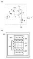
- 光電変換素子が設けられた画素領域と、周辺回路を構成するための周辺MOSトランジスタのゲート電極が設けられた周辺回路領域と、スクライブ領域と、を有するウエハを用意する工程と、
前記画素領域、前記周辺回路領域及び前記スクライブ領域を覆う絶縁膜を形成する工程と、
前記絶縁膜のうちの前記画素領域を覆う部分及び前記スクライブ領域を覆う部分を残すように、前記絶縁膜をエッチングして、前記ゲート電極の側面の上にサイドウォールスペーサを形成する工程と、
前記絶縁膜をシリサイド化から保護するためのマスクとして使って、前記周辺MOSトランジスタに金属シリサイド層を形成する工程と、
前記金属シリサイド層が形成された前記周辺MOSトランジスタを覆う第2の絶縁膜を形成する工程と、
前記第2の絶縁膜の形成後に層間絶縁膜を形成する工程と、
前記画素領域に残った前記絶縁膜および前記周辺MOSトランジスタを覆っている前記第2の絶縁膜をエッチングストッパとして使って、前記層間絶縁膜に、前記画素領域に設けられた画素MOSトランジスタのための第1のコンタクトホール及び前記周辺MOSトランジスタのための第2のコンタクトホールを形成する工程と、
前記第1のコンタクトホール及び前記第2のコンタクトホールの中にコンタクトプラグを形成する工程と、を含み、
前記金属シリサイド層を形成する工程において、前記スクライブ領域を覆う前記絶縁膜の面積は、前記スクライブ領域の面積の99%以上であることを特徴とする固体撮像装置の製造方法。 - 光電変換素子が設けられた画素領域と、周辺回路を構成するための周辺MOSトランジスタのゲート電極が設けられた周辺回路領域と、スクライブ領域と、を有するウエハを用意する工程と、
前記画素領域、前記周辺回路領域及び前記スクライブ領域を覆う絶縁膜を形成する工程と、
前記絶縁膜のうちの前記画素領域を覆う部分及び前記スクライブ領域を覆う部分を残すように、前記絶縁膜をエッチングして、前記ゲート電極の側面の上にサイドウォールスペーサを形成する工程と、
前記絶縁膜をシリサイド化から保護するためのマスクとして使って、前記周辺MOSトランジスタに金属シリサイド層を形成する工程と、
前記ウエハを前記スクライブ領域でダイシングすることによりチップを作製する工程と、
前記金属シリサイド層が形成された前記周辺MOSトランジスタを覆う第2の絶縁膜を形成する工程と、
前記第2の絶縁膜の形成後に層間絶縁膜を形成する工程と、
前記画素領域に残った前記絶縁膜および前記周辺MOSトランジスタを覆っている前記第2の絶縁膜をエッチングストッパとして使って、前記層間絶縁膜に、前記画素領域に設けられた画素MOSトランジスタのための第1のコンタクトホール及び前記周辺MOSトランジスタのための第2のコンタクトホールを形成する工程と、
前記第1のコンタクトホール及び前記第2のコンタクトホールの中にコンタクトプラグを形成する工程と、を含み、 前記チップの端面に金属シリサイド層が露出していないことを特徴とする固体撮像装置の製造方法。 - 前記絶縁膜は、酸化シリコン及び窒化シリコンを含む積層膜であることを特徴とする請求項1または2に記載の固体撮像装置の製造方法。
- 前記第2の絶縁膜は、窒化シリコン膜であることを特徴とする請求項1乃至3のいずれか1項に記載の固体撮像装置の製造方法。
- 前記サイドウォールスペーサを形成する前記工程では、前記絶縁膜の少なくとも前記光電変換素子を覆う部分を残すことを特徴とする請求項1乃至4のいずれか1項に記載の固体撮像装置の製造方法。
- 前記ウエハを用意する工程では、前記画素領域に前記光電変換素子で生じた電荷をリセットするため、または、前記光電変換素子の電荷に基づく信号を増幅するための画素MOSトランジスタのゲート電極が設けられており、
前記サイドウォールスペーサを形成する前記工程では、前記絶縁膜の前記画素MOSトランジスタの前記ゲート電極の上面を覆う部分を残すことを特徴とする請求項1乃至5のいずれか1項に記載の固体撮像装置の製造方法。 - 前記サイドウォールスペーサを形成する前記工程では、前記絶縁膜の前記スクライブ領域の一部を覆う部分を除去し、前記金属シリサイド層を形成する工程では、前記スクライブ領域に、金属シリサイド層を有するアライメントマークを形成することを特徴とする請求項1乃至6のいずれか1項に記載の固体撮像装置の製造方法。
- 各々が光電変換素子を有する複数の画素を含む画素領域と、MOSトランジスタを含む周辺回路領域と、を有するチップを備える固体撮像装置であって、
前記周辺回路領域は前記チップの端面と前記画素領域との間に配置されており、
前記MOSトランジスタは金属シリサイド層を含み、前記MOSトランジスタのゲート電極の側面にはサイドウォールスペーサが配置されており、
前記光電変換素子は、前記サイドウォールスペーサを構成する材料と同じ材料からなる絶縁層を含む第1絶縁膜で覆われ、前記チップの端面の一部は前記サイドウォールスペーサを構成する材料と同じ材料からなる絶縁層を含む第2絶縁膜で構成されており、前記MOSトランジスタは、第3絶縁膜で覆われ、
前記光電変換素子は、前記第1絶縁膜を介して層間絶縁膜で覆われ、前記MOSトランジスタは、前記第3絶縁膜を介して前記層間絶縁膜で覆われ、
前記第3絶縁膜は、前記端面まで延在せず、かつ、前記画素領域を覆わないように配置され、
前記第2絶縁膜に含まれる前記絶縁層の厚さが前記第1絶縁膜に含まれる前記絶縁層の厚さの99%以上101%以下であることを特徴とする固体撮像装置。 - 金属シリサイドが前記チップの前記端面を構成しないことを特徴とする請求項8に記載の固体撮像装置。
- 前記材料は窒化シリコンであり、前記第3絶縁膜は窒化シリコン膜であることを特徴とする請求項8または9に記載の固体撮像装置。
- 前記画素領域における前記第1絶縁膜は前記画素領域のMOSトランジスタに接続されるコンタクトプラグに接することを特徴とする請求項8乃至10のいずれか1項に記載の固体撮像装置。
- 前記周辺回路領域にはSTI型の素子分離部が設けられており、
前記素子分離部は前記チップの前記端面を構成しないことを特徴とする請求項8乃至11のいずれか1項に記載の固体撮像装置。 - 前記第1絶縁膜は前記画素領域のリセットMOSトランジスタを覆うことを特徴とする請求項8乃至12のいずれか1項に記載の固体撮像装置。
- 前記第2絶縁膜は前記サイドウォールスペーサを覆わないことを特徴とする請求項8乃至13のいずれか1項に記載の固体撮像装置。
- 前記金属シリサイド層に接続し、前記層間絶縁膜および前記第3絶縁膜に設けられたコンタクトホールの中に配置されたコンタクトプラグを有することを特徴とする請求項8乃至14のいずれか1項に記載の固体撮像装置。
- 前記金属シリサイド層を覆う窒化シリコン層を形成する工程と、
前記画素領域、前記周辺回路領域及び前記スクライブ領域を覆う層間絶縁膜を形成する工程と、
前記金属シリサイド層の上において、前記層間絶縁膜および前記窒化シリコン層にコンタクトホールを形成し、前記コンタクトホールの中にコンタクトプラグを形成する工程と、を有し、
前記窒化シリコン層は層間絶縁膜のうちの前記スクライブ領域の上の部分と前記絶縁膜との間に存在しないことを特徴とする請求項1乃至7のいずれか1項に記載の固体撮像装置の製造方法。
Priority Applications (3)
| Application Number | Priority Date | Filing Date | Title |
|---|---|---|---|
| JP2014122747A JP6362093B2 (ja) | 2014-06-13 | 2014-06-13 | 固体撮像装置の製造方法及び固体撮像装置 |
| US14/722,681 US10026774B2 (en) | 2014-06-13 | 2015-05-27 | Method of manufacturing solid-state image sensor and solid-state image sensor |
| CN201510320636.9A CN105321970A (zh) | 2014-06-13 | 2015-06-12 | 制造固态图像传感器的方法和固态图像传感器 |
Applications Claiming Priority (1)
| Application Number | Priority Date | Filing Date | Title |
|---|---|---|---|
| JP2014122747A JP6362093B2 (ja) | 2014-06-13 | 2014-06-13 | 固体撮像装置の製造方法及び固体撮像装置 |
Publications (3)
| Publication Number | Publication Date |
|---|---|
| JP2016004838A JP2016004838A (ja) | 2016-01-12 |
| JP2016004838A5 JP2016004838A5 (ja) | 2017-07-13 |
| JP6362093B2 true JP6362093B2 (ja) | 2018-07-25 |
Family
ID=54836838
Family Applications (1)
| Application Number | Title | Priority Date | Filing Date |
|---|---|---|---|
| JP2014122747A Active JP6362093B2 (ja) | 2014-06-13 | 2014-06-13 | 固体撮像装置の製造方法及び固体撮像装置 |
Country Status (3)
| Country | Link |
|---|---|
| US (1) | US10026774B2 (ja) |
| JP (1) | JP6362093B2 (ja) |
| CN (1) | CN105321970A (ja) |
Families Citing this family (5)
| Publication number | Priority date | Publication date | Assignee | Title |
|---|---|---|---|---|
| US9935140B2 (en) | 2015-05-19 | 2018-04-03 | Canon Kabushiki Kaisha | Solid state imaging device, manufacturing method of solid state imaging device, and imaging system |
| KR102432776B1 (ko) * | 2015-10-08 | 2022-08-17 | 에스케이하이닉스 주식회사 | 반도체 장치의 제조방법 |
| JP2018006443A (ja) * | 2016-06-29 | 2018-01-11 | ルネサスエレクトロニクス株式会社 | 半導体装置およびその製造方法 |
| JP2019004029A (ja) * | 2017-06-14 | 2019-01-10 | キヤノン株式会社 | 半導体装置の製造方法 |
| CN108063146A (zh) * | 2017-12-15 | 2018-05-22 | 上海华力微电子有限公司 | Cmos图像传感器的制造方法 |
Family Cites Families (14)
| Publication number | Priority date | Publication date | Assignee | Title |
|---|---|---|---|---|
| JP2518100B2 (ja) * | 1990-11-22 | 1996-07-24 | 三菱電機株式会社 | 半導体装置の製造方法 |
| JP2003017557A (ja) * | 2001-07-04 | 2003-01-17 | Denso Corp | 半導体装置及びその製造方法 |
| KR100695876B1 (ko) | 2005-06-24 | 2007-03-19 | 삼성전자주식회사 | 오버레이 키 및 그 형성 방법, 오버레이 키를 이용하여형성된 반도체 장치 및 그 제조 방법. |
| JP5110820B2 (ja) * | 2006-08-02 | 2012-12-26 | キヤノン株式会社 | 光電変換装置、光電変換装置の製造方法及び撮像システム |
| JP2008098373A (ja) * | 2006-10-11 | 2008-04-24 | Matsushita Electric Ind Co Ltd | 固体撮像素子およびその製造方法 |
| JP4873001B2 (ja) | 2008-12-10 | 2012-02-08 | ソニー株式会社 | 固体撮像装置とその製造方法、電子機器並びに半導体装置 |
| JP2010161236A (ja) * | 2009-01-08 | 2010-07-22 | Canon Inc | 光電変換装置の製造方法 |
| JP5428395B2 (ja) * | 2009-03-04 | 2014-02-26 | ソニー株式会社 | 固体撮像装置およびその製造方法、および撮像装置 |
| JP5717357B2 (ja) * | 2010-05-18 | 2015-05-13 | キヤノン株式会社 | 光電変換装置およびカメラ |
| JP5704848B2 (ja) * | 2010-06-30 | 2015-04-22 | キヤノン株式会社 | 固体撮像装置およびカメラ |
| JP2012094718A (ja) | 2010-10-27 | 2012-05-17 | Fujitsu Semiconductor Ltd | 半導体装置 |
| JP2012182426A (ja) | 2011-02-09 | 2012-09-20 | Canon Inc | 固体撮像装置、固体撮像装置を用いた撮像システム及び固体撮像装置の製造方法 |
| JP5933953B2 (ja) * | 2011-10-06 | 2016-06-15 | キヤノン株式会社 | 半導体装置の製造方法 |
| JP5880243B2 (ja) * | 2012-04-18 | 2016-03-08 | 富士通セミコンダクター株式会社 | 半導体装置とその製造方法 |
-
2014
- 2014-06-13 JP JP2014122747A patent/JP6362093B2/ja active Active
-
2015
- 2015-05-27 US US14/722,681 patent/US10026774B2/en active Active
- 2015-06-12 CN CN201510320636.9A patent/CN105321970A/zh active Pending
Also Published As
| Publication number | Publication date |
|---|---|
| JP2016004838A (ja) | 2016-01-12 |
| US10026774B2 (en) | 2018-07-17 |
| CN105321970A (zh) | 2016-02-10 |
| US20150364517A1 (en) | 2015-12-17 |
Similar Documents
| Publication | Publication Date | Title |
|---|---|---|
| JP2015109343A (ja) | 半導体装置の製造方法 | |
| JP6362093B2 (ja) | 固体撮像装置の製造方法及び固体撮像装置 | |
| JP5991729B2 (ja) | 固体撮像装置の製造方法 | |
| JP4490407B2 (ja) | Cmosイメージセンサとその製造方法 | |
| JP6612139B2 (ja) | 半導体装置 | |
| JP2010212536A (ja) | 固体撮像装置の製造方法 | |
| US20180070041A1 (en) | Solid-state image sensor, method of manufacturing the same, and camera | |
| JP6305030B2 (ja) | 光電変換装置の製造方法 | |
| US10777596B2 (en) | Imaging apparatus, method of manufacturing the same, and device | |
| JP6681150B2 (ja) | 固体撮像装置およびその製造方法ならびにカメラ | |
| JP2006024934A (ja) | Cmosイメージセンサーの製造方法 | |
| US20160126284A1 (en) | Solid-state imaging device and method of manufacturing solid-state imaging device | |
| JP5495524B2 (ja) | 光電変換装置 | |
| JP6341796B2 (ja) | 半導体装置の製造方法 | |
| US10163953B2 (en) | Image pickup device and method of manufacturing the same | |
| JP4115446B2 (ja) | Cmosイメージセンサの製造方法 | |
| WO2013018308A1 (ja) | 固体撮像装置の製造方法 | |
| TWI581409B (zh) | 固態成像裝置,製造固態成像裝置之方法,及成像裝置 | |
| JP2019161216A (ja) | 撮像装置およびその製造方法ならびに機器 | |
| JP2017143159A (ja) | 撮像装置、及びその製造方法 | |
| JP2015109342A (ja) | 撮像装置の製造方法 | |
| JP2014099474A (ja) | 固体撮像装置およびその製造方法ならびにカメラ | |
| JP2007027569A (ja) | 固体撮像装置 |
Legal Events
| Date | Code | Title | Description |
|---|---|---|---|
| A521 | Written amendment |
Free format text: JAPANESE INTERMEDIATE CODE: A523 Effective date: 20170601 |
|
| A621 | Written request for application examination |
Free format text: JAPANESE INTERMEDIATE CODE: A621 Effective date: 20170601 |
|
| A131 | Notification of reasons for refusal |
Free format text: JAPANESE INTERMEDIATE CODE: A131 Effective date: 20180213 |
|
| A977 | Report on retrieval |
Free format text: JAPANESE INTERMEDIATE CODE: A971007 Effective date: 20180215 |
|
| A521 | Written amendment |
Free format text: JAPANESE INTERMEDIATE CODE: A523 Effective date: 20180410 |
|
| TRDD | Decision of grant or rejection written | ||
| A01 | Written decision to grant a patent or to grant a registration (utility model) |
Free format text: JAPANESE INTERMEDIATE CODE: A01 Effective date: 20180521 |
|
| A61 | First payment of annual fees (during grant procedure) |
Free format text: JAPANESE INTERMEDIATE CODE: A61 Effective date: 20180619 |
|
| R151 | Written notification of patent or utility model registration |
Ref document number: 6362093 Country of ref document: JP Free format text: JAPANESE INTERMEDIATE CODE: R151 |